

Page 1
M
Charge Pump DC-to-DC Voltage Converter
TC7660
Features
• Wide Input Voltage Range: +1.5V to +10V
• Efficient Voltage Conversion (99.9%, typ)
• Excellent Power Efficiency (98%, typ)
• Low Power Consumption: 80 µA (typ) @ V
• Low Cost and Easy to Use
- Only Two External Capacitors Required
• Available in 8-Pin Small Outline (SOIC), 8-Pin
PDIP and 8-Pin CERDIP Packages
• Improved ESD Protection (3 kV HBM)
• No External Diode Required for High-Voltage
Operation
IN
= 5V
Applications
• RS-232 Negative Power Supply
• Simple Conversion of +5V to ±5V Supplies
• Voltage Multiplication V
• Negative Supplies for Data Acquisition Systems
and Instrumentation
OUT
= ± n V
+
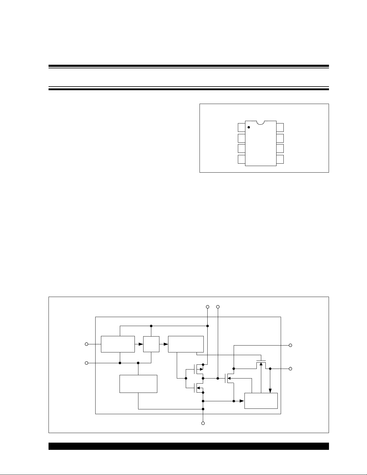
Functional Block Diagram
Package Types
PDIP/CERDIP/SOIC
+
8
V
7
OSC
LOW
6
VOLTAGE (LV)
5
V
OUT
CAP
GND
CAP
NC
1
+
2
TC7660
3
-
4
General Description
The TC7660 is a pin-compatible replacement for the
industry standard 7660 charge pump voltage
converter. It converts a +1.5V to +10V input to a
corresponding -1.5V to -10V output using only two low
cost capacitors, eliminating inductors and their
associated cost, size and electromagnetic interference
(EMI).
The on-board oscillator operates at a nominal
frequency of 10 kHz. Operation below 10 kHz (for
lower supply current applications) is possible by
connecting an external capacitor from OSC to ground.
The TC7660 is available in 8-Pin PDIP, 8-Pin Small
Outline (SOIC) and 8-Pin CERDIP packages in
commercial and extended temperature ranges.
+
+
V
CAP
82
OSC
LV
7
6
RC
Oscillator
Internal
Internal
Vol t age
Vol t age
Regulator
Regulator
÷
2
TC7660
2002 Microchip Technology Inc. DS21465B-page 1
Vol t age
Level
Translator
3
GND
Logic
Network
4
CAP-
5
V
OUT
Page 2
TC7660
1.0 ELECTRICAL CHARACTERISTICS
Absolute Maximum Ratings*
Supply Voltage .............................................................+10.5V
LV and OSC Inputs Voltage: (Note 1)
.............................................. -0.3V to V
..................................... (V
+
– 5.5V) to (V+) for V+ > 5.5V
Current into LV ......................................... 20 µA for V
Output Short Duration (V
Package Power Dissipation: (T
8-Pin CERDIP ....................................................800 mW
≤ 5.5V)............... Continuous
SUPPLY
≤ 70°C)
A
8-Pin PDIP .........................................................730 mW
8-Pin SOIC .........................................................470 mW
Operating Temperature Range:
C Suffix....................................................... 0°C to +70°C
I Suffix .....................................................-25°C to +85°C
E Suffix ....................................................-40°C to +85°C
M Suffix .................................................-55°C to +125°C
Storage Temperature Range .........................-65°C to +160°C
ESD protection on all pins (HBM) ................... ..............≥ 3kV
Maximum Junction Temperature ........... ....................... 150°C
for V+ < 5.5V
SS
+
> 3.5V
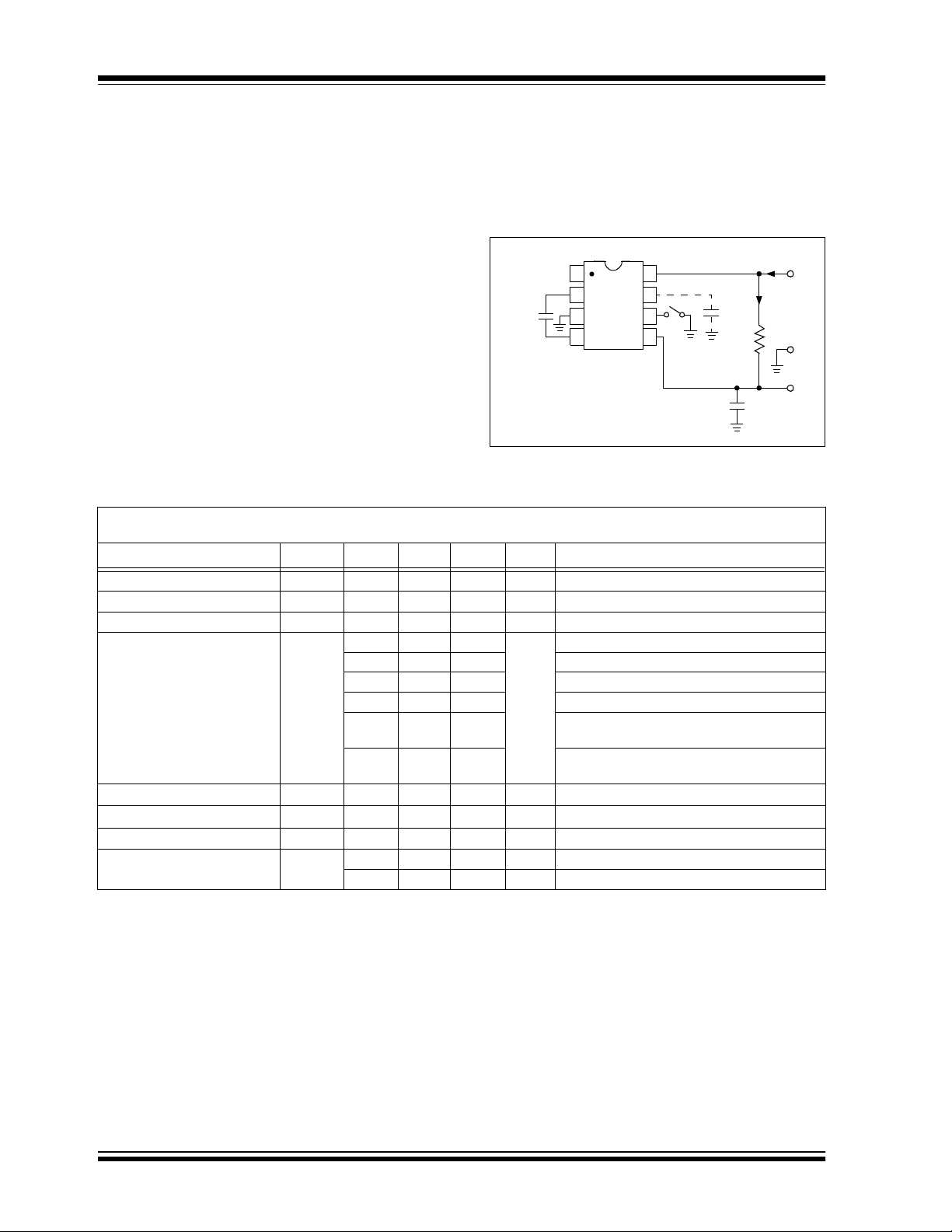
ELECTRICAL SPECIFICATIONS
Electrical Characteristics: Unless otherwise noted, specifications measured over operating temperature range with V+ = 5V,
C
= 0, refer to test circuit in Figure 1-1.
OSC
Parameters Sym Min Typ Max Units Conditions
R
OUT
f
OSC
P
EFF
V
OUTEFF
Z
OSC
+
I
+
H
+
L
Supply Current
Supply Voltage Range, High V
Supply Voltage Range, Low V
Output Source Resistance
Oscillator Frequency
Power Efficiency
Voltage Conversion Efficiency
Oscillator Impedance
Note 1: Destructive latch-up may occur if voltages greater than V
—80180µAR
3.0 — 10 V Min ≤ TA ≤ Max, RL = 10 kΩ, LV Open
1.5 — 3.5 V Min ≤ T
—70100Ω I
——120 I
——130 I
—104150 I
—150300 V
—160600 V
— 10 — kHz Pin 7 open
95 98 — % RL = 5 kΩ
97 99.9 — % RL = ∞
—1.0—MΩ V+ = 2V
—100—kΩ V
* Notice: Stresses above those listed under "Maximum Ratings" may cause permanent damage to the device. This is a
stress rating only and functional operation of the device at
those or any other conditions above those indicated in the
operational sections of this specification is not intended. Exposure to maximum rating conditions for extended periods may
affect device reliability.
I
C
10 µF
1
2
+
3
TC7660
1
4
8
7
6
5
C
OSC
+
I
L
R
C
2
10 µF
FIGURE 1-1: TC7660 Test Circuit.
= ∞
L
≤ Max, R
A
=20 mA, TA = +25°C
OUT
=20 mA, TA ≤ +70°C (C Device)
OUT
=20 mA, TA ≤ +85°C (E and I Device)
OUT
=20 mA, TA ≤ +125°C (M Device)
OUT
+
= 2V, I
+
= 2V, I
+
= 5V
OUT
≤ +70°C
A
OUT
A
0°C ≤ T
-55°C ≤ T
+
or less than GND are supplied to any input pin.
= 10 kΩ, LV to GND
L
= 3 mA, LV to GND
= 3 mA, LV to GND
≤ +125°C (M Device)
S
V
(+5V)
L
V
+
OUT
DS21465B-page 2 2002 Microchip Technology Inc.
Page 3
TC7660
5
0+25+75+100
5
50-55
)
SU
GE
k
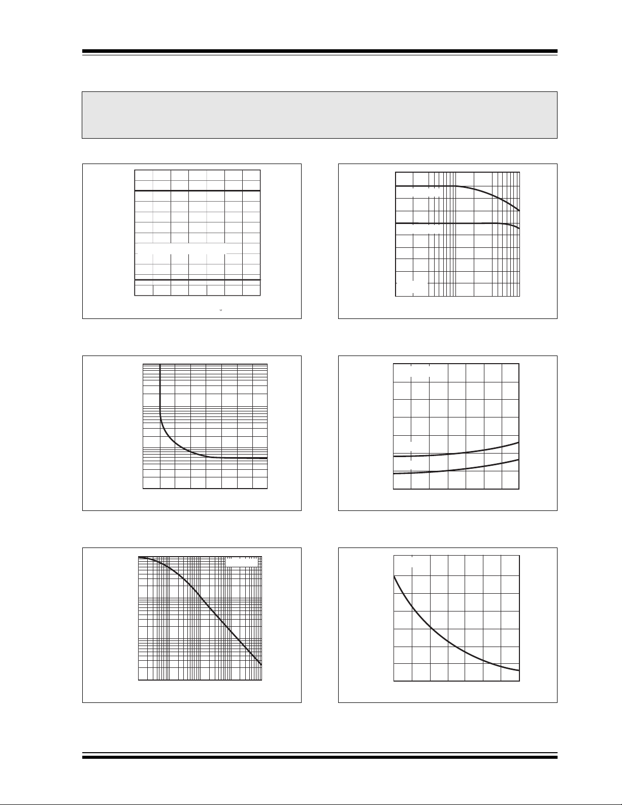
2.0 TYPICAL PERFORMANCE CURVES
Note: The graphs and tables provided following this note are a statistical summary based on a limited number of
samples and are provided for informational purposes only. The performance characteristics listed herein
are not tested or guaranteed. In some graphs or tables, the data presented may be outside the specified
operating range (e.g., outside specified power supply range) and therefore outside the warranted range.
Note: Unless otherwise indicated, C
12
10
8
6
PPLY VOLTAGE RAN
4
SUPPLY VOLTAGE (V)
2
0
-2
TEMPERATURE (C
+
= C2 = 10 µF, ESRC1 = ESRC2 = 1 Ω, TA = 25°C. See Figure 1-1.
1
+12
FIGURE 2-1: Operating Voltage vs. Temperature.
10k
1k
100Ω
OUTPUT SOURCE RESISTANCE (Ω)
10Ω
SUPPLY VOLTAGE (V)
7 8
6543210
FIGURE 2-2: Output Source Resistance vs. Supply Voltage.
100
98
I
= 1 mA
OUT
96
94
92
I
= 15 mA
OUT
90
88
86
84
82
V+ = +5V
POWER CONVERSION EFFICIENCY (%)
80
100 1k
OSCILLATOR FREQUENCY (Hz)
10
FIGURE 2-4: Power Conversion Efficiency vs. Oscillator Frequency.
500
I
= 1 mA
OUT
450
400
200
150
V+ = +2V
100
V + = +5V
50
OUTPUT SOURCE RESISTANCE (Ω)
0
-55 -25 0 +25 +50 +75 +100 +125
TEMPERATURE (°C)
FIGURE 2-5: Output Source Resistance vs. Temperature.
10k
1k
100
OSCILLATOR FREQUENCY (Hz)
10
1
10 100 1000 10k
OSCILLATOR CAPACITANCE (pF)
V+ = +5V
FIGURE 2-3: Frequency of Oscillation vs. Oscillator Capacitance.
FIGURE 2-6: Unloaded Oscillator Frequency vs. Temperature.
20
V+ = +5V
18
16
14
12
10
8
OSCILLATOR FREQUENCY (kHz)
6
-55
-25 0 +25 +50 +75 +100 +125
TEMPERATURE (°C)
2002 Microchip Technology Inc. DS21465B-page 3
Page 4
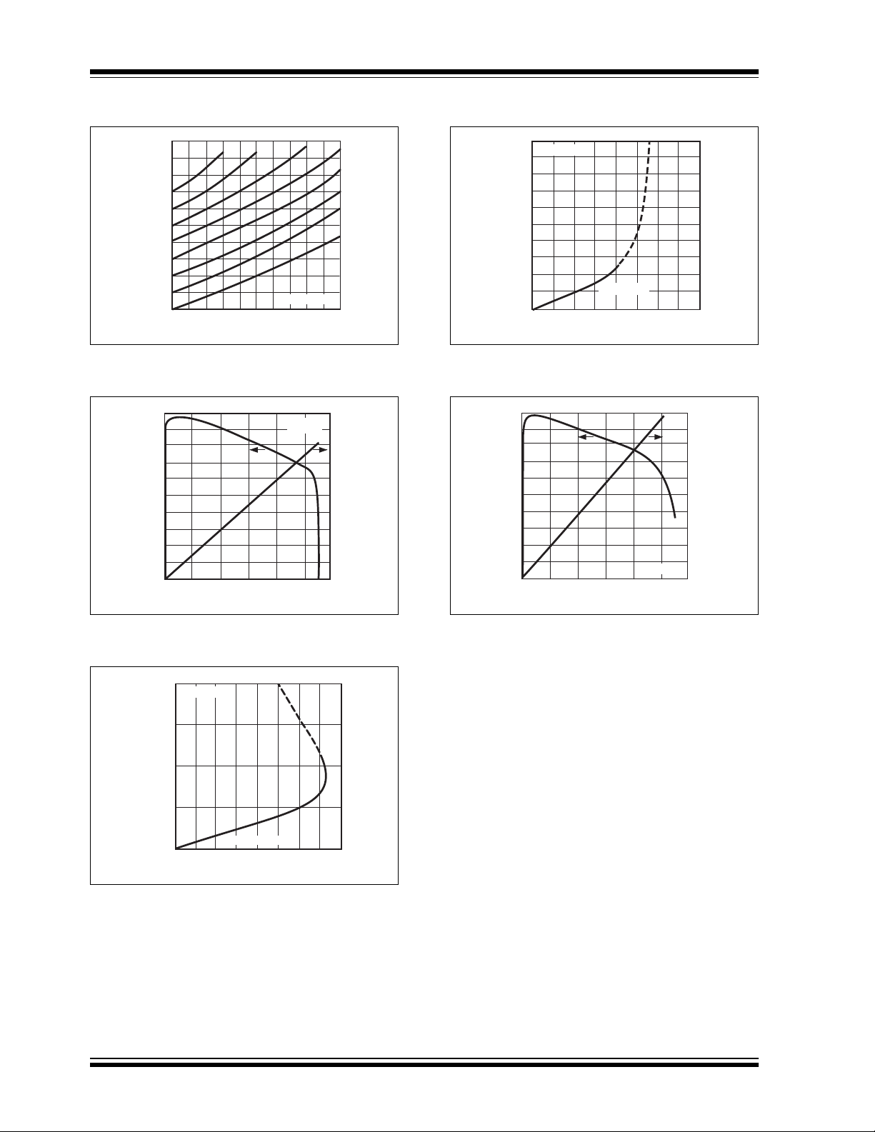
TC7660
Note: Unless otherwise indicated, C
0
-1
-2
-3
-4
-5
-6
-7
OUTPUT VOLTAGE (V)
-8
-9
-10
0
10 20 30 40 50 60 70 80 90 100
OUTPUT CURRENT (mA)
= C2 = 10 µF, ESRC1 = ESRC2 = 1 Ω, TA = 25°C. See Figure 1-1.
1
LV OPEN
FIGURE 2-7: Output Voltage vs. Output Current.
100
90
80
70
60
50
40
30
20
10
POWER CONVERSION EFFICIENCY (%)
0
1.5 3.0 4.5 6.0 7.5 9.0
LOAD CURRENT (mA)
V+ = 2V
20
18
16
14
12
10
8
6
SUPPLY CURRENT (mA)
4
2
0
5
V+ = +5V
4
3
2
1
0
-1
-2
OUTPUT VOLTAGE (V)
-3
SLOPE 55
-4
-5
0
10 20 30 40 50 60 70 80
LOAD CURRENT (mA)
Ω
FIGURE 2-10: Output Voltage vs. Load Current.
100
90
80
70
60
50
40
30
20
10
POWER CONVERSION EFFICIENCY (%)
0
10 20 30 40 50 60
LOAD CURRENT (mA)
V+ = +5V
100
90
80
70
60
50
40
30
SUPPLY CURRENT (mA)
20
10
0
FIGURE 2-8: Supply Current and Power Conversion Efficiency vs. Load Current.
2
V+ = +2V
1
0
-1
OUTPUT VOLTAGE (V)
-2
0
SLOPE 150Ω
123 4 5 67 8
LOAD CURRENT (mA)
FIGURE 2-9: Output Voltage vs. Load Current.
FIGURE 2-11: Supply Current and Power Conversion Efficiency vs. Load Current.
DS21465B-page 4 2002 Microchip Technology Inc.
Page 5
3.0 PIN DESCRIPTIONS
The descriptions of the pins are listed in Table 3-1.
TABLE 3-1: PIN FUNCTION TABLE
Pin No. Symbol Description
1 NC No connection
2CAP
3 GND Ground terminal
4CAP
5V
6 LV Low voltage pin. Connect to GND for V+ < 3.5V
7 OSC Oscillator control input. Bypass with an external capacitor to slow the oscillator
8V
OUT
+
+
Charge pump capacitor positive terminal
-
Charge pump capacitor negative terminal
Output voltage
Power supply positive voltage input
TC7660
3.1 Charge Pump Capacitor (CAP+)
Positive connection for the charge pump capacitor, or
flying capacitor, used to transfer charge from the input
source to the output. In the voltage-inverting configuration, the charge pump capacitor is charged to the input
voltage during the first half of the switching cycle. During the second half of the switching cycle, the charge
pump capacitor is inverted and charge is transferred to
the output capacitor and load.
It is recommended that a low ESR (equivalent series
resistance) capacitor be used. Additionally, larger
values will lower the output resistance.
3.2 Ground (GND)
Input and output zero volt reference.
3.3 Charge Pump Capacitor (CAP-)
Negative connection for the charge pump capacitor, or
flying capacitor, used to transfer charge from the input
to the output. Proper orientation is imperative when
using a polarized capacitor.
3.4 Output Voltage (V
Negative connection for the charge pump output
capacitor. In the voltage-inverting configuration, the
charge pump output capacitor supplies the output load
during the first half of the switching cycle. During the
second half of the switching cycle, charge is restored to
the charge pump output capacitor.
It is recommended that a low ESR (equivalent series
resistance) capacitor be used. Additionally, larger
values will lower the output ripple.
OUT
)
3.5 Low Voltage Pin (LV)
The low voltage pin ensures proper operation of the
internal oscillator for input voltages below 3.5V. The low
voltage pin should be connected to ground (GND) for
input voltages below 3.5V. Otherwise, the low voltage
pin should be allowed to float.
3.6 Oscillator Control Input (OSC)
The oscillator control input can be utilized to slow down
or speed up the operation of the TC7660. Refer to
Section 5.4, “Changing the TC7660 Oscillator
Frequency”, for details on altering the oscillator
frequency.
3.7 Power Supply (V+)
Positive power supply input voltage connection. It is
recommended that a low ESR (equivalent series resistance) capacitor be used to bypass the power supply
input to ground (GND).
2002 Microchip Technology Inc. DS21465B-page 5
Page 6
TC7660
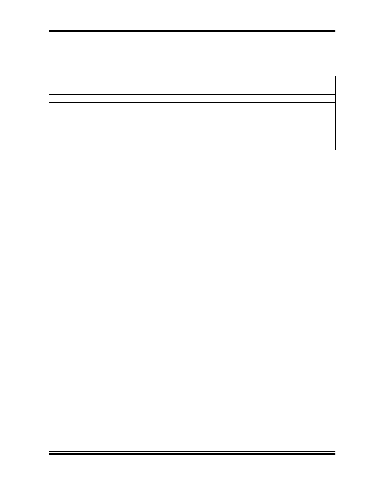
4.0 DETAILED DESCRIPTION
4.1 Theory of Operation
The TC7660 charge pump converter inverts the voltage
applied to the V
phase operation (Figure 4-1). During the first phase,
switches S
are closed. C1 charges to the voltage applied to the V
pin, with the load current being supplied from C2. During the second phase, switches S
and switches S
ferred from C
supplied from C
+
V
GND
FIGURE 4-1: Ideal Switched Capacitor Inverter.
In this manner, the TC7660 performs a voltage inversion, but does not provide regulation. The average output voltage will drop in a linear manner with respect to
load current. The equivalent circuit of the charge pump
inverter can be modeled as an ideal voltage source in
series with a resistor, as shown in Figure 4-2.
FIGURE 4-2: Switched Capacitor Inverter Equivalent Circuit Model.
The value of the series resistor (R
the switching frequency, capacitance and equivalent
series resistance (ESR) of C
tance of switches S
approximation for R
equation:
+
pin. The conversion consists of a two-
and S4 are open and switches S1 and S
2
and S4 are closed
and S3 are open. Charge is trans-
1
to C2, with the load current being
1
.
1
S
1
S
3
S
2
+
C
1
S
4
R
OUT
2
+
C
2
V
= -V
OUT
V
OUT
-
+
V
+
) is a function of
OUT
and C2 and the on-resis-
1
, S2, S3 and S4. A close
1
is given in the following
OUT
IN
EQUATION
1
R
OUT
--------- ------------- -------
f
PUMP
C1×
++ +=
8R
4ESRC1ESR
SW
C2
Where:
f
OSC
3
+
f
PUMP
R
SW
ESR
ESR
-----------
=
2
on-resistance of the switches=
equivalent series resistance of C
=
C1
equivalent series resistance of C
=
C2
1
2
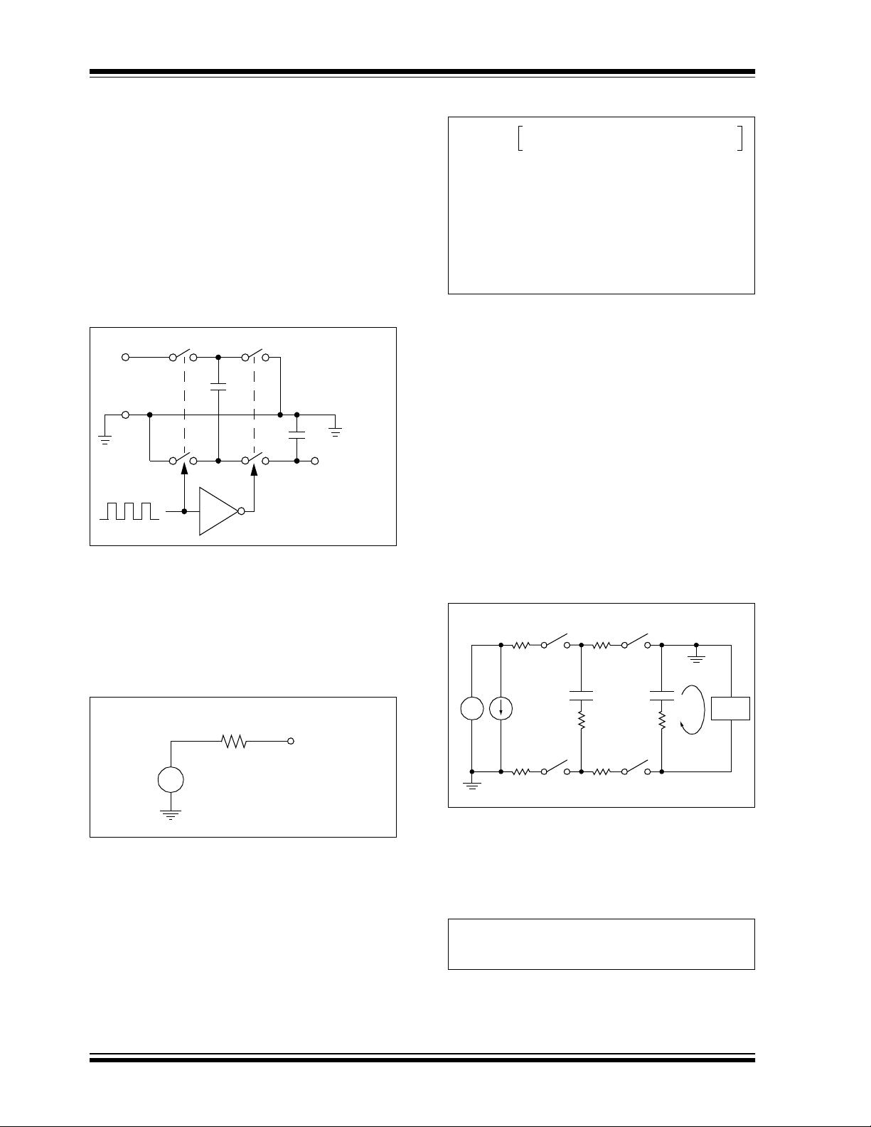
4.2 Switched Capacitor Inverter Power Losses
The overall power loss of a switched capacitor inverter
is affected by four factors:
1. Losses from power consumed by the internal
oscillator, switch drive, etc. These losses will
vary with input voltage, temperature and
oscillator frequency.
2. Conduction losses in the non-ideal switches.
3. Losses due to the non-ideal nature of the
external capacitors.
4. Losses that occur during charge transfer from
C
to C2 when a voltage difference between the
1
capacitors exists.
Figure 4-3 depicts the non-ideal elements associated
with the switched capacitor inverter power loss.
S
SW
SW
1
++
C
1
ESR
C1
S
3
R
+
V
I
DD
+
-
R
FIGURE 4-3: Non-Ideal Switched Capacitor Inverter.
The power loss is calculated using the following
equation:
EQUATION
P
LOSSIOUT
2
× I
S
SW
SW
OUT
ESR
2
C
2
I
LOAD
OUT
C2
S
4
V+×+=
DD
R
R
R
DS21465B-page 6 2002 Microchip Technology Inc.
Page 7

TC7660
5.0 APPLICATIONS INFORMATION
5.1 Simple Negative Voltage Converter
Figure 5-1 shows typical connections to provide a
negative supply where a positive supply is available. A
similar scheme may be employed for supply voltages
anywhere in the operating range of +1.5V to +10V,
keeping in mind that pin 6 (LV) is tied to the supply
negative (GND) only for supply voltages below 3.5V.
+
V
1
2
+
C
1
10 µF
* V
= -V+ for 1.5V ≤ V+ ≤ 10V
OUT
3
4
TC7660
FIGURE 5-1: Simple Negative Converter.
The output characteristics of the circuit in Figure 5-1
are those of a nearly ideal voltage source in series with
a 70Ω resistor. Thus, for a load current of -10 mA and
a supply voltage of +5V, the output voltage would be
-4.3V.
8
7
6
5
+
V
C
2
10 µF
OUT
*
5.2 Paralleling Devices
To reduce the value of R
converters can be connected in parallel (Figure 5-2).
The output resistance will be reduced by approximately
a factor of n, where n is the number of devices
connected in parallel.
EQUATION
R
=
OUT
While each device requires its own pump capacitor
(C
), all devices may share one reservoir capacitor
1
(C
). To preserve ripple performance, the value of C
2
should be scaled according to the number of devices
connected in parallel.
, multiple TC7660 voltage
OUT
R
of TC7660()
OUT
------------- ------------- ------------- ------------
n number of devices()
5.3 Cascading Devices
A larger negative multiplication of the initial supply voltage can be obtained by cascading multiple TC7660
devices. The output voltage and the output resistance
will both increase by approximately a factor of n, where
n is the number of devices cascaded.
EQUATION
R
OUT
V
OUT
nR×
n– V+()=
OUT
of TC7660()=
2
+
V
“1”
8
7
6
C
5
1
1
2
+
TC7660
3
4
“n”
1
2
+
C
1
TC7660
3
4
FIGURE 5-2: Paralleling Devices Lowers Output Impedance.
+
V
“1”
8
7
6
5
10 µF
+
10 µF
1
2
+
TC7660
3
4
“n”
10 µF
* V
1
2
+
TC7660
3
4
= -n V+ for 1.5V ≤ V+ ≤ 10V
OUT
8
7
R
L
6
5
C
2
+
8
7
6
V
5
10 µF
+
OUT
*
FIGURE 5-3: Increased Output Voltage By Cascading Devices.
2002 Microchip Technology Inc. DS21465B-page 7
Page 8

TC7660
5.4 Changing the TC7660 Oscillator Frequency
The operating frequency of the TC7660 can be
changed in order to optimize the system performance.
The frequency can be increased by over-driving the
OSC input (Figure 5-4). Any CMOS logic gate can be
utilized in conjunction with a 1 kΩ series resistor. The
resistor is required to prevent device latch-up. While
TTL level signals can be utilized, an additional 10 kΩ
pull-up resistor to V
the rising edge of the clock input. The resultant output
voltage ripple frequency is one half the clock input.
Higher clock frequencies allow for the use of smaller
pump and reservoir capacitors for a given output voltage ripple and droop. Additionally, this allows the
TC7660 to be synchronized to an external clock, eliminating undesirable beat frequencies.
At light loads, lowering the oscillator frequency can
increase the efficiency of the TC7660 (Figure 5-5). By
lowering the oscillator frequency, the switching losses
are reduced. Refer to Figure 2-3 to determine the typical operating frequency based on the value of the
external capacitor. At lower operating frequencies, it
may be necessary to increase the values of the pump
and reservoir capacitors in order to maintain the
desired output voltage ripple and output impedance.
10 µF
+
FIGURE 5-4: External Clocking.
1
2
+
C
1
3
4
+
is required. Transitions occur on
+
V
1
2
TC7660
3
4
“1”
8
1kΩ
7
6
5
8
7
TC7660
6
5
+
V
10 µF
+
+
CMOS
GATE
V
OUT
+
V
C
OSC
C
2
V
OUT
5.5 Positive Voltage Multiplication
Positive voltage multiplication can be obtained by
employing two external diodes (Figure 5-6). Refer to
the theory of operation of the TC7660 (Section 4.1).
During the half cycle when switch S
tor C
of Figure 5-6 is charged up to a voltage of
1
+
V
- VF1, where VF1 is the forward voltage drop of diode
D
. During the next half cycle, switch S1 is closed, shift-
1
ing the reference of capacitor C
energy in capacitor C
is transferred to capacitor C
1
is closed, capaci-
2
from GND to V+. The
1
through diode D2, producing an output voltage of
approximately:
EQUATION
+
2V
× VF1V
+
V
8
7
D
1
6
5
+
+()–=
D
2
C
1
F2
V
=
OUT
(2 V+) - (2 VF)
+
C
2
where:
V
OUT
V
is the forward voltage drop of diode D1
F1
and
V
is the forward voltage drop of diode D2.
F2
1
2
TC7660
3
4
FIGURE 5-6: Positive Voltage Multiplier.
5.6 Combined Negative Voltage Conversion and Positive Supply Multiplication
Simultaneous voltage inversion and positive voltage
multiplication can be obtained (Figure 5-7). Capacitors
C
and C3 perform the voltage inversion, while capaci-
1
tors C
and C4, plus the two diodes, perform the posi-
2
tive voltage multiplication. Capacitors C
the pump capacitors, while capacitors C
the reservoir capacitors for their respective functions.
Both functions utilize the same switches of the TC7660.
As a result, if either output is loaded, both outputs will
drop towards GND.
and C2 are
1
and C4 are
3
2
FIGURE 5-5: Lowering Oscillator Frequency.
DS21465B-page 8 2002 Microchip Technology Inc.
Page 9

+
V
V
1
2
TC7660
3
4
+
C
1
8
7
6
5
+
C
2
+
D
1
V
OUT
D
(2 V+) - (2 VF)
2
+
OUT
+
= -V
C
3
=
C
4
FIGURE 5-7: Combined Negative Converter And Positive Multiplier.
5.7 Efficient Positive Voltage Multiplication/Conversion
Since the switches that allow the charge pumping
operation are bidirectional, the charge transfer can be
performed backwards as easily as forwards.
Figure 5-8 shows a TC7660 transforming -5V to +5V
(or +5V to +10V, etc.). The only problem here is that the
internal clock and switch-drive section will not operate
until some positive voltage has been generated. An initial inefficient pump, as shown in Figure 5-7, could be
used to start this circuit up, after which it will bypass the
other (D
else the diode and resistor shown dotted in Figure 5-8
can be used to "force" the internal regulator on.
and D2 in Figure 5-7 would never turn on), or
1
TC7660
= -V
1MΩ
V
-
-
input
C
10 µF
V
OUT
1
2
+
1
3
4
TC7660
8
7
6
5
FIGURE 5-8: Positive Voltage Conversion.
+
10 µF
2002 Microchip Technology Inc. DS21465B-page 9
Page 10

TC7660
6.0 PACKAGING INFORMATION
6.1 Package Marking Information
8-Lead PDIP (300 mil)
XXXXXX XX
XXXXXN NN
YYWW
8-Lead CERDIP (300 mil)
XXXXXX XX
XXXXXN NN
YYWW
8-Lead SOIC (150 mil)
XXXXXXXX
XXXXYYWW
NNN
Example:
TC7660
CPA061
0221
Example:
TC7660
MJA061
0221
Example:
TC7660
COA0221
061
Legend: XX...X Customer specific information*
YY Year code (last 2 digits of calendar year)
WW Week code (week of January 1 is week ‘01’)
NNN Alphanumeric traceability code
Note: In the event the full Microchip part number cannot be marked on one line, it will
be carried over to the next line thus limiting the number of available characters
for customer specific information.
* Standard marking consists of Microchip part number, year code, week code, traceability code (facility
code, mask rev#, and assembly code). For marking beyond this, certain price adders apply. Please
check with your Microchip Sales Office.
DS21465B-page 10 2002 Microchip Technology Inc.
Page 11

8-Lead Plastic Dual In-line (P) – 300 mil (PDIP)
E1
D
2
TC7660
n
E
β
eB
Number of Pins
Pitch
Top to Seating Plane A .140 .155 .170 3.56 3.94 4.32
Molded Package Thickness A2 .115 .130 .145 2.92 3.30 3.68
Base to Seating Plane A1 .015 0.38
Shoulder to Shoulder Width E .300 .313 .325 7.62 7.94 8.26
Molded Package Width E1 .240 .250 .260 6.10 6.35 6.60
Overall Length D .360 .373 .385 9 .14 9.46 9.78
Tip to Seating Plane L .125 .130 .1 35 3 .18 3.30 3.43
Lead Thickness
Upper Lead Width B1 .045 .058 .070 1.14 1.46 1.78
Lower Lead Width B .014 .018 .022 0.36 0.46 0.56
Overall Row Spacing § eB .310 .370 .430 7.87 9.40 10.92
Mold Draft Angle Top
Mold Draft Angle Bottom
* Controlling Parameter
§ Significant Characteristic
Notes:
Dimensions D and E1 do not include m old flash or protrusions. Mold flash or protrusions shall not exceed
.010” (0.254mm) per side.
JEDEC Equivalent: MS-001
Drawing No. C04-018
Dimension Limits MIN NOM MAX MIN NOM MAX
1
α
A
c
Units INCHES* MILLIMETERS
n
p
c
α
β
.008 .012 .015 0.20 0.29 0.38
A1
B1
B
88
.100 2.54
51015 51015
51015 51015
A2
L
p
2002 Microchip Technology Inc. DS21465B-page 11
Page 12

TC7660
8-Lead Ceramic Dual In-line – 300 mil (CERDIP)
Packaging diagram not available at this time.
DS21465B-page 12 2002 Microchip Technology Inc.
Page 13

8-Lead Plastic Small Outline (SN) – Narrow, 150 mil (SOIC)
E
E1
p
D
2
TC7660
B
Number of Pins
Pitch
Foot Angle
Lead Thickness
Mold Draft Angle Top
Mold Draft Angle Bottom
* Controlling Paramete r
§ Significant Characteristic
Notes:
Dimensions D and E1 do not include mold flash or protrusions. Mold flash or protrusions shall not exceed
.010” (0.254mm) per side.
JEDEC Equivalent: MS-012
Drawing No. C04-057
n
45°
c
β
n
p
φ
c
α
β
1
h
A
φ
L
048048
A1
MILLIMETERSINCHES*Units
1.27.050
α
A2
MAXNOMMINMAXNOMMINDimension Limits
88
1.751.551.35.069.061.053AOverall Height
1.551.421.32.061.056.052A2Molded Package Thickness
0.250.180.10.010.007.004A1Standoff §
6.206.025.79.244.237.228EOverall Width
3.993.913.71.157.154.146E1Molded Package W idth
5.004.904.80.197.193.189DOverall Length
0.510.380.25.020.015.010hChamfer Distance
0.760.620.48.030.025.019LFoot Length
0.250.230.20.010.009.008
0.510.420.33.020.017.013BLead Width
1512015120
1512015120
2002 Microchip Technology Inc. DS21465B-page 13
Page 14

TC7660
NOTES:
DS21465B-page 14 2002 Microchip Technology Inc.
Page 15

TC7660
PRODUCT IDENTIFICATION SYSTEM
To order or obtain information, e.g., on pricing or delivery, refer to the factory or the listed sales office.
PART NO. X /XX
Device
PackageTemper a tur e
Range
Device: TC7660: DC-to-DC Voltage Converter
Temperature Range: C = 0°C to +70°C
Package: PA = Plastic DIP, (300 mil body), 8-lead
E = -40°C to +85°C
I = -25°C to +85°C (CERDIP only)
M = -55°C to +125°C (CERDIP only)
JA = Ceramic DIP, (300 mil body), 8-lead
OA = SOIC (Narrow), 8-lead
OA713 = SOIC (Narrow), 8-lead (Tape and Reel)
Sales and Support
Data Sheets
Products supported by a preliminary Data Sheet may have an errata sheet describing minor operational differences and recommended workarounds. To determine if an errata sheet exists for a particular device, please contact one of the following:
Examples:
a) TC7660COA: Commercial Temp., SOIC
package.
b) TC7660COA713: Tape and Reel, Commercial
Temp., SOIC package.
c) TC7660CPA: Commercial Temp., PDIP
package.
d) TC7660EOA: Extended Temp., SOIC
package.
e) TC7660EOA713: Tape and Reel, Extended
Temp., SOIC package.
f) TC7660EPA: Extended Temp., PDIP
package.
g) TC7660IJA: Industrial Tem p., CERDIP
package
h) TC7660MJA: Military Temp., CERDIP
package.
1. Your local Microchip sales office
2. The Microchip Corporate Literature Center U.S. FAX: (480) 792-7277
3. The Microchip Worldwide Site (www.microchip.com)
Please specify which device, revision of silicon and Data Sheet (include Literature #) you are using.
New Customer Notification System
Register on our web site (www.microchip.com/cn) to receive the most current information on our products.
2002 Microchip Technology Inc. DS21465B-page15
Page 16

TC7660
NOTES:
DS21465B-page 16 2002 Microchip Technology Inc.
Page 17

Note the following details of the code protection feature on Microchip devices:
• Microchip products meet the specification contained in their particular Microchip Data Sheet.
• Microchip believes that its family of products is one of the most secure families of its kind on the market today, when used in the
intended manner and under normal conditions.
• There ar e dishonest and possibly illegal methods used to breach the code protection feature. All of these methods, to our knowledge, require using the Microchip products in a manner outside the operating specifications contained in Microchip's Data
Sheets. Most likely, the person doing so is engaged in theft of intellectual property.
• Microchip is willing to work with the customer who is concerned about the integrity of their code.
• Neither Microchip nor any other semiconductor manufacturer can guarantee the security of their code. Code protection does not
mean that we are guaranteeing the product as “unbreakable.”
Code protection is constantly evolving. We at Microchip are committed to continuously improving the code protection features of our
products.
Information contained in this publication regarding device
applications and the like is intended through suggestion only
and may be superseded by updates. It is your responsibility to
ensure that your application meets with your specifications.
No representation or warranty is given and no liability is
assumed by Microchip Technology Incorporated with respect
to the accuracy or use of such information, or infringement of
patents or other intellectual property rights arising from such
use or otherwise. Use of Microchip’s products as critical components in life support systems is not authorized except with
express written approval by Microchip. No licenses are conveyed, implicitly or otherwise, under any intellectual property
rights.
Trademarks
The Microchip name and logo, the Microchip logo, K
EELOQ
MPLAB, PIC, PICmicro, PICSTART and PRO MATE are
registered trademarks of Microchip Technology Incorporated
in the U.S.A. and other countries.
FilterLab, microID, MXDEV, MXLAB, PICMASTER, SEEVAL
and The Embedded Control Solutions Company are
registered trademarks of Microchip Technology Incorporated
in the U.S.A.
dsPIC, dsPICDEM.net, ECONOMONITOR, FanSense,
FlexROM, fuzzyLAB, In-Circuit Serial Programming, ICSP,
ICEPIC, microPort, Migratable Memory, MPASM, MPLIB,
MPLINK, MPSIM, PICC, PICDEM, PICDEM.net, rfPIC, Select
Mode and Total Endurance are trademarks of Microchip
Technology Incorporated in the U.S.A. and other countries.
Serialized Quick Turn Programming (SQTP) is a service mark
of Microchip Technology Incorporated in the U.S.A.
All other trademarks mentioned herein are property of their
respective companies.
© 2002, Microchip Technology Incorporated, Printed in the
U.S.A., All Rights Reserved.
Printed on recycled paper.
,
Microchip received QS-9000 quality system
certification for its worldwide headquarters,
design and wafer fabrication facilities in
Chandler and Tempe, Arizona in July 1999
and Mountain View, California in March 2002.
The Company’s quality system processes and
procedures are QS-9000 compliant for its
PICmicro
devices, Serial EEPROMs, microperipherals,
non-volatile memory and analog produ cts. In
addition, Microchip’s qua lity system for the
design and manufacture of development
systems is ISO 9001 certified.
®
8-bit MCUs, KEEL
®
code hopping
OQ
2002 Microchip Technology Inc. DS21465B - page 17
Page 18

M
W
ORLDWIDE SALES AND SERVICE
AMERICAS
Corporate Office
2355 West Chandler B lvd.
Chandler, AZ 85224-6199
Tel: 480-792-7200 Fax: 480-792-7277
Technical Support: 480-792-7627
Web Address: http://www.microchip.com
Rocky Mountain
2355 West Chandler B lvd.
Chandler, AZ 85224-6199
Tel: 480-792-7966 Fax: 480-792-4338
Atlanta
3780 Mansell Road, Suite 130
Alpharetta, GA 30022
Tel: 770-640-0034 Fax: 770-640-0307
Boston
2 Lan Drive, Suit e 120
Westford, MA 01886
Tel: 978-692-3848 Fax: 978-692-3821
Chicago
333 Pierce Road, S uite 180
Itasca, IL 60143
Tel: 630-285-0071 Fax: 630-285-0075
Dallas
4570 Westgrove Drive, Suite 160
Addison, TX 75001
Tel: 972-818-7423 Fax: 972-818-2924
Detroit
Tri-Atria Office Building
32255 Northwestern Highway, Suite 190
Farmington Hills, MI 48334
Tel: 248-538-2250 Fax: 248-538-2260
Kokomo
2767 S. Albright Road
Kokomo, Indiana 46902
Tel: 765-864-8360 Fax: 765-864-8387
Los Angeles
18201 Von Karman, Suite 10 90
Irvine, CA 92612
Tel: 949-263-1888 Fax: 949-263-1338
San Jose
Microchip Technology Inc.
2107 North First S treet, Suite 590
San Jose, CA 95131
Tel: 408-436-7950 Fax: 408-436-7955
Toro nto
6285 Northam Drive, Suite 108
Mississauga, Ontario L4V 1X5, Canada
Tel: 905-673-0699 Fax: 905-673-6509
ASIA/PACIFIC
Australia
Microchip Technology Australia Pty Ltd
Suite 22, 41 Rawson Street
Epping 2121, NSW
Australia
Tel: 61-2-9868-6733 Fax: 61-2-9868-6755
China - Beijing
Microchip Technology Consulting (Shanghai)
Co., Ltd., Beijing Liaison Office
Unit 915
Bei Hai Wan Tai Bldg.
No. 6 Chaoyangmen Beidajie
Beijing, 100027, No. China
Tel: 86-10-852821 00 Fax: 86-10-852 82104
China - Chengdu
Microchip Technology Consulting (Shanghai)
Co., Ltd., Chengdu Liaison Office
Rm. 2401-2402, 24th Floor,
Ming Xing Financial Tower
No. 88 TIDU Street
Chengdu 610016, China
Tel: 86-28-867662 00 Fax: 86-28-867 66599
China - Fuzhou
Microchip Technology Consulting (Shanghai)
Co., Ltd., Fuzhou Liaison Office
Unit 28F, World Trade Plaza
No. 71 Wusi Road
Fuzhou 350001, China
Tel: 86-591-75035 06 Fax: 86-591-7503521
China - Shanghai
Microchip Technology Consulting (Shanghai)
Co., Ltd.
Room 701, Bldg. B
Far East International Plaza
No. 317 Xian Xia Road
Shanghai, 200051
Tel: 86-21-6275-5700 Fax: 86-21-6275-5060
China - Shenzhen
Microchip Technology Consulting (Shanghai)
Co., Ltd., Shenzhen L iaison Office
Rm. 15-16, 13/F, Shenzhen Kerry Centre,
Renminnan Lu
Shenzhen 518001, Ch ina
Tel: 86-755-82350 361 Fax: 86-755-82366086
China - Hong Kong SAR
Microchip Technology Hongkong Ltd.
Unit 901-6, Tower 2, Metroplaza
223 Hing Fong Road
Kwai Fong, N.T., Hong Kong
Tel: 852-2401-120 0 Fax: 852-2401-3431
India
Microchip Technology Inc.
India Liaison Office
Divyasree Chambers
1 Floor, Wing A (A3/A4)
No. 11, O’Shaugnessey Road
Bangalore, 560 025, India
Tel: 91-80-229006 1 Fax: 91-80-2290 062
Japan
Microchip Technology Japan K.K.
Benex S-1 6F
3-18-20, Shinyokohama
Kohoku-Ku, Yokohama-shi
Kanagawa, 222-0033, Japan
Tel: 81-45-471- 6166 Fax: 81-45-471-6122
Korea
Microchip Technology Korea
168-1, Youngbo Bldg. 3 Floor
Samsung-Dong, Kangnam-Ku
Seoul, Korea 135-882
Tel: 82-2-554-7200 Fax: 82-2-558-593 4
Singapore
Microchip Technology Singapore Pte Ltd.
200 Middle Road
#07-02 Prime Centre
Singapore, 188980
Tel: 65-6334-8870 Fax: 65-6334-8850
Ta iw an
Microchip Technology (Barbados) Inc.,
Taiwan Branch
11F-3, No. 207
Tung Hua North Road
Taipei, 105, Taiwan
Tel: 886-2-2717-7175 Fax: 886-2-2545-0139
EUROPE
Austria
Microchip Technology Austria GmbH
Durisolstrasse 2
A-4600 Wels
Austria
Tel: 43-7242-2244-399
Fax: 43-7242-2244-393
Denmark
Microchip Technology Nordic ApS
Regus Business Centre
Lautrup hoj 1-3
Ballerup DK-2750 Denmark
Tel: 45 4420 9895 Fax: 45 4420 9910
France
Microchip Technology SARL
Parc d’Activite du Moulin de Massy
43 Rue du Saule Trapu
Batiment A - ler Etage
91300 Massy, France
Tel: 33-1-69-53-63-20 Fax: 33-1-69-30-90-79
Germany
Microchip Technology GmbH
Steinheilstrasse 10
D-85737 Ismaning, Germany
Tel: 49-89-627-144 0 Fax: 49-89-627-144-44
Italy
Microchip Technology SRL
Centro Direzionale Colleoni
Palazzo Taurus 1 V. Le Colleoni 1
20041 Agrate Brianza
Milan, Italy
Tel: 39-039-65791-1 Fax: 39-039-6899883
United Kingdom
Microchip Ltd.
505 Eskdale Road
Winnersh Triangle
Wokingham
Berkshire, England RG41 5TU
Tel: 44 118 921 5869 Fax: 44-118 921-5820
11/ 15/ 02
DS21465B-page 18 2002 Microchip Technology Inc.
 Loading...