

Datasheet TC74A0-3.3VCT, TC74A0-5.0VCT, TC74A1-3.3VCT, TC74A1-5.0VCT, TC74A2-3.3VCT Datasheet (Microchip) [ru]
...Page 1
M
Tiny Serial Digital Thermal Sensor
TC74
Features
• Digital Temperature Sensing in SOT-23-5 or
TO-220 Packages
• Outputs Temperature as an 8-Bit Digital Word
• Simple SMBus/I
• Solid-State Temperature Sensing:
- ±2°C (max.) Accuracy from +25°C to +85°C
- ±3°C (max.) Accuracy from 0°C to +125°C
• Supply Voltage of 2.7V to 5.5V
•Low Power:
- 200 µA (typ.) Operating Current
- 5 µA (typ.) Standby Mode Current
2
C™ Serial Port Interface
Applications
• Thermal Protection for Hard Disk Drives
and other PC Peripherals
• PC Card Devices for Notebook Computers
• Low Cost Thermostat Controls
• Power Supplies
• Thermistor Replacement
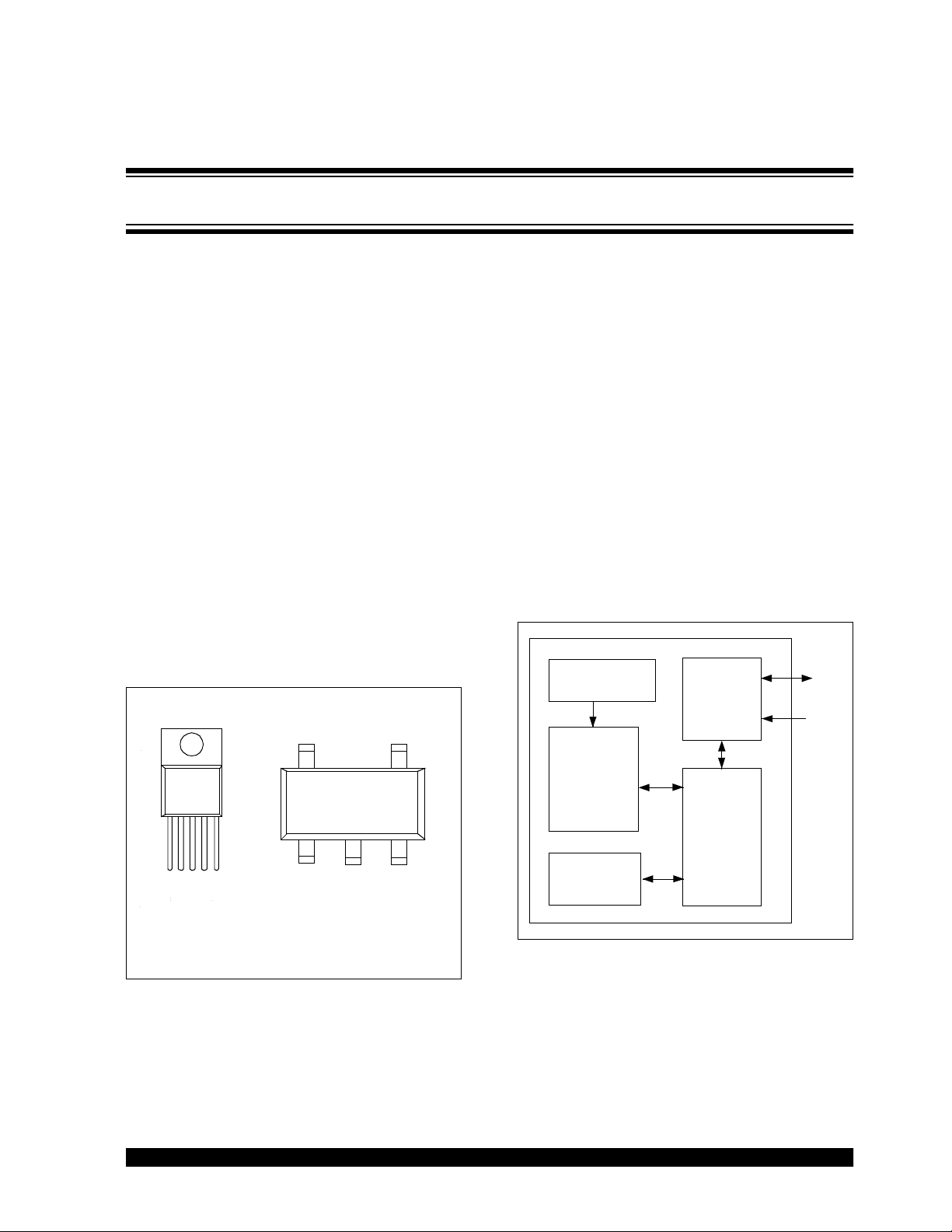
Package Types
TO-220 SOT-23
TC74
12345
SDA
5 4
TC74
SCLK
General Description
The TC74 is a serially accessible, digital temperature
sensor particularly suited for low cost and small formfactor applications. Temperature data is converted from
the onboard thermal sensing element and made
available as an 8-bit digital word.
Communication with the TC74 is accomplished via a 2wire SMBus/I
can be used to implement multi-drop/multi-zone
monitoring. The SHDN bit in the CONFIG register can
be used to activate the low power Standby mode.
Temperature resolution is 1°C. Conversion rate is a
nominal 8 samples/sec. During normal operation, the
quiescent current is 200 µA (typ). During standby
operation, the quiescent current is 5 µA (typ).
Small size, low installed cost and ease of use make the
TC74 an ideal choice for implementing thermal
management in a variety of systems.
2
C compatible serial port. This bus also
Functional Block Diagram
Internal Sensor
(Diode)
∆Σ
Modulator
Serial Port
Interface
Control
Logic
SDA
SCLK
12
GND
NC
SDA
VDD
GND
SCLK
Note: The TO-220 tab is connected
to pin 3 (GND)
2002 Microchip Technology Inc. DS21462C-page 1
NC
3
V
DD
Temperature
Register
Page 2
TC74
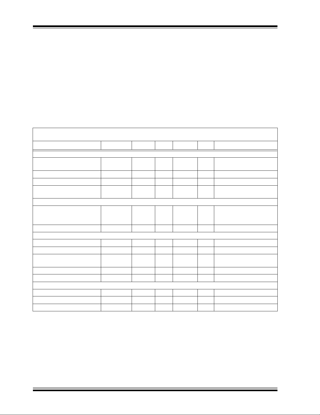
1.0 ELECTRICAL CHARACTERISTICS
1.1 Absolute Maximum Ratings†
Supply Voltage (VDD) ............................................ +6V
Voltage On Any Pin ....... (GND – 0.3V) to (V
+ 0.3V)
DD
† Notice: Stresses above those listed under "Maximum Ratings" may cause permanent damage to the
device. This is a stress rating only and functional operation of the device at those or any other conditions
above those indicated in the operation listings of this
specification is not implied. Exposure to maximum rating conditions for extended periods may affect device
reliability.
Current On Any Pin .......................................... ±50 mA
Operating Temperature (T
Storage Temperature (T
Junction Temperature (T
) ........ -40°C ≤ TA ≤ +125°C
A
) .............. -65°C to +150°C
STG
)................................ +150°C
J
DC CHARACTERISTICS
Electrical Specifications: Unless otherwise noted, V
V
= 5.0V for TC74AX-5.0VXX, -40°C ≤ TA ≤ 125°C. Note 5
DD
Parameters Sym Min Typ Max Units Conditions
Power Supply
Power-on Reset Threshold V
Supply Voltage V
Operating Current I
Standby Supply Current I
POR
DD
DD
DD-STANDBY
Temperature-to-Bits Converter
Temperature Accuracy T
ERR
Conversion Rate CR 4 8 — SPS Note 2
Serial Port Interface
Logic Input High V
Logic Input Low V
SDA Output Low V
Input Capacitance SDA, SCLK C
I/O Leakage I
Serial Port AC Timing (C
SMBus/I
2
C Clock Frequency f
LOAD
= 80 pF)
Low Clock Period t
High Clock Period t
IH
IL
OL
IN
LEAK
SMB
LOW
HIGH
0.8 x V
Note 1: Operating current is an average value integrated over multiple conversion cycles. Transient current may
exceed this specification.
2: Maximum ensured conversion time after Power-on Reset (POR to DATA_RDY) is 250 msec.
3: Output current should be minimized for best temperature accuracy. Power dissipation within the TC74 will
cause self-heating and temperature drift error.
4: SDA and SCLK must be connected to V
5: V
= 3.3V for TC74AX -3.3 VXX. VDD = 5.0V for TC74AX -5.0 VXX. All part types of the TC74 will operate
DD
properly over the wider power supply range of 2.7V to 5.5V. Each part type is tested and specified for rated
accuracy at its nominal supply voltage. As V
of V
change.
DD
= 3.3V for TC74AX-3.3VXX and
DD
1.2 — 2.2 V VDD Falling Edge or Rising
Edge
2.7 — 5.5 V Note 5
— 200 350 µA VDD = 5.5V, Note 1
— 5.0 10 µA VDD = 3.3V
Serial Port Inactive, Note 4
-2.0
-3.0
—
—
—
±2.0
——V
DD
+2.0
+3.0
— — 0.2 x V
—
—
—
—
0.4
0.6
—
°C +25°C <T
V
DD
VVIOL = 3 mA
< +85°C
0°C < T
-40°C < T
I
OL
A
< +125°C
A
< 0°C
A
= 6 mA, Note 3
—5.0— pF
-1.0 0.1 1.0 µA
10 — 100 kHz
4.7 — — µsec 10% to 10%
4.0 — — µsec 90% to 90%
or GND.
DD
varies from the nominal value, accuracy will degrade 1°C/V
DD
DS21462C-page 2 2002 Microchip Technology Inc.
Page 3
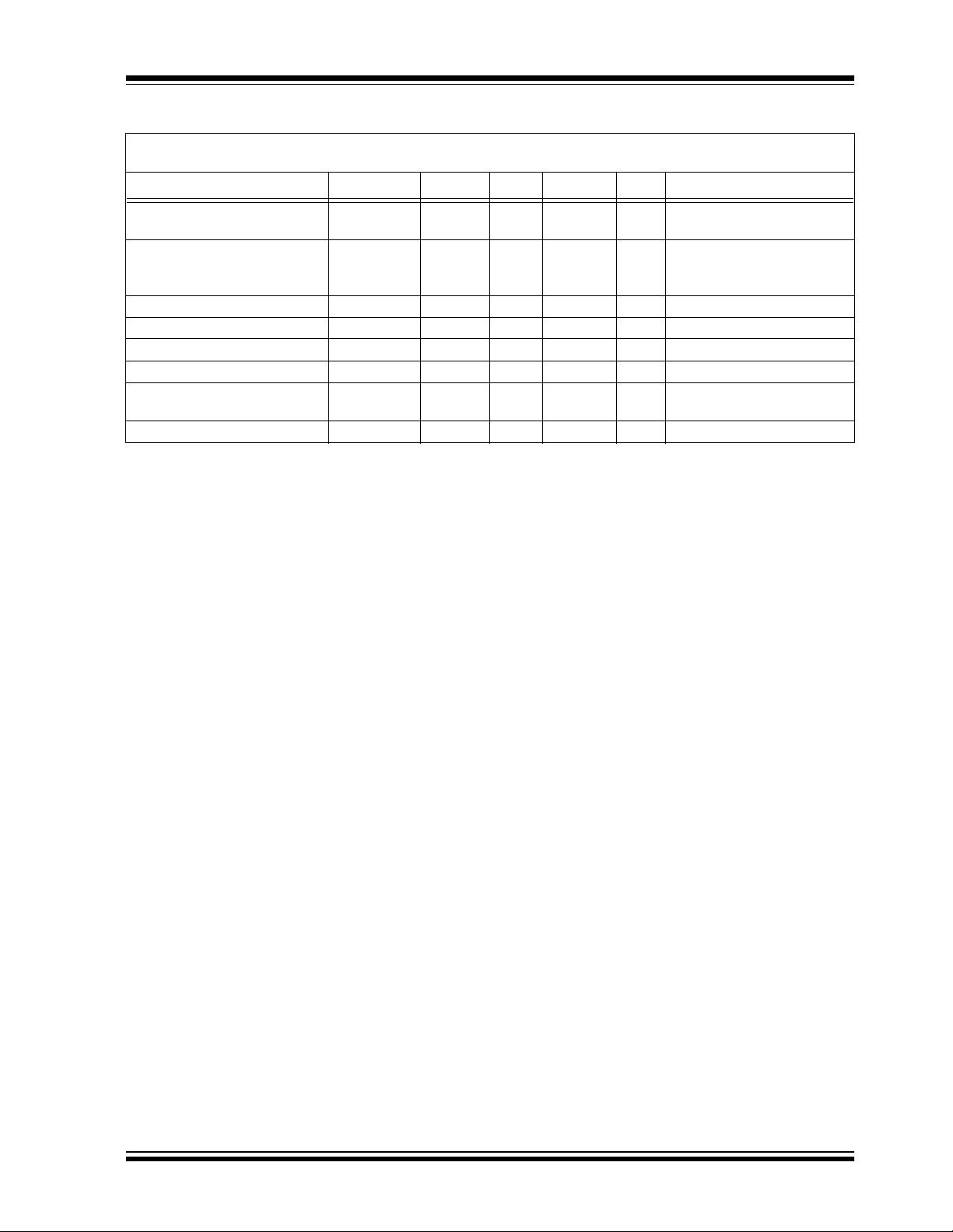
TC74
DC CHARACTERISTICS (CONTINUED)
Electrical Specifications: Unless otherwise noted, V
V
= 5.0V for TC74AX-5.0VXX, -40°C ≤ TA ≤ 125°C. Note 5
DD
Parameters Sym Min Typ Max Units Conditions
SMBus/I2C Rise Time
SMBus/I
2
C Fall Time
START Condition Setup Time
t
R
t
F
t
SU(START)
(for repeated START
Condition)
START Condition Hold Time t
Data In Setup Time t
Data In Hold Time t
STOP Condition Setup Time t
Bus Free Time Prior to New
H(START)
SU-DATA
H-DAT
SU(STOP)
t
IDLE
Transition
Power-on Reset Delay t
POR
Note 1: Operating current is an average value integrated over multiple conversion cycles. Transient current may
exceed this specification.
2: Maximum ensured conversion time after Power-on Reset (POR to DATA_RDY) is 250 msec.
3: Output current should be minimized for best temperature accuracy. Power dissipation within the TC74 will
cause self-heating and temperature drift error.
4: SDA and SCLK must be connected to V
5: V
= 3.3V for TC74AX -3.3 VXX. VDD = 5.0V for TC74AX -5.0 VXX. All part types of the TC74 will operate
DD
properly over the wider power supply range of 2.7V to 5.5V. Each part type is tested and specified for rated
accuracy at its nominal supply voltage. As V
of V
change.
DD
= 3.3V for TC74AX-3.3VXX and
DD
—
—
—
—
1000
300
nsec
nsec
10% to 90%
90% to10%
4.0 — — µsec 90% SCLK to 10% SDA
4.0 — — µsec
1000 — — nsec
1250 — — nsec
4.0 — — µsec
4.7 — — µsec
—500—µsecVDD ≥ V
or GND.
DD
varies from the nominal value, accuracy will degrade 1°C/V
DD
(Rising Edge)
POR
2002 Microchip Technology Inc. DS21462C-page 3
Page 4
TC74
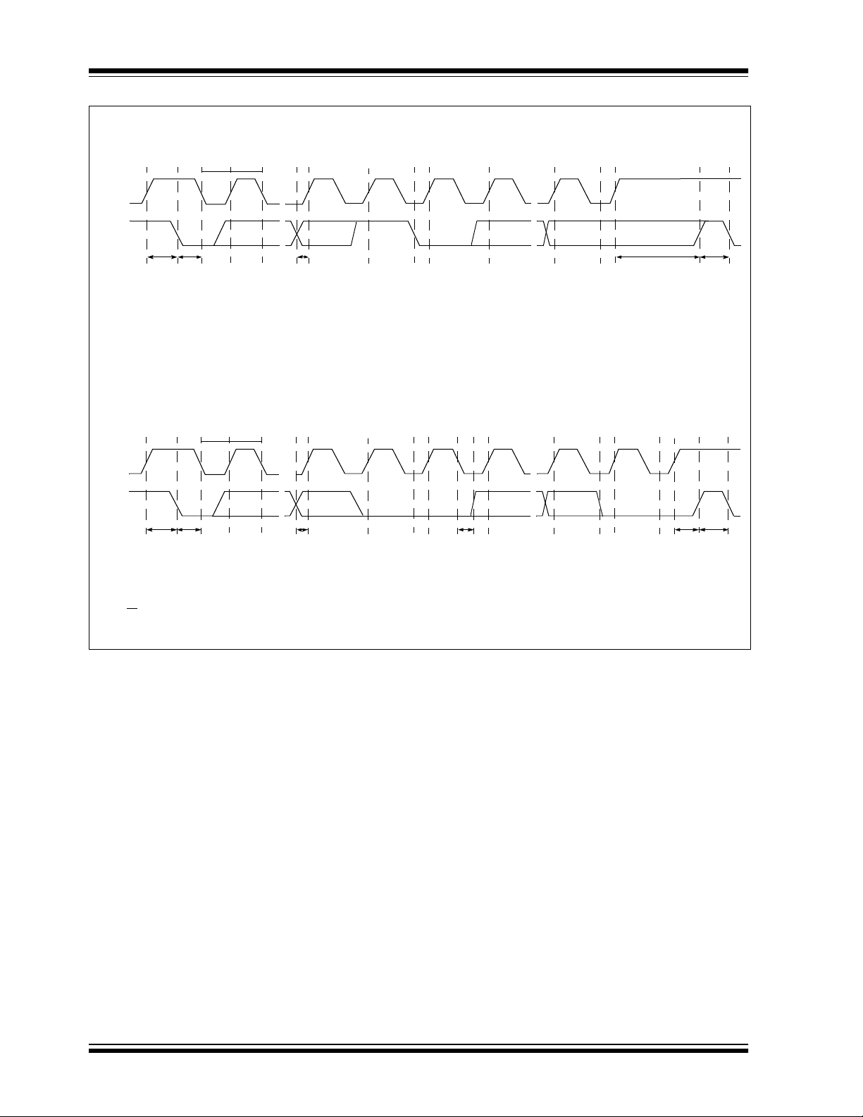
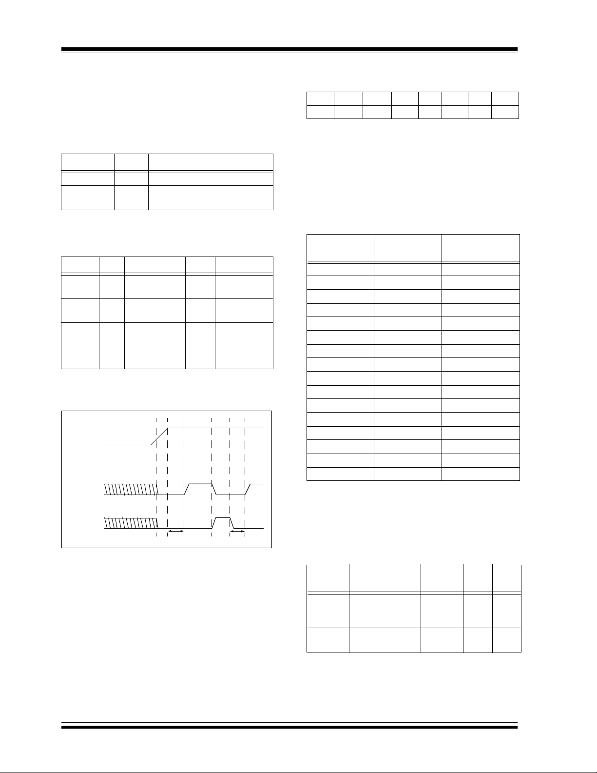
SMBUS Read Timing Diagram
t
LOW
B
t
HIGH
A
SCLK
SDA
t
SU(START)tH(START)
A = Start Condition
B = MSB of Address Clocked into Slave
C = LSB of Address Clocked into Slave
D = R/W Bit Clocked into Slave
SMBUS Write Timing Diagram
B
t
LOWtHIGH
SCLK
SDA
t
SU(START)tH(START)
A
CDEFG H
t
SU-DATA
E = Slave Pulls SDA Line Low
F = Acknowledge Bit Clocked into Master
G = MSB of Data Clocked into Master
H = LSB of Data Clocked into Master
CDEFG HIJ
t
SU-DATA
t
H-DATA
IJ
t
SU(STO P)tIDLE
I = Acknowledge Clock Pulse
J = Stop Condition
K = New Start Condition
KL
t
SU(STOP)tIDLE
K
M
A = Start Condition
B = MSB of Address Clocked into Slave
C = LSB of Address Clocked into Slave
D = R/W
E = Slave Pulls SDA Line Low
Bit Clocked into Slave
F = Acknowledge Bit Clocked into Master
G = MSB of Data Clocked into Slave
H = LSB of Data Clocked into Slave
I = Slave Pulls SDA Line Low
FIGURE 1-1: Timing Diagrams.
J = Acknowledge Clocked into Master
K = Acknowledge Clock Pulse
L = Stop Condition, Data Executed by Slave
M = New Start Condition
DS21462C-page 4 2002 Microchip Technology Inc.
Page 5
2.0 PIN DESCRIPTIONS
The descriptions of the pins are listed in Table 2-1.
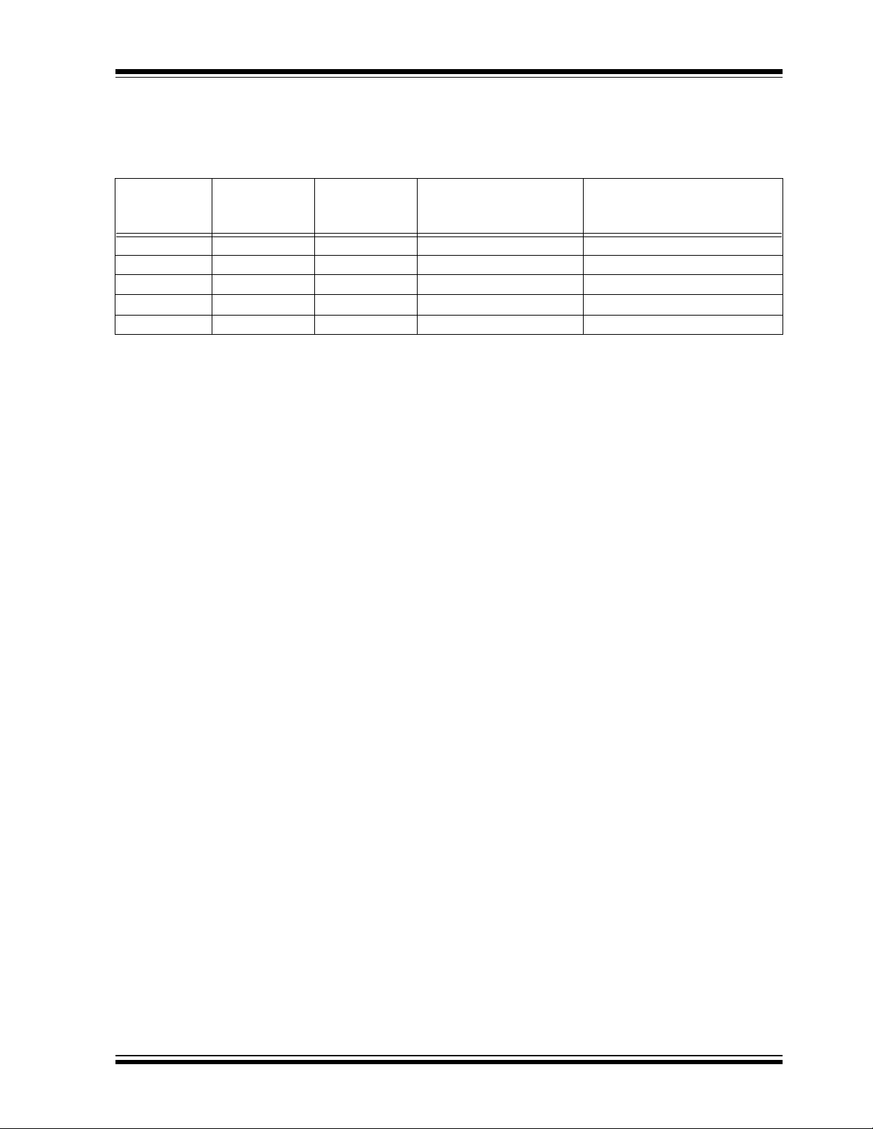
TABLE 2-1: PIN FUNCTION TABLE
Pin No.
(5-Pin
SOT-23)
1 1 NC None No Internal Connection
2 3 GND Power System Ground
35V
4 4 SCLK Input SMBus/I
5 2 SDA Bidirectional SMBus/I
2.1 Ground (GND)
Input. Ground return for all TC74 functions.
2.2 Power Supply Input (VDD)
Power supply input. See Electrical Specifications.
2.3 SMBus/I2C Serial Clock (SCLK)
Pin No.
(5-Pin TO-220)
Symbol Type Description
DD
Power Power Supply Input
2
C Serial Clock
2
C Serial Data
TC74
Input. SMBus/I2C serial clock. Clocks data into and out
of the TC74. See System Management Bus
Specification, Rev. 1.0, for timing diagrams.
2.4 Serial Data (SDA)
Bidirectional. Serial data is transferred on the SMBus/
2
I
C in both directions using this pin. See System
Management Bus Specification, Rev. 1.0 for timing
diagrams.
2002 Microchip Technology Inc. DS21462C-page 5
Page 6

TC74
3.0 DETAILED DESCRIPTION
3.1 Functional Description
The TC74 acquires and converts temperature
information from its onboard solid-state sensor with a
resolution of ±1°C. It stores the data in an internal
register which is then read through the serial port. The
system interface is a slave SMBus/I
which temperature data can be read at any time. Eight
SMBus/I
which allows for a multi-sensor configuration. Also,
there is low power Standby mode when temperature
acquisition is suspended.
2
C addresses are programmable for the TC74,
3.1.1 STANDBY MODE
The host is allowed, by the TC74, to put it into a low
power (I
mode, the A/D converter is halted and the temperature
data registers are frozen. The SMBus/I
operates normally. Standby mode is enabled by setting
the SHDN bit in the CONFIG register. Table 3-1
summarizes this operation.
= 5 µA, typical) Standby mode. In this
DD
TABLE 3-1: STANDBY MODE OPERATION
SHDN Bit Operating Mode
0 Normal
1 Standby
2
3.1.2 SMBUS/I
The TC74 is internally programmed to have a default
SMBus/I
addresses are available by custom order (contact
Microchip Technology Inc.
2
C address value of 1001 101b. Seven other
C SLAVE ADDRESS
3.2 Serial Port Operation
The Serial Clock input (SCLK) and bidirectional data
port (SDA) form a 2-wire bidirectional serial port for programming and interrogating the TC74. The
conventions used in this bus architecture are listed in
Table 3-2.
2
C port, through
2
C port, though,
TABLE 3-2: SERIAL BUS CONVENTIONS
Term Explanation
Transmitter The device sending data to the bus.
Receiver The device receiving data from the bus.
Master The device which controls the bus initi-
ating transfers (START), generating the
clock and terminating transfers
(STOP).
Slave The device addressed by the master.
START A unique condition signaling the begin-
ning of a transfer indicated by SDA
falling (high-low) while SCLK is high.
STOP A unique condition signaling the end of
a transfer indicated by SDA rising (lowhigh) while SCLK is high.
ACK A Receiver acknowledges the receipt
of each byte with this unique condition.
The Receiver drives SDA low during
SCLK high of the ACK clock-pulse. The
Master provides the clock pulse for the
ACK cycle.
Busy Communication is not possible
because the bus is in use.
NOT Busy When the bus is idle, both SDA and
SCLK will remain high.
Data Valid The state of SDA must remain stable
during the high period of SCLK in order
for a data bit to be considered valid.
SDA only changes state while SCLK is
low during normal data transfers (see
START and STOP conditions).
All transfers take place under the control of a host, usually a CPU or microcontroller, acting as the Master. This
host provides the clock signal for all transfers. The
TC74 always operates as a Slave. The serial protocol
is illustrated in Figure 3-1. All data transfers have two
phases and all bytes are transferred MSB first.
Accesses are initiated by a START condition, followed
by a device address byte and one or more data bytes.
The device address byte includes a Read/Write selection bit. Each access must be terminated by a STOP
condition. A convention called “Acknowledge” (ACK)
confirms receipt of each byte. Note that SDA can
change only during periods when SCLK is low (SDA
changes while SCLK is high are reserved for START
and STOP conditions).
DS21462C-page 6 2002 Microchip Technology Inc.
Page 7

Write Byte Format
SAddressWR ACKCommandACK Data ACK P
8 Bits7 Bits 8 Bits
Slave Address Command Byte: selects
which register you are
writing to.
Read Byte Format
SAddressWR ACKCommandACK S Address RD ACK Data NACK
7 Bits 8 Bits 7 Bits 8 Bits
Slave Address Command Byte: selects
which register you are
reading from.
Receive Byte Format
S Address RD ACK Data NACK P
7 Bits
S = START Condition
P = STOP Condition
Shaded = Slave Transmission
8 Bits
Data Byte: reads data from
the register commanded by
the last Read Byte or Write
Byte transmission.
Slave Address: repeated
due to change in dataflow direction.
Data Byte: data goes
into the register set
by the command byte.
Data Byte: reads from
the register set by the
command byte.
TC74
P
FIGURE 3-1: SMBus/I2C Protocols.
3.3 START Condition (S)
The TC74 continuously monitors the SDA and SCLK
lines for a START condition (a high-to-low transition of
SDA while SCLK is high) and will not respond until this
condition is met.
3.4 Address Byte
Immediately following the START condition, the host
must transmit the address byte to the TC74. The states
of A2, A1 and A0 determine the SMBus/I
2
C address for
the TC74. The 7-bit address transmitted in the serial bit
stream must match for the TC74 to respond with an
Acknowledge (indicating the TC74 is on the bus and
ready to accept data). The 8-bit in the address byte is
a Read/Write bit. This bit is a ‘1’ for a read operation or
‘0’ for a write operation. During the first phase of any
transfer, this bit will be set = 0, indicating that the
command byte is being written.
3.5 Acknowledge (ACK)
Acknowledge (ACK) provides a positive handshake
between the host and the TC74. The host releases
SDA after transmitting 8 bits. The host then generates
a ninth clock cycle to allow the TC74 to pull the SDA
line low. This action acknowledges that the TC74
successfully received the previous 8 bits of data or
address.
3.6 Data Byte
After a successful ACK of the address byte, the host
must transmit the data byte to be written, or clock-in the
data to be read (see the appropriate timing diagrams).
ACK will be generated upon a successful write of a
data byte into the TC74.
3.7 STOP Condition (P)
Communications must be terminated by a STOP
condition (a low-to-high transition of SDA while SCLK
is high). The STOP condition must be communicated
by the transmitter to the TC74. Refer to Figure 1-1,
“Timing Diagrams”, for serial bus timing.
2002 Microchip Technology Inc. DS21462C-page 7
Page 8
TC74
4.0 REGISTER SET AND
PROGRAMMER’S MODEL
TABLE 4-1: COMMAND BYTE
DESCRIPTION
(SMBUS/I
WRITE_BYTE)
Command Code Function
RTR 00h Read Temperature (TEMP)
RWCR 01h Read/Write Configuration
TABLE 4-2: CONFIGURATION REGISTER
(CONFIG); 8 BITS, READ/
WRITE)
Bit POR Function Type Operation
D[7] 0 STANDBY
Switch
D[6] 0 Data Ready * Read
D[5]-
D[0]
Note 1: *DATA_RDY bit RESET at power-up and
DATA_RDY
0 Reserved -
SHDN enable.
V
DD
Always
returns zero
when read
2
C READ_BYTE AND
(CONFIG)
Read/
Write
Only
N/A N/A
1 = standby,
0 = normal
1 = ready
0 = not ready
TABLE 4-3: TEMPERATURE REGISTER
(TEMP)
D[7] D[6] D[5] D[4] D[3] D[2] D[1] D[0]
MSB X X X X X X LSB
I
n temperature data registers, each unit value represents one degree (Celsius). The value is in 2’s
complement binary format such that a reading of 0000
0000b corresponds to 0°C. Examples of this
temperature to binary value relationship are shown in
Table 4-4
.
TABLE 4-4: TEMPERATURE-TO-DIGITAL
VALUE CONVERSION
(TEMP)
Actual
Temperature
+130.00°C +127°C 0111 1111
+127.00°C +127°C 0111 1111
+126.50°C +126°C 0111 1110
+25.25°C +25°C 0001 1001
+0.50°C 0°C 0000 0000
+0.25°C 0°C 0000 0000
0.00°C 0°C 0000 0000
-0.25°C -1°C 1111 1111
-0.50°C -1°C 1111 1111
-0.75°C -1°C 1111 1111
-1.00°C -1°C 1111 1111
-25.00°C -25°C 1110 0111
-25.25°C -26°C 1110 0110
-54.75°C -55°C 1100 1001
-55.00°C -55°C 1100 1001
-65.00°C -65°C 1011 1111
Registered
Temp erature
Binary
Hex
4.2 Register Set Summary
SHDN
t
conv
t
conv
FIGURE 4-1: DATA_RDY, SHDN Operation Logic Diagram.
4.1 Temperature Register (TEMP), 8 Bits, READ ONLY
The binary value (2’s complement format) in this register represents temperature of the onboard sensor
following a conversion cycle. The registers are
automatically updated in an alternating manner.
DS21462C-page 8 2002 Microchip Technology Inc.
The TC74 register set is summarized in Table 4-5. All
registers are 8 bits wide.
TABLE 4-5: TC74 REGISTER SET
SUMMARY
Name Description
TEMP Internal Sensor
Temperature (2’s
Complement)
CONFIG CONFIG
Register
Note 1: The TEMP register will be immediately
updated by the A/D converter after the
DATA_RDY Bit goes high.
POR
State
0000
0000b
0000
0000b
Read Write
(1)
√ N/A
√√
Page 9

5.0 PACKAGING INFORMATION
5.1 SOT23A Package Marking Information
5-Pin SOT-23A
TC74
5
1423
1
4
3
2
1 & 2 = part number code + temp. range and voltage
3 = year and quarter code
4 = lot ID number
SOT-23 Package Marking Codes
SOT-23 (V) Address Code SOT-23 (V) Address Code
TC74A0-3.3VCT 1001 000 V0 TC74A0-5.0VCT 1001 000 U0
TC74A1-3.3VCT 1001 001 V1 TC74A1-5.0VCT 1001 001 U1
TC74A2-3.3VCT 1001 010 V2 TC74A2-5.0VCT 1001 010 U2
TC74A3-3.3VCT 1001 011 V3 TC74A3-5.0VCT 1001 011 U3
TC74A4-3.3VCT 1001 100 V4 TC74A4-5.0VCT 1001 100 U4
TC74A5-3.3VCT 1001 101* V5 TC74A5-5.0VCT 1001 101* U5
TC74A6-3.3VCT 1001 110 V6 TC74A6-5.0VCT 1001 110 U6
TC74A7-3.3VCT 1001 111 V7 TC74A7-5.0VCT 1001 111 U7
Note: * Default Address
TO-220 Package Marking Information
TO-220
Legend: XX...X Customer specific information*
YY Year code (last 2 digits of calendar year)
WW Week code (week of January 1 is week ‘01’)
NNN Alphanumeric traceability code
Note: In the event the full Microchip part number cannot be
TC74A0-
3.3VAT
0229123
2345
1
* Standard marking consists of Microchip part number, year code, week code, and traceability code.
marked on one line, it will be carried over to the next line thus limiting the number of available characters for customer specific information.
2002 Microchip Technology Inc. DS21462C-page 9
Page 10
TC74
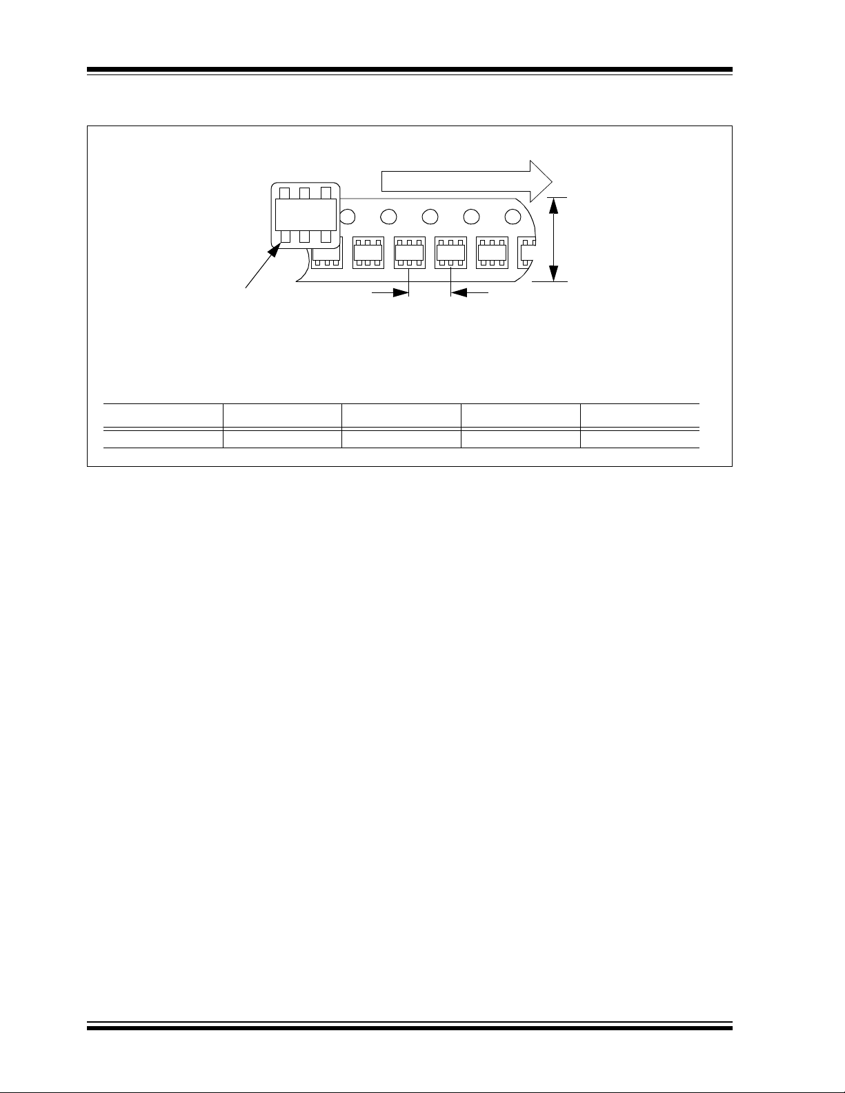
5.2 Taping Forms
Component Taping Orientation for 5-Pin SOT-23A (EIAJ SC-74A) Devices
Device
Marking
User Direction of Feed
W
PIN 1
Standard Reel Component Orientation
for TR Suffix Device
(Mark Right Side Up)
Carrier Tape, Number of Components Per Reel and Reel Size:
Package Carrier Width (W) Pitch (P) Part Per Full Reel Reel Size
5-Pin SOT-23A 8 mm 4 mm 3000 7 in.
P
DS21462C-page 10 2002 Microchip Technology Inc.
Page 11

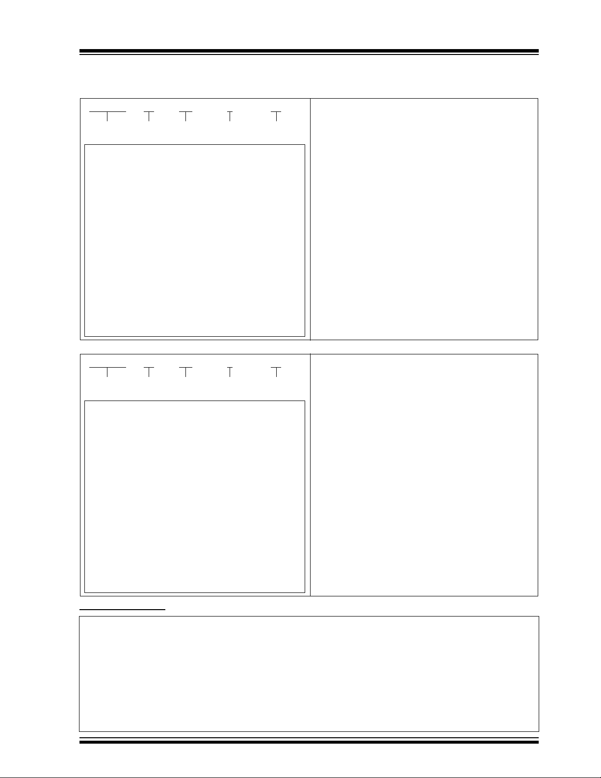
5.3 Package Dimensions
SOT-23A-5
TC74
.075 (1.90)
REF.
.057 (1.45)
.035 (0.90)
5-Pin TO-220
.293 (7.44)
.204 (5.18)
.122 (3.10)
.098 (2.50)
.020 (0.50)
.012 (0.30)
PIN 1
.006 (0.15)
.000 (0.00)
.117 (2.97)
.103 (2.62)
.118 (3.00)
.010 (2.80)
.415 (10.54)
.390 (9.91)
.071 (1.80)
.059 (1.50)
.037 (0.95)
REF.
10° MAX.
.156 (3.96)
.140 (3.56)
DIA.
.024 (0.60)
.004 (0.10)
.055 (1.40)
.045 (1.14)
.613 (15.57)
.569 (14.45)
.010 (0.25)
.004 (0.09)
Dimensions: inches (mm)
.185 (4.70)
.165 (4.19)
3 - 7.5
5 PLCS.
.590 (14.99)
.482 (12.24)
PIN 1
.273 (6.93)
.263 (6.68)
.037 (0.95)
.025 (0.64)
.025 (0.64)
.012 (0.30)
.072 (1.83)
.062 (1.57)
.115 (2.92)
.087 (2.21)
Dimensions: inches (mm)
2002 Microchip Technology Inc. DS21462C-page 11
Page 12

TC74
NOTES:
DS21462C-page 12 2002 Microchip Technology Inc.
Page 13
PRODUCT IDENTIFICATION SYSTEM
To order or obtain information, e.g., on pricing or delivery, refer to the factory or the listed sales office.
PART NO. XX XX
Device
Options
Device: TC74: Serial Digital Thermal Sensor
Address Options: A0 = 1001 00 0
Supply Voltage: 3.3 = Accuracy optimized for 3.3V
Operating Temperature: V = -40°C ≤ T
-XX
Supply
Vol tag e
A1 = 1001 001
A2 = 1001 010
A3 = 1001 011
A4 = 1001 100
A5 = 1001 101 *
A6 = 1001 110
A7 = 1001 111
* Default Address
5.0 = Accuracy opt imized for 5.0V
X
Operating
Temp era tur e
≤ +125°C
A
PackageAddress
Examples:
a) TC74A0-3.3VCTTR: SOT-2 3 Serial Digital Thermal Sensor
b) TC74A1-3.3VCTTR: SOT-2 3 Serial Digital Thermal Sensor
c) TC74A2-3.3VCTTR: SOT-23 Serial Digital Thermal Sensor
d) TC74A3-3.3VCTTR: SOT-2 3 Serial Digital Thermal Sensor
e) TC74A4-3.3VCTTR: SOT-2 3 Serial Digital Thermal Sensor
f) TC74A5-3.3VCTTR: SOT-23 Serial Digital Thermal Sensor *
g) TC74A6-3.3VCTTR: SOT-2 3 Serial Digital Thermal Sensor
h) TC74A7-3.3VCTTR: SOT-2 3 Serial Digital Thermal Sensor
a) TC74A0-5.0VCTTR: SOT-2 3 Serial Digital Thermal Sensor
b) TC74A1-5.0VCTTR: SOT-2 3 Serial Digital Thermal Sensor
c) TC74A2-5.0VCTTR: SOT-23 Serial Digital Thermal Sensor
d) TC74A3-5.0VCTTR: SOT-2 3 Serial Digital Thermal Sensor
e) TC74A4-5.0VCTTR: SOT-2 3 Serial Digital Thermal Sensor
f) TC74A5-5.0VCTTR: SOT-23 Serial Digital Thermal Sensor *
g) TC74A6-5.0VCTTR: SOT-2 3 Serial Digital Thermal Sensor
h) TC74A7-5.0VCTTR: SOT-2 3 Serial Digital Thermal Sensor
* Default Address
TC74
Package: CTTR = SOT-23-5 (Tape and Reel only)
PART NO. XX XX
Device
Options
Device: TC74: Serial Digital Thermal Sensor
Address Options: A0 = 1001 00 0
Output Voltage: 3.3 = Accuracy optimized for 3.3V
Operating Temperature: V = -40°C ≤ T
Package: AT = TO-220-5
-XX
Supply
Vol tag e
A1 = 1001 001
A2 = 1001 010
A3 = 1001 011
A4 = 1001 100
A5 = 1001 101 *
A6 = 1001 110
A7 = 1001 111
* Default Address
5.0 = Accuracy optimized for 5.0V
X
Operating
Temp era tur e
≤ +125°C
A
PackageAddress
Examples:
a) TC74A0-3.3VAT: TO-220 Serial Digital Thermal Sensor
b) TC74A1-3.3VAT: TO-220 Serial Digital Thermal Sensor
c) TC74A2-3.3VAT: TO-220 Serial Digital Thermal Sensor
d) TC74A3-3.3VAT: TO-220 Serial Digital Thermal Sensor
e) TC74A4-3.3VAT: TO-220 Serial Digital Thermal Sensor
f) TC74A5-3.3VAT: TO-220 Serial Digital Thermal Sensor *
g) TC74A6-3.3VAT: TO-220 Serial Digital Thermal Sensor
h) TC74A7-3.3VAT: TO-220 Serial Digital Thermal Sensor
a) TC74A0-5.0VAT: TO-220 Serial Digital Thermal Sensor
b) TC74A1-5.0VAT: TO-220 Serial Digital Thermal Sensor
c) TC74A2-5.0VAT: TO-220 Serial Digital Thermal Sensor
d) TC74A3-5.0VAT: TO-220 Serial Digital Thermal Sensor
e) TC74A4-5.0VAT: TO-220 Serial Digital Thermal Sensor
f) TC74A5-5.0VAT: TO-220 Serial Digital Thermal Sensor *
g) TC74A6-5.0VAT: TO-220 Serial Digital Thermal Sensor
h) TC74A7-5.0VAT: TO-220 Serial Digital Thermal Sensor
* Default Address
Sales and Support
Data Sheets
Products supported by a preliminary Data Sheet may have an errata sheet describing minor operational differences and recommended workarounds. To determine if an errata sheet exists for a particular device, please contact one of the following:
1. Your local Microchip sales office
2. The Microchip Corporate Literature Center U.S. FAX: (480) 792-7277
3. The Microchip Worldwide S ite (www.microchip.com)
Please specify which device, revision of silicon and Data Sheet (include Literature #) you are using.
New Customer Notification System
Register on our web site (www.microchip.com/cn) to receive the most current information on our products.
2002 Microchip Technology Inc. DS21462C-page13
Page 14

TC74
NOTES:
DS21462C-page 14 2002 Microchip Technology Inc.
Page 15

Note the following details of the code protection feature on Microchip devices:
• Microchip products meet the specification contained in their particular Microchip Data Sheet.
• Microchip believes that its family of products is one of the most secure families of its kind on the market today, when used in the
intended manner and under normal conditions.
• There ar e dishonest and possibly illegal methods used to breach the code protection feature. All of these methods, to our knowl-
edge, require using the Microchip products in a manner outside the operating specifications contained in Microchip's Data
Sheets. Most likely, the person doing so is engaged in theft of intellectual property.
• Microchip is willing to work with the customer who is concerned about the integrity of their code.
• Neither Microchip nor any other semiconductor manufacturer can guarantee the security of their code. Code protection does not
mean that we are guaranteeing the product as “unbreakable.”
Code protection is constantly evolving. We at Microchip are committed to continuously improving the code protection features of our
products.
Information contained in this publication regarding device
applications and the like is intended through suggestion only
and may be superseded by updates. It is your responsibility to
ensure that your application meets with your specifications.
No representation or warranty is given and no liability is
assumed by Microchip Technology Incorporated with respect
to the accuracy or use of such information, or infringement of
patents or other intellectual property rights arising from such
use or otherwise. Use of Microchip’s products as critical components in life support systems is not authorized except with
express written approval by Microchip. No licenses are conveyed, implicitly or otherwise, under any intellectual property
rights.
Trademarks
The Microchip name and logo, the Microchip logo, K
EELOQ
MPLAB, PIC, PICmicro, PICSTART and PRO MATE are
registered trademarks of Microchip Technology Incorporated
in the U.S.A. and other countries.
FilterLab, microID, MXDEV, MXLAB, PICMASTER, SEEVAL
and The Embedded Control Solutions Company are
registered trademarks of Microchip Technology Incorporated
in the U.S.A.
dsPIC, dsPICDEM.net, ECONOMONITOR, FanSense,
FlexROM, fuzzyLAB, In-Circuit Serial Programming, ICSP,
ICEPIC, microPort, Migratable Memory, MPASM, MPLIB,
MPLINK, MPSIM, PICC, PICDEM, PICDEM.net, rfPIC, Select
Mode and Total Endurance are trademarks of Microchip
Technology Incorporated in the U.S.A. and other countries.
Serialized Quick Turn Programming (SQTP) is a service mark
of Microchip Technology Incorporated in the U.S.A.
All other trademarks mentioned herein are property of their
respective companies.
© 2002, Microchip Technology Incorporated, Printed in the
U.S.A., All Rights Reserved.
Printed on recycled paper.
,
Microchip received QS-9000 quality system
certification for its worldwide headquarters,
design and wafer fabrication facilities in
Chandler and Tempe, Arizona in July 1999
and Mountain View, California in March 2002.
The Company’s quality system processes and
procedures are QS-9000 compliant for its
PICmicro
devices, Serial EEPROMs, microperipherals,
non-volatile memory and analog products. In
addition, Microchip’s qua lity system for the
design and manufacture of development
systems is ISO 9001 certified.
®
8-bit MCUs, KEEL
®
code hopping
OQ
2002 Microchip Technology Inc. DS21462C - page 15
Page 16

M
W
ORLDWIDE SALES AND SERVICE
AMERICAS
Corporate Office
2355 West Chandler B lvd.
Chandler, AZ 85224-6199
Tel: 480-792-7200 Fax: 480-792-7277
Technical Support: 480-792-7627
Web Address: http://www.microchip.com
Rocky Mountain
2355 West Chandler B lvd.
Chandler, AZ 85224-6199
Tel: 480-792-7966 Fax: 480-792-4338
Atlanta
500 Sugar Mill Road, Suite 200B
Atlanta, GA 30350
Tel: 770-640-0034 Fax: 770-640-0307
Boston
2 Lan Drive, Suit e 120
Westford, MA 01886
Tel: 978-692-3848 Fax: 978-692-3821
Chicago
333 Pierce Road, S uite 180
Itasca, IL 60143
Tel: 630-285-0071 Fax: 630-285-0075
Dallas
4570 Westgrove Drive, Suite 160
Addison, TX 75001
Tel: 972-818-7423 Fax: 972-818-2924
Detroit
Tri-Atria Office Building
32255 Northwestern Highway, Suite 190
Farmington Hills, MI 48334
Tel: 248-538-2250 Fax: 248-538-2260
Kokomo
2767 S. Albright Road
Kokomo, Indiana 46902
Tel: 765-864-8360 Fax: 765-864-8387
Los Angeles
18201 Von Karman, Suite 10 90
Irvine, CA 92612
Tel: 949-263-1888 Fax: 949-263-1338
San Jose
Microchip Technology Inc.
2107 North First S treet, Suite 590
San Jose, CA 95131
Tel: 408-436-7950 Fax: 408-436-7955
Toro nto
6285 Northam Drive, Suite 108
Mississauga, Ontario L4V 1X5, Canada
Tel: 905-673-0699 Fax: 905-673-6509
ASIA/PACIFIC
Australia
Microchip Technology Australia Pty Ltd
Suite 22, 41 Rawson Street
Epping 2121, NSW
Australia
Tel: 61-2-9868-6733 Fax: 61-2-9868-6755
China - Beijing
Microchip Technology Consulting (Shanghai)
Co., Ltd., Beijing Liaison Office
Unit 915
Bei Hai Wan Tai Bldg.
No. 6 Chaoyangmen Beidajie
Beijing, 100027, No. China
Tel: 86-10-852821 00 Fax: 86-10-852 82104
China - Chengdu
Microchip Technology Consulting (Shanghai)
Co., Ltd., Chengdu Liaison Office
Rm. 2401, 24th Floor,
Ming Xing Financial Tower
No. 88 TIDU Street
Chengdu 610016, China
Tel: 86-28-867662 00 Fax: 86-28-867 66599
China - Fuzhou
Microchip Technology Consulting (Shanghai)
Co., Ltd., Fuzhou Liaison Office
Unit 28F, World Trade Plaza
No. 71 Wusi Road
Fuzhou 350001, China
Tel: 86-591-75035 06 Fax: 86-591-7503521
China - Shanghai
Microchip Technology Consulting (Shanghai)
Co., Ltd.
Room 701, Bldg. B
Far East International Plaza
No. 317 Xian Xia Road
Shanghai, 200051
Tel: 86-21-6275-5700 Fax: 86-21-6275-5060
China - Shenzhen
Microchip Technology Consulting (Shanghai)
Co., Ltd., Shenzhen L iaison Office
Rm. 1315, 13/F, Shenzhen Kerry Centre,
Renminnan Lu
Shenzhen 518001, Ch ina
Tel: 86-755-82350 361 Fax: 86-755-82366086
China - Hong Kong SAR
Microchip Technology Hongkong Ltd.
Unit 901-6, Tower 2, Metroplaza
223 Hing Fong Road
Kwai Fong, N.T., Hong Kong
Tel: 852-2401-120 0 Fax: 852-2401-3431
India
Microchip Technology Inc.
India Liaison Office
Divyasree Chambers
1 Floor, Wing A (A3/A4)
No. 11, O’Shaugnessey Road
Bangalore, 560 025, India
Tel: 91-80-229006 1 Fax: 91-80-2290 062
Japan
Microchip Technology Japan K.K.
Benex S-1 6F
3-18-20, Shinyokohama
Kohoku-Ku, Yokohama-shi
Kanagawa, 222-0033, Japan
Tel: 81-45-471- 6166 Fax: 81-45-471-6122
Korea
Microchip Technology Korea
168-1, Youngbo Bldg. 3 Floor
Samsung-Dong, Kangnam-Ku
Seoul, Korea 135-882
Tel: 82-2-554-7200 Fax: 82-2-558-593 4
Singapore
Microchip Technology Singapore Pte Ltd.
200 Middle Road
#07-02 Prime Centre
Singapore, 188980
Tel: 65-6334-8870 Fax: 65-6334-8850
Ta iw an
Microchip Technology (Barbados) Inc.,
Taiwan Branch
11F-3, No. 207
Tung Hua North Road
Taipei, 105, Taiwan
Tel: 886-2-2717-7175 Fax: 886-2-2545-0139
EUROPE
Austria
Microchip Technology Austria GmbH
Durisolstrasse 2
A-4600 Wels
Austria
Tel: 43-7242-2244-399
Fax: 43-7242-2244-393
Denmark
Microchip Technology Nordic ApS
Regus Business Centre
Lautrup hoj 1-3
Ballerup DK-2750 Denmark
Tel: 45 4420 9895 Fax: 45 4420 9910
France
Microchip Technology SARL
Parc d’Activite du Moulin de Massy
43 Rue du Saule Trapu
Batiment A - ler Etage
91300 Massy, France
Tel: 33-1-69-53-63-20 Fax: 33-1-69-30-90-79
Germany
Microchip Technology GmbH
Steinheilstrasse 10
D-85737 Ismaning, Germany
Tel: 49-89-627-144 0 Fax: 49-89-627-144-44
Italy
Microchip Technology SRL
Centro Direzionale Colleoni
Palazzo Taurus 1 V. Le Colleoni 1
20041 Agrate Brianza
Milan, Italy
Tel: 39-039-65791-1 Fax: 39-039-6899883
United Kingdom
Microchip Ltd.
505 Eskdale Road
Winnersh Triangle
Wokingham
Berkshire, England RG41 5TU
Tel: 44 118 921 5869 Fax: 44-118 921-5820
10/18/02
DS21462C-page 16 2002 Microchip Technology Inc.
 Loading...