

查询TC72-2.8MMF供应商
M
Digital Temperature Sensor with SPI™ Interfa
Features
• Temperature-to-Digital Converter
• SPI™ Compatible Interface
• 10-Bit Resolution (0.25°C/Bit)
• ±2°C (max.) Accuracy from -40°C to +85°C
• ±3°C (max.) Accuracy from -55°C to +125°C
• 2.65V to 5.5V Operating Range
• Low Power Consumption:
- 250 µA (typ.) Continuous Temperature
Conversion Mode
- 1 µA (max.) Shutdown Mode
• Power Saving One-Shot Temperature
Measurement
• Industry Standard 8-Pin MSOP Package
• Space Saving 8-Pin DFN (3x3 mm) Package
Typical Applications
• Personal Computers and Servers
• Hard Disk Drives and Other PC Peripherals
• Entertainment Systems
• Office Equipment
• Datacom Equipment
• Mobile Phones
• General Purpose Temperature Monitoring
Package Types
MSOP
1
DFN
NC
SCK
CE
GND
NC
CE
SCK
GND
1
2
3
4
TC72
2
3
4
TC72
8
7
6
5
V
DD
NC
SDI
SDO
8
7
6
5SDI
V
DD
NC
SDO
TC72
ce
General Description
The TC72 is a digital temperature sensor capable of
reading temperatures from -55°C to +125°C. This sensor features a serial interface that allows communication with a host controller or other peripherals. The
TC72 interface is compatible with the SPI protocol. The
TC72 does not require any additional external components. However, it is recommended that a decoupling
capacitor of 0.01 µF to 0.1 µF be provided between the
V
and GND pins.
DD
The TC72 can be used either in a Continuous Temperature Conversion mode or a One-Shot Conversion
mode. The Continuous Conversion mode measures
the temperature approximately every 150 ms and
stores the data in the temperature registers. In contrast, the One-Shot mode performs a single temperature measurement and returns to the power saving
shutdown mode.
The TC72 features high temperature accuracy, easeof-use and is the ideal solution for implementing thermal management in a variety of systems. The device is
available in both 8-pin MSOP and 8-pin DFN spacesaving packages. The TC72 also features a shutdown
mode for low power operation.
Block Diagram
V
DD
Internal
Diode
Temperature
Sensor
10-Bit
Sigma Delta
A/D Converter
Temperature
Register
GND
TC72
Manufacturer
ID Register
Serial
Port
Interface
Control
Register
CE
SCK
SDO
SDI
2002 Microchip Technology Inc. DS21743A-page 1
TC72
Typical Application
V
DD
0.1µF
V
DD
TC72
PICmicro
MCU
®
SDO
GND
CE
SCK
AN0
SCK
SDI
SDOSDI
DS21743A-page 2 2002 Microchip Technology Inc.
TC72
1.0 ELECTRICAL
CHARACTERISTICS
1.1 Maximum Ratings
VDD........................................................................ 6.0V
All inputs and outputs w.r.t. GND ...-0.3V to V
Storage temperature .......................... -65°C to +150°C
Ambient temp. with power applied ..... -55°C to +125°C
Junction Temperature ........................................ 150°C
ESD protection on all pins:
Human Body Model (HBM)............................. > 4 kV
Man Machine Model (MM).............................> 400V
Latch-Up Current at each pin ........................ ±200 mA
Maximum Power Dissipation........................... 250 mW
† Notice: Stresses above t hose listed under "Maximum
Ratings" may cause permanent damage to the device. This is
a stress rating only and functional operation of the device at
those or any other conditions above those indicated in the
operation listings of this specification is not implied. Exposure
to maximum rating conditions for extended periods may affect
device reliability.
†
+0.3V
DD
DC CHARACTERISTICS
PIN FUNCTION TABLE
Name Function
NC No Internal Connection
CE Chip Enable Input, the device is selected
when this input is high
SCK Serial Clock Input
GND Ground
SDO Serial Data Output
SDI Serial Data Input
NC No Internal Connection
V
DD
Power Supply
Electrical Specifications: Unless otherwise noted, all parameters apply at VDD = 2.65V to 5.5V, TA = -55°C to +125 °C.
Parameters Sym Min Typ Max Units Conditions
Power Supply
Operating Voltage Range V
Operating Current:
Normal Mode, ADC Active
Shut-Down Supply Current I
Temperature Sensor and Analog-to-Digital Converter
Temperature Accuracy
(Note 1)
Resolution — 10 — Bits Note 4
ADC Conversion Time t
Digital Input / Output
High Level Input Voltage V
Low Level Input Voltage V
High Level Output Voltage V
Low Level Output Voltage V
Input Resist ance R
Pin Capacitance C
Note 1: The TC72-2.8MXX, TC72-3.3MXX and TC72-5.0MXX will operate from a supply voltage of 2.65V to 5.5V. However, the
TC72-2.8MXX, TC72-3.3MXX and TC72-5.0MXX are tested and specified at the nominal operating voltages of 2.8V,
3.3V and 5.0V respectively. As V
Figure 2-5 and Figure 2-6.
2: Measured with a load of C
3: All time measurements are measured with respect to the 50% point of the signal, except for the SCK rise and fall times.
The rise and fall times are defined as the 10% to 90% transition time.
4: Resolution = Temperature Range/No. of Bits = (+127°C – -128°C) / (2
DD
I
DD-CON
SHD
T
ACY
CONV
IH
IL
OH
OL
IN
IN
C
OUT
= 50 pF on the SDO output pin of the TC72.
L
2.65 — 5.5 V Note 1
— 250 400 µA Continuous temp. conversion mode
(Shutdown Bit = ‘0’)
— 0.1 1.0 µA Shutdown Mode (Shutdown Bit = ‘1’)
-2.0 — +2.0 °C -40°C < TA < +85°C
-3.0 — +3.0 -55°C < T
—150200ms
0.7 V
— — 0.2 V
0.7 V
— — 0.2 V
1.0 — — MΩ
—15—pF
—50—
varies from the nominal operating value, the accuracy may be degraded. Refer to
DD
——V
DD
DD
——VIOH = 1 mA
DD
DD
10
) = 256/1024 = 0.25°C/Bit
V
VIOL = 4 mA
< +125°C
A
2002 Microchip Technology Inc. DS21743A-page 3
TC72
DC CHARACTERISTICS (CONTINUED)
Electrical Specifications: Unless otherwise noted, all parameters apply at VDD = 2.65V to 5.5V, TA = -55°C to +125 °C.
Parameters Sym Min Typ Max Units Conditions
Serial Port AC Timing (Note 2, 3)
Clock Frequency f
SCK Low Time t
SCK High Time t
CE to SCK Setup t
SCK to Data Out Valid t
CE to Output Tri-state t
SCK to Data Hold Time t
Data to SCK Set-up Time t
SCK to CE Hold Time t
SCK Rise Time t
SCK Fall Time t
CE Inactive Time t
CLK
CL
CH
CC
CDD
CDZ
CDH
DC
CCH
R
F
CWH
Thermal Package Resistance
Thermal Resistance, MSOP-8 θ
Thermal Resistance, DFN-8 θ
JA
JA
Note 1: The TC72-2.8MXX, TC72-3.3MXX and TC72-5.0MXX will operate from a supply voltage of 2.65V to 5.5V. However, the
TC72-2.8MXX, TC72-3.3MXX and TC72-5.0MXX are tested and specified at the nominal operating voltages of 2.8V,
3.3V and 5.0V respectively. As V
Figure 2-5 and Figure 2-6.
2: Measured with a load of C
3: All time measurements are measured with respect to the 50% point of the signal, except for the SCK rise and fall times.
= 50 pF on the SDO output pin of the TC72.
L
The rise and fall times are defined as the 10% to 90% transition time.
4: Resolution = Temperature Range/No. of Bits = (+127°C – -128°C) / (2
DC — 7.5 MHz
65 — — ns
65 — — ns
400 — — ns
— — 55 ns
— — 40 ns
35 — — ns
35 — — ns
100 — — ns
——200ns
——200ns
400 — — ns
—206—°C/W
—60.5—°C/W
varies from the nominal operating value, the accuracy may be degraded. Refer to
DD
10
) = 256/1024 = 0.25°C/Bit
DS21743A-page 4 2002 Microchip Technology Inc.
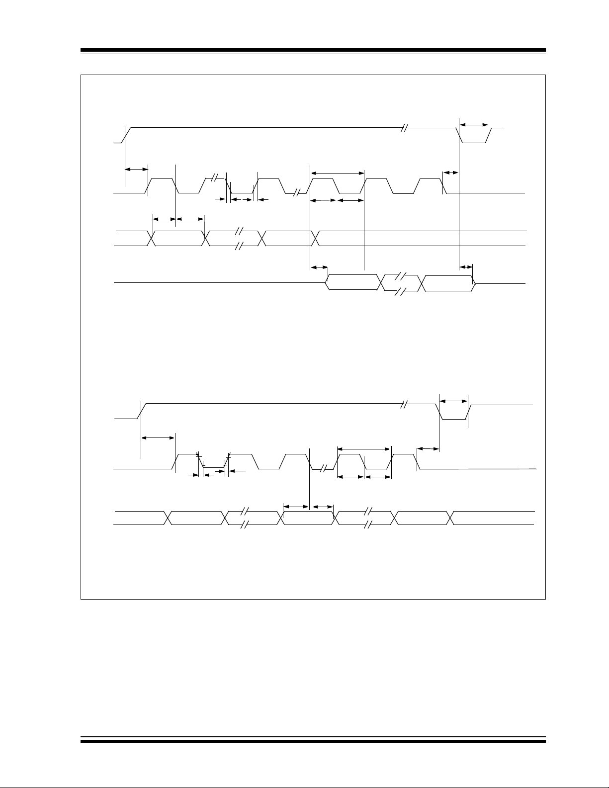
SPI READ DATA TRANSFER
(CP = 0, data shifted on rising edge of SCK, data clocked on falling edge of SCK, A7 = 0)
CE
1/f
t
CC
CLK
SCK
t
CCH
t
CWH
TC72
SDI
SDO
t
DC
A7
HIGH Z
t
CDH
MSb
t
t
R
F
A0
LSb
t
t
CH
CDD
D7
t
CL
MSb
SPI WRITE DATA TRANSFER
(CP = 0, data shifted on rising edge of SCK, data clocked on falling edge of SCK, A7 = 1)
CE
1/f
t
CC
CLK
SCK
t
t
R
F
t
t
DC
CDH
t
t
CL
CH
t
CCH
D0
t
CWH
LSb
t
CDZ
HIGH Z
SDI
A7 = 1
Note:
MSb LSb MSb LSb
The timing diagram is drawn with CP = 0. The
A0
D7 D0
TC72
also functions with CP = 1;
however, the edges of SCK are reversed as defined in Table 3-3 and Figure 3-2.
FIGURE 1-1: Serial Port Timing Diagrams.
2002 Microchip Technology Inc. DS21743A-page 5
TC72
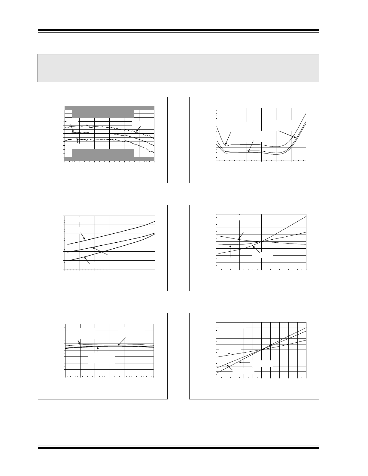
2.0 TYPICAL PERFORMANCE CURVES
Note: The graphs and tables provided following this note are a statistical summary based on a limited number of
samples and are provided for informational purposes only. The performance characteristics listed herein
are not tested or guaranteed. In some graphs or tables, the data presented may be outside the specified
operating range (e.g., outside specified power supply range) and therefore outside the warranted range.
Note: Unless otherwise indicated, all parameters apply at V
3.5
3
2.5
2
1.5
Mean
1
0.5
0
-0.5
-1
-1.5
-2
-2.5
Temperature Error (°C)
-3
-3.5
-55 -25 5 35 65 95 125
Upper Specification Limit
Mean + 3V
Mean - 3V
Lower Specification Limit
Reference Temperature (°C)
FIGURE 2-1: Accuracy vs. Temperature
(TC72-X.XMXX).
260
TC72-X.XMXX
250
TA = +25°C
240
230
220
210
Supply Current (µA)
200
2.5 3.0 3.5 4.0 4.5 5.0 5.5
TA = +125°C
TA = -55°C
Supply Voltage (V)
= 2.65V to 5.5V, TA = -55°C to +125°C.
DD
0.20
0.15
TC72-5.0MXX
= 5.0V
V
DD
0.10
0.05
Shutdown Current (µA)
0.00
-55 -25 5 35 65 95 125
TC72-5.0MXX
V
DD
Temperature (°C)
= 2.8V
TC72-3.3MXX
= 3.3V
V
DD
FIGURE 2-4: Shutdown Current vs.
Temperature.
0.4
TC72-2.8MXX
0.3
0.2
0.1
0.0
-0.1
-0.2
-0.3
Temperature Change (°C)
-0.4
2.6 2.7 2.8 2.9 3.0
T
A
TA = +25°C
= +85°C
TA = -25°C
Supply Voltage (V)
FIGURE 2-2: Supply Current vs. Supply
Voltage.
400
350
TC72-5.0MXX
= 5.0V
V
DD
300
250
200
150
100
Supply Current (uA)
50
0
-55-255 356595125
TC72-2.8MXX
= 2.8V
V
DD
Temperature (°C)
TC72-3.3MXX
= 3.3V
V
DD
FIGURE 2-3: Supply Current vs.
Temperature.
FIGURE 2-5: Temperature Accuracy vs.
Supply Voltage (TC72-2.8MXX).
1.0
TC72-5.0MXX
0.8
0.6
0.4
0.2
TA = +85°C
0.0
-0.2
-0.4
-0.6
-0.8
Temperature Change (°C)
-1.0
4.5 4.6 4.7 4.8 4.9 5.0 5.1 5.2 5.3 5.4 5.5
TA = +25°C
TA = -25°C
Supply Voltage (V)
FIGURE 2-6: Temperature Accuracy vs.
Supply Voltage (TC72-5.0MXX).
DS21743A-page 6 2002 Microchip Technology Inc.
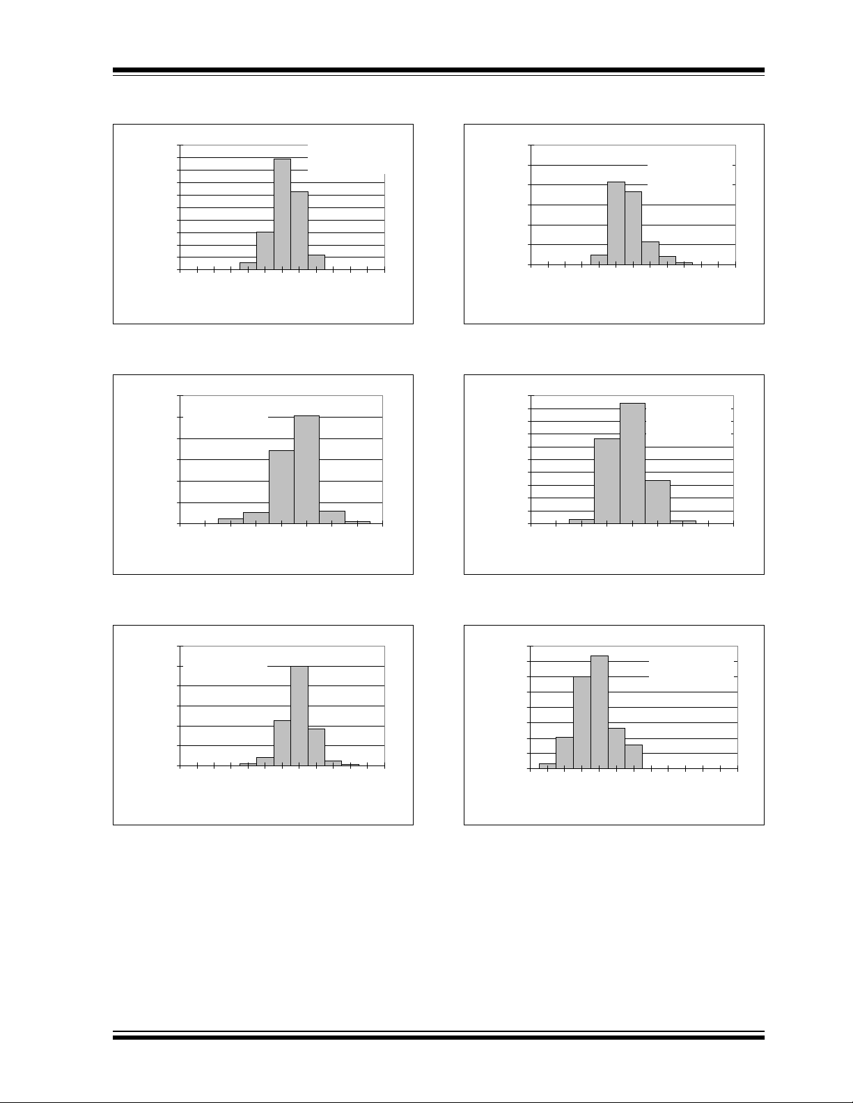
TC72
Note: Unless otherwise indicated, all parameters apply at V
50
45
40
35
30
25
20
15
10
5
0
Percentage of Occurances (%)
-3
-2.5-2-1.5-1-0.5
Temperature Error (°C)
TC72-X.XMXX
Sample Size = 166
= -55°C
T
A
0
0.511.522.5
3
FIGURE 2-7: Histogram of Temperature
Accuracy at -55 Degrees C.
60
TC72-X.XMXX
Sample Size = 166
50
= -40°C
T
A
40
30
20
10
0
Percentage of Occurances (%)
-2 -1.5 -1 -0.5 0 0.5 1 1.5 2
Temperature Error (°C)
= 2.65V to 5.5V, TA = -55°C to +125°C.
DD
60
50
40
30
20
10
0
Percentage of Occurances (%)
-1.50
-1.25
-1.00
-0.75
-0.50
Temperature Error (°C)
TC72-X.XMXX
Sample Size = 166
T
A
0.00
0.25
-0.25
= +65°C
0.50
0.75
FIGURE 2-10: Histogram of Temperature
Accuracy at +65 Degrees C.
50
45
40
35
30
25
20
15
10
5
0
Percentage of Occurances (%)
-2 -1.5 -1 -0.5 0 0.5 1 1.5 2
Temperature Error (°C)
TC72-X.XMXX
Sample Size = 166
= +85°C
T
A
1.00
1.25
1.50
FIGURE 2-8: Histogram of Temperature
Accuracy at -40 Degrees C.
60
TC72-X.XMXX
50
Sample Size = 166
= +25°C
T
A
40
30
20
10
0
Percentage of Occurances (%)
0.00
0.25
0.50
0.75
1.00
1.25
-1.50
-1.25
-1.00
-0.75
-0.50
Temperature Error (°C)
-0.25
1.50
FIGURE 2-9: Histogram of Temperature
Accuracy at +25 Degrees C.
FIGURE 2-11: Histogram of Temperature
Accuracy at +85 Degrees C.
40
35
30
25
20
15
10
5
0
Percentage of Occurances (%)
-3
-2.5-2-1.5-1-0.5
Temperature Error (°C)
TC72-X.XMXX
Sample Size = 166
= +125°C
T
A
0
0.511.522.5
3
FIGURE 2-12: Histogram of Temperature
Accuracy at +125 Degrees C.
2002 Microchip Technology Inc. DS21743A-page 7
TC72
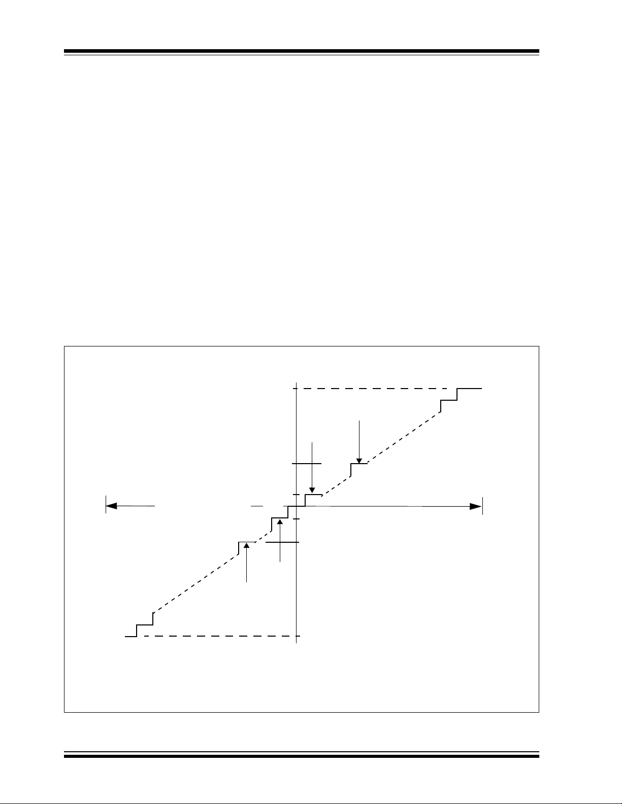
3.0 FUNCTIONAL DESCRIPTION
The TC72 consists of a band-gap type temperature
sensor, a 10-bit Sigma Delta Analog-to-Digital Converter (ADC), an internal conversion oscillator and a
double buffer digital output port. The 10-bit ADC is
scaled from -128°C to +127°C; therefore, the resolution
is 0.25°C per bit. The ambient temperature operating
range of the TC72 is specified from -55°C to +125°C.
This device features a four-wire serial interface that is
fully compatible with the SPI specification and, therefore, allows simple communications with common
microcontrollers and processors. The TC72 can be
used either in a Continuous Temperature Conversion
mode or a One-Shot Conversion mode. The TC72 temperature measurements are performed in the background and, therefore, reading the temperature via the
serial I/O lines does not affect the measurement in
progress.
MSB LSB
0111 1101 / 0000 0000
The Continuous Conversion mode measures the temperature approximately every 150 ms and stores the
data in the temperature registers. The TC72 has an
internal clock generator that controls the automatic
temperature conversion sequence. The automatic temperature sampling operation is repeated indefinitely
until the TC72 is placed in a shutdown mode by a write
operation to the Control register. The TC72 will remain
in the shutdown mode until the shutdown bit in the
Control register is reset.
In contrast, the One-Shot mode performs a single temperature measurement and returns to the power-saving shut down mode. This mode is especially useful for
low power applications.
Output
Code
Te m p
+25°C
+0.25°C
MSB LSB
0001 1001 / 0000 0000
MSB LSB
0000 0000 / 0100 0000
MSB LSB
0000 00 00 / 0000 0000
-55°C
-25°C
Note: The ADC converter is scaled from -128°C to -127°C, but the operating range of the
TC72 is specified from -55°C to +125°C.
0°C
-0.125°C
MSB LSB
1111 1111 / 1100 0000
MSB LSB
1110 0111 / 0000 0000
MSB LSB
1100 1001 / 0000 0000
Tem p
+125°C
FIGURE 3-1: Temperature-To-Digital Transfer Function (Non-linear Scale).
DS21743A-page 8 2002 Microchip Technology Inc.

TC72
3.1 Temperature Data Format
Temperature data is represented by a 10-bit two’s complement word with a resolution of 0.25°C per bit. The
temperature data is stored in the Temperature registers
in a two’s complement format. The ADC converter is
scaled from -128°C to +127°C, but the operating range
of the TC72 is specified from -55°C to +125°C.
Example:
Temperature = 41.5°C
MSB Temperature Register= 00101001b
=2
5
+ 23 + 2
0
= 32 + 8 + 1 = 41
LSB Temperature Register = 10000000b = 2
-1
= 0.5
TABLE 3-1: TC72 TEMPERATURE
OUTPUT DATA
Temperature
+125°C 0111 1101/0000 0000 7D00
+25°C 0001 1001/0000 0000 1900
+0.5°C 0000 0000/1000 0000 0080
+0.25°C 0000 0000/0100 0000 0040
0°C 0000 0000/0000 0000 0000
-0.25°C 1111 1111/1100 0000 FFC0
-25°C 1110 0111/0000 0000 E700
-55°C 1100 1001/0000 0000 C900
Binary
MSB / LSB
Hex
TABLE 3-2: TEMPERATURE REGISTER
D7 D6 D5 D4 D3 D2 D1 D0
Sign 2
6252423232120
-12-2
2
000000
Address/
Register
02H
Te m p . M S B
01H
Temp . L S B
3.2 Power-Up And Power-Down
The TC72 is in the low power consumption shutdown
mode at power-up. The Continuous Temperature Conversion mode is selected by performing a Write operation to the Control register, as described in Section 4.0,
“Internal Register Structure”.
A supply voltage lower than 1.6V (typical) is considered
a power-down state for the TC72. If the supply voltage
drops below the 1.6V threshold, the internal registers
are reset to the power-up default state.
3.3 Serial Bus Interface
The serial interface consists of the Chip Enable (CE),
Serial Clock (SCK), Serial Data Input (SDI) and Serial
Data Output (SDO) signals. The TC72 operates as a
slave and is compatible with the SPI bus specifications.
The serial interface is designed to be compatible with
the Microchip PICmicro
The CE input is used to select the TC72 when multiple
devices are connected to the serial clock and data
lines. The CE is active-high, and data is written to or
read from the device, when CE is equal to a logic high
voltage. The SCK input is disabled when CE is low. The
rising edge of the CE line initiates a read or write operation, while the falling edge of CE completes a read or
write operation.
The SCK input is provided by the external microcontroller and is used to synchronize the data on the SDI and
SDO lines. The SDI input writes data into the TC72’s
Control register, while the SDO outputs the temperature data from the Temperature register and the status
of Shutdown bit of the Control register.
The TC72 has the capability to function with either an
active-high or low SCK input. The SCK inactive state is
detected when the CE signal goes high, while the
polarity of the clock input (CP) determines whether the
data is clocked and shifted on either the rising or falling
edge of the system clock, as shown in Figure 3-2.
Table 3-3 gives the appropriate clock edge used to
transfer data into and out of the registers. Each data bit
is transferred at each clock pulse, and the data bits are
clocked in groups of eight bits, as shown in Figure 3-3.
The address byte is transferred first, followed by the
data. A7, the MSb of the address, determines whether
a read or write operation will occur. If A7 = ‘0’, one or
more read cycles will occur; otherwise, if A7 = ‘1’, one
or more write cycles will occur.
Data can be transferred either in a single byte or a
multi-byte packet, as shown in Figure 3-3. In the 3-byte
packet, the data sequence consists of the MSb temperature data, LSb temperature data, followed by the Control register data. The multi-byte read feature is initiated
by writing the highest address of the desired packet to
registers. The TC72 will automatically send the register
addressed and all of the lower address registers, as
long as the Chip Enable pin is held active.
®
family of microcontrollers.
2002 Microchip Technology Inc. DS21743A-page 9

TC72
TABLE 3-3: OPERATIONAL MODES
Mode CE SCK (Note 1) SDI SDO
Disable L Input Disabled Input Disabled High Z
Write (A7 = 1)HCP=1, Data Shifted on Falling Edge,
Data Clocked on Rising Edge
CP=0, Data Shifted on Rising Edge,
Data Clocked on Falling Edge
Read (A7 = 0)HCP=1, Data Shifted on Falling Edge,
Data Clocked on Rising Edge
CP=0, Data Shifted on Rising Edge,
Data Clocked on Falling Edge
Note 1: CP is the Clock Polarity of the microcontroller system clock. If the inactive state of SCK is logic level high,
CP is equal to ‘1’; otherwise, if the inactive state of SCK is low, CP is equal to ‘0’.
2: During a Read operation, SDO remains at a high impedance (High Z) level until the eight bits of data begin
to be shifted out of the Temperature register.
3.4 Read Operation
Data Bit Latch High Z
X Next data bit shift,
Note 2
The temperature and control register data is outputted
from the TC72 using the CE, SCK and SDO lines.
Figure 3-3 shows a timing diagram of the read operation. Communication is initiated by the chip enable (CE)
going high. The SDO line remains at the voltage level
of the LSb bit that is outputted and goes to the tri-state
level when the CE line goes to a logic low level.
3.5 Write Operation
Data is clocked into the Control register in order to
enable the TC72’s power saving shutdown mode. The
write operation is shown in Figure 3-3 and is
accomplished using the CE, SCK and SDI line.
CP = 0
CE
SCK
SHIFT
EDGE
CP = 1
CE
SCK
SHIFT
EDGE
CLOCK
EDGE
CLOCK
EDGE
FIGURE 3-2: Serial Clock Polarity (CP)
Operation.
DS21743A-page 10 2002 Microchip Technology Inc.

Single Byte Write Operation
(CP=0, data shifted on rising edge of SCK, data clocked on falling edge of SCK, A7=1)
CE
TC72
SCK
1
2 3 4 5 6 7 8 9 10 11 12 13 14 15 16
A7=1
A
SDI
A A A A A A A D D D D D D D D
7654321076543210
MSb LSb
SDO
High Z
Single Byte Read Operation
(CP=0, data shifted on rising edge of SCK, data clocked on falling edge of SCK, A7=0)
CE
SCK
2 3 4 5 6 7 8 9 10 11 12 13 14 15 16
1
A7=0
A
SDI
SDO
A A A A A A A
76543210
High Z
D D
70
High Z
MSb LSb
SPI Multiple Byte Transfer
CE
SCK
Write Operation
(CP=0, data shifted on rising edge of SCK, data clocked on falling edge of SCK, A7=1)
SDI
Address Byte = 80hex
A7 A0
SDO
Control Byte
D7 D0
High Z
Read Operation
(CP=0, data shifted on rising edge of SCK, data clocked on falling edge of SCK, A7=0)
SDI
Address Byte = 02hex
A0
MSB Temp. Byte
D7 D0 D7 D0
LSB Temp. Byte
SDO
A7
High Z High Z
FIGURE 3-3: Serial Interface Timing Diagrams (CP=0).
Control Byte
D7
D0
2002 Microchip Technology Inc. DS21743A-page 11

TC72
4.0 INTERNAL REGISTER
STRUCTURE
The TC72 registers are listed below.
TABLE 4-1: REGISTERS FOR TC72
Register
Control 00hex 80hex 000One-Shot
LSB Temperature 01hex N/A T1 T0 0 0 000 0 00hex
MSB Temperature 02hex N/A T9 T8 T7 T6 T5 T4 T3 T2 00hex
Manufacturer ID 03hex N/A 010 1 010 0 54hex
Read
Address
Write
Address
Bit7Bit6 Bit
5
Bit
4
(OS)
Bit3Bit2Bit
010Shutdown
1
Bit
0
(SHDN)
Value on
POR/BOR
05hex
4.1 Control Register
The Control register is both a read and a write register
that is used to select either the Shutdown, Continuous
or One-Shot Conversion operating mode. The Temperature Conversion mode selection logic is shown in
Table 4-2. The Shutdown (SHDN) bit is stored in bit 0
of the Control register. If SHDN is equal to ‘1’, the TC72
will go into the power-saving shutdown mode. If SHDN
is equal to ‘0’, the TC72 will perform a temperature
conversion approximately every 150 ms.
At power-up, the SHDN bit is set to ‘1’. Thus, the TC72
is in the shutdown operating mode at startup. The Continuous Temperature Conversion mode is selected by
writing a ‘0’ to the SHDN bit of the Control register.
The Shutdown mode can be used to minimize the
power consumption of the TC72 when active temperature monitoring is not required. The shutdown mode
disables the temperature conversion circuitry; however, the serial I/O communication port remains active.
A temperature conversion will be initialized by a Write
operation to the Control register to select either the
Continuous Temperature Conversion or the One-Shot
operating mode. The temperature data will be available
in the MSB and LSB Temperature registers approximately 150 ms after the Control register Write
operation.
The One-Shot mode is selected by writing a ‘1’ into bit
4 of the Control register. The One-Shot mode performs
a single temperature measurement and returns to the
power-saving shutdown mode. After completion of the
temperature conversion, the One-Shot bit (OS) is reset
to ‘0’ (i.e. “OFF”). The user must set the One-Shot bit
to ‘1’ to initiate another temperature conversion.
Bits 1, 3, 5, 6 and 7 of the Control register are not used
by the TC72. Bit 2 is set to a logic ‘1’. Any write operation to these bit locations will have no affect on the
operation of the TC72.
4.2 Temperature Register
The Temperature register is a read-only register and
contains a 10-bit two’s complement representation of
the temperature measurement. Bit 0 through Bit 5 of
the LSB Temperature register are always set to a logic
‘0’.
At Power-On Reset (POR) or a Brown-Out Reset
(BOR) low voltage occurrence, the temperature register is reset to all zeroes, which corresponds to a temperature value of 0°C. A V
1.6V is considered a reset event and will reset the
Temperature register to the power-up state.
power supply less than
DD
4.3 Manufacturer ID Register
The Manufacturer Identification (ID) register is a readonly register used to identify the temperature sensor as
a Microchip component.
TABLE 4-2: CONTROL REGISTER TEMPERATURE CONVERSION MODE SELECTION
Operational Mode One-Shot (OS) Bit 4 Shutdown (SHDN) Bit 0
Continuous Temperature Conversion 00
Shutdown 01
Continuous Temperature Conversion
(One-Shot Command is ignored if SHDN = ‘0’)
One-Shot 11
DS21743A-page 12 2002 Microchip Technology Inc.
10

5.0 APPLICATIONS INFORMATION
The TC72 does not require any additional components
in order to measure temperature; however, it is recommended that a decoupling capacitor of 0.1mF to 1mF
be provided between the V
the current consumption of the TC72 is modest
(250 mA, typical), the TC72 contains an on chip data
acquisition with internal digital switching circuitry. Thus,
it is considered good design practice to use an external
decoupling capacitor with the sensor. A high frequency
ceramic capacitor should be used and be located as
close as possible to the IC power pins in order to
provide effective noise protection to the TC72.
The TC72 measures temperature by monitoring the
voltage of a diode located on the IC die. The IC pins of
the TC72 provide a low impedance thermal path
between the die and the PCB, allowing the TC72 to
effectively monitor the temperature of the PCB board.
The thermal path between the ambient air is not as efficient because the plastic IC housing package functions
as a thermal insulator. Thus the ambient air temperature (assuming that a large temperature gradient exists
between the air and PCB) has only a small effect on the
temperature measured by the TC72.
Note that the exposed metal center pad on the bottom
of the DFN package is connected to the silicon substrate. The center pad should be connected to either
the PCB ground plane or treated as a “No Connect” pin.
The mechanical dimensions of the center pad are given
in Section 6.0, “Packaging Information”, of this
datasheet.
A potential for self-heating errors can exist if the TC72
SPI communication lines are heavily loaded. Typically,
the self-heating error is negligible because of the relatively small current consumption of the TC72. A temperature accuracy error of approximately 0.5°C will
result from self-heating if the SPI communication pins
sink/source the maximum current specified for the
TC72. Thus to maximize the temperature accuracy, the
output loading of the SPI signals should be minimized.
and GND pins. Although
DD
TC72
2002 Microchip Technology Inc. DS21743A-page 13
TC72
6.0 PACKAGING INFORMATION
6.1 Taping Form
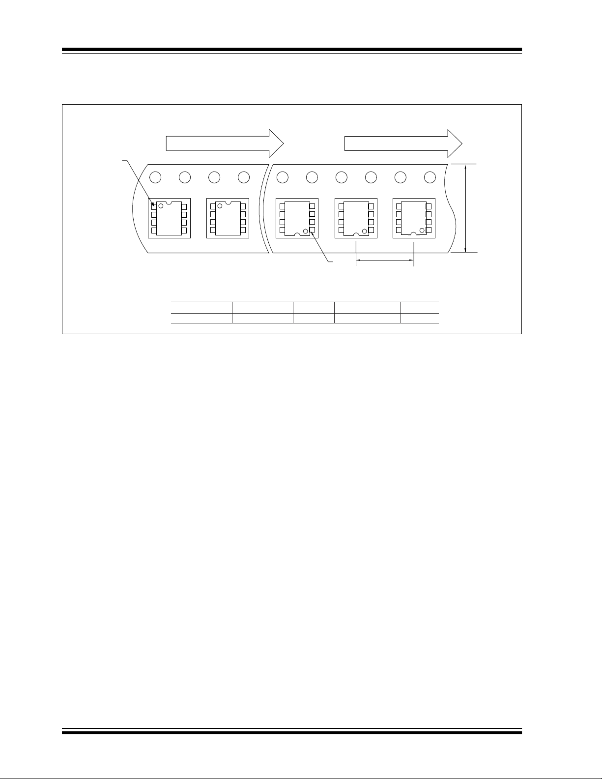
Component Taping Orientation for 8-Pin MSOP Devices
User Direction of Feed
PIN 1
PIN 1
User Direction of Feed
Standard Reel Component Orientation
for TR Suffix Device
Carrier Tape, Number of Components Per Reel and Reel Size
Package Carrier Width (W) Pitch (P) Part Per Full Reel Reel Size
8-Pin MSOP 12 mm 8 mm 2500 13 in
Reverse Reel Component Orientation
for RT Suffix Device
Tape and Reel information for the 8-Lead DFN package will be available TBD.
W
P
DS21743A-page 14 2002 Microchip Technology Inc.
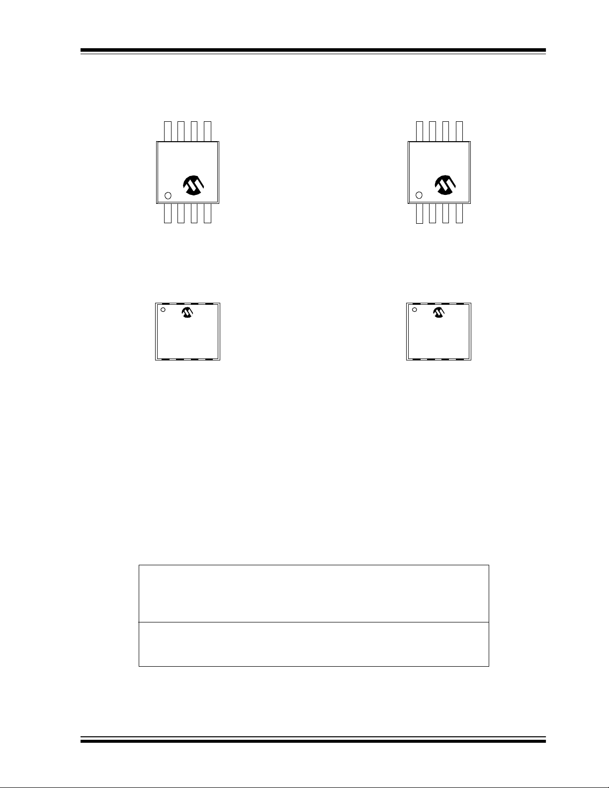
6.2 Package Marking Information
TC72
8-Lead MSOP
XXXXXX
YWWNNN
8-Lead DFN
XXXXXXXX
MYWW
NNN
Example:
TC722M
221067
Example
7228
8221
067
:
Legend: XX...X Customer specific information*
YY Year code (last 2 digits of calendar year)
WW Week code (week of January 1 is week ‘01’)
NNN Alphanumeric traceability code
Note: In the event the full Microchip part number cannot be marked on one line, it will
be carried over to the next line thus limiting the number of available characters
for customer specific information.
* Standard OTP marking consists of Microchip part number, year code, week code, and traceability code.
2002 Microchip Technology Inc. DS21743A-page 15

TC72
8-Lead Plastic Micro Small Outline Package (MS) (MSOP)
p
B
n 1
c
(F)
β
Dimension Limits
Number of Pins
Pitch
Overall Height
Molded Package Thickness
Standoff §
Overall Width
Molded Package Width
Overall Length
Foot Length
Foot Angle
Lead Thickness
Lead Width
Mold Draft Angle Top
Mold Draft Angle Bottom
*Controlling Parameter
§ Significant Characteristic
Notes:
Dimensions D and E1 do not include mold flash or protrusions. Mold flash or protrusions shall not
exceed .010" (0.254mm ) per side.
E1
E
D
2
A
Units
n
p
A
A2
A1
E
E1
D
L
φ
c
B
α
β
MIN
.030
.002
.184
.114
.114
.016
.004
.010
φ
L
INCHES
NOM
.026
.034
.193
.118
.118
.022
.037.035FFootprint (Reference)
0
.006
.012
A1
8
.044
.038
.006
.200
.122
.122
.028
6
.008
.016
7
7
MILLIMETERS*
MINMAX NOM
0.65
0.76
0.05
4.67
2.90
2.90
0.40
0
0.10
0.25
0.86
4.90
3.00
3.00
0.55
0.15
0.30
α
A2
MAX
8
1.18
0.97
0.15
.5.08
3.10
3.10
0.70
1.000.950.90.039
6
0.20
0.40
7
7
Drawing No. C04-111
DS21743A-page 16 2002 Microchip Technology Inc.

8-Lead Plastic Dual Flat Pack, No Lead (MF) 3x3x1 mm Body (DFN)
TC72
A3
E
TOP VIEW
A1
E2
p
2 1
n
L
D2
PIN 1
ID INDEX
AREA
(NOTE 2)
b
D
EXPOSED
METAL
PAD
BOTTOM VIEW
A
EXPOSED
TIE BAR
(NOTE 1)
Number of Pins
Pitch
Overall Height
Standoff
Lead Thickness
Overall Length
Exposed Pad Length
Overall Width
Exposed Pad Width
Lead Width
Lead Length
Dimension Limits
(Note 4)
(Note 4)
Units
MIN
n
p
A
A1
A3
E
E2
D
D2
b
L
INCHES
NOM
.026 BSC
.031
.000 .001
.008 REF.
.118 BSC
.055
.118 BSC
.047
.007
.012
.010
.019
MINMAX
8
.039
.002
.096
.069
.015
0.80
0.00
1.39
1.20
0.23
0.30.022
*Controlling Parameter
Notes:
Package may have one or more exposed tie bars at ends.1.
Pin 1 visual index feature may vary, but must be located within the hatched area.2.
Dimensions D and E do not include mold flash or protrusions. Mold flash or protrusions shall not
3.
exceed .010" (0.254mm) per side.
4.
Exposed pad dimensions vary with paddle size.
5. JEDEC equivalent: Pending
Drawing No. C04-062
MILLIMETERS*
NOM
8
0.65 BSC
0.90.035
0.02
0.20 REF.
3.00 BSC
3.00 BSC
0.26
0.48
MAX
1.00
0.05
2.45
1.75
0.37
0.55
2002 Microchip Technology Inc. DS21743A-page 17

TC72
8-Lead Plastic Dual Flat Pack, No Lead (MF) 3x3x1 mm Body (DFN)
Z G
X
CP
DFN LAND PATTERN
H
H2
p
Y
G2
THERMAL VIAS
ON 4 LAYER
PC BOARD
P1
0V
OPTIONAL FOUR LAYER
PCB LAND PATTERN
OPTIONAL TWO LAYER
PCB LAND PATTERN
Units
Dimension Limits
Terminal Pitch
Terminal Land Pattern O.D.
Terminal Land Pattern I.D.
Exposed Pad Clearance .006CP 0.15
Interior Lead Clearance Z .071 1.80
Terminal Land Width
Terminal Land Length
Exposed Pad Length
Optional Exposed Pad Length .130
Exposed Pad Width
Termal Via Pitch
Thermal Via Diameter
Minimum Solder Mask Clearance M .002 0.05
*Controlling Parameter
Notes:
Exposed pad dimensions vary with paddle size.1.
Drawing No. C04-2062
(Note 1)
A1
H2
G2
P1
MIN
p
Z
X
Y
H
V
M (TYP)
INCHES
NOM
.026 BSC
.134
.057
.033 .035 0.85 0.88
.130
.047
.012
TYPCAL SOLDER MASKS
MINMAX
.157
.060
3.40
1.45
3.30
3.30
MILLIMETERS*
NOM
0.65 BSC
1.20
0.30
MAX
4.00
1.53
0.420.35.014 .017
1.501.45.059.057
DS21743A-page 18 2002 Microchip Technology Inc.

TC72
ON-LINE SUPPORT
Microchip provides on-line support on the Microchip
World Wide Web site.
The web site is used by Microchip as a means to make
files and information easily available to customers. To
view the site, the user must have access to the Internet
and a web browser, such as Netscape
Internet Explorer. Files are also available for FTP
download from our FTP site.
Connecting to the Microchip Internet Web Site
The Microchip web site is available at the following
URL:
www.microchip.com
The file transfer site is available by using an FTP service to connect to:
ftp://ftp.microchip.com
The web site and file transfer site provide a variety of
services. Users may download files for the latest
Development Tools, Data Sheets, Application Notes,
User's Guides, Articles and Sample Programs. A variety of Microchip specific business information is also
available, including listings of Microchip sales offices,
distributors and factory representatives. Other data
available for consideration is:
• Latest Microchip Press Releases
• Technical Support Section with Frequently Asked
Questions
• Design Tips
• Device Errata
• Job Postings
• Microchip Consultant Program Member Listing
• Links to other useful web sites related to
Microchip Products
• Conferences for products, Development Systems,
technical information and more
• Listing of seminars and events
®
or Microsoft
SYSTEMS INFORMATION AND
UPGRADE HOT LINE
The Systems Information and Upgrade Line provides
system users a listing of the latest versions of all of
Microchip's development systems software products.
®
Plus, this line provides information on how customers
can receive the most current upgrade kits.The Hot Line
Numbers are:
1-800-755-2345 for U.S. and most of Canada, and
1-480-792-7302 for the rest of the world.
092002
2002 Microchip Technology Inc. DS21734A-page19

TC72
READER RESPONSE
It is our intention to provide you with the best documentation possible to ensure successful use of your Microchip product. If you wish to provide your comments on organization, clarity, subject matter, and ways in which our documentation
can better serve you, please FAX your comments to the Technical Publications Manager at (480) 792-4150.
Please list the following information, and use this outline to provide us with your comments about this document.
To :
RE: Reader Response
From:
Application (optional):
Would you like a reply? Y N
Device:
Questions:
1. What are the best features of this document?
2. How does this document meet your hardware and software development needs?
3. Do you find the organization of this document easy to follow? If not, why?
Technical Publications Manager
Name
Company
Address
City / State / ZIP / Country
Telephone: (_______) _________ - _________
TC72
Literature Number:
Total Pages Sent ________
FAX: (______) _________ - _________
DS21734A
4. What additions to the document do you think would enhance the structure and subject?
5. What deletions from the document could be made without affecting the overall usefulness?
6. Is there any incorrect or misleading information (what and where)?
7. How would you improve this document?
DS21734A-page20 2002 Microchip Technology Inc.

PRODUCT IDENTIFICATION SYSTEM
To order or obtain information, e.g., on pricing or delivery, refer to the factory or the listed sales office.
PART NO. -X.X XX
Device
Range
Device: TC72: Digital Temperature Sensor w/SPI Interface
Voltage Range: 2.8 = Accuracy Optimized for 2.8V
Temperature Range: M = -55°C to +125°C
Package: MF = Dual, Flat, No Lead (DFN) (3x3mm), 8-lead
3.3 = Accuracy Optimized for 3.3V
5.0 = Accuracy Optimized for 5.0V
MFTR = Dual, Flat, No L ead (DFN) (3x3mm), 8-lead
UA = Plastic Micro Small Outline (MSOP), 8-le ad
UATR = Plastic Micro Smal l Outline (MSOP), 8-lead
X
Temp era tur e
Range
(Tape and Reel)
(Tape and Reel)
PackageVoltag e
Examples:
a) TC72- 2.8MUA: Digital Temperature Sensor,
2.8V, 8LD MSOP package.
b) TC72- 2.8MUATR:
sor, 2.8V, 8LD MSOP (tape and reel) package.
c) TC72-2.8MMF: Digital Temperature Sensor,
2.8V, 8LD DFN package.
d) TC72- 3.3MUA:
3.3V, 8LD MSOP package.
e) TC72-3.3MMF: Digital Temperature Sensor,
3.3V, 8LD DFN package.
f) TC72- 5.0MUA:
5.0V, 8LD MSOP package.
g) TC72-5.0MMF: Digital Temperature Sensor,
5.0V, 8LD DFN package.
h) TC72-5.0MMFTR:
sor, 5.0V, 8LD DFN (tape an d reel) package.
TC72
Digital Temperature Sen-
Digital Temperature Sensor,
Digital Temperature Sensor,
Digital Temperature Sen-
Sales and Support
Data Sheets
Products supported by a preliminary Data Sheet may have an errata sheet describing minor operational differences and recommended workarounds. To determine if an errata sheet exists for a particular device, please contact one of the following:
1. Your local Microchip sales office
2. The Microchip Corporate Literature Center U.S. FAX: (480) 792-7277
3. The Microchip Worldwide Site (www.microchip.com)
Please specify which device, revision of silicon and Data Sheet (include Literature #) you are using.
New Customer Notification System
Register on our web site (www.microchip.com/cn) to receive the most current information on our products.
2002 Microchip Technology Inc. DS21743A-page21

TC72
NOTES:
DS21743A-page 22 2002 Microchip Technology Inc.

Information contained in this publication regarding device
applications and the like is intended through suggestion only
and may be superseded by updates. It is your responsibility to
ensure that your application meets with your specifications.
No representation or warranty is given and no liability is
assumed by Microchip Technology Incorporated with respect
to the accuracy or use of such information, or infringement of
patents or other intellectual property rights arising from such
use or otherwise. Use of Microchip’s products as critical components in life support systems is not authorized except with
express written approval by Microchip. No licenses are conveyed, implicitly or otherwise, under any intellectual property
rights.
Trademarks
The Microchip name and logo, the Microchip logo, K
EELOQ
MPLAB, PIC, PICmicro, PICSTART and PRO MATE are
registered trademarks of Microchip Technology Incorporated
in the U.S.A. and other countries.
FilterLab, microID, MXDEV, MXLAB, PICMASTER, SEEVAL
and The Embedded Control Solutions Company are
registered trademarks of Microchip Technology Incorporated
in the U.S.A.
dsPIC, dsPICDEM.net, ECONOMONITOR, FanSense,
FlexROM, fuzzyLAB, In-Circuit Serial Programming, ICSP,
ICEPIC, microPort, Migratable Memory, MPASM, MPLIB,
MPLINK, MPSIM, PICC, PICDEM, PICDEM.net, rfPIC, Select
Mode and Total Endurance are trademarks of Microchip
Technology Incorporated in the U.S.A. and other countries.
Serialized Quick Turn Programming (SQTP) is a service mark
of Microchip Technology Incorporated in the U.S.A.
All other trademarks mentioned herein are property of their
respective companies.
© 2002, Microchip Technology Incorporated, Printed in the
U.S.A., All Rights Reserved.
Printed on recycled paper.
,
Microchip received QS-9000 quality system
certification for its worldwide headquarters,
design and wafer fabrication facilities in
Chandler and Tempe, Arizona in July 1999
and Mountain View, California in March 2002.
The Company’s quality system processes and
procedures are QS-9000 compliant for its
PICmicro
devices, Serial EEPROMs, microperipherals,
non-volatile memory and analog produ cts. In
addition, Microchip’s qua lity system for the
design and manufacture of development
systems is ISO 9001 certified.
®
8-bit MCUs, KEEL
®
code hopping
OQ
2002 Microchip Technology Inc. DS21743A - page 23

M
W
ORLDWIDE SALES AND SERVICE
AMERICAS
Corporate Office
2355 West Chandler B lvd.
Chandler, AZ 85224-6199
Tel: 480-792-7200 Fax: 480-792-7277
Technical Support: 480-792-7627
Web Address: http://www.microchip.com
Rocky Mountain
2355 West Chandler B lvd.
Chandler, AZ 85224-6199
Tel: 480-792-7966 Fax: 480-792-4338
Atlanta
500 Sugar Mill Road, Suite 200B
Atlanta, GA 30350
Tel: 770-640-0034 Fax: 770-640-0307
Boston
2 Lan Drive, Suit e 120
Westford, MA 01886
Tel: 978-692-3848 Fax: 978-692-3821
Chicago
333 Pierce Road, S uite 180
Itasca, IL 60143
Tel: 630-285-0071 Fax: 630-285-0075
Dallas
4570 Westgrove Drive, Suite 160
Addison, TX 75001
Tel: 972-818-7423 Fax: 972-818-2924
Detroit
Tri-Atria Office Building
32255 Northwestern Highway, Suite 190
Farmington Hills, MI 48334
Tel: 248-538-2250 Fax: 248-538-2260
Kokomo
2767 S. Albright Road
Kokomo, Indiana 46902
Tel: 765-864-8360 Fax: 765-864-8387
Los Angeles
18201 Von Karman, Suite 10 90
Irvine, CA 92612
Tel: 949-263-1888 Fax: 949-263-1338
New York
150 Motor Parkwa y, Suite 202
Hauppauge, NY 11788
Tel: 631-273-5305 Fax: 631-273-5335
San Jose
Microchip Technology Inc.
2107 North First S treet, Suite 590
San Jose, CA 95131
Tel: 408-436-7950 Fax: 408-436-7955
Toro nto
6285 Northam Drive, Suite 108
Mississauga, Ontario L4V 1X5, Canada
Tel: 905-673-0699 Fax: 905-673-6509
ASIA/PACIFIC
Australia
Microchip Technology Australia Pty Ltd
Suite 22, 41 Rawson Street
Epping 2121, NSW
Australia
Tel: 61-2-9868-6733 Fax: 61-2-9868-6755
China - Beijing
Microchip Technology Consulting (Shanghai)
Co., Ltd., Beijing Liaison Office
Unit 915
Bei Hai Wan Tai Bldg.
No. 6 Chaoyangmen Beidajie
Beijing, 100027, No. China
Tel: 86-10-852821 00 Fax: 86-10-852 82104
China - Chengdu
Microchip Technology Consulting (Shanghai)
Co., Ltd., Chengdu Liaison Office
Rm. 2401, 24th Floor,
Ming Xing Financial Tower
No. 88 TIDU Street
Chengdu 610016, China
Tel: 86-28-867662 00 Fax: 86-28-867 66599
China - Fuzhou
Microchip Technology Consulting (Shanghai)
Co., Ltd., Fuzhou Liaison Office
Unit 28F, World Trade Plaza
No. 71 Wusi Road
Fuzhou 350001, China
Tel: 86-591-75035 06 Fax: 86-591-7503521
China - Shanghai
Microchip Technology Consulting (Shanghai)
Co., Ltd.
Room 701, Bldg. B
Far East International Plaza
No. 317 Xian Xia Road
Shanghai, 200051
Tel: 86-21-6275-5700 Fax: 86-21-6275-5060
China - Shenzhen
Microchip Technology Consulting (Shanghai)
Co., Ltd., Shenzhen L iaison Office
Rm. 1315, 13/F, Shenzhen Kerry Centre,
Renminnan Lu
Shenzhen 518001, Ch ina
Tel: 86-755-23503 61 Fax: 86-755-2366086
China - Hong Kong SAR
Microchip Technology Hongkong Ltd.
Unit 901-6, Tower 2, Metroplaza
223 Hing Fong Road
Kwai Fong, N.T., Hong Kong
Tel: 852-2401-120 0 Fax: 852-2401-3431
India
Microchip Technology Inc.
India Liaison Office
Divyasree Chambers
1 Floor, Wing A (A3/A4)
No. 11, O’Shaugnessey Road
Bangalore, 560 025, India
Tel: 91-80-229006 1 Fax: 91-80-2290 062
Japan
Microchip Technology Japan K.K.
Benex S-1 6F
3-18-20, Shinyokohama
Kohoku-Ku, Yokohama-shi
Kanagawa, 222-0033, Japan
Tel: 81-45-471- 6166 Fax: 81-45-471-6122
Korea
Microchip Technology Korea
168-1, Youngbo Bldg. 3 Floor
Samsung-Dong, Kangnam-Ku
Seoul, Korea 135-882
Tel: 82-2-554-7200 Fax: 82-2-558-593 4
Singapore
Microchip Technology Singapore Pte Ltd.
200 Middle Road
#07-02 Prime Centre
Singapore, 188980
Tel: 65-6334-8870 Fax: 65-6334-8850
Ta iw an
Microchip Technology (Barbados) Inc.,
Taiwan Branch
11F-3, No. 207
Tung Hua North Road
Taipei, 105, Taiwan
Tel: 886-2-2717-7175 Fax: 886-2-2545-0139
EUROPE
Austria
Microchip Technology Austria GmbH
Durisolstrasse 2
A-4600 Wels
Austria
Tel: 43-7242-2244-399
Fax: 43-7242-2244-393
Denmark
Microchip Technology Nordic ApS
Regus Business Centre
Lautrup hoj 1-3
Ballerup DK-2750 Denmark
Tel: 45 4420 9895 Fax: 45 4420 9910
France
Microchip Technology SARL
Parc d’Activite du Moulin de Massy
43 Rue du Saule Trapu
Batiment A - ler Etage
91300 Massy, France
Tel: 33-1-69-53-63-20 Fax: 33-1-69-30-90-79
Germany
Microchip Technology GmbH
Steinheilstrasse 10
D-85737 Ismaning, Germany
Tel: 49-89-627-144 0 Fax: 49-89-627-144-44
Italy
Microchip Technology SRL
Centro Direzionale Colleoni
Palazzo Taurus 1 V. Le Colleoni 1
20041 Agrate Brianza
Milan, Italy
Tel: 39-039-65791-1 Fax: 39-039-6899883
United Kingdom
Microchip Ltd.
505 Eskdale Road
Winnersh Triangle
Wokingham
Berkshire, England RG41 5TU
Tel: 44 118 921 5869 Fax: 44-118 921-5820
08/01/02
DS21743A-page 24 2002 Microchip Technology Inc.
 Loading...