

查询TC7129CJL713供应商
4-1/2 Digit Analog-to-Digital Converters with
TC7129
On-Chip LCD Drivers
Features:
• Count Resolution: ±19,999
• Resolution on 200mV Scale: 10 μV
• True Differential Input and Reference
• Low Power Consumption: 500 μA at 9V
• Direct LCD Driver for 4-1/2 D ig it s , Dec im al Po ints,
Low Battery Indicator, and Continuity Indicator
• Overrange and Underrange Outputs
• Range Select Input: 10:1
• High Common Mode Rejection Ratio: 110 dB
• External Phase Compensation Not Required
Applications:
• Full-Featured Multimeters
• Digital Measu rem en t Dev ic es
Device Selection Table
Package
Code
TC7129CPL Normal 40-Pin PDIP 0°C to +70°C
TC7129CKW Formed 44-Pin PQFP 0°C to +70°C
TC7129CLW – 44-Pin PLCC 0°C to +70°C
Pin
Layout
Package
Temperature
Range
General Description:
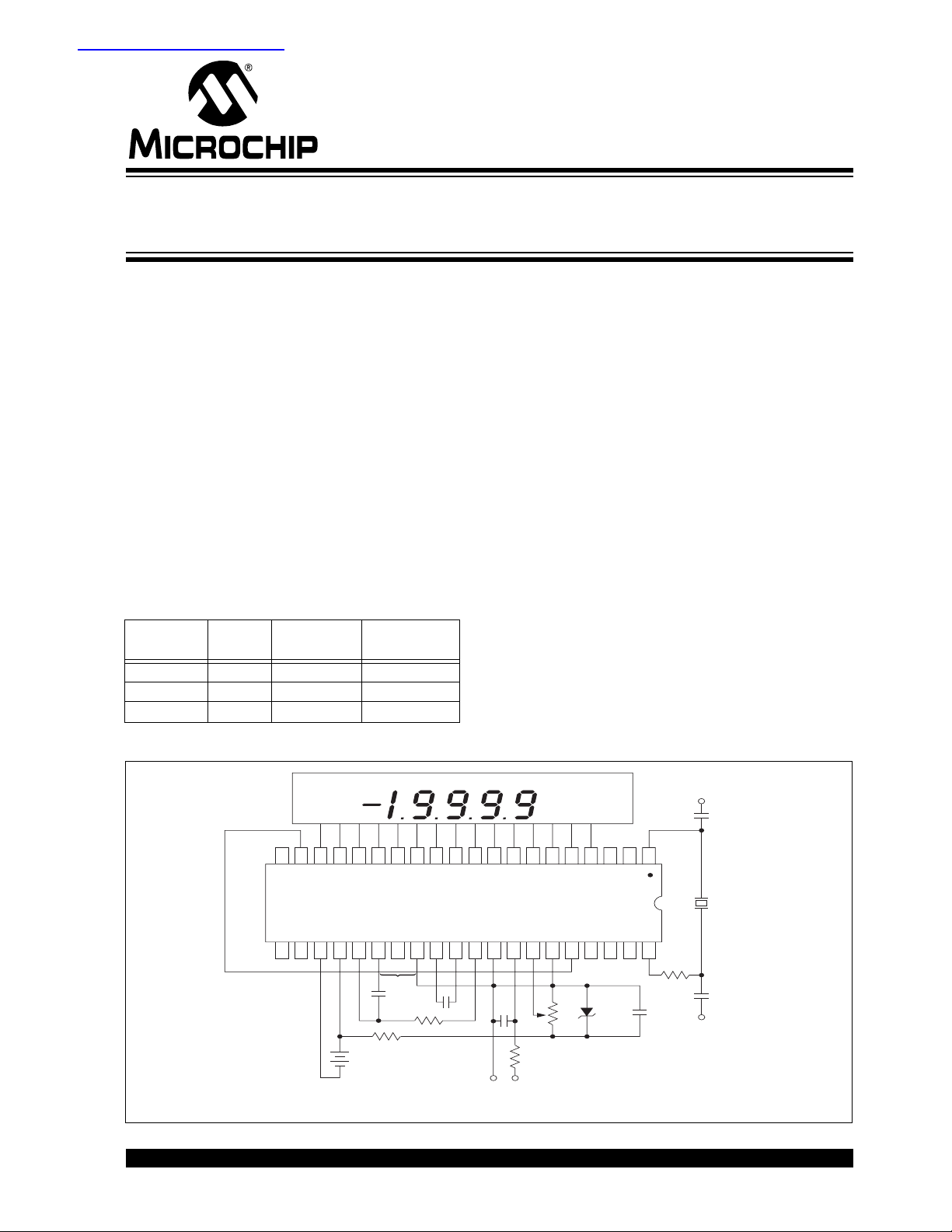
The TC7129 is a 4-1/2 di git Analog-to-Dig ital Con verter
(ADC) that directly drives a multiplexed Liquid Crystal
Display (LCD). Fabricated in high-performance, lowpower CMOS, the TC7129 ADC is designed specifically for high-resolution, battery-powered digital multimeter applications. The traditional dual-slope method
of A/D conversion has been enhanced with a successive integration technique to produce readings accurate to better than 0.005% of full-scale and resolution
down to 10 μV per count.
The TC7129 includes f eatures impor tant to multimeter
applications. It detects and ind icat es l ow bat ter y con dition. A continuity outp ut drives an annunciator on the
display and can be used with an external driver to sound
an audible alarm. Overrange and underrange o utputs,
along with a range-ch ange input, provi de the ability to
create auto-ranging instruments. For snapshot readings, the TC7129 includes a latch-and-hold input to
freeze the present reading. This combination of features
makes the TC7129 the ideal choice for full-featured
multimeter and digital measurement applications.
Typical Application
Low Battery
20
+
9V
*
N
ote
:
RC network between pins 26 and 28 is not required.
© 2006 Microchip Technology Inc. DS21459D-page 1
0.1 µF
10 kΩ
27262524232221
*
13141516171819
28
150 kΩ
1011
12
TC7129
29
+
1 µF
–
9
323130
0.1
µF
V
Continuity
8
33
100 kΩ
+
IN
V+
5 pF
1234567
120 kHz
3534
36
20
kΩ
39
40
3837
330 kΩ
10 pF
0.1 µF
V+
TC7129
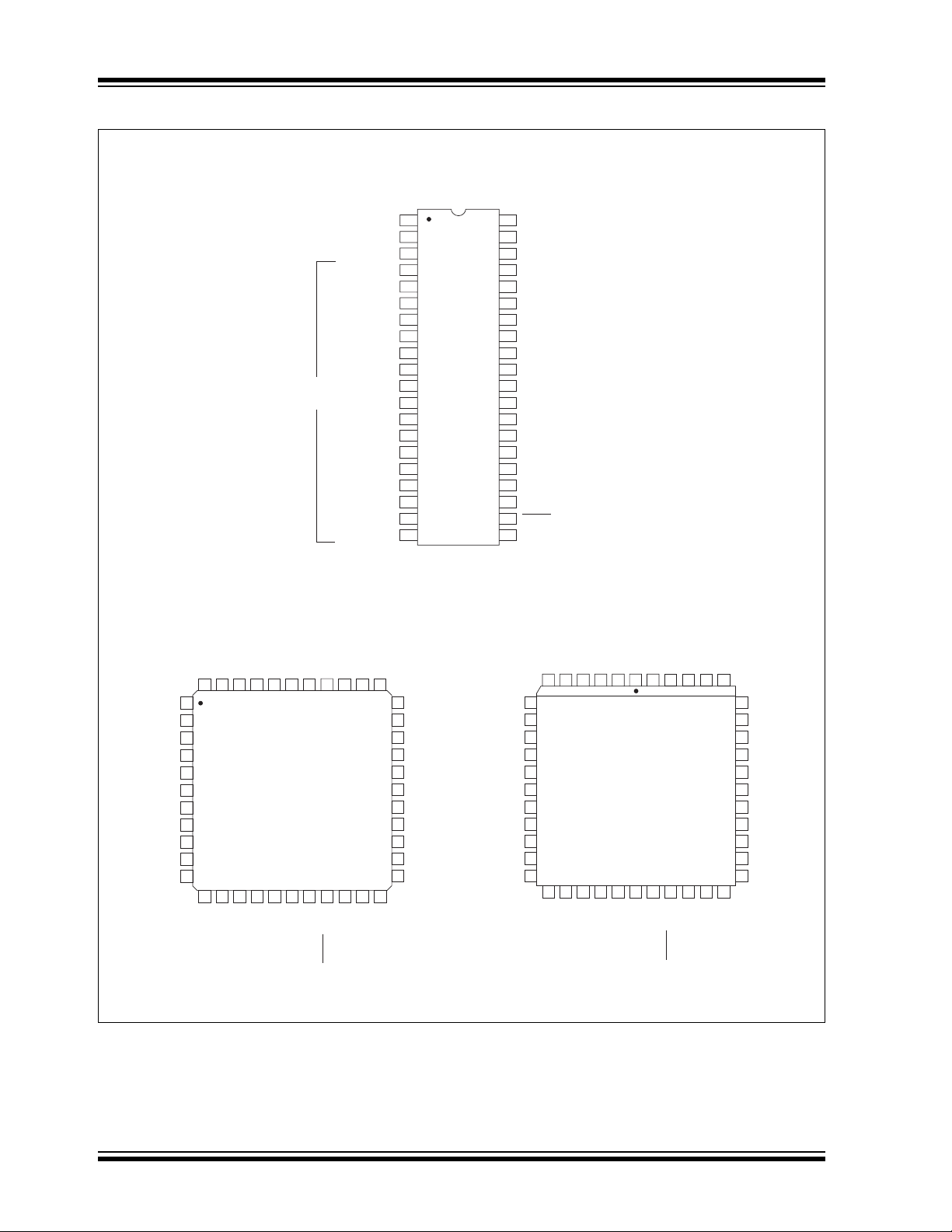
Package Types
ANNUNICATOR
B2, C2, LO BATT
Display
Output
Lines
B
, C1, CONT
1
A
F1, E1, DP
A
F2, E2, DP
B3, C
A
F3, E3, DP
B4, C
A4, G4, D
F4, E4, DP
, G1, D
1
, G2, D
2
MINUS
3
,
, G3, D
3
4
DP4/OR
OSC1
OSC3
BC
,
BP
BP
BP
V
DISP
40-Pin PDIP
1
2
3
4
5
1
6
1
7
8
2
9
2
10
11
3
12
3
13
5
14
4
15
4
16
3
17
2
18
1
19
20
TC7129CPL
40
39
38
37
36
35
34
33
32
31
30
29
28
27
26
25
24
23
22
21
OSC2
DP
1
DP
2
RANGE
DGND
REF LO
REF HI
IN HI
IN LO
BUFF
-
C
REF
+
C
REF
COMMON
CONTINUITY
INT OUT
INT IN
V+
V-
LATCH/HOLD
DP3/UR
, E1, DP
F
1
B2, C2, BATT
, G2, D
A
2
F2, E2, DP
B3, C
MINUS
3
,
A
, G3, D
3
F3, E3, DP
B4, C
A4, G4, D
F4, E4, DP
44-Pin QFP 44-Pin PLCC
1
, D
, CONT
1
1
, G
, C
1
1
ANNUNCIATOR
OSC3
A
44 43 42 41 39 3840
1
1
B
OSC1NCOSC2
2
3
2
4
2
5
NC
6
7
3
8
3
BC
9
4
5
,
10
4
11
4
12 13 14 15 17 18
BP3BP
1
2
BP
TC7129CKW
16
/OR
4
DISP
V
DP
NC
/UR
3
DP
1DP2
DP
RANGE
37 36 35 34
19 20 21 22
V-
V+
DGND
33
32
31
30
29
28
27
26
25
24
23
INT IN
REF LO
REF HI
IN HI
IN LO
BUFF
NC
C
-
REF
C
+
REF
COMMON
CONTINUITY
INT OUT
F1, E1, DP
B2, C2, BATT
, G2, D
A
2
F2, E2, DP
B3, C
3
,
A
, G3, D
3
F3, E3, DP
B4, C
A4, G4, D
F4, E4, DP
MINUS
NC
BC
4
,
LATCH/HOLD
1
, D
, CONT
1
1
, G
, C
1
1
A
B
6543 1442
7
1
8
9
2
10
2
11
12
13
3
3
5
4
4
18 19 20 21 23 24
3BP2
BP
ANNUNCIATOR
OSC3
OSC1NCOSC2
TC7129CLW
22
1
/OR
BP
DISP
4
V
DP
NC
/UR
3
DP
DP1DP2RANGE
43 42 41 40
25 26 27 28
V-
V+
LATCH/HOLD
DGND
39
38
37
36
35
34
33
3214
3115
3016
2917
INT IN
REF LO
REF HI
IN HI
IN LO
BUFF
NC
-
C
REF
C
+
REF
COMMON
CONTINUITY
INT OUT
DS21459D-page 2 © 2006 Microchip Technology Inc.
TC7129
1.0 ELECTRICAL
CHARACTERISTICS
Absolute Maximum Ratings*
Supply Voltage (V+ to V-).......................................15V
*Stresses above those listed under “Absolute Maximum
Ratings” may cause permanent damage to the device. These
are stress ratings only and functional operation of the device
at these or any other conditions above those indicated in the
operation sections of the specifications is not implied.
Exposure to Absolute Maximum Rating conditions for
extended periods may affect device reliability.
Reference Voltage (REF HI or REF LO)........ V+ to V–
Input Voltage (IN HI or IN LO) (Note 1).......... V+ to V–
.......................................... V+ to (DGND – 0.3V)
V
DISP
Digital Input (Pins 1, 2, 19, 20,
21, 22, 27, 37, 39, 40).......................... DGND to V+
Analog Input (Pins 25, 29, 30) ....................... V+ to V–
Package Power Dissipation (T
≤ 70°C)
A
Plastic DIP .....................................................1.23W
PLCC .............................................................1.23W
Plastic QFP....................................................1.00W
Operating Temperature Range ...............0°C to +70°C
Storage Temperature Range..............-65°C to +150°C
TC7129 ELECTRICAL SPECIFICATIONS
Electrica l Characteristics: V+ to V– = 9V, V
Pin numbers refer to 40-pin DIP.
Symbol Parameter Min Typ Max Unit Test Conditions
= 1V, TA = +25°C, f
REF
= 120 kHz, unless otherwise indicated.
CLK
Input
Zero Input Reading –0000 0000 +0000 Counts V
Zero Reading Drift — ±0.5 — μV/°C V
Ratiometric Reading 9996 — 10000 Counts VIN = V
= 0V, 200 mV scale
IN
= 0V, 0°C < TA < +70°C
IN
= 1000 mV,
REF
Range = 2V
Range Change Accuracy 0.9999 1.0000 1.0001 Ratio V
= 1V on High Range,
IN
= 0.1V on Low Range
V
IN
RE Rollover Error — 1 2 Counts VIN– = VIN+ = 199 mV
NL Linearity Error — 1 — Counts 200mV Scale
CMRR Common Mode Rejection Ratio — 110 — dB V
= 1V, VIN = 0V,
CM
200 mV scale
CMVR Common Mode Voltage Range — (V-) +
—VV
IN
= 0V
1.5
— (V+) – 1 — V 200mV scale
e
N
Noise (Peak-to-Peak Value not
Exceeded 95% of Time)
I
IN
Input Leakage Current — 1 1 0 pA VIN = 0V, pins 32, 33
Scale Factor Temperature
Coefficient
— 14—μV
P-PVIN
— 2 7 ppm/°C V
= 0V
200 mV scale
= 199 mV,
IN
0°C < T
External V
< +70°C
A
REF
= 0 ppm/°C
Note 1: Input voltages may exceed supply voltages, provided input current is limited to ±400 μA. Currents above
this value may result in invalid display readings, but will not destroy the device if limited to ±1 mA.
Dissipation ratings assume device is mounted with all leads soldered to printed circuit board.
© 2006 Microchip Technology Inc. DS21459D- page 3
TC7129
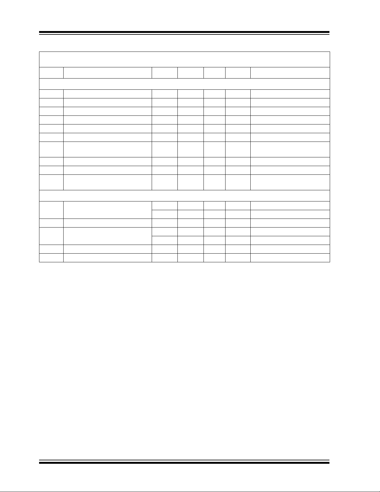
TC7129 ELECTRICAL SPECIFICATIONS (CONTINUED)
Electrica l Characteristics: V+ to V– = 9V, V
Pin numbers refer to 40-pin DIP.
Symbol Parameter Min Typ Max Unit Test Conditions
Power
V
COM
Common Voltage 2.8 3.2 3.5 V V+ to pin 28
Common Sink Current — 0.6 — mA ΔCommon = +0.1V
Common Source Current — 10 — μA ΔCommon = -0.1V
DGND Digital Ground Voltage 4.5 5.3 5.8 V V+ to pin 36, V+ to V– = 9V
Sink Current — 1.2 — mA ΔDGND = +0.5V
Supply Voltage Range 6 9 12 V V+ to V–
I
S
Supply Current Excluding
Common Current
f
CLK
Clock Frequency — 120 360 kHz
Resistance — 50 — kΩ V
V
DISP
Low Battery Flag Activation
Voltage
Digital
Continuity Comparator Threshold
Voltages
Pull-down C urrent — 2 10 μA Pins 37, 38, 39
“Weak Output” Current
Sink/Source
Pin 22 Source Current — 40 — μA
Pin 22 Sink Current — 3 — μA
Note 1: Input voltages may exceed supply voltages, provided input current is limited to ±400 μA. Currents above
this value may result in invalid display readings, but will not destroy the device if limited to ±1 mA.
Dissipation ratings assume device is mounted with all leads soldered to printed circuit board.
= 1V, TA = +25°C, f
REF
= 120 kHz, unless otherwise indicated.
CLK
— 0.8 1.3 mA V+ to V– = 9V
to V+
DISP
6.3 7.2 7.7 V V+ to V–
100 200 — mV V
— 200 400 mV V
pin 27 = High
OUT
pin 27 = Low
OUT
— 3/3—μA Pins 20, 21 sink/sourc e
— 3/9—μA Pin 27 sink/source
DS21459D-page 4 © 2006 Microchip Technology Inc.
TC7129
2.0 PIN DESCRIPTIONS
Descriptions of the pins are listed in Table 2-1.
TABLE 2-1: PIN FUNCTION TABLE
Pin No.
40-Pin PDIP
1 40 2 OSC1 Input to first clock inverter.
2 41 3 OSC3 Output of second clock inverter.
3 42 4 ANNUNCIATOR Backplane square wave output for driving annunciators.
443 5B
544 6A
617F
728B
839A
9410F
10 5 11 B
11 7 13 A
12 8 14 F
13 9 15 B
14 10 16 A
15 11 17 F
16 12 18 BP
17 13 19 BP
18 14 20 BP
19 15 21 V
20 16 22 DP
21 18 24 DP
22 19 25 LATCH
23 20 26 V– Negative power supply terminal.
24 21 27 V+ Positive power supply terminal and positive rail for display
25 22 28 INT IN Input to integrator amplifier.
26 23 29 INT OUT Output of integrator amplifier.
27 24 30 CONTINUITY Input: When low, continuity flag on the display is off. When high,
28 25 31 COMMON Sets common mode voltage of 3.2V below V+ for DE, 10X, etc.
29 26 32 C
30 27 33 C
31 29 35 BUFFER Output of buffer amplifier.
32 30 36 IN LO Negative input voltage terminal.
33 31 37 IN HI Positive input voltage terminal.
34 32 38 REF HI Positive reference voltage.
35 33 39 REF LO Negative reference voltage
Pin No.
44-Pin PQFP
Pin No.
44-Pin PLCC
Symbol Function
, C1, CONT Output to display segments.
1
, G1, D
1
, E1, DP
1
, C2,
2
Output to display segments.
1
Output to display segments.
1
Output to display segments.
LO BATT
, G2, D
2
, E2, DP
2
, C3, MINUS Output to display segments.
3
, G3, D
3
, E3, DP
3
, C4, BC
4
, D4, G
4
, E4, DP
4
3
2
1
DISP
/OR Input: When high, turns on most significant decimal point.
4
/UR Input: Second-most significant decimal point on when high.
3
Output to display segments.
2
Output to display segments.
2
Output to display segments.
3
Output to display segments.
3
Output to display segments.
5
Output to display segments.
4
Output to display segments.
4
Backplane #3 output to display.
Backplane #2 output to display.
Backplane #1 output to display.
Negative rail for display drivers.
Output: Pulled high when result count exceeds ±19,999.
Output: Pulled high when result count is less than ±1000.
/HOLD Input: When floating, ADC operates in Free Run mode. When
pulled high, the last displayed reading is held. When pulled low,
the result counter contents are shown incrementing during the
de-integrate phase of cycle.
Output: Negative going edge occurs when the data latches are
updated. Can be used for converter status signal.
drivers.
continuity flag is on.
Output: High when voltage between inputs i s less than +200 mV .
Low when voltage between inputs is more than +200 mV.
Can be used as pre-regulator for external reference.
+ Positive side of external reference capacitor.
REF
– Negative side of external reference capacitor.
REF
© 2006 Microchip Technology Inc. DS21459D- page 5
TC7129
TABLE 2-1: PIN FUNCTION TABLE (CONTINUED)
Pin No.
40-Pin PDIP
36 34 40 DGND Internal ground reference for digital section. See Section 4.2.1
37 35 41 RANGE 3 μA pull-down for 200 mV scale. Pulled high externally for 2V
38 36 42 DP
39 37 43 DP
40 38 44 OSC2 Output of first clock inverter. Input of second clock inverter.
— 6,17, 28, 39 12, 23, 34, 1 NC No connection.
Pin No.
44-Pin PQFP
Pin No.
44-Pin PLCC
Symbol Function
“±5V Power Supply”.
scale.
2
1
Internal 3 μA pull-down. When high, decimal point 2 will be on.
Internal 3 μA pull-down. When high, decimal point 1 will be on.
DS21459D-page 6 © 2006 Microchip Technology Inc.

TC7129
3.0 DETAILED DESCRIPTION
(All pin designations refer to 40-pin PDIP.)
The TC7129 is designed to be the heart of a high-
resolution analog measurement instrument. The only
additional components required are a few passive
elements: a voltage reference, a LCD and a power
source. Most component values are not critical;
substitutes can be chosen based on the information
given below.
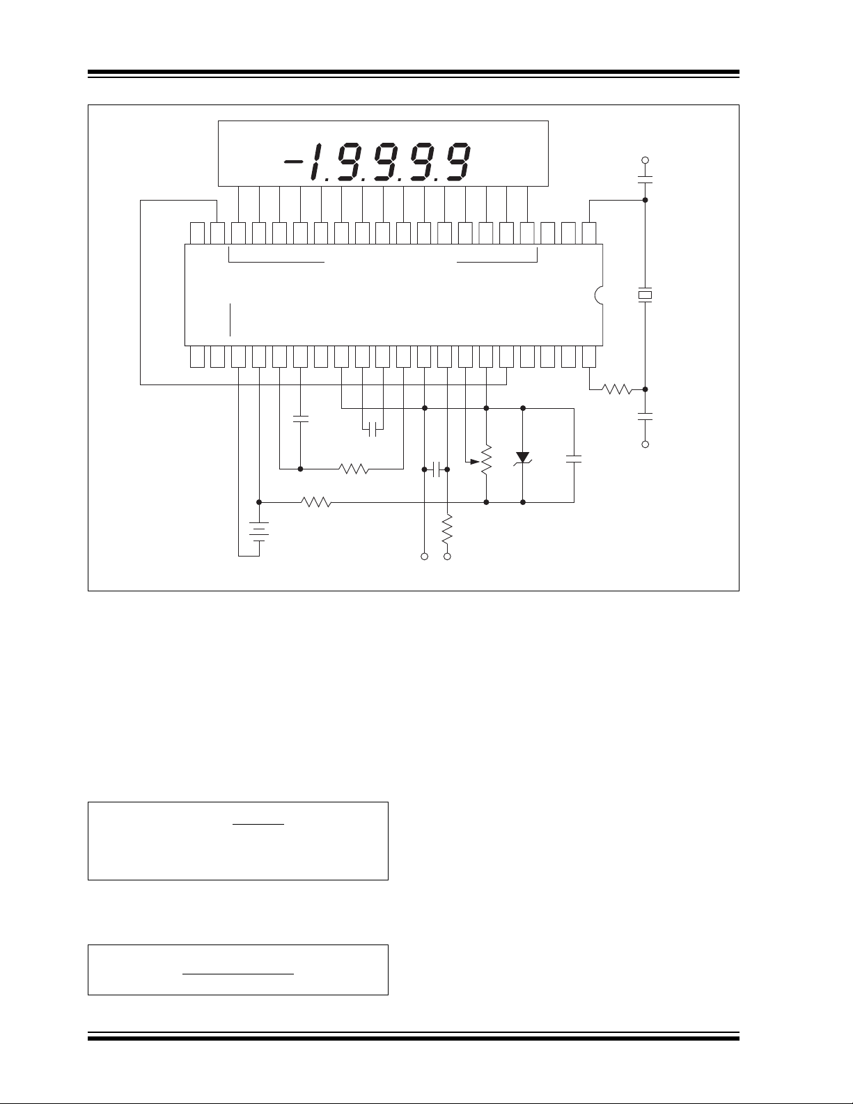
The basic circuit for a digital multimeter application is
shown in Figure 3-1. See Section 4.0 “Typical Appli-
cations”, for variations. Typical values for each
component are shown. The sections below give
component selection criteria.
3.1 Oscillator (X
The primary criterion for selecting the crystal oscillator
is to choose a frequency tha t achieves maxim um rejection of line frequency noise. To do this, the integration
phase should last an integral number of line cycles.
The integration phase of the TC7129 is 10,000 clock
cycles on the 200 mV range and 1000 clock cycles on
the 2V range. One cl ock c yc le is eq ua l to tw o os cil la t or
cycles. For 60 Hz rejection, the oscillator frequency
should be chosen so that the period of one line cycle
equals the integration time for the 2V range.
, CO1, CO2, RO)
OSC
The resistor and cap acitor values are not crit ica l; those
shown work for most applications. In some situations,
the capacitor values may have to be adjusted to
compensate for parasitic capacitance in the circuit. The
capacitors can be low-cost ceramic devices.
Some applications can use a simple RC network
instead of a crystal oscillator. The RC oscillator has
more potential for jitter, especially in the least
significant digit. See Section 4.5 “RC Oscillator”.
3.2 Integrating Resistor (R
The integrating resistor sets the charging current for
the integrating capacitor. Choo se a v alu e that provides
a current between 5μA and 20 μA at 2V, the maxim um
full-scale input. The typical value chosen gives a
charging current of 13.3 μA:
INT
)
EQUATION 3-1:
I
CHARGE
Too high a value for R
noise pickup and increases errors due to leakage
current. Too low a value degrades the linearity of the
integration, leading to inaccurate readings.
2V
=
INT
13.3 µA
150 kΩ
increases the sensitivity to
EQUATION 3-1:
1/60 second = 16.7 msec =
1000 clock cycles *2 OSC cycles/clock cycle
OSC Frequency
This equation gi ves an osc illa tor f requenc y of 120kHz.
A similar calculation gives an optimum frequency of
100 kHz for 50 H z rejection.
© 2006 Microchip Technology Inc. DS21459D- page 7
TC7129
Low Battery Continuity
V+
20
DP
4
/OR
DP
3
/UR
V
DISP
LATCH/
HOLD
V–
V+
+
INT IN
9V
13141516171819
Display Drive Outputs
CONTINUITY
COMMON
INT OUT
27262524232221
28
C
INT
0.1 µF
150 kΩ
10 kΩ
R
BIAS
12
TC7129
C
C
REF
REF
+
–
29
C
+
REF
1 µF
R
INT
9
1011
BUFF
IN LO
323130
– +
0.1
µF
C
V
IN HI
33
IF
IN
8
REF HI
R
IF
100 kΩ
REF LO
DGND
3534
36
R
REF
20
kΩ
ANNUNC
RANGE
DP
2
3837
D
REF
OSC3
DP
1
39
1234567
OSC1
OSC2
40
C
RF
0.1 µF
5 pF
120
kHz
330 kΩ
R
O
10 pF
V+
C
O1
Crystal
C
O2
Figure 3-1: Standard Circuit.
3.3 Integrating Capacitor (C
The charge stored in the integrating capacitor during
the integrate phase is directly proportional to the input
voltage. The primary selection criterion for C
choose a value that gives the highest voltage swing
while remaining within the high-linearity portion of the
integrator output ran ge. An integrat or swing of 2V i s the
recommended value. The capacitor value can be
calculated using the following equation:
INT
)
is to
INT
EQUATION 3-1:
x I
t
INT
V
SWING
INT
Where t
C
=
INT
is the integration time.
INT
Using the values derived above (assuming 60 Hz
operation), the equation becomes:
EQUATION 3-2:
C
16.7 msec x 13.3 μA
= = 0.1 μA
INT
2V
The capacitor should have low dielectric absorption to
ensure good integration linearity. Polypropylene and
Teflon® capacitors are usually suitable. A good
measurement of the dielectric absorption is to connect
the reference capacitor across the inputs by
connecting:
Pin-to-Pin:
20 → 33 (C
30 → 32 (C
+ to IN HI)
REF
– to IN LO)
REF
A reading between 10,000 and 9998 is acceptable;
anything lower indicates unacceptably high dielectric
absorption.
3.4 Reference Capacitor (C
REF
)
The reference capacitor stores the reference voltage
during several phases of the measurement cycle. Low
leakage is the primary selection criterion for this component. The value must be high enough to offset the
effect of stray cap acit anc e at the c ap acito r terminals . A
value of at least 1 μF is recommended.
DS21459D-page 8 © 2006 Microchip Technology Inc.
3.5 Voltage Reference
(D
, R
REF
REF
, R
The reference potentiometer (R
BIAS
, CRF)
) provides an
REF
adjustment for adjusting the reference voltage; any
value above 20 kΩ is adequate. The bias resistor
) limits the current through D
(R
BIAS
150 μA. The reference filter capacitor (C
RC filter with R
to help eliminate noise.
BIAS
to less than
REF
) forms an
RF
3.6 Input Filter (RIF, CIF)
For added stability, an RC input noise filter is usually
included in the circuit. The input filter resistor value
should not exceed 100 kΩ. A typical RC time constant
value is 16.7 msec to help reject line frequency noise.
The input filter capacitor should have low leakage for a
high-impedance input.
+5V
0.1 µF
0.1 µF
0.1 µF
36
DGND
TC7129
24
V+
REF HI
REF LO
COMMON
IN HI
IN LO
V–
23
TC7129
34
35
28
33
V
32
IN
+
–
3.7 Battery
The typical circuit uses a 9V battery as a power so urce.
However , a ny v alue b etwee n 6V a nd 12V can b e use d.
For operation from batteries with voltages lower than
6V and for operation from power supplies, see
Section 4.2 “Powering the TC7129”.
4.0 TYPICAL APPLICATIONS
4.1 TC7129 as a Replacement Part
The TC7129 is a direct pin-f or-pi n rep lac ement part for
the ICL7129. Note , howev er, that the ICL7129 require s
a capacitor an d resistor between pins 26 and 28 for
phase compensation. Since the TC7129 uses internal
phase compensat ion, these p art s are not requir ed and,
in fact, must be removed from the circuit for stable
operation.
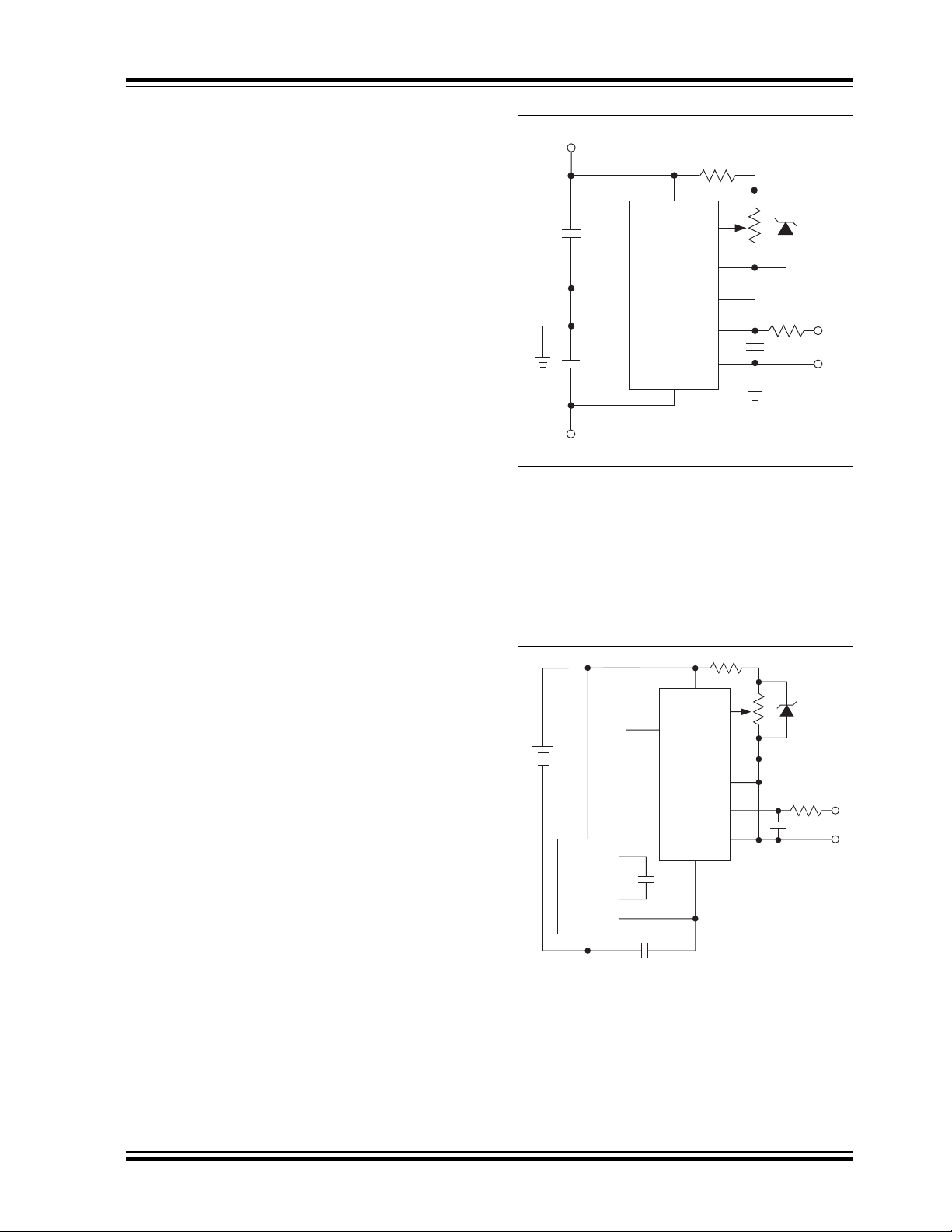
4.2 Powering the TC7129
While the most common power source for the TC7129
is a 9V battery, there are other possibilities. Some of
the more common ones are explained below.
4.2.1 ±5V Power Supply
Measurements are made with respect to power supply
ground. DGND (pin 36) is set intern ally to about 5V less
than V+ (pin 24); it is not i ntende d to be a pow er su pply
input and must not be tied directly to power supply
ground. It can be used as a refe rence for externa l logic,
as explaine d i n Section 4.3 “Connecting to External
Logic”, (see Figure 4-1).
-5V
Figure 4-1: Powering the TC7129 From
a ±5V Pow er Supply.
4.2.2 Low Voltage Battery Source
A battery with voltage between 3.8V and 6V can be
used to power the TC7129 when used with a voltage
doubler circuit, as shown in Figure 4-2. The voltage
doubler uses the TC7660 DC-to-DC voltage converter
and two external capacitors.
24
+
3.8V
to
6V
8
TC7660
3
2
4
5
36
+
10 µF
+
V+
REF HI
DGND
REF LO
COMMON
TC7129
V–
10 µF
IN HI
IN LO
23
34
35
28
33
32
+
V
IN
–
Figure 4-2: Powering the TC7129 From
a Low-Voltage Battery.
© 2006 Microchip Technology Inc. DS21459D- page 9

TC7129
–
4.2.3 +5V Power Supply
Measurements are made with respect to power supply
ground. COMMON (pin 28) is connected to REF LO
(pin 35). A voltage doubler is needed, since the supply
voltage is less than the 6V minimum needed by the
TC7129. DGND (pin 36) must be isolated from power
supply ground (see Figure 4-3).
+5V
24
V+
0.1 µF
34
TC7129
35
36
8
V+
TC7660
GND
3
0.1 µF
2
4
5
10 µF
DGND
+
10 µF
+
28
33
32
V–
23
+
V
IN
+
V
24
External
Logic
I
LOGIC
36
TC7129
DGND
23
V-
Figure 4-4: Extern al Logi c Refere nc ed
Directly to DGND.
V+
24
External
Logic
TC7129
Figure 4-3: Powering the TC7129 From
a +5V Power Supply.
4.3 Connecting to External Logic
External logic can be directly referenced to DGND
(pin 36), provided that the supply current of the externa l
logic does not exceed the sink current of DGND
(Figure 4-4). A safe value for DGND sink current is
1.2 mA. If the sink current is expected to exceed this
value, a buffer is recommended (see Figure4-5).
–
36
+
DGND
I
LOGIC
23
V–
Figure 4-5: Extern al Logi c Refere nc ed
to DGND with Buffer.
4.4 Temperature Compensation
For most applications , V
directly to DGND (pin 36). For applications with a wide
temperature range, some LCDs require that the drive
levels vary with temperature to maintain good viewing
angle and display contrast. Figure 4-6 shows two
circuits that c an be adjus ted to give t emperat ure com pensation of about 10mV/°C between V+ (pin 24) and
. The diode between DGND and V
V
DISP
have a low turn-on voltage because V
exceed 0.3V below DGND.
(pin 19) can be conne cted
DISP
DISP
DISP
should
cannot
DS21459D-page 10 © 2006 Microchip Technology Inc.

TC7129
V
V+
1N4148
39 kΩ
200 kΩ
24
TC7129
5 kΩ
75 kΩ
–
+
19
V
DISP
36
DGND
23
V–
Figure 4-6: Temperature Compensating Circuits.
4.5 RC Oscillator
For applications in which 3-1/2 digit (100μV) resolution
is sufficient, an RC oscillator is adequate. A recommended value for the capacitor is 51 pF. Other values
can be used as long as the y a re s ufficiently larger than
the circuit parasitic capacitance. The resistor value is
calculated as:
EQUATION 4-1:
0.45
R =
Freq * C
For 120 kHz frequency and C = 51 pF, the calculated
value of R is 75kΩ. The RC oscillator and the crystal
oscillator circuits are shown in Figu re 4-7.
TC7129
1 40 2
Ω
270 k
5 pF
+
120 kHz
10 pF
V+
V+
20 kΩ
39 kΩ
2N2222
19
36
18 kΩ
24
TC7129
V
DISP
DGND
23
V–
4.6 Measuring Techniques
Two important techniques are used in the TC7129:
successive integration and digital auto-zeroing.
Successive integratio n is a refinement to the trad itional
dual-slope conversion technique.
4.7 Dual-Slope Conversion
A dual-slope conversion has two basic phases: integrate and de-integra te. During the integrate phase, th e
input signal is integrated for a fixed period of time; the
integrated volt age level is thus proporti onal to the inp ut
voltage. During the de-integrate phase, the integrated
voltage is ram pe d d ow n at a fixed slope, and a counter
counts the clock cycles until the integrator voltage
crosses zero . T he co un t is a me as u rem en t o f t he ti me
to ramp the integrated v oltag e to zero and i s, therefor e,
proportional to the input voltage being measured. This
count can then be sc aled an d disp layed as a mea surement of the input vol tage. F igure 4-8 shows the phases
of the dual-slope conversion.
Integrate
De-integrate
Zero
Crossing
TC7129
1 40 2
Ω
75 k
51 pF
Figure 4-7: Oscillator Circuits.
Time
Figure 4-8: Dual-Slope Conversion.
The dual-slope method has a fundamental limitation.
The count can onl y stop on a c lock cycle, s o t hat me asurement accuracy is limited to the clock frequency. In
addition, a delay in the zero-crossing comparator can
add to the inaccuracy. Figure 4-9 shows these errors in
an actual measurement.
© 2006 Microchip Technology Inc. DS21459D- page 11

TC7129
r
Integrate
Time
De-integrate
Clock Pulses
Figure 4-9: Accuracy Errors in Dual-Slope Conversion.
Zero Integrate
and Latch
INT
1
Integrate
DE
1
De-integrate
REST X10
Overshoot due to zero-crossing between
clock pulses
Integrator Residue Voltage
Overshoot caused by comparato
delay of 1 clock pulse
DE
2
REST X10
DE
3
Zero Integrate
TC7129
Note: Shaded area greatly expanded in time and amplitude.
Figure 4-10: Integration Waveform.
Integrator
Residual Voltage
DS21459D-page 12 © 2006 Microchip Technology Inc.

TC7129
4.8 Successive Integration
The successive integration tech nique picks up where
dual-slope conversion ends. The overshoot voltage
shown in Figure 4-9 (called the “integrator residue
voltage”) is me asured to obtain a correction to the initial
count. Figure 4-10 shows the cycles in a successive
integration measurement.
The waveform shown is for a ne gative input s ignal. The
sequence of ev ents during the measure ment cycle is
shown in Table 4-1.
TABLE 4-1: MEASUREMENT CYCLE
SEQUENCE
Phase Description
INT
Input signal is integrated for fixed time (1000 clock
1
cycles on 2V scale, 10,000 on 200 mV).
Integrator voltage is ramped to zero. Counter
DE
1
counts up until zero-crossing to produce reading
accurate to 3-1/2 digits. Residue represents an
overshoot of the actual input voltage.
REST Rest; circuit settles.
X10 Residue voltage is amplified 10 times and
inverted.
Integrator voltage is ramped to zero. Counter
DE
2
counts down until zero-crossing to correct reading
to 4-1/2 digits. Residue represents an undershoot
of the actual input voltage.
REST Rest; circuit settles.
X10 Residue voltage is amplified 10 times and
inverted.
Integrator voltage is ramped to zero. Counter
DE
3
counts up until zero-crossing to correct reading to
5-1/2 digits. Residue is discarded.
4.9 Digital Auto-Zeroing
To eliminate the effect of amplifier offset errors, the
TC7129 uses a digital auto -zeroing techniqu e. After the
input voltage is measured as described above, the
measurement is repeated with the inputs shorted
internally. The reading with inputs shorted is a
measurement of the internal errors and is subtracted
from the previous reading to obtain a corrected
measurement. Digit al auto -zeroing el iminates the need
for an external auto-zeroing capacitor used in other
ADCs.
4.10 Inside the TC7129
Figure 4-11 shows a simplified block diagram of the
TC7129.
© 2006 Microchip Technology Inc. DS21459D- page 13

TC7129
Low Battery Continuity
OSC1
OSC2
OSC3
RANGE
L/H
CONT
V–
DGND
V+
TC7129
Segment Drives
Latch, Decode Display Multiplexer
Up/Down Results Counter
Sequence Counter/Decoder
Control Logic
Analog Section
Backplane
Drives
Annunciator
Drive
V
DISP
DP
1
DP
2
UR/DP
OR/DP
REF HI
REF LO
INT OUT
INT IN
3
4
COMMON INHIIN
LO
Figure 4-11: TC7129 Functional Block Diagram.
IN HI
Common
IN LO
Continuity
INT
INT
1
INT
1
,
–
V
200 mV
REF HI
2
+
C
REF
REF LO
DE
DE
DE- DE+
DE+
DE–
INT
–
+
Continuity
Comparator
500 k
–
+
ZI, X10
REST
Ω
Buffer
R
INT
Figure 4-12: Integrator Block Diagram.
BUFF
C
INT
Integrator
–
+
100 pF
TC7129
X10
10
Comparator 1
pF
+
–
To Display Driver
To Digital
Section
Comparator 2
DS21459D-page 14 © 2006 Microchip Technology Inc.

4.11 Integrator Section
The integrator section includes the integrator, comparator, input buffer amplifier and analog switches (see
Table 4-2) used to change the circuit configuration
during the separate measurement phases described
earlier. (See Figure 4-12).
TABLE 4-2: SWITCH LEGENDS
Label Description
Label Meaning.
DE Open during all de-integrate phases.
DE– Closed during all de-integrate phases when
input voltage is negative.
DE+ Closed during all de-integrate phases when
INT
INT
INT Open during both integrate phases.
REST Closed during the rest phase.
X10 Closed during the X10 phase.
X10 Open during the X10 phase.
The buffer amp li fier has a common mode inp ut vol t age
range from 1.5V above V– to 1V be low V+. The integrator amplifier can swing to within 0.3V of the rails.
However, for best linearity, the swing is usually limited
to within 1V. Both amplifiers can supply up to 80 μA of
output cur re nt , b u t sh ou l d be l im it e d to 20 μA for good
linearity.
input voltage is positive.
Closed during the first integrate phase
1
(measurement of the input voltage).
Closed during the second integrate phase
2
(measurement of the amplifier offset).
ZI Closed during the zero integrate phase.
TC7129
–
IN HI
COM
IN LO
CONT
200 mV
V
–
+
500 k
Ω
Figure 4-13: Continuity Indicator Circuit.
TC7129
DP4/OR, Pin 20
/UR, Pin 21
DP
LATCH/HOLD Pin 22
CONTINUITY, Pin 27
3
Figure 4-14: Input/Output Pin Schematic.
500 kΩ
+
Buffer
TC7129
To Display Driver
(Not Latched)
4.12 Continuity Indicator
A comparator with a 200 mV threshold is connected
between IN HI (pin 33) and IN LO (pin 32). Whenever
the voltage between inputs is less than 200 mV, the
CONTINUITY output (pin 27) will be pulled high,
activating the continuity annunciator on the display.
The continuity pin c an also be us ed as an input to drive
the continuity annunciator directly from an external
source (see Figure 4-13).
A schematic of the input/o utput nature of thi s pin is also
shown in Figure 4-14.
4.13 Common and Digital Ground
The common and digital ground (DGND) outputs are
generated from internal Zener diodes. The voltage
between V+ and DGND is the internal supply voltage
for the digital section of the TC7129. Common can
source approximately 12μA; DGND has essentially no
source capability (se e Figure4-15).
© 2006 Microchip Technology Inc. DS21459D- page 15

TC7129
24
V+
–
+
12 µA
N
Logic
Section
3.2V
COM
28
5V
36
P
DGND
TC7129
N
23
V–
Figure 4-15: Digital Ground (DGND) and
Common Outputs.
4.14 Low Battery
The low battery annun ciato r turns o n whe n supp ly vo ltage between V– and V+ drop s below 6.8V. The internal
zener diode has a threshold of 6.3V. When the supply
voltage drop s below 6.8V, the transistor tied to V– turn s
off pulling the “Low Battery” point high.
4.15 Sequence and Results Counter
A sequence counter and associated control logic provide signals that operate the analog switches in the
integrator section . The comparat or output from the integrator gates the res ults coun ter. The resul ts count er is
a six-sectio n up/down decade co unter that holds the
intermediate results from each successive integration.
4.16 Overrange and Underrange
Outputs
When the results counter holds a value greater than
±19,999, the DP
When the results counter value is less than ±1000, the
DP3/UR output (Pin 21) is driven high. Both s ignal s are
valid on the falling edge of LATCH
not change until the end of the next conversion cycle.
The signals are upd ated a t the end o f each conv ersion,
unless the L
21 can also be used as inputs for external control of
decimal point s 3 a nd 4. Fig ure 4-14 shows a schematic
of the input/output nature of these pins.
/OR output (Pin 20) is driven high.
4
/HOLD (L/H) and do
/H input (Pin 22) is held high. Pins 20 and
4.17 LATCH/Hold
The L/H output goes low during the last 100 cycles of
each conversion. This pulse latches the conversion
data into the display driv er secti on of the TC7129. Thi s
pin can also be used as an inp ut. When dr iven high, th e
display will not be updated; the previous reading is
displayed. When driven low, the display reading is not
latched; the sequence counter reading will be
displayed. Since the counter is counting much faster
than the backplanes are being updated, the reading
shown in this mode is somewhat erratic.
4.18 Display Driver
The TC7129 drives a triplexed LCD with three backplanes. The LCD can include decimal points, polarity
sign and annunciators for continuity and low battery.
Figure 4-16 shows the assignment of the display
segments to the backplanes and segment drive lines.
The backplane drive frequency is obtained by dividing
the oscillator freq uency by 1200. Thi s result s in a b ackplane drive frequency of 100 Hz for 60 Hz operation
(120 kHz crystal) and 83.3 Hz for 50 Hz operation
(100 kHz crystal).
Backplane waveforms are shown in Figure 4-17.
These appear on outputs BP
and 18). They remain the same, regardless of the
segments being driven.
Other display output lines (pins 4 through 15) have
waveforms that vary depending on the displayed
values. Figure 4-18 shows a set of waveforms for the
A, G, D outputs (pins 5, 8, 11 and 14) for several
combinations of “ON” segments.
The ANNUNCIATOR DRIVE output (pin 3) is a square
wave, running at the backplane frequency (100 Hz or
83.3 H z) with a peak-to-peak voltage equal to DGND
voltage. Connec ting an an nunci ator to pin 3 turn s it on;
connecting it to its backplane turns it off.
, BP2, BP3 (pins 16, 17
1
DS21459D-page 16 © 2006 Microchip Technology Inc.

TC7129
Low Battery
Continuity
BP
BP
1
2
Backplane
Connections
BP
3
Low Battery Continuity
F
E
DP
4
4
4
,
,
G
D
A
4
4
4
,
,
C
BC
B
4
4
4
,
,
E
DP
F
3
3
3
,
,
G
D
A
3
3
3
,
,
B
C
MINUS
3
3
,
,
B
1
,
A
1
,
F
1
,
B
2
,
A
2
,
F
2
,
C
Continuity
1
,
G
D
1
,
E
DP
1
,
C
Low Battery
2
,
G
D
2
,
E
DP
2
,
1
1
2
2
Figure 4-16: Display Segment Assignments.
BP
1
BP
2
BP
3
Figure 4-17: Backplane Waveforms.
b Segment
Line
All Off
a Segment
On
d, g Off
a, g On
d Off
All On
Figure 4-18: Typical Display Output
Waveforms.
V
V
V
V
V
V
V
V
V
V
V
V
V
V
V
V
DD
H
L
DISP
DD
H
L
DISP
DD
H
L
DISP
DD
H
L
DISP
© 2006 Microchip Technology Inc. DS21459D- page 17

TC7129
5.0 PACKAGING INFORMATION
5.1 Package Marking Information
Package mar k ing data not available a this time.
5.2 Taping Forms
Pin 1
User Direction of Feed
P, Pitch
Pin 1
W, Width
of Carrier
Tape
S tandard Reel Component Orientation
Component Taping Orientation for 44-Pin PQFP Devices
User Direction of Feed
Reverse Reel Component Orientation
Pin 1
W
P
Standard Reel Component Orientation
for 713 Suffix Device
Carrier Tape, Number of Components Per Reel and Reel Size
Package Carrier Width (W) Pitch (P) Part Per Full Reel Reel Size
44-Pin PQFP 24 mm 16 mm 500 13 in
Note: Drawing does not represent total number of pins.
DS21459D-page 18 © 2006 Microchip Technology Inc.

40-Lead Plastic Dual In-line (P) – 600 mil Body (PDIP)
E1
D
TC7129
2
n
E
β
eB
Number of Pins
Pitch
Molded Package Thickness
Lead Thickness
Overall Row Spacing §
Mold Draft Angle Top
Mold Draft Angle Bottom
* Controlling Parameter
§ Significant Characteristic
Notes:
Dimensions D and E1 do not include mold flash or protrusions. Mold flash or protrusions shall not exceed .010” (0.254mm) per side.
JEDEC Equivalent: MO-011
Drawing No. C04-016
1
A
c
A1
n
p
A2
c
eB
α
β
B1
B
MILLIMETERSINCHES*Units
0.38.015A1Base to Seating Plane
α
A2
L
p
MAXNOMMINMAXNOMMINDimension Limits
4040
2.54.100
4.834.454.06.190.175.160ATop to Seating Plane
4.063.813.56.160.150.140
15.8815.2415.11.625.600.595EShoulder to Shoulder Width
14.2213.8413.46.560.545.530E1Molded Package Width
52.4552.2651.942.0652.0582.045DOverall Length
3.433.303.05.135.130.120LTip to Seating Plane
0.380.290.20.015.012.008
1.781.270.76.070.050.030B1Upper Lead Width
0.560.460.36.022.018.014BLower Lead Width
17.2716.5115.75.680.650.620
1510515105
1510515105
© 2006 Microchip Technology Inc. DS21459D- page 19

TC7129
44-Lead Plastic Leaded Chip Carrier (LW) – Square (PLCC)
E
E1
#leads=n1
D
D1
2
n
1
CH2 x 45° CH1 x 45°
A3
α
A2
c
Number of Pins
Pitch
Molded Package Thickness
Side 1 Chamfer Height
Footprint Length
Lead Thickness
Lower Lead Width
Mold Draft Angle Top
Mold Draft Angle Bottom
* Controlling Parameter
§ Significant Characteristic
Notes:
Dimensions D and E1 do not include mold flash or protrusions. Mold flash or protrusions shall not exceed .010” (0.254mm) per side.
JEDEC Equivalent: MO-047
Drawing No. C04-048
E2
β
n
p
A2
A3
CH2Corner Chamfer (others)
D2
c
α
β
.145 .153 .160 3.68 3.87 4.06
A
35°
B1
B
p
D2
MILLIMETERSINCHES*Units
.028 .035 0.71 0.89
0.51.020A1Standoff §
A1
4444
1.27.050
1111n1Pins per Side
MAXNOMMINMAXNOMMINDimension Limits
4.574.394.19.180.173.165AOverall Height
0.860.740.61.034.029.024
1.271.141.02.050.045.040CH1Corner Chamfer 1
0.250.130.00.010.005.000
17.6517.5317.40.695.690.685EOverall Width
17.6517.5317.40.695.690.685DOverall Length
16.6616.5916.51.656.653.650E1Molded Package Width
16.6616.5916.51.656.653.650D1Molded Package Length
16.0015.7514.99.630.620.590E2Footprint Width
16.0015.7514.99.630.620.590
0.330.270.20.013.011.008
0.810.740.66.032.029.026B1Upper Lead Width
0.530.510.33.021.020.013B
10501050
10501050
DS21459D-page 20 © 2006 Microchip Technology Inc.

TC7129
44-Lead Plastic Quad Flatpack (KW) 10x10x2.0 mm Body, 1.95/ 0.25 mm Lea d Form (PQFP)
E
E1
p
D
D1
2
1
B
n
c
Units INCHES MILLIMETERS
Dimension Limits MIN NOM MAX MIN NOM MAX
Number of Pins
Pitch
Overall Height A - - .096 - - 2.45
Molded Package Thickness A2 .077 .079 .083 1.95 2.00 2.10
§
Standoff
Foot Length L .029 .035 .041 0.73 0.88 1.03
Foot Angle
Overall Width E .547 BSC 13.90 BSC
Overall Length D .547 BSC 13.90 BSC
Molded Package Width E1 .394 BSC 10.00 BSC
Molded Package Length D1 .394 BSC 10.00 BSC
Lead Thickness
Lead Width B .012 - .018 0.30 - 0.45
Mold Draft Angle Top
Mold Draft Angle Bottom
*
Controlling Parameter
§
Significant Characteristic
Notes:
Dimensions D and E1 do not include mold flash or protrusions. Mold flash or protrusions shall not exceed .010" (0.254mm) per side.
BSC: Basic Dimension. Theoretically exact value shown without tolerances.
See ASME Y14.5M
REF: Reference Dimension, usually without tolerance, for information purposes only.
See ASME Y14.5M
JEDEC Equivalent: MO-112 AA-1
Drawing No. C04-119
A1 .010 - - 0.25 - -
n
p
φ
c
α
β
CHAMFER VARIES
φ
.004 - .009 0.11 - 0.23
A2
L
A1
44 44
.031 BSC 0.80 BSC
0° 3.5° 7° 0° 3.5° 7°
5° - 16° 5° - 16°
5° - 16° 5° - 16°
F
β
1.95 REF..077 REF.FFootprint
Revised 07-21-05
α
A
*
© 2006 Microchip Technology Inc. DS21459D- page 21

TC7129
NOTES:
DS21459D-page 22 © 2006 Microchip Technology Inc.

PRODUCT IDENTIFICATION SYSTEM
To order or obtain information, e.g., on pricing or delivery, refer to the factory or the listed sales office.
PART NO. XX
Device
Device: TC7129: 4-1/2 Digit Analog-to-Digital Converter
X
Temp.
Pkg
XX
Taping
Direction
Examples:
a) TC7129CPL: 40-Pin PDIP
b) TC7129CKW713: 44-Pin PQFP
c) TC7129CLW: 44-Pin PLCC
TC7129
Tape and Reel
Temperature: C = 0°C to +70°C
Package: PL = 40-Pin PDIP
Taping Direction: 713 = Standard Taping
I = -25°C to +85°C
KW = 40-Pin PQFP
LW = 44-Pin PLCC
JL = 40-Pin CDIP
© 2006 Microchip Technology Inc. DS21459D-page 23

TC7129
NOTES:
DS21459D-page 24 © 2006 Microchip Technology Inc.

TC7129
THE MICROCHIP WEB SITE
Microchip provides onlin e support v ia our W WW site at
www.m ic roc hi p.c om . Thi s web si te i s us ed as a m ean s
to make files and information easily available to
customers. Accessible by using your favorite Internet
browser, the web site contains the following
information:
• Product Support – Data sheets and errata,
application notes and sample programs, design
resources, user’s guides and hardware support
documents, lat est softwa re releases and archived
software
• General Technical Support – Frequently Asked
Questions (FAQ), technical support requests,
online discussion groups, Microchip consultan t
program member listing
• Business of Microchip – Product selector and
ordering guides, latest Microchip press releases,
listing of s eminars and events, listings of
Microchip sales offices, distributors and factory
representatives
CUSTOMER CHANGE NOTIFICATION
SERVICE
CUSTOMER SUPPORT
Users of Microchip products can receive assistance
through several channels:
• Distributor or Representative
• Local Sal es Office
• Field Application Engineer (FAE)
• Technical Support
• Development Systems Information Line
Customers should contact their distributor,
representative or field application engineer (FAE) for
support. Local sales offices are also available to help
customers. A listing of sales offices and locations is
included in the back of this document.
T echnic al support is avail able throug h the web si te
at: http://support.microchip.com
Microchip’s customer notification service helps keep
customers current on Microchip products. Subscribers
will receive e-mail notification whenever there are
changes, updates, revisions or errata related to a
specified produ ct family or develo pment tool of inte rest.
To register, access the Microchip web site at
www.microchip.com, click on Customer Change
Notification and follow the registration instructions.
© 2006 Microchip Technology Inc. DS21459D-page 25

TC7129
READER RESPONSE
It is our intentio n to pro vi de you with the best documentation possible to ens ure suc c es sfu l u se of y ou r M ic roc hip product. If you wish to provid e your c omment s on org anizatio n, clarity, subject matter, and ways i n which o ur docum entatio n
can better serve you, please FAX your comments to the Technical Publications Manager at (480) 792-4150.
Please list the following information, and use this outline to provide us with your comments about this document.
To:
RE: Reader Response
From:
Application (optional):
Would you like a reply? Y N
Device: Literature Number:
Questions:
1. What are the best featu res of this document?
2. How does this document meet your hardware and software development needs?
3. Do you find the organization of this document easy to follow? If not, why?
Technical Publications Manager
Name
Company
Address
City / State / ZIP / Country
Telephone: (_______) _________ - _________
Total Pages Sent ________
FAX: (______) _________ - _________
DS21459DTC7129
4. What additions to the document do you think would enhance the structure and subject?
5. What deletions from the document could be made without affecting the overall usefulness?
6. Is there any incorrect or misleading information (what and where)?
7. How would you improve this document?
DS21459D-page 26 © 2006 Microchip Technology Inc.

Note the following details of the code protection feature on Microchip devices:
• Microchip products meet the specification contained in their particular Microchip Data Sheet.
• Microchip believes that its family of products is one of the most secure families of its kind on the market today, when used in the
intended manner and under normal conditions.
• There are dishonest and possibly illegal methods used to breach the code protection feature. All of these methods, to our
knowledge, require using the Microchip products in a manner outside the operating specifications contained in Microchip’s Data
Sheets. Most likely, the person doing so is engaged in theft of intellectual property.
• Microchip is willing to work with the customer who is concerned about the integrity of their code.
• Neither Microchip nor any other semiconductor manufacturer can guarantee the security of their code. Code protection does not
mean that we are guaranteeing the product as “unbreakable.”
Code protection is constantly evolving. We at Microchip are com mitted to continuously improving the code protect ion f eatures of our
products. Attempts to break Microchip’s code protection feature may be a violation of the Digit al Mill ennium Copyright Act. If such acts
allow unauthorized access to your software or other copyrighted work, you may have a right to sue for relief under that Act.
Information contained in this publication regarding device
applications and t he lik e is provided only for your convenience
and may be su perseded by upda t es . It is y our responsibility to
ensure that your application meets with your specifications.
MICROCHIP MAKES NO REPRESENTATIONS OR
WARRANTIES OF ANY KIND WHETHER EXPRESS OR
IMPLIED, WRITTEN OR ORAL, STATUTORY OR
OTHERWISE, RELATED TO THE INFORMATION,
INCLUDING BUT NOT LIMITED TO ITS CONDITION,
QUALITY, PERFORMANCE, MERCHANTABILITY OR
FITNESS FOR PURPOSE. Microchip disclaims all liability
arising from this information and its use. Use of Microchip
devices in life supp ort and/or safety ap plications is entir ely at
the buyer’s risk, and the buyer agrees to defend, indemnify and
hold harmless M icrochip from any and all dama ges, claims,
suits, or expenses re sulting from such use. No licens es are
conveyed, implicitly or otherwise, under any Microchip
intellectual property rights.
Trademarks
The Microchip name and logo, the Microchip logo, Accuron,
dsPIC, K
EELOQ, microID, MPLAB, PIC, PICmicro, PICSTART,
PRO MATE, PowerSmart, rfPIC, and SmartShunt are
registered trademarks of Microchip Technology Incorporated
in the U.S.A. and other countries.
AmpLab, FilterLab, Migratable Memory, MXDEV, MXLAB,
SEEVAL, SmartSensor and The Embedded Control Solutions
Company are registered trademarks of Microchip Technology
Incorporated in the U.S.A.
Analog-for-the-Digital Age, Application Maestro, dsPICDEM,
dsPICDEM.net, dsPICworks, ECAN, ECONOMONITOR,
FanSense, FlexROM, fuzzyLAB, In-Circuit Serial
Programming, ICSP , ICEPIC, Linear Active Thermistor, Mindi,
MiWi, MPASM, MPLIB, MPLINK, PICkit, PICDEM,
PICDEM.net, PICLAB, PICtail, PowerCal, PowerInfo,
PowerMate, PowerTool, REAL ICE, rfLAB, rfPICDEM, Select
Mode, Smart Serial, SmartTel, Total Endurance, UNI/O,
WiperLock and ZENA are trademarks of Microchip
Technology Incorporated in the U.S.A. and other countries.
SQTP is a service mark of Microchip T echnology Incorporated
in the U.S.A.
All other trademarks mentioned herein are property of their
respective companies.
© 2006, Microchip Technology Incorporated, Printed in the
U.S.A., All Rights Reserved.
Printed on recycled paper.
Microchip received ISO/TS-16949:2002 certification for its worldwide
headquarters, design and wafer fabrication facilities in Chandler and
Tempe, Arizona, Gresham, Oregon and Mountain View, California. The
Company’s quality system processes and procedures are for its
PICmicro
EEPROMs, microperipherals, nonvolatile memory and analog
products. In addition, Microchip’s quality system for the design and
manufacture of development systems is ISO 9001:2000 certified.
®
8-bit MCUs, KEELOQ
®
code hopping devices, Serial
© 2006 Microchip Technology Inc. DS21459D-page 27

WORLDWIDE SALES AND SERVICE
AMERICAS
Corporate Office
2355 West Chandler Blvd.
Chandler, AZ 85224-6199
Tel: 480-792-7200
Fax: 480-792-7277
Technical Support:
http://support.microchip.com
Web Address:
www.microchip.com
Atlanta
Alpharetta, GA
Tel: 770-640-0034
Fax: 770-640-0307
Boston
Westborough, MA
Tel: 774-760-0087
Fax: 774-760-0088
Chicago
Itasca, IL
Tel: 630-285-0071
Fax: 630-285-0075
Dallas
Addison, TX
Tel: 972-818-7423
Fax: 972-818-2924
Detroit
Farmington Hills, MI
Tel: 248-538-2250
Fax: 248-538-2260
Kokomo
Kokomo, IN
Tel: 765-864-8360
Fax: 765-864-8387
Los Angeles
Mission Viejo, CA
Tel: 949-462-9523
Fax: 949-462-9608
San Jose
Mountain View, CA
Tel: 650-215-1444
Fax: 650-961-0286
Toronto
Mississauga, Ontario,
Canada
Tel: 905-673-0699
Fax: 905-673-6509
ASIA/PACIFIC
Australia - Sydney
Tel: 61-2-9868-6733
Fax: 61-2-9868-6755
China - Beijing
Tel: 86-10-8528-2100
Fax: 86-10-8528-2104
China - Chengdu
Tel: 86-28-8676-6200
Fax: 86-28-8676-6599
China - Fuzhou
Tel: 86-591-8750-3506
Fax: 86-591-8750-3521
China - Hong Kong SAR
Tel: 852-2401-1200
Fax: 852-2401-3431
China - Qingdao
Tel: 86-532-8502-7355
Fax: 86-532-8502-7205
China - Shanghai
Tel: 86-21-5407-5533
Fax: 86-21-5407-5066
China - Shenyang
Tel: 86-24-2334-2829
Fax: 86-24-2334-2393
China - Shenzhen
Tel: 86-755-8203-2660
Fax: 86-755-8203-1760
China - Shunde
Tel: 86-757-2839-5507
Fax: 86-757-2839-5571
China - Wuhan
Tel: 86-27-5980-5300
Fax: 86-27-5980-5118
China - Xian
Tel: 86-29-8833-7250
Fax: 86-29-8833-7256
ASIA/PACIFIC
India - Bangalore
Tel: 91-80-4182-8400
Fax: 91-80-4182-8422
India - New Delhi
Tel: 91-11-5160-8631
Fax: 91-11-5160-8632
India - Pune
Tel: 91-20-2566-1512
Fax: 91-20-2566-1513
Japan - Yokohama
Tel: 81-45-471- 6166
Fax: 81-45-471-6122
Korea - Gumi
Tel: 82-54-473-4301
Fax: 82-54-473-4302
Korea - Seoul
Tel: 82-2-554-7200
Fax: 82-2-558-5932 or
82-2-558-5934
Malaysia - Penang
Tel: 60-4-646-8870
Fax: 60-4-646-5086
Philippines - Manila
Tel: 63-2-634-9065
Fax: 63-2-634-9069
Singapore
Tel: 65-6334-8870
Fax: 65-6334-8850
Taiwan - Hsin Chu
Tel: 886-3-572-9526
Fax: 886-3-572-6459
Taiwan - Kaohsiung
Tel: 886-7-536-4818
Fax: 886-7-536-4803
Taiwan - Taipei
Tel: 886-2-2500-6610
Fax: 886-2-2508-0102
Thailand - Bangkok
Tel: 66-2-694-1351
Fax: 66-2-694-1350
EUROPE
Austria - Wels
Tel: 43-7242-2244-399
Fax: 43-7242-2244-393
Denmark - Copenhagen
Tel: 45-4450-2828
Fax: 45-4485-2829
France - Paris
Tel: 33-1-69-53-63-20
Fax: 33-1-69-30-90-79
Germany - Munich
Tel: 49-89-627-144-0
Fax: 49-89-627-144-44
Italy - Milan
Tel: 39-0331-742611
Fax: 39-0331-466781
Netherlands - Drunen
Tel: 31-416-690399
Fax: 31-416-690340
Spain - Madrid
Tel: 34-91-708-08-90
Fax: 34-91-708-08-91
UK - Wokingham
Tel: 44-118-921-5869
Fax: 44-118-921-5820
02/16/06
DS21459D-page 28 © 2006 Microchip Technology Inc.
 Loading...