

Page 1
TC7109/A
12-Bit µA-Compatible Analog-to-Digital Converters
Features
• Zero Integrator Cycle forFast Recovery from
Input Overloads
• Eliminates Cross-Talk in Multiplexed Systems
• 12-Bit Plus Sign Integrating A/D Converter with
Over Range Indication
• Sign Magnitude Coding Format
• True DifferentialSignal Input and Differential
Reference Input
• Low Noise: 15µV
• Input Current: 1pA Typ.
• No Zero Adjustment needed
• TTL Compatible, Byte Organized Tri-State
Outputs
• UART Handshake Mode for simple Serial Data
Transmissions
P-P
Typ.
Device Selection Table
PartNumber
(TC7109X)*
TC7109CKW 44-Pin PQFP 0°C to +70°C
TC7109CLW 44-Pin PLCC 0°Cto +70°C
TC7109CPL 40-PinPDIP 0°C to +70°C
TC7109IJL 40-PinCERDIP -25°Cto +85°C
*The “A” version has a higher I
Package
OUT
Temperature
Range
on the digital lines.
General Description
The TC7109A is a 12-bit plus sign, CMOS low power
analog-to-digital converter (ADC). Only eight passive
components and a crystal are required to form a
complete dual slope integrating ADC.
TheimprovedV
featuresmakeitan attractiveper-channelalternativeto
analog multiplexing for many data acquisition applications. These features include typical input bias current
of 1pA, drift of less than 1µV/°C, input noise t ypically
15µV
erence allow measurement of bridge typetransducers,
such as load cells, strain gauges, and temperature
transducers.
The TC7109A provides a versatile digital interface. In
the Direct mode, chip select and HIGH
enable control parallel bus interface.In the Handshake
mode, the TC7109Awill operate with industry standard
UART sin controlling serial data transmission – ideal for
remote data logging. Controland monitoring of conversion timing is provided by the RUN/HOLD
STATUS output.
For applications requiring more resolution, see the
TC500, 15-bit plus sign ADC datasheet.The TC7109A
has improved over range recovery performance and
higher output drive capability than the original TC7109.
All new (or existing) designs should specify the
TC7109A wherever possible.
, and auto-zero. True differential input and ref-
P-P
source current and other TC7109A
OH
/LOW byte
input and
2002 Microchip TechnologyInc. DS21456B-page 1
Page 2
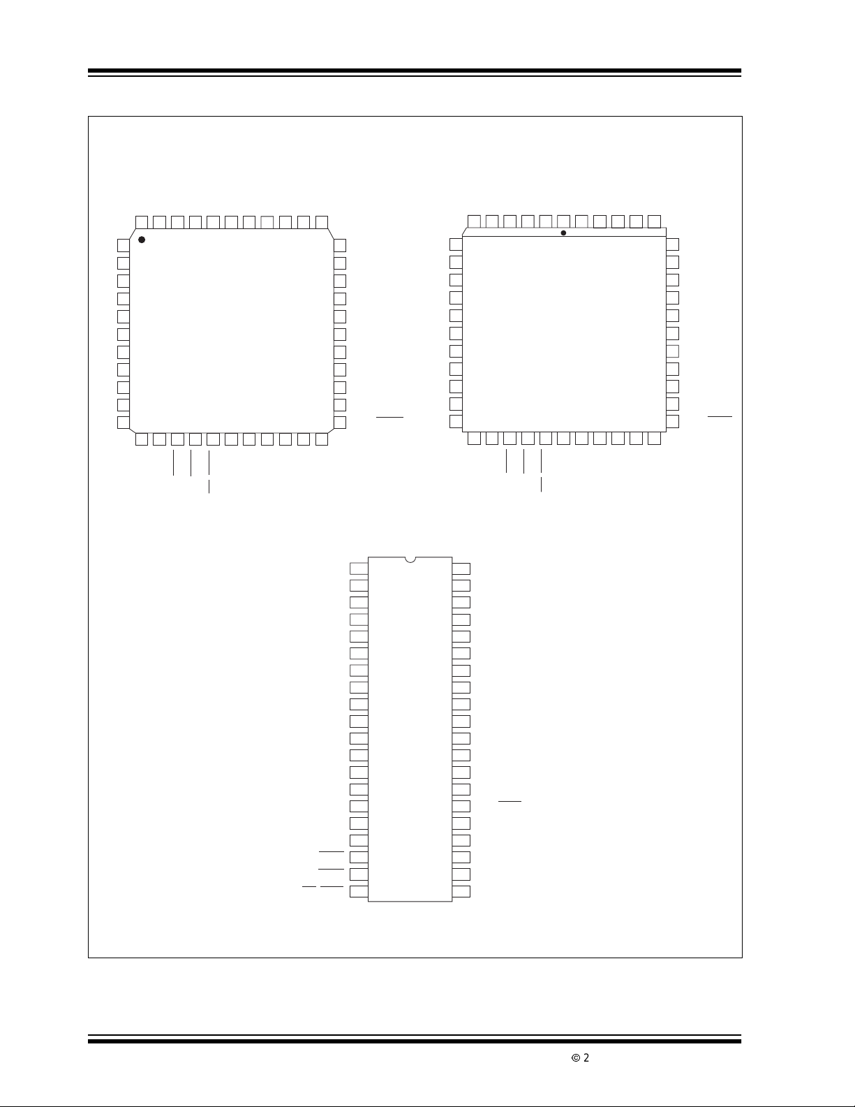
TC7109/A
Package Type
12
OR
B
44 43 42 41 39 3840
B
1
11
B
2
10
B
3
9
B
4
8
B
5
7
6
NC
B
7
6
B
5
B
4
B
3
B
2
12 13 14 15 17 18
1
B
TEST
44-Pin PQFP
STATUS
POL
GND
NC
TC7109ACKW
TC7109CKW
16
LBEN
NC
HBEN
CE/LOAD
REF CAP-
REF IN-
V+
37 36 35 34
19 20 21 22
MODE
OSC IN
OSC OUT
REF IN+
REF CAP+
33
32
31
30
29
28
27
268
259
2410
2311
BUFF
OSC SEL
OSC OUT
B
B
NC
11
10
B
9
B
8
B
7
B
6
B
5
B
4
B
3
B
2
IN HI
IN LO
COMMON
INT
AZ
NC
BUFF
REF OUT
V-
SEND
RUN/HOLD
40-Pin PDIP/CERDIP
44-Pin PLCC
12
B
6543 1442
7
8
9
10
11
12
13
18 19 20 21 23 24
1
B
OR
TEST
POL
LBEN
STATUS
TC7109ACLW
TC7109CLW
HBEN
GND
22
CE/LOAD
V+
NC
43 42 41 40
25 26 27 28
NC
MODE
REF CAP-
REF IN-
OSC IN
OSC OUT
REF IN+
REF CAP+
39
38
37
36
35
34
33
3214
3115
3016
2917
BUFF
OSC SEL
OSC OUT
IN HI
IN LO
COMMON
INT
AZ
NC
BUFF
REF OUT
V-
SEND
RUN/HOLD
GND
1
STATUS
CE/LOAD
POL
OR
B
B
B
B
B
B
B
B
B
B
B
B
TEST
LBEN
HBEN
2
3
4
5
12
6
11
10
7
TC7109A
8
9
9
8
10
7
6
11
12
5
13
4
14
3
15
2
16
1
17
18
19
20
NC = No internal connection
TC7109
40
V+
39
REF IN-
38
REF CAP-
37
REF CAP+
36
REF IN+
35
IN HI
IN LO
34
33
COMMON
32
INT
31
AZ
30
BUFF
REF OUT
29
28
V-
27
SEND
26
RUN/HOLD
25
BUFF OSC OUT
24
OSC SEL
23
OSC OUT
22
OSC IN
21
MODE
DS21456B-page 2
2002 Microchip TechnologyInc.
Page 3
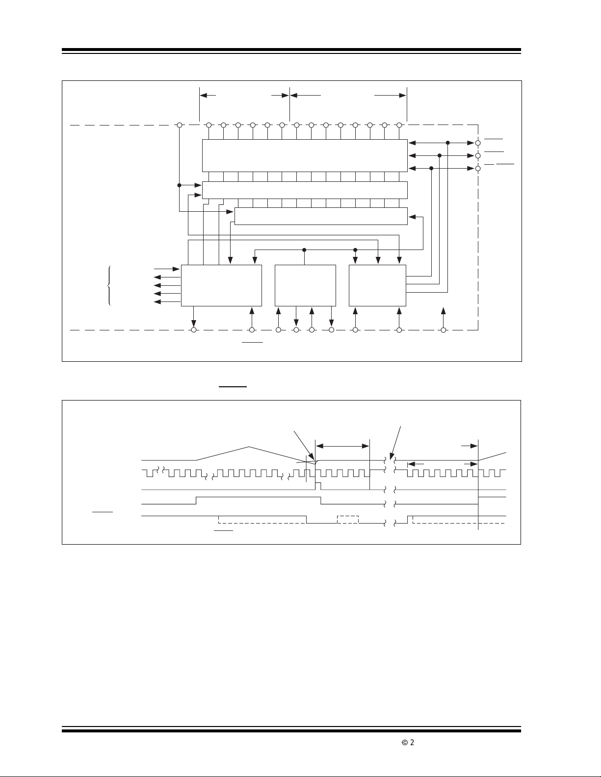
Typical Application
C
REF
REF
REF
IN+
CAP+
37 36
AZZIAZ
INT
35
Input
High
Common
Input Low
AZ
33
INT
34
DE (±)
DE
(–)DE(+)
DE
(+)
AZ
ZI
DE
(–)
TC7109/A
POL
TEST
Conversion
Control Logic
High Order
Byte Inputs
10
OR
B9B8B7B6B5B4B3B2B
B12B11B
16 Three-State Outputs
14 Latches
12-Bit Counter
Oscillator and
Clock Circuitry
Latch
Clock
Low Order
Byte Inputs
15 16
Handshake
Logic
1
18
LBEN
19
HBEN
20
CE/LOAD
TC7109A
REF
IN-
ZI
R
INT
REF
CAP-
3839
Buffer
–
+
ZI
10µA
–
+
6.2V
BUFF
C
AZ
3130
Integrator
–
+
AZ
To Analog
Section
AZ
32
C
INT
INT
Comparator
Comp Out
INT
DE (±)
17 3 4 5 6 7 8 9 10 11 12 13 14
Comp
Out
AZ
ZI
29
28 40
REF
V-
OUT
226222324
OSC
RUN/
V+
Status
HOLD
OSC
IN
OUT
OSC
SEL
25
BUFF
OSC
OUT
21
Mode
27
Send
1
GND
2002 Microchip TechnologyInc. DS21456B-page 3
Page 4
TC7109/A
1.0 ELECTRICAL
CHARACTERISTICS
Absolute Maximum Ratings*
Positive Supply Voltage (GND to V+)..................+6.2V
*Stresses above those listed under "Absolute Maximum
Ratings" may cause permanent damage to the device. These
are stress ratings only and functional operation of the device
at these or any other conditions above those indicated in the
operation sections of the specifications is not implied.
Exposure to Absolute Maximum Rating conditions for
extended periods may affectdevice reliability.
Negative Supply Voltage ( GND to V-).....................-9V
Analog Input Voltage (Low to High)
(Note 1)
....V+ to V-
Reference Input Voltage:
(Low to High) (Note 1) ............................. V+ to V-
Digital Input Voltage:
(Pins 2-27) (Note 2) ...........................GND – 0.3V
Power Dissipation, T
< 70°C (Note 3)
A
CerDIP ........................................................2.29W
Plastic DIP ..................................................1.23W
PLCC ..........................................................1.23W
PQFP ..........................................................1.00W
Operating Temperature Range
Plastic Package (C) .........................0°C to +70°C
Ceramic Package (I) .....................-25°C to +85°C
StorageTemperature Range..............-65°C to +150°C
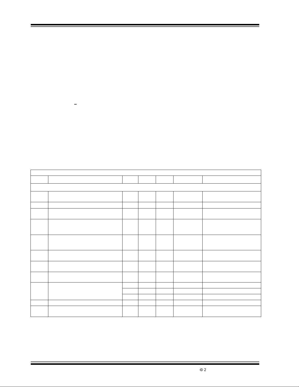
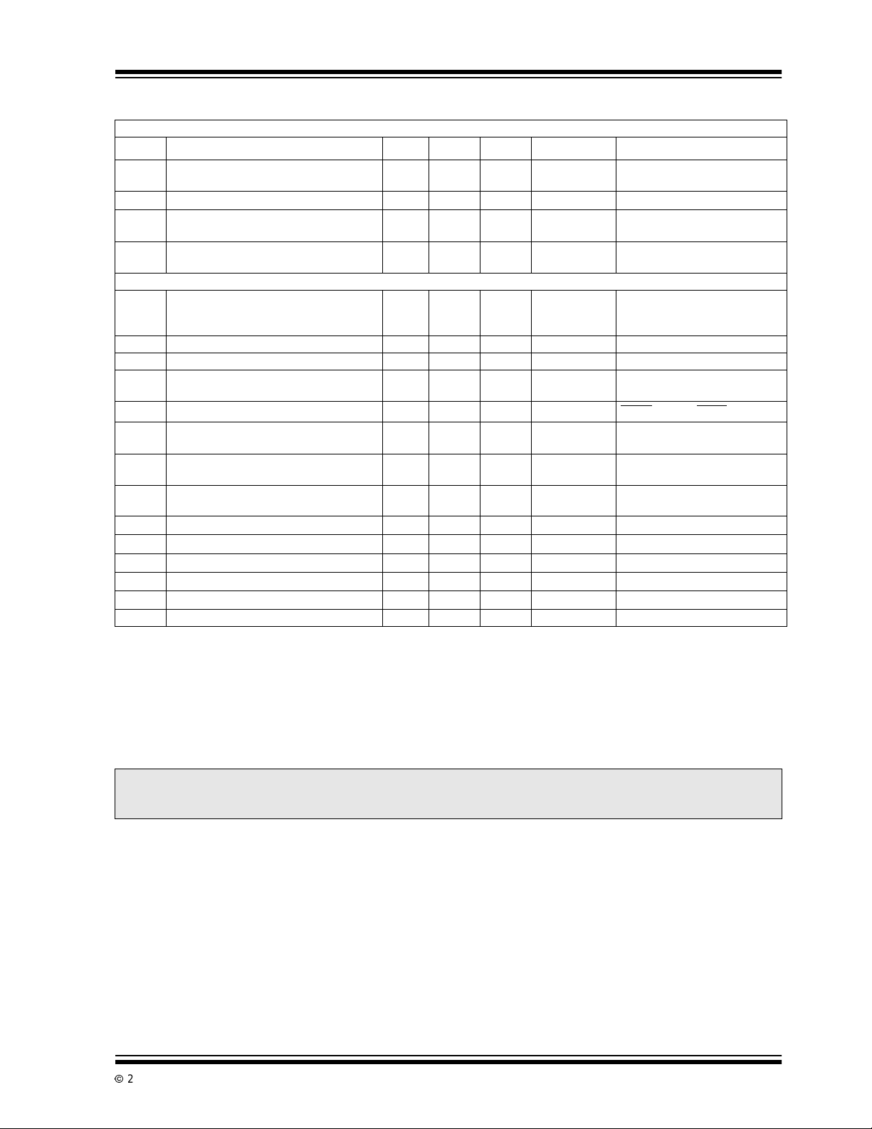
TC7109/TC7109A ELECTRICA L SPECIFICATIONS
Electrical Characteristics: All parameters with V+ = +5V, V-= -5V, GND = 0V, TA= +25°C, unless otherwise indicated.
Symbol Parameter Min Typ Max Unit Test Conditions
Analog
Overload Recovery Time (TC7109A) — 0 1 Measurement
Cycle
Zero InputReading -0000
Ratio Metric Reading 3777
NL Non-Linearity (Max Deviation
from Best Straight Line Fit)
Rollover Error (Differencein Readingfor
Equal Positive and Inputs near
(Full Scale)
CMRR Input Common Mode
Rejection Ratio
V
CMR
e
N
I
IN
TC
TC
Note 1: Input voltages may exceed supply voltages if input current is limited to ±100µA.
CommonMode Voltage Range V-+1.5 — V+ -1.5 V Input High, InputLow and
Noise (P-P Value Not
Exceeded 95% of Time)
Leakage Current at Input — 1 10 pA VIN, All Packages: +25°C
Zero Reading Drift — 0.2 1 µV/°C VIN=0V
ZS
Scale Factor Temperature Coefficient — 1 5 µV/°C VIN= 408.9mV = >7770
FS
2: Connecting any digital inputs or outputsto voltages greater than V+ or less than GND may cause destructive device
latchup. Therefore, it is recommended that inputsfrom sources other than the same power supply shouldnotbe applied
to the TC7109A beforeitspowersupply is established. In multiple supply systems, the supply to the device should be
activated first.
3: Thislimit refers to that of thepackage and will not occur during normal operation.
±00008+00008Octal Reading VIN= 0V; Full Scale = 409.6mV
8
3777
8
4000
-1 ±0.2 +1 Count Full Scale = 409.6mV to 2.048V
-1 ±0.02 +1 Count Full Scale = 409.6mV to
—50 — µV/V V
—15 — µVVIN= 0V,Full Scale = 409.6mV
— 20 100 pA C Device:0°C≤ T
— 100 250 pA I Device: -25°C ≤ T
40008Octal Reading VIN=V
8
8
REF
V
=204.8mV
REF
Over Full Operating
T emperature Range
2.048VOver Full Operating
T emperature Range
±1V, VIN=0V
CM
Full Scale = 409.6mV
Common Pins
≤ +70°C
A
A
Reading,ExtRef = 0ppm/°C
≤ +85°C
8
DS21456B-page 4
2002 Microchip TechnologyInc.
Page 5
TC7109/A
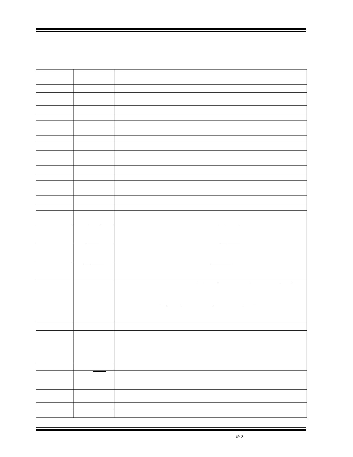
TC7109/TC7109A ELECTRICAL SPECIFICATIONS (CONTINUED)
Electrical Characteristics: All parameters with V+ = +5V, V-= -5V, GND = 0V, TA= +25°C, unless otherwise indicated.
Symbol Parameter Min Typ Max Unit Test Conditions
+
I
I
S
V
REF
TC
Digital
V
OH
V
OL
V
IH
V
IL
t
W
Note 1: Input voltages may exceed supply voltages if input current is limited to ±100µA.
Supply Current (V+ to GND) — 700 1500 µAVIN= 0V, Crystal Oscillator
3.58MHzTestCircuit
Supply Current (V+ to V-) — 700 1500 µA Pins 2-21, 25, 26, 27, 29 Open
Reference Out Voltage -2.4 -2.8 -3.2 V Referenced to V+, 25kΩ
Between V+ and Ref Out
Ref Out Temperature Coefficient — 80 — ppm/°C 25kΩ Between V+ and Ref Out
REF
OutputHighVoltage
I
=700µA
OUT
3.5 4.3 — V TC7109: I
OutputLowVoltage — 0.2 0.4 µAI
0°C ≤ T
Pins 3 -16, 18, 19,20
TC7109A: I
OUT
≤ +70°C
A
OUT
OUT
=1.6mA
=100µA
=700µA
OutputLeakage Current — ±0.01 ±1 µA P ins 3 -16 High Impedance
Control I /O Pull-up Current — 5 — µF Pins 18, 19, 20 V
Mode Input at GND
Control I/O Loading — — 50 pF HBEN
,Pin19;LBEN,Pin18
InputHighVoltage 2.5 — — V Pins 18 -21, 26, 27
Referenced to GND
Input Low Voltage — — 1 V Pins 18-21, 26, 27
Referenced to GND
Input Pull-up Current —
—
Input Pull-down Current — 1 — µAPins21,V
Oscillator OutputCurrent, High — 1 — mA V
Oscillator OutputCurrent, Low — 1.5 — mA V
Buffered Oscillator Output Current High — 2 — mA V
Buffered Oscillator Output Current Low — 5 — mA V
25
5
—
—
µA
µA
Pins 26, 27; V
Pins 17, 24; V
OUT
–2.5V
OUT
–2.5V
OUT
–2.5V
OUT
–2.5V
OUT
OUT
OUT
=GND=+3V
Mode Input Pulse Width 60 — — nsec
2: Connecting any digital inputs or outputsto voltages greater than V+ or less than GND may cause destructive device
latchup. Therefore, it is recommended that inputsfrom sources other than the same power supply shouldnotbe applied
to the TC7109A beforeitspowersupply is established. In multiple supply systems, the supply to the device should be
activated first.
3: Thislimit refers to that of thepackage and will not occur during normal operation.
=V+–3V
OUT
=V+–3V
=V+– 3V
HANDLING PRECAUTIONS: Thesedevices are CMOS andmust be handledcorrectlyto prevent damage. Package
and store only in conductive foam, antistatic tubes, or other conductingmaterial. Use proper antistatic handling procedures. Do not connectin circuits under "power-on" conditions, as high transients may cause permanent damage.
2002 Microchip TechnologyInc. DS21456B-page 5
Page 6
TC7109/A
2.0 PIN DESCRIPTIONS
ThedescriptionsofthepinsarelistedinTable2-1.
TABLE 2-1: PIN FUNCTION TABLE
Pin Number
(40-Pin PDIP)
1 GND Digital ground, 0V, ground return for all digital logic.
2 STATUS Output HIGH during integrate and de-integrate until datais latched. Output LOW when
3 POL Polarity - High for positive input.
4 OR Over Range - High if over ranged (Three-State Data bit).
5B
6B
7B
8B
9B
10 B
11 B
12 B
13 B
14 B
15 B
16 B
17 TEST Input High - Normal operation. Input LOW - Forces all bit outputs HIGH.
18 LBEN
19 HBEN
20 CE
21 MODE Input LOW - DirectOutputmodewhereCE
Symbol Description
analogsection is in auto-zero or zero integrator configuration.
12
11
10
9
8
7
6
5
4
3
2
1
Bit 12 (Most Significant bit) (Three-State Data bit).
Bit 11 (Three-State Data bit).
Bit10(Three-StateDatabit).
Bit 9 (Three-State Data bit).
Bit 8 (Three-State Data bit).
Bit 7 (Three-State Data bit).
Bit 6 (Three-State Data bit).
Bit 5 (Three-State Data bit).
Bit 4 (Three-State Data bit).
Bit 3 (Three-State Data bit).
Bit 2 (Three-State Data bit).
Bit 1 (Least Significant bit) (Three-State Data bit).
Note: This input is used for test purposes only.
Low Byte Enable - with MODE (Pin 21) LOW, and CE/LOAD (Pin 20) LOW, taking this pin
LOW activates low order byte outputs,B
low byte flag outputused in Handshakemode. (SeeFigure 3-7, Figure 3-8, and Figure 3-9.)
. With MODE (Pin 21) HIGH, this pin serves as
1–B8
High Byte Enable - with MODE (Pin 2 1) LOW, and CE/LOAD (Pin 20) LOW, taking this pin
LOW activates high order byte outputs, B
pin serves as high byte flag output used in Handshakemode.See Figures3-7,3-8,and3-9.
, POL, OR. With MODE (Pin 21) HIGH, this
9–B12
/LOAD Chip Enable/Load - with MO DE (Pin 21) LOW, CE/LOAD servesas a master output enable.
When HIGH,B
strobeis used in handshakemode. (See Figure 3-7, Figure 3-8, and Figure 3-9.)
, POL, OR outputs are disabled. When MODE (Pin 21) is HIGH, a load
1–B12
/LOAD(Pin 20), HBEN (Pin 19), and LBEN (Pin
18) act as inputs directlycontrolling byte outputs. InputP ulsed H IGH - Causes immediate
entryintoHandshake mode and output of data as in Figure3-9.
Input HIGH- enablesCE
/LOAD (Pin 20), HBEN (Pin 19), and LBEN (Pin 18) as outputs,
Handshake mode will be entered and data output as in Figure 3-7 and Figure 3-9
at conversions completion.
22 OSC IN Oscillator Input.
23 OSC OUT Oscillator Output.
24 OSC SEL Oscillator Select - Input HIGH configures OSC IN, OSC OUT ,BUFF OSC OUT as RC
oscillator - clock will be same phase and duty cycle as BUFF OSC OUT. Input LOW
configures OSC IN, OSC OUT for crystal oscillator - clock frequency will be 1/58 of frequency
at BUFF OSC OUT.
25 BUFFOSC OUT BufferedOscillator Output.
26 RUN/HOLD
Input HIGH - Conversionscontinuously performed every 8192clockpulses.
InputLOW-Conversionin progress completed; converterwill stop in auto-zero seven counts
beforeintegrate.
27 SEND Input- Used in Handshake mode to indicateability of an external device to accept data.
Connect to V+ if not used.
28 V- Analog Negative Supply - Nominally -5V with respect to GND (Pin 1).
29 REF OUT Reference Voltage Output - Nominally 2.8V down from V+ (Pin 40).
DS21456B-page 6
2002 Microchip TechnologyInc.
Page 7
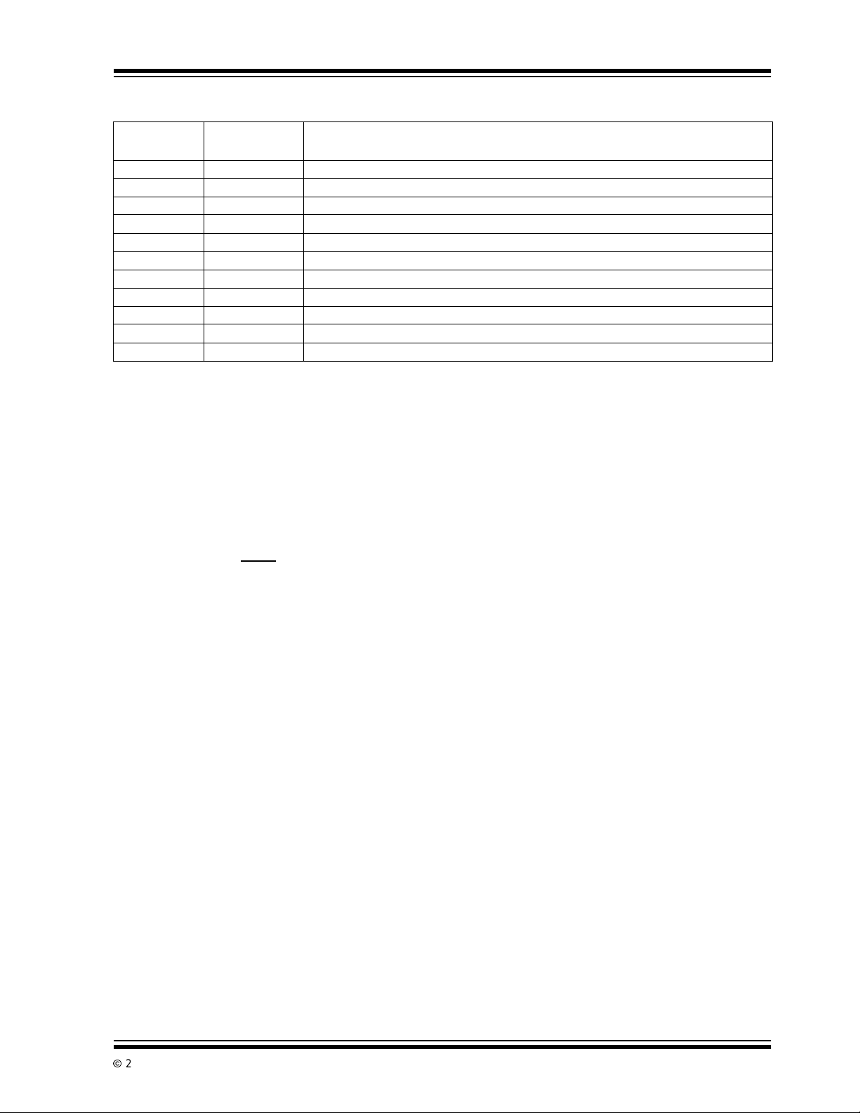
TABLE 2-1: PIN FUNCTION TABLE (CONTINUED)
Pin Number
(40-Pin PDIP)
30 BUFF Buffer Amplifier Output.
31 AZ Auto-Zero Node - Inside foil of C
32 INT Integrator Output - Outside foil of C
33 COMMON Analog Common - System is auto-zeroedto COMMON.
34 IN LO Differential Input Low Side.
35 IN HI Differential Input High Side.
36 REF IN+ Differential Reference Input Positive.
37 REF CAP+ Reference Capacitor Positive.
38 REF CAP- Reference Capacitor Negative.
39 REF IN- Differential Reference Input Negative.
40 V+ Positive Supply Voltage - Nominally +5V with respectto GND (Pin 1).
Note: All Digital levels are positive true.
Symbol Description
.
AZ
.
INT
TC7109/A
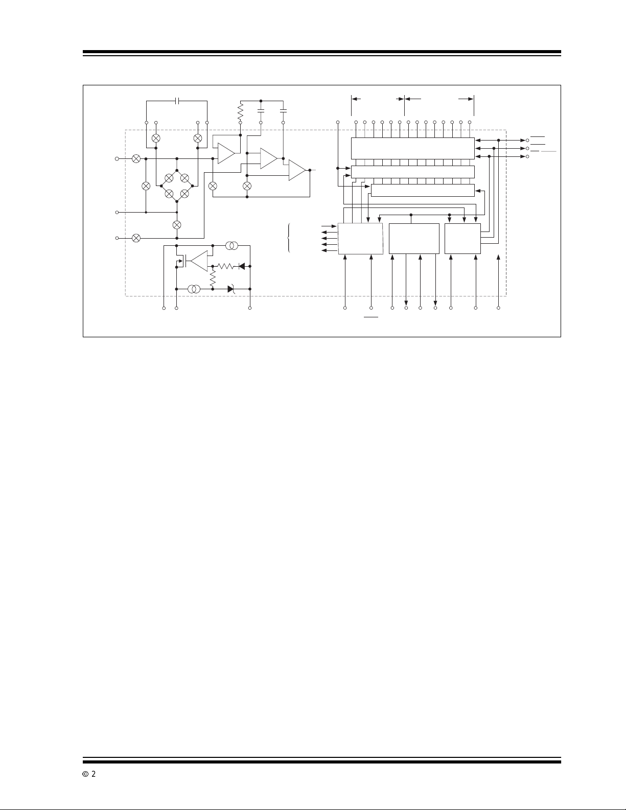
3.0 DETAILED DESCRIPTION
(All Pin Designations Refer to 40-Pin DIP.)
3.1 Analog Section
The Typical Application diagram on page 3 shows a
block diagram of the analog section of the TC7109A.
The circuit will perform conversions at a rate determined by the clock frequency (8192 clock periods per
cycle), when the RUN/HOLD
nected to V+. Each measurement cycle is divided into
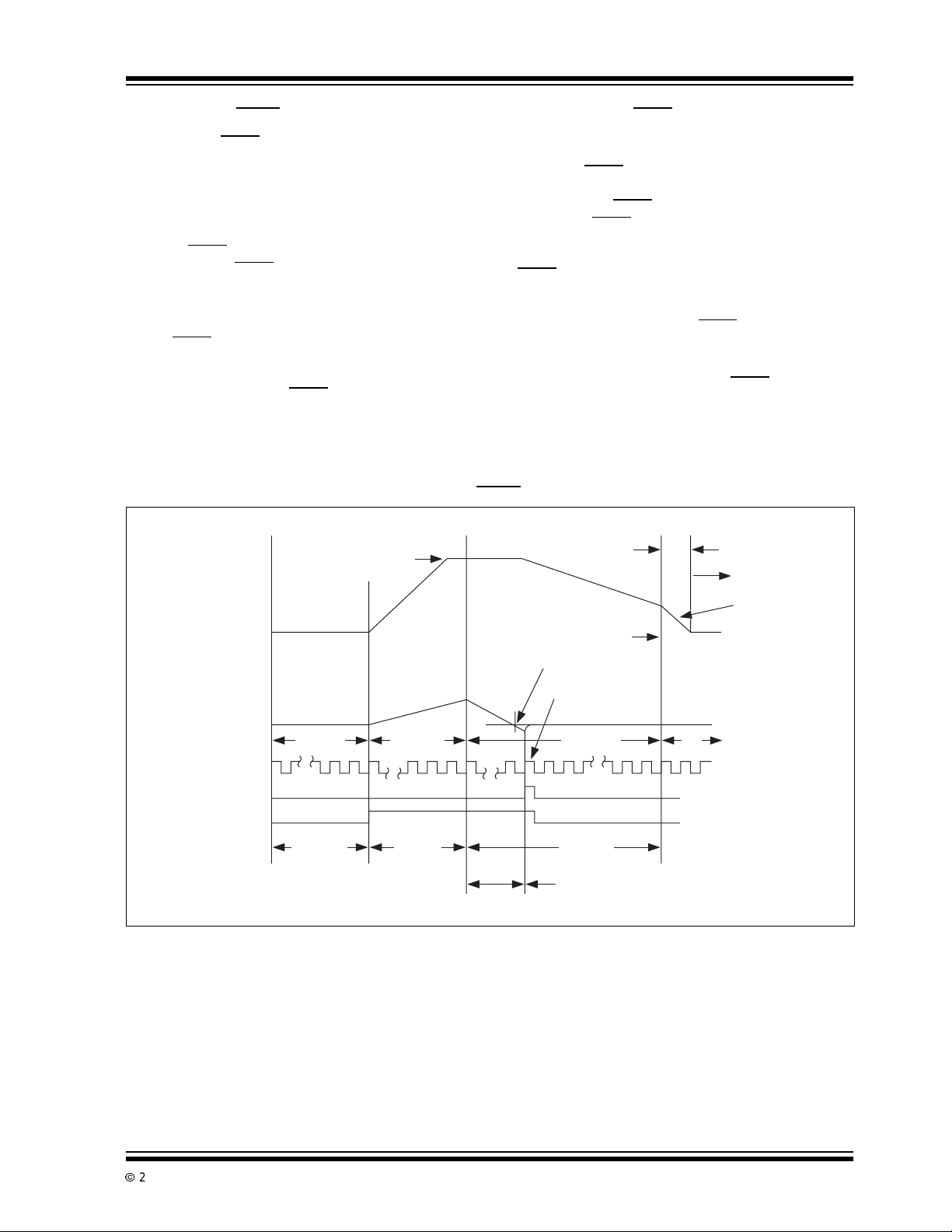
four phases, as shown in Figure 3- 1. They are:
(1) Auto-Zero (AZ), (2) Signal Integrate (INT), (3) Reference De-integrate (DE), and (4) Zero Integrator (ZI).
3.1.1 AUTO-ZERO PHASE
The buffer and the integrator inputs are disconnected
from input high and input low and connected to analog
common.The reference capacitorischargedto the reference voltage. A feedback loop is closed around the
system to charge the auto-zero capacitor, C
pensate for offset voltage in the buffer amplifier, i ntegrator, and comparator. Since the comparator is
included in the l oop, the AZ accuracy is limited only by
the noise of the system. The offset referred to the input
is less than 10µV.
input is left open or con-
,tocom-
AZ
3.1.2 SIGNAL INTEGRATE PHASE
The bufferandintegrator inputsareremovedfrom common and connected to input high and input low. The
auto-zero loop is opened. The auto-zero capacitor is
placed in series in the loop to provide an equal and
opposite compensating offset voltage. The differential
voltage between input high and input low is integrated
for a fixedtime of 2048 clock periods. At the end of this
phase, the polarity of the integrated signal is determined. If the input signal has no return to the converter's power supply, input low can be tied to analog
common to establish the correct Common mode
voltage.
3.1.3 DE-INTEGRATE P HA SE
Input high i s connected across the previously charged
reference capacitor and input low is internally connected to analog common. Circuitry within the chip
ensuresthecapacitor will be connectedwiththecorrect
polarity to cause the integrator output to return to the
zero crossing (established by auto-zero), with a fixed
slope. The time, represented by the number of clock
periods counted for the output to return to zero, is
proportionalto the input signal.
2002 Microchip TechnologyInc. DS21456B-page 7
Page 8

TC7109/A
3.1.4 Z ERO INTEGRATOR PHASE
The ZI phase only occurs when an input over range
condition exists. The function of the ZI phase is to eliminateresidualchargeon the integratorcapacitorafteran
overrangemeasurement.Unless removed,the residual
chargewillbe transferredto the auto-zerocapacitorand
cause an errorin the succeeding conversion.
The ZI phase virtually eliminates hysteresis, or "crosstalk" in multiplexed systems. An over range input on
one channel will not cause an erroron the next channel
measured. This feature is especially useful in thermocouple measurements, where unused (or broken t hermocouple) inputs are pulled to the positive supply rail.
During ZI, the referencecapacitorischargedto the reference voltage. The signal inputs are disconnected
fromthebufferandintegrator.Thecomparatoroutputis
connected to the buffer input, causing the integrator
output to be driven rapidly to 0V (Figure 3-1). The ZI
phase only occurs following an overrange and lasts for
a maximum of 1024 clock periods.
3.1.5 DIFFERENTIAL INPUT
The TC7109A has been optimized for operation with
analog common near digital ground. With +5V and -5V
power supplies, a full ±4V full scale integrator swing
maximizes the analog section's performance.
A typical CMRR of 86dB is achieved for input differential voltages anywhere within the typical Comm on
mode range of 1V below the positive supply, to 1.5V
above the negative supply. However, for optimum performance, the IN HI and IN LO inputs should not come
within 2V of either supply rail. Since the integrator also
swings with the Common mode voltage, care must be
exercised to ensure the integrator output does not saturate. A worst case condition is near a full scale negative differential input voltage with a large positive
Common mode voltage. The negative input signal
drives the integrator positive when most of its swing
has been used up by the positive Common mode voltage. In such cases, the integrator swing can be
reduced to less than the recommended ±4V full scale
value, with some loss of accuracy. The integrator output can swing to within 0.3V of either supply without
loss of linearity.
3.1.6 DIFFERENTIAL REFERENCE
The reference voltage can be generated anywhere
within the power supply voltage of the converter. Rollover voltage is the main source of Common mode
error, caused by the referencecapacitorlosingor gaining charge, due to stray capacity on its nodes. With a
large Common mode voltage, the reference capacitor
can gain charge (increasevoltage) when called upon to
de-integrate a positive signal and lose charge
(decrease voltage) when called upon to de-integrate a
negative input signal. This difference in reference for
(+) or (–) i nput voltages will causea rollovererror. This
error can be held to less than 0.5 count, worst case, by
using a large r eference capacitor in comparison to the
stray capacitance. To minimize rollover error from
these sources, keep the reference Common mode
voltage near or at analog common.
3.2 Digital Section
The di gital section is shown in Figure 3-2 and includes
the clock oscillator and scaling circuit, a 12-bit binary
counter with output latches and TTL compatible threestate output drivers, UART handshake logic, polarity,
over range, and control logic. Logic levels are referred
to as LOW or HIGH.
Inputs driven from TTL gates should have 3kΩ to 5kΩ
pull-up resistors added for maximum noise immunity.
For minimum power consumption, all inputs should
swing from GND (LOW) to V+ (HIGH).
3.2.1 STATUS OUTPUT
During a conversion cycle, the STATUS output goes
high at the beginning of signal integrate and goes low
one-half clock period after new data from the conversion has been stored in the output latches (see
Figure 3-1). The signal may be used as a "data valid"
flag to drive interrupts, or for monitoring the status of
theconverter.(Datawillnotchange while statusislow.)
3.2.2 MODE INPUT
The Output mode of the converter is controlled by the
MODE input. The converter is in its "Direct" Output
mode, when the MODE input i s LOW or left open. The
output data is directly accessible under the control of
the chip and byte enable inputs (this input is provided
with a pull-down resistor to ensure a LOW level when
the pin is left open). When the MODE input is pulsed
high, the converter enters the UART Handshake mode
and outputs the data in 2 bytes, then returnsto "Direct"
mode. When the MODE input is kept HIGH, the converter will output data in the Handshake mode at the
end of every conversion cycle. With MODE = 0 (direct
bus transfer), the send input should be tied toV+. (See
"Handshake Mode".)
DS21456B-page 8
2002 Microchip TechnologyInc.
Page 9
TC7109/A
t
3.2.3 RUN/HO LD INPUT
With the RUN/HOLD input high, or open, the circuit
operates normally as a dual slope ADC, as shown in
Figure 3-1. Conversion cycles operate continuously
with the output latches updated after zero crossing in
the De-integrate mode. An internal pull-up resistor is
provided to ensure a HIGH level with an open i nput.
The RUN/HOLD
sion time. If RUN/HOLD
crossing in the De-integrate mode, the circuit will jump
to auto-zero and eliminate that portion of time normally
spent in de-integrate.
If RUN/HOLD
complete with minimum time in de-integrate. It will stay
in auto-zero for the minimum time and waitin auto-zero
for a HIGH at the RUN/HOLD
Figure 3-3, the STATUS output will go HIGH, 7 clock
input may be used to shorten conver-
goes LOW any timeafter zero
stays or goes LOW, t he conversion will
input. As shown in
periods after RUN/HOLD
converter will begin the integrate phase of the next
conversion.
The RUN/HOLD
interface. The converter may be held at IDLE in autozero with RUN/HOLD
when RUN/HOLD
valid when the STATUS output goes LOW (or is transferred to the UART; see "Handshake Mode"). RUN/
HOLD
may now go LOW, terminating de-integrate and
ensuring a minimum auto-zero time before stopping to
wait for the next conversion. Conversion time can be
minimized by ensuring RUN/HOLD
de-integrate, after zero crossing, and goes HIGH after
the hold point is reached.
The required activity on the RUN/HOLD
provided by connecting it to the buffered oscillator output.In this mode, the inputvaluemeasureddetermines
the conversion time.
FIGURE 3-1: CONVERSION TIMING (RUN/HOLD PIN HIGH
Integrator
Saturates
Integrator Output
for Over Range Input
Integrator Output
for Normal Input
Internal Clock
AZ
Phase I
INT
Phase II
No Zero Crossing
Zero Crossing
Occurs
Zero Crossing
Detected
Phase III
DE
is changed to HIGH, and t he
input allows controlled conversion
LOW.Theconversionisstarted
goes HIGH, and the new data is
goes LOW during
input can be
ZI
AZ
Zero Integrator
Phase forces
Integrator Outpu
to 0V
AZ
Internal Latch
Status Output
2002 Microchip TechnologyInc. DS21456B-page 9
2048
Counts
Min.
Number of Counts to Zero Crossing
Fixed
2048
Counts
Proportional to V
4096
Counts
Max
After Zero Crossing, Analog section will
IN
be in Auto-Zero Configuration
Page 10
TC7109/A
FIGURE 3-2: DIGITAL SECTION
To
Analog
Section
COMP OUT
AZ
INT
DE (±)
TEST17POL3OR
ZI
High Order
Byte Outputs
B
B
B
B
12
11
10
4
5
6
7
Conversion
Control Logic
2262223242521
STATUS RUN/
HOLD
B
9
8
8
9
14 Three-State Outputs
14 Latches
12-Bit Counter
Oscillator and
Clock Circuitry
OSCINOSC
OUT
10
OSC
SEL
B
7
Latch
Clock
Low Order
Byte Outputs
B
B
6
5
11
12
BUFF
OSC
OUT
B
4
13
Handshake
MODE
14
B
3
15
Logic
B
2
B
1
16
27
SEND
1
GND
18
19
20
LBEN
HBEN
CE/LOAD
FIGURE 3-3: TC7109A RUN/HOLD
Determinated at
Zero Crossing
Integrator Output
Internal Clock
Internal Latch
Status Output
RUN/HOLD Input
RUN/HOLD input is ignored until end of auto-zero phase.*Note:
OPERATION
Detection
Auto-Zero Phase I
Min 1790 Counts
Max 2041 Counts
*
Static in
Hold State
INT
Phase II
7 Counts
DS21456B-page 10
2002 Microchip TechnologyInc.
Page 11

TC7109/A
3.2.4 DIRECT MODE
The data outputs (bits 1 through8, low order bytes;bits
9 through 12, polarity and over range high order bytes)
are accessible under control of the byte and chip
enable terminals as inputs, with the MODE pin at a
LOW level. These three inputs are all active LOW.
Internal pull-up resistors are provided for an inactive
HIGH level when left open. When chip enable is LOW,
a byte enable input LOW will allow the outputs of the
byte to become active. A variety of parallel data
accessing techniques may be used, as shown in t he
"Interfacing" section. (See Figure 3-4 and Table 3-1.)
The access of data should be synchronized with the
conversion cycle by m onitoring the STATUS output.
This prevents accessing data while it is being updated
and eliminates the acquisition of erroneous data.
FIGURE 3-4: TC7109A DIRECT MODE
OUTPUT TIMING
t
CE/LOAD
As Input
HBEN
As Input
LBEN
As Input
High Byte
Data
Low Byte
Data
t
BEA
t
DAB
= High Impedance
Data
Valid
t
DAB
t
DAC
CEA
Data
Valid
Data
Valid
t
DHC
TABLE 3-1: TC7109A DIRECT MODE
TIMING REQUIREMENTS
Symbol Description Min Typ Max Units
Byte EnableWidth 200 500 — nsec
t
BEA
t
DAB
t
DHB
t
CEA
t
DAC
t
DHC
Data Access Time
from Byte Enable
DataHoldTimefrom
ByteEnable
Chip Enable Width 300 500 nsec
Data Access Time
from Chip Enable
DataHoldTimefrom
Chip Enable
— 150 300 nsec
— 150 300 nsec
— 200 400 nsec
— 200 400 nsec
3.2.5 HANDS HAK E MODE
An alternative means of interfacing the TC7109A to
digital systems is provided when the Handshake OutputmodeoftheTC7109Abecomesactiveincontrolling
the flow of data, insteadof passivelyrespondingtochip
and byte enable inputs. This mode allows a directinterface between the TC7109A and industry standard
UARTs with no external logic required. The TC7109A
provides all the control and flag signals necessary to
sequence the two bytes of data into the UART and initiate their transmission in serial form when triggered
into the Handshake mode. The cost of designing
remote data acquisition stationsis reduced using serial
data transmission to minimize the number of lines to
the central controlling processor.
The MODE input controls the Handshake mode. When
the MODE input is heldHIGH, the TC7109A enters the
Handshakemodeafternewdatahas beenstoredinthe
output latches at the end of every conversion performed (see Figure 3-7 and Figure 3-8). Entry into the
Handshake mode may be triggered on demand by the
MODE input. At any time during the conversion cycle,
the LOW-to-HIGH transition of a short pulse at t he
MODE input will cause immediate entry into the Handshake mode. If this pulse occurs while new data is
being stored, the entry into H andshake mode is
delayed until the data is stable. The MODE input is
ignored i n the Handshake mode, and until the converter completes the output cycle and clears theHandshake mode, data updating will be inhibited (see
Figure 3-9).
When the MODE input is HIGH, or when the converter
enters the Handshake m ode, the chip and byte enable
inputs become TTL compatible outputs, which provide
the output cycle control signals (see Figure 3-7,
Figure 3-8 and Figure 3-9). The SEND input is used by
the converter as an indication of the ability of the
receivingdevice(suchas aUART)toacceptdatainthe
Handshake mode. The sequence of the output cycle
with SEND held HIGH is shown in Figure 3-7. The
Handshake mode (internal MODE HIGH) is entered
after the data latch pulse (the CE
HBEN
terminals are active as outputs, since MODE
remainsHIGH).
The HIGH level at the SEND input is sensed on the
same HIGH-to-LOW internal clock edge. On the next
LOW-to-HIGH internal clock edge, the high order byte
(bits 9 t hrough 12, POL, and OR) outputs are enabled
and the CE
LOWlevel.The CE
/LOAD and the HBEN outputs assume a
/LOAD output remains LOW for one
full internal clock period only; the data outputs remain
activefor 1-1/2internalclockperiods;andthehighbyte
enable remains LOW for 2 clock periods.
/LOAD, LBEN and
2002 Microchip TechnologyInc. DS21456B-page 11
Page 12

TC7109/A
The CE/LOAD output LOW level, or LOW-to-HIGH
edge, may be usedas a synchronizing signal to ensure
valid data, and the byte enable as an output may be
used asa byte identificationflag.WithSENDremaining
HIGH, the converter completes the output cycle using
CE
/LOAD and LBEN, while the low order byte outputs
(bits 1 through 8) are activated. When both bytes are
sent, the Handshake mode is t erminated. The t ypical
UART interfacing timing is shown in Figure 3-8.
The SEND input is used to delay portions of the
sequence, or handshake, to ensure correct data transfer. This timing diagram shows an industry standard
HD6403 or CDP1854 CMOS UART to interface to
serial data channels. The SEND input to the TC7109A
is driven by the TBRE (Transmitter Buffer Register
Empty) output of the UART, and the CE
the TC7109A drives the TBRL (Transmitter Buffer Register Load) input to the UART. The eight transmitter
buffer register inputs accept the parallel data outputs.
With the UART transmitter buffer register empty, the
SEND input will be HIGH when the Handshake mode is
entered, after new data is stored. The high order byte
outputs become active and the CE
inputs will go LOW a fter SEND is sensed. When CE/
LOAD
goes HIGH at the end of one clock period, the
high order byte data is clocked intothe UART transmitterbufferregister.TheUARTTBREoutputwillgoLOW,
which halts the output cycle with the HBEN output
LOW,and the high orderbyte outputs active. When the
UART has transferred the data to the transmitter register and cleared the transmitter buffer register, the
TBRE returns HIGH. The high order byte outputs are
disabled on t he next TC7109A internal clock HIGH-toLOW edge, and one-half internal clock later, t he HBEN
outputreturns HIGH. The CE/LOADand LBEN outputs
go LOW at the same t ime asthe low orderbyte outputs
become active. When the CE
the end of one clock period, the low order data is
clocked into the UART transmitter buffer register, and
TBRE again goes LOW. The next TC7109A internal
clock HIGH-to-LOW edge will sense when TBRE
returns to a HIGH, disabling the data inputs. One-half
internal clock later, the Handshake mode is cleared,
and the CE
HIGH and stay active, if MODE still remains HIGH.
Handshake output sequences may be performed on
demand by triggering the converter into Handshake
mode with a LOW-to-HIGHedge on the MODEinput.A
handshake output sequence triggered is shown in
Figure 3-9. The SEND input is LOW when the converter enters Handshake mode. The whole output
sequence is controlled by the SEND input, and the
sequence for the first (high order) byte is similar to t he
sequence for the second byte.
Figure 3-9 also shows t hat the output sequence can
take longer than a conversion cycle. New data will not
be latched when the Handshake mode is still in
progress and is, therefore, lost.
/LOAD, HBEN and LBEN terminals return
/LOAD returns HIGH at
/LOAD input of
/LOAD and HBEN
3.3 Oscillator
The oscillatormay be over driven, or may be operated
as an RC or crystal oscillator. The OSCILLATOR
SELECT input optimizes the internal configuration of
the oscillator for RC or crystal operation. The OSCILLATOR SELECT input i s provided with a pull-up resistor. When the OSCILLATOR SELECT input is HIGH or
left open, the oscillator is configured for RC operation.
The internal clock will be the same frequency and
phase as the signal at the BUFFERED OSCILLATOR
OUTPUT. Connect the resistor and capacitor as in
Figure 3-5. The circuitwilloscillateatafrequency given
by f = 0.45/RC. A 100kΩ resistor is recommended for
useful ranges of frequency. The capacitor value should
be chosen such that2048 clock periods are closeto an
integral multiple of the 60Hz period for optimum 60Hz
line rejection.
FIGURE 3-5: TC7109A RC
OSCILLATOR
OSC
23
OSC
OUT
R
= 0.45/RC
24
22
OSC
OSC
SEL
IN
V+ or Open
With OSCILLATOR SELECT input LOW, two on-chip
capacitors and a feedback device are added to the
oscillator. In this configuration, the oscillator will operate with most crystals in the 1MHz to 5MHz range, with
no external components (Figure 3-6). The OSCILLATORSELECT input LOW insertsa fixed 458 divider circuit between the BUFFERED OSCILLATOR OUTPUT
and the internal clock. A 3.58MHz TV crystal gives a
division ratio, providing an integration time given by:
F
EQUATION 3-1:
t = (2048 clock periods) = 33.18msec
58
3.58MHz
25
Buffered
OSC OUT
C
DS21456B-page 12
2002 Microchip TechnologyInc.
Page 13

TC7109/A
g
FIGURE 3-6: CRY S TAL OSCILLATOR
The error is less than 1% from two 60Hz periods, or
33.33msec, which will give better t han 40dB, 60Hz
V+
Clock
rejection. The converter will operate reliably at conversion rates up to 30 per second, corresponding to a
clock frequency of 245.8kHz.
÷
58
When the oscillator is to be over driven, the OSCILLATOROUTPUT should be left open, and the over driving
24
OSC
SEL
22
OSC
IN
23
OSC
OUT
25
Buffered
OSC OUT
signal should be applied at the OSCILLATOR INPUT.
The internal clock will be of the same duty cycle, fre-
quency and phase as the input signal. When the
OSCILLATOR SELECT is at GND, the clock will be
GND
Crystal
1/58 of the input frequency.
FIGURE 3-7: TC7109A HANDSHAKE WITH SEND INPUT HE LD POSITIVE
Integrator Output
Internal Clock
Internal Latch
Status Output
Mode Input
Internal Mode
Send Input
CE/LOAD
HBEN
High Byte Data
LBEN
Low Byte Data
UART
Norm
Zero Crossing Occurs
Zero Crossing Detected
Send Sensed Send Sensed
Data Valid
Mode High Activates
CE/LOAD, HBEN, LBEN
Data Invalid
Terminates
UART Mode
Mode Low, not
in Handshake Mode
Disables Outputs
CE/LOAD,
HBEN,
LBEN
Three-State
= Don't Care
2002 Microchip TechnologyInc. DS21456B-page 13
=
Hi
h Impendance
Three-State
=
will Pull-up
Page 14

TC7109/A
g
e
FIGURE 3-8: TC7109A HANDSHAKE - TYPICAL UART INTERFA CE TIMING
Zero Crossing Occurs
Integrator Output
Internal Clock
Internal Latch
Status Output
Mode Input
Internal Mode
Send Input (UART TBRE)
CE/LOAD Output (UART TBRL)
HBEN
UART
Norm
Zero Crossing Detected
Send
Sensed
Sensed
Send
Send
Sensed
Terminates
UART Mode
High Byte Data
LBEN
Low Byte Data
= Don't Care
Data Valid
=
Three-State High Impedance
Data Valid
FIGURE 3-9: TC7109A HANDSHAKE TRIGGERED BY MODE INPUT
Zero Crossing Occurs
Positive Transiton causes
Entry into UART Mode
Internal Clock
Internal Latch
Status Output
Mode Input
Internal Mode
Send Input
CE/LOAD as Output
UART
Norm
Send
Sensed
Status Output unchanged
in UART Mode
Send
Sensed
DE Phase III
Zero Crossing Detected
Latch Pulse inhibited in UART Mod
Terminates
Send
Sensed
UART Mode
HBEN
High Byte Data
LBEN
Low Byte Data
DS21456B-page 14
= Don't Care
Data Valid
Data Valid
Three-State
=
h Impedance
Hi
Three-State
=
with Pull-up
2002 Microchip TechnologyInc.
Page 15

TC7109/A
3.4 Test Input
The counterand itsoutputsmaybetestedeasily.When
the TEST input is connectedto GND, the internal clock
is disabled and the counter outputs are all forced into
the HIGH state. When the input returns to the 1/2
(V+ – GND) voltageor to V+ and one clock is input, the
counter outputs wi ll all be clocked to the LOW state.
The counteroutputlatches are enabledwhen the TEST
input is taken to a level halfway between V+ and GND,
allowingthe counter contents to be examined any time.
3.5 Component Value Selection
The integrator output swing for full scale should be as
large as possible. For example, with ±5V supplies and
COMMON connected to GND, the nominal integrator
output swing at full scale is ±4V. Since the integrator
output can go to 0.3V from either supply without significantly effecting linearity, a 4V integrator output swing
allows 0. 7V for variations in output swing, due to component value and oscillator tolerances. With ±5V supplies and a Comm on mode voltage range of ±1V
required, the component values should be selected to
provide ±3V integrator output swing. Noise and rollover errors will be slightly worse than in the ±4V case.
For large Common mode voltage ranges, the integrator
output swing must be reduced further. This will
increase both noise and rollover errors. To improve
performance,±6V supplies may be used.
3.5.1 INTEG RATING C APACITOR
The integrating capacitor, C
give the maximum integrator output voltage swing that
will not saturate the integrator to within 0.3V fromeither
supply. A ±3.5V to ±4V i ntegrator output swing is nominal for the TC7109A, with ±5V supplies and analog
common connected to GND. For 7-1/2 conversions per
second (61.72kHz internal clock frequency), nominal
values C
tively. These values should be changed if different
clock frequencies are used to maintain the integrator
output voltage s wing. The value of C
and CAZare 0.15µF and 0.33µF, respec-
INT
EQUATION 3-2:
C
INT
The integrating capacitor must have low dielectric
absorption to prevent rollover errors. Polypropylene
capacitors give undetectable errors, at reasonable
cost, up to +85°C.
(2048 Clock Period) (20µA)
=
Integrator Output Voltage Swings
3.5.2 INTEG RATING RESISTOR
The integrator and buffer amplifiers have a class A output stage with 100µA of quiescent current. They supply
20µA of drive current with negligible non-linearity. The
integratingresistor should be large enough to remain in
, should be selected to
INT
is given by:
INT
this very linear region over the input voltage range, but
small enough that undue leakage requirements are not
placedon the PC board.For 2.048Vfullscale,a 100kΩ
resistor is recommended and for 409.6mV full scale, a
20k resistor is recommended. R
other values of f ull scale by:
maybe selected for
INT
EQUATION 3-3:
R
INT
Full Scale Voltage
=
20µA
3.5.3 AUT O-ZERO CA PACITOR
As the auto-zero capacitor is made large, the system
noise is reduced. Since the TC7109A incorporates a
zero integrator cycle, the size of the auto-zero capacitordoesnotaffectoverload recovery.Theoptimalvalue
of the auto-zero capacitor is between 2 and 4 times
C
. A typical value for CAZis 0.33µF.
INT
The inner foil of C
the outer foil tothe RC summing junction.Theinnerfoil
of C
tion and the outer foil to Pin 32, for best rejection of
stray pickups.
should be connected to the RC summing junc-
INT
shouldbe connectedto Pin 31 and
AZ
3.5.4 REF ERENCE CAPACITOR
A1µF capacitor is recommended for most circuits.
However,wherea largeCommon mode voltage exists,
a larger value is required to prevent rollover error (e.g.,
the reference low is not analog common), and a
409.6mV scale is used. The rollover error will be held
to 0.5 count with a 10µF capacitor.
3.5.5 REFERENCE VOLTAGE
Togeneratefullscaleoutputof 4096counts,theanalog
input required is V
use a reference of 204.8mV. In many applications,
where the ADC is connected to a transducer, a scale
factorwillexistbet ween the input voltageandthedigital
reading. For instance, in a measuring system, the
designer might like to have a full scale reading when
the voltage for the transducer is 700mV. Instead of
dividing the input down to 409.6mV, the designer
should use the input voltage directly and select
V
= 350mV. Suitable values for integrating resistor
REF
and capacitor would be 34kΩ and 0.15µF. This makes
the system slightly quieter and also avoids a divider
networkon the input. Another advantage of this system
occurs when temperature and weight measurements,
with an offset or tare, are desired for non-zero input.
The offsetmaybeintroduced by connectingthevoltage
output of the transducer between common and analog
high,and the offset voltage between common and analog low, observing polarities carefully. In processor
based systems using the TC7109A, it may be more
desirable to use software and perform this type of scaling or tare subtraction digitally.
IN
=2V
. For 409.6mV full scale,
REF
2002 Microchip TechnologyInc. DS21456B-page 15
Page 16

TC7109/A
3.5.6 REF ERENCE SOURCES
A major factor in the absolute accuracy of the ADC is
the stability of the reference voltage. The 12-bit resolution of the TC7109A is one part in 4096, or 244 ppm.
Thus, for the on-board reference temperature coefficient of 70ppm/°C, a temperature differenceof 3°C will
introduce a one-bit absolute error. Where the ambient
temperature is not controlled, or where high accuracy
absolute measurements are being made, it is recommended that an external high quality reference be
used.
A reference output (Pin 29) is provided, which may be
used with a resistive divider to generate a suitable reference voltage (20mA may be sunk without significant
variationinoutputvoltage). A pull-up bias deviceis provided,whichsourcesabout10µA.The outputvoltageis
nominally2.8VbelowV+.Whenusingtheon-boardr eference, REF OUT (Pin 29) should be connected to
REF IN- (pin 39), and REF IN+ should be connected to
the wiper of a precision potentiometer between REF
OUT and V+. The test circuit shows the circuit for a
204.8mV reference, generated by a 2kΩ precision
potentiometer in series with a 24kΩ fixed resistor.
4.0 INTERFACING
4.1 Direct Mode
Combinations of chip enable and byte enable control
signals, which may be used when interfacing the
TC7109A to parallel data lines, are shown in Figure 4-1.
TheCE
/LOAD input may be tied low, allowing either byte
to be controlled by its own enable (see Figure 4-1(A)).
Figure 4-1(B) shows the HBEN
inputs, and CE
/LOAD as a masterenable, which could
be the READ st robe available from most microproces-
and LBEN as flag
sors. Figure 4-1(C) shows a configuration where the
two byte enables are connected together. The CE
LOAD
is a chip enable, and the HBEN and LBEN may
be used as a second chip enable, or connected to
ground. The 14 data outputs will be enabled at the
same time. In the direct MODE, SEND should be tied
to V+.
Figure 4-2 shows interfacing several TC7109A's to a
bus, ganging the HBEN
converters together, and using the CE
and LBEN signals to several
/LOAD input to
select the desired converter.
Figure 4-3 through Figure 4-5give practical circuits uti-
lizing the parallel three-state output capabilities of the
TC7109A. Figure 4-3 shows parallel interface to the
8748/49 systems via an 8255 PPI, where the TC7109A
data outputs ar e active at all times. This interface can
be used i n a read-after-update sequence, as shown in
Figure 4-4. The data is accessed by the high-to-low
transition of the STATUS driving an interrupt to the
microcontroller.
The RUN/HOLD
input is also used to initiate conver-
sions under software control.
Direct interfacing to most microcontroller busses i s
easily accomplished through the three-state output of
the TC7109A.
Figure 4-8 is a typical connection diagram. To ensure
requirements for setup and hold times, minimum pulse
widths, and the drive limitations on long busses are
met, it is necessary to carefully consider the system
timing in this type of interface. This type of interface is
used when the memory peripheral address density is
low, providing simple address decoding. Interrupt handling can be simplified by using an interface to reduce
the componentcount.
/
FIGURE 4-1: DIRECT MODE CHIP AND BY T E ENABLE COMBINATION
GND
A. B. C.
MODE CE/LOAD
B9 - B
POL, OR
12
6
GND
MODE CE/LOAD
TC7109A
B
- B
8
1
Analog In
RUN/HOLD
Control
DS21456B-page 16
8
LBENHBEN
Convert
Analog In
GND or
Chip Select 2
Chip Select 1
B1 - B
POL, OR
TC7109A
RUN/HOLD
LBENHBEN
12
14
Convert
GND
MODE CE/LOAD
Analog In
Chip Select
B9 - B
12
POL, OR
6
TC7109A
B
- B
8
1
8
RUN/HOLD
LBENHBEN
Byte Flags
2002 Microchip TechnologyInc.
Convert
Page 17
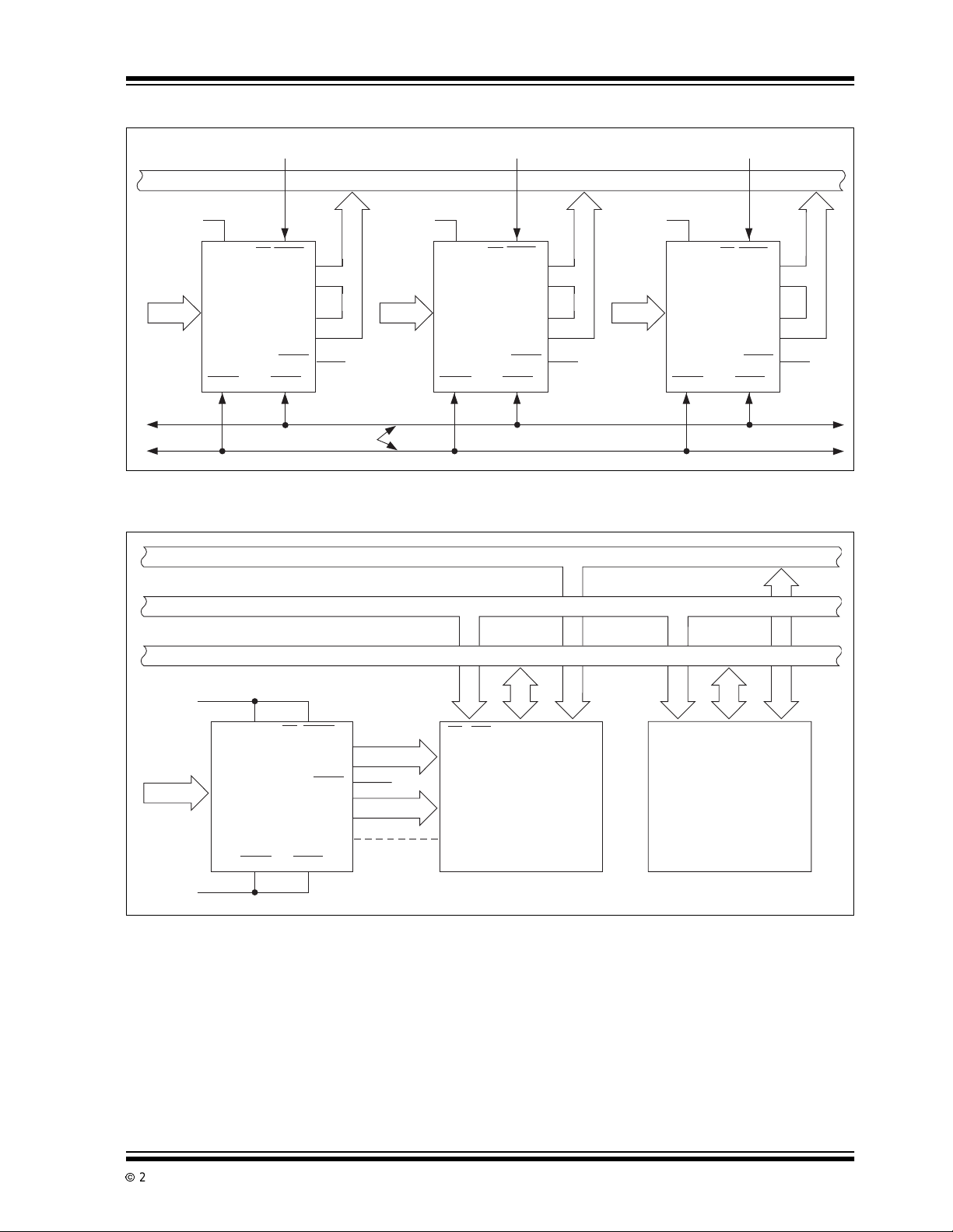
FIGURE 4-2: THREE-STATING SEVERAL TC7109AS TO A SMALL BUS
TC7109/A
GND
Analog In
Converter Select
MODE CE/LOAD
B9 - B
POL, OR
TC7109A
- B
B
1
RUN/HOLD
LBENHBEN
Byte Select Flags
GND
12
6
8
8
Analog In
+5V
Converter Select Converter Select
GND
MODE CE/LOAD
B
-
9
POL, OR
TC7109A
- B
B
1
RUN/HOLD
LBENHBEN
B
12
6
8
8
Analog In
+5V
MODE CE/LOAD
TC7109A
B9 - B
POL, OR
- B
B
1
RUN/HOLD
LBENHBEN
12
6
8
8
+5V
FIGURE 4-3: FULL TIME PARALLEL INTERFACE TO µPD8748H/494 MICROCONTROLLERS
Address Bus
GND
Analog In
GND
MODE
TC7109A
CE/LOAD
B9 - B
12
POL, OR
RUN/HOLD
B1 - B
STATUS
LBENHBEN
8
6
+5V
8
See Text
RD WR D7 - D0
PA5 - PA0
µPD8255A
(Mode 0)
PB7 - PB0
PC5
Control Bus
Data Bus
A0 - A1
CS
µPD8748H/49H
2002 Microchip TechnologyInc. DS21456B-page 17
Page 18

TC7109/A
FIGURE 4-4: FULL TIME PARALLEL INTERFACE TO µPD8748H/494 MICROCONTROLLERS
Address Bus
Control Bus
Data Bus
GND
Analog In
GND
MODE
TC7109A
CE/LOAD
B9 - B
POL, OR
RUN/HOLD
B1 - B
STATUS
LBENHBEN
12
8
6
8
STB
1µF
+5V
(See Text)
A
10kΩ
RD WR D7 - D0
PA5 - PA0
PC6
PB7 - PB0
PC4
µPD8255A
A0 - A1
CS
INTR
PC6 INTR
µPD8748H/49H
A
FIGURE 4-5: TC7109A HANDSHAKE INTERFACE TO µPD 8748H/ 494 MICROCONTROLLERS
Address Bus
Control Bus
Data Bus
Analog In
DS21456B-page 18
TC7109A
B9 - B
12
POL, OR
B
- B
1
CE/LOAD
SEND
RUN/HOLD
MODE
A
A
RD WR D7 - D0
PA7 - PA0
PC4
PC5
PC6
PC
PC7
µPD8255A
(Mode 1)
6
8
8
STB
IBF
A0 - A1
CS
PC3
µPD8748H/49H
INTR
2002 Microchip TechnologyInc.
Page 19

TC7109/A
y
4.2 Handshake Mode
The Handshake mode provides an interface to a wide
variety of external devices. The byte enables may be
used as byte identification flags, or as load enables,
and external latches may be clocked by the risingedge
of CE
/LOAD. A handshake interface to Intel®microprocessors using an 8255 PPI is shown in Figure 4-5. The
handshake operation with the 8255 is controlled by
inverting its Input Buffer Full ( IBF) flag to drive the
SEND input to the TC7109A, and using the CE
to drive the 8255strobe. The internal control register of
the PPI should be set in MODE 1 f or the port used. If
the 8255 IBF flag is LOW and the TC7109A is in Handshake mode,the next word will bestrobedintotheport.
The strobe will cause IBF t o go HIGH (SEND goes
LOW), which wi ll keep the enabledbyte outputs active.
The PPI will generate an interrupt which, when executed, will resultin the data being r ead. The IBF will be
reset LOW when the byte is read, causing the
TC7109A to sequence into the next byte. The MODE
inputtotheTC7109A is connectedtothe controllineon
the PPI.
The data from every conversion will be sequenced in
two bytes in the system, if this output is left HIGH, or
tied HIGH separately. (The data access must take less
time than a conversion.) The output sequence can be
obtained on demand if this output is made to go from
LOW to HIGH and the interrupt may be used to reset
the MODE bit.
/LOAD
Conversionsmay be obtained on command undersoftware control by driving the RUN/HOLD
input to the
TC7109A by a bit of the 8255. Another peripheral
devicemaybeserviced by the unusedportofthe8255.
The Handshake mode is particularly useful for directly
interfacingtoindustrystandardUARTs (such as Intersil
HD-6402), providing a means of serially transmitting
converted data with minimum component count.
A typical UART connection is shown in Figure 4-6. In
this circuit, any word received by the UART causes the
UART DR (Data Ready) output to go HIGH. TheMODE
input to the TC7109A goes HIGH, triggering the
TC7109A into Handshake mode. The high order byte is
output to the UART and when the UART has transferred the data to the Transmitter register, TBRE
(SEND) goes HIGH again, LBEN
will go HIGH, driving
the UART DRR (Data Ready Reset), which will signal
the end of the transfer of data from theTC7109A to the
UART.
An extension of the typical connection to several
TC7109A's with one UART is shown in Figure 4-7. I n
thiscircuit,thewordreceivedbytheUART(availableat
the RBR outputs when DR is HIGH) is used to select
which converter will handshake with the UART. Up to
eight TC7109A's may interface with one UART, with no
external components. Up to 256 converters may be
accessed on one serial line with additional
components.
FIGURE 4-6: TC7109 TYPICAL UART INTERFACE
CD4060B
15
+5V
GND
+5V
5–12
GND
Serial
Input
Serial
Output
1
3
4
13
14
15
16
20
25
Q3
RESET
V
GND
RRD
RBR1–8
HD-640R
CMOS UART
PE
FE
OE
SFD
RR1
TRO
*Note:
*TBR1–8
For lowest power consumption, TBR1-TBR8 inputs should have 100kΩ pull-up resistors to +5V.
Send an
word to UART to transmit latest result.
TRC
RRC
EPE
CLS1
CLS2
SBS
CRL
TRE
DRR
DR
TBRL
TBRE
MR
PI
40
17
39
38
37
36
35
GND
34
+5V
26–33
24
18
19
23
22
21
GND
+5V
CLK
1011
1
GND
6
8
8
GND
25
BUFF OSC OUT
2
STATUS
19
HBEN
3–8
B
9
POL, OR
9–16
B
1
17
TEST
18
LBEN
21
MODE
20
CE/LOAD
27
SEND
TC7109A
- B12,
- B
8
V+
REF IN-
REF CAP-
REF CAP+
REF IN+
IN HI
IN LO
COM
INT
AZ
BUFF
REF OUT
V-
RUN/HOLD
OSC SEL
OSC OUT
OSC IN
40
+5V
39
38
37
36
35
34
33
32
C
AZ
31
0.33µF
30
29
R
28
-5V
26
+5V or Open
24
GND
23
22
1µF
0.01µF
C
0.15µF
INT
100kΩ
3.58MHz
Crystal
1MΩ
INT
20kΩ
–
External
Reference
+
+
Input
–
Analog GND
0.2V
REF
1V
REF
2002 Microchip TechnologyInc. DS21456B-page 19
Page 20

TC7109/A
FIGURE 4-7: HANDSHAKE INTERFACE FOR M ULT IPLEXED CONVERTERS
Analog In
FIGURE 4-8:
CE/
LOAD
TC7109A
RUN/HOLD
SENDMODE
B9 - B
POL, OR
- B
B
1
LBENHBEN
TBRL DRR
12
6
8
8
6402 CMOS UART
TBRE RBR1 - RBR8 SFD TBR1 - TBR8
23
8-Bit Data Bus
Analog In
TC7109A
+5V
CE/
LOAD
B9 - B
POL, OR
RUN/HOLD
GND
SENDMODE
B
LBENHBEN
- B
1
12
8
Serial Output
Serial Input
6
Analog In
8
+5V
CE/
LOAD
TC7109A
RUN/HOLD
SENDMODE
B9 - B
POL, OR
- B
B
1
LBENHBEN
12
6
8
8
+5V
+5V
GND
+5V
+5V
+5V
+5V
GND
23
1
T0
4
RESET
5
SS
6
INT
µPD8748H/49H
P20 - P27
CMOS
Microcomputer
10
11
25
26
39
40
20
7
9
EA
WR
PSEN
ALE
PROG
V
DD
T1
V
CC
GND
P14 - P17
DB0 - DB7
XTAL2XTAL1
2
21-24,
35-38
8
+5V
GND
40
17
1
V+
GND
TEST
REF IN-
REF CAP-
REF CAP+
REF IN+
Other I/O
31-34
TC7109A
5
6
8
26
2
18
19
3-8
9-16
20
RUN/HOLD
STATUS
LBEN
HBEN
B9 - B12,
BUFF OSC OUT
POL, OR
B
- B
1
8
CE/LOAD
REF OUT
OSC SEL
OSC OUT
OSC IN
P13
P12
P11
P10
RD
30
29
28
27
12-19
8
8
IN HI
HI LO
COM
INT
AZ
BUFF
V-
SEND
MODE
39
38
37
36
35
34
33
32
31
30
29
28
27
25
24
23
22
21
C
AZ
0.33µF
-5V
GND
1µF
1MΩ
0.01µF
C
INT
0.15µF
R
INT
20k
10 kΩΩ
3.58MHz
Crystal
–
External
Reference
+
+
Input
–
Analog
GND
0.2 V
REF
1 V
REF
DS21456B-page 20
2002 Microchip TechnologyInc.
Page 21

TC7109/A
y
5.0 INTEGRATING CONVERTER
FEATURES
The output ofintegrating ADCs represents the integral,
or average, of an input voltage over a fixed period of
time. Compared with t echniques in which the input is
sampled and held, t he integrating converter averages
the effects of noise. A second important characteristic
is that time is used to quantize the answer, resulting in
extremely small non-linearity errors and no missing
output codes. The integrating converter also has very
good rejection of frequencies whose periods are an
integral multiple of the measurement period. This feature can be used to advantage in reducing line
frequency noise (Figure 5-1).
FIGURE 5-1: NORMAL MODE
REJECTION OF DUAL
SLOPE CONVERTER AS
A FUNCTION OF
FREQUENCY
30
t = Measurement
Period
20
10
Normal Mode Rejection Plan
0
0.1/t 1/t 10/t
Input Frequenc
2002 Microchip TechnologyInc. DS21456B-page 21
Page 22

TC7109/A
6.0 PACKAGING INFORMATION
6.1 Package Marking Information
Package marking data not available at this time.
6.2 Taping Form
Component Taping Orientation for 44-Pin PQFP Devices
User Direction of Feed
PIN 1
W
P
Standard Reel Component Orientation
for TR Suffix Device
Carrier Tape, Number of Components Per Reel and Reel Size
Package Carrier Width (W) Pitch (P) Part Per Full Reel Reel Size
44-Pin PQFP 24 mm 16 mm 500 13 in
Note: Drawing does not represent total number of pins.
Component Taping Orientation for 44-Pin PLCC Devices
User Direction of Feed
PIN 1
W
DS21456B-page 22
P
Standard Reel Component Orientation
for TR Suffix Device
Carrier Tape, Number of Components Per Reel and Reel Size
Package Carrier Width (W) Pitch (P) Part Per Full Reel Reel Size
44-Pin PLCC 32 mm 24 mm 500 13 in
Note: Drawing does not represent total number of pins.
2002 Microchip TechnologyInc.
Page 23

6.3 Package Dimensions
TC7109/A
40-Pin PDIP (Wide)
.200 (5.08)
.140 (3.56)
.150 (3.81)
.115 (2.92)
.110 (2.79)
.090 (2.29)
2.065 (52.45)
2.027 (51.49)
.070 (1.78)
.045 (1.14)
.022 (0.56)
.015 (0.38)
PIN 1
.555 (14.10)
.530 (13.46)
.040 (1.02)
.020 (0.51)
.015 (0.38)
.008 (0.20)
.610 (15.49)
.590 (14.99)
3° MIN.
.700 (17.78)
.610 (15.50)
Dimension: inches (mm)
40-Pin CERDIP (Wide)
.098 (2.49) MAX.
2.070 (52.58)
2.030 (51.56)
.210 (5.33)
.170 (4.32)
.200 (5.08)
.125 (3.18)
.110 (2.79)
.090 (2.29)
.065 (1.65)
.045 (1.14)
.020 (0.51)
.016 (0.41)
PIN 1
.540 (13.72)
.510 (12.95)
.030 (0.76) MIN.
.060 (1.52)
.020 (0.51)
.150 (3.81)
MIN.
.015 (0.38)
.008 (0.20)
.620 (15.75)
.590 (15.00)
3° MIN.
.700 (17.78)
.620 (15.75)
Dimension: inches (mm)
2002 Microchip TechnologyInc. DS21456B-page 23
Page 24

TC7109/A
(
6.3 Package Dimensions (Continued)
44-Pin PQFP
.018 (0.45)
.012 (0.30)
.031 (0.80) TYP.
44-Pin PLCC
.695 (17.65)
.685 (17.40)
.656 (16.66)
.650 (16.51)
PIN 1
.398 (10.10)
.390 (9.90)
.557 (14.15)
.537 (13.65)
PIN 1
.398 (10.10)
.390 (9.90)
.557 (14.15)
.537 (13.65)
.050 (1.27) TYP.
.009 (0.23)
.005 (0.13)
.096
7° MAX.
.041 (1.03)
.026 (0.65)
.010 (0.25) TYP.
.083 (2.10)
.075 (1.90)
2.45) MAX.
Dimension: inches (mm)
.021 (0.53)
.013 (0.33)
.630 (16.00)
.591 (15.00)
.032 (0.81)
.026 (0.66)
DS21456B-page 24
.656 (16.66)
.650 (16.51)
.695 (17.65)
.685 (17.40)
.180 (4.57)
.165 (4.19)
.020 (0.51) MIN.
.120 (3.05)
.090 (2.29)
Dimension: inches (mm)
2002 Microchip TechnologyInc.
Page 25

NOTES:
TC7109/A
2002 Microchip TechnologyInc. DS21456B-page 25
Page 26

TC7109/A
SALES AND SUPPORT
Data Sheets
Products supportedby a preliminary Data Sheet may have an errata sheet describing minor operational differences and recommendedworkarounds.To determine if an errata sheet exists for a particulardevice, please contactoneof the following:
1. Your local Microchip sales office
2. The Microchip CorporateLiterature Center U.S. FAX: (480)792-7277
3. The Microchip Worldwide Site (www.microchip.com)
Pleasespecify which device, revision of silicon and Data Sheet (includeLiterature#) you are using.
New Customer Notification System
Register on our web site (www.microchip.com/cn) to receive the most current information on our products.
DS21456B-page 26
2002 Microchip TechnologyInc.
Page 27

TC7109/A
Information contained in this publication regarding device
applications and the like is intended through suggestion only
and may be superseded by updates. It is your responsibility to
ensure that your application meets with your specifications.
No representation or warranty is given and no liability is
assumed by Microchip Technology Incorporated with respect
to the accuracy or use of such information, or infringement of
patents or other intellectual property rights arising from such
use or otherwise. Use of Microchip’s products as critical components in life support systems is not authorized except with
express written approval by Microchip. No licenses are conveyed, implicitly or otherwise, under any intellectual property
rights.
Trademarks
The Microchip name and logo, the Microchip logo, FilterLab,
K
EELOQ,microID,MPLAB,PIC,PICmicro,PICMASTER,
PICSTART, PRO MATE, SEEVAL and The Embedded Control
SolutionsCompany areregiste red trademarksof MicrochipTechnologyIncorp or ated in the U.S.A. and other countries .
dsPIC, ECONOMONITOR, FanSense, FlexR OM , fuzz yLA B,
In-Circuit Serial Programming, ICSP, ICEPIC, microPort,
Migratable Memory, MPASM, MPLIB, MPLINK, MPSIM,
MXDEV, PICC, PICDEM, PICDEM .n et , rfPIC, Select Mode
and TotalEndurancearetrademarksofMicrochipTechnology
Incorporated in the U.S.A.
Serialized Quick Turn Programming (SQTP) is a service mark
of Microchip TechnologyIncorporated in t he U.S.A.
All other trademarks mentioned herein are property of their
respective companies.
© 2002, Microchip Technology Incorporated, Printed in the
U.S.A., All Rights Reserved.
Printed on recycled paper.
Microchip received QS-9000 quality system
certification for its worldwide headquarters,
design and wafer fabrication facilities in
Chandler and Tempe, Arizona in July 1999
and Mountain View,California in March 2002.
The Company’s quality system processes and
procedures are QS-9000 compliant for its
®
PICmicro
devices, Serial EEPROMs, microperipherals,
non-volatile memory and analog products. In
addition, Microchip’s quality system for the
design and manufacture of development
systemsisISO 9001certified.
2002 Microchip TechnologyInc. DS21456B-page 27
8-bit MCUs, KEELOQ®code hopping
Page 28

WORLDWIDE SALES AND SERVICE
AMERICAS
Corporate Office
2355 West Chandler Blvd.
Chandler, AZ 85224-6199
Tel: 480-792-7200 Fax: 480-792-7277
Technical Support: 480-792-7627
Web Address: http://www.microchip.com
Rocky Mountain
2355 West Chandler Blvd.
Chandler, AZ 85224-6199
Tel: 480-792-7966 Fax: 480-792-7456
Atlanta
500 Sugar Mill Road, Suite 200B
Atlanta, GA 30350
Tel: 770-640-0034 Fax: 770-640-0307
Boston
2 Lan Drive, Suite 120
Westford, MA 01886
Tel: 978-692-3848 Fax: 978-692-3821
Chicago
333 Pierce Road, Suite 180
Itasca, IL 60143
Tel: 630-285-0071 Fax: 630-285-0075
Dallas
4570 Westgrove Drive, Suite 160
Addison, TX 75001
Tel: 972-818-7423 Fax: 972-818-2924
Detroit
Tri-Atria Office Building
32255 Northwestern Highway, Suite 190
Farmington Hills, MI 48334
Tel: 248-538-2250 Fax: 248-538-2260
Kokomo
2767 S. Albright Road
Kokomo, Indiana 46902
Tel: 765-864-8360 Fax: 765-864-8387
Los Angeles
18201 Von Karman, Suite 1090
Irvine, CA 92612
Tel: 949-263-1888 Fax: 949-263-1338
New York
150 Motor Parkway, Suite 202
Hauppauge, NY 11788
Tel: 631-273-5305 Fax: 631-273-5335
San Jose
Microchip Technology Inc.
2107 North First Street, Suite 590
San Jose, CA 95131
Tel: 408-436-7950 Fax: 408-436-7955
Toronto
6285 Northam Drive, Suite 108
Mississauga, Ontario L4V 1X5, Canada
Tel: 905-673-0699 Fax: 905-673-6509
ASIA/PACIFIC
Australia
Microchip Technology Australia Pty Ltd
Suite 22, 41 Rawson Street
Epping 2121, NSW
Australia
Tel: 61-2-9868-6733 Fax: 61-2-9868-6755
China - Beijing
Microchip Technology Consulting (Shanghai)
Co., Ltd., Beijing Liaison Office
Unit 915
Bei Hai Wan Tai Bldg.
No. 6 Chaoyangmen Beidajie
Beijing, 100027, No. China
Tel: 86-10-85282100 Fax: 86-10-85282104
China - Chengdu
Microchip Technology Consulting (Shanghai)
Co., Ltd., Chengdu Liaison Office
Rm. 2401, 24th Floor,
Ming Xing Financial Tower
No. 88 TIDU Street
Chengdu 610016, China
Tel: 86-28-6766200 Fax: 86-28-6766599
China - Fuzhou
Microchip Technology Consulting (Shanghai)
Co., Ltd., Fuzhou Liaison Office
Unit 28F, World Trade Plaza
No. 71 Wusi Road
Fuzhou 350001, China
Tel: 86-591-7503506 Fax: 86-591-7503521
China - Shanghai
Microchip Technology Consulting (Shanghai)
Co., Ltd.
Room 701, Bldg. B
Far East International Plaza
No. 317 Xian Xia Road
Shanghai, 200051
Tel: 86-21-6275-5700 Fax: 86-21-6275-5060
China - Shenzhen
Microchip Technology Consulting (Shanghai)
Co., Ltd., Shenzhen Liaison Office
Rm. 1315, 13/F , Shenzhen Kerry Centre,
Renminnan Lu
Shenzhen 518001, China
Tel: 86-755-2350361 Fax: 86-755-2366086
Hong Kong
Microchip Technology Hongkong Ltd.
Unit 901-6, Tower 2, Metroplaza
223 Hing Fong Road
Kwai Fong, N.T., Hong Kong
Tel: 852-2401-1200 Fax: 852-2401-3431
India
Microchip Technology Inc.
India Liaison Office
Divyasree Chambers
1 Floor, Wing A (A3/A4)
No. 11, O’Shaugnessey Road
Bangalore, 560 025, India
Tel: 91-80-2290061 Fax: 91-80-2290062
Japan
Microchip Technology Japan K.K.
Benex S-1 6F
3-18-20, Shinyokohama
Kohoku-Ku, Yokohama-shi
Kanagawa, 222-0033, Japan
Tel: 81-45-471- 6166 Fax: 81-45-471-6122
Korea
Microchip Technology Korea
168-1, Youngbo Bldg. 3 Floor
Samsung-Dong, Kangnam-Ku
Seoul, Korea 135-882
Tel: 82-2-554-7200 Fax: 82-2-558-5934
Singapore
Microchip Technology Singapore Pte Ltd.
200 Middle Road
#07-02 Prime Centre
Singapore, 188980
Tel: 65-6334-8870 Fax: 65-6334-8850
Taiwan
Microchip Technology Taiwan
11F-3, No. 207
Tung HuaNorth Road
Taipei, 105, Taiwan
Tel: 886-2-2717-7175 Fax: 886-2-2545-0139
EUROPE
Denmark
Microchip Technology Nordic ApS
Regus Business Centre
Lautrup hoj 1-3
Ballerup DK-2750 Denmark
Tel: 45 4420 9895 Fax: 45 4420 9910
France
Microchip Technology SARL
Parc d’Activite du Moulin de Massy
43 Rue du Saule Trapu
Batiment A - ler Etage
91300 Massy, France
Tel: 33-1-69-53-63-20 Fax: 33-1-69-30-90-79
Germany
Microchip Technology GmbH
Gustav-Heinemann Ring 125
D-81739 Munich, Germany
Tel: 49-89-627-144 0 Fax: 49-89-627-144-44
Italy
Microchip Technology SRL
Centro Direzionale Colleoni
Palazzo Taurus 1 V. Le Colleoni 1
20041 Agrate Brianza
Milan, Italy
Tel: 39-039-65791-1 Fax: 39-039-6899883
United Kingdom
Arizona Microchip Technology Ltd.
505 Eskdale Road
Winnersh Triangle
Wokingham
Berkshire, EnglandRG41 5TU
Tel: 44 118 921 5869 Fax: 44-118921-5820
03/01/02
DS21456B-page 28
*DS21456B*
2002 Microchip Technology Inc.
 Loading...