

TC7106/A/TC7107/A
3-1/2 Digit Analog-to-Digital Converters
Features
• Internal Reference with LowTemperature Drift
- TC7106/7: 80ppm/°C Typical
- TC7106A/7A: 20ppm/°C Typical
• Drives LCD (TC7106) or LED (TC7107)
Display Directly
• Zero Reading with Zero Input
• Low Noise for Stable Display
• Auto-Zero Cycle Eliminates Need for Zero
Adjustment
• True Polarity Indication for Precision Null
Applications
• Convenient 9V Battery Operation (TC7106A)
• High Impedance CMOS Differential Inputs: 10
• Differential R eference Inputs Simplify Ratiometric
Measurements
• Low Power Operation: 10mW
12
Applications
• Thermometry
• Bridge Readouts:StrainGauges, Load Cel ls, Null
Detectors
• Digital Meters: Voltage/Current/Ohms/Power, pH
• Digital Scales, Process Monitors
• PortableInstrumentation
General Description
The TC7106A and TC7107A 3-1/2 digit direct display
drive analog-to-digital converters allow existing 7106/
7107 based systems to be upgraded. Each device has
a precision reference with a 20ppm/°C max temperature coefficient.Thisrepresentsa4 to 7 times improvement over similar 3-1/2 digit converters. Existing 7106
and 7107 based systems may be upgraded without
changing external passive component values. The
TC7107A drives common anode light emitting diode
(LED) displays directly with 8mA per segment. A low
cost, high resolution indicating meter requires only a
display, four resistors, and four capacitors.The
TC7106A low power drain and 9V battery operation
Ω
make i t suitable for portable applications.
The TC7106A/TC7107A reduces linearity error to less
than1 count. Rollovererror–thedifference in readings
forequalmagnitude,butoppositepolarity input signals,
is below ±1 count. High impedance differential inputs
offer 1pA leakage current and a 10
ance. The differentialreferenceinput allows ratiometric
measurements for ohms or bridge transducer measurements.The15µV
“rock solid” reading. The auto-zero cycle ensures a
zero display reading with a zero volts input.
noise performanceensuresa
P–P
12
Ω input imped-
Device Selection Table
Package
Code
CPI 40-Pin PDIP Normal 0°Cto+70°C
IPL 40-Pin PDIP Normal -25°Cto+85°C
IJL 40-PinCERDIP Normal -25°Cto+85°C
CKW 44-PinPQFP FormedLeads 0°Cto+70°C
CLW 44-Pin PLCC — 0°Cto+70°C
2002 Microchip TechnologyInc. DS21455B-page 1
Package Pin Layout
Temperature
Range
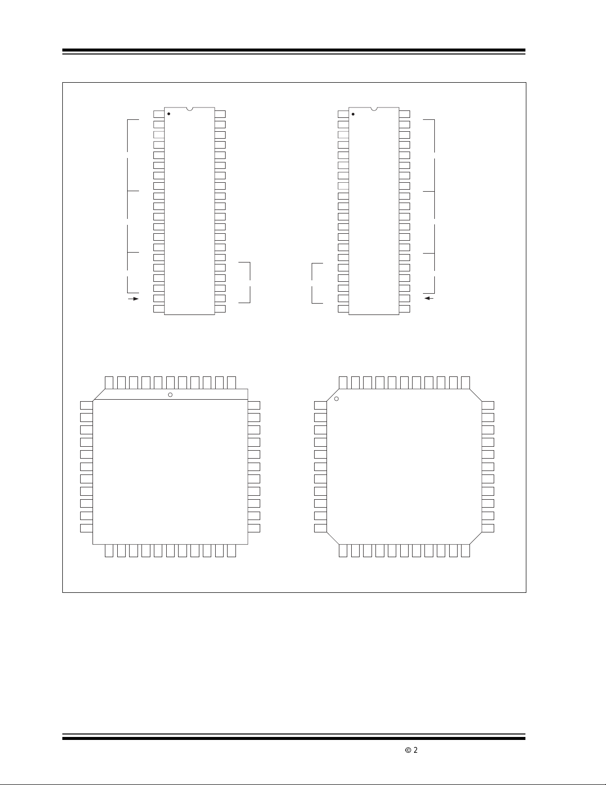
TC7106/A/TC7107/A
D
Package Type
1
V+
Normal Pin
D
2
Configuration
1
C
3
1
B
4
1
A
AB
POL
1
F
1
G
1
E
1
D
2
10
C
2
B
11
2
A
12
2
F
13
2
E
14
2
15
D
3
B
16
3
F
17
3
18
E
3
19
4
20
5
6
7
8
TC7106ACPL
9
TC7107AIPL
1's
10's
100's
1000's
(Minus Sign) (Minus Sign)
40
OSC1
39
OSC2
38
OSC3
37
TEST
36
V
35
V
C
34
C
33
ANALOG
32
COMMON
31
V
V
30
C
29
28
V
27
V
26
V-
25
G
24
C
23
A
22
G
21
BP/GND
(7106A/7107A)
REF
REF
REF
REF
IN
IN
AZ
BUFF
INT
2
3
3
3
+
-
+
-
+
-
100's
OSC1
OSC2
OSC3
TEST
V
REF
V
REF
C
REF
C
REF
ANALOG
COMMON
V
V
C
V
BUFF
V
100's
BP/GND
(7106A/7107A)
+
-
+
-
+
10
IN
-
11
IN
12
AZ
13
14
INT
15
V-
G
16
2
C
17
3
A
18
3
G
19
3
20
40-Pin CERDIP40-Pin PDIP
1
Reverse
2
Configuration
3
4
5
6
7
8
TC7106AIJL
9
TC7107AIJL
40
V+
D
39
1
C
38
1
B
37
1
A
36
1's
1
F
35
1
G
34
1
E
33
1
32
D
2
31
C
2
B
30
2
10's
A
29
2
F
28
2
E
27
2
26
D
3
B
25
3
100's
F
24
3
23
E
3
22
AB
1000's
4
21
POL
44-Pin PLCC 44-Pin PQFP
1
A
B1C1D1V+NCOSC1
7
F
1
8
G
1
9
E
1
10
D
2
11
C
2
12
NC
13
B
2
14
A
2
15
F
2
16
E
2
17
D
3
TC7106ACLW
TC7107ACLW
18 19 20 21 22 23 24 25 26 27 28
3F3
3AB4
B
E
POL
OSC2
44 43 42 41 40
123456
3A3C3G2
G
NC
BP/GND
OSC3
TEST
REF HI
39
38
37
36
35
34
33
32
31
30
29
REF LO
C
REF
C
REF
COMMON
IN HI
NC
IN LO
A/Z
BUFF
INT
V-
TEST
OSC3
OSC2
OSC1
1
NC
2
NC
3
4
5
NC
6
7
8
V+
9
D
1
10
C
1
11
B
1
12 13 14 15 16 17 18 19 20 21 22
REFCREF
REF HI
REF LO
C
COM
IN HI
394041424344
TC7106ACKW
TC7107ACKW
1F1
1E1D2C2B2A2F2E2D3
A
G
IN LO
A/Z
BUFF
INT
38 37 36 35 34
V-
NC
33
G
32
2
C
31
3
A
30
3
G
29
3
BP/GN
28
POL
27
26
AB
4
25
E
3
24
F
3
23
B
3
DS21455B-page 2
2002 Microchip TechnologyInc.
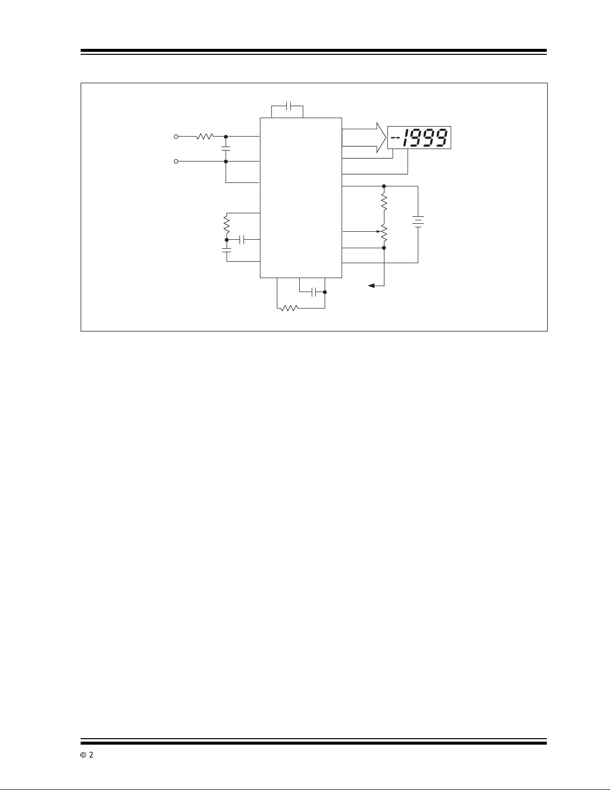
Typical Application
r
TC7106/A/TC7107/A
+
Analog
Input
–
1MΩ
0.01µF
47kΩ
0.22µF
0.47µF
0.1µF
34
+
REF
31
+
V
IN
30
V
-
IN
ANALOG
32
COMMON
TC7106/A
28
29
27
TC7107/A
V
BUFF
C
AZ
V
INT
39 38 40
R
OSC
100kΩ
33
C
REF
C
100pF
-C
OSC
2 - 19
22 - 25
POL
BP
V+
V
REF
V
REF
V-
OSC1OSC3OSC2
Segment
Drive
20
Minus Sign
21
1
V
REF
36
+
100mV
35
-
26
3 Conversions/Sec
200mV Full Scale
LCD Display (TC7106/A) o
Common Node w/ LED
Display (TC7107/A)
Backplane
Drive
24kΩ
+
1kΩ
To Analog
Common (Pin 32)
9V
2002 Microchip TechnologyInc. DS21455B-page 3
TC7106/A/TC7107/A
1.0 ELECTRICAL
CHARACTERISTICS
Absolute Maximum Ratings*
TC7106A
Supply Voltage (V+ to V-) .......................................15V
Analog Input Voltage(either Input) (Note 1) ... V+ to V-
Reference Input Voltage (either Input) ............V+ to V-
Clock Input ................................................... Test to V+
Package Power Dissipation (T
40-Pin CERDIP .......................................2.29W
40-Pin PDIP ............................................1.23W
44-Pin PLCC ...........................................1.23W
44-Pin PQFP ...........................................1.00W
Operating Temperature Range:
C (Commercial) Devices ..............0°C to +70°C
I (Industrial) Devices ................-25°C to +85°C
StorageTemperature Range..............-65°C t o +150°C
TC7107A
Supply Voltage (V+) ...............................................+6V
Supply Voltage (V-)..................................................-9V
Analog Input Voltage(either Input) (Note 1) ... V+ to V-
Reference Input Voltage (either Input) ............V+ to V-
Clock Input ..................................................GND to V+
Package Power Dissipation (T
40-Pin CERDip........................................2.29W
40-Pin PDIP ............................................1.23W
44-Pin PLCC ...........................................1.23W
44-Pin PQFP ...........................................1.00W
Operating Temperature Range:
C (Commercial) Devices ..............0°C to +70°C
I (Industrial) Devices ................-25°C to +85°C
StorageTemperature Range..............-65°C t o +150°C
≤ 70°C) (Note 2):
A
≤ 70°C) (Note 2):
A
*Stresses above those listed under "Absolute Maximum
Ratings" may cause permanent damage to the device. These
are stress ratings only and functional operation of the device
at these or any other conditions above those indicated in the
operation sections of the specifications is not implied.
Exposure to Absolute Maximum Rating conditions for
extended periods may affectdevice reliability.
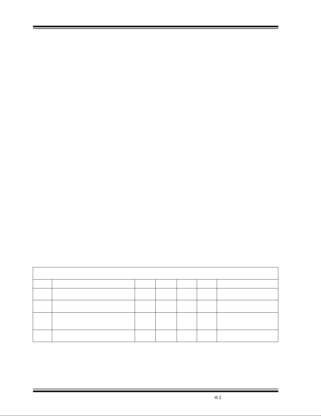
TC7106/A AND TC7107/A ELECTRICAL SPECIFICATIONS
Electrical Characteristics: Unless otherwise noted, specifications apply to both the TC7106/A and TC7107/A at TA=25°C,
f
= 48kHz. Partsare testedin the circuitof the Typical Operating Circuit.
CLOCK
Symbol Parameter Min Typ Max Unit Test Conditions
Z
IR
R/O Rollover Error (Difference in Readingfor
Note 1: Input voltages may exceed the supply voltages, provided the input current is limited to ±100µA.
DS21455B-page 4
Zero Input Reading -000.0 ±000.0 +000.0 Digital
Reading
Ratiometric Reading 999 999/1000 1000 Digital
Reading
-1 ±0.2 +1 Counts V
Equal Positive and Negative
Reading Near Full Scale)
Linearity (Max. Deviation from Best
Straight Line Fit)
2: Dissipationrating assumes device is mounted with all leads solderedto printedcircuit board.
3: Refer to “Differential Input” discussion.
4: Backplane drive is in phasewithsegment drive for “OFF” segment,180°out of phase for “ON” segment.
Frequency is 20 timesconversion rate. Average DC component is less than 50mV.
-1 ±0.2 +1 Counts Full Scale = 200mV or
VIN=0.0V
Full Scale = 200.0mV
V
IN=VREF
V
=100mV
REF
-=+VIN+ ≅ 200mV
IN
Full Scale = 2.000V
2002 Microchip TechnologyInc.
TC7106/A/TC7107/A
TC7106/A AND TC7107/A ELECTRICAL SPECIFICATIONS (CONTINUED)
Electrical Characteristics: Unless otherwise noted, specifications apply to both the TC7106/A and TC7107/A at TA=25°C,
f
= 48kHz. Partsare testedin the circuitof the Typical Operating Circuit.
CLOCK
Symbol Parameter Min Typ Max Unit Test Conditions
CMRR Common Mode Rejection Ratio (Note 3) —50—µV/V VCM=±1V,VIN=0V,
e
N
I
L
Noise (Peak to Peak Value not Exceeded
95% of Time)
Leakage Current at Input — 1 10 pA VIN=0V
—15—µVVIN=0V
Zero Reading Drift — 0.2 1 µV/°C V
—1.02µV/°C V
TC
Scale FactorTemperatureCoefficient — 1 5 ppm/°C VIN=199.0mV,
SF
——20ppm/°CV
I
DD
V
C
V
CTC
SupplyCurrent (Does not include LED
Current For TC7107/A)
AnalogCommonVoltage
(with Respectto PositiveSupply)
T emperature Coefficient of Analog
—0.81.8mAV
2.7 3.05 3.35 V 25kΩ BetweenCommonand
————25kΩ BetweenCommonand
Common (withRespectto Positive Supply)
7106/7/A
7106/7
V
CTC
V
SD
T emperature Coefficient of Analog
Common (withRespectto Positive Supply)
TC7106A ONLY Peak to Peak
— — 75 ppm/°C 0°C≤ TA≤ +70°C
456VV+toV-=9V
20
80
50
—
ppm/°C
ppm/°C
SegmentDriveVoltage
V
BD
TC7106A ONLY Peak to Peak
Backplane Drive Voltage
TC7107A ONLY
456VV+toV-=9V
58.0—mAV+=5.0V
SegmentSinking Current (Except Pin 19)
TC7107A ONLY
10 16 — mA V+ = 5.0V
SegmentSinking Current (Pin19)
Note 1: Input voltages may exceed the supply voltages, provided the input current is limited to ±100µA.
2: Dissipationrating assumes device is mounted with all leads solderedto printedcircuit board.
3: Refer to “Differential Input” discussion.
4: Backplane drive is in phasewithsegment drive for “OFF” segment,180°out of phase for “ON” segment.
Frequency is 20 timesconversion rate. Average DC component is less than 50mV.
Full Scale = 200.0mV
Full Scale - 200.0mV
=0V
IN
“C” Device = 0°C to +70°C
=0V
IN
“I” Device= -25°C to +85°C
“C” Device = 0°C to +70°C
(Ext.Ref = 0ppm°C)
=199.0mV
IN
“I” Device= -25°C to +85°C
=0.8
IN
Positive Supply
Positive Supply
0°C ≤ T
≤ +70°C
A
(“C” Commercial Temperature
Range Devices)
(“I” Industrial Temperature
Range Devices)
(Note 4)
(Note 4)
Segment Voltage = 3V
Segment Voltage = 3V
2002 Microchip TechnologyInc. DS21455B-page 5
TC7106/A/TC7107/A
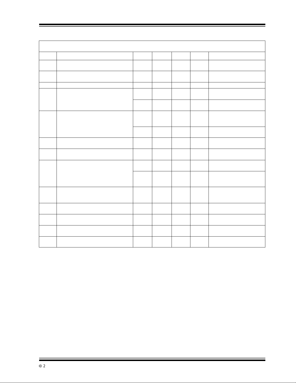
2.0 PIN DESCRIPTIONS
The descriptions of the pins are listed in Table 2-1.
TABLE 2-1: PIN FUNCTION TABLE
Pin Number
(40-Pin PDIP)
Normal
1 (40) V+ Positive supply voltage.
2(39)D
3(38)C
4(37)B
5(36)A
6(35)F
7(34)G
8(33)E
9(32)D
10 (31) C
11 (30) B
12 (29) A
13 (28) F
14 (27) E
15 (26) D
16 (25) B
17 (24) F
18 (23) E
19 (22) AB
20 (21) POL Activates the negativepolarity display.
21 (20) BP/GND LCD Backplane drive output (TC7106A). Digital Ground (TC7107A).
22 (19) G
23 (18) A
24 (17) C
25 (16) G
26 (15) V- Negative power supply voltage.
27 (14) V
28 (13) V
29 (12) C
30 (11) V
31 (10) V
32 (9) ANALOG
33 (8) C
34 (7) C
35 (6) V
Pin No.
(40-Pin PDIP)
(Reversed
Symbol Description
Activates the D section of the units display.
1
Activates the C section of the units display.
1
Activates the B section of t he units display.
1
Activates the A section of t he units display.
1
Activates the F sectionof the units display.
1
Activates the G section of the units display.
1
Activates the E section of t he units display.
1
Activates the D section of the tens display.
2
Activates the C section of the tens display.
2
Activates the B section of the tens display.
2
Activates the A section of the tens display.
2
Activates the F section of the tensdisplay.
2
Activates the E section of the tens display.
2
Activates the D section of the hundreds display.
3
Activates the B section of the hundreds display.
3
Activates the F section of the hundreds display.
3
Activates the E section of the hundreds display.
3
Activates both halves of the 1 in the thousands display.
4
Activates the G section of the hundreds display.
3
Activates the A section of the hundreds display.
3
Activates the C section of the hundreds display.
3
Activates the G section of the tens display.
2
Integrator output. Connection point for integration capacitor. See INTEGRATING
INT
CAPACITOR section for more details.
BUFF
Integration resistor connection. Use a 47kΩ resistor fora 200mV fullscalerange and
a47kΩ resistor for 2V full scale range.
The size of the auto-zero capacitor influences system noise.Usea 0.47µF capacitor
AZ
for 200mV full scale,anda 0.047µF capacitor for 2V full scale. See Section 7.1 on
Auto-Zero Capacitor for more details.
- The analogLOW input is connected to this pin.
IN
+ The analog HIGH input signal is connected to this pin.
IN
This pin is primarilyusedto set the Analog Commonmode voltage for battery opera-
COMMON
tion or in systems where the input signal is referenced to the power supply. It also
actsasareferencevoltage source.See Section 8.3 on ANALOGCOMMONfor more
details.
- See Pin 34.
REF
+A0.1µF capacitor is used in mostapplications. If a largeCommonmodevoltage
REF
exists (for example, the V
used, a 1µF capacitoris recommended and will hold the rollover errorto 0.5 count.
- See Pin 36.
REF
- pin is not at analog common), and a 200mV scale is
IN
DS21455B-page 6
2002 Microchip TechnologyInc.
TC7106/A/TC7107/A
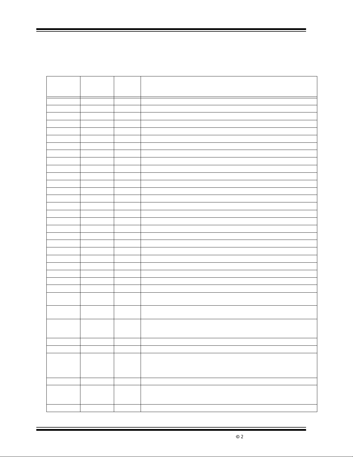
TABLE 2-1: PIN FUNCTION TABLE (CONTINUED)
Pin Number
(40-Pin PDIP)
Normal
36 (5) V
37 (4) TEST Lamp test. When pulled HIGH (to V+) all segments willbe turnedon and the display
38 (3) OSC3 See Pin 40.
39 (2) OSC2 See Pin 40.
40 (1) OSC1 Pins 40, 39, 38 make up the oscillator section. For a 48kHz clock (3 readings per
Pin No.
(40-Pin PDIP)
(Reversed
Symbol Description
+ Theanalog inputrequired to generate a fullscaleoutput (1999counts). Place100mV
REF
between Pins 35 and 36 for 199.9mVfull scale. Place1V between Pins 35 and 36 for
2V full scale. See paragraph on Reference Voltage.
shouldread -1888. It may also be used as a negativesupplyfor externallygenerated
decimal points. See paragraph under TEST for additionalinformation.
section), connect Pin 40 to the junction of a 100kΩ resistor and a 100pF capacitor.
The 100kΩ resistoristiedto Pin 39 and the 100pFcapacitor is tied to Pin 38.
2002 Microchip TechnologyInc. DS21455B-page 7
TC7106/A/TC7107/A
q
y
3.0 DETAILED DESCRIPTION
(All Pin designations refer to 40-Pin PDIP.)
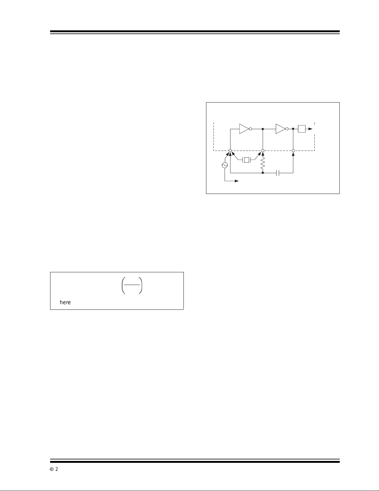
3.1 Dual S lope Conversion Principles
The TC7106Aand TC7107A are dual slope,integrating
analog-to-digital converters. An understanding of the
dualslopeconversiontechnique will aid infollowingthe
detailed operation theory.
The conventional dual slope converter measurement
cycle has two distinct phases:
• Input Signal Integration
• Reference VoltageIntegration (De-integration)
The input signal being converted is integrated for a
fixed time period (T
clock pulses. An opposite polarity constant reference
voltage is then integrated until the integrator output
voltage returns to zero. The reference integration time
is directly proportional to the input signal (T
Figure 3-1.
FIGURE 3-1: BASIC DUAL SLOPE
Analog
Input
Signal
). Time is measured by counting
SI
). See
RI
CONVERTER
C
Integrator
–
+
Comparator
–
+
For a constant VIN:
EQUATION 3-2:
T
VIN=V
RI
R
T
SI
The dual slope converter accuracy is unrelated to the
integrating resistor and capacitor values as long as
they are stable during a measurement cycle. An inherent benefit is noise immunity. Noise spikes are integrated or averaged to zero during the integration
periods.IntegratingADCs areimmunetothe largeconversion errors that plague successive approximation
converters in high noise environments. Interfering signals with frequency components at multiples of the
averaging period will be attenuated. Integrating ADCs
commonlyoperatewiththesignalintegrationperiodset
to a multiple of the 50/60Hz power line period (see
Figure 3-2).
FIGURE 3-2: NORM AL MODE
REJECTION OF DUAL
SLOPE CONVERTER
30
20
+/–
REF
Voltage
Output
Integrator
Fixed
Signal
Integrate
Time
Switch
Driver
Polarity Control
DISPLAY
Variable
Reference
Integrate
Time
Phase
Control
≈ V
V
IN
REF
VIN ≈ 1/2 V
REF
Control
Logic
Clock
Counter
In a simple dual slope converter, a complete c onversion requires the integrator output to “ramp-up” and
“ramp-down.” A simple mathematical equation relates
the input signal, referencevoltage and integration time.
EQUATION 3-1:
T
Where:
V
R
T
SI
T
RI
1
SI
VIN(t)dt=
∫
RC
0
= Reference voltage
= Signal integrationtime (fixed)
= Referencevoltageintegration time (variable).
V
RTRI
RC
10
Normal Mode Rejection (dB)
0
0.1/T 1/T 10/T
T = Measured Period
Input Fre
uenc
DS21455B-page 8
2002 Microchip TechnologyInc.

TC7106/A/TC7107/A
4.0 ANALOG SECTION
In addition to the basic signal integrate and deintegrate cycles discussed, the circuit incorporates an
auto-zero cycle. This cycle removes buffer amplifier,
integrator, and comparator offset voltage error terms
from the conversion. A true digital zero reading results
without adjusting external potentiometers. A complete
conversion consists of three cycles: an auto-zero,
signal integrate and reference integratecycle.
4.1 Auto-Zero Cycle
During the auto-zero cycle, the differential input signal
is disconnected from the circuit by opening internal
analog gates. The internalnodesare shorted to analog
common ( ground) to establish a zero input condition.
Additional analog gates close a feedback loop around
the integrator and comparator. This loop permits comparator offset voltage error compensation. The voltage
levelestablishedonC
voltages. The offset error referred to the input is less
than 10µV.
The auto-zero cycle length is 1000 to 3000 counts.
4.2 Signal Integrate Cycle
The auto-zero loop is entered and t he internal differential inputs connect to V
input signal is integrated for a fixed time period. The
TC7136/A signal integration period is 1000 clock periods or counts. The externally set clock frequency is
divided by four before clocking the internal counters.
The i ntegration t ime period is:
EQUATION 4-1:
Where: F
OSC
compensatesfordeviceoffset
AZ
+ and VIN-. The differential
IN
T
4
=
SI
= external clock frequency.
F
x 1000
OSC
The time requiredforthe output to return to zero is proportional to the input signal and is between0 and 2000
counts.
The digital reading displayed is:
EQUATION 4-2:
V
1000 =
V
IN
REF
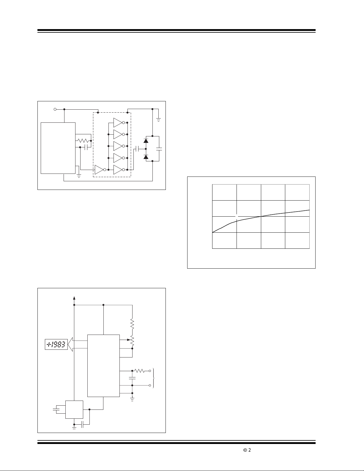
5.0 DIGITAL SECTION (TC7106A)
The TC7106A (Figure 5-2) contains all t he segment
drivers necessary t o directly drive a 3-1/2 digit liquid
crystal display (LCD). An LCD backplane driver is
included. The backplane frequency is the external
clock frequency divided by 800. For three conversions/
second, the backplane frequency is 60Hz with a 5V
nominal amplitude. When a segment driver is in phase
with the backplane signal, the segment is “OFF.” An
out of phase segment drive signal causes the segment
to be “ON” or visible. This AC drive configuration
results in negligible DC voltage across each LCD segment. This insures long LCD display life. The polarity
segment driver is “ON” for negative analog inputs. If
V
+andVIN-are reversed, this indicator will reverse.
IN
When the TEST pin on the TC7106A is pulledto V+, all
segments are turned “ON.” The display reads -1888.
During this mode, the LCD segments have a constant
DC voltage impressed. DO NOT LEAVE THE DISPLAY IN THIS MODE FOR MORE T HAN SEVERAL
MINUTES! LCD di splays may be destroyed if operated
with DC levels for extended periods.
The display font and the segment drive assignment are
showninFigure5-1.
FIGURE 5-1: DISPLAY FONT AND
SEGMENT ASSIGNMENT
The differential input voltage must be within the device
Common mode range when the converter and measured system share the same power supply common
(ground). If the converter and measured system do not
share the same power supply common, V
tied to analog common.
Polarity is determined at the end of signal integrate
phase. The sign bit is a true polarity indication, in that
signals less than 1LSB are correctly determined. This
allows precision null detection limited only by device
noise and auto-zero residual offsets.
4.3 Reference Integrate Phase
The third phase is reference integrate or de-integrate.
V
- is internally connected to analog common and
IN
V
+ is connectedacross the previously charged refer-
IN
ence capacitor. Circuitry within the chip ensures that
the capacitor will be connected with the correct polarity
to cause the integrator output to return to zero.
2002 Microchip TechnologyInc. DS21455B-page 9
-should be
IN
In the TC7106A, an internal digital ground is generated
from a 6-voltzener diode and a large P channel source
follower. This supply is made stiff to absorb the large
capacitive currents when the backplane voltage i s
switched.
1000's 100's 10's 1's
Display Font

TC7106/A/TC7107/A
T
FIGURE 5-2: TC7106A BLOCK DIAGRAM
V+
Segment
0.5mA
LCD Display
Output
2mA
Backplane
21
÷ 200
Decode
7 Segment
Decode
7 Segment
LCD Segment Drivers
Decode
7 Segment
To
INT
INT
C
V
27333634
Digital
Section
+
Data Latch
–
Tens Units
Hundreds
Thousands
To Switch Drivers
V+
1
From Comparator Output
Clock
TES
37
6.2V
Control Logic
÷4
OSC
F
26
Ω
500
= 1V
TH
V
Internal Digital Ground
V-
OSC3OSC1
OSC
C
39
OSC
OSC2
R
Typical Segment Output
Internal Digital Ground
AZ
C
INT
R
TC7106A
REF
C
V+
BUFF
V
-
REF
C
-
REF
+V
REF
V
+
REF
C
29
Integrator
1
28
35
A/Z
31
Comparator
Low
Tempco
DE
(+)
(–)
DE
INT
+
IN
V
V
–
A/Z
REF
+
DE (–)
DE (+)
32
ANALOG
V+ – 3.0V
AZ & DE (±)
30
-
IN
V
COMMON
26
INT
–
+
–
+
A/Z
A/Z
10
µA
40 38
V-
DS21455B-page 10
2002 Microchip TechnologyInc.
TC7106/A/TC7107/A
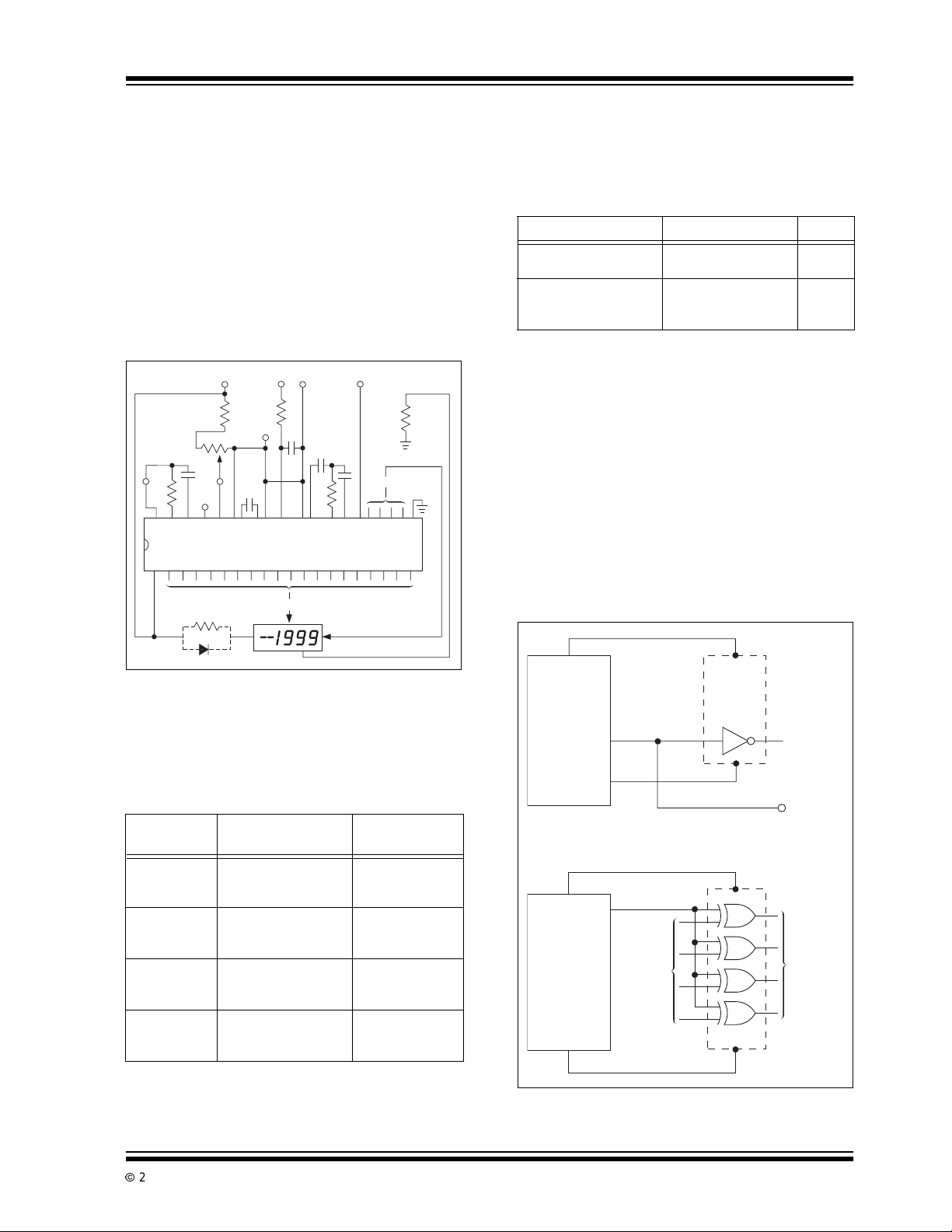
6.0 DIGITAL SECTION (TC7107A)
Figure 6-2 shows a TC7107A block diagram. It is
designed to drive common anode LEDs. It is identical
to the TC7106A, except that the regulated supply and
backplanedrivehavebeen eliminatedand the segment
drive is typically8mA. The 1000's output (Pin 19) sinks
currentfrom two LED segments,and has a 16mA drive
capability.
In both devices, the polarity indication is “ON” for negative analog inputs. If V
indication can be reversed also, if desired.
The display font is the same as the TC7106A.
6.1 System Timing
The oscillatorfrequencyi s dividedby4priorto clocking
the internal decade counters. The four-phase measurement cycle takes a total of 4000 counts, or 16,000
clock pulses. The 4000-count cycle is independent of
input signal magnitude.
Each phase of the measurement cycle has the following length:
1. Auto-zero phase: 1000 to 3000 counts (4000 to
12000 clock pulses).
For signals less than full scale, the auto-zero phase i s
assigned the unused reference integrate time period:
2. Signal integrate: 1000 counts (4000 clock
pulses).
This time period is fixed. The i ntegration period is:
- and VIN+ are reversed, this
IN
6.2 Clock Circuit
Three clockingmethods may be used (see Figure 6-1):
1. An external oscillator connected to Pin 40.
2. A crystal between Pins 39 and 40.
3. An RC oscillatorusing all three pins.
FIGURE 6-1: CLOCK CIRCUITS
TC7106A
TC7107A
To
÷
4
Counter
39
38
EXT
OSC
40
Crystal
RC Network
To TEST Pin on TSC7106A
To GND Pin on TSC7107A
EQUATION 6-1:
1
TSI= 4000
Where: F
3. ReferenceIntegrate:0 to2000counts(0to8000
clock pulses).
The TC7106A/7107A are drop-in replacements for the
7106/7107 parts. External component value changes
are not required to benefit from the low drift internal
reference.
is the externally set clock frequency.
OSC
F
OSC
2002 Microchip TechnologyInc. DS21455B-page 11

TC7106/A/TC7107/A
FIGURE 6-2: TC7107A BLOCK DIAGRAM
V+
0.5mA
Led Display
Output
Segment
8mA
Decode
7 Segment
Decode
7 Segment
LCD Segment Drivers
Decode
7 Segment
To
INT
INT
C
V
27333634
Digital
Section
+
Data Latch
–
Tens Units
Hundreds
Thousands
To Switch Drivers
V+
1
from Comparator Output
Clock
21
Logic Control
÷4
OSC
F
Digital
Ground
500Ω
Digital Ground
37
39
TEST
OSC3OSC1
OSC2
OSC
R
OSC
C
Typical Segment Output
Internal Digital Ground
AZ
C
INT
R
V
-
TC7107A
C
-
REF
REF
C
+V
REF
V
+
REF
C
V+
BUFF
REF
Integrator
29
1
28
35
–
–
A/Z
A/Z
10
Comparator
+
A/Z
REF
Low
Tempco
V
–
A/Z
+
DE (–)
DE (+)
32
V+ – 3.0V
AZ & DE (±)
30
ANALOG
COMMON
26
INT
-
IN
V
+
DE
(+)
(–)
DE
µA
INT
31
+
IN
V
40 38
V-
DS21455B-page 12
2002 Microchip TechnologyInc.

TC7106/A/TC7107/A
7.0 COMPONENT VALUE
SELECTION
7.1 Auto-Zero Capacitor (CAZ)
The CAZcapacitorsize has some influence on system
noise. A 0. 47µF capacitor is r ecommended for 200mV
full scaleapplicationswhere1LSBis100µV.A0.047µF
capacitoris adequate for 2.0V full scale applications.A
mylar type dielectric capacitor is adequate.
7.2 Reference Voltage Capacitor
)
(C
REF
The reference voltage used to ramp the integrator output voltage back to zero during the reference integrate
cycleisstoredonC
when V
mode voltage exists (V
application requires 200mV full scale,increase C
1.0µF.Rollovererror will be held to less than 1/2 count.
A mylar dielectric capacitoris adequate.
- is tied to analogcommon. If a largeCommon
IN
7.3 Integrating Capacitor (C
C
shouldbe selected to maximize the integrator out-
INT
put voltage swing without causing output saturation.
Due to the TC7106A/7107Asuperior temperature coefficient specification, analog common will normally supply t he differential voltage reference. For this case, a
±2V full scale integrator output swing is satisfactory.
For 3 readings/second(F
is suggested. If a different oscillator frequencyis used,
C
must be changed in inverse proportiontomaintain
INT
the nominal ±2V integrator swing.
An exact expression for C
EQUATION 7-1:
C
INT
Where:
= Clock Frequency at Pin 38
F
OSC
= Full Scale Input Voltage
V
FS
= Integrating Resistor
R
INT
= Desired Full Scale Integrator Output Swing
V
INT
C
must have low dielectric absorption to minimize
INT
rollover error. A polypropylene capacitor is recommended.
.A0.1µF capacitorisacceptable
REF
- – analog common)and the
REF
INT
=48kHz),a0.22µF value
OSC
is:
INT
V
(4000)
=
1
F
OSC
V
INT
FS
R
INT
REF
)
7.4 Integrating Resistor (R
The input buffer amplifier and integrator are designed
with class A output stages.The output stageidling current i s 100µA. The integrator and buffer can supply
20µA drive currents with negligible linearity errors.
R
ischosentoremainin the outputstagelineardrive
INT
region, but not so large that printed circuit board leakage currents induce errors. For a 200mV full scale,
R
is 47kΩ. 2.0V full scale requires 470kΩ.
INT
Component
Value
C
AZ
R
INT
C
INT
Note: F
to
7.5 Oscillator Components
R
OSC
selected using the equation:
OSC
(Pin 40 to Pin 39) should be 100kΩ.C
Nominal Full Scale Voltage
200.0mV 2.000V
0.47µF 0.047µF
47kΩ 470kΩ
0.22µF0.22µF
= 48kHz (3 readings per sec).
INT
)
is
OSC
EQUATION 7-2:
F
For F
Note that F
TC7106A internal control clock. The backplane drive
signal is derived by dividing F
To achieve maximum rejection of 60Hz noise pickup,
the signal integrate period should be a multiple of
60Hz. Oscillator frequencies of 240kHz, 120kHz,
80kHz, 60kHz, 48kHz, 40kHz,etc. should be selected.
For 50Hz r ejection, oscillator frequencies of 200kHz,
100kHz, 66-2/3kHz, 50kHz, 40kHz, etc. would be suitable. Note that 40kHz (2.5 readings/second) will reject
both 50Hz and 60Hz.
of 48kHz, C
OSC
is divided by four to generate the
OSC
0.45
=
OSC
OSC
RC
is 100pF nominally.
by 800.
OSC
7.6 Reference Voltage Selection
A full scale reading (2000 counts) requires the input
signal be twice the reference voltage.
Required Full Scale Voltage* V
200.0mV 100.0mV
2.000V 1.000V
*V
=2V
FS
In some applications, a scale factor other than unity
may exist between a transducer output voltage and the
required di gital reading. Assume, for example, a pressure transducer output is 400mV for 2000 lb/in
Rather than dividing the input voltage by two, the reference voltage should be set to 200mV. This permitsthe
transducer input t o be used directly.
REF.
REF
2
.
2002 Microchip TechnologyInc. DS21455B-page 13

TC7106/A/TC7107/A
(a)(
)
–
Thedifferentialreferencecanalsobeusedwhenadigital zero reading is required when V
is not equal to
IN
zero. This is common in temperature measuringinstrumentation. A compensating offset voltage can be
applied between analog common and V
ducer output is connected between V
-. The trans-
IN
+ and analog
IN
common.
The internal voltage reference potential available at
analog common will normally be used to supply the
converter's reference. This potential is stable whenever the supply potential is greater than approximately
7V. In applications where an externally generatedreference voltage is desired, refer to Figure 7-1.
FIGURE 7-1: EXTERNAL REF ERENCE
V+
V
REF
V
REF
TC7106A
TC7107A
V+
+
-
6.8V
Zener
I
Z
V+
TC7106A
TC7107A
V
REF
V
REF
Common
b
+
-
20kΩ
V+
6.8kΩ
1.2V
Ref
8.0 DEVICE PIN FUNCTIONAL
DESCRIPTION
FIGURE 8-1: COMMON MODE
VOLTAGE REDUCES
AVAILABLEI NTEG RATOR
SWING (V
Input Buffer
+
V
IN
V
CM
+
–
Where:
R
I
T
VI =
TI = Integration Time
C
R
I
C
R
I
= Integration Capacitor
I
= Integration Resistor
I
COM
I
≠ V
C
I
–
+
Integrator
VCM – V
[
)
IN
V
I
[
IN
4000
=
F
OSC
8.2 Differential Reference
+(Pin36),V
V
REF
The reference voltage can be generated anywhere
within the V+ to V-power supply range.
To prevent rollover type errors being induced by large
Common mode voltages, C
pared to stray node capacitance.
The TC7106A/TC7107A circuits have a significantly
lower analog common temperature coefficient. This
gives a very stable voltage suitable for use as a reference.The temperaturecoefficient of analog common is
20ppm/°C typically.
-(Pin35)
REF
should be large com-
REF
8.1 Differential Signal Inputs
+(Pin31),VIN-(Pin30)
V
IN
The TC7106A/7017A is designed with true differential
inputs and accepts input signals within the input stage
common mode voltage range ( V
is V+ – 1.0 to V+ + 1V. Common mode voltages are
removed from the system when the TC7106A/
TC7107A operates from a battery or floating power
source (isolated from measured system) and V
connectedto analog common (V
In systems where Common mode voltages exist, the
86dB Common mode rejection ratio minimizes error.
Common mode voltages do, however, affect the integratoroutputlevel.Integrator output saturationmustbe
prevented. A worstcase conditionexistsif a large positiveV
existsin conjunction with a full scale negative
CM
differential signal. The negative signal drives the integrator output positive along with V
For such applications the integrator output swing can
be reduced below the recommended 2.0V full scale
swing. The integrator output will swing wi thin 0.3V of
). The typical range
CM
) (see Figure 8-2).
COM
(see Figure 8-1).
CM
IN
-is
8.3 AnalogCommon(Pin32)
The analog common pin is set at a voltage potential
approximately3.0VbelowV+. The potentialis between
2.7V and 3.35V below V+. Analog common is tied internally to the N channel FET capable of sinking 20mA.
This FET will hold the common line at 3.0V should an
external load attempt to pull the common line toward
V+. Analog common source current is limited to 10µA.
Analog common is, therefore, easily pulled to a more
negative voltage (i.e., below V+ – 3.0V).
The TC7106A connects the internal V
inputs to analog common during the auto-zero cycle.
During the reference integrate phase, V
nected to analog common. If V
- is not externally con-
IN
nected t o analog common, a Common mode voltage
exists. This is r ejected by the converter's 86dB Common mode rejection ratio. In battery operation, analog
common and V
- are usually connected, removing
IN
Common mode voltageconcerns.In systems where Vis connected to the power supply ground, or to a given
voltage, analog common should be connected to V
+andVIN-
IN
- is con-
IN
IN
-.
V+ or V-without increasing linearity errors.
DS21455B-page 14
2002 Microchip TechnologyInc.

TC7106/A/TC7107/A
FIGURE 8-2: COMMON MODE VOLTAGE REMOVED IN BATTERY OPERATION WITH
VIN- = ANALOG COMMON
Segment
Drive
LCD Display
V+
V-
Powe r
Source
V+
V-
GND
Measured
System
GND
V
V
IN
VIN-
Analog
Common
Theanalogcommonpin servesto settheanalogsection
reference or common point. The TC7106A is specifically
designed to operate from a battery, or in any measurement system where input signals are not referenced
(float), with respect to the TC7106A power source. The
analog common potential of V+ – 3.0V gives a 6V end of
battery life voltage. The common potential has a 0.001%
voltage coefficient and a 15Ω output impedance.
With sufficiently high total supply voltage (V+ – V- >
7.0V), analog common is a very stable potential with
excellent temperature stability, typically 20ppm/°C.
This potential can be used to generate the reference
voltage.An external voltage referencewill be unnecessaryin most cases because of the 50ppm/°C maximum
temperature coefficient. See Internal Voltage Reference discussion.
8.4 TEST (Pin 37)
The TEST pin potential is 5V l ess than V+. TEST may
be used as the negative power supply connection for
external CMOS logic. The TEST pin is tied to the internally generated negative logic supply (Internal Logic
Ground) through a 500Ω resistor in the TC7106A. The
TEST pi n load should be no more than 1mA.
IfTEST is pulled to V+ all segments plus the minus sign
will be activated. Do not operate in this mode for more
than several minutes with the TC7106A. With
TEST = V+, the LCD segments are impressed with a
DC voltage which will destroy the LCD.
The TEST pin will sink about 10mA when pulled to V+.
8.5 Internal Voltage Reference
The analog common voltage temperature stability has
been significantly improved (Figure 8-3). The “A” version of the industry standard circuits allow users to
upgrade old systems and design new systems without
external voltage references. External R and C values
do not need to be changed. Figure 8-4 shows analog
common supplying the necessary voltage referencefor
the TC7106A/TC7107A.
BUF
+
CAZV
TC7106A
V
-
REF
REF
INT
+V
+
9V
BPPOL
OSC1
OSC3
OSC2
V-V+
FIGURE 8-3: ANALOG COMMON
TEMPERATURE
COEFFICIENT
200
180
No Maximum Specified
160
140
120
100
80
60
40
Temperature Coefficient (ppm/°C)
20
0
Maximum
Limit
Typical
TC
7106A
No
Maximum
Specified
Typical
ICL7106
Maximum
Specified
Typical
ICL7136
FIGURE 8-4: INTERNAL VOLTAGE
REFERENCE
CONNECTION
1
Set V
V-
TC7106A
TC7107A
= 1/2 V
REF
V
REF
V
REF
Analog
Common
FULL SCALE
V+
36
+
V
REF
35
-
32
No
24kΩ
1kΩ
2002 Microchip TechnologyInc. DS21455B-page 15
TC7106/A/TC7107/A
9.0 POWER SUPPLIES
The TC7107A is designed to work from ±5V supplies.
However,if a negativesupply is not available, it can be
generated from the clock output with two diodes, two
capacitors, and an inexpensive IC (Figure 9-1).
FIGURE 9-1: GENERATING NEGATIVE
SUPPLY F ROM +5V
V+
CD4009
V+
OSC1
OSC2
OSC3
TC7107A
GND
V-
V- = -3.3V
In selected applications a negative supply is not
required. The conditions to use a single +5V supply
are:
• The input signal can be referenced to the center
of the Common mode r ange of the converter.
• The signal is less than ±1.5V.
• An external reference is used.
The TSC7660DC to DC converter may be usedtogenerate -5V from +5V (Figure 9-2).
FIGURE 9-2: NEGATIVE POWER
SUPPLY GENERATION
WITH TC7660
+5V
1
V+
V
REF
V
10µF
LED
DRIVE
TC7107A
8
2
+
4
TC7660
3
5
+
10µF
(-5V)
REF
COM
VIN+
V
IN
GND
V-
26
0.047
1N914
µF
36
+
35
-
32
31
30
-
21
10
µF
1N914
+
–
V
IN
9.1 TC7107 Power Dissipation
Reduction
The TC7107A sinks the LED display current and this
causes heat to build up i n the IC package. If the internal voltage reference i s used, the changing chip temperature can cause the display to change reading. By
reducing the LED common anode voltage, the
TC7107A package power dissipation is reduced.
Figure 9-3 is a curve tracer display showing the relationship between output current and output voltage for
a typical TC7107CPL.SinceatypicalLED has 1.8 volts
across it at 7mA, and its common anode is connected
to +5V, the TC7107A output is at 3.2V (point A on
Figure 9-3). Maximum power dissipation is 8.1mA x
3.2V x 24 segments = 622mW.
FIGURE 9-3: T C7107 OUTPUT
CURRENT VS. O UTPUT
VOLTAGE
10.000
9.000
8.000
7.000
Output Current (mA)
6.000
2.00 2.50 3.00 3.50 4.00
B
C
Output Voltage (V)
Notice,however,thatoncetheTC7107Aoutputvoltage
is above two volts, the LED current is essentially constantas output voltage increases. Reducing the output
voltageby 0.7V (point B in Figure 9- 3) results in 7.7mA
of LED current, only a 5 percent reduction. Maximum
power dissipation is only 7.7mA x 2.5V x 24 = 462mW,
a reduction of 26%. An output voltage reduction of 1
volt (point C) reduces LED current by 10% (7.3mA) but
power dissipation by 38% (7.3mA x 2.2V x 24 =
385mW).
Reduced power dissipation is very easy to obtain.
Figure 9-4 shows two ways: either a 5. 1 ohm, 1/4 watt
resistor or a 1 Amp diode placed in series with the display (but not in series with the TC7107A). The resistor
will reduce the TC7107A output voltage, when all 24
segments are “ON,” to point “C” of Figure 9-4. When
segments turn off, t he output voltage will increase.The
diode, on the other hand, will result in a relatively
steady output voltage, around point “B.”
In addition to limiting maximum power dissipation, the
resistorreducesthe change in power dissipation as the
display changes. This effect is caused by the fact that,
as fewer segments are “ON,” each “ON” output drops
more voltage and current. For the best case of sixseg-
A
DS21455B-page 16
2002 Microchip TechnologyInc.
TC7106/A/TC7107/A
ments(a“111”display) to worst case (a “1888” display),
the resistor will change about 230mW, while a circuit
without the resistor will change about 470mW. Therefore, the resistor will reduce the effect of display dissipation on reference voltage drift by about 50%.
The changein LED brightness caused by the r esistor is
almost unnoticeable as more segments turn off. If display brightness remaining steady is very important to
the designer, a diode may be used instead of the
resistor.
FIGURE 9-4: DIODE OR RESISTOR
LIMITSPACKAGE POWER
DISSIPATION
+5V
24kΩ
1kΩ
100
pF
TP5
100
40 TP
TP2
kΩ
TP1
IN
+
1MΩ
TP3
0.01
µF
0.1
µF
30 21
TC7107A
5.1Ω 1/4W
1N4001
Display
-5V
–
150Ω
0.47
µF
0.22
µF
47
kΩ
Display
4
20101
10.2 Light Emitting Diode Display
Sources
Several LED manufacturers supply seven segment
digits with and without decimal point annunciators for
the TC7107A.
Manufacturer Address/Phone Display
Hewlett-Packard
Components
AND 720 Palomar Ave.
640 Page Mill Rd.
Palo Alto, CA 94304
Sunnyvale, CA 94086
408-523-8200
LED
LED
10.3 Decimal Point and Annunciator
Drive
The TEST pin is connected to the internally generated
digitallogicsupplygroundthrougha 500Ω resistor.The
TEST pin may be used as the negative supplyforexternal CMOS gate segment drivers. LCD display annunciators for decimal points, low battery indication, or
function indication may be added without adding an
additional supply. No more than 1mA should be suppliedby the TESTpin; its potential is approximately 5V
below V+ (see Figure 10-1
FIGURE 10-1: DECIMAL POINT DRIVE
V+
).
USING TEST AS L OGIC
GROUND
V+
10.0 TYPICAL APPLICATIONS
10.1 Liquid Cry stal Display Sources
Several manufacturers supply standard LCDs to interface with the TC7106A 3-1/2 digit analog-to-digital
converter.
Manufacturer Address/Phone
Crystaloid
Electronics
5282 Hudson Dr.
Hudson, OH 44236
216-655-2429
AND 720 Palomar Ave.
Sunnyvale, CA 94086
408-523-8200
Epson 3415 Kashikawa st.
Torrance, CA 90505
213-534-0360
Hamlin, Inc. 612 E. Lake St.
Lake Mills, WI 53551
414-648-236100
Note: Contact LCD manufacturer for full product listing and
specifications.
Representative
Part Numbers*
C5335,H5535,
T5135, SX440
FE 0201, 0701
FE 0203, 0701
FE 0501
LD-B709BZ
LD-H7992AZ
3902, 3933, 3903
TC7106A
TEST
V+
TC7106A
TEST
BP
BP
21
37
Decimal
Point
Select
4049
4030
GND
V+
GND
To LCD
Decimal
Point
To LCD
Backplane
To LCD
Decimal
Point
2002 Microchip TechnologyInc. DS21455B-page 17
TC7106/A/TC7107/A
y
10.4 Ratiometric Resistance
Measurements
The true differential input and differential reference
make ratiometric reading possible. Typically in a ratiometric operation, an unknown resistanceis measured,
with respect to a known standard resistance. No accurately defined reference voltage is needed.
The unknown resistance is put in series with a known
standard and a current passed through the pair. The
voltagedeveloped across the unknownisappliedtothe
input and the voltage across the known resistor is
applied to the reference input. If the unknown equals
the standard,the display will read 1000.
The displayed reading can be determined from the
following expression:
STANDARD
V+
+
REF
-
REF
+
IN
TC7106A
-
IN
RUnknown
------------------------------- x 1000=
RS dardtan
+
LCD Displa
9V
Displayed Reading()
The display will over range for:
R
UNKNOWN
≥ 2xR
FIGURE 10-2: LOW PARTS COUNT
RATIOMETRIC
RESISTANCE
MEASUREMENT
V
R
STANDARD
R
UNKNOWN
V
V
V
Analog
Common
FIGURE 10-3: TEMPERATURE SENSOR
FIGURE 10-4: POSITIVETEMPERATURE
COEFFICIENT RESISTOR
TEMPERATURE SENSOR
9V
+
5.6kΩ 160kΩ
V+ V-
0.7%/°C
PTC
1N914
R
3
20kΩ
20kΩ
R
1
R
2
VIN-
+
V
IN
TC7106A
+
V
REF
-
V
REF
Common
FIGURE 10-5: TC7106A, USING THE
INTERNAL REFERENCE:
200mV FULL SCALE, 3
READINGS-PER-SECOND
(RPS)
To Pin 1
TC7106A
40
39
38
37
36
35
34
33
32
31
30
29
28
27
26
25
24
23
22
21
Set V
100kΩ
100pF
0.1µF
0.47µF
0.22µF
To Display
To Backplane
= 100mV
REF
1kΩ 22kΩ
1MΩ
0.01µF
47kΩ
+
IN
+
–
9V
–
160kΩ 300kΩ 300kΩ
1N4148
Sensor
50kΩ
50kΩ
R
2
DS21455B-page 18
V+ V-
-
V
IN
R
1
+
V
IN
TC7106A
VFS = 2V
+
V
REF
V
-
REF
Common
2002 Microchip TechnologyInc.
TC7106/A/TC7107/A
g
+
FIGURE 10-6: TC7107 INTERNAL
REFERENCE: 200mV
FULL SCALE, 3RPS,
V
-TIEDTOGNDFOR
IN
SINGLE ENDED INPUTS
To Pin 1
TC7107A
40
39
38
37
36
35
34
33
32
31
30
29
28
27
26
25
24
23
22
21
0.1µF
0.47µF
0.22µF
To Display
Set V
100kΩ
100pF
1kΩ 22kΩ
0.01
47kΩ
REF
= 100mV
1MΩ
µF
FIGURE 10-7: CIRCUIT FOR
DEVELOPING UNDER
RANGE AND OVER
RANGE SIGNALS FROM
TC7106A OUTPUTS
O/R
U/R
CD4023
OR 74C10
V+
To Logic
V
CC
CD4077
1
40
TC7106A
2120
O/R = Over Range
U/R = Under Ran
+5V
+
IN
–
-5V
To Logic
V
CC
V-
e
FIGURE 10-8: TC7106/TC7107:
RECOMMENDED
COMPONENT VALUES
FOR 2.00VFULL SCALE
To Pin 1
TC7106A
TC7107A
40
39
38
37
36
35
34
33
32
31
30
29
28
27
26
25
24
23
22
21
0.1µF
0.047µF
0.22µF
To Display
Set V
100kΩ
100pF
25kΩ
470kΩ
0.01
REF
µ
= 1V
24kΩ
1M
F
V
Ω
+
IN
–
V-
FIGURE 10-9: TC7107 OPERATED FROM
SINGLE +5V SUPPLY
To PIn 1
40
39
38
37
36
35
34
33
TC7107A
Note: An external reference must be used in this application.
32
31
30
29
28
27
26
25
24
23
22
21
0.1µF
0.47µF
0.22µF
To Display
100kΩ
100pF
1kΩ
0.01µF
47kΩ
Set V
10kΩ
1.2V
REF
= 100mV
10kΩ
1M
Ω
V+
IN
–
2002 Microchip TechnologyInc. DS21455B-page 19

TC7106/A/TC7107/A
y
FIGURE 10-10: 3-1/2 DIGIT TRUE RMS A C DMM
–
+
1µF
+
–
1
2
3
4
AD636
5
6
7
V
IN
9MΩ
900kΩ
90kΩ
10kΩ
200mV
2V
20V
200V
COM
C1 = 3 - 10pF Variable
C2 = 132pF Variable
IN4148
0.02
47kΩ
10%
µF
1W
10kΩ
1MΩ
1MΩ
6.8µF
20kΩ
10%
9V
+
1
14
13
24kΩ
12
11
1kΩ
10
9
8
2.2µF
1MΩ 10%
0.01
µF
V+
36
V
REF
35
V
REF
32
Analog Common
31
V
IN
30
V
IN
26
V-
26
V-
TC7106A
+
-
+
-
27
29
28
40
38
39
FIGURE 10-11: INTEGRATED CIRCUIT TEMPERATURE SENSOR
9V
2 1
V+
REF02
GND
4 26
V
OUT
ADJ
TEMP
Constant 5V
6
5
3
Temperature
Dependent
Output
51kΩ 5.1kΩ
R
4
NC
1.3k
TC911
R
5
2
–
8
3
1
+
V
4
1.86V @
25°C
OUT
50kΩ
R
2
=
50kΩ
R
1
+
V
REF
TC7106A
V
-
REF
V
FS
V
-
IN
V
+
IN
Common
V+
= 2.00V
V-
SEG
DRIVE
LCD Displa
BP
DS21455B-page 20
2002 Microchip TechnologyInc.

11.0 PACKAGING INFORMATION
11.1 Package Marking Information
Package marking data not available at this time.
11.2 Taping Form
Component Taping Orientation for 44-Pin PLCC Devices
User Direction of Feed
PIN 1
TC7106/A/TC7107/A
W
P
Standard Reel Component Orientation
for TR Suffix Device
Carrier Tape, Number of Components Per Reel and Reel Size
Package Carrier Width (W) Pitch (P) Part Per Full Reel Reel Size
44-Pin PLCC 32 mm 24 mm 500 13 in
Note: Drawing does not represent total number of pins.
Component Taping Orientation for 44-Pin PQFP Devices
User Direction of Feed
PIN 1
W
P
Standard Reel Component Orientation
for TR Suffix Device
Carrier Tape, Number of Components Per Reel and Reel Size
Package Carrier Width (W) Pitch (P) Part Per Full Reel Reel Size
44-Pin PQFP 24 mm 16 mm 500 13 in
Note: Drawing does not represent total number of pins.
2002 Microchip TechnologyInc. DS21455B-page 21

TC7106/A/TC7107/A
11.3 Package Dimensions
40-Pin PDIP (Wide)
.200 (5.08)
.140 (3.56)
.150 (3.81)
.115 (2.92)
.110 (2.79)
.090 (2.29)
2.065 (52.45)
2.027 (51.49)
.070 (1.78)
.045 (1.14)
.022 (0.56)
.015 (0.38)
PIN 1
.555 (14.10)
.530 (13.46)
.040 (1.02)
.020 (0.51)
.015 (0.38)
.008 (0.20)
.610 (15.49)
.590 (14.99)
3° MIN.
.700 (17.78)
.610 (15.50)
Dimensions: inches (mm)
40-Pin CERDIP (Wide)
.098 (2.49) MAX.
2.070 (52.58)
2.030 (51.56)
.210 (5.33)
.170 (4.32)
.200 (5.08)
.125 (3.18)
.110 (2.79)
.090 (2.29)
.065 (1.65)
.045 (1.14)
.020 (0.51)
.016 (0.41)
PIN 1
.540 (13.72)
.510 (12.95)
.030 (0.76) MIN.
.060 (1.52)
.020 (0.51)
.150 (3.81)
MIN.
.015 (0.38)
.008 (0.20)
.620 (15.75)
.590 (15.00)
3° MIN.
.700 (17.78)
.620 (15.75)
Dimensions: inches (mm)
DS21455B-page 22
2002 Microchip TechnologyInc.

11.3 Package Dimensions (Continued)
(
TC7106/A/TC7107/A
44-Pin PLCC
.695 (17.65)
.685 (17.40)
.656 (16.66)
.650 (16.51)
44-Pin PQFP
.656 (16.66)
.650 (16.51)
.695 (17.65)
.685 (17.40)
PIN 1
.050 (1.27) TYP.
.021 (0.53)
.013 (0.33)
.630 (16.00)
.591 (15.00)
.032 (0.81)
.026 (0.66)
.020 (0.51) MIN.
.120 (3.05)
.090 (2.29)
.180 (4.57)
.165 (4.19)
Dimensions: inches (mm)
7° MAX.
PIN 1
.018 (0.45)
.012 (0.30)
.031 (0.80) TYP.
.398 (10.10)
.390 (9.90)
.557 (14.15)
.537 (13.65)
.398 (10.10)
.390 (9.90)
.557 (14.15)
.537 (13.65)
.009 (0.23)
.005 (0.13)
.096
.041 (1.03)
.026 (0.65)
.010 (0.25) TYP.
.083 (2.10)
.075 (1.90)
2.45) MAX.
Dimensions: inches (mm)
2002 Microchip TechnologyInc. DS21455B-page 23

TC7106/A/TC7107/A
PRODUCT IDENTIFICATION SYSTEM
To order or obtain information, e.g., on pricing or delivery, refer to the factory or the listed sales office.
PART CODE TC711X X X XXX
6 = LCD
7 = LED
A or blank*
R (reversed pins) or blank (CPL pkg only)
* "A" parts have an improved reference TC
Package Code (see below):
SALES AND SUPPORT
Data Sheets
Products supportedby a preliminaryData Sheet may have an errata sheet describing minor operational differences and recommendedworkarounds.To determine if an erratasheetexists for a particular device,please contact one of the following:
1. Your local Microchip sales office
2. TheMicrochip CorporateLiteratureCenter U.S. FAX:(480)792-7277
3. The Microchip Worldwide Site (www.microchip.com)
}
Pleasespecify which device, revision of silicon and Data Sheet (includeLiterature#) you are using.
New Customer Notification System
Register on our web site (www.microchip.com/cn) to r eceive the most current information on our products.
DS21455B-page 24
2002 Microchip TechnologyInc.

TC7106/A/TC7107/A
Information contained in this publication regarding device
applications and the like is intended through suggestion only
and may be superseded by updates. It is your responsibility to
ensure that your application meets with your specifications.
No representation or warranty is given and no liability is
assumed by Microchip Technology Incorporated with respect
to the accuracy or use of such information,or infringement of
patents or other intellectual property rights arising from such
use or otherwise. Use of Microchip’s products as critical components in life support systems is not authorized except with
express written approval by Microchip. No licenses are conveyed, implicitly or otherwise, under any intellectual property
rights.
Trademarks
The Microchip name and logo, the Microchip logo, FilterLab,
K
EELOQ,microID,MPLAB,PIC,PICmicro,PICMASTER,
PICSTART, PRO MATE, SEEVAL and The Embedded Control
SolutionsCompany areregiste red trademarksof MicrochipTechnologyIncorp or ated in the U.S.A. and other countries .
dsPIC, ECONOMONITOR, Fa nSense, FlexROM, fuzzyLAB,
In-Circuit Serial Programming, ICSP, ICEPIC, microPort,
Migratable Memory, MPASM, MPLIB, MPLINK, MPSIM,
MXDEV, PICC, PICDEM, PICDEM.net, rfPIC, Select Mode
and TotalEndurancearetrademarksofMicrochipTechnology
Incorporated in the U.S.A.
Serialized Quick Turn Programming (SQTP) is a service mark
of Microchip TechnologyIncorporated in t he U.S.A.
All other trademarks mentioned herein are property of their
respective companies.
© 2002, Microchip T echnology Incorporated, Printed in the
U.S.A., All Rights Reserved.
Printed on recycled paper.
Microchip received QS-9000 quality system
certification for its worldwide headquarters,
design and wafer fabrication facilities in
Chandler and Tempe, Arizona in July 1999
and Mountain View, California in March 2002.
The Company’s quality system processes and
procedures are QS-9000 compliant for its
®
PICmicro
devices, Serial EEPROMs, microperipherals,
non-volatile memory and analog products. In
addition, Microchip’s quality system for the
design and manufacture of development
systemsisISO 9001certified.
2002 Microchip TechnologyInc. DS21455B-page 25
8-bit MCUs, KEELOQ®code hopping
WORLDWIDE SALES AND SERVICE
AMERICAS
Corporate Office
2355 West Chandler Blvd.
Chandler, AZ 85224-6199
Tel: 480-792-7200 Fax: 480-792-7277
Technical Support: 480-792-7627
Web Address: http://www.microchip.com
Rocky Mountain
2355 West Chandler Blvd.
Chandler, AZ 85224-6199
Tel: 480-792-7966 Fax: 480-792-7456
Atlanta
500 Sugar Mill Road, Suite 200B
Atlanta, GA 30350
Tel: 770-640-0034 Fax: 770-640-0307
Boston
2 Lan Drive, Suite 120
Westford, MA 01886
Tel: 978-692-3848 Fax: 978-692-3821
Chicago
333 Pierce Road, Suite 180
Itasca, IL 60143
Tel: 630-285-0071 Fax: 630-285-0075
Dallas
4570 Westgrove Drive, Suite 160
Addison, TX 75001
Tel: 972-818-7423 Fax: 972-818-2924
Detroit
Tri-Atria Office Building
32255 Northwestern Highway, Suite 190
Farmington Hills, MI 48334
Tel: 248-538-2250 Fax: 248-538-2260
Kokomo
2767 S. Albright Road
Kokomo, Indiana 46902
Tel: 765-864-8360 Fax: 765-864-8387
Los Angeles
18201 Von Karman, Suite 1090
Irvine, CA 92612
Tel: 949-263-1888 Fax: 949-263-1338
New York
150 Motor Parkway, Suite 202
Hauppauge, NY 11788
Tel: 631-273-5305 Fax: 631-273-5335
San Jose
Microchip Technology Inc.
2107 North First Street, Suite 590
San Jose, CA 95131
Tel: 408-436-7950 Fax: 408-436-7955
Toronto
6285 Northam Drive, Suite 108
Mississauga, Ontario L4V 1X5, Canada
Tel: 905-673-0699 Fax: 905-673-6509
ASIA/PACIFIC
Australia
Microchip Technology Australia Pty Ltd
Suite 22, 41 Rawson Street
Epping 2121, NSW
Australia
Tel: 61-2-9868-6733 Fax: 61-2-9868-6755
China - Beijing
Microchip Tec hnology Consulting (Shanghai)
Co., Ltd., Beijing Liaison Office
Unit 915
Bei Hai Wan Tai Bldg.
No. 6 Chaoyangmen Beidajie
Beijing, 100027, No. China
Tel: 86-10-85282100 Fax: 86-10-85282104
China - Chengdu
Microchip Tec hnology Consulting (Shanghai)
Co., Ltd., Chengdu Liaison Office
Rm. 2401, 24th Floor,
Ming Xing Financial Tower
No. 88 TIDU Street
Chengdu 610016, China
Tel: 86-28-6766200 Fax: 86-28-6766599
China - Fuzhou
Microchip Tec hnology Consulting (Shanghai)
Co., Ltd., Fuzhou Liaison Office
Unit 28F, World Trade Plaza
No. 71 Wusi Road
Fuzhou 350001, China
Tel: 86-591-7503506 Fax: 86-591-7503521
China - Shanghai
Microchip Tec hnology Consulting (Shanghai)
Co., Ltd.
Room 701, Bldg. B
Far East International Plaza
No. 317 Xian Xia Road
Shanghai, 200051
Tel: 86-21-6275-5700 Fax: 86-21-6275-5060
China - Shenzhen
Microchip Tec hnology Consulting (Shanghai)
Co., Ltd., Shenzhen Liaison Office
Rm. 1315, 13/F , Shenzhen Kerry Centre,
Renminnan Lu
Shenzhen 518001, China
Tel: 86-755-2350361 Fax: 86-755-2366086
Hong Kong
Microchip Technology Hongkong Ltd.
Unit 901-6, Tower 2, Metroplaza
223 Hing Fong Road
Kwai Fong, N.T., Hong Kong
Tel: 852-2401-1200 Fax: 852-2401-3431
India
Microchip Technology Inc.
India Liaison Office
Divyasree Chambers
1 Floor, Wing A (A3/A4)
No. 11, O’Shaugnessey Road
Bangalore, 560 025, India
Tel: 91-80-2290061 Fax: 91-80-2290062
Japan
Microchip Technology Japan K.K.
Benex S-1 6F
3-18-20, Shinyokohama
Kohoku-Ku, Yokohama-shi
Kanagawa, 222-0033, Japan
Tel: 81-45-471- 6166 Fax: 81-45-471-6122
Korea
Microchip Technology Korea
168-1, Youngbo Bldg. 3 Floor
Samsung-Dong, Kangnam-Ku
Seoul, Korea 135-882
Tel: 82-2-554-7200 Fax: 82-2-558-5934
Singapore
Microchip Technology Singapore Pte Ltd.
200 Middle Road
#07-02 Prime Centre
Singapore, 188980
Tel: 65-6334-8870 Fax: 65-6334-8850
Taiwan
Microchip Technology Taiwan
11F-3, No. 207
Tung HuaNorth Road
Taipei, 105, Taiwan
Tel: 886-2-2717-7175 Fax: 886-2-2545-0139
EUROPE
Denmark
Microchip Technology Nordic ApS
Regus Business Centre
Lautrup hoj 1-3
Ballerup DK-2750 Denmark
Tel: 45 4420 9895 Fax: 45 4420 9910
France
Microchip Technology SARL
Parc d’Activite du Moulin de Massy
43 Rue du Saule Trapu
Batiment A - ler Etage
91300 Massy, France
Tel: 33-1-69-53-63-20 Fax: 33-1-69-30-90-79
Germany
Microchip Technology GmbH
Gustav-Heinemann Ring 125
D-81739 Munich, Germany
Tel: 49-89-627-144 0 Fax: 49-89-627-144-44
Italy
Microchip Technology SRL
Centro Direzionale Colleoni
Palazzo Taurus 1 V. Le Colleoni 1
20041 Agrate Brianza
Milan, Italy
Tel: 39-039-65791-1 Fax: 39-039-6899883
United Kingdom
Arizona Microchip Technology Ltd.
505 Eskdale Road
Winnersh Triangle
Wokingham
Berkshire, EnglandRG41 5TU
Tel: 44 118 921 5869 Fax: 44-118 921-5820
03/01/02
DS21455B-page 26
*DS21455B*
2002 Microchip Technology Inc.
 Loading...