

TC650/TC651
Tiny Integrated Temperature Sensor & Brushless DC Fan
Controller with Over-Temperature Alert
Features
• Integrated TemperatureSensing and Multi-speed
Fan Control
• Built-in Over Temperature Alert (T
• Temperature Proportional Fan Speed Control for
Acoustic Noise Reduction and Longer Fan Life
• PulseWidthModulationOutputDrivefor Cost and
Power Savings
• Solid-State Temperature Sensing
•±1°C (Typical) Accuracy from 25°Cto+70°C
• 2.8V – 5.5V Operating Range
• TC651 includesAuto Fan Shutdown
• Low Operating Current: 50µA(Typical)
OVER
)
Applications
• Thermal Protection For Personal Computers
• Digital Set-Top Boxes
• Notebook Computers
• Data Communications
• Power Supplies
•Projectors
Related Literature
• ApplicationNote: AN771
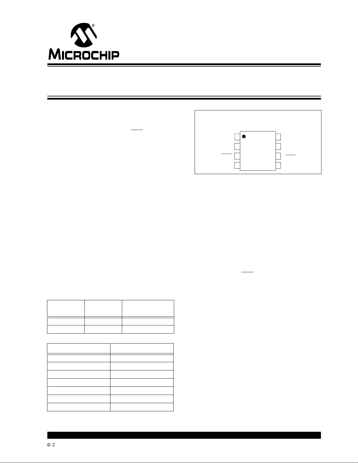
Device Selection Table
Part Number Package
TC650XXVUA 8-PinSOIC -40°Cto+125°C
TC651XXVUA 8-PinM SOP -40°Cto+125°C
Temperature
Range
Package Type
8-Pin MSOP
8-Pin SOIC
V
DD
NC
SHDN
GND
1
2
3
4
TC650
TC651
8
7
6
5
PWM
GND
T
OVER
NC
General Description
The TC650/TC651 are integrated temperaturesensors
and brushless DC fan speed controllers. The TC650/
TC651 measure their junction temperature and control
thespeedofthefanbasedonthattemperature,making
them especially suited for applications in modern
electronic equipment.
Temperature data is converted from the on-chip
thermal sensing element and translated into a
fractionalfan speed from 40% to 100%. A temperature
selection guide i n the data sheet is used to choose the
low and high temperature limits to control the fan. The
TC650/TC651 also include a single trip point over
temperature alert (T
additionaltemperature sensors. In addition, the TC651
features an auto fan shutdown function for additional
power savings.
The TC650/TC651are easy to use, requireno software
overhead and are therefore the ideal choice for
implementing thermal management in a variety of
systems.
) that eliminates the need for
OVER
XTemperature
A25
B30
C35
D40
E45
F50
G55
The "X" denotes a suffix for temperature threshold settings.
Contact factory for other temperature ranges.
2002 Microchip TechnologyInc. DS21450B-page 1
TC650/TC651
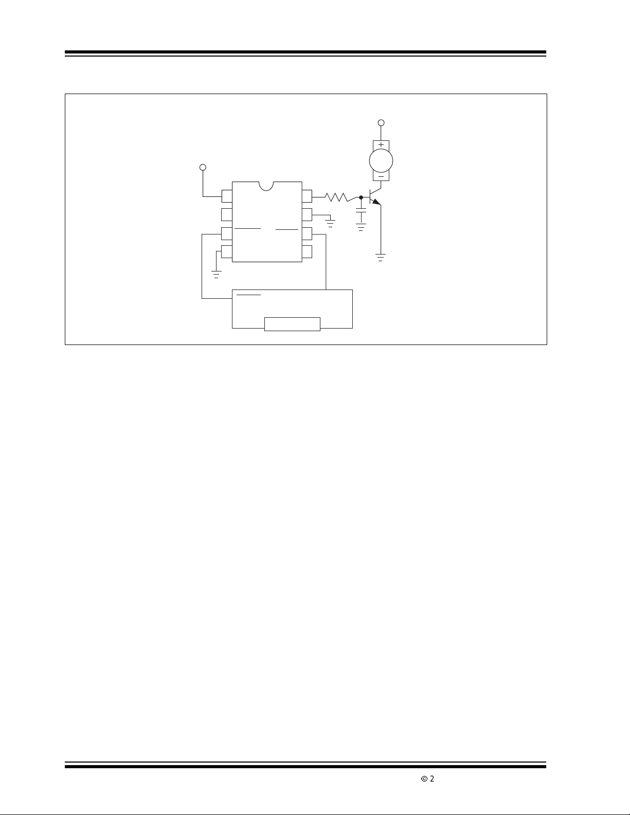
Typical Application Diagram
+5V V
DD
TC650
TC651
+12V
DC Fan
500mA
1
2
3
4
GND
V
DD
NC
SHDN
GND
SHDN Control
PWM
GND
T
OVER
µController
8
7
6
NC
5
Over-Temp.
Alert
C
SLOW
GND
DS21450B-page 2
2002 Microchip TechnologyInc.
TC650/TC651
1.0 ELECTRICAL
CHARACTERISTICS
*Stresses above those listed under "Absolute Maximum Ratings"maycause permanentdamage to thedevice.These are
stress ratings only and functional operation of the device at
these or any other conditions above those indicated in the
Absolute Maximum Ratings*
Input Voltage (VDDto GND)...................................+6V
operation sections of the specifications is not implied. E xposure to Absolute Maximum R ating conditions for extended
periodsmay affectdevice reliability.
Output Voltage (OUT to GND) .................................6V
Voltage On Any Pin.......(GND – 0.3V) to (V
Package Thermal Resistance (θ
) ..............250°C/W
JA
DD
+0.3V)
Operating Temperature Range ..........-40°Cto+125°C
Storage Temperature .........................-65°Cto+150°C
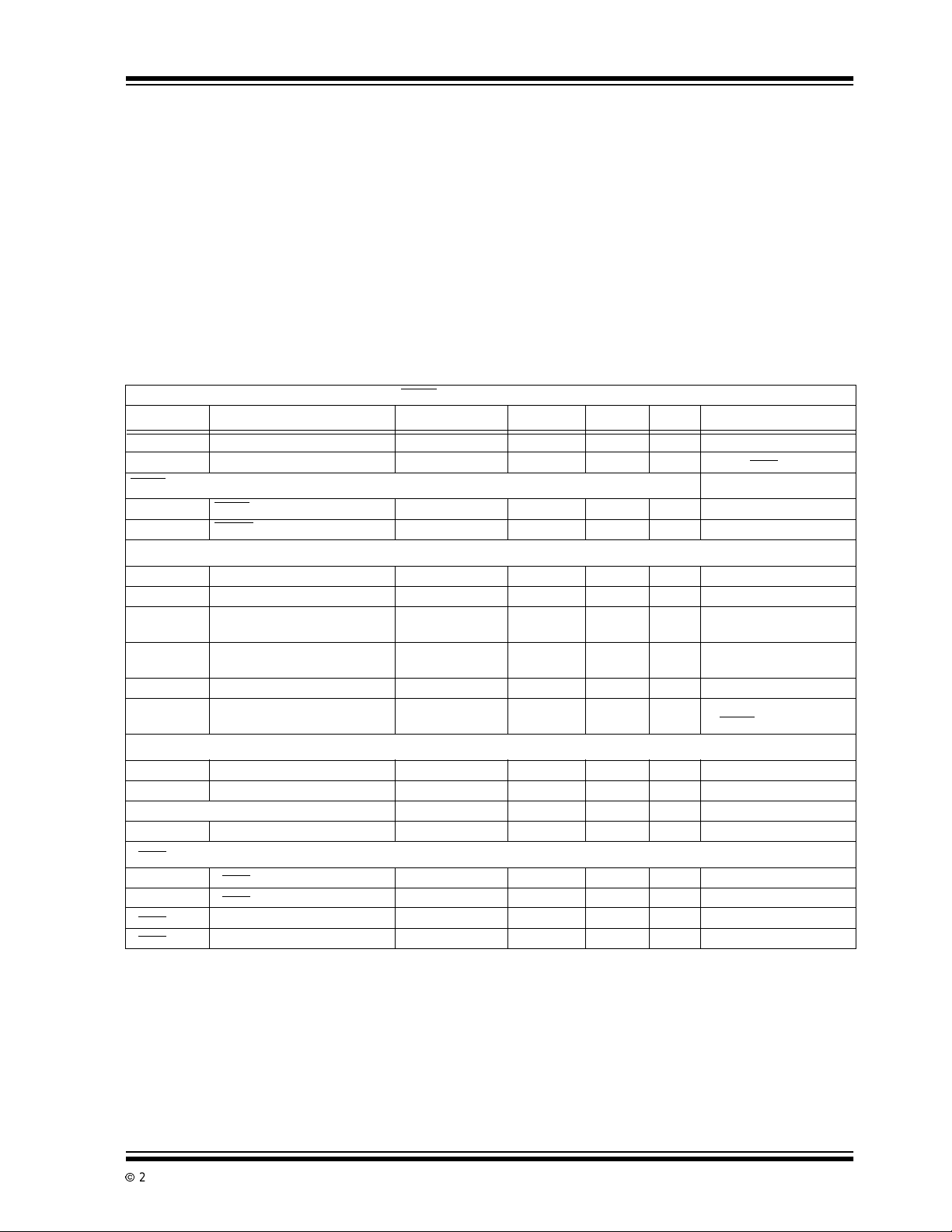
TC650/TC651 EL ECTRI CAL SPECIFICATIONS
Electrical Characteristics: VDD= 2.8V to 5.5V, SHDN =VDD,TA=-40°Cto125°C unlessotherwise specified.
Symbol Parameter Min Typ. Max Units Test Conditions
V
DD
I
DD
SHDN
V
IH
V
IL
PWM Output
V
OL
V
OH
t
R
t
F
f
OUT
t
STARTUP
Temperature Accuracy
T
H ACC
(T
H –TL) ACC
T
HYST
T
OVER
V
HIGH
V
LOW
T
OVER ACC
T
OVER HYST
Note 1: Transition from 90% to 100% Duty Cycle.
Supply Voltage 2.8 — 5.5 V
Supply Current — 50 90 µAPWM,T
Input
SHDN Input High Threshold 65 — — %V
SHDN Input Low Threshold — — 15 %V
PWM Output Low Voltage — — 0.3 V I
PWM Output HighVoltage VDD-0.5 — — V I
DD
DD
SINK
SOURCE
PWM Rise Time — 10 — µsec IOH=5mA,1nFfrom
PWM to GND
PWM Fall Time — 10 — µsec IOL=1mA,1nFfrom
PWM to GND
PWM Frequency 10 15 — H z
Start-upTime — 32/f
High Temperature Accuracy TH–3 T
OUT
H
—secVDDRises from GND,
or S HDN
TH+3 °C Note1
Temp. Range Accuracy -1.0 — +1.0 °C(TH-TL) ≤ 20°C
-2.5 — +2.5 °C(T
H-TL
Auto-shutdown Hysteresis — (TH-TL)/5 — °CTC651Only
Output
T
Output High Voltage VDD-0.5 — — V I
OVER
T
Output Low Voltage — — 0.4 V I
OVER
SOURCE
SINK
Absolute Accuracy — TH+10 — °C At Trip Point
Trip Point Hysteresis — 5 — °C
OVER
=1mA
=5mA
Released
) ≥ 20°C
=1.2mA
=2.5mA
are open
2002 Microchip TechnologyInc. DS21450B-page 3
TC650/TC651
2.0 PIN DESCRIPTIONS
ThedescriptionsofthepinsarelistedinTable2-1.
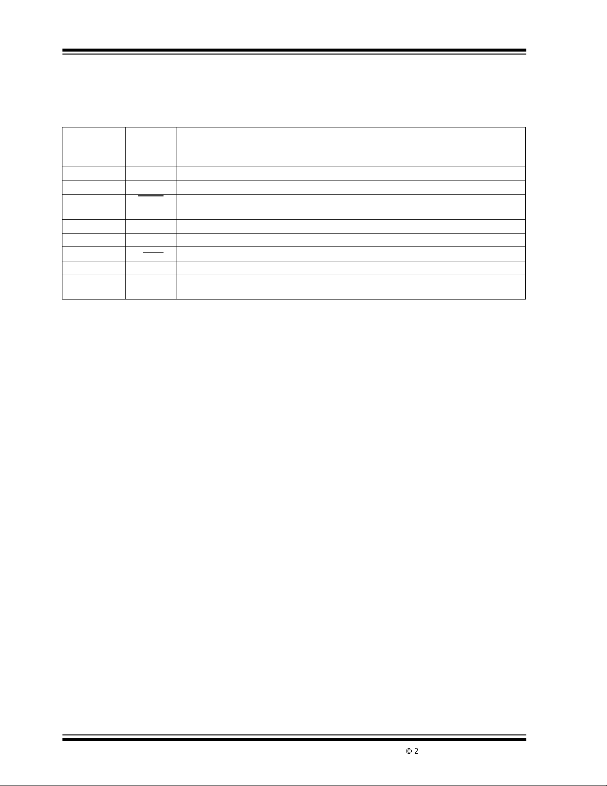
TABLE 2-1: PIN FUNCTION TABLE
Pin No.
(8-Pin MSOP)
(8-Pin SOIC)
1V
2 NC No Internal Connect.
3 SHDN
4 GND Ground. Ground return for all TC650/TC651 functions.
5 NC No Connect.
6T
7 GND Ground.
8 PWM PWM Fan Drive Output. Pulse width modulated rail-to-rail logic output. Nominal
Symbol Description
DD
OVER
Power Supply Input. May be independent of fan power supply.
Fan Shutdown, Active-Low Input. During Shutdown mode the chip still monitors temperature and T
Over-Temperature Alert, Active-Low Output.
Frequency is 15Hz.
is low if temperature rises above factory set point.
OVER
DS21450B-page 4
2002 Microchip TechnologyInc.
TC650/TC651
3.0 DETAILED DESCRIPTION
The TC650/TC651 acquire and convert their junction
temperature (T
sensor with a typical accuracy of ±1°C. The temperature
data is digitally stored in an internal register. The
register is compared with pre-defined threshold values.
The six threshold values are equally distributed over a
pre-defined range of t emperatures (see Table 3-1 and
Table 3-2). The TC650/TC651 control the speed of a
DC brushless fan using a fractional speed control
scheme.The output stage requiresonly a 2N2222-type
small-signal BJT for fans up to 300mA. For larger
current fans (up to 1 Amp) a logic-level N-channel
MOSFET may be used. In addition to controlling the
speed of the fan, the TC650/TC651 include an on-chip
over-temperature alarm (T
when the temperatureof the chip exceeds T
(typical).Thisfeature eliminatest he need for a separate
temperature sensor for over-temperature monitoring.
TABLE 3-1: TEMPERATURE RANGE
Temperature (T = T
T
L
T
1
T
2
T
3
T
4
<=T<T
T
H
T
) information from an on-chip solid-state
J
) thatgives a low signal
OVER
DEFINITION FOR T C650
(MINIMUM-SPEED MODE)
) PWM Duty Cycle
J
T<T
L
<=T<T
<=T<T
<=T<T
<=T<T
<=T<T
OV
1
2
3
4
H
OV
< = T 100% wi th OverTempAlert
(T
40%
50%
60%
70%
80%
90%
100%
OVER
=L)
by 10°C,
H
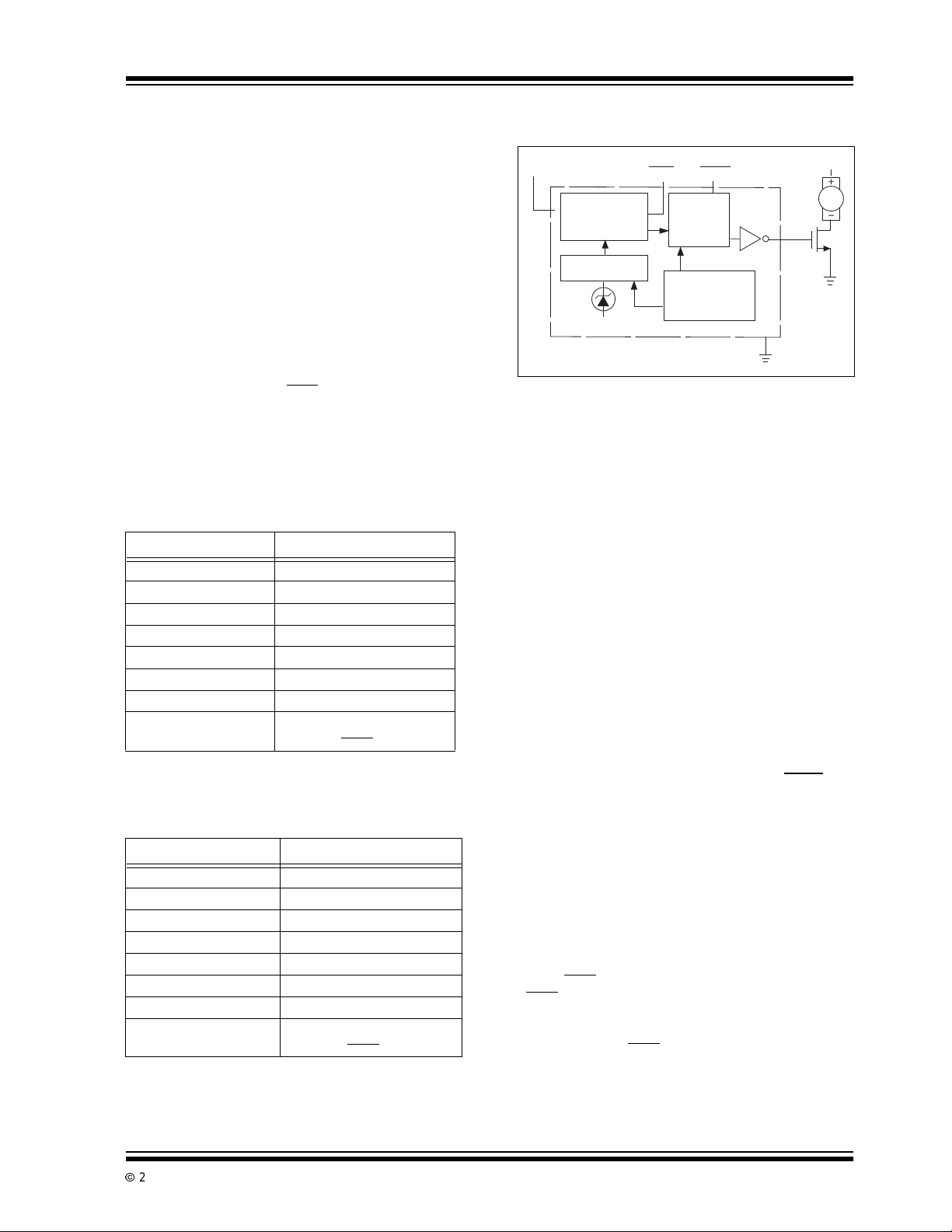
FIGURE 3-1: FUNCTIONAL BLOCK
DIAGRAM
V
DD
Temperature
Set Point and
Trim Range
A/D Converter
Temperature Sensor
T
OVER
SHDN
Duty Cycle
Logic
Control
Oscillator
V+
PWM
3.1 PWM Output
The PWM pin is designed to drive a low cost transistor
or MOSFET as thelow side power switching element in
the system. This output has an asymmetric
complementary drive and is optimized for driving NPN
transistors or N-channel MOSFETs. Since the system
relies on PWM rather than linear power control, t he
dissipation in the power switch is kept to a minimum.
Generally, very small devices (TO-92 or SOT
packages) will suffice. The frequency of the PWM is
about 15Hz. The PWM is also the time base for the
Start-up Timer (see paragraphs below). The PWM duty
cycle has a range of 40% to 100% for the TC650 and
50% to 100% for the TC651.
3.2 Start-Up Timer
To ensure reliable fan start-up,the Start-upTimerturns
PWM high for about 2 seconds whenever the fan is
started from the off state. This occurs at power-up and
when coming out of Shutdown mode.
TABLE 3-2: TEMPERATURE RANGE
DEFINITION FOR T C651
(AUTO-SHUTDOWN MODE)
Temperature (T = T
T<T
L
<=T<T
T
L
<=T<T
T
1
<=T<T
T
2
<=T<T
T
3
<=T<T
T
4
<=T<T
T
H
< = T 100% withOver-TempAlert
T
OV
Note:The temperature regions defined by the six temperature thresholds are pre-defined in the TC650/TC651 by means of trimming. Once
aT
andTHare programmed, the T1–T4thresholds are automatically
L
equally spaced between T
2002 Microchip TechnologyInc. DS21450B-page 5
) PWM Duty Cycle
J
1
2
3
4
H
OV
(T
OVER
and TH.
L
“OFF”
50%
60%
70%
80%
90%
100%
=L)
3.3 Over-Temperature Alert (T
This pin goes low whenthe THset point is exceeded by
o
10
C (typical). This indicates that the fan is at
OVER
maximum drive and the potential exists for system
overheating; either heat dissipation in the system has
gone beyond the cooling system's design limits, or
some FAULT exists such as fan bearing failure or an
airflow obstruction. This output may be treated as a
“System Overheat” warning and used to t rigger system
shutdown, or bring other fans to f ull speed in the
system. The f an will continue to run at 100% speed
while T
T
OVER
is at or near the T
falls through the T
maintains the T
is asserted. Built-in hysteresis prevents
OVER
from “chattering” when measured temperature
+ 10°C trip point. As t emperature
H
+ 10°C trip point, hysteresis
H
output low until measured
OVER
temperature is 5°C above the trip point setting.
)

TC650/TC651
3.4 Shutdown (SHDN)
The fan can be unconditionallyshutdown by pullinglow
the SHDN
pin. During shutdown, the PWM output is
low. This is i deal for notebook computers and other
portable applications when you need to change
batteries and must not have the f an running at that
time. Thermal monitoring and T
operation during shutdown. I
shutdown current is
DD
OVER
are still in
around 50µA.
3.5 Auto-Shutdown Mode
The TC651 features auto-shutdown; when the
temperature is below the factory set point at minimum
speed (T
), PWM is low and the fan is automatically
L
shut off (Auto-shutdownmode). This feature is ideal for
notebookcomputersandotherportableequipmentthat
need t o conserve as much battery power as possible
and thus run a fan when it is only absolutely needed.
The TC651 will continue to be active so as to m onitor
temperatureforTover. The TC651 exitsAuto-shutdown
modewhen the temperature rises above the factory set
point (T
).
1
3.6 Temperature Selection G uide
(Minimum Fan Speed/Full Speed)
TLand THcanbeselectedin5°Cincrements.THmust
be chosen at least 10
o
C higher than TL.TLcan range
anywhere from 25°C to 35°C.
As an example, suppose you wanted the fan to run at
40% speed at 25°C or less and go to full speed at
45°C. Youwouldorderthepartnumber TC650AEVUA.
As another example, suppose you wanted the fan to
turn on at 30°C and go to full speed at 45°C. You
would order the part number TC651BEVUA.
The five temperature regions defined by the six
thresholds are defined in the TC650/TC651 by means
of factory trimming. Once a T
T
thresholds are automatically equally spaced
4
between T
Temp.
Range
and TH.
L
T
L
and THare set, the T1–
L
T
H
Part #
10°C 25 35 AC
30 40 BD
35 45 C E
15°C 25 40 AD
30 45 BE
35 50 CF
20°C 25 45 AE
30 50 BF
35 55 CG
30°C 25 55 AG
Note:The Bo ld Type temperature settings are available for
ordering. Contact factory for other temperature selections.
DS21450B-page 6
2002 Microchip TechnologyInc.

4.0 TYPICAL APPLICATIONS
4.1 Reducing Switching Noise
For fans consuming more than 300mA, a slowdown
capacitor (C
switching PWM induced noise (see Figure 4-1). The
value of t his capacitor should be 4.7µFto47µF,
depending on the fan current consumption.
See Application Note AN771 “Suppressing Acoustic
Noise in PWM Fan Speed Control Systems” for more
information.
FIGURE 4-1: REDUCING SWITCHING
+5V V
DD
) is recommended for reducing
SLOW
NOISE
+12V
TC650
TC651
DC Fan
500mA
TC650/TC651
1
2
3
4
GND
V
NC
SHDN
GND
SHDN Control
DD
PWM
GND
T
OVER
NC
µController
8
C
SLOW
7
6
5
Over-Temp.
Alert
GND
2002 Microchip TechnologyInc. DS21450B-page 7

TC650/TC651
5.0 TYPICAL CHARACTERISTICS
The graphs and tables provided following this note ar e a statistical summary based on a limited number of samples
and are provided for informational purposes only. The performance characteristics listed herein are not t ested or
guaranteed. In some graphs or tables, the data presented may be outside the specified operating range ( e.g., outside specified power supply range) and therefore outside the warranted range
(µA)
DD
I
450
400
(mV)
OL
V
150
100
500
350
300
250
200
50
0.0
IDD vs. Temperature
90
80
70
V
60
50
40
30
20
10
0
-50
PWM, I
VDD = 2.8V
0
123 4 567
=
DD
-25
0
TEMPERATURE (˚C)
SINK
5.6
V
= 2.7
DD
50
25
75 100 125 150
vs. VOL, TA = 25˚C
= 5.5V
V
DD
8
910
(mA)
I
SINK
Temperature Accuracy vs. V
3.0
2.5
2.0
1.5
1.0
V
= 5.6
Temp Accuracy (˚C)
0.5
0.0
PWM, I
1.0
0.9
0.8
0.7
0.6
OH (V)
- V
0.5
DD
V
0.4
0.3
0.2
0.1
0.0
DD
V
= 2.7
DD
T
T
1
L
SOURCE
0
246 81012141618 20
T
vs. (VDD - VOH), TA = 25˚C
VDD = 2.8V
I
SOURCE
T
T
2
THRESHOLD
(mA)
T
3
4
VDD = 5.5V
TH
T
H
T
OVER
1.0
0.9
0.8
0.7
0.6
OH (V)
0.5
- V
DD
0.4
V
0.3
0.2
0.1
0.0
, I
0
DS21450B-page 8
SOURCE
VDD = 2.8V
123 4 567
vs. (V
I
SOURCE
V
DD
= 5.5V
DD
(mA)
- VOH), TA = 25˚C
8
910
2002 Microchip TechnologyInc.

6.0 PACKAGING INFORMATION
6.1 Package Marking Information
Package marking data not available at this time.
6.2 Taping Form
Component Taping Orientation for 8-Pin MSOP Devices
PIN 1
TC650/TC651
User Direction of Feed
W
P
Standard Reel Component Orientation
for TR Suffix Device
Carrier Tape, Number of Components Per Reel and Reel Size
Package Carrier Width (W) Pitch (P) Part Per Full Reel Reel Size
8-Pin MSOP 12 mm 8 mm 2500 13 in
Component Taping Orientation for 8-Pin SOIC (Narrow) Devices
User Direction of Feed
PIN 1
W
P
Standard Reel Component Orientation
for TR Suffix Device
Carrier Tape, Number of Components Per Reel and Reel Size
Package Carrier Width (W) Pitch (P) Part Per Full Reel Reel Size
8-Pin SOIC (N) 12 mm 8 mm 2500 13 in
2002 Microchip TechnologyInc. DS21450B-page 9

TC650/TC651
.
8
)
)
)
)
)
)
)
)
)
)
)
)
)
)
)
)
8
C
6.3 Package Dimensions
8-Pin MSOP
PIN 1
.026 (0.65) TYP.
.016 (0.40)
.010 (0.25)
-Pin SOI
.122 (3.10)
.114 (2.90)
.006 (0.15)
.002 (0.05)
.122 (3.10)
.114 (2.90)
.157 (3.99
.150 (3.81
.197 (5.00)
.189 (4.80)
.043 (1.10)
MAX.
.244 (6.20
.228 (5.79
6° MAX.
.008 (0.20)
.005 (0.13)
.028 (0.70)
.016 (0.40)
Dimensions: inches (mm)
DS21450B-page 10
.050 (1.27) TYP
.197 (5.00
.189 (4.80
.020 (0.51
.013 (0.33
.010 (0.25
.004 (0.10
.069 (1.75
.053 (1.35
.050 (1.27
.016 (0.40
.010 (0.25
.007 (0.18
Dimensions: inches (mm)
2002 Microchip TechnologyInc.

TC650/TC651
SALES AND SUPPORT
Data Sheets
Products supportedby a preliminaryDataSheetmayhavean erratasheet describingminoroperationaldifferences and recommendedworkarounds.To determine if an erratasheetexists for a particular device,please contactone of the following:
1. Your local Microchip sales office
2. TheMicrochip Corporate Literature Center U.S. FAX:(480)792-7277
3. The Microchip Worldwide Site (www.microchip.com)
Pleasespecify which device, revision of silicon and Data Sheet (includeLiterature #) you are using.
New Customer Notification System
Register on our web site (www.microchip.com/cn)to receive the most currentinformationon our products.
2002 Microchip TechnologyInc. DS21450B-page 11

TC650/TC651
NOTES:
DS21450B-page 12
2002 Microchip TechnologyInc.

TC650/TC651
Information contained in this publication regarding device
applications and the like is intended through suggestion only
and may be superseded by updates. It is your responsibility to
ensure that your application meets with your specifications.
No representation or warranty is given and no liability is
assumed by Microchip Technology Incorporated with respect
to the accuracy or use of such information, or infringementof
patents or other intellectual property rights arising from such
use or otherwise. Use of Microchip’s products as critical components in life support systems is not authorized except with
express written approval by Microchip. No licenses are conveyed, implicitly or otherwise, under any intellectual property
rights.
Trademarks
The Microchip name and logo, the Microchip logo, FilterLab,
K
EELOQ,microID,MPLAB,PIC,PICmicro,PICMASTER,
PICSTART, PRO MA TE, SEEVAL and The Embedded Control
SolutionsCompany areregiste red trademarksof MicrochipTechnologyIncorp or ated in the U.S.A. and other countries .
dsPIC, ECONOMONITOR, FanSense, FlexROM, fuz z yLAB,
In-Circuit Serial Programming, ICSP, ICEPIC, microPort,
Migratable Memory, MPASM, MPLIB, MPLINK, MPSIM,
MXDEV, PICC, PICDEM, PICDE M.net, rfPIC, Select Mode
and TotalEndurancearetrademarksofMicrochipTechnology
Incorporated in the U.S.A.
Serialized Quick Turn Programming (SQTP) is a service mark
of Microchip TechnologyIncorporated in t he U.S.A.
All other trademarks mentioned herein are property of their
respective companies.
© 2002, Microchip Technology Incorporated, Printed in the
U.S.A., All Rights Reserved.
Printed on recycled paper.
Microchip received QS-9000 quality system
certification for its worldwide headquarters,
design and wafer fabrication facilities in
Chandler and Tempe, Arizona in July 1999
and Mountain View, California in March 2002.
The Company’s quality system processes and
procedures are QS-9000 compliant for its
®
PICmicro
devices, Serial EEPROMs, microperipherals,
non-volatile memory and analog products. In
addition, Microchip’s quality system for the
design and manufacture of development
systemsisISO 9001certified.
2002 Microchip TechnologyInc. DS21450B-page 13
8-bit MCUs, KEELOQ®code hopping
WORLDWIDE SALES AND SERVICE
AMERICAS
Corporate Office
2355 West Chandler Blvd.
Chandler, AZ 85224-6199
Tel: 480-792-7200 Fax: 480-792-7277
Technical Support: 480-792-7627
Web Address: http://www.microchip.com
Rocky Mountain
2355 West Chandler Blvd.
Chandler, AZ 85224-6199
Tel: 480-792-7966 Fax: 480-792-7456
Atlanta
500 Sugar Mill Road, Suite 200B
Atlanta, GA 30350
Tel: 770-640-0034 Fax: 770-640-0307
Boston
2 Lan Drive, Suite 120
Westford, MA 01886
Tel: 978-692-3848 Fax: 978-692-3821
Chicago
333 Pierce Road, Suite 180
Itasca, IL 60143
Tel: 630-285-0071 Fax: 630-285-0075
Dallas
4570 Westgrove Drive, Suite 160
Addison, TX 75001
Tel: 972-818-7423 Fax: 972-818-2924
Detroit
Tri-Atria Office Building
32255 Northwestern Highway, Suite 190
Farmington Hills, MI 48334
Tel: 248-538-2250 Fax: 248-538-2260
Kokomo
2767 S. Albright Road
Kokomo, Indiana 46902
Tel: 765-864-8360 Fax: 765-864-8387
Los Angeles
18201 Von Karman, Suite 1090
Irvine, CA 92612
Tel: 949-263-1888 Fax: 949-263-1338
New York
150 Motor Parkway, Suite 202
Hauppauge, NY 11788
Tel: 631-273-5305 Fax: 631-273-5335
San Jose
Microchip Technology Inc.
2107 North First Street, Suite 590
San Jose, CA 95131
Tel: 408-436-7950 Fax: 408-436-7955
Toronto
6285 Northam Drive, Suite 108
Mississauga, Ontario L4V 1X5, Canada
Tel: 905-673-0699 Fax: 905-673-6509
ASIA/PACIFIC
Australia
Microchip Technology Australia Pty Ltd
Suite 22, 41 Rawson Street
Epping 2121, NSW
Australia
Tel: 61-2-9868-6733 Fax: 61-2-9868-6755
China - Beijing
Microchip Technology Consulting (Shanghai)
Co., Ltd., Beijing Liaison Office
Unit 915
Bei Hai Wan Tai Bldg.
No. 6 Chaoyangmen Beidajie
Beijing, 100027, No. China
Tel: 86-10-85282100 Fax: 86-10-85282104
China - Chengdu
Microchip Technology Consulting (Shanghai)
Co., Ltd., Chengdu Liaison Office
Rm. 2401, 24th Floor,
Ming Xing Financial Tower
No. 88 TIDU Street
Chengdu 610016, China
Tel: 86-28-6766200 Fax: 86-28-6766599
China - Fuzhou
Microchip Technology Consulting (Shanghai)
Co., Ltd., Fuzhou Liaison Office
Unit 28F, World Trade Plaza
No. 71 Wusi Road
Fuzhou 350001, China
Tel: 86-591-7503506 Fax: 86-591-7503521
China - Shanghai
Microchip Technology Consulting (Shanghai)
Co., Ltd.
Room 701, Bldg. B
Far East International Plaza
No. 317 Xian Xia Road
Shanghai, 200051
Tel: 86-21-6275-5700 Fax: 86-21-6275-5060
China - Shenzhen
Microchip Technology Consulting (Shanghai)
Co., Ltd., Shenzhen Liaison Office
Rm. 1315, 13/F , Shenzhen Kerry Centre,
Renminnan Lu
Shenzhen 518001, China
Tel: 86-755-2350361 Fax: 86-755-2366086
Hong Kong
Microchip Technology Hongkong Ltd.
Unit 901-6, To wer2, Metroplaza
223 Hing Fong Road
Kwai Fong, N.T ., Hong Kong
Tel: 852-2401-1200 Fax: 852-2401-3431
India
Microchip Technology Inc.
India Liaison Office
Divyasree Chambers
1 Floor, Wing A (A3/A4)
No. 11, O’Shaugnessey Road
Bangalore, 560 025, India
Tel: 91-80-2290061 Fax: 91-80-2290062
Japan
Microchip Technology Japan K.K.
Benex S-1 6F
3-18-20, Shinyokohama
Kohoku-Ku, Yokohama-shi
Kanagawa, 222-0033, Japan
Tel: 81-45-471- 6166 Fax: 81-45-471-6122
Korea
Microchip Technology Korea
168-1, Youngbo Bldg. 3 Floor
Samsung-Dong, Kangnam-Ku
Seoul, Korea 135-882
Tel: 82-2-554-7200 Fax: 82-2-558-5934
Singapore
Microchip Technology Singapore Pte Ltd.
200 Middle Road
#07-02 Prime Centre
Singapore, 188980
Tel: 65-6334-8870 Fax: 65-6334-8850
Taiwan
Microchip Technology Taiwan
11F-3, No. 207
Tung HuaNorth Road
Taipei, 105, T aiwan
Tel: 886-2-2717-7175 Fax: 886-2-2545-0139
EUROPE
Denmark
Microchip Technology Nordic ApS
Regus Business Centre
Lautrup hoj 1-3
Ballerup DK-2750 Denmark
Tel: 45 4420 9895 Fax: 45 4420 9910
France
Microchip Technology SARL
Parc d’Activite du Moulin de Massy
43 Rue du Saule Trapu
Batiment A - ler Etage
91300 Massy, France
Tel: 33-1-69-53-63-20 Fax: 33-1-69-30-90-79
Germany
Microchip Technology GmbH
Gustav-Heinemann Ring 125
D-81739 Munich, Germany
Tel: 49-89-627-144 0 Fax: 49-89-627-144-44
Italy
Microchip Technology SRL
Centro Direzionale Colleoni
Palazzo Taurus 1 V. Le Colleoni 1
20041 Agrate Brianza
Milan, Italy
Tel: 39-039-65791-1 Fax: 39-039-6899883
United Kingdom
Arizona Microchip Technology Ltd.
505 Eskdale Road
Winnersh Triangle
Wokingham
Berkshire, EnglandRG41 5TU
Tel: 44 118 921 5869 Fax: 44-118 921-5820
03/01/02
DS21450B-page 14
*DS21450B*
2002 Microchip Technology Inc.
 Loading...