

Page 1
TC4426A/TC4427A/TC4428A
1.5A Dual High-Speed Power MOSFET Drivers
Features
• High Peak Output Current – 1.5A
• Wide Input Supply Voltage Operating Range:
- 4.5V to 18V
• High Capacitive Load Drive Capability – 1000 pF
in 25 ns (typ.)
• Short Delay Times – 30 ns (typ.)
• Matched Rise, Fall and Delay Times
• Low Supply Current:
- With Logic ‘1’ Input – 1 mA (typ.)
- With Logic ‘0’ Input – 100 µA (typ.)
• Low Output Impedance – 7Ω (typ.)
• Latch-Up Protected: Wi ll Withstand 0.5A Revers e
Current
• Input Will Withstand Negative Inputs Up to 5V
• ESD Protected – 4 kV
• Pin-compatible with TC426/TC427/TC428 and
TC4426/TC4427/TC4428
• Space-saving 8-Pin MSOP and 8-Pin 6x5 DFN
Packages
Applications
• Switch Mode Power Supplies
• Line Drivers
• Pulse Transformer Drive
General Description
The TC4426A/TC4427A/TC4428A are improved
versions of th e e a r li er T C4 4 26 /TC4427/TC44 2 8 fa mi ly
of MOSFET drivers. In additi on to matched ris e and fall
times, the TC4426A/TC4427A/TC4428A devices have
matched leading and falling edge propagation delay
times.
These devices are highly latch-up resistant under any
conditions within their power and voltage ratings. They
are not subject to damage when up to 5V of noise
spiking (of either polarity) occurs on the ground pin.
They can accept, without damage or logic upset, up to
500 mA of reverse current (of either polarity) being
forced back into their outputs. All terminals are fully
protected against Electrostatic Discharge (ESD) up to
4kV.
The TC4426A/TC4427A/TC4428A MOSFET drivers
can easily charge/discharge 1000 pF gate
capacitances in under 30 ns. These devices provide
low enough impedance s in both the on and of f states to
ensure the MOSFET's intended state will not be
affected, even by large transients.
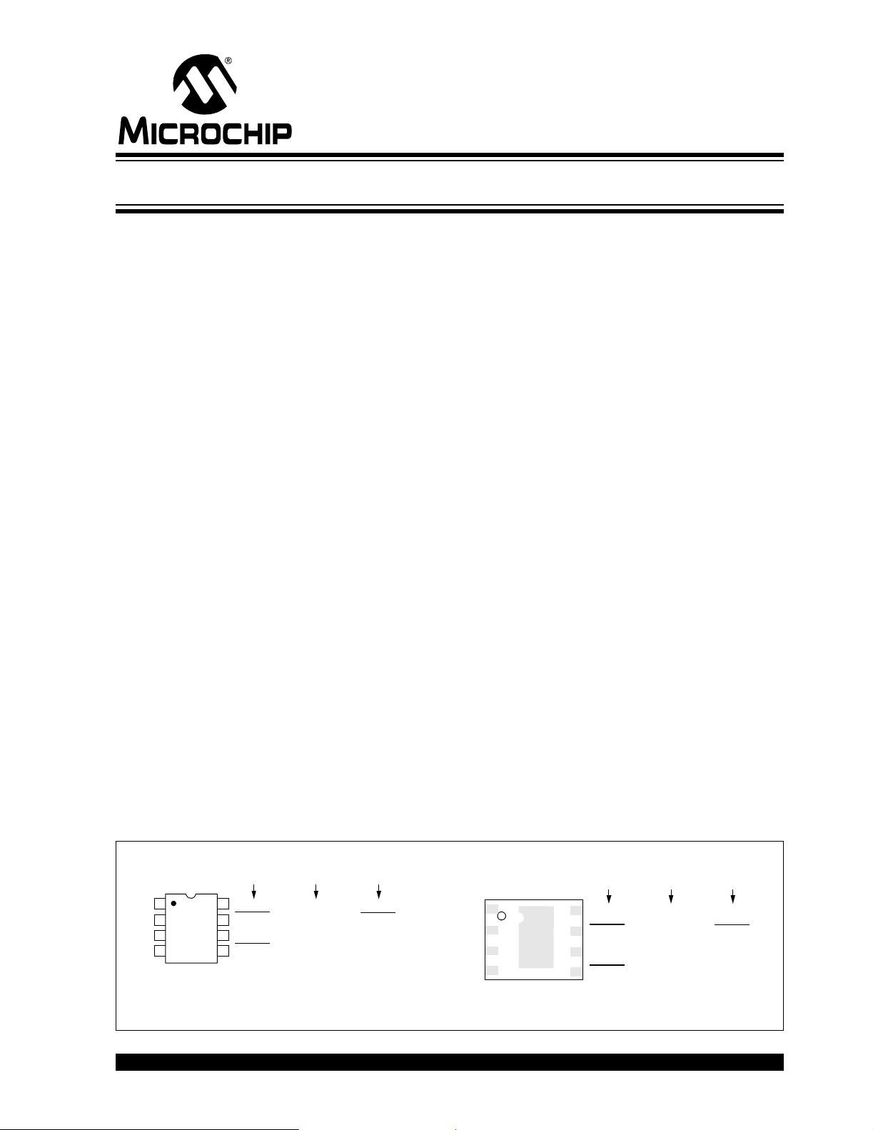
Package Types
8-Pin MSOP/
PDIP/SOIC
NC
IN A
GND
IN B
1
TC4426A
2
TC4427A
3
TC4428A
4
TC4426A TC4427A
8
7
6
5
NC
OUT A
V
DD
OUT B
NC
OUT A
V
DD
OUT B
TC4428A
NC
OUT A
V
DD
OUT B
NC
IN A
GND
IN B
8-Pin DFN
1
TC4426A
2
TC4427A
3
TC4428A
4
Note 1: Exposed pad of the DFN package is electrically isolated.
2004 Microchip Technology Inc. DS21423E-page 1
(1)
TC4426A TC4427A
8
NC
7
OUT A
6
V
DD
5
OUT B
NC
OUT A
V
DD
OUT B
TC4428A
NC
OUT A
V
DD
OUT B
Page 2
TC4426A/TC4427A/TC4428A
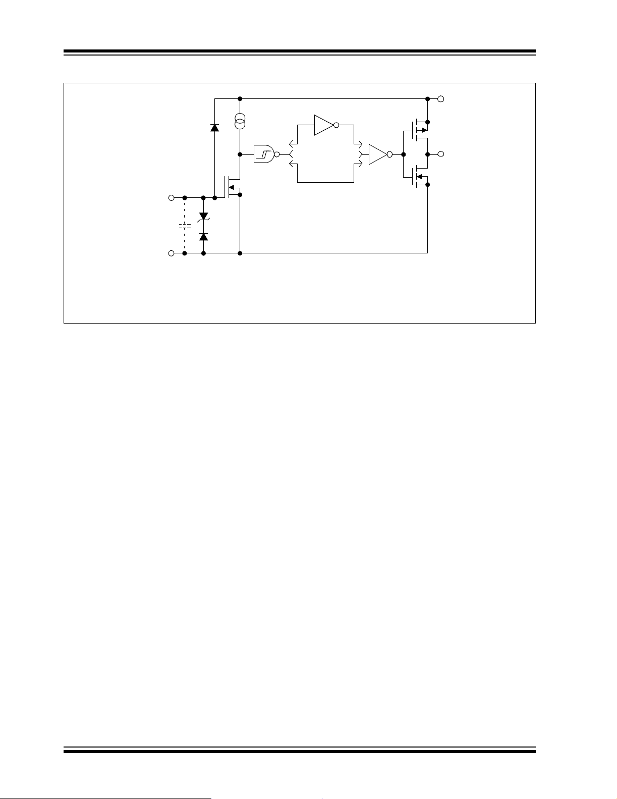
Functional Block Diagram
Inverting
500 µA
300 mV
V
DD
Output
Input
Effective
Input C = 12 pF
(Each Input)
GND
Note 1: TC4426A has two inverting drivers, while the TC4427A has two non-inverting
2: Ground any unused driver input.
Non-Inverting
4.7V
TC4426A/TC4427A/TC4428A
drivers. The TC4428A has one inverting and one non-inverting driver.
DS21423E-page 2 2004 Microchip Technology Inc.
Page 3
TC4426A/TC4427A/TC4428A
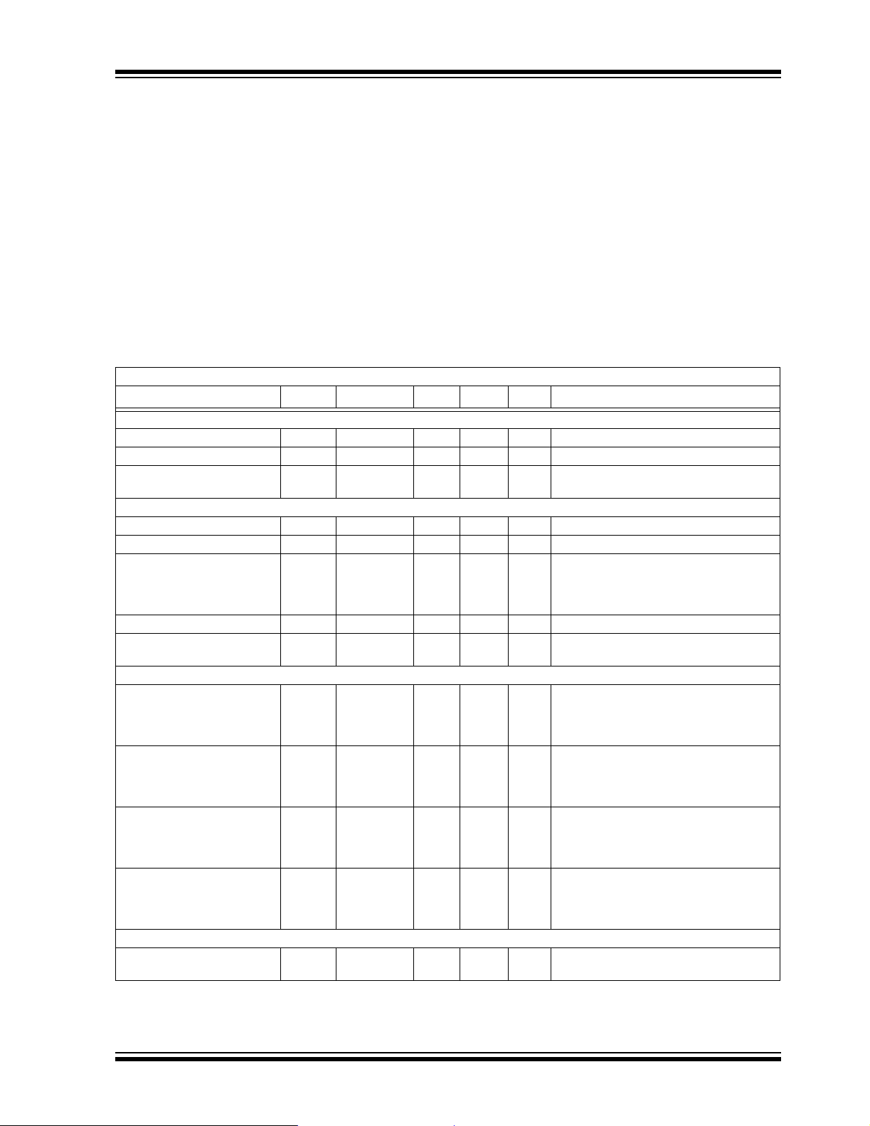
1.0 ELECTRICAL
CHARACTERISTICS
† Notice: Stresses above those listed under "Absolute Maximum Ratings" may cause permanent damage to the device.
These are stress ratings only and functional operation of the
device at these or any other conditions above those indicated
Absolute Maximum Ratings†
Supply Voltage.....................................................+22V
in the operation sections of the specifications is not implied.
Exposure to Absolute Maximum Rating conditions for
extended periods may affect device reliability.
Input Voltage, IN A or IN B
.....................................(V
+ 0.3V) to (GND – 5V)
DD
Package Power Dissipation (TA ≤ 70°C)
DFN.............................................................. Note 2
MSOP..........................................................340 mW
PDIP............................................................730 mW
SOIC............................................................470 mW
DC CHARACTERISTICS
Electrical Specifications: Unless otherwise noted, over operating temperature range with 4.5V ≤ VDD ≤ 18V.
Parameters Sym Min Typ Max Units Conditions
Input
Logic ‘1’, High Input Voltage V
Logic ‘0’, Low Input Voltage V
Input Current I
IH
IL
IN
Output
High Output Voltage V
Low Output Voltage V
Output Resistance R
Peak Output Current I
Latch-Up Protection
I
REV
OH
OL
O
PK
Withstand Reverse Current
Switching Time (Note 1)
Rise Time t
Fall Time t
Delay Time t
Delay Time t
R
F
D1
D2
Power Supply
Power Supply Current I
S
Note 1: Switching times ensured by design.
2: Package power dissipation is dependent on the copper pad area on the PCB.
2.4 — — V
——0.8V
–1.0
–10
—
+1.0
—
+10
µA 0V ≤ VIN ≤ V
DD
VDD – 0.025 — — V DC Test
— — 0.025 V DC Test
—
—
—
—
—1.5—AV
7
7
8
8
10
11
12
9
Ω I
= 10 mA, VDD = 18V, TA = +25°C
OUT
0°C ≤ T
-40°C ≤ T
-40°C ≤ T
DD
A
= 18V
≤ +70°C
≤ +85°C
A
≤ +125°C
A
— > 0.5 — A Duty cycle ≤ 2%, t ≤ 300 µsec
V
= 18V
DD
—
—
—
—
—
—
—
—
—
—
—
—
—
—
—
—
—
—
25
27
29
30
25
27
29
30
30
33
35
38
30
33
35
38
1.0
0.1
35
40
40
40
35
40
40
40
35
40
45
50
35
40
45
50
2.0
0.2
ns TA = +25°C
0°C ≤ T
-40°C ≤ T
-40°C ≤ T
≤ +70°C
A
≤ +85°C
A
≤ +125°C, Figure 4-1
A
ns TA = +25°C
0°C ≤ T
-40°C ≤ T
-40°C ≤ T
≤ +70°C
A
≤ +85°C
A
≤ +125°C, Figure 4-1
A
ns TA = +25°C
0°C ≤ T
-40°C ≤ T
-40°C ≤ T
≤ +70°C
A
≤ +85°C
A
≤ +125°C, Figure 4-1
A
ns TA = +25°C
0°C ≤ T
-40°C ≤ T
-40°C ≤ T
≤ +70°C
A
≤ +85°C
A
≤ +125°C, Figure 4-1
A
mA VIN = 3V (Both inputs)
V
= 0V (Both inputs), VDD = 18V
IN
2004 Microchip Technology Inc. DS21423E-page 3
Page 4
TC4426A/TC4427A/TC4428A
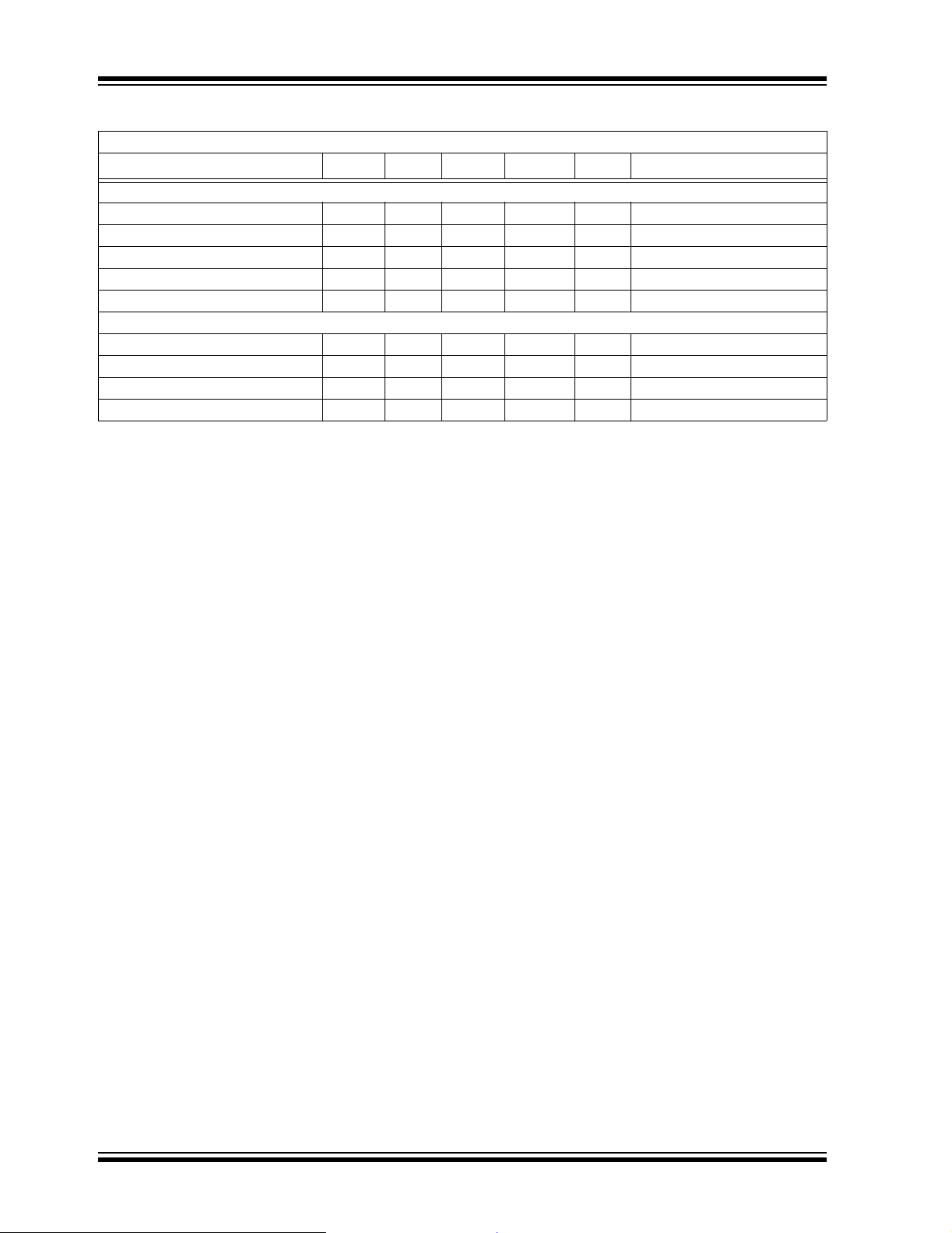
TEMPERATURE CHARACTERISTICS
Electrical Specifications: Unless otherwise noted, all parameters apply with 4.5V ≤ VDD ≤ 18V.
Parameters Sym Min Typ Max Units Conditions
Temperature Ranges
Specified Temperature Range (C) T
Specified Temperature Range (E) T
Specified Temperature Range (V) T
Maximum Junction Temperature T
Storage Temperature Range T
Package Thermal Resistances
Thermal Resistance, 8L-6x5 DFN θ
Thermal Resistance, 8L-MSOP θ
Thermal Resistance, 8L-PDIP θ
Thermal Resistance, 8L-SOIC θ
A
A
A
J
A
JA
JA
JA
JA
0—+70°C
-40 — +85 °C
-40 — +125 °C
——+150°C
-65 — +150 °C
—33.2 —°C/W
— 206 — °C/W
— 125 — °C/W
— 155 — °C/W
DS21423E-page 4 2004 Microchip Technology Inc.
Page 5
TC4426A/TC4427A/TC4428A
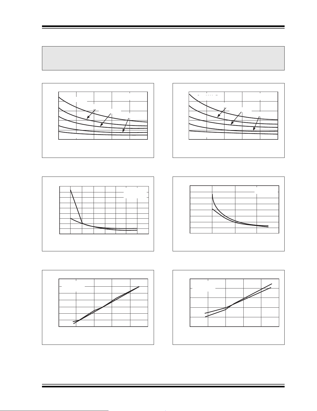
2.0 TYPICAL PERFORMANCE CURVES
Note: The graphs and tables provided following this note are a statistical summary based on a limited number of
samples and are provided for informational purposes only. The performance characteristics listed herein
are not tested or guaranteed. In some graphs or tables, the data presented may be outside the specified
operating range (e.g., outside specified power supply range) and therefore outside the warranted range.
Note: Unless otherwise indicated, over operating temperature range with 4.5V ≤ VDD ≤ 18V.
100
80
60
(nsec)
40
RISE
t
20
0
CL = 2200 pF
CL = 100 pF
5.0
CL = 1500 pF
CL = 1000 pF
7.5 10.0 12.5 15.0 17.5
V
(V)
DD
= +25
T
A
CL = 470 pF
FIGURE 2-1: Rise Time vs. Supply Voltage.
110
100
90
80
70
60
50
40
Delay Time (nsec)
30
20
t
D1
t
D2
12 3 4 567 8 9
Input Amplitude (V)
CL = 1000 pF
V
= 10V
DD
°C
100
(nsec)
FALL
t
CL = 2200pF
CL = 2200 pF
80
60
40
20
CL= 100pF
CL = 100 pF
0
5.0 7.5 10.0 12.5 15.0 17.5
CL = 1500 pF
CL = 1000 pF
V
DD
(V)
= +25
T
A
CL = 470 pF
°C
FIGURE 2-4: Fall Time vs. Supply Voltage.
60
55
50
45
40
35
30
Delay Time (nsec)
25
20
0 5 10 15 20
t
D1
t
D2
V
(V)
DD
CL = 1000 pF
FIGURE 2-2: Delay Time vs. Input Amplitude.
28
CL = 1000 pF
26
V
= 18V
DD
24
22
20
Time (nsec)
18
t
RISE
16
t
FALL
14
-100 -50 0 50 100 150
TEMPERATURE (°C)
FIGURE 2-3: Rise and F all Times vs. Temperature.
FIGURE 2-5: Propagation Delay Time vs. Supply Voltage.
40
CL = 1000 pF
35
V
= 18V
DD
30
25
t
Delay Time (nsec)
D2
20
15
t
D1
-100 -50 0 50 100 150
TEMPERATURE (°C)
FIGURE 2-6: Propagation Delay Time vs. Temperature.
2004 Microchip Technology Inc. DS21423E-page 5
Page 6
TC4426A/TC4427A/TC4428A
Note: Unless otherwise indicated, over operating temperature range with 4.5V ≤ VDD ≤ 18V.
30
= +125
T
25
20
(Ω)
15
DS(ON)
10
R
5
0
0 5 10 15 20
°C
A
= +25
T
°C
A
V
(V)
DD
FIGURE 2-7: Hig h-State Output Resistance.
60
50
40
(mA)
30
20
SUPPLY
I
10
0
CL = 2200 pF
0
500 1000 1500 2000 2500
CL = 1500 pF
CL = 1000 pF
FREQUENCY (kHz)
V
CL = 100 pF
DD
= 18V
30
25
= +125
20
(Ω)
15
DS(ON)
10
R
5
0
T
T
0
A
A
= +25
°C
°C
5
10
V
(V)
DD
15 20
FIGURE 2-10: Low-State Output Resistance.
60
50
40
(mA)
30
20
SUPPLY
I
10
0
0
2 MHz
500 1000 1500 2000 2500
C
V
LOAD
DD
= 18V
(pF)
900 kHz
600 kHz
200 kHz
20 kHz
FIGURE 2-8: Su ppl y Curre nt vs. Frequency.
80
70
60
50
(mA)
40
30
SUPPLY
I
20
10
0
V
= 12V
DD
500
1000
FREQUENCY (kHz)
1500 2000 2500
0
CL = 2200 pF
CL = 1500 pF
CL = 1000 pF
FIGURE 2-9: Su ppl y Curre nt vs. Frequency.
CL = 100 pF
FIGURE 2-11: Supply Current vs. Capacitive Load.
80
V
= 12V
DD
70
60
50
(mA)
40
30
SUPPLY
I
20
10
0
0
500
1000
1500 2000 2500
C
(pF)
LOAD
FIGURE 2-12: Supply Current vs. Capacitive Load.
2 MHz
900 kHz
600 kHz
200 kHz
20 kHz
DS21423E-page 6 2004 Microchip Technology Inc.
Page 7

TC4426A/TC4427A/TC4428A
Note: Unless otherwise indicated, over operating temperature range with 4.5V ≤ VDD ≤ 18V.
40
V
35
30
25
(mA)
20
15
SUPPLY
I
10
5
0
= 6V
DD
500
1000
FREQUENCY (kHz)
1500 2000 2500
0
CL = 2200 pF
CL = 1500 pF
CL = 1000 pF
CL = 100 pF
FIGURE 2-13: Supply Current vs. Frequency.
900
800
BOTH INPUTS = 1
700
600
(µA)
500
400
300
QUIESCENT
I
200
BOTH INPUTS = 0
100
0
0 5 10 15 20
V
(V)
DD
40
V
= 6V
DD
35
30
25
(mA)
20
15
SUPPLY
I
10
5
0
500
1000
1500 2000 2500
C
(pF)
LOAD
0
2 MHz
900 kHz
600 kHz
200 kHz
20 kHz
FIGURE 2-15: Supply Current vs. Capacitive Load.
1100
1000
BOTH INPUTS = 1
900
= 25
T
°C
A
800
(µA)
700
600
500
400
QUIESCENT
300
I
BOTH INPUTS = 0
200
100
0
-100 -50 0 50 100 150
TEMPERATURE (°C)
V
= 18V
DD
FIGURE 2-14: Quiescent Supply Current vs. Voltage.
FIGURE 2-16: Quiescent Supply Current vs. Temperature.
2004 Microchip Technology Inc. DS21423E-page 7
Page 8

TC4426A/TC4427A/TC4428A
3.0 PIN DESCRIPTIONS
The descriptions of the pins are listed in Table 3-1.
TABLE 3-1: PIN FUNCTION TABLE
8-Pin PDIP/
MSOP/SOIC
1 1 NC No connection
2 2 IN A Input A
33GNDGround
4 4 IN B Input B
55OUT BOutput B
66V
77OUT AOutput A
8 8 NC No connection
— PAD NC Exposed Metal Pad
Note 1: Duplicate pins must be connected for proper operation.
8-Pin
DFN
Symbol Description
DD
Supply input
3.1 Inputs A and B
MOSFET driver inputs A and B are high-impedance,
TTL/CMOS compatible inputs. These inputs also have
300 mV of hysteresis between the high and low
thresholds that prevents output glitching, even when
the rise and fall time of the input signal is very slow.
3.2 Ground (GND)
The ground pin is the return path for both the bias
current and the high peak current that discharges the
external lo ad capacitance. The gr ound pin should be
tied into a ground plane or have a v ery short trace to th e
bias supply source return.
3.3 Output A and B
MOSFET driver outputs A and B are low-impedance,
CMOS push-pull st yle outp uts . The pu ll-down an d pul lup devices are of equal strength, making the rise and
fall times equivalent.
3.4 Supply Input (VDD)
The VDD input is the bias supp ly for the MOSFET d river
and is rated for 4.5V to 18 V, with respect to the ground
pin. The VDD input should be bypassed with local
ceramic capacitors. The value of these capacitors
should be chosen based on the capacitive load that is
being driven.
3.5 Exposed Metal Pad
The exposed met al p ad of the 6x5 DFN pac kage is not
internally connected to any potential. Therefore, this
pad can be connected to a ground plane or other
copper plane on a printed circuit board, to aid in heat
removal from the package.
DS21423E-page 8 2004 Microchip Technology Inc.
Page 9

TC4426A/TC4427A/TC4428A
4.0 APPLICATIONS INFORMATION
Input
VDD = 18V
2
4
Input: 100 kHz,
square wave,
= t
t
RISE
FALL
6
3
≤ 10 ns
4.7 µF
7
5
0.1 µF
Output
CL = 1000 pF
+5V
Input
V
Output
+5V
Input
0V
V
DD
Output
0V
0V
DD
0V
10%
10%
t
D1
t
F
t
D2
90%
10%
Inverting Driver
(TC4426A, 1/2 TC4428A)
90%
90%
t
D1
t
R
t
D2
10%
Non-Inverting Driver
(TC4427A, 1/2 TC4428A)
90%
10%
t
R
10%
90%
90%
t
F
FIGURE 4-1: Switching Time Test Circuit.
2004 Microchip Technology Inc. DS21423E-page 9
Page 10
TC4426A/TC4427A/TC4428A
5.0 PACKAGING INFORMATION
5.1 Package Marking Information
8-Lead DFN
XXXXXXX
XXXXXXX
XXYYWW
NNN
8-Lead MSOP
XXXXX
YWWNNN
8-Lead PDIP (300 mil)
XXXXXXXX
XXXXXNNN
YYWW
Example
TC4426A
EMF
0420
Example:
4426AE
420256
Example:
TC4427A
EPA256
:
256
0420
8-Lead SOIC (150 mil)
XXXXXXXX
XXXXYYWW
NNN
Legend: XX...X Customer specific information*
YY Year code (last 2 digits of calendar year)
WW Week code (week of January 1 is week ‘01’)
NNN Alphanumeric traceability code
Note: In the event the full Micro chip p art num ber can not be ma rked on on e line, it will
be carried over to the next line thus limiti ng the number of available chara ct ers
for customer specific information.
* Standard marking consists of Microchip part number, year code, week code, traceability code (facility
code, mask r ev#, and assembly code).
DS21423E-page 10 2004 Microchip Technology Inc.
Example:
TC4428A
COA0420
256
Page 11

TC4426A/TC4427A/TC4428A
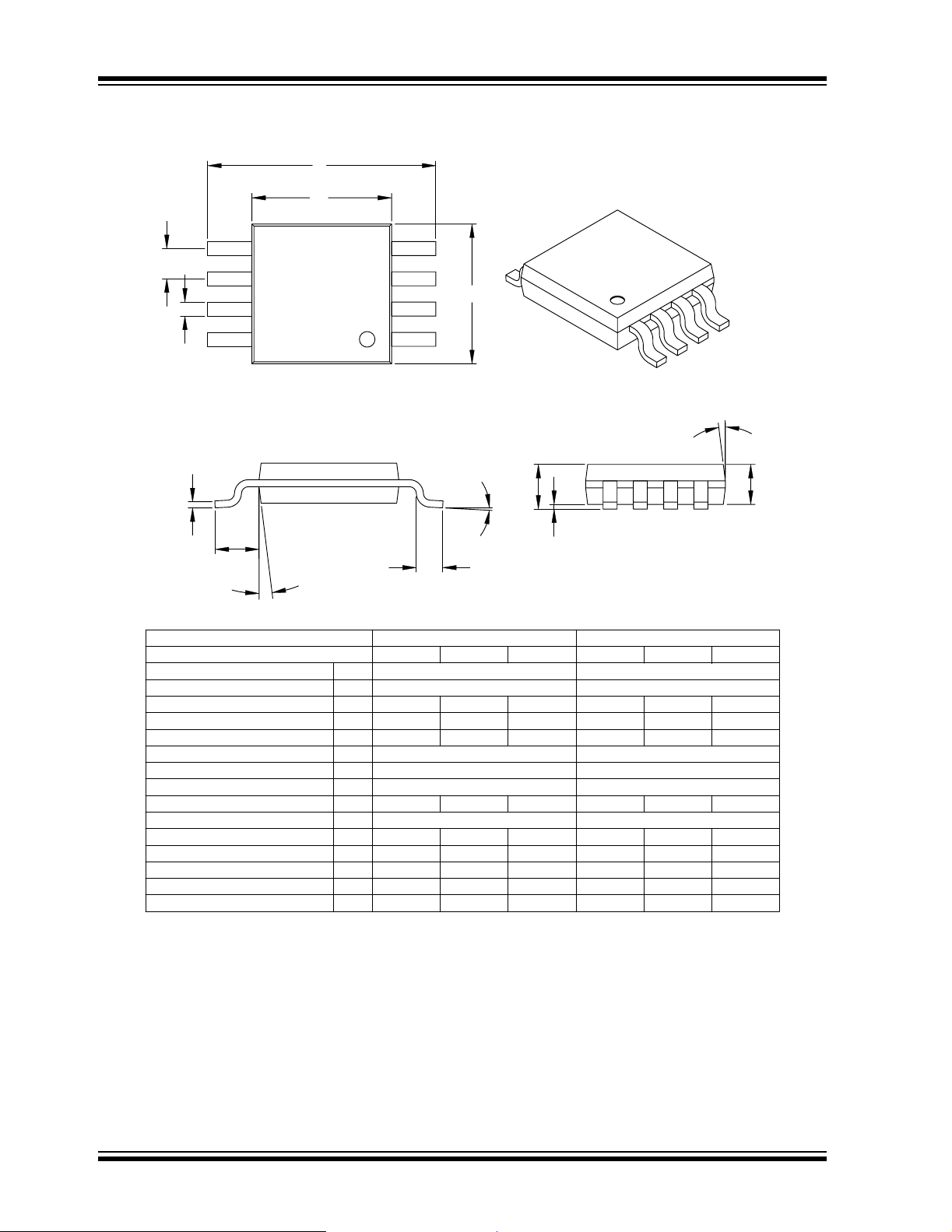
8-Lead Plastic Dual Flat No Lead Package (MF) 6x5 mm Body (DFN-S) – Saw Singulated
2004 Microchip Technology Inc. DS21423E-page 11
Page 12
TC4426A/TC4427A/TC4428A
8-Lead Plastic Micro Small Outline Package (UA) (MSOP)
E
E1
p
D
2
B
n 1
α
A
c
(F)
β
Units
Dimension Limits
Number of Pins
Pitch
Overall Height
Molded Package Thickness
Standoff
Overall Width
Molded Package Width
Overall Length
Foot Length
Foot Angle
Lead Thickness
Lead Width
Mold Draft Angle Top
Mold Draft Angle Bottom
*Controlling Parameter
Notes:
Dimensions D and E1 do not include mold flash or protrusions. Mold flash or protrusions shall not
exceed .010" (0.254mm) per side.
JEDEC Equivalent: MO-187
Drawing No. C04-111
A2
A1
E1
MIN
n
p
A
E
D
L
φ
c
B
α
β
INCHES
.026 BSC
.030
.000
.193 TYP.
.118 BSC
.118 BSC
.016 .024
.037 REFFFootprint (Reference)
0° - 8°
.003
.009
5°
5° -
L
NOM
8
.033
.006
.012
φ
A1
MAX NOM
--
-
-
.043
.037
.006
.031
.009
.016
15°
15°
MIN
0.75
0.00
0.40
0.08
0.22
MILLIMETERS*
MAX
8
0.65 BSC
--
0.85
-
4.90 BSC
3.00 BSC
3.00 BSC
0.60
0.95 REF
0°
-
-
-
A2
1.10
0.95
0.15
0.80
8°
0.23
0.40
15°5° 15°5° -
DS21423E-page 12 2004 Microchip Technology Inc.
Page 13
TC4426A/TC4427A/TC4428A
8-Lead Plastic Dual In-line (PA) – 300 mil (PDIP)
E1
D
2
n
E
β
eB
Number of Pins
Pitch
Top to Seating Plane A .140 .155 .170 3.56 3.94 4.32
Molded Package Thickness A2 .115 .130 .145 2.92 3.30 3.68
Base to Seating Plane A1 .015 0.38
Shoulder to Shoulder Width E .300 .3 13 .325 7.62 7.94 8.26
Molded Package Width E1 .240 .250 .260 6.10 6.35 6.60
Overall Length D .360 .373 .385 9.14 9.46 9.78
Tip to Seating Plane L .125 .130 .135 3.18 3.30 3.43
Lead Thickness
Upper Lead Width B1 .045 .058 .070 1.14 1.46 1.78
Lower Lead Width B .014 .018 .022 0.36 0.46 0.56
Overall Row Spacing § eB .310 .370 .430 7.87 9.40 10.92
Mold Draft Angle Top
Mold Draft Angle Bottom
* Controlling Parameter
§ Significant Characteristic
Notes:
Dimensions D and E1 do not include mold flash or protrusions. Mold flash or protrusions shall not exceed
.010” (0.254mm) per side.
JEDEC Equivalent: MS-001
Drawing No. C04-018
Dimension Limits MIN NOM MAX MIN NOM MAX
1
α
A
c
Units INCHES* MILLIMETERS
n
p
c
α
β
.008 .012 .015 0.20 0.29 0.38
A1
B1
B
88
.100 2.54
51015 51015
51015 51015
A2
L
p
2004 Microchip Technology Inc. DS21423E-page 13
Page 14

TC4426A/TC4427A/TC4428A
8-Lead Plastic Small Outline (OA) – Narrow, 150 mil (SOIC)
E
E1
p
D
2
B
Number of Pins
Pitch
Foot Angle
Lead Thickness
Mold Draft Angle Top
Mold Draft Angle Bottom
* Controlling Parameter
§ Significant Characteristic
Notes:
Dimensions D and E1 do not include mold flash or protrusions. Mold flash or protrusions shall not exceed
.010” (0.254mm) per side.
JEDEC Equivalent: MS-012
Drawing No. C04-057
n
45°
c
β
n
p
φ
c
α
β
1
h
A
φ
L
048048
A1
MILLIMETERSINCHES*Units
1.27.050
α
A2
MAXNOMMINMAXNOMMINDimension Limits
88
1.751.551.35.069.061.053AOverall Height
1.551.421.32.061.056.052A2M olded Pa ckag e Thickness
0.250.180.10.010.007.004A1Standoff §
6.206.025.79.244.237.228EOverall Width
3.993.913.71.157.154.146E1Molded Package Width
5.004.904.80.197.193.189DOverall Length
0.510.380.25.020.015.010hChamfer Distance
0.760.620.48.030.025.019LFoot Length
0.250.230.20.010.009.008
0.510.420.33.020.017.013BLead Width
1512015120
1512015120
DS21423E-page 14 2004 Microchip Technology Inc.
Page 15

TC4426A/TC4427A/TC4428A
PRODUCT IDENTIFICATION SYSTEM
To order or obtain information, e.g., on pricing or delivery, refer to the factory or the listed sales office.
PART NO. X XX
Device
PackageTemperature
XXX
Tape & ReelXPB Free
Range
Device: TC4426A: 1.5A Dual MOSFET Driver, Inverting
Temperature Range: C = 0°C to +70°C (PDIP & SOIC Only)
Package: MF = Dual, Flat, No-Lead (6X5 mm Body), 8-lead
PB Free: G = Lead-Free device *
TC4427A: 1.5A Dual MOSFET Driver, Non-Inverting
TC4428A: 1.5A Dual MOSFET Driver, Complementary
E = -40°C to +85°C
V = -40ºC to +125°C
MF713 = Dual, Flat, No-Lead (6X5 mm Body), 8-lead
PA = Plastic DIP (300 mil Body), 8-lead
OA = Plastic SOIC, (150 mil Body), 8-lead
OA713 = Plastic SOIC, (150 mil Body), 8-lead
UA = Plastic Micro Small Outline (MSOP), 8-lead
UA713 = Plastic Micro Small Outline (MSOP), 8-lead
* Available on selected packages. Contact your local sales
(Tape and Reel)
(Tape and Reel)
(Tape and Reel)
= Blank
representative for availability.
Examples:
a) TC4426ACOA: 1.5A Dual Inverting
b) TC4426AEOA: 1.5A Dual
c) TC4426AEMF: 1.5A Dual
a) TC4427ACPA: 1.5A Dual
b) TC4427AEPA: 1.5A Dual
c) TC4427AVMF713: 1.5A Dual
a) TC4428AEPA: 1.5A Dual
b) TC4428ACOA713: 1.5A Dual
c) TC4428AVMF: 1.5A Dual
MOSFET driver,
0°C to +70°C,
8LD SOIC package.
Inverting
MOSFET driver,
-40°C to +85°C,
8LD SOIC package.
Inverting
MOSFET driver,
-40°C to +85°C,
8LD DFN package.
Non-Inverting
MOSFET driver,
0°C to +70°C,
8LD PDIP package.
Non-Inverting
MOSFET driver,
-40°C to +85°C,
8LD PDIP package.
Non-Inverting
MOSFET driver,
-40°C to +125°C,
8LD DFN package,
Tape and Reel.
Complementary
MOSFET driver,
-40°C to +85°C,
8LD PDIP package.
Complementary
MOSFET driver,
0°C to +70°C
8LD SOIC package,
Tape and Reel.
Complementary
MOSFET driver,
-40°C to +125°C,
8LD DFN package.
Sales and Support
Data Sheets
Products supported by a preliminary Data Sheet may have an errata sheet describing minor operational differences and
recommended workarounds. To determine if an errata sheet exists for a particular device, please contact one of the following:
1. Your local Microchip sales office
2. The Microchip Corporate Literature Center U.S. FAX: (480) 792-7277
3. The Microchip Worldwide Site (www.microchip.com)
Please specify which device, revision of silicon and Data Sheet (include Literature #) you are using.
Customer Notification System
Register on our web site (www.microchip.com/cn) to receive the most current information on our products.
2004 Microchip Technology Inc. DS21423E-page 15
Page 16

TC4426A/TC4427A/TC4428A
NOTES:
DS21423E-page 16 2004 Microchip Technology Inc.
Page 17

Note the following details of the code protection feature on Microchip devices:
• Microchip products meet the specification contained in their particular Microchip Data Sheet.
• Microchip believes that i ts family of products is one of the most secure families of its kind on the market today, when used in the
intended manner and under normal conditions.
• There are dishonest and possibly illegal methods used to breach the code protection feature. All of these methods, to our
knowledge, require using the Microchip products in a manner outside the operating specifications contained in Microchip’s Data
Sheets. Most likely, the person doing so is engaged in theft of intellectual property.
• Microchip is willing to work with the customer who is concerned about the integrity of their code.
• Neither Microchip nor any other semiconductor manufacturer can guarantee the security of their code. Code protection does not
mean that we are guaranteeing the product as “unbreakable.”
Code protection is constantly evolving. We at Microchip are com mitted to continuously improving the code protect ion f eatures of our
products. Attempts to break Microchip’s code protection feature may be a violation of the Digit al Mill ennium Copyright Act. If such acts
allow unauthorized access to your software or other copyrighted work, you may have a right to sue for relief under that Act.
Information contained in this publication regarding device
applications and the like is intended through suggestion only
and may be superseded by updates. It is your responsibility to
ensure that your application meets with your specifications.
No representation or warranty is given and no liability is
assumed by Microchip Technology Incorporated with respect
to the accuracy or use of such information, or infringement of
patents or other intellectual property rights arising from such
use or otherwise. Use of Microchip’s products as critical
components in life support systems is not authorized except
with express written approval by Microchip. No licenses are
conveyed, implicitly or otherwise, under any intellectual
property rights.
Trademarks
The Microchip name and logo, the Microchip logo, Accuron,
dsPIC, K
EELOQ, microID, MPLAB, PIC, PICmicro,
PICSTART, PRO MATE, PowerSmart, rfPIC, a nd
SmartShunt are registered trademarks of Microchip
Technology Incorporated in the U.S.A. and other countries.
AmpLab, FilterLab, MXDEV, MXLAB, PICMASTER, SEEVAL,
SmartSensor and The Embedded Control Solutions Company
are registered trademarks of Microchip Technology
Incorporated in the U.S.A.
Analog-for-the-Digital Age, Application Maestro, dsPICDEM,
dsPICDEM.net, dsPICworks, ECAN, ECONOMONITOR,
FanSense, FlexROM, fuzzyLAB, In-Circuit Serial
Programming, ICSP, ICEPIC, Migratable Memory, MPASM ,
MPLIB, MPLINK, MPSIM, PICkit, PICDEM, PICDEM.net,
PICLAB, PICtail, PowerCal, PowerInfo, PowerMate,
PowerTool, rfLAB, rfPICDEM, Select Mode, Smart Serial,
SmartTel and Total Endurance are trademarks of Microchip
Technology Incorporated in the U.S.A. and other countries.
SQTP is a service mark of Microchip T echnology Incorporated
in the U.S.A.
All other trademarks mentioned herein are property of their
respective companies.
© 2004, Microchip Technology Incorporated, Printed in the
U.S.A., All Rights Reserved.
Printed on recycled paper.
Microchip received ISO/TS-16949:2002 quality system certification for
its worldwide headquarters, design and wafer fabrication facilities in
Chandler and Tempe, Arizona and Mountain View, California in
October 2003. The Company’s quality system processes and
procedures are for its PICmicro
devices, Serial EEPROMs, microperipherals, nonvolatile memory and
analog products. In addition, Microchip’s quality system for the design
and manufacture of development systems is ISO 9001:2000 certified.
®
8-bit MCUs, KEELOQ
®
code hopping
2004 Microchip Technology Inc. DS21423E-page 17
Page 18

WORLDWIDE SALES AND SERVICE
AMERICAS
Corporate Office
2355 West Chandler Blvd.
Chandler, AZ 85224-6199
Tel: 480-792-7200
Fax: 480-792-7277
Technical Support:
480-792-7627
Web Address:
www.microchip.com
Atlanta
Alpharetta, GA
Tel: 770-640-0034
Fax: 770-640-0307
Boston
Westford, MA
Tel: 978-692-3848
Fax: 978-692-3821
Chicago
Itasca, IL
Tel: 630-285-0071
Fax: 630-285-0075
Dallas
Addison, TX
Tel: 972-818-7423
Fax: 972-818-2924
Detroit
Farmington Hills, MI
Tel: 248-538-2250
Fax: 248-538-2260
Kokomo
Kokomo, IN
Tel: 765-864-8360
Fax: 765-864-8387
Los Angeles
Mission Viejo, CA
Tel: 949-462-9523
Fax: 949-462-9608
San Jose
Mountain View, CA
Tel: 650-215-1444
Fax: 650-961-0286
Toronto
Mississauga, Ontario,
Canada
Tel: 905-673-0699
Fax: 905-673-6509
ASIA/PACIFIC
Australia - Sydney
Tel: 61-2-9868-6733
Fax: 61-2-9868-6755
China - Beijing
Tel: 86-10-8528-2100
Fax: 86-10-8528-2104
China - Chengdu
Tel: 86-28-8676-6200
Fax: 86-28-8676-6599
China - Fuzhou
Tel: 86-591-750-3506
Fax: 86-591-750-3521
China - Hong Kong SAR
Tel: 852-2401-1200
Fax: 852-2401-3431
China - Shanghai
Tel: 86-21-6275-5700
Fax: 86-21-6275-5060
China - Shenzhen
Tel: 86-755-8290-1380
Fax: 86-755-8295-1393
China - Shunde
Tel: 86-757-2839-5507
Fax: 86-757-2839-5571
China - Qingdao
Tel: 86-532-502-7355
Fax: 86-532-502-7205
ASIA/PACIFIC
India - Bangalore
Tel: 91-80-2229-0061
Fax: 91-80-2229-0062
India - New Delhi
Tel: 91-11-5160-8632
Fax: 91-11-5160-8632
Japan - Kanagawa
Tel: 81-45-471- 6166
Fax: 81-45-471-6122
Korea - Seoul
Tel: 82-2-554-7200
Fax: 82-2-558-5932 or
82-2-558-5934
Singapore
Tel: 65-6334-8870
Fax: 65-6334-8850
Taiwan - Kaohsiung
Tel: 886-7-536-4816
Fax: 886-7-536-4817
Taiwan - Taipei
Tel: 886-2-2500-6610
Fax: 886-2-2508-0102
Taiwan - Hsinchu
Tel: 886-3-572-9526
Fax: 886-3-572-6459
EUROPE
Austria - Weis
Tel: 43-7242-2244-399
Fax: 43-7242-2244-393
Denmark - Ballerup
Tel: 45-4420-9895
Fax: 45-4420-9910
France - Massy
Tel: 33-1-69-53-63-20
Fax: 33-1-69-30-90-79
Germany - Ismaning
Tel: 49-89-627-144-0
Fax: 49-89-627-144-44
Italy - Milan
Tel: 39-0331-742611
Fax: 39-0331-466781
Netherlands - Drunen
Tel: 31-416-690399
Fax: 31-416-690340
England - Berkshire
Tel: 44-118-921-5869
Fax: 44-118-921-5820
08/24/04
DS21423E-page 18 2004 Microchip Technology Inc.
 Loading...