

查询TC4420EOA713供应商
TC4420/TC4429
6A High-Speed MOSFET Drivers
Features
• Latch-Up Protected: Will Withstand >1.5A
Reverse Output Current
• Logic Input Will Withstand Negative Swing Up To
5V
• ESD Protected: 4 kV
• Matched Rise and Fall Times:
- 25 ns (2500 pF load)
• High Peak Output Current: 6A
• Wide Input Supply Voltage Operating Range:
- 4.5V to 18V
• High Capacitive Load Drive Capability: 10,000pF
• Short Delay Time: 55 ns (typ.)
• CMOS/TTL Compatible Input
• Low Supply Current With Logic ‘1’ Input:
-450µA (typ.)
• Low Output Impedance: 2.5Ω
• Output Voltage Swing to Within 25 mV of Ground
or V
DD
• Space-Saving 8-Pin SOIC and 8-Pin 6x5 DFN
Packages
Applications
General Description
The TC4420/TC4429 are 6A (peak), single-output
MOSFET drivers. The TC4429 is an inverting driver
(pin-compatible with the TC429), while the TC4420 is a
non-inverting driver. These drivers are fabricated in
CMOS for lower power and more efficient operation
versus bipolar drivers.
Both devices have TTL/CMOS compatible inpu ts that
can be driven as high a s V
without upset or damage to th e device. T his elimi nates
the need for external level-shifting circuitry and its
associated cost and size. The output swing is rail-to-rail,
ensuring better dri ve voltage margin, espe cially during
power-up/power-down sequencing. Propagational
delay time is only 55 ns (typ.) and the output rise and fall
times are only 25 ns (typ.) into 2500 pF across the
usable power supply range.
Unlike other drivers, the TC4420/TC4429 are virtually
latch-up proof. They replace three or more discrete
components, saving PCB area, parts and improving
overall system reliability.
+ 0.3V or as low as –5V
DD
• Switch-Mode Power Supp lie s
• Motor Controls
• Pulse Transformer Driver
• Class D Switching Amplifiers
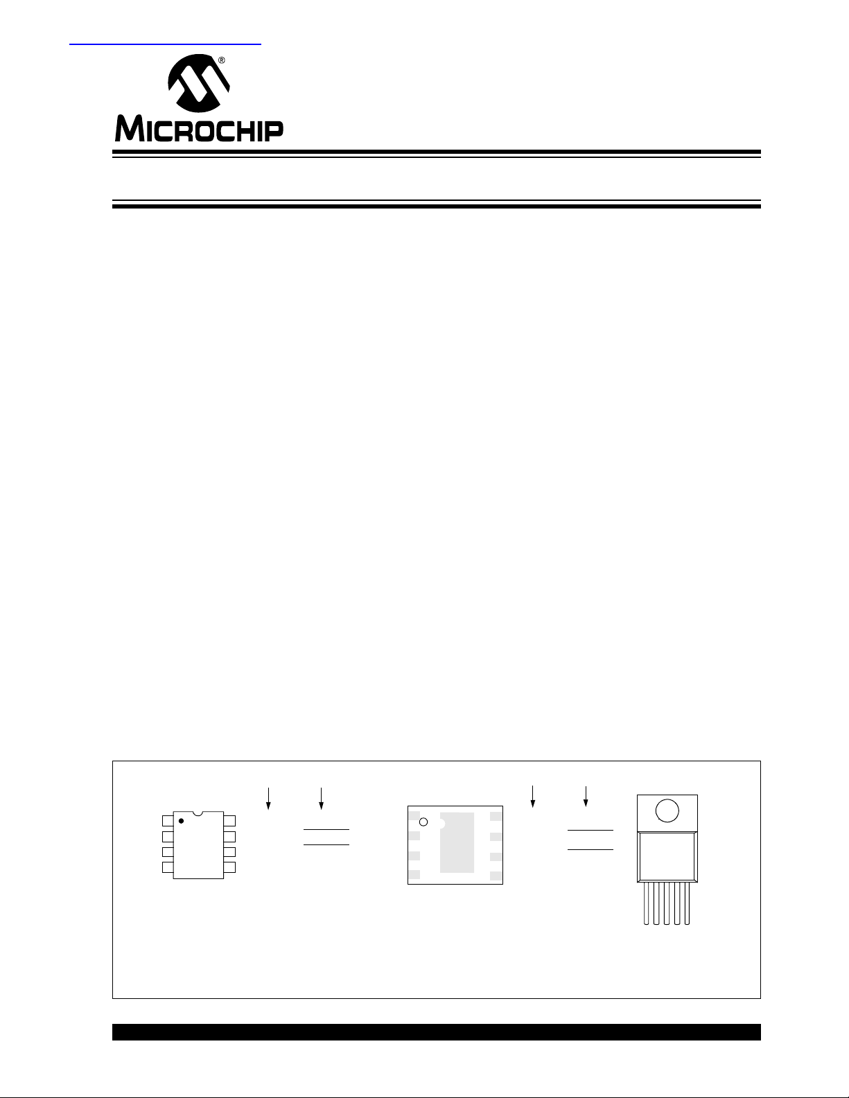
Package Types
8-Pin CERDIP/
(1)
TC4420 TC4429
PDIP/SOIC
V
1
V
1
DD
TC4420
2
INPUT
TC4429
3
NC
4
GND
Note 1: Duplicate pins must both be connected for proper operation.
2: Exposed pad of the DFN package is electrically isolated.
8
7
6
5
V
DD
OUTPUT
OUTPUT
GND
V
DD
OUTPUT
OUTPUT
GND
DD
INPUT
NC
GND
2
3
4
8-Pin DFN
TC4420
TC4429
(2)
TC4420 TC4429
V
8
DD
7
OUTPUT
6
OUTPUT
5
GND
V
DD
OUTPUT
OUTPUT
GND
5-Pin TO-220
Tab is
Common
to V
TC4420
TC4429
DD
V
GND
GND
INPUT
OUTPUT
DD
2004 Microchip Technology Inc. DS21419C-page 1
TC4420/TC4429
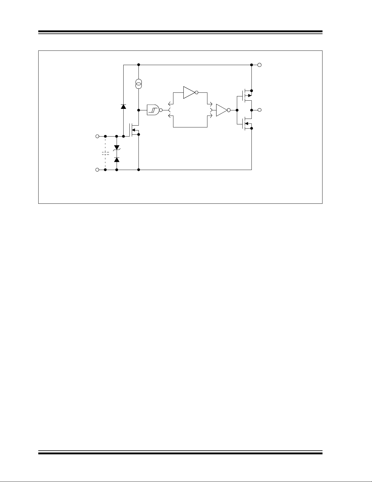
Functional Block Diagram
500 µA
300 mV
TC4429
Inverting
V
DD
Output
Input
GND
TC4420
Non-Inverting
4.7V
Effective
Input
C = 38 pF
DS21419C-page 2 2004 Microchip Technology Inc.
TC4420/TC4429
1.0 ELECTRICAL
CHARACTERISTICS
Absolute Maximum Ratings†
Supply Voltage.....................................................+20V
† Stresses above those listed under “Absolute Maximum
Ratings” may cause permanent damage to the device. These
are stress ratings only and functional operation of the device
at these or any other conditions above those indicated in the
operation sections of the specifications is not implied.
Exposure to Absolute Maximum Rating conditions for
extended periods may affect device reliability.
Input Voltage..................................– 5V to VDD + 0.3V
Input Current (VIN > VDD)...................................50 mA
Power Dissipation (T
≤ 70°C)
A
5-Pin TO-220....................................................1.6W
CERDIP.......................................................800 mW
DFN............................................ ...................Note 2
PDIP............................................................730 mW
SOIC............................................................470 mW
Package Power Dissipation (T
≤ 25°C)
A
5-Pin TO-220 (With Heatsink) ........................12.5W
Thermal Impedances (To Case)
5-Pin TO-220 R
......................................10°C/W
θJ-C
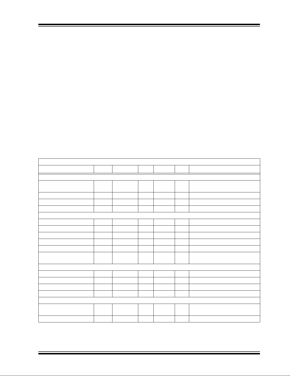
DC CHARACTERISTICS
Electrical Specifications: Unless other wise noted, TA = +25°C with 4.5V ≤ VDD ≤ 18V.
Parameters Sym Min Typ Max Units Conditions
Input
Logic ‘1’, High Input
Voltage
Logic ‘0’, Low Input Voltage V
Input Voltage Range V
Input Current I
Output
High Output Voltage V
Low Output Voltage V
Output Resistanc e, Hi gh R
Output Resistanc e, Low R
Peak Output Current I
Latch-Up Protection
Withstand Reverse Current
Switching Time (Note 1)
Rise Time t
Fall Time t
Delay Time t
Delay Time t
Power Supply
Power Supply Current I
Operating Input Voltage V
Note 1: Switching times ensured by design.
2: Package power dissipation is dependent on the copper pad area on the PCB.
V
I
REV
IH
IL
IN
IN
OH
OL
OH
OL
PK
2.4 1.8 — V
—1.30.8V
–5 — VDD+0.3 V
–10 — +10 µA 0V ≤ VIN ≤ V
VDD – 0.025 — — V DC TEST
— — 0.025 V DC TEST
—2.12.8Ω I
—1.52.5Ω I
—6.0—AV
— > 1.5 — A Duty cycle ≤ 2%, t ≤ 300 µsec
R
F
D1
D2
S
DD
—2535nsFigure 4-1, CL = 2,500 pF
—2535nsFigure 4-1, CL = 2,500 pF
—5575nsFigure 4-1
—5575nsFigure 4-1
—
—
0.45
55
1.5
150
mAµAVIN = 3V
4.5 — 18 V
OUT
OUT
V
DD
= 0V
IN
DD
= 10 mA, VDD = 18V
= 10 mA, VDD = 18V
= 18V
2004 Microchip Technology Inc. DS21419C-page 3
TC4420/TC4429
DC CHARACTERISTICS (OVER OPERATING TEMPERATURE RANGE)
Electrical Specifications: Unless otherwise noted, over operating temperature range with 4.5V ≤ VDD ≤ 18V.
Parameters Sym Min Typ Max Units Conditions
Input
Logic ‘1’, High Input
Voltage
Logic ‘0’, Low Input Voltage V
Input Voltage Range V
Input Current I
Output
High Output Voltage V
Low Output Voltage V
Output Resistanc e, Hi gh R
Output Resistanc e, Low R
Switching Time (Note 1)
Rise Time t
Fall Time t
Delay Time t
Delay Time t
Power Supply
Power Supply Current I
Operating Input Voltage V
Note 1: Switching times ensured by design.
V
IH
IL
IN
IN
OH
OL
OH
OL
R
F
D1
D2
S
DD
2.4 — — V
——0.8V
–5 — VDD + 0.3 V
–10 — +10 µA 0V ≤ VIN ≤ V
VDD – 0.025 — — V DC TEST
— — 0.025 V DC TEST
—35Ω I
—2.35Ω I
—3260nsFigure 4-1, CL = 2,500 pF
—3460nsFigure 4-1, CL = 2,500 pF
—50100nsFigure 4-1
—65100nsFigure 4-1
—
—
0.45
60
3
400
4.5 — 18 V
= 10 mA, VDD = 18V
OUT
= 10 mA, VDD = 18V
OUT
mAµAVIN = 3V
V
= 0V
IN
DD
TEMPERATURE CHARACTERISTICS
Electrical Specifications: Unless otherwise noted, all parameters apply with 4.5V ≤ V
Parameters Sym Min Typ Max Units Conditions
Temperature Ranges
Specified Temperature Range (C) T
Specified Temperature Range (I) T
Specified Temperature Range (E) T
Specified Temperature Range (V) T
Maximum Junction Temperature T
Storage Temperature Range T
Package Thermal Resistances
Thermal Resistance, 5L-TO-220 θ
Thermal Resistance, 8L-CERDIP θ
Thermal Resistance, 8L-6x5 DFN θ
Thermal Resistance, 8L-PDIP θ
Thermal Resistance, 8L-SOIC θ
A
A
A
A
J
A
JA
JA
JA
JA
JA
0—+70°C
–25 — +85 °C
–40 — +85 °C
–40 — +125 °C
— — +150 °C
–65 — +150 °C
—71—°C/W
—150—°C/W
— 33.2 — °C/W Typical four-layer board
—125—°C/W
—155—°C/W
≤ 18V.
DD
with vias to ground plane.
DS21419C-page 4 2004 Microchip Technology Inc.
TC4420/TC4429
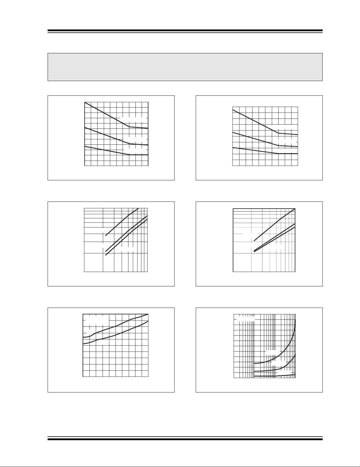
0
2.0 TYPICAL PERFORMANCE CURVES
Note: The graphs and ta bles provided followi ng thi s n ote are a statistical s umm ar y based on a limite d n um ber of
samples and are provided for informational purposes only. The performance characteristics listed herein
are not tested or guaranteed. In some graphs or tables, the data presented may be outside the specified
operating range (e.g., outside specified power supply range) and therefore outside the warranted range.
Note: Unless otherwise indicated, TA = +25°C with 4.5V ≤ VDD ≤ 18V.
120
100
C = 10,000 pF
80
60
Time (nsec)
40
20
0
579111315
Supply Voltage (V)
L
C = 4700 pF
L
C = 2200 pF
L
FIGURE 2-1: Rise Time vs. Supply
Voltage.
100
80
60
V = 5V
1000
DD
V = 12V
DD
Capcitive Load (pF)
V = 18V
DD
10,000
40
Time (nsec)
20
10
100
80
C = 10,000 pF
60
40
Time (nsec)
20
0
57 9111315
Supply Voltage (V)
L
C = 4700 pF
L
C = 2200 pF
L
FIGURE 2-4: Fall Time vs. Supply
Voltage.
100
80
60
40
V = 5V
DD
V = 12V
Time (nsec)
20
10
1000
DD
Capacitive Load (pF)
V = 18V
DD
10,00
FIGURE 2-2: Rise Time vs. Capacitive
Load.
50
C = 2200 pF
L
V = 18V
DD
40
t
D2
30
20
Delay Time (nsec)
10
0
t
D1
–60 –20 20 60 100
TA (°C)
140
FIGURE 2-3: Propagation Delay Time vs.
Temperature.
FIGURE 2-5: Fall Time vs. Capacitive
Load.
84
V = 15V
DD
70
56
42
28
Supply Current (mA)
14
0
0 100 1000
500 kHz
200 kHz
Capacitive Load (pF)
20 kHz
10,000
FIGURE 2-6: Supply Current vs.
Capacitive Load.
2004 Microchip Technology Inc. DS21419C-page 5
TC4420/TC4429
5
Note: Unless otherwise indicated, TA = +25°C with 4.5V ≤ VDD ≤ 18V.
50
C = 2200 pF
L
V = 18V
DD
40
30
20
Time (nsec)
10
0
t
FALL
t
RISE
–60 –20 20 60 100
TA (°C)
140
FIGURE 2-7: Rise and Fall Times vs.
Temperature.
65
60
55
t
50
45
Delay Time (nsec)
40
35
4 6 81012141618
D2
t
D1
Supply Voltage (V)
5
100 mA
10 mA
5913
7111
50 mA
Supply Voltage (V)
OUT
R ( )Ω
4
3
2
FIGURE 2-10: High-State Output
Resistance vs Supply Voltage.
200
Load = 2200 pF
160
120
Input 2.4V
Input 3V
80
Delay Time (nsec)
40
0
Input 5V
Input 8V and 10V
567 11 13
8 9 10 12 14
V (V)
DD
15
FIGURE 2-8: Propagation Delay Time vs.
Supply Voltage.
1000
C = 2200 pF
L
100
10
Supply Current (mA)
0
0 100 1000
Frequency (kHz)
18V
10V
5V
10,000
FIGURE 2-9: Supply Current vs.
Frequency.
FIGURE 2-11: Effect of Input Amplitude on
Propagation Delay.
2.5
2
OUT
R ( )Ω
1.5
1
5913
71115
Supply Voltage (V)
100 mA
50 mA
10 mA
FIGURE 2-12: Low-State Output
Resistance vs. Supply Voltage.
DS21419C-page 6 2004 Microchip Technology Inc.

Note: Unless otherwise indicated, TA = +25°C with 4.5V ≤ VDD ≤ 18V.
4
-8
3
2
1
Crossover Area (A•S) x 10
0
567 11 13
8 9 10 12 14
Supply Voltage (V)
15
The values on this graph represent the loss seen
by the driver during one complete cycle. For a
single transition, divide the value by 2.
FIGURE 2-13: Crossover Energy.
TC4420/TC4429
2004 Microchip Technology Inc. DS21419C-page 7

TC4420/TC4429
3.0 PIN DESCRIPTIONS
The descriptions of the pins are listed in Table 3-1.
TABLE 3-1: PIN FUNCTION TABLE
Pin No.
8-Pin CERDIP/
PDIP/SOIC
11—VDDSupply input, 4.5V to 18V
2 2 1 INPUT Control input, TTL/CMOS compatible input
3 3 — NC No Connection
4 4 2 GND Ground
5 5 4 GND Ground
6 6 5 OUTPUT CMOS push-pull output
7 7 — OUTPUT CMOS push-pull output
883V
—PAD— NCExposed Metal Pad
——TABV
3.1 Supply Input (VDD)
The VDD input is the bias supp ly for the MO SFET driver
and is rated for 4.5V to 18V with respect to the ground
pins. The VDD input should be bypassed to ground with
a local ceram ic capacitor. The value of the capacito r
should be chos en base d on the capaciti ve load th at is
being driven. A minimum val ue of 1. 0µF is suggested.
Pin No.
8-Pin DFN
Pin No.
5-Pin TO-220
Symbol Description
DD
DD
Supply input, 4.5V to 18V
Metal Tab is at the VDD Potential
3.3 CMOS Push-Pull Output
The MOSFET driver output is a low-impedance,
CMOS, push-pull style output capable of driving a
capacitive load with 6.0A peak currents. The MOSFET
driver output is capable of withstanding 1.5A peak
reverse currents of either polarity.
3.4 Ground
3.2 Control Input
The MOSFET driver input is a high-impedance,
TTL/CMOS compatible input. The input circuitry of the
TC4420/TC4429 MOSFET driver also has a “speedup” capacitor. This helps to decrease the propagation
delay times of the driver. Because of this, input signals
with slow rising or falling edges should not be us ed, a s
this can result in double-pulsing of the MOSFET driver
output.
The ground pins are the return path for the bias current
and the high peak currents that discharge the load
capacitor . The ground pins sh ould be tie d into a g round
plane or have very short traces to the bias supply
source return.
3.5 Exposed Metal Pad
The exposed met al p ad of the 6x5 DFN pac ka ge i s n ot
internally connected to any potential. Therefore, this
pad can be connected to a ground plane or other
copper plane on a printed circuit board (PCB) to aid in
heat removal from the package.
DS21419C-page 8 2004 Microchip Technology Inc.

4.0 APPLICATIONS INFORMATION
TC4420/TC4429
+5V
Input
V
0.1 µF
Input
= 18V
DD
4.7 µF
18
0.1 µF
26
Output
7
CL = 2,500 pF
+18V
Output
+5V
0V
0V
10%
Input
54
0V
10%
+18V
Input: 100 kHz,
square wave,
t
= t
RISE
FALL
≤ 10 ns
Output
0V
Note: Pinout shown is for the PDIP, SOIC, DFN and CERDIP packages.
t
D1
t
F
90%
10%
Inverting Driver
TC4429
90%
t
D1
t
R
10%
Non-Inverting Driver
TC4420
t
D2
90%
t
D2
90%
10%
t
R
10%
90%
90%
t
F
FIGURE 4-1: Switching Time Test Circuits.
2004 Microchip Technology Inc. DS21419C-page 9

TC4420/TC4429
5.0 PACKAGING INFORMATION
5.1 Package Marking Information
5-Lead TO-220
XXXXXXXXX
XXXXXXXXX
YYWWNNN
8-Lead CERDIP (300 mil)
XXXXXXXX
XXXXXNNN
YYWW
8-Lead DFN
Example:
TC4420CAT
0419256
Example:
TC4420
MJA256
Example
0419
:
XXXXXXX
XXXXXXX
XXYYWW
NNN
Legend: XX...X Customer specific information*
YY Year code (last 2 digits of calendar year)
WW Week code (week of January 1 is week ‘01’)
NNN Alphanumeric traceability code
Note: In the event the full Microchip part numbe r cannot be marke d on one li ne, it wi ll
be carried over to the next line thus limiti ng the number of available chara ct ers
for customer specific information.
* Standard OTP marking consists of Microchip part number, year code, week code, and traceability code.
TC4420
EMF
0419
256
DS21419C-page 10 2004 Microchip Technology Inc.

Package Marking Information (Continued)
TC4420/TC4429
8-Lead PDIP (300 mil)
XXXXXXXX
XXXXXNNN
YYWW
8-Lead SOIC (150 mil)
XXXXXXXX
XXXXYYWW
NNN
Example:
TC4420
CPA256
0419
Example:
TC4420
EOA0419
256
2004 Microchip Technology Inc. DS21419C-page 11

TC4420/TC4429
5-Lead Plastic Transistor Outline (AT) (TO-220)
L H1
b
Q
e1
e3
e
EJECTOR PIN
C1
J1
D
Units
Dimension Limits
Lead Pitch
Overall Lead Centers e1 .263
Space Between Leads e3 .030 1.02.040 0.76
Overall Height
Overall Width
Overall Length D
Flag Length H1 .234 6.55.258 5.94
Flag Thickness F .045 1.40.055 1.14
Through Hole Center
Through Hole Diameter P .146 .156 3.71 3.96
Lead Length
Lead Thickness
Lead Width
Mold Draft Angle
*Controlling Parameter
Notes:
Dimensions D and E1 do not include mold flash or protrusions. Mold flash or
protrusions shall not exceed .010" (0.254mm) per side.
JEDEC equivalent: TO-220
Drawing No. C04-036
e
A
E
Q
L
J1Base to Bottom of Lead .090 2.29.115 2.92
C1
b
a
E
ØP
(5X)
a
A
F
INCHES*
MIN
.060
.160 4.06
.385
.560
.103 2.87.113 2.62
.540
.014
3° 7° 3° 7°
.072 1.52 1.83
.273 6.68 6.93
.190
.415 9.78 10.54
.590 14.22 14.99
.560 13.72
.022 0.36 0.56
MILLIMETERS
MINMAX
MAX
4.83
14.22
1.020.64.040.025
DS21419C-page 12 2004 Microchip Technology Inc.

8-Lead Ceramic Dual In-line – 300 mil (JA) (CERDIP)
E1
2
TC4420/TC4429
n
E
eB
Number of Pins
Pitch
Standoff §
Ceramic Pkg. Width
Lead Thickness
Upper Lead Width
Overall Row Spacing
*Controlling Parameter
JEDEC Equivalent: MS-030
Drawing No. C04-010
1
D
A2
A
c
L
B1
A1
MINDimension Limits
n
p
A1
E1
c
B1
eB
B
NOM
p
MILLIMETERSINCHES*Units
MINMAX
NOM
2.54.100
MAX
88
5.084.574.06.200.180.160ATop to Seating Plane
1.020.770.51.040.030.020
8.137.757.37.320.305.290EShoulder to Shoulder Width
7.626.735.84.300.265.230
10.169.789.40.400.385.370DOverall Length
5.084.133.18.200.163.125LTip to Seating Plane
0.380.290.20.015.012.008
1.651.401.14.065.055.045
0.510.460.41.020.018.016BLower Lead Width
10.169.158.13.400.360.320
2004 Microchip Technology Inc. DS21419C-page 13

TC4420/TC4429
8-Lead Plastic Dual Flat No Lead Package (MF) 6x5 mm Body (DFN-S) – Saw Singulated
DS21419C-page 14 2004 Microchip Technology Inc.

8-Lead Plastic Dual In-line (PA) – 300 mil (PDIP)
E1
D
2
TC4420/TC4429
n
E
β
eB
Number of Pins
Pitch
Top to Seating Plane A .140 .155 .170 3.56 3.94 4.32
Molded Package Thickness A2 .115 .130 .145 2.92 3.30 3.68
Base to Seating Plane A1 .015 0.38
Shoulder to Shoulder Width E .300 .313 .325 7.62 7.94 8.26
Molded Package Width E1 .240 .250 .260 6.10 6.35 6.60
Overall Length D .360 .373 .38 5 9.14 9.46 9.78
Tip to Seating Plan e L .125 .130 .135 3.18 3.30 3.43
Lead Thickness
Upper Lead Width
Lower Lead Width B .014 .018 .022 0.36 0.46 0.56
Overall Row Spacing §
Mold Draft Angle Top
Mold Draft Angle Bottom
* Controlling Parameter
§ Significant Characteristic
Notes:
Dimensions D and E1 do not include mold flash or protrusions. Mold flash or protrusions shall not exceed
.010” (0.254mm) per side.
JEDEC Equivalent: MS-001
Drawing No. C04-018
Dimension Limits MIN NOM MAX MIN NOM MAX
1
α
A
c
Units INCHES* MILLIMETERS
n
p
c
B1
eB
α
β
.008 .012 .015 0.20 0.29 0.38
.045 .058 .070 1.14 1.46 1.78
.310 .370 .430 7.87 9.40 10.92
A1
B1
B
88
.100 2.54
5 10 15 5 10 15
5 10 15 5 10 15
A2
L
p
2004 Microchip Technology Inc. DS21419C-page 15

TC4420/TC4429
8-Lead Plastic Small Outline (OA) – Narrow, 150 mil (SOIC)
E
E1
p
D
2
B
Number of Pins
Pitch
Foot Angle
Lead Thickness
Mold Draft Angle Top
Mold Draft Angle Bottom
* Controlling Parameter
§ Significant Characteristic
Notes:
Dimensions D and E1 do not include mold flash or protrusions. Mold flash or protrusions shall not exceed
.010” (0.254mm) per side.
JEDEC Equivalent: MS-012
Drawing No. C04-057
n
45°
c
β
n
p
φ
c
α
β
1
h
A
φ
L
048048
A1
MILLIMETERSINCHES*Units
1.27.050
α
A2
MAXNOMMINMAXNOMMINDimension Limits
88
1.751.551.35.069.061.053AOverall Height
1.551.421.32.061.056.052A2Molded Package Thickness
0.250.180.10.010.007.004A1Standoff §
6.206.025.79.244.237.228EOverall Width
3.993.913.71.157.154.146E1Molded Package Width
5.004.904.80.197.193.189DOverall Length
0.510.380.25.020.015.010hChamfer Distance
0.760.620.48.030.025.019LFoot Length
0.250.230.20.010.009.008
0.510.420.33.020.017.013BLead Width
1512015120
1512015120
DS21419C-page 16 2004 Microchip Technology Inc.

TC4420/TC4429
PRODUCT IDENTIFICATION SYSTEM
To order or obtain information, e.g., on pricing or delivery, refer to the factory or the listed sales office.
PART NO. X XX
Device
PackageTemperature
Range
Device: TC4420: 6A High-Speed MOSFET Driver, Non-Inverting
Temperature Range: C = 0°C to +70°C (PDIP, SOIC, and TO-220 Only)
Package: AT = TO-220, 5-lead (C-Temp Only)
PB Free G = Lead-Free device*
TC4429: 6A High-Speed MOSFET Driver, Inverting
I = -25°C to +85°C (CERDIP Only)
E = -40°C to +85°C
V = -40°C to +125°C
JA = Ceramic Dual In-line (300 mil Body), 8-lead
MF = Dual, Flat, No-Lead (6X5 mm Body), 8-lead
MF713 = Dual, Flat, No-Lead (6X5 mm Body), 8-lead
PA = Plastic DIP (300 mil Body), 8-lead
OA = Plastic SOIC, (150 mil Body), 8-lead
OA713 = Plastic SOIC, (150 mil Body), 8-lead
* Available on selected packages. Contact your local sales
(I-Temp Only)
(Tape and Reel)
(Tape and Reel)
= Blank
representative for availability
XXX
Tape and
Reel
X
PB Free
Examples:
a) TC4420CAT: 6A High-Speed MOSFET
b) TC4420EOA:
c) TC4420VMF:
a) TC4429CAT:
Driver, Inverting,
b) TC4429EPA:
c) TC4429VMF:
Driver, Inverting,
Driver, Non-inverting,
TO-220 package,
0°C to +70°C.
6A High-Speed MOSFET
Driver, Non-inverting,
SOIC package,
-40°C to +85°C.
6A High-Speed MOSFET
Driver, Non-inverting,
DFN package,
-40°C to +125°C.
6A High-Speed MOSFET
TO-220 package,
0°C to +70°C
6A High-Speed MOSFET
Driver, Inverting,
PDIP package,
-40°C to +85°C
6A High-Speed MOSFET
DFN package,
-40°C to +125°C
Sales and Support
Data Sheets
Products supported by a preliminary Data Sheet may have an errata sheet describing minor operational differences and
recommended workarounds. To determine if an errata sheet exists for a particular device, please contact one of the following:
1. Your local Microchip sales office
2. The Microchip Corporate Literature Center U.S. FAX: (480) 792-7277
3. The Microchip Worldwide Site (www.microchip.com)
Please specify which device, revision of silicon and Data Sheet (include Literature #) you are using.
Customer Notification System
Register on our web site (www.microchip.com/cn) to receive the most current information on our products.
2004 Microchip Technology Inc. DS21419C-page 17

TC4420/TC4429
NOTES:
DS21419C-page 18 2004 Microchip Technology Inc.

Note the following details of the code protection feature on Microchip devices:
• Microchip products meet the specification contained in their particular Microchip Data Sheet.
• Microchip believes that its family of products is one of the most secure families of its kind on the market today, when used i n the
intended manner and under normal conditions.
• There are dishonest and possibly illegal methods used to breach the code protection feature. All of these methods, to our
knowledge, require using the Microchip products in a manner outside the operating specifications contained in Microchip’s Data
Sheets. Most likely, the person doing so is engaged in theft of intellectual property.
• Microchip is willing to work with the customer who is concerned about the integrity of their code.
• Neither Microchip nor any other semiconductor manufacturer can guarantee the security of their code. Code protection does not
mean that we are guaranteeing the product as “unbreakable.”
Code protection is constantly evolving. We at Microchip are com mitted to continuously improving the code protect ion f eatures of our
products. Attempts to break Microchip’s code protection feature may be a violation of the Digit al Mill ennium Copyright Act. If such acts
allow unauthorized access to your software or other copyrighted work, you may have a right to sue for relief under that Act.
Information contained in this publication regarding device
applications and the like is intended through suggestion only
and may be superseded by updates. It is your responsibility to
ensure that your application meets with your specifications.
No representation or warranty is given and no liability is
assumed by Microchip Technology Incorporated with respect
to the accuracy or use of such information, or infringement of
patents or other intellectual property rights arising from such
use or otherwise. Use of Microchip’s products as critical
components in life support systems is not authorized except
with express written approval by Microchip. No licenses are
conveyed, implicitly or otherwise, under any intellectual
property rights.
Trademarks
The Microchip name and logo, the Microchip logo, Accuron,
dsPIC, K
EELOQ, microID, MPLAB, PIC, PICmicro,
PICSTART, PRO MATE, PowerSmart, rfPIC, and
SmartShunt are registered trademarks of Microchip
Technology Incorporated in the U.S.A. and other countries.
AmpLab, FilterLab, MXDEV, MXLAB, PICMASTER, SEEVAL,
SmartSensor and The Embedded Control Solutions Company
are registered trademarks of Microchip Technology
Incorporated in the U.S.A.
Analog-for-the-Digital Age, Application Maestro, dsPICDEM,
dsPICDEM.net, dsPICworks, ECAN, ECONOMONITOR,
FanSense, FlexROM, fuzzyLAB, In-Circuit Serial
Programming, ICSP, ICEPIC, Migratable Memory, MPASM ,
MPLIB, MPLINK, MPSIM, PICkit, PICDEM, PICDEM.net,
PICLAB, PICtail, PowerCal, PowerInfo, PowerMate,
PowerTool, rfLAB, rfPICDEM, Select Mode, Smart Serial,
SmartTel and Total Endurance are trademarks of Microchip
Technology Incorporated in the U.S.A. and other countries.
SQTP is a service mark of Microchip T echnology Incorporated
in the U.S.A.
All other trademarks mentioned herein are property of their
respective companies.
© 2004, Microchip Technology Incorporated, Printed in the
U.S.A., All Rights Reserved.
Printed on recycled paper.
Microchip received ISO/TS-16949:2002 quality system certification for
its worldwide headquarters, design and wafer fabrication facilities in
Chandler and Tempe, Arizona and Mountain View, California in
October 2003. The Company’s quality system processes and
procedures are for its PICmicro
devices, Serial EEPROMs, microperipherals, nonvolatile memory and
analog products. In addition, Microchip’s quality system for the design
and manufacture of development systems is ISO 9001:2000 certified.
®
8-bit MCUs, KEELOQ
®
code hopping
2004 Microchip Technology Inc. DS21419C-page 19

WORLDWIDE SALES AND SERVICE
AMERICAS
Corporate Office
2355 West Chandler Blvd.
Chandler, AZ 85224-6199
Tel: 480-792-7200
Fax: 480-792-7277
Technical Support:
480-792-7627
Web Address:
www.microchip.com
Atlanta
Alpharetta, GA
Tel: 770-640-0034
Fax: 770-640-0307
Boston
Westford, MA
Tel: 978-692-3848
Fax: 978-692-3821
Chicago
Itasca, IL
Tel: 630-285-0071
Fax: 630-285-0075
Dallas
Addison, TX
Tel: 972-818-7423
Fax: 972-818-2924
Detroit
Farmington Hills, MI
Tel: 248-538-2250
Fax: 248-538-2260
Kokomo
Kokomo, IN
Tel: 765-864-8360
Fax: 765-864-8387
Los Angeles
Mission Viejo, CA
Tel: 949-462-9523
Fax: 949-462-9608
San Jose
Mountain View, CA
Tel: 650-215-1444
Fax: 650-961-0286
Toronto
Mississauga, Ontario,
Canada
Tel: 905-673-0699
Fax: 905-673-6509
ASIA/PACIFIC
Australia - Sydney
Tel: 61-2-9868-6733
Fax: 61-2-9868-6755
China - Beijing
Tel: 86-10-8528-2100
Fax: 86-10-8528-2104
China - Chengdu
Tel: 86-28-8676-6200
Fax: 86-28-8676-6599
China - Fuzhou
Tel: 86-591-750-3506
Fax: 86-591-750-3521
China - Hong Kong SAR
Tel: 852-2401-1200
Fax: 852-2401-3431
China - Shanghai
Tel: 86-21-6275-5700
Fax: 86-21-6275-5060
China - Shenzhen
Tel: 86-755-8290-1380
Fax: 86-755-8295-1393
China - Shunde
Tel: 86-757-2839-5507
Fax: 86-757-2839-5571
China - Qingdao
Tel: 86-532-502-7355
Fax: 86-532-502-7205
ASIA/PACIFIC
India - Bangalore
Tel: 91-80-2229-0061
Fax: 91-80-2229-0062
India - New Delhi
Tel: 91-1 1-5160-8632
Fax: 91-11-5160-8632
Japan - Kanagawa
Tel: 81-45-471- 6166
Fax: 81-45-471-6122
Korea - Seoul
Tel: 82-2-554-7200
Fax: 82-2-558-5932 or
82-2-558-5934
Singapore
Tel: 65-6334-8870
Fax: 65-6334-8850
Taiwan - Kaohsiung
Tel: 886-7-536-4816
Fax: 886-7-536-4817
Taiwan - Taipei
Tel: 886-2-2500-6610
Fax: 886-2-2508-0102
Taiwan - Hsinchu
Tel: 886-3-572-9526
Fax: 886-3-572-6459
EUROPE
Austria - Weis
Tel: 43-7242-2244-399
Fax: 43-7242-2244-393
Denmark - Ballerup
Tel: 45-4420-9895
Fax: 45-4420-9910
France - Massy
Tel: 33-1-69-53-63-20
Fax: 33-1-69-30-90-79
Germany - Ismaning
Tel: 49-89-627-144-0
Fax: 49-89-627-144-44
Italy - Milan
Tel: 39-0331-742611
Fax: 39-0331-466781
Netherlands - Drunen
Tel: 31-416-690399
Fax: 31-416-690340
England - Berkshire
Tel: 44-118-921-5869
Fax: 44-118-921-5820
08/24/04
DS21419C-page 20 2004 Microchip Technology Inc.
 Loading...