

TC14433/A
3-1/2 Digit, Analog-to-Digital Converter
Features
• Accuracy: ±0.05% of Reading ±1 Count
• Two Voltage Ranges: 1.999V and 199.9 mV
• Up to 25 Conversions Per Second
> 1000M Ohms
•Z
IN
• Single Positive Voltage Reference
• Auto-Polarity and Auto-Zero
• Overrange and Underrange Signals Available
• Operates in Auto-Ranging Circuits
• Uses On-Chip System Clock or External Clock
• Wide Supply Range: ±4.5V to ±8V
Applications
• PortableInstruments
• Digital Voltmeters
• Digital Panel Meters
• Digital Scales
• Digital Thermometers
• Remote A/D Sensing Systems
• MPU Systems
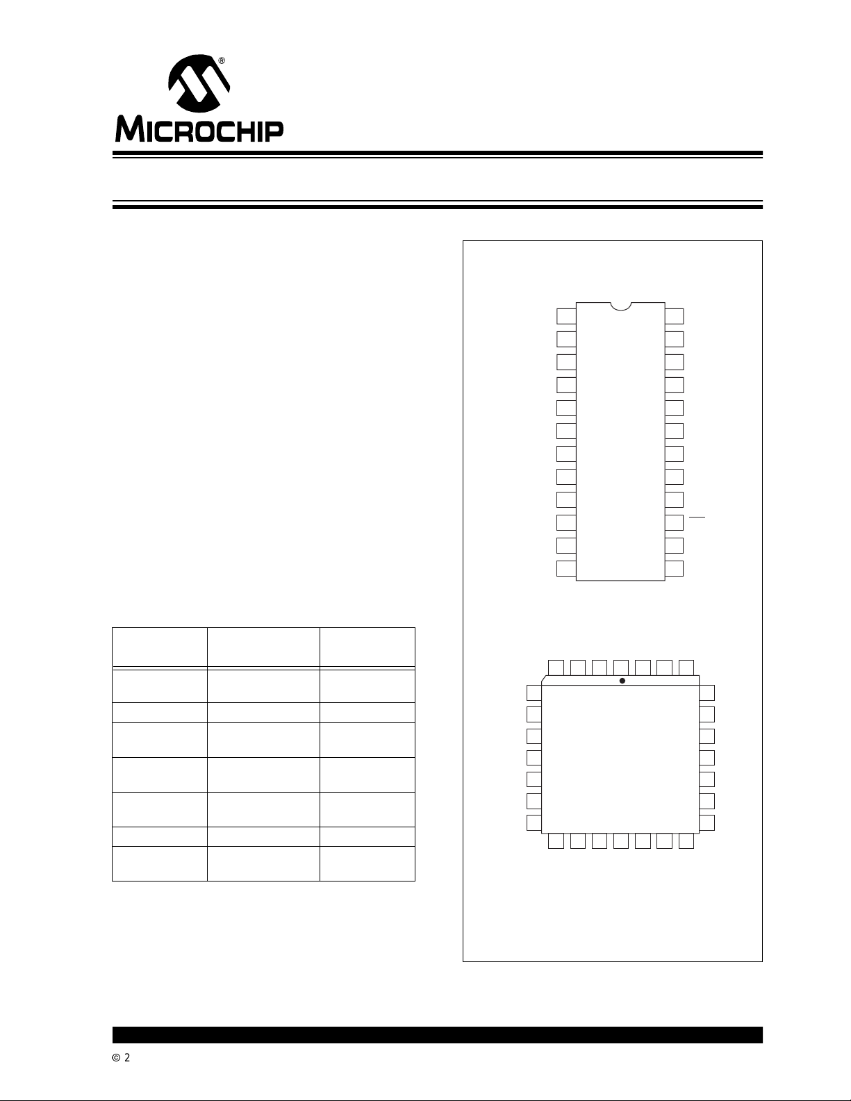
Device Selection Table
Package Type
24-Pin CERDIP (Wide)
V
AG
V
REF
V
X
R
1
R1/C
1
C
1
CO
1
CO
2
DU
CLK1
CLK0
V
EE
24-Pin PDIP (Wide)
24-Pin SOIC (Wide)
1
2
3
4
5
TC14433/A
6
7
8
9
10
11
12
24
23
22
21
20
19
18
17
16
15
14
13
28-Pin PLCC
V
DD
Q
3
Q
2
Q
1
Q
0
DS
DS
DS
DS
OR
EOC
V
SS
1
2
3
4
Part Num ber Package
TC14433AEJG 24-Pin CERDIP
Temperature
Range
-40°C to +85°C
(Wide)
TC14433AELI 28-Pin PLCC -40°C to +85°C
TC14433AEPG 24-Pin PDIP
-40°C to +85°C
(Wide)
TC14433COG 24-Pin SOIC
0°C to +70°C
(Wide)
TC14433EJG 24-Pin CERDIP
-40°C to +85°C
(Wide)
TC14433ELI 28-Pin PLCC -40°C to +85°C
TC14433EPG 24-Pin PDIP
-40°C to +85°C
(Wide)
3
EOC
2
Q
OR
25
24
23
22
21
20
19
Q
Q
DS
DS
DS
DS
1
0
1
2
3
4
REF
X
V
4 3 2 1 27 2628
R
5
1
R1/C
6
1
C
7
1
8
NC NC
CO
9
1
CO
10
2
11
DU
12 13 14 15 17 18
CLK1
Note 1: NC = No internal connection (In 28-Pin PLCC).
2: 24-Pin SOIC (Wide) package, only for
TC14433 device.
AG
V
NC
V
TC14433/A
16
EE
NC
V
CLK0
VDDQ
SS
V
2002 Microchip TechnologyInc. DS21394B-page 1
TC14433/A
General Description
The TC14433 is a low power, high performance,
monolithic CMOS 3-1/2 di git A/D converter. The
TC14433 combines both analog and digital circuits on
a single IC, thus minimizing the number of external
components.
This dual slope A/D converter provides automatic
polarity and zero correction with the addition of two
external resistors and two capacitors. The full scale
voltage range of this ratiometric IC extends from 199.9
millivolts to 1.999volts.TheTC14433can operateover
a wide range of power supply voltages, including
batteries and standard 5-volt supplies.
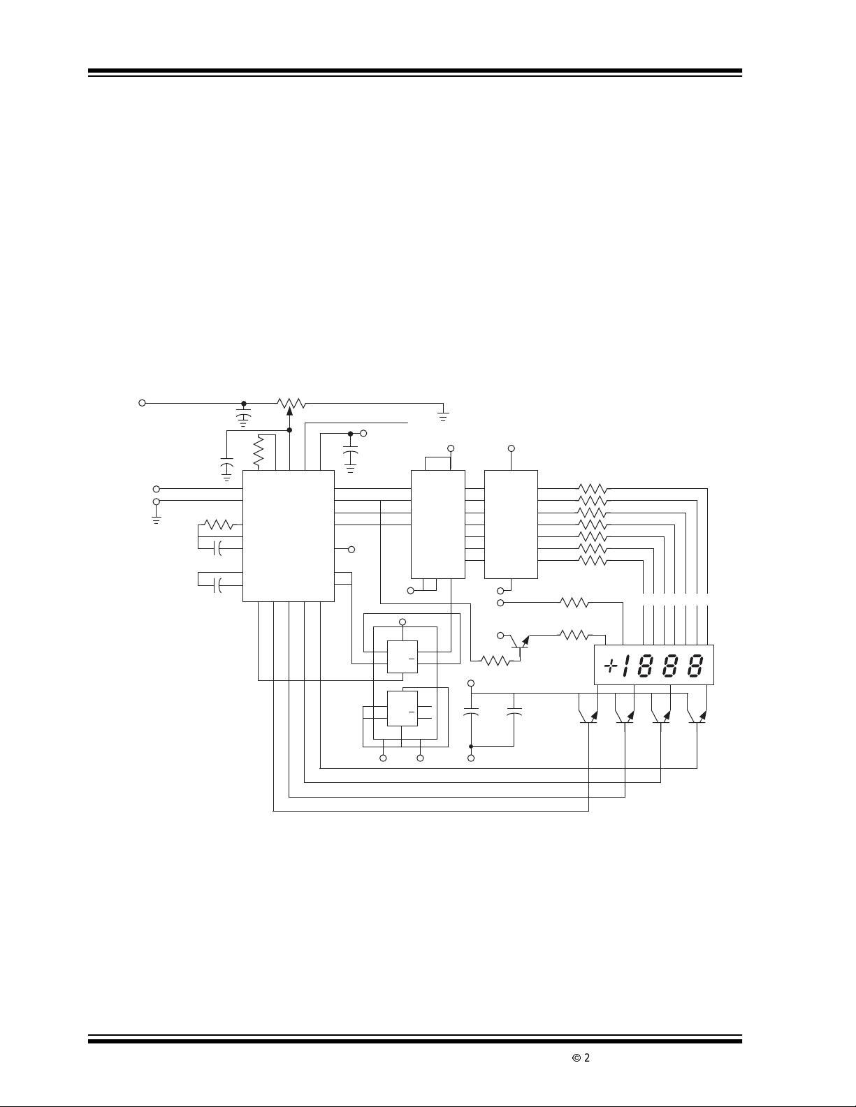
Typical Application
MCP1525
+5V
1µF
V
X
0.1µF**
0.1µF**
*R
= 470kΩ for 2V Range
1
R
= 27kΩ for 200mV Range
1
**Mylar Capacitor
300k
R
*
R
1
20k
1µF
C
11 10 2 12 24
3
1
4
TC14433
5
6
7
8
19 18 17 16
15
DS
DS
1
DS
2
23
22
21
20
13
9
14
14013B
DS
3
+5V
0.1
-5V
5
3
4
9
11
-5V
4
The TC14433A features improved performance over
the industry standard TC14433. Rollover, which is the
measurement of identical positive and negative
signals, i s specified to have the same reading within
one count f or the TC14433A. Power consumption of
the TC14433A is typically 4mW, approximately onehalf that of the industry standard TC14433.
The TC14433/A is available in 24-Pin PDIP, 24- Pin
CERDIP, 24-Pin SOI C (TC14433 device only), and
28-Pin PLCC packages.
-5V
+5V
0.1µF
1
16
4
2
3
5
4543B
8
67
-5V
-5V
6
1
S
Q
D
2
Q
C
R
8
S
13
Q
D
12
Q
C
R
714
10
+5V
10
11
12
13
14
15
9
+5V
+5V
7
6
5
4
3
2
1
1413
-5V
-5V
MPS-A12
-5V
51k
50µF
-5V
10
11
12
13
14
15
16
Minus Sign
Common
Anode Led
Display
0.1µF
MPS-A12
Segment
Resistors
150Ω (7)
200Ω
(4)
fgedcba
DS21394B-page 2
2002 Microchip TechnologyInc.
TC14433/A
1.0 ELECTRICAL
CHARACTERISTICS
Absolute Maximum Ratings*
Supply Voltage (VDD–VEE)................... -0.5V to +18V
*Stresses above those listed under "Absolute Maximum
Ratings" may cause permanent damage to the device. These
are stress ratings only and functional operation of the device
at these or any other conditions above those indicated in the
operation sections of the specifications is not implied.
Exposure to Absolute Maximum Rating conditions for
extended periods may affectdevice reliability.
Voltage on Any Pin:
ReferencetoV
.....................-0.5V to (VDD+0.5)
EE
DC Current, Any Pin: ........................................ ±10mA
Power Dissipation (T
≤ 70°C):
A
Plastic PLCC .................................................1.0W
Plastic PDIP.................................................. 940W
SOIC.............................................................940W
CERDIP .......................................................1.45W
Operating Temperature Range ...............0°C to +70°C
StorageTemperature Range..............-65°Cto +160°C
TC14433/A ELECTRIC AL SPECIFICATIONS
Electrical Characteristics: VDD=+5V,VEE=-5V,C1=0.1µF,(Mylar), C0=0.1µF, RC=300kΩ,R1=470kΩ @V
R
=27kΩ @V
1
Symbol Parameter Min Typ Max Min Typ Max Units Test Conditions
Analog Input T
SYE Rollover Error (Positive) and
Negative Full Scale
Symmetry
NL LinearityOutput Reading
(Note 1)
SOR Stability Output Reading
(Note 2)
ZOR Zero Output Reading — 0 0 ———LSD V
I
IN
CMRR Common mode Rejection — 65 — — —— dB V
Note 1: Accuracy - The accuracyof the meter at full scale is the accuracy of the setting of the referencevoltage. Zero is
Bias Current: Analog Input
recalculated during each conversion cycle. The meaningful specification is linearity. In other words, the deviation from
correct reading for all inputsother than positive full scaleand zero is definedas the linearity specification.
2: The LSD stability for 200mV scale is defined as the range that the LSD will occupy 95% of the time.
3: Pinnumbersreferto24-pinPDIP.
= 200mV, unless otherwise specified.
REF
-1 — +1 — — — Counts 200mV Full Scale
-0.05 +0.05 +0.05 — — — %rdg V
-1 count — +1 count — — — %rdg V
—— 2———LSDV
—— 3———LSDV
—
Reference Input
AnalogGround
—
—
= +25°C
A
±20
±20
±20
±100 —
±100 —
±100 —
=+25°C
T
A
—
—— pA
—— pA
V
V
V
—
pA
F
REF
IN-VIN
=2V
REF
=200mV
REF
=1.99V,
X
=2V
REF
=199mV,
X
=200mV
REF
=0V,V
X
=1.4V,V
X
=32kHz
OC
=2V,
=+V
REF
IN
=2V
REF
=2V,
2002 Microchip TechnologyInc. DS21394B-page 3
TC14433/A
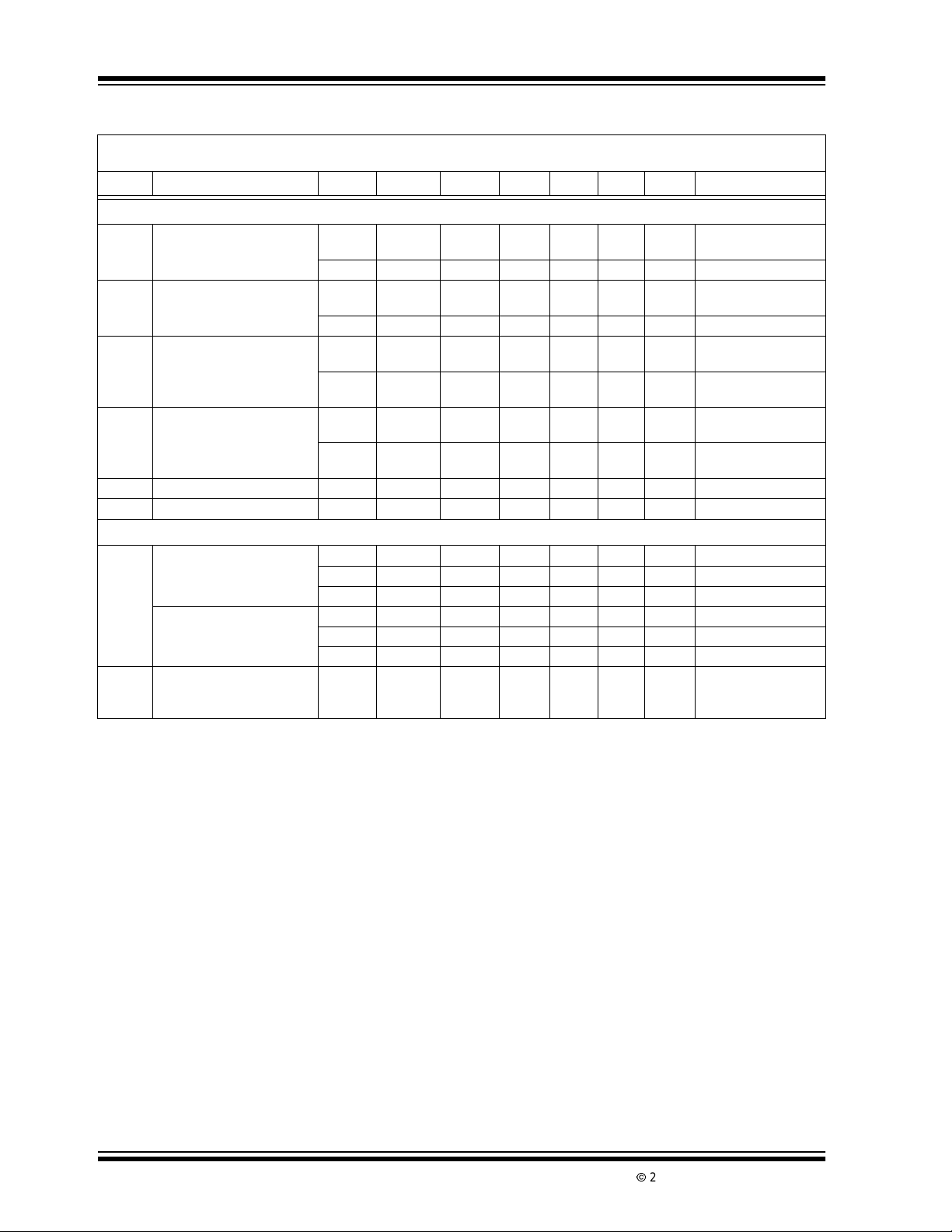
TC14433/A ELECTRICA L SPECIFICATIONS (CONTINUED)
Electrical Characteristics: VDD=+5V,VEE=-5V,C1=0.1µF,(Mylar), C0=0.1µF, RC=300kΩ,R1=470kΩ @V
R
=27kΩ @V
1
= 200mV, unless otherwise specified.
REF
Symbol Parameter Min Typ Max Min Typ Max Units Test Conditions
Digital
V
OL
Output Voltage
— 0 0.05 — — 0.05 V VSS= 0 V, "0" Level
(Pins14to23)(Note 3)
— -5 -4.95 — — -4.95 V V
V
OH
Output Voltage
4.95 5 — 4.95 — — V VSS= 0V, "1" Level
(Pins14to23)(Note 3)
4.95 5 — 4.95 — — V V
I
OH
Output Current
(Pins14to23)
-0.2 -0.36 — -0.14 — — mA VSS=0V,VOH=4.6V
Source
- 0.5 -0.9 — -0.35 — — mA V
Source
I
OL
Output Current
(Pins14to23)
0.51 0.88 — 0.36 — — mA VSS=0V,VOL=0.4V
Sink
1.3 2.25 — 0.9 — — mA V
V
f
CLK
I
DU
Clock Frequency — 66 — — — — kHzRC=300kΩ
Input Current -DU — ±0.00001 ±0.3 — — ±1 µA
Power
I
Q
Quiescent Current: 14433A: — — — — — — — VDDto VEE,ISS=0
— 0.4 2 — — 3.7 mA V
— 1.4 4 — — 7.4 mA V
Quiescent Current: 14433: — — — — — — — V
— 0.9 2 — — 3.7 mA V
— 1.8 4 — — 7.4 mA V
PSRR Supply Rejection — 0.5 — — — — mV/V V
V
V
Note 1: Accuracy - The accuracyof the meter at full scale is the accuracy of the setting of the referencevoltage. Zero is
recalculated during each conversion cycle. The meaningful specification is linearity. In other words, the deviation from
correct reading for all inputsother than positive full scaleand zero is definedas the linearity specification.
2: The LSD stability for 200mV scale is defined as the range that the LSD will occupy 95% of the time.
3: Pinnumbersreferto24-pinPDIP.
=2V,
REF
= -5V, "0" Level
SS
= -5V, "1" Level
SS
=-5V,VOH=5V
SS
=-5V,
SS
= -4.5V Sink
OL
=5,VEE=-5
DD
=8,VEE=-8
DD
to VEE,ISS=0
DD
=5,VEE=-5
DD
=8,VEE=-8
DD
to VEE,ISS=0,
DD
=2V,
REF
=5,VEE=-5
DD
DS21394B-page 4
2002 Microchip TechnologyInc.

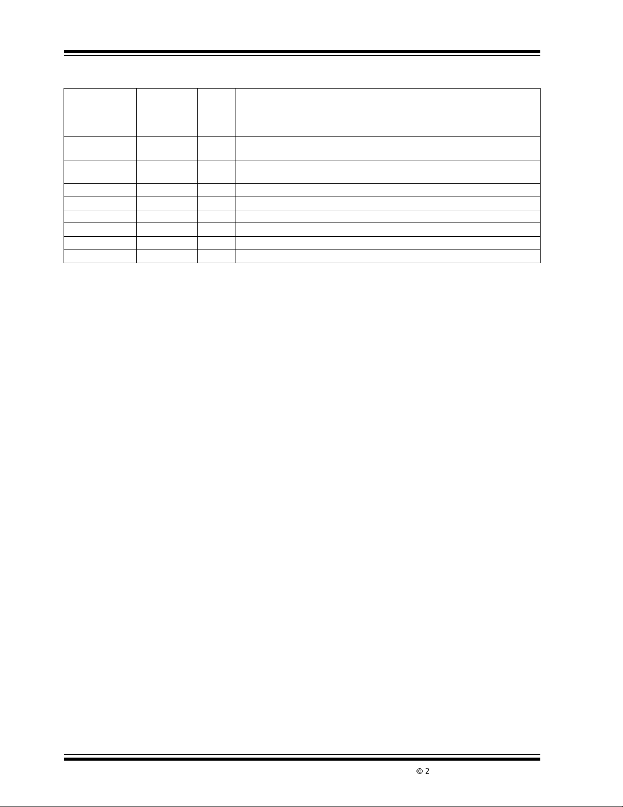
2.0 PIN DESCRIPTIONS
ThedescriptionsofthepinsarelistedinTable2.0.
TABLE 2-1: PIN FUNCTION TABLE
Pin No.
(24-Pin PDIP)
(24-Pin CERDIP)
(24-Pin SOIC)
12V
23V
34V
45R
56R
67C
79CO
810CO
9 11 DU Display update input pin. When DU is connected to the EOC output, every
10 12 CLK
11 13 CLK
12 14 V
13 16 V
14 17 EOC End of conversion output generates a pulse at the end of each conversion cycle.
15 18 OR
16 19 DS
17 20 DS
18 21 DS
19 23 DS
20 24 Q
Pin No.
(28-Pin PLCC)
Symbol Description
This is the analog ground. It has a high input impedance. The pin determines the
AG
reference level for the unknown input voltage (V
Reference voltage- Full scale outputisequalto the voltageapplied to V
REF
Therefore, full scale voltage of 1.999V requires 2V reference and 199.9mV full scale
requires a 200mV reference.V
to V
, the system is reset to the beginningof the conversioncycle.
EE
The unknowninput voltage (VX) is measured as a ratio of the reference voltage
X
(V
) in a rationetric A/D conversion.
REF
This pin is for external components used for the integration functionin the dual
1
slope conversion. Typical values are 0.1µF (mylar) capacitor for C
1/C1R1
1
=470kΩ (resistor)for2V fullscale.
R1=27kΩ (resistor)for 200mV full scale.Clock frequencyof66kHzgives 250msec
conversion time.
These pins are used for connecting the offset correction capacitor.
1
The recommended value is 0.1µF.
These pins are used for connecting the offset correction capacitor.
2
The recommended value is 0.1µF.
conversion is displayed. New data will be strobed into the output latches during the
conversion cycleif a positiveedgeis received on DU, prior to the ramp down cycle.
When this pin is driven from an external source, the voltageshould be referenced
to V
.
SS
Clock input pins. The TC14433 has its own oscillator system clock. Connecting a
1
single resistor between CLK
A crystalor OC circuit may be inserted in lieu of a resistor for improved CLK1,the
0
clock input, can be driven from an external clock source, which need only have
standardCMOSoutput drive.This pin is referenced to V
A300kΩ resistor yieldsa clock frequency of about66kHz.See Section5.0Typical
Characteristics. (Also see Figure 4-3 for alternatecircuits.)
Negative power current. Connection pin for the most negativesupply. Please note
EE
the current for the output drive circuit is returned through V
current is 0.8mA.
Negative powersupplyfor output circuitry. This pin sets the lowvoltage levelforthe
SS
outputpins (BCD,DigitSelects,EOC,OR). When connectedto analogground, the
output voltage is from analog ground to V
is from V
V
-3 volts and VEE.
DD
This generated pulse width is equal to one half the period of the system clock.
Overrange pin. Normally this pin is set high. When VXexceedsV
Digit select pin. The digit select output goes high when the respective digit is
4
selected. The MSD (1/2 digitturnson immediately afteran EOC pulse).
The remaining digits turn on in sequence from MSD to LSD.
3
To ensure that the BCD data has settled, an inter digitblanking time of two clock
2
periods is included.
Clock frequency divided by 80 equals multiplex rate. For example, a system clock of
1
60kHz gives a multiplex rate of 0.8kHz.
See Figure 4-4 for digit select timingdiagram.
0
TC14433/A
) and the reference voltage (V
X
functions as system reset also. When switched
REF
.
1
and CLK0sets the clock frequency.
1
forexternalclockinputs.
EE
. Typical supply
SS
. If connected to VEE, the output swing
to VDD. The recommended operating range for VSSis between the
EE
DD
the OR is low.
REF
REF
).
REF
.
2002 Microchip TechnologyInc. DS21394B-page 5
TC14433/A
TABLE 2-1: PIN FUNCTION TABLE (CONTINUED)
Pin No.
(24-Pin PDIP)
(24-Pin CERDIP)
(24-Pin SOIC)
21 25 Q
22 26 Q
23 27 Q
24 28 V
— 8 NC Not Used.
—15NCNotUsed.
—22NCNotUsed.
Pin No.
(28-Pin PLCC)
1NCNotUsed.
Symbol Description
BCD data outputpin. MultiplexedBCDoutputs contain threefulldigits of
1
informationduring digit selectDS
During DS1, the 1/2 digit, overrange,underrangeand polarity information
2
is available.
Refer to the Truth Table 4-1.
3
Positive power supply. This is the most positive power supply pin.
DD
,DS3,DS4.
2
DS21394B-page 6
2002 Microchip TechnologyInc.

TC14433/A
3.0 DETAILED DESCRIPTION
The TC14433 CMOS IC becomes a modified dualslope A/D with a minimum of external components.
This IC has the customary CMOS digital logic circuitry,
as well as CMOS analog circuitry. It provides the user
with digital functions such as (counters, latches,
multiplexers), and analog functions such as
(operational amplifiers and comparators) on a si ngle
chip.RefertotheFunctionalBlockdiagram, Figure 3-3
Features of the TC14433/A include auto-zero, high
input impedances and auto-polarity. Low power
consumption and a wide range of power supply voltages are also advantages of this CMOS device. The
system'sauto-zero functioncompensates for the offset
voltage of the internal amplifiers and comparators. In
this "ratiometric system," the output reading is the ratio
of the unknown voltageto the reference voltage,where
a ratio of 1 is equal to the maximum count of 1999. It
takes approximately 16,000 clock periods t o complete
one conversion cycle. Each conversion cycle may be
divided into 6 segments. Figure 3-1 shows the conversion cycle in 6 segments for both positive and negative
inputs.
FIGURE 3-1: INTEGRATOR
WAVEFORMSAT PIN 6
Segment 1 - The offsetcapacitor(CO), which compen-
sates for the input offsetvoltagesof the buffer and integrator amplifiers, is charged during this period.
However, the integrator capacitor is shorted. This
segment requires 4000 clock periods.
Segment 2 - During this segment, the integrator output
decreases to the comparator threshold voltage. At this
time, a number of counts equivalent to the input offset
voltageof the comparator is stored in the offset latches
for later use in the auto-zero process. The time for this
segment is variable and less than 800 clock periods.
Segment 3 - This segment of the conversion cycle is
the same as Segment 1.
Segment 4 - Segment4 is an up going ramp cycle with
the unknown input voltage (V
as the input to the
X
integrator. Figure 4-2 shows the equivalent
configuration of the analog section of the TC14433.
The actual configuration of the analog section is
dependent upon t he polarity of the input voltage during
the previous conversion cycle.
FIGURE 3-2: EQUIVALENT CIRCUIT
DIAGRAMS OF TH E
ANALOG SECTION
DURING SEGMENT 4 OF
THE TIMING CYCLE
Time
Segment
Number
Start
End
2
1
3
5
4
V
X
6
V
X
Typical
Positive
Input Voltage
Typical
Negative
Input Voltage
Segment 5 - This segment is a down-going ramp
period with the reference voltage as the input to the
integrator. Segment 5 of the conversion cycle has a
Buffer
–
V
+
X
R
1
C
1
Integrator
–
+
Comparator
+
–
time equal to the number of counts stored in the offset
storage latches during Segment 2. As a result, the system z eros automatically.
Segment 6 - This i s an extension of Segment 5. The
time period for this portion is 4000 clock periods. The
results of the A/D conversion cycle are determined in
this portion of the conversioncycle.
2002 Microchip TechnologyInc. DS21394B-page 7

TC14433/A
g
FIGURE 3-3: FUNCTIONAL BLOCK DIAGRAM
CLK
10
20-23
R
C
11
CLK
1
0
1's
Multiplexer
Latches
10's 100's 1,000'sClock
16 -19
TC14433/A
Overflow
CMOS
Analog Subsystem
C
CO1CO
1
rator
Display
Update
Control Logic
9
14
DU
EOC
End of
Conversion
456
R1/C
R
1
Inte
Q – Q3
BDC Data
DS1 – DS
Digit Strobe
Polarity Detect
15
2
1
3
78
2
Offset
4
V
V
V
Overrange
OR
Reference Voltage
REF
Analog Ground
AG
Analog Input
X
V
DD
VSS = Pin 13
V
EE
= Pin 24
= Pin 12
DS21394B-page 8
2002 Microchip TechnologyInc.

4.0 TYPICAL APPLICATIONS
The Typical Application circuit i s an example of a 3-1/2
digit voltmeter using the TC14433 with Commonanode displays.Thissystemrequiresa2.5Vreference.
Full scale may be adjusted to 1.999V or 199.9 mV.
Input overrange is indicated by flashing a display. This
display uses LEDs with common anode digit lines.
Power supply for this system i s shown as a dual ±5V
supply;however,the TC14433 will operate over a wide
voltage range
The circuit in Figure 4-1 shows a 3-1/2 digit LCD
voltmeter. The 14024B provides the low frequency
square wave signal drive to the LCD backplane. Dual
power supplies are shown here; however, one supply
maybeusedwhenV
case, V
must be at least 2. 8V above VEE.
AG
When only segments b and c of the decoder are connected to the 1/2 digit of the display, 4, 0, 7 and 3
appear as 1.
The overrange indication (Q
when the count is greater than 1999; (e.g., 1.999V for
a referenceof2V)Theunderrangeindication,usefulfor
auto-ranging circuits, occurs when the count is less
than 180; (e.g., 0.180V for a reference of 2V) .
isconnectedtoVEE.Inthis
SS
= 0 and Q0=1)occurs
3
TC14433/A
Note: If the most significant digit is connected to
a display other than a "1" only, such as a
full digit display, segments other than b
and c must be disconnected. The BCD to
7-segment decoder must blank on BCD
inputs 1010 to 1111. See Table 4-1
TABLE 4-1: TRUTH TABLE
Coded
Condition
of MSD
+0 1110 Blank
-0 1010
+0UR 1111
-0UR 1011
+1 01004–1
-1 0000
+1OR 0111
-1OR 0011
Note 1: Q3- 1/2 digit, low for "1", high for "0".
Figure 4-2 is an exampleof a 3-1/2 digitLEDvoltmeter
with a mi nimum of external components, (only 11
additional components). In this circuit, the 14511B
provides the segment drive and the 75492 or 1413
providessinkfordigitcurrent.Displayisblankedduring
the overrange condition.
Q
3Q2Q1Q0
BDC to 7- Segment
Decoding
Blank
Blank
Blank
Hook up
0–1
7–1
only segments
b and c to MSD
3–1
Q
- Polarity: "1" = positive,"0"= negative.
2
Q
- Out of range conditionexists if Q0=1.
0
When used in conjunction with Q
outofrange condition isindicated;i.e., Q
OR or Q
=1→ UR.
3
,thetypeof
3
=0→
3
2002 Microchip TechnologyInc. DS21394B-page 9
TC14433/A
FIGURE 4-1: 3-1/2 DIGIT VOLTMETER WITH LCD DISPLAY
C01C0
V
X
V
AG
V
REF
VDDVSSV
+V
14013B
D
C
RR
14013B
D
C
RR
2
TC14433
EE EOE DU
-V
14070B
1/4
-V
1/4 14070B
+V
R
470k
1
1/2 Digit
Plus
Sign
Minus
Sign
R
C
300k
DS4
DS3
DS2
DS1
Q
Q
Q
Q
R
0
1
2
3
C
14543B
+V
-V
14070B 1/4
+V
+V
C
14024B
R
-V
DS21394B-page 10
2002 Microchip TechnologyInc.

TC14433/A
FIGURE 4-2: 3-1/2 DIGIT LED VOLTMETER WITH LOW CO MPONENT COUNT USING
COMMON CATHODE DISPLAYS
FIGURE 4-3: ALTERNATE OSCILLATOR CIRCUITS
2002 Microchip TechnologyInc. DS21394B-page 11

TC14433/A
DS21394B-page 12
2002 Microchip TechnologyInc.
TC14433/A
0
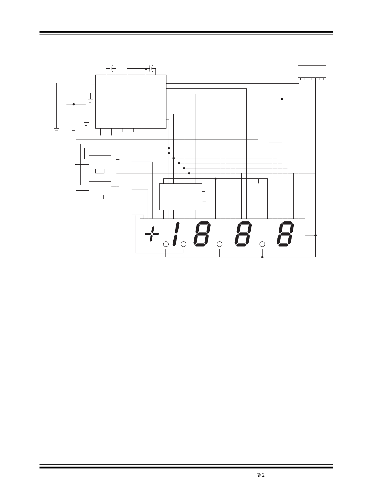
5.0 TYPICAL CHARACTERISTICS
Note: The graphs and tables provided following this not e are a statisticalsummary based on a limited number of
samplesandareprovidedfor informationalpurposesonly. The performancecharacteristicslistedhereinare
not tested or guaranteed. In some graphs or tables, the data presented may be outside the specified
operating range ( e.g., outside specified power supply range) and therefore outside the warranted range.
Typical Rollover Error vs. Power Supply Skew
4
3
2
1
0
Note: Rollover Error is the Difference in Output
-1
Reading for the same Analog Input Switched
from Positive to Negative.
AT FULL SCALE
-2
-3
ROLLOVER ERROR (IN LSD)
(PLUSE COUNT LESS MINUS COUNT)
Typical N-Channel Sink Current at V
5
4
3
2
- SINK CURRENT (mA)
1
D
I
0
-3 -2 -1
-4
(VDD I-IVEE I) - SUPPLY VOLTAGE SKEW (V)
01234 5
VDS - DRAIN TO SOURCE VOLTAGE (VDC)
01
– VSS = 5 Volts
DD
234
-40°C
+25°C
+85°C
Typical Quiescent Power Supply Current vs.Temp.
4
3
2
1
- QUIESCENT CURRENT (mA)
Q
I
-40 -20 0 20 40 60 80 10
0
Typical P-Channel Sink Current at V
-3
-2
-1
- SINK CURRENT (mA)
D
I
0
0-1-2-3-4-5
VEE = -8V
VDD = +8V
= -5V
V
EE
VDD = +5V
TA - TEMPERATURE (°C)
– VSS = 5 Volts
DD
VDS - DRAIN TO SOURCE VOLTAGE (VDC)
-40°C
+25°C
+85°C
Typical Clock Frequency vs. Resistor (RC)
Note: ±5% Typical Variation over
Supply Voltage Range
1M
100k
- CLOCK FREQUENCY (Hz)
CLK
I
10k
CONVERSION RATE =
MULTIPLEX RATE =
2002 Microchip TechnologyInc. DS21394B-page 13
of ±4.5V to ±8V
10kΩ 100kΩ 1MΩ
RC - CLOCK FREQUENCY RESISTOR
CLOCK FREQUENCY
16,400
CLOCK FREQUENCY
80
±1.5%
Typical % Change fo Clock Frequency vs. Temp.
4
3
2
1
0
-1
(% CHANGE)
-2
- CLOCK FREQUENCY
-3
CLK
I
-4
±5V Supply
±8V Supply
Normalized at 25°C
-40 -20 0 20 40 60 80
TA - TEMPERATURE (°C)
CONVERSION RATE =
MULTIPLEX RATE =
CLOCK FREQUENCY
16,400
CLOCK FREQUENCY
80
±1.5%
TC14433/A
6.0 PACKAGING INFORMATION
6.1 Package Marking Information
Package marking data not available at this time.
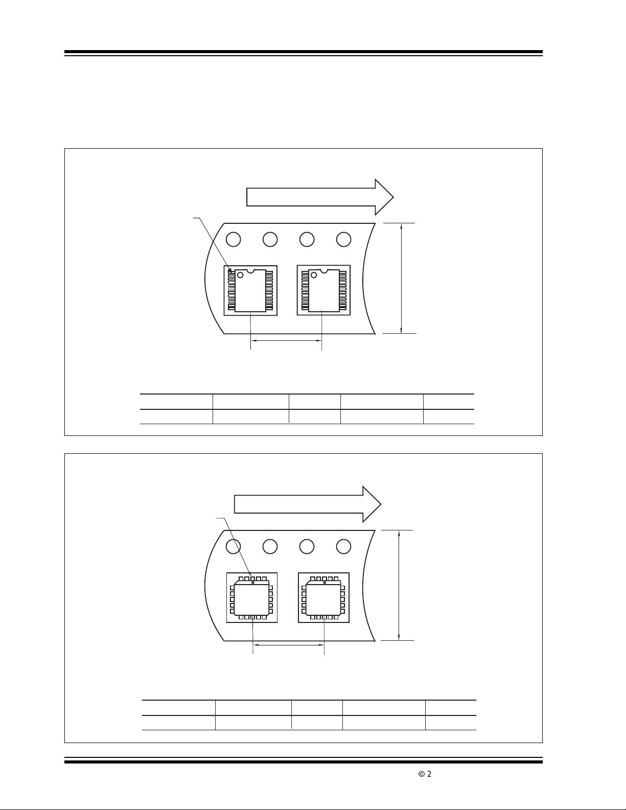
6.2 Taping Form
Component Taping Orientation for 24-Pin SOIC (Wide) Devices
User Direction of Feed
PIN 1
W
P
Standard Reel Component Orientation
for TR Suffix Device
Carrier Tape, Number of Components Per Reel and Reel Size
Package Carrier Width (W) Pitch (P) Part Per Full Reel Reel Size
24-Pin SOIC (W) 24 mm 12 mm 1000 13 in
Component Taping Orientation for 28-Pin PLCC Devices
User Direction of Feed
PIN 1
W
DS21394B-page 14
P
Standard Reel Component Orientation
for TR Suffix Device
Carrier Tape, Number of Components Per Reel and Reel Size
Package Carrier Width (W) Pitch (P) Part Per Full Reel Reel Size
28-Pin PLCC 24 mm 16 mm 750 13 in
2002 Microchip TechnologyInc.

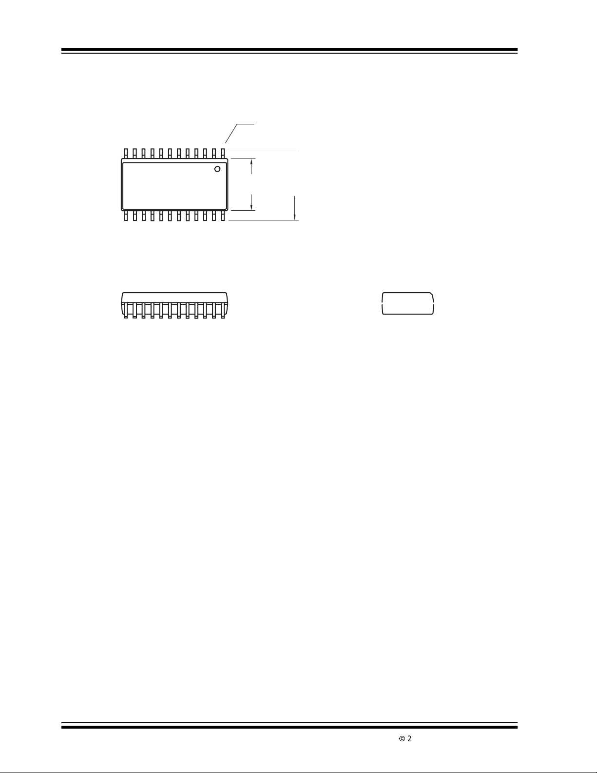
6.3 Package Dimensions
24-Pin PDIP (Wide)
TC14433/A
PIN 1
.555 (14.10)
.530 (13.46)
.200 (5.08)
.140 (3.56)
.150 (3.81)
.115 (2.92)
.110 (2.79)
.090 (2.29)
1.270 (32.26)
1.240 (31.50)
.070 (1.78)
.045 (1.14)
.022 (0.56)
.015 (0.38)
.040 (1.02)
.020 (0.51)
.015 (0.38)
.008 (0.20)
.610 (15.49)
.590 (14.99)
3°MIN.
.700 (17.78)
.610 (15.50)
Dimensions: inches (mm)
2002 Microchip TechnologyInc. DS21394B-page 15
TC14433/A
Package Dimensions (Continued)
24-Pin SOIC (Wide)
PIN 1
.050 (1.27) TYP.
.615 (15.62)
.597 (15.16)
.019 (0.48)
.014 (0.36)
.299 (7.59)
.291 (7.40)
.012 (0.30)
.004 (0.10)
.419 (10.65)
.398 (10.10)
.104 (2.64)
.097 (2.46)
8°
MAX.
.013 (0.33)
.009 (0.23)
.050 (1.27)
.016 (0.40)
DS21394B-page 16
2002 Microchip TechnologyInc.

TC14433/A
SALES AND SUPPORT
Data Sheets
Products supportedby a preliminary DataSheetmayhavean erratasheet describingminoroperationaldifferences and recommendedworkarounds.To determine if an errata sheetexists for a particular device,please contact one of the following:
1. Your local Microchip sales office
© 2002 Microchip TechnologyInc. DS21394B-page17

TC14433/A
NOTES:
DS21394B-page 18 © 2002 Microchip TechnologyInc.

TC14433/A
Information contained in this publication regarding device
applications and the like is intended through suggestion only
and may be superseded by updates. It is your responsibility to
ensure that your application meets with your specifications.
No representation or warranty is given and no liability is
assumed by Microchip Technology Incorporated with respect
to the accuracy or use of such information, or infringementof
patents or other intellectual property rights arising from such
use or otherwise. Use of Microchip’s products as critical components in life support systems is not authorized except with
express written approval by Microchip. No licenses are conveyed, implicitly or otherwise, under any intellectual property
rights.
Trademarks
The Microchip name and logo, the Microchip logo, FilterLab,
K
EELOQ,microID,MPLAB,PIC,PICmicro,PICMASTER,
PICSTART, PRO MATE, SEEVAL and The Embedded Control
SolutionsCompany areregiste red trademarksof MicrochipTechnologyIncorp or ated in the U.S.A. and other countries .
dsPIC, ECONOMONITOR, FanSense, FlexROM, fuzzyLAB,
In-Circuit Serial Programming, ICSP, ICEPIC, microPort,
Migratable Memory, MPASM, MPLIB, MP LINK, MPSIM,
MXDEV,MXLAB, PICC, PICDEM, PICDEM.net, rfPIC, Select
Mode and Total Endurance are trademarks of Microchip
TechnologyIncorporated in the U.S.A.
Serialized Quick Turn Programming (SQTP) is a service mark
of Microchip TechnologyIncorporated in t he U.S.A.
All other trademarks mentioned herein are property of their
respective companies.
© 2002, Microchip Technology Incorporated, Printed in the
U.S.A., All Rights Reserved.
Printed on recycled paper.
Microchip received QS-9000 quality system
certification for its worldwide headquarters,
design and wafer fabrication facilities in
Chandler and Tempe, Arizona in July 1999
and Mountain View, California in March 2002.
The Company’s quality system processes and
procedures are QS-9000 compliant for its
®
PICmicro
devices, Serial EEPROMs, microperipherals,
non-volatile memory and analog products. In
addition, Microchip’s quality system for the
design and manufacture of development
systemsisISO 9001certified.
2002 Microchip TechnologyInc. DS21394B-page 19
8-bit MCUs, KEELOQ®code hopping

WORLDWIDE SALES AND SERVICE
AMERICAS
Corporate Office
2355 West Chandler Blvd.
Chandler, AZ 85224-6199
Tel: 480-792-7200 Fax: 480-792-7277
Technical Support: 480-792-7627
Web Address: http://www.microchip.com
Rocky Mountain
2355 West Chandler Blvd.
Chandler, AZ 85224-6199
Tel: 480-792-7966 Fax: 480-792-7456
Atlanta
500 Sugar Mill Road, Suite 200B
Atlanta, GA 30350
Tel: 770-640-0034 Fax: 770-640-0307
Boston
2 Lan Drive, Suite 120
Westford, MA 01886
Tel: 978-692-3848 Fax: 978-692-3821
Chicago
333 Pierce Road, Suite 180
Itasca, IL 60143
Tel: 630-285-0071 Fax: 630-285-0075
Dallas
4570 Westgrove Drive, Suite 160
Addison, TX 75001
Tel: 972-818-7423 Fax: 972-818-2924
Detroit
Tri-Atria Office Building
32255 Northwestern Highway, Suite 190
Farmington Hills, MI 48334
Tel: 248-538-2250 Fax: 248-538-2260
Kokomo
2767 S. Albright Road
Kokomo, Indiana 46902
Tel: 765-864-8360 Fax: 765-864-8387
Los Angeles
18201 Von Karman, Suite 1090
Irvine, CA 92612
Tel: 949-263-1888 Fax: 949-263-1338
New York
150 Motor Parkway, Suite 202
Hauppauge, NY 11788
Tel: 631-273-5305 Fax: 631-273-5335
San Jose
Microchip Technology Inc.
2107 North First Street, Suite 590
San Jose, CA 95131
Tel: 408-436-7950 Fax: 408-436-7955
Toronto
6285 Northam Drive, Suite 108
Mississauga, Ontario L4V 1X5, Canada
Tel: 905-673-0699 Fax: 905-673-6509
ASIA/PACIFIC
Australia
Microchip Technology Australia Pty Ltd
Suite 22, 41 Rawson Street
Epping 2121, NSW
Australia
Tel: 61-2-9868-6733 Fax: 61-2-9868-6755
China - Beijing
Microchip Technology Consulting (Shanghai)
Co., Ltd., Beijing Liaison Office
Unit 915
Bei Hai Wan Tai Bldg.
No. 6 Chaoyangmen Beidajie
Beijing, 100027, No. China
Tel: 86-10-85282100 Fax: 86-10-85282104
China - Chengdu
Microchip Technology Consulting (Shanghai)
Co., Ltd., Chengdu Liaison Office
Rm. 2401, 24th Floor,
Ming Xing Financial Tower
No. 88 TIDU Street
Chengdu 610016, China
Tel: 86-28-86766200 Fax: 86-28-86766599
China - Fuzhou
Microchip Technology Consulting (Shanghai)
Co., Ltd., Fuzhou Liaison Office
Unit 28F, World Trade Plaza
No. 71 Wusi Road
Fuzhou 350001, China
Tel: 86-591-7503506 Fax: 86-591-7503521
China - Shanghai
Microchip Technology Consulting (Shanghai)
Co., Ltd.
Room 701, Bldg. B
Far East International Plaza
No. 317 Xian Xia Road
Shanghai, 200051
Tel: 86-21-6275-5700 Fax: 86-21-6275-5060
China - Shenzhen
Microchip Technology Consulting (Shanghai)
Co., Ltd., Shenzhen Liaison Office
Rm. 1315, 13/F , Shenzhen Kerry Centre,
Renminnan Lu
Shenzhen 518001, China
Tel: 86-755-2350361 Fax: 86-755-2366086
China - Hong Kong SAR
Microchip Technology Hongkong Ltd.
Unit 901-6, Tower2, Metroplaza
223 Hing Fong Road
Kwai Fong, N.T., Hong Kong
Tel: 852-2401-1200 Fax: 852-2401-3431
India
Microchip Technology Inc.
India Liaison Office
Divyasree Chambers
1 Floor, Wing A (A3/A4)
No. 11, O’Shaugnessey Road
Bangalore, 560 025, India
Tel: 91-80-2290061 Fax: 91-80-2290062
Japan
Microchip Technology Japan K.K.
Benex S-1 6F
3-18-20, Shinyokohama
Kohoku-Ku, Yokohama-shi
Kanagawa, 222-0033, Japan
Tel: 81-45-471- 6166 Fax: 81-45-471-6122
Korea
Microchip Technology Korea
168-1, Youngbo Bldg. 3 Floor
Samsung-Dong, Kangnam-Ku
Seoul, Korea 135-882
Tel: 82-2-554-7200 Fax: 82-2-558-5934
Singapore
Microchip Technology Singapore Pte Ltd.
200 Middle Road
#07-02 Prime Centre
Singapore, 188980
Tel: 65-6334-8870 Fax: 65-6334-8850
Taiwan
Microchip Technology Taiwan
11F-3, No. 207
Tung HuaNorth Road
Taipei, 105, Taiwan
Tel: 886-2-2717-7175 Fax: 886-2-2545-0139
EUROPE
Denmark
Microchip Technology Nordic ApS
Regus Business Centre
Lautrup hoj 1-3
Ballerup DK-2750 Denmark
Tel: 45 4420 9895 Fax: 45 4420 9910
France
Microchip Technology SARL
Parc d’Activite du Moulin de Massy
43 Rue du Saule Trapu
Batiment A - ler Etage
91300 Massy, France
Tel: 33-1-69-53-63-20 Fax: 33-1-69-30-90-79
Germany
Microchip Technology GmbH
Gustav-Heinemann Ring 125
D-81739 Munich, Germany
Tel: 49-89-627-144 0 Fax: 49-89-627-144-44
Italy
Microchip Technology SRL
Centro Direzionale Colleoni
Palazzo Taurus 1 V. Le Colleoni 1
20041 Agrate Brianza
Milan, Italy
Tel: 39-039-65791-1 Fax: 39-039-6899883
United Kingdom
Microchip Ltd.
505 Eskdale Road
Winnersh Triangle
Wokingham
Berkshire, England RG415TU
Tel: 44 118 921 5869 Fax: 44-118 921-5820
05/01/02
DS21394B-page 20
*DS21394B*
2002 Microchip Technology Inc.
 Loading...