

Page 1
M
2A High-Speed MOSFET Drivers
TC1412/TC1412N
Features
• Latch-Up Protected: Will Withstand 500 mA
Reverse Current
• Input Will Withstand Negative Inputs Up to 5V
• ESD Protected: 4 kV
• High Peak Output Current: 2A
• Wide Input Supply Voltage Operating Range:
- 4.5V to 16V
• High Capacitive Load Drive Capability:
- 1000 pF in 18 nsec
• Short Delay Time: 35 nsec Typ.
• Matched Delay Times
• Low Supply Current:
- With Logic ‘1’ Input: 500 µA
- With Logic ‘0’ Input: 100 µA
• Low Output Impedance: 4Ω
• Available in Space-Saving 8-pin MSOP Package
• Pinout Same as TC1410/TC1411/TC1413
Applications
• Switch Mode Power Supplies
• Pulse Transformer Drive
• Line Drivers
• Relay Driver
General Description
The TC1412/TC1412N are 2A CMOS buffers/drivers.
They will not latch-up under any conditions within their
power and voltage ratings. They are not subject to
damage when up to 5V of noise spiking of either
polarity occurs on the ground pin. They can accept,
without damage or logic upset, up to 500 mA of current
of either polarity being forced back into their output. All
terminals are fully protected against up to 4 kV of
electrostatic discharge.
As MOSFET drivers, the TC1412/TC1412N can easily
charge a 1000 pF gate capacitance in 18 nsec with
matched rise and fall times, and provide low enough
impedance in both the ON and the OFF states to
ensure the MOSFET’s intended state will not be
affected, even by large transients. The leading and
trailing edge propagation delay times are also matched
to allow driving short-duration inputs with greater
accuracy.
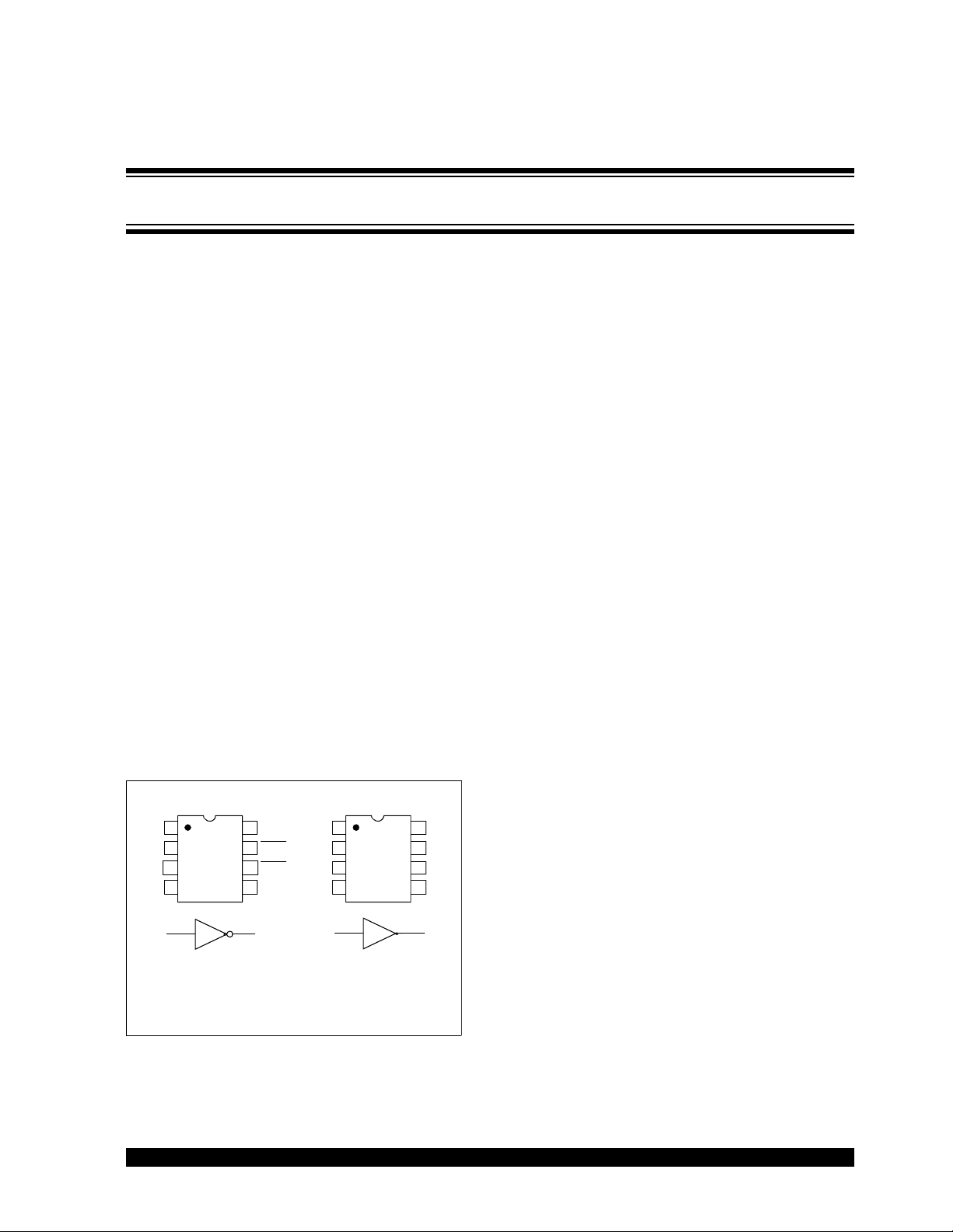
Package Type
8-Pin MSOP/PDIP/SOIC
6,7
8
7
6
5
V
DD
OUT
OUT
GND
1
V
DD
IN
2
TC1412N
NC
3
GND
45
2
Non-Inverting
6,7
8
7
6
V
DD
OUT
OUT
GND
V
1
DD
IN
2
TC1412
NC
3
4
GND
2
Inverting
NC = No Internal Connection
NOTE: Duplicate pins must be connected together
for proper operation.
2003 Microchip Technology Inc. DS21391C-page 1
Page 2
TC1412/TC1412N
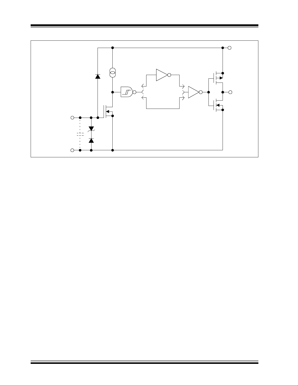
Functional Block Diagram
300 mV
TC1412
Inverting
Outputs
V
DD
Output
Input
Effective
Input C = 10 pF
GND
4.7V
Non-Inverting
Outputs
TC1412N
DS21391C-page 2 2003 Microchip Technology Inc.
Page 3
TC1412/TC1412N
1.0 ELECTRICAL
CHARACTERISTICS
Absolute Maximum Ratings †
Supply Voltage .....................................................+20V
Input Voltage ...................... V
Power Dissipation (T
≤ 70°C)
A
MSOP .......................................................... 340 mW
PDIP ............................................................ 730 mW
SOIC............................................................ 470 mW
Storage Temperature Range..............-65°C to +150°C
Maximum Junction Temperature...................... +150ºC
† Stresses above those listed under "Absolut e Maximum
Ratings" may cause permanent damage to the device. These
are stress ratings only and functional operation of the device
at these or any other conditions above those indicated in the
operation sections of the specifications is not implied.
Exposure to Absolute Maximum Rating conditions for
extended periods may affect device reliability.
+ 0.3V to GND – 5.0V
DD
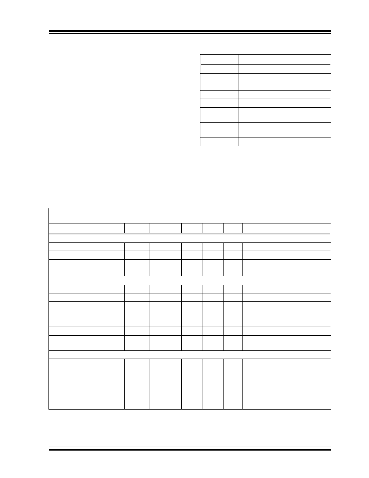
PIN FUNCTION TABLE
Symbol Description
V
DD
INPUT
NC No connection
GND Ground
GND Ground
OUTPUT CMOS push-pull output,
OUTPUT CMOS push-pull output,
V
DD
Supply input, 4.5V to 16V
Control input
common to pin 7
common to pin 6
Supply input, 4.5V to 16V
DC ELECTRICAL CHARACTERISTICS
Electrical Specifications: Unless otherwise noted, over operating temperature range with 4.5V ≤ V
Typical values are measured at T
Parameters Sym Min Typ Max Units Conditions
Input
Logic ‘1’, High Input Voltage V
Logic ‘0’, Low Input Voltage V
Input Current I
Output
High Output Voltage V
Low Output Voltage V
Output Resistance R
Peak Output Current I
Latch-Up Protection
Withstand Reverse Current
Switching Time (Note 1)
Rise Time t
Fall Time t
Note 1: Switching times ensured by design.
= +25°C, VDD = 16V.
A
IH
IL
IN
2.0 — — V
——0.8V
-1.0 — 1.0 µA 0V ≤ VIN ≤ V
-10 — 10 -40°C ≤ T
VDD – 0.025 — — V DC Test
OH
OL
O
— — 0.025 V DC Test
—46Ω VDD = 16V, IO = 10 mA, TA = +25°C
—57 0°C ≤ T
— 5 7 -40°C ≤ T
—2.0—AV
— 0.5 — A Duty cycle ≤ 2%, t ≤ 300 µsec,
—1826nsecT
I
REV
PK
R
—2031 0°C ≤ T
— 22 31 -40°C ≤ T
F
—1826nsecT
—2031 0°C ≤ T
— 22 31 -40°C ≤ T
= 16V
DD
V
= 16V
DD
= +25°C
A
= +25°C
A
DD, TA
≤ +85°C
A
≤ +70°C
A
≤ +85°C
A
≤ +70°C
A
≤ +85°C, Figure 4-1
A
≤ +70°C
A
≤ +85°C, Figure 4-1
A
≤ 16V.
DD
= +25°C
2003 Microchip Technology Inc. DS21391C-page 3
Page 4
TC1412/TC1412N
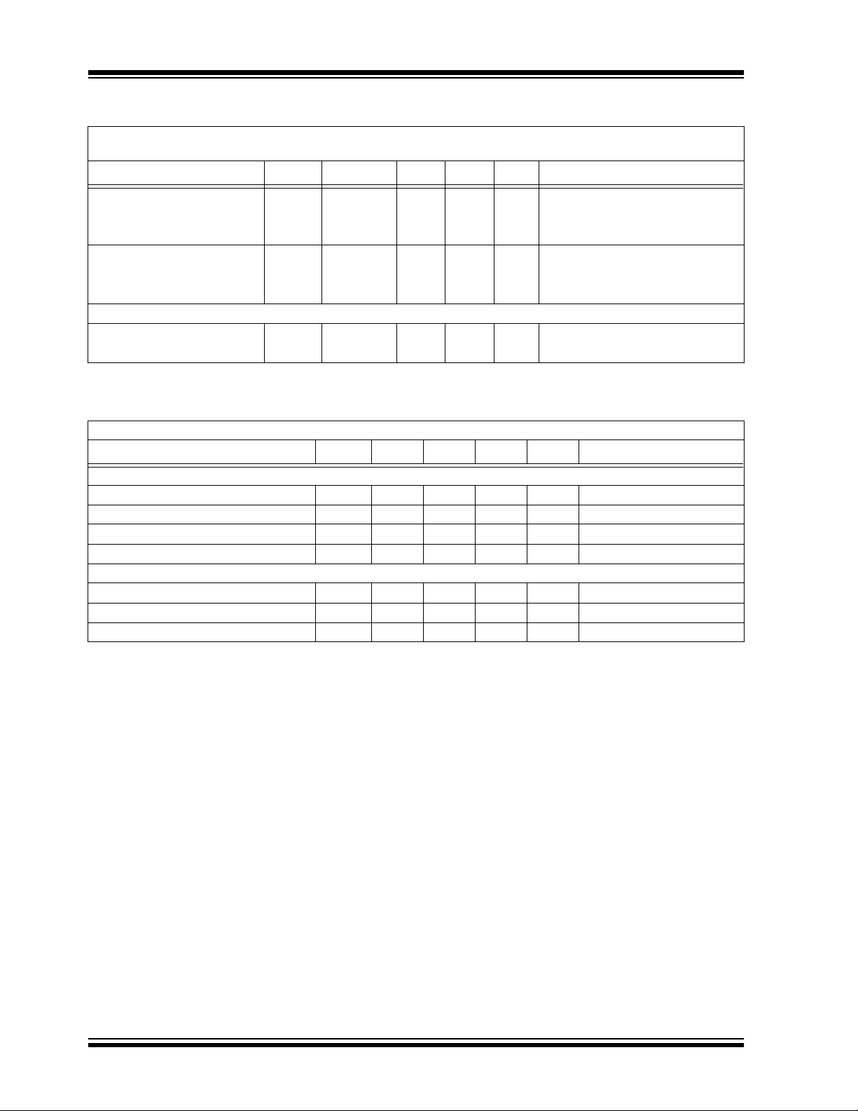
DC ELECTRICAL CHARACTERISTICS (CONTINUED)
Electrical Specifications: Unless otherwise noted, over operating temperature range with 4.5V ≤ V
Typical values are measured at T
= +25°C, VDD = 16V.
A
Parameters Sym Min Typ Max Units Conditions
Delay Time t
Delay Time t
D1
D2
—3545nsecT
—4050 0°C ≤ T
= +25°C,
A
A
— 40 50 -40°C ≤ T
—3545nsecT
—4050 0°C ≤ T
= +25°C
A
A
— 40 50 -40°C ≤ T
≤ +70°C
≤ +85°C, Figure 4-1
A
≤ +70°C
≤ +85°C, Figure 4-1
A
Power Supply
Power Supply Current I
S
—0.51.0mAV
— 0.1 0.15 V
= 3V, VDD = 16V
IN
= 0V
IN
Note 1: Switching times ensured by design.
TEMPERATURE CHARACTERISTICS
Electrical Specifications: Unless otherwise noted, all parameters apply with 4.5V ≤ V
Parameters Sym Min Typ Max Units Conditions
Temperature Ranges
Specified Temperature Range (C) T
Specified Temperature Range (E) T
Maximum Junction Temperature T
Storage Temperature Range T
A
A
J
A
0—+70ºC
-40 — +85 ºC
——+150ºC
-65 — +150 ºC
Package Thermal Resistances
Thermal Resistance, 8L-MSOP θ
Thermal Resistance, 8L-PDIP θ
Thermal Resistance, 8L-SOIC θ
JA
JA
JA
— 206 — ºC/W
— 125 — ºC/W
— 155 — ºC/W
DD
≤ 18V.
DD
≤ 16V.
DS21391C-page 4 2003 Microchip Technology Inc.
Page 5
TC1412/TC1412N
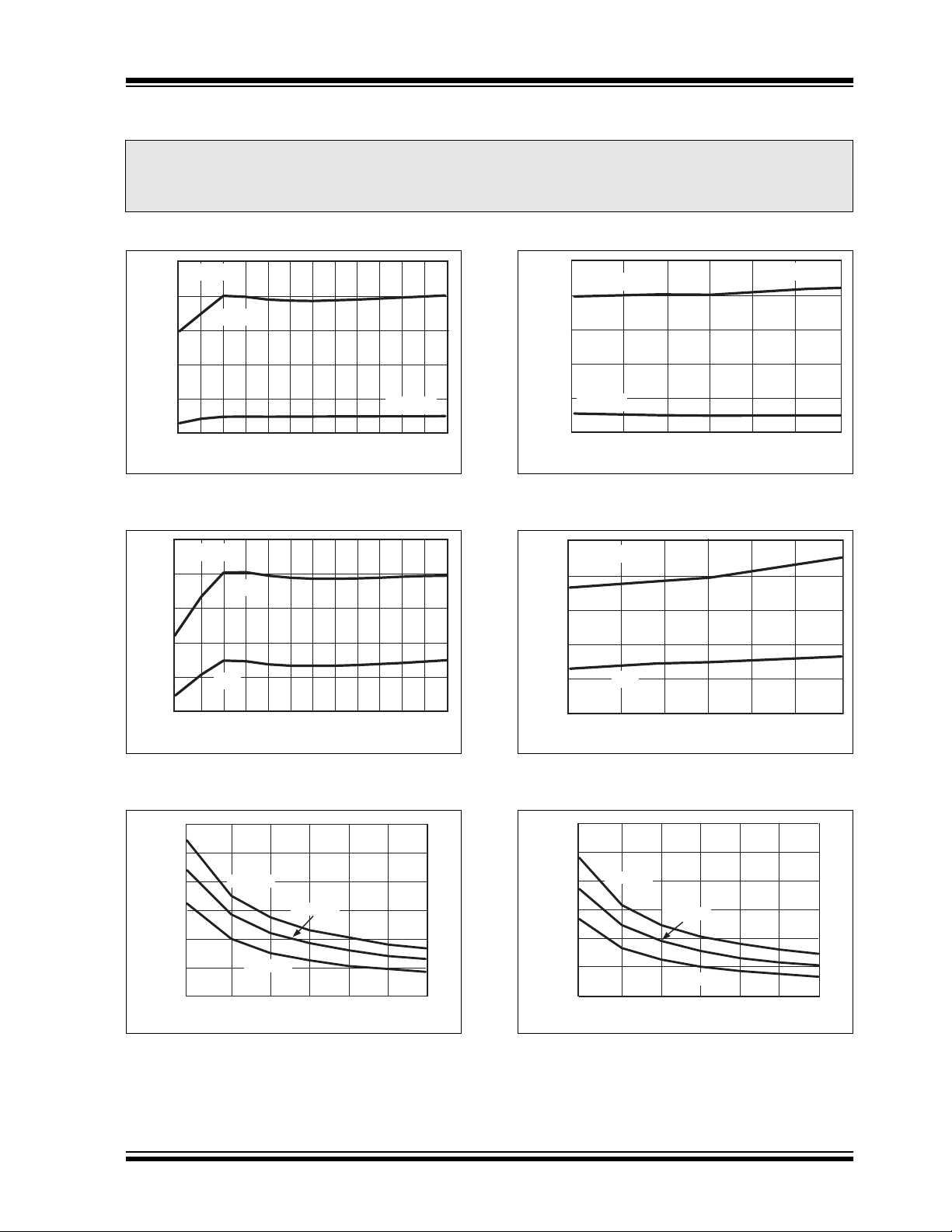
2.0 TYPICAL PERFORMANCE CURVES
Note: The graphs and tables provided following this note are a statistical summary based on a limited number of
samples and are provided for informational purposes only. The performance characteristics listed herein
are not tested or guaranteed. In some graphs or tables, the data presented may be outside the specified
operating range (e.g., outside specified power supply range) and therefore outside the warranted range.
Note: Unless otherwise indicated, over operating temperature range with 4.5V ≤ V
500
TA = +25°C
400
VIN = 3V
300
(µA)
200
SUPPLY
I
100
0
VDD (V)
VIN = 0V
FIGURE 2-1: Quiescent Supply Current vs. Supply Voltage.
1.6
TA = +25°C
1.5
(V)
1.4
1.3
THRESHOLD
V
1.2
1.1
V
IH
V
IL
VDD (V)
16141210864
16141210864
500
400
300
(µA)
200
SUPPLY
I
100
VIN = 3V
V
= 0V
IN
0
-40-200 20406080
FIGURE 2-4: Quiescent Supply Current vs. Temperature.
1.6
V
= 16V
SUPPLY
1.5
(V)
1.4
1.3
THRESHOLD
V
1.2
1.1
-40
V
-20 0 20 40 60 80
≤ 16V.
DD
TEMPERATURE (°C)
IL
TEMPERATURE (°C)
V
= 16V
SUPPLY
V
IH
FIGURE 2-2: Input Threshold vs. Supply Voltage.
13
11
°C
5
8
+
=
9
(Ohms)
7
DS-ON
R
5
3
1
T
A
°C
5
2
+
=
T
A
°C
0
4
-
=
T
A
VDD (V)
16141210864
FIGURE 2-3: High-State Output Resistance vs. Supply Voltage.
FIGURE 2-5: Input Threshold vs. Temperature.
13
11
°C
5
8
+
=
T
A
9
(Ohms)
DS-ON
R
7
5
3
1
°C
5
2
+
=
T
A
°C
0
4
-
=
T
A
V
(V)
DD
FIGURE 2-6: Low-State Output Resistance vs. Supply Voltage.
16141210864
2003 Microchip Technology Inc. DS21391C-page 5
Page 6

TC1412/TC1412N
Note: Unless otherwise indicated, over operating temperature range with 4.5V ≤ V
70
60
50
(nsec)
40
RISE
t
30
20
10
C
LOAD
T
= 1000 pF
= +85°C
A
= -40°C
T
A
= +25°C
T
A
VDD (V)
FIGURE 2-7: Rise Time vs. Supply Voltage.
100
90
80
70
60
(nsec)
D1
t
50
40
30
20
C
LOAD
= 1000 pF
= +85°C
T
A
T
A
T
= -40°C
= +25°C
A
VDD (V)
16141210864
16141210864
70
60
50
(nsec)
40
FALL
t
30
20
10
C
LOAD
T
T
A
= 1000 pF
= +85°C
A
= -40°C
FIGURE 2-10: Fall Time vs. Supply Voltage.
100
(nsec)
D2
t
90
80
70
60
50
40
30
20
C
LOAD
= 1000 pF
= +85°C
T
A
DD
≤ 16V.
= +25°C
T
A
T
A
VDD (V)
= +25°C
T
A
VDD (V)
16141210864
= -40°C
16141210864
FIGURE 2-8: Propagation Delay vs. Supply Voltage.
60
= +25°C
T
A
= 16V
V
DD
50
40
(nsec)
30
FALL
, t
20
RISE
t
10
0
0 1000 2000 3000 4000 5000
C
(pF)
LOAD
t
RISE
t
FALL
FIGURE 2-9: Rise and Fall Times vs. Capacitive Load.
FIGURE 2-11: Propagation Delay vs. Supply Voltage.
39
= +25°C
T
A
= 16V
V
38
DD
37
36
35
34
Propagation Delays (nsec)
33
32
0 1000
2000
3000 4000 5000
C
(pF)
LOAD
t
D2
t
D1
FIGURE 2-12: Propagation Delays vs. Capacitive Load.
DS21391C-page 6 2003 Microchip Technology Inc.
Page 7

TC1412/TC1412N
3.0 PIN DESCRIPTIONS
The descriptions of the pins are listed in Table 3-1.
TABLE 3-1: PIN FUNCTION TABLE
Pin
Symbol Description
No.
1V
2
INPUT
3 NC No connection
4 GND Ground
5 GND Ground
6 OUTPUT CMOS push-pull output,
7 OUTPUT CMOS push-pull output,
8V
3.1 Supply Input (VDD)
The VDD input is the bias supply for the MOSFET driver
and is rated for 4.5V to 16V with respect to the ground
pin. The V
a local ceramic capacitor. The value of the capacitor
should be chosen based on the capacitive load that is
being driven. A value of 1.0 µF is suggested.
DD
Supply input, 4.5V to 16V
DD
Control input
common to pin 7
common to pin 6
Supply input, 4.5V to 16V
DD
input should be bypassed to ground with
3.3 CMOS Push-Pull Output (OUTPUT)
The MOSFET driver output is a low-impedance, CMOS
push-pull style output, capable of driving a capacitive
load with 2A peak currents.
3.4 Ground (GND)
The ground pins are the return path for the bias current
and for the high peak currents that discharge the load
capacitor. The ground pins should be tied into a ground
plane or have very short traces to the bias supply
source return.
3.5 No Connect (NC)
No internal connection.
3.2 Control Input (INPUT)
The MOSFET driver input is a high-impedance,
TTL/CMOS-compatible input. The input has 300 mV of
hysteresis between the high and low thresholds which
prevents output glitching even when the rise and fall
time of the input signal is very slow.
2003 Microchip Technology Inc. DS21391C-page 7
Page 8

TC1412/TC1412N
4.0 APPLICATION INFORMATION
Input
V
1, 8
2
TC1412
TC1412N
Input: 100 kHz,
square wave,
t
= t
RISE
DD
FALL
= 16V
1.0 µF
4, 5
≤ 10 nsec
6, 7
0.1 µF
Output
CL = 1000 pF
+5V
Input
0V
V
DD
Output
0V
+5V
Input
0V
V
DD
Output
0V
10%
10%
t
D1
t
F
90%
10%
Inverting Driver
TC1412
90%
t
D1
10%
t
R
Non-Inverting Driver
TC1412N
t
D2
90%
90%
t
D2
90%
t
10%
R
10%
90%
t
F
FIGURE 4-1: Switching Time Test Circuit.
DS21391C-page 8 2003 Microchip Technology Inc.
Page 9

5.0 PACKAGING INFORMATION
5.1 Package Marking Information
TC1412/TC1412N
8-Lead PDIP (300 mil)
XXXXXX XX
XXXXXN NN
YYWW
8-Lead SOIC (150 mil)
XXXXXXX X
XXXXYYW W
NNN
8-Lead MSOP
XXXXXXX
YWWNNN
Example:
TC141 2
CPA057
0347
Example:
TC1412
COA0347
057
Example:
1412NE
347057
Legend: XX...X Customer specific information*
YY Year code (last 2 digits of calendar year)
WW Week code (week of January 1 is week ‘01’)
NNN Alphanumeric traceability code
Note: In the event the full Microchip part number cannot be marked on one line, it will
be carried over to the next line thus limiting the number of available characters
for customer specific information.
* Standard marking consists of Microchip part number, year code, week code, traceability code (facility
code, mask rev#, and assembly code). For marking beyond this, certain price adders apply. Please
check with your Microchip Sales Office.
2003 Microchip Technology Inc. DS21391C-page 9
Page 10

TC1412/TC1412N
8-Lead Plastic Dual In-line (PA) – 300 mil (PDIP)
E1
D
2
n
E
β
eB
Number of Pins
Pitch
Top to Seating Plane A .140 .155 .170 3.56 3.94 4.32
Molded Package Thickness A2 .115 .130 .145 2.92 3.30 3.68
Base to Seating Plane A1 .015 0.38
Shoulder to Shoulder Width E .300 .313 .325 7.62 7.94 8.26
Molded Package Width E1 .240 .250 .260 6 .10 6.35 6.60
Overall Length D .360 .373 .3 85 9.14 9.46 9.78
Tip to Seating Plane L .125 .130 .135 3.18 3.30 3.43
Lead Thickness
Upper Lead Width B1 .045 .058 .070 1.14 1.46 1.78
Lower Lead Width B .014 .018 .022 0.36 0.46 0.56
Overall Row Spacing § eB .310 .370 .430 7.87 9.40 10.92
Mold Draft Angle Top
Mold Draft Angle Bottom
* Controlling Parameter
§ Significant Characteristic
Notes:
Dimensions D and E1 do not include mold flash or protrusions. Mold flash or protrusions shall not exceed
.010” (0.254mm) per side.
JEDEC Equivalent: MS-001
Drawing No. C04-018
Dimension Limits MIN NOM MAX MIN NOM MAX
1
α
A
c
Units INCHES* MILLIMETERS
n
p
c
α
β
.008 .012 .015 0.20 0.29 0.38
A1
B1
B
88
.100 2.54
51015 51015
51015 51015
A2
L
p
DS21391C-page 10 2003 Microchip Technology Inc.
Page 11

TC1412/TC1412N
8-Lead Plastic Small Outline (OA) – Narrow, 150 mil (SOIC)
E
E1
p
D
2
B
Number of Pins
Pitch
Foot Angle
Lead Thickness
Mold Draft Angle Top
Mold Draft Angle Bottom
* Controlling Paramete r
§ Significant Characteristic
Notes:
Dimensions D and E1 do not include mold flash or protrusions. Mold flash or protrusions shall not exceed
.010” (0.254mm) per side.
JEDEC Equivalent: MS-012
Drawing No. C04-057
n
45°
c
β
n
p
φ
c
α
β
1
h
A
φ
L
048048
A1
MILLIMETERSINCHES*Units
1.27.050
α
A2
MAXNOMMINMAXNOMMINDimension Limits
88
1.751.551.35.069.061.053AOverall Height
1.551.421.32.061.056.052A2Molded Package Thickness
0.250.180.10.010.007.004A1Standoff §
6.206.025.79.244.237.228EOverall Width
3.993.913.71.157.154.146E1Molded Package W idth
5.004.904.80.197.193.189DOverall Length
0.510.380.25.020.015.010hChamfer Distance
0.760.620.48.030.025.019LFoot Length
0.250.230.20.010.009.008
0.510.420.33.020.017.013BLead Width
1512015120
1512015120
2003 Microchip Technology Inc. DS21391C-page 11
Page 12

TC1412/TC1412N
8-Lead Plastic Micro Small Outline Package (UA) (MSOP)
E
E1
p
D
2
B
n 1
A
c
A1
(F)
Units
Dimension Limits
Number of Pins
Pitch
Overall H e ight
Molded Package Thickness
Standoff
Overall Width
Molded Package Width
Overall Length
F oot Length
F oot Angle
Lead Thickness
Lead Width
Mold Draft Angle Top
Mo ld Dra ft Angle B ottom
*C ontr ollin g P ara m eter
Notes:
Dimens ions D a nd E 1 do not include mold flas h or protrusions. Mold flas h or protrusions s hall not
exceed .010" (0.254mm) per side.
JEDEC Equivalent: MO-187
Drawing No. C04-111
A2
A1
E1
MIN
n
p
A
.030
.000
E
D
L
FF ootprint (Reference)
c
B
.016 .024
0˚ - 8˚
.003
.009
5˚
5˚ -
L
INC HE S
NOM
.026 BSC
.033
.193 BSC
.118 BS C
.118 BS C
.037 RE F
.006
.012
MAX
8
--
-
-
.043
.037
.006
.031
.009
.016
15˚
15˚
MIN
0.75
0.00
0.40
0.08
0.22
MILLIMETERS*
NOM
0.65 BS C
--
0.85
4.90 BS C
3.00 BS C
3.00 BS C
0.60
0.95 R E F
0˚
MAX
8
-
-
-
-
A2
1.10
0.95
0.15
0.80
8˚
0.23
0.40
15˚5˚ 15˚5˚ -
DS21391C-page 12 2003 Microchip Technology Inc.
Page 13

PRODUCT IDENTIFICATION SYSTEM
TC1412/TC1412N
To order or obtain information, e.g., on pricing or delivery, refer to the factory or the listed sales office
PART NO. X /XX
Device
Device: TC1412: 2 A Single MOSFET Driver, Inverting
Temperature Range: C = 0°C to +70°C
Package: OA = Plastic SOIC, (150 mil Body), 8-lead
Range
TC1412N: 2 A Single MOSFET Driver, Non-Inverting
E = -40°C to +85°C
OA713 = Plastic SOIC, (150 mil Body), 8-lead
UA = Plastic Micro S mall Outline (MSOP), 8-le ad *
UA713 = Plastic Micro Small Outline (MSOP), 8-le ad *
PA = Plastic DIP (300 mil Body), 8-lead
* MSOP package is only available in E-Temp.
PackageTemp er atu re
(Tape and Reel)
(Tape and Reel)
Examples:
a) TC1412COA: 2A Single MOSFET driver,
SOIC package, 0°C to +70°C.
b) TC1412CPA: 2A Single MOSFET driver,
PDIP package, 0°C to +70°C.
c) TC1412EUA713: Tape and Reel, 2A
Single MOSFET driver, MSOP package,
-40°C to +85°C.
a) TC1412NCPA: 2A Single MOSFET
driver, PDIP package, 0°C to +70°C.
b) TC1412NEPA: 2A Single MOSFET
driver, PDIP package, -40°C to +85°C.
c) TC1412NEUA: 2A Single MOSFET
driver, MSOP package, -40°C to +85°C.
.
Sales and Support
Data Sheets
Products supported by a preliminary Data Sheet may have an errata sheet describing minor operational differences and
recommended workarounds. To determine if an errata sheet exists for a particular device, please contact one of the following:
1. Your local Microchip sales office
2. The Microchip Corporate Literature Center U.S. FAX: (480) 792-7277
3. The Microchip Worldwide Site (www.microchip.com)
Please specify which device, revision of silicon and Data Sheet (include Literature #) you are using.
Customer Notification System
Register on our web site (www.microchip.com/cn) to receive the most current information on our products.
2003 Microchip Technology Inc. DS21391C-page 13
Page 14

TC1412/TC1412N
NOTES:
DS21391C-page 14 2003 Microchip Technology Inc.
Page 15

Note the following details of the code protection feature on Microchip devices:
• Microchip products meet the specification contained in their particular Microchip Data Sheet.
• Microchip believes that its family of products is one of the most secure families of its kind on the market today, when used in the
intended manner and under normal conditions.
• There are dishonest and possibly illegal methods used to breach the code protection feature. All of these methods, to our
knowledge, require using the Microchip products in a manner outside the operating specifications contained in Microchip's Data
Sheets. Most likely, the person doing so is engaged in theft of intellectual property.
• Microchip is willing to work with the customer who is concerned about the integrity of their code.
• Neither Microchip nor any other semiconductor manufacturer can guarantee the security of their code. Code protection does not
mean that we are guaranteeing the product as “unbreakable.”
Code protection is constantly evolving. We at Microchip are committed to continuously improving the code protection features of our
products. Attempts to break microchip’s code protection feature may be a violation of the Digital Millennium Copyright Act. If such acts
allow unauthorized access to your software or other copyrighted work, you may have a right to sue for relief under that Act.
Information contained in this publication regarding device
applications and the like is intended through suggestion only
and may be superseded by updates. It is your responsibility to
ensure that your application meets with your specifications.
No representation or warranty is given and no liability is
assumed by Microchip Technology Incorporated with respect
to the accuracy or use of such information, or infringement of
patents or other intellectual property rights ar ising fr om such
use or otherwise. Use of Microchip’s products as critical
components in life support systems is not authorized except
with express written approval by Microchip. No licenses are
conveyed, implicitly or otherwise, under any intellectual
property rights.
Trademarks
The Microchip name and logo, the Microchip logo, K
EELOQ
,
MPLAB, PIC, PICmicro, PICSTART, PRO MATE and
PowerSmart are registered trademarks of Microchip
Technology Incorporated in the U.S.A. and other countries.
FilterLab, microID, MXDEV, MXLAB, PICMASTER, SEEVAL
and The Embedded Control Solutions Company are
registered trademarks of Microchip Technology Incorporated
in the U.S.A.
Accuron, Application Maestro, dsPIC, dsPICDEM,
dsPICDEM.net, ECONOMONITOR, FanSense, FlexROM,
fuzzyLAB, In-Circuit Serial Programming, ICSP, ICEPIC,
microPort, Migratable Memory, MPASM, MPLIB, MPLINK,
MPSIM, PICC, PICkit, PICDEM, PICDEM.net, PowerCal,
PowerInfo, PowerMate, PowerTool, rfLAB, rfPIC, Select
Mode, SmartSensor, SmartShunt, SmartTel and Total
Endurance are trademarks of Microchip Technology
Incorporated in the U.S.A. and other countries.
Serialized Quick Turn Programming (SQTP) is a service mark
of Microchip Technology Incorporated in the U.S.A.
All other trademarks mentioned herein are property of their
respective companies.
© 2003, Microchip Technology Incorporated, Printed in the
U.S.A., All Rights Reserved.
Printed on recycled paper.
Microchip received QS-9000 quality system
certification for its worldwide headqua rters,
design and wafer fabrication facilities in
Chandler and Tempe, Arizona in July 1999
and Mountain View, California in March 2002.
The Company’s quality system processes and
procedures are QS-9000 compliant for its
PICmicro
devices, Serial EEPROMs, microperipherals,
non-volatile memory and analog products. In
addition, Microchip’s quality system for the
design and manufacture of development
systems is ISO 9001 certified.
®
8-bit MCUs, KEEL
®
code hopping
OQ
2003 Microchip Technology Inc. DS21391C-page 15
Page 16

M
W
ORLDWIDE SALES AND SERVICE
AMERICAS
Corporate Office
2355 West Chandler B lvd.
Chandler, AZ 85224-6199
Tel: 480-792-7200 Fax: 480-792-7277
Technical Support: 480-792-7627
Web Address: http://www.microchip.com
Atlanta
3780 Mansell Road, Suite 130
Alpharetta, GA 30022
Tel: 770-640-0034 Fax: 770-640-0307
Boston
2 Lan Drive, Suit e 120
Westford, MA 01886
Tel: 978-692-3848 Fax: 978-692-3821
Chicago
333 Pierce Road, S uite 180
Itasca, IL 60143
Tel: 630-285-0071 Fax: 630-285-0075
Dallas
4570 Westgrove Drive, Suite 160
Addison, TX 75001
Tel: 972-818-7423 Fax: 972-818-2924
Detroit
Tri-Atria Office Building
32255 Northwestern Highway, Suite 190
Farmington Hills, MI 48334
Tel: 248-538-2250 Fax: 248-538-2260
Kokomo
2767 S. Albright Road
Kokomo, IN 46902
Tel: 765-864-8360 Fax: 765-864-8387
Los Angeles
18201 Von Karman, Suite 10 90
Irvine, CA 92612
Tel: 949-263-1888 Fax: 949-263-1338
Phoenix
2355 West Chandler B lvd.
Chandler, AZ 85224-6199
Tel: 480-792-7966 Fax: 480-792-4338
San Jose
Microchip Technology Inc.
2107 North First S treet, Suite 590
San Jose, CA 95131
Tel: 408-436-7950 Fax: 408-436-7955
Toront o
6285 Northam Drive, Suite 108
Mississauga, Ontario L4V 1X5, Canada
Tel: 905-673-0699 Fax: 905-673-6509
ASIA/PACIFIC
Australia
Microchip Technology Australia Pty Ltd
Marketing Support Division
Suite 22, 41 Rawson Street
Epping 2121, NSW
Australia
Tel: 61-2-9868-6733 Fax: 61-2-9868-6755
China - Beijing
Microchip Technology Consulting (Shanghai)
Co., Ltd., Beijing Liaison Office
Unit 915
Bei Hai Wan Tai Bldg.
No. 6 Chaoyangmen Beidajie
Beijing, 100027, No. China
Tel: 86-10-85282100 Fax: 86-10-85282104
China - Chengdu
Microchip Technology Consulting (Shanghai)
Co., Ltd., Chengdu Liaison Office
Rm. 2401-2402, 24 th Floor,
Ming Xing Financial Tower
No. 88 TIDU Street
Chengdu 610016, China
Tel: 86-28-86766200 Fax: 86-28-86766599
China - Fuzhou
Microchip Technology Consulting (Shanghai)
Co., Ltd., Fuzhou Liaison Office
Unit 28F, World Trade Plaza
No. 71 Wusi Road
Fuzhou 350001, China
Tel: 86-591-7503506 Fax: 86-591-7503521
China - Hong Kong SAR
Microchip Technology Hongkong Ltd.
Unit 901-6, Tower 2, Metroplaza
223 Hing Fong Ro ad
Kwai Fong, N.T., Hong Kong
Tel: 852-2401-1200 Fax: 852-2401-3431
China - Shanghai
Microchip Technology Consulting (Shanghai)
Co., Ltd.
Room 701, Bldg. B
Far East International Plaza
No. 317 Xian Xia Road
Shanghai, 200051
Tel: 86-21-6275-5700 Fax: 86-21-62 75-5060
China - Shenzhen
Microchip Technology Consulting (Shanghai)
Co., Ltd., Shenzhen Liaison Office
Rm. 1812, 18/F, Building A, United Plaza
No. 5022 Binhe Roa d, Futian District
Shenzhen 518033, China
Tel: 86-755-82901380 Fax: 86-755-82966626
China - Qingdao
Rm. B505A, Fullhope Plaza,
No. 12 Hong Kong Central Rd.
Qingdao 266071, China
Tel: 86-532-5027355 Fax: 86-532-5027205
India
Microchip Technology Inc.
India Liaison Office
Marketing Support Division
Divyasree Chamb ers
1 Floor, Wing A (A3/A4)
No. 11, O’Shaugnessey Road
Bangalore, 560 025, India
Tel: 91-80-2290061 Fax: 91-80-2290062
Japan
Microchip Technology Japan K.K.
Benex S-1 6F
3-18-20, Shinyokohama
Kohoku-Ku, Yokohama-shi
Kanagawa, 222-0033, Japan
Tel: 81-45-471- 6166 Fax: 81-45-471 -6122
Korea
Microchip Technology Korea
168-1, Youngbo Bldg. 3 Floor
Samsung-Dong, Kangnam-Ku
Seoul, Korea 135-882
Tel: 82-2-554-7200 Fax: 82-2-558-5934
Singapore
Microchip Technology Singapore Pte Ltd.
200 Middle Road
#07-02 Prime Cen tre
Singapore, 188980
Tel: 65-6334-8870 Fax: 65-6334-8850
Taiwan
Microchip Technology (Barbados) Inc.,
Taiwan Branch
11F-3, No. 207
Tung Hua North Road
Taipei, 105, Taiwan
Tel: 886-2-2717-7175 Fax: 886-2-25 45-0139
EUROPE
Austria
Microchip Technology Austria GmbH
Durisolstrasse 2
A-4600 Wels
Austria
Tel: 43-7242-2244-399
Fax: 43-7242-2244-393
Denmark
Microchip Technology Nordic ApS
Regus Business Centre
Lautrup hoj 1-3
Ballerup DK-2750 Denmark
Tel: 45-4420-9895 Fax: 45-4420-9910
France
Microchip Technology SARL
Parc d’Activite du M oulin de Massy
43 Rue du Saule Trapu
Batiment A - ler Etage
91300 Massy, France
Tel: 33-1-69-53-63-20 Fax: 33-1-69-30-90-79
Germany
Microchip Technology GmbH
Steinheilstrasse 10
D-85737 Ismaning, Germany
Tel: 49-89-627-144-0
Fax: 49-89-627-144-44
Italy
Microchip Technology SRL
Via Quasimodo, 12
20025 Legnano (MI)
Milan, Italy
Tel: 39-0331-742611 Fax: 39-0331-466781
United Kingdom
Microchip Ltd.
505 Eskdale Road
Winnersh Triangle
Wokingham
Berkshire, England RG41 5TU
Tel: 44-118-921-5869 Fax: 44-118-921-5820
03/25/03
DS21391C-page 16 2003 Microchip Technology Inc.
 Loading...