

Page 1
TC1303B Dual-Output
Regulator with Power-Good Output
User’ s Guide
© 2005 Microchip Technology Inc. DS51563A
Page 2
Note the following details of the code protection feature on Microchip devices:
• Microchip products meet the specification contained in their particular Microchip Data Sheet.
• Microchip believes that its family of products is one of the most secure families of its kind on the market today, when used in the
intended manner and under normal conditions.
• There are dishonest and possibly illegal methods used to breach the code protection feature. All of these methods, to our
knowledge, require using the Microchip products in a manner outside the operating specifications contained in Microchip’s Data
Sheets. Most likely, the person doing so is engaged in theft of intellectual property.
• Microchip is willing to work with the customer who is concerned about the integrity of their code.
• Neither Microchip nor any other semiconductor manufacturer can guarantee the security of their code. Code protection does not
mean that we are guaranteeing the product as “unbreakable.”
Code protection is constantly evolving. We at Microchip are committed to continuously improving the code protection features of our
products. Attempts to break Microchip’s code protection feature may be a violation of the Digit al Millennium Copyright Act. If suc h a c t s
allow unauthorized access to your software or other copyrighted work, you may have a right to sue for relief under that Act.
Information contained in this publication regarding device
applications and the like is provided only for your convenience
and may be superseded by updates. It is your responsibility to
ensure that your application meets with your specifications.
MICROCHIP MAKES NO REPRESENTATIONS OR WARRANTIES OF ANY KIND WHETHER EXPRESS OR IMPLIED,
WRITTEN OR ORAL, STATUTORY OR OTHERWISE,
RELATED TO THE INFORMATION, INCLUDING BUT NOT
LIMITED TO ITS CONDITION, QUALITY, PERFORMANCE,
MERCHANTABILITY OR FITNESS FOR PURPOSE.
Microchip disclaims all liability arising from this information and
its use. Use of M icrochip’s prod ucts as critical components in
life support systems is not authorized except with express
written approval by Microchip. No licenses are conveyed,
implicitly or otherwise, under any Microchip intellectual property
rights.
Trademarks
The Microchip name and logo, the Microchip logo, Accuron,
dsPIC, K
EELOQ, microID, MPLAB, PIC, PICmicro, PICSTART,
PRO MATE, PowerSmart, rfPIC, and SmartShunt are
registered trademarks of Microchip Technology Incorporated
in the U.S.A. and other countries.
AmpLab, FilterLab, Migratable Memory, MXDEV, MXLAB,
PICMASTER, SEEVAL, SmartSensor and The Embedded
Control Solutions Company are registered trademarks of
Microchip Technology Incorporated in the U.S.A.
Analog-for-the-Digital Age, Application Maestro, dsPICDEM,
dsPICDEM.net, dsPICworks, ECAN, ECONOMONITOR,
FanSense, FlexROM, fuzzyLAB, In-Circuit Serial
Programming, ICSP, ICEPIC, Linear Active Thermistor,
MPASM, MPLIB, MPLINK, MPSI M, PICkit, PIC DEM,
PICDEM.net, PICLAB, PICtail, PowerCal, PowerInfo,
PowerMate, PowerTool, rfLAB, rfPICDEM, Select Mode,
Smart Serial, SmartTel, Total Endurance and WiperLock are
trademarks of Microchip Technology Incorporated in the
U.S.A. and other countries.
SQTP is a service mark of Microchip Technology Incorporated
in the U.S.A.
All other trademarks mentioned herein are property of their
respective companies.
© 2005, Microchip Technology Inc orporat ed, Printed in the
U.S.A., All Rights Reserved.
Printed on recycled paper.
Microchip received ISO/TS-16949:2002 quality system certification for
its worldwide headquarters, design and wafer fabrication facilities in
Chandler and Tempe, Arizona and Mountain View, California in
October 2003. The Company’s quality system processes and
procedures are for its PICmicro
devices, Serial EEPROMs, microperipherals, nonvolatile memory and
analog products. In addition, Microchip’s quality system for the design
and manufacture of development systems is ISO 9001:2000 certified.
®
8-bit MCUs, KEELOQ
®
code hopping
DS51563A-page ii © 2005 Microchip Technology Inc.
Page 3

TC1303B DUAL-OUTPUT
REGULATOR USER’S GUIDE
Table of Contents
Preface ...........................................................................................................................1
Chapter 1. Product Overview
1.1 Introduction .....................................................................................................5
1.2 What is the TC1303B Dual-Output Regulator with Power-Good
Output Demo Board? ..................................................................................... 6
1.3 What the TC1303B Dual-Output Regulator with Power-Good
Output Demo Board kit includes .............................................................. .. ....6
Chapter 2. Installation and Operation
2.4 Introduction .....................................................................................................7
2.5 Features ..... .. .............. .. ............. .. .............. .. ............. .. .............. .. ............. .. ..... 7
2.6 Getting St a rt ed ................. ... ............. .. ............. .. .............. .. ............. .. .............. 7
Appendix A. Schematic and Layouts ..........................................................................9
A.1 Introduction ....................................................................................................9
A.2 Board Sche m a t ic ..................... .. .............. .. ............. .. .............. .. ............. .. ... 10
A.3 Board – As se mbly Drawing .................. .............. .. ............. ............. ... ......... 11
A.4 Board – Top Ov e rl a y ............. ............. .. .............. .. ............. .. .............. .. ....... 12
A.5 Board – Top La y er ... ............. .. ............. ... ............. .. ............. .............. .. ....... 13
A.6 Board – Bottom Layer ..... .. .. ............. ............. ... ............. .. ............. ... ......... 14
Appendix B. Bill-Of-Materials (BOM) .........................................................................15
Worldwide Sales and Service ....................................................................................16
© 2005 Microchip Technology Inc. DS51563A-page iii
Page 4

TC1303B Dual-Output Regulator User’s Guide
NOTES:
DS51563A-page iv © 2005 Microchip Technology Inc.
Page 5
TC1303B DUAL-OUTPUT
REGULATOR USER’S GUIDE
Preface
NOTICE TO CUSTOMERS
All documentation becomes dated, and this manual is no exception. Microchip tools and
documentation are constantly evolving to meet customer needs, so some actual dialogs
and/or tool descriptions may differ from those in this document. Please refer to our web site
(www.microchip.com) to obtain the latest documentation available.
Documents are identified with a “DS” number. This number is located on the bottom of each
page, in front of the page number. The numbering convention for the DS number is
“DSXXXXXA”, where “XXXXX” is the document number and “A” is the revision level of the
document.
INTRODUCTION
This chapter contains general information that will be useful to know before using the
TC1303B Dual-Output Regulator with Power-Good Output Demo Board. Items
discussed in this chapter include:
• Document Layout
• Conventions Used in this Guide
• Recommended Reading
• The Microchip Web Site
• Customer Support
• IDocument Revision History
DOCUMENT LAYOUT
This document describes how to use the TC1303B Dual-Output Regulator with
Power-Good Output Demo Board. The manual layout is as follows:
• Chapter 1. “Product Overview” – Important information about the TC1303B
Dual-Output Regulator with Power-Good Output Demo Board.
• Chapter 2. “Installation and Operation” – Provides a description of the demo
board and includes instructions on how to get started.
• Appendix A. “Schematic and Layouts” – Shows the schematic and layout
diagrams for the TC1303B Dual-Output Regulator with Power-Good Output Demo
Board.
• Appendix B. “Bill-Of-Materials (BOM)” – Lists the parts used to build the
TC1303B Dual-Output Regulator with Power-Good Output Demo Board.
© 2005 Microchip Technology Inc. DS51563A-page 1
Page 6
TC1303B Dual-Output Regulator User’s Guide
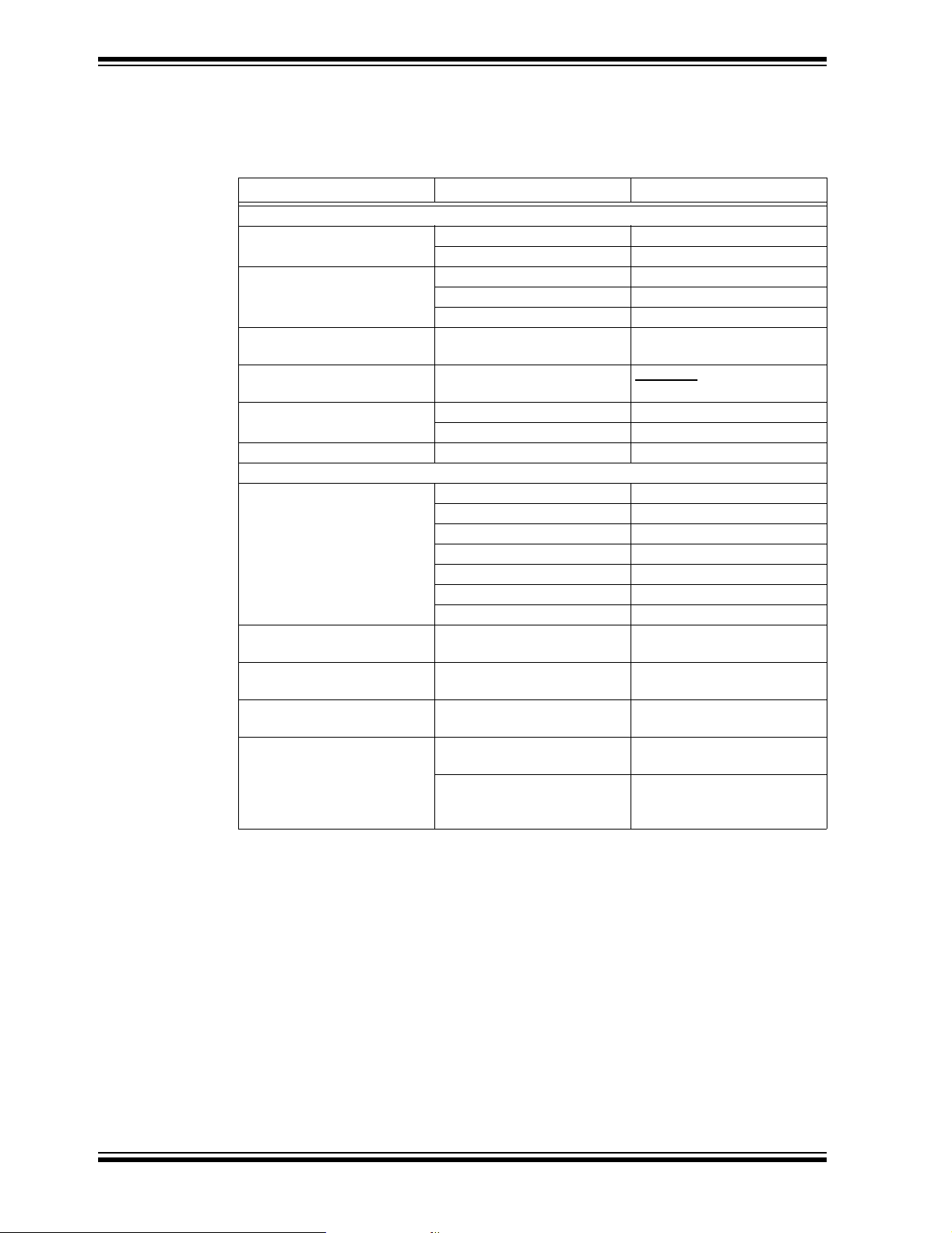
CONVENTIONS USED IN THIS GUIDE
This manual uses the following docum entat io n conven tion s:
DOCUMENTATION CONVENTIONS
Description Represents Examples
Arial font:
Italic characters Referenced books MPLAB
Emphasized text ...is the only comp ile r...
Initial caps A window the Output window
A dialog the Settings dialog
A menu selection select Enable Programmer
Quotes A field name in a window or
dialog
Underlined, italic text with
right angle bracket
Bold characters A dialog button Click OK
Text in angle br ackets < > A key on the keyboard Press <Enter>, <F1>
Courier font:
Plain Courier Sample source code #define START
Italic Courier A variable argument file.o, where file can be
Square brackets [ ] Optional arguments mcc18 [options] file
Curly brackets and pipe
character: { | }
Ellipses... Replaces r epeated text var_name [,
A menu path File>Save
A tab Click the Power tab
Filenames autoexec.bat
File paths c:\mcc18\h
Keywords _asm, _endasm, static
Command-line options -Opa+, -Opa-
Bit values 0, 1
Constants 0xFF, ‘A’
Choice of mutually exclusive
arguments; an OR selection
Represents code supplied by
user
®
IDE User’s Guide
“Save project before build”
any valid filename
[options]
errorlevel {0|1}
var_name...]
void main (void)
{ ...
}
RECOMMENDED READING
This user's guide describes how to use the TC1303B Dual-Output Regulator with
Power-Good Output Demo Board. The following Microchip document is available and
recommended as a supplemental reference resources.
TC1303B Data Sheet, “500 mA Synchronous Buck Regulator + 300 mA LDO with
Power-Good Output”, (DS21949)
This data sheet provides detailed information regarding the TC1303B product family.
DS51563A-page 2 © 2005 Microchip Technology Inc.
Page 7

THE MICROCHIP WEB SITE
Microchip provides online support via our web site at www.microchip.com. This web
site is used as a means to make files and information easily available to customers.
Accessible by using your favorite Internet browser, the web site contains the following
information:
• Product Support – Data sheets and errata, application notes and sample
programs, design resources, user’s guides and hardware support documents,
latest software releases and archived software
• General Technical Support – Frequently Asked Questions (FAQs), technical
support requests, online discussion groups, Microchip consultant program
member listing
• Business of Microchip – Product selector and ordering guides, latest Microchip
press releases, listing of seminars and events, listings of Microchip sales offices,
distributors and factory representatives
CUSTOMER SUPPORT
Users of Microchip products can receive assistance through several channels:
• Distributor or Representative
• Local Sales Office
• Field Application Engineer (FAE)
• Technical Support
• Development Systems Information Line
Customers should contact their distributor, representative or Field Application Engineer
(FAE) for support. Local sales offices are also available to help customers. A listing of
sales offices and locations is included in the back of this document.
Technical support is available through the web site at: http://support.microchip.com
Preface
IDOCUMENT REVISION HISTORY
Revision A (June 2005)
• Initial Release of this Document.
© 2005 Microchip Technology Inc. DS51563A-page 3
Page 8

TC1303B Dual-Output Regulator User’s Guide
NOTES:
DS51563A-page 4 © 2005 Microchip Technology Inc.
Page 9

Chapter 1. Product Overview
1.1 INTRODUCTION
The TC1303B Dual-Output Regulator with Power-Good Output Demo Board is used to
demonstrate the operation of the TC1303B. The TC1303B combines a 500 mA
synchronous buck regulator and 300 mA Low-Dropout Regulator (LDO) with a
power-good monitor to provide a highly integrated solution for devices that require
multiple supply voltages. The unique combination of an integrated buck switching
regulator and low-dropout linear regulator provides the smallest, lowest system cost for
dual-output voltage ap plications , with one low p rocessor core voltage a nd one hig her
bias voltage.
The 500 mA synchronous buck regulator switches at a fixed frequency of 2.0 MHz when
the load is heavy, providing a low noise, small solution. When the load on the buck
output is reduced to light levels, it changes operation to a pulse frequency modulation
mode to minimize quiescent current draw from t he battery. No intervention is necessary
for smooth transition from one mode to another.
The LDO provides a 300 mA auxiliary output that requires a single 1 µF ceramic output
capacitor, minimizing board area and cost. Typical dropout voltage for the LDO outpu t
is 137 mV for a 200 mA load.
For the TC1303B, the power-good output logic level is based on the regulation of the
LDO output only. T he buck regulator can be turned on and off without affecting the
power-good signal.
This chapter covers the following topics:
• What is the TC1303B Dual-Output Regulator with Power-Good Output Demo
Board?
• What the TC1303B Dual-Output Regulator with Power-Good Output Demo Board
kit includes
TC1303B DUAL-OUTPUT
REGULATOR USER’S GUIDE
© 2005 Microchip Technology Inc. DS51563A-page 5
Page 10

TC1303B Dual-Output Regulator User’s Guide
1.2 WHAT IS THE TC1303B DUAL-OUTPUT REGULATOR WITH POWER-GOOD OUTPUT DEMO BOARD?
The TC1303B Dual-Output Regulator with Power-Good Output Demo Board can be
used to evaluate the TC1303B device over the input voltage range and output current
range for both the synchronous buck regulator output and the low-dropout linear
regulator output.
Test points are provided for input power, output loads, shutdown control and
power-good monitoring.
1.3 WHAT THE TC1303B DUAL-OUTPUT REGULATOR WITH POWER-GOOD OUTPUT DEMO BOARD KIT INCLUDES
This TC1303B Dual-Output Regulator with Power-Good Output Demo Board kit
includes:
• The TC1303B Dual-Output Regulator with Power-Good Output Demo Board
Board (102-00055)
• TC1303B 500 mA Buck Regulator, 300 mA LDO with Power-Good Output Demo
Board User’s Guide (DS51563)
• TC1303B Data Sheet, “500 mA Synchronous Buck Regulator, + 300 mA LDO with
Power-Good Output”, (DS21949)
DS51563A-page 6 © 2005 Microchip Technology Inc.
Page 11

Chapter 2. Installation and Operation
2.1 INTRODUCTION
The TC1303B Dual-Output Regulator with Power-Good Output Demo Board
demonstrates Microchip’s TC1303B Dual Output Voltage Regulator over its entire
range of operation.
2.2 FEATURES
The TC1303B Dual-Output Regulator with Power-Good Output Demo Board has the
following features:
• Test points for applying input voltage (0V to 5.5V)
• Test points for connecting external loads
-Buck V
-LDO V
- PG Output
- Shutdown V
• The fixed output voltages for the TC1303B can be determined by using the data
sheet section titled “Product Ident ifica tion Syste m”. Refer to the TC1303B data
sheet (DS21949) for details.
= 0 mA to 500 mA
OUT1
= 0 mA to 300 mA
OUT2
and shutdown V
OUT1
TC1303B DUAL-OUTPUT
REGULATOR USER’S GUIDE
OUT2
2.3 GETTING STARTED
The TC1303B Dual-Output Regulator with Power-Good Output Demo Board is fully
assembled and tested for evaluating the TC1303B device operation.
2.3.1 Power Input and Output Connections
2.3.1.1 POWERING THE TC1303B DUAL-OUTPUT REGULATOR WITH
POWER-GOOD OUTPUT DEMO BOARD
For normal operation, it is not necessary to pull up the shutdown pins of the TC1303B
device, pull-up resistors are placed on the board.
1. Apply the input voltage (+2.7V to +5.5V for normal operation) to board test point
TP2 (+V
2. Connect buck regulator load (0 mA to 500 mA for normal operation) to board test
point TP3 (+V
3. Connect LDO regulator load (0 mA to 300 mA for normal operation) to TP10
(+V
) and TP11 (A
O2
4. The power-good output signal is available on test point TP5 (PG).
5. To shutdown V
(TP11) can be used. This will disable the buck regulator output voltage (the LDO
output voltage is not affected).
6. To shutdown V
(TP11) can be used. This will disable the LDO output voltage (the buck regulator
output voltage is not affected).
) and TP4 (P
IN
) and TP7 (P
O1
OUT1
OUT2
).
GND
).
GND
).
GND
, a jumper wire from TP8, (SHDN1) to the A
, a jumper wire from TP9 (SHDN2) to the A
GND
test point
GND
test point
© 2005 Microchip Technology Inc. DS51563A-page 7
Page 12

TC1303B Dual-Output Regulator User’s Guide
Note: When grounding the shutdown pins, the input voltage is placed across the
1MΩ pull-up resistor. This will cause the input current to increase by a few
micro-amps.
DS51563A-page 8 © 2005 Microchip Technology Inc.
Page 13

Appendix A. Schematic and Layouts
A.1 INTRODUCTION
This appendix contains the following schematic and layout diagrams for the TC1303B
Dual-Output Regulator with Power-Good Output Demo Board:
• Board Schematic
• Board – Assembly Drawing
• Board – Top Overlay
• Board – Top Layer
• Board – Bottom Layer
TC1303B DUAL-OUTPUT
REGULATOR USER’S GUIDE
© 2005 Microchip Technology Inc. DS51563A-page 9
Page 14

TC1303B Dual-Output Regulator User’s Guide
A.2 BOARD SCHEMATIC
DS51563A-page 10 © 2005 Microchip Technology Inc.
Page 15

A.3 BOARD – ASSEMBLY DRAWING
Schematic and Layouts
M
1.50
0.17
2.10
© 2005 Microchip Technology Inc. DS51563A-page 11
0.17
Page 16

TC1303B Dual-Output Regulator User’s Guide
A.4 BOARD – TOP OVERLAY
DS51563A-page 12 © 2005 Microchip Technology Inc.
Page 17

A.5 BOARD – TOP LAYER
Schematic and Layouts
© 2005 Microchip Technology Inc. DS51563A-page 13
Page 18

TC1303B Dual-Output Regulator User’s Guide
A.6 BOARD – BOTTOM LAYER
DS51563A-page 14 © 2005 Microchip Technology Inc.
Page 19

TC1303B DUAL-OUTPUT
REGULATOR USER’S GUIDE
Appendix B. Bill-Of-Materials (BOM)
TABLE B-1: BILL-OF-MATERIALS (BOM)
Qty. Reference Description Mfgr. Part Number
®
2 C1, C2 4.7 µF, X7R Ceramic, 6.3V, 0805 Panasonic
2 C4,C6 1 µF, X5R Ceramic, 6.3V, 0603 Panasonic-ECG ECJ-1VB0J105K
1 L1 4.7 µH Surface Mount Inductor Coilcraft
1 U1 TC1303B Dual Output Regulator Microchip
Technology Inc.
3 R2, R3, R4 1M, 1/16W, Chip Resistor, 0603 Panasonic-ECG ERJ-3EKF1004V
9 TP2, TP3, TP4, TP5,
TP7, TP8, TP9, TP10,
TP11
PC TEST POINT COMPACT SMT Keystone Electronics
-ECG ECJ-2FB0J475M
®
1008PS-472KL
TC1303B-PG0EMF
®
5016
© 2005 Microchip Technology Inc. DS51563A-page 15
Page 20

WORLDWIDE SALES AND SERVICE
AMERICAS
Corporate Office
2355 West Chandler Blvd.
Chandler, AZ 85224-6199
Tel: 480-792-7200
Fax: 480-792-7277
Technical Support:
http://support.microchip.com
Web Address:
www.microchip.com
Atlanta
Alpharetta, GA
Tel: 770-640-0034
Fax: 770-640-0307
Boston
Westborough, MA
Tel: 774-760-0087
Fax: 774-760-0088
Chicago
Itasca, IL
Tel: 630-285-0071
Fax: 630-285-0075
Dallas
Addison, TX
Tel: 972-818-7423
Fax: 972-818-2924
Detroit
Farmington Hills, MI
Tel: 248-538-2250
Fax: 248-538-2260
Kokomo
Kokomo, IN
Tel: 765-864-8360
Fax: 765-864-8387
Los Angeles
Mission Viejo, CA
Tel: 949-462-9523
Fax: 949-462-9608
San Jose
Mountain View, CA
Tel: 650-215-1444
Fax: 650-961-0286
Toronto
Mississauga, Ontario,
Canada
Tel: 905-673-0699
Fax: 905-673-6509
ASIA/PACIFIC
Australia - Sydney
Tel: 61-2-9868-6733
Fax: 61-2-9868-6755
China - Beijing
Tel: 86-10-8528-2100
Fax: 86-10-8528-2104
China - Chengdu
Tel: 86-28-8676-6200
Fax: 86-28-8676-6599
China - Fuzhou
Tel: 86-591-8750-3506
Fax: 86-591-8750-3521
China - Hong Kong SAR
Tel: 852-2401-1200
Fax: 852-2401-3431
China - Shanghai
Tel: 86-21-5407-5533
Fax: 86-21-5407-5066
China - Shenyang
Tel: 86-24-2334-2829
Fax: 86-24-2334-2393
China - Shenzhen
Tel: 86-755-8203-2660
Fax: 86-755-8203-1760
China - Shunde
Tel: 86-757-2839-5507
Fax: 86-757-2839-5571
China - Qingdao
Tel: 86-532-502-7355
Fax: 86-532-502-7205
ASIA/PACIFIC
India - Bangalore
Tel: 91-80-2229-0061
Fax: 91-80-2229-0062
India - New Delhi
Tel: 91-11-5160-8631
Fax: 91-11-5160-8632
Japan - Kanagawa
Tel: 81-45-471- 6166
Fax: 81-45-471-6122
Korea - Seoul
Tel: 82-2-554-7200
Fax: 82-2-558-5932 or
82-2-558-5934
Malaysia - Penang
Tel:011-604-646-8870
Fax:011-604-646-5086
Philippines - Manila
Tel: 011-632-634-9065
Fax: 011-632-634-9069
Singapore
Tel: 65-6334-8870
Fax: 65-6334-8850
Taiwan - Kaohsiung
Tel: 886-7-536-4818
Fax: 886-7-536-4803
Taiwan - Taipei
Tel: 886-2-2500-6610
Fax: 886-2-2508-0102
Taiwan - Hsinchu
Tel: 886-3-572-9526
Fax: 886-3-572-6459
EUROPE
Austria - Weis
Tel: 43-7242-2244-399
Fax: 43-7242-2244-393
Denmark - Ballerup
Tel: 45-4450-2828
Fax: 45-4485-2829
France - Massy
Tel: 33-1-69-53-63-20
Fax: 33-1-69-30-90-79
Germany - Ismaning
Tel: 49-89-627-144-0
Fax: 49-89-627-144-44
Italy - Milan
Tel: 39-0331-742611
Fax: 39-0331-466781
Netherlands - Drunen
Tel: 31-416-690399
Fax: 31-416-690340
England - Berkshire
Tel: 44-118-921-5869
Fax: 44-118-921-5820
04/20/05
DS51563A-page 16 © 2005 Microchip Technology Inc.
 Loading...