

M
3-Pin Reset Monitors for 5V Systems
TC1272/TC1273/TC1274
Features
• Precision VCC Monitor for 5.0V Systems
• 100 msec Minimum RESET
Duration
• Output Valid to V
Transient Immunity
•V
CC
• Small 3-Pin SOT-23B Package
• No External Components
CC
= 1.2V
, RESET Output
Applications
• Computers
• Embedded Systems
• Battery-Powered Equipment
• Critical µP Power Supply Monitoring
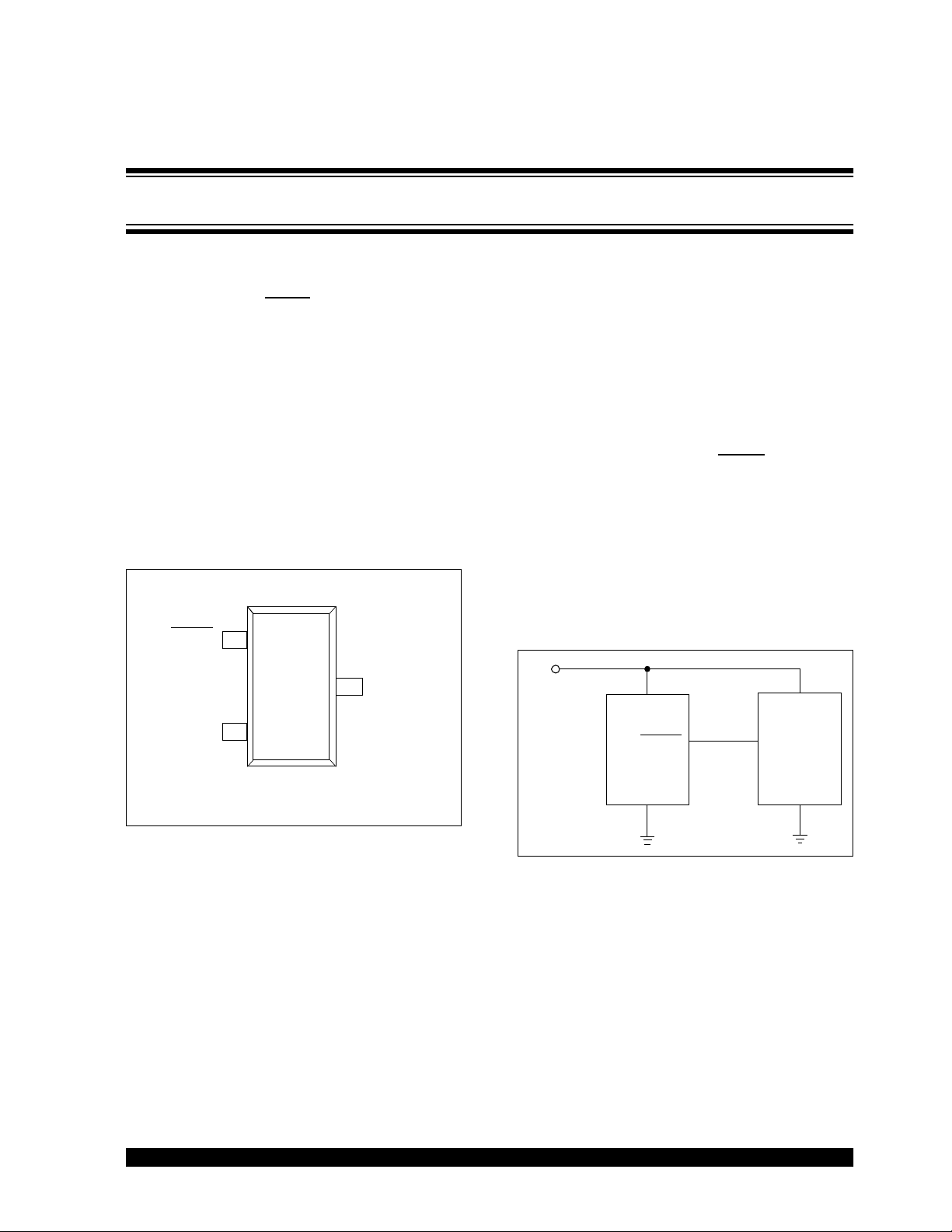
Package Type
3-Pin SOT-23B*
RESET
**(RESET)
* 3-Pin SOT-23B is equivalent to JEDEC TO-236
**( ) is for TC1274
1
TC1272
TC1273
TC1274
V
2
CC
3
GND
General Description
The TC1272/TC1273/TC1274 are cost-effective
system supervisor circuits designed to monitor V
digital systems and provide a reset signal to the host
processor when necessary. No external components
are required.
The reset output is driven active within 20 µsec of V
falling through the reset voltage threshold. RESET is
maintained active for a minimum of 100 msec after
V
rises above the reset threshold. The TC1274 has
CC
an active-high RESET output, while the TC1272 and
TC1273 have an active-low RESET
TC1272 and TC1274 each have a complimentary output, while the TC1273 has an open-drain output. The
output of the TC1272 and TC1273 is valid down to V
= 1.2V. The TC1274 is valid down to VCC = 1.8V. All
three devices are available in a 3-Pin SOT-23B
package.
The TC1272/TC1273/TC1274 devices are optimized to
reject fast transient glitches on the V
output. The
line.
CC
CC
in
CC
CC
Typical Operating Circuit
V
CC
2
V
CC
RESET
1
TC1272
GND GND
3
RESET
Input
Processor
V
CC
2003 Microchip Technology Inc. DS21382B-page 1
TC1272/TC1273/TC1274
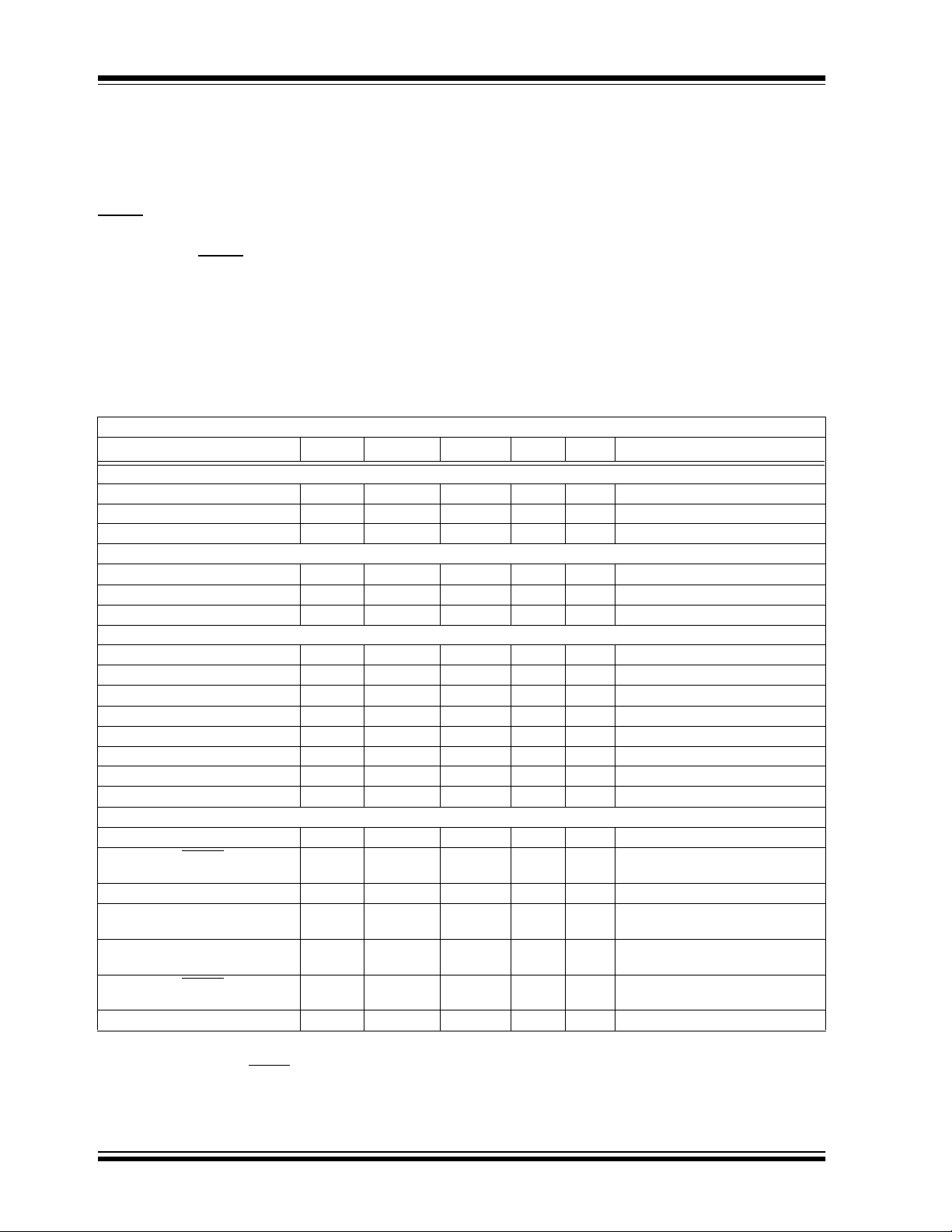
1.0 ELECTRICAL CHARACTERISTICS
† Stresses above those listed under "Absolute Maximum Ratings" may cause permanent damage to the device. These are
stress ratings only and functional operation of the device at
these or any other conditions above those indicated in the
Absolute Maximum Ratings†
Supply Voltage (VCC to GND) ............................. +6.0V
, RESET.......................... -0.3V to (VCC + 0.3V)
RESET
Input Current, V
Output Current, RESET
Power Dissipation (T
..............................................20 mA
CC
, RESET ........................20 mA
≤ 70°C)
A
operation sections of the specifications is not implied. Exposure to Absolute Maximum Rating conditions for extended
periods may affect device reliability.
3-Pin SOT-23B (derate 4 mW/°C above +70°C)
................................................................ 230 mW
Operating Temperature Range.............-40°C to +85°C
Storage Temperature Range..............-65°C to +150°C
DC CHARACTERISTICS
Electrical Specifications: Unless otherwise noted, TA = -40°C to +85°C. Typical values are at TA = +25°C.
Parameters Sym Min Typ Max Units Conditions
Supply Voltage
TC1272, TC1273 V
TC1274 V
Output Voltage @ 0-500 µA V
CC
CC
OH
Output Current @ 2.4 Volts
= 5V TC1272 I
V
CC
= 4V TC1274 I
V
CC
Output Current @ 0.4 Volts I
OH
OH
OL
Operating Current
< 5.5V: TC1272, TC1274 I
V
CC
< VCC < 5.5V: TC1273 I
V
CCTP
< V
V
CC
Trip Point (TC1272/3/4-5) V
V
CC
Trip Point (TC1272/3/4-10) V
V
CC
Trip Point (TC1272/3/4-15) V
V
CC
: TC1273 I
CCTP
Output Capacitance C
Internal Pull-Up Resistor R
AC Electrical Characteristics: T
RESET Active Time t
Detect to RESET
V
CC
TC1272, TC1273
Detect to RESET - TC1274 t
V
CC
Slew Rate
V
CC
(V
(MAX) to V
CCTP
Slew Rate
V
CC
(V
(MIN) to V
CCTP
Detect to RESET
V
CC
TC1272, TC1273
Detect to RESET - TC1274 t
V
CC
CCTP
CCTP
(MIN))
(MAX))
CC
CC
CC
CCTP-5
CCTP-10
CCTP-15
OUT
P
= -40°C to +85°C unless otherwise noted. Typical values are at TA = +25°C.
A
RST
t
RPD1
RPD2
t
F
t
R
t
RPU1
RPU2
Note 1: All voltages referenced to ground.
2: Measured with V
3: Measured with RESET
4: t
= 5 µsec.
R
5: A 1 kΩ external resistor may be required in some applications for proper operation of the microprocessor reset control
≥ 2.7 volts.
CC
output open for TC1272/TC1273; measured with RESET output open for TC1274.
circuit when using the TC1273.
1.2 — 5.5 V Note 1
1.8 — 5.5 V
VCC – 0.5V VCC – 0.1V — V TC1272, TC1274 (Note 1)
—10—mANote 2
—8—mA
+10 30 — mA Note 2, Note 5
—1740µANote 3
—1740µANote 3
— 700 1200 µA Note 3
4.50 4.62 4.75 V Note 1
4.25 4.37 4.49 V Note 1
4.00 4.12 4.24 V Note 1
—9—pF
369kΩ
100 200 300 msec
—2050µsecV
—2050µsecV
CC(LOW)
CC(LOW)
= 1V, Figure 4-2
= 1V, Figure 4-4
300 — — µsec Figure 4-2, Figure 4-4
0 — — nsec Figure 4-1, Figure 4-3
100 200 300 msec Note 4, Figure 4-1
100 200 300 msec Note 4, Figure 4-3
DS21382B-page 2 2003 Microchip Technology Inc.
TC1272/TC1273/TC1274
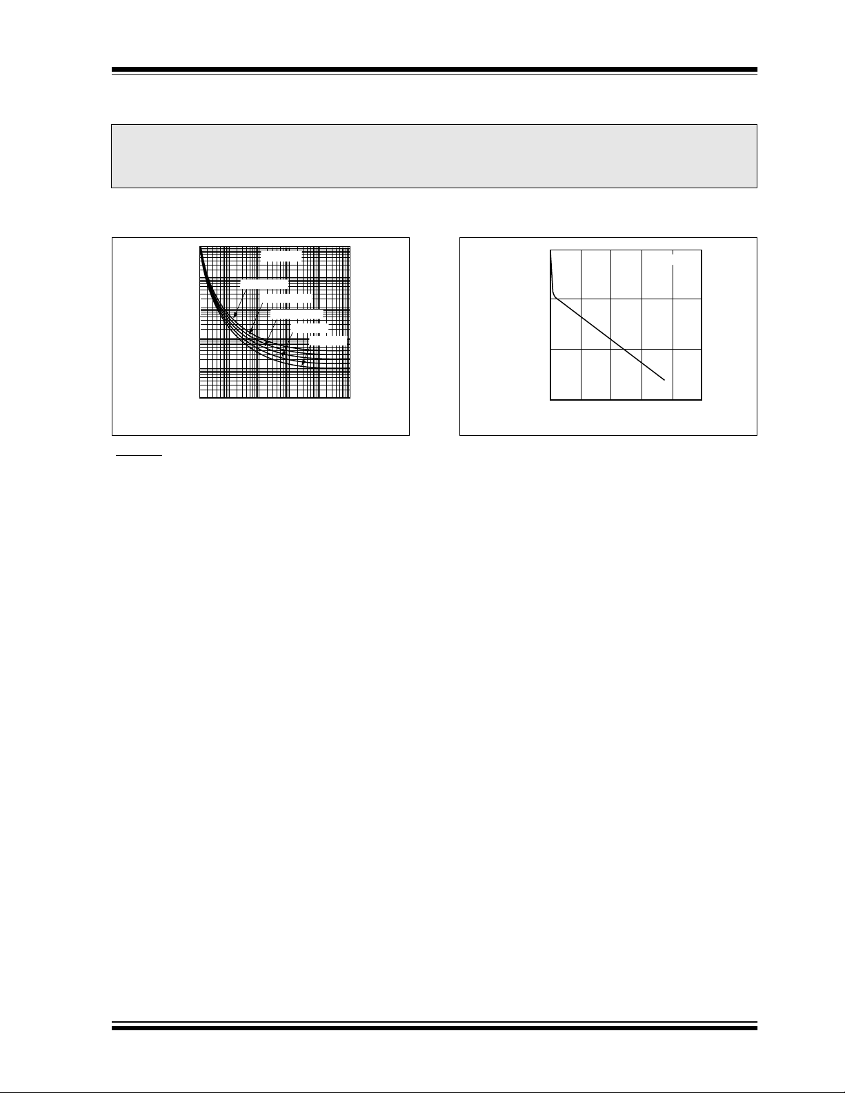
2.0 TYPICAL PERFORMANCE CURVES
Note: The graphs and tables provided following this note are a statistical summary based on a limited number of
samples and are provided for informational purposes only. The performance characteristics listed herein
are not tested or guaranteed. In some graphs or tables, the data presented may be outside the specified
operating range (e.g., outside specified power supply range) and therefore outside the warranted range.
Note: Unless otherwise indicated, T
Comparator Overdrive voltage (V
TA = 25°C
sec)
100000
µ
10000
1000
TO RESET DELAY (
100
CC
V
10
1
FIGURE 2-1: V
(RESET
).
VOD = 20mV
VOD = 100mV
VOD = 200mV
10
100
V
SLEW RATE (V/µsec)
CC
Detect to Reset
CC
VOD = 1V
1000
= -40°C to +85°C. Typical values are at TA = +25°C.
A
) is defined in Figure 4-5
OD
300
sec)
µ
200
VOD = 2V
10000
100000
100
TO RESET DELAY (
CC
V
0
0
COMPARATOR OVERDRIVE (V)
FIGURE 2-2: Reset Delays vs. Comparator Overdrive.
TA = 25°C
12 3
4
5
2003 Microchip Technology Inc. DS21382B-page 3
TC1272/TC1273/TC1274
3.0 PIN DESCRIPTIONS
The descriptions of the pins are listed in Table 3-1.
TABLE 3-1: PIN FUNCTION TABLES
Pin No. Symbol Function
1 RESET
1 RESET RESET Output (TC1274)
2V
3 GND Ground
CC
RESET Output (TC1272 and TC1273)
Supply voltage (1.2V to 5.5V TC1272 and TC1273; 1.8V to 5.5V TC1274)
3.1 RESET Output (RESET)
The RESET output remains low while VCC is below the
reset voltage threshold, and for 200 msec (100 msec
min.) after V
stage of the TC1272 is complimentary, while the output
stage of the TC1273 is open-drain.
rises above reset threshold. The output
CC
3.2 RESET Output (RESET)
The RESET output remains high while VCC is below the
reset voltage threshold, and for 200 msec (100 msec
min.) after V
stage of the TC1274 is complimentary.
rises above reset threshold. The output
CC
DS21382B-page 4 2003 Microchip Technology Inc.

4.0 APPLICATIONS INFORMATION
4.1 Operation – Power Monitor
TC1272/TC1273/TC1274
t
R
The TC1272/TC1273/TC1274 is designed to function
as a voltage monitor for +5V systems. These devices
provide a RESET signal to indicate that the V
CC
has
dropped below a preset voltage level that is selected by
the suffix part number. In addition, the RESET is held
active for approximately 200 ms after the power supply
has risen above the voltage threshold level to allow
time for the power supply to stabilize before system
operation commences.
t
R
V
(MAX)
CCTP
V
CCTP
t
RPU1
V
OH
V
CC
RESET
V
CCTP
(MIN)
FIGURE 4-1: Timing Diagram – Power Up (TC1272/TC1273).
V
(MAX)
CCTP
V
CCTP
t
RPU2
V
OL
V
CC
RESET
V
CCTP
(MIN)
FIGURE 4-3: Timing Diagram – Power Up (TC1274).
t
F
V
CC
V
(MAX)
CCTP
V
CCTP
V
CCTP
(MIN)
t
RPD2
t
V
CCTP
V
F
(MIN)
OL
t
RPD1
V
CC
RESET
V
CCTP
(MAX)
V
CCTP
FIGURE 4-2: Timing Diagram – Power Down (TC1272/TC1273).
V
OH
RESET
RESET Slews With V
FIGURE 4-4: Timing Diagram – Power Down (TC1274).
CC
2003 Microchip Technology Inc. DS21382B-page 5

TC1272/TC1273/TC1274
4.2 V
The TC1272/TC1273/TC1274 provides accurate V
Transient Rejection
CC
CC
monitoring and reset timing during power-up, powerdown and brownout/sag conditions, and rejects
negative-going transients (glitches) on the power
supply line. Figure 4-5 shows the maximum transient
duration vs. maximum negative excursion (overdrive)
for glitch rejection. Any combination of duration and
overdrive that lays under the curve will not generate a
reset signal. Combinations above the curve are
detected as a brownout or power-down condition.
Transient immunity can be improved by adding a
capacitor in close proximity to the V
pin of the
CC
TC1272/TC1273/TC1274.
4.3 RESET Signal Integrity During Power-Down
The TC1272 RESET output is valid to VCC = 1.2V.
Below this voltage the output becomes an "open
circuit" and does not sink current. This means CMOS
logic inputs to the µP will be floating at an undetermined voltage. Most digital systems are completely
shut down well above this voltage. However, in situations where RESET
V
= 0V, a pull-down resistor must be connected from
CC
RESET
to ground to discharge stray capacitances and
hold the output low (Figure 4-6). This resistor value,
though not critical, should be chosen such that it does
not appreciably load RESET
(100 kΩ will be suitable for most applications). Similarly, a pull-up resistor to V
TC1274 to ensure a valid high RESET
1.8V.
must be maintained valid to
under normal operation
is required for the
CC
for VCC below
V
CC
V
TH
Overdrive
Duration
500
400
300
200
100
0
MAXIMUM TRANSIENT DURATION (µsec)
1
RESET COMPARATOR OVERDRIVE,
TA = +25°C
10
[V
CCTP-VCC
TC1272/3/4
100
] (mV)
1000
FIGURE 4-5: Maximum Transient Duration vs. Overdrive For Glitch Rejection At +25°C.
V
CC
V
CC
TC1272
RESET
R
1
GND
FIGURE 4-6: Ensuring Reset
V
=0V.
cc
DS21382B-page 6 2003 Microchip Technology Inc.
100 kΩ
Valid To

5.0 PACKAGING INFORMATION
5.1 Package Marking Information
3-Pin SOT-23B
3
1 2 3 4
12
2
represents part number code +
1
&
temperature range and voltage
TC1272/TC1273/TC1274
Reset VCC
Threshold (V)
4.62 X1 Y1 Z1
4.37 X2 Y2 Z2
4.12 X3 Y3 Z3
represents year and quarter code
3
4
represents lot ID number
TC1272
Code
TC1273
Code
TC1274
Code
2003 Microchip Technology Inc. DS21382B-page 7

TC1272/TC1273/TC1274
3-Lead Plastic Small Outline Transistor (TT) (SOT23)
E
E1
2
B
n
1
c
β
Number of Pins
Pitch
Outside lead pitch (basic)
Molded Package Thickness
Foot Angle
Lead Thickness
Mold Draft Angle Top
Mold Draft Angle Bottom
* Controlling Parameter
§ Significant Characteristic
Notes:
Dimensions D and E1 do not include m old flash or protrusions. Mold flash or protrusions shall not exceed
.010” (0.254mm) per side.
JEDEC Equivalent: TO-236
Drawing No. C04-104
n
p
p1
A2
φ
c
α
β
p1
D
p
A
φ
L
A1
MILLIMETERSINCHES*Units
0.96.038
1.92.076
α
A2
MAXNOMMINMAXNOMMINDimension Limits
33
1.121.010.89.044.040.035AOverall Height
1.020.950.88.040.037.035
0.100.060.01.004.002.000A1Standoff §
2.642.372.10.104.093.083EOverall Width
1.401.301.20.055.051.047E1Molded Package Width
3.042.922.80.120.115.110DOverall Length
0.550.450.35.022.018.014LFoot Lengt h
10501050
0.180.140.09.007.006.004
0.510.440.37.020.017.015BLead Width
10501050
10501050
DS21382B-page 8 2003 Microchip Technology Inc.

TC1272/TC1273/TC1274
PRODUCT IDENTIFICATION SYSTEM
To order or obtain information, e.g., on pricing or delivery, refer to the factory or the listed sales office.
PART NO. X /XX
Device
Device: TC1272: 3-Pin Re set Monitor - Complementary
Reset V
CC
Threshold Voltage
Temperature Range: E = -40°C to +85°C
Package: NB = Plastic Small Outline Transistor (SOT-23), 3-lead
Sales and Support
Data Sheets
Products supported by a preliminary Data Sheet may have an errata sheet describing minor operational differences and recommended workarounds. To determine if an errata sheet exists for a particular device, please contact one of the following:
XX
Reset V
CC
Threshold
TC1273: 3-Pin Reset Monitor - Open Drain
TC1274: 3-Pin Re set Monitor - Complementary
5 = 4.62V
10 = 4.37V
15 = 4.12V
Range
PackageTe mp er at ur e
Examples:
a) TC1272-10ENBTR: 4.37V Reset
b) TC1272-15ENBTR: 4.12V Reset
c) TC1272-5ENBTR: 4.62V Reset
a) TC1273-10ENBTR: 4.37V Reset
b) TC1273-15ENBTR: 4.12V Reset
c) TC1273-5ENBTR: 4.62V Reset
a) TC1274-10ENBTR: 4.37V Reset
b) TC1274-15ENBTR: 4.12V Reset
c) TC1274-5ENBTR: 4.62V Reset
1. Your local Microchip sales office
2. The Microchip Corporate Literature Center U.S. FAX: (480) 792-7277
3. The Microchip Worldwide Site (www.microchip.com)
Please specify which device, revision of silicon and Data Sheet (include Literature #) you are using.
Customer Notification System
Register on our web site (www.microchip.com/cn) to receive the most current information on our products.
2003 Microchip Technology Inc. DS21382B-page9

TC1272/TC1273/TC1274
NOTES:
DS21382B-page 10 2003 Microchip Technology Inc.

Note the following details of the code protection feature on Microchip devices:
• Microchip products meet the specification contained in their particular Microchip Data Sheet.
• Microchip believes that its family of products is one of the most secure families of its kind on the market today, when used in the
intended manner and under normal conditions.
• There are dishonest and possibly illegal methods used to breach the code protection feature. All of these methods, to our
knowledge, require using the Microchip products in a manner outside the operating specifications contained in Microchip's Data
Sheets. Most likely, the person doing so is engaged in theft of intellectual property.
• Microchip is willing to work with the customer who is concerned about the integrity of their code.
• Neither Microchip nor any other semiconductor manufacturer can guarantee the security of their code. Code protection does not
mean that we are guaranteeing the product as “unbreakable.”
Code protection is constantly evolving. We at Microchip are committed to continuously improving the code protection features of our
products. Attempts to break microchip’s code protection feature may be a violation of the Digital Millennium Copyright Act. If such
acts allow unauthorized access to your software or other copyrighted work, you may have a right to sue for relief under that Act.
Information contained in this publication regarding device
applications and the like is intended through suggestion only
and may be superseded by updates. It is your responsibility to
ensure that your application meets with your specifications. No
representation or warranty is given and no liability is assumed
by Microchip Technology Incorporated with respect to the
accuracy or use of such information, or infringement of patents
or other intellectual property rights arising from such use or
otherwise. Use of Microchip’s products as critical components in
life support systems is not authorized except with express
written approval by Microchip. No licenses are conveyed,
implicitly or otherwise, under any intellectual property rights.
Trademarks
The Microchip name and logo, the Micr ochip logo, KEELOQ,
MPLAB, PIC, PICmicro, PICSTART, PRO MATE and
PowerSmart are registered trademarks of Microchip Technology
Incorporated in the U.S.A. and other countries.
FilterLab, microID, MXDEV, MXLAB, PICMASTER, SEEVAL
and The Embedded Control Solutions Company are registered
trademarks of Microchip Technology Incorporated in the U.S.A.
Accuron, Application Maestro, dsPIC, dsPICDEM,
dsPICDE M.net, ECONOMONITOR, FanSense, FlexROM,
fuzzyLAB, In-Circuit Serial Programming, ICSP, ICEPIC,
microPort, Migratable Memory, MPASM, MPLIB, MPLINK,
MPSIM, PICC, PICkit, PICDEM, PICDEM.net, PowerCal,
PowerInfo, PowerMate, PowerTool, rfLAB, rfPIC, Select Mode,
SmartSensor, SmartShunt, SmartTel and Total Endurance are
trademarks of Microchip Technology Incorporated in the U.S.A.
and other countries.
Serialized Quick Turn Programming (SQTP) is a service mark of
Microchip Technology Incorporated in the U.S.A.
All other trademarks mentioned herein are property of their
respective companies.
© 2003, Microchip Technology Incorporated, Printed in the
U.S.A., All Rights Reserved.
Printed on recycled pape r.
Microchip received QS-9000 quality system
certification for its worldwide headquarters,
design and wafer fabrication facilities in
Chandler and Tempe, Arizona in July 1999
and Mountain View, California in March 2002.
The Company’s quality system processes and
procedures are QS-9000 compliant for its
PICmicro
devices, Serial EEPROMs, microperipherals,
non-volatile memory and analog produ cts. In
addition, Microchip’s qua lity system for the
design and manufacture of development
systems is ISO 9001 certified.
®
8-bit MCUs, KEEL
®
code hopping
OQ
2003 Microchip Technology Inc. DS21382B - page 11

M
W
ORLDWIDE SALES AND SERVICE
AMERICAS
Corporate Office
2355 West Chandler B lvd.
Chandler, AZ 85224-6199
Tel: 480-792-7200 Fax: 480-792-7277
Technical Support: 480-792-7627
Web Address: http://www.microchip.com
Atlanta
3780 Mansell Road, Suite 130
Alpharetta, GA 30022
Tel: 770-640-0034 Fax: 770-640-0307
Boston
2 Lan Drive, Suit e 120
Westford, MA 01886
Tel: 978-692-3848 Fax: 978-692-3821
Chicago
333 Pierce Road, S uite 180
Itasca, IL 60143
Tel: 630-285-0071 Fax: 630-285-0075
Dallas
4570 Westgrove Drive, Suite 160
Addison, TX 75001
Tel: 972-818-7423 Fax: 972-818-2924
Detroit
Tri-Atria Office Building
32255 Northwestern Highway, Suite 190
Farmington Hills, MI 48334
Tel: 248-538-2250 Fax: 248-538-2260
Kokomo
2767 S. Albright Road
Kokomo, Indiana 46902
Tel: 765-864-8360 Fax: 765-864-8387
Los Angeles
18201 Von Karman, Suite 10 90
Irvine, CA 92612
Tel: 949-263-1888 Fax: 949-263-1338
Phoenix
2355 West Chandler B lvd.
Chandler, AZ 85224-6199
Tel: 480-792-7966 Fax: 480-792-4338
San Jose
Microchip Technology Inc.
2107 North First S treet, Suite 590
San Jose, CA 95131
Tel: 408-436-7950 Fax: 408-436-7955
Toro nto
6285 Northam Drive, Suite 108
Mississauga, Ontario L4V 1X5, Canada
Tel: 905-673-0699 Fax: 905-673-6509
ASIA/PACIFIC
Australia
Microchip Technology Australia Pty Ltd
Marketing Support Division
Suite 22, 41 Rawson Street
Epping 2121, NSW
Australia
Tel: 61-2-9868-6733 Fax: 61-2-9868-6755
China - Beijing
Microchip Technology Consulting (Shanghai)
Co., Ltd., Beijing Liaison Office
Unit 915
Bei Hai Wan Tai Bldg.
No. 6 Chaoyangmen Beidajie
Beijing, 100027, No. China
Tel: 86-10-852821 00 Fax: 86-10-852 82104
China - Chengdu
Microchip Technology Consulting (Shanghai)
Co., Ltd., Chengdu Liaison Office
Rm. 2401-2402, 24th Floor,
Ming Xing Financial Tower
No. 88 TIDU Street
Chengdu 610016, China
Tel: 86-28-867662 00 Fax: 86-28-867 66599
China - Fuzhou
Microchip Technology Consulting (Shanghai)
Co., Ltd., Fuzhou Liaison Office
Unit 28F, World Trade Plaza
No. 71 Wusi Road
Fuzhou 350001, China
Tel: 86-591-75035 06 Fax: 86-591-7503521
China - Hong Kong SAR
Microchip Technology Hongkong Ltd.
Unit 901-6, Tower 2, Metroplaza
223 Hing Fong Road
Kwai Fong, N.T., Hong Kong
Tel: 852-2401-120 0 Fax: 852-2401-3431
China - Shanghai
Microchip Technology Consulting (Shanghai)
Co., Ltd.
Room 701, Bldg. B
Far East International Plaza
No. 317 Xian Xia Road
Shanghai, 200051
Tel: 86-21-6275-5700 Fax: 86-21-6275-5060
China - Shenzhen
Microchip Technology Consulting (Shanghai)
Co., Ltd., Shenzhen L iaison Office
Rm. 1812, 18/F, Building A, United Plaza
No. 5022 Binhe Road, Futian District
Shenzhen 518033, Ch ina
Tel: 86-755-82901 380 Fax: 86-755-82966626
China - Qingdao
Rm. B505A, Fullhope Plaza,
No. 12 Hong Kong Central Rd.
Qingdao 266071, China
Tel: 86-532-50273 55 Fax: 86-532-5027205
India
Microchip Technology Inc.
India Liaison Office
Marketing Support Division
Divyasree Chambers
1 Floor, Wing A (A3/A4)
No. 11, O’Shaugnessey Road
Bangalore, 560 025, India
Tel: 91-80-229006 1 Fax: 91-80-2290 062
Japan
Microchip Technology Japan K.K.
Benex S-1 6F
3-18-20, Shinyokohama
Kohoku-Ku, Yokohama-shi
Kanagawa, 222-0033, Japan
Tel: 81-45-471- 6166 Fax: 81-45-471-6122
Korea
Microchip Technology Korea
168-1, Youngbo Bldg. 3 Floor
Samsung-Dong, Kangnam-Ku
Seoul, Korea 135-882
Tel: 82-2-554-7200 Fax: 82-2-558-593 4
Singapore
Microchip Technology Singapore Pte Ltd.
200 Middle Road
#07-02 Prime Centre
Singapore, 188980
Tel: 65-6334-8870 Fax: 65-6334-8850
Ta iw an
Microchip Technology (Barbados) Inc.,
Taiwan Branch
11F-3, No. 207
Tung Hua North Road
Taipei, 105, Taiwan
Tel: 886-2-2717-7175 Fax: 886-2-2545-0139
EUROPE
Austria
Microchip Technology Austria GmbH
Durisolstrasse 2
A-4600 Wels
Austria
Tel: 43-7242-2244-399
Fax: 43-7242-2244-393
Denmark
Microchip Technology Nordic ApS
Regus Business Centre
Lautrup hoj 1-3
Ballerup DK-2750 Denmark
Tel: 45 4420 9895 Fax: 45 4420 9910
France
Microchip Technology SARL
Parc d’Activite du Moulin de Massy
43 Rue du Saule Trapu
Batiment A - ler Etage
91300 Massy, France
Tel: 33-1-69-53-63-20 Fax: 33-1-69-30-90-79
Germany
Microchip Technology GmbH
Steinheilstrasse 10
D-85737 Ismaning, Germany
Tel: 49-89-627-144-0
Fax: 49-89-627-144-44
Italy
Microchip Technology SRL
Via Quasimodo, 12
20025 Legnano (MI)
Milan, Italy
Tel: 39-0331-742611 Fax: 39-0331-466781
United Kingdom
Microchip Ltd.
505 Eskdale Road
Winnersh Triangle
Wokingham
Berkshire, England RG41 5TU
Tel: 44 118 921 5869 Fax: 44-118 921-5820
03/25/03
DS21382B-page 12 2003 Microchip Technology Inc.
 Loading...