

M
TC1232
Microprocessor Monitor
Features
• Precision Voltage Monitor
- Adjustable +4.5V or +4.75V
• Reset Pulse Width – 250 msec minimum
• No External Components
• Adjustable Watchdog Timer
- 150 msec, 600 msec or 1.2 sec
• Debounced Manual Reset Input for External
Override
Applications
• Computers
• Controllers
• Intelligent Instruments
• Automotive Systems
• Critical µP Power Monitoring
General Description
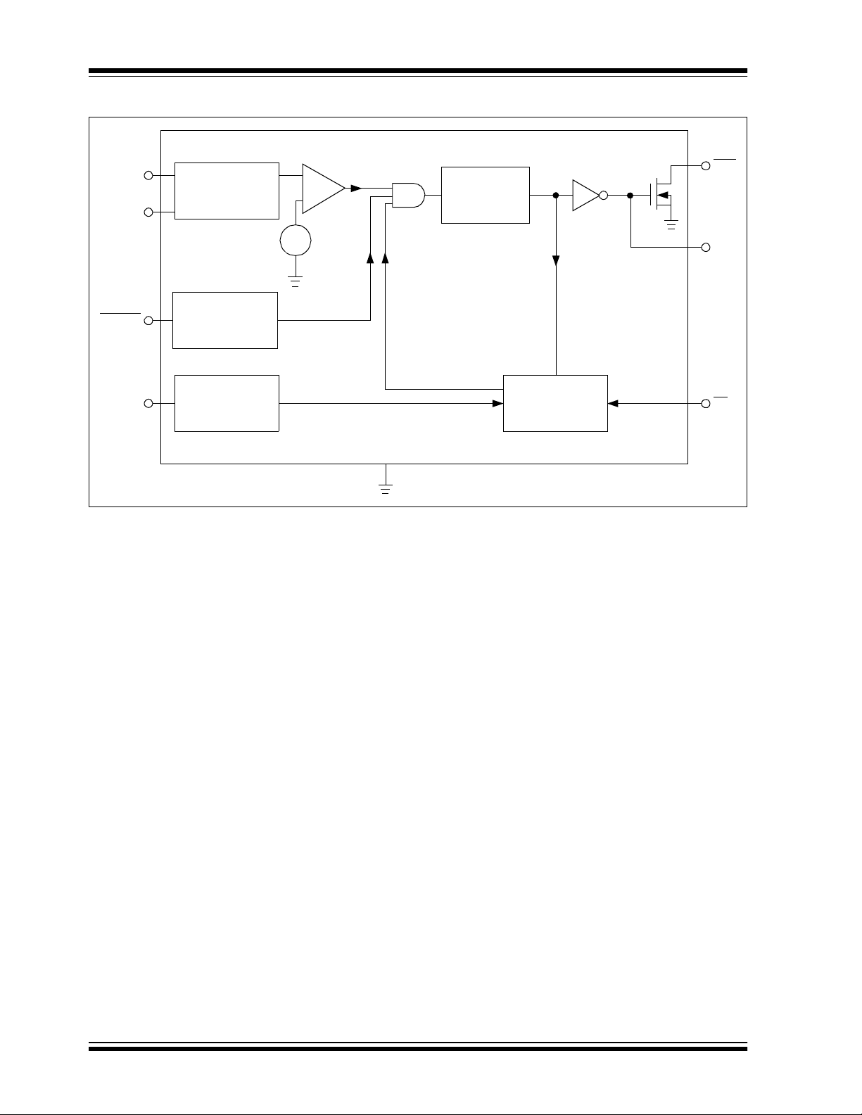
The TC1232 is a fully-integrated processor supervisor
that provides three important functions to safeguard
processor sanity: precision power on/off reset control,
watchdog timer and external reset override.
On power-up, the TC1232 holds the processor in the
reset state for a minimum of 250 msec after V
within tolerance to ensure a stable system start-up.
Microprocessor sanity is monitored by the on-board
watchdog circuit. The microprocessor must provide a
periodic low-going signal on the ST
processor fail to supply this signal within the selected
time-out period (150 msec, 600 msec or 1200 msec),
an out-of-control processor is indicated and the
TC1232 issues a processor reset as a result.
The outputs of the TC1232 are immediately driven
active when the PB input is brought low by an external
push-button switch or other electronic signal. When
connected to a push-button switch, the TC1232
provides contact debounce.
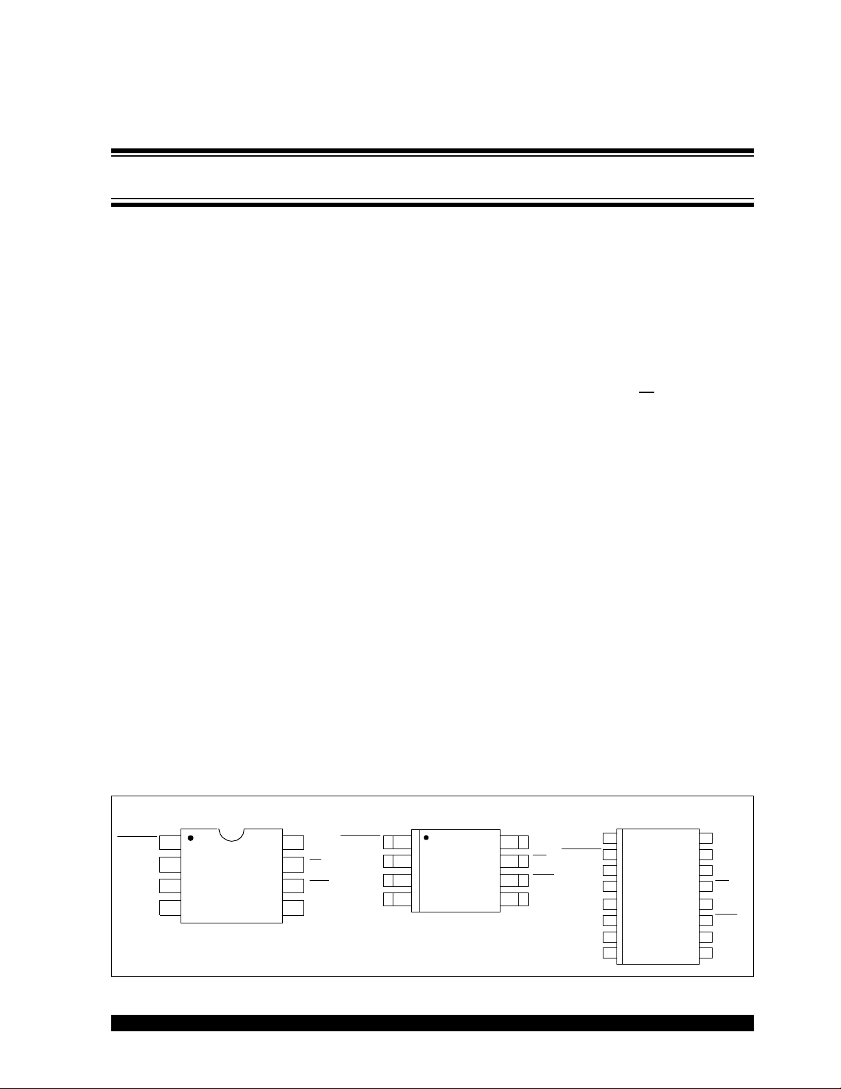
The TC1232 is packaged in a space-saving 8-Pin PDIP
or SOIC package and a 16-Pin SOIC (Wide) package
and requires no external components.
input. Should the
CC
is
Package Types
16-Pin SOIC Wide8-Pin PDIP 8-Pin SOIC
1
V
PB RST
2003 Microchip Technology Inc. DS21370B-page 1
18
TD
TOL
GND
2
3
4
TC1232
7
6
5
CC
ST
RST
RST
PB RST
TOL
18
18
TD
27
TC1232
TC1232
36
36
45
45
V
CC
ST
RST
RSTGND
NC
PB RST
NC
TD
NC
TOL
NC
GND
2
3
4
5
6
7
8
TC1232
16
NC
V
15
CC
NC
14
13
ST
NC
12
RST
11
NC
10
RST
9
TC1232
Functional Block Diagram
V
CC
TOL
PB RST
TD
5%/10%
Tol er an ce
Select
Debounce
Watchdog
Time ba se
Select
+
–
+
+
V
REF
–
Reset
Generator
RST
RST
TC1232
Watchdog
Time r
GND
ST
DS21370B-page 2 2003 Microchip Technology Inc.
TC1232
1.0 ELECTRICAL
CHARACTERISTICS
Absolute Maximum Ratings†
Voltage on Any Pin (With Respect to GND)
...................................................... -0.3V to +5.8V
† Stresses above those listed under "Absolute Maximum Ratings" may cause permanent damage to the device. These are
stress ratings only and functional operation of the device at
these or any other conditions above those indicated in the
operation sections of the specifications is not implied. Exposure to Absolute Maximum Rating conditions for extended
periods may affect device reliability.
Operating Temperature Range
C-Version ........................................ 0°C to +70°C
E-Version ..................................... -40°C to +85°C
Storage Temperature Range ............. -65°C to +150°C
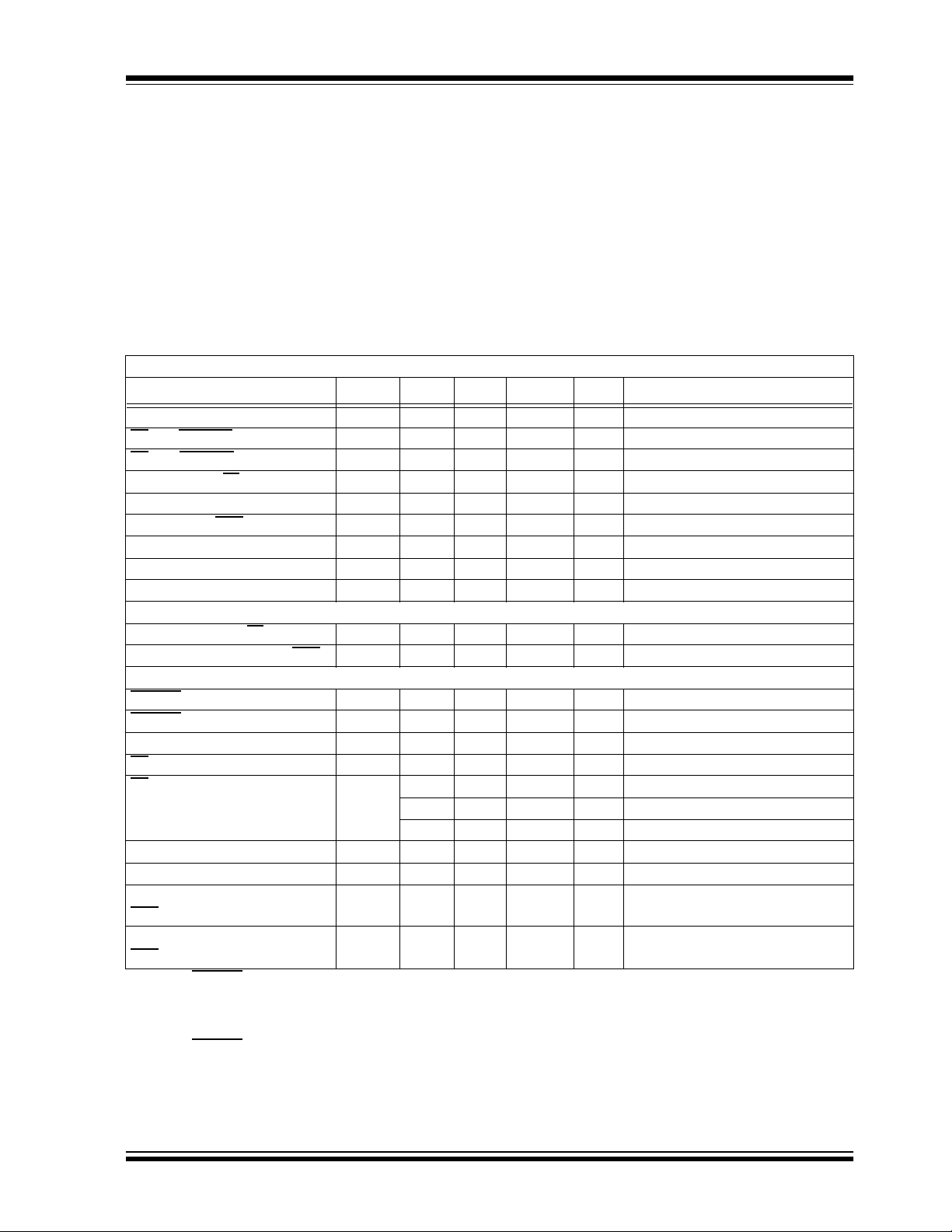
DC CHARACTERISTICS
= T
Electrical Specifications: Unless otherwise noted, T
A
Parameters Sym Min Typ Max Units Conditions
Supply Voltage V
and PB RST Input High Level V
ST
ST
and PB RST Input Low Level V
Input Leakage ST
, TOL I
Output Current RST I
Current RST, RST
Operating Current I
V
5% Trip Point V
CC
V
10% Trip Point V
CC
CC
IH
IL
L
OH
I
OL
CC
CCTP
CCTP
4.5 5.0 5.5 V
2.0 — VCC +0.3 V Note 1
-0.3 — +0.8 V
-1.0 — +1.0 µA
-1.0 -12 — mA VOH = 2.4V
2.0 10 — mA VOL = 0.4V
— 50 200 µA Note 2
4.50 4.62 4.74 V TOL = GND (Note 3)
4.25 4.37 4.49 V TOL = VCC (Note 3)
Capacitance Electrical Characteristics: Unless otherwise noted, T
Input Capacitance ST
Output Capacitance RST, RST
, TOL C
C
IN
OUT
—— 5 pF
—— 7 pF
AC Electrical Characteristics: Unless otherwise noted, T
PB RST
PB RST
Delay t
Reset Active Time t
Pulse Width t
ST
ST
Time-out Period t
t
PB
PBD
RST
ST
TD
20 — — msec Figure 3-3 (Note 5)
1 4 20 msec Figure 3-3
250 610 1000 msec
20 — — nsec Figure 3-4
62.5 150 250 msec TD Pin = 0V, Figure 3-4
250 600 1000 msec TD Pin = Open, Figure 3-4
500 1200 2000 msec TD Pin = V
VCC Fall Time t
V
Rise Time t
CC
V
Detect to RST High and
CC
Low
RST
V
Detect to RST High and
CC
Open
RST
Note 1: PB RST
is internally pulled up to Vcc with an internal impedance of typically 40 kΩ.
t
RPD
t
RPU
F
R
10 — — µsec Figure 3-5, (Note 4)
0— —µsecFigure 3-6, (Note 4)
— — 100 nsec Figure 3-7, VCC Falling
250 610 1000 msec Figure 3-8, VCC Rising, (Note 6)
2: Measured with outputs open.
3: All voltages referenced to GND.
4: Ensured by design.
= 5 µsec.
R
must be held low for a minimum of 20 msec to ensure a reset.
5: PB RST
6: t
MIN
A
= T
to T
MIN
; VCC = +4.5V to 5.5V.
MAX
= +25°C
A
to T
. (Note 4)
; VCC = +5V to ±10%.
MAX
Figure 3-4
CC,
2003 Microchip Technology Inc. DS21370B-page 3
TC1232
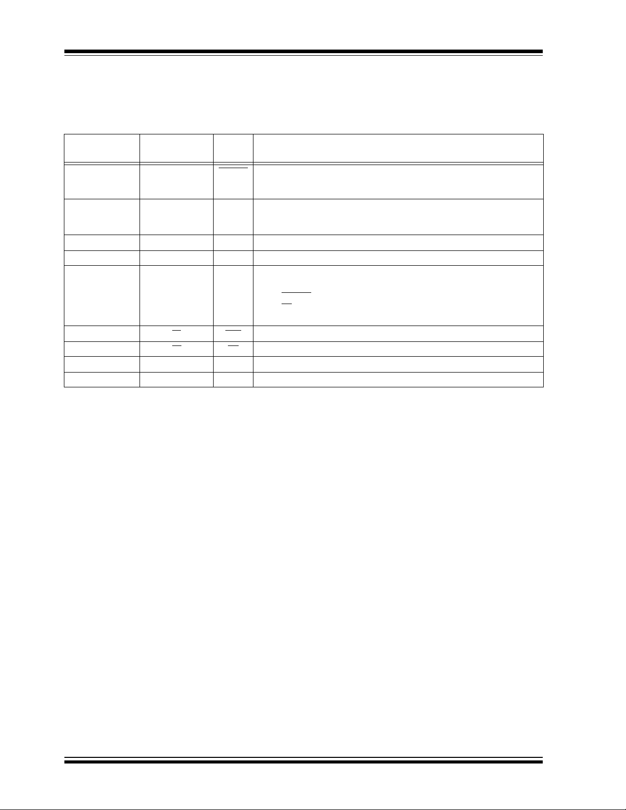
2.0 PIN DESCRIPTIONS
The descriptions of the pins are listed in Table 2-1.
TABLE 2-1: PIN FUNCTION TABLE
Pin No.
(8-pin PDIP, SOIC)
1 2 PB RST
2 4 TD Time Delay Set. The watchdog time-out select input (t
3 6 TOL Tolerance Input. Connect to GND for 5% tolerance or to V
4 8 GND Ground.
5 9 RST Reset Output (Active-High) – goes active:
611
713
815V
— 1,3,5,7,10,12,16 NC No internal connection.
Pin No.
(16-pin SOIC)
Symbol Function
Push-button Reset Input. A debounced active-low input that ignores pulses
less than 1 msec in duration and is ensured to recognize inputs of 20 msec or
greater.
0V,
t
= 600 msec for TD = open, tTD = 1.2 sec for TD = VCC).
TD
1. If V
2. If PB RST
3. If ST
4. During power-up
RST Reset output (active-low, open-drain) – see RST.
ST Strobe input. Input for watchdog timer.
The +5V power-supply input.
CC
TD
falls below the selected reset voltage threshold.
CC
is forced low.
is not strobed within the minimum time-out period.
= 150 msec for TD =
for 10% tolerance.
CC
DS21370B-page 4 2003 Microchip Technology Inc.
TC1232
3.0 DETAILED DESCRIPTION
3.1 Power Monitor
The TC1232 provides the function of warning the processor of a power failure. When V
being below the voltage levels defined by the TOL pin,
the TC1232’s comparator outputs the RST and RST
signals to a logic level that warns the system of an outof-tolerance power supply. The RST and RST
switch at a threshold value of 4.5V if TOL is tied to V
and at a value of 4.75 volts if TOL is grounded. The
RST and RST
signals are held active for a minimum of
250 msec to ensure that the power supply voltage has
been stabilized.
3.2 Push-Button Reset Input
The debounced manual reset input (PB RST) manually
forces the reset outputs into their active states. Once
PB RST
delay time) the reset outputs go active. The reset
outputs remain in their active states for a minimum of
250 msec after PB RST
A mechanical push-button or active logic signal can
drive the PB RST
input pulses less than 1 msec and ecognizes pulses of
20 msec or greater. No external pull-up resistor is
required
pull-up to
has been low for a time t
rises above VIH (Figure 3-3).
input. The debounced input ignores
because the PB RST input has an internal
of approximately 100 µA.
VCC
is detected as
CC
(the push-button
PBD
signals
CC
3.4 Supply Monitor Noise Sensitivity
The TC1232 is optimized for fast response to negativegoing changes in V
amount of electrical noise on V
using relays) may require a 0.01 µF or 0.1 µF bypass
capacitor to reduce detection sensitivity. This capacitor
should be installed as close to the TC1232 as possible
to keep the capacitor lead length short.
+5V
V
PB RST
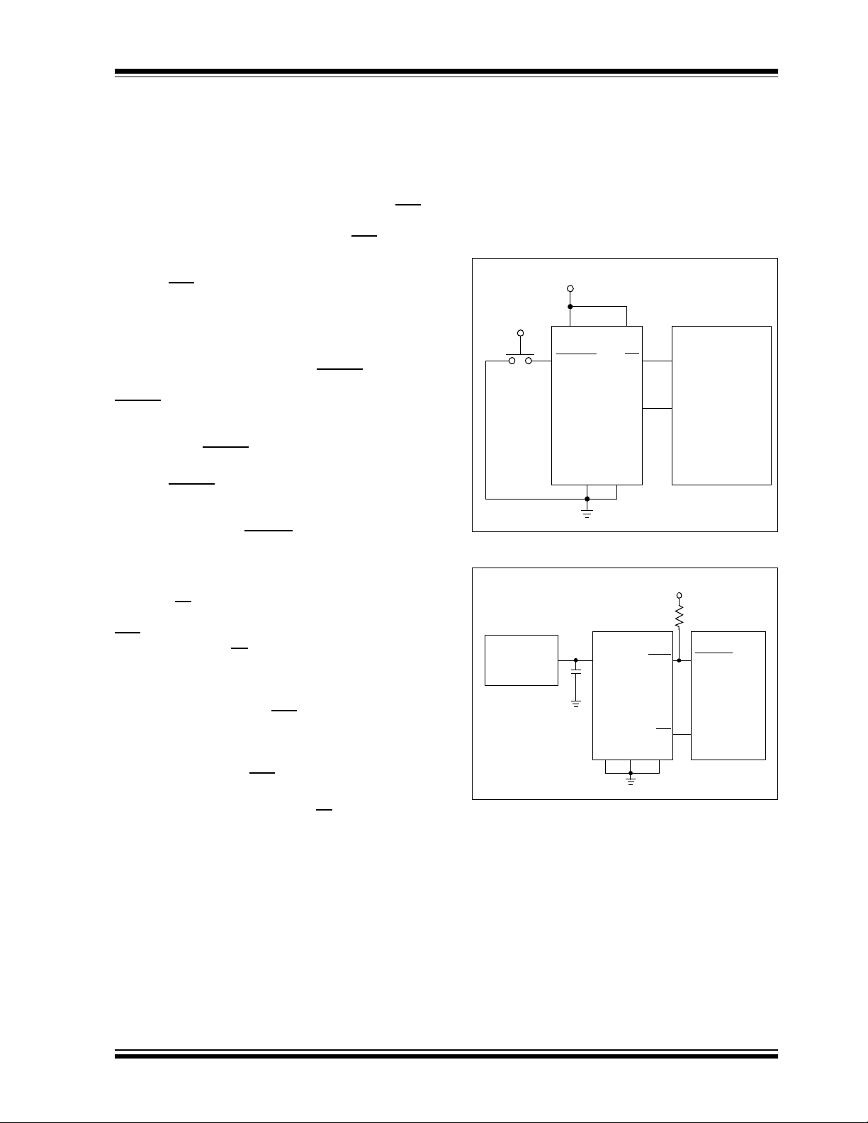
FIGURE 3-1: Push-Button Reset.
. Systems with an inordinate
DD
CC
TC1232
GND
TD
ST
RST
TOL
(such as systems
DD
I/O
processor
Reset
Micro-
3.3 Watchdog Timer
When the ST input is not stimulated for a preset time
period, the watchdog timer function forces RST and
RST
signals to the active state. The preset time period
is determined by the TD
connected to ground, 600 msec with TD floating, or
1200 msec with TD connected to V
watchdog timer starts timing-out from the set time
period as soon as RST and RST
to-low transition occurs on the ST input pin prior to
time-out, the watchdog timer is reset and begins to
time-out again. If the watchdog timer is allowed to timeout, then the RST and RST
active state for 250 msec minimum (Figure 3-2).
The software routine that strobes ST
code must be in a section of software that is executed
frequently enough so the time between toggles is less
than the watchdog time-out period. One common
technique controls the µP I/O line from two sections of
the program. The software might set the I/O line high
while operating in the foreground mode and set it low
while in the background or interrupt mode. If both
modes do not execute correctly, the watchdog timer
issues reset pulses.
inputs to be 150 msec with TD
(typical). The
CC
are inactive. If a high-
signals are driven to the
is critical. The
+5V
10 kΩ
0.1
µF
+5V
V
CC
TC1232
TOL GND
TD
RST
ST
RESET
processor
I/O
3-Terminal
Regulator
FIGURE 3-2: Watchdog Timer.
Micro-
2003 Microchip Technology Inc. DS21370B-page 5

TC1232
t
PB
V
IL
Input.
t
PBD
V
IH
t
RST
PB RST
RST
RST
The debounced PB RST input ignores input pulses less
than 1 msec and is designed to recognize pulses of
20 msec or greater.
FIGURE 3-3: Push-Button Reset –
PB RST
t
F
V
CC
+4.75V
+4.25V
FIGURE 3-5: Power-Down Slew Rate.
ST
t
ST
t
TD
Note: tTD is the maximum elapsed time between ST high-
to-low transitions (ST
is activated by falling edges
only) which will keep the watchdog timer from forcing
the reset outputs active for a time of t
function of the voltage at the TD pin, as tabulated
. ITD is a
RST
below:
I
Condition Min
TD pin = 0V 62.5 ms 150 ms 250 ms
TD pin = Open 250 ms 600 ms 1000 ms
TD pin = V
500 ms 1200 ms 2000 ms
CC
Typ
TD
Max
FIGURE 3-4: Strobe Input.
t
R
+4.75V
+4.25V
V
CC
FIGURE 3-6: Power-up Slew Rate.
DS21370B-page 6 2003 Microchip Technology Inc.

VCC = 5V
TC1232
+4.5V (5% Trip Point)
+4.25V (10% Trip Point)
RST
V
OH
V
RST
VCC SLEW RATE = 1.66 mV/µsec (0.5V/300 µsec)
FIGURE 3-7: V
Detect Reset Output
cc
OL
Delay (Power-Down).
t
RPD
V
CC
RST
RST
FIGURE 3-8: V
Delay (Power-Up).
4.6V (5% Trip Point)
4.5V(10% Trip Point)
V
OH
V
OL
Detect Reset Output
cc
t
RPU
2003 Microchip Technology Inc. DS21370B-page 7

TC1232
4.0 PACKAGING INFORMATION
4.1 Package Marking Information
8-Lead PDIP (300 mil)
XXXXXXXX
XXXXXNNN
YYWW
8-Lead SOIC (150 mil)
XXXXXXXX
XXXXYYWW
NNN
16-Lead SOIC (150 mil)
XXXXXXXXXXXXX
XXXXXXXXXXXXX
YYWWNNN
Example:
TC1232
I/P256
0351
Example:
TC1232
COA0351
256
Example:
TC1232COE
XXXXXXXXXX
0351256
Legend: XX...X Customer specific information*
YY Year code (last 2 digits of calendar year)
WW Week code (week of January 1 is week ‘01’)
NNN Alphanumeric traceability code
Note: In the event the full Microchip part number cannot be marked on one line, it will
be carried over to the next line thus limiting the number of available characters
for customer specific information.
* Standard OTP marking consists of Microchip part number, year code, week code, and traceability code.
DS21370B-page 8 2003 Microchip Technology Inc.

8-Lead Plastic Dual In-line (PA) – 300 mil (PDIP)
E1
D
2
TC1232
n
E
β
eB
Number of Pins
Pitch
Top to Seating Plane A .140 .155 .170 3.56 3.94 4.3 2
Molded Package Thickness A2 .115 .130 .145 2.92 3.30 3.68
Base to Seating Plane A1 .015 0.38
Shoulder to Shoulder Width E .300 .313 .325 7.62 7.94 8.26
Molded Package Width E1 .240 .250 .260 6.10 6.35 6.60
Overall Length D .360 .373 .385 9 .14 9.46 9.78
Tip to Seating Plane L .125 .130 .135 3.18 3.30 3.43
Lead Thickness
Upper Lead Width B1 .045 .058 .070 1 .14 1.46 1.78
Lower Lead Width B .014 .018 .022 0.36 0.4 6 0.56
Overall Row Spacing § eB .310 .370 .430 7.87 9.40 10.92
Mold Draft Angle Top
Mold Draft Angle Bottom
* Controlling Parameter
§ Significant Characteristic
Notes:
Dimensions D and E1 do not include m old flash or protrusions. Mold flash or protrusions shall not exceed
.010” (0.254mm) per side.
JEDEC Equivalent: MS-001
Drawing No. C04-018
Dimension Limits MIN NOM MAX M IN NOM MAX
1
α
A
c
Units INCHES* MILLIMETERS
n
p
c
α
β
.008 .012 .015 0.20 0.29 0.38
A1
B1
B
88
.100 2.54
51015 51015
51015 51015
A2
L
p
2003 Microchip Technology Inc. DS21370B-page 9

TC1232
8-Lead Plastic Small Outline (OA) – Narrow, 150 mil (SOIC)
E
E1
p
D
2
B
Number of Pins
Pitch
Foot Angle
Lead Thickness
Mold Draft Angle Top
Mold Draft Angle Bottom
* Controlling Paramete r
§ Significant Characteristic
Notes:
Dimensions D and E1 do not include mold flash or protrusions. Mold flash or protrusions shall not exceed
.010” (0.254mm) per side.
JEDEC Equivalent: MS-012
Drawing No. C04-057
n
45°
c
β
n
p
φ
c
α
β
1
h
A
φ
L
048048
A1
MILLIMETERSINCHES*Units
1.27.050
α
A2
MAXNOMMINMAXNOMMINDimension Limits
88
1.751.551.35.069.061.053AOverall Height
1.551.421.32.061.056.052A2Molded Package Thickness
0.250.180.10.010.007.004A1Standoff §
6.206.025.79.244.237.228EOverall Width
3.993.913.71.157.154.146E1Molded Package W idth
5.004.904.80.197.193.189DOverall Length
0.510.380.25.020.015.010hChamfer Distance
0.760.620.48.030.025.019LFoot Length
0.250.230.20.010.009.008
0.510.420.33.020.017.013BLead Width
1512015120
1512015120
DS21370B-page 10 2003 Microchip Technology Inc.

16-Lead Plastic Small Outline (OE) – Wide, 300 mil (SOIC)
TC1232
p
n
B
45°
c
β
Number of Pins
Pitch
Foot Angle
Lead Thickness
Mold Draft Angle Top
Mold Draft Angle Bottom
* Controlling Parameter
§ Significant Characteristic
Notes:
Dimensions D and E1 do not include mo ld flash or protrusions. Mold flash or protrusions shall not exceed
.010” (0.254mm) per side.
JEDEC Equivalent: MS-013
Drawing No. C04-102
E1
E
D
2
1
h
A
φ
L
n
p
φ
c
α
β
048048
A1
MILLIMETERSINCHES*Units
1.27.050
α
A2
MAXNOMMINMAXNOMMINDimension Limits
1616
2.642.502.36.104.099.093AOverall Height
2.392.312.24.094.091.088A2Molded Package Thickness
0.300.200.10.012.008.004A1Standoff §
10.6710.3410.01.420.407.394EOverall Width
7.597.497.39.299.295.291E1Molded Package Width
10.4910.3010.10.413.406.398DOverall Length
0.740.500.25.029.020.010hChamfer Distance
1.270.840.41.050.033.016LFoot Length
0.330.280.23.013.011.009
0.510.420.36.020.017.014BLead Width
1512015120
1512015120
2003 Microchip Technology Inc. DS21370B-page 11

TC1232
NOTES:
DS21370B-page 12 2003 Microchip Technology Inc.

TC1232
PRODUCT IDENTIFICATION SYSTEM
To order or obtain information, e.g., on pricing or delivery, refer to the factory or the listed sales office.
PART NO. X /XX
Device
Device: TC1232: M icroprocessor Monitor
Temperature Range: C = 0°C to +70°C
Package: PA = Plastic DIP (300 mil Body), 8-lead
Range
E = -40°C to +85°C
OA = Plastic SOIC, (150 mil Body), 8-lead
OA713 = Plastic SOIC, (150 mil Body), 8-lead
OE = Plastic SOIC (300 mil Body), 16-lead
OE713 = Plastic SOIC (300 mil Body), 16-lead
PackageTemp era tur e
Tape and Reel
Tape and Reel
Sales and Support
Data Sheets
Products supported by a preliminary Data Sheet may have an errata sheet describing minor operational differences and recommended workarounds. To determine if an errata sheet exists for a particular device, please contact one of the following:
Examples:
a) TC1232COA: 0°C to +70°C, 8L-SOIC
b) TC1232COA713: 0°C to +70°C, 8L-SOIC,
Tape and Reel
c) TC1232COE: 0°C to +70°C, 16L-SOIC
d) TC1232COE713: 0°C to +70°C, 16L-SOIC,
Tape and Reel
e) TC1232CPA: 0°C to +70°C, 8L- PDIP
f) TC1232EOA: -40°C to +85°C, 8L-SOIC
g) TC1232EOA713: -40°C to +85°C, 8L-SOIC,
Tape and Reel
h) TC1232EOE: -40°C to +85°C, 16L-SOIC
i) TC1232EOE713: -40°C to +85°C, 16L-SOIC,
Tape and Reel
j) TC1232EPA: -40°C to +85°C, 8L-PDIP
1. Your local Microchip sales office
2. The Microchip Corporate Literature Center U.S. FAX: (480) 792-7277
3. The Microchip Worldwide Site (www.microchip.com)
Please specify which device, revision of silicon and Data Sheet (include Literature #) you are using.
Customer Notification System
Register on our web site (www.microchip.com/cn) to receive the most current information on our products.
2003 Microchip Technology Inc. DS21370B-page13

TC1232
NOTES:
DS21370B-page 14 2003 Microchip Technology Inc.

Note the following details of the code protection feature on Microchip devices:
• Microchip products meet the specification contained in their particular Microchip Data Sheet.
• Microchip believes that its family of products is one of the most secure families of its kind on the market today, when used in the
intended manner and under normal conditions.
• There are dishonest and possibly illegal methods used to breach the code protection feature. All of these methods, to our
knowledge, require using the Microchip products in a manner outside the operating specifications contained in Microchip's Data
Sheets. Most likely, the person doing so is engaged in theft of intellectual property.
• Microchip is willing to work with the customer who is concerned about the integrity of their code.
• Neither Microchip nor any other semiconductor manufacturer can guarantee the security of their code. Code protection does not
mean that we are guaranteeing the product as “unbreakable.”
Code protection is constantly evolving. We at Microchip are committed to continuously improving the code protection features of our
products. Attempts to break microchip’s code protection feature may be a violation of the Digital Millennium Copyright Act. If such
acts allow unauthorized access to your software or other copyrighted work, you may have a right to sue for relief under that Act.
Information contained in this publication regarding device
applications and the like is intended through suggestion only
and may be superseded by updates. It is your responsibility to
ensure that your application meets with your specifications. No
representation or warranty is given and no liability is assumed
by Microchip Technology Incorporated with respect to the
accuracy or use of such information, or infringement of patents
or other intellectual property rights arising from such use or
otherwise. Use of Microchip’s products as critical components in
life support systems is not authorized except with express
written approval by Microchip. No licenses are conveyed,
implicitly or otherwise, under any intellectual property rights.
Trademarks
The Microchip name and logo, the Micr ochip logo, KEELOQ,
MPLAB, PIC, PICmicro, PICSTART, PRO MATE and
PowerSmart are registered trademarks of Microchip Technology
Incorporated in the U.S.A. and other countries.
FilterLab, microID, MXDEV, MXLAB, PICMASTER, SEEVAL
and The Embedded Control Solutions Company are registered
trademarks of Microchip Technology Incorporated in the U.S.A.
Accuron, Application Maestro, dsPIC, dsPICDEM,
dsPICDE M.net, ECONOMONITOR, FanSense, FlexROM,
fuzzyLAB, In-Circuit Serial Programming, ICSP, ICEPIC,
microPort, Migratable Memory, MPASM, MPLIB, MPLINK,
MPSIM, PICC, PICkit, PICDEM, PICDEM.net, PowerCal,
PowerInfo, PowerMate, PowerTool, rfLAB, rfPIC, Select Mode,
SmartSensor, SmartShunt, SmartTel and Total Endurance are
trademarks of Microchip Technology Incorporated in the U.S.A.
and other countries.
Serialized Quick Turn Programming (SQTP) is a service mark of
Microchip Technology Incorporated in the U.S.A.
All other trademarks mentioned herein are property of their
respective companies.
© 2003, Microchip Technology Incorporated, Printed in the
U.S.A., All Rights Reserved.
Printed on recycled pape r.
Microchip received QS-9000 quality system
certification for its worldwide headquarters,
design and wafer fabrication facilities in
Chandler and Tempe, Arizona in July 1999
and Mountain View, California in March 2002.
The Company’s quality system processes and
procedures are QS-9000 compliant for its
PICmicro
devices, Serial EEPROMs, microperipherals,
non-volatile memory and analog produ cts. In
addition, Microchip’s qua lity system for the
design and manufacture of development
systems is ISO 9001 certified.
®
8-bit MCUs, KEEL
®
code hopping
OQ
2003 Microchip Technology Inc. DS21370B - page 15

M
W
ORLDWIDE SALES AND SERVICE
AMERICAS
Corporate Office
2355 West Chandler B lvd.
Chandler, AZ 85224-6199
Tel: 480-792-7200 Fax: 480-792-7277
Technical Support: 480-792-7627
Web Address: http://www.microchip.com
Atlanta
3780 Mansell Road, Suite 130
Alpharetta, GA 30022
Tel: 770-640-0034 Fax: 770-640-0307
Boston
2 Lan Drive, Suit e 120
Westford, MA 01886
Tel: 978-692-3848 Fax: 978-692-3821
Chicago
333 Pierce Road, S uite 180
Itasca, IL 60143
Tel: 630-285-0071 Fax: 630-285-0075
Dallas
4570 Westgrove Drive, Suite 160
Addison, TX 75001
Tel: 972-818-7423 Fax: 972-818-2924
Detroit
Tri-Atria Office Building
32255 Northwestern Highway, Suite 190
Farmington Hills, MI 48334
Tel: 248-538-2250 Fax: 248-538-2260
Kokomo
2767 S. Albright Road
Kokomo, Indiana 46902
Tel: 765-864-8360 Fax: 765-864-8387
Los Angeles
18201 Von Karman, Suite 10 90
Irvine, CA 92612
Tel: 949-263-1888 Fax: 949-263-1338
Phoenix
2355 West Chandler B lvd.
Chandler, AZ 85224-6199
Tel: 480-792-7966 Fax: 480-792-4338
San Jose
Microchip Technology Inc.
2107 North First S treet, Suite 590
San Jose, CA 95131
Tel: 408-436-7950 Fax: 408-436-7955
Toro nto
6285 Northam Drive, Suite 108
Mississauga, Ontario L4V 1X5, Canada
Tel: 905-673-0699 Fax: 905-673-6509
ASIA/PACIFIC
Australia
Microchip Technology Australia Pty Ltd
Marketing Support Division
Suite 22, 41 Rawson Street
Epping 2121, NSW
Australia
Tel: 61-2-9868-6733 Fax: 61-2-9868-6755
China - Beijing
Microchip Technology Consulting (Shanghai)
Co., Ltd., Beijing Liaison Office
Unit 915
Bei Hai Wan Tai Bldg.
No. 6 Chaoyangmen Beidajie
Beijing, 100027, No. China
Tel: 86-10-852821 00 Fax: 86-10-852 82104
China - Chengdu
Microchip Technology Consulting (Shanghai)
Co., Ltd., Chengdu Liaison Office
Rm. 2401-2402, 24th Floor,
Ming Xing Financial Tower
No. 88 TIDU Street
Chengdu 610016, China
Tel: 86-28-867662 00 Fax: 86-28-867 66599
China - Fuzhou
Microchip Technology Consulting (Shanghai)
Co., Ltd., Fuzhou Liaison Office
Unit 28F, World Trade Plaza
No. 71 Wusi Road
Fuzhou 350001, China
Tel: 86-591-75035 06 Fax: 86-591-7503521
China - Hong Kong SAR
Microchip Technology Hongkong Ltd.
Unit 901-6, Tower 2, Metroplaza
223 Hing Fong Road
Kwai Fong, N.T., Hong Kong
Tel: 852-2401-120 0 Fax: 852-2401-3431
China - Shanghai
Microchip Technology Consulting (Shanghai)
Co., Ltd.
Room 701, Bldg. B
Far East International Plaza
No. 317 Xian Xia Road
Shanghai, 200051
Tel: 86-21-6275-5700 Fax: 86-21-6275-5060
China - Shenzhen
Microchip Technology Consulting (Shanghai)
Co., Ltd., Shenzhen L iaison Office
Rm. 1812, 18/F, Building A, United Plaza
No. 5022 Binhe Road, Futian District
Shenzhen 518033, Ch ina
Tel: 86-755-82901 380 Fax: 86-755-82966626
China - Qingdao
Rm. B505A, Fullhope Plaza,
No. 12 Hong Kong Central Rd.
Qingdao 266071, China
Tel: 86-532-50273 55 Fax: 86-532-5027205
India
Microchip Technology Inc.
India Liaison Office
Marketing Support Division
Divyasree Chambers
1 Floor, Wing A (A3/A4)
No. 11, O’Shaugnessey Road
Bangalore, 560 025, India
Tel: 91-80-229006 1 Fax: 91-80-2290 062
Japan
Microchip Technology Japan K.K.
Benex S-1 6F
3-18-20, Shinyokohama
Kohoku-Ku, Yokohama-shi
Kanagawa, 222-0033, Japan
Tel: 81-45-471- 6166 Fax: 81-45-471-6122
Korea
Microchip Technology Korea
168-1, Youngbo Bldg. 3 Floor
Samsung-Dong, Kangnam-Ku
Seoul, Korea 135-882
Tel: 82-2-554-7200 Fax: 82-2-558-593 4
Singapore
Microchip Technology Singapore Pte Ltd.
200 Middle Road
#07-02 Prime Centre
Singapore, 188980
Tel: 65-6334-8870 Fax: 65-6334-8850
Ta iw an
Microchip Technology (Barbados) Inc.,
Taiwan Branch
11F-3, No. 207
Tung Hua North Road
Taipei, 105, Taiwan
Tel: 886-2-2717-7175 Fax: 886-2-2545-0139
EUROPE
Austria
Microchip Technology Austria GmbH
Durisolstrasse 2
A-4600 Wels
Austria
Tel: 43-7242-2244-399
Fax: 43-7242-2244-393
Denmark
Microchip Technology Nordic ApS
Regus Business Centre
Lautrup hoj 1-3
Ballerup DK-2750 Denmark
Tel: 45 4420 9895 Fax: 45 4420 9910
France
Microchip Technology SARL
Parc d’Activite du Moulin de Massy
43 Rue du Saule Trapu
Batiment A - ler Etage
91300 Massy, France
Tel: 33-1-69-53-63-20 Fax: 33-1-69-30-90-79
Germany
Microchip Technology GmbH
Steinheilstrasse 10
D-85737 Ismaning, Germany
Tel: 49-89-627-144-0
Fax: 49-89-627-144-44
Italy
Microchip Technology SRL
Via Quasimodo, 12
20025 Legnano (MI)
Milan, Italy
Tel: 39-0331-742611 Fax: 39-0331-466781
United Kingdom
Microchip Ltd.
505 Eskdale Road
Winnersh Triangle
Wokingham
Berkshire, England RG41 5TU
Tel: 44 118 921 5869 Fax: 44-118 921-5820
03/25/03
DS21370B-page 16 2003 Microchip Technology Inc.
 Loading...