

Page 1

TC1017
150 mA, Tiny CMOS LDO With Shutdown
Features
• Spa ce -sav in g 5-Pi n SC- 70 an d SOT-23 Packages
• Extremely Low Operating Current for Longer
Battery Life: 53 µA (typ.)
• Very Low Dropout Voltage
• Rated 150 mA Output Current
• Requires Only 1 µF Ceramic Output Capacitance
• High Output Voltage Accuracy: ±0.5% (typ.)
• 10 µs (typ.) Wake-Up Time from SHDN
• Power-Saving Shutdown Mode: 0.05 µA (typ.)
• Overcurrent and Overtemperature Protection
• Pin-Compatible Upgrade for Bipolar Regulators
Applications
• Cellular/GSM/PHS Phones
• Battery-Operated Systems
• Portable Computers
• Medical Instruments
• Electronic Game s
• Pagers
General Description
The TC1017 is a high-accuracy (typically ±0.5%)
CMOS upgrade for bipolar low dropout regulators
(LDOs). It is offered in a SC-70 or SOT-23 package.
The SC-70 package represents a 50% footprint reduction versus the popular SOT-23 package and is of fered
in two pinouts to make board layout easier.
Developed specifically for battery-powered systems,
the TC1017’s CMOS construction consumes only
53 µA typical supply current over the entire 150 mA
operating load range. This can be as much as 60 times
less than the quiesce nt operatin g curren t consumed b y
bipolar LDOs.
The TC1017 is designed to be stable, over the entire
input voltage and output current range, with low-value
(1 µF) ceramic or tantalum capacitors. This helps to
reduce board space and save cost. Additional integrated features, such as shutdown, overcurrent and
overtemperature protection, further reduce the board
space and cost of the entire voltage-regulating
application.
Key performance parameters for the TC1017 include
low dropout voltage (285 mV typical at 150 mA output
current), low supply current while shutdown (0.05 µA
typical) and fast stable response to sudden input
voltage and load changes.
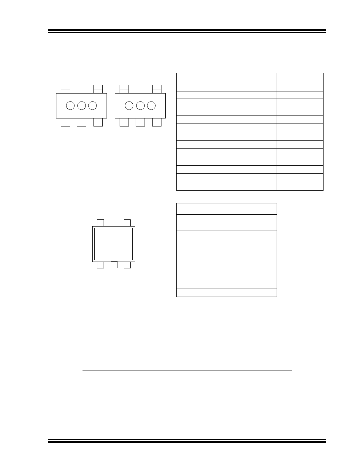
Package Types
SC-70
2
NC
V
OUT
45
GND
2
GND
NCV
45
SHDN
OUT
TC1017R
13
V
IN
V
IN
TC1017
13
SHDN
2004 Microchip Technology Inc. DS21813C-page 1
SOT-23
OUT
54
TC1017
1 23
IN
NCV
SHDNGNDV
Page 2
TC1017
1.0 ELECTRICAL
PIN FUNCTION TABLE
CHARACTERISTICS
Name Function
Absolute Maximum Ratings †
Input Voltage...................................................... .. .... .. .. ....6.5V
Output V o ltage ..........................................(-0.3) to (V
Power Dissipa ti o n ............... . ......... Int e rn a l l y L imited (Note 7)
Maximum Voltage On Any Pin..................V
+ 0.3V to -0.3V
IN
† Notice: Stresses above those listed under "Maximum
Ratings" may cause permanent damage to the device. This is
a stress rating only and functional operation of the device at
those or any other conditions above those indicated in the
operation listings of this specification is not implied. Exposure
to maximum rating conditions for extended periods may affect
device reliability.
+ 0.3)
IN
SHDN
NC No connect
GND Ground terminal
V
OUT
V
IN
Shutdown control input.
Regulated voltage output
Unregulated supply input
ELECTRICAL CHARACTERISTICS
Electrical Specifications: Unless otherwise noted, VIN = VR + 1V , IL = 100 µA, CL = 1.0 µF, SHDN > VIH, TA = +25°C
Boldface type specifications apply for junction temperat ures of –40°C to +125°C.
Parameter Sym Min T yp Max Units Test Conditions
Input Operating Voltage V
Maximum Output Current I
Output Voltage V
Temperature Coefficient TCV
V
OUT
Line Regulation |(∆V
Load Regulation (Note 4) |∆V
Dropout Voltage (Note 5) VIN – V
Supply Current I
Shutdown Supply Current I
OUTMAX
/∆VIN)| / V
OUT
OUT|
INSD
IN
OUT
OUT
IN
/ V
OUT
R
Power Supply Rejection Ratio PSRR — 58 — dB f =1 kHz, I
Wake-Up Time
t
WK
(from Shutdown Mode)
Note 1: The minimum V
is the regulator voltage setting. For example: VR = 1.8V, 2.7V, 2.8V, 3.0V.
2: V
R
3:
TCV
OUT
has to meet two conditions: VIN ≥ 2.7V and VIN ≥ (VR + 2.5%) + V
IN
V
OUTMAXVOUTMIN
------------------ ------------------------------ --------------------------------- ---- -
=
–()106×
V
OUT
T∆×
2.7 — 6.0 V Note 1
150 ——mA
VR – 2.5% VR ±0. 5% VR + 2.5% V Note 2
— 40 — ppm/°C Note 3
—0.040.2 %/V (VR + 1V) < VIN < 6V
R
—0.381.5 %IL = 0.1 mA to I
—
—
—
—
2
90
180
285
—
200
350
500
mV IL = 100 µA
I
= 50 mA
L
= 100 mA
I
L
= 150 mA
I
L
—5390 µA SHDN = VIH, IL = 0
— 0.05 2 µA SHDN = 0V
—10—µsV
DROPOUT
.
IN
C
IN
f = 100 Hz
= 5V, IL = 60 mA,
= C
L
OUT
OUTMAX
= 50 mA
=1 µF,
4: Regulation is measured at a constant junction temperature using low duty-cycle pulse testing. Load regulation is tested
over a load range from 0.1 mA to the maximum specified output current. Changes in output voltage due to heating
effects are covered by the thermal regulation specification.
5: Dropout voltage is defined as the input-to-output differential at which the output voltage drops 2% below its nominal
value at a 1V differential.
6: Thermal regulation is defined as the change in output voltage at a time T after a change in power dissip ation is applied,
excluding load or line regulation effects. S pecificati ons are for a current pulse equal to I
at VIN = 6V for t = 10 msec.
LMAX
7: The maximum allowable power dissipation is a function of ambient temperature, the maximum allowable junction
temperature and the thermal resistance from junction-to-air (i.e., T
dissipation causes the device to initiate thermal shutdown. Please see Section 5.1 “Thermal Shutdown”, for more
details
.
8:
Output current is limited to 120 mA (typ) when V
is less than 0.5V due to a load fault or short-circuit condition.
OUT
DS21813C-page 2 2004 Microchip Technology Inc.
, TJ, θJA). Exceeding the maximum allowable power
A
Page 3

TC1017
ELECTRICAL CHARACTERISTICS (CONTINUED)
Electrical Specifications: Unless otherwise noted, VIN = VR + 1V, IL = 100 µA, CL = 1.0 µF, SHDN > VIH, TA = +25°C
Boldface type specifications apply for junction temperat ures of –40°C to +125°C.
Parameter Sym Min T yp Max Units Test Conditions
Settling Time
(from Shutdown mode)
Output Short-Circuit Current I
Thermal Regulation V
Thermal Shutdown Die
Temperature
Thermal Shutdown Hysteresis ∆T
Output Noise eN — 800 — nV/√Hz f = 10 kHz
Input High Threshold V
SHDN
SHDN
Input Low Threshold V
Note 1: The minimum V
2: V
is the regulator voltage setting. For example: VR = 1.8V, 2.7V, 2.8V, 3.0V.
R
3:
TCV
OUT
has to meet two conditions: VIN ≥ 2.7V and VIN ≥ (VR + 2.5%) + V
IN
V
OUTMAXVOUTMIN
------------------ ------------------------------ --------------------------------- ---- -
=
t
S
OUTSC
OUT/PD
T
SD
SD
IH
IL
–()106×
V
OUT
—32—µsV
— 120 — mA V
= 5V, IL = 60 mA,
IN
= 1 µF,
C
IN
C
= 1 µF, f = 100 Hz
OUT
= 0V, Average
OUT
Current (Note 8)
—0.04—V/WNotes 6, 7
— 160 — °C
—10—°C
45 ——%V
INVIN
= 2.7V to 6.0V
——15 %VINVIN = 2.7V to 6.0V
.
DROPOUT
T∆×
4: Regulation is measured at a constant junction temperature using low duty-cycle pulse testing. Load regulation is tested
over a load range from 0.1 mA to the maximum specified output current. Changes in output voltage due to heating
effects are covered by the thermal regulation specification.
5: Dropout voltage is defined as the input-to-output differential at which the output voltage drops 2% below its nominal
value at a 1V differential.
6: Thermal regulation is defined as the change in output voltage at a time T after a change in power dissip ation is applied,
excluding load or line regulation effects. S peci fications are for a current pulse equal to I
at VIN = 6V for t = 10 msec.
LMAX
7: The maximum allowable power dissipation is a function of ambient temperature, the maximum allowable junction
temperature and the thermal resistance from junction-to-air (i.e., T
dissipation causes the device to initiate thermal shutdown. Please see Section 5.1 “Thermal Shutdown”, for more
details
.
8:
Output current is limited to 120 mA (typ) when V
is less than 0.5V due to a load fault or short-circuit condition.
OUT
, TJ, θJA). Exceeding the maximum allowable power
A
TEMPERATURE CHARACTERISTICS
Electrical Specifications: Unless otherwise indicated, VDD = +2.7V to +5.5V and VSS = GND.
Parameters Sym Min Typ Max Units Conditions
Temperature Ranges
Specified Temperature Range T
T
Operating Temperature Range T
Storage Temperature Range T
Thermal Package Resistances3
Thermal Resistance, 5L-SOT23 θ
Thermal Resistance, 5L-SC-70 θ
-40 — +85 °C Industrial Temperature parts
A
-40 — +125 °C Extended Temperature parts
A
-40 — +125 °C
A
-65 — +150 °C
A
JA
JA
— 255 — °C/W
— 450 — °C/W
2004 Microchip Technology Inc. DS21813C-page 3
Page 4

TC1017
= 2.85V
= 0-150 mA
= 6.0V
= 3.85V
= 3.3V
2.0 TYPICAL PERFORMANCE CHARACTERISTICS
Note: The graphs and tables prov id ed following this note are a statistical summary based on a l im ite d n um ber of
samples and are provided for informational purposes only. The performance characteristics listed herein
are not tested or guaranteed. In some graphs or tables, the data presented may be outside the specified
operating range (e.g., outside specified power supply range) and therefore outside the warranted range.
Note: Unless otherwise noted, VIN = VR + 1V, IL = 100 µA, CL = 1.0 µF, SHDN > VIH, TA = +25°C.
0.40
V
= 2.85V
OUT
0.35
0.30
0.25
0.20
TA = +125°C
TA = +25°C
TA = -40°C
0.15
0.10
Dropout Voltage (V)
0.05
0.00
0 25 50 75 100 125 150
Load Current (mA)
FIGURE 2-1: Dropout Voltage vs. Output Current.
-0.30
-0.35
-0.40
-0.45
Load Regulation (%)
-0.50
-0.55
-0.60
-0.65
V
IN
V
IN
V
IN
-0.70
-40 -15 10 35 60 85 110
Temperature (°C)
V
OUT
I
OUT
0.40
V
= 2.85V
OUT
0.35
I
0.30
OUT
= 150 mA
0.25
0.20
0.15
0.10
Dropout Voltage (V)
0.05
I
OUT
I
OUT
= 100 mA
= 50 mA
0.00
-40 -15 10 35 60 85 110
Temperature (°C)
FIGURE 2-4: Dropout Voltage vs. Temperature.
160
V
= 2.85V
OUT
140
120
100
80
60
40
20
Short Circuit Current (mA)
0
123456
Input Voltage (V)
FIGURE 2-2: Load Regulation vs. Temperature.
57
V
= 2.85V
OUT
56
55
TA = +125°C
54
53
TA = +25°C
52
Supply Current (µA)
51
TA = -40°C
50
3.3 3.6 3.9 4.2 4.5 4.8 5.1 5.4 5.7 6.0
Input Voltage (V)
FIGURE 2-3: Supply Current vs. Input Voltage.
FIGURE 2-5: Short-Circuit Current vs. Input Voltage.
57
56
V
= 6.0V
IN
55
54
V
= 3.85V
IN
53
52
Supply Current (µA)
51
V
IN
= 3.3V
50
-40 -15 10 35 60 85 110
Temperature (°C)
V
= 2.85V
OUT
FIGURE 2-6: Supply Current vs. Temperature.
DS21813C-page 4 2004 Microchip Technology Inc.
Page 5

Note: Unless otherwise noted, VIN = VR + 1V, IL = 100 µA, CL = 1.0 µF, SHDN > VIH, TA = +25°C.
TC1017
0.40
V
= 3.30V
OUT
0.35
0.30
0.25
0.20
TA = +125°C
TA = +25°C
TA = -40°C
0.15
0.10
Dropout Voltage (V)
0.05
0.00
0 25 50 75 100 125 150
Load Current (mA)
FIGURE 2-7: Dropout Voltage vs. Output Current.
-0.30
-0.35
V
= 6.0V
-0.40
IN
-0.45
-0.50
-0.55
V
= 4.3V
Load Regulation (%)
-0.60
-0.65
V
IN
IN
= 4.0V
-0.70
-40 -15 10 35 60 85 110
Temperature (°C)
V
OUT
I
OUT
= 3.30V
= 0-150 mA
0.40
V
= 3.30V
OUT
0.35
0.30
I
OUT
= 150 mA
0.25
0.20
0.15
0.10
Dropout Voltage (V)
0.05
I
OUT
I
OUT
= 100 mA
= 50 mA
0.00
-40 -15 10 35 60 85 110
Temperature (°C)
FIGURE 2-10: Dropout Voltage vs. Temperature.
60
V
= 3.30V
OUT
59
58
57
56
55
54
Supply Current (µA)
53
52
4.04.55.05.56.0
TA = +25°C
TA = +125°C
TA = -40°C
Input Voltage (V)
FIGURE 2-8: Load Regulation vs. Temperature.
60
59
58
57
56
V
V
= 6.0V
IN
= 4.3V
IN
55
54
Supply Current (µA)
53
V
= 4.0V
IN
52
-40 -15 10 35 60 85 110
Temperature (°C)
V
= 3.30V
OUT
FIGURE 2-9: Su ppl y Cur r ent vs. Temperature.
FIGURE 2-11: Supply Current vs. Input Voltage.
2.869
V
= 2.85V
2.868
2.867
OUT
TA = -40°C
2.866
TA = +25°C
TA = +125°C
Output Voltage (V)
2.865
2.864
2.863
2.862
3.3 3.6 3.9 4.2 4.5 4.8 5.1 5.4 5.7 6.0
Input Voltage (V)
FIGURE 2-12: Output Voltage vs. Supply Voltage.
2004 Microchip Technology Inc. DS21813C-page 5
Page 6

TC1017
Note: Unless otherwise noted, VIN = VR + 1V, IL = 100 µA, CL = 1.0 µF, SHDN > VIH, TA = +25°C.
2.870
2.868
V
= 2.85V
OUT
2.866
V
= 6.0V
2.864
IN
2.862
2.860
V
= 3.85V
Output Voltage (V)
2.858
2.856
IN
2.854
0 25 50 75 100 125 150
Load Current (mA)
FIGURE 2-13: Output Voltage vs. Output Current.
2.0
1.8
OUT
= 2.85V
1.6
1.4
1.2
1.0
0.8
0.6
0.4
Shutdown Current (µA)
0.2
0.0
3.3 3.6 3.9 4.2 4.5 4.8 5.1 5.4 5.7 6.0
Input Voltage (V)
TA = +125°CV
TA = +25°C
Output Voltage (V)
2.869
2.868
2.867
2.866
2.865
2.864
2.863
V
= 6.0V
IN
V
= 3.3V
IN
VIN= 3.85V
V
OUT
2.862
-40 -15 10 35 60 85 110
Temperature (°C)
FIGURE 2-16: Output Voltage vs. Temperature.
100
10
Hz)
1
Noise (µV/
0.1
0.01
10 100 1000 10000 100000 1000000
Frequency (Hz)
V
V
OUT
C
I
OUT
= 2.85V
= 3.85V
IN
= 2.85V
C
IN
OUT
= 40 mA
= 1 µF
= 1 µF
FIGURE 2-14: Shutdown Current vs. Input Voltage.
0
V
= 3.85V
INDC
V
V
INAC
OUTDC
= 100 mVp-p
= 2.85V
-10
-20
-30
-40
PSRR (dB)
-50
-60
-70
0.01 0.1 1 10 100 1000
Frequency (KHz)
I
= 100 µA
OUT
=1 µFX7RCeramic
C
OUT
FIGURE 2-15: Power Supply Rejection Ratio vs. Frequency.
FIGURE 2-17: Output Noise vs. Frequency.
0
V
= 3.85V
INDC
V
V
INAC
OUTDC
= 100 mVp-p
= 2.85V
-10
-20
-30
-40
PSRR (dB)
-50
-60
-70
0.01 0.1 1 10 100 1000
Frequency (KHz)
I
=1mA
OUT
=1µFX7RCeramic
C
OUT
FIGURE 2-18: Power Supply Rejection Ratio vs. Frequency.
DS21813C-page 6 2004 Microchip Technology Inc.
Page 7
Note: Unless otherwise noted, VIN = VR + 1V, IL = 100 µA, CL = 1.0 µF, SHDN > VIH, TA = +25°C.
= 3.85V
= 10 µF
= 1 µF Ceramic
t
= 10 µF
t
= 2.85V
= 10 µF
= 3.85V
= 10 µF
= 4.7 µF Ceramic
= 0 µF
TC1017
-10
-20
0
V
V
V
INDC
INAC
OUTDC
= 3.85V
= 100 mVp-p
= 2.85V
I
=50mA
OUT
=1µFX7RCeramic
C
OUT
-30
-40
-50
PSRR (dB)
-60
-70
-80
0.01 0.1 1 10 100 1000
Frequency (KHz)
FIGURE 2-19: Power Supply Rejection Ratio vs. Frequency.
V
= 2.85V
OUT
V
IN
C
IN
C
OUT
Shutdow n Inpu
VIN = 3.85V
C
IN
C
= 1 µF Ceramic
OUT
V
= 2.85V
OUT
= 0.1 mA to 120 mA
I
OUT
FIGURE 2-22: Load Transient Response.
V
IN
C
IN
C
OUT
V
= 2.85V
OUT
= 0.1 mA to 120 mA
I
OUT
FIGURE 2-20: Wake-U p Respon se.
V
OUT
V
= 3.85V
IN
C
IN
C
= 4.7 µF Ceramic
OUT
Shutdown Inpu
FIGURE 2-21: Wake-U p Respon se.
FIGURE 2-23: Load Transient Response.
C
= 1.0 µF Ceramic
OUT
I
= 120 mA
LOAD
IN
= 2.85V
V
OUT
V
= 3.85V to 4.85V
IN
C
FIGURE 2-24: Line Transient Response.
2004 Microchip Technology Inc. DS21813C-page 7
Page 8
TC1017
= 0 µF
= 0 µF
= 0 µF
= 10 µF Cerami c
Note: Unless otherwise noted, VIN = VR + 1V, IL = 100 µA, CL = 1.0 µF, SHDN > VIH, TA = +25°C.
C
= 4.7 µF Ceramic
OUT
= 120 mA
I
LOAD
IN
V
= 4.3V to 5.3V
IN
= 3.33V
V
OUT
= 2.85V
V
OUT
= 3.85V to 4.85V
V
IN
C
C
C
IN
OUT
I
= 100 µA
LOAD
FIGURE 2-25: Line Transient Response.
C
IN
C
= 1 µF Ceramic
OUT
= 100 µA
= 4.3V to 5.3V
V
IN
V
= 3.33V
OUT
I
LOAD
FIGURE 2-26: Line Transient Response.
FIGURE 2-27: Line Transient Response.
DS21813C-page 8 2004 Microchip Technology Inc.
Page 9

3.0 PIN DESCRIPTIONS
The descriptions of the pins are listed in Table 3-1.
TABLE 3-1: PIN FUNCTION TABLE
TC1017
Pin No.
5-Pin SC-70
13SHDN
24
32
45V
51V
Pin No.
5-Pin SOT-23
5-Pin SC-70R
Symbol Description
NC No Connect
GND Ground Terminal
OUT
IN
3.1 Shutdown Control Input (SHDN)
The regulator is fully enabled when a logic-high is
applied to SHDN
a logic-low is applied to this input. During shut down, the
output voltage falls to zero and the supply current is
reduced to 0.05 µA (typ.)
. The regulator enters shutdown when
3.2 Ground Terminal
For best performance, it is recommended that the
ground pin be tied to a ground plane.
Shutdown Control Input
Regulated Voltage Output
Unregulated Supply I nput
3.3 Regulated Voltage Output (V
Bypass the regulated voltage output to GND with a
minimum capacitance of 1 µF. A ceramic bypass
capacitor is recommended for best performance.
3.4 Unregulated Supply Input (VIN)
The minimum VIN has to meet two conditions in order
to ensure that the output maintains regulation:
VIN≥ 2.7V and VIN ≥ [(VR + 2.5%) + V
maximum V
Power dissipation may limit V
order to maintain a junction temperature below 125°C.
Refer to Section 5.0 “Thermal Considerations”, for
determining junction temperature.
It is recommended that V
ceramic capacitor.
should be less than or equal to 6V.
IN
to a lower potential in
IN
be bypassed to G ND wi th a
IN
OUT
DROPOUT
)
]. The
2004 Microchip Technology Inc. DS21813C-page 9
Page 10
TC1017
4.0 DETAILED DESCRIPTION
The TC1017 is a precision, fixed-output, linear voltage
regulator. The internal linear pass element is a
P-channel MOSFET. As with all P-channel CMOS
LDOs, there is a body drain diode with the cathode
connected to VIN and the anode connected to V
(Figure 4-1).
As is shown in Figure 4-1, the output voltage of the
LDO is sensed and divided down internally to reduce
external component count. The internal error amplifier
has a fixed bandgap reference on the inverting input
and the sensed output voltage on the non-inverting
input. The error amplifier output will pull the gate
voltage down until the inputs of the error amplifier are
equal to regulate the output voltage.
Output overl oad prot ect ion is impl eme nted b y se nsi ng
the current in the P-channe l MOSFET. During a shorted
or faulted load condition in which the output voltage
falls to less than 0.5V, the output current is limited to a
typical value of 120 mA. The current-limit protection
helps prevent excessive current from damaging the
Printed Circuit Board (PCB).
An internal thermal se nsing device is used to moni tor
the junction temperature of the LDO. When the sensed
temperature is over the set threshold of 160°C (typical),
the P-channel MOSFET is turned off. When the P-channel is off, the power dissipation internal to the device is
almost zero. The device cools until the junction temper-
OUT
ature is approximately 150°C and the P-channel is
turned on. If the internal power dissipation is still high
enough for the junction to rise to 160°C, it will again shut
off and cool. The maximum operating junction temperature of the device is 125°C. Steady-state operation at or
near the 160°C overtemp eratur e point can l ead to p ermanent damage of the device.
The output voltage V
remains stab l e ov er the en t ir e
OUT
input operating voltage range (2.7V to 6.0V) and the
entire load range (0 mA to 150 mA). The output voltage
is sensed through an internal resistor divider and
compared with a precision internal voltage reference.
Several fixed-output voltages are available by
changing the value of the internal resistor divider.
Figure 4-2 shows a typical application circuit. The
regulator is enabled any time the shutdown input pin is
at or above V
shutdown inpu t pin is below V
the SHDN
. It is shut down (disabled) any time the
IH
. For applications where
IL
feature is not used, tie the SHDN pin directl y
to the input supply voltage source. While in shutdown,
the supply current decreases to 0.006 µA (typical) and
the P-channel MOSFET is turned off.
As shown in Figure 4-2, batteries have internal source
impedance. An input capacitor is used to lower the
input impedance of the LDO. In so me applicat ions, high
input impedance can cause the LDO to become
unstable. Adding more input capacitance can
compensate for this.
1
SHDN
Current Limit
V
REF
-
EA
+
Error
Amp
R
R
1
Feedback Resistors
2
2
3
NC
GND
SHDN
Control
Over
Temp.
V
IN
FIGURE 4-1: TC1017 Block Diagram (5-Pin SC-70 Pinout).
5
V
IN
4
V
OUT
R
BATTERY
SOURCE
1
2
3
SHDN
TC1017
NC
GND
C
Body
Diode
C
IN
OUT
V
IN
5
V
OUT
4
1µF Ceramic
Load
1µF Ceramic
FIGURE 4-2: Typical Application Circuit (5-Pin SC-70 Pinout).
DS21813C-page 10 2004 Microchip Technology Inc.
Page 11

TC1017
4.1 Input Capacitor
Low input source impedance is necessary for the LDO
to operate properly. When operating from batteries, or
in applications with long lead length (> 10") between
the input source and th e LD O, so me inpu t ca pacitance
is required. A minimum of 0.1 µF is recommended for
most applications and the capacitor should be placed
as close to the input of the LDO as is practical. Larger
input capacitors will help reduce the input impedance
and further reduce any high-frequency noise on the
input and output of the LDO.
4.2 Output Capacitor
A minimum output capacitance of 1 µF for the TC1017
is required for stability. The Equivalent Series Resistance (ESR) requirements on the output capacitor are
between 0 and 2 ohm s. The out put cap acitor shou ld be
located as close to the LDO output as is practical.
Ceramic materials X7R and X5R hav e low temperatu re
coefficients and are well within the acceptable ESR
range required. A typical 1 µF X5R 0805 capacitor has
an ESR of 50 milli-ohm s. La rg er out p ut capac it o r s c an
be used with the TC1017 to im prove dynam ic beha vior
and input ripple-rejection performance.
Ceramic, aluminum electrolytic or tantalum capacitor
types can be used. Since many aluminum electrolytic
capacitors freeze at approximately –30°C, ceramic or
solid tantalums are recommended for applications
operating below –25°C. When operating from sources
other than batteries, supply-noise rejection and
transient response can be improved by increasing the
value of the input and output capacitors and employing
passive filterin g tech niq ues.
4.3 Turn-On Response
The turn-on response is defined as two separate
response categories, wake-up time (t
).
time (t
S
The TC1017 has a fa st w ake-up time (10 µsec, typical)
when released from shutdown. See Figure 4-3 for the
wake-up time designated as t
. The wake-u p ti me is
WK
defined as the time it takes for the output to rise to 2%
of the V
value after being released from shutdown.
OUT
The total turn-on response is defined as the settling
) (see Figure 4-3). Settling time (inclusive with
time (t
S
) is defined as the condition when the output is
t
WK
within 98% of its fully-enabled value (32 µsec, typical)
when released from shutdown. The settling time of the
output voltage is dependent on load conditions and
output capacitance on V
(RC response).
OUT
The table below demonstrates the typical turn-on
response timing for different input voltage power-up
frequencies: V
and C
OUT
= 1 µF.
= 2.85V, VIN = 5.0V, I
OUT
Frequency Typical (tWK) Typical (tS)
1000 Hz 5.3 µsec 14 µ sec
500 Hz 5.9 µsec 16 µsec
100 Hz 9.8 µsec 32 µsec
50 Hz 14.5 µsec 52 µsec
10 Hz 17.2 µsec 77 µsec
) and settling
WK
= 60 mA
OUT
V
IH
V
SHDN
IL
t
S
98%
V
OUT
2%
t
WK
FIGURE 4-3: Wake-Up Time from Shutdown.
2004 Microchip Technology Inc. DS21813C-page 11
Page 12

TC1017
5.0 THERMAL CONSIDERATIONS
5.1 Thermal Shutdown
Integrated thermal protection circuitry shuts the
regulator off when the die temperature exceeds
approximately 160°C. The regulator remains off until
the die temperature drops to approximately 150°C.
5.2 Power Dissipation: SC-70
The TC1017 is available in the SC-70 package. The
thermal resistance for the SC-70 package is
approximately 450°C/W when the copper area used in
the PCB layout is similar to the J EDEC J51-7 high thermal conductivity standard or semi-G42-88 standard.
For applications with a larger or thicker copper area,
the thermal resista nce can be lowered. See AN79 2, “A
Method to Determine How Much Power a SOT-23 Can
Dissipate in an Application”, DS00792, for a method to
determine the thermal resistance for a particular application.
The TC1017 power dissipation capability is dependant
upon several variables: input voltage, output voltage,
load current, ambient temperature and maximum
junction temperature. The absolute maximum steadystate junction temperature is rated at +125°C. The
power dissipation within the device is equal to:
Given the following example:
VIN= 3.0V to 4.1V
V
I
= 2.85V ±2.5%
OUT
= 120 mA (output current)
LOAD
TA= 55°C (max. desired ambient)
Find:
1. Internal power dissipation:
P
DMAX
V
IN_MAXVOUT_MIN
–()I
×=
LOAD
4.1V 2.85 0.975()×–()120mA×=
158.5mW=
2. Maximum allowable ambient temperature:
T
A_MAX
T
J_MAX
125
125
°
54
P–
DMAX
°
C 158.5 mW 450°C/W×–()=
°
C71°C–()=
R
θ
×=
JA
C=
3. Maximum allowable power dissipation at
desired ambient:
T
–
D
J_MAXTA
----------------------------- -=
R
θ
JA
°
C55°C–
125
-----------------------------------=
°
450
C/W
P
155mW=
EQUATION 5-1:
P
VINV
D
The VIN x I
term is typically very small when
GND
compared to th e (V
–()I
OUT
IN–VOUT
LOADVINIGND
) x I
LOAD
×+×=
term, simplifying
the power dissipation within the LDO to be:
EQUATION 5-2:
P
VINV
D
–()I
OUT
×=
LOAD
To determine the maximum power dissipation
capability, the following equation is used:
EQUATION 5-3:
T
–()
J_MAXTA_MAX
----------------------------------------------=
R
θ
JA
temperatur e allowed
temperature
junction to air
Where:
T
T
Rθ
P
DMAX
= the maximum junction
J_MAX
A_MAX
= the maximum ambient
= the thermal resistance from
JA
In this example, the TC1017 dissipates approximately
158.5 mW and the junction temperature is raised 71°C
over the ambient. The absolute maximum power
dissipation is 155mW when given a maxi mum a mbient
temperature of 55°C.
Input voltage, output voltage or load current limits can
also be determine d by s ubstit uting k nown va lue s in the
power dissipation equations.
Figure 5-1 and Figure 5-2 depict typical maximum
power dissipation versus ambient temperature, as well
as typical maximum current versus ambient temperature, with a 1V input voltage to output voltage
differential, respectively.
400
350
300
250
200
150
100
50
Power Dissipation (mW)
0
-40 -15 10 35 60 85 110
Ambient Temperature (°C)
FIGURE 5-1: Power Dissipation vs. Ambient Temperature (SC-70 package).
DS21813C-page 12 2004 Microchip Technology Inc.
Page 13

160
VIN - V
= 1V
140
120
100
80
60
40
20
Maximum Current (mA)
0
-40 -15 10 35 60 85 110
Ambient Temperature (°C)
OUT
FIGURE 5-2: Maximum Current vs. Ambient Temperature (SC-70 package).
5.3 Power Dissipation: SOT-23
The TC1017 is also available in a SOT-23 package for
improved thermal perf ormance. The thermal resistance
for the SOT-23 package is approximately 255°C/W
when the copper area used in the printed circuit board
layout is similar to the JEDEC J51-7 low thermal
conductivity standard or semi-G42-88 standard. For
applications with a larger or thicker copper area, the
thermal resistance can be lowered. See AN792, “A
Method to Determine How Much Power a SOT-23 Can
Dissipate in an Application”, DS00792, for a method to
determine the thermal resistance for a particular
application.
The TC1017 power dissipation capability is dependant
upon several variables: input voltage, output voltage,
load current, ambient temperature and maximum
junction temperature. The absolute maximum steadystate junction temperature is rated at +125°C. The
power dissipation within the device is equal to:
EQUATION 5-4:
P
VINV
D
The VIN x I
compared to the (V
–()I
OUT
term is typically very small when
GND
LOADVINIGND
) x I
IN–VOUT
power dissipation within the LDO to be:
EQUATION 5-5:
P
VINV
D
To determine the maximum power dissipation
capability, the following equation is used:
–()I
OUT
×+×=
term, simplifying th e
LOAD
×=
LOAD
TC1017
EQUATION 5-6:
T
–()
J_MAXTA_MAX
P
DMAX
Where:
= the maximum junction
T
J_MAX
T
= the maximum ambient
A_MAX
= the thermal resistance from
Rθ
JA
Given the following example:
VIN= 3.0V to 4.1V
V
OUT
I
LOAD
T
A
Find:
1. Internal power dissipation:
P
DMAX
2. Maximum allowable ambient temperature:
T
A_MAX
3. Maximum allowable power dissipation at
desired ambient:
P
In this example, the TC1017 dissipates approximately
158.5 mW and the junction temperature is raised
40.5°C over the ambient. The absolute maximum
power dissipation is 157 mW when given a maximum
ambient temperature of +85°C.
Input voltage, output voltage or load current limits can
also be determine d by s ubstit uting k nown va lue s in the
power dissipation equations.
Figure 5-3 and Figure 5-4 depict typical maximum
power dissipation versus ambient temperature, as well
as typical maximum current versus ambient temperature with a 1V input voltage to output voltage
differential, respectively.
----------------------------------------------
=
Rθ
JA
temperature allowed
temperature
junction to air
= 2.85V ±2.5%
= 120 mA (output current)
= +85°C (max. desired ambient)
V
–()I
IN_MAXVOUT_MIN
×=
LOAD
4.1V 2.85 0.975()×–()120mA×=
158.5mW=
T
125
84.5
D
J_MAX
125
P–
DMAX
°
C 158.5mW 255°C/W×–()=
°
C40.5°C–()=
°
C=
T
J_MAXTA
----------------------------- -=
R
θ
°
C85°C–
125
-----------------------------------=
255
JA
°
C/W
R
θ
×=
JA
–
157mW=
2004 Microchip Technology Inc. DS21813C-page 13
Page 14

TC1017
700
600
500
400
300
200
100
Power Dissipation (mW)
0
-40 -15 10 35 60 85 110
Ambient Temperat ure (°C)
FIGURE 5-3: Power Dissipation vs. Ambient Temperature (SOT-23 Package).
160
140
120
100
80
60
40
Maximum Current (mA)
20
0
-40 -15 10 35 60 85 110
Ambient Temperature (°C)
VIN - V
OUT
= 1V
5.4 Layout Considerations
The primary path for heat conduction out of the SC-70/
SOT-23 package is through the package leads. Using
heavy wide traces at the pads of the device will facilitate the removal of the heat within the package, thus
lowering the thermal resistance Rθ
thermal resista nce , the ma ximum i nte rnal power d issi pation capability of the package is increased.
SHDN
V
IN
C
1
U1
GND
FIGURE 5-5: SC-70 Package Suggested Layout.
. By loweri ng the
JA
V
OUT
C
2
FIGURE 5-4: Maximum Current vs. Ambient Temperature (SOT-23 Package).
DS21813C-page 14 2004 Microchip Technology Inc.
Page 15
6.0 PACKAGE INFORMATION
6.1 Package Marking Information
TC1017
5-Pin SC-70/SC-70R
XXN YWW
TOPSIDE
5-Lead SOT-23
BOTTOMSIDE
XXNN
Part Number
TC1017 - 1.8VLT CE CU
TC1017 - 1.85VLT CQ DF
TC1017 - 2.5VLT CR CV
TC1017 - 2.6VLT CF CW
TC1017 - 2.7VLT CG CX
TC1017 - 2.8VLT CH CY
TC1017 - 2.85VLT CJ CZ
TC1017 - 2.9VLT CK DA
TC1017 - 3.0VLT CL DB
TC1017 - 3.2VLT CC DC
TC1017 - 3.3VLT CM DD
TC1017 - 4.0VLT CP DE
Part Number Code
TC1017 - 1.8VCT DA
TC1017 - 1.85VCT DK
TC1017 - 2.6VCT DB
TC1017 - 2.7VCT DC
TC1017 - 2.8VCT DD
TC1017 - 2.85VCT DE
TC1017 - 2.9VCT DF
TC1017 - 3.0VCT DG
TC1017 - 3.3VCT DH
TC1017 - 4.0VCT DJ
TC1017 Pinout
Code
TC1017R Pinout
Code
Legend: XX...X Customer specific information*
Y Year code (last digit of calendar year)
YY Year code (last 2 digits of calendar year)
WW Week code (week of January 1 is week ‘01’)
NNN Alphanumeric traceability code
Note: In the event the full Microchi p pa rt numbe r cannot be marke d on one li ne, it will
be carried over to the next line thus limiti ng the number of available characters
for customer specific information.
* Standard device marking consists of Microchip part number, year code, week code, and traceability
code.
2004 Microchip Technology Inc. DS21813C-page 15
Page 16

TC1017
5-Lead Plastic Small Outline Transistor (LT) (SC-70)
E
E1
D
p
n
Q1
c
Number of Pins
Pitch
Molded Package Thickness
Standoff
Molded Package Width
Top of Molded Pkg to Lead Shoulder
Lead Thickness
A2
A1
E1
Q1
B
1
A2
A1
L
MILLIMETERS*INCHESUnits
MINDimension Limits
n
p
c
NOM
.004 .016 0.10 0.40
MINMAX
NOM
55
0.65 (BSC).026 (BSC)
A
MAX
1.100.80.043.031AOverall Height
1.000.80.039.031
0.100.00.004.000
2.401.80.094.071EOverall Width
1.351.15.053.045
2.201.80.087.071DOverall Length
0.300.10.012.004LFoot Length
0.180.10.007.004
0.300.15.012.006BLead Width
*Controlling Parameter
Notes:
Dimensions D and E1 do not include mold flash or protrusions. Mold flash or protrusions shall not
exceed .005" (0.127mm) per side.
JEITA (EIAJ) Standard: SC-70
Drawing No. C04-061
DS21813C-page 16 2004 Microchip Technology Inc.
Page 17

5-Lead Plastic Small Outline Transistor (OT) (SOT-23)
E
E1
p
B
p1
D
TC1017
n
c
β
Number of Pins
Pitch
Outside lead pitch (basic)
Foot Angle
Lead Thickne ss
Mold Draft Angle Top
Mold Draft Angle Bottom
* Controlling Parameter
§ Significant Characteristic
Notes:
Dimensions D and E1 do not include mold flash or protrusions. Mold flash or protrusions shall not exceed
.010” (0.254mm) per side.
JEDEC Equivalent: MO-178
Drawing No. C04-091
1
A
φ
L
n
p
p1
φ
c
α
β
A1
MILLIMETERSINCHES*Units
0.95.038
1.90.075
α
A2
MAXNOMMINMAXNOMMINDimension Limits
55
1.451.180.90.057.046.035AOverall Height
1.301.100.90.051.043.035A2Molded Package Thickness
0.150.080.00.006.003.000A1Standoff §
3.002.802.60.118.110.102EOverall Width
1.751.631.50.069.064.059E1Molded Package Width
3.102.952.80.122.116.110DOverall Length
0.550.450.35.022.018.014LFoot Length
10501050
0.200.150.09.008.006.004
0.500.430.35.020.017.014BLead Width
10501050
10501050
2004 Microchip Technology Inc. DS21813C-page 17
Page 18

TC1017
NOTES:
DS21813C-page 18 2004 Microchip Technology Inc.
Page 19

PRODUCT IDENTIFICATION SYSTEM
To order or obtain information, e.g., on pricing or delivery, refer to the factory or the listed sales office.
PART NO. X.XX X
Device
Options
Device: TC1017: 150 mA Tiny CMOS LDO with Shutdown
Voltage Options:*
(Standard)
Temperature
Range:
Package: LTTR = 5-pin SC-70 (Tape and Reel)
TemperatureVoltage
Range
TC1017R:150 mA Tiny CMOS LDO with Shutdown
(SC-70 only)
1.8V
1.85V
2.5V SC-70 only
2.6V
2.7V
2.8V
2.85V
2.9V
3.0V
3.2V SC-70 only
3.3V
4.0V
* Other voltage options available. Please contact
your local Microchip sales office for details.
V = -40°C to +125°C
CTTR = 5-pin SOT-23 (Tape and Reel)
XXXX
Package
Examples:
a) TC1017-1.8VLTTR: 150 mA, Tiny CMOS
b) TC1017R-1.8VLTTR:150mA, Tiny CMOS
c) TC1017-2.6V CTTR :150 mA, Tiny CMOS
d) TC1017-2.7VLTTR: 150 mA, Tiny CMOS
e) TC1017-2.8VCTTR:150 mA, Tiny CMOS
f) TC1017-2.85VLTTR:150 mA, Tiny CMOS
g) TC1017-2.9VCTTR:150 mA, Tiny CMOS
h) TC1017-3.0VLTTR: 150 mA, Tiny CMOS
i) TC1017-3.3VCTTR:150 mA, Tiny CMOS
j) TC1017-4.0VLTTR: 150 mA, Tiny CMOS
TC1017
LDO with Shutdown,
SC-70 package.
LDO with Shutdown,
SC-70R package.
LDO with Shutdown,
SOT-23 package.
LDO with Shutdown,
SC-70 package.
LDO with Shutdown,
SOT-23 package.
LDO with Shutdown,
SC-70 package.
LDO with Shutdown,
SOT-23 package.
LDO with Shutdown,
SC-70 package.
LDO with Shutdown,
SOT-23 package.
LDO with Shutdown,
SC-70 package.
Sales and Support
Data Sheets
Products supported by a preliminary Data Sheet may have an errata sheet describing minor operational differences and
recommended workarounds. To determine if an errata sheet exists for a particular device, please contact one of the following:
1. Your local Microchip sales office
2. The Microchip Worldwide Site (www.microchip.com)
Please specify which device, revision of silicon and Data Sheet (include Literature #) you are using.
Customer Notification System
Register on our web site (www.microchip.com) to receive the most current information on our products.
2004 Microchip Technology Inc. DS21813C-page 19
Page 20

TC1017
NOTES:
DS21813C-page 20 2004 Microchip Technology Inc.
Page 21

Note the following details of the code protection feature on Microchip devices:
• Microchip products meet the specification contained in their particular Microchip Data Sheet.
• Microchip believes that its family of products is one of the most secure families of its kind on the market today , when used in the
intended manner and under normal conditions.
• There are dishonest and possibly illegal methods used to breach the code protection feature. All of these methods, to our
knowledge, require using the Microchip products in a manner outside the operating specifications contained in Microchip’s Data
Sheets. Most likely, the person doing so is engaged in theft of intellectual property.
• Microchip is willing to work with the customer who is concerned about the integrity of their code.
• Neither Microchip nor any other semiconductor manufacturer can guarantee the security of their code. Code protection does not
mean that we are guaranteeing the product as “unbreakable.”
Code protection is constantly evolving. We at Microchip are com mitted to continuously improving the code protect ion f eatures of our
products. Attempts to break Microchip’s code protection feature may be a violation of the Digit al Mill ennium Copyright Act. If such acts
allow unauthorized access to your software or other copyrighted work, you may have a right to sue for relief under that Act.
Information contained in this publication regarding device
applications and the like is provided only for your convenience
and may be superseded by updates. It is your responsibility to
ensure that your application meets with your specifications.
MICROCHIP MAKES NO REPRESENTATIONS OR WARRANTIES OF ANY KIND WHETHER EXPRESS OR IMPLIED,
WRITTEN OR ORAL, STATUTORY OR OTHERWISE,
RELATED TO THE INFORMATION, INCLUDING BUT NOT
LIMITED TO ITS CONDITION, QUALITY, PERFORMANCE,
MERCHANTABILITY OR FITNESS FOR PURPOSE.
Microchip disclaims all liability arising from this information and
its use. Use of M icrochip’s prod ucts as critical components in
life support systems is not authorized except with express
written approval by Microchip. No licenses are conveyed,
implicitly or otherwise, under any Microchip intellectual property
rights.
Trademarks
The Microchip name and logo, the Microchip logo, Accuron,
dsPIC, K
EELOQ, microID, MPLAB, PIC, PICmicro,
PICSTART, PRO MATE, PowerSmart, rfP IC , and
SmartShunt are registered trademarks of Microchip
Technology Incorporated in the U.S.A. and other countries.
AmpLab, FilterLab, MXDEV, MXLAB, PICMASTER, SEEVAL,
SmartSensor and The Embedded Control Solutions Company
are registered trademarks of Microchip Technology
Incorporated in the U.S.A.
Analog-for-the-Digital Age, Application Maestro, dsPICDEM,
dsPICDEM.net, dsPICworks, ECAN, ECONOMONITOR,
FanSense, FlexROM, fuzzyLAB, In-Circuit Serial
Programming, ICSP, ICEPIC, Migratable Memory, MPASM ,
MPLIB, MPLINK, MPSIM, PICkit, PICDEM, PICDEM.net,
PICLAB, PICtail, PowerCal, PowerInfo, PowerMate,
PowerTool, rfLAB, rfPICDEM, Select Mode, Smart Serial,
SmartTel and Total Endurance are trademarks of Microchip
Technology Incorporated in the U.S.A. and other countries.
SQTP is a service mark of Microchip T echnology Incorporated
in the U.S.A.
All other trademarks mentioned herein are property of their
respective companies.
© 2004, Microchip Technology Incorporated, Printed in the
U.S.A., All Rights Reserved.
Printed on recycled paper.
Microchip received ISO/TS-16949:2002 quality system certification for
its worldwide headquarters, design and wafer fabrication facilities in
Chandler and Tempe, Arizona and Mountain View, California in
October 2003. The Company’s quality system processes and
procedures are for its PICmicro
devices, Serial EEPROMs, microperipherals, nonvolatile memory and
analog products. In addition, Microchip’s quality system for the design
and manufacture of development systems is ISO 9001:2000 certified.
®
8-bit MCUs, KEELOQ
®
code hopping
2004 Microchip Technology Inc. DS21813C-page 21
Page 22

WORLDWIDE SALES AND SERVICE
AMERICAS
Corporate Office
2355 West Chandler Blvd.
Chandler, AZ 85224-6199
Tel: 480-792-7200
Fax: 480-792-7277
Technical Support:
http://support.microchip.com
Web Address:
www.microchip.com
Atlanta
Alpharetta, GA
Tel: 770-640-0034
Fax: 770-640-0307
Boston
Westford, MA
Tel: 978-692-3848
Fax: 978-692-3821
Chicago
Itasca, IL
Tel: 630-285-0071
Fax: 630-285-0075
Dallas
Addison, TX
Tel: 972-818-7423
Fax: 972-818-2924
Detroit
Farmington Hills, MI
Tel: 248-538-2250
Fax: 248-538-2260
Kokomo
Kokomo, IN
Tel: 765-864-8360
Fax: 765-864-8387
Los Angeles
Mission Viejo, CA
Tel: 949-462-9523
Fax: 949-462-9608
San Jose
Mountain View, CA
Tel: 650-215-1444
Fax: 650-961-0286
Toronto
Mississauga, Ontario,
Canada
Tel: 905-673-0699
Fax: 905-673-6509
ASIA/PACIFIC
Australia - Sydney
Tel: 61-2-9868-6733
Fax: 61-2-9868-6755
China - Beijing
Tel: 86-10-8528-2100
Fax: 86-10-8528-2104
China - Chengdu
Tel: 86-28-8676-6200
Fax: 86-28-8676-6599
China - Fuzhou
Tel: 86-591-8750-3506
Fax: 86-591-8750-3521
China - Hong Kong SAR
Tel: 852-2401-1200
Fax: 852-2401-3431
China - Shanghai
Tel: 86-21-5407-5533
Fax: 86-21-5407-5066
China - Shenyang
Tel: 86-24-2334-2829
Fax: 86-24-2334-2393
China - Shenzhen
Tel: 86-755-8203-2660
Fax: 86-755-8203-1760
China - Shunde
Tel: 86-757-2839-5507
Fax: 86-757-2839-5571
China - Qingdao
Tel: 86-532-502-7355
Fax: 86-532-502-7205
ASIA/PACIFIC
India - Bangalore
Tel: 91-80-2229-0061
Fax: 91-80-2229-0062
India - New Delhi
Tel: 91-11-5160-8631
Fax: 91-11-5160-8632
Japan - Kanagawa
Tel: 81-45-471- 6166
Fax: 81-45-471-6122
Korea - Seoul
Tel: 82-2-554-7200
Fax: 82-2-558-5932 or
82-2-558-5934
Singapore
Tel: 65-6334-8870
Fax: 65-6334-8850
Taiwan - Kaohsiung
Tel: 886-7-536-4818
Fax: 886-7-536-4803
Taiwan - Taipei
Tel: 886-2-2500-6610
Fax: 886-2-2508-0102
Taiwan - Hsinchu
Tel: 886-3-572-9526
Fax: 886-3-572-6459
EUROPE
Austria - Weis
Tel: 43-7242-2244-399
Fax: 43-7242-2244-393
Denmark - Ballerup
Tel: 45-4450-2828
Fax: 45-4485-2829
France - Massy
Tel: 33-1-69-53-63-20
Fax: 33-1-69-30-90-79
Germany - Ismaning
Tel: 49-89-627-144-0
Fax: 49-89-627-144-44
Italy - Milan
Tel: 39-0331-742611
Fax: 39-0331-466781
Netherlands - Drunen
Tel: 31-416-690399
Fax: 31-416-690340
England - Berkshire
Tel: 44-118-921-5869
Fax: 44-118-921-5820
10/20/04
DS21813C-page 22 2004 Microchip Technology Inc.
 Loading...