

Page 1
TC1014/TC1015/TC1185
TC1014
TC1015
TC1185
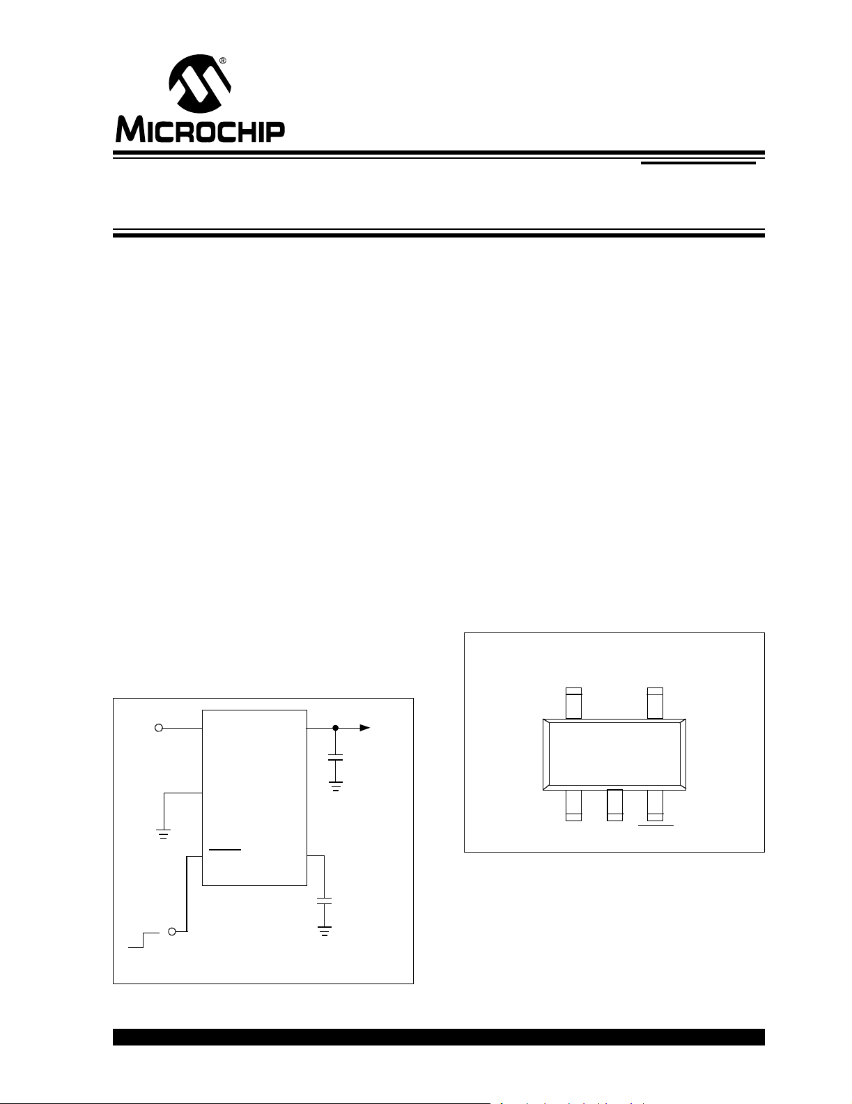
V
OUT
SHDN
GND
Bypass
470 pF
Reference
Bypass Cap
(Optional)
1µF
+
V
IN
V
IN
V
OUT
1
5
2
4
3
Shutdown Control
(from Power Control Logic)
Bypass
SHDN
5
5-Pin SOT-23
TC1014
TC1015
TC1185
13
4
2
V
IN
V
OUT
GND
50 mA, 100 mA and 150 mA CMOS LDOs with Shutdown
and Reference Bypass
Features:
General Description
• Low Supply Current (50 µA, typical)
• Low Dropout Voltage
• Choice of 50 mA (TC1014), 100 mA (TC1015)
and 150 mA (TC1185) Output
• High Output Voltage Accuracy
• Standard or Custom Output Voltages
• Power-Saving Shutdown Mode
• Reference Bypass Input for Ultra Low-Noise
Operation
• Overcurrent and Overtemperature Protection
• Space-Saving 5-Pin SOT-23 Package
• Pin-Compatible Upgrades for Bipolar Regulators
• Standard Output Voltage Options:
- 1.8V, 2.5V, 2.6V, 2.7V, 2.8V, 2.85V, 3.0V,
3.3V, 3.6V, 4.0V, 5.0V
Applications:
• Battery-Operated Systems
• Portable Computers
• Medical Instruments
• Instrumentation
• Cellular/GSM/PHS Phones
• Linear Post-Regulator for SMPS
• Pagers
The TC1014/TC1015/TC1185 are high accuracy
(typically ±0.5%) CMOS upgrades for older (bipolar)
Low Dropout Regulators (LDOs) such as the LP2980.
Designed specifically for battery-operated systems, the
devices’ CMOS construction eliminates wasted ground
current, significantly extending battery life. Total supply
current is typically 50 µA at full load (20 to 60 times
lower than in bipolar regulators).
The devices’ key features include ultra low-noise
operation (plus optional Bypass input), fast response to
step changes in load, and very low dropout voltage,
typically 85 mV (TC1014), 180 mV (TC1015), and
270 mV (TC1185) at full-load. Supply current is
reduced to 0.5 µA (max) and V
the shutdown input is low. The devices incorporate both
overtemperature and overcurrent protection.
The TC1014/TC1015/TC1185 are stable with an output
capacitor of only 1 µF and have a maximum output
current of 50 mA, 100 mA and 150 mA, respectively.
For higher output current regulators, please see the
TC1107 (DS21356), TC1108 (DS21357), TC1173
(DS21362) (I
= 300 mA) data sheets.
OUT
falls to zero when
OUT
Package Type
Typical Application
© 2007 Microchip Technology Inc. DS21335E-page 1
Page 2
TC1014/TC1015/TC1185
TC V
OUT
= (V
OUTMAX
– V
OUTMIN
)x 10
6
V
OUT
x ΔT
1.0 ELECTRICAL CHARACTERISTICS
† Notice: Stresses above those listed under "Absolute
Maximum Ratings" may cause permanent damage to
the device. These are stress ratings only and functional
operation of the device at these or any other conditions
Absolute Maximum Ratings†
Input Voltage .........................................................6.5V
Output Voltage...........................(-0.3V) to (V
+ 0.3V)
IN
above those indicated in the operation sections of the
specifications is not implied. Exposure to Absolute
Maximum Rating conditions for extended periods may
affect device reliability.
Power Dissipation................Internally Limited (Note 7)
Maximum Voltage on Any Pin ........ V
Operating Temperature Range...... -40°C < T
+0.3V to -0.3V
IN
< 125°C
J
Storage Temperature..........................-65°C to +150°C
TC1014/TC1015/TC1185 ELECTRICAL SPECIFICATIONS
Electrical Specifications: VIN = VR + 1V, IL = 100 µA, CL = 1.0 µF, SHDN > VIH, TA = +25°C, unless otherwise noted.
Boldface type specifications apply for junction temperatures of -40°C to +125°C.
Parameter Symbol Min Typ Max Units Device Test Conditions
Input Operating Voltage
Maximum Output Current
Output Voltage
V
Temperature Coefficient
OUT
Line Regulation
Load Regulation
Dropout Voltage
Supply Current (Note 8)
Shutdown Supply Current
Power Supply Rejection
Ratio
Output Short Circuit Current
Thermal Regulation
Thermal Shutdown Die
Temperature
Thermal Shutdown
Hysteresis
Note 1: The minimum VIN has to meet two conditions: VIN ≥ 2.7V and VIN ≥ VR + V
2: V
is the regulator output voltage setting. For example: VR = 1.8V, 2.5V, 2.6V, 2.7V, 2.8V, 2.85V, 3.0V, 3.3V, 3.6V, 4.0V, 5.0V.
R
3:
V
I
OUTMAX
V
OUT
TCV
ΔV
ΔV
ΔV
V
OUT
VIN-V
I
I
INSD
PSRR
I
OUTSC
ΔV
ΔP
T
ΔT
IN
OUT
OUT
IN
OUT
IN
OUT
SD
SD
/
/
OUT
/
D
2.7 — 6.0 V—Note 1
50
100
150
VR – 2.5% VR ±0.5% VR + 2.5% V—Note 2
—
—
—0.050c.35 %—(V
—
—
—
—
—
—
—
—5080 µA — SHDN = VIH, IL = 0
— 0.05 0.5 µA — SHDN = 0V
—64—dB —F
—300450mA —V
—0.04—V/W — Notes 6, 7
—160—°C —
—10—°C —
—
—
—
20
40
0.5
0.5
2
65
85
180
270
—
—
—
—
—
2
3
—
—
120
250
400
mA TC1014
TC1015
TC1185
ppm/°C — Note 3
% TC1014; TC1015
TC1185
mV —
.
DROPOUT
—
—
TC1015; TC1185
TC1185
+ 1V) ≤ VIN ≤ 6V
R
IL = 0.1 mA to I
IL = 0.1 mA to I
(Note 4)
IL = 100 µA
IL = 20 mA
IL = 50 mA
IL = 100 mA
IL = 150 mA (Note 5)
≤ 1kHz
RE
OUT
OUTMAX
OUTMAX
= 0V
4: Regulation is measured at a constant junction temperature using low duty cycle pulse testing. Load regulation is tested over a load range
from 1.0 mA to the maximum specified output current. Changes in output voltage due to heating effects are covered by the thermal
regulation specification.
5: Dropout voltage is defined as the input to output differential at which the output voltage drops 2% below its nominal value at a 1V
differential.
6: Thermal Regulation is defined as the change in output voltage at a time T after a change in power dissipation is applied, excluding load
or line regulation effects. Specifications are for a current pulse equal to I
7: The maximum allowable power dissipation is a function of ambient temperature, the maximum allowable junction temperature and the
thermal resistance from junction-to-air (i.e., T
initiate thermal shutdown. Please see Section 5.0 “Thermal Considerations” for more details.
8: Apply for Junction Temperatures of -40°C to +85°C.
, TJ, θJA). Exceeding the maximum allowable power dissipation causes the device to
A
at VIN = 6V for T = 10 ms.
LMAX
DS21335E-page 2 © 2007 Microchip Technology Inc.
Page 3
TC1014/TC1015/TC1185
TC V
OUT
= (V
OUTMAX
– V
OUTMIN
)x 10
6
V
OUT
x ΔT
TC1014/TC1015/TC1185 ELECTRICAL SPECIFICATIONS (CONTINUED)
Electrical Specifications: VIN = VR + 1V, IL = 100 µA, CL = 1.0 µF, SHDN > VIH, TA = +25°C, unless otherwise noted.
Boldface type specifications apply for junction temperatures of -40°C to +125°C.
Parameter Symbol Min Typ Max Units Device Test Conditions
Output Noise
SHDN Input High Threshold
SHDN Input Low Threshold
Note 1: The minimum VIN has to meet two conditions: VIN ≥ 2.7V and VIN ≥ VR + V
2: V
is the regulator output voltage setting. For example: VR = 1.8V, 2.5V, 2.6V, 2.7V, 2.8V, 2.85V, 3.0V, 3.3V, 3.6V, 4.0V, 5.0V.
R
3:
4: Regulation is measured at a constant junction temperature using low duty cycle pulse testing. Load regulation is tested over a load range
from 1.0 mA to the maximum specified output current. Changes in output voltage due to heating effects are covered by the thermal
regulation specification.
5: Dropout voltage is defined as the input to output differential at which the output voltage drops 2% below its nominal value at a 1V
differential.
6: Thermal Regulation is defined as the change in output voltage at a time T after a change in power dissipation is applied, excluding load
or line regulation effects. Specifications are for a current pulse equal to I
7: The maximum allowable power dissipation is a function of ambient temperature, the maximum allowable junction temperature and the
thermal resistance from junction-to-air (i.e., T
initiate thermal shutdown. Please see Section 5.0 “Thermal Considerations” for more details.
8: Apply for Junction Temperatures of -40°C to +85°C.
eN
V
V
—600—nV/√Hz —I
= I
L
OUTMAX
F = 10 kHz
470 pF from Bypass
to GND
IH
IL
45 — — %V
——15%VIN—V
LMAX
, TJ, θJA). Exceeding the maximum allowable power dissipation causes the device to
A
IN
.
DROPOUT
at VIN = 6V for T = 10 ms.
—V
= 2.5V to 6.5V
IN
= 2.5V to 6.5V
IN
,
TEMPERATURE CHARACTERISTICS
Electrical Specifications: VIN = VR + 1V, IL = 100 µA, CL = 1.0 µF, SHDN > VIH, TA = +25°C, unless otherwise noted.
Boldface type specifications apply for junction temperatures of -40°C to +125°C.
Parameters Sym Min Typ Max Units Conditions
Temperature Ranges:
Extended Temperature Range T
Operating Temperature Range T
Storage Temperature Range T
Thermal Package Resistances:
Thermal Resistance, 5L-SOT-23 θ
A
A
A
JA
-40 — +125 °C
-40 — +125 °C
-65 — +150 °C
— 256 — °C/W
© 2007 Microchip Technology Inc. DS21335E-page 3
Page 4
TC1014/TC1015/TC1185
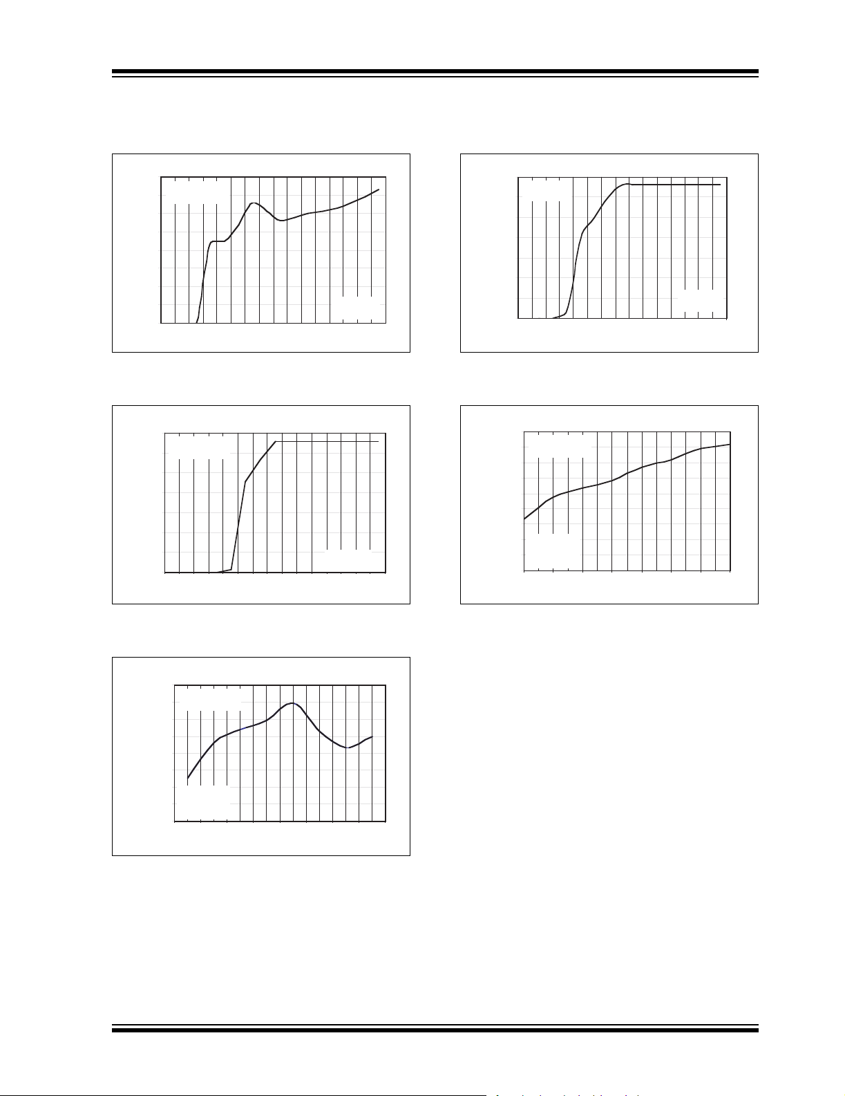
0
10
20
30
40
50
60
70
80
90
0 0.5 1 1.5 2 2.5 3 3.5 4 4.5 5 5.5 6 6.5 7 7.5
GND CURRENT (
µ
A)
0 0.5 1 1.5 2 2.5 3 3.5 4 4.5 5 5.5 6 6.5 7 7.5
V
IN
(V)
CIN = 1µF
C
OUT
= 1µF
Ground Current vs. V
IN
V
OUT
= 3.3V
I
LOAD
= 10mA
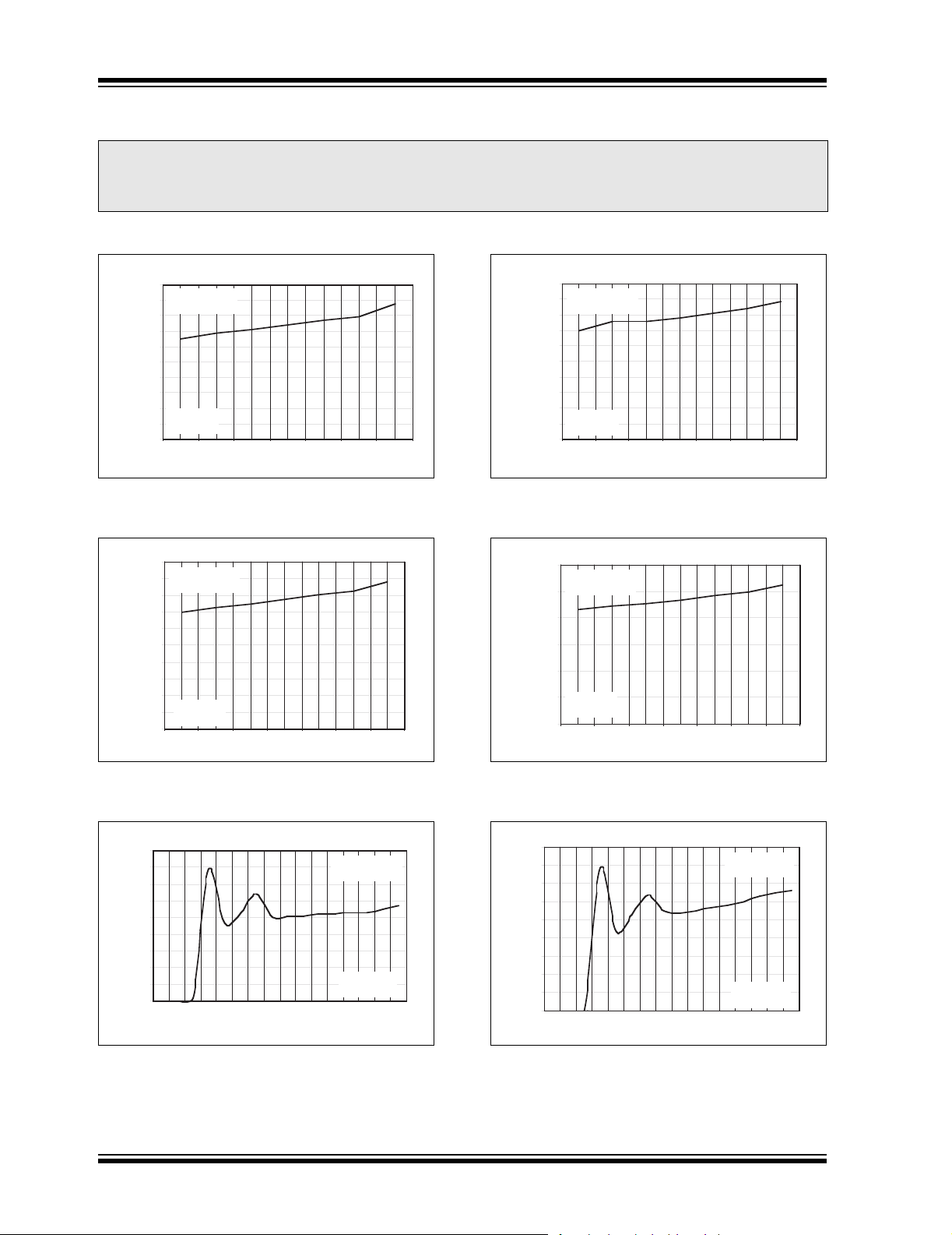
2.0 TYPICAL PERFORMANCE CURVES
Note: The graphs and tables provided following this note are a statistical summary based on a limited number of
samples and are provided for informational purposes only. The performance characteristics listed herein
are not tested or guaranteed. In some graphs or tables, the data presented may be outside the specified
operating range (e.g., outside specified power supply range) and therefore outside the warranted range.
Note: Unless otherwise specified, all parts are measured at temperature = +25°C.
0.020
0.018
0.016
0.014
0.012
0.010
0.008
0.006
0.004
DROPOUT VOLTAGE (V)
0.002
0.000
Dropout Voltage vs. Temperature
V
= 3.3V
OUT
I
= 10mA
LOAD
CIN = 1µF
C
= 1µF
OUT
-40 -20 0 20 50 70 125
TEMPERATURE (°C)
FIGURE 2-1: Dropout Voltage vs.
Temperature.
0.200
0.180
0.160
0.140
0.120
0.100
0.080
0.060
0.040
DROPOUT VOLTAGE (V)
0.020
0.000
Dropout Voltage vs. Temperature
V
= 3.3V
OUT
I
= 100mA
LOAD
CIN = 1µF
= 1µF
C
OUT
-40 -20 0 20 50 70 125
TEMPERATURE (°C)
FIGURE 2-2: Dropout Voltage vs.
Temperature.
0.100
0.090
0.080
0.070
0.060
0.050
0.040
0.030
0.020
DROPOUT VOLTAGE (V)
0.010
0.000
Dropout Voltage vs. Temperature
V
= 3.3V
OUT
I
= 50mA
LOAD
CIN = 1µF
C
= 1µF
OUT
-40 -20 0 20 50 70 12 5
TEMPERATURE (°C)
FIGURE 2-4: Dropout Voltage vs.
Temperature.
0.300
0.250
0.200
0.150
0.100
DROPOUT VOLTAGE (V)
0.050
0.000
Dropout Voltage vs. Temperature
V
= 3.3V
OUT
I
= 150mA
LOAD
CIN = 1µF
C
= 1µF
OUT
-40 -20 0 20 50 70 125
TEMPERATURE (°C)
FIGURE 2-5: Dropout Voltage vs.
Temperature.
FIGURE 2-3: Ground Current vs. Input
Voltage (V
DS21335E-page 4 © 2007 Microchip Technology Inc.
IN
).
90
80
70
A)
µ
60
50
40
30
GND CURRENT (
20
10
0
0 0.5 1 1.5 2 2.5 3 3.5 4 4.5 5 5.5 6 6.5 7 7.5
Ground Current vs. V
11.522.533.544.555.566.577.5
V
(V)
IN
IN
V
OUT
I
LOAD
= 3.3V
= 100mA
CIN = 1µF
C
= 1µF
OUT
FIGURE 2-6: Ground Current vs. Input
Voltage (VIN).
Page 5
TC1014/TC1015/TC1185
0
10
20
30
40
50
60
70
80
1.5 2 2.5 3 3.5 4 4.5 5 5.5 6 6.5 7 7.5
GND CURRENT (µA)
0 0.5 1 1.5 2 2.5 3 3.5 4 4.5 5 5.5 6 6.5 7 7.5
V
IN
(V)
CIN = 1µF
C
OUT
= 1µF
Ground Current vs. V
IN
V
OUT
= 3.3V
I
LOAD
= 150mA
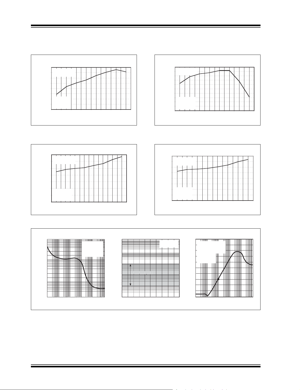
Output Voltage vs. Temperature
3.274
3.276
3.278
3.280
3.282
3.284
3.286
3.288
3.290
-40 -20 -10 0 20 40 85 125
V
OUT
(V)
TEMPERATURE (°C)
V
OUT
= 3.3V
I
LOAD
= 150mA
CIN = 1µF
C
OUT
= 1µF
V
IN
= 4.3V
TYPICAL PERFORMANCE CURVES (CONTINUED)
Note: Unless otherwise specified, all parts are measured at temperature = +25°C.
3.5
V
= 3.3V
OUT
I
= 0
3
LOAD
2.5
2
(V)
OUT
1.5
V
1
0.5
0
0 0.5 1 1.5 2 2.5 3 3.5 4 4.5 5 5.5 6 6.5 7
0 0.5 1 1.5 2 2.5 3 3.5 4 4.5 5 5.5 6 6.5 7
V
OUT
vs. VIN
V
(V)
IN
CIN = 1µF
C
= 1µF
OUT
FIGURE 2-7: Ground Current vs. Input
Voltage (V
(V)
OUT
V
FIGURE 2-8: Output Voltage (V
Input Voltage (V
).
IN
V
vs. VIN
3.5
V
= 3.3V
OUT
I
= 100mA
LOAD
I
= 100mA
3.0
2.5
2.0
1.5
1.0
0.5
0.0
LOAD
0 0.5 1 1.5 2 2.5 3 3.5 4 4.5 5 5.5 6 6.5 7
OUT
V
(V)
IN
).
IN
CIN = 1µF
C
= 1µF
OUT
OUT
) vs.
FIGURE 2-10: Output Voltage (V
Input Voltage (V
3.320
3.315
3.310
3.305
3.300
(V)
3.295
OUT
V
3.290
3.285
3.280
3.275
-40 -20 -10 0 20 40 85 125
).
IN
Output Voltage vs. Temperature
V
= 3.3V
OUT
I
= 10mA
LOAD
CIN = 1µF
C
= 1µF
OUT
= 4.3V
V
IN
TEMPERATURE (°C)
FIGURE 2-11: Output Voltage (V
Temperature.
OUT
OUT
) vs.
) vs.
FIGURE 2-9: Output Voltage (V
Temperature.
© 2007 Microchip Technology Inc. DS21335E-page 5
OUT
) vs.
Page 6
TC1014/TC1015/TC1185
Stable Region
S
n
K
TYPICAL PERFORMANCE CURVES (CONTINUED)
Note: Unless otherwise specified, all parts are measured at temperature = +25°C.
Output Voltage vs. Temperature
V
= 5V
OUT
I
= 10mA
LOAD
CIN = 1µF
= 1µF
C
OUT
V
= 6V
IN
-40 -20 -10 0 20 40 85 125
TEMPERATURE (°C)
(V)
V
OUT
5.025
5.020
5.015
5.010
5.005
5.000
4.995
4.990
4.985
FIGURE 2-12: Output Voltage (V
Temperature.
Temperature vs. Quiescent Current
70
V
= 5V
OUT
60
I
= 10mA
LOAD
A)
µ
50
40
30
20
GND CURRENT (
CIN = 1µF
C
10
= 1µF
OUT
V
= 6V
IN
0
-40 -20 -10 0 20 40 85 125
TEMPERATURE (°C)
OUT
) vs.
4.994
V
= 5V
OUT
4.992
I
= 150mA
LOAD
4.990
4.988
4.986
(V)
4.984
OUT
4.982
V
4.980
CIN = 1µF
4.978
C
= 1µF
4.976
4.974
OUT
= 6V
V
IN
-40 -20 -10 0 20 40 85 125
TEMPERATURE (°C)
FIGURE 2-14: Output Voltage (V
Temperature.
Output Voltage vs. Temperature
80
70
60
A)
μ
50
40
30
20
GND CURRENT (
10
Temperature vs. Quiescent Current
V
= 5V
OUT
I
= 150mA
LOAD
CIN = 1μF
C
= 1μF
OUT
= 6V
V
IN
0
-40 -20 -10 0 20 40 85 125
TEMPERATURE (°C)
OUT
) vs.
FIGURE 2-13: I
vs. Temperature.
GND
Output Noise vs. Frequency
NOISE (μV/√Hz)
10.0
1.0
0.1
0.0
0.01K
0.1K
1K 10K 100K
FREQUENCY (Hz)
R
C
C
C
LOAD
OUT
= 1μF
IN
BYP
= 50Ω
= 1μF
= 0
(Ω)
ESR
C
1000K
FIGURE 2-16: AC Characteristics.
FIGURE 2-15: I
Stability Region vs. Load Current
1000
100
OUT
0.1
0.01
10
table Regio
1
10
203040
0
LOAD CURRENT (mA)
C
OUT
to 10
50 60 70 80 90 100
= 1μF
μ
F
vs. Temperature.
GND
Power Supply Rejection Ratio
-30
I
10mA
OUT =
-35
-40
-45
-50
-55
-60
PSRR (dB)
-65
-70
-75
-80
0.01K
V
IN
DC
V
IN
AC
V
OUT
= 0
C
IN
C
OUT
0.1K
= 4V
= 100mV
p-p
= 3V
= 1μF
1K 10K
FREQUENCY (Hz)
100K
1000
DS21335E-page 6 © 2007 Microchip Technology Inc.
Page 7
TC1014/TC1015/TC1185
V
SHDN
V
OUT
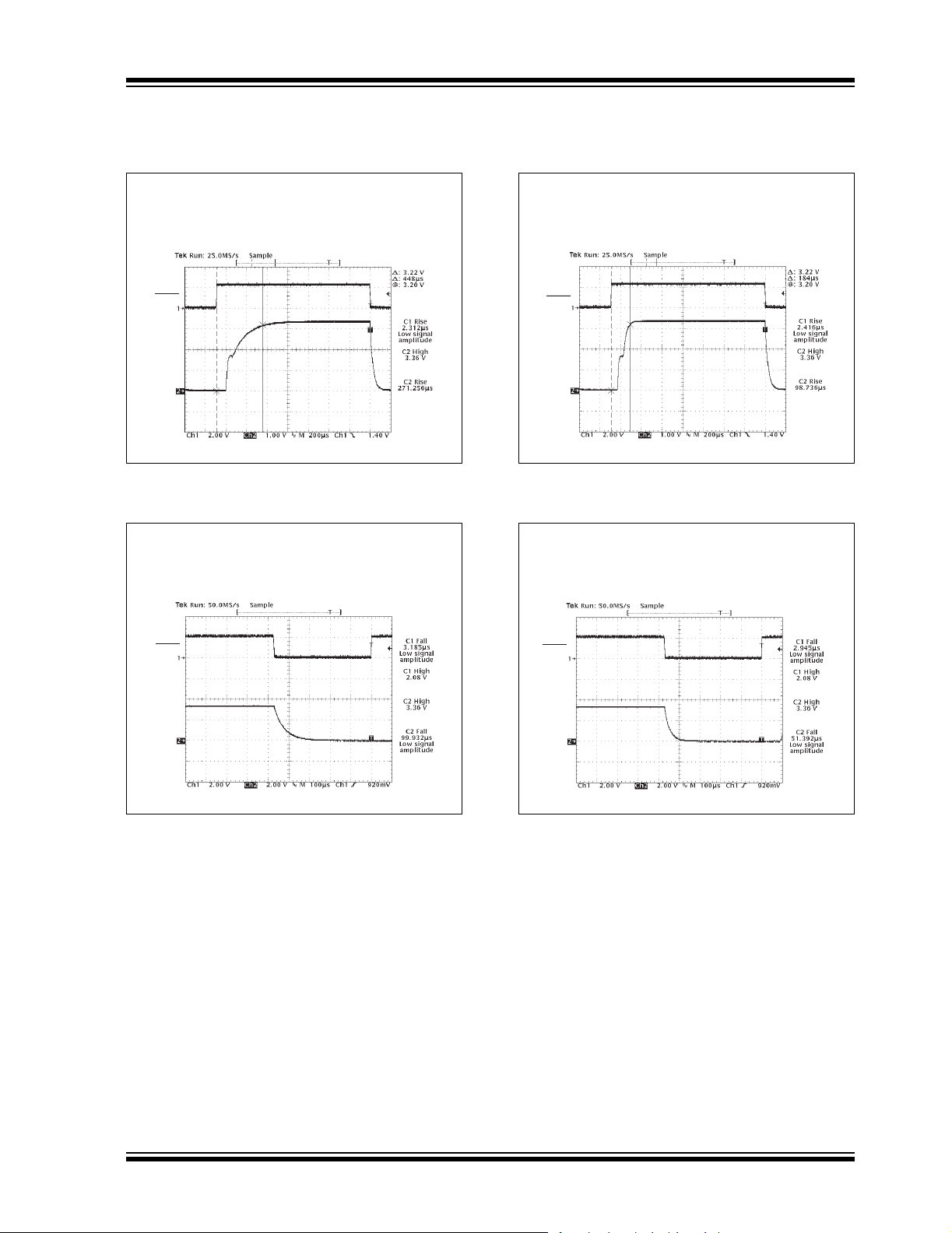
Measure Rise Time of 3.3V LDO With Bypass Capacitor
Conditions: CIN = 1μF, C
OUT
= 1μF, C
BYP
= 470pF, I
LOAD
= 100mA
V
IN
= 4.3V, Temp = 25°C, Rise Time = 448μS
TYPICAL PERFORMANCE CURVES (CONTINUED)
Note: Unless otherwise specified, all parts are measured at temperature = +25°C.
Measure Rise Time of 3.3V LDO Without Bypass Capacitor
Conditions: CIN = 1μF, C
V
SHDN
V
= 4.3V, Temp = 25°C, Rise Time = 184μS
V
IN
OUT
OUT
= 1μF, C
BYP
= 0pF, I
LOAD
= 100mA
FIGURE 2-17: Measure Rise Time of 3.3V
with Bypass Capacitor.
Measure Fall Time of 3.3V LDO With Bypass Capacitor
Conditions: CIN = 1μF, C
V
SHDN
V
OUT
= 4.3V, Temp = 25°C, Fall Time = 100μS
V
IN
OUT
= 1μF, C
BYP
= 470pF, I
LOAD
= 50mA
FIGURE 2-18: Measure Fall Time of 3.3V
with Bypass Capacitor.
FIGURE 2-19: Measure Rise Time of 3.3V
without Bypass Capacitor.
Measure Fall Time of 3.3V LDO Without Bypass Capacitor
Conditions: CIN = 1μF, C
V
SHDN
V
OUT
= 4.3V, Temp = 25°C, Fall Time = 52μS
V
IN
OUT
= 1μF, C
BYP
= 0pF, I
LOAD
= 100mA
FIGURE 2-20: Measure Fall Time of 3.3V
without Bypass Capacitor.
© 2007 Microchip Technology Inc. DS21335E-page 7
Page 8

TC1014/TC1015/TC1185
Measure Rise Time of 5.0V LDO With Bypass Capacitor
Conditions: CIN = 1μF, C
OUT
= 1μF, C
BYP
= 470pF, I
LOAD
= 100mA
V
IN
= 6V, Temp = 25°C, Rise Time = 390μS
V
SHDN
V
OUT
TYPICAL PERFORMANCE CURVES (CONTINUED)
Note: Unless otherwise specified, all parts are measured at temperature = +25°C.
Measure Rise Time of 5.0V LDO Without Bypass Capacitor
Conditions: CIN = 1μF, C
V
SHDN
V
OUT
= 6V, Temp = 25°C, Rise Time = 192μS
V
IN
OUT
= 1μF, C
BYP
= 0pF, I
LOAD
= 100mA
FIGURE 2-21: Measure Rise Time of 5.0V
with Bypass Capacitor.
Measure Fall Time of 5.0V LDO With Bypass Capacitor
Conditions: CIN = 1μF, C
V
SHDN
V
OUT
= 6V, Temp = 25°C, Fall Time = 167μS
V
IN
OUT
= 1μF, C
= 470pF, I
BYP
LOAD
= 50mA
FIGURE 2-22: Measure Fall Time of 5.0V
with Bypass Capacitor.
FIGURE 2-23: Measure Rise Time of 5.0V
without Bypass Capacitor.
Measure Fall Time of 5.0V LDO Without Bypass Capacitor
Conditions: CIN = 1μF, C
V
SHDN
V
OUT
= 6V, Temp = 25°C, Fall Time = 88μS
V
IN
OUT
= 1μF, C
BYP
= 0pF, I
LOAD
= 100mA
FIGURE 2-24: Measure Fall Time of 5.0V
without Bypass Capacitor.
DS21335E-page 8 © 2007 Microchip Technology Inc.
Page 9

TC1014/TC1015/TC1185
I
Load Regulation of 3.3V LDO
V
OUT
I
LOAD
Load Regulation of 3.3V LDO
Conditions: CIN = 1μF, C
OUT
= 2.2μF, C
BYP
= 470pF,
V
IN
= V
OUT
+ 0.25V, Temp = 25°C
I
LOAD
= 150mA switched in at 10kHz, V
OUT
is AC coupled
TYPICAL PERFORMANCE CURVES (CONTINUED)
Note: Unless otherwise specified, all parts are measured at temperature = +25°C.
Load Regulation of 3.3V LDO
Conditions: CIN = 1μF, C
V
= V
IN
I
= 50mA switched in at 10kHz, V
LOAD
LOAD
OUT
= 2.2μF, C
OUT
+ 0.25V, Temp = 25°C
is AC coupled
OUT
BYP
= 470pF,
Conditions: CIN = 1μF, C
V
IN
I
= 100mA switched in at 10kHz, V
LOAD
I
LOAD
= V
+ 0.25V, Temp = 25°C
OUT
= 2.2μF, C
OUT
is AC coupled
OUT
BYP
= 470pF,
V
OUT
FIGURE 2-25: Load Regulation of 3.3V
LDO.
V
OUT
FIGURE 2-27: Load Regulation of 3.3V
LDO.
Line Regulation of 3.3V LDO
Conditions: VIN = 4V, + 1V Squarewave @2.5kHz
V
IN
V
OUT
CIN = 0μF, C
I
LOAD
= 1μF, C
OUT
= 100mA, VIN & V
= 470pF,
BYP
are AC coupled
OUT
FIGURE 2-26: Load Regulation of 3.3V
LDO.
FIGURE 2-28: Load Regulation of 3.3V
LDO.
© 2007 Microchip Technology Inc. DS21335E-page 9
Page 10

TC1014/TC1015/TC1185
CIN = 0μF, C
OUT
= 1μF, C
BYP
= 470pF,
I
LOAD
= 100mA, VIN & V
OUT
are AC coupled
Line Regulation of 5.0V LDO
Conditions: VIN = 6V, + 1V Squarewave @2.5kHz
V
IN
V
OUT
TYPICAL PERFORMANCE CURVES (CONTINUED)
Note: Unless otherwise specified, all parts are measured at temperature = +25°C.
Thermal Shutdown Response of 5.0V LDO
Conditions: VIN = 6V, CIN = 0μF, C
V
OUT
I
was increased until temperature of die reached about 160°C, at
LOAD
which time integrated thermal protection circuitry shuts the regulator
off when die temperature exceeds approximately 160
remains off until die temperature drops to approximately 150
= 1μF
OUT
°C. The regulator
°C.
FIGURE 2-29: Line Regulation of 5.0V
LDO.
FIGURE 2-30: Thermal Shutdown
Response of 5.0V LDO.
DS21335E-page 10 © 2007 Microchip Technology Inc.
Page 11

3.0 PIN DESCRIPTIONS
The descriptions of the pins are listed in Table 3-1.
TABLE 3-1: PIN FUNCTION TABLE
TC1014/TC1015/TC1185
Pin No.
(5-Pin SOT-23)
1V
2 GND Ground terminal.
3 SHDN
4 Bypass Reference bypass input. Connecting a 470 pF to this input further reduces output
5V
Symbol Description
Unregulated supply input.
IN
Shutdown control input. The regulator is fully enabled when a logic high is applied to
this input. The regulator enters shutdown when a logic low is applied to this input.
During shutdown, output voltage falls to zero and supply current is reduced to
0.5 µA (maximum).
noise.
OUT
Regulated voltage output.
3.1 Input Voltage (VIN)
Connect the VIN pin to the unregulated source
voltage. Like all low dropout linear regulators, low
source impedance is necessary for the stable
operation of the LDO. The amount of capacitance
required to ensure low source impedance will
depend on the proximity of the input source
capacitors or battery type. For most applications,
1.0 µF of capacitance will ensure stable operation
of the LDO circuit. The type of capacitor used can
be ceramic, tantalum or aluminum electrolytic.
The low Effective Series Resistance (ESR) characteristics of the ceramic will yield better noise
and Power Supply Ripple Rejection (PSRR)
performance at high frequency.
3.2 Ground Terminal (GND)
Connect the ground pin to the input voltage
return. For the optimal noise and PSRR
performance, the GND pin of the LDO should be
tied to a quiet circuit ground. For applications
have switching or noisy inputs tie the GND pin to
the return of the output capacitor. Ground planes
help lower inductance and voltage spikes caused
by fast transient load currents and are
recommended for applications that are subjected
to fast load transients.
3.3 Shutdown (SHDN)
The Shutdown input is used to turn the LDO on
and off. When the SHDN
pin is at a logic high
level, the LDO output is enabled. When the
SHDN
pin is pulled to a logic low, the LDO output
is disabled. When disabled, the quiescent current
used by the LDO is less than 0.5 µA max.
3.4 Bypass
Connecting a low-value ceramic capacitor to the
Bypass pin will further reduce output voltage
noise and improve the PSRR performance of the
LDO. While smaller and larger values can be
used, these affect the speed at which the LDO
output voltage rises when the input power is
applied. The larger the bypass capacitor, the
slower the output voltage will rise.
3.5 Output Voltage (V
Connect the output load to V
connect one side of the LDO output capacitor as
close as possible to the V
OUT
)
OUT
of the LDO. Also
OUT
pin.
© 2007 Microchip Technology Inc. DS21335E-page 11
Page 12

TC1014/TC1015/TC1185
TC1014
TC1015
TC1185
V
OUT
SHDN
GND
Bypass
470 pF
Reference
Bypass Cap
(Optional)
+
V
IN
V
OUT
Shutdown Control
(to CMOS Logic or Tie
to V
IN
if unused)
1µF
+
Battery
+
1µF
4.0 DETAILED DESCRIPTION
The TC1014, TC1015 and TC1185 are precision fixed
output voltage regulators (if an adjustable version is
needed, see the TC1070, TC1071 and TC1187 data
sheet (DS21353). Unlike bipolar regulators, the
TC1014, TC1015 and TC1185 supply current does not
increase with load current. In addition, the LDOs’ output voltage is stable using 1 µF of capacitance over the
entire specified input voltage range and output current
range.
Figure 4-1 shows a typical application circuit. The
regulator is enabled anytime the shutdown input
) is at or above VIH, and disabled when SHDN is
(SHDN
at or below VIL. SHDN may be controlled by a CMOS
logic gate or I/O port of a microcontroller. If the SHDN
input is not required, it should be connected directly to
the input supply. While in shutdown, the supply current
decreases to 0.05 µA (typical) and V
volts.
falls to zero
OUT
4.1 Bypass Input
A 470 pF capacitor connected from the Bypass input to
ground reduces noise present on the internal
reference, which in turn, significantly reduces output
noise. If output noise is not a concern, this input may be
left unconnected. Larger capacitor values may be
used, but results in a longer time period to rated output
voltage when power is initially applied.
4.2 Output Capacitor
A 1 µF (min) capacitor from V
The output capacitor should have an effective series
resistance greater than 0.1Ω and less than 5Ω. A 1 µF
capacitor should be connected from V
is more than 10 inches of wire between the regulator
and the AC filter capacitor, or if a battery is used as the
power source. Aluminum electrolytic or tantalum
capacitor types can be used. (Since many aluminum
electrolytic capacitors freeze at approximately -30°C,
solid tantalums are recommended for applications
operating below -25°C.) When operating from sources
other than batteries, supply-noise rejection and
transient response can be improved by increasing the
value of the input and output capacitors and employing
passive filtering techniques.
to ground is required.
OUT
to GND if there
IN
FIGURE 4-1: Typical Application Circuit.
4.3 Input Capacitor
A 1 µF capacitor should be connected from VIN to GND
if there is more than 10 inches of wire between the
regulator and this AC filter capacitor, or if a battery is
used as the power source. Aluminum electrolytic or
tantalum capacitors can be used (since many
aluminum electrolytic capacitors freeze at
approximately -30°C, solid tantalum is recommended
for applications operating below -25°C). When
operating from sources other than batteries, supplynoise rejection and transient response can be
improved by increasing the value of the input and
output capacitors and employing passive filtering
techniques.
DS21335E-page 12 © 2007 Microchip Technology Inc.
Page 13

TC1014/TC1015/TC1185
PDV
INMAXVOUTMIN
–()I
LOADMAX
≈
Where:
P
D
= Worst-case actual power
dissipation
V
INMAX
= Maximum voltage on V
IN
V
OUTMIN
= Minimum regulator output voltage
I
LOADMAX
= Maximum output (load) current
Where all terms are previously defined.
P
DMAX
T
JMAXTAMAX
–()
θ
JA
--------------------------------------------=
P
DMAX
T
JMAXTAMAX
–()
θ
JA
--------------------------------------------=
125 55–()
220
-------------------------=
318 mW=
5.0 THERMAL CONSIDERATIONS
5.1 Thermal Shutdown
Integrated thermal protection circuitry shuts the
regulator off when die temperature exceeds 160°C.
The regulator remains off until the die temperature
drops to approximately 150°C.
5.2 Power Dissipation
The amount of power the regulator dissipates is
primarily a function of input and output voltage, and
output current. The following equation is used to
calculate worst-case actual power dissipation:
EQUATION 5-1:
Equation 5-1 can be used in conjunction with
Equation 5-2 to ensure regulator thermal operation is
within limits. For example:
Given:
V
INMAX
V
OUTMIN
I
LOADMAX
T
T
=3.0V +10%
= 2.7V – 2.5%
=40mA
=125°C
JMAX
=55°C
AMAX
Find:
1. Actual power dissipation
2. Maximum allowable dissipation
Actual power dissipation:
≈ (V
P
D
= [(3.0 x 1.1) – (2.7 x .975)]40 x 10
INMAX
– V
OUTMIN)ILOADMAX
–3
= 26.7 mW
Maximum allowable power dissipation:
The maximum allowable power dissipation
(Equation 5-2) is a function of the maximum ambient
temperature (T
temperature (T
junction-to-air (θ
), the maximum allowable die
A
MAX
) and the thermal resistance from
JMAX
). The 5-pin SOT-23 package has a
JA
θJA of approximately 220°C/Watt.
EQUATION 5-2:
In this example, the TC1014 dissipates a maximum of
26.7 mW below the allowable limit of 318 mW. In a
similar manner, Equation 5-1 and Equation 5-2 can be
used to calculate maximum current and/or input
voltage limits.
5.3 Layout Considerations
The primary path of heat conduction out of the package
is via the package leads. Therefore, layouts having a
ground plane, wide traces at the pads, and wide power
supply bus lines combine to lower θ
increase the maximum allowable power dissipation
limit.
and therefore
JA
© 2007 Microchip Technology Inc. DS21335E-page 13
Page 14

TC1014/TC1015/TC1185
1423
W, Width of
Carrier Tape
User Direction of Feed
P,Pitch
Standard Reel Component
Orientation
Reverse Reel Component
Orientation
PIN 1
Device
Marking
PIN 1
Carrier Tape, Number of Components per Reel and Reel Size
Package Carrier Width (W) Pitch (P) Part Per Full Reel Reel Size
5-Pin SOT-23 8 mm 4 mm 3000 7 in
6.0 PACKAGING INFORMATION
6.1 Package Marking Information
c
&d represents part number code + temperature
range and voltage
e
f
6.2 Taping Form
represents year and 2-month period code
represents lot ID number
TABLE 6-1: PART NUMBER CODE AND
TEMPERATURE RANGE
(V)
1.8 AY BY NY
2.5 A1 B1 N1
2.6 NB BT NT
2.7 A2 B2 N2
2.8 AZ BZ NZ
2.85 A8 B8 N8
3.0 A3 B3 N3
3.3 A5 B5 N5
3.6 A9 B9 N9
4.0 A0 B0 N0
5.0 A7 B7 N7
TC1014
Code
TC1015
Code
TC1185
Code
DS21335E-page 14 © 2007 Microchip Technology Inc.
Page 15

TC1014/TC1015/TC1185
5-Lead Plastic Small Outline Transistor (OT) [SOT-23]
Notes:
1. Dimensions D and E1 do not include mold flash or protrusions. Mold flash or protrusions shall not exceed 0.127 mm per side.
2. Dimensioning and tolerancing per ASME Y14.5M.
BSC: Basic Dimension. Theoretically exact value shown without tolerances.
Note: For the most current package drawings, please see the Microchip Packaging Specification located at
http://www.microchip.com/packaging
Units MILLIMETERS
Dimension Limits MIN NOM MAX
Number of Pins N 5
Lead Pitch e 0.95 BSC
Outside Lead Pitch e1 1.90 BSC
Overall Height A 0.90 – 1.45
Molded Package Thickness A2 0.89 – 1.30
Standoff A1 0.00 – 0.15
Overall Width E 2.20 – 3.20
Molded Package Width E1 1.30 – 1.80
Overall Length D 2.70 – 3.10
Foot Length L 0. 10 – 0.60
Footprint L1 0.35 – 0.80
Foot Angle φ 0° – 30°
Lead Thickness c 0.08 – 0.26
Lead Width b 0.20 – 0.51
φ
N
b
E
E1
D
1
2
3
e
e1
A
A1
A2
c
L
L1
Microchip Technology Drawing C04-091B
© 2007 Microchip Technology Inc. DS21335E-page 15
Page 16

TC1014/TC1015/TC1185
NOTES:
DS21335E-page 16 © 2007 Microchip Technology Inc.
Page 17

APPENDIX A: REVISION HISTORY
Revision E (February 2007)
• Section 1.0 “Electrical characteristics”:
Changed Dropout Voltage from mA to µA.
• Updated “Product Identification System”,
page 19.
• Updated Section 6.0 “Packaging Information”.
Revision D (April 2006)
• Removed “ERROR is open circuited” from SHDN
pin description in Pin Function Table.
• Added verbiage for pinout descriptions in Pin
Function Table.
• Replaced verbiage in first paragraph of Section
4.0 Detailed Description.
• Added Section 4.3 Input Capacitor
Revision C (January 2006)
• Changed TR suffix to 713 suffix in Taping Form in
Package Marking Section
TC1014/TC1015/TC1185
Revision B (May 2002)
• Converted Telcom data sheet to Microchip
standard for Analog Handbook
Revision A (February 2001)
• Original Release of this Document under Telcom.
© 2007 Microchip Technology Inc. DS21335E-page 17
Page 18

TC1014/TC1015/TC1185
NOTES:
DS21335E-page 18 © 2007 Microchip Technology Inc.
Page 19

TC1014/TC1015/TC1185
Device: TC1014: 50 mA LDO with Shutdown and V
REF
Bypass
TC1015: 100 mA LDO with Shutdown and V
REF
Bypass
TC1185: 150 mA LDO with Shutdown and V
REF
Bypass
Output Voltage: 1.8 = 1.8V
2.5 = 2.5V
2.6 = 2.6V
2.7 = 2.7V
2.8 = 2.8V
2.85 = 2.85V
3.0 = 3.0V
3.3 = 3.3V
3.6 = 3.6V
4.0 = 4.0V
5.0 = 5.0V
Temperature Range: V = -40° C to +125° C
Package: CT713 = Plastic Small Outline Transistor (SOT-23),
5-lead, Tape and Reel
PART NO. -X.X X
TemperatureOutput
Vol tag e
Device
Examples:
a) TC1014-1.8VCT713: 1.8V, 5LD SOT-23,
Tape and Reel.
b) TC1014-2.85VCT713: 2.85V, 5LD SOT-23,
Tape and Reel.
c) TC1014-3.3VCT713: 3.3V, 5LD SOT-23,
Tape and Reel.
a) TC1015-1.8VCT713: 1.8V, 5LD SOT-23,
Tape and Reel.
b) TC1015-2.85VCT713: 2.85V, 5LD SOT-23,
Tape and Reel.
c) TC1015-3.0VCT713: 3.0V, 5LD SOT-23,
Tape and Reel.
a) TC1185-1.8VCT713: 1.8V, 5LD SOT-23,
Tape and Reel.
b) TC1185-2.8VCT713: 2.8V, 5LD SOT-23,
Tape and Reel.
Range
XXX
XX
Package
PRODUCT IDENTIFICATION SYSTEM
To order or obtain information, e.g., on pricing or delivery, refer to the factory or the listed sales office.
© 2007 Microchip Technology Inc. DS21335E-page 19
Page 20

TC1014/TC1015/TC1185
NOTES:
DS21335E-page 20 © 2007 Microchip Technology Inc.
Page 21

Note the following details of the code protection feature on Microchip devices:
• Microchip products meet the specification contained in their particular Microchip Data Sheet.
• Microchip believes that its family of products is one of the most secure families of its kind on the market today, when used in the
intended manner and under normal conditions.
• There are dishonest and possibly illegal methods used to breach the code protection feature. All of these methods, to our
knowledge, require using the Microchip products in a manner outside the operating specifications contained in Microchip’s Data
Sheets. Most likely, the person doing so is engaged in theft of intellectual property.
• Microchip is willing to work with the customer who is concerned about the integrity of their code.
• Neither Microchip nor any other semiconductor manufacturer can guarantee the security of their code. Code protection does not
mean that we are guaranteeing the product as “unbreakable.”
Code protection is constantly evolving. We at Microchip are committed to continuously improving the code protection features of our
products. Attempts to break Microchip’s code protection feature may be a violation of the Digital Millennium Copyright Act. If such acts
allow unauthorized access to your software or other copyrighted work, you may have a right to sue for relief under that Act.
Information contained in this publication regarding device
applications and the like is provided only for your convenience
and may be superseded by updates. It is your responsibility to
ensure that your application meets with your specifications.
MICROCHIP MAKES NO REPRESENTATIONS OR
WARRANTIES OF ANY KIND WHETHER EXPRESS OR
IMPLIED, WRITTEN OR ORAL, STATUTORY OR
OTHERWISE, RELATED TO THE INFORMATION,
INCLUDING BUT NOT LIMITED TO ITS CONDITION,
QUALITY, PERFORMANCE, MERCHANTABILITY OR
FITNESS FOR PURPOSE. Microchip disclaims all liability
arising from this information and its use. Use of Microchip
devices in life support and/or safety applications is entirely at
the buyer’s risk, and the buyer agrees to defend, indemnify and
hold harmless Microchip from any and all damages, claims,
suits, or expenses resulting from such use. No licenses are
conveyed, implicitly or otherwise, under any Microchip
intellectual property rights.
Trademarks
The Microchip name and logo, the Microchip logo, Accuron,
dsPIC, K
EELOQ, KEELOQ logo, microID, MPLAB, PIC,
PICmicro, PICSTART, PRO MATE, PowerSmart, rfPIC, and
SmartShunt are registered trademarks of Microchip
Technology Incorporated in the U.S.A. and other countries.
AmpLab, FilterLab, Linear Active Thermistor, Migratable
Memory, MXDEV, MXLAB, PS logo, SEEVAL, SmartSensor
and The Embedded Control Solutions Company are
registered trademarks of Microchip Technology Incorporated
in the U.S.A.
Analog-for-the-Digital Age, Application Maestro, CodeGuard,
dsPICDEM, dsPICDEM.net, dsPICworks, ECAN,
ECONOMONITOR, FanSense, FlexROM, fuzzyLAB,
In-Circuit Serial Programming, ICSP, ICEPIC, Mindi, MiWi,
MPASM, MPLAB Certified logo, MPLIB, MPLINK, PICkit,
PICDEM, PICDEM.net, PICLAB, PICtail, PowerCal,
PowerInfo, PowerMate, PowerTool, REAL ICE, rfLAB,
rfPICDEM, Select Mode, Smart Serial, SmartTel, Total
Endurance, UNI/O, WiperLock and ZENA are trademarks of
Microchip Technology Incorporated in the U.S.A. and other
countries.
SQTP is a service mark of Microchip Technology Incorporated
in the U.S.A.
All other trademarks mentioned herein are property of their
respective companies.
© 2007, Microchip Technology Incorporated, Printed in the
U.S.A., All Rights Reserved.
Printed on recycled paper.
Microchip received ISO/TS-16949:2002 certification for its worldwide
headquarters, design and wafer fabrication facilities in Chandler and
Tempe, Arizona, Gresham, Oregon and Mountain View, California. The
Company’s quality system processes and procedures are for its PIC
MCUs and dsPIC® DSCs, KEELOQ
EEPROMs, microperipherals, nonvolatile memory and analog
products. In addition, Microchip’s quality system for the design and
manufacture of development systems is ISO 9001:2000 certified.
®
code hopping devices, Serial
© 2007 Microchip Technology Inc. DS21335E-page 21
®
Page 22

WORLDWIDE SALES AND SERVICE
AMERICAS
Corporate Office
2355 West Chandler Blvd.
Chandler, AZ 85224-6199
Tel: 480-792-7200
Fax: 480-792-7277
Technical Support:
http://support.microchip.com
Web Address:
www.microchip.com
Atlanta
Duluth, GA
Tel: 678-957-9614
Fax: 678-957-1455
Boston
Westborough, MA
Tel: 774-760-0087
Fax: 774-760-0088
Chicago
Itasca, IL
Tel: 630-285-0071
Fax: 630-285-0075
Dallas
Addison, TX
Tel: 972-818-7423
Fax: 972-818-2924
Detroit
Farmington Hills, MI
Tel: 248-538-2250
Fax: 248-538-2260
Kokomo
Kokomo, IN
Tel: 765-864-8360
Fax: 765-864-8387
Los Angeles
Mission Viejo, CA
Tel: 949-462-9523
Fax: 949-462-9608
Santa Clara
Santa Clara, CA
Tel: 408-961-6444
Fax: 408-961-6445
Toronto
Mississauga, Ontario,
Canada
Tel: 905-673-0699
Fax: 905-673-6509
ASIA/PACIFIC
Asia Pacific Office
Suites 3707-14, 37th Floor
Tower 6, The Gateway
Habour City, Kowloon
Hong Kong
Tel: 852-2401-1200
Fax: 852-2401-3431
Australia - Sydney
Tel: 61-2-9868-6733
Fax: 61-2-9868-6755
China - Beijing
Tel: 86-10-8528-2100
Fax: 86-10-8528-2104
China - Chengdu
Tel: 86-28-8665-5511
Fax: 86-28-8665-7889
China - Fuzhou
Tel: 86-591-8750-3506
Fax: 86-591-8750-3521
China - Hong Kong SAR
Tel: 852-2401-1200
Fax: 852-2401-3431
China - Qingdao
Tel: 86-532-8502-7355
Fax: 86-532-8502-7205
China - Shanghai
Tel: 86-21-5407-5533
Fax: 86-21-5407-5066
China - Shenyang
Tel: 86-24-2334-2829
Fax: 86-24-2334-2393
China - Shenzhen
Tel: 86-755-8203-2660
Fax: 86-755-8203-1760
China - Shunde
Tel: 86-757-2839-5507
Fax: 86-757-2839-5571
China - Wuhan
Tel: 86-27-5980-5300
Fax: 86-27-5980-5118
China - Xian
Tel: 86-29-8833-7250
Fax: 86-29-8833-7256
ASIA/PACIFIC
India - Bangalore
Tel: 91-80-4182-8400
Fax: 91-80-4182-8422
India - New Delhi
Tel: 91-11-4160-8631
Fax: 91-11-4160-8632
India - Pune
Tel: 91-20-2566-1512
Fax: 91-20-2566-1513
Japan - Yokohama
Tel: 81-45-471- 6166
Fax: 81-45-471-6122
Korea - Gumi
Tel: 82-54-473-4301
Fax: 82-54-473-4302
Korea - Seoul
Tel: 82-2-554-7200
Fax: 82-2-558-5932 or
82-2-558-5934
Malaysia - Penang
Tel: 60-4-646-8870
Fax: 60-4-646-5086
Philippines - Manila
Tel: 63-2-634-9065
Fax: 63-2-634-9069
Singapore
Tel: 65-6334-8870
Fax: 65-6334-8850
Taiwan - Hsin Chu
Tel: 886-3-572-9526
Fax: 886-3-572-6459
Taiwan - Kaohsiung
Tel: 886-7-536-4818
Fax: 886-7-536-4803
Taiwan - Taipei
Tel: 886-2-2500-6610
Fax: 886-2-2508-0102
Thailand - Bangkok
Tel: 66-2-694-1351
Fax: 66-2-694-1350
EUROPE
Austria - Wels
Tel: 43-7242-2244-39
Fax: 43-7242-2244-393
Denmark - Copenhagen
Tel: 45-4450-2828
Fax: 45-4485-2829
France - Paris
Tel: 33-1-69-53-63-20
Fax: 33-1-69-30-90-79
Germany - Munich
Tel: 49-89-627-144-0
Fax: 49-89-627-144-44
Italy - Milan
Tel: 39-0331-742611
Fax: 39-0331-466781
Netherlands - Drunen
Tel: 31-416-690399
Fax: 31-416-690340
Spain - Madrid
Tel: 34-91-708-08-90
Fax: 34-91-708-08-91
UK - Wokingham
Tel: 44-118-921-5869
Fax: 44-118-921-5820
12/08/06
DS21335E-page 22 © 2007 Microchip Technology Inc.
 Loading...