

Page 1

DC-50 GHz
Broadband RF Amplifier
Operating Manual
Email:
sales@centellax.com
support@centellax.com
www.centellax.com
451 Aviation Blvd, Suite 101
Santa Rosa, CA 95403-1069
Tel: 707.568.5900
Fax: 707.568.7647
Specifications are subject to change without notice.
All Centellax trademarks and trade names are the property of Centellax Inc.
Copyright © 2003-2006 Centellax Inc.
Printed in USA. 12 Sep 2006 (C10029-01)
CENTELLAX
TA0L50VA
Page 2

Page 3

Table of Contents
Section 1 Introduction ....................................... 2
Section 2 Description ........................................ 3
Section 3 Specifications .................................... 4
Section 4 Performance Verification .................. 6
Section 5 Operation ........................................... 7
Section 6 Warranty ........................................... 12
Email:
sales@centellax.com
support@centellax.com
www.centellax.com
451 Aviation Blvd, Suite 101
Santa Rosa, CA 95403-1069
Tel: 707.568.5900
Fax: 707.568.7647
Section 6: Warranty
Centellax, Inc. Standard Warranty
Test Instrument and Accessory Products
Centellax, Inc. (“Centellax”) warrants that the Test Instrument(s) and Accessory(s)
(“Product(s)”) it manufactures is/are free from defective material and workmanship for a
period of one (1) year subject to the following terms and conditions. Centellax will remedy any such warranted defect subject to the followings:
This warranty requires the Product to be delivered to Centellax intact for examination
with an RMA number and with all transportation charges prepaid to the factory, within
one (1) year from the date of sale to the original customer. Centellax will determine in its
sole discretion when such defect exists. Centellax will return the repaired or replaced
Product to the customer at its cost unless the shipment needs to be expedited or the shipment is international, in which cases customer will pay for return shipment.
During the warranty period, Centellax will, at its sole option, either repair or replace
Products, which prove to be defective.
This warranty is only for the benefice of the original buyer registered with Centellax and
is not assignable. This warranty does not extend to any of Centellax’ Products which have
been subject to misuse, neglect, accident, improper installation, or used in violation of
operating instructions. This warranty does not extend to Products, which have been
repaired, calibrated, or altered in any way by a facility that is not approved, in writing, by
Centellax to perform such work. This warranty does not apply to any Product where the
seals or serial number thereof has been removed, defaced or changed, nor to Products not
of our own manufacture.
THIS WARRANTY IS IN LIEU OF ALL OTHER WARRANTIES EXPRESSED OR
IMPLIED FOR THE PRODUCTS AND ALL SUCH OTHER WARRANTIES ARE
HEREBY EXPRESSLY EXCLUDED. CENTELLAX SPECIFICALLY DISCLAIMS
THE IMPLIED WARRANTIES OF MERCHANTABILITY AND FITNESS FOR A
PARTICULAR PURPOSE.
TO THE EXTENT ALLOWED BY LAW, THE REMEDIES PROVIDED HEREIN ARE
THE CUSTOMER’S SOLE AND EXCLUSIVE REMEDIES. CENTELLAX SHALL
NOT BE LIABLE FOR ANY DIRECT, INDIRECT, SPECIAL, INCIDENTAL OR
CONSEQUENTIAL DAMAGES, WHETHER BASED ON CONTRACT, TORT OR
ANY OTHER LEGAL THEORY.
Additional information with regard to the applications and maintenance of this equipment
may be avail
able from time to time.
Centellax reserves the right to modify or change the warranty without notice.
TA0L50VA Operating Manual
112
Page 4

High Performance
Broadband RF Amplifier
TA0L50VA
Operating Manual
Section 1: Introduction
The TA0L50VA is a versatile RF System Amplifier, which has many
uses in research, development, or production-line environments. This
amplifier is a useful addition to the laboratory where RF, microwave,
or millimeter wave measurements are made. Typical applications
include:
• RF Source Amplifier.
• Mixer LO Amplifier.
•
Noise Figure LNA and Noise Figure System Amplifier
• Pulse Amplifier and time domain applications
•
Digital Communication Systems.
• Antenna research and development.
• General purpose RF gain block.
NOTE
Source-driven RF power amplifiers should always be terminated in an absorbing load. Unterminated outputs will radiate RF
energy; this can be dangerous to the operator, may violate FCC
laws, and could result in damage to the amplifier.
Centellax is committed to providing amplifiers that have exceptional performance, are unconditionally stable, and will survive
accidental laboratory misuse, such as a fully-saturated unterminated output. TA0L50VA System Amplifiers have passed rigorous RF tests which include an RF burnout test. Test conditions
are: P
out
= 24dBm @ 10 MHz; open output (unterminated).
Internal Power Detector: The TA0L50VA System Amplifier incorporates a
power detection feature.
Two matched on-chip GaAs diodes are used:
One of the diodes is RF coupled to the final output stage of the amplifier.
The second is a matched diode, in close proximity to the detector diode, which
is not RF coupled but provides a reference voltage that is a function of temperature and biasing.
A differential measurement of these diodes provides a voltage proportional to the
amplifier output power level independent of temperature and bias level of the
output amplifier chip.
The two diode voltages are provided on the rear panel of the TA0L50VA System
Amplifier and can be used to determine the amplifier output power level (as
shown in Figure 9).
An application note details the use of these diodes and is available from the
Centellax website.
For additional questions, please email: support@centellax.com or call
707-568-5900x11.
The detector diode is frequency dependant and must be calibrated for each test
frequency. The diode is a nonlinear device and its output voltage varies with
power. This must also be characterized.
In an ATE environment, calibration of the detector diode is not complicated and
may be as simple as measuring the differential voltage at each test frequency and
power level. A look up table or curve fit can be used to provide a measure of
power delivered.
External ALC Leveling
Establishing a desired power level at the amplified DUT “Reference Plane”
with power request to the source is often desirable. Many modern sources support "External Power Leveling". This technique involves power leveling using
feedback from external sensors (e.g. power meters or detector diodes). Properly
configured, these sensors provide feedback to the source that can be used by
the source to level the power at a remote reference plane.
TA0L50VA Operating Manual
2 11
Page 5

Section 2: Description
The Centellax TA0L50VA System Amplifier is a high performance,
medium power broadband amplifier featuring baseband RF (<100KHz)
through millimeter wave (>50 GHz) frequency coverage.
The TA0L50VA is designed to be used as a general purpose RF System
Amplifier for laboratory or test system applications. The amplifier's
small size (3.5x3.5x1.0 inch) allows close placement to the measurement reference plane, its high gain helps make up for system losses (e.g.
cables from remote sources).
The TA0L50VA features 2.4mm 50GHz female connectors at the
amplifier’s input and output. Adapters to lower frequency connectors
e.g. 2.9mm, 3.5mm and SMA are readily available.
The TA0L50VA is self contained and plugs into standard AC power
sources.
Features
• Broadband: 100 kHz to 50 GHz
• Saturated Output Power (P
sat
): ~ 24 dBm
@ 2 GHz and ~18 dBm @ 50 GHz
• >27 dB Gain to 45 GHz
• Useful gain to 65 GHz
• <6dB Noise Figure
• Optional Power Detector
• AC Power Supply Included
• Small size: 3.5” x 3.5” x 1”
Rear Panel
Input: A 2.4 mm input connector is provided on the rear panel of the
TA0L50VA.
Power in: 9 Vdc @ ~500 mA, supplied by the included AC supply.
Figure 9: Rear panel of TA0L50VA
GND
GND
REF
.
DET
TA0L50VA Operating Manual TA0L50VA Operating Manual
10 3
Page 6

Front Panel
Output: The TA0L50VA features a 2.4mm 50GHz female connector at
the amplifier’s output.
Led Indicator: One LED annunciator on the front panel indicates the
System Amplifier is powered.
Figure 8: Front panel of TA0L50VA
3.5”
3.5”
1”
Note: Always terminate the RF driven amplifier output !
Section 3: Specifications
Table 1: Performance Specification
Parameter Description Min. Typ. Max.
S21 (dB) Small Signal Gain
1 to 26 GHz 27 30 —
26 to 45 GHz 24 27 —
S11/S22 (dB) In/Output Loss
1 to 26 GHz — -10 —
26 to 45 GHz — -8 —
P
sat
(dBm) Saturated Output Power
100 kHz to 26 GHz +20 +22 —
@ 40 GHz — +20 —
@ 50 GHz — +17 —
NF (dB) Noise Figure
2 to 18 GHz — 5 —
30 - 40 GHz — 6 —
H2(dBc) 2nd Harmonic
2 - 25 GHz — -30 —
Figure 1: Input Pulse = Ch3, 420 mVppk, 10.4 ps Rise Time
Output Pulse = Ch4, 6.5 Vppk, 11.0 ps Rise Time
TA0L50VA Operating Manual TA0L50VA Operating Manual
4 9
Page 7

-30
-25
-20
-15
-10
-5
0
5
10
15
20
25
30
35
10k 100k 1M 10M 100M 1G
Return Loss & Gain (dB)
Frequency (Hz)
-30
-25
-20
-15
-10
-5
0
5
10
15
20
25
30
35
10k 100k 1M 10M 100M 1G
Return Loss & Gain (dB)
Frequency (Hz)
-30
-25
-20
-15
-10
-5
0
5
10
15
20
25
30
35
10k 100k 1M 10M 100M 1G
Return Loss & Gain (dB)
Frequency (Hz)
10 20 30 40 50
-30
-25
-20
-15
-10
-5
0
5
10
15
20
25
30
35
Frequency (GHz)
S21
S11
S22
10 20 30 40 50
-30
-25
-20
-15
-10
-5
0
5
10
15
20
25
30
35
Frequency (GHz)
Figur
e 2:
Small Signal Parameters vs Frequency
Figure 3: Gain vs Output Power
(P
1dB
indicated with *)
Figure 4: Saturated Output Power
When the system is calibrated the actual power delivered to the input
"Reference Plane" is read on the power meter display for power sensor
A. Sensor A is used to monitor and provide feedback to the user or an
ATE system in order to set the "Reference Plane" power level. The
power level is set by adjusting the RF Source power level control.
Calibration of the system is accomplished by removing the DUT and
connecting sensor B to the input "Reference Plane" in order to determine the coupler's coupling coefficient and the other losses to the reference plane.
These losses are: PmB - PmA. These losses are frequency dependant
and must be measured at each test frequency.
Coupler through losses and their coupling coefficients are very linear
over their rated power range and therefore only need to be measured at
one power level.
The frequency dependant losses (PmB-PmA) are then provided to the
power meter in the form of a display offset for PmA.
The calibration is complete and the DUT input power level is displayed
directly on the power meter sensor A display.
This setup is quick and easy to calibrate and represents a good test
bench for the R&D laboratory, where a manual control system is sufficient to evaluate performance.
Understanding the compression characteristics of the TA0L50VA
System Amplifier is important in these situations and can often be compensated for in the Automated Test Environment (ATE) by using an iterative set and measure routine to set the input reference plane power
level close to the desired level.
Since the incident power is always accurately provided by a PmA meas-
urement, the setting does not always need to be exact for accurate
characterization of a DUT.
TA0L50VA Operating Manual TA0L50VA Operating Manual
8 5
Page 8
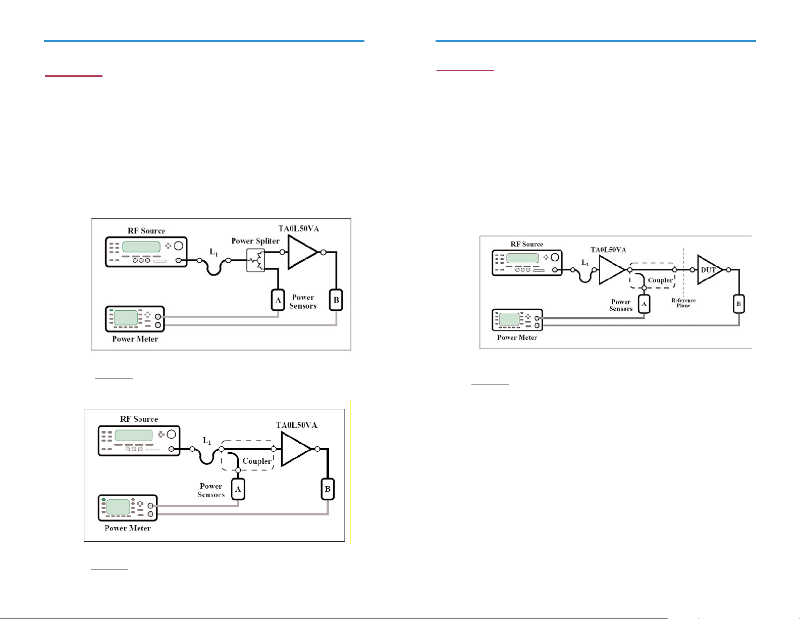
Section 5: Operation
Example Application:
The TA0L50VA System Amplifier amplifies the RF Source output
power to the level needed to characterize DUT performance.
The small size of TA0L50VA System Amplifier is easy to place close to
the DUT input “Reference Plane”. The high gain of the System
Amplifier easily overcomes the cable losses from the remote RF Source.
The Figure 7 shows an amplified RF power measurement system using
the TA0L50VA System Amplifier.
The DUT is characterized by setting the power level at the DUT input
“Reference Plane” and measuring the output power at various input
power levels for each test frequency.
The RF Source, used in this example, is a laboratory grade Synthesized
Source or Signal Generator with precise amplitude control, (e.g. Agilent
83650L RF Source, or Anritsu MG3694A). The power levels are measured using a power meter with two measurement port sensors (A and B),
(e.g. Agilent E4419B).
An RF power coupler provides a small, proportional amount of the
amplified power to power sensor A as shown in Figure 7.
Figure 7: Example of an Amplified RF Power Measurement System
Section 4: Performance Verification
The Figures below show the setup used to verify the performance of the
TA0L50VA System Amplifier.
A calibrated power splitter (or calibrated coupler) connected to the
amplifier input reference plane and to power sensor A , as shown, establishes the input power level. The output power is measured on power
sensor B. Measurements of gain vs output power at frequencies of interest establish the amplifier performance.
Figure 5: Verification setup with a power splitter
Figure 6: Verification setup with a calibrated coupler
TA0L50VA Operating Manual TA0L50VA Operating Manual
6 7
 Loading...