


Voltage Supervisor SOT-23-5/6
Evaluation Board
User’s Guide
© 2006 Microchip Technology Inc. DS51527B
Note the following details of the code protection feature on Microchip devices:
• Microchip products meet the specification contained in their particular Microchip Data Sheet.
• Microchip believes that its family of products is one of the most secure families of its kind on the market today, when used in the
intended manner and under normal conditions.
• There are dishonest and possibly illegal methods used to breach the code protection feature. All of these methods, to our
knowledge, require using the Microchip products in a manner outside the operating specifications contained in Microchip’s Data
Sheets. Most likely, the person doing so is engaged in theft of intellectual property.
• Microchip is willing to work with the customer who is concerned about the integrity of their code.
• Neither Microchip nor any other semiconductor manufacturer can guarantee the security of their code. Code protection does not
mean that we are guaranteeing the product as “unbreakable.”
Code protection is constantly evolving. We at Microchip are committed to continuously improving the code protection features of our
products. Attempts to break Microchip’s code protection feature may be a violation of the Digital Millennium Copyright Act. If such acts
allow unauthorized access to your software or other copyrighted work, you may have a right to sue for relief under that Act.
Information contained in this publication regarding device
applications and the like is provided only for your convenience
and may be superseded by updates. It is your responsibility to
ensure that your application meets with your specifications.
MICROCHIP MAKES NO REPRESENTATIONS OR
WARRANTIES OF ANY KIND WHETHER EXPRESS OR
IMPLIED, WRITTEN OR ORAL, STATUTORY OR
OTHERWISE, RELATED TO THE INFORMATION,
INCLUDING BUT NOT LIMITED TO ITS CONDITION,
QUALITY, PERFORMANCE, MERCHANTABILITY OR
FITNESS FOR PURPOSE. Microchip disclaims all liability
arising from this information and its use. Use of Microchip
devices in life support and/or safety applications is entirely at
the buyer’s risk, and the buyer agrees to defend, indemnify and
hold harmless Microchip from any and all damages, claims,
suits, or expenses resulting from such use. No licenses are
conveyed, implicitly or otherwise, under any Microchip
intellectual property rights.
Trademarks
The Microchip name and logo, the Microchip logo, Accuron,
dsPIC, K
EELOQ, microID, MPLAB, PIC, PICmicro, PICSTART,
PRO MATE, PowerSmart, rfPIC and SmartShunt are
registered trademarks of Microchip Technology Incorporated
in the U.S.A. and other countries.
AmpLab, FilterLab, Migratable Memory, MXDEV, MXLAB,
SEEVAL, SmartSensor and The Embedded Control Solutions
Company are registered trademarks of Microchip Technology
Incorporated in the U.S.A.
Analog-for-the-Digital Age, Application Maestro, dsPICDEM,
dsPICDEM.net, dsPICworks, ECAN, ECONOMONITOR,
FanSense, FlexROM, fuzzyLAB, In-Circuit Serial
Programming, ICSP, ICEPIC, Linear Active Thermistor, Mindi,
MiWi, MPASM, MPLIB, MPLINK, PICkit, PICDEM,
PICDEM.net, PICLAB, PICtail, PowerCal, PowerInfo,
PowerMate, PowerTool, REAL ICE, rfLAB, rfPICDEM, Select
Mode, Smart Serial, SmartTel, Total Endurance, UNI/O,
WiperLock and ZENA are trademarks of Microchip
Technology Incorporated in the U.S.A. and other countries.
SQTP is a service mark of Microchip Technology Incorporated
in the U.S.A.
All other trademarks mentioned herein are property of their
respective companies.
© 2006, Microchip Technology Incorporated, Printed in the
U.S.A., All Rights Reserved.
Printed on recycled paper.
Microchip received ISO/TS-16949:2002 certification for its worldwide
headquarters, design and wafer fabrication facilities in Chandler and
Tempe, Arizona, Gresham, Oregon and Mountain View, California. The
Company’s quality system processes and procedures are for its
PICmicro
EEPROMs, microperipherals, nonvolatile memory and analog
products. In addition, Microchip’s quality system for the design and
manufacture of development systems is ISO 9001:2000 certified.
®
8-bit MCUs, KEELOQ
®
code hopping devices, Serial
DS51527B-page ii © 2006 Microchip Technology Inc.

VOLTAGE SUPERVISOR SOT-23-5/6
EVALUATION BOARD USER’S GUIDE
Table of Contents
Preface ............................................................................................................................ 1
Chapter 1. Product Overview ........................................................................................ 5
1.1 Introduction ..................................................................................................... 5
1.2 What is the Voltage Supervisor SOT-23-5/6 Evaluation Board? .................... 5
1.3 What the Voltage Supervisor SOT-23-5/6 Evaluation Board Kit Includes ...... 5
Chapter 2. Installation and Operation .......................................................................... 7
2.1 Introduction ..................................................................................................... 7
2.2 Features ......................................................................................................... 7
2.3 Getting Started ............................................................................................... 8
2.4 Voltage Supervisor SOT-23-5/6 Evaluation Board Description .................... 16
2.5 Voltage Supervisor/Voltage Detector Circuits .............................................. 19
2.6 Digital Potentiometer Circuit ......................................................................... 23
Appendix A. Schematics and Layouts ....................................................................... 25
A.1 Introduction .................................................................................................. 25
A.2 Schematics and PCB Layout ....................................................................... 25
A.3 Schematic .................................................................................................. 26
A.4 Board Layout – Top Layer, Bottom Layer and Silk Screen .......................... 27
A.5 Board Layout – Top Layer and Silk Screen ................................................. 28
A.6 Board Layout – Bottom Layer ...................................................................... 29
A.7 Board Layout – Ground Plane ..................................................................... 30
A.8 Board Layout – Power Layer ....................................................................... 31
A.9 Board Layout – Top Components and Silk Screen ...................................... 32
Appendix B. Bill Of Materials (BOM) .......................................................................... 33
Appendix C. Microchip SOT-23-5/6 Device Compatibility ........................................ 35
C.1 Introduction .................................................................................................. 35
C.2 PCB Compatibility ........................................................................................ 35
C.3 Ideas on Evaluating An LDO ....................................................................... 39
Worldwide Sales and Service ..................................................................................... 40
© 2006 Microchip Technology Inc. DS51527B-page iii

Voltage Supervisor SOT-23-5/6 Evaluation Board User’s Guide
NOTES:
DS51527B-page iv © 2006 Microchip Technology Inc.
VOLTAGE SUPERVISOR SOT-23-5/6
EVALUATION BOARD USER’S GUIDE
Preface
NOTICE TO CUSTOMERS
All documentation becomes dated, and this manual is no exception. Microchip tools and
documentation are constantly evolving to meet customer needs, so some actual dialogs
and/or tool descriptions may differ from those in this document. Please refer to our web site
(www.microchip.com) to obtain the latest documentation available.
Documents are identified with a “DS” number. This number is located on the bottom of each
page, in front of the page number. The numbering convention for the DS number is
“DSXXXXXA”, where “XXXXX” is the document number and “A” is the revision level of the
document.
For the most up-to-date information on development tools, see the MPLAB
Select the Help menu, and then Topics to open a list of available on-line help files.
®
IDE on-line help.
INTRODUCTION
This chapter contains general information that will be useful to know before using the
Voltage Supervisor SOT-23-5/6 Evaluation Board. Items discussed in this chapter
include:
• Document Layout
• Conventions Used in this Guide
• Recommended Reading
• The Microchip Web Site
• Customer Support
• Document Revision History
DOCUMENT LAYOUT
This document describes how to use the Voltage Supervisor SOT-23-5/6 Evaluation
Board. The manual layout is as follows:
• Chapter 1. “Product Overview” – Important information about the Voltage
Supervisor SOT-23-5/6 Evaluation Board.
• Chapter 2. “Installation and Operation”– Includes instructions on how to get
started with the Voltage Supervisor SOT-23-5/6 Evaluation Board.
• Appendix A. “Schematics and Layouts” – Shows the schematic and layout
diagrams for the Voltage Supervisor SOT-23-5/6 Evaluation Board.
• Appendix B. “Bill Of Materials (BOM)” – Lists the parts used to build the
Voltage Supervisor SOT-23-5/6 Evaluation Board.
• Appendix C. “Microchip SOT-23-5/6 Device Compatibility” – Explains how this
board may be used with other Microchip analog devices in the SOT-23-5 or
SOT-23-6 packages.
© 2006 Microchip Technology Inc. DS51527B-page 1
Voltage Supervisor SOT-23-5/6 Evaluation Board User’s Guide
CONVENTIONS USED IN THIS GUIDE
This manual uses the following documentation conventions:
DOCUMENTATION CONVENTIONS
Description Represents Examples
Arial font:
Italic characters Referenced books MPLAB® IDE User’s Guide
Emphasized text ...is the only compiler...
RECOMMENDED READING
Table 1-1 shows the device and associated data sheet literature number. These
documents can be downloaded from the Microchip web site at: www.microchip.com.
TABLE 1-1: DEVICES AND DATA SHEET LITERATURE NUMBERS
Device Literature # Device Literature # Device Literature #
MCP601 21314 MCP6541 21690 TC52 21430
MCP601R 21314 MCP6541R 21690 TC53 21432
MCP606 11177 MCP6546 21714 TC54 21434
MCP6001 21733 MCP6546R 21714 TC105 21349
MCP6001R 21733 MCP3221 21732 TC77 20092
MCP6001U 21733 MCP9800 21909 MCP603 21314
MCP6231 21881 MCP9802 21909 TC1035 21343
MCP6231R 21881 MCP4012 21978 MCP4022 21916
MCP6231U 21881 MCP4013 21978 MCP4023 21916
MCP6241 21882 MCP4014 21978 MCP4024 21916
MCP6241R 21882 TC1014 21335 MCP73826 21705
MCP6241U 21882 TC1015 21335 PIC10F200 41239
MCP1316 21985 TC1017 21813 PIC10F202 41239
MCP1317 21985 TC1054 21350 PIC10F204 41239
MCP1318 21985 TC1055 21350 PIC10F206 41239
MCP1319 21985 TC1070 21353 TC1185 21350
MCP1320 21985 TC1071 21353
MCP1321 21985 TC1034 21343 TC1187 21368
TC1186 21353
MCP1322 21985 TC1037 21344 TC1223 21368
TC2014 21662 TC1038 21344 TC1224 21368
TC2015 21662 TC1039 21344 TC2055 21663
TC2185 21662 TC2054 21663 TC2186 21663
DS51527B-page 2 © 2006 Microchip Technology Inc.

THE MICROCHIP WEB SITE
Microchip provides online support via our web site at www.microchip.com. This web
site is used as a means to make files and information easily available to customers.
Accessible by using your favorite internet browser, the web site contains the following
information:
• Product Support – Data sheets and errata, application notes and sample
programs, design resources, user’s guides and hardware support documents,
latest software releases and archived software
• General Technical Support – Frequently Asked Questions (FAQs), technical
support requests, online discussion groups, Microchip consultant program
member listing
• Business of Microchip – Product selector and ordering guides, latest Microchip
press releases, listing of seminars and events, listings of Microchip sales offices,
distributors and factory representatives
CUSTOMER SUPPORT
Users of Microchip products can receive assistance through several channels:
• Distributor or Representative
• Local Sales Office
• Field Application Engineer (FAE)
• Technical Support
• Development Systems Information Line
Customers should contact their distributor, representative or field application engineer
for support. Local sales offices are also available to help customers. A listing of sales
offices and locations is included in the back of this document.
Technical support is available through the web site at: http://support.microchip.com
Preface
DOCUMENT REVISION HISTORY
Revision B (May 2006)
• Updated Bill of Materials (BOM) to show RoHS-compliant part numbers.
Revision A (January 2005)
• Initial Release of this Document.
© 2006 Microchip Technology Inc. DS51527B-page 3

Voltage Supervisor SOT-23-5/6 Evaluation Board User’s Guide
NOTES:
DS51527B-page 4 © 2006 Microchip Technology Inc.

VOLTAGE SUPERVISOR SOT-23-5/6
EVALUATION BOARD USER’S GUIDE
Chapter 1. Product Overview
1.1 INTRODUCTION
This chapter provides an overview of the Voltage Supervisor SOT-23-5/6 Evaluation
Board and covers the following topics:
• What is the Voltage Supervisor SOT-23-5/6 Evaluation Board?
• What the Voltage Supervisor SOT-23-5/6 Evaluation Board Kit includes
1.2 WHAT IS THE VOLTAGE SUPERVISOR SOT-23-5/6 EVALUATION BOARD?
The Voltage Supervisor SOT-23-5/6 Evaluation Board allows the system designer to
quickly evaluate the operation of Microchip Technology’s voltage supervisors and
voltage detectors in the SOT-23-5 (5-pin SOT-23) or SOT-23-6 (6-pin SOT-23)
packages.
The Voltage Supervisor SOT-23-5/6 Evaluation Board Printed Circuit Board (PCB)
supports the four different SOT-23-6 pinouts (which also supports compatible
SOT-23-5 footprints) and one SOT-23-5 footprint.
The Voltage Supervisor SOT-23-5/6 Evaluation Board has been made generic so that
other devices in the SOT-23-5 and SOT-23-6 packages may be supported with this
board. Microchip device families supported include:
• Voltage Supervisors/Voltage Detectors
• Nonvolatile Digital Potentiometers (Digi-Pots)
• Operational Amplifiers (Op Amps)
• Comparators
• Low Drop-out Regulators (LDOs)
• Thermal sensors
• Analog-to-Digital Converters (ADCs)
• PFM/PWM Step-Down DC/DC Controllers
• Battery Charger Controllers
•PICmicro
®
Microcontrollers
1.3 WHAT THE VOLTAGE SUPERVISOR SOT-23-5/6 EVALUATION BOARD KIT
INCLUDES
This Voltage Supervisor SOT-23-5/6 Evaluation Board Kit includes:
• Five Voltage Supervisor SOT-23-5/6 Evaluation Board PCBs
• Three voltage supervisor device samples that can be installed on the Voltage
Supervisor SOT-23-5/6 Evaluation Board PCBs
• Voltage Supervisor SOT-23-5/6 Evaluation Board User’s Guide
(Electronic version on CD)
© 2006 Microchip Technology Inc. DS51527B-page 5

Voltage Supervisor SOT-23-5/6 Evaluation Board User’s Guide
NOTES:
DS51527B-page 6 © 2006 Microchip Technology Inc.

Chapter 2. Installation and Operation
2.1 INTRODUCTION
The blank Printed Circuit Board (PCB) allows the desired voltage supervisor/voltage
detector device to be installed along with other desired passive components (resistors
and capacitors) and connection posts.
The PCB supports four different SOT-23-6 and one SOT-23-5 pinouts. Two of these
pinouts are used by the voltage supervisor/voltage detector product family, while the
other pinouts are used by other Microchip analog and PICmicro
products (see Appendix C. “Microchip SOT-23-5/6 Device Compatibility”). The
PIC10F2XX devices uses the last pinout. This board is generic so that other devices
may be supported. However, the silk-screen markings are designed for ease-of-use
with the voltage supervisor devices.
2.2 FEATURES
The Voltage Supervisor SOT-23-5/6 Evaluation Board has the following features:
• Connection terminals may be either through-hole or surface-mount
• Four SOT-23-6 pinouts supported
- Also supports V
• One SOT-23-5 pinout supported
• Footprints for optional passive components for:
- Power supply filtering
- Device bypass capacitor
- Output filtering
- Output pull-up resistor
- Output pull-down resistor
- Output loading resistor
- Output series resistor
• Footprints for two optional switches for:
- Voltage supervisor manual resets
- PIC10F2XX general purpose inputs
• Silk screen area to write specifics of implemented circuit (on back of PCB), such
as TC52 2.7V, 10 kΩ (to indicate that the device is the TC52 with the 2.7V trip
point and an external 10 kΩ pull-up resistor on the output)
VOLTAGE SUPERVISOR SOT-23-5/6
EVALUATION BOARD USER’S GUIDE
®
microcontroller
DD/VSS
footprint-compatible SOT-23-5 devices
© 2006 Microchip Technology Inc. DS51527B-page 7

Voltage Supervisor SOT-23-5/6 Evaluation Board User’s Guide
2.3 GETTING STARTED
The Voltage Supervisor SOT-23-5/6 Evaluation Board is a blank PCB that allows the
user to configure the circuit to their exact requirements. The passive components use
the surface-mount 805 package layout. Figure 2-1 shows the board circuit.
This evaluation board supports the following Microchip device families:
• Voltage Supervisors/Voltage Detectors
• Nonvolatile Digital Potentiometers (Digi-Pots)
• Operational Amplifiers (Op Amps)
• Comparators
• Low Drop-Out Regulators (LDOs)
• Thermal Sensors
• Aanalog-to-Digital Converters (ADCs)
• PFM/PWM Step-Down DC/DC Controllers
• Battery Charger Controllers
•PICmicro
Table 2-1 shows these product families, the devices that are supported and which
SOT-23-5/6 layout option to use. Devices that are in a 5-pin SOT-23 package can be
installed into the SOT-23-6 footprint.
Table 2-2 shows which circuit option needs to be used for a given voltage
supervisor/voltage detector. There are currently no voltage supervisors/voltage
detectors that use the option B, C or E pinout. For other Microchip analog devices,
please refer to Appendix C. “Microchip SOT-23-5/6 Device Compatibility”.
®
Microcontrollers
DS51527B-page 8 © 2006 Microchip Technology Inc.
Installation and Operation
V
DD
V
SS
A B C D E
2 6 2 3 2
BFMP Header (Top)
1
2
3
4
5
6
No Connect
TP3A (ICSPCLK)
TP1A (ICSPDT)
TP2A (V
TP5A (V
TP6A (V
SS
DD
PP
C5F
A B C D E
6 2 1 2 5
TP1A
R2A
TP 1
C5B
C1
1
2
3
C2
U1
Option A
R3A
C5A
6
5
TP4A
R2D
4
R3D
C5D
1
2
3
U2
Option B
6
5
4
TP5A
R2E
R3E
C5E
R1A
R1D
R1E
(V
OUT
V
)
IN+
A B C D E
1 1 6 1 1
S2
TP 4
(WDI
V
IN–
A B C D E
4 4 4 4 4
TP 5
(WDI
V
IN–
)
)
A B C D E
5 5 5 5 6
1
C3
)
)
2
3
U3
Option C
6
5
4
C6
)
1
5
TP2A
2
TP1A
C4
Option D
3
U4
4
TP3A
TP3A
Footprint Option
(A, B, C, D or E)
Pin Number of that
R2C
R3C
C5C
A B C D E
3 3 3 — 3
R1C
S1
TP 3
(MR
V
IN+
)
For:
Footprint Version
(1, 2, 3, 4, 5 or 6)
Footprint Option/Pin Number
Combination (Pad A3)
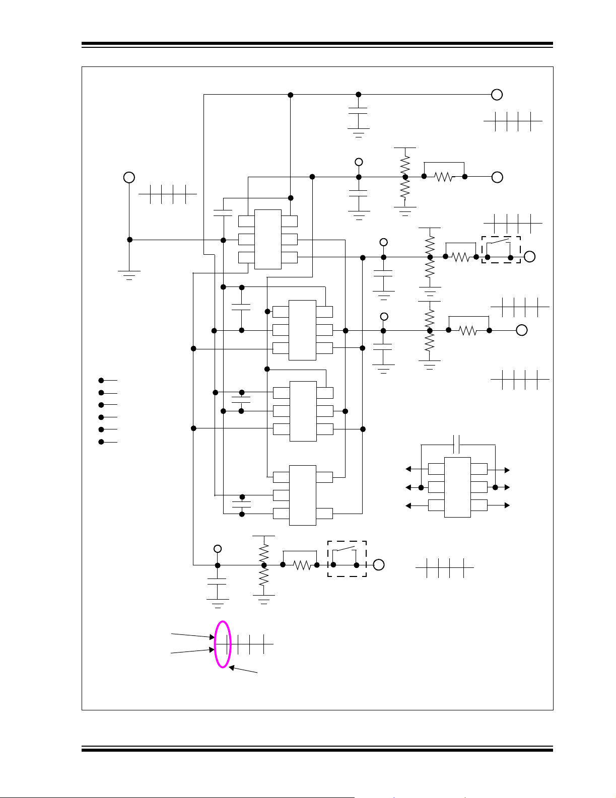
FIGURE 2-1: Voltage Supervisor SOT-23-5/6 Evaluation Board Circuit.
1
2
3
U5
Option E
6
5
4
TP5A
TP6A
TP4A
A B C D E
3 3 3 — 3
Version A use: MCP13XX
Version B use: MCP1035
Version C use: MCP4022
Version D use: TC52
Version E use: PIC10F200
© 2006 Microchip Technology Inc. DS51527B-page 9

Voltage Supervisor SOT-23-5/6 Evaluation Board User’s Guide
TABLE 2-1: SUPPORTED SOT-23-5 AND SOT-23-6 DEVICES
Family Device Option # of Pins
Voltage Supervisors/Detectors TC52 D 5
TC53C D 5
TC53N D 5
TC54 D 5
MCP13XX A 5
Digital Potentiometers (Digi-Pots) – Volatile MCP4012 C 6
MCP4013 C 6
MCP4014 C 5
Digital Potentiometers (Digi-Pots) –
Nonvolatile
Operational Amplifiers (Op Amps) MCP601 A 5
Comparators MCP6541 A 5
Thermal Sensors MCP9800 C 5
Analog-to-Digital Converter (ADC) MCP3221 C 5
MCP4022 C 6
MCP4023 C 6
MCP4024 C 5
MCP601R B 5
MCP603 A 6
MCP606 A 5
MCP6001 A 5
MCP6001R B 5
MCP6001U A 5
MCP6231 A 5
MCP6231R B 5
MCP6231U A 5
MCP6241 A 5
MCP6241R B 5
MCP6241U A 5
TC1034 B 5
TC1035 B 6
MCP6541R B 5
MCP6546 A 5
MCP6546R B 5
TC1037 A 5
TC1038 A 6
TC1039 A 6
MCP9802 C 5
TC77 A 5
DS51527B-page 10 © 2006 Microchip Technology Inc.

Installation and Operation
TABLE 2-1: SUPPORTED SOT-23-5 AND SOT-23-6 DEVICES (CONTINUED)
Family Device Option # of Pins
PICmicro® Microcontrollers PIC10F200 E 6
PIC10F202 E 6
PIC10F204 E 6
PIC10F206 E 6
Low Drop-Out Regulators (LDOs) TC1014 C 5
TC1015 C 5
TC1017 C 5
TC1054 C 5
TC1055 C 5
TC1070 C 5
TC1071 C 5
TC1185 C 5
TC1186 C 5
TC1187 C 5
TC1223 C 5
TC1224 C 5
TC2014 C 5
TC2015 C 5
TC2054 C 5
TC2055 C 5
TC2185 C 5
TC2186 C 5
PFM/PWM Step-Down DC/DC Controller TC105 D 5
Battery Charger Controller MCP73826 E 6
© 2006 Microchip Technology Inc. DS51527B-page 11

Voltage Supervisor SOT-23-5/6 Evaluation Board User’s Guide
TABLE 2-2: VOLTAGE SUPERVISOR / VOLTAGE DETECTOR DEVICES AND EVALUATION
BOARD CIRCUIT/FOOTPRINT OPTION
Device
Supported
on
MCP1316 Option A RST
Output Signal
(Active State)
(L) Push-Pull
Output Type
MCP1317 Option A RST (H) Push-Pull
MCP1318 Option A RST (H) and RST (L) Push-Pull
MCP1319 Option A RST (H) and RST
MCP1320 Option A RST
(L) Open-Drain R = TBD
MCP1321 Option A RST (H) and RST
MCP1322 Option A RST (H) and RST
TC52 Option D V
TC53C Option D V
TC53N Option D V
TC54VC Option D V
TC54VN Option D V
(L),
OUT1
V
(L)
OUT2
(L) Push-Pull
OUT
(L) Open-Drain R2A = 47 kΩ
OUT
(L) Push-Pull
OUT
(L) Open-Drain R2A = 47 kΩ
OUT
(L) Push-Pull
(L) Push-Pull and Open-Drain R = TBD
(L) Push-Pull and Open-Drain R = TBD
Open-Drain C4 = 0.1 µF, R2A = 47 kΩ
Comment/Recommended
Component Values
R2E = 47 kΩ, C1 = 1 µF
DS51527B-page 12 © 2006 Microchip Technology Inc.

Installation and Operation
2.3.1 The Hardware
Figure 2-2 shows the layout of the Voltage Supervisor SOT-23-5/6 Evaluation Board.
This is a small four-layer board (1.5" x 2" (38.1 mm x 50.8 mm)). There are six
connection points/pads that can use either through-hole or surface-mount connector
posts.
Additionally, a test point is available between the device pin and the PCB pad that may
be useful if the in-line resistor (R1A, R1C, R1D or R1E) is installed.
The different SOT-23 layout options are outlined in Section 2.4.3 “SOT-23-6 and
SOT-23-5 Footprints”, with Opt A, Opt B, Opt C, Opt D and Opt E indicating the layout
option of that SOT-23-5/6 footprint.
There are six pads on the PCB. One is labeled VDD, one is labeled VSS, with all pads
having a label that indicates the footprint option used (shown as “A B C D E”) and a
label underneath that indicates the pin number of that footprint. This footprint option/pin
number combination will be used to indicate the remaining pads. If the device is placed
in the option A footprint, the remaining pads would be A1, A3, A4 and A6, where the
VDD pad is also A6 and the VSS pad is A2. Figure 2-2 has text added on each pad to
show what the “pad name” would be (A1, A2, A3, A4, A5 and A6). If the device required
the option C footprint, what is currently A1 for option A would then be referred to as pad
C6 for option C.
Each of these four pads has four passive components associated with them. A pull-up
resistor, a pull-down resistor, an in-line resistor and a filtering/load capacitor. The
pull-up resistor is always R2x, the pull-down resistor is R3x, the in-line resistor is R1x
and the filtering/load capacitor is C5x. The “x” is an alpha character that corresponds
to a particular pad. So pad A1’s pull-up resistor is R2A.
The green area of Figure 2-2 shows the silk screen on the bottom layer of the PCB.
This is where the details of the implemented circuit can be written.
Resistor R2x is a pull-up resistor that may need to be installed for devices with an
open-drain output. Though resistor R3x is not currently required, it was placed for
possible future requirements. Resistor R1x is not required, but may be useful if this
board is to be interfaced into existing circuits. If resistor R1x is to be installed, remember to cut the trace that “shorts out” R3. Capacitors C1, C2, C3, C4, C6, C5A, C5C,
C5D, C5E and C5F are bypass capacitors that may be required to be installed, depending on the device selected and the system requirements (such as the noise present on
the power supply). Table 2-3 describes the components.
© 2006 Microchip Technology Inc. DS51527B-page 13

Voltage Supervisor SOT-23-5/6 Evaluation Board User’s Guide
A6
A3
A1
A5
A2
FIGURE 2-2: Voltage Supervisor SOT-23-5/6 Evaluation Board Layout with added “Pad Names”.
A4
TABLE 2-3: OPTIONAL PASSIVE COMPONENTS
Device Comment
C1, C2, C3, C4, C5, C5F, C6 Power supply bypass capacitor
C5A, C5C, C5D, C5E Output filter capacitor
R1, R3A, R3C, R3D, R3E Pull-up resistor
R2, R2A, R2C, R2D, R2E Pull-down resistor
R1A, R1C, R1D, R1E In-line resistance of device output
S1, S2 Switches
DS51527B-page 14 © 2006 Microchip Technology Inc.

Installation and Operation
2.4 VOLTAGE SUPERVISOR SOT-23-5/6 EVALUATION BOARD DESCRIPTION
The Voltage Supervisor SOT-23-5/6 Evaluation Board PCB is designed to be flexible in
the type of device evaluation that can be implemented.
The following sections describe each element of this evaluation board in further detail.
2.4.1 Power and Ground
The Voltage Supervisor SOT-23-5/6 Evaluation Board can have connection posts
installed for the power (V
through-hole or surface-mount connectors.
For device evaluation, the use of an external variable power supply or waveform
generator is required. The type of equipment used will determine the evaluation that
may be performed.
2.4.2 Pads A1, A3, A4 and A5 (for Footprint Option A)
The Voltage Supervisor SOT-23-5/6 Evaluation Board can have a connection post
installed for the pads A1, A3, A4 and A5 signals. Depending on the device installed,
this could be an input, output or bidirectional I/O signal. The layout allows either a
through-hole connector or a surface mount connector.
For device evaluation, the use of an oscilloscope or Digital Voltmeter (DVM) is required.
The type of equipment used will determine the evaluation that may be performed.
) and ground (VSS) planes. The layout allows either
DD
© 2006 Microchip Technology Inc. DS51527B-page 15

Voltage Supervisor SOT-23-5/6 Evaluation Board User’s Guide
2.4.3 SOT-23-6 and SOT-23-5 Footprints
There are four SOT-23-6 and one SOT-23-5 pinout options that the Voltage Supervisor
SOT-23-5/6 Evaluation Board PCB supports. Figure 2-3 shows these four pinouts.
Figure 2-4 shows the single SOT-23-5 pinout option. Some devices may use different
nomenclature for the pin names, such as GND instead of V
RESET (or RESET
) or RST instead of V
OUT
.
Other Microchip analog devices may be used with this PCB if the power and ground
pins match one of these four options. Appendix C. “Microchip SOT-23-5/6 Device
Compatibility” discusses other Microchip analog devices that may be used with this
PCB.
, VIN instead of VDD and
SS
Option A
1
V
2
SS
3
V
DD
6
5
4
V
Option B Option C Option E
V
SS
V
DD
V
SS
DD
1
2
3
6
5
4
FIGURE 2-3: SOT-23-6 (and SOT-23-5) Pinout Options.
Option D
1
V
2
DD
V
3
SS
5
4
FIGURE 2-4: SOT-23-5 Pinout Option.
2.4.4 Passive Components (R1x, R2x, R3x, C5x, R1, R2, C1, C2, C3,
C4 and C6)
The footprints for these components are present to allow maximum flexibility in the use
of this PCB to evaluate a wide range of SOT-23-3 devices. The purpose of these components may vary depending on the device under evaluation and how it is to be used
in the desired circuit. Please refer to the device data sheet for the recommended
components that should be used when evaluating that device.
1
2
3
6
5
4
1
V
2
SS
3
6
V
5
DD
4
2.4.5 Switches (S1 and S2)
The footprints for these components are present to allow maximum flexibility in the use
of this PCB to evaluate a wide range of SOT-23-5 and SOT-23-6 devices. The purpose
of these components may vary depending on the device under evaluation and how it is
to be used in the desired circuit. Please refer to the device data sheet for the
recommended components that should be used when evaluating that device.
2.4.6 BFMP Interface (Header J1)
The Baseline Flash Microcontroller Programmer (BFMP) interface allows a
PIC10F2XX device that is populated in the SOT-23-6 version E footprint to be
programmed with programmers that support this interface, such as the BFMP
programmer (part number PG164101).
DS51527B-page 16 © 2006 Microchip Technology Inc.

Installation and Operation
2.5 VOLTAGE SUPERVISOR/VOLTAGE DETECTOR CIRCUITS
Currently, the voltage detectors/voltage supervisors use either footprint option A or
footprint option D.
2.5.1 Option D Circuit
Using the TC53C or TC54VC, no passive components would be required and the
device V
Using the TC53N or TC54VN, an external pull-up resistor is required. This resistor
would be installed in the R2A location and the device V
D1 pad.
The TC52 is a dual-channel voltage detector. This means that the device has a V
and a V
Locations R2A and R2E should be installed with 47 kΩ resistors.
Detect voltage 2 (V
typically used to indicate a low-power situation, with V
system. Typically, a 0.1 µF capacitor would be on the V
location).
Power supply filtering may be required, so a 0.1 µF capacitor is suggested in the C4
location.
could be monitored on the D1 pad.
OUT
could be monitored on the
OUT
output. Both outputs are open-drain and require a pull-up resistor.
OUT2
) is lower than detect voltage 1 (V
OUT2
OUT1
being used to reset the
OUT2
pin (installed in the C5E
OUT2
). Therefore, V
OUT1
OUT1
is
V
SS
A B C D E
2 6 2 3 2
TP3A
R2C
C5C
Footprint Version
(A, B, C, D or E)
Pin Number of that
Footprint Version
(1, 2, 3, 4, 5 or 6)
R3C
Option D
1
2
C4
3
S1
R1C
A B C D E
5 5 5 5 6
TP1A
C5A
5
TC5X
4
U4
C5E
TP 3
(MR
V
)
IN+
A B C D E
3 3 3 — 3
Footprint Option/Pin Number
Combination (Pad D5)
C5D
C5F
TP5A
TP4A
R2A
R3A
R2E
R3E
R2D
R3D
R1A
R1D
R1E
V
DD
A B C D E
6 2 1 2 5
TP 1
(V
OUT
V
)
IN+
A B C D E
1 1 6 1 1
TP 5
(WDI
V
IN–
A B C D E
5 5 5 5 6
S2
(WDI
V
IN–
A B C D E
4 4 4 4 4
)
TP 4
)
FIGURE 2-5: Voltage Supervisor Circuit using Option D Footprint.
© 2006 Microchip Technology Inc. DS51527B-page 17

Voltage Supervisor SOT-23-5/6 Evaluation Board User’s Guide
2.5.2 Option A Circuit
The MCP13XX devices are only in the SOT-23-5 (5-pin) package, therefore option A
footprint pin 5 is not connected to the device. Once the device is released, please refer
to the data sheet to determine your desired circuit.
V
DD
C5F
A B C D E
6 2 1 2 5
V
SS
A B C D E
2 6 2 3 2
TP3A
R2C
C5C
Footprint Version
(A, B, C, D or E)
Pin Number of that
Footprint Version
(1, 2, 3, 4, 5 or 6)
R3C
C1
R1C
A B C D E
3 3 3 — 3
C5A
Option A
1
2
3
S1
Footprint Option/Pin Number
Combination (Pad A3)
6
5
MCP13XX
4
U1
TP 3
(MR
VIN+)
A B C D E
3 3 3 — 3
MCP13XX devices
do not use this pin.
TP1A
C5E
C5D
TP5A
TP4A
R2A
R3A
R2E
R3E
R2D
R3D
R1A
R1D
R1E
TP 1
(V
OUT
VIN+)
A B C D E
1 1 6 1 1
TP 5
(WDI
V
IN
A B C D E
5 5 5 5 6
S2
(WDI
VIN–)
A B C D E
4 4 4 4 4
–)
TP 4
FIGURE 2-6: Voltage Supervisor Circuit using Option A Footprint.
DS51527B-page 18 © 2006 Microchip Technology Inc.

V
SS
Installation and Operation
2.5.3 A Circuit with the PIC10F200 and a Voltage Supervisor
(MCP13XX)
The PIC10F200 can be used to show the operation of the Watchdog Timer feature
(WDI) or the Manual Reset (MR
devices.
Figure 2-7 shows the schematic to interface the appropriate MCP13XX device to the
PIC10F200 to exercise the Watch Dog Timer (WDI) and Manual Reset (MR
functionality of the device.
After the release of the MCP13XX devices, please check the Microchip web site for an
application note or technical brief that will demonstrate one of the MCP13XX devices
using the Voltage Supervisor SOT-23-5/6 Evaluation Board.
A B C D E
2 6 2 3 2
C1
Option A
1
2
3
U1
MCP13XX
) inputs that are available on some of the MCP13XX
C5F
TP1A
R2A
C5A
6
5
4
MCP13XX devices
do not use this pin.
R3A
R1A
TP4A
)
V
DD
A B C D E
6 2 1 2 5
TP 1
(V
OUT
VIN+)
A B C D E
1 1 6 1 1
TP 4
C6
BFMP Header (Top)
1
2
3
4
5
6
No Connect
TP3A (ICSPCLK)
TP1A (ICSPDT)
V
SS
V
DD
TP5A (VPP)
Footprint Option
(A, B, C, D or E)
Pin Number of that
Footprint Version
(1, 2, 3, 4, 5 or 6)
TP3A
C5C
A B C D E
3 3 3 — 3
GP1
GP0
1
2
PIC10F200
3
U5
Option E
R2C
R3C
Footprint Option/Pin Number
Combination (Pad A3)
GP3/MCLR
6
5
GP2
4
R1C
FIGURE 2-7: MCP13XX and a PIC10F200 Circuit.
S1
C5E
TP5A
R2E
R3E
TP 3
(MR
VIN+)
R1E
A B C D E
3 3 3 — 3
(WDI
VIN–)
A B C D E
4 4 4 4 4
TP 5
(WDI
VIN–)
A B C D E
5 5 5 5 6
© 2006 Microchip Technology Inc. DS51527B-page 19

Voltage Supervisor SOT-23-5/6 Evaluation Board User’s Guide
2.5.4 Evaluating a Voltage Supervisor or Voltage Detector Device
When evaluating a voltage supervisor/voltage detector device, a minimum set of test
equipment should be available. Table 2-4 shows the recommended test equipment.
TABLE 2-4: TEST EQUIPMENT
Hardware Connect to: Comment
Variable Power
Supply
Arbitrary
Waveform
Generator
Digital Multi-Meter
(D.M.M.)
Oscilloscope V
Test Light (LED) V
Note 1: The pad connection to connect to the V
device and the footprint option used.
A typical system that would be used to evaluate the voltage supervisor or voltage
detector device is shown in Figure 2-8. This also shows an example of input and output
waveforms for a voltage supervisor or voltage detector device.
VDD, VSS This allows the voltage to the SOT23 Evaluation Board
to be varied so the device output can be monitored.
VDD, VSS This is like a variable power supply, but allows program-
mability into the input signal that the device will be
subjected to. This also allows a particular waveform to
be repeated (such as a 60 Hz sine wave that varies from
1V to 5V).
(1)
V
OUT
Used to indicate the output state (low or high) of the
voltage supervisor/voltage detector.
(1)
OUT
Allows the device conditions and response to be
evaluated due to the ability to capture this information.
This is useful for faster signals and cases where small
spikes need to be detected.
(1)
OUT
Used to visually indicate the output state (low or high) of
the voltage supervisor/voltage detector. Ensure that the
current requirements of this LED can be supplied by the
device’s output pin.
or RST pin will be dependent on the
OUT
SOT-23-5/6 Evaluation Board PCB
Variable
Power
Supply
or
Arbitrary
Waveform
Generator
Arbitrary Waveform
Generator
Output
Test
Point or
V
OUT
Voltage
Supervisor
or
Voltage
Detector
Device VDD out of valid operating range.
Output voltage may be indeterminate.
FIGURE 2-8: Evaluation System.
C5
R2
R3
R1
Test Point
PCB
Pad
Oscilloscope
DS51527B-page 20 © 2006 Microchip Technology Inc.

2.6 DIGITAL POTENTIOMETER CIRCUIT
The Voltage Supervisor SOT-23-5/6 Evaluation Board can be utilized to demonstrate
and test Microchip’s SOT-23-5 and SOT-23-6 nonvolatile digital potentiometers. This is
accomplished by populating the PCB with the desired MCP401X or MCP402X device,
a PIC10F2XX microcontroller, two momentary switches and a few resistors.
Note: Microchip Technology Inc. offers a built-up evaluation board for the
MCP402X Digital Potentiometer (MCP402XEV). Additional information
regarding this evaluation board may be found on the CD-ROM directory:
CD-ROM:\00066 - MCP402X Digital Potentiometer Evaluation Board. Within this directory, you will find the user’s guide for this
evaluation board, the PIC10F200 program (firmware) and assembled HEX
file (00066_MCP402XEV.hex).
The code supplied for this evaluation board may be easily modified to demonstrate
operation of the Voltage Supervisor SOT-23-5/6 Evaluation Board.
Section 2.3 and Section 2.4 of the MCP401X/2X Digital Potentiometer Evaluation
Board User’s Guide (DS51546) discuss the MCP402XEV firmware. This firmware can
easily be modified to demonstrate using the Voltage Supervisor SOT-23-5/6 Evaluation
Board.
Figure 2-9 illustrates an example circuit. This circuit uses the MCP4023 and
PIC10F200 devices with all the components installed. The PCB silk-screen indicates
the VDD and VSS pads. The remaining PCB pads will be referred to by their footprint
option/pin number combination. These combinations are C3, C4, C5 and C6.
The PIC10F2XX will need to be programmed to make the system work. The
PIC10F2XX device can be programmed via the Baseline Flash Microcontroller
Programmer (BFMP) header (J1). The program (firmware) configures the GP1 and
GP2 pins to be outputs (driving high) and the GP0 and GP3 pins to be inputs. The GP1
and GP2 pins are individually polled to determine if either switch S1/D (down) and S2/U
(up) are depressed.
If the nonvolatile MCP402X device is used, the digital potentiometer setting can be
stored in nonvolatile memory, power can be cycled and the digital potentiometer will be
at the last saved setting for the volatile versions of the device. The wiper will go to its
default setting when power is cycled.
Installation and Operation
Note: The PIC10F2XX program (firmware) must take care in the timing require-
ments of the GP1 and GP2 pins, due to the multiplexing of the PIC10F2XX
GP1 pin with the MCP4023 U/D
the PIC10F2XX GP2 pin with the MCP4023 CS pin and switch S2.
© 2006 Microchip Technology Inc. DS51527B-page 21
pin and Switch S1, and the multiplexing of

Voltage Supervisor SOT-23-5/6 Evaluation Board User’s Guide
A B C D E
V
DD
1 1 1 1 1
C6
1
2
PIC10F200
3
U5
Option E
C5F
Option C
1
2
MCP4023
B
V
DD
V
SS
W
A
6
5
6
5
4
C3
R2A
0Ω
V
SS
A B C D E
2 2 2 2 2
A B C D E
A
6 6 6 6 6
A B C D E
W
5 5 5 5 5
3
U/D CS
U3
4
TP4A
Cut Trace
S2
A B C D E
R1D
Cut Trace
4 4 4 4 4
2.2 kΩ
Cut Trace
TP3A
S1
A B C D E
3 3 3 3 3
BFMP Header (Top)
1
2
3
4
5
6
No Connect
TP3A (ICSPCLK)
TP1A (ICSPDT)
V
SS
V
DD
TP5A (VPP)
Footprint Option
(A, B, C, D or E)
Pin Number of that
Footprint Version
R1C
2.2 kΩ
A B C D E
3 3 3 — 3
Cut Trace
Footprint Option/Pin Number
Combination (Pad C3)
(1, 2, 3, 4, 5 or 6)
FIGURE 2-9: Circuit Utilizing the MCP4023 Digital Pot and the PIC10F200 Microcontroller.
DS51527B-page 22 © 2006 Microchip Technology Inc.

VOLTAGE SUPERVISOR SOT-23-5/6
EVALUATION BOARD USER’S GUIDE
Appendix A. Schematics and Layouts
A.1 INTRODUCTION
This appendix contains the schematics and layouts for the Voltage Supervisor
SOT-23-5/6 Evaluation Board. Diagrams included in this appendix:
• Board Schematic - Digital Circuitry
• Board - Top Layer
A.2 SCHEMATICS AND PCB LAYOUT
Figure A.3 shows the schematic of the Voltage Supervisor SOT-23-5/6 Evaluation
Board.
Figure A.4 shows the layout for the top layer of the Voltage Supervisor SOT-23-5/6
Evaluation Board. The layer order is shown in Figure A-1.
FIGURE A-1: LAYER ORDER
Top Layer
Ground Layer
Power Layer
Bottom Layer
© 2006 Microchip Technology Inc. DS51527B-page 25

Voltage Supervisor SOT-23-5/6 Evaluation Board User’s Guide
A.3 SCHEMATIC
MM
DS51527B-page 26 © 2006 Microchip Technology Inc.

Schematics and Layouts
A.4 BOARD LAYOUT – TOP LAYER, BOTTOM LAYER AND SILK SCREEN
© 2006 Microchip Technology Inc. DS51527B-page 27

Voltage Supervisor SOT-23-5/6 Evaluation Board User’s Guide
A.5 BOARD LAYOUT – TOP LAYER AND SILK-SCREEN
DS51527B-page 28 © 2006 Microchip Technology Inc.

A.6 BOARD LAYOUT – BOTTOM LAYER
Schematics and Layouts
© 2006 Microchip Technology Inc. DS51527B-page 29

Voltage Supervisor SOT-23-5/6 Evaluation Board User’s Guide
A.7 BOARD LAYOUT – GROUND PLANE
DS51527B-page 30 © 2006 Microchip Technology Inc.

A.8 BOARD LAYOUT – POWER LAYER
Schematics and Layouts
© 2006 Microchip Technology Inc. DS51527B-page 31

Voltage Supervisor SOT-23-5/6 Evaluation Board User’s Guide
A.9 BOARD LAYOUT – TOP COMPONENTS AND SILK SCREEN
DS51527B-page 32 © 2006 Microchip Technology Inc.

VOLTAGE SUPERVISOR SOT-23-5/6
EVALUATION BOARD USER’S GUIDE
Appendix B. Bill Of Materials (BOM)
TABLE B-1: BILL OF MATERIALS
Qty
1 PCB 103-00050 Voltage Supervisor SOT-23-5/6 Evaluation
0 U1, U2, U3, U5 SOT-23-6 Device
0 U4 SOT-23-5 Device
0 C1, C2, C3, C4, C6 Device Power Supply Bypass Capacitor
0 C5F Power Supply Bypass Capacitor
0 C5A, C5C, C5D,
0 R2A, R2C, R2D,
0 R3A, R3C, R3D,
0 R1A, R1C, R1D,
0 R1 BFMP Header pin 1 pull up resistor
0 R2 BFMP Header pin 1 pull down resistor
0 J1 BFMP Header (6-pin, 100 mil spacing) — —
0 TP1A, TP3A, TP4A,
0S1, S2
0 S1, S2 Surface-mount Switch Panasonic EVQ-PJ504K
0V
0V
Note 1: This reference is a description of the silk screen name “A B C D E” that matches the footprint version
Reference Description Manufacturer Part Number
Board PCB
(Only one of U1 - U5 installed per board)
(Only one of U1 - U5 installed per board)
Microchip
Technology Inc.
Microchip
Technology Inc.
Microchip
Technology Inc.
103-00050
User-specified
User-specified
— User-specified
Surface-mount (805 package)
(Optional - Application-dependent)
— User-specified
Surface-mount (805 package)
(Optional - Application-dependent)
C5E
Output Filer Capacitor
Surface-mount (805 package)
— User-specified
(Optional - Application-dependent)
R2E
Output Pull-up resistor
Surface-mount (805 package)
— User-specified
(Optional - Application-dependent)
R3E
Output Pull-down resistor
Surface-mount (805 package)
— User-specified
(Optional - Application-dependent)
R1E
Output inline resistor
Surface-mount (805 package)
— User-specified
(Optional - Application-dependent)
(2)
——
(2)
——
5012
EVQ-ATA048
5012
5016
TP5A, H1TP
(3)
, VSS, A1
DD
(1)
(1)
, A4
A3
, VSS, A1
DD
(1)
(1)
, A4
A3
(1)
, A5
(1)
, A5
Through-hole Test Point connector Keystone
Through-hole Switch
V
,
(1)
,
(1)
, VSS and the other PCB Pads (A1
DD
(1)
, A5
A4
V
, VSS and the other PCB Pads (A1
DD
(1)
, A5
A4
(1)
) through-hole connector
(1)
) surface-mount connector
(3)
(1)
(1)
, A3
, A3
(1)
(1)
,
,
Electronics
Panasonic
Keystone
Electronics
Keystone
Electronics
®
®
®
®
option to the package pin number (“1 2 3 4 5 6”).
For example, A1 means footprint version option A, package pin number 1.
2: The current BFMP programming specifications has pin 1 (J1-1) unconnected. These footprints are to
support possible future functionality enhancements.
3: Revision 1 of the PCB has through-holes that are too small to support this switch. For Revision 1 boards,
please use surface-mount switches.
© 2006 Microchip Technology Inc. DS51527B-page 33

Voltage Supervisor SOT-23-5/6 Evaluation Board User’s Guide
NOTES:
DS51527B-page 34 © 2006 Microchip Technology Inc.

VOLTAGE SUPERVISOR SOT-23-5/6
EVALUATION BOARD USER’S GUIDE
Appendix C. Microchip SOT-23-5/6 Device Compatibility
C.1 INTRODUCTION
This appendix documents other Microchip analog devices that can be evaluated using
the Voltage Supervisor SOT-23-5/6 Evaluation Board. New devices may be introduced
after the publication of this document that may be supported. Compare the pinout of
the device to the PCB schematic/layout to determine compatibility of any SOT-23-5
(5-pin SOT-23) or SOT-23-6 (6-pin SOT-23) packaged device.
C.2 PCB COMPATIBILITY
There are four SOT-23-6 (6-pin SOT-23) pinouts that the Voltage Supervisor
SOT-23-5/6 Evaluation Board PCB supports. Figure C-1 shows these four pinouts.
There is an additional SOT-23-5 (5-pin SOT-23) pinout that the Voltage Supervisor
SOT-23-5/6 Evaluation Board PCB supports. Figure C-2 shows this pinout. Other
Microchip analog devices may be used with this PCB if the power and ground pins
match these available options. Though these devices may use different nomenclature
for the pin names, as long as the power and ground signals match one of the four
options, this PCB should be able to be used to evaluate that device.
Table C-1 shows the Microchip analog device part number, the analog family the device
belongs to, which footprint option to use and the recommended components to use for
the circuit. Please refer to the device data sheet for complete information on the
application circuit.
Option A
1
V
2
SS
3
V
6
DD
5
4
Option B Option C Option E
V
1
V
2
DD
3
6
5
4
SS
V
DD
V
SS
FIGURE C-1: SOT-23-6 (and SOT-23-5) Pinout Options.
Option D
1
V
2
DD
V
3
SS
5
4
FIGURE C-2: SOT-23-5 Pinout Option.
1
2
3
6
5
4
1
V
2
SS
3
6
V
5
DD
4
© 2006 Microchip Technology Inc. DS51527B-page 35

Voltage Supervisor SOT-23-5/6 Evaluation Board User’s Guide
TABLE C-1: MICROCHIP ANALOG AND PIC®MICRO DEVICES AND SOT-23-5/6 EVALUATION
BOARD CIRCUIT/FOOTPRINT OPTION SELECTION
Device Family Device
Digital Potentiometers
(Digi-Pots) – Volatile
Digital Potentiometers
(Digi-Pots) – Nonvolatile
Operational Amplifiers
(Op Amps)
MCP4012 C 6 See Device Data Sheet (DS21978) for
MCP4013 C 6 See Device Data Sheet (DS21978) for
MCP4014 C 5 See Device Data Sheet (DS21978) for
MCP4022 C 6 See Device Data Sheet (DS21916) for
MCP4023 C 6 See Device Data Sheet (DS21916) for
MCP4024 C 5 See Device Data Sheet (DS21916) for
MCP601 A 5 See Device Data Sheet (DS21314) for
MCP601R B 5 See Device Data Sheet (DS21314) for
MCP603 A 6 See Device Data Sheet (DS21314) for
MCP606 A 5 See Device Data Sheet (DS11177) for
MCP6001 A 5 See Device Data Sheet (DS21733) for
MCP6001R B 5 See Device Data Sheet (DS21733) for
MCP6001U A 5 See Device Data Sheet (DS21733) for
MCP6231 A 5 See Device Data Sheet (DS21881) for
MCP6231R B 5 See Device Data Sheet (DS21881) for
MCP6231U A 5 See Device Data Sheet (DS21881) for
MCP6241 A 5 See Device Data Sheet (DS21882) for
MCP6241R B 5 See Device Data Sheet (DS21882) for
MCP6241U A 5 See Device Data Sheet (DS21882) for
TC1034 B 5 See Device Data Sheet (DS21343) for
TC1035 B 6 See Device Data Sheet (DS21343) for
Option
Supported
On
# of
Pins
Comment
Recommended Component Values:
recommended components
recommended components
recommended components
recommended components
recommended components
recommended components
recommended components
recommended components
recommended components
recommended components
recommended components
recommended components
recommended components
recommended components
recommended components
recommended components
recommended components
recommended components
recommended components
recommended components
recommended components
DS51527B-page 36 © 2006 Microchip Technology Inc.

Microchip SOT-23-5/6 Device Compatibility
TABLE C-1: MICROCHIP ANALOG AND PIC®MICRO DEVICES AND SOT-23-5/6 EVALUATION
BOARD CIRCUIT/FOOTPRINT OPTION SELECTION (CONTINUED)
Option
Device Family Device
Comparators MCP6541 A 5 See Device Data Sheet (DS21696) for
MCP6541R B 5 See Device Data Sheet (DS21696) for
MCP6546 A 5 See Device Data Sheet (DS21714) for
MCP6546R B 5 See Device Data Sheet (DS21714) for
TC1037 A 5 See Device Data Sheet (DS21344) for
TC1038 A 6 See Device Data Sheet (DS21344) for
TC1039 A 6 See Device Data Sheet (DS21344) for
Thermal Sensors MCP9800 C 5 C3 = 0.1 µF
MCP9802 C 5 C3 = 0.1 µF
TC77 A 5 C1 = 0.1 µF
A/D Converter (ADC) MCP3221 C 5 See Device Data Sheet (DS21732) for
Supported
On
# of
Pins
Comment
Recommended Component Values:
recommended components
recommended components
recommended components
recommended components
recommended components
recommended components
recommended components
R2C = 10 kΩ
R2D = 10 kΩ
R2A = 10 kΩ
R2C = 10 kΩ
R2D = 10 kΩ
R2A = 10 kΩ
recommended components
© 2006 Microchip Technology Inc. DS51527B-page 37

Voltage Supervisor SOT-23-5/6 Evaluation Board User’s Guide
TABLE C-1: MICROCHIP ANALOG AND PIC®MICRO DEVICES AND SOT-23-5/6 EVALUATION
BOARD CIRCUIT/FOOTPRINT OPTION SELECTION (CONTINUED)
Device Family Device
Low Drop-Out
Regulators (LDOs)
®
PICmicro
Microcontrollers
PFM/PWM Step-Down
DC/DC Controller
Battery Charger
Controller
TC1014 C 5 C3 = 1 µF
TC1015 C 5 See Device Data Sheet (DS21335) for
TC1017 C 5 See Device Data Sheet (DS21813) for
TC1054 C 5 See Device Data Sheet (DS21350) for
TC1055 C 5 See Device Data Sheet (DS21350) for
TC1070 C 5 See Device Data Sheet (DS21353) for
TC1071 C 5 See Device Data Sheet (DS21353) for
TC1185 C 5 See Device Data Sheet (DS21350) for
TC1186 C 5 See Device Data Sheet (DS21353) for
TC1187 C 5 See Device Data Sheet (DS21368) for
TC1223 C 5 See Device Data Sheet (DS21368) for
TC1224 C 5 See Device Data Sheet (DS21368) or
TC2014 C 5 See Device Data Sheet (DS21662) for
TC2015 C 5 See Device Data Sheet(DS21662) for
TC2054 C 5 See Device Data Sheet (DS21663) for
TC2055 C 5 See Device Data Sheet (DS21663) for
TC2185 C 5 See Device Data Sheet (DS21662) for
TC2186 C 5 See Device Data Sheet (DS21663) for
PIC10F200 E 6 C6 = 1 µF
PIC10F202 E 6 C6 = 1 µF
PIC10F204 E 6 C6 = 1 µF
PIC10F206 E 6 C6 = 1 µF
TC105 D 5 See Device Data Sheet (DS21349) for
MCP73826 E 6 See Device Data Sheet (DS21705) for
Option
Supported
On
# of
Pins
Comment
Recommended Component Values:
C5A = 1 µF
C5D = 470 pF
Pad C3 (schematic TP3) connected to pad
V
DD
recommended components
recommended components
recommended components
recommended components
recommended components
recommended components
recommended components
recommended components
recommended components
recommended components
recommended components
recommended components
recommended components
recommended components
recommended components
recommended components
recommended components
recommended components
recommended components
DS51527B-page 38 © 2006 Microchip Technology Inc.

Microchip SOT-23-5/6 Device Compatibility
C.3 IDEAS ON EVALUATING AN LDO
One of the characteristics that a designer may wish to evaluate on a LDO is how the
LDO responds to transient loads. Figure C-3 shows a system block diagram for
evaluating a LDO and a typical waveform response (at test point) for the function
generator signal. The output of the function generator connects to a BJT transistor to
simulate the fast switching loads of the circuit.
The value of C2, R3 and C
Look at both the worst-case amplitude load requirements for a loaded and unloaded
system. As the output response of the LDOs become faster, the selection of a smaller
(cheaper) output load capacitor (C
performance).
Power
Supply
Function
Generator
Output
Test
Point
will depend on the LDO used and the load of the circuit.
L
SOT-23 Evaluation Board PCB
LDO
) becomes possible (for the same system
L
R3
C2
C
L
Test Point
From Function
Generator
FIGURE C-3: LDO Evaluation System.
© 2006 Microchip Technology Inc. DS51527B-page 39

WORLDWIDE SALES AND SERVICE
AMERICAS
Corporate Office
2355 West Chandler Blvd.
Chandler, AZ 85224-6199
Tel: 480-792-7200
Fax: 480-792-7277
Technical Support:
http://support.microchip.com
Web Address:
www.microchip.com
Atlanta
Alpharetta, GA
Tel: 770-640-0034
Fax: 770-640-0307
Boston
Westborough, MA
Tel: 774-760-0087
Fax: 774-760-0088
Chicago
Itasca, IL
Tel: 630-285-0071
Fax: 630-285-0075
Dallas
Addison, TX
Tel: 972-818-7423
Fax: 972-818-2924
Detroit
Farmington Hills, MI
Tel: 248-538-2250
Fax: 248-538-2260
Kokomo
Kokomo, IN
Tel: 765-864-8360
Fax: 765-864-8387
Los Angeles
Mission Viejo, CA
Tel: 949-462-9523
Fax: 949-462-9608
San Jose
Mountain View, CA
Tel: 650-215-1444
Fax: 650-961-0286
Toronto
Mississauga, Ontario,
Canada
Tel: 905-673-0699
Fax: 905-673-6509
ASIA/PACIFIC
Australia - Sydney
Tel: 61-2-9868-6733
Fax: 61-2-9868-6755
China - Beijing
Tel: 86-10-8528-2100
Fax: 86-10-8528-2104
China - Chengdu
Tel: 86-28-8676-6200
Fax: 86-28-8676-6599
China - Fuzhou
Tel: 86-591-8750-3506
Fax: 86-591-8750-3521
China - Hong Kong SAR
Tel: 852-2401-1200
Fax: 852-2401-3431
China - Qingdao
Tel: 86-532-8502-7355
Fax: 86-532-8502-7205
China - Shanghai
Tel: 86-21-5407-5533
Fax: 86-21-5407-5066
China - Shenyang
Tel: 86-24-2334-2829
Fax: 86-24-2334-2393
China - Shenzhen
Tel: 86-755-8203-2660
Fax: 86-755-8203-1760
China - Shunde
Tel: 86-757-2839-5507
Fax: 86-757-2839-5571
China - Wuhan
Tel: 86-27-5980-5300
Fax: 86-27-5980-5118
China - Xian
Tel: 86-29-8833-7250
Fax: 86-29-8833-7256
ASIA/PACIFIC
India - Bangalore
Tel: 91-80-4182-8400
Fax: 91-80-4182-8422
India - New Delhi
Tel: 91-11-5160-8631
Fax: 91-11-5160-8632
India - Pune
Tel: 91-20-2566-1512
Fax: 91-20-2566-1513
Japan - Yokohama
Tel: 81-45-471- 6166
Fax: 81-45-471-6122
Korea - Gumi
Tel: 82-54-473-4301
Fax: 82-54-473-4302
Korea - Seoul
Tel: 82-2-554-7200
Fax: 82-2-558-5932 or
82-2-558-5934
Malaysia - Penang
Tel: 60-4-646-8870
Fax: 60-4-646-5086
Philippines - Manila
Tel: 63-2-634-9065
Fax: 63-2-634-9069
Singapore
Tel: 65-6334-8870
Fax: 65-6334-8850
Taiwan - Hsin Chu
Tel: 886-3-572-9526
Fax: 886-3-572-6459
Taiwan - Kaohsiung
Tel: 886-7-536-4818
Fax: 886-7-536-4803
Taiwan - Taipei
Tel: 886-2-2500-6610
Fax: 886-2-2508-0102
Thailand - Bangkok
Tel: 66-2-694-1351
Fax: 66-2-694-1350
EUROPE
Austria - Wels
Tel: 43-7242-2244-399
Fax: 43-7242-2244-393
Denmark - Copenhagen
Tel: 45-4450-2828
Fax: 45-4485-2829
France - Paris
Tel: 33-1-69-53-63-20
Fax: 33-1-69-30-90-79
Germany - Munich
Tel: 49-89-627-144-0
Fax: 49-89-627-144-44
Italy - Milan
Tel: 39-0331-742611
Fax: 39-0331-466781
Netherlands - Drunen
Tel: 31-416-690399
Fax: 31-416-690340
Spain - Madrid
Tel: 34-91-708-08-90
Fax: 34-91-708-08-91
UK - Wokingham
Tel: 44-118-921-5869
Fax: 44-118-921-5820
02/16/06
DS51527B-page 40 © 2006 Microchip Technology Inc.
 Loading...