


SCH5127
Super I/O with Temperature Sensing, Auto Fan Contr ol and
Glue Logic
Product Features
• General Features
- 3.3 Volt Operation (Most I/O Pins are 5 Volt
Tolerant)
- LPC Interface
- PC99, PC2001 Compliant
- ACPI 2.0 Compliant
- Multiplexed Command, Address and Data
Bus
- Serial IRQ Interface Compatible with Serialized IRQ Support for PCI Systems
- PME Interface
- ISA Plug-and-Play Compatible Register Set
- Programmable Wake-up Event (PME) Interface
- System Management Interrupt (SMI)
- 30 General Purpose Input/Output Pins
• AC Power Failure Recovery
• Watchdog Timer Capable to Pulse PWRGD Low
and Change GPO Polarity
• 2.88MB Super I/O Floppy Disk Controller
- Licensed CMOS 765B Floppy Disk Controller
- Software and Register Compatible with
Microchip's Proprietary 82077AA Compatible
Core
- Supports One Floppy Drive
- Configurable Open Drain/Push-Pull
Output Drivers
- Supports Vertical Recording Format
- 16-Byte Data FIFO
- 100% IBM® Compatibility
- Detects All Overrun and Underrun Conditions
- Sophisticated Power Control Circuitry (PCC)
Including Multiple Powerdown Modes for
Reduced Power Consumption
- DMA Enable Logic
- Data Rate and Drive Control Registers
- 480 Address, Up to Eight IRQ and Four DMA
Options
- Support 3 Mode FDD
• Enhanced Digital Data Separator
- 2 Mbps, 1 Mbps, 500 Kbps, 300 Kbps, 250
Kbps Data Rates
- Programmable Precompensation Modes
• Serial Port
- Two Full Function Serial Ports
- High Speed NS16C550A Compatible UARTs
with Send/Receive 16-Byte FIFOs
- Supports 230k and 460k Baud
- Programmable Baud Rate Generator
- Modem Control Circuitry
- 480 Address and 15 IRQ Options
• Multi-Mode Parallel Port with ChiProtect
- Standard Mode IBM PC/XT
PS/2™ Compatible Bi-directional Parallel
Port
- Enhanced Parallel Port (EPP) Compatible EPP 1.7 and EPP 1.9 (IEEE 1284 Compliant)
- IEEE 1284 Compliant Enhanced Capabilities
Port (ECP)
- ChiProtect Circuitry for Protection
- 960 Address, Up to 15 IRQ and Four DMA
Options
• Keyboard Controller
- 8042 Software Compatible
- 8 Bit Microcomputer
- 2k Bytes of Program ROM
- 256 Bytes of Data RAM
- Four Open Drain Outputs Dedicated for Keyboard/Mouse Interface
- Asynchronous Access to Two Data Registers
and One Status Register
- Supports Interrupt and Polling Access
- 8 Bit Counter Timer
- Port 92 Support
- Fast Gate A20 and KRESET Outputs
- Phoenix Keyboard BIOS ROM
• Motherboard GLUE Logic
- Resume Reset Signal Generation
- IDE Reset Output
- (4) Buffered PCI Reset Outputs with software
controlled reset capability
- Two 3VSB Gate signal generation for Suspend to RAM or S3/S5 Wake up dual power
plane control
- Front Panel Reset Debouncing and Main
3.3V Power Good Signal Generation
- Power Supply Turn On Circuitry with Support
for power button on PS/2 Keyboard
- Switches for SMBus Isolation or Voltage
Translation for DDC to VGA Monitor Circuitry
- LED Control (2)
- Speaker Input & Output Control
®,
PC/AT®, and
2006 - 2016 Microchip Technology Inc. DS00002081A-page 1

SCH5127
• Fan Control
- LPC compliant interface for Hardware Monitoring
- 3 PWM (Pulse width Modulation) Outputs
with High Frequency PWM Support
- 3 Fan Tachometer Inputs
- Two Programmable automatic fan control
thermal zones based on Selectable Temperature Reading
- Fan Tachometer Event can generate PME,
SMI and/or Speaker Warning
• Temperature Monitor
- Monitoring of Two Remote Thermal Diodes
with 3C TYP, 5C MAX Accuracy
- Internal Ambient Temperature Measurement
- Beta Compensation for Accurate Temperature Sensing on Intel 65nm CPUs
- Limit Comparison of all Monitored Values
- Thermal Event can generate PME, SMI and/
or Speaker Warning
• Processor Hot and Thermal Trip Support
• Voltage Monitor
- Monitor Power supplies (V1_IN for +12V,
V2_IN for +5V, +2.5V, VCCP, VBAT,
+3.3VTR, +3.3VCC, +1.5VTRIP)
- Limit Comparison of all Monitored Values
- Voltage Event can generate PME, SMI and/or
Speaker Warning
• Intruder Detection Support
• 8 VID (Voltage Identification) Input/Output Pins
• VRD revision 10 or 11 Detection
• 128-Pin QFP (3.9mm footprint) RoHS Compliant
Package
DS00002081A-page 2 2006 - 2016 Microchip Technology Inc.

SCH5127
TO OUR VALUED CUSTOMERS
It is our intention to provide our valued customers with the best documentation possible to ensure successful use of your Microchip
products. To this end, we will continue to improve our publications to better suit your needs. Our publications will be refined and
enhanced as new volumes and updates are introduced.
If you have any questions or comments regarding this publication, please contact the Marketing Communications Department via
E-mail at docerrors@microchip.com. We welcome your feedback.
Most Current Data Sheet
To obtain the most up-to-date version of this data sheet, please register at our Worldwide Web site at:
http://www.microchip.com
You can determine the version of a data sheet by examining its literature number found on the bottom outside corner of any page.
The last character of the literature number is the version number, (e.g., DS30000000A is version A of document DS30000000).
Errata
An errata sheet, describing minor operational differences from the data sheet and recommended workarounds, may exist for current devices. As device/documentation issues become known to us, we will publish an errata sheet. The errata will specify the
revision of silicon and revision of document to which it applies.
To determine if an errata sheet exists for a particular device, please check with one of the following:
• Microchip’s Worldwide Web site; http://www.microchip.com
• Your local Microchip sales office (see last page)
When contacting a sales office, please specify which device, revision of silicon and data sheet (include -literature number) you are
using.
Customer Notification System
Register on our web site at www.microchip.com to receive the most current information on all of our products.
2006 - 2016 Microchip Technology Inc. DS00002081A-page 3

SCH5127
Table of Contents
1.0 General Description ........................................................................................................................................................................ 5
2.0 Pin Layout ....................................................................................................................................................................................... 6
3.0 Block Diagram ............................................................................................................................................................................... 15
4.0 Power Functionality ....................................................................................................................................................................... 16
5.0 SIO Overview ................................................................................................................................................................................ 20
6.0 LPC Interface ................................................................................................................................................................................ 21
7.0 Floppy Disk Controller ................................................................................................................................................................... 23
8.0 Serial Port (UART) ........................................................................................................................................................................ 57
9.0 Parallel Port ................................................................................................................................................................................... 71
10.0 Power Management .................................................................................................................................................................... 87
11.0 Serial IRQ .................................................................................................................................................................................... 88
12.0 8042 Keyboard Controller Description ........................................................................................................................................ 91
13.0 General Purpose I/O (GPIO) ....................................................................................................................................................... 99
14.0 System Management Interrupt (SMI) ........................................................................................................................................ 105
15.0 PME Support ............................................................................................................................................................................. 106
16.0 Watchdog Timer ........................................................................................................................................................................ 111
17.0 Buffered PCI Outputs ................................................................................................................................................................ 112
18.0 Power Control Features ............................................................................................................................................................ 114
19.0 Intruder Detection Support ........................................................................................................................................................ 135
20.0 Low Battery Detection Logic ..................................................................................................................................................... 137
21.0 Speaker Warning Output ........................................................................................................................................................... 139
22.0 VID Pin Operation ..................................................................................................................................................................... 141
23.0 SMBus Isolation Circuitry .......................................................................................................................................................... 142
24.0 Hardware Monitoring and Fan Control ...................................................................................................................................... 145
25.0 Hardware Monitoring Register Set ............................................................................................................................................ 174
26.0 Runtime Registers ..................................................................................................................................................................... 209
27.0 Configuration ............................................................................................................................................................................. 238
28.0 Valid Power Modes ................................................................................................................................................................... 252
29.0 Operational Description ............................................................................................................................................................. 253
30.0 Timing Diagrams ....................................................................................................................................................................... 258
31.0 Package Outline ........................................................................................................................................................................ 278
Appendix A: ADC Voltage Conversion .............................................................................................................................................. 279
Appendix B: Example Fan Circuits .................................................................................................................................................... 280
Appendix C: Test Mode ..................................................................................................................................................................... 283
Appendix D: Data Sheet Revision History ......................................................................................................................................... 285
The Microchip Web Site .................................................................................................................................................................... 286
Customer Change Notification Service ............................................................................................................................................. 286
Customer Support ............................................................................................................................................................................. 286
Product Identification System ............................................................................................................................................................ 287
DS00002081A-page 4 2006 - 2016 Microchip Technology Inc.

SCH5127
1.0 GENERAL DESCRIPTION
The SCH5127 is a 3.3V (Super I/O Block is 5V tolerant) PC99/PC2001 compliant Super I/O controller with an LPC interface. SCH5127 also includes Hardware Monitoring capabilities, enhanced Secu rity features, Power Control lo gic and
Motherboard Glue logic.
The SCH5127's hardware monitoring capability includes temperature, voltage and fan speed monitoring. It has the ability to alert the system to out-of-limit conditions and automatically control the speeds of multiple fans. There are five analog inputs for monitoring external voltages of +V1_IN (for scaled +12V), V2_IN (for scaled +5V), VTRIP (1.5V), +2.5V
and VCCP (core processor voltage), as well as internal monitoring of the SIO's VC C, VTR, and VBAT power supplies.
The SCH5127 includes support for monitoring two external temperatures via thermal diode inputs and an internal sensor
for measuring ambient temperature. The hardware monitoring block of the SCH5127 is accessible via the LPC Bus. The
out-of -limit temperature, voltage of fan tachometer events can be reported on the PME and/or SMI output pin and
speaker alarm annunciation.
The Motherboard Glue logic includes various power management and system logic including generation of nRSMRST,
SMBus isolation buffers, and buffered PCI reset outputs.
The SCH5127 incorporates complete legacy Super I/O functionality including an 8042 based keyboard and mouse controller, an IEEE 1284, EPP, and ECP compatible parallel port, one serial port that is 16C550A UART compatible, one
IrDA 1.0 infrared ports, and a floppy disk controller with Microchip's true CMOS 765B core and enhanced digital data
separator. The true CMOS 765B core provides 100% comp atibility with IBM PC/XT and PC/AT architectures and is software and register compatible with Microchip's proprietary 82077AA core. System related functionality, which offers flexibility to the system designer, is available via General Purpose I/O control functions, control of two LED's, and fan control
using fan tachometer inputs and pulse width modulator (PWM) outputs.
The SCH5127 is ACPI 1.0/2.0 compatible and therefore supports multiple low power-down modes. It incorporates
sophisticated power control circuitry (PCC), which includes support for keyboard and mouse wake-up events.
The SCH5127 supports the ISA Plug-and-Play Standard register set (Version 1.0a). The I/O Address, DMA Channel
and hardware IRQ of each logical device in the SCH5127 may be reprogrammed through the internal configuration registers. There are up to 480 (960 - Parallel Port) I/O address location options, a Serialized IRQ interface, and three DMA
channels.
1.1 Reference Documents
1. Intel Low Pin Count Specification, Revision 1.0, September 29, 1997
2. PCI Local Bus Specification, Revision 2.2, December 18, 1998
3. Advanced Configuration and Power Interface Specification, Revision 1.0b, February 2, 1999
4. IEEE 1284 Extended Capabilities Port Protocol and ISA Standard, Rev. 1.14, July 14, 1993
5. Hardware Description of the 8042, Intel 8 bit Embedded Controller Handbook
6. System Management Bus (SMBus) Specification, Version 2.0, dated August 3, 2000
2
C Bus Specification, version 2.0, Philips Semiconductors, Dec. 1998
7. I
8. Application Note (AN 8-8) “Keyboard and Mouse Wakeup Functionality”, dated 03/23/02
2006 - 2016 Microchip Technology Inc. DS00002081A-page 5
SCH5127
1
2
3
4
5
6
7
8
9
10
11
12
13
14
15
16
17
18
19
20
21
22
23
24
25
26
27
28
29
30
31
32
33
34
35
36
37
38
128
127
126
125
124
123
122
121
120
119
118
117
116
115
114
113
112
111
110
109
108
107
106
105
104
103
102
101
100
99
98
97
96
95
94
93
92
91
90
89
88
87
86
85
84
83
82
81
80
79
78
77
76
75
74
73
72
71
70
69
68
67
66
65
39404142434445464748495051525354555657585960616263
64
MDAT/GP32
MCLK/GP33
GP36/nKBDRST
GP37/A20M
VSS
VTR
nINIT
nSLCTIN
PD0
PD1
PD2
PD3
PD4
PD5
PD6
PD7
VSS
SLCT
PE
BUSY
nACK
nERROR
nALF
nSTROBE
nRI1
nDCD1
V1_IN
V2_IN
VTRIP_IN
VTR
nMTR0
nDSKCHG
nDS0
VSS
nDIR
nSTEP
nWDATA
nWGATE
nHDSEL
nINDEX
nTRK0
nWRTPRT
nRDATA
CLOCKI
LAD0
LAD1
LAD2
LAD3
nLFRAME
nLDRQ
nPCI_RESET
PCI_CLK
SER_IRQ
nIDE_RSTDRV/GP10
VTR
GP20/SPEAKER_OUT
VSS
VBAT
nINTRD_IN
AVSS
VCC
GP2 7 /nIO_S MI/P17
KDAT/GP21
KCLK/GP22
+2.5V_IN
VCCP_IN
REMOTE1+
REMOTE1-
REMOTE2+
REMOTE2-
HVTR
HVSS
VID0
VID1
VID2
VID3
VID4
FANTACH1
FANTACH2
VID5
FANTACH3
PWM1
PWM2
GP17/PWM3
GP16/PWM3/nPROCHOT
SDA (DDCSDA_2.5V)
SCLK (DDCSCL_2.5V)
SCLK1 (DDCSCL_5V)
SDA1 (DDCSDA_5V)
GP15/nTHERM_TRIP/nV_TRIP
VCC
VBAT
VCC
VTR
FCAP
VSS
nRSMRST
nPB_OUT
nPB_IN
nPCIRST_OUT1/GP11
nPCIRST_OUT2/GP12
nPCIRST_OUT3/GP13
GP60/nLED1/WDT
GP61/LED2
nPS_ON
VTR
GP42/nIO_PME
nSLP_S3
nSLP_S5
nPCIRST_OUT4/GP14
n3VSB_GATE2/GP41/DRVDEN0
n3VSB_GATE1
PWRGD_3V
PWRGD_CPU/SPEAKER_IN/GP40/DRVDEN0
PWRGD_PS
GP43/nFPRST/VRD_DET
GP57/nDTR2/SPEAKER_OUT
GP56/nCTS2/LED2
GP55/nRTS2/VID6
GP54/nDSR2/PWM2
GP53/TXD2(IRTX)/VID7
GP52/RXD2(IRRX)/SPEAKER_IN
VSS
GP51/nDCD2/LED1/WDT
VTR
GP5 0 /nRI2/P WM1
nDTR1
nCTS1
nRTS1 (SYSOPT)
nDSR1
TXD1
RXD1
128 PIN QFP
HVTR
2.0 PIN LAYOUT
2.1 Pin Layout
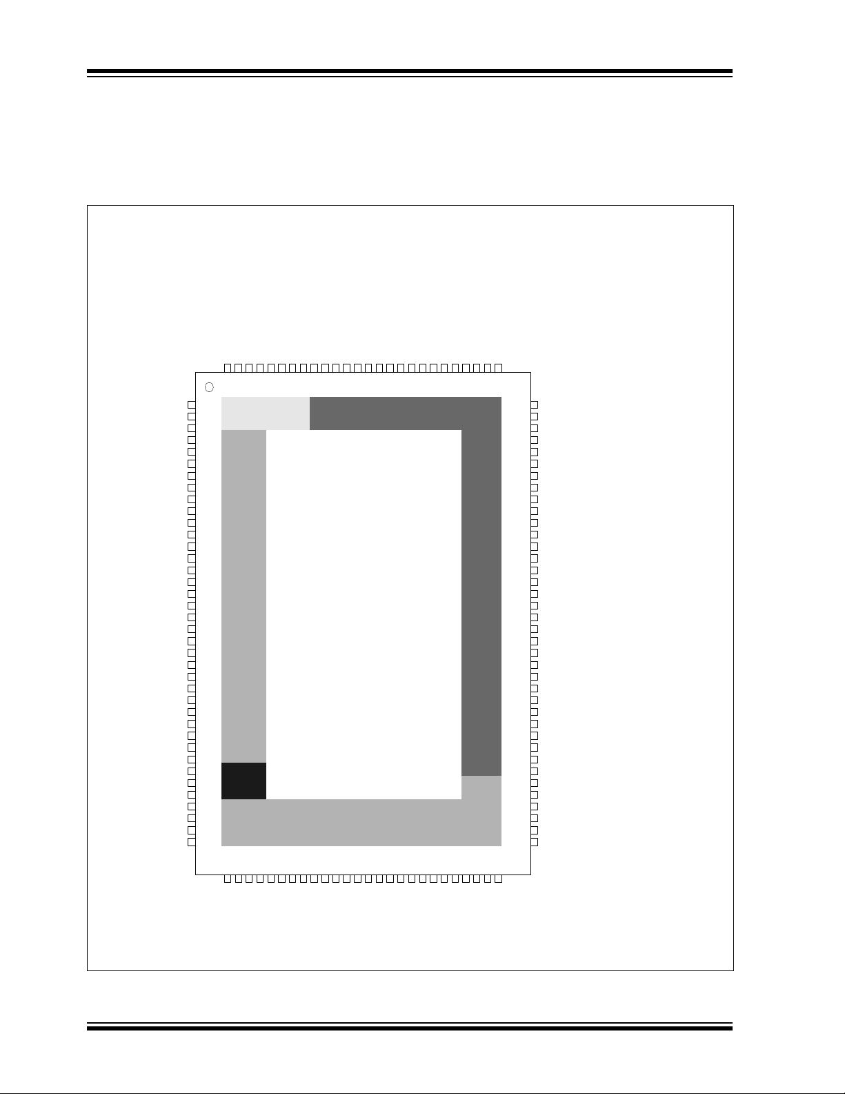
FIGURE 2-1: SCH5127 PIN LAYOUT
DS00002081A-page 6 2006 - 2016 Microchip Technology Inc.

SCH5127
2.2 Pin Configuration
TABLE 2-1: SCH5127 QFP PIN CONFIGURATION
Pin # Name Pin # Name Pin # Name Pin # Name
1 V1_IN (+12V_IN) 33 nINTRD_IN 65 RXD1 97 nPCIRST_OUT1/
2 V2_IN (+5V_IN) 34 AVSS 66 TXD1 (XNOR_OUT) 98 nPB_IN
3 VTRIP_IN 35 VCC 67 nDSR1 99 nPB_OUT
4 VTR 36 GP27/nIO_SMI/P17 68 nRTS1 (SYSOPT) 100 nRSMRST
5 nMTR0 37 KDAT/GP21 69 nCTS1 101 VSS
6 nDSKCHG 38 KCLK/GP22 70 nDTR1 102 FCAP
7 nDS0 39 MDAT/GP32 71 GP50/nRI2/PWM1 103 GP15/nTHERM_
8 VSS 40 MCLK/GP33 72 VTR 104 SDA1
9 nDIR 41 GP36/nKBDRST 73 GP51/nDCD2/LED1/
10 nSTEP 42 GP37/A20M 74 VSS 106 SCLK
1 1 nWDATA 43 VSS 75 GP52/RXD2/
12 nWGATE 44 VTR 76 GP53/TXD2/ VID7 108 GP16/PWM3/
13 nHDSEL 45 nINIT 77 GP54/nDSR2/PWM2 109 GP17/PWM3
14 nINDEX 46 nSLCTIN 78 GP55/nRTS2/VID6 110 PWM2
15 nTRK0 47 PD0 79 GP56/nCTS2/LED2 111 PWM1
16 nWRTPRT 48 PD1 80 GP57/nDTR2/
17 nRDATA 49 PD2 81 GP43/nFPRST/
18 CLOCKI 50 PD3 82 PWRGD_PS 1 14 FANTACH2
19 LAD0 51 PD4 83 PWRGD_CPU/
20 LAD1 52 PD5 84 PWRGD_3V 116 VID4
21 LAD2 53 PD6 85 n3VSB_GATE1 117 VID3
22 LAD3 54 PD7 86 n3VSB_GATE2/
23 nLFRAME 55 VSS 87 nPCIRST_OUT4/GP14 119 VID1
24 nLDRQ 56 SLCT 88 nSLP_S5 120 VID0
25 nPCI_RESET 57 PE 89 nSLP_S3 121 HVSS
26 PCI_CLK 58 BUSY 90 GP42/nIO_PME 122 HVTR
27 SER_IRQ 59 nACK 91 VTR 123 REMOTE228 nIDE_RSTDRV/G
P10
29 VTR 61 nALF 93 GP61/nLED2 125 REMOTE130 GP20/
SPEAKER_OUT
31 VSS 63 nRI1 95 nPCIRST_OUT3/GP13 127 VCCP_IN
32 VBAT 64 nDCD1 96 nPCIRST_OUT2/GP12 128 +2.5V_IN
60 nERROR 92 nPS_ON 124 REMOTE2+
62 nSTROBE 94 GP60/nLED1/WDT 126 REMOTE1+
WDT
SPEAKER_IN
SPEAKER_OUT
VRD_DET
SPEAKER_IN/
GP40/DRVDEN0
GP41/DRVDEN0
105 SCLK1
107 SDA
112 FANTACH3
113 VID5
115 FANTACH1
118 VID2
GP11
TRIP/nV_TRIP
(DDCSDA_5V)
(DDCSCL_5V)
(DDCSCL_2.5V)
(DDCSDA_2.5V)
nPROCHOT
2006 - 2016 Microchip Technology Inc. DS00002081A-page 7

SCH5127
APPLICATION NOTE: The V1_IN (+12V_IN) pin is a 1.125V input. If it is used to monitor 12V, it must be externally
scaled to 5V max. The V2_IN (+5V_IN) pin is a 1.125V inp ut. If it is used to monitor 5V, it
must be externally scaled to 5V max.
2.3 Pin Functions
TABLE 2-2: PIN FUNCTIONS DESCRIPTION
Note Name Description
POWER PINS
2-3, 2-4 VCC +3.3 Volt Supply Voltage
2-3, 2-4 VTR +3.3 Volt Standby Supply Voltage
2-7 VBAT +3.0 Volt Battery Supply
VSS Ground
AVSS Analog Ground
2-3 HVTR Analo g Power. +3.3V VTR pin dedicated
2-3 HVSS Analog Ground. Interna lly connected to
FCAP Capacitor for 1.8V regulator
CLOCKI 14.318MHz Clock Input VCC N/A IS
LAD[3:0] Multiplexed Command Address and Data VCC VCC PCI_IO
nLFRAME Frame signal. Indicates start of new cycle
nLDRQ Encoded DMA Request VCC VCC PCI_O
nPCI_RESET PCI Reset VCC N/A PCI_I
PCI_CLK PCI Clock VCC N/A PCI_I
SER_IRQ Serial IRQ VCC VCC PCI_IO
See GP40,
GP41
(DRVDEN0)
Muxed function
nMTR0 Motor On 0 N/A VCC (O12/OD12)
nDSKCHG Disk Change VCC N/A IS
nDS0 Drive Select 0 N/A VCC (O12/OD12)
nDIR Step Direction N/A VCC (O12/OD12)
nSTEP Step Pulse N/A VCC (O12/OD12)
nWDATA Write Disk Data N/A VCC (O12/OD12)
nWGATE Write Gate N/A VCC (O12/OD12)
nHDSEL Head Select N/A VCC (O12/OD12)
nINDEX Index Pulse Input VCC N/A IS
nTRK0 Track 0 VCC N/A IS
nWRTPRT Write Protected VCC N/A IS
nRDATA Read Disk Da ta VCC N/A IS
to the Hardware Monitoring
block. HVTR must be powered by
+3.3V Standby supply (VTR).
all of the Hardware Monitoring Block
circuitry.
LPC INTERFACE
and termination of broken cycle
FDD INTERFACE
Drive Density Select 0
)
CLOCK PIN
Input
Power
Plane
VCC N/A PCI_I
Output
Power
Plane
Buffer Modes
(Note 2-1)
DS00002081A-page 8 2006 - 2016 Microchip Technology Inc.

TABLE 2-2: PIN FUNCTIONS DESCRIPTION (CONTINUED)
Note Name Description
SERIAL PORT 1 INTERFACE
RXD1 Receive Data 1 VCC N/A IS
TXD1
/XNOR_OUT
nDSR1 Data Set Ready 1 VCC N/A I
2-6 nRTS1/
2-8, 2-11 nRI1 Ring Indicator 1 VCC,
2-8, 2-11 GP50
2-8, 2-11 GP51
2-8, 2-11 GP52
2-8, 2-10,
2-1 1
2-8, 2-11 GP54
2-8, 2-11 GP55
2-8, 2-11 GP56
2-8, 2-11 GP57
SYSOPT
nCTS1 Clear to Send 1 VCC N/A I
nDTR1 Data Terminal Ready 1 N/A VCC O8
nDCD1 Data Carrier Detect 1 VCC N/A I
/nRI2
/PWM1
/nDCD2
/LED1
/WDT
/RXD2 (IRRX)
/SPEAKER_IN
GP53
/TXD2 (IRTX)
/VID7
/nDSR2
/PWM2
/nRTS2
/VID6
/nCTS2
/LED2
/nDTR2
SPEAKER_OUT
Transmit Data 1
/ XNOR-Chain Test Mode Output
Request to Send 1/
SYSOPT (Configuration Port Base
Address Control)
SERIAL PORT 2 INTERFACE
General Purpose I/O
/Ring Indicator 2
/PWM1 Output
General Purpose I/O
/Data Carrier Detect 2
/LED 1
/Watchdog Timer output
General Purpose I/O
/Receive Data 2 (IRRX)
/Speaker Input
General Purpose I/O
/Transmit Data 2 (IRTX)
/VID7 I/O
General Purpose I/O
/Data Set Ready 2
PWM2 Output
General Purpose I/O
/Request to Send 2
/VID6 I/O
General Purpose I/O
/Clear to Send 2
/LED2
General Purpose I/O
/Data Terminal Ready 2
/Speaker Output
Power
Plane
SCH5127
Input
N/A VCC O12/O12
N/A VCC OP14
VTR
VTR VTR (I/O8/OD8)/I/
VCC,
VTR
VCC,
VTR
VTR VTR (I_VID/O16/
VCC,
VTR
VTR VTR (I_VID
VCC,
VTR
VTR VTR (I/O8/OD8)/I/
Output
Power
Plane
N/A IS
VTR (I/O12/OD12)/I(
VTR (IS/O8/OD8)/
VTR (I/O8/OD8)/I/
VTR (I/O12/OD12)/I/
Buffer Modes
(Note 2-1)
(O8/OD8)
O12/OD12)/
(O12/OD12)
IS/IS
OD16) /O16/
(I_VID/O16/
OD16)
(O8/OD8)
/O16/OD16)/
(O16/OD16)/
(I_VID
/O16/OD16)
(O12/OD12)
(O8/OD8)
PARALLEL PORT INTERFACE
nINIT Initiate Output N/A VCC (OD14/OP14)
nSLCTIN Printer Select Input N/A VCC (OD14/OP14)
PD0 Port Data 0 VCC VCC IOP14
PD1 Port Data 1 VCC VCC IOP14
PD2 Port Data 2 VCC VCC IOP14
PD3 Port Data 3 VCC VCC IOP14
PD4 Port Data 4 VCC VCC IOP14
2006 - 2016 Microchip Technology Inc. DS00002081A-page 9

SCH5127
TABLE 2-2: PIN FUNCTIONS DESCRIPTION (CONTINUED)
Note Name Description
PD5 Port Data 5 VCC VCC IOP14
PD6 Port Data 6 VCC VCC IOP14
PD7 Port Data 7 VCC VCC IOP14
SLCT Printer Selected Status VCC N/A I
PE Paper End VCC N/A I
BUSY Busy VCC N/A I
nACK Acknowledge VCC N/A I
nERROR Error VCC N/A I
nALF Autofeed Output N/A VCC (OD14/OP14)
nSTROBE Strobe Output N/A VCC (OD14/OP14)
KEYBOARD/MOUSE INTERFACE
2-8, 2-11 KDAT/GP21 Keyboard Data I/O
2-1 1 KCLK/GP22 Keyboard Clock I/O
2-8, 2-11 MDAT/GP32 Mouse Data I/O
2-1 1 MCLK/GP33 Mouse Clock I/O
2-5, 2-11 GP36
/nKBDRST
2-5, 2-11 GP37
/A20M
2-1 1 GP42/
nIO_PME
2-7, 2-8, 2-11GP60
/nLED1
/WDT
2-7, 2-8, 2-11GP61
/nLED2
2-8, 2-11 GP27
/nIO_SMI
/P17
2-1 1 GP20/
SPEAKER_OUT
2-8 nINTRD_IN Intruder Input. Latches the state of a
General Purpose I/O
General Purpose I/O
/General Purpose I/O
/General Purpose I/O
General Purpose I/O. GPIO can be
configured as an Open-Drain Output.
Keyboard Reset Open-Drain Output
(Note 2-5)
General Purpose I/O. GPIO can be
configured as an Open-Drain Output.
Gate A20 Open-Drain Output (Note 2-5)
MISCELLANEOUS PINS
General Purpose I/O.
Power Management Event Output. This
active low Power Management Event
signal allows this device to request wakeup in S3 and below.
General Purpose Output
/nLED1
Watchdog Timer Output
General Purpose Output
/nLED2
General Purpose I/O
/System Mgt. Interrupt
/8042 P17 I/O
General Purpose Input/Output.
/Speaker Output. Provides audio warning
of HW Monitor or Intruder events and
may be enabled by software.
INTRUDER DETECTION
chassis cover removal switch. A high-tolow or low-to-high will set the
INTRUSION bit to indicate an intrusion
event.
Input
Power
Plane
VCC,
VTR
VCC,
VTR
VCC,
VTR
VCC,
VTR
VTR VCC (I/O8/OD8)
VTR VCC (I/O8/OD8)
VTR VTR (I/O12/OD12)
N/A VTR O12/OD12
N/A VTR O12/OD12
VCC,
VTR
VCC,
VTR
VBAT N/A IL
Output
Power
Plane
VCC (I/OD16)/
VCC (I/OD16)/
VCC (I/OD16)/
VCC (I/OD16)/
VTR (I/O12/OD12)
VCC (I/O8/OD8)/
Buffer Modes
(Note 2-1)
(I/O16/OD16)
(I/O16/OD16)
(I/O16/OD16)
(I/O16/OD16)
/OD8
/OD8
/(O12/OD12)
/(O12/OD12)
/(I/O12/OD12)
(O8/OD8)
DS00002081A-page 10 2006 - 2016 Microchip Technology Inc.

SCH5127
TABLE 2-2: PIN FUNCTIONS DESCRIPTION (CONTINUED)
Input
Note Name Description
GLUE LOGIC
2-1 1 nPS_ON Power Supply Control Open Drain Output VTR VTR OD8
2-1 1 nPB_IN Power Button In is used to detect a
nPB_OUT Power Button Output N/A VTR OD12
2-1 1 nSLP_S3 S3 Sleep State Input Pin. VTR N/A I
2-1 1 nSLP_S5 S5 Sleep State Input Pin. VTR N/A I
2-1 1 GP43
/nFPRST
/VRD_DET
2-1 1 PWRGD_PS Power Good Input from Power Suppl y VTR N/A ISPU_400
2-1 1, 2-12 PWRGD_CPU
/SPEAKER_IN
/GP40
/DRVDEN0
PWRGD_3V Power Good Output – Push Pull N/A VTR O8
n3VSB_GATE1 PS Control Output 1 N/A VTR O 8
2-1 1, 2-12 n3VSB_GATE2
/GP41
/DRVDEN0
nPCIRST_OUT1
/GP11
nPCIRST_OUT2
/GP12
nPCIRST_OUT3
/GP13
nPCIRST_OUT4
/GP14
nIDE_RSTDRV
/GP10
nRSMRST Resume Reset Output N/A VTR O8
2-1 1 VID0 Voltage ID 0 Input/Output VTR VTR IO_VID
2-1 1 VID1 Voltage ID 1 Input/Output VTR VTR IO_VID
2-1 1 VID2 Voltage ID 2 Input/Output VTR VTR IO_VID
2-1 1 VID3 Voltage ID 3 Input/Output VTR VTR IO_VID
2-1 1 VID4 Voltage ID 4 Input/Output VTR VTR IO_VID
2-11 VID5 Voltage ID 5 Input/Output VTR VTR IO_VID
See GP55 (VID6)
Muxed function
See GP53 (VID7)
Muxed function
See GP43 (VRD_DET)
Muxed function
2-9, 2-10 +2.5V_IN Analog input for +2.5V HVTR N/A I
2-9 V1_IN Analog input for 1.125V HVTR N/A I
2-9 V2_IN Analog input for 1.125V HVTR N/A I
power button event
GP43/
Front Panel Reset
/VRD Detect Input
Power Good Output – Open Drain/
Speaker Input
General Purpose I/O
Drive Density Select 0
PS Control Output 2
General Purpose I/O
Drive Density Select 0
Buffered PCI Reset Output 1
/General Purpose Output.
Buffered PCI Reset Output 2
/General Purpose Output.
Buffered PCI Reset Output 3
/General Purpose Output.
Buffered PCI Reset Output 4
/General Purpose Output.
IDE Reset Output
/General Purpose Output.
VOLTAGE ID
Voltage ID 6 Input/Output - -
Voltage ID 7 Input/Output - -
VRD Detect Input - -
HARDWARE MONITORING, FAN CONTROL
Power
Plane
VTR N/A I
VTR VTR (I/O16/OD16)
VCC,
VTR
VTR VTR (O12/OD12)
N/A VTR OP14
N/A VTR OP14
N/A VTR OP14
N/A VTR OP14
N/A VCC I/OD8
Output
Power
Plane
VTR OD12/I/
Buffer Modes
(I/O12/OD12)/
(I/O12/OD12)/
(Note 2-1)
/ISPU_400
/I_VID
(O12/OD12)
(O12/OD12)
AN
AN
AN
2006 - 2016 Microchip Technology Inc. DS00002081A-page 11

SCH5127
TABLE 2-2: PIN FUNCTIONS DESCRIPTION (CONTINUED)
Input
Note Name Description
Power
Plane
2-9 VCCP_IN Analog input for +2.25V HVTR N/A I
2-9 VTRIP_IN Analog input for +1.5V HVTR N/A I
REMOTE1- This is the negative Analog input (current
HVTR N/A I
sink) from the remote thermal diode 1.
REMOTE1+ This is the positive input (current source)
HVTR N/A I
from the remote thermal diode 1.
REMOTE2- This is the negative Analog input (current
HVTR N/A I
sink) from the remote thermal diode 2.
REMOTE2+ This is the positive input (current source)
HVTR N/A I
from the remote thermal diode 2.
2-1 1 FANTACH1 Tachometer Input 1 for monitoring a fan. VT R N/A I
2-1 1 FANTACH2 Tachometer Input 2 for monitoring a fan. VT R N/A I
2-1 1 FANTACH3 Tachometer Input 3 for monitoring a fan. VTR N/A I
See also
PWM1 PWM Fan Speed Control 1 Output. N/A VTR OD8
GP50
See also
PWM2 PWM Fan Speed Control 2 Output N/A VTR OD8
GP54
GP17/PWM3 General Purpose Output.
N/A VTR I/O8/OD8
PWM Fan Speed Control 3 Output
GP16
/PWM3
/nPROCHOT
GP15
/nTHERM_TRIP
/nV_TRIP
General Purpose Output.
PWM Fan Speed Control 3 Output
PROCHOT output
General Purpose Output.
THERMTRIP Output
V_TRIP output
N/A VTR I/O8/OD8
N/A VCC I/O8/OD8
SMBUS POWER STATE ISOLATION (4)
2-1 1 SDA1
(DDCSDA_5V)
POWER STATE ISOLATION SMBus 1
Data. Can also be used for voltage
VTR VTR nSW
translation 5V data
2-1 1 SCLK1
(DDCSCL_5V)
POWER STATE ISOLATION SMBus 1
Clock.
VTR VTR nSW
Can also be used for voltage translation
5V clock
2-1 1 SDA
(DDCSDA_2.5V)
POWER STATE ISOLATION SMBus
Data.
VTR VTR nSW
Can also be used for voltage translation
2.5V data
2-1 1 SCLK
(DDCSCL_2.5V)
POWER STATE ISOLATION SMBus
Clock.
VTR VTR nSW
Can also be used for voltage translation
2.5V clock
Output
Power
Plane
Buffer Modes
(Note 2-1)
AN
AN
AND-
AND+
AND-
AND+
M
M
M
Note: The “n” as the first letter of a signal name or the “#” as the suffix of a signal name indicates an “Active Low”
signal.
Note 2-1 Buffer types per function on multiplexed pins are separated by a slash “/”. Buffer types in parenthesis
represent multiple buffer types for a single pin function.
Note 2-2 Pins that have input buffers must always be held to either a logical low or a logical hi gh state when
powered. Bi-directional buses that may be trisected should have either weak external pul l-ups or pulldowns to hold the pins in a logic state (i.e., logic states are VCC or ground).
Note 2-3 VCC, VTR and VSS pins are for Super I/O Blocks. HVTR and HVSS are dedicated for the Hardware
Monitoring Block. HVTR must be connected to VTR on the board.
Note 2-4 VTR can be connected to VCC if no wake-up functionality is required.
DS00002081A-page 12 2006 - 2016 Microchip Technology Inc.

SCH5127
Note 2-5 External pull-ups must be placed on the nKBDRST and A20M pins. These pins are GPIOs that are
inputs after an initial power-up (VTR POR). If the nKBDRST and A20M functions are to be used, the
system must ensure that these pins are high.
Note 2-6 The nRTS1/SYSOPT pin requires an external pull-down resistor to put the base I/O address for
configuration at 0x02E. An external pull-up resistor is required to move the base I/O address for
configuration to 0x04E.
Note 2-7 The LED pins are powered by VTR so that the LEDs can be controlled when the part is under VTR
power.
Note 2-8 This pin is an input into the wake-up logic that is powered by VTR.
Note 2-9 This analog input is backdrive protected. Although HVTR is powered by VTR, it is possible that
monitored power supplies may be powered when HVTR is off.
Note 2-10 The GP53/TXD2(IRTX) pin defaults to the GPIO input function on a VTR POR and presents a tristate
impedance. When VCC=0 the pin is tristate. If GP53 function is selected and VCC is power is applied,
the pin reflects the current state of GP53. The GP53/TXD2(IRTX) pin is tristate when it is configured
for the TXD2 (IRTX) function under various conditions.
Note 2-11 These pins are inputs to VTR powered logic internal to the part. These pins, if configured as input,
should be in a known state when VCC goes to 0 to prevent extra current drain caused by floating
inputs. The nR1, KDAT, and MDAT pins have VCC input operation for their UART and
keyboard/mouse functionality and VTR input operation for PME wake up. If the following UART2 pin
functions are selected, then these pins can float when VCC=0 with no extra current drain: nDCD2,
RXD2, nDSR2, nCTS2. This also applies to the SPEAKER _IN pin functions. See for the GPIO
Section for the VCC and VTR operation of all GPIO pins.
Note 2-12 These pins are VCC powered outputs when the DRVDEN0 function is selected in the associated
GPIO registers (GP40, GP41).
2.4 Buffer Description
Table 2-3 lists the buffers that are used in this device. A complete description of these b uffers can be found in the DC
Electrical Characteristics section.
TABLE 2-3: BUFFER DESCRIPTION
Buffer Description
I Input TTL Compatible - Super I/O Block.
IL Input, Low Leakage Current.
I
M
I
AN
I
AND-
I
AND+
IS Input with Schmitt Trigger.
I_VID Input, high input level 0.8V min, low input level 0.4V max.
IO_VID Input/Output, high input level 0.8V min, low input level 0.4V max,
O8 Output, 8mA sink, 8mA source.
OD8 Open Drain Output, 8mA sink.
IO8 Input/Output, 8mA sink, 8mA source.
IOD8 Input/Open Drain Output, 8mA sink, 8mA source.
IS/O8 Input with Schmitt Trigger/Output, 8mA sink, 8mA source.
O12 Output, 12mA sink, 12mA source.
OD12 Open Drain Output, 12mA sink.
IO12 Input/Output, 12mA sink, 12mA source.
Input - Hardware Monitoring Block.
Analog Input, Hardware Monitoring Block.
Remote Thermal Diode (current sink) Negative Input
Remote Thermal Diode (current source) Positive Input
16mA sink/source.
2006 - 2016 Microchip Technology Inc. DS00002081A-page 13

SCH5127
TABLE 2-3: BUFFER DESCRIPTION (CONTINUED)
Buffer Description
IOD12 Input/Open Drain Output, 12mA sink, 12mA source.
OD14 Open Drain Output, 14mA sink.
OP14 Output, 14mA sink, 14mA source.
IOP14 Input/Output, 14mA sink, 14mA source. Backdrive protected.
IO16 Input/Output 16mA sink.
IOD16 Input/Output (Open Drain), 16mA sink.
PCI_IO Input/Output. These pins must meet the PCI 3.3V AC and DC Char-
acteristics. (Note 2-13)
PCI_O Output. These pins must meet the PCI 3.3V AC and DC Character-
istics. (Note 2-13)
PCI_I Input. These pins must meet the PCI 3.3V AC and DC Characteris-
tics. (Note 2-13)
PCI_ICLK Clock Input. These pins must meet the PCI 3.3V AC and DC Char-
acteristics and timing. (Note 2-14)
nSW n Channel Switch (R
ISPU_400 Input with 400mV Schmitt Trigger and 30uA Integrated Pull-Up.
ISPU Input with Schmitt Trigger and Integrated Pull-Up.
Note 2-13 See the “PCI Local Bus Specification,” Revision 2.2, Section 4.2.2.
Note 2-14 See the “PCI Local Bus Specification,” Revision 2.2, Section 4.2.2 and 4.2.3.
~25 Ohms)
on
DS00002081A-page 14 2006 - 2016 Microchip Technology Inc.
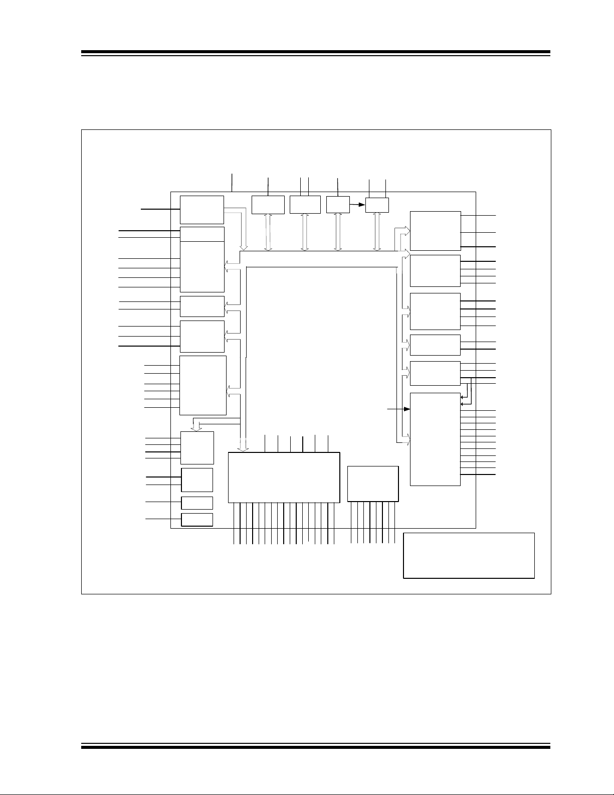
3.0 BLOCK DIAGRAM
LEDs
LED2*
LED1*
Internal Bus
(Data, Address, and Control lines)
Power Mgmt
nIO_SMI*
GP1[0:7]*, GP2[0:2,7]*
GP3[2,3,6,7]*, GP4[0,1,2,3]*
GP5[0:7]*, GP6[0:1]*
Note 1: This diagram does not show all power and
ground connections.
Note 2: Signal names followed by an asterisk (*) are
located on multifunction p ins. This diagram is
designed to show the various functions available on
the chip and should not be used as a pin layout.
CLOCK GEN
14MHz
CLOCKI
WDT
nDSR1, nDTR1
nDCD1, nRI1
Power Control
and Recovery
`
nSLP_S3
nSLP_S5
PWRGD_CPU
PWRGD_3V
n3VSB_GATE1
n3VSB_GATE2*
nRSMRST
nFPRST
PWRGD_PS
VTRIP_IN
VCCP_IN
V1_IN
V2_IN
+2.5V_IN
Remote1-
Remote1+
Remote2-
Remote2+
PWM1
PWM2
PWM3
FANTACH1
FANTACH2
FANTACH3
HVTR
HVSS
Hardware
Monitor/
Fan Control
General
Purpose
I/O
nIO_PME*
VCC
VTR
VBAT
PWRGD
HWM_INT
14MHz
WDT
SER_IRQ
LAD[3:0]
nLFRAME
nLDRQ
nPCI_RESET
PCI_CLK
LPC
Interface
SERIAL
IRQ
SMbus
Isolation
Switch
SDA1
SCLK1
SDA
SCLK
SMSC
Proprietary
82077
Compatible
Floppydisk
Controller with
Digital Data
Separator &
Write Precom-
pensation
nRDATA, nWDATA
nDIR, nSTEP
nMTR0, nTRK0, InNDEX
DRVDEN0*, nWRTPRT
nWGATE, nHDSEL
nDSKCHG, nDS0,
High-Speed
16550A
UART
PORT 1
TXD1*, RXD1
nCTS1, nRTS1*
Multi-Mode
Parallel Port
with
ChiProtect
TM
/
FDC MUX
PD[7,0]
BUSY, SLCT, PE,
nERROR, nACK
nSTROBE, nINIT,
nSLCTIN, nALF
Intruder
Detection
Keyboard/Mouse
8042
controller
KCLK, KDAT
MCLK, MDAT
A20M
nKBDRST
PCI Reset
Outputs
nPCIRST_OUT[1:4]
nIDE_RSTDRV
Speaker
SPEAKER_IN*
High-Speed
16550A
UART
PORT 2
TXD2 (IRTX)*,
RXD2 (IRRX)*
DSR2*, DTR2*
DCD2*, RI2*
CTS2*, RTS2 *
nPS_ON
nPB_IN
WDT*
nINTRD_IN
SPEAKER_OUT*
1.8V
Regulato
r
FCAP
VTR
VCC
VCC POR
Circuit
WDT
STRAP
OPTIONS
VBAT
VBAT
POR Ckt
VID I/O
VID0
VID1
VID2
VID3
VID4
VID5
VID6*, VID7*
VRD_DET*
FIGURE 3-1: SCH5127 BLOCK DIAGRAM
SCH5127
2006 - 2016 Microchip Technology Inc. DS00002081A-page 15

SCH5127
4.0 POWER FUNCTIONALITY
The SCH5127 has four power planes: VCC, VTR, HVTR and VBAT.
4.1 VCC Power
The SCH5127 is a 3.3 Volt part. The VCC supply is 3.3 Volts (nominal). VCC is the main power supply for the Super I/O
Block. See Section 29.2, "DC Electrical Characteristics," on page 253.
4.2 3 Volt Operation / 5 Volt Tolerance
The SCH5127 is a 3.3-Volt part. It is intended solely for 3.3V applications. Non-LPC bus pins are 5V tolerant; that is, the
operating input voltage is 5.0V Max, and the I/O buffer output pads are backdrive protected (they do not impose a load
on any external VCC powered circuitry). The 5V tolerant pins are applicable to the Super I/O Block only.
The LPC interface pins are 3.3 V only. These signals meet PCI DC specifications for 3.3V signaling. The operating input
voltage on these pins is 3.6V Max. These pins are:
• LAD[3:0]
• nLFRAME
• nLDRQ
The following pins are also 3.3 V only. The operating input voltage on these pins is 3.6V Max.
•VTR
•VCC
• VBAT
• V1_IN
• V2_IN
•VTRIP_IN
• +2.5V_IN
• VCCP_IN
• VID0-VID4, VID5
•SDA, SCLK
• GP43/nFPRST/VRD_DET
• GP55/nRTS2/VID6
• GP53/TXD2(IRTX)/VID7
The input voltage for all other pins is 5.0V max. These pins include all non-LPC Bus pins and the following pins in the
Super I/O Block:
• nPCI_RESET
• PCI_CLK
• SER_IRQ
•nIO_PME
4.3 HVTR Power
The SCH5127 is a 3.3 Volt part. The HVTR supply is 3.3 Volts (nominal). HVTR is a dedicated power supply for the
Hardware Monitoring Block. HVTR is connected to the VTR suspend well. See Section 29.2, "DC Electrical Character-
istics," on page 253.
Note: The hardware monitoring logic is powered by HVTR, but only operational whe n VCC is on. The hardware
monitoring block is connected to the suspend well to retain the programmed configuration through a sleep
cycle.
DS00002081A-page 16 2006 - 2016 Microchip Technology Inc.

SCH5127
4.4 VTR Support
The SCH5127 requires a trickle supply (VTR) to provide sleep current for the programmable wake-up events in the PME
interface when VCC is removed. The VTR supply is 3.3 Volts (nominal). See Section 29.0, "Operational Description,"
on page 253. The maximum VTR current that is required depends on the functions that are used in the part. See Section
29.0, "Operational Description," on page 253.
If the SCH5127 is not intended to provide wake-up capabilities on standby current, VTR can be connected to VCC. VTR
powers the IR interface, the PME configuration registers, and the PME interface. The VTR pin generates a VTR Poweron-Reset signal to initialize these components. If VTR is to be used for programmable wake-up events when VCC is
removed, VTR must be at its full minimum potential at least 10 ms before Vcc begins a power-on cycle. Note that under
all circumstances, the hardware monitoring HVTR must be driven as the same source as VTR.
4.4.1 TRICKLE POWER FUNCTIONALITY
When the SCH5127 is running under VTR on ly (VCC removed), PME w akeup events are active a nd (if enabled) able
to assert the nIO_PME pin active low. (See Table 15-2, “PME Events,” on page 106.)
The following requirements apply to all I/O pins that are specified to be 5 volt tolerant.
• I/O buffers that are wake-up event compatible are powered by VCC. Under VTR power (VCC=0), these pins may
only be configured as inputs. These pins have input buffers into the wakeup logic that are powered by VTR.
• I/O buffers that may be configured as either push-pull or open drain under VTR power (VCC=0), are powered by
VTR. This means, at a minimum, they will source their specified current from VTR even when VCC is present.
The GPIOs that are used for PME wakeup as input function as follows: (See Table 13-1, “GPIO Functionality,” on
page 99.)
• Buffers are powered by VCC, but in the absence of VCC they are backdrive protected (they do not impose a load
on any external VTR powered circuitry). They are wakeup compatible as inputs under VTR power. These pins
have input buffers into the wakeup logic that are powered by VTR.
The following list summarizes the blocks, registers and pins that are powered by VTR.
• PME interface block
• PME runtime register block (includes all PME, SMI, GPIO, Fan and other misce llaneous registers)
• Digital logic in the Hardware Monitoring block
• “Wake on Specific Key” logic
• LED control logic
• Watchdog Timer
• Power Control and Recovery Logic
• Intruder Detection Logic
• Pins for PME Wakeup:
- GPIOs and alternate functions as indicated in Table 13-1, “GPIO Functionality,” on page 99.
- nRI1 (input)
• Other pins:
- GPIOs and alternate functions as indicated in Table 13-1, “GPIO Functionality,” on page 99.
-nRSMRST
- nPB_IN
- nPB_OUT
- nPS_ON
-PWRGD_PS
- nSLP_S3#
- nSLP_S5#
- PWRGD_3V, PWRGD_CPU
- n3VSB_GATE1,2
- PWM1, PWM2, PWM3
- VID pins
2006 - 2016 Microchip Technology Inc. DS00002081A-page 17

SCH5127
4.5 VBAT Support
VBA T is a battery generated power supply that is needed to support the power recovery logic. The power recovery logic
is used to restore power to the system in the event of a power failure. Power may be returned to the system by a keyboard power button, the main power button, or by the power recovery logic following an unexpected power failure.
The VBAT supply is 3.0 Volts (nominal). See Sectio n 29.0, "Operational Description," on page 253.
The following input pin is powered by VBAT:
• nINTRD_IN
The following Runtime Registers are powered by VBAT:
• PME_PBOUT_EN at offset 03h
• PME_PB_EN1, PME_PB_EN3, PME_PB_EN5, PME_PB_EN6 at offset 10h-13h
• GP16 at offset 29h, GP17 at offset 2Ah
• GP41 at offset 3Ch, GP43 at offset 3Eh
• GP50-GP57 at offset 3Fh-46h
• PWR_REC Register at offset 49h
• SLP_S3_Shift Register at offset 4Ah
• INTRD Register at offset 52h
• SLP_S3_Pre_State at offset 53h
• DBLCLICK at offset 5Bh
• Mouse Specific Wake at offset 5Ch
• Keyboard Scan Code – Make Byte 1 at offset 5Fh
• Keyboard Scan Code – Make Byte 2 at offset 60h
• Keyboard Scan Code – Break Byte 1 at offset 61h
• Keyboard Scan Code – Break Byte 2 at offset 62h
• Keyboard Scan Code – Break Byte 3 at offset 63h
• Keyboard PWRBTN/SPEKEY at offset 64h
• SMB_ISO Register at offset 6Ah
• WDT Option at offset 6Bh
• PWM Start/Gate Option at offset 6Ch
• TEST at offset 6Dh.
Note: All VBA T powered pins and registers are powered by VTR when VTR power is on and are battery backed-
up when VTR is removed.
APPLICATION NOTE: If the battery features are not required and the VBAT pin is not connected to a battery, the
VBAT pin should be connected to ground. Note that in this case, the following features listed
above will not function as intended.
To conserve battery power, the battery logic is switched internally between the VBAT and VTR pins. The switch takes
place as follows:
• On rising VTR, switch from VBAT to VTR when VTR > 2.5V (nominal) or VTR > VBAT.
• On falling VTR, switch from VTR to VBAT when VTR < 2.45V (nominal) and VTR < VBAT.
Backdrive protection prevents VBAT from driving the VCC or VTR rails.
DS00002081A-page 18 2006 - 2016 Microchip Technology Inc.

SCH5127
4.6 Super I/O Functions
The maximum VTR current, ITR, is given with all outputs open (not loaded), and all inputs in a fixed state (i.e., 0V or
3.3V). The total maximum current for the part is the unloaded value PLUS the maximum current sourced by the pin that
is driven by VTR. The super I/O pins that are powered by VTR are as follows: GPIOs as indicated in Table 13-1, “GPIO
Functionality,” on page 99, PWRGD_3V, n3VSB_GATE1. These pins, if configured as push-pull outputs, will source a
minimum of 6mA at 2.4V when driving.
The maximum VCC current, I
3.3V).
The maximum Vbat current, I
4.7 Power Management Events (PME/SCI)
The SCH5127 offers support for Power Management Events (PMEs), also referred to as System Control Interrupt (SCI)
events. The terms PME and SCI are used synonymously throughout this document to refer to the indication of an event
to the chipset via the assertion of the nIO_PME output signal. See Section 15.0, "PME Support," on page 106.
, is given with all outputs open (not loaded) and all inputs in a fixed state (i.e., 0V or
CC
, is given with all outputs open (not loaded) and all inputs in a fixed state (i.e., 0V or 3.3V).
bat
2006 - 2016 Microchip Technology Inc. DS00002081A-page 19

SCH5127
5.0 SIO OVERVIEW
The SCH5127 is a Super I/O Device with hardware monitoring. The Super I/O features are implemented as logical
devices accessible through the LPC interface. The Super I/O blocks are powered by VCC, VTR, or VBAT. The Hardware
Monitoring block is powered by VTR and is accessible via the LPC interface. The following chapters define each of the
functional blocks implemented in the SCH5127, their corresponding registers, and physical characteristics.
This chapter offers an introduction into the Super I/O functional blo cks, registers and host interfa ce. Details regarding
the hardware monitoring block are defined in later chapters. The block diagram in
of the device. Note that the Super I/O registers are implemented as typical Plug-and-Play components.
Note: The LPC interface is the main interface used to access the components of this chip. The LPC interface is
used to access the Super I/O registers and the Hardware Monitoring registers.
5.1 Super I/O Registers
The address map, shown below in Table 5-1 shows the addresses of the different blocks of the Super I/O immediately
after power up. The base addresses of all the Super I/O Logical Blocks, including the configuration register block, can
be moved or relocated via the configuration registers.
Note: Some addresses are used to access more than one register.
5.2 Host Processor Interface (LPC)
Section 3.0 further details the layout
The host processor communicates with the Super I/O features in the SCH5127 through a series of read/write registers
via the LPC interface. The port addresses for these registers are shown in T able 5-1, "Super I/O Block Addresses". Register access is accomplished through I/O cycles or DMA transfers. All registers are 8 bits wide.
TABLE 5-1: SUPER I/O BLOCK ADDRESSES
Address Block Name Logical Device Notes
Base+(0-5) and +(7) Floppy Disk 0
na Reserved 1 (Note 5-3)
na Reserved 2 (Note 5-3)
Parallel Port
Base+(0-3)
Base+(0-7)
Base+(0-3), +(400-402)
Base+(0-7), +(400-402)
Base+(0-7) Serial Port Com 1 4
Base+(0-7) Serial Port Com 2 5
na Reserved 6
60, 64 KYBD 7
na Reserved
Base + (0-7F) Runtime Registers A (Note 5-2)
na Reserved B (Note 5-3)
Base + (0-1) Configuration (Note 5-1)
SPP
EPP
ECP
ECP+EPP+SPP
3
8,9
Note 5-1 Refer to the configuration register descriptions for setting the base address.
Note 5-2 Logical Device A is referred to as the Runtime Register block or PME Block and may be used
interchangeably throughout this document.
Note 5-3 na = not applicable
DS00002081A-page 20 2006 - 2016 Microchip Technology Inc.
SCH5127
6.0 LPC INTERFACE
6.1 LPC Interface Signal Definition
The signals implemented for the LPC bus interface are described in the tables below. LPC bus signals use PCI 33MHz
electrical signal characteristics.
6.1.1 LPC REQUIRED SIGNALS
Signal Name Type Description
LAD[3:0] I/O LPC address/data bus. Multiplexed command, address and data bus.
nLFRAME Input Frame sign al. Indicates start of new cycle and termination of broken cycle
nPCI_RESET Input PCI Reset. Used as LPC Interface Reset. Active low.
PCI_CLK Input PCI Clock.
6.1.2 LPC OPTIONAL SIGNALS
Signal Name Type Description
nLDRQ Output Encoded DMA/Bus Master request for the LPC inte rface.
SER_IRQ I/O Serial IRQ.
nIO_PME OD Same as the PME or Power Mgt Event signal. Allows the SCH5127 to request
wakeup in S3 and below.
6.2 Supported LPC Cycles
Table 6-1 summarizes the cycle types are supported by the SCH5127. All other cycle types are ignored.
TABLE 6-1: SUPPORTED LPC CYCLES
Cycle Type Transfer Size
I/O Write 1 Byte
I/O Read 1 Byte
DMA Write 1 Byte
DMA Read 1 Byte
6.3 Device Specific Information
The LPC interface conforms to the “Low Pin Count (LPC) Interface Specification”. The following section will review any
implementation specific information for this device.
6.3.1 SYNC PROTOCOL
The SYNC pattern is used to add wait states. For read cycles, the SCH5127 immediately drives the SYNC pattern upon
recognizing the cycle. The host immediately drives the sync pattern for write cycles. If the SCH5127 needs to assert
wait states, it does so by driving 0101 or 0110 on LAD[3:0] until it is ready, at which point it will drive 0000 or 1001. The
SCH5127 will choose to assert 0101 or 0110, but not switch between the two patterns.
The data (or wait state SYNC) will immediately follow the 0000 or 1001 value. The SYNC value of 0101 is intended to
be used for normal wait states, wherein the cycle will complete within a few clocks. The SCH5127 uses a SYNC of 0101
for all wait states in a DMA transfer.
The SYNC value of 01 10 is intended to be used where the number of wait states is large. This is provided for EPP cycles,
where the number of wait states could be quite large (>1 microsecond). However, the SCH5127 uses a SYNC of 0110
for all wait states in an I/O transfer.
2006 - 2016 Microchip Technology Inc. DS00002081A-page 21

SCH5127
The SYNC value is driven within 3 clocks.
6.3.2 RESET POLICY
The following rules govern the reset policy:
• When nPCI_RESET goes inactive (high), the PCI clock is assumed to have been running for 100usec prior to the
removal of the reset signal, so that everything is stable. This is the same reset active time after clock is stable that
is used for the PCI bus.
• When nPCI_RESET goes active (low):
1. The host drives the nLFRAME signal high, tristates the LAD[3:0] signals, and ignores the nLDRQ signal.
2. The SCH5127 ignores nLFRAME, tristates the LAD[3:0] pins and drives the nLDRQ signal inactive (high).
DS00002081A-page 22 2006 - 2016 Microchip Technology Inc.

SCH5127
7.0 FLOPPY DISK CONTROLLER
The Floppy Disk controller (FDC) provides the interface between a host microprocessor and the floppy disk drives. The
FDC integrates the functions of the Formatter/Controller, Digital Data Separator, Write Precompensation and Data Rate
Selection logic for an IBM XT/AT compatible FDC. The true CMOS 765B core provides 100% IBM PC XT/AT compatibility in addition to providing data overflow and underflow protection. SCH5127 supports a single floppy disk drive.
The FDC is compatible to the 82077AA using Microchip’s proprietary floppy disk controller core.
7.1 FDC Internal Registers
The Floppy Disk Controller contains eight internal registers which fa cilitate the interfacing between the host mi croprocessor and the disk drive. Table 7-1 shows the addresses required to access these registers. Registers other than the
ones shown are not supported. The rest of the description assumes that the primary addresses have been selected.
(Shown with base addresses of 3F0 and 370.)
TABLE 7-1: STATUS, DATA AND CONTROL REGISTERS
Primary Address
3F0
3F1
3F2
3F3
3F4
3F4
3F5
3F6
3F7
3F7
Secondary
Address
370
371
372
373
374
374
375
376
377
377
R/W Register
R
R
R/W
R/W
R
W
R/W
R
W
Status Register A (SRA)
Status Register B (SRB)
Digital Output Register (DOR)
Ta pe Drive Register (TDR)
Main Status Register (MSR)
Data Rate Select Register (DSR)
Data (FIFO)
Reserved
Digital Input Register (DIR)
Configuration Control Register (CCR)
7.1.1 STATUS REGISTER A (SRA)
Address 3F0 READ ONLY
This register is read-only and monitors the state of the internal inte rrupt signal and several disk interfa ce pins in PS/2
and Model 30 modes. The SRA can be accessed at any time when in PS/2 mode. In the PC/AT mode the data bus pins
D0 – D7 are held in a high impedance state for a read of address 3F0.
PS/2 Mode
7 6543210
INT
PENDING
RESET
COND.
Bit 0 DIRECTION
Active high status indicating the direction of head movement. A logic “1” indicates inward direction; a logic “0” indicates
outward direction.
Bit 1 nWRITE PROTECT
Active low status of the WRITE PROTECT disk interface input. A logic “0” indicates that the disk is write protected.
Bit 2 nINDEX
Active low status of the INDEX disk interface input.
Bit 3 HEAD SELECT
Active high status of the HDSEL disk interface input. A logic “1” selects side 1 and a logic “0” selects side 0.
Bit 4 nTRACK 0
Active low status of the TRK0 disk interface input.
0 1 0 N/A 0 N/A N/A 0
nDRV2 STEP nTRK0 HDSEL nINDX nWP DIR
2006 - 2016 Microchip Technology Inc. DS00002081A-page 23

SCH5127
Bit 5 STEP
Active high status of the STEP output disk interface output pin.
Bit 6 nDRV2
This function is not supported. This bit is always read as “1”.
Bit 7 INTERRUPT PENDING
Active high bit indicating the state of the Floppy Disk Interrupt output.
PS/2 Model 30 Mode
7 6543 210
INT PENDING DRQ STEP
RESET
COND.
Bit 0 DIRECTION
Active low status indicating the direction of head movement. A logic “0” indicates inward direction; a logic “1” indicates
outward direction.
Bit 1 WRITE PROTECT
Active high status of the WRITE PROTECT disk interface input. A logic “1” indicates that the disk is write protected.
Bit 2 INDEX
Active high status of the INDEX disk interface input.
Bit 3 HEAD SELECT
Active low status of the HDSEL disk interface input. A logic “0” selects side 1 and a logic “1” selects side 0.
Bit 4 TRACK 0
Active high status of the TRK0 disk interface input.
Bit 5 STEP
Active high status of the latched STEP disk interface output pin. This bit is latched with the STEP output going active,
and is cleared with a read from the DIR register, or with a hardware or software reset.
Bit 6 DMA REQUEST
Active high status of the DMA request pending.
Bit 7 INTERRUPT PENDING
Active high bit indicating the state of the Floppy Disk Interrupt.
0 0 0 N/A 1 N/A N/A 1
F/F
TRK0 nHDSEL INDX WP nDIR
7.1.2 STATUS REGISTER B (SRB)
Address 3F1 READ ONLY
This register is read-only and monitors the state of several disk interface pin s in PS/2 and Model 30 modes. The SRB
can be accessed at any time when in PS/2 mode. In the PC/AT mode the data bus pins D0 – D7 are held in a high
impedance state for a read of address 3F1.
PS/2 Mode
7654321 0
Reserved Reserved DRIVE
RESET
COND.
Bit 0 MOTOR ENABLE 0
Active high status of the MTR0 disk interface output pin. This bit is low after a hardware reset and unaffected by a software reset.
DS00002081A-page 24 2006 - 2016 Microchip Technology Inc.
1100000 0
SEL0
WDATA
TOGGLE
RDATA
TOGGLE
WGATE Reserved MOT EN0

SCH5127
Bit 1 Reserved
Reserved will return a zero (0) when read. This bit is low after a hardware reset and unaffected by a software reset.
Bit 2 WRITE GATE
Active high status of the WGATE disk interface output.
Bit 3 READ DATA TOGGLE
Every inactive edge of the RDATA input causes this bit to change state.
Bit 4 WRITE DATA TOGGLE
Every inactive edge of the WDATA input causes this bit to change state.
Bit 5 DRIVE SELECT 0
Reflects the status of the Drive Select 0 bit of the DOR (address 3F2 bit 0). This bit is cleared after a hardware reset
and it is unaffected by a software reset.
Bit 6 RESERVED
Always read as a logic “1”.
Bit 7 RESERVED
Always read as a logic “1”.
PS/2 Model 30 Mode
76543210
RESET
COND.
nDRV2 nDS1 nDS0 WDATA
F/F
N/A1 100011
RDATA F/F WGATE F/F nDS3 nDS2
Bit 0 nDRIVE SELECT 2
The DS2 disk interface is not supported.
Bit 1 nDRIVE SELECT 3
The DS3 disk interface is not supported.
Bit 2 WRITE GATE
Active high status of the latched WGATE output signal. This bit is latched by the active going edge of WGATE and is
cleared by the read of the DIR register.
Bit 3 READ DATA
Active high status of the latched RDATA output sig nal. This bit is latched by the inactive going edge of RDATA and is
cleared by the read of the DIR register.
Bit 4 WRITE DA TA
Active high status of the latched WDATA output signal. This bit is latched by the inactive goi ng edge of WDATA and is
cleared by the read of the DIR register. This bit is not gated with WGATE.
Bit 5 nDRIVE SELECT 0
Active low status of the DS0 disk interface output.
Bit 6 nDRIVE SELECT 1
The DS 1 disk interface is not supported.
Bit 7 nDRV2
Active low status of the DRV2 disk interface input. Note: This function is not supported.
7.1.3 DIGITAL OUTPUT REGISTER (DOR)
Address 3F2 READ/WRITE
The DOR controls the drive select and motor enab les of the disk interface ou tputs. It also contains the enable for the
DMA logic and a software reset bit. The contents of the DOR are unaffected by a software reset. The DOR can be written
to at any time.
2006 - 2016 Microchip Technology Inc. DS00002081A-page 25

SCH5127
76543210
MOT EN3 MOT EN2 MOT EN1 MOT EN0 DMAEN nRESET DRIVE
RESET
COND.
Bit 0 and 1 DRIVE SELECT
These two bits are binary encoded for the drive selects, thereby allowing only one drive to be selected at one time. For
proper device operation, they must be programmed to 0b00.
Bit 2 nRESET
A logic “0” written to this bit resets the Floppy disk controller. This reset will remain active until a logic “1” is written to
this bit. This software reset does not affect the DSR and CCR registers, nor does it affect the other bits of the DOR register. The minimum reset duration required is 100ns, therefore toggling this bit by consecutive writes to this register is a
valid method of issuing a software reset.
Bit 3 DMAEN
PC/AT and Model 30 Mode:
Writing this bit to logic “1” will enable the DMA and interrupt functions. This bit being a logic “0” will disable the DMA and
interrupt functions. This bit is a logic “0” after a reset and in these modes.
PS/2 Mode: In this mode the DMA and interrupt functions are always enabled. During a reset, this bit will be cleared to
a logic “0”.
Bit 4 MOTOR ENABLE 0
This bit controls the MTR0 disk interface output. A logic “1” in this bit wil l cause the output pin to go active.
Bit 5 MOTOR ENABLE 1
The MTR1 disk interface output is not support in the SCH5127. For proper device operation this bit must be programmed
with a zero (0).
00000000
SEL1
DRIVE
SEL0
Drive DOR Value
01CH
TABLE 7-2: INTERNAL 2 DRIVE DECODE – NORMAL
Digital Output Register Drive Select Outputs (Active Low) Motor On Outputs (Active Low)
Bit 4 Bit1 Bit 0 nDS0 nMTR0
100 0 nBIT 4
X10 1 nBIT 4
XX1 1 nBIT 4
Bit 6 MOTOR ENABLE 2
The MTR2 disk interface output is not supported in the SCH5127.
Bit 7 MOTOR ENABLE 3
The MTR3 disk interface output is not supported in the SCH5127.
7.1.4 TAPE DRIVE REGISTER (TDR)
Address 3F3 READ/WRITE
The Tape Drive Register (TDR) is included for 82077 software compatibility and allows the user to assign tape support
to a particular drive during initialization. Any future references to that drive automatically invokes tape support. The TDR
T ape Select bits TDR.[1:0] determine the tape drive number . Table 7-3 illustrates the T ape Select Bit encoding. Note that
drive 0 is the boot device and cannot be assigned tape support. The remaining Tape Drive Register bits TDR.[7:2] are
tristated when read. The TDR is unaffected by a software reset.
DS00002081A-page 26 2006 - 2016 Microchip Technology Inc.

SCH5127
TABLE 7-3: TAPE SELECT BITS
Tape SEL1
(TDR.1)
0
0
1
1
APPLICATION NOTE: Note that in this device since only drive 0 is supported, the tape sel0/1 bits must be set to
0b00 for proper operation.
Normal Floppy Mode
Normal mode.Register 3F3 contains only bits 0 and 1. When this register is read, bits 2 – 7 are ‘0’
Note only drive 0 is supported.
DB7 DB6 DB5 DB4 DB3 DB2 DB1 DB0
REG 3F3000000tape sel1tape sel0
Enhanced Floppy Mode 2 (OS2)
Register 3F3 for Enhanced Floppy Mode 2 operation.
Note only drive 0 is supported
Tape SEL0
(TDR.0)
0
1
0
1
Drive Selected
None
1 (not supported)
2 (not supported)
3 (not supported)
DB7 DB6 DB5 DB4 DB3 DB2 DB1 DB0
REG 3F3 Reserved Reserved Drive Type ID Floppy Boot Drive tape sel1 tape sel0
TABLE 7-4: DRIVE TYPE ID
Digital Output Register Register 3F3 – Drive Type ID
Bit 1 Bit 0 Bit 5 Bit 4
0 0 L0-CRF2 – B1 L0-CRF2 – B0
0 1 L0-CRF2 – B3 L0-CRF2 – B2
1 0 L0-CRF2 – B5 L0-CRF2 – B4
1 1 L0-CRF2 – B7 L0-CRF2 – B6
Note: L0-CRF2-Bx = Logical Device 0, Configuration Register F2, Bit x.
7.1.5 DATA RATE SELECT REGISTER (DSR)
Address 3F4 WRITE ONLY
This register is write only. It is used to program the data rate, amount of write precompensation, power down status, and
software reset. The data rate is programmed using the Configuration Control Register (CCR) not the DSR, for PC/AT
and PS/2 Model 30.
76543210
RESET
COND.
S/W
RESET
00000010
POWER
DOWN
0PRE-
COMP2
PRECOMP1
PRECOMP0
DRATE
SEL1
DRATE
SEL0
This register is write only. It is used to program the data rate, amount of write precompensation, power down status, and
software reset. The data rate is programmed using the Configuration Control Register (CCR) not the DSR, for PC/AT
and PS/2 Model 30.
2006 - 2016 Microchip Technology Inc. DS00002081A-page 27

SCH5127
Other applications can set the data rate in the DSR. The data rate of the floppy controller is the most re cent write of
either the DSR or CCR. The DSR is unaffected by a software reset. A hardware reset will set the DSR to 02H, which
corresponds to the default precompensation setting and 250 Kbps.
Bit 0 and 1 DATA RATE SELECT
These bits control the data rate of the floppy controller. See Table 7-6 for the settings corresponding to the individual
data rates. The data rate select bits are unaffected by a software reset, and are set to 250 Kbps after a hardware reset.
Bit 2 through 4 PRECOMPENSATION SELECT
These three bits select the value of write precompensation that will be applied to the WDATA output signal. Table 7-5
shows the precompensation values for the combination of these bits settings. Track 0 is the default starting track number
to start precompensation. This starting track number can be changed by the configure command.
TABLE 7-5: PRECOMPENSATION DELAYS
PRECOMP
432
111
001
010
011
100
101
110
000
Default: See Table 7-8 on page 29.
0.00
41.67
83.34
125.00
166.67
208.33
250.00
Default
Precompensation Delay (nsec)
<2Mbps 2Mbps
0
20.8
41.7
62.5
83.3
104.2
125
Default
Bit 5 UNDEFINED
Should be written as a logic “0”.
Bit 6 LOW POWER
A logic “1” written to this bit will put the floppy controller into manual low power mode. The floppy con troller clock and
data separator circuits will be turned off. The controller will come out of manual low power mode after a software reset
or access to the Data Register or Main Status Register.
Bit 7 SOFTWARE RESET
This active high bit has the same function as the DOR RESET (DOR bit 2) except that this bit is self clearing.
Note: The DSR is Shadowed in the Floppy Data Rate Select Shadow Register, located at the offset 0x1F in the
runtime register block Separator circuits will be turned off. The controller will come out of manual low power.
TABLE 7-6: DATA RATES
Drive Rate Data Rate Data Rate DENSEL DRATE(1)
DRT1 DRT0 SEL1 SEL0 MFM FM 10
0 0 1 1 1Meg --- 1 1 1
0 0 0 0 500 250 1 0 0
0 0 0 1 300 150 0 0 1
0 0 1 0 250 125 0 1 0
0 1 1 1 1Meg --- 1 1 1
0 1 0 0 500 250 1 0 0
0 1 0 1 500 250 0 0 1
0 1 1 0 250 125 0 1 0
1 0 1 1 1Meg --- 1 1 1
1 0 0 0 500 250 1 0 0
1 0 0 1 2Meg --- 0 0 1
1 0 1 0 250 125 0 1 0
DS00002081A-page 28 2006 - 2016 Microchip Technology Inc.

SCH5127
Drive Rate Table (Recommended) 00 = 360K, 1.2M, 720K, 1.44M and 2.88M Vertical Format
01 = 3-Mode Drive
10 = 2 Meg Tape
Note: The DRATE and DENSEL values are mapped onto the DRVDEN pins.
TABLE 7-7: DRVDEN MAPPING
DT1 DT0 DRVDEN1 (1) DRVDEN0 (1) Drive Type
0 0 DRATE0 DENSEL 4/2/1 MB 3.5”
1 0 DRATE0 DRATE1
0 1 DRATE0 nDENSEL PS/2
1 1 DRATE1 DRATE0
TABLE 7-8: DEFAULT PRECOMPENSATION DELAYS
Data Rate Precompensation Delays
2 Mbps
1 Mbps
500 Kbps
300 Kbps
250 Kbps
20.8 ns
41.67 ns
125 ns
125 ns
125 ns
2/1 MB 5.25” FDDS
2/1.6/1 MB 3.5” (3-MODE)
7.1.6 MAIN STATUS REGISTER
Address 3F4 READ ONLY
The Main Status Register is a read-only register and indicates the status of the disk controller. The Main Status Register
can be read at any time. The MSR indicates when the disk controller is ready to receive data via the Data Register. It
should be read before each byte transferring to or from the data register except in DMA mode. No delay is required when
reading the MSR after a data transfer.
76543210
RQM DIO NON DMA CMD BUSY Reserved Reserved Reserved DRV0 BUSY
Bit 0 DRV0 BUSY
This bit is set to 1 when a drive is in the seek portio n of a command, including implied an d overlapped seeks and re
calibrates.
BIT 1 RESERVED
Reserved - read returns 0
Bit 4 COMMAND BUSY
This bit is set to a 1 when a command is in progress. This bit will go active after the command byte has been accepted
and goes inactive at the end of the results phase. If there is no result phase (Seek, Re calibrate commands), this bit is
returned to a 0 after the last command byte.
Bit 5 NON-DMA
Reserved, read ‘0’. This part does not support non-DMA mode.
Bit 6 DIO
Indicates the direction of a data transfer once a RQM is set. A 1 indicates a read and a 0 indicates a write is required.
Bit 7 RQM
Indicates that the host can transfer data if set to a 1. No access is permitted if set to a 0.
2006 - 2016 Microchip Technology Inc. DS00002081A-page 29

SCH5127
7.1.7 DATA REGISTER (FIFO)
Address 3F5 READ/WRITE
All command parameter information, disk data and result status are transferred between the host processor and the
floppy disk controller through the Data Register.
Data transfers are governed by the RQM and DIO bits in the Main Status Register.
The Data Register defaults to FIFO disabled mode after any form of reset. This maintains PC/AT hardware compatibility .
The default values can be changed through the Configure command (enable full FIFO operation with threshold control).
The advantage of the FIFO is that it allows the system a larger DMA latency without causing a disk error. Table 7-9 gives
several examples of the delays with a FIFO.
The data is based upon the following formula:
DELAY = Fifo Threshold # x DATA RATE x 8 - 1.5 s
At the start of a command, the FIFO action is always disabled and command parameters must be sent based upon the
RQM and DIO bit settings. As the command execution phase is entered, the FIFO is cleared of any data to ensure that
invalid data is not transferred.
An overrun or underrun will terminate the current command and the transfer of data. Disk writes will complete the current
sector by generating a 00 pattern and valid CRC. Reads require the host to remove the remaining data so that the result
phase may be entered.
TABLE 7-9: FIFO SERVICE DELAY
FIFO THRESHOLD EXAMPLES MAXIMUM DELAY TO SERVICING AT 2 MBPS DATA RATE
1 byte
2 bytes
8 bytes
15 bytes
FIFO THRESHOLD EXAMPLES MAXIMUM DELAY TO SERVICING AT 1 MBPS DATA RATE
1 byte
2 bytes
8 bytes
15 bytes
FIFO THRESHOLD EXAMPLES MAXIMUM DELAY TO SERVICING AT 500 KBPS DATA RATE
1 byte
2 bytes
8 bytes
15 bytes
1 x 4 s - 1.5 s = 2.5 s
2 x 4 s - 1.5 s = 6.5 s
8 x 4 s - 1.5 s = 30.5 s
15 x 4 s - 1.5 s = 58.5 s
1 x 8
s - 1.5 s = 6.5 s
2 x 8 s - 1.5 s = 14.5 s
8 x 8 s - 1.5 s = 62.5 s
15 x 8 s - 1.5 s = 118.5 s
1 x 16 s - 1.5 s = 14.5 s
2 x 16 s - 1.5 s = 30.5 s
8 x 16 s - 1.5 s = 126.5 s
15 x 16 s - 1.5 s = 238.5 s
7.1.8 DIGITAL INPUT REGISTER (DIR)
Address 3F7 READ ONLY
This register is read-only in all modes.
PC-AT Mode
76543210
DSK CHG0000000
RESET
COND.
Bit 0 – 6 UNDEFINED
The data bus outputs D0 – 6 are read as ‘0’.
Bit 7 DSKCHG
This bit monitors the pin of the same name and reflects the opposi te value seen on the disk cable or the value programmed in the Force Disk Change Register (see the Runtime Register at offset 0x1E).
DS00002081A-page 30 2006 - 2016 Microchip Technology Inc.
N/A N/A N/A N/A N/A N/A N/A N/A

SCH5127
PS/2 Mode
76543210
DSK CHG 1 1 1 1 DRATE
RESET
COND.
Bit 0 nHIGH DENS
This bit is low whenever the 500 Kbps or 1 Mbps data rates are selected, and high when 250 Kbps and 300 Kbps are
selected.
Bits 1 – 2 DATA RATE SELECT
These bits control the data rate of the floppy controller. See Table 7-6 on page 28 for the settings corresponding to the
individual data rates. The data rate select bits are unaffected by a software reset, and are set to 250 Kbps after a hardware reset.
Bits 3 – 6 UNDEFINED
Always read as a logic “1”
Bit 7 DSKCHG
This bit monitors the pin of the same name and reflects the opposite value seen on the disk cable or the value programmed in the Force Disk Change Register (see Runtime Register at offset 0x1E).
Model 30 Mode
N/A N/A N/A N/A N/A N/A N/A 1
SEL1
DRATE
SEL0
nHIGH
DENS
76543210
DSK CHG 0 0 0 DMAEN NOPREC DRATE
RESET
COND.
Bits 0 – 1 DATA RATE SELECT
These bits control the data rate of the floppy controller. See Table 7-6 for the settings corresponding to the individual
data rates. The data rate select bits are unaffected by a software reset, and are set to 250 Kbps after a hardware reset.
Bit 2 NOPREC
This bit reflects the value of NOPREC bit set in the CCR register.
Bit 3 DMAEN
This bit reflects the value of DMAEN bit set in the DOR register bit 3.
Bits 4 – 6 UNDEFINED
Always read as a logic “0”
Bit 7 DSKCHG
This bit monitors the pin of the same name and reflects the opposite value seen on the disk cable or the value programmed in the Force Disk Change Register (see Runtime Register at offset 0x1E).
N/A0000010
SEL1
DRATE
SEL0
7.1.9 CONFIGURATION CONTROL REGISTER (CCR)
Address 3F7 WRITE ONLY
PC/AT and PS/2 Modes
76543210
000000DRATE
RESET
COND.
2006 - 2016 Microchip Technology Inc. DS00002081A-page 31
N/A N/A N/A N/A N/A N/A 1 0
SEL1
DRATE
SEL0

SCH5127
Bit 0 and 1 DATA RATE SELECT 0 and 1
These bits determine the data rate of the floppy controller. See Table 7-6 on page 28 for the appropriate values.
Bit 2 – 7 RESERVED
Should be set to a logical “0”
PS/2 Model 30 Mode
76543210
00000NOPRECDRATE
RESET
COND.
Bit 0 and 1 DATA RATE SELECT 0 and 1
These bits determine the data rate of the floppy controller. See Table 7-6 on page 28 for the appropriate values.
Bit 2 NO PRECOMPENSATION
This bit can be set by software, but it has no functionality. It can be read by bit 2 of the DSR when in Model 30 register
mode. Unaffected by software reset.
Bit 3 – 7 RESERVED
Should be set to a logical “0”
Table 7-7 on page 29 shows the state of the DENSEL pin. The DENSEL pin is set high after a hardware reset and is
unaffected by the DOR and the DSR resets.
N/A N/A N/A N/A N/A N/A 1 0
SEL1
DRATE
SEL0
7.2 Status Register Encoding
During the Result Phase of certain commands, the Data Register contains data bytes that give the status of the command just executed.
TABLE 7-10: STATUS REGISTER 0
Bit No. Symbol Name Description
7,6 IC Interrupt Code 00 - Normal terminatio n of command. The specified command
5 SE Seek End The FDC completed a Seek, Relative Seek or Recalibrate
4ECEquipment
Check
3 Unused. This bit is always "0".
2 H Head Address The current head address.
1,0 DS1,0 Drive Select The current selected drive.
was properly executed and completed without error.
01 - Abnormal termination of command. Command execution
was started, but was not successfully completed.
10 - Invalid command. The requested command could not be
executed.
11 - Abnormal termination caused by Polling.
command (used during a Sense Interrupt Command).
The TRK0 pin failed to become a "1" after:
1. 80 step pulses in the Recalibrate command.
2. The Relative Seek command caused the FDC to step
outward beyond Track 0.
DS00002081A-page 32 2006 - 2016 Microchip Technology Inc.

SCH5127
TABLE 7-11: STATUS REGISTER 1
Bit No. Symbol Name Description
7 EN End of Cylinder The FDC tried to access a sector beyond the final sector of the
6 Unused. This bit is always "0".
5 DE Data Error The FDC detected a CRC error in either the ID field or the data
4 OR Overrun/
Underrun
3 Unused. This bit is always "0".
2 ND No Data Any one of the following:
1 NW Not Writable WP pin became a "1" while the FDC is executing a Write Data,
0 MA Missing Address
Mark
track (255D). Will be set if TC is not issued after Read or Write
Data command.
field of a sector.
Becomes set if the FDC does not receive CPU or DMA service
within the required time interval, resulting in data overrun or
underrun.
1. Read Data, Read Deleted Data command - the FDC did not
find the specified sector.
2. Read ID command - the FDC cannot read the ID field
without an error.
3. Read A Track command - the FDC cannot find the proper
sector sequence.
Write Deleted Data, or Format A Track command.
Any one of the following:
1. The FDC did not detect an ID address mark at th e spec ified
track after encountering the index pulse from the nINDEX pin
twice.
2. The FDC cannot detect a data address mark or a deleted
data address mark on the specified track.
TABLE 7-12: STATUS REGISTER 2
Bit No. Symbol Name Description
7 Unused. This bit is always "0".
6 CM Control Mark Any one of the following:
5 DD Data Error in
Data Field
4 WC Wrong Cylinder The track address from the sector ID field is different from the
3 Unused. This bit is always "0".
2 Unused. This bit is always "0".
1 BC Bad Cylinder The track address from the sector ID field is different from the
0 MD Missing Data
Address Mark
Read Data command - the FDC encountered a deleted data
address mark.
Read Deleted Data command - the FDC encountered a data
address mark.
The FDC detected a CRC error in the data field.
track address maintained inside the FDC.
track address maintained inside the FDC and is equal to FF
hex, which indicates a bad track with a hard error according to
the IBM soft-sectored format.
The FDC cannot detect a data address mark or a deleted data
address mark.
2006 - 2016 Microchip Technology Inc. DS00002081A-page 33

SCH5127
TABLE 7-13: STATUS REGISTER 3
Bit No. Symbol Name Description
7 Unused. This bit is always "0".
6 WP Write Protected Indicates the status of the WRTPRT pin.
5 Unused. This bit is always "1".
4 T0 Track 0 Indicates the status of the TRK0 pin.
3 Unused. This bit is always "1".
2 HD Head Address Indicates the status of the HDSEL pin.
1,0 DS1,0 Drive Select Indicates the status of the DS1, DS0 pins.
7.2.1 RESET
There are three sources of system reset on the FDC: the nPCI_RESET pin, a reset generated via a bit in the DOR, and
a reset generated via a bit in the DSR. At power on, a Power On Reset initializes the FDC. All resets take the FDC out
of the power down state.
All operations are terminated upon a nPCI_RESET, and the FDC enters an idle state. A reset while a disk write is in
progress will corrupt the data and CRC.
On exiting the reset state, various internal registers are cleared, including the Configure command information, and the
FDC waits for a new command. Drive polling will start unless disabled by a new Configure command.
nPCI_RESET Pin (Hardware Reset)
The nPCI_RESET pin is a global reset and clears all registers except those programmed by the Specify command. The
DOR reset bit is enabled and must be cleared by the host to exit the reset state.
DOR Reset vs. DSR Reset (Software Reset)
These two resets are functionally the same. Both will reset the FDC core, which affects drive status information and the
FIFO circuits. The DSR reset clears itself automatically while the DOR reset requires the host to manually clear it. DOR
reset has precedence over the DSR reset. The DOR reset is set automatically upon a pin reset. The user must manually
clear this reset bit in the DOR to exit the reset state.
7.2.2 MODES OF OPERATION
The FDC has three modes of operation, PC/AT mode, PS/2 mode and Model 30 mode. These are determined by the
state of the Interface Mode bits in LD0-CRF0[3,2].
7.2.2.1 PC/AT Mode
The PC/AT register set is enabled, the DMA enable bit of the DOR becomes valid (controls the interrupt and DMA functions), and DENSEL is an active high signal.
7.2.2.2 PS/2 Mode
This mode supports the PS/2 models 50/60/80 configuration and register set. The DMA bit of the DOR becomes a “don’t
care”. The DMA and interrupt functions are always enabled, and DENSEL is active low.
7.2.2.3 Model 30 mo de
This mode supports PS/2 Model 30 configuration and register set. The DMA enable bit of the DOR becomes valid (controls the interrupt and DMA function s), and DE NSEL is active low.
7.2.3 DMA TRANSFERS
DMA transfers are enabled with the Specify command and are initiated by the FDC by activating a DMA request cycle.
DMA read, write and verify cycles are supported. The FDC supports two DMA transfer modes: Single Transfer and Burst
Transfer. Burst mode is enabled via Logical Device 0-CRF0-Bit[1] (LD0-CRF0[1]).
7.2.4 CONTROLLER PHASES
For simplicity, command handling in the FDC can be divided into three phases: Command, Execution, and Result. Each
phase is described in the following sections.
DS00002081A-page 34 2006 - 2016 Microchip Technology Inc.

SCH5127
7.2.4.1 Command Phase
After a reset, the FDC enters the command phase and is ready to a ccept a command from the host. For each of the
commands, a defined set of command code bytes and parameter bytes has to be written to the FDC before the com-
mand phase is complete. (Please refer to T able 7-14 on page 36 for the command set descriptions). These bytes of data
must be transferred in the order prescribed.
Before writing to the FDC, the host must examine the RQM and DIO bits of the Main Status Register. RQM and DIO
must be equal to “1” and “0” respectively before command bytes may be written. RQM is set false by the FDC after each
write cycle until the received byte is processed. The FDC asserts RQM again to request each parameter byte of the
command unless an illegal command condition is detected. After the last parameter byte is received, RQM remains “0”
and the FDC automatically enters the next phase as defined by the command definition.
The FIFO is disabled during the command phase to provide for the proper handling of the “Invalid Command” condition.
7.2.5 EXECUTION PHASE
All data transfers to or from the FDC occur during the execution phase, which can proceed in DMA mode as indi cated
in the Specify command.
After a reset, the FIFO is disabled. Each data byte is transferred by a read/write or DMA cycle dependi ng on th e DMA
mode. The Configure command can enable the FIFO and set the FIFO threshold value.
The following paragraphs detail the operation of the FIFO flow control. In these descriptions, <threshold> is defined as
the number of bytes available to the FDC when service is requested from the host and ranges from 1 to 16. The param-
eter FIFOTHR, which the user programs, is one less and ranges from 0 to 15.
A low threshold value (i.e. 2) results in longer periods of time between service requests, but requires faster servicing of
the request for both read and write cases. The host reads (writes) from (to) the FIFO until empty (full), then the transfer
request goes inactive. The host must be very responsive to the service request. This is the desired case for use with a
“fast” system.
A high value of threshold (i.e. 12) is used with a “slug gish” system by affording a long latency period after a service
request, but results in more frequent service requests.
Non-DMA Mode – Transfers from the FIFO to the Host
This part does not support non-DMA mode.
Non-DMA Mode – Transfers from the Host to the FIFO
This part does not support non-DMA mode.
DMA Mode – Transfers from the FIFO to the Host
The FDC generates a DMA request cycle when the FIFO contains (16 - <threshold>) bytes, or the last byte of a full
sector transfer has been placed in the FIFO. The DMA controller must respond to the request by reading data from the
FIFO. The FDC will deactivate the DMA request when the FIFO becomes empty by ge nerating the proper sync for the
data transfer.
DMA Mode – Transfers from the Host to the FIFO.
The FDC generates a DMA request cycle when entering the execution phase of the data transfer commands. The DMA
controller must respond by placing data in the FIFO. The DMA request remains active until the FIFO becomes full. The
DMA request cycle is reasserted when the FIFO has <threshold> bytes remaining in th e FIFO. The FDC will terminate
the DMA cycle after a TC, indicating that no more data is required.
7.2.6 DATA TRANSFER TERMINATION
The FDC supports terminal count explicitly through the T C pin and implicitly through the underrun/overrun and end-of-
track (EOT) functions. For full sector transfers, the EOT par ameter can define the last sector to be transferred in a single
or multi-sector transfer.
If the last sector to be transferred is a partial sector, the host can stop transferring the data in mid-sector, and the FDC
will continue to complete the sector as if a TC cycle was received. The only difference between these implicit functions
and TC cycle is that they return “abnormal termination” result status. Such status indications can be ignored if they were
expected.
Note that when the host is sending data to the FIFO of th e FDC, the internal sector count will be complete when the
FDC reads the last byte from its side of the FIFO. There may be a delay in the removal of the transfer request signal of
up to the time taken for the FDC to read the last 16 bytes from the FIFO. The host must tolerate this delay.
2006 - 2016 Microchip Technology Inc. DS00002081A-page 35

SCH5127
7.2.7 RESULT PHASE
The generation of the interrupt determines the beginning of the result phase. For each of the commands, a defined set
of result bytes has to be read from the FDC before the result phase is complete. These bytes of data must be read out
for another command to start.
RQM and DIO must both equal “1” before the result bytes may be read. After all the result bytes have been read, the
RQM and DIO bits switch to “1” and “0” respectively, and the CB bit is cleared, indicating that the FDC is ready to accept
the next command.
7.2.8 COMMAND SET/DESCRIPTIONS
Commands can be written whenever the FDC is in the command phase. Each command has a unique set of needed
parameters and status results. The FDC checks to see that the first byte is a valid command and, if valid, proceeds with
the command. If it is invalid, an interrupt is issued. The user sends a Sense Interrupt Status command which returns an
invalid command error. Refer to Table 7-14 for explanations of the various symbols used. Table 7-15 lists the required
parameters and the results associated with each command that the FDC is capable of performing.
TABLE 7-14: DESCRIPTION OF COMMAND SYMBOLS
Symbol Name Description
C Cylinder Address The currently selected address; 0 to 255.
D Data Pattern The pattern to be written in each sector data field during formatting.
D0, D1 Drive Select 0-1 Designates which drives are perpendicular drives on the Perpendicular Mode
DIR Direction Control If this bit is 0, then the head will step out from the spindle during a relative seek.
DS0, DS1 Disk Drive Select 00 Drive 0 selected
DTL Special Sector
Size
EC Enable Co unt When this bit is “1” the “DTL” parameter of the Verify command becomes SC
EFIFO Enable FIFO This active low bit when a 0, enables the FIFO. A “1” disables the FIFO (default).
EIS Enable Implied
Seek
EOT End of Track Th e final sector number of the current track.
GAP Alters Gap 2 length when using Perpendicular Mode.
GPL Gap Length The Gap 3 size. (Gap 3 is the space between sectors excluding the VCO
H/HDS Head Address Selected head: 0 or 1 (disk side 0 or 1) as encoded in the sector ID field.
HLT Head Lo ad Time The time interval that FDC waits after loading the head and before initializing a
HUT Head Unload Time The time interval from the end of the execution phase (of a read or write
LOCK Lock defines whether EFIFO, FIFOTHR, and PRETRK parameters of the
MFM MFM/FM Mode
Selector
Command. A “1” indicates a perpendicular drive.
If set to a 1, the head will step in toward the spindle.
01 not allowed
1x not allowed
By setting N to zero (00), DTL may be used to control the number of bytes
transferred in disk read/write commands. The sector size (N = 0) is set to 128.
If the actual sector (on the diskette) is larger than DTL, the remainder of the
actual sector is read but is not passed to the host during read commands; during
write commands, the remainder of the actual sector is written with all zero bytes.
The CRC check code is calculated with the actual sector. When N is not zero,
DTL has no meaning and should be set to FF HEX.
(number of sectors per track).
When set, a seek operation will be performed before executing any read or write
command that requires the C parameter in the command phase. A “0” disables
the implied seek.
synchronization field).
read or write operation. Refer to the Specify command for actual delays.
command) until the head is unloaded. Refer to the Specify command for actual
delays.
CONFIGURE COMMAND can be reset to their default values by a “software
Reset”. (A reset caused by writing to the appropriate bits of either the DSR or
DOR)
A one selects the double density (MFM) mode. A zero selects single density (FM)
mode.
DS00002081A-page 36 2006 - 2016 Microchip Technology Inc.

SCH5127
TABLE 7-14: DESCRIPTION OF COMMAND SYMBOLS (CONTINUED)
Symbol Name Description
MT Multi-Track
N Sector Size Code This specifies the number of bytes in a sector. If this parameter is "00", then the
NCN New Cylinder
ND Non-DMA Mode
OW Overwrite The bits D0-D3 of the Perpendicular Mode Command can only be modified if OW
PCN Present Cylinder
POLL Polling Disable When set, the internal polling routine is d isabled. When clear, polling is enabled.
PRETRK Precompensation
R Sector Address The sector number to be read or written. In multi-sector transfers, this parameter
RCN Relative Cylinder
SC Number of
SK Skip Flag When set to 1, sectors containing a deleted data address mark will automatically
SRT Step Rate Interval The time interval between step pulses issued by the FDC. Programma ble from
ST0
ST1
ST2
ST3
WGATE Write Gate Alters timing of WE to allow for pre-erase loads in perpendicular drives.
Selector
Number
Flag
Number
Start Track
Number
Number
Sectors Per Track
Status 0
Status 1
Status 2
Status 3
When set, this flag selects the multi-track operating mode. In this mode, the FDC
treats a complete cylinder under head 0 and 1 as a single track. The FDC
operates as this expanded track started at the first sector under head 0 and
ended at the last sector under head 1. With this flag set, a multitrack read or
write operation will automatically continue to the first sector under head 1 when
the FDC finishes operating on the last sector under head 0.
sector size is 128 bytes. The number of bytes transferred is determined by the
DTL parameter. Otherwise the sector size is (2 raised to the "N'th" power) times
128. All values up to "07" hex are allowable. "07"h wo uld equal a sector size of
16k. It is the user's responsibility to not select co mbinations that are not possible
with the drive.
N SECTOR SIZE
00 128 Bytes
01 256 Bytes
02 512 Bytes
03 1024 Bytes
… …
07 16K Bytes
The desired cylinder number.
Write ‘0’. This part does not support non-DMA mode.
is set to 1. OW id defined in the Lock command.
The current position of the head at the completion of Sense Interrupt Status
command.
Programmable from track 00 to FFH.
specifies the sector number of the first sector to be read or written.
Relative cylinder offset from present cylinder as used by the Relative Seek
command.
The number of sectors per track to be initialized by the Forma t command. The
number of sectors per track to be verified during a Verify command when EC is
set.
be skipped during the execution of Read Data. If Read Dele ted is ex ecuted, only
sectors with a deleted address mark will be accessed. When set to “0”, the sector
is read or written the same as the read and write commands.
0.5 to 8 milliseconds in increments of 0.5 ms at the 1 Mbit data rate. Refer to the
SPECIFY command for actual delays.
Registers within the FDC which store status information after a command has
been executed. This status information is available to the host during the result
phase after command execution.
2006 - 2016 Microchip Technology Inc. DS00002081A-page 37

SCH5127
7.3 Instruction Set
TABLE 7-15: INSTRUCTION SET
READ DATA
PHASE R/W
Command W MT MFM SK 0 0 1 1 0 Command Codes
W 0 0 0 0 0 HDS DS1 DS0
W C Sector ID information prior to
WH
WR
WN
WEOT
WGPL
WDTL
Execution Data transfer between the FDD
Result R ST0 Status information after
RST1
RST2
R C Sector ID information after
RH
RR
RN
DATA BUS
REMARKS
D7 D6 D5 D4 D3 D2 D1 D0
Command execution.
and system.
Command execution.
Command execution.
DS00002081A-page 38 2006 - 2016 Microchip Technology Inc.

READ DELETED DATA
SCH5127
PHASE R/W
Command W MT MFM SK 0 1 1 0 0 Command Codes
W 0 0 0 00HDSDS1DS0
W C Sector ID information prior
WH
WR
WN
WEOT
WGPL
WDTL
Execution Data transfer between the
Result R ST0 Status information after
RST1
RST2
R C Sector ID information after
RH
RR
RN
DATA BUS
REMARKS
D7 D6 D5 D4 D3 D2 D1 D0
to Command execution.
FDD and system.
Command execution.
Command execution.
2006 - 2016 Microchip Technology Inc. DS00002081A-page 39

SCH5127
WRITE DATA
PHASE R/W
Command W M T MFM 0 0 0 1 0 1 Command Codes
W 0 0 0 0 0 HDS DS1 DS0
W C Sector ID information prior
WH
WR
WN
WEOT
WGPL
WDTL
Execution Data transfer between the
Result R ST0 Status information after
RST1
RST2
R C Sector ID information after
RH
RR
RN
DATA BUS
REMARKS
D7 D6 D5 D4 D3 D2 D1 D0
to Command execution.
FDD and system.
Command execution.
Command execution.
DS00002081A-page 40 2006 - 2016 Microchip Technology Inc.

WRITE DELETED DATA
SCH5127
PHASE R/W
Command W MT MFM 0 0 1 0 0 1 Command Codes
W 0 0 0 0 0 HDS DS1 DS0
W C Sector ID information prior
WH
WR
WN
WEOT
WGPL
WDTL
Execution Data transfer between the
Result R ST0 Status information after
RST1
RST2
R C Sector ID information after
RH
RR
RN
DATA BUS
REMARKS
D7 D6 D5 D4 D3 D2 D1 D0
to Command execution.
FDD and system.
Command execution.
Command execution.
READ A TRACK
PHASE R/W
Command W 0 MFM 0 0 0 0 1 0 Command Codes
W 0 0 0 0 0 HDS DS1 DS0
W C Sector ID information prior to
WH
WR
WN
WEOT
WGPL
WDTL
Execution Data transfer between the
Result R ST0 Status information after
RST1
RST2
DATA BUS
REMARKS
D7 D6 D5 D4 D3 D2 D1 D0
Command execution.
FDD and system. FDC reads
all of cylinders’ contents from
index hole to EOT.
Command execution.
2006 - 2016 Microchip Technology Inc. DS00002081A-page 41

SCH5127
READ A TRACK
PHASE R/W
R C Sector ID information after
RH
RR
RN
READ A TRACK
PHASE R/W
Command W MT MFM SK 1 0 1 1 0 Command Codes
W EC 0 0 0 0 HDS DS1 DS0
W C Sector ID information
WH
WR
WN
WEOT
WGPL
WDTL/SC
Execution No data transfer takes
Result R ST0 Status information after
RST1
RST2
R C Sector ID information
RH
RR
RN
DATA BUS
REMARKS
D7 D6 D5 D4 D3 D2 D1 D0
Command execution.
DATA BUS
REMARKS
D7 D6 D5 D4 D3 D2 D1 D0
prior to Command
execution.
place.
Command execution.
after Command
execution.
VERSION
PHASE R/W
CommandW 00 0100 0 0 Command Code
Result R 10 0100 0 0 Enhanced Controller
DS00002081A-page 42 2006 - 2016 Microchip Technology Inc.
DATA BUS
REMARKS
D7 D6 D5 D4 D3 D2 D1 D0

FORMAT A TRACK
SCH5127
PHASE R/W
Command W 0 MFM 0 0 1 1 0 1 Command Codes
W 0 0 0 0 0 HDS DS1 DS0
W N Bytes/Sector
W SC Sectors/Cylinder
WGPLGap 3
W D Filler Byte
Execution for
Each Sector
Repeat:
Result R ST0 Status information after
W C Input Sector Parameters
WH
WR
WN
RST1
RST2
R Undefined
R Undefined
R Undefined
R Undefined
DATA BUS
REMARKS
D7 D6 D5 D4 D3 D2 D1 D0
FDC formats an entire
cylinder
Command execution
RECALIBRATE
PHASE R/W
Command W 0000011 1 Command Codes
W 000000DS1DS0
Execution Head retracted to Track 0
SENSE INTERRUPT STATUS
PHASE R/W
Command W 00001000Command Codes
Result R ST0 Status information at the end of each
RPCN
2006 - 2016 Microchip Technology Inc. DS00002081A-page 43
DATA BUS
REMARKS
D7 D6 D5 D4 D3 D2 D1 D0
Interrupt.
DATA BUS
REMARKS
D7 D6 D5 D4 D3 D2 D1 D0
seek operation.

SCH5127
SPECIFY
PHASE R/W
CommandW 0000001 1 Command Codes
WSRT HUT
WHLTND
SENSE DRIVE STATUS
PHASE R/W D7 D6 D5 D4 D3 D2 D1 D0 REMARKS
CommandW 000001 0 0 Command Codes
W 00000HDSDS1DS0
Result R ST3 Status information about FDD
SEEK
PHASE R/W
Command W 0 0 0 0 1 1 1 1 Command Co des
W 00000HDSDS1DS0
W NCN
Execution Head positioned over proper
DATA BUS
REMARKS
D7 D6 D5 D4 D3 D2 D1 D0
DATA BUS
DATA BUS
REMARKS
D7 D6 D5 D4 D3 D2 D1 D0
cylinder on diskette.
CONFIGURE
PHASE R/W
Command W 0 0 0 1 0 0 1 1 Configure Information
W000 0 0000
W 0 EIS EFIFO POLL FIFOTHR
Execution W PRETRK
RELATIVE SEEK
PHASE R/W
Command W 1 DIR 0 0 1 1 1 1
W 0 0 0 0 0 HDS DS1 DS0
W RCN
DS00002081A-page 44 2006 - 2016 Microchip Technology Inc.
DATA BUS
REMARKS
D7 D6 D5 D4 D3 D2 D1 D0
DATA BUS
REMARKS
D7 D6 D5 D4 D3 D2 D1 D0

DUMPREG
SCH5127
PHASE R/W
Command W 0 0 0 0 1 1 1 0 *Note:
Execution
Result R PCN-Drive 0
R PCN-Drive 1
R PCN-Drive 2
R PCN-Drive 3
RSRT HUT
RHLTND
RSC/EOT
R LOCK 0 D3 D2 D1 D0 GAP WGATE
R 0 EIS EFIFO POLL FIFOTHR
RPRETRK
READ ID
PHASE R/W D7 D6 D5 D4 D3 D2 D1 D0 REMARKS
Command W 0 MFM 0 0 1 0 1 0 Commands
W 0 0 0 0 0 HDS DS1 DS0
Execution The first correct ID
Result R ST0 Status information after
DATA BUS
REMARKS
D7 D6 D5 D4 D3 D2 D1 D0
Registers
placed in FIFO
DATA BUS
information on the Cylinder
is stored in Data Register
Command execution.
Disk status after the
Command has completed.
RST1
RST2
RC
RH
RR
RN
PERPENDICULAR MODE
DATA BUS
PHASE R/W D7 D6 D5 D4 D3 D2 D1 D0 REMARKS
Command W 0 001001 0 Command Codes
OW0 D3D2D1D0GAP WGATE
2006 - 2016 Microchip Technology Inc. DS00002081A-page 45

SCH5127
INVALID CODES
DATA BUS
PHASE R/W D7 D6 D5 D4 D3 D2 D1 D0 REMARKS
Command W Invalid Codes Invalid Command Codes (NoOp –
Result R ST0 ST0 = 80H
LOCK
DATA BUS
PHASE R/W D7 D6 D5 D4 D3 D2 D1 D0 REMARKS
Command W LOCK 0 0 1 0 1 0 0 Command Codes
Result R 0 00LOCK0000
SC is returned if the last command that was issued was the Format command. EOT is returned if the last command was
a Read or Write.
FDC goes into Standby State)
Note: These bits are used internally only. They are not reflected in the Drive Select pins. It is the user’s respon-
sibility to maintain correspondence between these bits and the Drive Select pins (DOR).
7.4 Data Transfer Commands
All of the Read Data, Write Data and V erify type commands use the same parameter bytes and return the same results
information, the only difference being the coding of bits 0-4 in the first byte.
An implied seek will be executed if the feature was enabled by the Configure command. This seek is completely transparent to the user. The Drive Busy bit for the drive will go active in the Main Status Register during the seek portion of
the command. If the seek portion fails, it is reflected in the results status normally returned for a Read/Write Data command. Status Register 0 (ST0) would contain the error code and C would contain the cylinder on which the seek failed.
7.4.1 READ DATA
A set of nine (9) bytes is required to place the FDC in the Read Data Mode. After the Read Data command has been
issued, the FDC loads the head (if it is in the unloaded state), waits the specified head settling time (defined in the Specify command), and begins reading ID Address Marks and ID fields. When the sector address read off the diskette
matches with the sector address specified in the command, the FDC reads the sector’s data field and transfers the data
to the FIFO.
After completion of the read operation from the current sector, the sector address is incremented by one and the data
from the next logical sector is read and output via the FIFO. This continuous read function is called “Multi-Sector Read
Operation”. Upon receipt of the TC cycle, or an implied TC (FIFO ov errun/underrun), the FDC stops sending data but
will continue to read data from the current sector, check the CRC bytes, and at the end of the sector, terminate the Read
Data Command.
N determines the number of bytes per sector (see Table 7-16). If N is set to zero, the sector size is set to 128. The DTL
value determines the number of bytes to be transferred. If DTL is less than 128, the FDC transfers the specified number
of bytes to the host. For reads, it continues to read the entire 128-byte sector and checks for CRC errors. For writes, it
completes the 128-byte sector by filling in zeros. If N is not set to 00 Hex, DTL should be set to FF Hex and has no
impact on the number of bytes transferred.
DS00002081A-page 46 2006 - 2016 Microchip Technology Inc.

SCH5127
TABLE 7-16: SECTOR SIZES
NSector Size
00
01
02
03
..
07
The amount of data which can be handled with a single command to the FDC depends upon MT (multi-track) and N
(number of bytes/sector).
The Multi-Track function (MT) allows the FDC to read data from both sides of the diskette. For a particular cylinder, data
will be transferred starting at Sector 1, Side 0 and completing the last sector of the same track at Side 1.
If the host terminates a read or write operation in the FDC, the ID information in the result phase is dependent upon the
state of the MT bit and EOT byte. Refer to Table 7-17.
At the completion of the Read Data command, the head is not unloaded until after the Head Unload Time Interval (specified in the Specify command) has elapsed. If the host issues another command before the head unloads, then the head
settling time may be saved between subsequent reads.
If the FDC detects a pulse on the nINDEX pin twice without finding the specified sector (meaning that the diskette’s index
hole passes through index detect logic in the drive twice), the FDC se ts the IC code in Status Register 0 to “01” indicating abnormal termination, sets the ND bit in Status Register 1 to “1” indicating a sector not found, and terminates the
Read Data Command.
After reading the ID and Data Fields in each sector, the FDC checks the CRC bytes. If a CRC error occurs in the ID or
data field, the FDC sets the IC code in Status Register 0 to “01” indicating abnormal termination, sets the DE bit flag in
Status Register 1 to “1”, sets the DD bit in Status Register 2 to “1” if CRC is incorrect in the ID field, and terminates the
Read Data Command. Table 7-18 describes the effect of the SK bit on the Read Data command execution and results.
Except where noted in Table 7-18, the C or R value of the sector address is automatically incremented (see Table 7-20
on page 48).
128 bytes
256 bytes
512 bytes
1024 bytes
…
16 Kbytes
TABLE 7-17: EFFECTS OF MT AND N BITS
MT N Maximum Transfer Capacity Final Sector Read from Disk
0
1
0
1
0
1
1
1
2
2
3
3
256 x 26 = 6,656
256 x 52 = 13,312
512 x 15 = 7,680
512 x 30 = 15,360
1024 x 8 = 8,192
1024 x 16 = 16,384
26 at side 0 or 1
26 at side 1
15 at side 0 or 1
15 at side 1
8 at side 0 or 1
16 at side 1
TABLE 7-18: SKIP BIT VS. READ DATA COMMAND
SK Bit Value
0
0
1
1
Data Address Mark Type
Encountered
Normal Data
Deleted Data
Normal Data
Deleted Data
Sector Read? CM Bit of ST2 Set? Description of Results
Yes
Yes
Yes
No
No
Yes
No
Yes
Results
Normal termination.
Address not incremented.
Next sector not searched
for. Normal termination.
Normal termination. Sector
not read (“skipped”).
2006 - 2016 Microchip Technology Inc. DS00002081A-page 47

SCH5127
7.4.2 READ DELETED DATA
This command is the same as the Read Data command, only it operates on sectors that contain a Deleted Data Address
Mark at the beginning of a Data Field.
Table 7-19 describes the effect of the SK bit on the Read Deleted Data command execution and results. Except where
noted in Table 7-19, the C or R value of the sector address is automatically incremented (see Table 7-20).
TABLE 7-19: SKIP BIT VS. READ DELETED DATA COMMAND
SK Bit Value
0
0
1
Data Address Mark Type
Encountered
Normal Data
Deleted Data
Normal Data
Sector Read? CM Bit of ST2 Set? Description of Results
Yes
Yes
No
Yes
No
Yes
Results
Address not incremented.
Next sector not searched
for.
Normal termination.
Normal termination. Sector
not read (“skipped”).
Normal termination.
1
Deleted Data
Yes
No
7.4.3 READ A TRACK
This command is similar to the Read Data command except that the entire data field is read continuously from each of
the sectors of a track. Immediately after encountering a pulse on the nINDEX pin, the FDC starts to read all data fields
on the track as continuous blocks of data without regard to logical sector numbers. If the FDC finds an error in the ID or
DATA CRC check bytes, it continues to read data from the track and sets the appropriate error bits at the end of the
command. The FDC compares the ID information read from each sector with the specified value in the co mmand a nd
sets the ND flag of Status Register 1 to a “1” if there no comparison. Multi-track or skip operations are not allowed with
this command. The MT and SK bits (bits D7 and D5 of the first command byte respectively) should always be set to “0”.
This command terminates when the EOT specified number of sectors has not been read. If the FDC doe s not find an
ID Address Mark on the diskette after the second occurrence of a pulse on the nINDEX pin, then it sets the IC code in
Status Register 0 to “01” (abnormal termination), sets the MA bit in Status Register 1 to “1”, and terminates the command.
TABLE 7-20: RESULT PHASE
MT Head
0 0 Less than EOT NC NC R + 1 NC
1 Less than EOT NC NC R + 1 NC
1 0 Less than EOT NC NC R + 1 NC
1 Less than EOT NC NC R + 1 NC
Final Sector
Transferred to
HOST C H R N
Equal to EOT C + 1 NC 01 NC
Equal to EOT C + 1 NC 01 NC
Equal to EOT NC LSB 01 NC
Equal to EOT C + 1 LSB 01 NC
ID Information at Result Phase
NC: No Change, the same value as the one at the beginning of command execution.
LSB: Least Significant Bit, the LSB of H is complemented.
DS00002081A-page 48 2006 - 2016 Microchip Technology Inc.

SCH5127
7.4.4 WRITE DATA
After the Write Data command has been issued, the FDC loads the head (if it is in the unloaded state), waits the specified
head load time if unloaded (defined in the Specify command), and begins reading ID fields. When the sector address
read from the diskette matches the sector address specified in the command, the FDC reads the data from the host via
the FIFO and writes it to the sector’s data field.
After writing data into the current sector, the FDC computes the CRC value and writes it into the CRC field at the end of
the sector transfer. The Sector Number stored in “R” is incremented by one, and the FDC continues writing to the next
data field. The FDC continues this “Multi-Sector Write Operation”. Upon receipt of a terminal count signal or if a FIFO
over/under run occurs while a data field is being written, then the remainder of the data field is filled with zeros. The FDC
reads the ID field of each sector and checks the CRC bytes. If it detects a CRC error in one of the ID fields, it sets the
IC code in Status Register 0 to “01” (abnormal termination), sets the DE bit of Status Register 1 to “1”, and terminates
the Write Data command.
The Write Data command operates in much the same manner as the Read Data command. The following items are the
same. Please refer to the Read Data Command for details:
• Transfer Capacity
• EN (End of Cylinder) bit
• ND (No Data) bit
• Head Load, Unload Time Interval
• ID information when the host terminates the command
• Definition of DTL when N = 0 and when N does not = 0
7.4.5 WRITE DELETED DATA
This command is almost the same as the Write Data command except that a Deleted Data Address Mark is written at
the beginning of the Data Field instead of the normal Data Address Mark. This command is typically used to mark a bad
sector containing an error on the floppy disk.
7.4.5.1 Verify
The Verify command is used to verify the data stored on a disk. This command acts exactly like a Read Data command
except that no data is transferred to the host. Data is read from the disk and CRC is computed and checked against the
previously-stored value.
Because data is not transferred to the host, the TC cycle cannot be used to terminate this command. By setting the EC
bit to “1”, an implicit TC will be issued to the FDC. This implicit TC will occur when the SC value has decremented to 0
(an SC value of 0 will verify 256 sectors). This command can also be terminated by setting the EC bit to “0” and the EOT
value equal to the final sector to be checked. If EC i s set to “0”, DTL/SC should be programmed to 0FFH. Refer to
Table 7-20 on page 48 and Table 7-21 on page 49 for information concerning the values of MT and EC versus SC and
EOT value.
7.4.5.2 Definitions:
# Sectors Per Side = Number of formatted sectors per each side of the disk.
# Sectors Remaining = Number of formatted sectors left which can be read, including side 1 of the disk if MT is set to “1”.
TABLE 7-21: VERIFY COMMAND RESULT PHASE
MT EC SC/EOT Value Termination Result
00SC = DTL
EOT <= # Sectors Per Side
00SC = DTL
EOT > # Sectors Per Side
0 1 SC <= # Sectors Remaining AND
EOT <= # Sectors Per Side
0 1 SC > # Sectors Remaining OR
EOT > # Sectors Per Side
10SC = DTL
EOT <= # Sectors Per Side
Success Termination
Result Phase Valid
Unsuccessful Termination
Result Phase Invalid
Successful Termination
Result Phase Valid
Unsuccessful Termination
Result Phase Invalid
Successful Termination
Result Phase Valid
2006 - 2016 Microchip Technology Inc. DS00002081A-page 49

SCH5127
TABLE 7-21: VERIFY COMMAND RESULT PHASE (CONTINUED)
10SC = DTL
EOT > # Sectors Per Side
1 1 SC <= # Sectors Remaining AND
EOT <= # Sectors Per Side
1 1 SC > # Sectors Remaining OR
EOT > # Sectors Per Side
Note: If MT is set to “1” and the SC value is greater than the number of remaini ng formatted sectors on Side 0,
verifying will continue on Side 1 of the disk.
7.4.6 FORMAT A TRACK
The Format command allows an entire track to be formatted. After a pulse from the nINDEX pin is de tected, the FDC
starts writing data on the disk including gaps, address marks, ID fields, and data fields per the IBM System 34 or 3740
format (MFM or FM respectively). The particular values that will be written to the gap and data field are controlled by the
values programmed into N, SC, GPL, and D which are specified by the host during the command phase. The data field
of the sector is filled with the data byte specified by D. The ID field for each sector is supplied by the host; that is, four
data bytes per sector are needed by the FDC for C, H, R, and N (cylinder, head, sector number and sector size respectively).
After formatting each sector, the host must send new values for C, H, R and N to the FDC for the next sector on the
track. The R value (sector number) is the only value that must be changed by the host after each secto r is formatted.
This allows the disk to be formatted with nonsequential sector addresses (interleaving). This incrementing and formatting continues for the whole track until the FDC encounters a pulse on the nINDEX pin again and it terminates the command.
Table 7-22 on page 51 contains typical values for gap fields which are dependent upon the size of the sector and the
number of sectors on each track. Actual values can vary due to drive electronics.
Unsuccessful Termination
Result Phase Invalid
Successful Termination
Result Phase Valid
Unsuccessful Termination
Result Phase Invalid
FORMAT FIELDS
SYSTEM 34 (DOUBLE DENSITY) FORMAT
GAP4
a
80x
4E
SYSTEM 3740 (SINGLE DENSITY) FORMAT
GAP4
a
40x
FF
PERPENDICULAR FORMAT
GAP4
a
80x
4E
SYN
IAM GAP
C
12x
00
3x
F
C
C
2
SYN
IAM GAP
C
6x
00
FC FE FB or
SYN
IAM GAP
C
12x
00
3x
F
C
C
2
1
50x
4E
1
26x
FF
1
50x
4E
SYN
C
12x
00
SYN
C
6x
00
SYN
C
12x
00
IDAM C
3x
F
A
E
1
IDAM C
IDAM C
3x
F
A
E
1
HDS
NOC
GAP
Y
E
L
HDS
Y
L
HDS
Y
L
R
C
C
NOC
E
R
C
C
NOC
E
R
C
C
2
22x
4E
GAP
2
11x
FF
GAP
2
41x
4E
SYN
C
12x
00
SYN
C
6x
00
SYN
C
12x
00
DATA
AM
3x
F
A
B
1
F8
DATA
AM
F8
DATA
AM
3x
F
A
B
1
F8
DATACRCGAP3GAP
4b
DATACRCGAP3GAP
4b
DATACRCGAP3GAP
4b
DS00002081A-page 50 2006 - 2016 Microchip Technology Inc.

SCH5127
TABLE 7-22: TYPICAL VALUES FOR FORMATTING
Format Sector Size N SC GPL1 GPL2
5.25” Drives FM 128
128
512
1024
2048
4096
...
MFM 256
256
512*
1024
2048
4096
...
3.5” Drives FM 128
256
512
3.5” Drives MFM 256
512**
1024
GPL1 = suggested GPL values in Read and Write commands to avoid splice point between data field and ID field
of contiguous sections.
GPL2 = suggested GPL value in Format A Track command.
*PC/AT values (typical)
**PS/2 values (typical). Applies with 1.0 MB and 2.0 MB drives.
Note:
All values except sector size are in hex.
00
00
02
03
04
05
...
01
01
02
03
04
05
...
0
1
2
1
2
3
12
10
08
04
02
01
12
10
09
04
02
01
0F
09
05
0F
09
05
07
10
18
46
C8
C8
0A
20
2A
80
C8
C8
07
0F
1B
0E
1B
35
09
19
30
87
FF
FF
0C
32
50
F0
FF
FF
1B
2A
3A
36
54
74
7.4.7 CONTROL COMMANDS
Control commands differ from the other commands in that no data transfer takes place. Three commands generate an
interrupt when complete: Read ID, Re calibrate, and Seek. The other control commands do not generate an interrupt.
7.4.7.1 Read ID
The Read ID command is used to find the present position of the recording heads. The FDC stores the values from the
first ID field it is able to read into its registers. If the FDC does not find an ID address mark on the diskette after the
second occurrence of a pulse on the nINDEX pin, it then sets the IC code in Status Register 0 to “01” (abnormal termination), sets the MA bit in Status Register 1 to “1”, and terminates the command.
The following commands will generate an interrupt upon completi on. They do not return any result bytes. It is highly
recommended that control commands be followed by the Sense Interrupt Status command. Otherwise, valuable interrupt status information will be lost.
7.4.7.2 Recalibrate
This command causes the read/write head within the FDC to retract to the track 0 position. The FDC clears the contents
of the PCN counter and checks the status of the nTRK0 pin from the FDD. As long as the nTRK0 pin is low, the DIR pin
remains 0 and step pulses are issued. When the nTRK0 pin goes high, the SE bit in Status Register 0 is set to “1” and
the command is terminated. If the nTRK0 pin is still low after 79 step pulses have been issued , the FDC sets the SE
and the EC bits of Status Register 0 to “1” and terminates the command. Disks capable of handling more than 80 tracks
per side may require more than one Recalibrate command to return the head back to physical Track 0.
The Recalibrate command does not have a result phase. The Sense Interrupt Status command must be issued after the
Recalibrate command to effectively terminate it and to provide verification of the head position (PCN). During the command phase of the recalibrate operation, the FDC is in th e BUSY state, but during the exe cuti on phase it is in a N ONBUSY state. At this time, another Recalibrate command may be issued, and in this manner parallel Recalibrate operations may be done on up to four drives at once. Upon power up, the software must issue a Recalibra te command to
properly initialize all drives and the controller.
2006 - 2016 Microchip Technology Inc. DS00002081A-page 51

SCH5127
7.4.7.3 Seek
The read/write head within the drive is moved from track to track under the control of the Seek command. The FDC
compares the PCN, which is the current head position, with the NCN and performs the following operation if there is a
difference:
• PCN < NCN: Direction signal to drive set to “1” (step in) and issues step pulses.
• PCN > NCN: Direction signal to drive set to “0” (step out) and issues step pulses.
The rate at which step pulses are issued is controlled by SRT (Stepping Rate Time) in the Specify command. After each
step pulse is issued, NCN is compared against PCN, and when NCN = PCN the SE bit in St atus Register 0 is set to “1”
and the command is terminated. During the command phase of the seek or recalibrate operation, the FDC is in the
BUSY state, but during the execution phase it is in the NON-BUSY state. At this time, another Seek or Recalibrate command may be issued, and in this manner, parallel seek operations may be done on up to four drives at once.
Note that if implied seek is not enabled, the read and write commands should be preceded by:
1. Seek command - Step to the proper track
2. Sense Interrupt Status command - Terminate the Seek command
3. Read ID - Verify head is on proper track
4. Issue Read/Write command.
The Seek command does not have a result phase. Therefore, it is highly recommended that the Sense Interrupt Status
command is issued after the Seek command to terminate it and to provide verification of the head position (PCN). The
H bit (Head Address) in ST0 will always return to a “0 ”. When exiting POWERDOWN mo de, the FDC clears the PCN
value and the status information to zero. Prior to issuing the POWERDOWN co mmand, it is h ighly recommende d that
the user service all pending interrupts through the Sense Interrupt Status command.
7.4.8 SENSE INTERRUPT STATUS
An interrupt signal is generated by the FDC for one of the following reasons:
1. Upon entering the Result Phase of:
a) Read Data command
b) Read A Track command
c) Read ID command
d) Read Deleted Data command
e) Write Data command
f) Format A Track command
g) Write Deleted Data command
h) Verify command
2. End of Seek, Relative Seek, or Recalibrate command
The Sense Interrupt Status command resets the interrupt signal and, via the IC code and SE bit of Status Register 0,
identifies the cause of the interrupt.
TABLE 7-23: INTERRUPT IDENTIFICATION
SE IC Interrupt Due to
0
1
1
The Seek, Relative Seek, and Recalibrate commands have no result phase. The Sense Interrupt Status command must
be issued immediately after these commands to terminate them and to provide verification of the head position (PCN).
The H (Head Address) bit in ST0 will always return a “0”. If a Sense Interrupt Status is not issued, the drive will continue
to be BUSY and may affect the operation of the next command.
11
00
01
Polling
Normal termination of Seek or Recalibrate command
Abnormal termination of Seek or Recalibrate command
DS00002081A-page 52 2006 - 2016 Microchip Technology Inc.

SCH5127
7.4.9 SENSE DRIVE STATUS
Sense Drive Status obtains drive status information. It has not execution phase and goes directly to the result phase
from the command phase. Status Register 3 contains the drive status information.
7.4.9.1 Specify
The Specify command sets the initial values for each of the three internal times. The HUT (Head Unload Time) defines
the time from the end of the execution phase of one of the read/write commands to the head unload state. The SRT
(Step Rate Time) defines the time interval between adjacent step pulses. Note that the spacing between the first a nd
second step pulses may be shorter than the remaining step pulses. T he HLT (Head Load Time) defines the time
between when the Head Load signal goes high and the read/write operation starts. The values change with the data
rate speed selection and are documented in Table7-24. The values are the same for MFM and FM.
DMA operation is selected by the ND bit. When ND is “0”, the DMA mo de is selected . This part do es not sup port nonDMA mode. In DMA mode, data transfers are signaled by the DMA request cycles.
7.4.9.2 Configure
The Configure command is issued to select the special features of the FDC. A Configure command need not be issued
if the default values of the FDC meet the system requirements.
TABLE 7-24: DRIVE CONTROL DELAYS (MS)
HUT SRT
2M 1M 500K 300K 250K 2M 1M 500K 300K 250K
0
1
.
E
F
64
4
..
56
60
128
8
..
112
120
256
16
..
224
240
426
26.7
..
373
400
512
32
..
448
480
HLT
4
3.75
..
0.5
0.25
8
7.5
..
1
0.5
16
15
..
2
1
26.7
25
..
3.33
1.67
32
30
..
4
2
2M 1M 500K 300K 250K
00
01
02
..
7F
7F
• EIS - No Implied Seeks
• EFIFO - FIFO Disabled
• POLL - Polling Enabled
• FIFOTHR - FIFO Threshold Set to 1 Byte
• PRETRK - Pre-Compensation Set to Track 0
• EIS - Enable Implied Seek. When set to "1", the FDC will perform a Seek operation before executing a read or
• EFIFO - A "1" disables the FIFO (default). This means data transfers are asked for on a byte-by-byte basis.
• POLL - Disable polling of the drives. Defaults to "0", polling enabled. When enabled, a single interrupt is generated
• FIFOTHR - The FIFO threshold in the execution phase of read or write commands. This is programmable from 1
• PRETRK - Pre-Compensation Start Track Number. Programmable from track 0 to 255. Defaults to track 0. A "00"
64
0.5
1
..
63
63.5
Configure Default Values:
write command. Defaults to no implied seek.
Defaults to "1", FIFO disabled. The threshold defaults to "1".
after a reset. No polling is performed while the drive head is loaded and the head unload delay has not expired.
to 16 bytes. Defaults to one byte. A "00" selects one byte; "0F" selects 16 bytes.
selects track 0; "FF" selects track 255.
128
1
2
..
126
127
256
2
4
..
252
254
426
3.3
6.7
..
420
423
512
4
8
.
504
508
2006 - 2016 Microchip Technology Inc. DS00002081A-page 53

SCH5127
7.4.9.3 Version
The Version command checks to see if the controller is an enhanced type or the older type (765A). A value of 90 H is
returned as the result byte.
7.4.9.4 Relative Seek
The command is coded the same as for Seek, except for the MSB of the first byte and the DIR bit.
DIR Head Step Direction Control
RCN Relative Cylinder Number that determines how many tracks to step the head in or out from the current track
number.
DIR Action
0
1
The Relative Seek command differs from the Seek command in that it steps the head the absolute number of tracks
specified in the command instead of making a comparison against an internal register. The Seek command is good for
drives that support a maximum of 256 tracks. Relative Seeks cannot be overlapped with other Relative Seeks. Only one
Relative Seek can be active at a time. Relative Seeks may be overlapped with Seeks and Recalibrates. Bit 4 of Status
Register 0 (EC) will be set if Relative Seek attempts to step outward beyond Track 0.
As an example, assume that a floppy drive has 300 usable tracks. The host needs to read track 300 and the head is on
any track (0-255). If a Seek command is issued, the head will stop at track 255. If a Relative Seek command is issued,
the FDC will move the head the specified number of tracks, regardless of the internal cylinder position register (but will
increment the register). If the head was on track 40 (d), the maximum track that the FDC could position the head on
using Relative Seek will be 295 (D), the initial track + 255 (D). The maximum count that the head can be moved with a
single Relative Seek command is 255 (D).
The internal register, PCN, will overflow as the cylinder number crosses track 255 and will contain 39 (D). The resulting
PCN value is thus (RCN + PCN) mod 256. Functionally, the FDC starts counting from 0 again as the track number goes
above 255 (D). It is the user’s responsibility to compensate FDC functions (pre compensation track number) when
accessing tracks greater than 255. The FDC does not keep track that it is working in an “extended track area” (greater
than 255). Any command issued will use the current PCN value except for the Recalibrate command, which only looks
for the TRACK0 signal. Recalibrate will return an error if the head is farther than 79 due to its limitation of issuing a maximum of 80 step pulses. The user simply needs to issue a second Recalibrate command . The Seek command and
implied seeks will function correctly within the 44 (D) track (299-255) area of the “extended track area”. It i s the user’s
responsibility not to issue a new track position that will exceed the maximum track that is present in the extended area.
To return to the standard floppy range (0-255) of tracks, a Relative Seek should be issued to cross the track 255 boundary.
A Relative Seek can be used instead of the normal Seek, but the host is requi red to calculate the difference between
the current head location and the new (target) head location. This may require the host to issue a Read ID command to
ensure that the head is physically on the track that software assumes it to be. Different FDC commands will retu rn different cylinder results which may be difficult to keep track of with software without the Read ID command.
Step Head Out
Step Head In
7.4.10 PERPENDICULAR MODE
The Perpendicular Mode command should be issued prior to executing Read/Write/Format commands that access a
disk drive with perpendicular recording capability. With this command, the length of the Gap2 field and VCO enable timing can be altered to accommodate the un ique requirements of these drives. Table 7-25 on page 55 describes the
effects of the WGATE and GAP bits for the Perpendicular Mode command. Upon a rese t, the FDC will default to the
conventional mode (WGATE = 0, GAP = 0).
Selection of the 500 Kbps and 1 Mbps perpendicular modes is independent of the actual data rate selected in the Data
Rate Select Register. The user must ensure that these two data rate s remai n con si s te n t.
The Gap2 and VCO timing requirements for perpendicular recording type drives are dictated by the design of the
read/write head. In the design of this head, a pre-erase head precedes the normal read/write head by a distance of 200
micrometers. This works out to about 38 bytes at a 1 Mbps recording density. Whenever the write head is enabled by
the Write Gate signal, the pre-erase head is also activated at the same time. Thus, when the write head is initially turned
DS00002081A-page 54 2006 - 2016 Microchip Technology Inc.

SCH5127
on, flux transitions recorded on the media for the first 38 bytes will not be preconditioned with the pre-erase head since
it has not yet been activated. To accommodate this head activation and deactivation time, the Gap2 field is expanded
to a length of 41 bytes. The Format Fields table illustrates the change in the Gap2 field size for the perpendicular format.
On the read back by the FDC, the controller must begin synchronization at the beginning of the sync field. For the conventional mode, the internal PLL VCO is enabled (VCOEN) approximately 24 bytes from the start of the Gap2 field. But,
when the controller operates in the 1 Mbps perpendicular mode (WGATE = 1, GAP = 1), VCOEN goes active after 43
bytes to accommodate the increased Gap2 field size. For both cases, and approximate two-byte cushion is maintained
from the beginning of the sync field for the purposes of avoiding write splices in the presence of motor speed variation.
For the Write Data case, the FDC activates Write Gate at the beginning of the sync field under the conventional mode.
The controller then writes a new sync field, data address mark, data field, and CRC. With the pre-erase head of the
perpendicular drive, the write head must be activated in the Gap2 field to insure a proper write of the new sync field. For
the 1 Mbps perpendicular mode (WGATE = 1, GAP = 1), 38 bytes will be written in the Gap2 space. Since the bit density
is proportional to the data rate, 19 bytes will be written in the Gap2 field for the 500 Kbps perpendicular mode (WGA TE
= 1, GAP =0).
It should be noted that none of the alterations in Gap2 size, VCO timing, or Write Gate timing affect normal program
flow. The information provided here is just for background purposes and is not needed for normal operation. Once the
Perpendicular Mode command is invoked, FDC software behavior from the user standpoint is unchanged.
The perpendicular mode command is enhanced to allow specific drives to be designated Perpendicular recording
drives. This enhancement allows data transfers between Conventional and Perpendicular drives without having to issue
Perpendicular mode commands between the accesses of the different drive types, nor having to change write pre-compensation values.
When both GAP and WGATE bits of the PERPENDICULAR MODE COMMAND are both programmed to “0” (Conventional mode), then D0, D1, D2, D3, and D4 can be programmed independently to “1” for that drive to be set automatically
to Perpendicular mode. In this mode the following set of conditions also apply:
• The GAP2 written to a perpendicular drive during a write operation will depend upon the programmed data rate.
• The write pre-compensation given to a perpendicular mode drive will be 0ns.
• For D0-D3 programmed to “0” for conventional mode drives any data written will be at the currently programmed
write pre-compensation.
Note: Bits D0-D3 can only be overwritten when OW is programmed as a “1”.If either GAP or WGATE is a “1” then
D0-D3 are ignored.
Software and hardware resets have the following effect on the PERPENDICULAR MODE COMMAND:
1. “Software” resets (via the DOR or DSR registers) will only clear GAP and WGATE bits to “0”. D0-D3 are unaf-
fected and retain their previous value.
2. “Hardware” resets will clear all bits (GAP, WGATE and D0-D3) to “0”, i.e., all conventional mode.
TABLE 7-25: EFFECTS OF WGATE AND GAP BITS
WGATE Gap Mode
0
0
1
1
0
1
0
1
Conventional
Perpendicular
(500 Kbps)
Reserved
(Conventional)
Perpendicular
(1 Mbps)
Length of GAP2
Format Field
22 Bytes
22 Bytes
22 Bytes
41 Bytes
Portion of GAP 2 Written
by Write Data Operation
0 Bytes
19 Bytes
0 Bytes
38 Bytes
7.4.10.1 Lock
In order to protect systems with long DMA latencies against older application software that can disable the FIFO the
LOCK Command has been added. This command should only be used by the FDC routines, and application software
should refrain from using it. If an application calls for the FIFO to be disabled then the CONFIGUR E command shou ld
be used.
The LOCK command defines whether the EFIFO, FIFOTHR, and PRETRK parameters of the CONFIGURE command
can be RESET by the DOR and DSR registers. When the LOCK bit is set to logic “1” all subsequent “software RESETS
by the DOR and DSR registers will not change the previously set parameters to their default values. All “hardware”
2006 - 2016 Microchip Technology Inc. DS00002081A-page 55

SCH5127
RESET from the PCI_RESET# pin will set the LOCK bit to logic “0” and return the EFIFO, FIFOTHR, and PRETRK to
their default values. A status byte is returned immediately after issuing a LOCK command. This byte reflects the value
of the LOCK bit set by the command byte.
7.4.10.2 Enhanced Dumpreg
The DUMPREG command is designed to support system run-time diagnostics and application software development
and debug. To accommodate the LOCK command and the enhanced PERPENDICULAR MODE comma nd the ei ghth
byte of the DUMPREG command has been modified to contain the additional data from these two commands.
7.4.11 COMPATIBILITY
The SCH5127 was designed with software compatibility in mind. It is a fully backwards- compatible solution with the
older generation 765A/B disk controllers. The FDC also implements on-board register s for compatibility with the PS/2,
as well as PC/AT and PC/XT, floppy disk controller subsystems. After a hardware reset of the FDC, all registers, functions and enhancements default to a PC/AT, PS/2 or PS/2 Model 30 compatible operating mode, depending on how the
IDENT and MFM bits are configured by the system BIOS.
DS00002081A-page 56 2006 - 2016 Microchip Technology Inc.

SCH5127
8.0 SERIAL PORT (UART)
The SCH5127 incorporates two full function UARTs. They are compatible with the NS16450, the 16450 ACE registers
and the NS16C550A. The UARTS perform serial-to-parallel conversion on received ch aracters and parallel-to-serial
conversion on transmit characters. The data rates are independently programmable from 460.8K baud down to 50 baud.
The character options are programmable for 1 start; 1, 1.5 or 2 stop bits; even, odd, sticky or no parity; and prioritized
interrupts. The UARTs each contain a programmable baud rate gene rator that is capable of dividing the input clock or
crystal by a number from 1 to 65535. The UARTs are also ca pable of supporting the MIDI data rate. Refer to the Configuration Registers for information on disabling, power down and changing the base address of the UARTs. The interrupt from a UART is enabled by programming OUT2 of that UART to a logic “1”. OUT2 being a logic “0” disables that
UART’s interrupt. The second UART also supports IrDA, HP-SIR and ASK-IR modes of operation.
Note: The UARTs 1 and 2 may be configured to share an interrupt. Refer to Table 27 -9, “Serial Port, Logical
Device 4 [Logical Device Number = 0X04,” on page 250 in Section 27.0, "Configuration" for more informa-
tion.
8.1 Register Description
Addressing of the accessible registers of the Se rial Port is shown below. The base addresses of the serial ports are
defined by the configuration registers (see Section 27.0, "Configuration," on page 238). The Serial Port registers are
located at sequentially increasing addresses above these base addresses. The SCH51 27 contains two serial ports,
each of which contain a register set as described below.
TABLE 8-1: ADDRESSING THE SERIAL PORT
DLAB* A2 A1 A0 Register Name
0 0 0 0 Receive Buffer (read)
0 0 0 0 Transmit Buffer (write)
0 0 0 1 Interrupt Enable (read/write)
X 0 1 0 Interrupt Identification (read)
X 0 1 0 FIFO Control (write)
X 0 1 1 Line Control (read/write)
X 1 0 0 Modem Control (read/write)
X 1 0 1 Line Status (read/write)
X 1 1 0 Modem Status (read/write)
X 1 1 1 Scratchpad (read/write)
1 0 0 0 Divisor LSB (read/write)
1 0 0 1 Divisor MSB (read/write)
Note: *DLAB is Bit 7 of the Line Control Register
The following section describes the operation of the registers.
Receive Buffer Register (RB)
Address Offset = 0H, DLAB = 0, READ ONLY
This register holds the received incoming data byte. Bit 0 is the least significant bit, which is transmitted and received
first. Received data is double buffered; this uses an additional shift register to receive the serial data stream and convert
it to a parallel 8 bit word which is transferred to the Receive Buffer register. The shift register is not accessible.
Transmit Buffer Register (TB)
Address Offset = 0H, DLAB = 0, WRITE ONLY
This register contains the data byte to be transmitted. The transmit buffer is double buffered, utilizing an additional shift
register (not accessible) to convert the 8 bit data word to a serial format. This shift register is loaded from the Transmit
Buffer when the transmission of the previous byte is complete.
2006 - 2016 Microchip Technology Inc. DS00002081A-page 57

SCH5127
Interrupt Enable Register (IER)
Address Offset = 1H, DLAB = 0, READ/WRITE
The lower four bits of this register control the enables of the five interrupt sources of the Serial Port interrupt. It is possible
to totally disable the interrupt system by resetting bits 0 through 3 of this register. Similarly, setting the appropriate bits
of this register to a high, selected interrupts can be enabled. Disabling the interrupt system inhibits the Interrupt Identification Register and disables any Serial Port interrupt out of the SCH5127 . All other system function s operate in their
normal manner, including the Line Status and MODEM Status Registers. The contents of the Interrupt Enable Register
are described below.
Bit 0
This bit enables the Received Data Available Interrupt (and timeout interrupts in the FIFO mode) when set to logic “1”.
Bit 1
This bit enables the Transmitter Holding Register Empty Interrupt when set to logic “1”.
Bit 2
This bit enables the Received Line Status Interrupt when set to logic “1”. The error sources causing the interrupt are
Overrun, Parity, Framing and Break. The Line St atus Register must be read to determine the source.
Bit 3
This bit enables the MODEM Status Interrupt when set to logic “1”. This is caused when one of the Modem St atus Register bits changes state.
Bits 4 through 7
These bits are always logic “0”.
FIFO Control Register (FCR)
Address Offset = 2H, DLAB = X, WRITE
This is a write only register at the same location as the IIR. This register is used to enable and clear the FIFOs, set the
RCVR FIFO trigger level. Note: DMA is not supported. The UART1 and UART2 FCRs are shadowed in the UART1 FIFO
Control Shadow Register (runtime register at offset 0x20) and UART2 FIFO Control Shadow Register (runtime register
at offset 0x21).
Bit 0
Setting this bit to a logic “1” enables both the XMIT and RCVR FIFOs. Clearing this bit to a logic “0” disables both the
XMIT and RCVR FIFOs and clears all bytes from both FIFOs. When ch anging from FIFO Mode to non-FIFO (164 50)
mode, data is automatically cleared from the FIFOs. This bit must be a 1 when other bits in this register are writte n to
or they will not be properly programmed.
Bit 1
Setting this bit to a logic “1” clears all bytes in the RCVR FIFO and resets its counter logic to 0. The shift register is not
cleared. This bit is self-clearing.
Bit 2
Setting this bit to a logic “1” clears all bytes in the XMIT FIFO and resets its counter logic to 0. The shift register is not
cleared. This bit is self-clearing.
Bit 3
Writing to this bit has no effect on the operation of the UART . The RXRDY and TXRDY pins are not available on this chip.
Bit 4,5
Reserved
Bit 6,7
These bits are used to set the Trigger Level For The Rcvr Fifo Interrupt.
DS00002081A-page 58 2006 - 2016 Microchip Technology Inc.

SCH5127
Interrupt Identification Register (IIR)
Address Offset = 2H, DLAB = X, READ
By accessing this register, the host CPU can determine the highest priority interrupt and its source. Four levels of priority
interrupt exist. They are in descending order of priority:
1. Receiver Line Status (highest priority)
2. Received Data Ready
3. Transmitter Holding Register Empty
4. MODEM Status (lowest priority)
Information indicating that a prioritized interrupt is pending and the source of that interrupt is stored in the Interrupt Iden-
tification Register (refer to Table 8-2 on page 60). When the CPU accesses the IIR, the Serial Port freezes all interrupts
and indicates the highest priority pending interrupt to the CPU. During this CPU access, even if the Serial Port records
new interrupts, the current indication does not change until access is completed. The contents of the IIR are described
below.
Bit 0
This bit can be used in either a hardwired prioritized or polled environment to indicate wheth er an inte rrupt is pend ing.
When bit 0 is a logic “0”, an interrupt is pending and the contents of the IIR may be used as a pointer to the appropriate
internal service routine. When bit 0 is a logic “1”, no interrupt is pending.
Bits 1 and 2
These two bits of the IIR are used to identify the highest priority interrupt p endi ng as in dicated by the Interrupt Control
Table (Table 8-2).
Bit 3
In non-FIFO mode, this bit is a logic “0”. In FIFO mode this bit is set along with bit 2 when a timeout interrupt is pending.
Bits 4 and 5
These bits of the IIR are always logic “0”.
Bits 6 and 7
These two bits are set when the FIFO CONTROL Register bit 0 equals 1.
Bit 7 Bit 6
00 1
01 4
10 8
11 14
RCVR FIFO
Trigger Level (Bytes)
2006 - 2016 Microchip Technology Inc. DS00002081A-page 59

SCH5127
Start LSB Data 5-8 bits MSB Parity Stop
TABLE 8-2: INTERRUPT CONTROL
FIFO
Mode
Only
BIT 3BIT 2BIT 1BIT 0PRIORITY
0001- None None 0 1 1 0 Highest Recei ver Line
0 1 0 0 Second Received Data
1 1 0 0 Second Character
0 0 1 0 Third Transmitter
0 0 0 0 Fourth MODEM Status Clear to Send or
Interrupt Identification
Register
LEVEL
Interrupt Set and Reset Functions
INTERRUPT
TYPE
Status
Available
Timeout
Indication
Holding Register
Empty
INTERRUPT
SOURCE
Overrun Error, Parity
Error, Framing Error
or Break Interrupt
Receiver Data
Available
No Characters Have
Been Removed
From or Input to the
RCVR FIFO during
the last 4 Char times
and there is at least
1 char in it during
this time
Transmitter Holding
Register Empty
Data Set Ready or
Ring Indicator or
Data Carrier Detect
INTERRUPT
RESET CONTROL
Reading the Line
Status Register
Read Receiver
Buffer or the FIFO
drops below the
trigger level.
Reading the
Receiver Buffer
Register
Reading the IIR
Register (if Source
of Interrupt) or
Writing the
Transmitter Holding
Register
Reading the
MODEM Status
Register
Line Control Register (LCR)
Address Offset = 3H, DLAB = 0, READ/WRITE
FIGURE 8-1: SERIAL DATA
This register contains the format information of the serial line. The bit definitions are:
Bits 0 and 1
These two bits specify the number of bits in each transmitted or received serial character. The encoding of bits 0 and 1
is as follows:
The Start, Stop and Parity bits are not included in the word length.
Bit 1 Bit 0 Word Length
0
0
1
1
0
1
0
1
5 Bits
6 Bits
7 Bits
8 Bits
DS00002081A-page 60 2006 - 2016 Microchip Technology Inc.

SCH5127
Bit 2
This bit specifies the number of stop bits in each transmitted or received serial character. The following table summarizes the information.
Bit 2 Word Length Number of Stop Bits
0-- 1
1 5 bits 1.5
16 bits 2
17 bits 2
18 bits 2
Note: The receiver will ignore all stop bits beyond the first, regardless of the number used in transmitting.
Bit 3
Parity Enable bit. When bit 3 is a logic “1”, a parity bit is generated (transmit data) or checked (receive data) between
the last data word bit and the first stop bit of the serial data. (The parity bit is used to generate an even or odd number
of 1s when the data word bits and the parity bit are summed).
Bit 4
Even Parity Select bit. When bit 3 is a logic “1” and bit 4 is a logic “0”, an odd number of logic “1”’s is transmitted or
checked in the data word bits and the parity bit. When bit 3 is a logic “1” and bit 4 is a logic “1 ” an even nu mber of bi ts
is transmitted and checked.
Bit 5
This bit is the Stick Parity bit. When parity is enabled it is used in conjunction with bit 4 to select Mark or Space Parity.
When LCR bits 3, 4 and 5 are 1 the Parity bit is transmitted and checked as a 0 (Space Parity). If bits 3 and 5 are 1 and
bit 4 is a 0, then the Parity bit is transmitted and checked as 1 (Mark Parity). If bit 5 is 0 Stick Parity is disabled.
Bit 6
Set Break Control bit. When bit 6 is a logic “1”, the transmit data output (TXD) is forced to the Spacing or logic “0” state
and remains there (until reset by a low level bit 6) regardless of other transmitter activity. This feature enables the Serial
Port to alert a terminal in a communications system.
Bit 7
Divisor Latch Access bit (DLAB). It must be set high (logic “1”) to access the Divisor Latches of the Baud Rate Generator
during read or write operations. It must be set low (logic “0”) to access the Receiver Buffer Register, the Transmitter
Holding Register, or the Interrupt Enable Register.
Modem Control Register (MCR)
Address Offset = 4H, DLAB = X, READ/WRITE
This 8 bit register controls the interface with the MODEM or data set (or device emulating a MODEM). The contents of
the MODEM control register are described below.
Bit 0
This bit controls the Data Terminal Ready (nDTR) output. When bit 0 is set to a logic “1”, th e nDTR output is force d to
a logic “0”. When bit 0 is a logic “0”, the nDTR output is forced to a logic “1”.
Bit 1
This bit controls the Request To Send (nRTS) output. Bit 1 affects the nRTS output in a manner identical to that
described above for bit 0.
Bit 2
This bit controls the Output 1 (OUT1) bit. This bit does not have an output pin and can only be read or written by the CPU.
Bit 3
Output 2 (OUT2). This bit is used to enable an UART interrupt. When OUT2 is a logic "0", the serial port interrupt output
is forced to a high impedance state - disabled. When OUT2 is a logic "1", the serial port interrupt outputs are enabled.
2006 - 2016 Microchip Technology Inc. DS00002081A-page 61

SCH5127
Bit 4
This bit provides the loopback feature for diagnostic testing of the Serial Port. When bit 4 is set to logic “1”, the following
occur:
1. The TXD is set to the Marking State (logic “1”).
2. The receiver Serial Input (RXD) is disconnected.
3. The output of the Transmitter Shift Register is “looped back” into the Receiver Shift Register input.
4. All MODEM Control inputs (nCTS, nDSR, nRI and nDCD) are disconnected.
5. The four MODEM Control outputs (nDTR, nRTS, OUT1 and OUT2) are internally connected to the four MODEM
Control inputs (nDSR, nCTS, RI, DCD).
6. The Modem Control output pins are forced inactive high.
7. Data that is transmitted is immediately received.
This feature allows the processor to verify the transmit and receive data paths of the Serial Port. In the diagnostic mode,
the receiver and the transmitter interrupts are fully operational. The MODEM Control Interrupts are also operational but
the interrupts’ sources are now the lower four bits of the MODEM Control Register instead of the MODEM Control inputs.
The interrupts are still controlled by the Interrupt Enable Register.
Bits 5 through 7
These bits are permanently set to logic zero.
Line Status Register (LSR)
Address Offset = 5H, DLAB = X, READ/WRITE
Bit 0
Data Ready (DR). It is set to a logic “1” whenever a complete incoming character has been received and transferred
into the Receiver Buffer Register or the FIFO. Bit 0 is reset to a logic “0” by reading all of the data in the Receive Buffer
Register or the FIFO.
Bit 1
Overrun Error (OE). Bit 1 indicates that data in the Receiver Buffer Register was not rea d before the next character was
transferred into the register, thereby destroying the previous character. In FIFO mode, an overrun error will occur only
when the FIFO is full and the next character has been completely received in the shift register, the character in the shift
register is overwritten but not transferred to the FIFO. The OE indicator is set to a logic “1” immediately upon detection
of an overrun condition, and reset whenever the Line Status Register is read.
Bit 2
Parity Error (PE). Bit 2 indicates that the received data character does not have the correct even or odd parity, as
selected by the even parity select bit. The PE is set to a logic “1” upon detection of a parity error and is reset to a logic
“0” whenever the Line Status Register is read. In the FIFO mode this error is associated with the particular character in
the FIFO it applies to. This error is indicated when the associated character is at the top of the FIFO.
Bit 3
Framing Error (FE). Bit 3 indicates that the received character did not have a valid stop bit. Bit 3 is set to a logic “1”
whenever the stop bit following the last data bit or parity bit is detected as a zero bit (Spacing level). The FE is reset to
a logic “0” whenever the Line Status Register is read. In the FIFO mode this error is associated with the particular character in the FIFO it applies to. This error is indicated when the associated character is at the top of the FIFO. The Serial
Port will try to resynchronize after a framing error. To do this, it assumes that the framing error was due to the next start
bit, so it samples this ‘start’ bit twice and then takes in the ‘data’.
Bit 4
Break Interrupt (BI). Bit 4 is set to a logic “1” whenever the received data input is held in the Spacing state (logic “0”) for
longer than a full word transmission time (that is, the total time of the start bit + data bits + parity bits + stop bits). The
BI is reset after the CPU reads the contents of the Line Status Register. In the FIFO mode this error is associated with
the particular character in the FIFO it applies to. This error is indicated when the associated character is a t the top of
the FIFO. When break occurs only one zero character is loaded into the FIFO. Restarting after a break is received,
requires the serial data (RXD) to be logic “1” for at least ½ bit time.
Note: Bits 1 through 4 are the error conditions that produce a Receiver Line Status Interrupt whenever any of the
corresponding conditions are detected and the interrupt is enabled.
DS00002081A-page 62 2006 - 2016 Microchip Technology Inc.

SCH5127
Bit 5
Transmitter Holding Register Empty (THRE). Bit 5 indicates that the Serial Port is ready to accept a new character for
transmission. In addition, this bit causes the Serial Port to issue an interrupt when the Transmitter Holding Register interrupt enable is set high. The THRE bit is set to a logic “1” when a character is transferred from th e Transmitter Holding
Register into the Transmitter Shift Register . The bit is reset to logic “0” whenever the CPU loads the Transmitter Holding
Register. In the FIFO mode this bit is set when the XMIT FIFO is empty, it is cleared when at least 1 byte is written to
the XMIT FIFO. Bit 5 is a read only bit.
Bit 6
Transmitter Empty (TEMT). Bit 6 is set to a logic “1” whenever the Transmitter Holding Register (THR) and Transmitter
Shift Register (TSR) are both empty. It is reset to logic “0” whenever either the THR or TSR contains a data character.
Bit 6 is a read only bit. In the FIFO mode this bit is set whenever the THR and TSR are both empty,
Bit 7
This bit is permanently set to logic “0” in the 450 mode. In t he FIFO mode, this bit is set to a logic “1” when there is at
least one parity error, framing error or break indication in the FIFO. This bit is cleared when the LSR is read if there are
no subsequent errors in the FIFO.
Modem Status Register (MSR)
Address Offset = 6H, DLAB = X, READ/WRITE
This 8 bit register provides the current state of the control line s from the MODE M (or peripheral device). In addition to
this current state information, four bits of the MODEM Status Register (MSR) provide change information. These bits
are set to logic “1” whenever a control input from the MODEM cha nges state. They are reset to logic “0” whenever the
MODEM Status Register is read.
Bit 0
Delta Clear To Send (DCTS). Bit 0 indicates that the n CTS input to th e chip has ch anged state since the last ti me the
MSR was read.
Bit 1
Delta Data Set Ready (DDSR). Bit 1 indicates that the nDSR input has changed state since the last time the MSR was
read.
Bit 2
Trailing Edge of Ring Indicator (TERI). Bit 2 indicates that the nRI input has changed from logic “0” to logic “1”.
Bit 3
Delta Data Carrier Detect (DDCD). Bit 3 indicates that the nDCD input to the chip has changed state.
Note: Whenever bit 0, 1, 2, or 3 is set to a logic “1”, a MODEM Status Interrupt is generated.
Bit 4
This bit is the complement of the Clear To Send (nCTS) input. If bit 4 of the MCR is set to logic “1”, this bit is equivalent
to nRTS in the MCR.
Bit 5
This bit is the complement of the Data Set Ready (nDSR) input. If bit 4 of the MCR is set to logic “1”, this bit is equivalent
to DTR in the MCR.
Bit 6
This bit is the complement of the Ring Indicator (nRI) input. If bit 4 of the MCR is set to logic “1”, this bit is equivalent to
OUT1 in the MCR.
Bit 7
This bit is the complement of the Data Carrier Detect (nDCD) input. If bit 4 of the MCR is set to logic “1”, this bit is equivalent to OUT2 in the MCR.
Scratchpad Register (SCR)
Address Offset =7H, DLAB =X, READ/WRITE
This 8 bit read/write register has no effect on the operation of the Se rial Port. It is intend ed as a scra tchpad register to
be used by the programmer to hold data temporarily.
2006 - 2016 Microchip Technology Inc. DS00002081A-page 63

SCH5127
8.1.1 PROGRAMMABLE BAUD RATE GENERATOR (AND DIVISOR LATCHES DLH, DLL)
The Serial Port contains a programmable Baud Rate Generator that is capable of dividing the internal PLL clock by any
divisor from 1 to 65535. The internal PLL clock is divided down to generate a 1.8462MHz frequency for Baud Rates less
than 38.4k, a 1.8432MHz frequency for 115.2k, a 3.6864MHz frequency for 230.4k and a 7.3728MHz frequency for
460.8k. This output frequency of the Baud Rate Generator is 16x the Baud rate. Two 8 bit latches store the divisor in 16
bit binary format. These Divisor Latches must be loaded during initialization in order to insure desired operati on of the
Baud Rate Generator. Upon loading either of the Divisor Latches, a 16 bit Baud counter is immediately loaded. This
prevents long counts on initial load. If a 0 is loaded into the BRG registers the output divides the clock by the number 3.
If a 1 is loaded the output is the inverse of the input oscillator. If a two is loaded the output is a divide by 2 signal with a
50% duty cycle. If a 3 or greater is loaded the output is low for 2 bits and high for the remainder of the count. The input
clock to the BRG is a 1.8462 MHz clock.
Table 8-3 on page 6 5 shows the baud rates possible.
8.1.2 EFFECT OF THE RESET ON THE REGISTER FILE
The Reset Function details the effect of the Reset input on each of the registers of the Serial Port.
8.1.3 FIFO INTERRUPT MODE OPERATION
When the RCVR FIFO and receiver interrupts are enabled (FCR bit 0 = “1”, IER bit 0 = “1 ”), RCVR i nterrupts occur as
follows:
• The receive data available interrupt will be issued when the FIFO has reached its programmed trigger level; it is
cleared as soon as the FIFO drops below its programmed trigger level.
• The IIR receive data available indication also occurs when the FIFO trigger level is reached. It is cleared when the
FIFO drops below the trigger level.
• The receiver line status interrupt (IIR=06H), has higher priority than the received data available (IIR=04H) inter-
rupt.
• The data ready bit (LSR bit 0) is set as soon as a character is transferred from the shift register to the RCVR FIFO.
It is reset when the FIFO is empty.
When RCVR FIFO and receiver interrupts are enabled, RCVR FIFO timeout interrupts occur as follows:
• A FIFO timeout interrupt occurs if all the following conditions exist:
At least one character is in the FIFO.
The most recent serial character received was longer than 4 continuous character times ago. (If 2 stop bits are pro-
grammed, the second one is included in this time delay).
The most recent CPU read of the FIFO was longer than 4 continuous character times ago.
This will cause a maximum character received to interrupt issued delay of 160 msec at 300 BAUD with a 12-bit character.
• Character times are calculated by using the RCLK input for a clock signal (this makes the delay proportional to the
baud rate).
• When a timeout interrupt has occurred it is cleared and the timer reset when the CPU reads one character from
the RCVR FIFO.
• When a timeout interrupt has not occurred the timeout timer is reset after a new character is received or after the
CPU reads the RCVR FIFO.
When the XMIT FIFO and transmitter interrupts are enabled (FCR bit 0 = “1”, IER bit 1 = “1”), XMIT interrupts occur as
follows:
• The transmitter holding register interrupt (02H) occurs when the XMIT FIFO is empty; it is cleared as soon as the
transmitter holding register is written to (1 of 16 characters may be written to the XMIT FIFO while servicing this
interrupt) or the IIR is read.
• The transmitter FIFO empty indications will be delayed 1 character time minus the last stop bit time whenever the
following occurs: THRE=1 and there have not been at least two bytes at the same time in the transmitter FIFO
since the last THRE=1. The transmitter interrupt after changing FCR0 will be immediate, if it is enabled.
Character timeout and RCVR FIFO trigger level interrupts have the same priority as the current received data available
interrupt; XMIT FIFO empty has the same priority as the curre nt tran smi tter holding register empty interrupt.
DS00002081A-page 64 2006 - 2016 Microchip Technology Inc.

SCH5127
8.1.4 FIFO POLLED MODE OPERATION
With FCR bit 0 = “1” resetting IER bits 0, 1, 2 or 3 or all to zero puts the UART in the FIFO Polled Mode of operation.
Since the RCVR and XMITTER are controlled separately, either one or both can be in the polled mode of operation. In
this mode, the user’s program will check RCVR and XMITTER status via the LSR. LSR definitions fo r the FIFO Polled
Mode are as follows:
Bit 0=1 as long as there is one byte in the RCVR FIFO.
Bits 1 to 4 specify which error(s) have occurred. Character error status is handled the same way as when in the interrupt
mode, the IIR is not affected since EIR bit 2=0.
Bit 5 indicates when the XMIT FIFO is empty.
Bit 6 indicates that both the XMIT FIFO and shift register are empty.
Bit 7 indicates whether there are any errors in the RCVR FIFO.
There is no trigger level reached or timeout condition indicated in the FIFO Polled Mode, however, the RCVR and XMIT
FIFOs are still fully capable of holding characters.
TABLE 8-3: BAUD RATES
Desired
Baud Rate
50 2304 0.001 X
75 1536 - X
110 1047 - X
134.5 857 0.004 X
150 768 - X
300 384 - X
600 192 - X
1200 96 - X
1800 64 - X
2000 58 0.005 X
2400 48 - X
3600 32 - X
4800 24 - X
7200 16 - X
9600 12 - X
19200 6 - X
38400 3 0.030 X
57600 2 0.16 X
1 15200 1 0.16 X
230400 32770 0.16 1
460800 32769 0.16 1
Note 8-1 The percentage error for all baud rates, except where indicated otherwise, is 0.2%.
Note 8-2 The High Speed bit is located in the Device Configuration Space.
Divisor Used to Generate
16X Clock
Percent Error Difference Between Desired
and Actual (8-1)
High Speed
Bit (8-2)
2006 - 2016 Microchip Technology Inc. DS00002081A-page 65

SCH5127
TABLE 8-4: RESET FUNCTION
Register/Signal Reset Control Reset State
Interrupt Enable Register RESET All bits low
Interrupt Identification Reg. RESET Bit 0 is high; Bits 1 - 7 low
FIFO Control RESET All bits low
Line Control Reg. RESET All bits low
MODEM Control Reg. RESET All bits low
Line Status Reg. RESET All bits low except 5, 6 high
MODEM Status Reg. RESET Bits 0 - 3 low; Bits 4 - 7 input
INTRPT (RCVR errs) RESET/Read LSR Low
INTRPT (RCVR Data Ready) RESET/Read RBR Low
INTRPT (THRE) RESET/Read IIR/Write THR Low
RCVR FIFO RESET/
FCR1*FCR0/_FCR0
XMIT FIFO RESET/
FCR1*FCR0/_FCR0
TABLE 8-5: PIN RESET
Pin Signal Reset Control Reset State
TXDn RESET High-Z (Note 8-3)
nRTSx RESET High-Z (Note 8-3)
nDTRx RESET High-Z (Note 8-3)
All Bits Low
All Bits Low
Note 8-3 Serial ports 1 and 2 may be placed in the powerdown mode by clearing the associated activate bit
located at CR30 or by clearing the associated power bit located in the Power Control register at
CR22. When in the powerdown mode, the serial port outputs are tristated. In cases where the serial
port is multiplexed as an alternate function, the corresponding output will only be tristated if the serial
port is the selected alternate function.
DS00002081A-page 66 2006 - 2016 Microchip Technology Inc.

2006 - 2016 Microchip Technology Inc. DS00002081A-page 67
TABLE 8-6: REGISTER SUMMARY FOR AN INDIVIDUAL UART CHANNEL
Register
Address
Register Name
(Note 8-4)
ADDR = 0
DLAB = 0
ADDR = 0
DLAB = 0
ADDR = 1
DLAB = 0
ADDR = 2 Interrupt Ident. Register
ADDR = 2 FIFO Control Register
ADDR = 3 Line Control Register LCR Divisor Latch
ADDR = 4 MODEM Control Register MCR 0 0 0 Loop OUT2
ADDR = 5 Line Status Register LSR Error in
ADDR = 6 MODEM Status Register MSR Data Carrier
ADDR = 7 Scratch Register (Note 8-8) SCR Bit 7 Bit 6 Bit 5 Bit 4 Bit 3 Bit 2 Bit 1 Bit 0
Receive Buffer Register
(Read Only)
Transmitter Holding Register
(Write Only)
Interrupt Enable RegisterIER0000Enable
(Read Only)
(Write Only)
Register
Symbol
RBR Data Bit 7 Data Bit 6 Data Bit 5 Data Bit 4 Data Bit 3 Data Bit 2 Data Bit 1 Data Bit 0
THR Data Bit 7 Data Bit 6 Data Bit 5 Data Bit 4 Data Bit 3 Data Bit 2 Data Bit 1 Data Bit 0
IIR FIFOs
FCR
(Note 8-11)
Bit 7Bit 6Bit 5Bit 4Bit 3Bit 2Bit 1Bit 0
Transmitter
Holding Reg-
ister Empty
(ETHREI)
Interrupt ID
RCVR FIFO
Word Length
Select Bit 1
Request to
)
Send (RTS)
Error (OE)
Delta Data
Set Ready
Enable
Interrupt
Bit
Reset
(WLS1)
Overrun
(DDSR)
rupt (ERDAI)
“0” if Interrupt
FIFO Enable
Word Length
Data Ready
Enabled
(Note 8-9)
RCVR Trig-
ger MSB
Access Bit
(DLAB)
RCVR FIFO
(Note 8-9)
Detect (DCD)
FIFOs
Enabled
(Note 6)
RCVR Trig-
ger LSB
Set Break Stick Parity Even Parity
Transmitter
Empty
(TEMT)
(Note 8-6)
Ring Indica-
tor (RI)
0 0 Interrupt ID
Reserved Reserved DMA Mode
Select (EPS)
Transmitter
Holding Register (THRE)
Data Set
Ready (DSR)
Break Inter-
rupt (BI)
Clear to
Send (CTS)
MODEM Sta-
tus Interrupt
(EMSI)
Bit (Note 8-9)
Select
(Note 8-10)
Parity Enable
(PEN)
(Note 8-7)
Framing
Error (FE)
Delta Data
Carrier
Detect
(DDCD)
Enable
Receiver
Line Status
Interrupt
(ELSI)
Interrupt ID
Bit
XMIT FIFO
Reset
Number of
Stop Bits
(STB)
OUT1
(Note 8-7
Parity Error
(PE)
Trailing Edge
Ring Indica-
tor (TERI)
(Note 8-5)
Enable
Received
Data Avail-
able Inter-
Pending
Select Bit 0
(WLS0)
Data Termi-
nal Ready
(DTR)
(DR)
Delta Clear
to Send
(DCTS)
SCH5127

DS00002081A-page 68 2006 - 2016 Microchip Technology Inc.
TABLE 8-6: REGISTER SUMMARY FOR AN INDIVIDUAL UART CHANNEL (CONTINUED)
Register
Address
(Note 8-4)
ADDR = 0
DLAB = 1
ADDR = 1
DLAB = 1
Note 8-4 DLAB is Bit 7 of the Line Control Register (ADDR = 3).
Note 8-5 Bit 0 is the least significant bit. It is the first bit serially transmitted or recei ved.
Note 8-6 When operating in the XT mode, this bit will be set any time that the transmitter shift register is empty.
Note 8-7 This bit no longer has a pin associated with it.
Note 8-8 When operating in the XT mode, this register is not available.
Note 8-9 These bits are always zero in the non-FIFO mode.
Note 8-10 Writing a one to this bit has no effect. DMA modes are not supported in this chip.
Note 8-11 The UART1 and UART2 FCR’s are shadowed in the UART1 FIFO Control Shadow Register (runtime register at offset 0x20) and UART2 FIFO
Register Name
Divisor Latch (LS) DDL Bit 7 Bit 6 Bit 5 Bit 4 Bit 3 Bit 2 Bit 1 Bit 0
Divisor Latch (MS) DLM Bit 15 Bit 14 Bit 13 Bit 12 Bit 11 Bit 10 Bit 9 Bit 8
Control Shadow Register (runtime register at offset 0x21).
Register
Symbol
Bit 7Bit 6Bit 5Bit 4Bit 3Bit 2Bit 1Bit 0
SCH5127

SCH5127
8.1.5 NOTES ON SERIAL PORT OPERATION
FIFO Mode Operation:
General
The RCVR FIFO will hold up to 16 bytes regardless of which trigger level is selected.
8.1.6 TX AND RX FIFO OPERATION
The Tx portion of the UART transmits data through TXD as soon as the CPU loads a byte into the Tx FIFO. The UART
will prevent loads to the Tx FIFO if it currently holds 16 characters. Loading to the Tx FIFO will again be enabled as
soon as the next character is transferred to the Tx shift register. These capabilities account for the largely autonomous
operation of the Tx.
The UART starts the above operations typically with a Tx interrupt. The chip issues a Tx interrupt whenever the Tx FIFO
is empty and the Tx interrupt is enabled, except in the following instance. Assume th at the Tx FIFO is empty and the
CPU starts to load it. When the first byte enters the FIFO the Tx FIFO empty interrupt will transition from active to inactive. Depending on the execution speed of the service routine software, the UART may be able to transfer this byte from
the FIFO to the shift register before the CPU loads another byte. If this happens, the Tx FIFO will be empty again and
typically the UART’s interrupt line would transition to the active state. This could cause a system with an interrupt control
unit to record a Tx FIFO empty condition, even though the CPU is currently servicing that interrupt. Therefore, after the
first byte has been loaded into the FIFO the UART will wait one serial character transmission time before issuing a new
Tx FIFO empty interrupt. This one character Tx interrupt delay will remain active until at least two bytes have been
loaded into the FIFO, concurrently. When the Tx FIFO empties after this condition, the Tx interrupt will be activated without a one character delay.
Rx support functions and operation are quite different from those described for the transmitter. The Rx FIFO receives
data until the number of bytes in the FIFO equals the selected in terrupt trigger level. At that time if Rx interrupts are
enabled, the UART will issue an interrupt to the CPU. The Rx FIFO will continue to store bytes until it holds 16 of them.
It will not accept any more data when it is full. Any more data entering the Rx shift register will set the Overrun Error flag.
Normally, the FIFO depth and the programmable trigger levels will give the CPU ample time to empty the Rx FIFO before
an overrun occurs.
One side-effect of having a Rx FIFO is that the selected interrupt trigger level may be above the data level in the FIFO.
This could occur when data at the end of the block contains fewer bytes than the trigger level. No interrupt w ould be
issued to the CPU and the data would remain in the UART . To prevent the software from having to check for this situation
the chip incorporates a timeout interrupt.
The timeout interrupt is activated when there is a least one byte in the Rx FIFO, and neither the CPU nor the Rx shift
register has accessed the Rx FIFO within 4 character times of the last byte. The timeout interrupt is cleared or reset
when the CPU reads the Rx FIFO or another character enters it.
These FIFO related features allow optimization of CPU/UART transactions and are especially useful give n the higher
baud rate capability (256 kbaud).
TXD2 Pin
The TXD2 signal is located on the GP53/TXD2(IRTX) pin. The operation of this pin following a power cycle is defined
in Section 8.2.1, "IR Transmit Pin," on page 70.
8.2 Infrared Interface
The infrared interface provides a two-way wireless communications port using infrared as a transmission medium. Two
IR implementations have been provided for the second UART in this chip (logical device 5), IrDA and Amplitude Shift
Keyed IR. The IR transmission can use the standard UART2 TXD2 and RXD2 pins. These can be selected through the
configuration registers.
IrDA 1.0 allows serial communication at baud rates up to 115.2 kbps. Each word is sent serially beginning with a zero
value start bit. A zero is signaled by sending a single IR pulse at the beginning of the serial bi t time. A one is signal ed
by sending no IR pulse during the bit time. Please refer to the AC timing for the parameters of these pulses and the IrDA
waveform.
The Amplitude Shift Keyed IR allows asynchronous serial communication at baud rates up to 19.2K Baud. Each word
is sent serially beginning with a zero value start bit. A zero is signaled by sending a 500KHz waveform for the duration
of the serial bit time. A one is signaled by sending no transmission during the bit time. Please refer to the AC timing for
the parameters of the ASK-IR waveform.
2006 - 2016 Microchip Technology Inc. DS00002081A-page 69

SCH5127
ACE UART
IrDA SIR
Sharp ASK
COM
ACE
Registers
Output
MUX
Host Interface
IR Options Register,
If the Half Duplex option is chosen, there is a time-out when the direction of the transmission is changed. This time-out
starts at the last bit transferred during a transmission and blocks the receiver input until the timeout expires. If the transmit buffer is loaded with more data before the time-out expires, the timer is restarted after the new byte is transmitted.
If data is loaded into the transmit buffer while a character is being received, the transmission will not start until the timeout expires after the last receive bit has been received. If the start bit of another character is received during this timeout, the timer is restarted after the new character is received. The IR half duplex time-out is programmable via CRF2 in
Logical Device 5. This register allows the time-out to be programme d to any value betwee n 0 an d 10 msec in 100 usec
increments.
The following figure shows the block diagram of the IR components in the SCH5127:
IR
COM
Bit 6
8.2.1 IR TRANSMIT PIN
The following description describes the state of the GP53/TXD2(IRTX) pin following a power cycle.
GP53/TXD2(IRTX) Pin. This pin defaults to the GPIO input function on a VBAT POR.
The GP53/TXD2(IRTX) pin will be tristate following a VCC POR, VTR POR, Soft Reset, or PCI Reset when it is configured for the TXD2 (IRTX) function. It will remain tristate until the UART is powered. Once the UART is powered, the state
of the pin will be determined by the UART block. If VCC>2.4V (nom.) and GP53 function is selected the pin wi ll refle ct
the current state of GP53.
Note: External hardware should be implemented to protect the transceiver when the IRTX2 pin is tristated.
DS00002081A-page 70 2006 - 2016 Microchip Technology Inc.

SCH5127
9.0 PARALLEL PORT
The SCH5127 incorporates an IBM XT/AT compatible parallel port. This supports the optional PS/2 type bi-directional
parallel port (SPP), the Enhanced Parallel Port (EPP) and the Extended Capabilities Port (ECP) parallel port modes.
Refer to the Configuration Registers for information on disabling, power- down, changin g the base address o f the parallel port, and selecting the mode of operation.
The parallel port also incorporates Microchip’s ChiProtect circuitry , which prevents possible damage to the parallel port
due to printer power-up.
The functionality of the Parallel Port is achieved through the use of eight addressable ports, with their associated registers and control gating. The control and data port are read/write by the CPU, the status port is read/write in the EPP
mode. The address map of the Parallel Port is shown below:
DATA PORT BASE ADDRESS + 00H
STATUS PORT BASE ADDRESS + 01H
CONTROL PORT BASE ADDRESS + 02H
EPP ADDR PORT BASE ADDRESS + 03H
EPP DATA PORT 0 BASE ADDRESS + 04H
EPP DATA PORT 1 BASE ADDRESS + 05H
EPP DATA PORT 2 BASE ADDRESS + 06H
EPP DATA PORT 3 BASE ADDRESS + 07H
The bit map of these registers is:
D0 D1 D2 D3 D4 D5 D6 D7 Note
DATA PORT PD0 PD1 PD2 PD3 PD4 PD5 PD6 PD7 1
STATUS
PORT
CONTROL
PORT
EPP ADDR
PORT
EPP DATA
PORT 0
EPP DATA
PORT 1
EPP DATA
PORT 2
EPP DATA
PORT 3
Notes:
1. These registers are available in all modes.
2. These registers are only available in EPP mode.
TMOUT 0 0 nERR SLCT PE nACK nBUSY 1
STROBE AUTOFD nINIT SLC IRQE PCD 0 0 1
PD0 PD1 PD2 PD3 PD4 PD5 PD6 PD7 2
PD0 PD1 PD2 PD3 PD4 PD5 PD6 PD7 2
PD0 PD1 PD2 PD3 PD4 PD5 PD6 PD7 2
PD0 PD1 PD2 PD3 PD4 PD5 PD6 PD7 2
PD0 PD1 PD2 PD3 PD4 PD5 PD6 PD7 2
TABLE 9-1: PARALLEL PORT CONNECTOR
Host Connector Pin Number Standard EPP ECP
1 83 nSTROBE nWrite nStrobe
2-9 68-75 PD<0:7> PData<0:7> PData<0:7>
10 80 nACK Intr nAck
11 7 9 BUSY nWait Busy, PeriphAck(3)
12 78 PE (User Defined) PError,
13 77 SLCT (User Defined) Select
nAckReverse (3)
2006 - 2016 Microchip Technology Inc. DS00002081A-page 71

SCH5127
TABLE 9-1: PARALLEL PORT CONNECTOR (CONTINUED)
Host Connector Pin Number Standard EPP ECP
14 82 nALF nDatastb nAutoFd,
15 81 nERROR (User Defined) nFault (1)
16 66 nINIT nRESET nInit(1)
17 67 nSLCTIN nAddrstrb nSelectIn(1,3)
(1) = Compatible Mode
(3) = High Speed Mode
Note: For the cable interconnection required for ECP support and the Slave Connector pin numbers, refer to the
IEEE 1284 Extended Capabilities Port Protocol and ISA Standard, Rev . 1.14, July 14, 1993. This document
is available from Microsoft.
9.1 IBM XT/AT Compatible, Bi-Directional and EPP Modes
9.1.1 DATA PORT
ADDRESS OFFSET = 00H
The Data Port is located at an offset of ‘00H’ from the base address. The data register is cleared at initialization by
RESET. During a WRITE operation, the Data Register latches the contents of the internal data bus. The contents of this
register are buffered (non inverting) and output onto the PD0 - PD7 ports. During a READ operation in SPP mode, PD0
- PD7 ports are buffered (not latched) and output to the host CPU.
HostAck(3)
nPeriphRequest (3)
nReverseRqst(3)
9.1.2 STATUS PORT
ADDRESS OFFSET = 01H
The Status Port is located at an offset of ‘01H’ from the base address. The contents of this register are latched for the
duration of a read cycle. The bits of the Status Port are defined as follows:
Bit 0 TMOUT - TIME OUT
This bit is valid in EPP mode only and indicates that a 10 usec time out has occurred on the EPP bus. A logic O means
that no time out error has occurred; a logic 1 means that a time out error has been detected. This bit is cleared by a
RESET . If the TIMEOUT_SELECT bit (bit 4 of the Parallel Port Mode Register 2, 0xF1 in Logical Device 3 Configuration
Registers) is ‘0’, writing a one to this bit clears the TMOUT status bit. Writing a zero to this bit has no effect. If the TIMEOUT_SELECT bit (bit 4 of the Parallel Port Mode Register 2, 0xF1 in Logical Device 3 Configuration Registers) is ‘1’,
the TMOUT bit is cleared on the trailing edge of a read of the EPP Status Register.
Bits 1, 2 - are not implemented as regi st er b its, during a read of the Printer Status Register these bits are a low level.
Bit 3 nERR – nERROR
The level on the nERROR input is read by the CPU as bit 3 of the Printer Status Register. A logic 0 means an error has
been detected; a logic 1 means no error has been detected.
Bit 4 SLT - Printer Selected Status
The level on the SLCT input is read by the CPU as bit 4 of the Printer Status Register. A logic 1 means the printer is on
line; a logic 0 means it is not selected.
Bit 5 PE - Paper End
The level on the PE input is read by the CPU as bit 5 of the Printer Status Register. A logic 1 indicates a paper end; a
logic 0 indicates the presence of paper.
Bit 6 nACK - Acknowledge
The level on the nACK input is read by the CPU as bit 6 of the Printer Status Register. A logic 0 means that the printer
has received a character and can now accept another. A logic 1 means that it is still processing the last character or has
not received the data.
DS00002081A-page 72 2006 - 2016 Microchip Technology Inc.

SCH5127
Bit 7 nBUSY - nBUSY
The complement of the level on the BUSY input is read by the CPU as bit 7 of the Printer Status Register. A logic 0 in
this bit means that the printer is busy and cannot accept a new character. A logic 1 means that it is ready to accept the
next character.
9.1.3 CONTROL PORT
ADDRESS OFFSET = 02H
The Control Port is located at an offset of ‘02H’ from the base address. The Control Register is initialized by the RESET
input, bits 0 to 5 only being affected; bits 6 and 7 are hard wired low.
Bit 0 STROBE - Strobe
This bit is inverted and output onto the nSTROBE output.
Bit 1 AUTOFD - Autofeed
This bit is inverted and output onto the nAutoFd output. A logic 1 causes the printer to generate a line feed after each
line is printed. A logic 0 means no autofeed.
Bit 2 nINIT - Initiate Output
This bit is output onto the nINIT output without inversion.
Bit 3 SLCTIN - Printer Select Input
This bit is inverted and output onto the nSLCTIN ou tput. A logic 1 on this bit se lects the printer; a logic 0 means the
printer is not selected.
Bit 4 IRQE - Interrupt Request Enable
The interrupt request enable bit when set to a high level may be used to enable interrupt requests from the Parallel Port
to the CPU. An interrupt request is generated on the IRQ port by a positive going nACK input. When the IRQE bit is
programmed low the IRQ is disabled.
Bit 5 PCD - PARALLEL CONTROL DIRECTION
Parallel Control Direction is not valid in printer mode. In printer mode, the direction is always out regardless of the state
of this bit. In bi-directional, EPP or ECP mode, a logic 0 means that the printer port is in output mode (write); a logic 1
means that the printer port is in input mode (read).
Bits 6 and 7 during a read are a low level, and cannot be written.
9.1.4 EPP ADDRESS PORT
ADDRESS OFFSET = 03H
The EPP Address Port is located at an offset of ‘03H’ from the base address. The address register is cleared at initialization by RESET . During a WRITE operation, the contents of the internal data bus DB0-DB7 are buffered (non inverting)
and output onto the PD0 - PD7 ports. An LPC I/O write cycle causes an EPP ADDRESS WRITE cycle to be performed,
during which the data is latched for the duration of the EPP write cycle. During a READ operation, PD0 - PD7 ports are
read. An LPC I/O read cycle causes an EPP ADDRESS READ cycle to be performed and the data output to the host
CPU, the deassertion of ADDRSTB latches the PData for the duration of the read cycle. This register is only available
in EPP mode.
9.1.5 EPP DATA PORT 0
ADDRESS OFFSET = 04H
The EPP Data Port 0 is located at an offset of ‘04H’ from the base address. The data register is cleared at initialization
by RESET. During a WRITE operation, the contents of the internal data bus DB0-DB7 are buffered (non inverting) and
output onto the PD0 - PD7 ports. An LPC I/O write cycle causes an EPP DATA WRITE cycle to be performed, during
which the data is latched for the duration of the EPP write cycle. During a READ operation, PD0 - PD7 ports are read.
An LPC I/O read cycle causes an EPP READ cycle to be performed and the data output to the host CPU, the deassertion
of DATASTB latches the PData for the duration of the read cycle. This register is only available in EPP mode.
9.1.6 EPP DATA PORT 1
ADDRESS OFFSET = 05H
The EPP Data Port 1 is located at an offset of ‘05H’ from the base address. Refer to EPP DA TA PORT 0 for a description
of operation. This register is only available in EPP mode.
2006 - 2016 Microchip Technology Inc. DS00002081A-page 73

SCH5127
9.1.7 EPP DATA PORT 2
ADDRESS OFFSET = 06H
The EPP Data Port 2 is located at an offset of ‘06H’ from the base address. Refer to EPP DA TA PORT 0 for a description
of operation. This register is only available in EPP mode.
9.1.8 EPP DATA PORT 3
ADDRESS OFFSET = 07H
The EPP Data Port 3 is located at an offset of ‘07H’ from the base address. Refer to EPP DA TA PORT 0 for a description
of operation. This register is only available in EPP mode.
9.1.9 EPP 1.9 OPERATION
When the EPP mode is selected in the configuration register, the standard and bi-directional modes are also available.
If no EPP Read, Write or Address cycle is currently executing, then the PDx bus is in the standard or bi-directional mode,
and all output signals (STROBE, AUTOFD, INIT) are as set by the SPP Control Port and direction is controlled by PCD
of the Control port.
In EPP mode, the system timing is closely coupled to the EPP timing. For this reason, a watchdog timer is required to
prevent system lockup. The timer indicates if more than 10usec have elapsed from the start of the EPP cycle to nWAIT
being deasserted (after command). If a time-out occurs, the current EPP cycle is aborted and the time-out condition is
indicated in Status bit 0.
During an EPP cycle, if STROBE is active, it overrides the EPP write signal forcing the PDx bus to always be in a write
mode and the nWRITE signal to always be asserted.
9.1.10 SOFTWARE CONSTRAINTS
Before an EPP cycle is executed, the software must ensure that the control register bit PCD is a logic “0” (i.e., a 04H or
05H should be written to the Control port). If the user leaves PCD as a logic “1”, and attempts to perform an EPP write,
the chip is unable to perform the write (because PCD is a logic “1”) and will appear to perform an EPP read on the parallel bus, no error is indicated.
9.1.11 EPP 1.9 WRITE
The timing for a write operation (address or data) is shown in timing diagram EPP Write Data or Address cycle. The chip
inserts wait states into the LPC I/O write cycle until it has been determined that the write cycle can complete. The write
cycle can complete under the following circumstances:
• If the EPP bus is not ready (nWAIT is active low) when nDATASTB or nADDRSTB goes active then the write can
complete when nWAIT goes inactive high.
• If the EPP bus is ready (nWAIT is inactive high) then the chip must wait for it to go active low before changing the
state of nDATASTB, nWRITE or nADDRSTB. The write can complete once nWAIT is determined inactive.
Write Sequence of operation
1. The host initiates an I/O write cycle to the selected EPP register.
2. If WAIT is not asserted, the chip must wait until WAIT is asserted.
3. The chip places address or data on PData bus, clears PDIR, and asserts nWRITE.
4. Chip asserts nDATASTB or nADDRSTRB indicating that PData bus contains valid information, and the WRITE
signal is valid.
5. Peripheral deasserts nWAIT, indicating that any setup requirements have been satisfied and the chip may begin
the termination phase of the cycle.
6.
a) The chip deasserts nDATASTB or nADDRSTRB, this marks the beginning of the termination phase. If it has
not already done so, the peripheral should latch the information byte now.
b) The chip latches the data from the internal data bus for the PData bus and drives the sync that indicates that
no more wait states are required followed by the TAR to complete the write cycle.
7. Peripheral asserts nWAIT, indicating to the host that any hold time requirements have been satisfied and
acknowledging the termination of the cycle.
8. Chip may modify nWRITE and nPDATA in preparation for the next cycle.
DS00002081A-page 74 2006 - 2016 Microchip Technology Inc.

SCH5127
9.1.12 EPP 1.9 READ
The timing for a read operation (data) is shown in timing diagram EPP Read Data cycle. The chip inserts wait states into
the LPC I/O read cycle until it has been determined that the read cycle can complete. The read cycle can complete under
the following circumstances:
• If the EPP bus is not ready (nWAIT is active low) when nDATASTB goes active then the read can complete when
nWAIT goes inactive high.
• If the EPP bus is ready (nWAIT is inactive high) then the chip must wait for it to go active low before changing the
state of nWRITE or before nDATASTB goes active. The read can complete once nWAIT is determined inactive.
Read Sequence of Operation
1. The host initiates an I/O read cycle to the selected EPP register.
2. If WAIT is not asserted, the chip must wait until WAIT is asserted.
3. The chip tri-states the PData bus and deasserts nWRITE.
4. Chip asserts nDATASTB or nADDRSTRB indicating that PData bus is tri-stated, PDIR is set and the nWRITE
signal is valid.
5. Peripheral drives PData bus valid.
6. Peripheral deasserts nWAIT, indicating that PData is valid and the chip may begin the termination phase of the
cycle.
7.
a) The chip latches the data from the PData bus for the internal data bus and deasserts nDATASTB or nAD-
DRSTRB. This marks the beginning of the termination phase.
b) The chip drives the sync that indicates that no more wait states are required and drives valid data onto the
LAD[3:0] signals, followed by the TAR to complete the read cycle.
8. Peripheral tri-states the PData bus and asserts nWAIT, indicating to the host that the PData bus is tri-stated.
9. Chip may modify nWRITE, PDIR and nPDATA in pr eparation fo r the next cycle.
9.1.13 EPP 1.7 OPERATION
When the EPP 1.7 mode is selected in the configuration register, the standard and bi-directional modes are also available. If no EPP Read, Write or Address cycle is currently executing, then the PDx bus is in the standard or bi-directional
mode, and all output signals (STROBE, AUTOFD, INIT) are as set by the SPP Control Port and direction is controll ed
by PCD of the Control port.
In EPP mode, the system timing is closely coupled to the EPP timing. For this reason, a watchdog timer is required to
prevent system lockup. The timer indicates if more than 10usec have elapsed from the start of the EPP cycle to the end
of the cycle. If a time-out occurs, the current EPP cycle is aborted and the time-out condition is indicated in St atus bit 0.
9.1.14 SOFTWARE CONSTRAINTS
Before an EPP cycle is executed, the software must ensure that the control register bits D0, D1 and D3 are set to zero.
Also, bit D5 (PCD) is a logic “0” for an EPP write or a logic “1” for and EPP read.
9.1.15 EPP 1.7 WRITE
The timing for a write operation (address or data) is shown in timing diagram EPP 1.7 Write Data or Address cycle. The
chip inserts wait states into the I/O write cycle when nWAIT is active low during the EPP cycle. This can be used to
extend the cycle time. The write cycle can complete when nWAIT is inactive high.
Write Sequence of Operation
• The host sets PDIR bit in the control register to a logic “0”. This asserts nWRITE.
• The host initiates an I/O write cycle to the selected EPP register.
• The chip places address or data on PData bus.
• Chip asserts nDATASTB or nADDRSTRB indicating that PData bus contains valid information, and the WRITE
signal is valid.
• If nWAIT is asserted, the chip inserts wait states into I/O write cycle until the peripheral deassert s nWAIT or a timeout occurs.
• The chip drives the final sync, deasserts nDATASTB or nADDRSTRB and latches the data from the internal data
bus for the PData bus.
• Chip may modify nWRITE, PDIR and nPDATA in preparation of the next cycle.
2006 - 2016 Microchip Technology Inc. DS00002081A-page 75

SCH5127
9.1.16 EPP 1.7 READ
The timing for a read operation (data) is shown in timing diagram EPP 1.7 Read Data cycle. The chip inserts wait states
into the I/O read cycle when nWAIT is active low during the EPP cycle. This can be used to extend the cycle time. The
read cycle can complete when nWAIT is inactive high.
Read Sequence of Operation
• The host sets PDIR bit in the control register to a logic “1”. This deasserts nWRITE and tri-states the PData bus.
• The host initiates an I/O read cycle to the selected EPP register.
• Chip asserts nDATASTB or nADDRSTRB indicating that PData bus is tri-stated, PDIR is set and the nWRITE signal is valid.
• If nWAIT is asserted, the chip inserts wait states into the I/O read cycle until the peripheral deasserts nWAIT or a
time-out occurs.
• The Peripheral drives PData bus valid.
• The Peripheral deasserts nWAIT, indicating that PD ata is valid and the chip may begin the termination phase of
the cycle.
• The chip drives the final sync and deasserts nDATASTB or nADDRSTRB.
• Peripheral tri-states the PData bus.
• Chip may modify nWRITE, PDIR and nPDATA in preparation of the next cycle.
TABLE 9-2: EPP PIN DESCRIPTIONS
EPP Signal EPP Name Type EPP Description
nWRITE nWrite O Thi s signal is active low. It denotes a write operation.
PD<0:7> Address/Data I/O Bi-directional EPP byte wide address and data bus.
INTR Interru pt I This signal is active high and positive edge triggered. (Pass through
nWAIT nWait I Thi s signal is active low. It is driven inactive as a positive
nDATASTB nData Strobe O This signal is active low. It is used to denote data read or write
nRESET nReset O This signal is active low. When driven active, the EPP device is reset
nADDRSTB Address Strobe O This signal is active low. It is used to denote address read or write
PE Paper End I Same as SPP mode.
SLCT Printer Selected
Status
nERR Error I Same as SPP mode.
Notes:
1. SPP and EPP can use 1 common register.
2. nWrite is the only EPP output that can be over-ridden by SPP control port during an EPP cycle. For correct EPP
read cycles, PCD is required to be a low.
I Same as SPP mode.
with no inversion, Same as SPP).
acknowledgment from the device that the transfer of data is
completed. It is driven active as an indication that the device is ready
for the next transfer.
operation.
to its initial operational mode.
operation.
9.2 Extended Capabilities Parallel Port
ECP provides a number of advantages, some of which are listed below. The individual features are explained in greater
detail in the remainder of this section.
High performance half-duplex forward and reverse channel Interlocked handshake, for fast reliabl e transfer Optional
single byte RLE compression for improved throughput (64:1) Channel addressing for low-cost peripherals Maintains link
and data layer separation Permits the use of active output drivers permits the use of adaptive signal timing Peer-to-peer
capability.
DS00002081A-page 76 2006 - 2016 Microchip Technology Inc.

SCH5127
9.2.1 VOCABULARY
The following terms are used in this document:
assert: When a signal asserts it transitions to a "true" state, when a signal deasserts it transitions to a "false" state.
forward: Host to Pe ripheral communication.
reverse: Peripheral to Host communication
Pword: A port word; equal in size to the width of the LPC interface. For this implementation, PWord is always 8 bits.
1A high level.
0 A low level.
These terms may be considered synonymous:
PeriphClk, nAck
HostAck, nAutoFd
PeriphAck, Busy
nPeriphRequest, nFault
nReverseRequest, nInit
nAckReverse, PError
Xflag, Select
ECPMode, nSelectln
HostClk, nStrobe
Reference Document: IEEE 1284 Extended Capabilities Port Protocol and ISA Interface Standard, Rev 1.14, July 14,
1993. This document is available from Microsoft.
The bit map of the Extended Parallel Port registers is:
D7 D6 D5 D4 D3 D2 D1 D0 Note
data PD7 PD6 PD5 PD4 PD3 PD2 PD1 PD0
ecpAFifo Addr/RLE Address or RLE field 2
dsr nBusy nAck PError Select nFault 0 0 0 1
dcr 0 0 Direction ackIntEn SelectIn nInit autofd strobe 1
cFifo Parallel Port Data FIFO 2
ecpDFifo ECP Data FIFO 2
tFifo Test FIFO 2
cnfgA 0 0 0 1 0 0 0 0
cnfgB compress intrValue Parallel Port IRQ Parallel Port DMA
ecr MODE nErrIntrEn dmaEn serviceI
ntr
Notes:
1. These registers are available in all modes.
2. All FIFOs use one common 16 byte FIFO.
3. The ECP Parallel Port Config Reg B reflects the IRQ and DMA channel sele cted by the Configuration Registers.
full empty
2006 - 2016 Microchip Technology Inc. DS00002081A-page 77

SCH5127
9.2.2 ECP IMPLEMENTATION STANDARD
This specification describes the standard interface to the Extended Capabilities Port (ECP). All LPC devices supporting
ECP must meet the requirements contained in this section or the port will not be supported by Microsoft. For a description of the ECP Protocol, please refer to the IEEE 1284 Extended Capabilities Port Protocol and ISA Interface Standard,
Rev. 1.14, July 14, 1993. This document is available from Microsoft.
Description
The port is software and hardware compatible with existing parallel ports so that it may be used as a standard LPT port
if ECP is not required. The port is designed to be simple and requires a small number of gates to implement. It does not
do any “protocol” negotiation, rather it provides an automatic high burst-bandwidth channel that supports DMA for ECP
in both the forward and reverse directions.
Small FIFOs are employed in both forward and reverse directions to smooth data flow and improve the maximum bandwidth requirement. The size of the FIFO is 16 bytes deep. The port supports an automatic handshake for the standard
parallel port to improve compatibility mode transfer speed.
The port also supports run length encoded (RLE) decompression (required) in hardware. Compression is accomplished
by counting identical bytes and transmitting an RLE byte that indicates how many times the next byte is to be repeated.
Decompression simply intercepts the RLE byte and repeats the following byte the specified number of times. Hardware
support for compression is optional.
TABLE 9-3: ECP PIN DESCRIPTIONS
Name Type Description
nStrobe O During write operations nStrobe registers data or address into the slave on the
PData 7:0 I/O Contains address or data or RLE data.
nAck I Indicates valid data driven by the peripheral when asserted. This signal
PeriphAck (Busy) I This signal deasserts to indicate that the peripheral can accept data. This signal
PError
(nAckReverse)
Select I Indicates printer on line.
nAutoFd
(HostAck)
nFault
(nPeriphRequest)
nInit O Sets the transfer direction (asserted = reverse, deasserted = forward). This pin
nSelectIn O Always deasserted in ECP mode.
I Used to acknowledge a change in the direction the transfer (asserted =
O Requests a byte of data from the peripheral when asserted, handshaking with
I Generates an error interrupt when asserted. This signal provides a mechanism
asserting edge (handshakes with Busy).
handshakes with nAutoFd in reverse.
handshakes with nStrobe in the forward direction. In the reverse direction this
signal indicates whether the data lines contain ECP command information or
data. The peripheral uses this signal to flow control in the forwar d direction. It
is an “interlocked” handshake with nStrobe. PeriphAck also provides command
information in the reverse direction.
forward). The peripheral drives this signal low to acknowle dge
nReverseRequest. It is an “interlocked” handshake with nReverseRequest. The
host relies upon nAckReverse to determine when it is permitted to drive the data
bus.
nAck in the reverse direction. In the forward direction this signal ind icates
whether the data lines contain ECP address or data. The host drives this signal
to flow control in the reverse direction. It is an “interlocked” handshake with
nAck. HostAck also provides command information in the forward phase.
for peer-to-peer communication. This signal is valid only in the forward direction.
During ECP Mode the peripheral is permitted (but not required) to drive this pin
low to request a reverse transfer. The request is merely a “hint” to the host; the
host has ultimate control over the transfer direction. This signal would be
typically used to generate an interrupt to the host CPU.
is driven low to place the channel in the reverse direction. The pe ripheral is only
allowed to drive the bi-directional data bus while in ECP Mode and HostAck is
low and nSelectIn is high.
DS00002081A-page 78 2006 - 2016 Microchip Technology Inc.

SCH5127
9.2.3 REGISTER DEFINITIONS
The register definitions are based on the standard IBM addresses for LPT . All of the standard printer ports are supported.
The additional registers attach to an upper bit decode of the standard LPT port definition to avoid conflict with standard
ISA devices. The port is equivalent to a generic parallel port interface and may be operated in that mode. The port registers vary depending on the mode field in the ecr. Table 9-4 lists these dependencies. Operati on of the devices in
modes other that those specified is undefined.
TABLE 9-4: ECP REGISTER DEFINITIONS
Name Address (Note 1) ECP Modes Function
data + 000h R/W 000-001 Data Register
ecpAFifo +000h R/W 011 ECP FIFO (Address)
dsr +001h R/W All Status Register
dcr +002h R/W All Control Regi ster
cFifo +400h R/W 010 Parallel Port Data FIFO
ecpDFifo +400h R/W 011 ECP FIFO (DATA)
tFifo + 400h R/W 110 Test FIFO
cnfgA +400h R 111 Configuration Register A
cnfgB +401h R/W 111 Configuration Register B
ecr +402h R/W All Extended Control Register
Notes:
1. These addresses are added to the parallel po rt base address as selected by configuration register or jumpers.
2. All addresses are qualified with AEN. Refer to the AEN pin definition.
TABLE 9-5: MODE DESCRIPTIONS
Mode Description*
000 SPP mode
001 PS/2 Parallel Port mode
010 Parallel Port Data FIFO mode
011 ECP Parallel Port mode
100 EPP mode (If this option is enabled in the configuration registers)
101 Reserved
110 Test mode
111 Configurati on mode
*Refer to ECR Register Description
9.2.3.1 Data and ecpAF ifo Port
ADDRESS OFFSET = 00H
Modes 000 and 001 (Data Port)
The Data Port is located at an offset of ‘00H’ from the base address. The data register is cleared at initialization by
RESET. During a WRITE operation, the Data Register latches the contents of the data bus. The contents of this register
are buffered (non inverting) and output onto the PD0 - PD7 ports. During a READ operation, PD0 - PD7 ports are read
and output to the host CPU.
Mode 011 (ECP FIFO - Address/RLE)
A data byte written to this address is placed in the FIFO and tagged as an ECP Address/RLE. The hardware at the ECP
port transmits this byte to the peripheral automatically. The operation of this register is only defined for the forward direction (direction is 0). Refer to FIGURE 30-18: ECP Parallel Port Forward Timing on page 269, located in Section 30.0,
"Timing Diagrams" of this data sheet.
2006 - 2016 Microchip Technology Inc. DS00002081A-page 79

SCH5127
9.2.3.2 Device Status Register (dsr)
ADDRESS OFFSET = 01H
The Status Port is located at an offset of ‘01H’ from the base address. Bits0 - 2 are not implemented as register bits,
during a read of the Printer Status Register these bits are a low level. The bits of the Status Port are defined as follows:
Bit 3 nFault
The level on the nFault input is read by the CPU as bit 3 of the Device Status Register.
Bit 4 Select
The level on the Select input is read by the CPU as bit 4 of the Device Status Register.
Bit 5 PError
The level on the PError input is read by the CPU as bit 5 of the Device Status Register. Printer Status Register.
Bit 6 nAck
The level on the nAck input is read by the CPU as bit 6 of the Device Status Register.
Bit 7 nBusy
The complement of the level on the BUSY input is read by the CPU as bit 7 of the Device Status Register.
9.2.3.3 Device Control Register (dcr)
ADDRESS OFFSET = 02H
The Control Register is located at an offset of ‘02H’ from the base address. The Control Register is initialized to zero by
the RESET input, bits 0 to 5 only being affected; bits 6 and 7 are hard wired low.
Bit 0 STROBE - STROBE
This bit is inverted and output onto the nSTROBE output.
Bit 1 AUTOFD - AUTOFEED
This bit is inverted and output onto the nAuto Fd outp ut. A logic 1 cau ses the p rinter to generate a li ne feed after each
line is printed. A logic 0 means no autofeed.
Bit 2 nINIT - INITIAT E OU TPUT
This bit is output onto the nINIT output without inversion.
Bit 3 SELECTIN
This bit is inverted and output onto the nSLCTIN ou tput. A logic 1 on this bit se lects the printer; a logic 0 means the
printer is not selected.
Bit 4 ackIntEn - INTERRUPT REQUEST ENABLE
The interrupt request enable bit when set to a high level may be used to enable interrupt requests from the Parallel Port
to the CPU due to a low to high transition on the nACK input. Refer to the description of the interrupt under Operation,
Interrupts.
Bit 5 DIRECTION
If mode=000 or mode=010, this bit has no effect and the direction is always out regardless of the state of this bit. In all
other modes, Direction is valid and a logic 0 means that the printer port is in output mode (write ); a logic 1 mea ns that
the printer port is in input mode (read).
Bits 6 and 7 during a read are a low level, and cannot be written.
9.2.3.4 cFifo (Parallel Port Data FIFO)
ADDRESS OFFSET = 400h
Mode = 010
Bytes written or DMAed from the system to this FIFO are transmitted by a hardware handshake to the peripheral using
the standard parallel port protocol. Transfers to the FIFO are byte aligned. This mode is only de fined for the forward
direction.
DS00002081A-page 80 2006 - 2016 Microchip Technology Inc.

SCH5127
9.2.3.5 ecpDFif o (ECP Data FIFO)
ADDRESS OFFSET = 400H
Mode = 011
Bytes written or DMAed from the system to this FIFO, when the direction bit is 0, are transmitted by a hardware hand-
shake to the peripheral using the ECP parallel port protocol. Transfers to the FIFO are byte aligned.
Data bytes from the peripheral are read under automatic hardware handshake from ECP into this FIFO when the direc-
tion bit is 1. Reads or DMAs from the FIFO will return bytes of ECP data to the system.
9.2.3.6 tFifo (Test FIFO Mode)
ADDRESS OFFSET = 400H
Mode = 110
Data bytes may be read, written or DMAed to or from the system to this FIFO in any direction. Data in the tFIFO will not
be transmitted to the to the parallel port lines using a hardware protocol handshake. However, data in the tFIFO may be
displayed on the parallel port data lines.
The tFIFO will not stall when overwritten or underrun. If an attempt is made to write data to a full tFIFO, the new data is
not accepted into the tFIFO. If an attempt is made to read data from an empty tFIFO, the last data byte is re-read again.
The full and empty bits must always keep track of the correct FIFO state. The tFIFO wi ll transfer data at the maximum
ISA rate so that software may generate performance metrics.
The FIFO size and interrupt threshold can be determined by writing bytes to the FIFO and checking the full and serviceIntr bits.
The writeIntrThreshold can be determined by starting with a full tFIFO, setting the direction bit to 0 and emptying it a
byte at a time until serviceIntr is set. This may generate a spurious interrupt, but will indicate that the threshold has been
reached.
The readIntrThreshold can be determined by setting the dire ction bit to 1 and fi lling the empty tFIFO a byte at a time
until serviceIntr is set. This may generate a spurious interrupt, but will indicate that the threshold has been reached.
Data bytes are always read from the head of tFIFO regardless of the value of the direction bit. For example if 44h, 33h,
22h is written to the FIFO, then reading the tFIFO will return 44h, 33h, 22h in the same order as was written.
9.2.3.7 cnfgA (Configuration Register A)
ADDRESS OFFSET = 400H
Mode = 111
This register is a read only register. When read, 10H is returned. This indicates to the system that this is an 8-bit imple-
mentation. (PWord = 1 byte)
9.2.3.8 cnfgB (Configuration Register B)
ADDRESS OFFSET = 401H
Mode = 111
Bit 7 compress
This bit is read only. During a read it is a low level. This means that this chip does not support hardware RLE compres-
sion. It does support hardware de-compression.
Bit 6 intrValue
Returns the value of the interrupt to determine possible conflicts.
Bit [5:3] Parallel Port IRQ (read-only)
to Table 9-7 on page 83.
Bits [2:0] Parallel Port DMA (read-only)
to Table 9-8 on page 83.
2006 - 2016 Microchip Technology Inc. DS00002081A-page 81

SCH5127
9.2.3.9 ecr (Extended Control Register)
ADDRESS OFFSET = 402H
Mode = all
This register controls the extended ECP parallel port functions.
Bits 7,6,5
These bits are Read/Write and select the Mode.
Bit 4 nErrIntrEn
Read/Write (Valid only in ECP Mode)
1: Disables the interrupt generated on the asserting edge of nFault.
0: Enables an interrupt pulse on the high to low edge of nFault. Note that an interrupt will be
generated if nFault is asserted (interrupting ) and this bit is written from a 1 to a 0. This prevents
interrupts from being lost in the time between the read of the ecr and the w rite of the ecr.
Bit 3 dmaEn
Read/Write
1: Enables DMA (DMA starts when serviceIntr is 0).
0: Disables DMA unconditionally.
Bit 2 serviceIntr
Read/Write
1: Disables DMA and all of the service inte rrupts.
0: Enables one of the following 3 cases of interrupts. Once one of the 3 service interrupts has
occurred serviceIntr bit shall be set to a 1 by hardware. It must be reset to 0 to re-enable the
interrupts. Writing this bit to a 1 will not cause an interrupt.
case dmaEn=1:
During DMA (this bit is set to a 1 when terminal count is reached).
case dmaEn=0 direction=0:
This bit shall be set to 1 whenever there are writeIntrThreshold or more bytes free in the FIFO.
case dmaEn=0 direction=1:
This bit shall be set to 1 whenever there are readIntrThreshold or more valid bytes to be read from
the FIFO.
Bit 1 full
Read only
1: The FIFO cannot accept ano ther byte or the FIFO is completely full.
0: The FIFO has at least 1 free byte.
Bit 0 empty
Read only
1: The FIFO is comple tely empty.
0: The FIFO contains at least 1 byte of data.
DS00002081A-page 82 2006 - 2016 Microchip Technology Inc.

SCH5127
TABLE 9-6: EXTENDED CONTROL REGISTER (A)
R/W Mode
000: Standard Parallel Port Mode. In this mode the FIFO is reset and common drain drivers are used on the
001: PS/2 Parallel Port Mode. Same as above except that di rection may be used to tri-state the data lines and
010: Parallel Port FIFO Mode. This is the same as 000 except that bytes are written or DMAed to the FIFO.
011: ECP Parallel Port Mode. In the forward direction (direction is 0 ) bytes placed in to the ecpDFifo and bytes
100: Selects EPP Mode: In this mode, EPP is selected if the EPP supported option is selected in configuration
101: Reserved
110: Test Mode. In this mode the FIFO may be written and read, but the data will not be transmitted on the
111: Configuration Mode. In this mode the confgA, confgB reg isters are accessible at 0x400 and 0x401. All
control lines (nStrobe, nAutoFd, nInit and nSelectIn). Setting the direction bit will not tri-state the output
drivers in this mode.
reading the data register returns the value on the data lines and not the value i n the data register. All
drivers have active pull-ups (push-pull).
FIFO data is automatically transmitted using the standard parallel port protocol. Note that this mode is
only useful when direction is 0. All drivers have active pull-ups (push-pull).
written to the ecpAFifo are placed in a single FIFO and transmitted automatically to the peripheral usin g
ECP Protocol. In the reverse direction (direction is 1) bytes are moved from the ECP parallel port and
packed into bytes in the ecpDFifo. All drivers have active pull-ups (push-pull).
register L3-CRF0. All drivers have active pull-ups (push-pull).
parallel port. All drivers have active pull-ups (push-pull).
drivers have active pull-ups (push-pull).
TABLE 9-7: EXTENDED CONTROL REGISTER (B)
IRQ Selected
15 110
14 101
11 100
10 011
9 010
7 001
5 111
All others 000
TABLE 9-8: EXTENDED CONTROL REGISTER (C)
IRQ Selected
3011
2 010
1 001
All others 000
9.2.4 OPERATION
Config Reg B
Bits 5:3
Config Reg B
Bits 5:3
9.2.4.1 Mode Switc hing /So ftware Contro l
Software will execute P1284 negotiation and all operation prior to a data transfer phase under programmed I/O control
(mode 000 or 001). Hardware provides an automati c control li ne handshake, moving data between the FIFO and the
ECP port only in the data transfer phase (modes 011 or 010).
Setting the mode to 011 or 010 will cause the hardware to initiate data transfer.
If the port is in mode 000 or 001 it may switch to any other mo de. If the port is not in mode 000 or 001 it can only be
switched into mode 000 or 001. The direction can only be changed in mode 001.
2006 - 2016 Microchip Technology Inc. DS00002081A-page 83

SCH5127
Once in an extended forward mode the software should wait for the FIFO to b e empty before switchin g back to mode
000 or 001. In this case all control signals will be deasserted before the mode switch. In an ecp reverse mode the software waits for all the data to be read from the FIFO before changing back to mode 000 or 001. Since the automatic
hardware ecp reverse handshake only cares about the state of the FIFO it may have acquired e x tra data which will be
discarded. It may in fact be in the middle of a transfer when the mode is changed back to 000 or 001 . In this case the
port will deassert nAutoFd independent of the state of the transfer. The design shall not cause glitches on the handshake
signals if the software meets the constraints above.
9.2.5 ECP OPERATION
Prior to ECP operation the Host must negotiate on the parallel port to determine if the peripheral supports the ECP protocol. This is a somewhat complex negotiation carried out under program control in mode 000.
After negotiation, it is necessary to initialize some of the port bits. The following are required:
Set Direction = 0, enabling the drivers.
Set strobe = 0, causing the nStrobe signal to default to the deasserted state.
Set autoFd = 0, causing the nAutoFd signal to default to the deasserted state.
Set mode = 011 (ECP Mode)
ECP address/RLE bytes or data bytes may be sent automatically by writing the ecpAFifo or ecpDFifo respectively.
Note that all FIFO data transfers are byte wide and byte aligned. Address/RLE transfers are byte-wide and only allowed
in the forward direction.
The host may switch directions by first switching to mode = 001, negotiating for the forward or reverse channel, setting
direction to 1 or 0, then setting mode = 011. When direction is 1 the hardware shall handshake for each ECP read data
byte and attempt to fill the FIFO. Bytes may then be read from the ecpDFifo as long as it is not empty.
ECP transfers may also be accomplished (albeit slowly) by handshaking individual bytes under program control in mode
= 001, or 000.
9.2.6 TERMINATION FROM ECP MODE
Termination from ECP Mode is similar to the termination from Nibble/Byte Modes. T he host is permitted to terminate
from ECP Mode only in specific well-defined states. The termination can only be executed while the bus is in the forward
direction. T o terminate while the channel is in the reverse direction, it must first be transitioned into th e forward direction.
9.2.7 COMMAND/DATA
ECP Mode supports two advanced features to improve the effectiveness of the protocol for some applications. The features are implemented by allowing the transfer of normal 8 bit data or 8 bit commands.
When in the forward direction, normal data is transferred when HostAck is high and an 8 bit command is transferred
when HostAck is low.
The most significant bit of the command indicates whether it is a run-length count (for compression) or a channel
address.
When in the reverse direction, normal data is transferred when PeriphAck is high and an 8 bit command is tra nsferred
when PeriphAck is low. The most significant bit of the command is always zero. Reverse channel addresses are seldom
used and may not be supported in hardware.
TABLE 9-9: CHANNEL/DATA COMMANDS SUPPORTED IN ECP MODE
Forward Channel Commands (HostAck Low)
Reverse Channel Commands (PeripAck Low)
D7 D[6:0]
0 Run-Length Count (0-127) (mode 0011 0X00 only)
1 Channel Address (0-127)
9.2.8 DATA COMPRESSION
The ECP port supports run length encoded (RLE) decompression in hardware and can transfer compressed data to a
peripheral. Run length encoded (RLE) compression in hardware is not supported. To transfer compressed data in ECP
mode, the compression count is written to the ecpAFifo and the data byte is written to the ecpDFifo.
DS00002081A-page 84 2006 - 2016 Microchip Technology Inc.

SCH5127
Compression is accomplished by counting identical bytes and transmitting an RLE byte that indicates how many times
the next byte is to be repeated. Decompression simply intercepts the RLE byte and repeats the following byte the specified number of times. When a run-length count is received from a peripheral, the subsequent data byte is replicated the
specified number of times. A run-length count of zero specifies that only one byte of data is represented by the next data
byte, whereas a run-length count of 127 indicates that the next byte should be expanded to 128 bytes. To prevent data
expansion, however, run-length counts of zero should be avoided.
9.2.9 PIN DEFINITION
The drivers for nStrobe, nAutoFd, nInit and nSelectIn are open-drain in mode 000 and are push-pull in all other modes.
9.2.10 LPC CONNECTIONS
The interface can never stall causing the host to hang. The width of data transfers is strictly controlled on an I/O address
basis per this specification. All FIFO-DMA transfers are byte wide, byte aligned and end on a byte boundary. (The PWord
value can be obtained by reading Configuration Register A, cnfgA, described in the next section). Single byte wide transfers are always possible with standard or PS/2 mode using program control of the control signals.
9.2.11 INTERRUPTS
The interrupts are enabled by serviceIntr in the ecr register.
serviceIntr = 1 Disables the DMA and all of the service interrupts.
serviceIntr = 0 Enables the selected interrupt condition. If the interrupting condition is valid, then the interrupts gen-
erated immediately when this bit is changed from a 1 to a 0. This can occur during Programmed I/O
if the number of bytes removed or added from/to the FIFO does not cross the threshold.
An interrupt is generated when:
1. For DMA transfers: When serviceIntr is 0, dmaEn is 1 and the DMA TC cycle is received.
2. For Programmed I/O:
a) When serviceIntr is 0, dmaEn is 0, direction is 0 and there are writeIntrThreshold or more free bytes in the
FIFO. Also, an interrupt is generated when serviceIntr is cleared to 0 whenever there are writeIntrThreshold
or more free bytes in the FIFO.
b) When serviceIntr is 0, dmaEn is 0, direction is 1 and there are readIntrThreshold or more bytes in the FIFO.
Also, an interrupt is generated when serviceIntr is cleared to 0 whenever there are readIntrThreshold or
more bytes in the FIFO.
3. When nErrIntrEn is 0 and nFault transitions from high to low or wh en nErrIn trEn is set fro m 1 to 0 and nFau lt is
asserted.
4. When ackIntEn is 1 and the nAck signal transitions from a low to a high.
9.2.12 FIFO OPERATION
The FIFO threshold is set in the chip configuration registers. All data transfers to or from the parallel port can proceed
in DMA or Programmed I/O (non-DMA) mode as indicated by the selected mode. The FIFO is used by selecting the
Parallel Port FIFO mode or ECP Parallel Port Mode. (FIFO test mode will be addressed separately.) After a reset, the
FIFO is disabled. Each data byte is transferred by a Programmed I/O cycle or DMA cycle depending on the selection of
DMA or Programmed I/O mode.
The following paragraphs detail the operation of the FIFO flow control. In these descrip tions, <threshold> range s from
1 to 16. The parameter FIFOTHR, which the user programs, is one less and ranges from 0 to 15.
A low threshold value (i.e. 2) results in longer periods of time between service requests, but requires faster servicing of
the request for both read and write cases. The host must be very responsive to the service request. This is the desired
case for use with a “fast” system. A high value of threshold (i.e. 12) is used with a “sluggish” system by affording a long
latency period after a service request, but results in more frequent service requests.
9.2.13 DMA TRANSFERS
DMA transfers are always to or from the ecpDFifo, tFifo or CFifo. DMA utilizes the standard PC DMA services. To use
the DMA transfers, the host first sets up the direction and state as in the programmed I/O case. Then it programs the
DMA controller in the host with the desired count and memory address. Lastly it sets dmaEn to 1 and serviceIntr to 0.
The ECP requests DMA transfers from the host by encoding the LDRQ# pin. The DMA will empty or fill the FIFO using
the appropriate direction and mode. When the terminal count in the DMA controller is reached, an interrupt is generated
and serviceIntr is asserted, disabling DMA. In order to prevent possible blocking of refresh requests a DMA cycle shall
2006 - 2016 Microchip Technology Inc. DS00002081A-page 85

SCH5127
not be requested for more than 32 DMA cycles in a row . The FIFO is enabled directly by the host initiating a DMA cycle
for the requested channel, and addresses need not be valid. An interrupt is generated when a TC cycle is re ceived.
(Note: The only way to properly terminate DMA transfers is with a TC cycle.)
DMA may be disabled in the middle of a transfer by first disabling the host DMA controller. Then setting serviceIntr to
1, followed by setting dmaEn to 0, and waiting for the FIFO to become empty or full. Restarting the DMA is accomplished
by enabling DMA in the host, setting dmaEn to 1, followed by setting serviceIntr to 0.
9.2.14 DMA MODE - TRANSFERS FROM THE FIFO TO THE HOST
Note: In the reverse mode, the peripheral may not continue to fill the FIFO if it runs out of data to transfer, even
if the chip continues to request more data from the peripheral.
The ECP requests a DMA cycle whenever there is data in the FIFO. The DMA controller must respond to the request
by reading data from the FIFO. The ECP stops requesting DMA cycles when the FIFO becomes empty or when a TC
cycle is received, indicating that no more data is required. If the ECP stops requesting DMA cycles due to the FIFO
going empty, then a DMA cycle is requested again as soon as there is one byte in the FIFO. If the ECP stops requesting
DMA cycles due to the TC cycle, then a DMA cycle is requested again when there is one byte in the FIFO, and serviceIntr has been re-enabled.
9.2.15 PROGRAMMED I/O MODE OR NON-DMA MODE
The ECP or parallel port FIFOs may also be operated using interrupt driven programmed I/O. Software can dete rmi ne
the writeIntrThreshold, readIntrThreshold, and FIFO depth by accessing the FIFO in Test Mode.
Programmed I/O transfers are to the ecpDFifo at 400H and ecpAFifo at 000H or from the ecpDFifo located at 400H, or
to/from the tFifo at 400H. T o use the programmed I/O transfers, the host first sets up the direction and state, sets dmaEn
to 0 and serviceIntr to 0.
The ECP requests programmed I/O transfers from the host by activating the interrupt. The programmed I/O will empty
or fill the FIFO using the appropriate direction and mode.
Note: A threshold of 16 is equivalent to a threshold of 15. These two cases are treated the same.
9.2.16 PROGRAMMED I/O - TRANSFERS FROM THE FIFO TO THE HOST
In the reverse direction an interrupt occurs when serviceIntr is 0 and readIntrThreshold bytes are available in the FIFO.
If at this time the FIFO is full it can be emptied completely in a single burst, otherwise readIntrThreshold bytes may be
read from the FIFO in a single burst.
readIntrThreshold = (16-<threshold>) data bytes in FIFO
An interrupt is generated when serviceIntr is 0 and the number of bytes in the F IFO is greater than or equal to (16<threshold>). (If the threshold = 12, then the interrupt is set whenever there are 4-16 bytes in the FIFO). The host must
respond to the request by reading data from the FIFO. This process is repeated until the last byte is transferred out of
the FIFO. If at this time the FIFO is full, it can be completely emptied in a single burst, otherwise a minimum of (16<threshold>) bytes may be read from the FIFO in a single burst.
9.2.17 PROGRAMMED I/O - TRANSFERS FROM THE HOST TO THE FIFO
In the forward direction an interrupt occurs when serviceIntr is 0 and there are writeIntrThreshold or more bytes free in
the FIFO. At this time if the FIFO is empty it can be filled with a single burst before the empty bit needs to be re-read.
Otherwise it may be filled with writeIntrThreshold bytes.
writeIntrThreshold = (16-<threshold>) free bytes in FIFO
An interrupt is generated when serviceIntr is 0 and the number of bytes in the FIFO is less than or equal to <threshold>.
(If the threshold = 12, then the interrupt is set whenever there are 12 or less bytes of data in the FIFO.) The host must
respond to the request by writing data to the FIFO. If at this time the FIFO is empty , it can be completely filled in a single
burst, otherwise a minimum of (16-<threshold>) bytes may be written to the FIFO in a single burst. This process is
repeated until the last byte is transferred into the FIFO.
DS00002081A-page 86 2006 - 2016 Microchip Technology Inc.

SCH5127
10.0 POWER MANAGEMENT
Power management capabilities are provided for the following logical devices: floppy disk, UART 1, UART 2 and the
parallel port.
Note: Each Logical Device may be place in powerdown mode by clearing the associated activate bit lo cated at
CR30 or by clearing the associated power bit located in the Power Control register at CR22.
10.1 FDC Power Management
Direct power management is controlled by CR22. Refer to CR22 for more information.
10.2 FDD Interface Pins
All pins in the FDD interface which can be connected directly to the floppy disk drive itself are either DISABLED or TRIST ATED.
Table 10-1, "State of Floppy Disk Drive Interface Pins in Powerdown" depicts the state of the floppy disk drive interface
pins in the powerdown state .
TABLE 10-1: STATE OF FLOPPY DISK DRIVE INTERFACE PINS IN POWERDOWN
FDD Pins State in Powerdown
INPUT PINS
nRDATA
nWRTPRT
nTRK0
nINDEX
nDSKCHG
OUTPUT PINS
nMTR0
nDS0
nDIR
nSTEP
nWDATA
nWGATE
nHDSEL
DRVDEN[0:1]
Input
Input
Input
Input
Input
Tristated
Tristated
Tristated
Tristated
Tristated
Tristated
Tristated
Tristated
10.3 UART Power Management
Direct power management is controlled by CR22. Refer to CR22 for more information.
10.4 Parallel Port
Direct power management is controlled by CR22. Refer to CR22 for more information.
2006 - 2016 Microchip Technology Inc. DS00002081A-page 87

SCH5127
RTSRTS
SER_IRQ
PCI_CLK
Host Controller
IRQ1
IRQ1
Drive Source
RT
None
IRQ0 FRAME IRQ1 FRAME
S RT
IRQ2 FRAME
None
START
START FRAME
H
SL
or
H
1
S R T S
SER_IRQ
PCI_CLK
Host Controller
IRQ15
Driver
R T
None
IRQ14
IRQ15
S R T
IOCHCK#
None
STOP
R T
STOP FRAME
H
I
START
NEXT CYCLE
1
2
3
FRAME
FRAME
FRAME
1 1.0 SERIAL IRQ
The SCH5127 supports the serial interrupt to transmit interrupt information to the host system. The serial interrupt
scheme adheres to the Serial IRQ Specification for PCI Systems, Version 6.0.
11.1 Timing Diagrams For SER_IRQ Cycle
a) Start Frame timing with source sampled a low pulse on IRQ1
Note 1: H=Host Control; R=Recovery; T=Turn-Around; SL=Slave Control; S=Sample
2: Start Frame pulse can be 4-8 clocks wide depending on the location of the device in the PCI bridge hierarchy
in a synchronous bridge design.
b) Stop Frame Timing with Host using 17 SER_IRQ sampling period
Note 1: H=Host Control; R=Recovery; T=Tu rn-Around; S=Sample; I=Idle
2: The next SER_IRQ cycle’s Start Frame pulse may
of the Stop Fr ame.
3: There may be none, one or more Idle states during the Stop Frame.
4: Stop pulse is 2 clocks wide for Quiet mode, 3 clocks wide for Continuous mode.
or may not start immediately after the turn-around clock
11.2 SER_IRQ Cycle Control
There are two modes of operation for the SER_IRQ Start Frame
1. Quiet (Active) Mode: Any device may initiate a Start Frame by driving the SER_IRQ low for one clock, while the
SER_IRQ is Idle. After driving low for one clock the SER_IRQ must immediately be tri-stated without at any time
driving high. A Start Frame may not be initiated while the SER_IRQ is Active. The SER_IRQ is Idle between Stop
and Start Frames. The SER_IRQ is Active between Start and Stop Frames. This mode of operation allows the
SER_IRQ to be Idle when there are no IRQ/Data transitions which should be most of the time.
Once a Start Frame has been initiated the Host Controller will take over driving the SER_IRQ low in the next clock and
will continue driving the SER_IRQ low for a programmable period of three to seven clocks. This makes a total low pulse
width of four to eight clocks. Finally, the Host Controller will drive th e SER_IRQ back high for one clock, then tri-state.
DS00002081A-page 88 2006 - 2016 Microchip Technology Inc.

SCH5127
Any SER_IRQ Device (i.e., The SCH5127) which detects any transition on an IRQ/Data line for which it is responsible
must initiate a Start Frame in order to update the Host Controller unless the SER_IRQ is already in an SER_IRQ Cycle
and the IRQ/Data transition can be delivered in that SER_IRQ Cycle
2. Continuous (Idle) Mode: Only the Host controller can initiate a S tart Frame to update IRQ/Data line information.
All other SER_IRQ agents become passive and may not initiate a Start Frame. SER_IRQ will be driven low for
four to eight clocks by Host Controller . This mode has two functions. It can be used to stop or idle the SER_IRQ
or the Host Controller can operate SER_IRQ in a continuous mode by initiating a Start Frame at the end of every
Stop Frame.
An SER_IRQ mode transition can only occur during the Stop Frame. Upon reset, SER_IRQ bus is defaulted to Continuous mode, therefore only the Host controller can initiate the first Start Frame. Slaves must continuously sample the
Stop Frames pulse width to determine the next SER_IRQ Cycle’s mode.
11.3 SER_IRQ Data Frame
Once a Start Frame has been initiated, the SCH5127 will watch for the rising edge of the Start Pulse and start counting
IRQ/Data Frames from there. Each IRQ/Data Frame is three clocks: Sample phase, Recovery phase, and Turn-around
phase. During the Sample phase the SCH5127 must drive th e SER_IRQ low, if and only if, its last detected IRQ/Data
value was low. If its detected IRQ/Data value is high, SER_IRQ must be left tri-stated. During the Recovery phase the
SCH5127 must drive the SER_IRQ high, if and only if, it had driven the SER_IRQ low during the previo us Sample
Phase. During the Turn-around Phase the SCH5127 must tri-state the SER_IRQ. The SCH5127 will drive the SER_IRQ
line low at the appropriate sample point if its associ ated IRQ/Data line is low, regardless of which device initiated the
Start Frame.
The Sample Phase for each IRQ/Data follows the low to high transition of the Start Frame pulse by a number of clocks
equal to the IRQ/Data Frame times three, minus one. (e.g. The IRQ5 Sample clock is the sixth IRQ/Data Frame, (6 x 3)
- 1 = 17
th
clock after the rising edge of the Start Pulse).
SER_IRQ Sampling Periods
SER_IRQ Period Signal Sampled # of Clocks Past Start
1 Not Used 2
2IRQ1 5
3 nIO_SMI/IRQ2 8
4IRQ3 11
5IRQ4 14
6IRQ5 17
7IRQ6 20
8IRQ7 23
9IRQ8 26
10 IRQ9 29
11 IRQ10 32
12 IRQ11 35
13 IRQ12 38
14 IRQ13 41
15 IRQ14 44
16 IRQ15 47
The SER_IRQ data frame supports IRQ2 from a logical device on Period 3, which can be used for the System Management Interrupt (nSMI). When using Period 3 for IRQ2 the user shoul d mask off the SMI via the SMI Enable Register.
Likewise, when using Period 3 for nSMI the user should not configure any logical devices as using IRQ2.
SER_IRQ Period 14 is used to transfer IRQ13. Logical devices 0 (FDC), 3 (Par Port), 4 (Ser Port 1), 5 (Ser Port 2), and
7 (KBD) shall have IRQ13 as a choice for their primary interrupt.
The SMI is enabled onto the SMI frame of the Serial IRQ via bit 6 of SMI En able Regi ste r 2 and onto the nIO_SMI p in
via bit 7 of the SMI Enable Register 2.
2006 - 2016 Microchip Technology Inc. DS00002081A-page 89

SCH5127
11.4 Stop Cyc le Control
Once all IRQ/Data Frames have completed the Host Controller will terminate SER_IRQ activity by initiating a Stop
Frame. Only the Host Controller can initiate the Stop Frame. A Stop Frame is indicated when the SER_IRQ is low for
two or three clocks. If the Stop Frame’s low time is two clocks then the next SER_IRQ Cycle’s sampled mode is the
Quiet mode; and any SER_IRQ device may initiate a Start Frame in the second clock or more after the rising edge of
the Stop Frame’s pulse. If the Stop Frame’s low time is three clocks then the next SER_IRQ Cycle’s sampled mode is
the Continuous mode; and only the Host Controller may initiate a Start Frame in the second clock or more after the rising
edge of the Stop Frame’s pulse.
11.5 Latency
Latency for IRQ/Data updates over the SER_IRQ bus in bridge-less systems with the minimum Host supported
IRQ/Data Frames of seventeen, will range up to 96 clocks (3.84S with a 25MHz PCI Bus or 2.88uS with a 33MHz PCI
Bus). If one or more PCI to PCI Bridge is added to a system, the latency for IRQ/Data updates from the secondary or
tertiary buses will be a few clocks longer for synchronous buses, and approximately double for asynchronous buses.
11.6 EOI/ISR Read Latency
Any serialized IRQ scheme has a potential implementation issue related to IRQ latency. IRQ latency could cause an
EOI or ISR Read to precede an IRQ transition that it should have followed. This could cause a system fault. The host
interrupt controller is responsible for ensuring that these latency issues are mitigated. The recommended solution is to
delay EOIs and ISR Reads to the interrupt controller by the same amount as the SER_IRQ Cycle latency in order to
ensure that these events do not occur out of order.
11.7 AC/DC Specification Issue
All SER_IRQ agents must drive / sample SER_IRQ synchronously related to the rising edge of PCI bus clock. The
SER_IRQ pin uses the electrical specification of PCI bus. Electrical parameters will follow PCI spec. section 4, sustained
tri-state.
11.8 Reset and Initialization
The SER_IRQ bus uses PCI_RESET# as its reset signal. The SER_IRQ pin is tri-stated by all agents while PCI_RESET# is active. With reset, SER_IRQ Slaves are put into the (continuous) IDLE mode. The Host Controller is responsible
for starting the initial SER_IRQ Cycle to collect system’s IRQ/Data default values. The system then follows with the Continuous/Quiet mode protocol (Stop Frame pulse width) for subsequent SER_IRQ Cycles. It is Host Controller’s responsibility to provide the default values to 8259’s and other system logic before the first SER_IRQ Cycle is performed. For
SER_IRQ system suspend, insertion, or removal application, the Host controller should be programmed into Continuous
(IDLE) mode first. This is to ensure SER_IRQ bus is in IDLE state before the system configuration changes.
DS00002081A-page 90 2006 - 2016 Microchip Technology Inc.

SCH5127
8042A
P27
P10
P26
TST0
P23
TST1
P22
P11
KDAT
KCLK
MCLK
MDAT
Keyboard and Mouse Interface
LS05
12.0 8042 KEYBOARD CONTROLLER DESCRIPTION
The SCH5127 is a Super I/O and Universal Keyboard Controller that is designe d for intelligent keyboard management
in desktop computer applications. The Universal Keyboard Controller uses an 8042 microcontroller CPU core. This section concentrates on the SCH5127 enhancements to the 8042. For general information a bout the 8042, refer to the
“Hardware Description of the 8042” in the 8-Bit Embedded Controller Handbook .
FIGURE 12-1: SCH5127 KEYBOARD AND MOUSE INTERFACE
KIRQ is the Keyboard IRQ
MIRQ is the Mouse IRQ
Port 21 is used to create a GATEA20 signal from the SCH5127.
12.1 Keyboard Interface
The SCH5127 LPC interface is functionally compatible with the 8042 style host interface. It consists of the D0-7 data
signals; the read and write signals and the Status register, Input Data register, and Output Data register. Table 12-1
shows how the interface decodes the control signals. In addition to the abo ve signals, the host interfac e includes keyboard and mouse IRQs.
TABLE 12-1: I/O ADDRESS MAP
2006 - 2016 Microchip Technology Inc. DS00002081A-page 91
Address Command Block Function (See Note 12-1)
0x60
0x64
Note 12-1 These registers consist of three separate 8-bit registers. Status, Data/Command Write and Data
Read.
Write KDATA Keyboard Data Write (C/D=0)
Read KDATA Keyboard Data Read
Write KDCTL Keybo ard Command Write (C/D=1)
Read KDCTL Keyboard Status Read

SCH5127
12.1.1 KEYBOARD DATA WRITE
This is an 8 bit write only register. When written, the C/D status bit of the status register is cleared to zero and the IBF
bit is set.
12.1.2 KEYBOARD DATA READ
This is an 8 bit read only register. If enabled by “ENABLE FLAGS”, when read, the KIRQ output is cleared and the OBF
flag in the status register is cleared. If not enabled, the KIRQ and/or AUXOBF1 must be clea red in software.
12.1.3 KEYBOARD COMMAND WRITE
This is an 8 bit write only register. When written, the C/D status bit of the status register is set to one and the IBF bit is set.
12.1.4 KEYBOARD STATUS READ
This is an 8 bit read only register. Refer to the description of the Status Register for more information.
12.1.5 CPU-TO-HOST COMMUNICATION
The SCH5127 CPU can write to the Output Data register via register DBB. A write to this register automatically sets Bit
0 (OBF) in the Status register. See Table 12-2.
TABLE 12-2: HOST INTERFACE FLAGS
8042 Instruction Flag
OUT DBB Set OBF, and, if enabled, the KIRQ output signal goes high
12.1.6 HOST-TO-CPU COMMUNICATION
The host system can send both commands and data to the Input Data register. The CPU differentiates between commands and data by reading the value of Bit 3 of the Status register. When bit 3 is “1”, the CPU interprets the register
contents as a command. When bit 3 is “0”, the CPU interprets the register contents as data. During a host write operation, bit 3 is set to “1” if SA2 = 1 or reset to “0” if SA2 = 0.
12.1.7 KIRQ
If “EN FLAGS” has been executed and P24 is set to a one: the OBF flag is gated onto KIRQ. The KIRQ signal can be
connected to system interrupt to signify that the SCH5127 CPU has written to the output data register via “OUT DBB,A”.
If P24 is set to a zero, KIRQ is forced low. On power-up, after a valid RST pulse has been delivered to the device, KIRQ
is reset to 0. KIRQ will normally reflects the status of writes “DBB”. (KIRQ is normally selected as IRQ1 for keyboard
support.)
If “EN FLAGS” has not been executed: KIRQ can be controlled by writing to P24. Writing a zero to P24 forces KIRQ low;
a high forces KIRQ high.
12.1.8 MIRQ
If “EN FLAGS” has been executed and P25 is set to a one:; IBF is inverted and gated onto MIRQ. The MIRQ signal can
be connected to system interrupt to signify that the SCH5127 CPU has read the DBB register. If “EN FLAGS” has not
been executed, MIRQ is controlled by P25, Writing a zero to P25 forces MIRQ low, a high forces MIRQ high. (MIRQ is
normally selected as IRQ12 for mouse support).
12.1.9 GATE A20
A general purpose P21 is used as a software controlled Gate A20 or user defined output.
12.1.10 8042 PINS
The 8042 functions P17, P16 and P12 are implemented as in a true 8042 part. Reference the 8042 spec for all timing.
A port signal of 0 drives the output to 0. A port signal of 1 causes the port enable signal to drive the output to 1 within
20-30nsec. After 500nsec (six 8042 clocks) the port enable goes away and the external pull -up maintains the output
signal as 1.
In 8042 mode, the pins can be programmed as open drain. W hen programmed in open drain mode, the port enables
do not come into play. If the port signal is 0 the output will be 0. If the port signal is 1, the output tristates: an external
pull-up can pull the pin high, and the pin can be shared . In 8042 mode, the pins cannot be progra mmed as input nor
inverted through the GP configuration registers.
DS00002081A-page 92 2006 - 2016 Microchip Technology Inc.

SCH5127
12.2 External Keyboard and Mouse Interface
Industry-standard PC-AT-compatible keyboards employ a two -wire, bidirectional TTL interface for data transmission.
Several sources also supply PS/2 mouse products that employ the same type of interface. To facilitate system expansion, the SCH5127 provides four signal pins that may be used to implement thi s interface directly fo r an external keyboard and mouse.
The SCH5127 has four high-drive, open-drain output, bidirectional port pins that can be used for external serial interfaces, such as external keyboard and PS/2-type mouse interfaces. They are KCLK, KDAT, MCLK, and MDAT. P26 is
inverted and output as KCLK. The KCL K pin is connected to TEST0. P27 is inverted and output as KDAT. The KDAT
pin is connected to P10. P23 is inverted and output as MCLK. The MCLK pin is connected to TEST1. P22 is inverted
and output as MDAT. The MDAT pin is connected to P11.
Note: External pull-ups may be required.
12.2.1 KEYBOARD/MOUSE SWAP BIT
There is a Keyboard/Mouse Swap bit in th e Mouse_Specific_Wake runtime register located at offset 0x5C in Logical
Device A. This bit can be used to swap the keyboard and mouse clock and data pins into/out of the 8042. The default
value of this bit is ‘0’ on VBAT POR. The KB_MSE_SWAP bit is defined as:
- 1=The Keyboard and Mouse Ports are swapped (internally swap the KCLK pin and the MCLK pin, and the
KDAT pin and the MDAT pin into/out of the 8042)
- 0=The Keyboard and Mouse Ports are not swapped (do not swap the keyboard and mouse clock and data
pins).
12.3 Keyboard Power Management
The keyboard provides support for two power-saving modes: soft power-down mode and hard power-down mode. In
soft power-down mode, the clock to the ALU is stopped but the timer/counter and interrupts are still active. In hard power
down mode the clock to the 8042 is stopped.
12.3.1 SOFT POWER-DOWN MODE
This mode is entered by executing a HALT instruction. The execution of program code is halted until either RESET is
driven active or a data byte is written to the DBBIN register by a master CPU. If this mode is exited using the interrupt,
and the IBF interrupt is enabled, then program execution resumes with a CALL to the interrupt routine, otherwise the
next instruction is executed. If it is exited using RESET then a normal reset sequence is initiated and program execution
starts from program memory location 0.
12.3.2 HARD POWER-DOWN MODE
This mode is entered by executing a STOP instruction. The oscillator is stopped by disabl ing the oscillator driver cell.
When either RESET is driven active or a data byte is written to the DBBIN register by a master CPU, this mode will be
exited (as above). However, as the oscillator cell will require an initialization time, either RESET must be held active for
sufficient time to allow the oscillator to stabilize. Program execution will resume as above.
12.4 Interrupts
The SCH5127 provides the two 8042 interrupts: IBF and the Timer/Counter Overflow.
12.5 Memory Configurations
The SCH5127 provides 2K of on-chip ROM and 256 bytes of on-chip RAM.
12.6 Register Definitions
12.6.1 HOST I/F DATA REGISTER
The Input Data register and Output Data register are each 8 bits wide. A write to this 8 bit register will load the Keyboard
Data Read Buffer , set the OBF flag and set the KIRQ output if enabled. A read of this register will read the data from the
Keyboard Data or Command Write Buffer and clear the IBF flag. Refer to the KIRQ and Status register descriptions for
more information.
2006 - 2016 Microchip Technology Inc. DS00002081A-page 93

SCH5127
12.6.2 HOST I/F STATUS REGISTER
The Status register is 8 bits wide.
Table 12-3 shows the contents of the Status register.
TABLE 12-3: STATUS REGISTER
D7 D6 D5 D4 D3 D2 D1 D0
UD UD UD UD C/D UD IBF OBF
12.6.3 STATUS REGISTER
This register is cleared on a reset. This register is read-only for the Host and read/write by the SCH5127 CPU.
UD Writable by SCH5127 CPU. These bits are user-definable.
C/D (Command Data)-This bit specifies whether the input data register contains data or a command (0
= data, 1 = command). During a host data/command write opera ti on, this bit is set to “1” if SA2 = 1
or reset to “0” if SA2 = 0.
IBF (Input Buffer Full)- This flag is set to 1 whenever the host system writes data into the input data reg-
ister. Setting this flag activates the SCH5127 CPU’s nIBF (MIRQ) interrupt if enabled. When the
SCH5127 CPU reads the input data register (DBB), this bit is automatically reset and the interrupt
is cleared. There is no output pin associated with this internal signal.
OBF (Output Buffer Full) - This flag is set to whenever the SCH5127 CPU write to the output data register
(DBB). When the host system reads the output data register, this bit is automatically reset.
12.7 External Clock Signal
The SCH5127 Keyboard Controller clock source is a 12 MHz clock generated from a 14.318 MHz clock. The reset pulse
must last for at least 24 16 MHz clock periods. The pulse-width requirement applies to bot h in ternall y (VCC POR) a nd
externally generated reset signals. In power-down mode, the external clock signal is not loaded by the chip.
12.8 Default Reset Conditions
The SCH5127 has one source of hardware reset: an external reset via the PCI_RESET# pin. Refer to Table 12-4 for
the effect of each type of reset on the internal registers.
TABLE 12-4: RESETS
Description Hardware Reset (PCI_RESET#)
KCLK Low
KDAT Low
MCLK Low
MDAT Low
Host I/F Data Reg N/A
Host I/F Status Reg 00h
Note:
12.8.1 GATEA20 AND KEYBOARD RESET
The SCH5127 provides two options for GateA20 and Keyboard Reset: 8042 Software Generated GateA20 and
KRESET and Port 92 Fast GateA20 and KRESET.
N/A = Not Applicable
12.8.2 PORT 92 FAST GATEA20 AND KEYBOARD RESET
Port 92 Register
This port can only be read or written if Port 92 has been enabled via bit 2 of the KRST_GA20 Register (Logical Device
7, 0xF0) set to 1.
This register is used to support the alternate reset (nALT_RST) and alternate A20 (ALT_A20) functions.
DS00002081A-page 94 2006 - 2016 Microchip Technology Inc.

SCH5127
Name Port 92
Location 92h
Default Value 24h
Attribute Read/Write
Size 8 bits
Port 92 Register
Bit Function
7:6 Reserved. Returns 00 when read
5 Reserved. Returns a 1 when read
4 Reserved. Returns a 0 when read
3 Reserved. Returns a 0 when read
2 Reserved. Returns a 1 when read
1 ALT_A20 Signal control. Writing a 0 to this bit causes the ALT_A20 signal to be driven low.
0 Alternate System Reset. This read/write bit provides an alternate system reset function. This
Writing a 1 to this bit causes the ALT_A20 signal to be driven high.
function provides an alternate means to reset the system CPU to effect a mode switch from
Protected Virtual Address Mode to the Real Address Mode. This provides a faster means of
reset than is provided by the Keyboard controller. This bit is set to a 0 by a system reset.
Writing a 1 to this bit will cause the nALT_RST signal to pulse active (low) for a minimum of
1 µs after a delay of 500 ns. Before another nALT_RST pulse can be generated, this bit
must be written back to a 0.
nGATEA20
8042
P21
000
011
101
111
Bit 0 of Port 92, which generates the nALT_RST signal, is used to reset the CPU under program control. This signal is
AND’ed together externally with the reset signal (nKBDRST) from the keyboard controller to provide a software means
of resetting the CPU. This provides a faster means of reset than is provided by the ke yboard control ler. Writing a 1 to
bit 0 in the Port 92 Register causes this signal to pulse low for a minimum of 6µs, a fter a delay of a minimum of 14µ s.
Before another nAL T_RST pulse can be generated, bit 0 must be set to 0 either by a system reset of a write to Port 92.
Upon reset, this signal is driven inactive high (bit 0 in the Port 92 Register is set to 0).
If Port 92 is enabled, i.e., bit 2 of KRST_GA20 is set to 1, then a pulse is generated by writing a 1 to bit 0 of the Port 92
Register and this pulse is AND’ed with the pulse generated from the 8042. This pulse is output on pin KRESET and its
polarity is controlled by the GPI/O polarity configuration.
ALT_A20
System
nA20M
2006 - 2016 Microchip Technology Inc. DS00002081A-page 95

SCH5127
8042
P92
Pulse
Gen
KBDRST
KRST_GA2
Bit 2
Bit 0
P20
KRST
nALT_RST
6us
14us
6us
14us
Note: When Port 92 is
return undefined
8042
VCC
D Q
KINT
KINT
new
RD 60
CLR
KLATCH Bit
~~
~
writes are ignored and
~
Bit 1 of Port 92, the ALT_A20 signal, is used to force nA20M to the CPU low for support of real mode compatible software. This signal is externally OR’ed with the A20GATE signal from the keyboard controller and CPURST to control the
nA20M input of the CPU. Writing a 0 to bit 1 of the Port 92 Register forces ALT_A20 low. ALT_A20 low drives nA20M
to the CPU low, if A20GATE from the keyboard controller is also low. Writing a 1 to bit 1 of the Port 9 2 Register forces
ALT_A20 high. ALT_A20 high drives nA20M to the CPU high, regardless of the state of A20GATE from the keyboard
controller. Upon reset, this signal is driven low.
Latches On Keyboard and Mouse IRQs
The implementation of the latches on the keyboard and mouse interrupts is shown below.
FIGURE 12-2: KEYBOARD LATCH
DS00002081A-page 96 2006 - 2016 Microchip Technology Inc.

FIGURE 12-3: MOUSE LATCH
8042
VCC
D Q
MINT
MINT
new
RD 60
CLR
MLATCH Bit
SCH5127
The KLATCH and MLATCH bits are located in the KRST_GA20 register, in Logical Device 7 at 0xF0.
These bits are defined as follows:
Bit[4]: MLATCH – Mouse Interrupt latch control bit. 0=MINT is the 8042 MINT ANDed with Latched MINT
(default), 1=MINT is the latched 8042 MINT.
Bit[3]: KLATCH – Keyboard Interrupt latch control bit. 0=KINT is the 8042 KINT ANDed with Latched KINT
(default), 1=KINT is the latched 8042 KINT.
See Table 27-11, “KYBD. Logical Device 7 [Logical Device Number = 0X07],” on page 251 for a description of this reg-
ister.
12.9 Keyboard and Mouse PME Generation
The SCH5127 sets the associated PME Status bits when the following conditions occur:
Keyboard Interrupt
• Mouse Interrupt
• Active Edge on Keyboard Data Signal (KDAT)
• Active Edge on Mouse Data Signal (MDAT)
These events can cause a PME to be generated if the associated PME Wake Enable register bit and the global PME_EN
bit are set. Refer to Section 15.0, "PME Support," on page 106 for more details on the PME interface logic and refer to
Section 26.0, "Runtime Registers," on page 209 for details on the PME Status and Enable registers.
The keyboard interrupt and mouse interrupt PMEs can be generated when the part is powered by VCC. The keyboard
data and mouse data PMEs can be generated both when the part is powered by VCC, and when the part is powered
by VTR (VCC=0).
When using the keyboard and mouse data signals for wakeup, it may be necessary to isolate the keyboard signals
(KCLK, KDAT, MCLK, MDAT) from the 8042 prior to entering certain system sleep states. This is due to the fact that the
normal operation of the 8042 can prevent the system from entering a sleep state or trigger false PME events. The
SCH5127 has “isolation” bits for the keyboard and mouse signals, which allow the keyboard and mouse data signals to
go into the wakeup logic but block the clock and data signals from the 8042. These bits may be used anytime it is necessary to isolate the 8042 keyboard and mouse signals from the 8042 before entering a system sleep state.
See Application Note (AN 8-8) “Keyboard and Mouse Wakeup Functionality”, dated 03/23/02 for more information.
2006 - 2016 Microchip Technology Inc. DS00002081A-page 97

SCH5127
The bits used to isolate the keyboard and mouse signals from the 8042 are located in Logical Device 7, Register 0xF0
(KRST_GA20) and are defined below. These bits reset on VTR POR only.
Bit[6] M_ISO. Enables/disables isolation of mouse signals into 8042. Does not affect the MDAT signal to
The mouse wakeup (PME) logic.
1 = block mouse clock and data signals into 8042
0 = do not block mouse clock and data signals into 8042
Bit[5] K_ISO. Enables/disables isolation of keyboard signals into 8042. Does not affect the KDAT signal
to the keyboard wakeup (PME) logic.
1 = block keyboard clock and data signals into 8042
0 = do not block keyboard clock and data signals into 8042
When the keyboard and/or mouse isolation bits are used, it may be necessary to reset the 8042 upon exiting the sleep
state. If either of the isolation bits is set prior to entering a sleep state where VCC goes inactive (S3-S5), then the 8042
must be reset upon exiting the sleep mode. Write 0x40 to global configuration register 0x2C to reset the 8042. The 8042
must then be taken out of reset by writing 0x00 to register 0x2C since the bit that resets the 8042 is not self-clearing.
CAUTION: Bit 6 of configuration register 0x2C is used to put the 8042 into reset - do not set any of the other bits in
register 0x2C, as this may produce undesired results.
It is not necessary to reset the 8042 if the isolation bits are used for a sleep state where VCC does not go inactive (S1,
S2).
USER’S NOTE: Regarding Exte rnal Keyboard and Mouse:
This is an application matter resulting from the behavior of the external 8042 in the keyboard.
When the external keyboard and external mouse are powered up, the KDAT and MDAT lines are driven low. This sets
the KBD bit (D3) and the MOUSE bit (D4) of the PME Wake Status Register since the KDA T and MDAT signals cannot
be isolated internal to the part. This causes an nIO_PME assertion to be generated if the keyboard and/or mouse PME
events are enabled. Note that the keyboard and mouse isolation bits only prevent the internal 8042 in the part from setting these status bits.
Case 1: Keyboard and/or Mouse Powered by VTR
The KBD and/or MOUSE status bits will be set upon a VTR POR if the keyboard and/or mouse are powered by VTR.
In this case, a nIO_PME will not be generated, since the keyboard and mouse PME S3 enable bits are reset to zero on
a VTR POR. The BIOS software needs to clear these PME status bits after power-up.
Case 2: Keyboard and/or Mouse Powered by VCC
The KBD and/or MOUSE status bits will be set upon a VCC POR if the keyboard and/or mouse are powered by VCC.
In this case, a nIO_PME will be generated if the enable bits were set for wakeup, since the keyboard and mouse PME
enable bits are VTRor Vbat powered. Therefore, if the keyboard and mouse are powered by VCC, the enable bits for
keyboard and mouse events should be cleared prior to entering a sleep state where VCC is removed (i.e., S3) to prevent
a false PME from being generated. In this case, the keyboard and mouse should only be used as PME a nd/or wake
events from the S0 and/or S1 states. The BIOS software needs to clear these PME status bits after power-up.
DS00002081A-page 98 2006 - 2016 Microchip Technology Inc.

SCH5127
13.0 GENERAL PURPOSE I/O (GPIO)
The SCH5127 provides a set of flexible Input/Output control functions to the system designer through the 30 independently programmable General Purpose I/O pins (GPIO). The GPIO pins can perform basic I/O and many of them
can be individually enabled to generate an SMI, a PME, and/or assert the power button (PB) output pin.
13.1 GPIO Pins
The following pins include GPIO functionality. These pins are defined in the table below. All GPIOs default to the GPIO
function except on indicated by Note 13-2.
TABLE 13-1: GPIO FUNCTIONALITY
GPIO Pin GPIO Register
Pin#
Alt FNS)
Pin Name
(Default FN/
28 nIDE_RSTDRVN/A VCC see
GP10 N/A VCC - - - - - -
97 nPCIRST_OUT1N/A VTR - Out see
GP11 N/AVTR-- - -----
96 nPCIRST_OUT2N/A VTR - Out see
GP12 N/AVTR-- - -----
95 nPCIRST_OUT3N/A VTR - Out see
GP13 N/AVTR-- - -----
87 nPCIRST_OUT4N/A VTR - Out see
GP14 N/AVTR-- - -----
103 GP15 N/A VCC Out,
nTHERMTRIP N/A VCC - - - - - - - nV_TRIP N/A VCC - - - - - - - -
108 GP16 N/A VTR - Out, OD
PWM3 N/AVTR-- - ----nPROCHOT N/A VTR - - - - - - - -
109 GP17 N/A VTR Out, OD
PWM3 N/AVTR-- - -----
30 GP20 VTR VCC - In 2B GP20 - 0x01 - -
SPEAKER_OUTN/A VCC - - - - - - - -
Well
Input PWR
Out- put
Pwr Well
note
13-6
OD
see
note
13-6
VCC
VTR
POR
POR
REG
Offset
Out 23 GP10 - 0x84 - - 13-2,
note 13-6
note 13-6
note 13-6
note 13-6
Out, OD
high see
note 13-6
high
high
24 GP11 - 0x04 - - 13-2,
25 GP12 - 0x04 - - 13-2,
26 GP13 - 0x04 - - 13-2,
27 GP14 - 0x04 - - 13-2,
28 GP15 0x80 0x80 - - 13-3,
29 GP16 - - 0x80 - 13-3,
2A GP17 - - 0x80 - 13-3,
(hex)
REG
VTR POR
VCC POR
PCI Reset/
VBAT POR
Note
SMI/PME/PB
13-3,
13-6
13-3,
13-6
13-6,
13-3
13-3,
13-6
13-3,
13-6
13-6
13-5,
13-6
13-5,
13-6
2006 - 2016 Microchip Technology Inc. DS00002081A-page 99

SCH5127
TABLE 13-1: GPIO FUNCTIONALITY (CONTINUED)
GPIO Pin GPIO Register
POR
VTR
POR
REG
Offset
(hex)
REG
VCC POR
PCI Reset/
VTR POR
VBAT POR
SMI/PME/PB
ME/PB
ME/PB
ME/PB
MI/PM
E/PB
ME/PB
ME/PB
ME/PB
ME/PB
13-1,
13-2
13-2,
13-1
13-2
13-2
13-2
13-5
13-5
13-5
VCC
Well
Input PWR
Out- put
N/A - - - - - - - SMI/P
VCC
Pwr Well
Pin#
Alt FNS)
Pin Name
(Default FN/
37 KDAT VTR VCC - In/ Out 2C GP21 - 0x8C - SMI/P
GP21 VTRVCC-- - ----SMI/P
38 KCLK VTR VCC - In/ Out 2D GP22 - 0x8C - - 13-1,
GP22 VTRVCC-- - ----SMI/P
36 GP27 VTR VCC - In 32 GP27 - 0x01 - nIO_S
nIO_SMI N/A VCC - - - - - - - P17 N/A VCC - - - - - - - -
39 MDAT VTR VCC - In/ Out 35 GP32 - 0x84 - SMI/P
GP32 VTRVCC-- - ----SMI/P
40 MCLK VTR VCC - In/ Out 36 GP33 - 0x84 - - 13-1,
GP33 VTRVCC-- - ----SMI/P
41 GP36 VTR VCC - In 39 GP36 - 0x01 - -
nKBDRST N/A VCC - - - - - - - -
42 GP37 VTR VCC - In 3A GP37 - 0x01 - -
A20M N/A VCC - - - - - - - -
83 PWRGD_CPU N/A VTR - Out 3B GP40 - 0x8C - - 13-1,
GP40 VTRVTR-- - ----SPEAKER_IN VCC N/A - - - - - - - DRVDEN0 N/A VCC - - - - - - - -
86 nVSB_GATE2 N/A VTR Out 3C GP41 - 0x08 - 13-2,
GP41 VTRVTR-- - ----DRVDEN0 N/A VCC - - - - - - - -
90 GP42 VTR VTR - In 3D GP42 - 0x01 - SMI
nIO_PME N/A VTR - - - - - - - -
81 GP43 VTR VCC - In 3E GP43 - - 0x01 - 13-2,
nFPRST VTR N/A - - - - - - - VRD_DET VTR N/A - - - - - - - -
71 GP50 VTR VTR - In 3F GP50 - - 0x01 PME/PB13-1,
nRI2 VTR,
PWM1 N/AVTR-- - -----
Note
DS00002081A-page 100 2006 - 2016 Microchip Technology Inc.
 Loading...