

Page 1
SAM R34 Xplained Pro
Evaluation Kit (DM320111)
SAM R34 Xplained Pro User Guide
Introduction
Microchip's SAM R34 Xplained Pro Evaluation Kit is a hardware platform used to evaluate the
ATSAMR34 Low Power LoRa® Sub-GHz SiP.
Supported by the Atmel Studio integrated development platform, the kit provides easy access to the
features of the SAM R34 SiP and explains how to integrate the device in a custom design.
The Xplained Pro MCU series evaluation kits include an on-board Embedded Debugger, and no external
tools are necessary to program or debug the SAM R34 devices.
The Xplained Pro extension kits offer additional peripherals to extend the features of the board and ease
the development of custom designs.
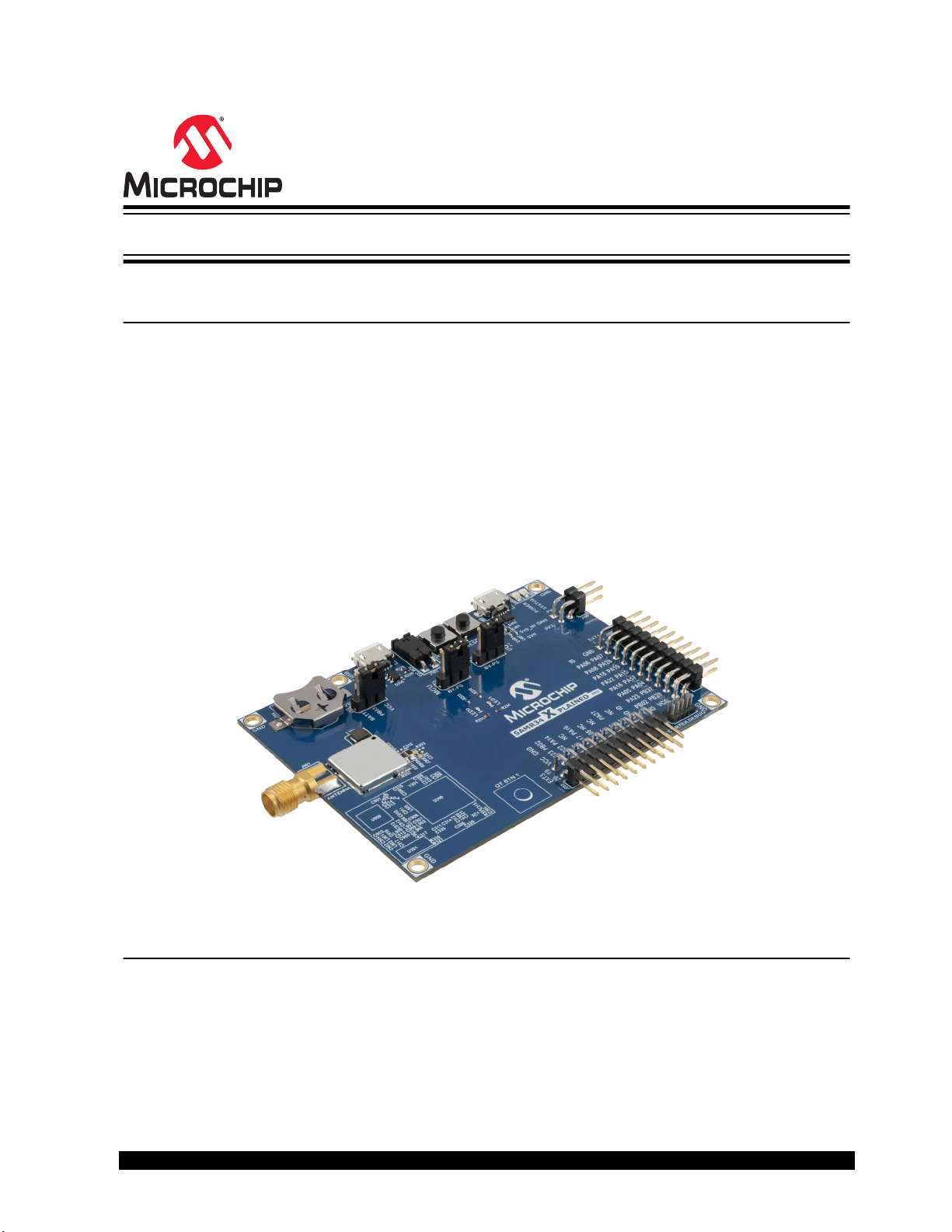
Figure 1. SAM R34 Xplained Pro Evaluation Board (DM320111)
Features
• SAM R34 SiP with Cortex® M0+ CPU and LoRa Transceiver
• Supports 868 MHz and 915 MHz Operation
• On-Board EDBG Debugger and Support for Atmel Studio 7 ICE
• Two Extension Headers for Signal Breakout and Expansion Boards
• On-Board Power Management System with Current Monitoring and USB Power Conditioning
• XPRO Current Measurement System Data Visualizer Support
© 2019 Microchip Technology Inc.
User Guide
DS50002803C-page 1
Page 2

SAM R34 Xplained Pro Evaluation Kit...
• USB Power Inlet with ESD Protection and Buck Converter
• On-Board TCXO
• Up to +20 dBm Maximum Output Power
• +13 dBm High-Efficiency Operation
• +17 dBm High-Power Operation
• SMA RF Antenna Port with External Whip Antenna Included
• Manual Reset Button
• GPIO Button
• Indicator LEDs for Status and Power
• Auxiliary 10-Pin Cortex Programming Header
• Direct USB Connection to SAM R34 with ESD Protection
• Qtouch® Button
• CR1220 Backup Battery Holder
• Supported by Studio 7 Integrated Development Platform
• Software Examples Supported in Advanced Software Framework (ASF)
© 2019 Microchip Technology Inc.
User Guide
DS50002803C-page 2
Page 3

SAM R34 Xplained Pro Evaluation Kit...
Table of Contents
Introduction......................................................................................................................1
Features.......................................................................................................................... 1
1. Kit Overview.............................................................................................................. 5
2. Xplained Pro Getting Started.....................................................................................6
2.1. Xplained Pro Quick Start.............................................................................................................. 6
2.2. Design Documentation and Relevant Links................................................................................. 6
2.3. Chip-Down Design Package ....................................................................................................... 7
3. Xplained Pro..............................................................................................................8
3.1. Xplained Pro.................................................................................................................................8
3.2. Embedded Debugger................................................................................................................... 8
3.3. Xplained Pro Analog Module........................................................................................................9
3.4. Hardware Identification System..................................................................................................11
3.5. Power Sources........................................................................................................................... 11
3.6. Xplained Pro Headers and Connectors......................................................................................12
4. Hardware User Guide..............................................................................................15
4.1. Schematics and BOM.................................................................................................................15
4.2. Power Distribution...................................................................................................................... 15
4.3. Connectors................................................................................................................................. 16
4.4. Peripherals................................................................................................................................. 19
4.5. Embedded Debugger Implementation........................................................................................20
4.6. Kit Modifications......................................................................................................................... 24
4.7. Limitations.................................................................................................................................. 25
5. Agency Certification.................................................................................................27
5.1. Antenna Considerations............................................................................................................. 27
5.2. A09-3167 Usage Instructions under Limited Modular Approval (FCC)...................................... 27
5.3. United States..............................................................................................................................27
5.4. Canada.......................................................................................................................................28
5.5. Europe........................................................................................................................................30
6. Hardware Revision History......................................................................................31
6.1. Identifying Product ID and Revision........................................................................................... 31
6.2. Hardware Revision..................................................................................................................... 31
7. Document Revision History..................................................................................... 33
The Microchip Web Site................................................................................................ 34
Customer Change Notification Service..........................................................................34
© 2019 Microchip Technology Inc.
User Guide
DS50002803C-page 3
Page 4

SAM R34 Xplained Pro Evaluation Kit...
Customer Support......................................................................................................... 34
Microchip Devices Code Protection Feature................................................................. 34
Legal Notice...................................................................................................................35
Trademarks................................................................................................................... 35
Quality Management System Certified by DNV.............................................................36
Worldwide Sales and Service........................................................................................37
© 2019 Microchip Technology Inc.
User Guide
DS50002803C-page 4
Page 5
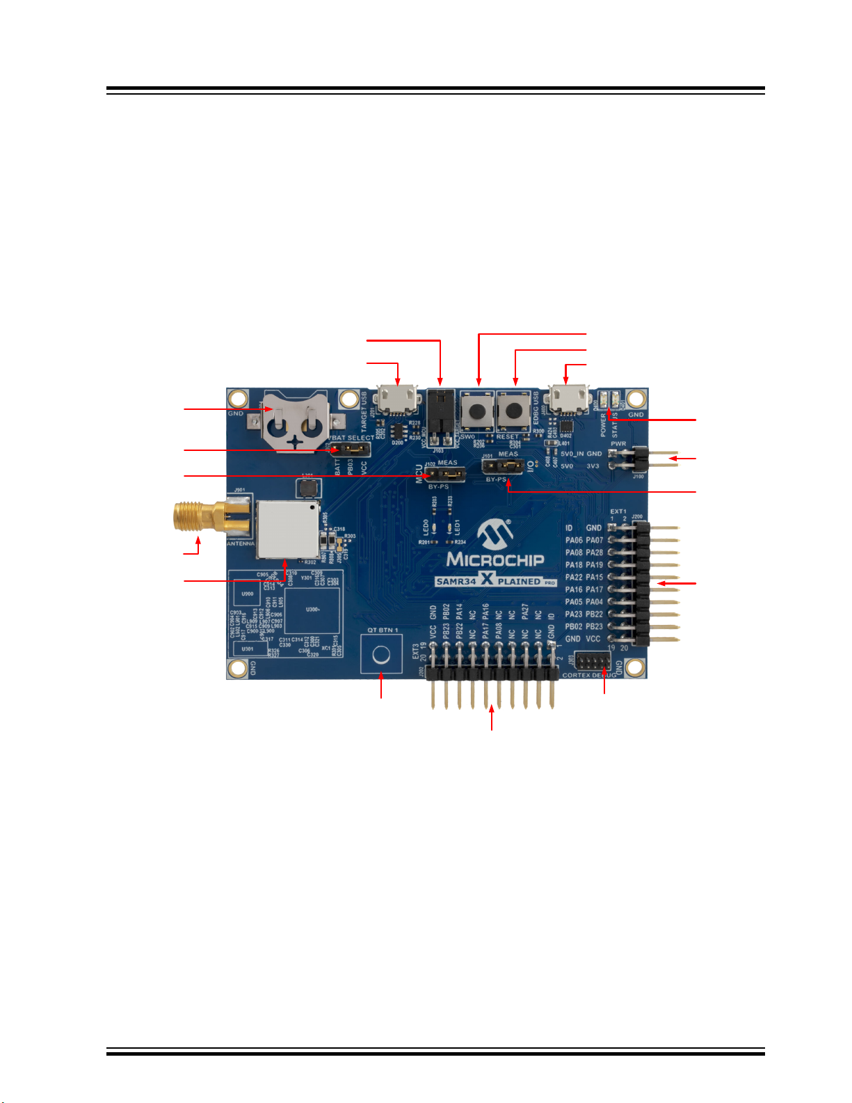
1. Kit Overview
Reset
SW0 User Button
Debug USB
Current Measurement
Header
Target USB
Power and
Status LED
Power Header
J101
Extension 1
Header
Cortex® Programming
Header
Extension 3 Header
Qtouch® Button
Battery
Power Source
J102
SMA
ATSAMR34J18B
The SAM R34 Xplained Pro Evaluation Kit is a hardware platform used to evaluate the ATSAMR34 Low
Power LoRa® Sub-GHz SiP module.
The kit offers a set of features that enable the user to get started with the ATSAMR34 Low Power LoRa
Sub-GHz SiP peripherals right away, and to understand how to integrate the device in their own design.
The SAM R34 Xplained Pro Evaluation Kit contains the following items:
• One SAM R34 Xplained Pro Evaluation Board
• One external antenna
SAM R34 Xplained Pro Evaluation Kit...
Kit Overview
®
© 2019 Microchip Technology Inc.
User Guide
DS50002803C-page 5
Page 6

SAM R34 Xplained Pro Evaluation Kit...
2. Xplained Pro Getting Started
2.1 Xplained Pro Quick Start
The steps to start exploring the Xplained Pro platform are listed below. See also: SAM R34 Xplained Pro
Evaluation Kit (DM320111) Quick Start Guide.
1. Download and install Atmel Studio.
2. Launch Atmel Studio.
When the Xplained Pro kit is connected to the computer for the first time, the operating system installs the
driver software automatically. This driver supports 32-bit and 64-bit versions of Microsoft® Windows® XP,
Windows Vista®, Windows 7, Windows 8, Windows 10, and Windows Server 2012.
When the Xplained Pro board is powered:
• The green power LED D400 is lit
• Atmel Studio automatically detects the connected Xplained Pro and extension board(s)
• In Atmel Studio, the landing page of the kit presents an option to launch the associated ASF. For
more details, see the SAM R34 MLS Getting Started Guide (DS50002812).
• The SAM R34 device is programmed and debugged by the on-board Embedded Debugger
• No external programmer or debugger tool is required
Xplained Pro Getting Started
2.2 Design Documentation and Relevant Links
The following list contains links to the most relevant documents and software for the SAM R34 Xplained
Pro Evaluation Kit.
• Ordering Code – The SAM R34 Xplained Pro Evaluation Kit can be ordered from
www.microchipdirect.com using Ordering Code “DM320111”.
• Atmel Studio – Atmel Studio presents Free Atmel IDE for development of C/C++ and assembler code
for microcontrollers and relevant documentation.
• Microchip sample store – Microchip sample store where samples of devices can be ordered.
• EDBG User Guide – User guide containing more information about the on-board Embedded
Debugger.
• Data Visualizer – Data Visualizer is a program used for processing and visualizing data. Data
Visualizer can receive data from various sources such as the Embedded Debugger Data Gateway
Interface found on Xplained Pro boards and COM ports.
• AN2842 SAM R34/R35 RF Hardware Design Guidelines Application Note – This application note
provides the RF design guidelines and circuit optimization techniques to design using the SAM R34.
This document is available in the SAM R34 Chip-Down Design Package.
• SAM R34/R35 Low Power LoRa® Sub-GHz SiP Data Sheet (DS70005356)
• SAM R34 MLS Getting Started User Guide (DS50002812)
• SAM R34 Xplained Pro Evaluation Kit (DM320111) Quick Start Guide (DS30010200)
• SAM L21 Family Data Sheet (DS60001477A)
• Semtech SX1276/77/78/79 Data Sheet rev 5
• SAM R34 Chip-down Design Package – Includes SAMR34-XPRO Design Database and MCHPRT
Test Application.
© 2019 Microchip Technology Inc.
User Guide
DS50002803C-page 6
Page 7

2.3 Chip-Down Design Package
The Chip-Down Design Package is a guide for customers wanting to do their own chip-level RF PCB
designs. In addition, it contains software tools for manufacturing and regulatory testing. The package
includes the following:
• AN2842 RF Hardware Design Guidelines
• Complete CAD source for SAMR34-XPRO
• MCHPRT PC Application for Production and Regulatory Testing
• Example Python® scripts
• SAMR34 Radio Utility Firmware
SAM R34 Xplained Pro Evaluation Kit...
Xplained Pro Getting Started
© 2019 Microchip Technology Inc.
User Guide
DS50002803C-page 7
Page 8
3. Xplained Pro
3.1 Xplained Pro
Xplained Pro is an evaluation platform which contains a series of microcontroller boards (evaluation kits)
and extension boards. Atmel Studio is used to program and debug the microcontrollers on these boards.
Atmel Studio includes Advanced Software Framework (ASF) and Atmel START, which has drivers and
demo code, and Data Visualizer, which supports data streaming and advanced debugging. Xplained Pro
evaluation kits can be connected to a wide range of Xplained Pro extension boards through standardized
headers and connectors. Xplained Pro extension boards have identification (ID) chips to uniquely identify
which boards are connected to the Xplained Pro evaluation kits.
3.2 Embedded Debugger
The SAM R34 Xplained Pro contains an Embedded Debugger (EDBG) for on-board debugging. The
EDBG is a USB composite device with the following interfaces:
• Debugger
• Virtual COM Port
• Data Gateway Interface (DGI)
SAM R34 Xplained Pro Evaluation Kit...
Xplained Pro
The EDBG can program and debug the SAM R34 with the help of Atmel Studio. The Serial Wire Debug
(SWD) interface is connected between the EDBG and the SAM R34 on the SAM R34 Xplained Pro.
The Virtual COM Port is connected to a UART on the SAM R34 and provides an easy way to
communicate with the target application through terminal software. It offers variable baud rate, parity, and
stop bit settings. The settings on the SAM R34 must match the settings given in the terminal software.
Info: The Virtual COM Port in the EDBG requires the terminal software to set the Data
Terminal Ready (DTR) signal to enable the UART pins connected to the SAM R34. If the DTR
signal is not enabled, the UART pins on the EDBG are kept in tri-state (high-Z) to render the
COM Port not usable. The DTR signal is automatically set by terminal software, but it may have
to be manually enabled in your terminal.
The DGI consists of several physical interfaces for bidirectional communication with the host computer.
Communication over the interfaces is bidirectional. It can be used to send event values and data from the
SAM R34. Traffic over the interfaces can be timestamped by the EDBG for more accurate tracking of
events, but timestamping reduces the maximal data throughput. The Data Visualizer is used to send and
receive data through DGI.
The EDBG controls two LEDs on the SAM R34 Xplained Pro; a power LED and a status LED. The
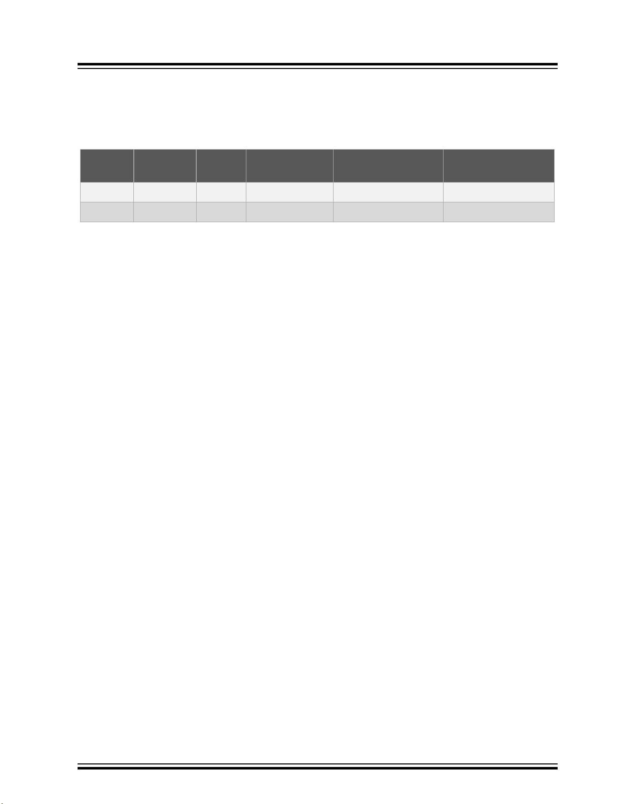
following table provides details on how the LEDs are controlled in different operation modes.
Table 3-1. EDBG LED Control
Mode Power LED Status LED
Normal mode The power LED is ON when
power is applied to the board.
© 2019 Microchip Technology Inc.
User Guide
Activity indicator, the LED flashes
when any communication
happens to the EDBG.
DS50002803C-page 8
Page 9
SAM R34 Xplained Pro Evaluation Kit...
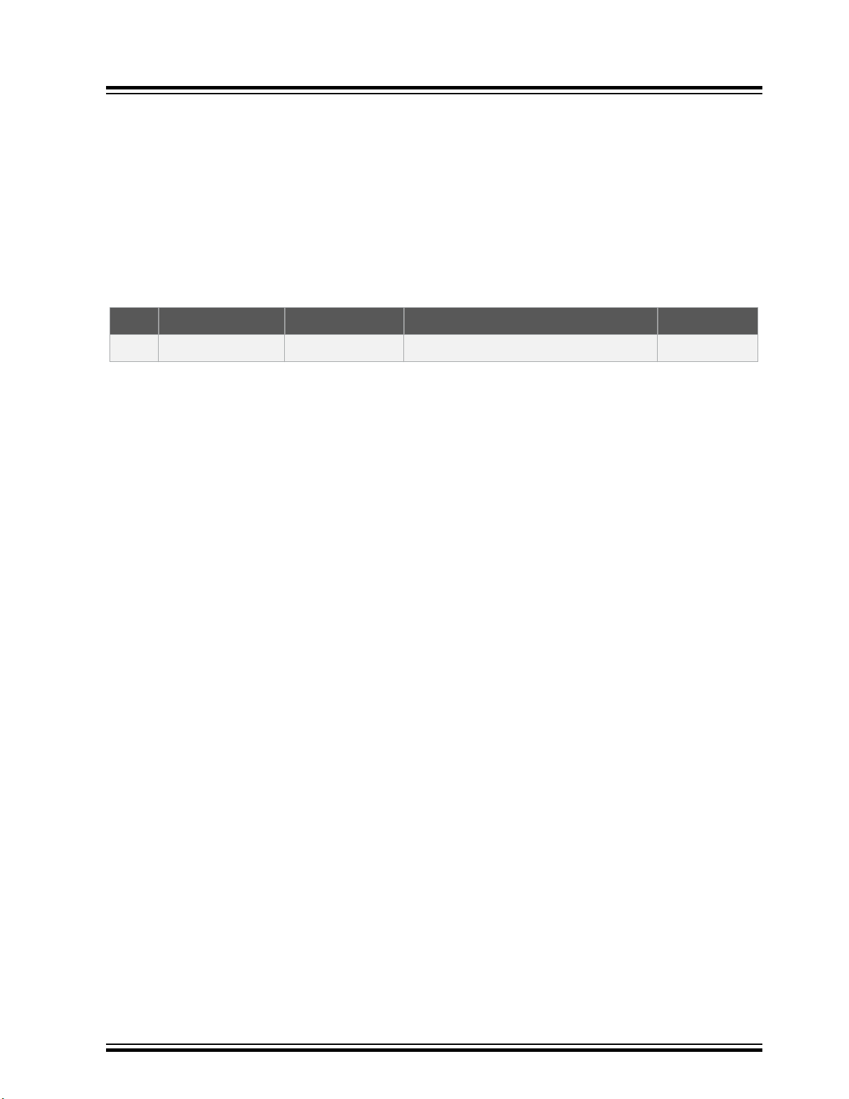
...........continued
Mode Power LED Status LED
Bootloader mode (idle) The power LED and the status LED blink simultaneously.
Xplained Pro
Bootloader mode (firmware
upgrade)
For additional information on the EDBG, see the EDBG User Guide.
3.3 Xplained Pro Analog Module
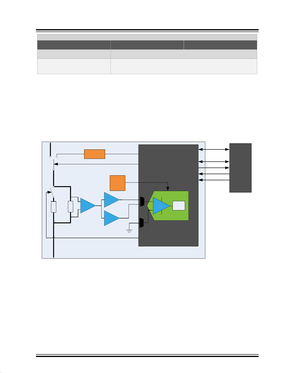
3.3.1 Overview
The Xplained Pro Analog Module (XAM) extends the embedded debugger with high dynamic range
current measurement. This enables power profiling of the target system.
Figure 3-1. XAM Block Diagram
Calibration
circuitry
Current output
Range selection
Calibration ON/OFF
100 mOhm
Pre-amplifier
20x
100 Ohm
20x
2x
16x
Active filter with
gain
The power LED and the status LED blink in an alternating pattern.
Sync GPIO
I2C
SPI
Clock sync
SWD
EDBG
voltage
reference
2.7V
GPIO(s)
GPIO
AREF
ADC0
ADC1
Control MCU
S&H
ADC
GND
GPIO
Current input
Xplained Pro Analog Module (XAM)
The XAM consists of:
• Calibration circuitry
• Voltage reference circuitry
• Analog front-end:
– Shunt resistors with a range selection switch
– Pre-amplifier
– Two active filters with gain
• Control MCU
– Analog-to-Digital Converter
– Signal processing
© 2019 Microchip Technology Inc.
User Guide
DS50002803C-page 9
Page 10
– Control/communication interface to the EDBG
The current measurement front-end is a high side shunt measurement with a pre-amplifier and a second
active filter stage with gain as shown in Figure 3-1. The wide dynamic range is achieved by four
measurement ranges, which are defined by two shunt resistors and the two parallel second stage active
filters with gain.
3.3.2 EDBG Interface
The XAM is connected to the EDBG with the following interfaces:
• I2C: This is used to control and configure the XAM.
• SPI: Current measurement data is streamed to the EDBG via this interface. This is a unidirectional
channel from the XAM to the EDBG.
• SWD: The MCU in the XAM is programmed via SWD from the EDBG.
• Clock sync: Signal used to synchronize ADC measurements with the EDBG.
• Reference clock: Reference clock for the XAM.
3.3.3 Sample Rate
The raw sampling rate of the XAM is up to 250 kHz and with the default averaging configuration (average
of 16 samples), the actual output of the XAM is 16.67 ksps.
SAM R34 Xplained Pro Evaluation Kit...
Xplained Pro
Info: The XAM output sample rate is not an integer fraction of the raw sampling.
3.3.4 Measurement Ranges and Accuracy
The XAM has four measurement ranges. These are defined by two shunt resistors and two gain stages.
Table 3-2. XAM Measurement Ranges and Accuracy
Measurement
Range
Range 1 Low current shunt and
Range 2 Low current shunt and
Range 3 High current shunt and
Range 4 High current shunt and
Hardware Resolution Accuracy Comments
high gain stage
low gain stage
high gain stage
low gain stage
20 nA 1 LSB ±1% Accuracy will decrease below
1 μA. Typical accuracy for
300 nA is 1 LSB ±10%.
150 nA 1 LSB ±1%
10 μA 1 LSB ±1%
100 μA 1 LSB ±1% Accuracy will decrease above
100 mA. Typical accuracy is
1 LSB ±5% at 400 mA.
Maximum current is 400 mA.
The ranges are automatically switched by the XAM to achieve the best measurement results, and the
currently active range is visualized in the Data Visualizer front-end tool. The maximum voltage drop over
the shunt resistor is 100 mV, and the XAM switches the range automatically before reaching this limit.
© 2019 Microchip Technology Inc.
User Guide
DS50002803C-page 10
Page 11
SAM R34 Xplained Pro Evaluation Kit...
3.4 Hardware Identification System
All Xplained Pro extension boards come with an identification chip (ATSHA204A CryptoAuthentication
chip) to uniquely identify the boards that are connected to the Xplained Pro Evaluation Kit. This chip
contains information that identifies the extension with its name and some extra data. When an Xplained
Pro extension is connected to an Xplained Pro Evaluation Kit, the information is read and sent to the
Atmel Studio. The following table shows the data fields stored in the ID chip with example content.
Table 3-3. Xplained Pro ID Chip Content
Data Field Data Type Example Content
Manufacturer ASCII string Microchip'\0'
Product name ASCII string Segment LCD1 Xplained Pro'\0'
Product revision ASCII string 02'\0'
Product serial number ASCII string 1774020200000010’\0’
Minimum voltage [mV] uint16_t 3000
Maximum voltage [mV] uint16_t 3600
Xplained Pro
™
Maximum current [mA] uint16_t 30
3.5 Power Sources
The SAM R34 Xplained Pro Evaluation Kit can be powered by several power sources, as listed in the
table below.
Table 3-4. Power Sources for SAM R34 Xplained Pro
Power input Voltage requirements Current requirements Connector marking
External power 5V ±2% (±100 mV) for
Embedded Debugger
USB
USB host operation.
4.3V to 5.5V if USB host
operation is not
required.
4.4V to 5.25V (according
to USB spec.)
Recommended
minimum is 1A to be
able to provide enough
current for connected
USB devices and the
board itself.
Recommended
maximum is 2A due to
the input protection
maximum current
specification.
500 mA (according to
USB spec.)
PWR
DEBUG USB
Target USB 4.4V to 5.25V (according
to USB spec.)
The kit will automatically detect which power sources are available and choose which one to use
according to the following priority:
© 2019 Microchip Technology Inc.
500 mA (according to
USB spec.)
User Guide
TARGET USB
DS50002803C-page 11
Page 12
SAM R34 Xplained Pro Evaluation Kit...
1. External power
2. Embedded Debugger USB
3. Target USB
Note: If powering the board from the Target USB connector then jumpers J101 and J102 MUST be in
the bypass position.
Info: External power is required when 500 mA from a USB connector is not enough to power
the board with possible extension boards. A connected USB device in a USB host application
might easily exceed this limit.
3.6 Xplained Pro Headers and Connectors
3.6.1 Xplained Pro Standard Extension Header
All Xplained Pro kits have many dual-row, 20-pin, 100 mil extension headers. The Xplained Pro MCU
boards have male headers, while the Xplained Pro extensions have their female counterparts. The
following table provides the pin description of all the connected pins.
Xplained Pro
Info: Not all pins are always connected on all extension headers.
The extension headers can be used to connect a variety of Xplained Pro extensions to Xplained Pro MCU
boards or to access the pins of the target microcontroller on the Xplained Pro boards.
Table 3-5. Xplained Pro Standard Extension Header
Pin Number Pin Name Description
1 ID Pin to communicate with the ID chip on an extension board.
2 GND Ground
3 ADC(+) Analog-to-Digital Converter; alternatively, a pin for the positive
terminal of a differential ADC.
4 ADC(-) Analog-to-Digital Converter; alternatively, a pin for the negative
terminal of a differential ADC.
5 GPIO1 General purpose I/O pin.
6 GPIO2 General purpose I/O pin.
7 PWM(+) Pulse-Width Modulation; alternatively, a pin for the positive part of a
differential PWM.
8 PWM(-) Pulse-Width Modulation; alternatively, a pin for the negative part of a
differential PWM.
9 IRQ/GPIO Interrupt request pin and/or general purpose I/O pin.
© 2019 Microchip Technology Inc.
User Guide
DS50002803C-page 12
Page 13

SAM R34 Xplained Pro Evaluation Kit...
...........continued
Pin Number Pin Name Description
Xplained Pro
10 SPI_SS_B/
GPIO
11 I2C_SDA Data pin for I2C interface. Always connected, bus type.
12 I2C_SCL Clock pin for I2C interface. Always connected, bus type.
13 UART_RX Receiver pin of target device UART.
14 UART_TX Transmitter pin of target device UART.
15 SPI_SS_A Slave select for SPI. This pin should preferably not be connected to
16 SPI_MOSI SPI master out slave in pin. Always connected, bus type.
17 SPI_MISO SPI master in slave out pin. Always connected, bus type.
18 SPI_SCK SPI clock pin. Always connected, bus type.
19 GND Ground pin for extension boards.
20 VCC Power pin for extension boards.
3.6.2 Xplained Pro Power Header
The power header can be used to connect external power to the SAM R34 Xplained Pro kit. The kit
automatically detects and switches to an external power source, if supplied. The power header can also
be used to supply power to external peripherals or extension boards. Ensure that the total current does
not exceed the recommended current limit of the on-board regulator when using the 3.3V pin.
Slave select pin for Serial Peripheral Interface (SPI) and/or general
purpose I/O pin.
anything else.
Table 3-6. Xplained Pro Power Header
Pin Number Pin Name Description
1 VEXT_P5V0 External 5V input pin
2 GND Ground pin
3 VCC_P5V0
4 VCC_P3V3
3.6.3 Interconnect with BTLC1000 XPRO Extension
The SAMR34 SERCOM5 is used for the UART connection to the EXT1 header. For more details, see
Peripherals section. This UART port does not support the CTS/RTS hardware flow-control needed for
BTLC1000 operation. To connect SAMR34-XPRO to BTLC1000-XPRO, use SERCOM 5 for the console
UART and SERCOM 0 to connect to BTLC1000. The connection mapping is shown in the following table.
Unregulated 5V pin (an output, derived from one of
the input sources)
Regulated 3.3V pin (an output, used as the main
power supply for the kit)
© 2019 Microchip Technology Inc.
User Guide
DS50002803C-page 13
Page 14

SAM R34 Xplained Pro Evaluation Kit...
Table 3-7. SAMR34-XPRO to BTLC1000-XPRO Connection Mapping
Xplained Pro
SAMR34 XPRO
PIN SIGNAL
J200.3 PA06 (S0 UART RTS) J100.16 16 (UART CTS) BLE UART
J200.4 PA07 (S0 UART CTS) J100.18 18 (UART RTS) BLE UART
J200.13 PA05 (S0 UART RXD) J100.15 15 (UART TXD) BLE UART
J200.14 PA04 (S0 UART TXD) J100.17 17 (UART RXD) BLE UART
J200.5 PA08 J100.3 3 GPIO - WAKEUP
J200.7 PA18 J100.7 7 GPIO - CHIP EN
J200.9 PA22 J100.9 9 IRQ
J200.15 PB02 S5 CONSOLE
TXD
J200.17 PA23 S5 CONSOLE
RXD
5 (Yellow) FTDI Yellow
4 (Orange) FTDI Orange
FTDI
TTL-232R-3V3
PLUG
RECEPTICAL
BTLC1000 XPRO
J100 PIN SIGNAL
RTS/CTS
RTS/CTS
PIN
Console UART
Cable RXD
Console UART
Cable TXD
J200.19 GND 1 (Black) J100.19 Power
J200.20 VCC J100.20 Power
Note:
1. SERCOM 5 will be used for console UART.
2. SERCOM 0 will be used for BTLC1000 connection
Cryptographic and Authentication demos
Developers using CryptoAuthentication demo boards, such as 88CKSCKT or ECC608, must use EXT3.
© 2019 Microchip Technology Inc.
User Guide
DS50002803C-page 14
Page 15
4. Hardware User Guide
4.1 Schematics and BOM
Complete and up-to-date schematics, Bill of Materials (BOM) and design documentation for SAM R43
XPRO is available in the SAM R34 Chip-Down Design Package.
Additionally, this package includes the MCHPRT test firmware, Python scripts and Radio Utility
Commands Reference documentation for evaluation and test.
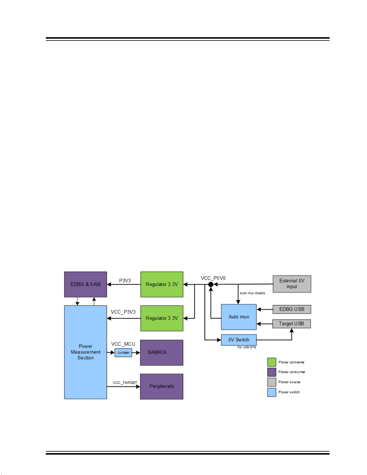
4.2 Power Distribution
The SAM R34 Xplained Pro Evaluation Kit can be powered by:
• EDBG USB
• TARGET USB
• External (5V)
The kit has a power mux which automatically chooses the power source if two or all three of the power
sources are available to the kit at the same time.
SAM R34 Xplained Pro Evaluation Kit...
Hardware User Guide
The kit contains:
• Two on-board voltage regulators (3.3V):
– One for an EDBG and XAM section
– Another one for SAM R34
• IO peripherals
• Power Measurement Section (XAM)
Figure 4-1. Power Supply Block Diagram
© 2019 Microchip Technology Inc.
User Guide
DS50002803C-page 15
Page 16

4.3 Connectors
The following sections describe the implementation of the relevant connectors and headers on the SAM
R34 Xplained Pro Evaluation Kit and their connection to the SAM R34. The tables of connections in the
sections also describe which signals are shared between the headers and on-board functionality.
4.3.1 Xplained Pro Extension Headers
The SAM R34 Xplained Pro Evaluation Kit headers EXT1 and EXT3 offer access to the I/O of the
microcontroller in order to expand the board e.g., by connecting extensions to the board. These headers
are based on the standard extension header specified in 3.6.1 Xplained Pro Standard Extension Header.
The headers have a pitch of 2.54 mm.
Table 4-1. Extension Header EXT1
EXT1 SAM R34 Shared Functionality
Pin Signal Port Pin
1 ID - - -
2 GND - - -
SAM R34 Xplained Pro Evaluation Kit...
Hardware User Guide
3 ADC(+) PA06 E3 -
4 ADC(-) PA07 F3 -
5 GPIO1 PA08 F4 EXT3
6 GPIO2 PA28 C6 4.4.2 Mechanical Buttons
7 PWM(+) PA18 E7 -
8 PWM(-) PA19 E8 -
9 IRQ PA22 D8 -
10 SPI_SS PA15 G8 -
11 TWI_SDA PA16 F7 EXT3
12 TWI_SCL PA17 E6 EXT3
13 UART_RX PA05 C4 4.5.2 Virtual COM Port
14 UART_TX PA04 D3 4.5.2 Virtual COM Port
15 SPI_SS PA23 D7 -
16 SPI_MOSI PB22 E5 EXT3
17 SPI_MISO PB02 B4 EXT3
18 SPI_SCK PB23 C7 EXT3
19 GND - - -
20 VCC - - -
© 2019 Microchip Technology Inc.
User Guide
DS50002803C-page 16
Page 17

SAM R34 Xplained Pro Evaluation Kit...
Hardware User Guide
Table 4-2. Extension Header EXT3
EXT3 SAM R34 Shared Functionality
Pin Signal Port Pin
1 ID - - -
2 GND - - -
3 ADC(+) - - -
4 ADC(-) - - -
5 GPIO1 PA27 E4 -
6 GPIO2 - - -
7 PWM(+) - - -
8 PWM(-) - - -
9 IRQ - - -
10 SPI_SS PA08 F4 EXT1
11 TWI_SDA PA16 F7 EXT1
12 TWI_SCL PA17 E6 EXT1
13 UART_RX - - -
14 UART_TX - - -
15 SPI_SS PA14 F8 -
16 SPI_MOSI PB22 E5 EXT1
17 SPI_MISO PB02 B4 EXT1
18 SPI_SCK PB23 C7 EXT1
19 GND - - -
20 VCC - - -
4.3.2 Direct USB Connection
For USB applications on SAM R34, there is a directly connected USB port designated TARGET_USB.
This is exposed as a Micro-B jack designated J201. The TARGET_USB port includes required ESD
suppression and power management circuitry. A GPIO is used to detect the VBUS voltage on the
connector, to detect when a TARGET USB cable is connected in Self-Powered mode. In USB Host mode,
VBUS voltage is provided by the kit and cannot identify the connected device; therefore, another GPIO is
used to detect the USB ID of the device.
Note: The SAMR35 does not have a USB PHY. The EDBG port is not directly connected to the SAM
R34 USB PHY.
Table 4-3. USB Connections
SAM R34 Pin USB Function Shared Functionality
PA07 VBUS Detection EXT1
© 2019 Microchip Technology Inc.
User Guide
DS50002803C-page 17
Page 18

...........continued
CAUTION
SAM R34 Pin USB Function Shared Functionality
PA15 USB ID EXT3
PA24 USB D- -
PA25 USB D+ -
4.3.3 Current Measurement Header
A right-angled 1x2, 100 mil pin header marked with the MCU current measurement is located at the upper
edge of the SAM R34 Xplained Pro. All power to the SAM R34 is exclusively routed through this header
(excluding power to extension headers and peripherals). To measure the power consumption of the
device, remove the jumper and replace it with an ammeter.
Removing the jumper from the pin header while the kit is powered may cause the SAM R34 to
be powered through its I/O pins. This may cause permanent damage to the device.
4.3.4 Cortex Debug Connector
SAM R34 Xplained Pro Evaluation Kit has a 10-pin 50-mil Cortex Debug Connector that can be used to
attach external debuggers to the SAM R34.
SAM R34 Xplained Pro Evaluation Kit...
Hardware User Guide
Table 4-4. Cortex Debug Connector
Cortex Debug
Connector pin
1 VCC_TARGET_P3V3 SAM R34 voltage -
2 PA31_SWDIO SWD data signal 4.5.1 Serial Wire Debug
3 GND Ground -
4 PA30_SWDCLK SWD clock signal 4.5.1 Serial Wire Debug
5 GND Ground -
6 - - -
7 - - -
8 - - -
9 GND Ground -
10 RESET* Target reset signal 4.4.2 Mechanical
Note: The target reset (RESET* pin on the ATSAMR34 Low Power LoRa® Sub-GHz SiP) is isolated
from the Cortex Debug Connector by R300 (0 Ohm link) which is not mounted by default in the PCBA.
Pin / Net Function Shared functionality
Buttons
© 2019 Microchip Technology Inc.
User Guide
DS50002803C-page 18
Page 19

4.4 Peripherals
4.4.1 External Clock
The SAM R34 Xplained Pro Evaluation Kit contains one mounted 32.768 kHz crystal that can be used as
a clock source for the SAM R34. The RF transceiver uses a 32 MHz external TCXO for optimal
performance at long range.
Table 4-5. External Clock
SAM R34 pin Function
A3 PA00_XIN32
A4 PA01_XOUT32
Table 4-6. External TCXO
SAM R34 pin Function
H6 RF_XTA
H7 NC
SAM R34 Xplained Pro Evaluation Kit...
Hardware User Guide
4.4.2 Mechanical Buttons
SAM R34 Xplained Pro Evaluation Kit contains two mechanical buttons:
• RESET button connected to the SAM R34 reset line
– When the RESET button is pressed it drives the I/O line to ground
• Generic user configurable button
– When the user button is pressed it drives the I/O line to target voltage
Note: There is no pull-up resistor connected to the generic user button. Remember to enable the
internal pull up in the SAM R34 to use the button.
Table 4-7. Mechanical Buttons
SAM R34 pin Silkscreen text Shared functionality
RESET* RESET 4.5.1 Serial Wire Debug
PA28 SW0 EXT1
4.4.3 LEDs
There is one yellow LED available on the SAM R34 Xplained Pro board that can be turned on and off.
The LED can be activated by driving the connected I/O line to GND.
Table 4-8. LED Connections
SAM R34 Pin Function Shared Functionality
PA19 Yellow LED0 EXT1
PA18 Green LED1
© 2019 Microchip Technology Inc.
User Guide
EXT1
DS50002803C-page 19
Page 20

4.4.4 UART Connection
The SAM R34 Xplained Pro Evaluation Kit exposes the UART on EXT1. This is useful for command line
interfaces, debugging and application layer code.
Info: The TXD/RXD UART signals exposed on EXT1 are connected to SERCOM 5 which is in
low-power domain PD0. Because of low-power constraints, SERCOM 5 does not support
CTS/RTS flow-control signals.
The following table provides the UART signals pin description.
Table 4-9. UART Signals Pin Description
SAM R34 pin Function Shared Functionality
D3 PA04_S0_UART_TX EXT1, EDBG
C4 PA05_S0_UART_RX EXT1, EDBG
4.4.5 CryptoAuthentication Device
The SAM R34 Xplained Pro Evaluation Kit has a depopulated socket for ATECC608 Security IC. This is
reserved for future revisions of the board.
SAM R34 Xplained Pro Evaluation Kit...
Hardware User Guide
4.4.6 QTouch Button
The SAM R34 Xplained Pro Evaluation Board contains a self-capacitance button, which can be used as
an I/O. This QTouch button is intended to be driven by the built-in Peripheral Touch Controller (PTC) of
the device. A zero ohm resistor is added on the board to easily disconnect the on-board touch buttons
from the extension header since the I/O lines are shared between the QTouch button and extension
header 1 (EXT1).
note: To get started with QTouch, refer to the QTouch® Library and QTouch® Composer.
Table 4-10. QTouch Connection
SAM R34 Pin Silkscreen Text Shared Functionality
PA06 QT BTN1 EXT1
4.4.7 Backup Battery
The SAM R34 Xplained Pro Evaluation Kit is equipped with a CR1220 backup battery holder. This
provides 35 mAH of power for SRAM Backup.
Note: To comply with shipping regulations, Lithium batteries are not included in this product.
4.5 Embedded Debugger Implementation
The SAM R34 Xplained Pro Evaluation Kit contains an Embedded Debugger (EDBG) that can be used to
program and debug the SAM R34 using Serial Wire Debug (SWD). The Embedded Debugger also
includes a Virtual Com port interface over UART, a Data Gateway Interface (DGI) over SPI, and I2C , and
also includes four of the SAM R34 GPIOs. The kit also includes a XAM extension processor to the
© 2019 Microchip Technology Inc.
User Guide
DS50002803C-page 20
Page 21

Embedded Debugger for on-board current measurement. Atmel Studio can be used as a front-end for the
Embedded Debugger.
4.5.1 Serial Wire Debug
The Serial Wire Debug (SWD) uses two pins to communicate with the target. For further information on
how to use the programming and debugging capabilities of the EDBG, see 3.2 Embedded Debugger.
Table 4-11. SWD Connections
SAM R34 pin Function
PA30 SWD clock
PA31 SWD data
4.5.2 Virtual COM Port
The Embedded Debugger acts as a Virtual Com Port gateway by using one of the SAM R34 UARTs. For
further information on how to use the Virtual COM port, see 3.2 Embedded Debugger.
Table 4-12. Virtual COM Port Connections
SAM R34 pin Function Shared functionality
SAM R34 Xplained Pro Evaluation Kit...
Hardware User Guide
PA05 RX line EXT1, EXT3
PA04 TX line EXT1, EXT3
4.5.3 Data Gateway Interface
The Embedded Debugger features a Data Gateway Interface (DGI) by using either an SPI or I²C. The
DGI can be used for sending data from the SAM R34 to the host PC. For further information on how to
use the DGI interface, refer to the Data Visualizer and the EDBG User Guide.
Table 4-13. DGI Interface Connections When Using SPI
SAM R34 Pin Function Shared Functionality
PA27 GPIO/SPI SS (Slave Select) (SAM R34
is Master)
PB02 SERCOM5 PAD[0] SPI MISO (Master
In, Slave Out)
PB22 SERCOM5 PAD[2] SPI MOSI (Master
Out, Slave in)
PB23 SERCOM5 PAD[3] SPI SCK (Clock Out) EXT1 and EXT3
Table 4-14. DGI Interface Connections When Using I²C
-
EXT1 and EXT3
EXT1 and EXT3
SAM R34 Pin Function Shared Functionality
PA16 SERCOM1 PAD[0] SDA (Data line) EXT1 and EXT3
PA17 SERCOM1 PAD[1] SCL (Clock line) EXT1 and EXT3
Three GPIO lines are connected to the Embedded Debugger. The EDBG can monitor these lines and
time stamp pin value changes. This makes it possible to accurately timestamp events in the SAM R34
© 2019 Microchip Technology Inc.
User Guide
DS50002803C-page 21
Page 22

SAM R34 Xplained Pro Evaluation Kit...
application code. For further information on how to configure and use the GPIO monitoring features, refer
to the Data Visualizer and the EDBG User Guide.
Table 4-15. GPIO Lines Connected to the EDBG
SAM R34 Pin Function Shared Functionality
PA08 GPIO0 EXT3
PA09 GPIO1 -
PA14 GPIO3 EXT3
4.5.4 SAM R34 Xplained Pro Evaluation Kit XAM Configuration
On the SAM R34 Xplained Pro Evaluation Kit the MCU and the MCU peripherals (e.g., extensions) are
powered by their own regulator, as shown in the following figure. All other parts of the board, mainly the
Embedded Debugger and accompanying Xplained Pro Analog Module (XAM), are powered from a
separate regulator. The current to the MCU and peripherals can be measured by connecting them to the
XAM output through jumper settings.
Hardware User Guide
© 2019 Microchip Technology Inc.
User Guide
DS50002803C-page 22
Page 23

SAM R34 Xplained Pro Evaluation Kit...
Figure 4-2. SAM R34 XAM Implementation Block Diagram
Hardware User Guide
On the SAM R34 Xplained Pro Evaluation Kit, the XAM can be used in four configurations:
1. No current measurement or external MCU current measurement: The XAM is bypassed and
thus the MCU and peripherals are supplied directly by the regulator. Set both jumpers in the
"BYPASS" position. In this configuration it is also possible to connect external measurement tools
on the Xplained Pro MCU power measurement header to measure MCU current directly instead of
using the XAM.
2. MCU current measurement: The XAM measures only the MCU current while the peripherals are
supplied directly by the regulator. For this configuration, place the jumper for "I/O" (peripherals) into
the "BYPASS" position and the for "MCU" into the "MEASURE" position.
3. Peripherals measurement: The XAM measures only the peripherals current while the MCU is
directly supplied by the regulator. For this configuration, place the jumper for "MCU" into the
"BYPASS" position and the "I/O" jumper into the "MEASURE" position.
4. MCU and peripherals measurement: In this configuration both MCU and peripherals are
measured by the XAM. Place both jumpers on "I/O" and "MCU" headers in the "MEASURE"
position.
© 2019 Microchip Technology Inc.
User Guide
DS50002803C-page 23
Page 24

4.6 Kit Modifications
The SAM R34 Xplained Pro Evaluation Kit contains several resistors that can be used to disconnect I/O
pins of the SAM R34 SiP from connectors and on-board ICs, and to disconnect power signals.
Table 4-16. EDBG Disconnect Resistors
SAM R34 Xplained Pro Evaluation Kit...
Hardware User Guide
Design
ator
R322 0R EDBG SWDIO PA31 SWDIO Debug interface from the EDBG to
R323 0R EDBG SWDCLK PA30 SWCLK
R324 0R EDBG TARGET RESET TARGET MCU
R310 0R EDBG SPI SS PA27 GPIO EDBG CDC and DGI interfaces to
R311 0R EDBG SPI SCK PB23 SPI SCK
R312 0R EDBG SPI MOSI PB22 SPI MOSI
R313 0R EDBG SPI MISO PB02 SPI MISO
R314 0R EDBG DGI SDA PA16 I2C SDA
R315 0R EDBG DGI SCL PA17 I2C SCL
R316 0R EDBG CDC RX PA04 UART TX
R317 0R EDBG CDC TX PA05 UART RX
R318 0R EDBG DGI_GPIO0 PA08 GPIO
R319 0R EDBG DGI_GPIO1 PA09 GPIO
Value From To Comment
the SAM R34
RESET
the SAM R34
R320 0R EDBG DGI_GPIO2 PA12 GPIO
R321 0R EDBG DGI_GPIO3 PA14 GPIO
R229 0R TARGET VUSB DETECT PA07 ADC7 Used to detect if a USB cable is
R109 47K VCC_P3V3_CM_IN TARGET VOLTAGE Used in the voltage divider
R325 0R RESET TARGET RESET
4.6.1 Operating at Other Voltages
The SAM R34 Xplained Pro board operates at 3.3V by default, but it is also possible to run the board at
lower voltages from an external supply. The EDBG is designed to run from a 3.3V supply and won't work
on other voltages; therefore, all connections from the EDBG and from the on-board 3.3V regulator to the
SAM R34 SoC must be removed.
To completely disconnect the EDBG and the on-board power supply from the SAM R34 SoC, do the
following:
SENSE
connected to the TARGET USB
connector.
network to detect the target
voltage of 3.3V.
Reset sense signal to EDBG,
used to detect external resets.
© 2019 Microchip Technology Inc.
User Guide
DS50002803C-page 24
Page 25

CAUTION
SAM R34 Xplained Pro Evaluation Kit...
Hardware User Guide
• Remove the two jumpers from the on-board 3-pin current measurement headers (J101 and J102),
and connect the two center pins (pin 2) together with a wire or an ammeter as shown in Figure 4-3.
• Remove all the EDGB disconnect resistors (refer to Table 4-16).
• Power ON the SAM R34 Xplained Pro via pin 4 (3V3) and pin 2 (GND) of the Power Header J100.
• Program SAM R34 using industry standard 2x5 50-mil Cortex Debug Connector and external
programmer such as Atmel ICE.
Info: Operating the SAM R34 SiP at voltages other than 3.3V requires physical modifications
on the kit using a soldering iron and an external debugger for programming the SAM R34 SiP.
The on-board current measurement only works at 3.3V. The on-board LED is selected for 3.3V
operation; the LED brightness at 1.8V operation is dull. To increase the emitted light level, the
value of the series resistor can be lowered. EDBG functionality can be restored by re-soldering
the removed components.
The voltage supplied through the power header is applied directly to the SAM R34 SoC and the
extension headers. Applying a voltage greater than 3.3V may damage the board permanently.
Figure 4-3. SAM R34 Xplained Pro Current Measurement Headers
Related Links
3.6.2 Xplained Pro Power Header
4.3.4 Cortex Debug Connector
4.7 Limitations
The SAM R34 Xplained Pro Evaluation Kit is optimized for operation in the 902-928 and 868 MHz bands.
The RF signal path is not designed to operate in the 470 MHz band. The RFI_LF and RFO_LF signals
are not connected. Contact Microchip technical support for advice on 470 MHz band operation.
The XPRO system includes an RF Switch and a Temperature Controlled Crystal Oscillator (TCXO). The
TCXO is required to achieve the exceptionally low receiver-sensitivity and generous link-budget. The RF
switch directs TX/RX signal flow in the RF signal path. It also allows users to evaluate both the high-
© 2019 Microchip Technology Inc.
User Guide
DS50002803C-page 25
Page 26
SAM R34 Xplained Pro Evaluation Kit...
Hardware User Guide
power PA_BOOST and high-efficiency RFO_HF modes. Both the TCXO and RF Switch consume
additional power when compared to the SAMR34 Data Sheet specifications. The additional consumption
needs to be factored into laboratory measurements with the SAM R34 XPRO. See the following table for
details.
Table 4-17. SAM R34 Xplained Pro Evaluation Kit Additional Power Consumers
REF_DES Description MFG MPN Typical Sleep Current
U900 RF Switch Skyworks SKY13373-460LF 5 µA 60 µA
XC1 TCXO Epson TG2016SMN N/A 1.8 mA
Typical Active
Current
© 2019 Microchip Technology Inc.
User Guide
DS50002803C-page 26
Page 27
SAM R34 Xplained Pro Evaluation Kit...
Agency Certification
5. Agency Certification
This equipment (SAM R34 Xplained Pro Evaluation Kit / A09-3167) is intended for evaluation purposes
only. The following regulatory notices are to cover the requirements under the regulatory approval.
5.1 Antenna Considerations
The following table provides the list of approved antennas along with the manufacturer and part number
details.
Table 5-1. A09-3167 with Antenna Types
S. No. Part Number Vendor Antenna Gain at 824 ~ 960 MHz Band Antenna Type
1 AL-A80355-UB701 Alead Technology 2 dBi Dipole
5.2 A09-3167 Usage Instructions under Limited Modular Approval (FCC)
When used in USA and Canada, the Evaluation Kit will only work on the 902-928 MHz Frequency band,
with hopping activated if the 125 kHz channels are enabled.
The host product manufacturer must ensure that the RF behavior adheres to the certification (e.g. FCC,
ISED) requirements when the module is installed in the final host product.
5.3 United States
The A09-3167 module has received Federal Communications Commission (FCC) CFR47
Telecommunications, Part 15 Subpart C “Intentional Radiators” limited single-modular approval in
accordance with Part 15.212 Modular Transmitter approval.
The user must comply with all of the instructions provided by the Grantee, which indicate installation
and/or operating conditions necessary for compliance.
5.3.1 Labeling and User Information Requirements
The A09-3167 has been labeled with their own FCC ID number. If the FCC ID is not visible when the
module is installed inside another device, then the outside of the finished product into which the module is
installed must display a label referring to the enclosed module. This exterior label can use wording as
follows:
For the A09-3167:
Contains Transmitter Module FCC ID: 2ADHKA093167
or
Contains FCC ID: 2ADHKA093167
This device complies with Part 15 of the FCC Rules. Operation is subject to the following two
conditions: (1) this device may not cause harmful interference, and (2) this device must accept
any interference received, including interference that may cause undesired operation.
A user's manual for the finished product should include the following statement:
This equipment has been tested and found to comply with the limits for a Class B digital device, pursuant
to part 15 of the FCC Rules. These limits are designed to provide reasonable protection against harmful
© 2019 Microchip Technology Inc.
User Guide
DS50002803C-page 27
Page 28

interference in a residential installation. This equipment generates, uses and can radiate radio frequency
energy, and if not installed and used in accordance with the instructions, may cause harmful interference
to radio communications. However, there is no guarantee interference will not occur in a particular
installation. If this equipment does cause harmful interference to radio or television reception, which can
be determined by turning the equipment off and on, the user is encouraged to try to correct the
interference by one or more of the following measures:
• Reorient or relocate the receiving antenna
• Increase the separation between the equipment and receiver
• Connect the equipment into an outlet on a circuit different from that to which the receiver is
connected
• Consult the dealer or an experienced radio/TV technician for help
Additional information on labeling and user information requirements for Part 15 devices can be found in
KDB Publication 784748, which is available at the FCC Office of Engineering and Technology (OET)
Laboratory Division Knowledge Database (KDB) https://apps.fcc.gov/oetcf/kdb/index.cfm
5.3.2 RF Exposure
All transmitters regulated by FCC must comply with RF exposure requirements. KDB 447498 General RF
Exposure Guidance provides guidance in determining whether proposed or existing transmitting facilities,
operations or devices comply with limits for human exposure to Radio Frequency (RF) fields adopted by
the Federal Communications Commission (FCC).
SAM R34 Xplained Pro Evaluation Kit...
Agency Certification
From the FCC Grant: Output power listed is conducted.
This transmitter is restricted for use with the specific antenna(s) tested in this application for Certification
and must not be co-located or operating in conjunction with any other antenna or transmitters within a
host device, except in accordance with FCC multi-transmitter product procedures. The antenna of this
transmitter must be installed to provide a separation distance of at least 20 cm from all persons.
5.3.3 Information for the OEMs or Integrators
This grant is valid only when the device is sold to OEM integrators and installation is done under the
control of the Grantee.
5.3.4 Approved Antenna Types
To maintain modular approval in the United States, only the antenna types that have been tested shall be
used.
Antennas approved for A09-3167 with the antenna types are listed in Table 5-1.
5.3.5 Helpful Web Sites
Federal Communications Commission (FCC): http://www.fcc.gov
FCC Office of Engineering and Technology (OET) Laboratory Division Knowledge Database (KDB):
https://apps.fcc.gov/oetcf/kdb/index.cfm
5.4 Canada
The A09-3167 has been certified for use in Canada under Innovation, Science and Economic
Development Canada (ISED, formerly Industry Canada) Radio Standards Procedure (RSP) RSP-100,
Radio Standards Specification (RSS) RSS-Gen and RSS-247.
© 2019 Microchip Technology Inc.
User Guide
DS50002803C-page 28
Page 29

SAM R34 Xplained Pro Evaluation Kit...
5.4.1 Labeling and User Information Requirements
Label Requirements (from RSP-100 Issue 11, Section 3): The host device shall be properly labeled to
identify the module within the host device.
The Innovation, Science and Economic Development Canada certification label of a module shall be
clearly visible at all times when installed in the host device, otherwise the host device must be labeled to
display the Innovation, Science and Economic Development Canada certification number of the module,
preceded by the words “Contains”, or similar wording expressing the same meaning, as follows:
For the A09-3167:
Contains IC: 20266-093167
User Manual Notice for License-Exempt Radio Apparatus (from Section 8.4 RSS-Gen, Issue 5, April
2018): User manuals for license-exempt radio apparatus shall contain the following or equivalent notice in
a conspicuous location in the user manual or alternatively on the device or both:
This device contains licence-exempt transmitter(s)/receiver(s) that comply with Innovation,
Science and Economic Development Canada’s licence-exempt RSS(s). Operation is subject to the
following two conditions:
(1) This device may not cause interference;
Agency Certification
(2) This device must accept any interference, including interference that may cause undesired
operation of the device.
L’émetteur/récepteur exempt de licence contenu dans le présent appareil est conforme aux CNR
d’Innovation, Sciences et Développement économique Canada applicables aux appareils radio
exempts de licence. L’exploitation est autorisée aux deux conditions suivantes:
• L’appareil ne doit pas produire de brouillage;
• L’appareil doit accepter tout brouillage radioélectrique subi, même si le brouillage est
susceptible d’en compromettre le fonctionnement.
Transmitter Antenna (From Section 6.8 RSS-GEN, Issue 5, April 2018): User manuals, for transmitters
shall display the following notice in a conspicuous location:
This radio transmitter [IC: 20266-093167] has been approved by Innovation, Science and
Economic Development Canada to operate with the antenna types listed below, with the maximum
permissible gain indicated. Antenna types not included in this list that have a gain greater than
the maximum gain indicated for any type listed are strictly prohibited for use with this device.
Le présent émetteur radio [IC: 20266-093167] a été approuvé par Innovation, Sciences et
Développement économique Canada pour fonctionner avec les types d'antenne énumérés
ci‑dessous et ayant un gain admissible maximal. Les types d'antenne non inclus dans cette liste,
et dont le gain est supérieur au gain maximal indiqué pour tout type figurant sur la liste, sont
strictement interdits pour l'exploitation de l'émetteur.
Immediately following the above notice, the manufacturer shall provide a list of all antenna types which
can be used with the transmitter, indicating the maximum permissible antenna gain (in dBi) and the
required impedance for each antenna type.
5.4.2 RF Exposure
All transmitters regulated by ISED must comply with RF exposure requirements listed in RSS-102 - Radio
Frequency (RF) Exposure Compliance of Radio communication Apparatus (All Frequency Bands).
© 2019 Microchip Technology Inc.
User Guide
DS50002803C-page 29
Page 30
This transmitter is restricted for use with a specific antenna tested in this application for certification, and
must not be co-located or operating in conjunction with any other antenna or transmitters within a host
device, except in accordance with Canada multi-transmitter product procedures.
The installation of the transmitter must ensure compliance is demonstrated according to the ISED SAR
procedures.
5.4.3 Helpful Websites
Industry Canada: http://www.ic.gc.ca/
5.5 Europe
This equipment (A09-3167) has been assessed under the Radio Equipment Directive (RED) for use in
European Union countries. A Declaration of Conformity must be issued for each of these standards and
kept on file as described in Radio Equipment Directive.
Furthermore, the manufacturer must maintain a copy of the module's documentation and ensure the final
product does not exceed the specified power ratings, antenna specifications, and/or installation
requirements as specified in the user manual. If any of these specifications are exceeded in the final
product, a submission must be made to a notified body for compliance testing to all required standards.
SAM R34 Xplained Pro Evaluation Kit...
Agency Certification
Important:
On account of the nature of radio equipment, the height of the CE marking affixed to radio
equipment may be lower than 5 mm, provided that it remains visible and legible.
More detailed information about CE marking requirements, refer Article 19 of "DIRECTIVE
2014/53/EU OF THE EUROPEAN PARLIAMENT AND OF THE COUNCIL" of 16 April 2014.
SIMPLIFIED EU DECLARATION OF CONFORMITY
Hereby, Microchip Technology Inc. declares that the radio equipment type [A09-3167] is in compliance
with Directive 2014/53/EU.
The full text of the EU declaration of conformity is available at the following internet address (refer product
specific pages): http://www.microchip.com/design-centers/wireless-connectivity/
© 2019 Microchip Technology Inc.
User Guide
DS50002803C-page 30
Page 31
SAM R34 Xplained Pro Evaluation Kit...
6. Hardware Revision History
6.1 Identifying Product ID and Revision
There are two ways to find the revision and product identifier of the Xplained Pro boards: either through
Atmel Studio or by looking at the sticker on the bottom side of the PCB.
When an Xplained Pro MCU board is connected to a computer with Atmel Studio running, an information
window with the serial number is shown. The first six digits of the serial number contain the product
identifier and revision. Information about connected Xplained Pro extension boards is also shown in the
window.
The same information can be found on the sticker on the bottom side of the PCB. Most kits have stickers
that have the identifier and revision printed in plain text as A09-nnnn/rr, where nnnn is the identifier and rr
is the revision. Boards with limited space have a sticker with only a data matrix code, which contains a
serial number string.
The serial number string has the following format:
Hardware Revision History
"nnnnrrssssssssss"
n = product identifier
r = revision
s = serial number
The product identifier for the SAM R34 Xplained Pro is A09-3167.
6.2 Hardware Revision
Revision 1
This is an internal release of a small lot for engineering validation testing.
Revision 2
This is an internal release of a small lot for regulatory pre-testing.
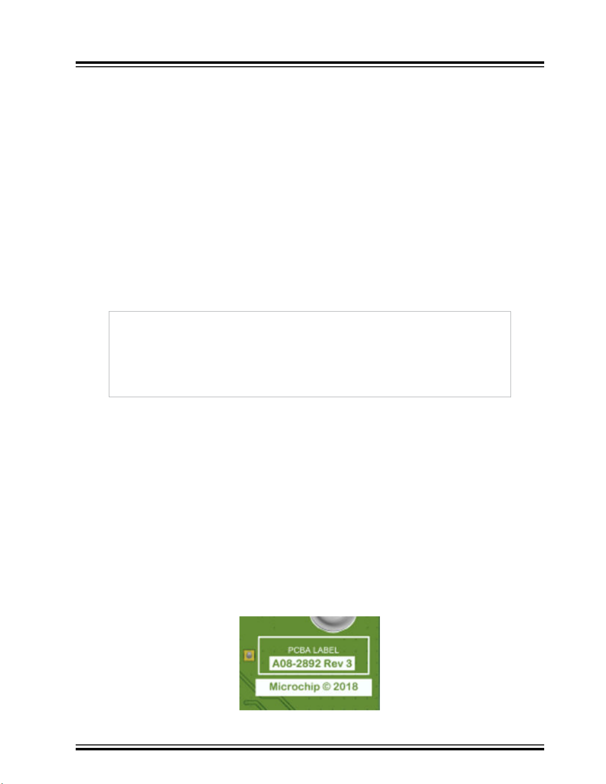
Revision 3
This is the first public release. This revision contains known errors on the silkscreen. The reference
designators for EXT1.15 and EXT1.10 are mismarked. For extension header (EXT1) pin details, see
Table 4-1. Revision 3 may be identified on the bottom side silkscreen as shown in the following image.
Figure 6-1. Bottom Side of Silkscreen
© 2019 Microchip Technology Inc.
User Guide
DS50002803C-page 31
Page 32

SAM R34 Xplained Pro Evaluation Kit...
Hardware Revision History
Revision 4
This revision is the second public release. Silkscreen errors were corrected. Revision 4 PCB may be
identified by the markings shown below.
Figure 6-2. Revision 4 Bottom Side Silkscreen
© 2019 Microchip Technology Inc.
User Guide
DS50002803C-page 32
Page 33

SAM R34 Xplained Pro Evaluation Kit...
7. Document Revision History
Revision Date Section Description
C 05/2019 Introduction Updated Figure 1.
Document Revision History
Kit Overview Updated image.
Hardware Revision
History
B 03/2019 Limitations Added a new section.
Reference Schematics Added a new section.
Bill of Materials Added a new section.
A 10/2018 Document Initial Release
Added Revision 4
description and image.
© 2019 Microchip Technology Inc.
User Guide
DS50002803C-page 33
Page 34

SAM R34 Xplained Pro Evaluation Kit...
The Microchip Web Site
Microchip provides online support via our web site at http://www.microchip.com/. This web site is used as
a means to make files and information easily available to customers. Accessible by using your favorite
Internet browser, the web site contains the following information:
• Product Support – Data sheets and errata, application notes and sample programs, design
resources, user’s guides and hardware support documents, latest software releases and archived
software
• General Technical Support – Frequently Asked Questions (FAQ), technical support requests, online
discussion groups, Microchip consultant program member listing
• Business of Microchip – Product selector and ordering guides, latest Microchip press releases,
listing of seminars and events, listings of Microchip sales offices, distributors and factory
representatives
Customer Change Notification Service
Microchip’s customer notification service helps keep customers current on Microchip products.
Subscribers will receive e-mail notification whenever there are changes, updates, revisions or errata
related to a specified product family or development tool of interest.
To register, access the Microchip web site at http://www.microchip.com/. Under “Support”, click on
“Customer Change Notification” and follow the registration instructions.
Customer Support
Users of Microchip products can receive assistance through several channels:
• Distributor or Representative
• Local Sales Office
• Field Application Engineer (FAE)
• Technical Support
Customers should contact their distributor, representative or Field Application Engineer (FAE) for support.
Local sales offices are also available to help customers. A listing of sales offices and locations is included
in the back of this document.
Technical support is available through the web site at: http://www.microchip.com/support
Microchip Devices Code Protection Feature
Note the following details of the code protection feature on Microchip devices:
• Microchip products meet the specification contained in their particular Microchip Data Sheet.
• Microchip believes that its family of products is one of the most secure families of its kind on the
market today, when used in the intended manner and under normal conditions.
• There are dishonest and possibly illegal methods used to breach the code protection feature. All of
these methods, to our knowledge, require using the Microchip products in a manner outside the
operating specifications contained in Microchip’s Data Sheets. Most likely, the person doing so is
engaged in theft of intellectual property.
• Microchip is willing to work with the customer who is concerned about the integrity of their code.
© 2019 Microchip Technology Inc.
User Guide
DS50002803C-page 34
Page 35

SAM R34 Xplained Pro Evaluation Kit...
• Neither Microchip nor any other semiconductor manufacturer can guarantee the security of their
code. Code protection does not mean that we are guaranteeing the product as “unbreakable.”
Code protection is constantly evolving. We at Microchip are committed to continuously improving the
code protection features of our products. Attempts to break Microchip’s code protection feature may be a
violation of the Digital Millennium Copyright Act. If such acts allow unauthorized access to your software
or other copyrighted work, you may have a right to sue for relief under that Act.
Legal Notice
Information contained in this publication regarding device applications and the like is provided only for
your convenience and may be superseded by updates. It is your responsibility to ensure that your
application meets with your specifications. MICROCHIP MAKES NO REPRESENTATIONS OR
WARRANTIES OF ANY KIND WHETHER EXPRESS OR IMPLIED, WRITTEN OR ORAL, STATUTORY
OR OTHERWISE, RELATED TO THE INFORMATION, INCLUDING BUT NOT LIMITED TO ITS
CONDITION, QUALITY, PERFORMANCE, MERCHANTABILITY OR FITNESS FOR PURPOSE.
Microchip disclaims all liability arising from this information and its use. Use of Microchip devices in life
support and/or safety applications is entirely at the buyer’s risk, and the buyer agrees to defend,
indemnify and hold harmless Microchip from any and all damages, claims, suits, or expenses resulting
from such use. No licenses are conveyed, implicitly or otherwise, under any Microchip intellectual
property rights unless otherwise stated.
Trademarks
The Microchip name and logo, the Microchip logo, AnyRate, AVR, AVR logo, AVR Freaks, BitCloud,
chipKIT, chipKIT logo, CryptoMemory, CryptoRF, dsPIC, FlashFlex, flexPWR, Heldo, JukeBlox, KeeLoq,
Kleer, LANCheck, LINK MD, maXStylus, maXTouch, MediaLB, megaAVR, MOST, MOST logo, MPLAB,
OptoLyzer, PIC, picoPower, PICSTART, PIC32 logo, Prochip Designer, QTouch, SAM-BA, SpyNIC, SST,
SST Logo, SuperFlash, tinyAVR, UNI/O, and XMEGA are registered trademarks of Microchip Technology
Incorporated in the U.S.A. and other countries.
ClockWorks, The Embedded Control Solutions Company, EtherSynch, Hyper Speed Control, HyperLight
Load, IntelliMOS, mTouch, Precision Edge, and Quiet-Wire are registered trademarks of Microchip
Technology Incorporated in the U.S.A.
Adjacent Key Suppression, AKS, Analog-for-the-Digital Age, Any Capacitor, AnyIn, AnyOut, BodyCom,
CodeGuard, CryptoAuthentication, CryptoAutomotive, CryptoCompanion, CryptoController, dsPICDEM,
dsPICDEM.net, Dynamic Average Matching, DAM, ECAN, EtherGREEN, In-Circuit Serial Programming,
ICSP, INICnet, Inter-Chip Connectivity, JitterBlocker, KleerNet, KleerNet logo, memBrain, Mindi, MiWi,
motorBench, MPASM, MPF, MPLAB Certified logo, MPLIB, MPLINK, MultiTRAK, NetDetach, Omniscient
Code Generation, PICDEM, PICDEM.net, PICkit, PICtail, PowerSmart, PureSilicon, QMatrix, REAL ICE,
Ripple Blocker, SAM-ICE, Serial Quad I/O, SMART-I.S., SQI, SuperSwitcher, SuperSwitcher II, Total
Endurance, TSHARC, USBCheck, VariSense, ViewSpan, WiperLock, Wireless DNA, and ZENA are
trademarks of Microchip Technology Incorporated in the U.S.A. and other countries.
SQTP is a service mark of Microchip Technology Incorporated in the U.S.A.
Silicon Storage Technology is a registered trademark of Microchip Technology Inc. in other countries.
GestIC is a registered trademark of Microchip Technology Germany II GmbH & Co. KG, a subsidiary of
Microchip Technology Inc., in other countries.
All other trademarks mentioned herein are property of their respective companies.
© 2019 Microchip Technology Inc.
User Guide
DS50002803C-page 35
Page 36

SAM R34 Xplained Pro Evaluation Kit...
©
2019, Microchip Technology Incorporated, Printed in the U.S.A., All Rights Reserved.
ISBN: 978-1-5224-4456-5
Quality Management System Certified by DNV
ISO/TS 16949
Microchip received ISO/TS-16949:2009 certification for its worldwide headquarters, design and wafer
fabrication facilities in Chandler and Tempe, Arizona; Gresham, Oregon and design centers in California
and India. The Company’s quality system processes and procedures are for its PIC® MCUs and dsPIC
DSCs, KEELOQ® code hopping devices, Serial EEPROMs, microperipherals, nonvolatile memory and
analog products. In addition, Microchip’s quality system for the design and manufacture of development
systems is ISO 9001:2000 certified.
®
© 2019 Microchip Technology Inc.
User Guide
DS50002803C-page 36
Page 37

Worldwide Sales and Service
AMERICAS ASIA/PACIFIC ASIA/PACIFIC EUROPE
Corporate Office
2355 West Chandler Blvd.
Chandler, AZ 85224-6199
Tel: 480-792-7200
Fax: 480-792-7277
Technical Support:
http://www.microchip.com/
support
Web Address:
www.microchip.com
Atlanta
Duluth, GA
Tel: 678-957-9614
Fax: 678-957-1455
Austin, TX
Tel: 512-257-3370
Boston
Westborough, MA
Tel: 774-760-0087
Fax: 774-760-0088
Chicago
Itasca, IL
Tel: 630-285-0071
Fax: 630-285-0075
Dallas
Addison, TX
Tel: 972-818-7423
Fax: 972-818-2924
Detroit
Novi, MI
Tel: 248-848-4000
Houston, TX
Tel: 281-894-5983
Indianapolis
Noblesville, IN
Tel: 317-773-8323
Fax: 317-773-5453
Tel: 317-536-2380
Los Angeles
Mission Viejo, CA
Tel: 949-462-9523
Fax: 949-462-9608
Tel: 951-273-7800
Raleigh, NC
Tel: 919-844-7510
New York, NY
Tel: 631-435-6000
San Jose, CA
Tel: 408-735-9110
Tel: 408-436-4270
Canada - Toronto
Tel: 905-695-1980
Fax: 905-695-2078
Australia - Sydney
Tel: 61-2-9868-6733
China - Beijing
Tel: 86-10-8569-7000
China - Chengdu
Tel: 86-28-8665-5511
China - Chongqing
Tel: 86-23-8980-9588
China - Dongguan
Tel: 86-769-8702-9880
China - Guangzhou
Tel: 86-20-8755-8029
China - Hangzhou
Tel: 86-571-8792-8115
China - Hong Kong SAR
Tel: 852-2943-5100
China - Nanjing
Tel: 86-25-8473-2460
China - Qingdao
Tel: 86-532-8502-7355
China - Shanghai
Tel: 86-21-3326-8000
China - Shenyang
Tel: 86-24-2334-2829
China - Shenzhen
Tel: 86-755-8864-2200
China - Suzhou
Tel: 86-186-6233-1526
China - Wuhan
Tel: 86-27-5980-5300
China - Xian
Tel: 86-29-8833-7252
China - Xiamen
Tel: 86-592-2388138
China - Zhuhai
Tel: 86-756-3210040
India - Bangalore
Tel: 91-80-3090-4444
India - New Delhi
Tel: 91-11-4160-8631
India - Pune
Tel: 91-20-4121-0141
Japan - Osaka
Tel: 81-6-6152-7160
Japan - Tokyo
Tel: 81-3-6880- 3770
Korea - Daegu
Tel: 82-53-744-4301
Korea - Seoul
Tel: 82-2-554-7200
Malaysia - Kuala Lumpur
Tel: 60-3-7651-7906
Malaysia - Penang
Tel: 60-4-227-8870
Philippines - Manila
Tel: 63-2-634-9065
Singapore
Tel: 65-6334-8870
Taiwan - Hsin Chu
Tel: 886-3-577-8366
Taiwan - Kaohsiung
Tel: 886-7-213-7830
Taiwan - Taipei
Tel: 886-2-2508-8600
Thailand - Bangkok
Tel: 66-2-694-1351
Vietnam - Ho Chi Minh
Tel: 84-28-5448-2100
Austria - Wels
Tel: 43-7242-2244-39
Fax: 43-7242-2244-393
Denmark - Copenhagen
Tel: 45-4450-2828
Fax: 45-4485-2829
Finland - Espoo
Tel: 358-9-4520-820
France - Paris
Tel: 33-1-69-53-63-20
Fax: 33-1-69-30-90-79
Germany - Garching
Tel: 49-8931-9700
Germany - Haan
Tel: 49-2129-3766400
Germany - Heilbronn
Tel: 49-7131-67-3636
Germany - Karlsruhe
Tel: 49-721-625370
Germany - Munich
Tel: 49-89-627-144-0
Fax: 49-89-627-144-44
Germany - Rosenheim
Tel: 49-8031-354-560
Israel - Ra’anana
Tel: 972-9-744-7705
Italy - Milan
Tel: 39-0331-742611
Fax: 39-0331-466781
Italy - Padova
Tel: 39-049-7625286
Netherlands - Drunen
Tel: 31-416-690399
Fax: 31-416-690340
Norway - Trondheim
Tel: 47-72884388
Poland - Warsaw
Tel: 48-22-3325737
Romania - Bucharest
Tel: 40-21-407-87-50
Spain - Madrid
Tel: 34-91-708-08-90
Fax: 34-91-708-08-91
Sweden - Gothenberg
Tel: 46-31-704-60-40
Sweden - Stockholm
Tel: 46-8-5090-4654
UK - Wokingham
Tel: 44-118-921-5800
Fax: 44-118-921-5820
© 2019 Microchip Technology Inc.
User Guide
DS50002803C-page 37
 Loading...