

Page 1
SAM E70 Xplained Ultra User's Guide
Introduction
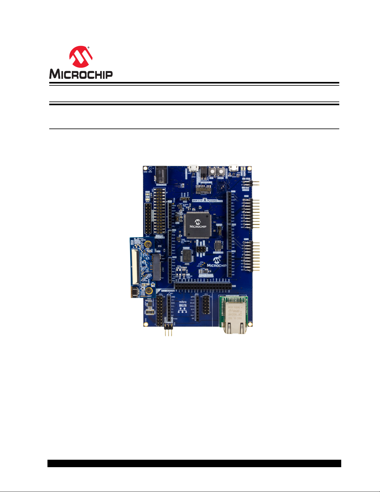
This user’s guide provides detailed information about the SAM E70 Xplained Ultra Evaluation kit and its
various features. Figure below illustrates the SAM E70 Xplained Ultra Evaluation kit.
Figure 1. SAM E70 Xplained Ultra Evaluation Kit with PHY Daughter Board
Features
• ATSAME70Q21 Microcontroller
• One Mechanical Reset Button
• One Mechanical User Push Button
• Two User LEDs
• 12.0 MHz Oscillator (DSC6003)
• 32.768 kHz Oscillator (DSC6083)
• 2-MB SDRAM
• 4-MB QSPI Flash (SST26VF032BA)
© 2019 Microchip Technology Inc.
DS70005389A-page 1
Page 2

• Ethernet Interface with External IEEE 802.3az 10Base-T/100Base-TX Ethernet RMII PHY on a
Daughter Board
• AT24MAC402 256KB EEPROM with EUI-48 Address
• ATA6561 CAN Transceiver
• Micro SD Card Connector with SDIO Support
• Camera Interface Connector
• Two Xplained Pro Extension Headers
• Graphics Card Interface
• CoreSight® 20 Connector for 4-bit ETM
• Arduino MEGA Shield Connector
• External Debugger Connector
• USB Interface, Device and Host Mode
• Embedded Debugger:
– Programming and debugging through USB interface
– Auto-ID for board identification in Atmel Studio and MPLAB® X
– One yellow status LED
– One green board power LED
– Symbolic debug of complex data types including scope information
– Data Gateway Interface: SPI, I2C, four GPIOs
– Virtual COM port (CDC)
• External Power Input (5-14V) or USB Power
• X32 Daughter Board Interface to Support Audio and Bluetooth
®
• One mikroBus™ Interface
Kit Overview
The Microchip PIC32 SAM E70 Xplained Ultra Development Kit (DM320113) provides a modular
development system for Microchip’s line of 32-bit Cortex® microcontrollers.
For a free Microchip demonstration code and additional information, visit the MPLAB Harmony™ web
page at: http://www.microchip.com/MPLABHarmony.
The Atmel SAM E70 Xplained Ultra Dvelopment Kit is a hardware platform to evaluate the Microchip
ATSAME70Q21. The kit offers a set of features that enables the ATSAME70Q21 users to start with the
SAM E70 peripherals and understand how to integrate the device in their design.
The SAM E70 Xlpained Ultra kit contains the following items:
• One SAM E70 Xplained Ultra Development Kit
• One KSZ8061 Ethernet PHY
• One Graphics card set up for 565 (16-bit color) graphics
Note: If any items are missing in the kit, contact Microchip sales office for assistance. A list of Microchip
Sales offices is provided on the last page of this document.
The figure below illustrates the SAM E70 Xplained Ultra Evaluation Kit features.
© 2019 Microchip Technology Inc.
DS70005389A-page 2
Page 3
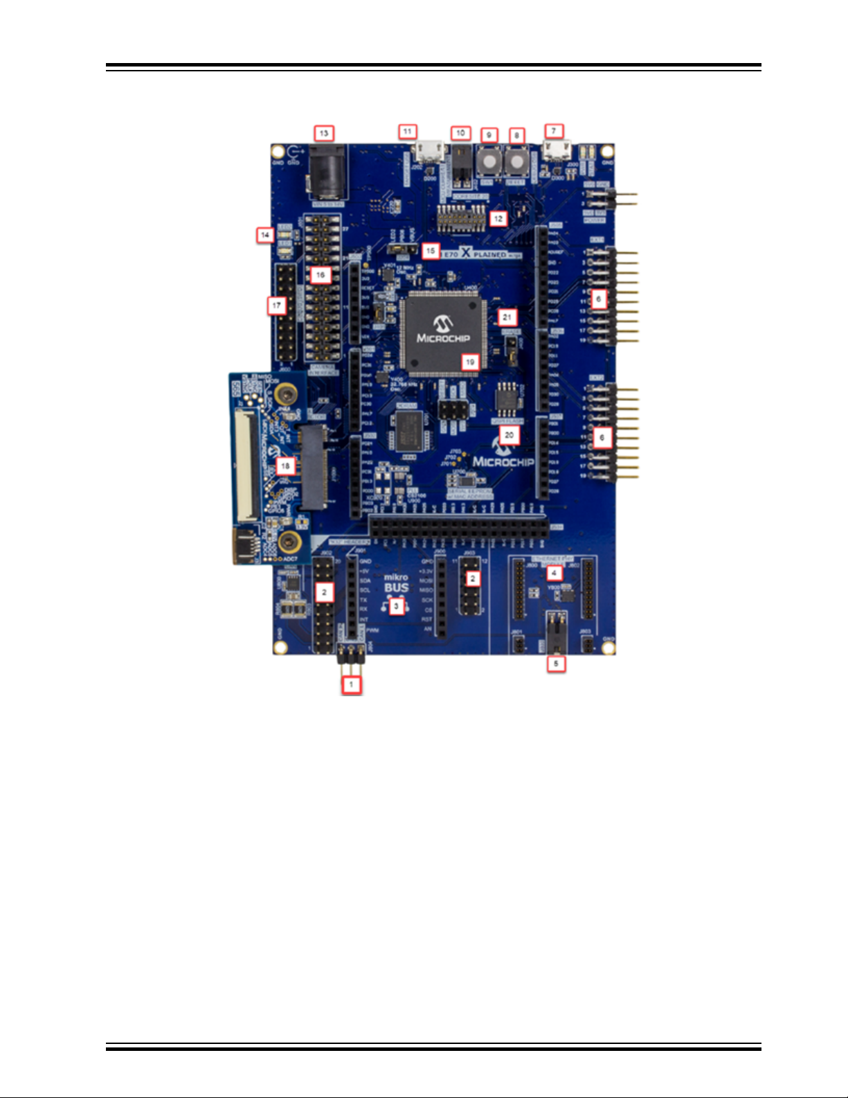
Figure 2. SAM E70 Xplained Ultra Evaluation Kit
© 2019 Microchip Technology Inc.
DS70005389A-page 3
Page 4
The table below provides the SAM E70 Xplained Ultra Evaluation kit feature descriptions.
Table 1. SAM E70 Xplained Ultra Evaluation Kit Feature and Location
Number Description
1 CAN interface
2 X32 Daughter Board interface
3 Mikro interface
4 Ethernet PHY interface
5 Ethernet Clock enable/disable jumper
1. Shorted = disabled
2. Open = enabled
6 EXT1/EXT2 interface
7 Debugger USB
1. Programming
2. Power
3. DGI
8 External Reset Button
9 User Button
10 MCU current measurement jumper
11 SAM E70 Host/Device USB
12 CoreSite® 20 (SWD + ETM) debugging interface
13 Barrel power input (2.1mm)
14 User defined LEDs
15 LED2/USB detect jumper
16 Image Sensor interface
17 SWD debugger interface
18 Graphics card interface
19 ATSAME70Q21B
20 SQI external Flash memory
© 2019 Microchip Technology Inc.
DS70005389A-page 4
Page 5

Table of Contents
Introduction......................................................................................................................1
1. Getting Started.......................................................................................................... 6
2. Xplained Ultra............................................................................................................8
3. Embedded Debugger................................................................................................ 9
3.1. Hardware Identification System....................................................................................................9
4. System Level Block Diagram...................................................................................11
5. Hardware Features..................................................................................................12
5.1. Xplained Pro Standard Extension Header..................................................................................12
5.2. Graphics Connectors or GFX Card Interface............................................................................. 13
5.3. SDRAM and LCD Connections.................................................................................................. 16
5.4. Camera Connector.....................................................................................................................18
5.5. USB Connectivity....................................................................................................................... 19
5.6. Chip Erase Header.....................................................................................................................20
5.7. Audio Connectivity......................................................................................................................20
5.8. mikroBUS™ Header................................................................................................................... 22
5.9. CAN............................................................................................................................................22
5.10. Ethernet......................................................................................................................................23
5.11. Debug USB Connectivity............................................................................................................24
5.12. Switches.....................................................................................................................................24
5.13. AT24MAC402 Serial EEPROM.................................................................................................. 25
5.14. Power Sources...........................................................................................................................26
6. Hardware.................................................................................................................28
6.1. SAM E70 Xplained Ultra Development Board Schematics........................................................ 28
6.2. Bill of Materials...........................................................................................................................50
The Microchip Web Site................................................................................................ 55
Customer Change Notification Service..........................................................................55
Customer Support......................................................................................................... 55
Microchip Devices Code Protection Feature................................................................. 55
Legal Notice...................................................................................................................56
Trademarks................................................................................................................... 56
Quality Management System Certified by DNV.............................................................57
Worldwide Sales and Service........................................................................................58
© 2019 Microchip Technology Inc.
DS70005389A-page 5
Page 6

1. Getting Started
SAM E70 Xplained Ultra Evaluation Quick Start
Follow these steps to explore the Atmel SAM E70 Xplained Ultra evaluation kit:
1. Download and install MPLAB X.
2. Launch MPLAB X.
3. Install MPLAB Harmony 3™.
Getting Started
When Microchip SAM E70 Xplained Ultra is connected to the computer for the first time, the operating
system will install a driver software. The driver file supports both 32-bit and 64-bit versions of Microsoft
Windows® XP/ Vista /7/8/10.
Once the kit is powered, the green power LED will be lit and MPLAB X will auto-detect the kit and identify
which Xplained Pro extension boards are connected. MPLAB X will provide relevant information like data
sheets and kit documentation. The SAM E70 device is programmed and debugged by the on-board
Embedded Debugger, hence no external programmer or debugger tool is needed.
Design Documentation and Relevant Links
The following list provides links to the relevant documents and software for the SAM E70 Xplained Ultra.
• Xplained Pro products
– Atmel Xplained Pro is a series of small-sized and easy-to-use evaluation kit for Microchip
microcontrollers and other Microchip products. It consists of a series of low-cost MCU boards for
evaluation and demonstration of features and capabilities of different MCU families.
• Microchip MPLAB® Integrated Development Environment
– A free Microchip MPLAB IDE for development of C/C++ and assembler code for Microchip
microcontrollers.
• MPLAB Harmony
– A free MPLAB Harmony code base is available for user application. The latest MPLAB Harmony
code is available for download at:http://www.microchip.com/MPLABHarmony.
• EDBG User Guide
– This user’s guide provides additional information about the on-board Embedded Debugger.
• Data Visualizer
– Data Visualizer is a program used for processing and visualizing data. The Data Visualizer can
receive data from various sources, such as the Embedded Debugger Data Gateway Interface
that is found on the Xplained Pro boards and COM ports.
• IAR Embedded Workbench® for ARM
– A commercial C/C++ compiler that is available for ARM. A 30-day evaluation version and a code
size limited kick-start version are also available for download from their web site. The code size
limit is 16-KB for devices with M0, M0+, M1 cores, and 32-KB for devices with other cores.
• Keil MDK-ARM Microcontroller Development Kit
– The MDK-ARM is a complete software development environment for Cortex®-M, Cortex-R4,
ARM7™, and ARM9™ processor-based devices. The MDK-ARM is specifically designed for
microcontroller applications, it is user friendly yet powerful enough for the most demanding
embedded applications.
• Design Documentation
™
®
®
© 2019 Microchip Technology Inc.
DS70005389A-page 6
Page 7

Getting Started
– Package containing schematics, BOM, assembly drawings, 3D plots, layer plots, and so on.
• Hardware Users Guide
– PDF version of this user guide.
© 2019 Microchip Technology Inc.
DS70005389A-page 7
Page 8

2. Xplained Ultra
The SAM E70 Xplained Ultra implements several Xplained Pro standards like extension headers and
connectors. Xplained Pro is an evaluation platform that provides a full Microchip microcontroller
experience. The platform consists of a series of Microcontroller (MCU) boards and extension boards that
are integrated with the Microchip MPLAB IDE that supports data streaming. The Xplained Pro MCU
boards support a wide range of Xplained Pro extension boards, such as audio DACs/CODECs, Ethernet
PHYs, graphics cards, and mikroBUS™ that are connected through a set of standardized headers and
connectors. Each extension board has an identification (ID) chip to uniquely identify which boards are
connected to a Xplained Pro MCU board. This information is used to present relevant user guides,
application notes, data sheets, and example code through MPLAB X.
Xplained Ultra
© 2019 Microchip Technology Inc.
DS70005389A-page 8
Page 9
3. Embedded Debugger
The SAM E70 Xplained Ultra contains Microchip Embedded Debugger (EDBG) for on-board debugging.
The EDBG is a composite USB device, which is based on the following interfaces:
• Debugger
• Virtual COM Port
• Data Gateway Interface (DGI)
Together with the Microchip MPLAB IDE, the EDBG debugger interface can program and debug the
ATSAME70Q21. On the SAM E70 Xplained Ultra, the SWD interface is connected between the EDBG
and the ATSAME70Q21.
The Virtual COM Port is connected to a UART on the ATSAME70Q21 and provides an easy way to
communicate with the target application through the terminal software. It offers variable baud rate, parity,
and Stop bit settings. The settings on the ATSAME70Q21 must match the settings given in the terminal
software.
Note: If not set automatically, Data Terminal Ready (DTR) must be set in the terminal software.
The DGI consists of several physical interfaces for communication with the host computer.
Communication over the interfaces is bidirectional. It can be used to send events and values from the
ATSAME70Q21, or as a generic printf-style data channel. Traffic over the interfaces can be timestamped
on the EDBG for accurate tracing of events. Note that timestamping imposes an overhead that reduces
maximal throughput. The Data Visualizer is used to send and receive data through DGI.
Embedded Debugger
The EDBG controls two LEDs on SAM E70 Xplained Ultra: a power LED and a status LED.
The following table describes how the LEDs are controlled in different operation modes.
Table 3-1. EDBG LED Control
Operation Mode Power LED Status LED
Normal operation The power LED is lit when power is
applied to the board.
Bootloader mode
(idle)
Bootloader mode
(firmware upgrade)
For additional information on EDBG, refer to the EDBG User Guide.
The power LED and the status LED
blinks simultaneously.
The power LED and the status LED
blinks in an alternating pattern.
3.1 Hardware Identification System
All Xplained Pro-compatible extension boards have an Microchip ATSHA204 CryptoAuthentication™ chip
mounted. This chip contains information that identifies the extension with its name and data. When an
Xplained Pro extension is connected to an Xplained Pro MCU board, the information is read and sent to
the MPLAB X IDE. The Microchip kits extension, installed with MPLAB X, provides relevant information,
such as code examples, and links to relevant documents. The following table provides the data fields
stored in the ID chip with content examples.
Activity indicator, LED flashes when any
communication happens to the EDBG.
The power LED and the status LED
blinks simultaneously.
The power LED and the status LED
blinks in an alternating pattern.
© 2019 Microchip Technology Inc.
DS70005389A-page 9
Page 10
Embedded Debugger
Table 3-2. Xplained Pro ID Chip Content Example
Data Field Data Type Example
Manufacture ASCII string Microchip’\0’
Product Name ASCII string
Product Revision ASCII string 04’\0’
Product Serial number ASCII string 1774020200000010’\0’
Minimum Voltage (mV) uint16_t 3000
Maximum Voltage (mV) uint16_t 3600
Maximum Current (mA) uint16_t 30
© 2019 Microchip Technology Inc.
DS70005389A-page 10
Page 11
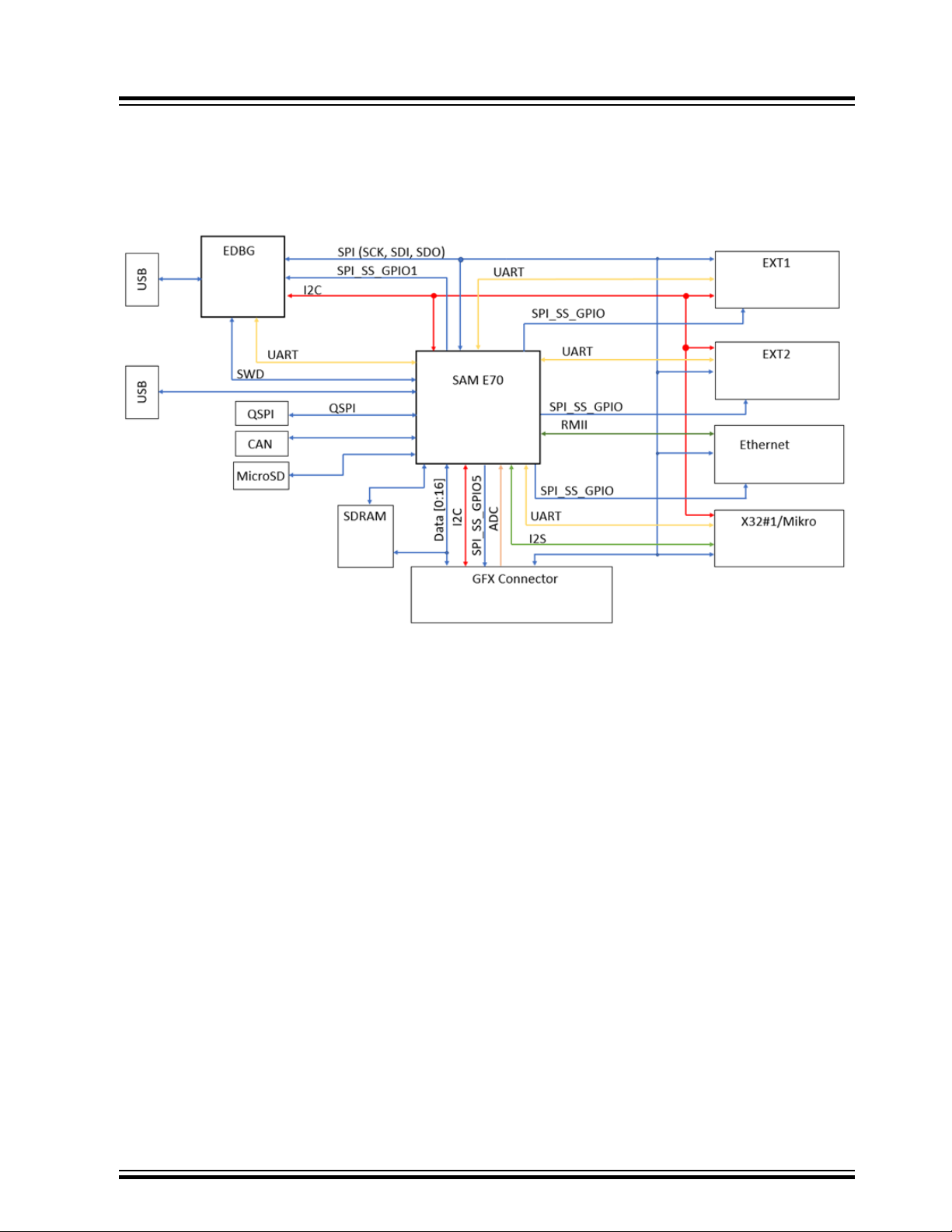
4. System Level Block Diagram
The following figure illustrates the high-level signal block diagram of the SAM E70 Xplained Ultra
Development Kit.
Figure 4-1. Signal Level Block Diagram
System Level Block Diagram
Wire buses that are tied together are connected together. In this system the SPI bus data and clock are
shared across several interfaces. The SPI Slave selects are addressed individually with GPIO.
System I2C uses I2C0 and connects to the debugger, EXT1, EXT2, and mikroBus/X32. Touch I2C uses
I2C2 and only goes from the microcontroller to the graphics connector.
The debugger has the following interfaces connected: DGI SPI, DGI I2C, DGI UART, and SWD.
UART wires from the microcontroller to the blocks are not shared with each other.
© 2019 Microchip Technology Inc.
DS70005389A-page 11
Page 12
5. Hardware Features
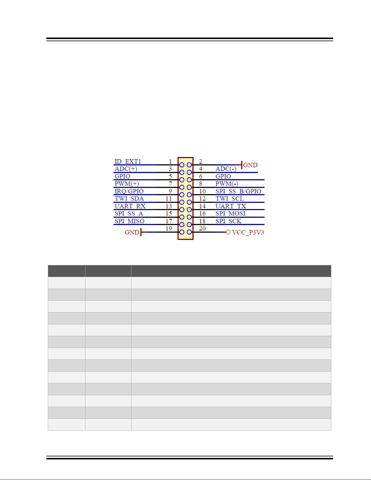
5.1 Xplained Pro Standard Extension Header
All Xplained Ultra Kits have many dual row, 20-pin, 100 mil extension headers. Xplained Ultra MCU
boards have male headers, while Xplained Ultra extensions have their female counterparts as shown in
the image below.
Note: All pins are not always connected.
The extension headers can be used to connect a variety of Xplained Pro extensions to Xplained Ultra
MCU boards or to access the pins of the target MCU on Xplained Ultra MCU boards directly.
Figure 5-1. Extension Headers
Hardware Features
All connected pins follow the defined pinout description as shown in the following table.
Table 5-1. Xplained Pro Standard Extension Header
Pin number Name Description
1 ID Communication line to the ID chip on an extension board
2 GND Ground
3 ADC(+) Analog-to-Digital Converter, alternatively positive part of differential ADC
4 ADC(-) Analog-to-Digital Converter, alternatively negative part of differential ADC
5 GPIO1 General purpose I/O
6 GPIO2 General purpose I/O
7 PWM(+) Pulse-Width Modulation, alternatively positive part of differential PWM
8 PWM(-) Pulse-Width Modulation, alternatively negative part of differential PWM
9 IRQ/INT/GPIO Interrupt request line and general purpose I/O
10 SPI SS B/GPIO SPI Slave Select or general purpose I/O
11 I2C SDA Data line for I2C interface. Always implemented, bus type
12 I2C SCL Clock line for I2C interface. Always implemented, bus type
13 UART RX Receiver line of target device UART
© 2019 Microchip Technology Inc.
DS70005389A-page 12
Page 13
Hardware Features
...........continued
Pin number Name Description
14 UART TX Transmitter line of target device UART
15 SPI SS A/GPIO SPI Slave Select or general purpose I/O
16 SPI MOSI Master Out Slave In line of serial peripheral interface. Always
implemented, bus type.
17 SPI MISO Master In Slave Out line of serial peripheral interface. Always
implemented, bus type.
18 SPI SCK Clock for serial peripheral interface. Always implemented, bus type.
19 GND Ground
20 V
CC
Power for extension boards (3.3V)
5.2 Graphics Connectors or GFX Card Interface
The SAM E70 Xplained Ultra Development Kit is designed to have a modular graphics interface. This
interface enables using several graphics cards, which allow for expandability and different use cases. A
565 adapter card is included in the kit, which takes 16-bit parallel LCD data and converts it to 24-bit data.
This card also provides access to ADC for resistive touch screens, hence an external controller is not
needed. See table below for pin descriptions.
Table 5-2. Graphics Interface Pinout
Pin Number Name Description
1 GND Ground
2 GND Ground
3 MCLR Master Clear, Controlled by the debuggers. Allows for a
complete system reboot.
4 IRQ1 (LCD Touch) Interrupt request line for cap touch device
5 5.0v V
6 IRQ2 (Q Touch) Interrupt request line for Q touch devices
CC
5.0v
7 LCDEN LCD Data Enable
8 IRQ3 (Display Controllers) Interrupt request line for external display controllers
9 LCDHSYNC/NCS3 LCD Horizontal Sync
10 IRQ4 (Resistive touch) Interrupt request line for resistive touch controllers
11 LCDVSYNC/nWE LEC Vertical Sync or Write enable (active-low)
12 5.0v V
13 LCDPCK/nRD LCD pixel Clock or Read Enable (active-low)
14 I2C SDA Data line for I2C interface. Always implemented, bus type.
© 2019 Microchip Technology Inc.
CC
+5.0v
DS70005389A-page 13
Page 14

Hardware Features
...........continued
Pin Number Name Description
15 LCD D0 LCD Data bit 0
16 I2C SCL Clock line for I2C interface. Always implemented, bus type.
17 LCD D1 LCD Data bit 1
18 SPI SCK Clock for serial peripheral interface. Always implemented, bus
type.
19 LCD D2 LCD Data bit 2
20 SPI MOSI Master Out Slave In line of serial peripheral interface.
21 LCD D3 LCD Data bit 3
22 SPI MISO Master In Slave Out line of serial peripheral interface.
23 LCD D4 LCD Data bit 4
24 SPI SS SPI Slave Select
25 LCD D5 LCD Data bit 5
26 UART RX Receiver line of target device UART
27 LCD D6 LCD Data bit 6
28 UART TX Transmitter line of target device UART. (from MCU to GFX
card)
29 LCD D7 LCD Data bit 7
30 UART RTS UART Ready To Send (from MCU to GFX card)
31 LCD D8 LCD Data bit 8
32 UART CTS UART Clear To Send (from MCU to GFX card)
33 LCD D9 LCD Data bit 9
34 LCD PWM LCD PWM back light control
35 LCD D10 LCD Data bit 10
36 PWM2 Pulse-Width Modulation,
37 LCD D11 LCD Data bit 11
38 GPIO1 General purpose I/O
39 LCD D12 LCD Data bit 12
40 GPIO2 General purpose I/O
41 LCD D13 LCD Data bit 13
42 GPIO3 General purpose I/O
43 LCD D14 LCD Data bit 14
© 2019 Microchip Technology Inc.
DS70005389A-page 14
Page 15

Hardware Features
...........continued
Pin Number Name Description
44 STBY/RST/GPIO4 Standby/Reset or general purpose I/O. For resetting devices
attached to the GFX connector.
45 LCD D15 LCD Data bit 15
46 STBY/RST/GPIO5 Standby2/Reset2 or general purpose I/O
47 LCD D16 LCD Data bit 16 (Not Implemented on this design)
48 ID pin Communication line to the ID chip on an extension board
49 LCD D17 LCD Data bit 17 (Not Implemented on this design)
50 ADC 0 Analog-to-Digital Converter to MCU
51 LCD D18 LCD Data bit 18 (Not Implemented on this design)
52 ADC1 Analog-to-Digital Converter to MCU
53 LCD D19 LCD Data bit 19 (Not Implemented on this design)
54 ADC2 Analog-to-Digital Converter to MCU
55 LCD D20 LCD Data bit 20 (Not Implemented on this design)
56 ADC3 Analog-to-Digital Converter to MCU
57 LCD D21 LCD Data bit 21 (Not Implemented on this design)
58 ADC4 Analog-to-Digital Converter to MCU
59 LCD D22 LCD Data bit 22
60 ADC5 Analog-to-Digital Converter to MCU
61 LCD D23 LCD Data bit 23
62 ADC6 Analog-to-Digital Converter to MCU
63 3.3V V
CC
+3.3V V
CC
64 ADC7 Analog-to-Digital Converter to MCU
65 GND Ground
66 3.3V V
CC
+3.3V V
CC
67 GND Ground
68 GND TAB Mounting Tab
69 GND TAB Mounting Tab
© 2019 Microchip Technology Inc.
DS70005389A-page 15
Page 16
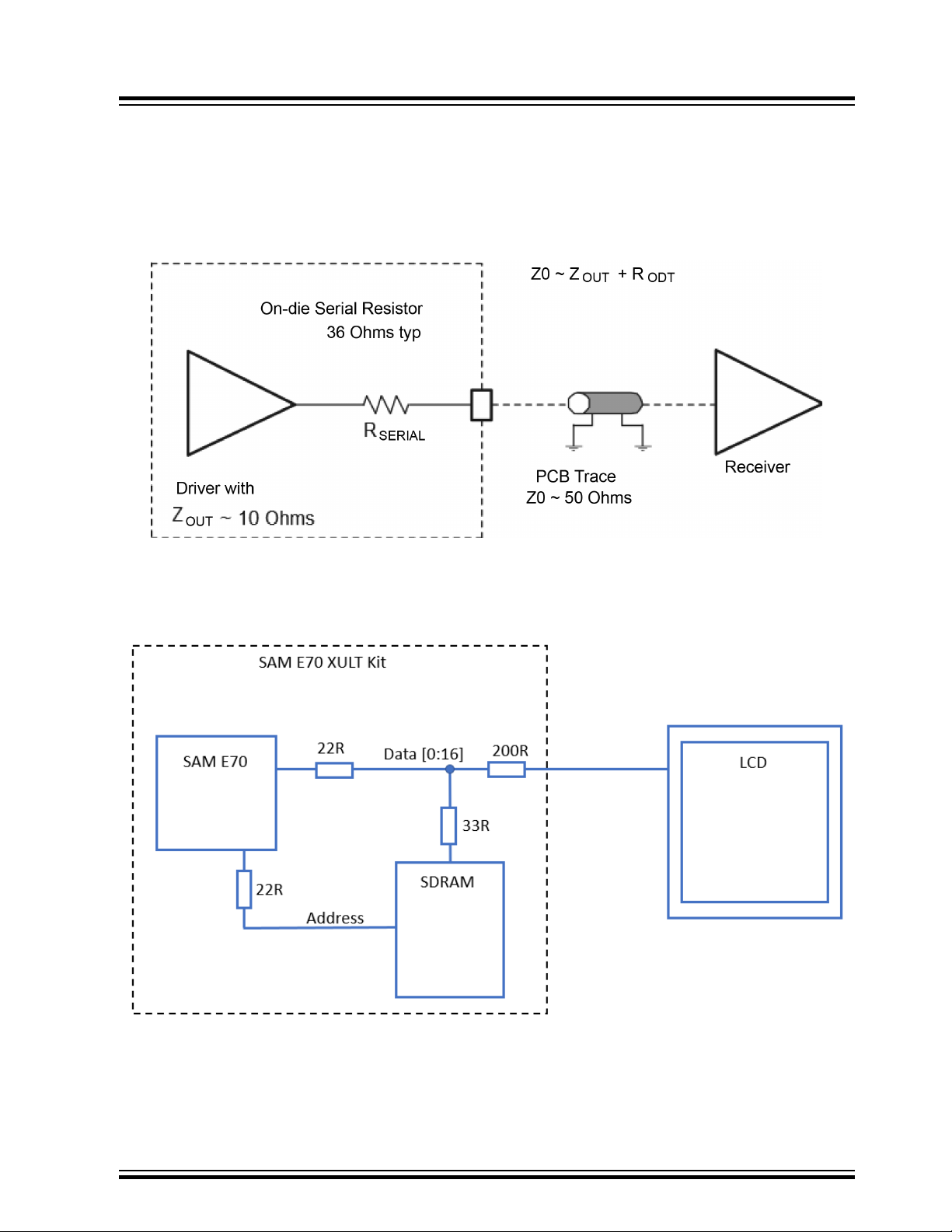
5.3 SDRAM and LCD Connections
The external bus interface (EBI) on SAM E71 Xplaned Ultra is controlled by the static memory controller
(SMC) and SDRAM controllers modules in the ATSAME70Q21B.
ATSAME70Q21B has on-die series termination on very I/O pin as shown in figure below.
Figure 5-2. On-Die Termination
Hardware Features
The EBI is connected to the on-board SDRAM and the Xplained Pro Graphics connector. The following
figure shows how the SDRAM and LCD share the same sets of data pins, and displays the location of the
series termination resistors.
Figure 5-3. LCD and SDRAM
As the I/O pins have on-die series termination, the impedance of the drivers must be matched to the
impedance of the EBI tracks on the PCB using series resistors. The EBI tracks are routed as 50Ω on
SAM E70 Xplained Ultra. The clock and address lines are only driven by the ATSAME70Q21B, while the
data lines are driven by the ATSAME70Q21B and the on-board SDRAM.
© 2019 Microchip Technology Inc.
DS70005389A-page 16
Page 17

Hardware Features
Simulation of the transmissions lines using IBIS files for the ATSAME70Q21B and the SDRAM gave the
results are shown in the table below.
Table 5-3. EBI Simulation Results
Driving Circuit Signal Type Driver Impedance
(from ibis)
ATSAME70Q21B Data/Address 22Ω 24Ω ≈ 22Ω 50Ω
Clock 21Ω 25Ω ≈ 22Ω 50Ω
SDRAM Data 11Ω 32Ω ≈ 33Ω 50Ω
The routing of the data lines to the LCD connector causes stubs on the data lines at the SDRAM (the
stubs are even longer when a cable is plugged in). The 200Ω resistors are placed close to the SDRAM to
create a high-impedance path for the signal to the stubs, improving the signal integrity when
communicating with the SDRAM.
TIP:
• The series-termination is always placed near to the driving pin.
• The 200Ω resistors are placed close to the intersection between the SDRAM routing and the routing
to the LCD connector.
• All designs must be simulated using an IBIS file for the ATSAMV71Q21B and the target peripherals
to check whether the signals are within the limits of the devices.
Series
Termination
Z
0
© 2019 Microchip Technology Inc.
DS70005389A-page 17
Page 18
5.4 Camera Connector
A 2 x 15, 100 mil pin-header camera connector is implemented to provide access to the SAM E70's
parallel Image Sensor Interface (ISI).
Table 5-4. Camera Interface Pin Description
Pin Number Name Function
Hardware Features
1 V
2 GND Ground
3 V
4 GND Ground
5 Reset Reset
6 PWD ISI PWD
7 I2C SCK Clock line for I2C interface. Always implemented, bus type.
8 I2C SDA Data line for I2C interface. Always implemented, bus type.
9 GND Ground
10 MCK Master Clock
11 GND Ground
12 VSYNC Image Sensor Vertical Sync
13 GND Ground
14 HSYNC Image Sensor Horizontal Sync
15 GND Ground
CC
CC
+3.3v
+3.3v
16 Pixel Clock Image Sensor Pixel Clock
17 GND Ground
18 ISI D0 Image Sensor Data Bit 0
19 ISI D1 Image Sensor Data Bit 1
20 ISI D2 Image Sensor Data Bit 2
21 ISI D3 Image Sensor Data Bit 3
22 ISI D4 Image Sensor Data Bit 4
23 ISI D5 Image Sensor Data Bit 5
24 ISI D6 Image Sensor Data Bit 6
25 ISI D7 Image Sensor Data Bit 7
26 ISI D8 Image Sensor Data Bit 8
27 ISI D9 Image Sensor Data Bit 9
28 ISI D10 Image Sensor Data Bit 10
© 2019 Microchip Technology Inc.
DS70005389A-page 18
Page 19

...........continued
Pin Number Name Function
29 ISI D11 Image Sensor Data Bit 11
30 GND Ground
5.5 USB Connectivity
Users can connect to the PIC32 USB microcontroller using any one of the following modes:
• Host mode: If connecting the device to the Type-A/B Micro connector, an adapter is required. Using
this method, a maximum of 400 mA can be supplied from the debug USB port to the host port. If a
full 500 mA supply is needed, an external supply must be connected to the application board.
• Device mode: Connect the SAM E70 to the target USB Micro-A/B port using a USB cable. This is
enough to power the board as a device. If programming and debugging is required, connect the
Debug USB Micro-A/B port. The other end of the cable must have a Type-A connector, to connect it
to a USB host.
• On-The-Go (OTG) mode: Connect the starter kit to the OTG device by using an OTG Micro-A/B
cable to the Micro-A/B port.
Hardware Features
There is a 1x3, 100mil pin-header marked VBUS on the kit. The PB08 pin on the SAM E70 can be
connected to the LED2 or to the target USB VBUS DETECT signal by placing a jumper between pin 1
and pin 2, or pin 2 and pin 3 on this pin-header. The USB VBUS DETECT is the target USB voltage
divided by 1.64. When connected to the PB08 pin the signal can be used to detect power on the target
USB connector.
Table 5-5. USB Jumper Description
Pin number Name Description
1 LED2 LED2 active-low
2 PB08 Pin and Port to microcontroller
3 VBUS_ Detect VBUS Detect, used to detect when a device cable (micro-B) is plugged
into the SAM E70
The SAM E70 Xplained Ultra has a Micro-USB connector to use with the SAM E70 USB module labeled
as TARGET USB on the kit. In USB Host mode, the VBUS voltage is provided by the kit, and must be
enabled by setting the VBUS Host Enable pin to low. When a USB OTG cable is plugged in, it will
automatically trigger the power supply.
Table 5-6. USB Interface Pin Description
Pin on SAM USB Function
PA08 VBUS Host Enable
HSDM USB -
HSDP USB +
© 2019 Microchip Technology Inc.
DS70005389A-page 19
Page 20

5.6 Chip Erase Header
A 1x2 pin-header is connected to the SAM E70 chip erase pin, PB12, and 3V3 is marked ERASE. This
header can be used to chip erase the SAM E70 by placing the jumper on the header and toggle power to
the board. After the power is toggled, the jumper must be removed. Using the chip erase jumper may be
the only way to erase a chip with the security bit set, and applications that immediately set invalid clock
options, or go into deep sleep without any wake-up sources enabled.
5.7 Audio Connectivity
The SAM E70 provides an audio connection through the X32 interface to the two main audio modules in
the chip, such as the SSC and the I2S. On this board the SSC interface is considered the main audio
interface. See image below.
There is a 32-pin interface to the board to support the audio codec or DACs and Bluetooth radios. This
interface has two audio supply interfaces, such as the SSC and the I2S. Addition to this other control lines
and data interfaces are available.
Figure 5-4. SSC/I2S Block Diagram
Hardware Features
Table 5-7. X32 Audio Interface Pin Description
Pin Number Name Description Interface
1 GND Ground Power
© 2019 Microchip Technology Inc.
DS70005389A-page 20
Page 21

Hardware Features
...........continued
Pin Number Name Description Interface
2 GND Ground Power
3 UART RX UART RX, receive to MCU from DB UART
4 UART CTS UART Clear to send UART
5 UART TX UART TX, transmit from MCU to DB UART
6 UART RTS UART Ready to send UART
7 I2C SCL Clock line for I2C interface I2C
8 STBY/RST Standby/Reset control GPIO
9 I2C SDA Data line for I2C interface I2C
10 Audio WS/LRCLK Audio Word Select/ Left Right Clock SSC
11 Audio In Audio into MCU, out from CODEC SSC
12 Audio CLK Audio clock SSC
13 Audio out Audio out of MCU, in to CODEC/DAC SSC
14 REFCLK/MCK Reference clock #1 REFCLK
15 GND Ground -
16 GND Ground -
17 NC Legacy hold over -
18 +3.3v V
19 NC Legacy hold over -
20 +5.0v V
21 (1) Audio WS/ Audio LRCLK Audio Word Select/ Left Right Clock I2S
22 (2) ADC/Card ID pin Analog-to-Digital Converter to read voltage on the
23 (3) Audio CLK Audio Clock I2S
24 (4) NC - -
25 (5) Audio IN Audio into MCU, out from CODEC I2S
26 (6) NC -
27 (7) Audio OUT Audio out of MCU, in to CODEC/DAC I2S
DD
DD
daughter card
-
-
ADC
28 (8) NC - -
29 (9) REFCLK2/MCK2 Reference clock #2 REFCLK
30 (10) NC - -
31 (11) GND Ground -
© 2019 Microchip Technology Inc.
DS70005389A-page 21
Page 22

...........continued
Pin Number Name Description Interface
32 (12) GND Ground -
5.8 mikroBUS™ Header
The mikroBUS™ interface enables using the additional click boards. For additional information and to
identify the boards to be used with this development kit, visit the following web site: https://
www.mikroe.com/.
Table 5-8. mikroBUS™ interface Pin Description
Pin Number Name Function
1 GND Ground
2 +5V +5.0V
3 SDA I2C SDA
4 SCL I2C SCL
Hardware Features
5 TX UART TX
6 RX UART RX
7 INT Interrupt request line
8 PWM Pulse-Width Modulation
9 GND Ground
10 +3.3V Ground
11 MOSI Master Out Slave In line of serial peripheral interface
12 MISO Master In Slave Out line of serial peripheral interface
13 SCK Clock for serial peripheral interface
14 CS Chip Select for serial peripheral interface. (Active-low)
15 RST Reset
16 AN Analog-to-Digital Converter.
5.9 CAN
The development kit provides access to the a CAN-FD interface that is post transceiver. The SAM E70
Xplained Ultra has two MCAN modules that perform communications according to ISO11898-1 (Robert
Bosch GmbH CAN specification 2.0 part A and B). Bosch CAN FD specification V1.0. MCAN1 is
connected to an on-board ATA6561 CAN physical-layer transceiver. These connections are described in
the following table.
© 2019 Microchip Technology Inc.
DS70005389A-page 22
Page 23

Table 5-9. Connections Between the ATSAME70Q21 and the ATA6561
Pin Number Name Description
1 CAN_H CAN High Signal
2 GND Ground
3 CAN_L CAN Low Signal
5.10 Ethernet
The SAM E70 Xplained Ultra kit has a modular Ethernet PHY system that allows for different PHYs to be
plugged into the board. This interface is set up to use a Reduced Media-Independent Interface (RMII), as
well as a SPI bus interface with GPIO.
Figure 5-5. Ethernet PHY Header Configuration
Hardware Features
Table 5-10. Ethernet Interface Pinout Description
Pin Number Name Description
1 GPIO General purpose I/O
2 GPIO General purpose I/O
3 RXD1 Receive Data 1
4 RXD0 Receive Data 0
© 2019 Microchip Technology Inc.
DS70005389A-page 23
Page 24

...........continued
Pin Number Name Description
5 RXER Receive Error
6 RXDV Receive Data Valid
7 MDC -
8 MDIO -
9 IRQ Interrupt request line
10 RESET Reset control to the Ethernet PHY
11 GPIO General purpose I/O
12 EGND Shield Ground
13 (1) TXEN Transmit Enable
14 (2) TXD0 Transmit Data
15 (3) TDX1 Transmit Data
Hardware Features
16 (4) MOSI Master Out Slave In line of serial peripheral interface
17 (5) MISO Master In Slave Out line of serial peripheral interface
18 (6) GND Ground
19 (7) NC No Connect
20 (8) REFCLK (in) Reference Clock input (50 MHz)
21 (9) GND GND
22 (10) +3.3v V
23 (11) CS Chip Select for serial peripheral interface
24 (12) SCK Clock for serial peripheral interface
25 -30 EGND Shield Ground
DD
5.11 Debug USB Connectivity
The starter kit includes an EDBG USB microcontroller that provides debugger connectivity over the USB.
The EDBG MCU is hard-wired to the SAM E70 device to provide protocol translation.
An external programmer, such as MPLAB ICD4, may be used with the development kit through either the
SWD interface or through the Coresite 20 interface.
+3.3V V
DD
5.12 Switches
The starter kit provides the following two push button switches. The push button switches do not have
any debounce circuitry and require the use of internal pull-up resistors. This enables the user to
investigate the software debounce techniques. When Idle, the switches are pulled high (+3.3V,) and when
pressed, they are grounded.
© 2019 Microchip Technology Inc.
DS70005389A-page 24
Page 25

• User switch
• Reset switch
5.13 AT24MAC402 Serial EEPROM
The development board has an on-board 2-Kbit I2C serial EEPROM which is available for user
applications. This serial EEPROM has a unique EUI-48, EUI-64, and 128-bit serial number. The unique
number can be seen in the Microchip MPLAB Xplained window or Atmel Studio Xplained window after the
kit has been plugged into the PC.
Figure 5-6. SAM E70 Xplained Ultra Window
Hardware Features
Note: The above figure provides an example of the Xplained window with the MAC48 address.
Users can change the device address using the solder pads on the board, but all address bits have been
defaulted to one, refer to schematics for additional information. For additional usage information of on this
part, refer to “AT24MAC402 and AT24MAC602 data sheet”, which is available for download from the
© 2019 Microchip Technology Inc.
DS70005389A-page 25
Page 26

following location: http://ww1.microchip.com/downloads/en/DeviceDoc/Atmel-8807-SEEPROM-
AT24MAC402-602-Datasheet.pdf.
5.14 Power Sources
The SAM E70 Xlplained Ultra evaluation kit has several power systems to it. This section covers the
power sub system in detail. Figure below shows a high-level block diagram of the power system.
Figure 5-7. Power Sources Block Diagram
Hardware Features
The following options can be used to power the development kit:
• Using the Micro-USB connector that is connected to the EDBG known as Debug USB.
• Using the Micro-USB connector which is known as Target USB.
• Using the Barrel Jack. This input can take a large range of power inputs from 5.5V to 19V.
• Using the Arduino headers. This has several options one must be careful of when using this method.
Not all power rails are protected from the user error. VIN connects to the input side of the main buck
supply (step down), and it is similar to the barrel jack (2.1 mm).
• Using the 2 x 2 x 0.1 header, located on the side of the board, which has a 3.3v and 5.0v capable
inputs.
The SAM E70 Xplained Ultra kit can be powered by several power sources as described in the following
table.
© 2019 Microchip Technology Inc.
DS70005389A-page 26
Page 27

Table 5-11. Power Sources for SAM E70 Xplained Ultra
Hardware Features
Power Input Voltage Requirements Current Requirements
External Power 5V ±2% (±100 mV) for USB
host operation. 4.3V to 5.5V if
USB host operation is not
required.
Embedded
Debugger USB
Target USB 4.4V to 5.25V (according to
External Jack
Input
The development kit will detech and choose the available power sources based on the following options:
• External jack input
• External power
• Embedded debugger USB
• Target USB
4.4V to 5.25V (according to
USB spec.)
USB spec.)
5.5v to 19V 1A minimum, 2.5A is recommended.
Recommended minimum current is
1A to be able to provide enough
current for the connected USB
devices and the board.
Recommended maximum current is
2A due to the input protection
maximum current specification.
500 mA (according to USB spec.) DEBUG USB
500 mA (according to USB spec.) TARGET USB
6A maximum.
Connector
Marking
5V0
VIN
© 2019 Microchip Technology Inc.
DS70005389A-page 27
Page 28

6. Hardware
SJ-5076
E1
SJ-5076
E3
SJ-5076
E2
SJ-5076
E4
EDBG_UART
DGI_I2C
DGI_SPI
DGI_GPIO
ID_SYS
EDBG_SWD
TARGET_RESET_SENSE
EDBG_TARGET_RESET
TARGET_VOLTAGE
U_SHT_3_EDBG_R4
SHT_3_EDBG_R4.SchDoc
DIG
SPI
DGI_GPIO
DGI_SPI
EDBG_UART
SWD
QSPI
ADCL
ADCH
COM
IOL
I2C
IOH
MikroBUS
EBI
SDRAM
SD_CARD
AUDIO
CAMERA
TRACE
CAN
EXT2
EXT1
ETHERNET
TARGET_RESET_SENSE
TARGET_RESET
EDBG_TARGET_RESET
TARGET_USB_N
TARGET_USB_P
DGI_I2C
EDBG_SWD
PC11
GFX-SYNC
GFX-CTRL
VBUS_HOST_EN
DETECT/LED
U_SHT_4_Target_MCU_R4
SHT_4_Target_MCU_R4.SchDoc
IOH
IOL
COM
ADCL
ADCH
DIG
SPI
U_SHT_5_Shield Headers_R4
SHT_5_Shield Headers_R4.SchDoc
CAMERA
EXT1
EXT2
ID_SYS
TRACE
SWD
ID3/ID4
TARGET_RESET
U_SHT_6_Ext and Test Headers_R4
SHT_6_Ext and Test Headers_R4.SchDoc
EBI
SDRAM
SD_CARD
I2C
QSPI
PC11
EBI-GFX-DATA
U_SHT_7_Memory_R4
SHT_7_Memory_R4.SchDoc
ETHERNET
CAN
U_SHT_8_Ethernet and CAN_R4
SHT_8_Ethernet and CAN_R4.SchDoc
A08-2907
SAME70 Xplained Ultra PCB
PCB1
A12-1342
TESTDOC1
A11-0422
FE AB2 6E0
FF FFFF FF
9F 0C4 D00
F3 57E 896
F4 649 80 2
35 07 928 6
62 87 5F0 E
FW1
A11-0423
$ >_
TEST1
A12-1341
PCBADOC1
M2.5x5mm Pan Phillip ScrewS1SCREW
M2.5x5mm Pan Phillip ScrewS2SCREW
Product number/revision
Serial number
A09-0611
Label PCBA
LABEL1
TARGET_VOLTAGE
TARGET_USB_N
TARGET_USB_P
VBUS_HOST_EN
DETECT/LED
U_SHT_2_Power_R4
SHT_2_Power_R4.SchDoc
TARGET_RESET
ID3/ID4
GFX-CTRL
EBI-GFX-DATA
GFX-SYNC
D8
D9
D10
U_SHT_10_GFX Connector_R4
SHT_10_GFX Connector_R4.SchDoc
AUDIO
MikroBUS D8
D9
D10
U_SHT_9_MikroBUS and X32 Audio_R4
SHT_9_MikroBUS and X32 Audio_R4.SchDoc
6.1 SAM E70 Xplained Ultra Development Board Schematics
Hardware
© 2019 Microchip Technology Inc.
DS70005389A-page 28
Page 29

VCC_EXT_P5V0_P14V0
VCC_IN_P5V0
123
NEB 21 R
J201
GND
5V to 14V input, 5V out Power Supply, 2A
CC_EXT_P5V0_P14V
0
CC_IN_P5V
0
1
NEB 21 R
201
GN
D
5V to 14V input, 5V out Power Supply, 2
A
3
1
2
IRLML5203PBF
Q200
GND
5 - 14V DC - 1.5 A
VIN
3.3V linear regulator EDBG and Accessories
GND GND GND
N
D
N
D
N
D
VCC_E
DBG_P3V3
VCC_P3V3
GND GND
GND GND
BLM18PG471SN1
L202
BLM18PG471SN1
L203
100n
C215
100n
C217
0R
R214
TARGET_VOLTAGE
GND
3.3V linear regulator Target
GND
GND
GNDGND
GN
D
N
D
N
D
N
D
22u/10V
C214
BLM18PG471SN1
L204
0R
R215
10n
C213
47k
R216
47k
R217
BLM18PG471SN1
L201
VCC_TARGET_P3V3
MBR230LSFT1
2 1
D204
VCC_P5V0
1uF
C216
1uF
C218
VCC_EDBG_USB_P5V0
GND
Power Connector
VCC_TARGET_P3V3
TARGET_USB_P
TARGET_USB_N
GND
GND
1M
R201
4.7n
DNP
C200
EGND_MCU
0R
R200
EGND_MCU
GND
VCC_TARGET_USB_P5V0
TARGET_USB_N
TARGET_USB_P
MBR230LSFT1
2 1
D202
MBR230LSFT1
2 1
D203
BoS
12
3
4
1125-1202S0R138R1
J202
HEADER 2x2
3 5
GND
VCC
2
1IO1
IO2
IO3
4
D200
TPD3E001DRLR
Polarity Protection
GND
100k
R211
100k
R212
1
3 2
AO3413
Q201
GND
PA08
VCC_P3V3
330R
R213
GREEN
GND
VBUS_HOST_EN
PB08
123
MTSW-103-08-L-S-276
J203
VBUS_DETECT
1
3 2
FDN304P
Q203
MBR230LSFT1
1
D2
02
DETECT/LED
VCC_TARGET_USB_P5V0
LED2
JS203
21
EL17-21SYGC
D205
3
1
2
IRLML5203PBF
Q204
MOSFET_P_GSD
VCC_P3V3
1k
R204
VBUS
1
D-
2
D+
3
GND
5
SHIELD16SHIELD2
7
ID
4
SHIELD38SHIELD4
9
ZX62D-AB-5P8
J200
30k
R206
16k
R205
VOUT1VOUT
2
GND
3
EN4VIN
6
NC
5
EP
7
MIC5528-3.3YMT
U202
1uF
C211
1uF
C210 1uF
C212
EN
3
GND
2
VIN
1
VOUT
5
NC
4
MIC5504-3.3YM5
U201
2.2uF
C202
10k
R202
4.7uF
C205
10k
R203
4.7uF
C204
GND
2 1
MBR230LSFT1
D201
100n
C206
100n
C207
XAL4020-222ME
L200
GND
SGND
4.7nF
C208
100uF/16V
C209
PGND6PGND
8
PVIN
13
PGND
7
PGND5P
G
N
D
P
G
N
D
P
V
IN
PGNDP
G
N
D
SW4SW9SW10SW
11
PVIN14PVIN18PVIN17PVIN16PVIN
15
BST
20
PVIN
19
PGND
21
PVDD
1
PGND
2
NC
3
SW
12
CS
22
VIN
27
EN
26
PG
25
FB
24
SGND
23
VDD
28
MIC24052YJL-TR
U200
R208
19.6K
Vout=5.00
R210
475R
GND
1uF
C203
SGND
GND
Vout=0.8 (1+(R209/R210))
R209
2.49K
1.2R
R207
102C Fu22
GND
When Vin = 5V the regulator uses a 100% duty-cycle mode
(passthrough).
Iout max = 300mA
Accuracy 2%
Low noise: 175 uVrms (10 Hz to 100 kHz)
Dropout 150mV at full load
Quiescent current 38 uA (no load)
Current limit 900 mA (Max)
Thermal shutdown and current limit protection
Minimum capacitance required on output is 1uF (< 200mOhm ESR)
500mA low noise LDO voltage regulator
N
oise: 28uVrms
Accuracy 2%
Dropout 500 mV at 500 mA (maximum)
Quiescent current 38 uA
Current limit 525 mA (minimum)
Thermal shutdown and current limit protection
Hardware
© 2019 Microchip Technology Inc.
DS70005389A-page 29
Page 30

AT32UC3A4256J-C1URAT
3
2
UC3
A42
56J
-
C
1
UR
PA00 / PA18
G8
VDDIO
F6
VDDIO
F2
VDDIO
B6
GNDIO
C8
VDDIO
J5
GNDIO
E2
GNDIO
H3
GNDIO
F5
VDDIO
B5
GNDIO
E6
GNDIO
C3
GNDCORE
F10
VDDCORE
E10
GNDPLL
B10
VDDIN
D10
VDDANA
J6
VDDIN
D9
GNDANA
H8
VDDIO
E5
PA01 / PA17
G10
PA02 / PX47
E1
PA03
F9
PA04
E9
PA05
G9
PA06 / PA13
E8
PA07 / PA19
H10
PA08F8PA09D8PA10
C10
PA11C9PA12 / PA25G7PA14 / PX11K7PA15 / PX45J7PA16E7PA20 / PX18H9PA21 / PX22
K10
PA23 / PX46
G6
PA24 / PX17
J10
PA26 / PB05F7PA27A2PA28A1PA29B4PA30A4PA31
C2
PA22 / PX20
H6
PC00/PX14
K5
PC01
K6
PC02
A5
PC03
A6
PC04
B7
PC05
A7
TMS
H7
TDO
J8
TDI
K8
TCK
K9
RESET_N
J9
DMHS
A9
DPHSA8DMFSB9DPFS
B8
USB_VBUS
A10
USB_VBIAS
C7
PB00
B1
PB01
B2
PB02
B3
PB03
C4
PB04
A3
PB06
D7
PB07
D6
PB08
C6
PB09
C5
PB10
D5
PB11
C1
PX00G4PX01
G2
PX02
G3
PX03
J1
PX04H1PX05G1PX06
F3
PX07
F4
PX08
E3
PX09
E4
PX10
D2
PX12D1PX13
D3
PX15 / PX32K4PX16 / PX53
D4
PX19 / PX59
F1
PX21
H2
PX23
K1
PX24
J2
PX25
H4
PX26J3PX27
K2
PX28
K3
PX29
J4
PX30
G5
PX31
H5
U300
TXD
RXD
EDBG_UART
EDBG_UART
DGI_I2C
EDBG_CDC_USART_RX
GND
GND
VCC_EDBG_P3V3
GND
GND
GND
GND
GND
VCC_EDBG_USB_P5V0
EDBG_USB_HS_N
EDBG_USB_HS_P
EDBG_USB_FS_P
EDBG_USB_FS_N
Shield
EDBG_CDC_USART_TX
STATUS_LED_CTRL
POWER_LED_CTRL
XIN0
XOUT0
MISO
MOSI
SCK
SS
DGI_SPI
DGI_SPI
EDBG_SPI_DGI_MISO
EDBG_SPI_DGI_MOSI
EDBG_SPI_DGI_SCK
EDBG_SPI_DGI_SS
VCC_EDBG_P3V3
EDBG_DGI_SDA
EDBG_DGI_SCL
DGI_GPIO0
DGI_GPIO1
DGI_GPIO2
DGI_GPIO3
DGI_GPIO
DGI_GPIO0
DGI_GPIO1
DGI_GPIO
ID_1
ID_2
ID_4
ID_SYS
ID_SYS
ID1
ID1
ID2
EDBG_FORCE_BOOT
Current limiters, 10mA @3.3V
Current limiter, 10mA @3.3V
GND
GND
EDBG_FORCE_BOOT
EDBG_RESET_N
EDBG_JTAG_TMS
EDBG_JTAG_TDO
EDBG_JTAG_TDI
EDBG_JTAG_TCK
VCC_EDBG_P3V3
GND
VCC_EDBG_P3V3
EDBG Power and Status LEDs
GND
SCL
SDA
DGI_I2C
EDBG_ADC0
ID2
GND
VCC_EDBG_P3V3
GND
SWCLK
SWDIO
TARGET_CHIP_RESET
TRACESWO
EDBG_SWD
EDBG_SWD
EDBG_SWDIO
EDBG_SWCLK
EDBG_RESET
TARGET_RESET_SENSE
DGI_GPIO2
DGI_GPIO3
21
EL17-21SYGC
D301
21
EL17-21UYC/A3
D302
4
5
3
2N7002DW
Q302A
2
1 6
2N7002DW
Q302B
330R
R331
330R
R333
0R
R321
330R
R326
0R
R3290RR327
TP302
TP303
TP304
TP306
TP305
TP307
39R
R318
39R
R316
BLM18PG471SN1
L300
1 nF C0G
C301
1 nF C0G
C302
BLM18PG471SN1
L301
100n
C305
1 nF C0G
C307
2.2uF
C306
GND
100n
C310
2.2uF
C308
1k
R313
1k
R314
0R
R3030RR304
TP301TP300
330R
R307
330R
R308
330R
R309
330R
R310
330R
R306
0R
R305
0R
R311
0R
R312
132 4
12.00MHz
XC300
4.7n
DNP
C300
10p
C303
22p
C304
22p
C309
1M1M
R300
1M1M
R330
1M1M
R332
6.81k
R320
VCC_EDBG_P3V3
330R
R322
330R
R323
330R
R324
330R
R325
GND
GND
0R
R301
EGND_EDBG
EGND_EDBG
GND
EDBG_TARGET_RESET
GND
0R
R302
1k
R315
ID4
TARGET_VOLTAGE
GND
100n
C311
100n
C312
100n
C313
2.2uF
C314
2.2uF
C315
VCC_EDBG_P3V3
GREEN
YELLOW
39R
39R
R328
CONN USB MICRO B RECPT SMT R/A
VBUS
1
D-
2
D+
3
GND
5
SHIELD16SHIELD2
7
ID
4
SHIELD3
8
SHIELD4
9
J300
3 5
GND
VCC
2
1IO1
IO2
IO3
4
D300
TPD3E001DRLR
GND
GND
VCC_EDBG_P3V3
100k
R319
1
2 3
DMN2075U
Q301
MOSFET_N_GSD
3
1
2
IRLML5203PBF
Q300
MOSFET_P_GSD
100k
R317
LED 1 LED 2
Input filter on USB
ower input.
Connect the test points during startup o
f
the EDBG to force it into bootloader
mode.
The test points should be covered with
solder so that it is easier to get a good
contact.
Programming interface of the
embedded debugger. The test
oints will be connected by needles
in the test fixture for programming.
GND test point is TP400.
Hardware
© 2019 Microchip Technology Inc.
DS70005389A-page 30
Page 31

PC31
PC00
PC01
PC02
PC03
PC04
PC05
PC06
PC07
PC08
PC09
PC10
PC11
PC12
PC13
PC14
PC15
PC16
PC17
PC18
PC19
PC20
PC21
PC22
PC23
PC24
PC25
PC26
PC27
PC28
PC29
PC30
PD02
PD03
PD04
PD05
PD06
PD07
PD08
PD09
PD10
PD11
PD12
PD13
PD14
PD15
PD16
PD17
PD18
PD19
PD20
PD21
PD22
PD23
PD24
PD25
PD26
PD27
PD28
PD29
PD30
PD31
PE00
PE01
PE02
PE03
PE04
PE05
PA00
PA01
PA02
PA03
PA04
PA05
PA06
XIN_32
PA08
PA09
PA10
PA11
PA12
PA13
PA14
PA15
PA16
PA17
PA18
PA19
PA20
PA21
PA22
PA23
PA24
PA25
PA26
PA27
PA28
PA29
PA30
PA31
PB00
PB01
PB02
PB03
PB04
PB05
PB06
PB07
XIN_12
PB12
PB13
GND
VDDOUT
100n
C413
GND GND
+
2.2uF
C417
100n
C415
100n
C412
JS401
GND
GND
VDDCORE
BLM18PG471SN1
L404
BLM18PG471SN1
L403
VDDPLL
VDDUTMIC
100n
C407
100n
C408
GND
GND
BLM18PG471SN1
L402
BLM18PG471SN1
L401
VCC_TARGET_P3V3
GND
10p
C404
5.62k
R406
GND
BLM18PG471SN1
L400
100n
C401
GND
VDDPLLUSB
VDDUTMII
TP402
TP401
TST
JTAGSEL
TARGET_RESET
PD00
PD01
DIG
DIG22
DIG23
DIG24
DIG25
DIG26
DIG27
DIG28
DIG29
DIG30
DIG31
DIG32
DIG33
DIG34
DIG35
DIG36
DIG37
DIG38
DIG39
DIG40
DIG41
DIG42
DIG43
DIG44
DIG45
DIG46
DIG47
DIG48
DIG49
DIG50
DIG51
DIG52
DIG53
DIG
SPI
SPI_MISO
SPI_MOSI
SPI_SCK
RESET
SPI
TARGET_RESET
0R
R404
SPI0_SPCK
SPI0_MOSI
SPI0_MISO
PD22
PD20
PD21
PA18
PCK2
PA21
RXD1
PB00TFPD19
CTS2
39R39R
R401
DGI_GPIO
DGI_SPI
EDBG_UART
PA23
PA02
GPIO / BTN0
GPIO / LED0
GPIO / EXT2 PIN9
PD21
PD20
PD22
SPI0_MOSI
SPI0_MISO
SPI0_SPCK
PD12
SPI0_NPCS2
PA09
PA21
RXD1
PD28
GPIO / EXT1 PIN9
PB04
TXD1
SWCLK
SWDIO
TARGET_CHIP_RESET
TRACESWO
SWD
SWD
PB12
ERASE
PB05
TRACESWO
PB06
SWDIO
PB07
SWCLK
MISO
MOSI
SCK
SS
DGI_SPI
DGI_GPIO0
DGI_GPIO1
DGI_GPIO2
DGI_GPIO3
DGI_GPIO
RXD
TXD
EDBG_UART
IO0
IO1
IO2
IO3
CLK
CS
QSPI
QSPI
PA13
PA12
PA17
PD31
PA14
PA11
PWMC1_PWML1
PWMC1_PWMH0
PWMC0_PWMH3
ISI_D11
WKUP7/PIODC5(3)
GPIO_INT
ADCL
AD0
AD1
AD2
AD3
AD4
AD5
AD6
AD7
ADCL
ADCH
AD8
AD9
AD10
AD11
DAC0
DAC1
CANRX
CANTX
ADCH
COM
DIG14
DIG15
DIG16
DIG17
DIG18
DIG19
DIG20
DIG21
COM
ADVREF
IOL
DIG0
DIG1
DIG2
DIG3
DIG4
DIG5
DIG6
DIG7
IOL
0R
R4140RR415
PA04
PA03
TWD0
TWCK0
PB03
PB02
CANRX0
CANTX0
PB13
PD00
DAC0
DAC1
SPI0_SPCK
SPI0_MOSI
SPI0_MISO
PD22
PD20
PD21
PD25
SPI0_NPCS1
PD27
SPI0_NPCS3
PD26
TD
PD24RFPA10RDPA22
RK
0R
R424
0R
DNP
R420
0R
DNP
R419
0R
DNP
R418
AFE0_AD8
PC13
AFE1_AD1
PA05
PA06
PWMC1_L3
GPIO
PD11
PC19
PA02
PWMC0_H0
PWMC0_H2
PWMC0_H1
LED_TIOB7
PD16
PD15
TXD2
RXD2
PD19
PD18
UTXD4
URXD4
PD27
PD28
TWD2
TWCK2
PB01
TXD0
PB00
RXD0
PC30
PA17
PC12
PC31
AFE1_AD5
AFE1_AD6
AFE0_AD3
AFE0_AD3
0R
R4210RR4220RR423
0R
R417
39R
39R
R413
0R
R416
PA19
PD30
AFE0_AD0
PC31
AFE1_AD06
PD28
URXD3
PD30
UTXD3
PC09
I2C
PA03
PA04
TWCK0
TWD0
PD10
PWMC0_L2
IOH
DIG9
DIG10
DIG11
DIG12
DIG13
DIG8
AREF
I2C_SCL
I2C_SDA
IOH
PD11
GTSUCOMP
PA17
PWMC0_PWMH3
0R
DNP
R407
0R
R408
0R
DNP
R409
0R
R410
SDA
SCL
I2C
1k1
k
R412
1k
1
k
R411
PIN1_ADC(+)
PIN2_RST
PIN3_CS
PIN4_SCK
PIN5_MISO
PIN6_MOSI
PIN11_SDA
PIN12_SCL
PIN13_TX
PIN14_RX
PIN15_IRQ
PIN16_PWM(+)
MikroBUS
MikroBUS
PC31
AFE1_AD06
PA00
PWMC0_H0
PD28
WKUP5
PB01
TXD0
PB00
RXD0
0R
R4270RR428
PA03
TWD0
PA04
TWCK0
PD21
SPI0_MOSI
PD20
SPI0_MISO
PD22
SPI0_SPCK
39R39R
R426
PA05
GPIO
PD11
VCC_TARGET_P3V3
D0D1D2D3D4D5D6D7D8D9D10
D11
D12
D13
D14
D15
EBI
EBI
SDRAM
PC00
PC01
PC02
PC03
PC04
PC05
PC06
PC07
PE00
PE01
PE02
PE03
PE04
PE05
PA15
PA16
D0D1D2D3D4D5D6D7D8D9D10
D11
D12
D13
D14
D15
A2A3A4A5A6A7A8A9A10
A11
SDA10
BA0
CASB
SDCKE
SDCK
SDCS
A0/NBS0
RASB
NWR1/NBS1
SDWE
PC20
PC21
PC22
PC23
PC24
PC25
PC26
PC27
PC28
PC29
PD13
PA20
PD17
PD14
PD23
PC15
PC18
PD16
PD15
PD29
MCCDA
MCCK
MCDA3
MCDA2
MCDA1
MCDA0
DETECT
SD_CARD
SD_CARD
PC16
GPIO
MCDA0
MCDA1
MCDA2
MCDA3
MCCK
MCCDA
PA30
PA31
PA26
PA27
PA25
PA28
AUDIO
PIN9_I2C_SDA
PIN7_I2C_SCL
PIN14_PCK2
PIN5_TXD0
PIN4_CTS0
PIN6_RTS0
PIN11_RD
PIN13_TD
PIN8_IRQ
REFCLK
PIN3_RXD0
PIN10_RF
PIN12_TKRKPIN10_TF
PIN2_ADC(+)
PIN9_AFEO_AD8
PIN3_BAO
AUDIO
PA03
PA04
0R
R4350RR4370RR4410RR4380RR4390RR4360RR434
TWCK0
TWD0
0R
R440
PB00
RXD0
PB01
TXD0
PB02
CTS0
PB03
RTS0
PA18
PCK2
PD21
TIOA11
PD11
GPIO
0R
R4290RR4300RR4310RR432
PD24
RF
PB01TKPA22RKPB00TFPA10RDPD26
TD
0R
R442
0R
R433
PD30
AFE0_AD0
CAS
RASCSCLK
CKEWELDQM
UDQM
A0A1A2A3A4A5A6A7A8A9A10
A11
SDRAM
0R
R443PA19
PA20
TIOA11
BAO
CAMERA
MCK
VSYNC
HSYNC
PCKD0D1D2D3D4D5D6D7D8D9
D10
D11
I2C_SCK
I2C_SDA
RST
PWD
CAMERA
PD21
PB03
PA09
PA05
PD11
PD12
PA27
PD27
PD28
PD30
PD31
PD24
PA06
PA24
PC19
PA13
PD25
PA04
TWCK0
ISI_PWD
GPIO
PCK0
ISI_PCK
ISI_HSYNC
ISI_VSYNC
ISI_D0
ISI_D1
ISI_D2
ISI_D3
ISI_D4
ISI_D5
ISI_D6
ISI_D7
ISI_D8
ISI_D9
ISI_D10
ISI_D11
39R39R
R484
PA03
TWD0
PD22
PA02
WKUP2
PD28
WKUP5
PA06
GPIO
IRQ4 (R Touch)
IRQ2 (Q Touch)
IRQ3 (Display Cntrl)
0R
R485
PD28
WKUP5
PA03
PA04
PD20
PD21
PD25
PD22
TWCK0
TWD0
SPI0 SPCK
SPI0 MOSI
SPI0 MISO
SPI0 NPCS1
LCDPWM
USART_RX
USART_TX
USART_RTS
USART_CTS
LED TIOB7
ADC0
ADC1
ADC2
ADC3
ADC4
ADC5
ADC6
ADC7
LCDDISP
STBY/RST
AFE0 AD0
RXD1
AFE1 AD06
AFE1 AD1
PB01 TXD0
GPIO4
ONE WIRE INTERFACE ID3 / ID4
RESET2
GPIO1
PWMC0 H2
GPIO2
GPIO3
GPIO5
PC09
PC13
PD30
PA21
PC31
PC13
PD19
PD11
TRACE
SWDIO
SWCLK
TRACECLK
TRACED0
TRACED1
TRACED2
TRACED3
nRESET
SWO
TRACE
PB06
PB07
TARGET_RESET
PD08
PD04
PD05
PD06
PD07
TRACECLK
TRACED0
TRACED1
TRACED2
TRACED3
PB05
TRACESWO
SWDIO
SWCLK
CANTX
CANRX
CAN
CAN
PC14
PC12
CANTX1
CANRX1
EXT2
EXT1
PIN10_SPI_SS_B/GPIO
PIN11_TWI_SDA
PIN12_TWI_SCL
PIN13_UART_RX
PIN14_UART_TX
PIN15_SPI_SS_A
PIN16_SPI_MOSI
PIN17_SPI_MISO
PIN18_SPI_SCK
PIN3_ADC(+)
PIN4_ADC(-)
PIN5_GPIO
PIN6_GPIO
PIN7_PWM(+)
PIN8_PWM(-)
PIN9_IRQ/GPIO
EXT1
PIN10_SPI_SS_B/GPIO
PIN11_TWI_SDA
PIN12_TWI_SCL
PIN13_UART_RX
PIN14_UART_TX
PIN15_SPI_SS_A
PIN16_SPI_MOSI
PIN17_SPI_MISO
PIN18_SPI_SCK
PIN3_ADC(+)
PIN4_ADC(-)
PIN5_GPIO
PIN6_GPIO
PIN7_PWM(+)
PIN8_PWM(-)
PIN9_IRQ/GPIO
EXT2
0R
R4860RR487
PB03
PB02
PC30
PA00
PC17
PA04
PA03
PB00
PB01
PD25
PD21
PD20
PD22
RTS0
CTS0
TIOB5
PWMC0_H0
GPIO
TWD0
TWCK0
RXD0
TXD0
SPI0_NPCS1
SPI0_MOSI
SPI0_MISO
SPI0_SPCK
PC13
PA06
PD11
PC19
PD26
PA02
PA24
PD27
PD21
PD20
PD22
SPI0_MOSI
SPI0_MISO
SPI0_SPCK
AFE1_AD1
GPIO
GPIO
PWMC0_H2
PWMC0_L2
WKUP2
GPIO
SPI0_NPCS3
0R
R489
39R
39R
R490
39R
39R
R488
PA04
PA03
TWD0
TWCK0
AFE0_AD8
PA19
PA21
RXD1
PC31
AFE1_AD06
PD30
AFE0_AD0
PD28
WKUP5
PB04
TXD1
TXD0
TXD1
TXEN
TXCK
RXD0
RXD1
MDC
MDIO
RXER
RXDV
RESET
SIGDET
MOSI
MISO
SCLKCSGPIO0
GPIO1
GPIO2
ETHERNET
ETHERNET
PA29
GPIO
GPIO
PD00
PD01
PD02
PD03
PD04
PD05
PD06
PD07
PD08
PD09
PC10
GTXCK
GTXEN
GTX0
GTX1
GRXDV
GRX0
GRX1
GRXER
GMDC
GMDIO
GPIO
PA19
0R
R5030RR5040RR5050RR506
0R
DNP
R507
0R
R5020RR5010RR5000RR4990RR498
39R
39R
R497
39R
39R
R496
39R
39R
R494
39R
39R
R493
0R
R492
39R
39R
R491
0R
R495
PD21
SPI0_MOSI
PD20
SPI0_MISO
PD22
SPI0_SPCK
PC19
ISI_PWD
GND
39R
R405
GN
D
3
9
R
R
4
0
5
TP400
21
EL17-21UYC/A3
D400
VCC_P3V3
330R
R400
USER BUTTONUSER LED
PA05
USER_LED0
PA11
USER_BUTTON0
GND
VCC_P3V3
GND
N
D
_
N
D
RESET button with current limit and noise filter
0R
R515
TARGET_RESET
2.2k
R512
100pF
C421
330R
R513
330R
R510
PA05
USER_LED0
USER_BUTTON0
PA11
ADVREF
22R
22R
R448
22R
22R
R449
22R
22R
R450
22R
22R
R451
22R
22R
R452
22R
22R
R453
22R
22R
R454
22R
22R
R455
22R
22R
R456
22R
22R
R457
22R
22R
R458
22R
22R
R459
22R
22R
R460
22R
22R
R461
22R
22R
R462
22R
22R
R463
22R
22R
R464
22R
22R
R465
22R
22R
R466
22R
22R
R467
22R
22R
R468
22R
22R
R469
22R
22R
R470
22R
22R
R471
22R
22R
R472
22R
22R
R473
22R
22R
R474
22R
22R
R475
22R
22R
R476
22R
22R
R477
22R
22R
R478
22R
22R
R479
22R
22R
R480
22R
22R
R481
22R
22R
R482
22R
22R
R483
0R
R425
0R
R516
TARGET_RESET_SENSE
YELLOW
0R
R5080RR509
100n
C416
100n
C414
100n
C411
100n
C410
100n
C406
100n
C405
100n
C403
100n
C402
100n
C400
GNDGND
VDDCOREVDDIO
1
00n
40
6
1
00n
40
5
1
00n
403
1
00n
40
2
1
00n
40
0
N
D
DDI
O
VDDIO De-Coupling
close to pins 30, 43, 72, 80 and 96
1
00n
41
6
1
00n
41
4
1
00n
411
1
00n
41
0
N
D
DD
CO
RE
VDDCORE De-Coupling
close to pins 29, 33, 50, 81 and 107
100n
C418
PB12
ERASE
VCC_TARGET_P3V3
JS400
TARGET_RESET
EDBG_TARGET_RESET
10uF/10V
C409
TARGET_USB_N
TARGET_USB_P
SDA
SCL
DGI_I2C
DGI_I2C
PA03
PA04
TWCK0
TWD0
GPIO
SWCLK
SWDIO
TARGET_CHIP_RESET
TRACESWO
EDBG_SWD
EDBG_SWD
PB12
ERASE
PB05
TRACESWO
PB06
SWDIO
PB07
SWCLK
PD28
WKUP5
PA02
WKUP2
PWMC1_PWML3
PA05
PA29
TCLK2
PB03
RTS0
PB13
SCK0
PA13
PWMC1_PWML1
PA25
CTS1
PA30
PWMC1_PWMEXTRG0
PB02
CTS0
PC14
CANTX1
PC12
CANRX1
PA18
PWMC1_PWMEXTRG1
0R
R403 PB01
TK
PD17
SCK2
PA01
WKUP1(1)
PA26
PWMC1_PWMFI1
PD18
RTS2
PA12
PWMC1_PWMH0
PA31
PWMC1_PWMH2
PB04
TXD1
PA24
RTS1
PA23
PWMC0_PWMH0
PA28
PWMC1_PWMFI2
JS402
GPIO
PC11
VDDIO
PC11
ATSAME70Q21B-ANT
TSAME70
Q
21B-ANT
PA00
102
PA0199PA0293PA0391PA0477PA0573PA06
114
PA0735PA0836PA0975PA1066PA1164PA1268PA1342PA1451PA1549PA1645PA1725PA1824PA1923PA2022PA2132PA2237PA2346PA2456PA2559PA2662PA2770PA28
112
PA29
129
PA30
116
PA31
118
PC0011PC0138PC0239PC0340PC0441PC0558PC0654PC0748PC0882PC0986PC1090PC1194PC1217PC1319PC1497PC1518PC16
100
PC17
103
PC18
111
PC19
117
PC20
120
PC21
122
PC22
124
PC23
127
PC24
130
PC25
133
PC2613PC2712PC2876PC2916PC3015PC31
14
PD001PD01
132
PD02
131
PD03
128
PD04
126
PD05
125
PD06
121
PD07
119
PD08
113
PD09
110
PD10
101
PD1198PD1292PD1388PD1484PD15
106
PD1678PD1774PD1869PD1967PD2065PD2163PD2260PD2357PD2455PD2552PD2653PD2747PD2871PD29
108
PD3034PD31
2
PB0021PB0120PB0226PB0331PB04
105
PB05
109
PB0679PB0789PB08
141
PB09
142
PB1287PB13
144
HSDP
137
HSDM
136
NRST83TST85JTAGSEL
104
VREFP9VREFN8VBG
140
PE004PE016PE027PE0310PE0427PE05
28
GND_0144GND_0261GND_0395GND_04
115
GND_05
135
GND_06
138
VDDIO_01
30
VDDIO_02
43
VDDIO_03
72
VDDIO_04
80
VDDIO_05
96
VDDIN
5
VDDUTMII
134
VDDPLLUSB
143
VDDPLL
123
VDDUTMIC
139
VDDOUT
3
VDDCORE_01
29
VDDCORE_02
33
VDDCORE_03
50
VDDCORE_04
81
VDDCORE_05
107
U400
TP403
1
2
J400
HEADER 1x2
1
2
J401
HEADER 1x2
1
2
Pin header 1x2 RA
J402
1 3
42
TS604VM1-035CR
SW400
1 3
42
TS604VM1-035CR
SW401
GFX-CTRL
PIN6_IRQ2
PIN8_IRQ3
PIN10_IRQ4
PIN4_IRQ1
PIN14_D0
PIN16_D1
PIN18_D2
PIN20_D3
PIN22_D4
PIN24_D5
PIN26_D6
PIN28_D7
PIN30_D8
PIN32_D9
PIN34_D10
PIN36_D11
PIN38_D12
PIN40_D13
PIN42_D14
PIN44_D15
PIN60_D23
PIN58_D22
PIN56_D21
PIN54_D20
PIN52_D19
PIN46_D16
PIN48_D17
PIN50_D18
PIN62_D24
PIN64_D25
GFX-CTRL
PC30
PC11
PD19
nCS
NWR
DCX
nRD
PC08
PIN11_LCDVSYNC
PIN13_LCDPCLK
PIN9_LCDHSYNC
PIN7_LCDEN
GFX-SYNC
GFX-SYNC
PA08
PB08
VBUS HOST EN
VBUS_HOST_EN
DETECT/LED
330R
R444
10n
C422
LED 3
12 MHz Oscillator
XIN_12
0R
R511
STB
1
GND
2
OUT3VDD
4
DSC6003CI2A-012.0000
Y401
GND
100n
C419
GND
VCC_TARGET_P3V3
XIN_1
2
R
11
1
ST
B
GN
D
O
U
T
DD
SC6003CI2A-012.000
0
4
01
ND
1
00n
41
9
GND
CC_TARGET_P3V
3
32.768 kHz Oscillator
XIN_32
0R
R514
OUT1GND
2
NC
3
VDD
4
DSC6083CE2A-032K768
Y400
100n
C420
GND
GND
XIN_3
2
R
R
5
1
4
1
T
ND N
C
D
D
D
SC
6083
C
E2A-032K768
4
00
1
00n
42
0
GN
D
GN
D
VCC_TARGET_P3V3
PB08
Resistors R448 thru R467 are
critical impedance
termination resistors which
must be placed as close as
Hardware
© 2019 Microchip Technology Inc.
DS70005389A-page 31
Page 32

IOH
DIG9
DIG10
DIG11
DIG12
DIG13
AREF
I2C_SCL
I2C_SDA
DIG8
IOH
IOL
DIG0
DIG1
DIG2
DIG3
DIG4
DIG5
DIG6
DIG7
IOL
COM
DIG14
DIG21
DIG15
DIG16
DIG17
DIG18
DIG19
DIG20
COM
ADCL
AD0
AD1
AD2
AD3
AD4
AD5
AD6
AD7
ADCL
ADCH
AD8
AD9
AD10
AD11
DAC0
DAC1
CANRX
CANTX
ADCH
SSQ-108-21-F-S
1234567
8
J501
1234567
8
SSQ-108-21-F-S
J506
123456789
10
SSQ-110-21-F-S
J505
1
2
3
4
5
6
HMTSW-103-23-F-D-237
J503
1234567
8
SSQ-108-21-F-S
J500
1234567
8
SSQ-108-21-F-S
J502
1234567
8
SSQ-108-21-F-S
J507
DIG
DIG22
DIG23
DIG24
DIG25
DIG26
DIG27
DIG28
DIG29
DIG30
DIG31
DIG32
DIG33
DIG34
DIG35
DIG36
DIG37
DIG38
DIG39
DIG40
DIG41
DIG42
DIG43
DIG44
DIG45
DIG46
DIG47
DIG48
DIG49
DIG50
DIG51
DIG52
DIG53
DIG
SPI
SPI_MISO
SPI_MOSI
SPI_SCK
RESET
SPI
VCC_TARGET_P3V3
VCC_P5V0
TARGET_RESET
VCC_TARGET_P3V3
IOREF
VCC_3V3
VCC_5V0
GND
GND
VIN
VCC_EXT_P5V0_P14V0
GND
GND
TARGET_RESET
SPI_SCK
SPI_MISO
GND
SPI_MOSI
VCC
VCC_P5V0GND
GND
VCC_P5V0
VCC_P5V0
GND
GND
D22D23
D24D25
D26D27
D28D29
D30D31
D32D33
D34D35
D36D37
D38D39
D40D41
D42D43
D44D45
D46D47
D48D49
D50D51
D52D53
12
34
56
78
910
1112
1314
1516
1718
1920
21
23
25
27
29
31
33
35
22
24
26
28
30
32
34
36
SSQ-118-01-G-D
J504
TD
AFE0_AD0
AFE1_AD1
AFE0_AD3
AFE1_AD06
CANRX0
CANTX0
DAC0
DAC1
RFRDRK
AFE0_AD3
TWD0
TWCK0
SPI0_SPCK
SPI0_MOSI/GTSUCOMP
SPI0_MISO
SPI0_NPCS1
PWMC0_PWMH3
LED TIOB7
SPI0_NPCS3
PWMC1_PWML3
GPIO
PWMC0_H0
PWMC0_H2
PWMC0_H1
URXD3
UTXD3
TXD2
RXD2
UTXD4
URXD4
TWD2
TWCK2
TXD0
RXD0
PCK2
TFPB00
CTS2
RTS0
CTS1
RXD1
CANRX1
TK
RTS2
CTS0
RTS1
TXD1
CANTX1
SPI0_SPCK
SPI0_MISO
SPI0_MOSI
PA02
PC19
PD11
PD27
PA06 / PD10
PA05
PD30
PD28
PA17
PC09
PD25
PD21/PD11
PD20
PD22
ADVREF
PA03
PA04
PB01
PB00
PD16
PD15
PD19
PD18
PD27
PD28
PD26
PC31
PD24
PB13
PA19
PC13
PC30
PA17
PB02
PB03
PD00
PA10
PC12
PC31
PA22
PD30
AFE0_AD8
AFE1_AD5
AFE1_AD6
TP500
PA18
PD19
PB03
PA25
PA21
PC12
PD22
PD20
PD21
PB01
PD18
PB02
PA24
PB04
PC14
PA05
PA29
PA18
PA30
PB13
PA13
PA28
PD17
PA01
PA26
PA12
PA31
PA23
PWMC1_PWMEXTRG1
PWMC1_PWMEXTRG0
SCK0
PWMC1_PWML1
SCK2
WKUP1(1)
PWMC1_PWMFI1
PWMC1_PWMH0
PWMC1_PWMH2
PWMC0_PWMH0
PWMC1_PWMFI2
Pin 34
Pin 32
Pin 30
Pin 28
Pin 26
Pin 24
Pin 22
Pin 20
Pin 18
Pin 16
Pin 14
Pin 12
Pin 10
Pin 8
Pin 6
Pin 4
Pin 33
Pin 31
Pin 29
Pin 27
Pin 25
Pin 23
Pin 21
Pin 19
Pin 17
Pin 15
Pin 13
Pin 11
Pin 9
Pin 7
Pin 5
Pin 3
TCLK2
PWMC1_PWML3
connected to J704
pin 2
to J507 pin 1 and 2
Hardware
© 2019 Microchip Technology Inc.
DS70005389A-page 32
Page 33

CAMERA
MCK
VSYNC
HSYNC
PCK
D0
D1
D2
D3
D4
D5
D6
D7
D8
D9
D10
D11
I2C_SCK
I2C_SDA
RST
PWD
CAMERA
VCC_P3V3
GND
GND
PWD
I2C_SDA
MCK
VSYNC
HSYNC
PCK
D0
2D1D
4D3D
6D5D
8D7D
01D9D
D11
RST
I2C_SCK
GND
CC
_
P3V3
GN
D
N
D
P
W
D
2C_SD
A
MCK
YN
C
H
S
YN
C
P
C
K
D
0
D1 D
2
D
3
D
4
D
5D6D7
D
8
D
9
D1
0
D11
R
S
T
2C_SCK
N
D
Camera Interface Connector
TWCK0
GPIO
ISI_D1
ISI_D3
ISI_D5
ISI_D7
ISI_D9
ISI_D11
ISI_D0
ISI_D2
ISI_D4
ISI_D6
ISI_D8
ISI_D10
PD22
ISI_PCK
ISI_HSYNC
ISI_VSYNC
PCK0
ISI_PWD
TWD0
GND
GND
VCC_P3V3
EXT1 extension header
N
D
N
D
CC_P3V
3
EXT1
ID_EXT1
PIN3_ADC(+)
PIN4_ADC(-)
PIN5_GPIO
PIN6_GPIO
PIN7_PWM(+)
PIN8_PWM(-)
PIN9_IRQ/GPIO
PIN10_SPI_SS_B/GPIO
PIN11_TWI_SDA
PIN12_TWI_SCL
PIN13_UART_RX
PIN14_UART_TX
PIN15_SPI_SS_A
PIN16_SPI_MOSI
PIN17_SPI_MISO
PIN18_SPI_SCK
EXT1
ADC(+)
GPIO
PWM(+)
IRQ/GPIO
TWI_SDA
UART_RX
SPI_SS_A
SPI_MISO
ADC(-)
GPIO
PWM(-)
SPI_SS_B/GPIO
TWI_SCL
UART_TX
SPI_MOSI
SPI_SCK
AFE1_AD06
RTS0
PWMC0_H0
WKUP5
TWD0
RXD0PB00
SPI0_NPCS1
SPI0_MISO
AFE0_AD8
CTS0
TIOB5
GPIO
TWCK0
PB01 TXD0
SPI0_MOSI
SPI0_SPCKPD22
GND
GND VCC_P3V3
N
D
N
D
CC_P3V3
EXT2
ID_EXT2
PIN3_ADC(+)
PIN4_ADC(-)
PIN5_GPIO
PIN6_GPIO
PIN7_PWM(+)
PIN8_PWM(-)
PIN9_IRQ/GPIO
PIN10_SPI_SS_B/GPIO
PIN11_TWI_SDA
PIN12_TWI_SCL
PIN13_UART_RX
PIN14_UART_TX
PIN15_SPI_SS_A
PIN16_SPI_MOSI
PIN17_SPI_MISO
PIN18_SPI_SCK
EXT2
ADC(+)
GPIO
PWM(+)
IRQ/GPIO
TWI_SDA
UART_RX
SPI_SS_A
SPI_MISO
ADC(-)
GPIO
PWM(-)
SPI_SS_B/GPIO
TWI_SCL
UART_TX
SPI_MOSI
SPI_SCK
AFE0_AD0
GPIO
PWMC0_H2
WKUP2
TWD0
RXD1
SPI0_NPCS3
SPI0_MISO
AFE1_AD1
GPIO
PWMC0_L2PD26
GPIO
TWCK0
TXD1
SPI0_MOSI
SPI0_SPCKPD22
ID_1
ID_2
ID_4
ID_SYS
ID_SYS
ID_EXT4
EXT2 extension header
TRACE (CoreSight 20)
TRACE
SWDIO
SWCLK
TRACECLK
TRACED0
TRACED1
TRACED2
TRACED3
nRESET
SWO
TRACE
VTREF
KEY (NC)
nTRST/TraceD1
GND
TDI
GND
TMS/SWDIO
GND
TCK/SWCLK
GND
GND
TDO/SWO
GND
nRST
SWO/TraceD0
KLCECART/KCTRCN
NC
DBGRQ/TraceD2
DBGACK/TraceD3
GND
VCC_P3V3
50Ω single ended for trace signals
TRACECLK
TRACED0
TRACED1
TRACED2
TRACED3
SWCLK
SWDIO
TARGET_CHIP_RESET
TRACESWO
SWD
SWD
GND
VCC_P3V3
VCC
HMTSW-110-23-F-D-237
12345
678
910111213
14
1516
1718
19
20
J600
N
D
CC_P3V3
HMT
SW
-110-23-F-D-23
7
1
1
0
11
1
2
1
3
1
4
1
5
1
6
1
7
1
8
19
2
0
60
0
ARM JTAG
0R
R600
0R
R601
0R
R603
VCC
TRST
NC / TDI
SWDIO / TMS
SWDCLK / TCLK
RTCK
SWO / TDO
RESETNCNC
VCC_P3V3
0R
R602
PB07 SWCLK
PB05 TRACESWO
PB06 SWDIO
PB07 SWCLK
PB05 TRACESWO
PB06 SWDIO
PD08
PD04
PD05
PD06
PD07
TARGET RESET
PD20
PD25
PA03
PD28
PA00
PB03
PC31
PA19
PB02
PC30
PC17
PA04
PD21
PD20
PD27
PA21
PA03
PA02
PC19
PA06
PD30
PC13
PD11
PA24
PA04
PB04
PD21
PD31
PD28
PA27
PD11
PA09
PD21
PA04
PA13
PC19
PA03
PA06
PD25
PD24
PA24
PB03
PA05
PD12
PD27
PD30
ID3/ID4
TARGET_RESET
1 2
3
4
5 6
7
8
9 10
11 12
13 14
15 16
17 18
19 20
212223 24
25 26
27 28
29 30
TSM-115-01-L-DV
J601
1 2
3 4
5 6
8
9 10
11 12
13 14
15 16
17 18
19 20
3132-20MS0BK00R3
J603
123
4
5
6
7
8
9
10
111213
141516
171819
20
1125-1210S0R138R1
J602
HEADER 2x10
1 2
3
4
5 6
7
8
9 10
11 12
13
14
15 16
17 18
19 20
1125-1210S0R138R1
J604
HEADER 2x10
Hardware
© 2019 Microchip Technology Inc.
DS70005389A-page 33
Page 34

MCCDA
MCCK
MCDA3
MCDA2
MCDA1
MCDA0
DETECT
SD_CARD
SD_CARD
GND
GND
VCC_TARGET_P3V3
100n
C710
GND
10uF
C711
GND
100k
R708
100k
R709
100k
R706
100k
R707
10k
R705
VCC_TARGET_P3V3VCC_TARGET_P3V3
TP700
10k
R711
VCC_TARGET_P3V3
SD_D0
SD_D1
SD_D2
SD_D3
SD_CLK
SD_CMD
SD_CD
SD_WP
MCCD
A
MCCK
M
C
DA3
M
C
DA
2
M
C
DA1
M
C
DA
0
DETE
CT
SDC
A
R
D
SD_CAR
D
GN
D
GN
D
CC_TARGET_P3V
3
100
n
C
7
1
0
GN
D
10
uF
711
GN
D
100
k
R
7
0
8
100
k
R
7
0
9
100
k
R
7
0
6
100
k
R
707
1
0
k
R
705
CC_TARGET_P3V
3
CC_TARGET_P3V
3
TP70
0
1
0
k
R71
1
CC_TARGET_P3V
3
SD_D
0
SD
_
D
1
SD_D
2
SD_D3SD_CLK
SD_CM
D
SD_CDSD_W
P
microSD-CARD
10k
R710
GPIO
MCDA0
MCDA1
MCDA2
MCDA3
MCCK
MCCDA
PA30
PA31
PA26
PA27
PA25
PA28
PC16
I2C
SDA
SCL
I2C
VCC_TARGET_P3V3
GND
100n
C704
10k
R700
10k
R701
10k
R702
10k
R703
MAC24_A0
MAC24_A1
MAC24_A2
VCC_TARGET_P3V3
CC_TARGET_P3V
3
N
D
1
00n
70
4
1
0
k
70
0
1
0
k
R
7
0
1
1
0
k
R
7
0
2
1
0
k
R
7
0
3
MAC24_A
0
MAC24_A1
MAC24_A
2
CC
_
TARGET
_
P3V3
Serial EEPROM with EIA-48 MAC address
A0
1
A12A2
3
GND
4
SDA
5
SCL6WP
7
VCC
8
AT24MAC402-MAHM-T
U700
TWCK0
TWD0PA03
PA04
VCC_TARGET_P3V3
GND
100n
C712
IO0
IO1
IO2
IO3
CLK
CS
QSPI
QSPI
PA13
PA12
PA17
PD31
PA14
PA11
QIO0
QIO1
QIO2
QIO3
QSCK
QCS
SST26VF032BA
CS
1
SO/IO12WP/IO2
3
VSS
4
VCC
8
HOLD/IO37SCK
6
SI/IO0
5
/I
O1
P/I
O2
C
C
H
O
LD/I
O3
K
SI/IO
0
PAD (NC)
0
U702
SST26VF032BA
GND
DM3AT-SF-PEJM5
M3AT-
S
F-PE
J
M5
D0
7
D1
8
D2
1
D3
2
CLK
5
CMD
3
SW_A
10
SW_B
9
VDD
4
VSS
6
G2
12
G3
13
G1
11
G4
14
J700
MAC24_WP
PC11
GND
EBI
CAS
RAS
CS
CLK
CKE
WE
LDQM
UDQM
A0
A1
A2
A3
A4
A5A6A7
A8
A9
A10
A11
SDRAM
SDRAM
GND GND
VCC_TARGET_P3V3
VCC_TARGET_P3V3
100n
C701
100n
C702
100n
C703
100n
C705
100n
C706
100n
C708
100n
C709
GND
GNDGND GND
GND
GND
GND
2.2uF
C700
GND
N
D
N
D
CC_TARGET_P3V
3
CC_TARGET_P3V3
1
00n
701
1
00n
70
2
1
00n
70
3
1
00n
70
5
1
00n
70
6
1
00n
708
1
00n
709
N
D
N
D
N
D
N
D
N
D
N
D
N
D
2
.
2
uF
70
0
N
D
SDRAM (16MBit)
100k
R704
VCC_TARGET_P3V3
PC00
PC01
PC02
PC03
PC04
PC05
PC06
PC07
PE00
PE01
PE02
PE03
PE04
PE05
PA15
PA16
PC20
PC21
PC22
PC23
PC24
PC25
PC26
PC27
PC28
PC29
PD13
PA20
PD17
PD14
PD23
PC15
PC18
PD16
PD15
PD29
DQ0
DQ1
DQ2
DQ3
DQ4
DQ5
DQ6
DQ7
DQ8
DQ9
DQ10
DQ11
DQ12
DQ13
DQ14
DQ15
D0
D1
D2
D3D4D5
D6
D7
D8
D9
D10
D11
D12
D13
D14
D15
EBI-GFX-DATA
A2A3A4
A5
A6A7A8A9A10
A11
SDA10
BA0
CASB
SDCKE
SDCK
SDCS
A0/NBS0
RASB
NWR1/NBS1
SDWE
IS42S16100H-7BLI SDRAM
VSS
A1
DQ15
A2
DQ0
A6
VDD
A7
DQ14
B1
VSSQ
B2
VDDQ
B6
DQ1
B7
DQ13
C1
VDDQ
C2
VSSQ
C6
DQ2
C7
DQ12D1DQ11
D2
DQ4D6DQ3
D7
DQ10
E1
VSSQ
E2
VDDQ
E6
DQ5
E7
DQ9
F1
VDDQ
F2
VSSQ
F6
DQ6F7DQ8
G1
DQ7
G7
VDD
H6
UDQM
J2
LDQM
J6WEJ7
CLK
K2
RASK6CAS
K7
CKEL1CS
L7
A11
M1A9M2
A8
N1
A7
N2
A0
N6
A10
N7
A6
P1
A5P2A2P6A1
P7
VSS
R1
A4
R2
A3
R6
VDD
R7
U701
16Mbit SDRAM
D0
D1
D2
D3
D4
D5
D6
D7
D8
D9
D10
D11
D12
D13
D14
D15
EBI
EBI-GFX-DATA
200R
R743
200R
R728
200R
R729
200R
R730
200R
R731
200R
R732
200R
R733
200R
R734
200R
R735
200R
R736
200R
R737
200R
R738
200R
R739
200R
R740
200R
R741
200R
R742
J701
J702
J703
GND
33R
R712
33R
R713
33R
R714
33R
R715
33R
R716
33R
R717
33R
R718
33R
R719
33R
R720
33R
R721
33R
R722
33R
R723
33R
R724
33R
R725
33R
R726
33R
R727
C/D is connected to COM when a card is placed into the socket.
Resistors R712 thru R727 are critical impedance termination resistors which
must be placed as close as possible to the SDRAM data pins
Hardware
© 2019 Microchip Technology Inc.
DS70005389A-page 34
Page 35

ETHERNET
GTXEN
GTX0
GTX1
GRX1
GRX0
GRXER
GMDIO
GMDC
GTXCK
GRXDV
GPIO
GPIO
GPIO
TXEN
EGND_PHY
RESET
MDIO
MDC
RXD1
RXD0
RXER
TXD0
TXD1
PHY_REFCLK
VCC_P3V3
100n
C805
GND
CRS_DV
G
TXEN
G
T
X
0
G
T
X
1
G
RXR
1
G
RXR
0
G
RXR
E
R
G
MDI
O
G
M
D
C
G
T
X
C
K
G
RXRDV
G
P
I
O
G
P
I
O
G
P
I
O
TXE
N
EGND_PHY
RE
S
ET
M
DI
O
M
D
C
RXD
1
RXD
0
RXER
TXD
0
TXD1
PHY_REF
C
LK
CC_P3V3
1
00n
80
5
N
D
RS_
D
V
0
1
Ethernet PHY Header Configuration
IRQ
TXD0
TXD1
TXEN
TXCK
RXD0
RXD1
MDC
MDIO
RXER
RXDV
GPIO0
RESET
SIGDET
MOSI
MISO
CS
SCLK
GPIO1
GPIO2
ETHERNET
PD01
PD02
PD03
PD00
PD06
PD05
PD07
PD04
PD08
PD09
PA29
PA19
PC10
PD01
PD02
PD03
MOSI
MISO
SCLK
CSGPIO
VCC_P5V0
VCC_P3V3
GND
GND
100n
C801
GND
100n
C802
CANTX
CANRX
CAN
CAN
CANH
CANL
15p
C800
GND
4.7uF
C804
62R
R803
62R
R804
GND
PC14 CANTX1
CANRX1PC12
PC10
PA29
PD09
PD08
PD04
PD07
PD05
PD06
TXD1GND
2
VCC3RXD
4
VIO
5
CANL
6
CANH
7
STBY
8
U800
ATA6563
EGND_PHY
1M
R802
4.7n
DNP
C803
0R
R800
GND
0R
R801
GND
EGND_PHY
PD00
SLM-103-01-L-S
123
J801
SLM-103-01-L-S
123
J803
SLM-112-01-L-S
Design comment:
2
7
834
9
10
1
5
11
12
6
J800
SLM-112-01-L-S
Design comment:
2
7
834
9
10
1
5
11
12
6
J802
PD28
PA02
WKUP5
WKUP2
WKUP5
WKUP2
PD28
PA02
SPI0_SPCK PD22
SPI0_MOSI PD 21
SPI0_MISO PD20
ISI_PWD PC19
PD21
PD20
PC19
PD22
ASEMB-50.000MHZ-LC-T
STBY
1
GND
2
OUT
3
VDD
4
TBY
N
D
T
D
D
Y800
VCC_P3V3
GND
100n
C806
GND
RT Pin Header 1X3
123
J804
HEADER 1x3
GND
1
2
Pin header 1x2 RA
J805
JS805
10k
R805
Hardware
© 2019 Microchip Technology Inc.
DS70005389A-page 35
Page 36

AUDIO
"X32" HEADER SIGNAL CONFIGURATIO
N
ANALOG_POT
TWCK0
TWD0
RXD0
TXD0
CTS0
RTS0
RD
TD
PCK2
MCLK
TK
AFE0_AD0
AFE1_AD06
SPI0_MOSI
SPI0_MISO
SPI0_SPCK
GPIO
PWMC0_H0
WKUP5
VCC_P3V3
VCC_P5V0
TWD0
TWCK0
TXD0
RXD0
PIN2_ADC(+)
PIN4_CTS0
PIN6_RTS0
PIN3_RXD0
PIN5_TXD0
PIN7_I2C_SCL
PIN9_I2C_SDA
PIN13_TD
PIN11_RD
PIN14_PCK2
PIN12_TK
PIN8_IRQ
PIN10_TF
PIN10_RF
REFCLK
RK
PIN9_AFEO_AD8
PIN3_BAO
AUDIO
PD30
PB02
PB03
PB00
PB01
PA04
PA03
PA10
PD26
PA18
PB01
PD11GPIO
PB00
PD24TFRF
PIN16_PWM(+)
PIN15_IRQ
PIN14_RX
PIN13_TX
PIN12_SCL
PIN11_SDA
PIN6_MOSI
PIN5_MISO
PIN4_SCK
PIN3_CS
PIN2_RST
PIN1_ADC(+)
MikroBUS
PA00
PD28
PB00
PB01
PA04
PA03
PC31
PD20
PD21
PD22
PA05
MikroBUS
GND
VCC_TARGET_P3V3
100n
DNP
C902
0R
DNP
R900
GND
12.00MHz
13
2
4
DNP
XC900
GND
GND
GN
D
CC
_
TARGET
_
P3V
3
1
00n
NP
90
2
R
NP
R90
0
N
D
12
.
00MHz
1
N
P
XC90
0
N
D
N
D
Programmable PLL
39R
DNP
R902
39p
DNP
C900
39p
DNP
C901
GNDGND
SDA/CDIN
10
SCL/CCLK
9
AD0/CS
8
XTI/REF_CLK
7
XTO
6
VD
1
AUX_OUT
4
GND
2
CLK_IN
5
CLK_OUT
3
DA/
C
DIN
L/
CC
LK
D0/
CS
XTI/REF
_
CLK
XT
O
AUX_OUT
GN
D
LK_IN
LK_OUT
CS2100CP-CZZ
DNP
U900
0R
R901
I2SC1_WS
I2SC1_BCK
I2SC1_DI
I2SC1_DO
I2SC1_MCK
PE00
PA20
PE01
PE02
PA19
D8
BA0
D10
D9
AFE0_AD8
PA22RK
TIOA11
PD21
MikroBUS
GND
GND
ADC(+)
RESET
PWM(+)
IRQ/GPIO
TWI_SDA
UART_RXSPI_SS_A
LCS_IWTOSIM_IPS
UART_TX
SPI_MOSI
SPI_SCK
12345
678
J900
1
2
3
4
5
6
7
8
J901
mikroBUS
C_P3V3
CC
_
N
D
N
D
DC
(
+
RESET
1
90
0
1
901
AN
RSTCSSCK
MISO
MOSI
+3.3V
GND
PWM
INTRXTX
SCL
SDA
+5V
GND
Header (Female)
TM
GND
VCC_P5V0
VCC_TARGET_P3V3
GND
USART_CTS
USART_RTS
USART_RX
USART_TX
I2C_SCL
I2C_SDA
I2S_DIN
I2S_DOUT
STBY/RST_B
DMM/I2S_WS
I2S_CK
NALOG P
O
T
T
WCK
0
T
W
D
0
R
X
D
0
T
X
D
0
CTS
0
RT
S
0
R
D
T
D
P
C
K
2
M
LK
TK
A
F
E
0
A
D
0
P
D
3
0
P
B
0
2
P
B
0
3
P
B
0
0
P
B
0
1
P
A
0
4
P
A
0
3
P
A
1
0
P
D
2
6
P
A
1
8
P
B
0
1
P
D
1
1
G
P
I
O
P
B
0
0
P
D
2
4
T
F
R
F
1
1
K
1 DI
I
2
1 D
O
1
K
P
E
0
0
P
A
2
0
PE
0
1
P
E
0
2
P
A
1
9
D
8
B
A
0
D
1
0
D
9
A
F
E
0
A
D
8
P
A
2
2
RKR
R
T
I
O
A
1
1
P
D
2
1
N
D
CC
_
P5V
0
CC_TARGET_P3V3
N
D
SART CTS_
SART RTS_
SART R
X
_
SART T
X
_
2C SCL_
2C SD
A
_
I2S DIN
_
2S DOUT
_
STBY/RST
B
_
DMM/I2S_WS
I2S CK
_
1 2
3 4
5
6
7 8
9 10
11
12
13
14
15 16
17
18
19
20
HMTSW-110-23-F-D-237
J902
HMTSW-106-23-F-D-237
1 2
3
4
5 6
7 8
9
10
11
12
J903
GND
0R
R903
0R
DNP
R904
PD11
GPIO
(DNP)
D8
D9
D10
The external PLL is added specifically support Ethernet AVB ap
plications.
The timer output TIOA11 can be used to generate a reference clock which is
connected to the PLL, the PLL can multiply this frequency to reconstruct a remote
clock for the Audio system
.
Hardware
© 2019 Microchip Technology Inc.
DS70005389A-page 36
Page 37

VCC_P3V3
GND
LCDEN
I2C_SCL
I2C_SDA
IRQ1 (LCD Touch)
IRQ2 (Q Touch)
MCLR
SPI_CS
SPI_MISO
SPI_MOSI
SPI_BCLK
HSYNC/DCX
VSYNC/nCS
PCLK/nWR
TWCK0
TWD0
WKUP2
BL
WKUP5
DE/nRD
D0_LCD
D1_LCD
D2_LCD
D3_LCD
D4_LCD
D5_LCD
D6_LCD
D7_LCD
D8_LCD
D9_LCD
D10_LCD
D11_LCD
D12_LCD
D13_LCD
D14_LCD
D15_LCD
PD28
PC00
PC01
PC02
PC03
PC04
PC05
PC06
PC07
PE00
PE01
PE02
PE03
PE04
PE05
PA15
PA16
GND
ADC0
ADC1
ADC2
ADC3
ADC4
ADC5
ADC6
ADC7
LCDHSYNC
LCDVSYNC
LCDPCLK
VCC_P5V0
IRQ3 (Display Cntrl)
IRQ2 (R Touch)
VCC_P5V0
VCC_P3V3
GPIO
WKUP5
BL
LCDDISP
STBY/RST
AFE0 AD0
RXD1
AFE1 AD06
AFE1 AD1
GPIO4
ONE WIRE INTERFACE ID3 / ID4
RESET2
USART_RX
USART_TX
USART_RTS
USART_CTS
GPIO1
PWMC0 H2
100k
R1001
SPI0 SPCK
PD22
SPI0 MOSI
SPI0 MISO
SPI0 NPCS1
GPIO2
GPIO3
GPIO5
10k
R1000
PC11
PC30
PD19
PC08
TARGET_RESET
PA02
PD28
PA06
PA03
PA04
PD21
PD20
PD25
PC09
PD19
PD11
PC13
PD30
PA21
PC31
PC13
ID3/ID4
GND
GND
MH1
MH2
GND
PIC32 GFX CONNECTOR W_MOUNTING LOC
38
35
32
29
26
23
20
11
8
5
2
39
40
36
37
27
28
30
31
33 34
24
25
21
22
3 4
6
7
9
10
1
41
42
43
44
45
46
47
48
49
50
51 52
53
54
55 56
57
58
59
60
61
62
63
64
65
66
67
13
15
17
19
12
14
16
18
68
69
J1000
D16_LCD
D17_LCD
D18_LCD
D19_LCD
D20_LCD
D21_LCD
D22_LCD
D23_LCD
PIN6_IRQ2
PIN8_IRQ3
PIN10_IRQ4
PIN4_IRQ1
PIN14_D0
PIN16_D1
PIN18_D2
PIN20_D3
PIN22_D4
PIN24_D5
PIN26_D6
PIN28_D7
PIN30_D8
PIN32_D9
PIN34_D10
PIN36_D11
PIN38_D12
PIN40_D13
PIN42_D14
PIN44_D15
PIN60_D23
PIN58_D22
PIN56_D21
PIN54_D20
PIN52_D19
PIN46_D16
PIN48_D17
PIN50_D18
PIN62_D24
PIN64_D25
GFX-CTRL
GFX-CTRL
D0
D1
D2
D3
D4
D5
D6
D7
D8
D9
D10
D11
D12
D13
D14
D15
EBI-GFX-DATA
EBI-GFX-DATA
PIN11_LCDVSYNC
PIN13_LCDPCLK
PIN9_LCDHSYNC
PIN7_LCDEN
GFX-SYNC
GFX-SYNC
D8
D9
D10
Hardware
© 2019 Microchip Technology Inc.
DS70005389A-page 37
Page 38

Hardware
© 2019 Microchip Technology Inc.
DS70005389A-page 38
Page 39

Hardware
© 2019 Microchip Technology Inc.
DS70005389A-page 39
Page 40

Hardware
© 2019 Microchip Technology Inc.
DS70005389A-page 40
Page 41

Hardware
© 2019 Microchip Technology Inc.
DS70005389A-page 41
Page 42

Hardware
© 2019 Microchip Technology Inc.
DS70005389A-page 42
Page 43

Hardware
© 2019 Microchip Technology Inc.
DS70005389A-page 43
Page 44

Hardware
© 2019 Microchip Technology Inc.
DS70005389A-page 44
Page 45

Hardware
© 2019 Microchip Technology Inc.
DS70005389A-page 45
Page 46

Hardware
© 2019 Microchip Technology Inc.
DS70005389A-page 46
Page 47

Hardware
© 2019 Microchip Technology Inc.
DS70005389A-page 47
Page 48

Hardware
© 2019 Microchip Technology Inc.
DS70005389A-page 48
Page 49

Hardware
© 2019 Microchip Technology Inc.
DS70005389A-page 49
Page 50

6.2 Bill of Materials
Qty Designator Description
1 C200 Ceramic capacitor, 22 uF, SMD 1206, X5R, 25V, 10%
1 C201 Ceramic capacitor, 2.2 uF, SMD 0805, X5R, 25V, 10%, (de20024)
3 C202, C203, C804 Ceramic capacitor, 4.7 uF, SMD 0805, X5R, 25V, ±10 %
Hardware
6 C204, C206, C207, C212,
C213, C220
1 C205 Ceramic capacitor, 100 uF, SMD 1210, X5R, 16V, 20%
1 C208 Ceramic capacitor, 10 nF, SMD 0402, X7R, 25V, +/-10%
1 C209 Ceramic capacitor, 22 uF, SMD 0805, X5R, 10V, ±20%
4 C214, C219, C300, C803 Ceramic capacitor, 4.7 uF, SMD 0402, X7R, 25V
3 C301, C302, C307 Ceramic capacitor, 1 nF, SMD 0402, C0G, 50V, +/-5%
2 C303, C404 Ceramic capacitor, 10 pF, SMD 0402, NP0, 50V, +/-5%
2 C304, C309 Ceramic capacitor, 22 pF, SMD 0402, NP0, 50V, +/-5%
5 C306, C308, C314, C315,
C700
42 C210, C211, C215, C217,
C218, C305, C310, C311,
C312, C313, C400, C401,
C402, C403, C405, C406,
C407, C408, C410, C411,
C412, C413, C414, C415,
C416, C418, C419, C420,
C701, C702, C703, C704,
C705, C706, C707, C708,
C709, C711, C801, C802,
C805, C806
Ceramic capacitor 1 UF 16V 10% X5R 0603
Ceramic capacitor, 2.2 uF, SMD 0402, X5R, 6.3V, +/-20%
Ceramic capacitor, 100 nF, SMD 0402, X7R, 16V, +/-10%
1 C409 Ceramic capacitor, 10 uF, SMD 0603, X5R, 10V,± 20%
1 C417 Capacitor Tantalum 10V 2.2 uF 10% ESR = 6 ohm, 1206
1 C710 Ceramic capacitor, 10 uF, SMD 0805, X5R, 10V, 10 %, (de19441)
1 C800 Ceramic capacitor, 15 pF, SMD 0402, NP0, 50V, +/-5%
2 D200, D300 TVS Diode Low-Capacitor 3-CH ESD-Protection for HS Data
Interfaces SOT553
4 D201, D202, D203, D204 2A, 30V,Vf = 0.43V, Schottky diode, SOD-123 FL
2 D205, D301 LED, Green, Wave length = 575nm, SMD 0805, ±70°
2 D302, D400 LED, Yellow, Wave length = 5 91nm, SMD 0805, ±70°
© 2019 Microchip Technology Inc.
DS70005389A-page 50
Page 51

Hardware
...........continued
Qty Designator Description
1 J200 Through-hole DC jack 2.1 mm, 12V, 3A
1 J201 Pin header, 2 x 2, Right Angle, 2.54 mm, THT, Pin-in-Paste
1 J202 CONN RCPT USB MICRO AB SMD
1 J300 mikroBUS™ USB 2.0 Receptacle Connector 5 Position Surface
Mount, Right Angle; through- hole
1 J204 1 x 3 pin header, 2.54 mm pitch, THM
2 J400, J401 1 x 2 pin header, 2.54 mm pitch, Pin-in-Paste THM
2 J402, J805 1 x 2 pin header, right angle, 2.54 mm pitch, through-hole
7 J500, J501, J502, J506, J507,
J900, J901
1 J503 2 x 3 pin header, 2.54 mm pitch, Pin-in-Paste THM
1 J504 2 x18 female pin header, 2.54 mm pitch, THM
1 J505 1 x 10 receptacle pin header, low insertion force, 2.54 mm pitch
2 J600, J902 2 x 10 pin header, 2.54 mm pitch, Pin-in-Paste THM, 1 mm hole
1 J601 Samtec TSM series, 2 x 15 pin header, straight, 2.54 mm pitch
2 J602, J604 Pin header, 2 x 10, Right Angle, 2.54 mm, THM, Pin-in-Paste
1 J603 50-mil header, shrouded, pin 7 removed, SMD
1 J700 Micro SD Card Connector, (8 + 2) Position Push - Push, SMT,
2 J800, J802 1 x 12 - THM - Female Receptacle - 0.05 pitch
2 J801, J803 1 x 3 - THM - Female Receptacle - 0.05 pitch
1 J804 1 x 3 pin header, 2.54 mm pitch, Right angle THM, Pin-in-Paste
1 J903 2 x 6 pin header, 2.54 mm pitch, Pin-in-Paste, 1 mm hole
1 x 8 receptacle pin header, low- insertion force, 2.54 mm pitch
THM, Pin-in-Paste
THM, Pin-in-Paste
SMD
Right Angle Gold
1 J1000 PIC32 GFX Connector W_MOUNTING LOC_2199230-3
5 JS204, JS400, JS401, JS402,
JS805
11 L201, L202, L203, L204, L300,
L301, L400, L401, L402, L403,
L404
1 L200 2.2 µH Shielded Power Inductor, 4 x 4 x 2 mm, Isat = 5.6A , Irms
2 MH1, MH2 Round Standoff Threaded M2.5 x 0.45 Steel 0.098 (H2.50 mm)
© 2019 Microchip Technology Inc.
Jumper cap for 2.54 mm pin header
SMD RF inductor 0603. Z = 470 Ohm (@100 MHz), Max
R(dc)=0.65 Ohm, Max current = 1A
= 4 .0A , DCR = 35.2 mÎ
©
DS70005389A-page 51
Page 52

Hardware
...........continued
Qty Designator Description
3 Q200, Q204, Q206 P-ch. MOSFET. -30V, -3.0A continuous, -24A Peak. RDS(ON) =
0.098 Ohm@VGS = -10V, RDS(ON) = 0.165 Ohm@VGS = -4.5V,
-2.5V<VGS(th)<-1.0V
1 Q201 P-CH MOSFET, SOT-23, 20V, 3A, Rds(on) = 0.097 mOhm@3A,
4.5V
2 Q202, Q203 P-Channel Power MOSFET 20V 2.4A continuous 10A peak
1 Q205 N-channel MOSFET, SOT23, 20V, 4.2A
2 Q300, Q301 N-Channel MOSFET. 60V, 0.300A continuous, 1.2A Peak.
RDS(ON) = 3.8 Ohm@VGS = 4.5V, VGS(th) < 2.5V
11 R200, R201, R700, R701,
R702, R703, R705, R710,
R711, R805, R1000
1 R202 RES 19.6 kOhm 1% 1/16W 0402
1 R203 RES SMD 2.49 kOhm 1% 1/16W 0402
76 R204, R207, R208, R220,
R221, R301, R302, R303,
R304, R305, R311, R312,
R319, R325, R327, R403,
R404, R408, R410, R414,
R415, R416, R417, R421,
R422, R423, R424, R425,
R427, R428, R429, R430,
R431, R432, R433, R434,
R435, R436, R437, R438,
R439, R440, R441, R442,
R443, R444, R445, R446,
R447, R485, R486, R487,
R489, R492, R495, R498,
R499, R500, R501, R502,
R503, R504, R505, R506,
R508, R509, R511, R514,
R600, R601, R602, R603,
R800, R801, R901, R903
Thick film resistor, SMD 0402, 1/16W, 1%
RES 0.0 Ohm 1/16W 0402 SMD
5 R205, R300, R328, R330,
R802
6 R206, R313, R314, R315,
R411, R412
3 R209, R210, R215 Thick film resistor, 47K, SMD 0402, 1/16W, 1%
© 2019 Microchip Technology Inc.
Thick film resistor, 1M, SMD 0402, 1/16W, 1%
Thick film resistor, 1K, SMD 0402, 1/16W, 1%
DS70005389A-page 52
Page 53

...........continued
Qty Designator Description
Hardware
10 R211, R212, R216, R218,
R704, R706, R707, R708,
R709, R1001
15 R213, R217, R306, R307,
R308, R309, R310, R320,
R321, R322, R323, R324,
R329, R331, R400
1 R214 Thick film resistor, 30K, SMD 0402, 1/16W, 1%
16 R219, R316, R317, R326,
R401, R405, R413, R426,
R484, R488, R490, R491,
R493, R494, R496, R497
1 R222 RES SMD 475 Ohm 1% 1/16W 0402
1 R318 Thick film resistor, 6.81K, SMD 0402, 1/16W, 1%
1 R406 Thick film resistor, 5.62K, SMD 0402, 1/16W, 1%
36 R448, R449, R450, R451,
R452, R453, R454, R455,
R456, R457, R458, R459,
R460, R461, R462, R463,
R464, R465, R466, R467,
R468, R469, R470, R471,
R472, R473, R474, R475,
R476, R477, R478, R479,
R480, R481, R482, R483
Thick film resistor, 100K, SMD 0402, 1/16W, 1%
Thick film resistor, 330R, SMD 0402, 1/16W, 1%
Thick film resistor, 39R, SMD 0402, 1/16W, 1%
RES 22 Ohm 1/20W 5% 0201 SMD
2 R803, R804 Thick film resistor, 62R, SMD 1210, 0.5W, 1%
1 U200 Microchip Buck Regulator 12V 6A MIC24052 QFN-28
1 U201 LDO 3.3V 0.3A SOT-23-5
1 U202 LDO 3.3V 0.5A 6TDFN
1 U300 EDBG controller
1 U400 ARM® Cortex®-M7 microcontroller,LQFP144
1 U700 2 Kbit I2C EEPROM, single EUI-48 MAC, 1.7-5.5V, 2 x 3 mm
UDFN (8MA2)
1 U701 16 Mbit SDRAM (512K Words x 16 Bits x 2 Banks), 143 MHz 3,3V
1 U702 FLASH 32MBIT_8SOIC (W5.3 mm) SST26VF032BAT-104I/SM
1 U800 High-speed CAN Transceiver with Standby mode CAN FD Ready
1 XC300 Fox FQ5032B 12.0000 MHz 20pF SMD crystal 738B-12, Fox
FQ5032B 12.0 MHz SMD crystal 738B-12
© 2019 Microchip Technology Inc.
DS70005389A-page 53
Page 54

...........continued
Qty Designator Description
1 Y400 Oscillator 32.768 KHz 1.71-3.3V DSC60xxL3.2xW2.5H0.9
1 Y401 Oscillator 12.000 MHz 1.71-3.3V DSC60xxL3.2xW2.5H0.9
1 Y800 Oscillator 50 MHz 1.71-3.3V DSC60xxL3.2xW2.5H0.9
2 SW201, SW400 SWITCH, SMD, 260 gf, 6.4 mm X 6.2 mm
4 E1, E2, E3, E4 2.8 mm adhesive feet, diam 8.0 mm
2 S1, S2 M2.5 x 5 mm Pan Phillip Screw
Hardware
© 2019 Microchip Technology Inc.
DS70005389A-page 54
Page 55

The Microchip Web Site
Microchip provides online support via our web site at http://www.microchip.com/. This web site is used as
a means to make files and information easily available to customers. Accessible by using your favorite
Internet browser, the web site contains the following information:
• Product Support – Data sheets and errata, application notes and sample programs, design
resources, user’s guides and hardware support documents, latest software releases and archived
software
• General Technical Support – Frequently Asked Questions (FAQ), technical support requests, online
discussion groups, Microchip consultant program member listing
• Business of Microchip – Product selector and ordering guides, latest Microchip press releases,
listing of seminars and events, listings of Microchip sales offices, distributors and factory
representatives
Customer Change Notification Service
Microchip’s customer notification service helps keep customers current on Microchip products.
Subscribers will receive e-mail notification whenever there are changes, updates, revisions or errata
related to a specified product family or development tool of interest.
To register, access the Microchip web site at http://www.microchip.com/. Under “Support”, click on
“Customer Change Notification” and follow the registration instructions.
Customer Support
Users of Microchip products can receive assistance through several channels:
• Distributor or Representative
• Local Sales Office
• Field Application Engineer (FAE)
• Technical Support
Customers should contact their distributor, representative or Field Application Engineer (FAE) for support.
Local sales offices are also available to help customers. A listing of sales offices and locations is included
in the back of this document.
Technical support is available through the web site at: http://www.microchip.com/support
Microchip Devices Code Protection Feature
Note the following details of the code protection feature on Microchip devices:
• Microchip products meet the specification contained in their particular Microchip Data Sheet.
• Microchip believes that its family of products is one of the most secure families of its kind on the
market today, when used in the intended manner and under normal conditions.
• There are dishonest and possibly illegal methods used to breach the code protection feature. All of
these methods, to our knowledge, require using the Microchip products in a manner outside the
operating specifications contained in Microchip’s Data Sheets. Most likely, the person doing so is
engaged in theft of intellectual property.
• Microchip is willing to work with the customer who is concerned about the integrity of their code.
© 2019 Microchip Technology Inc.
DS70005389A-page 55
Page 56

• Neither Microchip nor any other semiconductor manufacturer can guarantee the security of their
code. Code protection does not mean that we are guaranteeing the product as “unbreakable.”
Code protection is constantly evolving. We at Microchip are committed to continuously improving the
code protection features of our products. Attempts to break Microchip’s code protection feature may be a
violation of the Digital Millennium Copyright Act. If such acts allow unauthorized access to your software
or other copyrighted work, you may have a right to sue for relief under that Act.
Legal Notice
Information contained in this publication regarding device applications and the like is provided only for
your convenience and may be superseded by updates. It is your responsibility to ensure that your
application meets with your specifications. MICROCHIP MAKES NO REPRESENTATIONS OR
WARRANTIES OF ANY KIND WHETHER EXPRESS OR IMPLIED, WRITTEN OR ORAL, STATUTORY
OR OTHERWISE, RELATED TO THE INFORMATION, INCLUDING BUT NOT LIMITED TO ITS
CONDITION, QUALITY, PERFORMANCE, MERCHANTABILITY OR FITNESS FOR PURPOSE.
Microchip disclaims all liability arising from this information and its use. Use of Microchip devices in life
support and/or safety applications is entirely at the buyer’s risk, and the buyer agrees to defend,
indemnify and hold harmless Microchip from any and all damages, claims, suits, or expenses resulting
from such use. No licenses are conveyed, implicitly or otherwise, under any Microchip intellectual
property rights unless otherwise stated.
Trademarks
The Microchip name and logo, the Microchip logo, AnyRate, AVR, AVR logo, AVR Freaks, BitCloud,
chipKIT, chipKIT logo, CryptoMemory, CryptoRF, dsPIC, FlashFlex, flexPWR, Heldo, JukeBlox, KeeLoq,
Kleer, LANCheck, LINK MD, maXStylus, maXTouch, MediaLB, megaAVR, MOST, MOST logo, MPLAB,
OptoLyzer, PIC, picoPower, PICSTART, PIC32 logo, Prochip Designer, QTouch, SAM-BA, SpyNIC, SST,
SST Logo, SuperFlash, tinyAVR, UNI/O, and XMEGA are registered trademarks of Microchip Technology
Incorporated in the U.S.A. and other countries.
ClockWorks, The Embedded Control Solutions Company, EtherSynch, Hyper Speed Control, HyperLight
Load, IntelliMOS, mTouch, Precision Edge, and Quiet-Wire are registered trademarks of Microchip
Technology Incorporated in the U.S.A.
Adjacent Key Suppression, AKS, Analog-for-the-Digital Age, Any Capacitor, AnyIn, AnyOut, BodyCom,
CodeGuard, CryptoAuthentication, CryptoAutomotive, CryptoCompanion, CryptoController, dsPICDEM,
dsPICDEM.net, Dynamic Average Matching, DAM, ECAN, EtherGREEN, In-Circuit Serial Programming,
ICSP, INICnet, Inter-Chip Connectivity, JitterBlocker, KleerNet, KleerNet logo, memBrain, Mindi, MiWi,
motorBench, MPASM, MPF, MPLAB Certified logo, MPLIB, MPLINK, MultiTRAK, NetDetach, Omniscient
Code Generation, PICDEM, PICDEM.net, PICkit, PICtail, PowerSmart, PureSilicon, QMatrix, REAL ICE,
Ripple Blocker, SAM-ICE, Serial Quad I/O, SMART-I.S., SQI, SuperSwitcher, SuperSwitcher II, Total
Endurance, TSHARC, USBCheck, VariSense, ViewSpan, WiperLock, Wireless DNA, and ZENA are
trademarks of Microchip Technology Incorporated in the U.S.A. and other countries.
SQTP is a service mark of Microchip Technology Incorporated in the U.S.A.
Silicon Storage Technology is a registered trademark of Microchip Technology Inc. in other countries.
GestIC is a registered trademark of Microchip Technology Germany II GmbH & Co. KG, a subsidiary of
Microchip Technology Inc., in other countries.
All other trademarks mentioned herein are property of their respective companies.
© 2019 Microchip Technology Inc.
DS70005389A-page 56
Page 57

©
2019, Microchip Technology Incorporated, Printed in the U.S.A., All Rights Reserved.
ISBN: 978-1-5224-4113-7
Quality Management System Certified by DNV
ISO/TS 16949
Microchip received ISO/TS-16949:2009 certification for its worldwide headquarters, design and wafer
fabrication facilities in Chandler and Tempe, Arizona; Gresham, Oregon and design centers in California
and India. The Company’s quality system processes and procedures are for its PIC® MCUs and dsPIC
DSCs, KEELOQ® code hopping devices, Serial EEPROMs, microperipherals, nonvolatile memory and
analog products. In addition, Microchip’s quality system for the design and manufacture of development
systems is ISO 9001:2000 certified.
®
© 2019 Microchip Technology Inc.
DS70005389A-page 57
Page 58

Worldwide Sales and Service
AMERICAS ASIA/PACIFIC ASIA/PACIFIC EUROPE
Corporate Office
2355 West Chandler Blvd.
Chandler, AZ 85224-6199
Tel: 480-792-7200
Fax: 480-792-7277
Technical Support:
http://www.microchip.com/
support
Web Address:
www.microchip.com
Atlanta
Duluth, GA
Tel: 678-957-9614
Fax: 678-957-1455
Austin, TX
Tel: 512-257-3370
Boston
Westborough, MA
Tel: 774-760-0087
Fax: 774-760-0088
Chicago
Itasca, IL
Tel: 630-285-0071
Fax: 630-285-0075
Dallas
Addison, TX
Tel: 972-818-7423
Fax: 972-818-2924
Detroit
Novi, MI
Tel: 248-848-4000
Houston, TX
Tel: 281-894-5983
Indianapolis
Noblesville, IN
Tel: 317-773-8323
Fax: 317-773-5453
Tel: 317-536-2380
Los Angeles
Mission Viejo, CA
Tel: 949-462-9523
Fax: 949-462-9608
Tel: 951-273-7800
Raleigh, NC
Tel: 919-844-7510
New York, NY
Tel: 631-435-6000
San Jose, CA
Tel: 408-735-9110
Tel: 408-436-4270
Canada - Toronto
Tel: 905-695-1980
Fax: 905-695-2078
Australia - Sydney
Tel: 61-2-9868-6733
China - Beijing
Tel: 86-10-8569-7000
China - Chengdu
Tel: 86-28-8665-5511
China - Chongqing
Tel: 86-23-8980-9588
China - Dongguan
Tel: 86-769-8702-9880
China - Guangzhou
Tel: 86-20-8755-8029
China - Hangzhou
Tel: 86-571-8792-8115
China - Hong Kong SAR
Tel: 852-2943-5100
China - Nanjing
Tel: 86-25-8473-2460
China - Qingdao
Tel: 86-532-8502-7355
China - Shanghai
Tel: 86-21-3326-8000
China - Shenyang
Tel: 86-24-2334-2829
China - Shenzhen
Tel: 86-755-8864-2200
China - Suzhou
Tel: 86-186-6233-1526
China - Wuhan
Tel: 86-27-5980-5300
China - Xian
Tel: 86-29-8833-7252
China - Xiamen
Tel: 86-592-2388138
China - Zhuhai
Tel: 86-756-3210040
India - Bangalore
Tel: 91-80-3090-4444
India - New Delhi
Tel: 91-11-4160-8631
India - Pune
Tel: 91-20-4121-0141
Japan - Osaka
Tel: 81-6-6152-7160
Japan - Tokyo
Tel: 81-3-6880- 3770
Korea - Daegu
Tel: 82-53-744-4301
Korea - Seoul
Tel: 82-2-554-7200
Malaysia - Kuala Lumpur
Tel: 60-3-7651-7906
Malaysia - Penang
Tel: 60-4-227-8870
Philippines - Manila
Tel: 63-2-634-9065
Singapore
Tel: 65-6334-8870
Taiwan - Hsin Chu
Tel: 886-3-577-8366
Taiwan - Kaohsiung
Tel: 886-7-213-7830
Taiwan - Taipei
Tel: 886-2-2508-8600
Thailand - Bangkok
Tel: 66-2-694-1351
Vietnam - Ho Chi Minh
Tel: 84-28-5448-2100
Austria - Wels
Tel: 43-7242-2244-39
Fax: 43-7242-2244-393
Denmark - Copenhagen
Tel: 45-4450-2828
Fax: 45-4485-2829
Finland - Espoo
Tel: 358-9-4520-820
France - Paris
Tel: 33-1-69-53-63-20
Fax: 33-1-69-30-90-79
Germany - Garching
Tel: 49-8931-9700
Germany - Haan
Tel: 49-2129-3766400
Germany - Heilbronn
Tel: 49-7131-67-3636
Germany - Karlsruhe
Tel: 49-721-625370
Germany - Munich
Tel: 49-89-627-144-0
Fax: 49-89-627-144-44
Germany - Rosenheim
Tel: 49-8031-354-560
Israel - Ra’anana
Tel: 972-9-744-7705
Italy - Milan
Tel: 39-0331-742611
Fax: 39-0331-466781
Italy - Padova
Tel: 39-049-7625286
Netherlands - Drunen
Tel: 31-416-690399
Fax: 31-416-690340
Norway - Trondheim
Tel: 47-72884388
Poland - Warsaw
Tel: 48-22-3325737
Romania - Bucharest
Tel: 40-21-407-87-50
Spain - Madrid
Tel: 34-91-708-08-90
Fax: 34-91-708-08-91
Sweden - Gothenberg
Tel: 46-31-704-60-40
Sweden - Stockholm
Tel: 46-8-5090-4654
UK - Wokingham
Tel: 44-118-921-5800
Fax: 44-118-921-5820
© 2019 Microchip Technology Inc.
DS70005389A-page 58
 Loading...