

Page 1

SAME54 Curiosity Ultra Users Guide DM320210
Introduction
SAM E54
The SAM E54 Curiosity Ultra Development Board (DM320210) includes an integrated programmer and debugger,
hence additional hardware is not required to get started. Users can add functionality through MikroElectronika
mikroBUS™ Click™ adapter boards, add Ethernet connectivity with the Microchip PHY Daughter Board, add Wi-Fi
connectivity capability using the Microchip expansions boards, and add audio input and output capability with
Microchip audio daughter boards.
With or without expansion boards, the SAM E54 Curiosity Ultra Development Board provides the freedom to develop
for a variety of applications, including Bluetooth® Audio, CAN, Graphics User Interface (GUI), Internet of Things (IoT),
robotics development, and proof-of-concept (PoC) designs.
© 2019 Microchip Technology Inc.
DS70005405A-page 1
™
Page 2

Features
The following are features of the SAM E54 Curiosity Ultra development board
• ATSAME54P20A, 120 MHz, 1MB Flash, 256 KB RAM
• On-Board Debugger (EDBG)
– Real time Programming and Debugging
– Virtual COM port (VCOM)
– Data Gateway Interface (DGI)
• One mikroBUS interfaces
• One X32 audio interfaces supporting Bluetooth and audio
• Ethernet interface
• Graphics interface
• Xplained Pro extension compatible interface
• CAN interface
• User buttons
• User LEDs
• 8-MB QSPI memory
• Arduino Uno R3 compatible interface
SAM E54
Kit Contents
The development board kit contains one SAM E54 Curiosity Ultra development board (DM320210).
Note: If you are missing any part of the kit, contact a Microchip sales office for assistance. A list of Microchip offices
for sales and service is provided on the last page of this document.
© 2019 Microchip Technology Inc.
DS70005405A-page 2
Page 3

SAM E54
Table of Contents
Introduction.....................................................................................................................................................1
1. SAM E54 Curiosity Ultra Development Board Functionality and Features............................................. 4
2. Hardware...............................................................................................................................................19
The Microchip Website.................................................................................................................................32
Product Change Notification Service............................................................................................................32
Customer Support........................................................................................................................................ 32
Product Identification System.......................................................................................................................33
Microchip Devices Code Protection Feature................................................................................................33
Legal Notice................................................................................................................................................. 33
Trademarks.................................................................................................................................................. 34
Quality Management System....................................................................................................................... 34
Worldwide Sales and Service.......................................................................................................................35
© 2019 Microchip Technology Inc.
DS70005405A-page 3
Page 4

SAM E54
SAM E54 Curiosity Ultra Development Board ...
1. SAM E54 Curiosity Ultra Development Board Functionality and Features
The SAM E54 Curiosity Ultra development board features and functionalists are given in the following sections.
1.1 SAM E54 Curiosity Ultra Development Board Features
Figure 1-1. SAM E54 Curiosity Ultra Development Board Layout (Top View)
Table 1-1. SAM E54 Curiosity Ultra Development Board Feature Descriptions
Number Description of item
1 ATSAME54P20A
2 USB debugger interface
3 Xplained Pro expansion compatible interface
© 2019 Microchip Technology Inc.
DS70005405A-page 4
Page 5

SAM E54 Curiosity Ultra Development Board ...
...........continued
Number Description of item
4 Ethernet interface (RMII, SPI, GPIO).
5 X32 audio interface. 2 per board. Bluetooth & audio codecs sold separately
6 CAN interface
7 Graphics interface
8 DAC output
9 Audio reference clock select
10 I2C temp sensor (MCP9808)
11 ATECC508 (Not populated)
12 I2C Serial EEPROM with MAC address
13 2.1 mm barrel jack power input
14 Programmable user buttons and LEDs
15 USB to ATSAME54P20A
16 Quad SPI memory 256 Mb (8 MB)
SAM E54
© 2019 Microchip Technology Inc.
DS70005405A-page 5
Page 6

1.2 System Block Diagram
I2C6
USB
USB
EXT1
(ADC,GPIO,PWM,
IRQ,UART_2w)
EXT2
(ADC,GPIO,PWM,
IRQ,UART_2w)
ETH
(RMII,SPI,GPIO)
GFXConnector
(I2C,SPI,UART,REFCLK1,GPIO)
CAN
QSPI
SAME54
EDBG/
PKoB
X32#1/Mikro
(I2C,SPI,UART,
REFCLK1,GPIO)
PIO[0:7]
MicroSD
I2C4
UART1_2w
UART5_2w
UART2_2w
SPI0(SCK,SDI,SDO)
RMII
QSPI
SWD
UART7_4w
SPI_SS_GPIO5
SPI0_SS_GPIO4
SPI0_SS_GPIO2
SPI0_SS_GPIO3
SPI0_SS_GPIO1
ADC/PTC
I2S0
The following figure illustrates the system block diagram, which indicates the data bus routing.
Figure 1-2. System Block Diagram
SAM E54
SAM E54 Curiosity Ultra Development Board ...
© 2019 Microchip Technology Inc.
DS70005405A-page 6
Page 7

1.3 Power Block Diagram
The following diagram shows the power system on the SAM E54 Curiosity Ultra development board. The
development board has many power sub systems that allow it to accept up to 16V. The barrel jack is a 2.1 mm center
positive connector. The power in can also be connected through the Arduino header (Vin), and it supplies power
before the reverse voltage protection.
Figure 1-3. Power Block Diagram
SAM E54
SAM E54 Curiosity Ultra Development Board ...
© 2019 Microchip Technology Inc.
DS70005405A-page 7
Page 8

1.4 EDBG
The SAM E54 Curiosity Ultra development board implements several Curiosity Pro standards, such as extension
headers and connectors. Curiosity Pro is an evaluation platform that provides a full Microchip microcontroller
experience. The platform consists of a series of Microcontroller (MCU) boards and extension boards that are
integrated with the Microchip MPLAB® X IDE that supports data streaming. The Curiosity Pro MCU boards support a
wide range of Curiosity Pro extension boards, such as audio DACs and codecs, Ethernet PHYs, graphics cards, and
mikroBUS that are connected through a set of standardized headers and connectors. Each extension board has an
identification (ID) chip to uniquely identify which boards are connected to a Xplained Pro MCU board. This
information is given in the relevant user guides, application notes, data sheets, and the example code examples
through the MPLAB X IDE.
The development board contains a Microchip Embedded Debugger (EDBG) for on-board debugging. The EDBG is a
complex USB device, which is based on the following interfaces:
• Debugger
• Virtual COM Port
• Data Gateway Interface (DGI)
Together with the Microchip MPLAB X IDE, the EDBG debugger interface can program and debug the
ATSAME54P20A. On the development board, the SWD interface is connected between the EDBG and the
ATSAME54P20A.
The Virtual COM Port is connected to a UART on the ATSAME54P20A and provides an easy way to communicate
with the target application through the terminal software. It offers variable baud rate, parity, and Stop bit settings. The
settings on the ATSAME54P20A must match with the settings given in the terminal software.
Note: If not set automatically, Data Terminal Ready (DTR) must be set in the terminal software.
The DGI consists of several physical interfaces for communication with the host computer. Communication over the
interfaces is bidirectional. It can be used to send events and values from the ATSAME54P20A, or as a generic printfstyle data channel. Traffic over the interfaces can be timestamped on the EDBG for accurate tracing of events. Note
that timestamping imposes an overhead that reduces maximal throughput. The Data Visualizer is used to send and
receive data through DGI.
The EDBG controls two LEDs on the development board: a power LED and a status LED. The table below provides
how the LEDs are controlled in different operation modes.
Table 1-2. EDBG LED Control
SAM E54
SAM E54 Curiosity Ultra Development Board ...
Operation Mode Power LED Status LED
Normal operation The power LED is lit when power is applied
to the board.
Bootloader mode (Idle
mode)
Bootloader mode
(firmware upgrade)
For additional information on EDBG, refer to the EDBG User Guide.
Hardware Identification System
All Curiosity Pro-compatible extension boards have an Microchip ATSHA204 CryptoAuthentication™ chip mounted.
This chip contains information that identifies the extension with its name and data. When an Xplained Pro extension
is connected to a Curiosity Pro MCU board, the information is read and sent to the MPLAB X IDE. The Microchip kits
extension, installed with MPLAB X IDE, provides relevant information, such as code examples, and links to relevant
documents. The following table provides the data fields stored in the ID chip with content examples.
© 2019 Microchip Technology Inc.
The power LED and the status LED blinks
simultaneously.
The power LED and the status LED blinks in
an alternating pattern.
Activity indicator, LED flashes when any
communication happens to the EDBG.
The power LED and the status LED blinks
simultaneously.
The power LED and the status LED blinks in
an alternating pattern.
DS70005405A-page 8
Page 9

SAM E54
SAM E54 Curiosity Ultra Development Board ...
Table 1-3. Xplained Pro ID Chip Content Example
Data Field Data Type Example
Manufacture ASCII string Microchip’\0’
Product Name ASCII string -
Product Revision ASCII string 04’\0’
Product Serial number ASCII string 1774020200000010’\0’
Minimum Voltage (mV) uint16_t 3000
Maximum Voltage (mV) uint16_t 3600
Maximum Current (mA) uint16_t 30
© 2019 Microchip Technology Inc.
DS70005405A-page 9
Page 10

1.5 Audio Clock Selection
SAME54
GCLK
PA17
PA08
I2S
Codec
MCLK
Jumper
SAME54
GCLK
PA17
PA08
I2S
Codec
MCLK
SlaveMode
MasterMode
Jumper
(Notused)
(Notused)
Data
Data
The SAM E54 has two ways of supporting I2S audio applications: Host mode and Slave mode. This refers to which
mode generates the I2S Master clock, and it also known as a reference clock. The following figure shows the
relationship between the devices. On this board there is a jumper to select between the two modes, Master mode
and Slave mode. The usable modes also depend on which codec it supports, as not all codecs can support both the
modes.
Figure 1-4. Audio Clock Selection
SAM E54
SAM E54 Curiosity Ultra Development Board ...
1.5.1 Pinout
The following table describes the pinout for the X32 Audio Interface. See the 2.1 Schematics for more information.
Table 1-4. Pinout
Pin Number Name Description Interface
1 GND Ground Power
2 GND Ground Power
3 UART RX UART RX, receive to MCU from DB UART
4 UART CTS UART Clear to send UART
5 UART TX UART TX, transmit from MCU to DB UART
6 UART RTS UART Ready to send UART
7 I2C SCL Clock line for I2C interface. I2C
8 STBY/RST Standby/Reset control GPIO
© 2019 Microchip Technology Inc.
DS70005405A-page 10
Page 11

SAM E54
SAM E54 Curiosity Ultra Development Board ...
...........continued
Pin Number Name Description Interface
9 I2C SDA Data line for I2C interface. I2C
10 Audio WS/LRCLK Audio Word Select/Left Right Clock I2S
11 Audio In Audio into MCU, out from codac I2S
12 Audio CLK Audio clock I2S
13 Audio out Audio out of MCU, into codac/DAC I2S
14 REFCLK/MCK Reference clock #1 REFCLK
15 GND Ground Power
16 GND Ground Power
17 NC Legacy hold over -
18 +3.3v VDD Power
19 NC Legacy hold over -
20 +5.0v VDD Power
21 (1) NC NC
22 (2) ADC/Card ID pin Analog-to-Digital Converter to read voltage on the daughter card 1-wire
23 (3) NC NC
24 (4) NC NC
25 (5) NC NC
26 (6) NC NC
27 (7) NC NC
28 (8) NC NC
29 (9) NC NC
30 (10) NC NC
31 (11) GND Ground Power
32 (12) GND Ground Power
1.5.2 X32 Port Connections
The following table provides the port and connection details of the X32 audio interface. The I2S signals listed are the
Main signals, and both the signals are available at each interface.
Table 1-5. X32 Port Connections
Interface X32
UART RX PC13
UART TX PC12
UART RTS PC14
UART CTS PC15
I2C SDA PD09
I2C SCL PD08
© 2019 Microchip Technology Inc.
DS70005405A-page 11
Page 12

...........continued
I2S Audio Out (MOSI) PA11
I2S Audio In (MISO) PB10
I2S LRCLK PA09
1.6 mikroBUS
The mikroBUS interface enables using additional click boards. For more information, and to see the boards that can
be used with this development board follow the link: https://www.mikroe.com/.
Note: Some of these pins are shared with the X32 audio interface. Due to location, an X32 audio card cannot be
used simultaneously as the click interface due to mechanical interference.
SAM E54
SAM E54 Curiosity Ultra Development Board ...
Interface X32
Reset PC18
REFCLK PA08/PA17 (refer to Figure 1-4 Audio Clock Selection)
I2S Clock PA10
© 2019 Microchip Technology Inc.
DS70005405A-page 12
Page 13

SAM E54 Curiosity Ultra Development Board ...
1.7 Xplained Pro Standard Extension Header
All Xplained Ultra and Curiosity Ultra Kits have many dual-row, 20-pin, and 100 mil extension headers. Xplained Ultra
and Curiosity Ultra MCU boards have male headers, while Xplained Ultra extensions have their female counterparts
as shown in the following figure.
Note: All pins are not always connected.
The extension headers can be used to connect a variety of Xplained Pro extensions to Xplained Ultra and Curiosity
Ultra MCU boards, or to access the pins of the target MCU on Xplained Ultra MCU or Curiosity Ultra boards directly.
Figure 1-5. Extension Headers
SAM E54
All connected pins follow the defined pinout description as shown in the following table.
Table 1-6. Xplained Pro Standard Extension Header
Pin number Name Description
1 ID Communication line to the ID chip on an extension board
2 GND Ground
3 ADC(+) Analog-to-Digital Converter (ADC), alternatively positive part of differential ADC
4 ADC(-) Analog-to-Digital Converter (ADC), alternatively negative part of differential ADC
5 GPIO1 General purpose I/O
6 GPIO2 General purpose I/O
7 PWM(+) Pulse-Width Modulation (PWM), alternatively positive part of differential PWM
8 PWM(-) Pulse-Width Modulation (PWM), alternatively negative part of differential PWM
9 IRQ/INT/GPIO Interrupt request line and general purpose I/O
10 SPI SS B/GPIO SPI Slave Select or general purpose I/O
11 I2C SDA Data line for I2C interface. Always implemented, bus type
12 I2C SCL Clock line for I2C interface. Always implemented, bus type
13 UART RX Receiver line of target device UART
14 UART TX Transmitter line of target device UART
15 SPI SS A/GPIO SPI Slave Select or general purpose I/O
16 SPI MOSI Master Out Slave In line of serial peripheral interface. Always implemented, bus
type.
17 SPI MISO Master In Slave Out line of serial peripheral interface. Always implemented, bus
type.
© 2019 Microchip Technology Inc.
DS70005405A-page 13
Page 14
SAM E54 Curiosity Ultra Development Board ...
...........continued
Pin number Name Description
18 SPI SCK Clock for serial peripheral interface. Always implemented, bus type.
19 GND Ground
SAM E54
20 V
CC
Power for extension boards (3.3V)
1.8 Graphics Connectors or GFX Card Interface
The SAM E54 Curiosity Ultra development kit is designed to have a modular graphics interface. This interface
enables the use of several different graphics cards, which allows for expandability and different use cases. A 24-bit
pass though card is included with the kit, this board passes parallel data through, and can be configured to an 8-bit
8080 MCU mode. This card also provides access to the ADC for resistive touch screen or self-drive PTC touch
screens. Refer to the following table for the pin description.
Table 1-7. Graphics Interface Pinout
Pin Number Name Description
1 GND Ground
2 GND Ground
3 MCLR Master Clear Reset controlled by the debuggers. Allows for a complete
system reboot.
4 IRQ1 (LCD Touch) Interrupt request line for cap touch device
5 5.0V V
6 IRQ2 (Q Touch) Interrupt request line for Q touch devices
7 LCDEN LCD Data Enable
8 IRQ3 (Display Controllers) Interrupt request line for external display controllers
CC
5.0V
9 LCDHSYNC/NCS3 LCD Horizontal Sync or GPIO
10 IRQ4 (Resistive touch) Interrupt request line for resistive touch controllers
11 LCDVSYNC/nWE LCD Vertical Sync, CS, or GPIO
12 5.0v V
13 LCDPCK/nRD LCD pixel clock, Write Enable or GPIO
14 I2C SDA Data line for I2C interface. Always implemented, bus type.
15 LCD D0 LCD Data bit 0
16 I2C SCL Clock line for I2C interface. Always implemented, bus type.
17 LCD D1 LCD Data bit 1
18 SPI SCK Clock for serial peripheral interface. Always implemented, bus type.
19 LCD D2 LCD Data bit 2
20 SPI MOSI Master Out Slave In line of serial peripheral interface.
21 LCD D3 LCD Data bit 3
22 SPI MISO Master In Slave Out line of serial peripheral interface.
23 LCD D4 LCD Data bit 4
CC
+5.0v
© 2019 Microchip Technology Inc.
DS70005405A-page 14
Page 15

SAM E54
SAM E54 Curiosity Ultra Development Board ...
...........continued
Pin Number Name Description
24 SPI SS SPI Slave Select
25 LCD D5 LCD Data bit 5
26 UART RX Receiver line of target device UART
27 LCD D6 LCD Data bit 6
28 UART TX Transmitter line of target device UART. (from MCU to GFX card)
29 LCD D7 LCD Data bit 7
30 UART RTS UART Ready-To-Send (from MCU to GFX card)
31 LCD D8 No Connect
32 UART CTS UART Clear-To-Send (from MCU to GFX card)
33 LCD D9 No Connect
34 LCD PWM LCD PWM back light control
35 LCD D10 No Connect
36 PWM2 Pulse-Width Modulation (PWM)
37 LCD D11 No Connect
38 GPIO1 General purpose I/O
39 LCD D12 No Connect
40 GPIO2 General purpose I/O
41 LCD D13 No Connect
42 GPIO3 General purpose I/O
43 LCD D14 No Connect
44 STBY/RST/GPIO4 Standby/Reset or general purpose I/O. For resetting devices attached to
the GFX connector.
45 LCD D15 No Connect
46 STBY/RST/GPIO5 Standby2/Reset2 or general purpose I/O
47 LCD D16 No Connect
48 ID pin Communication line to the ID chip on an extension board
49 LCD D17 No Connect
50 ADC 0 Analog-to-Digital Converter to MCU
51 LCD D18 No Connect
52 ADC1 Analog-to-Digital Converter to MCU
53 LCD D19 No Connect
54 ADC2 Analog-to-Digital Converter to MCU
55 LCD D20 No Connect
56 ADC3 Analog-to-Digital Converter to MCU
57 LCD D21 No Connect
© 2019 Microchip Technology Inc.
DS70005405A-page 15
Page 16

SAM E54 Curiosity Ultra Development Board ...
...........continued
Pin Number Name Description
58 ADC4 Analog-to-Digital Converter to MCU
59 LCD D22 No Connect
60 ADC5 Analog-to-Digital Converter to MCU
61 LCD D23 No Connect
62 ADC6 Analog-to-Digital Converter to MCU
SAM E54
63 3.3V V
64 ADC7 Analog-to-Digital Converter to MCU
65 GND Ground
66 3.3V V
67 GND Ground
68 GND TAB Mounting Tab
69 GND TAB Mounting Tab
1.9 Ethernet
The SAM E54 Curiosity Ultra development kit has a modular Ethernet PHY system that enables different PHYs to be
plugged into the board. This interface is setup to use a Reduced Media-Independent Interface (RMII) and a SPI bus
interface with GPIO. The following figure illustrates the Ethernet PHY header configuration.
CC
CC
+3.3V V
+3.3V V
CC
CC
© 2019 Microchip Technology Inc.
DS70005405A-page 16
Page 17

Figure 1-6. Ethernet PHY Header Configuration
SAM E54
SAM E54 Curiosity Ultra Development Board ...
The following table provides the Ethernet PHY interface pinout descriptions.
Table 1-8. Ethernet Interface Pinout Description
Pin Number Name Description
1 GPIO General purpose I/O
2 GPIO General purpose I/O
3 RXD1 Receive Data 1
4 RXD0 Receive Data 0
5 RXER Receive Error
6 RXDV Receive Data Valid
7 MDC -
8 MDIO -
9 IRQ Interrupt request line
10 RESET Reset control to the Ethernet PHY
11 GPIO General purpose I/O
12 EGND Shield Ground
13 (1) TXEN Transmit Enable
14 (2) TXD0 Transmit Data
© 2019 Microchip Technology Inc.
DS70005405A-page 17
Page 18
SAM E54
SAM E54 Curiosity Ultra Development Board ...
...........continued
Pin Number Name Description
15 (3) TDX1 Transmit Data
16 (4) MOSI Master Out Slave In line of serial peripheral interface
17 (5) MISO Master In Slave Out line of serial peripheral interface
18 (6) GND Ground
19 (7) NC No Connect
20 (8) REFCLK (in) Reference Clock input (50 MHz)
21 (9) GND GND
22 (10) +3.3v V
23 (11) CS Chip Select for serial peripheral interface
24 (12) SCK Clock for serial peripheral interface
25 -30 EGND Shield Ground
DD
1.10 AT24MAC402 Serial EEPROM
The development board has an on-board 2-Kbit I2C serial EEPROM which is available for user applications. This
serial EEPROM has a unique EUI-48, and 128-bit serial number. The unique number can be seen in the Microchip
MPLAB Kit window or Atmel Studio Xplained window after the kit has been plugged into the PC.
Users can change the device address using the solder pads on the board, but all address bits have been defaulted to
one. Refer to schematics for additional information. For additional usage information of on this part, refer to the
“AT24MAC402 and AT24MAC602 Data Sheet”, which is available for download from the Hardware Features, or from
the following location: http://ww1.microchip.com/downloads/en/DeviceDoc/Atmel-8807-SEEPROM-
AT24MAC402-602-Datasheet.pdf.
The following are default address for the device:
AT24MAC_I2C_EEPROM_ADDR 0b1010110 //0x56 (7 bit)
AT24MAC_I2C_EXTENDED_ADDR 0b1011110 //0x5E (7 bit)
1.11 On-Board External Temperature Sensor
This development kit has an on-board external I2C-based temperature sensor for application use. The external
sensor is a MCP8908. The temperature sensor has a user programmable temperature alert output and a user
programmable temperature limits with a typical accuracy of +/-0.25°C.
This part has an I2C address of 0x18h. For additional information, refer to the “±0.5°C Maximum Accuracy Digital
Temperature Sensor” document,which is available for download from the following location: http://
ww1.microchip.com/downloads/en/DeviceDoc/25095A.pdf.
+3.3V V
DD
1.12 Hardware Features
The starter kit provides the following two push button switches: User switch and Reset switch. The push button
switches do not have any debounce circuitry and require the use of internal pull-up resistors. This enables the user to
investigate the software debounce techniques. When Idle, the switches are pulled high (+3.3V,) and when pressed,
they are grounded.
© 2019 Microchip Technology Inc.
DS70005405A-page 18
Page 19

2. Hardware
SAM E54 Curiosity Ultra
TARGET_USB_N
TARGET_USB_P
OTG_SW
TARGET_VOLTAGE
VBUS_DET
USB_ID_DET
U_SHT_2_Power_R2
SHT_2_Power_R2.SchDoc
DGI_SPI
EDBG_UART
QSPI
MikroBUS
SD_CARD
AUDIO
PCC
TRACE
CAN
EXT2
EXT1
ETHERNET
TARGET_RESETN_SENSE
EDBG_TARGET_RESETN
TARGET_USB_N
TARGET_USB_P
EDBG_SWD
GFX-CTRL
TARGET_RESETN SHIELD_ANA
SHIELD_DIG
GFX-DATA
DAC_OUT
ID_4
AREF
OTG_SW
VBUS_DET
DGI_I2C
DGI_GPIO
USB_ID_DET
EPROM_I2C
U_SHT_4_Target_MCU_R2
SHT_4_Target_MCU_R2.SchDoc
SHIELD_ANA
TARGET_RESETN
SHIELD_DIG
AREF
U_SHT_5_Shield Headers_R2
SHT_5_Shield Headers_R2.SchDoc
GFX-CTRL
GFX-DATA
U_SHT_10_GFX Connector_R2
SHT_10_GFX Connector_R2.SchDoc
PCC
EXT1
EXT2
TRACE
DAC_OUT
ID_1
ID_2
U_SHT_6_Ext and Test Headers_R2
SHT_6_Ext and Test Headers_R2.SchDoc
SD_CARD
QSPI
EPROM_I2C
U_SHT_7_Memory_R2
SHT_7_Memory_R2.SchDoc
AUDIO
MikroBUS
ID_3
U_SHT_9_MikroBUS and X32 Audio_R2
SHT_9_MikroBUS and X32 Audio_R2.SchDoc
EDBG_UART
DGI_SPI
EDBG_SWD
TARGET_RESETN_SENSE
EDBG_TARGET_RESET
TARGET_VOLTAGE
DGI_I2C
DGI_GPIO
ID_1
ID_2
ID_3
ID_4
ID_5
U_SHT_3_EDBG_R2
SHT_3_EDBG_R2.SchDoc
ETHERNET
CAN
ID_5
U_SHT_8_Ethernet and CAN_R2
SHT_8_Ethernet and CAN_R2.SchDoc
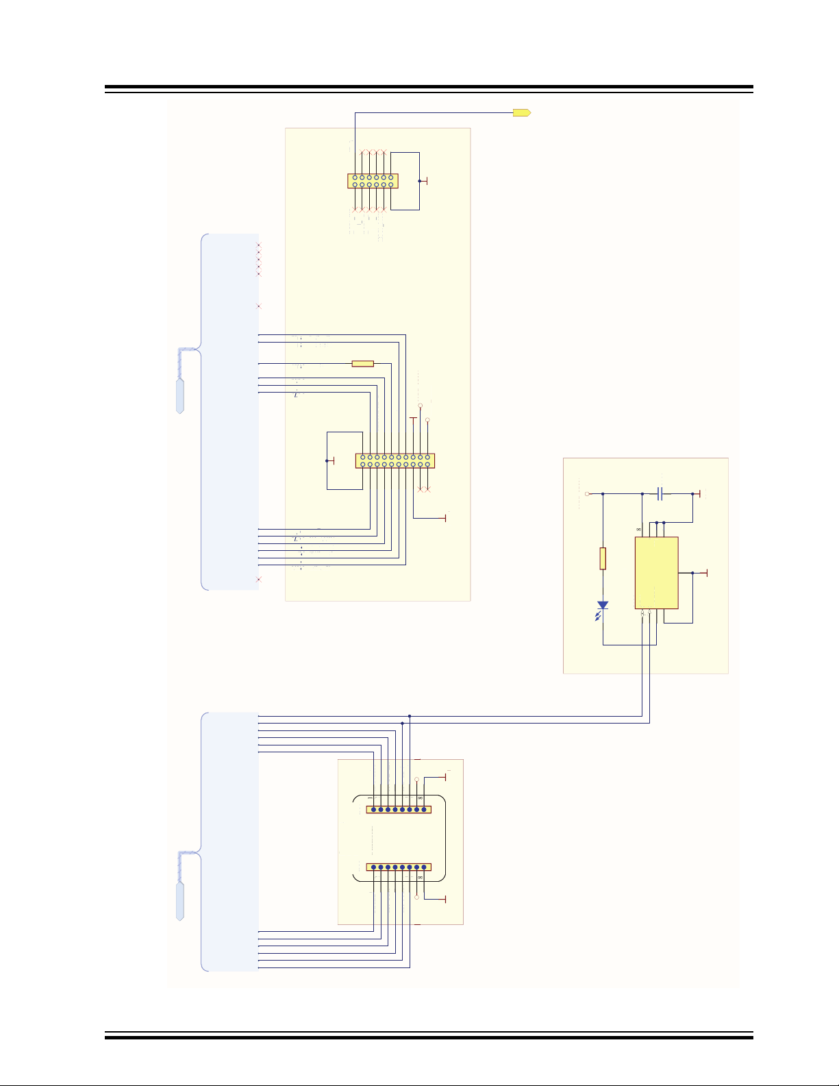
2.1 Schematics
SAM E54
Hardware
© 2019 Microchip Technology Inc.
DS70005405A-page 19
Page 20

VCC_EXT_5P0V_14P0V
VCC_IN_5P0V
123
NEB 21 R
J201
GND
5V to 14V input, 5V out Power Supply, 2A
CC_EXT_5P0V_14P0
V
CC_IN_5P0
V
1
NEB 21 R
201
N
D
5V to 14V input, 5V out Power Supply, 2
A
3
1
2
IRLML5203PBF
Q200
GND
5 - 14V DC - 1.5 A
VIN
3.3V linear regulator EDBG and Accessories
GND
GND
GND
N
D
ND
N
D
VCC_EDBG_3P3V
VCC_3P3V
GND GND
GND GND
BLM18PG471SN1
L202
BLM18PG471SN1
L203
0R
R213
3.3V linear regulator Target
GND
GND
GNDGND
N
D
ND
N
D
N
D
0R
R214
BLM18PG471SN1
L201
MBR230LSFT1
2 1
D204
VCC_5P0V
1uF
C218
1uF
C219
VCC_EDBG_USB_5P0V
GND
Power Connector
VCC_3P3V
TARGET_USB_P
TARGET_USB_N
GND
GND
1M
R201
4.7n
DNP
C200
DNP
EGND_MCU
0R
R200
EGND_MCU
GND
VCC_TARGET_USB_5P0V
TARGET_USB_N
TARGET_USB_P
MBR230LSFT1
2 1
D202
MBR230LSFT1
2 1
D203
BoS
12
34
1125-1202S0R138R1
J202
HEADER 2x2
3 5
GND
VCC
2
1IO1
IO2
IO3
4
D200
D200
Polarity Protection
GND
100k
R212
100k
R209
1
3 2
AO3413
Q201
GND
GND
OTG_SW
1
3 2
FDN304P
Q202
MBR230L
S
FT1
1
D2
02
VCC_3P3V
1k
R207
VBUS
1
D-
2
D+
3
GND
5
SHIELD16SHIELD2
7
ID
4
SHIELD38SHIELD4
9
ZX62D-AB-5P8
J200
30k
R206
16k
R205
VOUT1VOUT
2
GND
3
EN4VIN
6
NC
5
EP
7
MIC5528-3.3YMT
U202
1uF
C210
1uF
C211
2.2uF
C202
10k
R203
4.7uF
C204
10k
R202
4.7uF
C203
GND
2 1
MBR230LSFT1
D201
XAL4020-222ME
L200
SGND
4.7nF
C208
100uF/16V
C209
R208
R208
Vout=5.00
R211
R211
GND
1uF
C205
SGNDGND
Vout=0.8 (1+(R209/R210))
R210
R210
22uFC201
GND
GND
VCC_MCU_3P3V
10uF/10V
C215
PGND36PGND5
8
PVIN1
13
PGND4
7
PGND25P
G
ND3
PGND
5
P
V
IN
1
P
G
ND
4
P
G
ND
2
SW14SW29SW310SW4
11
PVIN214PVIN618PVIN517PVIN416PVIN3
15
BST
20
PVIN719PGND6
21
PVDD
1
PGND1
2
NC
3
SW5
12
CS
22
VIN
27
EN
26
PG
25
FB
24
SGND
23
VDD
28
MIC24052YJL-TR
U200
JS203
47k
R215
47k
R216
TARGET_VOLTAGE
GND
VBUS_DET
1
2
1125-1102S0R138R1
J203
0.1uF
C206
0.1uF
C216
0.1uF
C214
0.1uF
C217
2.2R
R204
0.1uF
C212
0.1uF
C207
2.2R
R221
0.1uF
C220
SGND
SGND
VOUT1VOUT
2
GND
3
EN4VIN
6
NC
5
EP
7
MIC5528-3.3YMT
U201
10uF/10V
C213
USB_ID_DET
4.7R
R220
100k
R222
GND
1
5 6
FDC6327C
Q203A
24
3
FDC6327C
Q203B
When Vin = 5V the regulator uses a 100% duty-cycle mode
(p
assthrou
g
h
)
.
500mA low noise LDO voltage regulator
N
oise: 28uVrms
Accuracy 2%
Dropout 500 mV at 500 mA (maximum)
Quiescent current 38 uA
Current limit 525 mA (minimum)
Thermal shutdown and current limit protection
SAM E54
Hardware
© 2019 Microchip Technology Inc.
DS70005405A-page 20
Page 21

AT32UC3A4256J-C1URAT
3
2
UC3
A42
56J
-
C
1
UR
PA00 / PA18
G8
VDDIO
F6
VDDIO
F2
VDDIO
B6
GNDIO
C8
VDDIO
J5
GNDIO
E2
GNDIO
H3
GNDIO
F5
VDDIO
B5
GNDIO
E6
GNDIO
C3
GNDCORE
F10
VDDCORE
E10
GNDPLL
B10
VDDIN
D10
VDDANA
J6
VDDIN
D9
GNDANA
H8
VDDIO
E5
PA01 / PA17
G10
PA02 / PX47E1PA03F9PA04E9PA05G9PA06 / PA13E8PA07 / PA19
H10
PA08F8PA09D8PA10
C10
PA11C9PA12 / PA25G7PA14 / PX11K7PA15 / PX45J7PA16E7PA20 / PX18H9PA21 / PX22
K10
PA23 / PX46G6PA24 / PX17
J10
PA26 / PB05F7PA27A2PA28A1PA29B4PA30A4PA31
C2
PA22 / PX20
H6
PC00 / PX14
K5
PC01
K6
PC02
A5
PC03
A6
PC04
B7
PC05
A7
TMSH7TDO
J8
TDI
K8
TCK
K9
RESET_N
J9
DMHSA9DPHSA8DMFSB9DPFS
B8
USB_VBUS
A10
USB_VBIAS
C7
PB00
B1
PB01
B2
PB02
B3
PB03
C4
PB04
A3
PB06
D7
PB07
D6
PB08
C6
PB09
C5
PB10
D5
PB11
C1
PX00G4PX01G2PX02G3PX03J1PX04H1PX05G1PX06F3PX07F4PX08E3PX09E4PX10D2PX12D1PX13
D3
PX15 / PX32K4PX16 / PX53
D4
PX19 / PX59
F1
PX21H2PX23K1PX24J2PX25H4PX26J3PX27K2PX28K3PX29J4PX30G5PX31
H5
U300
TXD
RXD
EDBG_UART
EDBG_UART
EDBG_USART_RX
GND
GND
VCC_EDBG_3P3V
GND
GND
GND
GND
GND
VCC_EDBG_USB_5P0V
EDBG_USB_HS_N
EDBG_USB_HS_P
EDBG_USB_FS_P
EDBG_USB_FS_N
Shield
EDBG_USART_TX
STATUS_LED_CTRL
POWER_LED_CTRL
XIN0
XOUT0
MISO
MOSI
SCK
SS
DGI_SPI
DGI_SPI
EDBG_SPI_DGI_MISO
EDBG_SPI_DGI_MOSI
EDBG_SPI_DGI_SCK
EDBG_SPI_DGI_SS
VCC_EDBG_3P3V
EDBG_DGI_SDA
EDBG_DGI_SCL
DGI_GPIO0
DGI_GPIO1
ID1
ID1
ID2
EDBG_FORCE_BOOT
Current limiters, 10mA @3.3V
Current limiter, 10mA @3.3V
GND
GND
EDBG_FORCE_BOOT
EDBG_RESET_N
EDBG_JTAG_TMS
EDBG_JTAG_TDO
EDBG_JTAG_TDI
EDBG_JTAG_TCK
VCC_EDBG_3P3V
GND
VCC_EDBG_3P3V
EDBG Power and Status LEDs
GND
EDBG_ADC0
ID2
GND
VCC_EDBG_3P3V
GND
SWCLK
SWDIO
TARGET_CHIP_RESET
TRACESWO
EDBG_SWD
EDBG_SWD
EDBG_SWDIO
EDBG_SWCLK
EDBG_RESET
TARGET_RESETN_SENSE
DGI_GPIO2
DGI_GPIO3
21
EL17-21SYGC
D301
D301
21
EL17-21UYC/A3
D302
D302
4
5
3
2N7002DW
Q302A
2
1 6
2N7002DW
Q302B
330R
R327
330R
R329
0R
R317
330R
R322
0R
R3250RR323
TP302
TP303
TP304
TP306
TP305
TP307
39R
R314
39R
R312
BLM18PG471SN1
L300
1 nF C0G
C301
1 nF C0G
C302
BLM18PG471SN1
L301
100n
C305
1 nF C0G
C307
2.2uF
C306
GND
100n
C310
2.2uF
C308
1k
R309
0R
R304
TP301TP300
330R
R308
0R
R307
1 3
2 4
12.00MHz
XC300
XC300
4.7n
DNP
C300
DNP
10p
C303
22p
C304
22p
C309
1M
R300
1M1M
R326
1M1M
R328
6.81k
R316
VCC_EDBG_3P3V
330R
R318
330R
R319
330R
R320
330R
R321
GND
GND
0R
R301
EGND_EDBG
EGND_EDBG
GND
EDBG_TARGET_RESET
GND
0R
R302
1k
R311
TARGET_VOLTAGE
GND
100n
C311
100n
C312
100n
C313
2.2uF
C314
2.2uF
C315
VCC_EDBG_3P3V
GREEN
YELLOW
39R
39R
R324
CONN USB MICRO B RECPT SMT R/A
VBUS
1
D-
2
D+
3
GND
5
SHIELD16SHIELD2
7
ID
4
SHIELD38SHIELD4
9
J300
3 5
GND
VCC
2
1IO1
IO2
IO3
4
D300
D300
GND
GND
VCC_EDBG_3P3V
100k
R315
1
2 3
DMN2075U
Q301
Q301
3
1
2
IRLML5203PBF
Q300
Q300
100k
R313
LED 1 LED 2
0R
R303
1k
R310
ID4
SDA
SCL
DGI_I2C
DGI_I2C
0R
R3050RR306
330R
R330
330R
R331
330R
R332
330R
R333
DGI_GPIO0
DGI_GPIO1
DGI_GPIO2
DGI_GPIO3
DGI_GPIO
DGI_GPIO
1k
R341
ID_1
ID_2
ID_3
ID_4
0R
R340
ID4
ID3
ID3
ID_5 0R
R342
1k
R343
ID5
ID5
Input filter on USB
ower input.
Connect the test points during startup o
f
the EDBG to force it into bootloader
mode.
The test points should be covered with
solder so that it is easier to get a good
contact.
Programming interface of the
embedded debugger. The test
oints will be connected by needles
in the test fixture for programming.
GND test point is TP400.
SAM E54
Hardware
© 2019 Microchip Technology Inc.
DS70005405A-page 21
Page 22
TARGET_RESETN
DGI_SPI
EDBG_UART
SPI0_MOSI
SPI0_MISO
SPI0_SPCK
SPI0_SS_GPIO1
RXD1
TXD1
MISO
MOSI
SCK
SS
DGI_SPI
RXD
TXD
EDBG_UART
IO0
IO1
IO2
IO3
CLK
CS
QSPI
QSPI
SYS_SDA6
SYS_SCL6
1k1
k
R428
1k
R427
PIN1_ADC(+)
PIN2_RST
PIN3_CS
PIN4_SCK
PIN5_MISO
PIN6_MOSI
PIN11_SDA
PIN12_SCL
PIN13_TX
PIN14_RX
PIN15_IRQ
PIN16_PWM(+)
MikroBUS
MikroBUS
ADC0/AIN0
PWM0/WO1
INT
UART7_TX
UART7_RX
0R
R4620RR463
SPI0_MOSI
SPI0_MISO
SPI0_SPCK
39R39R
R461
SPI0_SS_GPIO6
VCC_3P3V
CMD
CLKD3D2D1D0
DETECT
WP
SD_CARD
SD_CARD
SDHC1/SDDAT0
SDHC1/SDCMD
AUDIO
0R
R4350RR4370RR4380RR4360RR434
SYS_SCL6
SYS_SDA6
0R
R440
RXD
TXD
CTS
RTS
I2S/MCK0
0R
R4290RR4300RR4310RR432
I2S/SCK0
I2S/FS0
I2S/SDI
I2S/SDO
0R
R433
PCC
IRQ2 (Q Touch)
IRQ3 (Display Cntrl)
0R
R464
SPI0 SCK
SPI0 MOSI
SPI0 MISO
SPI0_SS_GPIO5
LCD_PWM
ADC0
ADC1
ADC2
ADC3
ADC4
ADC5
ADC6
ADC7
LCDDISP
STBY/RST
ONE WIRE INTERFACE
GPIO1
PWM
GPIO2
GPIO3
TRACE
SWDIO
SWCLK
TRACECLK
TRACED0
TRACED1
TRACED2
TRACED3
nRESET
SWO
TRACE
TARGET_RESETN
TRACECLK
TRACED0
TRACED1
TRACED2
TRACED3
TRACESWO
SWDIO
SWCLK
CANTX
CANRX
CAN
CAN
CAN0_TX
CAN0_RX
EXT2
EXT1
PIN10_SPI_SS_B/GPIO
PIN11_I2C_SDA
PIN12_I2C_SCL
PIN13_UART_RX
PIN14_UART_TX
PIN15_SPI_SS_A
PIN16_SPI_MOSI
PIN17_SPI_MISO
PIN18_SPI_SCK
PIN3_ADC(+)
PIN4_ADC(-)
PIN5_GPIO
PIN6_GPIO
PIN7_PWM(+)
PIN8_PWM(-)
PIN9_IRQ/GPIO
EXT1
PIN10_SPI_SS_B/GPIO
PIN11_I2C_SDA
PIN12_I2C_SCL
PIN13_UART_RX
PIN14_UART_TX
PIN15_SPI_SS_A
PIN16_SPI_MOSI
PIN17_SPI_MISO
PIN18_SPI_SCK
PIN3_ADC(+)
PIN4_ADC(-)
PIN5_GPIO
PIN6_GPIO
PIN7_PWM(+)
PIN8_PWM(-)
PIN9_IRQ/GPIO
EXT2
0R
R4220RR423
GPIO2
SPI0_SS_GPIO3
SYS_SDA6
SYS_SCL6
UART2_RX
UART2_TX
SPI0_SS_B
SPI0_MOSI
SPI0_MISO
SPI0_SCK
SPI0_MOSI
SPI0_MISO
SPI0_SCK
TCC4/WO0
IRQ/GPIO2
SPI0_SS_GPIO2
SPI0_SS_A
0R
R425
39R
39R
R426
39R
39R
R424
UART5_TX
ADC1/AIN2
IRQ/GPIO3
TXD0
TXD1
TXEN
TXCK
RXD0
RXD1
MDC
MDIO
RXER
RXDV
RESET
SIGDET
MOSI
MISO
SCLKCSGPIO0
GPIO1
GPIO2
ETHERNET
ETHERNET
GPIO
GPIO
GTXCK
GTXEN
GTX0
GTX1
GRXDV
GRX0
GRX1
GRXER
GMDC
GMDIO
GPIO
0R
R4540RR4550RR4560RR457
0R
DNP
R458
DNP
0R
R453
DNP
0R
R4520RR4510RR4500RR449
39R
39R
R448
39R
39R
R447
39R
39R
R445
39R
39R
R444
0R
R443
39R
39R
R442
0R
R446
SPI0_MOSI
SPI0_MISO
SPI0_SPCK
ISI_PWD
GND
39R
R475
GN
D
3
9
R
R47
5
TP402
21
EL17-21UYC/A3
D400
VCC_3P3V
330R
R467
USER BUTTON 2
USER LED 1
PC21
USER_LED0
PD01
USER_BUTTON2
GND
VCC_3P3V
GND
N
D
_
N
D
RESET button with current limit and noise filter
0R
R472
TARGET_RESETN
2.2k
R469
100pF
C419
330R
R470
330R
R465
0R
R473
TARGET_RESETN_SENSE
YELLOW
0R
R459
DNP
0R
R460
DNP
EDBG_TARGET_RESETN
TARGET_USB_N
TARGET_USB_P
SWCLK
SWDIO
TARGET_CHIP_RESET
TRACESWO
EDBG_SWD
EDBG_SWD
TRACESWO
SWDIO
SWCLK
WKUP5
WKUP2
STBY/RST
TP401
1 3
42
TS604VM1-035CR
SW402
1 3
42
TS604VM1-035CR
SW401
GFX-CTRL
PIN6_IRQ2
PIN8_IRQ3
PIN10_IRQ4
PIN4_IRQ1
PIN14_I2C_SDA
PIN16_I2C_SCL
PIN18_SPI_SCLK
PIN20_SPI_MOSI
PIN22_SPI_MISO
PIN24_SPI_SS
PIN26_USART_RX
PIN28_USART_TX
PIN30_USART_RTS
PIN32_USART_CTS
PIN34_LCDPWM
PIN36_PWM
PIN38_GPIO1
PIN40_GPIO2
PIN42_GPIO3
PIN44_STBY/RST
PIN60_ADC5
PIN58_ADC4
PIN56_ADC3
PIN54_ADC2
PIN52_ADC1
PIN46_RESET2
PIN48_OWI
PIN50_ADC0
PIN62_ADC6
PIN64_ADC7
GFX-CTRL
VSYNC/nCS
PCLK/nWR
HSYNC/DCX
DE/nRD
10n
DNP
C420
DNP
LED 1
12 MHz Oscillator
XIN_12
0R
R471
STB
1
GND
2
OUT3VDD
4
DSC6003CI2A-012.0000
Y401
GND
100n
C418
GND
VCC_3P3V
XIN
_
1
2
R
471
1
T
B
GNDO
U
T
DD
D
SC
6003
C
I2A-012.000
0
4
0
1
ND
1
00n
418
ND
CC
_
3P3
V
32.768 kHz Oscillator
XIN_32
0R
R466
OUT1GND
2
NC
3
VDD
4
DSC6083CE2A-032K768
Y400
100n
C421
GND
GND
XIN_3
2
R
4
66
1
T
ND N
C
DD
DSC6083CE2A-032K768
4
00
1
00n
42
1
ND
N
D
VCC_3P3V
TARGET_RESETN
VCC_MCU_3P3V
GND
Close to VDDCORE
GND
VCC_MCU_3P3V
N
D
CC_MCU_3P3
V
VDDIO
VCC_MCU_VDDCORE
N
D
CC
_
MCU
_
VDDCORE
4.7uF
C406
VCC_MCU_VSW
LQH3NPN100MJ0
L401
VDDANA filter
100n
C408
VCC_MCU_VDDANA
GND
BLM18PG471SN1
L400
VCC_MCU_3P3V
CC_MCU_VDDAN
A
LM18PG471SN1
L4
00
CC_MCU_3P3
V
10uF/10V
C401
10uF/10V
C402
100n
C404
GND
408
GN
D
Close to each VDDANA pair
100n
C410
GND
100n
C412
GND
VCC_MCU_VDDANA
100n
C403
GND
1
00n
40
3
N
D
Close to each VDDIO pair
100n
C405
GND
100n
C407
GND
100n
C409
GND
100n
C411
GND
100n
C413
GND
100n
C414
GND
100n
C415
GND
100n
C416
GND
100n
C417
GND
VCC_MCU_3P3V
0R
R411
VCC_MCU_VDDIOB
CC
_
MCU
_
3P3
V
R
411
CC
_
MCU
_
VDDIO
B
VDDIOB disconnect
VCC_MCU_VDDIOB
A0A1A2A3A4
A5
SHIELD_ANA
SHIELD_ANA
RX/D0
TX/D1D2PWM/D3D4PWM/D5
PWM/D6D7D8
PWM/D9
PWM/D10
PWM/D11
D12
D13
SDA/D14
SCL/D15
SHIELD_DIG
SHIELD_DIG
PA03
PB06
PB07
PA04
PB02
PB03
PB30
PB31
PD10
PD11
PD12
PB14
PB15
PC10
PD21
PB16
PB28
PB24
PC25
PB25
PD09
PD08
PA00(XIN32)1PA00
(
XIN32
)
PA01(XOUT32)2PC003PC014GND5VDDANA6PC027PC038PA029PA0310PB0411PB0512PD0013GNDANA14VDDANA15PD0116PB0617PB0718PB0819PB0920PA0421PA0522PA0623PA0724GNDANA25VDDANA26PC0427PC0528PC0629PC0730GND31VDDIOB
32
PA08
33
PA09
34
PA10
35
PA11
36
VDDIOB
37
GND
38
PB10
39
PB11
40
PB12
41
PB13
42
PB14
43
PB15
44
GND
45
VDDIO
46
PD08
47
PD09
48
PD10
49
PD11
50
PD12
51
PC10
52
GND
53
VDDIO
54
PC11
55
PC12
56
PC13
57
PC14
58
PC15
59
PA12
60
PA13
61
PA14(XIN0)
62
PA15(XOUT0)
63
GND
64
VDDIO
65
PA1666PA1767PA1868PA19
69
PC1670PC1771PC1872PC1973PC2074PC2175PC2276PC23
77
GND
78
VDDIO
79
PD2080PD21
81
PB1682PB1783PB1884PB1985PB2086PB21
87
PA2088PA21
89
GND
90
VDDIO
91
PA22
92
GND
96
VDDIO
97
(XIN1)PB22
98
PA23
93
(USB_N)PA24
94
(USB_P)PA25
95
(XOUT1)PB23
99
PB24
100
PB25
101
PB26
102
PB27
103
PB28
104
PB29
105
GND
106
VDDIO
107
PC24
108
PC25
109
PC26
110
PC27
111
PC28
112
PA27
113
RESETN
114
VDDCORE
115
GNDIO
116
VSW
117
VDDIO
118
(SWDCLK)PA30
119
(SWDIO)PA31
120
(SWO)PB30
121
PB31
122
PC30
123
PC31
124
PB00
125
PB01
126
PB02
127
PB03
128
ATSAME54P20A
U401
XIN_32
PA22
PA23
PB16
PB17
PB18
PB19
PB20
PB21
PB06
PB07
PB08
PB09
PB04
PB05
PC00
PC01
PC02
PC03
PC04
PC05
PC06
PC07
PB00
PB01
PB02
PB03
PB24
PB25
PB26
PB27
PB28
PB29
PC30
PC31
PC24
PC25
PC26
PC27
PC28
XIN_12
PB23
PB30
PB31
PA02
PA03
PA04
PA05
PA06
PA07
PD00
PD01
PA08
PA09
PA10
PA11
PB10
PB11
PB12
PB13
PB14
PB15
1k
R418
1k
R419
1k
R420
1k
R421
PD08
PD09
PD08
PD09
PD10
PD11
PD12
PC10
PC11
PC12
PC13
PC14
PC15
PA12
PA13
PA14
PA15
PA16
PA17
PA18
PA19
PC16
PC17
PC18
PC19
PC20
PC21
PC22
PC23
PD20
PD21
PA20
PA21
VCC_MCU_3P3V
VCC_MCU_3P3V
VCC_MCU_3P3V
VCC_MCU_3P3V
VCC_MCU_3P3V
VCC_MCU_3P3V
VCC_MCU_3P3V
GND GNDGND GND
PA14
PA17
PA18
PA19
PC20
PA13
PA12
PA15
PC22
PC23
PB24
PB25
PC25
PA27
PC18
PB03
PB02
PA04
PB07
PB06
PA03
PD08
PD09
PB25
PC25
PB24
PB28
PB16
PD21
PC10
PB15
PB14
PD12
PD11
PD10
PB31
PB30
PA08
PA09
PA10
PA11
PB10
PB11
QSPI_DATA0
QSPI_DATA1
QSPI_DATA2
QSPI_DATA3
QSPI_SCK
QSPI_CS
PA22
PA23
PCC_DATA09
PCC_DATA08
PCC_DATA07
PCC_DATA06
PCC_DATA05
PCC_DATA04
PCC_DATA03
PCC_DATA02
PCC_DATA01
PA17
PA18
PA19
PA20
PA21
PA22
PA23
PB14
PB15
PCC_DEN1
PA12
PCC_DEN2
PA13
PCC_DATA00
PA16
GRXER
PA15
SYS_SDA6
SYS_SCL6
PD08
PD09
GMDIO
PC23
GMDC
PC22
PC27
PC28
PC25
PB24
PB25
PC26
PA30
PA31
GND
PC17
PA01
PB25
PB24
PC18
PC25
PC16
LCD_D0
LCD_D1
LCD_D2
LCD_D3
LCD_D4
LCD_D5
LCD_D6
LCD_D7
PC00
PC01
PC02
PC03
PC04
PC05
PC06
PC07
PD10
PD10
GPIO1
GPIO1
PD11
PD12
PD11
PD12
PD09
PD08
SYS_SDA6
SYS_SCL6
PD09
PD08
PB26
PB27
UART5_RX
PB30
PB31
PB24
PB25
PC25
PC24
PB24
PB25
PC25
PC24
PA08
ADC1/AIN3
PA09
ADC1/AIN2
PA08
ADC1/AIN3
PA09
TCC4/WO1
PB14
PB15
TCC4/WO0
TCC4/WO1
PB14
PB15
GPIO3
PB29
PB28
PC18
PA02
SYS_SDA6
SYS_SCL6
PD09
PD08
PC14
PC15
PC12
PC13
PB16
PB24
PB25
PC25
SDHC1/SDDAT1
SDHC1/SDDAT2
SDHC1/SDDAT3
SDHC1/SDCD
SDHC1/SDCK
PB18
PB19
PB20
PB21
PD20
PA20
PA21
GFX-DATA
PA07
ADC0/AIN7
ADC0/AIN6
PA06
PA04
ADC0/AIN4
PB09
PB08
PB17
PB04
TARGET_RESETN
PC24
PC25
PC26
PC27
PC28
PA30
PA31
PB30
0R
R4090RR4080RR4070RR4060RR4050RR4030RR4020RR404
Pin7_PCLK
Pin16_DATA00
Pin15_DATA01
Pin14_DATA02
Pin13_DATA03
Pin12_DATA04
Pin11_DATA05
Pin10_DATA06
Pin9_DATA07
Pin18_DATA08
Pin17_DATA09
Pin6_HSYNC/DEN2
Pin3_I2C_SCL
Pin4_I2C_SDA
Pin20_PWDN
Pin19_RESET
Pin5_VSYNC/DEN1
Pin8_MCLK
PCC
PA14
PCC/CLK
PIN4_CTS
PIN6_RTS
PIN3_RXD
PIN5_TXD
PIN7_I2C_SCL
PIN9_I2C_SDA
PIN13_I2S/SDO
PIN11_I2S/SDI
PIN14_I2S/MCK
PIN12_I2S/SCK
PIN8_STBY/RST
PIN10_I2S/FS
REFCLK_IN
PIN9_I2S/MCK1
PIN3_I2S/SCK1
PIN1_I2S/FS1
PIN5_I2S/SDI1
PIN7_I2S/SDO1
REFCLK_OUT
AUDIO
PD09
PD08
PA08
PA09
PA10
PA11
PC13
PC12
PC15
PC14
PB10
STBY/RST
PC18
PA03
ADC0/AIN1
PB06
ADC1/AIN8
ADC1/AIN9
PB07
IRQ1 (LCD Touch)
PC31
VCC_MCU_VDDIOB
GND
GND
GND
GND
VCC_MCU_VDDIOB
VCC_MCU_VSW
VCC_MCU_3P3V
VCC_MCU_VDDCORE
GND GND
PA27
VCC_MCU_VDDANA
GND
VCC_MCU_VDDANA
VCC_MCU_VDDANA
GND
DAC0
DAC1
DAC_OUT
DAC_OUT
PA02
PA05
DAC0
DAC1
PA02
PA05
GND
39R
R468
GND
3
9
R
R
468
TP400
USER BUTTON 1
PD00
USER_BUTTON1
1 3
42
TS604VM1-035CR
SW400
21
EL17-21UYC/A3
D401
VCC_3P3V
330R
R474
USER LED 2
PA16
USER_LED2
YELLOW LED 2
TOUCH_SDA4
PB12
PB13
PC30
ID_4
ADC0/AIN12
ADC0/AIN13
ADC0/AIN14
ADC0/AIN15
PB00
PB01
PB02
PB03
GND
AREF
AREF GENERATOR
GND
10k
R400
10k
R401
VCC_MCU_VDDCORE
100n
C400
GND
4
3
1
2 5
U400
U400
OTG_SW
VBUS_DET
PA31
PA30
TARGET_RESETN
PB30
100R
R410
SDA
SCL
DGI_I2C
DGI_I2C
SYS_SCL6
SYS_SDA6
PD09
PD08
VCC_MCU_VDDCORE
PB00
PB01
ADC1/AIN12
ADC1/AIN13
TOUCH_SCL4
1k
R4121kR4131kR4141kR4151kR4161kR417
i
GRAPHICS
YN
C
/
n
PCLK/
n
R
H
S
YN
C
/D
CX
DE
/n
R
D
CD_D0CD_D1CD_D2CD_D3CD_D4CD_D5CD_D6CD_D
7
PC00P
C
01
P
C
0
2
P
C
03
P
C
0
4
PC05PC06PC0
7
PB09PB08PB17PB
04
330R
R439
Pin15_D0
Pin17_D1
Pin19_D2
Pin21_D3
Pin23_D4
Pin25_D5
Pin27_D6
Pin29_D7
Pin3_MCLR
Pin7_LCDEN
Pin9_LCDHSYNC
Pin11_LCDVSYNC
Pin13_LCDPCLK
GFX-DATA
DGI_GPIO0
DGI_GPIO1
DGI_GPIO2
DGI_GPIO3
DGI_GPIO
DGI_GPIO
PC24
PB28
PC21
PD00
IRQ/GPIO3
LED1
BTN1
IRQ/GPIO2
1 2
3 4
5 6
7 8
9 10
1310-1205SNS073R1
DNP
J400
DNP
GND
PA31
PA30
TARGET_RESETN
SWDIO
SWCLK
VCC_MCU_3P3V
1
1
0-
2
05S
N
S0
7
3
R
1
N
P
40
0
GN
D
PA
3
1
PA
30
TARGET_RESETN
DI
O
LK
CC_MCU_3P3
V
Cortex Debug Connector
USB_ID_DET
SYS_SCL6
SYS_SDA6
PD09
PD08
SDA
SCL
EPROM_I2C
EPROM_I2C
SYS_SDA4
SYS_SCL4
1k
R479
1k
1
k
R478
PB13
PB12
123
MTSW-103-08-L-S-276
J401
GTXEN
PA17
JS401
SAM E54
Hardware
© 2019 Microchip Technology Inc.
DS70005405A-page 22
Page 23

A0A1A2A3A4
A5
SHIELD_ANA
SHIELD_ANA
GND
GND
RESET_UNO
12345
6
SSQ-106-21-F-S
J501
1234567
8
SSQ-108-21-F-S
J504
1234567
8
SSQ-108-21-F-S
J500
123456789
10
SSQ-110-21-F-S
J503
0R
R500
TARGET_RESETN
ARDUINO UNO COMPATIBLE HEADERS
VCC_3P3V
IOREF
RESET
3.3V
5.0V
VCC_5P0V
GND
GND
VIN
ANALOG INPOWER
DIGITAL (~PWM)
RX/D0
TX/D1
D2
PWM/D3
D4
PWM/D5
PWM/D6
D7
D8
PWM/D9
PWM/D10
PWM/D11
D12
D13
SDA/D14
SCL/D15
SHIELD_DIG
SHIELD_DIG
AREF
GND
VCC_3P3V
PA03
D0/UART-RX
D1/UART-TX
D2D3D4D5D6
D7
D8
D9
D10/SPI-SS
D11/SPI-MOSI
D12/SPI-MISO
D13/SPI-SCK
D14/I2C-SDA
D15/I2C-SCL
ADC0
ADC1
ADC2
ADC3
ADC4
ADC5
1 2
3 4
5 6
HMTSW-103-23-F-D-237
J502
GND
MISO
SCK MOSI
VCC_EXT_5P0V_14P0V
AREF
AREF
VCC_5P0V
PB06
PB07
PA04
PB02
PB03
PB30
PB31
PD10
PD11
PD12
PB14
PB15
PC10
PD21
PB16
PB28
PB24
PC25
PB25
PD09
PD08
SAM E54
Hardware
© 2019 Microchip Technology Inc.
DS70005405A-page 23
Page 24

PCC
PCC Interface Connector
GND
GND
VCC_3P3V
EXT1 Extension Header
N
D
N
D
EXT1
ID_EXT1
PIN3_ADC(+)
PIN4_ADC(-)
PIN5_GPIO
PIN6_GPIO
PIN7_PWM(+)
PIN8_PWM(-)
PIN9_IRQ/GPIO
PIN10_SPI_SS_B/GPIO
PIN11_I2C_SDA
PIN12_I2C_SCL
PIN13_UART_RX
PIN14_UART_TX
PIN15_SPI_SS_A
PIN16_SPI_MOSI
PIN17_SPI_MISO
PIN18_SPI_SCK
EXT1
ADC(+)
GPIO
PWM(+)
IRQ/GPIO
TWI_SDA
UART_RX
SPI_SS_A
SPI_MISO
ADC(-)
GPIO
PWM(-)
SPI_SS_B/GPIO
TWI_SCL
UART_TX
SPI_MOSI
SPI_SCK
PB27
PB26
PB25
GND
GND VCC_3P3V
N
D
N
D
CC_3P3
V
EXT2
ID_EXT2
PIN3_ADC(+)
PIN4_ADC(-)
PIN5_GPIO
PIN6_GPIO
PIN7_PWM(+)
PIN8_PWM(-)
PIN9_IRQ/GPIO
PIN10_SPI_SS_B/GPIO
PIN11_I2C_SDA
PIN12_I2C_SCL
PIN13_UART_RX
PIN14_UART_TX
PIN15_SPI_SS_A
PIN16_SPI_MOSI
PIN17_SPI_MISO
PIN18_SPI_SCK
EXT2
ADC(+)
GPIO
PWM(+)
IRQ/GPIO
TWI_SDA
UART_RX
SPI_SS_A
SPI_MISO
ADC(-)
GPIO
PWM(-)
SPI_SS_B/GPIO
TWI_SCL
UART_TX
SPI_MOSI
SPI_SCK
PB15
PB25
EXT2 Extension Header
TRACE (CoreSight 20)
TRACE
SWDIO
SWCLK
TRACECLK
TRACED0
TRACED1
TRACED2
TRACED3
nRESET
SWO
TRACE
VTREF
KEY (NC)
nTRST/TraceD1
GND
TDI
GND
TMS/SWDIO
GND
TCK/SWCLK
GND
GND
TDO/SWO
GND
nRST
SWO/TraceD0
NC RTCK/TRACECLK
NC
DBGRQ/TraceD2
DBGACK/TraceD3
GND
VCC_3P3V
50Ω single ended for trace signals
TRACECLK
TRACED0
TRACED1
TRACED2
TRACED3
PA30
PB30
PA31
PC27
PC28
PC26
PC25
PC24
TARGET_RESETN
PC25
PC24
PD09
PD12
PB14
PD10
PA08
PA09
PD11
PB15
PB29
PD08
PB24
PC25
PC24
PB30
PD09
PD11
PB14
PD10
PA08
PA09
PD12
PB28
PD08
PB31
PB24
1 2
3 4
5 689 10
11 12
13 14
15 16
17 18
19 20
3132-20MS0BK00R3
DNP
J603
DNP
1 2
3 4
5 6
7 8
9 10
11 12
13 14
15 16
17 18
19 20
1125-1210S0R138R1
J602
1 2
3 4
5 6
7 8
9 10
11 12
13 14
15 16
17 18
19 20
1125-1210S0R138R1
J604
CC_3P3
V
HMTSW-110-23-F-D-237
1 2
3 4
5 6
7 8
9 10
11 12
13 14
15 16
17 18
19 20
J601
GND
SCL
VSYNC HSYNC
SDA
GND
PCLK XCLK
DOUT00DOUT01
DOUT02DOUT03
DOUT04DOUT05
DOUT06DOUT07
DOUT08DOUT09
PWDNRESET
SWCLK
TRACESWO
SWDIO
Pin7_PCLK
Pin16_DATA00
Pin15_DATA01
Pin14_DATA02
Pin13_DATA03
Pin12_DATA04
Pin11_DATA05
Pin10_DATA06
Pin9_DATA07
Pin18_DATA08
Pin17_DATA09
Pin6_HSYNC/DEN2
Pin3_I2C_SCL
Pin4_I2C_SDA
Pin20_PWDN
Pin19_RESET
Pin5_VSYNC/DEN1
Pin8_MCLK
PCC
PCC_DATA09
PCC_DATA08
PCC_DATA07
PCC_DATA06
PCC_DATA05
PCC_DATA04
PCC_DATA03
PCC_DATA02
PCC_DATA01
PCC_DEN1
PCC_DEN2
PCC_DATA00
GRXER
SYS_SDA6
SYS_SCL6
GMDIO
GMDC
PCC/CLK
PC23
PB15
PA17
PA19
PA21
PA23
PA14
PA12
PD08
PD09
PA13
PA15
PA22
PA20
PA18
PA16
PB14
PC22
DAC0
DAC1
DAC_OUT
GND DAC_OUT
N
D
PA02
PA05
DAC0
DAC1
123
1125-1103S0S113R1
J600
VCC_3P3V
ADC1/AIN2
GPIO1
TCC4/WO0
IRQ/GPIO3
SPI0_MISO
SPI0_SS_B
UART2_RX
SYS_SDA6
SPI0_SCK
SPI0_MOSI
ADC1/AIN3
GPIO2
UART2_TX
TCC4/WO1
SPI0_SS_GPIO3
SYS_SCL6
SPI0_MOSI
SPI0_MISO
SPI0_SCK
IRQ/GPIO2
SPI0_SS_GPIO2
SPI0_SS_A
UART5_TX
GPIO1
SYS_SDA6
SYS_SCL6
UART5_RX
ADC1/AIN2
ADC1/AIN3
TCC4/WO0
TCC4/WO1
GPIO3
ID_1
ID_2
SAM E54
Hardware
© 2019 Microchip Technology Inc.
DS70005405A-page 24
Page 25
SD_CARD
GND
GND
VCC_3P3V
100n
C701
GND
10uF
C702
GND
100k
R703
100k
R704
100k
R701
100k
R702
10k
R700
VCC_3P3V
TP700
SD_D0
SD_D1
SD_D2
SD_D3
SD_CLK
SD_CMD
SD_CD
N
DND
CC_3P3
V
1
0
0
n
C
7
0
1
N
D
10
uF
70
2
N
D
1
0
0
k
R
7
0
3
1
0
0
k
R
7
0
4
1
0
0
k
R
7
0
1
1
0
0
k
R
7
0
2
1
0
k
R
7
0
0
CC_3P3
V
TP70
0
SD_D0SD_D1
SD_D2SD_D3
SD_CLK
SD_CMDSD_CD
microSD-CARD
10k
R705
PB18
PB19
PB20
PB21
PA21
PA20
PD20
Serial Quad I/O Flash Memory
VCC_3P3V
GND
100n
C700
IO0
IO1
IO2
IO3
CLK
CS
QSPI
QSPI
PA08
QIO0
QIO1
QIO2
QIO3
QSCK
QCS
DM3AT-SF-PEJM5
DM3AT-
S
F-PE
J
M
5
D07D18D21D32CLK5CMD3SW_A10SW_B
9
VDD
4
VSS
6
G212G313G111G4
14
J704
PA09
PA10
PA11
PB10
PB11
CMD
CLK
D3D2D1
D0
DETECT
WP
SD_CARD
SDHC1/SDDAT[0]
SDHC1/SDCMD
SDHC1/SDDAT[1]
SDHC1/SDDAT[2]
SDHC1/SDDAT[3]
SDHC1/SDCD
SDHC1/SDCK
GND
CS
1
SO/IO12WP/IO2
3
VSS
4
VCC
8
HOLD/IO37SCK
6
SI/IO0
5
/I
O
1
P/I
O2
H
O
LD/I
O3
K
I/I
O0
SST26VF064BA-104I/SM
U700
SDA
SCL
EPROM_I2C
VCC_3P3V
GND
100n
C703
10k
R709
10k
R706
10k
R707
CC_3P3
V
ND
1
00n
70
3
1
0
k
R
7
0
910
k
R
7
0
6
1
0
k
R
707
Serial EEPROM with EIA-48 MAC address
A01A12A2
3
GND
4
SDA5SCL6WP
7
VCC
8
AT24MAC402-MAHM-T
U701
SYS_SCL6
SYS_SDA6PD09
PD08
MAC24_WP
J701
J702
J703
GND
EPROM_I2C
JS700
GND
MAC24_A0
MAC24_A1
MAC24_A2
1
2
1125-1102S0S113R1
J700
CryptoAuthentication Device
SYS_SCL6
SYS_SDA6
VCC8NC7SCL6SDA
5
NC1NC2NC
3
GND
4
ATECC508A-SSHDA
U702
DNP
0R
R711
DNP
0R
R712
DNP
GND
VCC_3P3V
100n
C704
DNP
VCC_3P3V
1k1
k
R710
100k
R708
C/D is connected to COM when a card is placed into the socket.
SAM E54
Hardware
© 2019 Microchip Technology Inc.
DS70005405A-page 25
Page 26

ETHERNET
GTXEN
GTX0
GTX1
GRX1
GRX0
GRXER
GMDIO
GMDC
GTXCK
GRXDV
GPIO
GPIO
TXEN
EGND_PHY
RESET
MDIO
MDC
RXD1
RXD0
RXER
TXD0
TXD1
PHY_REFCLK
100n
C805
GND
CRS_DV
G
T
XEN
G
T
X
0
G
T
X
1
G
RXR
1
G
RXR
0
G
RXR
R
ER
G
MDI
O
G
M
D
C
G
T
X
C
K
G
RXRRD
VGP
I
O
G
P
I
O
TXE
N
EGND_PHY
RESE
T
MDI
O
MD
C
RXD1
RXD0RXER
TXD0TXD1
PHY_REF
C
LK
1
00n
80
5
N
D
RS_D
V
Ethernet PHY Header Configuration
IRQ
TXD0
TXD1
TXEN
TXCK
RXD0
RXD1
MDC
MDIO
RXER
RXDV
GPIO0
RESET
SIGDET
MOSI
MISO
CS
SCLK
GPIO1
GPIO2
ETHERNET
PD01
PD02
PD03
PD00
PD06
PD05
PD07
PD04
PD08
PD09
PA29
PA19
PC10
PD01
PD02
PD03
MOSI
MISO
SCLK
CSGPIO
VCC_5P0V
VCC_3P3V
GND
GND
100n
C801
GND
100n
C803
CANTX
CANRX
CAN
CAN
CANH
CANL
15p
C800
GND
4.7uF
C806
62R
R803
62R
R804
GND
PC10
PA29
PD09
PD08
PD04
PD07
PD05
PD06
TXD1GND2VCC3RXD
4
VIO
5
CANL
6
CANH
7
STBY
8
U800
U800
EGND_PHY
1M
R802
4.7n
DNP
C802
DNP
0R
R800
GND
0R
R801
GND
EGND_PHY
PD00
SLM-103-01-L-S
123
J801
SLM-103-01-L-S
123
J803
SLM-112-01-L-S
2
7
8
3
4
9
10
1
5
11
12
6
J800
SLM-112-01-L-S
2
7
8
3
4
9
10
1
5
11
12
6
J802
PD28
PA02
WKUP5
WKUP2
WKUP5
WKUP2
PD28
PA02
SPI0_SPCK PD22
SPI0_MOSI PD21
SPI0_MISO PD20
ISI_PWD PC19
PD21
PD20
PC19
PD22
VCC_3P3V
GND
100n
C804
GND
HTSW-103-08-F-S-RA
123
J804
GND
10k
R805
CAN0_TX
CAN0_RX
PA22
PA23
GPIO
STB
1
GND
2
OUT
3
VDD
4
T
B
N
D
T
D
D
DSC6101CI2A-050.0000
Y800
ID_5
SAM E54
Hardware
© 2019 Microchip Technology Inc.
DS70005405A-page 26
Page 27
AUDIO
"X32" HEADER SIGNAL CONFIGURATION
ID_3
SYS_SCL6
SYS_SDA6
UART7_RX
UART7_TX
I2S/SDO
I2S/MCK0
MCLK
I2S/SCK0
SPI0_MOSI
SPI0_MISO
SPI0_SPCK
VCC_3P3V VCC_5P0V
SYS_SCL6
PIN4_CTS
PIN6_RTS
PIN3_RXD
PIN5_TXD
PIN7_I2C_SCL
PIN9_I2C_SDA
PIN13_I2S/SDO
PIN11_I2S/SDI
PIN14_I2S/MCK
PIN12_I2S/SCK
PIN8_STBY/RST
PIN10_I2S/FS
REFCLK_IN
REFCLK_OUT
PIN9_I2S/MCK1
PIN3_I2S/SCK1
PIN1_I2S/FS1
PIN5_I2S/SDI1
PIN7_I2S/SDO1
AUDIO
PC15
PC14
PC13
PC12
PD08
PD09
PB10
PA11
PA08
PA10
PC18
PA09
I2S/FS0
PIN16_PWM(+)
PIN15_IRQ
PIN14_RX
PIN13_TX
PIN12_SCL
PIN11_SDA
PIN6_MOSI
PIN5_MISO
PIN4_SCK
PIN3_CS
PIN2_RST
PIN1_ADC(+)
MikroBUS
PB16
PC14
PC13
PC12
PD08
PD09
PA02
PC25
PB24
PB25
PC15
MikroBUS
I2SC1_WS
I2SC1_BCK
I2SC1_DI
I2SC1_DO
I2SC1_MCK
MikroBUS
GNDGND
ADC(+)
RESET
PWM(+)
IRQ/GPIO
I2C_SDA
UART_RXSPI_SS_A
SPI_MISO I2C_SCL
UART_TX
SPI_MOSI
SPI_SCK
1234567
8
J900
1234567
8
J901
mikroBUS
Cannot open
file
C:\Users\C1
8255\Deskto
C_3P3
V
CC
_
N
D
N
D
DC
(
+
RE
S
ET
1
90
0
90
1
annot open
fil
e
:\
U
sers\
C1
8255
\
D
es
kt
o
AN
RSTCSSCK
MISO
MOSI
+3.3V
GND
PWM
INTRXTX
SCL
SDA
+5V
GND
Header (Female)
TM
GND
VCC_5P0V
VCC_3P3V
GND
USART_CTS
USART_RTS
USART_RX
USART_TX
I2C_SCL
I2C_SDA
I2S_DIN
I2S_DOUT
STBY/RST_B
DMM/I2S_WS
I2S_CK
D_
SYSSC
L
6
SYS
SDA
6
U
A
RT7R
X
U
A
RT7T
X
I
2
S/SDO
I
2
S
/
MCK
0
M
LK
I
2
S/S
C
K
0
P
C
1CC
5
P
C
1
CC4
P
C
1
C
C
3
P
C
1CC
2
PDP
P08PDP
P
0
9
PBP
P
1
0
PAPP
1
1
PAP
P
08
PAP
P
1
0
P
C
1
C
C
8
PAP
P
0
9
I
2
S
/
F
S
0
1
K
DI
D
O
1
M
K
N
D
CC_5P0
V
CC_3P3
V
N
D
SART_CTS
SART_RTS
SART_R
X
SART_T
X
2C_SCL
2C_SD
A
I2S_DIN
2S_DOUT
STBY/RST_BDMM/I2S_WS
2S_CK
1 2
3 4
5 6
7 8
9 10
11 12
13 14
15 16
17 18
19 20
HMTSW-110-23-F-D-237
J902
HMTSW-106-23-F-D-237
1 2
3 4
5 6
7 8
9 10
11 12
J903
GND
0R
R903
PC18
I2S/SDI
UART7_RTS
UART7_CTS
STBY/RST
SYS_SDA6
ADC0/AIN0
PWM0/WO1
INT
UART7_TX
UART7_RX
SPI0_SS_GPIO6
STBY/RST
GND
SDA1SCL2ALERT3GND
4
A25A16A0
7
VDD
8
EP
9
MCP9808
U900
GND
VCC_3P3V
100n
C900
GND
D
A
1
L
LERT
N
D
1
D
D
E
P
9
P
9808
90
0
N
D
CC_3P3
V
1
00n
90
0
N
D
Temperature Sensor with Indicator
21
EL17-21SURC
D900
100k
R900
RED
ID_3
SAM E54
Hardware
© 2019 Microchip Technology Inc.
DS70005405A-page 27
Page 28

VCC_3P3V
GND
LCDEN
I2C_SCL
I2C_SDA
IRQ1 (LCD Touch)
IRQ2 (Q Touch)
MCLR
SPI_CS
SPI_MISO
SPI_MOSI
SPI_BCLK
HSYNC/DCX
VSYNC/nCS
PCLK/nWR
DE/nRD
PC16
PC00
PC01
PC02
PC03
PC04
PC05
PC06
PC07
GND
ADC0
ADC1
ADC2
ADC3
ADC4
ADC5
ADC6
ADC7
LCDHSYNC
LCDVSYNC
LCDPCLK
VCC_5P0V
IRQ3 (Display Cntrl)
IRQ4 (R Touch)
VCC_5P0V
VCC_3P3V
GPIO
LCD PWM
LCDDISP
STBY/RST
ONE WIRE INTERFACE
USART_RX
USART_TX
USART_RTS
USART_CTS
SPI0 SPCK
PB25
SPI0 MOSI
SPI0 MISO
GPIO3
PB08
PB17
PB04
PB09
PC17
PC31
PA06
PB12
PB13
PB24
PC25
PC30
PA01
PB00
PB01
PC18
PA03
PA04
PA06
PA07
GND
GND
MH1000 MH1001
GND
PIC32 GFX CONNECTOR W_MOUNTING LOC
38
35
32
29
26
23
20
11
852
39 403637
27 283031
33 34
24
25
21 22
3 467
9 10
1
41 42
43 44
45 46
47 48
49 50
51 52
53 54
55 56
57 58
59 60
61 62
63 64
65 66
67
131517
19
121416
18
68
69
J1000
PIN6_IRQ2
PIN8_IRQ3
PIN10_IRQ4
PIN4_IRQ1
PIN14_I2C_SDA
PIN16_I2C_SCL
PIN18_SPI_SCLK
PIN20_SPI_MOSI
PIN22_SPI_MISO
PIN24_SPI_SS
PIN26_USART_RX
PIN28_USART_TX
PIN30_USART_RTS
PIN32_USART_CTS
PIN34_LCDPWM
PIN36_PWM
PIN38_GPIO1
PIN40_GPIO2
PIN42_GPIO3
PIN44_STBY/RST
PIN60_ADC5
PIN58_ADC4
PIN56_ADC3
PIN54_ADC2
PIN52_ADC1
PIN46_RESET2
PIN48_OWI
PIN50_ADC0
PIN62_ADC6
PIN64_ADC7
GFX-CTRL
GFX-CTRL
GFX-DATA
PWM
ADC1/AIN9
ADC1/AIN8
ADC0/AIN7
ADC0/AIN6
ADC0/AIN4
ADC0/AIN1
PB06
PB07
TOUCH_SDA4
TOUCH_SCL4
SPI0_SS_GPIO5
ID_4
ADC1/AIN12
ADC1/AIN13
PB00
PB01
PB02
PB03
10k
DNP
R1000
DNP
Pin15_D0
Pin17_D1
Pin19_D2
Pin21_D3
Pin23_D4
Pin25_D5
Pin27_D6
Pin29_D7
Pin3_MCLR
Pin7_LCDEN
Pin9_LCDHSYNC
Pin11_LCDVSYNC
Pin13_LCDPCLK
GFX-DATA
0R
R1001
DNP
0R
R1002
DNP
0R
R1003
DNP
0R
R1004
DNP
0R
R1005
DNP
0R
R1006
DNP
0R
R1007
DNP
0R
R1008
DNP
ADC0/AIN12
ADC0/AIN13
ADC0/AIN14
ADC0/AIN15
LCD_D0
LCD_D1
LCD_D2
LCD_D3
LCD_D4
LCD_D5
LCD_D6
LCD_D7
LCD_D8
LCD_D9
LCD_D10
LCD_D11
LCD_D12
LCD_D13
LCD_D14
LCD_D15
LCD_D16
LCD_D17
LCD_D18
LCD_D19
LCD_D20
LCD_D21
LCD_D22
LCD_D23
SAM E54
Hardware
© 2019 Microchip Technology Inc.
DS70005405A-page 28
Page 29
SAM E54
Hardware
2.2 Bill of Materials
Qty Designator Value Description
1 C201 22uF Ceramic capacitor, SMD 1206, X5R, 25V, 10%
1 C202 2.2uF Ceramic capacitor, SMD 0805, X5R, 25V, 10%
3 C203, C204, C806 4.7uF Ceramic capacitor, SMD 0805, X5R, 25V, ±10 %
5 C205, C210, C211, C218, C219 1uF CAP CER 1UF 16V 10% X5R 0603
7 C206, C207, C212, C214, C216, C217,
C220
1 C208 4.7nF Ceramic capacitor, SMD 0402, X7R, 25V, +/-10%
1 C209 100uF/16V Ceramic capacitor, SMD 1210, X5R, 16V, 20%
4 C213, C215, C401, C402 10uF/10V Ceramic capacitor, SMD 0603, X5R, 10V, 10UF ± 20%
3 C301, C302, C307 1 nF C0G Ceramic capacitor, SMD 0402, C0G, 50V, +/-5%
1 C303 10p Ceramic capacitor, SMD 0402, NP0, 50V, +/-5%
2 C304, C309 22p Ceramic capacitor, SMD 0402, NP0, 50V, +/-5%
30 C305, C310, C311, C312, C313, C400,
C403, C404, C405, C407, C408, C409,
C410, C411, C412, C413, C414, C415,
C416, C417, C418, C421, C700, C701,
C703, C801, C803, C804, C805, C900
4 C306, C308, C314, C315 2.2uF Ceramic capacitor, SMD 0402, X5R, 6.3V, +/-20%
1 C406 4.7uF Ceramic capacitor, SMD 0603, X5R, 10V, 10% (de31036)
1 C419 100pF Ceramic Capacitor, SMD 0402, COG, 50V, +/-5%
1 C702 10uF Ceramic capacitor, SMD 0805, X5R, 10V, 10 %, (de19441)
1 C800 15p Ceramic capacitor, SMD 0402, NP0, 50V, +/-5%
2 D200, D300 TPD3E001DRLR TVS DIODE LOW-CAP 3-CH ESD-Protection for HS Data Interfaces SOT553
4 D201, D202, D203, D204 MBR230LSFT1 2A, 30V,Vf=0.43V, Schottky diode ,SOD-123FL
1 D301 EL17-21SYGC LED, Green, Wave length=575nm, SMD 0805, ±70°
3 D302, D400, D401 EL17-21UYC/A3 LED, Yellow, Wave length=591nm, SMD 0805, ±70°
1 D900 EL17-21SURC LED, Red, Wave length=639nm, SMD 0805, ±70°
4 E1, E2, E3, E4 SJ-5076 2.8mm adhesive feet,diam 8.0mm
1 J200 ZX62D-AB-5P8 Micro USB AB Connector, Standard SMT + DIP
1 J201 NEB 21 R Through hole DC jack 2.1mm, 12V, 3A
1 J202 1125-1202S0R138R1 Pin header, 2x2, Right Angle, 2.54mm, THT
1 J203 Pin header 1x2 RA 1x2 pin header, right angle, 2.54 mm pitch, THT
1 J300 CONN USB MICRO B RECPT SMT R/A micro B USB 2.0 Receptacle Connector 5 Position Surface Mount, Right Angle; Through Hole
1 J401 MTSW-103-08-L-S-276 1x3 pin header, 2.54 mm pitch, THM
2 J500, J504 SSQ-108-21-F-S 1x8 receptacle pin header, low insertion force, 2.54mm pitch THM, Pin in Paste
1 J501 SSQ-106-21-F-S 1x6 receptacle pin header, 2.54mm pitch THM
1 J502 HMTSW-103-23-F-D-237 2x3 pin header, 2.54mm pitch, Pin-in-Paste THM
1 J503 SSQ-110-21-F-S 1x10 receptacle pin header, low insertion force, 2.54mm pitch THM, Pin in Paste
1 J600 1125-1103S0S113R1 1x3 pin Header, 2.54mm pitch, TH
2 J601, J902 HMTSW-110-23-F-D-237 2x10 pin header, 2.54mm pitch, Pin-in-Paste THM
0.1uF CAP CER 0.1UF 50V 10% X7R 0402
100n Ceramic capacitor, SMD 0402, X7R, 16V, +/-10%
© 2019 Microchip Technology Inc.
DS70005405A-page 29
Page 30

SAM E54
Hardware
...........continued
Qty Designator Value Description
2 J602, J604 1125-1210S0R138R1 Pin header, 2x10, Right Angle, 2.54mm, THM
1 J700 1125-1102S0S113R1 1x2 pin header, 2.54mm pitch, Pin-in-Paste THM
1 J704 DM3AT-SF-PEJM5 Micro SD Card Connector, (8 + 2) Position Push - Push, SMT, Right Angle Gold
2 J800, J802 SLM-112-01-L-S 1x12 - THM - Female Receptacle - 0.05 pitch
2 J801, J803 SLM-103-01-L-S 1x3 - THM - Female Receptacle - 0.05 pitch
1 J804 RT Pin Header 1X3 1x3 pin header, 2.54 mm pitch, Right angle THM
2 J900, J901 610-91-08GB00 PINREX, 2.54mm 1x8 Female Header Straight, THM, H=8.5mm, Gold Flash, Black Insulator
1 J903 HMTSW-106-23-F-D-237 2x6 pin header, 2.54mm pitch, Pin-in-Paste, 1mm hole
1 J1000 PIC32 GFX CONNECTOR W_MOUNTING
3 JS203, JS401, JS700 SNT-100-BK-G Jumper cap for 2.54mm pinheader
1 L200 XAL4020-222ME 2.2µH Shielded Power Inductor, 4x4x2mm, Isat=5.6A , Irms=4.0A , DCR=35.2mÎ
6 L201, L202, L203, L300, L301, L400 BLM18PG471SN1 SMD RF inductor 0603. Z=470Ohm (@100MHz), Max R(dc)=0.65Ohm, Max current=1A
1 L401 LQH3NPN100MJ0 10uH power inductor, Isat = 560mA , Itemp = 710mA, Rdc = 0.360ohm
2 MH1000, MH1001 ROUND SMT STANDOFF M2.5 H2.5mm Round Standoff Threaded M2.5x0.45 Steel 0.098" (H2.50mm)
2 Q200, Q300 IRLML5203PBF P-ch. MOSFET. -30V, -3.0A continuous, -24A Peak. RDS(ON)=0.098Ohm@VGS=-10V,
1 Q201 AO3413 P-CH MOSFET, SOT-23, 20V, 3A, Rds(on)=0.097mOhm@3A, 4.5V
1 Q202 FDN304P P-Channel Power MOSFET 20V 2.4A cont 10A peak
1 Q203 FDC6327C Dual N/P-ch MOSFET, 20V, 2.7A/-1.9A cont, 8A/-8A pulse,
59 R200, R213, R214, R301, R302, R303,
R304, R305, R306, R307, R317, R323,
R325, R340, R342, R402, R403, R404,
R405, R406, R407, R408, R409, R411,
R422, R423, R425, R429, R430, R431,
R432, R433, R434, R435, R436, R437,
R438, R440, R443, R446, R449, R450,
R451, R452, R454, R455, R456, R457,
R462, R463, R464, R466, R471, R472,
R473, R500, R800, R801, R903
2 R201, R802 1M Thick film resistor, SMD 0402, 1/16W, 1%
10 R202, R203, R400, R401, R700, R705,
R706, R707, R709, R805
2 R204, R221 2.2R Thick film resistor, SMD 0603, 1/10W, 1%
1 R205 16k Thick film resistor, SMD 0402, 1/16W, 1%
1 R206 30k Thick film resistor, SMD 0402, 1/16W, 1%
21 R207, R309, R310, R311, R341, R343,
R412, R413, R414, R415, R416, R417,
R418, R419, R420, R421, R427, R428,
R478, R479, R710
1 R208 RES 19.6K OHM 1% 1/16W 0402 RES 19.6K OHM 1% 1/16W 0402
11 R209, R212, R222, R313, R315, R701,
R702, R703, R704, R708, R900
1 R210 RES 2.49K OHM 1% 1/16W 0402 RES 2.49K OHM 1% 1/16W 0402
1 R211 RES SMD 475 OHM 1% 1/16W 0402 RES SMD 475 OHM 1% 1/16W 0402
2 R215, R216 47k Thick film resistor, SMD 0402, 1/16W, 1%
LOC
0R RES 0.0 OHM 1/16W 0402 SMD
10k Thick film resistor, SMD 0402, 1/16W, 1%
1k Thick film resistor, SMD 0402, 1/16W, 1%
100k Thick film resistor, SMD 0402, 1/16W, 1%
PIC32 GFX CONNECTOR W_MOUNTING LOC_2199230-3
©
RDS(ON)=0.165Ohm@VGS=-4.5V, -2.5V<VGS(th)<-1.0V
RDS(ON)<0.08/0.17Ohm@VGS=4.5V, VGS(th)<1.5/-1.5V, SSOT6
© 2019 Microchip Technology Inc.
DS70005405A-page 30
Page 31
...........continued
Qty Designator Value Description
1 R220 4.7R Thick film resistor, SMD 0402, 1/16W, 1%
3 R300, R326, R328 1M Thick film resistror, SMD 0402, 1/16W, 1%
17 R308, R318, R319, R320, R321, R322,
R327, R329, R330, R331, R332, R333,
R439, R465, R467, R470, R474
13 R312, R314, R324, R424, R426, R442,
R444, R445, R447, R448, R461, R468,
R475
1 R316 6.81k Thick film resistor, SMD 0402, 1/16W, 1%
1 R410 100R Thick film resistor, SMD 0402, 1/16W, 1%
1 R469 2.2k Thick film resistor, SMD 0402, 1/16W, 1%
2 R803, R804 62R Thick film resistor, SMD 1210, 0.5W, 1%
2 S1, S2 M2.5x5mm Pan Phillip Screw M2.5x5mm Pan Phillip Screw
3 SW400, SW401, SW402 TS604VM1-035CR SWITCH, SMD, 260gf, 6.4mm X 6.2mm
1 U200 MCHP BUCK REGULATOR 12V 6A
2 U201, U202 MIC5528-3.3YMT LDO 3.3V 0.5A 6TDFN
1 U300 AT32UC3A4256J-C1UR EDBG controller
1 U400 MCP6001UT-I/OT Single Op Amplifier, 1MHz, Low power, SOT-23-5
1 U401 ATSAME54P20A Atmel 32-bit RISC MCU
1 U700 SST26VF064B-104ISM 2.5V/3.0V 64 Mbit Serial Quad I/O (SQI) Flash Memory
1 U701 AT24MAC402-MAHM-T 2kbit I2C EEPROM, single EUI-48 MAC, 1.7-5.5V, 2x3mm UDFN
1 U800 ATA6563 High-speed CAN Transceiver w Standby Mode CAN FD Ready
1 U900 MCP9808 ±0.5°C Maximum Accuracy Digital Temp Sensor, I2C/SMBus
1 XC300 12.00MHz Fox FQ5032B 12.0000MHz 20pF SMD crystal 738B-12
1 Y400 OSCILLATOR 32.768KHz
1 Y401 OSCILLATOR 12.000MHz
1 Y800 OSCILLATOR 50MHz
330R Thick film resistor, SMD 0402, 1/16W, 1%
39R Thick film resistor, SMD 0402, 1/16W, 1%
MCHP BUCK REGULATOR 12V 6A MIC24052 QFN-28
MIC24052 QFN-28
OSCILLATOR 32.768KHz 1.71-3.3V DSC60xxL3.2xW2.5H0.9
DSC60xxL3.2xW2.5H0.90
OSCILLATOR 12.000MHz 1.71-3.3V DSC60xxL3.2xW2.5H0.9
DSC60xxL3.2xW2.5H0.90
OSCILLATOR 50MHz 1.71-3.3V DSC60xxL3.2xW2.5H0.9
DSC61xxL3.2xW2.5H0.90
SAM E54
Hardware
© 2019 Microchip Technology Inc.
DS70005405A-page 31
Page 32

SAM E54
The Microchip Website
Microchip provides online support via our website at http://www.microchip.com/. This website is used to make files
and information easily available to customers. Some of the content available includes:
• Product Support – Data sheets and errata, application notes and sample programs, design resources, user’s
guides and hardware support documents, latest software releases and archived software
• General Technical Support – Frequently Asked Questions (FAQs), technical support requests, online
discussion groups, Microchip design partner program member listing
• Business of Microchip – Product selector and ordering guides, latest Microchip press releases, listing of
seminars and events, listings of Microchip sales offices, distributors and factory representatives
Product Change Notification Service
Microchip’s product change notification service helps keep customers current on Microchip products. Subscribers will
receive email notification whenever there are changes, updates, revisions or errata related to a specified product
family or development tool of interest.
To register, go to http://www.microchip.com/pcn and follow the registration instructions.
Customer Support
Users of Microchip products can receive assistance through several channels:
• Distributor or Representative
• Local Sales Office
• Embedded Solutions Engineer (ESE)
• Technical Support
Customers should contact their distributor, representative or ESE for support. Local sales offices are also available to
help customers. A listing of sales offices and locations is included in this document.
Technical support is available through the web site at: http://www.microchip.com/support
© 2019 Microchip Technology Inc.
DS70005405A-page 32
Page 33

PART NO.
–X
/XX
Package
[X]
(1)
Tape
and Reel
Device Temperature
Range
SAM E54
Product Identification System
To order or obtain information, e.g., on pricing or delivery, refer to the factory or the listed sales office.
Device: Device A, Feature A, (Package A) Device B, Feature B, (Package B)
Tape & Reel Option: Blank = Tube
T = Tape & Reel
Temperature Range: I = -40°C to +85°C (Industrial)
E = -40°C to +125°C (Extended)
Package: AA = Package AA
BB = Package BB
Examples:
• MCPXXXXXAT-E/AA: Tape and Reel, Extended temperature, XAA package
• MCPXXXXXBT-E/BB: Tape and Reel Extended temperature, XBB package
Note:
1. Tape and Reel identifier only appears in the catalog part number description. This identifier is used for ordering
purposes and is not printed on the device package. Check with your Microchip Sales Office for package
availability with the Tape and Reel option.
2. Small form-factor packaging options may be available. Please check http://www.microchip.com/packaging for
small-form factor package availability, or contact your local Sales Office.
Microchip Devices Code Protection Feature
Note the following details of the code protection feature on Microchip devices:
• Microchip products meet the specification contained in their particular Microchip Data Sheet.
• Microchip believes that its family of products is one of the most secure families of its kind on the market today,
when used in the intended manner and under normal conditions.
• There are dishonest and possibly illegal methods used to breach the code protection feature. All of these
methods, to our knowledge, require using the Microchip products in a manner outside the operating
specifications contained in Microchip’s Data Sheets. Most likely, the person doing so is engaged in theft of
intellectual property.
• Microchip is willing to work with the customer who is concerned about the integrity of their code.
• Neither Microchip nor any other semiconductor manufacturer can guarantee the security of their code. Code
protection does not mean that we are guaranteeing the product as “unbreakable.”
Code protection is constantly evolving. We at Microchip are committed to continuously improving the code protection
features of our products. Attempts to break Microchip’s code protection feature may be a violation of the Digital
Millennium Copyright Act. If such acts allow unauthorized access to your software or other copyrighted work, you
may have a right to sue for relief under that Act.
Legal Notice
Information contained in this publication regarding device applications and the like is provided only for your
convenience and may be superseded by updates. It is your responsibility to ensure that your application meets with
your specifications. MICROCHIP MAKES NO REPRESENTATIONS OR WARRANTIES OF ANY KIND WHETHER
© 2019 Microchip Technology Inc.
DS70005405A-page 33
Page 34

SAM E54
EXPRESS OR IMPLIED, WRITTEN OR ORAL, STATUTORY OR OTHERWISE, RELATED TO THE INFORMATION,
INCLUDING BUT NOT LIMITED TO ITS CONDITION, QUALITY, PERFORMANCE, MERCHANTABILITY OR
FITNESS FOR PURPOSE. Microchip disclaims all liability arising from this information and its use. Use of Microchip
devices in life support and/or safety applications is entirely at the buyer’s risk, and the buyer agrees to defend,
indemnify and hold harmless Microchip from any and all damages, claims, suits, or expenses resulting from such
use. No licenses are conveyed, implicitly or otherwise, under any Microchip intellectual property rights unless
otherwise stated.
Trademarks
The Microchip name and logo, the Microchip logo, Adaptec, AnyRate, AVR, AVR logo, AVR Freaks, BesTime,
BitCloud, chipKIT, chipKIT logo, CryptoMemory, CryptoRF, dsPIC, FlashFlex, flexPWR, HELDO, IGLOO, JukeBlox,
KeeLoq, Kleer, LANCheck, LinkMD, maXStylus, maXTouch, MediaLB, megaAVR, Microsemi, Microsemi logo, MOST,
MOST logo, MPLAB, OptoLyzer, PackeTime, PIC, picoPower, PICSTART, PIC32 logo, PolarFire, Prochip Designer,
QTouch, SAM-BA, SenGenuity, SpyNIC, SST, SST Logo, SuperFlash, Symmetricom, SyncServer, Tachyon,
TempTrackr, TimeSource, tinyAVR, UNI/O, Vectron, and XMEGA are registered trademarks of Microchip Technology
Incorporated in the U.S.A. and other countries.
APT, ClockWorks, The Embedded Control Solutions Company, EtherSynch, FlashTec, Hyper Speed Control,
HyperLight Load, IntelliMOS, Libero, motorBench, mTouch, Powermite 3, Precision Edge, ProASIC, ProASIC Plus,
ProASIC Plus logo, Quiet-Wire, SmartFusion, SyncWorld, Temux, TimeCesium, TimeHub, TimePictra, TimeProvider,
Vite, WinPath, and ZL are registered trademarks of Microchip Technology Incorporated in the U.S.A.
Adjacent Key Suppression, AKS, Analog-for-the-Digital Age, Any Capacitor, AnyIn, AnyOut, BlueSky, BodyCom,
CodeGuard, CryptoAuthentication, CryptoAutomotive, CryptoCompanion, CryptoController, dsPICDEM,
dsPICDEM.net, Dynamic Average Matching, DAM, ECAN, EtherGREEN, In-Circuit Serial Programming, ICSP,
INICnet, Inter-Chip Connectivity, JitterBlocker, KleerNet, KleerNet logo, memBrain, Mindi, MiWi, MPASM, MPF,
MPLAB Certified logo, MPLIB, MPLINK, MultiTRAK, NetDetach, Omniscient Code Generation, PICDEM,
PICDEM.net, PICkit, PICtail, PowerSmart, PureSilicon, QMatrix, REAL ICE, Ripple Blocker, SAM-ICE, Serial Quad
I/O, SMART-I.S., SQI, SuperSwitcher, SuperSwitcher II, Total Endurance, TSHARC, USBCheck, VariSense,
ViewSpan, WiperLock, Wireless DNA, and ZENA are trademarks of Microchip Technology Incorporated in the U.S.A.
and other countries.
SQTP is a service mark of Microchip Technology Incorporated in the U.S.A.
The Adaptec logo, Frequency on Demand, Silicon Storage Technology, and Symmcom are registered trademarks of
Microchip Technology Inc. in other countries.
GestIC is a registered trademark of Microchip Technology Germany II GmbH & Co. KG, a subsidiary of Microchip
Technology Inc., in other countries.
All other trademarks mentioned herein are property of their respective companies.
©
2019, Microchip Technology Incorporated, Printed in the U.S.A., All Rights Reserved.
ISBN: 978-1-5224-4870-9
AMBA, Arm, Arm7, Arm7TDMI, Arm9, Arm11, Artisan, big.LITTLE, Cordio, CoreLink, CoreSight, Cortex, DesignStart,
DynamIQ, Jazelle, Keil, Mali, Mbed, Mbed Enabled, NEON, POP, RealView, SecurCore, Socrates, Thumb,
TrustZone, ULINK, ULINK2, ULINK-ME, ULINK-PLUS, ULINKpro, µVision, Versatile are trademarks or registered
trademarks of Arm Limited (or its subsidiaries) in the US and/or elsewhere.
Quality Management System
For information regarding Microchip’s Quality Management Systems, please visit http://www.microchip.com/quality.
© 2019 Microchip Technology Inc.
DS70005405A-page 34
Page 35

Worldwide Sales and Service
AMERICAS ASIA/PACIFIC ASIA/PACIFIC EUROPE
Corporate Office
2355 West Chandler Blvd.
Chandler, AZ 85224-6199
Tel: 480-792-7200
Fax: 480-792-7277
Technical Support:
http://www.microchip.com/support
Web Address:
http://www.microchip.com
Atlanta
Duluth, GA
Tel: 678-957-9614
Fax: 678-957-1455
Austin, TX
Tel: 512-257-3370
Boston
Westborough, MA
Tel: 774-760-0087
Fax: 774-760-0088
Chicago
Itasca, IL
Tel: 630-285-0071
Fax: 630-285-0075
Dallas
Addison, TX
Tel: 972-818-7423
Fax: 972-818-2924
Detroit
Novi, MI
Tel: 248-848-4000
Houston, TX
Tel: 281-894-5983
Indianapolis
Noblesville, IN
Tel: 317-773-8323
Fax: 317-773-5453
Tel: 317-536-2380
Los Angeles
Mission Viejo, CA
Tel: 949-462-9523
Fax: 949-462-9608
Tel: 951-273-7800
Raleigh, NC
Tel: 919-844-7510
New York, NY
Tel: 631-435-6000
San Jose, CA
Tel: 408-735-9110
Tel: 408-436-4270
Canada - Toronto
Tel: 905-695-1980
Fax: 905-695-2078
Australia - Sydney
Tel: 61-2-9868-6733
China - Beijing
Tel: 86-10-8569-7000
China - Chengdu
Tel: 86-28-8665-5511
China - Chongqing
Tel: 86-23-8980-9588
China - Dongguan
Tel: 86-769-8702-9880
China - Guangzhou
Tel: 86-20-8755-8029
China - Hangzhou
Tel: 86-571-8792-8115
China - Hong Kong SAR
Tel: 852-2943-5100
China - Nanjing
Tel: 86-25-8473-2460
China - Qingdao
Tel: 86-532-8502-7355
China - Shanghai
Tel: 86-21-3326-8000
China - Shenyang
Tel: 86-24-2334-2829
China - Shenzhen
Tel: 86-755-8864-2200
China - Suzhou
Tel: 86-186-6233-1526
China - Wuhan
Tel: 86-27-5980-5300
China - Xian
Tel: 86-29-8833-7252
China - Xiamen
Tel: 86-592-2388138
China - Zhuhai
Tel: 86-756-3210040
India - Bangalore
Tel: 91-80-3090-4444
India - New Delhi
Tel: 91-11-4160-8631
India - Pune
Tel: 91-20-4121-0141
Japan - Osaka
Tel: 81-6-6152-7160
Japan - Tokyo
Tel: 81-3-6880- 3770
Korea - Daegu
Tel: 82-53-744-4301
Korea - Seoul
Tel: 82-2-554-7200
Malaysia - Kuala Lumpur
Tel: 60-3-7651-7906
Malaysia - Penang
Tel: 60-4-227-8870
Philippines - Manila
Tel: 63-2-634-9065
Singapore
Tel: 65-6334-8870
Taiwan - Hsin Chu
Tel: 886-3-577-8366
Taiwan - Kaohsiung
Tel: 886-7-213-7830
Taiwan - Taipei
Tel: 886-2-2508-8600
Thailand - Bangkok
Tel: 66-2-694-1351
Vietnam - Ho Chi Minh
Tel: 84-28-5448-2100
Austria - Wels
Tel: 43-7242-2244-39
Fax: 43-7242-2244-393
Denmark - Copenhagen
Tel: 45-4450-2828
Fax: 45-4485-2829
Finland - Espoo
Tel: 358-9-4520-820
France - Paris
Tel: 33-1-69-53-63-20
Fax: 33-1-69-30-90-79
Germany - Garching
Tel: 49-8931-9700
Germany - Haan
Tel: 49-2129-3766400
Germany - Heilbronn
Tel: 49-7131-72400
Germany - Karlsruhe
Tel: 49-721-625370
Germany - Munich
Tel: 49-89-627-144-0
Fax: 49-89-627-144-44
Germany - Rosenheim
Tel: 49-8031-354-560
Israel - Ra’anana
Tel: 972-9-744-7705
Italy - Milan
Tel: 39-0331-742611
Fax: 39-0331-466781
Italy - Padova
Tel: 39-049-7625286
Netherlands - Drunen
Tel: 31-416-690399
Fax: 31-416-690340
Norway - Trondheim
Tel: 47-72884388
Poland - Warsaw
Tel: 48-22-3325737
Romania - Bucharest
Tel: 40-21-407-87-50
Spain - Madrid
Tel: 34-91-708-08-90
Fax: 34-91-708-08-91
Sweden - Gothenberg
Tel: 46-31-704-60-40
Sweden - Stockholm
Tel: 46-8-5090-4654
UK - Wokingham
Tel: 44-118-921-5800
Fax: 44-118-921-5820
© 2019 Microchip Technology Inc.
DS70005405A-page 35
 Loading...