

Page 1

PL360G55CB-EK
PL360G55CB-EK User Guide
Introduction
PL360G55CB-EK is an evaluation kit for the PL360 modem. PL360 is a programmable modem for
narrow-band Power Line Communication (PLC) from Microchip Technology Inc, able to run any PLC
protocol in the frequency band below 500 kHz. The PL360 has been conceived to be driven by external
Microchip host controller devices; in this case a SAMG55 ARM® Cortex®-M4 RISC processor is used. The
Microchip host device loads the corresponding PLC-protocol firmware and then controls the PL360
modem operation.
The PL360G55CB-EK board has been conceived to communicate in CENELEC B-Band (95 kHz to 125
kHz) and it complies with CENELEC standard EN 50065 regulations and Smart Energy applications. It
can be connected directly to AC mains or DC power rails.
Contents
• Welcome letter
• Board:
– One PL360G55CB-EKv2 board
• Cable:
– One Micro A/B-type USB cable
• Jumpers:
– Two jumpers with pitch 1.27 mm
• Pin Headers:
– Two 8-pin headers with pitch 2.54 mm
Features
• PL360G55CB-EK board mounts a PL360 PLC transceiver and a SAMG55J19 ARM Cortex M4
microcontroller.
• PL360G55CB-EK board provides a full featured platform to develop a complete communications
system based on PLC technology working in CENELEC B-Band.
• PL360 is a compact and highly efficient device for a wide range of Smart Grid applications such as
lighting control, industrial/home automation and renewable-energy management, among others.
• PL360G55CB-EK board provides support for:
– PLC band characterization and noise level measurement
– PLC sensitivity level measurement
– Power consumption
– Power fail detection
• PL360G55CB-EK board includes a SWD/JTAG interface for MCU debugging and programming
purposes. Firmware is also upgradable via USB/serial interface
• USB 2.0 full-speed interface
© 2019 Microchip Technology Inc.
User Guide
DS50002871A-page 1
Page 2

PL360G55CB-EK
• mikroBUS™ add-on connectors to integrate the board itself as a module for interfacing with other
microcontrollers or microprocessors (mikroBUS main board).
• PL360G55CB-EK board can be externally supplied by:
– mikroBUS connector
– Micro-B USB connector
– DC Jack connector
© 2019 Microchip Technology Inc.
User Guide
DS50002871A-page 2
Page 3

PL360G55CB-EK
Table of Contents
Introduction......................................................................................................................1
Contents.......................................................................................................................... 1
Features.......................................................................................................................... 1
1. Evaluation Kit Specifications..................................................................................... 4
1.1. Safety Recommendations............................................................................................................ 4
1.2. Electrical Specifications................................................................................................................4
2. Getting Started.......................................................................................................... 6
2.1. Powering-Up the Board................................................................................................................ 6
2.2. Running Preloaded Firmware.......................................................................................................7
2.3. Code and Technical Support........................................................................................................ 7
3. PL360G55CB-EK Board............................................................................................9
3.1. Overview...................................................................................................................................... 9
3.2. Features List.................................................................................................................................9
3.3. Hardware Description – System.................................................................................................16
3.4. Hardware Description – MCU Peripherals................................................................................. 26
3.5. Hardware Description – MCU Interface Ports............................................................................ 28
3.6. PL360G55CB-EK Schematics....................................................................................................30
3.7. PL360G55CB-EK Layout........................................................................................................... 34
4. Compliance for Specific Standards......................................................................... 40
5. References.............................................................................................................. 41
6. Revision History.......................................................................................................42
6.1. Rev A - 04/2019......................................................................................................................... 42
The Microchip Web Site................................................................................................ 43
Customer Change Notification Service..........................................................................43
Customer Support......................................................................................................... 43
Microchip Devices Code Protection Feature................................................................. 43
Legal Notice...................................................................................................................44
Trademarks................................................................................................................... 44
Quality Management System Certified by DNV.............................................................45
Worldwide Sales and Service........................................................................................46
© 2019 Microchip Technology Inc.
User Guide
DS50002871A-page 3
Page 4
1. Evaluation Kit Specifications
CAUTION
1.1 Safety Recommendations
This evaluation board must only be used by expert technicians. The PL360G55CB-EK board is powered
from a DC power source, so only the PLC coupling stage could have a hazardous voltage when is
connected to mains. The risk of electric shock is minimized since all required connectors and
configuration jumpers are galvanically isolated from the coupling stage.
Be careful, there is risk of electric shock in the PLC coupling stage. A normal use of the
PL360G55CB-EK board is for indoor use only.
This evaluation board does not have any switch on mains connection to switch it on or off.
To avoid damage of measurement instruments, do not connect any probe to the high voltage sections if
the board is not isolated from the mains supply.
Temperature operating range should be from 0ºC to +85ºC. Running extended periods at minimum and
maximum values may cause permanent damage to the board. Quartz crystal components could not cover
previous temperature range with desired performance due to aging.
PL360G55CB-EK
Evaluation Kit Specifications
The evaluation board is intended for further engineering, development, demonstration, or evaluation
purposes only. It is not a finished product, unless otherwise noted on the board/kit.
Important: Microchip does not assume any responsibility for the consequences arising from
any improper use of this board.
1.2 Electrical Specifications
This section shows the electrical characteristics of the PL360G55CB-EK board.
Table 1-1. Power Supply Requirements
Parameter Condition Min. Typ. Max. Unit
DC Mains Voltage Range DC Jack Connector, J8 6 - 30 V
Maximum Input Current DC Jack Connector, J8 590
Isolation Voltage PLC coupling transformer 3000 V
Note that the PL360G55CB-EK can be supplied with several power sources. For more information about
the power supply system, see section 3.3.6 Power Supply System.
DC
1
mA
AC
Note:
1. Board supplied with 6 VDC, transmission against very low impedance (2Ω) and all peripherals are
on.
© 2019 Microchip Technology Inc.
User Guide
DS50002871A-page 4
Page 5

Table 1-2. Power Consumption
Parameter Condition Consumption Unit
Low Impedance Load (2Ω LISN, see Figure C.1
TX Power Consumption
High Impedance Load (CISPR LISN, see Figure
Evaluation Kit Specifications
FW: G3 CEN-B PHY TX Test Console
Application.
of ITU-T G.9901).
Measured on 12V DC/DC output.
FW: G3 CEN-B PHY TX Test Console
Application.
5 of EN 50065-1).
Measured on 12V DC/DC output.
PL360G55CB-EK
1
1932
322
1
mW
mW
RX Power Consumption Measured on 3.3V DC/DC output 264
Notes:
1. These measurements were taken running the PHY TX Test Console project with a default
configuration in TX and RX modes, and correspond to the whole PCBA design and not only to
PL360 and SAMG55J19 devices. All PCB is supplied in the worst consumption conditions (board is
supplied with a minimum input voltage, 6 VDC) and emitting in CENELEC B-band. Refer to PL360
and SAMG55 datasheets for their respective power consumption.
1
mW
© 2019 Microchip Technology Inc.
User Guide
DS50002871A-page 5
Page 6
2. Getting Started
WARNING
2.1 Powering-Up the Board
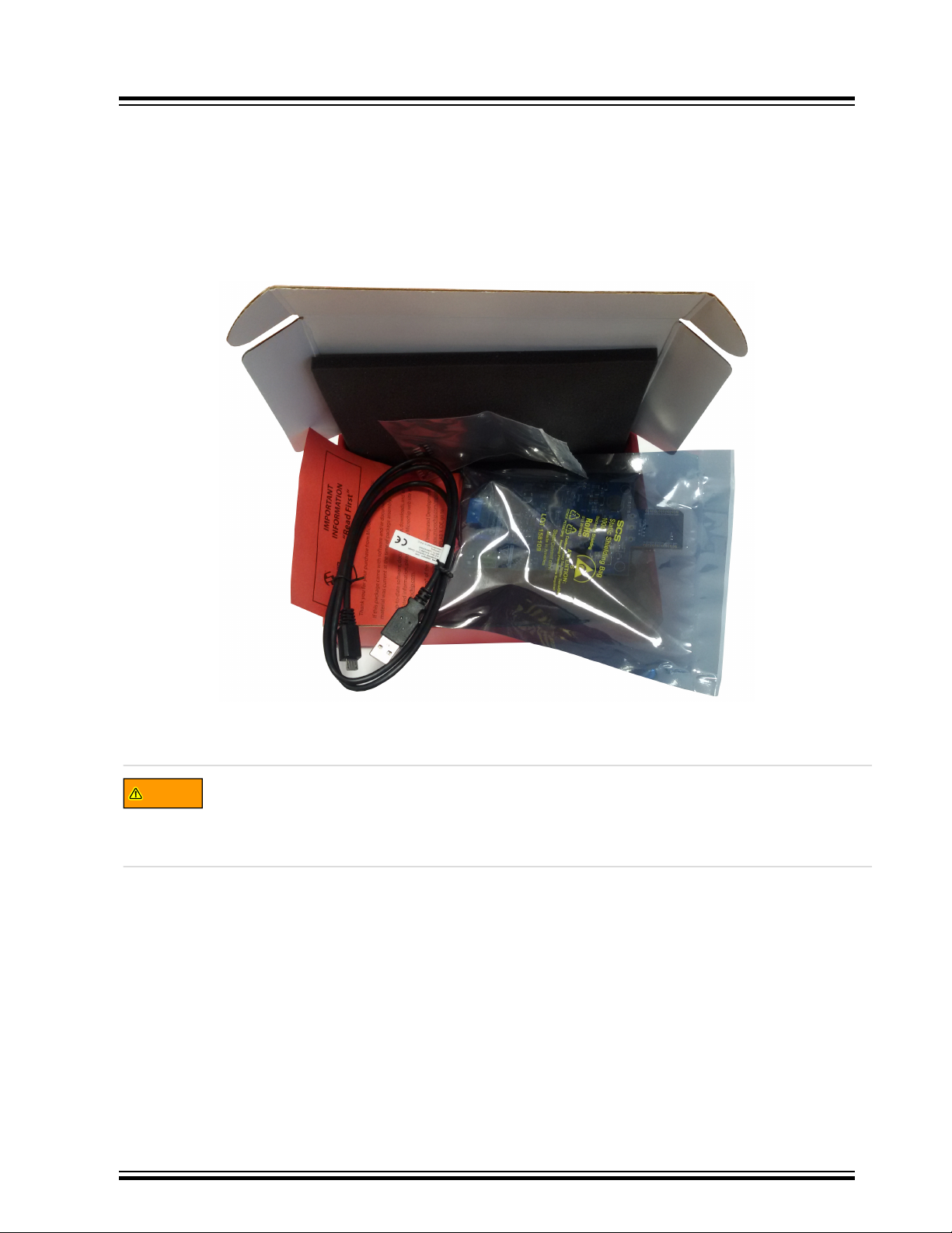
Unpack and inspect the kit carefully.
Figure 2-1. Unpacked PL360G55CB-EK
PL360G55CB-EK
Getting Started
Kit contents are covered by anti-static foam. The PL360G55CB-EK board is shipped in an anti-static
shielding bag.
The board must not be subject to high electrostatic discharge. We recommend using a
grounding strap or similar ESD protective device when handling the board in hostile ESD
environments. Avoid touching the components’ pins or any other metallic elements on the
board.
© 2019 Microchip Technology Inc.
User Guide
DS50002871A-page 6
Page 7
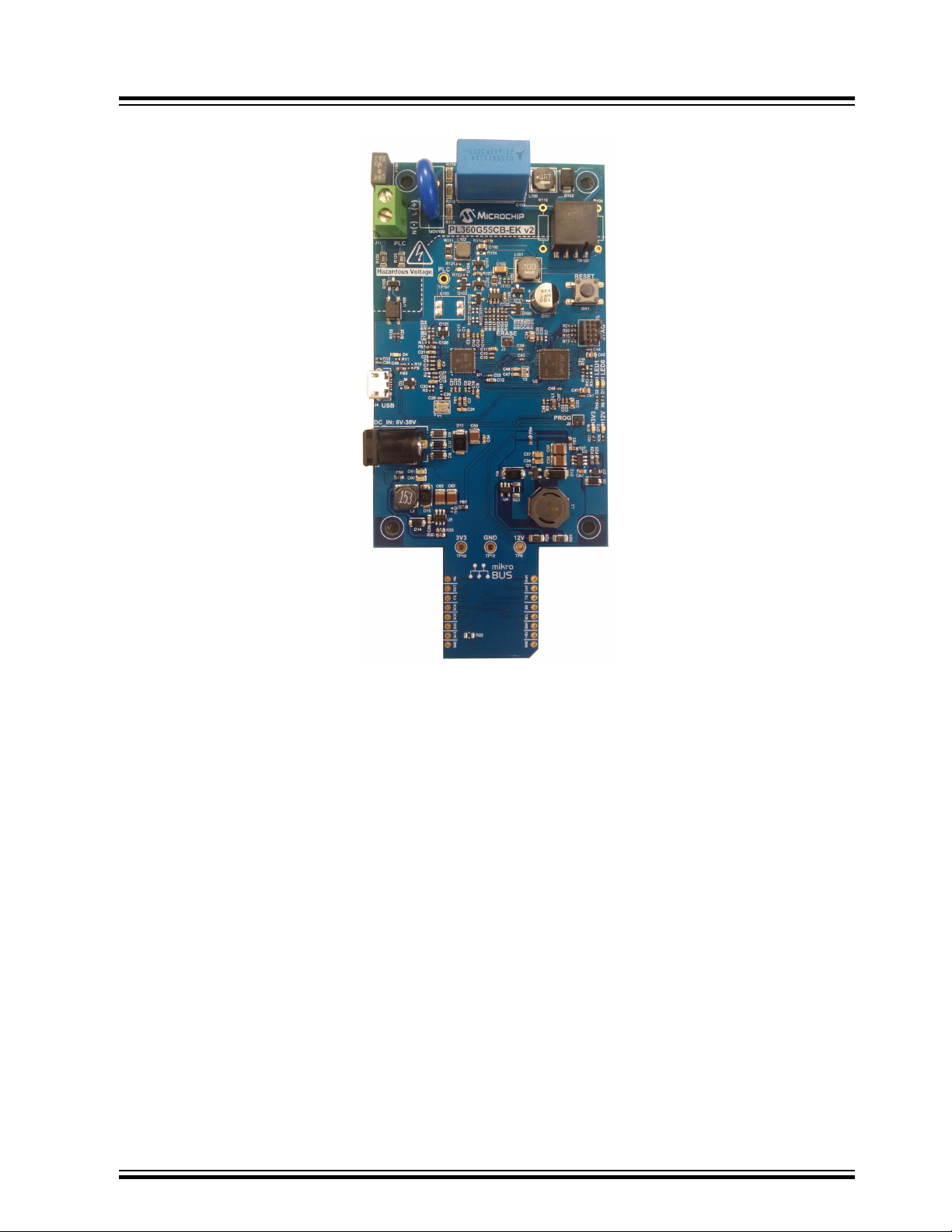
Figure 2-2. PL360G55CB-EKv2 Board Top View
PL360G55CB-EK
Getting Started
Take into account that the connectors to supply the board are different than the one for PLC signals. The
board can be supplied by three different ways:
• +5V from USB Micro-B connector (J4)
• +5V from mikroBUS connector (J6)
• DC voltage (from +6V to +30V) from DC Jack connector (J8)
2.2 Running Preloaded Firmware
Once the board is supplied, LEDs will show activity. The PL360G55CB-EK board is delivered with a preprogrammed application in SAMG55 Flash memory: the G3-PLC PHY Tester for CENELEC B-Band. PLC
communications are developed for CENELEC B-Band in AC or DC voltage grid.
The kit includes a USB 2.0 type A to Micro-B cable that can be used to connect the board to a computer.
Connect a suitable cable in the PLC connector (J1) and plug it to an AC/DC voltage grid to communicate.
By means of the PLC PHY Tester PC application, it is possible to send and receive PLC messages using
the PHY layer in the CENELEC B-Band according to the binary flashed in PL360G55CB-EK board.
2.3 Code and Technical Support
Firmware developers can not only run the given example code, but also implement their own applications
based on the provided firmware stacks.
© 2019 Microchip Technology Inc.
User Guide
DS50002871A-page 7
Page 8

PL360G55CB-EK
Getting Started
Please note that the latest software code, documentation and support materials are available online.
Follow instructions described in the welcome letter for more information.
For any technical support requests, please visit http://support.microchip.com.
© 2019 Microchip Technology Inc.
User Guide
DS50002871A-page 8
Page 9
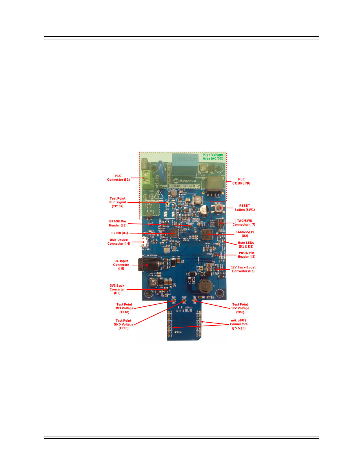
3. PL360G55CB-EK Board
JTAG/SWD
Connector (J7)
mikroBUS
Connectors
(J5 & J6)
USB Device
Connector (J4)
ERASE Pin
Header (J3)
Test Point
12V Voltage
(TP6)
Test Point
3V3 Voltage
(TP10)
PROG Pin
Header (J2)
RESET
Button (SW1)
PLC
Connector (J1)
Test Point
PLC signal
(TP107)
DC Input
Connector
(J8)
PL360 (U1)
3V3 Buck
Converter
(U5)
12V Buck-Boost
Converter (U3)
User LEDs
(D1 & D2)
SAMG55J19
(U2)
PLC
COUPLING
Test Point
GND Voltage
(TP16)
High Voltage
Area (AC/DC)
3.1 Overview
This section summarizes the PL360G55CB-EK board design. It introduces system-level concepts, such
as power supply, MCU, PLC coupling, peripherals and interface board.
PL360G55CB-EK is a PLC modem board based on the PL360 transceiver and on the SAMG55 ARM
Cortex-M4 RISC processor. This evaluation board can be used as a PLC modem reference design for
modular architectures; or, in any case to provide a platform to develop a complete communications
system over PLC technology.
Figure 3-1. PL360G55CB-EKv2 Board Description
PL360G55CB-EK
PL360G55CB-EK Board
3.2 Features List
The PL360G55CB-EK board includes the following features:
• PL360 PLC Transceiver:
© 2019 Microchip Technology Inc.
– Multi-protocol PLC modem:
• G3-PLC
• PRIME 1.3 and PRIME 1.4
User Guide
DS50002871A-page 9
Page 10

PL360G55CB-EK
PL360G55CB-EK Board
– One SPI peripheral to external MCU
– Zero-Cross Detection
– Embedded PLC Analog Front End (AFE)
– Low-power consumption in transmission and reception
• SAMG55 MCU:
– Core:
• ARM Cortex-M4 running at up to 120 MHz
• Memory Protection Unit (MPU)
• DSP instruction set
• Floating-Point Unit (FPU)
• Thumb®-2 instruction set
• Instruction and Data Cache Controller with 2 Kbytes cache memory
• Up to 512 Kbytes of embedded Flash, 176 Kbytes of embedded SRAM, 8 Kbytes of ROM
– Memories:
• Up to 512 Kbytes of embedded Flash
• Up to 176 Kbytes of embedded SRAM
• Up to 8 Kbytes of ROM with embedded bootloader, single-cycle access at full speed
• PLC Coupling designed to communicate in CENELEC B-Band (95 kHz to 125 kHz)
• A 3.3V buck converter for the digital circuitry and a 12V Buck-Boost converter for supplying the PLC
Power Amplifier. It allows supply of the board with any of the three different power sources
• Mains Zero-Crossing Detector Circuit
• Peripherals:
– Supply monitor
– User LEDs
– Reset button
– Chip Erase jumper
– Chip Programming jumper
• Interfaces:
– USB Device
– mikroBUS add-on connectors
– SWD/JTAG debugging port
3.2.1 PL360G55CB-EK Block Diagram
The following figure shows the block diagram of the PL360G55CB-EK board.
© 2019 Microchip Technology Inc.
User Guide
DS50002871A-page 10
Page 11
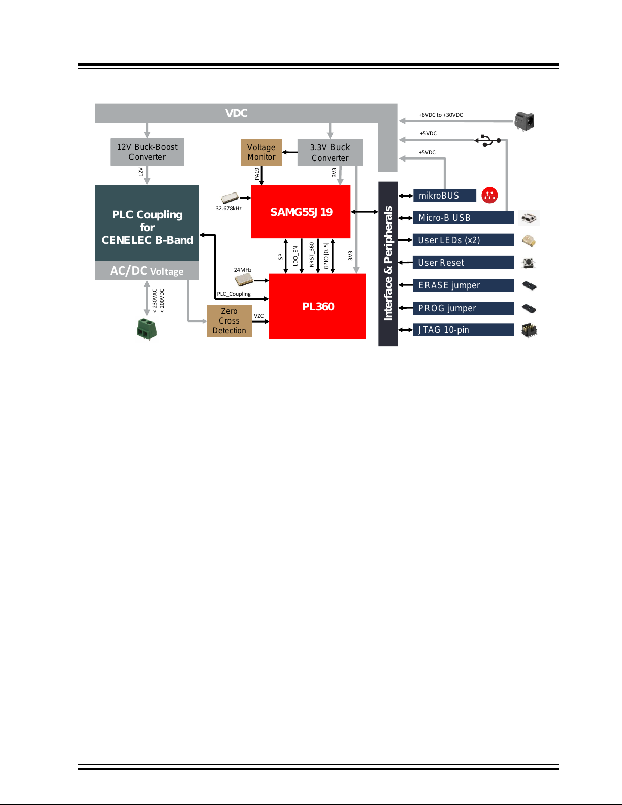
Figure 3-2. PL360G55CB-EK Block Diagram
Interface & Peripherals
VDC
3.3V Buck
Converter
mikroBUS
ERASE jumper
JTAG 10-pin
User LEDs (x2)
User Reset
12V Buck-Boost
Converter
SAMG55J19
PLC Coupling
for
CENELEC B-Band
AC/DC Voltage
Zero
Cross
Detection
SPI
GPIO [0..5]
LDO_EN
NRST_360
+5VDC
< 230VAC
< 200VDC
+5VDC
PLC_Coupling
PROG jumper
+6VDC to +30VDC
PA19
PL360
VZC
Micro-B USB
32.678kHz
24MHz
Voltage
Monitor
12V
3V3
3V3
PL360G55CB-EK
PL360G55CB-EK Board
3.2.2 Interface Connection
The PL360G55CB-EK board includes hardware interfaces such as jumpers, connectors and a button.
Following figure shows an overview of the connectors, jumpers and button of the PL360G55CB-EK
board.
© 2019 Microchip Technology Inc.
User Guide
DS50002871A-page 11
Page 12
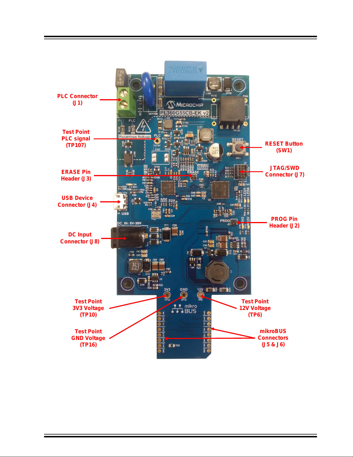
Figure 3-3. PL360G55CB-EK Connectors, Button and Jumpers Overview
JTAG/SWD
Connector (J7)
mikroBUS
Connectors
(J5 & J6)
USB Device
Connector (J4)
ERASE Pin
Header (J3)
Test Point
12V Voltage
(TP6)
Test Point
3V3 Voltage
(TP10)
PROG Pin
Header (J2)
RESET Button
(SW1)
PLC Connector
(J1)
Test Point
PLC signal
(TP107)
DC Input
Connector (J8)
Test Point
GND Voltage
(TP16)
PL360G55CB-EK
PL360G55CB-EK Board
3.2.2.1 Connectors
The PL360G55CB-EK board includes the following connectors:
1. PLC connector (for an AC/DC grid), J1.
© 2019 Microchip Technology Inc.
User Guide
DS50002871A-page 12
Page 13
Table 3-1. PLC Connector (for an AC/DC grid), J1
Pin Signal Name Description
1 L / +VDC Line / Positive Voltage
2 N / -VDC Neutral / Negative Voltage
2. Micro-B female USB connector, J4.
Table 3-2. USB Device Connector, J4
Pin Signal Name Description
1 VUSB 5V power
2 D+ Data Plus
3 D- Data Minus
4 ID On the Go Identification
5 GND Ground
PL360G55CB-EK
PL360G55CB-EK Board
3. mikroBUS add-on connectors, J5 and J6.
Table 3-3. mikroBUS Connector, J5
Pin Mnemonic Description
1 AN Analog
2 RST Reset
3 CS SPI Chip Select
4 SCK SPI Clock
5 SDO SPI Master Input Slave Output
6 SDI SPI Master Output Slave Input
7 3V3 VCC - 3.3V power
8 GND Reference Ground
Table 3-4. mikroBUS Connector, J6
Pin Mnemonic Description
1 PWM PWM
2 INT Hardware Interrupt
3 TX UART Transmit
4 RX UART Receive
5 SCL I2C Clock
6 SDA I2C Data
7 5V VCC - 5V power
© 2019 Microchip Technology Inc.
User Guide
DS50002871A-page 13
Page 14
...........continued
Pin Mnemonic Description
8 GND Reference Ground
4. JTAG/SWD 10-pin connector for SAMG55J19, J7.
Table 3-5. SW-DP Connector, J7
Pin Mnemonic Description
This is the target reference voltage. It is used to check if the
target has power, to create the logic-level reference for the
1 VCC
2 SWDIO/TMS
input comparators, and to control the output logic levels to the
target. It is normally fed from VCC on the target board and
must not have a series resistor.
Serial Wire Input Output / Test Mode Select. JTAG mode set
input of target CPU. This pin should be pulled up on the
target. Output signal that sequences the target's JTAG state
machine, sampled on the rising edge of the TCK signal.
PL360G55CB-EK
PL360G55CB-EK Board
3 GND Ground.
Serial Wire Clock / Test Clock. JTAG clock signal to target
4 SWDCLK/TCK
5 GND Ground.
6 SWO/TDO Test Asynchronous Data Out from target CPU.
7 KEY -
8 NC/TDI
9 GND Detect Ground.
10 nRESET
5. DC Input connector, J8.
Table 3-6. DC Input Connector, J8
CPU (output timing signal, for synchronizing test logic and
control register access).
Not Connected / Test Data Input. JTAG data input of target
CPU (serial data output line, sampled on the rising edge of the
TCK signal). It is recommended that this pin is pulled to a
defined state on the target board.
JTAG Reset (active-low output signal that resets the target).
Output from SAM-ICE™ to the Reset signal on the target JTAG
port. This pin is normally pulled HIGH on the target to avoid
unintentional resets when there is no connection.
Pin Signal Name Description
1 DC_IN DC Input voltage (6 - 30V)
2 GND Ground
3 - -
© 2019 Microchip Technology Inc.
User Guide
DS50002871A-page 14
Page 15

3.2.2.2 Jumper Configurations
The following table describes the functionality of the jumpers.
Table 3-7. Jumper Configuration
Jumper Label Default Setting Function
PL360G55CB-EK
PL360G55CB-EK Board
J3 ERASE Open
J2 PROG Open
Note: Pitch jumpers are 1.27 mm (0.050").
3.2.2.3 Test Points
Some test points (probes and pads) have been placed on the PL360G55CB-EK board for the verification
of the main signals.
Table 3-8. Test Point Probes
Table 3-9. Test Point Pads
Reference Function Reference Function
SAMG55J19 Flash memory code erase
(closed = erase).
SAMG55J19 Flash memory upgrade
(closed = programming).
Reference Function
TP6 12V
TP10 3V3
TP16 GND
TP107 PLC signal
TP1 PROG TP24 PL360 pin PA7
TP2 ERASE TP25 PL360 pin PA8
TP3 SAMG55J19 pin PA12, LED D1 TP26 PL360 pin PA9
TP4 SAMG55J19 pin PA15, LED D2 TP27 PL360 pin PA0
TP5 NRST TP28 PL360 pin PA3
TP7 12V TP100 PL360 pin TXRX1
TP8 DC_IN TP101 P Channel MOSFET
TP9 VDC TP102 Line
TP11 3V3 TP103 N Channel MOSFET
TP12 Ground TP104 Neutral
TP13 Ground TP105 Zero cross signal, VZC
TP14 Ground TP106 PL360 pin TXRX0
TP15 Ground TP108 PLC RX
TP23 PL360 pin PA6 - -
© 2019 Microchip Technology Inc.
User Guide
DS50002871A-page 15
Page 16

3.3 Hardware Description – System
13
24MHz
Y1
GND
MISO
MOSI
SCK
CS
GPIO3
GPIO2
GPIO1
GPIO0
GPIO5
GPIO4
GPIO[0..5]
GND
GND AGND
0.1uFC15
0.1uFC16
0.1uFC17
0.1uFC18
0.1uFC19
0.1uFC20
0.1uFC21
0.1uFC22
GND
4.7uFC13
4.7uFC12
4.7uFC11
0.1uFC10
4.7uFC9
3V3
3V3
2.2uFC2
2.2uFC3
0.1uFC1
0.1uFC5
GND
0.1uFC25
4.7uFC24
GND
470R
FB1
0.1uFC27
0.1uFC28 AGND
AGC
TXRX0
EMIT0
EMIT1
EMIT2
EMIT3
EMIT[0..3]
10000pFC7
0.022uFC8
0.022uFC6
AGND
VIN
3V3A
1uFC30
10kR3
GND
3V3
NRST_PL360
GND
LDOEN
TXRX1
10000pFC4
VZC
10k
R2
4.7uFC14
0.1uFC23
0RR1
PA3
16
VIN
39
VREFN
43
VREFP
41
VREFC
42
PA0
13
NRST
1
XIN
2
XOUT
3
PA7/SPCK
18
PA8/MOSI
19
PA9/MISO
20
EMIT0
23
EMIT1
25
EMIT2
27
EMIT3
31
PA11/TXRX1
33
PA10/TXRX0
34
AGC
35
PA6/NPCS0
17
TST
48
PA4/SWDIO
10
PA5/SWCLK
11
PA1
14
PA2/TRACESWO
15
PA12/VZC
47
PL360B
U1A
VDDIO
4
VDDCORE
7
VDDIO
12
VDDIO
21
VDDIO
24
VDDPLL
5
VDDIN_AN
40
VDDIN_AN
45
VDDIN
8
AGND
44
AGND
38
GND
37
VDDIO
26
VDDIO
28
VDDIO
32
VDDCORE
29
VDDIO
36
VDDIO
46
GND
30
GND
22
GNDOSC
6
LDO ENABLE
9
GND
49
PL360B
U1B
TP100
33pFC26
33pFC29
3.3.1 PL360
The PL360G55CB-EK board is equipped with a PL360 device in 48-pin QFN (0.4 mm pitch).
PL360 is a multi-protocol (G3-PLC, PRIME 1.3 and PRIME 1.4) modem for Power Line Communication
implementing a very flexible architecture, which allows implementation of standard and customized PLC
solutions.
PL360 transceiver has been conceived to be easily managed by an external Microchip MCU through a 4line standard Serial Peripheral Interface (SPI) accessing the internal peripheral registers. Two additional
signals are used by the host microcontroller to control the PL360 transceiver: LDO enable and NRST.
Figure 3-4. PL360 PLC Modem
PL360G55CB-EK
PL360G55CB-EK Board
Important: Some GPIOs of PL360 device must be connected to the external MCU for the right
implementation of the firmware of the PLC standard. G3-PLC requires a GPIO for an external
interrupt line (EINT) and PRIME requires two GPIOs for an external interrupt and carrier detect
indication lines (EINT and CD). Please, check this point with the firmware user guide.
Remember: The PL360 control lines from MCU perspective (SPI lines, EINT in GPIO3 and CD
in GPIO0) are accessible via test points.
Microchip provides highly efficient, reduced BOM reference designs for different coupling options,
targeting common configurations in all PLC bands (<500 kHz) complying with existing regulations.
© 2019 Microchip Technology Inc.
User Guide
DS50002871A-page 16
Page 17

Figure 3-5. PLC Bands Supported by PL360
G3-PLC
CEN-A
0
100 200 300 400 500
Frequency
(kHz)
G3-
PLC
CEN-B
CENELEC [3...148,5 kHz]
G3-PLC ARIB
ARIB [10...450 kHz]
G3-PLC FCC
FCC [10...490 kHz]
USA
JAPAN
EUROPE
CH3 CH4 CH5 CH6 CH7 CH8
CH3 CH4 CH5 CH6 CH7
PRIME 1.4
CH1 CH2
PRIME 1.3 & 1.4
PRIME 1.4
PL360G55CB-EK
PL360G55CB-EK Board
For a further description of the PL360 device see the corresponding PL360 datasheet.
3.3.2 SAMG55J19
The PL360G55CB-EK board is equipped with a SAMG55J19 device in 64-pin QFN. The SAM G55
devices are general-purpose low-power microcontrollers which offer high performance, processing power
and small package options combined with a rich and flexible peripheral set.
The Microchip's SAM G55 embeds a Cortex-M4 CPU with an FPU (floating point unit). This ensures
maximum throughput. This is very important as it allows minimization of the active power consumption
and getting to sleep faster in order to reduce the overall power consumption. Additionally, the device has
30 DMA channels, which gives extremely high throughput.
The SAMG55J19 operates at a maximum speed of 120 MHz and features 512 Kbytes of Flash and up to
176 Kbytes of SRAM. The peripheral set includes eight flexible communication units comprising of
USARTs, SPIs and I2C-bus interfaces (TWIs), two three-channel general-purpose 16-bit timers, two I2S
controllers, one-channel pulse density modulation, one 8-channel 12-bit ADC, one Real-Time Timer
(RTT) and one Real-Time Clock (RTC), both located in the ultra-low power backup area.
© 2019 Microchip Technology Inc.
User Guide
DS50002871A-page 17
Page 18

Figure 3-6. SAMG55 Microcontroller
EP
65
TEST
10
RESET
2
JTAGSEL
63
VREFP
28
VDDUSB
26
VDDOUT
30
VDDIO
64
VDDIO
32
VDDIO
31
VDDIO
27
VDDIO
1
GND
53
GND
29
GND
13
VDDCORE
45
VDDCORE
9
PA08/XOUT3 2
12
PA07/XIN32
11
PA17/AD0
33
PA18/AD1
34
PA19/AD2
35
PA20/AD3
36
PB08/XOUT
59
PB09/XIN
60
PB00/AD4
37
PB01/AD5
38
PB02/AD6
39
PB03/AD7
40
PA00
6
PA01
7
PA02
61
PA03
5
PA04
4
PA05
8
PA06
17
PA09
49
PA10
48
PA11
44
PA12
43
PA13
42
PA14
41
PA15
22
PA16
18
PA21
25
PA22
24
PA23
23
PA24
58
PA25
56
PA26
52
PA27
51
PA28
21
PA29
20
PA30
19
PA31
16
PB10
46
PB11
47
PB12
3
PB13
57
PB14
15
PB15
14
PB04/TDI
62
PB05/TDO/TR ACESWO
50
PB06/TMS/SWDIO
54
PB07/TCK/SWTCK
55
ATSAMG55J19B
U2
PA2
PA5
PA3
PA6
PA4
PA24
PA23
PA9
PA10
PA12
PA11
PA13
PA14
PA19
PA20
PA0
PA1
PA[0..31]
PA16
PA15
PA17
PA18
PA27
PA26
PA25
PA[0..31]
PB2
PB5
PB3
PB6
PB4
PB7
PB8
PB9
PB10
PB12
PB11
PB13
PB14
PB0
PB1
PB15
PB[0..15]
PB[0..15]
PA28
PA31
PA30
PA29
GND
PB[0..15]
PB[0..15]
PB[0..15]
PB[0..15]
PA[0..31]
PA[0..31]
PB00 -> SP I0_CL K (mikr oBUS)
PB01 -> No t Conn ected
PB02 -> T WCK1 (m ikr oBUS)
PB03 -> T WD1 (mik roBUS)
PB04 -> T DI
PB05 -> T DO/TRA CESWO
PB06 -> T MS/SWDI O
PB07 -> T CK/SWC LK
4.7uF
C40
4.7uF
C42
0.1uF
C43
0.1uF
C41
0.1uF
C35
0.1uF
C36
0.1uF
C45
0.1uF
25V
0402
C32
GND
NRST
0R
R7
3V3
0.1uF
C44
VDDCORE
GND
Near pin 30
GND
ADVREF
GND
GND
Near pin 28
ADVREF
3V3
1R
R6
4.7uF
C46
4.7uF
C34
4.7uF
C33
0.1uF
C37
0.1uF
C38
0.1uF
C39
GND
3V3
3V3
USB_DP
USB_DN
USB_Device
USB_Device
32.768Khz
Y2
22pF
C48
22pF
C47
10uH
L1
EP
65
TEST
10
RESET
2
JTAGSEL
63
VREFP
28
VDDUSB
26
VDDOUT
30
VDDIO
64
VDDIO
32
VDDIO
31
VDDIO
27
VDDIO
1
GND
53
GND
29
GND
13
VDDCORE
45
VDDCORE
9
PA08/XOUT3 2
12
PA07/XIN32
11
PA17/AD0
33
PA18/AD1
34
PA19/AD2
35
PA20/AD3
36
PB08/XOUT
59
PB09/XIN
60
PB00/AD4
37
PB01/AD5
38
PB02/AD6
39
PB03/AD7
40
PA00
6
PA01
7
PA02
61
PA03
5
PA04
4
PA05
8
PA06
17
PA09
49
PA10
48
PA11
44
PA12
43
PA13
42
PA14
41
PA15
22
PA16
18
PA21
25
PA22
24
PA23
23
PA24
58
PA25
56
PA26
52
PA27
51
PA28
21
PA29
20
PA30
19
PA31
16
PB10
46
PB11
47
PB12
3
PB13
57
PB14
15
PB15
14
PB04/TDI
62
PB05/TDO/TR ACESWO
50
PB06/TMS/SWDIO
54
PB07/TCK/SWTC K
55
U2
PA2
PA5
PA3
PA6
PA4
PA24
PA23
PA9
PA10
PA12
PA11
PA13
PA14
PA19
PA20
PA0
PA1
PA[0..31]
PA16
PA15
PA17
PA18
PA27
PA26
PA25
PA[0..31]
PB2
PB5
PB3
PB6
PB4
PB7
PB8
PB9
PB10
PB12
PB11
PB13
PB14
PB0
PB1
PB15
PB[0..15]
PB[0..15]
PA28
PA31
PA30
PA29
GND
PB[0..15]
PB[0..15]
PA[0..31]
PA[0..31]
4.7uF
C40
4.7uF
C42
0.1uF
C43
0.1uF
C41
0.1uF
C35
0.1uF
C36
0.1uF
C45
0.1uF
25V
0402
C32
GND
NRST
0R
R7
3V3
0.1uF
C44
VDDCORE
GND
Near pin 30
GND
Near pin 28
ADVREF
4.7uF
C34
4.7uF
C33
0.1uF
C37
0.1uF
C38
0.1uF
C39
GND
3V3
3V3
USB_DP
USB_DN
USB_Device
USB_Device
3V3
PB12
Er ase pin
32.768Khz
Y2
22pF
C48
22pF
C47
1 2
J3
PRO G pin h eader
1 2J2PA18
GND
TP1
TP2
Procedure for SAMG55 chiperase:
1) Connect the two pins of the he ader w
2) Remove power fro m the kit
3) Connect pow er to the kit
4) Remove jumper
The ERASE pin has an internal pul l-dow
not configu red as GPIO in the user appl
Procedure for SAMG55 programming:
1) Power off the board
2) Place jumper in PROG header
3) Power on th e board
4) Remove jumper aft er programming
The PROG pin has an internal pull -up if
not configu red as GPIO in the user appli
PL360G55CB-EK
PL360G55CB-EK Board
Table 3-10 and Table 3-11 summarize the functionality of each input/output line of the SAMG55J19
microcontroller in PL360G55CB-EK board.
Table 3-10. Pinout of SAMG55J19 PortA in PL360G55CB-EK Board
I/O LINE Function I/O LINE Function
PA0 PL360 GPIO3 PA16 PL360 GPIO4
PA1 PL360 GPIO2 PA17 AD0 (mikroBUS)
PA2 Not Connected PA18 PROG
PA3 PL360 MOSI PA19 Voltage Monitor
PA4 PL360 MISO PA20 Not Connected
PA5 PL360 GPIO1 PA21
PA6 PL360 GPIO5 PA22 USB Device Diff Positive
PA7 XIN32 PA23 TIOA1 (mikroBUS)
© 2019 Microchip Technology Inc.
PA8 XOUT32 PA24 Not Connected
PA9 SPI0 MISO (mikroBUS) PA25 SPI0 CS0 (mikroBUS)
PA10 SPI0 MOSI (mikroBUS) PA26 Not Connected
PA11 USB Detect PA27 Not Connected
PA12 User LED0 PA28 Not Connected
PA13 Not Connected PA29 PL360 NRST
PA14 WKUP8 (mikroBUS) PA30 PL360 LDO_EN
User Guide
USB Device Diff
Negative
DS50002871A-page 18
Page 19

...........continued
13
24MHz
Y1
GND
MISO
MOSI
SCK
CS
GPIO3
GPIO2
GPIO1
GPIO0
GPIO5
GPIO4
GPIO[0..5]
GND
AGC
TXRX0
EMIT0
EMIT1
EMIT2
EMIT3
EMIT[0..3]
10000pFC7
0.022uFC8
0.022uFC6
AGND
VIN
1uFC30
10kR3
GND
3V3
NRST_PL360
TXRX1
10000pFC4
VZC
0RR1
PA3
16
VIN
39
VREFN
43
VREFP
41
VREFC
42
PA0
13
NRST
1
XIN
2
XOUT
3
PA7/SPCK
18
PA8/MOSI
19
PA9/MISO
20
EMIT0
23
EMIT1
25
EMIT2
27
EMIT3
31
PA11/TXRX1
33
PA10/TXRX0
34
AGC
35
PA6/NPCS0
17
TST
48
PA4/SWDIO
10
PA5/SWCLK
11
PA1
14
PA2/TRACESWO
15
PA12/VZC
47
PL360B
U1A
TP100
33pFC26
33pFC29
I/O LINE Function I/O LINE Function
PA15 User LED1 PA31 PL360 GPIO0
Table 3-11. Pinout of SAMG55J19 PortB in PL360G55CB-EK Board
I/O LINE Function I/O LINE Function
PB0 SPI0 CLK (mikroBUS) PB8 Not Connected
PB1 Not Connected PB9 Not Connected
PB2 TWCK1 (mikroBUS) PB10 TXD4 (mikroBUS)
PB3 TWD1 (mikroBUS) PB11 RXD4 (mikroBUS)
PB4 TDI PB12 ERASE
PB5 TDO/TRACESWO PB13 PL360 SCK
PB6 TMS/SDWIO PB14 PL360 CS
PB7 TCK/SWCLK PB15 Not Connected
PL360G55CB-EK
PL360G55CB-EK Board
The right implementation of the PLC standards require some GPIOs of the transceiver PL360 connected
to the SAMG55. G3-PLC requires a GPIO for an external interrupt line (PA0 of SAMG55) and PRIME
requires two GPIOs for an external interrupt and carrier detect (PA0 and PA31 of SAMG55) indication
lines. Please check this point with the firmware user guide.
For a further description of the SAMG55J19 capabilities see the corresponding SAMG55 datasheet.
3.3.3 Clock Circuitry
Besides the embedded RC oscillators of SAMG55J19, two crystal oscillators are assembled on the
PL360G55CB-EK board to obtain a more precise and stable system clock reference:
• A 24 MHz clock signal, Y1, generated for the PLC transceiver PL360
• A low-power 32.768 kHz crystal oscillator, Y2, for the SAMG55J19
Figure 3-7. 24 MHz Crystal Oscillator Scheme
© 2019 Microchip Technology Inc.
User Guide
DS50002871A-page 19
Page 20

Figure 3-8. 32.768 kHz Crystal Oscillator Scheme
EP
65
TEST
10
RESET
2
JTAGSEL
63
VREFP
28
VDDUSB
26
VDDOUT
30
VDDIO
64
VDDIO
32
VDDIO
31
VDDIO
27
VDDIO
1
GND
53
GND
29
GND
13
VDDCORE
45
VDDCORE
9
PA08/XOU T32
12
PA07/XIN3 2
11
PA17/AD0
33
PA18/AD1
34
PA19/AD2
35
PA20/AD3
36
PB08/XOUT
59
PB09/XIN
60
PB00/AD4
37
PB01/AD5
38
PB02/AD6
39
PB03/AD7
40
PA00
6
PA01
7
PA02
61
PA03
5
PA04
4
PA05
8
PA06
17
PA09
49
PA10
48
PA11
44
PA12
43
PA13
42
PA14
41
PA15
22
PA16
18
PA21
25
PA22
24
PA23
23
PA24
58
PA25
56
PA26
52
PA27
51
PA28
21
PA29
20
PA30
19
PA31
16
PB10
46
PB11
47
PB12
3
PB13
57
PB14
15
PB15
14
PB04/TDI
62
PB05/TDO/ TRACESWO
50
PB06/TMS/SWDI O
54
PB07/TCK/SWT CK
55
ATSAMG55J19B
U2
PA2
PA5
PA3
PA6
PA4
PA24
PA23
PA9
PA10
PA12
PA11
PA13
PA14
PA19
PA20
PA0
PA1
PA[0..31]
PA16
PA15
PA17
PA18
PA27
PA26
PA25
PA[0..31]
PB2
PB5
PB3
PB6
PB4
PB7
PB8
PB9
PB10
PB12
PB11
PB13
PB14
PB0
PB1
PB15
PB[0..15]
PB[0..15]
PA28
PA31
PA30
PA29
GND
PB[0..15]
PB[0..15]
PB[0..15]
PB[0..15]
PA[0..31]
PA[0..31]
4.7uF
C42
0.1uF
C43
0.1uF
C41
0.1uF
C35
0.1uF
C36
0.1uF
25V
0402
C32
GND
NRST
0R
R7
3V3
0.1uF
C44
VDDCORE
GND
GND
ADVREF
0.1uF
C37
0.1uF
C38
0.1uF
C39
GND
3V3
3V3
USB_DP
USB_DN
USB_Device
32.768Kh z
Y2
22pF
C48
22pF
C47
PL360G55CB-EK
PL360G55CB-EK Board
3.3.4 Reset
The reset sources of the PL360G55CB-EK board are:
• Power-on Reset function, embedded in the SAMG55 device.
• Push button reset. Both devices, SAMG55J19 and PL360, have a NRST pin: “NRST” for
SAMG55J19 and “NRST_360” for PL360. The user can manually reset the SAMG55J19, which
manages the PL360 reset, by using the push button SW1. See section 3.4.2.2 Push Buttons.
• JTAG reset from an in-circuit emulator.
3.3.5 PLC Coupling Circuitry Description
The European regulations concerning Power Line Communications are described in CENELEC standard
EN 50065. This standard applies to electrical equipment using signals in the frequency range 3 kHz to
148,5 kHz to transmit information on low voltage electrical systems, either on the public supply system or
within installations in consumers' premises. The following figure shows the different frequency bands
allocated to the different applications.
© 2019 Microchip Technology Inc.
User Guide
DS50002871A-page 20
Page 21

PL360G55CB-EK
PL360G55CB-EK Board
Figure 3-9. CENELEC Frequency Bands
The PL360G55CB-EK evaluation board communicates in the CENELEC B-Band frequency. The use of
frequencies in this band shall be restricted to consumer use; for example, for end-user applications such
as industrial applications.
Microchip has designed five coupling reference designs for CENELEC B-Band with variations in the BOM
cost and the communication performance. Table 3-12 summarizes the main features of the available
designs.
Table 3-12. Characteristics of PLCOUPxxx Boards for CENELEC B-Band
Board Name
PLCOUP012-
ISO
PLCOUP012-
NONISO
PLCOUP013
PLCOUP014-
ISO
PLCOUP014-
NONISO
Description
Low cost with internal
driver G3 CENELEC B
compliant
Low cost with internal
driver G3 CENELEC B
compliant
Ultra low cost with
internal driver and
non-Isolated G3
CENELEC B
compliant
G3 CENELEC B
compliant
G3 CENELEC B
compliant
Frequency
Band (kHz)
95 - 125 Single Yes -
95 - 125 Single No -
95 - 125 Single No -
95 - 125 Single Yes -
95 - 125 Single No -
Branch
Electrical
Isolation
PRIME
Channel
G3-PLC
Band
G3
CENELEC B
G3
CENELEC B
G3
CENELEC B
G3
CENELEC B
G3
CENELEC B
Applicable
Regulation
CENELEC
EN 50065
CENELEC
EN 50065
CENELEC
EN 50065
CENELEC
EN 50065
CENELEC
EN 50065
The PL360G55CB-EK board is assembled with the PLCOUP014-ISO coupling design. The goal is to
provide a cost-optimized fully-featured design according to the G3-PLC requirements. Still, the
PL360G55CB-EK board is designed to allow using all the other coupling designs by changing the
corresponding components and firmware configurations.
Important: Check the online resources from Microchip website to download the proper files
according to your desired CENELEC B-Band design.
© 2019 Microchip Technology Inc.
User Guide
DS50002871A-page 21
Page 22

1
2
4
3
PL360G55CB-EK
PL360G55CB-EK Board
The following figure shows the PLC Coupling assembled (PLCOUP014-ISO) which is composed of four
sub-circuits:
1. Transmission Stage
2. Filtering Stage
3. Coupling Stage
4. Reception Stage
Figure 3-10. PLC Coupling Schematic on PL360G55CB-EK Board
Remember: PLC Coupling circuitry adds a yellow LED, D104, for visual indication of PLC
frames transmission.
The following sections describe the aim of every sub-circuit assembled in the PL360G55CB-EK board.
3.3.5.1 PLC Transmission Circuit
The transmission stage adapts the EMIT signals and amplifies them. In the PL360G55CB-EK board, see
Figure 3-10, it is a single branch composed of:
• Driver: It adapts the EMIT signals to either control the amplifier or to be filtered by the next stage
• Amplifier: A Class-D amplifier generating a square waveform from 0 to 12V
• Bias and protection: It provides a DC component and provides protection from received disturbances
The transmission stage is followed by a filtering stage.
3.3.5.2 PLC Filtering Circuit
The in-band flat response filtering stage reduces spurious emission to the limits set by the corresponding
regulation and blocks potential interferences from other transmission channels without distorting the
injected signal.
The filtering stage used in PL360G55CB-EK, see Figure 3-10, has three aims:
• Band-pass filtering of high frequency components of the square waveform generated by the
transmission stage
© 2019 Microchip Technology Inc.
User Guide
DS50002871A-page 22
Page 23

• Adapt Input/Output impedance for optimal reception/transmission. This is controlled by TXRX0 signal
CAUTION
• A band-pass filtering for received signals
3.3.5.3 PLC Coupling Circuit
PLC coupling circuit connects the PLC signal directly to the mains grid or even to DC power rails without
requiring any hardware adaptation. The main purpose of the circuit is to block the mains voltage of the
grid to/from which the signal is injected/received. This is carried out in PL360G55CB-EK, see Figure 3-10,
by a high voltage capacitor, C103. Resistors R108, R112 and R115 allow the high voltage capacitor to
discharge after disconnection from mains.
PLC coupling components are designed for a maximum voltage of 230 VAC or 200 VDC.
The TR100 transformer (with turn ratio 1:1) provides galvanic isolation from mains. A non-isolated version
could easily be implemented removing TR100, soldering R106 and R116 resistors and updating the value
of L103 according to the PLCOUP014-NONISO design.
MOV100 varistor, F100 fuse and D102 TVS diode protect the coupling circuit from the overvoltages and
high transient voltages (surges and spikes) from mains.
PL360G55CB-EK
PL360G55CB-EK Board
3.3.5.4 PLC Reception Circuit
The PLC reception circuit used in PL360G55CB-EK, see Figure 3-10, is the reference design for the
reception stage and it is composed of:
• Single-pole low pass filter, R133 and C109
• Automatic Gain Control (AGC) circuit. A resistor, R134, is used to attenuate the incoming PLC signal
in case its amplitude is high enough to exceed the input dynamic range of the embedded ADC
• A resistor, R132, for impedance matching
• DC decoupling capacitor, C106
3.3.6 Power Supply System
The PL360G55CB-EK board can be powered by several power sources. Supply the board via:
• the DC jack 2.0 mm connector J8, DC_IN, with a DC source from 6V to 30V (±5%) and 4.2W
• the USB connector (+5V), J4
• the power supply pin (+5V) of mikroBUS standard
Table 3-13. Power Sources for PL360G55CB-EK Board
Power Input Voltage Requirements Power Requirements Connector Marking
DC Jack connector +6V to +30V (±5%) 4.2 Watts DC_IN
Target USB +5V
According to USB
specifications
USB
mikroBUS Power pin
(+5V)
The PL360G55CB-EK board has two voltage rails:
• +3.3V for the digital part of the PLC modem, PL360, and the SAMG55J19 MCU
• +12V to power the class-D amplifier of the PLC coupling circuit
© 2019 Microchip Technology Inc.
+5V
According to mainboard
specifications
User Guide
+5V
DS50002871A-page 23
Page 24

CAUTION
BOOST
VIN
EN
GND
VFB
SW
VDD
IN
OUT
GND
GND
3V3
GREEN
D16
GND
600mA max
3.3 Volts
VDC
GND
GND
GND
TP10
TP11
300R
R31
10k
R33
470R
FB6
BOOST
GND
2
VFB
3
EN
4
SW
6
VIN
5
U5
MCP16301
GND
1M
R32
4.7uF
50V
C62
4.7uF
50V
C63
0.1uF
C59
B140-13-F
D15
1N4448W
D14
10uF
C60
10uF
C61
15uH
L3
31.6k
R30
3V3 Buck C onver ter
470R
FB7
PL360G55CB-EK
PL360G55CB-EK Board
Note that the PL360G55CB-EK board does not provide a power supply protection circuit; only a
TVS diode is used to protect from voltage spikes at the DC rail.
The 12V voltage rail is obtained from the MC16301 buck-boost converter. For a further description about
the buck-boost converter see the MCP16301 Buck-Boost Converter User's Guide. If the VDC voltage is
always higher than 12V, it is possible to improve the power efficiency by transforming the converter mode
from buck-boost to buck, see MCP16301 datasheet for a further explanation.
Figure 3-11. 12V Voltage Design
Restriction: Note that some power sources, such as USB port and mikroBUS rail, might have
limited current capabilities and they could not supply enough current for the class-D amplifier
transmitting against low impedance values. In this case, an external AC/DC power supply with
enough current rating is recommended to maintain the PLC performance at its best. In case of
using one, we recommend a module complying to national regulations or CISPR 32:2015.
Another buck converter, MC16301, is used to generate a regulated 3.3V voltage rail required by the
PL360 modem and the SAMG55J19 MCU. For a further description about the buck converter see the
MCP16301 Buck Converter User's Guide.
Figure 3-12. 3.3V Buck Converter Design
There are one LED and two test points on each voltage rail to check whether all power supplies are
operating properly.
To avoid on board self-generated disturbances within the PLC signal band, both converters are switching
at 500 kHz fixed frequency, out of the PLC band (95 to 125 kHz).
© 2019 Microchip Technology Inc.
User Guide
DS50002871A-page 24
Page 25

Tip: In case of choosing a different SMPS in the customer design, it is important to analyze its
PL360G55CB-EK
PLC
Rejection
Filter
Power
Source
(Very Low Z
for PLC signal)
PLC Coupling
Power Supply
(3V3 Buck Converter & 12V
Buck-Boost Converter)
560uH
560uH
100nF
N / DC-
L / DC+
potential interference on the PLC frequency band.
Attention: To avoid noise interferences, the switching frequency of the SMPS must be out of
the PLC band and preferably in frequencies above it to avoid harmonics influence. This is
essential to obtain a good reception performance.
3.3.6.1 PLC Rejection Filter
When the PLC coupling circuit is in parallel with the power supply circuit, the input impedance of the final
equipment could be affected. If the requirements about total input impedance are not satisfied, an
appropriate input filter is needed at the power supply input to increase the input impedance.
Apart from the input filter, it is also recommended to add a PLC rejection filter to avoid the absorption of
the PLC signals by the power supply circuit. This filter also increases the input impedance, so it helps to
achieve the requisites about input impedance.
PL360G55CB-EK
PL360G55CB-EK Board
Notice: The PL360G55CB-EK board has PLC coupling and power supply circuits separated,
so the PLC rejection filter is not included. A PLC rejection filter is needed in case of low input
impedance after connecting in the same point the PLC Coupling connector J1 and the power
source of the board.
An example of PLC rejection filter is composed of two inductance in-series (L = 560 μH) and a capacitor
in-parallel (C = 100 nF) at the power supply input as shown in the following picture.
Figure 3-13. PLC Rejection Filter Example
© 2019 Microchip Technology Inc.
User Guide
DS50002871A-page 25
Page 26

3.3.7 Zero-Crossing Detector Circuit
VZC
3V3
GND
PLC+
PLC-
0R
R125
4.7k
R123
TP105
3 4
1 6
TLP183(GB-TPL,E
U100
BAT54
D105
56kR126
56kR129
PA17/AD0
33
PA18/AD1
34
PA19/AD2
35
PA20/AD3
36
PB00/AD4
37
PB01/AD5
38
PB02/AD6
39
PB03/AD7
40
PB10
PB11
47
PB12
3
PB13
57
PB14
15
PB15
14
PB04/TDI
62
PB05/TDO/TRACESWO
50
PB06/TMS/SWDIO
54
PB07/TCK/SWTCK
55
PA19
PA20
PA17
PA18
PB2
PB3
PB0
PB1
PA[0..31]
PA[0..31]
Phase identification is an important feature of devices that are connected to a Smart Grid network. A
typical implementation is based on measuring the time difference between a specific PLC frame reception
and the last zero crossing event of the mains single-phase to which the device is connected.
Important: The phase identification feature is mandatory for G3-PLC and PRIME1.4, but not
for PRIME1.3.
Figure 3-14 shows the Zero-Crossing Detection circuit used in the PL360G55CB-EK board, which
features detection of rising edges of the mains voltage. The output signal of the detection circuit “VZ
CROSS” is connected to VZ pin of PL360 and a synchronization algorithm is applied in order to obtain an
accurate measurement of the time between PLC frame reception and zero crossing events.
Figure 3-14. Zero-Crossing Detection Circuit
PL360G55CB-EK
PL360G55CB-EK Board
Notice: Designs that do not require galvanic isolation can use a simpler Zero-Crossing
Detector circuit, such as a Zener diode, instead of the previous circuit.
3.4 Hardware Description – MCU Peripherals
3.4.1 Voltage Monitor
The input pin PA19 of SAMG55J19 is used to monitor the 3.3V voltage rail through external voltage
divisors. It can be used to monitor the VDC voltage rail mounting R14 and removing R15 resistor.
Important: The R14 resistor value depends on the voltage value of the input source power.
© 2019 Microchip Technology Inc.
User Guide
DS50002871A-page 26
Page 27

Figure 3-15. Voltage Monitor Circuit
PA19
VDC 3V3
1k
1%
R15
10k
1%
R19
1%
R14
470pF
C51
1k1%
R16
GND
In case to sense VDC
voltage, select the right
value of the resistor, R14,
according to your voltage
value. And remove
resistor, R15.
3V3
3V3
(LED0)
(LED1)PA15
PA12
GREEN
D1
RED
D2
300R
R8
300R
R10
TP3
TP4
GND NRST
NRST
TP5
1 4
2 3
SW1
The voltage monitor circuit allows the implementation of multiple applications such as:
• Detection of fault conditions
• Detection of Low-Power mode entering conditions
• Detection of wake-up situations
3.4.2 LEDs and Buttons
The PL360G55CB-EK board is equipped with several LEDs and one user push button.
PL360G55CB-EK
PL360G55CB-EK Board
3.4.2.1 User LEDs
The PL360G55CB-EK board includes two general purpose LEDs, one green connected to PA12 (LED0)
and one red connected to PA15 (LED1).
Figure 3-16. User LEDs
In addition, this board disposes of two green LEDs, D13 and D16, connected to 12V and 3.3V supplies
for visual status of these voltages, and a yellow LED, D104, for visual indication of PLC frames
transmission.
3.4.2.2 Push Buttons
The PL360G55CB-EK board is equipped with a momentary push button switch mounted directly to the
board. When the button is pressed it will drive the SAMG55 reset line, NRST, to GND. And PA29 will drive
the PL360 reset line, NRST_PL360, to GND.
Figure 3-17. Reset Button
3.4.3 Chip Programming
The 1x2 pin-header J2 marked as “PROG” is connected to the SAMG55J19 chip input pin (PA18) and
GND. This header can be used to upgrade (using a bootloader binary file of the SAMG55J19) the PLC
stack running on the SAMG55 by the USB/serial port. See Smart Energy: Serial Bootloader User Guide
for more information.
© 2019 Microchip Technology Inc.
User Guide
DS50002871A-page 27
Page 28

3.4.4 Chip Erase
VUSBD
DUSB_N
GNDGND
DUSB_P
GND
GND
PA11
USB_DP
USB_DN
USB_Device
USB_Device
123450
ID D+ D- +5VGND
USB2.0 MICRO-B FEMALE
J4
GND
YELLOW
D4
300R
R11
1M
R13
27kR9
47k
R12
470RFB3
4700pF
C50
0.1uF
C49
1
2
4
3
D3
PRTR5V0U2X
GND
CAUTION
The 1x2 pin-header J3 marked as “ERASE” is connected to the SAMG55J19 chip erase pin (PB12) and
3.3V. This header can be used to re-initialize the Flash content (and some of its NVM bits) to an erased
state (all bits read as logic level 1) by placing a jumper on the header and pressing the reset switch
button. After a while, the erase jumper should be removed and the PCBA must be turned off and turned
on by disconnecting and connecting it again to the selected power supply. See section “ERASE Pin” in
the SAMG55J19 datasheet for more information.
Notice: Take into account that when Flash is erased, the bootloader application will also be
removed; therefore the SAMG55J19 device will be programmable only via JTAG.
3.5 Hardware Description – MCU Interface Ports
3.5.1 USB Device Port
The USB Device Port (UDP) is compliant with the Universal Serial Bus (USB) 2.0 full-speed device
specification. There is a USB available on the PL360G55CB-EK board that can act as both host and
device. It has a Micro-B female USB connector with the silk screen USB.
PL360G55CB-EK
PL360G55CB-EK Board
The I/O line PA11 allows the application to check if VUSBD is available.
Figure 3-18. USB Circuit
Important: Check online resources from the Microchip Website to download the drivers
according to your Operating System.
The USB connector is not isolated from mains. Please make use of proper isolation (i.e.: USB
isolator device) in case of using this connector when the board is not galvanically isolated (using
a PLC Coupling design which it is not isolated from mains). Take into account the possible noise
interference that these isolators could be adding to the PLC network. For instance, you can use
the UH401.
© 2019 Microchip Technology Inc.
User Guide
DS50002871A-page 28
Page 29

3.5.2 SAMG55J SWD/JTAG Port
3V3
GND
NRST
PB6
PB7
PB5
PB4
3V3
100kR18
100kR17
100kR20
100kR21
1
2
3
4
5
6
7
8
9
10
J7
nRESET
NC/TDI
SWO/TDO
SWDCLK/TCK
SWDIO/TMSVCC
GND
GND
KEY
GNDDetect
CAUTION
The PL360G55CB-EK board includes an SWD (Serial Wire Debug) / JTAG interface port to provide
debug level access to the system-on-chip. It also embeds a serial wire trace. This connector provides the
required interface for in-circuit emulators, like the Atmel-ICE or SAM-ICE. The SW-DP/JTAG port is a 10pin, dual row, 0.1-inch male connector (J7). When using the SAM-ICE, a JTAG adapter for 20 to 10 pins
is necessary, e.g., this one.
Important: Note that the PL360G55CB-EK kit does not include either Atmel SAM-ICE or
Atmel-ICE JTAG emulators.
Please refer to the SAMG55 datasheet for further description of the JTAG debug port.
Figure 3-19. JTAG/SWD Interface Schematic
PL360G55CB-EK
PL360G55CB-EK Board
The JTAG/SWD connector is not isolated from mains. Please make use of proper isolation (i.e.:
USB isolator device) if using this connector when the board is not galvanically isolated (using a
PLC Coupling design which it is not isolated from mains). Take into account the possible noise
interference that these isolators could be adding to the PLC network. For instance, you can use
the UH401.
3.5.3 mikroBUS Connector
The PL360G55CB-EK board incorporates mikroBUS add-on connectors (J5 and J6) to integrate the
board itself as a module which is able to interface with other microcontrollers or microprocessors (main
board).
The mikroBUS standard specifies the size and shape of the add-on boards, but because of special
constraints, the board exceeds those limits although keeping the smallest size model S as a reference for
the plug-in area.
The PL360G55CB-EK board is designed to operate only from the +5V power supply rail of the mikroBUS
socket. Therefore, +3.3V power supply pin is not connected.
Important: By default, J5 and J6 headers are not populated in the board. The 8-pin headers
are included in a zip bag as kit contents.
This mikroBUS standard has a pair of 1x8 male headers with the following pinout:
© 2019 Microchip Technology Inc.
User Guide
DS50002871A-page 29
Page 30

• SPI
AN
RST
CS
SCK
SDO
SDI
3V3
GND GND
5V
SDA
SCL
RX
TX
INT
PWM
5V
GND
3V3
GND
PA23
PB10
PB11
PA9
PA10
PA14
PA17
PA25
PB0
PB2
PB3
1
2
3
4
5
6
7
8
J6
1
2
3
4
5
6
7
8
J5
NRST
0R
R22
• UART
• I2C
• PWM
• Interrupt
• Analog input
• Reset
• Chip Select
• +3.3V
• +5V
• Two GND pins
Figure 3-20. mikroBUS Connector
PL360G55CB-EK
PL360G55CB-EK Board
Notice: The mikroBUS Xplained Pro is an extension board which contains the female header
to connect the mikroBUS add-on boards to the Xplained Pro MCU boards.
3.6 PL360G55CB-EK Schematics
This section contains the schematics for the PL360G55CB-EKv2 board:
• Top Level Schematic, Figure 3-21
• PL360 Schematic, Figure 3-22
• SAMG55 MCU Schematic, Figure 3-23
• Interface and Peripherals SAMG55 Schematic, Figure 3-24
• Power Supply Schematic, Figure 3-25
• PLC Coupling Schematic, Figure 3-26
User Guide
DS50002871A-page 30
© 2019 Microchip Technology Inc.
Page 31

Figure 3-21. Top Level Schematic
1
1
2
2
3
3
4
4
5
5
6
6
D D
C C
B B
A A
1 of 6
PL360G55CB-EK
01/04/2019 12: 26:12
Main.SchDoc
Project Title
Sch #: Date:
File:
Revision: Sheet
Designed with
Drawn By:
R. Navarro
Sheet Title
Top Level Schematic
Engineer:
J.L. Caceres
03-**
2
Size
B
**
PartNumber:
Altium.com
REV ECO# DESCRIPTION DATE
Top Level Schematic
PLC
VZC
PLC_Coupling
U_PL360
PL360.SchDoc
VZC
PLC_Coupling
N
L
U_PLC Coupling
PLC_Coupling.SchDoc
PA[0..31]
NRST
PB[0..15]
PLC
USB_Device
U_SAMG55
SAMG55.SchDoc
PA[0..31]
PB[0..15]
NRST
USB_Device
U_INTERFACE
Interface.SchDoc
AC/DC volt age
U_Power Supply
Power_Supply.SchDoc
12
J1
PLC Connector
PAD2 PAD4PAD3PAD1
2
Adding PROG header & minor changes 01/04/2019
1
1
2
2
3
3
4
4
5
5
6
6
D D
C C
B B
A A
2 of 6
PL360G55CB-EK
01/04/2019 12: 26:12
PL360.SchDoc
Project Title
Sch #: Date:
File:
Revision: Sheet
Designed with
Drawn By:
R. Navarro
Sheet Title
PL360 Modem
Engineer:
J.L. Caceres
03-**
2
Size
B
**
PartNumber:
Altium.com
13
24MHz
Y1
GND
MISO
MOSI
SCK
CS
GPIO3
GPIO2
GPIO1
GPIO0
GPIO5
GPIO4
GPIO[0..5]
GND
GND AGND
0RR4
0RR5
GND AGND
0.1uFC15
0.1uFC16
0.1uFC17
0.1uFC18
0.1uFC19
0.1uFC20
0.1uFC21
0.1uFC22
GND
4.7uFC13
4.7uFC12
4.7uFC11
0.1uFC10
4.7uFC9
3V3
3V3
2.2uFC2
2.2uFC3
0.1uFC1
0.1uFC5
GND
0.1uFC25
4.7uFC24
GND
470R
FB1
0.1uFC27
0.1uFC28 AGND
AGC
TXRX0
EMIT0
EMIT1
EMIT2
EMIT3
EMIT[0..3]
10000pFC7
0.022uFC8
0.022uFC6
AGND
VIN
3V3A
470RFB2
3V3
1uFC30
10kR3
GND
3V3
NRST_PL360
GND
LDOEN
VZC
PL360
MISO
MOSI
SCK
CS
GPIO[0..5]
NRST_PL360
LDOEN
PLC
PLC
EMIT[0..3]
TXRX0
TXRX1
AGC
VIN
PLC_Coupling
PLC_Coupling
MISO
MOSI
SCK
CS
GPIO[0..5]
NRST_PL360
TXRX1
LDOEN
EMIT[0..3]
TXRX0
TXRX1
AGC
VIN
VZC
10000pFC4
VZC
10k
R2
4.7uFC14
0.1uFC23
4.7uF
C31
3V3A
AGND
0RR1
TP23
MISO
MOSI
SCK
CS
TP24
TP25
TP26
TP27
TP28
GPIO3
GPIO0
PA3
16
VIN
39
VREFN
43
VREFP
41
VREFC
42
PA0
13
NRST
1
XIN
2
XOUT
3
PA7/SPCK
18
PA8/MOSI
19
PA9/MISO
20
EMIT0
23
EMIT1
25
EMIT2
27
EMIT3
31
PA11/TXRX1
33
PA10/TXRX0
34
AGC
35
PA6/NPCS0
17
TST
48
PA4/SWDIO
10
PA5/SWCLK
11
PA1
14
PA2/TRACESWO
15
PA12/VZC
47
PL360B
U1A
VDDIO
4
VDDCORE
7
VDDIO
12
VDDIO
21
VDDIO
24
VDDPLL
5
VDDIN_AN
40
VDDIN_AN
45
VDDIN
8
AGND
44
AGND
38
GND
37
VDDIO
26
VDDIO
28
VDDIO
32
VDDCORE
29
VDDIO
36
VDDIO
46
GND
30
GND
22
GNDOSC
6
LDO ENABLE
9
GND
49
PL360B
U1B
TP100
33pFC26
33pFC29
PL360G55CB-EK
PL360G55CB-EK Board
Figure 3-22. PL360 Schematic
© 2019 Microchip Technology Inc.
User Guide
DS50002871A-page 31
Page 32

Figure 3-23. SAMG55 MCU Schematic
1
1
2
2
3
3
4
4
5
5
6
6
D D
C C
B B
A A
3 of 6
PL360G55CB-EK
01/04/2019 12: 26:12
SAMG55.SchDoc
Project Title
Sch #: Date:
File:
Revision: Sheet
Designed with
Drawn By:
R. Navarro
Sheet Title
SAMG55 MCU
Engineer:
J.L. Caceres
03-**
2
Size
B
**
PartNumber:
Altium.com
SAMG55 MCU
EP
65
TEST
10
RESET
2
JTAGSEL
63
VREFP
28
VDDUSB
26
VDDOUT
30
VDDIO
64
VDDIO
32
VDDIO
31
VDDIO
27
VDDIO
1
GND
53
GND
29
GND
13
VDDCORE
45
VDDCORE
9
PA08/XOUT32
12
PA07/XIN32
11
PA17/AD0
33
PA18/AD1
34
PA19/AD2
35
PA20/AD3
36
PB08/XOUT
59
PB09/XIN
60
PB00/AD4
37
PB01/AD5
38
PB02/AD6
39
PB03/AD7
40
PA00
6
PA01
7
PA02
61
PA03
5
PA04
4
PA05
8
PA06
17
PA09
49
PA10
48
PA11
44
PA12
43
PA13
42
PA14
41
PA15
22
PA16
18
PA21
25
PA22
24
PA23
23
PA24
58
PA25
56
PA26
52
PA27
51
PA28
21
PA29
20
PA30
19
PA31
16
PB10
46
PB11
47
PB12
3
PB13
57
PB14
15
PB15
14
PB04/TDI
62
PB05/TDO/TRACESWO
50
PB06/TMS/SWDIO
54
PB07/TCK/SWTCK
55
ATSAMG55J19B
U2
PA2
PA5
PA3
PA6
PA4
PA24
PA23
PA9
PA10
PA12
PA11
PA13
PA14
PA19
PA20
PA0
PA1
PA[0..31]
PA16
PA15
PA17
PA18
PA27
PA26
PA25
PA[0..31]
PB2
PB5
PB3
PB6
PB4
PB7
PB8
PB9
PB10
PB12
PB11
PB13
PB14
PB0
PB1
PB15
PB[0..15]
PB[0..15]
PA28
PA31
PA30
PA29
GND
PB[0..15]
PB[0..15]
PB[0..15]
PB[0..15]
PA[0..31]
PA[0..31]
SAMG55 PINOUT
PA00 -> PL 360 GPI O3
PA01 -> PL 360 GPI O2
PA02 -> Not Connect ed
PA03 -> PL 360 MOSI
PA04 -> PL 360 MISO
PA05 -> PL 360 GPI O1
PA06 -> PL 360 GPI O5
PA07 -> XIN 32
PA08 -> XOUT 32
PA09 -> SPI 0_MISO (mikr oBUS)
PA10 -> SPI 0_MOSI (mikr oBUS)
PA11 -> USB Det ect
PA12 -> User LED0
PA13 -> Not Connect ed
PA14 -> WK UP8 (mik roBUS)
PA15 -> User LED1
PA16 -> PL 360 GPI O4
PA17 -> AD0 (m ikroB US)
PA18 -> PR OG
PA19 -> Volt age Mon itor
PA20 -> Not Connect ed
PA21 -> USB Device Diff_Negativ e
PA22 -> USB Device Diff_Positi ve
PA23 -> TI OA1 (mik roBUS)
PA24 -> Not Connect ed
PA25 -> SPI 0_CS0 (m ikroBUS)
PA26 -> Not Connect ed
PA27 -> Not Connect ed
PA28 -> Not Connect ed
PA29 -> PL 360 NRST
PA30 -> PL 360 LDO_E N
PA31 -> PL 360 GPI O0
PB00 -> SPI 0_CLK (mikr oBUS)
PB01 -> Not C onnected
PB02 -> TW CK1 (mik roBUS)
PB03 -> TW D1 (mikr oBUS)
PB04 -> TDI
PB05 -> TDO /TRAC ESWO
PB06 -> TM S/SWDIO
PB07 -> TC K/SWCL K
PB08 -> Not C onnected
PB09 -> Not C onnected
PB10 -> TXD4 (mikr oBUS)
PB11 -> RXD4 (mikr oBUS)
PB12 -> ER ASE
PB13 -> PL 360 SCK
PB14 -> PL 360 CS
PB15 -> Not C onnected
4.7uF
C40
4.7uF
C42
0.1uF
C43
0.1uF
C41
0.1uF
C35
0.1uF
C36
0.1uF
C45
0.1uF
25V
0402
C32
GND
MISO
MOSI
SCK
CS
GPIO[0..5]
NRST_PL360
LDOEN
NRST
NRST
NRST
0R
R7
3V3
0.1uF
C44
VDDCORE
GND
Near pin 30
GND
ADVREF
GND
GND
Near pin 28
ADVREF
3V3
1R
R6
4.7uF
C46
4.7uF
C34
4.7uF
C33
0.1uF
C37
0.1uF
C38
0.1uF
C39
GND
3V3
PA3
PA4
PB13
PB14
PA0
PA1
PA30
PA29
PA31
PA5
GPIO3
GPIO2
GPIO1
GPIO0
GPIO5
GPIO4
GPIO[0..5]
3V3
USB_DP
USB_DN
USB_Device
USB_Device
JP2
3V3
PB12
Era se pin
MISO
MOSI
SCK
CS
GPIO[0..5]
NRST_PL360
LDOEN
PLC
PLC
PA16
PA6
32.768Khz
Y2
22pF
C48
22pF
C47
1 2
J3
10uH
L1
JP1
PROG pin hea der
1 2J2PA18
GND
TP1
TP2
Procedure for SAMG55 chipe rase:
1) Place jumper in ERASE h eader
2) Power off the board
3) Power on the board
4) Remove jumper
The ERASE pin has an internal pull-down if
not configured as GP IO in the user applicat ion.
Procedure for SAMG55 progra mming:
1) Power off the board
2) Place jumper in PROG he ader
3) Power on the board
4) Remove jumper after programm ing
The PROG pin has an i nternal pull-up if
not configured as GP IO in the user applicat ion.
1
1
2
2
3
3
4
4
5
5
6
6
D D
C C
B B
A A
4 of 6
PL360G55CB-EK
01/04/2019 12: 26:12
Interface.SchDoc
Project Title
Sch #: Date:
File:
Revision: Sheet
Designed with
Drawn By:
R. Navarro
Sheet Title
Interface & Peripherals SAMG55
Engineer:
J.L. Caceres
03-**
2
Size
B
**
PartNumber:
Altium.com
Interface & Peripherals SAMG55
PB[0..15]
PA2
PA3
PA4
PA17
PA20
PA18
PA19
PA5
PA6
PA8
PA7
PA9
PA10
PA15
PA16
PA0
PA1
PA27
PA26
PA[0..31]
PA12
PA11
PA13
PA14
PA23
PA22
PA24
PA25
PA21
PA[0..31]
PA30
PA29
PA31
PA28
PB2
PB3
PB4
PB5
PB6
PB8
PB7
PB9
PB10
PB15
PB1
PB12
PB11
PB13
PB14
PB[0..15]
PB0
VUSBD
DUSB_N
GNDGND
DUSB_P
GND
GND
PA11
USB_DP
USB_DN
USB_Device
USB_Device
GND NRST
NRST
3V3
3V3
(LED0)
(LED1)PA15
PA12
Voltage M onitor
PA19
VDC 3V3
1k
1%
R15
10k
1%
R19
1%
R14
470pF
C51
1k1%
R16
Connect or for J TAG/SWD p rogra mmer/d ebugger
3V3
GND
NRST
PB6
PB7
PB5
PB4
3V3
GREEN
D1
User LE Ds
RED
D2
AN
RST
CS
SCK
SDO
SDI
3V3
GND GND
5V
SDA
SCL
RX
TX
INT
PWM
5V
GND
3V3
GND
PA23
PB10
PB11
PA9
PA10
PA14
PA17
PA25
PB0
PB2
PB3
123450
ID D+ D-+5VGND
USB2.0 MICRO-B FEMALE
J4
mikr oBUS Socket
GND
YELLOW
D4
GND
300R
R8
300R
R10
300R
R11
100kR18
100kR17
100kR20
100kR21
1M
R13
27kR9
47k
R12
470RFB3
4700pF
C50
0.1uF
C49
TP3
TP4
TP5
1 4
2 3
SW1
Reset
1
2
4
3
D3
PRTR5V0U2X
GND
1
2
3
4
5
6
7
8
J6
1
2
3
4
5
6
7
8
J5
NRST
USB
1
2
3
4
5
6
7
8
9
10
J7
nRESET
NC/TDI
SWO/TDO
SWDCLK/TCK
SWDIO/TMSVCC
GND
GND
KEY
GNDDetect
0R
R22
PA11 can be used to c heck if power is
available on the targe t USB.
In case to sense VDC
voltage, select the ri ght
value of the resistor , R14,
according to your vo ltage
value. And remove
resistor, R15.
PL360G55CB-EK
PL360G55CB-EK Board
Figure 3-24. Interface and Peripherals SAMG55 Schematic
© 2019 Microchip Technology Inc.
User Guide
DS50002871A-page 32
Page 33

Figure 3-25. Power Supply Schematic
1
1
2
2
3
3
4
4
5
5
6
6
D D
C C
B B
A A
5 of 6
PL360G55CB-EK
01/04/2019 12: 26:12
Power_Supply.SchDoc
Project Title
Sch #: Date:
File:
Revision: Sheet
Designed with
Drawn By:
R. Navarro
Sheet Title
Power Supply
Engineer:
J.L. Caceres
03-**
2
Size
B
**
PartNumber:
Altium.com
3V3
+DC_IN
GREEN
D16
GREEN
D13
GND
GND
Power Supply
GND
12V
GND
600mA max
3.3 Volts
GND
VDC
VDC
GND GNDGN DGN DGNDGND GND
GND GND GND
5V
2
3
1
POWER 2.0mm
J8
TP6 TP7
TP10 TP11
TP9TP8
TP12
TP13
TP14
TP15
300R
R31
10k
R29
10k
R33
470RFB6
470RFB4
BOOST
1
GND
2
VFB
3
EN
4
SW
6
VIN
5
U5
MCP16301
GND
BOOST
1
GND
2
VFB
3
EN
4
SW
6
VIN
5
U3
MCP16301
1MR32
2.2k
R26
4.7uF
50V
C55
4.7uF
50V
C56
4.7uF
50V
C62
4.7uF
50V
C63
0.1uF
C59
4.7uF
50V
C53
0.1uF
50V
C54
SMBJ30A
D11
1N4448WD6 7.5VD7
B140-13-F
D12
B140-13-F
D9
IN3OUT
5
GND
1
VDD
2
GND
4
MCP1402
U4
B140-13-F
D15
1N4448WD14
10uF
C60
10uF
C61
15uHL3
140k
R25
100k
R27
2.21k
R24
2.21k
R28
31.6k
R30
VUSBD
0RR23
12V Buck-Boost C onverter
3V3 Buck Conv erter
TP16
470RFB7
470RFB5
3
1
2
FDN359AN
Q1
MBR0530
D5
MBR0530
D8
47uHL2
0.1uF
C52
10uF
C57
10uF
C58
MBR0540T1G
D10
Note: See DS52020 User's Guide for more information about 12V converter.
Note: See DS51978 User's Guide for more information about 3V3 converter.
Three power inputs c an be used to
power the whole boa rd:
- USB Device
- 5 Volts of mikroBU S interface
- DC jack connector (6V to 30V)
Resistor R23 lets yo u convert the
buck-bost converter i n a buck
converter to increment th e power
performance, only when V IN is
higher than 12 Vol ts.
1
1
2
2
3
3
4
4
5
5
6
6
D D
C C
B B
A A
6 of 6
PL360G55CB-EK
01/04/2019 12: 26:13
PLC_Coupling.SchDoc
Project Title
Sch #: Date:
File:
Revision: Sheet
Designed with
Drawn By:
R. Navarro
Sheet Title
PLC Coupling CENELEC B-Band
Engineer:
J.L. Caceres
03-**
2
Size
B
**
PartNumber:
Altium.com
EMIT0
1 2
3
BAT54SLT1
D101
1k
R133
1 2
3
PMBD7000
D106
AGND
4.02k
1%
R132
10000pF
C106
VIN
AGC
PLC Coupling for CENELEC B-Band
16R
R134
3V3
3V3
P
N
100pF
C109
AGND
YELLOW
D104
1k
R122
1
2
3
BC807
Q102
GND
3V3
10k
R109
10k
R105
GND
10k
R100
10k
R119
GND
GND
33k
1%
R104
33k
1%
R113
12V
GND
10k
R102
10k
R118
3k
R101
3k
R114
GND
12V
0.1uF
25V
C104
TXRX0
GND
PLC_RX
33k
R120
VZC
3V3
GND
PLC+
PLC-
PLC+
PLC-
1458
T60403-K5024-X044
TR100
SMBJ12CA
D102
L
N
GND
0R
R125
4.7k
R123
270k
R108
270k
R115
270k
R112
0.47uFC103
TP106
TP108
TP102
TP104
TP105
TP107
2A
F100
EMIT[0..3]
TXRX0
TXRX1
AGC
VIN
PLC_Coupling
PLC_Coupling
EMIT[0..3]
TXRX0
TXRX1
AGC
VIN
EMIT0
EMIT1
EMIT2
EMIT3
EMIT[0..3]
GND
12V
275V
MOV100
PLCOUP014 Isolated
510R
0603
R110
EMIT1
TP101
TP103
0RR127
EMIT0
0RR128
EMIT3
0RR130
0RR131
300R
R121
0R
R111
EMIT2
EMIT1
100uF
C107
10uH
L101
7.5R
1%
R103
7.5R
1%
R117
470uH
L103
4.7uH
L100
3 4
1 6
TLP183(GB-TPL,E
U100
0R
R107
0R
R124
1uH
L102
2.2uF
C105
0.22uF
C102
12V
BAT54
D100
BAT54
D103
BAT54
D105
0.1uF
25V
0603
C108
56kR126
56kR129
0.1uF
25V
C100
0RR106
0RR116
3
4
2
FDC6420C
Q100B
1
5
6
FDC6420C
Q100A
3
1
2
DMN2056U
Q103
3
1
2
DMN2056U
Q101
rel002 Updating FDC6420 symbol and replacing Q101 & Q103 by DMN2056U 01/04/2019 R.N.
Revision Description Date Author
The PLC signal transf ormer (TR100) provides sa fety isolation from
the L-N connection ( AC mains or DC).
If removed, when connecti ng other devices to the board, like a PC
through the USB or J TAG port, it wil be required to add adequ ate
external isolation (e.g. USB isolator).
Also, in the case of a DC bus, please respect the board polarity and
connect the positi ve voltage to L and the ground to N.
PL360G55CB-EK
PL360G55CB-EK Board
Figure 3-26. PLC Coupling Schematic
© 2019 Microchip Technology Inc.
User Guide
DS50002871A-page 33
Page 34

3.7 PL360G55CB-EK Layout
This section contains the layout graphics for the PL360G55CB-EKv2 board:
• Layer 1: Top Layer, Figure 3-27
• Layer 2: Mid Layer 1 (Ground), Figure 3-28
• Layer 3: Mid Layer 2 (Power Supplies), Figure 3-29
• Layer 4: Bottom Layer, Figure 3-30
• Top Components Placement, Figure 3-31
• Bottom Components Placement, Figure 3-32
Figure 3-27. PL360G55CB-EKv2 Layout: Top Layer
PL360G55CB-EK
PL360G55CB-EK Board
© 2019 Microchip Technology Inc.
User Guide
DS50002871A-page 34
Page 35

Figure 3-28. PL360G55CB-EKv2 Layout: Mid Layer 1 (Ground)
PL360G55CB-EK
PL360G55CB-EK Board
© 2019 Microchip Technology Inc.
User Guide
DS50002871A-page 35
Page 36

Figure 3-29. PL360G55CB-EKv2 Layout: Mid Layer 2 (Power Supplies)
PL360G55CB-EK
PL360G55CB-EK Board
© 2019 Microchip Technology Inc.
User Guide
DS50002871A-page 36
Page 37

Figure 3-30. PL360G55CB-EKv2 Layout: Bottom Layer
PL360G55CB-EK
PL360G55CB-EK Board
© 2019 Microchip Technology Inc.
User Guide
DS50002871A-page 37
Page 38

Figure 3-31. PL360G55CB-EKv2 Layout: Top Silkscreen
PL360G55CB-EK
PL360G55CB-EK Board
© 2019 Microchip Technology Inc.
User Guide
DS50002871A-page 38
Page 39

Figure 3-32. PL360G55CB-EKv2 Layout: Bottom Silkscreen
PL360G55CB-EK
PL360G55CB-EK Board
© 2019 Microchip Technology Inc.
User Guide
DS50002871A-page 39
Page 40

4. Compliance for Specific Standards
The development/evaluation tool is designed to be used for research and development in a laboratory
environment. This development/evaluation tool is not intended to be a finished appliance, nor is it
intended for incorporation into finished appliances that are made commercially available as single
functional units to end users.
The PL360G55CB-EK board is a CE mark product which passes the EN 50065-1, EN 50065-2-3, EN
50065-7 EMC standards. It also satisfies the Pb-Free and ROHS directive.
PL360G55CB-EK
Compliance for Specific Standards
© 2019 Microchip Technology Inc.
User Guide
DS50002871A-page 40
Page 41

5. References
• CENELEC, EN 50065. Signaling on low-voltage electrical installations in the frequency range 3 kHz
to 148.5 kHz, 2002
• PL360 Datasheet, 2018
• SAMG55 Datasheet, 2016
• MCP16301 High-Voltage Input Integrated Switch Step-Down Regulator, 2015
• MCP16301 High Voltage Buck-Boost Demo Board User’s Guide, 2012
• MCP16301 High Voltage Buck Converter 600mA Demo Board User’s Guide, 2011
PL360G55CB-EK
References
© 2019 Microchip Technology Inc.
User Guide
DS50002871A-page 41
Page 42

6. Revision History
6.1 Rev A - 04/2019
Document Initial release.
PL360G55CB-EK
Revision History
© 2019 Microchip Technology Inc.
User Guide
DS50002871A-page 42
Page 43

PL360G55CB-EK
The Microchip Web Site
Microchip provides online support via our web site at http://www.microchip.com/. This web site is used as
a means to make files and information easily available to customers. Accessible by using your favorite
Internet browser, the web site contains the following information:
• Product Support – Data sheets and errata, application notes and sample programs, design
resources, user’s guides and hardware support documents, latest software releases and archived
software
• General Technical Support – Frequently Asked Questions (FAQ), technical support requests, online
discussion groups, Microchip consultant program member listing
• Business of Microchip – Product selector and ordering guides, latest Microchip press releases,
listing of seminars and events, listings of Microchip sales offices, distributors and factory
representatives
Customer Change Notification Service
Microchip’s customer notification service helps keep customers current on Microchip products.
Subscribers will receive e-mail notification whenever there are changes, updates, revisions or errata
related to a specified product family or development tool of interest.
To register, access the Microchip web site at http://www.microchip.com/. Under “Support”, click on
“Customer Change Notification” and follow the registration instructions.
Customer Support
Users of Microchip products can receive assistance through several channels:
• Distributor or Representative
• Local Sales Office
• Field Application Engineer (FAE)
• Technical Support
Customers should contact their distributor, representative or Field Application Engineer (FAE) for support.
Local sales offices are also available to help customers. A listing of sales offices and locations is included
in the back of this document.
Technical support is available through the web site at: http://www.microchip.com/support
Microchip Devices Code Protection Feature
Note the following details of the code protection feature on Microchip devices:
• Microchip products meet the specification contained in their particular Microchip Data Sheet.
• Microchip believes that its family of products is one of the most secure families of its kind on the
market today, when used in the intended manner and under normal conditions.
• There are dishonest and possibly illegal methods used to breach the code protection feature. All of
these methods, to our knowledge, require using the Microchip products in a manner outside the
operating specifications contained in Microchip’s Data Sheets. Most likely, the person doing so is
engaged in theft of intellectual property.
• Microchip is willing to work with the customer who is concerned about the integrity of their code.
© 2019 Microchip Technology Inc.
User Guide
DS50002871A-page 43
Page 44

PL360G55CB-EK
• Neither Microchip nor any other semiconductor manufacturer can guarantee the security of their
code. Code protection does not mean that we are guaranteeing the product as “unbreakable.”
Code protection is constantly evolving. We at Microchip are committed to continuously improving the
code protection features of our products. Attempts to break Microchip’s code protection feature may be a
violation of the Digital Millennium Copyright Act. If such acts allow unauthorized access to your software
or other copyrighted work, you may have a right to sue for relief under that Act.
Legal Notice
Information contained in this publication regarding device applications and the like is provided only for
your convenience and may be superseded by updates. It is your responsibility to ensure that your
application meets with your specifications. MICROCHIP MAKES NO REPRESENTATIONS OR
WARRANTIES OF ANY KIND WHETHER EXPRESS OR IMPLIED, WRITTEN OR ORAL, STATUTORY
OR OTHERWISE, RELATED TO THE INFORMATION, INCLUDING BUT NOT LIMITED TO ITS
CONDITION, QUALITY, PERFORMANCE, MERCHANTABILITY OR FITNESS FOR PURPOSE.
Microchip disclaims all liability arising from this information and its use. Use of Microchip devices in life
support and/or safety applications is entirely at the buyer’s risk, and the buyer agrees to defend,
indemnify and hold harmless Microchip from any and all damages, claims, suits, or expenses resulting
from such use. No licenses are conveyed, implicitly or otherwise, under any Microchip intellectual
property rights unless otherwise stated.
Trademarks
The Microchip name and logo, the Microchip logo, AnyRate, AVR, AVR logo, AVR Freaks, BitCloud,
chipKIT, chipKIT logo, CryptoMemory, CryptoRF, dsPIC, FlashFlex, flexPWR, Heldo, JukeBlox, KeeLoq,
Kleer, LANCheck, LINK MD, maXStylus, maXTouch, MediaLB, megaAVR, MOST, MOST logo, MPLAB,
OptoLyzer, PIC, picoPower, PICSTART, PIC32 logo, Prochip Designer, QTouch, SAM-BA, SpyNIC, SST,
SST Logo, SuperFlash, tinyAVR, UNI/O, and XMEGA are registered trademarks of Microchip Technology
Incorporated in the U.S.A. and other countries.
ClockWorks, The Embedded Control Solutions Company, EtherSynch, Hyper Speed Control, HyperLight
Load, IntelliMOS, mTouch, Precision Edge, and Quiet-Wire are registered trademarks of Microchip
Technology Incorporated in the U.S.A.
Adjacent Key Suppression, AKS, Analog-for-the-Digital Age, Any Capacitor, AnyIn, AnyOut, BodyCom,
CodeGuard, CryptoAuthentication, CryptoAutomotive, CryptoCompanion, CryptoController, dsPICDEM,
dsPICDEM.net, Dynamic Average Matching, DAM, ECAN, EtherGREEN, In-Circuit Serial Programming,
ICSP, INICnet, Inter-Chip Connectivity, JitterBlocker, KleerNet, KleerNet logo, memBrain, Mindi, MiWi,
motorBench, MPASM, MPF, MPLAB Certified logo, MPLIB, MPLINK, MultiTRAK, NetDetach, Omniscient
Code Generation, PICDEM, PICDEM.net, PICkit, PICtail, PowerSmart, PureSilicon, QMatrix, REAL ICE,
Ripple Blocker, SAM-ICE, Serial Quad I/O, SMART-I.S., SQI, SuperSwitcher, SuperSwitcher II, Total
Endurance, TSHARC, USBCheck, VariSense, ViewSpan, WiperLock, Wireless DNA, and ZENA are
trademarks of Microchip Technology Incorporated in the U.S.A. and other countries.
SQTP is a service mark of Microchip Technology Incorporated in the U.S.A.
Silicon Storage Technology is a registered trademark of Microchip Technology Inc. in other countries.
GestIC is a registered trademark of Microchip Technology Germany II GmbH & Co. KG, a subsidiary of
Microchip Technology Inc., in other countries.
All other trademarks mentioned herein are property of their respective companies.
© 2019 Microchip Technology Inc.
User Guide
DS50002871A-page 44
Page 45

PL360G55CB-EK
©
2019, Microchip Technology Incorporated, Printed in the U.S.A., All Rights Reserved.
ISBN: 978-1-5224-4370-4
Quality Management System Certified by DNV
ISO/TS 16949
Microchip received ISO/TS-16949:2009 certification for its worldwide headquarters, design and wafer
fabrication facilities in Chandler and Tempe, Arizona; Gresham, Oregon and design centers in California
and India. The Company’s quality system processes and procedures are for its PIC® MCUs and dsPIC
DSCs, KEELOQ® code hopping devices, Serial EEPROMs, microperipherals, nonvolatile memory and
analog products. In addition, Microchip’s quality system for the design and manufacture of development
systems is ISO 9001:2000 certified.
®
© 2019 Microchip Technology Inc.
User Guide
DS50002871A-page 45
Page 46

Worldwide Sales and Service
AMERICAS ASIA/PACIFIC ASIA/PACIFIC EUROPE
Corporate Office
2355 West Chandler Blvd.
Chandler, AZ 85224-6199
Tel: 480-792-7200
Fax: 480-792-7277
Technical Support:
http://www.microchip.com/
support
Web Address:
www.microchip.com
Atlanta
Duluth, GA
Tel: 678-957-9614
Fax: 678-957-1455
Austin, TX
Tel: 512-257-3370
Boston
Westborough, MA
Tel: 774-760-0087
Fax: 774-760-0088
Chicago
Itasca, IL
Tel: 630-285-0071
Fax: 630-285-0075
Dallas
Addison, TX
Tel: 972-818-7423
Fax: 972-818-2924
Detroit
Novi, MI
Tel: 248-848-4000
Houston, TX
Tel: 281-894-5983
Indianapolis
Noblesville, IN
Tel: 317-773-8323
Fax: 317-773-5453
Tel: 317-536-2380
Los Angeles
Mission Viejo, CA
Tel: 949-462-9523
Fax: 949-462-9608
Tel: 951-273-7800
Raleigh, NC
Tel: 919-844-7510
New York, NY
Tel: 631-435-6000
San Jose, CA
Tel: 408-735-9110
Tel: 408-436-4270
Canada - Toronto
Tel: 905-695-1980
Fax: 905-695-2078
Australia - Sydney
Tel: 61-2-9868-6733
China - Beijing
Tel: 86-10-8569-7000
China - Chengdu
Tel: 86-28-8665-5511
China - Chongqing
Tel: 86-23-8980-9588
China - Dongguan
Tel: 86-769-8702-9880
China - Guangzhou
Tel: 86-20-8755-8029
China - Hangzhou
Tel: 86-571-8792-8115
China - Hong Kong SAR
Tel: 852-2943-5100
China - Nanjing
Tel: 86-25-8473-2460
China - Qingdao
Tel: 86-532-8502-7355
China - Shanghai
Tel: 86-21-3326-8000
China - Shenyang
Tel: 86-24-2334-2829
China - Shenzhen
Tel: 86-755-8864-2200
China - Suzhou
Tel: 86-186-6233-1526
China - Wuhan
Tel: 86-27-5980-5300
China - Xian
Tel: 86-29-8833-7252
China - Xiamen
Tel: 86-592-2388138
China - Zhuhai
Tel: 86-756-3210040
India - Bangalore
Tel: 91-80-3090-4444
India - New Delhi
Tel: 91-11-4160-8631
India - Pune
Tel: 91-20-4121-0141
Japan - Osaka
Tel: 81-6-6152-7160
Japan - Tokyo
Tel: 81-3-6880- 3770
Korea - Daegu
Tel: 82-53-744-4301
Korea - Seoul
Tel: 82-2-554-7200
Malaysia - Kuala Lumpur
Tel: 60-3-7651-7906
Malaysia - Penang
Tel: 60-4-227-8870
Philippines - Manila
Tel: 63-2-634-9065
Singapore
Tel: 65-6334-8870
Taiwan - Hsin Chu
Tel: 886-3-577-8366
Taiwan - Kaohsiung
Tel: 886-7-213-7830
Taiwan - Taipei
Tel: 886-2-2508-8600
Thailand - Bangkok
Tel: 66-2-694-1351
Vietnam - Ho Chi Minh
Tel: 84-28-5448-2100
Austria - Wels
Tel: 43-7242-2244-39
Fax: 43-7242-2244-393
Denmark - Copenhagen
Tel: 45-4450-2828
Fax: 45-4485-2829
Finland - Espoo
Tel: 358-9-4520-820
France - Paris
Tel: 33-1-69-53-63-20
Fax: 33-1-69-30-90-79
Germany - Garching
Tel: 49-8931-9700
Germany - Haan
Tel: 49-2129-3766400
Germany - Heilbronn
Tel: 49-7131-67-3636
Germany - Karlsruhe
Tel: 49-721-625370
Germany - Munich
Tel: 49-89-627-144-0
Fax: 49-89-627-144-44
Germany - Rosenheim
Tel: 49-8031-354-560
Israel - Ra’anana
Tel: 972-9-744-7705
Italy - Milan
Tel: 39-0331-742611
Fax: 39-0331-466781
Italy - Padova
Tel: 39-049-7625286
Netherlands - Drunen
Tel: 31-416-690399
Fax: 31-416-690340
Norway - Trondheim
Tel: 47-72884388
Poland - Warsaw
Tel: 48-22-3325737
Romania - Bucharest
Tel: 40-21-407-87-50
Spain - Madrid
Tel: 34-91-708-08-90
Fax: 34-91-708-08-91
Sweden - Gothenberg
Tel: 46-31-704-60-40
Sweden - Stockholm
Tel: 46-8-5090-4654
UK - Wokingham
Tel: 44-118-921-5800
Fax: 44-118-921-5820
© 2019 Microchip Technology Inc.
User Guide
DS50002871A-page 46
 Loading...