


PICDEM™ LCD 2
Demonstration Kit
User’s Guide
© 2007 Microchip Technology Inc. DS51662A

Note the following details of the code protection feature on Microchip devices:
• Microchip products meet the specification contained in their particular Microchip Data Sheet.
• Microchip believes that its family of products is one of the most secure families of its kind on the market today, when used in the
intended manner and under normal conditions.
• There are dishonest and possibly illegal methods used to breach the code protection feature. All of these methods, to our
knowledge, require using the Microchip products in a manner outside the operating specifications contained in Microchip’s Data
Sheets. Most likely, the person doing so is engaged in theft of intellectual property.
• Microchip is willing to work with the customer who is concerned about the integrity of their code.
• Neither Microchip nor any other semiconductor manufacturer can guarantee the security of their code. Code protection does not
mean that we are guaranteeing the product as “unbreakable.”
Code protection is constantly evolving. We at Microchip are committed to continuously improving the code protection features of our
products. Attempts to break Microchip’s code protection feature may be a violation of the Digital Millennium Copyright Act. If such acts
allow unauthorized access to your software or other copyrighted work, you may have a right to sue for relief under that Act.
Information contained in this publication regarding device
applications and the like is provided only for your convenience
and may be superseded by updates. It is your responsibility to
ensure that your application meets with your specifications.
MICROCHIP MAKES NO REPRESENTATIONS OR
WARRANTIES OF ANY KIND WHETHER EXPRESS OR
IMPLIED, WRITTEN OR ORAL, STATUTORY OR
OTHERWISE, RELATED TO THE INFORMATION,
INCLUDING BUT NOT LIMITED TO ITS CONDITION,
QUALITY, PERFORMANCE, MERCHANTABILITY OR
FITNESS FOR PURPOSE. Microchip disclaims all liability
arising from this information and its use. Use of Microchip
devices in life support and/or safety applications is entirely at
the buyer’s risk, and the buyer agrees to defend, indemnify and
hold harmless Microchip from any and all damages, claims,
suits, or expenses resulting from such use. No licenses are
conveyed, implicitly or otherwise, under any Microchip
intellectual property rights.
Trademarks
The Microchip name and logo, the Microchip logo, Accuron,
dsPIC, K
EELOQ, KEELOQ logo, microID, MPLAB, PIC,
PICmicro, PICSTART, PRO MATE, PowerSmart, rfPIC, and
SmartShunt are registered trademarks of Microchip
Technology Incorporated in the U.S.A. and other countries.
AmpLab, FilterLab, Linear Active Thermistor, Migratable
Memory, MXDEV, MXLAB, PS logo, SEEVAL, SmartSensor
and The Embedded Control Solutions Company are
registered trademarks of Microchip Technology Incorporated
in the U.S.A.
Analog-for-the-Digital Age, Application Maestro, CodeGuard,
dsPICDEM, dsPICDEM.net, dsPICworks, ECAN,
ECONOMONITOR, FanSense, FlexROM, fuzzyLAB,
In-Circuit Serial Programming, ICSP, ICEPIC, Mindi, MiWi,
MPASM, MPLAB Certified logo, MPLIB, MPLINK, PICkit,
PICDEM, PICDEM.net, PICLAB, PICtail, PowerCal,
PowerInfo, PowerMate, PowerTool, REAL ICE, rfLAB,
rfPICDEM, Select Mode, Smart Serial, SmartTel, Total
Endurance, UNI/O, WiperLock and ZENA are trademarks of
Microchip Technology Incorporated in the U.S.A. and other
countries.
SQTP is a service mark of Microchip Technology Incorporated
in the U.S.A.
All other trademarks mentioned herein are property of their
respective companies.
© 2007, Microchip Technology Incorporated, Printed in the
U.S.A., All Rights Reserved.
Printed on recycled paper.
Microchip received ISO/TS-16949:2002 certification for its worldwide
headquarters, design and wafer fabrication facilities in Chandler and
Tempe, Arizona, Gresham, Oregon and Mountain View, California. The
Company’s quality system processes and procedures are for its PIC
MCUs and dsPIC® DSCs, KEEL
EEPROMs, microperipherals, nonvolatile memory and analog
products. In addition, Microchip’s quality system for the design and
manufacture of development systems is ISO 9001:2000 certified.
®
OQ
code hopping devices, Serial
DS51662A-page ii © 2007 Microchip Technology Inc.
®

PICDEM™ LCD 2 DEMONSTRATION
KIT USER’S GUIDE
Table of Contents
Preface ........................................................................................................................... 1
Chapter 1. Introduction
1.1 Welcome ........................................................................................................ 5
1.2 PICDEM LCD 2 Demonstration Board Hardware Features ........................... 6
1.3 Sample Devices ............................................................................................. 7
1.4 Sample Programs ........................................................................................... 7
Chapter 2. Getting Started
2.1 PICDEM LCD 2 as a Stand-Alone Board – Preprogrammed Device ............. 9
2.2 PICDEM LCD 2 Used with an In-Circuit Emulator or In-Circuit Debugger .... 10
Chapter 3. Using the Demo Software
3.1 Demo Firmware Operation ........................................................................... 11
Appendix A. Board Technical Information
A.1 Processors ................................................................................................... 19
A.2 LCD Display ................................................................................................. 20
A.3 LED Display ................................................................................................. 34
A.4 Charge Pump and V
A.5 Resistive Ladder Versus Charge Pump ....................................................... 34
A.6 Oscillator Options ......................................................................................... 35
A.7 RS-232 Serial Port ....................................................................................... 35
A.8 Real-Time Clock .......................................................................................... 35
A.9 Serial EEPROM ........................................................................................... 35
A.10 Analog Input ............................................................................................... 35
A.11 Temperature Sensor .................................................................................. 36
A.12 Switches ..................................................................................................... 36
A.13 ICD Connector ........................................................................................... 36
A.14 Power Supply ............................................................................................. 37
A.15 Board Layout and Schematics ................................................................... 40
A.16 PIM Layout and Schematics ...................................................................... 44
LCAP ............................................................................. 34
Worldwide Sales and Service .................................................................................... 52
© 2007 Microchip Technology Inc. DS51662A-page iii

PICDEM™ LCD 2 Demonstration Kit User’s Guide
NOTES:
DS51662A-page iv © 2007 Microchip Technology Inc.

© 2007 Microchip Technology Inc. DS51662A-page v

PICDEM™ LCD 2 DEMONSTRATION
KIT USER’S GUIDE
Preface
NOTICE TO CUSTOMERS
All documentation becomes dated, and this manual is no exception. Microchip tools and
documentation are constantly evolving to meet customer needs, so some actual dialogs
and/or tool descriptions may differ from those in this document. Please refer to our web site
(www.microchip.com) to obtain the latest documentation available.
Documents are identified with a “DS” number. This number is located on the bottom of each
page, in front of the page number. The numbering convention for the DS number is
“DSXXXXXA”, where “XXXXX” is the document number and “A” is the revision level of the
document.
For the most up-to-date information on development tools, see the MPLAB
Select the Help menu, and then Topics to open a list of available on-line help files.
The VL logo is a registered logo of Varitronix Limited. The illustrations on pages 20, 21,
25, 27, 30 and 33 are copyrighted materials of Varitronix and VL Electronics. Reprinted
with permission.
®
IDE on-line help.
INTRODUCTION
This chapter contains general information that will be useful to know before using the
PICDEM™ LCD 2 Demonstration Kit User’s Guide. Items discussed in this chapter
include:
• About this Guide
• Conventions Used in this Guide
• Recommended Reading
• The Microchip Web Site
• Development Systems Customer Change Notification Service
• Customer Support
ABOUT THIS GUIDE
Document Layout
This document describes how to use the PICDEM LCD 2 as a development tool to
emulate and debug firmware on a target board. The manual layout is as follows:
• Chapter 1. Introduction – Describes the hardware of the PICDEM LCD 2
Demonstration Board.
• Chapter 2. Getting Started – Describes how to use the PICDEM LCD 2
Demonstration Board.
• Chapter 3. Using the Demo Software – Describes how to use the application in
Demo mode and also how it can be customized.
• Appendix A. Board Technical Information – Shows the schematic and layout
diagrams for the PICDEM LCD 2 Demonstration Board.
© 2007 Microchip Technology Inc. DS51662A-page 1
CONVENTIONS USED IN THIS GUIDE
This manual uses the following documentation conventions:
DOCUMENTATION CONVENTIONS
Description Represents Examples
Arial font:
Italic characters Referenced books
Initial caps A window the Output window
Quotes A field name in a window or
Underlined, italic text with
right angle bracket
Bold characters A dialog button Click OK
Text in angle brackets < > A key on the keyboard Press <Enter>, <F1>
Courier font:
Plain Courier New Sample source code #define START
Italic Courier New A variable argument file.o, where file can be
0xnnnn A hexadecimal number where
Square brackets [ ] Optional arguments mcc18 [options] file
Curly brackets and pipe
character: { | }
Ellipses... Replaces repeated text var_name [,
Preface
PICDEM LCD 2 User’s Guide
Emphasized text ...is the
A dialog the Settings dialog
A menu selection select Enable Programmer
“Save project before build”
dialog
A menu path
A tab Click the Power tab
Filenames autoexec.bat
File paths c:\mcc18\h
Keywords _asm, _endasm, static
Command-line options -Opa+, -Opa-
Bit values 0, 1
A binary number ‘b00100, ‘b10
n is a hexadecimal digit
Choice of mutually exclusive
arguments; an OR selection
Represents code supplied by
user
File>Save
any valid filename
0xFFFF, 0x007A
[options]
errorlevel {0|1}
var_name...]
void main (void)
{...
}
only
compiler...
© 2007 Microchip Technology Inc. DS51662A-page 2

PICDEM™ LCD 2 Demonstration Kit User’s Guide
RECOMMENDED READING
This user’s guide describes how to use the PICDEM LCD 2 Demonstration Kit. Other
useful documents are listed below. The following Microchip documents are available
and recommended as supplemental reference resources.
Readme Files
For the latest information on using other tools, read the tool-specific Readme files in
the Readmes subdirectory of the MPLAB
contain update information and known issues that may not be included in this user’s
guide.
The following documents are comprehensive references for Microchip’s enhanced
microcontrollers with LCD driver:
“PIC18F85J90 Family Data Sheet”
“PIC18F6390/6490/8390/8490 Data Sheet”
“PIC16C9XX Data Sheet”
“PIC16C925/926 Data Sheet”
“PIC16F917/916/914/913 Data Sheet”
THE MICROCHIP WEB SITE
Microchip provides online support via our web site at www.microchip.com. This web
site is used as a means to make files and information easily available to customers.
Accessible by using your favorite Internet browser, the web site contains the following
information:
• Product Support – Data sheets and errata, application notes and sample
programs, design resources, user’s guides and hardware support documents,
latest software releases and archived software
• General Technical Support – Frequently Asked Questions (FAQs), technical
support requests, online discussion groups, Microchip consultant program
member listing
• Business of Microchip – Product selector and ordering guides, latest Microchip
press releases, listing of seminars and events, listings of Microchip sales offices,
distributors and factory representatives
(DS30444)
(DS39544)
®
IDE installation directory. The Readme files
(DS39770)
(DS39629)
(DS41250)
DS51662A-page 3 © 2007 Microchip Technology Inc.

Preface
DEVELOPMENT SYSTEMS CUSTOMER CHANGE NOTIFICATION SERVICE
Microchip’s customer notification service helps keep customers current on Microchip
products. Subscribers will receive e-mail notification whenever there are changes,
updates, revisions or errata related to a specified product family or development tool of
interest.
To register, access the Microchip web site at www.microchip.com, click on Customer
Change Notification and follow the registration instructions.
The Development Systems product group categories are:
• Compilers – The latest information on Microchip C compilers and other language
tools. These include the MPLAB C17, MPLAB C18 and MPLAB C30 C compilers;
MPASM™ and MPLAB ASM30 assemblers; MPLINK™ and MPLAB LINK30
object linkers; and MPLIB™ and MPLAB LIB30 object librarians.
• Emulators – The latest information on Microchip in-circuit emulators. This
includes the MPLAB ICE 2000 and MPLAB ICE 4000.
• In-Circuit Debuggers – The latest information on the Microchip in-circuit
debugger, MPLAB ICD 2.
• MPLAB IDE – The latest information on Microchip MPLAB IDE, the Windows
operating system Integrated Development Environment for development systems
tools. This list is focused on the MPLAB IDE, MPLAB SIM and MPLAB SIM30
simulators, MPLAB IDE Project Manager and general editing and debugging
features.
• Programmers – The latest information on Microchip programmers. These include
the MPLAB PM3 and PRO MATE
PICSTART
®
Plus development programmer.
®
II device programmers and the
®
CUSTOMER SUPPORT
Users of Microchip products can receive assistance through several channels:
• Distributor or Representative
• Local Sales Office
• Field Application Engineer (FAE)
• Technical Support
• Development Systems Information Line
Customers should contact their distributor, representative or field application engineer
(FAE) for support. Local sales offices are also available to help customers. A listing of
sales offices and locations is included in the back of this document.
Technical support is available through the web site at:
http://support.microchip.com
In addition, there is a Development Systems Information Line which lists the latest
versions of Microchip’s development systems software products. This line also
provides information on how customers can receive currently available upgrade kits.
The Development Systems Information Line numbers are:
1-800-755-2345 – United States and most of Canada
1-480-792-7302 – Other International Locations
© 2007 Microchip Technology Inc. DS51662A-page 4

1.1 WELCOME
Thank you for purchasing the PICDEM LCD 2 Demonstration Kit from Microchip
Technology Incorporated. The PICDEM LCD 2 demonstrates the capabilities of the
PIC18FXXJ90, PIC18FXX90 and PIC16X9XX families of devices.
The PICDEM LCD 2 can be used stand-alone with a preprogrammed part, with an
in-circuit emulator (e.g., MPLAB
ICD 2). Sample programs are provided to demonstrate the unique features of the
supported devices.
The PICDEM LCD 2 Demonstration Kit comes with the following:
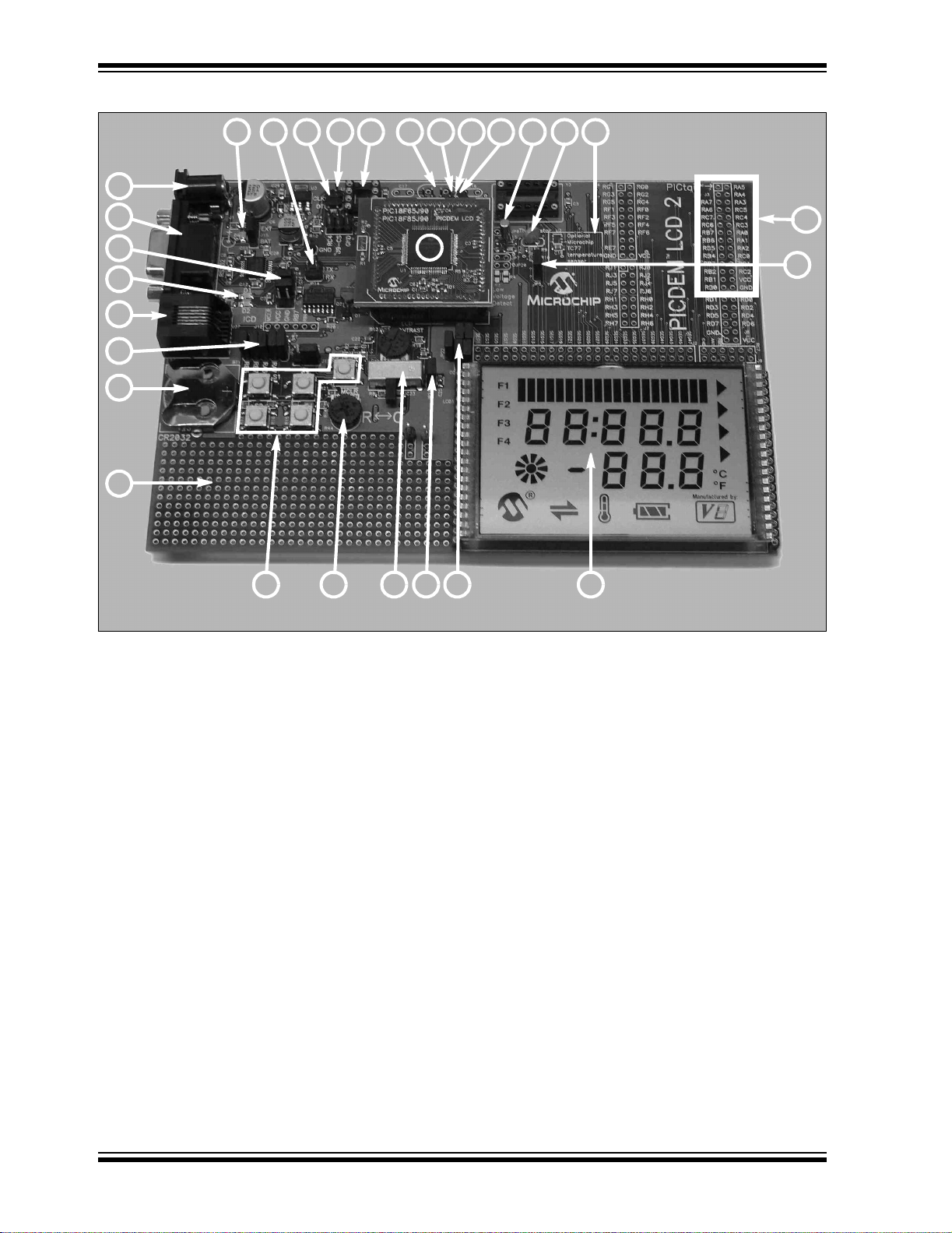
1. PICDEM LCD 2 Demonstration Board (Figure 1-1)
2. Sample Plug-in Module (PIM)
3. CD-ROM which contains:
If you are missing any part of the kit, please contact your nearest Microchip sales office
listed in the back of this publication for help.
PICDEM™ LCD 2 DEMONSTRATION
KIT USER’S GUIDE
Chapter 1. Introduction
®
ICE) or with an in-circuit debugger (e.g., MPLAB
• Sample Programs
•
“PICDEM™ LCD 2 Demonstration Kit User’s Guide”
© 2007 Microchip Technology Inc. DS51662A-page 5

1.2 PICDEM LCD 2 DEMONSTRATION BOARD HARDWARE FEATURES
The PICDEM LCD 2 Demonstration Board has the following hardware features; each
feature’s number corresponding to the number in Figure 1-1:
1. The demonstration board provides a daughter board option for the
PIC18F85J90, PIC18F8490, PIC16F914/917 and PIC16F946 families of devices
and MPLAB ICE. The board is also supplied with a PIM populated with a
PIC18F85J90 device.
Note: Optional PIMs populated with PIC18FXX90 and PIC16F9XX devices are
available for purchase from Microchip Direct (www.microchipdirect.com).
The MPLAB ICE can be plugged onto the board without any transition socket for
PIC18FXX90 devices. For other devices, a transition socket may be needed.
2. On-board adjustable voltage regulator for direct input from 9V, 100 mA AC/DC
wall adapter or 3V button cell battery.
3. Jumper J15 to select different power options.
4. Green power-on indicator LED for direct input from 9V.
5. Varitronix custom segmented LCD display.
6. Jumpers, COM0, COM1, COM2 and COM3, to disconnect COM pins from
on-board LCD and allow the usage of any customized LCD glass.
7. RS-232 connection and associated hardware for direct connection to RS-232
interface.
8. Jumpers, JP13 and JP14, to disconnect TX and RX.
9. In-Circuit Debugger (ICD) connector.
10. R44, 10 kΩ, potentiometer for devices with analog inputs.
11. Five push button switches (S1 through S5) for external stimulus and Reset.
12. Jumpers, JP19, JP18, JP1 and JP2, to disconnect switches from RB6, RB7, RA6
and RA7 input pins.
13. Jumper, J11, to select either 10 kΩ (POT R44) or the S1-S4 switches to AN0
(RA0).
14. Two green LEDs connected to RC3 and RC4 (device dependent).
15. Jumpers in J14 to disconnect LEDs from RC3 and RC4.
16. A slide switch (S6) to select either the resistor ladder or the charge pump option
for generating the bias values for the LCD pins.
17. Jumper, JP21, to physically tie the resistor ladder to ground.
18. Unpopulated holes provided for crystal connection.
19. Jumpers, JP11 and JP12, to disconnect crystal from OSC1 and OSC2.
20. 32.768 kHz crystal with Timer1 for Real-Time Clock (RTC) operation.
21. A Microwire EEPROM 93AA46C provided on a socket.
22. Jumpers, JP15 and JP16, to disconnect EEPROM from CK and DT. Jumper, J6,
to connect CS to GND or to RC4 (device dependent). Jumper, J13, to select
either 128 x 8 or 64 x 16 memory organization.
23. Thermistor for sensing temperature.
24. Jumper, JP5, to connect thermistor to AN1 (RA1) (device dependent).
25. Jumper, JP17, to select either V
26. Unpopulated option for TC77 temperature sensor.
27. Prototype area for user hardware.
28. PICtail™ daughter board connection. (The pin names on the board are valid only
for the PIC18F8490 device. For other devices, the PICtail daughter board pin
connections may be different or not connected.)
CC or I/O to power the peripherals.
© 2007 Microchip Technology Inc. DS51662A-page 6
PICDEM™ LCD 2 Demonstration Kit User’s Guide
FIGURE 1-1: PICDEM™ LCD 2 HARDWARE
15
14
12
27
13
4
2
7
9
2
22
8
3
18 19 23
21 25 20
1
26
28
24
11
10
1.3 SAMPLE DEVICES
A PIM, populated with the PIC18F85J90, is included.
1.4 SAMPLE PROGRAMS
The PICDEM LCD 2 Demonstration Kit includes a CD-ROM with sample demonstration
programs. Depending on the device, these programs may be used with some of the
included sample devices with an In-Circuit Emulator (ICE) or with an In-Circuit
Debugger (ICD). For each type of device (PIC16F946, PIC16F917, PIC18F8490 and
PIC18F85J90), demo source code, several C and/or .asm files and compiled code
(one HEX file) are provided.
16
17
56
DS51662A-page 7 © 2007 Microchip Technology Inc.

NOTES:
© 2007 Microchip Technology Inc. DS51662A-page 8

PICDEM™ LCD 2 DEMONSTRATION
KIT USER’S GUIDE
Chapter 2. Getting Started
The PICDEM LCD 2 may be used as a stand-alone board with a preprogrammed
device, with an In-Circuit Emulator (ICE) or with an In-Circuit Debugger (ICD). For a list
®
of PIC
Development Systems Ordering Guide”
2.1 PICDEM LCD 2 AS A STAND-ALONE BOARD – PREPROGRAMMED DEVICE
The PICDEM LCD 2 may be demonstrated immediately by following the steps listed
below:
• Apply power to the PICDEM LCD 2. For information on acceptable power
microcontroller compatible ICEs or ICDs, please refer to the
(DS30177)
sources, see Appendix A. “Board Technical Information”.
Note: In the event that the preprogrammed PICDEM LCD 2 Demonstration Board
with the PIC18F85J90 PIM does not operate, check the following
conditions:
- The jumper, J15, is configured as per the power supply used. The slide
switch, S6, is switched to C.
- JP1, JP2, JP6, JP18 and JP19 are connected.
- The middle two jumpers of J14 are connected.
- JP9 and JP10 are connected.
- J11 connecting POT to AN0 and JP17 connecting V
The status of all other jumpers will not affect the preprogrammed
demonstration.
Refer to Figure A-1 in Appendix A. “Board Technical Information”.
.
“Microchip
CC to I/O.
To reprogram the sample device, the following will be necessary:
1. User source code may be programmed to the device or the sample program may
be restored from the file on the included CD-ROM.
2. An assembler, such as the MPASM™ Assembler (available with MPLAB IDE), or
a compiler, such as MPLAB C18 C Compiler (PIC18XXXX/18XXJXX devices
only) must be used.
Source code must be assembled or compiled into a HEX file before it can be
programmed into the device. Microchip Technology’s MPASM Assembler or
MPLAB C18 C Compiler may be used. Both are compatible with MPLAB IDE;
however, other assemblers/compilers may be used.
3. Once the sample program is in the HEX file format, it can be programmed to a
Flash device using an MPLAB ICD 2 or PM3 with an ICSP™ module. Microchip
Technology’s MPLAB ICD 2 is compatible with MPLAB IDE.
If the code protection bit(s) have not been programmed, the on-chip program
memory can be read out for verification purposes.
© 2007 Microchip Technology Inc. DS51662A-page 9

2.2 PICDEM LCD 2 USED WITH AN IN-CIRCUIT EMULATOR OR IN-CIRCUIT DEBUGGER
To use the PICDEM LCD 2 with an In-Circuit Emulator (ICE) or In-Circuit Debugger
(ICD), refer to the tool’s user’s guide for instructions on how to power-up and configure
the ICE/ICD, as well as how to connect to target boards.
Configure the PICDEM LCD 2 for the desired oscillator as described in Table 2-1. Refer
to the ICE/ICD user’s guide for any oscillator configuration requirements.
TABLE 2-1: OSCILLATOR SELECTION
Oscillator Selection on
PICDEM™ LCD 2
Crystal JP9 and JP10 not connected. No canned oscillator on board,
crystal in Y2, JP11 and JP12 connected, caps in C16 and C17.
Canned Oscillator Put canned oscillator on socket Y3. Y2 empty, JP9, JP11 and
JP12 not connected.
Device Internal Oscillator JP11 and JP12 not connected. No canned oscillator on board.
Ceramic Resonator – no
internal caps
Ceramic Resonator – with
internal caps
JP9 and JP10 not connected. No canned oscillator on board,
resonator in Y2, JP11 and JP12 connected, caps in C16 and
C17.
JP9 and JP10 not connected. No canned oscillator on board,
resonator in Y2, JP11 and JP12 connected, C16 and C17
empty.
Modification on PICDEM™ LCD 2
Note: The MPLAB ICE can be plugged onto the board without any transition
socket for PIC18FXX90 devices. For other devices, a transition socket may
be needed.
© 2007 Microchip Technology Inc. DS51662A-page 10

PICDEM™ LCD 2 DEMONSTRATION
Chapter 3. Using the Demo Software
The demo programs are preprogrammed into the sample devices. Also, this program
is included on the CD-ROM program disk for user reference. This demo program uses
the functions or macros provided by the firmware LCD driver module to display the
required characters, strings or icons on the LCD.
3.1 DEMO FIRMWARE OPERATION
The demo firmware is made up of four components, which are individually displayed on
the LCD. The PIC microcontroller’s internal RC oscillator is used as the system clock
source.
1. Voltmeter (F1)
This mode uses the A/D module to measure the voltage of the R44 pot through
analog channel AN0, and displays a voltage between 0.00V and 3.30V on the
LCD using the LCD module. Voltage is continually updated until the mode is
exited by pressing either the S1 or S2 switch.
2. Thermometer (F2)
This mode uses the A/D module to measure the voltage of the thermistor R11
through analog channel AN1, and converts to temperature both in Celsius and
Fahrenheit and displays the temperature on the LCD using the LCD module.
Temperature is continually updated until the mode is exited by pressing either the
S1 or S2 switch.
3. Clock (F3)
This mode uses the Timer1 module and a 32 kHz clock crystal. Once this mode
is entered from the main menu, the Real-Time Clock will start counting from
00:00:00. The S3 switch is used to increment minutes and the S4 switch is used
to increment hours. To perform the increment operations, press and hold the
switches. The clock keeps running continuously until the mode is exited by
pressing either the S1 or S2 switch.
4. Charge Pump and Software Contrast (F4)
This mode is available only for the PIC18F85J90 family of devices and uses the
on-board charge pump and LCD voltage regulator. The LCD module is configured in Charge Pump mode and software contrast is achieved by either pressing
S3 to increase the contrast or S4 to decrease the contrast until the mode is exited
by pressing either the S1 or S2 switch. By exiting this mode, the Voltmeter mode
is entered and retains the contrast level.
(1)
KIT USER’S GUIDE
(1)
Note 1: For low-power battery operation in JP17, remove jumper on Vcc and I/O
and connect I/O and RB0.
© 2007 Microchip Technology Inc. DS51662A-page 11
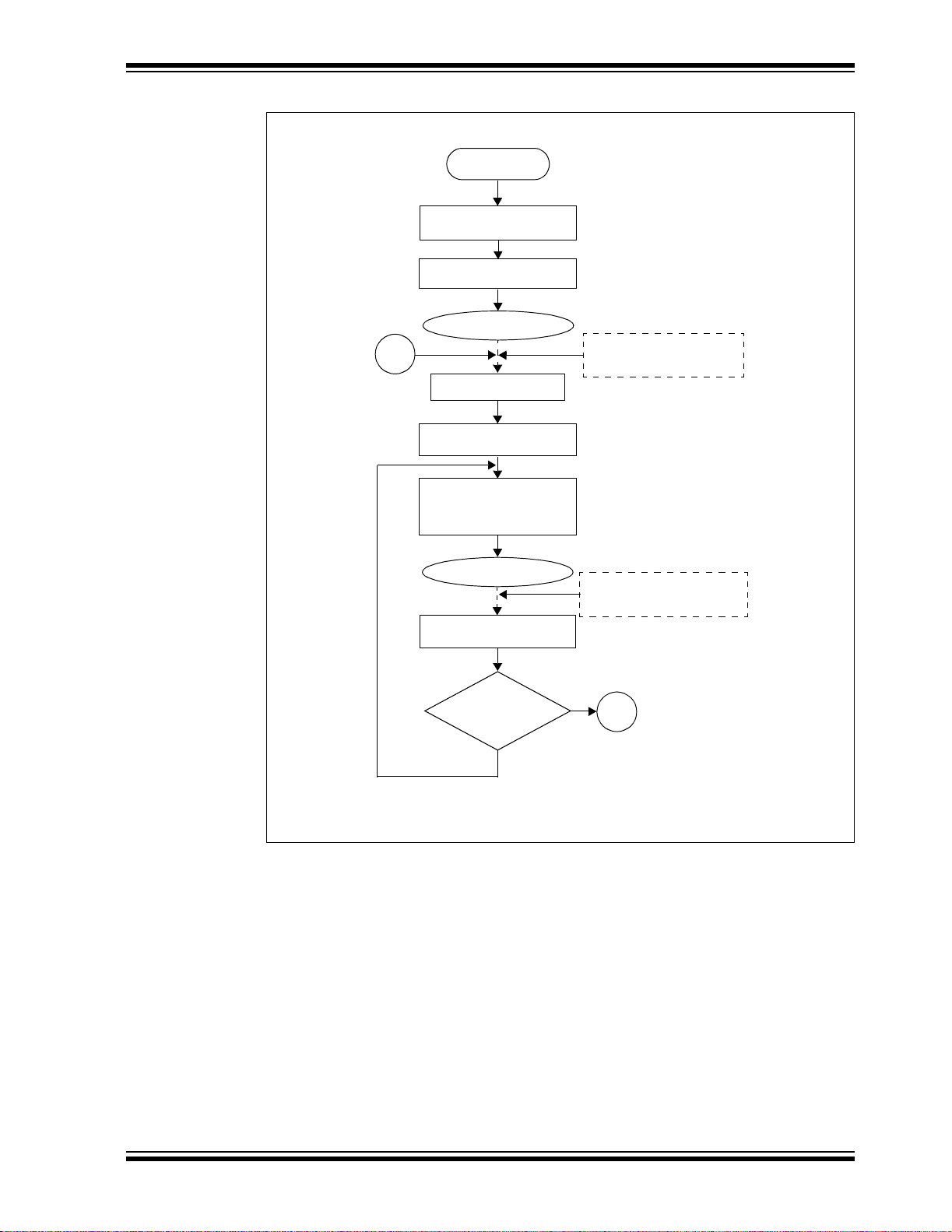
FIGURE 3-1: DEMO PROGRAM FLOWCHART
Power-up
Display Microchip Logo
Display Varitronix Logo
Sleep
A
Voltmeter Demo
Display F1
Start A/D
Conversion on
Channel AN0
Wake-up from Sleep
by Pressing either S1 or S2
Sleep
Display the Voltage
Is S1/S2
switch pressed?
No
Wake-up from Sleep
on Completion of Conversion
Yes
B
© 2007 Microchip Technology Inc. DS51662A-page 12
PICDEM™ LCD 2 Demonstration Kit User’s Guide
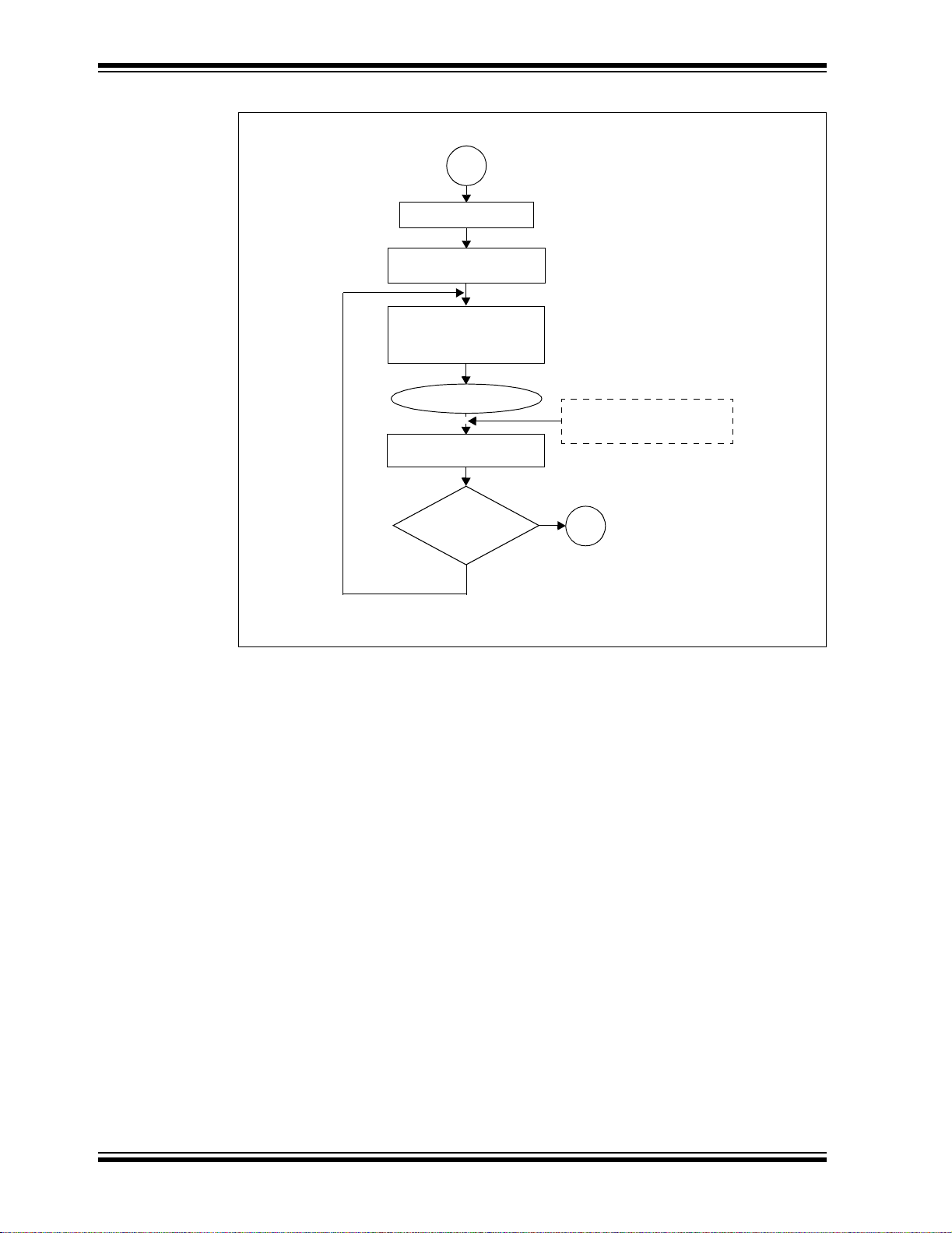
FIGURE 3-2: DEMO PROGRAM FLOWCHART
B
Thermometer Demo
Display F2
Start A2D
Conversion on
Channel AN1
Sleep
Display the Temperature
Is S1/S2
switch pressed?
No
Wake-up from Sleep
on Completion of Conversion
Yes
C
DS51662A-page 13 © 2007 Microchip Technology Inc.

FIGURE 3-3: DEMO PROGRAM FLOWCHART
C
Real-Time Clock Demo
Display F3
Is S1/S2
switch pressed?
No
Display Time
Sleep
Is S3
switch pressed?
No
Is S4
switch pressed?
No
Yes
Yes
Yes
D
Wake-up from Sleep
Every Second
Increment
Minute
Increment
Hour
© 2007 Microchip Technology Inc. DS51662A-page 14

PICDEM™ LCD 2 Demonstration Kit User’s Guide
FIGURE 3-4: DEMO PROGRAM FLOWCHART
D
Software Contrast Demo
using Charge Pump
Display F4
Is S1/S2
switch pressed?
No
Display
LCDREG<BIAS> bits
Is S3
switch pressed?
No
Is S4
switch pressed?
No
Yes
Yes
Yes
A
Increase
Contrast
Decrease
Contrast
DS51662A-page 15 © 2007 Microchip Technology Inc.

FIGURE 3-5: DEMO PROGRAM FLOWCHART
ISR
Increment Second Register
Is it 60?
Yes
Clear Second
Register,
Increment Minute
Register
Is it 60?
Yes
Clear Minute
Register,
Increment Hour
Register
Is it 24?
Yes
No
No
No
Clear Hour Register
Return
© 2007 Microchip Technology Inc. DS51662A-page 16

PICDEM™ LCD 2 DEMONSTRATION
KIT USER’S GUIDE
Appendix A. Board Technical Information
The PICDEM LCD 2 hardware is not complicated and is intended to illustrate the ease
of use of various PIC
hardware elements.
Note: Many of the following hardware sections will require specific demo board
jumper configurations. If a jumper is not listed in a particular section, then
that jumper has no effect on the circuitry within the hardware section you
are working. Figure A-1 shows a diagram of the PICDEM LCD 2 silkscreen
with all necessary jumpers highlighted in gray. Also, refer to the schematic
for circuit connections.
®
microcontrollers. The PICDEM LCD 2 features the following
© 2007 Microchip Technology Inc. DS51662A-page 17

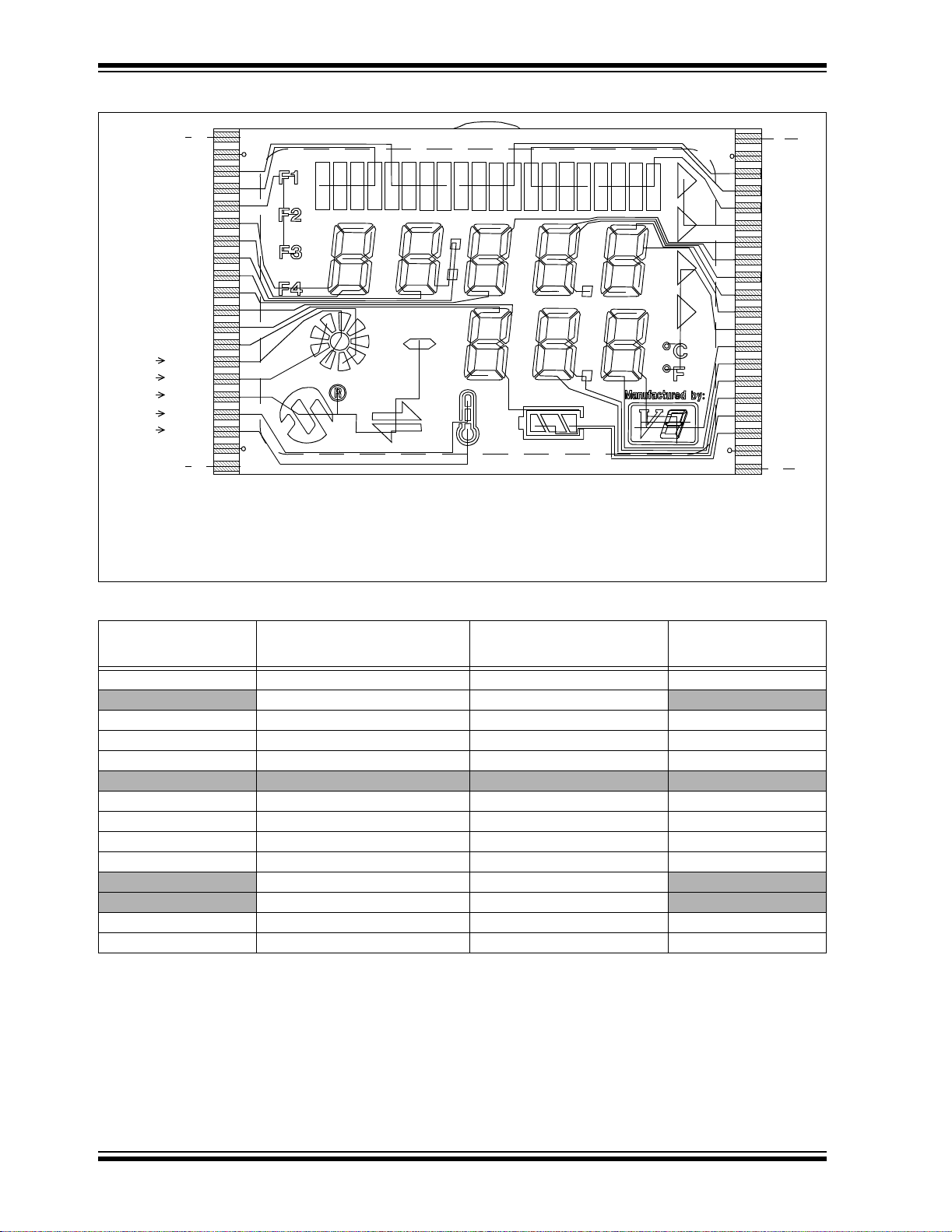
FIGURE A-1: PICDEM™ LCD 2 DEFAULT JUMPER LOCATION
© 2007 Microchip Technology Inc. DS51662A-page 18

PICDEM™ LCD 2 Demonstration Kit User’s Guide
A.1 PROCESSORS
While there is no actual processor populated on the board, a processor is provided with
the plug-in module (PIM) that is shipped with the demonstration board. The default
processor on the PIM is the PIC18F85J90.
The board also supports the PIC18F8490, PIC16F946 and PIC16F917 processors,
which have been designed for use with the PICDEM LCD 2. These three processors
are in the PICDEM LCD 2 PIM Pack which is available for separate purchase.
The part numbers for a replacement PIC18F85J90 and the PIM pack are given in
Ta bl e A - 1.
TABLE A-1: PART NUMBERS
Item Part number
PICDEM LCD 2 PIM Pack
• PIC18F8490 PIM
• PIC16F946 PIM
• PIC16F917 PIM
PIC18F85J90 PIM MA180022
For the availability and pricing of parts, go to www.microchipdirect.com.
†
(†)
MA180019
DS51662A-page 19 © 2007 Microchip Technology Inc.

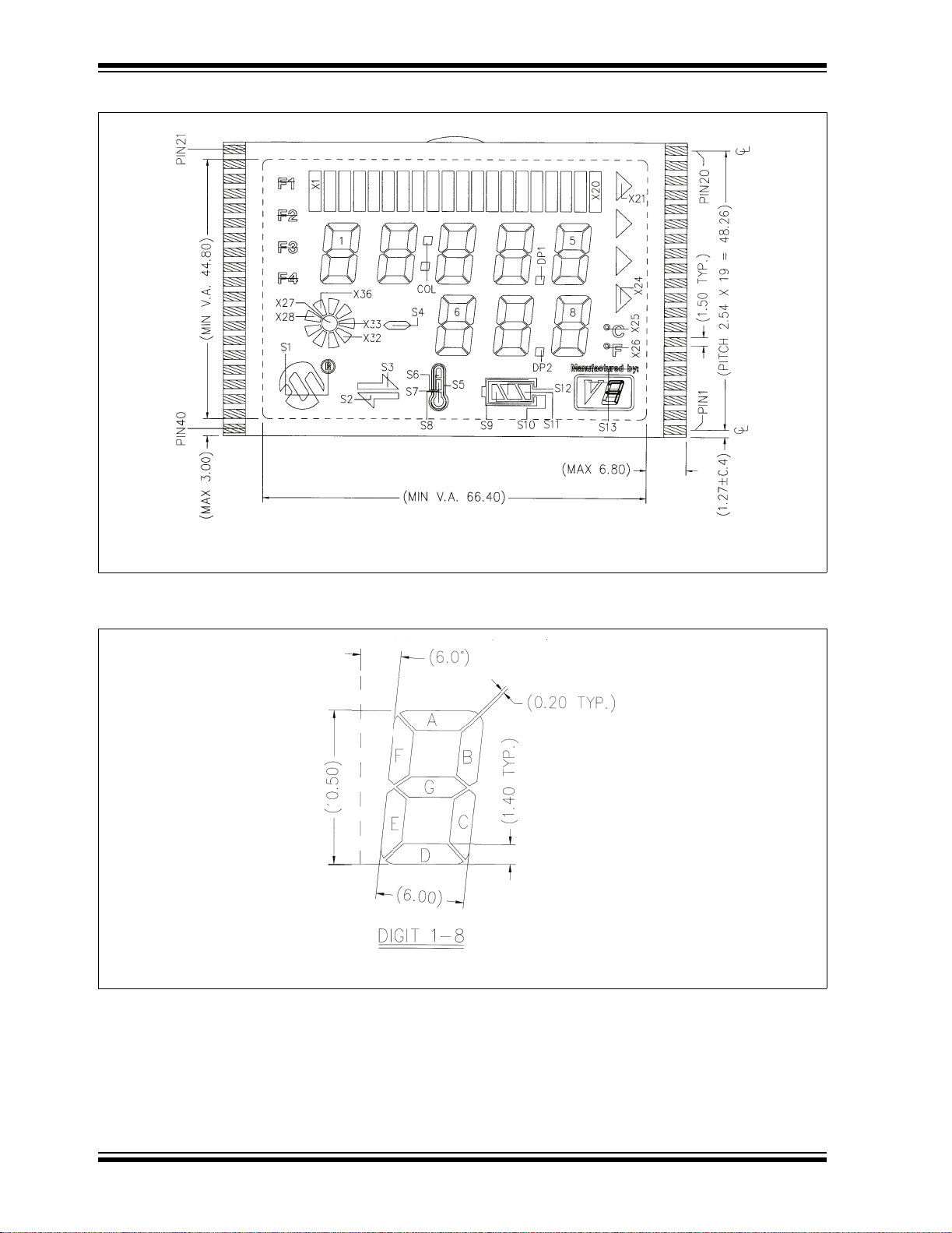
A.2 LCD DISPLAY
A custom made segmented LCD glass, manufactured by the Varitronix Corporation, is
provided as shown in Figure A-2. This LCD has 4 commons and 32 segments.
Table A-2 provides a few of the specifics for the display. Refer to the Varitronix
specification sheet (VL_5573_V00) for additional details.
FIGURE A-2: PICDEM™ LCD 2 DISPLAY
21
N.C.
COM2
SEG16
SEG17
SEG18
SEG19
SEG20
SEG21
SEG22
SEG23
SEG24
SEG25
SEG26
SEG27
SEG28
SEG29
SEG30
SEG31
COM3
40
N.C.
Legend: N.C. = No connection
20
COM1
SEG15
SEG14
SEG13
SEG12
SEG11
SEG10
SEG9
SEG8
SEG7
SEG6
SEG5
SEG4
SEG3
SEG2
SEG1
SEG0
COM0
1
© VL Electronics
N.C.
N.C.
TABLE A-2: LCD GLASS SPECIFICATIONS
Type Specification
P.I.D. VL_5573_V00
Mode/Color/Type Positive / -- / TN
Viewing Direction 6:00 O’Clock
Driving Scheme 1/4 Duty, 1/3 Bias
Drive Voltage (VLCD) ~3.0 Volt (p-p), +20°C
Operating Temperature 0°C - +50°C
Storage Temperature -10°C - +60°C
Polarizer – Front STD.Transmissive
Polarizer – Back STD.Reflective
Since the glass used on the PICDEM LCD 2 operates at 3V, there is a voltage protection circuit on the LCDBIAS3 pin, which is enabled in the default configuration. When
enabled, even if the V
DD is greater than 3V, it regulates the LCDBIAS3 voltage such
that it always maintains the value to 3V. This is not necessary for operation of the LCD
module, but it is a protection circuit to prevent accidentally applying voltages higher
than 3V to the LCD glass present on the board.
© 2007 Microchip Technology Inc. DS51662A-page 20
PICDEM™ LCD 2 Demonstration Kit User’s Guide
FIGURE A-3: DISPLAY DEFINITIONS
FIGURE A-4: DIGIT DESCRIPTION
© VL Electronics
© VL Electronics
DS51662A-page 21 © 2007 Microchip Technology Inc.

TABLE A-3: LCD SEGX AND COMX
Pin ICE Pin COM0 COM1 COM2 COM3
1 N.C. N.C. N.C. N.C.
2COM0———
3 SEG0 S12 — — S10
4 SEG1 S11 — — —
5 SEG2 7D 7F 7A 7E
6 SEG3 DP2 7G 7B 7C
7 SEG4 8D 8F 8A 8E
8 SEG5 S13 8G 8B 8C
9 SEG6 X23 X25 X26 X24
10 SEG7 5B 5C — 5G
11 SEG8 5A 5E 5D 5F
12 SEG9 4B 4C DP1 4G
13 SEG10 4A 4E 4D 4F
14 SEG11 3B 3C — 3G
15 SEG12 — X22 X21 —
16 SEG13 X17 X19 X20 X18
17 SEG14 X16 X14 X13 X15
18 SEG15 X9 X11 X12 X10
19 — COM1 — —
20 N.C. N.C. N.C. N.C.
21 N.C. N.C. N.C. N.C.
22 — — COM2 —
23 SEG16 X8 X6 X5 X7
24 SEG17 X1 X3 X4 X2
25 SEG18 — F2 F1 F3
26 SEG19 1A 1E F4 1F
27 SEG20 1B 1C 1D 1G
28 SEG21 2A 2E 2D 2F
29 SEG22 2B 2C COL 2G
30 SEG23 3A 3E 3D 3F
31 SEG24 S9 6G 6B 6C
32 SEG25 6D 6F 6A 6E
33 SEG26 X31 X33 X34 X32
34 SEG27 — X27 X35 X30
35 SEG28 — X28 X36 X29
36 SEG29 S1 S3 S4 S2
37 SEG30 S6 — — S7
38 SEG31 S5 — — S8
39 — — — COM3
40 N.C. N.C. N.C. N.C.
Legend: N.C. = No connection
© 2007 Microchip Technology Inc. DS51662A-page 22

PICDEM™ LCD 2 Demonstration Kit User’s Guide
A.2.1 Device-Specific LCD Segment Configuration
The following figures and tables detail which segments are available for specific
®
PIC
devices.
TABLE A-4: PIC18F85J90 PIM AND ICE PIN/PORT COMPARISON
PIC18F85J90
PIM Pin No.
10 RG4 SEG26 SEG26 RG4 21 50 RA6 OSC2 OSC2 RA6 63
11 V
12
13 RF7 SEG25 SEG25 RF7 25 53
14 RF6 SEG24 SEG24 RF6 26 54 RB4 SEG11 SEG11 RB4 68
15 RF5 SEG23 SEG23 RF5 27 55 RB3 SEG10 SEG10 RB3 69
16 RF4 SEG22 SEG22 RF4 28 56 RB2 SEG9 SEG9 RB2 70
17 RF3 SEG21 SEG21 RF3 29 57 RB1 SEG8 SEG8 RB1 71
18 RF2 SEG20 SEG20 RF2 30 58 RB0 RB0 RB0 RB0 72
19 RH7 SEG43 SEG43 RH7 31 59 RJ3 SEG35 SEG35 RJ3 73
20 RH6 SEG42 SEG42 RH6 32 60 RJ2 SEG34 SEG34 RJ2 74
21 RH5 SEG41 SEG41 RH5 33 61 RJ1 SEG33 SEG33 RJ1 75
22 RH4 SEG40 SEG40 RH4 34 62 RJ0 NC NC
23 RF1 SEG19 SEG19 RF1 35 63 RD7 SEG7 SEG7 RD7 77
24
25 AV
26 AV
27 RA3 NC NC 67 RD3 SEG3 SEG3 RD3 81
28
29
30 RA0 AN0 AN0 RA0 42 70 V
31 V
32 V
33 RA5 SEG15 SEG15 RA5 46 73
34 RA4 SEG14 SEG14 RA4 47 74 RE6 COM3 COM3 RE6 5
35 RC1 T1OSCI T1OSCI RC1 48 75 RE5 COM2 COM2 RE5 6
36 RC0 T1OSCO T1OSCO RC0 49 76 RE4 COM1 COM1 RE4 7
37 RC6 TX/CK TX/CK RC6 50 77 RE3 COM0 COM0 COM0 8
38 RC7 RX/DT RX/DT RC7 51 78 RE2 BIAS3 BIAS3 RE2 9
39 RJ4 SEG39 SEG39 RJ4 52 79
40 RJ5 SEG38 SEG38 RJ5 53 80
Legend: Unshaded cells indicate where a perfect match between PIM and ICE pins and ports exists.
PIC18F85J90
Port
1 RH2 SEG45 SEG30 RG0 16 41 RJ6 SEG37 SEG37 RJ6 54
2
3 RE1 BIAS2 BIAS2 RE1 14 43 RC2 SEG13 SEG13 RC2 56
4 RE0 BIAS1 BIAS1 RE0 15 44
5
6 RG1 NC NC 46 RC5 SEG12 SEG12 RC5 59
7
8
9RG5MCLR
RH3 SEG44 SEG29 RG1 17 42 RJ7 SEG36 SEG36 RJ7 55
RG0 BIAS0 BIAS0 RB5 67 45 RC4 SEG16 SEG16 RA2 40
RG2 VLCAP1 VLCAP1 RC3 57 47 RB7 RB7 RB7 RB7 60
RG3 VLCAP2 VLCAP2 RC4 58 48 VDD ICEVDD ICEVDD VDD 61
VDDCORE VDDCORE VDD VDD 24 52 RB6 RB6 RB6 RB6 66
ENVREG ENVREG 64 RD6 SEG6 SEG6 RD6 78
RA2 AN2 AN1 RA1 41 68 RD2 SEG2 SEG2 RD2 82
RA1 SEG18 SEG18 RF0 36 69 RD1 SEG1 SEG1 RD1 83
Shaded cells indicate where differences between PIM and ICE ports and pins exist.
Bold text indicates the PIM pins that are not connected to any ICE pins or ports.
PIC18F85J90
Pin
SS VSS VSS VSS 23 51 VSS VSS VSS VSS 65
DD AVDD ICEVDD AVDD 37 65 RD5 SEG5 SEG5 RD5 79
SS AVSS AVSS AVSS 38 66 RD4 SEG4 SEG4 RD4 80
SS VSS VSS VSS 44 71 VDD VDD VDD VDD 2
DD ICEVDD ICEVDD VDD 45 72 RD0 SEG0 SEG0 RD0 3
ICE Pin
ICEMCLR RG5 20 49 RA7 OSC1 OSC1 RA7 62
ICE
Port
ICE
Pin
No.
PIC18F85J90
PIM Pin No.
PIC18F85J90
Port
RC3 SEG17 SEG17 RA3 39
RB5 SEG29 SEG27 RG3 19
SS VSS VSS VSS 84
RE7 SEG31 SEG28 RG2 18
RH0 SEG47 SEG32 RJ0 76
RH1 SEG46 SEG31 RE7 4
PIC18F85J90
Pin
ICE Pin
ICE
Port
ICE
Pin
No.
DS51662A-page 23 © 2007 Microchip Technology Inc.
TABLE A-5: PIC18F85J90 LCD CONNECTIONS COMPARISON
PIC18F85J90 ICE Pin #
NC
COM2 COM2 22 COM3 COM2 19 COM1 COM1
SEG16 SEG16 23 X8,X6,X5,X7 X9,X11,X12,X10 18 SEG15 SEG15
SEG17 SEG17 24 X1,X3,X4,X2 X16,X14,X13,X15 17 SEG14 SEG14
SEG18 SEG18 25 -,F2,F1,F3 X17,X19,X20,X18 16 SEG13 SEG13
SEG19 SEG19 26 1A,1E,F4,1F -,X22,X21,- 15 SEG12 SEG12
SEG20 SEG20 27 1B,1C,1D,1G 3B,3C,-,3G 14 SEG11 SEG11
SEG21 SEG21 28 2A,2E,2D,2F 4A,4E,4D,4F 13 SEG10 SEG10
SEG22 SEG22 29 2B,2C,COL,2G 4B,4C,DP1,4G 12 SEG9 SEG9
SEG23 SEG23 30 3A,3E,3D,3F 5A,5E,5D,5F 11 SEG8 SEG8
SEG24 SEG24 31 S9,6G,6B,6C 5B,5C,-,5G 10 SEG7 SEG7
SEG25 SEG25 32 6D,6F,6A,6E X23,X25,X26,X24 9 SEG6 SEG6
SEG26 SEG26 33 X31,X33,X34,X32 S13,8G,8B,8C 8 SEG5 SEG5
SEG29 SEG27 34 -,X27,X35,X30 8D,8F,8A,8E 7 SEG4 SEG4
SEG31 SEG28 35 -,X28,X36,X29 DP2,7G,7B,7C 6 SEG3 SEG3
SEG44 SEG29 36 S1,S3,S4,S2 7D,7F,7A,7E 5 SEG2 SEG2
SEG45 SEG30 37 S6,-,-,S7 S11,-,-,- 4 SEG1 SEG1
SEG46 SEG31 38 S5,-,-S8 S12,-,-,S10 3 SEG0 SEG0
COM3 COM3 39 COM4 COM1 2 COM0 COM0
NC
Legend: Unshaded cells indicate a perfect match between the PIM and the glass.
Shaded cells indicate the pins that are remapped to the corresponding pin on the PIM.
21
40 NC NC 1
NC NC
Pin
ICE PIC18F85J90
#
NC
20
NC
© 2007 Microchip Technology Inc. DS51662A-page 24
PICDEM™ LCD 2 Demonstration Kit User’s Guide
FIGURE A-5: SEGMENT CONFIGURATION FOR PIC18F85J90 DEVICES
SEG29 SEG27
SEG31 SEG28
(1)
SEG44
SEG29
(1)
SEG30
SEG45
(1)
SEG46
SEG31
21
N.C.
COM2
SEG16
SEG17
SEG18
SEG19
SEG20
SEG21
SEG22
SEG23
SEG24
SEG25
SEG26
(2)
(2)
(2)
COM3
40
N.C.
Legend: N.C. = No connection
Note 1: SEG44, SEG45, and SEG46 exist only on PIC18F85J90 devices.
2: Disable SEG27, SEG28, SEG30, and SEG32 when the LCD module is enabled. Although SEG32 is
not listed in the diagram, it is multiplexed with the Timer1 oscillator, and therefore, must be disabled
when the Timer1 oscillator is enabled.
© VL Electronics
20
COM1
SEG15
SEG14
SEG13
SEG12
SEG11
SEG10
SEG9
SEG8
SEG7
SEG6
SEG5
SEG4
SEG3
SEG2
SEG1
SEG0
COM0
1
N.C.
N.C.
TABLE A-6: PIC18F85J90 PORT AND PIN COMPARISON
PIC18F85J90
Port
RA0 AN0 AN0 RA0
RA1 SEG18 SEG18 RF0
RA6 OSC2 OSC2 RA6
RA7 OSC1 OSC1 RA7
RB0 RB0 RB0 RB0
RB5 SEG29 SEG27 RG3
RB6 RB6 RB6 RB6
RB7 RB7 RB7 RB7
RC0 T1OSC1 T1OSC0 RC0
RC1 TIOSC0 TIOSC1 RC1
RC3 SEG17 SEG17 RA3
RC4 SEG16 SEG16 RA2
RC6 TX/CK TX/CK RC6
RC7 RX/DT RX/DT RC7
Legend: Unshaded cells indicate a perfect match between the PIM and the glass.
Shaded cells indicate the pins that are remapped to the corresponding pin on the PIM.
PIC18F85J90 PIN ICE Pin ICE Port
DS51662A-page 25 © 2007 Microchip Technology Inc.
TABLE A-7: PIC18F8490 PIM AND ICE PORT/PIN COMPARISON
PIC18F8490
PIM Pin No.
PIC18F8490
Port
PIC18F8490
Pin
ICE Pin
1 RH2 SEG45 SEG45 RH2 12 41 RJ6 SEG37 SEG37 RJ6 54
2 RH3 SEG44 SEG44 RH3 13 42 RJ7 SEG36 SEG36 RJ7 55
3 LCDBIAS2 LCDBIAS2 BIAS2 RE1 14 43 RC2 SEG13 SEG13 RC2 56
4 LCDBIAS1 LCDBIAS1 BIAS1 RE0 15 44 RC3 RC3 RC3 RC3 57
5 RG0 SEG30 SEG30 RG0 16 45 RC4 RC4 RC4 RC4 58
6 RG1 SEG29 SEG29 RG1 17 46 RC5 SEG12 SEG12 RC5 59
7 RG2 SEG28 SEG28 RG2 18 47 RB7 RB7 RB7 RB7 60
8 RG3 SEG27 SEG27 RG3 19 48 V
9RG5MCLR
ICEMCLR RG5 20 49 RA7 OSC1 OSC1 RA7 62
10 RG4 SEG26 SEG26 RG4 21 50 RA6 OSC2 OSC2 RA6 63
11 V
12 V
SS VSS VSS VSS 23 51 VSS VSS VSS VSS 65
DD VDD ICEVDD VDD 24 52 RB6 RB6 RB6 RB6 66
13 RF7 SEG25 SEG25 RF7 25 53 RB5 RB5 RB5 RB5 67
14 RF6 SEG24 SEG24 RF6 26 54 RB4 SEG11 SEG11 RB4 68
15 RF5 SEG23 SEG23 RF5 27 55 RB3 SEG10 SEG10 RB3 69
16 RF4 SEG22 SEG22 RF4 28 56 RB2 SEG9 SEG9 RB2 70
17 RF3 SEG21 SEG21 RF3 29 57 RB1 SEG8 SEG8 RB1 71
18 RF2 SEG20 SEG20 RF2 30 58 RB0 RB0 RB0 RB0 72
19 RH7 SEG43 SEG43 RH7 31 59 RJ3 SEG35 SEG35 RJ3 73
20 RH6 SEG42 SEG42 RH6 32 60 RJ2 SEG34 SEG34 RJ2 74
21 RH5 SEG41 SEG41 RH5 33 61 RJ1 SEG33 SEG33 RJ1 75
22 RH4 SEG40 SEG40 RH4 34 62 RJ0 SEG32 SEG32 RJ0 76
23 RF1 SEG19 SEG19 RF1 35 63 RD7 SEG7 SEG7 RD7 77
24 RF0 SEG18 SEG18 RF0 36 64 RD6 SEG6 SEG6 RD6 78
25 AV
26 AV
DD AVDD ICEVDD AVDD 37 65 RD5 SEG5 SEG5 RD5 79
SS AVSS AVSS AVSS 38 66 RD4 SEG4 SEG4 RD4 80
27 RA3 SEG17 SEG17 RA3 39 67 RD3 SEG3 SEG3 RD3 81
28 RA2 SEG16 SEG16 RA2 40 68 RD2 SEG2 SEG2 RD2 82
29 RA1 AN1 AN1 RA1 41 69 RD1 SEG1 SEG1 RD1 83
30 RA0 AN0 AN0 RA0 42 70 V
31 V
32 V
SS VSS VSS VSS 44 71 VDD VDD VDD VDD 2
DD VDD ICEVDD VDD 45 72 RD0 SEG0 SEG0 RD0 3
33 RA5 SEG15 SEG15 RA5 46 73 RE7 SEG31 SEG31 RE7 4
34 RA4 SEG14 SEG14 RA4 47 74 RE6 COM3 COM3 RE6 5
35 RC1 TIOSC0 TIOSC1 RC1 48 75 RE5 COM2 COM2 RE5 6
36 RC0 T1OSC1 T1OSC0 RC0 49 76 RE4 COM1 COM1 RE4 7
37 RC6 TX/CK TX/CK RC6 50 77 COM0 COM0 COM0 RE3 8
38 RC7 RX/DT RX/DT RC7 51 78 LCDBIAS3 LCDBIAS3 BIAS3 RE2 9
39 RJ4 SEG39 SEG39 RJ4 52 79 RH0 SEG47 SEG47 RH0 10
40 RJ5 SEG38 SEG38 RJ5 53 80 RH1 SEG46 SEG46 RH1 11
ICE
Port
ICE
Pin
No.
PIC18F8490
PIM Pin No.
PIC18F8490
Port
PIC18F8490
Pin
DD VDD ICEVDD VDD 61
SS VSS VSS VSS 84
ICE Pin
ICE
Port
ICE
Pin
No.
© 2007 Microchip Technology Inc. DS51662A-page 26

PICDEM™ LCD 2 Demonstration Kit User’s Guide
TABLE A-8: PIC18F8490 LCD CONNECTIONS COMPARISON
PIC18F8490 ICE Pin # Pin # ICE PIC18F8490
NC 21 NC NC 20 NC
COM2 COM2 22 COM3 COM2 19 COM1 COM1
SEG16 SEG16 23 X8,X6,X5,X7 X9,X11,X12,X10 18 SEG15 SEG15
SEG17 SEG17 24 X1,X3,X4,X2 X16,X14,X13,X15 17 SEG14 SEG14
SEG18 SEG18 25 -,F2,F1,F3 X17,X19,X20,X18 16 SEG13 SEG13
SEG19 SEG19 26 1A,1E,F4,1F -,X22,X21,- 15 SEG12 SEG12
SEG20 SEG20 27 1B,1C,1D,1G 3B,3C,-,3G 14 SEG11 SEG11
SEG21 SEG21 28 2A,2E,2D,2F 4A,4E,4D,4F 13 SEG10 SEG10
SEG22 SEG22 29 2B,2C,COL,2G 4B,4C,DP1,4G 12 SEG9 SEG9
SEG23 SEG23 30 3A,3E,3D,3F 5A,5E,5D,5F 11 SEG8 SEG8
SEG24 SEG24 31 S9,6G,6B,6C 5B,5C,-,5G 10 SEG7 SEG7
SEG25 SEG25 32 6D,6F,6A,6E X23,X25,X26,X24 9 SEG6 SEG6
SEG26 SEG26 33 X31,X33,X34,X32 S13,8G,8B,8C 8 SEG5 SEG5
SEG27 SEG27 34 -,X27,X35,X30 8D,8F,8A,8E 7 SEG4 SEG4
SEG28 SEG28 35 -,X28,X36,X29 DP2,7G,7B,7C 6 SEG3 SEG3
SEG29 SEG29 36 S1,S3,S4,S2 7D,7F,7A,7E 5 SEG2 SEG2
SEG30 SEG30 37 S6,-,-,S7 S11,-,-,- 4 SEG1 SEG1
SEG31 SEG31 38 S5,-,-S8 S12,-,-,S10 3 SEG0 SEG0
COM3 COM3 39 COM4 COM1 2 COM0 COM0
NC 40 NC NC 1 NC
FIGURE A-6: SEGMENT CONFIGURATION FOR PIC18F8490 DEVICES
21
N.C.
COM2
SEG16
SEG17
SEG18
SEG19
SEG20
SEG21
SEG22
SEG23
SEG24
SEG25
SEG26
SEG27
SEG28
SEG29
SEG30
SEG31
COM3
40
N.C.
Legend: N.C. = No connection
20
COM1
SEG15
SEG14
SEG13
SEG12
SEG11
SEG10
SEG9
SEG8
SEG7
SEG6
SEG5
SEG4
SEG3
SEG2
SEG1
SEG0
COM0
1
© VL Electronics
N.C.
N.C.
DS51662A-page 27 © 2007 Microchip Technology Inc.

TABLE A-9: PIC18F8490 PIN AND PORT COMPARISON
PIC18F8490 Port PIC18F8490 Pin ICE Pin ICE Port
RA0 AN0 AN0 RA0
RA1 AN1 AN1 RA1
RA6OSC2OSC2RA6
RA7OSC1OSC1RA7
RB0 RB0 RB0 RB0
RB5 RB5 RB5 RB5
RB6 RB6 RB6 RB6
RB7 RB7 RB7 RB7
RC0 T1OSC1 T1OSC0 RC0
RC1 TIOSC0 TIOSC1 RC1
RC3 RC3 RC3 RC3
RC4 RC4 RC4 RC4
RC6 TX/CK TX/CK RC6
RC7 RX/DT RX/DT RC7
© 2007 Microchip Technology Inc. DS51662A-page 28

PICDEM™ LCD 2 Demonstration Kit User’s Guide
TABLE A-10: PIC16F946 PIM AND ICE PIN/PORT COMPARISON
PIC16F946
PIM Pin
No.
Legend: Unshaded cells indicate where a perfect match between PIM and ICE pins and ports exists.
PIC16F946
Port
1 RD6 SEG19 SEG19 RF1 35 33 RE0 SEG21 SEG21 RF3 29
2
3
4
5
6
7
8
9V
10 V
11
12
13
14
15 RB0 RB0 RB0 RB0 72 47
16
17
18
19 V
20 V
21
22
23 RB6 RB6 RB6 RB6 66 55 RD2 NC NC
24 RB7 RB7 RB7 RB7 60 56 V
25 AV
26 AV
27 RA0 AN0 AN0 RA0 42 59 RC4 RC4 RC4 VLCAP1\
28 RA1 AN1 AN1 RA1 41 60
29
30
31
32
RD7 SEG20 SEG20 RF2 30 34 RE1 SEG22 SEG22 RF4 28
RG0 SEG36 SEG36 RB1 71 35 RE2 SEG23 SEG23 RF5 27
RG1 SEG37 SEG37 RB2 70 36 ICEMCLR ICEMCLR ICEMCLR ICEMCLR 20
RG2 SEG38 SEG38 RJ5 53 37 RE4 SEG24 SEG24 RF6 26
RG3 SEG39 SEG39 RJ4 52 38 ICEVDD ICEVDD ICEVDD ICEVDD 61
RG4 SEG40 SEG40 RH4 34 39 RA7 T1OSCI T1OSCI RC1 48
RG5 SEG41 SEG41 RH5 33 40 RA6 T1OSCO T1OSCO RC0 49
RF0 SEG32 SEG32 RJ0 76 43 RE6 SEG26 SEG26 RG4 21
RF1 SEG33 SEG33 RD0 3 44 RE7 SEG27 SEG27 RG3 19
RF2 SEG34 SEG34 RD6 78 45 RE4 SEG28 SEG28 RG2 18
RF3 SEG35 SEG35 RD7 77 46 RF5 SEG29 SEG29 RG1 17
RB1 SEG1 SEG1 RD1 83 48 RF7 SEG31 SEG31 RE7 4
RB2 SEG2 SEG2 RD2 82 49 RC0 VLCD1 BIAS1 RE0 15
RB3 SEG3 SEG3 RD3 81 50 RC1 VLCD2 BIAS2 RE1 14
RB4 COM0 COM0 RE3 8 53 RD0 COM3 COM3 RE6 5
RB5 COM1 COM1 RE4 7 54 RD1 NC NC
RA2 COM2 COM2 RE5 6 61 RC6 TX/CK TX/CK TX/CK 50
RA3 SEG15 SEG15 RA5 46 62 RC7 RX/DT RX/DT RX/DT 51
RA4 SEG4 SEG4 RD4 80 63 RD4 SEG17 SEG17 RA3 39
RA5 SEG5 SEG5 RD5 79 64 RD5 SEG18 SEG18 RF0 36
Shaded cells indicate where differences between PIM and ICE ports and pins exist.
Bold text indicates the PIM pins that are not connected to any ICE pins or ports.
PIC16F946
Pin
SS VSS VSS VSS 23 41 VSS VSS VSS VSS 65
DD VDD ICEVDD ICEVDD 24 42 RE5 SEG25 SEG25 RF7 25
DD VDD ICEVDD ICEVDD 37 51 RC2 VLCD3 BIAS3 RE2 9
SS VSS VSS AVSS 38 52 RC3 RC3 VLCAP1 RC3 57
DD AVDD ICEVDD ICEVDD 45 57 VDD VDD VDD VDD 2
SS AVSS AVSS AVSS 44 58 RD3 SEG16 SEG16 RA2 40
ICE Pin ICE Port
ICE
Pin
No.
PIC16F946
PIM Pin
No.
PIC16F946
Port
RF6 SEG30 SEG30 RG0 16
RC5 SEG10 SEG10 RB3 69
PIC16F946
Pin
SS VSS VSS VSS 1
ICE Pin ICE Port
ICE
Pin
No.
58
RC4
DS51662A-page 29 © 2007 Microchip Technology Inc.

TABLE A-11: PIC16F946 LCD CONNECTIONS COMPARISON
PIC16F946 ICE Pin # Pin # ICE PIC16F946
NC 21 NC NC 20 NC
COM2 COM2 22 COM3 COM2 19 COM1 COM1
SEG16 SEG16 23 X8,X6,X5,X7 X9,X11,X12,X10 18 SEG15 SEG15
SEG17 SEG17 24 X1,X3,X4,X2 X16,X14,X13,X15 17 SEG14
SEG18 SEG18 25 -,F2,F1,F3 X17,X19,X20,X18 16 SEG13
SEG19 SEG19 26 1A,1E,F4,1F -,X22,X21,- 15 SEG12
SEG20 SEG20 27 1B,1C,1D,1G 3B,3C,-,3G 14 SEG11
SEG21 SEG21 28 2A,2E,2D,2F 4A,4E,4D,4F 13 SEG10 SEG10
SEG22 SEG22 29 2B,2C,COL,2G 4B,4C,DP1,4G 12 SEG9
SEG23 SEG23 30 3A,3E,3D,3F 5A,5E,5D,5F 11 SEG8
SEG24 SEG24 31 S9,6G,6B,6C 5B,5C,-,5G 10 SEG7
SEG25 SEG25 32 6D,6F,6A,6E X23,X25,X26,X24 9 SEG6
SEG26 SEG26 33 X31,X33,X34,X32 S13,8G,8B,8C 8 SEG5 SEG5
SEG27 SEG27 34 -,X27,X35,X30 8D,8F,8A,8E 7 SEG4 SEG4
SEG28 SEG28 35 -,X28,X36,X29 DP2,7G,7B,7C 6 SEG3 SEG3
SEG29 SEG29 36 S1,S3,S4,S2 7D,7F,7A,7E 5 SEG2 SEG2
SEG30 SEG30 37 S6,-,-,S7 S11,-,-,- 4 SEG1 SEG1
SEG31 SEG31 38 S5,-,-S8 S12,-,-,S10 3 SEG0 SEG33
COM3 COM3 39 COM4 COM1 2 COM0 COM0
NC 40 NC NC 1 NC
Legend: Unshaded cells indicate a perfect match between the PIM and the glass.
Shaded cells indicate the pins that are remapped to the corresponding pin on the PIM.
SEG41
SEG40
SEG39
SEG38
SEG37
SEG36
SEG35
SEG34
FIGURE A-7: SEGMENT CONFIGURATION FOR PIC16F946 DEVICES
21
N.C.
COM2
SEG16
SEG17
SEG18
SEG19
SEG20
SEG21
SEG22
SEG23
SEG24
SEG25
SEG26
SEG27
SEG28
SEG29
SEG30
SEG31
COM3
40
N.C.
Legend: N.C. = No connection
Note 1: Disable SEG0, SEG6, SEG7, SEG8, SEG9, SEG11, SEG12, SEG13 and SEG14 when the LCD module is enabled.
20
N.C.
COM1
SEG15
(1)
SEG14
SEG41
(1)
SEG13
SEG40
(1)
SEG12
SEG39
(1)
SEG11
SEG38
SEG10
(1)
SEG9
SEG37
(1)
SEG8
SEG36
(1)
SEG35
SEG7
(1)
SEG34
SEG6
SEG5
SEG4
SEG3
SEG2
SEG1
(1)
SEG0
SEG33
COM0
1
N.C.
© VL Electronics
© 2007 Microchip Technology Inc. DS51662A-page 30
PICDEM™ LCD 2 Demonstration Kit User’s Guide
TABLE A-12: PIC16F946 PORT AND PIN COMPARISON
PIC16F946 Port PIC16F946 Pin ICE Pin ICE Port
RA0 AN0 AN0 RA0
RA1 AN1 AN1 RA1
RA6 T1OSCO T1OSCO RC0
RA7 T1OSCI T1OSCI RC1
RB0 RB0 RB0 RB0
RB5 COM1 COM1 RE4
RB6 RB6 RB6 RB6
RB7 RB7 RB7 RB7
RC0 VLCD1 BIAS1 RE0
RC1 VLCD2 BIAS2 RE1
RC3 RC3 RC3 RC3
RC4 RC4 RC4 RC4
RC6 TX/CK TX/CK RC6
RC7 RX/DT RX/DT RC7
Legend: Unshaded cells indicate a perfect match between the PIM and the glass.
Shaded cells indicate the pins that are remapped to the corresponding pin/port on the PIM.
DS51662A-page 31 © 2007 Microchip Technology Inc.

TABLE A-13: PIC16F917 PIM AND ICE PIN/PORT COMPARISON
PIC16F917
PIM Pin No.
1 RC7 RX/DT RX/DT RC7 51
2
3
4
5
6V
7VDD ICEVDD ICEVDD VDD 45
8 RB0 RB0 RB0 RB0 72
9
10
11
14
15
16 RB6 RB6 RB6 RB6 66
17 RB7 RB7 RB7 RB7 60
18 ICEMCLR ICEMCLR ICEMCLR ICEMCLR 20
19 RA0 AN0 AN0 RA0 42
20 RA1 AN1 AN1 RA1 41
21
22
23
24
25
26
27
28 V
29 V
30 RA7 T1OSCI T1OSCI RC1 48
31
32
35
36
37
38
39
40
41
42
43
44 RC6 TX/CK TX/CK RC6 50
Legend: Unshaded cells indicate where a perfect match between PIM and ICE pins and ports exists.
Shaded cells indicate where differences between PIM and ICE ports and pins exist.
Bold text indicates the PIM pins that are not connected to any ICE pins or ports.
PIC16F917
Port
PIC16F917
Pin
ICE Pin ICE Port ICE Pin No.
RD4 SEG17 SEG17 RA3 17
RD5 SEG18 SEG18 RF0 18
RD6 SEG19 SEG19 RF1 19
RD7 SEG20 SEG20 RF2 20
SS VSS VSS VSS VSS
RB1 SEG1 SEG6 RD6 78
RB2 SEG2 SEG7 RD7 77
RB3 SEG3 SEG8 RB1 71
RB4 COM0 COM0 RE3 8
RB5 COM1 COM1 RE4 7
RA2 COM2 COM2 RE5 6
RA3 SEG15 SEG15 RA5 15
RA4 SEG4 SEG9 RB2 4
RA5 SEG5 SEG10 RB3 5
RE0 SEG21 SEG21 RF3 21
RE1 SEG22 SEG22 RF4 22
RE2 SEG23 SEG23 RF5 23
DD ICEVDD2ICEVDD VDD 2
SS VSS VSS VSS VSS
RA6 T1OSCO T1OSCO RC0 49
RC0 VLCD1 BIAS1 RE0 15
RC1 VLCD2 BIAS2 RE1 14
RC2 VLCD3 BIAS3 RE2 9
RC3 SEG6 SEG11 RB4 68
RD0 COM3 COM3 RE6 5
RD1 RD1 RC3 RC3 57
RD2 RD2 RC4 RC4 58
RD3 SEG16 SEG16 RA2 16
RC4 SEG11 SEG14 RA4 47
RC5 SEG10 SEG13 RC2 56
© 2007 Microchip Technology Inc. DS51662A-page 32

PICDEM™ LCD 2 Demonstration Kit User’s Guide
TABLE A-14: PIC16F917 LCD CONNECTIONS COMPARISON
PIC16F917 ICE Pin # Pin # ICE PIC16F917
NC 21 NC NC 20 NC
COM2 COM2 22 COM3 COM2 19 COM1 COM1
SEG16 SEG16 23 X8,X6,X5,X7 X9,X11,X12,X10 18 SEG15 SEG15
SEG17 SEG17 24 X1,X3,X4,X2 X16,X14,X13,X15 17 SEG14
SEG18 SEG18 25 -,F2,F1,F3 X17,X19,X20,X18 16 SEG13
SEG19 SEG19 26 1A,1E,F4,1F -,X22,X21,- 15 SEG12 NC
SEG20 SEG20 27 1B,1C,1D,1G 3B,3C,-,3G 14 SEG11
SEG21 SEG21 28 2A,2E,2D,2F 4A,4E,4D,4F 13 SEG10
SEG22 SEG22 29 2B,2C,COL,2G 4B,4C,DP1,4G 12 SEG9
SEG23 SEG23 30 3A,3E,3D,3F 5A,5E,5D,5F 11 SEG8
NC SEG24 31 S9,6G,6B,6C 5B,5C,-,5G 10 SEG7
NC SEG25 32 6D,6F,6A,6E X23,X25,X26,X24 9 SEG6
NC SEG26 33 X31,X33,X34,X32 S13,8G,8B,8C 8 SEG5 NC
NC SEG27 34 -,X27,X35,X30 8D,8F,8A,8E 7 SEG4 NC
NC SEG28 35 -,X28,X36,X29 DP2,7G,7B,7C 6 SEG3 NC
NC SEG29 36 S1,S3,S4,S2 7D,7F,7A,7E 5 SEG2 NC
NC SEG30 37 S6,-,-,S7 S11,-,-,- 4 SEG1 NC
NC SEG31 38 S5,-,-S8 S12,-,-,S10 3 SEG0 NC
COM3 COM3 39 COM4 COM1 2 COM0 COM0
NC 40 NC NC 1 NC
Legend: Unshaded cells indicate a perfect match between the PIM and the glass.
Shaded cells indicate the pins that are remapped to the corresponding pin on the PIM.
Bold text indicates the PIM pins that are not connected.
SEG11
SEG10
SEG6
SEG5
SEG4
SEG3
SEG2
SEG1
FIGURE A-8: SEGMENT CONFIGURATION FOR PIC16F914/917 DEVICES
21
N.C.
SEG16 SEG16
SEG17 SEG17
SEG18 SEG18
SEG19 SEG19
SEG20 SEG20
SEG21 SEG21
SEG22 SEG22
SEG23 SEG23
COM2
SEG24
SEG25
SEG26
SEG27
SEG28
SEG29
SEG30
SEG31
COM3
40
N.C.
Legend: N.C. = No connection
Note 1: Disable SEG0, SEG7, SEG8, SEG9, SEG12, and SEG14 when the LCD module is enabled.
= Only segments available to PIC16F914/917 devices
20
N.C.
COM1
SEG15 SEG15
(1)
SEG11
SEG14
(1)
SEG10
SEG13
(1)
SEG12
SEG11 SEG6
SEG10 SEG5
(1)
SEG4
SEG9
(1)
SEG3
SEG8
(1)
SEG7
SEG2
SEG6 SEG1
SEG5
SEG4
SEG3
SEG2
SEG1
(1)
SEG0
COM0
1
N.C.
© VL Electronics
DS51662A-page 33 © 2007 Microchip Technology Inc.

TABLE A-15: PIC16F917 PIN AND PORT COMPARISON
Legend: Unshaded cells indicate a perfect match between the PIM and the glass.
A.3 LED DISPLAY
Two green LEDs are connected to RC3 and RC4 of U1A through the J14 pins, 1, 2 and
7, 8 (outer ends), respectively.
One green LED is provided to determine whether there is power to the LCD 2
Demonstration Board (LED on) or not (LED off).
PIC16F917 Port PIC16F917 Pin ICE Pin ICE Port
RA0 AN0 AN0 RA0
RA1 AN1 AN1 RA1
RA6 T1OSCO T1OSCO RC0
RA7 T1OSCI T1OSCI RC1
RB0 RB0 RB0 RB0
RB5 COM1 COM1 RE4
RB6 RB6 RB6 RB6
RB7 RB7 RB7 RB7
RC0 VLCD1 BIAS1 RE0
RC1 VLCD2 BIAS2 RE1
RC3 SEG6 SEG11 RB4
RC4 SEG11 SEG14 RA4
RC6 TX/CK TX/CK RC6
RC7 RX/DT RX/DT RC7
Shaded cells indicate the pins that are remapped to the corresponding pin on the PIM.
Note 1: For the PIC18F85J90 PIM, the RG2 and RG3 pins are connected to RC3
and RC4 of U1A, respectively.
2: For the PIC16F17 PIM, the RD1 and RD2 pins are connected to RC3 and
RC4 of U1A, respectively.
3: For the PIC18F8490 PIM, the RC3 and RD4 pins are connected to RC3
and RC4 of U1A, respectively
A.4 CHARGE PUMP AND VLCAP
For charge pump mode operation in PIC18F85J90 devices, it is required that RC3 and
RC4 of U1A connect to charge pump capacitor C7 through the J14 pins, 3, 4 and 5, 6
(inner pins), respectively.
A.5 RESISTIVE LADDER VERSUS CHARGE PUMP
The switch, S6, allows the connection of either the resistor ladder or the capacitors to
the BIAS pins to generate the BIAS voltages for the LCD operation. For the charge
pump mode operation in PIC18F85J90 devices, it is required that the S6 switch is
flipped towards C and the VLCAP is connected through the inner jumpers of J14. For
the resistor ladder, S6 must be flipped towards R. The R45 potentiometer controls the
contrast to the LCD in the Resistive Ladder mode.
A.5.1 Jumper JP21
When jumper JP21 is on, the LCDBIAS0 is physically tied to ground. The jumper needs
to be on for PIC18F85J90 devices when the bias voltages are generated through the
resistor ladder.
© 2007 Microchip Technology Inc. DS51662A-page 34

PICDEM™ LCD 2 Demonstration Kit User’s Guide
A.6 OSCILLATOR OPTIONS
The on-board firmware uses the internal RC oscillator running at 8 MHz.
• Internal RC oscillator running at 8 MHz can be used.
• Pads provided for user-furnished crystal/resonator (Y2) and two capacitors
(C16 and C17).
• Socket provided for a canned oscillator (Y3). This oscillator can be disabled by
removing jumpers, JP9, JP11 and JP12.
• 32.768 kHz (watch-type) crystal for Timer1 (Y1) is always connected to RC0 and
RC1.
A.7 RS-232 SERIAL PORT
An RS-232 level shifting IC has been provided with all necessary hardware to support
connection of an RS-232 host through the DB9 connector (PI). The port is configured
as DCE and can be connected to a PC using a serial cable.
A.8 REAL-TIME CLOCK
This circuit allows the user to configure a PIC microcontroller for timekeeping using a
32.768 kHz clock crystal connected to Timer1 module’s T1OSO and T1OSI pins.
A.9 SERIAL EEPROM
A socket for a Microwire EEPROM is provided on the board to illustrate usage of
the Synchronous mode of operation of the USART module. For its operation:
• Jumpers, JP15 and JP16, should be connected.
• In the jumper, J6, U9-CS should be connected with RB5.
• In the jumper, J13, U9-ORG (pin 6) should be connected to GND.
Note 1: For the PIC18F85J90 PIM, the RG2 and RG3 pins are connected to RC3
2: For the PIC16F917 PIM, the RD1 and RD2 pins are connected to RC3
3: For the PIC18F8490 and the PIC16F946 PIMs, the RC3 and RC4 pins
A.10 ANALOG INPUT
A 10 kΩ potentiometer is connected through a series of 100Ω resistors to AN0. The
potentiometer can be adjusted from V
connecting the potentiometer to AN0.
and RC4 of U1A, respectively.
and RC4 of U1A, respectively.
are connected to RC3 and RC4 of U1A, respectively.
CC to GND. The jumper, J11, should be
DS51662A-page 35 © 2007 Microchip Technology Inc.

A.11 TEMPERATURE SENSOR
A 10 kΩ TC thermistor (R11) is provided to sense the temperature. It is connected to
AN1 (RA1) through the jumper, JP5. An optional unpopulated TC77-based circuit is
provided to read the temperature serially using the USART module. The jumpers, JP15
and JP16, are to be connected and RA1 of U1A should be made digital to be used to
enable TC77.
Note 1: For the PIC18F85J90 PIM, the RA2 pin is connected to RA1 of U1A and
AN2 is used instead of AN1.
2: For the PIC18F8490, PIC16F946, and PIC16F917 PIMs, the RA1 pin is
connected to RA1 of U1A.
A.12 SWITCHES
Four switches provide the following functions for digital I/Os:
• S1 – Active-low switch connected to RB6.
• S2 – Active-low switch connected to RB6 and RB7.
• S3 – Active-low switch connected to RB6, RB7 and RA6.
• S4 – Active-low switch connected to RB6, RB7, RA6 and RA7.
For this type of sensing, the jumpers, JP1, JP2, JP6, JP18, JP19, JP9 and JP10,
should be connected and the potentiometer should be connected to AN0 through J11.
Sensing should be done in the sequence, S1, S2, S3 and S4, only. Individual switch
sensing is not allowed.
Additionally, the four switches provide the following functions for analog input (AN0):
• S1 – AN0 will be approximately at V
• S2 – AN0 will be approximately at V
• S3 – AN0 will be approximately at V
• S4 – AN0 will be approximately at V
For this type of sensing, the jumpers, JP1, JP2, JP6, JP18 and JP19, should not be
connected and the SWT should be connected to AN0 through J11.
CC/2.
CC/3.
CC/5.2.
CC/7.7.
A.13 ICD CONNECTOR
By way of the modular connector (J37), the MPLAB ICD 2 can be connected for
low-cost debugging. The ICD connector utilizes RB6/PGC and RB7/PGD of the
microcontrollers for in-circuit debugging.
© 2007 Microchip Technology Inc. DS51662A-page 36

PICDEM™ LCD 2 Demonstration Kit User’s Guide
A.14 POWER SUPPLY
There are four ways to supply power to the PICDEM LCD 2:
• A 3V button cell (CR2032) can be plugged into BT1.
• A 9V, 100 mA unregulated AC to DC supply can be plugged into J5. A
power supply can be purchased through Microchip Technology
(Part Number AC162039).
• A 100 mA regulated DC supply of maximum +5V can be connected to the hooks
provided.
Note: There is one J15 jumper associated with the power supply circuit. This
jumper must be correctly connected to select the required power supply.
Refer to Figure A-9 for jumper setting examples.
MPLAB ICD 2 users may use the ICD to power the target board to 5V, up to 200 mA,
for the following devices
PIC18F85J90 family of devices do not support this capability.
The default power on the board is 5V. The board voltage can be varied based on
resistors populated on the PIM in conjunction with the processor being used.
FIGURE A-9: J15 POWER SUPPLY CIRCUIT SETTING EXAMPLES
only
: PIC18F8490, PIC16F946 and PIC16F916. The
EXAMPLE A EXAMPLE B EXAMPLE C
J15
1
3
5
VLCDBIAS = 3V, External Power
a) External Supply with
VLCDBIAS Regulated
(Default): This is the recommended jumper setting to
operate when using external
supply. This configuration
allows the VLCDBIAS to be
regulated to 3V even if the V
of the board is higher than 3V.
Note: For all examples shown above, the voltage regulation on the VLCDBIAS for 3V is not required for the
2
4
6
b) Battery Operation: This is the
recommend jumper setting
when operating on a battery. In
this configuration, VLCDBIAS is
directly connected to the battery
voltage.
DD
regular operation of the module or device. It is added here for additional protection for the glass since
the board is capable of generating 3.3V or 5V depending on the PIM being used.
J15
1
3
5
VLCDBIAS = Battery
2
4
6
1
3
5
VLCDBIAS = VCC
c) External Supply with VLCDBIAS
Unregulated: This is not recommended to use with on-board glass
as voltage higher than 3V may
damage the glass.
If an external glass is connected to
J2 and is capable of handling
higher voltages, then this jumper
setting allows V
directly to the VLCDBIAS when an
external power supply is used.
J15
2
4
6
CC to connect
DS51662A-page 37 © 2007 Microchip Technology Inc.
A.14.1 Using the Adjustable Voltage Regulator
The PICDEM LCD 2 board features an adjustable voltage regulator, the venerable
LM317. It is U3 on the board, and can be recognized by the SO-223 package on the
upper left side. Nearby, there is a header, J10, and two resistors, R25 and R26. R25
and R26 are used to set the output voltage of the LM317. By default, R25 = 1K and
R26 = 330R, which results in an output voltage of 5.0V.
The reason an adjustable voltage regulator is provided is so that the PICDEM LCD 2
Demonstration Board can be used with a wide range of LCD PIC microcontrollers. The
PIC18FXXJ90 family of devices tolerates a maximum V
PIC18FXX90, PIC16F91X and PIC16F946 tolerate a maximum V
adjustable voltage regulator allows a different V
DD to be provided for PIC18FJ devices
and PIC18F and PIC16F LCD devices.
The switching between 3.6V and 5.5V parts is very convenient. The plug-in module
boards are populated with the R101 and R102, appropriately, according to the processor module requirement which mates with the daughterboard/emulator header that
surrounds the ICE module (U1A). J10 on the PICDEM LCD 2 board is intended to connect with the 3-pin header on the plug-in module. This allows the resistors, R101 and
R102, on the plug-in module to be connected in parallel to the resistors, R25 and R26.
This way V
DD can automatically be adjusted to the voltage appropriate to the part
soldered onto the plug-in module.
The plug-in module is prepopulated with the values shown in Table A-16:
TABLE A-16: PIM PREPOPULATED VALUES
Module R101 R102 VDD
PIC18F85J90 Open 1.18K 3.3V
PIC18F8490 Open Open 5.0V
PIC16F914/917 Open Open 5.0V
PIC16F946 Open Open 5.0V
DD of 3.6V, whereas the
DD of 5.5V. The
For V
DD = 3.3 volts, R101 can be left unpopulated and R102 can be 1.18K.
(1% resistors are recommended for precise adjustment of V
Now, let’s look at how to determine R101 and R102 if a different V
DD.)
DD is desired. First,
it is a good idea to look at the data sheet for the LM317 to understand how the voltage
is adjusted. We won’t duplicate all the details here. The following equation is taken from
an LM317 data sheet:
EQUATION A-1:
VOUT = VREF (1+ R2/R1) + IADJ * R2
I
ADJ is minimized by the LM317, so it can be assumed to be zero or at least very small.
V
REF =1.25V; it is the reference voltage developed by the LM317 between the output
and adjustment terminal.
That gives us the following equation:
EQUATION A-2:
VOUT = 1.25V(1+R2/R1)
R2 = R25 || R102 = (R25* R102)/(R25+R102)
R1 = R26 || R101.= (R26* R101)/(R26+R101)
As stated previously, R25 = 1K and R26 = 330. You can see that without R102 and
R101, V
OUT = 1.25V(1+ 1K/330R) = 5.04V.
© 2007 Microchip Technology Inc. DS51662A-page 38

PICDEM™ LCD 2 Demonstration Kit User’s Guide
For a desired VOUT, first solve for R2, given R1 = R26 = 330R. Then, knowing R2 and
R25, solve for R102. Determine the nearest available resistor value for R102 and
recalculate the resulting V
part you will be using.
Table A-17 shows values for R101 and R102 for different V
R25 and R26 on the PICDEM LCD 2 Board are left as their default values of 1K and
330R.
DD to make sure it doesn’t exceed the maximum VDD for the
DD values, assuming that
TABLE A-17: R101 AND R102 V
VDD R101 R102
5V Open Open
3.6V Open 1.62K
3.3V Open 1.18K
3.0V Open 866R
DD VALUES
Recommended operating voltages for the various PIMs are:
• PIC18F85J90 family of devices – 3.3V
• PIC18F8490 family of devices – 5V
• PIC16F917/914 devices – 5V
• PIC16F946 – 5V (when operating on an external 9V DC supply)
A.14.2 Slide Switch (S6)
The slide switch allows choosing the BIAS values, either generated by the resistor
ladder, or by the capacitive charge pump. When S6 is switched to the left, the LCDBIAS
pins of the microcontroller are connected to the resistor ladder. When S6 is switched to
the right, the LCDBIAS pins of the microcontroller are connected to the capacitor
network.
DS51662A-page 39 © 2007 Microchip Technology Inc.

A.15 BOARD LAYOUT AND SCHEMATICS
The following figures show the parts layout (silkscreen) and schematics for the
PICDEM LCD 2 board.
FIGURE A-10: PICDEM™ LCD 2 DEMONSTRATION BOARD PARTS LAYOUT (SILKSCREEN)
© 2007 Microchip Technology Inc. DS51662A-page 40

PICDEM™ LCD 2 Demonstration Kit User’s Guide
FIGURE A-11: PICDEM™ LCD 2 SCHEMATIC SHEET 1 OF 3
.1 μF
.1 μF
.1 μF
VDD
CC
V
VSS
153138101216
V+
VCC
C1+
C1-
C2+
C2-
245
6119
.1 μF
.1 μF
INVALID
FORCEON
EN
1
7
V-
FORCEOFF
GND
14
.1 μF
VCC
1 μF
VCC
VCC
VCC
VCC
VCC
CC
V
DS51662A-page 41 © 2007 Microchip Technology Inc.

FIGURE A-12: PICDEM™ LCD 2 SCHEMATIC SHEET 2 OF 3
VCC
.1 μF
VCC
VCC
VCC
.1 μF
.1 μF
.1 μF
.1 μF
VSS
VDD
32 kHz
VDD
VCC
VSS
VCC
VDD
VSS
VDD
VCC
VSS
AVSS
VCC
AVDD
VCC
VCC
.1 μF
© 2007 Microchip Technology Inc. DS51662A-page 42

PICDEM™ LCD 2 Demonstration Kit User’s Guide
FIGURE A-13: PICDEM™ LCD 2 SCHEMATIC SHEET 3 OF 3
.47 μF
.47 μF
.47 μF
.47 μF
1 μF
1 μF
VCC
.1 μF
VOUT
100 μF
VIN
.1 μF
VIN
VOUT
220 μF
DS51662A-page 43 © 2007 Microchip Technology Inc.

A.16 PIM LAYOUT AND SCHEMATICS
The following figures show the layout (silkscreen) for the individual PIMs.
FIGURE A-14: PIC18F65J90 AND PIC18F85J90 PIM LAYOUT
PIC18F65J90
PIC18F85J90 PICDEM™ LCD 2
FIGURE A-15: PIC16F914/917 PIM LAYOUT
PICDEM™ LCD 2
PIC16F917/914
© 2007 Microchip Technology Inc. DS51662A-page 44

PICDEM™ LCD 2 Demonstration Kit User’s Guide
FIGURE A-16: PIC16F946 PIM LAYOUT
PIC16F946 PICDEM™ LCD 2
FIGURE A-17: PIC18F6490/8490 PIM LAYOUT
PICDEM™ LCD 2
PIC18F6490
PIC18F8490
DS51662A-page 45 © 2007 Microchip Technology Inc.

FIGURE A-18: PICDEM™ LCD 2 PIC16F914/917 PIM SCHEMATIC
.1 μF
.1 μF
VSS
VSS
PIC16F917
FIGURE A-19: PICDEM™ LCD 2 PIC16F946 PIM SCHEMATIC
VSS
VDD
VSS
VDD
PIC16F946
VSS
VDD
AVSS
AVDD
VSS
VDD
© 2007 Microchip Technology Inc. DS51662A-page 46

PICDEM™ LCD 2 Demonstration Kit User’s Guide
FIGURE A-20: PICDEM™ LCD 2 PIC18F6490 64-PIN PIM SCHEMATIC
VSSVSS
VDD
VSS
VDD
AVSS
AVDD
PIC18F6490
VDD
VSS
VDD
FIGURE A-21: PICDEM™ LCD 2 PIC18F8490 80-PIN PIM SCHEMATIC
VSS
VDD
PIC18F8490
VSS
VDD
AVDD
AVSS
VSS
VDD
VSS
VDD
DS51662A-page 47 © 2007 Microchip Technology Inc.

FIGURE A-22: PICDEM™ LCD 2 PIC18F6XJ90 64-PIN PIM SCHEMATIC
VSS
VDD
VSS
VDDCORE/VCAP
AVDD
AVSS
PIC18F6XJ90
VSS
VSS
VDD
VDD
© 2007 Microchip Technology Inc. DS51662A-page 48

PICDEM™ LCD 2 Demonstration Kit User’s Guide
FIGURE A-23: PICDEM™ LCD 2 PIC18F85J90 80-PIN PIM SCHEMATIC
VSS
VDD
VSS
VDDCORE/VCAP
PIC18F85J90
AVDD
AVSS
VSS
VDD
VSS
VDD
DS51662A-page 49 © 2007 Microchip Technology Inc.

NOTES:
© 2007 Microchip Technology Inc. DS51662A-page 50

PICDEM™ LCD 2 DEMONSTRATION
KIT USER’S GUIDE
Index
A
Analog Input............................................................. 35
B
Board ......................................................................... 5
C
Charge Pump and Software Contrast ...................... 11
Clock ........................................................................ 11
Customer Support...................................................... 4
D
Demonstration Board.
Demonstration Programs.
Documentation
Conventions........................................................ 2
Layout ................................................................. 1
See
Board
See
Sample Programs.
H
Hardware Features .................................................... 6
I
Internet Address......................................................... 3
K
Kit Components ......................................................... 5
L
LCD
Digit Description................................................ 21
Display Definition.............................................. 21
SEGX and COMX ............................................. 22
LCD Display ............................................................. 20
LEDs
Green Display................................................... 34
Green Power..................................................... 34
M
Microchip Internet Web Site....................................... 3
MPASM Assembler.................................................... 9
MPLAB C18 C Compiler ............................................ 9
MPLAB ICD 2..................................................5
MPLAB ICE...........................................................5
MPLAB IDE................................................................ 9
, 10, 36
, 10
O
Oscillator Options..................................................... 35
Oscillator Selection .................................................. 10
P
Part Numbers........................................................... 19
PIC16XXXX
Demo ................................................................ 11
PIC18XXXX
Demo Program.................................................. 11
PICDEM LCD 2 Board
Hardware .......................................................... 17
See
PICDEM LCD 2 Board.
PICDEM LCD 2 Demo Board..................................... 6
PICDEM LCD 2 Hardware (Graphic) ......................... 7
PICDEM LCD 2 Kit.
PICDEM LCD 2 Stand-Alone Board........................... 9
Power Supply...................................................... 9
PICDEM LCD2 Board
Power Supply.................................................... 37
Processors ............................................................... 19
See
Push Buttons.
Switches.
Board.
See
Kit Components.
R
Reading, Recommended ........................................... 3
Real-Time Clock....................................................... 35
RS-232 ................................................................. 6, 35
S
Sample Devices ......................................................... 7
Sample PIM................................................................ 5
Sample Programs .................................................. 5, 7
Serial EEPROM ....................................................... 35
Switches..................................................................... 6
Analog Input...................................................... 36
Digital I/O .......................................................... 36
T
Temperature Sensor ................................................ 36
Thermometer............................................................ 11
U
Using the Demo Software ........................................ 11
V
Voltmeter.................................................................. 11
W
WWW Address........................................................... 3
© 2007 Microchip Technology Inc. DS51662A-page 51

WORLDWIDE SALES AND SERVICE
AMERICAS
Corporate Office
2355 West Chandler Blvd.
Chandler, AZ 85224-6199
Tel: 480-792-7200
Fax: 480-792-7277
Technical Support:
http://support.microchip.com
Web Address:
www.microchip.com
Atlanta
Duluth, GA
Tel: 678-957-9614
Fax: 678-957-1455
Boston
Westborough, MA
Tel: 774-760-0087
Fax: 774-760-0088
Chicago
Itasca, IL
Tel: 630-285-0071
Fax: 630-285-0075
Dallas
Addison, TX
Tel: 972-818-7423
Fax: 972-818-2924
Detroit
Farmington Hills, MI
Tel: 248-538-2250
Fax: 248-538-2260
Kokomo
Kokomo, IN
Tel: 765-864-8360
Fax: 765-864-8387
Los Angeles
Mission Viejo, CA
Tel: 949-462-9523
Fax: 949-462-9608
Santa Clara
Santa Clara, CA
Tel: 408-961-6444
Fax: 408-961-6445
Toronto
Mississauga, Ontario,
Canada
Tel: 905-673-0699
Fax: 905-673-6509
ASIA/PACIFIC
Asia Pacific Office
Suites 3707-14, 37th Floor
Tower 6, The Gateway
Habour City, Kowloon
Hong Kong
Tel: 852-2401-1200
Fax: 852-2401-3431
Australia - Sydney
Tel: 61-2-9868-6733
Fax: 61-2-9868-6755
China - Beijing
Tel: 86-10-8528-2100
Fax: 86-10-8528-2104
China - Chengdu
Tel: 86-28-8665-5511
Fax: 86-28-8665-7889
China - Fuzhou
Tel: 86-591-8750-3506
Fax: 86-591-8750-3521
China - Hong Kong SAR
Tel: 852-2401-1200
Fax: 852-2401-3431
China - Qingdao
Tel: 86-532-8502-7355
Fax: 86-532-8502-7205
China - Shanghai
Tel: 86-21-5407-5533
Fax: 86-21-5407-5066
China - Shenyang
Tel: 86-24-2334-2829
Fax: 86-24-2334-2393
China - Shenzhen
Tel: 86-755-8203-2660
Fax: 86-755-8203-1760
China - Shunde
Tel: 86-757-2839-5507
Fax: 86-757-2839-5571
China - Wuhan
Tel: 86-27-5980-5300
Fax: 86-27-5980-5118
China - Xian
Tel: 86-29-8833-7250
Fax: 86-29-8833-7256
ASIA/PACIFIC
India - Bangalore
Tel: 91-80-4182-8400
Fax: 91-80-4182-8422
India - New Delhi
Tel: 91-11-4160-8631
Fax: 91-11-4160-8632
India - Pune
Tel: 91-20-2566-1512
Fax: 91-20-2566-1513
Japan - Yokohama
Tel: 81-45-471- 6166
Fax: 81-45-471-6122
Korea - Gumi
Tel: 82-54-473-4301
Fax: 82-54-473-4302
Korea - Seoul
Tel: 82-2-554-7200
Fax: 82-2-558-5932 or
82-2-558-5934
Malaysia - Penang
Tel: 60-4-646-8870
Fax: 60-4-646-5086
Philippines - Manila
Tel: 63-2-634-9065
Fax: 63-2-634-9069
Singapore
Tel: 65-6334-8870
Fax: 65-6334-8850
Taiwan - Hsin Chu
Tel: 886-3-572-9526
Fax: 886-3-572-6459
Taiwan - Kaohsiung
Tel: 886-7-536-4818
Fax: 886-7-536-4803
Taiwan - Taipei
Tel: 886-2-2500-6610
Fax: 886-2-2508-0102
Thailand - Bangkok
Tel: 66-2-694-1351
Fax: 66-2-694-1350
EUROPE
Austria - Wels
Tel: 43-7242-2244-39
Fax: 43-7242-2244-393
Denmark - Copenhagen
Tel: 45-4450-2828
Fax: 45-4485-2829
France - Paris
Tel: 33-1-69-53-63-20
Fax: 33-1-69-30-90-79
Germany - Munich
Tel: 49-89-627-144-0
Fax: 49-89-627-144-44
Italy - Milan
Tel: 39-0331-742611
Fax: 39-0331-466781
Netherlands - Drunen
Tel: 31-416-690399
Fax: 31-416-690340
Spain - Madrid
Tel: 34-91-708-08-90
Fax: 34-91-708-08-91
UK - Wokingham
Tel: 44-118-921-5869
Fax: 44-118-921-5820
12/08/06
DS51662A-page 52 © 2007 Microchip Technology Inc.
 Loading...