

Page 1
PIC-BLE Hardware User Guide
Preface
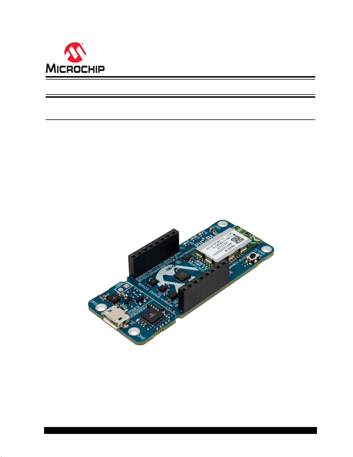
The PIC-BLE Development Board is a small and easily expandable demonstration and development platform for
Bluetooth® Low Energy (BLE) solutions based on the PIC® microcontroller architecture. It is designed to demonstrate
that the design of a typical BLE application can be simplified by partitioning the task into three blocks:
• Smart – represented by the PIC16LF18456 microcontroller
• Secure – represented by the ATECC608A secure element
• Connected – represented by the RN4870 BLE module
In addition, the PIC-BLE Development Board features the following elements:
• The on-board debugger (PKoB nano) supplies full programming and debugging support through Microchip
MPLAB® X IDE. It also provides access to a serial port interface (serial to USB bridge) and one logic analyzer
channel (debug GPIO).
• A mikroBUS™ socket enables the ability to expand the board capabilities with the selection from 450+ sensors
and actuators options offered by MikroElektronika (www.mikroe.com) via a growing portfolio of Click board™.
© 2020 Microchip Technology Inc.
User Guide
DS50002963A-page 1
Page 2

Table of Contents
Preface........................................................................................................................................................... 1
1. Introduction............................................................................................................................................. 3
1.1. Features....................................................................................................................................... 3
1.2. Board Overview............................................................................................................................3
2. Getting Started........................................................................................................................................ 6
2.1. Quick Start....................................................................................................................................6
2.2. Design Documentation and Relevant Links................................................................................. 7
3. Hardware User Guide............................................................................................................................. 8
3.1. On-Board Debugger Overview..................................................................................................... 8
3.2. Power Supply............................................................................................................................. 13
3.3. Low-Power Operation.................................................................................................................14
3.4. Target Current Measurement..................................................................................................... 14
3.5. Peripherals................................................................................................................................. 15
4. Hardware Revision History and Known Issues..................................................................................... 22
4.1. Identifying Product ID and Revision........................................................................................... 22
4.2. Revision 4...................................................................................................................................22
4.3. Revision 3...................................................................................................................................22
5. Document Revision History...................................................................................................................23
6. Appendix............................................................................................................................................... 24
6.1. Schematics.................................................................................................................................24
6.2. Assembly Drawing......................................................................................................................27
The Microchip Website.................................................................................................................................28
Product Change Notification Service............................................................................................................28
Customer Support........................................................................................................................................ 28
Microchip Devices Code Protection Feature................................................................................................ 28
Legal Notice................................................................................................................................................. 28
Trademarks.................................................................................................................................................. 29
Quality Management System....................................................................................................................... 29
Worldwide Sales and Service.......................................................................................................................30
© 2020 Microchip Technology Inc.
User Guide
DS50002963A-page 2
Page 3
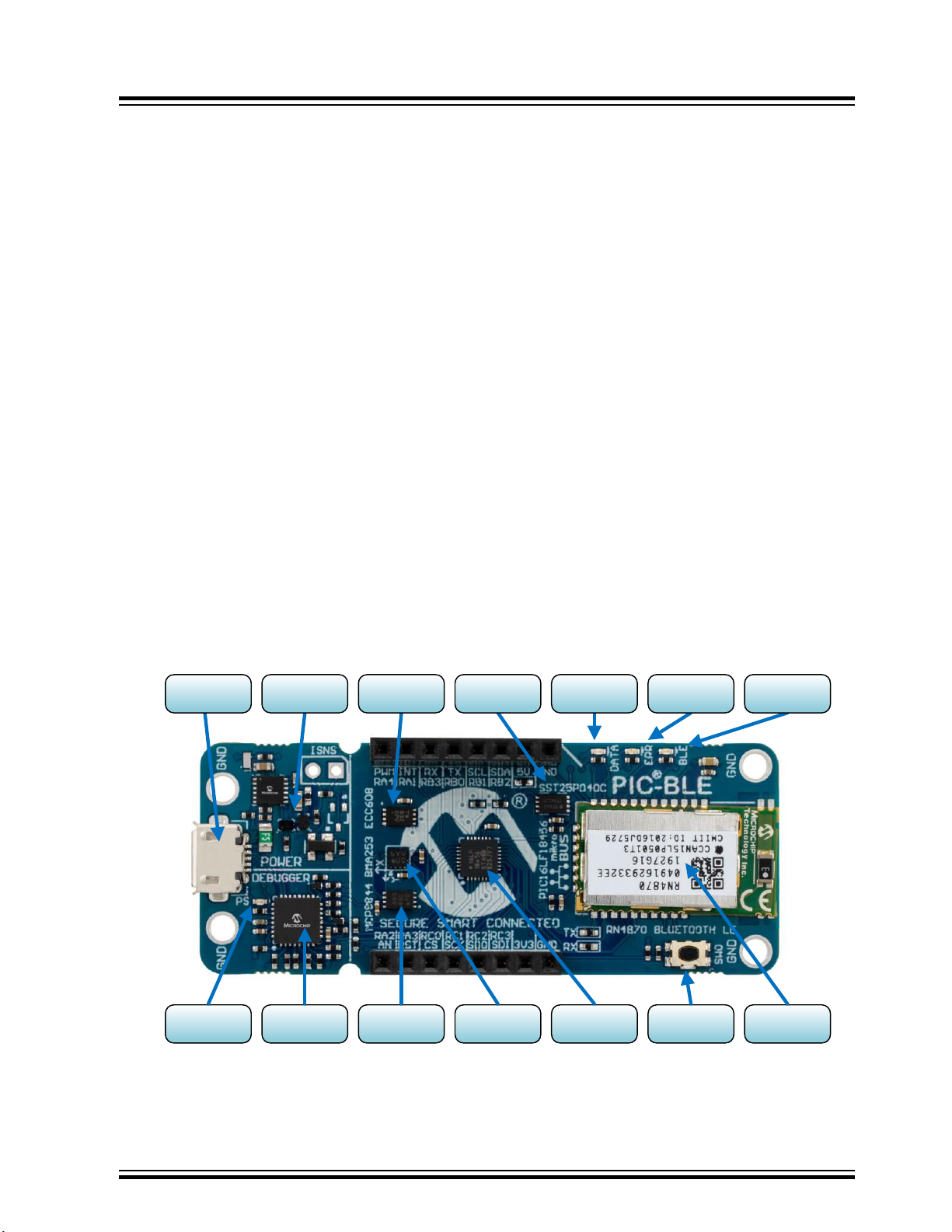
1. Introduction
Micro USB
Connector
Debugger
Power/Status
LED
ATECC6080A
Crypto
Data LED
(Green)
Error LED
(Red)
SST25PF040CT
Serial Flash
USB/Battery
MUX
BLE LED
(Blue)
MCP9844
Temp-sensor
BMA253
Accelerometer
PIC16LF18456
MCU
User Switch
(SW0)
RN4870
BLE module
1.1 Features
• PIC16LF18456 Microcontroller
• Two User LEDs (Data and Error)
• Mechanical Button
• RN4870 Bluetooth Low Energy (BLE) Module
• MCP9844 Temperature Sensor
• BMA253 Acceleration Sensor
• ATECC608A CryptoAuthentication™ Device
• SST25PF040CT 4Mb Serial Flash
• mikroBUS Socket
• On-board Debugger
– Board identification in Microchip MPLAB® X IDE
– Programming and debugging
– Virtual serial port (USB CDC)
– One logic analyzer channel (DGI GPIO)
• USB or Battery Powered
Introduction
1.2 Board Overview
The PIC-BLE development board is a hardware platform that is being used to evaluate the PIC16LF18456
microcontroller and RN4870 BLE module.
Figure 1-1. PIC-BLE Development Board Front Side
© 2020 Microchip Technology Inc.
User Guide
DS50002963A-page 3
Page 4
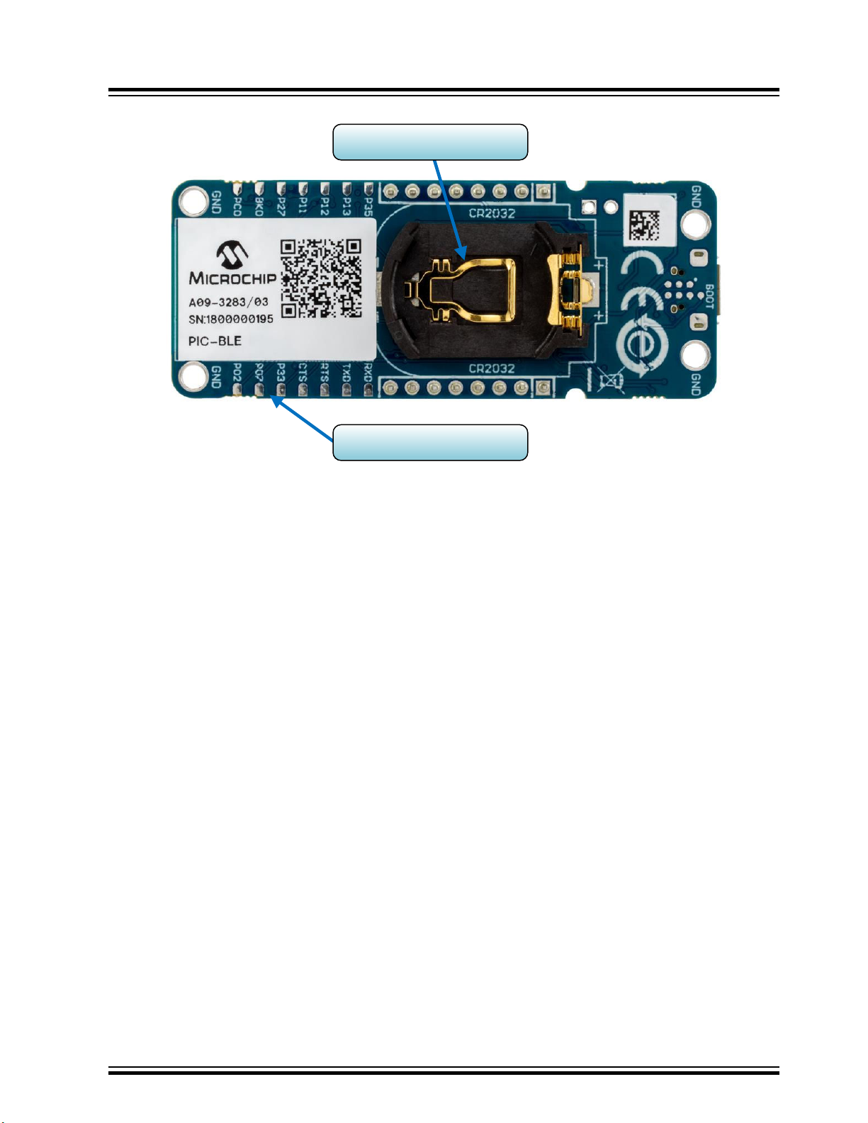
Figure 1-2. PIC-BLE Development Board Back Side
CR2032 Battery Holder
Additional RN4870 GPIO
Introduction
© 2020 Microchip Technology Inc.
User Guide
DS50002963A-page 4
Page 5
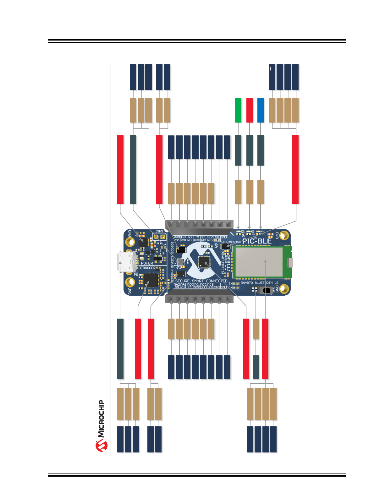
Figure 1-3. PIC-BLE Quick Reference Overview
PIC-BLE Development Board (DT100112)
MIC33050 DC/DC Converter
BMA253 Acceleration Sensor
ATECC608A Secure Element
RA4
RA1
RB3
RB0
RB1
RB2
5.0V
GND
SST25PF040C 4MB FLASH
RA5
Micro USB Connector
PKoB Nano Debugger/ Programmer
MCP9844 Temperature Sensor
AN
RST
SPI CS
SPI SCK
SPI MISO
SPI MOSI
3.3V
GND
PIC16LF18456 MCU
User Switch 0
RN4870 Bluetooth Low Energy Module
RA2
RA3
RC0
RC1
RC2
RC3
RA7
PWM
INT
UART RX
UART TX
I
2
C SCL
I
2
C SDA
DATA LED
RN4870 P2_2
RN4870 P1_1
BLE STATUS LED
ERROR LED
CDC RX
CDC TX
DEBUG GPIO0
RB4 | EUSART1 TX
RB5 | EUSART1 RX
RA7
I
2
C SCL
I
2
C SDA
RB1
RB2
BLE MODE
BLE RST
BLE RX
RA7
RA0
RC4 | EUSART2 TX
BLE TX RC5 | EUSART2 RX
SPI FLASH CS
SPI SCK
SPI MISO
RC7
RC1
RC2
SPI MOSIRC3
I
2
C SCL
I
2
C SDA
BMA 253 INT1
RB1
RB2
RA6
I
2
C SCL
I
2
C SDA
RB1
RB2
GREEN
BLUE
RED
Introduction
© 2020 Microchip Technology Inc.
User Guide
DS50002963A-page 5
Page 6
2. Getting Started
2.1 Quick Start
Demo Application
Out of the box, the PIC-BLE board comes programmed with the pic-lightblue-explorer-demo. This application can be
used to demonstrate a number of the board features using the LightBlue® app by Punch Through.
1. Download the LightBlue® app for iOS or Android.
2. Power the board through a Micro-USB cable or CR2032 battery.
3. Open the LightBlue® app and select the PIC-BLE peripheral.
4. Use the custom interface to explore the board.
Info: The PIC-BLE will show up in the LightBlue® app as PIC-BLE_xxxx, where xxxx are the last two
bytes of the RN4870 BLE module’s Bluetooth MAC address. This makes it possible to distinguish between
multiple PIC-BLE boards.
Communication between the demo application and the LightBlue® app is done by using a protocol based on ASCII
packets. Refer to the protocol chapter on the pic-lightblue-explorer-demo page for a list of commands with examples,
as well as the full source code for the project.
Development Requirements
MPLAB® X IDE:
• MPLAB X IDE v5.30 or later
• XC8 Compiler v2.10 or later
For help with installation, view the MPLAB X installation guide.
Build an Application
View the default source code that is pre-loaded onto the development board. Explore, modify, and build off this
source code to create a custom application.
1. View the source code at the pic-lightblue-explorer-demo GitHub page.
2. Read through the README.md to get more information on how to expand the solution.
3. Download the project from GitHub and open it in the latest version of MPLAB® X IDE.
4. Connect a USB cable (Standard-A to Micro-B or Micro-AB) between the Windows, Mac or Linux device, and
the debug USB port on the PIC-BLE. The board will be identified in the kit window in MPLAB® X IDE.
5. Explore, modify, and build off the source code.
6. Make and program the device. Select the PKoB nano serial number as the debug tool when prompted.
Driver Installation
When the board is connected to the computer for the first time, the operating system will perform a driver software
installation. The driver file supports both 32- and 64-bit versions of Microsoft® Windows® XP, Windows Vista®,
Windows 7, Windows 8, and Windows 10. The drivers for the board are included with Microchip MPLAB® X IDE.
Kit Window
Once the board is powered, the green status LED will be lit and Microchip MPLAB® X IDE will auto-detect which
boards are connected. Microchip MPLAB® X IDE will present relevant information like data sheets and board
documentation. The PIC16LF18456 device on the PIC-BLE board is programmed and debugged by the on-board
debugger, and therefore, no external programmer or debugger tool is required.
Getting Started
© 2020 Microchip Technology Inc.
User Guide
DS50002963A-page 6
Page 7

Tip: The Kit Window can be opened in MPLAB® X IDE through the menu bar Window > Kit Window
2.2 Design Documentation and Relevant Links
The following list contains links to the most relevant documents and software for the PIC-BLE Board:
• MPLAB® X IDE - MPLAB X IDE is a software program that runs on a PC (Windows®, Mac OS®, Linux®) to
develop applications for Microchip microcontrollers and digital signal controllers. It is called an Integrated
Development Environment (IDE) because it provides a single integrated “environment” to develop code for
embedded microcontrollers.
• MPLAB® Xpress Cloud-based IDE - MPLAB Xpress Cloud-Based IDE is an online development environment
that contains the most popular features of our award-winning MPLAB X IDE. This simplified and distilled
application is a faithful reproduction of our desktop-based program, which allows users to easily transition
between the two environments.
• MPLAB® Code Configurator - MPLAB Code Configurator (MCC) is a free software plug-in that provides a
graphical interface to configure peripherals and functions specific to your application.
• Microchip Sample Store - Microchip sample store where you can order samples of devices.
• MPLAB Data Visualizer - MPLAB Data Visualizer is a program used for processing and visualizing data. The
Data Visualizer can receive data from various sources such as serial ports and on-board debugger’s Data
Gateway Interface, as found on Curiosity Nano and Xplained Pro boards.
• Microchip PIC and AVR Examples - Microchip PIC and AVR Device Examples is a collection of examples and
labs that use Microchip development boards to showcase the use of PIC and AVR device peripherals.
• Microchip PIC and AVR Solutions - Microchip PIC and AVR Device Solutions contains complete applications
for use with Microchip development boards, ready to be adapted and extended.
• PIC-BLE website - Kit information, latest user guide and design documentation.
• PIC-BLE on Microchip Direct - Purchase this kit on Microchip Direct.
Getting Started
© 2020 Microchip Technology Inc.
User Guide
DS50002963A-page 7
Page 8
3. Hardware User Guide
3.1 On-Board Debugger Overview
PIC-BLE contains an on-board debugger for programming and debugging. The on-board debugger is a composite
USB device consisting of several interfaces:
• A debugger that can program and debug the PIC16LF18456 in Microchip MPLAB® X IDE
• A mass storage device that allows drag-and-drop programming of the PIC16LF18456
• A virtual serial port (CDC) that is connected to a Universal Asynchronous Receiver/Transmitter (UART) on the
PIC16LF18456, and provides an easy way to communicate with the target application through terminal software
• A Data Gateway Interface (DGI) for code instrumentation with logic analyzer channels (debug GPIO) to visualize
program flow
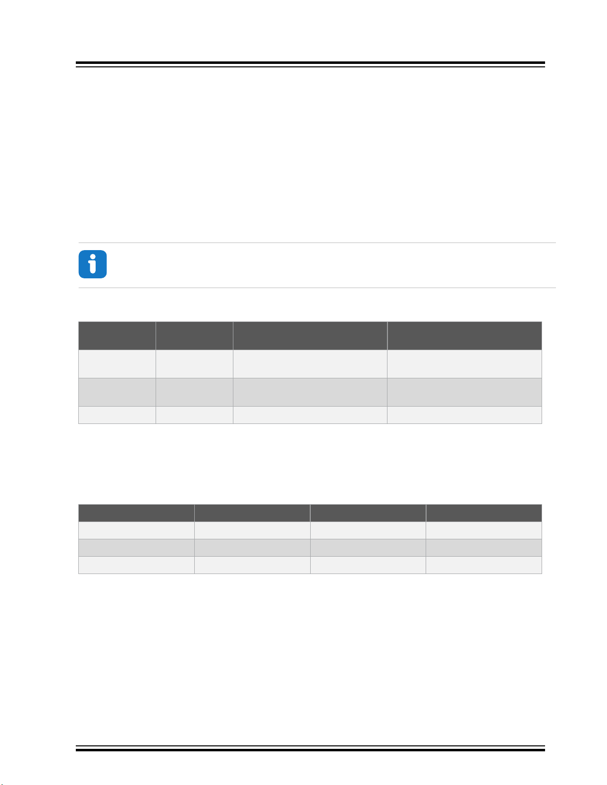
The on-board debugger controls a Power and Status LED (marked PS) on the PIC-BLE Board. The table below
shows how the LED is controlled in different operation modes.
Table 3-1. On-Board Debugger LED Control
Operation Mode Power and Status LED
Hardware User Guide
Boot Loader mode The LED blinks slowly during power-up.
Power-up The LED is ON.
Normal operation The LED is ON.
Programming Activity indicator: The LED blinks slowly during programming/debugging.
Drag-and-drop
programming
Fault The LED blinks rapidly if a power Fault is detected.
Sleep/Off The LED is OFF. The on-board debugger is either in a sleep mode or powered down.
3.1.1 Debugger
The on-board debugger on the PIC-BLE Board appears as a Human Interface Device (HID) on the host computer’s
USB subsystem. The debugger supports full-featured programming and debugging of the PIC16LF18456 using
Microchip MPLAB® X IDE.
Success: The LED blinks slowly for 2 sec.
Failure: The LED blinks rapidly for 2 sec.
This can occur if the board is externally powered.
Info: Slow blinking is approximately 1 Hz, and rapid blinking is approximately 5 Hz.
Remember: Keep the debugger’s firmware up-to-date. Firmware upgrades are done automatically when
using Microchip MPLAB® X IDE.
3.1.2 Virtual Serial Port (CDC)
The virtual serial port (CDC) is a general purpose serial bridge between a host PC and a target device.
© 2020 Microchip Technology Inc.
User Guide
DS50002963A-page 8
Page 9
3.1.2.1 Overview
Target MCU
UART TX
UART RX
Debugger
USB
CDC RX
CDC TX
PC
Terminal
Software
Target
Receive
Target
Send
Terminal
Receive
Terminal
Send
The on-board debugger implements a composite USB device that includes a standard Communications Device Class
(CDC) interface, which appears on the host as a virtual serial port. The CDC can be used to stream arbitrary data in
both directions between the host computer and the target: All characters sent through the virtual serial port on the
host computer will be transmitted as UART on the debugger’s CDC TX pin, and UART characters captured on the
debugger’s CDC RX pin will be returned to the host computer through the virtual serial port.
Figure 3-1. CDC Connection
Hardware User Guide
Info: As shown in Figure 3-1, the debugger’s CDC TX pin is connected to a UART RX pin on the target
for receiving characters from the host computer. Similarly, the debugger’s CDC RX pin is connected to a
UART TX pin on the target for transmitting characters to the host computer.
3.1.2.2 Operating System Support
On Windows machines, the CDC will enumerate as Curiosity Virtual COM Port and appear in the Ports section of the
Windows Device Manager. The COM port number can also be found there.
Info: On older Windows systems, a USB driver is required for CDC. This driver is included in installations
of Microchip MPLAB® X IDE.
On Linux machines, the CDC will enumerate and appear as /dev/ttyACM#.
Info: tty* devices belong to the “dialout” group in Linux, so it may be necessary to become a member of
that group to have permissions to access the CDC.
On MAC machines, the CDC will enumerate and appear as /dev/tty.usbmodem#. Depending on which terminal
program is used, it will appear in the available list of modems as usbmodem#.
Info: For all operating systems: Be sure to use a terminal emulator that supports DTR signaling. See
Section 3.1.2.4 “Signaling”.
3.1.2.3 Limitations
Not all UART features are implemented in the on-board debugger CDC. The constraints are outlined here:
• Baud rate: Must be in the range of 1200 bps to 500 kbps. Any baud rate outside this range will be set to the
closest limit, without warning. Baud rate can be changed on-the-fly.
• Character format: Only 8-bit characters are supported.
© 2020 Microchip Technology Inc.
User Guide
DS50002963A-page 9
Page 10

• Parity: Can be odd, even, or none.
• Hardware flow control: Not supported.
• Stop bits: One or two bits are supported.
3.1.2.4 Signaling
During USB enumeration, the host OS will start both communication and data pipes of the CDC interface. At this
point, it is possible to set and read back the baud rate and other UART parameters of the CDC, but data sending and
receiving will not be enabled.
When a terminal connects on the host, it must assert the DTR signal. As this is a virtual control signal implemented
on the USB interface, it is not physically present on the board. Asserting the DTR signal from the host will indicate to
the on-board debugger that a CDC session is active. The debugger will then enable its level shifters (if available), and
start the CDC data send and receive mechanisms.
Deasserting the DTR signal will not disable the level shifters but will disable the receiver so no further data will be
streamed to the host. Data packets that are already queued up for sending to the target will continue to be sent out,
but no further data will be accepted.
Hardware User Guide
Remember: Set up the terminal emulator to assert the DTR signal. Without the signal, the on-board
debugger will not send or receive any data through its UART.
Tip: The on-board debugger’s CDC TX pin will not be driven until the CDC interface is enabled by the
host computer. Also, there are no external pull-up resistors on the CDC lines connecting the debugger and
the target, which means that during power-up, these lines are floating. To avoid any glitches resulting in
unpredictable behavior like framing errors, the target device should enable the internal pull-up resistor on
the pin connected to the debugger’s CDC TX pin.
3.1.2.5 Advanced Use
CDC Override Mode
In normal operation, the on-board debugger is a true UART bridge between the host and the device. However, in
certain use cases, the on-board debugger can override the basic operating mode and use the CDC TX and RX pins
for other purposes.
Dropping a text file into the on-board debugger’s mass storage drive can be used to send characters out of the
debugger’s CDC TX pin. The filename and extension are trivial, but the text file must start with the characters:
CMD:SEND_UART=
The maximum message length is 50 characters – all remaining data in the frame are ignored.
The default baud rate used in this mode is 9600 bps, but if the CDC is already active or has been configured, the
previously used baud rate still applies.
USB-Level Framing Considerations
Sending data from the host to the CDC can be done byte-wise or in blocks, which will be chunked into 64-byte USB
frames. Each such frame will be queued up for sending to the debugger’s CDC TX pin. Transferring a small amount
of data per frame can be inefficient, particularly at low baud rates, because the on-board debugger buffers frames
and not bytes. A maximum of four 64-byte frames can be active at any time. The on-board debugger will throttle the
incoming frames accordingly. Sending full 64-byte frames containing data is the most efficient method.
When receiving data on the debugger’s CDC RX pin, the on-board debugger will queue up the incoming bytes into
64-byte frames, which are sent to the USB queue for transmission to the host when they are full. Incomplete frames
are also pushed to the USB queue at approximately 100 ms intervals, triggered by USB start-of-frame tokens. Up to
eight 64-byte frames can be active at any time.
© 2020 Microchip Technology Inc.
User Guide
DS50002963A-page 10
Page 11

If the host (or the software running on it) fails to receive data fast enough, an overrun will occur. When this happens,
the last-filled buffer frame will be recycled instead of being sent to the USB queue, and a full frame of data will be
lost. To prevent this occurrence, the user must ensure that the CDC data pipe is being read continuously, or the
incoming data rate must be reduced.
3.1.3 Mass Storage Device
The on-board debugger includes a simple Mass Storage Device implementation, which is accessible for read/write
operations via the host operating system to which it is connected.
It provides:
• Read access to basic text and HTML files for detailed kit information and support
• Write access for programming Intel® HEX formatted files into the target device’s memory
• Write access for simple text files for utility purposes
3.1.3.1 Mass Storage Device Implementation
The on-board debugger implements a highly optimized variant of the FAT12 file system that has several limitations,
partly due to the nature of FAT12 itself and optimizations made to fulfill its purpose for its embedded application.
The Curiosity Nano USB Device is USB Chapter 9-compliant as a mass storage device but does not, in any way,
fulfill the expectations of a general purpose mass storage device. This behavior is intentional.
When using the Windows operating system, the on-board debugger enumerates as a Curiosity Nano USB Device
that can be found in the disk drives section of the device manager. The CURIOSITY drive appears in the file manager
and claims the next available drive letter in the system.
The CURIOSITY drive contains approximately one MB of free space. This does not reflect the size of the target
device’s Flash in any way. When programming an Intel® HEX file, the binary data are encoded in ASCII with
metadata providing a large overhead, so one MB is a trivially chosen value for disk size.
It is not possible to format the CURIOSITY drive. When programming a file to the target, the filename may appear in
the disk directory listing. This is merely the operating system’s view of the directory, which, in reality, has not been
updated. It is not possible to read out the file contents. Removing and replugging the board will return the file system
to its original state, but the target will still contain the application that has been previously programmed.
To erase the target device, copy a text file starting with “CMD:ERASE” onto the disk.
Hardware User Guide
By default, the CURIOSITY drive contains several read-only files for generating icons as well as reporting status and
linking to further information:
• AUTORUN.ICO – icon file for the Microchip logo
• AUTORUN.INF – system file required for Windows Explorer to show the icon file
• CLICK-ME.HTM – redirect to the PIC-BLE web demo application
• KIT-INFO.HTM – redirect to the development board website
• KIT-INFO.TXT – a text file containing details about the board’s debugger firmware version, board name, USB
serial number, device, and drag-and-drop support
• STATUS.TXT – a text file containing the programming status of the board
Info: STATUS.TXT is dynamically updated by the on-board debugger. The contents may be cached by
the OS and, therefore, do not reflect the correct status.
3.1.3.2 Configuration Words
Configuration Words (PIC® MCU Targets)
Configuration Word settings included in the project being programmed after program Flash is programmed. The
debugger will not mask out any bits in the Configuration Words when writing them, but since it uses Low-Voltage
Programming mode, it is unable to clear the LVP Configuration bit. If the incorrect clock source is selected, for
© 2020 Microchip Technology Inc.
User Guide
DS50002963A-page 11
Page 12

example, and the board does not boot, it is always possible to perform a bulk erase (always done before
programming) and restore the device to its default settings.
3.1.3.3 Special Commands
Several utility commands are supported by copying text files to the mass storage disk. The filename or extension is
irrelevant – the command handler reacts to content only.
Table 3-2. Special File Commands
Command Content Description
CMD:ERASE
CMD:SEND_UART=
CMD:RESET
Info: The commands listed here are triggered by the content being sent to the mass storage emulated
disk, and no feedback is provided in the case of either success or failure.
Hardware User Guide
Executes a chip erase of the target
Sends a string of characters to the CDC UART. See “CDC Override Mode”.
Resets the target device by entering Programming mode and then exiting
Programming mode immediately thereafter. Exact timing can vary according to
the programming interface of the target device. (Debugger firmware v1.16 or
newer.)
3.1.4 Data Gateway Interface (DGI)
Data Gateway Interface (DGI) is a USB interface for transporting raw and time-stamped data between on-board
debuggers and host computer-based visualization tools. MPLAB Data Visualizer is used on the host computer to
display debug GPIO data. It is available as a plug-in for MPLAB® X IDE or a stand-alone application that can be used
in parallel with Microchip MPLAB® X IDE.
Although DGI encompasses several physical data interfaces, the PIC-BLE implementation includes logic analyzer
channels:
• One debug GPIO channel (also known as DGI GPIO)
3.1.4.1 Debug GPIO
Debug GPIO channels are timestamped digital signal lines connecting the target application to a host computer
visualization application. They are typically used to plot the occurrence of low-frequency events on a time-axis – for
example, when certain application state transitions occur.
The figure below shows the monitoring of the digital state of a mechanical switch connected to a debug GPIO in
MPLAB Data Visualizer.
© 2020 Microchip Technology Inc.
User Guide
DS50002963A-page 12
Page 13

Hardware User Guide
Figure 3-2. Monitoring Debug GPIO with MPLAB Data Visualizer
Debug GPIO channels are timestamped, so the resolution of DGI GPIO events is determined by the resolution of the
DGI timestamp module.
Important: Although bursts of higher-frequency signals can be captured, the useful frequency range of
signals for which debug GPIO can be used is up to about 2 kHz. Attempting to capture signals above this
frequency will result in data saturation and overflow, which may cause the DGI session to be aborted.
3.1.4.2 Timestamping
DGI sources are timestamped as they are captured by the debugger. The timestamp counter implemented in the
Curiosity Nano debugger increments at 2 MHz frequency, providing a timestamp resolution of a half microsecond.
3.2 Power Supply
The board can be powered through the USB port or by a CR2032 battery. It will automatically switch to the battery if
USB power is not available. While powered through USB, the board generates 3.3V for the debugger,
PIC16LF18456, and peripherals. During battery operation, the PIC16LF18456 and peripherals run directly on the
battery voltage, while the debugger is not powered.
Current drawn from the USB port is limited to 500 mA by a PTC resettable fuse.
Important: When powering the PIC-BLE board with a CR2032 battery, it is important to leave the
PIC16LF18456 pins that connect to the CDC UART in Tri-State (Input) mode. This is to prevent the
debugger from getting powered through its GPIO.
© 2020 Microchip Technology Inc.
User Guide
DS50002963A-page 13
Page 14
Figure 3-3. Power Supply Block Diagram
USB
On-Board
Debugger
Power source
Power disconnect
Power consumer
Power converter
VUSB
MIC33050
(buck)
MUX
(MIC94050)
(MIC94165)
Power MUX
Battery
Holder
(CR2032)
VCC_P3V3
VBAT
VBAT_OUT
0Ω resistor
Target MCU
Peripherals
mBUS
RN4870
0Ω resistor
P3V3_ENABLE
Info: On the mikroBUS socket, the +5V rail is powered from the USB port. Consequently, +5V will not be
available when the board is powered from a battery.
Hardware User Guide
3.3 Low-Power Operation
To achieve the lowest power consumption of the board the following considerations must be taken:
• Set the MCP9844 in Shutdown mode
– Set bit 8 (SHDN) in the 16-bit CONFIG register (address 0x01)
• Set the BMA253 in Deep Suspend mode
– Set bit 5 (deep suspend) in the 8-bit PMU_LPW register (address 0x11)
• Set the RN4870 in Sleep mode
– Set the RX_IND pin high (RC6 on the PIC16LF18456)
– Send the "O,0\r" command to the RN4870
• Set unused PIC16LF18456 I/O pins as input and disable the digital input buffer
Important: EUSART pins RB4 and RB5 are connected directly to the on-board debugger. It is important
to tri-state the EUSART pins when the board is powered from a CR2032 battery to prevent powering the
debugger through its I/O pins. Doing so will increase the power consumption and cause undefined
behavior from the on-board debugger.
Info: The load switch U300 in the power MUX can leak up to 1 μA when the board is powered from a
battery. By modifying the board and removing resistor R303 (0Ω), U300 can be disconnected. Be warned
that a board modified this way can no longer be powered from USB, and consequently neither
programmed nor debugged using the on-board debugger until the 0Ω resistor is reconnected.
3.4 Target Current Measurement
© 2020 Microchip Technology Inc.
Power to the PIC16LF18456 and its peripherals is connected from the on-board power supply through a 0Ω resistor
(R301) in parallel with a 100-mil Current sense pin header footprint marked with “ISNS” in silkscreen (J301). To
User Guide
DS50002963A-page 14
Page 15

0Ω resistor
(R301)
Current sense footprint
(J301)
Hardware User Guide
measure the power consumption of the PIC16LF18456 and other peripherals on the board, de-solder the 0Ω resistor
and connect an ammeter over the Current sense footprint.
Figure 3-4. Current sense footprint
3.5 Peripherals
3.5.1 PIC16LF18456
Tip: A 100-mil pin header can be soldered into the Current sense (J301) footprint for easy connection of
an ammeter. Once the ammeter is not needed anymore, place a jumper cap on the pin header.
Microchip PIC16LF18456 is a microcontroller featuring Intelligent Analog, Core Independent Peripherals (CIPs), and
communication peripherals combined with eXtreme Low Power (XLP) for a wide range of general purpose and lowpower applications. Features such as a 12-bit Analog-to-Digital Converter with Computation (ADC2 ), Memory
Access Partitioning (MAP), the Device Information Area (DIA), Power-Saving Operating modes, and Peripheral Pin
Select (PPS) offer flexible solutions for a wide variety of custom applications.
© 2020 Microchip Technology Inc.
User Guide
DS50002963A-page 15
Page 16

3.5.2 mikroBUS Socket
AN PWM
RST INT
CS RX
SCK TX
MISO SCL
MOSI SDA
+3.3V +5V
GND GND
RA2 RA4
RA3 RA1
RC0 RB3
RC1 RB0
RC2 RB1
RC3 RB2
VCC VBUS
GND GND
Figure 3-5. mikroBUS Socket Pinout
Hardware User Guide
The PIC-BLE board features a mikroBUS socket for expanding the functionality of the development board using
MikroElektronika Click board and other mikroBUS add-on boards. The socket is populated with two 1x8 2.54 mm
pitch female headers and is ready to mount add-on boards.
Table 3-3. mikroBUS Socket Pinout
mikroBUS Socket Pin PIC16LF18456 Pin Function Shared Functionality
AN RA2 ADCC ANA2 —
RST RA3 GPIO —
CS RC0 MSSP SPI CS —
SCK RC1 MSSP SPI SCK SST25PF040CT
MISO RC2 MSSP SPI MISO SST25PF040CT
MOSI RC3 MSSP SPI MOSI SST25PF040CT
+3.3V V
GND GND Ground —
PWM RA4 CCP5 —
INT RA1 EXT_INT —
RX RB3 EUSART RX —
TX RB0 EUSART TX —
SCL RB1 MSSP I2C SCL MCP9844, BMA253 and
DD
VCC_TARGET —
ATECC608A
SDA RB2 MSSP I2C SDA MCP9844, BMA253 and
+5V — VBUS —
GND GND Ground —
© 2020 Microchip Technology Inc.
User Guide
ATECC608A
DS50002963A-page 16
Page 17

Info: VBUS is powered from USB. Consequently, +5V will not be available while the board is powered
from a battery.
Info: VCC_TARGET will have the battery voltage when the board is powered from a battery, which can
be less than +3.3V.
3.5.3 RN4870 BLE Module
The RN4870 is a Bluetooth® Low Energy (BLE) module that integrates a Bluetooth® 5.0 baseband controller, onboard Bluetooth stack, digital and analog I/O, and RF power amplifier into one solution.
Additional Features:
• Range up to 50m
• Operating Voltage Range: 1.9V to 3.6V
• TX / RX mode Peak Current: 10 mA (typical)
• Low-Power Mode Current: 60 μA (typical)
• Shutdown Current: 2.9 μA (max)
The RN4870 BLE module is connected to the PIC16LF18456 through UART as well as three GPIOs for control and
configuration of the module. The RST signals resets the module, while the RX_IND signal is used to wake the
module from Low-Power mode. The MODE signal, available from the PIC16LF18456, the debugger as well as by a
physical switch, allows the module to be put in a “Test Mode” where the RN4870 firmware can be updated.
The module has two of its GPIO pins connected to LEDs. By default the BLE LED will indicate connection status,
while ERR LED must be controlled by the user. Both LEDs can be configured for a number of other functions. Many
of the other RN4870 GPIO pins are available as pads around the label on the back side of the PIC-BLE board, as can
be seen in Figure 1-2.
Hardware User Guide
Info: Some RN4870 settings have been changed during manufacturing of PIC-BLE. Using the S-
command, the device name has been changed to “PIC-BLE”. In addition, the communication settings have
been configured for PIC16LF18456 EUSART settings of 9600,8,N,1.
Table 3-4. RN4870 Connections
RN4870 Pin PIC16LF18456
Pin
RX RC4 EUSART TX —
TX RC5 EUSART RX —
RST RA0 GPIO —
P2_0 / MODE RA7 GPIO Mechanical Switch and On-board
P3_3 / RX_IND RC6 GPIO —
P1_1 / STATUS1 — Connection LED (BLE) BLE LED
P2_2 — Custom configurable LED (ERR) ERR LED
Function Shared Functionality
debugger
© 2020 Microchip Technology Inc.
User Guide
DS50002963A-page 17
Page 18

Info: The RST and MODE signals are pulled up by external resistors.
3.5.4 ATECC608A Secure Element
The ATECC608A is a secure element from the Microchip CryptoAuthentication portfolio with advanced Elliptic Curve
Cryptography (ECC) capabilities. With ECDH and ECDSA being built right in, this device is ideal for the rapidly
growing Internet of Things (IoT) market by easily supplying the full range of security, such as confidentiality, data
integrity, and authentication to systems with MCU or MPUs running encryption/decryption algorithms. Similar to all
Microchip CryptoAuthentication products, the ATECC608A employs ultra-secure, hardware-based cryptographic key
storage and cryptographic countermeasures that eliminate any potential backdoors linked to software weaknesses.
The ATECC608A CryptoAuthentication device on the PIC-BLE board can be used to authenticate the board with
other hardware for secure IoT communication.
Info: 7-bit I2C address: 0x58.
Hardware User Guide
Table 3-5. ATECC608A Connections
ATECC608A Pin PIC16LF18456
Pin
SDA RB2 MSSP I2C SDA MCP9844, BMA253 and mikroBUS
SCL RB1 MSSP I2C SCL MCP9844, BMA253 and mikroBUS
3.5.5 SST25PF040CT Serial Flash
The SST25PF040CT is a 4 Mbit Serial Flash with extended operating voltage range and low-power consumption.
Additional Features:
• Operating Voltage Range: 2.3V to 3.6V
• Active Read Current: 5 mA (typical)
• Power Down Standby Current: 3 μA (typical)
The SST25PF040CT Serial Flash is connected to the PIC16LF18456 through SPI.
Info: The Flash is SPI Mode 0 and Mode 3 compatible, and supports clock speeds up to 40 MHz
Table 3-6. SST25PF040CT Connections
SST25PF040CT
Pin
PIC16LF18456
Pin
Function Shared Functionality
Function Shared Functionality
CS RC7 GPIO —
SCK RC1 MSSP SPI SCK mikroBUS
MISO RC2 MSSP SPI MISO mikroBUS
© 2020 Microchip Technology Inc.
User Guide
DS50002963A-page 18
Page 19

...........continued
SST25PF040CT
Pin
MOSI RC3 MSSP SPI MOSI mikroBUS
PIC16LF18456
Pin
3.5.6 MCP9844 Temperature Sensor
The MCP9844 digital temperature sensor converts circuit board temperatures between -40°C and +125°C to a digital
word with ±1°C/±3°C (typical/maximum) accuracy.
Additional features:
• Accuracy:
– ±0.2°C/±1°C (typical/maximum) from +75°C to +95°C
– ±0.5°C/±2°C (typical/maximum) from +40°C to +125°C
– ±1°C/±3°C (typical/maximum) from -40°C to +125°C
• User Selectable Measurement Resolution:
– 0.5°C, 0.25°C, 0.125°C, 0.0625°C
• User Programmable Temperature Limits:
– Temperature Window Limit
– Critical Temperature Limit
• User Programmable Temperature Alert Output
• Operating Voltage Range:
– 1.7V to 3.6V
• Operating Current:
– 100 μA (typical)
• Shutdown Current:
– 0.2 μA (typical)
The MCP9844 temperature sensor is connected to the PIC16LF18456 through I2C.
Hardware User Guide
Function Shared Functionality
Info: 7-bit I2C address: 0x18.
Table 3-7. MCP9844 Connections
MCP9844 Pin PIC16LF18456
Pin
SDA RB2 MSSP I2C SDA ATECC608A, BMA253 and
SCL RB1 MSSP I2C SCL ATECC608A, BMA253 and
3.5.7 BMA253 Acceleration Sensor
The Bosch BMA253 is a low-g acceleration sensor with digital output for measurements of acceleration in three
perpendicular axes.
Additional Features:
• 12-Bit Sensitivity
• User Selectable Acceleration Ranges: ±2g, ±4g, ±8g, ±16g
• On-Chip 32 frame First-In First-Out (FIFO)
• Motion Triggered Interrupts:
Function Shared Functionality
mikroBUS
mikroBUS
© 2020 Microchip Technology Inc.
User Guide
DS50002963A-page 19
Page 20
Hardware User Guide
– New Data
– Any Motion Detection
– Single/Double Tap Sensing
– Orientation Recognition
– Flat Detection
– Low/High-g Detection
– Inactivity Detection
• Operating Voltage Range: 1.62V to 3.6V
• Operating Current (Normal mode): 130 μA (typical)
• Shutdown Current (Deep Suspend mode): 1 μA (typical)
The BMA253 acceleration sensor is connected to the PIC16LF18456 through I2C and a GPIO for the user
configurable interrupt outputs.
Info: 7-bit I2C address: 0x19
Table 3-8. BMA253 Connections
BMA253 Pin PIC16LF18456
SDA RB2 MSSP I2C SDA MCP9844, ATECC608A and
SCL RB1 MSSP I2C SCL MCP9844, ATECC608A and
INT1 RA6 GPIO / EXT_INT —
3.5.8 LEDs
There is one user LED available on the PIC-BLE board that can be controlled by either GPIO or PWM. In addition,
there are two LEDs connected directly to the BLE module. The LEDs can be activated by driving their connected I/O
lines to GND.
Table 3-9. LED Connections
LED PIC16LF18456 Pin Function Shared Functionality
Green Data LED RA5 GPIO / CCP5 On-board debugger
Red Error LED — Connected to BLE module RN4870
Blue BLE LED — Connected to BLE module RN4870
3.5.9 Mechanical Switch
The PIC-BLE board has one mechanical switch. This is a generic user-configurable switch that will drive the
connected I/O line to ground (GND) when it is pressed. An external resistor pulls the signal high when the switch is
not pressed.
Holding the switch during power-up can be used to put the Bluetooth module in Configuration mode. See 3.5.3
RN4870 BLE Module for more information.
Function Shared Functionality
Pin
mikroBUS
mikroBUS
© 2020 Microchip Technology Inc.
User Guide
DS50002963A-page 20
Page 21

Table 3-10. Mechanical Switch Connection
Switch PIC16LF18456 Pin Function Shared Functionality
SW0 RA7 GPIO / EXT_INT RN4870 and On-board
Info: The SW0 signal is pulled up by an external resistor.
3.5.10 On-Board Debugger Implementation
PIC-BLE features an on-board debugger that can be used to program and debug the PIC16LF18456 using In-Circuit
Serial Programming (ICSP). The on-board debugger also includes a virtual serial port (CDC) interface over UART
and debug GPIO. Microchip MPLAB® X IDE can be used as a front-end for the on-board debugger for programming
and debugging. MPLAB Data Visualizer can be used as a front-end for the CDC and debug GPIO.
3.5.10.1 On-Board Debugger Connections
The table below shows the connections between the target and the debugger section. All connections between the
target and the debugger are tri-stated as long as the debugger is not actively using the interface. Hence, since there
are little contaminations of the signals, the pins can be configured to anything the user wants.
For further information on how to use the capabilities of the on-board debugger, see 3.1 On-Board Debugger
Overview.
Table 3-11. On-Board Debugger Connections
Hardware User Guide
debugger
PIC16LF18456
Pin
RB5 CDC TX EUSART RX (PIC16LF18456 RX
RB4 CDC RX EUSART TX (PIC16LF18456 TX
RB7 DBG0 ICSP DATA —
RB6 DBG1 ICSP CLOCK —
RA7 DBG2 DEBUG GPIO0 Mechanical Switch and RN4870
MCLR DBG3 MCLR —
Debugger Pin Function Shared Functionality
—
line)
—
line)
© 2020 Microchip Technology Inc.
User Guide
DS50002963A-page 21
Page 22

Hardware Revision History and Known Issues
4. Hardware Revision History and Known Issues
This user guide is written to provide information about the latest available revision of the board. The following
sections contain information about known issues, a revision history of older revisions, and how older revisions differ
from the latest revision.
4.1 Identifying Product ID and Revision
The revision and product identifier of the PIC-BLE Board can be found in two ways: Either by utilizing the Microchip
MPLAB® X IDE Kit Window or by looking at the sticker on the bottom side of the PCB.
By connecting a PIC-BLE to a computer with Microchip MPLAB® X IDE running, the Kit Window will pop up. The first
six digits of the serial number, which is listed under kit information, contain the product identifier and revision.
Tip: The Kit Window can be opened in MPLAB® X IDE through the menu bar Window > Kit Window.
The same information can be found on the sticker on the bottom side of the PCB. Most boards will have the identifier
and revision printed in plain text as A09-nnnn\rr, where “nnnn” is the identifier, and “rr” is the revision. Boards with
limited space have a sticker with only a data matrix code, containing the product identifier, revision, and serial
number.
The serial number string has the following format:
"nnnnrrssssssssss"
n = product identifier
r = revision
s = serial number
The product identifier for PIC-BLE is A09-3283.
4.2 Revision 4
Revision 4 is functionally the same as revision 3, but features a RN4870 BLE module with firmware version 1.40 (part
number RN4870-V/RM140).
In the silkscreen, the part number of the serial flash chip is wrong. It should be SST25PF040C, but shows
SST25P040C.
4.3 Revision 3
Revision 3 is the initial released revision of the board. It features a RN4870 BLE module with firmware version 1.30
(part number RN4870-I/RM130).
© 2020 Microchip Technology Inc.
User Guide
DS50002963A-page 22
Page 23

5. Document Revision History
Doc. rev. Date Comment
A 03/2020 Initial document release
Document Revision History
© 2020 Microchip Technology Inc.
User Guide
DS50002963A-page 23
Page 24

1
1
2
2
3
3
4
4
5
5
6
6
7
7
8
8
D D
C C
B B
A A
2 of 5
PIC-BLE
2020-01-10
PIC-BLE_Target_MCU.SchDoc
Project Title
PCB Assembly Number: PCBA Revision:
File:
PCB Number: PCB Revision:
Designed with
Drawn By:
Microchip Norway
Sheet Title
Target MCU
Engineer:
TF
A08-3003 3
Size
A3
A09-3283 4
Page:
Date:
Altium.com
GND
100n
C200
1k
R210
USER LE DS
VCC_TARGET
USER BUTT ON
DBG0
CDC_UART
TX
RX
UART
DBG1
DBG2
2185-108SS0CYNP1
1
234
5
6
7
8
J200
2185-108SS0CYNP1
1234567
8
J201
mikr oBUS
GND GND
AN
RSTCSSCK
MISO
MOSI
+3.3V
GND
PWM
INTRXTX
SCL
SDA
+5V
GND
Head er (Female )
TM
RN4870
10uF/10V
C202
10nF
C201
330R
R207
1 2
43
5
KMR221G
SW200
1k
R209
1k
R208
GND
SDA5SCL
6
GND
4
VCC
8
PAD
9
NC1NC2NC3NC
7
U201
GND
GND
100k
R201
VCC_TARGET
VCC_TARGET
RB1_I2C_SCL
RB2_I2C_SDA
VCC_TARGET
GND
100n
C204
Cryp toAuth enticat ionTM Temper atur e Sensor
GND
VCC_TARGET
4.7k
R204
4.7k
R205
VCC_TARGET
VCC_TARGET
TP211
TP203
TP210
TP212
TP208
2 1
GREEN LED
SML-P12MTT86R
D200
RED LED
SML-P12VTT86R
2 1
D201
Default I2C address: 0x18
RC5_BLE_UART2_RX
RC4_BLE_UART2_TX
RA3_MBUS_RST
RB1_I2C_SCL
RB2_I2C_SDA
RA2_MBUS_AIN
RA1_MBUS_INT
Default I2C address: 0x58
2 1
BLUE LED
SMLP13BC8TT86
D202
VCC_TARGET
GND
RB0_UART2_TX
RB3_UART2_RX
TP214
100n
C205
SW0
VBUS0R
R206
+5V
TP213
TP209
MCLR
DATA
ATECC608A
DBG3
RB1_I2C_SCL
RB2_I2C_SDA
4.7k
R203
4.7k
R202
GND
VCC_TARGET
GND
RB7_ICSPDAT
RB6_ICSPCLK
MCLR
RB1_I2C_SCL
RB2_I2C_SDA
RA2_MBUS_AIN
RA3_MBUS_RST
RB3_UART2_RX
RB0_UART2_TX
RA1_MBUS_INT
RC6_BLE_RX_IND
RB4_CDC_TX
RB5_CDC_RX
10k
R200
3-axial Accelera tion Sensor
VCC_TARGET
GND
100n
C206
GND
100n
C207
GND
Alternate I2C address: 0x19
VCC_TARGET
RB1_I2C_SCL
RB2_I2C_SDA
1uF
C203
GND
PIC16LF18456
RA6_ACCEL_INT1
RC7_FLASH_CS
GND
MCP9844
SDA5SCL6EVENT7GND
4
A23A12A0
1
VDD
8
EP
9
U202
RN4870_BLE_LED
RN4870_BLE_LED
RA6_ACCEL_INT1
RA2
1
RA3
2
RA4
3
RA5
4
VSS
5
RA7
6
RA6
7
RC08RC19RC2
10
RC3
11
RC4
12
RC513RC6
14
RC7
15
RB422RB523ICSPCLK/RB624ICSPDAT/RB725MCLR/RE326RA027RA1
28
RB3
21
RB2
20
RB0
18
VDD
17
VSS
16
RB1
19
PAD
29
PIC16LF18456T-I/STX
U200
RC2_SPI_MISO
RC1_SPI_SCK
RC3_SPI_MOSI
RC0_SPI_CS
RC2_SPI_MISO
RC1_SPI_SCK
RC3_SPI_MOSI
RC0_SPI_CS
RC6_BLE_RX_IND
RC5_BLE_UART2_RX
RC4_BLE_UART2_TX
RA0_BLE_RST
SDO/ASEL1SDx2VDDIO3NC
4
INT1
5
INT2
6
VDD
7
GNDIO
8
GND
9
CSB
10
PS
11
SCx
12
BMA253
U203
512k x 8 Seria l Flash
VCC_TARGET
GND
100n
C208
GND
VCC_TARGET
RN4870_ERR_LED
RN4870_ERR_LED
RA4_MBUS_PWM
RA4_MBUS_PWM
RA5_DATA_LED
RA5_DATA_LED
BLE
ERR
RA7_SW0_DGI_FW
TP201
RC7_FLASH_CS
RC2_SPI_MISO
RC1_SPI_SCK
RC3_SPI_MOSI
10k
R212
10k
R211
VCC_TARGET
VCC_TARGET
TP207
TP206
TP202
TP204
TP205
RA0_BLE_RST
RN4870-V/RM140
GND1GND2GND
3
VBAT
4
P2_2
5
VDD_IO6VDD_IO
7
ULPC_O
8
P2_3
9
BK_O
10
P1_1
12
P1_0
16
P3_6/RTS
17
P2_0/MODE
18
P2_4
19
NC
20
RST
21
UART_RX
22
UART_TX
23
P3_1
24
P3_2
25
P3_3
26
P3_4
27
P3_5
28
P0_729P0_2
30
GND31GND32GND
33
P2_7/TX_IND
11
P1_2/SCL
13
P1_3/SDA
14
P0_0/CTS
15
M200
CE#1SO/SIO12WP#3VSS
4
VDD
8
HOLD#
7
SCK
6
SI/SIO0
5
SST25PF040CT-40I/NP
U204
Make sure that the CDC UART and ICSP pins are
not used (driven high) when operating in battery
mode to avoid powering the debugger through its
I/O pins (causing leakage from VCC_TARGET to
VCC_DEBUGGER).
BKO
PCO
CTS
RTS
P02
P07
P12
P13
P27
0R
R2130RR214
RN4870_TX
RN4870_RX
RA7_SW0_DGI_FW
RA7_SW0_DGI_FW
RA7_SW0_DGI_FW
VDD
3
VOUT
1
VSS
2
MCP111T-195
U205
N.M.
GND
VCC_TARGET
P35
Crossing RX/TX here!
RN4870_TX
RN4870_RX
RA7_SW0_DGI_FW
Appendix
6. Appendix
6.1 Schematics
Figure 6-1. PIC-BLE Target schematic
© 2020 Microchip Technology Inc.
User Guide
DS50002963A-page 24
Page 25

1
1
2
2
3
3
4
4
5
5
6
6
7
7
8
8
D D
C C
B B
A A
3 of 5
PIC-BLE
2020-01-10
PIC-BLE_Power.SchDoc
Project Title
PCB Assembly Number: PCBA Revision:
File:
PCB Number: PCB Revision:
Designed with
Drawn By:
Microchip Norway
Sheet Title
Power
Engineer:
TF
A08-3003 3
Size
A3
A09-3283 4
Page:
Date:
Altium.com
VCC_P3V3
GND
4.7uF
C300
GND
560p
C301
SW
4
PGND
2
VOUT
7
SNS
10
EN
9
VOUT
8
SW
5
VIN
1
AGND
12
EP
13
SW3SW
6
FB/CFF
11
MIC33050-SYHL
U301
100k
R305
10uF/10V
C302
GND
GND
VCC_DEBUGGER
VCC_TARGET
1 2
CH7410-2032LF
J300
VBUS
MIC94165
VIN
B2
VOUT
A1
VINA2EN
C2
GND
C1
VOUT
B1
U300
MIC94165
VIN
B2
VOUT
A1
VINA2EN
C2
GND
C1
VOUT
B1
U302
GND
GND
GND
GND
2M
R300
VBAT
0R
R301
0R
R304
1
2
1125-1102S0S113R1
J301
N.M.
2
1
4
SS
G
DS
3
MIC94050
Q300
0R
R303
1k
R306
P3V3_ENABLE
VBAT_OUT
2 1
NSR20F30NXT5G
D300
GND
1k
R308
2.2k
R307
5.6k
R302
VBUSmin = 4.4V -> P3V3_ENABLE = 3.16V,
VBUSmax = 5.25V -> P3V3_ENABLE = 3.77V
POWER
MIC33050:
Vin: 2.5V to 5.5V
Vout: Fixed 3.3V
Imax: 600mA
Appendix
Figure 6-2. PIC-BLE Power Schematic
© 2020 Microchip Technology Inc.
User Guide
DS50002963A-page 25
Page 26

1
1
2
2
3
3
4
4
5
5
6
6
7
7
8
8
D D
C C
B B
A A
4 of 5
PIC-BLE
2020-01-10
PIC-BLE_Debugger.SchDoc
Project Title
PCB Assembly Number: PCBA Revision:
File:
PCB Number: PCB Revision:
Designed with
Drawn By:
Microchip Norway
Sheet Title
Debugger
Engineer:
TF
A08-3003 3
Size
A3
A09-3283 4
Page:
Date:
Altium.com
DEBUGG ER USB MIC RO-B CO NNECTOR
GND
USBD_P
USBD_N
100n
C102
100n
C103
RX
TX
UART
CDC_UART
1k
R100
VCC_DEBUGGER
SRST
STATUS_LED
SHIELD
VBUS
VCC_DEBUGGER
GND
TP100
Testpoint Array
1 2
3 4
5 6
7 8
9 10
TCK
TDO
TMS
Vsup
TDI GND
TRST
SRST
VTref
GND
J100
DBG0
21
GREEN LED
SML-P12MTT86R
D100
VBUS1D-
2
D+3GND5SHIELD16SHIELD27ID4SHIELD38SHIELD4
9
MU-MB0142AB2-269
J101
PAD
33
PA001PA012PA023PA03
4
GND
10
VDDANA
9
PA045PA056PA067PA07
8
PA08
11
PA09
12
PA10
13
PA11
14
PA14
15
PA15
16
PA16
17
PA17
18
PA18
19
PA19
20
PA22
21
USB_SOF/PA23
22
USB_DM/PA24
23
USB_DP/PA25
24
PA27
25
RESETN
26
PA28
27
GND
28
VDDCORE
29
VDDIN
30
SWDCLK/PA30
31
SWDIO/PA31
32
SAMD21E18A-MUT
U100
USBD_P
USBD_N
GND
1u
C101
VCC_MCU_CORE
VCC_DEBUGGER
GND
GND
GND
DBG2
S1_0_TX
S0_2_TX
DAC
VTG_ADC
RESERVED
S0_3_CLK
DBG0_CTRL
CDC_TX_CTRL
BOOT
DEBUGGE R POWE R/STATUS LED
1k
R104
DBG1
DBG1_CTRL
REG_ENABLE
100k
R101
100k
R102
SWCLK
100k
R109
GND
SRST
DEBUGG ER TEST POINT
DBG2_CTRL
CDC_RX_CTRL
100k
R106
SWCLK
DBG2_GPIO
VBUS_ADC
VTG_ADC
ID_SYS
VTG_EN
VBUS_ADC
SWDIO
SWDIO
GND
VOFF
VCC_DEBUGGER
330R
R107
330R
R105
330R
R103
Crossing RX/TX here!
DBG0
DBG2
S1_1_RX
S0_0_RX
DBG1
DBG3
GND
DBG3_CTRL
1
2 3
DMN65D8LFB
Q100
1k
R108
DBG3_CTRL
DBG3 OP EN DRAIN
Signal
DBG0
DBG1
DBG2
DBG3
ICSP
Interface
DAT
CLK
GPIO
MCLR
CDC TX
CDC RX
UART RX
UART TX
TARGET
VCC -
MC36213
F100
Target and debugger
VCC is the same.
VCC_VBUS
330R
R111
330R
R110
1
23
DMN65D8LFB
Q101
VCC_DEBUGGER
VCC_DEBUGGER
100k
R112
GND
VCC_DEBUGGER
100k
R113
DEBUGGER
Programming connector
for factory programming
of the Debugger
Appendix
Figure 6-3. PIC-BLE Debugger Schematic
© 2020 Microchip Technology Inc.
User Guide
DS50002963A-page 26
Page 27

6.2 Assembly Drawing
®
®
E
PIC-BLE
PAC10101
PAC10102
COC101
PAC10201
PAC10202
COC102
PAC10301
PAC10302
COC103
PAC20001
PAC20002
COC200
PAC20102
PAC20101
COC201
PAC20201
PAC20202
COC202
PAC20302
PAC20301
COC203
PAC20401
PAC20402
COC204
PAC20501
PAC20502
COC205
PAC20602
PAC20601
COC206
PAC20702
PAC20701
COC207
PAC20802
PAC20801
COC208
PAC30001
PAC30002
COC300
PAC30102
PAC30101
COC301
PAC30201
PAC30202
COC302
PAD10001
PAD10002
COD100
PAD20001
PAD20002
COD200
PAD20101
PAD20102
COD201
PAD20201
PAD20202
COD202
PAD30002
PAD30001
COD300
PAF10001
PAF10002
COF100
PAJ10001
PAJ10002
PAJ10003
PAJ10004
PAJ10005
PAJ10006
COJ100
PAJ10106
PAJ10107
PAJ10109
PAJ10108
PAJ101010
PAJ101011
PAJ10105
PAJ10104
PAJ10103
PAJ10102
PAJ10101
PAJ10100
COJ101
PAJ20001
PAJ20002
PAJ20004
PAJ20003
PAJ20007
PAJ20008
PAJ20006
PAJ20005
PAJ20000
COJ200
PAJ20101
PAJ20102
PAJ20104
PAJ20103
PAJ20107
PAJ20108
PAJ20106
PAJ20105
PAJ20100
COJ201
PAJ30002
PAJ30001
COJ300
PAJ30101
PAJ30102
PAJ30100
COJ301
COLABEL1
PAM20003
PAM200031
PAM20008
PAM20007
PAM200014
PAM200013
PAM20006
PAM200021
PAM200020
PAM200010
PAM20004
PAM200030
PAM20005
PAM200011
PAM20009
PAM200024
PAM200028
PAM200029
PAM200012
PAM200025
PAM200026
PAM200027
PAM200016
PAM200019
PAM200018
PAM200017
PAM200015
PAM200023
PAM200022
PAM200032
PAM200033
PAM20002
PAM20001
COM200
PAQ10001
PAQ10002
PAQ10003
PAQ10000
COQ100
PAQ10101
PAQ10102
PAQ10103
PAQ10100
COQ101
PAQ30001
PAQ30002
PAQ30003
PAQ30004
COQ300
PAR10002
PAR10001
COR100
PAR10102
PAR10101
COR101
PAR10202
PAR10201
COR102
PAR10302
PAR10301
COR103
PAR10401
PAR10402
COR104
PAR10502
PAR10501
COR105
PAR10601
PAR10602
COR106
PAR10701
PAR10702
COR107
PAR10802
PAR10801
COR108
PAR10902
PAR10901
COR109
PAR11002
PAR11001
COR110
PAR11102
PAR11101
COR111
PAR11202
PAR11201
COR112
PAR11302
PAR11301
COR113
PAR20002
PAR20001
COR200
PAR20101
PAR20102
COR201
PAR20201
PAR20202
COR202
PAR20301
PAR20302
COR203
PAR20402
PAR20401
COR204
PAR20502
PAR20501
COR205
PAR20602
PAR20601
COR206
PAR20701
PAR20702
COR207
PAR20802
PAR20801
COR208
PAR20901
PAR20902
COR209
PAR21002
PAR21001
COR210
PAR21101
PAR21102
COR211
PAR21202
PAR21201
COR212
PAR21302
PAR21301
COR213
PAR21402
PAR21401
COR214
PAR30002
PAR30001
COR300
PAR30101
PAR30102
COR301
PAR30202
PAR30201
COR302
PAR30301
PAR30302
COR303
PAR30401
PAR30402
COR304
PAR30501
PAR30502
COR305
PAR30601
PAR30602
COR306
PAR30701
PAR30702
COR307
PAR30802
PAR30801
COR308
PASW20003
PASW20004
PASW20001
PASW20002
PASW20005
COSW200
PATP10001
COTP100
PATP20101
COTP201
PATP20201
COTP202
PATP20301
COTP203
PATP20401
COTP204
PATP20501
COTP205
PATP20601
COTP206
PATP20701
COTP207
PATP20801
COTP208
PATP20901
COTP209
PATP21001
COTP210
PATP21101
COTP211
PATP21201
COTP212
PATP21301
COTP213
PATP21401
COTP214
PAU10009
PAU10008
PAU10007
PAU10006
PAU10005
PAU10004
PAU10003
PAU10002
PAU10001
PAU100010
PAU100011
PAU100012
PAU100013
PAU100014
PAU100015
PAU100016
PAU100017
PAU100018
PAU100019
PAU100020
PAU100021
PAU100022
PAU100023
PAU100024
PAU100025
PAU100026
PAU100027
PAU100028
PAU100029
PAU100030
PAU100031
PAU100032
PAU100033
COU100
PAU200029
PAU200028
PAU200027
PAU200026
PAU200025
PAU200024
PAU200023
PAU200022
PAU200021
PAU200020
PAU200019
PAU200018
PAU200017
PAU200016
PAU200015
PAU200014
PAU200013
PAU200012
PAU200011
PAU200010
PAU20009
PAU20008
PAU20007
PAU20006
PAU20005
PAU20004
PAU20003
PAU20002
PAU20001
PAU20000
COU200
PAU20109
PAU20101
PAU20102
PAU20103
PAU20104
PAU20105
PAU20106
PAU20107
PAU20108
COU201
PAU20209
PAU20201
PAU20202
PAU20204
PAU20203
PAU20206
PAU20205
PAU20207
PAU20208
PAU20200
COU202
PAU20306
PAU20305
PAU20303
PAU20304
PAU20307
PAU20308
PAU20309
PAU20302
PAU20301
PAU203010
PAU203011
PAU203012
COU203
PAU20400
PAU20408
PAU20407
PAU20406
PAU20405
PAU20404
PAU20403
PAU20402
PAU20401
COU204
PAU20501
PAU20502
PAU20503
COU205
PAU3000C2
PAU3000C1
PAU3000B2
PAU3000B1
PAU3000A2
PAU3000A1
COU300
PAU30101
PAU30102
PAU30103
PAU30104
PAU30105
PAU30106
PAU301012
PAU301011
PAU301010
PAU30109
PAU30108
PAU30107
PAU301013
COU301
PAU3020C2
PAU3020C1
PAU3020B2
PAU3020B1
PAU3020A2
PAU3020A1
COU302
LABEL
PCBA
c
t
R
PAC10101
PAC10102
COC101
PAC10201
PAC10202
COC102
PAC10301
PAC10302
COC103
PAC20001
PAC20002
COC200
PAC20102
PAC20101
COC201
PAC20201
PAC20202
COC202
PAC20302
PAC20301
COC203
PAC20401
PAC20402
COC204
PAC20501
PAC20502
COC205
PAC20602
PAC20601
COC206
PAC20702
PAC20701
COC207
PAC20802
PAC20801
COC208
PAC30001
PAC30002
COC300
PAC30102
PAC30101
COC301
PAC30201
PAC30202
COC302
PAD10001
PAD10002
COD100
PAD20001
PAD20002
COD200
PAD20101
PAD20102
COD201
PAD20201
PAD20202
COD202
PAD30002
PAD30001
COD300
PAF10001
PAF10002
COF100
PAJ10001
PAJ10002
PAJ10003
PAJ10004
PAJ10005
PAJ10006
COJ100
PAJ10106
PAJ10107
PAJ10109
PAJ10108
PAJ101010
PAJ101011
PAJ10105
PAJ10104
PAJ10103
PAJ10102
PAJ10101
PAJ10100
COJ101
PAJ20001
PAJ20002
PAJ20004
PAJ20003
PAJ20007
PAJ20008
PAJ20006
PAJ20005
PAJ20000
COJ200
PAJ20101
PAJ20102
PAJ20104
PAJ20103
PAJ20107
PAJ20108
PAJ20106
PAJ20105
PAJ20100
COJ201
PAJ30002
PAJ30001
COJ300
PAJ30101
PAJ30102
PAJ30100
COJ301
COLABEL1
PAM20003
PAM200031
PAM20008
PAM20007
PAM200014
PAM200013
PAM20006
PAM200021
PAM200020
PAM200010
PAM20004
PAM200030
PAM20005
PAM200011
PAM20009
PAM200024
PAM200028
PAM200029
PAM200012
PAM200025
PAM200026
PAM200027
PAM200016
PAM200019
PAM200018
PAM200017
PAM200015
PAM200023
PAM200022
PAM200032
PAM200033
PAM20002
PAM20001
COM200
PAQ10001
PAQ10002
PAQ10003
PAQ10000
COQ100
PAQ10101
PAQ10102
PAQ10103
PAQ10100
COQ101
PAQ30001
PAQ30002
PAQ30003
PAQ30004
COQ300
PAR10002
PAR10001
COR100
PAR10102
PAR10101
COR101
PAR10202
PAR10201
COR102
PAR10302
PAR10301
COR103
PAR10401
PAR10402
COR104
PAR10502
PAR10501
COR105
PAR10601
PAR10602
COR106
PAR10701
PAR10702
COR107
PAR10802
PAR10801
COR108
PAR10902
PAR10901
COR109
PAR11002
PAR11001
COR110
PAR11102
PAR11101
COR111
PAR11202
PAR11201
COR112
PAR11302
PAR11301
COR113
PAR20002
PAR20001
COR200
PAR20101
PAR20102
COR201
PAR20201
PAR20202
COR202
PAR20301
PAR20302
COR203
PAR20402
PAR20401
COR204
PAR20502
PAR20501
COR205
PAR20602
PAR20601
COR206
PAR20701
PAR20702
COR207
PAR20802
PAR20801
COR208
PAR20901
PAR20902
COR209
PAR21002
PAR21001
COR210
PAR21101
PAR21102
COR211
PAR21202
PAR21201
COR212
PAR21302
PAR21301
COR213
PAR21402
PAR21401
COR214
PAR30002
PAR30001
COR300
PAR30101
PAR30102
COR301
PAR30202
PAR30201
COR302
PAR30301
PAR30302
COR303
PAR30401
PAR30402
COR304
PAR30501
PAR30502
COR305
PAR30601
PAR30602
COR306
PAR30701
PAR30702
COR307
PAR30802
PAR30801
COR308
PASW20003
PASW20004
PASW20001
PASW20002
PASW20005
COSW200
PATP10001
COTP100
PATP20101
COTP201
PATP20201
COTP202
PATP20301
COTP203
PATP20401
COTP204
PATP20501
COTP205
PATP20601
COTP206
PATP20701
COTP207
PATP20801
COTP208
PATP20901
COTP209
PATP21001
COTP210
PATP21101
COTP211
PATP21201
COTP212
PATP21301
COTP213
PATP21401
COTP214
PAU10009
PAU10008
PAU10007
PAU10006
PAU10005
PAU10004
PAU10003
PAU10002
PAU10001
PAU100010
PAU100011
PAU100012
PAU100013
PAU100014
PAU100015
PAU100016
PAU100017
PAU100018
PAU100019
PAU100020
PAU100021
PAU100022
PAU100023
PAU100024
PAU100025
PAU100026
PAU100027
PAU100028
PAU100029
PAU100030
PAU100031
PAU100032
PAU100033
COU100
PAU200029
PAU200028
PAU200027
PAU200026
PAU200025
PAU200024
PAU200023
PAU200022
PAU200021
PAU200020
PAU200019
PAU200018
PAU200017
PAU200016
PAU200015
PAU200014
PAU200013
PAU200012
PAU200011
PAU200010
PAU20009
PAU20008
PAU20007
PAU20006
PAU20005
PAU20004
PAU20003
PAU20002
PAU20001
PAU20000
COU200
PAU20109
PAU20101
PAU20102
PAU20103
PAU20104
PAU20105
PAU20106
PAU20107
PAU20108
COU201
PAU20209
PAU20201
PAU20202
PAU20204
PAU20203
PAU20206
PAU20205
PAU20207
PAU20208
PAU20200
COU202
PAU20306
PAU20305
PAU20303
PAU20304
PAU20307
PAU20308
PAU20309
PAU20302
PAU20301
PAU203010
PAU203011
PAU203012
COU203
PAU20400
PAU20408
PAU20407
PAU20406
PAU20405
PAU20404
PAU20403
PAU20402
PAU20401
COU204
PAU20501
PAU20502
PAU20503
COU205
PAU3000C2
PAU3000C1
PAU3000B2
PAU3000B1
PAU3000A2
PAU3000A1
COU300
PAU30101
PAU30102
PAU30103
PAU30104
PAU30105
PAU30106
PAU301012
PAU301011
PAU301010
PAU30109
PAU30108
PAU30107
PAU301013
COU301
PAU3020C2
PAU3020C1
PAU3020B2
PAU3020B1
PAU3020A2
PAU3020A1
COU302
Figure 6-4. PIC-BLE Assembly Drawing Top
Figure 6-5. PIC-BLE Assembly Drawing Bottom
Appendix
© 2020 Microchip Technology Inc.
User Guide
DS50002963A-page 27
Page 28

The Microchip Website
Microchip provides online support via our website at http://www.microchip.com/. This website is used to make files
and information easily available to customers. Some of the content available includes:
• Product Support – Data sheets and errata, application notes and sample programs, design resources, user’s
guides and hardware support documents, latest software releases and archived software
• General Technical Support – Frequently Asked Questions (FAQs), technical support requests, online
discussion groups, Microchip design partner program member listing
• Business of Microchip – Product selector and ordering guides, latest Microchip press releases, listing of
seminars and events, listings of Microchip sales offices, distributors and factory representatives
Product Change Notification Service
Microchip’s product change notification service helps keep customers current on Microchip products. Subscribers will
receive email notification whenever there are changes, updates, revisions or errata related to a specified product
family or development tool of interest.
To register, go to http://www.microchip.com/pcn and follow the registration instructions.
Customer Support
Users of Microchip products can receive assistance through several channels:
• Distributor or Representative
• Local Sales Office
• Embedded Solutions Engineer (ESE)
• Technical Support
Customers should contact their distributor, representative or ESE for support. Local sales offices are also available to
help customers. A listing of sales offices and locations is included in this document.
Technical support is available through the website at: http://www.microchip.com/support
Microchip Devices Code Protection Feature
Note the following details of the code protection feature on Microchip devices:
• Microchip products meet the specification contained in their particular Microchip Data Sheet.
• Microchip believes that its family of products is one of the most secure families of its kind on the market today,
when used in the intended manner and under normal conditions.
• There are dishonest and possibly illegal methods used to breach the code protection feature. All of these
methods, to our knowledge, require using the Microchip products in a manner outside the operating
specifications contained in Microchip’s Data Sheets. Most likely, the person doing so is engaged in theft of
intellectual property.
• Microchip is willing to work with the customer who is concerned about the integrity of their code.
• Neither Microchip nor any other semiconductor manufacturer can guarantee the security of their code. Code
protection does not mean that we are guaranteeing the product as “unbreakable.”
Code protection is constantly evolving. We at Microchip are committed to continuously improving the code protection
features of our products. Attempts to break Microchip’s code protection feature may be a violation of the Digital
Millennium Copyright Act. If such acts allow unauthorized access to your software or other copyrighted work, you
may have a right to sue for relief under that Act.
Legal Notice
Information contained in this publication regarding device applications and the like is provided only for your
convenience and may be superseded by updates. It is your responsibility to ensure that your application meets with
© 2020 Microchip Technology Inc.
User Guide
DS50002963A-page 28
Page 29

your specifications. MICROCHIP MAKES NO REPRESENTATIONS OR WARRANTIES OF ANY KIND WHETHER
EXPRESS OR IMPLIED, WRITTEN OR ORAL, STATUTORY OR OTHERWISE, RELATED TO THE INFORMATION,
INCLUDING BUT NOT LIMITED TO ITS CONDITION, QUALITY, PERFORMANCE, MERCHANTABILITY OR
FITNESS FOR PURPOSE. Microchip disclaims all liability arising from this information and its use. Use of Microchip
devices in life support and/or safety applications is entirely at the buyer’s risk, and the buyer agrees to defend,
indemnify and hold harmless Microchip from any and all damages, claims, suits, or expenses resulting from such
use. No licenses are conveyed, implicitly or otherwise, under any Microchip intellectual property rights unless
otherwise stated.
Trademarks
The Microchip name and logo, the Microchip logo, Adaptec, AnyRate, AVR, AVR logo, AVR Freaks, BesTime,
BitCloud, chipKIT, chipKIT logo, CryptoMemory, CryptoRF, dsPIC, FlashFlex, flexPWR, HELDO, IGLOO, JukeBlox,
KeeLoq, Kleer, LANCheck, LinkMD, maXStylus, maXTouch, MediaLB, megaAVR, Microsemi, Microsemi logo, MOST,
MOST logo, MPLAB, OptoLyzer, PackeTime, PIC, picoPower, PICSTART, PIC32 logo, PolarFire, Prochip Designer,
QTouch, SAM-BA, SenGenuity, SpyNIC, SST, SST Logo, SuperFlash, Symmetricom, SyncServer, Tachyon,
TempTrackr, TimeSource, tinyAVR, UNI/O, Vectron, and XMEGA are registered trademarks of Microchip Technology
Incorporated in the U.S.A. and other countries.
APT, ClockWorks, The Embedded Control Solutions Company, EtherSynch, FlashTec, Hyper Speed Control,
HyperLight Load, IntelliMOS, Libero, motorBench, mTouch, Powermite 3, Precision Edge, ProASIC, ProASIC Plus,
ProASIC Plus logo, Quiet-Wire, SmartFusion, SyncWorld, Temux, TimeCesium, TimeHub, TimePictra, TimeProvider,
Vite, WinPath, and ZL are registered trademarks of Microchip Technology Incorporated in the U.S.A.
Adjacent Key Suppression, AKS, Analog-for-the-Digital Age, Any Capacitor, AnyIn, AnyOut, BlueSky, BodyCom,
CodeGuard, CryptoAuthentication, CryptoAutomotive, CryptoCompanion, CryptoController, dsPICDEM,
dsPICDEM.net, Dynamic Average Matching, DAM, ECAN, EtherGREEN, In-Circuit Serial Programming, ICSP,
INICnet, Inter-Chip Connectivity, JitterBlocker, KleerNet, KleerNet logo, memBrain, Mindi, MiWi, MPASM, MPF,
MPLAB Certified logo, MPLIB, MPLINK, MultiTRAK, NetDetach, Omniscient Code Generation, PICDEM,
PICDEM.net, PICkit, PICtail, PowerSmart, PureSilicon, QMatrix, REAL ICE, Ripple Blocker, SAM-ICE, Serial Quad
I/O, SMART-I.S., SQI, SuperSwitcher, SuperSwitcher II, Total Endurance, TSHARC, USBCheck, VariSense,
ViewSpan, WiperLock, Wireless DNA, and ZENA are trademarks of Microchip Technology Incorporated in the U.S.A.
and other countries.
SQTP is a service mark of Microchip Technology Incorporated in the U.S.A.
The Adaptec logo, Frequency on Demand, Silicon Storage Technology, and Symmcom are registered trademarks of
Microchip Technology Inc. in other countries.
GestIC is a registered trademark of Microchip Technology Germany II GmbH & Co. KG, a subsidiary of Microchip
Technology Inc., in other countries.
All other trademarks mentioned herein are property of their respective companies.
©
2020, Microchip Technology Incorporated, Printed in the U.S.A., All Rights Reserved.
ISBN: 978-1-5224-5768-8
Quality Management System
For information regarding Microchip’s Quality Management Systems, please visit http://www.microchip.com/quality.
© 2020 Microchip Technology Inc.
User Guide
DS50002963A-page 29
Page 30

Worldwide Sales and Service
AMERICAS ASIA/PACIFIC ASIA/PACIFIC EUROPE
Corporate Office
2355 West Chandler Blvd.
Chandler, AZ 85224-6199
Tel: 480-792-7200
Fax: 480-792-7277
Technical Support:
http://www.microchip.com/support
Web Address:
http://www.microchip.com
Atlanta
Duluth, GA
Tel: 678-957-9614
Fax: 678-957-1455
Austin, TX
Tel: 512-257-3370
Boston
Westborough, MA
Tel: 774-760-0087
Fax: 774-760-0088
Chicago
Itasca, IL
Tel: 630-285-0071
Fax: 630-285-0075
Dallas
Addison, TX
Tel: 972-818-7423
Fax: 972-818-2924
Detroit
Novi, MI
Tel: 248-848-4000
Houston, TX
Tel: 281-894-5983
Indianapolis
Noblesville, IN
Tel: 317-773-8323
Fax: 317-773-5453
Tel: 317-536-2380
Los Angeles
Mission Viejo, CA
Tel: 949-462-9523
Fax: 949-462-9608
Tel: 951-273-7800
Raleigh, NC
Tel: 919-844-7510
New York, NY
Tel: 631-435-6000
San Jose, CA
Tel: 408-735-9110
Tel: 408-436-4270
Canada - Toronto
Tel: 905-695-1980
Fax: 905-695-2078
Australia - Sydney
Tel: 61-2-9868-6733
China - Beijing
Tel: 86-10-8569-7000
China - Chengdu
Tel: 86-28-8665-5511
China - Chongqing
Tel: 86-23-8980-9588
China - Dongguan
Tel: 86-769-8702-9880
China - Guangzhou
Tel: 86-20-8755-8029
China - Hangzhou
Tel: 86-571-8792-8115
China - Hong Kong SAR
Tel: 852-2943-5100
China - Nanjing
Tel: 86-25-8473-2460
China - Qingdao
Tel: 86-532-8502-7355
China - Shanghai
Tel: 86-21-3326-8000
China - Shenyang
Tel: 86-24-2334-2829
China - Shenzhen
Tel: 86-755-8864-2200
China - Suzhou
Tel: 86-186-6233-1526
China - Wuhan
Tel: 86-27-5980-5300
China - Xian
Tel: 86-29-8833-7252
China - Xiamen
Tel: 86-592-2388138
China - Zhuhai
Tel: 86-756-3210040
India - Bangalore
Tel: 91-80-3090-4444
India - New Delhi
Tel: 91-11-4160-8631
India - Pune
Tel: 91-20-4121-0141
Japan - Osaka
Tel: 81-6-6152-7160
Japan - Tokyo
Tel: 81-3-6880- 3770
Korea - Daegu
Tel: 82-53-744-4301
Korea - Seoul
Tel: 82-2-554-7200
Malaysia - Kuala Lumpur
Tel: 60-3-7651-7906
Malaysia - Penang
Tel: 60-4-227-8870
Philippines - Manila
Tel: 63-2-634-9065
Singapore
Tel: 65-6334-8870
Taiwan - Hsin Chu
Tel: 886-3-577-8366
Taiwan - Kaohsiung
Tel: 886-7-213-7830
Taiwan - Taipei
Tel: 886-2-2508-8600
Thailand - Bangkok
Tel: 66-2-694-1351
Vietnam - Ho Chi Minh
Tel: 84-28-5448-2100
Austria - Wels
Tel: 43-7242-2244-39
Fax: 43-7242-2244-393
Denmark - Copenhagen
Tel: 45-4485-5910
Fax: 45-4485-2829
Finland - Espoo
Tel: 358-9-4520-820
France - Paris
Tel: 33-1-69-53-63-20
Fax: 33-1-69-30-90-79
Germany - Garching
Tel: 49-8931-9700
Germany - Haan
Tel: 49-2129-3766400
Germany - Heilbronn
Tel: 49-7131-72400
Germany - Karlsruhe
Tel: 49-721-625370
Germany - Munich
Tel: 49-89-627-144-0
Fax: 49-89-627-144-44
Germany - Rosenheim
Tel: 49-8031-354-560
Israel - Ra’anana
Tel: 972-9-744-7705
Italy - Milan
Tel: 39-0331-742611
Fax: 39-0331-466781
Italy - Padova
Tel: 39-049-7625286
Netherlands - Drunen
Tel: 31-416-690399
Fax: 31-416-690340
Norway - Trondheim
Tel: 47-72884388
Poland - Warsaw
Tel: 48-22-3325737
Romania - Bucharest
Tel: 40-21-407-87-50
Spain - Madrid
Tel: 34-91-708-08-90
Fax: 34-91-708-08-91
Sweden - Gothenberg
Tel: 46-31-704-60-40
Sweden - Stockholm
Tel: 46-8-5090-4654
UK - Wokingham
Tel: 44-118-921-5800
Fax: 44-118-921-5820
© 2020 Microchip Technology Inc.
User Guide
DS50002963A-page 30
 Loading...