

Page 1
PIC24H
Family Overview
High-Performance 16-Bit
Microcontrollers
© 2005 Microchip Technology Inc. Preliminary DS70166A
Page 2

Note the following details of the code protection feature on Microchip devices:
• Microchip products meet the specification contained in their particular Microchip Data Sheet.
• Microchip believes that its family of products is one of the most secure families of its kind on the market today, when used in the
intended manner and under normal conditions.
• There are dishonest and possibly illegal methods used to breach the code protection feature. All of these methods, to our
knowledge, require using the Microchip products in a manner outside the operating specifications contained in Microchip’s Data
Sheets. Most likely, the person doing so is engaged in theft of intellectual property.
• Microchip is willing to work with the customer who is concerned about the integrity of their code.
• Neither Microchip nor any other semiconductor manufacturer can guarantee the security of their code. Code protection does not
mean that we are guaranteeing the product as “unbreakable.”
Code protection is constantly evolving. We at Microchip are committed to continuously improving the code protection features of our
products. Attempts to break Microchip’s code protection feature may be a violation of the Digital Millennium Copyright Act. If such ac t s
allow unauthorized access to your software or other copyrighted work, you may have a right to sue for relief under that Act.
Information contained in this publication regarding device
applications and the like is provided only for your convenience
and may be superseded by updates. It is your responsibility to
ensure that your application meets with your specifications.
MICROCHIP MAKES NO REPRESENTATIONS OR WARRANTIES OF ANY KIND WHETHER EXPRESS OR IMPLIED,
WRITTEN OR ORAL, STATUTORY OR OTHERWISE,
RELATED TO THE INFORMATION, INCLUDING BUT NOT
LIMITED TO ITS CONDITION, QUALITY, PERFORMANCE,
MERCHANTABILITY OR FITNESS FOR PURPOSE.
Microchip disclaims all liability arising from this information and
its use. Use of M icrochip’s prod ucts as critical components in
life support systems is not authorized except with express
written approval by Microchip. No licenses are conveyed,
implicitly or otherwise, under any Microchip intellectual property
rights.
Trademarks
The Microchip name and logo, the Microchip logo, Accuron,
dsPIC, K
EELOQ, microID, MPLAB, PIC, PICmicro, PICSTART,
PRO MATE, PowerSmart, rfPIC, and SmartShunt are
registered trademarks of Microchip Technology Incorporated
in the U.S.A. and other countries.
AmpLab, FilterLab, Migratable Memory, MXDEV, MXLAB,
PICMASTER, SEEVAL, SmartSensor and The Embedded
Control Solutions Company are registered trademarks of
Microchip Technology Incorporated in the U.S.A.
Analog-for-the-Digital Age, Application Maestro, dsPICDEM,
dsPICDEM.net, dsPICworks, ECAN, ECONOMONITOR,
FanSense, FlexROM, fuzzyLAB, In-Circuit Serial
Programming, ICSP, ICEPIC, Linear Active Thermistor,
MPASM, MPLIB, MPLINK, MPSIM, PICkit, PICDEM,
PICDEM.net, PICLAB, PICtail, PowerCal, PowerInfo,
PowerMate, PowerTool, rfLAB, rfPICD EM, Select Mode,
Smart Serial, SmartTel, Total Endurance and WiperLock are
trademarks of Microchip Technology Incorporated in the
U.S.A. and other countries.
SQTP is a service mark of Microchip Technology Incorporated
in the U.S.A.
All other trademarks mentioned herein are property of their
respective companies.
© 2005, Microchip Technology Incorporated, Printed in the
U.S.A., All Rights Reserved.
Printed on recycled paper.
Microchip received ISO/TS-16949:2002 quality system certification for
its worldwide headquarters, design and wafer fabrication facilities in
Chandler and Tempe, Arizona and Mountain View, California in
October 2003. The Company’s quality system processes and
procedures are for its PICmicro
devices, Serial EEPROMs, microperipherals, nonvolatile memory and
analog products. In addition, Microchip’s quality system for the design
and manufacture of development systems is ISO 9001:2000 certified.
®
8-bit MCUs, KEELOQ
®
code hopping
DS70166A-page ii Preliminary © 2005 Microchip Technology Inc.
Page 3

PIC24H
PIC24H High-Performance 16-Bit MCU Overview
Operating Range
• DC – 40 MIPS ( 40 M IPS @ 3. 0-3 .6 V, -40° to +8 5°C)
• Industrial temperature range (-40° to +85°C)
High-Performance DSC CPU
• Modified Harvard architecture
• C compiler optimized instruction set
• 16-bit wide data path
• 24-bit wide instructions
• Linear program memory addressing up to 4M
instruction words
• Linear data m emory addressing up to 64 Kbytes
• 74 base instructions: mostly 1 word/1 cycle
• Sixteen 16-bit general-purpose registers
• Flexible and powerful addressing modes
• Software stack
• 16 x 16 integer multiply operations
• 32/16 and 16/16 divide operations
• Single-cycle multiply
• Up to ± 16-bit shifts
Direct Memory Access (DMA)
• 8-channel hardware DMA
• Allows data transfer between RAM and a
peripheral while CPU is executing code (no cycle
stealing)
• 2 KB of dual-porte d DM A bu f fe r area (DMA RAM)
to store data transferred via DMA
• Most peripherals support DMA
Interrupt Controller
• 5-cycle latency
• 118 interrupt vectors
• Up to 61 available interrupt sources, up to
5 external interrupts
• 7 programmable priority level s
• 5 processor exceptions
Digital I/O
• Up to 85 programmable digital I/O pins
• Wake-up/Interrupt-on-Change on up to 24 pins
• Output pins can drive from 3.0V to 3.6V
• All digital input pins are 5V tolerant
• 4 mA sink and source on all I/O pins
On-Chip Flash and SRAM
• Flash program memory, up to 256 Kbytes
• Data SRAM (up to 30 Kbytes):
- Includes 2 KB of DMA RA M
System Management
• Flexible clock options:
- External, crystal, resonator, internal RC
- Fully integrated P LL
- Extremely low jitter PLL
• Power-up timer
• Oscillator Start-up Timer/Stabilizer
• Watchdog timer with its own RC oscillator
• Fail-Safe Clock Mo nito r
• Reset by multiple sources
Power Management
• On-chip 2.5V voltage regulator
• Switch between clock sources in real time
• Idle, Sleep and Doze modes with fast wake-up
© 2005 Microchip Technology Inc. Preliminary DS70166A-page 1
Page 4

PIC24H
Timers/Capture/Compare/PWM
• Timer/Counters: up to nine 16-bit timers:
- Can pair up to make four 32-bit timers
- 1 timer runs as Real-Time Clock with external
32 kHz oscill ator
- Programmable prescaler
• Input Capture (up to 8 channels):
- Capture on up, down or both edges
- 16-bit capture input functions
- 4-deep FIFO on each capture
• Output Compare (up to 8 channels):
- Single or Dual 16-Bit Compare mode
- 16-Bit Glitchless PWM mode
Communication Modules
• 3-wire SPI™ (up to 2 modules):
- Framing supports I/O interface to simple
codecs
- Supports 8-bit and 16-bit data
- Supports all serial clock formats and
sampling modes
- 8-word FIFO buffers
2
C™ (up to 2 modules):
•I
- Full Multi-Master Slave mode s upport
- 7-bit and 10-bit addressing
- Bus collision detection and arbitration
- Integrated signal conditioning
-Address masking
• UART (up to 2 modules):
- Interrupt-on-address bit detect
- Wake-up-on-Start bit from Sleep mode
- 4-character TX and RX FIFO buffers
- LIN bus support
®
-IrDA
- High-Speed Baud mode
• Enhanced CAN 2.0B active (up to 2 modules):
- Up to 8 transmit and up to 32 receive buffers
- 16 receive filters and 3 masks
- Loopback, Listen Only and Listen All
- Wake-up on CAN message
- FIFO mode using DMA
encoding and decoding in hardware
Messages modes for diagnostics and bus
monitoring
Analog-to-Digit al Converters (ADC)
• Up to two 10-bit or 12-bit ADC modules in a
device
• 10-bit 2.2 Msps or 12-bit 1 Msps conversion:
- 2, 4 or 8 simultaneous samples
- Up to 32 input channels with auto-scanning
- Conversion start can be manual or
synchronized with 1 of 4 trigger sources
- Conversion possible in Sleep mode
- ±1 LSB max integral nonlinearity
- ±1 LSB max differential nonlinearity
CMOS Flash T echnology
• Low-power, high-speed Flash technology
• Fully static design
• 3.3V (+/- 10%) operating voltage
• Industrial temperature
• Low-power consumption
Packaging:
• 100-pin TQ FP (14x14x1 mm and 12x12x 1 mm)
• 64-pin TQFP (10x10x1 mm)
Note: See Table 1-1 for exact peripheral
features per device.
DS70166A-page 2 Preliminary © 2005 Microchip Technology Inc.
Page 5
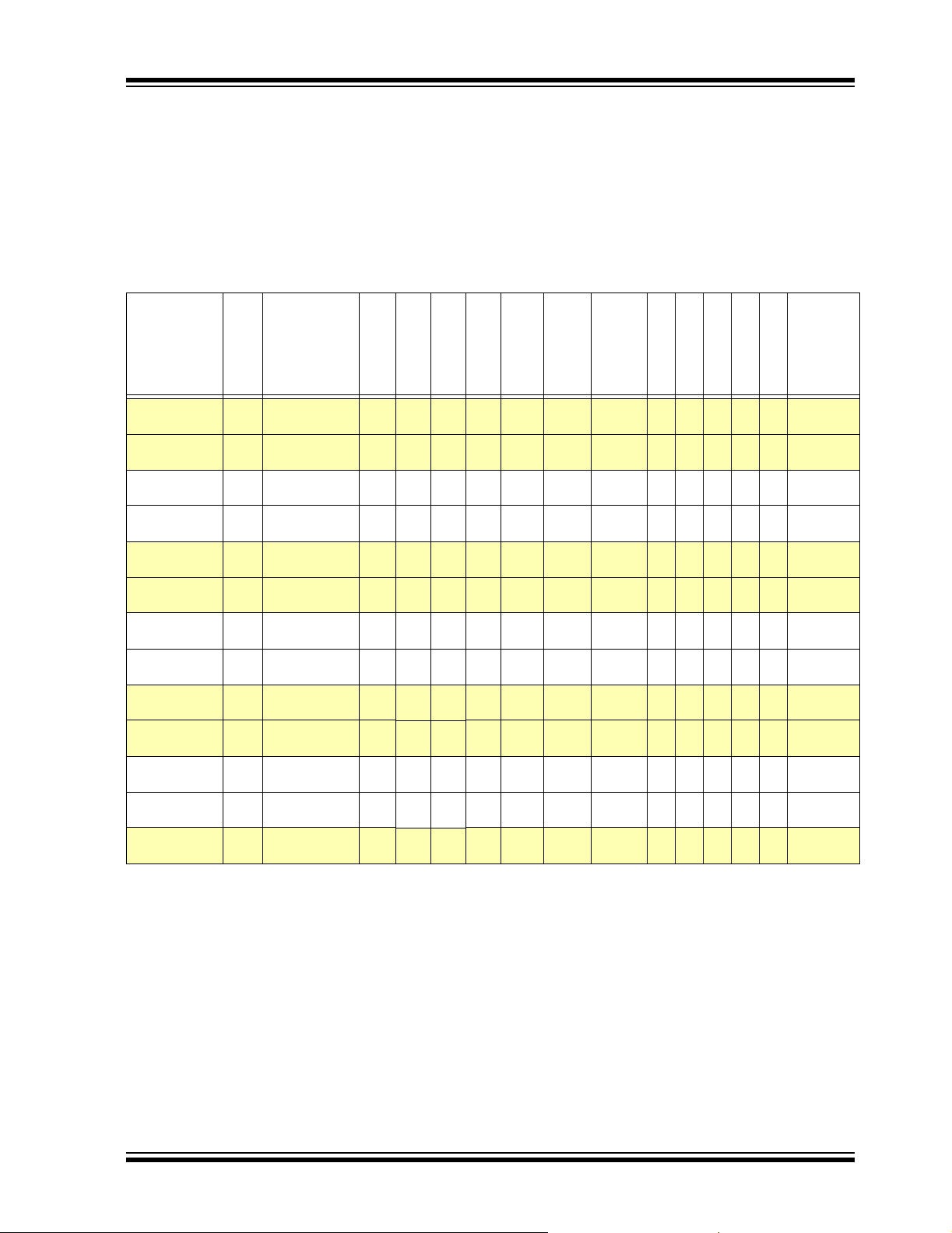
1.0 PIC24H PRODUCT FAMILIES
1.1 General-Purpose Family
The PIC24H General-purpose Family (Table 1-1)
is ideal for a wide variety of 16-bit MCU embedded
applications. The variants with codec interfaces are
well-suited for audio applications.
TABLE 1-1: PIC24H GENERAL-PURPOSE FAMILY VARIANTS
PIC24H
(2)
Device Pins
24HJ64GP206 64 64 8 8 9 8 8 0 1 ADC,
24HJ64GP210 100 64 8 8 9 8 8 0 1 ADC,
24HJ64GP506 64 64 8 8 9 8 8 0 1 ADC,
24HJ64GP510 100 64 8 8 9 8 8 0 1 ADC,
24HJ128GP206 64 128 8 8 9 8 8 0 1 ADC,
24HJ128GP210 100 128 8 8 9 8 8 0 1 ADC,
24HJ128GP506 64 128 8 8 9 8 8 0 1 ADC,
24HJ128GP510 100 128 8 8 9 8 8 0 1 ADC,
24HJ128GP306 64 128 16 8 9 8 8 0 1 ADC,
24HJ128GP310 100 128 16 8 9 8 8 0 1 ADC,
24HJ256GP206 64 256 16 8 9 8 8 0 1 ADC,
24HJ256GP210 100 256 16 8 9 8 8 0 1 ADC,
24HJ256GP610 100 256 16 8 9 8 8 0 2 ADC,
Note 1: RAM size is inclusive of 2 KB DMA RAM.
2: Maximum I/O pin count includes pins shared by the peripheral functions.
Program Flash
Memory (KB)
(1)
RAM
(KB)
Interface
18 ch
32 ch
18 ch
32 ch
18 ch
32 ch
18 ch
32 ch
18 ch
32 ch
18 ch
32 ch
32 ch
ADC
Codec
Timer 16-bit
DMA Channels
Input Capture
Std. PWM
Output Compare
CAN
Packages
I/O Pins (Max)
C™
2
I
SPI™
UART
2 2 1 0 53 PT
2 2 2 0 85 PT
222153 PF, PT
222185 PT
2 2 2 0 53 PT
2 2 2 0 85 PF, PT
222153 PT
222185 PT
2 2 2 0 53 PF, PT
2 2 2 0 85 PT
222053 PT
222085 PF, PT
2 2 2 2 85 PF, PT
© 2005 Microchip Technology Inc. Preliminary DS70166A-page 3
Page 6
PIC24H
PRODUCT IDENTIFICATION SYSTEM
24 HJ 256 GP6 10 T I / PT - XXX
PIC
Microchip Trademark
Architecture
Flash Memory Family
Program Memory Size (KB)
Product Group
Pin Count
Tape and Reel Flag (if applicable)
Temperature Range
Package
Pattern
Architecture 24 = 16-bit Microcontroller
Flash Memory Family HJ = Flash program memory, 3.3V, high-speed
Program Memory Size 64 = 64 Kbytes
Product Group GP2 = General Purpose family
128 = 128 Kbytes
256 = 256 Kbytes
GP3 = Gene ra l Purp ose fami ly
GP5 = Gene ra l Purp ose fami ly
GP6 = Gene ra l Purp ose fami ly
Examples:
a) dsPIC24HJ64GP610I/PT:
General Purpose dsPIC24H, 64 KB program
memory, 100-pin, Industrial temp.,
TQFP package.
b) dsPIC24HJ64GP206I/PT-ES:
Motor Control dsPIC24H, 64 KB program
memory, 64-pin, Industrial temp.,
TQFP package, Engineering Sample.
Tape & Reel T = Applicable
Pin Count 06 = 64-pin
Temperature Range I = -40°C to +85°C (Industrial)
Package PT = 10x10 or 12x12 mm TQFP (Thin Quad Flatpack)
Pattern Three-digit QTP, SQTP, Code or Special Requirements
Blank = Not applicable
10 = 100-pin
PF = 14x14 mm TQFP (Thin Quad Flatpack)
(blank otherwise)
ES = Engineering Sample
DS70166A-page 4 Preliminary © 2005 Microchip Technology Inc.
Page 7
PIC24H
2.0 PIC24H DEVICE FAMILY OVERVIEW
The PIC24H device family employs a powerful 16-bit
microcontroller (MCU). The res ulti ng CPU fun cti ona lity
is ideal for applications that rely on high-speed,
repetitive comput at ion s, as well as contro l.
Flexible and deterministic interrupt handling, coupled
with a powerful array of peripherals, renders the
PIC24H devices suitable for control applications.
FIGURE 2-1: PIC24H DEVICE BLOCK DIAGRAM
X-Data Bus <16-bit>
Shifter
Divide Control
Legend:
MCU/DSP X-Data Path
Address Path
17 x 17 Multiplier
W Register
Array
16 x 16
Memory
Mapped
16-bit ALU
Program Flash
Memory Data
Access
Program Counter
<23 bits>
Instruction
Prefetch & Decode
STATUS Register
Further, Direct Memory Access (DMA) enables
overhead-free transfer of data between several
peripherals and a dedicated DMA RAM. Reliable, field
programmable Flash program memory ensures
scalability of applications that use PIC24H devices.
Figure 2-1 shows a sample device block diagram
typical of the PIC24H product family.
Data SRAM
24
up to
28 Kbytes
Flash
Program
Memory
up to
256 Kbytes
Dual Port
RAM
2 Kbytes
I/O Ports
Peripherals
DMA
Controller
AGU
23
© 2005 Microchip Technology Inc. Preliminary DS70166A-page 5
Page 8

PIC24H
3.0 CPU ARCHITECTURE
3.1 Overview
The PIC24H C P U mo du l e has a 1 6 -bi t ( data ) mo dif i ed
Harvard architecture with an enhanced instruction set.
The CPU has a 24-bit instruction word with a variable
length opcode field. The Program Counter (PC) is
23 bits wide and addresses up to 4M x 24 bits of user
program memory spac e. The actual amou nt of program
memory implemented, as illustrated in Figure 3-1,
varies from one device to another. A single-cycle
instruction prefetch mechanism is used to help
maintain throughput and provides predictable
execution. All instructions execute in a single cycle,
with the exception of instructions that change the
program flow, the double word move (MOV.D)
instruction and the table instructions. Overhead-free
program loop constructs are supported using the
REPEAT instruction, which is interruptible at any point.
The PIC24H devices have sixteen 16-bit working
registers in the programmer’s model. Each of the
working registers can serve as a data, address or
address offset register. The 16th working register
(W15) operates as a software Stack Pointer (SP) for
interrupts and calls.
The PIC24H instruction set includes many addressing
modes and is designed for optimum C compiler
efficiency.
3.1.1 DATA MEMORY OVERVIEW
The data space can be addressed as 32K words or
64 Kbytes . Reads and w rites are per formed usin g an
Address Generation Unit (AGU), which accesses the
entire memory map as one linear data space.
DS70166A-page 6 Preliminary © 2005 Microchip Technology Inc.
Page 9

PIC24H
3.1.2 ADDRESSING MODES OVERVIEW
The CPU supports Inherent (no operand), Relative,
Literal, Memory Direct, Register Direct and Register
Indirect Addressing modes. Each instruction is
associated with a predefined addressing mode group
depending upon its functional requirements. As many
as 6 addressing modes are supported for each
instruction.
For most instructions, the PIC24H is capable of
executing a data (or program data) memory read, a
working register (data) read, a data memory write and
a program (instruction) memory read per instruction
cycle. As a result, three parameter instructions can be
supported, allowing A + B = C operations to be
executed in a single cycle.
3.1.3 SPECIAL MCU FEATURES
The PIC24H features a 17-bit by 17-bit, single-cycle
multiplier. The multiplier can perform signed, unsigned
and mixed-sign multiplication. Using a 17-bit by 17-bit
multiplier for 16-bit by 16-bit multiplication allows you to
perform mixed-sign multiplication.
The PIC24H supports 16/16 and 32/16 divide
operations, both fractional and integer. All divide
instructions are iterative operations. They must be
executed within a REPEAT loop, resulting in a total
execution time of 19 instruction cycles. The divide
operation can be interrupted during any of those 19
cycles without loss of data.
A 40-bit data shifter is used to perform up to a 16-bit left
or right shift in a single cycle.
3.1.5 FEATURES TO ENHANCE COMPILER EFFICIENCY
The CPU architecture possesses several features that
lead to a more efficient (code size and speed) C
compiler.
1. For most instructions, three-parameter instruc-
tions can be supported, allowing A + B = C
operations to be executed in a single cycle.
2. Instruction addressing modes are extremely
flexible to meet compiler needs.
3. The working re gister array consis ts of 16 x 16-b it
registers, each of which can act as data,
address or offse t registers. One w orking regist er
(W15) operates as the software Stack Pointer
for interrupts and calls.
4. Linear indirect access of all data space is
possible, plus the memory direct address range
is up to 8 Kbytes. This capability, together with
the addition of 16-bit direct address MOV-based
instructions, has provided a contiguous linear
addressing space.
5. Linear indirect access of 32K word (64 Kbyte)
pages within program space is possible, using
any working register via new table read and
write instructions.
6. Part of dat a sp a ce c an be mapped into program
space, allowi ng const ant dat a to be acc essed as
if it were in data space.
3.1.4 INTERRUPT OVER VIE W
The PIC24H has a vectored exception scheme with up
to 5 sources of non-maskable traps and 67 interrupt
sources. Each interrup t source can be assign ed to one
of seven priority levels.
© 2005 Microchip Technology Inc. Preliminary DS70166A-page 7
Page 10

PIC24H
3.2 Programmer’s Model
The programmer’s model, shown in Figure 3-2,
consists of 16 x 16-bit working registers (W0 through
W15), STATUS reg ister (SR), Dat a Table Page register
(TBLPAG), Program Space Visibility Page register
(PSVPAG), REPEAT count register (RCOUNT) and
Program Counter (PC). The working registers can act
as data, addres s or offset registers. A ll registers are
memory mapped. W0 is the W register for all
instructions that perform file register addressing.
Some of these registers have a shadow register
associated with them (see the legend in Figure 3-2).
The shadow register is used as a temporary holding
register and can tran sfe r it s co ntents to or from its host
register upon some event occurring in a single cycle.
None of the shadow registers are accessible directly.
When a byte operation is performed on a working
register, only the Least Significant Byte (LSB) of the
target register is affected. However, a benefit of
memory mapped working registers is that both the
Least and Most Significant Bytes (MSBs) can be
manipulated through byte-wide data memory space
accesses.
W15 is the dedicated software Stack Pointer (SP). It is
automatically modified by exception processing and
subroutine calls and returns. However, W15 can be
referenced by any instruction in the same manner as all
other W registers. This simplifies the reading, writing
and manipulation of the Stack Pointer (e.g., creating
stack frames).
W14 has been dedica ted as a Stack Frame Pointer, as
defined by the LNK and ULNK instructions. However,
W14 can be referenced by any instruction in the same
manner as all other W registers.
The Stack Pointer always points to the first available
free word and grows from lower addresses towards
higher addresses. It pre-decrements for stack pops
(reads) and post-increments for stack pushes (writes).
DS70166A-page 8 Preliminary © 2005 Microchip Technology Inc.
Page 11
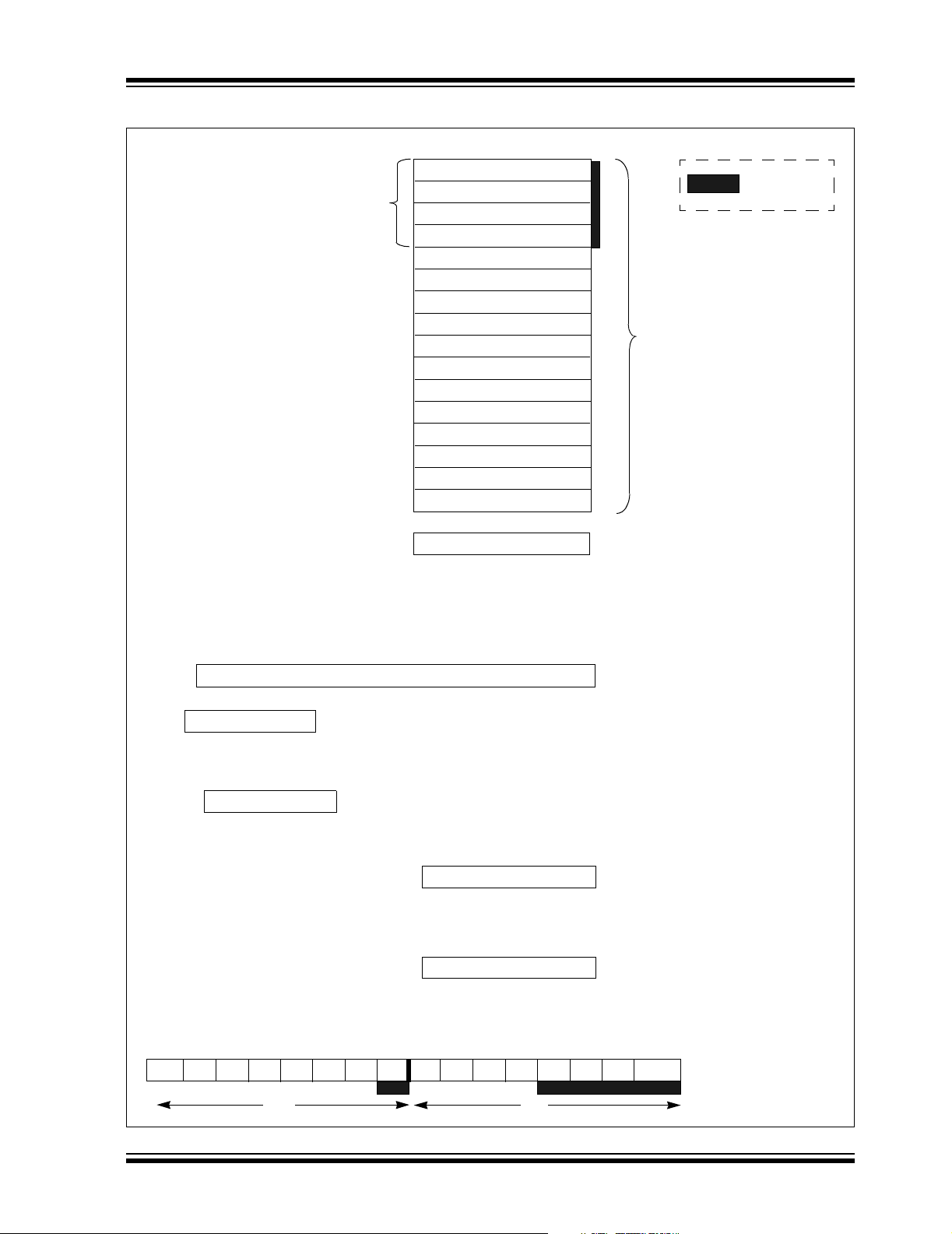
FIGURE 3-2: PROGRAMMER’S MODEL
PIC24H
DIV and MUL
Result Registers
015
W0/WREG
W1
W2
W3
W4
W5
W6
W7
W8
W9
W10
W11
W12
W13
W14/Frame Pointer
W15*/Stack Pointer
SPLIM* Stack Pointer Limit Register
Legend:
Working Registers
*W15 and SPLIM not shadowed
PUSH.S Shadow
22
7
TABPAG
TBLPAG
7
PSVPAG
PSVPAG
— — — —
SRH
0
0
— —
Data Table Page Address
Program Space Visibility Page Address
15
RCOUNT
15
CORCON
—DC
IPL2 IPL1
IPL0 OV
RA
SRL
N
0
0
0
Program Counter
REPEAT Loop Counter
Core Configuration Register
Z
C
STATUS Register
© 2005 Microchip Technology Inc. Preliminary DS70166A-page 9
Page 12

PIC24H
3.3 Data Address Sp ace
The data space is accessed as one unified linear
address range (for MCU instructions). The data space
is accessed using the Address Generat ion Unit (AG U).
All Effective Addre sses (EAs) are 16 b its wide and poi nt
to bytes within the data space. Therefore, the data
space address range is 64 Kbytes or 32K words,
though the implemented memory locations vary from
one device to another.
3.3.1 DMA RAM
Every PIC24H device contains 2 Kbytes of DMA RAM
located at the end of Y data space. Memo ry locations in
the DMA RAM space are accessible simultaneously by
the CPU and the DMA Controller module. DMA RAM is
utilized by the DMA Controller to store data to be
transferred to various peripherals using DMA, as well as
data transferred from various peripherals using DMA.
When the CPU and the DMA Controller attempt to
concurrently write to the same DMA RAM location, the
hardware ensures tha t the C PU is giv en prec edenc e in
accessing the DMA RAM location. Therefore, the DMA
RAM provides a reliable means of transferring DMA
data without ever having to stall the CPU.
3.3.2 DATA SPACE WIDTH
The core data width is 16 bits. All internal registers are
organized as 16 -bit wide word s. Dat a space memory is
organized in byte addressable, 16-bit wide blocks.
Figure 3-3 depicts a sam ple data space memo ry map
for the PIC24H device with 16 Kbytes of RAM.
3.3.3 DATA ALIGNMENT
To help maintain backward compatibility with
PICmicro
memory usage efficiency, the PIC24H instruction set
supports both word and byte operations. Data is
aligned in data memory and registers as words, but all
data space EAs resolv e to byt es. Data b yte rea ds will
read the complete word which contains the byte, using
the Least Significant bit (LSb) of any EA to determine
which byte to select.
As a consequence of t his byte accessib ility , all Effec tive
Address calculations are internally scaled. For
example, the core would recognize that Post-Modified
Register Indi rect Ad dressin g mode, [Ws+ +], wil l result
in a value of Ws + 1 for byt e op erations and Ws + 2 for
word operations.
All word accesses m ust be al igned to an even a ddress.
Misaligned word data fetches are not supported.
Should a misaligned read or write be attempted, a trap
will then be ex ec ut e d, al l ow in g t he sys tem an d/ o r use r
to examine the machine state prior to execution of the
address Fault.
®
MCU devices and improve data space
DS70166A-page 10 Preliminary © 2005 Microchip Technology Inc.
Page 13
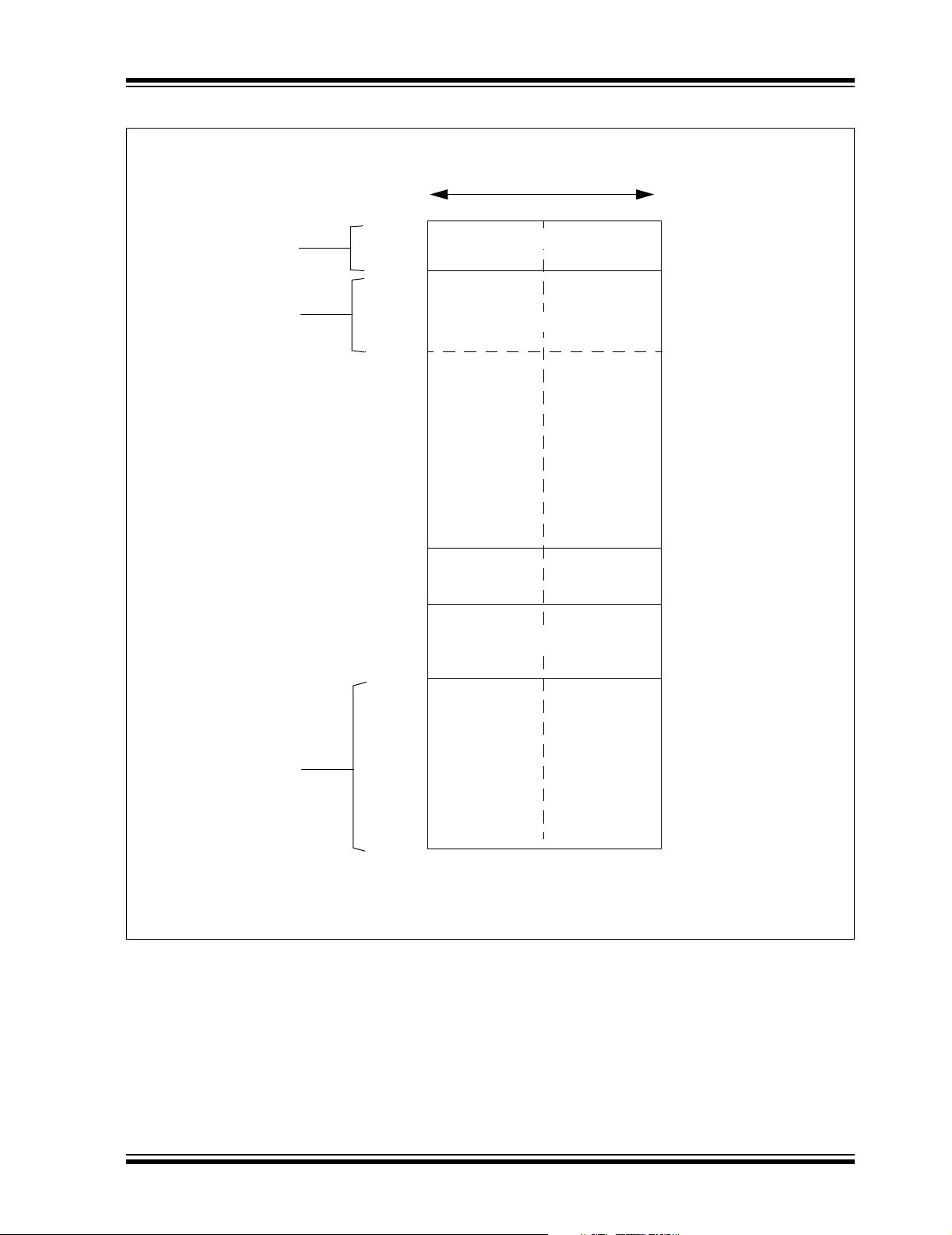
FIGURE 3-3: SAMPLE DATA SPACE MEMORY MAP
PIC24H
2-Kbyte
SFR Space
8-Kbyte
Data Space
Most Significant Byte
Address
0x0001
0x07FF
0x0801
0x1FFF 0x1FFE
0x3FFF
0x4001
0x47FF 0x47FE
0x4801 0x4800
16 Bits
LSBMSB
SFR Space
Data RAM
DMA RAM
Unimplemented
Least Significant Byte
Address
0x0000
0x07FE
0x0800
0x3FFE
0x4000
0x8001 0x8000
Optionally
Mapped
into Program
Memory
0xFFFF
Note: This data memory map is for the largest memory PIC24H devic e. Data memory map s for other de vices
may vary.
0xFFFE
© 2005 Microchip Technology Inc. Preliminary DS70166A-page 11
Page 14
PIC24H
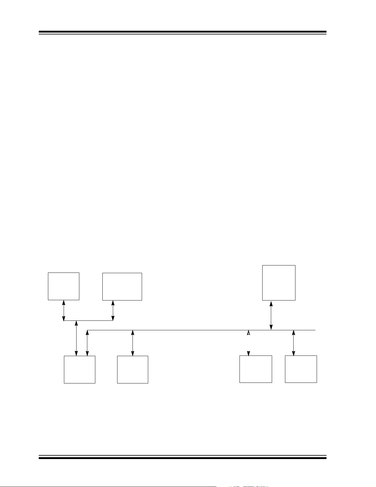
4.0 DIRECT MEMORY ACCESS
Direct Memory Access (DMA) is a very efficient
mechanism of copying data between peripheral SFRs
(e.g., UART Receive register, Input Capture 1 buffer)
and buffers or variables stored in RAM with minimal
CPU intervention. The DMA Controller can
automatically copy entire blocks of data, without the
user software havin g to read or w rite peripheral Special
Function Registers (SFRs) every time a peripheral
interrupt occurs. To exploit the DMA capability, the
corresponding user buffers or variables must be
located in DMA RAM space.
The DMA Controller features eight identical data
transfer channels, each with its own set of control and
status registers. The UART, SPI, DCI, Input Capture,
Output Compare, ECAN™ technology and ADC
modules can utilize DMA. Each DMA channel can be
configured to copy data either from buffers stored in
DMA RAM to peripheral SFRs o r fro m periph eral SF Rs
to buffers in DMA RAM.
Each channel support s the fol low i ng feat ures :
• Word or byte-sized data transfers
• Transfers from peripheral to DMA RAM or DMA
RAM to peripheral
• Indirect addressing of DMA RA M loc ation s with or
without automatic post-increment
• Peripheral Indirect Addressing – In some
peripherals, the DMA RAM read/write addresses
may be partially derived from the peripheral
• One-Shot Block Transfers – Terminating DMA
transfer after one block transfer
• Continuous Block Transfers – Reloading DMA
RAM buffer start address aft er every block
transfer is complete
• Ping-Pong Mode – Switching between two DMA
RAM start addresses between successive block
transfers, thereby filling two buffers alternately
• Automatic or manual initiation of block transfers
• Each channel can select from 32 possible
sources of data sources or destinations
For each DMA channel, a DMA interrupt request is
generated when a block transfer is complete.
Alternatively , an interrupt can be ge nerated when half of
the block has been filled. Additionally, a DMA error trap
is generated in either of the following Fault conditions:
• DMA RAM data write collision between the CPU
and a peripheral
• Peripheral SFR data wri te collision between the
CPU and the DMA Controller
FIGURE 4-1: TOP LEVEL SYSTEM ARCHITECTURE USING A DEDICATED TRANSACTION BUS
DMA
Ready
Peripheral 3
DMA
Ready
Peripheral 2
SRAM
SRAM X-Bus
CPU
DMA RAM
PORT 1
PORT 2
CPU Peripheral DS Bus
Non-DMA
Ready
Peripheral
DMA
Ready
Peripheral 1
DS70166A-page 12 Preliminary © 2005 Microchip Technology Inc.
Page 15

PIC24H
5.0 EXCEPTION PROCESSING
The PIC24H has four pro cessor ex ception s (trap s) and
up to 61 sources o f interrupt s, whi ch must be arbitrate d
based on a pr iority sche me.
The processor core is responsible for reading the
Interrupt Vector Table (IVT) and transferring the
address contained in the interrupt vector to the
Program Counter.
The Interrupt Vector Table (IVT) and Alternate In terrupt
Vector Table (AIVT) are placed near the beginning of
program memory (0x000004) for ease of debugging.
The interrupt controller hardware pre-processes the
interrupts before they are presented to the CPU.
The interrupts and traps are enabled, prioritized and
controlled using centralized Special Function Registers.
Each individual interrupt source has its own vector
address and can be individ ually enabled and prioritized
in user software. Each interrupt source a lso has it s own
status flag. This indepe ndent control and monitoring of
the interrupt eliminates the need to poll various status
flags to determine the interrupt source
Table 5-1 contains information about the interrupt
vector.
Certain interrupts have specialized control bits for
features like edge or level triggered interrupts, interrupton-change, etc. Control of these features remains within
the peripheral m od ul e, which generates the interr upt.
The special DISI instruction ca n be used to disable
the processing of interru pt s of pri orit ies 6 and lowe r for
a certain number of instruction cycles, during which
the DISI bit remains set.
TABLE 5-1: INTERRUPT VECTORS
Vector
Number
8 0x000014 0x000114 INT0 – External Interrupt 0
9 0x000016 0x000116 IC1 – Input Compare 1
10 0x000018 0x000118 OC1 – Output Compare 1
11 0x00001A 0x00011A T1 – Timer1
12 0x00001C 0x00011C DMA0 – DMA Channel 0
13 0x00001E 0x00011E IC2 – Input Capture 2
14 0x000020 0x000120 OC2 – Output Compare 2
15 0x000022 0x000122 T2 – Timer2
16 0x000024 0x000124 T3 – Timer3
17 0x000026 0x000126 SPI1E – SPI1 Error
18 0x000028 0x000128 SPI1 – SPI1 Transfer Done
19 0x00002A 0x00012A U1RX – UART1 Receiver
20 0x00002C 0x00012C U1TX – UART1 Transmitter
21 0x00002E 0x00012E ADC1 – ADC 1
22 0x000030 0x000130 DMA1 – DMA Channel 1
23 0x000032 0x000132 Reserved
24 0x000034 0x000134 I2C1S – I2C1 Slave Event
25 0x000036 0x000136 I2C1M – I2C1 Master Event
26 0x000038 0x000138 Reserved
27 0x00003A 0x00013A Change Notification Interrupt
28 0x00003C 0x00013C INT1 – External Interrupt 1
29 0x00003E 0x00013E ADC2 – ADC 2
30 0x000040 0x000140 IC7 – Input Capture 7
31 0x000042 0x000142 IC8 – Input Capture 8
32 0x000044 0x000144 DMA2 – DMA Channel 2
33 0x000046 0x000146 OC3 – Output Compare 3
34 0x000048 0x000148 OC4 – Output Compare 4
35 0x00004A 0x00014A T4 – Timer4
36 0x00004C 0x00014C T5 – Timer5
37 0x00004E 0x00014E INT2 – External Interrupt 2
38 0x000050 0x000150 U2RX – UART2 Receiver
39 0x000052 0x000152 U2TX – UART2 Transmitter
IVT Address AIVT Address Interrupt Source
© 2005 Microchip Technology Inc. Preliminary DS70166A-page 13
Page 16

PIC24H
TABLE 5-1: INTERRUPT VECTORS (CONTINUED)
Vector
Number
40 0x000054 0x000154 SPI2E – SPI2 Error
41 0x000056 0x000156 SPI1 – SPI1 Transfer Done
42 0x000058 0x000158 C1RX – ECAN1 Receive Data Ready
43 0x00005A 0x00015A C1 – ECAN1 Event
44 0x00005C 0x00015C DMA3 – DMA Channel 3
45 0x00005E 0x00015E IC3 – Input Capture 3
46 0x000060 0x000160 IC4 – Input Capture 4
47 0x000062 0x000162 IC5 – Input Capture 5
48 0x000064 0x000164 IC6 – Input Capture 6
49 0x000066 0x000166 OC5 – Output Compare 5
50 0x000068 0x000168 OC6 – Output Compare 6
51 0x00006A 0x00016A OC7 – Output Compare 7
52 0x00006C 0x00016C OC8 – Output Compare 8
53 0x00006E 0x00016E Reserved
54 0x000070 0x000170 DMA4 – DMA Channel 4
55 0x000072 0x000172 T6 – Timer6
56 0x000074 0x000174 T7 – Timer7
57 0x000076 0x000176 I2C2S – I2C2 Slave Event
58 0x000078 0x000178 I2C2M – I2C2 Master Event
59 0x00007A 0x00017A T8 – Timer8
60 0x00007C 0x00017C T9 – Timer9
61 0x00007E 0x00017E INT3 – External Interrupt 3
62 0x000080 0x000180 INT4 – External Interrupt 4
63 0x000082 0x000182 C2RX – ECAN2 Receive Data Ready
64 0x000084 0x000184 C2 – ECAN2 Event
65-68 0x000086-0x00008C 0x000186-0x00018C Reserved
69 0x00008E 0x00018E DMA5 – DMA Channel 5
70-72 0x000090-0x000094 0x000190-0x000194 Reserved
73 0x000096 0x000196 U1E – UART1 Error
74 0x000098 0x000198 U2E – UART2 Error
75 0x00009A 0x00019A Reserved
76 0x00009C 0x00019C DMA6 – DMA Channel 6
77 0x00009E 0x00019E DMA7 – DMA Channel 7
78 0x0000A0 0x0001A0 C1TX – ECAN1 Transmit Data Request
79 0x0000A2 0x0001A2 C2TX – ECAN2 Transmit Data Request
80-125 0x0000A4-
IVT Address AIVT Address Interrupt Source
0x0000FE
0x0001A4-
0x0001FE
Reserved
DS70166A-page 14 Preliminary © 2005 Microchip Technology Inc.
Page 17

PIC24H
5.1 Interrupt Priority
Each interrupt source can be user-assigned to one of
8 priority levels, 0 through 7. Levels 7 and 1 represent
the highest and lowest maskable priorities,
respectively. A priority level of 0 disables the interrupt.
Since more than one interrupt request source may be
assigned to a user-specified priority level, a means is
provided to assign priority within a given level. This
method is called “Natural Order Priority”.
The Natural Order Priori ty of an interrup t is nu merica lly
identical to its vector number. The Natural Order
Priority scheme has 0 as the highe st pri orit y and 74 as
the lowest priority.
The ability for the user to assign every interrupt to one
of eight priority levels implies that the user can assign
a very high overall priority level to an interrupt with a
low Natural Order Priority, thereby providing much
flexibility in designing applications that use a large
number of peripherals.
5.2 Interrupt Nesting
Interrupts, by default, are nestable. Any ISR that is in
progress may be interrupted by another source of
interrupt with a higher user-assigned priority level.
Interrupt nesting may be optionally disabled by
setting the NSTDIS control bit (INTCON1<15>).
When the NSTDIS control bit is se t, all interrupts in
progress will force the CPU priority to level 7 by
setting IPL<2:0> = 111. This action will effectively
mask all other sources of interrupt until a RETFIE
instruction is executed. When interrupt nesting is
disabled, the user-assigned in terrupt priority levels
will have no effect, except to resolve conflicts
between simultaneous pending interrupts.
The IPL<2:0> bits become read-only when interrupt
nesting is disabled. This prevents the user software
from settin g IPL<2:0> to a lower va lue, which would
effectively re-enable interrupt nesting.
5.3 Traps
Traps can be considered as non-maskable, nestable
interrupts that adhere to a fixed priority structure.
Traps are intended to provide the user a means to
correct erroneous operation during debug and when
operating within the application. If the user does not
intend to ta ke corrective ac tion in the even t of a trap
error condition, these vectors must be loaded with the
address of a software routi ne th at w il l reset the device.
Otherwise, the trap vector is programmed with the
address of a service routine that will correct the trap
condition.
The PIC24H has five implemented sources of
non-maskable traps:
• Oscillator Failure Trap
• Address Error Trap
• Stack Error Trap
• Math Error Trap
• DMA Error Trap
Many of these trap conditions can only be detected
when they happen. Consequently, the instruction that
caused the trap is allowed to complete before
exception processing begins. Therefore, the user may
have to correct the action of the instruction that
caused the trap.
Each trap s ource h as a fixe d priori ty as de fined by its
position in the IVT. An oscillator failure trap has the
highest priority, while an arithmetic error trap has the
lowest priority.
Table 5-2 contains information about the trap vector.
5.4 Generating a Software Interrupt
Any available interrupt can be manually generated by
user software (even if the corresponding peripheral is
disabled), simply by enabling the interrupt and then
setting the interrupt flag bit when required.
TABLE 5-2: TRAP VECTORS
Vector Number IVT Address AIVT Address Trap Source
0 0x000004 0x000084 Reserved
1 0x000006 0x000086 Oscillator Failure
2 0x000008 0x000088 Address Error
3 0x0 000 0A 0x00008A Stack Error
4 0x00000C 0x00008C Math Error
5 0x00000E 0x00008E DMA Error Trap
6 0x000010 0x000090 Reserved
7 0x000012 0x000092 Reserved
© 2005 Microchip Technology Inc. Preliminary DS70166A-page 15
Page 18

PIC24H
6.0 SYSTEM INTEGRATION
System managemen t servic es provided by the PI C24H
device family include:
• Control of clock options and oscillators
• Power-on Reset
• Oscillator Start-up Timer/Stabilizer
• Watchdog Timer with RC oscillator
• Fail-Safe Clock Monitor
• Reset by multiple sources
6.1 Clock Options and Oscillators
There are 7 clock options provided by the PIC24H:
• FRC Oscillator
• FRC Oscillator with PLL
• Primary (XT, HS or EC) Oscillator
• Primary Oscillator with PLL
• Secondary (LP) Oscillator
• LPRC Oscillator
The FRC (Fast RC) inte rnal osci llator runs at a nom inal
frequency of 7.37 MHz. The user s oftware can tune th e
FRC frequency. User software can specify a factor by
which this clock frequency is scaled.
The primary oscillator can use one of the following as
its clock source:
1. XT (Cryst al): Cryst als and c eramic re sonators i n
the range of 3 MHz to 10 MHz. The crystal is
connected to the OSC1 and OSC2 pins.
2. HS (High-Speed Crystal): Crystals in the range
of 10 MHz to 40 MHz. The crysta l is conn ected
to the OSC1 and OSC2 pins.
3. EC (External Clock): External clock signal in the
range of 0.8 MHz to 64 MHz. The extern al cloc k
signal is directly applied to the OSC1 pin.
The secondary (LP) os cillator is design ed for low power
and uses a 32 kHz cryst al or ceramic resonator . The LP
oscillator uses the SOSCI and SOSCO pins.
The LPRC (Low-Power RC) internal oscIllator runs at a
nominal frequency of 32.768 kHz. Another scaled
reference clock is used by the Watchdog Timer (WDT)
and Fail-Safe Clock Monitor (FSCM).
The clock signals generated by the FRC and primary
oscillators can be optionally applied to an on-chip
Phase Locked Loop (PLL) to provide a wide range of
output frequencies for device operation. The input to
the PLL can be in the range of 1.6 MH z to 16 MHz, and
the PLL Phase Detector Input Divider, PLL Multiplier
Ratio and PLL Voltage Controlled Osc illato r (VCO) ca n
be individually conf igured b y user so ftware to genera te
output frequencies in the range of 25 MHz to 160 MHz.
The output of the oscillator (or the output of the PLL if
a PLL mode has been selected) is divided by 2 to
generate the device instruction clock (F
CY). FCY
defines the operating speed of the device, and speeds
up to 40 MHz are supported by the PIC24H
architecture.
The PIC24H oscillator system provides:
• Various external and internal oscillator options as
clock sources
• An on-chip PLL to scale the internal operating
frequency to the required system clock frequency
• The internal FRC oscillator can also be used with
the PLL, thereby allowing full-speed operation
without any external clock generation hardware
• Clock switching between various clock sources
• Programmable clock postscaler f or s ystem po w er
savings
• A Fail-Safe Clock Monitor (FSCM) that detects
clock failure and takes fail-safe measures
• A Clock Control register (OSCCON)
• Nonvolatile Configuration bits for main oscillator
selection.
A simplified block diagram of the oscillator system is
shown in Figure 6-1.
DS70166A-page 16 Preliminary © 2005 Microchip Technology Inc.
Page 19

FIGURE 6-1: OSCILLATOR SYSTEM BLOCK DIAGRAM
PIC24H
OSC1
OSC2
SOSCO
SOSCI
Primary
Oscillator
Internal Fast
RC (FRC)
Oscillator
Secondary
Oscillator
32 kHz
PLL
Module
Primary Osc
Secondary Osc
Internal Low-Power
RC (LPRC)
Oscillator
Clock
Switching
and
Control
Block
FOSC
Divide by 2
To Timer1
FCY
6.2 Power-on Reset (POR)
When a supply voltage is applied to the device, a
Power-on Reset (POR) is generated. A new Power-on
Reset event is generated if the supply voltage falls
below the device threshold voltage (V
POR). An internal
POR pulse is gene rated w hen the ri sing suppl y vol tag e
crosses the POR circuit threshold voltage.
6.3 Oscillator St art-up Timer/St abilizer (OST)
An Oscillator Start-up Timer (OST) is included to
ensure that a crystal oscillator (or ceramic resonator)
has started and stabilized. The OST is a simple, 10-bit
counter that counts 1024 T
the oscillator clock to the rest of the system. The timeout period is designated as T
involved every time the oscillator has to restart (i.e ., o n
Power-on Reset and wake-up from Sleep). The
Oscillator Start-up Timer is applied to the LP oscillator,
XT and HS modes (upon wake-up from Sleep, POR
and Brown-out Reset (BOR)) for the prima ry oscilla tor .
OSC cycles before releasing
OST. The TOST time is
6.4 Watchdog Ti mer (WDT)
The primary function of the Watchdog Timer (WDT) is
to reset the processor in the event of a software
malfunction. The WDT is a fre e-run nin g ti me r tha t run s
off the on-chip LPRC oscillator, requiring no external
component. The WDT continues to operate even if the
main proces sor clock (e.g., the crys tal oscillator) fails.
The Watchdog Timer can be “Enabled” or “Disabled”
either through a Configuration bit (FWDTEN) in the
Configuration register, or through an SFR bit
(SWDTEN).
Any device programmer capable of programming
®
DSC devices (such as Microchip’s MPLAB
dsPIC
PM3 Programmer) allows programming of this and
other Configuration bit s to the d esired st ate. If enab led,
the WDT increments until it overflows or “times out”. A
WDT time-out forces a device Reset (except during
Sleep).
®
© 2005 Microchip Technology Inc. Preliminary DS70166A-page 17
Page 20

PIC24H
6.5 Fail-Safe Clock Monitor (FSCM)
The Fail-Safe Clock Monit or (FSC M) al lows the dev ic e
to continue to ope rate ev en in th e eve nt of an oscil lator
failure. The FSCM fu nction is enab led by programmin g.
If the FSCM function is enabled, the LPRC internal
oscillator run s at all tim es (ex cep t du ri ng Sl eep mode )
and is not subject to control by the W atc hd og Timer.
In the event of an oscillator failure, the FSCM
generates a clock failure trap event and switches the
system clock over to the FRC oscillato r . The application
program then can ei ther attempt to res tart the oscillato r ,
or execute a controlled shutdown. The trap can be
treated as a warm Reset by simply loading the Reset
address into the oscillator fail trap vector.
6.6 Reset System
The Reset system combines all Reset sources and
controls the device Master Reset signal.
Device Reset sources include:
• POR: Power-on Reset
• BOR: Brown-out Reset
•SWR: RESET Instruction
• EXTR: MCLR
• WDTR: Watchdog Timer Time-out Reset
• TRAPR: Trap Conflict
• IOPUWR: Attempted execution of an Illegal
Opcode, or Indirect Addressing, using an
Uninitialized W register
Reset
DS70166A-page 18 Preliminary © 2005 Microchip Technology Inc.
Page 21

PIC24H
7.0 DEVICE POWER MANAGEMENT
Power management services provided by the PIC24H
devices include:
• Real-Time Clock Source Switching
• Power-Saving Modes
7.1 Real-Time Clock Source Switching
Configuration bits determine the clock source upon
Power-on Reset (POR) and Brown-out Reset (BOR).
Thereafter, the clock source can be changed between
permissible clock sources. The OSCCON register
controls the clock switching and reflects system clock
related status bits. To reduce power consumption, the
user can switch to a slower clock source.
7.2 Power-Saving Modes
The PIC24H devices have two reduced power modes
that can be entered through execution of the PWRSAV
instruction.
• Sleep Mode: The CPU, system clock source and
any peripherals that operate on the system clock
source are disabled. This is the lowest power
mode of the device.
• Idle Mode: The CPU is disabled but the system
clock source continues to operate. Peripherals
continue to operate but can optionally be disabled.
• Doze Mode: The CPU clock is tempora rily s lowed
down relative to the peripheral clock by a
user-selectab le fac tor.
These modes provide an effective way to reduce power
consumption during periods when the CPU is n ot in use.
7.2.1 SLEEP MODE
When the device enters Sleep mode:
• System clock source is shut down. If an on-chip
oscillator is used, it is turned off.
• Device current consumption is at minimum
provided that no I/O pin is sourcing current.
• Fail-Safe Clock Monitor (FSCM) does not op erate
during Sleep mode because the system clock
source is disabled.
• LPRC clock continues to run in Sleep mode if the
WDT is enabled.
• BOR circuit, if enabled, remains operative during
Sleep mode
• WDT, if enabled, is automatically cleared prior to
entering Sleep mode.
• Some peripherals may continue to operate in
Sleep mode. These peripherals include I/O pins
that detect a change in the input signal, or
peripherals that use an external clock input. Any
peripheral that is operating on the system clock
source is disabled in Sleep mode.
The processor exits (wakes up) from Sleep on one of
these events:
• Any interrupt source that is individually enabled
• Any form of device Reset
• A WDT time-out
7.2.2 IDLE MODE
When the device enters Idle mode:
• CPU stops executing ins tructions
• WDT is automatically cleared
• System clock source remains active
• Peripheral modules, by default, continue to
operate normally from the system clock source
• Peripherals, optionally, can be shut down in Idle
mode using their ‘stop-in-idle’ control bit.
• If the WDT or FSCM is enabled, the LPRC also
remains active
The processor wakes from Idle mode on th ese events:
• Any interrupt that is individually enabled
• Any source of device Reset
• A WDT time-out
Upon wake-up from Idle, the clock is re-applied to the
CPU and instruction execution begins immediately
starting with the instruction following the PWRSAV
instruction, or the first instruction in the Interrupt
Service Routine (ISR).
7.2.3 DOZE MODE
The Doze mode provides the user software the ability
to temporarily reduce the processor instruction cycle
frequency relative to the peripheral frequency. Clock
frequency ratios of 1:1, 1:2, 1:4, 1:8, 1:16, 1:32, 1:64
and 1:128 are supported.
For example, suppose the device is operating at
20 MIPS and the CAN module has been co nfigure d for
500 kbps bit rate based on this device operating speed.
If the device is now placed in Doze mode with a clock
frequency ratio of 1:4 , the C AN mod ul e w ill co nti nue to
communicat e at the re quired bi t rate o f 500 kbps, bu t
the CPU now starts executing instructions at a
frequency of 5 MIPS.
This feature further reduces the power consumption
during periods where relatively less CPU activity is
required.
When the device is operating in Doze mode, the
hardware ensures that there is no loss of
synchronization between peripheral events and SFR
accesses by the CPU.
© 2005 Microchip Technology Inc. Preliminary DS70166A-page 19
Page 22

PIC24H
8.0 PIC24H PERIPHERALS
The Digital Signal Controller (DSC) family of 16-bit
DSC devices provides the integrated functionality of
many peripherals. Specific peripheral functions
include:
• Analog-to-Digital Converters (ADC)
- 10-bit High-Speed ADC
- 12-bit High-Resolution ADC
• General-purpose 16-Bit Timers
• M otor Control PWM module
• Quadrature Encoder Interface module
• Input Capture module
• Output Compare/PWM module
• Data Converter Interface
• Serial Peripheral Interface (SPI™) module
•UART module
2
•I
C™ module
• Controller Area Network (CAN) module
• I/O pins
8.1 Analog-to-Digital Converters
The Analog-to-Digital Converters provide up to 32
analog inputs with both single-ended and differential
inputs. These mod ules o f fer on -board s ample and hold
circuitry.
To minimize control loop errors due to finite update
times (conversion plus computations), a high-speed
low-latency ADC is required.
In addition, several hardware features have been
included in the perip heral interface to improve real -time
performance in a typical DSP-based application.
• Result alignment options
• Automated sampling
• Automated channel scanning
• Dual port data buffer
• External con version start control
The ADC can be configured by the user application in
either of the following configurations:
• 10-bit, 1.1 Msps ADC module (2.2 Msps ADC
conversion using 2 A/D modules)
• 12-bit, 500 ksps ADC module (1 Msps ADC
conversion using 2 A/D modules)
Key features of the ADC module include:
• 10-bit or 12-bit resolution
• Unipolar differential sample/hold amplifiers
• Up to 32 input channels
• Selectable voltage reference sources (external
REF+ and VREF- pins available)
V
• ±1 LSB max Differential Nonlinearity (DNL)
(3.3V ±10%)
• ±1 LSB max Integral Nonlinearity (INL)
(3.3V ±10%)
• Up to 4 on-chip sample and hold amplifiers in
each ADC (enables s imultan eous sampling of 2, 4
or 8 analog inputs)
• Automated channel scanning
• Single-supply operation: 3.0-3.6V
• 2.2 Msps or 1 Msps sampling rate at 3.0V
• Ability to convert during CPU Sleep and Idle
modes
• Conversion start can be manual or synchronized
with 1 of 4 trigger sources (automatic, T imer3 or 5,
external interrupt, PWM period match )
• ADC can use DMA for buffer storage
8.2 General-Purpose Timer Modules
The General-Purpose (GP) timer modules provide the
time base elements for input capture and output
compare/PWM. They can be configured for Real-Time
Clock operation as well as various timer/counter
modes. The timer modes count pulses of the internal
time base, whereas counter modes count external
pulses that appear on the timer clock pin.
The PIC24H device supports up to nine 16-bit timers
(Timer1 through Timer9). Eight of the 16-bit timers can
be configured as four 32-bit timers (T imer2/ 3, T imer4/5,
Timer6/7 and Timer8/9). Each timer has several
selectable operating modes.
8.2.1 TIMER1
The Timer1 module (Figure 8-1) is a 16-bit timer that can
serve as the time counter for an asynchronous RealTime Clock, or operate as a free-running interval timer/
counter. The 16-bit timer has the follow ing mode s:
•16-Bit Timer
• 16-Bit Synchronous Counter
• 16-Bit Asynchronous Counter
Further, the following operational characteristics are
supported:
• Timer gated by external pulse
• Selectable prescaler settings
• Timer operation during CPU Idle and Sleep modes
• Interrupt on 16-Bit Period register match or falling
edge of external gate signal
Timer1, when operating in Real-Time Clock (RTC)
mode, provides time of day and event time-stamping
capabilitie s. Key operational feat ures of the RTC are:
• Operation from 32 kHz LP oscillator
• 8-bit prescaler
•Low power
• Real-Time Clock interrupts
DS70166A-page 20 Preliminary © 2005 Microchip Technology Inc.
Page 23

FIGURE 8-1: 16-BIT TIMER1 MODULE BLOCK DIAGRAM
PIC24H
T1IF
Event Flag
SOSCO/
T1CK
SOSCI
0
1
TGATE
Equal
Reset
LPOSCEN
PR1
Comparator x 16
TMR1
QD
Q
8.2.2 TIMER2/3
The Timer2/3 module is a 32-bit timer (which can be
configured as two 16-bit timers) with selectable
operating modes. These timers are used by other
peripheral modules, such as:
• Input Capture
• Output Compare/Simple PWM
Timer2/3 has the following modes:
• Two independent 16-bit timers (Timer2 and
Timer3) with Timer and Synchronous Counter
modes
• Single 32-Bit Timer
• Single 32-Bit Synchronous Counter
Further, the following operational characteristics are
supported:
• ADC conversion start trigger
• 32-bit timer gated by external pulse
• Selectable p rescaler s ettings
• Timer counter operation during Idle and Sleep
modes
• Interrupt on a 32-Bit Period register match
• Timer2/3 can use DMA for buffer storage
CK
Gate
Sync
CY
T
TSYNC
1
Sync
0
TGATE
TCS
1 x
0 1
0 0
TGATE
TON
TCKPS<1:0>
2
Prescaler
1, 8, 64, 256
8.2.3 TIMER4/5, TIMER6/7, TIMER8/9
The Timer4/5, Timer6/7 and Timer8/9 modules are
similar in operation to the T imer2/3 modul e. Differen ces
include:
• These modules do not support the ADC event
trigger feature
• These modules can not be used by other
peripheral modules, su ch as input cap ture and
output compare
© 2005 Microchip Technology Inc. Preliminary DS70166A-page 21
Page 24

PIC24H
8.3 Input Capture Module
The input capture module is useful in applications
requiring frequency (period) and pulse measurement.
The PIC24H devices support up to eight input capture
channels.
The input capture module captures the 16-bit value of
the selected time base register when an event occurs
at the ICx pin. Th e events that caus e a capture ev ent
are listed below in three categories:
1. Simple Capture Event modes
- Capture timer value on every falling edge of
input at ICx pin
- Capture timer value on every rising edg e of
input at ICx pin
2. Capture timer value on every edge (rising and falling)
3. Prescaler Capture Event modes
- Capture timer value on every 4th rising
edge of input at ICx pin
- Capture timer value on every 16th rising
edge of input at ICx pin
Each input capture channel can select between one of
two 16-bit timers (Timer2 or Timer3) for the time base.
The selected timer can use either an internal or an
external clock.
Other operational features include:
• Device wake-up from capture pin during CPU
Sleep and Idle modes
• Interrupt on input capture event
• 4-word FIFO buffer for capture values
- Interrupt optionally generated after 1, 2, 3 or
4 buffer locations are filled
• Input capture can also be used to provide
additional sources of external interrupts.
Input capture channels IC1 and IC2 support DMA data
transfers.
8.4 Output Compare/PWM Module
The output compare module featur es are quite useful i n
applications that require controlled timing pulses or
PWM modulated pulse streams.
The output compare module has the ability to compare
the value of a selected time base with the value of one
or two compare registers (depending on the operation
mode selected). Furthermore, it has the ability to
generate a single output pulse, or a repetitive
sequence of outpu t pulses, o n a comp are matc h event.
Like most PIC24H peripherals, it also has the ability to
generate interrupts on compare match events.
The PIC24H device may have up to eight output
compare channels, designated OC1 through OC8.
Refer to the specific device data sheet for the number
of channels available in a particular device. All output
compare channels are functionally identical.
Each output compare channel can use one of two
selectable t im e bases. The time base is se lec ted using
the OCTSEL bit (OCxCON<3>). An ‘x’ in the pin,
register or bit name denotes the specific output
compare channel . Refer to the dev ice data shee t for the
specific timers that can be used with each output
compare channel number.
Each output compare module has the following modes
of operation:
• Single Compare Match mode
• Dual Compare Match mode generating
- Single Output Pulse
- Continuous Output Pulses
• Simple Pulse-Width Modulation mode
- With Fault Protection Input
- Without Fault Protection Input
Output compare channels, OC1 and OC2, support
DMA data transfers.
8.5 SPI Module
The Serial Peripheral Interface (SPI) module is a
synchronous serial interface for communicating with
other peripheral or microcontroller devices such as
serial EEPROMs, shift registers, display drivers, ADC,
etc. It is compatible with Motorola
interfaces.
This SPI module includes all SPI modes. A Frame
Synchronization mode is also included for support of
voice band codecs.
Four pins make up the serial interface: SDI, Serial Data
Input; SDO, Serial Data Ou tpu t; SCK, Shi ft Cl ock Input
or Output; SS
serves as the FSYNC (Frame Synchronization Pulse).
A device set up as an SPI master provides the serial
communication clock signal on its SCK pin.
A series of 8 or 16 clock pulses (depending on mode)
shift out the 8 or 16 bits (depending on whether a byte
or word is being transferred) and simu ltaneously shift in
8 or 16 bits of data from the SDI pin. An interrupt is
generated when the transfer is complete.
Slave select sync hroni zati on al lows se lecti ve en abli ng
of SPI slave devices, which is particularly useful when
a single master is connected to multiple slaves.
The SPI1 and SPI2 modules support DMA data
transfers.
, Active-Low Slave Select, which also
®
SPI and SIOP
DS70166A-page 22 Preliminary © 2005 Microchip Technology Inc.
Page 25

PIC24H
8.6 UART Module
The UART is a full-duplex asynchronous system that
can communicate with peripheral devices, such as
personal computers, RS-232 and RS-485 interfaces.
The PIC24H devices have one or more UARTs.
The key features of the UART module are:
• Full-duplex operation with 8 or 9-bit data
• Even, odd or no parity options (for 8-bit data)
• One or two Stop bits
• Fully integrated Baud Rate Generator (BRG) with
16-bit prescaler
• Baud rates range from up to 10 Mbps and down to
38 Hz at 40 MIPS
• 4-character deep transmit data buffer
• 4-character deep receive data buffer
• Parity, framing and buffer overrun error detection
•Full IrDA
and decoding of IrDA
• LIN bus support
- Auto wake-up from Sleep or Idle mode on
- Auto-baud detection
- Break character support
• Support for interrupt on address detect (9th bit = 1)
• Separate transmit and receive interrupts
- On transmission of 1 or 4 characters
- On reception of 1, 3 and 4 characters
• Loopback mode for diagnostics
The UART1 and UART2 modules support DMA data
transfers.
®
support, including hardware encoding
Start bit detect
®
messages
8.7 I2C Module
The Inter-Integrated Circuit (I2C) module is a
synchronous serial interface, useful for communicating
with other peripheral or microcontroller devices. These
peripheral devices may be serial EEPROMs, shift
registers, display drivers, ADC, etc.
2
C module offers full hardware support for both
The I
slave and multi-master operations.
2
The key features of the I
2
C slave operation supports 7 and 10-bit address
•I
•I2C master opera t i on su pp orts 7 and 10-bit add r ess
2
•I
C port allows bidirectional transfers between
master and slaves
• Serial clock synchronization for I
used as a handshake mechanism to s uspen d and
resume serial transfer (serial clock stretching)
•I2C supports multi-master operation; detects bus
collision and will arbitrate accordingly
• Slew rate control for 100 kHz and 400 kHz bus speeds
2
C mode, pin SCL is clock and pin SDA is data. The
In I
module will override the data direction bits for these pins.
C module are:
2
C port can be
8.8 Controller Area Network (CAN) Module
The Controller Area Network (CAN) module is a serial
interface useful for communicating with other CAN
modules or microcontroller devices. This interface/
protocol was designed to allow communications within
noisy environment s .
The CAN module is a communication controller
implementing the CAN 2.0 A/B protocol, as defined in
the BOSCH specification. The module supports
CAN 1.2, CAN 2.0A, CAN 2.0B Passive and CAN 2.0B
Active versions of the protocol. Details of these protocols
can be found in the BOSCH CAN specification.
The CAN module features :
• Implementation of the CAN protocol CAN 1.2,
CAN 2.0A and CAN 2.0B
• Standard and extended data frames
• Data lengths of 0-8 bytes
• Programmable bit rate up to 1 Mbit/sec
• Automatic response to remote frames
• Up to 32 receive buffers in DMA RAM
• FIFO Buffer mode (up to 32 messages deep)
• 16 full (standard/extended identifier) acceptance
filters
• 3 full acceptance filter masks
• Up to 8 transmit buffers in DMA RAM
• DMA can be used for transmission and reception
• Programmable wake-up functionality with
integrated low-pass fil ter
• Programmable Loopback mode suppo rts self-test
operation
• Signaling via interrupt capabilities for all CAN
receiver and transmitter error states
• Programmable clock source
• Programmable link to timer module for
time-stamping and network synchronization
• Low-power Sleep and Idl e mode
The CAN bus module cons ists of a protoc ol engine and
message buffering/control. The CAN protocol engine
handles all functions for receiving and transmitting
messages on the CAN bus. Messages are transmitted
by first loading the appropriate data registers. Status
and errors can be checked by reading the appropriate
registers. Any message detected on the CAN bus is
checked for errors and then matched against filters to
see if it should be received and stored in one of the
receive registers.
© 2005 Microchip Technology Inc. Preliminary DS70166A-page 23
Page 26

PIC24H
8.9 I/O Pins
Some pins for the I/O p in funct ions are multip lexed w ith
an alternate function for the peripheral features on the
device. In general, when a peripheral is enabled, that
pin may not be used as a general-purpose I/O pin.
All I/O port pins have three registers directly associated
with the operation of the port pin. The Data Direction
register determines whether the pin is an input or an
output. The Port Data Latch register provides latched
output data for t h e I/ O p i ns . Th e Por t re gi st e r pr o vi d es
visibility of the logic state of the I/O pins. Reading the
Port register provides the I/O pin logic state, while
writes to the Port register write the dat a to the Port Da ta
Latch register.
I/O port pins have latch bits (Port Data Latch register).
This register, when read, yields the contents of the I/O
latch and when written , modifies the co ntents of the I/O
latch, thus modifying the value driven out on a pin if the
corresponding Data Direction register bit is configured
for output. This can be used in read-modify-write
instructions that allow the user to modify the contents
of the Port Data Latch register , re gard le ss o f t he status
of the corresponding pins.
The I/O pins have the following features:
• Schmitt Trigger input
• CMOS output drivers
• Weak internal pull-up
All I/O pins configured as digital inputs can accept 5V
signals. This provides a degree of compatibility with
external signals of dif ferent voltage levels. How ever , al l
digital outputs and analog pins can only generate
voltage levels up to 3.6V.
The input change notification module gives PIC24H
devices the ability to gen era te inte rrup t reque st s to the
processor in resp onse to a chan ge of s tat e on sele cted
input pins. This module is capable of detecting input
changes of st ate, even in Sleep mode , when th e clocks
are disabled. There are up to 24 external signals (CN0
through CN23) that can be selected (enabled) for
generating an interrupt request on a change of state.
Each of the CN pins also has an optional weak pull-up
feature.
DS70166A-page 24 Preliminary © 2005 Microchip Technology Inc.
Page 27

PIC24H
9.0 PIC24H INSTRUCTION SET
9.1 Introduction
The PIC24H instruction set provides a broad suite of
instructions which supports traditional microcontroller
applications, and a class of in struction s which sup port s
math-intensive applications. Since almost all of the
functionality of the PICmicro MCU instruction set has
been maintained, this hybrid instruction set allows a
friendly migration path for users already familiar with
the PICmicro microcontroller.
9.2 Instruction Set Overview
The PIC24H instruction set contains 76 instructions
which can be gr ouped into th e ten function al categorie s
shown in Table 9-1. Table 9-2 defines the symbols
used in the instruction summary tables, Table 9-3
through Table 9-11. These tables define the syntax,
description, storage and execution requirements
for each instruction. Storage requirements are represented in 24-bit instruction words and execution
requirements are represented in instruction cycles.
Most instructions have several different addressing
modes and execution flows which require different
instruction variants. For instance, there are six unique
ADD instructions and each instruction variant has its
own instruction encoding.
TABLE 9-1: PIC24H INSTRUCTION
GROUPS
Functional Group Summary Table
Move Instructions Table 9-3
Math Instructions Table 9-4
Logic Instructions Table9-5
Rotate/Shift Instructions Table 9-6
Bit Instructions Table 9-7
Compare/Skip Instructions Table 9-8
Program Flow Instructions Table 9-9
Shadow/Stack Instructions Table 9-10
Control Instructions Table 9-11
9.2.1 MULTI-CYCLE INSTRUCTIONS
As the instruction summary tables show, most
instructions execute in a single cycle with the following
exceptions:
• Instructions MOV.D, POP.D, PUSH.D,
TBLRDH, TBLRDL, TBLWTH and TBLWTL
require 2 cycles to execute.
• Instructions DIVF, DIV.S, DIV.U are single-
cycle instructions, which should be executed
18 consecutive times as the target REPEAT
instruction.
• Instructions that change the Program Counter
also require 2 cycles to execute, with the extra
cycle executed as a NOP. Skip instructions, which
skip over a 2-word instruction, require 3
instruction cycles to execute with 2 cycles
executed as a NOP.
•The RETFIE, RETLW and RETURN are special
cases of instructions that change the Program
Counter. These execute in 3 cycles unless an
exception is pending, and then they execute in
2 cycles.
Note: Instructions that access progr am memor y
as data, using Program Space Visibility,
incur some cycle count overhead.
9.2.2 MULTI-WORD INSTRUCTIONS
As the instruction summary tables show, almost all
instructions consume one instruction word (24 bits),
with the exception of the CALL and GOTO instructions,
which are flow instructions listed in Table 9-9. These
instructions require two words of memory because their
opcodes embed large literal operands.
© 2005 Microchip Technology Inc. Preliminary DS70166A-page 25
Page 28

PIC24H
TABLE 9-2: SYMBOLS USED IN SUMMARY TABLES
Symbol Description
# Literal operand designation
bit4 4-bit wide bit position (0:15)
Expr Absolute address, label or expression (resolved by the linker)
f File register address
lit1 1-bit literal (0:1)
lit4 4-bit literal (0:15)
lit5 5-bit literal (0:31)
lit8 8-bit literal (0:255)
lit10 10-bit literal (0:255 for Byte mode, 0:1023 for Word mode)
lit14 14-bit literal (0:16383)
lit16 16-bit literal (0:65535)
lit23 23-bit literal (0:8388607)
Slit4 Signed 4-bit literal (-8:7)
Slit6 Signed 6-bit literal (-16:16)
Slit10 Signed 10-bit literal (-512:511)
Slit16 Signed 16-bit literal (-32768:32767)
TOS Top-of-Stack
Wb Base working register
Wd Destination working register (direct and indirect addressing)
Wm, Wn Working register divide pair (dividend, divisor)
Wm*Wm Working register multiplier pair (same source register)
Wm*Wn Working register multiplier pair (different source registers)
Wn Both source and destination working register (direct addressing)
Wnd Destination working register (direct addressing)
Wns Source working register (direct addressing)
WREG Default working register
Ws Source working register (direct and indirect addressing)
DS70166A-page 26 Preliminary © 2005 Microchip Technology Inc.
Page 29

PIC24H
TABLE 9-3: MOVE INSTRUCTIONS
Assembly Syntax Description Words Cycles
EXCH Wns,Wnd Swap Wns and Wnd 1 1
MOV f {,WREG} Move f to destination 1 1
MOV WREG,f Move WREG to f 1 1
MOV f,Wnd Move f to Wnd 1 1
MOV Wns,f Move Wns to f 1 1
MOV.b #lit8,Wnd Move 8-bit literal to Wnd 1 1
MOV #lit16,Wnd Move 16-bit literal to Wnd 1 1
MOV [Ws+Slit10],Wnd Move [Ws + signed 10-bit offset] to Wnd 1 1
MOV Wns,[Wd+Slit10] Move Wns to [Wd + signed 10-bit offset] 1 1
MOV Ws,Wd Move Ws to Wd 1 1
MOV.D Ws,Wnd Move double Ws to Wnd:Wnd + 1 1 2
MOV.D Wns,Wd Move double Wns:Wns + 1 to Wd 1 2
SWAP Wn Wn = byte or nibble swap Wn 1 1
TBLRDH Ws,Wd Read high program word to Wd 1 2
TBLRDL Ws,Wd Read low program word to Wd 1 2
TBLWTH Ws,Wd Write Ws to high program word 1 2
TBLWTL Ws,Wd Write Ws to low program word 1 2
Note: When the optional {,WREG} operand is specified, the destination of the instruction is WREG. When
{,WREG} is not specified, the destination of the instruction is the file register f.
Note: Table 9-3 through Table9-11 present the base instruction syntax for the PIC24H. These instructions do not
include all of the available addressing modes. For example, some instructions show the Byte Addressing
mode and others do not.
© 2005 Microchip Technology Inc. Preliminary DS70166A-page 27
Page 30

PIC24H
TABLE 9-4: MATH INSTRUCTIONS
Assembly Syntax Description Words Cycles
ADD f {,WREG} Destination = f + WREG 1 1
ADD #lit10,Wn Wn = lit10 + Wn 1 1
ADD Wb,#lit5,Wd Wd = Wb + lit5 1 1
ADD Wb,Ws,Wd Wd = Wb + Ws 1 1
ADDC f {,WREG} Destination = f + WREG + (C) 1 1
ADDC #lit10,Wn Wn = lit10 + Wn + (C) 1 1
ADDC Wb,#lit5,Wd Wd = Wb + lit5 + (C) 1 1
ADDC Wb,Ws,Wd
DS70166A-page 28 Preliminary © 2005 Microchip Technology Inc.
Page 31

PIC24H
TABLE 9-5: LOGIC INSTRUCTIONS
Assembly Syntax Description Words Cycles
AND f {,WREG} Destination = f .AND. WREG 1 1
AND #lit10,Wn Wn = lit10 .AND. Wn 1 1
AND Wb,#lit5,Wd Wd = Wb .AND. lit5 1 1
AND Wb,Ws,Wd Wd = Wb .AND. Ws 1 1
CLR f f = 0x0000 1 1
CLR WREG WREG = 0x0000 1 1
CLR Wd Wd = 0x0000 1 1
COM f {,WREG} Destination = f
COM Ws,Wd Wd = Ws
IOR f {,WREG} Destination = f .IOR. WREG 1 1
IOR #lit10,Wn Wn = lit10 .IOR. Wn 1 1
IOR Wb,#lit5,Wd Wd = Wb .IOR. lit5 1 1
IOR Wb,Ws,Wd Wd = Wb .IOR. Ws 1 1
NEG f {,WREG} Destination = f
NEG Ws,Wd Wd = Ws
SETM f f = 0xFFFF 1 1
SETM WREG WREG = 0xFFFF 1 1
SETM Wd Wd = 0xFFFF 1 1
XOR f {,WREG} Destination = f .XOR. WREG 1 1
XOR #lit10,Wn Wn = lit10 .XOR. Wn 1 1
XOR Wb,#lit5,Wd Wd = Wb .XOR. lit5 1 1
XOR Wb,Ws,Wd Wd = Wb .XOR. Ws 1 1
Note: When the optional {,WREG} operand is specified, the destination of the instruction is WREG. When
{,WREG} is not specified, the destination of the instruction is the file register f.
11
11
+ 1 1 1
+ 1 1 1
© 2005 Microchip Technology Inc. Preliminary DS70166A-page 29
Page 32

PIC24H
TABLE 9-6: ROTATE/SHIFT INSTRUCTIONS
Assembly Syntax Description Words Cycles
ASR f {,WREG} Destination = arithmetic right shift f 1 1
ASR Ws,Wd Wd = arithmetic right shift Ws 1 1
ASR Wb,#lit4,Wnd W nd = arithmetic right shift Wb by lit4 1 1
ASR Wb,Wns,Wnd Wnd = arithmetic right shift Wb by Wns 1 1
LSR f {,WREG} Destination = logical right shift f 1 1
LSR Ws,Wd Wd = logical right shift Ws 1 1
LSR Wb,#lit4,Wnd Wnd = logical right shift Wb by lit4 1 1
LSR Wb,Wns,Wnd Wnd = logical right shift Wb by Wns 1 1
RLC f {,WREG} Destination = rotate left through Carry f 1 1
RLC Ws,Wd Wd = rotate left through Carry Ws 1 1
RLNC f {,WREG} Destination = rotate left (no Carry) f 1 1
RLNC Ws,Wd Wd = rotate left (no Carry) Ws 1 1
RRC f {,WREG} Destination = rotate right through Carry f 1 1
RRC Ws,Wd Wd = rotate right through Carry Ws 1 1
RRNC f {,WREG} Destination = rotate right (no Carry) f 1 1
RRNC Ws,Wd Wd = rotate right (no Carry) Ws 1 1
SL f {,WREG} Destination = left shift f 1 1
SL Ws,Wd Wd = left shift Ws 1 1
SL Wb,#lit4,Wnd Wnd = left shift Wb by lit4 1 1
SL Wb,Wns,Wnd Wnd = left shift Wb by Wns 1 1
Note: When the optional {,WREG} operand is specified, the destination of the instruction is WREG. When
{,WREG} is not specified, the destination of the instruction is the file register f.
TABLE 9-7: BIT INSTRUCTIONS
Assembly Syntax Description Words Cycles
BCLR f,#bit4 Bit clear f 1 1
BCLR Ws,#bit4 Bit clear Ws 1 1
BSET f,#bit4 Bit set f 1 1
BSET Ws,#bit4 Bit set Ws 1 1
BSW.C Ws,Wb Write C bit to Ws<Wb> 1 1
BSW.Z Ws,Wb Write S
BTG f,#bit4 Bit toggle f 1 1
BTG Ws,#bit4 Bit toggle Ws 1 1
BTST f,#bit4 Bit test f 1 1
BTST.C Ws,#bit4 Bit test Ws to C 1 1
BTST.Z Ws,#bit4 Bit test Ws to SZ 1 1
BTST.C Ws,Wb Bit test Ws<Wb> to C 1 1
BTST.Z Ws,Wb Bit test Ws<Wb> to SZ 1 1
BTSTS f,#bit4 Bit test f then set f 1 1
BTSTS.C Ws,#bit4 Bit test Ws to C then set Ws 1 1
BTSTS.Z Ws,#bit4 Bit test Ws to SZ then set Ws 1 1
FBCL Ws,Wnd Find bit change from left (MSb) side 1 1
FF1L Ws,Wnd Find first one from left (MSb) side 1 1
FF1R Ws,Wnd Find first one from right (LSb) side 1 1
Note: Bit positions are specified by bit4 (0:15) for word operations.
Z bit to Ws<Wb> 1 1
DS70166A-page 30 Preliminary © 2005 Microchip Technology Inc.
Page 33

PIC24H
TABLE 9-8: COMPARE/SKIP INSTRUCTIONS
Assembly Syntax Description Words Cycles
BTSC f,#bit4 Bit test f, skip if clear 1 1 (2 or 3)
BTSC Ws,#bit4 Bit test Ws, skip if clear 1 1 (2 or 3)
BTSS f,#bit4 Bit test f, skip if set 1 1 (2 or 3)
BTSS Ws,#bit4 Bit test Ws, skip if set 1 1 (2 or 3)
CP f Compare (f – WREG) 1 1
CP Wb,#lit5 Compare (Wb – lit5) 1 1
CP Wb,Ws Compare (Wb – Ws) 1 1
CP0 f Compare (f – 0x0000) 1 1
CP0 Ws Compare (Ws – 0x0000) 1 1
CPB f Compare with Borrow (f – WREG – C
CPB Wb,#lit5 Compare with Borrow (Wb – lit5 – C
CPB Wb,Ws Compare with Borrow (Wb – Ws – C
CPSEQ Wb,Wn Compare Wb with Wn, Skip if Equal (Wb = Wn) 1 1 (2 or 3)
CPSGT Wb,Wn Signed Compare Wb with Wn, Skip if Greater Than (Wb > Wn) 1 1 (2 or 3)
CPSLT Wb,Wn Signed Compare Wb with Wn, Skip if Less Than (Wb < Wn) 1 1 (2 or 3)
CPSNE Wb,Wn Signed Compare Wb with Wn, Skip if Not Equal (Wb ≠ Wn) 1 1 (2 or 3)
Note 1: Bit positions are specified by bit4 (0:15) for word operations.
2: Conditional skip instructions execute in 1 cycle if the skip is not taken, 2 cycles if the skip is taken over a
one-word instruction and 3 cycles if the skip is taken over a two-word instruction.
)11
)11
)11
© 2005 Microchip Technology Inc. Preliminary DS70166A-page 31
Page 34

PIC24H
TABLE 9-9: PROGRAM FLOW INSTRUCTIONS
Assembly Syntax Description Words Cycles
BRA Expr Branch unconditionally 1 2
BRA Wn Computed branch 1 2
BRA C,Expr Branch if Carry (no Borrow) 1 1 (2)
BRA GE,Expr Branch if greater than or equal 1 1 (2)
BRA GEU,Expr Branch if unsigned greater than or equal 1 1 (2)
BRA GT,Expr Branch if greater than 1 1 (2)
BRA GTU,Expr Branch if unsigned greater than 1 1 (2)
BRA LE,Expr Branch if less than or equal 1 1 (2)
BRA LEU,Expr Branch if unsigned less than or equal 1 1 (2)
BRA LT,Expr Branch if less than 1 1 (2)
BRA LTU,Expr Branch if unsigned less than 1 1 (2)
BRA N,Expr Branch if Negative 1 1 (2)
BRA NC,Expr Branch if not Carry (Borrow) 1 1 (2)
BRA NN,Expr Branch if not Negative 1 1 (2)
BRA NOV,Expr Branch if not Overflow 1 1 (2)
BRA NZ,Expr Branch if not Zero 1 1 (2)
BRA OA,Expr Branch if Accumulator A Overflow 1 1 (2)
BRA OB,Expr Branch if Accumulator B Overflow 1 1 (2)
BRA OV,Expr Branch if Overflow 1 1 (2)
BRA SA,Expr Branch if Accumulator A Saturate 1 1 (2)
BRA SB,Expr Branch if Accumulator B Saturate 1 1 (2)
BRA Z,Expr Branch if Zero 1 1 (2)
CALL Expr Call subroutine 2 2
CALL Wn Call indirect subroutine 1 2
GOTO Expr Go to address 2 2
GOTO Wn Go to address indirectly 1 2
RCALL Expr Relative call 1 2
RCALL Wn Computed call 1 2
REPEAT #lit14 Repeat next instruction (lit14 + 1) times 1 1
REPEAT Wn Repeat next instruction (Wn + 1) times 1 1
RETFIE Return from interrupt enable 1 3 (2)
RETLW #lit10,Wn Return with lit10 in Wn 1 3 (2)
RETURN Return from subroutine 1 3 (2)
Note 1: Conditional branch instructions execute in 1 cycle if the branch is not taken, or 2 cycles if the b ranch is
taken.
2: RETURN normally executes in 3 cycles; however, it executes in 2 cycles if an interrupt is pending.
DS70166A-page 32 Preliminary © 2005 Microchip Technology Inc.
Page 35

PIC24H
TABLE 9-10: SHADOW/STACK INSTRUCTIONS
Assembly Syntax Description Words Cycles
LNK #lit14 Link Frame Pointer 1 1
POP f Pop TOS to f 1 1
POP Wd Pop TOS to Wd 1 1
POP.D Wnd Double pop from TOS to Wnd:Wnd + 1 1 2
POP.S Pop shadow registers 1 1
PUSH f Push f to TOS 1 1
PUSH Ws Push Ws to TOS 1 1
PUSH.D Wns Push double Wns:Wns + 1 to TOS 1 2
PUSH.S Push shadow registers 1 1
ULNK Unlink Frame Pointer 1 1
TABLE 9-11: CONTROL INSTRUCTIONS
Assembly Syntax Description Words Cycles
CLRWDT Clear Watchdog Timer 1 1
DISI #lit14 Disable interrupts for (lit14 + 1) instruction cycles 1 1
NOP No operation 1 1
NOPR No operation 1 1
PWRSAV #lit1 Enter Power-Saving mode lit1 1 1
RESET Software device Reset 1 1
© 2005 Microchip Technology Inc. Preliminary DS70166A-page 33
Page 36

PIC24H
10.0 MICROCHIP DEVELOPMENT TOOL SUPPORT
Microchip offers comprehensive development tools
and libraries to support the dsPIC30F, dsPIC33F and
PIC24H architectures. In addition, the company is
partnering with many third party tools manufacturers for
additional devic e support. Table 10-1 lists development
tools that support the PIC24H family. The paragraphs
that follo w describe each of the tools in more detail.
TABLE 10-1: PIC24H DEVELOPMENT TOOLS
Development Tool Description Part # From
MPLAB® IDE
(see Section 10.1 MPLAB Integrated Development Environment
Software)
MPLAB ASM30
(see Section 10.2 MPLAB ASM30
Assembler/Linker/Librarian)
MPLAB SIM
(see Section 10.3 MPLAB SIM
Essential
Software Simulator)
Software Tools
MPLAB VDI
(see Section 10.4 MPLAB Visual
Device Initializer)
MPLAB C30
(see Section 10.5 MPLAB C30 C
Compiler/Linker/Librarian)
MPLAB ICD 2
(see Section 10.6 MP LA B ICD 2
In-Circuit Debugger)
MPLAB PM3
Essential
(see Section 10.7 MP LA B PM 3
Universal Device Prog ram mer )
Hardware Tools
Legend: TBD = To Be Determined
Integrated Development Environment SW007002 Microchip
Assembler (included in MPLAB IDE) SW007002 Microchip
Software Simulator (Included in MPLAB IDE) SW007002 Microchip
Visual Device Initializer for PIC24H
(included in MPLAB IDE)
ANSI C Compiler, Assembler, Linker and Librarian SW006012 Microchip
In-Circuit Debugger and Device Programmer DV164005 Microchip
Full-Featured Device Programmer, Base Unit DV007004 Microchip
Socket Module for 100L TQFP Devices (14 mm x 14 mm) TBD Microchip
Socket Module for 80L TQFP Devices (12 mm x 12 mm) TBD Microchip
Socket Module for 64L TQFP Devices (10 mm x 10 mm) TBD Microchip
SW007002 Mic rochip
DS70166A-page 34 Preliminary © 2005 Microchip Technology Inc.
Page 37

PIC24H
10.1 MPLAB Integrated Development Environment Software
The MPLAB Integrated Development Environment
(IDE) is available at no cost. The MPLAB IDE lets the
user edit, compile and emulate from a single user
interface, as depicted in Figure 10-1. Code can be
designed and dev elo ped for the dsPIC DSC devices in
the same design environment as the PICmicro
microcontrollers. Th e MPLAB IDE is a 32-bit Wind ows
operating system-based application that provides
many advanced features for the deman ding engineer in
a modern, easy-to-use interface. MPLAB IDE
integrates:
• Full-featured, color coded text editor
• Easy to use project manager with visual display
• Source level debugging
• Enhanced source level debugging for ‘C’
(structures, automatic variables, etc.)
• Customizable toolbar and key mapping
• Dynamic status bar displays processor condition
FIGURE 10-1: MPLAB® IDE DESKTOP
• Context sensitive, interactive on-line help
• Integrated MPLAB SIM instruction simulator
• User interface for MPLAB PM3 and PICSTART
®
Plus device programmers (sold separately)
• User interface for MPLAB ICD 2 In-Circuit
Debugger (sold separately)
The MPLAB IDE allows:
®
• Editing of source files in either assembly or ‘C’
• One-touch compiling and downloading to dsPIC
DSC emulator or simulator
• Debugging using:
- Source f i les
- Machine code
- Mixed mode source and machine code
The ability to use the MPLAB IDE with multiple
development and debugging targets provides easy
transition from the cost-effective simulator to MPLAB
ICD 2, or to a full-featured emulator with minimal
retraining.
Powerful Project Manager handles
multiple projects and all file types
Color keyed editor makes
source code debug easier
Status bar updates on
single step or run
Set break/trace points with
a click of the mouse
Simply move your mouse over a
variable to view or modify
Fully customizable watch windows
to view and modify registers and
memory locations
© 2005 Microchip Technology Inc. Preliminary DS70166A-page 35
Page 38

PIC24H
10.2 MPLAB ASM30 Assembler/Linker/ Librarian
MPLAB ASM30 is a full-featured macro assembler.
User-defined macros, conditional assembly and a
variety of assembler directives make the MPLAB
ASM30 a powerful code generation tool.
The accompanyi ng MPLAB LINK30 L inker and MPLAB
LIB30 Librarian modules allow efficient linking, library
creation and maintenance.
Notable features of the assembler include:
• Support for the entire dsPIC DSC instruction set
• Support for fixed-point and floating-point data
• Available for Windows operating system
• Command Line Interface
• Rich Directive Set
• Flexible Macro Language
• MPLAB IDE compatibility
Notable features of the linker include:
• Automatic or user-defined stack allocation
• Supports dsPIC DSC Program Space Visibility
(PSV) window
• Available for Windows operating systems
• Command Line Interface
• Linker scripts for all dsPIC DSC devices
• MPLAB IDE compatibility
10.3 MPLAB SIM Software Simulator
10.4 MPLAB Visual Device Initializer
The MPLAB Visual Device Initializer (VDI) simplifies
the task of configuring the PIC24H. MPLAB VDI
software allows you to configure the entire processor
graphically (see Figure10-2). And when you’re done, a
mouse click generates your code in assembly or
‘C’ code. MPLAB VDI performs extensive error
checking on assignments and conflicts on pins,
memories and interrupts, as well as selection of
operating conditions. Generated code files are
integrated seamlessly with the rest of our application
code through MPLAB Project.
Detailed resource assignment and configuration
reports simplify p roje ct doc um entation. Key features of
MPLAB VDI include:
• Drag-and-drop feature selection
• One click configuration
• Extensive error checking
• Generates initialization code in the form of a
‘C’ callable assembly function
• Integrates seamlessly in MPLAB Project
• Printed reports ease project documentation
requirements
• MPLAB Visual Device Initializer is an MPLAB
plug-in and can be installed independently of
MPLAB IDE
FIGURE 10-2: MPLAB® VDI DISPLAY
The MPLAB SIM software simulator provides code
development for the PIC24H family in a PC-hosted
environment by simulating the PIC24H device on an
instruction l evel. O n any inst ruction, you can ex amine
or modify the data areas an d apply stim uli t o any of th e
pins from a file or by pressing a user-defined key.
The execution can be performed in Single-Step,
Execute-Until-Break or Trace mode. The MPLAB SIM
software simulator fully supports symbolic debugging
using the MPLAB C30 C compiler and assembler. The
software sim ulator gives you the flex ibility to develop
and debug code o uts ide of the la boratory envi ronmen t,
making it an excellent multi-project software
development too l. Complex stim uli can be in jected from
files, synchronous clocks or user-defined keys. Output
files log register activi ty for sophisti cated post ana lysis.
Besides modeling the behavior of the CPU, MPLAB
SIM also supports the following peripherals:
• Timers • Motor Control PWM
• Input Capture • UART
• 12-Bit ADC • I/O Ports
• 10-Bit ADC • Program Flash
DS70166A-page 36 Preliminary © 2005 Microchip Technology Inc.
Page 39

PIC24H
10.5 MPLAB C30 C Compiler/Linker/ Librarian
The Microchip Technology MPLAB C30 C Compiler
provides ‘C’ language support for the PIC24H family.
This C compiler is a fully ANSI-compliant product with
standard libraries . It is hig hly op tim iz ed fo r the PIC24H
family and takes advantage of many PIC24H
architecture-specifi c features to h elp you gene rate very
efficient so ftware c ode. Figure 10-3 illustrates the code
size efficiency relative to several competitors.
MPLAB C30 also provides extensions that allow for
excellent support of the hardware, such as interrupts
and peripherals. It is fully integrated with MPLAB IDE
for high-level source debugging.
FIGURE 10-3: RELATIVE CODE SIZE (IN BYTES)
The MPLAB C30 has these characteristics:
• 16-bit native data types
• Efficient use of register-based, 3-operand
instructions
• Complex addressing modes
• Efficient multi-bit shift operations
• Efficient signed/unsigned comparisons
MPLAB C30 comes complete with its o wn assemb ler,
linker and librarian. These allow Mixed mode ‘C’ and
assembly programs and link the resulting object files
into a single executable file. The compiler is sold
separately. The assembler, linker and librarian are
available for free with MPLAB C30.
MPLAB C30 also includes the M ath Lib rary, Peripheral
Library and standard ‘C’ libraries.
© 2005 Microchip Technology Inc. Preliminary DS70166A-page 37
Page 40

PIC24H
10.6 MPLAB ICD 2 In-Circuit Debugger
The MPLAB ICD 2 In-Circuit Debugger is a powerful,
low-cost, run-time development tool that uses in-circuit
debugging capability built into the PIC24H Flash
devices. This feature, along with Microchip’s In-Circuit
Serial Programming™
cost-effective, in-circuit debugging from the graphical
user interface of MPLAB IDE. It lets you develop and
debug source code by watching variables, singlestepping and setting breakpoints, as well as running at
full speed to test hardware in real time.
The MPLAB ICD 2 has these features:
• Full-speed operation to the range of the device
• Serial or USB PC connector
• USB-powered from PC interface
• Low noise power (V
analog and other noise sensitive applications
• Operation down to 2.0V
• Can be used as debugger and inexpensive serial
programmer
• Some device resources required (80 bytes of
RAM and 2 pins)
FIGURE 10-4: MPLAB® ICD 2 IN-CIRCUIT
(ICSP™) protocol, gives you
PP and VDD) for use with
DEBUGGER
The MPLAB PM3 programmer is designed with
40 programmable socket pins and therefore, each
socket module can be configured to support many
different o(b10.2d)-11e-16( o(b10.2d2.9(o)-u6 l5lTD0.0 m)9..4(andbrigh5lTDg[(i)11.s(andbrigh5lTgrnu)--0.710.114.62.5( a11.s(t)12.ho5.8(ffe13.3(’g 5( a11.3)12.2(ces)10.12.0H.3)12.2(ces)10.2267 TD-(m)9.2p)12.8(nt))l /M)9.4(u)3(’g 56.4(u)311.9(ag3.29(u)3119 M)9.4(3 l5lTD)]TJ0 g and )-1rtt)14.6on1(s)-1613.4(the lates)10(Bt7(mM)9.4(p1(s)-1)12.s)-1n
10.7 MPLAB PM3 Universal Device
Programmer
The MPLAB PM3 Universal Device Programmer is easy
to use with a PC, or as a stand-alone unit, to program
Microchip’s entire line of PICmicro MCU devices as well
as the latest PIC24H DSC devices. The MPLAB PM3
features a large and bright LCD unit (128 x 64 pixels) to
display easy menus, programming statistics and status
information.
The MPLAB PM3 programmer has exceptional
programming speed for high production throughput,
especially important for large memory devices. It also
includes a Secure Dig ita l/Mult imedi a Car d slot for e asy
and secure data storage and transfer.
DS70166A-page 38 Preliminary © 2005 Microchip Technology Inc.
Page 41

PIC24H
1 1.0 PIC24H DEVELOPMENT T OOLS
AND APPLICATION LIBRARIES
Microchip offers a comprehensive set of tools and
libraries to help with rapid development of PIC24H
device-based application(s).
Table 11-1 summarizes available and planned PIC24H
software tools and libraries. Microchip also provides
value added services, such as skilled/certified
technical application contacts, reference designs and
hardware and software develope rs. (Conta ct Microc hip
DSCD Marketing for availability.)
TABLE 11-1: MICROCHIP SOFTWARE DEVELOPMENT TOOLS AND APPLICATION LIBRARIES
Development Tool Description Part #
Math Library (see Section 11.1 Math
Library)
Peripheral Library (see Section 11.2
Peripheral Driver Library)
dsPICworks™ Tool (see Section 11.3
dsPICworks™ Dat a Ana lys is Tool and DSP
Software)
TCP/IP Library (see Section 11.4 Microchip
TCP/IP Stack)
Double Precision and Floating-Point Library
(ASM, C Wrapper)
Peripheral Initialization, Control and Utility Routines (C) SW300021
Graphical Data Analysis and Conversion Tool for DSP Algorithms SW300023
TCP/IP Connectivity and Protocol Support SW300024
SW300020
© 2005 Microchip Technology Inc. Preliminary DS70166A-page 39
Page 42

PIC24H
11.1 Math Library
The PIC24H Math Library is the c ompiled version of the
math library that is distributed with the highly optimized,
ANSI-compliant PIC24H MPLAB C30 C Compiler
(SW006012). It contains advanced single and doubleprecision floating-point arithmetic and trigonometric
functions from the standard ‘C’ header file (math.h).
The library delivers small program code size and data
size, reduced cycles and high accuracy.
Features
• The math library is callable from either MPLAB
C30 or PIC24H assembly language.
• The functions are IEEE-754 compliant, with
signed zero, signed infinity, NaN (Not a Number)
and denormal support and operated in the “Roun d
to Nearest” mode.
• Compatible with MPLAB ASM30 and MPLAB
LINK30, which are available at no charge from
Microchip’s web site.
Table 11 -2 s how s the me mo ry u sa ge a nd performance
of the Math Library. Table 11-3 lists the math functions
that are included.
TABLE 11-3: MATH FUNCTIONS
Single and Double-Precision Floating-Point Functions
TABLE 11-2: MEMORY USAGE AND
PERFORMANCE
Memory Usage (bytes)
Code size 5250
Data size 4
Performance (cycles)
add 122
sub 124
mul 109
div 361
rem 385
sqrt 492
Note 1: Results are based on using PIC24H
MPLAB C30 C Compiler (SW006012),
version 1.20.
2: Maximum “Memory Usage” when all
functions in the library are loaded. Most
applications will use less.
3: Average 32-bit floating-point perfor mance
results.
(1,2)
(1,3)
Arithmetic Functions add, subtract, mul tiply, divide, remaind er
Root and Power Functions pow, sqrt
Trigonometric and Hyperbolic Functions acos, asin, atan, atan2, cos, cosh, sin, sinh, tan, tanh
Logarithmic and Exponential Functions exp, log, log10, frexp, ldexp
Rounding Functions ceil, floor
Absolute Value Functions fabs
Modular Arithmetic Functions fmod, modf
Comparison and Conversions comparison, integer and floating-point conversions
DS70166A-page 40 Preliminary © 2005 Microchip Technology Inc.
Page 43

PIC24H
11.2 Peripheral Driver Library
Microchip offers a free peripheral driver library that
supports the setup and control of PIC24H hardware
peripherals, including, but not limited to:
• Analog-to-Digital Converter
•UART
• SPI
2
C
•I
• General-purpose Timers
• Input Capture
• Output Compare/Simple PWM
•CAN
• I/O Ports and External Interrupts
• Reset
In addition to the hardware peripherals, the library
supports software generated peripherals, such as
standard LCD drivers, which support an Hitachi style
controller.
The peripheral library consist of more than 270
functions, as well as several macros for simple tasks
such as enabling a nd disabling interru pts. All perip heral
driver routines are developed and optimized using the
MPLAB C30 C Compiler. Electronic documentation
accompanies the peripheral library to help you become
familiar with and implement the library functions.
Key features of the PI C24H Periph eral Librar y includ e:
• A library file for each individual device from the
PIC24H family, including functions corresponding
to peripherals present in that particular device.
•‘C’ include files that let you take advantage of
predefined constants for pas sing parameters to
various library functions . There is an include file
for each peripheral module.
• Since the functions are in the form of pre compi led
libraries, they can be called from a user
application program written in either MPLAB
C Compiler or PIC24H assembly language.
• Included ‘C’ source code allows you to custo mi ze
peripheral functions to suit your specific
application requirements.
• Predefined constants in the ‘C’ include files
eliminate the need to refer to the details and
structure of every Sp ecial Funct ion R egister w hile
initializing peripherals or checking status bits.
C30
11. 3 dsPICworks™ Data Analysis Tool and DSP Software
The dsPICworks tool is a free data analysis and signal
processing package for use with Microsoft
Windows®9x, Windows NT®, Windows 2000 and
Windows XP platforms. It provides an extensive
number of functions encompassing:
• Wide variety of Signal Generators – Sine, Square,
Triangular, Window Functions, Noise
• Extensive DSP Functions – FFT, DCT, Filtering,
Convolution, Interpolation
• Extensive Arithmetic Functions – Algebraic
Expressions, Data Sca lin g, Clipp in g, etc.
• 1-D, 2-D and 3-D Displays
• Multiple Data Quantization and Saturation
Options
• Multi-Channel Data Support
• Automatic “Script File”-based Execution Options
available for any user-defined sequence of
dsPICworks Tool Functions
• File Import/Export interoperable with MPLAB IDE
• Digital Filtering Options support Filters generated
by dsPIC DSC Filter Design
• ASM30 Assembler File Option to export Data
Tables into PIC24H RAM
FIGURE 11-1:
dsPICworks™
DATA
ANALYSIS TOOL AND
DSP SOFTWARE
®
© 2005 Microchip Technology Inc. Preliminary DS70166A-page 41
Page 44

PIC24H
11.3.1 SIGNAL GENERATION
dsPICworks Data Analysis Tool and DSP Software
support an extensive set of signal generators, including
basic sine, square and triangle wave generators, a s well
as advanced generators for window functions, unit step,
unit sample, sine, exponential and noise functions.
Noise, with specified distribution, can be added to any
signal. Signals can be generated as 32-bit floating-point,
or as 16-bit fractional fixed-point values, for any desired
sampling rate. The length of the generated signal is
limited only by available disk space. Signals can be
imported or exported from or to MPLAB IDE file register
windows. Multi-channel data can be created by a set of
multiplexing functions.
11.3.2 DIGITAL SIGNAL PROCESSING (DSP) AND ARITHMETIC OPERATIONS
dsPICworks Data Analysis Tool and DSP Software
have a wide range of DSP and arithmetic functions that
can be applied to signals. Standard DSP functions
include transform operations: FFT and DCT,
convolution and correlation, signal decimation, signal
interpolation sample rate conversion and digital
filtering. Digital filtering is an important part of the
dsPICworks tool. It uses filters designed by the sisterapplication, dsPIC DSC Filter Desig n, and applies them
to synthesized or imported signals. The dsPICworks
tool also features special operations, such as signal
clipping, scaling and quantization, all of which are vital
in real practical analysis of DSP algorithms.
11.3.3 DISPLAY AND MEASUREMENT
dsPICworks Data Analysis Tool and DSP Software
have a wide variety of display and measurement
options. Frequency domain data may be plotted in the
form of 2-dimension al ‘spectrogram’ and 3-dimensional
‘waterfall’ options. The signals can be measured
accurately by a simple mouse click. The log window
shows current cursor coordinates, as well as derived
values, such as the difference from last position and
signal frequency. Signal strength can be measured
over a particular range of frequencies. Special support
also exists for dis playing multi-c hannel and m ultiplexed
data. Graphs al low zoom opti ons. The user can choose
from a set of color scheme options to customize display
settings.
11.3.4 FILE IMPORT/EXPORT – MPLAB IDE AND MPLAB ASM30 SUPPORT
dsPICworks Data Analysis Tool and DSP Software
allow data to be imported from the external world in the
form of ASCII text or binary files. Conversely, it also
allows data to be expo rt ed out in th e form of fi les. The
dsPICworks tool supports all file formats supported by
the MPLAB import/exp ort table. This feature allows th e
user to bring real-world data from MPLAB IDE into the
dsPICworks tool f or anal ysis . The d sPICwo rks to ol ca n
also create ASM30 assembler files that can be
included into the MPLAB workspace.
11.4 Microchip TCP/IP Stack
The free Microchip TCP/IP Stack is a suite of program s
that can provide services to standard (HTTP Server,
Mail Client, etc.) or custo m TCP/IP-based applicati ons.
Users do not need to be an expert in TCP/IP
specifications to use it and only need specific
knowledge of TCP/IP in the accompanying HTTP
Server application.
This stack is implement ed in a modular fa shion, w ith all
of its services creating highly abstracted layers, each
layer accessing services from one or more layers
directly below it. The stack is optimized for size and is
designed to run on the PIC24H using the
dsPICDEM.net™ Development Board; however, it can
be easily retargeted to any hardware equipped with a
PIC24H. HTML web pages generated by the PIC24H
can be viewed with a standard web browser such as
Microsoft Internet Explorer.
Key features of the Microchip TCP/IP Stack include:
• Out-of-box support for Microchip C30 C Compiler
• Implements comp lete TCP state machine
• Multiple TCP and UDP sockets wi th simul t aneou s
connection/management
• Includes modules supporting various standard
protocols: MAC, SLIP, ARP, IP, ICMP, TCP,
SNMP, UDP, DHCP, FTP, IP Gleaning, HTTP,
MPFS (Microchip File System)
• Can be used as a part of the HTTP Server
(included) or any custom TCP/IP-ba sed
application
• RTOS independent
DS70166A-page 42 Preliminary © 2005 Microchip Technology Inc.
Page 45

12.0 THIRD PARTY DEVELOPMENT TOOLS AND APPLICATION LIBRARIES
Besides providing development tools and application
libraries for PIC 24H pro ducts, Mic roch ip also par tners
with key third party tool manufacturers to develop
quality hardware and software tools in support of the
PIC24H product family. Details of various third party
development tools will be provid ed sh ortly.
PIC24H
© 2005 Microchip Technology Inc. Preliminary DS70166A-page 43
Page 46

PIC24H
13.0 PIC24H HARDWARE DEVELOPMENT BOARDS
Microchip initially offers two hardware development
boards that help y ou quickly prototype and valid ate ke y
aspects of your design. Each board features various
PIC24H peripherals and supports Microchip’s MPLAB
TABLE 13-1: HARDWARE DEVELOPMENT BOARDS
Development Tool Description Part # From
General-purpose
Development Board
Reference Designs
Development Boards and
Plug-in Sample
(see Section 13.3
Plug-in Modules)
Plug-in
Samples
Acoustic Accessory
Kit
(see Section 13.3
Kits
Plug-in Modules)
Accessory
dsPICDEM™ 80-Pin Starter Development Board DM300019 Microchip
Explorer 16 Development Board DM240001 Microchip
PC board with 100-pin PIC24H MCU sample; use with
DM240001 development board.
PC board with 100-pin PIC24H MCU sample; use with
DM300019 development board.
Accessory Kit includes: audio cable, headset, oscillators,
microphone, speaker, DB9 M/F RS-232 cable,
DB9M-DB9M Null Modem Adapter and can be used for
library evaluation.
In-Circuit Debugger (ICD 2) tool for cost-effective
debugging and programming of the PIC24H devices.
These two boards are shown in Table 13-1.
Microchip plans to offer additional hardware
development boards to support the PIC24H product
family. Contact Microchip DSCD Marketing for
additional information.
TBD Microchip
TBD Microchip
AC300030 Microchip
DS70166A-page 44 Preliminary © 2005 Microchip Technology Inc.
Page 47

PIC24H
13.1 dsPICDEM™ 80-Pin Starter Development Board
This development board offers a very economical way
to evaluate both the dsPIC30F and PIC24H Generalpurpose and Motor Control Fam il y de vi ces . Thi s boa rd
is an ideal prototyping tool to help you quickly develop
and validate key design requirements.
Some key features and attributes of the dsPICDEM
80-Pin Starter Development Board includ e:
• Includes an 80-pin dsPIC30F6014A plug-in
module (MA300014)
• Power input from 9V supply
• Selectable voltage regulator outputs of 5V
and 3.3V
• LEDs, switches, potentiometer, UART interface
• ADC input filter circuit for speech band signal
input
• On-board DAC and filter for speech band signal output
• Circuit prototyping area
• Assembly language demonstration program and
tutorial
• Can accommodate 100 to 80-pin ada pter PIC 24H
plug-in module
FIGURE 13-1: dsPICDEM™ 80-PIN
STARTE R DEVELOPMENT
BOARD
13.2 Explorer 16 Development Board
This development board offers a very economical way
to evaluate both the PIC24H General-purpose and
Motor Control Family devices, as well as the PIC24F
devices. This board is an ideal prototyping tool to help
you quickly develop and validate key design
requirements.
Some key features and attributes of the Explorer 16
Development Board include:
• Includes a 100-pin PIC24H plug-in module
• Includes a 100-pin PIC24 plug-in module
• Power input from 9V supply
• Modular design for plug-in demonstration boards,
expansion header
• ICD 2 and JTAG connection for reprogramming
• USB and protocol translation support through
PIC18F4450
• RS-232 connection with firmware and driver
support
• LED bank for general indication
• Serial EEPROM
• 16 x 2 alphanumeric LCD
• Temperature sensor
• Terminal interface program and menu programs
FIGURE 13-2: EXPLORER 16
DEVELOPMENT BOARD
© 2005 Microchip Technology Inc. Preliminary DS70166A-page 45
Page 48

PIC24H
13.3 Plug-in Modules
The various PIC24H development boards may use the
plug-in modu les f or the P IC24H sili con devi ces. Since
the boards contain device header pins on the PCB,
they also are used to provide flexibility for the
replacement of the PIC24H silicon. Plug-in sample
types will be provided, supporting the 64-pin and 100pin TQFP package types for General-purpose device
samples. The use of plug-in samples is considered to
be an interim development board mechanization.
13.4 Acoustic Accessory Kit
The Acoustic Accessory Kit includes the following
accessories targeted towards acoustics-oriented
application development support:
• 6 ft. Stereo Audi o Cable
• Stereo Headset
• Two 14.7456 MHz Oscillators
• Clip-on Microphone
• Fold-up Speaker
• 6 ft. DB9 M/F RS-232 Cable
• D B9M-DB9M Null Modem Adapter
DS70166A-page 46 Preliminary © 2005 Microchip Technology Inc.
Page 49

PIC24H
APPENDIX A: DEVICE I/O PINOUTS
AND FUNCTIONS
FOR GENERALPURPOSE FAMILY
Table A-1 provides a brief description of device I/O
pinouts and functions that can be multiplexed to a port
pin. Multiple funct ions m ay exi st on on e port pin . When
multiplexing occurs, the peripheral module’s functional
requirements may force an override of the data
direction of the port pin.
TABLE A-1: PINOUT I/O DESCRIPTIONS FOR GENERAL-PURPOSE FAMILY
Pin Name
AN0-AN31 I Analog Analog input channels.
AV
DD P P Positive supply for analog module.
AVSS P P Ground reference for analog module.
CLKI
CLKO
CN0-CN23 I ST Input change notification i npu ts. Ca n be software programme d for
COFS
CSCK
CSDI
CSDO
C1RX
C1TX
C2RX
C2TX
PGD1/EMUD1
PGC1/EMUC1
PGD2/EMUD2
PGC2/EMUC2
PGD3/EMUD3
PGC3/EMUC3
IC1-IC8 I ST Capture inp uts 1 thro ug h 8.
INT0
INT1
INT2
INT3
INT4
MCLR
OCFA
OCFB
OC1-OC8
OSC1
OSC2
RA0-RA7
RA9-RA10
RA12-RA15
RB0-RB15 I/O ST PORTB is a bidirectional I/O port.
Legend: CMOS = CMOS compatible input or output; Analog = Analog input
ST = Schmitt Trigger input with CMOS levels; O = Output; I = Input; P = Power
Pin
Type
I
O
I/O
I/O
I
O
I
O
I
O
I/O
I
I/O
I
I/O
I
I
I
I
I
I
I/P ST Master Clear (Reset) input or programming voltage input. This pin is
I
I
O
I
I/O
I/O
I/O
I/O
Input Buffer
Type
ST/CMOS—External clock sour ce input. Always associat ed with OSC1 pin
function.
Oscillator crystal output. Connects to crystal or resonator in Crystal
Oscillator mode. Optionally functions as CLKO in RC and EC modes.
Always associated with OSC2 pin function.
internal we ak pull-ups on all in puts.
ST
ST
ST
—
ST
—
ST
—
ST
ST
ST
ST
ST
ST
ST
ST
ST
ST
ST
ST
ST
—
ST/CMOS—Oscillator crystal input. ST buffer when configured in RC mode;
ST
ST
ST
Data Converter Interfac e fram e synchronization pin .
Data Converter Interface serial clock input/ou tput pi n.
Data Converter Interfac e ser i al data inp ut pin .
Data Converter Interfac e ser i al data out put pi n.
ECAN1 bus receive pin.
ECAN1 bus transmit pin.
ECAN2 bus receive pin.
ECAN2 bus transmit pin.
Data I/O pin for programming/debugging communication channel 1.
Clock input pin for programming/debugging com mu ni cation channel 1.
Data I/O pin for programming/debugging communication channel 2.
Clock input pin for programming/debugging communication channel 2.
Data I/O pin for programming/debugging communication channel 3.
Clock input pin for programming/debugging communication channel 3.
External interrupt 0.
External interrupt 1.
External interrupt 2.
External interrupt 3.
External interrupt 4.
an active-low Rese t to t he device.
Compare Fault A i nput (for Compare Channels 1, 2, 3 and 4).
Compare Fault B i nput (for Compare Channels 5, 6, 7 and 8).
Compare out puts 1 through 8.
CMOS otherwise.
Oscillator crystal output. Connects to crystal or resonator in Crystal
Oscillator mode. Optionally functions as CLKO in RC and EC modes.
PORTA is a bidirectional I/O port.
Description
© 2005 Microchip Technology Inc. Preliminary DS70166A-page 47
Page 50

PIC24H
TABLE A-1: PINOUT I/O DESCRIPTIONS FOR GENERAL-PURPOSE FAMILY (CONTINUED)
Pin Name
RC1-RC4
RC12-RC15
RD0-RD15 I/O ST PORTD is a bidirectional I/O port.
RE0-RE9 I/O ST PORTE is a bidirectional I/O port.
RF0-RF8
RF12-RF13
RG0-RG3
RG6-RG9
RG12-RG15
SCK1
SDI1
SDO1
SS1
SCK2
SDI2
SDO2
SS2
SCL1
SDA1
SCL2
SDA2
SOSCI
SOSCO
TMS
TCK
TDI
TDO
T1CK
T2CK
T3CK
T4CK
T5CK
T6CK
T7CK
T8CK
T9CK
U1CTS
U1RTS
U1RX
U1TX
U2CTS
U2RTS
U2RX
U2TX
DD P — Positi ve supply for peripheral logi c and I/O pins.
V
VDDCORE P — CPU logic filt er capacit or connection.
SS P — Ground referen ce for logic and I/O pins.
V
VREF+ I Analog Analog voltage reference (high) input.
REF- I An al og Analog voltage refere nce (low) input.
V
Legend: CMOS = CMOS compatible input or output; Analog = Analog input
ST = Schmitt Trigger input with CMOS levels; O = Output; I = Input; P = Power
Pin
Type
I/O
I/O
I/O
I/O
I/O
I/O
I/O
I/O
I
O
I
I/O
I
O
I
I/O
I/O
I/O
I/O
I
O
I
I/O
I
O
I
I
I
I
I
I
I
I
I
I
O
I
O
I
O
I
O
Input Buffer
Type
ST
ST
ST
ST
ST
ST
ST
ST
ST
—
ST
ST
ST
—
ST
ST
ST
ST
ST
ST/CMOS—32 kHz low-power oscillator crystal input; CMOS otherwise.
ST
ST
ST
—
ST
ST
ST
ST
ST
ST
ST
ST
ST
ST
—
ST
—
ST
—
ST
—
PORTC is a bidirectional I/O port.
PORTF is a bidirectional I/O port.
PORTG is a bidirectional I/O port.
Synchronous serial clock input/output for SPI1.
SPI1 data in.
SPI1 data out.
SPI1 slave synchronization.
Synchronous serial clock input/output for SPI2.
SPI2 data in.
SPI2 data out.
SPI2 slave synchronization.
Synchronous serial clock input/output for I2C1.
Synchronous seri al data input/output for I2C1.
Synchronous serial clock input/output for I2C2.
Synchronous seri al data input/output for I2C2.
32 kHz low-power oscillator crystal output.
JTAG Test mode select pin.
JTAG test clock input/output pin.
JTAG test data input pin.
JTAG test data output pin.
Timer1 external clock input.
Timer2 external clock input.
Timer3 external clock input.
Timer4 external clock input.
Timer5 external clock input.
Timer6 external clock input.
Timer7 external clock input.
Timer8 external clock input.
Timer9 external clock input.
UART1 clear to send.
UART1 ready to send.
UART1 receive.
UART1 transmit.
UART2 clear to send.
UART2 ready to send.
UART2 receive.
UART2 transmit.
Description
DS70166A-page 48 Preliminary © 2005 Microchip Technology Inc.
Page 51

Pin Diagrams (Continued)
64-Pin TQFP
PIC24H
DDCORE
RG13
RG12
RG14
RG1
RF1
RG0
OC8/CN16/RD7
V
VDD
RF0
OC7/CN15/RD6
OC6/IC6/CN14/RD5
OC5/IC5/CN13/RD4
OC4/RD3
OC3/RD2
OC2/RD1
AN16/T2CK/T7CK/RC1
AN17/T3CK/T6CK/RC2
SDO2/CN10/RG8
/T5CK/CN11/RG9
SS2
AN5/IC8/CN7/RB5
AN4/IC7/CN6/RB4
AN2/SS1
PGC3/EMUC3/AN1/V
PGD3/EMUD3/AN0/V
/LVDIN/CN4/RB2
RG15
SCK2/CN8/RG6
SDI2/CN9/RG7
MCLR
VSS
VDD
AN3/CN5/RB3
REF-/CN3/RB1
REF+/CN2/RB0
646362616059585756
1
2
3
4
5
6
7
8
9
10
11
12
13
14
15
16
PIC24HJ64GP206
PIC24HJ128GP206
PIC24HJ256GP206
171819202122232425
DD
AVSS
AV
U2CTS/AN8/RB8
PGD1/EMUD1/AN7/RB7
PGC1/EMUC1/AN6/OCFA/RB6
AN9/RB9
545352
55
27
26
SS
V
VDD
TDO/AN11/RB11
TMS/AN10/RB10
TCK/AN12/RB12
504951
48
PGC2/EMUC2/SOSCO/T1CK/CN0/RC14
47
PGD2/EMUD2/SOSCI/T4CK/CN1/RC13
46
OC1/RD0
IC4/INT4/RD11
45
44
IC3/INT3/RD10
IC2/U1CTS/INT2/RD9
43
IC1/INT1/RD8
42
V
41
40
39
38
37
36
35
34
33
32
31
30
29
28
TDI/AN13/RB13
U2TX/CN18/RF5
U2RX/CN17/RF4
U2RTS/AN14/RB14
AN15/OCFB/CN12/RB15
SS
OSC2/CLKO/RC15
OSC1/CLKIN/RC12
V
DD
SCL1/RG2
SDA1/RG3
U1RTS/SCK1/INT0/RF6
U1RX/SDI1/RF2
U1TX/SDO1/RF3
Note: The PIC24HJ64GP206 device does not have the SCL2 and SDA2 pins.
© 2005 Microchip Technology Inc. Preliminary DS70166A-page 49
Page 52

PIC24H
Pin Diagrams (Continued)
64-Pin TQFP
DDCORE
RG13
RG12
RG14
RG1
RF1
RG0
OC8/CN16/RD7
V
VDD
RF0
OC7/CN15/RD6
OC6/IC6/CN14/RD5
OC5/IC5/CN13/RD4
OC4/RD3
OC3/RD2
OC2/RD1
AN16/T2CK/T7CK/RC1
AN17/T3CK/T6CK/RC2
SDO2/CN10/RG8
/T5CK/CN11/RG9
SS2
AN5/IC8/CN7/RB5
AN4/IC7/CN6/RB4
AN2/SS1
PGC3/EMUC3/AN1/V
PGD3/EMUD3/AN0/V
/LVDIN/CN4/RB2
RG15
SCK2/CN8/RG6
SDI2/CN9/RG7
MCLR
VSS
VDD
AN3/CN5/RB3
REF-/CN3/RB1
REF+/CN2/RB0
646362616059585756
1
2
3
4
5
6
7
8
9
10
11
12
13
14
15
16
PIC24HJ128GP306
171819202122232425
DD
AVSS
AV
U2CTS/AN8/RB8
PGD1/EMUD1/AN7/RB7
PGC1/EMUC1/AN6/OCFA/RB6
AN9/RB9
545352
55
27
26
SS
V
VDD
TDO/AN11/RB11
TMS/AN10/RB10
TCK/AN12/RB12
504951
48
PGC2/EMUC2/SOSCO/T1CK/CN0/RC14
47
PGD2/EMUD2/SOSCI/T4CK/CN1/RC13
46
OC1/RD0
IC4/INT4/RD11
45
44
IC3/INT3/RD10
IC2/U1CTS/INT2/RD9
43
IC1/INT1/RD8
42
V
41
40
39
38
37
36
35
34
33
32
31
30
29
28
TDI/AN13/RB13
U2RTS/AN14/RB14
U2TX/SCL2/CN18/RF5
U2RX/SDA2/CN17/RF4
AN15/OCFB/CN12/RB15
SS
OSC2/CLKO/RC15
OSC1/CLKIN/RC12
V
DD
SCL1/RG2
SDA1/RG3
U1RTS/SCK1/INT0/RF6
U1RX/SDI1/RF2
U1TX/SDO1/RF3
DS70166A-page 50 Preliminary © 2005 Microchip Technology Inc.
Page 53

Pin Diagrams (Continued)
64-Pin TQFP
PIC24H
DDCORE
CSDO/RG13
CSDI/RG12
CSCK/RG14
RG1
C1TX/RF1
RG0
OC8/CN16/RD7
V
VDD
C1RX/RF0
OC7/CN15/RD6
OC6/IC6/CN14/RD5
OC5/IC5/CN13/RD4
OC4/RD3
OC3/RD2
OC2/RD1
AN16/T2CK/T7CK/RC1
AN17/T3CK/T6CK/RC2
SDO2/CN10/RG8
/T5CK/CN11/RG9
SS2
AN5/IC8/CN7/RB5
AN4/IC7/CN6/RB4
AN2/SS1
PGC3/EMUC3/AN1/V
PGD3/EMUD3/AN0/V
/LVDIN/CN4/RB2
COFS/RG15
SCK2/CN8/RG6
SDI2/CN9/RG7
MCLR
VSS
VDD
AN3/CN5/RB3
REF-/CN3/RB1
REF+/CN2/RB0
646362616059585756
1
2
3
4
5
6
7
8
9
10
11
12
13
14
15
16
PIC24HJ64GP506
PIC24HJ128GP506
171819202122232425
DD
AVSS
AV
PGD1/EMUD1/AN7/RB7
PGC1/EMUC1/AN6/OCFA/RB6
U2CTS/AN8/RB8
AN9/RB9
545352
55
27
26
SS
V
VDD
TDO/AN11/RB11
TMS/AN10/RB10
TCK/AN12/RB12
504951
48
PGC2/EMUC2/SOSCO/T1CK/CN0/RC14
47
PGD2/EMUD2/SOSCI/T4CK/CN1/RC13
46
OC1/RD0
45
IC4/INT4/RD11
44
IC3/INT3/RD10
43
IC2/U1CTS/INT2/RD9
42
IC1/INT1/RD8
41
V
SS
40
OSC2/CLKO/RC15
39
OSC1/CLKIN/RC12
38
V
DD
37
SCL1/RG2
36
SDA1/RG3
35
U1RTS/SCK1/INT0/RF6
34
U1RX/SDI1/RF2
33
U1TX/SDO1/RF3
32
31
30
29
28
TDI/AN13/RB13
U2RTS/AN14/RB14
U2TX/SCL2/CN18/RF5
U2RX/SDA2/CN17/RF4
AN15/OCFB/CN12/RB15
© 2005 Microchip Technology Inc. Preliminary DS70166A-page 51
Page 54

PIC24H
Pin Diagrams (Continued)
99
1
2
3
4
5
6
7
8
9
10
11
12
13
14
15
16
17
18
19
20
21
22
23
24
25
9294939190898887868584838281807978
95
969897
76
77
75
74
73
72
71
70
69
68
67
66
65
64
63
62
61
60
59
58
57
56
55
54
53
52
51
26
2829303132333435363738
27
41
40
39
45
44
43
42
4647484950
DS70166A-page 52 Preliminary © 2005 Microchip Technology Inc.
Page 55

Pin Diagrams (Continued)
100-Pin TQFP
AN28/RE4
AN27/RE3
99
100
RG15
AN29/RE5
AN30/RE6
AN31/RE7
AN16/T2CK/T7CK/RC1
AN17/T3CK/T6CK/RC2
AN18/T4CK/T9CK/RC3
AN19/T5CK/T8CK/RC4
SCK2/CN8/RG6
SDI2/CN9/RG7
SDO2/CN10/RG8
MCLR
SS2/CN11/RG9
TMS/RA0
AN20/INT1/RE8
AN21/INT2/RE9
AN5/CN7/RB5
AN4/CN6/RB4
AN3/CN5/RB3
/LVDIN/CN4/RB2
AN2/SS1
PGC 3 /E M U C 3 /A N1/CN3/R B 1
PGD 3 /E M U D 3 /A N0/CN2/R B 0
1
2
DD
V
3
4
5
6
7
8
9
10
11
12
13
14
SS
V
15
16
DD
V
17
18
19
20
21
22
23
24
25
AN26/RE2
PIC24H
DDCORE
RG1
DD
C1RX/RF0
C1TX/R F1
V
AN23/CN23/RA7
RG13
RG12
RG14
95
969897
AN22/CN22/RA6
AN25/RE1
AN24/RE0
RG0
929493
91908988878685848382818079
PIC24HJ64GP510
PIC24HJ128GP510
OC6/CN14/RD5
OC5/CN13/RD4
IC6/CN19/RD13
IC5/RD12
OC4/RD3
OC3/RD2
V
OC8/CN16/RD7
OC7/CN15/RD6
OC2/RD1
78
76
77
75
V
SS
PGC2/EMUC2/SOSCO/T1CK/CN0/RC14
74
73
PGD2/EMUD2/SOSCI/CN1/RC13
OC1/RD0
72
IC4/RD11
71
IC3/RD10
70
IC2/RD9
69
IC1/RD8
68
INT4/R A15
67
66
INT3/R A14
V
SS
65
OSC2/CLKO/RC15
64
OSC1 /CLKIN/RC12
63
DD
V
62
TDO/RA5
61
TDI/RA4
60
SDA2/RA3
59
SCL2/RA2
58
SCL1/RG2
57
SDA1/RG3
56
SCK1/INT0/RF6
55
SDI1/R F7
54
SDO1/RF8
53
U1RX/RF2
52
51
U1TX/RF3
26
2829303132333435363738
27
SS
DD
AV
AV
-/RA9
+/RA10
REF
V
PGD1/EMUD1/AN7/RB7
PGC1/EMUC1/AN6/OCFA/RB6
AN8/RB8
REF
V
AN9/RB9
AN10/RB10
41
40
39
SS
DD
V
V
TCK/RA1
AN11/RB1 1
AN12/RB12
U2RTS/RF13
U2CTS/RF12
42
AN13/RB13
43
AN14/RB14
44
45
4647484950
SS
DD
V
V
AN15/OCFB/CN12/RB15
U2TX/CN18/RF5
U2RX/CN17/RF4
IC7/U1CTS/CN20/RD14
IC8/U1RTS/CN21/RD15
© 2005 Microchip Technology Inc. Preliminary DS70166A-page 53
Page 56

PIC24H
Pin Diagrams (Continued)
100-Pin TQFP
AN28/RE4
AN27/RE3
99
100
RG15
AN29/RE5
AN30/RE6
AN16/T2CK/T7CK/RC1
AN17/T3CK/T6CK/RC2
AN18/T4CK/T9CK/RC3
AN19/T5CK/T8CK/RC4
AN2/SS1
PGC3/EMUC3/AN1/CN3/RB1
PGD3/EMUD3/AN0/CN2/RB0
AN31/RE7
SCK2/CN8/RG6
SDI2/CN9/RG7
SDO2/CN10/RG8
MCLR
SS2/CN11/RG9
TMS/RA0
AN20/INT1/RE8
AN21/INT2/RE9
AN5/CN7/RB5
AN4/CN6/RB4
AN3/CN5/RB3
/LVDIN/CN4/RB2
1
DD
V
2
3
4
5
6
7
8
9
10
11
12
13
14
V
SS
15
V
DD
16
17
18
19
20
21
22
23
24
25
AN26/RE2
C2TX/RG1
DD
C1RX/RF0
V
C1TX/RF1
AN23/CN23/RA7
RG13
RG12
RG14
95
969897
AN22/CN22/RA6
AN25/RE1
AN24/RE0
C2RX/RG0
9294939190898887868584838281807978
PIC24HJ256GP610
OC6/CN14/RD5
OC5/CN13/RD4
IC6/CN19/RD13
IC5/RD12
OC4/RD3
OC3/RD2
V
OC8/CN16/RD7
OC7/CN15/RD6
OC2/RD1
76
77
75
V
SS
74
PGC2/EMUC2/SOSCO/T1CK/CN0/RC14
PGD2/EMUD2/SOSCI/CN1/RC13
73
OC1/RD0
72
IC4/RD11
71
IC3/RD10
70
IC2/RD9
69
68
IC1/RD8
INT4/RA15
67
66
INT3/RA14
V
SS
65
OSC2/CLKO/RC15
64
OSC1/CLKIN/RC12
63
V
DD
62
61
TDO/RA5
TDI/RA4
60
SDA2/RA3
59
SCL2/RA2
58
SCL1/RG 2
57
SDA1/RG3
56
SCK1/INT0/RF6
55
SDI1/RF7
54
SDO1/RF8
53
U1RX/RF2
52
51
U1TX/RF3
DDCORE
26
2829303132333435363738
27
SS
DD
AV
AV
-/RA9
+/RA10
REF
V
PGD1/EMUD1/AN7/RB7
PGC1 /EMUC1/AN6/OCFA/RB6
AN8/RB8
REF
V
AN9/RB9
41
40
39
SS
DD
V
V
TCK/RA1
AN11/RB1 1
AN10/RB10
AN12/RB12
U2RTS/RF13
U2CTS/RF12
45
44
43
42
AN13/RB13
AN14/RB14
AN15/OCFB/CN12/RB15
4647484950
SS
DD
V
V
IC8/U1RTS/CN21/RD15
IC7/U1CTS/CN20/RD14
U2RX/CN17/RF4
U2TX/CN18/RF5
DS70166A-page 54 Preliminary © 2005 Microchip Technology Inc.
Page 57

NOTES:
PIC24H
© 2005 Microchip Technology Inc. Preliminary DS70166A-page 55
Page 58

WORLDWIDE SALES AND SERVICE
AMERICAS
Corporate Office
2355 West Chandler Blvd.
Chandler, AZ 85224-6199
Tel: 480-792-7200
Fax: 480-792-7277
Technical Support:
http://support.microchip.com
Web Address:
www.microchip.com
Atlanta
Alpharetta, GA
Tel: 770-640-0034
Fax: 770-640-0307
Boston
Westborough, MA
Tel: 774-760-0087
Fax: 774-760-0088
Chicago
Itasca, IL
Tel: 630-285-0071
Fax: 630-285-0075
Dallas
Addison, TX
Tel: 972-818-7423
Fax: 972-818-2924
Detroit
Farmington Hills, MI
Tel: 248-538-2250
Fax: 248-538-2260
Kokomo
Kokomo, IN
Tel: 765-864-8360
Fax: 765-864-8387
Los Angeles
Mission Viejo, CA
Tel: 949-462-9523
Fax: 949-462-9608
San Jose
Mountain View, CA
Tel: 650-215-1444
Fax: 650-961-0286
Toronto
Mississauga, Ontario,
Canada
Tel: 905-673-0699
Fax: 905-673-6509
ASIA/PACIFIC
Australia - Sydney
Tel: 61-2-9868-6733
Fax: 61-2-9868-6755
China - Beijing
Tel: 86-10-8528-2100
Fax: 86-10-8528-2104
China - Chengdu
Tel: 86-28-8676-6200
Fax: 86-28-8676-6599
China - Fuzhou
Tel: 86-591-8750-3506
Fax: 86-591-8750-3521
China - Hong Kong SAR
Tel: 852-2401-1200
Fax: 852-2401-3431
China - Qingdao
Tel: 86-532-8502-7355
Fax: 86-532-8502-7205
China - Shanghai
Tel: 86-21-5407-5533
Fax: 86-21-5407-5066
China - Shenyang
Tel: 86-24-2334-2829
Fax: 86-24-2334-2393
China - Shenzhen
Tel: 86-755-8203-2660
Fax: 86-755-8203-1760
China - Shunde
Tel: 86-757-2839-5507
Fax: 86-757-2839-5571
China - Wuhan
Tel: 86-27-5980-5300
Fax: 86-27-5980-5118
China - Xian
Tel: 86-29-8833-7250
Fax: 86-29-8833-7256
ASIA/PACIFIC
India - Bangalore
Tel: 91-80-2229-0061
Fax: 91-80-2229-0062
India - New Delhi
Tel: 91-11-5160-8631
Fax: 91-11-5160-8632
India - Pune
Tel: 91-20-2566-1512
Fax: 91-20-2566-1513
Japan - Yokohama
Tel: 81-45-471- 6166
Fax: 81-45-471-6122
Korea - Gumi
Tel: 82-54-473-4301
Fax: 82-54-473-4302
Korea - Seoul
Tel: 82-2-554-7200
Fax: 82-2-558-5932 or
82-2-558-5934
Malaysia - Penang
Tel: 604-646-8870
Fax: 604-646-5086
Philippines - Manila
Tel: 632-634-9065
Fax: 632-634-9069
Singapore
Tel: 65-6334-8870
Fax: 65-6334-8850
Tai wan - Hsin Chu
Tel: 886-3-572-9526
Fax: 886-3-572-6459
Taiwan - Kaohsiung
Tel: 886-7-536-4818
Fax: 886-7-536-4803
Taiwan - Taipei
Tel: 886-2-2500-6610
Fax: 886-2-2508-0102
Thailand - Bangkok
Tel: 66-2-694-1351
Fax: 66-2-694-1350
EUROPE
Austria - Weis
Tel: 43-7242-2244-399
Fax: 43-7242-2244-393
Denmark - Copenhagen
Tel: 45-4450-2828
Fax: 45-4485-2829
France - Paris
Tel: 33-1-69-53-63-20
Fax: 33-1-69-30-90-79
Germany - Munich
Tel: 49-89-627-144-0
Fax: 49-89-627-144-44
Italy - Milan
Tel: 39-0331-742611
Fax: 39-0331-466781
Netherlands - Drunen
Tel: 31-416-690399
Fax: 31-416-690340
Spain - Madrid
Tel: 34-91-352-30-52
Fax: 34-91-352-11-47
UK - Wokingham
Tel: 44-118-921-5869
Fax: 44-118-921-5820
08/24/05
DS70166A-page 56 Preliminary © 2005 Microchip Technology Inc.
 Loading...