


PIC24FJXXXGA1/GB1
PIC24FJXXXGA1/GB1 Families Flash Programming
Specification
1.0 DEVICE OVERVIEW
This document defines the programming specification
for the PIC24FJXXXGA1/GB1 families of 16-bit
microcontroller devices. This programming specification
is required only for those developing programming
support for the PIC24FJXXXGA1/GB1 families.
Customers using only one of these devices should use
development tools that already provide support for
device programming.
This specification includes programming specifications
for the following devices:
• PIC24FJ256GA106 • PIC24FJ256GB106
• PIC24FJ256GA108 • PIC24FJ256GB108
• PIC24FJ256GA110 • PIC24FJ256GB110
• PIC24FJ192GA106 • PIC24FJ192GB106
• PIC24FJ192GA108 • PIC24FJ192GB108
• PIC24FJ192GA110 • PIC24FJ192GB110
• PIC24FJ128GA106 • PIC24FJ128GB106
• PIC24FJ128GA108 • PIC24FJ128GB108
• PIC24FJ128GA110 • PIC24FJ128GB110
• PIC24FJ64GB106 • PIC24FJ64GB108
• PIC24FJ64GB110
2.0 PROGRAMMING OVERVIEW OF THE PIC24FJXXXGA1/GB1 FAMILIES
There are two methods of programming the
PIC24FJXXXGA1/GB1 families of devices discussed
in this programming specification. They are:
• In-Circuit Serial Programming™ (ICSP™)
• Enhanced In-Circuit Serial Programming
(Enhanced ICSP)
The ICSP programming method is the most direct
method to program the device; however, it is also the
slower of the two methods. It provides native, low-level
programming capability to erase, program and verify
the chip.
The Enhanced In-Circuit Serial Programming
(Enhanced ICSP) protocol uses a faster method that
takes advantage of the programming executive, as
illustrated in Figure 2-1. The programming executive
provides all the necessary functionality to erase, program and verify the chip through a small command set.
The command set allows the programmer to program
the PIC24FJXXXGA1/GB1 devices without having to
deal with the low-level programming protocols of the
chip.
FIGURE 2-1: PROGRAMMING SYSTEM
PIC24FJXXXGA1/GB1
Programming
Executive
OVERVIEW FOR
ENHANCED ICSP™
On-Chip Memory
Programmer
This specification is divided into major sections that
describe the programming methods independently.
Section 4.0 “Device Programming – Enhanced
ICSP” describes the Run-Time Self-Programming
(RTSP) method. Section 3.0 “Device Programming –
ICSP” describes the In-Circuit Serial Programming
method.
© 2007 Microchip Technology Inc. DS39907A-page 1
PIC24FJXXXGA1/GB1
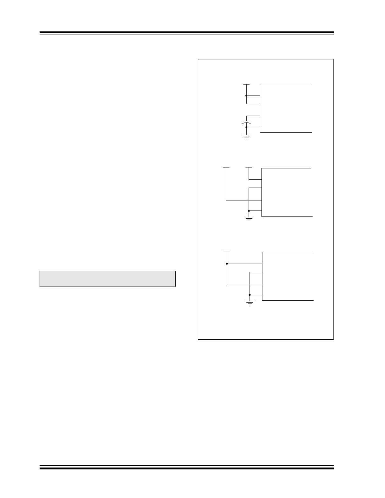
2.1 Power Requirements
All devices in the PIC24FJXXXGA1/GB1 families are
dual voltage supply designs: one supply for the core
and peripherals and another for the I/O pins. A regulator is provided on-chip to alleviate the need for two
external voltage supplies.
All PIC24FJXXXGA1/GB1 devices power their core
digital logic at a nominal 2.5V. To simplify system
design, all devices in the PIC24FJXXXGA1/GB1 families incorporate an on-chip regulator that allows the
device to run its core logic from V
DD.
The regulator provides power to the core from the other
VDD pins. A low-ESR capacitor (such as tantalum) must
be connected to the V
DDCORE pin (Table 2-1 and
Figure 2-2). This helps to maintain the stability of the
regulator. The specifications for core voltage and capacitance are listed in Section 7.0 “AC/DC Characteristics
and Timing Requirements”.
2.2 Program Memory Write/Erase Requirements
The Flash program memory on PIC24FJXXXGA1/GB1
devices has a specific write/erase requirement that
must be adhered to for proper device operation. The
rule is that any given word in memory must not be written more than twice before erasing the page in which it
is located. Thus, the easiest way to conform to this rule
is to write all the data in a programming block within
one write cycle. The programming methods specified in
this specification comply with this requirement.
Note: Writing to a location multiple times without
erasing is not recommended.
2.3 Pin Diagrams
FIGURE 2-2: CONNECTIONS FOR THE
ON-CHIP REGULATOR
Regulator Enabled (ENVREG tied to VDD):
3.3V
CEFC
(10
μF typ)
Regulator Disabled (ENVREG tied to ground):
(1)
2.5V
Regulator Disabled (VDD tied to VDDCORE):
2.5V
3.3V
(1)
PIC24FJXXXGA1/GB1
VDD
ENVREG
V
DDCORE/VCAP
VSS
(1)
PIC24FJXXXGA1/GB1
VDD
ENVREG
V
DDCORE/VCAP
VSS
PIC24FJXXXGA1/GB1
VDD
ENVREG
VDDCORE/VCAP
VSS
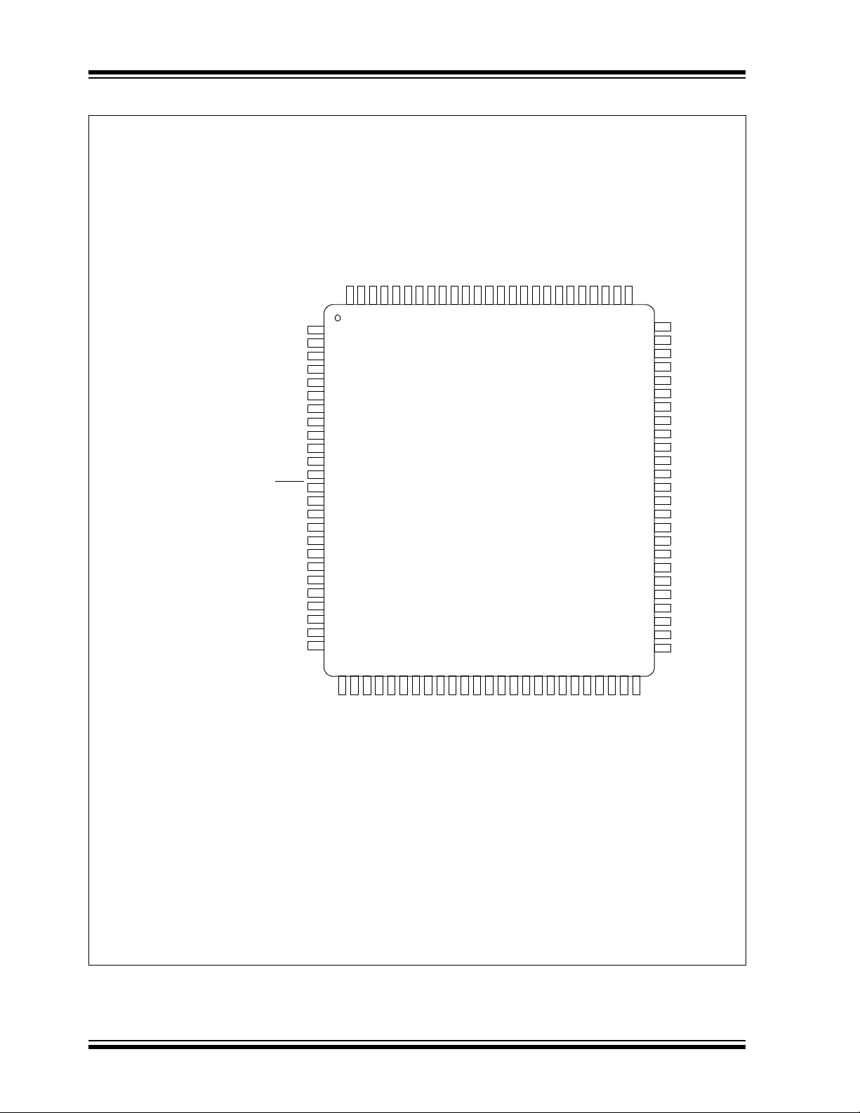
The pin diagrams for the PIC24FJXXXGA1/GB1 families are shown in the following figures. The pins that are
required for programming are listed in Table 2-1 and
are shown in bold letters in the figures. Refer to the
Note 1: These are typical operating voltages. Refer
Section 7.0 “AC/DC Characteristics and
to
Timing Requirements”
ranges of V
DD and VDDCORE.
for the full operating
appropriate device data sheet for complete pin
descriptions.
2.3.1 PGCx AND PGDx PIN PAIRS
All of the devices in the PIC24FJXXXGA1/GB1 families
have three separate pairs of programming pins,
labelled as PGEC1/PGED1, PGEC2/PGED2, and
PGEC3/PGED3. Any one of these pin pairs may be
used for device programming by either ICSP or
Enhanced ICSP. Unlike voltage supply and ground
pins, it is not necessary to connect all three pin pairs to
program the device. However, the programming
method must use both pins of the same pair.
DS39907A-page 2 © 2007 Microchip Technology Inc.
PIC24FJXXXGA1/GB1
TABLE 2-1: PIN DESCRIPTIONS (DURING PROGRAMMING)
Pin Name
Pin Name Pin Type Pin Description
MCLR MCLR P Programming Enable
ENVREG ENVREG I Enable for On-Chip Voltage Regulator
(1)
(1)
VDD P Power Supply
VSS PGround
DD and AVDD
V
VSS and AVSS
DDCORE VDDCORE P Regulated Power Supply for Core
V
PGECx PGCx I Programming Pin Pairs 1, 2 and 3: Serial Clock
PGEDx PGDX I/O Programming Pin Pairs 1, 2 and 3: Serial Data
Legend: I = Input, O = Output, P = Power
Note 1: All power supply and ground pins must be connected, including analog supplies (AVDD) and ground
(AV
SS).
FIGURE 2-3: PIN DIAGRAMS
64-Pin TQFP
During Programming
PGEC3/AN5/RP18/C1INA/CN7/RB5
PGED3/AN4/RP28/C1INB/CN6/RB4
PGEC1/AN1/RP1/V
PGED1/AN0/RP0/PMA6/V
REF-/CN3/RB1
REF+/
RE5
RE6
RE7
RG6
RG7
RG8
MCLR
RG9
VSS
V
DD
RB3
RB2
CN2/RB0
RE0
RE4
RE3
636261596058575654555352514950
64
1
2
3
4
5
6
7
8
9
10
11
12
13
14
15
16
171920
18
RF1
RE2
RE1
RF0
ENVREG
PIC24FJXXXGA106
2244242526272829303132
23
21
SS
RB8
RB9
AVDD
AV
RB11
RB10
CAP/VDDCORE
RD7
RD6
RD5
RD4
RD3
RD2
V
DD
VSS
V
RB12
RB13
RD1
48
RC14
47
RC13
46
RD0
45
RD11
RD10
43
RD9
42
RD8
41
VSS
40
RC15
39
RC12
38
V
DD
37
RG2
36
RG3
35
RF6
34
RF2
33
RF3
RF5
RF4
RB14
RB15
PGEC2/AN6/RP6/CN24/RB6
PGED2/AN7/RP7/CN25/RB7
© 2007 Microchip Technology Inc. DS39907A-page 3

PIC24FJXXXGA1/GB1
FIGURE 2-4: PIN DIAGRAMS (CONTINUED
80-Pin TQFP
RE2
RE4
RE3
RE1
RE0
DDCORE
RD5
RD4
RD13
RD12
RD3
RD2
RG0
RF0
VCAP/V
ENVREG
RG1
RF1
RD7
RD6
RD1
PGEC3/AN5/RP18/
PGED3/AN4/RP28/
PGEC1/AN1/RP1/CN3/RB1
PGED1/AN0/RP0/CN2/RB0
RE5
RE6
RE7
RC1
RC3
RG6
RG7
RG8
MCLR
RG9
VSS
V
DD
CN66/RE8
CN67/RE9
C1INA/CN7/RB5
C1INB/CN6/RB4
RB3
RB2
807978
1
2
3
4
5
6
7
8
9
10
11
12
13
14
15
16
17
18
19
20
21
232425
22
RA9
76
77
757473717270696866676564636162
PIC24FJXXXGA108
26
2829303132333435363738
27
SS
DD
RB8
RB9
AV
AV
RA10
DD
VSS
V
RB11
RB10
RB12
RB13
RC14
60
59
RC13
58
RD0
57
RD11
56
RD10
RD9
55
RD8
54
RA15
53
RA14
52
VSS
51
RC15
50
RC12
49
V
DD
48
RG2
47
RG3
46
RF6
45
RF7
44
RF8
43
RF2
42
RF3
41
40
39
RF5
RB14
RF4
RB15
RD15
RD14
PGEC2/AN6/RP6/CN24/RB6
PGED2/AN7/RP7/CN25/RB7
DS39907A-page 4 © 2007 Microchip Technology Inc.
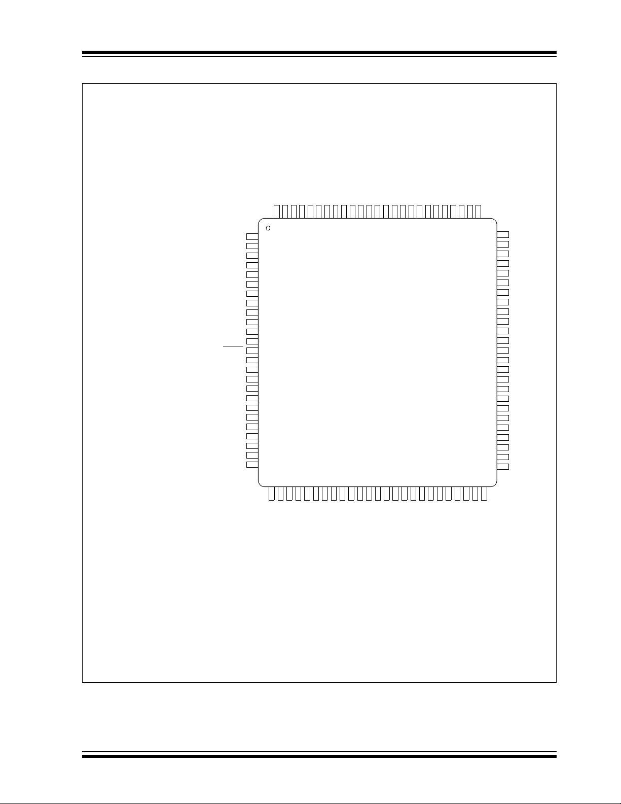
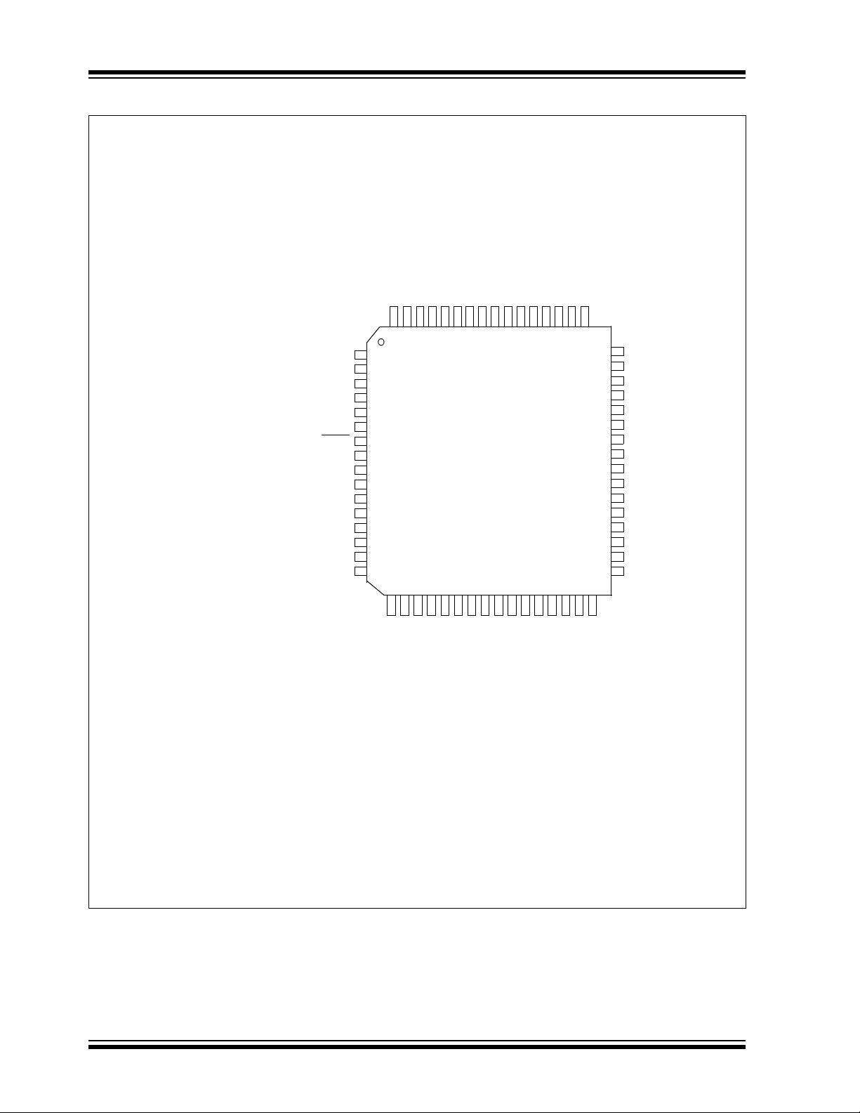
FIGURE 2-5: PIN DIAGRAMS (CONTINUED)
100-Pin TQFP
RE2
RG13
RE4
RE3
99
100
DD
DD
1
2
3
4
5
6
7
8
9
10
11
12
13
14
SS
15
16
17
18
19
20
21
22
23
24
25
27
26
2829303132333435363738
RG15
V
RE5
RE6
RE7
RC1
RC2
RC3
RC4
RG6
RG7
RG8
MCLR
RG9
V
V
RA0
RE8
RE9
PGEC3/AN5/RP18/VBUSON/C1INA/CN7/RB5
PGED3/AN4/RP28/USBOEN/C1INB/CN6/RB4
RB3
RB2
PGEC1/AN1/RP1/CN3/RB1
PGED1/AN0/RP0/CN2/RB0
PIC24FJXXXGA1/GB1
CAP/VDDCORE
RA7
RG12
RG14
95
969897
RA6
RE1
RE0
9294939190898887868584838281807978
PIC24FJXXXGA110
RG1
RG0
RF1
ENVREG
RF0
40
39
V
RD7
RD6
RD5
RD4
RD13
RD12
RD3
RD2
RD1
76
77
75
74
73
72
71
70
69
68
67
66
65
64
63
62
61
60
59
58
57
56
55
54
53
52
51
4647484950
45
44
43
42
41
SS
V
RC14
RC13
RD0
RD11
RD10
RD9
RD8
RA15
RA14
VSS
RC15
RC12
V
DD
RA5
RA4
RA3
RA2
RG2
RG3
RF6
RF7
RF8
RF2
RF3
DD
RA9
PGEC2/AN6/RP6/CN24/RB6
PGED2/AN7/RP7/RCV/CN25/RB7
RB8
RB9
AVSS
AV
RA10
DD
VSS
V
RA1
RB11
RB10
RF12
RF13
RB12
SS
V
RB13
VDD
RB14
RB15
RF5
RF4
RD15
RD14
© 2007 Microchip Technology Inc. DS39907A-page 5
PIC24FJXXXGA1/GB1
FIGURE 2-6: PIN DIAGRAMS (CONTINUED)
64-Pin TQFP
RE4
64
1
RE5
2
RE6
RE7
3
RG6
4
RG7
5
RG8
6
MCLR
PGEC3/AN5/RP18/VBUSON/C1INA/CN7/RB5
PGED3/AN4/RP28/USBOEN/C1INB/CN6/RB4
PGEC1/AN1/RP1/V
PGED1/AN0/RP0/PMA6/V
REF-/CN3/RB1
REF+/
CN2/RB0
RG9
VSS
V
DD
RB3
RB2
7
8
9
10
11
12
13
14
15
16
17
CAP/VDDCORE
RD6
RD5
RD4
RE3
RE2
RE1
RF0
V
ENVREG
RE0
RF1
636261596058575654555352514950
RD7
RD3
PIC24FJXXXGB106
2244242526272829303132
192021
18
23
RD2
RD1
48
RC14
47
RC13
46
RD0
45
RD11
RD10
43
RD9
42
RD8
41
VSS
40
RC15
39
RC12
38
V
DD
37
D+/RG2
36
D-/RG3
35
V
USB
34
VBUS
33
RF3
SS
RB8
RB9
AV
AVDD
PGEC2/AN6/RP6/CN24/RB6
PGED2/AN7/RP7/RCV/CN25/RB7
DD
VSS
V
RB11
RB10
RB12
RB13
RF5
RF4
RB14
RB15
DS39907A-page 6 © 2007 Microchip Technology Inc.

FIGURE 2-7: PIN DIAGRAMS (CONTINUED)
80-Pin TQFP
RE2
RE4
RE3
PIC24FJXXXGA1/GB1
DDCORE
RD5
RD4
RD13
RD12
RD3
RD2
RE1
RE0
RG0
RF0
VCAP/V
ENVREG
RG1
RF1
RD7
RD6
RD1
PGEC3/AN5/RP18/VBUSON/
PGED3/AN4/RP28/USBOEN/
PGEC1/AN1/RP1/CN3/RB1
PGED1/AN0/RP0/CN2/RB0
RE5
RE6
RE7
RC1
RC3
RG6
RG7
RG8
MCLR
RG9
VSS
V
DD
CN66/RE8
CN67/RE9
C1INA/CN7/RB5
C1INB/CN6/RB4
RB3
RB2
807978
1
2
3
4
5
6
7
8
9
10
11
12
13
14
15
16
17
18
19
20
21
232425
22
RA9
76
77
757473717270696866676564636162
PIC24FJXXXGB108
26
2829303132333435363738
27
SS
DD
RB8
RB9
AV
AV
RA10
DD
VSS
V
RB11
RB10
RB12
RB13
RC14
60
59
RC13
58
RD0
57
RD11
56
RD10
RD9
55
RD8
54
RA15
53
RA14
52
VSS
51
RC15
50
RC12
49
V
DD
48
D+/RG2
47
D-/RG3
46
V
USB
45
VBUS
44
RF8
43
RF2
42
RF3
41
40
39
RF5
RB14
RF4
RB15
RD15
RD14
PGEC2/AN6/RP6/CN24/RB6
PGED2/AN7/RP7/RCV/CN25/RB7
© 2007 Microchip Technology Inc. DS39907A-page 7
PIC24FJXXXGA1/GB1
FIGURE 2-8: PIN DIAGRAMS (CONTINUED)
100-Pin TQFP
RE2
RG13
RG12
RE3
969897
99
2829303132333435363738
27
RG15
V
DD
RE5
RE6
RE7
RC1
RC2
RC3
RC4
RG6
RG7
RG8
MCLR
RG9
V
V
DD
RA0
RE8
PGEC3/AN5/RP18/VBUSON/C1INA/CN7/RB5
PGED3/AN4/RP28/USBOEN/C1INB/CN6/RB4
PGEC1/AN1/RP1/CN3/RB1
PGED1/AN0/RP0/CN2/RB0
RE9
RB3
RB2
RE4
100
1
2
3
4
5
6
7
8
9
10
11
12
13
14
SS
15
16
17
18
19
20
21
22
23
24
25
26
CAP/VDDCORE
RG1
RA7
RG14
95
RA6
RE1
RE0
RG0
9294939190898887868584838281807978
V
RF1
RF0
ENVREG
RD7
PIC24FJXXXGB110
41
40
39
RD6
RD5
RD4
RD13
RD12
RD3
RD2
RD1
76
77
75
74
73
72
71
70
69
68
67
66
65
64
63
62
61
60
59
58
57
56
55
54
53
52
51
45
44
43
42
4647484950
SS
V
RC14
RC13
RD0
RD11
RD10
RD9
RD8
RA15
RA14
VSS
RC15
RC12
DD
V
RA5
RA4
RA3
RA2
D+/RG2
D-/RG3
V
USB
VBUS
RF8
RF2
RF3
SS
V
RB13
VDD
RB14
RB15
RF5
RF4
RD15
RD14
PGEC2/AN6/RP6/CN24/RB6
PGED2/AN7/RP7/RCV/CN25/RB7
RA9
DD
RB8
RB9
AVSS
AV
RA10
DD
VSS
V
RA1
RB11
RB10
RF12
RF13
RB12
DS39907A-page 8 © 2007 Microchip Technology Inc.

PIC24FJXXXGA1/GB1
2.4 Memory Map
The program memory map extends from 000000h to
FFFFFEh. Code storage is located at the base of the
memory map and supports up to 87K instruction words
(about 256 Kbytes). Table 2-2 shows the program
memory size and number of erase and program blocks
present in each device variant. Each erase block, or
page, contains 512 instructions, and each program
block, or row, contains 64 instructions.
Locations 800000h through 8007FEh are reserved for
executive code memory. This region stores the
programming executive and the debugging executive.
The programming executive is used for device programming and the debugging executive is used for
in-circuit debugging. This region of memory can not be
used to store user code.
The last three implemented program memory locations
are reserved for the Flash Configuration Words. In
PIC24FJXXXGB1 family devices, the last three locations are used for the Configuration Words; for
PIC24FJXXXGA1 devices, the last two locations are
used. The reserved addresses are shown in Table 2-2.
Locations FF0000h and FF0002h are reserved for the
Device ID registers. These bits can be used by the
programmer to identify what device type is being
programmed. They are described in Section 6.1
“Device ID”. The Device ID registers read out
normally, even after code protection is applied.
Figure 2-9 shows the memory map for the
PIC24FJXXXGA1/GB1 family variants.
TABLE 2-2: CODE MEMORY SIZE AND FLASH CONFIGURATION WORD LOCATIONS FOR
PIC24FJXXXGA1/GB1 DEVICES
User Memory
Device
PIC24FJ64GB1XX 00ABFEh (22K) 344 43 00ABFEh 00ABFCh 00ABFAh
PIC24FJ128GA1XX
PIC24FJ128GB1XX
PIC24FJ192GA1XX
PIC24FJ192GB1XX
PIC24FJ256GA1XX
PIC24FJ256GB1XX
Address Limit
(Instruction Words)
0157FEh (44K) 688 86 0157FEh 0157FCh 0157FAh
020BFEh (67K) 1048 131 020BFEh 020BFCh 020BFA
02ABFEh (87K) 1368 171 02ABFEh 02ABFCh 02ABFA
Write
Blocks
Erase
Blocks
Configuration Word Addresses
123
© 2007 Microchip Technology Inc. DS39907A-page 9

PIC24FJXXXGA1/GB1
FIGURE 2-9: PROGRAM MEMORY MAP
000000h
Space
User Memory
User Flash
Code Memory
Flash Configuration Words
Reserved
Executive Code Memory
(1024 x 24-bit)
Words
(8 x 24-bit)
(1)
0XXXF9h
0XXXFAh
0XXXFEh
0XXX00h
7FFFFEh
800000h
8007FAh
8007F0hDiagnostic and Calibration
800800h
(1)
(1)
(1)
(1)
Space
Reserved
Configuration Memory
FEFFFEh
Device ID
(2 x 16-bit)
Reserved
Note 1: The size and address boundaries for user Flash code memory are device dependent. See Table 2-2 for details.
DS39907A-page 10 © 2007 Microchip Technology Inc.
FF0000h
FF0002h
FF0004h
FFFFFEh
PIC24FJXXXGA1/GB1
3.0 DEVICE PROGRAMMING – ICSP
ICSP mode is a special programming protocol that
allows you to read and write to the memory of
PIC24FJXXXGA1/GB1 devices. The ICSP mode is the
most direct method used to program the device; note,
however, that Enhanced ICSP is faster. ICSP mode
also has the ability to read the contents of executive
memory to determine if the programming executive is
present. This capability is accomplished by applying
control codes and instructions, serially to the device,
using pins PGCx and PGDx.
In ICSP mode, the system clock is taken from the
PGCx pin, regardless of the device’s oscillator Configuration bits. All instructions are shifted serially into an
internal buffer, then loaded into the Instruction Register
(IR) and executed. No program fetching occurs from
internal memory. Instructions are fed in 24 bits at a
time. PGDx is used to shift data in and PGCx is used
as both the serial shift clock and the CPU execution
clock.
Note: During ICSP operation, the operating
frequency of PGCx must not exceed
10 MHz.
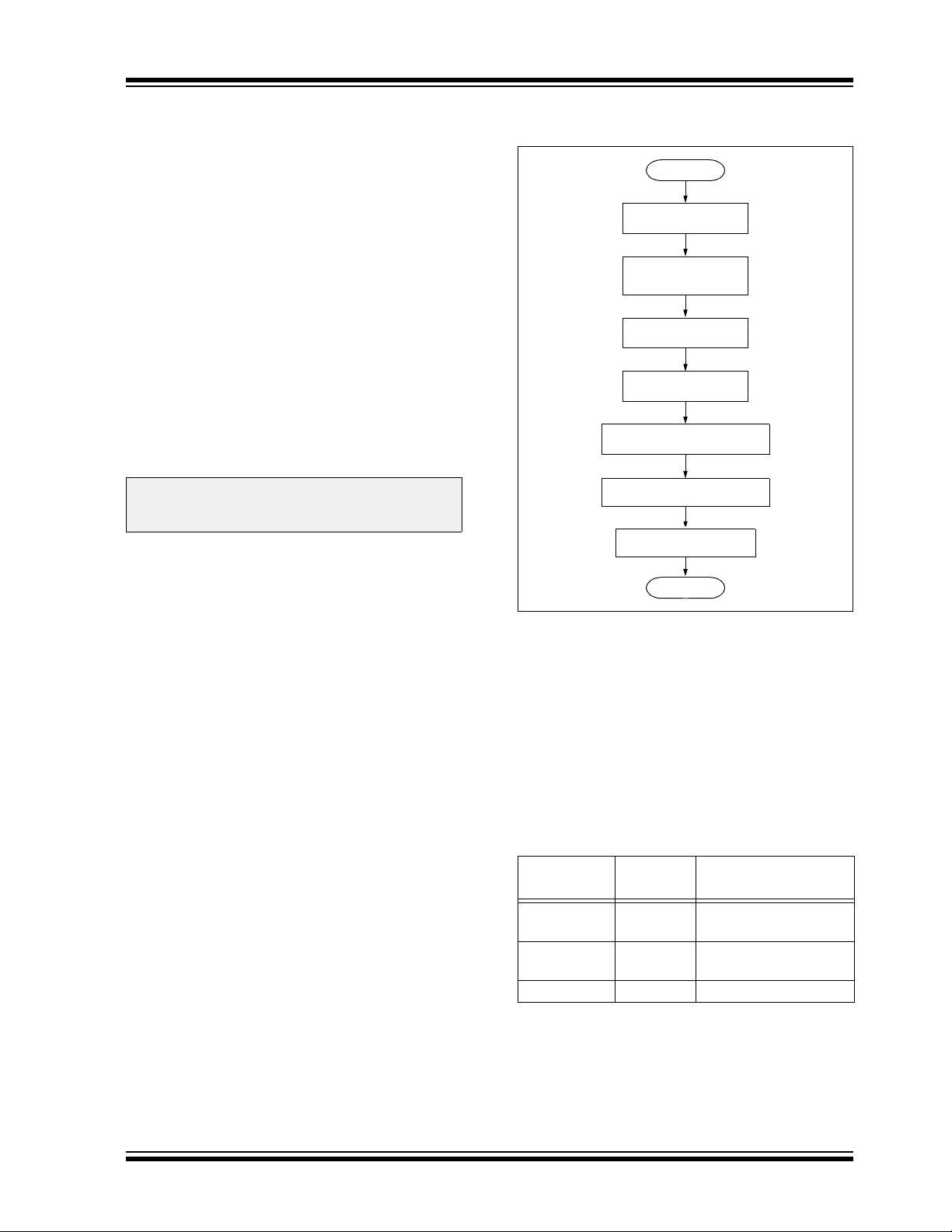
3.1 Overview of the Programming Process
Figure 3-1 shows the high-level overview of the
programming process. After entering ICSP mode, the
first action is to Chip Erase the device. Next, the code
memory is programmed, followed by the device
Configuration registers. Code memory (including the
Configuration registers) is then verified to ensure that
programming was successful. Then, program the
code-protect Configuration bits, if required.
FIGURE 3-1: HIGH-LEVEL ICSP™
PROGRAMMING FLOW
Start
Enter ICSP™
Perform Chip
Erase
Program Memory
Verify Program
Program Configuration Bits
Verify Configuration Bits
Exit ICSP
Done
3.2 ICSP Operation
Upon entry into ICSP mode, the CPU is Idle. Execution
of the CPU is governed by an internal state machine. A
4-bit control code is clocked in using PGCx and PGDx,
and this control code is used to command the CPU (see
Table 3-1).
The SIX control code is used to send instructions to the
CPU for execution, and the REGOUT control code is
used to read data out of the device via the VISI register.
TABLE 3-1: CPU CONTROL CODES IN
ICSP™ MODE
4-Bit
Control Code
0000b SIX Shift in 24-bit instruction
0001b REGOUT Shift out the VISI (0784h)
0010b-1111b N/A Reserved.
© 2007 Microchip Technology Inc. DS39907A-page 11
Mnemonic Description
and execute.
register.
PIC24FJXXXGA1/GB1
3.2.1 SIX SERIAL INSTRUCTION EXECUTION
The SIX control code allows execution of PIC24F family
assembly instructions. When the SIX code is received,
the CPU is suspended for 24 clock cycles, as the instruction is then clocked into the internal buffer. Once the
instruction is shifted in, the state machine allows it to be
executed over the next four PGC clock cycles. While the
received instruction is executed, the state machine
simultaneously shifts in the next 4-bit command (see
Figure 3-2).
FIGURE 3-2: SIX SERIAL EXECUTION
4 5
23 123 2324 1 2 3 4
16
PGCx
P3
P2
00
PGDx
0000
Execute PC – 1,
Fetch SIX
Control Code
78 9
Only for
Program
Memory Entry
P4
LSB X X X X X X X X X X X X X X MSB
P1A
P1B
Coming out of Reset, the first 4-bit control code is
always forced to SIX and a forced NOP instruction is
executed by the CPU. Five additional PGCx clocks are
needed on start-up, resulting in a 9-bit SIX command
instead of the normal 4-bit SIX command.
After the forced SIX is clocked in, ICSP operation
resumes as normal. That is, the next 24 clock cycles
load the first instruction word to the CPU.
Note: To account for this forced NOP, all example
P1
456 78 181920212217
24-Bit Instruction Fetch
PGDx = Input
code in this specification begins with a
NOP to ensure that no data is lost.
P4A
0000000
Execute 24-Bit
Instruction, Fetch
Next Control Code
3.2.1.1 Differences Between Execution of
SIX and Normal Instructions
There are some differences between executing instructions normally and using the SIX ICSP command. As a
result, the code examples in this specification may not
match those for performing the same functions during
normal device operation.
The important differences are:
• Two-word instructions require two SIX operations
to clock in all the necessary data.
Examples of two-word instructions are GOTO and
CALL.
• Two-cycle instructions require two SIX operations.
The first SIX operation shifts in the instruction and
begins to execute it. A second SIX operation – which
should shift in a NOP to avoid losing data – provides
the CPU clocks required to finish executing the
instruction.
Examples of two-cycle instructions are table read
and table write instructions.
• The CPU does not automatically stall to account
for pipeline changes.
A CPU stall occurs when an instruction modifies a
register that is used for Indirect Addressing by the
following instruction.
During normal operation, the CPU automatically
will force a NOP while the new data is read. When
using ICSP, there is no automatic stall, so any
indirect references to a recently modified
register should be preceded by a NOP.
For example, the instructions, MOV #0x0,W0 and
MOV [W0],W1, must have a NOP inserted
between them.
If a two-cycle instruction modifies a register that is
used indirectly, it will require two following NOPs: one
to execute the second half of the instruction and a
second to stall the CPU to correct the pipeline.
Instructions such as TBLWTL [W0++],[W1]
should be followed by two NOPs.
• The device Program Counter (PC) continues to
automatically increment during ICSP instruction
execution, even though the Flash memory is not
being used.
As a result, the PC may be incremented to point to
invalid memory locations. Invalid memory spaces
include unimplemented Flash addresses and the
vector space (locations 0x0 to 0x1FF).
If the PC points to these locations, the device will
reset, possibly interrupting the ICSP operation. To
prevent this, instructions should be periodically
executed to reset the PC to a safe space. The optimal method to accomplish this is to perform a
GOTO 0x200.
DS39907A-page 12 © 2007 Microchip Technology Inc.
PIC24FJXXXGA1/GB1
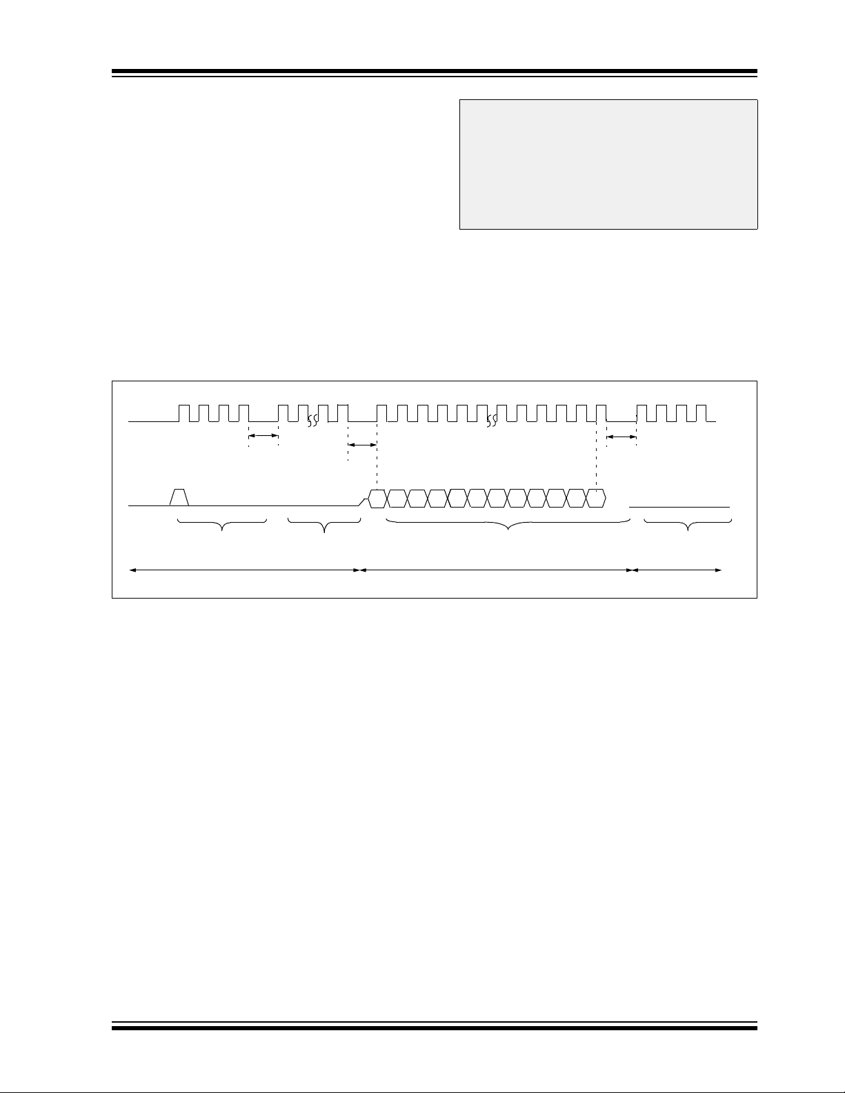
3.2.2 REGOUT SERIAL INSTRUCTION EXECUTION
The REGOUT control code allows for data to be
extracted from the device in ICSP mode. It is used to
clock the contents of the VISI register, out of the device,
over the PGDx pin. After the REGOUT control code is
received, the CPU is held Idle for 8 cycles. After these
8 cycles, an additional 16 cycles are required to clock the
data out (see Figure 3-3).
The REGOUT code is unique because the PGDx pin is
an input when the control code is transmitted to the
device. However, after the control code is processed,
the PGDx pin becomes an output as the VISI register is
shifted out.
FIGURE 3-3: REGOUT SERIAL EXECUTION
PGCx
PGDx
123 4 1 278
P4
1
0
0
123 1234
P5
1234
LSb
Note 1: After the contents of VISI are shifted out,
the PIC24FJXXXGA1/GB1 devices
maintain PGDx as an output until the first
rising edge of the next clock is received.
2: Data changes on the falling edge and
latches on the rising edge of PGCx. For
all data transmissions, the Least
Significant bit (LSb) is transmitted first.
456
11 13 15 161412
P4A
...
11100
MSb
141312
0000
Execute Previous Instruction,
Fetch REGOUT Control Code
PGDx = Input
CPU Held in Idle
Shift Out VISI Register<15:0>
PGDx = Output
No Execution Takes Place,
Fetch Next Control Code
PGDx = Input
© 2007 Microchip Technology Inc. DS39907A-page 13
PIC24FJXXXGA1/GB1
3.3 Entering ICSP Mode
As shown in Figure 3-4, entering ICSP Program/Verify
mode requires three steps:
1. MCLR
2. A 32-bit key sequence is clocked into PGDx.
3. MCLR
The programming voltage applied to MCLR is VIH,
which is essentially V
PIC24FJXXXGA1/GB1 devices. There is no minimum
time requirement for holding at VIH. After VIH is
removed, an interval of at least P18 must elapse before
presenting the key sequence on PGDx.
FIGURE 3-4: ENTERING ICSP™ MODE
MCLR
VDD
PGDx
PGCx
is briefly driven high, then low.
is then driven high within a specified
period of time and held.
DD in the case of
P6
P14
VIH
Program/Verify Entry Code = 4D434851h
0100 0 0
b31 b30 b29 b28 b27 b2 b1 b0b3
P18
1
P1A
P1B
...
The key sequence is a specific 32-bit pattern:
‘0100 1101 0100 0011 0100 1000 0101 0001’
(more easily remembered as 4D434851h in hexadecimal). The device will enter Program/Verify mode only
if the sequence is valid. The Most Significant bit (MSb) of
the most significant nibble must be shifted in first.
Once the key sequence is complete, V
applied to MCLR
and held at that level for as long as
IH must be
Program/Verify mode is to be maintained. An interval of
at least time, P19 and P7, must elapse before presenting data on PGDx. Signals appearing on PGCx before
P7 has elapsed will not be interpreted as valid.
On successful entry, the program memory can be
accessed and programmed in serial fashion. While in
ICSP mode, all unused I/Os are placed in the
high-impedance state.
P19
V
IH
0
1
P7
DS39907A-page 14 © 2007 Microchip Technology Inc.

PIC24FJXXXGA1/GB1
3.4 Flash Memory Programming in
ICSP Mode
3.4.1 PROGRAMMING OPERATIONS
Flash memory write and erase operations are controlled
by the NVMCON register. Programming is performed by
setting NVMCON to select the type of erase operation
(Table 3-2) or write operation (Table 3-3) and initiating
the programming by setting the WR control bit
(NVMCON<15>).
In ICSP mode, all programming operations are
self-timed. There is an internal delay between the user
setting the WR control bit and the automatic clearing of
the WR control bit when the programming operation
is complete. Please refer to Section 7.0 “AC/DC
Characteristics and Timing Requirements” for
information about the delays associated with various
programming operations.
TABLE 3-2: NVMCON ERASE
OPERATIONS
NVMCON
Value
404Fh Erase all code memory, executive
memory and Configuration registers
(does not erase Unit ID or Device ID
registers).
4042h Erase a page of code memory or
executive memory.
TABLE 3-3: NVMCON WRITE
NVMCON
Value
Erase Operation
OPERATIONS
Write Operation
3.5 Erasing Program Memory
The procedure for erasing program memory (all of code
memory, data memory, executive memory and
code-protect bits) consists of setting NVMCON to
404Fh and executing the programming cycle.
A Chip Erase can erase all of user memory or all of both
the user and configuration memory. A table write
instruction should be executed prior to performing the
Chip Erase to select which sections are erased.
When this table write instruction is executed:
• If the TBLPAG register points to user space (is
less than 0x80), the Chip Erase will erase only
user memory.
• If TBLPAG points to configuration space (is
greater than or equal to 0x80), the Chip Erase will
erase both user and configuration memory.
If configuration memory is erased, the internal
oscillator Calibration Word, located at 0x807FE,
will be erased. This location should be stored prior
to performing a whole Chip Erase and restored
afterward to prevent internal oscillators from
becoming uncalibrated.
Figure 3-5 shows the ICSP programming process for
performing a Chip Erase. This process includes the
ICSP command code, which must be transmitted (for
each instruction), Least Significant bit first, using the
PGCx and PGDx pins (see Figure 3-2).
Note: Program memory must be erased before
writing any data to program memory.
FIGURE 3-5: CHIP ERASE FLOW
Start
4003h Write a Configuration Word register.
4001h Program 1 row (64 instruction words) of
code memory or executive memory.
3.4.2 STARTING AND STOPPING A PROGRAMMING CYCLE
The WR bit (NVMCON<15>) is used to start an erase or
write cycle. Setting the WR bit initiates the programming
cycle.
All erase and write cycles are self-timed. The WR bit
should be polled to determine if the erase or write cycle
has been completed. Starting a programming cycle is
performed as follows:
BSET NVMCON, #WR
© 2007 Microchip Technology Inc. DS39907A-page 15
Write 404Fh to NVMCON SFR
Set the WR bit to Initiate Erase
Delay P11 + P10 Time
Done

PIC24FJXXXGA1/GB1
TABLE 3-4: SERIAL INSTRUCTION EXECUTION FOR CHIP ERASE
Command
(Binary)
Step 1: Exit the Reset vector.
0000
0000
0000
Step 2: Set the NVMCON to erase all program memory.
0000
0000
Step 3: Set TBLPAG and perform dummy table write to select what portions of memory are erased.
0000
0000
0000
0000
0000
0000
Step 4: Initiate the erase cycle.
0000
0000
0000
Step 5: Repeat this step to poll the WR bit (bit 15 of NVMCON) until it is cleared by the hardware.
0000
0000
0000
0000
0000
0001
0000
Data
(Hex)
000000
040200
000000
2404FA
883B0A
200000
880190
200000
BB0800
000000
000000
A8E761
000000
000000
040200
000000
803B02
883C22
000000
<VISI>
000000
Description
NOP
GOTO 0x200
NOP
MOV #0x404F, W10
MOV W10, NVMCON
MOV #<PAGEVAL>, W0
MOV W0, TBLPAG
MOV #0x0000, W0
TBLWTL W0,[W0]
NOP
NOP
BSET NVMCON, #WR
NOP
NOP
GOTO 0x200
NOP
MOV NVMCON, W2
MOV W2, VISI
NOP
Clock out contents of the VISI register.
NOP
DS39907A-page 16 © 2007 Microchip Technology Inc.

PIC24FJXXXGA1/GB1
3.6 Writing Code Memory
The procedure for writing code memory is the same as
the procedure for writing the Configuration registers,
except that 64 instruction words are programmed at a
time. To facilitate this operation, working registers,
W0:W5, are used as temporary holding registers for the
data to be programmed.
Table 3-5 shows the ICSP programming details, including the serial pattern with the ICSP command code
which must be transmitted, Least Significant bit first,
using the PGCx and PGDx pins (see Figure 3-2).
In Step 1, the Reset vector is exited. In Step 2, the
NVMCON register is initialized for programming a full
row of code memory. In Step 3, the 24-bit starting destination address for programming is loaded into the
TBLPAG register and W7 register. (The upper byte of
the starting destination address is stored in TBLPAG
and the lower 16 bits of the destination address are
stored in W7.)
To minimize the programming time, a packed instruction
format is used (Figure 3-6).
In Step 4, four packed instruction words are stored in
working registers, W0:W5, using the MOV instruction,
and the Read Pointer, W6, is initialized. The contents of
W0:W5 (holding the packed instruction word data) are
shown in Figure 3-6.
In Step 5, eight TBLWT instructions are used to copy the
data from W0:W5 to the write latches of code memory.
Since code memory is programmed 64 instruction
words at a time, Steps 4 and 5 are repeated 16 times to
load all the write latches (Step 6).
After the write latches are loaded, programming is
initiated by writing to the NVMCON register in Steps 7
and 8. In Step 9, the internal PC is reset to 200h. This
is a precautionary measure to prevent the PC from
incrementing into unimplemented memory when large
devices are being programmed. Lastly, in Step 10,
Steps 3-9 are repeated until all of code memory is
programmed.
FIGURE 3-6: PACKED INSTRUCTION
WORDS IN W0:W5
15 8 7 0
W0 LSW0
W1 MSB1 MSB0
W2 LSW1
W3 LSW2
W4 MSB3 MSB2
W5 LSW3
TABLE 3-5: SERIAL INSTRUCTION EXECUTION FOR WRITING CODE MEMORY
Command
(Binary)
Step 1: Exit the Reset vector.
0000
0000
0000
Step 2: Set the NVMCON to program 64 instruction words.
0000
0000
Step 3: Initialize the Write Pointer (W7) for TBLWT instruction.
0000
0000
0000
Step 4: Load W0:W5 with the next 4 instruction words to program.
0000
0000
0000
0000
0000
0000
Data
(Hex)
000000
040200
000000
24001A
883B0A
200xx0
880190
2xxxx7
2xxxx0
2xxxx1
2xxxx2
2xxxx3
2xxxx4
2xxxx5
Description
NOP
GOTO 0x200
NOP
MOV #0x4001, W10
MOV W10, NVMCON
MOV #<DestinationAddress23:16>, W0
MOV W0, TBLPAG
MOV #<DestinationAddress15:0>, W7
MOV #<LSW0>, W0
MOV #<MSB1:MSB0>, W1
MOV #<LSW1>, W2
MOV #<LSW2>, W3
MOV #<MSB3:MSB2>, W4
MOV #<LSW3>, W5
© 2007 Microchip Technology Inc. DS39907A-page 17

PIC24FJXXXGA1/GB1
TABLE 3-5: SERIAL INSTRUCTION EXECUTION FOR WRITING CODE MEMORY (CONTINUED)
Command
(Binary)
Step 5: Set the Read Pointer (W6) and load the (next set of) write latches.
0000
0000
0000
0000
0000
0000
0000
0000
0000
0000
0000
0000
0000
0000
0000
0000
0000
0000
0000
0000
0000
0000
0000
0000
0000
0000
Step 6: Repeat Steps 4 and 5, sixteen times, to load the write latches for 64 instructions.
Step 7: Initiate the write cycle.
0000
0000
0000
Step 8: Repeat this step to poll the WR bit (bit 15 of NVMCON) until it is cleared by the hardware.
0000
0000
0000
0000
0000
0001
0000
Step 9: Reset device internal PC.
0000
0000
Step 10: Repeat Steps 3-9 until all code memory is programmed.
Data
(Hex)
EB0300
000000
BB0BB6
000000
000000
BBDBB6
000000
000000
BBEBB6
000000
000000
BB1BB6
000000
000000
BB0BB6
000000
000000
BBDBB6
000000
000000
BBEBB6
000000
000000
BB1BB6
000000
000000
A8E761
000000
000000
040200
000000
803B02
883C22
000000
<VISI>
000000
040200
000000
Description
CLR W6
NOP
TBLWTL [W6++], [W7]
NOP
NOP
TBLWTH.B [W6++], [W7++]
NOP
NOP
TBLWTH.B [W6++], [++W7]
NOP
NOP
TBLWTL [W6++], [W7++]
NOP
NOP
TBLWTL [W6++], [W7]
NOP
NOP
TBLWTH.B [W6++], [W7++]
NOP
NOP
TBLWTH.B [W6++], [++W7]
NOP
NOP
TBLWTL [W6++], [W7++]
NOP
NOP
BSET NVMCON, #WR
NOP
NOP
GOTO 0x200
NOP
MOV NVMCON, W2
MOV W2, VISI
NOP
Clock out contents of the VISI register.
NOP
GOTO 0x200
NOP
DS39907A-page 18 © 2007 Microchip Technology Inc.

PIC24FJXXXGA1/GB1
FIGURE 3-7: PROGRAM CODE MEMORY FLOW
N = N + 1
Start
N = 1
LoopCount = 0
Configure
Device for
Writes
Load 2 Bytes
to Write
Buffer at <Addr>
N = 1
LoopCount =
LoopCount + 1
No
No
bytes
written?
Start Write Sequence
and Poll for WR bit
to be Cleared
locations
done?
Done
All
Yes
All
Yes
© 2007 Microchip Technology Inc. DS39907A-page 19

PIC24FJXXXGA1/GB1
3.7 Writing Configuration Words
Device configuration for PIC24FJXXXGA1/GB1 devices
is stored in Flash Configuration Words at the end of the
user space program memory, and in multiple register
Configuration Words located in the test space. These
registers reflect values read at any Reset from program
memory locations. The values for the Configuration
Words for the default device configurations are listed in
Table 3-6.
The values can be changed only by programming the
content of the corresponding Flash Configuration Word
and resetting the device. The Reset forces an automatic
reload of the Flash stored configuration values by
sequencing through the dedicated Flash Configuration
Words and transferring the data into the Configuration
registers.
For the PIC24FJXXXGA1/GB1 families, certain Configuration bits have default states that must always be
maintained to ensure device functionality, regardless of
the settings of other Configuration bits. These bits and
their values are listed in Table 3-7.
To change the values of the Flash Configuration Word
once it has been programmed, the device must be Chip
Erased, as described in Section 3.5 “Erasing Program
Memory”, and reprogrammed to the desired value. It is
not possible to program a ‘0’ to ‘1’, but they may be
programmed from a ‘1’ to ‘0’ to enable code protection.
Table 3-8 shows the ICSP programming details for programming the Configuration Word locations, including
the serial pattern with the ICSP command code which
must be transmitted, Least Significant bit first, using the
PGCx and PGDx pins (see Figure 3-2).
In Step 1, the Reset vector is exited. In Step 2, the
NVMCON register is initialized for programming of
code memory. In Step 3, the 24-bit starting destination
address for programming is loaded into the TBLPAG
register and W7 register.
The TBLPAG register must be loaded with the
following:
• 64 Kbyte devices: 00h
• 128, 192 and 256 Kbyte devices: 01h
To verify the data by reading the Configuration Words
after performing the write in order, the code protection
bits initially should be programmed to a ‘1’ to ensure
that the verification can be performed properly. After
verification is finished, the code protection bit can be
programmed to a ‘0’ by using a word write to the
appropriate Configuration Word.
TABLE 3-6: DEFAULT CONFIGURATION
REGISTER VALUES
Address Name Default Value
Last Word CW1 7FFFh
Last Word – 2 CW2 F7FFh
Last Word – 4 CW3 FFFFh
TABLE 3-7: RESERVED CONFIGURATION
BIT LOCATIONS
Bit Location Value
CW1<15> 0
CW1<10> 1
CW2<11> 0
CW2<2>
Note 1: This bit is implemented as I2C2SEL on
(1)
PIC24FJXXXGA110 devices, and should
be programmed as required.
1
DS39907A-page 20 © 2007 Microchip Technology Inc.

PIC24FJXXXGA1/GB1
TABLE 3-8: SERIAL INSTRUCTION EXECUTION FOR WRITING CONFIGURATION REGISTERS
Command
(Binary)
Step 1: Exit the Reset vector.
0000
0000
0000
Step 2: Initialize the Write Pointer (W7) for the TBLWT instruction.
0000 2xxxx7 MOV <CW2Address15:0>, W7
Step 3: Set the NVMCON register to program CW2.
0000
0000
Step 4: Initialize the TBLPAG register.
0000
0000
Step 5: Load the Configuration register data to W6.
0000 2xxxx6 MOV #<CW2_VALUE>, W6
Step 6: Write the Configuration register data to the write latch and increment the Write Pointer.
0000
0000
0000
0000
Step 7: Initiate the write cycle.
0000
0000
0000
Step 8: Repeat this step to poll the WR bit (bit 15 of NVMCON) until it is cleared by the hardware.
0000
0000
0000
0000
0000
0001
0000
Step 9: Reset device internal PC.
0000
0000
Step 10: Repeat Steps 5-9 to write CW1.
Data
(Hex)
000000
040200
000000
24003A
883B0A
200xx0
880190
000000
BB1B86
000000
000000
A8E761
000000
000000
040200
000000
803B02
883C22
000000
<VISI>
000000
040200
000000
Description
NOP
GOTO 0x200
NOP
MOV #0x4003, W10
MOV W10, NVMCON
MOV <CW2Address23:16>, W0
MOV W0, TBLPAG
NOP
TBLWTL W6, [W7++]
NOP
NOP
BSET NVMCON, #WR
NOP
NOP
GOTO 0x200
NOP
MOV NVMCON, W2
MOV W2, VISI
NOP
Clock out contents of the VISI register.
NOP
GOTO 0x200
NOP
© 2007 Microchip Technology Inc. DS39907A-page 21

PIC24FJXXXGA1/GB1
3.8 Reading Code Memory
Reading from code memory is performed by executing
a series of TBLRD instructions and clocking out the data
using the REGOUT command.
Table 3-9 shows the ICSP programming details for
reading code memory. In Step 1, the Reset vector is
exited. In Step 2, the 24-bit starting source address for
reading is loaded into the TBLPAG register and W6
register. The upper byte of the starting source address
is stored in TBLPAG and the lower 16 bits of the source
address are stored in W6.
To minimize the reading time, the packed instruction
word format that was utilized for writing is also used for
reading (see Figure 3-6). In Step 3, the Write Pointer,
W7, is initialized. In Step 4, two instruction words are
read from code memory and clocked out of the device,
through the VISI register, using the REGOUT
command. Step 4 is repeated until the desired amount
of code memory is read.
TABLE 3-9: SERIAL INSTRUCTION EXECUTION FOR READING CODE MEMORY
Command
(Binary)
Step 1: Exit Reset vector.
0000
0000
0000
Step 2: Initialize TBLPAG and the Read Pointer (W6) for TBLRD instruction.
0000
0000
0000
Step 3: Initialize the Write Pointer (W7) to point to the VISI register.
0000
0000
Step 4: Read and clock out the contents of the next two locations of code memory, through the VISI register, using
the REGOUT command.
0000
0000
0000
0001
0000
0000
0000
0000
0000
0000
0000
0001
0000
0000
0000
0000
0001
0000
Step 5: Repeat Step 4 until all desired code memory is read.
Step 6: Reset device internal PC.
0000
0000
Data
(Hex)
000000
040200
000000
200xx0
880190
2xxxx6
207847
000000
BA0B96
000000
000000
<VISI>
000000
BADBB6
000000
000000
BAD3D6
000000
000000
<VISI>
000000
BA0BB6
000000
000000
<VISI>
000000
040200
000000
Description
NOP
GOTO 0x200
NOP
MOV #<SourceAddress23:16>, W0
MOV W0, TBLPAG
MOV #<SourceAddress15:0>, W6
MOV #VISI, W7
NOP
TBLRDL [W6], [W7]
NOP
NOP
Clock out contents of VISI register
NOP
TBLRDH.B [W6++], [W7++]
NOP
NOP
TBLRDH.B [++W6], [W7--]
NOP
NOP
Clock out contents of VISI register
NOP
TBLRDL [W6++], [W7]
NOP
NOP
Clock out contents of VISI register
NOP
GOTO 0x200
NOP
DS39907A-page 22 © 2007 Microchip Technology Inc.

PIC24FJXXXGA1/GB1
3.9 Reading Configuration Words
The procedure for reading configuration memory is
similar to the procedure for reading code memory,
except that 16-bit data words are read (with the upper
byte read being all ‘0’s) instead of 24-bit words.
Configuration Words are read one register at a time.
Table 3-10 shows the ICSP programming details for
reading the Configuration Words. Note that the
TBLPAG register must be loaded with 00h for 64 Kbyte
and below devices and 01h for 128 Kbyte and larger
devices (the upper byte address of configuration memory), and the Read Pointer, W6, is initialized to the
lower 16 bits of the Configuration Word location.
TABLE 3-10: SERIAL INSTRUCTION EXECUTION FOR READING ALL CONFIGURATION MEMORY
Command
(Binary)
Step 1: Exit Reset vector.
0000
0000
0000
Step 2: Initialize TBLPAG, the Read Pointer (W6) and the Write Pointer (W7) for TBLRD instruction.
0000
0000
0000
0000
0000
Step 3: Read the Configuration register and write it to the VISI register (located at 784h), and clock out the
VISI register using the REGOUT command.
0000
0000
0000
0001
0000
Step 4: Repeat Step 3 twice to read Configuration Word 2 and Configuration Word 1.
Step 5: Reset device internal PC.
0000
0000
Data
(Hex)
000000
040200
000000
200xx0
880190
2xxxx7
207847
000000
BA0BB6
000000
000000
<VISI>
000000
040200
000000
Description
NOP
GOTO 0x200
NOP
MOV <CW3Address23:16>, W0
MOV W0, TBLPAG
MOV <CW3Address15:0>, W6
MOV #VISI, W7
NOP
TBLRDL [W6++], [W7]
NOP
NOP
Clock out contents of VISI register
NOP
GOTO 0x200
NOP
© 2007 Microchip Technology Inc. DS39907A-page 23

PIC24FJXXXGA1/GB1
3.10 Verify Code Memory and Configuration Word
The verify step involves reading back the code memory
space and comparing it against the copy held in the
programmer’s buffer. The Configuration registers are
verified with the rest of the code.
The verify process is shown in the flowchart in
Figure 3-8. Memory reads occur a single byte at a time,
so two bytes must be read to compare against the word
in the programmer’s buffer. Refer to Section 3.8
“Reading Code Memory” for implementation details
of reading code memory.
Note: Because the Configuration registers
include the device code protection bit,
code memory should be verified immediately after writing if code protection is
enabled. This is because the device will
not be readable or verifiable if a device
Reset occurs after the code-protect bit in
CW1 has been cleared.
FIGURE 3-8: VERIFY CODE
MEMORY FLOW
Start
Set TBLPTR = 0
3.11 Reading the Application ID Word
The Application ID Word is stored at address 8005BEh
in executive code memory. To read this memory
location, you must use the SIX control code to move
this program memory location to the VISI register.
Then, the REGOUT control code must be used to clock
the contents of the VISI register out of the device. The
corresponding control and instruction codes that must
be serially transmitted to the device to perform this
operation are shown in Table 3-11.
After the programmer has clocked out the Application
ID Word, it must be inspected. If the Application ID has
the value, BBh, the programming executive is resident
in memory and the device can be programmed using
the mechanism described in Section 4.0 “Device
Programming – Enhanced ICSP”. However, if the
Application ID has any other value, the programming
executive is not resident in memory; it must be loaded
to memory before the device can be programmed. The
procedure for loading the programming executive to
memory is described in Section 5.4 “Programming
the Programming Executive to Memory”.
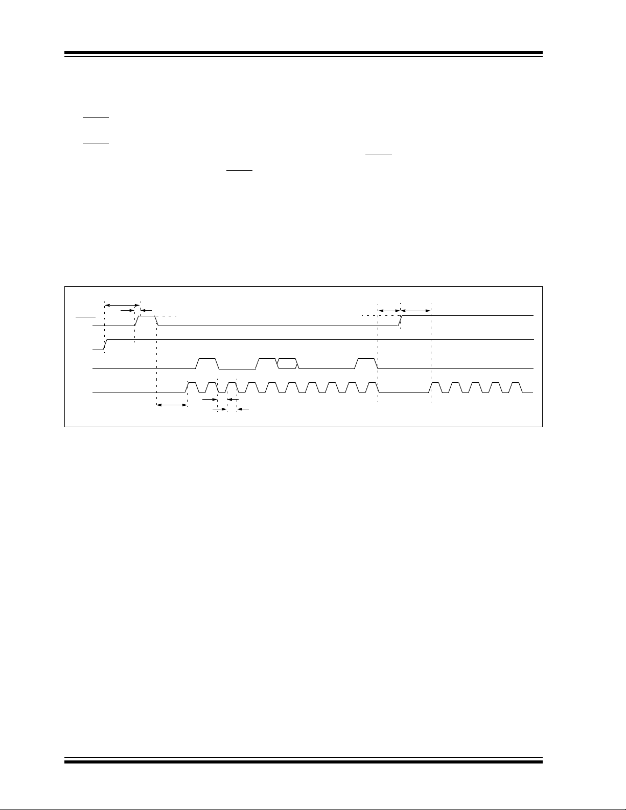
3.12 Exiting ICSP Mode
Exiting Program/Verify mode is done by removing VIH
from MCLR, as shown in Figure 3-9. The only requirement for exit is that an interval, P16, should elapse
between the last clock and program signals on PGCx
and PGDx before removing V
IH.
Read Low Byte
with Post-Increment
Read High Byte
with Post-Increment
Word = Expect
No
code memory
verified?
Does
Data?
All
Done
Yes
Yes
No
Failure,
Report
Error
FIGURE 3-9: EXITING ICSP™ MODE
P16
P17
VIH
MCLR
VDD
PGDx
PGCx
VIH
PGD = Input
DS39907A-page 24 © 2007 Microchip Technology Inc.

PIC24FJXXXGA1/GB1
TABLE 3-11: SERIAL INSTRUCTION EXECUTION FOR READING THE APPLICATION ID WORD
Command
(Binary)
Step 1: Exit Reset vector.
0000
0000
0000
Step 2: Initialize TBLPAG and the Read Pointer (W0) for TBLRD instruction.
0000
0000
0000
0000
0000
0000
0000
0000
Step 3: Output the VISI register using the REGOUT command.
0001
0000
Data
(Hex)
000000
040200
000000
200800
880190
205BE0
207841
000000
BA0890
000000
000000
<VISI>
000000
Description
NOP
GOTO 0x200
NOP
MOV #0x80, W0
MOV W0, TBLPAG
MOV #0x5BE, W0
MOV #VISI, W1
NOP
TBLRDL [W0], [W1]
NOP
NOP
Clock out contents of the VISI register
NOP
© 2007 Microchip Technology Inc. DS39907A-page 25

PIC24FJXXXGA1/GB1
4.0 DEVICE PROGRAMMING –
ENHANCED ICSP
This section discusses programming the device
through Enhanced ICSP and the programming executive. The programming executive resides in executive
memory (separate from code memory) and is executed
when Enhanced ICSP Programming mode is entered.
The programming executive provides the mechanism
for the programmer (host device) to program and verify
the PIC24FJXXXGA1/GB1 devices using a simple
command set and communication protocol. There are
several basic functions provided by the programming
executive:
• Read Memory
• Erase Memory
• Program Memory
• Blank Check
• Read Executive Firmware Revision
The programming executive performs the low-level
tasks required for erasing, programming and verifying
a device. This allows the programmer to program the
device by issuing the appropriate commands and data.
Table 4-1 summarizes the commands. A detailed
description for each command is provided in
Section 5.2 “Programming Executive Commands”.
TABLE 4-1: COMMAND SET SUMMARY
Command Description
SCHECK Sanity Check
READC Read Device ID Registers
READP Read Code Memory
PROGP
PROGW
QBLANK Query if the Code Memory is Blank
QVER Query the Software Version
The programming executive uses the device’s data
RAM for variable storage and program execution. After
the programming executive has run, no assumptions
should be made about the contents of data RAM.
4.1 Overview of the Programming
Figure 4-1 shows the high-level overview of the
programming process. After entering Enhanced ICSP
mode, the programming executive is verified. Next, the
device is erased. Then, the code memory is
programmed, followed by the configuration locations.
Code memory (including the Configuration registers) is
then verified to ensure that programming was successful.
Program One Row of Code Memory
and Verify
Program One Word of Code Memory
and Verify
Process
After the programming executive has been verified
in memory (or loaded if not present), the
PIC24FJXXXGA1/GB1 families can be programmed
using the command set shown in Table 4-1.
FIGURE 4-1: HIGH-LEVEL ENHANCED
ICSP™ PROGRAMMING FLOW
Start
Enter Enhanced ICSP™
Perform Chip
Erase
Program Memory
Verify Program
Program Configuration Bits
Verify Configuration Bits
Exit Enhanced ICSP
Done
4.2 Confirming the Presence of the Programming Executive
Before programming can begin, the programmer must
confirm that the programming executive is stored in
executive memory. The procedure for this task is
shown in Figure 4-2.
First, In-Circuit Serial Programming mode (ICSP) is
entered. Then, the unique Application ID Word stored in
executive memory is read. If the programming executive
is resident, the Application ID Word is BBh, which means
programming can resume as normal. However, if the
Application ID Word is not BBh, the programming
executive must be programmed to executive code
memory using the method described in Section 5.4
“Programming the Programming Executive to
Memory”.
Section 3.0 “Device Programming – ICSP” describes
the ICSP programming method. Section 3.11 “Reading
the Application ID Word” describes the procedure for
reading the Application ID Word in ICSP mode.
DS39907A-page 26 © 2007 Microchip Technology Inc.

PIC24FJXXXGA1/GB1
FIGURE 4-2: CONFIRMING PRESENCE
OF PROGRAMMING
EXECUTIVE
Start
Enter ICSP™ Mode
Read the
Application ID
from Address
807F0h
Is
Application ID
BBh?
Yes
Prog. Executive is
Resident in Memory
Finish
No
Prog. Executive must
be Programmed
4.3 Entering Enhanced ICSP Mode
As shown in Figure 4-3, entering Enhanced ICSP
Program/Verify mode requires three steps:
1. The MCLR
2. A 32-bit key sequence is clocked into PGDx.
3. MCLR
period of time and held.
The programming voltage applied to MCLR is VIH,
which is essentially V
PIC24FJXXXGA1/GB1 devices. There is no minimum
time requirement for holding at VIH. After VIH is
removed, an interval of at least P18 must elapse before
presenting the key sequence on PGDx.
The key sequence is a specific 32-bit pattern:
‘0100 1101 0100 0011 0100 1000 0101 0000’
(more easily remembered as 4D434850h in hexadecimal format). The device will enter Program/Verify
mode only if the key sequence is valid. The Most
Significant bit (MSb) of the most significant nibble must
be shifted in first.
Once the key sequence is complete, V
applied to MCLR
Program/Verify mode is to be maintained. An interval of
at least time P19 and P7 must elapse before presenting
data on PGDx. Signals appearing on PGDx before P7
has elapsed will not be interpreted as valid.
On successful entry, the program memory can be
accessed and programmed in serial fashion. While in
the Program/Verify mode, all unused I/Os are placed in
the high-impedance state.
pin is briefly driven high, then low.
is then driven high within a specified
DD in the case of
IH must be
and held at that level for as long as
FIGURE 4-3: ENTERING ENHANCED ICSP™ MODE
P6
MCLR
VDD
PGDx
PGCx
P14
VIH
Program/Verify Entry Code = 4D434850h
01001 0000
b31 b30 b29 b28 b27 b2 b1 b0b3
P18
P1A
P1B
...
VIH
P19
P7
© 2007 Microchip Technology Inc. DS39907A-page 27

PIC24FJXXXGA1/GB1
4.4 Blank Check
The term “Blank Check” implies verifying that the
device has been successfully erased and has no
programmed memory locations. A blank or erased
memory location is always read as ‘1’.
The Device ID registers (FF0002h:FF0000h) can be
ignored by the Blank Check since this region stores
device information that cannot be erased. The device
Configuration registers are also ignored by the Blank
Check. Additionally, all unimplemented memory space
should be ignored by the Blank Check.
The QBLANK command is used for the Blank Check. It
determines if the code memory is erased by testing
these memory regions. A ‘BLANK’ or ‘NOT BLANK’
response is returned. If it is determined that the device
is not blank, it must be erased before attempting to
program the chip.
4.5 Code Memory Programming
4.5.1 PROGRAMMING METHODOLOGY
Code memory is programmed with the PROGP
command. PROGP programs one row of code memory
starting from the memory address specified in the
command. The number of PROGP commands
required to program a device depends on the number
of write blocks that must be programmed in the device.
A flowchart for programming the code memory of the
PIC24FJXXXGA1/GB1 families is shown in Figure 4-4.
In this example, all 87K instruction words of a
256 Kbyte device are programmed. First, the number
of commands to send (called ‘RemainingCmds’ in the
flowchart) is set to 1368 and the destination address
(called ‘BaseAddress’) is set to ‘0’. Next, one write
block in the device is programmed with a PROGP
command. Each PROGP command contains data for
one row of code memory of the device. After the first
command is processed successfully, ‘RemainingCmds’
is decremented by 1 and compared with 0. Since there
are more PROGP commands to send, ‘BaseAddress’
is incremented by 80h to point to the next row of
memory.
On the second PROGP command, the second row is
programmed. This process is repeated until the entire
device is programmed. No special handling must be
performed when a panel boundary is crossed.
FIGURE 4-4: FLOWCHART FOR
PROGRAMMING CODE
MEMORY
Start
BaseAddress = 00h
RemainingCmds = 1368
Send PROGP
Command to Program
BaseAddress
BaseAddress =
BaseAddress + 80h
No
Is
PROGP response
PASS?
Yes
RemainingCmds =
RemainingCmds – 1
Are
RemainingCmds
0?
Yes
Finish
No
Failure
Report Error
4.5.2 PROGRAMMING VERIFICATION
After code memory is programmed, the contents of
memory can be verified to ensure that programming
was successful. Verification requires code memory to
be read back and compared against the copy held in
the programmer’s buffer.
The READP command can be used to read back all of
the programmed code memory.
Alternatively, you can have the programmer perform
the verification after the entire device is programmed
using a checksum computation.
DS39907A-page 28 © 2007 Microchip Technology Inc.

PIC24FJXXXGA1/GB1
4.6 Configuration Bits Programming
4.6.1 OVERVIEW
The PIC24FJXXXGA1/GB1 families have Configuration bits stored in the last three locations of implemented program memory (see Table 2-2 for locations).
These bits can be set or cleared to select various
device configurations. There are three types of Configuration bits: system operation bits, code-protect bits
and unit ID bits. The system operation bits determine
the power-on settings for system level components,
such as oscillator and Watchdog Timer. The
code-protect bits prevent program memory from being
read and written.
The descriptions for the Configuration bits in the Flash
Configuration Words are shown in Table 4-2.
Note: Although not implemented with a specific
function, some Configuration bit positions
have default states that must always be
maintained to ensure device functionality,
regardless of the settings of other Configuration bits. Refer to Table 3-7 for a list of
these bit positions and their default states.
TABLE 4-2: PIC24FJXXXGA1/GB1 CONFIGURATION BITS DESCRIPTION
Bit Field Register Description
DEBUG CW1<11> Background Debug Enable bit
1 = Device will reset in User mode
0 = Device will reset in Debug mode
DISUVREG
FCKSM<1:0> CW2<7:6> Clock Switching Mode bits
FNOSC<2:0> CW2<10:8> Initial Oscillator Source Selection bits
FWDTEN CW1<7> Watchdog Timer Enable bit
FWPSA CW1<4> Watchdog Timer Postscaler bit
GCP CW1<13> General Segment Code-Protect bit
GWRP CW1<12> General Segment Write-Protect bit
Note 1: Available on PIC24FJXXXGB1XX devices only.
(1)
2: Available on PIC24FJXXXGA110 devices only. On other devices, always maintain this bit as ‘1’.
CW2<3> Internal USB 3.3v Regulator Disable bit
1 = Regulator is disabled
0 = Regulator is enabled
1x = Clock switching is disabled, Fail-Safe Clock Monitor is disabled
01 = Clock switching is enabled, Fail-Safe Clock Monitor is disabled
00 = Clock switching is enabled, Fail-Safe Clock Monitor is enabled
111 = Internal Fast RC (FRCDIV) oscillator with postscaler
110 = Reserved
101 = Low-Power RC (LPRC) oscillator
100 = Secondary (SOSC) oscillator
011 = Primary (XTPLL, HSPLL, ECPLL) oscillator with PLL
010 = Primary (XT, HS, EC) oscillator
001 = Internal Fast RC (FRCPLL) oscillator with postscaler and PLL
000 = Fast RC (FRC) oscillator
1 = Watchdog Timer always enabled (LPRC oscillator cannot be disabled;
clearing the SWDTEN bit in the RCON register will have no effect)
0 = Watchdog Timer enabled/disabled by user software (LPRC can be
disabled by clearing the SWDTEN bit in the RCON register)
1 = 1:128
0 = 1:32
1 = User program memory is not code-protected
0 = User program memory is code-protected
1 = User program memory is not write-protected
0 = User program memory is write-protected
© 2007 Microchip Technology Inc. DS39907A-page 29

PIC24FJXXXGA1/GB1
TABLE 4-2: PIC24FJXXXGA1/GB1 CONFIGURATION BITS DESCRIPTION (CONTINUED)
Bit Field Register Description
I2C2SEL
ICS1:ICS0 CW1<9,8>
IESO CW2<15> Internal External Switchover bit
IOL1WAY CW2<4>
JTAGEN CW1<14> JTAG Enable bit
OSCIOFNC CW2<5> OSC2 Pin Function bit (except in XT and HS modes)
PLLDIV2:PLLDIV0
POSCMD1:
POSCMD0
WDTPOST3:
WDTPOST0
Note 1: Available on PIC24FJXXXGB1XX devices only.
(2)
(1)
2: Available on PIC24FJXXXGA110 devices only. On other devices, always maintain this bit as ‘1’.
CW2<2>
CW2<14:12> USB 96MHz PLL Prescaler Select bits
CW2<1:0> Primary Oscillator Mode Select bits
CW1<3:0> Watchdog Timer Prescaler bit
I2C2 Pin Select bit (PIC24FJXXXGA1XX devices only)
1 = Use SCL2/SDA2 pins for I
0 = Use ASCL2/ASDA2 pins for I
ICD Emulator Pin Placement Select bits
11 = Emulator functions are shared with PGEC1/PGED1
10 = Emulator functions are shared with PGEC2/PGED2
01 = Emulator functions are shared with PGEC3/PGED3
00 = Reserved; do not use
1 = Two-Speed Start-up enabled
0 = Two-Speed Start-up disabled
IOLOCK Bit One-Way Set Enable bit
0 = The OSCCON<IOLOCK> bit can be set and cleared as needed
(provided an unlocking sequence is executed)
1 = The OSCCON<IOLOCK> bit can only be set once (provided an
unlocking sequence is executed). Once IOLOCK is set, this prevents
any possible future RP register changes
1 = JTAG enabled
0 = JTAG disabled
1 = OSC2 is clock output
0 = OSC2 is general purpose digital I/O pin
111 = Oscillator input divided by 12 (48 MHz input)
110 = Oscillator input divided by 10 (40 MHz input)
101 = Oscillator input divided by 6 (24 MHz input)
100 = Oscillator input divided by 5 (20 MHz input)
011 = Oscillator input divided by 4 (16 MHz input)
010 = Oscillator input divided by 3 (12 MHz input)
001 = Oscillator input divided by 2 (8 MHz input)
000 = Oscillator input used directly (4 MHz input)
11 = Primary oscillator disabled
10 = HS Crystal Oscillator mode
01 = XT Crystal Oscillator mode
00 = EC (External Clock) mode
1111 = 1:32,768
1110 = 1:16,384
.
.
.
0001 = 1:2
0000 = 1:1
2
C™ module 2
2
C module 2
DS39907A-page 30 © 2007 Microchip Technology Inc.

PIC24FJXXXGA1/GB1
TABLE 4-2: PIC24FJXXXGA1/GB1 CONFIGURATION BITS DESCRIPTION (CONTINUED)
Bit Field Register Description
WINDIS CW1<6> Windowed WDT bit
1 = Watchdog Timer in Non-Window mode
0 = Watchdog Timer in Window mode; FWDTEN must be ‘1’
WPCFG CW3<14> Configuration Word Code Page Protection Select bit
1 = Last page (at the top of program memory) and Flash Configuration Words
are not protected
0 = Last page and Flash Configuration Words are code-protected
WPDIS CW3<13> Segment Write Protection Disable bit
1 = Segmented code protection disabled
0 = Segmented code protection enabled; protected segment defined by
WPEND, WPCFG and WPFPx Configuration bits
WPEND CW3<15> Segment Write Protection End Page Select bit
1 = Protected code segment lower boundary is at the bottom of program
memory (000000h); upper boundary is the code page specified by
WPFP8:WPFP0
0 = Protected code segment upper boundary is at the last page of program
memory; lower boundary is the code page specified by WPFP8:WPFP0
WPFP8:WPFP0 CW3<8:0> Protected Code Segment Boundary Page bits
Designates the 16K word program code page that is the boundary of the
protected code segment, starting with Page 0 at the bottom of program
memory
If WPEND =
Last address of designated code page is the upper boundary of the segment
If WPEND =
First address of designated code page is the lower boundary of the segment
Note 1: Available on PIC24FJXXXGB1XX devices only.
2: Available on PIC24FJXXXGA110 devices only. On other devices, always maintain this bit as ‘1’.
1:
0:
© 2007 Microchip Technology Inc. DS39907A-page 31

PIC24FJXXXGA1/GB1
4.6.2 PROGRAMMING METHODOLOGY
Configuration bits may be programmed a single byte at
a time using the PROGP command. This command
specifies the configuration data and Configuration
register address. When Configuration bits are
programmed, any unimplemented or reserved bits
must be programmed with a ‘1’.
Two PROGP commands are required to program the
Configuration bits. A flowchart for Configuration bit
4.6.3 PROGRAMMING VERIFICATION
After the Configuration bits are programmed, the
contents of memory should be verified to ensure that
the programming was successful. Verification requires
the Configuration bits to be read back and compared
against the copy held in the programmer’s buffer. The
READP command reads back the programmed
Configuration bits and verifies that the programming
was successful.
programming is shown in Figure 4-5.
Note: If the General Segment Code-Protect bit
(GCP) is programmed to ‘0’, code memory
is code-protected and can not be read.
Code memory must be verified before
enabling read protection. See Section 4.6.4
“Code-Protect Configuration Bits” for
more information about code-protect
Configuration bits.
FIGURE 4-5: CONFIGURATION BIT PROGRAMMING FLOW
Start
ConfigAddress = 0XXXFAh
(1)
Send PROGP
Command
Is
PROGP response
PASS ?
ConfigAddress =
ConfigAddress + 2
Note 1: Refer to Table 2-2 for Flash Configuration Word addresses.
No
Is
ConfigAddress
0XXXFEh?
Finish
Yes
Yes
No
(1)
Failure
Report Error
DS39907A-page 32 © 2007 Microchip Technology Inc.

PIC24FJXXXGA1/GB1
4.6.4 CODE-PROTECT CONFIGURATION BITS
PIC24FJXXXGA1/GB1 family devices provide two
complimentary methods to protect application code
from overwrites and erasures. These also help to protect the device from inadvertent configuration changes
during run time. Additional information is available in
the product data sheet.
4.6.4.1 GENERAL SEGMENT
PROTECTION
For all devices in the PIC24FJXXXGA1/GB1 families,
the on-chip program memory space is treated as a
single block, known as the General Segment (GS).
Code protection for this block is controlled by one Configuration bit, GCP. This bit inhibits external reads and
writes to the program memory space. It has no direct
effect in normal execution mode.
Write protection is controlled by the GWRP bit in the
Configuration Word. When GWRP is programmed to
‘0’, internal write and erase operations to program
memory are blocked.
4.6.4.2 CODE SEGMENT PROTECTION
In addition to global General Segment protection, a
separate subrange of the program memory space can
be individually protected against writes and erases.
This area can be used for many purposes where a
separate block of write and erase-protected code is
needed, such as bootloader applications. Unlike
common boot block implementations, the specially protected segment in PIC24FJXXXGA1/GB1 devices can
be located by the user anywhere in the program space,
and configured in a wide range of sizes.
Code segment protection provides an added level of
protection to a designated area of program memory by
disabling the NVM safety interlock whenever a write or
erase address falls within a specified range. It does not
override general segment protection controlled by the
GCP or GWRP bits. For example, if GCP and GWRP
are enabled, enabling segmented code protection for
the bottom half of program memory does not undo
general segment protection for the top half.
4.7 Exiting Enhanced ICSP Mode
Exiting Program/Verify mode is done by removing VIH
from MCLR, as shown in Figure 4-6. The only requirement for exit is that an interval, P16, should elapse
between the last clock and program signals on PGCx
and PGDx before removing V
FIGURE 4-6: EXITING ENHANCED
MCLR
VDD
PGDx
PGCx
PGDx = Input
IH.
ICSP™ MODE
P16
P17
VIH
VIH
Note: Bulk Erasing in ICSP mode is the only way
to reprogram code-protect bits from an ON
state (‘0’) to an Off state (‘1’).
© 2007 Microchip Technology Inc. DS39907A-page 33

PIC24FJXXXGA1/GB1
5.0 THE PROGRAMMING EXECUTIVE
5.1 Programming Executive Communication
The programmer and programming executive have a
master-slave relationship, where the programmer is
the master programming device and the programming
executive is the slave.
All communication is initiated by the programmer in the
form of a command. Only one command at a time can
be sent to the programming executive. In turn, the
programming executive only sends one response to
the programmer after receiving and processing a
command. The programming executive command set
is described in Section 5.2 “Programming Executive
Commands”. The response set is described in
Section 5.3 “Programming Executive Responses”.
5.1.1 COMMUNICATION INTERFACE
AND PROTOCOL
The Enhanced ICSP interface is a 2-wire SPI,
implemented using the PGCx and PGDx pins. The
PGCx pin is used as a clock input pin and the clock
source must be provided by the programmer. The
PGDx pin is used for sending command data to, and
receiving response data from, the programming
executive.
Data transmits to the device must change on the rising
edge and hold on the falling edge. Data receives from
the device must change on the falling edge and hold on
the rising edge.
All data transmissions are sent to the Most Significant
bit (MSb) first, using 16-bit mode (see Figure 5-1).
FIGURE 5-1: PROGRAMMING
EXECUTIVE SERIAL
TIMING FOR DATA
RECEIVED FROM DEVICE
P1
13
12
123
PGCx
P1A
P1B
PGDx
14 13 12 11
MSb 123
45
6
...
11
P2
45
14
15
16
P3
LSb
FIGURE 5-2: PROGRAMMING
EXECUTIVE SERIAL TIMING
FOR DATA TRANSMITTED
TO DEVICE
P1
13
12
123
PGCx
P1A
P1B
PGDx
MSb 123
45
14 13 12 11
11
6
P2
...
14
15
16
P3
45
LSb
Since a 2-wire SPI is used, and data transmissions are
half duplex, a simple protocol is used to control the
direction of PGDx. When the programmer completes a
command transmission, it releases the PGDx line and
allows the programming executive to drive this line
high. The programming executive keeps the PGDx line
high to indicate that it is processing the command.
After the programming executive has processed the
command, it brings PGDx low for 15 μs to indicate to the
programmer that the response is available to be clocked
out. The programmer can begin to clock out the response
23 μs after PGDx is brought low, and it must provide the
necessary amount of clock pulses to receive the entire
response from the programming executive.
After the entire response is clocked out, the programmer should terminate the clock on PGCx until it is time
to send another command to the programming
executive. This protocol is shown in Figure 5-3.
5.1.2 SPI RATE
In Enhanced ICSP mode, the PIC24FJXXXGA1/GB1
devices operate from the Internal Fast RC oscillator
(FRCDIV), which has a nominal frequency of 8 MHz.
This oscillator frequency yields an effective system
clock frequency of 4 MHz. To ensure that the programmer does not clock too fast, it is recommended that a
4 MHz clock be provided by the programmer.
5.1.3 TIME-OUTS
The programming executive uses no Watchdog Timer
or time-out for transmitting responses to the programmer. If the programmer does not follow the flow control
mechanism using PGCx, as described in Section 5.1.1
“Communication Interface and Protocol”, it is
possible that the programming executive will behave
unexpectedly while trying to send a response to the
programmer. Since the programming executive has no
time-out, it is imperative that the programmer correctly
follow the described communication protocol.
As a safety measure, the programmer should use the
command time-outs identified in Table 5-1. If the
command time-out expires, the programmer should
reset the programming executive and start
programming the device again.
DS39907A-page 34 © 2007 Microchip Technology Inc.

PIC24FJXXXGA1/GB1
FIGURE 5-3: PROGRAMMING EXECUTIVE – PROGRAMMER COMMUNICATION PROTOCOL
Programming Executive
Processes Command
1 0
P9
PGCx = Input (Idle)
PGDx = Output
PGCx
PGDx
Host Transmits
Last Command Word
1 2 15 16
MSB X X X LSB
PGCx = Input
PGDx = Input
P8
5.2 Programming Executive Commands
The programming executive command set is shown in
Table 5-1. This table contains the opcode, mnemonic,
length, time-out and description for each command.
Functional details on each command are provided in
Section 5.2.4 “Command Descriptions”.
5.2.1 COMMAND FORMAT
All programming executive commands have a general
format consisting of a 16-bit header and any required
data for the command (see Figure 5-4). The 16-bit
header consists of a 4-bit opcode field, which is used to
identify the command, followed by a 12-bit command
length field.
FIGURE 5-4: COMMAND FORMAT
15 12 11 0
Opcode Length
Command Data First Word (if required)
•
•
Command Data Last Word (if required)
The command opcode must match one of those in the
command set. Any command that is received which
does not match the list in Table 5-1 will return a “NACK”
response (see Section 5.3.1.1 “Opcode Field”).
The command length is represented in 16-bit words
since the SPI operates in 16-bit mode. The programming executive uses the command length field to
determine the number of words to read from the SPI
port. If the value of this field is incorrect, the command
will not be properly received by the programming
executive.
Host Clocks Out Response
1 2 15 16
MSB X X X LSB
P20
PGCx = Input
PGDx = Output
12 1516
MSB X X X LSB
P21
5.2.2 PACKED DATA FORMAT
When 24-bit instruction words are transferred across
the 16-bit SPI interface, they are packed to conserve
space using the format shown in Figure 5-5. This
format minimizes traffic over the SPI and provides the
programming executive with data that is properly
aligned for performing table write operations.
FIGURE 5-5: PACKED INSTRUCTION
WORD FORMAT
15 8 7 0
LSW1
MSB2 MSB1
LSW2
LSWx: Least Significant 16 bits of instruction word
MSBx: Most Significant Bytes of instruction word
Note: When the number of instruction words
transferred is odd, MSB2 is zero and
LSW2 can not be transmitted.
5.2.3 PROGRAMMING EXECUTIVE ERROR HANDLING
The programming executive will “NACK” all
unsupported commands. Additionally, due to the
memory constraints of the programming executive, no
checking is performed on the data contained in the
programmer command. It is the responsibility of the
programmer to command the programming executive
with valid command arguments or the programming
operation may fail. Additional information on error
handling is provided in Section 5.3.1.3 “QE_Code
Field”.
© 2007 Microchip Technology Inc. DS39907A-page 35

PIC24FJXXXGA1/GB1
TABLE 5-1: PROGRAMMING EXECUTIVE COMMAND SET
Opcode Mnemonic
0h SCHECK 1 1 ms Sanity check.
1h READC 3 1 ms Read an 8-bit word from the specified Device ID register.
2h READP 4 1 ms/row Read N 24-bit instruction words of code memory starting from
3h RESERVED N/A N/A This command is reserved. It will return a NACK.
4h PROGC 4 5 ms Write an 8-bit word to the specified Device ID registers.
5h PROGP 99 5 ms Program one row of code memory at the specified address,
6h PROGW 5 5 ms Program one instruction word of code memory at the specified
7h RESERVED N/A N/A This command is reserved. It will return a NACK.
8h RESERVED N/A N/A This command is reserved. It will return a NACK.
9h RESERVED N/A N/A This command is reserved. It will return a NACK.
Ah QBLANK 3 TBD Query if the code memory is blank.
Bh QVER 1 1 ms Query the programming executive software version.
Legend: TBD = To Be Determined
Note 1: One row of code memory consists of (64) 24-bit words. Refer to Table 2-2 for device-specific information.
Length
(16-bit words)
Time-out Description
the specified address.
then verify.
address, then verify.
(1)
5.2.4 COMMAND DESCRIPTIONS
All commands supported by the programming executive
are described in Section 5.2.5 “SCHECK Command”
through Section 5.2.12 “QVER Command”.
5.2.5 SCHECK COMMAND
15 12 11 0
Opcode Length
Field Description
Opcode 0h
Length 1h
The SCHECK command instructs the programming
executive to do nothing but generate a response. This
command is used as a “Sanity Check” to verify that the
programming executive is operational.
Expected Response (2 words):
1000h
0002h
Note: This instruction is not required for
programming but is provided for
development purposes only.
DS39907A-page 36 © 2007 Microchip Technology Inc.

PIC24FJXXXGA1/GB1
5.2.6 READC COMMAND
15 12 11 8 7 0
Opcode Length
NAddr_MSB
Addr_LS
Field Description
Opcode 1h
Length 3h
N Number of 8-bit Device ID registers to
read (max. of 256)
Addr_MSB MSB of 24-bit source address
Addr_LS Least Significant 16 bits of 24-bit
source address
The READC command instructs the programming
executive to read N or Device ID registers, starting from
the 24-bit address specified by Addr_MSB and
Addr_LS. This command can only be used to read 8-bit
or 16-bit data.
When this command is used to read Device ID
registers, the upper byte in every data word returned by
the programming executive is 00h and the lower byte
contains the Device ID register value.
Expected Response (4 + 3 * (N – 1)/2 words for N odd):
1100 h
2 + N
Device ID Register 1
...
Device ID Register N
Note: Reading unimplemented memory will
cause the programming executive to
reset. Please ensure that only memory
locations present on a particular device
are accessed.
5.2.7 READP COMMAND
15 12 11 8 7 0
Opcode Length
N
Reserved Addr_MSB
Addr_LS
Field Description
Opcode 2h
Length 4h
N Number of 24-bit instructions to read
(max. of 32768)
Reserved 0h
Addr_MSB MSB of 24-bit source address
Addr_LS Least Significant 16 bits of 24-bit
source address
The READP command instructs the programming
executive to read N 24-bit words of code memory,
including Configuration Words, starting from the 24-bit
address specified by Addr_MSB and Addr_LS. This
command can only be used to read 24-bit data. All data
returned in response to this command uses the packed
data format described in Section 5.2.2 “Packed Data
Format”.
Expected Response (2 + 3 * N/2 words for N even):
1200h
2 + 3 * N/2
Least significant program memory word 1
...
Least significant data word N
Expected Response (4 + 3 * (N – 1)/2 words for N odd):
1200h
4 + 3 * (N – 1)/2
Least significant program memory word 1
...
MSB of program memory word N (zero padded)
Note: Reading unimplemented memory will
cause the programming executive to
reset. Please ensure that only memory
locations present on a particular device
are accessed.
© 2007 Microchip Technology Inc. DS39907A-page 37

PIC24FJXXXGA1/GB1
5.2.8 PROGC COMMAND
15 12 11 8 7 0
Opcode Length
Reserved Addr_MSB
Addr_LS
Data
Field Description
Opcode 4h
Length 4h
Reserved 0h
Addr_MSB MSB of 24-bit destination address
Addr_LS Least Significant 16 bits of 24-bit
destination address
Data 8-bit data word
The PROGC command instructs the programming
executive to program a single Device ID register
located at the specified memory address.
After the specified data word has been programmed to
code memory, the programming executive verifies the
programmed data against the data in the command.
Expected Response (2 words):
1400h
0002h
5.2.9 PROGP COMMAND
15 12 11 8 7 0
Opcode Length
Reserved Addr_MSB
Addr_LS
D_1
D_2
...
D_96
Field Description
Opcode 5h
Length 63h
Reserved 0h
Addr_MSB MSB of 24-bit destination address
Addr_LS Least Significant 16 bits of 24-bit
destination address
D_1 16-bit data word 1
D_2 16-bit data word 2
... 16-bit data word 3 through 95
D_96 16-bit data word 96
The PROGP command instructs the programming
executive to program one row of code memory, including Configuration Words (64 instruction words), to the
specified memory address. Programming begins with
the row address specified in the command. The
destination address should be a multiple of 80h.
The data to program to memory, located in command
words, D_1 through D_96, must be arranged using the
packed instruction word format shown in Figure 5-5.
After all data has been programmed to code memory,
the programming executive verifies the programmed
data against the data in the command.
Expected Response (2 words):
1500h
0002h
Note: Refer to Table 2-2 for code memory size
information.
DS39907A-page 38 © 2007 Microchip Technology Inc.

PIC24FJXXXGA1/GB1
5.2.10 PROGW COMMAND
15 12 11 8 7 2 1 0
Opcode Length
Data_MSB Addr_MSB
Addr_LS
Data_LS
Field Description
Opcode 6h
Length 5h
Reserved 0h
Addr_MSB MSB of 24-bit destination address
Addr_LS Least Significant 16 bits of 24-bit
destination address
Data_MSB MSB of 24-bit data
Data_LS Least Significant 16 bits of 24-bit data
The PROGW command instructs the programming
executive to program one word of code memory
(3 bytes) to the specific memory address.
After the word has been programmed to code memory,
the programming executive verifies the programmed
data against the data in the command.
Expected Response (2 words):
1600h
0002h
5.2.11 QBLANK COMMAND
15 12 11 0
Opcode Length
PSize_MSW
PSize_LSW
Field Description
Opcode Ah
Length 3h
PSize Length of program memory to check
in 24-bit words plus one (max. of
49152)
The QBLANK command queries the programming
executive to determine if the contents of code memory
and code-protect Configuration bits (GCP and GWRP)
are blank (contain all ‘1’s). The size of code memory to
check must be specified in the command.
The Blank Check for code memory begins at 0h and
advances toward larger addresses for the specified
number of instruction words.
QBLANK returns a QE_Code of F0h if the specified
code memory and code-protect bits are blank;
otherwise, QBLANK returns a QE_Code of 0Fh.
Expected Response (2 words for blank device):
1AF0h
0002h
Expected Response (2 words for non-blank device):
1A0Fh
0002h
Note: QBLANK does not check the system
operation Configuration bits, since these
bits are not set to ‘1’ when a Chip Erase is
performed.
© 2007 Microchip Technology Inc. DS39907A-page 39

PIC24FJXXXGA1/GB1
5.2.12 QVER COMMAND
15 12 11 0
Opcode Length
Field Description
Opcode Bh
Length 1h
The QVER command queries the version of the
programming executive software stored in test
memory. The “version.revision” information is returned
in the response’s QE_Code using a single byte with the
following format: main version in upper nibble and
revision in the lower nibble (i.e., 23h means version 2.3
of programming executive software).
Expected Response (2 words):
1BMNh (where “MN” stands for version M.N)
0002h
5.3 Programming Executive Responses
The programming executive sends a response to the
programmer for each command that it receives. The
response indicates if the command was processed
correctly. It includes any required response data or
error data.
The programming executive response set is shown in
Table 5-2. This table contains the opcode, mnemonic
and description for each response. The response format
is described in Section 5.3.1 “Response Format”.
TABLE 5-2: PROGRAMMING EXECUTIVE
RESPONSE OP CODES
Opcode Mnemonic Description
1h PASS Command successfully
processed
2h FAIL Command unsuccessfully
processed
3h NACK Command not known
5.3.1 RESPONSE FORMAT
All programming executive responses have a general
format consisting of a two-word header and any
required data for the command.
15 12 11 8 7 0
Opcode Last_Cmd QE_Code
Length
D_1 (if applicable)
...
D_N (if applicable)
Field Description
Opcode Response opcode
Last_Cmd Programmer command that
generated the response
QE_Code Query code or error code.
Length Response length in 16-bit words
(includes 2 header words)
D_1 First 16-bit data word (if applicable)
D_N Last 16-bit data word (if applicable)
5.3.1.1 Opcode Field
The opcode is a 4-bit field in the first word of the
response. The opcode indicates how the command
was processed (see Table 5-2). If the command was
processed successfully, the response opcode is PASS.
If there was an error in processing the command, the
response opcode is FAIL and the QE_Code indicates
the reason for the failure. If the command sent to
the programming executive is not identified, the
programming executive returns a NACK response.
5.3.1.2 Last_Cmd Field
The Last_Cmd is a 4-bit field in the first word of
the response and indicates the command that the
programming executive processed. Since the programming executive can only process one command at a
time, this field is technically not required. However, it
can be used to verify that the programming executive
correctly received the command that the programmer
transmitted.
DS39907A-page 40 © 2007 Microchip Technology Inc.

PIC24FJXXXGA1/GB1
5.3.1.3 QE_Code Field
The QE_Code is a byte in the first word of the
response. This byte is used to return data for query
commands and error codes for all other commands.
When the programming executive processes one of the
two query commands (QBLANK or QVER), the
returned opcode is always PASS and the QE_Code
holds the query response data. The format of the
QE_Code for both queries is shown in Table 5-3.
TABLE 5-3: QE_Code FOR QUERIES
Query QE_Code
QBLANK 0Fh = Code memory is NOT blank
F0h = Code memory is blank
QVER 0xMN, where programming executive
software version = M.N (i.e., 32h means
software version 3.2)
When the programming executive processes any
command other than a query, the QE_Code represents
an error code. Supported error codes are shown in
Table 5-4. If a command is successfully processed, the
returned QE_Code is set to 0h, which indicates that
there was no error in the command processing. If the
verify of the programming for the PROGP or PROGC
command fails, the QE_Code is set to 1h. For all other
programming executive errors, the QE_Code is 2h.
TABLE 5-4: QE_Code FOR NON-QUERY
COMMANDS
QE_Code Description
0h No error
1h Verify failed
2h Other error
5.3.1.4 Response Length
The response length indicates the length of the
programming executive’s response in 16-bit words.
This field includes the 2 words of the response header.
With the exception of the response for the READP
command, the length of each response is only 2 words.
The response to the READP command uses the
packed instruction word format described in
Section 5.2.2 “Packed Data Format”. When reading
an odd number of program memory words (N odd), the
response to the READP command is (3 * (N + 1)/2 + 2)
words. When reading an even number of program
memory words (N even), the response to the READP
command is (3 * N/2 + 2) words.
© 2007 Microchip Technology Inc. DS39907A-page 41

PIC24FJXXXGA1/GB1
5.4 Programming the Programming Executive to Memory
5.4.1 OVERVIEW
If it is determined that the programming executive is
not present in executive memory (as described
in Section 4.2 “Confirming the Presence of the
Programming Executive”), it must be programmed
into executive memory using ICSP, as described in
Section 3.0 “Device Programming – ICSP”.
Storing the programming executive to executive
memory is similar to normal programming of code
memory. Namely, the executive memory must be
erased, and then the programming executive must be
programmed 64 words at a time. Erasing the last page
of executive memory will cause the FRC oscillator
calibration settings and device diagnostic data in the
Diagnostic and Calibration Words, at addresses
8007F0h to 8007FEh, to be erased. In order to retain
this calibration, these memory locations should be read
and stored prior to erasing executive memory. They
should then be reprogrammed in the last words of program memory. This control flow is summarized in
Table 5-5.
TABLE 5-5: PROGRAMMING THE PROGRAMMING EXECUTIVE
Command
(Binary)
Step 1: Exit Reset vector and erase executive memory.
0000
0000
0000
Step 2: Initialize pointers to read Diagnostic and Calibration Words for storage in W6-W13.
0000
0000
0000
0000
0000
Step 3: Repeat this step 8 times to read Diagnostic and Calibration Words, storing them in W registers, W6-W13.
0000
0000
0000
Step 4: Initialize the NVMCON to erase executive memory.
0000
0000
Step 5: Initialize Erase Pointers to first page of executive and then initiate the erase cycle.
0000
0000
0000
0000
0000
0000
0000
0000
00000
0000
Data
(Hex)
000000
040200
000000
200800
880190
207F00
2000C2
000000
BA1931
000000
000000
240420
883B00
200800
880190
200001
000000
BB0881
000000
000000
A8E761
000000
000000
Description
NOP
GOTO 0x200
NOP
MOV #0x80, W0
MOV W0, TBLPAG
MOV #0x07F0, W1
MOV #0xC, W2
NOP
TBLRDL [W1++].[W2++]
NOP
NOP
MOV #0x4042, W0
MOV W0, NVMCON
MOV #0x80, W0
MOV W0, TBLPAG
MOV #0x0, W1
NOP
TBLWTL W1, [W1]
NOP
NOP
BSET NVMCON, #15
NOP
NOP
Step 6: Repeat this step to poll the WR bit (bit 15 of NVMCON) until it is cleared by the hardware.
0000
0000
0000
0000
0001
0000
DS39907A-page 42 © 2007 Microchip Technology Inc.
040200
000000
803B02
883C22
000000
<VISI>
000000
GOTO 0x200
NOP
MOV NVMCON, W2
MOV W2, VISI
NOP
Clock out contents of the VISI register.
NOP

PIC24FJXXXGA1/GB1
TABLE 5-5: PROGRAMMING THE PROGRAMMING EXECUTIVE (CONTINUED)
Command
(Binary)
Step 7: Repeat Steps 5 and 6 to erase the second page of executive memory. The W1 Pointer should be
incremented by 400h to point to the second page.
Step 8: Initialize TBLPAG and NVMCON to write stored diagnostic and calibration as single words. Initialize W1
and W2 as Write and Read Pointers to rewrite stored Diagnostic and Calibration Words.
0000
0000
0000
0000
0000
0000
0000
Step 9: Perform write of a single word of calibration data and initiate single-word write cycle.
0000
0000
0000
0000
0000
0000
Step 10: Repeat this step to poll the WR bit (bit 15 of NVMCON) until it is cleared by the hardware.
0000
0000
0000
0000
0000
0001
0000
Step 11: Repeat steps 9-10 seven more times to program the remainder of the Diagnostic and Calibration Words
back into program memory.
Step 12: Initialize the NVMCON to program 64 instruction words.
0000
0000
Step 13: Initialize TBLPAG and the Write Pointer (W7).
0000
0000
0000
0000
Step 14: Load W0:W5 with the next four words of packed programming executive code and initialize W6 for
programming. Programming starts from the base of executive memory (800000h) using W6 as a Read
Pointer and W7 as a Write Pointer.
0000
0000
0000
0000
0000
0000
Data
(Hex)
200800
880190
240031
883B01
207F00
2000C2
000000
BB18B2
000000
000000
A8E761
000000
000000
040200
000000
803B00
883C20
000000
<VISI>
000000
240010
883B00
200800
880190
EB0380
000000
2<LSW0>0
2<MSB1:MSB0>1
2<LSW1>2
2<LSW2>3
2<MSB3:MSB2>4
2<LSW3>5
Description
MOV #0x80, W0
MOV W0, TBLPAG
MOV #0x4003, W1
MOV W1, NVMCON
MOV #0x07F0, W1
MOV #0xC, W2
NOP
TBLWTL [W2++], [W1++]
NOP
NOP
BSET NVMCON, #15
NOP
NOP
GOTO 0x200
NOP
MOV NVMCON, W0
MOV W0, VISI
NOP
Clock out contents of VISI register.
NOP
MOV #0x4001, W0
MOV W0, NVMCON
MOV #0x80, W0
MOV W0, TBLPAG
CLR W7
NOP
MOV #<LSW0>, W0
MOV #<MSB1:MSB0>, W1
MOV #<LSW1>, W2
MOV #<LSW2>, W3
MOV #<MSB3:MSB2>, W4
MOV #<LSW3>, W5
© 2007 Microchip Technology Inc. DS39907A-page 43

PIC24FJXXXGA1/GB1
TABLE 5-5: PROGRAMMING THE PROGRAMMING EXECUTIVE (CONTINUED)
Command
(Binary)
Step 15: Set the Read Pointer (W6) and load the (next four write) latches.
0000
0000
0000
0000
0000
0000
0000
0000
0000
0000
0000
0000
0000
0000
0000
0000
0000
0000
0000
0000
0000
0000
0000
0000
0000
0000
Step 16: Repeat Steps 14-15, sixteen times, to load the write latches for the 64 instructions.
Step 17: Initiate the programming cycle.
0000
0000
0000
Step 18: Repeat this step to poll the WR bit (bit 15 of NVMCON) until it is cleared by the hardware.
0000
0000
0000
0000
0000
0001
0000
Step 19: Reset the device internal PC.
0000
0000
Step 20: Repeat Steps 14-19 until all 16 rows of executive memory have been programmed. On the final row, make
sure to initialize the write latches at the Diagnostic and Calibration Words locations with 0xFFFFFF to
ensure that the calibration is not overwritten.
Data
(Hex)
EB0300
000000
BB0BB6
000000
000000
BBDBB6
000000
000000
BBEBB6
000000
000000
BB1BB6
000000
000000
BB0BB6
000000
000000
BBDBB6
000000
000000
BBEBB6
000000
000000
BB1BB6
000000
000000
A8E761
000000
000000
040200
000000
803B02
883C22
000000
<VISI>
000000
040200
000000
Description
CLR W6
NOP
TBLWTL [W6++], [W7]
NOP
NOP
TBLWTH.B [W6++], [W7++]
NOP
NOP
TBLWTH.B [W6++], [++W7]
NOP
NOP
TBLWTL [W6++], [W7++]
NOP
NOP
TBLWTL [W6++], [W7]
NOP
NOP
TBLWTH.B [W6++], [W7++]
NOP
NOP
TBLWTH.B [W6++], [++W7]
NOP
NOP
TBLWTL [W6++], [W7++]
NOP
NOP
BSET NVMCON, #15
NOP
NOP
GOTO 0x200
NOP
MOV NVMCON, W2
MOV W2, VISI
NOP
Clock out contents of the VISI register.
NOP
GOTO 0x200
NOP
DS39907A-page 44 © 2007 Microchip Technology Inc.

PIC24FJXXXGA1/GB1
5.4.2 PROGRAMMING VERIFICATION
After the programming executive has been
programmed to executive memory using ICSP, it must
be verified. Verification is performed by reading out the
contents of executive memory and comparing it with
the image of the programming executive stored in the
programmer.
Reading the contents of executive memory can be
performed using the same technique described in
Section 3.8 “Reading Code Memory”. A procedure
for reading executive memory is shown in Table 5-6.
Note that in Step 2, the TBLPAG register is set to 80h,
such that executive memory may be read. The last
eight words of executive memory should be verified
with stored values of the Diagnostic and Calibration
Words to ensure accuracy.
TABLE 5-6: READING EXECUTIVE MEMORY
Command
(Binary)
Step 1: Exit the Reset vector.
0000
0000
0000
Step 2: Initialize TBLPAG and the Read Pointer (W6) for TBLRD instruction.
0000
0000
0000
Step 3: Initialize the Write Pointer (W7) to point to the VISI register.
0000
0000
Step 4: Read and clock out the contents of the next two locations of executive memory through the VISI register
using the REGOUT command.
0000
0000
0000
0001
0000
0000
0000
0000
0000
0000
0000
0001
0000
0000
0000
0000
0001
0000
Step 5: Reset the device internal PC.
0000
0000
Step 6: Repeat Steps 4-5 until all 1024 instruction words of executive memory are read.
Data
(Hex)
000000
040200
000000
200800
880190
EB0300
207847
000000
BA0B96
000000
000000
<VISI>
000000
BADBB6
000000
000000
BAD3D6
000000
000000
<VISI>
000000
BA0BB6
000000
000000
<VISI>
000000
040200
000000
Description
NOP
GOTO 0x200
NOP
MOV #0x80, W0
MOV W0, TBLPAG
CLR W6
MOV #VISI, W7
NOP
TBLRDL [W6], [W7]
NOP
NOP
Clock out contents of VISI register
NOP
TBLRDH.B [W6++], [W7++]
NOP
NOP
TBLRDH.B [++W6], [W7--]
NOP
NOP
Clock out contents of VISI register
NOP
TBLRDL [W6++], [W7]
NOP
NOP
Clock out contents of VISI register
NOP
GOTO 0x200
NOP
© 2007 Microchip Technology Inc. DS39907A-page 45

PIC24FJXXXGA1/GB1
6.0 DEVICE DETAILS
6.1 Device ID
The Device ID region of memory can be used to
determine mask, variant and manufacturing
information about the chip. The Device ID region is
2 x 16 bits and it can be read using the READC
command. This region of memory is read-only and can
also be read when code protection is enabled.
Table 6-1 shows the Device ID for each device, Table 6-2
shows the Device ID registers and Table 6-3 describes
the bit field of each register.
TABLE 6-1: DEVICE IDs
Device DEVID
PIC24FJ128GA106
PIC24FJ192GA106
PIC24FJ256GA106
PIC24FJ128GA100
PIC24FJ192GA108
PIC24FJ256GA108
PIC24FJ128GA110
PIC24FJ192GA110
PIC24FJ256GA110
PIC24FJ64GB106
PIC24FJ128GB106
PIC24FJ192GB106
PIC24FJ256GB106
PIC24FJ64GB108
PIC24FJ128GB108
PIC24FJ192GB108
PIC24FJ256GB108
PIC24FJ64GB110
PIC24FJ128GB110
PIC24FJ192GB110
PIC24FJ256GB110
1008h
1010h
1018h
100Ah
1012h
101Ah
100Eh
1016h
101Eh
1001h
1009h
1011h
1019h
1003h
100Bh
1013h
101Bh
1007h
100Fh
1017h
101Fh
TABLE 6-2: PIC24FJXXXGA1/GB1 DEVICE ID REGISTERS
Address Name
FF0000h DEVID
FF0002h DEVREV
1514131211109876543210
—
—MAJRV<2:0>—DOT<2:0>
FAMID<7:0> DEV<5:0>
Bit
TABLE 6-3: DEVICE ID BIT DESCRIPTIONS
Bit Field Register Description
FAMID<7:0> DEVID Encodes the family ID of the device
DEV<5:0> DEVID Encodes the individual ID of the device
MAJRV<2:0> DEVREV Encodes the major revision number of the device
DOT<2:0> DEVREV Encodes the minor revision number of the device
DS39907A-page 46 © 2007 Microchip Technology Inc.

PIC24FJXXXGA1/GB1
6.2 Checksum Computation
Checksums for the PIC24FJXXXGA1/GB1 families are
16 bits in size. The checksum is calculated by summing
the following:
• Contents of code memory locations
• Contents of Configuration registers
Table 6-4 describes how to calculate the checksum for
each device. All memory locations are summed, one
byte at a time, using only their native data size. More
specifically, Configuration registers are summed by
adding the lower two bytes of these locations (the
upper byte is ignored), while code memory is summed
by adding all three bytes of code memory.
TABLE 6-4: CHECKSUM COMPUTATION
Device
PIC24FJ128GA106 Disabled CFGB + SUM(0:1F7F9) TBD TBD
PIC24FJ192GA106 Disabled CFGB + SUM(0:20BF9) TBD TBD
PIC24FJ256GA106 Disabled CFGB + SUM(0:2ABF9) TBD TBD
PIC24FJ128GA108 Disabled CFGB + SUM(0:1F7F9) TBD TBD
PIC24FJ192GA108 Disabled CFGB + SUM(0:20BF9) TBD TBD
PIC24FJ256GA108 Disabled CFGB + SUM(0:2ABF9) TBD TBD
PIC24FJ128GA110 Disabled CFGB + SUM(0:1F7F9) TBD TBD
PIC24FJ192GA110 Disabled CFGB + SUM(0:20BF9) TBD TBD
PIC24FJ256GA110 Disabled CFGB + SUM(0:2ABF9) TBD TBD
PIC24FJ64GB106 Disabled CFGB + SUM(0:ABF9) TBD TBD
PIC24FJ128GB106 Disabled CFGB + SUM(0:1F7F9) TBD TBD
PIC24FJ192GB106 Disabled CFGB + SUM(0:20BF9) TBD TBD
PIC24FJ256GB106 Disabled CFGB + SUM(0:2ABF9) TBD TBD
PIC24FJ64GB108 Disabled CFGB + SUM(0:ABF9) TBD TBD
Legend: Item Description
SUM[a:b] = Byte sum of locations, a to b inclusive (all 3 bytes of code memory)
CFGB = CFGB = Configuration Block (masked) Byte sum of (CW1 & 0x7BDF + CW2 & 0xF7FF +
TBD = To Be Determined
Note: CW1 address is last location of implemented program memory; CW2 is (last location – 2); CW3 is (last
location – 4).
Read Code
Protection
Enabled 0 TBD TBD
Enabled 0 TBD TBD
Enabled 0 TBD TBD
Enabled 0 TBD TBD
Enabled 0 TBD TBD
Enabled 0 TBD TBD
Enabled 0 TBD TBD
Enabled 0 TBD TBD
Enabled 0 TBD TBD
Enabled 0 TBD TBD
Enabled 0 TBD TBD
Enabled 0 TBD TBD
Enabled 0 TBD TBD
Enabled 0 TBD TBD
CW3 & 0xE1FF)
Checksum Computation
Erased
Checksum
Value
Checksum with
0xAAAAAA at 0x0
and Last Code
Address
© 2007 Microchip Technology Inc. DS39907A-page 47

PIC24FJXXXGA1/GB1
TABLE 6-4: CHECKSUM COMPUTATION (CONTINUED)
Device
PIC24FJ128GB108 Disabled CFGB + SUM(0:1F7F9) TBD TBD
PIC24FJ192GB108 Disabled CFGB + SUM(0:0157FB)
PIC24FJ256GB108 Disabled CFGB + SUM(0:0157FB)
PIC24FJ64GB110 Disabled CFGB + SUM(0:ABF9) TBD TBD
PIC24FJ128GB110 Disabled CFGB + SUM(0:1F7F9) TBD TBD
PIC24FJ192GB110 Disabled CFGB + SUM(0:20BF9) TBD TBD
PIC24FJ256GB110 Disabled CFGB + SUM(0:2ABF9) TBD TBD
Legend: Item
SUM[a:b] = Byte sum of locations, a to b inclusive (all 3 bytes of code memory)
CFGB = CFGB = Configuration Block (masked) Byte sum of (CW1 & 0x7BDF + CW2 & 0xF7FF +
TBD = To Be Determined
Note: CW1 address is last location of implemented program memory; CW2 is (last location – 2); CW3 is (last
location – 4).
Read Code
Protection
Enabled 0 TBD TBD
Enabled 0
Enabled 0
Enabled 0 TBD TBD
Enabled 0 TBD TBD
Enabled 0 TBD TBD
Enabled 0 TBD TBD
Description
CW3 & 0xE1FF)
Checksum Computation
Erased
Checksum
Value
TBD TBD
TBD TBD
TBD TBD
TBD TBD
Checksum with
0xAAAAAA at 0x0
and Last Code
Address
DS39907A-page 48 © 2007 Microchip Technology Inc.

PIC24FJXXXGA1/GB1
7.0 AC/DC CHARACTERISTICS AND TIMING REQUIREMENTS
Standard Operating Conditions
Operating Temperature: 0°C to +70°C. Programming at +25°C is recommended.
Param
D111 V
D112 IPP Programming Current on MCLR —5μA
D113 I
D031 V
D041 V
D080 V
D090 V
D012 C
D013 C
P1 T
P1A T
P1B T
P2 T
P3 T
P4 T
P4A T
P5 T
P6 TSET2VDD ↑ Setup Time to MCLR ↑ 100 — ns
P7 T
P8 T
P9 T
P10 T
P11 T
P12 T
P13 T
P14 T
P15 T
P16 T
P17 T
P18 T
P19 T
P20 T
P21 T
Note 1: V
Symbol Characteristic Min Max Units Conditions
No.
DD Supply Voltage During Programming VDDCORE 3.60 V Normal programming
DDP Supply Current During Programming — 2 mA
IL Input Low Voltage VSS 0.2 VDD V
IH Input High Voltage 0.8 VDD VDD V
OL Output Low Voltage — 0.4 V IOL = 8.5 mA @ 3.6V
OH Output High Voltage 3.0 — V IOH = -3.0 mA @ 3.6V
IO Capacitive Loading on I/O pin (PGDx) — 50 pF To meet AC specifications
F Filter Capacitor Value on VCAP 4.7 10 μF Required for controller core
PGC Serial Clock (PGCx) Period 100 — ns
PGCL Serial Clock (PGCx) Low Time 40 — ns
PGCH Serial Clock (PGCx) High Time 40 — ns
SET1 Input Data Setup Time to Serial Clock ↑ 15 — ns
HLD1 Input Data Hold Time from PGCx ↑ 15 — ns
DLY1 Delay Between 4-Bit Command and
40 — ns
Command Operand
DLY1A Delay Between 4-Bit Command Operand
40 — ns
and Next 4-Bit Command
DLY2 Delay Between Last PGCx ↓ of Command
20 — ns
Byte to First PGCx ↑ of Read of Data Word
HLD2 Input Data Hold Time from MCLR ↑ 25 — ms
DLY3 Delay Between Last PGCx ↓ of Command
12 — μs
Byte to PGDx ↑ by Programming Executive
DLY4 Programming Executive Command
40 — μs
Processing Time
DLY6 PGCx Low Time After Programming 400 — ns
DLY7 Chip Erase Time 400 — ms
DLY8 Page Erase Time 40 — ms
DLY9 Row Programming Time 2 — ms
R MCLR Rise Time to Enter ICSP™ mode — 1.0 μs
VALID Data Out Valid from PGCx ↑ 10 — ns
DLY10 Delay Between Last PGCx ↓ and MCLR ↓ 0—s
HLD3MCLR ↓ to VDD ↓ —100ns
KEY1 Delay from First MCLR ↓ to First PGCx ↑ for
40 — ns
Key Sequence on PGDx
KEY2 Delay from Last PGCx ↓ for Key Sequence
on PGDx to Second MCLR
DLY11 Delay Between PGDx ↓ by Programming
↑
1—ms
23 — µs
Executive to PGDx Driven by Host
DLY12 Delay Between Programming Executive
8—ns
Command Response Words
DDCORE must be supplied to the VDDCORE/VCAP pin if the on-chip voltage regulator is disabled. See
Section 2.1 “Power Requirements” for more information. (Minimum V
DDCORE allowing Flash programming is
2.25V.)
DD must also be supplied to the AVDD pins during programming. AVDD and AVSS should always be within ±0.3V
2: V
DD and VSS, respectively.
of V
(1,2)
© 2007 Microchip Technology Inc. DS39907A-page 49

PIC24FJXXXGA1/GB1
NOTES:
DS39907A-page 50 © 2007 Microchip Technology Inc.

Note the following details of the code protection feature on Microchip devices:
• Microchip products meet the specification contained in their particular Microchip Data Sheet.
• Microchip believes that its family of products is one of the most secure families of its kind on the market today, when used in the
intended manner and under normal conditions.
• There are dishonest and possibly illegal methods used to breach the code protection feature. All of these methods, to our
knowledge, require using the Microchip products in a manner outside the operating specifications contained in Microchip’s Data
Sheets. Most likely, the person doing so is engaged in theft of intellectual property.
• Microchip is willing to work with the customer who is concerned about the integrity of their code.
• Neither Microchip nor any other semiconductor manufacturer can guarantee the security of their code. Code protection does not
mean that we are guaranteeing the product as “unbreakable.”
Code protection is constantly evolving. We at Microchip are committed to continuously improving the code protection features of our
products. Attempts to break Microchip’s code protection feature may be a violation of the Digital Millennium Copyright Act. If such acts
allow unauthorized access to your software or other copyrighted work, you may have a right to sue for relief under that Act.
Information contained in this publication regarding device
applications and the like is provided only for your convenience
and may be superseded by updates. It is your responsibility to
ensure that your application meets with your specifications.
MICROCHIP MAKES NO REPRESENTATIONS OR
WARRANTIES OF ANY KIND WHETHER EXPRESS OR
IMPLIED, WRITTEN OR ORAL, STATUTORY OR
OTHERWISE, RELATED TO THE INFORMATION,
INCLUDING BUT NOT LIMITED TO ITS CONDITION,
QUALITY, PERFORMANCE, MERCHANTABILITY OR
FITNESS FOR PURPOSE. Microchip disclaims all liability
arising from this information and its use. Use of Microchip
devices in life support and/or safety applications is entirely at
the buyer’s risk, and the buyer agrees to defend, indemnify and
hold harmless Microchip from any and all damages, claims,
suits, or expenses resulting from such use. No licenses are
conveyed, implicitly or otherwise, under any Microchip
intellectual property rights.
Trademarks
The Microchip name and logo, the Microchip logo, Accuron,
dsPIC, K
EELOQ, KEELOQ logo, microID, MPLAB, PIC,
PICmicro, PICSTART, PRO MATE, rfPIC and SmartShunt are
registered trademarks of Microchip Technology Incorporated
in the U.S.A. and other countries.
AmpLab, FilterLab, Linear Active Thermistor, Migratable
Memory, MXDEV, MXLAB, SEEVAL, SmartSensor and The
Embedded Control Solutions Company are registered
trademarks of Microchip Technology Incorporated in the
U.S.A.
Analog-for-the-Digital Age, Application Maestro, CodeGuard,
dsPICDEM, dsPICDEM.net, dsPICworks, dsSPEAK, ECAN,
ECONOMONITOR, FanSense, FlexROM, fuzzyLAB,
In-Circuit Serial Programming, ICSP, ICEPIC, Mindi, MiWi,
MPASM, MPLAB Certified logo, MPLIB, MPLINK, PICkit,
PICDEM, PICDEM.net, PICLAB, PICtail, PowerCal,
PowerInfo, PowerMate, PowerTool, REAL ICE, rfLAB, Select
Mode, Smart Serial, SmartTel, Total Endurance, UNI/O,
WiperLock and ZENA are trademarks of Microchip
Technology Incorporated in the U.S.A. and other countries.
SQTP is a service mark of Microchip Technology Incorporated
in the U.S.A.
All other trademarks mentioned herein are property of their
respective companies.
© 2007, Microchip Technology Incorporated, Printed in the
U.S.A., All Rights Reserved.
Printed on recycled paper.
Microchip received ISO/TS-16949:2002 certification for its worldwide
headquarters, design and wafer fabrication facilities in Chandler and
Tempe, Arizona; Gresham, Oregon and design centers in California
and India. The Company’s quality system processes and procedures
are for its PIC
devices, Serial EEPROMs, microperipherals, nonvolatile memory and
analog products. In addition, Microchip’s quality system for the design
and manufacture of development systems is ISO 9001:2000 certified.
®
MCUs and dsPIC® DSCs, KEELOQ
®
code hopping
© 2007 Microchip Technology Inc. DS39907A-page 51

深圳市英锐恩科技有限公司(Microchip Authorized Design Partner)指定授权
Add: Room 1203-1205 Top office,Glittery City,No. 3027, Shennan Road Central,Futian ,
Shenzhen City
电话(tel) :86-755-88845951,82543411 传真(fax) :86-755-82543511
Web: Http://www.Enroo.com ,"o"为字母.
E-mail: enroo@enroo.com jason.ma@139.com
联系人:马先生,王小姐 公司在线咨询:QQ:27781279 MSN:picmcu@hotmail.com
DS39907A-page 52 © 2007 Microchip Technology Inc.
 Loading...