

Page 1

PIC24FJ64GA004 Family
Data Sheet
28/44-Pin General Purpose,
16-Bit Flash Microcontrollers
© 2007 Microchip Technology Inc. Preliminary DS39881B
Page 2

Note the following details of the code protection feature on Microchip devices:
• Microchip products meet the specification contained in their particular Microchip Data Sheet.
• Microchip believes that its family of products is one of the most secure families of its kind on the market today, when used in the
intended manner and under normal conditions.
• There are dishonest and possibly illegal methods used to breach the code protection feature. All of these methods, to our
knowledge, require using the Microchip products in a manner outside the operating specifications contained in Microchip’s Data
Sheets. Most likely, the person doing so is engaged in theft of intellectual property.
• Microchip is willing to work with the customer who is concerned about the integrity of their code.
• Neither Microchip nor any other semiconductor manufacturer can guarantee the security of their code. Code protection does not
mean that we are guaranteeing the product as “unbreakable.”
Code protection is constantly evolving. We at Microchip are committed to continuously improving the code protection features of our
products. Attempts to break Microchip’s code protection feature may be a violation of the Digital Millennium Copyright Act. If such acts
allow unauthorized access to your software or other copyrighted work, you may have a right to sue for relief under that Act.
Information contained in this publication regarding device
applications and the like is provided only for your convenience
and may be superseded by updates. It is your responsibility to
ensure that your application meets with your specifications.
MICROCHIP MAKES NO REPRESENTATIONS OR
WARRANTIES OF ANY KIND WHETHER EXPRESS OR
IMPLIED, WRITTEN OR ORAL, STATUTORY OR
OTHERWISE, RELATED TO THE INFORMATION,
INCLUDING BUT NOT LIMITED TO ITS CONDITION,
QUALITY, PERFORMANCE, MERCHANTABILITY OR
FITNESS FOR PURPOSE. Microchip disclaims all liability
arising from this information and its use. Use of Microchip
devices in life support and/or safety applications is entirely at
the buyer’s risk, and the buyer agrees to defend, indemnify and
hold harmless Microchip from any and all damages, claims,
suits, or expenses resulting from such use. No licenses are
conveyed, implicitly or otherwise, under any Microchip
intellectual property rights.
Trademarks
The Microchip name and logo, the Microchip logo, Accuron,
dsPIC, K
EELOQ, KEELOQ logo, microID, MPLAB, PIC,
PICmicro, PICSTART, PRO MATE, PowerSmart, rfPIC, and
SmartShunt are registered trademarks of Microchip
Technology Incorporated in the U.S.A. and other countries.
AmpLab, FilterLab, Linear Active Thermistor, Migratable
Memory, MXDEV, MXLAB, PS logo, SEEVAL, SmartSensor
and The Embedded Control Solutions Company are
registered trademarks of Microchip Technology Incorporated
in the U.S.A.
Analog-for-the-Digital Age, Application Maestro, CodeGuard,
dsPICDEM, dsPICDEM.net, dsPICworks, ECAN,
ECONOMONITOR, FanSense, FlexROM, fuzzyLAB,
In-Circuit Serial Programming, ICSP, ICEPIC, Mindi, MiWi,
MPASM, MPLAB Certified logo, MPLIB, MPLINK, PICkit,
PICDEM, PICDEM.net, PICLAB, PICtail, PowerCal,
PowerInfo, PowerMate, PowerTool, REAL ICE, rfLAB,
rfPICDEM, Select Mode, Smart Serial, SmartTel, Total
Endurance, UNI/O, WiperLock and ZENA are trademarks of
Microchip Technology Incorporated in the U.S.A. and other
countries.
SQTP is a service mark of Microchip Technology Incorporated
in the U.S.A.
All other trademarks mentioned herein are property of their
respective companies.
© 2007, Microchip Technology Incorporated, Printed in the
U.S.A., All Rights Reserved.
Printed on recycled paper.
Microchip received ISO/TS-16949:2002 certification for its worldwide
headquarters, design and wafer fabrication facilities in Chandler and
Tempe, Arizona, Gresham, Oregon and Mountain View, California. The
Company’s quality system processes and procedures are for its PIC
MCUs and dsPIC® DSCs, KEEL
EEPROMs, microperipherals, nonvolatile memory and analog
products. In addition, Microchip’s quality system for the design and
manufacture of development systems is ISO 9001:2000 certified.
®
OQ
code hopping devices, Serial
DS39881B-page ii Preliminary © 2007 Microchip Technology Inc.
®
Page 3
PIC24FJ64GA004 FAMILY
28/44-Pin General Purpose, 16-Bit Flash Microcont rollers
High-Performance CPU:
• Modified Harvard Architecture
• Up to 16 MIPS Operation @ 32 MHz
• 8 MHz Internal Oscillator with 4x PLL Option and
Multiple Divide Options
• 17-Bit by 17-Bit Single-Cycle Hardware Multiplier
• 32-Bit by 16-Bit Hardware Divider
• 16-Bit x 16-Bit Working Register Array
• C Compiler Optimized Instruction Set Architecture:
- 76 base instructions
- Flexible addressing modes
• Two Address Generation Units for Separate Read
and Write Addressing of Data Memory
Special Microcontroller Features:
• Operating Voltage Range of 2.0V to 3.6V
• 5.5V Tolerant Input (digital pins only)
• High-Current Sink/Source (18 mA/18 mA) on All I/O Pins
• Flash Program Memory:
- 10,000 erase/write
- 20-year data retention minimum
• Power Management modes:
- Sleep, Idle, Doze and Alternate Clock modes
- Operating current 650 μA/MIPS typical at 2.0V
- Sleep current 150 nA typical at 2.0V
• Fail-Safe Clock Monitor Operation:
- Detects clock failure and switches to on-chip,
low-power RC oscillator
• On-Chip, 2.5V Regulator with Tracking mode
• Power-on Reset (POR), Power-up Timer (PWRT)
and Oscillator Start-up Timer (OST)
• Flexible Watchdog Timer (WDT) with On-Chip,
Low-Power RC Oscillator for Reliable Operation
• In-Circuit Serial Programming™ (ICSP™) and
In-Circuit Debug (ICD) via 2 Pins
• JTAG Boundary Scan and Programming Support
Analog Features:
• 10-Bit, up to 13-Channel Analog-to-Digital Converter:
- 500 ksps conversion rate
- Conversion available during Sleep and Idle
• Dual Analog Comparators with Programmable
Input/Output Configuration
Peripheral Features:
• Peripheral Pin Select:
- Allows independent I/O mapping of many peripherals
- Up to 26 available pins (44-pin devices)
- Continuous hardware integrity checking and safety
interlocks prevent unintentional configuration changes
• 8-Bit Parallel Master/Slave Port (PMP/PSP):
- Up to 16-bit multiplexed addressing, with up to
11 dedicated address pins on 44-pin devices
- Programmable polarity on control lines
• Hardware Real-Time Clock/Calendar (RTCC):
- Provides clock, calendar and alarm functions
• Programmable Cyclic Redundancy Check (CRC)
• Two 3-Wire/4-Wire SPI modules (support 4 Frame
modes) with 8-Level FIFO Buffer
2
•Two I
• Two UART modules:
• Five 16-Bit Timers/Counters with Programmable Prescaler
• Five 16-Bit Capture Inputs
• Five 16-Bit Compare/PWM Outputs
• Configurable Open-Drain Outputs on Digital I/O Pins
• Up to 4 External Interrupt Sources
C™ modules support Multi-Master/Slave
mode and 7-Bit/10-Bit Addressing
- Supports RS-485, RS-232, and LIN 1.2
- On-chip hardware encoder/decoder for IrDA
- Auto-wake-up on Start bit
- Auto-Baud Detect
- 4-level deep FIFO buffer
®
Remappable Peripherals
PIC24FJ
Device
16GA002 28 16K 4K 16 5 5 5 2 2 2 10 2 Y Y
32GA002 28 32K 8K 16 5 5 5 2 2 2 10 2 Y Y
48GA002 28 48K 8K 16 5 5 5 2 2 2 10 2 Y Y
64GA002 28 64K 8K 16 5 5 5 2 2 2 10 2 Y Y
16GA004 44 16K 4K 26 5 5 5 2 2 2 13 2 Y Y
32GA004 44 32K 8K 26 5 5 5 2 2 2 13 2 Y Y
48GA004 44 48K 8K 26 5 5 5 2 2 2 13 2 Y Y
64GA004 44 64K 8K 26 5 5 5 2 2 2 13 2 Y Y
© 2007 Microchip Technology Inc. Preliminary DS39881B-page 1
Pins
Program
SRAM
(bytes)
Memory
(bytes)
Pins
Remappable
16-Bit
Timers
Input
Capture
PWM
Compare/
Output
®
IrDA
UART w/
C™
2
SPI
I
(ch)
10-Bit A/D
Comparators
JTAG
PMP/PSP
Page 4
PIC24FJ64GA004 FAMILY
Pin Diagrams
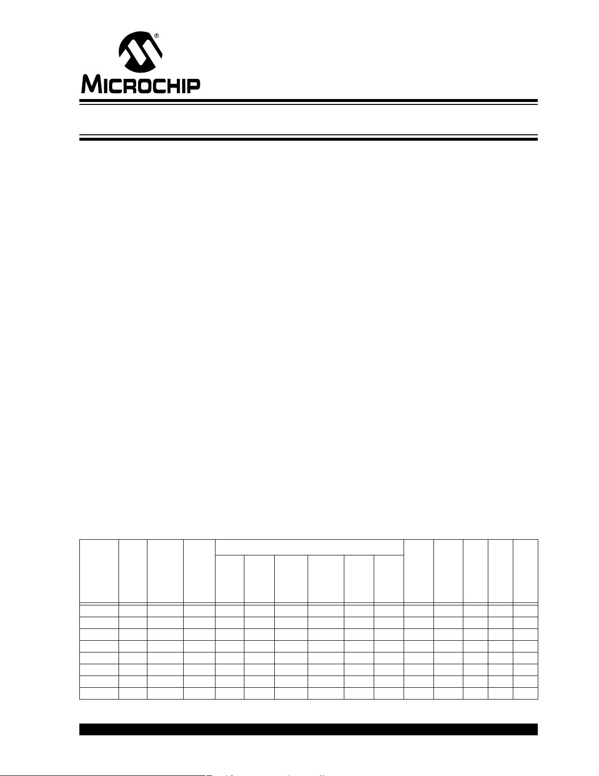
28-Pin SPDIP, SSOP, SOIC
PGD1/EMUD1/AN2/C2IN-/RP0/CN4/RB0
PGC1/EMUC1/AN3/C2IN+/RP1/CN5/RB1
AN4/C1IN-/RP2/SDA2/CN6/RB2
AN5/C1IN+/RP3/SCL2/CN7/RB3
OSCI/CLKI/CN30/RA2
OSCO/CLKO/CN29/PMA0/RA3
SOSCI/RP4/PMBE/CN1/RB4
SOSCO/T1CK/CN0/PMA1/RA4
PGD3/EMUD3/RP5/SDA1
28-Pin QFN
(1)
(1)
AN0/VREF+/CN2/RA0
AN1/V
MCLR
REF-/CN3/RA1
(2)
/CN27/x/RB5
VSS
VDD
DD
V
1
2
3
4
5
6
7
8
9
10
11
12
13
14
28
VSS
27
AN9/RP15/CN11/PMCS1/RB15
26
AN10/CV
25
24
23
22
21
20
19
18
PIC24FJXXGA002
17
16
15
REF/RTCC/RP14/CN12/PMWR/RB14
AN11/RP13/CN13/PMRD/RB13
AN12/RP12/CN14/PMD0/RB12
PGC2/EMUC2/TMS/RP11/CN15/PMD1/RB11
PGD2/EMUD2/TDI/RP10/CN16/PMD2/RB10
V
CAP/VDDCORE
DISVREG
TDO/RP9/SDA1/CN21/PMD3/RB9
TCK/RP8/SCL1/CN22/PMD4/RB8
RP7/INT0/CN23/PMD5/RB7
PGC3/EMUC3/RP6/SCL1
(2)
/CN24/PMD6/RB6
DD
V
VSS
12 13 14
/CN27/PMD7/RB5
/CN24/PMD6/RB6
(2)
(2)
PGD3/EMUD3/RP5/SDA1
PGC3/EMUC3/RP6/SCL1
REF/RTCC/RP14/CN12/PMWR/RB14
AN9/RP15/CN11/PMCS1/RB15
AN10/CV
22
232425262728
AN11/RP13/CN13/PMRD/RB13
21
AN12/RP12/CN14/PMD0/RB12
20
PGC2/EMUC2/TMS/RP11/CN15/PMD1/RB11
19
18
PGD2/EMUD2/TDI/RP10/CN16/PMD2/RB10
V
CAP/VDDCORE
17
DISVREG
16
15
TDO/RP9/SDA1/CN21/PMD3/RB9
RP7/INT0/CN23/PMD5/RB7
TCK/RP8/SCL1/CN22/PMD4/RB8
PGD1/EMUD1/AN2/C2IN-/RP0/CN4/RB0
PGC1/EMUC1/AN3/C2IN+/RP1/CN5/RB1
AN4/C1IN-/RP2/SDA2/CN6/RB2
AN5/C1IN+/RP3/SCL2/CN7/RB3
V
OSCI/CLKI/CN30/RA2
OSCO/CLKO/CN29/PMA0/RA3
1
2
3
PIC24FJXXGA002
4
SS
5
6
7
8
REF-/CN3/RA1
AN1/V
9
SOSCI/RP4/PMBE/CN1/RB4
AN0/VREF+/CN2/RA0
10 11
SOSCO/T1CK/CN0/PMA1/RA4
MCLR
VDD
Legend: RPn represents remappable peripheral pins.
Note 1: RPn pins can be configured to function as any of the following peripherals: timers, UART, input capture, output
compare, PWM, comparator digital outputs and SPI. For more information, see Section 9.4 “Peripheral Pin
Select” and the specific peripheral sections.
2: Alternative multiplexing for SDA1 and SCL1 when I2C1SEL Configuration bit is cleared.
DS39881B-page 2 Preliminary © 2007 Microchip Technology Inc.
Page 5
Pin Diagrams (Continued)
44-Pin QFN
RP9/SDA1/CN21/PMD3/RB9
RP22/CN18/PMA1/RC6
RP23/CN17/PMA0/RC7
RP24/CN20/PMA5/RC8
RP25/CN19/PMA6/RC9
PGD2/EMUD2/RP10/CN16/PMD2/RB10
PGC2/EMUC2/RP11/CN15/PMD1/RB11
AN12/RP12/CN14/PMD0/RB12
AN11/RP13/CN13/PMRD/RB13
DISVREG
V
CAP/VDDCORE
PIC24FJ64GA004 FAMILY
/CN27/PMD7/RB5
/CN24/PMD6/RB6
(2)
(2)
DD
PGD3/EMUD3/RP5/SDA1
V
RP7/INT0/CN23/PMD5/RB7
PGC3/EMUC3/RP6/SCL1
15
16
AVSS
VSSRP21/CN26/PMA3/RC5
39
17
RP8/SCL1/CN22/PMD4/RB8
4443424140
1
2
3
4
5
PIC24FJXXGA004
6
7
8
9
10
11
121314
DD
AV
TDI/PMA9/RA9
RP20/CN25/PMA4/RC4
RP19/CN28/PMBE/RC3
38
363435
37
1819202122
MCLR
SOSCO/T1CK/CN0/RA4
SOSCI/RP4/CN1/RB4
33
TDO/PMA8/RA8
32
OSCO/CLKO/CN29/RA3
31
OSCI/CLKI/CN30/RA2
30
VSS
29
28
V
DD
AN8/RP18/CN10/PMA2/RC2
27
AN7/RP17/CN9/RC1
26
AN6/RP16/CN8/RC0
25
AN5/C1IN+/RP3/SCL2/CN7/RB3
24
23
AN4/C1IN-/RP2/SDA2/CN6/RB2
REF-/CN3/RA1
TCK/PMA7/RA7
TMS/PMA10/RA10
AN9/RP15/CN11/PMCS1/RB15
REF/RTCC/RP14/CN12/PMWR/RB14
AN10/CV
REF+/CN2/RA0
AN0/V
AN1/V
PGD1/EMUD1/AN2/C2IN-/RP0/CN4/RB0
PGC1/EMUC1/AN3/C2IN+/RP1/CN5/RB1
Legend: RPn represents remappable peripheral pins.
Note 1: RPn pins can be configured to function as any of the following peripherals: timers, UART, input capture, output
compare, PWM, comparator digital outputs and SPI. For more information, see Section 9.4 “Peripheral Pin
Select” and the specific peripheral sections.
2: Alternative multiplexing for SDA1 and SCL1 when I2C1SEL Configuration bit is cleared.
© 2007 Microchip Technology Inc. Preliminary DS39881B-page 3
Page 6

PIC24FJ64GA004 FAMILY
Pin Diagrams (Continued)
44-Pin TQFP
4443424140
1
2
3
4
5
PIC24FJXXGA004
6
7
8
9
10
11
121314
15
16
38
39
37
1819202122
17
363435
33
32
31
30
29
28
27
26
25
24
23
DS39881B-page 4 Preliminary © 2007 Microchip Technology Inc.
Page 7

PIC24FJ64GA004 FAMILY
Table of Contents
1.0 Device Overview .......................................................................................................................................................................... 7
2.0 CPU ........................................................................................................................................................................................... 17
3.0 Memory Organization................................................................................................................................................................. 23
4.0 Flash Program Memory.............................................................................................................................................................. 41
5.0 Resets ........................................................................................................................................................................................ 47
6.0 Interrupt Controller ..................................................................................................................................................................... 53
7.0 Oscillator Configuration.............................................................................................................................................................. 87
8.0 Power-Saving Features.............................................................................................................................................................. 95
9.0 I/O Ports ..................................................................................................................................................................................... 97
10.0 Timer1 ...................................................................................................................................................................................... 117
11.0 Timer2/3 and Timer4/5 ............................................................................................................................................................ 119
12.0 Input Capture............................................................................................................................................................................ 125
13.0 Output Compare....................................................................................................................................................................... 127
14.0 Serial Peripheral Interface (SPI)............................................................................................................................................... 133
15.0 Inter-Integrated Circuit (I
16.0 Universal Asynchronous Receiver Transmitter (UART) ........................................................................................................... 153
17.0 Parallel Master Port (PMP)....................................................................................................................................................... 161
18.0 Real-Time Clock and Calendar (RTCC) .................................................................................................................................. 171
19.0 Programmable Cyclic Redundancy Check (CRC) Generator .................................................................................................. 181
20.0 10-bit High-Speed A/D Converter............................................................................................................................................. 185
21.0 Comparator Module.................................................................................................................................................................. 195
22.0 Comparator Voltage Reference................................................................................................................................................ 199
23.0 Special Features ...................................................................................................................................................................... 201
24.0 Development Support............................................................................................................................................................... 211
25.0 Instruction Set Summary.......................................................................................................................................................... 215
26.0 Electrical Characteristics.......................................................................................................................................................... 223
27.0 Packaging Information.............................................................................................................................................................. 237
Appendix A: Revision History............................................................................................................................................................. 245
Index ................................................................................................................................................................................................. 247
The Microchip Web Site..................................................................................................................................................................... 251
Customer Change Notification Service .............................................................................................................................................. 251
Customer Support .............................................................................................................................................................................. 251
Reader Response .............................................................................................................................................................................. 252
Product Identification System ............................................................................................................................................................ 253
2
C™) ................................................................................................................................................. 143
© 2007 Microchip Technology Inc. Preliminary DS39881B-page 5
Page 8

PIC24FJ64GA004 FAMILY
TO OUR VALUED CUSTOMERS
It is our intention to provide our valued customers with the best documentation possible to ensure successful use of your Microchip
products. To this end, we will continue to improve our publications to better suit your needs. Our publications will be refined and
enhanced as new volumes and updates are introduced.
If you have any questions or comments regarding this publication, please contact the Marketing Communications Department via
E-mail at docerrors@microchip.com or fax the Reader Response Form in the back of this data sheet to (480) 792-4150. We
welcome your feedback.
Most Current Data Sheet
To obtain the most up-to-date version of this data sheet, please register at our Worldwide Web site at:
http://www.microchip.com
You can determine the version of a data sheet by examining its literature number found on the bottom outside corner of any page.
The last character of the literature number is the version number, (e.g., DS30000A is version A of document DS30000).
Errata
An errata sheet, describing minor operational differences from the data sheet and recommended workarounds, may exist for current
devices. As device/documentation issues become known to us, we will publish an errata sheet. The errata will specify the revision
of silicon and revision of document to which it applies.
To determine if an errata sheet exists for a particular device, please check with one of the following:
• Microchip’s Worldwide Web site; http://www.microchip.com
• Your local Microchip sales office (see last page)
When contacting a sales office, please specify which device, revision of silicon and data sheet (include literature number) you are
using.
Customer Notification System
Register on our web site at www.microchip.com to receive the most current information on all of our products.
DS39881B-page 6 Preliminary © 2007 Microchip Technology Inc.
Page 9

PIC24FJ64GA004 FAMILY
1.0 DEVICE OVERVIEW
This document contains device-specific information for
the following devices:
• PIC24FJ16GA002
• PIC24FJ32GA002
• PIC24FJ48GA002
• PIC24FJ64GA002
• PIC24FJ16GA004
• PIC24FJ32GA004
• PIC24FJ48GA004
• PIC24FJ64GA004
This family introduces a new line of Microchip devices:
a 16-bit microcontroller family with a broad peripheral
feature set and enhanced computational performance.
The PIC24FJ64GA004 family offers a new migration
option for those high-performance applications which
may be outgrowing their 8-bit platforms, but don’t
require the numerical processing power of a digital
signal processor.
1.1 Core Features
1.1.1 16-BIT ARCHITECTURE
Central to all PIC24F devices is the 16-bit modified
Harvard architecture, first introduced with Microchip’s
dsPIC® digital signal controllers. The PIC24F CPU core
offers a wide range of enhancements, such as:
• 16-bit data and 24-bit address paths with the
ability to move information between data and
memory spaces
• Linear addressing of up to 12 Mbytes (program
space) and 64 Kbytes (data)
• A 16-element working register array with built-in
software stack support
• A 17 x 17 hardware multiplier with support for
integer math
• Hardware support for 32 by 16-bit division
• An instruction set that supports multiple
addressing modes and is optimized for high-level
languages such as ‘C’
• Operational performance up to 16 MIPS
1.1.2 POWER-SAVING TECHNOLOGY
All of the devices in the PIC24FJ64GA004 family
incorporate a range of features that can significantly
reduce power consumption during operation. Key
items include:
• On-the-Fly Clock Switching: The device clock
can be changed under software control to the
Timer1 source or the internal, low-power RC
oscillator during operation, allowing the user to
incorporate power-saving ideas into their software
designs.
• Doze Mode Operation: When timing-sensitive
applications, such as serial communications,
require the uninterrupted operation of peripherals,
the CPU clock speed can be selectively reduced,
allowing incremental power savings without
missing a beat.
• Instruction-Based Power-Saving Modes: The
microcontroller can suspend all operations, or
selectively shut down its core while leaving its
peripherals active, with a single instruction in
software.
1.1.3 OSCILLATOR OPTIONS AND
FEATURES
All of the devices in the PIC24FJ64GA004 family offer
five different oscillator options, allowing users a range
of choices in developing application hardware. These
include:
• Two Crystal modes using crystals or ceramic
resonators.
• Two External Clock modes offering the option of a
divide-by-2 clock output.
• A Fast Internal Oscillator (FRC) with a nominal
8 MHz output, which can also be divided under
software control to provide clock speeds as low as
31 kHz.
• A Phase Lock Loop (PLL) frequency multiplier,
available to the external oscillator modes and the
FRC oscillator, which allows clock speeds of up to
32 MHz.
• A separate internal RC oscillator (LPRC) with a
fixed 31 kHz output, which provides a low-power
option for timing-insensitive applications.
The internal oscillator block also provides a stable
reference source for the Fail-Safe Clock Monitor. This
option constantly monitors the main clock source
against a reference signal provided by the internal
oscillator and enables the controller to switch to the
internal oscillator, allowing for continued low-speed
operation or a safe application shutdown.
© 2007 Microchip Technology Inc. Preliminary DS39881B-page 7
Page 10

PIC24FJ64GA004 FAMILY
1.1.4 EASY MIGRATION
Regardless of the memory size, all devices share the
same rich set of peripherals, allowing for a smooth
migration path as applications grow and evolve.
The consistent pinout scheme used throughout the
entire family also aids in migrating to the next larger
device. This is true when moving between devices with
the same pin count, or even jumping from 28-pin to
44-pin devices.
The PIC24F family is pin-compatible with devices in the
dsPIC33 family, and shares some compatibility with the
pinout schema for PIC18 and dsPIC30. This extends
the ability of applications to grow from the relatively
simple, to the powerful and complex, yet still selecting
a Microchip device.
1.2 Other Special Features
• Communications: The PIC24FJ64GA004 family
incorporates a range of serial communication
peripherals to handle a range of application
requirements. There are two independent I
modules that support both Master and Slave
modes of operation. Devices also have, through
peripheral pin select feature, two indepen-
the
dent UARTs with built-in IrDA encoder/decoders
and two SPI modules.
• Peripheral Pin Select: The peripheral pin select
feature allows most digital peripherals to be
mapped over a fixed set of digital I/O pins. Users
may independently map the input and/or output of
any one of the many digital peripherals to any one
of the I/O pins.
• Parallel Master/Enhanced Parallel Slave Port:
One of the general purpose I/O ports can be
reconfigured for enhanced parallel data communications. In this mode, the port can be configured
for both master and slave operations, and
supports 8-bit and 16-bit data transfers with up to
16 external address lines in Master modes.
• Real-Time Clock/Calendar: This module
implements a full-featured clock and calendar with
alarm functions in hardware, freeing up timer
resources and program memory space for use of
the core application.
• 10-Bit A/D Converter: This module incorporates
programmable acquisition time, allowing for a
channel to be selected and a conversion to be
initiated without waiting for a sampling period, as
well as faster sampling speeds.
2
C
1.3 Details on Individual Family Members
Devices in the PIC24FJ64GA004 family are available
in 28-pin and 44-pin packages. The general block
diagram for all devices is shown in Figure 1-1.
The devices are differentiated from each other in two
ways:
1. Flash program memory (64 Kbytes for
PIC24FJ64GA devices, 48 Kbytes for
PIC24FJ48GA devices, 32 Kbytes for
PIC24FJ32GA devices and 16 Kbytes for
PIC24FJ16GA devices).
2. Internal SRAM memory (4k for PIC24FJ16GA
devices, 8k for all other devices in the family).
3. Available I/O pins and ports (21 pins on 2 ports
for 28-pin devices and 35 pins on 3 ports for
44-pin devices).
All other features for devices in this family are identical.
These are summarized in Table 1-1.
A list of the pin features available on the
PIC24FJ64GA004 family devices, sorted by function, is
shown in Table 1-2. Note that this table shows the pin
location of individual peripheral features and not how
they are multiplexed on the same pin. This information
is provided in the pinout diagrams in the beginning of
the data sheet. Multiplexed features are sorted by the
priority given to a feature, with the highest priority
peripheral being listed first.
DS39881B-page 8 Preliminary © 2007 Microchip Technology Inc.
Page 11
PIC24FJ64GA004 FAMILY
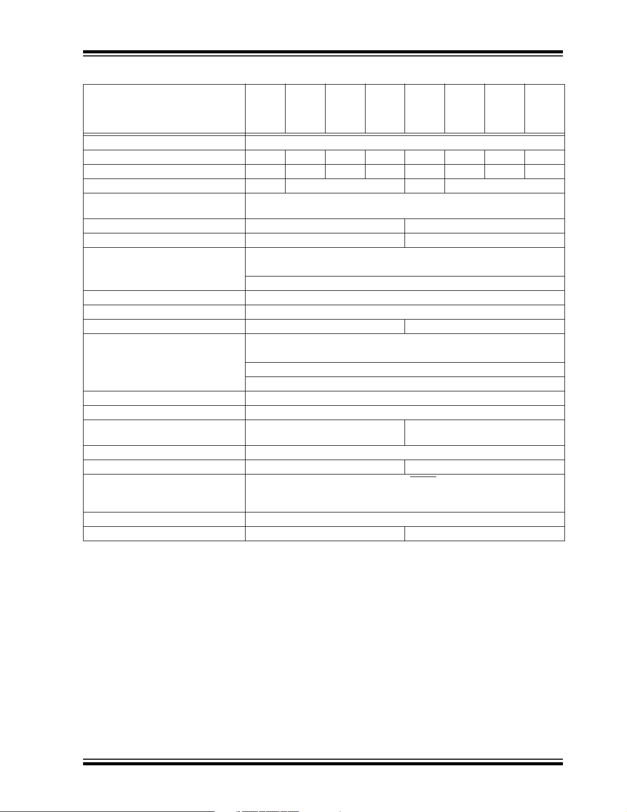
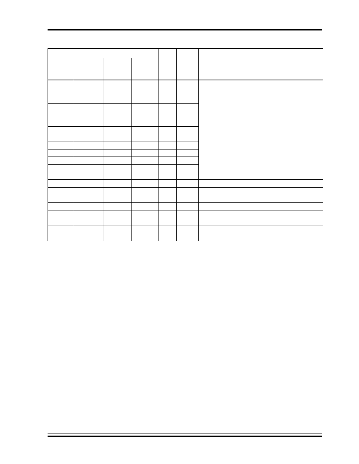
TABLE 1-1: DEVICE FEATURES FOR THE PIC24FJ64GA004 FAMILY
Features
16GA002
Operating Frequency DC – 32 MHz
Program Memory (bytes) 16K 32K 48K 64K 16K 32K 48K 64K
Program Memory (instructions) 5,504 11,008 16,512 22,016 5,504 11,008 16,512 22,016
Data Memory (bytes) 4096 8192 4096 8192
Interrupt Sources
(soft vectors/NMI traps)
I/O Ports Ports A, B Ports A, B, C
Total I/O Pins 21 35
Timers:
Total Number (16-bit) 5
32-Bit (from paired 16-bit timers) 2
Input Capture Channels 5
Output Compare/PWM Channels 5
Input Change Notification Interrupt 21 30
Serial Communications:
UART 2
SPI (3-wire/4-wire) 2
I2C™ 2
Parallel Communications (PMP/PSP) Yes
JTAG Boundary Scan Yes
10-Bit Analog-to-Digital Module
(input channels)
Analog Comparators 2
Remappable Pins 16 26
Resets (and delays) POR, BOR, RESET Instruction, MCLR
REPEAT Instruction Hardware Traps, Configuration Word Mismatch
Instruction Set 76 Base Instructions, Multiple Addressing Mode Variations
Packages 28-Pin SPDIP/SSOP/SOIC/QFN 44-Pin QFN/TQFP
Note 1: Peripherals are accessible through remappable pins.
32GA002
48GA002
10 13
(PWRT, OST, PLL Lock)
64GA002
43
(39/4)
16GA004
(1)
(1)
(1)
(1)
(1)
, WDT; Illegal Opcode,
32GA004
48GA004
64GA004
© 2007 Microchip Technology Inc. Preliminary DS39881B-page 9
Page 12

PIC24FJ64GA004 FAMILY
FIGURE 1-1: PIC24FJ64GA004 FAMILY GENERAL BLOCK DIAGRAM
OSCO/CLKO
OSCI/CLKI
DISVREG
PSV & Table
Data Access
Control Block
Address Latch
Program Memory
Data Latch
Timing
Generation
FRC/LPRC
Oscillators
Precision
Band Gap
Reference
Volt ag e
Regulator
Interrupt
Controller
23
PCU
23
Program Counter
Stac k
Control
Logic
Address Bus
Instruction
Decode &
Control
Power-up
Timer
Oscillator
Start-up Timer
Power-on
Reset
Watchdog
Timer
BOR and
(2)
LVD
8
24
Control Signals
16
PCH PCL
Repeat
Control
Logic
Data Bus
16
Inst Latch
Inst Register
Divide
Support
17x17
Multiplier
16
Data Latch
Data RAM
Address
Latch
16
Read AGU
Write AGU
EA MUX
16
Literal Data
16 x 16
W Reg Array
16-Bit ALU
16
(1)
PORTA
RA0:RA9
16
PORTB
RB0:RB15
16
(1)
PORTC
RC0:RC9
(1)
RP
RP0:RP25
16
VDDCORE/VCAP
Timer1
IC1-5
Note 1: Not all pins or features are implemented on all device pinout configurations. See Table 1-2 for I/O port pin descriptions.
2: BOR functionality is provided when the on-board voltage regulator is enabled.
3: Peripheral I/Os are accessible through remappable pins.
V
V
DD,
SS
MCLR
(3)
Timer2/3
(3)
PWM/
OC1-5
(3)
Timer4/5
CN1-22
(3)
RTCC
SPI1/2
(3)
(1)
10-Bit
ADC
I2C1/2
Comparators
UART1/2
(3)
PMP/PSP
(3)
DS39881B-page 10 Preliminary © 2007 Microchip Technology Inc.
Page 13
PIC24FJ64GA004 FAMILY
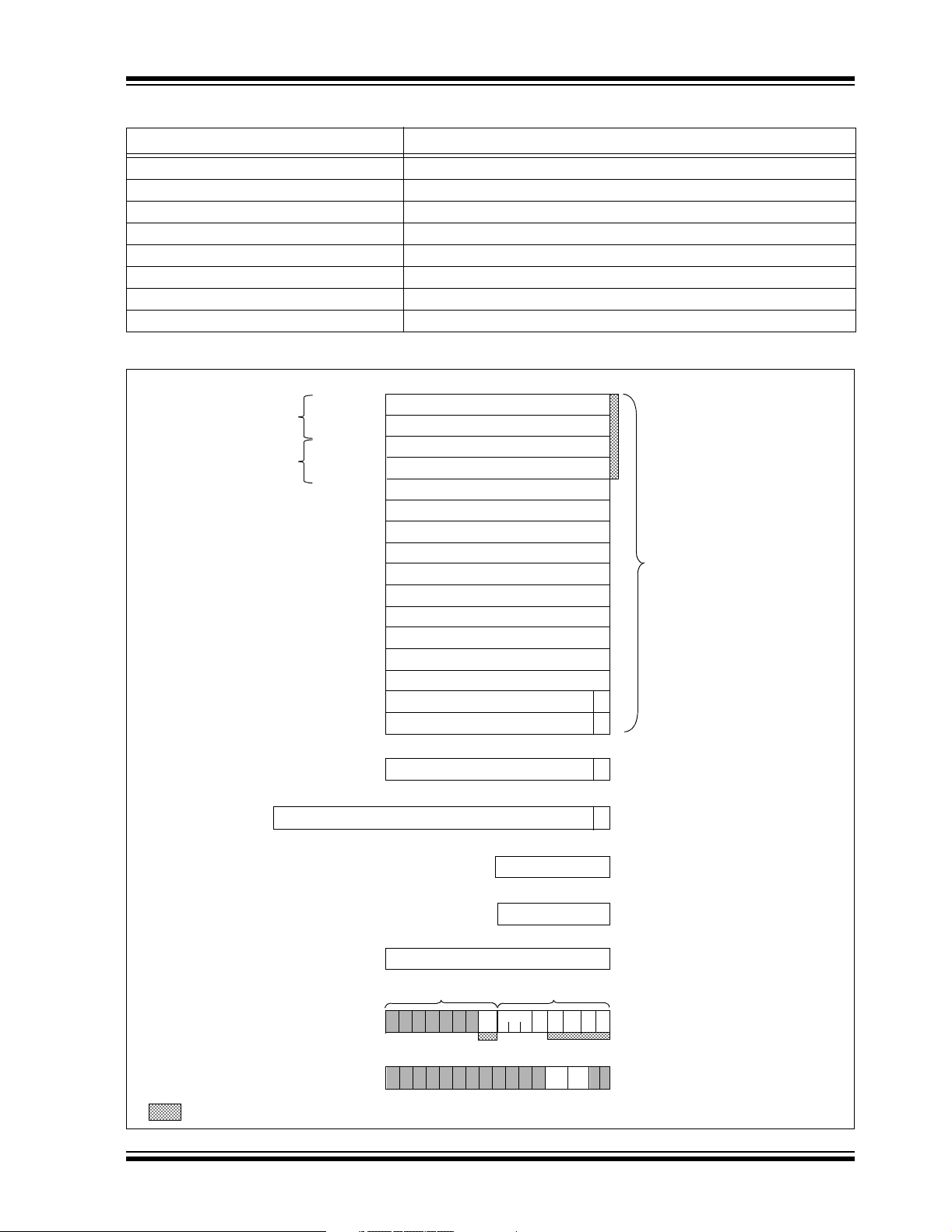
TABLE 1-2: PIC24FJ64GA004 FAMILY PINOUT DESCRIPTIONS
Pin Number
Function
AN0 2 27 19 I ANA A/D Analog Inputs.
AN1 3 28 20 I ANA
AN2 4 1 21 I ANA
AN3 5 2 22 I ANA
AN4 6 3 23 I ANA
AN5 7 4 24 I ANA
AN6 — — 25 I ANA
AN7 — — 26 I ANA
AN8 — — 27 I ANA
AN9 26 23 15 I ANA
AN10 25 22 14 I ANA
AN11 24 21 11 I ANA
AN12 23 20 10 I ANA
DD — — 17 P — Positive Supply for Analog Modules.
AV
AV
SS — — 16 P — Ground Reference for Analog Modules.
C1IN- 6 3 23 I ANA Comparator 1 Negative Input.
C1IN+ 7 4 24 I ANA Comparator 1 Positive Input.
C2IN- 4 1 21 I ANA Comparator 2 Negative Input.
C2IN+ 5 2 22 I ANA Comparator 2 Positive Input.
CLKI 9 6 30 I ANA Main Clock Input Connection.
CLKO 10 7 31 O — System Clock Output.
Legend: TTL = TTL input buffer ST = Schmitt Trigger input buffer
Note 1: Alternative multiplexing for SDA1 and SCL1 when I2C1SEL Configuration bit is cleared.
28-Pin
SPDIP/
SSOP/SOIC
ANA = Analog level input/output I
28-Pin
QFN
44-Pin
QFN/TQFP
I/O
Input
Buffer
2
C™ = I2C/SMBus input buffer
Description
© 2007 Microchip Technology Inc. Preliminary DS39881B-page 11
Page 14

PIC24FJ64GA004 FAMILY
TABLE 1-2: PIC24FJ64GA004 FAMILY PINOUT DESCRIPTIONS (CONTINUED)
Pin Number
Function
CN0 12 9 34 I ST Interrupt-on-Change Inputs.
CN1 11 8 33 I ST
CN2 2 27 19 I ST
CN3 3 28 20 I ST
CN4 4 1 21 I ST
CN5 5 2 22 I ST
CN6 6 3 23 I ST
CN7 7 4 24 I ST
CN8 — — 25 I ST
CN9 — — 26 I ST
CN10 — — 27 I ST
CN11 26 23 15 I ST
CN12 25 22 14 I ST
CN13 24 21 11 I ST
CN14 23 20 10 I ST
CN15 22 19 9 I ST
CN16 21 18 8 I ST
CN17 — — 3 I ST
CN18 — — 2 I ST
CN19 — — 5 I ST
CN20 — — 4 I ST
CN21 18 15 1 I ST
CN22 17 14 44 I ST
CN23 16 13 43 I ST
CN24 15 12 42 I ST
CN25 — — 37 I ST
CN26 — — 38 I ST
CN27 14 11 41 I ST
CN28 — — 36 I ST
CN29 10 7 31 I ST
CN30 9 6 30 I ST
REF 25 22 14 O ANA Comparator Voltage Reference Output.
CV
DISVREG 19 16 6 I ST Voltage Regulator Disable.
EMUC1 5 2 21 I/O ST In-Circuit Emulator Clock Input/Output.
EMUD1 4 1 22 I/O ST In-Circuit Emulator Data Input/Output.
EMUC2 22 19 9 I/O ST In-Circuit Emulator Clock Input/Output.
EMUD2 21 18 8 I/O ST In-Circuit Emulator Data Input/Output.
EMUC3 15 12 42 I/O ST In-Circuit Emulator Clock Input/Output.
EMUD3 14 11 41 I/O ST In-Circuit Emulator Data Input/Output.
INT0 16 13 43 I ST External Interrupt Input.
MCLR
Legend: TTL = TTL input buffer ST = Schmitt Trigger input buffer
Note 1: Alternative multiplexing for SDA1 and SCL1 when I2C1SEL Configuration bit is cleared.
28-Pin
SPDIP/
SSOP/SOIC
1 26 18 I ST Master Clear (device Reset) Input. This line is brought low
ANA = Analog level input/output I
28-Pin
QFN
44-Pin
QFN/TQFP
I/O
Input
Buffer
to cause a Reset.
2
C™ = I2C/SMBus input buffer
Description
DS39881B-page 12 Preliminary © 2007 Microchip Technology Inc.
Page 15

PIC24FJ64GA004 FAMILY
TABLE 1-2: PIC24FJ64GA004 FAMILY PINOUT DESCRIPTIONS (CONTINUED)
Pin Number
Function
OSCI 9 6 30 I ANA Main Oscillator Input Connection.
OSCO 10 7 31 O ANA Main Oscillator Output Connection.
PGC1 5 2 22 I/O ST In-Circuit Debugger and ICSP™ Programming Clock
PGD1 4 1 21 I/O ST In-Circuit Debugger and ICSP Programming Data.
PGC2 22 19 9 I/O ST In-Circuit Debugger and ICSP Programming Clock.
PGD2 21 18 8 I/O ST In-Circuit Debugger and ICSP Programming Data.
PGC3 14 12 42 I/O ST In-Circuit Debugger and ICSP Programming Clock.
PGD3 15 11 41 I/O ST In-Circuit Debugger and ICSP Programming Data.
PMA0 10 7 3 I/O ST Parallel Master Port Address Bit 0 Input (Buffered Slave
PMA1 12 9 2 I/O ST Parallel Master Port Address Bit 1 Input (Buffered Slave
PMA2 — — 27 O — Parallel Master Port Address (Demultiplexed Master
PMA3 — — 38 O —
PMA4 — — 37 O —
PMA5 — — 4 O —
PMA6 — — 5 O —
PMA7 — — 13 O —
PMA8 — — 32 O —
PMA9 — — 35 O —
PMA10 — — 12 O —
PMA11 — — — O —
PMA12 — — — O —
PMA13 — — — O —
PMBE 11 8 36 O — Parallel Master Port Byte Enable Strobe.
PMCS1 26 23 15 O — Parallel Master Port Chip Select 1 Strobe/Address Bit 14.
PMD0 23 20 10 I/O ST Parallel Master Port Data (Demultiplexed Master mode) or
PMD1 22 19 9 I/O ST
PMD2 21 18 8 I/O ST
PMD3 18 15 1 I/O ST
PMD4 17 14 44 I/O ST
PMD5 16 13 43 I/O ST
PMD6 15 12 42 I/O ST
PMD7 14 11 41 I/O ST
PMRD 24 21 11 O — Parallel Master Port Read Strobe.
PMWR 25 22 14 O — Parallel Master Port Write Strobe.
Legend: TTL = TTL input buffer ST = Schmitt Trigger input buffer
Note 1: Alternative multiplexing for SDA1 and SCL1 when I2C1SEL Configuration bit is cleared.
28-Pin
SPDIP/
SSOP/SOIC
ANA = Analog level input/output I
28-Pin
QFN
44-Pin
QFN/TQFP
I/O
Input
Buffer
modes) and Output (Master modes).
modes) and Output (Master modes).
modes).
Address/Data (Multiplexed Master modes).
2
C™ = I2C/SMBus input buffer
Description
© 2007 Microchip Technology Inc. Preliminary DS39881B-page 13
Page 16

PIC24FJ64GA004 FAMILY
TABLE 1-2: PIC24FJ64GA004 FAMILY PINOUT DESCRIPTIONS (CONTINUED)
Pin Number
Function
RA0 2 27 19 I/O ST PORTA Digital I/O.
RA1 3 28 20 I/O ST
RA2 9 6 30 I/O ST
RA3 10 7 31 I/O ST
RA4 12 9 34 I/O ST
RA7 — — 13 I/O ST
RA8 — — 32 I/O ST
RA9 — — 35 I/O ST
RA10 — — 12 I/O ST
RB0 4 1 21 I/O ST PORTB Digital I/O.
RB1 5 2 22 I/O ST
RB2 6 3 23 I/O ST
RB3 7 4 24 I/O ST
RB4 11 8 33 I/O ST
RB5 14 11 41 I/O ST
RB6 15 12 42 I/O ST
RB7 16 13 43 I/O ST
RB8 17 14 44 I/O ST
RB9 18 15 1 I/O ST
RB10 21 18 8 I/O ST
RB11 22 19 9 I/O ST
RB12 23 20 10 I/O ST
RB13 24 21 11 I/O ST
RB14 25 22 14 I/O ST
RB15 26 23 15 I/O ST
RC0 — — 25 I/O ST PORTC Digital I/O.
RC1 — — 26 I/O ST
RC2 — — 27 I/O ST
RC3 — — 36 I/O ST
RC4 — — 37 I/O ST
RC5 — — 38 I/O ST
RC6 — — 2 I/O ST
RC7 — — 3 I/O ST
RC8 — — 4 I/O ST
RC9 — — 5 I/O ST
Legend: TTL = TTL input buffer ST = Schmitt Trigger input buffer
Note 1: Alternative multiplexing for SDA1 and SCL1 when I2C1SEL Configuration bit is cleared.
28-Pin
SPDIP/
SSOP/SOIC
ANA = Analog level input/output I
28-Pin
QFN
44-Pin
QFN/TQFP
I/O
Input
Buffer
2
C™ = I2C/SMBus input buffer
Description
DS39881B-page 14 Preliminary © 2007 Microchip Technology Inc.
Page 17

PIC24FJ64GA004 FAMILY
TABLE 1-2: PIC24FJ64GA004 FAMILY PINOUT DESCRIPTIONS (CONTINUED)
Pin Number
Function
RP0 4 1 21 I/O ST Remappable Peripheral.
RP1 5 2 22 I/O ST
RP2 6 3 23 I/O ST
RP3 7 4 24 I/O ST
RP4 11 8 33 I/O ST
RP5 14 11 41 I/O ST
RP6 15 12 42 I/O ST
RP7 16 13 43 I/O ST
RP8 17 14 44 I/O ST
RP9 18 15 1 I/O ST
RP10 21 18 8 I/O ST
RP11 22 19 9 I/O ST
RP12 23 20 10 I/O ST
RP13 24 21 11 I/O ST
RP14 25 22 14 I/O ST
RP15 26 23 15 I/O ST
RP16 — — 25 I/O ST
RP17 — — 26 I/O ST
RP18 — — 27 I/O ST
RP19 — — 36 I/O ST
RP20 — — 37 I/O ST
RP21 — — 38 I/O ST
RP22 — — 2 I/O ST
RP23 — — 3 I/O ST
RP24 — — 4 I/O ST
RP25 — — 5 I/O ST
RTCC 25 22 14 O — Real-Time Clock Alarm Output.
SCL1 17, 15
SCL2 7 4 I/O I
SDA1 18, 14
SDA2 6 3 I/O I
SOSCI 11 8 33 I ANA Secondary Oscillator/Timer1 Clock Input.
SOSCO 12 9 34 O ANA Secondary Oscillator/Timer1 Clock Output.
Legend: TTL = TTL input buffer ST = Schmitt Trigger input buffer
Note 1: Alternative multiplexing for SDA1 and SCL1 when I2C1SEL Configuration bit is cleared.
28-Pin
SPDIP/
SSOP/SOIC
(1)
(1)
ANA = Analog level input/output I
28-Pin
QFN
14, 12
15, 11
(1)
(1)
44-Pin
QFN/TQFP
(1)
44, 42
(1)
1, 41
Input
I/O
Buffer
I/O I2C I2C1 Synchronous Serial Clock Input/Output.
I/O I2C I2C1 Data Input/Output.
2
C I2C2 Synchronous Serial Clock Input/Output.
2
C I2C2 Data Input/Output.
2
C™ = I2C/SMBus input buffer
Description
© 2007 Microchip Technology Inc. Preliminary DS39881B-page 15
Page 18

PIC24FJ64GA004 FAMILY
TABLE 1-2: PIC24FJ64GA004 FAMILY PINOUT DESCRIPTIONS (CONTINUED)
Pin Number
Function
T1CK 12 9 34 I ST Timer1 Clock.
TCK 17 14 13 I ST JTAG Test Clock/Programming Clock Input.
TDI 21 18 35 I ST JTAG Test Data/Programming Data Input.
TDO 18 15 32 O — JTAG Test Data Output.
TMS 22 19 12 I ST JTAG Test Mode Select Input.
DD 13, 28 10, 25 28, 40 P — Positive Supply for Peripheral Digital Logic and I/O Pins.
V
DDCAP 20 17 7 P — External Filter Capacitor Connection (regulator enabled).
V
V
DDCORE 20 17 7 P — Positive Supply for Microcontroller Core Logic (regulator
REF- 3 28 20 I ANA A/D and Comparator Reference Voltage (low) Input.
V
V
REF+ 2 27 19 I ANA A/D and Comparator Reference Voltage (high) Input.
SS 8, 27 5, 24 29, 39 P — Ground Reference for Logic and I/O Pins.
V
Legend: TTL = TTL input buffer ST = Schmitt Trigger input buffer
Note 1: Alternative multiplexing for SDA1 and SCL1 when I2C1SEL Configuration bit is cleared.
28-Pin
SPDIP/
SSOP/SOIC
ANA = Analog level input/output I
28-Pin
QFN
44-Pin
QFN/TQFP
I/O
Input
Buffer
disabled).
2
C™ = I2C/SMBus input buffer
Description
DS39881B-page 16 Preliminary © 2007 Microchip Technology Inc.
Page 19

PIC24FJ64GA004 FAMILY
2.0 CPU
The PIC24F CPU has a 16-bit (data) modified Harvard
architecture with an enhanced instruction set and a
24-bit instruction word with a variable length opcode
field. The Program Counter (PC) is 23 bits wide and
addresses up to 4M instructions of user program
memory space. A single-cycle instruction prefetch
mechanism is used to help maintain throughput and provides predictable execution. All instructions execute in a
single cycle, with the exception of instructions that
change the program flow, the double-word move
(MOV.D) instruction and the table instructions. Overhead-free program loop constructs are supported using
the REPEAT instructions, which are interruptible at any
point.
PIC24F devices have sixteen, 16-bit working registers
in the programmer’s model. Each of the working
registers can act as a data, address or address offset
register. The 16th working register (W15) operates as
a Software Stack Pointer for interrupts and calls.
The upper 32 Kbytes of the data space memory map
can optionally be mapped into program space at any
16K word boundary defined by the 8-bit Program Space
Visibility Page Address (PSVPAG) register. The program
to data space mapping feature lets any instruction
access program space as if it were data space.
The Instruction Set Architecture (ISA) has been
significantly enhanced beyond that of the PIC18, but
maintains an acceptable level of backward compatibility. All PIC18 instructions and addressing modes are
supported, either directly, or through simple macros.
Many of the ISA enhancements have been driven by
compiler efficiency needs.
The core supports Inherent (no operand), Relative,
Literal, Memory Direct and three groups of addressing
modes. All modes support Register Direct and various
Register Indirect modes. Each group offers up to seven
addressing modes. Instructions are associated with
predefined addressing modes depending upon their
functional requirements.
For most instructions, the core is capable of executing
a data (or program data) memory read, a working reg-
© 2007 Microchip Technology Inc. Preliminary DS39881B-page 17
Page 20
PIC24FJ64GA004 FAMILY
FIGURE 2-1: PIC24F CPU CORE BLOCK DIAGRAM
PSV & Table
Data Access
Control Block
Interrupt
Controller
8
23
23
23
PCU
Program Counter
Stac k
Control
Logic
16
PCH PCL
Loop
Control
Logic
Data Bus
16
16
Data Latch
Data RAM
Address
Latch
16
16
Address Latch
Program Memory
Data Latch
Address Bus
24
Instruction
Decode &
Control
Control Signals
to Various Blocks
ROM Latch
Instruction Reg
Hardware
Multiplier
Divide
Support
RAGU
WAGU
EA MUX
16
16
Literal Data
16 x 16
W Register Array
16-Bit ALU
16
16
To Peripheral Modules
DS39881B-page 18 Preliminary © 2007 Microchip Technology Inc.
Page 21
PIC24FJ64GA004 FAMILY
TABLE 2-1: CPU CORE REGISTERS
Register(s) Name Description
W0 through W15 Working Register Array
PC 23-Bit Program Counter
SR ALU STATUS Register
SPLIM Stack Pointer Limit Value Register
TBLPAG Table Memory Page Address Register
PSVPAG Program Space Visibility Page Address Register
RCOUNT Repeat Loop Counter Register
CORCON CPU Control Register
FIGURE 2-2: PROGRAMMER’S MODEL
015
Divider Working Registers
Multiplier Registers
W0 (WREG)
W1
W2
W3
W4
W5
W6
W7
W8
W9
W10
W11
W12
W13
W14
W15
Frame Pointer
Stack Pointer
Working/Address
Registers
0
SPLIM
22
PC
7
TBLPAG
7
PSVPAG
15
RCOUNT
SRH
15
———————
15 0
————————————
Registers or bits shadowed for PUSH.S and POP.S instructions.
© 2007 Microchip Technology Inc. Preliminary DS39881B-page 19
DC
IPL
210
SRL
NOVZ C
RA
IPL3 PSV
0
0
0
0
0
0
0
——
Stack Pointer Limit
Value Register
Program Counter
Table Memory Page
Address Register
Program Space Visibility
Page Address Register
Repeat Loop Counter
Register
ALU STATUS Register (SR)
CPU Control Register (CORCON)
Page 22
PIC24FJ64GA004 FAMILY
2.2 CPU Control Registers
REGISTER 2-1: SR: ALU STATUS REGISTER
U-0 U-0 U-0 U-0 U-0 U-0 U-0 R/W-0
— — — — — — —DC
bit 15 bit 8
(1)
-0
R/W
(2)
IPL2
bit 7 bit 0
Legend:
R = Readable bit W = Writable bit U = Unimplemented bit, read as ‘0’
-n = Value at POR ‘1’ = Bit is set ‘0’ = Bit is cleared x = Bit is unknown
bit 15-9 Unimplemented: Read as ‘0’
bit 8 DC: ALU Half Carry/Borrow bit
1 = A carry-out from the 4th low-order bit (for byte-sized data) or 8th low-order bit (for word-sized data)
0 = No carry-out from the 4th or 8th low-order bit of the result has occurred
bit 7-5 IPL2:IPL0: CPU Interrupt Priority Level Status bits
111 = CPU interrupt priority level is 7 (15); user interrupts disabled.
110 = CPU interrupt priority level is 6 (14)
101 = CPU Interrupt Priority Level is 5 (13)
100 = CPU interrupt priority level is 4 (12)
011 = CPU interrupt priority level is 3 (11)
010 = CPU interrupt priority level is 2 (10)
001 = CPU interrupt priority level is 1 (9)
000 = CPU interrupt priority level is 0 (8)
bit 4 RA: REPEAT Loop Active bit
1 = REPEAT loop in progress
0 = REPEAT loop not in progress
bit 3 N: ALU Negative bit
1 = Result was negative
0 = Result was non-negative (zero or positive)
bit 2 OV: ALU Overflow bit
1 = Overflow occurred for signed (2’s complement) arithmetic in this arithmetic operation
0 = No overflow has occurred
bit 1 Z: ALU Zero bit
1 = An operation which effects the Z bit has set it at some time in the past
0 = The most recent operation which effects the Z bit has cleared it (i.e., a non-zero result)
bit 0 C: ALU Carry/Borrow
1 = A carry-out from the Most Significant bit of the result occurred
0 = No carry-out from the Most Significant bit of the result occurred
(1)
R/W-0
(2)
IPL1
of the result occurred
R/W-0
IPL0
bit
(2)
(1)
R-0 R/W-0 R/W-0 R/W-0 R/W-0
RA N OV Z C
(1,2)
Note 1: The IPL Status bits are read-only when NSTDIS (INTCON1<15>) = 1.
2: The IPL Status bits are concatenated with the IPL3 bit (CORCON<3>) to form the CPU Interrupt Priority
Level (IPL). The value in parentheses indicates the IPL when IPL3 = 1.
DS39881B-page 20 Preliminary © 2007 Microchip Technology Inc.
Page 23
PIC24FJ64GA004 FAMILY
REGISTER 2-2: CORCON: CPU CONTROL REGISTER
U-0 U-0 U-0 U-0 U-0 U-0 U-0 U-0
— — — — — — — —
bit 15 bit 8
U-0 U-0 U-0 U-0 R/C-0 R/W
— — — —IPL3
bit 7 bit 0
Legend:
R = Readable bit W = Writable bit U = Unimplemented bit, read as ‘0’
-n = Value at POR ‘1’ = Bit is set ‘0’ = Bit is cleared x = Bit is unknown
bit 15-4 Unimplemented: Read as ‘0’
bit 3 IPL3: CPU Interrupt Priority Level Status bit
1 = CPU interrupt priority level is greater than 7
0 = CPU interrupt priority level is 7 or less
bit 2 PSV: Program Space Visibility in Data Space Enable bit
1 = Program space visible in data space
0 = Program space not visible in data space
bit 1-0 Unimplemented: Read as ‘0’
Note 1: User interrupts are disabled when IPL3 = 1.
2.3 Arithmetic Logic Unit (ALU)
The PIC24F ALU is 16 bits wide and is capable of addition, subtraction, bit shifts and logic operations. Unless
otherwise mentioned, arithmetic operations are 2’s
complement in nature. Depending on the operation, the
ALU may affect the values of the Carry (C), Zero (Z),
Negative (N), Overflow (OV) and Digit Carry (DC)
Status bits in the SR register. The C and DC Status bits
operate as Borrow
for subtraction operations.
The ALU can perform 8-bit or 16-bit operations,
depending on the mode of the instruction that is used.
Data for the ALU operation can come from the W
register array, or data memory, depending on the
addressing mode of the instruction. Likewise, output
data from the ALU can be written to the W register array
or a data memory location.
and Digit Borrow bits, respectively,
(1)
(1)
The PIC24F CPU incorporates hardware support for
both multiplication and division. This includes a dedicated hardware multiplier and support hardware for
16-bit divisor division.
2.3.1 MULTIPLIER
The ALU contains a high-speed, 17-bit x 17-bit
multiplier. It supports unsigned, signed or mixed sign
operation in several multiplication modes:
1. 16-bit x 16-bit signed
2. 16-bit x 16-bit unsigned
3. 16-bit signed x 5-bit (literal) unsigned
4. 16-bit unsigned x 16-bit unsigned
5. 16-bit unsigned x 5-bit (literal) unsigned
6. 16-bit unsigned x 16-bit signed
7. 8-bit unsigned x 8-bit unsigned
-0 U-0 U-0
PSV — —
© 2007 Microchip Technology Inc. Preliminary DS39881B-page 21
Page 24

PIC24FJ64GA004 FAMILY
2.3.2 DIVIDER
The divide block supports 32-bit/16-bit and 16-bit/16-bit
signed and unsigned integer divide operations with the
following data sizes:
1. 32-bit signed/16-bit signed divide
2. 32-bit unsigned/16-bit unsigned divide
3. 16-bit signed/16-bit signed divide
4. 16-bit unsigned/16-bit unsigned divide
The quotient for all divide instructions ends up in W0
and the remainder in W1. Sixteen-bit signed and
unsigned DIV instructions can specify any W register
for both the 16-bit divisor (Wn), and any W register
(aligned) pair (W(m + 1):Wm) for the 32-bit dividend.
The divide algorithm takes one cycle per bit of divisor,
so both 32-bit/16-bit and 16-bit/16-bit instructions take
the same number of cycles to execute.
2.3.3 MULTI-BIT SHIFT SUPPORT
The PIC24F ALU supports both single bit and
single-cycle, multi-bit arithmetic and logic shifts.
Multi-bit shifts are implemented using a shifter block,
capable of performing up to a 15-bit arithmetic right
shift, or up to a 15-bit left shift, in a single cycle. All
multi-bit shift instructions only support Register Direct
Addressing for both the operand source and result
destination.
A full summary of instructions that use the shift
operation is provided below in Table 2-2.
TABLE 2-2: INSTRUCTIONS THAT USE THE SINGLE AND MULTI-BIT SHIFT OPERATION
Instruction Description
ASR Arithmetic shift right source register by one or more bits.
SL Shift left source register by one or more bits.
LSR Logical shift right source register by one or more bits.
DS39881B-page 22 Preliminary © 2007 Microchip Technology Inc.
Page 25
PIC24FJ64GA004 FAMILY
3.0 MEMORY ORGANIZATION
from either the 23-bit Program Counter (PC) during program execution, or from table operation or data space
As Harvard architecture devices, PIC24F microcontrollers feature separate program and data memory
spaces and busses. This architecture also allows the
direct access of program memory from the data space
during code execution.
3.1 Program Address Space
The program address memory space of
PIC24FJ64GA004 family devices is 4M instructions.
The space is addressable by a 24-bit value derived
remapping, as described in Section 3.3 “Interfacing
Program and Data Memory Spaces”.
User access to the program memory space is restricted
to the lower half of the address range (000000h to
7FFFFFh). The exception is the use of TBLRD/TBLWT
operations which use TBLPAG<7> to permit access to
the Configuration bits and device ID sections of the
configuration memory space.
Memory maps for the PIC24FJ64GA004 family of
devices are shown in Figure 3-1.
FIGURE 3-1: PROGRAM SPACE MEMORY MAP FOR PIC24FJ64GA004 FAMILY DEVICES
PIC24FJ16GA
GOTO Instruction
Reset Address
Interrupt Vector Table
Reserved
Alternate Vector Table
User Flash
Program Memory
(5.5K instructions)
Flash Config Words
PIC24FJ32GA
GOTO Instruction
Reset Address
Interrupt Vector Table
Reserved
Alternate Vector Table
User Flash
Program Memory
(11K instructions)
PIC24FJ48GA
GOTO Instruction
Reset Address
Interrupt Vector Table
Reserved
Alternate Vector Table
User Flash
Program Memory
(16K instructions)
PIC24FJ64GA
GOTO Instruction
Reset Address
Interrupt Vector Table
Reserved
Alternate Vector Table
User Flash
Program Memory
(22K instructions)
000000h
000002h
000004h
0000FEh
000100h
000104h
0001FEh
000200h
002BFEh
002C00h
User Memory Space
Unimplemented
Read ‘0’
Reserved
Device Config Registers
Reserved
Configuration Memory Space
DEVID (2)
Flash Config Words
Unimplemented
Read ‘0’
Reserved
Device Config Registers
Reserved
DEVID (2)
Flash Config Words
Unimplemented
Read ‘0’
Reserved
Device Config Registers
Reserved
DEVID (2)
Flash Config Words
Unimplemented
Read ‘0’
Reserved
Device Config Registers
Reserved
DEVID (2)
0057FEh
005800h
0083FEh
008400h
00ABFEh
00AC00h
7FFFFFh
800000h
F7FFFEh
F80000h
F8000Eh
F80010h
FEFFFEh
FF0000h
FFFFFFh
Note: Memory areas are not shown to scale.
© 2007 Microchip Technology Inc. Preliminary DS39881B-page 23
Page 26
PIC24FJ64GA004 FAMILY
3.1.1 PROGRAM MEMORY ORGANIZATION
The program memory space is organized in
word-addressable blocks. Although it is treated as
24 bits wide, it is more appropriate to think of each
address of the program memory as a lower and upper
word, with the upper byte of the upper word being
unimplemented. The lower word always has an even
address, while the upper word has an odd address
(Figure 3-2).
Program memory addresses are always word-aligned
on the lower word, and addresses are incremented or
decremented by two during code execution. This
arrangement also provides compatibility with data
memory space addressing and makes it possible to
access data in the program memory space.
3.1.2 HARD MEMORY VECTORS
All PIC24F devices reserve the addresses between
00000h and 000200h for hard coded program execution vectors. A hardware Reset vector is provided to
redirect code execution from the default value of the
PC on device Reset to the actual start of code. A GOTO
instruction is programmed by the user at 000000h, with
the actual address for the start of code at 000002h.
PIC24F devices also have two interrupt vector tables,
located from 000004h to 0000FFh and 000100h to
0001FFh. These vector tables allow each of the many
device interrupt sources to be handled by separate
ISRs. A more detailed discussion of the interrupt vector
tables is provided in Section 6.1 “Interrupt Vector
Tabl e”.
3.1.3 FLASH CONFIGURATION WORDS
In PIC24FJ64GA004 family devices, the top two words
of on-chip program memory are reserved for configuration information. On device Reset, the configuration
information is copied into the appropriate Configuration
registers. The addresses of the Flash Configuration
Word for devices in the PIC24FJ64GA004 family are
shown in Table 3-1. Their location in the memory map
is shown with the other memory vectors in Figure 3-1.
The Configuration Words in program memory are a
compact format. The actual Configuration bits are
mapped in several different registers in the configuration
memory space. Their order in the Flash Configuration
Words do not reflect a corresponding arrangement in the
configuration space. Additional details on the device
Configuration Words are provided in Section 23.1
“Configuration Bits”.
TABLE 3-1: FLASH CONFIGURATION
WORDS FOR PIC24FJ64GA004
FAMILY DEVICES
Program
Device
PIC24FJ16GA 5.5
PIC24FJ32GA 11
PIC24FJ48GA 16
PIC24FJ64GA 22
Memory
(K words)
Configuration
Word
Addresses
002BFCh:
002BFEh
0057FCh:
0057FEh
0083FCh:
0083FEh
00ABFCh:
00ABFEh
FIGURE 3-2: PROGRAM MEMORY ORGANIZATION
msw
Address (lsw Address)
000001h
000003h
000005h
000007h
DS39881B-page 24 Preliminary © 2007 Microchip Technology Inc.
most significant word
23
00000000
00000000
00000000
00000000
Program Memory
‘Phantom’ Byte
(read as ‘0’)
least significant word
Instruction Width
PC Address
0816
000000h
000002h
000004h
000006h
Page 27
PIC24FJ64GA004 FAMILY
3.2 Data Address Space
The PIC24F core has a separate, 16-bit wide data memory space, addressable as a single linear range. The
data space is accessed using two Address Generation
Units (AGUs), one each for read and write operations.
The data space memory map is shown in Figure 3-3.
All Effective Addresses (EAs) in the data memory space
are 16 bits wide and point to bytes within the data space.
This gives a data space address range of 64 Kbytes or
32K words. The lower half of the data memory space
(that is, when EA<15> = 0) is used for implemented
memory addresses, while the upper half (EA<15> = 1) is
reserved for the program space visibility area (see
Section 3.3.3 “Reading Data from Program Memory
Using Program Space Visibility”).
PIC24FJ64GA family devices implement a total of
8 Kbytes of data memory. Should an EA point to a
location outside of this area, an all zero word or byte will
be returned.
3.2.1 DATA SPACE WIDTH
The data memory space is organized in
byte-addressable, 16-bit wide blocks. Data is aligned
in data memory and registers as 16-bit words, but all
data space EAs resolve to bytes. The Least Significant
Bytes of each word have even addresses, while the
Most Significant Bytes have odd addresses.
FIGURE 3-3: DATA SPACE MEMORY MAP FOR PIC24FJ64GA004 FAMILY DEVICES
LSB
Address
0000h
07FEh
0800h
1FFEh
2000h
27FEh
2800h
SFR
Space
Near
Data Space
(2)
Implemented
Data RAM
MSB
Address
0001h
07FFh
0801h
1FFFh
2001h
27FFh
2801h
LSBMSB
SFR Space
Data RAM
(2)
(1)
Unimplemented
Read as ‘0’
7FFFh
8001h
Program Space
Visibility Area
FFFFh
Note 1: Data memory areas are not shown to scale.
2: Upper memory limit for PIC24FJ16GAXXX devices is 17FFh.
7FFFh
8000h
FFFEh
© 2007 Microchip Technology Inc. Preliminary DS39881B-page 25
Page 28
PIC24FJ64GA004 FAMILY
3.2.2 DATA MEMORY ORGANIZATION AND ALIGNMENT
To maintain backward compatibility with PIC
and improve data space memory usage efficiency, the
PIC24F instruction set supports both word and byte
operations. As a consequence of byte accessibility, all
effective address calculations are internally scaled to
step through word-aligned memory. For example, the
core recognizes that Post-Modified Register Indirect
Addressing mode [Ws++] will result in a value of Ws + 1
for byte operations and Ws + 2 for word operations.
Data byte reads will read the complete word which contains the byte, using the LSb of any EA to determine
which byte to select. The selected byte is placed onto
the LSB of the data path. That is, data memory and registers are organized as two parallel, byte-wide entities
with shared (word) address decode but separate write
lines. Data byte writes only write to the corresponding
side of the array or register which matches the byte
address.
All word accesses must be aligned to an even address.
Misaligned word data fetches are not supported, so
care must be taken when mixing byte and word operations, or translating from 8-bit MCU code. If a
misaligned read or write is attempted, an address error
trap will be generated. If the error occurred on a read,
the instruction underway is completed; if it occurred on
a write, the instruction will be executed but the write will
not occur. In either case, a trap is then executed, allowing the system and/or user to examine the machine
state prior to execution of the address Fault.
All byte loads into any W register are loaded into the
Least Significant Byte. The Most Significant Byte is not
modified.
®
devices
A sign-extend instruction (SE) is provided to allow
users to translate 8-bit signed data to 16-bit signed
values. Alternatively, for 16-bit unsigned data, users
can clear the MSB of any W register by executing a
zero-extend (ZE) instruction on the appropriate
address.
Although most instructions are capable of operating on
word or byte data sizes, it should be noted that some
instructions operate only on words.
3.2.3 NEAR DATA SPACE
The 8-Kbyte area between 0000h and 1FFFh is
referred to as the near data space. Locations in this
space are directly addressable via a 13-bit absolute
address field within all memory direct instructions. The
remainder of the data space is addressable indirectly.
Additionally, the whole data space is addressable using
MOV instructions, which support Memory Direct
Addressing with a 16-bit address field.
3.2.4 SFR SPACE
The first 2 Kbytes of the near data space, from 0000h
to 07FFh, are primarily occupied with Special Function
Registers (SFRs). These are used by the PIC24F core
and peripheral modules for controlling the operation of
the device.
SFRs are distributed among the modules that they control and are generally grouped together by module.
Much of the SFR space contains unused addresses;
these are read as ‘0’. A diagram of the SFR space,
showing where SFRs are actually implemented, is
shown in Table 3-2. Each implemented area indicates
a 32-byte region where at least one address is implemented as an SFR. A complete listing of implemented
SFRs, including their addresses, is shown in Tables 3-3
through 3-24.
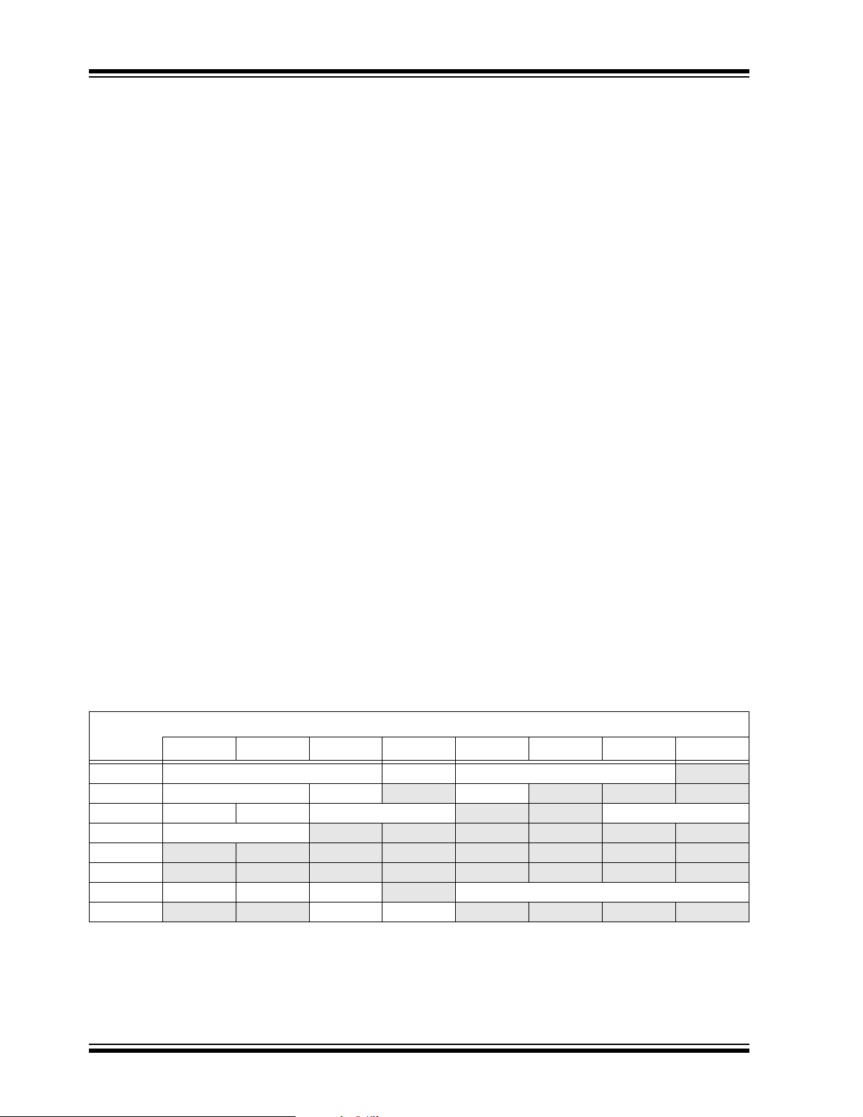
TABLE 3-2: IMPLEMENTED REGIONS OF SFR DATA SPACE
SFR Space Address
xx00 xx20 xx40 xx60 xx80 xxA0 xxC0 xxE0
000h Core ICN Interrupts
100h Timers Capture
2
200h I
300h A/D — — — — — —
400h
500h
600h PMP RTC/Comp CRC — PPS
700h
Legend: — = No implemented SFRs in this block
DS39881B-page 26 Preliminary © 2007 Microchip Technology Inc.
C™ UART SPI — — I/O
— — — — — — — —
— — — — — — — —
— — System NVM/PMD — — — —
— Compare — — —
—
Page 29
PIC24FJ64GA004 FAMILY
All
All
0000
0000
0000
Resets
Resets
0000
CN16IE
CN16PUE
(1)
(1)
CN17IE
CN17PUE
(1)
(1)
CN18IE
CN18PUE
(1)
(1)
CN19IE
CN19PUE
(1)
(1)
— — — — — — — — Program Counter High Byte Register 0000
— — — — — — — — Table Memory Page Address Register 0000
— — — — — — — — Program Space Visibility Page Address Register 0000
— — — — — — — DC IPL2 IPL1 IPL0 RA N OV Z C 0000
— — — — — — — — — — — — IPL3 PSV — — 0000
— — Disable Interrupts Counter Register xxxx
CN7IE CN6IE CN5IE CN4IE CN3IE CN2IE CN1IE CN0IE
CN7PUE CN6PUE CN5PUE CN4PUE CN3PUE CN2PUE CN1PUE CN0PUE
(1)
(1)
CN24IE CN23IE CN22IE CN21IE CN20IE
CN8IE
(1)
CN9IE
(1)
CN24PUE CN23PUE CN22PUE CN21PUE CN20PUE
CN8PUE
(1)
(1)
(1)
CN25IE
CN9PUE
CN25PUE
(1)
(1)
(1)
CN27IE CN26IE
CN27PUE CN26PUE
(1)
(1)
CN30IE CN29IE CN28IE
CN30PUE CN29PUE CN28PUE
CN15IE CN14IE CN13IE CN12IE CN11IE CN10IE
AddrBit 15Bit 14Bit 13Bit 12Bit 11Bit 10Bit 9Bit 8Bit 7Bit 6Bit 5Bit 4Bit 3Bit 2Bit 1Bit 0
CN15PUE CN14PUE CN13PUE CN12PUE CN11PUE CN10PUE
Addr Bit 15 Bit 14 Bit 13 Bit 12 Bit 11 Bit 10 Bit 9 Bit 8 Bit 7 Bit 6 Bit 5 Bit 4 Bit 3 Bit 2 Bit 1 Bit 0
File
Name
WREG0 0000 Working Register 0 0000
WREG1 0002 Working Register 1 0000
WREG2 0004 Working Register 2 0000
WREG3 0006 Working Register 3 0000
WREG4 0008 Working Register 4 0000
WREG5 000A Working Register 5 0000
WREG6 000C Working Register 6 0000
WREG7 000E Working Register 7 0000
WREG8 0010 Working Register 8 0000
WREG9 0012 Working Register 9 0000
WREG10 0014 Working Register 10 0000
WREG11 0016 Working Register 11 0000
WREG12 0018 Working Register 12 0000
WREG13 001A Working Register 13 0000
WREG14 001C Working Register 14 0000
WREG15 001E Working Register 15 0800
TABLE 3-3: CPU CORE REGISTERS MAP
SPLIM 0020 Stack Pointer Limit Value Register xxxx
PCL 002E Program Counter Low Byte Register 0000
TBLPAG 0032
PSVPAG 0034
PCH 0030
RCOUNT 0036 Repeat Loop Counter Register xxxx
CORCON 0044
Legend: — = unimplemented, read as ‘0’. Reset values are shown in hexadecimal.
DISICNT 0052
SR 0042
File
Name
CNEN1 0060
CNEN2 0062 —
CNPU1 0068
CNPU2 006A —
TABLE 3-4: ICN REGISTER MAP
Legend: — = unimplemented, read as ‘0’. Reset values are shown in hexadecimal.
© 2007 Microchip Technology Inc. Preliminary DS39881B-page 27
Note 1: Bits not available on 28-pin devices; read as ‘0’.
Page 30
PIC24FJ64GA004 FAMILY
All
Resets
— — — — INT1IF CNIF CMIF MI2C1IF SI2C1IF 0000
— — — — — — — — — — — INT2EP INT1EP INT0EP 0000
— — — — — — — — — — MATHERR ADDRERR STKERR OSCFAIL — 0000
— — AD1IF U1TXIF U1RXIF SPI1IF SPF1IF T3IF T2IF OC2IF IC2IF — T1IF OC1IF IC1IF INT0IF 0000
— —PMPIF— — —OC5IF— IC5IF IC4IF IC3IF — — — SPI2IF SPF2IF 0000
—RTCIF— — — — — — — — — — —MI2C2IFSI2C2IF— 0000
Addr Bit 15 Bit 14 Bit 13 Bit 12 Bit 11 Bit 10 Bit 9 Bit 8 Bit 7 Bit 6 Bit 5 Bit 4 Bit 3 Bit 2 Bit 1 Bit 0
— — — — — — —LVDIF— — — — CRCIF U2ERIF U1ERIF — 0000
— — AD1IE U1TXIE U1RXIE SPI1IE SPF1IE T3IE T2IE OC2IE IC2IE — T1IE OC1IE IC1IE INT0IE 0000
— — — — INT1IE CNIE CMIE MI2C1IE SI2C1IE 0000
— —PMPIE— — —OC5IE— IC5IE IC4IE IC3IE — — — SPI2IE SPF2IE 0000
—RTCIE— — — — — — — — — — — MI2C2IE SI2C2IE — 0000
— — — — — — —LVDIE— — — — CRCIE U2ERIE U1ERIE — 0000
— T1IP2 T1IP1 T1IP0 — OC1IP2 OC1IP1 OC1IP0 — IC1IP2 IC1IP1 IC1IP0 — INT0IP2 INT0IP1 INT0IP0 4444
— T2IP2 T2IP1 T2IP0 — OC2IP2 OC2IP1 OC2IP0 — IC2IP2 IC2IP1 IC2IP0 — — — — 4444
— U1RXIP2 U1RXIP1 U1RXIP0 — SPI1IP2 SPI1IP1 SPI1IP0 — SPF1IP2 SPF1IP1 SPF1IP0 — T3IP2 T3IP1 T3IP0 4444
— — — — — — — — — AD1IP2 AD1IP1 AD1IP0 — U1TXIP2 U1TXIP1 U1TXIP0 4444
— CNIP2 CNIP1 CNIP0 — CMIP2 CMIP1 CMIP0 — MI2C1P2 MI2C1P1 MI2C1P0 — SI2C1P2 SI2C1P1 SI2C1P0 4444
— — — — — — — — — — — — — INT1IP2 INT1IP1 INT1IP0 4444
— T4IP2 T4IP1 T4IP0 — OC4IP2 OC4IP1 OC4IP0 — OC3IP2 OC3IP1 OC3IP0 — — — — 4444
— U2TXIP2 U2TXIP1 U2TXIP0 — U2RXIP2 U2RXIP1 U2RXIP0 — INT2IP2 INT2IP1 INT2IP0 — T5IP2 T5IP1 T5IP0 4444
— — — — — — — — — SPI2IP2 SPI2IP1 SPI2IP0 — SPF2IP2 SPF2IP1 SPF2IP0 4444
— IC5IP2 IC5IP1 IC5IP0 — IC4IP2 IC4IP1 IC4IP0 — IC3IP2 IC3IP1 IC3IP0 — — — — 4444
— — — — — — — — — OC5IP2 OC5IP1 OC5IP0 — — — — 4444
— — — — — — — — — PMPIP2 PMPIP1 PMPIP0 — — — — 4444
— — — — — MI2C2P2 MI2C2P1 MI2C2P0 — SI2C2P2 SI2C2P1 SI2C2P0 — — — — 4444
— — — — — RTCIP2RTCIP1RTCIP0 — — — — — — — — 4444
— CRCIP2 CRCIP1 CRCIP0 — U2ERIP2 U2ERIP1 U2ERIP0 — U1ERIP2 U1ERIP1 U1ERIP0 — — — — 4444
— — — — — — — — — — — — — LVDIP2 LVDIP1 LVDIP0 4444
File
Name
INTCON1 0080 NSTDIS
INTCON2 0082 ALTIVT DISI
IFS1 0086 U2TXIF U2RXIF INT2IF T5IF T4IF OC4IF OC3IF
TABLE 3-5: INTERRUPT CONTROLLER REGISTER MAP
IFS0 0084
IFS4 008C
IEC0 0094
IFS3 008A
IFS2 0088
IEC1 0096 U2TXIE U2RXIE INT2IE T5IE T4IE OC4IE OC3IE
IEC4 009C
IPC0 00A4
IEC3 009A
IEC2 0098
IPC2 00A8
IPC1 00A6
IPC3 00AA
IPC4 00AC
IPC7 00B2
IPC5 00AE
IPC6 00B0
IPC10 00B8
IPC11 00BA
IPC12 00BC
IPC15 00C2
IPC16 00C4
IPC8 00B4
IPC9 00B6
IPC18 00C8
Legend: — = unimplemented, read as ‘0’. Reset values are shown in hexadecimal.
DS39881B-page 28 Preliminary © 2007 Microchip Technology Inc.
Page 31

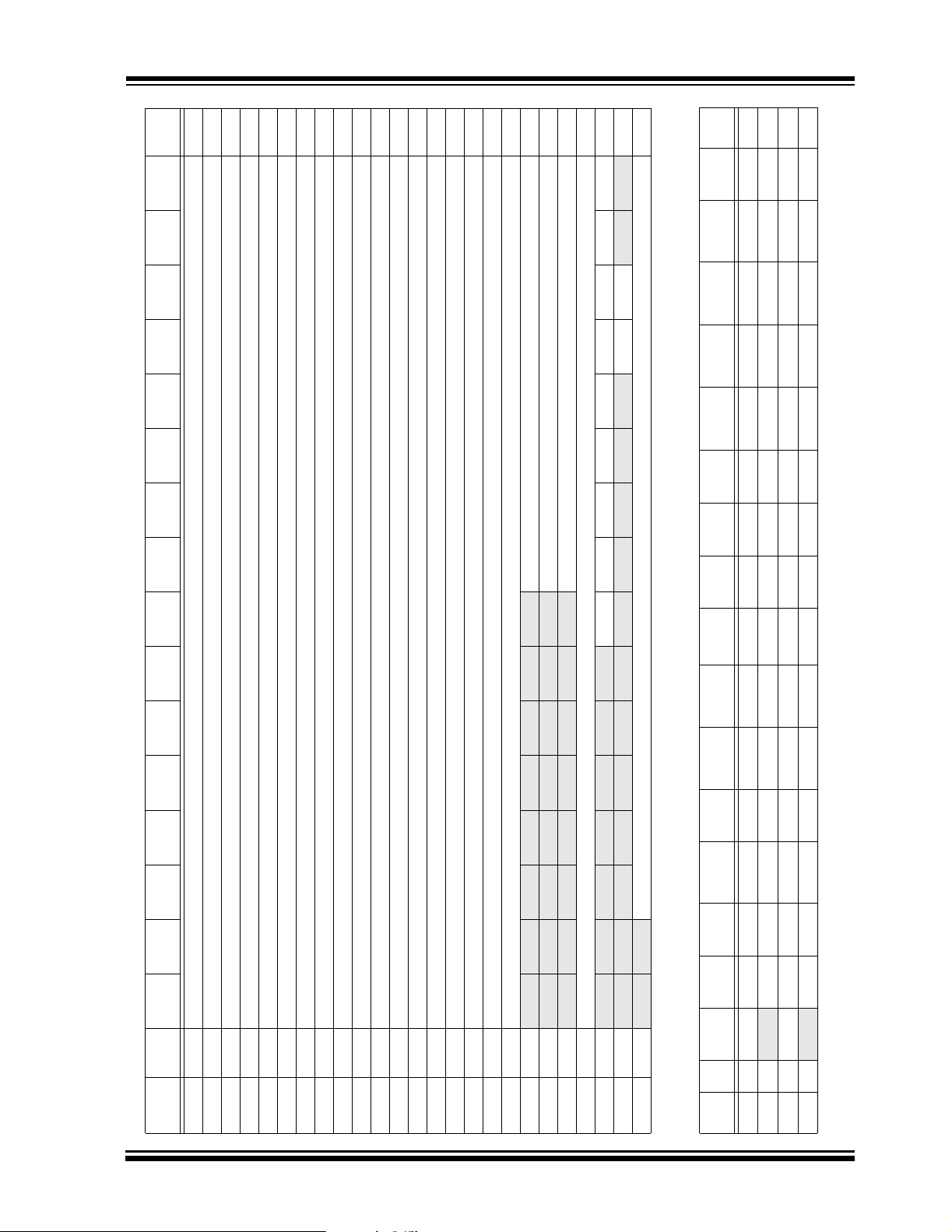
PIC24FJ64GA004 FAMILY
All
Resets
All
Resets
—TSIDL— — — — — — TGATE TCKPS1 TCKPS0 — TSYNC TCS — 0000
—TSIDL— — — — — — TGATE TCKPS1 TCKPS0 T32 —TCS— 0000
—TSIDL— — — — — — TGATE TCKPS1 TCKPS0 — —TCS— 0000
—TSIDL— — — — — — TGATE TCKPS1 TCKPS0 T32 —TCS— 0000
—TSIDL— — — — — — TGATE TCKPS1 TCKPS0 — —TCS— 0000
— —ICSIDL— — — — — ICTMR ICI1 ICI0 ICOV ICBNE ICM2 ICM1 ICM0 0000
— —ICSIDL— — — — — ICTMR ICI1 ICI0 ICOV ICBNE ICM2 ICM1 ICM0 0000
— —ICSIDL— — — — — ICTMR ICI1 ICI0 ICOV ICBNE ICM2 ICM1 ICM0 0000
— —ICSIDL— — — — — ICTMR ICI1 ICI0 ICOV ICBNE ICM2 ICM1 ICM0 0000
— —ICSIDL— — — — — ICTMR ICI1 ICI0 ICOV ICBNE ICM2 ICM1 ICM0 0000
File
TABLE 3-6: TIMER REGISTER MAP
Addr Bit 15 Bit 14 Bit 13 Bit 12 Bit 11 Bit 10 Bit 9 Bit 8 Bit 7 Bit 6 Bit 5 Bit 4 Bit 3 Bit 2 Bit 1 Bit 0
Name
TMR1 0100 Timer1 Register 0000
PR1 0102 Timer1 Period Register FFFF
T1CON 0104 TON
TMR2 0106 Timer2 Register 0000
TMR3H 0108 Timer3 Holding Register (for 32-bit timer operations only) 0000
TMR3 010A Timer 3 Register 0000
PR2 010C Timer2 Period Register FFFF
PR3 010E Timer3 Period Register FFFF
T2CON 0110 TON
T3CON 0112 TON
TMR4 0114 Timer4 Register 0000
TMR5H 0116 Timer5 Holding Register (for 32-bit operations only) 0000
TMR5 0118 Timer5 Register 0000
PR4 011A Timer4 Period Register FFFF
PR5 011C Timer5 Period Register FFFF
T4CON 011E TON
T5CON 0120 TON
Legend: — = unimplemented, read as ‘0’. Reset values are shown in hexadecimal.
Addr Bit 15 Bit 14 Bit 13 Bit 12 Bit 11 Bit 10 Bit 9 Bit 8 Bit 7 Bit 6 Bit 5 Bit 4 Bit 3 Bit 2 Bit 1 Bit 0
File
Name
IC1BUF 0140 Input 1 Capture Register FFFF
IC1CON 0142
IC2BUF 0144 Input 2 Capture Register FFFF
IC2CON 0146
IC3BUF 0148 Input 3 Capture Register FFFF
IC3CON 014A
IC4BUF 014C Input 4 Capture Register FFFF
IC4CON 014E
IC5BUF 0150 Input 5 Capture Register FFFF
IC5CON 0152
TABLE 3-7: INPUT CAPTURE REGISTER MAP
Legend: — = unimplemented, read as ‘0’. Reset values are shown in hexadecimal.
© 2007 Microchip Technology Inc. Preliminary DS39881B-page 29
Page 32
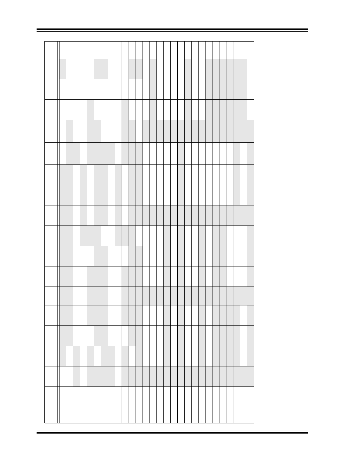
PIC24FJ64GA004 FAMILY
All
All
Resets
Resets
— —OCSIDL— — — — — — — — OCFLT OCTSEL OCM2 OCM1 OCM0 0000
— —OCSIDL— — — — — — — — OCFLT OCTSEL OCM2 OCM1 OCM0 0000
— —OCSIDL— — — — — — — — OCFLT OCTSEL OCM2 OCM1 OCM0 0000
— —OCSIDL— — — — — — — — OCFLT OCTSEL OCM2 OCM1 OCM0 0000
— —OCSIDL— — — — — — — — OCFLT OCTSEL OCM2 OCM1 OCM0 0000
C™ REGISTER MAP
2
— — — BCL GCSTAT ADD10 IWCOL I2COV D/A PSR/WRBF TBF 0000
— I2CSIDL SCLREL IPMIEN A10M DISSLW SMEN GCEN STREN AKDT ACKEN RCEN PEN RSEN SEN 1000
— — — — — — — — Receive Register 1 0000
— — — — — — — — Transmit Register 1 00FF
— — — — — — — Baud Rate Generator Register 1 0000
— — — — — — Address Register 1 0000
— — — — — — AMSK9 AMSK8 AMSK7 AMSK6 AMSK5 AMSK4 AMSK3 AMSK2 AMSK1 AMSK‘ 0000
— — — — — — — — Receive Register 2 0000
— — — — — — — — Transmit Register 2 00FF
— — — BCL GCSTAT ADD10 IWCOL I2COV D/A PSR/WRBF TBF 0000
— I2CSIDL SCLREL IPMIEN A10M DISSLW SMEN GCEN STREN ACKDT ACKEN RCEN PEN RSEN SEN 1000
— — — — — — — Baud Rate Generator Register 2 0000
— — — — — — Address Register 2 0000
— — — — — — AMSK9 AMSK8 AMSK7 AMSK6 AMSK5 AMSK4 AMSK3 AMSK2 AMSK1 AMSK‘ 0000
Addr Bit 15 Bit 14 Bit 13 Bit 12 Bit 11 Bit 10 Bit 9 Bit 8 Bit 7 Bit 6 Bit 5 Bit 4 Bit 3 Bit 2 Bit 1 Bit 0
File
Name
I2C1RCV 0200
TABLE 3-9: I
I2C1TRN 0202
I2C1STAT 0208 AKSTAT TRSTAT
I2C1ADD 020A
I2C1CON 0206 I2CEN
I2C1BRG 0204
I2C2TRN 0212
I2C1MSK 020C
I2C2RCV 0210
I2C2STAT 0218 ACKSTAT TRSTAT
I2C2ADD 021A
I2C2CON 0216 I2CEN
I2C2BRG 0214
I2C2MSK 021C
File
TABLE 3-8: OUTPUT COMPARE REGISTER MAP
Addr Bit 15 Bit 14 Bit 13 Bit 12 Bit 11 Bit 10 Bit 9 Bit 8 Bit 7 Bit 6 Bit 5 Bit 4 Bit 3 Bit 2 Bit 1 Bit 0
Name
OC1RS 0180 Output Compare 1 Secondary Register FFFF
OC1R 0182 Output Compare 1 Register FFFF
OC1CON 0184
OC2RS 0186 Output Compare 2 Secondary Register FFFF
OC2R 0188 Output Compare 2 Register FFFF
OC2CON 018A
OC3RS 018C Output Compare 3 Secondary Register FFFF
OC3R 018E Output Compare 3 Register FFFF
OC3CON 0190
OC4RS 0192 Output Compare 4 Secondary Register FFFF
OC4R 0194 Output Compare 4 Register FFFF
OC4CON 0196
OC5RS 0198 Output Compare 5 Secondary Register FFFF
OC5R 019A Output Compare 5 Register FFFF
OC5CON 019C
Legend: — = unimplemented, read as ‘0’. Reset values are shown in hexadecimal.
DS39881B-page 30 Preliminary © 2007 Microchip Technology Inc.
Legend: — = unimplemented, read as ‘0’. Reset values are shown in hexadecimal.
Page 33

PIC24FJ64GA004 FAMILY
All
Resets
All
Resets
— USIDL IREN RTSMD — UEN1 UEN0 WAKE LPBACK ABAUD RXINV BRGH PDSEL1 PDSEL0 STSEL 0000
— UTXBRK UTXEN UTXBF TRMT URXISEL1 URXISEL0 ADDEN RIDLE PERR FERR OERR URXDA 0110
— — — — — — — UTX8 UTX7 UTX6 UTX5 UTX4 UTX3 UTX2 UTX1 UTX0 0000
— — — — — — — URX8 URX7 URX6 URX5 URX4 URX3 URX2 URX1 URX0 0000
— USIDL IREN RTSMD — UEN1 UEN0 WAKE LPBACK ABAUD RXINV BRGH PDSEL1 PDSEL0 STSEL 0000
— UTXBRK UTXEN UTXBF TRMT URCISEL1 URCISEL0 ADDEN RIDLE PERR FERR OERR URXDA 0110
— — — — — — — UTX8 UTX7 UTX6 UTX5 UTX4 UTX3 UTX2 UTX1 UTX0 0000
— — — — — — — URX8 URX7 URX6 URX5 URX4 URX3 URX2 URX1 URX0 0000
— — — — — — — — — — — SPIFE SPIBEN 0000
— SPISIDL — — SPIBEC2 SPIBEC1 SPIBEC0 — SPIROV — — — — SPITBF SPIRBF 0000
— — — DISSCK DISSDO MODE16 SMP CKE SSEN CKP MSTEN SPRE2 SPRE1 SPRE0 PPRE1 PPRE0 0000
— — — — — — — — — — — SPIFE SPIBEN 0000
— SPISIDL — — SPIBEC2 SPIBEC1 SPIBEC0 — SPIROV — — — — SPITBF SPIRBF 0000
— — — DISSCK DISSDO MODE16 SMP CKE SSEN CKP MSTEN SPRE2 SPRE1 SPRE0 PPRE1 PPRE0 0000
File Name Addr Bit 15 Bit 14 Bit 13 Bit 12 Bit 11 Bit 10 Bit 9 Bit 8 Bit 7 Bit 6 Bit 5 Bit 4 Bit 3 Bit 2 Bit 1 Bit 0
TABLE 3-10: UART REGISTER MAP
U1MODE 0220 UARTEN
U1TXREG 0224
U1RXREG 0226
U1STA 0222 UTXISEL1 UTXINV UTXISEL0
U1BRG 0228 Baud Rate Generator Prescaler Register 0000
U2MODE 0230 UARTEN
U2TXREG 0234
U2RXREG 0236
U2BRG 0238 Baud Rate Generator Prescaler 0000
U2STA 0232 UTXISEL1 UTXINV UTXISEL0
Legend: — = unimplemented, read as ‘0’. Reset values are shown in hexadecimal.
File Name Addr Bit 15 Bit 14 Bit 13 Bit 12 Bit 11 Bit 10 Bit 9 Bit 8 Bit 7 Bit 6 Bit 5 Bit 4 Bit 3 Bit 2 Bit 1 Bit 0
SPI1STAT 0240 SPIEN
SPI1CON2 0244 FRMEN SPIFSD SPIFPOL
SPI1CON1 0242
TABLE 3-11: SPI REGISTER MAP
SPI1BUF 0248 SPI1 Transmit/Receive Buffer 0000
SPI2STAT 0260 SPIEN
SPI2CON2 0264 FRMEN SPIFSD SPIFPOL
SPI2CON1 0262
SPI2BUF 0268 SPI2 Transmit/Receive Buffer 0000
Legend: — = unimplemented, read as ‘0’. Reset values are shown in hexadecimal.
© 2007 Microchip Technology Inc. Preliminary DS39881B-page 31
Page 34
PIC24FJ64GA004 FAMILY
All
Resets
RA1 RA0 0000
ODA1 ODA0 0000
LATA1 LATA0 0000
TRISA1 TRISA0 079F
(3)
(3)
(3)
(3)
RA2
ODA2
LATA2
TRISA2
(2)
(2)
(2)
(2)
— — TRISA4 TRISA3
— —RA4RA3
— —LATA4LATA3
— — ODA4 ODA3
(1)
(1)
(1)
(1)
RA7
ODA7
LATA7
TRISA7
(1)
(1)
(1)
(1)
RA8
ODA8
LATA8
TRISA8
(1)
(1)
(1)
(1)
RA9
ODA9
LATA9
TRISA9
(1)
(1)
(1)
(1)
All
Resets
All
Resets
All
Resets
— — — — — TRISA10
— — — — —RA10
— — — — —LATA10
— — — — —ODA10
Addr Bit 15 Bit 14 Bit 13 Bit 12 Bit 11 Bit 10 Bit 9 Bit 8 Bit 7 Bit 6 Bit 5 Bit 4 Bit 3 Bit 2 Bit 1 Bit 0
02D0 — — — — — — TRISC9 TRISC8 TRISC7 TRISC6 TRISC5 TRISC4 TRISC3 TRISC2 TRISC1 TRISC0 03FF
02D2 — — — — — — RC9 RC8 RC7 RC6 RC5 RC4 RC3 RC2 RC1 RC0 0000
02D4 — — — — — — LATC9 LATC8 LATC7 LATC6 LATC5 LATC4 LATC3 LATC2 LATC1 LATC0 0000
Addr Bit 15 Bit 14 Bit 13 Bit 12 Bit 11 Bit 10 Bit 9 Bit 8 Bit 7 Bit 6 Bit 5 Bit 4 Bit 3 Bit 2 Bit 1 Bit 0
2: Bits are available only when the primary oscillator is disabled (POSCMD<1:0> = 00); otherwise read as ‘0’.
3: Bits are available only when the primary oscillator is disabled or EC mode is selected (POSCMD<1:0> = 00 or 11) and CLKO is disabled (OSCIOFNC = 0); otherwise, read as ‘0’.
File
Name
TRISA 02C0
LATA 02C4
ODCA 02C6
Legend: — = unimplemented, read as ‘0’.
TABLE 3-12: PORTA REGISTER MAP
PORTA 02C2
Note 1: Bits are not available on 28-pin devices; read as ‘0’.
Addr Bit 15 Bit 14 Bit 13 Bit 12 Bit 11 Bit 10 Bit 9 Bit 8 Bit 7 Bit 6 Bit 5 Bit 4 Bit 3 Bit 2 Bit 1 Bit 0
(1)
File
Name
TRISB 02C8 TRISB15 TRISB14 TRISB13 TRISB12 TRISB11 TRISB10 TRISB9 TRISB8 TRISB7 TRISB6 TRISB5 TRISB4 TRISB3 TRISB2 TRISB1 TRISB0 FFFF
PORTB 02CA RB15 RB14 RB13 RB12 RB11 RB10 RB9 RB8 RB7 RB6 RB5 RB4 RB3 RB2 RB1 RB0 0000
LATB 02CC LATB15 LATB14 LATB13 LATB12 LATB11 LATB10 LATB9 LATB8 LATB7 LATB6 LATB5 LATB4 LATB3 LATB2 LATB1 LATB0 0000
ODCB 02CE ODB15 ODB14 ODB13 ODB12 ODB11 ODB10 ODB9 ODB8 ODB7 ODB6 ODB5 ODB4 ODB3 ODB2 ODB1 ODB0 0000
TABLE 3-13: PORTB REGISTER MAP
Legend: — = unimplemented, read as ‘0’
File
Name
TABLE 3-14: PORTC REGISTER MAP
TRISC
02D6 — — — — — — ODC9 OSC8 ODC7 ODC6 ODC5 ODC4 ODC3 ODC2 ODC1 ODC0 0000
(1)
(1)
(1)
PORTC
LATC
ODCC
Legend: — = unimplemented, read as ‘0’
Note 1: Bits not available on 28-pin devices; read as ‘0’.
TABLE 3-15: PAD CONFIGURATION REGISTER MAP
— — — — — — — — — — — — — — RTSECSEL PMPTTL 0000
PADCFG1 02 FC
File Name Addr Bit 15 Bit 14 Bit 13 Bit 12 Bit 11 Bit 10 Bit 9 Bit 8 Bit 7 Bit 6 Bit 5 Bit 4 Bit 3 Bit 2 Bit 1 Bit 0
Legend: — = unimplemented, read as ‘0’
DS39881B-page 32 Preliminary © 2007 Microchip Technology Inc.
Page 35
PIC24FJ64GA004 FAMILY
All
All
Resets
Resets
— — CSCNA — —BUFS— SMPI3 SMPI2 SMPI1 SMPI0 BUFM ALTS 0000
— — IB3F IB2F IB1F IB0F OBE OBUF — — OB3E OB2E OB1E OB0E 0000
—ADSIDL— — — FORM1 FORM0 SSRC2 SSRC1 SSRC0 — — ASAM SAMP DONE 0000
— — SAMC4 SAMC3 SAMC2 SAMC1 SAMC0 ADCS7 ADCS6 ADCS5 ADCS4 ADCS3 ADCS2 ADCS1 ADCS0 0000
— — — CH0SB3 CH0SB2 CH0SB1 CH0SB0 CH0NA — — — CH0SA3 CH0SA2 CH0SA1 CH0SA0 0000
— — — PCFG12 PCFG11 PCFG10 PCFG9 PCFG8 PCFG7 PCFG6 PCFG5 PCFG4 PCFG3 PCFG2 PCFG1 PCFG0 0000
— — — CSSL12 CSSL11 CSSL10 CSSL9 CSSL8 CSSL7 CSSL6 CSSL5 CSSL4 CSSL3 CSSL2 CSSL1 CSSL0 0000
File Name Addr Bit 15 Bit 14 Bit 13 Bit 12 Bit 11 Bit 10 Bit 9 Bit 8 Bit 7 Bit 6 Bit 5 Bit 4 Bit 3 Bit 2 Bit 1 Bit 0
AD1BUF0 0300 ADC Data Buffer 0 xxxx
AD1BUF1 0302 ADC Data Buffer 1 xxxx
AD1BUF2 0304 ADC Data Buffer 2 xxxx
AD1BUF3 0306 ADC Data Buffer 3 xxxx
AD1BUF4 0308 ADC Data Buffer 4 xxxx
AD1BUF5 030A ADC Data Buffer 5 xxxx
AD1BUF6 030C ADC Data Buffer 6 xxxx
AD1BUF7 030E ADC Data Buffer 7 xxxx
AD1BUF8 0310 ADC Data Buffer 8 xxxx
AD1BUF9 0312 ADC Data Buffer 9 xxxx
AD1BUFA 0314 ADC Data Buffer 10 xxxx
AD1BUFB 0316 ADC Data Buffer 11 xxxx
AD1BUFC 0318 ADC Data Buffer 12 xxxx
AD1BUFD 031A ADC Data Buffer 13 xxxx
TABLE 3-16: ADC REGISTER MAP
AD1BUFE 031C ADC Data Buffer 14 xxxx
AD1BUFF 031E ADC Data Buffer 15 xxxx
AD1CON2 0322 VCFG2 VCFG1 VCFG0
AD1CON1 0320 ADON
AD1PCFG 032C
AD1CHS0 0328 CH0NB
AD1CSSL 0330
AD1CON3 0324 ADRC
Legend: — = unimplemented, read as ‘0’
TABLE 3-17: PARALLEL MASTER/SLAVE PORT REGISTER MAP
— PSIDL ADRMUX1 ADRMUX0 PTBEEN PTWREN PTRDEN CSF1 CSF0 ALP — CS1P BEP WRSP RDSP 0000
—CS1 — — — ADDR10 ADDR9 ADDR8 ADDR7 ADDR6 ADDR5 ADDR4 ADDR3 ADDR2 ADDR1 ADDR0 0000
File Name Addr Bit 15 Bit 14 Bit 13 Bit 12 Bit 11 Bit 10 Bit 9 Bit 8 Bit 7 Bit 6 Bit 5 Bit 4 Bit 3 Bit 2 Bit 1 Bit 0
PMCON 0600 PMPEN
PMMODE 0602 BUSY IRQM1 IRQM0 INCM1 INCM0 MODE16 MODE1 MODE0 WAITB1 WAITB0 WAITM3 WAITM2 WAITM1 WAITM0 WAITE1 WAITE0 0000
PMDOUT1 Parallel Port Data Out Register 1 (Buffers 0 and 1) 0000
PMDOUT2 0606 Parallel Port Data Out Register 2 (Buffers 2 and 3) 0000
PMADDR 0604
PMDIN1 0608 Parallel Port Data In Register 1 (Buffers 0 and 1) 0000
PMDIN2 060A Parallel Port Data In Register 2 (Buffers 2 and 3) 0000
—PTEN14— — — PTEN10 PTEN9 PTEN8 PTEN7 PTEN6 PTEN5 PTEN4 PTEN3 PTEN2 PTEN1 PTEN0 0000
PMAEN 060C
PMSTAT 060E IBF IBOV
© 2007 Microchip Technology Inc. Preliminary DS39881B-page 33
Legend: — = unimplemented, read as ‘0’.
Page 36

PIC24FJ64GA004 FAMILY
All
Resets
All
Resets
All
Resets
— 0000
— RTCWREN RTCSYNC HALFSEC RTCOE RTCPTR1 RTCPTR0 CAL7 CAL6 CAL5 CAL4 CAL3 CAL2 CAL1 CAL0 0000
— C2EVT C1EVT C2EN C1EN C2OUTEN C1OUTEN C2OUT C1OUT C2INV C1INV C2NEG C2POS C1NEG C1POS 0000
— — — — — — — — CVREN CVROE CVRR CVRSS CVR3 CVR2 CVR1 CVR0 0000
— — CSIDL VWORD4 VWORD3 VWORD2 VWORD1 VWORD0 CRCFUL CRCMPT — CRCGO PLEN3 PLEN2 PLEN1 PLEN0 0040
File Name Addr Bit 15 Bit 14 Bit 13 Bit 12 Bit 11 Bit 10 Bit 9 Bit 8 Bit 7 Bit 6 Bit 5 Bit 4 Bit 3 Bit 2 Bit 1 Bit 0
ALRMVAL 0620 Alarm Value Register Window Based on APTR<1:0> xxxx
TABLE 3-18: REAL-TIME CLOCK AND CALENDAR REGISTER MAP
ALCFGRPT 0622 ALRMEN CHIME AMASK3 AMASK2 AMASK1 AMASK0 ALRMPTR1 ALRMPTR0 ARPT7 ARPT6 ARPT5 ARPT4 ARPT3 ARPT2 ARPT1 ARPT0 0000
RTCVAL 0624 RTCC Value Register Window Based on RTCPTR<1:0> xxxx
RCFGCAL 0626 RTCEN
Legend: — = unimplemented, read as ‘0’
File Name Addr Bit 15 Bit 14 Bit 13 Bit 12 Bit 11 Bit 10 Bit 9 Bit 8 Bit 7 Bit 6 Bit 5 Bit 4 Bit 3 Bit 2 Bit 1 Bit 0
TABLE 3-19: DUAL COMPARATOR REGISTER MAP
CMCON 0630 CMIDL
Legend: — = unimplemented, read as ‘0’
CVRCON 0632
File NameAddrBit 15Bit 14Bit 13Bit 12Bit 11Bit 10Bit 9Bit 8Bit 7Bit 6Bit 5Bit 4Bit 3Bit 2Bit 1Bit 0
CRCCON 0640
CRCXOR0642X15X14X13X12X11X10X9X8X7X6X5X4X3X2X1
CRCDAT 0644 CRC Data Input Register 0000
CRCWDAT 0646 CRC Result Register 0000
TABLE 3-20: CRC REGISTER MAP
Legend: — = unimplemented, read as ‘0’
DS39881B-page 34 Preliminary © 2007 Microchip Technology Inc.
Page 37
PIC24FJ64GA004 FAMILY
All
Resets
0000
(1)
RP16R0
(1)
RP16R1
(1)
RP16R2
(1)
RP16R3
(1)
— — —RP16R4
0000
(1)
RP18R0
(1)
RP18R1
(1)
RP18R2
(1)
RP18R3
(1)
— — —RP18R4
0000
(1)
RP20R0
(1)
RP20R1
(1)
RP20R2
(1)
RP20R3
(1)
— — —RP20R4
0000
(1)
RP22R0
(1)
RP22R1
(1)
RP22R2
(1)
RP22R3
(1)
— — —RP22R4
0000
(1)
RP24R0
(1)
RP24R1
(1)
RP24R2
(1)
RP24R3
(1)
— — —RP24R4
— — — INTR4 INTR3 INTR2 INTR1 INTR0 — — — — — — — — 1F00
— — — — — — — — — — — INTR4 INTR3 INTR2 INTR1 INTR0 001F
— — — T3CKR4 T3CKR3 T3CKR2 T3CKR1 T3CKR0 — — — T2CKR4 T2CKR3 T2CKR2 T2CKR1 T2CKR0 1F1F
— — — T5CKR4 T5CKR3 T5CKR2 T5CKR1 T5CKR0 — — — T4CKR4 T4CKR3 T4CKR2 T4CKR1 T4CKR0 1F1F
— — — IC2R4 IC2R3 IC2R2 IC2R1 IC2R0 — — — IC1R4 IC1R3 IC1R2 IC1R1 IC1R0 1F1F
— — — IC4R4 IC4R3 IC4R2 IC4R1 IC4R0 — — — IC3R4 IC3R3 IC3R2 IC3R1 IC3R0 1F1F
— — — — — — — — — — — IC5R4 IC5R3 IC5R2 IC5R1 IC5R0 001F
— — — OCFBR4 OCFBR3 OCFBR2 OCFBR1 OCFBR0 — — — OCFAR4 OCFAR3 OCFAR2 OCFAR1 OCFAR0 1F1F
— — — U1CTSR4 U1CTSR3 U1CTSR2 U1CTSR1 U1CTSR0 — — — U1RXR4 U1RXR3 U1RXR2 U1RXR1 U1RXR0 1F1F
— — — U2CTSR4 U2CTSR3 U2CTSR2 U2CTSR1 U2CTSR0 — — — U2RXR4 U2RXR3 U2RXR2 U2RXR1 U2RXR0 1F1F
— — — SCK1R4 SCK1R3 SCK1R2 SCK1R1 SCK1R0 — — — SDI1R4 SDI1R3 SDI1R2 SDI1R1 SDI1R0 1F1F
— — — — — — — — — — — SS1R4 SS1R3 SS1R2 SS1R1 SS1R0 001F
— — — SCK2R4 SCK2R3 SCK2R2 SCK2R1 SCK2R0 — — — SDI2R4 SDI2R3 SDI2R2 SDI2R1 SDI2R0 1F1F
— — — — — — — — — — — SS2R4 SS2R3 SS2R2 SS2R1 SS2R0 001F
— — — RP1R4 RP1R3 RP1R2 RP1R1 RP1R0 — — — RP0R4 RP0R3 RP0R2 RP0R1 RP0R0 0000
— — — RP3R4 RP3R3 RP3R2 RP3R1 RP3R0 — — — RP2R4 RP2R3 RP2R2 RP2R1 RP2R0 0000
— — — RP5R4 RP5R3 RP5R2 RP5R1 RP5R0 — — — RP4R4 RP4R3 RP4R2 RP4R1 RP4R0 0000
— — — RP7R4 RP7R3 RP7R2 RP7R1 RP7R0 — — — RP6R4 RP6R3 RP6R2 RP6R1 RP6R0 0000
— — — RP9R4 RP9R3 RP9R2 RP9R1 RP9R0 — — — RP8R4 RP8R3 RP8R2 RP8R1 RP8R0 0000
— — — RP11R4 RP11R3 RP11R2 RP11R1 RP11R0 — — — RP10R4 RP10R3 RP10R2 RP10R1 RP10R0 0000
— — — RP13R4 RP13R3 RP13R2 RP13R1 RP13R0 — — — RP12R4 RP12R3 RP12R2 RP12R1 RP12R0 0000
— — — RP15R4 RP15R3 RP15R2 RP15R1 RP15R0 — — — RP14R4 RP14R3 RP14R2 RP14R1 RP14R0 0000
(1)
RP17R0
(1)
RP17R1
(1)
RP17R2
(1)
RP17R3
(1)
— — —RP17R4
(1)
RP19R0
(1)
RP19R1
(1)
RP19R2
(1)
RP19R3
(1)
— — —RP19R4
(1)
RP21R0
(1)
RP21R1
(1)
RP21R2
(1)
RP21R3
(1)
— — —RP21R4
(1)
RP23R0
(1)
RP23R1
(1)
RP23R2
(1)
RP23R3
(1)
— — —RP23R4
(1)
RP25R0
(1)
RP25R1
(1)
RP25R2
(1)
RP25R3
(1)
— — —RP25R4
Addr Bit 15 Bit 14 Bit 13 Bit 12 Bit 11 Bit 10 Bit 9 Bit 8 Bit 7 Bit 6 Bit 5 Bit 4 Bit 3 Bit 2 Bit 1 Bit 0
File
Name
RPINR0 0680
RPINR1 0682
RPINR3 0686
RPINR4 0688
RPINR7 068E
RPINR8 0690
RPINR9 0692
RPINR11 0696
RPINR18 06A4
RPINR19 06A6
RPINR20 06A8
RPINR21 06AA
RPINR22 06AC
RPINR23 06AE
RPOR0 06C0
RPOR1 06C2
RPOR2 06C4
RPOR3 06C6
RPOR4 06C8
RPOR5 06CA
TABLE 3-21: PERIPHERAL PIN SELECT REGISTER MAP
RPOR6 06CC
RPOR9 06D2
RPOR10 06D4
RPOR11 06D6
RPOR12 06D8
Legend: — = unimplemented, read as ‘0’
RPOR7 06CE
RPOR8 06D0
Note 1: Bits only available on the 44-pin devices; otherwise, they read as ‘0’.
© 2007 Microchip Technology Inc. Preliminary DS39881B-page 35
Page 38

PIC24FJ64GA004 FAMILY
(1)
All
Resets
OSWEN (Note 2)
SOSCEN
All
Resets
All
Resets
IOLOCK LOCK —CF—
— — — — — — — — 0100
CLKLOCK
— — — — — —ERASE— — NVMOP3 NVMOP2 NVMOP1 NVMOP0 0000
— — — — CM VREGS EXTR SWR SWDTEN WDTO SLEEP IDLE BOR POR (Note 1)
— — — — —I2C2MD— 0000
— — — I2C1MD U2MD U1MD SPI2MD SPI1MD — — ADC1MD 0000
CMPMD RTCCMD PMPMD CRCPMD
— — — IC5MD IC4MD IC3MD IC2MD IC1MD — — — OC5MD OC4MD OC3MD OC2MD OC1MD 0000
— — — — —
PMD2 0772
PMD3 0774
PMD1 0770 T5MD T4MD T3MD T2MD T1MD
Legend: — = unimplemented, read as ‘0’
File
TABLE 3-22: CLOCK CONTROL REGISTER MAP
— COSC2 COSC1 COSC0 — NOSC2 NOSC1 NOSC0
— — — — — — — — — — TUN5 TUN4 TUN3 TUN2 TUN1 TUN0 0000
Addr Bit 15 Bit 14 Bit 13 Bit 12 Bit 11 Bit 10 Bit 9 Bit 8 Bit 7 Bit 6 Bit 5 Bit 4 Bit 3 Bit 2 Bit 1 Bit 0
2: OSCCON register Reset values dependent on configuration fuses and by type of Reset.
Name
RCON 0740 TRAPR IOPUWR
OSCCON 0742
OSCTUN 0748
CLKDIV 0744 ROI DOZE2 DOZE1 DOZE0 DOZEN RCDIV2 RCDIV1 RCDIV0
Legend: — = unimplemented, read as ‘0’
Note 1: RCON register Reset values dependent on type of Reset.
TABLE 3-23: NVM REGISTER MAP
0766 — — — — — — — — NVMKEY<7:0> 0000
File Name Addr Bit 15 Bit 14 Bit 13 Bit 12 Bit 11 Bit 10 Bit 9 Bit 8 Bit 7 Bit 6 Bit 5 Bit 4 Bit 3 Bit 2 Bit 1 Bit 0
Legend: — = unimplemented, read as ‘0’
Note 1: Reset value shown is for POR only. Value on other Reset states is dependent on the state of memory write or erase operations at the time of Reset.
NVMKEY
NVMCON 0760 WR WREN WRERR
File Name Addr Bit 15 Bit 14 Bit 13 Bit 12 Bit 11 Bit 10 Bit 9 Bit 8 Bit 7 Bit 6 Bit 5 Bit 4 Bit 3 Bit 2 Bit 1 Bit 0
TABLE 3-24: PMD REGISTER MAP
DS39881B-page 36 Preliminary © 2007 Microchip Technology Inc.
Page 39
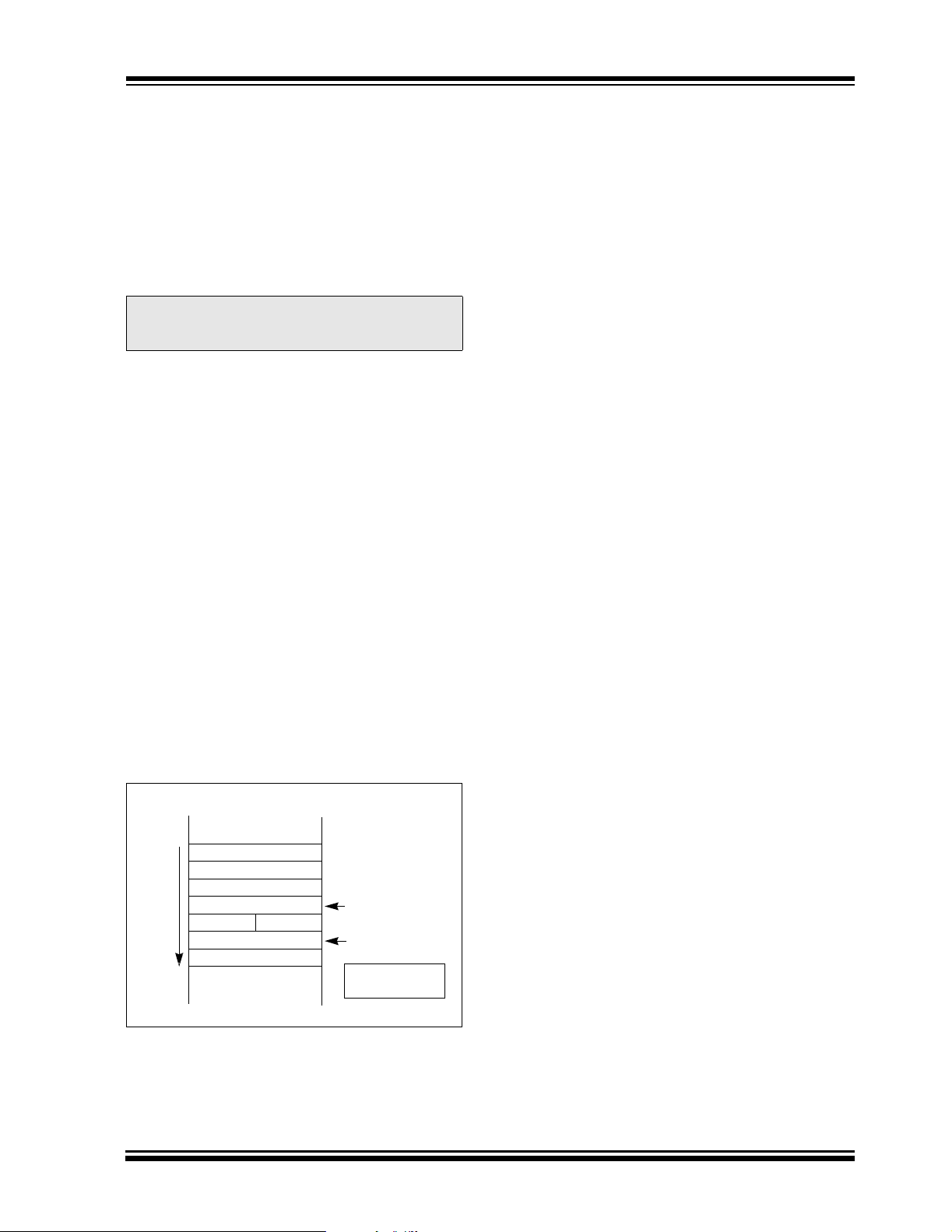
PIC24FJ64GA004 FAMILY
3.2.5 SOFTWARE STACK
In addition to its use as a working register, the W15 register in PIC24F devices is also used as a Software
Stack Pointer. The pointer always points to the first
available free word and grows from lower to higher
addresses. It pre-decrements for stack pops and
post-increments for stack pushes, as shown in
Figure 3-4. Note that for a PC push during any CALL
instruction, the MSB of the PC is zero-extended before
the push, ensuring that the MSB is always clear.
Note: A PC push during exception processing
will concatenate the SRL register to the
MSB of the PC prior to the push.
The Stack Pointer Limit Value register (SPLIM) associated with the Stack Pointer sets an upper address
boundary for the stack. SPLIM is uninitialized at Reset.
As is the case for the Stack Pointer, SPLIM<0> is
forced to ‘0’ because all stack operations must be
word-aligned. Whenever an EA is generated using
W15 as a source or destination pointer, the resulting
address is compared with the value in SPLIM. If the
contents of the Stack Pointer (W15) and the SPLIM register are equal, and a push operation is performed, a
stack error trap will not occur. The stack error trap will
occur on a subsequent push operation. Thus, for example, if it is desirable to cause a stack error trap when the
stack grows beyond address 2000h in RAM, initialize
the SPLIM with the value, 1FFEh.
Similarly, a Stack Pointer underflow (stack error) trap is
generated when the Stack Pointer address is found to
be less than 0800h. This prevents the stack from
interfering with the Special Function Register (SFR)
space.
A write to the SPLIM register should not be immediately
followed by an indirect read operation using W15.
FIGURE 3-4: CALL STACK FRAME
0000h
Stack Grows Towards
000000000
Higher Address
PC<15:0>
PC<22:16>
<Free Word>
015
W15 (before CALL)
W15 (after CALL)
POP : [--W15]
PUSH : [W15++]
3.3 Interfacing Program and Data Memory Spaces
The PIC24F architecture uses a 24-bit wide program
space and 16-bit wide data space. The architecture is
also a modified Harvard scheme, meaning that data
can also be present in the program space. To use this
data successfully, it must be accessed in a way that
preserves the alignment of information in both spaces.
Aside from normal execution, the PIC24F architecture
provides two methods by which program space can be
accessed during operation:
• Using table instructions to access individual bytes
or words anywhere in the program space
• Remapping a portion of the program space into
the data space (program space visibility)
Table instructions allow an application to read or write
to small areas of the program memory. This makes the
method ideal for accessing data tables that need to be
updated from time to time. It also allows access to all
bytes of the program word. The remapping method
allows an application to access a large block of data on
a read-only basis, which is ideal for look-ups from a
large table of static data. It can only access the least
significant word of the program word.
3.3.1 ADDRESSING PROGRAM SPACE
Since the address ranges for the data and program
spaces are 16 and 24 bits, respectively, a method is
needed to create a 23-bit or 24-bit program address
from 16-bit data registers. The solution depends on the
interface method to be used.
For table operations, the 8-bit Table Memory Page
Address register (TBLPAG) is used to define a 32K word
region within the program space. This is concatenated
with a 16-bit EA to arrive at a full 24-bit program space
address. In this format, the Most Significant bit of
TBLPAG is used to determine if the operation occurs in
the user memory (TBLPAG<7> = 0) or the configuration
memory (TBLPAG<7> = 1).
For remapping operations, the 8-bit Program Space
Visibility Page Address register (PSVPAG) is used to
define a 16K word page in the program space. When
the Most Significant bit of the EA is ‘1’, PSVPAG is concatenated with the lower 15 bits of the EA to form a
23-bit program space address. Unlike table operations,
this limits remapping operations strictly to the user
memory area.
Table 3-25 and Figure 3-5 show how the program EA is
created for table operations and remapping accesses
from the data EA. Here, P<23:0> refers to a program
space word, whereas D<15:0> refers to a data space
word.
© 2007 Microchip Technology Inc. Preliminary DS39881B-page 37
Page 40
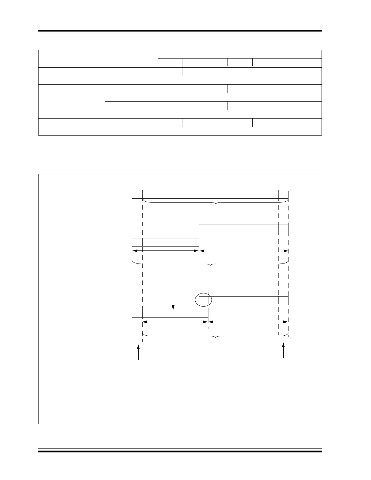
PIC24FJ64GA004 FAMILY
TABLE 3-25: PROGRAM SPACE ADDRESS CONSTRUCTION
Access Type
Instruction Access
(Code Execution)
TBLRD/TBLWT
(Byte/Word Read/Write)
Program Space Visibility
(Block Remap/Read)
Note 1: Data EA<15> is always ‘1’ in this case, but is not used in calculating the program space address. Bit 15 of
the address is PSVPAG<0>.
Access
Space
User 0 PC<22:1> 0
User TBLPAG<7:0> Data EA<15:0>
Configuration TBLPAG<7:0> Data EA<15:0>
User 0 PSVPAG<7:0> Data EA<14:0>
<23> <22:16> <15> <14:1> <0>
0xxx xxxx xxxx xxxx xxxx xxxx
1xxx xxxx xxxx xxxx xxxx xxxx
0 xxxx xxxx xxx xxxx xxxx xxxx
FIGURE 3-5: DATA ACCESS FROM PROGRAM SPACE ADDRESS GENERATION
Program Space Address
0xx xxxx xxxx xxxx xxxx xxx0
(1)
Program Counter
Table Operations
Program Space Visibility
(Remapping)
(1)
(2)
User/Configuration
0
1/0
(1)
0
Space Select
TBLPAG
8 bits
PSVPAG
8 bits
Select
23 bits
24 bits
1
23 bits
EA
16 bits
EA
15 bits
0Program Counter
1/0
0
Byte Select
Note 1: The LSb of program space addresses is always fixed as ‘0’ in order to maintain word alignment of
data in the program and data spaces.
2: Table operations are not required to be word-aligned. Table read operations are permitted in the
configuration memory space.
DS39881B-page 38 Preliminary © 2007 Microchip Technology Inc.
Page 41
PIC24FJ64GA004 FAMILY
3.3.2 DATA ACCESS FROM PROGRAM MEMORY USING TABLE INSTRUCTIONS
The TBLRDL and TBLWTL instructions offer a direct
method of reading or writing the lower word of any
address within the program space without going through
data space. The TBLRDH and TBLWTH instructions are
the only method to read or write the upper 8 bits of a
program space word as data.
The PC is incremented by two for each successive
24-bit program word. This allows program memory
addresses to directly map to data space addresses.
Program memory can thus be regarded as two 16-bit
word-wide address spaces, residing side by side, each
with the same address range. TBLRDL and TBLWTL
access the space which contains the least significant
data word, and TBLRDH and TBLWTH access the space
which contains the upper data byte.
Two table instructions are provided to move byte or
word-sized (16-bit) data to and from program space.
Both function as either byte or word operations.
1. TBLRDL (Table Read Low): In Word mode, it
maps the lower word of the program space
location (P<15:0>)
In Byte mode, either the upper or lower byte of
the lower program word is mapped to the lower
byte of a data address. The upper byte is
selected when byte select is ‘1’; the lower byte
is selected when it is ‘0’.
to a data address (D<15:0>).
2. TBLRDH (Table Read High): In Word mode, it
maps the entire upper word of a program address
(P<23:16>) to a data address. Note that
D<15:8>, the “phantom byte”, will always be ‘0’.
In Byte mode, it maps the upper or lower byte of
the program word to D<7:0> of the data
address, as above. Note that the data will
always be ‘0’ when the upper “phantom” byte is
selected (byte select = 1).
In a similar fashion, two table instructions, TBLWTH
and TBLWTL, are used to write individual bytes or
words to a program space address. The details of
their operation are explained in Section 4.0 “Flash
Program Memory”.
For all table operations, the area of program memory
space to be accessed is determined by the Table
Memory Page Address register (TBLPAG). TBLPAG
covers the entire program memory space of the
device, including user and configuration spaces. When
TBLPAG<7> = 0, the table page is located in the user
memory space. When TBLPAG<7> = 1, the page is
located in configuration space.
Note: Only table read operations will execute in
the configuration memory space, and only
then, in implemented areas such as the
device ID. Table write operations are not
allowed.
FIGURE 3-6: ACCESSING PROGRAM MEMORY WITH TABLE INSTRUCTIONS
Program Space
TBLPAG
02
23 15 0
000000h
020000h
030000h
800000h
00000000
00000000
00000000
00000000
‘Phantom’ Byte
TBLRDH.B (Wn<0> = 0)
TBLRDL.B (Wn<0> = 1)
TBLRDL.B (Wn<0> = 0)
TBLRDL.W
The address for the table operation is determined by the data EA
within the page defined by the TBLPAG register.
Only read operations are shown; write operations are also valid in
the user memory area.
Data EA<15:0>
081623
© 2007 Microchip Technology Inc. Preliminary DS39881B-page 39
Page 42

PIC24FJ64GA004 FAMILY
3.3.3 READING DATA FROM PROGRAM MEMORY USING PROGRAM SPACE VISIBILITY
The upper 32 Kbytes of data space may optionally be
mapped into any 16K word page of the program space.
This provides transparent access of stored constant
data from the data space without the need to use
special instructions (i.e., TBLRDL/H).
Program space access through the data space occurs
if the Most Significant bit of the data space EA is ‘1’ and
program space visibility is enabled by setting the PSV
bit in the CPU Control register (CORCON<2>). The
location of the program memory space to be mapped
into the data space is determined by the Program
Space Visibility Page Address register (PSVPAG). This
8-bit register defines any one of 256 possible pages of
16K words in program space. In effect, PSVPAG functions as the upper 8 bits of the program memory
address, with the 15 bits of the EA functioning as the
lower bits. Note that by incrementing the PC by 2 for
each program memory word, the lower 15 bits of data
space addresses directly map to the lower 15 bits in the
corresponding program space addresses.
Data reads to this area add an additional cycle to the
instruction being executed, since two program memory
fetches are required.
Although each data space address, 8000h and higher,
maps directly into a corresponding program memory
address (see Figure 3-7), only the lower 16 bits of the
24-bit program word are used to contain the data. The
upper 8 bits of any program space locations used as
data should be programmed with ‘1111 1111’ or
‘0000 0000’ to force a NOP. This prevents possible
issues should the area of code ever be accidentally
executed.
Note: PSV access is temporarily disabled during
table reads/writes.
For operations that use PSV and are executed outside
a REPEAT loop, the MOV and MOV.D instructions will
require one instruction cycle in addition to the specified
execution time. All other instructions will require two
instruction cycles in addition to the specified execution
time.
For operations that use PSV which are executed inside
a REPEAT loop, there will be some instances that
require two instruction cycles in addition to the
specified execution time of the instruction:
• Execution in the first iteration
• Execution in the last iteration
• Execution prior to exiting the loop due to an
interrupt
• Execution upon re-entering the loop after an
interrupt is serviced
Any other iteration of the REPEAT loop will allow the
instruction accessing data, using PSV, to execute in a
single cycle.
FIGURE 3-7: PROGRAM SPACE VISIBILITY OPERATION
When CORCON<2> = 1 and EA<15> = 1:
Program Space
PSVPAG
02
The data in the page
designated by
PSVPAG is mapped
into the upper half of
the data memory
space....
23 15 0
000000h
010000h
018000h
800000h
Data Space
PSV Area
0000h
8000h
FFFFh
Data EA<14:0>
...while the lower 15
bits of the EA specify
an exact address
within the PSV area.
This corresponds
exactly to the same
lower 15 bits of the
actual program space
address.
DS39881B-page 40 Preliminary © 2007 Microchip Technology Inc.
Page 43

PIC24FJ64GA004 FAMILY
4.0 FLASH PROGRAM MEMORY
Note: This data sheet summarizes the features
of this group of PIC24F devices. It is not
intended to be a comprehensive reference
source. For more information, refer to the
associated
Manual”
The PIC24FJ64GA004 family of devices contains internal Flash program memory for storing and executing
application code. The memory is readable, writable and
erasable during normal operation over the entire V
range.
Flash memory can be programmed in four ways:
• In-Circuit Serial Programming (ICSP)
• Run-Time Self-Programming (RTSP)
•JTAG
• Enhanced In-Circuit Serial Programming
(Enhanced ICSP)
ICSP allows a PIC24FJ64GA004 family device to be
serially programmed while in the end application circuit.
This is simply done with two lines for the programming
clock and programming data (which are named PGCx
and PGDx, respectively), and three other lines for
power (V
DD), ground (VSS) and Master Clear (MCLR).
This allows customers to manufacture boards with
unprogrammed devices and then program the microcontroller just before shipping the product. This also
allows the most recent firmware or a custom firmware
to be programmed.
“PIC24F Family Reference
chapter.
DD
RTSP is accomplished using TBLRD (table read) and
TBLWT (table write) instructions. With RTSP, the user
may write program memory data in blocks of 64 instructions (192 bytes) at a time, and erase program memory
in blocks of 512 instructions (1536 bytes) at a time.
4.1 Table Instructions and Flash Programming
Regardless of the method used, all programming of
Flash memory is done with the table read and table
write instructions. These allow direct read and write
access to the program memory space from the data
memory while the device is in normal operating mode.
The 24-bit target address in the program memory is
formed using the TBLPAG<7:0> bits and the Effective
Address (EA) from a W register specified in the table
instruction, as shown in Figure 4-1.
The TBLRDL and the TBLWTL instructions are used to
read or write to bits<15:0> of program memory.
TBLRDL and TBLWTL can access program memory in
both Word and Byte modes.
The TBLRDH and TBLWTH instructions are used to read
or write to bits<23:16> of program memory. TBLRDH
and TBLWTH can also access program memory in Word
or Byte mode.
FIGURE 4-1: ADDRESSING FOR TABLE REGISTERS
24 Bits
Using
User/Configuration
Space Select
Program
Counter
Using
Table
Instruction
0
1/0
TBLPAG Reg
8 Bits
Program Counter
Working Reg EA
24-Bit EA
0
16 Bits
Byte
Select
© 2007 Microchip Technology Inc. Preliminary DS39881B-page 41
Page 44

PIC24FJ64GA004 FAMILY
4.2 RTSP Operation
The PIC24F Flash program memory array is organized
into rows of 64 instructions or 192 bytes. RTSP allows
the user to erase blocks of eight rows (512 instructions)
at a time and to program one row at a time. It is also
possible to program single words.
The 8-row erase blocks and single row write blocks are
edge-aligned, from the beginning of program memory, on
boundaries of 1536 bytes and 192 bytes, respectively.
When data is written to program memory using TBLWT
instructions, the data is not written directly to memory.
Instead, data written using table writes is stored in
holding latches until the programming sequence is
executed.
Any number of TBLWT instructions can be executed
and a write will be successfully performed. However,
64 TBLWT instructions are required to write the full row
of memory.
To ensure that no data is corrupted during a write, any
unused addresses should be programmed with
FFFFFFh. This is because the holding latches reset to
an unknown state, so if the addresses are left in the
Reset state, they may overwrite the locations on rows
which were not rewritten.
The basic sequence for RTSP programming is to set up
a Table Pointer, then do a series of TBLWT instructions
to load the buffers. Programming is performed by
setting the control bits in the NVMCON register.
Data can be loaded in any order and the holding registers can be written to multiple times before performing
a write operation. Subsequent writes, however, will
wipe out any previous writes.
Note: Writing to a page multiple times without
not
erasing it is
All of the table write operations are single-word writes
(2 instruction cycles), because only the buffers are written. A programming cycle is required for programming
each row.
recommended.
4.4 Enhanced In-Circuit Serial Programming
Enhanced In-Circuit Serial Programming uses an
on-board boot loader, known as the program executive,
to manage the programming process. Using an SPI
data frame format, the program executive can erase,
program and verify program memory. For more
information on Enhanced ICSP, see the device
programming specification.
4.5 Control Registers
There are two SFRs used to read and write the
program Flash memory: NVMCON and NVMKEY.
The NVMCON register (Register 4-1) controls which
blocks are to be erased, which memory type is to be
programmed and when the programming cycle starts.
NVMKEY is a write-only register that is used for write
protection. To start a programming or erase sequence,
the user must consecutively write 55h and AAh to the
NVMKEY register. Refer to Section 4.6 “Programming
Operations” for further details.
4.6 Programming Operations
A complete programming sequence is necessary for
programming or erasing the internal Flash in RTSP
mode. During a programming or erase operation, the
processor stalls (waits) until the operation is finished.
Setting the WR bit (NVMCON<15>) starts the operation and the WR bit is automatically cleared when the
operation is finished.
Configuration Word values are stored in the last two
locations of program memory. Performing a page erase
operation on the last page of program memory clears
these values and enables code protection. As a result,
avoid performing page erase operations on the last
page of program memory.
4.3 JTAG Operation
The PIC24F family supports JTAG programming and
boundary scan. Boundary scan can improve the manufacturing process by verifying pin-to-PCB connectivity.
Programming can be performed with industry standard
JTAG programmers supporting Serial Vector Format
(SVF).
DS39881B-page 42 Preliminary © 2007 Microchip Technology Inc.
Page 45

PIC24FJ64GA004 FAMILY
REGISTER 4-1: NVMCON: FLASH MEMORY CONTROL REGISTER
(1)
R/SO-0
WR WREN WRERR — — — — —
bit 15 bit 8
R/W-0
(1)
R/W-0
(1)
U-0 U-0 U-0 U-0 U-0
U-0 R/W
-0
U-0 U-0 R/W-0
(1)
— ERASE — —NVMOP3
(1)
(2)
R/W-0
NVMOP2
(1)
(2)
R/W-0
NVMOP1
(1)
(2)
R/W-0
NVMOP0
(1)
(2)
bit 7 bit 0
Legend: SO = Set-Only bit
R = Readable bit W = Writable bit U = Unimplemented bit, read as ‘0’
-n = Value at POR ‘1’ = Bit is set ‘0’ = Bit is cleared x = Bit is unknown
bit 15 WR: Write Control bit
(1)
1 = Initiates a Flash memory program or erase operation. The operation is self-timed and the bit is
cleared by hardware once operation is complete.
0 = Program or erase operation is complete and inactive
bit 14 WREN: Write Enable bit
(1)
1 = Enable Flash program/erase operations
0 = Inhibit Flash program/erase operations
bit 13 WRERR: Write Sequence Error Flag bit
(1)
1 = An improper program or erase sequence attempt or termination has occurred (bit is set
automatically on any set attempt of the WR bit)
0 = The program or erase operation completed normally
bit 12-7 Unimplemented: Read as ‘0’
bit 6 ERASE: Erase/Program Enable bit
(1)
1 = Perform the erase operation specified by NVMOP3:NVMOP0 on the next WR command
0 = Perform the program operation specified by NVMOP3:NVMOP0 on the next WR command
bit 5-4 Unimplemented: Read as ‘0’
bit 3-0 NVMOP3:NVMOP0: NVM Operation Select bits
1111 = Memory bulk erase operation (ERASE = 1) or no operation (ERASE = 0)
(1,2)
(3)
0011 = Memory word program operation (ERASE = 0) or no operation (ERASE = 1)
0010 = Memory page erase operation (ERASE = 1) or no operation (ERASE = 0)
0001 = Memory row program operation (ERASE = 0) or no operation (ERASE = 1)
Note 1: These bits can only be reset on POR.
2: All other combinations of NVMOP3:NVMOP0 are unimplemented.
3: Available in ICSP™ mode only. Refer to device programming specification.
© 2007 Microchip Technology Inc. Preliminary DS39881B-page 43
Page 46

PIC24FJ64GA004 FAMILY
4.6.1 PROGRAMMING ALGORITHM FOR FLASH PROGRAM MEMORY
The user can program one row of program Flash memory
at a time. To do this, it is necessary to erase the 8-row
erase block containing the desired row. The general
process is:
1. Read eight rows of program memory
(512 instructions) and store in data RAM.
2. Update the program data in RAM with the
desired new data.
3. Erase the block (see Example 4-1):
a) Set the NVMOP bits (NVMCON<3:0>) to
‘0010’ to configure for block erase. Set the
ERASE (NVMCON<6>) and WREN
(NVMCON<14>) bits.
b) Write the starting address of the block to be
erased into the TBLPAG and W registers.
c) Write 55h to NVMKEY.
d) Write AAh to NVMKEY.
e) Set the WR bit (NVMCON<15>). The erase
cycle begins and the CPU stalls for the dura-
tion of the erase cycle. When the erase is
done, the WR bit is cleared automatically.
4. Write the first 64 instructions from data RAM into
the program memory buffers (see Example 4-1).
5. Write the program block to Flash memory:
a) Set the NVMOP bits to ‘0001’ to configure
for row programming. Clear the ERASE bit
and set the WREN bit.
b) Write 55h to NVMKEY.
c) Write AAh to NVMKEY.
d) Set the WR bit. The programming cycle
begins and the CPU stalls for the duration
of the write cycle. When the write to Flash
memory is done, the WR bit is cleared
automatically.
6. Repeat steps 4 and 5, using the next available
64 instructions from the block in data RAM by
incrementing the value in TBLPAG, until all
512 instructions are written back to Flash
memory.
For protection against accidental operations, the write
initiate sequence for NVMKEY must be used to allow
any erase or program operation to proceed. After the
programming command has been executed, the user
must wait for the programming time until programming
is complete. The two instructions following the start of
the programming sequence should be NOPs, as shown
in Example 4-3.
EXAMPLE 4-1: ERASING A PROGRAM MEMORY BLOCK
; Set up NVMCON for block erase operation
MOV #0x4042, W0 ;
; Init pointer to row to be ERASED
MOV W0, NVMCON ; Initialize NVMCON
MOV #tblpage(PROG_ADDR), W0 ;
MOV W0, TBLPAG ; Initialize PM Page Boundary SFR
MOV #tbloffset(PROG_ADDR), W0 ; Initialize in-page EA[15:0] pointer
TBLWTL W0, [W0] ; Set base address of erase block
DISI #5 ; Block all interrupts with priority <7
; for next 5 instructions
MOV #0x55, W0
MOV W0, NVMKEY ; Write the 55 key
MOV #0xAA, W1 ;
MOV W1, NVMKEY ; Write the AA key
BSET NVMCON, #WR ; Start the erase sequence
NOP ; Insert two NOPs after the erase
NOP ; command is asserted
DS39881B-page 44 Preliminary © 2007 Microchip Technology Inc.
Page 47

PIC24FJ64GA004 FAMILY
EXAMPLE 4-2: LOADING THE WRITE BUFFERS
; Set up NVMCON for row programming operations
; Set up a pointer to the first program memory location to be written
; program memory selected, and writes enabled
; Perform the TBLWT instructions to write the latches
; 0th_program_word
; 1st_program_word
; 2nd_program_word
; 63rd_program_word
MOV #0x4001, W0 ;
MOV W0, NVMCON ; Initialize NVMCON
MOV #0x0000, W0 ;
MOV W0, TBLPAG ; Initialize PM Page Boundary SFR
MOV #0x6000, W0 ; An example program memory address
MOV #LOW_WORD_0, W2 ;
MOV #HIGH_BYTE_0, W3 ;
TBLWTL W2, [W0] ; Write PM low word into program latch
TBLWTH W3, [W0++] ; Write PM high byte into program latch
MOV #LOW_WORD_1, W2 ;
MOV #HIGH_BYTE_1, W3 ;
TBLWTL W2, [W0] ; Write PM low word into program latch
TBLWTH W3, [W0++] ; Write PM high byte into program latch
MOV #LOW_WORD_2, W2 ;
MOV #HIGH_BYTE_2, W3 ;
TBLWTL W2,
TBLWTH W3,
•
•
•
MOV #LOW_WORD_31, W2 ;
MOV #HIGH_BYTE_31, W3 ;
TBLWTL W2,
TBLWTH W3,
[W0] ; Write PM low word into program latch
[W0++] ; Write PM high byte into program latch
[W0] ; Write PM low word into program latch
[W0] ; Write PM high byte into program latch
EXAMPLE 4-3: INITIATING A PROGRAMMING SEQUENCE
DISI #5 ; Block all interrupts with priority <7
MOV #0x55, W0
MOV W0, NVMKEY ; Write the 55 key
MOV #0xAA, W1 ;
MOV W1, NVMKEY ; Write the AA key
BSET NVMCON, #WR ; Start the erase sequence
BTSC NVMCON, #15 ; and wait for it to be
BRA $-2 ; completed
; for next 5 instructions
© 2007 Microchip Technology Inc. Preliminary DS39881B-page 45
Page 48

PIC24FJ64GA004 FAMILY
4.6.2 PROGRAMMING A SINGLE WORD OF FLASH PROGRAM MEMORY
If a Flash location has been erased, it can be programmed using table write instructions to write an
instruction word (24-bit) into the write latch. The
TBLPAG register is loaded with the 8 Most Significant
Bytes of the Flash address. The TBLWTL and TBLWTH
instructions write the desired data into the write latches
and specify the lower 16 bits of the program memory
address to write to. To configure the NVMCON register
for a word write, set the NVMOP bits (NVMCON<3:0>)
to ‘0011’. The write is performed by executing the
unlock sequence and setting the WR bit (see
Example 4-4).
EXAMPLE 4-4: PROGRAMMING A SINGLE WORD OF FLASH PROGRAM MEMORY
; Setup a pointer to data Program Memory
MOV #tblpage(PROG_ADDR), W0 ;
MOV W0, TBLPAG ;Initialize PM Page Boundary SFR
MOV #tbloffset(PROG_ADDR), W0 ;Initialize a register with program memory address
MOV #LOW_WORD_N, W2 ;
MOV #HIGH_BYTE_N, W3 ;
TBLWTL W2, [W0] ; Write PM low word into program latch
TBLWTH W3, [W0++] ; Write PM high byte into program latch
; Setup NVMCON for programming one word to data Program Memory
MOV #0x4003, W0 ;
MOV W0, NVMCON ; Set NVMOP bits to 0011
DISI #5 ; Disable interrupts while the KEY sequence is written
MOV #0x55, W0 ; Write the key sequence
MOV W0, NVMKEY
MOV #0xAA, W0
MOV W0, NVMKEY
BSET NVMCON, #WR ; Start the write cycle
DS39881B-page 46 Preliminary © 2007 Microchip Technology Inc.
Page 49

PIC24FJ64GA004 FAMILY
5.0 RESETS
Note: This data sheet summarizes the features
of this group of PIC24F devices. It is not
intended to be a comprehensive reference
source. For more information, refer to the
associated
Manual”
The Reset module combines all Reset sources and
controls the device Master Reset Signal, SYSRST
following is a list of device Reset sources:
• POR: Power-on Reset
•MCLR
: Pin Reset
•SWR: RESET Instruction
• WDT: Watchdog Timer Reset
• BOR: Brown-out Reset
• TRAPR: Trap Conflict Reset
• IOPUWR: Illegal Opcode Reset
• UWR: Uninitialized W Register Reset
A simplified block diagram of the Reset module is
shown in Figure 5-1.
Any active source of Reset will make the SYSRST
signal active. Many registers associated with the CPU
and peripherals are forced to a known Reset state.
Most registers are unaffected by a Reset; their status is
unknown on POR and unchanged by all other Resets.
“PIC24F Family Reference
chapter.
. The
Note: Refer to the specific peripheral or CPU
section of this manual for register Reset
states.
All types of device Reset will set a corresponding status
bit in the RCON register to indicate the type of Reset
(see Register 5-1). A Power-on Reset will clear all bits
except for the BOR and POR bits (RCON<1:0>) which
are set. The user may set or clear any bit at any time
during code execution. The RCON bits only serve as
status bits. Setting a particular Reset status bit in
software will not cause a device Reset to occur.
The RCON register also has other bits associated with
the Watchdog Timer and device power-saving states.
The function of these bits is discussed in other sections
of this manual.
Note: The status bits in the RCON register
should be cleared after they are read so
that the next RCON register value after a
device Reset will be meaningful.
FIGURE 5-1: RESET SYSTEM BLOCK DIAGRAM
RESET
Instruction
Glitch Filter
MCLR
WDT
Module
Sleep or Idle
VDD Rise
Detect
VDD
Brown-out
Reset
Enable Voltage Regulator
Trap Conflict
Illegal Opcode
Uninitialized W Register
POR
BOR
SYSRST
© 2007 Microchip Technology Inc. Preliminary DS39881B-page 47
Page 50
PIC24FJ64GA004 FAMILY
REGISTER 5-1: RCON: RESET CONTROL REGISTER
R/W-0 R/W-0 U-0 U-0 U-0 U-0 R/W-0 R/W-0
TRAPR IOPUWR
bit 15 bit 8
R/W
-0 R/W-0 R/W-0 R/W-0 R/W-0 R/W-0 R/W-1 R/W-1
EXTR SWR SWDTEN
bit 7 bit 0
Legend:
R = Readable bit W = Writable bit U = Unimplemented bit, read as ‘0’
-n = Value at POR ‘1’ = Bit is set ‘0’ = Bit is cleared x = Bit is unknown
bit 15 TRAPR: Trap Reset Flag bit
1 = A Trap Conflict Reset has occurred
0 = A Trap Conflict Reset has not occurred
bit 14 IOPUWR: Illegal Opcode or Uninitialized W Access Reset Flag bit
1 = An illegal opcode detection, an illegal address mode or uninitialized W register used as an
Address Pointer caused a Reset
0 = An illegal opcode or uninitialized W Reset has not occurred
bit 13-10 Unimplemented: Read as ‘0’
bit 9 CM: Configuration Word Mismatch Reset Flag bit
1 = A Configuration Word Mismatch Reset has occurred
0 = A Configuration Word Mismatch Reset has not occurred
bit 8 VREGS: Voltage Regulator Standby Enable bit
1 = Regulator remains active during Sleep
0 = Regulator goes to standby during Sleep
bit 7 EXTR: External Reset (MCLR
1 = A Master Clear (pin) Reset has occurred
0 = A Master Clear (pin) Reset has not occurred
bit 6 SWR: Software Reset (Instruction) Flag bit
1 = A RESET instruction has been executed
0 = A RESET instruction has not been executed
bit 5 SWDTEN: Software Enable/Disable of WDT bit
1 = WDT is enabled
0 = WDT is disabled
bit 4 WDTO: Watchdog Timer Time-out Flag bit
1 = WDT time-out has occurred
0 = WDT time-out has not occurred
bit 3 SLEEP: Wake From Sleep Flag bit
1 = Device has been in Sleep mode
0 = Device has not been in Sleep mode
bit 2 IDLE: Wake-up From Idle Flag bit
1 = Device has been in Idle mode
0 = Device has not been in Idle mode
bit 1 BOR: Brown-out Reset Flag bit
1 = A Brown-out Reset has occurred. Note that BOR is also set after a Power-on Reset.
0 = A Brown-out Reset has not occurred
bit 0 POR: Power-on Reset Flag bit
1 = A Power-up Reset has occurred
0 = A Power-up Reset has not occurred
— — — —CMVREGS
(2)
WDTO SLEEP IDLE BOR POR
) Pin bit
(1)
(2)
Note 1: All of the Reset status bits may be set or cleared in software. Setting one of these bits in software does not
cause a device Reset.
2: If the FWDTEN Configuration bit is ‘1’ (unprogrammed), the WDT is always enabled, regardless of the
SWDTEN bit setting.
DS39881B-page 48 Preliminary © 2007 Microchip Technology Inc.
Page 51

PIC24FJ64GA004 FAMILY
TABLE 5-1: RESET FLAG BIT OPERATION
Flag Bit Setting Event Clearing Event
TRAPR (RCON<15>) Trap Conflict Event POR
IOPUWR (RCON<14>) Illegal Opcode or Uninitialized W Register Access POR
EXTR (RCON<7>) MCLR
SWR (RCON<6>) RESET Instruction POR
WDTO (RCON<4>) WDT Time-out PWRSAV Instruction, POR
SLEEP (RCON<3>) PWRSAV #SLEEP Instruction POR
IDLE (RCON<2>) PWRSAV #IDLE Instruction POR
BOR (RCON<1>) POR, BOR —
POR (RCON<0>) POR —
Note: All Reset flag bits may be set or cleared by the user software.
Reset POR
5.1 Clock Source Selection at Reset
If clock switching is enabled, the system clock source at
device Reset is chosen as shown in Table 5-2. If clock
switching is disabled, the system clock source is always
selected according to the oscillator configuration bits.
Refer to Section 7.0 “Oscillator Configuration” for
further details.
TABLE 5-2: OSCILLATOR SELECTION vs.
TYPE OF RESET (CLOCK
SWITCHING ENABLED)
Reset Type Clock Source Determinant
POR Oscillator Configuration Bits
BOR
MCLR
WDTO
SWR
(CW2<10:8>)
COSC Control bits
(OSCCON<14:12>)
5.2 Device Reset Times
The Reset times for various types of device Reset are
summarized in Table 5-3. Note that the system Reset
signal, SYSRST, is released after the POR and PWRT
delay times expire.
The time that the device actually begins to execute
code will also depend on the system oscillator delays,
which include the Oscillator Start-up Timer (OST) and
the PLL lock time. The OST and PLL lock times occur
in parallel with the applicable SYSRST
The FSCM delay determines the time at which the
FSCM begins to monitor the system clock source after
the SYSRST
signal is released.
delay times.
© 2007 Microchip Technology Inc. Preliminary DS39881B-page 49
Page 52

PIC24FJ64GA004 FAMILY
TABLE 5-3: RESET DELAY TIMES FOR VARIOUS DEVICE RESETS
Reset Type Clock Source SYSRST Delay
POR
POR EC, FRC, FRCDIV, LPRC T
+ TSTARTUP + TRST ——1, 2, 3
System Clock
Delay
ECPLL, FRCPLL TPOR + TSTARTUP + TRST TLOCK TFSCM 1, 2, 3, 5, 6
POR
XT, HS, SOSC T
+ TSTARTUP + TRST TOST TFSCM 1, 2, 3, 4, 6
XTPLL, HSPLL TPOR + TSTARTUP + TRST TOST + TLOCK TFSCM 1, 2, 3, 4, 5, 6
BOR EC, FRC, FRCDIV, LPRC TSTARTUP + TRST ——2, 3
ECPLL, FRCPLL T
STARTUP + TRST TLOCK TFSCM 2, 3, 5, 6
XT, HS, SOSC TSTARTUP + TRST TOST TFSCM 2, 3, 4, 6
XTPLL, HSPLL TSTARTUP + TRST TOST + TLOCK TFSCM 2, 3, 4, 5, 6
MCLR
WDT Any Clock T
Any Clock TRST ——3
RST ——3
Software Any clock TRST ——3
Illegal Opcode Any Clock TRST ——3
Uninitialized W Any Clock T
RST ——3
Trap Conflict Any Clock TRST ——3
Note 1: TPOR = Power-on Reset delay (10 μs nominal).
2: TSTARTUP = TVREG (10 μs nominal) if on-chip regulator is enabled or TPWRT (64 ms nominal) if on-chip
regulator is disabled.
RST = Internal state Reset time (20 μs nominal).
3: T
4: TOST = Oscillator Start-up Timer. A 10-bit counter counts 1024 oscillator periods before releasing the
oscillator clock to the system.
LOCK = PLL lock time (20 μs nominal).
5: T
6: T
FSCM = Fail-Safe Clock Monitor delay (100 μs nominal).
FSCM
Delay
Notes
DS39881B-page 50 Preliminary © 2007 Microchip Technology Inc.
Page 53

PIC24FJ64GA004 FAMILY
5.2.1 POR AND LONG OSCILLATOR START-UP TIMES
The oscillator start-up circuitry and its associated delay
timers are not linked to the device Reset delays that
occur at power-up. Some crystal circuits (especially
low-frequency crystals) will have a relatively long
start-up time. Therefore, one or more of the following
conditions is possible after SYSRST
• The oscillator circuit has not begun to oscillate.
• The Oscillator Start-up Timer has not expired (if a
crystal oscillator is used).
• The PLL has not achieved a lock (if PLL is used).
The device will not begin to execute code until a valid
clock source has been released to the system. Therefore, the oscillator and PLL start-up delays must be
considered when the Reset delay time must be known.
is released:
5.2.2 FAIL-SAFE CLOCK MONITOR (FSCM) AND DEVICE RESETS
If the FSCM is enabled, it will begin to monitor the
system clock source when SYSRST
valid clock source is not available at this time, the
device will automatically switch to the FRC oscillator
and the user can switch to the desired crystal oscillator
in the Trap Service Routine.
is released. If a
5.2.2.1 FSCM Delay for Crystal and PLL
Clock Sources
When the system clock source is provided by a crystal
oscillator and/or the PLL, a small delay, T
automatically be inserted after the POR and PWRT
delay times. The FSCM will not begin to monitor the
system clock source until this delay expires. The FSCM
delay time is nominally 100 μs and provides additional
time for the oscillator and/or PLL to stabilize. In most
cases, the FSCM delay will prevent an oscillator failure
trap at a device Reset when the PWRT is disabled.
FSCM, will
5.3 Special Function Register Reset
States
Most of the Special Function Registers (SFRs) associated with the PIC24F CPU and peripherals are reset to a
particular value at a device Reset. The SFRs are
grouped by their peripheral or CPU function and their
Reset values are specified in each section of this manual.
The Reset value for each SFR does not depend on the
type of Reset, with the exception of four registers. The
Reset value for the Reset Control register, RCON, will
depend on the type of device Reset. The Reset value
for the Oscillator Control register, OSCCON, will
depend on the type of Reset and the programmed
values of the FNOSC bits in the CW2 register (see
Table 5-2). The RCFGCAL and NVMCON registers are
only affected by a POR.
© 2007 Microchip Technology Inc. Preliminary DS39881B-page 51
Page 54

PIC24FJ64GA004 FAMILY
NOTES:
DS39881B-page 52 Preliminary © 2007 Microchip Technology Inc.
Page 55

PIC24FJ64GA004 FAMILY
6.0 INTERRUPT CONTROLLER
Note: This data sheet summarizes the features
of this group of PIC24F devices. It is not
intended to be a comprehensive reference
source. For more information, refer to the
associated
Manual”
The PIC24F interrupt controller reduces the numerous
peripheral interrupt request signals to a single interrupt
request signal to the PIC24F CPU. It has the following
features:
• Up to 8 processor exceptions and software traps
• 7 user-selectable priority levels
• Interrupt Vector Table (IVT) with up to 118 vectors
• A unique vector for each interrupt or exception
source
• Fixed priority within a specified user priority level
• Alternate Interrupt Vector Table (AIVT) for debug
support
• Fixed interrupt entry and return latencies
6.1 Interrupt Vector Table
The Interrupt Vector Table (IVT) is shown in Figure 6-1.
The IVT resides in program memory, starting at location
000004h. The IVT contains 126 vectors, consisting of
8 non-maskable trap vectors, plus up to 118 sources of
interrupt. In general, each interrupt source has its own
vector. Each interrupt vector contains a 24-bit wide
address. The value programmed into each interrupt
vector location is the starting address of the associated
Interrupt Service Routine (ISR).
Interrupt vectors are prioritized in terms of their natural
priority; this is linked to their position in the vector table.
All other things being equal, lower addresses have a
higher natural priority. For example, the interrupt associated with vector 0 will take priority over interrupts at
any other vector address.
PIC24FJ64GA004 family devices implement
non-maskable traps and unique interrupts. These are
summarized in Table 6-1 and Table 6-2.
“PIC24F Family Reference
chapter.
6.1.1 ALTERNATE INTERRUPT VECTOR TAB LE
The Alternate Interrupt Vector Table (AIVT) is located
after the IVT, as shown in Figure 6-1. Access to the
AIVT is provided by the ALTIVT control bit
(INTCON2<15>). If the ALTIVT bit is set, all interrupt
and exception processes will use the alternate vectors
instead of the default vectors. The alternate vectors are
organized in the same manner as the default vectors.
The AIVT supports emulation and debugging efforts by
providing a means to switch between an application
and a support environment without requiring the interrupt vectors to be reprogrammed. This feature also
enables switching between applications for evaluation
of different software algorithms at run time. If the AIVT
is not needed, the AIVT should be programmed with
the same addresses used in the IVT.
6.2 Reset Sequence
A device Reset is not a true exception because the
interrupt controller is not involved in the Reset process.
The PIC24F devices clear their registers in response to
a Reset which forces the PC to zero. The microcontroller then begins program execution at location
000000h. The user programs a GOTO instruction at the
Reset address, which redirects program execution to
the appropriate start-up routine.
Note: Any unimplemented or unused vector
locations in the IVT and AIVT should be
programmed with the address of a default
interrupt handler routine that contains a
RESET instruction.
© 2007 Microchip Technology Inc. Preliminary DS39881B-page 53
Page 56
PIC24FJ64GA004 FAMILY
FIGURE 6-1: PIC24F INTERRUPT VECTOR TABLE
Reset – GOTO Instruction 000000h
Reset – GOTO Address 000002h
Reserved 000004h
Oscillator Fail Trap Vector
Address Error Trap Vector
Stack Error Trap Vector
Math Error Trap Vector
Reserved
Reserved
Reserved
Interrupt Vector 0 000014h
Interrupt Vector 1
—
—
—
Interrupt Vector 52 00007Ch
Interrupt Vector 53 00007Eh
Interrupt Vector 54 000080h
—
—
Interrupt Vector 116 0000FCh
Interrupt Vector 117 0000FEh
Decreasing Natural Order Priority
Oscillator Fail Trap Vector
Address Error Trap Vector
Stack Error Trap Vector
Math Error Trap Vector
Interrupt Vector 116
Interrupt Vector 117 0001FEh
—
Reserved 000100h
Reserved 000102h
Reserved
Reserved
Reserved
Reserved
Interrupt Vector 0 000114h
Interrupt Vector 1
—
—
—
Interrupt Vector 52 00017Ch
Interrupt Vector 53 00017Eh
Interrupt Vector 54 000180h
—
—
—
Start of Code 000200h
Interrupt Vector Table (IVT)
Alternate Interrupt Vector Table (AIVT)
(1)
(1)
Note 1: See Table 6-2 for the interrupt vector list.
TABLE 6-1: TRAP VECTOR DETAILS
Vector Number IVT Address AIVT Address Trap Source
0 000004h 000104h Reserved
1 000006h 000106h Oscillator Failure
2 000008h 000108h Address Error
3 00000Ah 00010Ah Stack Error
4 00000Ch 00010Ch Math Error
5 00000Eh 00010Eh Reserved
6 000010h 000110h Reserved
7 000012h 0001172h Reserved
DS39881B-page 54 Preliminary © 2007 Microchip Technology Inc.
Page 57

PIC24FJ64GA004 FAMILY
TABLE 6-2: IMPLEMENTED INTERRUPT VECTORS
Interrupt Source
ADC1 Conversion Done 13 00002Eh 00012Eh IFS0<13> IEC0<13> IPC3<6:4>
Comparator Event 18 000038h 000138h IFS1<2> IEC1<2> IPC4<10:8>
CRC Generator 67 00009Ah 00019Ah IFS4<3> IEC4<3> IPC16<14:12>
External Interrupt 0 0 000014h 000114h IFS0<0> IEC0<0> IPC0<2:0>
External Interrupt 1 20 00003Ch 00013Ch IFS1<4> IEC1<4> IPC5<2:0>
External Interrupt 2 29 00004Eh 00014Eh IFS1<13> IEC1<13> IPC7<6:4>
I2C1 Master Event 17 000036h 000136h IFS1<1> IEC1<1> IPC4<6:4>
I2C1 Slave Event 16 000034h 000034h IFS1<0> IEC1<0> IPC4<2:0>
I2C2 Master Event 50 000078h 000178h IFS3<2> IEC3<2> IPC12<10:8>
I2C2 Slave Event 49 000076h 000176h IFS3<1> IEC3<1> IPC12<6:4>
Input Capture 1 1 000016h 000116h IFS0<1> IEC0<1> IPC0<6:4>
Input Capture 2 5 00001Eh 00011Eh IFS0<5> IEC0<5> IPC1<6:4>
Input Capture 3 37 00005Eh 00015Eh IFS2<5> IEC2<5> IPC9<6:4>
Input Capture 4 38 000060h 000160h IFS2<6> IEC2<6> IPC9<10:8>
Input Capture 5 39 000062h 000162h IFS2<7> IEC2<7> IPC9<14:12>
Input Change Notification 19 00003Ah 00013Ah IFS1<3> IEC1<3> IPC4<14:12>
Output Compare 1 2 000018h 000118h IFS0<2> IEC0<2> IPC0<10:8>
Output Compare 2 6 000020h 000120h IFS0<6> IEC0<6> IPC1<10:8>
Output Compare 3 25 000046h 000146h IFS1<9> IEC1<9> IPC6<6:4>
Output Compare 4 26 000048h 000148h IFS1<10> IEC1<10> IPC6<10:8>
Output Compare 5 41 000066h 000166h IFS2<9> IEC2<9> IPC10<6:4>
Parallel Master Port 45 00006Eh 00016Eh IFS2<13> IEC2<13> IPC11<6:4>
Real-Time Clock/Calendar 62 000090h 000190h IFS3<14> IEC3<13> IPC15<10:8>
SPI1 Error 9 000026h 000126h IFS0<9> IEC0<9> IPC2<6:4>
SPI1 Event 10 000028h 000128h IFS0<10> IEC0<10> IPC2<10:8>
SPI2 Error 32 000054h 000154h IFS2<0> IEC0<0> IPC8<2:0>
SPI2 Event 33 000056h 000156h IFS2<1> IEC2<1> IPC8<6:4>
Timer1 3 00001Ah 00011Ah IFS0<3> IEC0<3> IPC0<14:12>
Timer2 7 000022h 000122h IFS0<7> IEC0<7> IPC1<14:12>
Timer3 8 000024h 000124h IFS0<8> IEC0<8> IPC2<2:0>
Timer4 27 00004Ah 00014Ah IFS1<11> IEC1<11> IPC6<14:12>
Timer5 28 00004Ch 00014Ch IFS1<12> IEC1<12> IPC7<2:0>
UART1 Error 65 000096h 000196h IFS4<1> IEC4<1> IPC16<6:4>
UART1 Receiver 11 00002Ah 00012Ah IFS0<11> IEC0<11> IPC2<14:12>
UART1 Transmitter 12 00002Ch 00012Ch IFS0<12> IEC0<12> IPC3<2:0>
UART2 Error 66 000098h 000198h IFS4<2> IEC4<2> IPC16<10:8>
UART2 Receiver 30 000050h 000150h IFS1<14> IEC1<14> IPC7<10:8>
UART2 Transmitter 31 000052h 000152h IFS1<15> IEC1<15> IPC7<14:12>
LVD Low-Voltage Detect 72 0000A4h 000124h IFS4<8> IEC4<8> IPC17<2:0>
Vector
Number
IVT Address
AIVT
Address
Interrupt Bit Locations
Flag Enable Priority
© 2007 Microchip Technology Inc. Preliminary DS39881B-page 55
Page 58

PIC24FJ64GA004 FAMILY
6.3 Interrupt Control and Status Registers
The PIC24FJ64GA004 family of devices implement a
total of 28 registers for the interrupt controller:
• INTCON1
• INTCON2
• IFS0 through IFS4
• IEC0 through IEC4
• IPC0 through IPC12, IPC15, IPC16 and IPC18
Global interrupt control functions are controlled from
INTCON1 and INTCON2. INTCON1 contains the Interrupt Nesting Disable (NSTDIS) bit, as well as the
control and status flags for the processor trap sources.
The INTCON2 register controls the external interrupt
request signal behavior and the use of the Alternate
Interrupt Vector Table.
The IFSx registers maintain all of the interrupt request
flags. Each source of interrupt has a status bit which is
set by the respective peripherals, or external signal,
and is cleared via software.
The IECx registers maintain all of the interrupt enable
bits. These control bits are used to individually enable
interrupts from the peripherals or external signals.
The IPCx registers are used to set the interrupt priority
level for each source of interrupt. Each user interrupt
source can be assigned to one of eight priority levels.
The interrupt sources are assigned to the IFSx, IECx
and IPCx registers in the same sequence that they are
listed in Table 6-2. For example, the INT0 (External
Interrupt 0) is shown as having a vector number and a
natural order priority of 0. Thus, the INT0IF status bit is
found in IFS0<0>, the INT0IE enable bit in IEC0<0>
and the INT0IP<2:0> priority bits in the first position of
IPC0 (IPC0<2:0>).
Although they are not specifically part of the interrupt
control hardware, two of the CPU control registers contain bits that control interrupt functionality. The ALU
STATUS register (SR) contains the IPL2:IPL0 bits
(SR<7:5>). These indicate the current CPU interrupt
priority level. The user may change the current CPU
priority level by writing to the IPL bits.
The CORCON register contains the IPL3 bit, which
together with IPL2:IPL0, also indicates the current CPU
priority level. IPL3 is a read-only bit so that trap events
cannot be masked by the user software.
All interrupt registers are described in Register 6-1
through Register 6-29, in the following pages.
DS39881B-page 56 Preliminary © 2007 Microchip Technology Inc.
Page 59
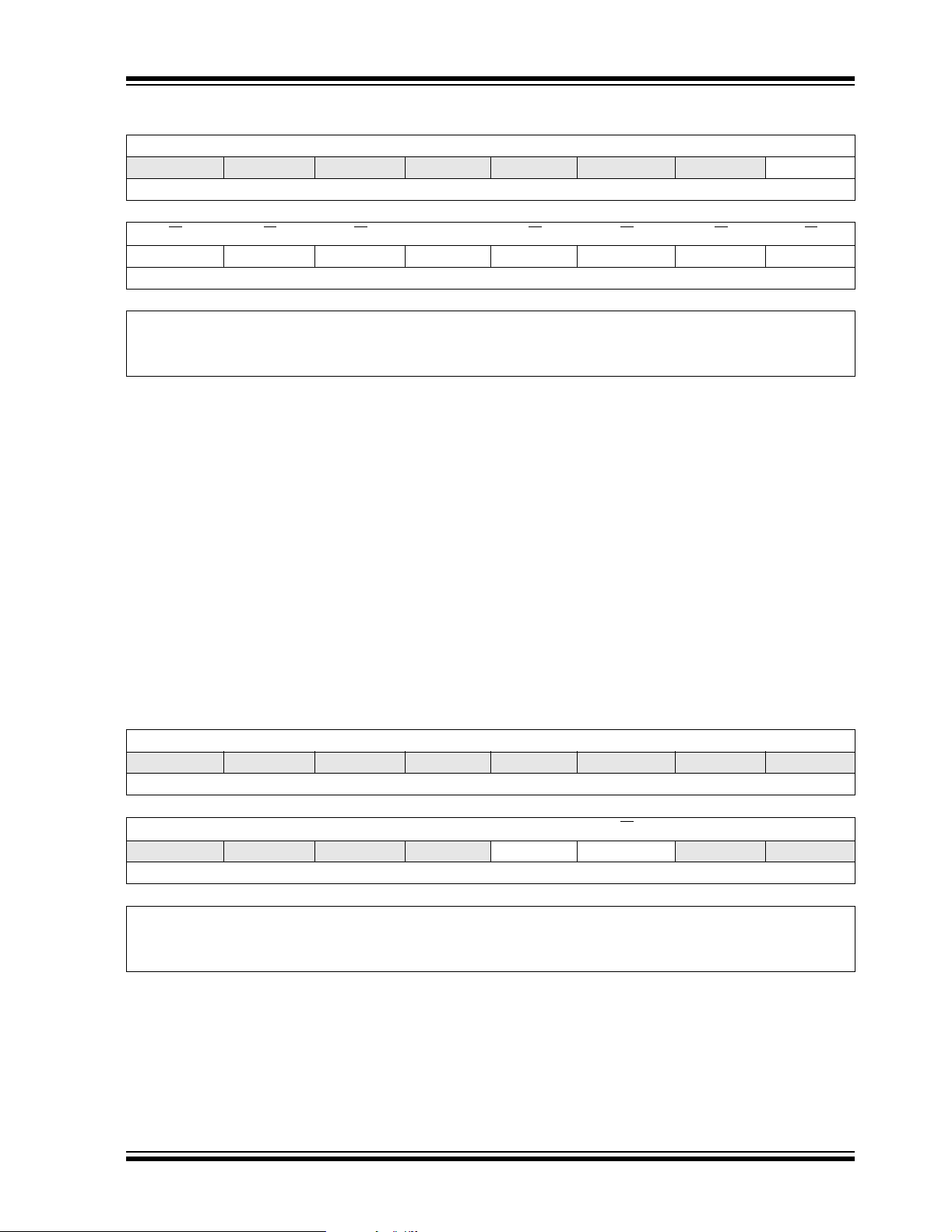
PIC24FJ64GA004 FAMILY
REGISTER 6-1: SR: ALU STATUS REGISTER (IN CPU)
U-0 U-0 U-0 U-0 U-0 U-0 U-0 R-0
— — — — — — —DC
bit 15 bit 8
-0 R/W-0 R/W-0 R-0 R/W-0 R/W-0 R/W-0 R/W-0
R/W
IPL2
(2,3)
IPL1
(2,3)
IPL0
(2,3)
RA
(1)
(1)
N
OV
(1)
(1)
Z
bit 7 bit 0
Legend:
R = Readable bit W = Writable bit U = Unimplemented bit, read as ‘0’
-n = Value at POR ‘1’ = Bit is set ‘0’ = Bit is cleared x = Bit is unknown
(1)
(1)
C
bit 7-5 IPL2:IPL0: CPU Interrupt Priority Level Status bits
(2,3)
111 = CPU interrupt priority level is 7 (15). User interrupts disabled.
110 = CPU interrupt priority level is 6 (14)
101 = CPU interrupt priority level is 5 (13)
100 = CPU interrupt priority level is 4 (12)
011 = CPU interrupt priority level is 3 (11)
010 = CPU interrupt priority level is 2 (10)
001 = CPU interrupt priority level is 1 (9)
000 = CPU interrupt priority level is 0 (8)
Note 1: See Register 2-1 for the description of the remaining bit (s) that are not dedicated to interrupt control
functions.
2: The IPL bits are concatenated with the IPL3 bit (CORCON<3>) to form the CPU interrupt priority level.
The value in parentheses indicates the Interrupt Priority Level if IPL3 = 1.
3: The IPL Status bits are read-only when NSTDIS (INTCON1<15>) = 1.
REGISTER 6-2: CORCON: CPU CONTROL REGISTER
U-0 U-0 U-0 U-0 U-0 U-0 U-0 U-0
— — — — — — — —
bit 15 bit 8
U-0 U-0 U-0 U-0 R/C-0 R/W
— — — —IPL3
(2)
bit 7 bit 0
-0 U-0 U-0
(1)
PSV
— —
Legend: C = Clearable bit
R = Readable bit W = Writable bit U = Unimplemented bit, read as ‘0’
-n = Value at POR ‘1’ = Bit is set ‘0’ = Bit is cleared x = Bit is unknown
bit 8 IPL3: CPU Interrupt Priority Level Status bit
(2)
1 = CPU interrupt priority level is greater than 7
0 = CPU interrupt priority level is 7 or less
Note 1: See Register 2-2 for the description of remaining bit (s) that are not dedicated to interrupt control
functions.
2: The IPL3 bit is concatenated with the IPL2:IPL0 bits (SR<7:5>) to form the CPU interrupt priority level.
© 2007 Microchip Technology Inc. Preliminary DS39881B-page 57
Page 60

PIC24FJ64GA004 FAMILY
REGISTER 6-3: INTCON1: INTERRUPT CONTROL REGISTER 1
R/W-0 U-0 U-0 U-0 U-0 U-0 U-0 U-0
NSTDIS
bit 15 bit 8
— — — — — — —
U-0 U-0 U-0 R/W
— — — MATHERR ADDRERR STKERR OSCFAIL —
bit 7 bit 0
Legend:
R = Readable bit W = Writable bit U = Unimplemented bit, read as ‘0’
-n = Value at POR ‘1’ = Bit is set ‘0’ = Bit is cleared x = Bit is unknown
bit 15 NSTDIS: Interrupt Nesting Disable bit
1 = Interrupt nesting is disabled
0 = Interrupt nesting is enabled
bit 14-5 Unimplemented: Read as ‘0’
bit 4 MATHERR: Arithmetic Error Trap Status bit
1 = Overflow trap has occurred
0 = Overflow trap has not occurred
bit 3 ADDRERR: Address Error Trap Status bit
1 = Address error trap has occurred
0 = Address error trap has not occurred
bit 2 STKERR: Stack Error Trap Status bit
1 = Stack error trap has occurred
0 = Stack error trap has not occurred
bit 1 OSCFAIL: Oscillator Failure Trap Status bit
1 = Oscillator failure trap has occurred
0 = Oscillator failure trap has not occurred
bit 0 Unimplemented: Read as ‘0’
-0 R/W-0 R/W-0 R/W-0 U-0
DS39881B-page 58 Preliminary © 2007 Microchip Technology Inc.
Page 61

PIC24FJ64GA004 FAMILY
REGISTER 6-4: INTCON2: INTERRUPT CONTROL REGISTER 2
R/W-0 R-0 U-0 U-0 U-0 U-0 U-0 U-0
ALTIVT DISI
bit 15 bit 8
— — — — — —
U-0 U-0 U-0 U-0 U-0 R/W
— — — — — INT2EP INT1EP INT0EP
bit 7 bit 0
Legend:
R = Readable bit W = Writable bit U = Unimplemented bit, read as ‘0’
-n = Value at POR ‘1’ = Bit is set ‘0’ = Bit is cleared x = Bit is unknown
bit 15 ALTIVT: Enable Alternate Interrupt Vector Table bit
1 = Use Alternate Interrupt Vector Table
0 = Use standard (default) vector table
bit 14 DISI: DISI Instruction Status bit
1 = DISI instruction is active
0 = DISI instruction is not active
bit 13-3 Unimplemented: Read as ‘0’
bit 2 INT2EP: External Interrupt 2 Edge Detect Polarity Select bit
1 = Interrupt on negative edge
0 = Interrupt on positive edge
bit 1 INT1EP: External Interrupt 1 Edge Detect Polarity Select bit
1 = Interrupt on negative edge
0 = Interrupt on positive edge
bit 0 INT0EP: External Interrupt 0 Edge Detect Polarity Select bit
1 = Interrupt on negative edge
0 = Interrupt on positive edge
-0 R/W-0 R/W-0
© 2007 Microchip Technology Inc. Preliminary DS39881B-page 59
Page 62

PIC24FJ64GA004 FAMILY
REGISTER 6-5: IFS0: INTERRUPT FLAG STATUS REGISTER 0
U-0 U-0 R/W-0 R/W-0 R/W-0 R/W-0 R/W-0 R/W-0
— — AD1IF U1TXIF U1RXIF SPI1IF SPF1IF T3IF
bit 15 bit 8
R/W
-0 R/W-0 R/W-0 U-0 R/W-0 R/W-0 R/W-0 R/W-0
T2IF OC2IF IC2IF
bit 7 bit 0
Legend:
R = Readable bit W = Writable bit U = Unimplemented bit, read as ‘0’
-n = Value at POR ‘1’ = Bit is set ‘0’ = Bit is cleared x = Bit is unknown
bit 15-14 Unimplemented: Read as ‘0’
bit 13 AD1IF: A/D Conversion Complete Interrupt Flag Status bit
1 = Interrupt request has occurred
0 = Interrupt request has not occurred
bit 12 U1TXIF: UART1 Transmitter Interrupt Flag Status bit
1 = Interrupt request has occurred
0 = Interrupt request has not occurred
bit 11 U1RXIF: UART1 Receiver Interrupt Flag Status bit
1 = Interrupt request has occurred
0 = Interrupt request has not occurred
bit 10 SPI1IF: SPI1 Event Interrupt Flag Status bit
1 = Interrupt request has occurred
0 = Interrupt request has not occurred
bit 9 SPF1IF: SPI1 Fault Interrupt Flag Status bit
1 = Interrupt request has occurred
0 = Interrupt request has not occurred
bit 8 T3IF: Timer3 Interrupt Flag Status bit
1 = Interrupt request has occurred
0 = Interrupt request has not occurred
bit 7 T2IF: Timer2 Interrupt Flag Status bit
1 = Interrupt request has occurred
0 = Interrupt request has not occurred
bit 6 OC2IF: Output Compare Channel 2 Interrupt Flag Status bit
1 = Interrupt request has occurred
0 = Interrupt request has not occurred
bit 5 IC2IF: Input Capture Channel 2 Interrupt Flag Status bit
1 = Interrupt request has occurred
0 = Interrupt request has not occurred
bit 4 Unimplemented: Read as ‘0’
bit 3 T1IF: Timer1 Interrupt Flag Status bit
1 = Interrupt request has occurred
0 = Interrupt request has not occurred
bit 2 OC1IF: Output Compare Channel 1 Interrupt Flag Status bit
1 = Interrupt request has occurred
0 = Interrupt request has not occurred
bit 1 IC1IF: Input Capture Channel 1 Interrupt Flag Status bit
1 = Interrupt request has occurred
0 = Interrupt request has not occurred
bit 0
INT0IF: External Interrupt 0 Flag Status bit
1 = Interrupt request has occurred
0 = Interrupt request has not occurred
— T1IF OC1IF IC1IF INT0IF
DS39881B-page 60 Preliminary © 2007 Microchip Technology Inc.
Page 63

PIC24FJ64GA004 FAMILY
REGISTER 6-6: IFS1: INTERRUPT FLAG STATUS REGISTER 1
R/W-0 R/W-0 R/W-0 R/W-0 R/W-0 R/W-0 R/W-0 U-0
U2TXIF U2RXIF INT2IF T5IF T4IF OC4IF OC3IF —
bit 15 bit 8
U-0 U-0 U-0 R/W-0 R/W-0 R/W-0 R/W-0 R/W-0
— — — INT1IF CNIF CMIF MI2C1IF SI2C1IF
bit 7 bit 0
Legend:
R = Readable bit W = Writable bit U = Unimplemented bit, read as ‘0’
-n = Value at POR ‘1’ = Bit is set ‘0’ = Bit is cleared x = Bit is unknown
bit 15 U2TXIF: UART2 Transmitter Interrupt Flag Status bit
1 = Interrupt request has occurred
0 = Interrupt request has not occurred
bit 14 U2RXIF: UART2 Receiver Interrupt Flag Status bit
1 = Interrupt request has occurred
0 = Interrupt request has not occurred
bit 13 INT2IF: External Interrupt 2 Flag Status bit
1 = Interrupt request has occurred
0 = Interrupt request has not occurred
bit 12 T5IF: Timer5 Interrupt Flag Status bit
1 = Interrupt request has occurred
0 = Interrupt request has not occurred
bit 11 T4IF: Timer4 Interrupt Flag Status bit
1 = Interrupt request has occurred
0 = Interrupt request has not occurred
bit 10 OC4IF: Output Compare Channel 4 Interrupt Flag Status bit
1 = Interrupt request has occurred
0 = Interrupt request has not occurred
bit 9 OC3IF: Output Compare Channel 3 Interrupt Flag Status bit
1 = Interrupt request has occurred
0 = Interrupt request has not occurred
bit 8-5 Unimplemented: Read as ‘0’
bit 4 INT1IF: External Interrupt 1 Flag Status bit
1 = Interrupt request has occurred
0 = Interrupt request has not occurred
bit 3 CNIF: Input Change Notification Interrupt Flag Status bit
1 = Interrupt request has occurred
0 = Interrupt request has not occurred
bit 2 CMIF: Comparator Interrupt Flag Status bit
1 = Interrupt request has occurred
0 = Interrupt request has not occurred
bit 1 MI2C1IF: Master I2C1 Event Interrupt Flag Status bit
1 = Interrupt request has occurred
0 = Interrupt request has not occurred
bit 0 SI2C1IF: Slave I2C1 Event Interrupt Flag Status bit
1 = Interrupt request has occurred
0 = Interrupt request has not occurred
© 2007 Microchip Technology Inc. Preliminary DS39881B-page 61
Page 64
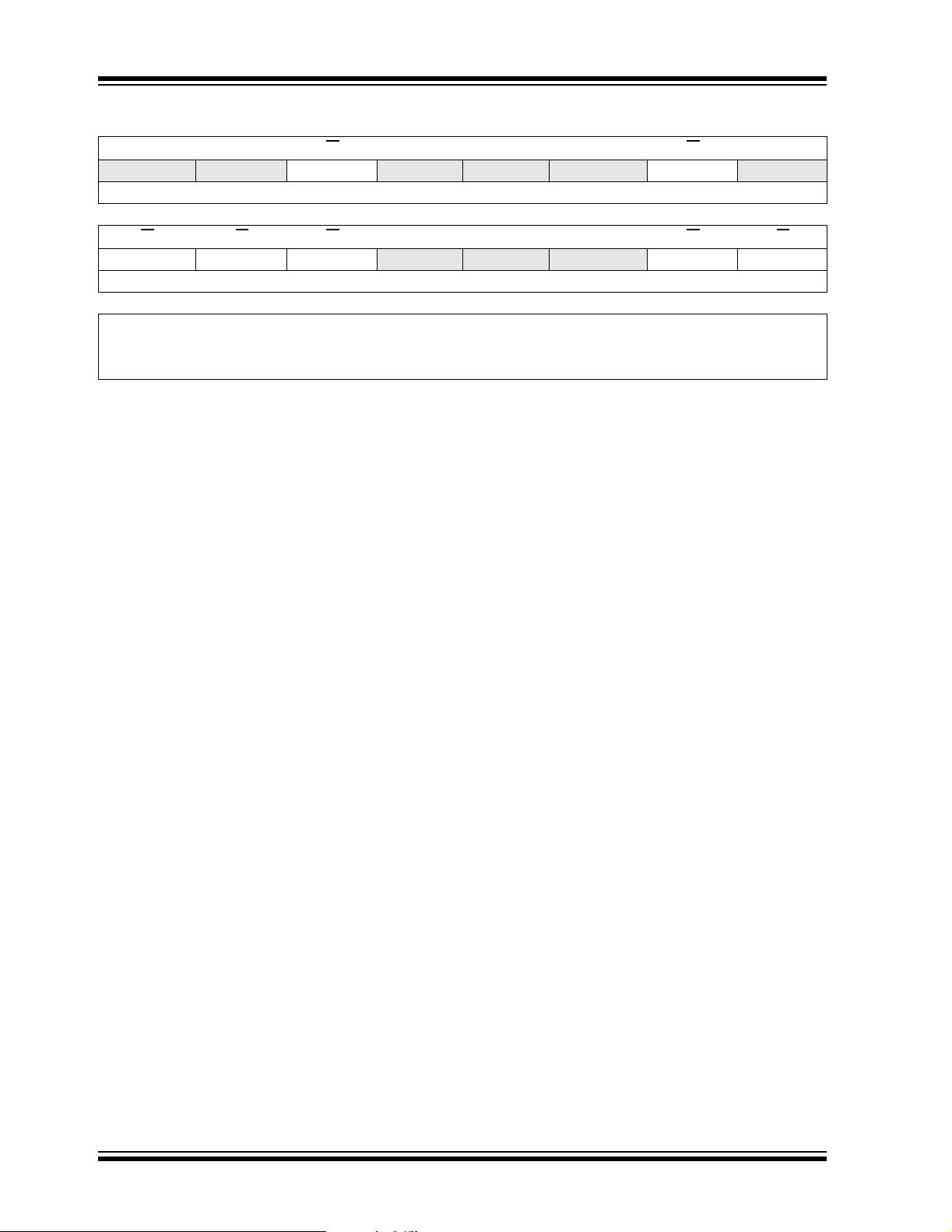
PIC24FJ64GA004 FAMILY
REGISTER 6-7: IFS2: INTERRUPT FLAG STATUS REGISTER 2
U-0 U-0 R/W-0 U-0 U-0 U-0 R/W-0 U-0
— —PMPIF— — —OC5IF—
bit 15 bit 8
-0 R/W-0 R/W-0 U-0 U-0 U-0 R/W-0 R/W-0
R/W
IC5IF IC4IF IC3IF
bit 7 bit 0
Legend:
R = Readable bit W = Writable bit U = Unimplemented bit, read as ‘0’
-n = Value at POR ‘1’ = Bit is set ‘0’ = Bit is cleared x = Bit is unknown
bit 15-14 Unimplemented: Read as ‘0’
bit 13 PMPIF: Parallel Master Port Interrupt Flag Status bit
1 = Interrupt request has occurred
0 = Interrupt request has not occurred
bit 12-10 Unimplemented: Read as ‘0’
bit 9 OC5IF: Output Compare Channel 5 Interrupt Flag Status bit
1 = Interrupt request has occurred
0 = Interrupt request has not occurred
bit 8 Unimplemented: Read as ‘0’
bit 7 IC5IF: Input Capture Channel 5 Interrupt Flag Status bit
1 = Interrupt request has occurred
0 = Interrupt request has not occurred
bit 6 IC4IF: Input Capture Channel 4 Interrupt Flag Status bit
1 = Interrupt request has occurred
0 = Interrupt request has not occurred
bit 5 IC3IF: Input Capture Channel 3 Interrupt Flag Status bit
1 = Interrupt request has occurred
0 = Interrupt request has not occurred
bit 4-2 Unimplemented: Read as ‘0’
bit 1 SPI2IF: SPI2 Event Interrupt Flag Status bit
1 = Interrupt request has occurred
0 = Interrupt request has not occurred
bit 0 SPI2IF: SPI2 Fault Interrupt Flag Status bit
1 = Interrupt request has occurred
0 = Interrupt request has not occurred
— — — SPI2IF SPF2IF
DS39881B-page 62 Preliminary © 2007 Microchip Technology Inc.
Page 65

PIC24FJ64GA004 FAMILY
REGISTER 6-8: IFS3: INTERRUPT FLAG STATUS REGISTER 3
U-0 R/W-0 U-0 U-0 U-0 U-0 U-0 U-0
—RTCIF— — — — — —
bit 15 bit 8
U-0 U-0 U-0 U-0 U-0 R/W
— — — — — MI2C2IF SI2C2IF —
bit 7 bit 0
Legend:
R = Readable bit W = Writable bit U = Unimplemented bit, read as ‘0’
-n = Value at POR ‘1’ = Bit is set ‘0’ = Bit is cleared x = Bit is unknown
bit 15 Unimplemented: Read as ‘0’
bit 14 RTCIF: Real-Time Clock/Calendar Interrupt Flag Status bit
1 = Interrupt request has occurred
0 = Interrupt request has not occurred
bit 13-3 Unimplemented: Read as ‘0’
bit 2 MI2C2IF: Master I2C2 Event Interrupt Flag Status bit
1 = Interrupt request has occurred
0 = Interrupt request has not occurred
bit 1 SI2C2IF: Slave I2C2 Event Interrupt Flag Status bit
1 = Interrupt request has occurred
0 = Interrupt request has not occurred
bit 0 Unimplemented: Read as ‘0’
-0 R/W-0 U-0
© 2007 Microchip Technology Inc. Preliminary DS39881B-page 63
Page 66
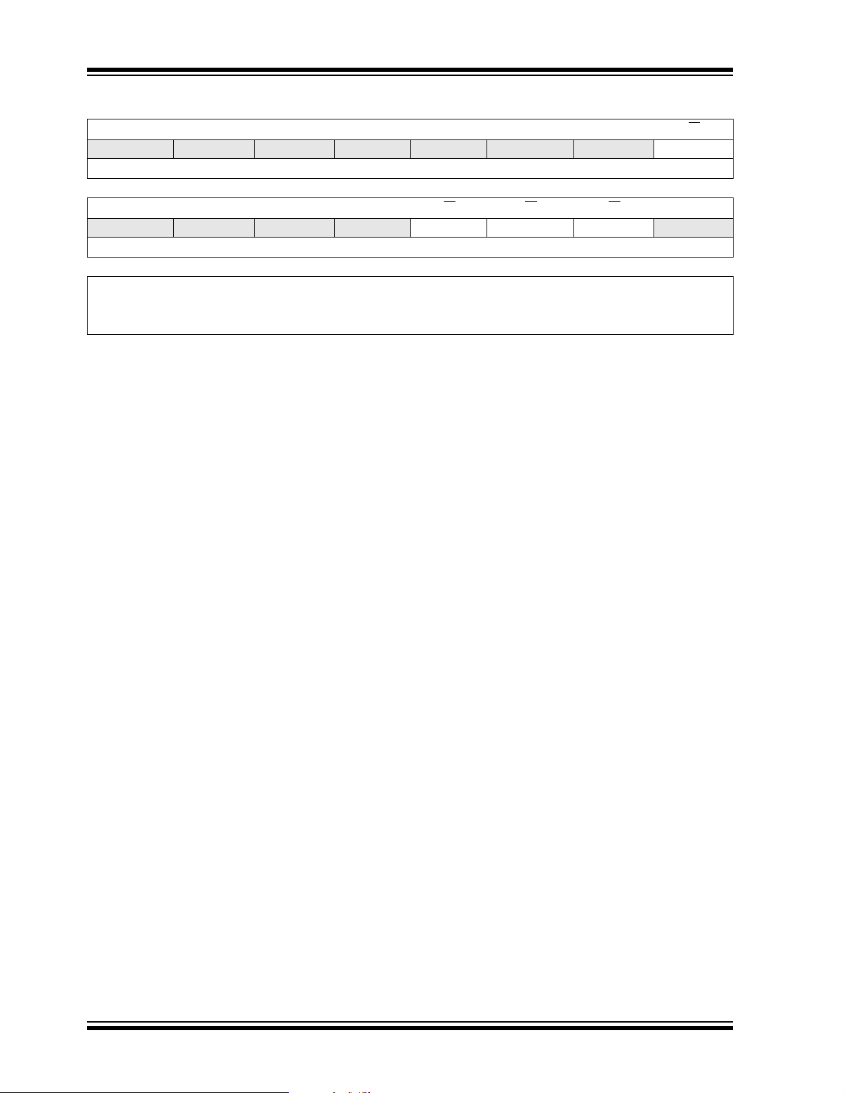
PIC24FJ64GA004 FAMILY
REGISTER 6-9: IFS4: INTERRUPT FLAG STATUS REGISTER 4
U-0 U-0 U-0 U-0 U-0 U-0 U-0 R/W-0
— — — — — — —LVDIF
bit 15 bit 8
U-0 U-0 U-0 U-0 R/W
— — — — CRCIF U2ERIF U1ERIF —
bit 7 bit 0
Legend:
R = Readable bit W = Writable bit U = Unimplemented bit, read as ‘0’
-n = Value at POR ‘1’ = Bit is set ‘0’ = Bit is cleared x = Bit is unknown
bit 15-9 Unimplemented: Read as ‘0’
bit 8 LVDIF: Low-Voltage Detect Interrupt Flag Status bit
1 = Interrupt request has occurred
0 = Interrupt request has not occurred
bit 7-4 Unimplemented: Read as ‘0’
bit 3 CRCIF: CRC Generator Interrupt Flag Status bit
1 = Interrupt request has occurred
0 = Interrupt request has not occurred
bit 2 U2ERIF: UART2 Error Interrupt Flag Status bit
1 = Interrupt request has occurred
0 = Interrupt request has not occurred
bit 1 U1ERIF: UART1 Error Interrupt Flag Status bit
1 = Interrupt request has occurred
0 = Interrupt request has not occurred
bit 0 Unimplemented: Read as ‘0’
-0 R/W-0 R/W-0 U-0
DS39881B-page 64 Preliminary © 2007 Microchip Technology Inc.
Page 67
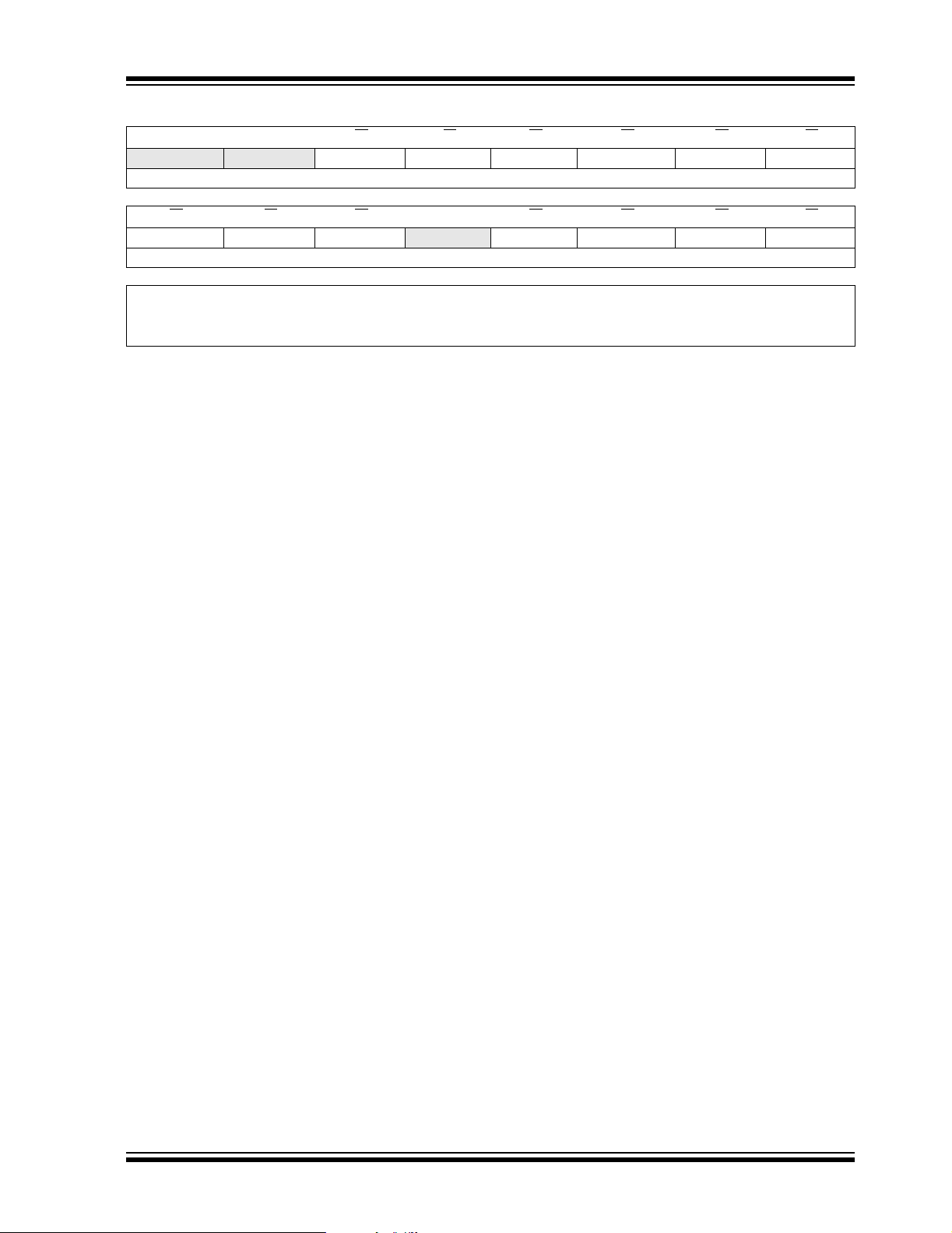
PIC24FJ64GA004 FAMILY
REGISTER 6-10: IEC0: INTERRUPT ENABLE CONTROL REGISTER 0
U-0 U-0 R/W-0 R/W-0 R/W-0 R/W-0 R/W-0 R/W-0
— — AD1IE U1TXIE U1RXIE SPI1IE SPF1IE T3IE
bit 15 bit 8
R/W
-0 R/W-0 R/W-0 U-0 R/W-0 R/W-0 R/W-0 R/W-0
T2IE OC2IE IC2IE
bit 7 bit 0
Legend:
R = Readable bit W = Writable bit U = Unimplemented bit, read as ‘0’
-n = Value at POR ‘1’ = Bit is set ‘0’ = Bit is cleared x = Bit is unknown
bit 15-14 Unimplemented: Read as ‘0’
bit 13 AD1IE: A/D Conversion Complete Interrupt Enable bit
1 = Interrupt request enabled
0 = Interrupt request not enabled
bit 12 U1TXIE: UART1 Transmitter Interrupt Enable bit
1 = Interrupt request enabled
0 = Interrupt request not enabled
bit 11 U1RXIE: UART1 Receiver Interrupt Enable bit
1 = Interrupt request enabled
0 = Interrupt request not enabled
bit 10 SPI1IE: SPI1 Transfer Complete Interrupt Enable bit
1 = Interrupt request enabled
0 = Interrupt request not enabled
bit 9 SPF1IE: SPI1 Fault Interrupt Enable bit
1 = Interrupt request enabled
0 = Interrupt request not enabled
bit 8 T3IE: Timer3 Interrupt Enable bit
1 = Interrupt request enabled
0 = Interrupt request not enabled
bit 7 T2IE: Timer2 Interrupt Enable bit
1 = Interrupt request enabled
0 = Interrupt request not enabled
bit 6 OC2IE: Output Compare Channel 2 Interrupt Enable bit
1 = Interrupt request enabled
0 = Interrupt request not enabled
bit 5 IC2IE: Input Capture Channel 2 Interrupt Enable bit
1 = Interrupt request enabled
0 = Interrupt request not enabled
bit 4 Unimplemented: Read as ‘0’
bit 3 T1IE: Timer1 Interrupt Enable bit
1 = Interrupt request enabled
0 = Interrupt request not enabled
bit 2 OC1IE: Output Compare Channel 1 Interrupt Enable bit
1 = Interrupt request enabled
0 = Interrupt request not enabled
bit 1 IC1IE: Input Capture Channel 1 Interrupt Enable bit
1 = Interrupt request enabled
0 = Interrupt request not enabled
bit 0 INT0IE:
1 = Interrupt request enabled
0 = Interrupt request not enabled
External Interrupt 0 Enable bit
— T1IE OC1IE IC1IE INT0IE
(1)
(1)
Note 1: If INTxIE = 1, this external interrupt input must be configured to an available RPx pin. See Section 9.4
”Peripheral Pin Select” for more information.
© 2007 Microchip Technology Inc. Preliminary DS39881B-page 65
Page 68
PIC24FJ64GA004 FAMILY
REGISTER 6-11: IEC1: INTERRUPT ENABLE CONTROL REGISTER 1
R/W-0 R/W-0 R/W-0 R/W-0 R/W-0 R/W-0 R/W-0 U-0
U2TXIE U2RXIE INT2IE
bit 15 bit 8
U-0 U-0 U-0 R/W
— — —INT1IE
bit 7 bit 0
Legend:
R = Readable bit W = Writable bit U = Unimplemented bit, read as ‘0’
-n = Value at POR ‘1’ = Bit is set ‘0’ = Bit is cleared x = Bit is unknown
bit 15 U2TXIE: UART2 Transmitter Interrupt Enable bit
1 = Interrupt request enabled
0 = Interrupt request not enabled
bit 14 U2RXIE: UART2 Receiver Interrupt Enable bit
1 = Interrupt request enabled
0 = Interrupt request not enabled
bit 13 INT2IE: External Interrupt 2 Enable bit
1 = Interrupt request enabled
0 = Interrupt request not enabled
bit 12 T5IE: Timer5 Interrupt Enable bit
1 = Interrupt request enabled
0 = Interrupt request not enabled
bit 11 T4IE: Timer4 Interrupt Enable bit
1 = Interrupt request enabled
0 = Interrupt request not enabled
bit 10 OC4IE: Output Compare Channel 4 Interrupt Enable bit
1 = Interrupt request enabled
0 = Interrupt request not enabled
bit 9 OC3IE: Output Compare Channel 3 Interrupt Enable bit
1 = Interrupt request enabled
0 = Interrupt request not enabled
bit 8-5 Unimplemented: Read as ‘0’
bit 4 INT1IE: External Interrupt 1 Enable bit
1 = Interrupt request enabled
0 = Interrupt request not enabled
bit 3 CNIE: Input Change Notification Interrupt Enable bit
1 = Interrupt request enabled
0 = Interrupt request not enabled
bit 2 CMIE: Comparator Interrupt Enable bit
1 = Interrupt request enabled
0 = Interrupt request not enabled
bit 1 MI2C1IE: Master I2C1 Event Interrupt Enable bit
1 = Interrupt request enabled
0 = Interrupt request not enabled
bit 0 SI2C1IE: Slave I2C1 Event Interrupt Enable bit
1 = Interrupt request enabled
0 = Interrupt request not enabled
(1)
T5IE T4IE OC4IE OC3IE —
-0 R/W-0 R/W-0 R/W-0 R/W-0
(1)
(1)
(1)
CNIE CMIE MI2C1IE SI2C1IE
Note 1: If INTxIE = 1, this external interrupt input must be configured to an available RPx pin. See Section 9.4
”Peripheral Pin Select” for more information.
DS39881B-page 66 Preliminary © 2007 Microchip Technology Inc.
Page 69

PIC24FJ64GA004 FAMILY
REGISTER 6-12: IEC2: INTERRUPT ENABLE CONTROL REGISTER 2
U-0 U-0 R/W-0 U-0 U-0 U-0 R/W-0 U-0
© 2007 Microchip Technology Inc. Preliminary DS39881B-page 67
Page 70
PIC24FJ64GA004 FAMILY
REGISTER 6-13: IEC3: INTERRUPT ENABLE CONTROL REGISTER 3
U-0 R/W-0 U-0 U-0 U-0 U-0 U-0 U-0
—RTCIE— — — — — —
bit 15 bit 8
U-0 U-0 U-0 U-0 U-0 R/W
— — — — — MI2C2IE SI2C2IE —
bit 7 bit 0
Legend:
R = Readable bit W = Writable bit U = Unimplemented bit, read as ‘0’
-n = Value at POR ‘1’ = Bit is set ‘0’ = Bit is cleared x = Bit is unknown
bit 15 Unimplemented: Read as ‘0’
bit 14 RTCIE: Real-Time Clock/Calendar Interrupt Enable bit
1 = Interrupt request enabled
0 = Interrupt request not enabled
bit 13-3 Unimplemented: Read as ‘0’
bit 2 MI2C2IE: Master I2C2 Event Interrupt Enable bit
1 = Interrupt request enabled
0 = Interrupt request not enabled
bit 1 SI2C2IE: Slave I2C2 Event Interrupt Enable bit
1 = Interrupt request enabled
0 = Interrupt request not enabled
bit 0 Unimplemented: Read as ‘0’
-0 R/W-0 U-0
DS39881B-page 68 Preliminary © 2007 Microchip Technology Inc.
Page 71
PIC24FJ64GA004 FAMILY
REGISTER 6-14: IEC4: INTERRUPT ENABLE CONTROL REGISTER 4
U-0 U-0 U-0 U-0 U-0 U-0 U-0 R/W-0
— — — — — — —LVDIE
bit 15 bit 8
U-0 U-0 U-0 U-0 R/W
— — — — CRCIE U2ERIE U1ERIE —
bit 7 bit 0
Legend:
R = Readable bit W = Writable bit U = Unimplemented bit, read as ‘0’
-n = Value at POR ‘1’ = Bit is set ‘0’ = Bit is cleared x = Bit is unknown
bit 15-9 Unimplemented: Read as ‘0’
bit 8 LVDIE: Low-Voltage Detect Interrupt Enable Status bit
1 = Interrupt request enabled
0 = Interrupt request not enabled
bit 7-4 Unimplemented: Read as ‘0’
bit 3 CRCIE: CRC Generator Interrupt Enable bit
1 = Interrupt request enabled
0 = Interrupt request not enabled
bit 2 U2ERIE: UART2 Error Interrupt Enable bit
1 = Interrupt request enabled
0 = Interrupt request not enabled
bit 1 U1ERIE: UART1 Error Interrupt Enable bit
1 = Interrupt request enabled
0 = Interrupt request not enabled
bit 0 Unimplemented: Read as ‘0’
-0 R/W-0 R/W-0 U-0
© 2007 Microchip Technology Inc. Preliminary DS39881B-page 69
Page 72
PIC24FJ64GA004 FAMILY
REGISTER 6-15: IPC0: INTERRUPT PRIORITY CONTROL REGISTER 0
U-0 R/W-1 R/W-0 R/W-0 U-0 R/W-1 R/W-0 R/W-0
— T1IP2 T1IP1 T1IP0 — OC1IP2 OC1IP1 OC1IP0
bit 15 bit 8
U-0 R/W
— IC1IP2 IC1IP1 IC1IP0 — INT0IP2 INT0IP1 INT0IP0
bit 7 bit 0
Legend:
R = Readable bit W = Writable bit U = Unimplemented bit, read as ‘0’
-n = Value at POR ‘1’ = Bit is set ‘0’ = Bit is cleared x = Bit is unknown
bit 15 Unimplemented: Read as ‘0’
bit 14-12 T1IP2:T1IP0: Timer1 Interrupt Priority bits
111 = Interrupt is priority 7 (highest priority interrupt)
•
•
•
001 = Interrupt is priority 1
000 = Interrupt source is disabled
bit 11 Unimplemented: Read as ‘0’
bit 10-8 OC1IP2:OC1IP0: Output Compare Channel 1 Interrupt Priority bits
111 = Interrupt is priority 7 (highest priority interrupt)
•
•
•
001 = Interrupt is priority 1
000 = Interrupt source is disabled
bit 7 Unimplemented: Read as ‘0’
bit 6-4 IC1IP2:IC1IP0: Input Capture Channel 1 Interrupt Priority bits
111 = Interrupt is priority 7 (highest priority interrupt)
•
•
•
001 = Interrupt is priority 1
000 = Interrupt source is disabled
bit 3 Unimplemented: Read as ‘0’
bit 2-0 INT0IP2:INT0IP0: External Interrupt 0 Priority bits
111 = Interrupt is priority 7 (highest priority interrupt)
•
•
•
001 = Interrupt is priority 1
000 = Interrupt source is disabled
-1 R/W-0 R/W-0 U-0 R/W-1 R/W-0 R/W-0
DS39881B-page 70 Preliminary © 2007 Microchip Technology Inc.
Page 73

PIC24FJ64GA004 FAMILY
REGISTER 6-16: IPC1: INTERRUPT PRIORITY CONTROL REGISTER 1
U-0 R/W-1 R/W-0 R/W-0 U-0 R/W-1 R/W-0 R/W-0
— T2IP2 T2IP1 T2IP0 — OC2IP2 OC2IP1 OC2IP0
bit 15 bit 8
U-0 R/W
— IC2IP2 IC2IP1 IC2IP0 — — — —
bit 7 bit 0
Legend:
R = Readable bit W = Writable bit U = Unimplemented bit, read as ‘0’
-n = Value at POR ‘1’ = Bit is set ‘0’ = Bit is cleared x = Bit is unknown
bit 15 Unimplemented: Read as ‘0’
bit 14-12 T2IP2:T2IP0: Timer2 Interrupt Priority bits
111 = Interrupt is priority 7 (highest priority interrupt)
•
•
•
001 = Interrupt is priority 1
000 = Interrupt source is disabled
bit 11 Unimplemented: Read as ‘0’
bit 10-8 OC2IP2:OC2IP0: Output Compare Channel 2 Interrupt Priority bits
111 = Interrupt is priority 7 (highest priority interrupt)
•
•
•
001 = Interrupt is priority 1
000 = Interrupt source is disabled
bit 7 Unimplemented: Read as ‘0’
bit 6-4 IC2IP2:IC2IP0: Input Capture Channel 2 Interrupt Priority bits
111 = Interrupt is priority 7 (highest priority interrupt)
•
•
•
001 = Interrupt is priority 1
000 = Interrupt source is disabled
bit 3-0 Unimplemented: Read as ‘0’
-1 R/W-0 R/W-0 U-0 U-0 U-0 U-0
© 2007 Microchip Technology Inc. Preliminary DS39881B-page 71
Page 74

PIC24FJ64GA004 FAMILY
REGISTER 6-17: IPC2: INTERRUPT PRIORITY CONTROL REGISTER 2
U-0 R/W-1 R/W-0 R/W-0 U-0 R/W-1 R/W-0 R/W-0
— U1RXIP2 U1RXIP1 U1RXIP0 — SPI1IP2 SPI1IP1 SPI1IP0
bit 15 bit 8
U-0 R/W
— SPF1IP2 SPF1IP1 SPF1IP0 — T3IP2 T3IP1 T3IP0
bit 7 bit 0
Legend:
R = Readable bit W = Writable bit U = Unimplemented bit, read as ‘0’
-n = Value at POR ‘1’ = Bit is set ‘0’ = Bit is cleared x = Bit is unknown
bit 15 Unimplemented: Read as ‘0’
bit 14-12 U1RXIP2:U1RXIP0: UART1 Receiver Interrupt Priority bits
111 = Interrupt is priority 7 (highest priority interrupt)
•
•
•
001 = Interrupt is priority 1
000 = Interrupt source is disabled
bit 11 Unimplemented: Read as ‘0’
bit 10-8 SPI1IP2:SPI1IP0: SPI1 Event Interrupt Priority bits
111 = Interrupt is priority 7 (highest priority interrupt)
•
•
•
001 = Interrupt is priority 1
000 = Interrupt source is disabled
bit 7 Unimplemented: Read as ‘0’
bit 6-4 SPF1IP2:SPF1IP0: SPI1 Fault Interrupt Priority bits
111 = Interrupt is priority 7 (highest priority interrupt)
•
•
•
001 = Interrupt is priority 1
000 = Interrupt source is disabled
bit 3 Unimplemented: Read as ‘0’
bit 2-0 T3IP2:T3IP0: Timer3 Interrupt Priority bits
111 = Interrupt is priority 7 (highest priority interrupt)
•
•
•
001 = Interrupt is priority 1
000 = Interrupt source is disabled
-1 R/W-0 R/W-0 U-0 R/W-1 R/W-0 R/W-0
DS39881B-page 72 Preliminary © 2007 Microchip Technology Inc.
Page 75
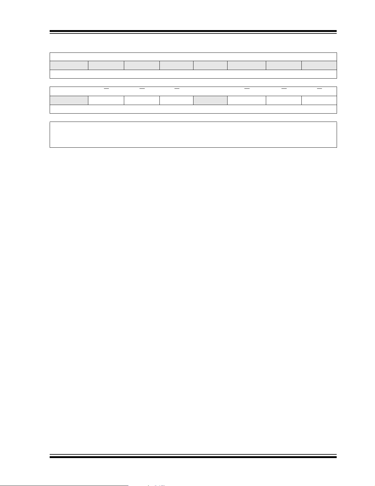
PIC24FJ64GA004 FAMILY
REGISTER 6-18: IPC3: INTERRUPT PRIORITY CONTROL REGISTER 3
U-0 U-0 U-0 U-0 U-0 U-0 U-0 U-0
— — — — — — — —
bit 15 bit 8
U-0 R/W
— AD1IP2 AD1IP1 AD1IP0 — U1TXIP2 U1TXIP1 U1TXIP0
bit 7 bit 0
Legend:
R = Readable bit W = Writable bit U = Unimplemented bit, read as ‘0’
-n = Value at POR ‘1’ = Bit is set ‘0’ = Bit is cleared x = Bit is unknown
bit 15-7 Unimplemented: Read as ‘0’
bit 6-4 AD1IP2:AD1IP0: A/D Conversion Complete Interrupt Priority bits
111 = Interrupt is priority 7 (highest priority interrupt)
•
•
•
001 = Interrupt is priority 1
000 = Interrupt source is disabled
bit 3 Unimplemented: Read as ‘0’
bit 2-0 U1TXIP2:U1TXIP0: UART1 Transmitter Interrupt Priority bits
111 = Interrupt is priority 7 (highest priority interrupt)
•
•
•
001 = Interrupt is priority 1
000 = Interrupt source is disabled
-1 R/W-0 R/W-0 U-0 R/W-1 R/W-0 R/W-0
© 2007 Microchip Technology Inc. Preliminary DS39881B-page 73
Page 76

PIC24FJ64GA004 FAMILY
REGISTER 6-19: IPC4: INTERRUPT PRIORITY CONTROL REGISTER 4
U-0 R/W-1 R/W-0 R/W-0 U-0 R/W-1 R/W-0 R/W-0
— CNIP2 CNIP1 CNIP0 — CMIP2 CMIP1 CMIP0
bit 15 bit 8
U-0 R/W
— MI2C1P2 MI2C1P1 MI2C1P0 — SI2C1P2 SI2C1P1 SI2C1P0
bit 7 bit 0
Legend:
R = Readable bit W = Writable bit U = Unimplemented bit, read as ‘0’
-n = Value at POR ‘1’ = Bit is set ‘0’ = Bit is cleared x = Bit is unknown
bit 15 Unimplemented: Read as ‘0’
bit 14-12 CNIP2:CNIP0: Input Change Notification Interrupt Priority bits
111 = Interrupt is priority 7 (highest priority interrupt)
•
•
•
001 = Interrupt is priority 1
000 = Interrupt source is disabled
bit 11 Unimplemented: Read as ‘0’
bit 10-8 CMIP2:CMIP0: Comparator Interrupt Priority bits
111 = Interrupt is priority 7 (highest priority interrupt)
•
•
•
001 = Interrupt is priority 1
000 = Interrupt source is disabled
bit 7 Unimplemented: Read as ‘0’
bit 6-4 MI2C1P2:MI2C1P0: Master I2C1 Event Interrupt Priority bits
111 = Interrupt is priority 7 (highest priority interrupt)
•
•
•
001 = Interrupt is priority 1
000 = Interrupt source is disabled
bit 3 Unimplemented: Read as ‘0’
bit 2-0 SI2C1P2:SI2C1P0: Slave I2C1 Event Interrupt Priority bits
111 = Interrupt is priority 7 (highest priority interrupt)
•
•
•
001 = Interrupt is priority 1
000 = Interrupt source is disabled
-1 R/W-0 R/W-0 U-0 R/W-1 R/W-0 R/W-0
DS39881B-page 74 Preliminary © 2007 Microchip Technology Inc.
Page 77

PIC24FJ64GA004 FAMILY
REGISTER 6-20: IPC5: INTERRUPT PRIORITY CONTROL REGISTER 5
U-0 U-0 U-0 U-0 U-0 U-0 U-0 U-0
— — — — — — — —
bit 15 bit 8
U-0 U-0 U-0 U-0 U-0 R/W
— — — — — INT1IP2 INT1IP1 INT1IP0
bit 7 bit 0
Legend:
R = Readable bit W = Writable bit U = Unimplemented bit, read as ‘0’
-n = Value at POR ‘1’ = Bit is set ‘0’ = Bit is cleared x = Bit is unknown
bit 15-3 Unimplemented: Read as ‘0’
bit 2-0 INT1IP2:INT1IP0: External Interrupt 1 Priority bits
111 = Interrupt is priority 7 (highest priority interrupt)
•
•
•
001 = Interrupt is priority 1
000 = Interrupt source is disabled
-1 R/W-0 R/W-0
© 2007 Microchip Technology Inc. Preliminary DS39881B-page 75
Page 78

PIC24FJ64GA004 FAMILY
REGISTER 6-21: IPC6: INTERRUPT PRIORITY CONTROL REGISTER 6
U-0 R/W-1 R/W-0 R/W-0 U-0 R/W-1 R/W-0 R/W-0
— T4IP2 T4IP1 T4IP0 — OC4IP2 OC4IP1 OC4IP0
bit 15 bit 8
U-0 R/W
— OC3IP2 OC3IP1 OC3IP0 — — — —
bit 7 bit 0
Legend:
R = Readable bit W = Writable bit U = Unimplemented bit, read as ‘0’
-n = Value at POR ‘1’ = Bit is set ‘0’ = Bit is cleared x = Bit is unknown
bit 15 Unimplemented: Read as ‘0’
bit 14-12 T4IP2:T4IP0: Timer4 Interrupt Priority bits
111 = Interrupt is priority 7 (highest priority interrupt)
•
•
•
001 = Interrupt is priority 1
000 = Interrupt source is disabled
bit 11 Unimplemented: Read as ‘0’
bit 10-8 OC4IP2:OC4IP0: Output Compare Channel 4 Interrupt Priority bits
111 = Interrupt is priority 7 (highest priority interrupt)
•
•
•
001 = Interrupt is priority 1
000 = Interrupt source is disabled
bit 7 Unimplemented: Read as ‘0’
bit 6-4 OC3IP2:OC3IP0: Output Compare Channel 3 Interrupt Priority bits
111 = Interrupt is priority 7 (highest priority interrupt)
•
•
•
001 = Interrupt is priority 1
000 = Interrupt source is disabled
bit 3-0 Unimplemented: Read as ‘0’
-1 R/W-0 R/W-0 U-0 U-0 U-0 U-0
DS39881B-page 76 Preliminary © 2007 Microchip Technology Inc.
Page 79

PIC24FJ64GA004 FAMILY
REGISTER 6-22: IPC7: INTERRUPT PRIORITY CONTROL REGISTER 7
U-0 R/W-1 R/W-0 R/W-0 U-0 R/W-1 R/W-0 R/W-0
— U2TXIP2 U2TXIP1 U2TXIP0 — U2RXIP2 U2RXIP1 U2RXIP0
bit 15 bit 8
U-0 R/W
— INT2IP2 INT2IP1 INT2IP0 — T5IP2 T5IP1 T5IP0
bit 7 bit 0
Legend:
R = Readable bit W = Writable bit U = Unimplemented bit, read as ‘0’
-n = Value at POR ‘1’ = Bit is set ‘0’ = Bit is cleared x = Bit is unknown
bit 15 Unimplemented: Read as ‘0’
bit 14-12 U2TXIP2:U2TXIP0: UART2 Transmitter Interrupt Priority bits
111 = Interrupt is priority 7 (highest priority interrupt)
•
•
•
001 = Interrupt is priority 1
000 = Interrupt source is disabled
bit 11 Unimplemented: Read as ‘0’
bit 10-8 U2RXIP2:U2RXIP0: UART2 Receiver Interrupt Priority bits
111 = Interrupt is priority 7 (highest priority interrupt)
•
•
•
001 = Interrupt is priority 1
000 = Interrupt source is disabled
bit 7 Unimplemented: Read as ‘0’
bit 6-4 INT2IP2:INT2IP0: External Interrupt 2 Priority bits
111 = Interrupt is priority 7 (highest priority interrupt)
•
•
•
001 = Interrupt is priority 1
000 = Interrupt source is disabled
bit 3 Unimplemented: Read as ‘0’
bit 2-0 T5IP2:T5IP0: Timer5 Interrupt Priority bits
111 = Interrupt is priority 7 (highest priority interrupt)
•
•
•
001 = Interrupt is priority 1
000 = Interrupt source is disabled
-1 R/W-0 R/W-0 U-0 R/W-1 R/W-0 R/W-0
© 2007 Microchip Technology Inc. Preliminary DS39881B-page 77
Page 80

PIC24FJ64GA004 FAMILY
REGISTER 6-23: IPC8: INTERRUPT PRIORITY CONTROL REGISTER 8
U-0 U-0 U-0 U-0 U-0 U-0 U-0 U-0
— — — — — — — —
bit 15 bit 8
U-0 R/W
— SPI2IP2 SPI2IP1 SPI2IP0 — SPF2IP2 SPF2IP1 SPF2IP0
bit 7 bit 0
Legend:
R = Readable bit W = Writable bit U = Unimplemented bit, read as ‘0’
-n = Value at POR ‘1’ = Bit is set ‘0’ = Bit is cleared x = Bit is unknown
bit 15-7 Unimplemented: Read as ‘0’
bit 6-4 SPI2IP2:SPI2IP0: SPI2 Event Interrupt Priority bits
111 = Interrupt is priority 7 (highest priority interrupt)
•
•
•
001 = Interrupt is priority 1
000 = Interrupt source is disabled
bit 3 Unimplemented: Read as ‘0’
bit 2-0 SPF2IP2:SPF2IP0: SPI2 Fault Interrupt Priority bits
111 = Interrupt is priority 7 (highest priority interrupt)
•
•
•
001 = Interrupt is priority 1
000 = Interrupt source is disabled
-1 R/W-0 R/W-0 U-0 R/W-1 R/W-0 R/W-0
DS39881B-page 78 Preliminary © 2007 Microchip Technology Inc.
Page 81
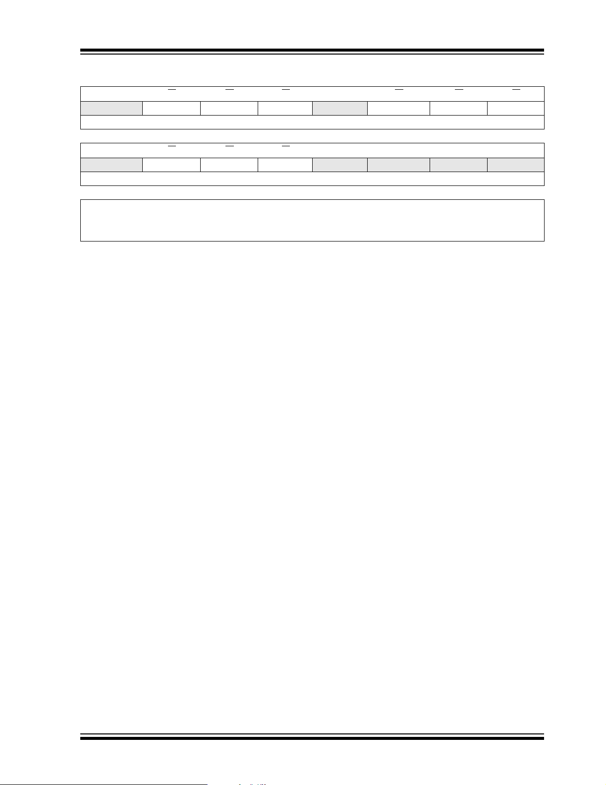
PIC24FJ64GA004 FAMILY
REGISTER 6-24: IPC9: INTERRUPT PRIORITY CONTROL REGISTER 9
U-0 R/W-1 R/W-0 R/W-0 U-0 R/W-1 R/W-0 R/W-0
— IC5IP2 IC5IP1 IC5IP0 — IC4IP2 IC4IP1 IC4IP0
bit 15 bit 8
U-0 R/W
— IC3IP2 IC3IP1 IC3IP0 — — — —
bit 7 bit 0
Legend:
R = Readable bit W = Writable bit U = Unimplemented bit, read as ‘0’
-n = Value at POR ‘1’ = Bit is set ‘0’ = Bit is cleared x = Bit is unknown
bit 15 Unimplemented: Read as ‘0’
bit 14-12 IC5IP2:IC5IP0: Input Capture Channel 5 Interrupt Priority bits
111 = Interrupt is priority 7 (highest priority interrupt)
•
•
•
001 = Interrupt is priority 1
000 = Interrupt source is disabled
bit 11 Unimplemented: Read as ‘0’
bit 10-8 IC4IP2:IC4IP0: Input Capture Channel 4 Interrupt Priority bits
111 = Interrupt is priority 7 (highest priority interrupt)
•
•
•
001 = Interrupt is priority 1
000 = Interrupt source is disabled
bit 7 Unimplemented: Read as ‘0’
bit 6-4 IC3IP2:IC3IP0: Input Capture Channel 3 Interrupt Priority bits
111 = Interrupt is priority 7 (highest priority interrupt)
•
•
•
001 = Interrupt is priority 1
000 = Interrupt source is disabled
bit 3-0 Unimplemented: Read as ‘0’
-1 R/W-0 R/W-0 U-0 U-0 U-0 U-0
© 2007 Microchip Technology Inc. Preliminary DS39881B-page 79
Page 82

PIC24FJ64GA004 FAMILY
REGISTER 6-25: IPC10: INTERRUPT PRIORITY CONTROL REGISTER 10
U-0 U-0 U-0 U-0 U-0 U-0 U-0 U-0
— — — — — — — —
bit 15 bit 8
U-0 R/W
— OC5IP2 OC5IP1 OC5IP0 — — — —
bit 7 bit 0
Legend:
R = Readable bit W = Writable bit U = Unimplemented bit, read as ‘0’
-n = Value at POR ‘1’ = Bit is set ‘0’ = Bit is cleared x = Bit is unknown
bit 15-7 Unimplemented: Read as ‘0’
bit 6-4 OC5IP2:OC5IP0: Output Compare Channel 5 Interrupt Priority bits
111 = Interrupt is priority 7 (highest priority interrupt)
•
•
•
001 = Interrupt is priority 1
000 = Interrupt source is disabled
bit 3-0 Unimplemented: Read as ‘0’
-1 R/W-0 R/W-0 U-0 U-0 U-0 U-0
REGISTER 6-26: IPC11: INTERRUPT PRIORITY CONTROL REGISTER 11
U-0 U-0 U-0 U-0 U-0 U-0 U-0 U-0
— — — — — — — —
bit 15 bit 8
U-0 R/W
— PMPIP2 PMPIP1 PMPIP0 — — — —
bit 7 bit 0
Legend:
R = Readable bit W = Writable bit U = Unimplemented bit, read as ‘0’
-n = Value at POR ‘1’ = Bit is set ‘0’ = Bit is cleared x = Bit is unknown
bit 15-7 Unimplemented: Read as ‘0’
bit 6-4 PMPIP2:PMPIP0: Parallel Master Port Interrupt Priority bits
111 = Interrupt is priority 7 (highest priority interrupt)
•
•
•
001 = Interrupt is priority 1
000 = Interrupt source is disabled
bit 3-0 Unimplemented: Read as ‘0’
DS39881B-page 80 Preliminary © 2007 Microchip Technology Inc.
-1 R/W-0 R/W-0 U-0 U-0 U-0 U-0
Page 83
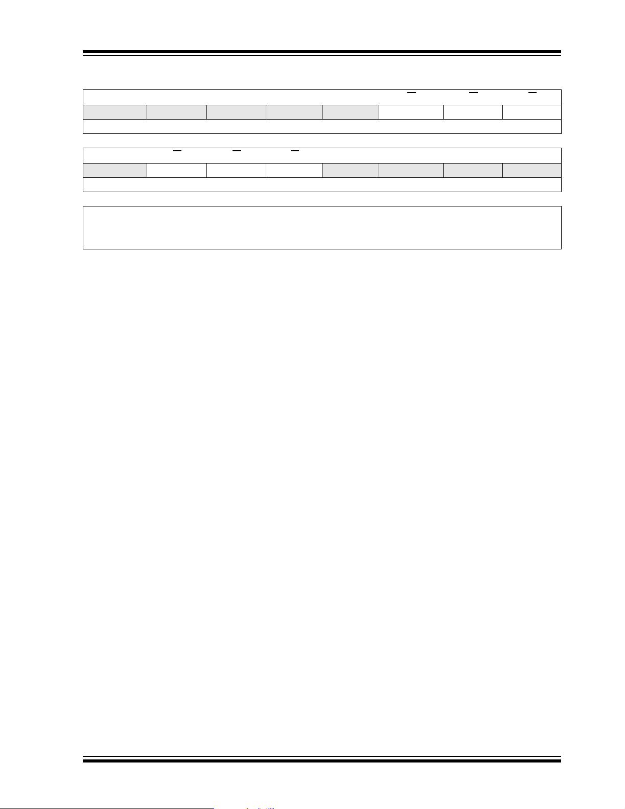
PIC24FJ64GA004 FAMILY
REGISTER 6-27: IPC12: INTERRUPT PRIORITY CONTROL REGISTER 12
U-0 U-0 U-0 U-0 U-0 R/W-1 R/W-0 R/W-0
— — — — — MI2C2P2 MI2C2P1 MI2C2P0
bit 15 bit 8
U-0 R/W
— SI2C2P2 SI2C2P1 SI2C2P0 — — — —
bit 7 bit 0
Legend:
R = Readable bit W = Writable bit U = Unimplemented bit, read as ‘0’
-n = Value at POR ‘1’ = Bit is set ‘0’ = Bit is cleared x = Bit is unknown
bit 15-11 Unimplemented: Read as ‘0’
bit 10-8 MI2C2P2:MI2C2P0: Master I2C2 Event Interrupt Priority bits
111 = Interrupt is priority 7 (highest priority interrupt)
•
•
•
001 = Interrupt is priority 1
000 = Interrupt source is disabled
bit 7 Unimplemented: Read as ‘0’
bit 6-4 SI2C2P2:SI2C2P0: Slave I2C2 Event Interrupt Priority bits
111 = Interrupt is priority 7 (highest priority interrupt)
•
•
•
001 = Interrupt is priority 1
000 = Interrupt source is disabled
bit 3-0 Unimplemented: Read as ‘0’
-1 R/W-0 R/W-0 U-0 U-0 U-0 U-0
© 2007 Microchip Technology Inc. Preliminary DS39881B-page 81
Page 84

PIC24FJ64GA004 FAMILY
REGISTER 6-28: IPC15: INTERRUPT PRIORITY CONTROL REGISTER 15
U-0 U-0 U-0 U-0 U-0 R/W-1 R/W-0 R/W-0
— — — — — RTCIP2 RTCIP1 RTCIP0
bit 15 bit 8
U-0 U-0 U-0 U-0 U-0 U-0 U-0 U-0
— — — — — — — —
bit 7 bit 0
Legend:
R = Readable bit W = Writable bit U = Unimplemented bit, read as ‘0’
-n = Value at POR ‘1’ = Bit is set ‘0’ = Bit is cleared x = Bit is unknown
bit 15-11 Unimplemented: Read as ‘0’
bit 10-8 RTCIP2:RTCIP0: Real-Time Clock/Calendar Interrupt Priority bits
111 = Interrupt is priority 7 (highest priority interrupt)
•
•
•
001 = Interrupt is priority 1
000 = Interrupt source is disabled
bit 7-0 Unimplemented: Read as ‘0’
DS39881B-page 82 Preliminary © 2007 Microchip Technology Inc.
Page 85

PIC24FJ64GA004 FAMILY
REGISTER 6-29: IPC16: INTERRUPT PRIORITY CONTROL REGISTER 16
U-0 R/W-1 R/W-0 R/W-0 U-0 R/W-1 R/W-0 R/W-0
— CRCIP2 CRCIP1 CRCIP0 — U2ERIP2 U2ERIP1 U2ERIP0
bit 15 bit 8
U-0 R/W
— U1ERIP2 U1ERIP1 U1ERIP0 — — — —
bit 7 bit 0
Legend:
R = Readable bit W = Writable bit U = Unimplemented bit, read as ‘0’
-n = Value at POR ‘1’ = Bit is set ‘0’ = Bit is cleared x = Bit is unknown
bit 15 Unimplemented: Read as ‘0’
bit 14-12 CRCIP2:CRCIP0: CRC Generator Error Interrupt Priority bits
111 = Interrupt is priority 7 (highest priority interrupt)
•
•
•
001 = Interrupt is priority 1
000 = Interrupt source is disabled
bit 11 Unimplemented: Read as ‘0’
bit 10-8 U2ERIP2:U2ERIP0: UART2 Error Interrupt Priority bits
111 = Interrupt is priority 7 (highest priority interrupt)
•
•
•
001 = Interrupt is priority 1
000 = Interrupt source is disabled
bit 7 Unimplemented: Read as ‘0’
bit 6-4 U1ERIP2:U1ERIP0: UART1 Error Interrupt Priority bits
111 = Interrupt is priority 7 (highest priority interrupt)
•
•
•
001 = Interrupt is priority 1
000 = Interrupt source is disabled
bit 3-0 Unimplemented: Read as ‘0’
-1 R/W-0 R/W-0 U-0 U-0 U-0 U-0
© 2007 Microchip Technology Inc. Preliminary DS39881B-page 83
Page 86
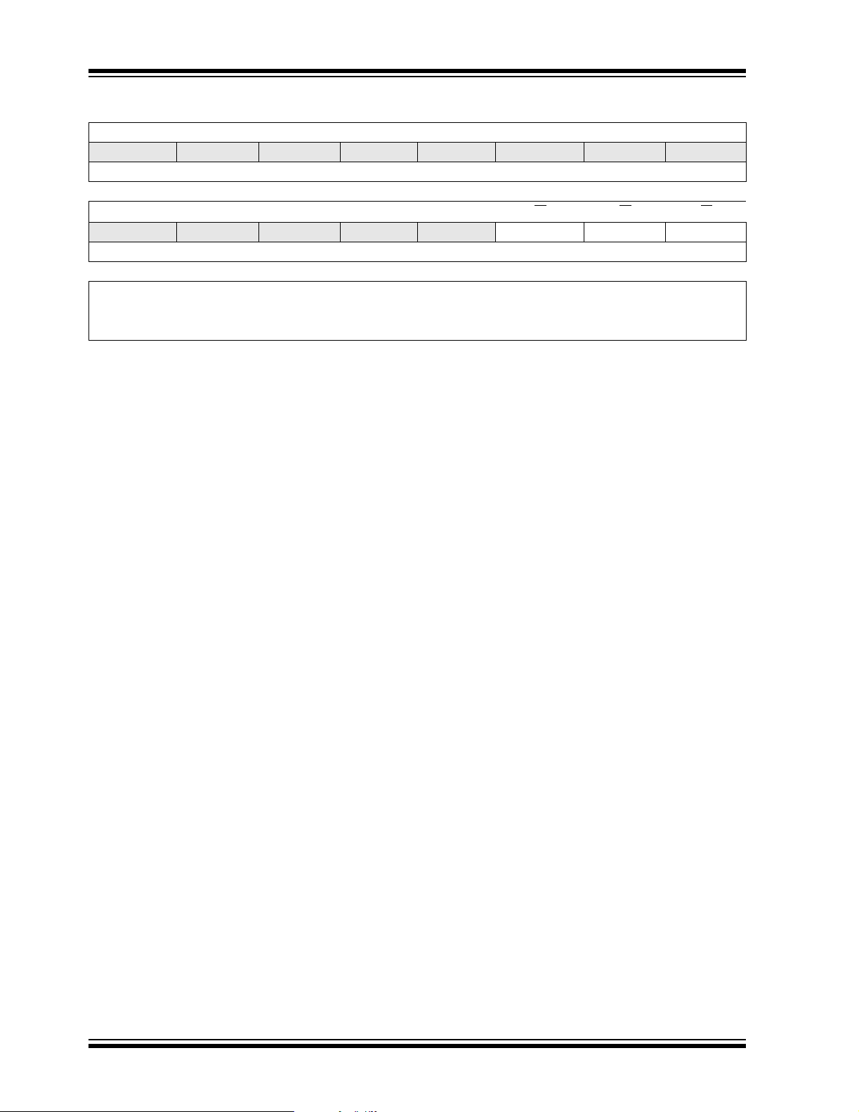
PIC24FJ64GA004 FAMILY
REGISTER 6-30: IPC18: INTERRUPT PRIORITY CONTROL REGISTER 18
U-0 U-0 U-0 U-0 U-0 U-0 U-0 U-0
— — — — — — — —
bit 15 bit 8
U-0 U-0 U-0 U-0 U-0 R/W
— — — — — LVDIP2 LVDIP1 LVDIP0
bit 7 bit 0
Legend:
R = Readable bit W = Writable bit U = Unimplemented bit, read as ‘0’
-n = Value at POR ‘1’ = Bit is set ‘0’ = Bit is cleared x = Bit is unknown
bit 15-3 Unimplemented: Read as ‘0’
bit 12-0 LVDIP2 :LVDI P0: Low-Voltage Detect Interrupt Priority bits
111 = Interrupt is priority 7 (highest priority interrupt)
•
•
•
001 = Interrupt is priority 1
000 = Interrupt source is disabled
-1 R/W-0 R/W-0
DS39881B-page 84 Preliminary © 2007 Microchip Technology Inc.
Page 87

PIC24FJ64GA004 FAMILY
6.4 Interrupt Setup Procedures
6.4.1 INITIALIZATION
To configure an interrupt source:
1. Set the NSTDIS Control bit (INTCON1<15>) if
nested interrupts are not desired.
2. Select the user-assigned priority level for the
interrupt source by writing the control bits in the
appropriate IPCx register. The priority level will
depend on the specific application and type of
interrupt source. If multiple priority levels are not
desired, the IPCx register control bits for all
enabled interrupt sources may be programmed
to the same non-zero value.
Note: At a device Reset, the IPCx registers are
initialized, such that all user interrupt
sources are assigned to priority level 4.
3. Clear the interrupt flag status bit associated with
the peripheral in the associated IFSx register.
4. Enable the interrupt source by setting the
interrupt enable control bit associated with the
source in the appropriate IECx register.
6.4.2 INTERRUPT SERVICE ROUTINE
The method that is used to declare an ISR and initialize
the IVT with the correct vector address will depend on
the programming language (i.e., ‘C’ or assembler) and
the language development toolsuite that is used to
develop the application. In general, the user must clear
the interrupt flag in the appropriate IFSx register for the
source of the interrupt that the ISR handles. Otherwise,
the ISR will be re-entered immediately after exiting the
routine. If the ISR is coded in assembly language, it
must be terminated using a RETFIE instruction to
unstack the saved PC value, SRL value and old CPU
priority level.
6.4.3 TRAP SERVICE ROUTINE
A Trap Service Routine (TSR) is coded like an ISR,
except that the appropriate trap status flag in the
INTCON1 register must be cleared to avoid re-entry
into the TSR.
6.4.4 INTERRUPT DISABLE
All user interrupts can be disabled using the following
procedure:
1. Push the current SR value onto the software
stack using the PUSH instruction.
2. Force the CPU to priority level 7 by inclusive
ORing the value OEh with SRL.
To enable user interrupts, the POP instruction may be
used to restore the previous SR value.
Note that only user interrupts with a priority level of 7 or
less can be disabled. Trap sources (level 8-15) cannot
be disabled.
The DISI instruction provides a convenient way to
disable interrupts of priority levels 1-6 for a fixed period
of time. Level 7 interrupt sources are not disabled by
the DISI instruction.
© 2007 Microchip Technology Inc. Preliminary DS39881B-page 85
Page 88

PIC24FJ64GA004 FAMILY
NOTES:
DS39881B-page 86 Preliminary © 2007 Microchip Technology Inc.
Page 89
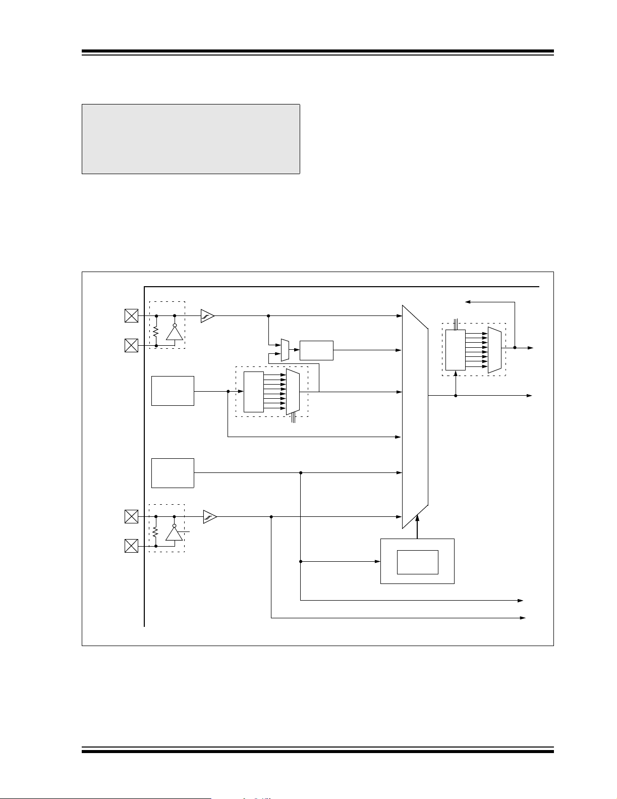
PIC24FJ64GA004 FAMILY
7.0 OSCILLATOR CONFIGURATION
• A total of four external and internal oscillator options
as clock sources, providing 11 different clock modes
• On-chip 4x PLL to boost internal operating frequency
Note: This data sheet summarizes the features
of this group of PIC24F devices. It is not
intended to be a comprehensive reference
source. For more information, refer to the
associated
Manual”
“PIC24F Family Reference
chapter.
The oscillator system for PIC24FJ64GA004 family
devices has the following features:
on select internal and external oscillator sources
• Software-controllable switching between various
clock sources
• Software-controllable postscaler for selective
clocking of CPU for system power savings
• A Fail-Safe Clock Monitor (FSCM) that detects
clock failure and permits safe application recovery
or shutdown
A simplified diagram of the oscillator system is shown
in Figure 7-1.
FIGURE 7-1: PIC24FJ64GA004 FAMILY CLOCK DIAGRAM
PIC24FJ64GA004 Family
XT, HS, EC
XTPLL, HSPLL
8 MHz
4 MHz
ECPLL,FRCPLL
FRCDIV
4 x PLL
OSCO
OSCI
Primary Oscillator
FRC
Oscillator
8 MHz
(nominal)
Postscaler
CLKO
CLKDIV<14:12>
CPU
Postscaler
Peripherals
SOSCO
SOSCI
LPRC
Oscillator
Secondary Oscillator
31 kHz (nominal)
SOSCEN
Enable
Oscillator
CLKDIV<10:8>
FRC
LPRC
SOSC
Clock Control Logic
Fail-Safe
Clock
Monitor
WDT, PWRT
Clock Source Option
for Other Modules
© 2007 Microchip Technology Inc. Preliminary DS39881B-page 87
Page 90

PIC24FJ64GA004 FAMILY
7.1 CPU Clocking Scheme
The system clock source can be provided by one of
four sources:
• Primary Oscillator (POSC) on the OSCI and
OSCO pins
• Secondary Oscillator (SOSC) on the SOSCI and
SOSCO pins
• Fast Internal RC (FRC) Oscillator
• Low-Power Internal RC (LPRC) Oscillator
The primary oscillator and FRC sources have the
option of using the internal 4x PLL. The frequency of
the FRC clock source can optionally be reduced by the
programmable clock divider. The selected clock source
generates the processor and peripheral clock sources.
The processor clock source is divided by two to produce the internal instruction cycle clock, F
document, the instruction cycle clock is also denoted
OSC/2. The internal instruction cycle clock, FOSC/2,
by F
can be provided on the OSCO I/O pin for some
operating modes of the primary oscillator.
CY. In this
7.2 Oscillator Configuration
The oscillator source (and operating mode) that is
used at a device Power-on Reset event is selected
using Configuration bit settings. The oscillator Configuration bit settings are located in the Configuration
registers in the program memory (refer to
Section 23.1 “Configuration Bits” for further
details). The Primary Oscillator Configuration bits,
POSCMD1:POSCMD0 (Configuration Word 2<1:0>),
and the Initial Oscillator Select Configuration bits,
FNOSC2:FNOSC0 (Configuration Word 2<10:8>),
select the oscillator source that is used at a Power-on
Reset. The FRC primary oscillator with postscaler
(FRCDIV) is the default (unprogrammed) selection.
The secondary oscillator, or one of the internal
oscillators, may be chosen by programming these bit
locations.
The Configuration bits allow users to choose between
the various clock modes, shown in Table 7-1.
7.2.1 CLOCK SWITCHING MODE CONFIGURATION BITS
The FCKSM Configuration bits (Configuration
Word 2<7:6>) are used to jointly configure device clock
switching and the Fail-Safe Clock Monitor (FSCM).
Clock switching is enabled only when FCKSM1 is
programmed (‘0’). The FSCM is enabled only when
FCKSM1:FCKSM0 are both programmed (‘00’).
TABLE 7-1: CONFIGURATION BIT VALUES FOR CLOCK SELECTION
Oscillator Mode Oscillator Source
Fast RC Oscillator with Postscaler
(FRCDIV)
(Reserved) Internal 00 110 1
Low-Power RC Oscillator (LPRC) Internal 00 101 1
Secondary (Timer1) Oscillator
(SOSC)
Primary Oscillator (XT) with PLL
Module (XTPLL)
Primary Oscillator (EC) with PLL
Module (ECPLL)
Primary Oscillator (HS) Primary 10 010
Primary Oscillator (XT) Primary 01 010
Primary Oscillator (EC) Primary 00 010
Fast RC Oscillator with PLL Module
(FRCPLL)
Fast RC Oscillator (FRC) Internal 00 000 1
Note 1: OSCO pin function is determined by the OSCIOFCN Configuration bit.
2: This is the default oscillator mode for an unprogrammed (erased) device.
Internal 00 111 1, 2
Secondary 00 100 1
Primary 01 011
Primary 00 011
Internal 00 001 1
POSCMD1:
POSCMD0
FNOSC2:
FNOSC0
Note
DS39881B-page 88 Preliminary © 2007 Microchip Technology Inc.
Page 91

PIC24FJ64GA004 FAMILY
7.3 Control Registers
The operation of the oscillator is controlled by three
Special Function Registers:
• OSCCON
•CLKDIV
•OSCTUN
The OSCCON register (Register 7-1) is the main control register for the oscillator. It controls clock source
switching and allows the monitoring of clock sources.
The Clock Divider register (Register 7-2) controls the
features associated with Doze mode, as well as the
postscaler for the FRC oscillator.
The FRC Oscillator Tune register (Register 7-3) allows
the user to fine tune the FRC oscillator over a range of
approximately ±12%. Each bit increment or decrement
changes the factory calibrated frequency of the FRC
oscillator by a fixed amount.
© 2007 Microchip Technology Inc. Preliminary DS39881B-page 89
Page 92

PIC24FJ64GA004 FAMILY
REGISTER 7-1: OSCCON: OSCILLATOR CONTROL REGISTER
U-0 R-0 R-0 R-0 U-0 R/W-x
(1)
— COSC2 COSC1 COSC0 — NOSC2 NOSC1 NOSC0
bit 15 bit 8
R/W-x
(1)
R/W-x
(1)
R/SO-0 R/W
CLKLOCK IOLOCK
-0 R-0
(2)
(3)
U-0 R/CO-0 U-0 R/W-0 R/W-0
LOCK —CF — SOSCEN OSWEN
bit 7 bit 0
Legend: CO = Clear-Only bit SO = Set-Only bit
R = Readable bit W = Writable bit U = Unimplemented bit, read as ‘0’
-n = Value at POR ‘1’ = Bit is set ‘0’ = Bit is cleared x = Bit is unknown
bit 15 Unimplemented: Read as ‘0’
bit 14-12 COSC2:COSC0: Current Oscillator Selection bits
111 = Fast RC Oscillator with Postscaler (FRCDIV)
110 = Reserved
101 = Low-Power RC Oscillator (LPRC)
100 = Secondary Oscillator (SOSC)
011 = Primary Oscillator with PLL module (XTPLL, HSPLL, ECPLL)
010 = Primary Oscillator (XT, HS, EC)
001 = Fast RC Oscillator with Postscaler and PLL module (FRCPLL)
000 = Fast RC Oscillator (FRC)
bit 11 Unimplemented: Read as ‘0’
(1)
bit 10-8 NOSC2:NOSC0: New Oscillator Selection bits
111 = Fast RC Oscillator with Postscaler (FRCDIV)
110 = Reserved
101 = Low-Power RC Oscillator (LPRC)
100 = Secondary Oscillator (SOSC)
011 = Primary Oscillator with PLL module (XTPLL, HSPLL, ECPLL)
010 = Primary Oscillator (XT, HS, EC)
001 = Fast RC Oscillator with Postscaler and PLL module (FRCPLL)
000 = Fast RC Oscillator (FRC)
bit 7 CLKLOCK: Clock Selection Lock Enabled bit
If FSCM is enabled (FCKSM1 =
1):
1 = Clock and PLL selections are locked
0 = Clock and PLL selections are not locked and may be modified by setting the OSWEN bit
If FSCM is disabled (FCKSM1 =
0):
Clock and PLL selections are never locked and may be modified by setting the OSWEN bit.
bit 6 IOLOCK: I/O Lock Enable bit
(2)
1 = I/O lock is active
0 = I/O lock is not active
(3)
bit 5 LOCK: PLL Lock Status bit
1 = PLL module is in lock or PLL module start-up timer is satisfied
0 = PLL module is out of lock, PLL start-up timer is running or PLL is disabled
bit 4 Unimplemented: Read as ‘0’
Note 1: Reset values for these bits are determined by the FNOSC Configuration bits.
2: The state of the IOLOCK bit can only be changed once an unlocking sequence has been executed. In
addition, if the IOL1WAY Configuration bit is ‘1’, once the IOLOCK bit is set, it cannot be cleared.
3: Also resets to ‘0’ during any valid clock switch or whenever a non-PLL clock mode is selected.
DS39881B-page 90 Preliminary © 2007 Microchip Technology Inc.
Page 93

PIC24FJ64GA004 FAMILY
REGISTER 7-1: OSCCON: OSCILLATOR CONTROL REGISTER (CONTINUED)
bit 3 CF: Clock Fail Detect bit
1 = FSCM has detected a clock failure
0 = No clock failure has been detected
bit 2 Unimplemented: Read as ‘0’
bit 1 SOSCEN: 32 kHz Secondary Oscillator (SOSC) Enable bit
1 = Enable secondary oscillator
0 = Disable secondary oscillator
bit 0 OSWEN: Oscillator Switch Enable bit
1 = Initiate an oscillator switch to clock source specified by NOSC2:NOSC0 bits
0 = Oscillator switch is complete
Note 1: Reset values for these bits are determined by the FNOSC Configuration bits.
2: The state of the IOLOCK bit can only be changed once an unlocking sequence has been executed. In
addition, if the IOL1WAY Configuration bit is ‘1’, once the IOLOCK bit is set, it cannot be cleared.
3: Also resets to ‘0’ during any valid clock switch or whenever a non-PLL clock mode is selected.
© 2007 Microchip Technology Inc. Preliminary DS39881B-page 91
Page 94

PIC24FJ64GA004 FAMILY
REGISTER 7-2: CLKDIV: CLOCK DIVIDER REGISTER
R/W-0 R/W-0 R/W-0 R/W-0 R/W-0 R/W-0 R/W-0 R/W-1
ROI DOZE2 DOZE1 DOZE0 DOZEN
bit 15 bit 8
U-0 U-0 U-0 U-0 U-0 U-0 U-0 U-0
— — — — — — — —
bit 7 bit 0
Legend:
R = Readable bit W = Writable bit U = Unimplemented bit, read as ‘0’
-n = Value at POR ‘1’ = Bit is set ‘0’ = Bit is cleared x = Bit is unknown
bit 15 ROI: Recover on Interrupt bit
1 = Interrupts clear the DOZEN bit and reset the CPU peripheral clock ratio to 1:1
0 = Interrupts have no effect on the DOZEN bit
bit 14-12 DOZE2:DOZE0: CPU Peripheral Clock Ratio Select bits
111 = 1:128
110 = 1:64
101 = 1:32
100 = 1:16
011 = 1:8
010 = 1:4
001 = 1:2
000 = 1:1
bit 11 DOZEN: DOZE Enable bit
1 = DOZE2:DOZE0 bits specify the CPU peripheral clock ratio
0 = CPU peripheral clock ratio set to 1:1
bit 10-8 RCDIV2:RCDIV0: FRC Postscaler Select bits
111 = 31.25 kHz (divide by 256)
110 = 125 kHz (divide by 64)
101 = 250 kHz (divide by 32)
100 = 500 kHz (divide by 16)
011 = 1 MHz (divide by 8)
010 = 2 MHz (divide by 4)
001 = 4 MHz (divide by 2)
000 = 8 MHz (divide by 1)
bit 7-0 Unimplemented: Read as ‘0’
(1)
(1)
RCDIV2 RCDIV1 RCDIV0
Note 1: This bit is automatically cleared when the ROI bit is set and an interrupt occurs.
DS39881B-page 92 Preliminary © 2007 Microchip Technology Inc.
Page 95

PIC24FJ64GA004 FAMILY
REGISTER 7-3: OSCTUN: FRC OSCILLATOR TUNE REGISTER
U-0 U-0 U-0 U-0 U-0 U-0 U-0 U-0
— — — — — — — —
bit 15 bit 8
U-0 U-0 R/W
— — TUN5 TUN4 TUN3 TUN2 TUN1 TUN0
bit 7 bit 0
Legend:
R = Readable bit W = Writable bit U = Unimplemented bit, read as ‘0’
-n = Value at POR ‘1’ = Bit is set ‘0’ = Bit is cleared x = Bit is unknown
bit 15-6 Unimplemented: Read as ‘0’
bit 5-0 TUN5:TUN0: FRC Oscillator Tuning bits
011111 = Maximum frequency deviation
011110 =
•
•
•
000001 =
000000 = Center frequency, oscillator is running at factory calibrated frequency
111111 =
•
•
•
100001 =
100000 = Minimum frequency deviation
-0 R/W-0 R/W-0 R/W-0 R/W-0 R/W-0
7.4 Clock Switching Operation
With few limitations, applications are free to switch
between any of the four clock sources (POSC, SOSC,
FRC and LPRC) under software control and at any
time. To limit the possible side effects that could result
from this flexibility, PIC24F devices have a safeguard
lock built into the switching process.
Note: The primary oscillator mode has three
different submodes (XT, HS and EC)
which are determined by the POSCMDx
Configuration bits. While an application
can switch to and from primary oscillator
mode in software, it cannot switch
between the different primary submodes
without reprogramming the device.
7.4.1 ENABLING CLOCK SWITCHING
To enable clock switching, the FCKSM1 Configuration
bit in Flash Configuration Word 2 must be programmed
to ‘0’. (Refer to Section 23.1 “Configuration Bits” for
further details.) If the FCKSM1 Configuration bit is
unprogrammed (‘1’), the clock switching function and
Fail-Safe Clock Monitor function are disabled. This is
the default setting.
The NOSCx control bits (OSCCON<10:8>) do not
control the clock selection when clock switching is disabled. However, the COSCx bits (OSCCON<14:12>)
will reflect the clock source selected by the FNOSCx
Configuration bits.
The OSWEN control bit (OSCCON<0>) has no effect
when clock switching is disabled. It is held at ‘0’ at all
times.
© 2007 Microchip Technology Inc. Preliminary DS39881B-page 93
Page 96

PIC24FJ64GA004 FAMILY
7.4.2 OSCILLATOR SWITCHING SEQUENCE
At a minimum, performing a clock switch requires this
basic sequence:
1. If desired, read the COSCx bits
(OSCCON<14:12>), to determine the current
oscillator source.
2. Perform the unlock sequence to allow a write to
the OSCCON register high byte.
3. Write the appropriate value to the NOSCx bits
(OSCCON<10:8>) for the new oscillator source.
4. Perform the unlock sequence to allow a write to
the OSCCON register low byte.
5. Set the OSWEN bit to initiate the oscillator
switch.
Once the basic sequence is completed, the system
clock hardware responds automatically as follows:
1. The clock switching hardware compares the
DS39881B-page 94 Preliminary © 2007 Microchip Technology Inc.
Page 97

PIC24FJ64GA004 FAMILY
8.0 POWER-SAVING FEATURES
Note: This data sheet summarizes the features
of this group of PIC24F devices. It is not
intended to be a comprehensive reference
source. For more information, refer to the
associated
Manual”
The PIC24FJ64GA004 family of devices provides the
ability to manage power consumption by selectively
managing clocking to the CPU and the peripherals. In
general, a lower clock frequency and a reduction in the
number of circuits being clocked constitutes lower
consumed power. All PIC24F devices manage power
consumption in four different ways:
• Clock frequency
• Instruction-based Sleep and Idle modes
• Software controlled Doze mode
• Selective peripheral control in software
Combinations of these methods can be used to selectively tailor an application’s power consumption, while
still maintaining critical application features, such as
timing-sensitive communications.
8.1 Clock Frequency and Clock Switching
PIC24F devices allow for a wide range of clock
frequencies to be selected under application control. If
the system clock configuration is not locked, users can
choose low-power or high-precision oscillators by simply
changing the NOSC bits. The process of changing a system clock during operation, as well as limitations to the
process, are discussed in more detail in Section 7.0
“Oscillator Configuration”.
8.2 Instruction-Based Power-Saving Modes
PIC24F devices have two special power-saving modes
that are entered through the execution of a special
PWRSAV instruction. Sleep mode stops clock operation
and halts all code execution; Idle mode halts the CPU
and code execution, but allows peripheral modules to
continue operation. The assembly syntax of the
PWRSAV instruction is shown in Example 8-1.
“PIC24F Family Reference
chapter.
Sleep and Idle modes can be exited as a result of an
enabled interrupt, WDT time-out or a device Reset.
When the device exits these modes, it is said to
“wake-up”.
Note: SLEEP_MODE and IDLE_MODE are con-
stants defined in the assembler include
file for the selected device.
8.2.1 SLEEP MODE
Sleep mode has these features:
• The system clock source is shut down. If an
on-chip oscillator is used, it is turned off.
• The device current consumption will be reduced
to a minimum provided that no I/O pin is sourcing
current.
• The Fail-Safe Clock Monitor does not operate
during Sleep mode since the system clock source
is disabled.
• The LPRC clock will continue to run in Sleep
mode if the WDT is enabled.
• The WDT, if enabled, is automatically cleared
prior to entering Sleep mode.
• Some device features or peripherals may
continue to operate in Sleep mode. This includes
items such as the input change notification on the
I/O ports, or peripherals that use an external clock
input. Any peripheral that requires the system
clock source for its operation will be disabled in
Sleep mode.
The device will wake-up from Sleep mode on any of the
these events:
• On any interrupt source that is individually
enabled
• On any form of device Reset
• On a WDT time-out
On wake-up from Sleep, the processor will restart with
the same clock source that was active when Sleep
mode was entered.
EXAMPLE 8-1: PWRSAV INSTRUCTION SYNTAX
PWRSAV #SLEEP_MODE ; Put the device into SLEEP mode
PWRSAV #IDLE_MODE ; Put the device into IDLE mode
© 2007 Microchip Technology Inc. Preliminary DS39881B-page 95
Page 98

PIC24FJ64GA004 FAMILY
8.2.2 IDLE MODE
Idle mode has these features:
• The CPU will stop executing instructions.
• The WDT is automatically cleared.
• The system clock source remains active. By
default, all peripheral modules continue to operate
normally from the system clock source, but can
also be selectively disabled (see Section 8.4
“Selective Peripheral Module Control”).
• If the WDT or FSCM is enabled, the LPRC will
also remain active.
The device will wake from Idle mode on any of these
events:
• Any interrupt that is individually enabled.
• Any device Reset.
• A WDT time-out.
On wake-up from Idle, the clock is re-applied to the
CPU and instruction execution begins immediately,
starting with the instruction following the PWRSAV
instruction or the first instruction in the ISR.
8.2.3 INTERRUPTS COINCIDENT WITH
POWER SAVE INSTRUCTIONS
Any interrupt that coincides with the execution of a
PWRSAV instruction will be held off until entry into Sleep
or Idle mode has completed. The device will then
wake-up from Sleep or Idle mode.
8.3 Doze Mode
Generally, changing clock speed and invoking one of
the power-saving modes are the preferred strategies
for reducing power consumption. There may be circumstances, however, where this is not practical. For
example, it may be necessary for an application to
maintain uninterrupted synchronous communication,
even while it is doing nothing else. Reducing system
clock speed may introduce communication errors,
while using a power-saving mode may stop
communications completely.
Doze mode is a simple and effective alternative method
to reduce power consumption while the device is still
executing code. In this mode, the system clock continues to operate from the same source and at the same
speed. Peripheral modules continue to be clocked at
the same speed while the CPU clock speed is reduced.
Synchronization between the two clock domains is
maintained, allowing the peripherals to access the
SFRs while the CPU executes code at a slower rate.
Doze mode is enabled by setting the DOZEN bit
(CLKDIV<11>). The ratio between peripheral and core
clock speed is determined by the DOZE2:DOZE0 bits
(CLKDIV<14:12>). There are eight possible
configurations, from 1:1 to 1:256, with 1:1 being the
default.
It is also possible to use Doze mode to selectively
reduce power consumption in event driven applications. This allows clock sensitive functions, such as
synchronous communications, to continue without
interruption while the CPU idles, waiting for something
to invoke an interrupt routine. Enabling the automatic
return to full-speed CPU operation on interrupts is
enabled by setting the ROI bit (CLKDIV<15>). By
default, interrupt events have no effect on Doze mode
operation.
8.4 Selective Peripheral Module Control
Idle and Doze modes allow users to substantially
reduce power consumption by slowing or stopping the
CPU clock. Even so, peripheral modules still remain
clocked and thus consume power. There may be cases
where the application needs what these modes do not
provide: the allocation of power resources to CPU
processing with minimal power consumption from the
peripherals.
PIC24F devices address this requirement by allowing
peripheral modules to be selectively disabled, reducing
or eliminating their power consumption. This can be
done with two control bits:
• The Peripheral Enable bit, generically named,
“XXXEN”, located in the module’s main control
SFR.
• The Peripheral Module Disable (PMD) bit,
generically named, “XXXMD”, located in one of
the PMD control registers.
Both bits have similar functions in enabling or disabling
its associated module. Setting the PMD bit for a module
disables all clock sources to that module, reducing its
power consumption to an absolute minimum. In this
state, the control and status registers associated with
the peripheral will also be disabled, so writes to those
registers will have no effect and read values will be
invalid. Many peripheral modules have a corresponding
PMD bit.
In contrast, disabling a module by clearing its XXXEN
bit disables its functionality, but leaves its registers
available to be read and written to. Power consumption
is reduced, but not by as much as the PMD bit does.
Most peripheral modules have an enable bit;
exceptions include capture, compare and RTCC.
To achieve more selective power savings, peripheral
modules can also be selectively disabled when the
device enters Idle mode. This is done through the
control bit of the generic name format, “XXXIDL”. By
default, all modules that can operate during Idle mode
will do so. Using the disable on Idle feature allows further reduction of power consumption during Idle mode,
enhancing power savings for extremely critical power
applications.
DS39881B-page 96 Preliminary © 2007 Microchip Technology Inc.
Page 99

PIC24FJ64GA004 FAMILY
9.0 I/O PORTS
Note: This data sheet summarizes the features
of this group of PIC24F devices. It is not
intended to be a comprehensive reference
source. For more information, refer to the
associated
Manual”
All of the device pins (except VDD, VSS, MCLR and
OSCI/CLKI) are shared between the peripherals and
the parallel I/O ports. All I/O input ports feature Schmitt
Trigger inputs for improved noise immunity.
9.1 Parallel I/O (PIO) Ports
A parallel I/O port that shares a pin with a peripheral is,
in general, subservient to the peripheral. The peripheral’s output buffer data and control signals are
provided to a pair of multiplexers. The multiplexers
select whether the peripheral or the associated port
has ownership of the output data and control signals of
the I/O pin. The logic also prevents “loop through”, in
which a port’s digital output can drive the input of a
peripheral that shares the same pin. Figure 9-1 shows
how ports are shared with other peripherals and the
associated I/O pin to which they are connected.
“PIC24F Family Reference
chapter.
When a peripheral is enabled and the peripheral is
actively driving an associated pin, the use of the pin as
a general purpose output pin is disabled. The I/O pin
may be read, but the output driver for the parallel port
bit will be disabled. If a peripheral is enabled, but the
peripheral is not actively driving a pin, that pin may be
driven by a port.
All port pins have three registers directly associated
with their operation as digital I/O. The Data Direction
register (TRISx) determines whether the pin is an input
or an output. If the data direction bit is a ‘1’, then the pin
is an input. All port pins are defined as inputs after a
Reset. Reads from the Output Latch register (LATx),
read the latch. Writes to the latch, write the latch.
Reads from the port (PORTx), read the port pins, while
writes to the port pins, write the latch.
Any bit and its associated data and control registers
that are not valid for a particular device will be
disabled. That means the corresponding LATx and
TRISx registers and the port pin will read as zeros.
When a pin is shared with another peripheral or function that is defined as an input only, it is, nevertheless,
regarded as a dedicated port because there is no
other competing source of outputs.
FIGURE 9-1: BLOCK DIAGRAM OF A TYPICAL SHARED PORT STRUCTURE
Read TRIS
Data Bus
WR TRIS
WR LAT +
WR PORT
Read LAT
Peripheral Module
Peripheral Input Data
Peripheral Module Enable
Peripheral Output Enable
Peripheral Output Data
PIO Module
QD
CK
TRIS Latch
QD
CK
Data Latch
Output Multiplexers
1
Output Enable
0
1
Output Data
0
I/O
I/O Pin
Input Data
Read PORT
© 2007 Microchip Technology Inc. Preliminary DS39881B-page 97
Page 100

PIC24FJ64GA004 FAMILY
9.1.1 OPEN-DRAIN CONFIGURATION
In addition to the PORT, LAT and TRIS registers for
data control, each port pin can also be individually configured for either digital or open-drain output. This is
controlled by the Open-Drain Control register, ODCx,
associated with each port. Setting any of the bits configures the corresponding pin to act as an open-drain
output.
The open-drain feature allows the generation of
outputs higher than V
digital only pins by using external pull-up resistors. The
maximum open-drain voltage allowed is the same as
the maximum V
DD (e.g., 5V) on any desired
IH specification.
9.2 Configuring Analog Port Pins
The use of the AD1PCFG and TRIS registers control
the operation of the A/D port pins. The port pins that are
desired as analog inputs must have their corresponding TRIS bit set (input). If the TRIS bit is cleared
(output), the digital output level (V
converted.
When reading the PORT register, all pins configured as
analog input channels will read as cleared (a low level).
Pins configured as digital inputs will not convert an
analog input. Analog levels on any pin that is defined as
a digital input (including the ANx pins) may cause the
input buffer to consume current that exceeds the
device specifications.
9.2.1 I/O PORT WRITE/READ TIMING
One instruction cycle is required between a port
direction change or port write operation and a read
operation of the same port. Typically, this instruction
would be a NOP.
OH or VOL) will be
9.3 Input Change Notification
The input change notification function of the I/O ports
allows the PIC24FJ64GA004 family of devices to generate interrupt requests to the processor in response to
a change of state on selected input pins. This feature is
capable of detecting input change of states even in
Sleep mode, when the clocks are disabled. Depending
on the device pin count, there are up to 22 external signals (CN0 through CN21) that may be selected
(enabled) for generating an interrupt request on a
change of state.
There are four control registers associated with the CN
module. The CNEN1 and CNEN2 registers contain the
interrupt enable control bits for each of the CN input
pins. Setting any of these bits enables a CN interrupt
for the corresponding pins.
Each CN pin also has a weak pull-up connected to it.
The pull-ups act as a current source that is connected
to the pin, and eliminate the need for external resistors
when push button or keypad devices are connected.
The pull-ups are enabled separately using the CNPU1
and CNPU2 registers, which contain the control bits for
each of the CN pins. Setting any of the control bits
enables the weak pull-ups for the corresponding pins.
When the internal pull-up is selected, the pin uses
DDCORE as the pull-up source voltage. Make sure that
V
there is no external pull-up source when the internal
pull-ups are enabled, as the voltage difference can
cause a current path.
Note: Pull-ups on change notification pins
should always be disabled whenever the
port pin is configured as a digital output.
EXAMPLE 9-1: PORT WRITE/READ EXAMPLE
MOV 0xFF00, W0 ; Configure PORTB<15:8> as inputs
MOV W0, TRISBB ; and PORTB<7:0> as outputs
NOP ; Delay 1 cycle
BTSS PORTB, #13 ; Next Instruction
DS39881B-page 98 Preliminary © 2007 Microchip Technology Inc.
 Loading...