


查询PIC18F24供应商查询PIC18F24供应商
PIC18FXX8
Data Sheet
28/40-Pin High-Performance,
Enhanced Flash Microcontrollers
with CAN Module
2004 Microchip Technology Inc. DS41159D

Note the following details of the code protection feature on Microchip devices:
• Microchip products meet the specification contained in their particular Microchip Data Sheet.
• Microchip believes that its family of products is one of the most secure families of its kind on the market today, when used in the
intended manner and under normal conditions.
• There are dishonest and possibly illegal methods used to breach the code protection feature. All of these methods, to our
knowledge, require using the Microchip products in a manner outside the operating specifications contained in Microchip’s Data
Sheets. Most likely, the person doing so is engaged in theft of intellectual property.
• Microchip is willing to work with the customer who is concerned about the integrity of their code.
• Neither Microchip nor any other semiconductor manufacturer can guarantee the security of their code. Code protection does not
mean that we are guaranteeing the product as “unbreakable.”
Code protection is constantly evolving. We at Microchip are committed to continuously improving the code protection features of our
products. Attempts to break Microchip’s code protection feature may be a violation of the Digit al Millennium Copyright Act. If suc h a c t s
allow unauthorized access to your software or other copyrighted work, you may have a right to sue for relief under that Act.
Information contained in this publication regarding device
applications and the like is provided only for your convenience
and may be superseded by updates. It is your responsibility to
ensure that your application meets with your specifications.
MICROCHIP MAKES NO REPRESENTATIONS OR WARRANTIES OF ANY KIND WHETHER EXPRESS OR IMPLIED,
WRITTEN OR ORAL, STATUTORY OR OTHERWISE,
RELATED TO THE INFORMATION, INCLUDING BUT NOT
LIMITED TO ITS CONDITION, QUALITY, PERFORMANCE,
MERCHANTABILITY OR FITNESS FOR PURPOSE.
Microchip disclaims all liability arising from this information and
its use. Use of M icrochip’s prod ucts as critical components in
life support systems is not authorized except with express
written approval by Microchip. No licenses are conveyed,
implicitly or otherwise, under any Microchip intellectual property
rights.
Trademarks
The Microchip name and logo, the Microchip logo, Accuron,
dsPIC, K
EELOQ, microID, MPLAB, PIC, PICmicro, PICSTART,
PRO MATE, PowerSmart, rfPIC, and SmartShunt are
registered trademarks of Microchip Technology Incorporated
in the U.S.A. and other countries.
AmpLab, FilterLab, MXDEV, MXLAB, PICMASTER, SEEVAL,
SmartSensor and The Embedded Control Solutions Company
are registered trademarks of Microchip Technology
Incorporated in the U.S.A.
Analog-for-the-Digital Age, Application Maestro, dsPICDEM,
dsPICDEM.net, dsPICworks, ECAN, ECONOMONITOR,
FanSense, FlexROM, fuzzyLAB, In-Circuit Serial
Programming, ICSP, ICEPIC, Migratable Memory, MPASM,
MPLIB, MPLINK, MPSIM, PICkit, PICDEM, PICDEM.net,
PICLAB, PICtail, PowerCal, PowerInfo, PowerMate,
PowerTool, rfLAB, rfPICDEM, Select Mode, Sm art Serial,
SmartTel and Total Endurance are trademarks of Microchip
Technology Incorporated in the U.S.A. and other countries.
SQTP is a service mark of Microchip Technology Incorporated
in the U.S.A.
All other trademarks mentioned herein are property of their
respective companies.
© 2004, Microchip Technology Incorporated, Printed in the
U.S.A., All Rights Reserved.
Printed on recycled paper.
Microchip received ISO/TS-16949:2002 quality system certification for
its worldwide headquarters, design and wafer fabrication facilities in
Chandler and Tempe, Arizona and Mountain View, California in
October 2003. The Company’s quality system processes and
procedures are for its PICmicro
devices, Serial EEPROMs, microperipherals, nonvolatile memory and
analog products. In addition, Microchip’s quality system for the design
and manufacture of development systems is ISO 9001:2000 certified.
®
8-bit MCUs, KEELOQ
®
code hopping
DS41159D-page ii 2004 Microchip Technology Inc.

PIC18FXX8
28/40-Pin High-Performance, Enhanced Flash
Microcontrollers with CAN
High-Performance RISC CPU:
• Linear program memory addressing up to
2Mbytes
• Linear data memory addressing to 4 Kbytes
• Up to 10 MIPS operation
• DC – 40 MHz clock input
• 4 MHz-10 MHz oscillator/clock inp ut with
PLL active
• 16-bit wide instructions, 8-bit wide data path
• Priority levels for interrupts
• 8 x 8 Single-Cycle Hardware Multiplier
Peripheral Features:
• High current sink/source 25 mA/25 mA
• Three external interrupt pins
•Timer0 module: 8-bit/16-bit timer/counter with
8-bit programmable prescaler
•Timer1 module: 16-bit timer/counter
•Timer2 module: 8-bit timer/counter with 8-bit
period register (time base for PWM)
•Timer3 module: 16-bit timer/counter
• Secondary osc il lat or c loc k option – Timer1/T i me r3
• Capture/Compare/PWM (CCP) modules;
CCP pins can be configured as:
- Capture input: 16-bit, max resolution 6.25 ns
- Compare: 16-bit, max resolution 100 ns (T
- PWM output: PWM resolution is 1 to 10-bit
Max. PWM freq. @:8-bit resolution = 156 kHz
10-bit resolution = 39 kHz
• Enhanced CCP modu le which has al l the features
of the standard CCP module, but also has the
following features for advanced motor control:
- 1, 2 or 4 PWM outputs
- Selectable PWM polar ity
- Programmable PWM dead time
• Master Synchronous Serial Port (MSSP) with two
modes of operation:
- 3-wire SPI™ (Supports all 4 SPI modes)
2
-I
C™ Master and Slave mode
• Addressable USART module:
- Supports interrupt-on-address bit
CY)
Advanced Analog Features:
• 10-bit, up to 8-channel Analog-to-Digital Converter
module (A/D) with:
- Conversion available during Sleep
- Up to 8 channels available
• Analog Comparator module:
- Programmable input and output multiplexing
• Comparator Voltage Reference module
• Programmable Low-Voltage Detection (LVD) module:
- Supports interrupt-on -Low -Voltage Detection
• Programmable Brown-out Reset (BOR)
CAN bus Module Features:
• Complies with ISO CAN Conformance Test
• Message bit rates up to 1 Mbps
• Conforms to CAN 2.0B Active Spec with:
- 29-bit Identifier Fields
- 8-byte message length
- 3 Transmit Message Buffers with prioritizatio n
- 2 Receive Message Buffers
- 6 full, 29-bit Acceptance Filters
- Prioritization of Acceptance Filters
- Multiple Receive Buffers for High Priority
Messages to prevent loss due to overflow
- Advanced Error Management Features
Special Microcontroller Features:
• Power-on Reset (POR), Power-up Tim er (PWR T)
and Oscillator Start-up Timer (OST)
• Watchdog Timer (WDT) with its own on-chip RC
oscillator
• Programmable code protection
• Power-saving Sleep mode
• Selectable oscillator options, including:
- 4x Phase Lock Lo op (PLL) of primary osci ll at or
- Secondary Oscillator (32 kHz) clock input
• In-Circuit Serial ProgrammingTM (ICSPTM) via two pins
Flash Technology:
• Low-power, high-speed Enhanced Flas h tech nolog y
• Fully static design
• Wide operating voltage range (2.0V to 5.5V)
• Industrial and Extended temperature ranges
2004 Microchip Technology Inc. DS41159D-page 1

PIC18FXX8
Program Memory Data Memory
Device
Flash
(bytes)
# Single-Word
Instructions
SRAM
(bytes)
EEPROM
(bytes)
I/O
10-bit
A/D
(ch)
CCP/
ECCP
(PWM)
Comparators
PIC18F248 16K 8192 768 256 22 5 — 1/0 Y Y Y 1/3
PIC18F258 32K 16384 1536 256 22 5 — 1/0 Y Y Y 1/3
PIC18F448 16K 8192 768 256 33 8 2 1/1 Y Y Y 1/3
PIC18F458 32K 16384 1536 256 33 8 2 1/1 Y Y Y 1/3
Pin Diagrams
PDIP
MCLR/VPP
RA0/AN0/CVREF
RA1/AN1
RA2/AN2/V
RA3/AN3/V
RA5/AN4/SS
RE1/AN6/WR/C1OUT
RE2/AN7/CS
OSC2/CLKO/RA6
RC0/T1OSO/T1CKI
RC3/SCK/SCL
RD0/PSP0/C1IN+
RD1/PSP1/C1IN-
REF-
REF+
RA4/T0CKI
/LVDIN
RE0/AN5/RD
/C2OUT
VDD
VSS
OSC1/CLKI
RC1/T1OSI
RC2/CCP1
1
2
3
4
5
6
PIC18F458
7
8
9
10
11
12
13
14
15
16
17
18
19
20
40
39
38
37
36
35
PIC18F448
34
33
32
31
30
29
28
27
26
25
24
23
22
21
RB7/PGD
RB6/PGC
RB5/PGM
RB4
RB3/CANRX
RB2/CANTX/INT2
RB1/INT1
RB0/INT0
DD
V
VSS
RD7/PSP7/P1D
RD6/PSP6/P1C
RD5/PSP5/P1B
RD4/PSP4/ECCP1/P1A
RC7/RX/DT
RC6/TX/CK
RC5/SDO
RC4/SDI/SDA
RD3/PSP3/C2INRD2/PSP2/C2IN+
SPI™
MSSP
Master
USART
2
C™
I
Timers
8/16-bit
PLCC
RA4/T0CKI
RA5/AN4/SS
RE1/AN6/WR/C1OUT
RE2/AN7/CS
OSC2/CLKO/RA6
RC0/T1OSO/T1CK1
/LVDIN
RE0/AN5/RD
/C2OUT
V
DD
VSS
OSC1/CLKI
NC
7
8
9
10
11
12
13
14
15
16
17
REF
REF-
RA2/AN2/V
RA3/AN3/VREF+
RA0/AN0/CV
RA1/AN1
PIC18F448
PIC18F458
20
21
18
19
RC2/CCP1
RC1/T1OSI
RC3/SCK/SCL
RD0/PSP0/C1IN+
RB4
RB7/PGD
NC
RB6/PGC
RB5/PGM
MCLR/VPP
NC
1
23456
22
23
RD1/PSP1/C1IN-
RD2/PSP2/C2IN+
43
44
24
25
RC4/SDI/SDA
RD3/PSP3/C2IN-
42
26
RC5/SDO
40
41
27
28
RC6/TX/CK
39
38
37
36
35
34
33
32
31
30
29
NC
RB3/CANRX
RB2/CANTX/INT2
RB1/INT1
RB0/INT0
VDD
SS
V
RD7/PSP7/P1D
RD6/PSP6/P1C
RD5/PSP5/P1B
RD4/PSP4/ECCP1/P1A
RC7/RX/DT
DS41159D-page 2 2004 Microchip Technology Inc.
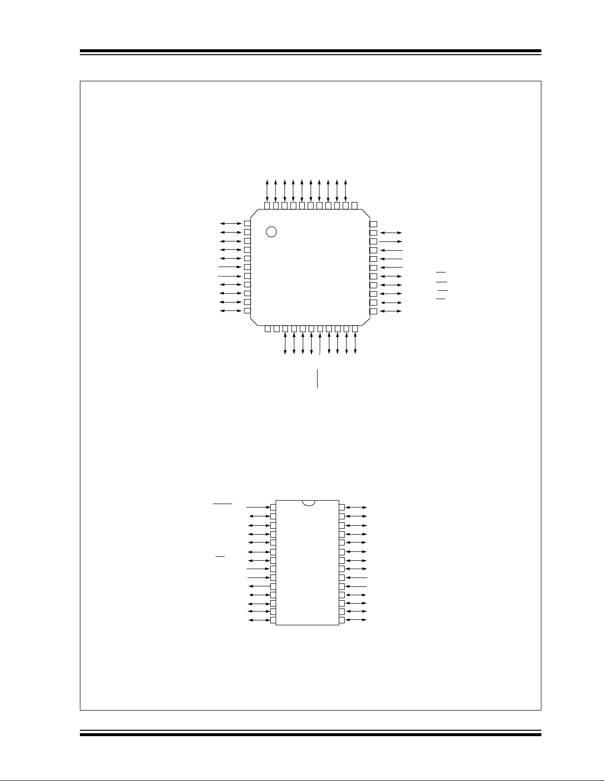
Pin Diagrams (Continued)
TQFP
RC7/RX/DT
RD4/PSP4/ECCP1/P1A
RD5/PSP5/P1B
RD6/PSP6/P1C
RD7/PSP7/P1D
RB0/INT0
RB1/INT1
RB2/CANTX/INT2
RB3/CANRX
V
VDD
PIC18FXX8
RC5/SDO
RC4/SDI/SDA
RD2/PSP2/C2IN+
RD1/PSP1/C1IN-
RC2/CCP1
RC1/T1OSI
RC6/TX/CK
RD3/PSP3/C2IN-
RD0/PSP0/C1IN+
38
39
40
41
42
43
44
1
2
3
4
SS
5
6
7
8
9
10
11
PIC18F448
PIC18F458
13
141516
12
17
18
RC3/SCK/SCL
35
36
37
21
20
19
NC
34
22
33
32
31
30
29
28
27
26
25
24
23
NC
RC0/T1OSO/T1CKI
OSC2/CLKO/RA6
OSC1/CLKI
SS
V
VDD
RE2/AN7/CS/C2OUT
RE1/AN6/WR
RE0//AN5/RD
RA5/AN4/SS/L VDIN
RA4/T0CKI
/C1OUT
SPDIP, SOIC
/VPP
MCLR
RA0/AN0/CVREF
RA1/AN1
RA2/AN2/V
RA3/AN3/V
RA5/AN4/SS
OSC2/CLKO/RA6
RC0/T1OSO/T1CKI
RC3/SCK/SCL
REF-
REF+
RA4/T0CKI
/LVDIN
V
OSC1/CLKI
RC1/T1OSI
RC2/CCP1
NC
NC
RB4
1
2
3
4
5
6
SS
7
8
9
10
11
12
13
14
/VPP
RB6/PGC
RB7/PGD
RB5/PGM
MCLR
PIC18F248
PIC18F258
+
REF
REF-
REF
RA1/AN1
RA3/AN3/V
RA2/AN2/V
RA0/AN0/CV
28
27
26
25
24
23
22
21
20
19
18
17
16
15
RB7/PGD
RB6/PGC
RB5/PGM
RB4
RB3/CANRX
RB2/CANTX/INT2
RB1/INT1
RB0/INT0
V
DD
VSS
RC7/RX/DT
RC6/TX/CK
RC5/SDO
RC4/SDI/SDA
2004 Microchip Technology Inc. DS41159D-page 3

PIC18FXX8
Table of Contents
1.0 Device Overview..........................................................................................................................................................................7
2.0 Oscillator Configurations............................................................................................................................................................ 17
3.0 Reset.......................................................................................................................................................................................... 25
4.0 Memory Organization.................................................................................................................................................................37
5.0 Data EEPROM Memory ......... ..................... ..................... ..................... ..................... ...............................................................59
6.0 Flash Program Memory............... ..................... ..................... ..................... ..................... ...........................................................65
7.0 8 x 8 Hardware Multiplier............................................................................................. ...............................................................75
8.0 Interrupts....................................................................................................................................................................................77
9.0 I/O Ports...................... ..................... ..................... ..................... ................................................................................................ 93
10.0 Parallel Slave Port................. ..................... ..................... .......................................... ...............................................................107
11.0 Timer0 Module ......................................................................................................................................................................... 109
12.0 Timer1 Module ......................................................................................................................................................................... 113
13.0 Timer2 Module ......................................................................................................................................................................... 117
14.0 Timer3 Module ......................................................................................................................................................................... 119
15.0 Capture/Compare/PWM (CCP) Modules .................................................................................................................................123
16.0 Enhanced Capture/Compare/PWM (ECCP) Module................................................................................................................ 131
17.0 Master Synchronous Serial Port (MSSP) Module .................................................................................................................... 143
18.0 Addressable Universal Synchronous Asynchronous Receiver Transmitter (USA RT ).............................................................. 183
19.0 CAN Module.............................................................................................................................................................................199
20.0 Compatible 10-Bit Analog-to-Digital Converter (A/D) Module ..................................................................................................241
21.0 Comparator Module.............................................................................. .. .... ......... .. .... .... .. .........................................................249
22.0 Comparator Voltage Reference Module........................................... .... .. .... .. ....... .... .. .... .. ....... .... .. ............................................ 255
23.0 Low-Voltage Detect.................................................................................................................................................................. 259
24.0 Special Features of the CPU.............. ..................... ..................... ............................................................................................ 265
25.0 Instruction Set Summary.......................................................................................................................................................... 281
26.0 Development Support...............................................................................................................................................................323
27.0 Electrical Characteristics.......................................................................................................................................................... 329
28.0 DC and AC Characteristics Graphs and Tables.......................................................................................................................361
29.0 Packaging Informa tio n..... ..................... .......................................... ..................... ..................................................................... 377
Appendix A: Data Sheet Revision History.......................................................................................................................................... 385
Appendix B: Device Differences.........................................................................................................................................................385
Appendix C: Device Migrations................................................. .. .... .. ....... .... .. .. .... .. ......... .. .. .... .. .........................................................386
Appendix D: Migrating From Other PICmicro
Index .................................................................................................................................................................................................. 387
On-Line Support........................................................................ .. .... .. ......... .... .. .... ......... .. ................................................................... 397
Systems Information and Upgrade Hot Line...................................................................................................................................... 397
Reader Response.............................................................................................................................................................................. 398
PIC18FXX8 Product Identification System......................................................................................................................................... 399
®
Devices ..................................................................................................................... 386
DS41159D-page 4 2004 Microchip Technology Inc.

PIC18FXX8
TO OUR VALUED CUSTOMERS
It is our intention to provide our valued customers with the best documentation possible to ensure successful use of your Microchip
products. To this end, we will continue to improve our publications to better suit your needs. Our publications will be refined and
enhanced as new volumes and updates are introduced.
If you have any questions or c omm ents regarding t his publication, p lease c ontact the M arket ing Co mmunications Department via
E-mail at docerrors@microchip.com or fax the Reader Response Form in the back of this data sheet to (480) 792-4150. We
welcome your feedback.
Most Current Data Sheet
To obtain the most up-to-date version of this data sheet, please register at our Worldwide Web site at:
http://www.microchip.com
You can determine the version of a data sheet by examining its literature number found on the bottom outside corner of any page.
The last character of the literature number is the version number, (e.g., DS30000A is version A of document DS30000).
Errata
An errata sheet, describing minor operational differences from the data sheet and recommended workarounds, may exist for current
devices. As device/documentation issues become known to us, we will publish an errata sheet. The errata will specify the revision
of silicon and revision of document to which it applies.
To determine if an errata sheet exists for a particular device, please check with one of the following:
• Microchip’s Worldwide Web site; http://www.microchip.com
• Your local Microchip sales office (see last page)
When contacting a sales office, please specify which device, revision of silicon and data sheet (include literature number) you are
using.
Customer Notification System
Register on our web site at www.microchip.com to receive the most current information on all of our products.
2004 Microchip Technology Inc. DS41159D-page 5

PIC18FXX8
NOTES:
DS41159D-page 6 2004 Microchip Technology Inc.

PIC18FXX8
1.0 DEVICE OVERVIEW
This documen t conta i ns dev ic e spec if i c in for m at i on fo r
the following devices:
• PIC18F248
• PIC18F258
•PIC18F448
•PIC18F458
These devices are available in 28-pin, 40-pin and
44-pin packages. They are differentiated from each
other in four ways:
1. PIC18FX58 devices have twice the Flash
program memory and data RAM of PIC18FX48
devices (32 Kbytes and 1536 bytes vs.
16 Kbytes and 768 bytes, respectively).
2. PIC18F2X8 devices imple me nt 5 A/D channels,
as opposed to 8 for PIC18F4X8 devices.
3. PIC18F2X8 devices implement 3 I/O ports,
while PIC18F4X8 devices implement 5.
4. Only PIC18F4X8 devices implement the
Enhanced CCP module, analog comparators
and the Parallel Slave Port.
All other features for devices in the PIC18FXX8 family,
including the serial communications modules, are
identical. These are summarized in Table 1-1.
Block diagrams of the PIC18F2X8 and PIC18F4X8
devices are provided in Figure 1-1 and Figure 1-2,
respectively. The pinouts for these device families are
listed in Table 1-2.
TABLE 1-1: PIC18FXX8 DEVICE FEATURES
Features PIC18F248 PIC18F258 PIC18F448 PIC18F458
Operating Frequency DC – 40 MHz DC – 40 MHz DC – 40 MHz DC – 40 MHz
Internal
Program
Memory
Data Memory (Bytes) 768 1536 768 1536
Data EEPROM Memory (Bytes) 256 256 256 256
Interrupt Sources 17 17 21 21
I/O Ports Ports A, B, C Ports A, B, C Ports A, B, C, D, E Ports A, B, C, D, E
Timers 4 4 4 4
Capture/Compare/PWM Modules 1 1 1 1
Enhanced Capture/Compare/
PWM Modules
Serial Communic ations MSSP, CAN,
Parallel Communications (PSP) No No Yes Yes
10-bit Analog-to-Digital Converter 5 input channels 5 input channels 8 input channels 8 input channels
Analog Comparators No No 2 2
Analog Comparators V
Resets (and Delays) POR, BOR,
Programmable Low-Voltage Detect Yes Yes Yes Yes
Programmable Brown-out Reset Yes Yes Yes Yes
CAN Module Yes Yes Yes Yes
In-Circuit Serial Programming™
(ICSP™)
Instruction Set 75 Instructions 75 Instructions 75 Instructions 75 Instructions
Packages 28-pin SPDIP
Bytes 16K 32K 16K 32K
# of Single-Word
Instructions
REF Output N/A N/A Yes Yes
8192 16384 8192 16384
—— 1 1
Addressable USART
RESET Instruction,
Stack Fu ll,
Stack U nderflow
(PWRT, OST)
Yes Yes Yes Yes
28-pin SOIC
MSSP, CAN,
Addressable USART
POR, BOR,
RESET Instruction,
Stack Full,
Stack U nderflow
(PWRT, OST)
28-pin SPDIP
28-pin SOIC
MSSP, CAN,
Addressable USART
POR, BOR,
RESET Instruction,
Stack Full,
Stack U nderflow
(PWRT, OST)
40-pin PDIP
44-pin PLCC
44-pin TQFP
MSSP, CAN,
Addressable USART
POR, BOR,
RESET Instruction,
Stack Full,
Stack U nderflow
(PWRT, OST )
40-pin PDIP
44-pin PLCC
44-pin TQFP
2004 Microchip Technology Inc. DS41159D-page 7

PIC18FXX8
FIGURE 1-1: PIC18F248/258 BLOCK DIAGRAM
Address Latch
Program Memory
up to 32 Kbytes
Data Latch
OSC2/CLKO/RA6
OSC1/CLKI
T1OSI
T1OSO
21
21
21
16
Instruction
Decode &
Control
Timing
Generation
4X PLL
Precision
Band Gap
Reference
T able Pointer<21>
inc/dec logic
PCLATU
PCU
Program Counter
31 Level Stack
Table Latch
8
ROM Latch
8
PCLATH
PCH PCL
IR
Power-up
Timer
Oscillator
Star t-up T ime r
Power-on
Reset
Watchdog
Timer
Brown-out
Reset
Test Mode
Select
8
4
BSR
Decode
BITOP
Data Latch
Data RAM
up to 1536 bytes
Address Latch
Address<12>
12
FSR0
FSR1
FSR2
inc/dec
logic
PRODH
8 x 8 Multiply
3
8
8
Data Bus<8>
12
4
Bank0, F
PRODL
W
8
ALU<8>
8
PORTA
RA0/AN0/CVREF
RA1/AN1
RA2/AN2/VREFRA3/AN3/VREF+
RA4/T0CKI
RA5/AN4/SS
PORTB
12
PORTC
8
8
8
OSC2/CLK O/RA 6
RB0/INT0
RB1/INT1
RB2/CANTX/INT2
RB3/CANRX
RB4
RB5/PGM
RB6/PGC
RB7/PGD
RC0/T1OSO/T1CKI
RC1/T1OSI
RC2/CCP1
RC3/SCK/SCL
RC4/SDI/SDA
RC5/SDO
RC6/TX/CK
RC7/RX/DT
/LVDIN
Band Gap
PBOR
PLVD
DataEEPROM
Timer0
Timer1 Timer2
CCP1
MCLR
VDD, VSS
USART
Timer3
Synchronous
Serial Port
10-bit
ADC
CAN Module
DS41159D-page 8 2004 Microchip Technology Inc.
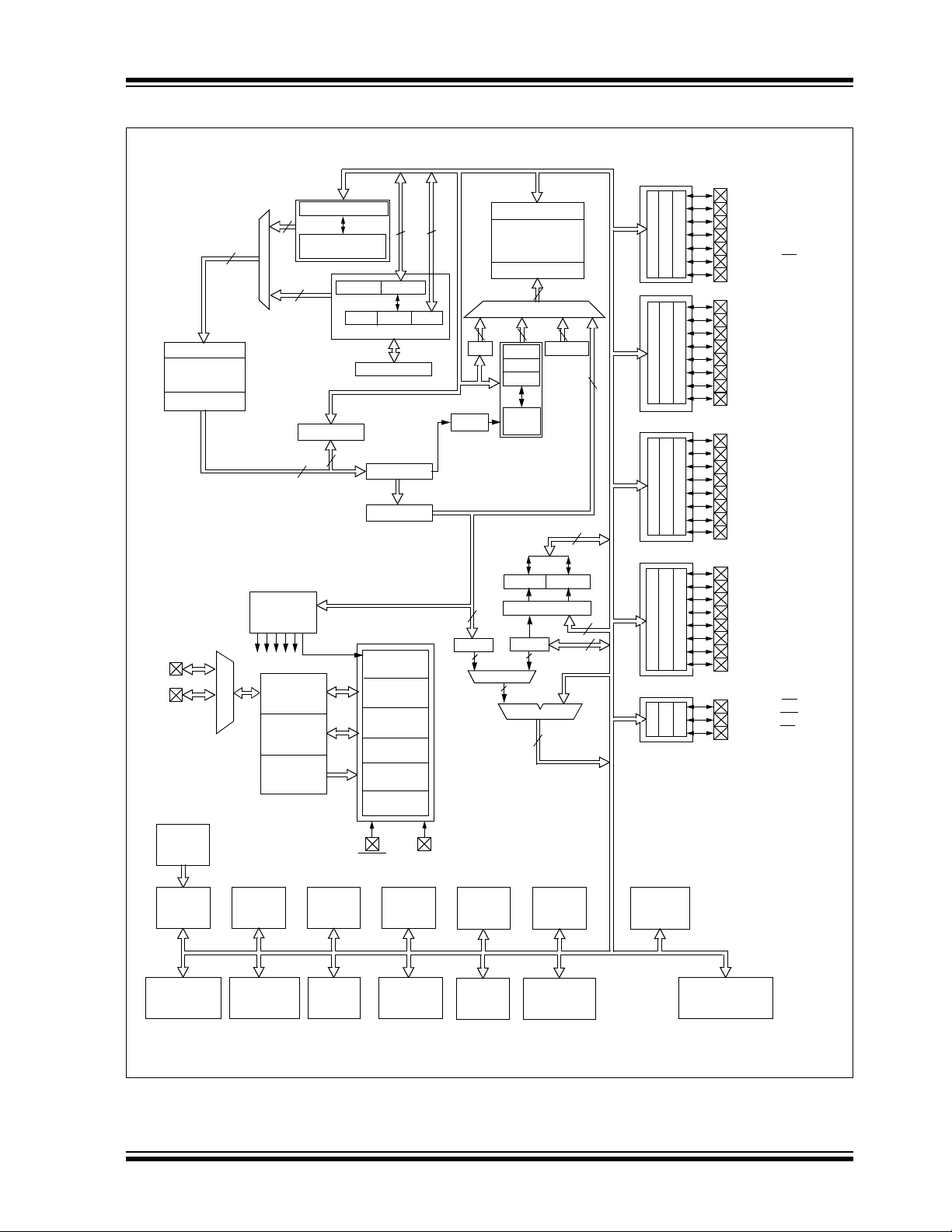
FIGURE 1-2: PIC18F448/458 BLOCK DIAGRAM
PIC18FXX8
Address Latch
Program Memory
up to 32 Kbytes
Data Latch
OSC2/CLKO/RA6
OSC1/CLKI
T1OSI
T1OSO
21
21
21
16
Instruction
Decode &
Control
Timing
Generation
4X
PLL
Precision
Band Gap
Reference
T able Pointer<21>
inc/dec logic
PCLATU
PCU
Program Counter
31 Level Stack
Table Latch
8
ROM Latch
IR
Power-up
Oscillator
Start-up Timer
Power-on
Watchdog
Brown-out
Test Mode
8
PCLATH
PCH PCL
Timer
Reset
Timer
Reset
Select
8
4
BSR
Decode
BITOP
Data Latch
Data RAM
up to 1536 Kbyt es
Address Latch
Address<12>
12
FSR0
FSR1
FSR2
inc/dec
logic
8 x 8 Multiply
3
8
8
ALU<8>
Data Bus<8>
12
4
Bank0, F
PRODLPRODH
W
8
8
PORTA
RA0/AN0/CVREF
RA1/AN1
RA2/AN2/VREFRA3/AN3/VREF+
RA4/T0CKI
RA5/AN4/SS
PORTB
12
PORTC
8
8
8
PORTD
PORTE
OSC2/CLKO/RA6
RB0/INT0
RB1/INT1
RB2/CANTX/INT2
RB3/CANRX
RB4
RB5/PGM
RB6/PGC
RB7/PGD
RC0/T1OSO/T1CKI
RC1/T1OSI
RC2/CCP1
RC3/SCK/SCL
RC4/SDI/SDA
RC5/SDO
RC6/TX/CK
RC7/RX/DT
RD0/PSP0/C1IN+
RD1/PSP1/C1INRD2/PSP2/C2IN+
RD3/PSP3/C2INRD4/PSP4/ECCP1/P1A
RD5/PSP5/P1B
RD6/PSP6/P1C
RD7/PSP7/P1D
RE0/AN5/RD
RE1/AN6/WR//C1OUT
RE2/AN7/CS/C2OUT
/LVDIN
Band Gap
MCLR
VDD, VSS
PBOR
PLVD
DataEEPROM
Timer0
Comparators
Timer1 Timer2
CCP1
USART
Enhanced
CCP
Timer3
USART
10-bit
ADC
Synchronous
Serial Port
Parallel
Slave Port
CAN Module
2004 Microchip Technology Inc. DS41159D-page 9

PIC18FXX8
TABLE 1-2: PIC18FXX8 PINOUT I/O DESCRIPTIONS
Pin Number
Pin Name
SPDIP, SOIC PDIP TQFP PLCC
Pin
Type
Buffer
Type
DescriptionPIC18F248/258 PIC18F448/458
MCLR/VPP
MCLR
VPP
NC — — 12, 13,
OSC1/CLKI
OSC1
CLKI
OSC2/CLKO/RA6
OSC2
CLKO
RA6
Legend: TTL = TTL compatible input CMOS = CMOS compatible input or output
ST = Schmitt Trigger input with CMOS levels Analog = Analog input
I = Input O = Output
P = Power OD = Open-Drain (no P diode to V
11182
I
P
1, 17,
33, 34
9 133014
10 14 31 15
28, 40
— — These pins should be left
IICMOS/ST
O
O
I/O
ST
—
CMOS
—
—
TTL
Master Clear (input) or
programming voltage (output).
Master Clear (Reset) input.
This pin is an active low Reset
to the device.
Programming voltage inpu t.
unconnected.
Oscillator crystal or external clock
input.
Oscillator crystal input or
external clock sou rce inpu t. ST
buffer when configured in RC
mode; otherwise, CMOS.
External clock source input.
Always associated with pin
function OSC1 (see OSC1/
CLKI, OSC2/CLKO pins).
Oscillator crystal or clock output.
Oscillator crystal output.
Connects to crystal or
resonator in Crystal Oscillator
mode.
In RC mode, OSC2 pin output s
CLKO, which has 1/4 the
frequency of OSC1 and
denotes the instruction cycle
rate.
General purpose I/O pin.
DD)
DS41159D-page 10 2004 Microchip Technology Inc.

TABLE 1-2: PIC18FXX8 PINOUT I/O DESCRIPTIONS (CONTINUED)
Pin Number
Pin Name
RA0/AN0/C
RA0
AN0
CVREF
RA1/AN1
RA1
AN1
VREF
Pin
Type
SPDIP, SOIC PDIP TQFP PLCC
22193
33204
I/O
O
I/O
Buffer
Type
TTL
I
Analog
Analog
TTL
I
Analog
PIC18FXX8
DescriptionPIC18F248/258 PIC18F448/458
PORTA is a bidirectional I/O port.
Digital I/O.
Analog input 0.
Comparator voltage reference
output.
Digital I/O.
Analog input 1.
RA2/AN2/V
RA2
AN2
V
RA3/AN3/V
RA3
AN3
V
RA4/T0CKI
RA4
T0CKI
RA5/AN4/SS
RA5
AN4
SS
LVDIN
RA6 See the OSC2/CLKO/RA6 pin.
Legend: TTL = TTL compatible input CMOS = CMOS compatible input or output
REF-
REF-
REF+
REF+
/LVDIN
ST = Schmitt Trigger input with CMOS levels Analog = Analog input
I = Input O = Output
P = Power OD = Open-Drain (no P diode to V
44215
I/O
I
I
55226
I/O
I
I
66237
I/OITTL/OD
77248
I/O
I
I
I
TTL
Analog
Analog
TTL
Analog
Analog
ST
TTL
Analog
ST
Analog
Digital I/O.
Analog input 2.
A/D reference voltage
(Low) input.
Digital I/O.
Analog input 3.
A/D reference voltage
(High) input.
Digital I/O – open-drain when
configured as output.
Timer0 external clock input.
Digital I/O.
Analog input 4.
SPI™ slave select input.
Low-Voltage Detect input.
DD)
2004 Microchip Technology Inc. DS41159D-page 11

PIC18FXX8
TABLE 1-2: PIC18FXX8 PINOUT I/O DESCRIPTIONS (CONTINUED)
Pin Number
Pin
I/O
Buffer
Type
TTL
I
ST
Pin Name
RB0/INT0
RB0
INT0
Type
SPDIP, SOIC PDIP TQFP PLCC
21 33 8 36
DescriptionPIC18F248/258 PIC18F448/458
PORTB is a bidirectional I/O port.
PORTB can be software
programme d for internal weak
pull-ups on a ll inputs.
Digital I/O.
External interrupt 0.
RB1/INT1
RB1
INT1
RB2/CANTX/INT2
RB2
CANTX
INT2
RB3/CANRX
RB3
CANRX
RB4 25 371441I/OTTL Digital I/O.
RB5/PGM
RB5
PGM
RB6/PGC
RB6
PGC
22 34 9 37
23 35 10 38
24 36 11 39
26 38 15 42
27 39 16 43
I/O
I/O
O
I/O
I/O
I/O
TTL
I
I
I
I
I
ST
TTL
TTL
ST
TTL
TTL
TTL
ST
TTL
ST
Digital I/O.
External interrupt 1.
Digital I/O.
Transmit signal for CAN bus.
External interrupt 2.
Digital I/O.
Receive signal for CAN bus.
Interrupt-on-change pin.
Digital I/O.
Interrupt-on-change pin.
Low-voltage ICSP™
programming enable.
Digital I/O. In-Circuit
Debugger pin.
Interrupt-on-change pin.
ICSP programming clock.
RB7/PGD
RB7
PGD
Legend: TTL = TTL compatible input CMOS = CMOS compatible input or output
ST = Schmitt Trigger input with CMOS levels Analog = Analog input
I = Input O = Output
P = Power OD = Open-Drain (no P diode to V
DS41159D-page 12 2004 Microchip Technology Inc.
28 40 17 44
I/O
I/O
TTL
ST
Digital I/O. In-Circuit
Debugger pin.
Interrupt-on-change pin.
ICSP programming data.
DD)

TABLE 1-2: PIC18FXX8 PINOUT I/O DESCRIPTIONS (CONTINUED)
Pin Number
Pin Name
RC0/T1OSO/T1CKI
RC0
T1OSO
T1CKI
RC1/T1OSI
RC1
T1OSI
Pin
Type
SPDIP, SOIC PDIP TQFP PLCC
11 15 32 16
12 16 35 18
I/O
O
I/O
Buffer
Type
ST
—
I
I
ST
ST
CMOS
PIC18FXX8
DescriptionPIC18F248/258 PIC18F448/458
PORTC is a bidirectional I/O port.
Digital I/O.
Timer1 oscillator output.
Timer1/Timer3 external clock
input.
Digital I/O.
Timer1 oscillator input.
RC2/CCP1
RC2
CCP1
RC3/SCK/SCL
RC3
SCK
SCL
RC4/SDI/SDA
RC4
SDI
SDA
RC5/SDO
RC5
SDO
RC6/TX/CK
RC6
TX
CK
RC7/RX/DT
RC7
RX
DT
Legend: TTL = TTL compatible input CMOS = CMOS compatible input or output
ST = Schmitt Trigger input with CMOS levels Analog = Analog input
I = Input O = Output
P = Power OD = Open-Drain (no P diode to V
13 17 36 19
14 18 37 20
15 23 42 25
16 24 43 26
17 25 44 27
18 26 1 29
I/O
I/O
I/O
I/O
I/O
I/O
I/O
I/O
O
I/O
O
I/O
I/O
I/O
ST
ST
ST
ST
ST
ST
I
I
ST
ST
ST
—
ST
—
ST
ST
ST
ST
Digital I/O.
Capture 1 input/Compare 1
output/PWM1 output.
Digital I/O.
Synchronous serial clock
input/output for SPI™ mode.
Synchronous serial clock
input/output for I
Digital I/O.
SPI data in.
2
C data I/O.
I
Digital I/O.
SPI data out.
Digital I/O.
USART asynchronous
transmit.
USART synchronous clock
(see RX/DT).
Digital I/O.
USART asynchronous receive.
USART synchronous data
(see TX/CK).
2
C™ mode.
DD)
2004 Microchip Technology Inc. DS41159D-page 13

PIC18FXX8
TABLE 1-2: PIC18FXX8 PINOUT I/O DESCRIPTIONS (CONTINUED)
Pin Number
Pin
I/O
I/O
Buffer
Type
ST
TTL
I
Analog
Pin Name
RD0/PSP0/C1IN+
RD0
PSP0
C1IN+
Type
SPDIP, SOIC PDIP TQFP PLCC
— 193821
DescriptionPIC18F248/258 PIC18F448/458
PORTD is a bidirectional I/O port.
These pins have TTL inp ut buf fers
when external memory is enabled.
Digital I/O.
Parallel Slave Port data.
Comparator 1 input.
RD1/PSP1/C1IN-
RD1
PSP1
C1IN-
RD2/PSP2/C2IN+
RD2
PSP2
C2IN+
RD3/PSP3/C2IN-
RD3
PSP3
C2IN-
RD4/PSP4/ECCP1/
P1A
RD4
PSP4
ECCP1
P1A
RD5/PSP5/P1B
RD5
PSP5
P1B
— 203922
I/O
I/O
I
— 214023
I/O
I/O
I
— 224124
I/O
I/O
I
—27230
I/O
I/O
I/O
O
—28331
I/O
I/O
O
ST
TTL
Analog
ST
TTL
Analog
ST
TTL
Analog
ST
TTL
ST
—
ST
TTL
—
Digital I/O.
Parallel Slave Port data.
Comparator 1 input.
Digital I/O.
Parallel Slave Port data.
Comparator 2 input.
Digital I/O.
Parallel Slave Port data.
Comparator 2 input.
Digital I/O.
Parallel Slave Port data.
ECCP1 capture/compare.
ECCP1 PWM output A.
Digital I/O.
Parallel Slave Port data.
ECCP1 PWM output B.
RD6/PSP6/P1C
RD6
PSP6
P1C
RD7/PSP7/P1D
RD7
PSP7
P1D
Legend: TTL = TTL compatible input CMOS = CMOS compatible input or output
ST = Schmitt Trigger input with CMOS levels Analog = Analog input
I = Input O = Output
P = Power OD = Open-Drain (no P diode to V
DS41159D-page 14 2004 Microchip Technology Inc.
—29432
I/O
I/O
O
—30533
I/O
I/O
O
ST
TTL
—
ST
TTL
—
Digital I/O.
Parallel Slave Port data.
ECCP1 PWM output C.
Digital I/O.
Parallel Slave Port data.
ECCP1 PWM output D.
DD)

TABLE 1-2: PIC18FXX8 PINOUT I/O DESCRIPTIONS (CONTINUED)
Pin Number
Pin Name
RE0/AN5/RD
RE0
AN5
RD
RE1/AN6/WR/C1OUT
RE1
AN6
WR
C1OUT
Pin
Type
SPDIP, SOIC PDIP TQFP PLCC
—8259
—92610
I/O
I/O
O
Buffer
Type
ST
I
Analog
I
TTL
ST
I
Analog
I
TTL
Analog
PIC18FXX8
DescriptionPIC18F248/258 PIC18F448/458
PORTE is a bidirectional I/O port.
Digital I/O.
Analog input 5.
Read control for Parallel Slave
Port (see WR
Digital I/O.
Analog input 6.
Write control for Paralle l Slave
Port (see CS
Comparator 1 output.
and CS pins).
and RD pins).
RE2/AN7/CS/C2OUT
RE2
AN7
CS
C2OUT
VSS 19, 8 12, 31 6, 29 13, 34 — — Ground reference for logic and
DD 20 11, 32 7, 28 12, 35 — — Positive supply for logic and I/O
V
Legend: TTL = TTL compatible input CMOS = CMOS compatible input or output
ST = Schmitt Trigger input with CMOS levels Analog = Analog input
I = Input O = Output
P = Power OD = Open-Drain (no P diode to V
—102711
I/O
I
I
O
ST
Analog
TTL
Analog
Digital I/O.
Analog input 7.
Chip select control for Parallel
Slave Port (see RD
pins).
Comparator 2 output.
I/O pins.
pins.
and WR
DD)
2004 Microchip Technology Inc. DS41159D-page 15

PIC18FXX8
NOTES:
DS41159D-page 16 2004 Microchip Technology Inc.
PIC18FXX8
2.0 OSCILLATOR
CONFIGURATIONS
2.1 Oscillator Types
The PIC18FXX8 can be operated in one of eight oscillator modes, programmable by three configuration bits
(FOSC2, FOSC1 and FOSC0).
1. LP Low-Power Crystal
2. XT Crystal/Resonator
3. HS High-Speed Crystal/Resonator
4. HS4 High-Speed Crystal/Resonator with
PLL enabled
5. RC External Resistor/Capacito r
6. RCIO External Resistor/Capacitor with I/O
pin enabled
7. EC External Clock
8. ECIO External Clock with I/O pin enabled
2.2 Crystal Oscillator/Ceramic
Resonators
In XT, LP, HS or HS4 (PLL) Oscillator modes, a crystal
or ceramic resonator is connected to the OSC1 and
OSC2 pins to establish oscillation. Figure 2-1 shows
the pin connections . An ext ernal clock source m ay also
be connected to the OSC1 pin, as shown in Figure 2-3
and Figure 2-4.
The PIC18FXX8 oscilla tor d esign requires the use of a
parallel cut crystal.
Note: Use of a series cut crystal may give a fre-
quency out of the crystal manufacturer’s
specifications.
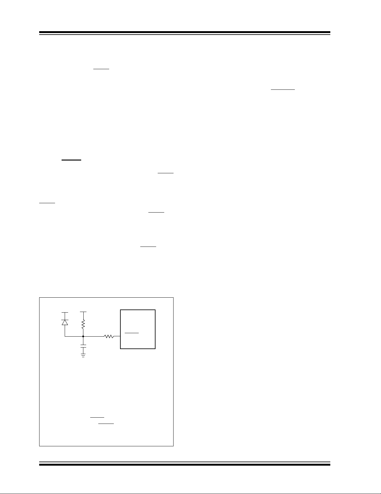
FIGURE 2-1: CRYSTAL/CERAMIC
RESONATOR OPERATION
(HS, XT OR LP OSC
CONFIGURATION)
(1)
C1
(1)
C2
Note 1: See Table 2-1 and Table 2-2 for recommended
values of C1 and C2.
2: A series resistor (R
strip cut crystals.
3: R
OSC1
XTAL
(2)
RS
OSC2
F varies with the crystal chosen.
(3)
RF
PIC18FXX8
S) may be required for AT
To
Internal
Logic
Sleep
TABLE 2-1: CERAMIC RESONATORS
Ranges Tested:
Mode Freq OSC1 OSC2
XT 455 kHz
2.0 MHz
4.0 MHz
HS 8.0 MHz
16.0 MHz
These values are for design guidance only.
See notes following Table 2-2.
Resonators Used:
455 kHz Panasonic EFO-A455K04B ±0.3%
2.0 MHz Murata Erie CSA2.00MG ±0.5%
4.0 MHz Murata Erie CSA4.00MG ±0.5%
8.0 MHz Murata Erie CSA8.00MT ±0.5%
16.0 MHz Murata Erie CSA16.00MX ±0.5%
All resonators used did not have built-in capacitors.
68-100 pF
15-68 pF
15-68 pF
10-68 pF
10-22 pF
68-100 pF
15-68 pF
15-68 pF
10-68 pF
10-22 pF
2004 Microchip Technology Inc. DS41159D-page 17
PIC18FXX8
TABLE 2-2: CAPACITOR SELECTION FOR
CRYSTAL OSCILLATOR
Osc Type
Crystal
Freq
LP 32.0 kHz 33 pF 33 pF
200 kHz 15 pF 15 pF
XT 200 kHz 47-68 pF 47-68 pF
1.0 MHz 15 pF 15 pF
4.0 MHz 15 pF 15 pF
HS 4.0 MHz 15 pF 15 pF
8.0 MHz 15-33 pF 15-33 pF
20.0 MHz 15-33 pF 15-33 pF
25.0 MHz 15-33 pF 15-33 pF
These values are for design guidance only.
See notes on this page.
32.0 kHz Epson C-001R32.768K-A ±20 PPM
200 kHz STD XTL 200.000KHz ±20 PPM
1.0 MHz ECS ECS-10-13-1 ±50 PPM
4.0 MHz ECS ECS-40-20-1 ±50 PPM
8.0 MHz EPSON CA-301 8.000M-C ±30 PPM
20.0 MHz EPSON CA-301 20.000M-C ±30 PPM
Note 1: Recommended values of C1 and C2 are
identical to the ranges tested (Table 2-1).
2: Higher capacitance inc reases the st abilit y
of the oscillator but also increases the
start-up time.
3: Since each resonator/crystal has its own
characteristics, the user should consult
the resonator/crystal manufacturer for
appropriate values of external
components.
4: Rs may be required in HS mode, as well
as XT mode, to avoid overdrivi ng crys t als
with low drive level specification.
Cap. Range C1Cap. Range
Crystals Used
C2
2.3 RC Oscillator
For timing insensitive applications, the “RC” and “RCIO”
device options offer additional cost savings. The RC
oscillator frequency is a function of the supply voltage,
the resistor (R
operating temperature. In addition to this, the oscillator
frequency will vary from unit to unit due to normal
process parameter variation. Furthermore, the differ-
ence in lead frame capacit ance between package types
will also affect the oscillation frequency, especially for
EXT values. The user also needs to take into
low C
account variation due to tolerance of external R and C
components used. Figure 2-2 shows how the RC
combination is connected.
In the RC Oscillator mode, the oscillator frequency
divided by 4 is available on the OSC2 pin. This signal
may be used f or t e st pu r pos es or t o sy nc hr o n iz e ot he r
logic.
Note: If the oscillator frequency divided by 4
FIGURE 2-2: RC OSCILLATOR MODE
REXT
CEXT
VSS
Recommended values: 3 kΩ ≤ REXT ≤ 100 kΩ
The RCIO Oscillato r mode f unc tions like t he RC m ode,
except that the OSC2 pin becomes an additional
general purpose I/O pin. The I/O pin becomes bit 6 of
PORTA (RA6).
EXT) and capacitor (CEXT) values and the
signal is not required in the application, it
is recommended to use RCIO mode to
save current.
VDD
PIC18FXX8
OSC1
F
OSC/4
OSC2/CLKO
C
EXT > 20 pF
Internal
Clock
DS41159D-page 18 2004 Microchip Technology Inc.

PIC18FXX8
2.4 External Clock Input
The EC and ECIO Oscillator mode s require an externa l
clock source to be connected to the OSC1 pin. The
feedback device between OSC1 and OSC2 is turned
off in these modes to save current. There is no oscillator start-up time required after a Power-on Reset or
after a recovery from Sleep mode.
In the EC Oscillator mode, the oscillator frequency
divided by 4 is available on the OSC2 pin. This signal
may be used f or t e st pu r pos es or t o sy nc hr o n iz e ot he r
logic. Figure 2-3 shows the pin connections for the EC
Oscillator mode.
FIGURE 2-3: EXTERNAL CLOCK INPUT
OPERATION (EC OSC
CONFIGURATION)
PIC18FXX8
Clock from
Ext. System
OSC/4
F
The ECIO Oscillator mode func ti ons li ke t he EC m od e,
except that the OSC2 pin becomes an additional
general purpose I/O pin. Figure 2-4 shows the pin
connections for the ECIO Osci ll ator mode.
OSC1
OSC2
FIGURE 2-4: EXTERNAL CLOCK INPUT
OPERATION (ECIO
CONFIGURATION)
PIC18FXX8
Clock from
Ext. System
OSC1
I/O (OSC2)
2.5 HS4 (PLL)
A Phase Locked Loop circuit is pro vided as a programmable option for users that want to multiply the
frequency of the incoming cry sta l oscil lator sig nal by 4.
For an input clock frequency of 10 MHz, the internal
clock frequency will be multiplied to 40 MHz. This is
useful for customers who are concerned with EMI due
to high-frequency crystals.
The PLL can only be enabled when the oscillator
configuration bi ts are pro grammed for HS mod e. If the y
are programmed for any other mode, the PLL is not
enabled and the system clock will come directly from
OSC1.
The PLL is one of the modes of the FOSC2:FOSC0
configuration bits. The oscillator mode is specified
during device programming.
A PLL lock timer is used to ensure that the PLL has
locked before device execution starts. The PLL lock
timer has a time-out referred to as T
PLL.
FIGURE 2-5: PLL BLOCK DIAGRAM
OSC2
Crystal
Osc
OSC1
Phase
Comparator
F
IN
FOUT
FOSC2:FOSC0 = 110
Loop
Filter
Divide by 4
VCO
SYSCLK
MUX
2004 Microchip Technology Inc. DS41159D-page 19

PIC18FXX8
2.6 Oscillator Switching Feature
The PIC18FXX8 devices include a featu re that allows
the system clock source to be switc hed from the mai n
oscillator to an alternate low-frequency clock source.
For the PIC18FXX8 devices, this alternate clock source
is the Timer1 oscillator. If a low-frequency crystal
(32 kHz, for example) has been attached to the Timer1
oscillator pins and the Timer1 oscillator has been
enabled, the device can switch to a Low-Power Execution mode. Figure 2-6 shows a block diagram of the
system clock sources. The clock switching feature is
enabled by programming the Oscillator Switching
Enable (OSCSEN
CONFIG1H, to a ‘0’. Clock switching is disabled in an
erased device. See Section 1 2.2 “Timer 1 Oscillat or”
for further details of the Timer1 oscillator and
Section 24.1 “Configuration Bits” for Configuration
register details.
FIGURE 2-6: DEVICE CLOCK SOURCES
) bit in Configuration register,
PIC18FXX8
OSC2
OSC1
T1OSO
T1OSI
Main Oscillator
Sleep
Timer 1 Oscillator
T1OSCEN
Enable
Oscillator
2.6.1 SYSTEM CLOCK SWITCH BIT
The system clock source switching is performed under
software control. The system clock switch bit, SCS
(OSCCON register), controls the clock switching. When
the SCS bit is ‘0’, the system clock source comes from
the main oscillator selected by the FOSC2:FOSC0
configuration bits. When the SCS bit is set, the system
clock source comes from the Timer1 oscilla tor . The SCS
bit is cleared on all forms of Reset.
Note: The Timer1 oscillator must be enabled to
switch the system clock source. The
Timer1 oscillator is enabled by setting the
T1OSCEN bit in the Timer1 Control register (T1CON). If the Timer1 oscillator is not
enabled, any write to the SCS bit will be
ignored (SCS bit forced cleared) and the
main oscillator con t in ues to be t he s ys tem
clock source.
4 x PLL
TOSC
TT1P
Clock Source Option
for Other Modules
TOSC/4
MUX
Clock
Source
TSCLK
Note: I/O pins have diode protection to VDD and VSS.
REGISTER 2-1: OSCCON: OSCILLATOR CONTROL REGISTER
U-0 U-0 U-0 U-0 U-0 U-0 U-0 R/W-1
— — — — — — —SCS
bit 7 bit 0
bit 7-1 Unimplemented: Read as ‘0’
bit 0 SCS: System Clock Switch bit
When
OSCSEN configuration bit = 0 and T1OSCEN bit is set:
1 = Switch to Timer1 oscillator/clock pin
0 = Use primary oscillator/clock input pin
OSCSEN is clear or T1OSCEN is clear:
When
Bit is force d clear.
Legend:
R = Readable bit W = Writable bit U = Unimplemented bit, read as ‘0’
-n = Value at POR ‘1’ = Bit is set ‘0’ = Bit is cleared x = Bit is unknown
DS41159D-page 20 2004 Microchip Technology Inc.

PIC18FXX8
2.6.2 OSCILLATOR TRANSITIONS
The PIC18FXX8 devices contain circuitry to prevent
“glitches” when switching between oscillator sources.
Essentially, the circuitry waits for eight rising edges of
the clock source that the processor is swit ching to. This
ensures that the n ew c lo ck s ourc e is s t able and that its
pulse width will not be less than the shortest pulse
width of the two clock sources.
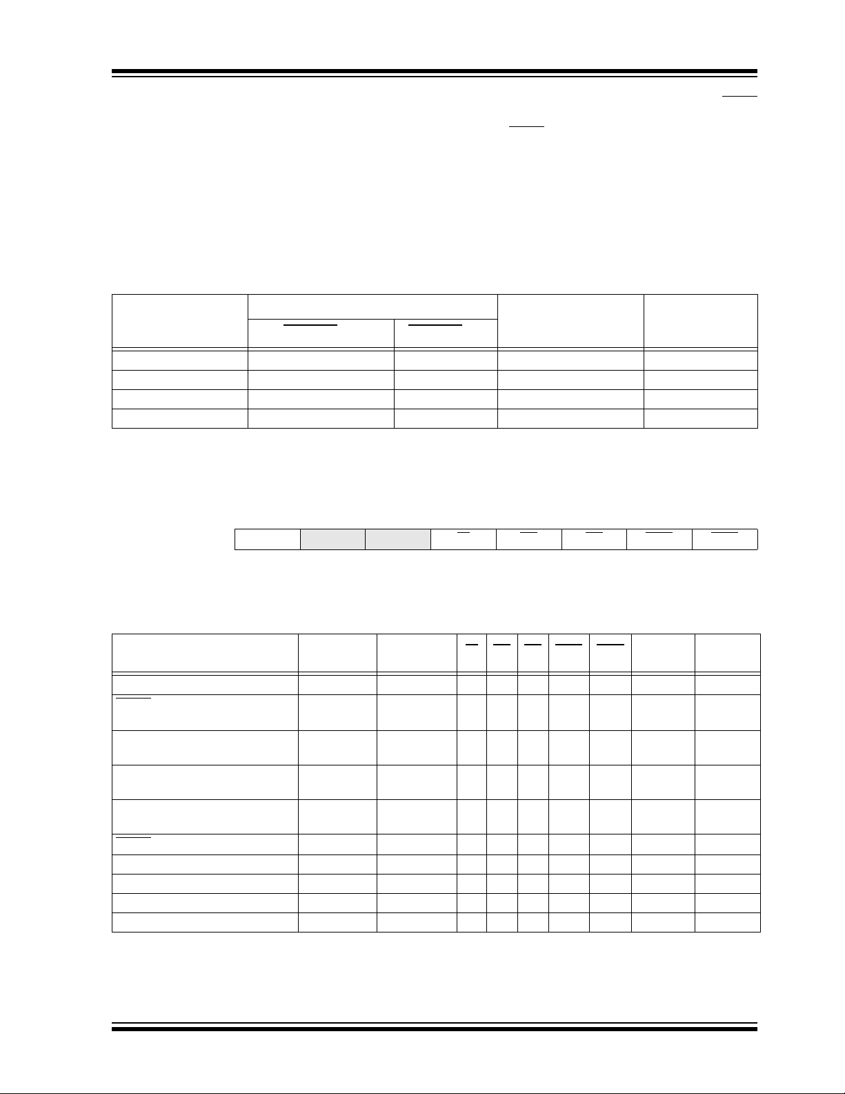
Figure 2-7 shows a timing diagram indicating the transition from the main oscillator to the Timer1 oscillator.
The Timer1 oscillator is assumed to be running all the
The sequence of events that takes place when switching from the Timer1 oscillator to the main oscillator will
depend on the mode of the main oscillator. In addition
to eight clock cycles of the main oscillator, additional
delays may take place.
If the main oscillator is configured for an external
crystal (HS, XT, LP), the transition will take place after
an oscillator st art-up time (T
OST) has occurred. A timing
diagram indicating the transition from the Timer1
oscillator to the main oscillator for HS, XT and LP
modes is shown in Figure 2-8.
time. After the SCS bit is set, th e proce ssor is frozen at
the next occurring Q1 cycle . After eight synchroniz ation
cycles are counted from the Timer1 oscillator,
operation resumes. No additional delays are required
after the synchronization cy cle s.
FIGURE 2-7: TIMING DIAGRAM FOR TRANSITION FROM OSC1 TO TIMER1 OSCILLATOR
Q1
T1OSI
OSC1
Internal
System
Clock
SCS
(OSCCON<0>)
Program
Counter
TOSC
Q4
Q3Q2
Q1
TDLY
TT1P
21345678
Tscs
PC + 2PC
Q3Q2Q1
Q4 Q1
Q2 Q3 Q4 Q1
PC + 4
Note 1: Delay on internal system clock is eight oscillator cycles for synchronization.
FIGURE 2-8: TIMING DIAGRAM FOR TRANSITION BETWEEN TIMER1 AND OSC1 (HS, XT , LP)
T1OSI
OSC1
OSC2
Internal System
Clock
(OSCCON<0>)
Note 1: T
SCS
Program
Counter
OST = 1024 TOSC (drawing not to scale).
Q3 Q4
PC PC + 2
Q1
TOST
TOSC
TT1P
12345678
TSCS
Q1 Q2 Q3 Q4 Q1 Q2
Q3
PC + 4
2004 Microchip Technology Inc. DS41159D-page 21

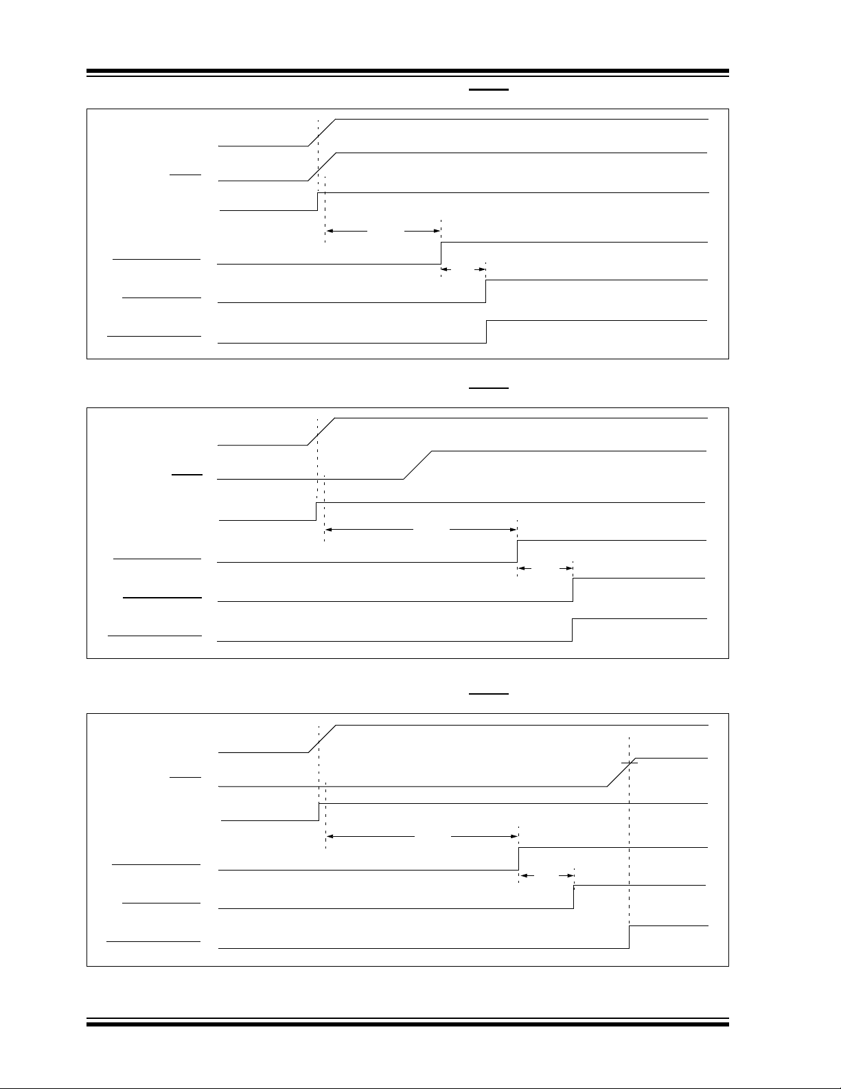
PIC18FXX8
If the main oscillator is configured for HS4 (PLL) mode,
an oscillator start-up time (T
time-out (T
PLL) will occur. The PLL time-out is typically
OST) plus an additional PLL
2 ms and allows the PLL to lock to the main oscillator
frequency. A timing diagram indicating the transition
from the Timer 1 oscilla tor to the mai n oscillator f or HS4
mode is shown in Figure 2-9.
If the main oscillato r is co nfigure d in th e RC, R CIO, EC
or ECIO modes, the re is no oscillator start-u p t im e-ou t.
Operation will resume after eight cycles of the main
oscillator have been counted. A ti ming diag ram indicating the transition from the Timer1 oscillator to the main
oscillator for RC, RC IO, EC and EC IO mo des is sho wn
in Figure 2-10.
FIGURE 2-9: TIMING FOR TRANSITION BETWEEN TIMER1 AND OSC1 (HS WITH PLL)
Q3
PC + 4
T1OSI
OSC1
OSC2
PLL Clock
Input
Internal System
Note 1: T
Clock
(OSCCON<0>)
SCS
Program
Counter
OST = 1024 TOSC (drawing not to scale).
Q4 Q1
TOST
PC PC + 2
TPLL
TOSC
TT1P
TSCS
123456
Q1 Q2 Q3 Q4 Q1 Q2
8
7
Q4
FIGURE 2-10: TIMING FOR TRANSITION BETWEEN TIMER1 AND OSC1 (RC, EC)
Q3 Q4
T1OSI
OSC1
OSC2
Internal System
Note 1: RC Oscillator mode assumed.
Clock
(OSCCON<0>)
SCS
Program
Counter
Q1
PC PC + 2
TT1P
TOSC
12345 678
TSCS
Q1 Q2 Q3 Q4 Q1 Q2 Q3
Q4
PC + 4
DS41159D-page 22 2004 Microchip Technology Inc.

PIC18FXX8
2.7 Effects of Sleep Mode on the
On-Chip Oscillator
When the device executes a SLEEP instruction, the
on-chip clocks and oscillator are turned off and the
device is held at the beginning of an instruction cycle
(Q1 state). With the os ci lla tor o f f, the OSC1 and OSC2
signals will stop oscillating. Since all the transistor
switching currents have been removed, Sleep mode
achieves the lowest current consumption of the device
(only leakage currents). Enabling any on-chip feature
that will operate during Sleep will increase the current
consumed during Sleep. The user can wake from
Sleep through external Reset, Watchdog Timer Reset
or through an interrupt.
2.8 Power-up Delays
Power-up delays are con trolled by two time rs so that no
external Reset circuitry is required for most applications. The delays ensure that the device is kept in
Reset until the device power supply and clock are
stable. For additional information on Reset operation,
see Section 3.0 “Reset”.
The first timer is the Power-up Timer (PWRT), which
optionally provides a fixed delay of T
#D033) on power-up only (POR and BOR). The second
timer is the Oscillator S t art-up T imer (OST), inten ded to
keep the chip in Reset until the crystal oscillator is
stable.
With the PLL enabled ( HS4 Osc ill ato r mo de), the timeout sequence following a Power-on Reset is different
from other oscillator modes. The time-out sequence is
as follows: the PWRT time-out is invoked after a POR
time delay has expired, then the Oscillator Start-up
Timer (OST) is invoked. However, this is still not a
sufficient a mount of ti me to allow the PLL to l ock at hig h
frequencies. The PWRT timer is used to provide an
additional fixed 2ms (nominal) to allow the PLL ample
time to lock to the incoming clock frequency.
TABLE 2-3: OSC1 AND OSC2 PIN STATES IN SLEEP MODE
OSC Mode OSC1 Pin OSC2 Pin
RC Floating, external resistor should pull high At logic low
RCIO Floating, external resistor should pull high Configured as PORTA, bit 6
ECIO Floating Configured as PORTA, bit 6
EC Floating At logic low
LP, XT and HS Feedback inverter disabled at quiescent
voltage level
Note: See Table 3-1 in Section 3.0 “Reset” for time-outs due to Sleep and MCLR
Feedback inverter disabled at quiescent
voltage level
Reset.
PWRT (parameter
2004 Microchip Technology Inc. DS41159D-page 23

PIC18FXX8
NOTES:
DS41159D-page 24 2004 Microchip Technology Inc.

PIC18FXX8
3.0 RESET
The PIC18FXX8 differentiates between various kinds
of RESET:
a) Power-on Reset (POR)
b) MCLR
c) MCLR Rese t during Sleep
d) Watchdog Timer (WDT) Reset during normal
e) Programmable Brown-out Reset (PBOR)
f) RESET Instr uction
g) Stack Full Reset
h) Stack Underflow Reset
Most registers are unaffected by a Reset. Their status
is unknown on POR and unchanged by all other
Resets. The other registers are forced to a “Reset”
Reset during normal operation
operation
state on Power-on Reset, MCLR
out Reset, MCLR
Reset during Sleep and by the
RESET instruction.
Most registers are not affected by a WDT wake-up,
since this is viewed as the resumption of normal operation. Status bits from the RCON register, RI
POR
and BOR are set or cleared differently in different
Reset situations, as indicated in Table 3-2. These bits
are used in software to determine the nature of the
Reset. See Table 3-3 for a full description of the Reset
states of all registers.
A simplified block di agram of the On-Chip Reset Circu it
is shown in Figure 3-1.
The Enhanced MCU devices have a MCLR
in the MCLR
Reset path. The filter will detect and
ignore small pulses.
A WDT Reset does not drive MCLR
, WDT Reset, Brown-
FIGURE 3-1: SIMPLIFIED BLOCK DIAGRAM OF ON-CHIP RESET CIRCUIT
RESET
Instruction
Stack
Pointer
Stack Full/Underflow Reset
External Reset
, TO, PD,
noise filter
pin low.
MCLR
WDT
Module
V
DD Rise
Detect
VDD
OSC1
Note 1: This is a separate oscillator from the RC oscillator of the CLKI pin.
Brown-out
Reset
OST/PWRT
OST
On-chip
RC OSC
2: See Table 3-1 for time-out situations.
PWRT
(1)
Sleep
WDT
Time-out
Reset
Power-on Reset
BOREN
10-bit Ripple Counter
10-bit Ripple Counter
S
R
Enable PWRT
Enable OST
Chip_Reset
Q
(2)
2004 Microchip Technology Inc. DS41159D-page 25
PIC18FXX8
.
t
l
3.1 Power-on Reset (POR)
A Power-on Reset pulse is generated on-chip when a
DD rise is detected. To take advantage of the POR
V
circuitry, connect the MCLR
resistor) to V
DD. This eliminates external RC compo-
pin directly (or through a
nents usually needed to create a Power-on Reset
delay. A minimum rise rate for V
DD is specified (refer to
parameter D004). For a slow rise time, see Figure 3-2.
When the device starts normal operation (exits the
Reset condition), device operating parameters
(voltage, frequency, temperature, etc.) must be met to
ensure operation. If these conditions are not met, the
device must be held in Reset until the operating conditions are met. Brown-out Reset may be used to meet
the voltage start-up condition.
3.2 MCLR
PIC18FXX8 devices have a noise filter in the MCLR
Reset path. The filter will detect and ignore small
pulses.
It should be noted that a WDT Reset does not drive
pin low.
MCLR
The behavior of the ESD protection on the MCLR
differs from previous devices of this family. Voltages
applied to the pin that exceed its specification can
result in both Resets and current draws outside of
device specification during the Reset event. For this
reason, Microchip recommends that the MCLR
longer be tied directly to V
DD. The use of an RC
network, as shown in Figure 3-2, is suggested.
pin
pin no
3.3 Power-up Timer (PWRT)
The Power-up Timer provides a fixed nominal time-out
(parameter #33), only on power-up from the POR. The
Power-up Timer operates on an internal RC oscillator.
The chip is kept in R eset as long a s the PWRT is active.
The PWRT’s ti me delay allows V
able level. A configuration bit (PWRTEN
DD to rise to an accept-
in CONFIG2L
register) is provided to enable/disable the PWRT.
The power-up time dela y will vary f rom chip to chip due
DD, temperature and process variation. See DC
to V
parameter #33 for details.
3.4 Oscillator Start-up Timer (OST)
The Oscillator Start-up Timer (OST) provides a 1024
oscillator cycle (from OSC1 input) delay after the
PWRT delay is over (parameter #32). This additional
delay ensures that the crystal oscillator or resonator
has started and stabilized.
The OST time-out is invoked only for XT, LP, HS and
HS4 modes and only on Power-on Reset or wake-up
from Sleep.
3.5 PLL Lock Time-out
With the PLL enabled, the time-ou t sequen ce foll owin g
a Power-on Reset is different from other oscillator
modes. A portion of the Po wer-up Timer is used to provide a fixed time-out th at is suff icient for the PLL to lock
to the main oscillator fre quenc y. This PLL lock time-out
PLL) is typically 2 ms and follows the oscillator
(T
start-up time-out (OST).
FIGURE 3-2: EXTERNAL POWER-ON
RESET CIRCUIT (FOR
SLOW V
V
DD
D
R
C
Note 1: External Power-on Reset circuit is required
only if the V
The diode D helps discharge the capacitor
quickly when V
2: R < 40 kΩ is recommended to make sure tha
the voltage drop across R does not violate
the device’s electrical specification.
3: R1 = 100Ω to 1 kΩ will limit any current flow-
ing into MCLR
the event of MCLR/
Electrostatic Discharge (ESD) or Electrica
Overstress (EOS).
DD power-up slope is too slow
DD POWER-UP)
R1
MCLR
PIC18FXXX
DD powers down.
from external capacitor C, in
VPP pin breakdown due to
3.6 Brown-out Reset (BOR)
A configuration bit, BOREN, can disable (if clear/
programmed), or enable (if set), the Brown-out Reset
circuitry. If VDD falls below parameter D005 for greater
than parameter #35, the brown-out situation resets the
chip. A Reset may not occur if VDD falls below parameter D005 for less than parameter #35. The chip will
remain in Brown-out Reset unt il V
The Power-up T im er wil l th en be invoked and will keep
the chip in Reset an additional time delay (parameter
#33). If V
DD drops below BVDD while the Power-up
Timer is ru nni ng, the chip will go back in to a Bro wn-out
Reset and the Power-up Timer will be initialized. Once
DD rises above BVDD, the Power-up Timer will
V
execute the additional time delay.
DD rises above BVDD.
DS41159D-page 26 2004 Microchip Technology Inc.
PIC18FXX8
3.7 Time-out Sequence
On power-up, the time-out sequence is as follows:
First, PWRT time-out is invoked after the POR time
delay has expired, then OST is activated. The total
time-out will vary based on oscillator configuration and
the status o f th e PW RT . Fo r e xa mple, in RC mode with
the PWRT disabled, there will be no time-out at all.
Figure 3-3, Figure 3-4, Figure 3-5, Figure 3-6 and
Figure 3-7 depict time-out sequences on power-up.
Since the time-outs occur from the POR pulse, if MC LR
is kept low long enough, the time-outs will expire.
Bringing MCLR
(Figure 3-5). This is useful for testing purposes or to
synchronize more than one PIC18FXX8 device
operating in parallel.
Table 3-2 shows the Reset condi tions f or some Spec ial
Function Registers, while Table 3-3 shows the Reset
conditions for all registers.
high will begin execution immediately
TABLE 3-1: TIME-OUT IN VARIOUS SITUATIONS
Oscillator
Configuration
HS with PLL enabled
HS, XT, LP 72 ms + 1024 TOSC 1024 TOSC 72 ms + 1024 TOSC 1024 TOSC
EC 72 ms — 72 ms —
External RC 72 ms — 72 ms —
Note 1: 2 ms = Nominal time required for the 4x PLL to lock.
2: 72 ms is the nominal Power-up Timer delay.
(1)
PWRTEN
72 ms + 1024 TOSC + 2 ms 1024 TOSC + 2 ms 72 ms + 10 24 TOSC + 2 m s 1024 TOSC + 2 ms
Power-up
= 0 PWRTEN = 1
(2)
Brown-out
(2)
REGISTER 3-1: RCON REGISTER BITS AND POSITIONS
R/W-0 U-0 U-0 R/W-1 R/W-1 R/W-1 R/W-0 R/W-1
IPEN
bit 7 bit 0
— —RITO PD POR BOR
Wake-up from
Sleep or
Oscillator Switch
TABLE 3-2: STATUS BITS, THEIR SIGNIFICANCE AND THE INITIALIZATION CONDITION FOR
RCON REGISTER
Condition
Power-on Reset 0000h 0--1 110q 1 1 1 0 0 u u
MCLR Reset during normal
operation
Software Reset during normal
operation
Stack Full Reset during normal
operation
Stack Underflow Reset during
normal operation
MCLR
Reset during Sleep 0000h 0--0 011q u 1 0 u u u u
WDT Reset 0000h 0--0 011q u 0 1 u u u u
WDT Wake-up PC + 2 0--1 101q u 0 0 u u u u
Brown-out Reset 0000h 0--1 110q 1 1 1 u 0 u u
Interrupt wake-up from Sleep PC + 2
Legend: u = unchanged, x = unknown, - = unimplemented bit, read as ‘0’
Note 1: When the wake-up is due to an interrupt and the GIEH or GIEL bits are set, the PC is loaded with the
interrupt vector (000008h or 0000 18h ).
Program
Counter
0000h 0--0 011q u u u u u u u
0000h 0--0 011q 0 u u u u u u
0000h 0--0 011q u u u 1 1 u 1
0000h 0--0 011q u u u 1 1 1 u
(1)
RCON
Register
0--1 101q u 1 0 u u u u
TO PD POR BOR STKFUL STKUNF
RI
2004 Microchip Technology Inc. DS41159D-page 27
PIC18FXX8
FIGURE 3-3: TIME-OUT SEQUENCE ON POWER-UP (MCLR TIED TO VDD )
VDD
MCLR
INTERNAL POR
TPWRT
PWRT TIME-OUT
OST TIME-OUT
INTERNAL RESET
TOST
FIGURE 3-4: TIME-OUT SEQUENCE ON POWER-UP (MCLR
VDD
MCLR
INTERNAL POR
PWRT TI ME-OUT
OST TIME-OUT
INTERNAL RESET
TPWRT
NOT TIED TO VDD): CASE 1
TOST
FIGURE 3-5: TIME-OUT SEQUENCE ON POWER-UP (MCLR
VDD
MCLR
INTERNAL POR
TPWRT
PWRT TIME-OUT
OST TIME-OUT
INTERNAL RESET
DS41159D-page 28 2004 Microchip Technology Inc.
NOT TIED TO VDD): CASE 2
TOST

FIGURE 3-6: SLOW RISE TIME (MCLR TIED TO VDD)
5V
VDD
MCLR
INTERNAL POR
0V
PWRT
T
1V
PIC18FXX8
PWRT TIME-OUT
OST TIME-OUT
INTERNAL RES ET
TOST
FIGURE 3-7: TIME-OUT SEQUENCE ON POR W/PLL ENABLED (MCLR TIED TO VDD)
VDD
MCLR
IINTERNAL POR
TPWRT
PWRT TIME-OUT
OST TIME-OUT
PLL TIME-OUT
TOST
TPLL
INTERNAL RESET
Note: TOST = 1024 clock cycles.
T
PLL ≈ 2 ms max. First three stages of the PWRT timer.
2004 Microchip Technology Inc. DS41159D-page 29

PIC18FXX8
TABLE 3-3: INITIALIZATION CONDITIONS FOR ALL REGISTERS
Reset
MCLR
Register Applicable Devices
Power-on Reset,
Brown-out Reset
TOSU PIC18F2X8 PIC18F4X8 ---0 0000 ---0 0000 ---0 uuuu
TOSH PIC18F2X8 PIC18F4X8 0000 0000 0000 0000 uuuu uuuu
TOSL PIC18F2X8 PIC18F4X8 0000 0000 0000 0000 uuuu uuuu
STKPTR PIC18F2X8 PIC18F4X8 00-0 0000 uu-0 0000 uu-u uuuu
PCLATU PIC18F2X8 PIC18F4X8 ---0 0000 ---0 0000 ---u uuuu
PCLATH PIC18F2X8 PIC18F4X8 0000 0000 0000 0000 uuuu uuuu
PCL PIC18F2X8 PIC18F4X8 0000 0000 0000 0000 PC + 2
TBLPTRU PIC18F2X8 PIC18F4X8 --00 0000 --00 0000 --uu uuuu
TBLPTRH PIC18F2X8 PIC18F4X8 0000 0000 0000 0000 uuuu uuuu
TBLPTRL PIC18F2X8 PIC18F4X8 0000 0000 0000 0000 uuuu uuuu
TABLAT PIC18F2X8 PIC18F4X8 0000 0000 0000 0000 uuuu uuuu
PRODH PIC18F2X8 PIC18F4X8 xxxx xxxx uuuu uuuu uuuu uuuu
PRODL PIC18F2X8 PIC18F4X8 xxxx xxxx uuuu uuuu uuuu uuuu
INTCON PIC18F2X8 PIC18F4X8 0000 000x 0000 000u uuuu uuuu
INTCON2 PIC18F2X8 PIC18F4X8 111- -1-1 111- -1-1 uuu- -u-u
INTCON3 PIC18F2X8 PIC18F4X8 11-0 0-00 11-0 0-00 uu-u u-uu
INDF0 PIC18F2X8 PIC18F4X8 N/A N/A N/A
POSTINC0 PIC18F2X8 PIC18F4X8 N/A N/A N/A
POSTDEC0 PIC18F2X8 PIC18F4X8 N/A N/A N/A
PREINC0 PIC18F2X8 PIC18F4X8 N/A N/A N/A
PLUSW0 PIC18F2X8 PIC18F4X8 N/A N/A N/A
FSR0H PIC18F2X8 PIC18F4X8 ---- xxxx ---- uuuu ---- uuuu
FSR0L PIC18F2X8 PIC18F4X8 xxxx xxxx uuuu uuuu uuuu uuuu
WREG PIC18F2X8 PIC18F4X8 xxxx xxxx uuuu uuuu uuuu uuuu
INDF1 PIC18F2X8 PIC18F4X8 N/A N/A N/A
POSTINC1 PIC18F2X8 PIC18F4X8 N/A N/A N/A
POSTDEC1 PIC18F2X8 PIC18F4X8 N/A N/A N/A
PREINC1 PIC18F2X8 PIC18F4X8 N/A N/A N/A
PLUSW1 PIC18F2X8 PIC18F4X8 N/A N/A N/A
Legend: u = unchanged, x = unknown, - = unimplemented bit, read as ‘0’, q = value depends on condition.
Shaded cells indicate condi tions do not apply for the designated device.
Note 1: One or more bits in the INTCONx or PIRx registers will be affected (to cause wake-up).
2: When the wake-up is due to an interrupt and the GIEL or GIEH bit is set, the PC is loaded with the
interrupt vector (0008h or 0018h).
3: When the wake-up is due to an interrupt and the G IEL o r GIEH b it is set, the TOSU, TOSH and TOSL are
updated with the current value of the PC. The STKPTR is modified to point to the next location in the
hardware stack.
4: See Table 3-2 for Reset value for specific condition.
5: Bit 6 of PORTA, LATA and TRISA are enabled in ECIO and RCIO Oscillator modes only. In all other
oscillator modes, they are disabled and read ‘0’.
6: Values for CANSTAT also apply to its other instances (CANSTATRO1 through CANSTATRO4).
WDT Reset
RESET Instruction
Stack Resets
Wake-up via WDT
or Interrupt
(3)
(3)
(3)
(3)
(2)
(1)
(1)
(1)
DS41159D-page 30 2004 Microchip Technology Inc.

PIC18FXX8
TABLE 3-3: INITIALIZATION CONDITIONS FOR ALL REGISTERS (CONTINUED)
Reset
MCLR
Register Applicable Devices
FSR1H PIC18F2X8 PIC18F4X8 ---- xxxx ---- uuuu ---- uuuu
FSR1L PIC18F2X8 PIC18F4X8 xxxx xxxx uuuu uuuu uuuu uuuu
BSR PIC18F2X8 PIC18F4X8 ---- 0000 ---- 0000 ---- uuuu
INDF2 PIC18F2X8 PIC18F4X8 N/A N/A N/A
POSTINC2 PIC18F2X8 PIC18F4X8 N/A N/A N/A
POSTDEC2 PIC18F2X8 PIC18F4X8 N/A N/A N/A
PREINC2 PIC18F2X8 PIC18F4X8 N/A N/A N/A
PLUSW2 PIC18F2X8 PIC18F4X8 N/A N/A N/A
FSR2H PIC18F2X8 PIC18F4X8 ---- xxxx ---- uuuu ---- uuuu
FSR2L PIC18F2X8 PIC18F4X8 xxxx xxxx uuuu uuuu uuuu uuuu
STATUS PIC18F2X8 PIC18F4X8 ---x xxxx ---u uuuu ---u uuuu
TMR0H PIC18F2X8 PIC18F4X8 0000 0000 0000 0000 uuuu uuuu
TMR0L PIC18F2X8 PIC18F4X8 xxxx xxxx uuuu uuuu uuuu uuuu
T0CON PIC18F2X8 PIC18F4X8 1111 1111 1111 1111 uuuu uuuu
OSCCON PIC18F2X8 PIC18F4X8 ---- ---0 ---- ---0 ---- ---u
LVDCON PIC18F2X8 PIC18F4X8 --00 0101 --00 0101 --uu uuuu
WDTCON PIC18F2X8 PIC18F4X8 ---- ---0 ---- ---0 ---- ---u
(4)
RCON
TMR1H PIC18F2X8 PIC18F4X8 xxxx xxxx uuuu uuuu uuuu uuuu
TMR1L PIC18F2X8 PIC18F4X8 xxxx xxxx uuuu uuuu uuuu uuuu
T1CON PIC18F2X8 PIC18F4X8 0-00 0000 u-uu uuuu u-uu uuuu
TMR2 PIC18F2X8 PIC18F4X8 0000 0000 0000 0000 uuuu uuuu
PR2 PIC18F2X8 PIC18F4X8 1111 1111 1111 1111 1111 1111
T2CON PIC18F2X8 PIC18F4X8 -000 0000 -000 0000 -uuu uuuu
SSPBUF PIC18F2X8 PIC18F4X8 xxxx xxxx uuuu uuuu uuuu uuuu
SSPADD PIC18F2X8 PIC18F4X8 0000 0000 0000 0000 uuuu uuuu
SSPSTAT PIC18F2X8 PIC18F4X8 0000 0000 0000 0000 uuuu uuuu
SSPCON1 PIC18F2X8 PIC18F4X8 0000 0000 0000 0000 uuuu uuuu
SSPCON2 PIC18F2X8 PIC18F4X8 0000 0000 0000 0000 uuuu uuuu
ADRESH PIC18F2X8 PIC18F4X8 xxxx xxxx uuuu uuuu uuuu uuuu
ADRESL PIC18F2X8 PIC18F4X8 xxxx xxxx uuuu uuuu uuuu uuuu
ADCON0 PIC18F2X8 PIC18F4X8 0000 00-0 0000 00-0 uuuu uu-u
Legend: u = unchanged, x = unknown, - = unimplemented bit, read as ‘0’, q = value depends on condition.
Shaded cells indicate condi tions do not apply for the designated device.
Note 1: One or more bits in the INTCONx or PIRx registers will be affected (to cause wake-up).
2: When the wake-up is due to an interrupt and the GIEL or GIEH bit is set, the PC is loaded with the
interrupt vector (0008h or 0018h).
3: When the wake-up is due to an interrupt and the G IEL o r GIEH b it is set, the TOSU, TOSH and TOSL are
updated with the current value of the PC. The STKPTR is modified to point to the next location in the
hardware stack.
4: See Table 3-2 for Reset value for specific condition.
5: Bit 6 of PORTA, LATA and TRISA are enabled in ECIO and RCIO Oscillator modes only. In all other
oscillator modes, they are disabled and read ‘0’.
6: Values for CANSTAT also apply to its other instances (CANSTATRO1 through CANSTATRO4).
PIC18F2X8 PIC18F4X8 0--1 110q 0--0 011q 0--1 101q
Power-on Reset,
Brown-out Reset
WDT Reset
RESET Instruction
Stack Resets
Wake-up via WDT
or Interrupt
2004 Microchip Technology Inc. DS41159D-page 31

PIC18FXX8
TABLE 3-3: INITIALIZATION CONDITIONS FOR ALL REGISTERS (CONTINUED)
Reset
MCLR
Register Applicable Devices
ADCON1 PIC18F2X8 PIC18F4X8 00-- 0000 00-- 0000 uu-- uuuu
CCPR1H PIC18F2X8 PIC18F4X8 xxxx xxxx uuuu uuuu uuuu uuuu
CCPR1L PIC18F2X8 PIC18F4X8 xxxx xxxx uuuu uuuu uuuu uuuu
CCP1CON PIC18F2X8 PIC18F4X8 --00 0000 --00 0000 --uu uuuu
ECCPR1H
ECCPR1L
ECCP1CON PIC18F2X8 PIC18F4X8 0000 0000 0000 0000 0000 0000
ECCP1DEL PIC18F2X8 PIC18F4X8 0000 0000 0000 0000 0000 0000
ECCPAS
CVRCON PIC18F2X8 PIC18F4X8 0000 0000 0000 0000 uuuu uuuu
CMCON PIC18F2X8 PIC18F4X8 0000 0000 0000 0000 uuuu uuuu
TMR3H PIC18F2X8 PIC18F4X8 xxxx xxxx uuuu uuuu uuuu uuuu
TMR3L PIC18F2X8 PIC18F4X8 xxxx xxxx uuuu uuuu uuuu uuuu
T3CON PIC18F2X8 PIC18F4X8 0000 0000 uuuu uuuu uuuu uuuu
SPBRG PIC18F2X8 PIC18F4X8 0000 0000 0000 0000 uuuu uuuu
RCREG PIC18F2X8 PIC18F4X8 0000 0000 0000 0000 uuuu uuuu
TXREG PIC18F2X8 PIC18F4X8 0000 0000 0000 0000 uuuu uuuu
TXSTA PIC18F2X8 PIC18F4X8 0000 -010 0000 -010 uuuu -uuu
RCSTA PIC18F2X8 PIC18F4X8 0000 000x 0000 000u uuuu uuuu
EEADR PIC18F2X8 PIC18F4X8 xxxx xxxx uuuu uuuu uuuu uuuu
EEDATA PIC18F2X8 PIC18F4X8 xxxx xxxx uuuu uuuu uuuu uuuu
EECON2 PIC18F2X8 PIC18F4X8 xxxx xxxx uuuu uuuu uuuu uuuu
EECON1 PIC18F2X8 PIC18F4X8 xx-0 x000 uu-0 u000 uu-0 u000
IPR3 PIC18F2X8 PIC18F4X8 1111 1111 1111 1111 uuuu uuuu
PIR3 PIC18F2X8 PIC18F4X8 0000 0000 0000 0000 uuuu uuuu
PIE3 PIC18F2X8 PIC18F4X8 0000 0000 0000 0000 uuuu uuuu
IPR2 PIC18F2X8 PIC18F4X8 -1-1 1111 -1-1 1111 -u-u uuuu
PIR2 PIC18F2X8 PIC18F4X8 -0-0 0000 -0-0 0000 -u-u uuuu
PIE2 PIC18F2X8 PIC18F4X8 -0-0 0000 -0-0 0000 -u-u uuuu
IPR1 PIC18F2X8 PIC18F4X8 1111 1111 1111 1111 uuuu uuuu
PIR1 PIC18F2X8 PIC18F4X8 0000 0000 0000 0000 uuuu uuuu
PIE1 PIC18F2X8 PIC18F4X8 0000 0000 0000 0000 uuuu uuuu
Legend: u = unchanged, x = unknown, - = unimplemented bit, read as ‘0’, q = value depends on condition.
Shaded cells indicate condi tions do not apply for the designated device.
Note 1: One or more bits in the INTCONx or PIRx registers will be affected (to cause wake-up).
2: When the wake-up is due to an interrupt and the GIEL or GIEH bit is set, the PC is loaded with the
interrupt vector (0008h or 0018h).
3: When the wake-up is due to an interrupt and the G IEL o r GIEH b it is set, the TOSU, TOSH and TOSL are
updated with the current value of the PC. The STKPTR is modified to point to the next location in the
hardware stack.
4: See Table 3-2 for Reset value for specific condition.
5: Bit 6 of PORTA, LATA and TRISA are enabled in ECIO and RCIO Oscillator modes only. In all other
oscillator modes, they are disabled and read ‘0’.
6: Values for CANSTAT also apply to its other instances (CANSTATRO1 through CANSTATRO4).
PIC18F2X8 PIC18F4X8 xxxx xxxx uuuu uuuu uuuu uuuu
PIC18F2X8 PIC18F4X8 xxxx xxxx uuuu uuuu uuuu uuuu
PIC18F2X8 PIC18F4X8 0000 0000 0000 0000 0000 0000
Power-on Reset,
Brown-out Reset
WDT Reset
RESET Instruction
Stack Resets
Wake-up via WDT
or Interrupt
(1)
(1)
DS41159D-page 32 2004 Microchip Technology Inc.

PIC18FXX8
TABLE 3-3: INITIALIZATION CONDITIONS FOR ALL REGISTERS (CONTINUED)
Reset
MCLR
Register Applicable Devices
Power-on Reset,
Brown-out Reset
TRISE PIC18F2X8 PIC18F4X8 0000 -111 0000 -111 uuuu -uuu
TRISD PIC18F2X8 PIC18F4X8 1111 1111 1111 1111 uuuu uuuu
TRISC PIC18F2X8 PIC18F4X8 1111 1111 1111 1111 uuuu uuuu
TRISB PIC18F2X8 PIC18F4X8 1111 1111 1111 1111 uuuu uuuu
TRISA
(5)
PIC18F2X8 PIC18F4X8 -111 1111
(5)
LATE PIC18F2X8 PIC18F4X8 ---- -xxx ---- -uuu ---- -uuu
LATD PIC18F2X8 PIC18F4X8 xxxx xxxx uuuu uuuu uuuu uuuu
LATC PIC18F2X8 PIC18F4X8 xxxx xxxx uuuu uuuu uuuu uuuu
LATB PIC18F2X8 PIC18F4X8 xxxx xxxx uuuu uuuu uuuu uuuu
LATA
(5)
PIC18F2X8 PIC18F4X8 -xxx xxxx
(5)
PORTE PIC18F2X8 PIC18F4X8 ---- -xxx ---- -000 ---- -uuu
PORTD
PIC18F2X8 PIC18F4X8 xxxx xxxx uuuu uuuu uuuu uuuu
PORTC PIC18F2X8 PIC18F4X8 xxxx xxxx uuuu uuuu uuuu uuuu
PORTB PIC18F2X8 PIC18F4X8 xxxx xxxx uuuu uuuu uuuu uuuu
PORTA
(5)
PIC18F2X8 PIC18F4X8 -x0x 0000
(5)
TXERRCNT PIC18F2X8 PIC18F4X8 0000 0000 0000 0000 uuuu uuuu
RXERRCNT PIC18F2X8 PIC18F4X8 0000 0000 0000 0000 uuuu uuuu
COMSTAT PIC18F2X8 PIC18F4X8 0000 0000 0000 0000 uuuu uuuu
CIOCON PIC18F2X8 PIC18F4X8 --00 ---- --00 ---- --uu ----
BRGCON3 PIC18F2X8 PIC18F4X8 -0-- -000 -0-- -000 -u-- -uuu
BRGCON2 PIC18F2X8 PIC18F4X8 0000 0000 0000 0000 uuuu uuuu
BRGCON1 PIC18F2X8 PIC18F4X8 0000 0000 0000 0000 uuuu uuuu
CANCON PIC18F2X8 PIC18F4X8 xxxx xxx- uuuu uuu- uuuu uuu-
CANSTAT
(6)
PIC18F2X8 PIC18F4X8 xxx- xxx- uuu- uuu- uuu- uuu-
RXB0D7 PIC18F2X8 PIC18F4X8 xxxx xxxx uuuu uuuu uuuu uuuu
RXB0D6 PIC18F2X8 PIC18F4X8 xxxx xxxx uuuu uuuu uuuu uuuu
RXB0D5 PIC18F2X8 PIC18F4X8 xxxx xxxx uuuu uuuu uuuu uuuu
RXB0D4 PIC18F2X8 PIC18F4X8 xxxx xxxx uuuu uuuu uuuu uuuu
RXB0D3 PIC18F2X8 PIC18F4X8 xxxx xxxx uuuu uuuu uuuu uuuu
RXB0D2 PIC18F2X8 PIC18F4X8 xxxx xxxx uuuu uuuu uuuu uuuu
RXB0D1 PIC18F2X8 PIC18F4X8 xxxx xxxx uuuu uuuu uuuu uuuu
RXB0D0 PIC18F2X8 PIC18F4X8 xxxx xxxx uuuu uuuu uuuu uuuu
Legend: u = unchanged, x = unknown, - = unimplemented bit, read as ‘0’, q = value depends on condition.
Shaded cells indicate condi tions do not apply for the designated device.
Note 1: One or more bits in the INTCONx or PIRx registers will be affected (to cause wake-up).
2: When the wake-up is due to an interrupt and the GIEL or GIEH bit is set, the PC is loaded with the
interrupt vector (0008h or 0018h).
3: When the wake-up is due to an interrupt and the G IEL o r GIEH b it is set, the TOSU, TOSH and TOSL are
updated with the current value of the PC. The STKPTR is modified to point to the next location in the
hardware stack.
4: See Table 3-2 for Reset value for specific condition.
5: Bit 6 of PORTA, LATA and TRISA are enabled in ECIO and RCIO Oscillator modes only. In all other
oscillator modes, they are disabled and read ‘0’.
6: Values for CANSTAT also apply to its other instances (CANSTATRO1 through CANSTATRO4).
WDT Reset
RESET Instruction
Stack Resets
-111 1111
-uuu uuuu
-u0u 0000
(5)
(5)
(5)
Wake-up via WDT
or Interrupt
-uuu uuuu
-uuu uuuu
-uuu uuuu
(5)
(5)
(5)
2004 Microchip Technology Inc. DS41159D-page 33

PIC18FXX8
TABLE 3-3: INITIALIZATION CONDITIONS FOR ALL REGISTERS (CONTINUED)
Reset
MCLR
Register Applicable Devices
RXB0DLC PIC18F2X8 PIC18F4X8 -xxx xxxx -uuu uuuu -uuu uuuu
RXB0EIDL PIC18F2X8 PIC18F4X8 xxxx xxxx uuuu uuuu uuuu uuuu
RXB0EIDH PIC18F2X8 PIC18F4X8 xxxx xxxx uuuu uuuu uuuu uuuu
RXB0SIDL PIC18F2X8 PIC18F4X8 xxxx x-xx uuuu u-uu uuuu u-uu
RXB0SIDH PIC18F2X8 PIC18F4X8 xxxx xxxx uuuu uuuu uuuu uuuu
RXB0CON PIC18F2X8 PIC18F4X8 000- 0000 000- 0000 uuu- uuuu
RXB1D7 PIC18F2X8 PIC18F4X8 xxxx xxxx uuuu uuuu uuuu uuuu
RXB1D6 PIC18F2X8 PIC18F4X8 xxxx xxxx uuuu uuuu uuuu uuuu
RXB1D5 PIC18F2X8 PIC18F4X8 xxxx xxxx uuuu uuuu uuuu uuuu
RXB1D4 PIC18F2X8 PIC18F4X8 xxxx xxxx uuuu uuuu uuuu uuuu
RXB1D3 PIC18F2X8 PIC18F4X8 xxxx xxxx uuuu uuuu uuuu uuuu
RXB1D2 PIC18F2X8 PIC18F4X8 xxxx xxxx uuuu uuuu uuuu uuuu
RXB1D1 PIC18F2X8 PIC18F4X8 xxxx xxxx uuuu uuuu uuuu uuuu
RXB1D0 PIC18F2X8 PIC18F4X8 xxxx xxxx uuuu uuuu uuuu uuuu
RXB1DLC PIC18F2X8 PIC18F4X8 -xxx xxxx -uuu uuuu -uuu uuuu
RXB1EIDL PIC18F2X8 PIC18F4X8 xxxx xxxx uuuu uuuu uuuu uuuu
RXB1EIDH PIC18F2X8 PIC18F4X8 xxxx xxxx uuuu uuuu uuuu uuuu
RXB1SIDL PIC18F2X8 PIC18F4X8 xxxx x-xx uuuu u-uu uuuu u-uu
RXB1SIDH PIC18F2X8 PIC18F4X8 xxxx xxxx uuuu uuuu uuuu uuuu
RXB1CON PIC18F2X8 PIC18F4X8 000- 0000 000- 0000 uuu- uuuu
TXB0D7 PIC18F2X8 PIC18F4X8 xxxx xxxx uuuu uuuu uuuu uuuu
TXB0D6 PIC18F2X8 PIC18F4X8 xxxx xxxx uuuu uuuu uuuu uuuu
TXB0D5 PIC18F2X8 PIC18F4X8 xxxx xxxx uuuu uuuu uuuu uuuu
TXB0D4 PIC18F2X8 PIC18F4X8 xxxx xxxx uuuu uuuu uuuu uuuu
TXB0D3 PIC18F2X8 PIC18F4X8 xxxx xxxx uuuu uuuu uuuu uuuu
TXB0D2 PIC18F2X8 PIC18F4X8 xxxx xxxx uuuu uuuu uuuu uuuu
TXB0D1 PIC18F2X8 PIC18F4X8 xxxx xxxx uuuu uuuu uuuu uuuu
TXB0D0 PIC18F2X8 PIC18F4X8 xxxx xxxx uuuu uuuu uuuu uuuu
TXB0DLC PIC18F2X8 PIC18F4X8 -x-- xxxx -u-- uuuu -u-- uuuu
TXB0EIDL PIC18F2X8 PIC18F4X8 xxxx xxxx uuuu uuuu uuuu uuuu
TXB0EIDH PIC18F2X8 PIC18F4X8 xxxx xxxx uuuu uuuu uuuu uuuu
TXB0SIDL PIC18F2X8 PIC18F4X8 xxx- x-xx uuu- u-uu uuu- u-uu
Legend: u = unchanged, x = unknown, - = unimplemented bit, read as ‘0’, q = value depends on condition.
Shaded cells indicate condi tions do not apply for the designated device.
Note 1: One or more bits in the INTCONx or PIRx registers will be affected (to cause wake-up).
2: When the wake-up is due to an interrupt and the GIEL or GIEH bit is set, the PC is loaded with the
interrupt vector (0008h or 0018h).
3: When the wake-up is due to an interrupt and the G IEL o r GIEH b it is set, the TOSU, TOSH and TOSL are
updated with the current value of the PC. The STKPTR is modified to point to the next location in the
hardware stack.
4: See Table 3-2 for Reset value for specific condition.
5: Bit 6 of PORTA, LATA and TRISA are enabled in ECIO and RCIO Oscillator modes only. In all other
oscillator modes, they are disabled and read ‘0’.
6: Values for CANSTAT also apply to its other instances (CANSTATRO1 through CANSTATRO4).
Power-on Reset,
Brown-out Reset
WDT Reset
RESET Instruction
Stack Resets
Wake-up via WDT
or Interrupt
DS41159D-page 34 2004 Microchip Technology Inc.

PIC18FXX8
TABLE 3-3: INITIALIZATION CONDITIONS FOR ALL REGISTERS (CONTINUED)
Reset
MCLR
Register Applicable Devices
TXB0SIDH PIC18F2X8 PIC18F4X8 xxxx xxxx uuuu uuuu uuuu uuuu
TXB0CON PIC18F2X8 PIC18F4X8 -000 0-00 -000 0-00 -uuu u-uu
TXB1D7 PIC18F2X8 PIC18F4X8 xxxx xxxx uuuu uuuu uuuu uuuu
TXB1D6 PIC18F2X8 PIC18F4X8 xxxx xxxx uuuu uuuu uuuu uuuu
TXB1D5 PIC18F2X8 PIC18F4X8 xxxx xxxx uuuu uuuu uuuu uuuu
TXB1D4 PIC18F2X8 PIC18F4X8 xxxx xxxx uuuu uuuu uuuu uuuu
TXB1D3 PIC18F2X8 PIC18F4X8 xxxx xxxx uuuu uuuu uuuu uuuu
TXB1D2 PIC18F2X8 PIC18F4X8 xxxx xxxx uuuu uuuu uuuu uuuu
TXB1D1 PIC18F2X8 PIC18F4X8 xxxx xxxx uuuu uuuu uuuu uuuu
TXB1D0 PIC18F2X8 PIC18F4X8 xxxx xxxx uuuu uuuu uuuu uuuu
TXB1DLC PIC18F2X8 PIC18F4X8 -x-- xxxx -u-- uuuu -u-- uuuu
TXB1EIDL PIC18F2X8 PIC18F4X8 xxxx xxxx uuuu uuuu uuuu uuuu
TXB1EIDH PIC18F2X8 PIC18F4X8 xxxx xxxx uuuu uuuu uuuu uuuu
TXB1SIDL PIC18F2X8 PIC18F4X8 xxx- x-xx uuu- u-uu uuu- u-uu
TXB1SIDH PIC18F2X8 PIC18F4X8 xxxx xxxx uuuu uuuu uuuu uuuu
TXB1CON PIC18F2X8 PIC18F4X8 0000 0000 0000 0000 uuuu uuuu
TXB2D7 PIC18F2X8 PIC18F4X8 xxxx xxxx uuuu uuuu uuuu uuuu
TXB2D6 PIC18F2X8 PIC18F4X8 xxxx xxxx uuuu uuuu uuuu uuuu
TXB2D5 PIC18F2X8 PIC18F4X8 xxxx xxxx uuuu uuuu uuuu uuuu
TXB2D4 PIC18F2X8 PIC18F4X8 xxxx xxxx uuuu uuuu uuuu uuuu
TXB2D3 PIC18F2X8 PIC18F4X8 xxxx xxxx uuuu uuuu uuuu uuuu
TXB2D2 PIC18F2X8 PIC18F4X8 xxxx xxxx uuuu uuuu uuuu uuuu
TXB2D1 PIC18F2X8 PIC18F4X8 xxxx xxxx uuuu uuuu uuuu uuuu
TXB2D0 PIC18F2X8 PIC18F4X8 xxxx xxxx uuuu uuuu uuuu uuuu
TXB2DLC PIC18F2X8 PIC18F4X8 -x-- xxxx -u-- uuuu -u-- uuuu
TXB2EIDL PIC18F2X8 PIC18F4X8 xxxx xxxx uuuu uuuu uuuu uuuu
TXB2EIDH PIC18F2X8 PIC18F4X8 xxxx xxxx uuuu uuuu uuuu uuuu
TXB2SIDL PIC18F2X8 PIC18F4X8 xxx- x-xx uuu- u-uu uuu- u-uu
TXB2SIDH PIC18F2X8 PIC18F4X8 xxxx xxxx uuuu uuuu uuuu uuuu
TXB2CON PIC18F2X8 PIC18F4X8 -000 0-00 -000 0-00 -uuu u-uu
RXM1EIDL PIC18F2X8 PIC18F4X8 xxxx xxxx uuuu uuuu uuuu uuuu
RXM1EIDH PIC18F2X8 PIC18F4X8 xxxx xxxx uuuu uuuu uuuu uuuu
Legend: u = unchanged, x = unknown, - = unimplemented bit, read as ‘0’, q = value depends on condition.
Shaded cells indicate condi tions do not apply for the designated device.
Note 1: One or more bits in the INTCONx or PIRx registers will be affected (to cause wake-up).
2: When the wake-up is due to an interrupt and the GIEL or GIEH bit is set, the PC is loaded with the
interrupt vector (0008h or 0018h).
3: When the wake-up is due to an interrupt and the G IEL o r GIEH b it is set, the TOSU, TOSH and TOSL are
updated with the current value of the PC. The STKPTR is modified to point to the next location in the
hardware stack.
4: See Table 3-2 for Reset value for specific condition.
5: Bit 6 of PORTA, LATA and TRISA are enabled in ECIO and RCIO Oscillator modes only. In all other
oscillator modes, they are disabled and read ‘0’.
6: Values for CANSTAT also apply to its other instances (CANSTATRO1 through CANSTATRO4).
Power-on Reset,
Brown-out Reset
WDT Reset
RESET Instruction
Stack Resets
Wake-up via WDT
or Interrupt
2004 Microchip Technology Inc. DS41159D-page 35

PIC18FXX8
TABLE 3-3: INITIALIZATION CONDITIONS FOR ALL REGISTERS (CONTINUED)
Reset
MCLR
Register Applicable Devices
RXM1SIDL PIC18F2X8 PIC18F4X8 xxx- --xx uuu- --uu uuu- --uu
RXM1SIDH PIC18F2X8 PIC18F4X8 xxxx xxxx uuuu uuuu uuuu uuuu
RXM0EIDL PIC18F2X8 PIC18F4X8 xxxx xxxx uuuu uuuu uuuu uuuu
RXM0EIDH PIC18F2X8 PIC18F4X8 xxxx xxxx uuuu uuuu uuuu uuuu
RXM0SIDL PIC18F2X8 PIC18F4X8 xxx- --xx uuu- --uu uuu- --uu
RXM0SIDH PIC18F2X8 PIC18F4X8 xxxx xxxx uuuu uuuu uuuu uuuu
RXF5EIDL PIC18F2X8 PIC18F4X8 xxxx xxxx uuuu uuuu uuuu uuuu
RXF5EIDH PIC18F2X8 PIC18F4X8 xxxx xxxx uuuu uuuu uuuu uuuu
RXF5SIDL PIC18F2X8 PIC18F4X8 xxx- x-xx uuu- u-uu uuu- u-uu
RXF5SIDH PIC18F2X8 PIC18F4X8 xxxx xxxx uuuu uuuu uuuu uuuu
RXF4EIDL PIC18F2X8 PIC18F4X8 xxxx xxxx uuuu uuuu uuuu uuuu
RXF4EIDH PIC18F2X8 PIC18F4X8 xxxx xxxx uuuu uuuu uuuu uuuu
RXF4SIDL PIC18F2X8 PIC18F4X8 xxx- x-xx uuu- u-uu uuu- u-uu
RXF4SIDH PIC18F2X8 PIC18F4X8 xxxx xxxx uuuu uuuu uuuu uuuu
RXF3EIDL PIC18F2X8 PIC18F4X8 xxxx xxxx uuuu uuuu uuuu uuuu
RXF3EIDH PIC18F2X8 PIC18F4X8 xxxx xxxx uuuu uuuu uuuu uuuu
RXF3SIDL PIC18F2X8 PIC18F4X8 xxx- x-xx uuu- u-uu uuu- u-uu
RXF3SIDH PIC18F2X8 PIC18F4X8 xxxx xxxx uuuu uuuu uuuu uuuu
RXF2EIDL PIC18F2X8 PIC18F4X8 xxxx xxxx uuuu uuuu uuuu uuuu
RXF2EIDH PIC18F2X8 PIC18F4X8 xxxx xxxx uuuu uuuu uuuu uuuu
RXF2SIDL PIC18F2X8 PIC18F4X8 xxx- x-xx uuu- u-uu uuu- u-uu
RXF2SIDH PIC18F2X8 PIC18F4X8 xxxx xxxx uuuu uuuu uuuu uuuu
RXF1EIDL PIC18F2X8 PIC18F4X8 xxxx xxxx uuuu uuuu uuuu uuuu
RXF1EIDH PIC18F2X8 PIC18F4X8 xxxx xxxx uuuu uuuu uuuu uuuu
RXF1SIDL PIC18F2X8 PIC18F4X8 xxx- x-xx uuu- u-uu uuu- u-uu
RXF1SIDH PIC18F2X8 PIC18F4X8 xxxx xxxx uuuu uuuu uuuu uuuu
RXF0EIDL PIC18F2X8 PIC18F4X8 xxxx xxxx uuuu uuuu uuuu uuuu
RXF0EIDH PIC18F2X8 PIC18F4X8 xxxx xxxx uuuu uuuu uuuu uuuu
RXF0SIDL PIC18F2X8 PIC18F4X8 xxx- x-xx uuu- u-uu uuu- u-uu
RXF0SIDH PIC18F2X8 PIC18F4X8 xxxx xxxx uuuu uuuu uuuu uuuu
Legend: u = unchanged, x = unknown, - = unimplemented bit, read as ‘0’, q = value depends on condition.
Shaded cells indicate condi tions do not apply for the designated device.
Note 1: One or more bits in the INTCONx or PIRx registers will be affected (to cause wake-up).
2: When the wake-up is due to an interrupt and the GIEL or GIEH bit is set, the PC is loaded with the
interrupt vector (0008h or 0018h).
3: When the wake-up is due to an interrupt and the G IEL o r GIEH b it is set, the TOSU, TOSH and TOSL are
updated with the current value of the PC. The STKPTR is modified to point to the next location in the
hardware stack.
4: See Table 3-2 for Reset value for specific condition.
5: Bit 6 of PORTA, LATA and TRISA are enabled in ECIO and RCIO Oscillator modes only. In all other
oscillator modes, they are disabled and read ‘0’.
6: Values for CANSTAT also apply to its other instances (CANSTATRO1 through CANSTATRO4).
Power-on Reset,
Brown-out Reset
WDT Reset
RESET Instruction
Stack Resets
Wake-up via WDT
or Interrupt
DS41159D-page 36 2004 Microchip Technology Inc.

PIC18FXX8
4.0 MEMORY ORGANIZATION
There are three memory blocks in Enhanced MCU
devices. These memory blocks are:
• Enhanced Flash Program Memory
• Data Memory
• EEPROM Data Memory
Data and program memory use separate busses,
which allows concurrent access of these blocks.
Additional detailed information on data EEPROM and
Flash program memory is provided in Section 5.0
“Data EEPROM Memory” and Section 6.0 “Flash
Program Memory”, respectively.
4.1 Program Memory Organization
The PIC18F258/458 devices have a 21-bit program
counter that is capable of addressing a 2-Mbyte
program memory space.
The Reset vector add res s is at 00 00h and the interrupt
vector addresses are at 0008h and 0018h.
FIGURE 4-1: PROGRAM MEMORY MAP
AND STACK FOR
PIC18F248/448
PC<20:0>
CALL,RCALL,RETURN
RETFIE,RETLW
Stack Level 1
Stack Level 31
Reset Vector
High Priority Interrupt Vector
Low Priority Interrupt Vector
21
•
•
•
0000h
0008h
0018h
Figure 4-1 shows the diagram for program memory
map and stack for the PIC18F248 and PIC18F448.
Figure 4-2 shows the diag ram for the pr ogram mem ory
map and stack for the PIC18F258 and PIC18F458.
4.1.1 INTERNAL PROGRAM MEMORY
OPERATION
The PIC18F258 and the PIC18F458 have 32 Kbytes of
internal Enhanced Flash program memory. This means
that the PIC18F258 and the PIC18F4 58 can store up to
16K of single-word instructions. The PIC18F248 and
PIC18F448 have 16Kbytes of Enhanced Flash
program memory . This translates into 8192 sing le-word
instructions, which can be stored in the program
memory. Accessing a location between the physically
implemented memory and the 2-Mbyte address will
cause a read of all ‘0’s (a NOP instruction).
FIGURE 4-2: PROGRAM MEMORY MAP
AND STACK FOR
PIC18F258/458
PC<20:0>
CALL,RCALL,RETURN
RETFIE,RETLW
Stack Level 1
Stack Level 31
Reset Vector
High Priority Interrupt Vector
Low Priority Interrupt Vector
21
•
•
•
0000h
0008h
0018h
On-Chip
Program Memory
3FFFh
4000h
Read ‘0’
1FFFFFh
200000h
2004 Microchip Technology Inc. DS41159D-page 37
User Memory Space
On-Chip
Program Memory
Read ‘0’
7FFFh
8000h
1FFFFFh
200000h
User Memory Space

PIC18FXX8
4.2 Return Address Stack
The return address s tack allows any combinatio n of up
to 31 program calls and interrupts to occur. The PC
(Program Counter) is pushed onto the stack when a
PUSH, CALL or RCALL instruction is ex ecuted, or an
interrupt is Acknowledged. The PC value is pulled off
the stack on a RETURN, RETLW or a RETFIE instruc-
tion. PCLATU and PCLATH are not affected by any of
the RETURN instructions.
The stack operates as a 31-word by 21-bit stack
memory and a 5-bit Stack Pointer register, with the
Stack Pointer initialized to 00000b after all Resets.
There is no RAM associated with Stack Pointer
00000b. This is only a Reset value. During a CALL type
instruction, causing a push onto the stack, the Stack
Pointer is first incremented and the RAM location
pointed to by the Stack Pointer is written with the contents of the PC. During a RETURN type instruction,
causing a pop from the stack, the contents of the RAM
location indicated b y the STKPTR are transferred to the
PC and then the Stac k Poin ter is dec rem en ted .
The stack space is not part of either program or data
space. The Stack Pointer is readable and writable and
the data on the top of the st ack is readable and writable
through SFR registers. Status bits indicate if the stack
pointer is at or beyond the 31 levels provided.
4.2.1 TOP-OF-STACK ACCESS
The top of the stack is readable and writable. Three
register locations, TOSU, TOSH and TOSL allow
access to the contents of the stack l ocation indic ated by
the STKPTR regist er. This allows users to implemen t a
software stac k, if necessary. After a CALL, RCALL or
interrupt, the software can read the pushed value by
reading the TOSU, TOSH and TOSL registers. These
values can be placed on a us er defined s oftware st ack.
At return time, the software can replace the TOSU,
TOSH and TOSL and do a return.
The user should d isabl e t he glo bal i nterrupt enabl e bit s
during this time to prevent inadvertent stack
operations.
4.2.2 RETURN STACK POINTER
(STKPTR)
The STKPTR register contai ns the S t ack Poi nter valu e,
the STKFUL (Stack Full) status bit and the STKUNF
(Stack Underflow) status bits. Register 4-1 shows the
STKPTR register . T he value of the St ack Pointer ca n be
0 through 31. The Stack Pointer increments when values are pushed onto the stack and decrements when
values are popped off the stack. At Reset, the Stack
Pointer value will be ‘0’. The user may read and write
the Stack Pointer value. This feature can be used by a
Real-Time Operating System for return stack
maintenance.
After the PC is pus hed on to the st ack 31 tim es (wi thout
popping any values off the stack), the STKFUL bit is
set. The STKFUL bit can on ly be cleared in so ftware or
by a POR.
The action that takes place when the stack becomes
full depends on the state of the STVREN (Stack Overflow Reset Enable) configuration bit. Refer to
Section 21.0 “Comparator Module” for a description
of the device configuration bits. If STVREN is set
(default), the 31st push will push the (PC + 2) value
onto the stack, set the STKFUL bit and reset the
device. The STKFUL bit will remain set and the Stack
Pointer will be set to ‘0’.
If STVREN is cleared, the STKFUL bit will be set on the
31st push and the Stack Pointer will increment to 31.
The 32nd push will overwrite th e 31st push (and so on),
while STKPTR remains at 31.
When the stack has been popped enough times to
unload the stac k, the next pop will ret urn a value of zero
to the PC and sets the STKUNF bit, while the stack
pointer remains at ‘0’. The STKUNF bit will remain set
until cleared in software or a POR occurs.
Note: Returning a value of zero to the PC on an
underflow has the effect of vectoring the
program to the Reset vector, where the
stack conditions can be verified and
appropriate actions can be taken.
DS41159D-page 38 2004 Microchip Technology Inc.

REGISTER 4-1: STKPTR: STACK POINTER REGISTER
R/C-0 R/C-0 U-0 R/W-0 R/W-0 R/W-0 R/W-0 R/W-0
STKFUL STKUNF — SP4 SP3 SP2 SP1 SP0
bit 7 bit 0
bit 7 STKFUL: Stack Full Flag bit
1 = Stack became full or overflowed
0 = Stack has not become full or overflowed
bit 6 STKUNF: Stack Underflow Flag bit
1 = Stack underflow occurred
0 = Stack underflow did not occur
bit 5 Unimplemented: Read as ‘0’
bit 4-0 SP4:SP0: Stack Pointer Locati on bits
Note: Bit 7 and bit 6 need to be cleared following a stack underflow or a stack overflow.
Legend:
R = Readable bit W = Writable bit U = Unimplemented bit, read as ‘0’
-n = Value at POR ‘1’ = Bit is set ‘0’ = Bit is cleared C = Clearable bit
PIC18FXX8
FIGURE 4-3: RETURN ADDRESS STACK AND ASSOCIATED REGISTERS
Return Address Stack
11111
11110
TOSLTOSHTOSU
34h1Ah00h
Top-of-Stack
Note 1: No RAM associated with this address; always maintained ‘0’s.
001A34h
000D58h
000000h
11101
00011
00010
00001
00000
STKPTR<4:0>
00010
(1)
2004 Microchip Technology Inc. DS41159D-page 39

PIC18FXX8
4.2.3 PUSH AND POP INSTRUCTIONS
Since the Top-of-Stack (TOS) is readable and writ abl e,
the ability to push valu es onto the stack and pull va lues
off the sta ck, withou t disturbi ng normal program ex ecution, is a desirable optio n. To push the current PC valu e
onto the stack, a PUSH instruction can be executed.
This will increment the Stack Pointer and load the
current PC value onto the stack. TOSU, TOSH and
TOSL can then be modified to place a return address
on the stack.
The POP instruction discards the current TOS by decrementing the Stack Pointer. The previous value pushed
onto the stack then becomes the TOS value.
4.2.4 STACK FULL/UNDERFLOW RESETS
These Resets are enabled by programming the
STVREN configuration bit. When the STVREN bit is
disabled, a full or underf low condition will set the appropriate STKFUL or STKUNF bit, but not cause a device
Reset. When the STVREN bit is enabled, a full or
underflow condition wi ll set the appro priate STK FUL or
STKUNF bit and then cause a device Reset. The
STKFUL or STKUNF bits are only cleared by the user
software or a POR.
4.3 Fast Register Stack
A “fast return” option is available for interrupts and
calls. A fast register stack is provided for the Status,
WREG and BSR registers and is only one layer in
depth. The stack is not readable or writable and is
loaded with the current value of the corresponding
register when the processor vectors for an interrupt.
The values in the fast register stack are then loaded
back into the working registers if the FAST RETURN
instruction is used to return from the interrupt.
A low or high priority interrupt source will push values
into the stack registers. If both low and high priority
interrupts are enabled, the stack registers cannot be
used reliably for low priority interrupts. If a high priority
interrupt occurs while servicing a low priority interrupt,
the stack register values stored by the low priority
interrupt will be overwritten.
If high priority interrupts are not disabled during low
priority inte rr up ts, us e rs mu st save th e key r eg ist er s in
software during a low priority interrupt.
If no interrupts are used, the fast register stack can be
used to restore the S tatus, WR EG and BSR registers at
the end of a subroutine call. To use the fast register
stack for a subroutine call, a FAST CALL instruction
must be executed.
Example 4-1 shows a source code example that uses
the fast register stack.
EXAMPLE 4-1: FAST REGISTER STACK
CODE EXAMPLE
CALL SUB1, FAST ;STATUS, WREG, BSR
;SAVED IN FAST REGISTER
;STACK
•
•
SUB1 •
•
•
RETURN FAST ;RESTORE VALUES SAVED
;IN FAST REGISTER STACK
4.4 PCL, PCLATH and PCLATU
The Program Counter (PC) s pecifies the ad dress of the
instruction to fetch for execution. The PC is 21 bits
wide. The low byte is called the PCL register. This register is readable and writable. The high byte is called
the PCH register. This register contains the PC<15:8>
bits and is not directly readable or writable. Updates to
the PCH register may be performed through the
PCLATH register. The upper byte is called PCU. This
register contains th e PC<20 :16> bit s an d is not d irectly
readable or writable. Updates to the PCU register may
be performed through the PCLATU register.
The PC addresses bytes in the program memory. To
prevent the PC from becoming misaligned with word
instructions, the LSb of PCL is fixed to a value of ‘0’.
The PC increments by 2 to address sequential
instructions in the program memo ry.
The CALL, RCALL, GOTO and program branch
instructions write to the program counter directly. For
these instructions, the contents of PCLATH and
PCLATU are not transferred to the program counter.
The contents of PCLATH and PCLATU will be
transferred to the program counter by a n operatio n that
writes PCL. Similarly, the upper two bytes of the
program counter will be transferred to PCLATH and
PCLATU by an operation that reads PCL. This is useful
for computed offsets to the PC (see Section 4.8.1
“Computed GOTO”).
DS41159D-page 40 2004 Microchip Technology Inc.

4.5 Clocking Scheme/Instruction
Cycle
The clock input (from OSC1) is internally divided by
four to generate four non-overlapping quadrature
clocks, namely Q1, Q2, Q3 and Q4. Internally, the
Program Cou nter (PC) is increme nted every Q1, the
instruction is fetched from the program memory and
latched into the instruction register in Q4. The instruction is decoded and executed during the following Q1
through Q4. The clocks and instruction execution flow
are shown in Figure4-4.
FIGURE 4-4: CLOCK/INSTRUCTION CYCLE
PIC18FXX8
Q2 Q3 Q4
OSC1
Q1
Q2
Q3
Q4
PC
OSC2/CLKO
(RC Mode)
Q1
PC
Fetch INST (PC)
Execute INST (PC – 2) Fetch INST (PC + 2)
Q1
4.6 Instruction Flow/Pipelining
An “Instruction Cycle” consists of four Q cycles (Q1,
Q2, Q3 and Q4). The instruc ti on fe tch and execute are
pipelined such that fetch takes one instruction cycle,
while decode and execute take another instruction
cycle. However, due to the pipelining, each instruction
effectively executes in one cycle. If an instruction
causes the program counter to change (e.g., GOTO),
two cycles are required to complete the instruction
(Example 4-2).
A fetch cycle begins with the Program Counter (PC)
incrementing in Q1.
In the execution cy cle, the fetc hed instructi on is latche d
into the “Instruction Register” (IR) in cycle Q1. This
instruction is then decoded and executed during the
Q2, Q3 and Q4 cycle s. Dat a memory is read during Q2
(operand read) and written during Q4 (destination
write).
Q2 Q3 Q4
PC + 2 PC + 4
Execute INST (PC) Fetch INST (PC + 4)
Q2 Q3 Q4
Q1
Execute INST (PC + 2)
4.7 Instructions in Program Memory
The program memory is addressed in bytes. Instructions are stored as two bytes or four bytes in program
memory. The Least Significant Byte of an instruction
word is always stored in a program memory location
with an even address (LSB = 0). Figure 4-3 shows an
example of how instruction words are stored in the
program memory. To maintain alignment with instruction boundaries, the PC increments in steps of 2 and
the LSB will always read ‘0’ (see Section 4 .4 “PCL,
PCLATH and PCLATU”).
The CALL and GOTO instructions have an absolute
program memory address embedded into the instruction. Since instructions are always stored on word
boundaries, the data contained in the instruction is a
word address. The word address is written to PC<20:1>,
which accesses the desired byte address in program
memory. Instruction #2 in Example 4-3 shows how the
instruction “GOTO 000006h” is encoded in the program
memory. Program branch instructions that encode a
relative address offset operate in the same manner . The
offset value stored in a br anch instruction represent s the
number of single-word instructions by which the PC will
be offset. Section 25.0 “Instruction Set Summary”
provides further details of the instruction set.
Internal
Phase
Clock
2004 Microchip Technology Inc. DS41159D-page 41

PIC18FXX8
EXAMPLE 4-2: INSTRUCTION PIPELINE FLOW
TCY0TCY1TCY2TCY3TCY4TCY5
1. MOVLW 55h Fetch 1 Execute 1
2. MOVWF PORTB Fetch 2 Execute 2
3. BRA SUB_1 Fetch 3 Execute 3
4. BSF PORTA, BIT3 (Forced NOP) Fetch 4
5. Instruction @ address SUB_1 Fetch SUB_1 Execute SUB_1
Flush
Note: All instructions are single cycle, except for any program branches. These take two cycles, since the fetch instruction is
“flushed” from the pipeli ne while the new instruction is being fetch ed and then executed.
EXAMPLE 4-3: INST RUCTIONS IN PROGRAM MEMORY
Instruction Opcode Memory Address
— 000007h
MOVLW 055h 0E55h 55h 000008h
0Eh 000009h
GOTO 000006h 0EF03h, 0F000h 03h 00000Ah
0EFh 00000Bh
00h 00000Ch
0F0h 00000Dh
MOVFF 123h, 456h 0C123h, 0F456h 23 h 00000Eh
0C1h 00000Fh
56h 000010h
0F4h 000011h
— 000012h
DS41159D-page 42 2004 Microchip Technology Inc.

PIC18FXX8
4.7.1 TWO-WORD INSTRUCTIONS
The PIC18FXX8 devices have 4 two-word instructions:
MOVFF, CALL, GOTO and LFSR. The 4 Most Significant bits of the second word are set to ‘1’s and indicate
a special NOP instruction. The lower 12 bits of the
second word contain the data to be used by the
instruction. If the first word of the instruction is executed,
the data in the second word is accessed. If the second
word of the instruction is executed by itself (first word
was skipped), it will execute as a NOP. This action is
necessary when the two-word instruction is preceded by
a conditional instruction that changes the PC. A program
example that demonstrates this concept is shown in
Example 4-4. Refer to Section 25.0 “Instruction Set
Summary” for further details of the instruction set.
4.8 Look-up Tables
Look-up tables are implemented two ways. These are:
• Computed GOTO
• Table Reads
4.8.1 COMPUTED GOTO
A computed GOTO is accomplish ed by adding an offset
to the program counter (ADDWF PCL).
A look-up table can be formed with an ADDWF PCL
instruction and a group of RETLW 0xnn instructions.
WREG is loaded with an offset into the table before
executing a call to that table. The first instruction of the
called routi ne is the ADDWF PCL instruction. The next
instruction executed will be one of the RETLW 0xnn
instructions that returns the value 0xnn to the calling
function.
The offset v alue (val ue in WR EG) speci fies the number
of bytes that the program counter should advance.
In this method, only one data byte may be stored in
each instruction location and room on the return
address stack is required.
Note 1: The LSb of PCL is fixed to a value of ‘0’.
Hence, computed GOTO to an odd addre ss
is not possible.
2: The ADDWF PCL instruction does not
update PCLATH/PCLATU. A read op e r ation on PCL must be performed to update
PCLATH and PCLATU.
4.8.2 TABLE READS/TABLE WRITES
A better method of storing data in program memory
allows 2 bytes of data to be stored in each instruction
location.
Look-up table data may be stored as 2 bytes per
program word by using table reads and writes. The
T abl e Pointer (TBLP TR) specifi es the byte add ress and
the T a ble Latch (TABLA T) contains the dat a that is read
from, or written to, program memory. Data is
transferred to/from program memory, one byte at a
time.
A description of the table read/table write operation is
shown in Section 6.1 “Table Reads and Table Writes”.
EXAMPLE 4-4: TWO-WORD INSTRUCTIONS
CASE 1:
Object Code Source Code
0110 0110 0000 0000 TSTFSZ REG1 ; is RAM location 0?
1100 0001 0010 0011 MOVFF REG1, REG2 ; No, execute 2-word instruction
1111 0100 0101 0110 ; 2nd operand holds address of REG2
0010 0100 0000 0000 ADDWF REG3 ; continue code
CASE 2:
Object Code Source Code
0110 0110 0000 0000 TSTFSZ REG1 ; is RAM location 0?
1100 0001 0010 0011 MOVFF REG1, REG2 ; Yes
1111 0100 0101 0110 ; 2nd operand becomes NOP
0010 0100 0000 0000 ADDWF REG3 ; continue code
2004 Microchip Technology Inc. DS41159D-page 43

PIC18FXX8
4.9 Data Memory Organization
The data memory i s impl emented as static RAM. Each
register in the data memory has a 12-bit address,
allowing up to 4096 byt es of data mem ory. Figure 4-6
shows the data memory organization for the
PIC18FXX8 devices.
The data memory map is divided into as many as
16 banks that cont a in 2 56 by tes ea ch. The lower 4 bits
of the Bank Select Register (BSR<3:0>) select which
bank will be accessed. T he upper 4 bits for the BSR are
not implemented.
The data memory contains Special Function Registers
(SFRs) and General Purpose Registers (GPRs). The
SFRs are used for control and status of the controller
and peripheral functio ns, while GPRs are us ed for data
storage and scratchpad operations in the user’s application. The SFRs start at the last location of Bank 15
(FFFh) and grow downwards. GPRs start at the first
location of Bank 0 and grow upwards. Any read of an
unimplemented location will read as ‘0’s.
The entire data memory may be accessed directly or
indirectly. Direct addressing may require th e us e of th e
BSR register. Indirect addressing requires the use of
the File Select Register (FSR). Each FSR holds a
12-bit address value that can be used to access any
location in the data memory map without banking.
The instruction set and architecture allow operations
across all banks. This m ay be accompli shed by indirec t
addressing or by the use of th e MOVFF instruction. The
MOVFF instruction is a two-word/two-cycle instruction,
that moves a value from one register to another.
To ensure that commonly used registers (SFRs and
select GPRs) can be accessed in a single cycle,
regardless of the current BSR values, an Access Bank
is implemented. A s egment of Ban k 0 and a segm ent of
Bank 15 comprise the Access RAM. Section 4.10
“Access Bank” provides a detailed description of the
Access RAM.
4.9.1 GENERAL PURPOSE
REGISTER FILE
The register file can be accessed either directly or
indirectly . Indirect ad dressing operates through the File
Select Registers (FSR). The operation of indirect
addressing is shown in Section 4.12 “Indirect
Addressing, INDF and FSR Registers”.
Enhanced MCU devices may have banked memory in
the GPR area. GPRs are not initialized by a Power-on
Reset and are unchanged on all other Resets.
Data RAM is available for use as GPR registers by all
instructions. Bank 15 (F00h to FFFh) contains SFRs.
All other banks of da t a m em ory c on tain GPR registers,
starting with Bank 0.
4.9.2 SPECIAL FUNCTION REGISTERS
The Special Function Registers (SFRs) are registers
used by the CPU an d peripheral mod ules for control ling
the desired operation of the device. These reg isters are
implemented as static RAM. A list of these registers is
given in Table 4-1.
The SFRs can be classified into two sets: those associated with the “core” function and those related to the
peripheral functions. Those registers related to the
“core” are described i n this section, while those relate d
to the operation of the peripheral features are
described in the section of that periphe ral feature.
The SFRs are typically distributed among the
peripherals whose functions they control.
The unused SFR locations will be unimplemented and
read as ‘0’s. See Table 4-1 for addresses for the SFRs.
DS41159D-page 44 2004 Microchip Technology Inc.

FIGURE 4-5: DATA MEMORY MAP FOR PIC18F248/448
PIC18FXX8
BSR<3:0>
= 0000
= 0001
= 0010
= 0011
= 1110
Bank 0
Bank 1
Bank 2
Bank 3
to
Bank 14
Data Memory Map
00h
FFh
00h
FFh
00h
FFh
Access RAM
Read ‘00h’
GPR
GPR
GPR
Unused
000h
05Fh
060h
0FFh
100h
1FFh
200h
300h
Access Bank
Access Bank Low
(GPR)
Access Bank High
(SFR)
When a = 0,
the BSR is ignored and
the Access Bank is used.
The first 96 bytes are
general purpose RAM
(from Bank 0).
The next 160 bytes are
Special Function
Registers (from Bank 15).
00h
5Fh
60h
FFh
= 1111
Bank 15
00h
FFh
Unused
SFR
EFFh
F00h
F5Fh
F60h
FFFh
When a = 1,
the BSR is used to specify
the RAM location that the
instruction uses.
2004 Microchip Technology Inc. DS41159D-page 45

PIC18FXX8
FIGURE 4-6: DATA MEMORY MAP FOR PIC18F258/458
BSR<3:0>
= 0000
= 0001
= 0010
= 0011
= 0100
= 0101
= 0110
= 1110
= 1111
Bank 0
Bank 1
Bank 2
Bank 3
Bank 4
Bank 5
Bank 6
to
Bank 14
Bank 15
Data Memory Map
00h
Access RAM
FFh
00h
FFh
00h
FFh
00h
FFh
00h
FFh
00h
FFh
GPR
GPR
GPR
GPR
GPR
GPR
Unused
Read ‘00h’
SFR
SFR
000h
05Fh
060h
0FFh
100h
1FFh
200h
2FFh
300h
3FFh
400h
4FFh
500h
5FFh
600h
EFFh
F00h
F5Fh
F60h
FFFh
Access Bank
Access Bank low
(GPR)
Access Bank high
(SFR)
When a = 0,
the BSR is ignored and the
Access Bank is used.
The first 96 bytes are
general purpose RAM
(from Bank 0).
The next 160 bytes are
Special Function Re gisters
(from Bank 15).
00h
5Fh
60h
FFh
When a = 1,
the BSR i s used to s pecif y
the RAM location that the
instruction uses.
DS41159D-page 46 2004 Microchip Technology Inc.

PIC18FXX8
TABLE 4-1: SPECIAL FUNCTION REGISTER MAP
Address Name Address Name Address Name Address Name
FFFh TOSU FDFh INDF2
FFEh TOSH FDEh POSTINC2
FFDh TOSL FDDh POSTDEC2
FFCh STKPTR FDCh PREINC2
FFBh PCLATU FDBh PLUSW2
FFAh PCLATH FDAh FSR2H FBAh ECCP1CON
FF9h PCL FD9h FSR2L FB9h — F99h —
FF8h TBLPTRU FD8h STATUS FB8h — F98h —
FF7h TBLPTRH FD7h TMR0H FB7h ECCP1DEL
FF6h TBLPTRL FD6h TMR0L FB6h ECCPAS
FF5h TABLAT FD5h T0CON FB5h CVRCON
FF4h PRODH FD4h — FB4h CMCON
FF3h PRODL FD3h OSCCON FB3h TMR3H F93h TRISB
FF2h INTCON FD2h LVDCON FB2h TMR3L F92h TRISA
FF1h INTCON2 FD1h WDTCON FB1h T3CON F91h —
FF0h INTCON3 FD0h RCON FB0h — F90h —
(2)
FEFh INDF0
FEEh POSTINC0
FEDh POSTDEC0
FECh PREINC0
FEBh PLUSW0
FCFh TMR1H FAFh SPBRG F8Fh —
(2)
FCEh TMR1L FAEh RCREG F8Eh —
(2)
FCDh T1CON FADh TXREG F8Dh LATE
(2)
FCCh TMR2 FACh TXSTA F8Ch LATD
(2)
FCBh PR2 FABh RCSTA F8Bh LATC
FEAh FSR0H FCAh T2CON FAAh — F8Ah LATB
FE9h FSR0L FC9h SSPBUF FA9h EEADR F89h LATA
FE8h WREG FC8h SSPADD FA8h EEDATA F88h —
FE7h INDF1
(2)
FE6h POSTINC1
FE5h POSTDEC1
FE4h PREINC1
FE3h PLUSW1
(2)
(2)
(2)
FC6h SSPCON1 FA6h EECON1 F86h —
(2)
FC4h ADRESH FA4h PIR3 F84h PORTE
FC3h ADRESL FA3h PIE3 F83h PORTD
FC7h SSPSTAT FA7h EECON2 F87h —
FC5h SSPCON2 FA5h IPR3 F85h —
FE2h FSR1H FC2h ADCON0 FA2h IPR2 F82h PORTC
FE1h FSR1L FC1h ADCON1 FA1h PIR2 F81h PORTB
FE0h BSR FC0h — FA0h PIE2 F80h PORTA
(2)
FBFh CCPR1H F9Fh IPR1
(2)
FBEh CCPR1L F9Eh PIR1
(2)
FBDh CCP1CON F9Dh PIE1
(2)
FBCh ECCPR1H
(2)
FBBh ECCPR1L
(5)
F9Ch —
(5)
F9Bh —
(5)
F9Ah —
(5)
F97h —
(5)
F96h TRISE
(5)
F95h TRISD
(5)
F94h TRISC
(5)
(5)
(5)
(5)
(5)
(5)
Note 1: Unim plemented registers are read as ‘0’.
2: This is not a physical register.
3: Contents of register are dependent on WIN2:WIN0 bits in the CANCON register.
4: CANSTAT register is repeated i n th ese lo cation s to si mpli fy appl icati on firm ware. Un ique n ames a re g iven
for each instance of the CANSTAT register due to the Microchip header file requirement.
5: These registers are not implemented on the PIC18F248 and PIC18F258.
2004 Microchip Technology Inc. DS41159D-page 47

PIC18FXX8
TABLE 4-1: SPECIAL FUNCTION REGISTER MAP (CONTINUED)
Address Name Address Name Address Name Address Name
F7Fh — F5Fh — F3Fh — F1Fh RXM1EIDL
F7Eh —
F5Eh CANSTATRO1
(4)
F3Eh CANST ATRO3
F7Dh — F5Dh RXB1D7 F3Dh TXB1D7 F1Dh RXM1SIDL
F7Ch — F5Ch RXB1D6 F3Ch TXB1D6 F1Ch RXM1SIDH
F7Bh —
F5Bh RXB1D5 F3Bh TXB1D5 F1Bh RXM0EIDL
F7Ah — F5Ah RXB1D4 F3Ah TXB1D4 F1Ah RXM0EIDH
F79h — F59h RXB1D3 F39h TXB1D3 F19h RXM0SIDL
F78h —
F58h RXB1D2 F38h TXB1D2 F18h RXM0SIDH
F77h — F57h RXB1D1 F37h TXB1D1 F17h RXF5EIDL
F76h TXERRCNT F56h RXB1D0 F36h TXB1D0 F16h RXF5EIDH
F75h RXERRCNT
F55h RXB1DLC F35h TXB1DLC F15h RXF5SIDL
F74h COMSTAT F54h RXB1EIDL F34h TXB1EIDL F14h RXF5SIDH
F73h CIOCON F53h RXB1EIDH F33h TXB1EIDH F13h RXF4EIDL
F72h BRGCON3
F52h RXB1SIDL F32h TXB1SIDL F12h RXF4EIDH
F71h BRGCON2 F51h RXB1SIDH F31h TXB1SIDH F11h RXF4SIDL
F70h BRGCON1 F50h RXB1CON F30h TXB1CON F10h RXF4SIDH
F6Fh CANCON
F6Eh CANSTAT F4Eh CANSTATRO2
F6Dh RXB0D7
F6Ch RXB0D6
F6Bh RXB0D5
F6Ah RXB0D4
F69h RXB0D3
F68h RXB0D2
F67h RXB0D1
F66h RXB0D0
F65h RXB0DLC
F64h RXB0EIDL
F63h RXB0EIDH
F62h RXB0SIDL
F61h RXB0SIDH
F60h RXB0CON
(3)
F4Dh TXB0D7 F2Dh TXB2D7 F0Dh RXF3SIDL
(3)
F4Ch TXB0D6 F2Ch TXB2D6 F0Ch RXF3SIDH
(3)
F4Bh TXB0D5 F2Bh TXB2D5 F0Bh RXF2EIDL
(3)
F4Ah TXB0D4 F2Ah TXB2D4 F0Ah RXF2EIDH
(3)
F49h TXB0D3 F29h TXB2D3 F09h RXF2SIDL
(3)
F48h TXB0D2 F28h TXB2D2 F08h RXF2SIDH
(3)
F47h TXB0D1 F27h TXB2D1 F07h RXF1EIDL
(3)
F46h TXB0D0 F26h TXB2D0 F06h RXF1EIDH
(3)
F45h TXB0DLC F25h TXB2DLC F05h RXF1SIDL
(3)
F44h TXB0EIDL F24h TXB2EIDL F04h RXF1SIDH
(3)
F43h TXB0EIDH F23h TXB2EIDH F03h RXF0EIDL
(3)
F42h TXB0SIDL F22h TXB2SIDL F02h RXF0EIDH
(3)
F41h TXB0SIDH F21h TXB2SIDH F01h RXF0SIDL
(3)
F40h TXB0CON F20h TXB2CON F00h RXF0SIDH
F4Fh — F2Fh — F0Fh RXF3EIDL
(4)
F2Eh CANST ATRO4
(4)
F1Eh RXM1EIDH
(4)
F0Eh RXF3EIDH
Note: Shaded registers are available in Bank 15, while the rest are in Access Bank low.
Note 1: Unim plemented registers are read as ‘0’.
2: This is not a physical register.
3: Contents of register are dependent on WIN2:WIN0 bits in the CANCON register.
4: CANSTAT register is repeat ed in th ese lo cation s to si mpli fy appl icati on f irmware. Un iqu e name s are g iven
for each instance of the CANSTAT register due to the Microchip header file requirement.
5: These registers are not implemented on the PIC18F248 and PIC18F258.
DS41159D-page 48 2004 Microchip Technology Inc.

PIC18FXX8
TABLE 4-2: REGISTER FILE SUMMARY
File Name Bit 7 Bit 6 Bit 5 Bit 4 Bit 3 Bit 2 Bit 1 Bit 0
TOSU
TOSH Top-of-Stack High Byte (TOS<15:8>) 0000 0000 30, 38
TOSL Top-of-Stack Low Byte (TOS<7:0>) 0000 0000 30, 38
STKPTR STKFUL STKUNF
PCLATU
PCLATH Holding Register for PC<15:8> 0000 0000 30, 40
PCL PC Low Byte (PC<7:0>) 0000 0000 30, 40
TBLPTRU
TBLPTRH Program Memory Table Pointer Hig h By te (TBL P TR < 15: 8> ) 0000 0000 30, 68
TBLPTRL Program Memory Table Pointer Low Byte (TBLPTR<7:0>) 0000 0000 30, 68
TABL AT Program Memory Table Latc h 0000 0000 30, 68
PRODH Product Register High Byte xxxx xxxx 30, 75
PRODL Product Register Low Byte xxxx xxxx 30, 75
INTCON GIE/GIEH PEIE/GIEL TMR0IE INT0IE RBIE TMR0IF INT0IF RBIF 0000 000x 30, 79
INTCON2 RBPU
INTCON3 INT2IP INT1IP
INDF0 Uses contents of FSR 0 t o addr es s da t a me mo ry – v al ue of FS R0 not ch an ge d (n ot a ph y sic a l reg ist e r) N/A 30, 55
POSTINC0 Uses contents of FSR0 to a ddr ess da t a m emor y – v alu e of FS R0 pos t -in cr em en ted (n ot a ph y sic a l reg i ste r) N/A 30, 55
POSTDEC0 Uses conte nt s of FSR 0 t o a ddres s da t a mem or y – v alu e of FS R0 pos t-i n cr em en ted (n ot a ph y sic a l reg i ste r) N/A 30, 55
PREINC0 Uses contents of FSR0 to a ddr es s da ta mem or y – v alu e of FSR 0 pre -i ncr em en te d (n ot a p hys ica l reg i ste r) N/A 30, 55
PLUSW0 Uses content s of FSR 0 to a ddr es s da ta mem or y – v alu e of FSR 0 of fs et by W (no t a phy si ca l re gi ste r) N/A 30, 55
FSR0H
FSR0L Indirect Data Memory Address Pointer 0 Low Byte xxxx xxxx 30, 55
WREG Working Register xxxx xxxx 30, 55
INDF1 Uses contents of FSR 1 t o addr es s da t a me mo ry – v al ue of FS R1 not ch an ge d (n ot a ph y sic a l reg ist e r) N/A 30, 55
POSTINC1 Uses contents of FSR1 to a ddr ess da t a m emor y – v alu e of FS R1 pos t -in cr em en ted (n ot a ph y sic a l reg i ste r) N/A 30, 55
POSTDEC1 Uses conte nt s of FSR 1 t o a ddres s da t a mem or y – v alu e of FS R1 pos t-i n cr em en ted (n ot a ph y sic a l reg i ste r) N/A 30, 55
PREINC1 Uses contents of FSR1 to a ddr es s da ta mem or y – v alu e of FSR 1 pre -i ncr em en te d (n ot a p hys ica l reg i ste r) N/A 30, 55
PLUSW1 Uses content s of FSR 1 to a ddr es s da ta mem or y – v alu e of FSR 1 of fs et by W (no t a phy si ca l re gi ste r) N/A 30, 55
FSR1H
FSR1L Indirect Data Memory Address Pointer 1 Low Byte xxxx xxxx 31, 55
BSR
INDF2 Uses contents of FSR 2 t o addr es s da t a me mo ry – v al ue of FS R2 not ch an ge d (n ot a ph y sic a l reg ist e r) N/A 31, 55
POSTINC2 Uses contents of FSR2 to a ddr ess da t a m emor y – v alu e of FS R2 pos t -in cr em en ted (n ot a ph y sic a l reg i ste r) N/A 31, 55
POSTDEC2 Uses conte nt s of FSR 2 t o a ddres s da t a mem or y – v alu e of FS R2 pos t-i n cr em en ted (n ot a ph y sic a l reg i ste r) N/A 31, 55
PREINC2 Uses contents of FSR2 to a ddr es s da ta mem or y – v alu e of FSR 2 pre -i ncr em en te d (n ot a p hys ica l reg i ste r) N/A 31, 55
PLUSW2 Uses content s of FSR 2 to a ddr es s da ta mem or y – v alu e of FSR 2 of fs et by W (no t a phy si ca l re gi ste r) N/A 31, 55
FSR2H
FSR2L Indirect Data Memory Address Pointer 2 Low Byte xxxx xxxx 31, 55
STATUS
TMR0H Timer0 Register High Byte 0000 0000 31, 111
TMR0L Timer0 Register Low By te xxxx xxxx 31, 111
T0CON TMR0ON T08BIT T0CS T0SE PSA T0PS2 T0PS1 T0PS0 1111 1111 31, 109
OSCCON
LVDCON
WDTCON
RCON IPEN
Legend: x = unknown , u = unchanged, - = unimplemented, q = value depends on condition
Note 1: These registers or register bits are not implemented on the PIC18F248 and PIC18F258 and read as ‘0’s.
2: Bit 21 of the TBLPTRU allows access to the device configuration bits.
3: RA6 and associated bits are configured as port pins in RCIO and ECIO Oscillator mode only and read ‘0’ in all other oscillator modes.
— — — Top-of-Stack Upper Byte (TOS<20:16>) ---0 0000 30, 38
— Return Stack Pointer 00-0 0000 30, 39
— —bit 21
— —bit 21
INTEDG0 INTEDG1 — —TMR0IP—RBIP111- -1-1 30, 80
— — — — Indirect Data Memory Address Pointer 0 High ---- xxxx 30, 55
— — — — Indirect Data Memory Address Pointer 1 High ---- xxxx 31, 55
— — — — Bank Select Register ---- 0000 31, 54
— — — — Indirect Data Memory Address Pointer 2 High ---- xxxx 31, 55
— — —NOVZDCC---x xxxx 31, 57
— — — — — — —SCS---- ---0 31, 20
— — IRVST LVDEN LVDL3 LVDL2 LVDL1 LVDL0 --00 0101 31, 261
— — — — — — —SWDTEN---- ---0 31, 272
— —RITO PD POR BOR 0--1 110q 31, 58, 91
(2)
Holding Register for PC<20:16> ---0 0000 30, 40
(2)
Program Memory Table Pointer Upper Byte (TBLPTR<20:16>) --00 0000 30, 68
—INT2IEINT1IE— INT2IF INT1IF 11-0 0-00 30, 81
Value on
POR, BOR
Details on
Page:
2004 Microchip Technology Inc. DS41159D-page 49

PIC18FXX8
TABLE 4-2: REGISTER FILE SUMMARY (CONTINUED)
File Name Bit 7 Bit 6 Bit 5 Bit 4 Bit 3 Bit 2 Bit 1 Bit 0
TMR1H Timer1 Register High Byte xxxx xxxx 31, 116
TMR1L Timer1 Register Low Byte xxxx xxxx 31, 116
T1CON RD16
TMR2 Timer2 Register 0000 0000 31, 118
PR2 Tim er2 P e riod Re gis t er 1111 1111 31, 118
T2CON
SSPBUF SSP Receive Buffer/Transmit Register xxxx xxxx 31, 146
SSPADD SSP Address Register in I
SSPSTAT SMP CKE D/A
SSPCON1 WCOL SSPOV SSPEN CKP SSPM3 SSPM2 SSPM1 SSPM0 0000 0000 31, 145,
SSPCON2 GCEN ACKSTAT ACKDT ACKEN RCEN PEN RSEN SEN 0000 0000 31, 155
ADRESH A/D Result Register High Byte xxxx xxxx 31, 243
ADRESL A/D Result Register Low Byte xxxx xxxx 31, 243
ADCON0 ADCS1 ADCS0 CHS2 CHS1 CHS0 GO/DONE
ADCON1 ADFM ADCS2
CCPR1H Capture/Comp ar e/ P WM R egi st e r 1 Hi gh Byt e xxxx xxxx 32, 124
CCPR1L Capture/Comp are/ P WM R eg ist e r 1 Lo w By te xxxx xxxx 32, 124
CCP1CON
ECCPR1H
ECCPR1L
ECCP1CON
ECCP1DEL
ECCPAS
CVRCON
CMCON
TMR3H Timer3 Register High Byte xxxx xxxx 32, 121
TMR3L Timer3 Register Low Byte xxxx xxxx 32, 121
T3CON RD16 T3ECCP1 T3CKPS1 T3CKPS0 T3CCP1 T3SYNC
SPBRG USART Baud Rate Generator 0000 0000 32, 185
RCREG USART Receive Register 0000 0000 32, 191
TXREG USART Transmit Register 0000 0000 32, 189
TXSTA CSRC TX9 TXEN SYNC
RCSTA SPEN RX9 SREN CREN ADDEN FERR OERR RX9D 0000 000x 32, 184
EEADR EEPROM Address Register xxxx xxxx 32, 59
EEDATA EEPROM Data Register xxxx xxxx 32, 59
EECON2 EEPROM Control Register 2 (not a physical register) xxxx xxxx 32, 59
EECON1 EEPGD CFGS
IPR3 IRXIP WAKIP ERRIP TXB2IP TXB1IP TXB0IP RXB1IP RXB0IP 1111 1111 32, 90
PIR3 IRXIF WAKIF ERRIF TXB2IF TXB1IF TXB0IF RXB1IF RXB0IF 0000 0000 32, 84
PIE3 IRXIE WAKIE ERRIE TXB2IE TXB1IE TXB0IE RXB1IE RXB0IE 0000 0000 32, 87
IPR2
PIR2
PIE2
Legend: x = unknown , u = unchanged, - = unimplemented, q = value depends on condition
Note 1: These registers or register bits are not implemented on the PIC18F248 and PIC18F258 and read as ‘0’s.
(1)
(1)
(1)
(1)
(1)
(1)
2: Bit 21 of the TBLPTRU allows access to the device configuration bits.
3: RA6 and associated bits are configured as port pins in RCIO and ECIO Oscillator mode only and read ‘0’ in all other oscillator modes.
— TOUTPS3 TOUTPS2 TOUTPS1 TOUTPS0 TMR2ON T2CKPS1 T2CKPS0 -000 0000 31, 117
— — DC1B1 DC1B0 CCP1M3 CCP1M2 CCP1M1 CCP1M0 --00 0000 32, 123
Enhanced Capt u re/C o mp a re /PWM Re gis t er 1 Hig h By te xxxx xxxx 32, 133
Enhanced Capture/Compare/PWM Register 1 Low Byte xxxx xxxx 32, 133
(1)
EPWM1M1 EPWM1M0 EDC1B1 EDC1B0 ECCP1M3 ECCP1M2 ECCP1M1 ECCP1M0 0000 0000 32, 131
EPDC7 EPDC6 EPDC5 EPDC4 EPDC3 EPDC2 EPDC1 EPDC0 0000 0000 32, 140
ECCPASE ECCPAS2 ECCPAS1 ECCPAS0 PSSAC1 PSSAC0 PSSBD1 PSSBD0 0000 0000 32, 142
CVREN CVROE CVRR CVRSS CVR3 CVR2 CVR1 CVR0 0000 0000 32, 255
C2OUT C1OUT C2INV C1INV CIS CM2 CM1 CM0 0000 0000 32, 249
—CMIP— EEIP BCLIP LVDIP TMR3IP ECCP1IP
—CMIF— EEIF BCLIF LVDIF TMR3IF ECCP1IF
—CMIE— EEIE BCLIE LVDIE TMR3IE ECCP1IE
— T1CKPS1 T1CKPS0 T1OSCEN T1SYNC TMR1CS TMR1ON 0-00 0000 31, 113
2
C™ Slave mode. SSP Baud Rate Reload Register in I2C Master mode. 0000 0000 31, 152
PSR/WUA BF 0000 0000 31, 144,
—ADON0000 00-0 31, 241
— — PCFG3 PCFG2 PCFG1 PCFG0 00-- 0000 32, 242
TMR3CS TMR3ON 0000 0000 32, 119
— BRGH TRMT TX9D 0000 -010 32, 183
— FREE WRERR WREN WR RD xx-0 x000 32, 60, 67
Value on
POR, BOR
(1)
-1-1 1111 32, 89
(1)
-0-0 0000 32, 83
(1)
-0-0 0000 32, 86
Details on
Page:
153
145
DS41159D-page 50 2004 Microchip Technology Inc.

PIC18FXX8
TABLE 4-2: REGISTER FILE SUMMARY (CONTINUED)
File Name Bit 7 Bit 6 Bit 5 Bit 4 Bit 3 Bit 2 Bit 1 Bit 0
IPR1 PSPIP
PIR1 PSPIF
PIE1 PSPIE
(1)
TRISE
(1)
TRISD
(1)
ADIP RCIP TXIP SSPIP CCP1IP TMR2IP TMR1IP 1111 1111 32, 88
(1)
ADIF RCIF TXIF SSPIF CCP1IF TMR2IF TMR1IF 0000 0000 32, 82
(1)
ADIE RCIE TXIE SSPIE CCP1IE TMR2IE TMR1IE 0000 0000 32, 85
IBF OBF IBOV PSPMODE — Data Direction bits for PORTE
Data Direction Control Register for PORTD
(1)
(1)
Value on
POR, BOR
0000 -111 33, 105
1111 1111 33, 102
TRISC Data Direction Control Register for PORTC 1111 1111 33, 100
TRISB Data Direction Control Register for PORTB 1111 1111 33, 96
(3)
TRISA
LAT E
LAT D
(1)
(1)
— Data Direction Control Register for PORTA -111 1111 33, 93
— — — — — Read PORTE Data Latch, Write
Read PORTD Data Latch, Write PORTD Data Latch
(1)
PORTE Data Latch
(1)
---- -xxx 33, 104
xxxx xxxx 33, 102
LATC Read PORTC Data Latch, Write PORTC Data Latch xxxx xxxx 33, 100
LAT B Read PORTB Data La tch, Write PORTB Data La tc h xxxx xxxx 33, 96
(3)
LATA
PORTE
PORTD
(1)
(1)
— Read PORT A Data Latch, Write POR TA Data Latch -xxx xxxx 33, 93
— — — — — Read PORTE pins, Write PORTE Data
Read PORTD pins, Write PORTD Data Latch
(1)
Latch
(1)
---- -xxx 33, 104
xxxx xxxx 33, 102
PORTC Read PORTC pins, Write PORTC Data Latch xxxx xxxx 33, 100
PORTB Read PORTB pins, Wri t e PORTB Data Latch xxxx xxxx 33, 96
(3)
PORTA
— Read PORTA pins, Wri t e PO R TA Data Latch -x0x 0000 33, 93
TXERRCNT TEC7 TEC6 TEC5 TEC4 TEC3 TEC2 TEC1 TEC0 0000 0000 33, 209
RXERRCNT REC7 REC6 REC5 REC4 REC3 REC2 REC1 REC0 0000 0000 33, 214
COMSTAT RXB0OVFL RXB1OVFL TXBO TXBP RXBP TXWARN RXWARN EWARN 0000 0000 33, 205
CIOCON
BRGCON3
— — ENDRHI CANCAP — — — — --00 ---- 33, 221
— WAKFIL — — — SEG2PH2 SEG2PH1 SEG2PH0 -0-- -000 33, 220
BRGCON2 SEG2PHTS SAM SEG1PH2 SEG1PH1 SEG1PH0 PRSEG2 PRSEG1 PRSEG0 0000 0000 33, 219
BRGCON1 SJW1 SJW0 BRP5 BRP4 BRP3 BRP2 BRP1 BRP0 0000 0000 33, 218
CANCON REQOP2 REQOP1 REQOP0 ABAT WIN2 WIN1 WIN0
CANSTAT OPMODE2 OPMODE1 OPMODE0
— ICODE2 ICODE1 ICODE0 — xxx- xxx- 33, 202
— xxxx xxx- 33, 201
RXB0D7 RXB0D77 RXB0D76 RXB0D75 RXB0D74 RXB0D73 RXB0D72 RXB0D71 RXB0D70 xxxx xxxx 33, 214
RXB0D6 RXB0D67 RXB0D66 RXB0D65 RXB0D64 RXB0D63 RXB0D62 RXB0D61 RXB0D60 xxxx xxxx 33, 214
RXB0D5 RXB0D57 RXB0D56 RXB0D55 RXB0D54 RXB0D53 RXB0D52 RXB0D51 RXB0D50 xxxx xxxx 33, 214
RXB0D4 RXB0D47 RXB0D46 RXB0D45 RXB0D44 RXB0D43 RXB0D42 RXB0D41 RXB0D40 xxxx xxxx 33, 214
RXB0D3 RXB0D37 RXB0D36 RXB0D35 RXB0D34 RXB0D33 RXB0D32 RXB0D31 RXB0D30 xxxx xxxx 33, 214
RXB0D2 RXB0D27 RXB0D26 RXB0D25 RXB0D24 RXB0D23 RXB0D22 RXB0D21 RXB0D20 xxxx xxxx 33, 214
RXB0D1 RXB0D17 RXB0D16 RXB0D15 RXB0D14 RXB0D13 RXB0D12 RXB0D11 RXB0D10 xxxx xxxx 33, 214
RXB0D0 RXB0D07 RXB0D06 RXB0D05 RXB0D04 RXB0D03 RXB0D02 RXB0D01 RXB0D00 xxxx xxxx 33, 214
RXB0DLC
— RXRTR RB1 RB0 DLC3 DLC2 DLC1 DLC0 -xxx xxxx 34, 213
RXB0EIDL EID7 EID6 EID5 EID4 EID3 EID2 EID1 EID0 xxxx xxxx 34, 213
RXB0EIDH EID15 EID14 EID13 EID12 EID11 EID10 EID9 EID8 xxxx xxxx 34, 212
RXB0SIDL SID2 SID1 SID0 SRR EXID
—EID17EID16xxxx x-xx 34, 212
RXB0SIDH SID10 SID9 SID8 SID7 SID6 SID5 SID4 SID3 xxxx xxxx 34, 212
RXB0CON RXFUL RXM1 RXM0
— RXRTRRO RXB0DBEN JTOFF FILHIT0 000- 0000 34, 210
Legend: x = unknown , u = unchanged, - = unimplemented, q = value depends on condition
Note 1: These registers or register bits are not implemented on the PIC18F248 and PIC18F258 and read as ‘0’s.
2: Bit 21 of the TBLPTRU allows access to the device configuration bits.
3: RA6 and associated bits are configured as port pins in RCIO and ECIO Oscillator mode only and read ‘0’ in all other oscillator modes.
Details on
Page:
2004 Microchip Technology Inc. DS41159D-page 51

PIC18FXX8
TABLE 4-2: REGISTER FILE SUMMARY (CONTINUED)
File Name Bit 7 Bit 6 Bit 5 Bit 4 Bit 3 Bit 2 Bit 1 Bit 0
CANSTATRO1 OPMODE2 OPMODE1 OPMODE0 — ICODE2 ICODE1 ICODE0 — xxx- xxx- 33, 202
RXB1D7 RXB1D77 RXB1D76 RXB1D75 RXB1D74 RXB1D73 RXB1D72 RXB1D71 RXB1D70 xxxx xxxx 34, 214
RXB1D6 RXB1D67 RXB1D66 RXB1D65 RXB1D64 RXB1D63 RXB1D62 RXB1D61 RXB1D60 xxxx xxxx 34, 214
RXB1D5 RXB1D57 RXB1D56 RXB1D55 RXB1D54 RXB1D53 RXB1D52 RXB1D51 RXB1D50 xxxx xxxx 34, 214
RXB1D4 RXB1D47 RXB1D46 RXB1D45 RXB1D44 RXB1D43 RXB1D42 RXB1D41 RXB1D40 xxxx xxxx 34, 214
RXB1D3 RXB1D37 RXB1D36 RXB1D35 RXB1D34 RXB1D33 RXB1D32 RXB1D31 RXB1D30 xxxx xxxx 34, 214
RXB1D2 RXB1D27 RXB1D26 RXB1D25 RXB1D24 RXB1D23 RXB1D22 RXB1D21 RXB1D20 xxxx xxxx 34, 214
RXB1D1 RXB1D17 RXB1D16 RXB1D15 RXB1D14 RXB1D13 RXB1D12 RXB1D11 RXB1D10 xxxx xxxx 34, 214
RXB1D0 RXB1D07 RXB1D06 RXB1D05 RXB1D04 RXB1D03 RXB1D02 RXB1D01 RXB1D00 xxxx xxxx 34, 214
RXB1DLC
RXB1EIDL EID7 EID6 EID5 EID4 EID3 EID2 EID1 EID0 xxxx xxxx 34, 213
RXB1EIDH EID15 EID14 EID13 EID12 EID11 EID10 EID9 EID8 xxxx xxxx 34, 212
RXB1SIDL SID2 SID1 SID0 SRR EXID
RXB1SIDH SID10 SID9 SID8 SID7 SID6 SID5 SID4 SID3 xxxx xxxx 34, 212
RXB1CON RXFUL RXM1 RXM0
CANSTATRO2 OPMODE2 OPMODE1 OPMODE0
TXB0D7 TXB0D77 TXB0D76 TXB0D75 TXB0D74 TXB0D73 TXB0D72 TXB0D71 TXB0D70 xxxx xxxx 34, 208
TXB0D6 TXB0D67 TXB0D66 TXB0D65 TXB0D64 TXB0D63 TXB0D62 TXB0D61 TXB0D60 xxxx xxxx 34, 208
TXB0D5 TXB0D57 TXB0D56 TXB0D55 TXB0D54 TXB0D53 TXB0D52 TXB0D51 TXB0D50 xxxx xxxx 34, 208
TXB0D4 TXB0D47 TXB0D46 TXB0D45 TXB0D44 TXB0D43 TXB0D42 TXB0D41 TXB0D40 xxxx xxxx 34, 208
TXB0D3 TXB0D37 TXB0D36 TXB0D35 TXB0D34 TXB0D33 TXB0D32 TXB0D31 TXB0D30 xxxx xxxx 34, 208
TXB0D2 TXB0D27 TXB0D26 TXB0D25 TXB0D24 TXB0D23 TXB0D22 TXB0D21 TXB0D20 xxxx xxxx 34, 208
TXB0D1 TXB0D17 TXB0D16 TXB0D15 TXB0D14 TXB0D13 TXB0D12 TXB0D11 TXB0D10 xxxx xxxx 34, 208
TXB0D0 TXB0D07 TXB0D06 TXB0D05 TXB0D04 TXB0D03 TXB0D02 TXB0D01 TXB0D00 xxxx xxxx 34, 208
TXB0DLC
TXB0EIDL EID7 EID6 EID5 EID4 EID3 EID2 EID1 EID0 xxxx xxxx 34, 208
TXB0EIDH EID15 EID14 EID13 EID12 EID11 EID10 EID9 EID8 xxxx xxxx 34, 207
TXB0SIDL SID2 SID1 SID0
TXB0SIDH SID10 SID9 SID8 SID7 SID6 SID5 SID4 SID3 xxxx xxxx 35, 207
TXB0CON
CANSTATRO3 OPMODE2 OPMODE1 OPMODE0
TXB1D7 TXB1D77 TXB1D76 TXB1D75 TXB1D74 TXB1D73 TXB1D72 TXB1D71 TXB1D70 xxxx xxxx 35, 208
TXB1D6 TXB1D67 TXB1D66 TXB1D65 TXB1D64 TXB1D63 TXB1D62 TXB1D61 TXB1D60 xxxx xxxx 35, 208
TXB1D5 TXB1D57 TXB1D56 TXB1D55 TXB1D54 TXB1D53 TXB1D52 TXB1D51 TXB1D50 xxxx xxxx 35, 208
TXB1D4 TXB1D47 TXB1D46 TXB1D45 TXB1D44 TXB1D43 TXB1D42 TXB1D41 TXB1D40 xxxx xxxx 35, 208
TXB1D3 TXB1D37 TXB1D36 TXB1D35 TXB1D34 TXB1D33 TXB1D32 TXB1D31 TXB1D30 xxxx xxxx 35, 208
TXB1D2 TXB1D27 TXB1D26 TXB1D25 TXB1D24 TXB1D23 TXB1D22 TXB1D21 TXB1D20 xxxx xxxx 35, 208
TXB1D1 TXB1D17 TXB1D16 TXB1D15 TXB1D14 TXB1D13 TXB1D12 TXB1D11 TXB1D10 xxxx xxxx 35, 208
TXB1D0 TXB1D07 TXB1D06 TXB1D05 TXB1D04 TXB1D03 TXB1D02 TXB1D01 TXB1D00 xxxx xxxx 35, 208
TXB1DLC
TXB1EIDL EID7 EID6 EID5 EID4 EID3 EID2 EID1 EID0 xxxx xxxx 35, 208
TXB1EIDH EID15 EID14 EID13 EID12 EID11 EID10 EID9 EID8 xxxx xxxx 35, 207
TXB1SIDL SID2 SID1 SID0
TXB1SIDH SID10 SID9 SID8 SID7 SID6 SID5 SID4 SID3 xxxx xxxx 35, 207
TXB1CON
Legend: x = unknown , u = unchanged, - = unimplemented, q = value depends on condition
Note 1: These registers or register bits are not implemented on the PIC18F248 and PIC18F258 and read as ‘0’s.
2: Bit 21 of the TBLPTRU allows access to the device configuration bits.
3: RA6 and associated bits are configured as port pins in RCIO and ECIO Oscillator mode only and read ‘0’ in all other oscillator modes.
— RXRTR RB1 RB0 DLC3 DLC2 DLC1 DLC0 -xxx xxxx 34, 213
—EID17EID16xxxx x-xx 34, 212
— RXRTRRO FILHIT2 FILHIT1 FILHIT0 000- 0000 34, 211
— ICODE2 ICODE1 ICODE0 — xxx- xxx- 33, 202
—TXRTR— — DLC3 DLC2 DLC1 DLC0 -x-- xxxx 34, 209
— EXIDE —EID17EID16xxx- x-xx 34, 207
— TXABT TXLARB TXERR TXREQ — TXPRI1 TXPRI0 -000 0-00 35, 206
— ICODE2 ICODE1 ICODE0 — xxx- xxx- 33, 202
—TXRTR— — DLC3 DLC2 DLC1 DLC0 -x-- xxxx 35, 209
— EXIDE —EID17EID16xxx- x-xx 35, 207
— TXABT TXLARB TXERR TXREQ — TXPRI1 TXPRI0 0000 0000 35, 206
Value on
POR, BOR
Details on
Page:
DS41159D-page 52 2004 Microchip Technology Inc.

PIC18FXX8
TABLE 4-2: REGISTER FILE SUMMARY (CONTINUED)
File Name Bit 7 Bit 6 Bit 5 Bit 4 Bit 3 Bit 2 Bit 1 Bit 0
CANSTATRO4 OPMODE2 OPMODE1 OPMODE0 — ICODE2 ICODE1 ICODE0 — xxx- xxx- 33, 202
TXB2D7 TXB2D77 TXB2D76 TXB2D75 TXB2D74 TXB2D73 TXB2D72 TXB2D71 TXB2D70 xxxx xxxx 35, 208
TXB2D6 TXB2D67 TXB2D66 TXB2D65 TXB2D64 TXB2D63 TXB2D62 TXB2D61 TXB2D60 xxxx xxxx 35, 208
TXB2D5 TXB2D57 TXB2D56 TXB2D55 TXB2D54 TXB2D53 TXB2D52 TXB2D51 TXB2D50 xxxx xxxx 35, 208
TXB2D4 TXB2D47 TXB2D46 TXB2D45 TXB2D44 TXB2D43 TXB2D42 TXB2D41 TXB2D40 xxxx xxxx 35, 208
TXB2D3 TXB2D37 TXB2D36 TXB2D35 TXB2D34 TXB2D33 TXB2D32 TXB2D31 TXB2D30 xxxx xxxx 35, 208
TXB2D2 TXB2D27 TXB2D26 TXB2D25 TXB2D24 TXB2D23 TXB2D22 TXB2D21 TXB2D20 xxxx xxxx 35, 208
TXB2D1 TXB2D17 TXB2D16 TXB2D15 TXB2D14 TXB2D13 TXB2D12 TXB2D11 TXB2D10 xxxx xxxx 35, 208
TXB2D0 TXB2D07 TXB2D06 TXB2D05 TXB2D04 TXB2D03 TXB2D02 TXB2D01 TXB2D00 xxxx xxxx 35, 208
TXB2DLC
TXB2EIDL EID7 EID6 EID5 EID4 EID3 EID2 EID1 EID0 xxxx xxxx 35, 208
TXB2EIDH EID15 EID14 EID13 EID12 EID11 EID10 EID9 EID8 xxxx xxxx 35, 207
TXB2SIDL SID2 SID1 SID0
TXB2SIDH SID10 SID9 SID8 SID7 SID6 SID5 SID4 SID3 xxxx xxxx 35, 207
TXB2CON
RXM1EIDL EID7 EID6 EID5 EID4 EID3 EID2 EID1 EID0 xxxx xxxx 35, 217
RXM1EIDH EID15 EID14 EID13 EID12 EID11 EID10 EID9 EID8 xxxx xxxx 35, 217
RXM1SIDL SID2 SID1 SID0
RXM1SIDH SID10 SID9 SID8 SID7 SID6 SID5 SID4 SID3 xxxx xxxx 36, 216
RXM0EIDL EID7 EID6 EID5 EID4 EID3 EID2 EID1 EID0 xxxx xxxx 36, 217
RXM0EIDH EID15 EID14 EID13 EID12 EID11 EID10 EID9 EID8 xxxx xxxx 36, 217
RXM0SIDL SID2 SID1 SID0
RXM0SIDH SID10 SID9 SID8 SID7 SID6 SID5 SID4 SID3 xxxx xxxx 36, 216
RXF5EIDL EID7 EID6 EID5 EID4 EID3 EID2 EID1 EID0 xxxx xxxx 36, 216
RXF5EIDH EID15 EID14 EID13 EID12 EID11 EID10 EID9 EID8 xxxx xxxx 36, 216
RXF5SIDL SID2 SID1 SID0
RXF5SIDH SID10 SID9 SID8 SID7 SID6 SID5 SID4 SID3 xxxx xxxx 36, 215
RXF4EIDL EID7 EID6 EID5 EID4 EID3 EID2 EID1 EID0 xxxx xxxx 36, 216
RXF4EIDH EID15 EID14 EID13 EID12 EID11 EID10 EID9 EID8 xxxx xxxx 36, 216
RXF4SIDL SID2 SID1 SID0
RXF4SIDH SID10 SID9 SID8 SID7 SID6 SID5 SID4 SID3 xxxx xxxx 36, 215
RXF3EIDL EID7 EID6 EID5 EID4 EID3 EID2 EID1 EID0 xxxx xxxx 36, 216
RXF3EIDH EID15 EID14 EID13 EID12 EID11 EID10 EID9 EID8 xxxx xxxx 36, 216
RXF3SIDL SID2 SID1 SID0
RXF3SIDH SID10 SID9 SID8 SID7 SID6 SID5 SID4 SID3 xxxx xxxx 36, 215
RXF2EIDL EID7 EID6 EID5 EID4 EID3 EID2 EID1 EID0 xxxx xxxx 36, 216
RXF2EIDH EID15 EID14 EID13 EID12 EID11 EID10 EID9 EID8 xxxx xxxx 36, 216
RXF2SIDL SID2 SID1 SID0
RXF2SIDH SID10 SID9 SID8 SID7 SID6 SID5 SID4 SID3 xxxx xxxx 36, 215
RXF1EIDL EID7 EID6 EID5 EID4 EID3 EID2 EID1 EID0 xxxx xxxx 36, 216
RXF1EIDH EID15 EID14 EID13 EID12 EID11 EID10 EID9 EID8 xxxx xxxx 36, 216
RXF1SIDL SID2 SID1 SID0
RXF1SIDH SID10 SID9 SID8 SID7 SID6 SID5 SID4 SID3 xxxx xxxx 36, 215
RXF0EIDL EID7 EID6 EID5 EID4 EID3 EID2 EID1 EID0 xxxx xxxx 36, 216
RXF0EIDH EID15 EID14 EID13 EID12 EID11 EID10 EID9 EID8 xxxx xxxx 36, 216
RXF0SIDL SID2 SID1 SID0
RXF0SIDH SID10 SID9 SID8 SID7 SID6 SID5 SID4 SID3 xxxx xxxx 36, 215
Legend: x = unknown , u = unchanged, - = unimplemented, q = value depends on condition
Note 1: These registers or register bits are not implemented on the PIC18F248 and PIC18F258 and read as ‘0’s.
2: Bit 21 of the TBLPTRU allows access to the device configuration bits.
3: RA6 and associated bits are configured as port pins in RCIO and ECIO Oscillator mode only and read ‘0’ in all other oscillator modes.
—TXRTR— — DLC3 DLC2 DLC1 DLC0 -x-- xxxx 35, 209
— EXIDE —EID17EID16xxx- x-xx 35, 207
— TXABT TXLARB TXERR TXREQ — TXPRI1 TXPRI0 -000 0-00 35, 206
— — —EID17EID16xxx- --xx 36, 217
— — —EID17EID16xxx- --xx 36, 217
—EXIDEN—EID17EID16xxx- x-xx 36, 215
—EXIDEN—EID17EID16xxx- x-xx 36, 215
—EXIDEN—EID17EID16xxx- x-xx 36, 215
—EXIDEN—EID17EID16xxx- x-xx 36, 215
—EXIDEN—EID17EID16xxx- x-xx 36, 215
—EXIDEN—EID17EID16xxx- x-xx 36, 215
Value on
POR, BOR
Details on
Page:
2004 Microchip Technology Inc. DS41159D-page 53

PIC18FXX8
4.10 Access Bank
The Access Bank is an arch itectural e nhanc ement th at
is very useful for C compiler code optimization. The
techniques used by the C compiler are also useful for
programs written in assembly.
This data memory region can be used for:
• Intermediate computational values
• Local variables of subroutines
• Faster context saving/switching of variables
• Common variables
• Faster evaluation/control of SFRs (no banking)
The Access Bank is comprised of the upper 160 bytes
in Bank 15 (SFRs) and the lower 96 bytes in Bank 0.
These two sections will be referred to as Access Bank
High and Access Bank Low, respectively. Figure 4-6
indicates the Access Bank areas.
A bit in the instruction word spec ifie s if the opera tion is
to occur in the bank spec ifi ed by the BSR register or in
the Access Bank.
When forced in the Access Bank (a = 0), the last
address in Access Bank Low is followed by the first
address in Access Bank High. Access Ban k High m aps
most of the Special Function Registers so that these
registers can be accessed without any software
overhead.
4.1 1 Bank Select Register (BSR)
The need for a large general purpose memory space
dictates a RAM banking scheme. The data memory is
partitioned into sixteen banks. When using direct
addressing, the BSR should be configured for the
desired bank.
BSR<3:0> holds the upper 4 bits of the 12-bit RAM
address. The BSR<7:4> bits will always read ‘0’s and
writes will have no effect.
A MOVLB instruction has been provided in the
instruction set to assist in selecting banks.
If the currently selected bank is not implemented, any
read will return all ‘0’s and all writes are ignored. The
Stat us register bit s will be set/clea red as appropriate for
the instruction performed.
Each Bank extends up to FFh (256 bytes). All data
memory is implemented as static RAM.
A MOVFF instruction ignores the BSR since the 12-bit
addresses are embedded into the instruction word.
Section 4.12 “Indirect Addressing, INDF and FSR
Registers” provides a description of indirect address-
ing, which allows linear addressing of the entire RAM
space.
FIGURE 4-7: DIRECT ADDRESSING
Direct Addressing
BSR<3:0> 7
Bank Select
Note 1: For register file map detail, see Table 4-1.
(2)
2: The access bit of t he inst ruction can b e used to force an override of the selected bank (BSR<3: 0>) t o the
registers of the Access Bank.
3: The MOVFF instruct ion embeds the entire 12-bit address in the instruction.
Location Select
From Opcode
Data
Memory
(3)
(1)
(3)
0
00h 01h 0Eh 0Fh
000h
0FFh
100h
1FFh
0E00h
0EFFh
Bank 0 Bank 1 Bank 14 Bank 15
0F00h
0FFFh
DS41159D-page 54 2004 Microchip Technology Inc.

PIC18FXX8
4.12 Indirect Addressing, INDF and
FSR Registers
Indirect addressing is a mode of addressing dat a memory where the data memory address in the instruction
is not fixed. A SFR register is used as a pointer to the
data memory location that i s to be read or written. Since
this pointer is in RAM, the cont en t s c an be mo difi ed by
the program. This can be useful for data tables in the
data memory and for software stacks. Figure 4-8
shows the operation of indirect addressing. This shows
the moving of the value to the data memory address
specified b y the value of the FSR register.
Indirect addressing is po ss ible by us ing one of the INDF
registers. Any instruction usi ng the INDF register actually
accesses the regis ter indic ated by the File Select R egister, FSR. Reading the INDF register itself, indirectly
(FSR = 0), will read 00h. Writing to the INDF register
indirectly, results in a no operation. The FSR register
contains a 12-bit addres s w hic h is sh own in Figure 4-8.
The INDFn (0 ≤ n ≤ 2) register is not a physical regi ster .
Addressing INDFn actually addresses the register
whose address is contained in the FSRn register
(FSRn is a pointer). This is indirect addressing.
Example 4-5 shows a simple use of indire ct addressin g
to clear the RAM in Bank 1 (locations 100h-1FFh) in a
minimum number of instructions.
EXAMPLE 4-5: HOW TO CLEAR RAM
(BANK 1) USING
INDIRECT ADDRESSING
LFSR FSR0, 100h ;
NEXT CLRF POSTINC0 ; Clear INDF
; register
; & inc pointer
BTFSS FSR0H, 1 ; All done
; w/ Bank1?
BRA NEXT ; NO, clear next
CONTINUE ;
: ; YES, continue
There are three indirect addressing registers. To
address the entire data memory space (4096 bytes),
these registers are 12 bits wide. To store the 12 bits of
addressing information, two 8-bit registers are
required. These indirect addres si ng regi ste r s are:
1. FSR0: composed of FSR0H:FSR0L
2. FSR1: composed of FSR1H:FSR1L
3. FSR2: composed of FSR2H:FSR2L
In addition, there are registers INDF0, INDF1 and
INDF2, which are not physically implemented. Reading
or writing to these registers activates indirect addressing, with the value in the corresponding FSR register
being the address of the data.
If an instruction writes a value to INDF0, the value will
be written to the address indicated by FSR0H:FSR0L.
A read from INDF1 reads the data from the address
indicated by FSR1H:FSR1L. INDFn can be used in
code anywhere an operand can be used.
If INDF0, INDF1 or INDF2 are read indirectly via an
FSR, all ‘0’s are read (zero bit is set). Similarly, if
INDF0, INDF1 or INDF2 are written to indirectly, the
operation will be equivale nt to a NOP instruction and the
Status bits are not affected.
4.12.1 INDIRECT ADDRESSING
Each FSR register has an INDF register associated with
it, plus four additional register addresses. Performing an
operation on one of these five registers determines how
the FSR will be modified during indirect addressing.
• When data access is done to one of the five
When using the auto-increment or auto-decrement
features, the effect on the FSR is not reflected in the
Status register. For example, if the indirect address
causes the FSR to equal ‘0’, the Z bit will not be set.
Incrementing or decrementing an FSR affects all
12 bits. That is, when FSRnL overflows from an
increment, FSRnH will be incremented automatically.
Adding these features allows the FSRn to be used as a
software stack pointer in addition to its uses for table
operations in data mem ory.
Each FSR has an address associated with it that
performs an indexed indirect access. When a data
access to this INDFn location (PLUSWn) occurs, the
FSRn is configur ed to add t he 2’s complement value in
the WREG register and the value in FSR to form the
address before an indirect access. The FSR value is not
changed.
If an FSR register c ontains a value that in dicates one of
the INDFn, an indirect read will read 00h (zero bit is
set), while an indirect write will be equivalent to a NOP
(Status bits are not affected).
If an indirect addressing operation is done where the
target address is an FSRnH or FSRnL register, the
write operation will dominate over the pre- or
post-increment/decrement functions.
OPERATION
INDFn locations, the address selected will
configure the FSRn register to:
- Do nothing to FSRn after an indirect access
(no change) – INDFn
- Auto-decrement FSRn after an indirect
access (post-decrement) – POSTDECn
- Auto-increment FSRn after an indirect
access (post-increment) – POSTINCn
- Auto-increment FSRn before an indirect
access (pre-increment) – PREINCn
- Use the value in the WREG register as an
offset to FSRn. Do not modify th e value of the
WREG or the FSRn register after an indirect
access (no change) – PLUSWn
2004 Microchip Technology Inc. DS41159D-page 55

PIC18FXX8
FIGURE 4-8: INDIRECT ADDRESSING
Indirect Addressing
FSR Register
11 8 7
FSRnH FSRnL
Location Select
0
0000h
Data
Memory
Note 1: For register file map detail, see Table 4-1.
(1)
0FFFh
DS41159D-page 56 2004 Microchip Technology Inc.

PIC18FXX8
4.13 Status Register
The St atus register , sho wn in Register4-2, contains the
arithmetic status of the ALU. The Status register can be
the destination for any instruction, as with any other
register. If the Status register is the destination for an
instruction that affects the Z, DC, C, OV or N bits, then
the write to these fiv e bits is d isabled. These bits are set
or cleared accordi ng to th e d ev ic e log ic . Th ere fore , th e
result of an instruction with the Status register as
destination may be different than intended.
REGISTER 4-2: STATUS REGISTER
U-0 U-0 U-0 R/W-x R/W-x R/W-x R/W-x R/W-x
— — —NOVZDCC
bit 7 bit 0
bit 7-5 Unimplemented: Read as ‘0’
bit 4 N: Negative bit
This bit is used for signed arith metic (2’s comp lement). It indicate s whether the result of the ALU
operation was negative (ALU MSb = 1).
1 = Result was negative
0 = Result was positive
bit 3 OV: Overflow bit
This bit is used for signed arithmetic (2’s complement). It indicates an overflow of the 7-bit
magnitude which causes the sign bit (bit 7) to change state.
1 = Overflow occurred for signed arithmetic (in this arithmetic operation)
0 = No overflow occurred
bit 2 Z: Zero bit
1 = The result of an arithmetic or logic operation is zero
0 = The result of an arithmetic or logic operation is not zero
bit 1 DC: Digit Carry/Borrow
For ADDWF, ADDLW, SUBLW and SUBWF instructions:
1 = A carry-out from the 4th low-order bit of the result occurred
0 = No carry-out from the 4th low-order bit of the result
Note: For Borrow,
complement of the s econd operand. For rotate (RRCF, RRNCF, RLCF and RLNCF)
instructions, this bit is loaded with either bit 4 or bit 3 of the source register.
bit 0 C: Carry/Borrow
For ADDWF, ADDLW, SUBLW and SUBWF instructions:
1 = A carry-out from the Most Significant bit of the result occurred
0 = No carry-out from the Most Significant bit of the result occurred
Note: For Borrow,
complement of the second operand. For rotate (RRF, RLF) instructions, this bit is
loaded with either the high or low-order bit of the source register.
bit
the polarity is reversed. A subtraction is executed by adding the 2’s
bit
the polarity is reversed. A subtraction is executed by adding the 2’s
For example, CLRF STATUS will clear the upper three
bits and set the Z bit. Thi s leav es the Status register as
000u u1uu (where u = unchanged).
It is recommended, therefore, that only BCF, BSF,
SWAPF, MOVFF and MOVWF instructions are used to
alter the Status register, because these instructions do
not affect the Z, C, DC, OV or N bits from the Status
register. For other instructions which do not affect the
status bits, see Table 25-2.
Note: The C and DC bits operate as a Borrow
and Digit Borrow bit respectively, in
subtraction.
Legend:
R = Readable bit W = Writable bit U = Unimplemented bit, read as ‘0’
-n = Value at POR ‘1’ = Bit is set ‘0’ = Bit is cleared x = Bit is unknown
2004 Microchip Technology Inc. DS41159D-page 57

PIC18FXX8
4.14 RCON Register
The Reset Control (RCON) register contains flag bits
that allow differentiation between the sources of a
device Reset. These flags include the TO
BOR
and RI bits. This register is readable and writ able.
, PD, POR,
Note 1: If the BOREN configuration bit is set,
BOR
BOREN configuration bit is clear, BOR
unknown on Power-on Reset.
The BOR status bit is a “don’t ca re” and is
not necessarily predictable if the brownout circuit is disab led (the BORE N configuration bit is clea r). BOR
by the user and checked on subsequent
Resets to see if it is clear, indicating a
brown-out has occurred.
2: It is recommended th at the POR
after a Power-on Reset has been
detected, so that subsequent Power-on
Resets may be detected.
REGISTER 4-3: RCON: RESET CONTROL REGISTER
R/W-0 U-0 U-0 R/W-1 R/W R/W R/W-0 R/W-0
IPEN
bit 7 bit 0
bit 7 IPEN: Interrupt Priority Enable bit
1 = Enable priority levels on interrupts
0 = Disable priority levels on interrupts (PIC16CXXX Compatibility mode)
bit 6-5 Unimplemented: Read as ‘0’
bit 4 RI
bit 3 TO
bit 2 PD
bit 1 POR
bit 0 BOR
: RESET Instruction Flag bit
1 = The RESET instruction was not executed
0 = The RESET instruction was executed causing a device Reset
(must be set in software after a Brown-out Reset occurs)
: Watchdog Time-out Flag bit
1 = After power-up, CLRWDT instruction or SLEEP instruction
0 = A WDT time-out occurred
: Power-down Detection Flag bit
1 = After power-up or by the CLRWDT instruction
0 = By execution of the SLEEP instruction
: Power-on Reset Status bit
1 = A Power-on Reset has not occurred
0 = A Power-on Reset occurred (must be set in software after a Power-on Reset occurs)
: Brown-out Reset Status bit
1 = A Brown-out Reset has not occurred
0 = A Brown-out Reset occurred (must be set in software after a Brown-out Reset occurs)
— —RITO PD POR BOR
is ‘1’ on Power-on Reset. If the
is
must then be set
bit be set
Legend:
R = Readable bit W = Writable bit U = Unimplemented bit, read as ‘0’
-n = Value at POR ‘1’ = Bit is set ‘0’ = Bit is cleared x = Bit is unknown
DS41159D-page 58 2004 Microchip Technology Inc.

PIC18FXX8
5.0 DATA EEPROM MEMORY
The data EEPROM is readable and writable during
normal operation over the entire V
memory is not directly mapped in the register file
space. Instead, it is indirectly addressed through the
Special Function Registers (SFR).
There are four SFRs used to read and write the
program and data EEPROM memory. These registers
are:
• EECON1
• EECON2
• EEDATA
• EEADR
The EEPROM data memory allows byte read and write.
When interfacing to the data memory block, EEDATA
holds the 8-bit data for read/write and EEADR holds the
address of the EEPROM locati on bein g access ed. The
PIC18FXX8 devices have 256 bytes of data EEPROM
with an address range from 00h to FFh.
The EEPROM data memory is rated for high erase/
write cycles. A byt e write autom atically er ases the loc ation and writes the new data (erase-before-write). The
write time is controlled by an on-chip timer. The write
time will vary with vo ltag e and tempe rat ure, as wel l as
from chip-to-chip. Please refer to the specifications for
exact limits.
DD range. Th e data
5.1 EEADR Register
The address register can address up to a maximum of
256 bytes of data EEPROM.
5.2 EECON1 and EECON2 Registers
EECON1 is the control register for EEPROM memory
accesses.
EECON2 is not a physical register. Reading EECON2
will read all ‘0’s. The EECON2 register is used
exclusively in the EEPROM write sequence.
Control bits, RD
tions, respectively. These bits cannot be cleared, only
set, in software. They are cleared in hardware at the
completion of the read or write operation. The inability
to clear the WR bit in software prevents the accidental
or premature termination of a write operation.
The WREN bit, when set, will allow a write operation.
On power-up, the WREN bit is c lear . Th e WRERR bit is
set when a write operation is interrupted by a MCLR
Reset, or a WDT Time-out Reset, during normal operation. In these situations, the user can check the
WRERR bit and rewrite the location. It is necessary to
reload the data and address regi sters (EEDATA and
EEADR) due to the Reset condition forcing the
contents of the registers to zero.
Note: Interrupt flag bit, EEIF in the PIR2 registe r ,
and WR, initiate read an d w ri te opera-
is set when write is complete. It must be
cleared in software.
2004 Microchip Technology Inc. DS41159D-page 59

PIC18FXX8
REGISTER 5-1: EECON1: EEPROM CONTROL REGISTER 1
R/W-x R/W-x U-0 R/W-0 R/W-x R/W-0 R/S-0 R/S-0
EEPGD CFGS
bit 7 bit 0
bit 7 EEPGD: Flash Program or Data EEPROM Memory Select bit
1 = Access progra m Flash mem ory
0 = Access data EEPROM memory
bit 6 CFGS: Flash Program/Data EE or Configuration Select bit
1 = Access Configuration registers
0 = Access program Flash or data EEPROM memory
bit 5 Unimplemented: Read as ‘0’
bit 4 FREE: Flash Row Erase Enable bit
1 = Erase the program memory row addressed by TBLPTR on the next WR
(reset by hardware)
0 = Perform write only
bit 3 WRERR: Write Error Flag bit
1 = A write operation is prematurely terminated
(any MCLR
0 =The write operation completed
Note: When a WRERR occurs, the EEPGD or FREE bits are not cleared. This allows
bit 2 WREN: Write Enable bit
1 = Allows write cycles
0 = Inhibits write to the EEPROM or Flash memory
bit 1 WR
bit 0 RD
: Write Contro l bit
1 = Initiates a data EEPROM erase/wri te cycle or a progra m memory erase cycle or write cycle
(The operation is self-tim ed and the bit is cleared by hardware once write is co mplete. The
WR bit can only be set (not cleared) in software.)
0 = Write cycle is complete
: Read Control bit
1 = Initiates an EEPROM read
(Read takes one cycl e. RD
in software. RD
0 = Does not initiate an EEPROM read
or any WDT Reset during self-timed programming in normal operation)
tracing of the error condition.
bit cannot be set when EEPGD = 1.)
— FREE WRERR WREN WR RD
is cleared in hardware. The RD bit c an on ly be set (not cleare d)
command
Legend:
R = Readable bit W = Writable bit S = Settable bit U = Unimplemented bit, read as ‘0’
-n = Value at POR ‘1’ = Bit is set ‘0’ = Bit is cleared x = Bit is unknown
DS41159D-page 60 2004 Microchip Technology Inc.

PIC18FXX8
5.3 Reading the Data EEPROM
Memory
T o read a d ata memory loca tion, the user must write the
address to the EEADR register, clear the EEPGD and
CFGS control bits (EECON1<7:6>) and then set
control bit RD
the very next instruction cycle of the EEDATA register;
therefore, it can be read by the next instruction.
EEDATA will hold this value until another read
operation or until it is written to by the user (during a
write operation).
EXAMPLE 5-1: DATA EEPROM READ
MOVLW DATA_EE_ADDR ;
MOVWF EEADR ;Data Memory Address
BCF EECON1, EEPGD ;Point to DATA memory
BCS EECON1, CFGS ;
BSF EECON1, RD ;EEPROM Read
MOVF EEDATA, W ;W = EEDATA
(EECON1<0>). The data is available in
;to read
5.4 Writing to the Data EEPROM
Memory
To write an EEPROM data location, the address must
first be written to the EEADR register and the da ta written to the EEDATA register. Then, the sequence in
Example 5-2 must be fol lowed to initia te the write cy cle.
The write will not initiate if the above sequence is not
exactly followed (write 55h to EECON2, write 0AAh to
EECON2, then set WR
recommended that interrupts be disabled during this
code segment.
Additionally, the WREN bit in EECON1 must be set to
enable writes. This mechanism prevents accidental
writes to data EEPROM due to unexpected code execution (i.e., runaway programs). The WREN bit should
be kept clear at all times, except when updating the
EEPROM. The WREN bit is not cleared by hardware.
After a write sequence has been initiated, clearing the
WREN bit will not aff ect the current write cycle. The WR
bit will be inhibited from being set unless the WREN bit
is set. The WREN bit must be set on a previous ins truction. Both WR and WREN can not be set with the same
instruction.
At the completion of the write cycle, the WR
cleared in hardware and th e EEPROM Write Complete
Interrupt Flag bit (EEIF) is set. The user may either
enable this interrupt or roll this bit. EEIF must be
cleared by software.
bit) for each byte. It is strongly
bit is
EXAMPLE 5-2: DATA EEPROM WRITE
MOVLW DATA_EE_ADDR ;
MOVWF EEADR ; Data Memory Address to read
MOVLW DATA_EE_DATA ;
MOVWF EEDATA ; Data Memory Value to write
BCF EECON1, EEPGD ; Point to DATA memory
BCF EECON1, CFGS ; Access program FLASH or Data EEPROM memory
BSF EECON1, WREN ; Enable writes
Required MOVLW 55h ;
Sequence MOVWF EECON2 ; Write 55h
BCF INTCON, GIE ; Disable interrupts
MOVLW 0AAh ;
MOVWF EECON2 ; Write AAh
BSF EECON1, WR ; Set WR bit to begin write
BSF INTCON, GIE ; Enable interrupts
. ; user code execution
.
.
BCF EECON1, WREN ; Disable writes on write complete (EEIF set)
2004 Microchip Technology Inc. DS41159D-page 61

PIC18FXX8
5.5 Write Verify
Depending on the application, good programming
practice may dictate that the value written to the
memory should be verified against the original value.
This should be used in applications where excessive
writes can stress bits near the specification limit.
Generally, a write failure will be a bit which was written
as a ‘1’, but reads back as a ‘0’ (due to leakage off the
cell).
5.6 Protection Against Spurious Write
There are conditions when the device may not want to
write to the data EEPROM memory. To protect against
spurious EEPROM writes, various mechanisms have
been built -in. On powe r-up, the WR EN bit is cl eared.
Also, the Power-up Timer (72 ms duration) prevents
EEPROM write.
The write initiate se quence and the WREN bit together
reduce the probability of an accidental write during
brown-out, power glitch or software malfunction.
5.7 Operation During Code-Protect
Data EEPROM memory has its own code-protect
mechanism. External read and write operations are
disabled if either of these mechanisms are enabled.
The microcontroller itself can both read and write to the
internal data EEPROM, regardless of the state of the
code-protect configuration bit. Refer to Section 24.0
“Special Features of the CPU” for additional
information.
5.8 Using the Data EEPROM
The data EEPROM is a hi gh-endu rance, byte a ddress able array that has been optimized for the storage of
frequently changing information (e.g., program
variables or other data that are updated often).
Frequently changing values will typically be updated
more often than specification D124 or D124A. If this is
not the case, an ar ray r efr esh m ust be pe rfor med . For
this reason, variables that change infrequently (such as
constants, IDs, calibration, etc.) should be stored in
Flash program memory. A simple data EEPROM
refresh routine is shown in Example 5-3.
Note: If data EEPROM is only used to store
constants an d/or data that changes rarely,
an array refresh is likely not required. See
specification D124 or D124A.
EXAMPLE 5-3: DATA EEPROM REFRESH ROUTINE
CLRF EEADR ; Start at address 0
BCF EECON1, CFGS ; Set for memory
BCF EECON1, EEPGD ; Set for Data EEPROM
BCF INTCON, GIE ; Disable interrupts
BSF EECON1, WREN ; Enable writes
Loop ; Loop to refresh array
BSF EECON1, RD ; Read current address
MOVLW 55h ;
MOVWF EECON2 ; Write 55h
MOVLW 0AAh ;
MOVWF EECON2 ; Write AAh
BSF EECON1, WR ; Set WR bit to begin write
BTFSC EECON1, WR ; Wait for write to complete
BRA $-2
INCFSZ EEADR, F ; Increment address
BRA Loop ; Not zero, do it again
BCF EECON1, WREN ; Disable writes
BSF INTCON, GIE ; Enable interrupts
DS41159D-page 62 2004 Microchip Technology Inc.

PIC18FXX8
TABLE 5-1: REGISTERS ASSOCIATED WITH DATA EEPROM MEMORY
Name Bit 7 Bit 6 Bit 5 Bit 4 Bit 3 Bit 2 Bit 1 Bit 0
INTCON GIE/GIEH PEIE/GIEL
EEADR EEPROM Address Register xxxx xxxx uuuu uuuu
EEDATA EEPROM Data Register xxxx xxxx uuuu uuuu
EECON2 EEPROM Control Register 2 (not a physical register) — —
EECON1 EEPGD CFGS
IPR2
PIR2
PIE2
Legend: x = unknown, u = unchanged, r = reserved, - = unimplemented, read as ‘0’.
Note 1: These registers or register bits are not implemented on the PIC18F248 and PIC18F258 and read as ‘0’s.
—CMIP—EEIPBCLIPLVDIPTMR3IPECCP1IP
— CMIF —EEIFBCLIFLVDIF TM R3IF ECCP1IF
— CMIE —EEIEBCLIELVDIE TMR3IE ECCP1IE
Shaded cells are not used during Flash/EEPROM access.
TMR0IE INT0IE RBIE TMR0IF INT0IF RBIF 0000 000x 0000 000u
— FREE WRERR WREN WR RD xx-0 x000 uu-0 u000
Value on:
POR, BOR
(1)
-1-1 1111 -1-1 1111
(1)
-0-0 0000 -0-0 0000
(1)
-0-0 0000 -0-0 0000
Value on
all other
Resets
2004 Microchip Technology Inc. DS41159D-page 63

PIC18FXX8
NOTES:
DS41159D-page 64 2004 Microchip Technology Inc.

PIC18FXX8
6.0 FLASH PROGRAM MEMORY
The Flash program memory is readable, writable and
erasable during normal operation over the entire V
range.
A read from program memory is executed on one byte
at a time. A write to program memory is executed on
blocks of 8 byt es at a time. Program memory is erase d
in blocks of 64 bytes at a time. A bulk erase operation
may not be issued from user code.
Writing or erasing program memory will cease instruction fetches until the operation is complete. The
program memory cannot be accessed during the write
or erase, therefore, code cannot execute. An internal
programming timer terminates program memory writes
and erases.
A value written to progra m memory does not nee d to be
a valid instruction. Executing a program memory
location that forms an invalid instruction results in a
NOP.
DD
6.1 Table Reads and Table Writes
In order to read and write program memory, there are
two operations that allow the processor to move bytes
between the program memory space and the data
RAM:
• Table Read (TBLRD)
• Table Write (TBLWT)
The program memory space is 16 bits wide, while the
data RAM space is 8 bits wide. Table reads and table
writes move data between these two memory spaces
through an 8-bit register (TABLAT).
Table read operations retrieve data from program
memory and place it into the data RAM space.
Figure 6-1 shows the operation of a table read with
program memory and data RAM.
T abl e write ope rations sto re data from the dat a memor y
space into holding registers in program memory. The
procedure to write th e co ntents of the holding registers
into program memory is detailed in Section 6.5
“Writing to Flash Program Memory”. Figure 6-2
shows the operation of a table write with program
memory and data RAM.
Table operations work with byte entities. A table block
containing d ata, rather than prog ram instruct ions, is n ot
required to be word aligned. Therefore, a table block
can start and en d at any byte ad dress. If a table wr ite is
being used to write executable code into program
memory, program instructions will need to be word
aligned.
FIGURE 6-1: TABLE READ OPERATION
Table Pointer
TBLPTRU
Note 1: Table Pointer points to a byte in program memory.
TBLPTRH TBLPTRL
(1)
Program Memory
(TBLPTR)
Instruction: TBLRD*
Program Memory
Table Latch (8-bit)
TABLAT
2004 Microchip Technology Inc. DS41159D-page 65

PIC18FXX8
FIGURE 6-2: TABLE WRITE OPERATION
Instruction: TBLWT*
Program Memory
Table Pointer
TBLPTRU
Note 1: T able Pointer actually points to one of eight holding registers, the address of which is determined by TBLPTRL<2:0>.
The process for physically writing data to the program memory array is discussed in Section 6.5 “Writing to Flash
Program Memory”.
TBLPTRH TBLPTRL
(1)
Program Memory
(TBLPTR)
Holding Registers
Table Latch (8-bit)
TABLAT
6.2 Control Registers
Several control registers are used in conjunction with
the TBLRD and TBLWT instructions. These include the:
• EECON1 register
• EECON2 register
• TABLAT register
• TBLPTR registers
6.2.1 EECON1 AND EECON2 REGISTERS
EECON1 is the control register for memory accesses.
EECON2 is not a physical register. Reading EECON2
will read all ‘0’s. The EECON2 register is used
exclusively in the memory write and erase sequences.
Control bit EEPGD determines if the access will be a
program or data EEPROM memory access. When
clear, any subsequent operations will operate on the
data EEPROM memory. When set, any subsequent
operations will operate on the program memory.
Control bit CFGS determin es if the access will be to the
Configuration/Calibration registers or to program
memory/data EEPROM memory. When set,
subsequent operations will operate on Configuration
registers regardless of EEPGD (see Section 24.0
“Special Features o f the CPU”). Wh en clear , memory
selection access is determined by EEPGD.
The FREE bit, when set, will allow a program memory
erase operation. When the FREE bit is set, the erase
operation is initiated on the next WR
command. When
FREE is clear , only wr ite s are enab led .
The WREN bit, when set, will allow a write operation.
On power-up, the WREN bit is c lear . T he WRERR bit is
set when a write operation is interrupted by a MCLR
Reset or a WDT Time-out Reset during normal operation. In these situations, the user can check the
WRERR bit and rewrite the location. It is necessary to
reload the data and address regi sters (EEDATA and
EEADR) due to Reset values of zero.
Control bits, RD
and WR, initiate read an d w ri te operations, respectively. These bits cannot be cleared, only
set, in software. They are cleared in hardware at the
completion of the read or write operation. The inability
to clear the WR
bit in software prevents the accidental
or premature termination of a write operation. The RD
bit cannot be set when accessing program memory
(EEPGD = 1).
Note: Interrupt flag bit, EEIF in the PIR2 r egi ste r,
is set when write is complete. It must be
cleared in software.
DS41159D-page 66 2004 Microchip Technology Inc.

REGISTER 6-1: EECON1: EEPROM CONTROL REGISTER 1
R/W-x R/W-x U-0 R/W-0 R/W-x R/W-0 R/S-0 R/S-0
EEPGD CFGS
bit 7 bit 0
bit 7 EEPGD: Flash Program or Data EEPROM Memory Select bit
1 = Access progra m Flash mem ory
0 = Access data EEPROM memory
bit 6 CFGS: Flash Program/Data EE or Configuration Select bit
1 = Access Configuration registers
0 = Access program Flash or data EEPROM memory
bit 5 Unimplemented: Read as ‘0’
bit 4 FREE: Flash Row Erase Enable bit
1 = Erase the program memory row addressed by TBLPTR on the next WR
(cleared by completion of erase operation)
0 = Perform write only
bit 3 WRERR: Write Error Flag bit
1 = A write operation is prematurely terminated
(any MCLR
0 =The write operation completed
Note: When a WRERR occurs, the EEPGD and CFGS bits are not cleared. This allows
bit 2 WREN: Write Enable bit
1 = Allows write cycles
0 = Inhibits write to the EEPROM or Flash memory
bit 1 WR
bit 0 RD
: Write Control bit
1 = Initiates a data EEPROM erase/wri te cycle or a progra m memory erase cycle or write cycle
(The operation is self-tim ed and the bit is cleared by hardware once write is co mplete. The
WR bit can only be set (not cleared) in software.)
0 = Write cycle to the EEPROM is complete
: Read Control bit
1 = Initiates an EEPROM read
(Read takes one cycl e. RD
in software. RD
0 = Does not initiate an EEPROM read
or any WDT Reset during self-timed programming in normal operation)
tracing of the error condition.
bit cannot be set when EEPGD = 1.)
— FREE WRERR WREN WR RD
is cleared in hardware. The RD bit c an on ly be set (not cleare d)
PIC18FXX8
command
Legend:
R = Readable bit W = Writable bit S = Settable bit U = Unimplemented bit, read as ‘0’
-n = Value at POR ‘1’ = Bit is set ‘0’ = Bit is cleared x = Bit is unknown
2004 Microchip Technology Inc. DS41159D-page 67

PIC18FXX8
6.2.2 TABLAT – TABLE LATCH REGISTER
The Table Latch (TABLAT) is an 8-bit register mapped
into the SFR space. The Table Latch is used to hold
8-bit data during data transfers between program
memory and data RAM.
6.2.3 TBLPTR – TABLE POINTER
REGISTER
The Table Pointer (TBLPTR) addresses a byte within
the program memory. The TBLPTR is comprised of
three SFR registers: Table Pointer Upper Byte, Table
Pointer High Byte and Table Pointer Low Byte
(TBLPTRU:TBLPTRH:TBLPTRL). These three registers join to form a 22-bit wide po inter. The low-order
21 bits allow the device to address up to 2 Mbytes of
program memory sp ace. Th e 22nd b it allow s acce ss to
the device ID, the user ID and the configuration bits.
The Table Pointer, TBLPTR, is used by the TBLRD and
TBLWT instructions. These instructions can update the
TBLPTR in one of four ways based on the table
operation. These operations are shown in Table 6-1.
These operations on the TBLPTR only affect the
low-order 21 bits.
6.2.4 TABLE POINTER BOUNDARIES
TBLPTR is used in reads, writes and erases of the
Flash program memory.
When a TBLRD is executed, all 22 bits of the Table
Pointer determine which byte is read from program
memory into TABLAT.
When a TBLWT is executed, the three LSbs of the Table
Pointer (TBLPTR<2:0>) determine which of the eight
program memory holding registers is written to. When
the timed write to program memory (long write) begins,
the 19 MSbs of the Table Pointer, TBLPTR
(TBLPTR<21:3>), will determine which program
memory block of 8 bytes is written to. For more detail,
see Section 6.5 “Writing to Flash Program Memory”.
When an erase of program memory is executed, the
16 MSbs of the Table Pointer (TBLPTR<21 :6>) point to
the 64-byte block that will be erased. The Least
Significant bits (TBLPTR<5:0>) are ignored.
Figure 6-3 describes the relevant boundaries of
TBLPTR based on Flash program memory operations.
TABLE 6-1: TABLE POINTER OPERATIONS WITH TBLRD AND TBLWT INSTRUCTIONS
Example Operation on Table Pointer
TBLRD*
TBLWT*
TBLRD*+
TBLWT*+
TBLRD*TBLWT*-
TBLRD+*
TBLWT+*
TBLPTR is incremented after the read/write
TBLPTR is decremented after the read/write
TBLPTR is incremented before the read /write
TBLPTR is not modified
FIGURE 6-3: TABLE POINTER BOUNDARIES BASED ON OPERATION
21 16 15 87 0
DS41159D-page 68 2004 Microchip Technology Inc.
TBLPTRU
ERASE – TBLPTR<21:6>
TBLPTRH
WRITE – TBLPTR<21:3>
READ – TBLPTR<21:0>
TBLPTRL

PIC18FXX8
6.3 Reading the Flash Program
Memory
The TBLRD instruction is used to retrieve data from
program memory and places it into data RAM. Table
reads from program memory are pe rformed one by te at
a time.
TBLPTR points to a byte address in program space.
Executing TBLRD places the byte pointed to into
TABLAT. In addition, TBLPTR can be modified
automatically for the next table read operation.
The internal program memory is typically organize d by
words. The Least Significant b it of th e address selects
between the high and low bytes of the word. Figure 6-4
shows the interface between the internal program
memory and the TABLAT.
FIGURE 6-4: READS FROM FLASH PROGRAM MEMORY
Program Memory
(Even Byte Address)
(Odd Byte Address)
TBLPTR = xxxxx1
Instruction Register
(IR)
FETCH
TBLRD
EXAMPLE 6-1: READING A FLASH PROGRAM MEMORY WORD
MOVLW CODE_ADDR_UPPER ; Load TBLPTR with the base
MOVWF TBLPTRU ; address of the word
MOVLW CODE_ADDR_HIGH
MOVWF TBLPTRH
MOVLW CODE_ADDR_LOW
READ_WORD
MOVWF TBLPTRL
TBLRD*+ ; read into TABLAT and increment
MOVF TABLAT, W ; get data
MOVWF WORD_LSB
TBLRD*+ ; read into TABLAT and increment
MOVF TABLAT, W ; get data
MOVWF WORD_MSB
TBLPTR = xxxxx0
TABLAT
Read Register
2004 Microchip Technology Inc. DS41159D-page 69

PIC18FXX8
6.4 Erasing Flash Program Memory
The minimum eras e block is 32 wo rds or 64 b ytes. Only
through the use of an external programmer, or through
ICSP control, can larger blocks of program memory be
bulk erased. Word erase in the Flash array is not
supported.
When initiating an erase sequence from the microcontroller itself, a blo ck of 64 bytes of program memo ry
is erased. The Most Significant 16 bits of the
TBLPTR<21:6> point to the block being erased.
TBLPTR<5:0> are ignored.
The EECON1 register comma nds the erase operation.
The EEPGD bit must be set to point to the Flash
program memory. The WREN bit must be set to enable
write operations. The F REE bit is set to select an erase
operation.
For protection, the wri te i ni tiat e s equ enc e f or EECO N2
must be used.
A long write is nec essa ry for erasin g the i nternal Flash.
Instruction execution is halted while in a long write
6.4.1 FLASH PROGRAM MEMORY
ERASE SEQUENCE
The sequence of events for erasing a block of internal
program memory location is:
1. Load Table Pointer with address of row being
erased.
2. Set the EECON1 register for the erase operation:
• set the EEPGD bit to point to program memory;
• clear the CFGS bit to access program memory;
• set the WREN bit to enable writes;
• set the FREE bit to enable the erase.
3. Disable interrupts.
4. Write 55h to EECON2.
5. Write 0AAh to EECON2.
6. Set the WR
cycle.
7. The CPU will stall for duration of the erase
(about 2 ms using internal timer).
8. Re-enable interrupts.
cycle. The long write will be terminated by the internal
programming timer.
EXAMPLE 6-2: ERASING A FLASH PROGRAM MEMORY ROW
MOVLW upper (CODE_ADDR) ; load TBLPTR with the base
MOVWF TBLPTRU ; address of the memory block
MOVLW high (CODE_ADDR)
MOVWF TBLPTRH
MOVLW low (CODE_ADDR)
MOVWF TBLPTRL
ERASE_ROW
Required MOVLW 0AAh
Sequence MOVWF EECON2 ; write 0AAH
BSF EECON1, EEPGD ; point to FLASH program memory
BCF EECON1, CFGS ; access FLASH program memory
BSF EECON1, WREN ; enable write to memory
BSF EECON1, FREE ; enable Row Erase operation
BCF INTCON, GIE ; disable interrupts
MOVLW 55h
MOVWF EECON2 ; write 55H
BSF EECON1, WR ; start erase (CPU stall)
NOP ; NOP needed for proper code execution
BSF INTCON, GIE ; re-enable interrupts
bit. This will begin the row erase
DS41159D-page 70 2004 Microchip Technology Inc.

PIC18FXX8
6.5 Writing to Flash Program Memory
The minimum programmi ng block is 4 words or 8 bytes .
Word or byte programming is not supported.
Table writes are used internally to load the holding
registers needed to program the Flash memory. There
are 8 holding registers used by the table writes for
programming.
Since the Table Latch (TABLAT) is only a single byte,
the TBLWT instruction has to be executed 8 times for
each programming operation. All of the table write
operations will es sentially be short writes, b ecause only
the holding registe rs a re wr itten. A t the e nd of u pdatin g
8 registers, the EECON1 register mu st be written to, to
start the programming operation with a long write.
The long write is necessary for programming the internal Flash. Instruc tion exe cution i s halted while i n a long
write cycle. The long write will be terminated by the
internal programming timer.
The EEPROM on-chip timer controls the write time.
The write/erase voltages are generated by an on-chip
charge pump rated t o operate over t he voltag e range of
the device for byte or word operations.
6.5.1 FLASH PROGRAM MEMORY WRITE
SEQUENCE
The sequenc e of events for program ming an internal
program memory location should be:
1. Read 64 bytes into RAM.
2. Update data values in RAM as necessary.
3. Load Table Pointer with address being erased.
4. Do the row erase procedure.
5. Load Table Pointer with address of first byte
being written.
6. Write the first 8 bytes into the holding registers
using the TBLWT instruction, auto-increment
may be used.
7. Set the EECON1 register for th e write operatio n:
• set the EEPGD bit to point to program memory;
• clear the CFGS bit to access program memory;
• set the WREN to enable byte writes.
8. Disable interrupts.
9. Write 55h to EECON2.
10. Write AAh to EECON2.
11. S et the WR
12. The CPU will stall for dura tion of t he write (about
2 ms using internal timer).
13. Re-enable interrupts.
14. Repeat steps 6-14 seven times to write
64 bytes.
15. Verify the memory (table read).
This procedure will require about 18 ms to update one
row of 64 bytes of memory. An example of the required
code is given in Example 6-3.
bit. This will begin the write cycle.
Note: Before setting the WR bit, the Table
Pointer address needs to be within the
intended address range of the 8 bytes in
the holding registers.
FIGURE 6-5: TABLE WRITES TO FLASH PROGRAM MEMORY
TABLAT
Write Register
8 8 8
TBLPTR = xxxxx2
Holding Register
Program Memory
TBLPTR = xxxxx0
Holding Register
8
TBLPTR = xxxxx1
Holding Register
TBLPTR = xxxxx7
Holding Register
2004 Microchip Technology Inc. DS41159D-page 71

PIC18FXX8
EXAMPLE 6-3: WRITING TO FLASH PROGRAM MEMORY
MOVLW D'64 ; number of bytes in erase block
MOVWF COUNTER
MOVLW high (BUFFER_ADDR) ; point to buffer
MOVWF FSR0H
MOVLW low (BUFFER_ADDR)
MOVWF FSR0L
MOVLW upper (CODE_ADDR) ; Load TBLPTR with the base
MOVWF TBLPTRU ; address of the memory block
MOVLW high (CODE_ADDR)
MOVWF TBLPTRH
MOVLW low (CODE_ADDR)
READ_BLOCK
MODIFY_WORD
ERASE_BLOCK
Required MOVWF EECON2 ; write 55H
Sequence MOVLW 0AAh
WRITE_BUFFER_BACK
PROGRAM_LOOP
WRITE_WORD_TO_HREGS
MOVWF TBLPTRL
TBLRD*+ ; read into TABLAT, and inc
MOVF TABLAT, W ; get data
MOVWF POSTINC0 ; store data
DECFSZ COUNTER ; done?
BRA READ_BLOCK ; repeat
MOVLW DATA_ADDR_HIGH ; point to buffer
MOVWF FSR0H
MOVLW DATA_ADDR_LOW
MOVWF FSR0L
MOVLW NEW_DATA_LOW ; update buffer word
MOVWF POSTINC0
MOVLW NEW_DATA_HIGH
MOVWF INDF0
MOVLW upper (CODE_ADDR) ; load TBLPTR with the base
MOVWF TBLPTRU ; address of the memory block
MOVLW high (CODE_ADDR)
MOVWF TBLPTRH
MOVLW low (CODE_ADDR)
MOVWF TBLPTRL
BSF EECON1, EEPGD ; point to FLASH program memory
BCF EECON1, CFGS ; access FLASH program memory
BSF EECON1, WREN ; enable write to memory
BSF EECON1, FREE ; enable Row Erase operation
BCF INTCON, GIE ; disable interrupts
MOVLW 55h
MOVWF EECON2 ; write AAH
BSF EECON1, WR ; start erase (CPU stall)
NOP
BSF INTCON, GIE ; re-enable interrupts
TBLRD*- ; dummy read decrement
MOVLW 8 ; number of write buffer groups of 8 bytes
MOVWF COUNTER_HI
MOVLW high (BUFFER_ADDR) ; point to buffer
MOVWF FSR0H
MOVLW low (BUFFER_ADDR)
MOVWF FSR0L
MOVLW 8 ; number of bytes in holding register
MOVWF COUNTER
MOVFW POSTINC0, W ; get low byte of buffer data
MOVWF TABLAT ; present data to table latch
TBLWT+* ; write data, perform a short write
; to internal TBLWT holding register.
DECFSZ COUNTER ; loop until buffers are full
BRA WRITE_WORD_TO_HREGS
DS41159D-page 72 2004 Microchip Technology Inc.

EXAMPLE 6-3: WRITING TO FLASH PROGRAM MEMORY (CONTINUED)
WRITE_WORD_TO_HREGS
MOVFW POSTINC0, W ; get low byte of buffer data
MOVWF TABLAT ; present data to table latch
TBLWT+* ; write data, perform a short write
; to internal TBLWT holding register.
DECFSZ COUNTER ; loop until buffers are full
BRA WRITE_WORD_TO_HREGS
PROGRAM_MEMORY
BSF EECON1, EEPGD ; point to FLASH program memory
BCF EECON1, CFGS ; access FLASH program memory
BSF EECON1, WREN ; enable write to memory
BCF INTCON, GIE ; disable interrupts
MOVLW 55h ; write 55h
Required MOVWF EECON2
Sequence MOVLW 0AAh ; write 0AAh
MOVWF EECON2 ; start program (CPU stall)
BSF EECON1, WR
NOP
BSF INTCON, GIE ; re-enable interrupts
DECFSZ COUNTER_HI ; loop until done
BRA PROGRAM_LOOP
BCF EECON1, WREN ; disable write to memory
PIC18FXX8
6.5.2 WRITE VERIFY
Depending on the application, good programming
practice may dictate that the value written to the
memory should be verified against the original value.
This should be used in applications where excessive
writes can stress bits near the specification limit.
6.5.3 UNEXPECTED TERMINATION OF
WRITE OPERATION
If a write is termin ate d b y a n u npl anned event, such as
loss of power or an unexpected Reset, the memory
location just pr ogrammed shou ld be verifi ed and rep rogrammed if neede d.The WRERR bit i s set when a w rite
operation is interrupted by a MCLR
Time-out Reset during normal operation. In these
situations, users can ch eck the WRERR bit and rewrite
the location.
Reset or a WDT
6.5.4 PROTECTION AGAINST SPURIOUS
WRITES
To reduce the probability against spurious writes to
Flash program memory, the write initiate sequence
must also be followed. See Section 24.0 “Special
Features of the CPU” for more detail.
6.6 Flash Program Operation During
Code Protection
See Section 24.0 “Special Features of the CPU” for
details on code protection of Flash program memory.
2004 Microchip Technology Inc. DS41159D-page 73
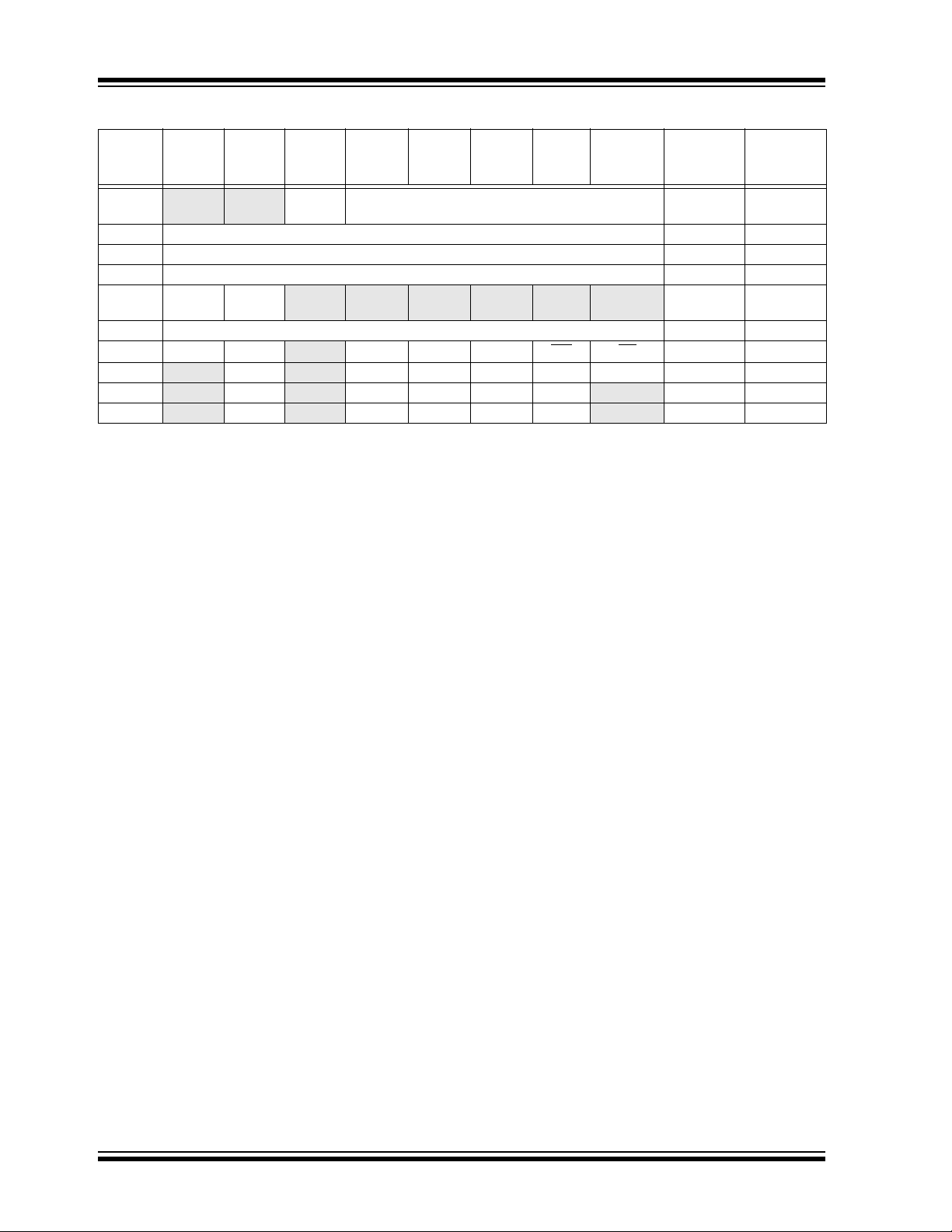
PIC18FXX8
TABLE 6-2: REGISTERS ASSOCIATED WITH PROGRAM FLASH MEMORY
Name Bit 7 Bit 6 Bit 5 Bit 4 Bit 3 Bit 2 Bit 1 Bit 0
TBLPTRU
TBPLTRH Program Memory Table Pointer High Byte (TBLPTR<15:8>) 0000 0000 0000 0000
TBLPTRL P rogram Mem ory Table Pointer Low Byte (TBLPTR<7:0>) 0000 0000 0000 0000
TABLAT Program Memory Table Latch 0000 0000 0000 0000
INTCON GIE/GIEH PEIE/
EECON2 EEPROM Control Register 2 (not a physical register) — —
EECON1 EEPGD CFGS
IPR2
PIR2
PIE2
Legend: x = unknown, u = unchanged, - = unimplemented, read as ‘0’.
Note 1: These registers or register bits are not implemented on the PIC18F248 and PIC18F258 and read as ‘0’s.
— — bit 21 Program Memory Table Pointer Upper Byte
(TBLPTR<20:16>)
TMR0IE INTE RBIE TMR0IF INTF RBIF 0000 000x 0000 000u
GIEL
— FREE WRERR WREN WR RD xx-0 x000 uu-0 u000
—CMIP—EEIPBCLIPLVDIPTMR3IPECCP1IP
—CMIF— EEIF BCLIF LVDIF TMR3IF ECCP1IF
—CMIE—EEIEBCLIELVDIETMR3IEECCP1IE
Shaded cells are not used during Flash/EEPROM access.
Value on:
POR, BOR
--00 0000 --00 0000
(1)
-1-1 1111 -1-1 1111
(1)
-0-0 0000 -0-0 0000
(1)
-0-0 0000 -0-0 0000
Value on
all other
Resets
DS41159D-page 74 2004 Microchip Technology Inc.

PIC18FXX8
7.0 8 x 8 HARDWARE MULTIPLIER
7.1 Introduction
An 8 x 8 hardware multiplier is included in the ALU of
the PIC18FXX8 devices. By making the multiply a
hardware operatio n, i t co mp letes in a single instruction
cycle. This is an unsign ed multiply that gives a 16-bit
result. The result is store d in the 1 6-bit pro duct reg ister
pair (PRODH:PRODL). The multiplier does not affect
any flags in the ALUSTA register.
Making the 8 x 8 multiplier execute in a single cycle
gives the following advantages:
• Higher computational throughput
• Reduces code size requ ire me nt s for multiply
algorithms
The performance increas e allows the device to be used
in applications previously reserved for Digital Signal
Processors.
Table 7-1 shows a perf ormance comparison be tween
Enhanced devices using the single-cycle hardware
multiply and performing the same function without the
hardware multiply.
7.2 Operation
Example 7-1 shows the sequence to do an 8 x 8
unsigned multiply. Only one instruction is required
when one argument of the multiply is already loaded in
the WREG register.
Example 7-2 shows the se quence to do an 8 x 8 si gned
multiply. To account for the sign bits of the arguments,
each argument’s Most Significant bit (MSb) is tested
and the appropriate subtractions are done.
EXAMPLE 7-1: 8 x 8 UNSIGNED
MULTIPLY ROUTINE
MOVF ARG1, W ;
MULWF ARG2 ; ARG1 * ARG2 ->
; PRODH:PRODL
EXAMPLE 7-2: 8 x 8 SIGNED MULTIPLY
ROUTINE
MOVF ARG1, W
MULWF ARG2 ; ARG1 * ARG2 ->
; PRODH:PRODL
BTFSC ARG2, SB ; Test Sign Bit
SUBWF PRODH ; PRODH = PRODH
; - ARG1
MOVF ARG2, W
BTFSC ARG1, SB ; Test Sign Bit
SUBWF PRODH ; PRODH = PRODH
; - ARG2
TABLE 7-1: PERFORMANCE COMPARISON
Program
Routine Multiply Method
8 x 8 unsigned
8 x 8 signed
16 x 16 unsigned
16 x 16 signed
Without hardware multiply 13 69 6.9 µs 27.6 µs 69 µs
Hardware multiply 1 1 100 ns 400 ns 1 µs
Without hardware multiply 33 91 9.1 µs 36.4 µs 91 µs
Hardware multiply 6 6 600 ns 2.4 µs6 µs
Without hardware multiply 21 242 24.2 µs 96.8 µs 242 µs
Hardware multiply 24 24 2.4 µs9.6 µs 24 µs
Without hardware multiply 52 254 25.4 µs102.6 µs 254 µs
Hardware multiply 36 36 3.6 µs 14.4 µs 36 µs
Memory
(Words)
Cycles
(Max)
Time
@ 40 MHz @ 10 MHz @ 4 MHz
2004 Microchip Technology Inc. DS41159D-page 75

PIC18FXX8
Example 7-3 shows the sequence to do a 16 x 16
unsigned multiply. Equation 7-1 shows the algorithm
that is used. The 32-bit re sult is st ored in four re gisters,
RES3:RES0.
EQUATION 7-1: 16 x 16 UNSIGNED
MULTIPLICATION
ALGORITHM
RES3:RES0 = ARG1H:ARG1L • ARG2H:ARG2L
= (ARG1H • ARG2H • 2
(ARG1H • ARG2L • 2
(ARG1L • ARG2H • 2
(ARG1L • ARG2L)
16
) +
8
) +
8
) +
EXAMPLE 7-3: 16 x 16 UNSIGNED
MULTIPLY ROUTINE
MOVF ARG1L, W
MULWF ARG2L ; ARG1L * ARG2L ->
MOVFF PRODH, RES1 ;
MOVFF PRODL, RES0 ;
;
MOVF ARG1H, W
MULWF ARG2H ; ARG1H * ARG2H ->
MOVFF PRODH, RES3 ;
MOVFF PRODL, RES2 ;
;
MOVF ARG1L, W
MULWF ARG2H ; ARG1L * ARG2H ->
MOVF PRODL, W ;
ADDWF RES1 ; Add cross
MOVF PRODH, W ; products
ADDWFC RES2 ;
CLRF WREG ;
ADDWFC RES3 ;
;
MOVF ARG1H, W ;
MULWF ARG2L ; ARG1H * ARG2L ->
MOVF PRODL, W ;
ADDWF RES1 ; Add cross
MOVF PRODH, W ; products
ADDWFC RES2 ;
CLRF WREG ;
ADDWFC RES3 ;
Example 7-4 shows the sequence to do a 16 x 16
signed multiply. Equation 7-2 shows the algorithm
used. The 32-bit result is stored in four registers,
RES3:RES0. To account for the sign bits of the arguments, each argu ment p air’s Most Signi ficant bit (M Sb)
is tested and the appropriate subtractions are done.
; PRODH:PRODL
; PRODH:PRODL
; PRODH:PRODL
; PRODH:PRODL
EQUATION 7-2: 16 x 16 SIGNED
MULTIPLICATION
ALGORITHM
RES3:RES0
= ARG1H:ARG1L • ARG2H:ARG2L
= (ARG1H • ARG2H • 2
(ARG1H • ARG2L • 2
(ARG1L • ARG2H • 2
(ARG1L • ARG2L)+
(-1 • ARG2H<7> • AR G1H:ARG1L • 2
(-1 • ARG1H<7> • AR G2H:ARG2L • 2
16
) +
8
) +
8
) +
EXAMPLE 7-4: 16 x 16 SIGNED
MULTIPLY ROUTINE
MOVF ARG1L, W
MULWF ARG2L ; ARG1L * ARG2L ->
MOVFF PRODH, RES1 ;
MOVFF PRODL, RES0 ;
;
MOVF ARG1H, W
MULWF ARG2H ; ARG1H * ARG2H ->
MOVFF PRODH, RES3 ;
MOVFF PRODL, RES2 ;
;
MOVF ARG1L, W
MULWF ARG2H ; ARG1L * ARG2H ->
MOVF PRODL, W ;
ADDWF RES1 ; Add cross
MOVF PRODH, W ; products
ADDWFC RES2 ;
CLRF WREG ;
ADDWFC RES3 ;
;
MOVF ARG1H, W ;
MULWF ARG2L ; ARG1H * ARG2L ->
MOVF PRODL, W ;
ADDWF RES1 ; Add cross
MOVF PRODH, W ; products
ADDWFC RES2 ;
CLRF WREG ;
ADDWFC RES3 ;
;
BTFSS ARG2H, 7 ; ARG2H:ARG2L neg?
BRA SIGN_ARG1 ; no, check ARG1
MOVF ARG1L, W ;
SUBWF RES2 ;
MOVF ARG1H, W ;
SUBWFB RES3
;
SIGN_ARG1
BTFSS ARG1H, 7 ; ARG1H:ARG1L neg?
BRA CONT_CODE ; no, done
MOVF ARG2L, W ;
SUBWF RES2 ;
MOVF ARG2H, W ;
SUBWFB RES3
;
CONT_CODE
:
; PRODH:PRODL
; PRODH:PRODL
; PRODH:PRODL
; PRODH:PRODL
16
) +
16
)
DS41159D-page 76 2004 Microchip Technology Inc.

PIC18FXX8
8.0 INTERRUPTS
The PIC18FXX8 devices have multiple interrupt
sources and an interrupt priority feature that allows
each interrupt source to be assigned a high priority
level or a low priority level. The high priority interrupt
vector is at 000008h and the low prio rity interrupt vector
is at 000018h. High priority interrupt events will
override any low priority interrupts that may be in
progress.
There are 13 registers that are use d to c ontrol interru pt
operation. These registers are:
• RCON
•INTCON
• INTCON2
• INTCON3
• PIR1, PIR2, PIR3
• PIE1, PIE2, PIE3
• IPR1, IPR2, IPR3
It is recommended that the Microchip header files,
supplied with MPLAB
names in these registers. This allows the assembler/
compiler to automatical ly ta ke care of the pla ceme nt of
these bits within the specified register.
Each interrupt source has three bits to control its
operation. The functions of these bits are:
• Flag bit to indicate that an interrupt event
occurred
• Enable bit that allows program execution to
branch to the interrupt vector address when the
flag bit is set
• Priority bit to select high priority or low priority
The interrupt priority feature is enabled by setting the
IPEN bit (RCON register). When interrupt priority is
enabled, there are two bits that enable interrupts
globally . Setti ng the GIEH bit (INTC ON<7>) enable s all
interrupts. Setting the GIEL bit (INTCON register)
enables all interrupts that have the priority bit cleared.
When the interrupt flag, enable bit and appropriate
global interrupt enable bit are set, the interrupt wi ll vector immediately to address 000008h or 000018h,
depending on the priority level. Individual inte rrupts can
be disabled through their corresponding enable bits.
®
IDE, be used for the symbolic bit
When the IPEN bit is cleared (default state), the
interrupt priority feature is disabled and interrupts are
compatible with PICmicro
Compatibilit y mode, the in terrupt prior ity bits for each
source have no effe ct. T he PEIE b it (IN TCO N regi st er)
enables/disables all peripheral interrupt sources. The
GIE bit (INTCON register) enab les/disables all in terrupt
sources. All interrupts branch to address 000008h in
Compatibility mode.
When an interrupt is responded to, the global interrupt
enable bit is cleared to disable further interrupts. If the
IPEN bit is cleared, this is the GIE bit. If interru pt priority
levels are used, this wi ll be either the GIEH or G IEL bit.
High priority interrupt sources can interrupt a low
priority interrupt.
The return address is pushed onto the stack and the
PC is loaded with the interrupt vector address
(000008h or 000018h). Once in the Interrupt Service
Routine, the source(s) of the interrupt can be determined by polling the interrupt flag bits. The interrupt
flag bits must be cleared in s oftware be fore re-enab ling
interrupts to avoid recursive interrupts.
The “return from interrupt” instruction, RETFIE, exits
the interrupt routine and set s the GIE bit (GIEH or GI EL
if priority levels are used), which re-enables interrupts.
For external interrupt events, such as the INT pins or
the PORTB input chang e interrupt, the i nterrupt latenc y
will be three to four instruction cycles. The exact
latency is the same for one or two-cycle instructions.
Individual interrupt flag bits are set regardless of the
status of their corresponding enable bit or the GIE bit.
Note: Do not use the MOVFF instruction to modify
any of the interrupt control registers while
any interrupt is enabled. Doing so may
cause erratic microcontroller behavior.
®
mid-range devices. In
2004 Microchip Technology Inc. DS41159D-page 77

PIC18FXX8
FIGURE 8-1: INTERRUPT LOGIC
Peripheral Interrupt Flag bit
Peripheral Interrupt Enable bit
Peripheral Interrupt Priority bit
TMR1IF
TMR1IE
TMR1IP
XXXXIF
XXXXIE
XXXXIP
Additional Peripheral Interrupts
High Priority Interrupt Generation
Low Priority Interrupt Generation
IPEN
TMR0IF
TMR0IE
TMR0IP
RBIF
RBIE
RBIP
INT0IF
INT0IE
INT1IF
INT1IE
INT1IP
INT2IF
INT2IE
INT2IP
IPEN
GIEL/PEIE
IPEN
Wake-up if in Sleep mode
Interrupt to CPU
Vector to Location
0008h
GIE/GIEH
Peripheral Interrupt Flag bit
Peripheral Interrupt Enable bit
Peripheral Interrupt Priority bit
TMR1IF
TMR1IE
TMR1IP
XXXXIF
XXXXIE
XXXXIP
Additional Peripheral Interrupts
TMR0IF
TMR0IE
TMR0IP
RBIF
RBIE
RBIP
INT0IF
INT0IE
INT1IF
INT1IE
INT1IP
INT2IF
INT2IE
INT2IP
Interrupt to CPU
Vector to Location
0018h
PEIE/GIEL
GIE/GIEH
DS41159D-page 78 2004 Microchip Technology Inc.

PIC18FXX8
8.1 INTCON Registers
The INTCON registers are readable an d writa ble registers which cont ain v arious enab le, pri ority and fla g bit s.
Because of the number of interrupts to be controlled,
PIC18FXX8 devices have three INTCON registers.
They are detai led in Register 8-1 through Register 8-3.
Note: Interrupt flag bi ts are set when an in terrupt
condition occurs regardless of the state of
its corresponding enable bit or the global
interrupt enable bit. User software should
ensure the appropriate interrupt flag bits
are clear prior to enabling an interrupt.
This feature allows software polling.
REGISTER 8-1: INTCON: INTERRUPT CONTROL REGISTER
R/W-0 R/W-0 R/W-0 R/W-0 R/W-0 R/W-0 R/W-0 R/W-x
GIE/GIEH PEIE/GIEL TMR0IE INT0IE RBIE TMR0IF INT0IF RBIF
bit 7 bit 0
bit 7 GIE/GIEH: Global Interrupt Enable bit
When IPEN (RCON<7>) = 0:
1 = Enables all unmasked interrupts
0 = Disables all interrupts
PEN (RCON<7>) = 1:
When I
1 = Enables all high priority interrupts
0 = Disables all priority interrupts
bit 6 PEIE/GIEL: Peripheral Interrupt Enable bit
When IPEN (RCON<7>) =
1 = Enables all unmasked peripheral interrupts
0 = Disables all peripheral inter rupts
When IPEN (RCON<7>) =
1 = Enables all low priority peripheral interrupts
0 = Disables all low priority peripheral interrupts
bit 5 TMR0IE: TMR0 Overflow Interrupt Enable bit
1 = Enables the TMR0 overflow interrupt
0 = Disables the TMR0 overflow interrupt
bit 4 INT0IE: INT0 External Interrupt Enable bit
1 = Enables the INT0 external interrupt
0 = Disables the INT0 external interrupt
bit 3 RBIE: RB Port Change Interrupt Enable bit
1 = Enables the RB port change interrupt
0 = Disables the RB port change int errupt
bit 2 TMR0IF: TMR0 Overflow Interrupt Flag bit
1 = TMR0 register has overflowed (must be cleared in software)
0 = TMR0 register did no t overflow
bit 1 INT0IF: INT0 External Interrupt Flag bit
1 = The INT0 external interrupt occurred (must be cleared in software by reading PORTB)
0 = The INT0 external interrupt did not occur
bit 0 RBIF: RB Port Change Interrupt Flag bit
1 = At least one of the RB7:RB4 pins changed state (must be cleared in software)
0 = None of the RB7:RB4 pins have changed state
Note: A mismatch condition will continue to set this bit. Reading PORTB will end the
mismatch condition and allow the bit to be cleared.
0:
1:
Legend:
R = Readable bit W = Writable bit U = Unimplemented bit, read as ‘0’
-n = Value at POR ‘1’ = Bit is set ‘0’ = Bit is cleared x = Bit is unknown
2004 Microchip Technology Inc. DS41159D-page 79

PIC18FXX8
REGISTER 8-2: INTCON2: INTERRUPT CONTROL REGISTER 2
R/W-1 R/W-1 R/W-1 U-0 U-0 R/W-1 U-0 R/W-1
RBPU INTEDG0 INTEDG1 — —TMR0IP—RBIP
bit 7 bit 0
bit 7 RBPU
bit 6 INTEDG0: External Interrupt 0 Edge Select bit
bit 5 INTEDG1: External Interrupt 1 Edge Select bit
bit 4-3 Unimplemented: Read as ‘0’
bit 2 TMR0IP: TMR0 Overflow Interrupt Priority bit
bit 1 Unimplemented: Read as ‘0’
bit 0 RBIP: RB Port Change Interrupt Priority bit
: PORTB Pull-up Enable bit
1 = All PORTB pull-ups are disabled
0 = PORTB pull-ups are enabled by individual port latch values
1 = Interrupt on rising edge
0 = Interrupt on falling edge
1 = Interrupt on rising edge
0 = Interrupt on falling edge
1 = High priori ty
0 = Low priority
1 = High priority
0 = Low priority
Legend:
R = Readable bit W = Writable bit U = Unimplemented bit, read as ‘0’
-n = Value at POR ‘1’ = Bit is set ‘0’ = Bit is cleared x = Bit is unknown
Note: Interrupt flag bi ts a r e s et w h en an i nt e rr up t cond i t io n o cc urs r eg a rdl es s o f th e stat e
of its corresponding enable bit or the global interrupt enable bit. User software
should ensure the appropriate interrupt flag bits are clear prior to enabling an
interrupt. This feature allows software polling.
DS41159D-page 80 2004 Microchip Technology Inc.

REGISTER 8-3: INTCON3: INTERRUPT CONTROL REGISTER 3
R/W-1 R/W-1 U-0 R/W-0 R/W-0 U-0 R/W-0 R/W-0
INT2IP INT1IP
bit 7 bit 0
bit 7 INT2IP: INT2 External Interrupt Priority bit
1 = High priori ty
0 = Low priority
bit 6 INT1IP: INT1 External Interrupt Priority bit
1 = High priori ty
0 = Low priority
bit 5 Unimplemented: Read as ‘0’
bit 4 INT2IE: INT2 External Interrupt Enable bit
1 = Enables the INT2 external interrupt
0 = Disables the INT2 external interrupt
bit 3 INT1IE: INT1 External Interrupt Enable bit
1 = Enables the INT1 external interrupt
0 = Disables the INT1 external interrupt
bit 2 Unimplemented: Read as ‘0’
bit 1 INT2IF: INT2 External Interrupt Flag bit
1 = The INT2 external interrupt occurred (must be cleared in software)
0 = The INT2 external interrupt did not occur
bit 0 INT1IF: INT1 External Interrupt Flag bit
1 = The INT1 external interrupt occurred (must be cleared in software)
0 = The INT1 external interrupt did not occur
—INT2IEINT1IE— INT2IF INT1IF
PIC18FXX8
Legend:
R = Readable bit W = Writable bit U = Unimplemented bit, read as ‘0’
-n = Value at POR ‘1’ = Bit is set ‘0’ = Bit is cleared x = Bit is unknown
Note: Interrupt flag bi ts a r e s et w h en an i nt e rr up t cond i t io n o cc urs r eg a rdl es s o f th e stat e
of its corresponding enable bit or the global interrupt enable bit. User software
should ensure the appropriate interrupt flag bits are clear prior to enabling an
interrupt. This feature allows software polling.
2004 Microchip Technology Inc. DS41159D-page 81

PIC18FXX8
8.2 PIR Registers
The Peripheral Interrupt Request (PIR) registers
contain the individual flag bits for the peripheral
interrupts (Register 8-4 through Register 8-6). Due to
the number of peripheral interrupt sources, there are
three Peripheral Interrupt Request (Flag) registers
(PIR1, PIR2, PIR3).
Note 1: Interrupt flag bits are set when an interrupt
condition occurs rega rdless of the st ate of
its corresponding enable bit or the Global
Interrupt Enable bit, GIE (INTCON
register).
2: User software should en sure the appropri-
ate interrupt flag bits are cleared prior to
enabling an interrupt and after servicing
that interrupt.
REGISTER 8-4: PIR1: PERIPHERAL INTERRUPT REQUEST (FLAG) REGISTER 1
R/W-0 R/W-0 R-0 R-0 R/W-0 R/W-0 R/W-0 R/W-0
(1)
PSPIF
bit 7 bit 0
bit 7 PSPIF: Parallel Slave Port Read/Write Interrupt Flag bit
1 = A read or a write operation has taken place (must be cleared in software)
0 = No read or write has occurred
bit 6 ADIF: A/D Converter Interrupt Flag bit
1 = An A/D conversion completed (must be cleared in software)
0 = The A/D conversion is not complete
bit 5 RCIF: USART Receive Interrupt Flag bit
1 = Th e USART receive buffer, RCREG, is full (cleared when RCREG is read)
0 = The USART recei v e buffer is empty
bit 4 TXIF: USART Transmit Interrupt Flag bit
1 = The USART transmit buffer, TXREG, is empty (cleared when TXREG is written)
0 = The USART transmit buffer is full
bit 3 SSPIF: Master Synchronous Serial Port Interrupt Flag bit
1 = The transmission/reception is complete (must be cleared in software)
0 = Waiting to transmit/receive
bit 2 CCP1IF: CCP1 Interrupt Flag bit
Capture mode:
1 = A TMR1 register capture occurred (must be cleared in software)
0 = No TMR1 register capture occurred
Compare mode:
1 = A TMR1 register compare match occurred (must be cleared in software)
0 = No TMR1 register compare match occurred
PWM mode:
Unused in this mode.
bit 1 TMR2IF: TMR2 to PR2 Match Interrupt Flag bit
1 = TMR2 to PR2 match occurred (must be cleared in software)
0 = No TMR2 to PR2 match occurred
bit 0 TMR1IF: TMR1 Overflow Interrupt Flag bit
1 = TMR1 registe r overflowe d (must be cleared in software)
0 = TMR1 register did not overflow
ADIF RCIF TXIF SSPIF CCP1IF TMR2IF TMR1IF
(1)
Note 1: Th is bit is only avail able o n PIC1 8F4X8 d evice s. For P IC18F 2X8 dev ices, this bi t
is unimplemented and reads as ‘0’.
Legend:
R = Readable bit W = Writable bit U = Unimplemented bit, read as ‘0’
-n = Value at POR ‘1’ = Bit is set ‘0’ = Bit is cleared x = Bit is unknown
DS41159D-page 82 2004 Microchip Technology Inc.

PIC18FXX8
REGISTER 8-5: PIR2: PERIPHERAL INTERRUPT REQUEST (FLAG) REGISTER 2
U-0 R/W-0 U-0 R/W-0 R/W-0 R/W-0 R/W-0 R/W-0
—CMIF
bit 7 bit 0
bit 7 Unimplemented: Read as ‘0’
bit 6 CMIF: Comparator Interrupt Flag bit
1 = Comparator input has changed
0 = Comparator input has not changed
bit 5 Unimplemented: Read as ‘0’
bit 4 EEIF: EEPROM Write Operation Interrupt Flag bit
1 = Write operation is complete (must be cleared in software)
0 = Write operation is not complete
bit 3 BCLIF: Bus Collision Interrupt Flag bit
1 = A bus collision occurred (must be cleared in software)
0 = No bus collision occurred
bit 2 LVDIF: Low-Voltage Detect Interrupt Flag bit
1 = A low-voltage condition oc curred (must be cleared in software)
0 = The device voltage is above the Low-Voltage Detect trip point
bit 1 TMR3IF: TMR3 Overflow Interrupt Flag bit
1 = TMR3 register overflowed (must be cleared in soft ware)
0 = TMR3 register did not overflow
bit 0 ECCP1IF: ECCP1 Interrupt Flag bit
Capture mode:
1 = A TMR1 (TMR3) register capture occurred (must be cleared in software)
0 = No TMR1 (TMR3) register capture occurred
Compare mode:
1 = A TMR1 register compare match occurred (must be cleared in software)
0 = No TMR1 register compare match occurred
PWM mode:
Unused in this mode.
(1)
— EEIF BCLIF LVDIF TMR3IF ECCP1IF
(1)
(1)
(1)
Note 1: Th is bit is only avail able o n PIC1 8F4X8 d evice s. For P IC18F 2X8 dev ices, this bi t
is unimplemented and reads as ‘0’.
Legend:
R = Readable bit W = Writable bit U = Unimplemented bit, read as ‘0’
-n = Value at POR ‘1’ = Bit is set ‘0’ = Bit is cleared x = Bit is unknown
2004 Microchip Technology Inc. DS41159D-page 83

PIC18FXX8
REGISTER 8-6: PIR3: PERIPHERAL INTERRUPT REQUEST (FLAG) REGISTER 3
R/W-0 R/W-0 R/W-0 R/W-0 R/W-0 R/W-0 R/W-0 R/W-0
IRXIF WAKIF ERRIF TXB2IF TXB1IF TXB0IF RXB1IF RXB0IF
bit 7 bit 0
bit 7 IRXIF: Invalid Message Received Interrupt Flag bit
1 = An invalid message has occurred on the CAN bus
0 = An invalid message has not occurred on the CAN bus
bit 6 WAKIF: Bus Activity Wake-up Interrupt Flag bit
1 = Activity on the CAN bus has occurred
0 = Activity on the CAN bus has not occurred
bit 5 ERRIF: CAN bus Error Interrupt Flag bit
1 = An error has occurred in the CAN module (multiple sources)
0 = An error has not occurred in the CAN module
bit 4 TXB2IF: Transmit Buffer 2 Interrupt Flag bit
1 = Transmit Buffer 2 has completed transmission of a message and may be reloaded
0 = Transmit Buffer 2 has not completed transmission of a message
bit 3 TXB1IF: Transmit Buffer 1 Interrupt Flag bit
1 = Transmit Buffer 1 has completed transmission of a message and may be reloaded
0 = Transmit Buffer 1 has not completed transmission of a message
bit 2 TXB0IF: Transmit Buffer 0 Interrupt Flag bit
1 = Transmit Buffer 0 has completed transmission of a message and may be reloaded
0 = Transmit Buffer 0 has not completed transmission of a message
bit 1 RXB1IF: Receive Buffer 1 Interrupt Flag bit
1 = Receive Buffer 1 has received a new message
0 = Receive Buffer 1 has not received a new message
bit 0 RXB0IF: Receive Buffer 0 Interrupt Flag bit
1 = Receive Buffer 0 has received a new message
0 = Receive Buffer 0 has not received a new message
Legend:
R = Readable bit W = Writable bit U = Unimplemented bit, read as ‘0’
-n = Value at POR ‘1’ = Bit is set ‘0’ = Bit is cleared x = Bit is unknown
DS41159D-page 84 2004 Microchip Technology Inc.

PIC18FXX8
8.3 PIE Registers
The Peripheral Interrupt En abl e (PIE) registers contain
the individual enable bits for the peripheral interrupts
(Register 8-7 through Register 8-9). Due to the number
of peripher a l int er ru p t sour c e s, th er e ar e t hr e e Pe r i ph eral Interrupt Enable registers (PIE1, PIE2, PIE3).
When IPEN is clear, the PEIE bit must be set to enable
any of these peripheral interrupts.
REGISTER 8-7: PIE1: PERIPHERAL INTERRUPT ENABLE REGISTER 1
R/W-0 R/W-0 R/W-0 R/W-0 R/W-0 R/W-0 R/W-0 R/W-0
(1)
PSPIE
bit 7 bit 0
ADIE RCIE TXIE SSPIE CCP1IE TMR2IE TMR1IE
bit 7 PSPIE: Parallel Slave Port Read/Write Interru pt Enab le bit
1 = Enables the PSP read/write interrupt
0 = Disables the PSP read/write interrupt
bit 6 ADIE: A/D Converter Interrupt Enable bit
1 = Enables the A/D interrupt
0 = Disables the A/D interrupt
bit 5 RCIE: USART Receive Interrupt Enable bit
1 = Enables the USART receive interrupt
0 = Disables the USART receive interrupt
bit 4 TXIE: USART Transmit Interrupt Enable bit
1 = Enables the USART transmit interrupt
0 = Disables the USART transmit interrupt
bit 3 SSPIE: Master Synchronous Serial Port Interrupt Enable bit
1 = Enables the MSSP interrupt
0 = Disables the MSSP interrupt
bit 2 CCP1IE: CCP1 Interrupt Enable bit
1 = Enables the CCP1 interrupt
0 = Disables the CCP1 interrupt
bit 1 TMR2IE: TMR2 to PR2 Match Interrupt Enable bit
1 = Enables the TMR2 to PR2 match interrupt
0 = Disables the TMR2 to PR2 match interrupt
bit 0 TMR1IE: TMR1 Overflow Interrupt Enable bit
1 = Enables the TMR1 overflow interrupt
0 = Disables the TMR1 overflow interrupt
(1)
Note 1: Th is bit is only avail able o n PIC1 8F4X8 d evice s. For P IC18F 2X8 dev ices, this bi t
is unimplemented and reads as ‘0’.
Legend:
R = Readable bit W = Writable bit U = Unimplemented bit, read as ‘0’
-n = Value at POR ‘1’ = Bit is set ‘0’ = Bit is cleared x = Bit is unknown
2004 Microchip Technology Inc. DS41159D-page 85

PIC18FXX8
REGISTER 8-8: PIE2: PERIPHERAL INTERRUPT ENABLE REGISTER 2
U-0 R/W-0 U-0 R/W-0 R/W-0 R/W-0 R/W-0 R/W-0
—CMIE
bit 7 bit 0
bit 7 Unimplemented: Read as ‘0’
bit 6 CMIE: Comparator Interrupt Enable bit
1 = Enables the comparator interrupt
0 = Disables the comparator interrupt
bit 5 Unimplemented: Read as ‘0’
bit 4 EEIE: EEPROM Write Interrupt Enable bit
1 = Enabled
0 =Disabled
bit 3 BCLIE: Bus Collision Interrupt Enable bit
1 = Enabled
0 =Disabled
bit 2 LVDIE: Low-Voltage Detect Interrupt Enable bit
1 = Enabled
0 =Disabled
bit 1 TMR3IE: TMR3 Overflow Interr upt Enable bit
1 = Enables the TMR3 overflow interrupt
0 = Disables the TMR3 overflow interrupt
bit 0 ECCP1IE: ECCP1 Interrupt Ena ble bit
1 = Enables the ECCP1 interrupt
0 = Disables the ECCP1 interrupt
(1)
— EEIE BCLIE LVDIE TMR3IE ECCP1IE
(1)
(1)
(1)
Note 1: Th is bit is only avail able o n PIC1 8F4X8 d evice s. For P IC18F 2X8 dev ices, this bi t
is unimplemented and reads as ‘0’.
Legend:
R = Readable bit W = Writable bit U = Unimplemented bit, read as ‘0’
-n = Value at POR ‘1’ = Bit is set ‘0’ = Bit is cleared x = Bit is unknown
DS41159D-page 86 2004 Microchip Technology Inc.

PIC18FXX8
REGISTER 8-9: PIE3: PERIPHERAL INTERRUPT ENABLE REGISTER 3
R/W-1 R/W-1 R/W-1 R/W-1 R/W-1 R/W-1 R/W-1 R/W-1
IRXIE WAKIE ERRIE TXB2IE TXB1IE TXB0IE RXB1IE RXB0IE
bit 7 bit 0
bit 7 IRXIE: Invalid CAN Message Received Interrupt Enable bit
1 = Enables the invalid CAN message received interrupt
0 = Disables the invalid CAN message received interrupt
bit 6 WAKIE: Bus Activity Wake-up Interrupt Enable bit
1 = Enables the bus activity wake-up interrupt
0 = Disables the bus activity wake-up interrupt
bit 5 ERRIE: CAN bus Error Interrupt Enable bit
1 = Enables the CAN bus error interrupt
0 = Disables the CAN bus error interrupt
bit 4 TXB2IE: Transmit Buffer 2 Interrupt Enable bit
1 = Enables the Transmit Buffer 2 interrupt
0 = Disables th e Transmit Buffer 2 interrupt
bit 3 TXB1IE: Transmit Buffer 1 Interrupt Enable bit
1 = Enables the Transmit Buffer 1 interrupt
0 = Disables th e Transmit Buffer 1 interrupt
bit 2 TXB0IE: Transmit Buffer 0 Interrupt Enable bit
1 = Enables the Transmit Buffer 0 interrupt
0 = Disables th e Transmit Buffer 0 interrupt
bit 1 RXB1IE: Receive Buffer 1 Interrupt Enable bit
1 = Enables the Receive Buffer 1 interrupt
0 = Disables the Receive Buffer 1 interrupt
bit 0 RXB0IE: Receive Buffer 0 Interrupt Enable bit
1 = Enables the Receive Buffer 0 interrupt
0 = Disables the Receive Buffer 0 interrupt
Legend:
R = Readable bit W = Writable bit U = Unimplemented bit, read as ‘0’
-n = Value at POR ‘1’ = Bit is set ‘0’ = Bit is cleared x = Bit is unknown
2004 Microchip Technology Inc. DS41159D-page 87

PIC18FXX8
8.4 IPR Registers
The Interrupt Priority (IPR) registe rs contain the indi vidual priority bits for the peripheral interrupts. Due to the
number of peripheral interrup t sour ces , the re are thre e
Peripheral Interrupt Priority registers (IPR1, IPR2 and
IPR3). The operation of the priority bits requires that
the Interrupt Priority Enable bit (IPEN) be set.
REGISTER 8-10: IPR1: PERIPHERAL INTERRUPT PRIORITY REGISTER 1
R/W-1 R/W-1 R/W-1 R/W-1 R/W-1 R/W-1 R/W-1 R/W-1
(1)
PSPIP
bit 7 bit 0
ADIP RCIP TXIP SSPIP CCP1IP TMR2IP TMR1IP
bit 7 PSPIP: Parallel Slave Port Read/ W ri te Interru pt Priori ty bit
1 =High priority
0 = Low priority
bit 6 ADIP: A/D Converter Interrupt Priority bit
1 =High priority
0 = Low priority
bit 5 RCIP: USART Receive Interrupt Priority bit
1 =High priority
0 = Low priority
bit 4 TXIP: USART Transmit Interrupt Priority bit
1 =High priority
0 = Low priority
bit 3 SSPIP: Master Synchronous Serial Port Interrupt Priority bit
1 =High priority
0 = Low priority
bit 2 CCP1IP: CCP1 Interrupt Priority bit
1 = High priority
0 = Low priority
bit 1 TMR2IP: TMR2 to PR2 Match Interrupt Priority bit
1 =High priority
0 = Low priority
bit 0 TMR1IP: TMR1 Overflow Interrupt Priority bit
1 = High priority
0 = Low priority
(1)
Note 1: Th is bit is only avail able o n PIC1 8F4X8 d evice s. For P IC18F 2X8 dev ices, this bi t
is unimplemented and reads as ‘0’.
Legend:
R = Readable bit W = Writable bit U = Unimplemented bit, read as ‘0’
-n = Value at POR ‘1’ = Bit is set ‘0’ = Bit is cleared x = Bit is unknown
DS41159D-page 88 2004 Microchip Technology Inc.

PIC18FXX8
REGISTER 8-11: IPR2: PERIPHERAL INTERRUPT PRIORITY REGISTER 2
U-0 R/W-1 U-0 R/W-1 R/W-1 R/W-1 R/W-1 R/W-1
—CMIP
bit 7 bit 0
bit 7 Unimplemented: Read as ‘0’
bit 6 CMIP: Comparator Interrupt Priority bit
1 =High priority
0 = Low priority
bit 5 Unimplemented: Read as ‘0’
bit 4 EEIP: EEPROM Write Interrupt Priority bit
1 =High priority
0 = Low priority
bit 3 BCLIP: Bus Collision Interrupt Priority bit
1 =High priority
0 = Low priority
bit 2 LVDIP: Low-Voltage Detect Interrupt Priority bit
1 =High priority
0 = Low priority
bit 1 TMR3IP: TMR3 Overflow Interrupt Priority bit
1 =High priority
0 = Low priority
bit 0 ECCP1IP: ECCP1 Interrupt Priority bit
1 =High priority
0 = Low priority
(1)
— EEIP BCLIP LVDIP TMR3IP ECCP1IP
(1)
(1)
(1)
Note 1: Th is bit is only avail able o n PIC1 8F4X8 d evice s. For P IC18F 2X8 dev ices, this bi t
is unimplemented and reads as ‘0’.
Legend:
R = Readable bit W = Writable bit U = Unimplemented bit, read as ‘0’
-n = Value at POR ‘1’ = Bit is set ‘0’ = Bit is cleared x = Bit is unknown
2004 Microchip Technology Inc. DS41159D-page 89

PIC18FXX8
REGISTER 8-12: IPR3: PERIPHERAL INTERRUPT PRIORITY REGISTER 3
R/W-1 R/W-1 R/W-1 R/W-1 R/W-1 R/W-1 R/W-1 R/W-1
IRXIP WAKIP ERRIP TXB2IP TXB1IP TXB0IP RXB1IP RXB0IP
bit 7 bit 0
bit 7 IRXIP: Invalid Message Received Interrupt Priority bit
1 =High priority
0 = Low priority
bit 6 WAKIP: Bus Activity Wake-up Interrupt Priority bit
1 =High priority
0 = Low priority
bit 5 ERRIP: CAN bus Error Interrupt Priority bit
1 =High priority
0 = Low priority
bit 4 TXB2IP: Transmit Buffer 2 Interrupt Priority bit
1 =High priority
0 = Low priority
bit 3 TXB1IP: Transmit Buffer 1 Interrupt Priority bit
1 =High priority
0 = Low priority
bit 2 TXB0IP: Transmit Buffer 0 Interrupt Priority bit
1 =High priority
0 = Low priority
bit 1 RXB1IP: Receive Buffer 1 Interrupt Priority bit
1 =High priority
0 = Low priority
bit 0 RXB0IP: Receive Buffer 0 Interrupt Priority bit
1 =High priority
0 = Low priority
Legend:
R = Readable bit W = Writable bit U = Unimplemented bit, read as ‘0’
-n = Value at POR ‘1’ = Bit is set ‘0’ = Bit is cleared x = Bit is unknown
DS41159D-page 90 2004 Microchip Technology Inc.

8.5 RCON Register
The Reset Control (RCON) register contains the IPEN
bit which is used to enable prioritized interrupts. The
functions of the other bits in this register are discussed
in more detail in Section 4.14 “RCON Register”.
REGISTER 8-13: RCON: RESET CONTROL REGISTER
R/W-0 U-0 U-0 R/W-1 R-1 R-1 R/W-0 R/W-0
IPEN
bit 7 bit 0
bit 7 IPEN: Interrupt Priority Enable bit
1 = Enable priority levels on interrupts
0 = Disable priority levels on interrupts (PIC16CXXX Compatibility mode)
bit 6-5 Unimplemented: Read as ‘0’
bit 4 RI
bit 3 TO: Watchdog Time-out Flag bit
bit 2 PD: Power-down Detection Flag bit
bit 1 POR: Power-on Reset Status bit
bit 0 BOR: Brown-ou t Reset Status bit
: RESET Instruction Flag bit
For details of bit operation, see Register 4-3.
For details of bit operation, see Register 4-3.
For details of bit operation, see Register 4-3.
For details of bit operation, see Register 4-3.
For details of bit operation, see Register 4-3.
— —RITO PD POR BOR
PIC18FXX8
Legend:
R = Readable bit W = Writable bit U = Unimplemented bit, read as ‘0’
-n = Value at POR ‘1’ = Bit is set ‘0’ = Bit is cleared x = Bit is unknown
2004 Microchip Technology Inc. DS41159D-page 91

PIC18FXX8
8.6 INT Interrupts
External interrupts on the RB0/INT0, RB1/INT1 and
RB2/CANTX/INT2 pins are e dge triggered: eith er rising
if the corresponding INTEDGx bit is set in the
INTCON2 register, or falling if the INTEDGx bi t is c lear.
When a valid edge appears on the RBx/INTx pin, the
corresponding flag bit INTxIF is set. This interrupt can
be disabled by clearing the corresponding enable bit
INTxIE. Flag bit INTxIF must be cl eared in softwa re in
the Interrupt Service Routine before re-enabling the
interrupt. All external interrupts (INT0, INT1 and INT2)
can wake-up the proc essor from Sleep if b it INTxIE was
set prior to going into Sleep. If the Global Interrupt
Enable bit, GIE, is set, the processor will branch to the
interrupt vector following wake-up.
Interrupt priority for INT1 and INT2 is determ ined by the
value contained in the interrupt priority bits INT1IP
(INTCON3<6>) and INT2IP (INTCON3<7>). There is
no priority bi t ass ociate d with INT0; it is alwa ys a high
priority interrupt source.
8.7 TMR0 Interrupt
In 8-bit mode (wh ich is the de fault), an ov erflow (FFh →
00h) in the TMR0 r egister wi ll set flag bit TMR0I F. In
16-bit mode, an overflow (FFFFh → 0000h) in the
TMR0H:TMR0L registers will set flag bit TMR0IF. The
interrupt can be enabled/disabled by setting/clearing
enable bit TMR0IE (INTCON register ). Interrupt pri ority
for Timer0 is determined by the value contained in the
interrupt priority bit TMR0IP (INTCON2 register). See
Section 11.0 “Timer0 Module” for further details.
8.8 PORTB Interrupt-on-Change
An input change on PORTB<7:4> sets flag bit RBIF
(INTCON register). The interrupt can be enabled/
disabled by setting/clearing enable bit RBIE (INTCON
register). Interrupt priority for PORTB interrupt-onchange is determined by the value contained in the
interrupt priority bit RBIP (INTCON2 register).
8.9 Context Saving During Interrupts
During an interrupt, the return PC v alue is sa ved on the
stack. Additionally, the WREG, Status and BSR
registers ar e saved on the fas t return stack. If a f ast
return from interrupt is not used (see Section 4.3 “Fast
Register Stack”), the user may need to save the
WREG, St atus and BSR reg isters in softw are. De pending on the user’s application, other registers may also
need to be saved. Exam ple 8-1 saves and restores the
WREG, Status and BSR registers during an Interrupt
Service Routine.
EXAMPLE 8-1: SAVING STATUS, WREG AND BSR REGISTERS IN RAM
MOVWF W_TEMP ; W_TEMP is in Low Access bank
MOVFF STATUS, STATUS_TEMP ; STATUS_TEMP located anywhere
MOVFF BSR, BSR_TEMP ; BSR located anywhere
;
; USER ISR CODE
;
MOVFF BSR_TEMP, BSR ; Restore BSR
MOVF W_TEMP, W ; Restore WREG
MOVFF STATUS_TEMP, STATUS ; Restore STATUS
DS41159D-page 92 2004 Microchip Technology Inc.

PIC18FXX8
9.0 I/O PORTS
Depending on the device selected, there are up to five
general purpose I/O ports available on PIC18FXX8
devices. Some pins of the I/O ports are multiplexed
with an alternate function from the peripheral features
on the device. In general , when a peripheral is enabled,
that pin may not be used as a ge neral purpose I/O pin.
Each port has three registers for its operation:
• TRIS register (Data Direction register)
• PORT register (rea ds the level s on the pins of the
device)
• LAT register (output latch)
The data latc h ( L AT register) is us ef u l f o r re a d- m od ify write operations on the value that the I/O pins are
driving.
9.1 PORTA, TRISA and LATA
Registers
PORTA is a 7-bit wide, bidirectional port. The corresponding Data Direction register is TRISA. Setting a
TRISA bit (= 1) will make the correspondi ng PORT A pin
an input (i.e., put the corresponding output driver in a
high-impedance mode). Clearing a TRISA bit (= 0) will
make the correspondin g POR TA pin an output (i.e., put
the contents o f the output lat ch on the sel ected pin) . On
a Power-on Reset, these pins are configured as inputs
and read as ‘0’.
Reading the PORTA register reads the status of the
pins, whereas writing to it will write to the port latch.
Read-modify-write operations on the LATA register
read and write the latched output value for PORTA.
The RA4 pin is multiplexed with the Timer0 module
clock input to become the RA4/T0CKI pin. The RA4/
T0CKI pin is a Schmit t Trigger input and an open-drai n
output. All other RA port pins have TTL input levels an d
full CMOS output drivers.
The other PORTA pins are multiplexed with analog
inputs and the analog V
operation of each p in is sel ected by clearing /setting th e
control bits in the ADCON1 register (A/D Control
Register 1). On a Power-on Reset, these pins are
configured as analog inputs and read as ‘0’.
Note: On a Power-on Reset, RA5 and RA3:RA0
are configured as analog inputs and read
as ‘0’. RA6 and RA4 are configured as
digital inputs.
The TRISA register controls the direction of the RA
pins, even when they a re being used as analog inputs.
The user must ensure the bit s in the TRISA registe r are
maintained set, when using them as analog inputs.
REF+ and VREF- inputs. The
EXAMPLE 9-1: INITIA LIZING PORTA
CLRF PORTA ; Initialize PORTA by
CLRF LATA ; Alternate method to clear
MOVLW 07h ; Configure A/D
MOVWF ADCON1 ; for digital inputs
MOVLW 0CFh ; Value used to initialize
MOVWF TRISA ; Set RA3:RA0 as inputs,
; clearing output data latches
; output data latches
; data direction
; RA5:RA4 as outputs
2004 Microchip Technology Inc. DS41159D-page 93

PIC18FXX8
t
FIGURE 9-1: RA3:RA0 AND RA5 PINS
BLOCK DIAGRAM
RD LATA
Data Bus
WR LATA
WR PORTA
WR TRISA
Analog
Input Mode
RD TRISA
RD PORTA
Note 1: I/O pins have diode protection to VDD and VSS.
or
SS Input (RA5 only)
To A/D Converter and LVD Modules
D
CK
Q
Data Latch
D
CK
TRIS Latch
Q
VDD
P
(1)
Q
Q
QD
EN
N
VSS
I/O pin
TTL
Input
Buffer
FIGURE 9-2: RA4/T0CKI PIN BLOCK
DIAGRAM
RD LATA
Data Bus
WR LATA or
WR PORTA
WR TRISA
RD TRISA
RD PORTA
TMR0 Clock Input
Note 1: I/O pin has diode protection to V
D
CK
Q
Data Latch
CK
Q
TRIS Latch
Q
QD
N
SS
V
TTL
Input
Buffer
QD
EN
SS only.
I/O pin
Schmit
Trigger
Input
Buffer
(1)
FIGURE 9-3: OSC2/CLKO/RA6 PIN BLOCK DIAGRAM
(FOSC = 101, 111)
CLKO (FOSC/4)
Data Bus
WR PORTA
WR TRISA
(FOSC = 100,
101, 110, 111)
RD TRISA
RD PORTA
OSC = 110, 100)
(F
Note 1: CLKO is 1/4 of FOSC.
2: I/O pin has diode protection to V
Data Latch
D
CK
TRIS Latch
D
CK
Q
Q
Q
Q
1
0
QD
Data Latch
DD and VSS.
From OSC1
EN
Oscillator
Circuit
VDD
P
N
SS
V
Schmitt
Trigger
Input Buffer
OSC2/CLKO
(2)
RA6 pin
DS41159D-page 94 2004 Microchip Technology Inc.

PIC18FXX8
TABLE 9-1: PORTA FUNCTIONS
Name Bit# Buffer Function
RA0/AN0/CVREF bit 0 TTL Input/output, analog input or analog comparator voltage reference
output.
RA1/AN1 bit 1 TTL Input/output or analog input.
RA2/AN2/V
RA3/AN3/VREF+ bit 3 TTL Input/output, analog input or VREF+.
RA4/T0CKI bit 4 ST/OD Input/output, external clock input for Timer0, output is open-drain type.
RA5/AN4/SS/
OSC2/CLKO/RA6 bit 6 TTL Oscillator clock output or input/output.
Legend: TTL = TTL input, ST = Schmitt Trigger input, OD = Open-Drain
REF- bit 2 TTL Input/output, analog input or VREF-.
L VD I N bit 5 TTL Input/output, analog input, sl ave se lec t in pu t for s yn ch rono us se rial port
or Low-Voltage Detect input.
TABLE 9-2: SUMMARY OF REGISTERS ASSOCIATED WITH PORTA
Name Bit 7 Bit 6 Bit 5 Bit 4 Bit 3 Bit 2 Bit 1 Bit 0
PORTA
LATA — Latch A Data Output Register -xxx xxxx -uuu uuuu
TRISA — PORTA Data Direction Register -111 1111 -111 1111
ADCON1
Legend: x = unknown, u = unchanged, - = unimplemented locations read as ‘0’. Shaded cells are not used by PORTA.
— RA6 RA5 RA4 RA3 RA2 RA1 RA0 -00x 0000 -uuu uuuu
ADFM ADCS2 — — PCFG3 PCFG2 PCFG1 PCFG0 00-- 0000 uu-- uuuu
Value on
POR, BOR
Value on
all other
Resets
2004 Microchip Technology Inc. DS41159D-page 95

PIC18FXX8
9.2 PORTB, TRISB and LATB
Registers
PORTB is an 8-bit wide, bidirectional port. The corresponding Data Direction register is TRISB. Setting a
TRISB bit (= 1) will make the corresponding PORTB
pin an input (i.e., put the corres pondi ng outpu t drive r in
a high-impedance mode). Clearing a TRISB bit (= 0)
will make the c orrespond ing POR TB pi n an out put (i.e.,
put the contents of the outpu t latch on the selected pi n).
Read-modify-write operations on the LATB register,
read and write the latched output value for PORTB.
EXAMPLE 9-2: INITIALIZI NG PORTB
CLRF PORTB ; Initialize PORTB by
; clearing output
; data latches
CLRF LATB ; Alternate method
; to clear output
; data latches
MOVLW 0CFh ; Value used to
; initialize data
; direction
MOVWF TRISB ; Set RB3:RB0 as inputs
; RB5:RB4 as outputs
; RB7:RB6 as inputs
Each of the PORTB pi ns has a w eak i nternal pul l-up. A
single cont rol bit can turn on a ll the pull-ups. This is
performed by clearing bit RBPU (INTCON2 register).
The weak pull-up is automatically turned off when the
port pin is c onfigured as an out put. The pull-ups are
disabled on a Power-on Reset.
Four of the PORTB pins (RB7:RB4) have an interrupton-change feature. Only pins configured as inputs can
cause this interrupt to occur (i.e., any RB7:RB4 pin
configured as an output is excluded from the interrupton-change comparison). The input pins (of RB7:RB4)
are compared with the old value latched on the last
read of PORTB. The “mismatch” outputs of RB7:RB4
are ORed together to generate the RB Port Change
Interrupt with Flag bit RBIF (INTCON register).
This interrupt can wake the device from Sleep. The
user, in the Interrupt Service Routine, can clear the
interrupt in the following manner:
a) Any read or write of PORTB (except with the
MOVFF instruction) . This will end the mismatch
condition.
b) Clear flag bit RBIF.
A mismatch c ond it i on wi ll cont i n ue to s et f lag bi t RB IF.
Reading PORTB will end the mismatch condition and
allow flag bit RBIF to be cleared.
The interrupt-on-change feature is recommended for
wake-up on key depression operation and operations
where PORTB is only used for the interrupt-on-change
feature. Polling of PORTB is not recommended while
using the interrupt-on-change feature.
Note 1: While in Low-Voltage ICSP mode, the
RB5 pin can no longer be used as a
general purpose I/O pin and should not
be held low during normal operation to
protect against inadvertent ICSP mode
entry.
2: When using Low-Voltage ICSP Program-
ming (LVP), the pull-up on RB5 becomes
disabled. If TRISB bit 5 is cleared,
thereby setting RB5 as an output, LATB
bit 5 must also be cleared for proper
operation.
DS41159D-page 96 2004 Microchip Technology Inc.

PIC18FXX8
FIGURE 9-4: RB7:RB4 PINS BLOCK
DIAGRAM
DD
(2)
RBPU
Data Bus
WR LATB
or
WR PORTB
WR TRISB
RD TRISB
RD LATB
RD PORTB
Set RBIF
From other
RB7:RB4 pin s
RBx/INTx
Note 1: I/O pins have diode protection to V
2: To enable weak pull-ups, set the appropriate TRIS
Data Latch
QD
CK
TRIS Latch
QD
CK
bit(s) and clear the RBPU
Latch
QD
QD
bit (INTCON2 register).
V
TTL
Input
Buffer
EN
EN
DD and VSS.
P
Weak
Pull-up
I/O pin
Buffer
Q1
Q3
ST
FIGURE 9-5: RB1:RB0 PINS BLOCK
DIAGRAM
DD
(2)
RBPU
Data Bus
(1)
WR Port
WR TRIS
RD TRIS
RD Port
RBx/INTx
Note 1: I/O pins have diode protec tion to V
2: To enable weak pull-ups, set the appropriate TRIS
Data Latch
QD
CK
TRIS Latch
QD
CK
bit(s) and clear the RBPU
QD
Schmitt Trigger
Buffer
bit (INTCON2 register).
V
TTL
Input
Buffer
EN
DD and VSS.
P
Weak
Pull-up
I/O pin
(1)
2004 Microchip Technology Inc. DS41159D-page 97

PIC18FXX8
FIGURE 9-6: RB2/CANTX/INT2 PIN BLOCK DIAGRAM
OPMODE2:OPMODE0 = 000
ENDRHI
CANTX
RD LATB
Data Bus
WR PORTB or
WR LATB
WR TRISB
RD TRISB
RD PORTB
Note 1: I/O pin has diode protection to VDD and VSS.
Data Latch
D
Q
CK
Q
TRIS Latch
Q
D
Q
CK
0
1
FIGURE 9-7: RB3/CANRX PIN BLOCK DIAGRAM
CANCON<7:5>
(2)
RBPU
Data Bus
WR LATB or PORTB
WR TRISB
Data Latch
QD
CK
TRIS Latch
QD
CK
QD
EN
DD
V
Weak
P
Pull-up
I/O pin
VDD
P
N
V
(1)
SS
RB2/CANTX/
INT2 pin
Schmitt
Trigger
(1)
TTL
RD TRISB
RD LATB
RD PORTB
RB3 or CANRX
Schmitt Trigger
Buffer
Note 1: I/O pins have diode protection to VDD and VSS.
2: To enable weak pull-ups, set the appropriate TRIS bit(s) and clear the RBPU
DS41159D-page 98 2004 Microchip Technology Inc.
Input
Buffer
QD
EN
bit (INTCON2<7>).
 Loading...