

Page 1

PIC18F97J60 Family
Data Sheet
64/80/100-Pin High-Performance,
1-Mbit Flash Microcontrollers
with Ethernet
© 2008 Microchip Technology Inc. Preliminary DS39762D
Page 2

Note the following details of the code protection feature on Microchip devices:
• Microchip products meet the specification contained in their particular Microchip Data Sheet.
• Microchip believes that its family of products is one of the most secure families of its kind on the market today, when used in the
intended manner and under normal conditions.
• There are dishonest and possibly illegal methods used to breach the code protection feature. All of these methods, to our
knowledge, require using the Microchip products in a manner outside the operating specifications contained in Microchip’s Data
Sheets. Most likely, the person doing so is engaged in theft of intellectual property.
• Microchip is willing to work with the customer who is concerned about the integrity of their code.
• Neither Microchip nor any other semiconductor manufacturer can guarantee the security of their code. Code protection does not
mean that we are guaranteeing the product as “unbreakable.”
Code protection is constantly evolving. We at Microchip are committed to continuously improving the code protection features of our
products. Attempts to break Microchip’s code protection feature may be a violation of the Digital Millennium Copyright Act. If such acts
allow unauthorized access to your software or other copyrighted work, you may have a right to sue for relief under that Act.
Information contained in this publication regarding device
applications and the like is provided only for your convenience
and may be superseded by updates. It is your responsibility to
ensure that your application meets with your specifications.
MICROCHIP MAKES NO REPRESENTATIONS OR
WARRANTIES OF ANY KIND WHETHER EXPRESS OR
IMPLIED, WRITTEN OR ORAL, STATUTORY OR
OTHERWISE, RELATED TO THE INFORMATION,
INCLUDING BUT NOT LIMITED TO ITS CONDITION,
QUALITY, PERFORMANCE, MERCHANTABILITY OR
FITNESS FOR PURPOSE. Microchip disclaims all liability
arising from this information and its use. Use of Microchip
devices in life support and/or safety applications is entirely at
the buyer’s risk, and the buyer agrees to defend, indemnify and
hold harmless Microchip from any and all damages, claims,
suits, or expenses resulting from such use. No licenses are
conveyed, implicitly or otherwise, under any Microchip
intellectual property rights.
Trademarks
The Microchip name and logo, the Microchip logo, Accuron,
dsPIC, K
EELOQ, KEELOQ logo, MPLAB, PIC, PICmicro,
PICSTART, PRO MATE, rfPIC and SmartShunt are registered
trademarks of Microchip Technology Incorporated in the
U.S.A. and other countries.
FilterLab, Linear Active Thermistor, MXDEV, MXLAB,
SEEVAL, SmartSensor and The Embedded Control Solutions
Company are registered trademarks of Microchip Technology
Incorporated in the U.S.A.
Analog-for-the-Digital Age, Application Maestro, CodeGuard,
dsPICDEM, dsPICDEM.net, dsPICworks, dsSPEAK, ECAN,
ECONOMONITOR, FanSense, In-Circuit Serial
Programming, ICSP, ICEPIC, Mindi, MiWi, MPASM, MPLAB
Certified logo, MPLIB, MPLINK, mTouch, PICkit, PICDEM,
PICDEM.net, PICtail, PIC
32
logo, PowerCal, PowerInfo,
PowerMate, PowerTool, REAL ICE, rfLAB, Select Mode, Total
Endurance, UNI/O, WiperLock and ZENA are trademarks of
Microchip Technology Incorporated in the U.S.A. and other
countries.
SQTP is a service mark of Microchip Technology Incorporated
in the U.S.A.
All other trademarks mentioned herein are property of their
respective companies.
© 2008, Microchip Technology Incorporated, Printed in the
U.S.A., All Rights Reserved.
Printed on recycled paper.
Microchip received ISO/TS-16949:2002 certification for its worldwide
headquarters, design and wafer fabrication facilities in Chandler and
Tempe, Arizona; Gresham, Oregon and design centers in California
and India. The Company’s quality system processes and procedures
are for its PIC
devices, Serial EEPROMs, microperipherals, nonvolatile memory and
analog products. In addition, Microchip’s quality system for the design
and manufacture of development systems is ISO 9001:2000 certified.
®
MCUs and dsPIC® DSCs, KEELOQ
®
code hopping
DS39762D-page ii Preliminary © 2008 Microchip Technology Inc.
Page 3

PIC18F97J60 FAMILY
64/80/100-Pin High-Performance,
1-Mbit Flash Microcontrollers with Ethernet
Ethernet Features:
• IEEE 802.3™ Compatible Ethernet Controller
• Fully Compatible with 10/100/1000Base-T Networks
• Integrated MAC and 10Base-T PHY
• 8-Kbyte Transmit/Receive Packet Buffer SRAM
• Supports One 10Base-T Port
• Programmable Automatic Retransmit on Collision
• Programmable Padding and CRC Generation
• Programmable Automatic Rejection of Erroneous
Packets
• Activity Outputs for 2 LED Indicators
•Buffer:
- Configurable transmit/receive buffer size
- Hardware-managed circular receive FIFO
- Byte-wide random and sequential access
- Internal DMA for fast memory copying
- Hardware assisted checksum calculation for
various protocols
•MAC:
- Support for Unicast, Multicast and Broadcast
packets
- Programmable Pattern Match of up to 64 bytes
within packet at user-defined offset
- Programmable wake-up on multiple packet
formats
•PHY:
- Wave shaping output filter
Flexible Oscillator Structure:
• Selectable System Clock derived from Single
25 MHz External Source:
- 2.778 to 41.667 MHz
• Internal 31 kHz Oscillator
• Secondary Oscillator using Timer1 @ 32 kHz
• Fail-Safe Clock Monitor:
- Allows for safe shutdown if oscillator stops
• Two-Speed Oscillator Start-up
External Memory Bus (100-pin devices only):
• Address Capability of up to 2 Mbytes
• 8-Bit or 16-Bit Interface
• 12-Bit, 16-Bit and 20-Bit Addressing modes
Peripheral Highlights:
• High-Current Sink/Source: 25 mA/25 mA on PORTB
and PORTC
• Five Timer modules (Timer0 to Timer4)
• Four External Interrupt pins
• Two Capture/Compare/PWM (CCP) modules
• Three Enhanced Capture/Compare/PWM (ECCP)
modules:
- One, two or four PWM outputs
- Selectable polarity
- Programmable dead time
- Auto-shutdown and auto-restart
• Up to Two Master Synchronous Serial Port (MSSP)
modules supporting SPI (all 4 modes) and I
Master and Slave modes
• Up to Two Enhanced USART modules:
- Supports RS-485, RS-232 and LIN 1.2
- Auto-wake-up on Start bit
- Auto-Baud Detect (ABD)
• 10-Bit, Up to 16-Channel Analog-to-Digital Converter
module (A/D):
- Auto-acquisition capability
- Conversion available during Sleep
• Dual Analog Comparators with Input Multiplexing
• Parallel Slave Port (PSP) module
(100-pin devices only)
2
C™
Special Microcontroller Features:
• 5.5V Tolerant Inputs (digital-only pins)
• Low-Power, High-Speed CMOS Flash Technology:
- Self-reprogrammable under software control
• C compiler Optimized Architecture for Reentrant Code
• Power Management Features:
- Run: CPU on, peripherals on
- Idle: CPU off, peripherals on
- Sleep: CPU off, peripherals off
• Priority Levels for Interrupts
• 8 x 8 Single-Cycle Hardware Multiplier
• Extended Watchdog Timer (WDT):
- Programmable period from 4 ms to 134s
• Single-Supply 3.3V In-Circuit Serial Programming™
(ICSP™) via Two Pins
• In-Circuit Debug (ICD) with 3 Breakpoints via
Two Pins
• Operating Voltage Range of 2.35V to 3.6V (3.1V to
3.6V using Ethernet module)
• On-Chip 2.5V Regulator
© 2008 Microchip Technology Inc. Preliminary DS39762D-page 1
Page 4
PIC18F97J60 FAMILY
Flash
Device
PIC18F66J60 64K 3808 8192 39 11 2/3 1 Y Y 1 2 2/3 N N
PIC18F66J65 96K 3808 8192 39 11 2/3 1 Y Y 1 2 2/3 N N
PIC18F67J60 128K 3808 8192 39 11 2/3 1 Y Y 1 2 2/3 N N
PIC18F86J60 64K 3808 8192 55 15 2/3 1 Y Y 2 2 2/3 N N
PIC18F86J65 96K 3808 8192 55 15 2/3 1 Y Y 2 2 2/3 N N
PIC18F87J60 128K 3808 8192 55 15 2/3 1 Y Y 2 2 2/3 N N
PIC18F96J60 64K 3808 8192 70 16 2/3 2 Y Y 2 2 2/3 Y Y
PIC18F96J65 96K 3808 8192 70 16 2/3 2 Y Y 2 2 2/3 Y Y
PIC18F97J60 128K 3808 8192 70 16 2/3 2 Y Y 2 2 2/3 Y Y
Program
Memory
(bytes)
SRAM
Data
Memory
(bytes)
Ethernet
TX/RX
Buffer
(bytes)
I/O
10-Bit
A/D (ch)
CCP/
ECCP
MSSP
SPI
Master
2
I
C™
EUSART
Comparators
Timers
8/16-Bit
PSP
External
Memory Bus
DS39762D-page 2 Preliminary © 2008 Microchip Technology Inc.
Page 5
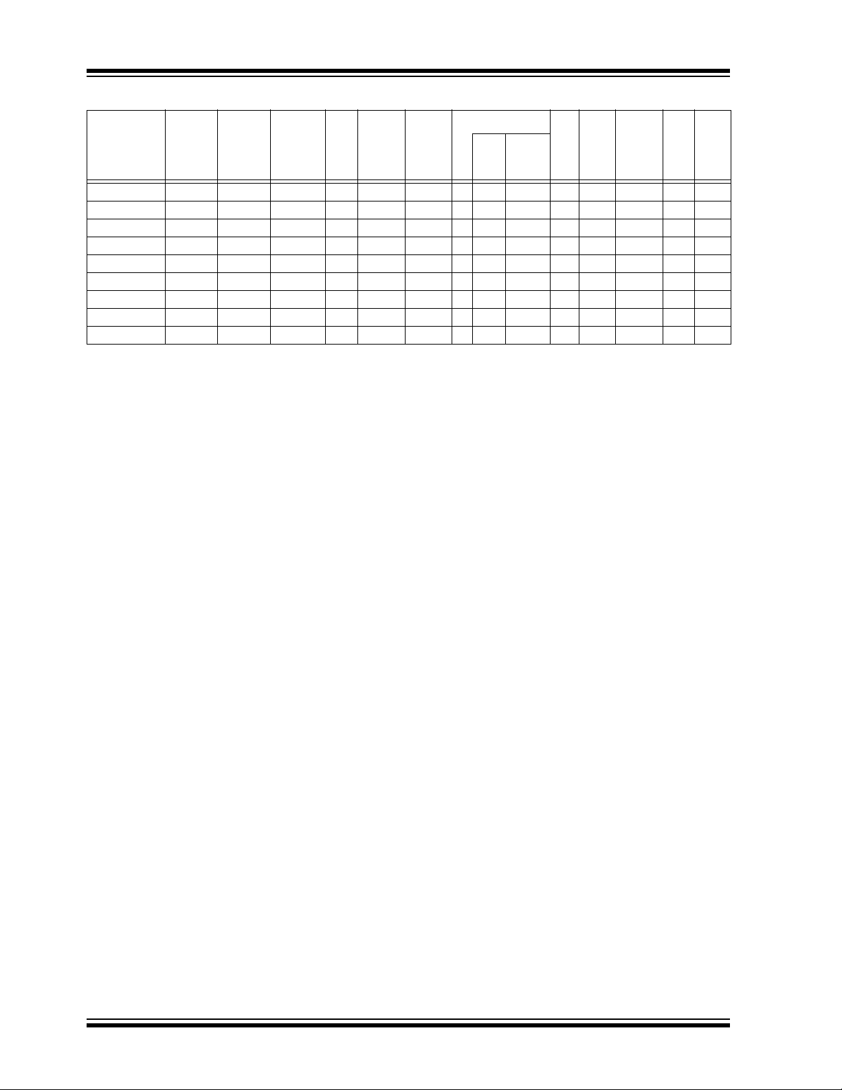
Pin Diagrams
64-Pin TQFP
PIC18F97J60 FAMILY
RE1/P2C
RE0/P2D
RB0/INT0/FLT0
RB1/INT1
RB2/INT2
RB3/INT3
RG4/CCP5/P1D
RF5/AN10/CV
RF2/AN7/C1OUT
MCLR
VSS
VDDCORE/VCAP
RF7/SS1
RF6/AN11
REF
RF4/AN9
RF3/AN8
SSPLL
RE2/P2B
RE3/P3C
RE4/P3B
RE5/P1C
RD0/P1B
64
63 62 61
1
2
3
4
5
6
7
8
9
10
11
12
13
14
15
16
17 18 19 20 21 22 23 24 25 26
VDD
RD1/ECCP3/P3A
RD2/CCP4/P3D
V
VSS
PIC18F66J60
PIC18F66J65
PIC18F67J60
SSTX
VDDPLL
RBIAS
V
TPOUT+
TPOUT-
54 53 52 5158 57 56 5560 59
27 28 29 30 32
50 49
31
DDTX
V
48
47
46
45
44
43
42
41
40
39
38
37
36
35
34
33
VDDRX
TPIN+
TPIN-
VSSRX
RB4/KBI0
RB5/KBI1
RB6/KBI2/PGC
VSS
OSC2/CLKO
OSC1/CLKI
VDD
RB7/KBI3/PGD
RC5/SDO1
RC4/SDI1/SDA1
RC3/SCK1/SCL1
RC2/ECCP1/P1A
RF1/AN6/C2OUT
RA1/LEDB/AN1
RA0/LEDA/AN0
SS
V
VDD
RA5/AN4
RA4/T0CKI
RC6/TX1/CK1
RC7/RX1/DT1
RC0/T1OSO/T13CKI
RC1/T1OSI/ECCP2/P2A
DD
AV
ENVREG
REF-
AVSS
RA2/AN2/V
RA3/AN3/VREF+
© 2008 Microchip Technology Inc. Preliminary DS39762D-page 3
Page 6
PIC18F97J60 FAMILY
Pin Diagrams (Continued)
80-Pin TQFP
(1)
/P2A
(2)
(2)
(1)
(2)
(2)
RH2
RH3
RE1/P2C
RE0/P2D
RB0/INT0/FLT0
RB1/INT1
RB2/INT2
RB3/INT3
MCLR
RG4/CCP5/P1D
VSS
VDDCORE/VCAP
RF7/SS1
RF6/AN11
RF5/AN10/CV
REF
RF4/AN9
RF3/AN8
RF2/AN7/C1OUT
RH7/AN15/P1B
RH6/AN14/P1C
RH1
RH0
RE2/P2B
RE3/P3C
RE4/P3B
RE5/P1C
RE6/P1B
RE7/ECCP2
RD0
VDDVSS
RD1
RD2
VSSPLL
68 67 66 6572 71 70 6974 7378 77 76 757980
VDDPLL
RBIAS
SSTX
V
64 63 62 61
1
2
3
4
5
6
7
8
9
10
11
12
PIC18F86J60
PIC18F86J65
PIC18F87J60
13
14
15
16
17
18
(2)
(2)
19
20
21 22 23 24 25 26 27 28 29 30 31 32
33 34
37
35 36 38
DDTX
TPOUT+
TPOUT-
V
60
59
58
57
56
55
54
53
52
51
50
49
48
47
46
45
44
43
42
41
40
39
VDDRX
TPIN+
TPIN-
V
SSRX
RG0/ECCP3/P3A
RG1/TX2/CK2
RB4/KBI0
RB5/KBI1
RB6/KBI2/PGC
V
SS
OSC2/CLKO
OSC1/CLKI
VDD
RB7/KBI3/PGD
RC5/SDO1
RC4/SDI1/SDA1
RC3/SCK1/SCL1
RC2/ECCP1/P1A
RG2/RX2/DT2
RG3/CCP4/P3D
RA5/AN4
RA4/T0CKI
(1)
/P2A
(1)
RC6/TX1/CK1
RJ5
RJ4
RC7/RX1/DT1
(2)
(2)
DD
AV
REF-
AVSS
SS
V
VDD
ENVREG
RA2/AN2/V
RA1/LEDB/AN1
RF1/AN6/C2OUT
RH5/AN13/P3B
RH4/AN12/P3C
RA3/AN3/VREF+
RA0/LEDA/AN0
RC0/T1OSO/T13CKI
RC1/T1OSI/ECCP2
Note 1: The ECCP2/P2A pin placement depends on the CCP2MX Configuration bit setting.
2: P1B, P1C, P3B and P3C pin placement depends on the ECCPMX Configuration bit setting.
DS39762D-page 4 Preliminary © 2008 Microchip Technology Inc.
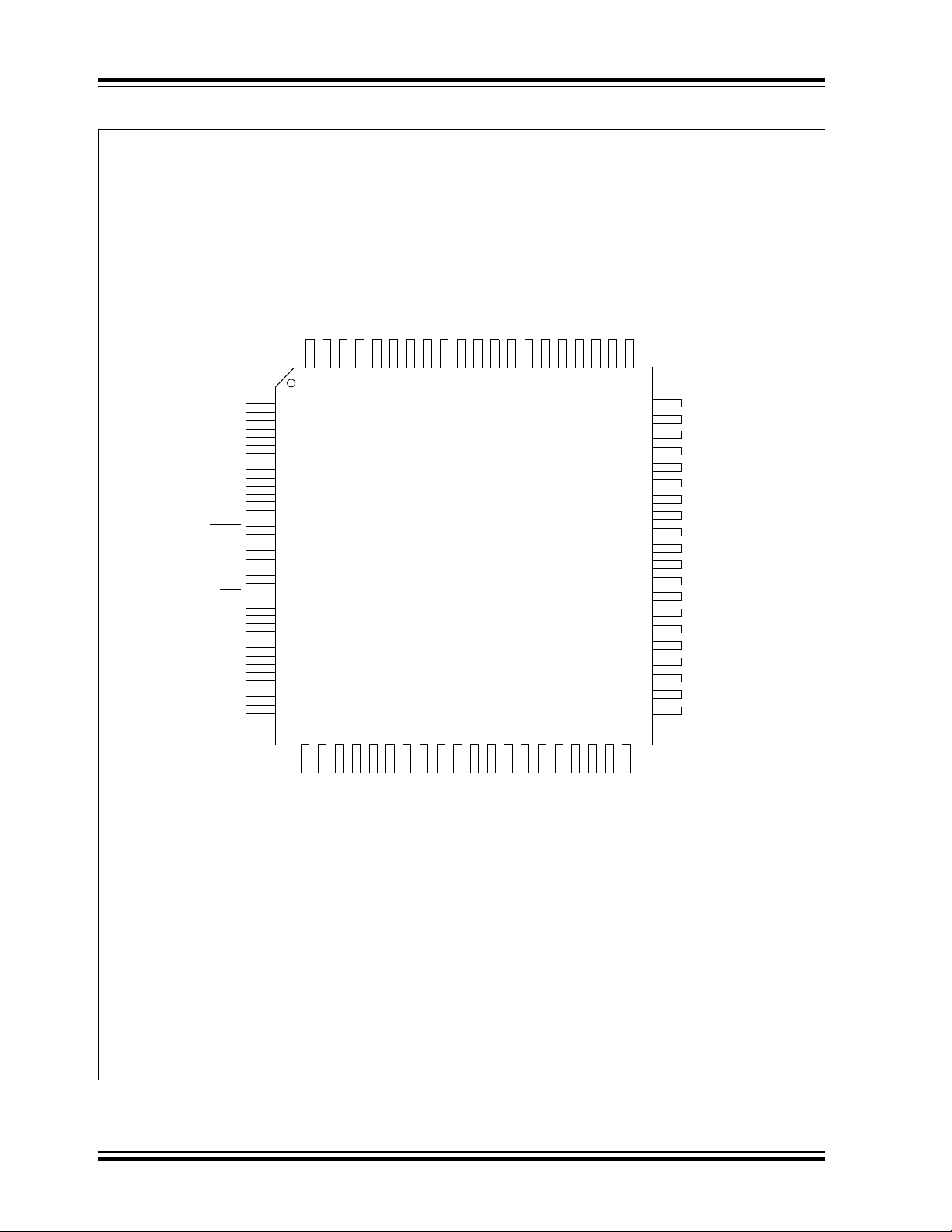
Page 7
Pin Diagrams (Continued)
100-Pin TQFP
RE1/AD9/WR/P2C
RE0/AD8/RD
RB0/INT0/FLT0
RB3/INT3/ECCP2
RG4/CCP5/P1D
VDDCORE/VCAP
RF5/AN10/CVREF
RF2/AN7/C1OUT
RH7/AN15/P1B
RH6/AN14/P1C
RH2/A18
RH3/A19
/P2D
RB1/INT1
RB2/INT2
(1)
/P2A
RG6
RG5
RF0/AN5
MCLR
V
V
RF7/SS1
RF6/AN11
RF4/AN9
RF3/AN8
NC
SS
DD
1
2
3
4
5
6
7
(1)
8
9
10
11
12
13
14
15
16
17
18
19
20
21
22
23
(2)
24
(2)
25
(1)
/P2A
(1)
(2)
(2)
(2)
(2)
RE3/AD11/P3C
RE2/AD10/CS/P2B
RE4/AD12/P3B
RE5/AD13/P1C
RE6/AD14/P1B
RH1/A17
RH0/A16
99
100
26
2829303132333435363738
27
RE7/AD15/ECCP2
95
969897
PIC18F97J60 FAMILY
RD0/AD0/PSP0
RD1/AD1/PSP1
RD2/AD2/PSP2
RD3/AD3/PSP3
RD4/AD4/PSP4/SDO2
VDDVSS
RD5/AD5/PSP5/SDI2/SDA2
RD6/AD6/PSP6/SCK2/SCL2
RD7/AD7/PSP7/SS2
9294939190898887868584838281807978
PIC18F96J60
PIC18F96J65
PIC18F97J60
43
42
41
40
39
SSTX
VSSPLL
VDDPLL
RBIAS
V
82818079787677
45
44
4647484950
TPOUT+
DDTX
TPOUT-
V
76
77
75
74
73
72
71
70
69
68
67
66
65
64
63
62
61
60
59
58
57
56
55
54
53
52
51
VDDRX
TPIN+
TPIN-
SSRX
V
RG0/ECCP3/P3A
RG1/TX2/CK2
RB4/KBI0
RB5/KBI1
RB6/KBI2/PGC
RJ2/WRL
V
SS
OSC2/CLKO
OSC1/CLKI
DD
V
RJ3/WRH
VSS
VDD
RJ6/LB
RB7/KBI3/PGD
RC5/SDO1
RC4/SDI1/SDA1
RC3/SCK1/SCL1
RC2/ECCP1/P1A
RG2/RX2/DT2
RG3/CCP4/P3D
(2)
(2)
DD
AV
AVSS
ENVREG
RF1/AN6/C2OUT
RH5/AN13/P3B
RH4/AN12/P3C
RA3/AN3/VREF+
REF-
RA2/AN2/V
RA1/LEDB/AN1
RA0/LEDA/AN0
SS
V
VDD
RG7
RJ7/UB
(1)
SS
V
/P2A
(1)
RA5/AN4
RA4/T0CKI
RJ5/CE
RJ1/OE
RJ4/BA0
RJ0/ALE
RC6/TX1/CK1
RC7/RX1/DT1
RC0/T1OSO/T13CKI
RC1/T1OSI/ECCP2
Note 1: The ECCP2/P2A pin placement depends on the CCP2MX Configuration bit and Processor mode settings.
2: P1B, P1C, P3B and P3C pin placement depends on the ECCPMX Configuration bit setting.
© 2008 Microchip Technology Inc. Preliminary DS39762D-page 5
Page 8

PIC18F97J60 FAMILY
Table of Contents
1.0 Device Overview .......................................................................................................................................................................... 9
2.0 Oscillator Configurations ............................................................................................................................................................ 41
3.0 Power-Managed Modes ............................................................................................................................................................. 47
4.0 Reset .......................................................................................................................................................................................... 55
5.0 Memory Organization ................................................................................................................................................................. 69
6.0 Flash Program Memory.............................................................................................................................................................. 97
7.0 External Memory Bus ............................................................................................................................................................... 107
8.0 8 x 8 Hardware Multiplier.......................................................................................................................................................... 119
9.0 Interrupts .................................................................................................................................................................................. 121
10.0 I/O Ports ................................................................................................................................................................................... 137
11.0 Timer0 Module ......................................................................................................................................................................... 165
12.0 Timer1 Module ......................................................................................................................................................................... 169
13.0 Timer2 Module ......................................................................................................................................................................... 175
14.0 Timer3 Module ......................................................................................................................................................................... 177
15.0 Timer4 Module ......................................................................................................................................................................... 181
16.0 Capture/Compare/PWM (CCP) Modules ................................................................................................................................. 183
17.0 Enhanced Capture/Compare/PWM (ECCP) Modules .............................................................................................................. 191
18.0 Ethernet Module ....................................................................................................................................................................... 207
19.0 Master Synchronous Serial Port (MSSP) Module .................................................................................................................... 257
20.0 Enhanced Universal Synchronous Asynchronous Receiver Transmitter (EUSART) ............................................................... 303
21.0 10-Bit Analog-to-Digital Converter (A/D) Module ..................................................................................................................... 327
22.0 Comparator Module.................................................................................................................................................................. 337
23.0 Comparator Voltage Reference Module ................................................................................................................................... 343
24.0 Special Features of the CPU.................................................................................................................................................... 347
25.0 Instruction Set Summary.......................................................................................................................................................... 361
26.0 Development Support............................................................................................................................................................... 411
27.0 Electrical Characteristics.......................................................................................................................................................... 415
28.0 Packaging Information.............................................................................................................................................................. 451
Appendix A: Revision History............................................................................................................................................................. 461
Appendix B: Device Differences......................................................................................................................................................... 462
Index .................................................................................................................................................................................................. 463
The Microchip Web Site..................................................................................................................................................................... 475
Customer Change Notification Service .............................................................................................................................................. 475
Customer Support .............................................................................................................................................................................. 475
Reader Response .............................................................................................................................................................................. 476
Product Identification System............................................................................................................................................................. 477
DS39762D-page 6 Preliminary © 2008 Microchip Technology Inc.
Page 9

PIC18F97J60 FAMILY
TO OUR VALUED CUSTOMERS
It is our intention to provide our valued customers with the best documentation possible to ensure successful use of your Microchip
products. To this end, we will continue to improve our publications to better suit your needs. Our publications will be refined and
enhanced as new volumes and updates are introduced.
If you have any questions or comments regarding this publication, please contact the Marketing Communications Department via
E-mail at docerrors@microchip.com or fax the Reader Response Form in the back of this data sheet to (480) 792-4150. We
welcome your feedback.
Most Current Data Sheet
To obtain the most up-to-date version of this data sheet, please register at our Worldwide Web site at:
http://www.microchip.com
You can determine the version of a data sheet by examining its literature number found on the bottom outside corner of any page.
The last character of the literature number is the version number, (e.g., DS30000A is version A of document DS30000).
Errata
An errata sheet, describing minor operational differences from the data sheet and recommended workarounds, may exist for current
devices. As device/documentation issues become known to us, we will publish an errata sheet. The errata will specify the revision
of silicon and revision of document to which it applies.
To determine if an errata sheet exists for a particular device, please check with one of the following:
• Microchip’s Worldwide Web site; http://www.microchip.com
• Your local Microchip sales office (see last page)
When contacting a sales office, please specify which device, revision of silicon and data sheet (include literature number) you are
using.
Customer Notification System
Register on our web site at www.microchip.com to receive the most current information on all of our products.
© 2008 Microchip Technology Inc. Preliminary DS39762D-page 7
Page 10

PIC18F97J60 FAMILY
NOTES:
DS39762D-page 8 Preliminary © 2008 Microchip Technology Inc.
Page 11

PIC18F97J60 FAMILY
1.0 DEVICE OVERVIEW
This document contains device-specific information for
the following devices:
• PIC18F66J60 • PIC18F87J60
• PIC18F66J65 • PIC18F96J60
• PIC18F67J60 • PIC18F96J65
• PIC18F86J60 • PIC18F97J60
• PIC18F86J65
This family introduces a new line of low-voltage devices
with the foremost traditional advantage of all PIC18
microcontrollers – namely, high computational performance and a rich feature set at an extremely
competitive price point. These features make the
PIC18F97J60 family a logical choice for many
high-performance applications where cost is a primary
consideration.
1.1 Core Features
1.1.1 OSCILLATOR OPTIONS AND FEATURES
All of the devices in the PIC18F97J60 family offer five
different oscillator options, allowing users a range of
choices in developing application hardware. These
options include:
• Two Crystal modes, using crystals or ceramic
resonators.
• Two External Clock modes, offering the option of
a divide-by-4 clock output.
• A Phase Lock Loop (PLL) frequency multiplier,
available to the external oscillator modes, which
allows clock speeds of up to 41.667 MHz.
• An internal RC oscillator with a fixed 31 kHz
output which provides an extremely low-power
option for timing-insensitive applications.
The internal oscillator block provides a stable reference
source that gives the family additional features for
robust operation:
• Fail-Safe Clock Monitor: This option constantly
monitors the main clock source against a reference
signal provided by the internal oscillator. If a clock
failure occurs, the controller is switched to the
internal oscillator, allowing for continued low-speed
operation or a safe application shutdown.
• Two-Speed Start-up: This option allows the
internal oscillator to serve as the clock source
from Power-on Reset, or wake-up from Sleep
mode, until the primary clock source is available.
1.1.2 EXPANDED MEMORY
The PIC18F97J60 family provides ample room for
application code, from 64 Kbytes to 128 Kbytes of code
space. The Flash cells for program memory are rated
to last 100 erase/write cycles. Data retention without
refresh is conservatively estimated to be greater than
20 years.
The PIC18F97J60 family also provides plenty of room
for dynamic application data with 3808 bytes of data
RAM.
1.1.3 EXTERNAL MEMORY BUS
In the unlikely event that 128 Kbytes of memory are
inadequate for an application, the 100-pin members of
the PIC18F97J60 family also implement an External
Memory Bus (EMB). This allows the controller’s internal program counter to address a memory space of up
to 2 Mbytes, permitting a level of data access that few
8-bit devices can claim. This allows additional memory
options, including:
• Using combinations of on-chip and external
memory up to the 2-Mbyte limit
• Using external Flash memory for reprogrammable
application code or large data tables
• Using external RAM devices for storing large
amounts of variable data
1.1.4 EXTENDED INSTRUCTION SET
The PIC18F97J60 family implements the optional
extension to the PIC18 instruction set, adding eight
new instructions and an Indexed Addressing mode.
Enabled as a device configuration option, the extension
has been specifically designed to optimize reentrant
application code originally developed in high-level
languages, such as C.
1.1.5 EASY MIGRATION
Regardless of the memory size, all devices share the
same rich set of peripherals, allowing for a smooth
migration path as applications grow and evolve.
© 2008 Microchip Technology Inc. Preliminary DS39762D-page 9
Page 12

PIC18F97J60 FAMILY
1.2 Other Special Features
• Communications: The PIC18F97J60 family
incorporates a range of serial communication
peripherals, including up to two independent
Enhanced USARTs and up to two Master SSP
modules, capable of both SPI and I
and Slave) modes of operation. In addition, one of
the general purpose I/O ports can be reconfigured
as an 8-bit Parallel Slave Port for direct
processor-to-processor communications.
• CCP Modules: All devices in the family incorporate
two Capture/Compare/PWM (CCP) modules and
three Enhanced CCP (ECCP) modules to maximize
flexibility in control applications. Up to four different
time bases may be used to perform several
different operations at once. Each of the three
ECCP modules offers up to four PWM outputs,
allowing for a total of twelve PWMs. The ECCP
modules also offer many beneficial features,
including polarity selection, programmable dead
time, auto-shutdown and restart and Half-Bridge
and Full-Bridge Output modes.
• 10-Bit A/D Converter: This module incorporates
programmable acquisition time, allowing for a
channel to be selected and a conversion to be
initiated without waiting for a sampling period and
thus, reducing code overhead.
• Extended Watchdog Timer (WDT): This
enhanced version incorporates a 16-bit prescaler,
allowing an extended time-out range. See
Section 27.0 “Electrical Characteristics” for
time-out periods.
2
C™ (Master
1.3 Details on Individual Family Members
Devices in the PIC18F97J60 family are available in
64-pin, 80-pin and 100-pin packages. Block diagrams
for the three groups are shown in Figure 1-1,
Figure 1-2 and Figure 1-3.
The devices are differentiated from each other in four
ways:
1. Flash program memory (three sizes, ranging
from 64 Kbytes for PIC18FX6J60 devices to
128 Kbytes for PIC18FX7J60 devices).
2. A/D channels (eleven for 64-pin devices, fifteen
for 80-pin pin devices and sixteen for 100-pin
devices).
3. Serial communication modules (one EUSART
module and one MSSP module on 64-pin
devices, two EUSART modules and one MSSP
module on 80-pin devices and two EUSART
modules and two MSSP modules on 100-pin
devices).
4. I/O pins (39 on 64-pin devices, 55 on 80-pin
devices and 70 on 100-pin devices).
All other features for devices in this family are identical.
These are summarized in Table 1-1, Table 1-2 and
Table 1-3.
The pinouts for all devices are listed in Table 1-4,
Table 1-5 and Table 1-6.
DS39762D-page 10 Preliminary © 2008 Microchip Technology Inc.
Page 13

PIC18F97J60 FAMILY
TABLE 1-1: DEVICE FEATURES FOR THE PIC18F97J60 FAMILY (64-PIN DEVICES)
Features PIC18F66J60 PIC18F66J65 PIC18F67J60
Operating Frequency DC – 41.667 MHz DC – 41.667 MHz DC – 41.667 MHz
Program Memory (Bytes) 64K 96K 128K
Program Memory (Instructions) 32764 49148 65532
Data Memory (Bytes) 3808
Interrupt Sources 26
I/O Ports Ports A, B, C, D, E, F, G
I/O Pins 39
Timers 5
Capture/Compare/PWM Modules 2
Enhanced Capture/Compare/PWM Modules 3
Serial Communications MSSP (1), Enhanced USART (1)
Ethernet Communications (10Base-T) Yes
Parallel Slave Port Communications (PSP) No
External Memory Bus No
10-Bit Analog-to-Digital Module 11 Input Channels
Resets (and Delays) POR, BOR, RESET Instruction, Stack Full,
Stack Underflow, MCLR
Instruction Set 75 Instructions, 83 with Extended Instruction Set Enabled
Packages 64-Pin TQFP
, WDT (PWRT, OST)
TABLE 1-2: DEVICE FEATURES FOR THE PIC18F97J60 FAMILY (80-PIN DEVICES)
Features PIC18F86J60 PIC18F86J65 PIC18F87J60
Operating Frequency DC – 41.667 MHz DC – 41.667 MHz DC – 41.667 MHz
Program Memory (Bytes) 64K 96K 128K
Program Memory (Instructions) 32764 49148 65532
Data Memory (Bytes) 3808
Interrupt Sources 27
I/O Ports Ports A, B, C, D, E, F, G, H, J
I/O Pins 55
Timers 5
Capture/Compare/PWM Modules 2
Enhanced Capture/Compare/PWM Modules 3
Serial Communications MSSP (1), Enhanced USART (2)
Ethernet Communications (10Base-T) Yes
Parallel Slave Port Communications (PSP) No
External Memory Bus No
10-Bit Analog-to-Digital Module 15 Input Channels
Resets (and Delays) POR, BOR, RESET Instruction, Stack Full,
Stack Underflow, MCLR
Instruction Set 75 Instructions, 83 with Extended Instruction Set Enabled
Packages 80-Pin TQFP
, WDT (PWRT, OST)
© 2008 Microchip Technology Inc. Preliminary DS39762D-page 11
Page 14

PIC18F97J60 FAMILY
TABLE 1-3: DEVICE FEATURES FOR THE PIC18F97J60 FAMILY (100-pin DEVICES)
Features PIC18F96J60 PIC18F96J65 PIC18F97J60
Operating Frequency DC – 41.667 MHz DC – 41.667 MHz DC – 41.667 MHz
Program Memory (Bytes) 64K 96K 128K
Program Memory (Instructions) 32764 49148 65532
Data Memory (Bytes) 3808
Interrupt Sources 29
I/O Ports Ports A, B, C, D, E, F, G, H, J
I/O Pins 70
Timers 5
Capture/Compare/PWM Modules 2
Enhanced Capture/Compare/PWM Modules 3
Serial Communications MSSP (2), Enhanced USART (2)
Ethernet Communications (10Base-T) Yes
Parallel Slave Port Communications (PSP) Yes
External Memory Bus Yes
10-Bit Analog-to-Digital Module 16 Input Channels
Resets (and Delays) POR, BOR, RESET Instruction, Stack Full,
Stack Underflow, MCLR
Instruction Set 75 Instructions, 83 with Extended Instruction Set Enabled
Packages 100-Pin TQFP
, WDT (PWRT, OST)
DS39762D-page 12 Preliminary © 2008 Microchip Technology Inc.
Page 15
PIC18F97J60 FAMILY
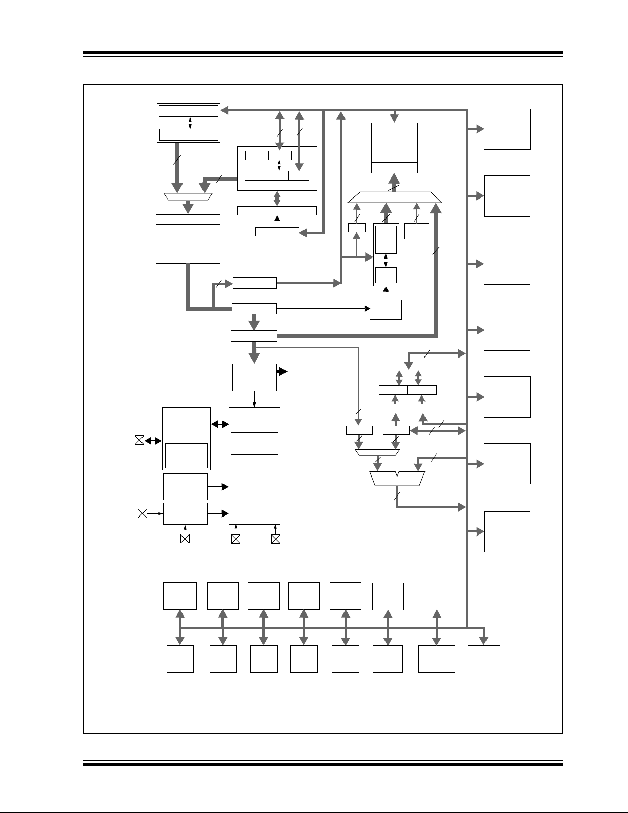
FIGURE 1-1: PIC18F66J60/66J65/67J60 (64-PIN) BLOCK DIAGRAM
OSC2/CLKO
OSC1/CLKI
ENVREG
Table Pointer<21>
inc/dec logic
21
20
Address Latch
Program Memory
(64, 96, 128 Kbytes)
Data Latch
8
Instruction Bus <16>
Timing
Generation
INTRC
Oscillator
Precision
Band Gap
Reference
Voltage
Regulator
VDDCORE/VCAP
PCLATU
PCU
Table Latch
ROM Latch
Instruction
Decode and
Control
Power-up
Timer
Oscillator
Start-up Timer
Power-on
Reset
Watchdog
Timer
Brown-out
Reset
V
V
DD,
SS
8
PCLATH
PCH PCL
Program Counter
31 Level Stack
STKPTR
IR
State Machine
Control Signals
(2)
MCLR
Data Bus<8>
8
Data Latch
Data Memory
(3808 Bytes)
Address Latch
Data Address<12>
4
BSR
FSR0
FSR1
FSR2
inc/dec
logic
Address
Decode
3
BITOP
8
12
12
Access
Bank
PRODLPRODH
8 x 8 Multiply
W
8
8
ALU<8>
8
PORTA
(1)
RA0:RA5
PORTB
(1)
RB0:RB7
4
12
PORTC
RC0:RC7
(1)
PORTD
(1)
RD0:RD2
8
PORTE
(1)
RE0:RE5
8
8
8
PORTF
RF1:RF7
(1)
PORTG
(1)
RG4
ADC
10-Bit
ECCP1
ECCP2
ECCP3 CCP4 CCP5
Timer2Timer1 Timer3Timer0
Timer4
MSSP1
Comparators
EUSART1
Ethernet
Note 1: See Table 1-4 for I/O port pin descriptions.
2: BOR functionality is provided when the on-board voltage regulator is enabled.
© 2008 Microchip Technology Inc. Preliminary DS39762D-page 13
Page 16
PIC18F97J60 FAMILY
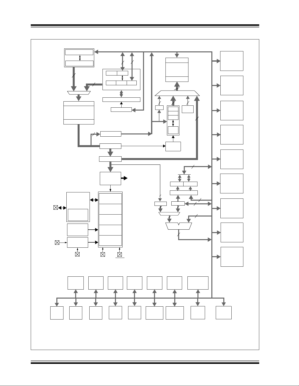
FIGURE 1-2: PIC18F86J60/86J65/87J60 (80-PIN) BLOCK DIAGRAM
OSC2/CLKO
OSC1/CLKI
ENVREG
Table Pointer<21>
inc/dec logic
21
20
Address Latch
Program Memory
(64, 96, 128 Kbytes)
Data Latch
8
Instruction Bus <16>
Timing
Generation
INTRC
Oscillator
Precision
Band Gap
Reference
Voltage
Regulator
PCLATH
PCLATU
PCU
Program Counter
31 Level Stack
STKPTR
Table Latch
ROM Latch
IR
Instruction
Decode &
Control
Power-up
Timer
Oscillator
Start-up Timer
Power-on
Reset
Watchdog
Timer
Brown-out
(2)
Reset
Data Bus<8>
8
PCH PCL
State Machine
Control Signals
8
Data Latch
Data Memory
PORTA
RA0:RA5
(1)
(3808 Bytes)
Address Latch
12
PORTB
RB0:RB7
(1)
Data Address<12>
BSR
4
FSR0
FSR1
FSR2
inc/dec
logic
Address
Decode
4
12
Access
Bank
PORTC
RC0:RC7
(1)
12
PORTD
(1)
RD0:RD2
PORTE
(1)
RE0:RE7
8
PORTF
RF1:RF7
PORTG
RG0:RG4
PORTH
RH0:RH7
(1)
(1)
(1)
3
BITOP
8
PRODLPRODH
8 x 8 Multiply
W
8
8
ALU<8>
8
8
8
8
PORTJ
RJ4:RJ5
(1)
ECCP1
VDDCORE/VCAP
ADC
10-Bit
ECCP2 ECCP3
DD, VSS
V
MCLR
Timer2Timer1 Timer3Timer0
CCP4 CCP5
EUSART1
Timer4
EUSART2
Comparators
MSSP1
Ethernet
Note 1: See Table 1-5 for I/O port pin descriptions.
2: BOR functionality is provided when the on-board voltage regulator is enabled.
DS39762D-page 14 Preliminary © 2008 Microchip Technology Inc.
Page 17
PIC18F97J60 FAMILY
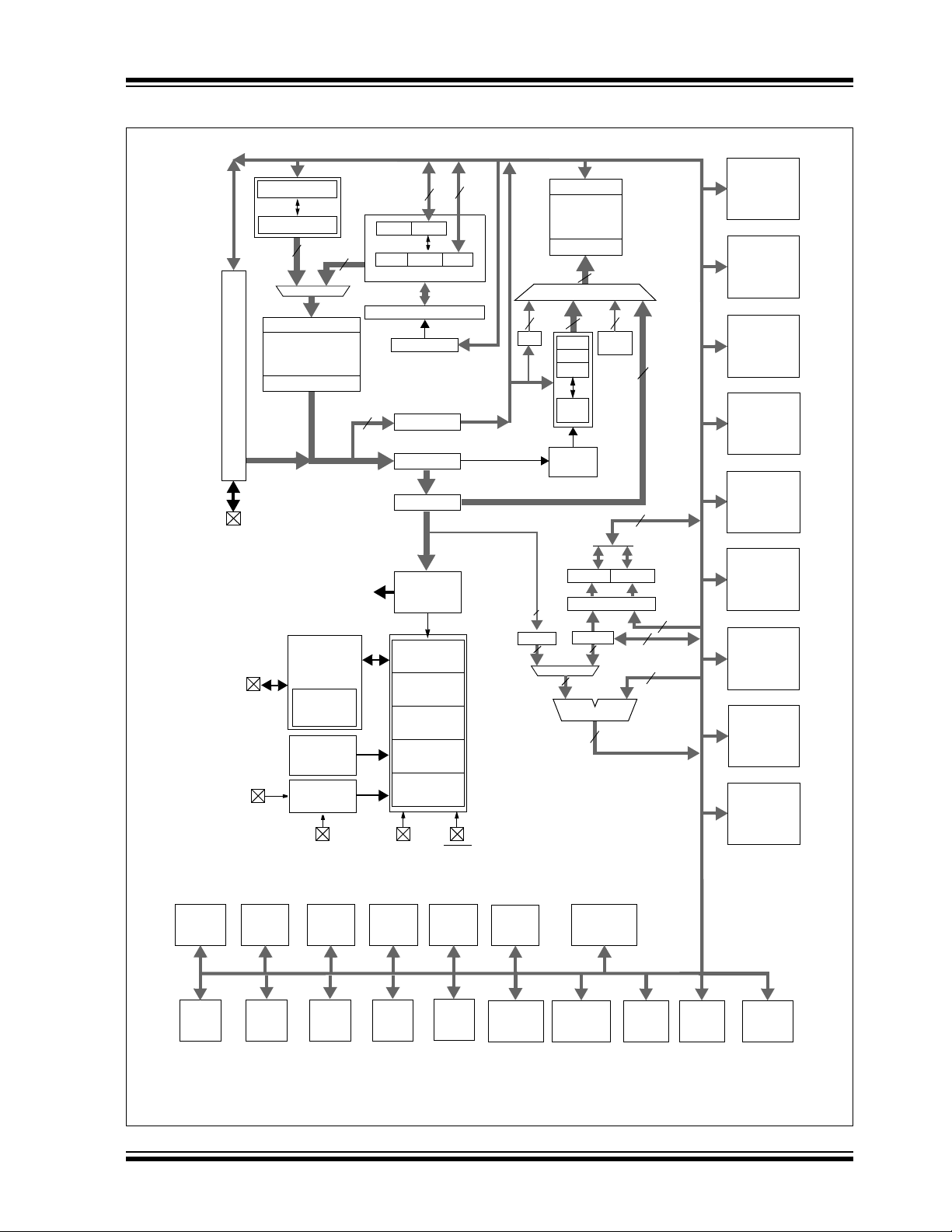
FIGURE 1-3: PIC18F96J60/96J65/97J60 (100-PIN) BLOCK DIAGRAM
Data Bus<8>
Table Pointer<21>
inc/dec logic
21
Address Latch
Program Memory
(64, 96, 128 Kbytes)
Data Latch
System Bus Interface
Instruction Bus <16>
AD15:AD0, A19:A16
(Multiplexed with PORTD,
PORTE and PORTH)
State Machine
Control Signals
OSC2/CLKO
OSC1/CLKI
ENVREG
Generation
INTRC
Oscillator
Precision
Band Gap
Reference
Voltage
Regulator
Timing
20
8
8
PCLATH
PCLATU
PCH PCL
PCU
Program Counter
31 Level Stack
STKPTR
Table Latch
ROM Latch
IR
Instruction
Decode &
Control
Power-up
Timer
Oscillator
Start-up Timer
Power-on
Reset
Watchdog
Timer
Brown-out
(2)
Reset
8
Data Latch
Data Memory
PORTA
RA0:RA5
(1)
(3808 Bytes)
Address Latch
12
PORTB
RB0:RB7
(1)
Data Address<12>
BSR
4
FSR0
FSR1
FSR2
inc/dec
logic
Address
Decode
4
12
Access
Bank
PORTC
RC0:RC7
(1)
12
PORTD
RD0:RD7
(1)
PORTE
(1)
RE0:RE7
8
PORTF
RF0:RF7
PORTG
RG0:RG7
PORTH
RH0:RH7
(1)
(1)
(1)
3
BITOP
8
PRODLPRODH
8 x 8 Multiply
W
8
8
ALU<8>
8
8
8
8
PORTJ
(1)
RJ0:RJ7
ADC
10-Bit
ECCP1
VDDCORE/VCAP
ECCP2 ECCP3
V
Timer2Timer1 Timer3Timer0
DD, VSS
MCLR
Timer4
EUSART1
Comparators
EUSART2
MSSP1
MSSP2CCP4 CCP5
Ethernet
Note 1: See Table 1-6 for I/O port pin descriptions.
2: BOR functionality is provided when the on-board voltage regulator is enabled.
© 2008 Microchip Technology Inc. Preliminary DS39762D-page 15
Page 18

PIC18F97J60 FAMILY
TABLE 1-4: PIC18F66J60/66J65/67J60 PINOUT I/O DESCRIPTIONS
Pin Name
Pin Number
TQFP
Pin
Type
Buffer
Type
Description
MCLR
OSC1/CLKI
OSC1
CLKI
OSC2/CLKO
OSC2
CLKO
RA0/LEDA/AN0
RA0
LEDA
AN0
RA1/LEDB/AN1
RA1
LEDB
AN1
RA2/AN2/V
RA3/AN3/V
RA4/T0CKI
RA5/AN4
Legend: TTL = TTL compatible input CMOS = CMOS compatible input or output
REF-
RA2
AN2
REF-
V
REF+
RA3
AN3
REF+
V
RA4
T0CKI
RA5
AN4
ST = Schmitt Trigger input with CMOS levels Analog = Analog input
I = Input O = Output
P = Power OD = Open-Drain (no P diode to V
7 I ST Master Clear (Reset) input. This pin is an active-low Reset
to the device.
39
40
24
23
22
21
28
27
O
O
I/O
O
I/O
O
I/O
I/O
I/O
I/O
I
I
CMOS
I
Analog
I
Analog
I
Analog
I
Analog
I
Analog
I
Analog
I
I
Analog
Oscillator crystal or external clock input.
ST
—
—
TTL
—
TTL
—
TTL
TTL
ST
ST
TTL
Oscillator crystal input or external clock source input.
ST buffer when configured in internal RC mode; CMOS
otherwise.
External clock source input. Always associated
with pin function OSC1. (See related OSC2/CLKO pin.)
Oscillator crystal or clock output.
Oscillator crystal output. Connects to crystal or
resonator in Crystal Oscillator mode.
In Internal RC mode, OSC2 pin outputs CLKO which has
1/4 the frequency of OSC1 and denotes the
instruction cycle rate.
PORTA is a bidirectional I/O port.
Digital I/O.
Ethernet LEDA indicator output.
Analog input 0.
Digital I/O.
Ethernet LEDB indicator output.
Analog input 1.
Digital I/O.
Analog input 2.
A/D reference voltage (low) input.
Digital I/O.
Analog input 3.
A/D reference voltage (high) input.
Digital I/O.
Timer0 external clock input.
Digital I/O.
Analog input 4.
DD)
DS39762D-page 16 Preliminary © 2008 Microchip Technology Inc.
Page 19

PIC18F97J60 FAMILY
TABLE 1-4: PIC18F66J60/66J65/67J60 PINOUT I/O DESCRIPTIONS (CONTINUED)
Pin Name
RB0/INT0/FLT0
RB0
INT0
FLT0
RB1/INT1
RB1
INT1
RB2/INT2
RB2
INT2
RB3/INT3
RB3
INT3
RB4/KBI0
RB4
KBI0
RB5/KBI1
RB5
KBI1
RB6/KBI2/PGC
RB6
KBI2
PGC
RB7/KBI3/PGD
RB7
KBI3
PGD
Legend: TTL = TTL compatible input CMOS = CMOS compatible input or output
ST = Schmitt Trigger input with CMOS levels Analog = Analog input
I = Input O = Output
P = Power OD = Open-Drain (no P diode to V
Pin Number
TQFP
3
4
5
6
44
43
42
37
Pin
Type
I/O
I
I
I/O
I
I/O
I
I/O
I
I/O
I
I/O
I
I/O
I
I/O
I/O
I
I/O
Buffer
Type
TTL
ST
ST
TTL
ST
TTL
ST
TTL
ST
TTL
TTL
TTL
TTL
TTL
TTL
ST
TTL
TTL
ST
Description
PORTB is a bidirectional I/O port. PORTB can be software
programmed for internal weak pull-ups on all inputs.
Digital I/O.
External interrupt 0.
Enhanced PWM Fault input (ECCP modules); enabled
in software.
Digital I/O.
External interrupt 1.
Digital I/O.
External interrupt 2.
Digital I/O.
External interrupt 3.
Digital I/O.
Interrupt-on-change pin.
Digital I/O.
Interrupt-on-change pin.
Digital I/O.
Interrupt-on-change pin.
In-Circuit Debugger and ICSP™ programming clock pin.
Digital I/O.
Interrupt-on-change pin.
In-Circuit Debugger and ICSP programming data pin.
DD)
© 2008 Microchip Technology Inc. Preliminary DS39762D-page 17
Page 20

PIC18F97J60 FAMILY
TABLE 1-4: PIC18F66J60/66J65/67J60 PINOUT I/O DESCRIPTIONS (CONTINUED)
Pin Name
RC0/T1OSO/T13CKI
RC0
T1OSO
T13CKI
RC1/T1OSI/ECCP2/P2A
RC1
T1OSI
ECCP2
P2A
RC2/ECCP1/P1A
RC2
ECCP1
P1A
RC3/SCK1/SCL1
RC3
SCK1
SCL1
RC4/SDI1/SDA1
RC4
SDI1
SDA1
RC5/SDO1
RC5
SDO1
RC6/TX1/CK1
RC6
TX1
CK1
RC7/RX1/DT1
RC7
RX1
DT1
Legend: TTL = TTL compatible input CMOS = CMOS compatible input or output
ST = Schmitt Trigger input with CMOS levels Analog = Analog input
I = Input O = Output
P = Power OD = Open-Drain (no P diode to V
Pin Number
TQFP
30
29
33
34
35
36
31
32
Pin
Type
I/O
O
I
I/O
I
I/O
O
I/O
I/O
O
I/O
I/O
I/O
I/O
I
I/O
I/O
O
I/O
O
I/O
I/O
I
I/O
Buffer
Type
ST
—
ST
ST
CMOS
ST
—
ST
ST
—
ST
ST
ST
ST
ST
ST
ST
—
ST
—
ST
ST
ST
ST
Description
PORTC is a bidirectional I/O port.
Digital I/O.
Timer1 oscillator output.
Timer1/Timer3 external clock input.
Digital I/O.
Timer1 oscillator input.
Capture 2 input/Compare 2 output/PWM2 output.
ECCP2 PWM output A.
Digital I/O.
Capture 1 input/Compare 1 output/PWM1 output.
ECCP1 PWM output A.
Digital I/O.
Synchronous serial clock input/output for SPI mode.
Synchronous serial clock input/output for I
Digital I/O.
SPI data in.
I2C data I/O.
Digital I/O.
SPI data out.
Digital I/O.
EUSART1 asynchronous transmit.
EUSART1 synchronous clock (see related RX1/DT1 pin).
Digital I/O.
EUSART1 asynchronous receive.
EUSART1 synchronous data (see related TX1/CK1 pin).
2
C™ mode.
DD)
DS39762D-page 18 Preliminary © 2008 Microchip Technology Inc.
Page 21

PIC18F97J60 FAMILY
TABLE 1-4: PIC18F66J60/66J65/67J60 PINOUT I/O DESCRIPTIONS (CONTINUED)
Pin Name
RD0/P1B
RD0
P1B
RD1/ECCP3/P3A
RD1
ECCP3
P3A
RD2/CCP4/P3D
RD2
CCP4
P3D
Legend: TTL = TTL compatible input CMOS = CMOS compatible input or output
ST = Schmitt Trigger input with CMOS levels Analog = Analog input
I = Input O = Output
P = Power OD = Open-Drain (no P diode to V
Pin Number
TQFP
60
59
58
Pin
Type
I/O
O
I/O
I/O
O
I/O
I/O
O
Buffer
Type
ST
—
ST
ST
—
ST
ST
—
Description
PORTD is a bidirectional I/O port.
Digital I/O.
ECCP1 PWM output B.
Digital I/O.
Capture 3 input/Compare 3 output/PWM3 output.
ECCP3 PWM output A.
Digital I/O.
Capture 4 input/Compare 4 output/PWM4 output.
CCP4 PWM output D.
DD)
© 2008 Microchip Technology Inc. Preliminary DS39762D-page 19
Page 22

PIC18F97J60 FAMILY
TABLE 1-4: PIC18F66J60/66J65/67J60 PINOUT I/O DESCRIPTIONS (CONTINUED)
Pin Name
RE0/P2D
RE0
P2D
RE1/P2C
RE1
P2C
RE2/P2B
RE2
P2B
RE3/P3C
RE3
P3C
RE4/P3B
RE4
P3B
RE5/P1C
RE5
P1C
Legend: TTL = TTL compatible input CMOS = CMOS compatible input or output
ST = Schmitt Trigger input with CMOS levels Analog = Analog input
I = Input O = Output
P = Power OD = Open-Drain (no P diode to V
Pin Number
TQFP
2
1
64
63
62
61
Pin
Type
I/O
O
I/O
O
I/O
O
I/O
O
I/O
O
I/O
O
Buffer
Type
ST
—
ST
—
ST
—
ST
—
ST
—
ST
—
Description
PORTE is a bidirectional I/O port.
Digital I/O.
ECCP2 PWM output D.
Digital I/O.
ECCP2 PWM output C.
Digital I/O.
ECCP2 PWM output B.
Digital I/O.
ECCP3 PWM output C.
Digital I/O.
ECCP3 PWM output B.
Digital I/O.
ECCP1 PWM output C.
DD)
DS39762D-page 20 Preliminary © 2008 Microchip Technology Inc.
Page 23

PIC18F97J60 FAMILY
TABLE 1-4: PIC18F66J60/66J65/67J60 PINOUT I/O DESCRIPTIONS (CONTINUED)
Pin Name
RF1/AN6/C2OUT
RF1
AN6
C2OUT
RF2/AN7/C1OUT
RF2
AN7
C1OUT
RF3/AN8
RF3
AN8
RF4/AN9
RF4
AN9
RF5/AN10/CV
RF5
AN10
CVREF
RF6/AN11
RF6
AN11
RF7/SS1
RF7
SS1
Legend: TTL = TTL compatible input CMOS = CMOS compatible input or output
REF
ST = Schmitt Trigger input with CMOS levels Analog = Analog input
I = Input O = Output
P = Power OD = Open-Drain (no P diode to VDD)
Pin Number
TQFP
17
16
15
14
13
12
11
Pin
Type
I/O
I
O
I/O
I
O
I/O
I
I/O
I
I/O
I
O
I/O
I
I/O
I
Buffer
Type
ST
Analog
—
ST
Analog
—
ST
Analog
ST
Analog
ST
Analog
—
ST
Analog
ST
TTL
Description
PORTF is a bidirectional I/O port.
Digital I/O.
Analog input 6.
Comparator 2 output.
Digital I/O.
Analog input 7.
Comparator 1 output.
Digital I/O.
Analog input 8.
Digital I/O.
Analog input 9.
Digital I/O.
Analog input 10.
Comparator reference voltage output.
Digital I/O.
Analog input 11.
Digital I/O.
SPI slave select input.
© 2008 Microchip Technology Inc. Preliminary DS39762D-page 21
Page 24

PIC18F97J60 FAMILY
TABLE 1-4: PIC18F66J60/66J65/67J60 PINOUT I/O DESCRIPTIONS (CONTINUED)
Pin Name
Pin Number
TQFP
RG4/CCP5/P1D
8
RG4
CCP5
P1D
V
SS 9, 25, 41, 56 P — Ground reference for logic and I/O pins.
DD 26, 38, 57 P — Positive supply for peripheral digital logic and I/O pins.
V
AVSS 20 P — Ground reference for analog modules.
DD 19 P — Positive supply for analog modules.
AV
ENVREG 18 I ST Enable for on-chip voltage regulator.
DDCORE/VCAP
V
10
VDDCORE
VCAP
SSPLL 55 P — Ground reference for Ethernet PHY PLL.
V
VDDPLL 54 P — Positive 3.3V supply for Ethernet PHY PLL.
SSTX 52 P — Ground reference for Ethernet PHY transmit subsystem.
V
VDDTX 49 P — Positive 3.3V supply for Ethernet PHY transmit subsystem.
SSRX 45 P — Ground reference for Ethernet PHY receive subsystem.
V
VDDRX 48 P — Positive 3.3V supply for Ethernet PHY receive subsystem.
RBIAS 53 I Analog Bias current for Ethernet PHY. Must be tied to V
TPOUT+ 51 O — Ethernet differential signal output.
TPOUT- 50 O — Ethernet differential signal output.
TPIN+ 47 I Analog Ethernet differential signal input.
TPIN- 46 I Analog Ethernet differential signal input.
Legend: TTL = TTL compatible input CMOS = CMOS compatible input or output
ST = Schmitt Trigger input with CMOS levels Analog = Analog input
I = Input O = Output
P = Power OD = Open-Drain (no P diode to V
Pin
Type
I/O
I/O
O
P
P
Buffer
Type
ST
ST
—
—
—
Description
PORTG is a bidirectional I/O port.
Digital I/O.
Capture 5 input/Compare 5 output/PWM5 output.
ECCP1 PWM output D.
Core logic power or external filter capacitor connection.
Positive supply for microcontroller core logic
(regulator disabled).
External filter capacitor connection (regulator enabled).
SS via a resistor;
see Section 18.0 “Ethernet Module” for specification.
DD)
DS39762D-page 22 Preliminary © 2008 Microchip Technology Inc.
Page 25

PIC18F97J60 FAMILY
TABLE 1-5: PIC18F86J60/86J65/87J60 PINOUT I/O DESCRIPTIONS
Pin Name
Pin Number
TQFP
Pin
Typ e
Buffer
Type
Description
MCLR
OSC1/CLKI
OSC1
CLKI
OSC2/CLKO
OSC2
CLKO
RA0/LEDA/AN0
RA0
LEDA
AN0
RA1/LEDB/AN1
RA1
LEDB
AN1
RA2/AN2/V
RA3/AN3/V
RA4/T0CKI
RA5/AN4
Legend: TTL = TTL compatible input CMOS = CMOS compatible input or output
Note 1: Default assignment for ECCP2/P2A when CCP2MX Configuration bit is set.
REF-
RA2
AN2
REF-
V
REF+
RA3
AN3
REF+
V
RA4
T0CKI
RA5
AN4
ST = Schmitt Trigger input with CMOS levels Analog = Analog input
I = Input O = Output
P = Power OD = Open-Drain (no P diode to V
2: Default assignments for P1B/P1C/P3B/P3C (ECCPMX Configuration bit is set).
3: Alternate assignment for ECCP2/P2A when CCP2MX Configuration bit is cleared.
4: Alternate assignments for P1B/P1C/P3B/P3C (ECCPMX Configuration bit is cleared).
9 I ST Master Clear (Reset) input. This pin is an active-low Reset to
the device.
49
50
30
29
28
27
34
33
O
O
I/O
O
I/O
O
I/O
I/O
I/O
I/O
I
I
CMOS
I
Analog
I
Analog
I
Analog
I
Analog
I
Analog
I
Analog
I
I
Analog
Oscillator crystal or external clock input.
ST
—
—
TTL
—
TTL
—
TTL
TTL
ST
ST
TTL
Oscillator crystal input or external clock source input.
ST buffer when configured in internal RC mode; CMOS
otherwise.
External clock source input. Always associated with
pin function OSC1. (See related OSC2/CLKO pin.)
Oscillator crystal or clock output.
Oscillator crystal output. Connects to crystal or
resonator in Crystal Oscillator mode.
In Internal RC mode, OSC2 pin outputs CLKO which has
1/4 the frequency of OSC1 and denotes the
instruction cycle rate.
PORTA is a bidirectional I/O port.
Digital I/O.
Ethernet LEDA indicator output.
Analog input 0.
Digital I/O.
Ethernet LEDB indicator output.
Analog input 1.
Digital I/O.
Analog input 2.
A/D reference voltage (low) input.
Digital I/O.
Analog input 3.
A/D reference voltage (high) input.
Digital I/O.
Timer0 external clock input.
Digital I/O.
Analog input 4.
DD)
© 2008 Microchip Technology Inc. Preliminary DS39762D-page 23
Page 26

PIC18F97J60 FAMILY
TABLE 1-5: PIC18F86J60/86J65/87J60 PINOUT I/O DESCRIPTIONS (CONTINUED)
Pin Name
RB0/INT0/FLT0
RB0
INT0
FLT0
RB1/INT1
RB1
INT1
RB2/INT2
RB2
INT2
RB3/INT3
RB3
INT3
RB4/KBI0
RB4
KBI0
RB5/KBI1
RB5
KBI1
RB6/KBI2/PGC
RB6
KBI2
PGC
RB7/KBI3/PGD
RB7
KBI3
PGD
Legend: TTL = TTL compatible input CMOS = CMOS compatible input or output
ST = Schmitt Trigger input with CMOS levels Analog = Analog input
I = Input O = Output
P = Power OD = Open-Drain (no P diode to V
Note 1: Default assignment for ECCP2/P2A when CCP2MX Configuration bit is set.
2: Default assignments for P1B/P1C/P3B/P3C (ECCPMX Configuration bit is set).
3: Alternate assignment for ECCP2/P2A when CCP2MX Configuration bit is cleared.
4: Alternate assignments for P1B/P1C/P3B/P3C (ECCPMX Configuration bit is cleared).
Pin Number
TQFP
5
6
7
8
54
53
52
47
Pin
Typ e
I/O
I
I
I/O
I
I/O
I
I/O
I
I/O
I
I/O
I
I/O
I
I/O
I/O
I
I/O
Buffer
Type
TTL
ST
ST
TTL
ST
TTL
ST
TTL
ST
TTL
TTL
TTL
TTL
TTL
TTL
ST
TTL
TTL
ST
Description
PORTB is a bidirectional I/O port. PORTB can be software
programmed for internal weak pull-ups on all inputs.
Digital I/O.
External interrupt 0.
Enhanced PWM Fault input (ECCP modules); enabled
in software.
Digital I/O.
External interrupt 1.
Digital I/O.
External interrupt 2.
Digital I/O.
External interrupt 3.
Digital I/O.
Interrupt-on-change pin.
Digital I/O.
Interrupt-on-change pin.
Digital I/O.
Interrupt-on-change pin.
In-Circuit Debugger and ICSP™ programming clock pin.
Digital I/O.
Interrupt-on-change pin.
In-Circuit Debugger and ICSP programming data pin.
DD)
DS39762D-page 24 Preliminary © 2008 Microchip Technology Inc.
Page 27

PIC18F97J60 FAMILY
TABLE 1-5: PIC18F86J60/86J65/87J60 PINOUT I/O DESCRIPTIONS (CONTINUED)
Pin Name
RC0/T1OSO/T13CKI
RC0
T1OSO
T13CKI
RC1/T1OSI/ECCP2/P2A
RC1
T1OSI
(1)
ECCP2
(1)
P2A
RC2/ECCP1/P1A
RC2
ECCP1
P1A
RC3/SCK1/SCL1
RC3
SCK1
SCL1
RC4/SDI1/SDA1
RC4
SDI1
SDA1
RC5/SDO1
RC5
SDO1
RC6/TX1/CK1
RC6
TX1
CK1
RC7/RX1/DT1
RC7
RX1
DT1
Legend: TTL = TTL compatible input CMOS = CMOS compatible input or output
ST = Schmitt Trigger input with CMOS levels Analog = Analog input
I = Input O = Output
P = Power OD = Open-Drain (no P diode to V
Note 1: Default assignment for ECCP2/P2A when CCP2MX Configuration bit is set.
2: Default assignments for P1B/P1C/P3B/P3C (ECCPMX Configuration bit is set).
3: Alternate assignment for ECCP2/P2A when CCP2MX Configuration bit is cleared.
4: Alternate assignments for P1B/P1C/P3B/P3C (ECCPMX Configuration bit is cleared).
Pin Number
TQFP
36
35
43
44
45
46
37
38
Pin
Typ e
I/O
O
I
I/O
I
I/O
O
I/O
I/O
O
I/O
I/O
I/O
I/O
I
I/O
I/O
O
I/O
O
I/O
I/O
I
I/O
Buffer
Type
ST
—
ST
ST
CMOS
ST
—
ST
ST
—
ST
ST
ST
ST
ST
ST
ST
—
ST
—
ST
ST
ST
ST
Description
PORTC is a bidirectional I/O port.
Digital I/O.
Timer1 oscillator output.
Timer1/Timer3 external clock input.
Digital I/O.
Timer1 oscillator input.
Capture 2 input/Compare 2 output/PWM2 output.
ECCP2 PWM output A.
Digital I/O.
Capture 1 input/Compare 1 output/PWM1 output.
ECCP1 PWM output A.
Digital I/O.
Synchronous serial clock input/output for SPI mode.
Synchronous serial clock input/output for I
Digital I/O.
SPI data in.
I2C data I/O.
Digital I/O.
SPI data out.
Digital I/O.
EUSART1 asynchronous transmit.
EUSART1 synchronous clock (see related RX1/DT1 pin).
Digital I/O.
EUSART1 asynchronous receive.
EUSART1 synchronous data (see related TX1/CK1 pin).
2
C™ mode.
DD)
© 2008 Microchip Technology Inc. Preliminary DS39762D-page 25
Page 28

PIC18F97J60 FAMILY
TABLE 1-5: PIC18F86J60/86J65/87J60 PINOUT I/O DESCRIPTIONS (CONTINUED)
Pin Name
RD0 72 I/O ST Digital I/O.
RD1 69 I/O ST Digital I/O.
RD2 68 I/O ST Digital I/O.
RE0/P2D
RE0
P2D
RE1/P2C
RE1
P2C
RE2/P2B
RE2
P2B
RE3/P3C
RE3
(2)
P3C
RE4/P3B
RE4
(2)
P3B
RE5/P1C
RE5
(2)
P1C
RE6/P1B
RE6
(2)
P1B
RE7/ECCP2/P2A
RE7
(3)
ECCP2
(3)
P2A
Legend: TTL = TTL compatible input CMOS = CMOS compatible input or output
ST = Schmitt Trigger input with CMOS levels Analog = Analog input
I = Input O = Output
P = Power OD = Open-Drain (no P diode to V
Note 1: Default assignment for ECCP2/P2A when CCP2MX Configuration bit is set.
2: Default assignments for P1B/P1C/P3B/P3C (ECCPMX Configuration bit is set).
3: Alternate assignment for ECCP2/P2A when CCP2MX Configuration bit is cleared.
4: Alternate assignments for P1B/P1C/P3B/P3C (ECCPMX Configuration bit is cleared).
Pin Number
TQFP
4
3
78
77
76
75
74
73
Pin
Typ e
I/O
O
I/O
O
I/O
O
I/O
O
I/O
O
I/O
O
I/O
O
I/O
I/O
O
Buffer
Type
ST
—
ST
—
ST
—
ST
—
ST
—
ST
—
ST
—
ST
ST
—
Description
PORTD is a bidirectional I/O port.
PORTE is a bidirectional I/O port.
Digital I/O.
ECCP2 PWM output D.
Digital I/O.
ECCP2 PWM output C.
Digital I/O.
ECCP2 PWM output B.
Digital I/O.
ECCP3 PWM output C.
Digital I/O.
ECCP3 PWM output B.
Digital I/O.
ECCP1 PWM output C.
Digital I/O.
ECCP1 PWM output B.
Digital I/O.
Capture 2 input/Compare 2 output/PWM2 output.
ECCP2 PWM output A.
DD)
DS39762D-page 26 Preliminary © 2008 Microchip Technology Inc.
Page 29

PIC18F97J60 FAMILY
TABLE 1-5: PIC18F86J60/86J65/87J60 PINOUT I/O DESCRIPTIONS (CONTINUED)
Pin Name
RF1/AN6/C2OUT
RF1
AN6
C2OUT
RF2/AN7/C1OUT
RF2
AN7
C1OUT
RF3/AN8
RF3
AN8
RF4/AN9
RF4
AN9
RF5/AN10/CV
RF5
AN10
CVREF
RF6/AN11
RF6
AN11
RF7/SS1
RF7
SS1
Legend: TTL = TTL compatible input CMOS = CMOS compatible input or output
Note 1: Default assignment for ECCP2/P2A when CCP2MX Configuration bit is set.
REF
ST = Schmitt Trigger input with CMOS levels Analog = Analog input
I = Input O = Output
P = Power OD = Open-Drain (no P diode to VDD)
2: Default assignments for P1B/P1C/P3B/P3C (ECCPMX Configuration bit is set).
3: Alternate assignment for ECCP2/P2A when CCP2MX Configuration bit is cleared.
4: Alternate assignments for P1B/P1C/P3B/P3C (ECCPMX Configuration bit is cleared).
Pin Number
TQFP
23
18
17
16
15
14
13
Pin
Typ e
I/O
I
O
I/O
I
O
I/O
I
I/O
I
I/O
I
O
I/O
I
I/O
I
Buffer
Type
ST
Analog
—
ST
Analog
—
ST
Analog
ST
Analog
ST
Analog
—
ST
Analog
ST
TTL
Description
PORTF is a bidirectional I/O port.
Digital I/O.
Analog input 6.
Comparator 2 output.
Digital I/O.
Analog input 7.
Comparator 1 output.
Digital I/O.
Analog input 8.
Digital I/O.
Analog input 9.
Digital I/O.
Analog input 10.
Comparator reference voltage output.
Digital I/O.
Analog input 11.
Digital I/O.
SPI slave select input.
© 2008 Microchip Technology Inc. Preliminary DS39762D-page 27
Page 30

PIC18F97J60 FAMILY
TABLE 1-5: PIC18F86J60/86J65/87J60 PINOUT I/O DESCRIPTIONS (CONTINUED)
Pin Name
RG0/ECCP3/P3A
RG0
ECCP3
P3A
RG1/TX2/CK2
RG1
TX2
CK2
RG2/RX2/DT2
RG2
RX2
DT2
RG3/CCP4/P3D
RG3
CCP4
P3D
RG4/CCP5/P1D
RG4
CCP5
P1D
Legend: TTL = TTL compatible input CMOS = CMOS compatible input or output
ST = Schmitt Trigger input with CMOS levels Analog = Analog input
I = Input O = Output
P = Power OD = Open-Drain (no P diode to V
Note 1: Default assignment for ECCP2/P2A when CCP2MX Configuration bit is set.
2: Default assignments for P1B/P1C/P3B/P3C (ECCPMX Configuration bit is set).
3: Alternate assignment for ECCP2/P2A when CCP2MX Configuration bit is cleared.
4: Alternate assignments for P1B/P1C/P3B/P3C (ECCPMX Configuration bit is cleared).
Pin Number
TQFP
56
55
42
41
10
Pin
Typ e
I/O
I/O
O
I/O
O
I/O
I/O
I
I/O
I/O
I/O
O
I/O
I/O
O
Buffer
Type
ST
ST
—
ST
—
ST
ST
ST
ST
ST
ST
—
ST
ST
—
Description
PORTG is a bidirectional I/O port.
Digital I/O.
Capture 3 input/Compare 3 output/PWM3 output.
ECCP3 PWM output A.
Digital I/O.
EUSART2 asynchronous transmit.
EUSART2 synchronous clock (see related RX2/DT2 pin).
Digital I/O.
EUSART2 asynchronous receive.
EUSART2 synchronous data (see related TX2/CK2 pin).
Digital I/O.
Capture 4 input/Compare 4 output/PWM4 output.
ECCP3 PWM output D.
Digital I/O.
Capture 5 input/Compare 5 output/PWM5 output.
ECCP1 PWM output D.
DD)
DS39762D-page 28 Preliminary © 2008 Microchip Technology Inc.
Page 31

PIC18F97J60 FAMILY
TABLE 1-5: PIC18F86J60/86J65/87J60 PINOUT I/O DESCRIPTIONS (CONTINUED)
Pin Name
RH0 79 I/O ST Digital I/O.
RH1 80 I/O ST Digital I/O.
RH2 1 I/O ST Digital I/O.
RH3 2 I/O ST Digital I/O.
RH4/AN12/P3C
RH4
AN12
(4)
P3C
RH5/AN13/P3B
RH5
AN13
(4)
P3B
RH6/AN14/P1C
RH6
AN14
(4)
P1C
RH7/AN15/P1B
RH7
AN15
(4)
P1B
Legend: TTL = TTL compatible input CMOS = CMOS compatible input or output
ST = Schmitt Trigger input with CMOS levels Analog = Analog input
I = Input O = Output
P = Power OD = Open-Drain (no P diode to VDD)
Note 1: Default assignment for ECCP2/P2A when CCP2MX Configuration bit is set.
2: Default assignments for P1B/P1C/P3B/P3C (ECCPMX Configuration bit is set).
3: Alternate assignment for ECCP2/P2A when CCP2MX Configuration bit is cleared.
4: Alternate assignments for P1B/P1C/P3B/P3C (ECCPMX Configuration bit is cleared).
Pin Number
TQFP
22
21
20
19
Pin
Typ e
I/O
I
O
I/O
I
O
I/O
I
O
I/O
I
O
Buffer
Type
ST
Analog
—
ST
Analog
—
ST
Analog
—
ST
Analog
—
Description
PORTH is a bidirectional I/O port.
Digital I/O.
Analog input 12.
ECCP3 PWM output C.
Digital I/O.
Analog input 13.
ECCP3 PWM output B.
Digital I/O.
Analog input 14.
ECCP1 PWM output C.
Digital I/O.
Analog input 15.
ECCP1 PWM output B.
© 2008 Microchip Technology Inc. Preliminary DS39762D-page 29
Page 32

PIC18F97J60 FAMILY
TABLE 1-5: PIC18F86J60/86J65/87J60 PINOUT I/O DESCRIPTIONS (CONTINUED)
Pin Name
Pin Number
TQFP
RJ4 39 I/O ST Digital I/O.
RJ5 40 I/O ST Digital I/O
SS 11, 31, 51, 70 P — Ground reference for logic and I/O pins.
V
DD 32, 48, 71 P — Positive supply for peripheral digital logic and I/O pins.
V
SS 26 P — Ground reference for analog modules.
AV
DD 25 P — Positive supply for analog modules.
AV
ENVREG 24 I ST Enable for on-chip voltage regulator.
DDCORE/VCAP
V
12
VDDCORE
VCAP
V
SSPLL 67 P — Ground reference for Ethernet PHY PLL.
DDPLL 66 P — Positive 3.3V supply for Ethernet PHY PLL.
V
SSTX 64 P — Ground reference for Ethernet PHY transmit subsystem.
V
VDDTX 61 P — Positive 3.3V supply for Ethernet PHY transmit subsystem.
SSRX 57 P — Ground reference for Ethernet PHY receive subsystem.
V
VDDRX 60 P — Positive 3.3V supply for Ethernet PHY receive subsystem.
RBIAS 65 I Analog Bias current for Ethernet PHY. Must be tied to V
TPOUT+ 63 O — Ethernet differential signal output.
TPOUT- 62 O — Ethernet differential signal output.
TPIN+ 59 I Analog Ethernet differential signal input.
TPIN- 58 I Analog Ethernet differential signal input.
Legend: TTL = TTL compatible input CMOS = CMOS compatible input or output
ST = Schmitt Trigger input with CMOS levels Analog = Analog input
I = Input O = Output
P = Power OD = Open-Drain (no P diode to V
Note 1: Default assignment for ECCP2/P2A when CCP2MX Configuration bit is set.
2: Default assignments for P1B/P1C/P3B/P3C (ECCPMX Configuration bit is set).
3: Alternate assignment for ECCP2/P2A when CCP2MX Configuration bit is cleared.
4: Alternate assignments for P1B/P1C/P3B/P3C (ECCPMX Configuration bit is cleared).
Pin
Typ e
P
P
Buffer
Type
—
—
Description
PORTJ is a bidirectional I/O port.
Core logic power or external filter capacitor connection.
Positive supply for microcontroller core logic
(regulator disabled).
External filter capacitor connection (regulator enabled).
SS via a resistor;
see Section 18.0 “Ethernet Module” for specification.
DD)
DS39762D-page 30 Preliminary © 2008 Microchip Technology Inc.
Page 33

PIC18F97J60 FAMILY
TABLE 1-6: PIC18F96J60/96J65/97J60 PINOUT I/O DESCRIPTIONS
Pin Name
Pin Number
TQFP
Pin
Typ e
Buffer
Type
Description
MCLR
OSC1/CLKI
OSC1
CLKI
OSC2/CLKO
OSC2
CLKO
RA0/LEDA/AN0
RA0
LEDA
AN0
RA1/LEDB/AN1
RA1
LEDB
AN1
RA2/AN2/V
RA3/AN3/V
RA4/T0CKI
RA5/AN4
Legend: TTL = TTL compatible input CMOS = CMOS compatible input or output
Note 1: Alternate assignment for ECCP2/P2A when CCP2MX Configuration bit is cleared (Extended Microcontroller mode).
REF-
RA2
AN2
REF-
V
REF+
RA3
AN3
REF+
V
RA4
T0CKI
RA5
AN4
ST = Schmitt Trigger input with CMOS levels Analog = Analog input
I = Input O = Output
P = Power OD = Open-Drain (no P diode to V
2: Default assignment for ECCP2/P2A for all devices in all operating modes (CCP2MX Configuration bit is set).
3: Default assignments for P1B/P1C/P3B/P3C (ECCPMX Configuration bit is set).
4: Alternate assignment for ECCP2/P2A when CCP2MX Configuration bit is cleared (Microcontroller mode).
5: Alternate assignments for P1B/P1C/P3B/P3C (ECCPMX Configuration bit is cleared).
13 I ST Master Clear (Reset) input. This pin is an active-low Reset to
the device.
63
64
35
34
33
32
42
41
O
O
I/O
O
I/O
O
I/O
I/O
I/O
I/O
I
I
CMOS
I
Analog
I
Analog
I
Analog
I
Analog
I
Analog
I
Analog
I
I
Analog
Oscillator crystal or external clock input.
ST
—
—
TTL
—
TTL
—
TTL
TTL
ST
ST
TTL
Oscillator crystal input or external clock source input.
ST buffer when configured in internal RC mode; CMOS
otherwise.
External clock source input. Always associated with
pin function OSC1. (See related OSC2/CLKO pin.)
Oscillator crystal or clock output.
Oscillator crystal output. Connects to crystal or resonator
in Crystal Oscillator mode.
In Internal RC mode, OSC2 pin outputs CLKO which has 1/4
the frequency of OSC1 and denotes the instruction cycle rate.
PORTA is a bidirectional I/O port.
Digital I/O.
Ethernet LEDA indicator output.
Analog input 0.
Digital I/O.
Ethernet LEDB indicator output.
Analog input 1.
Digital I/O.
Analog input 2.
A/D reference voltage (low) input.
Digital I/O.
Analog input 3.
A/D reference voltage (high) input.
Digital I/O.
Timer0 external clock input.
Digital I/O.
Analog input 4.
DD)
© 2008 Microchip Technology Inc. Preliminary DS39762D-page 31
Page 34

PIC18F97J60 FAMILY
TABLE 1-6: PIC18F96J60/96J65/97J60 PINOUT I/O DESCRIPTIONS (CONTINUED)
Pin Name
RB0/INT0/FLT0
RB0
INT0
FLT0
RB1/INT1
RB1
INT1
RB2/INT2
RB2
INT2
RB3/INT3/ECCP2/P2A
RB3
INT3
(1)
ECCP2
(1)
P2A
RB4/KBI0
RB4
KBI0
RB5/KBI1
RB5
KBI1
RB6/KBI2/PGC
RB6
KBI2
PGC
RB7/KBI3/PGD
RB7
KBI3
PGD
Legend: TTL = TTL compatible input CMOS = CMOS compatible input or output
ST = Schmitt Trigger input with CMOS levels Analog = Analog input
I = Input O = Output
P = Power OD = Open-Drain (no P diode to V
Note 1: Alternate assignment for ECCP2/P2A when CCP2MX Configuration bit is cleared (Extended Microcontroller mode).
2: Default assignment for ECCP2/P2A for all devices in all operating modes (CCP2MX Configuration bit is set).
3: Default assignments for P1B/P1C/P3B/P3C (ECCPMX Configuration bit is set).
4: Alternate assignment for ECCP2/P2A when CCP2MX Configuration bit is cleared (Microcontroller mode).
5: Alternate assignments for P1B/P1C/P3B/P3C (ECCPMX Configuration bit is cleared).
Pin Number
TQFP
5
6
7
8
69
68
67
57
Pin
Typ e
I/O
I
I
I/O
I
I/O
I
I/O
I
I/O
O
I/O
I
I/O
I
I/O
I
I/O
I/O
I
I/O
Buffer
Type
TTL
ST
ST
TTL
ST
TTL
ST
TTL
ST
ST
—
TTL
TTL
TTL
TTL
TTL
TTL
ST
TTL
TTL
ST
Description
PORTB is a bidirectional I/O port. PORTB can be software
programmed for internal weak pull-ups on all inputs.
Digital I/O.
External interrupt 0.
Enhanced PWM Fault input (ECCP modules); enabled
in software.
Digital I/O.
External interrupt 1.
Digital I/O.
External interrupt 2.
Digital I/O.
External interrupt 3.
Capture 2 input/Compare 2 output/PWM2 output.
ECCP2 PWM output A.
Digital I/O.
Interrupt-on-change pin.
Digital I/O.
Interrupt-on-change pin.
Digital I/O.
Interrupt-on-change pin.
In-Circuit Debugger and ICSP™ programming clock pin.
Digital I/O.
Interrupt-on-change pin.
In-Circuit Debugger and ICSP programming data pin.
DD)
DS39762D-page 32 Preliminary © 2008 Microchip Technology Inc.
Page 35

PIC18F97J60 FAMILY
TABLE 1-6: PIC18F96J60/96J65/97J60 PINOUT I/O DESCRIPTIONS (CONTINUED)
Pin Name
RC0/T1OSO/T13CKI
RC0
T1OSO
T13CKI
RC1/T1OSI/ECCP2/P2A
RC1
T1OSI
(2)
ECCP2
(2)
P2A
RC2/ECCP1/P1A
RC2
ECCP1
P1A
RC3/SCK1/SCL1
RC3
SCK1
SCL1
RC4/SDI1/SDA1
RC4
SDI1
SDA1
RC5/SDO1
RC5
SDO1
RC6/TX1/CK1
RC6
TX1
CK1
RC7/RX1/DT1
RC7
RX1
DT1
Legend: TTL = TTL compatible input CMOS = CMOS compatible input or output
ST = Schmitt Trigger input with CMOS levels Analog = Analog input
I = Input O = Output
P = Power OD = Open-Drain (no P diode to V
Note 1: Alternate assignment for ECCP2/P2A when CCP2MX Configuration bit is cleared (Extended Microcontroller mode).
2: Default assignment for ECCP2/P2A for all devices in all operating modes (CCP2MX Configuration bit is set).
3: Default assignments for P1B/P1C/P3B/P3C (ECCPMX Configuration bit is set).
4: Alternate assignment for ECCP2/P2A when CCP2MX Configuration bit is cleared (Microcontroller mode).
5: Alternate assignments for P1B/P1C/P3B/P3C (ECCPMX Configuration bit is cleared).
Pin Number
TQFP
44
43
53
54
55
56
45
46
Pin
Typ e
I/O
O
I
I/O
I
I/O
O
I/O
I/O
O
I/O
I/O
I/O
I/O
I
I/O
I/O
O
I/O
O
I/O
I/O
I
I/O
Buffer
Type
ST
—
ST
ST
CMOS
ST
—
ST
ST
—
ST
ST
ST
ST
ST
ST
ST
—
ST
—
ST
ST
ST
ST
Description
PORTC is a bidirectional I/O port.
Digital I/O.
Timer1 oscillator output.
Timer1/Timer3 external clock input.
Digital I/O.
Timer1 oscillator input.
Capture 2 input/Compare 2 output/PWM2 output.
ECCP2 PWM output A.
Digital I/O.
Capture 1 input/Compare 1 output/PWM1 output.
ECCP1 PWM output A.
Digital I/O.
Synchronous serial clock input/output for SPI mode.
Synchronous serial clock input/output for I
Digital I/O.
SPI data in.
I2C data I/O.
Digital I/O.
SPI data out.
Digital I/O.
EUSART1 asynchronous transmit.
EUSART1 synchronous clock (see related RX1/DT1 pin).
Digital I/O.
EUSART1 asynchronous receive.
EUSART1 synchronous data (see related TX1/CK1 pin).
2
C™ mode.
DD)
© 2008 Microchip Technology Inc. Preliminary DS39762D-page 33
Page 36

PIC18F97J60 FAMILY
TABLE 1-6: PIC18F96J60/96J65/97J60 PINOUT I/O DESCRIPTIONS (CONTINUED)
Pin Name
RD0/AD0/PSP0
RD0
AD0
PSP0
RD1/AD1/PSP1
RD1
AD1
PSP1
RD2/AD2/PSP2
RD2
AD2
PSP2
RD3/AD3/PSP3
RD3
AD3
PSP3
RD4/AD4/PSP4/SDO2
RD4
AD4
PSP4
SDO2
RD5/AD5/PSP5/
SDI2/SDA2
RD5
AD5
PSP5
SDI2
SDA2
RD6/AD6/PSP6/
SCK2/SCL2
RD6
AD6
PSP6
SCK2
SCL2
RD7/AD7/PSP7/SS2
RD7
AD7
PSP7
SS2
Legend: TTL = TTL compatible input CMOS = CMOS compatible input or output
ST = Schmitt Trigger input with CMOS levels Analog = Analog input
I = Input O = Output
P = Power OD = Open-Drain (no P diode to V
Note 1: Alternate assignment for ECCP2/P2A when CCP2MX Configuration bit is cleared (Extended Microcontroller mode).
2: Default assignment for ECCP2/P2A for all devices in all operating modes (CCP2MX Configuration bit is set).
3: Default assignments for P1B/P1C/P3B/P3C (ECCPMX Configuration bit is set).
4: Alternate assignment for ECCP2/P2A when CCP2MX Configuration bit is cleared (Microcontroller mode).
5: Alternate assignments for P1B/P1C/P3B/P3C (ECCPMX Configuration bit is cleared).
Pin Number
TQFP
92
91
90
89
88
87
84
83
Pin
Typ e
I/O
I/O
I/O
I/O
I/O
I/O
I/O
I/O
I/O
I/O
I/O
I/O
I/O
I/O
I/O
O
I/O
I/O
I/O
I
I/O
I/O
I/O
I/O
I/O
I/O
I/O
I/O
I/O
I
Buffer
Type
ST
TTL
TTL
ST
TTL
TTL
ST
TTL
TTL
ST
TTL
TTL
ST
TTL
TTL
—
ST
TTL
TTL
ST
ST
ST
TTL
TTL
ST
ST
ST
TTL
TTL
TTL
Description
PORTD is a bidirectional I/O port.
Digital I/O.
External memory address/data 0.
Parallel Slave Port data.
Digital I/O.
External memory address/data 1.
Parallel Slave Port data.
Digital I/O.
External memory address/data 2.
Parallel Slave Port data.
Digital I/O.
External memory address/data 3.
Parallel Slave Port data.
Digital I/O.
External memory address/data 4.
Parallel Slave Port data.
SPI data out.
Digital I/O.
External memory address/data 5.
Parallel Slave Port data.
SPI data in.
2
C™ data I/O.
I
Digital I/O.
External memory address/data 6.
Parallel Slave Port data.
Synchronous serial clock input/output for SPI mode.
Synchronous serial clock input/output for I
Digital I/O.
External memory address/data 7.
Parallel Slave Port data.
SPI slave select input.
2
C mode.
DD)
DS39762D-page 34 Preliminary © 2008 Microchip Technology Inc.
Page 37

PIC18F97J60 FAMILY
TABLE 1-6: PIC18F96J60/96J65/97J60 PINOUT I/O DESCRIPTIONS (CONTINUED)
Pin Name
RE0/AD8/RD/P2D
RE0
AD8
RD
P2D
RE1/AD9/WR
RE1
AD9
WR
P2C
RE2/AD10/CS
RE2
AD10
CS
P2B
RE3/AD11/P3C
RE3
AD11
P3C
RE4/AD12/P3B
RE4
AD12
P3B
RE5/AD13/P1C
RE5
AD13
P1C
RE6/AD14/P1B
RE6
AD14
P1B
RE7/AD15/ECCP2/P2A
RE7
AD15
ECCP2
P2A
Legend: TTL = TTL compatible input CMOS = CMOS compatible input or output
Note 1: Alternate assignment for ECCP2/P2A when CCP2MX Configuration bit is cleared (Extended Microcontroller mode).
/P2C
/P2B
(3)
(3)
(3)
(3)
(4)
(4)
ST = Schmitt Trigger input with CMOS levels Analog = Analog input
I = Input O = Output
P = Power OD = Open-Drain (no P diode to V
2: Default assignment for ECCP2/P2A for all devices in all operating modes (CCP2MX Configuration bit is set).
3: Default assignments for P1B/P1C/P3B/P3C (ECCPMX Configuration bit is set).
4: Alternate assignment for ECCP2/P2A when CCP2MX Configuration bit is cleared (Microcontroller mode).
5: Alternate assignments for P1B/P1C/P3B/P3C (ECCPMX Configuration bit is cleared).
Pin Number
TQFP
4
3
98
97
96
95
94
93
Pin
Typ e
I/O
I/O
I
O
I/O
I/O
I
O
I/O
I/O
I
O
I/O
I/O
O
I/O
I/O
O
I/O
I/O
O
I/O
I/O
O
I/O
I/O
I/O
O
Buffer
Type
ST
TTL
TTL
—
ST
TTL
TTL
—
ST
TTL
TTL
—
ST
TTL
—
ST
TTL
—
ST
TTL
—
ST
TTL
—
ST
TTL
ST
—
Description
PORTE is a bidirectional I/O port.
Digital I/O.
External memory address/data 8.
Read control for Parallel Slave Port.
ECCP2 PWM output D.
Digital I/O.
External memory address/data 9.
Write control for Parallel Slave Port.
ECCP2 PWM output C.
Digital I/O.
External memory address/data 10.
Chip select control for Parallel Slave Port.
ECCP2 PWM output B.
Digital I/O.
External memory address/data 11.
ECCP3 PWM output C.
Digital I/O.
External memory address/data 12.
ECCP3 PWM output B.
Digital I/O.
External memory address/data 13.
ECCP1 PWM output C.
Digital I/O.
External memory address/data 14.
ECCP1 PWM output B.
Digital I/O.
External memory address/data 15.
Capture 2 input/Compare 2 output/PWM2 output.
ECCP2 PWM output A.
DD)
© 2008 Microchip Technology Inc. Preliminary DS39762D-page 35
Page 38

PIC18F97J60 FAMILY
TABLE 1-6: PIC18F96J60/96J65/97J60 PINOUT I/O DESCRIPTIONS (CONTINUED)
Pin Name
RF0/AN5
RF0
AN5
RF1/AN6/C2OUT
RF1
AN6
C2OUT
RF2/AN7/C1OUT
RF2
AN7
C1OUT
RF3/AN8
RF3
AN8
RF4/AN9
RF4
AN9
RF5/AN10/CV
RF5
AN10
CVREF
RF6/AN11
RF6
AN11
RF7/SS1
RF7
SS1
Legend: TTL = TTL compatible input CMOS = CMOS compatible input or output
Note 1: Alternate assignment for ECCP2/P2A when CCP2MX Configuration bit is cleared (Extended Microcontroller mode).
REF
ST = Schmitt Trigger input with CMOS levels Analog = Analog input
I = Input O = Output
P = Power OD = Open-Drain (no P diode to V
2: Default assignment for ECCP2/P2A for all devices in all operating modes (CCP2MX Configuration bit is set).
3: Default assignments for P1B/P1C/P3B/P3C (ECCPMX Configuration bit is set).
4: Alternate assignment for ECCP2/P2A when CCP2MX Configuration bit is cleared (Microcontroller mode).
5: Alternate assignments for P1B/P1C/P3B/P3C (ECCPMX Configuration bit is cleared).
Pin Number
TQFP
12
28
23
22
21
20
19
18
Pin
Typ e
I/O
ISTAnalog
I/O
I
Analog
O
I/O
I
Analog
O
I/O
ISTAnalog
I/O
ISTAnalog
I/O
I
Analog
O
I/O
ISTAnalog
I/O
I
Buffer
Type
ST
—
ST
—
ST
—
ST
TTL
Description
PORTF is a bidirectional I/O port.
Digital I/O.
Analog input 5.
Digital I/O.
Analog input 6.
Comparator 2 output.
Digital I/O.
Analog input 7.
Comparator 1 output.
Digital I/O.
Analog input 8.
Digital I/O.
Analog input 9.
Digital I/O.
Analog input 10.
Comparator reference voltage output.
Digital I/O.
Analog input 11.
Digital I/O.
SPI slave select input.
DD)
DS39762D-page 36 Preliminary © 2008 Microchip Technology Inc.
Page 39

PIC18F97J60 FAMILY
TABLE 1-6: PIC18F96J60/96J65/97J60 PINOUT I/O DESCRIPTIONS (CONTINUED)
Pin Name
RG0/ECCP3/P3A
RG0
ECCP3
P3A
RG1/TX2/CK2
RG1
TX2
CK2
RG2/RX2/DT2
RG2
RX2
DT2
RG3/CCP4/P3D
RG3
CCP4
P3D
RG4/CCP5/P1D
RG4
CCP5
P1D
RG5 11 I/O ST Digital I/O.
RG6 10 I/O ST Digital I/O.
RG7 38 I/O ST Digital I/O.
Legend: TTL = TTL compatible input CMOS = CMOS compatible input or output
ST = Schmitt Trigger input with CMOS levels Analog = Analog input
I = Input O = Output
P = Power OD = Open-Drain (no P diode to V
Note 1: Alternate assignment for ECCP2/P2A when CCP2MX Configuration bit is cleared (Extended Microcontroller mode).
2: Default assignment for ECCP2/P2A for all devices in all operating modes (CCP2MX Configuration bit is set).
3: Default assignments for P1B/P1C/P3B/P3C (ECCPMX Configuration bit is set).
4: Alternate assignment for ECCP2/P2A when CCP2MX Configuration bit is cleared (Microcontroller mode).
5: Alternate assignments for P1B/P1C/P3B/P3C (ECCPMX Configuration bit is cleared).
Pin Number
TQFP
71
70
52
51
14
Pin
Typ e
I/O
I/O
O
I/O
O
I/O
I/O
I
I/O
I/O
I/O
O
I/O
I/O
O
Buffer
Type
ST
ST
—
ST
—
ST
ST
ST
ST
ST
ST
—
ST
ST
—
Description
PORTG is a bidirectional I/O port.
Digital I/O.
Capture 3 input/Compare 3 output/PWM3 output.
ECCP3 PWM output A.
Digital I/O.
EUSART2 asynchronous transmit.
EUSART2 synchronous clock (see related RX2/DT2 pin).
Digital I/O.
EUSART2 asynchronous receive.
EUSART2 synchronous data (see related TX2/CK2 pin).
Digital I/O.
Capture 4 input/Compare 4 output/PWM4 output.
ECCP3 PWM output D.
Digital I/O.
Capture 5 input/Compare 5 output/PWM5 output.
ECCP1 PWM output D.
DD)
© 2008 Microchip Technology Inc. Preliminary DS39762D-page 37
Page 40

PIC18F97J60 FAMILY
TABLE 1-6: PIC18F96J60/96J65/97J60 PINOUT I/O DESCRIPTIONS (CONTINUED)
Pin Name
RH0/A16
RH0
A16
RH1/A17
RH1
A17
RH2/A18
RH2
A18
RH3/A19
RH3
A19
RH4/AN12/P3C
RH4
AN12
(5)
P3C
RH5/AN13/P3B
RH5
AN13
(5)
P3B
RH6/AN14/P1C
RH6
AN14
(5)
P1C
RH7/AN15/P1B
RH7
AN15
(5)
P1B
Legend: TTL = TTL compatible input CMOS = CMOS compatible input or output
ST = Schmitt Trigger input with CMOS levels Analog = Analog input
I = Input O = Output
P = Power OD = Open-Drain (no P diode to V
Note 1: Alternate assignment for ECCP2/P2A when CCP2MX Configuration bit is cleared (Extended Microcontroller mode).
2: Default assignment for ECCP2/P2A for all devices in all operating modes (CCP2MX Configuration bit is set).
3: Default assignments for P1B/P1C/P3B/P3C (ECCPMX Configuration bit is set).
4: Alternate assignment for ECCP2/P2A when CCP2MX Configuration bit is cleared (Microcontroller mode).
5: Alternate assignments for P1B/P1C/P3B/P3C (ECCPMX Configuration bit is cleared).
Pin Number
TQFP
99
100
1
2
27
26
25
24
Pin
Typ e
I/O
O
I/O
O
I/O
O
I/O
O
I/O
I
O
I/O
I
O
I/O
I
O
I/O
I
O
Buffer
Type
ST
—
ST
—
ST
—
ST
—
ST
Analog
—
ST
Analog
—
ST
Analog
—
ST
Analog
—
Description
PORTH is a bidirectional I/O port.
Digital I/O.
External memory address 16.
Digital I/O.
External memory address 17.
Digital I/O.
External memory address 18.
Digital I/O.
External memory address 19.
Digital I/O.
Analog input 12.
ECCP3 PWM output C.
Digital I/O.
Analog input 13.
ECCP3 PWM output B.
Digital I/O.
Analog input 14.
ECCP1 PWM output C.
Digital I/O.
Analog input 15.
ECCP1 PWM output B.
DD)
DS39762D-page 38 Preliminary © 2008 Microchip Technology Inc.
Page 41
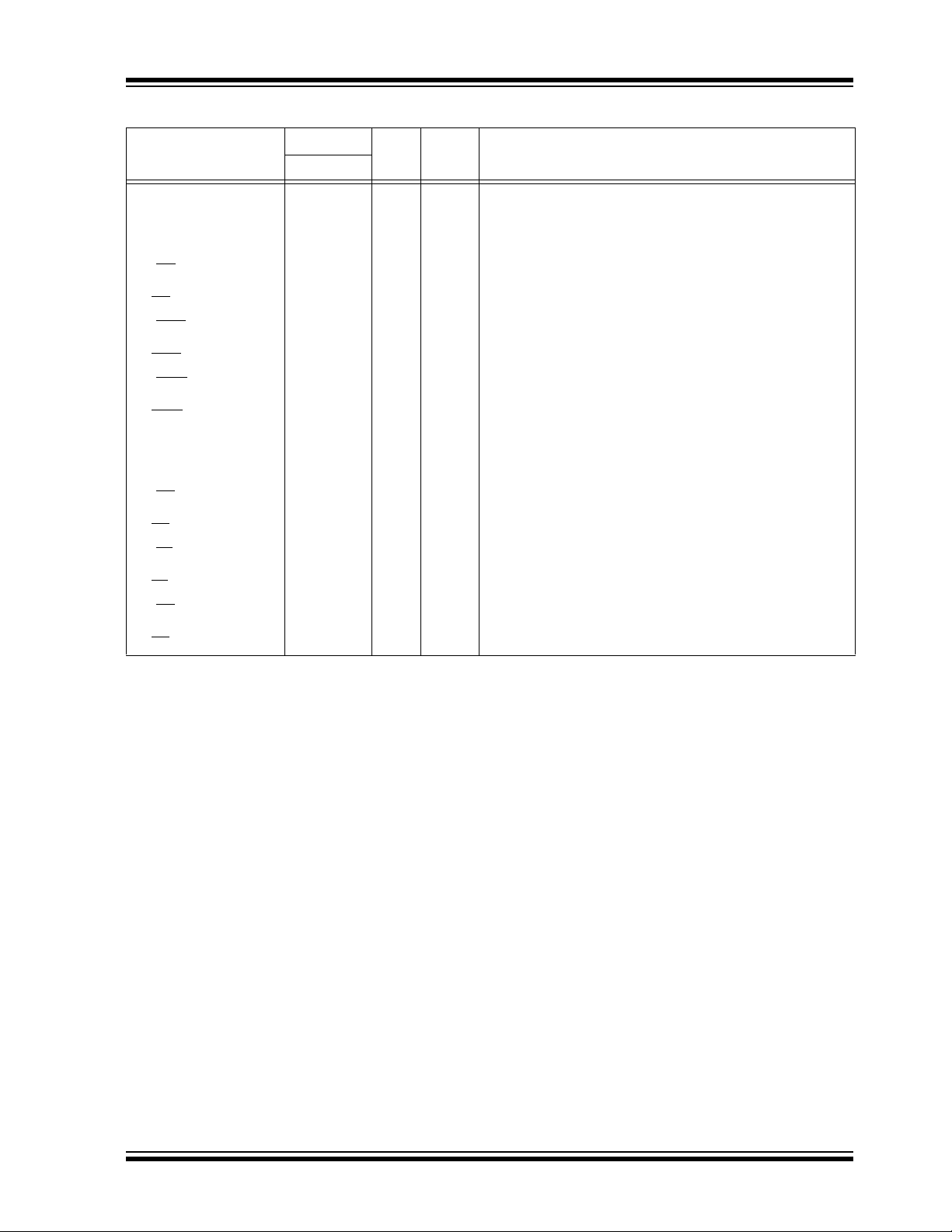
PIC18F97J60 FAMILY
TABLE 1-6: PIC18F96J60/96J65/97J60 PINOUT I/O DESCRIPTIONS (CONTINUED)
Pin Name
RJ0/ALE
RJ0
ALE
RJ1/OE
RJ1
OE
RJ2/WRL
RJ2
WRL
RJ3/WRH
RJ3
WRH
RJ4/BA0
RJ4
BA0
RJ5/CE
RJ5
CE
RJ6/LB
RJ6
LB
RJ7/UB
RJ7
UB
Legend: TTL = TTL compatible input CMOS = CMOS compatible input or output
ST = Schmitt Trigger input with CMOS levels Analog = Analog input
I = Input O = Output
P = Power OD = Open-Drain (no P diode to VDD)
Note 1: Alternate assignment for ECCP2/P2A when CCP2MX Configuration bit is cleared (Extended Microcontroller mode).
2: Default assignment for ECCP2/P2A for all devices in all operating modes (CCP2MX Configuration bit is set).
3: Default assignments for P1B/P1C/P3B/P3C (ECCPMX Configuration bit is set).
4: Alternate assignment for ECCP2/P2A when CCP2MX Configuration bit is cleared (Microcontroller mode).
5: Alternate assignments for P1B/P1C/P3B/P3C (ECCPMX Configuration bit is cleared).
Pin Number
TQFP
49
50
66
61
47
48
58
39
Pin
Typ e
I/O
O
I/O
O
I/O
O
I/O
O
I/O
O
I/O
O
I/O
O
I/O
O
Buffer
Type
ST
—
ST
—
ST
—
ST
—
ST
—
ST
—
ST
—
ST
—
Description
PORTJ is a bidirectional I/O port.
Digital I/O.
External memory address latch enable.
Digital I/O.
External memory output enable.
Digital I/O.
External memory write low control.
Digital I/O.
External memory write high control.
Digital I/O.
External memory byte address 0 control.
Digital I/O
External memory chip enable control.
Digital I/O.
External memory low byte control.
Digital I/O.
External memory high byte control.
© 2008 Microchip Technology Inc. Preliminary DS39762D-page 39
Page 42

PIC18F97J60 FAMILY
TABLE 1-6: PIC18F96J60/96J65/97J60 PINOUT I/O DESCRIPTIONS (CONTINUED)
Pin Name
Pin Number
TQFP
NC 9 — — No connect.
VSS 15, 36, 40,
60, 65, 85
V
DD 17, 37, 59,
62, 86
AV
SS 31 P — Ground reference for analog modules.
DD 30 P — Positive supply for analog modules.
AV
ENVREG 29 I ST Enable for on-chip voltage regulator.
DDCORE/VCAP
V
16
VDDCORE
VCAP
SSPLL 82 P — Ground reference for Ethernet PHY PLL.
V
VDDPLL 81 P — Positive 3.3V supply for Ethernet PHY PLL.
SSTX 79 P — Ground reference for Ethernet PHY transmit subsystem.
V
VDDTX 76 P — Positive 3.3V supply for Ethernet PHY transmit subsystem.
SSRX 72 P — Ground reference for Ethernet PHY receive subsystem.
V
VDDRX 75 P — Positive 3.3V supply for Ethernet PHY receive subsystem.
RBIAS 80 I Analog Bias current for Ethernet PHY. Must be tied to V
TPOUT+ 78 O — Ethernet differential signal output.
TPOUT- 77 O — Ethernet differential signal output.
TPIN+ 74 I Analog Ethernet differential signal input.
TPIN- 73 I Analog Ethernet differential signal input.
Legend: TTL = TTL compatible input CMOS = CMOS compatible input or output
ST = Schmitt Trigger input with CMOS levels Analog = Analog input
I = Input O = Output
P = Power OD = Open-Drain (no P diode to V
Note 1: Alternate assignment for ECCP2/P2A when CCP2MX Configuration bit is cleared (Extended Microcontroller mode).
2: Default assignment for ECCP2/P2A for all devices in all operating modes (CCP2MX Configuration bit is set).
3: Default assignments for P1B/P1C/P3B/P3C (ECCPMX Configuration bit is set).
4: Alternate assignment for ECCP2/P2A when CCP2MX Configuration bit is cleared (Microcontroller mode).
5: Alternate assignments for P1B/P1C/P3B/P3C (ECCPMX Configuration bit is cleared).
Pin
Typ e
Buffer
Type
Description
P — Ground reference for logic and I/O pins.
P — Positive supply for peripheral digital logic and I/O pins.
Core logic power or external filter capacitor connection.
P
—
Positive supply for microcontroller core logic
(regulator disabled).
P
—
External filter capacitor connection (regulator enabled).
SS via a resistor;
see Section 18.0 “Ethernet Module” for specification.
DD)
DS39762D-page 40 Preliminary © 2008 Microchip Technology Inc.
Page 43
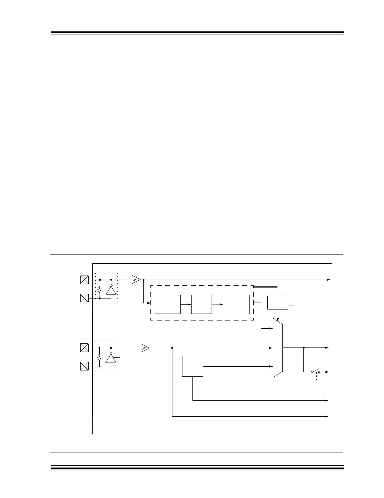
PIC18F97J60 FAMILY
2.0 OSCILLATOR CONFIGURATIONS
2.1 Overview
Devices in the PIC18F97J60 family incorporate an
oscillator and microcontroller clock system that differs
from standard PIC18FXXJXX devices. The addition of
the Ethernet module, with its requirement for a stable
25 MHz clock source, makes it necessary to provide a
primary oscillator that can provide this frequency as
well as a range of different microcontroller clock
speeds. An overview of the oscillator structure is shown
in Figure 2-1.
Other oscillator features used in PIC18FXXJXX
enhanced microcontrollers, such as the internal RC
oscillator and clock switching, remain the same. They
are discussed later in this chapter.
2.2 Oscillator Types
The PIC18F97J60 family of devices can be operated in
five different oscillator modes:
1. HS High-Speed Crystal/Resonator
2. HSPLL High-Speed Crystal/Resonator
with Software PLL Control
3. EC External Clock with F
4. ECPLL External Clock with Software PLL
Control
5. INTRC Internal 31 kHz Oscillator
2.2.1 OSCILLATOR CONTROL
The oscillator mode is selected by programming the
FOSC2:FOSC0 Configuration bits. FOSC1:FOSC0
bits select the default primary oscillator modes, while
FOSC2 selects when INTRC may be invoked.
The OSCCON register (Register 2-2) selects the Active
Clock mode. It is primarily used in controlling clock
switching in power-managed modes. Its use is discussed
in Section 2.7.1 “Oscillator Control Register”.
The OSCTUNE register (Register 2-1) is used to select
the system clock frequency from the primary oscillator
source by selecting combinations of prescaler/postscaler
settings and enabling the PLL. Its use is described in
Section 2.6.1 “PLL Block”.
OSC/4 Output
FIGURE 2-1: PIC18F97J60 FAMILY CLOCK DIAGRAM
PIC18F97J60 Family
PLL/Prescaler/Postscaler
5x PLL
EC, HS, ECPLL, HSPLL
INTRC
Source
OSC2
OSC1
T1OSO
T1OSI
Primary Oscillator
Sleep
PLL
Prescaler
Secondary Oscillator
T1OSCEN
Enable
Oscillator
PLL
Postscaler
T1OSC
Internal Oscillator
Ethernet Clock
OSCTUNE<7:5>
Clock
Control
WDT, PWRT, FSCM
and Two-Speed Start-up
Clock Source Option
for Other Modules
FOSC2:FOSC0
OSCCON<1:0>
Peripherals
MUX
IDLEN
(1)
CPU
Note 1: See Table 2-2 for OSCTUNE register configurations and their corresponding frequencies.
© 2008 Microchip Technology Inc. Preliminary DS39762D-page 41
Page 44

PIC18F97J60 FAMILY
2.3 Crystal Oscillator/Ceramic Resonators (HS Modes)
In HS or HSPLL Oscillator modes, a crystal is
connected to the OSC1 and OSC2 pins to establish
oscillation. Figure 2-2 shows the pin connections.
The oscillator design requires the use of a crystal that
is rated for parallel resonant operation.
Note: Use of a crystal rated for series resonant
operation may give a frequency out of the
crystal manufacturer’s specifications.
FIGURE 2-2: CRYSTAL OSCILLATOR
OPERATION (HS OR
HSPLL CONFIGURATION)
(1)
C1
(1)
C2
Note 1: See Table 2-1 for initial values of C1 and C2.
2: A series resistor (R
crystals with a low drive specification.
F varies with the oscillator mode chosen.
3: R
XTAL
RS
OSC1
OSC2
(2)
To
Internal
RF
(3)
Logic
Sleep
PIC18FXXJ6X
S) may be required for
Note 1: Higher capacitance increases the stability
of the oscillator but also increases the
start-up time.
2: Since each crystal has its own character-
istics, the user should consult the crystal
manufacturer for appropriate values of
external components.
3: Rs may be required to avoid overdriving
crystals with low drive level specifications.
4: Always verify oscillator performance over
DD and temperature range that is
the V
expected for the application.
2.4 External Clock Input (EC Modes)
The EC and ECPLL Oscillator modes require an external clock source to be connected to the OSC1 pin.
There is no oscillator start-up time required after a
Power-on Reset or after an exit from Sleep mode.
In the EC Oscillator mode, the oscillator frequency
divided by 4 is available on the OSC2 pin. This signal
may be used for test purposes or to synchronize other
logic. Figure 2-3 shows the pin connections for the EC
Oscillator mode.
FIGURE 2-3: EXTERNAL CLOCK
INPUT OPERATION
(EC CONFIGURATION)
TABLE 2-1: CAPACITOR SELECTION FOR
CRYSTAL OSCILLATOR
Osc Type
Crystal
Freq.
HS 25 MHz 33 pF 33 pF
Capacitor values are for design guidance only.
Different capacitor values may be required to produce
acceptable oscillator operation. The user should test
the performance of the oscillator over the expected
DD and temperature range for the application. Refer
V
to the following application notes for oscillator specific
information:
®
• AN588, “PIC
Microcontroller Oscillator Design
Guide”
• AN826, “Crystal Oscillator Basics and Crystal
Selection for rfPIC
• AN849, “Basic PIC
• AN943, “Practical PIC
Design”
• AN949, “Making Your Oscillator Work”
See the notes following this table for additional
information.
Typical Capacitor Values
Tested:
C1 C2
®
and PIC® Devices”
®
Oscillator Design”
®
Oscillator Analysis and
Clock from
Ext. System
OSC/4
F
OSC1/CLKI
PIC18FXXJ6X
OSC2/CLKO
An external clock source may also be connected to the
OSC1 pin in the HS mode, as shown in Figure 2-4. In
this configuration, the OSC2 pin is left open. Current
consumption in this configuration will be somewhat
higher than EC mode, as the internal oscillator’s
feedback circuitry will be enabled (in EC mode, the
feedback circuit is disabled).
FIGURE 2-4: EXTERNAL CLOCK
INPUT OPERATION
(HS CONFIGURATION)
Clock from
Ext. System
Open
OSC1
PIC18FXXJ6X
(HS Mode)
OSC2
DS39762D-page 42 Preliminary © 2008 Microchip Technology Inc.
Page 45

PIC18F97J60 FAMILY
2.5 Internal Oscillator Block
The PIC18F97J60 family of devices includes an internal
oscillator source (INTRC) which provides a nominal
31 kHz output. The INTRC is enabled on device
power-up and clocks the device during its configuration
cycle until it enters operating mode. INTRC is also
enabled if it is selected as the device clock source or if
any of the following are enabled:
• Fail-Safe Clock Monitor
• Watchdog Timer
• Two-Speed Start-up
These features are discussed in greater detail in
Section 24.0 “Special Features of the CPU”.
The INTRC can also be optionally configured as the
default clock source on device start-up by setting the
FOSC2 Configuration bit. This is discussed in
Section 2.7.1 “Oscillator Control Register”.
2.6 Ethernet Operation and the Microcontroller Clock
Although devices of the PIC18F97J60 family can accept
a wide range of crystals and external oscillator inputs,
they must always have a 25 MHz clock source when
used for Ethernet applications. No provision is made for
internally generating the required Ethernet clock from a
primary oscillator source of a different frequency. A
frequency tolerance is specified, likely excluding the use
of ceramic resonators. See Section 27.0 “Electrical
Characteristics”, Table 27-6, parameter 5, for more
details.
2.6.1 PLL BLOCK
To accommodate a range of applications and microcontroller clock speeds, a separate PLL block is
incorporated into the clock system. It consists of three
components:
• A configurable prescaler (1:2 or 1:3)
• A 5x PLL frequency multiplier
• A configurable postscaler (1:1, 1:2, or 1:3)
The operation of the PLL block’s components is
controlled by the OSCTUNE register (Register 2-1).
The use of the PLL block’s prescaler and postscaler,
with or without the PLL itself, provides a range of system clock frequencies to choose from, including the
unaltered 25 MHz of the primary oscillator. The full
range of possible oscillator configurations compatible
with Ethernet operation is shown in Table 2-2.
REGISTER 2-1: OSCTUNE: PLL BLOCK CONTROL REGISTER
R/W-0 R/W-0 R/W-0 R/W-0 U-0 U-0 U-0 U-0
PPST1 PLLEN
bit 7 bit 0
Legend:
R = Readable bit W = Writable bit U = Unimplemented bit, read as ‘0’
-n = Value at POR ‘1’ = Bit is set ‘0’ = Bit is cleared x = Bit is unknown
bit 7 PPST1: PLL Postscaler Configuration bit
1 = Divide-by-2
0 = Divide-by-3
bit 6 PLLEN: 5x Frequency Multiplier PLL Enable bit
1 = PLL enabled
0 = PLL disabled
bit 5 PPST0: PLL Postscaler Enable bit
1 = Postscaler enabled
0 = Postscaler disabled
bit 4 PPRE: PLL Prescaler Configuration bit
1 = Divide-by-2
0 = Divide-by-3
bit 3-0 Unimplemented: Read as ‘0’
(1)
PPST0 PPRE — — — —
(1)
Note 1: Available only for ECPLL and HSPLL oscillator configurations; otherwise, this bit is unavailable and is read
as ‘0’.
© 2008 Microchip Technology Inc. Preliminary DS39762D-page 43
Page 46

PIC18F97J60 FAMILY
TABLE 2-2: DEVICE CLOCK SPEEDS FOR VARIOUS PLL BLOCK CONFIGURATIONS
PLL Block
5x PLL PLL Prescaler PLL Postscaler
Disabled x101 (Note 1)
÷2
Enabled
÷3
Disabled
Disabled
Legend: x = Don’t care
Note 1: Reserved configuration; represents a clock frequency beyond the microcontroller’s operating range.
2: The prescaler is automatically disabled when the PLL and postscaler are both disabled.
(2)
÷2
÷3
÷2 1111 31.2500
÷3 0111 20.8333
Disabled x100 41.6667
÷2 1110 20.8333
÷3 0110 13.8889
Disabled x00x 25 (Default)
÷2 1011 6.2500
÷3 0011 4.1667
÷2 1010 4.1667
÷3 0010 2.7778
Configuration
(OSCTUNE<7:4>)
Clock Frequency
(MHz)
2.7 Clock Sources and Oscillator Switching
The PIC18F97J60 family of devices includes a feature
that allows the device clock source to be switched from
the main oscillator to an alternate clock source. These
devices also offer two alternate clock sources. When
an alternate clock source is enabled, the various
power-managed operating modes are available.
Essentially, there are three clock sources for these
devices:
• Primary oscillators
• Secondary oscillators
• Internal oscillator block
The primary oscillators include the External Crystal
and Resonator modes and the External Clock modes.
The particular mode is defined by the FOSC2:FOSC0
Configuration bits. The details of these modes are
covered earlier in this chapter.
The secondary oscillators are those external sources
not connected to the OSC1 or OSC2 pins. These
sources may continue to operate even after the controller
is placed in a power-managed mode. The PIC18F97J60
family of devices offers the Timer1 oscillator as a secondary oscillator. In all power-managed modes, this oscillator
is often the time base for functions such as a Real-Time
Clock (RTC).
Most often, a 32.768 kHz watch crystal is connected
between the RC0/T1OSO/T13CKI and RC1/T1OSI
pins. Loading capacitors are also connected from each
pin to ground. The Timer1 oscillator is discussed in
greater detail in Section 12.3 “Timer1 Oscillator”.
In addition to being a primary clock source, the internal
oscillator is available as a power-managed mode
clock source. The INTRC source is also used as the
clock source for several special features, such as the
WDT and Fail-Safe Clock Monitor.
The clock sources for the PIC18F97J60 family devices
are shown in Figure 2-1. See Section 24.0 “Special
Features of the CPU” for Configuration register details.
DS39762D-page 44 Preliminary © 2008 Microchip Technology Inc.
Page 47

PIC18F97J60 FAMILY
2.7.1 OSCILLATOR CONTROL REGISTER
The OSCCON register (Register 2-2) controls several
aspects of the device clock’s operation, both in
full-power operation and in power-managed modes.
The System Clock Select bits, SCS1:SCS0, select the
clock source. The available clock sources are the
primary clock (defined by the FOSC2:FOSC0 Configuration bits), the secondary clock (Timer1 oscillator) and
the internal oscillator. The clock source changes after
one or more of the bits are changed, following a brief
clock transition interval.
The OSTS (OSCCON<3>) and T1RUN (T1CON<6>)
bits indicate which clock source is currently providing
the device clock. The T1RUN bit indicates when the
Timer1 oscillator is providing the device clock in
secondary clock modes. In power-managed modes,
only one of these bits will be set at any time. If neither
bit is set, the INTRC source is providing the clock, or
the internal oscillator has just started and is not yet
stable.
The IDLEN bit determines if the device goes into Sleep
mode or one of the Idle modes when the SLEEP
instruction is executed.
The use of the flag and control bits in the OSCCON
register is discussed in more detail in Section 3.0
“Power-Managed Modes”.
Note 1: The Timer1 oscillator must be enabled to
select the secondary clock source. The
Timer1 oscillator is enabled by setting the
T1OSCEN bit in the Timer1 Control register (T1CON<3>). If the Timer1 oscillator
is not enabled, then any attempt to select
a secondary clock source will be ignored.
2: It is recommended that the Timer1
oscillator be operating and stable before
executing the SLEEP instruction or a very
long delay may occur while the Timer1
oscillator starts.
REGISTER 2-2: OSCCON: OSCILLATOR CONTROL REGISTER
R/W-0 U-0 U-0 U-0 R-q U-0 R/W-0 R/W-0
IDLEN — — —OSTS
bit 7 bit 0
(1)
—SCS1SCS0
Legend: q = Value determined by configuration
R = Readable bit W = Writable bit U = Unimplemented bit, read as ‘0’
-n = Value at POR ‘1’ = Bit is set ‘0’ = Bit is cleared x = Bit is unknown
bit 7 IDLEN: Idle Enable bit
1 = Device enters Idle mode on SLEEP instruction
0 = Device enters Sleep mode on SLEEP instruction
bit 6-4 Unimplemented: Read as ‘0’
bit 3 OSTS: Oscillator Status bit
1 = Device is running from oscillator source defined when SCS1:SCS0 = 00
0 = Device is running from oscillator source defined when SCS1:SCS0 = 01, 10 or 11
bit 2 Unimplemented: Read as ‘0’
bit 1-0 SCS1:SCS0: System Clock Select bits
11 = Internal oscillator
10 = Primary oscillator
01 = Timer1 oscillator
When FOSC2 =
00 = Primary oscillator
When FOSC2 = 0;
00 = Internal oscillator
Note 1: Reset value is ‘0’ when Two-Speed Start-up is enabled and ‘1’ if disabled.
1;
(1)
© 2008 Microchip Technology Inc. Preliminary DS39762D-page 45
Page 48

PIC18F97J60 FAMILY
2.7.1.1 System Clock Selection and the
FOSC2 Configuration Bit
The SCS bits are cleared on all forms of Reset. In the
device’s default configuration, this means the primary
oscillator defined by FOSC1:FOSC0 (that is, one of the
HC or EC modes) is used as the primary clock source
on device Resets.
The default clock configuration on Reset can be changed
with the FOSC2 Configuration bit. This bit affects the
clock source selection setting when SCS1:SCS0 = 00.
When FOSC2 = 1 (default), the oscillator source
defined by FOSC1:FOSC0 is selected whenever
SCS1:SCS0 = 00. When FOSC2 = 0, the INTRC oscillator is selected whenever SCS1:SCS2 = 00. Because the
SCS bits are cleared on Reset, the FOSC2 setting also
changes the default oscillator mode on Reset.
Regardless of the setting of FOSC2, INTRC will always
be enabled on device power-up. It will serve as the
clock source until the device has loaded its configuration values from memory. It is at this point that the
FOSC Configuration bits are read and the oscillator
selection of operational mode is made.
Note that either the primary clock or the internal
oscillator will have two bit setting options, at any given
time, depending on the setting of FOSC2.
2.7.2 OSCILLATOR TRANSITIONS
PIC18F97J60 family devices contain circuitry to
prevent clock “glitches” when switching between clock
sources. A short pause in the device clock occurs
during the clock switch. The length of this pause is the
sum of two cycles of the old clock source and three to
four cycles of the new clock source. This formula
assumes that the new clock source is stable.
Clock transitions are discussed in greater detail in
Section 3.1.2 “Entering Power-Managed Modes”.
2.8 Effects of Power-Managed Modes on the Various Clock Sources
When PRI_IDLE mode is selected, the designated
primary oscillator continues to run without interruption.
For all other power-managed modes, the oscillator
using the OSC1 pin is disabled. The OSC1 pin (and
OSC2 pin if used by the oscillator) will stop oscillating.
In secondary clock modes (SEC_RUN and
SEC_IDLE), the Timer1 oscillator is operating and
providing the device clock. The Timer1 oscillator may
also run in all power-managed modes if required to
clock Timer1 or Timer3.
In RC_RUN and RC_IDLE modes, the internal oscillator provides the device clock source. The 31 kHz
INTRC output can be used directly to provide the clock
and may be enabled to support various special
features, regardless of the power-managed mode (see
Section 24.2 “Watchdog Timer (WDT)” through
Section 24.5 “Fail-Safe Clock Monitor” for more
information on WDT, Fail-Safe Clock Monitor and
Two-Speed Start-up).
If the Sleep mode is selected, all clock sources are
stopped. Since all the transistor switching currents have
been stopped, Sleep mode achieves the lowest current
consumption of the device (only leakage currents).
Enabling any on-chip feature that will operate during
Sleep will increase the current consumed during Sleep.
The INTRC is required to support WDT operation. The
Timer1 oscillator may be operating to support a
Real-Time Clock. Other features may be operating that
do not require a device clock source (i.e., MSSP slave,
PSP, INTx pins and others). Peripherals that may add
significant current consumption are listed in
Section 27.2 “DC Characteristics: Power-Down and
Supply Current”.
2.9 Power-up Delays
Power-up delays are controlled by two timers, so that
no external Reset circuitry is required for most applications. The delays ensure that the device is kept in
Reset until the device power supply is stable under normal circumstances and the primary clock is operating
and stable. For additional information on power-up
delays, see Section 4.6 “Power-up Timer (PWRT)”.
The first timer is the Power-up Timer (PWRT), which
provides a fixed delay on power-up (parameter 33,
Table 27-12); it is always enabled.
The second timer is the Oscillator Start-up Timer
(OST), intended to keep the chip in Reset until the
crystal oscillator is stable (HS modes). The OST does
this by counting 1024 oscillator cycles before allowing
the oscillator to clock the device.
There is a delay of interval T
Table 27-12), following POR, while the controller
becomes ready to execute instructions.
CSD (parameter 38,
TABLE 2-3: OSC1 AND OSC2 PIN STATES IN SLEEP MODE
Oscillator Mode OSC1 Pin OSC2 Pin
EC, ECPLL Floating, pulled by external clock At logic low (clock/4 output)
HS, HSPLL Feedback inverter disabled at quiescent
voltage level
Note: See Table 4-2 in Section 4.0 “Reset” for time-outs due to Sleep and MCLR
DS39762D-page 46 Preliminary © 2008 Microchip Technology Inc.
Feedback inverter disabled at quiescent
voltage level
Reset.
Page 49
PIC18F97J60 FAMILY
3.0 POWER-MANAGED MODES
The PIC18F97J60 family devices provide the ability to
manage power consumption by simply managing clocking to the CPU and the peripherals. In general, a lower
clock frequency and a reduction in the number of circuits
being clocked constitutes lower consumed power. For
the sake of managing power in an application, there are
three primary modes of operation:
• Run mode
• Idle mode
• Sleep mode
These modes define which portions of the device are
clocked and at what speed. The Run and Idle modes
may use any of the three available clock sources
(primary, secondary or internal oscillator block); the
Sleep mode does not use a clock source.
The power-managed modes include several
power-saving features offered on previous PIC
devices. One is the clock switching feature, offered in
other PIC18 devices, allowing the controller to use the
Timer1 oscillator in place of the primary oscillator. Also
included is the Sleep mode, offered by all PIC MCU
devices, where all device clocks are stopped.
3.1 Selecting Power-Managed Modes
Selecting a power-managed mode requires two
decisions: if the CPU is to be clocked or not and which
clock source is to be used. The IDLEN bit
(OSCCON<7>) controls CPU clocking, while the
SCS1:SCS0 bits (OSCCON<1:0>) select the clock
source. The individual modes, bit settings, clock sources
and affected modules are summarized in Table 3-1.
®
MCU
3.1.1 CLOCK SOURCES
The SCS1:SCS0 bits allow the selection of one of three
clock sources for power-managed modes. They are:
• The primary clock, as defined by the
FOSC2:FOSC0 Configuration bits
• The secondary clock (Timer1 oscillator)
• The internal oscillator
3.1.2 ENTERING POWER-MANAGED
MODES
Switching from one power-managed mode to another
begins by loading the OSCCON register. The
SCS1:SCS0 bits select the clock source and determine
which Run or Idle mode is to be used. Changing these
bits causes an immediate switch to the new clock
source, assuming that it is running. The switch may
also be subject to clock transition delays. These are
discussed in Section 3.1.3 “Clock Transitions and
Status Indicators” and subsequent sections.
Entry to the power-managed Idle or Sleep modes is
triggered by the execution of a SLEEP instruction. The
actual mode that results depends on the status of the
IDLEN bit.
Depending on the current mode and the mode being
switched to, a change to a power-managed mode does
not always require setting all of these bits. Many
transitions may be done by changing the oscillator
select bits, or changing the IDLEN bit, prior to issuing a
SLEEP instruction. If the IDLEN bit is already
configured correctly, it may only be necessary to
perform a SLEEP instruction to switch to the desired
mode.
TABLE 3-1: POWER-MANAGED MODES
Mode
Sleep 0 N/A Off Off None – All clocks are disabled
PRI_RUN N/A 10 Clocked Clocked Primary – HS, EC, HSPLL, ECPLL;
SEC_RUN N/A 01 Clocked Clocked Secondary – Timer1 Oscillator
RC_RUN N/A 11 Clocked Clocked Internal Oscillator
PRI_IDLE 110Off Clocked Primary – HS, EC, HSPLL, ECPLL
SEC_IDLE 101Off Clocked Secondary – Timer1 Oscillator
RC_IDLE 111Off Clocked Internal Oscillator
Note 1: IDLEN reflects its value when the SLEEP instruction is executed.
© 2008 Microchip Technology Inc. Preliminary DS39762D-page 47
OSCCON<7,1:0> Module Clocking
(1)
IDLEN
SCS1:SCS0 CPU Peripherals
Available Clock and Oscillator Source
this is the normal, full-power execution mode
Page 50

PIC18F97J60 FAMILY
3.1.3 CLOCK TRANSITIONS AND STATUS INDICATORS
The length of the transition between clock sources is
the sum of two cycles of the old clock source and three
to four cycles of the new clock source. This formula
assumes that the new clock source is stable.
Two bits indicate the current clock source and its
status: OSTS (OSCCON<3>) and T1RUN
(T1CON<6>). In general, only one of these bits will be
set while in a given power-managed mode. When the
OSTS bit is set, the primary clock is providing the
device clock. When the T1RUN bit is set, the Timer1
oscillator is providing the clock. If neither of these bits
is set, INTRC is clocking the device.
Note: Executing a SLEEP instruction does not
necessarily place the device into Sleep
mode. It acts as the trigger to place the
controller into either the Sleep mode, or
one of the Idle modes, depending on the
setting of the IDLEN bit.
3.1.4 MULTIPLE SLEEP COMMANDS
The power-managed mode that is invoked with the
SLEEP instruction is determined by the setting of the
IDLEN bit at the time the instruction is executed. If
another SLEEP instruction is executed, the device will
enter the power-managed mode specified by IDLEN at
that time. If IDLEN has changed, the device will enter the
new power-managed mode specified by the new setting.
3.2 Run Modes
In the Run modes, clocks to both the core and
peripherals are active. The difference between these
modes is the clock source.
3.2.2 SEC_RUN MODE
The SEC_RUN mode is the compatible mode to the
“clock switching” feature offered in other PIC18
devices. In this mode, the CPU and peripherals are
clocked from the Timer1 oscillator. This gives users the
option of lower power consumption while still using a
high accuracy clock source.
SEC_RUN mode is entered by setting the SCS1:SCS0
bits to ‘01’. The device clock source is switched to the
Timer1 oscillator (see Figure 3-1), the primary
oscillator is shut down, the T1RUN bit (T1CON<6>) is
set and the OSTS bit is cleared.
Note: The Timer1 oscillator should already be
running prior to entering SEC_RUN mode.
If the T1OSCEN bit is not set when the
SCS1:SCS0 bits are set to ‘01’, entry to
SEC_RUN mode will not occur. If the
Timer1 oscillator is enabled, but not yet
running, device clocks will be delayed until
the oscillator has started. In such
situations, initial oscillator operation is far
from stable and unpredictable operation
may result.
On transitions from SEC_RUN mode to PRI_RUN, the
peripherals and CPU continue to be clocked from the
Timer1 oscillator while the primary clock is started.
When the primary clock becomes ready, a clock switch
back to the primary clock occurs (see Figure 3-2).
When the clock switch is complete, the T1RUN bit is
cleared, the OSTS bit is set and the primary clock is
providing the clock. The IDLEN and SCS bits are not
affected by the wake-up; the Timer1 oscillator
continues to run.
3.2.1 PRI_RUN MODE
The PRI_RUN mode is the normal, full-power execution mode of the microcontroller. This is also the default
mode upon a device Reset unless Two-Speed Start-up
is enabled (see Section 24.4 “Two-Speed Start-up”
for details). In this mode, the OSTS bit is set. (see
Section 2.7.1 “Oscillator Control Register”).
DS39762D-page 48 Preliminary © 2008 Microchip Technology Inc.
Page 51
PIC18F97J60 FAMILY
FIGURE 3-1: TRANSITION TIMING FOR ENTRY TO SEC_RUN MODE
Q4Q3Q2
Q1
Q1
Q4Q3Q2 Q1 Q3Q2
T1OSI
OSC1
CPU
Clock
Peripheral
Clock
Program
Counter
123
Clock Transition
n-1
n
PC + 2PC
PC + 4
FIGURE 3-2: TRANSITION TIMING FROM SEC_RUN MODE TO PRI_RUN MODE (HSPLL)
T1OSI
OSC1
PLL Clock
Output
CPU Clock
Peripheral
Clock
Program
Counter
Q1 Q3 Q4
(1)
TOST
PC
Q3 Q4 Q1
Q2 Q2 Q3
(1)
TPLL
12 n-1n
Clock
Transition
PC + 2
Q1
Q2
PC + 4
SCS1:SCS0 bits Changed
Note 1: TOST = 1024 TOSC; TPLL = 2 ms (approx). These intervals are not shown to scale.
OSTS bit Set
© 2008 Microchip Technology Inc. Preliminary DS39762D-page 49
Page 52

PIC18F97J60 FAMILY
3.2.3 RC_RUN MODE
In RC_RUN mode, the CPU and peripherals are
clocked from the internal oscillator; the primary clock is
shut down. This mode provides the best power conservation of all the Run modes while still executing code.
It works well for user applications which are not highly
timing sensitive or do not require high-speed clocks at
all times.
This mode is entered by setting SCS<1:0> to ‘11’.
On transitions from RC_RUN mode to PRI_RUN mode,
the device continues to be clocked from the INTRC
while the primary clock is started. When the primary
clock becomes ready, a clock switch to the primary
clock occurs (see Figure 3-4). When the clock switch is
complete, the OSTS bit is set and the primary clock is
providing the device clock. The IDLEN and SCS bits
are not affected by the switch. The INTRC source will
continue to run if either the WDT or Fail-Safe Clock
Monitor is enabled.
When the clock source is switched to the INTRC (see
Figure 3-3), the primary oscillator is shut down and the
OSTS bit is cleared.
FIGURE 3-3: TRANSITION TIMING TO RC_RUN MODE
Q4Q3Q2
Q1
123 n-1n
Clock Transition
PC + 2PC
INTRC
OSC1
CPU
Clock
Peripheral
Clock
Program
Counter
Q1
Q4Q3Q2 Q1 Q3Q2
PC + 4
FIGURE 3-4: TRANSITION TIMING FROM RC_RUN MODE TO PRI_RUN MODE
Q2
Q3 Q4
Q1
INTRC
OSC1
PLL Clock
Output
CPU Clock
Peripheral
Clock
Program
Counter
SCS1:SCS0 bits Changed
Note 1: TOST = 1024 TOSC ; TPLL = 2 ms (approx). These intervals are not shown to scale.
TOST
Q2
(1)
PC
Q3
(1)
TPLL
OSTS bit Set
12 n-1n
Clock
Transition
PC + 2
Q1
Q4
Q1
PC + 4
Q2
Q3
DS39762D-page 50 Preliminary © 2008 Microchip Technology Inc.
Page 53

PIC18F97J60 FAMILY
3.3 Sleep Mode
The power-managed Sleep mode is identical to the
legacy Sleep mode offered in all other PIC MCU
devices. It is entered by clearing the IDLEN bit (the
default state on device Reset) and executing the
SLEEP instruction. This shuts down the selected
oscillator (Figure 3-5). All clock source status bits are
cleared.
Entering the Sleep mode from any other mode does not
require a clock switch. This is because no clocks are
needed once the controller has entered Sleep. If the
WDT is selected, the INTRC source will continue to
operate. If the Timer1 oscillator is enabled, it will also
continue to run.
When a wake event occurs in Sleep mode (by interrupt,
Reset or WDT time-out), the device will not be clocked
until the clock source selected by the SCS1:SCS0 bits
becomes ready (see Figure 3-6), or it will be clocked
from the internal oscillator if either the Two-Speed
Start-up or the Fail-Safe Clock Monitor is enabled (see
Section 24.0 “Special Features of the CPU”). In
either case, the OSTS bit is set when the primary clock
is providing the device clocks. The IDLEN and SCS bits
are not affected by the wake-up.
3.4 Idle Modes
The Idle modes allow the controller’s CPU to be
selectively shut down while the peripherals continue to
operate. Selecting a particular Idle mode allows users
to further manage power consumption.
If the IDLEN bit is set to ‘1’ when a SLEEP instruction is
executed, the peripherals will be clocked from the clock
source selected using the SCS1:SCS0 bits; however, the
CPU will not be clocked. The clock source status bits are
not affected. Setting IDLEN and executing a SLEEP
instruction provides a quick method of switching from a
given Run mode to its corresponding Idle mode.
If the WDT is selected, the INTRC source will continue
to operate. If the Timer1 oscillator is enabled, it will also
continue to run.
Since the CPU is not executing instructions, the only exits
from any of the Idle modes are by interrupt, WDT
time-out or a Reset. When a wake event occurs, CPU
execution is delayed by an interval of T
(parameter 38, Table 27-12) while it becomes ready to
execute code. When the CPU begins executing code, it
resumes with the same clock source for the current Idle
mode. For example, when waking from RC_IDLE mode,
the internal oscillator block will clock the CPU and peripherals (in other words, RC_RUN mode). The IDLEN and
SCS bits are not affected by the wake-up.
While in any Idle mode or the Sleep mode, a WDT
time-out will result in a WDT wake-up to the Run mode
currently specified by the SCS1:SCS0 bits.
CSD
FIGURE 3-5: TRANSITION TIMING FOR ENTRY TO SLEEP MODE
Q4Q3Q2
Q1Q1
OSC1
CPU
Clock
Peripheral
Clock
Sleep
Program
Counter
PC + 2PC
FIGURE 3-6: TRANSITION TIMING FOR WAKE FROM SLEEP MODE (HSPLL)
OSC1
PLL Clock
Output
CPU Clock
Peripheral
Clock
Program
Counter
Note1: T
Q1 Q2 Q3 Q4 Q1 Q2
(1)
TOST
Wake Event
OST = 1024 TOSC; TPLL = 2 ms (approx). These intervals are not shown to scale.
(1)
TPLL
PC
OSTS bit Set
Q3 Q4 Q1 Q2
PC + 2
Q3 Q4
Q1 Q2 Q3 Q4
PC + 6PC + 4
© 2008 Microchip Technology Inc. Preliminary DS39762D-page 51
Page 54
PIC18F97J60 FAMILY
3.4.1 PRI_IDLE MODE
This mode is unique among the three low-power Idle
modes in that it does not disable the primary device
clock. For timing sensitive applications, this allows for
the fastest resumption of device operation with its more
accurate primary clock source, since the clock source
does not have to “warm up” or transition from another
oscillator.
PRI_IDLE mode is entered from PRI_RUN mode by
setting the IDLEN bit and executing a SLEEP instruction. If the device is in another Run mode, set IDLEN
first, then set the SCS<1:0> bits to ‘10’ and execute
SLEEP. Although the CPU is disabled, the peripherals
continue to be clocked from the primary clock source
specified by the FOSC1:FOSC0 Configuration bits.
The OSTS bit remains set (see Figure 3-7).
When a wake event occurs, the CPU is clocked from the
primary clock source. A delay of interval T
required between the wake event and when code
execution starts. This is required to allow the CPU to
become ready to execute instructions. After the
wake-up, the OSTS bit remains set. The IDLEN and
SCS bits are not affected by the wake-up (see
Figure 3-8).
CSD is
3.4.2 SEC_IDLE MODE
In SEC_IDLE mode, the CPU is disabled but the
peripherals continue to be clocked from the Timer1
oscillator. This mode is entered from SEC_RUN by setting the IDLEN bit and executing a SLEEP instruction. If
the device is in another Run mode, set IDLEN first, then
set SCS<1:0> to ‘01’ and execute SLEEP. When the
clock source is switched to the Timer1 oscillator, the
primary oscillator is shut down, the OSTS bit is cleared
and the T1RUN bit is set.
When a wake event occurs, the peripherals continue to
be clocked from the Timer1 oscillator. After an interval
CSD following the wake event, the CPU begins exe-
of T
cuting code being clocked by the Timer1 oscillator. The
IDLEN and SCS bits are not affected by the wake-up;
the Timer1 oscillator continues to run (see Figure 3-8).
Note: The Timer1 oscillator should already be
running prior to entering SEC_IDLE mode.
If the T1OSCEN bit is not set when the
SLEEP instruction is executed, the SLEEP
instruction will be ignored and entry to
SEC_IDLE mode will not occur. If the
Timer1 oscillator is enabled, but not yet running, peripheral clocks will be delayed until
the oscillator has started. In such situations,
initial oscillator operation is far from stable
and unpredictable operation may result.
FIGURE 3-7: TRANSITION TIMING FOR ENTRY TO IDLE MODE
Q1
OSC1
CPU Clock
Peripheral
Clock
Program
Counter
Q1
Q2
Q3
PC PC + 2
Q4
FIGURE 3-8: TRANSITION TIMING FOR WAKE FROM IDLE TO RUN MODE
OSC1
CPU Clock
Peripheral
Clock
Program
Counter
Q1 Q3 Q4
TCSD
PC
Wake Event
Q2
DS39762D-page 52 Preliminary © 2008 Microchip Technology Inc.
Page 55

PIC18F97J60 FAMILY
3.4.3 RC_IDLE MODE
In RC_IDLE mode, the CPU is disabled but the peripherals continue to be clocked from the internal oscillator.
This mode allows for controllable power conservation
during Idle periods.
From RC_RUN mode, RC_IDLE mode is entered by
setting the IDLEN bit and executing a SLEEP instruction.
If the device is in another Run mode, first set IDLEN,
then clear the SCS bits and execute SLEEP. When the
clock source is switched to the INTRC, the primary
oscillator is shut down and the OSTS bit is cleared.
When a wake event occurs, the peripherals continue to
be clocked from the INTRC. After a delay of T
following the wake event, the CPU begins executing
code being clocked by the INTRC. The IDLEN and
SCS bits are not affected by the wake-up. The INTRC
source will continue to run if either the WDT or the
Fail-Safe Clock Monitor is enabled.
CSD
3.5 Exiting Idle and Sleep Modes
An exit from Sleep mode, or any of the Idle modes, is
triggered by an interrupt, a Reset or a WDT time-out.
This section discusses the triggers that cause exits
from power-managed modes. The clocking subsystem
actions are discussed in each of the power-managed
modes sections (see Section 3.2 “Run Modes”,
Section 3.3 “Sleep Mode” and Section 3.4 “Idle
Modes”).
3.5.1 EXIT BY INTERRUPT
Any of the available interrupt sources can cause the
device to exit from an Idle mode, or the Sleep mode, to
a Run mode. To enable this functionality, an interrupt
source must be enabled by setting its enable bit in one
of the INTCON or PIE registers. The exit sequence is
initiated when the corresponding interrupt flag bit is set.
On all exits from Idle or Sleep modes by interrupt, code
execution branches to the interrupt vector if the
GIE/GIEH bit (INTCON<7>) is set. Otherwise, code
execution continues or resumes without branching
(see Section 9.0 “Interrupts”).
A fixed delay of interval T
is required when leaving the Sleep and Idle modes.
This delay is required for the CPU to prepare for execution. Instruction execution resumes on the first clock
cycle following this delay.
CSD following the wake event
3.5.2 EXIT BY WDT TIME-OUT
A WDT time-out will cause different actions depending
on which power-managed mode the device is in when
the time-out occurs.
If the device is not executing code (all Idle modes and
Sleep mode), the time-out will result in an exit from the
power-managed mode (see Section 3.2 “Run
Modes” and Section 3.3 “Sleep Mode”). If the device
is executing code (all Run modes), the time-out will
result in a WDT Reset (see Section 24.2 “Watchdog
Timer (WDT)”).
The WDT timer and postscaler are cleared by one of
the following events:
• Executing a SLEEP or CLRWDT instruction
• The loss of a currently selected clock source (if
the Fail-Safe Clock Monitor is enabled)
3.5.3 EXIT BY RESET
Exiting an Idle or Sleep mode by Reset automatically
forces the device to run from the INTRC.
3.5.4 EXIT WITHOUT AN OSCILLATOR
START-UP TIMER DELAY
Certain exits from power-managed modes do not
invoke the OST at all. There are two cases:
• PRI_IDLE mode, where the primary clock source
is not stopped
• The primary clock source is either the EC or
ECPLL mode
In these instances, the primary clock source either
does not require an oscillator start-up delay since it is
already running (PRI_IDLE), or normally does not
require an oscillator start-up delay (EC). However, a
fixed delay of interval T
still required when leaving the Sleep and Idle modes to
allow the CPU to prepare for execution. Instruction
execution resumes on the first clock cycle following this
delay.
CSD following the wake event is
© 2008 Microchip Technology Inc. Preliminary DS39762D-page 53
Page 56

PIC18F97J60 FAMILY
NOTES:
DS39762D-page 54 Preliminary © 2008 Microchip Technology Inc.
Page 57

PIC18F97J60 FAMILY
4.0 RESET
A simplified block diagram of the on-chip Reset circuit
is shown in Figure 4-1.
The PIC18F97J60 family of devices differentiates
between various kinds of Reset:
a) MCLR Reset during normal operation
b) MCLR
Reset during power-managed modes
c) Power-on Reset (POR)
d) Brown-out Reset (BOR)
e) Configuration Mismatch (CM)
f) RESET Instruction
g) Stack Full Reset
h) Stack Underflow Reset
i) Watchdog Timer (WDT) Reset during execution
This section discusses Resets generated by hard
events (MCLR), power events (POR and BOR) and
4.1 RCON Register
Device Reset events are tracked through the RCON
register (Register 4-1). The lower six bits of the register
indicate that a specific Reset event has occurred. In
most cases, these bits can only be set by the event and
must be cleared by the application after the event. The
state of these flag bits, taken together, can be read to
indicate the type of Reset that just occurred. This is
described in more detail in Section 4.7 “Reset State
of Registers”.
The RCON register also has a control bit for setting
interrupt priority (IPEN). Interrupt priority is discussed
in Section 9.0 “Interrupts”.
Configuration Mismatches (CM). It also covers the
operation of the various start-up timers. Stack Reset
events are covered in Section 5.1.6.4 “Stack Full and
Underflow Resets”. WDT Resets are covered in
Section 24.2 “Watchdog Timer (WDT)”.
FIGURE 4-1: SIMPLIFIED BLOCK DIAGRAM OF ON-CHIP RESET CIRCUIT
RESET Instruction
MCLR
VDD
Configuration Word Mismatch
Stack
Pointer
Stack Full/Underflow Reset
External Reset
( )_IDLE
Sleep
WDT
Time-out
DD Rise
V
Detect
Brown-out
Reset
PWRT
32 μs
INTRC
POR Pulse
(1)
PWRT
11-Bit Ripple Counter
66 ms
S
Chip_Reset
R
Q
Note 1: The ENVREG pin must be tied high to enable Brown-out Reset. The Brown-out Reset is provided by the on-chip
© 2008 Microchip Technology Inc. Preliminary DS39762D-page 55
voltage regulator when there is insufficient source voltage to maintain regulation.
Page 58
PIC18F97J60 FAMILY
REGISTER 4-1: RCON: RESET CONTROL REGISTER
R/W-0 U-0 R/W-1 R/W-1 R-1 R-1 R/W-0 R/W-0
IPEN
bit 7 bit 0
Legend:
R = Readable bit W = Writable bit U = Unimplemented bit, read as ‘0’
-n = Value at POR ‘1’ = Bit is set ‘0’ = Bit is cleared x = Bit is unknown
bit 7 IPEN: Interrupt Priority Enable bit
bit 6 Unimplemented: Read as ‘0’
bit 5 CM
bit 4 RI
bit 3 TO
bit 2 PD
bit 1 POR
bit 0 BOR
—CMRI TO PD POR BOR
1 = Enable priority levels on interrupts
0 = Disable priority levels on interrupts (PIC16CXXX Compatibility mode)
: Configuration Mismatch Flag bit
1 = A Configuration Mismatch Reset has not occurred
0 = A Configuration Mismatch Reset has occurred (must be set in software after a Configuration
Mismatch Reset occurs)
: RESET Instruction Flag bit
1 = The RESET instruction was not executed (set by firmware only)
0 = The RESET instruction was executed causing a device Reset (must be set in software after a
Brown-out Reset occurs)
: Watchdog Timer Time-out Flag bit
1 = Set by power-up, CLRWDT instruction or SLEEP instruction
0 = A WDT time-out occurred
: Power-Down Detection Flag bit
1 = Set by power-up or by the CLRWDT instruction
0 = Set by execution of the SLEEP instruction
: Power-on Reset Status bit
1 = A Power-on Reset has not occurred (set by firmware only)
0 = A Power-on Reset occurred (must be set in software after a Power-on Reset occurs)
: Brown-out Reset Status bit
1 = A Brown-out Reset has not occurred (set by firmware only)
0 = A Brown-out Reset occurred (must be set in software after a Brown-out Reset occurs)
Note 1: It is recommended that the POR bit be set after a Power-on Reset has been detected so that subsequent
Power-on Resets may be detected.
2: If the on-chip voltage regulator is disabled, BOR
BOR” for more information.
3: Brown-out Reset is said to have occurred when BOR
‘1’ by software immediately after a Power-on Reset).
DS39762D-page 56 Preliminary © 2008 Microchip Technology Inc.
remains ‘0’ at all times. See Section 4.4.1 “Detecting
is ‘0’ and POR is ‘1’ (assuming that POR was set to
Page 59
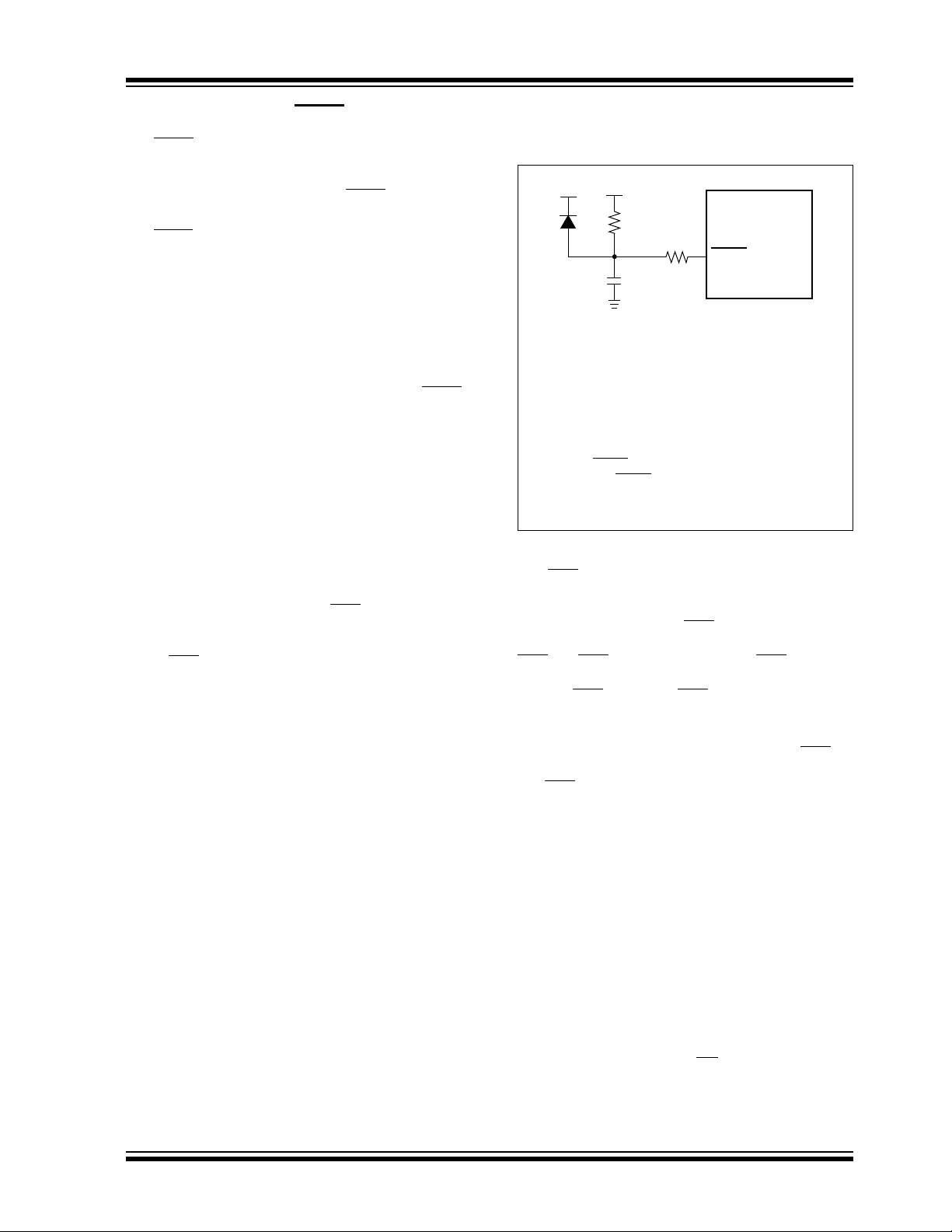
PIC18F97J60 FAMILY
4.2 Master Clear (MCLR)
The MCLR pin provides a method for triggering a hard
external Reset of the device. A Reset is generated by
holding the pin low. PIC18 extended microcontroller
devices have a noise filter in the MCLR
Reset path
which detects and ignores small pulses.
The MCLR
pin is not driven low by any internal Resets,
including the WDT.
4.3 Power-on Reset (POR)
A Power-on Reset condition is generated on-chip
whenever V
DD rises above a certain threshold. This
allows the device to start in the initialized state when
DD is adequate for operation.
V
To take advantage of the POR circuitry, tie the MCLR
pin through a resistor (1 kΩ to 10 kΩ) to VDD. This will
eliminate external RC components usually needed to
create a Power-on Reset delay. A minimum rise rate for
DD is specified (parameter D004). For a slow rise
V
time, see Figure 4-2.
When the device starts normal operation (i.e., exits the
Reset condition), device operating parameters
(voltage, frequency, temperature, etc.) must be met to
ensure operation. If these conditions are not met, the
device must be held in Reset until the operating
conditions are met.
POR events are captured by the POR
bit (RCON<1>).
The state of the bit is set to ‘0’ whenever a Power-on
Reset occurs; it does not change for any other Reset
event. POR
is not reset to ‘1’ by any hardware event.
To capture multiple events, the user manually resets
the bit to ‘1’ in software following any Power-on Reset.
4.4 Brown-out Reset (BOR)
The PIC18F97J60 family of devices incorporates a
simple BOR function when the internal regulator is
enabled (ENVREG pin is tied to V
below VBOR (parameter D005), for greater than time
T
BOR (parameter 35), will reset the device. A Reset
may or may not occur if V
BOR. The chip will remain in Brown-out Reset
than T
until V
DD rises above VBOR.
Once a BOR has occurred, the Power-up Timer will
keep the chip in Reset for T
DD drops below VBOR while the Power-up Timer is
V
running, the chip will go back into a Brown-out Reset
and the Power-up Timer will be initialized. Once V
rises above VBOR, the Power-up Timer will execute the
additional time delay.
DD). Any drop of VDD
DD falls below VBOR for less
PWRT (parameter 33). If
DD
FIGURE 4-2: EXTERNAL POWER-ON
RESET CIRCUIT (FOR
SLOW V
VDD
Note 1: External Power-on Reset circuit is required
VDD
(1)
D
2: R < 40 kΩ is recommended to make sure that
3: R1 ≥ 1 kΩ will limit any current flowing into
(2)
R
R1
C
only if the V
The diode D helps discharge the capacitor
quickly when V
the voltage drop across R does not violate
the device’s electrical specification.
MCLR
of MCLR
Electrostatic Discharge (ESD), or Electrical
Overstress (EOS).
DD power-up slope is too slow.
from external capacitor C in the event
/VPP pin breakdown, due to
DD POWER-UP)
(3)
MCLR
PIC18FXXJ6X
DD powers down.
4.4.1 DETECTING BOR
The BOR bit always resets to ‘0’ on any Brown-out
Reset or Power-on Reset event. This makes it difficult
to determine if a Brown-out Reset event has occurred
just by reading the state of BOR
alone. A more reliable
method is to simultaneously check the state of both
POR and BOR. This assumes that the POR bit is reset
to ‘1’ in software immediately after any Power-on Reset
event. If BOR
is ‘0’ while POR is ‘1’, it can be reliably
assumed that a Brown-out Reset event has occurred.
If the voltage regulator is disabled, Brown-out Reset
functionality is disabled. In this case, the BOR
bit
cannot be used to determine a Brown-out Reset event.
The BOR bit is still cleared by a Power-on Reset event.
4.5 Configuration Mismatch (CM)
The Configuration Mismatch (CM) Reset is designed to
detect and attempt to recover from random, memory
corrupting events. These include Electrostatic
Discharge (ESD) events which can cause widespread
single-bit changes throughout the device and result in
catastrophic failure.
In PIC18FXXJ Flash devices, the device Configuration
registers (located in the configuration memory space)
are continuously monitored during operation by comparing their values to complimentary shadow registers.
If a mismatch is detected between the two sets of
registers, a CM Reset automatically occurs. These
events are captured by the CM
state of the bit is set to ‘0’ whenever a CM event occurs;
it does not change for any other Reset event.
bit (RCON<5>). The
© 2008 Microchip Technology Inc. Preliminary DS39762D-page 57
Page 60

PIC18F97J60 FAMILY
A CM Reset behaves similarly to a Master Clear Reset,
RESET instruction, WDT time-out or Stack Event Reset.
As with all hard and power Reset events, the device
Configuration Words are reloaded from the Flash Configuration Words in program memory as the device
restarts.
4.6 Power-up Timer (PWRT)
PIC18F97J60 family of devices incorporates an
on-chip Power-up Timer (PWRT) to help regulate the
Power-on Reset process. The PWRT is always
enabled. The main function is to ensure that the device
voltage is stable before code is executed.
The Power-up Timer (PWRT) of the PIC18F97J60 family devices is an 11-bit counter which uses the INTRC
source as the clock input. This yields an approximate
time interval of 2048 x 32 μs = 66 ms. While the PWRT
is counting, the device is held in Reset.
The power-up time delay depends on the INTRC clock
and will vary from chip-to-chip due to temperature and
process variation. See DC parameter 33 for details.
4.6.1 TIME-OUT SEQUENCE
The PWRT time-out is invoked after the POR pulse has
cleared. The total time-out will vary based on the status
of the PWRT. Figure 4-3, Figure 4-4, Figure 4-5 and
Figure 4-6 all depict time-out sequences on power-up.
Since the time-outs occur from the POR pulse, if MCLR
is kept low long enough, the PWRT will expire. Bringing
high will begin execution immediately
MCLR
(Figure 4-5). This is useful for testing purposes or to
synchronize more than one PIC18FXXJ6X device
operating in parallel.
FIGURE 4-3: TIME-OUT SEQUENCE ON POWER-UP (MCLR TIED TO VDD, VDD RISE < TPWRT)
VDD
MCLR
INTERNAL POR
TPWRT
PWRT TIME-OUT
INTERNAL RESET
FIGURE 4-4: TIME-OUT SEQUENCE ON POWER-UP (MCLR
VDD
MCLR
INTERNAL POR
TPWRT
PWRT TIME-OUT
INTERNAL RESET
NOT TIED TO VDD): CASE 1
DS39762D-page 58 Preliminary © 2008 Microchip Technology Inc.
Page 61

PIC18F97J60 FAMILY
FIGURE 4-5: TIME-OUT SEQUENCE ON POWER-UP (MCLR NOT TIED TO VDD): CASE 2
VDD
MCLR
INTERNAL POR
TPWRT
PWRT TIME-OUT
INTERNAL RESET
FIGURE 4-6: SLOW RISE TIME (MCLR
VDD
MCLR
INTERNAL POR
PWRT TIME-OUT
INTERNAL RESET
0V
PWRT
T
TIED TO VDD, VDD RISE > TPWRT)
3.3V
1V
© 2008 Microchip Technology Inc. Preliminary DS39762D-page 59
Page 62
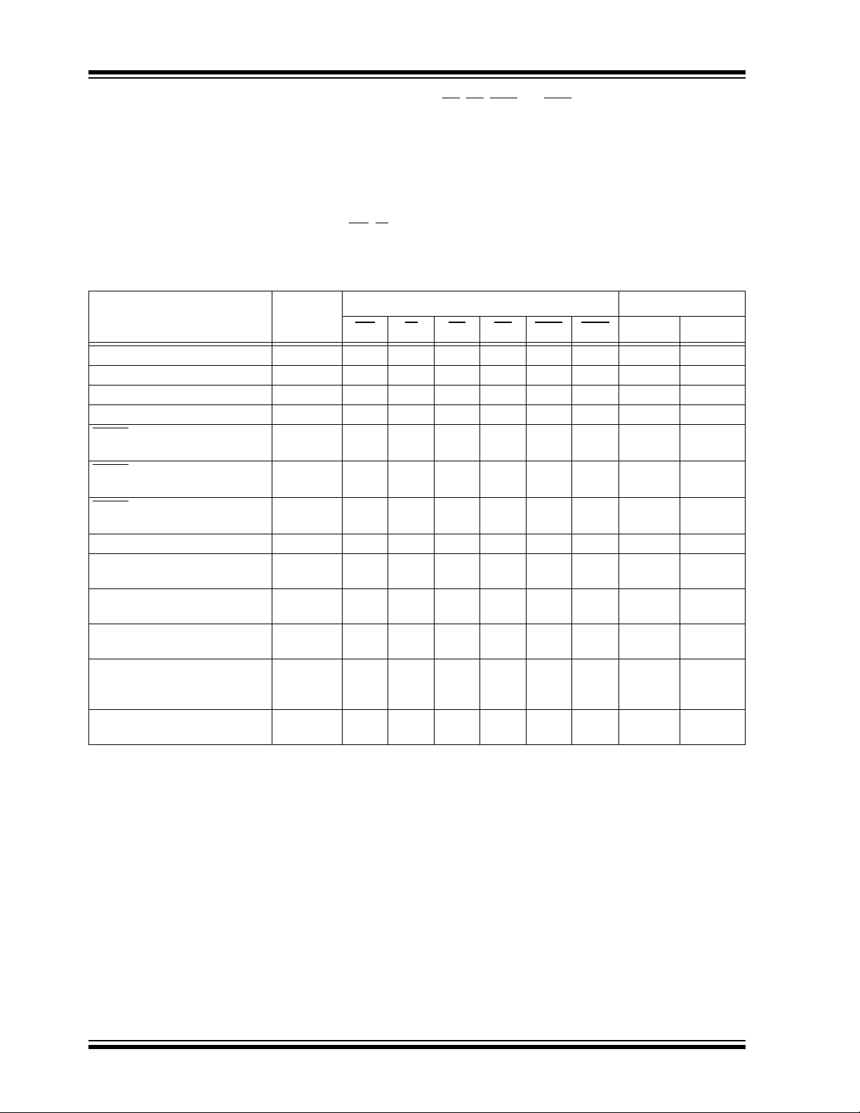
PIC18F97J60 FAMILY
, PD, POR and BOR) are set or cleared differently in
4.7 Reset State of Registers
Most registers are unaffected by a Reset. Their status
is unknown on POR and unchanged by all other
Resets. The other registers are forced to a “Reset
state” depending on the type of Reset that occurred.
Most registers are not affected by a WDT wake-up
since this is viewed as the resumption of normal
operation. Status bits from the RCON register (CM
TABLE 4-1: STATUS BITS, THEIR SIGNIFICANCE AND THE INITIALIZATION CONDITION FOR
RCON REGISTER
Condition
Power-on Reset 0000h 111100 0 0
RESET Instruction 0000h u0uuuu u u
Brown-out Reset 0000h 1111u0 u u
Configuration Mismatch Reset 0000h 0uuuuu u u
during power-managed
MCLR
Run modes
MCLR
during power-managed
Idle modes and Sleep mode
MCLR
during full-power
execution
Stack Full Reset (STVREN = 1) 0000h uuuuuu 1 u
Stack Underflow Reset
(STVREN = 1)
Stack Underflow Error (not an
actual Reset, STVREN = 0)
WDT time-out during full power
or power-managed Run modes
WDT time-out during
power-managed Idle or Sleep
modes
Interrupt exit from
power-managed modes
Legend: u = unchanged
Note 1: When the wake-up is due to an interrupt, and the GIEH or GIEL bit is set, the PC is loaded with the interrupt
vector (0008h or 0018h).
Program
Counter
(1)
0000h uu1uuu u u
0000h uu10uu u u
0000h uuuuuu u u
0000h uuuuuu u 1
0000h uuuuuu u 1
0000h uu0uuu u u
PC + 2 uu00uu u u
PC + 2 uuu0uu u u
, RI,
CM
TO
different Reset situations, as indicated in Table 4-1.
These bits are used in software to determine the nature
of the Reset.
Table 4-2 describes the Reset states for all of the
Special Function Registers. These are categorized by
Power-on and Brown-out Resets, Master Clear and
WDT Resets and WDT wake-ups.
RCON Register STKPTR Register
RI TO PD POR BOR STKFUL STKUNF
DS39762D-page 60 Preliminary © 2008 Microchip Technology Inc.
Page 63

PIC18F97J60 FAMILY
TABLE 4-2: INITIALIZATION CONDITIONS FOR ALL REGISTERS
MCLR
Reset,
Register Applicable Devices
TOSU PIC18F6XJ6X PIC18F8XJ6X PIC18F9XJ6X ---0 0000 ---0 0000 ---0 uuuu
TOSH PIC18F6XJ6X PIC18F8XJ6X PIC18F9XJ6X 0000 0000 0000 0000 uuuu uuuu
TOSL PIC18F6XJ6X PIC18F8XJ6X PIC18F9XJ6X 0000 0000 0000 0000 uuuu uuuu
STKPTR PIC18F6XJ6X PIC18F8XJ6X PIC18F9XJ6X 00-0 0000 uu-0 0000 uu-u uuuu
PCLATU PIC18F6XJ6X PIC18F8XJ6X PIC18F9XJ6X ---0 0000 ---0 0000 ---u uuuu
PCLATH PIC18F6XJ6X PIC18F8XJ6X PIC18F9XJ6X 0000 0000 0000 0000 uuuu uuuu
PCL PIC18F6XJ6X PIC18F8XJ6X PIC18F9XJ6X 0000 0000 0000 0000 PC + 2
TBLPTRU PIC18F6XJ6X PIC18F8XJ6X PIC18F9XJ6X --00 0000 --00 0000 --uu uuuu
TBLPTRH PIC18F6XJ6X PIC18F8XJ6X PIC18F9XJ6X 0000 0000 0000 0000 uuuu uuuu
TBLPTRL PIC18F6XJ6X PIC18F8XJ6X PIC18F9XJ6X 0000 0000 0000 0000 uuuu uuuu
TABLAT PIC18F6XJ6X PIC18F8XJ6X PIC18F9XJ6X 0000 0000 0000 0000 uuuu uuuu
PRODH PIC18F6XJ6X PIC18F8XJ6X PIC18F9XJ6X xxxx xxxx uuuu uuuu uuuu uuuu
PRODL PIC18F6XJ6X PIC18F8XJ6X PIC18F9XJ6X xxxx xxxx uuuu uuuu uuuu uuuu
INTCON PIC18F6XJ6X PIC18F8XJ6X PIC18F9XJ6X 0000 000x 0000 000u uuuu uuuu
INTCON2 PIC18F6XJ6X PIC18F8XJ6X PIC18F9XJ6X 1111 1111 1111 1111 uuuu uuuu
INTCON3 PIC18F6XJ6X PIC18F8XJ6X PIC18F9XJ6X 1100 0000 1100 0000 uuuu uuuu
INDF0 PIC18F6XJ6X PIC18F8XJ6X PIC18F9XJ6X N/A N/A N/A
POSTINC0 PIC18F6XJ6X PIC18F8XJ6X PIC18F9XJ6X N/A N/A N/A
POSTDEC0 PIC18F6XJ6X PIC18F8XJ6X PIC18F9XJ6X N/A N/A N/A
PREINC0 PIC18F6XJ6X PIC18F8XJ6X PIC18F9XJ6X N/A N/A N/A
PLUSW0 PIC18F6XJ6X PIC18F8XJ6X PIC18F9XJ6X N/A N/A N/A
FSR0H PIC18F6XJ6X PIC18F8XJ6X PIC18F9XJ6X ---- xxxx ---- uuuu ---- uuuu
FSR0L PIC18F6XJ6X PIC18F8XJ6X PIC18F9XJ6X xxxx xxxx uuuu uuuu uuuu uuuu
WREG PIC18F6XJ6X PIC18F8XJ6X PIC18F9XJ6X xxxx xxxx uuuu uuuu uuuu uuuu
INDF1 PIC18F6XJ6X PIC18F8XJ6X PIC18F9XJ6X N/A N/A N/A
POSTINC1 PIC18F6XJ6X PIC18F8XJ6X PIC18F9XJ6X N/A N/A N/A
POSTDEC1 PIC18F6XJ6X PIC18F8XJ6X PIC18F9XJ6X N/A N/A N/A
PREINC1 PIC18F6XJ6X PIC18F8XJ6X PIC18F9XJ6X N/A N/A N/A
PLUSW1 PIC18F6XJ6X PIC18F8XJ6X PIC18F9XJ6X N/A N/A N/A
FSR1H PIC18F6XJ6X PIC18F8XJ6X PIC18F9XJ6X ---- xxxx ---- uuuu ---- uuuu
FSR1L PIC18F6XJ6X PIC18F8XJ6X PIC18F9XJ6X xxxx xxxx uuuu uuuu uuuu uuuu
BSR PIC18F6XJ6X PIC18F8XJ6X PIC18F9XJ6X ---- 0000 ---- 0000 ---- uuuu
INDF2 PIC18F6XJ6X PIC18F8XJ6X PIC18F9XJ6X N/A N/A N/A
POSTINC2 PIC18F6XJ6X PIC18F8XJ6X PIC18F9XJ6X N/A N/A N/A
POSTDEC2 PIC18F6XJ6X PIC18F8XJ6X PIC18F9XJ6X N/A N/A N/A
PREINC2 PIC18F6XJ6X PIC18F8XJ6X PIC18F9XJ6X N/A N/A N/A
PLUSW2 PIC18F6XJ6X PIC18F8XJ6X PIC18F9XJ6X N/A N/A N/A
FSR2H PIC18F6XJ6X PIC18F8XJ6X PIC18F9XJ6X ---- xxxx ---- uuuu ---- uuuu
FSR2L PIC18F6XJ6X PIC18F8XJ6X PIC18F9XJ6X xxxx xxxx uuuu uuuu uuuu uuuu
Legend: u = unchanged, x = unknown, - = unimplemented bit, read as ‘0’, q = value depends on condition.
Shaded cells indicate conditions do not apply for the designated device.
Note 1: When the wake-up is due to an interrupt and the GIEL or GIEH bit is set, the TOSU, TOSH and TOSL are updated with
the current value of the PC. The STKPTR is modified to point to the next location in the hardware stack.
2: When the wake-up is due to an interrupt and the GIEL or GIEH bit is set, the PC is loaded with the interrupt vector
(0008h or 0018h).
3: One or more bits in the INTCONx or PIRx registers will be affected (to cause wake-up).
4: See Table 4-1 for Reset value for specific condition.
Power-on Reset,
Brown-out Reset
WDT Reset,
RESET Instruction,
Stack Resets,
CM
Reset
Wake-up via WDT
or Interrupt
(1)
(1)
(1)
(1)
(2)
(3)
(3)
(3)
© 2008 Microchip Technology Inc. Preliminary DS39762D-page 61
Page 64

PIC18F97J60 FAMILY
TABLE 4-2: INITIALIZATION CONDITIONS FOR ALL REGISTERS (CONTINUED)
Reset,
MCLR
Register Applicable Devices
STATUS PIC18F6XJ6X PIC18F8XJ6X PIC18F9XJ6X ---x xxxx ---u uuuu ---u uuuu
TMR0H PIC18F6XJ6X PIC18F8XJ6X PIC18F9XJ6X 0000 0000 0000 0000 uuuu uuuu
TMR0L PIC18F6XJ6X PIC18F8XJ6X PIC18F9XJ6X xxxx xxxx uuuu uuuu uuuu uuuu
T0CON PIC18F6XJ6X PIC18F8XJ6X PIC18F9XJ6X 1111 1111 1111 1111 uuuu uuuu
OSCCON PIC18F6XJ6X PIC18F8XJ6X PIC18F9XJ6X 0--- q-00 0--- q-00 u--- q-uu
ECON1 PIC18F6XJ6X PIC18F8XJ6X PIC18F9XJ6X 0000 00-- 0000 00-- uuuu uu--
WDTCON PIC18F6XJ6X PIC18F8XJ6X PIC18F9XJ6X ---- ---0 ---- ---0 ---- ---u
(4)
RCON
TMR1H PIC18F6XJ6X PIC18F8XJ6X PIC18F9XJ6X xxxx xxxx uuuu uuuu uuuu uuuu
TMR1L PIC18F6XJ6X PIC18F8XJ6X PIC18F9XJ6X xxxx xxxx uuuu uuuu uuuu uuuu
T1CON PIC18F6XJ6X PIC18F8XJ6X PIC18F9XJ6X 0000 0000 u0uu uuuu uuuu uuuu
TMR2 PIC18F6XJ6X PIC18F8XJ6X PIC18F9XJ6X 0000 0000 0000 0000 uuuu uuuu
PR2 PIC18F6XJ6X PIC18F8XJ6X PIC18F9XJ6X 1111 1111 1111 1111 1111 1111
T2CON PIC18F6XJ6X PIC18F8XJ6X PIC18F9XJ6X -000 0000 -000 0000 -uuu uuuu
SSP1BUF PIC18F6XJ6X PIC18F8XJ6X PIC18F9XJ6X xxxx xxxx uuuu uuuu uuuu uuuu
SSP1ADD PIC18F6XJ6X PIC18F8XJ6X PIC18F9XJ6X 0000 0000 0000 0000 uuuu uuuu
SSP1STAT PIC18F6XJ6X PIC18F8XJ6X PIC18F9XJ6X 0000 0000 0000 0000 uuuu uuuu
SSP1CON1 PIC18F6XJ6X PIC18F8XJ6X PIC18F9XJ6X 0000 0000 0000 0000 uuuu uuuu
SSP1CON2 PIC18F6XJ6X PIC18F8XJ6X PIC18F9XJ6X 0000 0000 0000 0000 uuuu uuuu
ADRESH PIC18F6XJ6X PIC18F8XJ6X PIC18F9XJ6X xxxx xxxx uuuu uuuu uuuu uuuu
ADRESL PIC18F6XJ6X PIC18F8XJ6X PIC18F9XJ6X xxxx xxxx uuuu uuuu uuuu uuuu
ADCON0 PIC18F6XJ6X PIC18F8XJ6X PIC18F9XJ6X 0-00 0000 0-00 0000 u-uu uuuu
ADCON1 PIC18F6XJ6X PIC18F8XJ6X PIC18F9XJ6X --00 0000 --00 0000 --uu uuuu
ADCON2 PIC18F6XJ6X PIC18F8XJ6X PIC18F9XJ6X 0-00 0000 0-00 0000 u-uu uuuu
CCPR1H PIC18F6XJ6X PIC18F8XJ6X PIC18F9XJ6X xxxx xxxx uuuu uuuu uuuu uuuu
CCPR1L PIC18F6XJ6X PIC18F8XJ6X PIC18F9XJ6X xxxx xxxx uuuu uuuu uuuu uuuu
CCP1CON PIC18F6XJ6X PIC18F8XJ6X PIC18F9XJ6X 0000 0000 0000 0000 uuuu uuuu
CCPR2H PIC18F6XJ6X PIC18F8XJ6X PIC18F9XJ6X xxxx xxxx uuuu uuuu uuuu uuuu
CCPR2L PIC18F6XJ6X PIC18F8XJ6X PIC18F9XJ6X xxxx xxxx uuuu uuuu uuuu uuuu
CCP2CON PIC18F6XJ6X PIC18F8XJ6X PIC18F9XJ6X 0000 0000 0000 0000 uuuu uuuu
CCPR3H PIC18F6XJ6X PIC18F8XJ6X PIC18F9XJ6X xxxx xxxx uuuu uuuu uuuu uuuu
CCPR3L PIC18F6XJ6X PIC18F8XJ6X PIC18F9XJ6X xxxx xxxx uuuu uuuu uuuu uuuu
CCP3CON PIC18F6XJ6X PIC18F8XJ6X PIC18F9XJ6X 0000 0000 0000 0000 uuuu uuuu
ECCP1AS PIC18F6XJ6X PIC18F8XJ6X PIC18F9XJ6X 0000 0000 0000 0000 uuuu uuuu
CVRCON PIC18F6XJ6X PIC18F8XJ6X PIC18F9XJ6X 0000 0000 0000 0000 uuuu uuuu
CMCON PIC18F6XJ6X PIC18F8XJ6X PIC18F9XJ6X 0000 0111 0000 0111 uuuu uuuu
TMR3H PIC18F6XJ6X PIC18F8XJ6X PIC18F9XJ6X xxxx xxxx uuuu uuuu uuuu uuuu
TMR3L PIC18F6XJ6X PIC18F8XJ6X PIC18F9XJ6X xxxx xxxx uuuu uuuu uuuu uuuu
Legend: u = unchanged, x = unknown, - = unimplemented bit, read as ‘0’, q = value depends on condition.
Note 1: When the wake-up is due to an interrupt and the GIEL or GIEH bit is set, the TOSU, TOSH and TOSL are updated with
2: When the wake-up is due to an interrupt and the GIEL or GIEH bit is set, the PC is loaded with the interrupt vector
3: One or more bits in the INTCONx or PIRx registers will be affected (to cause wake-up).
4: See Table 4-1 for Reset value for specific condition.
PIC18F6XJ6X PIC18F8XJ6X PIC18F9XJ6X 0-q1 1100 0-uq qquu u-uu qquu
Shaded cells indicate conditions do not apply for the designated device.
the current value of the PC. The STKPTR is modified to point to the next location in the hardware stack.
(0008h or 0018h).
Power-on Reset,
Brown-out Reset
WDT Reset,
RESET Instruction,
Stack Resets,
Reset
CM
Wake-up via WDT
or Interrupt
DS39762D-page 62 Preliminary © 2008 Microchip Technology Inc.
Page 65

PIC18F97J60 FAMILY
TABLE 4-2: INITIALIZATION CONDITIONS FOR ALL REGISTERS (CONTINUED)
Reset,
MCLR
Register Applicable Devices
T3CON PIC18F6XJ6X PIC18F8XJ6X PIC18F9XJ6X 0000 0000 uuuu uuuu uuuu uuuu
PSPCON PIC18F6XJ6X PIC18F8XJ6X PIC18F9XJ6X 0000 ---- 0000 ---- uuuu ----
SPBRG1 PIC18F6XJ6X PIC18F8XJ6X PIC18F9XJ6X 0000 0000 0000 0000 uuuu uuuu
RCREG1 PIC18F6XJ6X PIC18F8XJ6X PIC18F9XJ6X 0000 0000 0000 0000 uuuu uuuu
TXREG1 PIC18F6XJ6X PIC18F8XJ6X PIC18F9XJ6X xxxx xxxx uuuu uuuu uuuu uuuu
TXSTA1 PIC18F6XJ6X PIC18F8XJ6X PIC18F9XJ6X 0000 0010 0000 0010 uuuu uuuu
RCSTA1 PIC18F6XJ6X PIC18F8XJ6X PIC18F9XJ6X 0000 000x 0000 000x uuuu uuuu
EECON2 PIC18F6XJ6X PIC18F8XJ6X PIC18F9XJ6X ---- ---- ---- ---- ---- ----
EECON1 PIC18F6XJ6X PIC18F8XJ6X PIC18F9XJ6X ---0 x00- ---0 x00- ---u uuu-
IPR3 PIC18F6XJ6X PIC18F8XJ6X PIC18F9XJ6X 1111 1111 1111 1111 uuuu uuuu
PIR3 PIC18F6XJ6X PIC18F8XJ6X PIC18F9XJ6X 0000 0000 0000 0000 uuuu uuuu
PIE3 PIC18F6XJ6X PIC18F8XJ6X PIC18F9XJ6X 0000 0000 0000 0000 uuuu uuuu
IPR2 PIC18F6XJ6X PIC18F8XJ6X PIC18F9XJ6X 1111 1-11 1111 1-11 uuuu u-uu
PIR2 PIC18F6XJ6X PIC18F8XJ6X PIC18F9XJ6X 0000 0-00 0000 0-00 uuuu u-uu
PIE2 PIC18F6XJ6X PIC18F8XJ6X PIC18F9XJ6X 0000 0-00 0000 0-00 uuuu u-uu
IPR1 PIC18F6XJ6X PIC18F8XJ6X PIC18F9XJ6X 1111 1111 1111 1111 uuuu uuuu
PIR1 PIC18F6XJ6X PIC18F8XJ6X PIC18F9XJ6X 0000 0000 0000 0000 uuuu uuuu
PIE1 PIC18F6XJ6X PIC18F8XJ6X PIC18F9XJ6X 0000 0000 0000 0000 uuuu uuuu
MEMCON
OSCTUNE PIC18F6XJ6X PIC18F8XJ6X PIC18F9XJ6X 0000 ---- 0000 ---- uuuu ----
TRISJ
TRISH
TRISG PIC18F6XJ6X
TRISF PIC18F6XJ6X PIC18F8XJ6X
TRISE PIC18F6XJ6X
TRISD PIC18F6XJ6X PIC18F8XJ6X
TRISC PIC18F6XJ6X PIC18F8XJ6X PIC18F9XJ6X 1111 1111 1111 1111 uuuu uuuu
TRISB PIC18F6XJ6X PIC18F8XJ6X PIC18F9XJ6X 1111 1111 1111 1111 uuuu uuuu
TRISA PIC18F6XJ6X PIC18F8XJ6X PIC18F9XJ6X --11 1111 --11 1111 --uu uuuu
LATJ
LATH
Legend: u = unchanged, x = unknown, - = unimplemented bit, read as ‘0’, q = value depends on condition.
Note 1: When the wake-up is due to an interrupt and the GIEL or GIEH bit is set, the TOSU, TOSH and TOSL are updated with
2: When the wake-up is due to an interrupt and the GIEL or GIEH bit is set, the PC is loaded with the interrupt vector
3: One or more bits in the INTCONx or PIRx registers will be affected (to cause wake-up).
4: See Table 4-1 for Reset value for specific condition.
PIC18F6XJ6X PIC18F8XJ6X PIC18F9XJ6X 0-00 --00 0-00 --00 u-uu --uu
PIC18F6XJ6X PIC18F8XJ6X PIC18F9XJ6X --11 ---- --11 ---- --uu ----
PIC18F6XJ6X PIC18F8XJ6X PIC18F9XJ6X 1111 1111 1111 1111 uuuu uuuu
PIC18F6XJ6X PIC18F8XJ6X PIC18F9XJ6X 1111 1111 1111 1111 uuuu uuuu
PIC18F8XJ6X PIC18F9XJ6X ---1 ---- ---1 ---- ---u ----
PIC18F6XJ6X PIC18F8XJ6X PIC18F9XJ6X ---1 1111 ---1 1111 ---u uuuu
PIC18F6XJ6X PIC18F8XJ6X PIC18F9XJ6X 1111 1111 1111 1111 uuuu uuuu
PIC18F9XJ6X 1111 111- 1111 111- uuuu uuu-
PIC18F6XJ6X PIC18F8XJ6X PIC18F9XJ6X 1111 1111 1111 1111 uuuu uuuu
PIC18F8XJ6X PIC18F9XJ6X --11 1111 --11 1111 --uu uuuu
PIC18F6XJ6X PIC18F8XJ6X PIC18F9XJ6X 1111 1111 1111 1111 uuuu uuuu
PIC18F9XJ6X ---- -111 ---- -111 ---- -uuu
PIC18F6XJ6X PIC18F8XJ6X PIC18F9XJ6X 1111 1111 1111 1111 uuuu uuuu
PIC18F6XJ6X PIC18F8XJ6X PIC18F9XJ6X --xx ---- --uu ---- --uu ----
PIC18F6XJ6X PIC18F8XJ6X PIC18F9XJ6X xxxx xxxx uuuu uuuu uuuu uuuu
PIC18F6XJ6X PIC18F8XJ6X PIC18F9XJ6X xxxx xxxx uuuu uuuu uuuu uuuu
Shaded cells indicate conditions do not apply for the designated device.
the current value of the PC. The STKPTR is modified to point to the next location in the hardware stack.
(0008h or 0018h).
Power-on Reset,
Brown-out Reset
WDT Reset,
RESET Instruction,
Stack Resets,
Reset
CM
Wake-up via WDT
or Interrupt
(3)
(3)
(3)
© 2008 Microchip Technology Inc. Preliminary DS39762D-page 63
Page 66
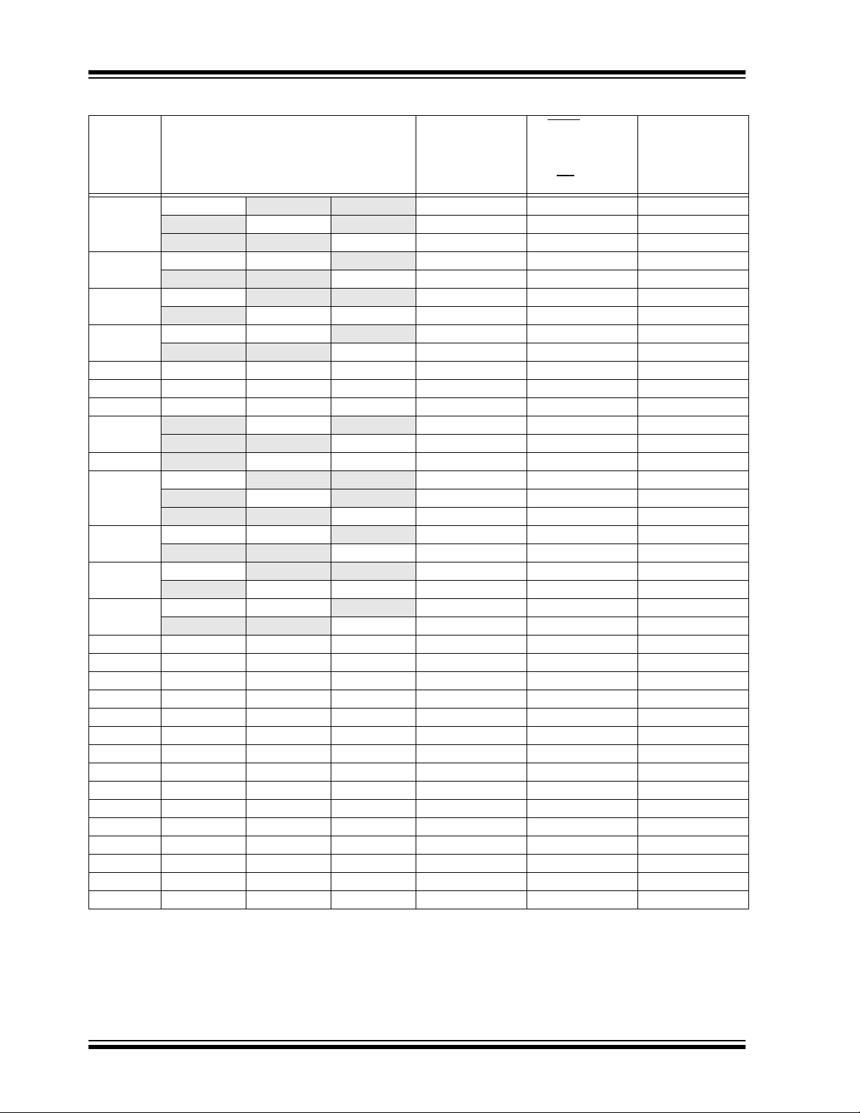
PIC18F97J60 FAMILY
TABLE 4-2: INITIALIZATION CONDITIONS FOR ALL REGISTERS (CONTINUED)
Reset,
MCLR
Register Applicable Devices
LATG PIC18F6XJ6X
PIC18F6XJ6X PIC18F8XJ6X PIC18F9XJ6X ---x xxxx ---u uuuu ---u uuuu
PIC18F6XJ6X PIC18F8XJ6X PIC18F9XJ6X xxxx xxxx uuuu uuuu uuuu uuuu
LATF PIC18F6XJ6X PIC18F8XJ6X
PIC18F6XJ6X PIC18F8XJ6X PIC18F9XJ6X xxxx xxxx uuuu uuuu uuuu uuuu
LATE PIC18F6XJ6X
PIC18F6XJ6X PIC18F8XJ6X PIC18F9XJ6X xxxx xxxx uuuu uuuu uuuu uuuu
LATD PIC18F6XJ6X PIC18F8XJ6X
PIC18F6XJ6X PIC18F8XJ6X PIC18F9XJ6X xxxx xxxx uuuu uuuu uuuu uuuu
LATC PIC18F6XJ6X PIC18F8XJ6X PIC18F9XJ6X xxxx xxxx uuuu uuuu uuuu uuuu
LATB PIC18F6XJ6X PIC18F8XJ6X PIC18F9XJ6X xxxx xxxx uuuu uuuu uuuu uuuu
LATA PIC18F6XJ6X PIC18F8XJ6X PIC18F9XJ6X 00xx xxxx 00uu uuuu uuuu uuuu
PORTJ
PORTH
PORTG PIC18F6XJ6X
PORTF PIC18F6XJ6X PIC18F8XJ6X
PORTE PIC18F6XJ6X
PORTD PIC18F6XJ6X PIC18F8XJ6X
PORTC PIC18F6XJ6X PIC18F8XJ6X PIC18F9XJ6X xxxx xxxx uuuu uuuu uuuu uuuu
PORTB PIC18F6XJ6X PIC18F8XJ6X PIC18F9XJ6X xxxx xxxx uuuu uuuu uuuu uuuu
PORTA PIC18F6XJ6X PIC18F8XJ6X PIC18F9XJ6X 0-0x 0000 0-0u 0000 u-uu uuuu
SPBRGH1 PIC18F6XJ6X PIC18F8XJ6X PIC18F9XJ6X 0000 0000 0000 0000 uuuu uuuu
BAUDCON1 PIC18F6XJ6X PIC18F8XJ6X PIC18F9XJ6X 0100 0-00 0100 0-00 uuuu u-uu
SPBRGH2 PIC18F6XJ6X PIC18F8XJ6X PIC18F9XJ6X 0000 0000 0000 0000 uuuu uuuu
BAUDCON2 PIC18F6XJ6X PIC18F8XJ6X PIC18F9XJ6X 0100 0-00 0100 0-00 uuuu u-uu
ERDPTH PIC18F6XJ6X PIC18F8XJ6X PIC18F9XJ6X ---0 1010 ---0 1010 ---u uuuu
ERDPTL PIC18F6XJ6X PIC18F8XJ6X PIC18F9XJ6X 1111 0101 1111 0101 uuuu uuuu
ECCP1DEL PIC18F6XJ6X PIC18F8XJ6X PIC18F9XJ6X 0000 0000 0000 0000 uuuu uuuu
TMR4 PIC18F6XJ6X PIC18F8XJ6X PIC18F9XJ6X 0000 0000 0000 0000 uuuu uuuu
PR4 PIC18F6XJ6X PIC18F8XJ6X PIC18F9XJ6X 1111 1111 1111 1111 1111 1111
T4CON PIC18F6XJ6X PIC18F8XJ6X PIC18F9XJ6X -000 0000 -000 0000 -uuu uuuu
CCPR4H PIC18F6XJ6X PIC18F8XJ6X PIC18F9XJ6X xxxx xxxx uuuu uuuu uuuu uuuu
CCPR4L PIC18F6XJ6X PIC18F8XJ6X PIC18F9XJ6X xxxx xxxx uuuu uuuu uuuu uuuu
Legend: u = unchanged, x = unknown, - = unimplemented bit, read as ‘0’, q = value depends on condition.
Note 1: When the wake-up is due to an interrupt and the GIEL or GIEH bit is set, the TOSU, TOSH and TOSL are updated with
2: When the wake-up is due to an interrupt and the GIEL or GIEH bit is set, the PC is loaded with the interrupt vector
3: One or more bits in the INTCONx or PIRx registers will be affected (to cause wake-up).
4: See Table 4-1 for Reset value for specific condition.
PIC18F6XJ6X PIC18F8XJ6X PIC18F9XJ6X --xx ---- --uu ---- --uu ----
PIC18F6XJ6X PIC18F8XJ6X PIC18F9XJ6X xxxx xxxx uuuu uuuu uuuu uuuu
PIC18F6XJ6X PIC18F8XJ6X PIC18F9XJ6X xxxx xxxx uuuu uuuu uuuu uuuu
PIC18F6XJ6X PIC18F8XJ6X PIC18F9XJ6X ---x xxxx ---u uuuu ---u uuuu
PIC18F6XJ6X PIC18F8XJ6X PIC18F9XJ6X 111x xxxx 111u uuuu uuuu uuuu
PIC18F6XJ6X PIC18F8XJ6X PIC18F9XJ6X x000 000- x000 000- uuuu uuu-
PIC18F6XJ6X PIC18F8XJ6X PIC18F9XJ6X xxxx xxxx uuuu uuuu uuuu uuuu
PIC18F6XJ6X PIC18F8XJ6X PIC18F9XJ6X xxxx xxxx uuuu uuuu uuuu uuuu
Shaded cells indicate conditions do not apply for the designated device.
the current value of the PC. The STKPTR is modified to point to the next location in the hardware stack.
(0008h or 0018h).
PIC18F8XJ6X PIC18F9XJ6X ---x ---- ---u ---- ---u ----
PIC18F9XJ6X xxxx xxx- uuuu uuu- uuuu uuu-
PIC18F8XJ6X PIC18F9XJ6X --xx xxxx --uu uuuu --uu uuuu
PIC18F9XJ6X ---- -xxx ---- -uuu ---- -uuu
PIC18F8XJ6X PIC18F9XJ6X ---x ---- ---u ---- ---u ----
PIC18F9XJ6X x000 000- x000 000- uuuu uuu-
PIC18F8XJ6X PIC18F9XJ6X --xx xxxx --uu uuuu --uu uuuu
PIC18F9XJ6X ---- -xxx ---- -uuu ---- -uuu
Power-on Reset,
Brown-out Reset
WDT Reset,
RESET Instruction,
Stack Resets,
Reset
CM
Wake-up via WDT
or Interrupt
DS39762D-page 64 Preliminary © 2008 Microchip Technology Inc.
Page 67

PIC18F97J60 FAMILY
TABLE 4-2: INITIALIZATION CONDITIONS FOR ALL REGISTERS (CONTINUED)
Reset,
MCLR
Register Applicable Devices
CCP4CON PIC18F6XJ6X PIC18F8XJ6X PIC18F9XJ6X --00 0000 --00 0000 --uu uuuu
CCPR5H PIC18F6XJ6X PIC18F8XJ6X PIC18F9XJ6X xxxx xxxx uuuu uuuu uuuu uuuu
CCPR5L PIC18F6XJ6X PIC18F8XJ6X PIC18F9XJ6X xxxx xxxx uuuu uuuu uuuu uuuu
CCP5CON PIC18F6XJ6X PIC18F8XJ6X PIC18F9XJ6X --00 0000 --00 0000 --uu uuuu
SPBRG2 PIC18F6XJ6X PIC18F8XJ6X PIC18F9XJ6X 0000 0000 0000 0000 uuuu uuuu
RCREG2 PIC18F6XJ6X PIC18F8XJ6X PIC18F9XJ6X 0000 0000 0000 0000 uuuu uuuu
TXREG2 PIC18F6XJ6X PIC18F8XJ6X PIC18F9XJ6X 0000 0000 0000 0000 uuuu uuuu
TXSTA2 PIC18F6XJ6X PIC18F8XJ6X PIC18F9XJ6X 0000 0010 0000 0010 uuuu uuuu
RCSTA2 PIC18F6XJ6X PIC18F8XJ6X PIC18F9XJ6X 0000 000x 0000 000x uuuu uuuu
ECCP3AS PIC18F6XJ6X PIC18F8XJ6X PIC18F9XJ6X 0000 0000 0000 0000 uuuu uuuu
ECCP3DEL PIC18F6XJ6X PIC18F8XJ6X PIC18F9XJ6X 0000 0000 0000 0000 uuuu uuuu
ECCP2AS PIC18F6XJ6X PIC18F8XJ6X PIC18F9XJ6X 0000 0000 0000 0000 uuuu uuuu
ECCP2DEL PIC18F6XJ6X PIC18F8XJ6X PIC18F9XJ6X 0000 0000 0000 0000 uuuu uuuu
SSP2BUF PIC18F6XJ6X PIC18F8XJ6X PIC18F9XJ6X xxxx xxxx uuuu uuuu uuuu uuuu
SSP2ADD PIC18F6XJ6X PIC18F8XJ6X PIC18F9XJ6X 0000 0000 0000 0000 uuuu uuuu
SSP2STAT PIC18F6XJ6X PIC18F8XJ6X PIC18F9XJ6X 0000 0000 0000 0000 uuuu uuuu
SSP2CON1 PIC18F6XJ6X PIC18F8XJ6X PIC18F9XJ6X 0000 0000 0000 0000 uuuu uuuu
SSP2CON2 PIC18F6XJ6X PIC18F8XJ6X PIC18F9XJ6X 0000 0000 0000 0000 uuuu uuuu
EDATA PIC18F6XJ6X PIC18F8XJ6X PIC18F9XJ6X xxxx xxxx uuuu uuuu uuuu uuuu
EIR PIC18F6XJ6X PIC18F8XJ6X PIC18F9XJ6X -000 0-00 -000 0-00 -uuu u-uu
ECON2 PIC18F6XJ6X PIC18F8XJ6X PIC18F9XJ6X 100- ---- 100- ---- uuu- ----
ESTAT PIC18F6XJ6X PIC18F8XJ6X PIC18F9XJ6X -0-0 -000 -0-0 -000 -u-u -uuu
EIE PIC18F6XJ6X PIC18F8XJ6X PIC18F9XJ6X -000 0-00 -000 0-00 -uuu u-uu
EDMACSH PIC18F6XJ6X PIC18F8XJ6X PIC18F9XJ6X 0000 0000 0000 0000 uuuu uuuu
EDMACSL PIC18F6XJ6X PIC18F8XJ6X PIC18F9XJ6X 0000 0000 0000 0000 uuuu uuuu
EDMADSTH PIC18F6XJ6X PIC18F8XJ6X PIC18F9XJ6X ---0 0000 ---0 0000 ---u uuuu
EDMADSTL PIC18F6XJ6X PIC18F8XJ6X PIC18F9XJ6X 0000 0000 0000 0000 uuuu uuuu
EDMANDH PIC18F6XJ6X PIC18F8XJ6X PIC18F9XJ6X ---0 0000 ---0 0000 ---u uuuu
EDMANDL PIC18F6XJ6X PIC18F8XJ6X PIC18F9XJ6X 0000 0000 0000 0000 uuuu uuuu
EDMASTH PIC18F6XJ6X PIC18F8XJ6X PIC18F9XJ6X ---0 0000 ---0 0000 ---u uuuu
EDMASTL PIC18F6XJ6X PIC18F8XJ6X PIC18F9XJ6X 0000 0000 0000 0000 uuuu uuuu
ERXWRPTH
ERXWRPTL PIC18F6XJ6X PIC18F8XJ6X PIC18F9XJ6X 0000 0000 0000 0000 uuuu uuuu
ERXRDPTH PIC18F6XJ6X PIC18F8XJ6X PIC18F9XJ6X ---0 0101 ---0 0101 ---u uuuu
ERXRDPTL PIC18F6XJ6X PIC18F8XJ6X PIC18F9XJ6X 1111 1010 1111 1010 uuuu uuuu
ERXNDH PIC18F6XJ6X PIC18F8XJ6X PIC18F9XJ6X ---1 1111 ---1 1111 ---u uuuu
ERXNDL PIC18F6XJ6X PIC18F8XJ6X PIC18F9XJ6X 1111 1111 1111 1111 uuuu uuuu
ERXSTH PIC18F6XJ6X PIC18F8XJ6X PIC18F9XJ6X ---0 0101 ---0 0101 ---u uuuu
ERXSTL PIC18F6XJ6X PIC18F8XJ6X PIC18F9XJ6X 1111 1010 1111 1010 uuuu uuuu
Legend: u = unchanged, x = unknown, - = unimplemented bit, read as ‘0’, q = value depends on condition.
Note 1: When the wake-up is due to an interrupt and the GIEL or GIEH bit is set, the TOSU, TOSH and TOSL are updated with
2: When the wake-up is due to an interrupt and the GIEL or GIEH bit is set, the PC is loaded with the interrupt vector
3: One or more bits in the INTCONx or PIRx registers will be affected (to cause wake-up).
4: See Table 4-1 for Reset value for specific condition.
PIC18F6XJ6X PIC18F8XJ6X PIC18F9XJ6X ---0 0000 ---0 0000 ---u uuuu
Shaded cells indicate conditions do not apply for the designated device.
the current value of the PC. The STKPTR is modified to point to the next location in the hardware stack.
(0008h or 0018h).
Power-on Reset,
Brown-out Reset
WDT Reset,
RESET Instruction,
Stack Resets,
Reset
CM
Wake-up via WDT
or Interrupt
© 2008 Microchip Technology Inc. Preliminary DS39762D-page 65
Page 68

PIC18F97J60 FAMILY
TABLE 4-2: INITIALIZATION CONDITIONS FOR ALL REGISTERS (CONTINUED)
Reset,
MCLR
Register Applicable Devices
ETXNDH PIC18F6XJ6X PIC18F8XJ6X PIC18F9XJ6X ---0 0000 ---0 0000 ---u uuuu
ETXNDL PIC18F6XJ6X PIC18F8XJ6X PIC18F9XJ6X 0000 0000 0000 0000 uuuu uuuu
ETXSTH PIC18F6XJ6X PIC18F8XJ6X PIC18F9XJ6X ---0 0000 ---0 0000 ---u uuuu
ETXSTL PIC18F6XJ6X PIC18F8XJ6X PIC18F9XJ6X 0000 0000 0000 0000 uuuu uuuu
EWRPTH PIC18F6XJ6X PIC18F8XJ6X PIC18F9XJ6X ---0 0000 ---0 0000 ---u uuuu
EWRPTL PIC18F6XJ6X PIC18F8XJ6X PIC18F9XJ6X 0000 0000 0000 0000 uuuu uuuu
EPKTCNT PIC18F6XJ6X PIC18F8XJ6X PIC18F9XJ6X 0000 0000 0000 0000 uuuu uuuu
ERXFCON PIC18F6XJ6X PIC18F8XJ6X PIC18F9XJ6X 1010 0001 1010 0001 uuuu uuuu
EPMOH PIC18F6XJ6X PIC18F8XJ6X PIC18F9XJ6X ---0 0000 ---0 0000 ---u uuuu
EPMOL PIC18F6XJ6X PIC18F8XJ6X PIC18F9XJ6X 0000 0000 0000 0000 uuuu uuuu
EPMCSH PIC18F6XJ6X PIC18F8XJ6X PIC18F9XJ6X 0000 0000 0000 0000 uuuu uuuu
EPMCSL PIC18F6XJ6X PIC18F8XJ6X PIC18F9XJ6X 0000 0000 0000 0000 uuuu uuuu
EPMM7 PIC18F6XJ6X PIC18F8XJ6X PIC18F9XJ6X 0000 0000 0000 0000 uuuu uuuu
EPMM6 PIC18F6XJ6X PIC18F8XJ6X PIC18F9XJ6X 0000 0000 0000 0000 uuuu uuuu
EPMM5 PIC18F6XJ6X PIC18F8XJ6X PIC18F9XJ6X 0000 0000 0000 0000 uuuu uuuu
EPMM4 PIC18F6XJ6X PIC18F8XJ6X PIC18F9XJ6X 0000 0000 0000 0000 uuuu uuuu
EPMM3 PIC18F6XJ6X PIC18F8XJ6X PIC18F9XJ6X 0000 0000 0000 0000 uuuu uuuu
EPMM2 PIC18F6XJ6X PIC18F8XJ6X PIC18F9XJ6X 0000 0000 0000 0000 uuuu uuuu
EPMM1 PIC18F6XJ6X PIC18F8XJ6X PIC18F9XJ6X 0000 0000 0000 0000 uuuu uuuu
EPMM0 PIC18F6XJ6X PIC18F8XJ6X PIC18F9XJ6X 0000 0000 0000 0000 uuuu uuuu
EHT7 PIC18F6XJ6X PIC18F8XJ6X PIC18F9XJ6X 0000 0000 0000 0000 uuuu uuuu
EHT6 PIC18F6XJ6X PIC18F8XJ6X PIC18F9XJ6X 0000 0000 0000 0000 uuuu uuuu
EHT5 PIC18F6XJ6X PIC18F8XJ6X PIC18F9XJ6X 0000 0000 0000 0000 uuuu uuuu
EHT4 PIC18F6XJ6X PIC18F8XJ6X PIC18F9XJ6X 0000 0000 0000 0000 uuuu uuuu
EHT3 PIC18F6XJ6X PIC18F8XJ6X PIC18F9XJ6X 0000 0000 0000 0000 uuuu uuuu
EHT2 PIC18F6XJ6X PIC18F8XJ6X PIC18F9XJ6X 0000 0000 0000 0000 uuuu uuuu
EHT1 PIC18F6XJ6X PIC18F8XJ6X PIC18F9XJ6X 0000 0000 0000 0000 uuuu uuuu
EHT0 PIC18F6XJ6X PIC18F8XJ6X PIC18F9XJ6X 0000 0000 0000 0000 uuuu uuuu
MIRDH PIC18F6XJ6X PIC18F8XJ6X PIC18F9XJ6X 0000 0000 0000 0000 uuuu uuuu
MIRDL PIC18F6XJ6X PIC18F8XJ6X PIC18F9XJ6X 0000 0000 0000 0000 uuuu uuuu
MIWRH PIC18F6XJ6X PIC18F8XJ6X PIC18F9XJ6X 0000 0000 0000 0000 uuuu uuuu
MIWRL PIC18F6XJ6X PIC18F8XJ6X PIC18F9XJ6X 0000 0000 0000 0000 uuuu uuuu
MIREGADR PIC18F6XJ6X PIC18F8XJ6X PIC18F9XJ6X ---0 0000 ---0 0000 ---u uuuu
MICMD PIC18F6XJ6X PIC18F8XJ6X PIC18F9XJ6X ---- --00 ---- --00 ---- --uu
MAMXFLH PIC18F6XJ6X PIC18F8XJ6X PIC18F9XJ6X 0000 0110 0000 0110 uuuu uuuu
MAMXFLL PIC18F6XJ6X PIC18F8XJ6X PIC18F9XJ6X 0000 0000 0000 0000 uuuu uuuu
Legend: u = unchanged, x = unknown, - = unimplemented bit, read as ‘0’, q = value depends on condition.
Shaded cells indicate conditions do not apply for the designated device.
Note 1: When the wake-up is due to an interrupt and the GIEL or GIEH bit is set, the TOSU, TOSH and TOSL are updated with
the current value of the PC. The STKPTR is modified to point to the next location in the hardware stack.
2: When the wake-up is due to an interrupt and the GIEL or GIEH bit is set, the PC is loaded with the interrupt vector
(0008h or 0018h).
3: One or more bits in the INTCONx or PIRx registers will be affected (to cause wake-up).
4: See Table 4-1 for Reset value for specific condition.
Power-on Reset,
Brown-out Reset
WDT Reset,
RESET Instruction,
Stack Resets,
Reset
CM
Wake-up via WDT
or Interrupt
DS39762D-page 66 Preliminary © 2008 Microchip Technology Inc.
Page 69

PIC18F97J60 FAMILY
TABLE 4-2: INITIALIZATION CONDITIONS FOR ALL REGISTERS (CONTINUED)
Reset,
MCLR
Register Applicable Devices
MAIPGH PIC18F6XJ6X PIC18F8XJ6X PIC18F9XJ6X -000 0000 -000 0000 -uuu uuuu
MAIPGL PIC18F6XJ6X PIC18F8XJ6X PIC18F9XJ6X -000 0000 -000 0000 -uuu uuuu
MABBIPG PIC18F6XJ6X PIC18F8XJ6X PIC18F9XJ6X -000 0000 -000 0000 -uuu uuuu
MACON4 PIC18F6XJ6X PIC18F8XJ6X PIC18F9XJ6X -000 --00 -000 --00 -uuu --uu
MACON3 PIC18F6XJ6X PIC18F8XJ6X PIC18F9XJ6X 0000 0000 0000 0000 uuuu uuuu
MACON1 PIC18F6XJ6X PIC18F8XJ6X PIC18F9XJ6X ---0 0000 ---0 0000 ---u uuuu
EPAUSH PIC18F6XJ6X PIC18F8XJ6X PIC18F9XJ6X 0001 0000 0001 0000 000u uuuu
EPAUSL PIC18F6XJ6X PIC18F8XJ6X PIC18F9XJ6X 0000 0000 0000 0000 uuuu uuuu
EFLOCON PIC18F6XJ6X PIC18F8XJ6X PIC18F9XJ6X ---- -000 ---- -000 ---- -uuu
MISTAT PIC18F6XJ6X PIC18F8XJ6X PIC18F9XJ6X ---- 0000 ---- 0000 ---- uuuu
MAADR2 PIC18F6XJ6X PIC18F8XJ6X PIC18F9XJ6X 0000 0000 0000 0000 uuuu uuuu
MAADR1 PIC18F6XJ6X PIC18F8XJ6X PIC18F9XJ6X 0000 0000 0000 0000 uuuu uuuu
MAADR4 PIC18F6XJ6X PIC18F8XJ6X PIC18F9XJ6X 0000 0000 0000 0000 uuuu uuuu
MAADR3 PIC18F6XJ6X PIC18F8XJ6X PIC18F9XJ6X 0000 0000 0000 0000 uuuu uuuu
MAADR6 PIC18F6XJ6X PIC18F8XJ6X PIC18F9XJ6X 0000 0000 0000 0000 uuuu uuuu
MAADR5 PIC18F6XJ6X PIC18F8XJ6X PIC18F9XJ6X 0000 0000 0000 0000 uuuu uuuu
Legend: u = unchanged, x = unknown, - = unimplemented bit, read as ‘0’, q = value depends on condition.
Shaded cells indicate conditions do not apply for the designated device.
Note 1: When the wake-up is due to an interrupt and the GIEL or GIEH bit is set, the TOSU, TOSH and TOSL are updated with
the current value of the PC. The STKPTR is modified to point to the next location in the hardware stack.
2: When the wake-up is due to an interrupt and the GIEL or GIEH bit is set, the PC is loaded with the interrupt vector
(0008h or 0018h).
3: One or more bits in the INTCONx or PIRx registers will be affected (to cause wake-up).
4: See Table 4-1 for Reset value for specific condition.
Power-on Reset,
Brown-out Reset
WDT Reset,
RESET Instruction,
Stack Resets,
Reset
CM
Wake-up via WDT
or Interrupt
© 2008 Microchip Technology Inc. Preliminary DS39762D-page 67
Page 70

PIC18F97J60 FAMILY
NOTES:
DS39762D-page 68 Preliminary © 2008 Microchip Technology Inc.
Page 71
PIC18F97J60 FAMILY
5.0 MEMORY ORGANIZATION
There are two types of memory in PIC18 Flash
microcontroller devices:
• Program Memory
• Data RAM
As Harvard architecture devices, the data and program
memories use separate busses. This allows for
concurrent access of the two memory spaces.
Additional detailed information on the operation of the
Flash program memory is provided in Section 6.0
“Flash Program Memory”.
5.1 Program Memory Organization
PIC18 microcontrollers implement a 21-bit program
counter which is capable of addressing a 2-Mbyte
program memory space. Accessing a location between
the upper boundary of the physically implemented
memory and the 2-Mbyte address will return all ‘0’s (a
NOP instruction).
The entire PIC18F97J60 family offers three sizes of
on-chip Flash program memory, from 64 Kbytes (up
to 32,764 single-word instructions) to 128 Kbytes
(65,532 single-word instructions). The program memory maps for individual family members are shown in
Figure 5-1.
FIGURE 5-1: MEMORY MAPS FOR PIC18F97J60 FAMILY DEVICES
CALL, CALLW, RCALL,
RETURN, RETFIE, RETLW,
ADDULNK, SUBULNK
PIC18FX6J60 PIC18FX6J65 PIC18FX7J60
On-Chip
Memory
PC<20:0>
Stack Level 1
•
•
•
Stack Level 31
On-Chip
Memory
21
On-Chip
Memory
000000h
Config. Words
Config. Words
Config. Words
Unimplemented
Read as ‘0’
Note: Sizes of memory areas are not to scale. Sizes of program memory areas are enhanced to show detail.
Unimplemented
Read as ‘0’
Unimplemented
Read as ‘0’
00FFFFh
017FFFh
01FFFFh
User Memory Space
1FFFFFh
© 2008 Microchip Technology Inc. Preliminary DS39762D-page 69
Page 72

PIC18F97J60 FAMILY
5.1.1 HARD MEMORY VECTORS
All PIC18 devices have a total of three hard-coded
return vectors in their program memory space. The
Reset vector address is the default value to which the
program counter returns on all device Resets; it is
located at 0000h.
PIC18 devices also have two interrupt vector
addresses for the handling of high-priority and
low-priority interrupts. The high-priority interrupt vector
is located at 0008h and the low-priority interrupt vector
is at 0018h. Their locations in relation to the program
memory map are shown in Figure 5-2.
FIGURE 5-2: HARD VECTOR AND
CONFIGURATION WORD
LOCATIONS FOR
PIC18F97J60 FAMILY
DEVICES
Reset Vector
High-Priority Interrupt Vector
Low-Priority Interrupt Vector
0000h
0008h
0018h
5.1.2 FLASH CONFIGURATION WORDS
Because the PIC18F97J60 family devices do not have
persistent configuration memory, the top four words of
on-chip program memory are reserved for configuration
information. On Reset, the configuration information is
copied into the Configuration registers.
The Configuration Words are stored in their program
memory location in numerical order, starting with the
lower byte of CONFIG1 at the lowest address and ending with the upper byte of CONFIG4. For these devices,
only Configuration Words, CONFIG1 through
CONFIG3, are used; CONFIG4 is reserved. The actual
addresses of the Flash Configuration Words for
devices in the PIC18F97J60 family are shown in
Table 5-1. Their location in the memory map is shown
with the other memory vectors in Figure 5-2.
Additional details on the device Configuration Words
are provided in Section 24.1 “Configuration Bits”.
TABLE 5-1: FLASH CONFIGURATION
WORDS FOR PIC18F97J60
FAMILY DEVICES
Device
Program
Memory
(Kbytes)
Configuration
Word Addresses
On-Chip
Program Memory
Flash Configuration Words
Read as ‘
Legend: (Top of Memory) represents upper boundary
of on-chip program memory space (see
Figure 5-1 for device-specific values).
Shaded area represents unimplemented
memory. Areas are not shown to scale.
0’
(Top of Memory-7)
(Top of Memory)
1FFFFFh
PIC18F66J60
PIC18F96J60
PIC18F66J65
PIC18F86J65
PIC18F96J65
PIC18F67J60
PIC18F87J60
PIC18F97J60
64 FFF8h to FFFFhPIC18F86J60
96
128
17FF8h to
17FFFh
1FFF8h to
1FFFFh
DS39762D-page 70 Preliminary © 2008 Microchip Technology Inc.
Page 73

PIC18F97J60 FAMILY
5.1.3 PIC18F9XJ60/9XJ65 PROGRAM MEMORY MODES
•The Extended Microcontroller Mode allows
access to both internal and external program
memories as a single block. The device can
The 100-pin devices in this family can address up to a
total of 2 Mbytes of program memory. This is achieved
through the external memory bus. There are two
distinct operating modes available to the controllers:
• Microcontroller (MC)
• Extended Microcontroller (EMC)
The program memory mode is determined by setting
the EMB Configuration bits (CONFIG3L<5:4>), as
shown in Register 5-1. (See also Section 24.1
“Configuration Bits” for additional details on the
device Configuration bits.)
The program memory modes operate as follows:
•The Microcontroller Mode accesses only on-chip
Flash memory. Attempts to read above the top of
on-chip memory causes a read of all ‘0’s (a NOP
access its entire on-chip program memory. Above
this, the device accesses external program
memory up to the 2-Mbyte program space limit.
Execution automatically switches between the
two memories as required.
The setting of the EMB Configuration bits also controls
the address bus width of the external memory bus. This
is covered in more detail in Section 7.0 “External
Memory Bus”.
In all modes, the microcontroller has complete access
to data RAM.
Figure 5-3 compares the memory maps of the different
program memory modes. The differences between
on-chip and external memory access limitations are
more fully explained in Table 5-2.
instruction).
The Microcontroller mode is also the only operating
mode available to 64-pin and 80-pin devices.
REGISTER 5-1: CONFIG3L: CONFIGURATION REGISTER 3 LOW
R/WO-1 R/WO-1 R/WO-1 R/WO-1 R/WO-1 U-0 U-0 U-0
WAIT
(1)
BW
(1)
EMB1
(1)
EMB0
(1)
EASHFT
(1)
— — —
bit 7 bit 0
Legend:
R = Readable bit WO = Write-Once bit U = Unimplemented bit, read as ‘0’
-n = Value when device is unprogrammed ‘1’ = Bit is set ‘0’ = Bit is cleared
bit 7 WAIT: External Bus Wait Enable bit
(1)
1 = Wait states for operations on external memory bus disabled
0 = Wait states for operations on external memory bus enabled and selected by MEMCON<5:4>
bit 6 BW: Data Bus Width Select bit
(1)
1 = 16-Bit Data Width mode
0 = 8-Bit Data Width mode
bit 5-4 EMB1:EMB0: External Memory Bus Configuration bits
(1)
11 = Microcontroller mode, external bus disabled
10 = Extended Microcontroller mode,12-Bit Addressing mode
01 = Extended Microcontroller mode,16-Bit Addressing mode
00 = Extended Microcontroller mode, 20-Bit Addressing mode
bit 3 EASHFT: External Address Bus Shift Enable bit
(1)
1 = Address shifting enabled; address on external bus is offset to start at 000000h
0 = Address shifting disabled; address on external bus reflects the PC value
bit 2-0 Unimplemented: Read as ‘0’
Note 1: Implemented on 100-pin devices only.
© 2008 Microchip Technology Inc. Preliminary DS39762D-page 71
Page 74
PIC18F97J60 FAMILY
5.1.4 EXTENDED MICROCONTROLLER MODE AND ADDRESS SHIFTING
By default, devices in Extended Microcontroller mode
directly present the program counter value on the
external address bus for those addresses in the range
of the external memory space. In practical terms, this
means addresses in the external memory device below
To avoid this, the Extended Microcontroller mode
implements an address shifting option to enable automatic address translation. In this mode, addresses
presented on the external bus are shifted down by the
size of the on-chip program memory and are remapped
to start at 0000h. This allows the complete use of the
external memory device’s memory space.
the top of on-chip memory are unavailable.
FIGURE 5-3: MEMORY MAPS FOR PIC18F97J60 FAMILY PROGRAM MEMORY MODES
Microcontroller Mode
On-Chip
Memory
Space
000000h
On-Chip
Program
Memory
(Top of Memory)
(Top of Memory) + 1
Reads
‘0’s
(1)
Extended Microcontroller Mode
External
Memory
Space
No
Access
External
Memory
On-Chip
Memory
Space
000000h
On-Chip
Program
Memory
(Top of Memory)
(Top of Memory) + 1
Mapped
to
External
Memory
Space
(2)
Extended Microcontroller Mode
with Address Shifting
External
Memory
Space
External
Memory
On-Chip
Memory
Space
On-Chip
Program
Memory
Mapped
to
External
Memory
Space
000000h
(Top of Memory)
(Top of Memory) + 1
1FFFFFh –
(Top of Memory)
(2)
1FFFFFh
Legend: (Top of Memory) represents upper boundary of on-chip program memory space (see Figure 5-1 for device-specific
values). Shaded areas represent unimplemented or inaccessible areas depending on the mode.
Note 1: This mode is the only available mode on 64-pin and 80-pin devices and the default on 100-pin devices.
2: These modes are only available on 100-pin devices.
1FFFFFh
1FFFFFh
TABLE 5-2: MEMORY ACCESS FOR PIC18F9XJ60/9XJ65 PROGRAM MEMORY MODES
Internal Program Memory External Program Memory
Operating Mode
Microcontroller Yes Yes Yes No Access No Access No Access
Extended Microcontroller Yes Yes Yes Yes Yes Yes
Execution
From
Table Read
From
Tab l e W r i t e ToExecution
From
Table R e a d
From
Table W r ite
To
DS39762D-page 72 Preliminary © 2008 Microchip Technology Inc.
Page 75

PIC18F97J60 FAMILY
5.1.5 PROGRAM COUNTER
The Program Counter (PC) specifies the address of the
instruction to fetch for execution. The PC is 21 bits wide
and is contained in three separate 8-bit registers. The
low byte, known as the PCL register, is both readable
and writable. The high byte, or PCH register, contains
the PC<15:8> bits; it is not directly readable or writable.
Updates to the PCH register are performed through the
PCLATH register. The upper byte is called PCU. This
register contains the PC<20:16> bits; it is also not
directly readable or writable. Updates to the PCU
register are performed through the PCLATU register.
The contents of PCLATH and PCLATU are transferred
to the program counter by any operation that writes to
the PCL. Similarly, the upper two bytes of the program
counter are transferred to PCLATH and PCLATU by an
operation that reads PCL. This is useful for computed
offsets to the PC (see Section 5.1.8.1 “Computed
GOTO”).
The PC addresses bytes in the program memory. To
prevent the PC from becoming misaligned with word
instructions, the Least Significant bit of PCL is fixed to
a value of ‘0’. The PC increments by 2 to address
sequential instructions in the program memory.
The CALL, RCALL, GOTO and program branch
instructions write to the program counter directly. For
these instructions, the contents of PCLATH and
PCLATU are not transferred to the program counter.
5.1.6 RETURN ADDRESS STACK
The return address stack allows any combination of up to
31 program calls and interrupts to occur. The PC is
pushed onto the stack when a CALL or RCALL instruction
is executed, or an interrupt is Acknowledged. The PC
value is pulled off the stack on a RETURN, RETLW or a
RETFIE instruction (and on ADDULNK and SUBULNK
instructions if the extended instruction set is enabled).
PCLATU and PCLATH are not affected by any of the
RETURN or CALL instructions.
The stack operates as a 31-word by 21-bit RAM and a
5-bit Stack Pointer, STKPTR. The stack space is not
part of either program or data space. The Stack Pointer
is readable and writable and the address on the top of
the stack is readable and writable through the
Top-of-Stack Special Function Registers. Data can also
be pushed to, or popped from the stack, using these
registers.
A CALL type instruction causes a push onto the stack.
The Stack Pointer is first incremented and the location
pointed to by the Stack Pointer is written with the
contents of the PC (already pointing to the instruction
following the CALL). A RETURN type instruction causes
a pop from the stack. The contents of the location
pointed to by the STKPTR are transferred to the PC
and then the Stack Pointer is decremented.
The Stack Pointer is initialized to ‘00000’ after all
Resets. There is no RAM associated with the location
corresponding to a Stack Pointer value of ‘00000’; this
is only a Reset value. Status bits indicate if the stack is
full, has overflowed or has underflowed.
5.1.6.1 Top-of-Stack Access
Only the top of the return address stack (TOS) is readable and writable. A set of three registers,
TOSU:TOSH:TOSL, holds the contents of the stack
location pointed to by the STKPTR register
(Figure 5-4). This allows users to implement a software
stack if necessary. After a CALL, RCALL or interrupt
(and ADDULNK and SUBULNK instructions if the
extended instruction set is enabled), the software can
read the pushed value by reading the
TOSU:TOSH:TOSL registers. These values can be
placed on a user-defined software stack. At return time,
the software can return these values to
TOSU:TOSH:TOSL and do a return.
The user must disable the global interrupt enable bits
while accessing the stack to prevent inadvertent stack
corruption.
FIGURE 5-4: RETURN ADDRESS STACK AND ASSOCIATED REGISTERS
Return Address Stack <20:0>
Top-of-Stack Registers
TOSLTOSHTOSU
34h1Ah00h
To p- of - Stac k
© 2008 Microchip Technology Inc. Preliminary DS39762D-page 73
001A34h
000D58h
11111
11110
11101
00011
00010
00001
00000
Stack Pointer
STKPTR<4:0>
00010
Page 76

PIC18F97J60 FAMILY
5.1.6.2 Return Stack Pointer (STKPTR)
The STKPTR register (Register 5-2) contains the Stack
Pointer value, the STKFUL (Stack Full) status bit and
the STKUNF (Stack Underflow) status bit. The value of
the Stack Pointer can be 0 through 31. The Stack
Pointer increments before values are pushed onto the
stack and decrements after values are popped off the
stack. On Reset, the Stack Pointer value will be zero.
The user may read and write the Stack Pointer value.
This feature can be used by a Real-Time Operating
System (RTOS) for return stack maintenance.
After the PC is pushed onto the stack 31 times (without
popping any values off the stack), the STKFUL bit is
set. The STKFUL bit is cleared by software or by a
POR.
The action that takes place when the stack becomes
full depends on the state of the STVREN (Stack Overflow Reset Enable) Configuration bit. (Refer to
Section 24.1 “Configuration Bits” for a description of
the device Configuration bits.) If STVREN is set
(default), the 31st push will push the (PC + 2) value
onto the stack, set the STKFUL bit and reset the
device. The STKFUL bit will remain set and the Stack
Pointer will be set to zero.
If STVREN is cleared, the STKFUL bit will be set on the
31st push and the Stack Pointer will increment to 31.
Any additional pushes will not overwrite the 31st push
and the STKPTR will remain at 31.
When the stack has been popped enough times to
unload the stack, the next pop returns a value of zero
to the PC, and sets the STKUNF bit, while the Stack
Pointer remains at zero. The STKUNF bit will remain
set until cleared by software or until a POR occurs.
Note: Returning a value of zero to the PC on an
underflow has the effect of vectoring the
program to the Reset vector, where the
stack conditions can be verified and
appropriate actions can be taken. This is
not the same as a Reset, as the contents
of the SFRs are not affected.
5.1.6.3 PUSH and POP Instructions
Since the Top-of-Stack is readable and writable, the
ability to push values onto the stack and pull values off
the stack, without disturbing normal program execution, is a desirable feature. The PIC18 instruction set
includes two instructions, PUSH and POP, that permit
the TOS to be manipulated under software control.
TOSU, TOSH and TOSL can be modified to place data
or a return address on the stack.
The PUSH instruction places the current PC value onto
the stack. This increments the Stack Pointer and loads
the current PC value onto the stack.
The POP instruction discards the current TOS by
decrementing the Stack Pointer. The previous value
pushed onto the stack then becomes the TOS value.
REGISTER 5-2: STKPTR: STACK POINTER REGISTER
R/C-0 R/C-0 U-0 R/W-0 R/W-0 R/W-0 R/W-0 R/W-0
STKFUL
bit 7 bit 0
Legend: C = Clearable bit
R = Readable bit W = Writable bit U = Unimplemented bit, read as ‘0’
-n = Value at POR ‘1’ = Bit is set ‘0’ = Bit is cleared x = Bit is unknown
bit 7 STKFUL: Stack Full Flag bit
bit 6 STKUNF: Stack Underflow Flag bit
bit 5 Unimplemented: Read as ‘0’
bit 4-0 SP4:SP0: Stack Pointer Location bits
Note 1: Bit 7 and bit 6 are cleared by user software or by a POR.
(1)
STKUNF
1 = Stack became full or overflowed
0 = Stack has not become full or overflowed
1 = Stack underflow occurred
0 = Stack underflow did not occur
(1)
— SP4 SP3 SP2 SP1 SP0
(1)
(1)
DS39762D-page 74 Preliminary © 2008 Microchip Technology Inc.
Page 77

PIC18F97J60 FAMILY
5.1.6.4 Stack Full and Underflow Resets
Device Resets on stack overflow and stack underflow
conditions are enabled by setting the STVREN bit in
Configuration Register 1L. When STVREN is set, a full
or underflow condition will set the appropriate STKFUL
or STKUNF bit and then cause a device Reset. When
STVREN is cleared, a full or underflow condition will set
the appropriate STKFUL or STKUNF bit, but not cause
a device Reset. The STKFUL or STKUNF bit is cleared
by user software or a Power-on Reset.
5.1.7 FAST REGISTER STACK
A Fast Register Stack is provided for the STATUS,
WREG and BSR registers to provide a “fast return”
option for interrupts. This stack is only one level deep
and is neither readable nor writable. It is loaded with the
current value of the corresponding register when the
processor vectors for an interrupt. All interrupt sources
will push values into the Stack registers. The values in
the registers are then loaded back into the working
registers if the RETFIE, FAST instruction is used to
return from the interrupt.
If both low and high-priority interrupts are enabled, the
Stack registers cannot be used reliably to return from
low-priority interrupts. If a high-priority interrupt occurs
while servicing a low-priority interrupt, the Stack
register values stored by the low-priority interrupt will
be overwritten. In these cases, users must save the key
registers in software during a low-priority interrupt.
If interrupt priority is not used, all interrupts may use the
Fast Register Stack for returns from interrupt. If no
interrupts are used, the Fast Register Stack can be
used to restore the STATUS, WREG and BSR registers
at the end of a subroutine call. To use the Fast Register
Stack for a subroutine call, a CALL label, FAST
instruction must be executed to save the STATUS,
WREG and BSR registers to the Fast Register Stack. A
RETURN, FAST instruction is then executed to restore
these registers from the Fast Register Stack.
Example 5-1 shows a source code example that uses
the Fast Register Stack during a subroutine call and
return.
EXAMPLE 5-1: FAST REGISTER STACK
CODE EXAMPLE
CALL SUB1, FAST ;STATUS, WREG, BSR
;SAVED IN FAST REGISTER
;STACK
•
•
SUB1 •
•
RETURN FAST ;RESTORE VALUES SAVED
;IN FAST REGISTER STACK
5.1.8 LOOK-UP TABLES IN PROGRAM MEMORY
There may be programming situations that require the
creation of data structures, or look-up tables, in
program memory. For PIC18 devices, look-up tables
can be implemented in two ways:
• Computed GOTO
• Table Reads
5.1.8.1 Computed GOTO
A computed GOTO is accomplished by adding an offset
to the program counter. An example is shown in
Example 5-2.
A look-up table can be formed with an ADDWF PCL
instruction and a group of RETLW nn instructions. The
W register is loaded with an offset into the table before
executing a call to that table. The first instruction of the
called routine is the ADDWF PCL instruction. The next
instruction executed will be one of the RETLW nn
instructions, that returns the value ‘nn’ to the calling
function.
The offset value (in WREG) specifies the number of
bytes that the program counter should advance and
should be multiples of 2 (LSb = 0).
In this method, only one data byte may be stored in
each instruction location and room on the return
address stack is required.
EXAMPLE 5-2: COMPUTED GOTO USING
AN OFFSET VALUE
MOVF OFFSET, W
CALL TABLE
ORG nn00h
TABLE ADDWF PCL
RETLW nnh
RETLW nnh
RETLW nnh
.
.
.
5.1.8.2 Table Reads
A better method of storing data in program memory
allows two bytes of data to be stored in each instruction
location.
Look-up table data may be stored two bytes per
program word while programming. The Table Pointer
(TBLPTR) specifies the byte address and the Table
Latch (TABLAT) contains the data that is read from the
program memory. Data is transferred from program
memory one byte at a time.
Table read operation is discussed further in
Section 6.1 “Table Reads and Table Writes”.
© 2008 Microchip Technology Inc. Preliminary DS39762D-page 75
Page 78

PIC18F97J60 FAMILY
5.2 PIC18 Instruction Cycle
5.2.1 CLOCKING SCHEME
The microcontroller clock input, whether from an
internal or external source, is internally divided by four
to generate four non-overlapping quadrature clocks
(Q1, Q2, Q3 and Q4). Internally, the program counter is
incremented on every Q1. The instruction is fetched
from the program memory and latched into the
Instruction Register (IR) during Q4. The instruction is
decoded and executed during the following Q1 through
Q4. The clocks and instruction execution flow are
shown in Figure 5-5.
FIGURE 5-5: CLOCK/ INSTRUCTION CYCLE
OSC1
Q1
Q2
Q3
Q4
PC
OSC2/CLKO
(RC mode)
Q2 Q3 Q4
Q1
PC PC + 2 PC + 4
Execute INST (PC – 2)
Fetch INST (PC)
Q2 Q3 Q4
Q1
Execute INST (PC)
Fetch INST (PC + 2)
5.2.2 INSTRUCTION FLOW/PIPELINING
An “Instruction Cycle” consists of four Q cycles, Q1
through Q4. The instruction fetch and execute are
pipelined in such a manner that a fetch takes one
instruction cycle, while the decode and execute take
another instruction cycle. However, due to the pipelining,
each instruction effectively executes in one cycle. If an
instruction causes the program counter to change
(e.g., GOTO), then two cycles are required to complete
the instruction (Example 5-3).
A fetch cycle begins with the Program Counter (PC)
incrementing in Q1.
In the execution cycle, the fetched instruction is latched
into the Instruction Register (IR) in cycle Q1. This
instruction is then decoded and executed during the Q2,
Q3 and Q4 cycles. Data memory is read during Q2
(operand read) and written during Q4 (destination write).
Q2 Q3 Q4
Q1
Internal
Phase
Clock
Execute INST (PC + 2)
Fetch INST (PC + 4)
EXAMPLE 5-3: INSTRUCTION PIPELINE FLOW
TCY0TCY1TCY2TCY3TCY4TCY5
1. MOVLW 55h
2. MOVWF PORTB
3. BRA SUB_1
4. BSF PORTA, BIT3 (Forced NOP)
5. Instruction @ address SUB_1
All instructions are single cycle, except for any program branches. These take two cycles since the fetch instruction
is “flushed” from the pipeline while the new instruction is being fetched and then executed.
DS39762D-page 76 Preliminary © 2008 Microchip Technology Inc.
Fetch 1 Execute 1
Fetch 2 Execute 2
Fetch 3 Execute 3
Fetch 4 Flush (NOP)
Fetch SUB_1 Execute SUB_1
Page 79

PIC18F97J60 FAMILY
5.2.3 INSTRUCTIONS IN PROGRAM MEMORY
The program memory is addressed in bytes. Instructions are stored as two bytes or four bytes in program
memory. The Least Significant Byte of an instruction
word is always stored in a program memory location
with an even address (LSb = 0). To maintain alignment
with instruction boundaries, the PC increments in steps
of 2 and the LSb will always read ‘0’ (see Section 5.1.5
“Program Counter”).
Figure 5-6 shows an example of how instruction words
are stored in the program memory.
The CALL and GOTO instructions have the absolute
program memory address embedded into the instruction.
Since instructions are always stored on word boundaries,
the data contained in the instruction is a word address.
The word address is written to PC<20:1> which
accesses the desired byte address in program memory.
Instruction #2 in Figure 5-6 shows how the instruction,
GOTO 0006h, is encoded in the program memory.
Program branch instructions, which encode a relative
address offset, operate in the same manner. The offset
value stored in a branch instruction represents the
number of single-word instructions that the PC will be
offset by. Section 25.0 “Instruction Set Summary”
provides further details of the instruction set.
FIGURE 5-6: INSTRUCTIONS IN PROGRAM MEMORY
LSB = 1 LSB = 0 ↓
F0h 00h 00000Ch
F4h 56h 000010h
Instruction 1:
Instruction 2:
Instruction 3:
Program Memory
Byte Locations
MOVLW 055h 0Fh 55h 000008h
GOTO 0006h EFh 03h 00000Ah
MOVFF 123h, 456h C1h 23h 00000Eh
→
Word Address
000000h
000002h
000004h
000006h
000012h
000014h
5.2.4 TWO-WORD INSTRUCTIONS
The standard PIC18 instruction set has four, two-word
instructions: CALL, MOVFF, GOTO and LSFR. In all
cases, the second word of the instructions always has
‘1111’ as its four Most Significant bits; the other 12 bits
are literal data, usually a data memory address.
The use of ‘1111’ in the 4 MSbs of an instruction
specifies a special form of NOP. If the instruction is
executed in proper sequence – immediately after the
first word – the data in the second word is accessed
and used by the instruction sequence. If the first word
is skipped for some reason and the second word is
executed by itself, a NOP is executed instead. This is
necessary for cases when the two-word instruction is
preceded by a conditional instruction that changes the
PC. Example 5-4 shows how this works.
Note: See Section 5.5 “Program Memory and
the Extended Instruction Set” for
information on two-word instructions in the
extended instruction set.
EXAMPLE 5-4: TWO-WORD INSTRUCTIONS
CASE 1:
Object Code Source Code
0110 0110 0000 0000 TSTFSZ REG1 ; is RAM location 0?
1100 0001 0010 0011 MOVFF REG1, REG2 ; No, skip this word
1111 0100 0101 0110 ; Execute this word as a NOP
0010 0100 0000 0000 ADDWF REG3 ; continue code
CASE 2:
Object Code Source Code
0110 0110 0000 0000 TSTFSZ REG1 ; is RAM location 0?
1100 0001 0010 0011 MOVFF REG1, REG2 ; Yes, execute this word
1111 0100 0101 0110 ; 2nd word of instruction
0010 0100 0000 0000 ADDWF REG3 ; continue code
© 2008 Microchip Technology Inc. Preliminary DS39762D-page 77
Page 80

PIC18F97J60 FAMILY
5.3 Data Memory Organization
Note: The operation of some aspects of data
memory are changed when the PIC18
extended instruction set is enabled. See
Section 5.6 “Data Memory and the
Extended Instruction Set” for more
information.
The data memory in PIC18 devices is implemented as
static RAM. Each register in the data memory has a
12-bit address, allowing up to 4096 bytes of addressable
memory. The memory space is divided into 16 banks
that contain 256 bytes each. All of the PIC18F97J60
family devices implement all available banks and provide 3808 bytes of data memory available to the user.
Figure 5-7 shows the data memory organization for the
devices.
The data memory contains Special Function Registers
(SFRs) and General Purpose Registers (GPRs). The
SFRs are used for control and status of the controller
and peripheral functions, while GPRs are used for data
storage and scratchpad operations in the user’s
application. Any read of an unimplemented location will
read as ‘0’s.
The instruction set and architecture allow operations
across all banks. The entire data memory may be
accessed by Direct, Indirect or Indexed Addressing
modes. Addressing modes are discussed later in this
section.
To ensure that commonly used registers (most SFRs
and select GPRs) can be accessed in a single cycle,
PIC18 devices implement an Access Bank. This is a
256-byte memory space that provides fast access to
the majority of SFRs and the lower portion of GPR
Bank 0 without using the BSR. Section 5.3.2 “Access
Bank” provides a detailed description of the Access
RAM.
5.3.1 BANK SELECT REGISTER
Large areas of data memory require an efficient
addressing scheme to make rapid access to any
address possible. Ideally, this means that an entire
address does not need to be provided for each read or
write operation. For PIC18 devices, this is accomplished with a RAM banking scheme. This divides the
memory space into 16 contiguous banks of 256 bytes.
Depending on the instruction, each location can be
addressed directly by its full 12-bit address, or an 8-bit
low-order address and a 4-bit Bank Pointer.
Most instructions in the PIC18 instruction set make use
of the Bank Pointer, known as the Bank Select Register
(BSR). This SFR holds the 4 Most Significant bits of a
location’s address; the instruction itself includes the
8 Least Significant bits. Only the four lower bits of the
BSR are implemented (BSR3:BSR0). The upper four
bits are unused; they will always read ‘0’ and cannot be
written to. The BSR can be loaded directly by using the
MOVLB instruction.
The value of the BSR indicates the bank in data memory.
The 8 bits in the instruction show the location in the bank
and can be thought of as an offset from the bank’s lower
boundary. The relationship between the BSR’s value
and the bank division in data memory is shown in
Figure 5-8.
Since up to 16 registers may share the same low-order
address, the user must always be careful to ensure that
the proper bank is selected before performing a data
read or write. For example, writing what should be
program data to an 8-bit address of F9h, while the BSR
is 0Fh, will end up resetting the program counter.
While any bank can be selected, only those banks that
are actually implemented can be read or written to.
Writes to unimplemented banks are ignored, while
reads from unimplemented banks will return ‘0’s. Even
so, the STATUS register will still be affected as if the
operation was successful. The data memory map in
Figure 5-7 indicates which banks are implemented.
In the core PIC18 instruction set, only the MOVFF
instruction fully specifies the 12-bit address of the
source and target registers. This instruction ignores the
BSR completely when it executes. All other instructions
include only the low-order address as an operand and
must use either the BSR or the Access Bank to locate
their target registers.
DS39762D-page 78 Preliminary © 2008 Microchip Technology Inc.
Page 81
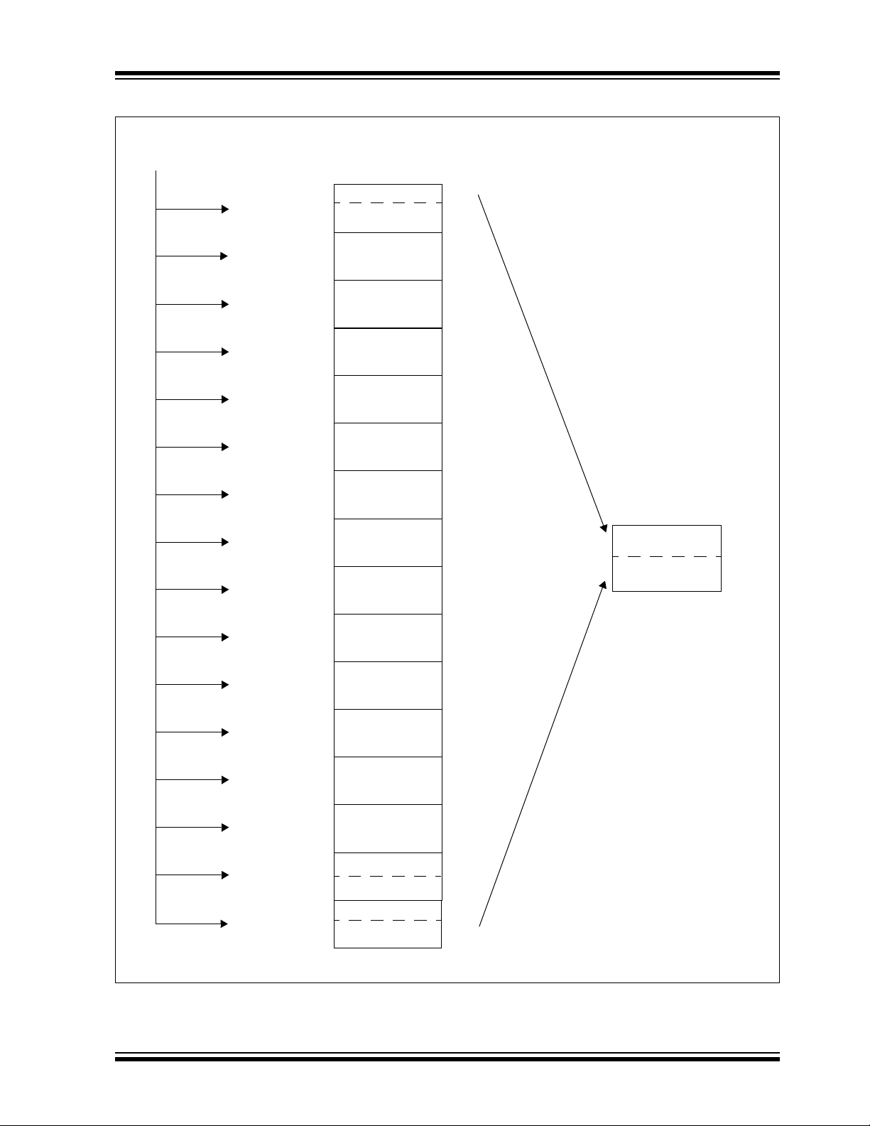
PIC18F97J60 FAMILY
FIGURE 5-7: DATA MEMORY MAP FOR PIC18F97J60 FAMILY DEVICES
When a = 0:
BSR<3:0>
= 0000
= 0001
= 0010
= 0011
= 0100
= 0101
= 0110
= 0111
= 1000
= 1001
= 1010
= 1011
= 1100
= 1101
= 1110
= 1111
Bank 0
Bank 1
Bank 2
Bank 3
Bank 4
Bank 5
Bank 6
Bank 7
Bank 8
Bank 9
Bank 10
Bank 11
Bank 12
Bank 13
Bank 14
Bank 15
Data Memory Map
00h
FFh
00h
FFh
00h
FFh
00h
FFh
00h
FFh
00h
FFh
00h
FFh
00h
FFh
00h
FFh
00h
FFh
00h
FFh
00h
FFh
00h
FFh
00h
FFh
00h
FFh
00h
FFh
Access RAM
GPR
GPR
GPR
GPR
GPR
GPR
GPR
GPR
GPR
GPR
GPR
GPR
GPR
GPR
GPR
Ethernet SFR
GPR
SFR
000h
05Fh
060h
0FFh
100h
1FFh
200h
2FFh
300h
3FFh
400h
4FFh
500h
5FFh
600h
6FFh
700h
7FFh
800h
8FFh
900h
9FFh
A00h
AFFh
B00h
BFFh
C00h
CFFh
D00h
DFFh
E00h
E7Fh
E80h
EFFh
F00h
F5Fh
F60h
FFFh
The BSR is ignored and the
Access Bank is used.
The first 96 bytes are general
purpose RAM (from Bank 0).
The remaining 160 bytes are
Special Function Registers
(from Bank 15).
When a = 1:
The BSR specifies the bank
used by the instruction.
Access Bank
Access RAM Low
Access RAM High
(SFRs)
00h
5Fh
60h
FFh
© 2008 Microchip Technology Inc. Preliminary DS39762D-page 79
Page 82

PIC18F97J60 FAMILY
FIGURE 5-8: USE OF THE BANK SELECT REGISTER (DIRECT ADDRESSING)
(1)
7
0000
Bank Select
Note 1: The Access RAM bit of the instruction can be used to force an override of the selected bank (BSR<3:0>) to
BSR
0010
(2)
the registers of the Access Bank.
2: The MOVFF instruction embeds the entire 12-bit address in the instruction.
000h
0
100h
200h
300h
E00h
F00h
FFFh
Data Memory
Bank 0
Bank 1
Bank 2
Bank 3
through
Bank 13
Bank 14
Bank 15
00h
FFh
00h
FFh
00h
FFh
00h
FFh
00h
FFh
00h
FFh
From Opcode
7
11111111
11111111
(2)
0
5.3.2 ACCESS BANK
While the use of the BSR with an embedded 8-bit
address allows users to address the entire range of
data memory, it also means that the user must always
ensure that the correct bank is selected. Otherwise,
data may be read from or written to the wrong location.
This can be disastrous if a GPR is the intended target
of an operation but an SFR is written to instead.
Verifying and/or changing the BSR for each read or
write to data memory can become very inefficient.
To streamline access for the most commonly used data
memory locations, the data memory is configured with
an Access Bank, which allows users to access a
mapped block of memory without specifying a BSR.
The Access Bank consists of the first 96 bytes of
memory (00h-5Fh) in Bank 0 and the last 160 bytes of
memory (60h-FFh) in Bank 15. The lower block is
known as the “Access RAM” and is composed of
GPRs. The upper block is where the device’s SFRs are
mapped. These two areas are mapped contiguously in
the Access Bank and can be addressed in a linear
fashion by an 8-bit address (Figure 5-7).
The Access Bank is used by core PIC18 instructions
that include the Access RAM bit (the ‘a’ parameter in
the instruction). When ‘a’ is equal to ‘1’, the instruction
uses the BSR and the 8-bit address included in the
opcode for the data memory address. When ‘a’ is ‘0’,
however, the instruction is forced to use the Access
Bank address map; the current value of the BSR is
ignored entirely.
Using this “forced” addressing allows the instruction to
operate on a data address in a single cycle without
updating the BSR first. For 8-bit addresses of 60h and
above, this means that users can evaluate and operate
on SFRs more efficiently. The Access RAM below 60h
is a good place for data values that the user might need
to access rapidly, such as immediate computational
results or common program variables. Access RAM
also allows for faster and more code efficient context
saving and switching of variables.
The mapping of the Access Bank is slightly different
when the extended instruction set is enabled (XINST
Configuration bit = 1). This is discussed in more detail
in Section 5.6.3 “Mapping the Access Bank in
Indexed Literal Offset Mode”.
5.3.3 GENERAL PURPOSE REGISTER FILE
PIC18 devices may have banked memory in the GPR
area. This is data RAM which is available for use by all
instructions. GPRs start at the bottom of Bank 0
(address 000h) and grow upwards towards the bottom
of the SFR area. GPRs are not initialized by a
Power-on Reset and are unchanged on all other
Resets.
DS39762D-page 80 Preliminary © 2008 Microchip Technology Inc.
Page 83

PIC18F97J60 FAMILY
5.3.4 SPECIAL FUNCTION REGISTERS
The Special Function Registers (SFRs) are registers
used by the CPU and peripheral modules for controlling
the desired operation of the device. These registers are
implemented as static RAM.
The main group of SFRs start at the top of data memory
(FFFh) and extend downward to occupy more than the
top half of Bank 15 (F60h to FFFh). These SFRs can
be classified into two sets: those associated with the
“core” device functionality (ALU, Resets and interrupts)
Reset and Interrupt registers are described in their
respective chapters, while the ALU’s STATUS register
is described later in this section. Registers related to
the operation of the peripheral features are described
in the chapter for that peripheral.
The SFRs are typically distributed among the
peripherals whose functions they control. Unused SFR
locations are unimplemented and read as ‘0’s. A list of
SFRs is given in Table 5-3; a full description is provided
in Table 5-5.
and those related to the peripheral functions. The
TABLE 5-3: SPECIAL FUNCTION REGISTER MAP FOR PIC18F97J60 FAMILY DEVICES
Address Name Address Name Address Name Address Name Address Name
FFFh TOSU FDFh INDF2
FFEh TOSH FDEh POSTINC2
FFDh TOSL FDDh POSTDEC2
FFCh STKPTR FDCh PREINC2
FFBh PCLATU FDBh PLUSW2
FFAh PCLATH FDAh FSR2H FBAh CCP2CON F9Ah TRISJ
FF9h PCL FD9h FSR2L FB9h CCPR3H F99h TRISH
FF8h TBLPTRU FD8h STATUS FB8h CCPR3L F98h TRISG F78h TMR4
FF7h TBLPTRH FD7h TMR0H FB7h CCP3CON F97h TRISF F77h PR4
FF6h TBLPTRL FD6h TMR0L FB6h ECCP1AS F96h TRISE F76h T4CON
FF5h TABLAT FD5h T0CON FB5h CVRCON F95h TRISD F75h CCPR4H
FF4h PRODH FD4h
FF3h PRODL FD3h OSCCON FB3h TMR3H F93h TRISB F73h CCP4CON
FF2h INTCON FD2h ECON1 FB2h TMR3L F92h TRISA F72h CCPR5H
FF1h INTCON2 FD1h WDTCON FB1h T3CON F91h LATJ
FF0h INTCON3 FD0h RCON FB0h PSPCON F90h LATH
FEFh INDF0
(1)
FEEh POSTINC0
FEDh POSTDEC0
FECh PREINC0
FEBh PLUSW0
(1)
(1)
FCFh TMR1H FAFh SPBRG1 F8Fh LATG F6Fh SPBRG2
(1)
FCEh TMR1L FAEh RCREG1 F8Eh LATF F6Eh RCREG2
(1)
FCDh T1CON FADh TXREG1 F8Dh LATE F6Dh TXREG2
FCCh TMR2 FACh TXSTA1 F8Ch LATD F6Ch TXSTA2
FCBh PR2 FABh RCSTA1 F8Bh LATC F6Bh RCSTA2
FEAh FSR0H FCAh T2CON FAAh
FE9h FSR0L FC9h SSP1BUF FA9h
FE8h WREG FC8h SSP1ADD FA8h
FE7h INDF1
(1)
FE6h POSTINC1
FE5h POSTDEC1
FE4h PREINC1
FE3h PLUSW1
(1)
(1)
FC7h SSP1STAT FA7h EECON2
(1)
FC6h SSP1CON1 FA6h EECON1 F86h PORTG F66h SSP2BUF
(1)
FC5h SSP1CON2 FA5h IPR3 F85h PORTF F65h SSP2ADD
FC4h ADRESH FA4h PIR3 F84h PORTE F64h SSP2STAT
FC3h ADRESL FA3h PIE3 F83h PORTD F63h SSP2CON1
FE2h FSR1H FC2h ADCON0 FA2h IPR2 F82h PORTC F62h SSP2CON2
FE1h FSR1L FC1h ADCON1 FA1h PIR2 F81h PORTB F61h EDATA
FE0h BSR FC0h ADCON2 FA0h PIE2 F80h PORTA F60h EIR
(1)
(1)
(1)
(2)
—
FBFh CCPR1H F9Fh IPR1 F7Fh SPBRGH1
(1)
FBEh CCPR1L F9Eh PIR1 F7Eh BAUDCON1
(1)
FBDh CCP1CON F9Dh PIE1 F7Dh SPBRGH2
FBCh CCPR2H F9Ch MEMCON
(4)
F7Ch BAUDCON2
FBBh CCPR2L F9Bh OSCTUNE F7Bh ERDPTH
(3)
(3)
F7Ah ERDPTL
F79h ECCP1DEL
FB4h CMCON F94h TRISC F74h CCPR4L
(3)
(3)
(2)
—
(2)
—
(2)
—
(1)
F8Ah LATB F6Ah ECCP3AS
F89h LATA F69h ECCP3DEL
F88h PORTJ
F87h PORTH
(3)
(3)
F71h CCPR5L
F70h CCP5CON
F68h ECCP2AS
F67h ECCP2DEL
Note 1: This is not a physical register.
2: Unimplemented registers are read as ‘0’.
3: This register is not available on 64-pin devices.
4: This register is not available on 64 and 80-pin devices.
© 2008 Microchip Technology Inc. Preliminary DS39762D-page 81
Page 84
PIC18F97J60 FAMILY
5.3.5 ETHERNET SFRs
In addition to the standard SFR set in Bank 15,
members of the PIC18F97J60 family have a second
set of SFRs. This group, associated exclusively with
the Ethernet module, occupies the top half of Bank 14
(E80h to EFFh).
Note: To improve performance, frequently
accessed Ethernet registers are located in
the standard SFR bank (F60h through
FFFh).
A complete list of Ethernet SFRs is given in Table 5-4.
All SFRs are fully described in Table 5-5
TABLE 5-4: ETHERNET SFR MAP FOR PIC18F97J60 FAMILY DEVICES
Address Name Address Name Address Name Address Name
EFFh
(1)
—
EDFh —
EFEh ECON2 EDEh —
EFDh ESTAT EDDh —
EFCh —
(1)
EDCh —
EFBh EIE EDBh —
EFAh —
EF9h —
EF8h
(1)
(2)
(2)
—
EDAh —
ED9h EPKTCNT EB9h MIRDH E99h EPAUSH
ED8h ERXFCON EB8h MIRDL E98h EPAUSL
EF7h EDMACSH ED7h
EF6h EDMACSL ED6h
EF5h EDMADSTH ED5h EPMOH EB5h —
EF4h EDMADSTL ED4h EPMOL EB4h MIREGADR E94h —
EF3h EDMANDH ED3h —
EF2h EDMANDL ED2h —
EF1h EDMASTH ED1h EPMCSH EB1h —
EF0h EDMASTL ED0h EPMCSL EB0h —
EEFh ERXWRPTH ECFh EPMM7 EAFh —
EEEh ERXWRPTL ECEh EPMM6 EAEh —
EEDh ERXRDPTH ECDh EPMM5 EADh —
EECh ERXRDPTL ECCh EPMM4 EACh —
EEBh ERXNDH ECBh EPMM3 EABh MAMXFLH E8Bh —
EEAh ERXNDL ECAh EPMM2 EAAh MAMXFLL E8Ah MISTAT
EE9h ERXSTH EC9h EPMM1 EA9h
EE8h ERXSTL EC8h EPMM0 EA8h —
EE7h ETXNDH EC7h EHT7 EA7h MAIPGH E87h —
EE6h ETXNDL EC6h EHT6 EA6h MAIPGL E86h —
EE5h ETXSTH EC5h EHT5 EA5h —
EE4h ETXSTL EC4h EHT4 EA4h MABBIPG E84h MAADR1
EE3h EWRPTH EC3h EHT3 EA3h MACON4 E83h MAADR4
EE2h EWRPTL EC2h EHT2 EA2h MACON3 E82h MAADR3
(1)
EE1h
EE0h
—
(1)
—
EC1h EHT1 EA1h —
EC0h EHT0 EA0h MACON1 E80h MAADR5
(1)
(1)
(1)
(1)
(1)
(1)
(1)
—
(1)
—
(2)
(2)
EBFh —
EBEh —
EBDh —
EBCh —
EBBh —
EBAh —
EB7h MIWRH E97h EFLOCON
EB6h MIWRL E96h —
EB3h —
EB2h MICMD E92h —
(1)
(1)
(1)
(1)
(1)
(1)
(1)
(2)
(1)
(1)
(2)
(1)
(1)
(1)
(1)
—
(1)
(2)
(1)
E9Fh —
E9Eh —
E9Dh —
E9Ch —
E9Bh —
E9Ah —
E95h —
E93h —
E91h —
E90h —
E8Fh —
E8Eh —
E8Dh —
E8Ch —
E89h —
E88h —
E85h MAADR2
E81h MAADR6
(1)
(1)
(1)
(1)
(1)
(1)
(2)
(2)
(2)
(2)
(2)
(2)
(2)
(2)
(2)
(2)
(2)
(2)
(1)
(1)
(1)
(1)
Note 1: Reserved register location; do not modify.
2: Unimplemented registers are read as ‘0’.
DS39762D-page 82 Preliminary © 2008 Microchip Technology Inc.
Page 85
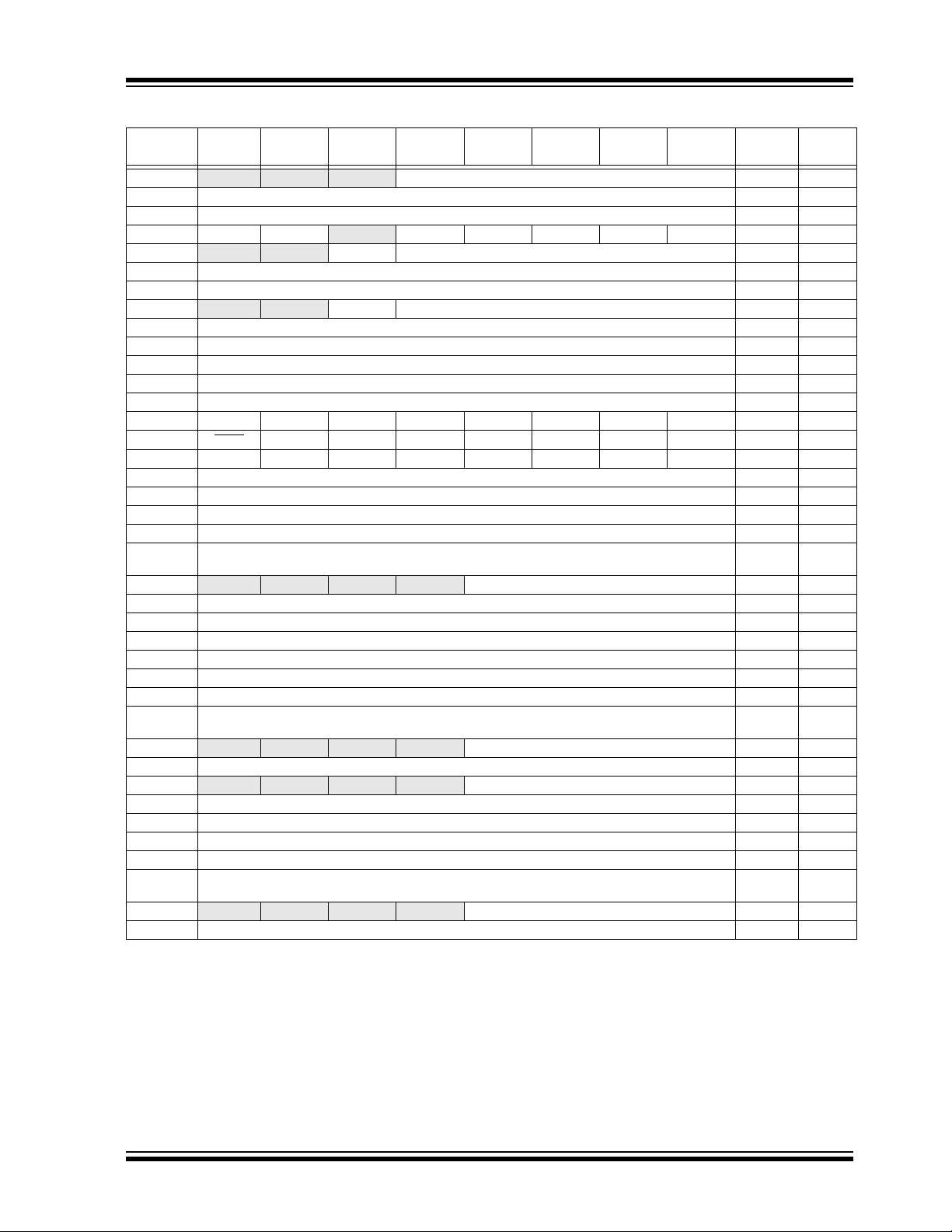
PIC18F97J60 FAMILY
TABLE 5-5: REGISTER FILE SUMMARY (PIC18F97J60 FAMILY)
File Name Bit 7 Bit 6 Bit 5 Bit 4 Bit 3 Bit 2 Bit 1 Bit 0
TOSU
TOSH Top-of-Stack Register High Byte (TOS<15:8>) 0000 0000 61, 73
TOSL Top-of-Stack Register Low Byte (TOS<7:0>) 0000 0000 61, 73
STKPTR STKFUL
PCLATU
PCLATH Holding Register for PC<15:8> 0000 0000 61, 73
PCL PC Low Byte (PC<7:0>) 0000 0000 61, 73
TBLPTRU
TBLPTRH Program Memory Table Pointer High Byte (TBLPTR<15:8>) 0000 0000 61, 100
TBLPTRL Program Memory Table Pointer Low Byte (TBLPTR<7:0>) 0000 0000 61, 100
TABLAT Program Memory Table Latch 0000 0000 61, 100
PRODH Product Register High Byte xxxx xxxx 61, 119
PRODL Product Register Low Byte xxxx xxxx 61, 119
INTCON GIE/GIEH PEIE/GIEL TMR0IE INT0IE RBIE TMR0IF INT0IF RBIF 0000 000x 61, 123
INTCON2 RBPU
INTCON3 INT2IP INT1IP INT3IE INT2IE INT1IE INT3IF INT2IF INT1IF 1100 0000 61, 125
INDF0 Uses contents of FSR0 to address data memory – value of FSR0 not changed (not a physical register) N/A 61, 91
POSTINC0 Uses contents of FSR0 to address data memory – value of FSR0 post-incremented (not a physical register) N/A 61, 92
POSTDEC0 Uses contents of FSR0 to address data memory – value of FSR0 post-decremented (not a physical register) N/A 61, 92
PREINC0 Uses contents of FSR0 to address data memory – value of FSR0 pre-incremented (not a physical register) N/A 61, 92
PLUSW0 Uses contents of FSR0 to address data memory – value of FSR0 pre-incremented (not a physical register) –
FSR0H
FSR0L Indirect Data Memory Address Pointer 0 Low Byte xxxx xxxx 61, 92
WREG Working Register xxxx xxxx 61
INDF1 Uses contents of FSR1 to address data memory – value of FSR1 not changed (not a physical register) N/A 61, 91
POSTINC1 Uses contents of FSR1 to address data memory – value of FSR1 post-incremented (not a physical register) N/A 61, 92
POSTDEC1 Uses contents of FSR1 to address data memory – value of FSR1 post-decremented (not a physical register) N/A 61, 92
PREINC1 Uses contents of FSR1 to address data memory – value of FSR1 pre-incremented (not a physical register) N/A 61, 92
PLUSW1 Uses contents of FSR1 to address data memory – value of FSR1 pre-incremented (not a physical register) –
FSR1H
FSR1L Indirect Data Memory Address Pointer 1 Low Byte xxxx xxxx 61, 91
BSR
INDF2 Uses contents of FSR2 to address data memory – value of FSR2 not changed (not a physical register) N/A 61, 91
POSTINC2 Uses contents of FSR2 to address data memory – value of FSR2 post-incremented (not a physical register) N/A 61, 92
POSTDEC2 Uses contents of FSR2 to address data memory – value of FSR2 post-decremented (not a physical register) N/A 61, 92
PREINC2 Uses contents of FSR2 to address data memory – value of FSR2 pre-incremented (not a physical register) N/A 61, 92
PLUSW2 Uses contents of FSR2 to address data memory – value of FSR2 pre-incremented (not a physical register) –
FSR2H
FSR2L Indirect Data Memory Address Pointer 2 Low Byte xxxx xxxx 61, 91
Legend: x = unknown, u = unchanged, - = unimplemented, read as ‘0’, q = value depends on condition, r = reserved bit, do not modify. Shaded cells
Note 1: Bit 7 and bit 6 are cleared by user software or by a POR.
2: Bit 21 of the PC is only available in Serial Programming modes.
3: Reset value is ‘0’ when Two-Speed Start-up is enabled and ‘1’ if disabled.
4: Alternate names and definitions for these bits when the MSSP module is operating in I
5: These bits and/or registers are only available in 100-pin devices; otherwise, they are unimplemented and read as ‘0’. Reset values shown
6: These bits and/or registers are only available in 80-pin and 100-pin devices; in 64-pin devices, they are unimplemented and read as ‘0’. Reset
7: In Microcontroller mode, the bits in this register are unwritable and read as ‘0’.
8: PLLEN is only available when either ECPLL or HSPLL Oscillator mode is selected; otherwise, read as ‘0’.
9: Implemented in 100-pin devices in Microcontroller mode only.
— — — Top-of-Stack Register Upper Byte (TOS<20:16>) ---0 0000 61, 73
(1)
— —bit 21
— — bit 21 Program Memory Table Pointer Upper Byte (TBLPTR<20:16>) --00 0000 61, 100
value of FSR0 offset by W
— — — — Indirect Data Memory Address Pointer 0 High Byte ---- xxxx 61, 91
value of FSR1 offset by W
— — — — Indirect Data Memory Address Pointer 1 High Byte ---- xxxx 61, 91
— — — — Bank Select Register ---- 0000 61, 91
value of FSR2 offset by W
— — — — Indirect Data Memory Address Pointer 2 High Byte ---- xxxx 61, 91
are unimplemented, read as ‘0’.
apply only to 100-pin devices.
values are shown for 100-pin devices.
(1)
STKUNF
INTEDG0 INTEDG1 INTEDG2 INTEDG3 TMR0IP INT3IP RBIP 1111 1111 61, 124
— SP4 SP3 SP2 SP1 SP0 00-0 0000 61, 74
(2)
Holding Register for PC<20:16> ---0 0000 61, 73
2
C™ Slave mode.
Values on
POR, BOR
Details on
Page:
N/A 61, 92
N/A 61, 92
N/A 61, 92
© 2008 Microchip Technology Inc. Preliminary DS39762D-page 83
Page 86
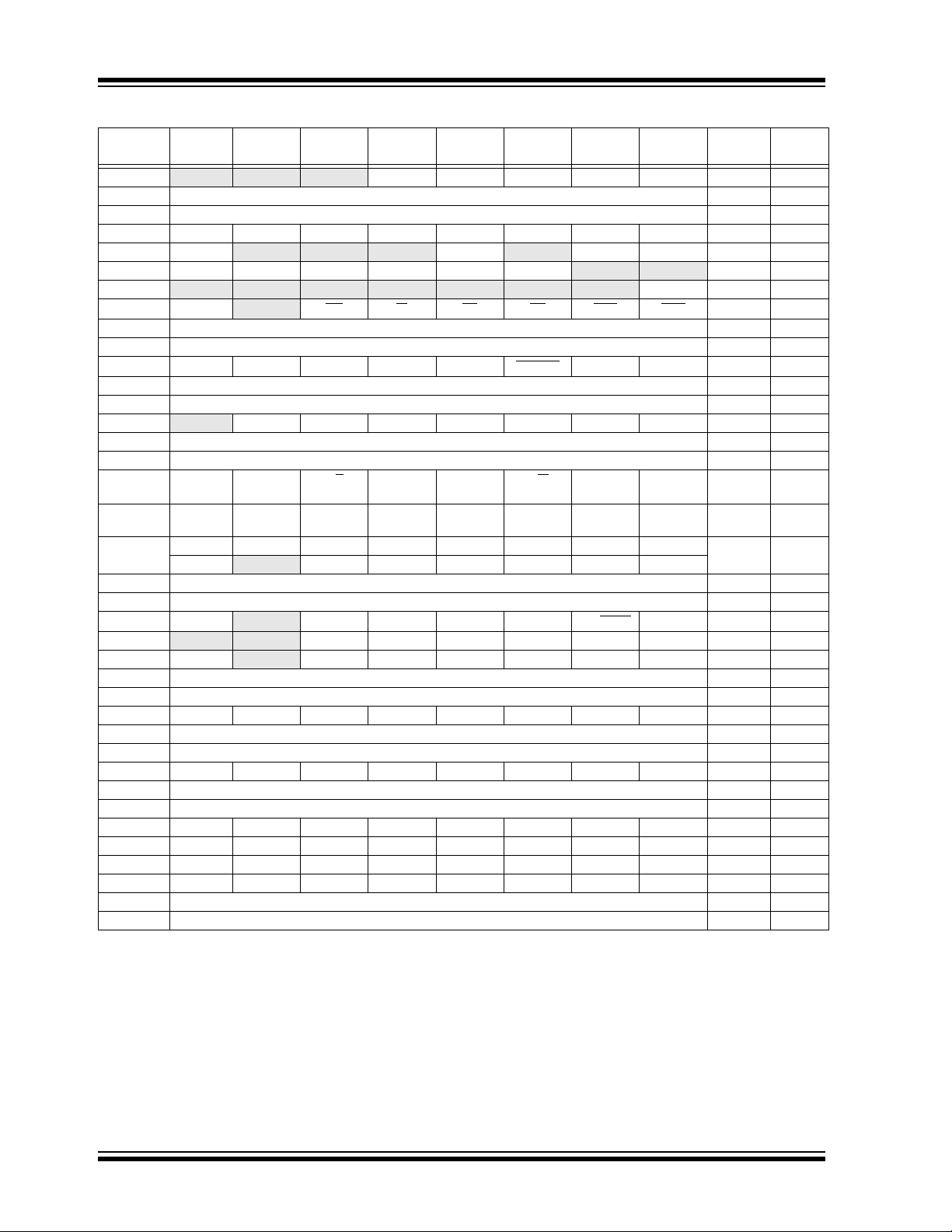
PIC18F97J60 FAMILY
TABLE 5-5: REGISTER FILE SUMMARY (PIC18F97J60 FAMILY) (CONTINUED)
File Name Bit 7 Bit 6 Bit 5 Bit 4 Bit 3 Bit 2 Bit 1 Bit 0
STATUS — — —NOVZDCC---x xxxx 62, 89
TMR0H Timer0 Register High Byte 0000 0000 62, 165
TMR0L Timer0 Register Low Byte xxxx xxxx 62, 165
T0CON TMR0ON T08BIT T0CS T0SE PSA T0PS2 T0PS1 T0PS0 1111 1111 62, 165
OSCCON IDLEN
ECON1 TXRST RXRST DMAST CSUMEN TXRTS RXEN
WDTCON
RCON IPEN
TMR1H Timer1 Register High Byte xxxx xxxx 62, 169
TMR1L Timer1 Register Low Byte xxxx xxxx 62, 169
T1CON RD16 T1RUN T1CKPS1 T1CKPS0 T1OSCEN T1SYNC
TMR2 Timer2 Register 0000 0000 62, 175
PR2 Timer2 Period Register 1111 1111 62, 175
T2CON
SSP1BUF MSSP1 Receive Buffer/Transmit Register xxxx xxxx 62, 267
SSP1ADD MSSP1 Address Register (I
SSP1STAT SMP CKE D/A
SSP1CON1 WCOL SSPOV SSPEN CKP SSPM3 SSPM2 SSPM1 SSPM0 0000 0000 62, 259,
SSP1CON2 GCEN ACKSTAT ACKDT ACKEN RCEN PEN RSEN SEN 0000 0000 62, 270
ADRESH A/D Result Register High Byte xxxx xxxx 62, 335
ADRESL A/D Result Register Low Byte xxxx xxxx 62, 335
ADCON0 ADCAL
ADCON1
ADCON2 ADFM
CCPR1H Capture/Compare/PWM Register 1 High Byte xxxx xxxx 62, 187
CCPR1L Capture/Compare/PWM Register 1 Low Byte xxxx xxxx 62, 187
CCP1CON P1M1 P1M0 DC1B1 DC1B0 CCP1M3 CCP1M2 CCP1M1 CCP1M0 0000 0000 62, 191
CCPR2H Capture/Compare/PWM Register 2 High Byte xxxx xxxx 62, 187
CCPR2L Capture/Compare/PWM Register 2 Low Byte xxxx xxxx 62, 187
CCP2CON P2M1 P2M0 DC2B1 DC2B0 CCP2M3 CCP2M2 CCP2M1 CCP2M0 0000 0000 62, 191
CCPR3H Capture/Compare/PWM Register 3 High Byte xxxx xxxx 62, 187
CCPR3L Capture/Compare/PWM Register 3 Low Byte xxxx xxxx 62, 187
CCP3CON P3M1 P3M0 DC3B1 DC3B0 CCP3M3 CCP3M2 CCP3M1 CCP3M0 0000 0000 62, 191
ECCP1AS ECCP1ASE ECCP1AS2 ECCP1AS1 ECCP1AS0 PSS1AC1 PSS1AC0 PSS1BD1 PSS1BD0 0000 0000 62, 203
CVRCON CVREN CVROE CVRR CVRSS CVR3 CVR2 CVR1 CVR0 0000 0000 62, 343
CMCON C2OUT C1OUT C2INV C1INV CIS CM2 CM1 CM0 0000 0111 62, 337
TMR3H Timer3 Register High Byte xxxx xxxx 62, 177
TMR3L Timer3 Register Low Byte xxxx xxxx 62, 177
Legend: x = unknown, u = unchanged, - = unimplemented, read as ‘0’, q = value depends on condition, r = reserved bit, do not modify. Shaded cells
Note 1: Bit 7 and bit 6 are cleared by user software or by a POR.
2: Bit 21 of the PC is only available in Serial Programming modes.
3: Reset value is ‘0’ when Two-Speed Start-up is enabled and ‘1’ if disabled.
4: Alternate names and definitions for these bits when the MSSP module is operating in I
5: These bits and/or registers are only available in 100-pin devices; otherwise, they are unimplemented and read as ‘0’. Reset values shown
6: These bits and/or registers are only available in 80-pin and 100-pin devices; in 64-pin devices, they are unimplemented and read as ‘0’. Reset
7: In Microcontroller mode, the bits in this register are unwritable and read as ‘0’.
8: PLLEN is only available when either ECPLL or HSPLL Oscillator mode is selected; otherwise, read as ‘0’.
9: Implemented in 100-pin devices in Microcontroller mode only.
— — — — — — —SWDTEN--- ---0 62, 355
— T2OUTPS3 T2OUTPS2 T2OUTPS1 T2OUTPS0 TMR2ON T2CKPS1 T2CKPS0 -000 0000 62, 175
GCEN
— — VCFG1 VCFG0 PCFG3 PCFG2 PCFG1 PCFG0 --00 0000 62, 328
are unimplemented, read as ‘0’.
apply only to 100-pin devices.
values are shown for 100-pin devices.
— — —OSTS
—CMRI TO PD POR BOR 0-q1 1100 62, 56, 135
2
C™ Slave mode), MSSP1 Baud Rate Reload Register (I2C Master mode) 0000 0000 62, 267
PSR/WUA BF 0000 0000 62, 258,
ACKSTAT ADMSK5
— CHS3 CHS2 CHS1 CHS0 GO/DONE ADON 0-00 0000 62, 327
— ACQT2 ACQT1 ACQT0 ADCS2 ADCS1 ADCS0 0-00 0000 62, 329
(4)
ADMSK4
(4)
ADMSK3
(3)
— SCS1 SCS0 0--- q-00 62, 45
— — 0000 00-- 62, 215
TMR1CS TMR1ON 0000 0000 62, 169
(4)
ADMSK2
(4)
ADMSK1
2
C™ Slave mode.
(4)
SEN
Values on
POR, BOR
Details on
Page:
268
269
DS39762D-page 84 Preliminary © 2008 Microchip Technology Inc.
Page 87

PIC18F97J60 FAMILY
TABLE 5-5: REGISTER FILE SUMMARY (PIC18F97J60 FAMILY) (CONTINUED)
File Name Bit 7 Bit 6 Bit 5 Bit 4 Bit 3 Bit 2 Bit 1 Bit 0
Values on
POR, BOR
T3CON RD16 T3CCP2 T3CKPS1 T3CKPS0 T3CCP1 T3SYNC TMR3CS TMR3ON 0000 0000 63, 177
(5)
PSPCON
IBF OBF IBOV PSPMODE — — — — 0000 ---- 63, 162
SPBRG1 EUSART1 Baud Rate Generator Register Low Byte 0000 0000 63, 308
RCREG1 EUSART1 Receive Register 0000 0000 63, 315
TXREG1 EUSART1 Transmit Register xxxx xxxx 63, 317
TXSTA1 CSRC TX9 TXEN SYNC SENDB BRGH TRMT TX9D 0000 0010 63, 308
RCSTA1 SPEN RX9 SREN CREN ADDEN FERR OERR RX9D 0000 000x 63, 308
EECON2 Program Memory Control Register (not a physical register) ---- ---- 63, 98
EECON1
IPR3 SSP2IP
PIR3 SSP2IF
PIE3 SSP2IE
IPR2 OSCFIP CMIP ETHIP r BCL1IP
PIR2 OSCFIF CMIF ETHIF r BCL1IF
PIE2 OSCFIE CMIE ETHIE r BCL1IE
IPR1 PSPIP
PIR1 PSPIF
PIE1 PSPIE
MEMCON
(5,7)
OSCTUNE PPST1 PLLEN
(6)
TRISJ
(6)
TRISH
TRISG TRISG7
TRISF TRISF7 TRISF6 TRISF5 TRISF4 TRISF3 TRISF2 TRISF1 TRISF0
TRISE TRISE7
TRISD TRISD7
— — — FREE WRERR WREN WR — ---0 x00- 63, 99
(5)
(5)
(5)
BCL2IP
BCL2IF
BCL2IE
(5)
(5)
(5)
RC2IP
RC2IF
RC2IE
(6)
(6)
(6)
TX2IP
TX2IF
TX2IE
(6)
TMR4IP CCP5IP CCP4IP CCP3IP 1111 1111 63, 134
(6)
TMR4IF CCP5IF CCP4IF CCP3IF 0000 0000 63, 128
(6)
TMR4IE CCP5IE CCP4IE CCP3IE 0000 0000 63, 131
— TMR3IP CCP2IP 1111 1-11 63, 133
— TMR3IF CCP2IF 0000 0-00 63, 127
— TMR3IE CCP2IE 0000 0-00 63, 130
(9)
ADIP RC1IP TX1IP SSP1IP CCP1IP TMR2IP TMR1IP 1111 1111 63, 132
(9)
ADIF RC1IF TX1IF SSP1IF CCP1IF TMR2IF TMR1IF 0000 0000 63, 126
(9)
ADIE RC1IE TX1IE SSP1IE CCP1IE TMR2IE TMR1IE 0000 0000 63, 129
EBDIS —WAIT1WAIT0— —WM1WM00-00 --00 63, 108
(8)
PPST0 PPRE — — — — 0000 ---- 63, 43
(5)
(6)
(5)
(6)
(5)
TRISJ5
TRISH5
TRISG5
(6)
(6)
(5)
(6)
TRISJ4
TRISH4
TRISJ3
(6)
TRISH3
TRISG4 TRISG3
(5)
(6)
(6)
TRISJ2
TRISH2
TRISG2
(5)
(6)
(6)
TRISJ1
TRISH1
TRISG1
(5)
(6)
(6)
TRISJ0
TRISH0
TRISG0
(5)
1111 1111 63, 160
(6)
1111 1111 63, 158
(6)
1111 1111 63, 156
(5)
1111 1111 63, 153
TRISE5 TRISE4 TRISE3 TRISE2 TRISE1 TRISE0 1111 1111 63, 151
TRISD5
(5)
TRISD4
(5)
TRISD3
(5)
TRISD2 TRISD1 TRISD0 1111 1111 63, 148
TRISJ7
TRISH7
(5)
TRISJ6
(6)
TRISH6
(5)
TRISG6
(6)
TRISE6
(5)
TRISD6
TRISC TRISC7 TRISC6 TRISC5 TRISC4TRISC3TRISC2TRISC1TRISC01111 1111 63, 145
TRISB TRISB7 TRISB6 TRISB5 TRISB4 TRISB3 TRISB2 TRISB1 TRISB0 1111 1111 63, 142
TRISA
(6)
LATJ
(6)
LATH
LATG LATG7
LATF LATF7 LATF6 LATF5 LATF4 LATF3 LATF2 LATF1 LATF0
LATE LATE7
LATD LATD7
— — TRISA5 TRISA4 TRISA3 TRISA2 TRISA1 TRISA0 --11 1111 63, 139
LATJ7
LATH7
(5)
(6)
(5)
(6)
(5)
LATJ6
LATH6
LATG6
LATE6
LATD6
(5)
(6)
(5)
(6)
(5)
LATJ5
LATH5
LATG5
(6)
(6)
(5)
(6)
LATJ4
LATH4
LATJ3
(6)
LATH3
LATG4 LATG3
(5)
(6)
(6)
LATJ2
LATH2
LATG2
(5)
(6)
(6)
LATJ1
LATH1
LATG1
(5)
(6)
(6)
LATJ0
LATH0
LATG0
(5)
xxxx xxxx 63, 160
(6)
xxxx xxxx 63, 158
(6)
xxxx xxxx 64, 156
(5)
xxxx xxxx 64, 153
LATE5 LATE4 LATE3 LATE2 LATE1 LATE0 xxxx xxxx 64, 151
LATD5
(5)
LATD4
(5)
LATD3
(5)
LATD2 LATD1 LATD0 xxxx xxxx 64, 148
LATC LATC7 LATC6 LATC5 LATC4 LATC3 LATC2 LATC1 LATC0 xxxx xxxx 64, 145
LATB LATB7 LATB6 LATB5 LATB4 LATB3 LATB2 LATB1 LATB0 xxxx xxxx 64, 142
LATA RDPU REPU LATA5 LATA4 LATA3 LATA2 LATA1 LATA0 00xx xxxx 64, 139
(6)
PORTJ
(6)
PORTH
PORTG RG7
RJ7
RH7
(5)
(6)
(5)
RJ6
RH6
RG6
(5)
(6)
(5)
RJ5
RH5
RG5
(6)
(6)
(5)
(6)
RJ4
(6)
RH4
RG4 RG3
RJ3
RH3
(5)
(6)
(6)
RJ2
RH2
RG2
(5)
(6)
(6)
RJ1
RH1
RG1
(5)
(6)
(6)
RJ0
RH0
RG0
(5)
xxxx xxxx 64, 160
(6)
0000 xxxx 64, 158
(6)
111x xxxx 64, 156
Legend: x = unknown, u = unchanged, - = unimplemented, read as ‘0’, q = value depends on condition, r = reserved bit, do not modify. Shaded cells
are unimplemented, read as ‘0’.
Note 1: Bit 7 and bit 6 are cleared by user software or by a POR.
2: Bit 21 of the PC is only available in Serial Programming modes.
3: Reset value is ‘0’ when Two-Speed Start-up is enabled and ‘1’ if disabled.
4: Alternate names and definitions for these bits when the MSSP module is operating in I
2
C™ Slave mode.
5: These bits and/or registers are only available in 100-pin devices; otherwise, they are unimplemented and read as ‘0’. Reset values shown
apply only to 100-pin devices.
6: These bits and/or registers are only available in 80-pin and 100-pin devices; in 64-pin devices, they are unimplemented and read as ‘0’. Reset
values are shown for 100-pin devices.
7: In Microcontroller mode, the bits in this register are unwritable and read as ‘0’.
8: PLLEN is only available when either ECPLL or HSPLL Oscillator mode is selected; otherwise, read as ‘0’.
9: Implemented in 100-pin devices in Microcontroller mode only.
Details on
Page:
© 2008 Microchip Technology Inc. Preliminary DS39762D-page 85
Page 88

PIC18F97J60 FAMILY
TABLE 5-5: REGISTER FILE SUMMARY (PIC18F97J60 FAMILY) (CONTINUED)
File Name Bit 7 Bit 6 Bit 5 Bit 4 Bit 3 Bit 2 Bit 1 Bit 0
PORTF RF7 RF6 RF5 RF4 RF3 RF2 RF1 RF0
PORTE RE7
PORTD RD7
(6)
(5)
RE6
RD6
(6)
(5)
RE5 RE4 RE3 RE2 RE1 RE0 xxxx xxxx 64, 151
RD5
(5)
RD4
(5)
RD3
(5)
RD2 RD1 RD0 xxxx xxxx 64, 148
Values on
POR, BOR
(5)
0000 0000 64, 153
PORTC RC7 RC6 RC5 RC4 RC3 RC2 RC1 RC0 xxxx xxxx 64, 145
PORTB RB7 RB6 RB5 RB4 RB3 RB2 RB1 RB0 xxxx xxxx 64, 142
PORTA RJPU
(6)
— RA5 RA4 RA3 RA2 RA1 RA0 0-0x 0000 64, 139
SPBRGH1 EUSART1 Baud Rate Generator Register High Byte 0000 0000 64, 308
BAUDCON1 ABDOVF RCIDL RXDTP TXCKP BRG16
— WUE ABDEN 0100 0-00 64, 306
SPBRGH2 EUSART2 Baud Rate Generator Register High Byte 0000 0000 64, 308
BAUDCON2 ABDOVF RCIDL RXDTP TXCKP BRG16
ERDPTH
— — — Buffer Read Pointer High Byte ---0 0101 64, 211
— WUE ABDEN 0100 0-00 64, 306
ERDPTL Buffer Read Pointer Low Byte 1111 1010 64, 211
ECCP1DEL P1RSEN P1DC6 P1DC5 P1DC4 P1DC3 P1DC2 P1DC1 P1DC0 0000 0000 64, 202
TMR4 Timer4 Register 0000 0000 64, 181
PR4 Timer4 Period Register 1111 1111 64, 181
T4CON
— T4OUTPS3 T4OUTPS2 T4OUTPS1 T4OUTPS0 TMR4ON T4CKPS1 T4CKPS0 -000 0000 64, 181
CCPR4H Capture/Compare/PWM Register 4 High Byte xxxx xxxx 64, 187
CCPR4L Capture/Compare/PWM Register 4 Low Byte xxxx xxxx 64, 187
CCP4CON
— — DC4B1 DC4B0 CCP4M3 CCP4M2 CCP4M1 CCP4M0 --00 0000 65, 183
CCPR5H Capture/Compare/PWM Register 5 High Byte xxxx xxxx 65, 187
CCPR5L Capture/Compare/PWM Register 5 Low Byte xxxx xxxx 65, 187
CCP5CON
— — DC5B1 DC5B0 CCP5M3 CCP5M2 CCP5M1 CCP5M0 --00 0000 65, 183
SPBRG2 EUSART2 Baud Rate Generator Register Low Byte 0000 0000 65, 308
RCREG2 EUSART2 Receive Register 0000 0000 65, 315
TXREG2 EUSART2 Transmit Register 0000 0000 65, 317
TXSTA2 CSRC TX9 TXEN SYNC SENDB BRGH TRMT TX9D 0000 0010 65, 304
RCSTA2 SPEN RX9 SREN CREN ADDEN FERR OERR RX9D 0000 000x 65, 305
ECCP3AS ECCP3ASE ECCP3AS2 ECCP3AS1 ECCP3AS0 PSS3AC1 PSS3AC0 PSS3BD1 PSS3BD0 0000 0000 65, 203
ECCP3DEL P3RSEN P3DC6 P3DC5 P3DC4 P3DC3 P3DC2 P3DC1 P3DC0 0000 0000 65, 202
ECCP2AS ECCP2ASE ECCP2AS2 ECCP2AS1 ECCP2AS0 PSS2AC1 PSS2AC0 PSS2BD1 PSS2BD0 0000 0000 65, 203
ECCP2DEL P2RSEN P2DC6 P2DC5 P2DC4 P2DC3 P2DC2 P2DC1 P2DC0 0000 0000 65, 202
SSP2BUF MSSP2 Receive Buffer/Transmit Register xxxx xxxx 65, 267
SSP2ADD MSSP2 Address Register (I
SSP2STAT SMP CKE D/A
2
C™ Slave mode), MSSP2 Baud Rate Reload Register (I2C Master mode) 0000 0000 65, 267
PSR/WUA BF 0000 0000 65, 258
SSP2CON1 WCOL SSPOV SSPEN CKP SSPM3 SSPM2 SSPM1 SSPM0 0000 0000 65, 259,
SSP2CON2 GCEN ACKSTAT ACKDT ACKEN RCEN PEN RSEN SEN 0000 0000 65, 270
GCEN
ACKSTAT ADMSK5
(4)
ADMSK4
(4)
ADMSK3
(4)
ADMSK2
(4)
ADMSK1
(4)
SEN
EDATA Ethernet Transmit/Receive Buffer Register (EDATA<7:0>) xxxx xxxx 65, 211
EIR
ECON2 AUTOINC PKTDEC ETHEN
— PKTIF DMAIF LINKIF TXIF — TXERIF RXERIF -000 0-00 65, 229
— — — — — 100- ---- 65, 216
Legend: x = unknown, u = unchanged, - = unimplemented, read as ‘0’, q = value depends on condition, r = reserved bit, do not modify. Shaded cells
are unimplemented, read as ‘0’.
Note 1: Bit 7 and bit 6 are cleared by user software or by a POR.
2: Bit 21 of the PC is only available in Serial Programming modes.
3: Reset value is ‘0’ when Two-Speed Start-up is enabled and ‘1’ if disabled.
4: Alternate names and definitions for these bits when the MSSP module is operating in I
2
C™ Slave mode.
5: These bits and/or registers are only available in 100-pin devices; otherwise, they are unimplemented and read as ‘0’. Reset values shown
apply only to 100-pin devices.
6: These bits and/or registers are only available in 80-pin and 100-pin devices; in 64-pin devices, they are unimplemented and read as ‘0’. Reset
values are shown for 100-pin devices.
7: In Microcontroller mode, the bits in this register are unwritable and read as ‘0’.
8: PLLEN is only available when either ECPLL or HSPLL Oscillator mode is selected; otherwise, read as ‘0’.
9: Implemented in 100-pin devices in Microcontroller mode only.
Details on
Page:
269
DS39762D-page 86 Preliminary © 2008 Microchip Technology Inc.
Page 89
PIC18F97J60 FAMILY
TABLE 5-5: REGISTER FILE SUMMARY (PIC18F97J60 FAMILY) (CONTINUED)
File Name Bit 7 Bit 6 Bit 5 Bit 4 Bit 3 Bit 2 Bit 1 Bit 0
ESTAT —BUFER —r— RXBUSY TXABRT PHYRDY -0-0 -000 65, 216
EIE
EDMACSH DMA Checksum Register High Byte 0000 0000 65, 253
EDMACSL DMA Checksum Register Low Byte 0000 0000 65, 253
EDMADSTH
EDMADSTL DMA Destination Register Low Byte 0000 0000 65, 253
EDMANDH
EDMANDL DMA End Register Low Byte 0000 0000 65, 253
EDMASTH
EDMASTL DMA Start Register Low Byte 0000 0000 65, 253
ERXWRPTH
ERXWRPTL Receive Buffer Write Pointer Low Byte 0000 0000 65, 213
ERXRDPTH
ERXRDPTL Receive Buffer Read Pointer Low Byte 1111 1010 65, 213
ERXNDH
ERXNDL Receive End Register Low Byte 1111 1111 65, 213
ERXSTH
ERXSTL Receive Start Register Low Byte 1111 1010 65, 213
ETXNDH
ETXNDL Transmit End Register Low Byte 0000 0000 66, 214
ETXSTH
ETXSTL Transmit Start Register Low Byte 0000 0000 66, 214
EWRPTH
EWRPTL Buffer Write Pointer Low Byte 0000 0000 66, 211
EPKTCNT Ethernet Packet Count Register 0000 0000 66, 240
ERXFCON UCEN ANDOR CRCEN PMEN MPEN HTEN MCEN BCEN 1010 0001 66, 248
EPMOH
EPMOL Pattern Match Offset Register Low Byte 0000 0000 66, 251
EPMCSH Pattern Match Checksum Register High Byte 0000 0000 66, 251
EPMCSL Pattern Match Checksum Register Low Byte 0000 0000 66, 251
EPMM7 Pattern Match Mask Register Byte 7 0000 0000 66, 251
EPMM6 Pattern Match Mask Register Byte 6 0000 0000 66, 251
EPMM5 Pattern Match Mask Register Byte 5 0000 0000 66, 251
EPMM4 Pattern Match Mask Register Byte 4 0000 0000 66, 251
EPMM3 Pattern Match Mask Register Byte 3 0000 0000 66, 251
EPMM2 Pattern Match Mask Register Byte 2 0000 0000 66, 251
EPMM1 Pattern Match Mask Register Byte 1 0000 0000 66, 251
EPMM0 Pattern Match Mask Register Byte 0 0000 0000 66, 251
Legend: x = unknown, u = unchanged, - = unimplemented, read as ‘0’, q = value depends on condition, r = reserved bit, do not modify. Shaded cells
Note 1: Bit 7 and bit 6 are cleared by user software or by a POR.
2: Bit 21 of the PC is only available in Serial Programming modes.
3: Reset value is ‘0’ when Two-Speed Start-up is enabled and ‘1’ if disabled.
4: Alternate names and definitions for these bits when the MSSP module is operating in I
5: These bits and/or registers are only available in 100-pin devices; otherwise, they are unimplemented and read as ‘0’. Reset values shown
6: These bits and/or registers are only available in 80-pin and 100-pin devices; in 64-pin devices, they are unimplemented and read as ‘0’. Reset
7: In Microcontroller mode, the bits in this register are unwritable and read as ‘0’.
8: PLLEN is only available when either ECPLL or HSPLL Oscillator mode is selected; otherwise, read as ‘0’.
9: Implemented in 100-pin devices in Microcontroller mode only.
— PKTIE DMAIE LINKIE TXIE — TXERIE RXERIE -000 0-00 65, 228
— — — DMA Destination Register High Byte ---0 0000 65, 253
— — — DMA End Register High Byte ---0 0000 65, 253
— — — DMA Start Register High Byte ---0 0000 65, 253
— — — Receive Buffer Write Pointer High Byte ---0 0000 65, 213
— — — Receive Buffer Read Pointer High Byte ---0 0101 65, 213
— — — Receive End Register High Byte ---1 1111 65, 213
— — — Receive Start Register High Byte ---0 0101 65, 213
— — — Transmit End Register High Byte ---0 0000 66, 214
— — — Transmit Start Register High Byte ---0 0000 66, 214
— — — Buffer Write Pointer High Byte ---0 0000 66, 211
— — — Pattern Match Offset Register High Byte ---0 0000 66, 251
are unimplemented, read as ‘0’.
2
C™ Slave mode.
apply only to 100-pin devices.
values are shown for 100-pin devices.
Values on
POR, BOR
Details on
Page:
© 2008 Microchip Technology Inc. Preliminary DS39762D-page 87
Page 90
PIC18F97J60 FAMILY
TABLE 5-5: REGISTER FILE SUMMARY (PIC18F97J60 FAMILY) (CONTINUED)
File Name Bit 7 Bit 6 Bit 5 Bit 4 Bit 3 Bit 2 Bit 1 Bit 0
EHT7 Hash Table Register Byte 7 0000 0000 66, 247
EHT6 Hash Table Register Byte 6 0000 0000 66, 247
EHT5 Hash Table Register Byte 5 0000 0000 66, 247
EHT4 Hash Table Register Byte 4 0000 0000 66, 247
EHT3 Hash Table Register Byte 3 0000 0000 66, 247
EHT2 Hash Table Register Byte 2 0000 0000 66, 247
EHT1 Hash Table Register Byte 1 0000 0000 66, 247
EHT0 Hash Table Register Byte 0 0000 0000 66, 247
MIRDH MII Read Data Register High Byte 0000 0000 66, 220
MIRDL MII Read Data Register Low Byte 0000 0000 66, 220
MIWRH MII Write Data Register High Byte 0000 0000 66, 220
MIWRL MII Write Data Register Low Byte 0000 0000 66, 220
MIREGADR
MICMD
MAMXFLH Maximum Frame Length Register High Byte 0000 0110 66, 233
MAMXFLL Maximum Frame Length Register Low Byte 0000 0000 66, 233
MAIPGH
MAIPGL
MABBIPG
MACON4
MACON3 PADCFG2 PADCFG1 PADCFG0 TXCRCEN PHDREN HFRMEN FRMLNEN FULDPX 0000 0000 67, 218
MACON1
EPAUSH Pause Timer Value Register High Byte 0001 0000 67, 246
EPAUSL Pause Timer Value Register Low Byte 0000 0000 67, 246
EFLOCON
MISTAT
MAADR2 MAC Address Register Byte 2 (MAADR<39:32>), OUI Byte 2 0000 0000 67, 233
MAADR1 MAC Address Register Byte 1 (MAADR<47:40>), OUI Byte 1 0000 0000 67, 233
MAADR4 MAC Address Register Byte 4 (MAADR<23:16>) 0000 0000 67, 233
MAADR3 MAC Address Register Byte 3 (MAADR<31:24>), OUI Byte 3 0000 0000 67, 233
MAADR6 MAC Address Register Byte 6 (MAADR<7:0>) 0000 0000 67, 233
MAADR5 MAC Address Register Byte 5 (MAADR<15:8>) 0000 0000 67, 233
Legend: x = unknown, u = unchanged, - = unimplemented, read as ‘0’, q = value depends on condition, r = reserved bit, do not modify. Shaded cells
Note 1: Bit 7 and bit 6 are cleared by user software or by a POR.
2: Bit 21 of the PC is only available in Serial Programming modes.
3: Reset value is ‘0’ when Two-Speed Start-up is enabled and ‘1’ if disabled.
4: Alternate names and definitions for these bits when the MSSP module is operating in I
5: These bits and/or registers are only available in 100-pin devices; otherwise, they are unimplemented and read as ‘0’. Reset values shown
6: These bits and/or registers are only available in 80-pin and 100-pin devices; in 64-pin devices, they are unimplemented and read as ‘0’. Reset
7: In Microcontroller mode, the bits in this register are unwritable and read as ‘0’.
8: PLLEN is only available when either ECPLL or HSPLL Oscillator mode is selected; otherwise, read as ‘0’.
9: Implemented in 100-pin devices in Microcontroller mode only.
— — — MII Address Register ---0 0000 66, 220
— — — — — — MIISCAN MIIRD ---- --00 66, 219
— MAC Non Back-to-Back Inter-Packet Gap Register High Byte -000 0000 67, 233
— MAC Non Back-to-Back Inter-Packet Gap Register Low Byte -000 0000 67, 233
— BBIPG6 BBIPG5 BBIPG4 BBIPG3 BBIPG2 BBIPG1 BBIPG0 -000 0000 67, 234
— DEFER r r — —r r-000 --00 67, 219
— — — r TXPAUS RXPAUS PASSALL MARXEN ---0 0000 67, 217
— — — — — r FCEN1 FCEN0 ---- -000 67, 246
— — — — r NVALID SCAN BUSY ---- 0000 67, 220
are unimplemented, read as ‘0’.
2
C™ Slave mode.
apply only to 100-pin devices.
values are shown for 100-pin devices.
Values on
POR, BOR
Details on
Page:
DS39762D-page 88 Preliminary © 2008 Microchip Technology Inc.
Page 91
PIC18F97J60 FAMILY
5.3.6 STATUS REGISTER
The STATUS register, shown in Register 5-3, contains
the arithmetic status of the ALU. The STATUS register
can be the operand for any instruction, as with any
other register. If the STATUS register is the destination
for an instruction that affects the Z, DC, C, OV or N bits,
then the write to these five bits is disabled.
These bits are set or cleared according to the device
logic. Therefore, the result of an instruction with the
STATUS register as destination may be different than
intended. For example, CLRF STATUS will set the Z bit
but leave the other bits unchanged. The STATUS
register then reads back as ‘000u u1uu’. It is recom-
mended, therefore, that only BCF, BSF, SWAPF, MOVFF
and MOVWF instructions are used to alter the STATUS
register because these instructions do not affect the Z,
C, DC, OV or N bits in the STATUS register.
For other instructions not affecting any Status bits, see
the instruction set summaries in Table 25-2 and
Table 25-3.
Note: The C and DC bits operate as a Borrow
and Digit Borrow bit respectively, in
subtraction.
REGISTER 5-3: STATUS REGISTER
U-0 U-0 U-0 R/W-x R/W-x R/W-x R/W-x R/W-x
— — —NOVZDC
bit 7 bit 0
Legend:
R = Readable bit W = Writable bit U = Unimplemented bit, read as ‘0’
-n = Value at POR ‘1’ = Bit is set ‘0’ = Bit is cleared x = Bit is unknown
(1)
(2)
C
bit 7-5 Unimplemented: Read as ‘0’
bit 4 N: Negative bit
This bit is used for signed arithmetic (2’s complement). It indicates whether the result was negative
(ALU MSb = 1).
1 = Result was negative
0 = Result was positive
bit 3 OV: Overflow bit
This bit is used for signed arithmetic (2’s complement). It indicates an overflow of the 7-bit magnitude
which causes the sign bit (bit 7 of the result) to change state.
1 = Overflow occurred for signed arithmetic (in this arithmetic operation)
0 = No overflow occurred
bit 2 Z: Zero bit
1 = The result of an arithmetic or logic operation is zero
0 = The result of an arithmetic or logic operation is non-zero
(1)
bit
(2)
bit
bit 1 DC: Digit Carry/Borrow
For ADDWF, ADDLW, SUBLW and SUBWF instructions:
1 = A carry-out from the 4th low-order bit of the result occurred
0 = No carry-out from the 4th low-order bit of the result
bit 0 C: Carry/Borrow
For ADDWF, ADDLW, SUBLW and SUBWF instructions:
1 = A carry-out from the Most Significant bit of the result occurred
0 = No carry-out from the Most Significant bit of the result occurred
Note 1: For Borrow
operand. For rotate (RRF, RLF) instructions, this bit is loaded with either bit 4 or bit 3 of the source register.
2: For Borrow
operand. For rotate (RRF, RLF) instructions, this bit is loaded with either the high or low-order bit of the
source register.
, the polarity is reversed. A subtraction is executed by adding the 2’s complement of the second
, the polarity is reversed. A subtraction is executed by adding the 2’s complement of the second
© 2008 Microchip Technology Inc. Preliminary DS39762D-page 89
Page 92

PIC18F97J60 FAMILY
5.4 Data Addressing Modes
Note: The execution of some instructions in the
core PIC18 instruction set are changed
when the PIC18 extended instruction set is
enabled. See Section 5.6 “Data Memory
and the Extended Instruction Set” for
more information.
While the program memory can be addressed in only
one way – through the program counter – information
in the data memory space can be addressed in several
ways. For most instructions, the addressing mode is
fixed. Other instructions may use up to three modes,
depending on which operands are used and whether or
not the extended instruction set is enabled.
The addressing modes are:
• Inherent
• Literal
•Direct
•Indirect
An additional addressing mode, Indexed Literal Offset,
is available when the extended instruction set is
enabled (XINST Configuration bit = 1). Its operation is
discussed in greater detail in Section 5.6.1 “Indexed
Addressing with Literal Offset”.
5.4.1 INHERENT AND LITERAL ADDRESSING
Many PIC18 control instructions do not need any
argument at all. They either perform an operation that
globally affects the device, or they operate implicitly on
one register. This addressing mode is known as Inherent
Addressing. Examples include SLEEP, RESET and DAW.
Other instructions work in a similar way, but require an
additional explicit argument in the opcode. This is
known as Literal Addressing mode because they
require some literal value as an argument. Examples
include ADDLW and MOVLW, which respectively, add or
move a literal value to the W register. Other examples
include CALL and GOTO, which include a 20-bit
program memory address.
5.4.2 DIRECT ADDRESSING
Direct Addressing mode specifies all or part of the
source and/or destination address of the operation
within the opcode itself. The options are specified by
the arguments accompanying the instruction.
In the core PIC18 instruction set, bit-oriented and
byte-oriented instructions use some version of Direct
Addressing by default. All of these instructions include
some 8-bit literal address as their Least Significant
Byte. This address specifies either a register address in
one of the banks of data RAM (Section 5.3.3 “General
Purpose Register File”) or a location in the Access
Bank (Section 5.3.2 “Access Bank”) as the data
source for the instruction.
The Access RAM bit, ‘a’, determines how the address
is interpreted. When ‘a’ is ‘1’, the contents of the BSR
(Section 5.3.1 “Bank Select Register”) are used with
the address to determine the complete 12-bit address
of the register. When ‘a’ is ‘0’, the address is interpreted
as being a register in the Access Bank. Addressing that
uses the Access RAM is sometimes also known as
Direct Forced Addressing mode.
A few instructions, such as MOVFF, include the entire
12-bit address (either source or destination) in their
opcodes. In these cases, the BSR is ignored entirely.
The destination of the operation’s results is determined
by the destination bit, ‘d’. When ‘d’ is ‘1’, the results are
stored back in the source register, overwriting its original contents. When ‘d’ is ‘0’, the results are stored in
the W register. Instructions without the ‘d’ argument
have a destination that is implicit in the instruction.
Their destination is either the target register being
operated on or the W register.
5.4.3 INDIRECT ADDRESSING
Indirect Addressing mode allows the user to access a
location in data memory without giving a fixed address
in the instruction. This is done by using File Select
Registers (FSRs) as pointers to the locations to be read
or written to. Since the FSRs are themselves located in
RAM as Special Function Registers, they can also be
directly manipulated under program control. This
makes FSRs very useful in implementing data
structures, such as tables and arrays in data memory.
The registers for Indirect Addressing are also
implemented with Indirect File Operands (INDFs) that
permit automatic manipulation of the pointer value with
auto-incrementing, auto-decrementing or offsetting
with another value. This allows for efficient code using
loops, such as the example of clearing an entire RAM
bank in Example 5-5. It also enables users to perform
indexed addressing and other Stack Pointer operations
for program memory in data memory.
EXAMPLE 5-5: HOW TO CLEAR RAM
(BANK 1) USING INDIRECT
ADDRESSING
LFSR FSR0, 100h ;
NEXT CLRF POSTINC0 ; Clear INDF
; register then
; inc pointer
BTFSS FSR0H, 1 ; All done with
; Bank1?
BRA NEXT ; NO, clear next
CONTINUE ; YES, continue
DS39762D-page 90 Preliminary © 2008 Microchip Technology Inc.
Page 93

PIC18F97J60 FAMILY
5.4.3.1 FSR Registers and the
INDF Operand
At the core of Indirect Addressing are three sets of
registers: FSR0, FSR1 and FSR2. Each represents a
pair of 8-bit registers: FSRnH and FSRnL. The four
upper bits of the FSRnH register are not used, so each
FSR pair holds a 12-bit value. This represents a value
that can address the entire range of the data memory
in a linear fashion. The FSR register pairs, then, serve
as pointers to data memory locations.
Indirect Addressing is accomplished with a set of Indirect
File Operands: INDF0 through INDF2. These can be
thought of as “virtual” registers; they are mapped in the
FIGURE 5-9: INDIRECT ADDRESSING
Using an instruction with one of the
Indirect Addressing registers as the
operand....
...uses the 12-bit address stored in
the FSR pair associated with that
register....
xxxx1111 11001100
ADDWF, INDF1, 1
FSR1H:FSR1L
SFR space but are not physically implemented. Reading
or writing to a particular INDF register actually accesses
its corresponding FSR register pair. A read from INDF1,
for example, reads the data at the address indicated by
FSR1H:FSR1L. Instructions that use the INDF registers
as operands actually use the contents of their
corresponding FSR as a pointer to the instruction’s
target. The INDF operand is just a convenient way of
using the pointer.
Because Indirect Addressing uses a full 12-bit address,
data RAM banking is not necessary. Thus, the current
contents of the BSR and Access RAM bit have no effect
on determining the target address.
000h
Bank 0
100h
Bank 1
200h
300h
07
7
0
Bank 2
Bank 3
through
Bank 13
...to determine the data memory
location to be used in that operation.
In this case, the FSR1 pair contains
FCCh. This means the contents of
location FCCh will be added to that
of the W register and stored back in
FCCh.
E00h
F00h
FFFh
Bank 14
Bank 15
Data Memory
© 2008 Microchip Technology Inc. Preliminary DS39762D-page 91
Page 94

PIC18F97J60 FAMILY
5.4.3.2 FSR Registers and POSTINC,
POSTDEC, PREINC and PLUSW
In addition to the INDF operand, each FSR register pair
also has four additional indirect operands. Like INDF,
these are “virtual” registers that cannot be indirectly
read or written to. Accessing these registers actually
accesses the associated FSR register pair, but also
performs a specific action on its stored value. They are:
• POSTDEC: accesses the FSR value, then
automatically decrements it by ‘1’ afterwards
• POSTINC: accesses the FSR value, then
automatically increments it by ‘1’ afterwards
• PREINC: increments the FSR value by ‘1’, then
uses it in the operation
• PLUSW: adds the signed value of the W register
(range of -128 to 127) to that of the FSR and uses
the new value in the operation
In this context, accessing an INDF register uses the
value in the FSR registers without changing them.
Similarly, accessing a PLUSW register gives the FSR
value offset by the value in the W register; neither value
is actually changed in the operation. Accessing the
other virtual registers changes the value of the FSR
registers.
Operations on the FSRs with POSTDEC, POSTINC
and PREINC affect the entire register pair; that is, rollovers of the FSRnL register from FFh to 00h carry over
to the FSRnH register. On the other hand, results of
these operations do not change the value of any flags
in the STATUS register (e.g., Z, N, OV, etc.).
The PLUSW register can be used to implement a form
of Indexed Addressing in the data memory space. By
manipulating the value in the W register, users can
reach addresses that are fixed offsets from pointer
addresses. In some applications, this can be used to
implement some powerful program control structure,
such as software stacks, inside of data memory.
5.4.3.3 Operations by FSRs on FSRs
Indirect Addressing operations that target other FSRs, or
virtual registers, represent special cases. For example,
using an FSR to point to one of the virtual registers will
not result in successful operation. As a specific case,
assume that the FSR0H:FSR0L pair contains FE7h, the
address of INDF1. Attempts to read the value of the
INDF1, using INDF0 as an operand, will return 00h.
Attempts to write to INDF1, using INDF0 as the operand,
will result in a NOP.
On the other hand, using the virtual registers to write to
an FSR pair may not occur as planned. In these cases,
the value will be written to the FSR pair but without any
incrementing or decrementing. Thus, writing to INDF2
or POSTDEC2 will write the same value to the
FSR2H:FSR2L pair.
Since the FSRs are physical registers mapped in the
SFR space, they can be manipulated through all direct
operations. Users should proceed cautiously when
working on these registers, particularly if their code
uses Indirect Addressing.
Similarly, operations by Indirect Addressing are generally permitted on all other SFRs. Users should exercise
the appropriate caution that they do not inadvertently
change settings that might affect the operation of the
device.
5.5 Program Memory and the Extended Instruction Set
The operation of program memory is unaffected by the
use of the extended instruction set.
Enabling the extended instruction set adds five
additional two-word commands to the existing PIC18
instruction set: ADDFSR, CALLW, MOVSF, MOVSS and
SUBFSR. These instructions are executed as described
in Section 5.2.4 “Two-Word Instructions”.
5.6 Data Memory and the Extended Instruction Set
Enabling the PIC18 extended instruction set (XINST
Configuration bit = 1) significantly changes certain
aspects of data memory and its addressing. Specifically,
the use of the Access Bank for many of the core PIC18
instructions is different. This is due to the introduction of
a new addressing mode for the data memory space.
This mode also alters the behavior of Indirect
Addressing using FSR2 and its associated operands.
What does not change is just as important. The size of
the data memory space is unchanged, as well as its
linear addressing. The SFR map remains the same.
Core PIC18 instructions can still operate in both Direct
and Indirect Addressing mode; inherent and literal
instructions do not change at all. Indirect Addressing
with FSR0 and FSR1 also remains unchanged.
DS39762D-page 92 Preliminary © 2008 Microchip Technology Inc.
Page 95

PIC18F97J60 FAMILY
5.6.1 INDEXED ADDRESSING WITH LITERAL OFFSET
Enabling the PIC18 extended instruction set changes
the behavior of Indirect Addressing using the FSR2
register pair and its associated file operands. Under the
proper conditions, instructions that use the Access
Bank – that is, most bit-oriented and byte-oriented
instructions – can invoke a form of Indexed Addressing
using an offset specified in the instruction. This special
addressing mode is known as Indexed Addressing with
Literal Offset, or Indexed Literal Offset mode.
When using the extended instruction set, this
addressing mode requires the following:
• The use of the Access Bank is forced (‘a’ = 0);
and
• The file address argument is less than or equal to
5Fh.
Under these conditions, the file address of the
instruction is not interpreted as the lower byte of an
address (used with the BSR in Direct Addressing) or as
an 8-bit address in the Access Bank. Instead, the value
is interpreted as an offset value to an Address Pointer
specified by FSR2. The offset and the contents of
FSR2 are added to obtain the target address of the
operation.
5.6.2 INSTRUCTIONS AFFECTED BY INDEXED LITERAL OFFSET MODE
Any of the core PIC18 instructions that can use Direct
Addressing are potentially affected by the Indexed Literal
Offset Addressing mode. This includes all byte-oriented
and bit-oriented instructions, or almost half of the
standard PIC18 instruction set. Instructions that only use
Inherent or Literal Addressing modes are unaffected.
Additionally, byte-oriented and bit-oriented instructions
are not affected if they use the Access Bank (Access
RAM bit is ‘1’) or include a file address of 60h or above.
Instructions meeting these criteria will continue to
execute as before. A comparison of the different possible
addressing modes when the extended instruction set is
enabled is shown in Figure 5-10.
Those who desire to use byte-oriented or bit-oriented
instructions in the Indexed Literal Offset mode should
note the changes to assembler syntax for this mode.
This is described in more detail in Section 25.2.1
“Extended Instruction Syntax”.
© 2008 Microchip Technology Inc. Preliminary DS39762D-page 93
Page 96
PIC18F97J60 FAMILY
FIGURE 5-10: COMPARING ADDRESSING OPTIONS FOR BIT-ORIENTED AND
BYTE-ORIENTED INSTRUCTIONS (EXTENDED INSTRUCTION SET ENABLED)
EXAMPLE INSTRUCTION: ADDWF, f, d, a (Opcode: 0010 01da ffff ffff)
When a = 0 and f ≥ 60h:
The instruction executes in
Direct Forced mode. ‘f’ is
interpreted as a location in the
Access RAM between 060h
and FFFh. This is the same as
locations F60h to FFFh
(Bank 15) of data memory.
Locations below 060h are not
available in this addressing
mode.
When a = 0 and f ≤ 5Fh:
The instruction executes in
Indexed Literal Offset mode. ‘f’
is interpreted as an offset to the
address value in FSR2. The
two are added together to
obtain the address of the target
register for the instruction. The
address can be anywhere in
the data memory space.
Note that in this mode, the
correct syntax is now:
ADDWF [k], d
where ‘k’ is the same as ‘f’.
000h
060h
100h
F00h
F40h
FFFh
000h
060h
100h
F00h
F40h
FFFh
Bank 0
Bank 1
through
Bank 14
Bank 15
SFRs
Data Memory
Bank 0
Bank 1
through
Bank 14
Bank 15
SFRs
Data Memory
00h
60h
Access RAM
FSR2H FSR2L
FFh
ffffffff001001da
Valid Range
for ‘f’
BSR
When a = 1 (all values of f):
The instruction executes in
Direct mode (also known as
Direct Long mode). ‘f’ is
interpreted as a location in
one of the 16 banks of the data
memory space. The bank is
designated by the Bank Select
000h
060h
100h
Bank 0
Bank 1
through
Bank 14
00000000
ffffffff001001da
Register (BSR). The address
can be in any implemented
bank in the data memory
space.
DS39762D-page 94 Preliminary © 2008 Microchip Technology Inc.
F00h
F40h
FFFh
Bank 15
SFRs
Data Memory
Page 97
PIC18F97J60 FAMILY
5.6.3 MAPPING THE ACCESS BANK IN INDEXED LITERAL OFFSET MODE
The use of Indexed Literal Offset Addressing mode
effectively changes how the lower part of Access RAM
(00h to 5Fh) is mapped. Rather than containing just the
contents of the bottom part of Bank 0, this mode maps
the contents from Bank 0 and a user-defined “window”
that can be located anywhere in the data memory
space. The value of FSR2 establishes the lower
boundary of the addresses mapped into the window,
while the upper boundary is defined by FSR2 plus 95
(5Fh). Addresses in the Access RAM above 5Fh are
mapped as previously described (see Section 5.3.2
“Access Bank”). An example of Access Bank
remapping in this addressing mode is shown in
Figure 5-11.
Remapping of the Access Bank applies only to operations using the Indexed Literal Offset mode. Operations
that use the BSR (Access RAM bit is ‘1’) will continue
to use Direct Addressing as before. Any indirect or
indexed operation that explicitly uses any of the indirect
file operands (including FSR2) will continue to operate
as standard Indirect Addressing. Any instruction that
uses the Access Bank, but includes a register address
of greater than 05Fh, will use Direct Addressing and
the normal Access Bank map.
5.6.4 BSR IN INDEXED LITERAL OFFSET MODE
Although the Access Bank is remapped when the
extended instruction set is enabled, the operation of the
BSR remains unchanged. Direct Addressing, using the
BSR to select the data memory bank, operates in the
same manner as previously described.
FIGURE 5-11: REMAPPING THE ACCESS BANK WITH INDEXED LITERAL
OFFSET ADDRESSING
Example Situation:
ADDWF f, d, a
FSR2H:FSR2L = 120h
Locations in the region
from the FSR2 Pointer
(120h) to the pointer plus
05Fh (17Fh) are mapped
to the bottom of the
Access RAM (000h-05Fh).
Special Function Registers
at F60h through FFFh are
mapped to 60h through
FFh, as usual.
Bank 0 addresses below
5Fh are not available in
this mode. They can still
be addressed by using the
BSR.
000h
05Fh
100h
120h
17Fh
200h
F00h
F60h
FFFh
Not Accessible
Bank 0
Window
Bank 1
Bank 2
through
Bank 14
Bank 15
SFRs
Data Memory
00h
Bank 1 “Window”
5Fh
60h
SFRs
FFh
Access Bank
© 2008 Microchip Technology Inc. Preliminary DS39762D-page 95
Page 98

PIC18F97J60 FAMILY
NOTES:
DS39762D-page 96 Preliminary © 2008 Microchip Technology Inc.
Page 99
PIC18F97J60 FAMILY
6.0 FLASH PROGRAM MEMORY
The Flash program memory is readable, writable and
erasable during normal operation over the entire V
range.
A read from program memory is executed on one byte
at a time. A write to program memory is executed on
blocks of 64 bytes at a time. Program memory is
erased in blocks of 1024 bytes at a time. A Bulk Erase
operation may not be issued from user code.
Writing or erasing program memory will cease
instruction fetches until the operation is complete. The
program memory cannot be accessed during the write
or erase, therefore, code cannot execute. An internal
programming timer terminates program memory writes
and erases.
A value written to program memory does not need to be
a valid instruction. Executing a program memory
location that forms an invalid instruction results in a
NOP.
DD
6.1 Table Reads and Table Writes
In order to read and write program memory, there are
two operations that allow the processor to move bytes
between the program memory space and the data RAM:
• Table Read (TBLRD)
• Table Write (TBLWT)
The program memory space is 16 bits wide, while the
data RAM space is 8 bits wide. Table reads and table
writes move data between these two memory spaces
through an 8-bit register (TABLAT).
Table read operations retrieve data from program
memory and place it into the data RAM space.
Figure 6-1 shows the operation of a table read with
program memory and data RAM.
Table write operations store data from the data memory
space into holding registers in program memory. The
procedure to write the contents of the holding registers
into program memory is detailed in Section 6.5 “Writing
to Flash Program Memory”. Figure 6-2 shows the
operation of a table write with program memory and data
RAM.
Table operations work with byte entities. A table block
containing data, rather than program instructions, is not
required to be word-aligned. Therefore, a table block can
start and end at any byte address. If a table write is being
used to write executable code into program memory,
program instructions will need to be word-aligned.
FIGURE 6-1: TABLE READ OPERATION
Table Pointer
TBLPTRU
Note 1: Table Pointer register points to a byte in program memory.
TBLPTRH TBLPTRL
(1)
Program Memory
(TBLPTR)
Instruction: TBLRD*
Program Memory
Table Latch (8-bit)
TAB LAT
© 2008 Microchip Technology Inc. Preliminary DS39762D-page 97
Page 100
PIC18F97J60 FAMILY
FIGURE 6-2: TABLE WRITE OPERATION
Instruction: TBLWT*
Program Memory
Holding Registers
TBLPTRU
Table Pointer
TBLPTRH TBLPTRL
(1)
Program Memory
(TBLPTR)
Table Latch (8-bit)
TAB LAT
Note 1: Table Pointer actually points to one of 64 holding registers, the address of which is determined by
TBLPTRL<5:0>. The process for physically writing data to the program memory array is discussed in
Section 6.5 “Writing to Flash Program Memory”.
6.2 Control Registers
Several control registers are used in conjunction with
the TBLRD and TBLWT instructions. These include the:
• EECON1 register
• EECON2 register
• TABLAT register
• TBLPTR registers
6.2.1 EECON1 AND EECON2 REGISTERS
The EECON1 register (Register 6-1) is the control
register for memory accesses. The EECON2 register is
not a physical register; it is used exclusively in the
memory write and erase sequences. Reading
EECON2 will read all ‘0’s.
The FREE bit, when set, will allow a program memory
erase operation. When FREE is set, the erase
operation is initiated on the next WR command. When
FREE is clear, only writes are enabled.
The WREN bit, when set, will allow a write operation.
On power-up, the WREN bit is clear. The WRERR bit is
set in hardware when the WR bit is set, and cleared
when the internal programming timer expires and the
write operation is complete.
Note: During normal operation, the WRERR is
read as ‘1’. This can indicate that a write
operation was prematurely terminated by
a Reset, or a write operation was
attempted improperly.
The WR control bit initiates write operations. The bit
cannot be cleared, only set, in software; it is cleared in
hardware at the completion of the write operation.
DS39762D-page 98 Preliminary © 2008 Microchip Technology Inc.
 Loading...