


PIC18F6585/8585/6680/8680
Data Sheet
64/68/80-Pin High-Performance,
64-Kbyte Enhanced Flash
Microcontrollers with ECAN Module
2004 Microchip Technology Inc. DS30491C

Note the following details of the code protection feature on Microchip devices:
• Microchip products meet the specification contained in their particular Microchip Data Sheet.
• Microchip believes that its family of products is one of the most secure families of its kind on the market today, when used in the
intended manner and under normal conditions.
• There are dishonest and possibly illegal methods used to breach the code protection feature. All of these methods, to our
knowledge, require using the Microchip products in a manner outside the operating specifications contained in Microchip's Data
Sheets. Most likely, the person doing so is engaged in theft of intellectual property.
• Microchip is willing to work with the customer who is concerned about the integrity of their code.
• Neither Microchip nor any other semiconductor manufacturer can guarantee the security of their code. Code protection does not
mean that we are guaranteeing the product as “unbreakable.”
Code protection is constantly evolving. We at Microchip are committed to continuously impro ving the cod e protection features of our
products. Attempts to break Microchip’s code protection feature may be a violation of the Digital Millennium Copyright Act. If such acts
allow unauthorized access to your software or other copyrighted work, you may have a right to sue for relief under that Act.
Information contained in this publication regarding device
applications and the like is intended through suggestion only
and may be superseded by updates. It is your responsibility to
ensure that your application meets with your specifications.
No representation or warranty is given and no liability is
assumed by Microchip Technology Incorporated with respect
to the accuracy or use of such information, or infringement of
patents or other intellectual property rights arising from such
use or otherwise. Use of Microchip’s products as critical
components in life support systems is not authorized except
with express written approval by Microchip. No licenses are
conveyed, implicitly or otherwise, under any intellectual
property rights.
Trademarks
The Microchip name and logo, the Microchip logo, Accuron,
dsPIC, K
EELOQ, MPLAB, PIC, PICmic ro, PI C START,
PRO MATE, PowerSmart and rfPIC are registered
trademarks of Microchip Technology Incorporated in the
U.S.A. and other countries.
AmpLab, FilterLab, microID, MXDEV, MXLA B, PICMASTER,
SEEVAL, SmartShunt and The Embedded Control Solutions
Company are registered trademarks of Microchip Technology
Incorporated in the U.S.A.
Application Maestro, dsPICDEM, dsPICDEM.net,
dsPICworks, ECAN, ECONOMONITOR, FanSense,
FlexROM, fuzzyLAB, In-Circuit Serial Programming, ICSP,
ICEPIC, Migratable Memory, MPASM, MPLIB, MPLINK,
MPSIM, PICkit, PICDEM, PICDEM.net, PICtail, PowerCal,
PowerInfo, PowerMate, PowerTool, rfLAB, Select Mode,
SmartSensor, SmartTel and Total Endurance are trademarks
of Microchip Technology Incorporated in the U.S.A. and other
countries.
Serialized Quick Turn Programming (SQTP) is a service mark
of Microchip Technology Incorporated in the U.S.A.
All other trademarks mentioned herein are property of their
respective companies.
© 2004, Microchip Technology Incorporated, Printed in the
U.S.A., All Rights Reserved.
Printed on recycled paper.
Microchip re cei v ed I S O/T S - 16 949 : 20 02 qu ality system c er ti f ic at io n f or
its worldwide headquarters, design and wafer fabrication facilities in
Chandler and Tempe, Arizona and Mountain View, California in October
2003. The Com pany’s quality sy stem proces ses and pro cedures are for
its PICmicro
EEPROMs, microperipherals, nonvolatile memory and analog
products. In addition, Microchip’s quality system for the design and
manufacture of development systems is ISO 9001:2000 certified.
®
8-bit MCUs, KEELOQ
®
code hopping devices, Serial
DS30491C-page ii 2004 Microchip Technology Inc.

PIC18F6585/8585/6680/8680
64/68/80-Pin High-Performance, 64-Kbyte Enhanced Flash
Microcontrollers with ECAN Module
High-Performance RISC CPU:
• Source code compatible with the PIC16 and
PIC17 instruction sets
• Linear program memory addressing to 2 Mbytes
• Linear data memory addr essing to 4096 bytes
• 1 Kbyte of data EEPROM
• Up to 10 MIPs operation:
- DC – 40 MHz osc./clock input
- 4 MHz-10 MHz osc./clock input with PLL active
• 16-bit wide instructions, 8-bit wide data path
• Priority levels for interrupts
• 31-level, so ftware accessible hardware stack
• 8 x 8 Single-Cycle Hardware Multiplier
External Memory Interface (PIC18F8X8X Devices Only):
• Address c apability of up to 2 Mbytes
• 16-bit interface
Peripheral Features:
• High current sink/source 25 mA/25 mA
• Four ext ernal inte rrupt pins
• Timer0 module: 8-bit/16-bit timer/counter
• Timer1 module: 16-bit timer/counter
• Timer2 module: 8-bit timer/counter
• Timer3 module: 16-bit timer/counter
• Secondary oscillator clock option – Timer1/Timer3
• One Capture/Compare/PWM (CCP) module:
- Capture is 16-bit, max. resolution 6.25 ns
(T
CY/16)
- Compare is 16-bit, max. resolution 100 ns (T
- PWM output: PWM resolution is 1 to 10-bit
• Enhanced Capture/Compare/PWM (ECCP) module:
- Same Ca pture/Compare featur es as CCP
- One, two or four PWM outputs
- Selectable polarity
- Programmable dead time
- Auto-shutdown on external event
- Auto-restart
• Master Synchronous Serial Port (MSSP) module
with two modes of operation:
- 3-wire SPI™ (supports all 4 SPI modes)
2
-I
C™ Master and Slave mode
• Enhanced Addressable USART module:
- Supports RS-232, RS-485 and LIN 1.2
- Programmable wake-up on Start bit
- Auto-baud detect
• Parallel Slave Port (PSP) module
CY)
Analog Features:
• Up to 16-channel, 10-bit Analog-to-Digital
Converter module (A/D) with:
- Fast sampling rate
- Programmable acquisition time
- Conversion available during Sleep
• Programmable 16-level Low-Voltage Detection
(LVD) module:
- Supports interrupt on Low-Voltage Detection
• Programmable Brown-out Reset (BOR)
• Dual analog comparators:
- Programmable input/output configuration
ECAN Module Features:
• Message bit rates up to 1 Mbps
• Conforms to CAN 2.0B ACTIVE Specification
• Fully backward compatible with PIC18XXX8 CAN
modules
• Three modes of operation:
- Legacy, Enhanced Legacy, FIFO
• Three dedicated tra ns mi t bu f f ers with prioritization
• Two dedicated receive buffers
• Six programmable receive/transmit buffers
• Three full 29-bit acceptance masks
• 16 full 29-bit accept ance filt ers with dy namic asso ciatio n
• DeviceNet™ data byte filter support
• Automatic remote frame handling
• Advanced Error Management features
Special Microcontroller Features:
• 100,000 erase/write cycl e Enhan ced Flas h
program memory typical
• 1,000,000 erase/write cycle Data EEPROM
memory typical
• 1-second programming time
• Flash/Data EEPROM Retention: > 40 years
• Self-reprogrammable under software control
• Power-on Reset (POR), Power-up Timer (PWR T)
and Oscillator Start-up Timer (OST)
• Watchdog Timer (WDT) with its own On-Chip
RC Oscillator
• Programmable code protection
• Power saving Sleep mode
• Selectable oscillator options including:
- Software enabled 4x Phase Lock Loop (of
primary oscillator)
- Secondary Oscillator (32 kHz) clock input
• In-Circuit Serial Programming™ (ICSP™) via two pins
• MPLAB
®
In-Circuit Debug (ICD) via two pins
2004 Microchip Technology Inc. DS30491C-page 1

PIC18F6585/8585/6680/8680
CMOS Technology:
• Low-power, high-speed Flash technology
• Fully static design
• Wide operating voltage range (2.0V to 5.5V)
• Industrial and Extended tempera ture ranges
Program Memory Data Memory
Device
PIC18F6585 48K 24576 3328 1024 53 12 1/1 Y Y Y/Y 2/3 N
PIC18F6680 64K 32768 3328 1024 53 12 1/1 Y Y Y/Y 2/3 N
PIC18F8585 48K 24576 3328 1024 69 16 1/1 Y Y Y/Y 2/3 Y
PIC18F8680 64K 32768 3328 1024 69 16 1/1 Y Y Y/Y 2/3 Y
Bytes
# Single-Word
Instructions
SRAM
(bytes)
EEPROM
(bytes)
I/O
10-bit
A/D (ch)
CCP/
ECCP
(PWM)
SPI
MSSP
Master
I
2
C
ECAN/
AUSART
Timers
8-bit/16-bit
EMA
DS30491C-page 2 2004 Microchip Technology Inc.
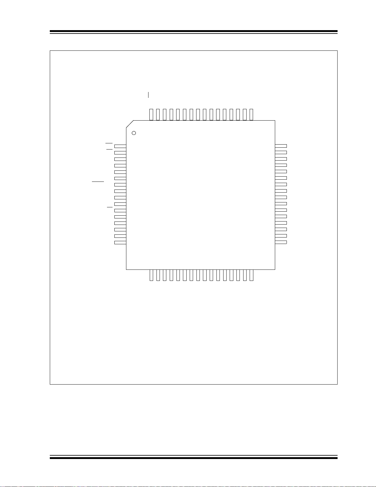
Pin Diagrams
64-Pin TQFP
PIC18F6585/8585/6680/8680
(1)
RE2/CS
RE3
RE4
RE5/P1C
RE6/P1B
RE7/CCP2
RD0/PSP0
VDDVSS
RD1/PSP1
RD2/PSP2
RD3/PSP3
RD4/PSP4
RD5/PSP5
RD6/PSP6
RD7/PSP7
RE1/WR
RE0/RD
RG0/CANTX1
RG1/CANTX2
RG2/CANRX
RG5/MCLR
RG4/P1D
RF7/SS
RF6/AN11/C1IN-
RF5/AN10/C1IN+/CV
RF4/AN9/C2IN-
RF3/AN8/C2IN+
RF2/AN7/C1OUT
RG3
/VPP
VSS
VDD
REF
64
63 62 61
1
2
3
4
5
6
7
8
9
10
11
12
13
14
15
16
17 18 19 20 21 22 23 24 25 26
DD
AV
RF0/AN5
RF1/AN6/C2OUT
PIC18F6X8X
REF-
AVSS
RA2/AN2/V
RA3/AN3/VREF+
RA1/AN1
54 53 52 5158 57 56 5560 59
27 28
SS
V
VDD
RA0/AN0
RA5/AN4/LVDIN
50 49
31
29 30 32
(1)
RA4/T0CKI
RC1/T1OSI/CCP2
RC0/T1OSO/T13CKI
RC6/TX/CK
RC7/RX/DT
48
47
46
45
44
43
42
41
40
39
38
37
36
35
34
33
RB0/INT0
RB1/INT1
RB2/INT2
RB3/INT3
RB4/KBI0
RB5/KBI1/PGM
RB6/KBI2/PGC
SS
V
OSC2/CLKO/RA6
OSC1/CLKI
DD
V
RB7/KBI3/PGD
RC5/SDO
RC4/SDI/SDA
RC3/SCK/SCL
RC2/CCP1/P1A
Note 1: CCP2 pin placement depends on CCP2MX setting.
2004 Microchip Technology Inc. DS30491C-page 3
PIC18F6585/8585/6680/8680
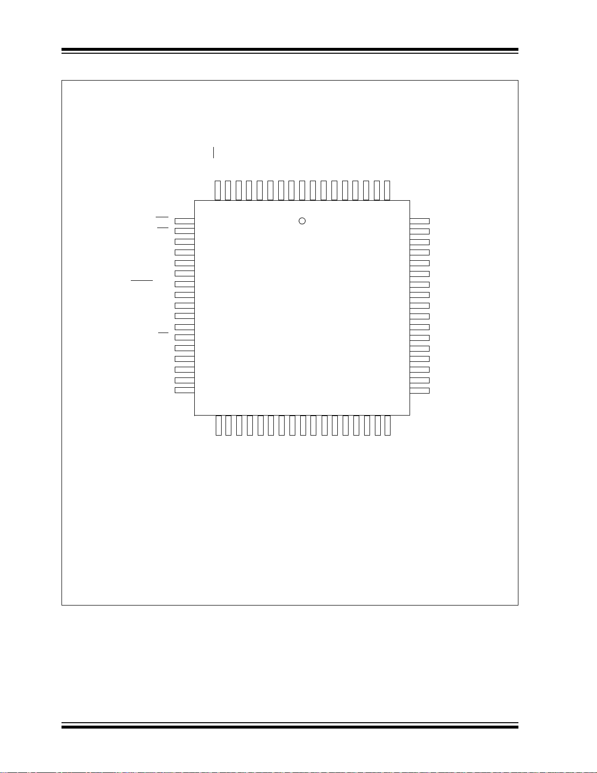
Pin Diagrams (Continued)
68-Pin PLCC
(1)
RE1/WR
RE0/RD
RG0/CANTX1
RG1/CANTX2
RG2/CANRX
RG5/MCLR
RG4/P1D
RF7/SS
RF6/AN11/C1IN-
RF5/AN10/C1IN+/CV
RF4/AN9/C2IN-
RF3/AN8/C2IN+
RF2/AN7/C1OUT
RG3
/VPP
N/C
SS
V
VDD
REF
RE2/CS
RE3
RE4
RE5/P1C
RE6/P1B
RE7/CCP2
9 8 7 6 5 4 3 2 1 6867666564636261
10
11
12
13
14
15
16
17
18
19
20
21
22
23
24
25
26
2728 2930 3132 33 34 35 36 37 38 39 40 41 42 43
DD
AVSS
AV
RF0/AN5
RA2/AN2/VREF-
RF1/AN6/C2OUT
RA3/AN3/VREF+
N/C
RD0/PSP0
VDDVSS
Top View
PIC18F6X8X
SS
V
N/C
RA1/AN1
RA0/AN0
RD1/PSP1
RD2/PSP2
RD3/PSP3
DD
V
RA4/T0CKI
RA5/AN4/LVDIN
(1)
RD4/PSP4
RC1/T1OSI/CCP2
RD5/PSP5
RD6/PSP6
RC0/T1OSO/T13CKI
RC6/TX/CK
RD7/PSP7
RC7/RX/DT
60
59
58
57
56
55
54
53
52
51
50
49
48
47
46
45
44
RB0/INT0
RB1/INT1
RB2/INT2
RB3/INT3
RB4/KBI0
RB5/KBI1/PGM
RB6/KBI2/PGC
V
SS
N/C
OSC2/CLKO/RA6
OSC1/CLKI
DD
V
RB7/KBI3/PGD
RC5/SDO
RC4/SDI/SDA
RC3/SCK/SCL
RC2/CCP1/P1A
Note 1: CCP2 pin placement depends on CCP2MX setting.
DS30491C-page 4 2004 Microchip Technology Inc.

Pin Diagrams (Continued)
80-Pin TQFP
RH2/A18
RH3/A19
RE1/WR/AD9
RE0/RD
/AD8
RG0/CANTX1
RG1/CANTX2
RG2/CANRX
RG3
RG5/MCLR
/VPP
RG4/P1D
VSS
VDD
RF7/SS
RF6/AN11/C1IN-
RF5/AN10/C1IN+/CVREF
RF4/AN9/C2IN-
RF3/AN8/C2IN+
RF2/AN7/C1OUT
RH7/AN15/P1B
RH6/AN14/P1C
(3)
(3)
1
2
3
4
5
6
7
8
9
10
11
12
13
14
15
16
17
18
19
20
PIC18F6585/8585/6680/8680
(3)
(3)
/AD15
/AD0
(2)
(1)
DD
RE2/CS/AD10
RE3/AD11
RE4/AD12
RH0/A16
RH1/A17
80
78
79
RE5/AD13/P1C
77 76 75
21 22 23 24 25 26 27 28 29 30 31 32
RD0/PSP0
RE6/AD14/P1B
RE7/CCP2
V
PIC18F8X8X
VSS
/AD1
(1)
RD1/PSP1
/AD2
(1)
RD2/PSP2
68 67 66 6572 71 70 6974 73
33 34
/AD3
(1)
RD3/PSP3
/AD4
(1)
RD4/PSP4
35 36
/AD5
/AD6
(1)
(1)
(1)
RD5/PSP5
RD6/PSP6
64 63 62 61
37
38
/AD7
RD7/PSP7
39
RJ0/ALE
RJ1/OE
60
59
58
57
56
55
54
53
52
51
50
49
48
47
46
45
44
43
42
41
RJ2/WRL
RJ3/WRH
RB0/INT0
RB1/INT1
RB2/INT2
RB3/INT3/CCP2
RB4/KBI0
RB5/KBI1/PGM
RB6/KBI2/PGC
V
SS
OSC2/CLKO/RA6
OSC1/CLKI
V
DD
RB7/KBI3/PGD
RC5/SDO
RC4/SDI/SDA
RC3/SCK/SCL
RC2/CCP1/P1A
RJ7/UB
RJ6/LB
(2)
40
DD
AV
RH5/AN13
RF0/AN5
RH4/AN12
RF1/AN6/C2OUT
REF-
AVSS
RA2/AN2/V
RA3/AN3/VREF+
SS
V
RA1/AN1
RA0/AN0
(2)
VDD
RJ5/CE
RA4/T0CKI
RC6/TX/CK
RJ4/BA0
RC7/RX/DT
RA5/AN4/LVDIN
RC1/T1OSI/CCP2
RC0/T1OSO/T13CKI
Note 1: PSP is available only in Microcontroller mode.
2: CCP2 pin placement depends on CCP2MX and Processor mode settings.
3: P1B and P1C pin placement depends on ECCPMX setting.
2004 Microchip Technology Inc. DS30491C-page 5

PIC18F6585/8585/6680/8680
Table of Contents
1.0 Device Overview..........................................................................................................................................................................9
2.0 Oscillator Configurations........ ....................................................................................................................................................23
3.0 Reset..........................................................................................................................................................................................33
4.0 Memory Organization.................................................................................................................................................................51
5.0 Flash Program Memory............... ...................................... ................................................... ...................................................... 83
6.0 External Memory Interface.........................................................................................................................................................93
7.0 Data EEPROM Memory....................... ......................... ......................... ..................................................................................101
8.0 8 x 8 Hardware Multiplier.......................................................................................................................................................... 107
9.0 Interrupts..................................................................................................................................................................................109
10.0 I/O Ports........................................... ......................... ......................... ......................................................................................125
11.0 Timer0 Module .........................................................................................................................................................................155
12.0 Timer1 Module .........................................................................................................................................................................159
13.0 Timer2 Module .........................................................................................................................................................................162
14.0 Timer3 Module .........................................................................................................................................................................164
15.0 Capture/Compare/PWM (CCP) Modules .................................................................................................................................167
16.0 Enhanced Capture/Compare/PWM (ECCP) Module................................................................................................................ 175
17.0 Master Synchronous Serial Port (MSSP) Module .................................................................................................................... 189
18.0 Enhanced Universal Synchronous Asynchronous Receiver Transmitter (USART)..................................................................229
19.0 10-bit Analog-to-Digital Converter (A/D) Module......................................................................................................................249
20.0 Comparator Module............................................................................................. .... .. .... .. ......................................................... 259
21.0 Comparator Voltage Reference Module.................................. ....... .... .. .... .. ....... .... .. .... .. .... ....... .. .............................................. 265
22.0 Low-Voltage Detect..................................................................................................................................................................269
23.0 ECAN Module..................................... .. .. .. .. .. .. .. .. ..... .. .... .. .. .. .. .. ..... .. .. .. .. .. .. .. .. ..... .. .. .. .. .. .. ...........................................................275
24.0 Special Features of the CPU......................................................................................... ........................................................... 345
25.0 Instruction Set Summary ..........................................................................................................................................................365
26.0 Development Support. .............................................................................................................................................................. 407
27.0 Electrical Characteristics..........................................................................................................................................................413
28.0 DC and AC Characteristics Graphs and Tables....................................................................................................................... 449
29.0 Packaging Information....................................................... ....................................................................................................... 465
Appendix A: Revision History............................................................................................................................................................. 469
Appendix B: Device Differences......................................................................................................................................................... 469
Appendix C: Conversion Considerations .................................................................... .... .. .... .. .... ....................................................... 470
Appendix D: Migration from Mid-Range to Enhanced Devices.......................................................................................................... 470
Appendix E: Migration from High-End to Enhanced Devices.............................................................................................................471
Index .................................................................................................................................................................................................. 473
On-Line Support........................................................................ .... .. ......... .... .. .... .... ....... .... ................................................................. 487
Systems Information and Upgrade Hot Line......................................................................................................................................487
Reader Response..............................................................................................................................................................................488
PIC18F6585/8585/6680/8680 Product Identification System ............................................................................................................ 489
DS30491C-page 6 2004 Microchip Technology Inc.

PIC18F6585/8585/6680/8680
TO OUR VALUED CUSTOMERS
It is our intention to provide our valued customers with the best documentation possible to ensure successful use of your Microchip
products. To this end, we will continue to improve our publications t o better suit your needs. Our publications will be refined and
enhanced as new volumes and updates are introduced.
If you have any questions or c omm ents regarding t his publication, p lease c ontact the M arket ing Co mmunications Department via
E-mail at docerrors@mail.microchip.com or fax the Reader Response Form in the back of this data sheet to (480) 792-4150.
We welcome your feedback.
Most Current Data Sheet
To obtain the most up-to-date version of this data sheet, please register at our Worldwide Web site at:
http://www.microchip.com
You can determ ine the version of a data sheet by examining its literature number found on the bottom outside corner of any page.
The last character of the literature number is the version number, (e.g., DS30000A is version A of document DS30000).
Errata
An errata sheet, describing minor operational differences from the data sheet and recommended workarounds, may exist for current
devices. As device/documentation issues become known to us, we will publish an errata sheet. The errata will specify the revision
of silicon and revision of document to which it applies.
To determine if an errata sheet exists for a particular device, please check with one of the following:
• Microchip’s Worldwide Web site; http://www.microchip.com
• Your local Microchip sales office (see last page)
• The Microchip Corporate Literature Center; U.S. FAX: (480) 792-7277
When contacting a sales office or the literature center, please specify which device, revision of silicon and data sheet (include literature number) you are using.
Customer Notification System
Register on our Web site at www.microchip.com/cn to receive the most current information on all of our products.
2004 Microchip Technology Inc. DS30491C-page 7

PIC18F6585/8585/6680/8680
NOTES:
DS30491C-page 8 2004 Microchip Technology Inc.

PIC18F6585/8585/6680/8680
1.0 DEVICE OVERVIEW
All other features for devices in the
PIC18F6585/8585/6680/8680 family are identical.
This documen t conta i ns dev ic e spec if i c in for m at i on fo r
the following devices:
• PIC18F6585 • PIC18F8585
• PIC18F6680 • PIC18F8680
PIC18F6X8X devices are av ailable in 64-pin TQFP an d
These are summarized in Table 1-1.
Block diagrams of the PIC18F6X8X and PIC18F8X8X
devices are provided in Figure 1-1 and Figure 1-2,
respectively. The pinouts for these device families are
listed in Table 1-2.
68-pin PLCC packages. PIC18F8X8X devices are
available in the 80-pin TQFP package. They are
differentiated from each other in four way s :
1. Flash program memory (48 Kbytes for
PIC18FX585 devices, 64Kbytes for
PIC18FX680)
2. A/D channels (1 2 for PIC18F6X8X devices,
16 for PIC1 8F8X8X)
3. I/O ports (7 on PIC18F6X8X devices, 9 on
PIC18F8X8X)
4. External program memory interface (present
only on PIC18F8X8X devices)
T ABLE 1-1: PIC18F6585/8585/6680/8680 DEVICE FEATURES
Features PIC18F6585 PIC18F6680 PIC18F8585 PIC18F8680
Operating Frequency DC – 40 MHz DC – 40 MHz DC – 40 MHz
DC–25MHzw/EMA
Program Memory (Bytes) 48K 64K 48K (2 MB EMA) 64K (2 MB EMA)
Program Memory (Instructions) 24576 32768 24576 32768
Data Memory (Bytes) 3328 3328 3328 3328
Data EEPROM Memory (Bytes) 1024 1024 1024 10 24
External Memory Interface No No Yes Yes
Interrupt Sourc e s 29 29 29 29
I/O Ports Ports A
Timers 4 4 4 4
Capture/Compare/PWM M odule 1 1 1 1
Enhanced Capture/Compare/PWM
Module
Serial Communications MSSP,
Enhanced AUSAR T ,
Parallel Communications PSP PSP PSP
10-bit Analog-to-Digital Module 12 input cha nnels 12 input ch annels 16 inp ut cha nnels 16 inpu t chan nels
Resets (and Delays) POR, BOR,
RESET Instruction,
Stack Underflow
(PWRT, OST)
Programmable Low-Voltage Detect Y es Yes Yes Yes
Programmable Brown-out Reset Yes Yes Yes Yes
Instruction Set 75 Instructions 75 Instruc tions 75 Instructions 75 Instructions
Package 64-pin TQFP,
68-pin PLCC
Note 1: PSP is only available in Microcontroller mode.
-G Ports A-GPorts A-H, J Ports A-H, J
11 1 1
ECAN
Stack Full,
MSSP,
Enhanced AUSAR T,
ECAN
POR, BOR,
RESET Instruction,
Stack Full,
Stack Underflow
(PWRT, OST)
64-pin TQFP ,
68-pin PLCC
MSSP,
Enhanced AUSART,
ECAN
(1)
POR, BOR,
RESET Instruction,
Stack Full,
Stack Underflow
(PWRT, OST)
80-pin TQFP 80-pin TQFP
DC–40MHz
DC – 25 MHz w/EMA
MSSP,
Enhanced AUSAR T,
ECAN
(1)
PSP
POR, BOR,
RESET Instruction,
Stack Full,
Stack Underflow
(PWRT, OST)
2004 Microchip Technology Inc. DS30491C-page 9
PIC18F6585/8585/6680/8680
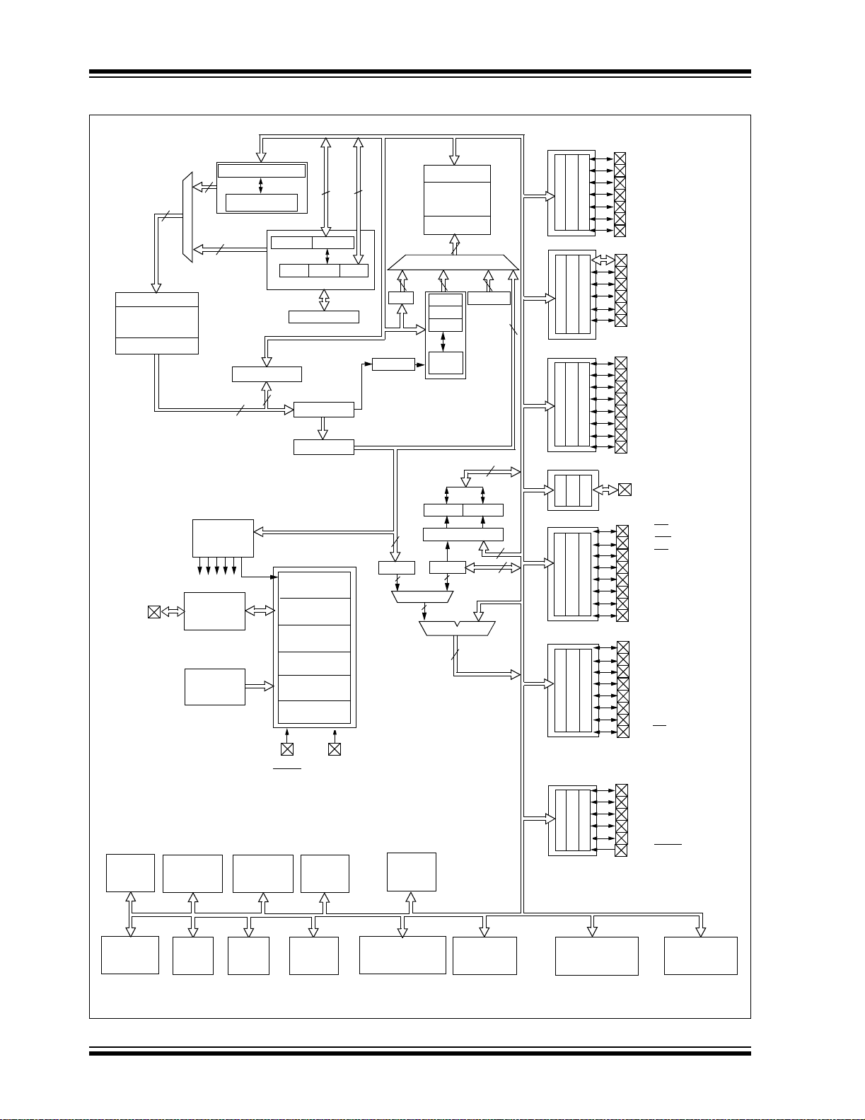
FIGURE 1-1: PIC18F6X8X BLOCK DIAGRAM
Data Bus<8>
21
Address Latch
Program Memory
(48 Kbytes)
Data Latch
OSC2/CLKO/RA6
OSC1/CLKI
Table Pointer<21>
21
21
Instruction
Decode &
Control
Timing
Generation
Precision
Band Gap
Reference
inc/dec logic
Table Latch
16
PCLATH
PCLATU
PCU
PCH PCL
Program Counter
31 Level Stack
8
ROM Latch
IR
Power-up
Timer
Oscillator
Start-up Timer
Power-on
Reset
Watchdog
Timer
Brown-out
Reset
Te st Mode
Select
8
8
Decode
BITOP
4
BSR
3
8
Data Latch
Data RAM
(3328 bytes)
Address Latch
12
Address<12>
12 4
FSR0
FSR1
FSR2
inc/dec
logic
8 x 8 Multiply
W
8
8
ALU<8>
8
Bank0, F
PRODLPRODH
PORTA
RA0/AN0
RA1/AN1
RA2/AN2/VREFRA3/AN3/VREF+
RA4/T0CKI
RA5/AN4/LVDIN
PORTB
12
PORTC
PORTD
8
PORTE
8
8
PORTF
OSC2/CLKO/RA6
RB2/INT2:RB0/INT0
RB3/INT3
RB4/KBI0
RB5/KBI1/PGM
RB6/KBI2/PGC
RB7/KBI3/PGD
RC0/T1OSO/T13CKI
RC1/T1OSI/CCP2
RC2/CCP1/P1A
RC3/SCK/SCL
RC4/SDI/SDA
RC5/SDO
RC6/TX/CK
RC7/RX/DT
RD7/PSP7
RE0/RD
RE1/WR
RE2/CS
RE3
RE4
RE5/P1C
RE6/P1B
RE7/CCP2
RF0/AN5
RF1/AN6/C2OUT
RF2/AN7/C1OUT
RF3/AN8/C2IN+
RF4/AN9/C2INRF5/AN10/C1IN+/CVREF
RF6/AN11/C1INRF7/SS
(1)
:RD0/PSP0
(1)
BOR
LVD
Timer0
ECCP1
Timer1
CCP2
RG5/
MCLR
AUSARTComparator
DD, VSS
V
Timer2
Timer3
ECAN Module
Synchronous
Serial Port
PORTG
10-bit
ADC
RG0/CANTX1
RG1/CANTX2
RG2/CANRX
RG3
RG4/P1D
RG5/MCLR/VPP
Data EEPROM
Note 1: The CCP2 pin placement depends on the CCP2MX and Processor mode settings.
DS30491C-page 10 2004 Microchip Technology Inc.
PIC18F6585/8585/6680/8680
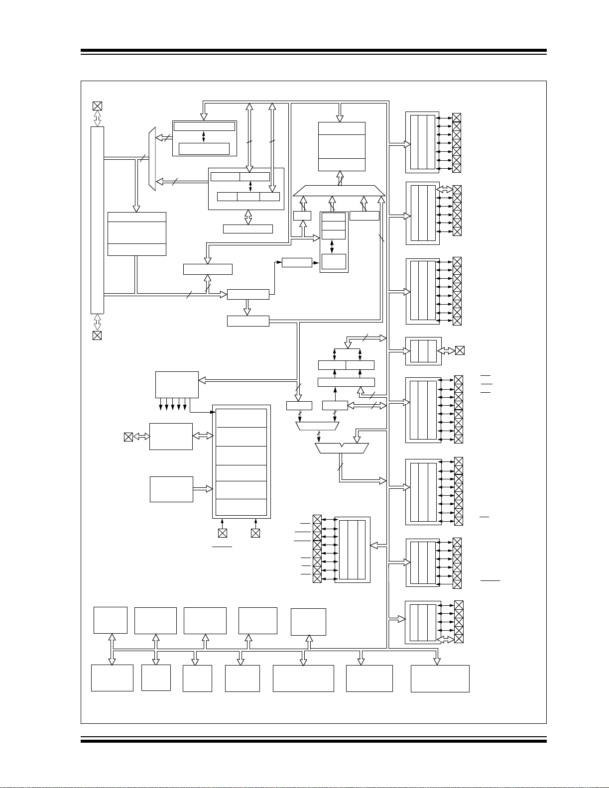
FIGURE 1-2: PIC18F8X8X BLOCK DIAGRAM
AD7:AD0
Address Latch
Program Memory
(64 Kbytes)
Data Latch
System Bus Interface
A16, AD15:AD8
OSC2/CLKO/RA6
OSC1/CLKI
BOR
LVD
21
Generation
Timer0
Table Pointer<21>
21
21
16
Instruction
Decode &
Control
Timing
Precision
Band Gap
Reference
inc/dec logic
PCLATU
Table Latch
8
RG5/
MCLR
Timer1
8
PCLATH
PCU
PCH PCL
Program Counter
31 Level Stack
ROM Latch
IR
Power-up
Timer
Oscillator
Start-up Timer
Power-on
Reset
Watchdog
Timer
Brown-out
Reset
Test Mode
Select
V
DD, VSS
Timer2
8
BSR
Decode
BITOP
RJ0/ALE
RJ1/OE
RJ2/WRL
RJ3/WRH
RJ4/BA0
RJ5/CE
RJ6/LB
RJ7/UB
Timer3
4
3
8
Data Bus<8>
Data Latch
Data RAM
(3328 bytes)
Address Latch
12
Address<12>
12 4
FSR0
FSR1
FSR2
inc/dec
logic
8 x 8 Multiply
W
8
8
ALU<8>
8
PORTJ
Bank0, F
PRODLPRODH
PORTA
RA0/AN0
RA1/AN1
RA2/AN2/VREFRA3/AN3/VREF+
RA4/T0CKI
RA5/AN4/LVDIN
PORTB
12
PORTC
PORTD
8
PORTE
8
8
PORTF
PORTG
PORTH
OSC2/CLKO/RA6
RB2/INT2:RB0/INT0
RB3/INT3/CCP2
RB4/KBI0
RB5/KBI1/PGM
RB6/KBI2/PGC
RB7/KBI3/PGD
RC0/T1OSO/T13CKI
RC1/T1OSI/CCP2
RC2/CCP1/P1A
RC3/SCK/SCL
RC4/SDI/SDA
RC5/SDO
RC6/TX/CK
RC7/RX/DT
RD7/PSP7
RD0/PSP0/AD0
RE0/RD/AD8
RE1/WR/AD9
RE2/CS/AD10
RE3/AD11
RE4/AD12
RE5/AD13/P1C
RE6/AD14/P1B
RE7/CCP2
RF0/AN5
RF1/AN6/C2OUT
RF2/AN7/C1OUT
RF3/AN8/C2IN+
RF4/AN9/C2IN-
RF5/AN10/C1IN+/CVREF
RF6/AN11/C1IN-
RF7/SS
RG0/CANTX1
RG1/CANTX2
RG2/CANRX
RG3
RG4/P1D
RG5/MCLR/VPP
RH7/AN15/P1B
RH6/AN14/P1C
RH5/AN13
RH4/AN12
RH3/A19:RH0/A16
/AD7:
(1)
/AD15
(1)
(1)
(2)
(2)
(2)
(2)
ECCP1
CCP2
AUSARTComparator
ECAN Module
Synchronous
Serial Port
10-bit
ADC
Note 1: The CCP2 pin placement depends on the CCP2MX and Processor mode settings.
2: P1B and P1C pin placement depends on the ECCPMX setting.
2004 Microchip Technology Inc. DS30491C-page 11

PIC18F6585/8585/6680/8680
TABLE 1-2: PIC18F6585/8585/6680/8680 PINOUT I/O DESCRIPTIONS
Pin Number
Pin Name
Pin
Type
TQFP PLCC TQFP
Buffer
Type
DescriptionPIC18F6X8X PIC18F8X8X
RG5/MCLR
RG5
MCLR
VPP
OSC1/CLKI
OSC1
CLKI
OSC2/CLKO/RA6
OSC2
CLKO
RA6
Legend: TTL = TTL compatible input CMOS = CMOS compatible input or output
Note 1: Alternate assignment for CCP2 in all operating modes except Microcontroller – applies to PIC18F8X8X only.
/VPP
ST = Schmitt Trigger input with CMOS levels Analog = Analog input
I = Input O = Output
P = Power OD = Open-Drain (no P diode to V
2: Default assignment when CCP2MX is set.
3: External memory interface functions are only available on PIC18F8X8X devices.
4: CCP2 is multiplexed with this pin by default when configured in Microcontroller mode; otherwise, it is
multiplexed with either RB3 or RC1.
5: PORTH and PORTJ are only available on PIC18F8X8X (80-pin) devices.
6: PSP is available in Microcontroller mode only.
7: On PIC18F8X8X devices, these pins can be multiplexed with RH7/RH6 by changing the ECCPMX
configuration bit.
716 9
39 50 49
40 51 50
I
I
P
IICMOS/ST
O
O
I/O
ST
ST
CMOS
TTL
Master Clear (input) or programming
voltage (input).
General purpose input pin.
Master Clear (Reset ) in pu t. This pin is
an active-low Reset to the device.
Programming voltage inp ut.
Oscillator crystal or external clock input.
Oscillator crystal input or external clock
source input. ST buffer when configured
in RC mode; otherwise CMOS.
External cloc k source input. Always
associated with pin function OSC1
(see OSC1/CLKI, OSC2/CLKO pins).
Oscillator crystal or clock output.
—
—
Oscillator crystal output.
Connects to crystal or resonator in
Crystal Oscillator mode.
In RC mode, OSC2 pi n o utpu ts CLKO
which has 1/4 the frequency of OSC1
and denotes the instruction cycle rate.
General purpose I/O pin.
DD)
DS30491C-page 12 2004 Microchip Technology Inc.

PIC18F6585/8585/6680/8680
T ABLE 1-2: PIC18F6585/8585/6680/8680 PINOUT I/O DESCRIPTIONS (CONTINUED)
Pin Number
Pin Name
TQFP PLCC TQFP
RA0/AN0
RA0
AN0
RA1/AN1
RA1
AN1
RA2/AN2/V
RA2
AN2
V
RA3/AN3/VREF+
RA3
AN3
V
RA4/T0CKI
RA4
T0CKI
RA5/AN4/LVDIN
RA5
AN4
LVDIN
RA6 See the OSC2/CLKO/RA6 pin.
Legend: TTL = TTL compatible input CMOS = CMOS compatible input or output
Note 1: Alternate assignment for CCP2 in all operating modes except Microcontroller – applies to PIC18F8X8X only.
REF-
REF-
REF+
ST = Schmitt Trigger input with CMOS levels Analog = Analog input
I = Input O = Output
P = Power OD = Open-Drain (no P diode to V
2: Default assignment when CCP2MX is set.
3: External memory interface functions are only available on PIC18F8X8X devices.
4: CCP2 is multiplexed with this pin by default when configured in Microcontroller mode; otherwise, it is
multiplexed with either RB3 or RC1.
5: PORTH and PORTJ are only available on PIC18F8X8X (80-pin) devices.
6: PSP is available in Microcontroller mode only.
7: On PIC18F8X8X devices, these pins can be multiplexed with RH7/RH6 by changing the ECCPMX
configuration bit.
24 34 30
23 33 29
22 32 28
21 31 27
28 39 34
27 38 33
Pin
Type
I/O
I/O
I/O
I/O
I/OIST/OD
I/O
Buffer
Type
PORTA is a bidirectional I/O port.
TTL
I
Analog
TTL
I
Analog
TTL
I
Analog
I
Analog
TTL
I
Analog
I
Analog
ST
TTL
I
Analog
I
Analog
Digital I/O.
Analog input 0.
Digital I/O.
Analog input 1.
Digital I/O.
Analog input 2.
A/D reference voltage (Low) input.
Digital I/O.
Analog input 3.
A/D reference voltage (High) input.
Digital I/O – Open-drain when
configured as output.
Timer0 external clock input.
Digital I/O.
Analog input 4.
Low-voltage detect input.
DescriptionPIC18F6X8X PIC18F8X8X
DD)
2004 Microchip Technology Inc. DS30491C-page 13

PIC18F6585/8585/6680/8680
TABLE 1-2: PIC18F6585/8585/6680/8680 PINOUT I/O DESCRIPTIONS (CONTINUED)
Pin Number
Pin Name
TQFP PLCC TQFP
RB0/INT0
RB0
INT0
RB1/INT1
RB1
INT1
RB2/INT2
RB2
INT2
RB3/INT3/CCP2
RB3
INT3
(1)
CCP2
RB4/KBI0
RB4
KBI0
RB5/KBI1/PGM
RB5
KBI1
PGM
RB6/KBI2/PGC
RB6
KBI2
PGC
RB7/KBI3/PGD
RB7
KBI3
PGD
Legend: TTL = TTL compatible input CMOS = CMOS compatible input or output
ST = Schmitt Trigger input with CMOS levels Analog = Analog input
I = Input O = Output
P = Power OD = Open-Drain (no P diode to V
Note 1: Alternate assignment for CCP2 in all operating modes except Microcontroller – applies to PIC18F8X8X only.
2: Default assignment when CCP2MX is set.
3: External memory interface functions are only available on PIC18F8X8X devices.
4: CCP2 is multiplexed with this pin by default when configured in Microcontroller mode; otherwise, it is
multiplexed with either RB3 or RC1.
5: PORTH and PORTJ are only available on PIC18F8X8X (80-pin) devices.
6: PSP is available in Microcontroller mode only.
7: On PIC18F8X8X devices, these pins can be multiplexed with RH7/RH6 by changing the ECCPMX
configuration bit.
48 60 58
47 59 57
46 58 56
45 57 55
44 56 54
43 55 53
42 54 52
37 48 47
Pin
Type
I/O
I/O
I/O
I/O
I/O
I/O
I/O
I/O
I/O
I/O
I/O
I/O
I/O
Buffer
Type
PORTB is a bidirectional I/O port. PORTB
can be software programmed for internal
weak pull-ups on all inputs.
TTL
I
I
I
I
I
I
ST
TTL
ST
TTL
ST
TTL
ST
ST
TTL
ST
TTL
ST
ST
TTL
ST
ST
TTL
ST
Digital I/O.
External interrupt 0.
Digital I/O.
External interrupt 1.
Digital I/O.
External interrupt 2.
Digital I/O.
External interrupt 3.
Capture 2 input/Compare 2 output/
PWM 2 output.
Digital I/O.
Interrupt-on-change pin.
Digital I/O.
Interrupt-on-change pin.
Low-Voltage ICSP Programming
enable pin.
Digital I/O.
Interrupt-on-change pin.
In-circuit debugger and ICSP
programming clock.
Digital I/O.
Interrupt-on-change pin.
In-circuit debugger and ICSP
programming data.
DescriptionPIC18F6X8X PIC18F8X8X
DD)
DS30491C-page 14 2004 Microchip Technology Inc.

PIC18F6585/8585/6680/8680
T ABLE 1-2: PIC18F6585/8585/6680/8680 PINOUT I/O DESCRIPTIONS (CONTINUED)
Pin Number
Pin Name
TQFP PLCC TQFP
RC0/T1OSO/T13CKI
RC0
T1OSO
T13CKI
RC1/T1OSI/CCP2
RC1
T1OSI
(1, 4)
CCP2
RC2/CCP1/P1A
RC2
CCP1
P1A
RC3/SCK/SCL
RC3
SCK
SCL
RC4/SDI/SDA
RC4
SDI
SDA
RC5/SDO
RC5
SDO
RC6/TX/CK
RC6
TX
CK
RC7/RX/DT
RC7
RX
DT
Legend: TTL = TTL compatible input CMOS = CMOS compatible input or output
ST = Schmitt Trigger input with CMOS levels Analog = Analog input
I = Input O = Output
P = Power OD = Open-Drain (no P diode to V
Note 1: Alternate assignment for CCP2 in all operating modes except Microcontroller – applies to PIC18F8X8X only.
2: Default assignment when CCP2MX is set.
3: External memory interface functions are only available on PIC18F8X8X devices.
4: CCP2 is multiplexed with this pin by default when configured in Microcontroller mode; otherwise, it is
multiplexed with either RB3 or RC1.
5: PORTH and PORTJ are only available on PIC18F8X8X (80-pin) devices.
6: PSP is available in Microcontroller mode only.
7: On PIC18F8X8X devices, these pins can be multiplexed with RH7/RH6 by changing the ECCPMX
configuration bit.
30 41 36
29 40 35
33 44 43
34 45 44
35 46 45
36 47 46
31 42 37
32 43 38
Pin
Type
I/O
I/O
I/O
I/O
I/O
I/O
I/O
I/O
I/O
I/O
I/O
I/O
I/O
I/O
I/O
I/O
Buffer
Type
PORTC is a bidirectional I/O port.
ST
O
I
I
I
O
O
I
—
ST
ST
CMOS
ST
ST
ST
ST
ST
ST
ST
ST
ST
ST
ST
—
ST
—
ST
ST
ST
ST
Digital I/O.
Timer1 oscillator output.
Timer1/Timer3 external clock input.
Digital I/O.
Timer1 oscillator input.
CCP2 Capture input/Compare output/
PWM 2 output.
Digital I/O.
CCP1 Capture input/Compare output.
CCP1 PWM output A.
Digital I/O.
Synchronous serial clock input/output
for SPI mode.
Synchronous serial clock input/output
for I
Digital I/O.
SPI data in.
2
C data I/O .
I
Digital I/O.
SPI data out.
Digital I/O.
USART asynchronous tran sm it.
USART synchronous clo ck
(see RX/DT).
Digital I/O.
USART 1 asynchronous receive.
USART 1 synchronous data
(see TX/CK).
2
C mode.
DescriptionPIC18F6X8X PIC18F8X8X
DD)
2004 Microchip Technology Inc. DS30491C-page 15

PIC18F6585/8585/6680/8680
TABLE 1-2: PIC18F6585/8585/6680/8680 PINOUT I/O DESCRIPTIONS (CONTINUED)
Pin Number
Pin Name
Pin
Type
TQFP PLCC TQFP
RD0/PSP0/AD0
RD0
(6)
PSP0
(3)
AD0
RD1/PSP1/AD1
RD1
(6)
PSP1
(3)
AD1
RD2/PSP2/AD2
RD2
(6)
PSP2
(3)
AD2
RD3/PSP3/AD3
RD3
(6)
PSP3
(3)
AD3
RD4/PSP4/AD4
RD4
(6)
PSP4
(3)
AD4
RD5/PSP5/AD5
RD5
(6)
PSP5
(3)
AD5
RD6/PSP6/AD6
RD6
(6)
PSP6
(3)
AD6
RD7/PSP7/AD7
RD7
(6)
PSP7
(3)
AD7
58 3 72
55 67 69
54 66 68
53 65 67
52 64 66
51 63 65
50 62 64
49 61 63
Legend: TTL = TTL compatible input CMOS = CMOS compatible input or output
ST = Schmitt Trigger input with CMOS levels Analog = Analog input
I = Input O = Output
P = Power OD = Open-Drain (no P diode to V
Note 1: Alternate assignment for CCP2 in all operating modes except Microcontroller – applies to PIC18F8X8X only.
2: Default assignment when CCP2MX is set.
3: External memory interface functions are only available on PIC18F8X8X devices.
4: CCP2 is multiplexed with this pin by default when configured in Microcontroller mode; otherwise, it is
multiplexed with either RB3 or RC1.
5: PORTH and PORTJ are only available on PIC18F8X8X (80-pin) devices.
6: PSP is available in Microcontroller mode only.
7: On PIC18F8X8X devices, these pins can be multiplexed with RH7/RH6 by changing the ECCPMX
configuration bit.
I/O
I/O
I/O
I/O
I/O
I/O
I/O
I/O
I/O
I/O
I/O
I/O
I/O
I/O
I/O
I/O
I/O
I/O
I/O
I/O
I/O
I/O
I/O
I/O
Buffer
Type
ST
TTL
TTL
ST
TTL
TTL
ST
TTL
TTL
ST
TTL
TTL
ST
TTL
TTL
ST
TTL
TTL
ST
TTL
TTL
ST
TTL
TTL
DescriptionPIC18F6X8X PIC18F8X8X
PORTD is a bidirectional I/O port. These
pins have TTL input buf fers when ex ternal
memory is enabled.
Digital I/O.
Parallel Slave Port data.
External memory address/data 0.
Digital I/O.
Parallel Slave Port data.
External memory address/data 1.
Digital I/O.
Parallel Slave Port data.
External memory address/data 2.
Digital I/O.
Parallel Slave Port data.
External memory address/data 3.
Digital I/O.
Parallel Slave Port data.
External memory address/data 4.
Digital I/O.
Parallel Slave Port data.
External memory address/data 5.
Digital I/O.
Parallel Slave Port data.
External memory address/data 6.
Digital I/O.
Parallel Slave Port data.
External memory address/data 7.
DD)
DS30491C-page 16 2004 Microchip Technology Inc.
PIC18F6585/8585/6680/8680
T ABLE 1-2: PIC18F6585/8585/6680/8680 PINOUT I/O DESCRIPTIONS (CONTINUED)
Pin Number
Pin Name
Pin
Type
TQFP PLCC TQFP
RE0
(6)
RD
AD8
RE1
WR
AD9
RE2
(6)
CS
AD10
/AD8
(3)
/AD9
(6)
(3)
/AD10
(3)
RE0/RD
RE1/WR
RE2/CS
RE3/AD11
RE3
(3)
AD11
RE4/AD12
RE4
(3)
AD12
RE5/AD13/P1C
RE5
(3)
AD13
(7)
P1C
RE6/AD14/P1B
RE6
(3)
AD14
(7)
P1B
RE7/CCP2/AD15
RE7
(1,4)
CCP2
(3)
AD15
211 4
I/O
I/O
110 3
I/O
I/O
64 9 78
I/O
I/O
63 8 77
I/O
I/O
62 7 76
I/O
I/O
61 6 75
I/O
I/O
I/O
60 5 74
I/O
I/O
I/O
59 4 73
I/O
I/O
I/O
Legend: TTL = TTL compatible input CMOS = CMOS compatible input or output
ST = Schmitt Trigger input with CMOS levels Analog = Analog input
I = Input O = Output
P = Power OD = Open-Drain (no P diode to V
Note 1: Alternate assignment for CCP2 in all operating modes except Microcontroller – applies to PIC18F8X8X only.
2: Default assignment when CCP2MX is set.
3: External memory interface functions are only available on PIC18F8X8X devices.
4: CCP2 is multiplexed with this pin by default when configured in Microcontroller mode; otherwise, it is
multiplexed with either RB3 or RC1.
5: PORTH and PORTJ are only available on PIC18F8X8X (80-pin) devices.
6: PSP is available in Microcontroller mode only.
7: On PIC18F8X8X devices, these pins can be multiplexed with RH7/RH6 by changing the ECCPMX
configuration bit.
Buffer
Type
DescriptionPIC18F6X8X PIC18F8X8X
PORTE is a bidirectional I/O port.
ST
I
TTL
TTL
ST
I
TTL
TTL
ST
I
TTL
TTL
ST
TTL
ST
TTL
ST
TTL
ST
ST
TTL
ST
ST
ST
Digital I/O.
Read control for Parallel Slave Port
(see WR
and CS pins).
External memory address/data 8.
Digital I/O.
Write control for Parallel Slave Port
(see CS
and RD pins).
External memory address/data 9.
Digital I/O.
Chip select control for Parallel Slave
Port (see RD
and WR).
External memory address/data 10.
Digital I/O.
External memory address/data 11.
Digital I/O.
External memory address/data 12.
Digital I/O.
External memory address/data 13.
ECCP1 PWM output C.
Digital I/O.
External memory address/data 14.
ECCP1 PWM output B.
Digital I/O.
Capture 2 input/Compare 2 output/
PWM 2 output.
TTL
External memory address/data 15.
DD)
2004 Microchip Technology Inc. DS30491C-page 17
PIC18F6585/8585/6680/8680
TABLE 1-2: PIC18F6585/8585/6680/8680 PINOUT I/O DESCRIPTIONS (CONTINUED)
Pin Number
Pin Name
TQFP PLCC TQFP
RF0/AN5
RF0
AN5
RF1/AN6/C2OUT
RF1
AN6
C2OUT
RF2/AN7/C1OUT
RF2
AN7
C1OUT
RF3/AN8/C2IN+
RF1
AN8
C2IN+
RF4/AN9/C2IN-
RF1
AN9
C2IN-
RF5/AN10/C1IN+/CV
RF1
AN10
C1IN+
REF
CV
RF6/AN11/C1IN-
RF6
AN11
C1IN-
RF7/SS
RF7
SS
Legend: TTL = TTL compatible input CMOS = CMOS compatible input or output
ST = Schmitt Trigger input with CMOS levels Analog = Analog input
I = Input O = Output
P = Power OD = Open-Drain (no P diode to V
Note 1: Alternate assignment for CCP2 in all operating modes except Microcontroller – applies to PIC18F8X8X only.
2: Default assignment when CCP2MX is set.
3: External memory interface functions are only available on PIC18F8X8X devices.
4: CCP2 is multiplexed with this pin by default when configured in Microcontroller mode; otherwise, it is
multiplexed with either RB3 or RC1.
5: PORTH and PORTJ are only available on PIC18F8X8X (80-pin) devices.
6: PSP is available in Microcontroller mode only.
7: On PIC18F8X8X devices, these pins can be multiplexed with RH7/RH6 by changing the ECCPMX
configuration bit.
18 28 24
17 27 23
16 26 18
15 25 17
14 24 16
REF
13 23 15
12 22 14
11 21 13
Pin
Type
I/O
I/O
O
I/O
O
I/O
I/O
I/O
O
I/O
I/O
Buffer
Type
PORTF is a bidirectional I/O port.
ST
I
Analog
ST
I
Analog
ST
ST
I
Analog
ST
ST
I
Analog
I
Analog
ST
I
Analog
I
Analog
ST
I
Analog
I
Analog
Analog
ST
I
Analog
I
Analog
ST
I
TTL
Digital I/O.
Analog input 5.
Digital I/O.
Analog input 6.
Comparator 2 output.
Digital I/O.
Analog input 7.
Comparator 1 output.
Digital I/O.
Analog input 8.
Comparator 2 input (+).
Digital I/O.
Analog input 9.
Comparator 2 input (-).
Digital I/O.
Analog input 10.
Comparator 1 input (+).
Comparator V
Digital I/O.
Analog input 11.
Comparator 1 input (-)
Digital I/O.
SPI slave select input.
DescriptionPIC18F6X8X PIC18F8X8X
REF output.
DD)
DS30491C-page 18 2004 Microchip Technology Inc.

PIC18F6585/8585/6680/8680
T ABLE 1-2: PIC18F6585/8585/6680/8680 PINOUT I/O DESCRIPTIONS (CONTINUED)
Pin Number
Pin Name
TQFP PLCC TQFP
RG0/CANTX1
RG0
CANTX1
RG1/CANTX2
RG1
CANTX2
RG2/CANRX
RG2
CANRX
RG3
RG3
RG4/P1D
RG4
P1D
RG5 7 16 9 I ST General purpose input pin.
Legend: TTL = TTL compatible input CMOS = CMOS compatible input or output
ST = Schmitt Trigger input with CMOS levels Analog = Analog input
I = Input O = Output
P = Power OD = Open-Drain (no P diode to V
Note 1: Alternate assignment for CCP2 in all operating modes except Microcontroller – applies to PIC18F8X8X only.
2: Default assignment when CCP2MX is set.
3: External memory interface functions are only available on PIC18F8X8X devices.
4: CCP2 is multiplexed with this pin by default when configured in Microcontroller mode; otherwise, it is
multiplexed with either RB3 or RC1.
5: PORTH and PORTJ are only available on PIC18F8X8X (80-pin) devices.
6: PSP is available in Microcontroller mode only.
7: On PIC18F8X8X devices, these pins can be multiplexed with RH7/RH6 by changing the ECCPMX
configuration bit.
312 5
413 6
514 7
615 8
817 10
Pin
Type
I/O
I/O
I/O
I/O ST Digital I/O.
I/O
Buffer
Type
PORTG is a bidirectional I/O port.
ST
O
O
I
O
TTL
ST
TTL
ST
TTL
ST
TTL
Digital I/O.
CAN bus transmit 1.
Digital I/O.
CAN bus transmit 2.
Digital I/O.
CAN bus receive.
Digital I/O.
ECCP1 PWM output D.
DescriptionPIC18F6X8X PIC18F8X8X
DD)
2004 Microchip Technology Inc. DS30491C-page 19

PIC18F6585/8585/6680/8680
TABLE 1-2: PIC18F6585/8585/6680/8680 PINOUT I/O DESCRIPTIONS (CONTINUED)
Pin Number
Pin Name
TQFP PLCC TQFP
RH0/A16
RH0
A16
RH1/A17
RH1
A17
RH2/A18
RH2
A18
RH3/A19
RH3
A19
RH4/AN12
RH4
AN12
RH5/AN13
RH5
AN13
RH6/AN14/P1C
RH6
AN14
(7)
P1C
RH7/AN15/P1B
RH7
AN15
(7)
P1B
Legend: TTL = TTL compatible input CMOS = CMOS compatible input or output
ST = Schmitt Trigger input with CMOS levels Analog = Analog input
I = Input O = Output
P = Power OD = Open-Drain (no P diode to V
Note 1: Alternate assignment for CCP2 in all operating modes except Microcontroller – applies to PIC18F8X8X only.
2: Default assignment when CCP2MX is set.
3: External memory interface functions are only available on PIC18F8X8X devices.
4: CCP2 is multiplexed with this pin by default when configured in Microcontroller mode; otherwise, it is
multiplexed with either RB3 or RC1.
5: PORTH and PORTJ are only available on PIC18F8X8X (80-pin) devices.
6: PSP is available in Microcontroller mode only.
7: On PIC18F8X8X devices, these pins can be multiplexed with RH7/RH6 by changing the ECCPMX
configuration bit.
—— 79
—— 80
—— 1
—— 2
—— 22
—— 21
—— 20
—— 19
Pin
Type
I/O
O
I/O
O
I/O
O
I/O
O
I/O
I/O
I/O
I/O
I/O
Buffer
Type
PORTH is a bidirectional I/O port
ST
TTL
ST
TTL
ST
TTL
ST
TTL
ST
I
Analog
ST
I
Analog
ST
I
Analog
ST
ST
I
Analog
Digital I/O.
External memory address 16.
Digital I/O.
External memory address 17.
Digital I/O.
External memory address 18.
Digital I/O.
External memory address 19.
Digital I/O.
Analog input 12.
Digital I/O.
Analog input 13.
Digital I/O.
Analog input 14.
Alternate CCP1 PWM out put C.
Digital I/O.
Analog input 15.
Alternate CCP1 PWM out put B.
DescriptionPIC18F6X8X PIC18F8X8X
(5)
.
DD)
DS30491C-page 20 2004 Microchip Technology Inc.
PIC18F6585/8585/6680/8680
T ABLE 1-2: PIC18F6585/8585/6680/8680 PINOUT I/O DESCRIPTIONS (CONTINUED)
Pin Number
Pin Name
TQFP PLCC TQFP
RJ0/ALE
RJ0
ALE
RJ1/OE
RJ1
OE
RJ2/WRL
RJ2
WRL
RJ3/WRH
RJ3
WRH
RJ4/BA0
RJ4
BA0
RJ5/CE
CE
RJ6/LB
RJ6
LB
RJ7/UB
RJ7
UB
VSS 9, 25,
V
DD 10, 26,
SS 20 30 26 P — Ground reference for analog modules.
AV
DD 19 29 25 P — Positive supply for analog modules.
AV
NC — 1, 18,
Legend: TTL = TTL compatible input CMOS = CMOS compatible input or output
ST = Schmitt Trigger input with CMOS levels Analog = Analog input
I = Input O = Output
P = Power OD = Open-Drain (no P diode to V
Note 1: Alternate assignment for CCP2 in all operating modes except Microcontroller – applies to PIC18F8X8X only.
2: Default assignment when CCP2MX is set.
3: External memory interface functions are only available on PIC18F8X8X devices.
4: CCP2 is multiplexed with this pin by default when configured in Microcontroller mode; otherwise, it is
multiplexed with either RB3 or RC1.
5: PORTH and PORTJ are only available on PIC18F8X8X (80-pin) devices.
6: PSP is available in Microcontroller mode only.
7: On PIC18F8X8X devices, these pins can be multiplexed with RH7/RH6 by changing the ECCPMX
configuration bit.
—— 62
—— 61
—— 60
—— 59
—— 39
— — 40 I/O
—— 42
—— 41
41, 56
38, 57
19, 36,
53, 68
2, 20,
37, 49
35, 52
11, 31,
51, 70
12, 32,
48, 71
— — — No connect.
Pin
Type
I/O
I/O
I/O
I/O
I/O
I/O
I/O
Buffer
Type
PORTJ is a bidirectional I/O port
ST
O
O
O
O
O
O
O
O
P — Ground reference for logic and I/O pins.
P — Positive supply for logic and I/O pins.
TTL
ST
TTL
ST
TTL
ST
TTL
ST
TTL
ST
TTL
ST
TTL
ST
TTL
Digital I/O.
External memory address latch
enable.
Digital I/O.
External memory output enable.
Digital I/O.
External memory write low control.
Digital I/O.
External memory write high control.
Digital I/O.
System bus byte address 0 control.
Digital I/O
External memory chip enable.
Digital I/O.
External memory low byte sele ct.
Digital I/O.
External memory high byte select.
DescriptionPIC18F6X8X PIC18F8X8X
(5)
.
DD)
2004 Microchip Technology Inc. DS30491C-page 21

PIC18F6585/8585/6680/8680
NOTES:
DS30491C-page 22 2004 Microchip Technology Inc.
PIC18F6585/8585/6680/8680
2.0 OSCILLATOR CONFIGURATIONS
2.1 Oscillator Types
The PIC18F6585/8585/6680/8680 devices can be
operated in eleven different oscillator modes. The user
can program four configuration bits (FOSC3, FOSC2,
FOSC1 and FOSC0) to select one of these eleven
modes:
1. LP Low-Power Crystal
2. XT Crystal/Resonator
3. HS High-Speed Crystal/Resonator
4. RC External Resistor/Cap ac ito r
5. EC External Clock
6. ECIO External Clock with I/O
pin enabled
7. HS+PLL High-Speed Crystal/Resonator
with PLL enabled
8. RCIO External Resist or/Capacitor with
I/O pin enabled
9. ECIO+SPLL External Clock with software
controlled PLL
10. ECIO+PLL External Clock with PLL and I/O
pin enabled
11. HS+SPLL High-Speed Crystal/Resonator
with software control
2.2 Crystal Oscillator/Ceramic Resonators
In XT, LP, HS, HS+PLL or HS+SPLL Oscillator modes,
a crystal or ceramic resonator is connected to the OSC1
and OSC2 pins to establish oscillation. Figure 2-1
shows the pin connections.
The PIC18F6585/8585/6680/8680 oscillator design
requires the use of a parallel cut crystal.
Note: Use of a series cut crystal may give a fre-
quency out of the crystal manufacturers
specifications.
FIGURE 2-1: CRYSTAL/CERAMIC
RESONATOR OPERATION
(HS, XT OR LP
CONFIGURATION)
(1)
C1
(1)
C2
Note 1: See Table 2-1 and Table 2-2 for recommended
2: A series resistor (R
3: R
OSC1
XTAL
(2)
RS
OSC2
values of C1 and C2.
strip cut crystals.
F varies with the oscillator mode chosen.
(3)
RF
Sleep
PIC18FXX80/XX85
S) may be required for AT
To
Internal
Logic
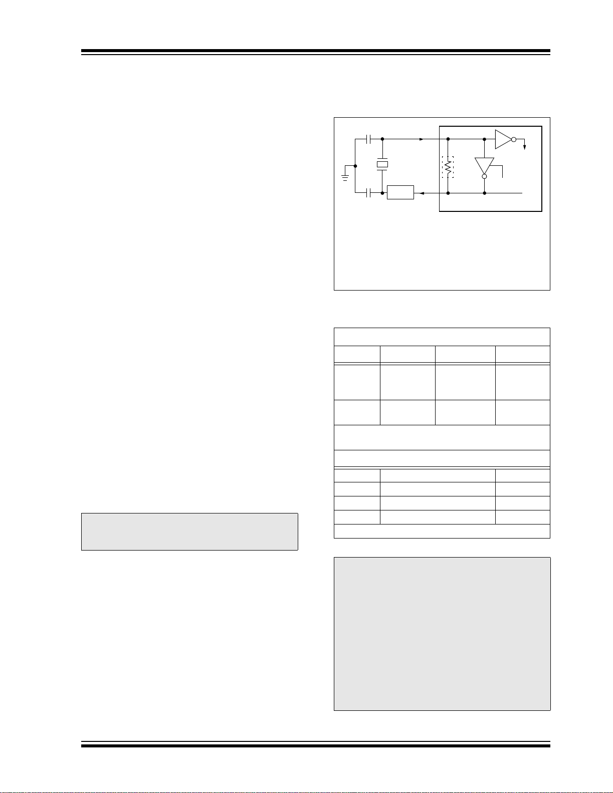
T ABLE 2-1: CAPACITOR SELECTION FOR
CERAMIC RESONATORS
Ranges Tested:
Mode Freq C1 C2
XT 455 kHz
2.0 MHz
4.0 MHz
HS 8.0 MHz
16.0 MHz
These values are for design guid ance only.
See notes following this table.
Resonators Used:
2.0 MHz Murata Erie CSA2.00MG ± 0.5%
4.0 MHz Murata Erie CSA4.00MG ± 0.5%
8.0 MHz Murata Erie CSA8.00MT ± 0.5 %
16.0 MHz Murata Erie CSA16.00MX ± 0.5%
All resonators used di d not have built-in capac itors.
68-100 pF
15-68 pF
15-68 pF
10-68 pF
10-22 pF
68-100 pF
15-68 pF
15-68 pF
10-68 pF
10-22 pF
Note 1: Hig her cap acitance increase s the stabi lity
of the oscillator, but also increases the
start-up time.
2: When operating below 3V V
DD, or when
using certain ceramic resonators at any
voltage, it may be necessary to use high
gain HS mode, try a lower frequency
resonator, or switch to a crystal oscillator.
3: Since each resonator/crystal has its own
characteristics, the user should consul t the
resonator/crystal manufacturer for appropriate values of external components, or
verify oscillator performance.
2004 Microchip Technology Inc. DS30491C-page 23
PIC18F6585/8585/6680/8680
TABLE 2-2: CAPACITOR SELECTION FOR
CRYSTAL OSCILLATOR
Ranges Tested:
Mode Freq C1 C2
LP 32.0 kHz 33 pF 33 pF
200 kHz 15 pF 15 pF
XT 200 kHz 47-68 pF 47-68 pF
1.0 MHz 15 pF 15 pF
4.0 MHz 15 pF 15 pF
HS 4.0 MHz 15 pF 15 pF
8.0 MHz 15-33 pF 15-33 pF
20.0 MHz 15-33 pF 15-33 pF
25.0 MHz TBD TBD
These values are for de sign guid ance only.
See notes following this table.
Crystals Used
32.0 kHz Epson C-001R32.768K-A ± 20 PPM
200 kHz STD XTL 200.000KHz ± 20 PPM
1.0 MHz ECS ECS-10-13-1 ± 50 PPM
4.0 MHz ECS ECS-40-20-1 ± 50 PPM
8.0 MHz Epson CA-301 8.000M-C ± 30 PPM
20.0 MHz Epson CA-301 20.000M-C ± 30 PPM
Note 1: Hi gher capac itance inc reases th e stabilit y
of the oscillator, but also increases the
start-up time.
2: Rs (see Figure 2-1) may be required in
HS mode, as we ll as XT mode , to avoid
overdriving crystals with low drive level
specifications.
3: Since each resonator/crystal has its own
characteristics, the user should consult the
resonator/crystal manufacturer for appropriate values of external components, or
verify oscillator performance.
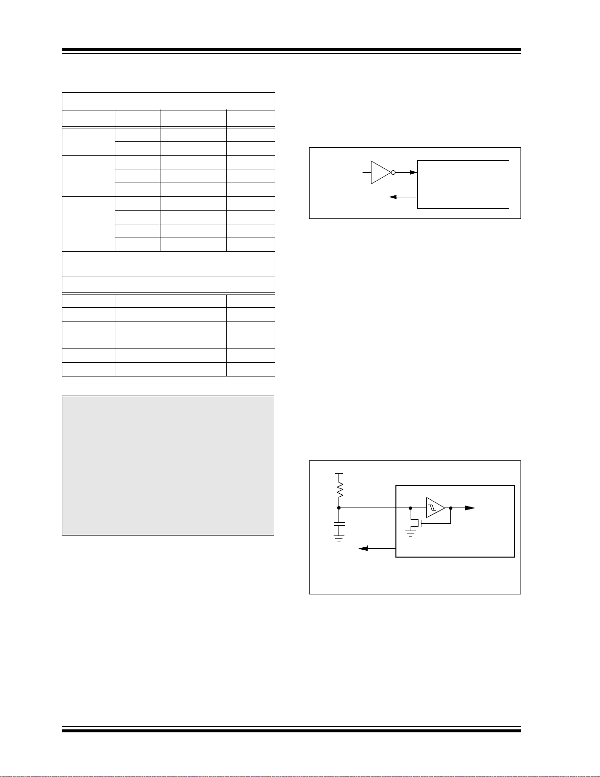
An external clock source may also be connected to the
OSC1 pin in the HS, XT and LP modes, as shown in
Figure 2-2.
FIGURE 2-2: EXTERNAL CLOCK INPUT
OPERATION (HS, XT OR
LP OSC CONFIG URAT ION)
Clock from
Ext. System
Open
OSC1
PIC18FXX80/XX85
OSC2
2.3 RC Oscillator
For timing insensitive applications, the “RC” and
“RCIO” device options offer additional cost savings.
The RC oscillator frequency is a function of the supply
voltage, the resistor (R
ues and the operating temperature. In addition to this,
the oscillator frequency will vary from unit to unit, due
to normal process parameter variation. Furthermore,
the difference in lead frame cap acitance bet ween package types will also affect the oscillation frequency,
especially for low C
take into account variation due to tolerance of external
R and C components used. Figure 2-3 shows how the
R/C combination is connected.
In the RC Oscillator mode, the oscillator frequency
divided by 4 is available on the OSC2 pin. This signal
may be used f or t e st pu r pos es or t o sy nc hr o n iz e ot he r
logic.
FIGURE 2-3: RC OSCILLATOR MODE
VDD
REXT
CEXT
VSS
F
Recommended values: 3 kΩ ≤ REXT ≤ 100 kΩ
EXT) and capacitor (CEXT) val-
EXT values. Th e user also needs to
OSC1
Internal
Clock
PIC18FXX80/XX85
OSC2/CLKO
OSC/4
EXT > 20pF
C
The RCIO Oscillator mode functions like the RC mode
except that the OSC2 pin becomes an additional general purpose I/O pin. The I/O pin becomes bit 6 of
PORTA (RA6).
DS30491C-page 24 2004 Microchip Technology Inc.
PIC18F6585/8585/6680/8680
2.4 External Clock Input
The EC, ECIO, EC+PLL and EC+SPLL Oscillator
modes require an external clock source to be connected to the OSC 1 pin. T he feed back device b etwee n
OSC1 and OSC2 is turned off in these modes to save
current. There is a maximum 1.5 µs start-up requ ired
after a Power-on Reset, or wake-up from Sleep mode.
In the EC Oscillator mode, the oscillator frequency
divided by 4 is available on the OSC2 pin. This signal
may be used f or t e st pu r pos es or t o sy nc hr o n iz e ot he r
logic. Figure 2-4 shows the pin connections for the EC
Oscillator mode.
FIGURE 2-4: EXTERNAL CLOCK INPUT
OPERATION
(EC CONFIGURATION)
Clock from
Ext. System
F
OSC/4
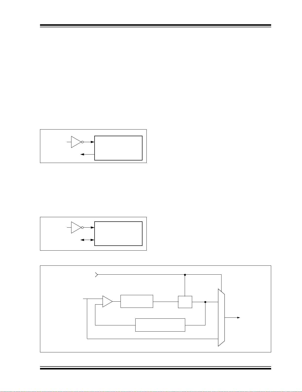
The ECIO Oscillator mode func ti ons li ke t he EC m od e,
except that the OSC2 pin becomes an additional general purpose I/O pin. The I/O pin becomes bit 6 of
PORTA (RA6). Figure 2-5 shows the pin connections
for the ECIO Oscillator mode.
FIGURE 2-5: EXTERNAL CLOCK INPUT
OSC1
PIC18FXX80/XX85
OSC2
OPERATION
(ECIO CONFIGURATION)
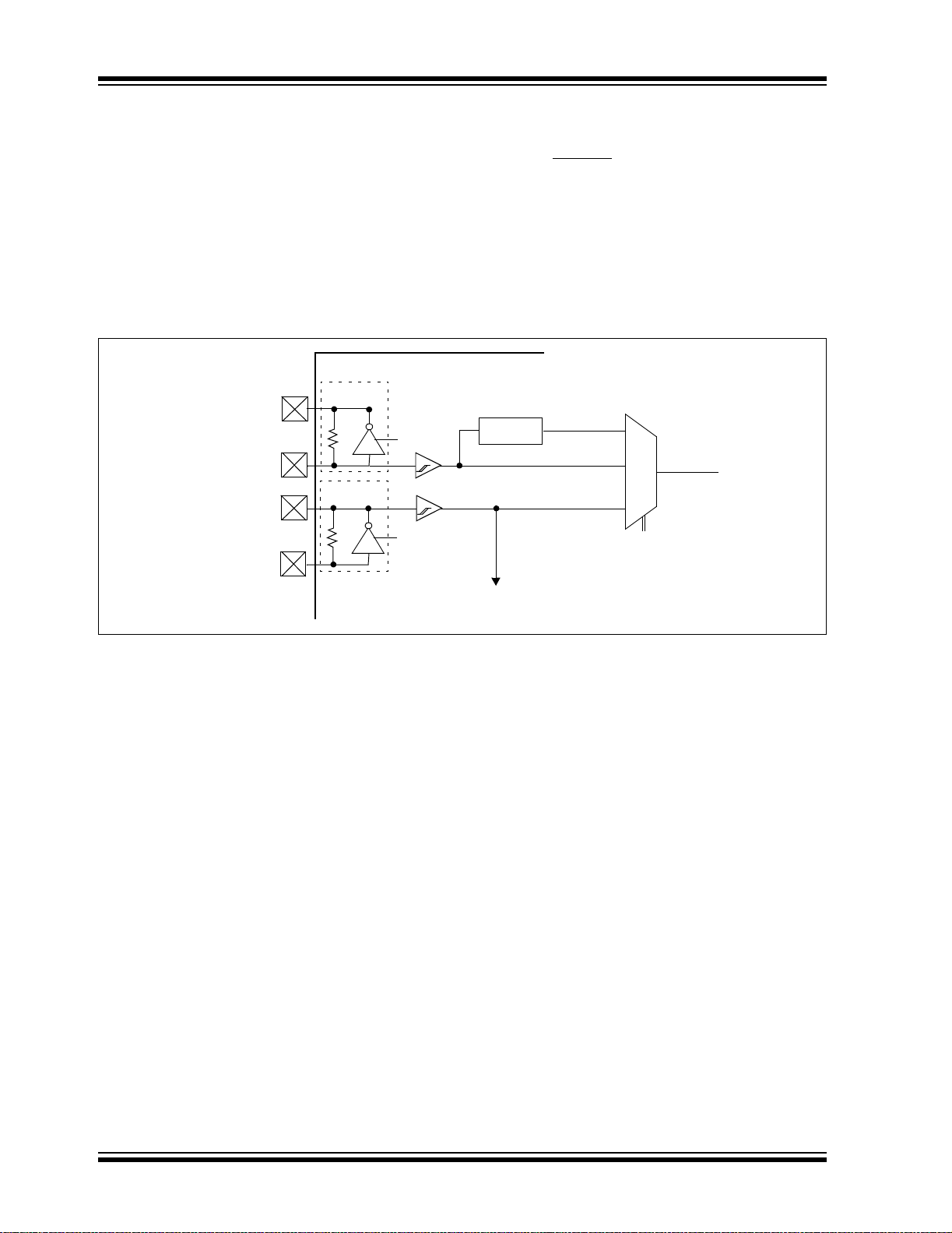
2.5 Phase Locked Loop (PLL)
A Phase Locked Loop circuit is provided as a
programmable option for us ers that want to multip ly the
frequency of the in com in g osc il lat or s ig nal by 4 . For an
input clock frequency of 10 MHz, the internal clock
frequency will b e multipli ed to 40 MHz. This is usefu l for
customers who are concerned with EMI due to
high-frequency crystals.
The PLL can only be enabled when the oscillator configuration bits are programmed for High-Speed Oscillator
or External Clock mode. If they are programmed for any
other mode, the PLL is not enabled and the system clock
will come directly from OSC1. There are two types of
PLL modes: Software Controlled PLL and Configuration
bits Controlled PLL. In Software Controlled PLL mode,
PIC18F6585/8585/6680/8680 executes at regular clock
frequency after all Reset conditions. During execution,
application can enable PLL and switch to 4x clock
frequency operation by setting the PLLEN bit in the
OSCCON register. In Configuration bits Controlled PLL
mode, PIC18F6585/8585/6680/8680 always executes
with 4x clock frequency.
The type of PLL is selected by programming the
FOSC<3:0> configuration bits in the CONFIG1H
Configuration register. The oscillator mode is specified
during device programming.
A PLL lock timer is used to ensure that the PLL has
locked before device execution starts. The PLL lock
timer has a time-out that is called T
PLL.
Clock from
Ext. System
RA6
OSC1
PIC18FXX80/XX85
I/O (OSC2)
FIGURE 2-6: PLL BLOCK DIAGRAM
PLL Enable
Phase
Comparator
F
IN
FOUT
Loop
Filter
Divide by 4
VCO
SYSCLK
MUX
2004 Microchip Technology Inc. DS30491C-page 25
PIC18F6585/8585/6680/8680
2.6 Oscillator Switching Feature
The PIC18F6585/8585/6680/8680 devices include a
feature that allows the system clock source to be
switched from the main oscillator to an alternate
low-frequency clock source. For the
PIC18F6585/8585/6680/8680 devices, this alternate
clock source is the Timer1 oscillator. If a low-frequency
crystal (32 kHz, for ex am pl e ) ha s bee n at tac he d to the
Timer1 oscillator pins and the Timer1 oscillator has
been enabled, the device can switch to a low-power
FIGURE 2-7: DEVICE CLOCK SOURCES
PIC18FXX80/XX85
OSC2
OSC1
T1OSO
T1OSI
Main Oscillator
Sleep
Timer1 Oscillator
T1OSCEN
Enable
Oscillator
execution mode. Figure 2-7 shows a block diagram of
the system clock sources. The clock switching feature
is enabled by programming the Oscillator Switching
Enable (OSCSEN
) bit in configuration register,
CONFIG1H, to a ‘0’. Clock switching is disabled in an
erased device. See Se ction 12.0 “Timer1 Module” for
further details of the Timer1 oscillator . See Section 24.0
“Special Features of the CPU” for configuration
register details.
4 x PLL
TOSC
TT1P
Tosc/4
MUX
Clock
Source
TSCLK
Clock Source Option
for other Modules
DS30491C-page 26 2004 Microchip Technology Inc.
PIC18F6585/8585/6680/8680
2.6.1 SYSTEM CLOCK SWITCH BIT
The system clock source switching is p erformed under
software control. The System Clock Switch bits,
SCS1:SCS0 (OSCCON<1:0>), control the clock switching. When the SCS0 bit is ‘ 0’, the system cl ock source
comes from the main oscillator that is selected by the
FOSC configuration bits in configuration register,
CONFIG1H. When the SCS0 bit is set, the system clock
source will come from the Timer1 oscillator. The SCS0
bit is clear ed on al l fo rm s of R eset.
When FOSC bits are programmed for software PLL
mode, the SCS1 bit c an be us ed to select between primary oscillator/clo ck and PLL output . The SCS1 bit wil l
only have an effect on the system clock if the PLL is
REGISTER 2-1: OSCCON REGISTER
U-0 U-0 U-0 U-0 R/W-0 R/W-0 R/W-0 R/W-0
— — — — LOCK PLLEN SCS1 SCS0
bit 7 bit 0
bit 7-4 Unimplemented: Read as ‘0’
bit 3 LOCK: Phase Lock Loop Lock Status bit
1 = Phase Lock Loop output is stable as system clock
0 = Phase Lock Loop output is not stable and output cannot be used as system clock
(1)
bit 2 PLLEN
1 = Enable Phase Lock Loop output as system clock
0 = Disable Phase Lock Loop
bit 1 SCS1: System Clock Switch bit 1
When PLLEN and LOCK bits are set:
1 = Use PLL output
0 = Use primary oscillator/clock input pin
When PLLEN or LOCK bit is cleared:
Bit is forced clear.
bit 0 SCS0
When
1 = Switch to Timer1 oscillator/clock pin
0 = Use primary oscillator/clock input pin
When
Bit is forced clear.
: Phase Lock Loop Enable bit
(2)
: System Clock Switch bit 0
OSCSEN configuration bit = 0 and T1OSCEN bit = 1:
OSCSEN and T1OSCEN are in other states:
Note 1: PLLEN bit is ignored when configured for ECIO+PLL and HS+PLL. This bit is used
in ECIO+SPLL and HS+SPLL modes only.
2: The setting of SCS0 = 1 supersedes SCS1 = 1.
enabled (PLLEN = 1) and locked (LOCK = 1), else it will
be forced clear. When programmed with Configuration
Controlled PLL mode, the SCS1 bit w ill be forced c lear .
Note: The Timer1 oscillator must be enabled
and operating to switch the system clock
source. The Timer1 oscillator is enabled
by setting the T1OSCEN bit in the Timer1
Control register (T1CON). If the Timer1
oscillator is not enabled, then any write to
the SCS0 bit will be ignored (SCS0 bit
forced cleared) and the main osci llator w ill
continue to be the system clock source.
Legend:
R = Readable bit W = Writable bit U = Unimplemented bit, read as ‘0’
- n = Value at POR ‘1’ = Bit is set ‘0’ = Bit is cleared x = Bit is unknown
2004 Microchip Technology Inc. DS30491C-page 27
PIC18F6585/8585/6680/8680
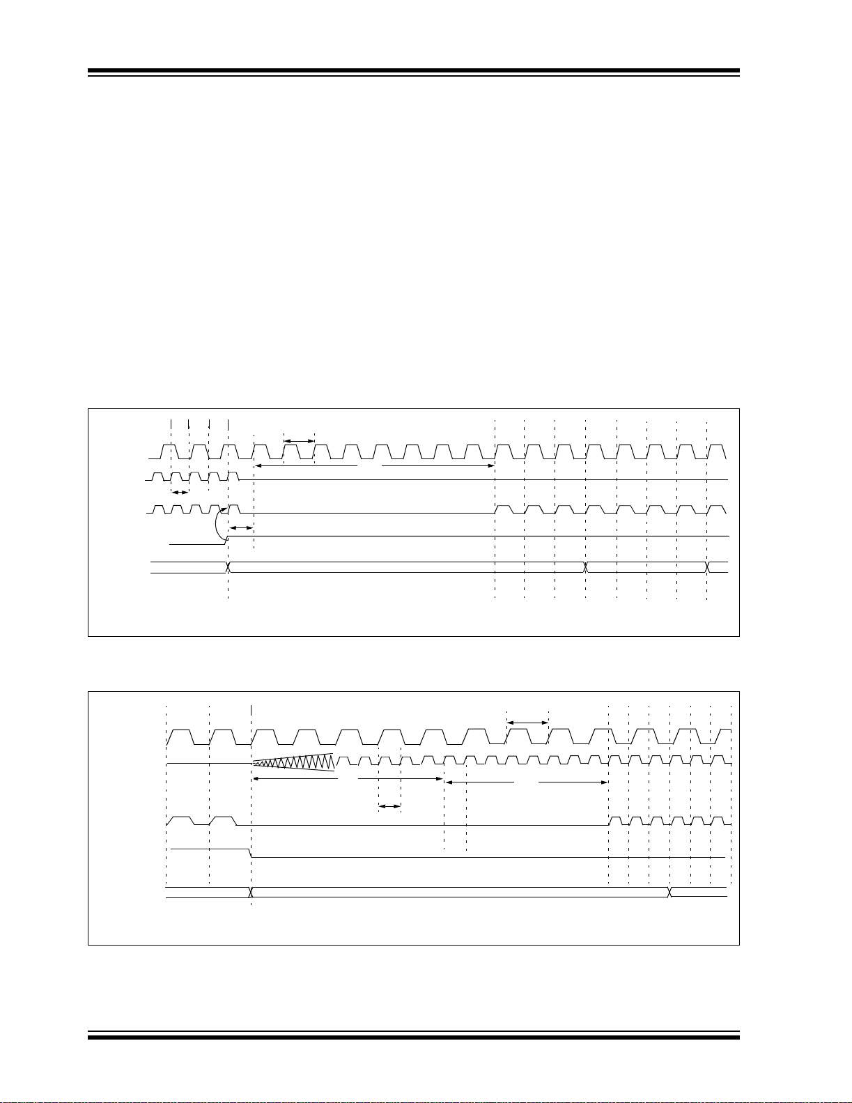
2.6.2 OSCILLATOR TRANSITIONS
PIC18F6585/8585/6680/8680 devices contain circuitry
to prevent “glitches” when switching between oscillator
sources. Essentially, the circuitry waits for eight rising
edges of the clock source that the processor is switching to. This e ns ures t hat the new clock source is st abl e
and that its pulse wid th will not be less than the sho rtest
pulse width of the two clock sources.
A timing diagram, indicating the transition from the
main oscillator to the Timer1 oscillator, is shown in
Figure 2-8. The Timer1 oscillator is assu med to be run-
The sequence of events that takes place when switching from the Timer1 oscillator to the main oscillator will
depend on the mode of the main oscillator. In addition
to eight clock cycles of the main oscillator, additional
delays may take place.
If the main oscillator is configured for an external
crystal (HS, XT, LP), then the transition will take place
after an oscillator start-up time (T
OST) has occurred. A
timing diagram, indicating the transition from the
Timer1 oscillator to the main oscillator for HS, XT and
LP modes, is shown in Figure 2-9.
ning all the time. After the SCS0 bit is set, the processor
is frozen at the next occurring Q1 cycle. After eight
synchronization cycles are counted from the Timer1
oscillator, operation resumes. No additional delays are
required after the synchronization cycles.
FIGURE 2-8: TIMING DIAGRAM FOR TRANSITION FROM OSC1 TO TIMER1 OSCILLATOR
Q1
T1OSI
OSC1
Internal
System
Clock
SCS
(OSCCON<0>)
Program
Counter
TOSC
Q1
TDLY
TT1P
21 345678
TSCS
PC + 2PC
Q3Q2Q1Q4Q3Q2
Q4 Q1
Q2 Q3 Q4 Q1
PC + 4
Note: TDLY is the delay from SCS high to first count of transition circuit.
FIGURE 2-9: TIMING FOR TRANSITION BETWEEN TIMER1 AND OSC1 (HS, XT, LP)
Q3 Q4
T1OSI
OSC1
Internal
System Clock
(OSCCON<0>)
Note: TOST = 1024 TOSC (drawing not to scale).
SCS
Program
Counter
PC PC + 2
Q1
TOST
TT1P
12345678
TSCS
TOSC
Q1 Q2 Q3 Q4 Q1 Q2
Q3
PC + 6
DS30491C-page 28 2004 Microchip Technology Inc.

PIC18F6585/8585/6680/8680
If the main oscillator is configured for HS mode with
PLL active, an oscillator start-up time (T
additional PLL time -out (T
PLL) will occur . The PLL tim e-
OST) plus an
out is typically 2 ms and allows the PLL to lock to the
main oscillator frequency. A timing diagram, indicating
the transition from the Timer1 oscillator to the main
If the main oscillator is configured for EC mode with PLL
active, only the PLL time-out (T
time-out is typically 2 ms and allows the PLL to lock to
the main oscillator frequency. A timing diagram, indicating the transition from the Timer1 oscillator to the main
oscillator for EC with PLL active, is shown in Figure 2-11.
oscillator for HS-PLL mode, is shown in Figure 2-10.
FIGURE 2-10: TIMING FOR TRANSITION BETWEEN TIMER1 AND OSC1
(HS WITH PLL ACTIVE, SCS1 = 1)
Q4 Q1
T1OSI
OSC1
TOST
PLL Clock
Input
Internal System
(OSCCON<0>)
Program Counter
Note: TOST = 1024 TOSC (drawing not to scale).
Clock
SCS
PC PC + 2
TPLL
TT1P
TOSC
1 234 5678
TSCS
Q1 Q2 Q3 Q4 Q1 Q2
PLL) will occur. The PLL
Q3
Q4
PC + 4
FIGURE 2-11: TIMING FOR T R ANSITION BETWEEN TIMER1 AND OSC1
(EC WITH PLL ACTIVE, SCS1 = 1)
Q1 Q2 Q3 Q4 Q1 Q2
T1OSI
OSC1
PLL Clock
Input
Internal System
(OSCCON<0>)
Program Counter
Clock
SCS
Q4 Q1
TPLL
TOSC
PC PC + 2
TT1P
TSCS
1 234 5678
Q3
PC + 4
Q4
2004 Microchip Technology Inc. DS30491C-page 29
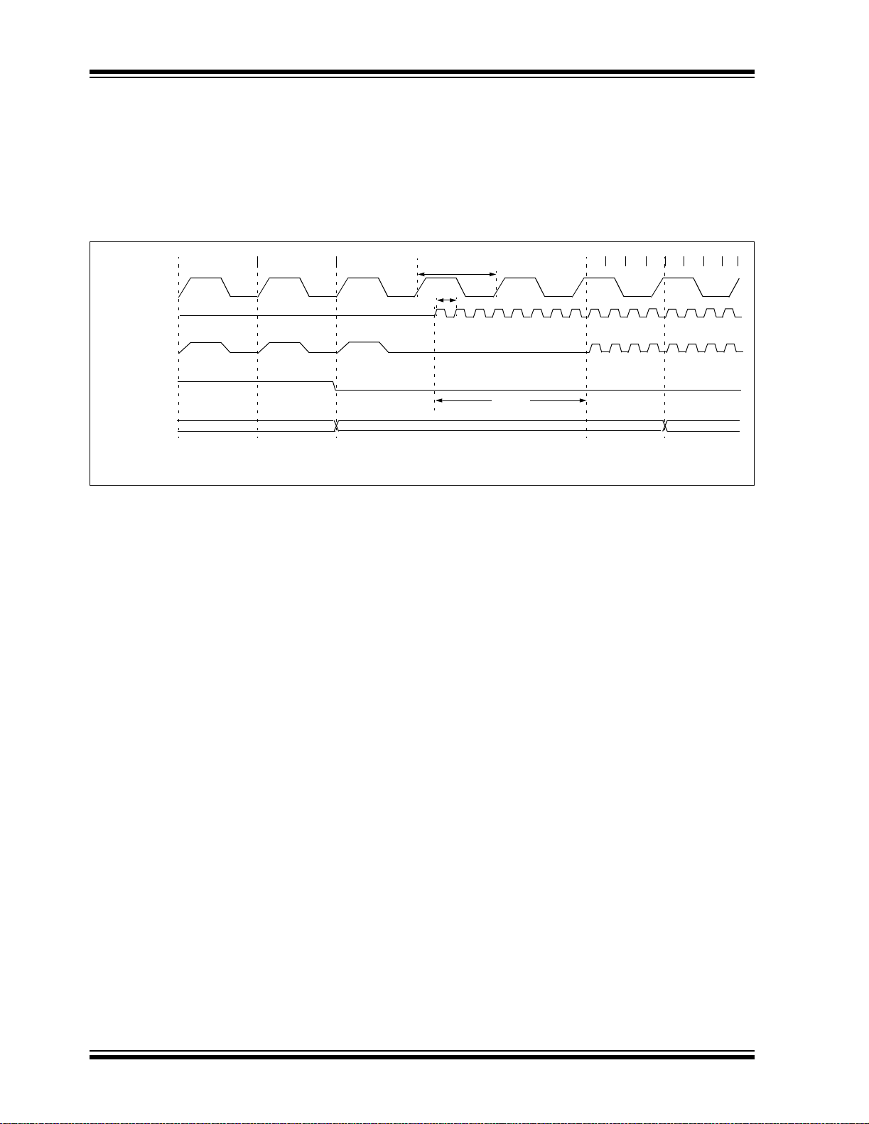
PIC18F6585/8585/6680/8680
If the main oscillato r is c onfigur ed in th e RC, R CIO, EC
or ECIO modes, th ere is no os cillator start-up time-out.
Operation will resume after eight cycles of the main
oscillator have been counted. A timing diagram, indicating the transition from the Timer1 oscillator to the
main oscillator for RC, RCIO, EC and ECIO modes, is
shown in Figure 2-12.
FIGURE 2-12: TIMING FOR TRANSITION BETWEEN TIMER1 AND OSC1 (RC, EC)
Q3 Q4
T1OSI
OSC1
Internal System
Note: RC Oscillator mode assumed.
Clock
(OSCCON<0>)
SCS
Program
Counter
PC
Q1
T
OSC
1
TT1P
23
45678
TSCS
PC + 2
Q1 Q2 Q3 Q4 Q1 Q2 Q3
PC + 4
Q4
DS30491C-page 30 2004 Microchip Technology Inc.

PIC18F6585/8585/6680/8680
2.7 Effects of Sleep Mode on the On-Chip Oscillator
When the device e xecutes a SLEEP i nstructio n, the onchip clocks and oscillator are turn ed off and the device
is held at the beginning of an instruction cycle (Q1
state). With the oscillator off, the OSC1 and OSC2
signals will stop oscillating. Since all the transistor
switching currents have been removed, Sleep mode
achieves the lowest current consumption of the device
(only leakage currents). Enabling any on-chip feature
that will operate during Sleep will increase the current
consumed during Sleep. The user can wake from
Sleep through external Reset, Watchdog Timer Reset,
or through an interrupt.
TABLE 2-3: OSC1 AND OSC2 PIN STATES IN SLEEP MODE
OSC Mode OSC1 Pin OSC2 Pin
RC Floating, external resistor should pull high At logic low
RCIO Floating, external resistor should pull high Configured as PORTA, bit 6
ECIO Floating Configured as PORTA, bit 6
EC Floating At logic low
LP, XT, and HS Feedback inverter disabled at
quiescent voltage level
Note: See Table 3-1 in Section 3.0 “Reset”, for time-outs due to Sleep and MCLR
2.8 Power-up Delays
Power-up delays are con trolled by two time rs so that no
external Reset circuitry is required for most applications. The delays ensure that the device is kept in
Reset until the device power supply and clock are stable. For additional information on Reset operation, see
Section 3.0 “Reset”.
The first timer is the Power-up Timer (PWRT) which
optionally provid es a fix ed delay of 72 ms (nominal) on
power-up only (POR and BOR). The second timer is
the Oscillator Start-up Timer (OST), intended to keep
the chip in Reset until the crystal oscillator is stable.
With the PLL enabled (HS+PLL and EC+PLL Oscillator
mode), the time-out sequence following a Power-on
Reset is different from other oscillator modes. The
time-out sequence is as follows: First, the PWRT timeout is invoked after a POR time delay has expired.
Then, the Oscillator Start-up Timer (OST) is invoked.
However, this is still not a sufficient amount of time to
allow the PLL to lock at high frequencies. The PWRT
timer is used to provide an additional fixed 2 ms
(nominal) time-out to allow the PLL ample time to lock
to the incoming clock frequency.
Feedback inverter disabled at
quiescent voltage level
Reset.
2004 Microchip Technology Inc. DS30491C-page 31

PIC18F6585/8585/6680/8680
NOTES:
DS30491C-page 32 2004 Microchip Technology Inc.
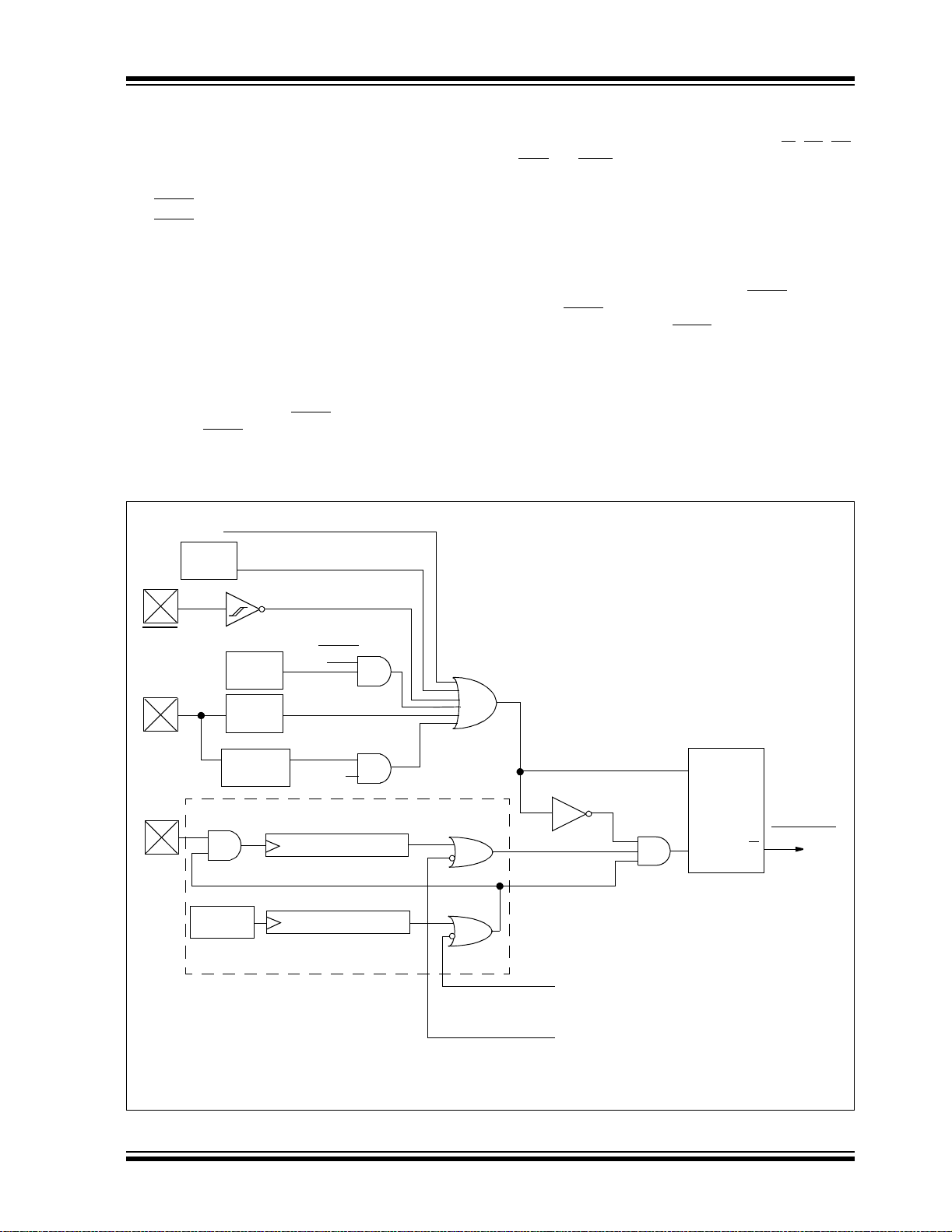
PIC18F6585/8585/6680/8680
3.0 RESET
Most registers are not affected by a WDT wake-up
since this is viewed as the resumption of normal oper-
The PIC18F6585/8585/6680/8680 devices differentiate
between various kinds of Reset:
a) Power-on Reset (POR)
b) MCLR
Reset during normal operation
c) MCLR Reset during Sleep
d) Watchdog Timer (WDT) Reset (during normal
operation)
e) Programmable Brown-out Reset (BOR)
f) RESET Instruction
g) Stack Full Reset
h) Stack Underflow Reset
ation. Status bits from the RCON register, R I, TO, PD,
and BOR, are set or cleared differently in different
POR
Reset situations, as indicated in Table 3-2. These bits
are used in software to determine the nature of the
Reset. See Table 3-3 for a full description of the Reset
states of all registers.
A simplified block di agram of the On-Chip Reset Circu it
is shown in Figure 3- 1.
The Enhanced MCU devices have a MCLR
in the MCLR
ignore small puls es. T he MC LR
Reset path. The filter will detect and
pin is not driv en lo w b y
any internal Resets, including the WDT.
Most registers are unaffected by a Reset. Their status
is unknown on POR and unchanged by all other
Resets. The other registers are forced to a “Reset
state” on Power-on Reset, MCL R
out Reset, MCLR
Reset during Sleep and by the
, WDT Reset, Brown-
RESET instruction.
FIGURE 3-1: SIMPLIFIED BLOCK DIAGRAM OF ON-CHIP RESET CIRCUIT
RESET
Instruction
Stack
Pointer
Stack Full/Underflow Reset
noise filter
MCLR
VDD
OSC1
Module
DD Rise
V
Detect
Brown-out
OST/PWRT
On-chip
RC OSC
External Reset
WDT
Reset
(1)
WDT
Time-out
Reset
OST
10-bit Ripple Counter
PWRT
10-bit Ripple Counter
SLEEP
Power-on Reset
BOREN
Enable PWRT
Enable OST
S
Chip_Reset
R
(2)
Q
Note 1: This is a separate oscillator from the RC oscillator of the CLKI pin.
2: See Table 3-1 for time-out situations.
2004 Microchip Technology Inc. DS30491C-page 33

PIC18F6585/8585/6680/8680
.
t
l
3.1 Power-on Reset (POR)
A Power-on Reset pulse is generated on-chip when
DD rise is detected. To take advan tage of t he POR cir-
V
cuitry, tie the MCLR
tor to V
DD. This will eliminate external RC components
pin through a 1 k Ω to 1 0 kΩ resis-
usually needed to create a Power-on Reset delay. A
minimum rise rate for V
DD is specified (parameter
D004). For a slow rise time, see Figure 3-2.
When the device st arts normal operation (i.e., exits th e
Reset condition), device operating parameters (voltage, frequency, temperature, etc.) must be met to
ensure operation. If these conditions are not met, the
device must be held in Reset until the operating
conditions are met.
FIGURE 3-2: EXTERNAL POWER-ON
RESET CIRCUIT (FOR
SLOW V
DD
V
D
R
C
Note 1: External Power-on Reset circuit is required
only if the V
The diode D helps discharge the capacitor
quickly when V
2: R < 40 kΩ is recommended to make sure tha
the voltage drop across R does not violate
the device’s electrical specification.
3: R1 = 1 kΩ to 10 kΩ will limit any current flow-
ing into MCLR
the event of MCLR/
Electrostatic Discharge (ESD) or Electrica
Overstress (EOS).
DD power-up slope is too slow
DD POWER-UP)
R1
MCLR
PIC18FXX8X
DD powers down.
from external capacitor C, in
VPP pin breakdown due to
3.2 Power-up Timer (PWRT)
The Power-up Timer provides a fixed nominal time-out
(parameter #33) only on power-up from the POR. The
Power-up Timer operates on an internal RC oscillator.
The chip is kept in Reset as long as the PWRT is active.
The PWRT’s time delay allows V
acceptable level. A configuration bit is provided to
enable/disable the PWRT.
The power-up time delay will vary fr om chip-to-ch ip due
DD, temperature and process variation. See DC
to V
parameter #33 for deta ils.
DD to rise to an
3.3 Oscillator Start-up Timer (OST)
The Oscillator Start-up Timer (OST) provides 1024
oscillator cycles (from OSC1 input) delay after the
PWRT delay is over (para meter #32). Th is ensures th at
the crystal oscillator or resonator has started and
stabilized.
The OST time-out is invoked only for XT, LP and HS
modes and only on Power-on Reset, or wake-up from
Sleep.
3.4 PLL Lock Time-out
With the PLL enabled, the time-ou t sequen ce foll owin g
a Power-on Reset is different from other oscillator
modes. A portion of the Po wer-up Timer is used to provide a fixed time-out th at is suff icient for the PLL to lock
to the main oscillator fre quenc y. This PLL lock time-out
PLL) is typically 2 ms and follows the oscillator
(T
start-up time-out (OST).
3.5 Brown-out Reset (BOR)
A configuration bit, BOREN, can disable (if clear/
programmed), or enable (if set) the Brown-out Reset
circuitry. If V
DD falls below parameter D005 for greater
than parameter #35, the brown-out situation will reset
the chip. A Reset may not occur if VDD falls below
parameter D005 for less than p aram et er #35 . The chip
will remain in Brown-out Reset until VDD rises above
DD. If the Power-up Timer is enabled, it will be
BV
invoked after V
DD rises above BVDD; it then will keep
the chip in Reset for an additional time delay (parameter #33). If VDD drops below BVDD while the Power-up
Timer is ru nni ng, the chip will go back into a Brow n-o ut
Reset and the Power-up Timer will be initialized. Once
DD rises above BVDD, the Power-up Timer will
V
execute the additional time delay.
3.6 Time-out Sequence
On power-up, the time-out sequence is as follows:
First, PWRT time-out is invoked after the POR time
delay has expi red. Then, OST is activ ated. The total
time-out will vary based on oscillator configuration and
the status of th e PWRT. Fo r e xam pl e, in RC m ode wi th
the PWRT disabled, there will be no time-out at all.
Figure 3-3, Figure 3-4, Figure 3-5, Figure 3-6 and
Figure 3-7 depict time-out sequences on power-up.
Since the time-outs occur from the POR pulse, the
time-outs will expire if MCLR
Bringing MCLR
high will begin execution immediately
(Figure 3-5). This is useful for testing purposes or to
synchronize more than one PIC18FXX8X device
operating in parallel.
Table 3-2 shows the Reset conditions f or some Special
Function Registers while Table 3-3 shows the Reset
conditions for all of the registers.
is kept low long enough.
DS30491C-page 34 2004 Microchip Technology Inc.
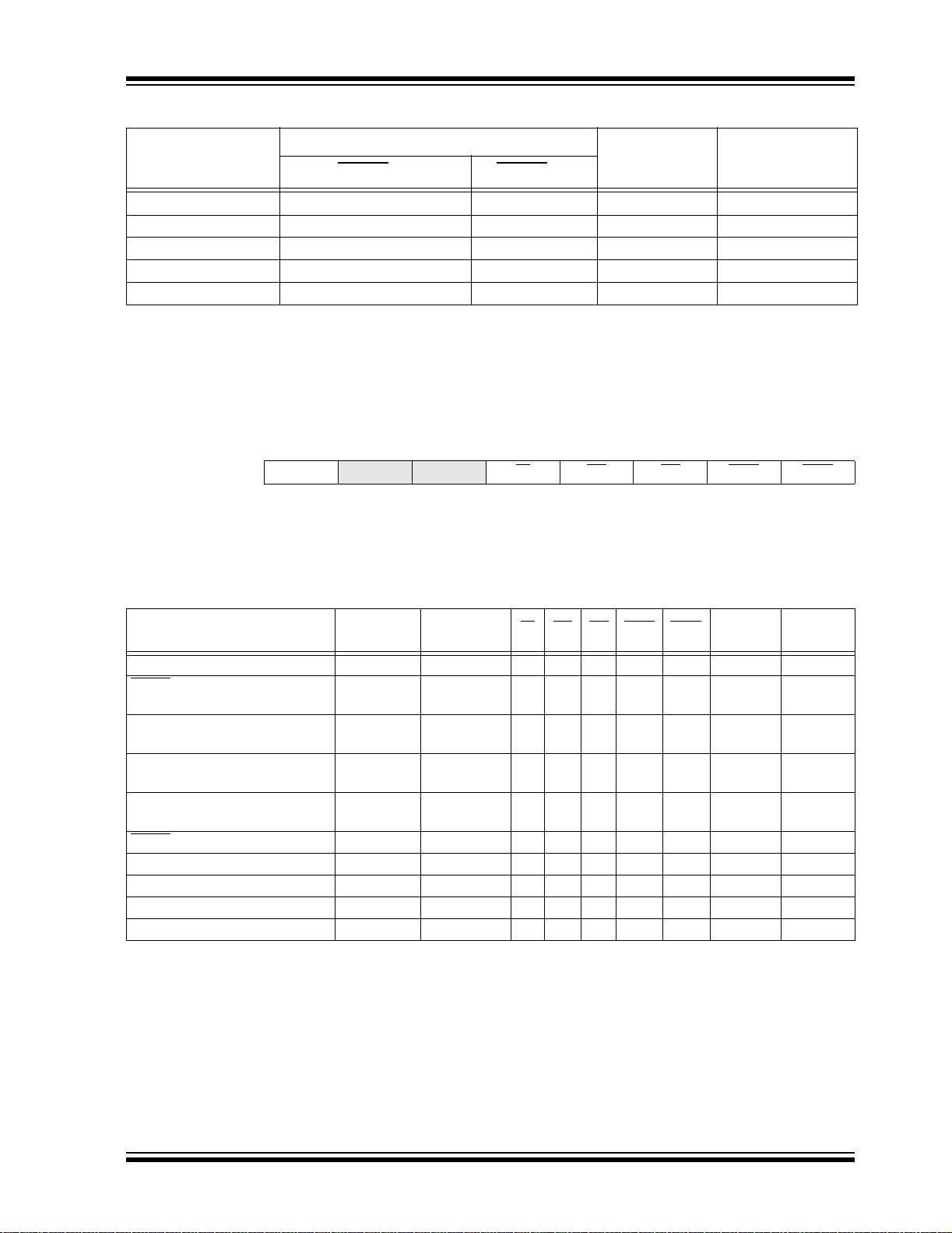
PIC18F6585/8585/6680/8680
TABLE 3-1: TIME-OUT IN VARIOUS SITUATIONS
Oscillator
Configuration
HS with PLL enabled
EC with PLL enabled
HS, XT, LP 72 ms + 1024 TOSC 1024 TOSC 1024 TOSC 1024 TOSC
EC 72 ms 1.5 µs1.5 µs1.5 µs
External RC 72 ms 1.5 µs1.5 µs1.5 µs
Note 1: 2 ms is the nominal time required for the 4x PLL to lock.
2: 72 ms is the nominal power-up timer delay if implemented.
3: 1.5 µs is the recovery time from Sleep. There is no recovery time from oscillator switch.
(1)
(1)
PWRTE = 0 PWRTE = 1
72 ms + 1024 TOSC + 2ms 1024 TOSC + 2 ms 1024 TOSC + 2 ms 1024 TOSC + 2 ms
72 ms + 2ms 1.5 µs + 2 ms 2 ms 1.5 µs + 2 ms
Power-up
REGISTER 3-1: RCON REGISTER BITS AND POSITIONS
R/W-0 U-0 U-0 R/W-1 R/W-1 R/W-1 R/W-1 R/W-0
IPEN
bit 7 bit 0
Note: Refer to Section 4.14 “RCON Register” for bit definitions.
— —RITO PD POR BOR
(2)
Brown-out
Wake-up from
Sleep or
Oscillator Switch
(3)
TABLE 3-2: STATUS BITS, THEIR SIGNIFICANCE AND THE INITIALIZATION CONDITION FOR
RCON REGISTER
Condition
Power-on Reset 0000h 0--1 1100 1 1 1 0 0 u u
Reset during normal
MCLR
operation
Software Reset during normal
operation
Stack Full Reset during normal
operation
Stack Underflow Reset during
normal operation
MCLR
Reset during Sleep 0000h 0--u 10uu u 1 0 u u u u
WDT Reset 0000h 0--u 01uu 1 0 1 u u u u
WDT Wake-up PC + 2 u--u 00uu u 0 0 u u u u
Brown-out Reset 0000h 0--1 11u0 1 1 1 1 0 u u
Interrupt wake-up from Sleep PC + 2
Legend: u = unchanged, x = unknown, – = unimplemented bit, read as ‘0’
Note 1: When the wake-up is due to an interrupt and the GIEH or GIEL bits are set, the PC is loaded with the
interrupt vector (000008h or 0000 18h ).
Program
Counter
0000h 0--u uuuu u u u u u u u
0000h 0--0 uuuu 0 u u u u u u
0000h 0--u uu11 u u u u u u 1
0000h 0--u uu11 u u u u u 1 u
(1)
RCON
Register
u--u 00uu u 1 0 u u u u
TO PD POR BOR STKFUL STKUNF
RI
2004 Microchip Technology Inc. DS30491C-page 35

PIC18F6585/8585/6680/8680
TABLE 3-3: INITIALIZATION CONDITIONS FOR ALL REGISTERS
Resets
MCLR
Register Applicable Devices
TOSU
PIC18F6X8X PIC18F8X8X
Power-on Reset,
Brown-out Reset
---0 0000
TOSH PIC18F6X8X PIC18F8X8X 0000 0000 0000 0000 uuuu uuuu
TOSL PIC18F6X8X PIC18F8X8X 0000 0000 0000 0000 uuuu uuuu
STKPTR PIC18F6X8X PIC18F8X8X 00-0 0000 uu-0 0000 uu-u uuuu
PCLATU PIC18F6X8X PIC18F8X8X ---0 0000 ---0 0000 ---u uuuu
PCLATH PIC18F6X8X PIC18F8X8X 0000 0000 0000 0000 uuuu uuuu
PCL PIC18F6X8X PIC18F8X8X 0000 0000 0000 0000 PC + 2
TBLPTRU PIC18F6X8X PIC18F8X8X --00 0000 --00 0000 --uu uuuu
TBLPTRH PIC18F6X8X PIC18F8X8X 0000 0000 0000 0000 uuuu uuuu
TBLPTRL PIC18F6X8X PIC18F8X8X 0000 0000 0000 0000 uuuu uuuu
TABLAT PIC18F6X8X PIC18F8X8X 0000 0000 0000 0000 uuuu uuuu
PRODH PIC18F6X8X PIC18F8X8X xxxx xxxx uuuu uuuu uuuu uuuu
PRODL PIC18F6X8X PIC18F8X8X xxxx xxxx uuuu uuuu uuuu uuuu
INTCON PIC18F6X8X PIC18F8X8X 0000 000x 0000 000x uuuu uuuu
INTCON2 PIC18F6X8X PIC18F8X8X 1111 1111 1111 1111 uuuu uuuu
INTCON3 PIC18F6X8X PIC18F8X8X 1100 0000 1100 0000 uuuu uuuu
INDF0 PIC18F6X8X PIC18F8X8X N/A N/A N/A
POSTINC0 PIC18F6X8X PIC18F8X8X N/A N/A N/A
POSTDEC0 PIC18F6X8X PIC18F8X8X N/A N/A N/A
PREINC0 PIC18F6X8X PIC18F8X8X N/A N/A N/A
PLUSW0 PIC18F6X8X PIC18F8X8X N/A N/A N/A
FSR0H PIC18F6X8X PIC18F8X8X ---- xxxx ---- uuuu ---- uuuu
FSR0L PIC18F6X8X PIC18F8X8X xxxx xxxx uuuu uuuu uuuu uuuu
WREG PIC18F6X8X PIC18F8X8X xxxx xxxx uuuu uuuu uuuu uuuu
INDF1 PIC18F6X8X PIC18F8X8X N/A N/A N/A
POSTINC1 PIC18F6X8X PIC18F8X8X N/A N/A N/A
POSTDEC1 PIC18F6X8X PIC18F8X8X N/A N/A N/A
PREINC1 PIC18F6X8X PIC18F8X8X N/A N/A N/A
PLUSW1 PIC18F6X8X PIC18F8X8X N/A N/A N/A
Legend: u = unchanged, x = unknown, - = unimplemented bit, read as ‘0’, q = value depends on condition.
Shaded cells indicate condi tions do not apply for the designated device.
Note 1: One or more bits in the INTCONx or PIRx registers will be affected (to cause wake-up).
2: When the wake-up is due to an interrupt and the GIEL or GIEH bit is set, the PC is loaded with the
interrupt vector (0008h or 0018h).
3: When the wake -up i s due to an interrupt and the GIEL or GIEH bit is set, the T O SU, T O SH an d TOSL are
updated with the current value of the PC. The STKPTR is modified to point to the next location in the
hardware stack.
4: See Table 3-2 for Reset value for specific condition.
5: Bit 6 of PORTA, LATA, and TRISA are enabled in ECIO and RCIO Oscillator modes only. In all other
oscillator modes, they are disabled and read ‘0’.
6: Bit 6 of PORTA, LATA and TRISA are not available on all devices. When unimplemented, they read ‘0’.
7: This register reads all ‘0’s until ECAN is set up in Mode 1 or Mode 2.
WDT Reset
RESET Instruction
Wake-up via WDT
or Interrupt
Stack Resets
---0 0000 ---0 uuuu
(3)
(3)
(3)
(3)
(2)
(1)
(1)
(1)
DS30491C-page 36 2004 Microchip Technology Inc.

PIC18F6585/8585/6680/8680
TABLE 3-3: INITIALIZATION CONDITIONS FOR ALL REGISTERS (CONTINUED)
Resets
MCLR
Register Applicable Devices
FSR1H
FSR1L PIC18F6X8X PIC18F8X8X xxxx xxxx uuuu uuuu uuuu uuuu
BSR PIC18F6X8X PIC18F8X8X ---- 0000 ---- 0000 ---- uuuu
INDF2 PIC18F6X8X PIC18F8X8X N/A N/A N/A
POSTINC2 PIC18F6X8X PIC18F8X8X N/A N/A N/A
POSTDEC2 PIC18F6X8X PIC18F8X8X N/A N/A N/A
PREINC2 PIC18F6X8X PIC18F8X8X N/A N/A N/A
PLUSW2 PIC18F6X8X PIC18F8X8X N/A N/A N/A
FSR2H PIC18F6X8X PIC18F8X8X ---- xxxx ---- uuuu ---- uuuu
FSR2L PIC18F6X8X PIC18F8X8X xxxx xxxx uuuu uuuu uuuu uuuu
STATUS PIC18F6X8X PIC18F8X8X ---x xxxx ---u uuuu ---u uuuu
TMR0H PIC18F6X8X PIC18F8X8X 0000 0000 uuuu uuuu uuuu uuuu
TMR0L PIC18F6X8X PIC18F8X8X xxxx xxxx uuuu uuuu uuuu uuuu
T0CON PIC18F6X8X PIC18F8X8X 1111 1111 1111 1111 uuuu uuuu
OSCCON PIC18F6X8X PIC18F8X8X ---- 0000 ---- 0000 ---- uuuu
LVDCON PIC18F6X8X PIC18F8X8X --00 0101 --00 0101 --uu uuuu
WDTCON PIC18F6X8X PIC18F8X8X ---- ---0 ---- ---0 ---- ---u
(4)
RCON
TMR1H PIC18F6X8X PIC18F8X8X xxxx xxxx uuuu uuuu uuuu uuuu
TMR1L PIC18F6X8X PIC18F8X8X xxxx xxxx uuuu uuuu uuuu uuuu
T1CON PIC18F6X8X PIC18F8X8X 0-00 0000 u-uu uuuu u-uu uuuu
TMR2 PIC18F6X8X PIC18F8X8X 0000 0000 0000 0000 uuuu uuuu
PR2 PIC18F6X8X PIC18F8X8X 1111 1111 1111 1111 1111 1111
T2CON PIC18F6X8X PIC18F8X8X -000 0000 -000 0000 -uuu uuuu
SSPBUF PIC18F6X8X PIC18F8X8X xxxx xxxx uuuu uuuu uuuu uuuu
SSPADD PIC18F6X8X PIC18F8X8X 0000 0000 0000 0000 uuuu uuuu
SSPSTAT PIC18F6X8X PIC18F8X8X 0000 0000 0000 0000 uuuu uuuu
SSPCON1 PIC18F6X8X PIC18F8X8X 0000 0000 0000 0000 uuuu uuuu
SSPCON2 PIC18F6X8X PIC18F8X8X 0000 0000 0000 0000 uuuu uuuu
Legend: u = unchanged, x = unknown, - = unimplemented bit, read as ‘0’, q = value depends on condition.
Note 1: One or more bits in the INTCONx or PIRx registers will be affected (to cause wake-up).
2: When the wake-up is due to an interrupt and the GIEL or GIEH bit is set, the PC is loaded with the
3: When the wake -up i s due to an i nterrupt and the GIEL or GIEH bit is set, the TOSU, T OSH an d T O SL are
4: See Table 3-2 for Reset value for specific condition.
5: Bit 6 of PORTA, LATA, and TRISA are enabled in ECIO and RCIO Oscillator modes only. In all other
6: Bit 6 of PORTA, LATA and TRISA are not available on all devices. When unimplemented, they read ‘0’.
7: This register reads all ‘0’s until ECAN is set up in Mode 1 or Mode 2.
PIC18F6X8X PIC18F8X8X
PIC18F6X8X PIC18F8X8X 0--q 11qq 0--q qquu u--u qquu
Shaded cells indicate condi tions do not apply for the designated device.
interrupt vector (0008h or 0018h).
updated with the current value of the PC. The STKPTR is modified to point to the next location in the
hardware stack.
oscillator modes, they are disabled and read ‘0’.
Power-on Reset,
Brown-out Reset
---- xxxx ---- uuuu ---- uuuu
WDT Reset
RESET Instruction
Stack Resets
Wake-up via WDT
or Interrupt
2004 Microchip Technology Inc. DS30491C-page 37

PIC18F6585/8585/6680/8680
TABLE 3-3: INITIALIZATION CONDITIONS FOR ALL REGISTERS (CONTINUED)
Resets
MCLR
Register Applicable Devices
ADRESH
ADRESL PIC18F6X8X PIC18F8X8X xxxx xxxx uuuu uuuu uuuu uuuu
ADCON0 PIC18F6X8X PIC18F8X8X --00 0000 --00 0000 --uu uuuu
ADCON1 PIC18F6X8X PIC18F8X8X --00 0000 --00 0000 --uu uuuu
ADCON2 PIC18F6X8X PIC18F8X8X 0-00 0000 0-00 0000 u-uu uuuu
CCPR1H PIC18F6X8X PIC18F8X8X xxxx xxxx uuuu uuuu uuuu uuuu
CCPR1L PIC18F6X8X PIC18F8X8X xxxx xxxx uuuu uuuu uuuu uuuu
CCP1CON PIC18F6X8X PIC18F8X8X 0000 0000 0000 0000 uuuu uuuu
CCPR2H PIC18F6X8X PIC18F8X8X xxxx xxxx uuuu uuuu uuuu uuuu
CCPR2L PIC18F6X8X PIC18F8X8X xxxx xxxx uuuu uuuu uuuu uuuu
CCP2CON PIC18F6X8X PIC18F8X8X --00 0000 --00 0000 --uu uuuu
CCPAS1 PIC18F6X8X PIC18F8X8X 0000 0000 0000 0000 uuuu uuuu
CVRCON PIC18F6X8X PIC18F8X8X 0000 0000 0000 0000 uuuu uuuu
CMCON PIC18F6X8X PIC18F8X8X 0000 0000 0000 0000 uuuu uuuu
TMR3H PIC18F6X8X PIC18F8X8X xxxx xxxx uuuu uuuu uuuu uuuu
TMR3L PIC18F6X8X PIC18F8X8X xxxx xxxx uuuu uuuu uuuu uuuu
T3CON PIC18F6X8X PIC18F8X8X 0000 0000 uuuu uuuu uuuu uuuu
PSPCON PIC18F6X8X PIC18F8X8X 0000 ---- 0000 ---- uuuu ----
SPBRG PIC18F6X8X PIC18F8X8X 0000 0000 0000 0000 uuuu uuuu
RCREG PIC18F6X8X PIC18F8X8X 0000 0000 0000 0000 uuuu uuuu
TXREG PIC18F6X8X PIC18F8X8X 0000 0000 0000 0000 uuuu uuuu
TXSTA PIC18F6X8X PIC18F8X8X 0000 0010 0000 0010 uuuu uuuu
RCSTA PIC18F6X8X PIC18F8X8X 0000 000x 0000 000x uuuu uuuu
EEADRH PIC18F6X8X PIC18F8X8X ---- --00 ---- --00 ---- --uu
EEADR PIC18F6X8X PIC18F8X8X 0000 0000 0000 0000 uuuu uuuu
EEDATA PIC18F6X8X PIC18F8X8X 0000 0000 0000 0000 uuuu uuuu
EECON2 PIC18F6X8X PIC18F8X8X xx-0 x000 uu-0 u000 uu-0 u000
EECON1 PIC18F6X8X PIC18F8X8X 00-0 x000 00-0 u000 uu-u uuuu
Legend: u = unchanged, x = unknown, - = unimplemented bit, read as ‘0’, q = value depends on condition.
Note 1: One or more bits in the INTCONx or PIRx registers will be affected (to cause wake-up).
2: When the wake-up is due to an interrupt and the GIEL or GIEH bit is set, the PC is loaded with the
3: When the wake -up i s due to an interrupt and the GIEL or GIEH bit is set, the T O SU, T O SH an d TOSL are
4: See Table 3-2 for Reset value for specific condition.
5: Bit 6 of PORTA, LATA, and TRISA are enabled in ECIO and RCIO Oscillator modes only. In all other
6: Bit 6 of PORTA, LATA and TRISA are not available on all devices. When unimplemented, they read ‘0’.
7: This register reads all ‘0’s until ECAN is set up in Mode 1 or Mode 2.
PIC18F6X8X PIC18F8X8X
Shaded cells indicate condi tions do not apply for the designated device.
interrupt vector (0008h or 0018h).
updated with the current value of the PC. The STKPTR is modified to point to the next location in the
hardware stack.
oscillator modes, they are disabled and read ‘0’.
Power-on Reset,
Brown-out Reset
xxxx xxxx uuuu uuuu uuuu uuuu
WDT Reset
RESET Instruction
Stack Resets
Wake-up via WDT
or Interrupt
DS30491C-page 38 2004 Microchip Technology Inc.

PIC18F6585/8585/6680/8680
TABLE 3-3: INITIALIZATION CONDITIONS FOR ALL REGISTERS (CONTINUED)
Resets
MCLR
Register Applicable Devices
IPR3
PIC18F6X8X PIC18F8X8X
Power-on Reset,
Brown-out Reset
1111 1111 1111 1111 uuuu uuuu
PIR3 PIC18F6X8X PIC18F8X8X 0000 0000 0000 0000 uuuu uuuu
PIE3 PIC18F6X8X PIC18F8X8X 0000 0000 0000 0000 uuuu uuuu
IPR2 PIC18F6X8X PIC18F8X8X -1-1 1111 -1-1 1111 -u-u uuuu
PIR2 PIC18F6X8X PIC18F8X8X -0-0 0000 -0-0 0000 -u-u uuuu
PIE2 PIC18F6X8X PIC18F8X8X -0-0 0000 -0-0 0000 -u-u uuuu
IPR1 PIC18F6X8X PIC18F8X8X 1111 1111 1111 1111 uuuu uuuu
PIR1 PIC18F6X8X PIC18F8X8X 0000 0000 0000 0000 uuuu uuuu
PIE1 PIC18F6X8X PIC18F8X8X 0000 0000 0000 0000 uuuu uuuu
MEMCON
PIC18F6X8X PIC18F8X8X 0-00 --00 0-00 --00 u-uu --uu
TRISJ PIC18F6X8X PIC18F8X8X 1111 1111 1111 1111 uuuu uuuu
TRISH PIC18F6X8X PIC18F8X8X 1111 1111 1111 1111 uuuu uuuu
TRISG PIC18F6X8X PIC18F8X8X ---1 1111 ---1 1111 ---u uuuu
TRISF PIC18F6X8X PIC18F8X8X 1111 1111 1111 1111 uuuu uuuu
TRISE PIC18F6X8X PIC18F8X8X 0000 -111 0000 -111 uuuu -uuu
TRISD PIC18F6X8X PIC18F8X8X 1111 1111 1111 1111 uuuu uuuu
TRISC PIC18F6X8X PIC18F8X8X 1111 1111 1111 1111 uuuu uuuu
TRISB PIC18F6X8X PIC18F8X8X 1111 1111 1111 1111 uuuu uuuu
TRISA
(5,6)
PIC18F6X8X PIC18F8X8X -111 1111
(5)
LATJ PIC18F6X8X PIC18F8X8X xxxx xxxx uuuu uuuu uuuu uuuu
LATH PIC18F6X8X PIC18F8X8X xxxx xxxx uuuu uuuu uuuu uuuu
LATG PIC18F6X8X PIC18F8X8X ---x xxxx ---u uuuu ---u uuuu
LATF PIC18F6X8X PIC18F8X8X xxxx xxxx uuuu uuuu uuuu uuuu
LATE PIC18F6X8X PIC18F8X8X xxxx xxxx uuuu uuuu uuuu uuuu
LATD PIC18F6X8X PIC18F8X8X xxxx xxxx uuuu uuuu uuuu uuuu
LATC PIC18F6X8X PIC18F8X8X xxxx xxxx uuuu uuuu uuuu uuuu
LATB PIC18F6X8X PIC18F8X8X xxxx xxxx uuuu uuuu uuuu uuuu
LATA
(5,6)
PIC18F6X8X PIC18F8X8X -xxx xxxx
(5)
Legend: u = unchanged, x = unknown, - = unimplemented bit, read as ‘0’, q = value depends on condition.
Shaded cells indicate condi tions do not apply for the designated device.
Note 1: One or more bits in the INTCONx or PIRx registers will be affected (to cause wake-up).
2: When the wake-up is due to an interrupt and the GIEL or GIEH bit is set, the PC is loaded with the
interrupt vector (0008h or 0018h).
3: When the wake -up i s due to an i nterrupt and the GIEL or GIEH bit is set, the TOSU, T OSH an d T O SL are
updated with the current value of the PC. The STKPTR is modified to point to the next location in the
hardware stack.
4: See Table 3-2 for Reset value for specific condition.
5: Bit 6 of PORTA, LATA, and TRISA are enabled in ECIO and RCIO Oscillator modes only. In all other
oscillator modes, they are disabled and read ‘0’.
6: Bit 6 of PORTA, LATA and TRISA are not available on all devices. When unimplemented, they read ‘0’.
7: This register reads all ‘0’s until ECAN is set up in Mode 1 or Mode 2.
WDT Reset
RESET Instruction
Stack Resets
-111 1111
-uuu uuuu
(5)
(5)
Wake-up via WDT
or Interrupt
-uuu uuuu
-uuu uuuu
(1)
(1)
(5)
(5)
2004 Microchip Technology Inc. DS30491C-page 39

PIC18F6585/8585/6680/8680
TABLE 3-3: INITIALIZATION CONDITIONS FOR ALL REGISTERS (CONTINUED)
Resets
MCLR
Register Applicable Devices
PORTJ
PORTH PIC18F6X8X PIC18F8X8X 0000 xxxx 0000 uuuu uuuu uuuu
PORTG PIC18F6X8X PIC18F8X8X --xx xxxx --uu uuuu --uu uuuu
PORTF PIC18F6X8X PIC18F8X8X x000 0000 u000 0000 u000 0000
PORTE PIC18F6X8X PIC18F8X8X ---- -000 ---- -000 ---- -uuu
PORTD PIC18F6X8X PIC18F8X8X xxxx xxxx uuuu uuuu uuuu uuuu
PORTC PIC18F6X8X PIC18F8X8X xxxx xxxx uuuu uuuu uuuu uuuu
PORTB PIC18F6X8X PIC18F8X8X xxxx xxxx uuuu uuuu uuuu uuuu
(5,6)
PORTA
SPBRGH PIC18F6X8X PIC18F8X8X 0000 0000 0000 0000 uuuu uuuu
BAUDCON PIC18F6X8X PIC18F8X8X -1-0 0-00 -1-0 0-00 -u-u u-uu
ECCP1DEL PIC18F6X8X PIC18F8X8X 0000 0000 0000 0000 uuuu uuuu
ECANCON PIC18F6X8X PIC18F8X8X 0001 0000 0001 0000 uuuu uuuu
TXERRCNT PIC18F6X8X PIC18F8X8X 0000 0000 0000 0000 uuuu uuuu
RXERRCNT PIC18F6X8X PIC18F8X8X 0000 0000 0000 0000 uuuu uuuu
COMSTAT PIC18F6X8X PIC18F8X8X 0000 0000 0000 0000 uuuu uuuu
CIOCON PIC18F6X8X PIC18F8X8X 0000 ---- 0000 ---- uuuu ----
BRGCON3 PIC18F6X8X PIC18F8X8X 00-- -000 00-- -000 uu-- -uuu
BRGCON2 PIC18F6X8X PIC18F8X8X 0000 0000 0000 0000 uuuu uuuu
BRGCON1 PIC18F6X8X PIC18F8X8X 0000 0000 0000 0000 uuuu uuuu
CANCON PIC18F6X8X PIC18F8X8X 1000 000- 1000 000- uuuu uuu-
CANSTAT PIC18F6X8X PIC18F8X8X 100- 000- 100- 000- uuu- uuu-
RXB0D7 PIC18F6X8X PIC18F8X8X xxxx xxxx uuuu uuuu uuuu uuuu
RXB0D6 PIC18F6X8X PIC18F8X8X xxxx xxxx uuuu uuuu uuuu uuuu
RXB0D5 PIC18F6X8X PIC18F8X8X xxxx xxxx uuuu uuuu uuuu uuuu
RXB0D4 PIC18F6X8X PIC18F8X8X xxxx xxxx uuuu uuuu uuuu uuuu
RXB0D3 PIC18F6X8X PIC18F8X8X xxxx xxxx uuuu uuuu uuuu uuuu
RXB0D2 PIC18F6X8X PIC18F8X8X xxxx xxxx uuuu uuuu uuuu uuuu
RXB0D1 PIC18F6X8X PIC18F8X8X xxxx xxxx uuuu uuuu uuuu uuuu
RXB0D0 PIC18F6X8X PIC18F8X8X xxxx xxxx uuuu uuuu uuuu uuuu
RXB0DLC PIC18F6X8X PIC18F8X8X -xxx xxxx -uuu uuuu -uuu uuuu
Legend: u = unchanged, x = unknown, - = unimplemented bit, read as ‘0’, q = value depends on condition.
Note 1: One or more bits in the INTCONx or PIRx registers will be affected (to cause wake-up).
2: When the wake-up is due to an interrupt and the GIEL or GIEH bit is set, the PC is loaded with the
3: When the wake -up i s due to an interrupt and the GIEL or GIEH bit is set, the T O SU, T O SH an d TOSL are
4: See Table 3-2 for Reset value for specific condition.
5: Bit 6 of PORTA, LATA, and TRISA are enabled in ECIO and RCIO Oscillator modes only. In all other
6: Bit 6 of PORTA, LATA and TRISA are not available on all devices. When unimplemented, they read ‘0’.
7: This register reads all ‘0’s until ECAN is set up in Mode 1 or Mode 2.
PIC18F6X8X PIC18F8X8X
PIC18F6X8X PIC18F8X8X -x0x 0000
Shaded cells indicate condi tions do not apply for the designated device.
interrupt vector (0008h or 0018h).
updated with the current value of the PC. The STKPTR is modified to point to the next location in the
hardware stack.
oscillator modes, they are disabled and read ‘0’.
Power-on Reset,
Brown-out Reset
xxxx xxxx uuuu uuuu uuuu uuuu
(5)
WDT Reset
RESET Instruction
Stack Resets
-u0u 0000
(5)
Wake-up via WDT
or Interrupt
-uuu uuuu
(5)
DS30491C-page 40 2004 Microchip Technology Inc.

PIC18F6585/8585/6680/8680
TABLE 3-3: INITIALIZATION CONDITIONS FOR ALL REGISTERS (CONTINUED)
Resets
MCLR
Register Applicable Devices
RXB0EIDL PIC18F6X8X PIC18F8X8X xxxx xxxx uuuu uuuu uuuu uuuu
RXB0EIDH PIC18F6X8X PIC18F8X8X xxxx xxxx uuuu uuuu uuuu uuuu
RXB0SIDL PIC18F6X8X PIC18F8X8X xxxx x-xx uuuu u-uu uuuu u-uu
RXB0SIDH PIC18F6X8X PIC18F8X8X xxxx xxxx uuuu uuuu uuuu uuuu
RXB0CON PIC18F6X8X PIC18F8X8X 000- 0000 000- 0000 uuu- uuuu
RXB1D7 PIC18F6X8X PIC18F8X8X xxxx xxxx uuuu uuuu uuuu uuuu
RXB1D6 PIC18F6X8X PIC18F8X8X xxxx xxxx uuuu uuuu uuuu uuuu
RXB1D5 PIC18F6X8X PIC18F8X8X xxxx xxxx uuuu uuuu uuuu uuuu
RXB1D4 PIC18F6X8X PIC18F8X8X xxxx xxxx uuuu uuuu uuuu uuuu
RXB1D3 PIC18F6X8X PIC18F8X8X xxxx xxxx uuuu uuuu uuuu uuuu
RXB1D2 PIC18F6X8X PIC18F8X8X xxxx xxxx uuuu uuuu uuuu uuuu
RXB1D1 PIC18F6X8X PIC18F8X8X xxxx xxxx uuuu uuuu uuuu uuuu
RXB1D0 PIC18F6X8X PIC18F8X8X xxxx xxxx uuuu uuuu uuuu uuuu
RXB1DLC PIC18F6X8X PIC18F8X8X -xxx xxxx -uuu uuuu -uuu uuuu
RXB1EIDL PIC18F6X8X PIC18F8X8X xxxx xxxx uuuu uuuu uuuu uuuu
RXB1EIDH PIC18F6X8X PIC18F8X8X xxxx xxxx uuuu uuuu uuuu uuuu
RXB1SIDL PIC18F6X8X PIC18F8X8X xxxx x-xx uuuu u-uu uuuu u-uu
RXB1SIDH PIC18F6X8X PIC18F8X8X xxxx xxxx uuuu uuuu uuuu uuuu
RXB1CON PIC18F6X8X PIC18F8X8X 000- 0000 000- 0000 uuu- uuuu
TXB0D7 PIC18F6X8X PIC18F8X8X xxxx xxxx uuuu uuuu uuuu uuuu
TXB0D6 PIC18F6X8X PIC18F8X8X xxxx xxxx uuuu uuuu uuuu uuuu
TXB0D5 PIC18F6X8X PIC18F8X8X xxxx xxxx uuuu uuuu uuuu uuuu
TXB0D4 PIC18F6X8X PIC18F8X8X xxxx xxxx uuuu uuuu uuuu uuuu
TXB0D3 PIC18F6X8X PIC18F8X8X xxxx xxxx uuuu uuuu uuuu uuuu
TXB0D2 PIC18F6X8X PIC18F8X8X xxxx xxxx uuuu uuuu uuuu uuuu
TXB0D1 PIC18F6X8X PIC18F8X8X xxxx xxxx uuuu uuuu uuuu uuuu
TXB0D0 PIC18F6X8X PIC18F8X8X xxxx xxxx uuuu uuuu uuuu uuuu
TXB0DLC PIC18F6X8X PIC18F8X8X -x-- xxxx -u-- uuuu -u-- uuuu
TXB0EIDL PIC18F6X8X PIC18F8X8X xxxx xxxx uuuu uuuu uuuu uuuu
TXB0EIDH PIC18F6X8X PIC18F8X8X xxxx xxxx uuuu uuuu -uuu uuuu
TXB0SIDL PIC18F6X8X PIC18F8X8X xxx- x-xx uuu- u-uu uuu- u-uu
Legend: u = unchanged, x = unknown, - = unimplemented bit, read as ‘0’, q = value depends on condition.
Shaded cells indicate condi tions do not apply for the designated device.
Note 1: One or more bits in the INTCONx or PIRx registers will be affected (to cause wake-up).
2: When the wake-up is due to an interrupt and the GIEL or GIEH bit is set, the PC is loaded with the
interrupt vector (0008h or 0018h).
3: When the wake -up i s due to an i nterrupt and the GIEL or GIEH bit is set, the TOSU, T OSH an d T O SL are
updated with the current value of the PC. The STKPTR is modified to point to the next location in the
hardware stack.
4: See Table 3-2 for Reset value for specific condition.
5: Bit 6 of PORTA, LATA, and TRISA are enabled in ECIO and RCIO Oscillator modes only. In all other
oscillator modes, they are disabled and read ‘0’.
6: Bit 6 of PORTA, LATA and TRISA are not available on all devices. When unimplemented, they read ‘0’.
7: This register reads all ‘0’s until ECAN is set up in Mode 1 or Mode 2.
Power-on Reset,
Brown-out Reset
WDT Reset
RESET Instruction
Stack Resets
Wake-up via WDT
or Interrupt
2004 Microchip Technology Inc. DS30491C-page 41

PIC18F6585/8585/6680/8680
TABLE 3-3: INITIALIZATION CONDITIONS FOR ALL REGISTERS (CONTINUED)
Resets
MCLR
Register Applicable Devices
TXB0SIDH PIC18F6X8X PIC18F8X8X xxxx xxxx uuuu uuuu uuuu uuuu
TXB0CON PIC18F6X8X PIC18F8X8X 0000 0-00 0000 0-00 uuuu u-uu
TXB1D7 PIC18F6X8X PIC18F8X8X xxxx xxxx uuuu uuuu uuuu uuuu
TXB1D6 PIC18F6X8X PIC18F8X8X xxxx xxxx uuuu uuuu uuuu uuuu
TXB1D5 PIC18F6X8X PIC18F8X8X xxxx xxxx uuuu uuuu uuuu uuuu
TXB1D4 PIC18F6X8X PIC18F8X8X xxxx xxxx uuuu uuuu uuuu uuuu
TXB1D3 PIC18F6X8X PIC18F8X8X xxxx xxxx uuuu uuuu uuuu uuuu
TXB1D2 PIC18F6X8X PIC18F8X8X xxxx xxxx uuuu uuuu uuuu uuuu
TXB1D1 PIC18F6X8X PIC18F8X8X xxxx xxxx uuuu uuuu uuuu uuuu
TXB1D0 PIC18F6X8X PIC18F8X8X xxxx xxxx uuuu uuuu uuuu uuuu
TXB1DLC PIC18F6X8X PIC18F8X8X -x-- xxxx -u-- uuuu -u-- uuuu
TXB1EIDL PIC18F6X8X PIC18F8X8X xxxx xxxx uuuu uuuu uuuu uuuu
TXB1EIDH PIC18F6X8X PIC18F8X8X xxxx xxxx uuuu uuuu uuuu uuuu
TXB1SIDL PIC18F6X8X PIC18F8X8X xxx- x-xx uuu- u-uu uuu- uu-u
TXB1SIDH PIC18F6X8X PIC18F8X8X xxxx xxxx uuuu uuuu -uuu uuuu
TXB1CON PIC18F6X8X PIC18F8X8X 0000 0-00 0000 0-00 uuuu u-uu
TXB2D7 PIC18F6X8X PIC18F8X8X xxxx xxxx uuuu uuuu 0uuu uuuu
TXB2D6 PIC18F6X8X PIC18F8X8X xxxx xxxx uuuu uuuu 0uuu uuuu
TXB2D5 PIC18F6X8X PIC18F8X8X xxxx xxxx uuuu uuuu 0uuu uuuu
TXB2D4 PIC18F6X8X PIC18F8X8X xxxx xxxx uuuu uuuu 0uuu uuuu
TXB2D3 PIC18F6X8X PIC18F8X8X xxxx xxxx uuuu uuuu 0uuu uuuu
TXB2D2 PIC18F6X8X PIC18F8X8X xxxx xxxx uuuu uuuu 0uuu uuuu
TXB2D1 PIC18F6X8X PIC18F8X8X xxxx xxxx uuuu uuuu 0uuu uuuu
TXB2D0 PIC18F6X8X PIC18F8X8X xxxx xxxx uuuu uuuu 0uuu uuuu
TXB2DLC PIC18F6X8X PIC18F8X8X -x-- xxxx -u-- uuuu -u-- uuuu
TXB2EIDL PIC18F6X8X PIC18F8X8X xxxx xxxx uuuu uuuu uuuu uuuu
TXB2EIDH PIC18F6X8X PIC18F8X8X xxxx xxxx uuuu uuuu uuuu uuuu
TXB2SIDL PIC18F6X8X PIC18F8X8X xxx- x-xx uuu- u-uu uuu- u-uu
TXB2SIDH PIC18F6X8X PIC18F8X8X xxx- x-xx uuu- u-uu uuu- u-uu
TXB2CON PIC18F6X8X PIC18F8X8X 0000 0-00 0000 0-00 uuuu u-uu
RXM1EIDL PIC18F6X8X PIC18F8X8X xxxx xxxx uuuu uuuu uuuu uuuu
Legend: u = unchanged, x = unknown, - = unimplemented bit, read as ‘0’, q = value depends on condition.
Shaded cells indicate condi tions do not apply for the designated device.
Note 1: One or more bits in the INTCONx or PIRx registers will be affected (to cause wake-up).
2: When the wake-up is due to an interrupt and the GIEL or GIEH bit is set, the PC is loaded with the
interrupt vector (0008h or 0018h).
3: When the wake -up i s due to an interrupt and the GIEL or GIEH bit is set, the T O SU, T O SH an d TOSL are
updated with the current value of the PC. The STKPTR is modified to point to the next location in the
hardware stack.
4: See Table 3-2 for Reset value for specific condition.
5: Bit 6 of PORTA, LATA, and TRISA are enabled in ECIO and RCIO Oscillator modes only. In all other
oscillator modes, they are disabled and read ‘0’.
6: Bit 6 of PORTA, LATA and TRISA are not available on all devices. When unimplemented, they read ‘0’.
7: This register reads all ‘0’s until ECAN is set up in Mode 1 or Mode 2.
Power-on Reset,
Brown-out Reset
WDT Reset
RESET Instruction
Stack Resets
Wake-up via WDT
or Interrupt
DS30491C-page 42 2004 Microchip Technology Inc.

PIC18F6585/8585/6680/8680
TABLE 3-3: INITIALIZATION CONDITIONS FOR ALL REGISTERS (CONTINUED)
Resets
MCLR
Register Applicable Devices
RXM1EIDH PIC18F6X8X PIC18F8X8X xxxx xxxx uuuu uuuu uuuu uuuu
RXM1SIDL PIC18F6X8X PIC18F8X8X xxx- x-xx uuu- u-uu uuu- u-uu
RXM1SIDH PIC18F6X8X PIC18F8X8X xxxx xxxx uuuu uuuu uuuu uuuu
RXM0EIDL PIC18F6X8X PIC18F8X8X xxxx xxxx uuuu uuuu uuuu uuuu
RXM0EIDH PIC18F6X8X PIC18F8X8X xxxx xxxx uuuu uuuu uuuu uuuu
RXM0SIDL PIC18F6X8X PIC18F8X8X xxx- x-xx uuu- u-uu uuu- u-uu
RXM0SIDH PIC18F6X8X PIC18F8X8X xxxx xxxx uuuu uuuu uuuu uuuu
RXF5EIDL PIC18F6X8X PIC18F8X8X xxxx xxxx uuuu uuuu uuuu uuuu
RXF5EIDH PIC18F6X8X PIC18F8X8X xxxx xxxx uuuu uuuu uuuu uuuu
RXF5SIDL PIC18F6X8X PIC18F8X8X xxx- x-xx uuu- u-uu uuu- u-uu
RXF5SIDH PIC18F6X8X PIC18F8X8X xxxx xxxx uuuu uuuu uuuu uuuu
RXF4EIDL PIC18F6X8X PIC18F8X8X xxxx xxxx uuuu uuuu uuuu uuuu
RXF4EIDH PIC18F6X8X PIC18F8X8X xxxx xxxx uuuu uuuu uuuu uuuu
RXF4SIDL PIC18F6X8X PIC18F8X8X xxx- x-xx uuu- u-uu uuu- u-uu
RXF4SIDH PIC18F6X8X PIC18F8X8X xxxx xxxx uuuu uuuu uuuu uuuu
RXF3EIDL PIC18F6X8X PIC18F8X8X xxxx xxxx uuuu uuuu uuuu uuuu
RXF3EIDH PIC18F6X8X PIC18F8X8X xxxx xxxx uuuu uuuu uuuu uuuu
RXF3SIDL PIC18F6X8X PIC18F8X8X xxx- x-xx uuu- u-uu uuu- u-uu
RXF3SIDH PIC18F6X8X PIC18F8X8X xxxx xxxx uuuu uuuu uuuu uuuu
RXF2EIDL PIC18F6X8X PIC18F8X8X xxxx xxxx uuuu uuuu uuuu uuuu
RXF2EIDH PIC18F6X8X PIC18F8X8X xxxx xxxx uuuu uuuu uuuu uuuu
RXF2SIDL PIC18F6X8X PIC18F8X8X xxx- x-xx uuu- u-uu uuu- u-uu
RXF2SIDH PIC18F6X8X PIC18F8X8X xxxx xxxx uuuu uuuu uuuu uuuu
RXF1EIDL PIC18F6X8X PIC18F8X8X xxxx xxxx uuuu uuuu uuuu uuuu
RXF1EIDH PIC18F6X8X PIC18F8X8X xxxx xxxx uuuu uuuu uuuu uuuu
RXF1SIDL PIC18F6X8X PIC18F8X8X xxx- x-xx uuu- u-uu uuu- u-uu
RXF1SIDH PIC18F6X8X PIC18F8X8X xxxx xxxx uuuu uuuu uuuu uuuu
RXF0EIDL PIC18F6X8X PIC18F8X8X xxxx xxxx uuuu uuuu uuuu uuuu
RXF0EIDH PIC18F6X8X PIC18F8X8X xxxx xxxx uuuu uuuu uuuu uuuu
RXF0SIDL PIC18F6X8X PIC18F8X8X xxx- x-xx uuu- u-uu uuu- u-uu
RXF0SIDH PIC18F6X8X PIC18F8X8X xxxx xxxx uuuu uuuu uuuu uuuu
Legend: u = unchanged, x = unknown, - = unimplemented bit, read as ‘0’, q = value depends on condition.
Shaded cells indicate condi tions do not apply for the designated device.
Note 1: One or more bits in the INTCONx or PIRx registers will be affected (to cause wake-up).
2: When the wake-up is due to an interrupt and the GIEL or GIEH bit is set, the PC is loaded with the
interrupt vector (0008h or 0018h).
3: When the wake -up i s due to an i nterrupt and the GIEL or GIEH bit is set, the TOSU, T OSH an d T O SL are
updated with the current value of the PC. The STKPTR is modified to point to the next location in the
hardware stack.
4: See Table 3-2 for Reset value for specific condition.
5: Bit 6 of PORTA, LATA, and TRISA are enabled in ECIO and RCIO Oscillator modes only. In all other
oscillator modes, they are disabled and read ‘0’.
6: Bit 6 of PORTA, LATA and TRISA are not available on all devices. When unimplemented, they read ‘0’.
7: This register reads all ‘0’s until ECAN is set up in Mode 1 or Mode 2.
Power-on Reset,
Brown-out Reset
WDT Reset
RESET Instruction
Stack Resets
Wake-up via WDT
or Interrupt
2004 Microchip Technology Inc. DS30491C-page 43

PIC18F6585/8585/6680/8680
TABLE 3-3: INITIALIZATION CONDITIONS FOR ALL REGISTERS (CONTINUED)
Resets
MCLR
Register Applicable Devices
(7)
B5D7
(7)
B5D6
(7)
B5D5
(7)
B5D4
(7)
B5D3
(7)
B5D2
(7)
B5D1
(7)
B5D0
B5DLC
B5EIDL
B5EIDH
B5SIDL
B5SIDH
B5CON
(7)
B4D7
(7)
B4D6
(7)
B4D5
(7)
B4D4
(7)
B4D3
(7)
B4D2
(7)
B4D1
(7)
B4D0
B4DLC
B4EIDL
B4EIDH
B4SIDL
B4SIDH
B4CON
(7)
B3D7
(7)
B3D6
(7)
B3D5
(7)
(7)
(7)
(7)
(7)
(7)
(7)
(7)
(7)
(7)
(7)
(7)
PIC18F6X8X PIC18F8X8X xxxx xxxx uuuu uuuu uuuu uuuu
PIC18F6X8X PIC18F8X8X xxxx xxxx uuuu uuuu uuuu uuuu
PIC18F6X8X PIC18F8X8X xxxx xxxx uuuu uuuu uuuu uuuu
PIC18F6X8X PIC18F8X8X xxxx xxxx uuuu uuuu uuuu uuuu
PIC18F6X8X PIC18F8X8X xxxx xxxx uuuu uuuu uuuu uuuu
PIC18F6X8X PIC18F8X8X xxxx xxxx uuuu uuuu uuuu uuuu
PIC18F6X8X PIC18F8X8X xxxx xxxx uuuu uuuu uuuu uuuu
PIC18F6X8X PIC18F8X8X xxxx xxxx uuuu uuuu uuuu uuuu
PIC18F6X8X PIC18F8X8X -xxx xxxx -uuu uuuu -uuu uuuu
PIC18F6X8X PIC18F8X8X xxxx xxxx uuuu uuuu uuuu uuuu
PIC18F6X8X PIC18F8X8X xxxx xxxx uuuu uuuu uuuu uuuu
PIC18F6X8X PIC18F8X8X xxxx x-xx uuuu u-uu uuuu u-uu
PIC18F6X8X PIC18F8X8X xxxx x-xx uuuu u-uu uuuu u-uu
PIC18F6X8X PIC18F8X8X 0000 0000 0000 0000 uuuu uuuu
PIC18F6X8X PIC18F8X8X xxxx xxxx uuuu uuuu uuuu uuuu
PIC18F6X8X PIC18F8X8X xxxx xxxx uuuu uuuu uuuu uuuu
PIC18F6X8X PIC18F8X8X xxxx xxxx uuuu uuuu uuuu uuuu
PIC18F6X8X PIC18F8X8X xxxx xxxx uuuu uuuu uuuu uuuu
PIC18F6X8X PIC18F8X8X xxxx xxxx uuuu uuuu uuuu uuuu
PIC18F6X8X PIC18F8X8X xxxx xxxx uuuu uuuu uuuu uuuu
PIC18F6X8X PIC18F8X8X xxxx xxxx uuuu uuuu uuuu uuuu
PIC18F6X8X PIC18F8X8X xxxx xxxx uuuu uuuu uuuu uuuu
PIC18F6X8X PIC18F8X8X -xxx xxxx -uuu uuuu -uuu uuuu
PIC18F6X8X PIC18F8X8X xxxx xxxx uuuu uuuu uuuu uuuu
PIC18F6X8X PIC18F8X8X xxxx xxxx uuuu uuuu uuuu uuuu
PIC18F6X8X PIC18F8X8X xxxx x-xx uuuu u-uu uuuu u-uu
PIC18F6X8X PIC18F8X8X xxxx xxxx uuuu uuuu uuuu uuuu
PIC18F6X8X PIC18F8X8X 0000 0000 0000 0000 uuuu uuuu
PIC18F6X8X PIC18F8X8X xxxx xxxx uuuu uuuu uuuu uuuu
PIC18F6X8X PIC18F8X8X xxxx xxxx uuuu uuuu uuuu uuuu
PIC18F6X8X PIC18F8X8X xxxx xxxx uuuu uuuu uuuu uuuu
Power-on Reset,
Brown-out Reset
Legend: u = unchanged, x = unknown, - = unimplemented bit, read as ‘0’, q = value depends on condition.
Shaded cells indicate condi tions do not apply for the designated device.
Note 1: One or more bits in the INTCONx or PIRx registers will be affected (to cause wake-up).
2: When the wake-up is due to an interrupt and the GIEL or GIEH bit is set, the PC is loaded with the
interrupt vector (0008h or 0018h).
3: When the wake -up i s due to an interrupt and the GIEL or GIEH bit is set, the T O SU, T O SH an d TOSL are
updated with the current value of the PC. The STKPTR is modified to point to the next location in the
hardware stack.
4: See Table 3-2 for Reset value for specific condition.
5: Bit 6 of PORTA, LATA, and TRISA are enabled in ECIO and RCIO Oscillator modes only. In all other
oscillator modes, they are disabled and read ‘0’.
6: Bit 6 of PORTA, LATA and TRISA are not available on all devices. When unimplemented, they read ‘0’.
7: This register reads all ‘0’s until ECAN is set up in Mode 1 or Mode 2.
WDT Reset
RESET Instruction
Stack Resets
Wake-up via WDT
or Interrupt
DS30491C-page 44 2004 Microchip Technology Inc.

PIC18F6585/8585/6680/8680
TABLE 3-3: INITIALIZATION CONDITIONS FOR ALL REGISTERS (CONTINUED)
Resets
MCLR
Register Applicable Devices
(7)
B3D4
(7)
B3D3
(7)
B3D2
(7)
B3D1
(7)
B3D0
B3DLC
B3EIDL
B3EIDH
B3SIDL
B3SIDH
B3CON
(7)
B2D7
(7)
B2D6
(7)
B2D5
(7)
B2D4
(7)
B2D3
(7)
B2D2
(7)
B2D1
(7)
B2D0
B2DLC
B2EIDL
B2EIDH
B2SIDL
B2SIDH
B2CON
(7)
B1D7
(7)
B1D6
(7)
B1D5
(7)
B1D4
(7)
B1D3
(7)
B1D2
(7)
(7)
(7)
(7)
(7)
(7)
(7)
(7)
(7)
(7)
(7)
(7)
PIC18F6X8X PIC18F8X8X xxxx xxxx uuuu uuuu uuuu uuuu
PIC18F6X8X PIC18F8X8X xxxx xxxx uuuu uuuu uuuu uuuu
PIC18F6X8X PIC18F8X8X xxxx xxxx uuuu uuuu uuuu uuuu
PIC18F6X8X PIC18F8X8X xxxx xxxx uuuu uuuu uuuu uuuu
PIC18F6X8X PIC18F8X8X xxxx xxxx uuuu uuuu uuuu uuuu
PIC18F6X8X PIC18F8X8X -xxx xxxx -uuu uuuu -uuu uuuu
PIC18F6X8X PIC18F8X8X xxxx xxxx uuuu uuuu uuuu uuuu
PIC18F6X8X PIC18F8X8X xxxx xxxx uuuu uuuu uuuu uuuu
PIC18F6X8X PIC18F8X8X xxxx x-xx uuuu u-uu uuuu u-uu
PIC18F6X8X PIC18F8X8X xxxx xxxx uuuu uuuu uuuu uuuu
PIC18F6X8X PIC18F8X8X 0000 0000 0000 0000 uuuu uuuu
PIC18F6X8X PIC18F8X8X xxxx xxxx uuuu uuuu uuuu uuuu
PIC18F6X8X PIC18F8X8X xxxx xxxx uuuu uuuu uuuu uuuu
PIC18F6X8X PIC18F8X8X xxxx xxxx uuuu uuuu uuuu uuuu
PIC18F6X8X PIC18F8X8X xxxx xxxx uuuu uuuu uuuu uuuu
PIC18F6X8X PIC18F8X8X xxxx xxxx uuuu uuuu uuuu uuuu
PIC18F6X8X PIC18F8X8X xxxx xxxx uuuu uuuu uuuu uuuu
PIC18F6X8X PIC18F8X8X xxxx xxxx uuuu uuuu uuuu uuuu
PIC18F6X8X PIC18F8X8X xxxx xxxx uuuu uuuu uuuu uuuu
PIC18F6X8X PIC18F8X8X -xxx xxxx -uuu uuuu -uuu uuuu
PIC18F6X8X PIC18F8X8X xxxx xxxx uuuu uuuu uuuu uuuu
PIC18F6X8X PIC18F8X8X xxxx xxxx uuuu uuuu uuuu uuuu
PIC18F6X8X PIC18F8X8X xxxx x-xx uuuu u-uu uuuu u-uu
PIC18F6X8X PIC18F8X8X xxxx xxxx uuuu uuuu uuuu uuuu
PIC18F6X8X PIC18F8X8X 0000 0000 0000 0000 uuuu uuuu
PIC18F6X8X PIC18F8X8X xxxx xxxx uuuu uuuu uuuu uuuu
PIC18F6X8X PIC18F8X8X xxxx xxxx uuuu uuuu uuuu uuuu
PIC18F6X8X PIC18F8X8X xxxx xxxx uuuu uuuu uuuu uuuu
PIC18F6X8X PIC18F8X8X xxxx xxxx uuuu uuuu uuuu uuuu
PIC18F6X8X PIC18F8X8X xxxx xxxx uuuu uuuu uuuu uuuu
PIC18F6X8X PIC18F8X8X xxxx xxxx uuuu uuuu uuuu uuuu
Power-on Reset,
Brown-out Reset
Legend: u = unchanged, x = unknown, - = unimplemented bit, read as ‘0’, q = value depends on condition.
Shaded cells indicate condi tions do not apply for the designated device.
Note 1: One or more bits in the INTCONx or PIRx registers will be affected (to cause wake-up).
2: When the wake-up is due to an interrupt and the GIEL or GIEH bit is set, the PC is loaded with the
interrupt vector (0008h or 0018h).
3: When the wake -up i s due to an i nterrupt and the GIEL or GIEH bit is set, the TOSU, T OSH an d T O SL are
updated with the current value of the PC. The STKPTR is modified to point to the next location in the
hardware stack.
4: See Table 3-2 for Reset value for specific condition.
5: Bit 6 of PORTA, LATA, and TRISA are enabled in ECIO and RCIO Oscillator modes only. In all other
oscillator modes, they are disabled and read ‘0’.
6: Bit 6 of PORTA, LATA and TRISA are not available on all devices. When unimplemented, they read ‘0’.
7: This register reads all ‘0’s until ECAN is set up in Mode 1 or Mode 2.
WDT Reset
RESET Instruction
Stack Resets
Wake-up via WDT
or Interrupt
2004 Microchip Technology Inc. DS30491C-page 45

PIC18F6585/8585/6680/8680
TABLE 3-3: INITIALIZATION CONDITIONS FOR ALL REGISTERS (CONTINUED)
Resets
MCLR
Register Applicable Devices
(7)
B1D1
(7)
B1D0
(7)
B1DLC
B1EIDL
B1EIDH
B1SIDL
B1SIDH
B1CON
B0D7
B0D6
B0D5
B0D4
B0D3
B0D2
B0D1
B0D0
B0DLC
B0EIDL
B0EIDH
B0SIDL
B0SIDH
B0CON
TXBIE
BIE0
BSEL0
MSEL3
MSEL2
MSEL1
MSEL0
SDFLC
(7)
(7)
(7)
(7)
(7)
(7)
(7)
(7)
(7)
(7)
(7)
(7)
(7)
(7)
(7)
(7)
(7)
(7)
(7)
(7)
(7)
(7)
(7)
(7)
(7)
(7)
(7)
RXFCON1
PIC18F6X8X PIC18F8X8X xxxx xxxx uuuu uuuu uuuu uuuu
PIC18F6X8X PIC18F8X8X xxxx xxxx uuuu uuuu uuuu uuuu
PIC18F6X8X PIC18F8X8X -xxx xxxx -uuu uuuu -uuu uuuu
PIC18F6X8X PIC18F8X8X xxxx xxxx uuuu uuuu uuuu uuuu
PIC18F6X8X PIC18F8X8X xxxx xxxx uuuu uuuu uuuu uuuu
PIC18F6X8X PIC18F8X8X xxxx x-xx uuuu u-uu uuuu u-uu
PIC18F6X8X PIC18F8X8X xxxx xxxx uuuu uuuu uuuu uuuu
PIC18F6X8X PIC18F8X8X 0000 0000 0000 0000 uuuu uuuu
PIC18F6X8X PIC18F8X8X xxxx xxxx uuuu uuuu uuuu uuuu
PIC18F6X8X PIC18F8X8X xxxx xxxx uuuu uuuu uuuu uuuu
PIC18F6X8X PIC18F8X8X xxxx xxxx uuuu uuuu uuuu uuuu
PIC18F6X8X PIC18F8X8X xxxx xxxx uuuu uuuu uuuu uuuu
PIC18F6X8X PIC18F8X8X xxxx xxxx uuuu uuuu uuuu uuuu
PIC18F6X8X PIC18F8X8X xxxx xxxx uuuu uuuu uuuu uuuu
PIC18F6X8X PIC18F8X8X xxxx xxxx uuuu uuuu uuuu uuuu
PIC18F6X8X PIC18F8X8X xxxx xxxx uuuu uuuu uuuu uuuu
PIC18F6X8X PIC18F8X8X -xxx xxxx -uuu uuuu -uuu uuuu
PIC18F6X8X PIC18F8X8X xxxx xxxx uuuu uuuu uuuu uuuu
PIC18F6X8X PIC18F8X8X xxxx xxxx uuuu uuuu uuuu uuuu
PIC18F6X8X PIC18F8X8X xxxx x-xx uuuu u-uu uuuu u-uu
PIC18F6X8X PIC18F8X8X xxxx xxxx uuuu uuuu uuuu uuuu
PIC18F6X8X PIC18F8X8X 0000 0000 0000 0000 uuuu uuuu
PIC18F6X8X PIC18F8X8X ---0 00-- ---u uu-- ---u uu--
PIC18F6X8X PIC18F8X8X 0000 0000 0000 0000 uuuu uuuu
PIC18F6X8X PIC18F8X8X 0000 00-- 0000 00-- uuuu uu--
PIC18F6X8X PIC18F8X8X 0000 0000 0000 0000 uuuu uuuu
PIC18F6X8X PIC18F8X8X 0000 0000 0000 0000 uuuu uuuu
PIC18F6X8X PIC18F8X8X 0000 0101 0000 0101 uuuu uuuu
PIC18F6X8X PIC18F8X8X 0101 0000 0101 0000 uuuu uuuu
PIC18F6X8X PIC18F8X8X ---0 0000 ---0 0000 -u-- uuuu
(7)
PIC18F6X8X PIC18F8X8X 0000 0000 0000 0000 uuuu uuuu
Power-on Reset,
Brown-out Reset
Legend: u = unchanged, x = unknown, - = unimplemented bit, read as ‘0’, q = value depends on condition.
Shaded cells indicate condi tions do not apply for the designated device.
Note 1: One or more bits in the INTCONx or PIRx registers will be affected (to cause wake-up).
2: When the wake-up is due to an interrupt and the GIEL or GIEH bit is set, the PC is loaded with the
interrupt vector (0008h or 0018h).
3: When the wake -up i s due to an interrupt and the GIEL or GIEH bit is set, the T O SU, T O SH an d TOSL are
updated with the current value of the PC. The STKPTR is modified to point to the next location in the
hardware stack.
4: See Table 3-2 for Reset value for specific condition.
5: Bit 6 of PORTA, LATA, and TRISA are enabled in ECIO and RCIO Oscillator modes only. In all other
oscillator modes, they are disabled and read ‘0’.
6: Bit 6 of PORTA, LATA and TRISA are not available on all devices. When unimplemented, they read ‘0’.
7: This register reads all ‘0’s until ECAN is set up in Mode 1 or Mode 2.
WDT Reset
RESET Instruction
Stack Resets
Wake-up via WDT
or Interrupt
DS30491C-page 46 2004 Microchip Technology Inc.

PIC18F6585/8585/6680/8680
TABLE 3-3: INITIALIZATION CONDITIONS FOR ALL REGISTERS (CONTINUED)
Resets
MCLR
Register Applicable Devices
RXFCON0
RXFBCON7
RXFBCON6
RXFBCON5
RXFBCON4
RXFBCON3
RXFBCON2
RXFBCON1
RXFBCON0
RXF15EIDL
RXF15EIDH
RXF15SIDL
RXF15SIDH
RXF14EIDL
RXF14EIDH
RXF14SIDL
RXF14SIDH
RXF13EIDL
RXF13EIDH
RXF13SIDL
RXF13SIDH
RXF12EIDL
RXF12EIDH
RXF12SIDL
RXF12SIDH
RXF11EIDL
RXF11EIDH
RXF11SIDL
RXF11SIDH
RXF10EIDL
RXF10EIDH
(7)
PIC18F6X8X PIC18F8X8X 0000 0000 0000 0000 uuuu uuuu
(7)
PIC18F6X8X PIC18F8X8X 0000 0000 0000 0000 uuuu uuuu
(7)
PIC18F6X8X PIC18F8X8X 0000 0000 0000 0000 uuuu uuuu
(7)
PIC18F6X8X PIC18F8X8X 0000 0000 0000 0000 uuuu uuuu
(7)
PIC18F6X8X PIC18F8X8X 0000 0000 0000 0000 uuuu uuuu
(7)
PIC18F6X8X PIC18F8X8X 0000 0000 0000 0000 uuuu uuuu
(7)
PIC18F6X8X PIC18F8X8X 0001 0001 0001 0001 uuuu uuuu
(7)
PIC18F6X8X PIC18F8X8X 0001 0001 0001 0001 uuuu uuuu
(7)
PIC18F6X8X PIC18F8X8X 0000 0000 0000 0000 uuuu uuuu
(7)
PIC18F6X8X PIC18F8X8X xxxx xxxx uuuu uuuu uuuu uuuu
(7)
PIC18F6X8X PIC18F8X8X xxxx xxxx uuuu uuuu uuuu uuuu
(7)
PIC18F6X8X PIC18F8X8X xxx- x-xx uuu- u-uu uuu- u-uu
(7)
PIC18F6X8X PIC18F8X8X xxxx xxxx uuuu uuuu uuuu uuuu
(7)
PIC18F6X8X PIC18F8X8X xxxx xxxx uuuu uuuu uuuu uuuu
(7)
PIC18F6X8X PIC18F8X8X xxxx xxxx uuuu uuuu uuuu uuuu
(7)
PIC18F6X8X PIC18F8X8X xxx- x-xx uuu- u-uu uuu- u-uu
(7)
PIC18F6X8X PIC18F8X8X xxxx xxxx uuuu uuuu uuuu uuuu
(7)
PIC18F6X8X PIC18F8X8X xxxx xxxx uuuu uuuu uuuu uuuu
(7)
PIC18F6X8X PIC18F8X8X xxxx xxxx uuuu uuuu uuuu uuuu
(7)
PIC18F6X8X PIC18F8X8X xxx- x-xx uuu- u-uu uuu- u-uu
(7)
PIC18F6X8X PIC18F8X8X xxxx xxxx uuuu uuuu uuuu uuuu
(7)
PIC18F6X8X PIC18F8X8X xxxx xxxx uuuu uuuu uuuu uuuu
(7)
PIC18F6X8X PIC18F8X8X xxxx xxxx uuuu uuuu uuuu uuuu
(7)
PIC18F6X8X PIC18F8X8X xxx- x-xx uuu- u-uu uuu- u-uu
(7)
PIC18F6X8X PIC18F8X8X xxxx xxxx uuuu uuuu uuuu uuuu
(7)
PIC18F6X8X PIC18F8X8X xxxx xxxx uuuu uuuu uuuu uuuu
(7)
PIC18F6X8X PIC18F8X8X xxxx xxxx uuuu uuuu uuuu uuuu
(7)
PIC18F6X8X PIC18F8X8X xxx- x-xx uuu- u-uu uuu- u-uu
(7)
PIC18F6X8X PIC18F8X8X xxxx xxxx uuuu uuuu uuuu uuuu
(7)
PIC18F6X8X PIC18F8X8X xxxx xxxx uuuu uuuu -uuu uuuu
(7)
PIC18F6X8X PIC18F8X8X xxxx xxxx uuuu uuuu -uuu uuuu
Power-on Reset,
Brown-out Reset
Legend: u = unchanged, x = unknown, - = unimplemented bit, read as ‘0’, q = value depends on condition.
Shaded cells indicate condi tions do not apply for the designated device.
Note 1: One or more bits in the INTCONx or PIRx registers will be affected (to cause wake-up).
2: When the wake-up is due to an interrupt and the GIEL or GIEH bit is set, the PC is loaded with the
interrupt vector (0008h or 0018h).
3: When the wake -up i s due to an i nterrupt and the GIEL or GIEH bit is set, the TOSU, T OSH an d T O SL are
updated with the current value of the PC. The STKPTR is modified to point to the next location in the
hardware stack.
4: See Table 3-2 for Reset value for specific condition.
5: Bit 6 of PORTA, LATA, and TRISA are enabled in ECIO and RCIO Oscillator modes only. In all other
oscillator modes, they are disabled and read ‘0’.
6: Bit 6 of PORTA, LATA and TRISA are not available on all devices. When unimplemented, they read ‘0’.
7: This register reads all ‘0’s until ECAN is set up in Mode 1 or Mode 2.
WDT Reset
RESET Instruction
Stack Resets
Wake-up via WDT
or Interrupt
2004 Microchip Technology Inc. DS30491C-page 47

PIC18F6585/8585/6680/8680
TABLE 3-3: INITIALIZATION CONDITIONS FOR ALL REGISTERS (CONTINUED)
Resets
MCLR
Register Applicable Devices
RXF10SIDL
RXF10SIDH
RXF9EIDL
RXF9EIDH
RXF9SIDL
RXF9SIDH
RXF8EIDL
RXF8EIDH
RXF8SIDL
RXF8SIDH
RXF7EIDL
RXF7EIDH
RXF7SIDL
RXF7SIDH
RXF6EIDL
RXF6EIDH
RXF6SIDL
RXF6SIDH
(7)
PIC18F6X8X PIC18F8X8X xxx- x-xx uuu- u-uu -uuu uuuu
(7)
PIC18F6X8X PIC18F8X8X xxxx xxxx uuuu uuuu -uuu uuuu
(7)
PIC18F6X8X PIC18F8X8X xxxx xxxx uuuu uuuu -uuu uuuu
(7)
PIC18F6X8X PIC18F8X8X xxxx xxxx uuuu uuuu -uuu uuuu
(7)
PIC18F6X8X PIC18F8X8X xxx- x-xx uuu- u-uu -uuu uuuu
(7)
PIC18F6X8X PIC18F8X8X xxxx xxxx uuuu uuuu -uuu uuuu
(7)
PIC18F6X8X PIC18F8X8X xxxx xxxx uuuu uuuu -uuu uuuu
(7)
PIC18F6X8X PIC18F8X8X xxxx xxxx uuuu uuuu -uuu uuuu
(7)
PIC18F6X8X PIC18F8X8X xxx- x-xx uuu- u-uu -uuu uuuu
(7)
PIC18F6X8X PIC18F8X8X xxxx xxxx uuuu uuuu -uuu uuuu
(7)
PIC18F6X8X PIC18F8X8X xxxx xxxx uuuu uuuu -uuu uuuu
(7)
PIC18F6X8X PIC18F8X8X xxxx xxxx uuuu uuuu -uuu uuuu
(7)
PIC18F6X8X PIC18F8X8X xxx- x-xx uuu- u-uu -uuu uuuu
(7)
PIC18F6X8X PIC18F8X8X xxxx xxxx uuuu uuuu -uuu uuuu
(7)
PIC18F6X8X PIC18F8X8X xxxx xxxx uuuu uuuu -uuu uuuu
(7)
PIC18F6X8X PIC18F8X8X xxxx xxxx uuuu uuuu -uuu uuuu
(7)
PIC18F6X8X PIC18F8X8X xxx- x-xx uuu- u-uu -uuu uuuu
(7)
PIC18F6X8X PIC18F8X8X xxxx xxxx uuuu uuuu -uuu uuuu
Power-on Reset,
Brown-out Reset
Legend: u = unchanged, x = unknown, - = unimplemented bit, read as ‘0’, q = value depends on condition.
Shaded cells indicate condi tions do not apply for the designated device.
Note 1: One or more bits in the INTCONx or PIRx registers will be affected (to cause wake-up).
2: When the wake-up is due to an interrupt and the GIEL or GIEH bit is set, the PC is loaded with the
interrupt vector (0008h or 0018h).
3: When the wake -up i s due to an interrupt and the GIEL or GIEH bit is set, the T O SU, T O SH an d TOSL are
updated with the current value of the PC. The STKPTR is modified to point to the next location in the
hardware stack.
4: See Table 3-2 for Reset value for specific condition.
5: Bit 6 of PORTA, LATA, and TRISA are enabled in ECIO and RCIO Oscillator modes only. In all other
oscillator modes, they are disabled and read ‘0’.
6: Bit 6 of PORTA, LATA and TRISA are not available on all devices. When unimplemented, they read ‘0’.
7: This register reads all ‘0’s until ECAN is set up in Mode 1 or Mode 2.
WDT Reset
RESET Instruction
Stack Resets
Wake-up via WDT
or Interrupt
DS30491C-page 48 2004 Microchip Technology Inc.

PIC18F6585/8585/6680/8680
FIGURE 3-3: TIME-OUT SEQUENCE ON POWER-UP (MCLR TIED TO VDD VIA 1 kΩ RESISTOR)
VDD
MCLR
INTERNAL POR
TPWRT
PWRT TIME-OUT
OST TIME-OUT
INTERNAL RESET
TOST
FIGURE 3-4: TIME-OUT SEQUENCE ON POWER-UP (MCLR
VDD
MCLR
INTERNAL POR
PWRT TI ME-OUT
OST TIME-OUT
INTERNAL RESET
TPWRT
NOT TIED TO VDD): CASE 1
TOST
FIGURE 3-5: TIME-OUT SEQUENCE ON POWER-UP (MCLR
VDD
MCLR
INTERNAL POR
TPWRT
PWRT TIME-OUT
OST TIME-OUT
INTERNAL RESET
2004 Microchip Technology Inc. DS30491C-page 49
NOT TIED TO VDD): CASE 2
TOST
PIC18F6585/8585/6680/8680
FIGURE 3-6: SLOW RISE TIME (MCLR TIED TO VDD VIA 1 kΩ RESISTOR)
5V
VDD
MCLR
INTERNAL POR
0V
PWRT
T
1V
PWRT TIME-OUT
OST TIME-OUT
INTERNAL RES ET
TOST
FIGURE 3-7: TIME-OUT SEQUENCE ON POR W/ PLL ENABLED
(MCLR
VDD
MCLR
IINTERNAL POR
PWRT TIME-OUT
OST TIME-OUT
TIED TO VDD VIA 1 kΩ RESISTOR)
TPWRT
TOST
TPLL
PLL TIME-OUT
INTERNAL RESET
Note: TOST = 1024 clock cycles.
T
PLL ≈ 2 ms max. First three stages of the PWRT timer.
DS30491C-page 50 2004 Microchip Technology Inc.

PIC18F6585/8585/6680/8680
4.0 MEMORY ORGANIZATION
There are three memory blocks in
PIC18F6585/8585/6680/8680 devices. They are:
• Program Memory
• Data RAM
• Data EEPROM
Data and program memory use separate busses which
allows for concurrent access of these blocks. Additional
detailed information for Flash program memory and data
EEPROM is provided in Section 5.0 “Flash Program
Memory” and Section 7.0 “Data EEPROM Memory”,
respectively.
In addition to on-chip Flash, the PIC18F8X8X devices
are also capable of accessing external program memory through an external mem ory bus. Depending on the
selected operating mode (discussed in Section 4.1.1
“PIC18F8X8X Program Memory Modes”), the
controllers may access either internal or external program memory exc lusivel y, or both internal and ext ernal
memory in selected blocks. Additional information on
the external memory interface is provided in
Section 6.0 “External Memory Interface”.
4.1 Program Memory Organization
A 21-bit program counter is capable of addressing the
2-Mbyte program memory space. Accessing a location
between the physically implemented memory and the
2-Mbyte address will cause a read of all ‘0’s (a NOP
instruction).
The PIC18F6585 and PIC18F8585 each have
48 Kbytes of on-chip Flash memory, while the
PIC18F6680 and PIC18F8680 have 64 Kbytes of Flash.
This means that PIC18FX585 devices can store inter nally up to 24,576 single-word instructions and
PIC18FX680 devices can store up to 32,768 single-word
instructions.
The Reset vector address is at 0000h and the interru pt
vector addresses are at 0008h and 0018h.
Figure 4-1 shows the program memory map for
PIC18F6585/8585 devices while Figure 4-2 shows the
program memory map for PIC18F6680/8680 devices.
4.1.1 PIC18F8X8X PROGRAM MEMORY MODES
PIC18F8X8X devices differ significantly from their
PIC18 predecessors in their utilization of program
memory . In addition t o availa ble on-ch ip Flash program
memory, these controllers can also address up to
2 Mbytes of external program memory through the
external memory interface. There are four distinct
operating modes available to the controllers:
• Microprocessor (MP)
• Microprocessor with Boot Block (MPBB)
• Extended Microcontroller (EMC)
• Microcontroller (MC)
The Program Memory mode is determined by setting
the two Least Significant bits of the CONFIG3L configuration byte, as shown in Register 4-1. (See also
Section 24.1 “Configuration Bits” for additional
details on the device configuration bits.)
The Program Memory modes operate as follows:
•The Microprocesso r Mod e permits access only
to external program memory; the contents of the
on-chip Flash memory are ignore d. The 21-bit
program counter permits access to a 2-MByte
linear program memory space.
•The Microprocesso r wit h Boot Block Mode
accesses on-chip Flash memory from addresses
000000h to 0007FFh. Above this, external
program memory is accessed all the way up to
the 2-MByte limit. Program execution automatically switches between the two memories as
required.
•The Microcontroller Mode accesses only
on-chip Flash memory. Attempts to read above
the physical limit of th e on-chip Flash (0BFFFh for
the PIC18F8585, 0FFFFh for the PIC18F8680)
causes a read of all ‘0’s (a NOP instruction).
The Microcontroller mode is the only operating
mode available to PIC18F6X8X devices.
•The Extended Microcontroller Mode allows
access to both internal and external program
memories as a single block. The device can
access its entire on-chip Flash memory; above
this, the device accesses external program memory up to the 2-MByte program space limit. As
with Boot Block mode, execution automatically
switches between the two memories as required.
In all modes, the microcontroller has complete access
to data RAM and EEPROM.
Figure 4-3 compares the memory map s o f th e d ifferent
Program Memory modes. Th e differences between onchip and external memory access limitations are more
fully explained in Table 4-1.
2004 Microchip Technology Inc. DS30491C-page 51

PIC18F6585/8585/6680/8680
FIGURE 4-1: INTERNAL PROGRAM
MEMORY MAP AND
STACK FOR
PIC18F6585/8585
PC<20:0>
CALL,RCALL,RETURN
RETFIE,RETLW
Stack Level 1
Stack Level 31
Reset Vector
High Priority Interrupt Vector
Low Priority Interrupt Vector
On-Chip Flash
Program Memory
21
•
•
•
000000h
000008h
000018h
00BFFFh
00C000h
FIGURE 4-2: INTERNAL PROGRAM
MEMORY MAP AND
STACK FOR
PIC18F6680/8680
PC<20:0>
CALL,RCALL,RETURN
RETFIE,RETLW
Stack Level 1
Stack Level 31
Reset Vector
High Priority Interrupt Vector
Low Priori ty In t e r r u pt Vector
On-Chip Flash
Program Memory
21
•
•
•
000000h
000008h
000018h
00FFFFh
010000h
1FFFFFh
200000h
Read ‘0’
User Memory Space
Read ‘0’
1FFFFFh
200000h
TABLE 4-1: MEMORY ACCESS FOR PIC18F8X8X PROGRAM MEMORY MODES
Internal Program Memory External Program Memory
Operating Mode
Microprocessor No Access No Access No Access Yes Yes Yes
Microproce ss or w/
Boot Block
Microcontroller Yes Yes Yes No Access No Access No Access
Extended
Microcontroller
Execution
From
Table Read
From
Table Write To
Execution
From
Table Read
From
Yes Yes Yes Yes Yes Yes
Yes Yes Yes Yes Yes Yes
Table Write To
User Memory Space
DS30491C-page 52 2004 Microchip Technology Inc.
PIC18F6585/8585/6680/8680
REGISTER 4-1: CONFIG3L CONFIGURATION BYTE
R/P-1 U-0 U-0 U-0 U-0 U-0 R/P-1 R/P-1
WAIT — — — — —PM1PM0
bit 7 bit 0
bit 7 WAIT: External Bus Data Wait Enable bit
1 = Wait selections unavailable, device will not wait
0 = Wait programmed by WAIT1 and WAIT0 bits of MEMCOM register (MEMCOM<5:4>)
bit 6-2 Unimplemented: Read as ‘0’
bit 1-0 PM1:PM0: Processor Data Memory Mode Select bits
11 = Microcontroller mode
10 = Microprocessor mode
01 = Microcontroller with Boot Block mode
00 = Extended Microcontroller mode
Legend:
R = Readable bit P = Programmable bit U = Unimplemented bit, read as ‘0’
- n = Value after erase ‘1’ = Bit is set ‘0’ = Bit is cleared x = Bit is unknown
FIGURE 4-3: MEMORY MAPS FOR PIC18F8X8X PROGRAM MEMORY MODES
Microprocessor
Mode
000000h
External
Program
Memory
Program Space Execution
1FFFFFh
External
Memory Flash
Note 1: PIC18F6585 and PIC18F8585.
2: PIC18F6680 and PIC18F8680.
On-Chip
Program
Memory
(No
access)
On-Chip
000000h
0007FFh
000800h
1FFFFFh
Microprocessor
with Boot Block
Mode
External
Program
Memory
External
Memory Flash
On-Chip
Program
Memory
On-Chip
000000h
00BFFFh
00FFFFh
00C000h
010000h
1FFFFFh
Microcontroller
Mode
On-Chip
Program
(1)
(2)
(1)
(2)
Memory
Reads
‘0’s
On-Chip
Flash
000000h
00BFFFh
00FFFFh
00C000h
010000h
1FFFFFh
Extended
Microcontroller
Mode
(1)
(2)
(1)
(2)
External
Program
Memory
External
Memory
On-Chip
Program
Memory
On-Chip
Flash
2004 Microchip Technology Inc. DS30491C-page 53

PIC18F6585/8585/6680/8680
4.2 Return Address Stack
The return address s tack allows any combination of u p
to 31 program calls and interrupts to occur. The PC
(Program Counter) is pushed onto the stack when a
CALL or RCALL instruction is execute d or an interrup t is
Acknowledged. The PC val ue is pul led of f th e stack on
a RETURN, RETLW, or a RETFIE instruction. PCLATU
and PCLATH are not affected by any of the RETURN or
CALL instructions.
The stack operates as a 31-word by 21-bit RAM and a
5-bit stack pointer, with the stack pointer initialized to
00000b after all Resets. There is no RAM as sociated
with stack pointer 00000b. This is only a Reset value.
During a CALL type instruc tion caus ing a push o nto the
stack, the stack pointer is first incremented and the
RAM location pointed to by the stack pointer is written
with the contents of the PC. During a RETURN type
instruction causing a pop from the stack, the contents
of the RAM location pointed to by the STKPTR are
transferred to the PC and then the stack pointer is
decremented.
The stack space is not part of either program or data
space. The stack po inter is r eadabl e and writabl e and
the address on the top of the stac k is readab le and writable through SFR registers. Data can also be pushed
to or popped from the stack, using the top-of-stack
SFRs. Status bits indicate if the stack pointer is at or
beyond the 31 levels provided.
4.2.1 TOP-OF-STACK ACCESS
The top of the stack is readable and writable. Three
register locations, TOSU, TOSH and TOSL, hold the
contents of the stack location pointed to by the
STKPTR register. This allows users to implement a
software stack if necessary. After a CALL, RCALL or
interrupt, the software can read the pushed value by
reading the TOSU, TOSH and TOSL registers. These
values can be placed on a us er defined s oftware st ack.
At return time, the software can replace the TOSU,
TOSH and TOSL and do a return.
The user must disable the global interrupt enable bits
during this time to prevent inadvertent stack
operations.
4.2.2 RETURN STACK POINTER (STKPTR)
The STKPTR register contains the stack pointer value,
the STKFUL (Stack Full) status bit, and the STKUNF
(Stack Underflow) status bits. Register 4-2 shows the
STKPTR register. The value of the stack pointer can be
0 through 31. The stack pointer increments when values
are pushed onto the stack and decrements when values
are popped off the stack. At Reset, the stack pointer
value will be ‘0’. The user may read and write the stack
pointer value. This feature can be used by a Real-Time
Operating System for return stack maintenance.
After the PC is pus hed on to the st ack 31 tim es (wi thout
popping any values off the stack), the STKFUL bit is
set. The STKFUL bit can on ly be cleared in so ftware or
by a POR.
The action that takes place when the stack becomes
full depends on the state of the STVREN (Stack
Overflow Reset Enable) configuration bit. Refer to
Section 25.0 “Instruction Set Summary” for a
description of the device configuration bits. If STVREN
is set (default), the 31st push will push the (PC + 2)
value onto the stack, set the STKFUL bit and reset the
device. The STKFUL bit will remain set and the stack
pointer will be set to ‘0’.
If STVREN is cleared, the STKFUL bit will be set on the
31st push and the stack pointer will increment to 31.
Any additional pushes will not overwrite the 31st push
and STKPTR will remain at 31.
When the stack has been popped enough times to
unload the stac k, the next pop will ret urn a value of zero
to the PC and sets the STKUNF bit while the stack
pointer remains at ‘0’. The STKUNF bit will remain set
until cleared in software or a POR occurs.
Note: Returning a value of zero to the PC on an
underflow has the effect of vectoring the
program to the Reset vector, where the
stack conditions can be verified and
appropriate actions can be taken.
DS30491C-page 54 2004 Microchip Technology Inc.

PIC18F6585/8585/6680/8680
REGISTER 4-2: STKPTR REGISTER
R/C-0 R/C-0 U-0 R/W-0 R/W-0 R/W-0 R/W-0 R/W-0
(1)
STKFUL
bit 7 bit 0
bit 7 STKFUL: Stack Full Flag bit
1 = Stack became full or overflowed
0 = Stack has not become full or overflowed
bit 6 STKUNF: Stack Underflow Flag bit
1 = Stack underflow occurred
0 = Stack underflow did not occur
bit 5 Unimplemented: Read as ‘0’
bit 4-0 SP4:SP0: Stack Pointer Location bits
Note 1: Bit 7 and bit 6 can only be cleared in user software or by a POR.
Legend:
C = Clearable bit R = Readable bit U = Unimplemented bit, read as ‘0’ W = Writable bit
- n = Value at POR ‘1’ = Bit is set ‘0’ = Bit is cleared x = Bit is unknown
STKUNF
(1)
— SP4 SP3 SP2 SP1 SP0
FIGURE 4-4: RETURN ADDRESS STACK AND ASSOCIATED REGISTERS
Return Address S t ac k
11111
11110
TOSLTOSHTOSU
34h1Ah00h
Top-of-Stack
4.2.3 PUSH AND POP INSTRUCTIONS
Since the Top-of-Stac k (TOS) is readable and writable,
the ability to push valu es onto the stack and pull va lues
off the sta ck, withou t disturbi ng normal program ex ecution, is a desirable optio n. To push the current PC value
onto the stack, a PUSH instruction can be executed.
This will i ncrem ent th e stack point er and load the cu rrent PC value onto the stack. TOSU, TOSH and TOSL
can then be modified to place a return address on the
stack.
The ability to pull the TOS value off of the stack and
replace it with the value that was previously pushed
onto the stack, without disturbing normal execution, is
achieved by using the POP inst ruction. T he POP instru ction discards the current TOS by decrementing the
stack pointer. The previous value pushed onto the
stack then becomes the TOS value.
11101
001A34h
000D58h
00011
00010
00001
00000
4.2.4 STACK FULL/UNDERFLOW RESETS
These Resets are enabled by programming the
STVREN configuration bit. When the STVREN bit is
disabled, a full or underflow condition will set the
appropriate STKFUL or STKUNF bit, but not cause a
device Rese t. Wh en t he ST VRE N bit is en abl ed, a full
or underflow condition will set the appropriate STKFUL
or STKUNF bit and then cause a device Reset. The
STKFUL or STKUNF bits are only cleared by the user
software or a POR Reset.
STKPTR<4:0>
00010
2004 Microchip Technology Inc. DS30491C-page 55

PIC18F6585/8585/6680/8680
4.3 Fast Register Stack
A “fast interrupt return” optio n is available for in terrupts.
A fast register stack is provided for the Status, WREG
and BSR registers and is only one in depth. The stack
is not readable or writable and is loaded with the
current value of the corresponding register when the
processor vectors for an interrupt. The values in the
registers are then loaded back into the working registers if the FAST RETURN instruction is used to return
from the interrupt.
A low or high priority interrupt source will push values
into the stack registers. If both low and high priority
interrupts are enabled, the stack registers cannot be
used reliably for low priority interrupts. If a high priority
interrupt occurs while servicing a low priority interrupt,
the stack register values stored by the low priority
interrupt will be overwritten.
If high priority interrupts are not disabled during low
priority inte rr up ts, us e rs mu st save th e key r eg ist er s in
software during a low priority interrupt.
If no interrupts are used, the fast register stack can be
used to restore the S tatus, WR EG and BSR registers at
the end of a subroutine call. To use the fast register
stack for a subroutine call, a FAST CALL instruction
must be executed.
Example 4-1 shows a source code example that uses
the fast register stack.
EXAMPLE 4-1: FAST REGISTER STACK
CODE EXAMPLE
CALL SUB1, FAST ;STATUS, WREG, BSR
;SAVED IN FAST REGISTER
;STACK
•
•
SUB1 •
•
•
RETURN FAST ;RESTORE VALUES SAVED
;IN FAST REGISTER STACK
4.4 PCL, PCLATH and PCLATU
The program counter ( PC) spe ci fie s th e ad dre ss of th e
instruction to fetch for execution. The PC is 21 bits
wide. The low byte is called the PCL register; this register is readable and writable. The high byte is called
the PCH register. This register contains the PC<15:8>
bits and is not directly readable or writable; updates to
the PCH register may be performed through the
PCLATH register. The upper byte is called PCU. This
register contains th e PC<20 :16> bit s an d is not d irectly
readable or writable; updates to the PCU register may
be performed through the PCLATU register.
The PC addresses bytes in the program memory. To
prevent the PC from becoming misaligned with word
instructions, the LSB of the PCL is fixed to a value of
‘0’. The PC increments by 2 to address sequential
instructions in the program memo ry.
The CALL, RCALL, GOTO and program branch
instructions write to the program counter directly. For
these instructions, the contents of PCLATH and
PCLATU are not transferred to the program counter.
The contents of PCLATH and PCLATU will be transferred to the program counter by an operation that
writes PCL. Similarly, the upper two bytes of the program counter will be transferred to PCLATH and
PCLATU by an operation that reads PCL. This is useful
for computed offsets to the PC (see Section 4.8.1
“Computed GOTO”).
4.5 Clocking Scheme/Instruction
Cycle
The clock input (from OSC1) is internally divided by
four to generate four non-overlapping quadrature
clocks, namely Q1, Q2, Q3 and Q4. Internally, the
program counter (PC) is incremented every Q1, the
instruction is fetched from the program memory and
latched into the instruction register in Q4. The instruction is decoded and executed during the following Q1
through Q4. The clocks and instruction execution flow
are shown in Figure4-5.
FIGURE 4-5: CLOCK/INSTRUCTION CYCLE
Q2 Q3 Q4
Q1
OSC1
Q1
Q2
Q3
Q4
PC
OSC2/CLKO
(RC Mode)
DS30491C-page 56 2004 Microchip Technology Inc.
PC
Execute INST (PC-2)
Fetch INST (PC)
Q2 Q3 Q4
Q1
Execute INST (PC)
Fetch INST (PC+2)
PC+2
Q2 Q3 Q4
Q1
PC+4
Execute INST (PC+2)
Fetch INST (PC+4)
Internal
Phase
Clock
PIC18F6585/8585/6680/8680
4.6 Instruction Flow/Pipelining
An “Instruction Cycle” consists of four Q cycles (Q1,
Q2, Q3 and Q4). The instruc ti on fe tch and execute are
pipelined such that fetch takes one instruction cycle,
while decode and execute takes another instruction
cycle. However, due to the pipelining each instruction
effectively executes in one cycle. If an instruction
causes the program counter to change (e.g., GOTO),
A fetch cycle begins with the program counter (PC)
incrementing in Q1.
In the execution cy cle, the fetch ed instruction i s latched
into the “Instruction Register” (IR) in cycle Q1. This
instruction is then decoded and executed during the
Q2, Q3, and Q4 cycles. Dat a memory is read during Q2
(operand read) and written during Q4 (destination
write).
then two cycles are re quired to com plete the inst ruction
(Example 4-2).
EXAMPLE 4-2: INSTRUCTION PIPELINE FLOW
TCY0TCY1TCY2TCY3TCY4TCY5
1. MOVLW 55h
2. MOVWF PORTB
3. BRA SUB_1
4. BSF PORTA, 3 (Forced NOP)
5. Instruction @ address SUB_1
All instructions are si ngle cycl e exc ept fo r any program branc hes. The se t ake two cy cles sinc e the fetch instru ction
is “flushed” from the pipeline while the new instruction is being fetched and then executed.
Fetch 1 Execute 1
Fetch 2 Execute 2
Fetch 3 Execute 3
Fetch 4 Flush (NOP)
Fetch SUB_1 Execute SUB_1
4.7 Instructions in Program Memory
The CALL and GOTO ins tructions have an absol ute program memory address embedded into the instruction.
The program memory is addressed in bytes. Instructions are stored as two bytes or four bytes in program
memory. The Least Significant Byte (LSB) of an
instruction word is alw ays stor ed in a progra m memo ry
location wit h an even address (LSB = 0). Figure 4-6
shows an example of how instruction words are stored
in the program memory. To maintain alignment with
instruction boundarie s, the PC incremen t s in step s of 2
and the LSB will always read ‘0’ (see Section 4.4
“PCL, PCLATH and PCLATU”).
Since instructions are always stored on word boundaries, the data contained in the instruction is a word
address. The word address is written to PC<20:1>
which accesses the desired byte address in program
memory. Instruction #2 in Figure 4-6 shows how the
instruction “GOTO 000006h” is encoded in the program
memory. Program branch instructions which encode a
relative address offset operate in the same manner.
The offset value stored in a branch instruction represents the number of single-word instructions that the
PC will be offset by. Section 25.0 “Instruction Set
Summary” provides further details of the instruction
set.
FIGURE 4-6: INSTRUCTIONS IN PROGRAM MEMORY
LSB = 1 LSB = 0 ↓
0Fh 55h 000008h
0EFh 03h 00000Ah
0F0h 00h 00000Ch
0C1h 23h 00000Eh
0F4h 56h 000010h
Instruction 1:
Instruction 2:
Instruction 3:
Program Memory
Byte Locations
MOVLW 055h
GOTO 000006h
MOVFF 123h, 456h
→
Word Address
000000h
000002h
000004h
000006h
000012h
000014h
2004 Microchip Technology Inc. DS30491C-page 57

PIC18F6585/8585/6680/8680
4.7.1 TWO-WORD INSTRUCTIONS
The PIC18F6585/8585/6680/8680 devices have four
two-word instructions: MOVFF, CALL, GOTO and
LFSR. The second word of these instr uct ions has t he 4
MSBs set to ‘1’ s and is a spec ial kind of NOP instruction.
The lower 12 bit s of the sec ond word c ontai n data to b e
used by the instruction. If the first word of the instruction is executed, the data in the second word is
accessed. If the second word of the instruction is executed by itself (first word was skipped), it w ill execute as
a NOP. This action is necessary when the two-word
instruction is preceded by a conditional instruction that
changes the PC. A program example that demonstrates this concept is shown in Example 4-3. Refer to
Section 25.0 “Instruction Set Summary” for further
details of the instruction set.
EXAMPLE 4-3: TWO-WORD INSTRUCTIONS
CASE 1:
Object Code Source Code
0110 0110 0000 0000 TSTFSZ REG1 ; is RAM location 0?
1100 0001 0010 0011 MOVFF REG1, REG2 ; No, execute 2-word instruction
1111 0100 0101 0110 ; 2nd operand holds address of REG2
0010 0100 0000 0000 ADDWF REG3 ; continue code
CASE 2:
Object Code Source Code
0110 0110 0000 0000 TSTFSZ REG1 ; is RAM location 0?
1100 0001 0010 0011 MOVFF REG1, REG2 ; Yes
1111 0100 0101 0110 ; 2nd operand becomes NOP
0010 0100 0000 0000 ADDWF REG3 ; continue code
4.8 Look-up Tables
Look-up tables are implemented two ways. These are:
• Computed GOTO
• Table Reads
4.8.1 COMPUTED GOTO
A computed GOTO is accomplish ed by adding an offset
to the program counter (ADDWF PCL).
A look-up table can be formed with an ADDWF PCL
instruction and a group of RETLW 0xnn instructions.
WREG is loaded with an offset into the table before
executing a call to tha t t able. The first instruction of the
called routine is the ADDWF PCL instruct ion. The next
instruction executed will be one of the RETLW 0xnn
instructions that returns the value 0xnn to the calling
function.
The offset value (va lue in WREG) specifie s the number
of bytes that the program counter should advance.
In this method, only one data byte may be stored in
each instruction location and room on the return
address stack is required.
4.8.2 TABLE READS/TABLE WRITES
A better method of storing data in program memory
allows 2 bytes of data to be stored in each instruction
location.
Look-up table data may be stored 2 bytes per program
word by using tab le reads and writes. The T ab le Pointer
(TBLPTR) specifies the byte address and the Table
Latch (TABLAT) contains the data that is read from, or
written to program memory. Data is transferred to/from
program memory, one byte at a time.
A description of the table read/table write operation is
shown in Section 5.0 “Flash Program Memory”.
DS30491C-page 58 2004 Microchip Technology Inc.

PIC18F6585/8585/6680/8680
4.9 Data Memory Organization
The data memory i s impl emented as static RAM. Each
register in the data memory has a 12-bit address,
allowing up to 4096 byt es of data mem ory. Figure 4-7
shows the data memory organization for the
PIC18F6585/8585/6680/8680 devices.
The data memory map is divided into 16 banks that
contain 256 bytes each. The lower 4 bits of the Bank
Select Register (BSR<3:0>) select which bank will be
accessed. The upper 4 bits for the BSR are not
implemented.
The data memory contains Special Function Registers
(SFR) and General Purpose Registers (GPR). The
SFRs are used for control and status of the controller
and peripheral functio ns, while GPRs are us ed for data
storage and scratch pad operations in the user’s application. The SFRs start at the last location of Bank 15
(0FFFh) and extend downwards. Any remaining space
beyond the SFRs in the Bank may be implemented as
GPRs. GPRs start at the first location of Bank 0 and
grow upwards. Any re ad of a n un im pl em ente d l oc atio n
will read as ‘0’s.
The entire data memory may be accessed directly or
indirectly. Direct addressing may require the use of th e
BSR register. Indirect addressing requires the use of a
File Select Register (FSRn) and a corresponding Indirect File Operand (INDFn). Each FSR holds a 12-bit
address value that can be used to access any location
in the data memory map without banking.
The instruction set and architecture allow operations
across all banks. This m ay be accompli shed by indirec t
addressing or by the us e of t he MOVFF instruction. The
MOVFF instruction is a two-word/two-cycle instruction
that moves a value from one register to another.
To ensure that commonly used registers (SFRs and
select GPRs) can be accessed i n a single c ycle regardless of the current BSR values, an Access Bank is
implemented. A segment of Bank 0 and a segment of
Bank 15 comprise the Access RAM. Section 4.10
“Access Bank” provides a detailed description of the
Access RAM.
4.9.1 GENERAL PUR POSE REGISTER FILE
The register file can b e access ed eithe r dire ctly o r indirectly. Indirect addressing operates using a File Select
Register and correspond ing Ind irect Fi le Ope rand. Th e
operation of indirect addressing is shown in
Section 4.12 “Indirect Addressing, INDF and FSR
Registers”.
Enhanced MCU devices may have banked memory in
the GPR area. GPRs are not initialized by a Power-on
Reset and are unchanged on all other Resets.
Data RAM is available for use as general purpose registers by all instructions. The top section of Bank 15
(0F60h to 0FFFh) contains SFRs. All other banks of data
memory contain GPR registers, starting with Bank 0.
4.9.2 SPECIAL FUNCTION REGISTERS
The Special Function Registers (SFRs) are registers
used by the CPU an d peripheral modul es for controllin g
the desired operation of the device. These reg isters are
implemented as static RAM. A list of these registers is
given in Table 4-2 and Table 4-3.
The SFRs can be classified into two sets: those associated with the “core” function and those related to the
peripheral functions. Those registers related to the
“core” are described i n this section, while those related
to the operation of the peripheral features are
described in the section of that peripheral feature. The
SFRs are typically distributed among the peripherals
whose functions they control.
The unused SFR locations are unimplemented and
read as ‘0’s. The addresses for the SFRs are listed in
Table 4-2.
2004 Microchip Technology Inc. DS30491C-page 59

PIC18F6585/8585/6680/8680
FIGURE 4-7: DATA MEMORY MAP FOR PIC18FXX80/XX85 DEVICES
BSR<3:0>
= 0000
= 0001
= 0010
= 0011
= 0100
= 1101
= 1110
= 1111
When a = 1,
the BSR is used to specify the
RAM location that the instruction
uses.
Bank 0
Bank 1
Bank 2
Bank 3
Bank 4
Bank 5
to
Bank 12
Bank 13
Bank 14
Bank 15
Data Memory Map
00h
Access RAM
FFh
00h
FFh
00h
FFh
00h
FFh
00h
FFh
00h
FFh
GPRs
GPRs
GPRs
GPRs
GPRs
GPRs
CAN SFRs
CAN SFRs
CAN SFRs
SFRs
000h
05Fh
060h
0FFh
100h
1FFh
200h
2FFh
300h
3FFh
400h
4FFh
500h
CFFh
D00h
DFFh
E00h
EFFh
F00h
F5Fh
F60h
FFFh
Access Bank
Access RAM low
Access RAM high
(SFRs)
When a = 0,
the BSR is ignored and the
Access Bank is used.
The first 96 bytes are General
Purpose RAM (from Bank 0).
The second 160 bytes are
Special Function Registers
(from Bank 15).
00h
5Fh
60h
FFh
DS30491C-page 60 2004 Microchip Technology Inc.

PIC18F6585/8585/6680/8680
TABLE 4-2: SPECIAL FUNCTION REGISTER MAP
Address Name Address Name Address Name Address Name
(3)
FFFh TOSU FDFh INDF2
FFEh TOSH FDEh POSTINC2
FFDh TOSL FDDh POSTDEC2
FFCh STKPTR FDCh PREINC2
FFBh PCLATU FDBh PLUSW2
FFAh PCLATH FDAh FSR2H FBAh CCP2CON F9Ah TRISJ
FF9h PCL FD9h FSR2L FB9h —
FF8h TBLPTRU FD8h STATUS FB8h —
FF7h TBLPTRH FD7h TMR0H FB7h —
FF6h TBLPTRL FD6h TMR0L FB6h ECCP1AS F96h TRISE
FF5h TABLAT FD5h T0CON FB5h CVRCON F95h TRISD
FF4h PRODH FD4h —
FF3h PROD L FD3h OSCCON FB3h T MR3H F93h TRISB
FF2h INTCON FD2h LVDCON FB2h TMR3L F92h TRISA
FF1h INTCON2 FD1h WDTCON FB1h T3CON F91h LATJ
FF0h INTCON3 FD0h RCON FB0h PSPCON F90h LATH
FEFh INDF0
FEEh POSTINC0
FEDh POSTDEC0
FECh PREINC0
FEBh PLUSW0
(3)
FCFh TMR1H FAFh SPBRG F8Fh LATG
(3)
FCEh TMR1L FAEh RCREG F8Eh LATF
(3)
FCDh T1CON FADh TXREG F8Dh LATE
(3)
FCCh TMR2 FACh TXSTA F8Ch LATD
(3)
FCBh PR2 FABh RCSTA F8Bh LATC
FEAh FSR0H FCAh T2CON FAAh EEADRH F8Ah LATB
FE9h FSR0L FC9h SSPBUF FA9h EEADR F89h LATA
FE8h WREG FC8h SSPADD FA8h EEDATA F88h PORTJ
FE7h INDF1
FE6h POSTINC1
FE5h POSTDEC1
FE4h PREINC1
FE3h PLUSW1
(3)
FC7h SSPSTAT FA7h EECON2 F87h PORTH
(3)
FC6h SSPCON1 FA6h EECON1 F86h PORTG
(3)
FC5h SSPCON2 FA5h IPR3 F85h PORTF
(3)
FC4h ADRESH FA4h PIR3 F84h PORTE
(3)
FC3h ADRESL FA3h PIE3 F83h PORTD
FE2h FSR1H FC2h ADCON0 FA2h IPR2 F82h PORTC
FE1h FSR1L FC1h ADCON1 FA1h PIR2 F81h PORTB
FE0h BSR FC0h ADCON2 FA0h PIE2 F80h PORTA
FBFh CCPR1H F9Fh IPR1
(3)
FBEh CCPR1L F9Eh PIR1
(3)
FBDh CCP1CON F9Dh PIE1
(3)
FBCh CCPR2H F9Ch MEMCON
(3)
FBBh CCPR2L F9Bh —
(1)
(1)
(1)
(1)
FB4h CMCON F94h TRISC
F99h TRISH
F98h TRISG
F97h TRISF
(2)
(1)
(2)
(2)
(2)
(2)
(2)
(2)
Note 1: Unimplemented registers are read as ‘0’.
2: This register is not available on PIC18F6X8X devices.
3: This is not a physical register.
2004 Microchip Technology Inc. DS30491C-page 61

PIC18F6585/8585/6680/8680
TABLE 4-2: SPECIAL FUNCTION REGISTER MAP (CONTINUED)
Address Name Address Name Address Name Address Name
F7Fh SPBRGH F5Fh CANCON_RO0 F3Fh CANCON_RO2 F1Fh RXM1EIDL
F7Eh BAUDCON F5Eh CANSTAT_RO0 F3Eh CANSTAT_RO2 F1Eh RXM1EIDH
F7Dh —
F7Ch —
F7Bh —
F7Ah —
F79h ECCP1DEL F59h RXB1D3 F39h TXB1D3 F19h RXM0SIDL
F78h —
F77h ECANCON F57h RXB1D1 F37h TXB1D1 F17h RXF5EIDL
F76h TXERRCNT F56h RXB1D0 F36h TXB1D0 F16h RXF5EIDH
F75h RXERRCNT F55h RXB1DLC F35h TXB1DLC F15h RXF5SIDL
F74h COMSTAT F54h RXB1EIDL F34h TXB1EIDL F14h RXF5SIDH
F73h CIOCON F53h RXB1EIDH F33h TXB1EIDH F13h RXF4EIDL
F72h BRGCON3 F52h RXB1SIDL F32h TXB1SIDL F12h RXF4EIDH
F71h BRGCON2 F51h RXB1SIDH F31h TXB1SIDH F11h RXF4SIDL
F70h BRGCON1 F50h RXB1CON F30h TXB1CON F10h RXF4SIDH
F6Fh CANCON F4Fh CANCON_RO1 F2Fh CANCON_RO3 F0Fh RXF3EIDL
F6Eh CANSTAT F4Eh CANSTAT_RO1 F2Eh CANSTAT_RO3 F0Eh RXF3EIDH
F6Dh RXB0D7 F4Dh TXB0D7 F2Dh TXB2D7 F0Dh RXF3SIDL
F6Ch RXB0D6 F4Ch TXB0D6 F2Ch TXB2D6 F0Ch RXF3SIDH
F6Bh RXB0D5 F4Bh TXB0D5 F2Bh TXB2D5 F0Bh RXF2EIDL
F6Ah RXB0D4 F4Ah TXB0D4 F2Ah TXB2D4 F0Ah RXF2EIDH
F69h RXB0D3 F49h TXB0D3 F29h TXB2D3 F09h RXF2SIDL
F68h RXB0D2 F48h TXB0D2 F28h TXB2D2 F08h RXF2SIDH
F67h RXB0D1 F47h TXB0D1 F27h TXB2D1 F07h RXF1EIDL
F66h RXB0D0 F46h TXB0D0 F26h TXB2D0 F06h RXF1EIDH
F65h RXB0DLC F45h TXB0DLC F25h TXB2DLC F05h RXF1SIDL
F64h RXB0EIDL F44h TXB0EIDL F24h TXB2EIDL F04h RXF1SIDH
F63h RXB0EIDH F43h TXB0EIDH F23h TXB2EIDH F03h RXF0EIDL
F62h RXB0SIDL F42h TXB0SIDL F22h TXB2SIDL F02h RXF0EIDH
F61h RXB0SIDH F41h TXB0SIDH F21h TXB2SIDH F01h RXF0SIDL
F60h RXB0CON F40h TXB0CON F20h TXB2CON F00h RXF0SIDH
(1)
(1)
(1)
(1)
(1)
F5Dh RXB1D7 F3Dh TXB1D7 F1Dh RXM1SIDL
F5Ch RXB1D6 F3Ch TXB1D6 F1Ch RXM1SIDH
F5Bh RXB1D5 F3Bh TXB1D5 F1Bh RXM0EIDL
F5Ah RXB1D4 F3Ah TXB1D4 F1Ah RXM0EIDH
F58h RXB1D2 F38h TXB1D2 F18h RXM0SIDH
Note 1: Unimplemented registers are read as ‘0’.
2: This register is not available on PIC18F6X8X devices.
3: This is not a physical register.
DS30491C-page 62 2004 Microchip Technology Inc.

PIC18F6585/8585/6680/8680
TABLE 4-2: SPECIAL FUNCTION REGISTER MAP (CONTINUED)
Address Name Address Name Address Name Address Name
EFFh —
EFEh —
EFDh —
EFCh —
EFBh —
EFAh —
EF9h —
EF8h —
EF7h —
EF6h —
EF5h —
EF4h —
EF3h —
EF2h —
EF1h —
EF0h —
EEFh —
EEEh —
EEDh —
EECh —
EEBh —
EEAh —
EE9h —
EE8h —
EE7h —
EE6h —
EE5h —
EE4h —
EE3h —
EE2h —
EE1h —
EE0h —
(1)
(1)
(1)
(1)
(1)
(1)
(1)
(1)
(1)
(1)
(1)
(1)
(1)
(1)
(1)
(1)
(1)
(1)
(1)
(1)
(1)
(1)
(1)
(1)
(1)
(1)
(1)
(1)
(1)
(1)
(1)
(1)
EDFh —
EDEh —
EDDh —
EDCh —
EDBh —
EDAh —
ED9h —
ED8h —
ED7h —
ED6h —
ED5h —
ED4h —
ED3h —
ED2h —
ED1h —
ED0h —
ECFh —
ECEh —
ECDh —
ECCh —
ECBh —
ECAh —
EC9h —
EC8h —
EC7h —
EC6h —
EC5h —
EC4h —
EC3h —
EC2h —
EC1h —
EC0h —
(1)
(1)
(1)
(1)
(1)
(1)
(1)
(1)
(1)
(1)
(1)
(1)
(1)
(1)
(1)
(1)
(1)
(1)
(1)
(1)
(1)
(1)
(1)
(1)
(1)
(1)
(1)
(1)
(1)
(1)
(1)
(1)
EBFh —
EBEh —
EBDh —
EBCh —
EBBh —
EBAh —
EB9h —
EB8h —
EB7h —
EB6h —
EB5h —
EB4h —
EB3h —
EB2h —
EB1h —
EB0h —
EAFh —
EAEh —
EADh —
EACh —
EABh —
EAAh —
EA9h —
EA8h —
EA7h —
EA6h —
EA5h —
EA4h —
EA3h —
EA2h —
EA1h —
EA0h —
(1)
(1)
(1)
(1)
(1)
(1)
(1)
(1)
(1)
(1)
(1)
(1)
(1)
(1)
(1)
(1)
(1)
(1)
(1)
(1)
(1)
(1)
(1)
(1)
(1)
(1)
(1)
(1)
(1)
(1)
(1)
(1)
E9Fh —
E9Eh —
E9Dh —
E9Ch —
E9Bh —
E9Ah —
E99h —
E98h —
E97h —
E96h —
E95h —
E94h —
E93h —
E92h —
E91h —
E90h —
E8Fh —
E8Eh —
E8Dh —
E8Ch —
E8Bh —
E8Ah —
E89h —
E88h —
E87h —
E86h —
E85h —
E84h —
E83h —
E82h —
E81h —
E80h —
(1)
(1)
(1)
(1)
(1)
(1)
(1)
(1)
(1)
(1)
(1)
(1)
(1)
(1)
(1)
(1)
(1)
(1)
(1)
(1)
(1)
(1)
(1)
(1)
(1)
(1)
(1)
(1)
(1)
(1)
(1)
(1)
Note 1: Unimplemented registers are read as ‘0’.
2: This register is not available on PIC18F6X8X devices.
3: This is not a physical register.
2004 Microchip Technology Inc. DS30491C-page 63

PIC18F6585/8585/6680/8680
TABLE 4-2: SPECIAL FUNCTION REGISTER MAP (CONTINUED)
Address Name Address Name Address Name Address Name
E7Fh CANCON_RO4 E5Fh CANCON_RO6 E3Fh CANCON_RO8 E1Fh —
E7Eh CANSTAT_RO4 E5Eh CANSTAT_RO6 E3Eh CANSTAT_RO8 E1Eh —
E7Dh B5D7 E5Dh B3D7 E3Dh B1D7 E1Dh —
E7Ch B5D6 E5Ch B3D6 E3Ch B1D6 E1Ch —
E7Bh B5D5 E5Bh B3D5 E3Bh B1D5 E1Bh —
E7Ah B5D4 E5Ah B3D4 E3Ah B1D4 E1Ah —
E79h B5D3 E59h B3D3 E39h B1D3 E19h —
E78h B5D2 E58h B3D2 E38h B1D2 E18h —
E77h B5D1 E57h B3D1 E37h B1D1 E17h —
E76h B5D0 E56h B3D0 E36h B1D0 E16h —
E75h B5DLC E55h B3DLC E35h B1DLC E15h —
E74h B5EIDL E54h B3EIDL E34h B1EIDL E14h —
E73h B5EIDH E53h B3EIDH E33h B1EIDH E13h —
E72h B5SIDL E52h B3SIDL E32h B1SIDL E12h —
E71h B5SIDH E51h B3SIDH E31h B1SIDH E11h —
E70h B5CON E50h B3CON E30h B1CON E10h —
E6Fh CANCON_RO5 E4Fh CANCON_RO7 E2Fh CANCON_RO9 E0Fh —
E6Eh CANSTAT_RO5 E4Eh CANSTAT_RO7 E2Eh CANSTAT_RO9 E0Eh —
E6Dh B4D7 E4Dh B2D7 E2Dh B0D7 E0Dh —
E6Ch B4D6 E4Ch B2D6 E2Ch B0D6 E0Ch —
E6Bh B4D5 E4Bh B2D5 E2Bh B0D5 E0Bh —
E6Ah B4D4 E4Ah B2D4 E2Ah B0D4 E0Ah —
E69h B4D3 E49h B2D3 E29h B0D3 E09h —
E68h B4D2 E48h B2D2 E28h B0D2 E08h —
E67h B4D1 E47h B2D1 E27h B0D1 E07h —
E66h B4D0 E46h B2D0 E26h B0D0 E06h —
E65h B4DLC E45h B2DLC E25h B0DLC E05h —
E64h B4EIDL E44h B2EIDL E24h B0EIDL E04h —
E63h B4EIDH E43h B2EIDH E23h B0EIDH E03h —
E62h B4SIDL E42h B2SIDL E22h B0SIDL E02h —
E61h B4SIDH E41h B2SIDH E21h B0SIDH E01h —
E60h B4CON E40h B2CON E20h B0CON E00h —
(1)
(1)
(1)
(1)
(1)
(1)
(1)
(1)
(1)
(1)
(1)
(1)
(1)
(1)
(1)
(1)
(1)
(1)
(1)
(1)
(1)
(1)
(1)
(1)
(1)
(1)
(1)
(1)
(1)
(1)
(1)
(1)
Note 1: Unimplemented registers are read as ‘0’.
2: This register is not available on PIC18F6X8X devices.
3: This is not a physical register.
DS30491C-page 64 2004 Microchip Technology Inc.

PIC18F6585/8585/6680/8680
TABLE 4-2: SPECIAL FUNCTION REGISTER MAP (CONTINUED)
Address Name Address Name Address Name Address Name
DFFh —
DFEh —
DFDh —
(1)
(1)
(1)
DDFh —
DDEh —
DDDh —
DFCh TXBIE DDCh —
DFBh —
(1)
DDBh —
DFAh BIE0 DDAh —
DF9h —
(1)
DD9h —
DF8h BSEL0 DD8h SDFLC DB8h —
DF7h —
DF6h —
DF5h —
DF4h —
(1)
(1)
(1)
(1)
DD7h —
DD6h —
DD5h RXFCON1 DB5h —
DD4h RXFCON0 DB4h —
DF3h MSEL3 DD3h —
DF2h MSEL2 DD2h —
DF1h MSEL1 DD1h —
DF0h MSEL0 DD0h —
DEFh —
DEEh —
DEDh —
DECh —
DEBh —
DEAh —
DE9h —
DE8h —
(1)
(1)
(1)
(1)
(1)
(1)
(1)
(1)
DCFh —
DCEh —
DCDh —
DCCh —
DCBh —
DCAh —
DC9h —
DC8h —
DE7h RXFBCON7 DC7h —
DE6h RXFBCON6 DC6h —
DE5h RXFBCON5 DC5h —
DE4h RXFBCON4 DC4h —
DE3h RXFBCON3 DC3h —
DE2h RXFBCON2 DC2h —
DE1h RXFBCON1 DC1h —
DE0h RXFBCON0 DC0h —
(1)
(1)
(1)
(1)
(1)
(1)
(1)
(1)
(1)
(1)
(1)
(1)
(1)
(1)
(1)
(1)
(1)
(1)
(1)
(1)
(1)
(1)
(1)
(1)
(1)
(1)
(1)
(1)
(1)
DBFh —
DBEh —
DBDh —
DBCh —
DBBh —
DBAh —
DB9h —
DB7h —
DB6h —
DB3h —
DB2h —
DB1h —
DB0h —
DAFh —
DAEh —
DADh —
DACh —
DABh —
DAAh —
DA9h —
DA8h —
DA7h —
DA6h —
DA5h —
DA4h —
DA3h —
DA2h —
DA1h —
DA0h —
(1)
(1)
(1)
(1)
(1)
(1)
(1)
(1)
(1)
(1)
(1)
(1)
(1)
(1)
(1)
(1)
(1)
(1)
(1)
(1)
(1)
(1)
(1)
(1)
(1)
(1)
(1)
(1)
(1)
(1)
(1)
(1)
D9Fh —
D9Eh —
D9Dh —
D9Ch —
D9Bh —
D9Ah —
D99h —
D98h —
D97h —
D96h —
D95h —
D94h —
D93h RXF15EIDL
D92h RXF15EIDH
D91h RXF15SIDL
D90h RXF15SIDH
D8Fh —
D8Eh —
D8Dh —
D8Ch —
D8Bh RXF14EIDL
D8Ah RXF14EIDH
D89h RXF14SIDL
D88h RXF14SIDH
D87h RXF13EIDL
D86h RXF13EIDH
D85h RXF13SIDL
D84h RXF13SIDH
D83h RXF12EIDL
D82h RXF12EIDH
D81h RXF12SIDL
D80h RXF12SIDH
(1)
(1)
(1)
(1)
(1)
(1)
(1)
(1)
(1)
(1)
(1)
(1)
(1)
(1)
(1)
(1)
Note 1: Unimplemented registers are read as ‘0’.
2: This register is not available on PIC18F6X8X devices.
3: This is not a physical register.
2004 Microchip Technology Inc. DS30491C-page 65

PIC18F6585/8585/6680/8680
TABLE 4-2: SPECIAL FUNCTION REGISTER MAP (CONTINUED)
Address Name Address Name Address Name Address Name
D7Fh —
D7Eh —
D7Dh —
D7Ch —
D7Bh RXF11EIDL
D7Ah RXF11EIDH
D79h RXF11SIDL
D78h RXF11SIDH
D77h RXF10EIDL
D76h RXF10EIDH
D75h RXF10SIDL
D74h RXF10SIDH
D73h RXF9EIDL
D72h RXF9EIDH
D71h RXF9SIDL
D70h RXF9SIDH
D6Fh —
D6Eh —
D6Dh —
D6Ch —
D6Bh RXF8EIDL
D6Ah RXF8EIDH
D69h RXF8SIDL
D68h RXF8SIDH
D67h RXF7EIDL
D66h RXF7EIDH
D65h RXF7SIDL
D64h RXF7SIDH
D63h RXF6EIDL
D62h RXF6EIDH
D61h RXF6SIDL
D60h RXF6SIDH
(1)
(1)
(1)
(1)
(1)
(1)
(1)
(1)
Note 1: Unimplemented registers are read as ‘0’.
2: This register is not available on PIC18F6X8X devices.
3: This is not a physical register.
DS30491C-page 66 2004 Microchip Technology Inc.

PIC18F6585/8585/6680/8680
TABLE 4-3: REGISTER FILE SUMMARY
File Name Bit 7 Bit 6 Bit 5 Bit 4 Bit 3 Bit 2 Bit 1 Bit 0
TOSU — — — Top-of-Stack Upper Byte (TOS<20: 16>)
TOSH Top-of- Stack High Byte (TOS<15:8>)
TOSL Top-of-Stack Low Byte (TOS< 7:0>)
STKPTR STKFUL STKUNF
PCLAT U
PCLATH Holding Register for PC<15:8>
PCL PC Low Byte (P C<7 :0>)
TBLPT RU
TBLPTRH Program Memory T abl e Poi nte r Hi gh Byt e (T BL PT R<15:8 >)
TBLPTRL Program Memory Table Pointer Low Byte (TBLPTR<7:0 >)
TABLAT Program Memory Table Latch
PRODH Product Register High Byte
PRODL Product Register Low Byte
INTCON GIE/GIEH PEIE/GIEL TMR0IE INT0IE RBIE TMR0IF INT0IF RBIF
INTCON2 RBPU INTEDG0 INTEDG1 INTEDG2 INTEDG3 TMR0IP INT3IP RBIP
INTCON3 INT2IP INT1IP INT3IE INT2IE INT1IE INT3IF INT2IF INT1IF
INDF0 Uses conten t s of F S R0 t o addr ess d at a memo ry – valu e of FSR0 not ch anged ( no t a physic al regis ter) n/a 79
POSTINC0 Uses contents of FS R0 t o ad dres s dat a memo r y – v alue of F SR0 post-i nc remen ted (not a phy sic al r eg ister) n/a 79
POSTDEC0 Uses contents of FSR0 t o ad dr ess d at a memo ry – valu e of FSR0 pos t-de crem ente d (no t a phy sical regi s ter) n/a 79
PREINC0 Uses contents of FSR0 t o ad dr ess d at a memo ry – valu e of FSR0 pre-i nc remen ted (not a phy sical reg ister ) n/a 79
PLUSW0 Uses contents of FSR0 t o ad dres s dat a memo r y – v alu e of FSR0 pre-i nc remen ted
FSR0H
FSR0L Indirect Data Memo ry A ddres s Po in ter 0 Low By te
WREG Working Register
INDF1 Uses conten t s of F S R1 t o addr ess d at a memo ry – valu e of FSR1 not ch anged ( no t a physic al regis ter) n/a 79
POSTINC1 Uses contents of FS R1 t o ad dres s dat a memo r y – v alue of F SR1 post-i nc remen ted (not a phy sic al r eg ister) n/a 79
POSTDEC1 Uses contents of FSR1 t o ad dr ess d at a memo ry – valu e of FSR1 pos t-de crem ente d (no t a phy sical regi s ter) n/a 79
PREINC1 Uses contents of FSR1 t o ad dr ess d at a memo ry – valu e of FSR1 pre-i nc remen ted (not a phy sical reg ister ) n/a 79
PLUSW1 Uses contents of FSR1 t o ad dres s dat a memo r y – v alu e of FSR1 pre-i nc remen ted
FSR1H
FSR1L Indirect Data Memo ry A ddres s Po in ter 1 Low By te
BSR
INDF2 Uses conten t s of F S R2 t o addr ess d at a memo ry – valu e of FSR2 not ch anged ( no t a physic al regis ter) n/a 79
POSTINC2 Uses contents of FS R2 t o ad dres s dat a memo r y – v alue of F SR2 post-i nc remen ted (not a phy sic al r eg ister) n/a 79
POSTDEC2 Uses contents of FSR2 t o ad dr ess d at a memo ry – valu e of FSR2 pos t-de crem ente d (no t a phy sical regi s ter) n/a 79
PREINC2 Uses contents of FSR2 t o ad dr ess d at a memo ry – valu e of FSR2 pre-i nc remen ted (not a phy sical reg ister ) n/a 79
PLUSW2 Uses contents of FSR2 t o ad dres s dat a memo r y – v alu e of FSR2 pre-i nc remen ted
FSR2H
FSR2L Indirect Data Memo ry A ddres s Po in ter 2 Low By te
Legend: x = unknown, u = unchanged, – = unimplemented, q = value depends on condition
Note 1: RA6 and associated bits are configured as port pins in RCIO and ECIO Oscillator mode only and read ‘0’ in all other oscillator
2: Bit 21 of the TBLPTRU allows access to the device configuration bits.
3: These registers are unus ed on PIC18F6X80 devices; always maint ain these clear.
4: These bits have multiple functions depending on the CAN module mode selection.
5: Meaning of this register depends on whether this buffer is configured as transmit or receive.
6: RG5 is available as an input when MCLR
7: This register reads all ‘0’s until the ECAN module is set up in Mode 1 or Mode 2.
— — bit 21 Holding Register for PC< 20:1 6>
— —bit 21
(not a physical registe r) – val ue of FS R0 offset by value in WREG
— — — — Indirect Data Memory Address Point er 0 H igh Byte
(not a physical registe r) – val ue of FS R1 offset by value in WREG
— — — — Indirect Data Memory Address Point er 1 H igh Byte
— — — — Bank Select Register
(not a physical registe r) – val ue of FS R2 offset by value in WREG
— — — — Indirect Data Memory Address Point er 2 H igh Byte
modes.
— Return Stack P ointer
(2)
Program Memory Table Pointer Upper Byte (TB LPTR<20:16>)
is disabled.
Value on
POR, BOR
---0 0000
0000 0000
0000 0000
00-0 0000
--00 0000
0000 0000
0000 0000
--00 0000
0000 0000
0000 0000
0000 0000
xxxx xxxx
xxxx xxxx
0000 000x
1111 1111
1100 0000
n/a 79
---- 0000
xxxx xxxx
xxxx xxxx
n/a 79
---- 0000
xxxx xxxx
---- 0000
n/a 79
---- 0000
xxxx xxxx
Details
on page:
36, 54
36, 54
36, 54
36, 55
36, 56
36, 56
36, 56
36, 86
36, 86
36, 86
36, 86
36, 107
36, 107
36, 111
36, 1 12
36, 1 13
36, 79
36, 79
37, 79
37, 79
37, 78
37, 79
37, 79
36
2004 Microchip Technology Inc. DS30491C-page 67
PIC18F6585/8585/6680/8680
TABLE 4-3: REGISTER FILE SUMMARY (CONTINUED)
File Name Bit 7 Bit 6 Bit 5 Bit 4 Bit 3 Bit 2 Bit 1 Bit 0
STATUS — — —NOV ZDCC
TMR0H Timer0 Register High Byte
TMR0L Ti mer0 Regis ter Lo w By te
T0CON TMR0ON T08BIT T0CS T0SE PSA T0PS2 T0PS1 T0PS0
OSCCON
LVDCON
WDTCON
RCON IPEN
TMR1H Timer1 Register High Byte
TMR1L Ti mer1 Regis ter Lo w By te
T1CON RD16
TMR2 Timer2 Register
PR2 Timer 2 Period Regist er
T2CON
SSPBUF SSP Receive Buffer/Transmit Register
SSPADD SSP Address Register in I
SSPSTAT SMP CKE D/A
SSPCON1 WCOL SSPOV SSPEN CKP SSPM3 SSPM2 SSPM1 SSPM0
SSPCON2 GCEN ACKSTAT ACKDT ACKEN RCEN PEN RSEN SEN
ADRESH A/D Result Register High Byte
ADRESL A/D Result Register Low Byte
ADCON0
ADCON1
ADCON2 ADFM
CCPR1H Enhanced Capture/Compare/PWM Reg ister 1 Hi gh B yte
CCPR1L Enhanced Capture/Com p are/P WM Reg ister 1 Low By te
CCP1CON P1M1 P1M0 DC1B1 DC1B0 CCP1M3 CCP1M2 CCP1M1 CCP1M0
CCPR2H Capture/Compare/PWM Reg iste r 2 Hi gh Byte
CCPR2L Capture/Compare/ PW M Reg iste r 2 Lo w By te
CCP2CON
ECCP1AS ECCPASE ECCPAS2 ECCPAS1 ECCPAS0 PSSAC1 PSSAC0 PSSBD1 PSSBD0
CVRCON CVREN CVROE CVRR CVRSS CVR3 CVR2 CVR1 CVR0
CMCON C2OUT C1OUT C2INV C1INV CIS CM2 CM1 CM0
TMR3H Timer3 Register High Byte
TMR3L Ti mer3 Regis ter Lo w By te
T3CON RD16 T3CCP2 T3CKPS1 T3CKPS0 T3CCP1 T3SYNC
PSPCON IBF OBF IBOV PSPMODE
Legend: x = unknown, u = unchanged, – = unimplemented, q = value depe nds on condition
Note 1: RA6 and associated bits are configured as port pins in RCIO and ECIO Oscillator mode only and read ‘0’ in all other oscillator
2: Bit 21 of the TBLPTRU allows access to the device configuration bits.
3: These registers are unus ed on PIC18F6X80 devices; always maint ain these clear.
4: These bits have multiple functions depending on the CAN module mode selection.
5: Meaning of this register depends on whether this buffer is configured as transmit or receive.
6: RG5 is available as an input when MCLR
7: This register reads all ‘0’s until the ECAN module is set up in Mode 1 or Mode 2.
— — — — LOCK PLLEN SCS1 SCS
— — IRVST LVDEN LVDL3 LVDL2 LVDL1 LVDL0
— — — — — — —SWDTE
— —RITO PD POR BOR
— T1CKPS1 T1CKPS0 T1OSCEN T1SYNC TMR1CS TMR1ON
— T2OUTPS3 T2OUTPS2 T2OUTPS1 T2OUTPS0 TMR2ON T2CKPS1 T2CKPS0
2
C Slave mode. SSP Baud Ra te Re load Re gis ter in I2C Master mode.
PSR/WUA BF
— — CHS3 CHS2 CHS1 CHS0 GO/DONE ADON
— — VCFG1 VCFG0 PCFG3 PCFG2 PCFG1 PCFG0
— ACQT2 ACQT1 ACQT0 ADCS2 ADCS1 ADCS0
— — DC2B1 DC2B0 CCP2M3 CCP2M2 CCP2M1 CCP2M0
TMR3CS TMR3ON
— — — —
modes.
is disabled.
Value on
POR, BOR
---x xxxx
0000 0000
xxxx xxxx
1111 1111
---- 0000
--00 0101
---- ---0
0--1 11qq
xxxx xxxx
xxxx xxxx
0-00 0000
0000 0000
1111 1111
-000 0000
xxxx xxxx
0000 0000
0000 0000
0000 0000
0000 0000
xxxx xxxx
xxxx xxxx
--00 0000
--00 0000
0-00 0000
xxxx xxxx
xxxx xxxx
0000 0000
xxxx xxxx
xxxx xxxx
--00 0000
0000 0000
0000 0000
0000 0000
xxxx xxxx
xxxx xxxx
0000 0000
0000 ----
on page:
37, 157
37, 157
37, 155
37, 271
37, 355
37, 159
37, 159
37, 159
37, 162
37, 163
37, 162
37, 189
37, 198
37, 199
37, 191
37, 201
38, 257
38, 257
38, 249
38, 257
38, 251
38, 173
38, 172
38, 172
38, 172
38, 172
38, 172
38, 172
38, 265
38, 259
38, 164
38, 164
38, 164
38, 153
Details
37, 81
27, 37
37, 82,
123
DS30491C-page 68 2004 Microchip Technology Inc.
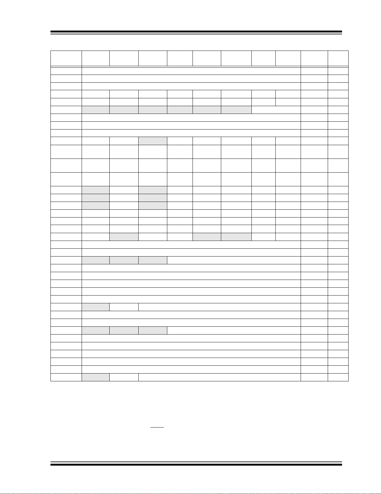
PIC18F6585/8585/6680/8680
TABLE 4-3: REGISTER FILE SUMMARY (CONTINUED)
File Name Bit 7 Bit 6 Bit 5 Bit 4 Bit 3 Bit 2 Bit 1 Bit 0
SPBRG USART Baud Rate Generato r
RCREG USART Receive Register
TXREG USART Transm it Regi ster
TXST A CSRC TX9 TXEN SYNC SENDB BRGH TRMT TX9D
RCSTA SPEN RX9 SREN CREN ADDEN FERR OERR RX9D
EEADRH
EEADR Data EEPROM Addre ss Reg ister
EEDA TA Data EEPROM Dat a R e gi st er
EECON2 Data EEPROM Control Re giste r 2 ( no t a physic al regi ster )
EECON1 EEPGD CFGS
IPR3 IRXIP WAKIP ERRIP TXB2IP/
PIR3 IRXIF WAKIF ERRIF TXB2IF/
PIE3 IRXIE WAKIE ERRIE TXB2IE/
IPR2
PIR2
PIE2
IPR1 PSPIP ADIP RCIP TXIP SSPIP CCP1IP TMR2IP TMR1IP
PIR1 PSPIF ADIF RCIF TXIF SSPIF CCP1IF TMR2IF TMR1IF
PIE1 PSPIE ADIE RCIE TXIE SSPIE CCP1IE TMR2IE TMR1IE
MEMCON
TRISJ
TRISH
TRISG
TRISF Data Direction Control Register for PORT F
TRISE Data Direction Control Register f or PO R TE
TRISD Data Direction Con trol Regis ter f or PO R T D
TRISC Data Direction Con trol Regis ter f or PO R T C
TRISB Data Direction Control Register f or PO R TB
TRISA
LATJ
LATH
LATG
LATF Read PORTF Data Latc h, Write PORTF Data Latch
LATE Read PORT E Dat a Latch, W ri te PO R TE Dat a Latc h
LATD Read PORTD Data Latch, Write P ORTD Data Latch
LATC Read PORTC Data Latch, Write P ORTC Data Latch
LATB Read PORT B Dat a Latch, W ri te PO R TB Dat a Latc h
LATA
Legend: x = unknown, u = unchanged, – = unimplemented, q = value depends on condition
Note 1: RA6 and associated bits are configured as port pins in RCIO and ECIO Oscillator mode only and read ‘0’ in all other oscillator
(3)
(3)
(3)
(3)
(3)
2: Bit 21 of the TBLPTRU allows access to the device configuration bits.
3: These registers are unus ed on PIC18F6X80 devices; always maint ain these clear.
4: These bits have multiple functions depending on the CAN module mode selection.
5: Meaning of this register depends on whether this buffer is configured as transmit or receive.
6: RG5 is available as an input when MCLR
7: This register reads all ‘0’s until the ECAN module is set up in Mode 1 or Mode 2.
— — — — — — EE Adr Register High
— FREE WRERR WREN WR RD
TXBnIP
TXBnIF
TXBnIE
—CMIP— EEIP BCLIP LVDIP TMR3IP CCP2IP
—CMIF— EEIF BCLIF LVDIF TMR3IF CCP2IF
—CMIE— EEIE BCLIE LVDIE TMR3IE CCP2IE
EBDIS —WAIT1WAIT0— —WM1WM0
Data Direction Control Register f or POR TJ
Data Direction Control Register f or POR TH
— — — Data Direction Control Register for PORT G
—TRISA6
Read PORTJ Data Lat ch, Write PORTJ Data Latch
Read PORTH Data L atc h, W r ite P O R TH Dat a Lat ch
— — — Read PORTG Data Latch, Write PO R TG Dat a Lat ch
—LATA6
modes.
(1)
Data Direction Control Re gist er for POR TA
(1)
Read PORTA Data Latch, Write POR TA Data Latch
is disabled.
TXB1IP TXB0IP RXB1IP/
RXBnIP
TXB1IF TXB0IF RXB1IF/
RXBnIF
TXB1IE TXB0IE RXB1IE/
RXBnIE
(1)
RXB0IP/
FIFOWMIP
RXB0IF/
FIFOWMIF
RXB0IE/
FIFOWMIE
Value on
POR, BOR
0000 0000
0000 0000
0000 0000
0000 0010
0000 000x
---- --00
0000 0000
0000 0000
---- ----
00-0 x000
1111 1111
0000 0000
0000 0000
-1-1 1111
-0-0 0000
-0-0 0000
0111 1111
0000 0000
0000 0000
0-00 --00
1111 1111
1111 1111
---1 1111
1111 1111
1111 1111
1111 1111
1111 1111
1111 1111
-111 1111
xxxx xxxx
xxxx xxxx
---x xxxx
xxxx xxxx
xxxx xxxx
xxxx xxxx
xxxx xxxx
xxxx xxxx
-xxx xxxx
Details
on page:
38, 239
38, 241
38, 239
38, 230
38, 231
38, 105
38, 105
38, 105
38, 105
38, 102
39, 122
39, 1 16
39, 1 19
39, 121
39, 1 15
39, 1 18
39, 120
39, 1 14
39, 1 17
39, 151
39, 148
39, 145
39, 141
39, 138
39, 135
39, 131
39, 128
39, 125
39, 151
39, 148
39, 145
39, 141
39, 138
39, 133
39, 131
39, 128
39, 125
39, 94
2004 Microchip Technology Inc. DS30491C-page 69
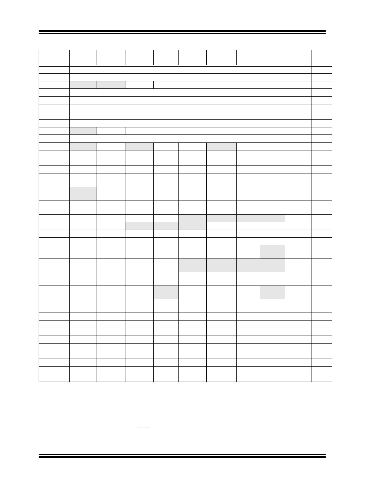
PIC18F6585/8585/6680/8680
TABLE 4-3: REGISTER FILE SUMMARY (CONTINUED)
File Name Bit 7 Bit 6 Bit 5 Bit 4 Bit 3 Bit 2 Bit 1 Bit 0
(3)
PORTJ
PORTH
PORTG
PORTF Read PORTF pins, Write POR TF Dat a Latch
PORTE Read PORTE pins, W r ite PO R T E Data Latch
PORTD Read PORT D p ins, W ri te POR T D Da t a La tch
PORTC Read PORT C p ins, W ri te POR T C Da t a La tch
PORTB Read PORTB pins, W r ite PO R T B Data Latch
PORTA
SPBRGH Enhanced USART Baud Rate Generator Hig h B yte
BAUDCON
ECCP1DEL PRSEN PDC6 PDC5 PDC4 PDC3 PDC2 PDC1 PDC0
TXERRCNT TEC7 TEC6 TEC5 TEC4 TEC3 TEC2 TEC1 TEC0
RXERRCNT REC7 REC6 REC5 REC4 REC3 REC2 REC1 REC0
COMSTAT
Mode 0
COMSTAT
Mode 1
COMSTAT
Mode 2
CIOCON TX2SRC TX2EN ENDRHI CANCAP
BRGCON3 WAKDIS WAKFIL
BRGCON2 SEG2PHT SAM SEG1PH2 SEG1PH1 SEG1PH0 PRSEG2 PRSEG1 PRSEG0
BRGCON1 SJW1 SJW0 BRP5 BRP4 BRP3 BRP2 BRP1 BRP0
CANCON
Mode 0
CANCON
Mode 1
CANCON
Mode 2
CANSTAT
Mode 0
CANSTAT
Modes 0, 1
ECANCON MDSEL1 MDSEL0 FIFOWM EWIN4 EWIN3 EWIN2 EWIN1 EWIN0
RXB0D7 RXB0D77 RXB0D76 RXB0D75 RXB0D74 RXB0D73 RXB0D72 RXB0D71 RXB0D70
RXB0D6 RXB0D67 RXB0D66 RXB0D65 RXB0D64 RXB0D63 RXB0D62 RXB0D61 RXB0D60
RXB0D5 RXB0D57 RXB0D56 RXB0D55 RXB0D54 RXB0D53 RXB0D52 RXB0D51 RXB0D50
RXB0D4 RXB0D47 RXB0D46 RXB0D45 RXB0D44 RXB0D43 RXB0D42 RXB0D41 RXB0D40
RXB0D3 RXB0D37 RXB0D36 RXB0D35 RXB0D34 RXB0D33 RXB0D32 RXB0D31 RXB0D30
RXB0D2 RXB0D27 RXB0D26 RXB0D25 RXB0D24 RXB0D23 RXB0D22 RXB0D21 RXB0D20
RXB0D1 RXB0D17 RXB0D16 RXB0D15 RXB0D14 RXB0D13 RXB0D12 RXB0D11 RXB0D10
RXB0D0 RXB0D07 RXB0D06 RXB0D05 RXB0D04 RXB0D03 RXB0D02 RXB0D01 RXB0D00
Legend: x = unknown, u = unchanged, – = unimplemented, q = value depe nds on condition
Note 1: RA6 and associated bits are configured as port pins in RCIO and ECIO Oscillator mode only and read ‘0’ in all other oscillator
Read PORTJ pins, Write PORTJ Data Latch
(3)
Read PORTH pins, Wri te POR T H Dat a La tch
— —RG5
—RA6
— RCIDL — SCKP BRG16 — WUE ABDEN
RXB0OVFL RXB1OVFL TXBO TXBP RXBP TXWARN RXWARN EWARN
— RXBnOVFL TXBO TXBP RXBP TXWARN RXWARN EWARN
FIFOEMPTY
REQOP2 REQOP1 REQOP0 ABAT WIN2 WIN1 WIN0
REQOP2 REQOP1 REQOP0 ABAT
REQOP2 REQOP1 REQOP0 ABAT FP3 FP2 FP1 FP0
OPMODE2 OPMODE1 OPMODE0
OPMODE2 OPMODE1 OPMODE0 EICODE4 EICODE3 EICODE2 EICODE1 EICOD E0
modes.
2: Bit 21 of the TBLPTRU allows access to the device configuration bits.
3: These registers are unus ed on PIC18F6X80 devices; always maint ain these clear.
4: These bits have multiple functions depending on the CAN module mode selection.
5: Meaning of this register depends on whether this buffer is configured as transmit or receive.
6: RG5 is available as an input when MCLR
7: This register reads all ‘0’s until the ECAN module is set up in Mode 1 or Mode 2.
(1)
RXBnOVFL TXBO TXBP RXBP TXWARN RXWARN EWARN
(6)
Read PORTG pins, Write PORTG Data Latch
Read PORTA pins, Write PORTA Data Latch
— — — —
— — — SEG2PH2 SEG2PH1 SEG2PH0
— — — —
— ICODE2 ICODE1 ICODE0 —
is disabled.
(1)
—
Value on
POR, BOR
xxxx xxxx
xxxx xxxx
--0x xxxx
xxxx xxxx
xxxx xxxx
xxxx xxxx
xxxx xxxx
xxxx xxxx
-x0x 0000
0000 0000
-1-0 0-00
0000 0000
0000 0000
0000 0000
0000 0000
-000 0000
0000 0000
0000 ----
00-- -000
0000 0000
0000 0000
1000 000-
1000 ----
1000 0000
000- 0000
0000 0000
0001 0000
xxxx xxxx
xxxx xxxx
xxxx xxxx
xxxx xxxx
xxxx xxxx
xxxx xxxx
xxxx xxxx
xxxx xxxx
on page:
40, 151
40, 148
40, 145
40, 141
40, 136
40, 133
40, 131
40, 128
40, 125
40, 233
40, 233
40, 187
40, 288
40, 296
40, 284
40, 284
40, 284
40, 318
40, 317
40, 317
40, 317
40, 239
40, 239
40, 239
40, 239
40, 239
40, 323
40, 230
40, 230
40, 230
40, 230
40, 230
40, 230
40, 230
40, 230
Details
DS30491C-page 70 2004 Microchip Technology Inc.

PIC18F6585/8585/6680/8680
TABLE 4-3: REGISTER FILE SUMMARY (CONTINUED)
File Name Bit 7 Bit 6 Bit 5 Bit 4 Bit 3 Bit 2 Bit 1 Bit 0
RXB0DLC — RXRTR RB1 RB0 DLC3 DLC2 DLC1 DLC0
RXB0EIDL EID7 EID6 EID5 EID4 EID3 EID2 EID1 EID0
RXB0EIDH EID15 EID14 EID13 EID12 EID11 EID10 EID9 EID8
RXB0SIDL SID2 SID1 SID0 SRR EXID
—EID17EID16
RXB0SIDH SID10 SID9 SID8 SID7 SID6 SID5 SID4 SID3
RXB0CON
RXFUL RXM1 RXM0
(4)
(4)
—
RXRTRR0
(4)
RXB0DBEN
(4)
JTOFF
(4)
FILHIT0
POR, BOR
-xxx xxxx
xxxx xxxx
xxxx xxxx
xxxx x-xx
xxxx xxxx
(4)
000- 0000
Value on
Mode 0
RXB0CON
RXFUL RXM1 RTRR0
(4)
FILHIT4
(4)
FILHIT3
(4)
FILHIT2
(4)
FILHIT1
(4)
FILHIT0
(4)
0000 0000
Mode 1, 2
RXB1D7 RXB1D77 RXB1D76 RXB1D75 RXB1D74 RXB1D73 RXB1D72 RXB1D71 RXB1D70
RXB1D6 RXB1D67 RXB1D66 RXB1D65 RXB1D64 RXB1D63 RXB1D62 RXB1D61 RXB1D60
RXB1D5 RXB1D57 RXB1D56 RXB1D55 RXB1D54 RXB1D53 RXB1D52 RXB1D51 RXB1D50
RXB1D4 RXB1D47 RXB1D46 RXB1D45 RXB1D44 RXB1D43 RXB1D42 RXB1D41 RXB1D40
RXB1D3 RXB1D37 RXB1D36 RXB1D35 RXB1D34 RXB1D33 RXB1D32 RXB1D31 RXB1D30
RXB1D2 RXB1D27 RXB1D26 RXB1D25 RXB1D24 RXB1D23 RXB1D22 RXB1D21 RXB1D20
RXB1D1 RXB1D17 RXB1D16 RXB1D15 RXB1D14 RXB1D13 RXB1D12 RXB1D11 RXB1D10
RXB1D0 RXB1D07 RXB1D06 RXB1D05 RXB1D04 RXB1D03 RXB1D02 RXB1D01 RXB1D00
RXB1DLC
— RXRTR RB1 RB0 DLC3 DLC2 DLC1 DLC0
RXB1EIDL EID7 EID6 EID5 EID4 EID3 EID2 EID1 EID0
RXB1EIDH EID15 EID14 EID13 EID12 EID11 EID10 EID9 EID8
RXB1SIDL SID2 SID1 SID0 SRR EXID
—EID17EID16
RXB1SIDH SID10 SID9 SID8 SID7 SID6 SID5 SID4 SID3
RXB1CON
RXFUL RXM1 RXM0
(4)
(4)
—
RXRTRR0
(4)
FILHIT2
(4)
FILHIT1
(4)
FILHIT0
xxxx xxxx
xxxx xxxx
xxxx xxxx
xxxx xxxx
xxxx xxxx
xxxx xxxx
xxxx xxxx
xxxx xxxx
-xxx xxxx
xxxx xxxx
xxxx xxxx
xxxx x-xx
xxxx xxxx
(4)
000- 0000
Mode 0
RXB1CON
RXFUL RXM1 RTRRO
(4)
FILHIT4
(4)
FILHIT3
(4)
FILHIT2
(4)
FILHIT1
(4)
FILHIT0
(4)
0000 0000
Mode 1, 2
TXB0D7 TXB0D77 TXB0D76 TXB0D75 TXB0D74 TXB0D73 TXB0D72 TXB0D71 TXB0D70
TXB0D6 TXB0D67 TXB0D66 TXB0D65 TXB0D64 TXB0D63 TXB0D62 TXB0D61 TXB0D60
TXB0D5 TXB0D57 TXB0D56 TXB0D55 TXB0D54 TXB0D53 TXB0D52 TXB0D51 TXB0D50
TXB0D4 TXB0D47 TXB0D46 TXB0D45 TXB0D44 TXB0D43 TXB0D42 TXB0D41 TXB0D40
TXB0D3 TXB0D37 TXB0D36 TXB0D35 TXB0D34 TXB0D33 TXB0D32 TXB0D31 TXB0D30
TXB0D2 TXB0D27 TXB0D26 TXB0D25 TXB0D24 TXB0D23 TXB0D22 TXB0D21 TXB0D20
TXB0D1 TXB0D17 TXB0D16 TXB0D15 TXB0D14 TXB0D13 TXB0D12 TXB0D11 TXB0D10
TXB0D0 TXB0D07 TXB0D06 TXB0D05 TXB0D04 TXB0D03 TXB0D02 TXB0D01 TXB0D00
TXB0DLC
—TXRTR— — DLC3 DLC2 DLC1 DLC0
TXB0EIDL EID7 EID6 EID5 EID4 EID3 EID2 EID1 EID0
TXB0EIDH EID15 EID14 EID13 EID12 EID11 EID10 EID9 EID8
TXB0SIDL SID2 SID1 SID0
—EXIDE —EID17EID16
TXB0SIDH SID10 SID9 SID8 SID7 SID6 SID5 SID4 SID3
TXB0CON
— TXABT TXLARB TXERR TXREQ — TXPRI1 TXPRI0
xxxx xxxx
xxxx xxxx
xxxx xxxx
xxxx xxxx
xxxx xxxx
xxxx xxxx
xxxx xxxx
xxxx xxxx
-x-- xxxx
xxxx xxxx
xxxx xxxx
xx-x x-xx
xxxx xxxx
-000 0-00
Mode 0
TXB0CON
TXBIF TXABT TXLARB TXERR TXREQ
— TXPRI1 TXPRI0
0000 0-00
Mode 1, 2
Legend: x = unknown, u = unchanged, – = unimplemented, q = value depends on condition
Note 1: RA6 and associated bits are configured as port pins in RCIO and ECIO Oscillator mode only and read ‘0’ in all other oscillator
modes.
2: Bit 21 of the TBLPTRU allows access to the device configuration bits.
3: These registers are unus ed on PIC18F6X80 devices; always maint ain these clear.
4: These bits have multiple functions depending on the CAN module mode selection.
5: Meaning of this register depends on whether this buffer is configured as transmit or receive.
6: RG5 is available as an input when MCLR
is disabled.
7: This register reads all ‘0’s until the ECAN module is set up in Mode 1 or Mode 2.
Details
on page:
40, 230
41, 230
41, 230
41, 230
41, 230
41, 230
41, 230
41, 230
41, 230
41, 230
41, 230
41, 230
41, 230
41, 230
41, 230
41, 230
41, 230
41, 230
41, 230
41, 230
41, 230
41, 230
41, 230
41, 230
41, 230
41, 230
41, 230
41, 230
41, 230
41, 230
41, 230
41, 230
41, 230
41, 230
42, 230
42, 230
42, 230
2004 Microchip Technology Inc. DS30491C-page 71

PIC18F6585/8585/6680/8680
TABLE 4-3: REGISTER FILE SUMMARY (CONTINUED)
File Name Bit 7 Bit 6 Bit 5 Bit 4 Bit 3 Bit 2 Bit 1 Bit 0
TXB1D7 TXB1D77 TXB1D76 TXB1D75 TXB1D74 TXB1D73 TXB1D72 TXB1D71 TXB1D70
TXB1D6 TXB1D67 TXB1D66 TXB1D65 TXB1D64 TXB1D63 TXB1D62 TXB1D61 TXB1D60
TXB1D5 TXB1D57 TXB1D56 TXB1D55 TXB1D54 TXB1D53 TXB1D52 TXB1D51 TXB1D50
TXB1D4 TXB1D47 TXB1D46 TXB1D45 TXB1D44 TXB1D43 TXB1D42 TXB1D41 TXB1D40
TXB1D3 TXB1D37 TXB1D36 TXB1D35 TXB1D34 TXB1D33 TXB1D32 TXB1D31 TXB1D30
TXB1D2 TXB1D27 TXB1D26 TXB1D25 TXB1D24 TXB1D23 TXB1D22 TXB1D21 TXB1D20
TXB1D1 TXB1D17 TXB1D16 TXB1D15 TXB1D14 TXB1D13 TXB1D12 TXB1D11 TXB1D10
TXB1D0 TXB1D07 TXB1D06 TXB1D05 TXB1D04 TXB1D03 TXB1D02 TXB1D01 TXB1D00
TXB1DLC
TXB1EIDL EID7 EID6 EID5 EID4 EID3 EID2 EID1 EID0
TXB1EIDH EID15 EID14 EID13 EID12 EID11 EID10 EID9 EID8
TXB1SIDL SID2 SID1 SID0
TXB1SIDH SID10 SID9 SID8 SID7 SID6 SID5 SID4 SID3
TXB1CON
Mode 0
TXB1CON
Mode 1, 2
TXB2D7 TXB2D77 TXB2D76 TXB2D75 TXB2D74 TXB2D73 TXB2D72 TXB2D71 TXB2D70
TXB2D6 TXB2D67 TXB2D66 TXB2D65 TXB2D64 TXB2D63 TXB2D62 TXB2D61 TXB2D60
TXB2D5 TXB2D57 TXB2D56 TXB2D55 TXB2D54 TXB2D53 TXB2D52 TXB2D51 TXB2D50
TXB2D4 TXB2D47 TXB2D46 TXB2D45 TXB2D44 TXB2D43 TXB2D42 TXB2D41 TXB2D40
TXB2D3 TXB2D37 TXB2D36 TXB2D35 TXB2D34 TXB2D33 TXB2D32 TXB2D31 TXB2D30
TXB2D2 TXB2D27 TXB2D26 TXB2D25 TXB2D24 TXB2D23 TXB2D22 TXB2D21 TXB2D20
TXB2D1 TXB2D17 TXB2D16 TXB2D15 TXB2D14 TXB2D13 TXB2D12 TXB2D11 TXB2D10
TXB2D0 TXB2D07 TXB2D06 TXB2D05 TXB2D04 TXB2D03 TXB2D02 TXB2D01 TXB2D00
TXB2DLC
TXB2EIDL EID7 EID6 EID5 EID4 EID3 EID2 EID1 EID0
TXB2EIDH EID15 EID14 EID13 EID12 EID11 EID10 EID9 EID8
TXB2SIDL SID2 SID1 SID0
TXB2SIDH SID10 SID9 SID8 SID7 SID6 SID5 SID4 SID3
TXB2CON
Mode 0
TXB2CON
Mode 1, 2
RXM1EIDL EID7 EID6 EID5 EID4 EID3 EID2 EID1 EID0
RXM1EIDH EID15 EID14 EID13 EID12 EID11 EID10 EID9 EID8
RXM1SIDL SID2 SID1 SID0
RXM1SIDH SID10 SID9 SID8 SID7 SID6 SID5 SID4 SID3
RXM0EIDL EID7 EID6 EID5 EID4 EID3 EID2 EID1 EID0
RXM0EIDH EID15 EID14 EID13 EID12 EID11 EID10 EID9 EID8
RXM0SIDL SID2 SID1 SID0
RXM0SIDH SID10 SID9 SID8 SID7 SID6 SID5 SID4 SID3
RXF15EIDL
Legend: x = unknown, u = unchanged, – = unimplemented, q = value depe nds on condition
Note 1: RA6 and associated bits are configured as port pins in RCIO and ECIO Oscillator mode only and read ‘0’ in all other oscillator
2: Bit 21 of the TBLPTRU allows access to the device configuration bits.
3: These registers are unus ed on PIC18F6X80 devices; always maint ain these clear.
4: These bits have multiple functions depending on the CAN module mode selection.
5: Meaning of this register depends on whether this buffer is configured as transmit or receive.
6: RG5 is available as an input when MCLR
7: This register reads all ‘0’s until the ECAN module is set up in Mode 1 or Mode 2.
—TXRTR— — DLC3 DLC2 DLC1 DLC0
—EXIDE —EID17EID16
— TXABT TXLARB TXERR TXREQ — TXPRI1 TXPRI0
TXBIF TXABT TXLARB TXERR TXREQ
—TXRTR— — DLC3 DLC2 DLC1 DLC0
—EXIDE —EID17EID16
— TXABT TXLARB TXERR TXREQ — TXPRI1 TXPRI0
TXBIF TXABT TXLARB TXERR TXREQ
—EXIDEN —EID17EID16
—EXIDM —EID17EID16
(7)
EID7 EID6 EID5 EID4 EID3 EID2 EID1 EID0
modes.
is disabled.
— TXPRI1 TXPRI0
— TXPRI1 TXPRI0
Value on
POR, BOR
xxxx xxxx
xxxx xxxx
xxxx xxxx
xxxx xxxx
xxxx xxxx
xxxx xxxx
xxxx xxxx
xxxx xxxx
-x-- xxxx
xxxx xxxx
xxxx xxxx
xx-x x-xx
xxxx xxxx
-000 0-00
0000 0-00
xxxx xxxx
xxxx xxxx
xxxx xxxx
xxxx xxxx
xxxx xxxx
xxxx xxxx
xxxx xxxx
xxxx xxxx
-x-- xxxx
xxxx xxxx
xxxx xxxx
xxx- x-xx
xxxx xxxx
-000 0-00
0000 0-00
xxxx xxxx
xxxx xxxx
xx-x 0-xx
xxxx xxxx
xxxx xxxx
xxxx xxxx
xx-x 0-xx
xxxx xxxx
xxxx xxxx
on page:
42, 230
42, 230
42, 230
42, 230
42, 230
42, 230
42, 230
42, 230
42, 230
42, 230
42, 230
42, 230
42, 230
42, 230
42, 230
42, 230
42, 230
42, 230
42, 230
42, 230
42, 230
42, 230
42, 230
42, 230
42, 230
42, 230
42, 230
42, 230
42, 230
42, 230
42, 230
43, 230
43, 230
43, 230
43, 230
43, 230
43, 230
43, 230
47, 230
Details
DS30491C-page 72 2004 Microchip Technology Inc.
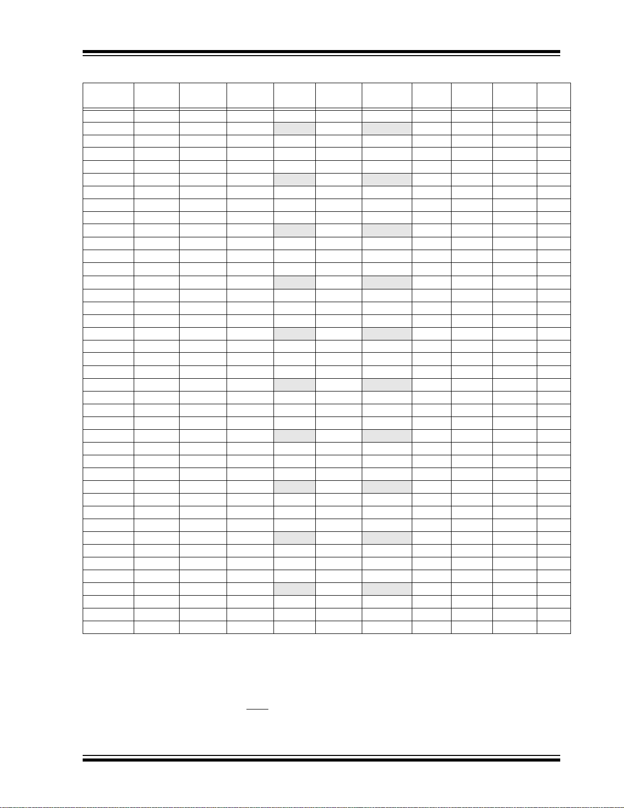
PIC18F6585/8585/6680/8680
TABLE 4-3: REGISTER FILE SUMMARY (CONTINUED)
File Name Bit 7 Bit 6 Bit 5 Bit 4 Bit 3 Bit 2 Bit 1 Bit 0
RXF15EIDH
RXF15SIDL
RXF15SIDH
RXF14EIDL
RXF14EIDH
RXF14SIDL
RXF14SIDH
RXF13EIDL
RXF13EIDH
RXF13SIDL
RXF13SIDH
RXF12EIDL
RXF12EIDH
RXF12SIDL
RXF12SIDH
RXF11EIDL
RXF11EIDH
RXF11SIDL
RXF11SIDH
RXF10EIDL
RXF10EIDH
RXF10SIDL
RXF10SIDH
RXF9EIDL
RXF9EIDH
RXF9SIDL
RXF9SIDH
RXF8EIDL
RXF8EIDH
RXF8SIDL
RXF8SIDH
RXF7EIDL
RXF7EIDH
RXF7SIDL
RXF7SIDH
RXF6EIDL
RXF6EIDH
RXF6SIDL
RXF6SIDH
(7)
EID15 EID14 EID13 EID12 EID11 EID10 EID9 EID8
(7)
SID2 SID1 SID0 —EXIDEN —EID17EID16
(7)
SID10 SID9 SID8 SID7 SID6 SID5 SID4 SID3
(7)
EID7 EID6 EID5 EID4 EID3 EID2 EID1 EID0
(7)
EID15 EID14 EID13 EID12 EID11 EID10 EID9 EID8
(7)
SID2 SID1 SID0 —EXIDEN —EID17EID16
(7)
SID10 SID9 SID8 SID7 SID6 SID5 SID4 SID3
(7)
EID7 EID6 EID5 EID4 EID3 EID2 EID1 EID0
(7)
EID15 EID14 EID13 EID12 EID11 EID10 EID9 EID8
(7)
SID2 SID1 SID0 —EXIDEN —EID17EID16
(7)
SID10 SID9 SID8 SID7 SID6 SID5 SID4 SID3
(7)
EID7 EID6 EID5 EID4 EID3 EID2 EID1 EID0
(7)
EID15 EID14 EID13 EID12 EID11 EID10 EID9 EID8
(7)
SID2 SID1 SID0 —EXIDEN —EID17EID16
(7)
SID10 SID9 SID8 SID7 SID6 SID5 SID4 SID3
(7)
EID7 EID6 EID5 EID4 EID3 EID2 EID1 EID0
(7)
EID15 EID14 EID13 EID12 EID11 EID10 EID9 EID8
(7)
SID2 SID1 SID0 —EXIDEN —EID17EID16
(7)
SID10 SID9 SID8 SID7 SID6 SID5 SID4 SID3
(7)
EID7 EID6 EID5 EID4 EID3 EID2 EID1 EID0
(7)
EID15 EID14 EID13 EID12 EID11 EID10 EID9 EID8
(7)
SID2 SID1 SID0 —EXIDEN —EID17EID16
(7)
SID10 SID9 SID8 SID7 SID6 SID5 SID4 SID3
(7)
EID7 EID6 EID5 EID4 EID3 EID2 EID1 EID0
(7)
EID15 EID14 EID13 EID12 EID11 EID10 EID9 EID8
(7)
SID2 SID1 SID0 —EXIDEN —EID17EID16
(7)
SID10 SID9 SID8 SID7 SID6 SID5 SID4 SID3
(7)
EID7 EID6 EID5 EID4 EID3 EID2 EID1 EID0
(7)
EID15 EID14 EID13 EID12 EID11 EID10 EID9 EID8
(7)
SID2 SID1 SID0 —EXIDEN —EID17EID16
(7)
SID10 SID9 SID8 SID7 SID6 SID5 SID4 SID3
(7)
EID7 EID6 EID5 EID4 EID3 EID2 EID1 EID0
(7)
EID15 EID14 EID13 EID12 EID11 EID10 EID9 EID8
(7)
SID2 SID1 SID0 —EXIDEN —EID17EID16
(7)
SID10 SID9 SID8 SID7 SID6 SID5 SID4 SID3
(7)
EID7 EID6 EID5 EID4 EID3 EID2 EID1 EID0
(7)
EID15 EID14 EID13 EID12 EID11 EID10 EID9 EID8
(7)
SID2 SID1 SID0 —EXIDEN —EID17EID16
(7)
SID10 SID9 SID8 SID7 SID6 SID5 SID4 SID3
RXF5EIDL EID7 EID6 EID5 EID4 EID3 EID2 EID1 EID0
RXF5EIDH EID15 EID14 EID13 EID12 EID11 EID10 EID9 EID8
Value on
POR, BOR
xxxx xxxx
xx-x x-xx
xxxx xxxx
xxxx xxxx
xxxx xxxx
xx-x x-xx
xxxx xxxx
xxxx xxxx
xxxx xxxx
xx-x x-xx
xxxx xxxx
xxxx xxxx
xxxx xxxx
xx-x x-xx
xxxx xxxx
xxxx xxxx
xxxx xxxx
xx-x x-xx
xxxx xxxx
xxxx xxxx
xxxx xxxx
xx-x x-xx
xxxx xxxx
xxxx xxxx
xxxx xxxx
xx-x x-xx
xxxx xxxx
xxxx xxxx
xxxx xxxx
xx-x x-xx
xxxx xxxx
xxxx xxxx
xxxx xxxx
xx-x x-xx
xxxx xxxx
xxxx xxxx
xxxx xxxx
xx-x x-xx
xxxx xxxx
xxxx xxxx
xxxx xxxx
Legend: x = unknown, u = unchanged, – = unimplemented, q = value depends on condition
Note 1: RA6 and associated bits are configured as port pins in RCIO and ECIO Oscillator mode only and read ‘0’ in all other oscillator
modes.
2: Bit 21 of the TBLPTRU allows access to the device configuration bits.
3: These registers are unus ed on PIC18F6X80 devices; always maint ain these clear.
4: These bits have multiple functions depending on the CAN module mode selection.
5: Meaning of this register depends on whether this buffer is configured as transmit or receive.
6: RG5 is available as an input when MCLR
is disabled.
7: This register reads all ‘0’s until the ECAN module is set up in Mode 1 or Mode 2.
Details
on page:
47, 230
47, 230
47, 230
47, 230
47, 230
47, 230
47, 230
47, 230
47, 230
47, 230
47, 230
47, 230
47, 230
47, 230
47, 230
47, 230
47, 230
47, 230
47, 230
47, 230
47, 230
48, 230
48, 230
47, 230
48, 230
48, 230
48, 230
48, 230
48, 230
48, 230
48, 230
48, 230
48, 230
48, 230
48, 230
48, 230
48, 230
48, 230
48, 230
43, 230
43, 230
2004 Microchip Technology Inc. DS30491C-page 73

PIC18F6585/8585/6680/8680
TABLE 4-3: REGISTER FILE SUMMARY (CONTINUED)
File Name Bit 7 Bit 6 Bit 5 Bit 4 Bit 3 Bit 2 Bit 1 Bit 0
RXF5SIDL SID2 SID1 SID0 —EXIDEN —EID17EID16
RXF5SIDH SID10 SID9 SID8 SID7 SID6 SID5 SID4 SID3
RXF4EIDL EID7 EID6 EID5 EID4 EID3 EID2 EID1 EID0
RXF4EIDH EID15 EID14 EID13 EID12 EID11 EID10 EID9 EID8
RXF4SIDL SID2 SID1 SID0
—EXIDEN —EID17EID16
RXF4SIDH SID10 SID9 SID8 SID7 SID6 SID5 SID4 SID3
RXF3EIDL EID7 EID6 EID5 EID4 EID3 EID2 EID1 EID0
RXF3EIDH EID15 EID14 EID13 EID12 EID11 EID10 EID9 EID8
RXF3SIDL SID2 SID1 SID0
—EXIDEN —EID17EID16
RXF3SIDH SID10 SID9 SID8 SID7 SID6 SID5 SID4 SID3
RXF2EIDL EID7 EID6 EID5 EID4 EID3 EID2 EID1 EID0
RXF2EIDH EID15 EID14 EID13 EID12 EID11 EID10 EID9 EID8
RXF2SIDL SID2 SID1 SID0
—EXIDEN —EID17EID16
RXF2SIDH SID10 SID9 SID8 SID7 SID6 SID5 SID4 SID3
RXF1EIDL EID7 EID6 EID5 EID4 EID3 EID2 EID1 EID0
RXF1EIDH EID15 EID14 EID13 EID12 EID11 EID10 EID9 EID8
RXF1SIDL SID2 SID1 SID0
—EXIDEN —EID17EID16
RXF1SIDH SID10 SID9 SID8 SID7 SID6 SID5 SID4 SID3
RXF0EIDL EID7 EID6 EID5 EID4 EID3 EID2 EID1 EID0
RXF0EIDH EID15 EID14 EID13 EID12 EID11 EID10 EID9 EID8
RXF0SIDL SID2 SID1 SID0
—EXIDEN —EID17EID16
RXF0SIDH SID10 SID9 SID8 SID7 SID6 SID5 SID4 SID3
(7)
B5D7
(7)
B5D6
(7)
B5D5
(7)
B5D4
(7)
B5D3
(7)
B5D2
(7)
B5D1
(7)
B5D0
B5DLC
B5EIDL
B5EIDH
B5SIDL
B5SIDH
B5CON
(7)
B4D7
(7)
B4D6
(7)
B4D5
(7)
B4D4
(7)
(7)
(7)
(7)
(7)
(5, 7)
B5D77 B5D76 B5D75 B5D74 B5D73 B5D72 B5D71 B5D70
B5D67 B5D66 B5D65 B5D64 B5D63 B5D62 B5D61 B5D60
B5D57 B5D56 B5D55 B5D54 B5D53 B5D52 B5D51 B5D50
B5D47 B5D46 B5D45 B5D44 B5D43 B5D42 B5D41 B5D40
B5D37 B5D36 B5D35 B5D34 B5D33 B5D32 B5D31 B5D30
B5D27 B5D26 B5D25 B5D24 B5D23 B5D22 B5D21 B5D20
B5D17 B5D16 B5D15 B5D14 B5D13 B5D12 B5D11 B5D10
B5D07 B5D06 B5D05 B5D04 B5D03 B5D02 B5D01 B5D00
— RXRTR RB1 RB0 DLC3 DLC2 DLC1 DLC0
EID7 EID6 EID5 EID4 EID3 EID2 EID1 EID0
EID15 EID14 EID13 EID12 EID11 EID10 EID9 EID8
SID2 SID1 SID0 SRR EXID/
EXIDE
(5)
—EID17EID16
SID10 SID9 SID8 SID7 SID6 SID5 SID4 SID3
RXFUL/
TXBIF
RXM1/
TXABT
RTRRO/
TXLARB
FILHIT4/
TXERR
FILHIT3/
TXREQ
FILHIT2/
RTREN
FILHIT1/
TXPRI1
FILHIT0/
TXPRI0
B4D77 B4D76 B4D75 B4D74 B4D73 B4D72 B4D71 B4D70
B4D67 B4D66 B4D65 B4D64 B4D63 B4D62 B4D61 B4D60
B4D57 B4D56 B4D55 B4D54 B4D53 B4D52 B4D51 B4D50
B4D47 B4D46 B4D45 B4D44 B4D43 B4D42 B4D41 B4D40
Legend: x = unknown, u = unchanged, – = unimplemented, q = value depe nds on condition
Note 1: RA6 and associated bits are configured as port pins in RCIO and ECIO Oscillator mode only and read ‘0’ in all other oscillator
modes.
2: Bit 21 of the TBLPTRU allows access to the device configuration bits.
3: These registers are unus ed on PIC18F6X80 devices; always maint ain these clear.
4: These bits have multiple functions depending on the CAN module mode selection.
5: Meaning of this register depends on whether this buffer is configured as transmit or receive.
6: RG5 is available as an input when MCLR
is disabled.
7: This register reads all ‘0’s until the ECAN module is set up in Mode 1 or Mode 2.
Value on
POR, BOR
xx-x x-xx
xxxx xxxx
xxxx xxxx
xxxx xxxx
xx-x x-xx
xxxx xxxx
xxxx xxxx
xxxx xxxx
xx-x x-xx
xxxx xxxx
xxxx xxxx
xxxx xxxx
xx-x x-xx
xxxx xxxx
xxxx xxxx
xxxx xxxx
xx-x x-xx
xxxx xxxx
xxxx xxxx
xxxx xxxx
xx-x x-xx
xxxx xxxx
xxxx xxxx
xxxx xxxx
xxxx xxxx
xxxx xxxx
xxxx xxxx
xxxx xxxx
xxxx xxxx
xxxx xxxx
-xxx xxxx
xxxx xxxx
xxxx xxxx
xxxx x-xx
xxxx xxxx
0000 0000
xxxx xxxx
xxxx xxxx
xxxx xxxx
xxxx xxxx
on page:
43, 230
43, 230
43, 230
43, 230
43, 230
43, 230
43, 230
43, 230
43, 230
43, 230
43, 230
43, 230
43, 230
43, 230
43, 230
43, 230
43, 230
43, 230
43, 230
43, 230
43, 230
43, 230
44, 230
44, 230
44, 230
44, 230
44, 230
44, 230
44, 230
44, 230
44, 230
44, 230
44, 230
44, 230
44, 230
44, 230
44, 230
44, 230
44, 230
44, 230
Details
DS30491C-page 74 2004 Microchip Technology Inc.

PIC18F6585/8585/6680/8680
TABLE 4-3: REGISTER FILE SUMMARY (CONTINUED)
File Name Bit 7 Bit 6 Bit 5 Bit 4 Bit 3 Bit 2 Bit 1 Bit 0
(7)
B4D3
B4D2
B4D1
B4D0
B4DLC
B4EIDL
B4EIDH
B4SIDL
B4SIDH
B4CON
B3D7
B3D6
B3D5
B3D4
B3D3
B3D2
B3D1
B3D0
B3DLC
B3EIDL
B3EIDH
B3SIDL
B3SIDH
B3CON
B2D7
B2D6
B2D5
B2D4
B2D3
B2D2
B2D1
B2D0
B2DLC
B2EIDL
B2EIDH
B2SIDL
B2SIDH
(7)
(7)
(7)
(7)
(7)
(7)
(7)
(7)
(5, 7)
(7)
(7)
(7)
(7)
(7)
(7)
(7)
(7)
(7)
(7)
(7)
(7)
(7)
(5, 7)
(7)
(7)
(7)
(7)
(7)
(7)
(7)
(7)
(7)
(7)
(7)
(7)
(7)
B4D37 B4D36 B4D35 B4D34 B4D33 B4D32 B4D31 B4D30
B4D27 B4D26 B4D25 B4D24 B4D23 B4D22 B4D21 B4D20
B4D17 B4D16 B4D15 B4D14 B4D13 B4D12 B4D11 B4D10
B4D07 B4D06 B4D05 B4D04 B4D03 B4D02 B4D01 B4D00
— RXRTR RB1 RB0 DLC3 DLC2 DLC1 DLC0
EID7 EID6 EID5 EID4 EID3 EID2 EID1 EID0
EID15 EID14 EID13 EID12 EID11 EID10 EID9 EID8
SID2 SID1 SID0 SRR EXID/
EXIDE
(5)
—EID17EID16
SID10 SID9 SID8 SID7 SID6 SID5 SID4 SID3
RXFUL/
TXB3IF
RXM1/
TXABT
RTRRO/
TXLARB
FILHIT4/
TXERR
FILHIT3/
TXREQ
FILHIT2/
RTREN
FILHIT1/
TXPRI1
FILHIT0/
B3D77 B3D76 B3D75 B3D74 B3D73 B3D72 B3D71 B3D70
B3D67 B3D66 B3D65 B3D64 B3D63 B3D62 B3D61 B3D60
B3D57 B3D56 B3D55 B3D54 B3D53 B3D52 B3D51 B3D50
B3D47 B3D46 B3D45 B3D44 B3D43 B3D42 B3D41 B3D40
B3D37 B3D36 B3D35 B3D34 B3D33 B3D32 B3D31 B3D30
B3D27 B3D26 B3D25 B3D24 B3D23 B3D22 B3D21 B3D20
B3D17 B3D16 B3D15 B3D14 B3D13 B3D12 B3D11 B3D10
B3D07 B3D06 B3D05 B3D04 B3D03 B3D02 B3D01 B3D00
— RXRTR RB1 RB0 DLC3 DLC2 DLC1 DLC0
EID7 EID6 EID5 EID4 EID3 EID2 EID1 EID0
EID15 EID14 EID13 EID12 EID11 EID10 EID9 EID8
SID2 SID1 SID0 SRR EXID/
EXIDE
(5)
—EID17EID16
SID10 SID9 SID8 SID7 SID6 SID5 SID4 SID3
RXFUL/
TXBIF
RXM1/
TXABT
RTRRO/
TXLARB
FILHIT4/
TXERR
FILHIT3/
TXREQ
FILHIT2/
RTREN
FILHIT1/
TXPRI1
FILHIT0/
B2D77 B2D76 B2D75 B2D74 B2D73 B2D72 B2D71 B2D70
B2D67 B2D66 B2D65 B2D64 B2D63 B2D62 B2D61 B2D60
B2D57 B2D56 B2D55 B2D54 B2D53 B2D52 B2D51 B2D50
B2D47 B2D46 B2D45 B2D44 B2D43 B2D42 B2D41 B2D40
B2D37 B2D36 B2D35 B2D34 B2D33 B2D32 B2D31 B2D30
B2D27 B2D26 B2D25 B2D24 B2D23 B2D22 B2D21 B2D20
B2D17 B2D16 B2D15 B2D14 B2D13 B2D12 B2D11 B2D10
B2D07 B2D06 B2D05 B2D04 B2D03 B2D02 B2D01 B2D00
— RXRTR RB1 RB0 DLC3 DLC2 DLC1 DLC0
EID7 EID6 EID5 EID4 EID3 EID2 EID1 EID0
EID15 EID14 EID13 EID12 EID11 EID10 EID9 EID8
SID2 SID1 SID0 SRR EXID/
EXIDE
(5)
—EID17EID16
SID10 SID9 SID8 SID7 SID6 SID5 SID4 SID3
TXPRI0
TXPRI0
Value on
POR, BOR
xxxx xxxx
xxxx xxxx
xxxx xxxx
xxxx xxxx
-xxx xxxx
xxxx xxxx
xxxx xxxx
xxxx x-xx
xxxx xxxx
0000 0000
xxxx xxxx
xxxx xxxx
xxxx xxxx
xxxx xxxx
xxxx xxxx
xxxx xxxx
xxxx xxxx
xxxx xxxx
-xxx xxxx
xxxx xxxx
xxxx xxxx
xxxx x-xx
xxxx xxxx
0000 0000
xxxx xxxx
xxxx xxxx
xxxx xxxx
xxxx xxxx
xxxx xxxx
xxxx xxxx
xxxx xxxx
xxxx xxxx
-xxx xxxx
xxxx xxxx
xxxx xxxx
xxxx x-xx
xxxx xxxx
Legend: x = unknown, u = unchanged, – = unimplemented, q = value depends on condition
Note 1: RA6 and associated bits are configured as port pins in RCIO and ECIO Oscillator mode only and read ‘0’ in all other oscillator
modes.
2: Bit 21 of the TBLPTRU allows access to the device configuration bits.
3: These registers are unus ed on PIC18F6X80 devices; always maint ain these clear.
4: These bits have multiple functions depending on the CAN module mode selection.
5: Meaning of this register depends on whether this buffer is configured as transmit or receive.
6: RG5 is available as an input when MCLR
is disabled.
7: This register reads all ‘0’s until the ECAN module is set up in Mode 1 or Mode 2.
Details
on page:
44, 230
44, 230
44, 230
44, 230
44, 230
44, 230
44, 230
44, 230
44, 230
44, 230
44, 230
44, 230
44, 230
45, 230
45, 230
45, 230
45, 230
45, 230
45, 230
45, 230
45, 230
45, 230
45, 230
45, 230
45, 230
45, 230
45, 230
45, 230
45, 230
45, 230
45, 230
45, 230
45, 230
45, 230
45, 230
45, 230
45, 230
2004 Microchip Technology Inc. DS30491C-page 75

PIC18F6585/8585/6680/8680
TABLE 4-3: REGISTER FILE SUMMARY (CONTINUED)
File Name Bit 7 Bit 6 Bit 5 Bit 4 Bit 3 Bit 2 Bit 1 Bit 0
(5, 7)
B2CON
(7)
B1D7
(7)
B1D6
(7)
B1D5
(7)
B1D4
(7)
B1D3
(7)
B1D2
(7)
B1D1
(7)
B1D0
(7)
B1DLC
(7)
B1EIDL
(7)
B1EIDH
(7)
B1SIDL
(7)
B1SIDH
(5, 7)
B1CON
(7)
B0D7
(7)
B0D6
(7)
B0D5
(7)
B0D4
(7)
B0D3
(7)
B0D2
(7)
B0D1
(7)
B0D0
(7)
B0DLC
(7)
B0EIDL
(7)
B0EIDH
(7)
B0SIDL
(7)
B0SIDH
(5, 7)
B0CON
(7)
TXBIE
(7)
BIE0
(7)
BSEL0
(7)
MSEL3
(7)
MSEL2
(7)
MSEL1
(7)
MSEL0
(7)
SDFLC
RXFCON1
RXFCON0
RXFUL/
TXBIF
RXM1/
TXABT
RTRRO/
TXLARB
FILHIT4/
TXERR
FILHIT3/
TXREQ
FILHIT2/
RTREN
FILHIT1/
TXPRI1
B1D77 B1D76 B1D75 B1D74 B1D73 B1D72 B1D71 B1D70
B1D67 B1D66 B1D65 B1D64 B1D63 B1D62 B1D61 B1D60
B1D57 B1D56 B1D55 B1D54 B1D53 B1D52 B1D51 B1D50
B1D47 B1D46 B1D45 B1D44 B1D43 B1D42 B1D41 B1D40
B1D37 B1D36 B1D35 B1D34 B1D33 B1D32 B1D31 B1D30
B1D27 B1D26 B1D25 B1D24 B1D23 B1D22 B1D21 B1D20
B1D17 B1D16 B1D15 B1D14 B1D13 B1D12 B1D11 B1D10
B1D07 B1D06 B1D05 B1D04 B1D03 B1D02 B1D01 B1D00
— RXRTR RB1 RB0 DLC3 DLC2 DLC1 DLC0
EID7 EID6 EID5 EID4 EID3 EID2 EID1 EID0
EID15 EID14 EID13 EID12 EID11 EID10 EID9 EID8
SID2 SID1 SID0 SRR EXID —EID17EID16
SID10 SID9 SID8 SID7 SID6 SID5 SID4 SID3
RXFUL/
TXBIF
RXM1/
TXABT
RTRRO/
TXLARB
FILHIT4/
TXERR
FILHIT3/
TXREQ
FILHIT2/
RTREN
FILHIT1/
TXPRI1
B0D77 B0D76 B0D75 B0D74 B0D73 B0D72 B0D71 B0D70
B0D67 B0D66 B0D65 B0D64 B0D63 B0D62 B0D61 B0D60
B0D57 B0D56 B0D55 B0D54 B0D53 B0D52 B0D51 B0D50
B0D47 B0D46 B0D45 B0D44 B0D43 B0D42 B0D41 B0D40
B0D37 B0D36 B0D35 B0D34 B0D33 B0D32 B0D31 B0D30
B0D27 B0D26 B0D25 B0D24 B0D23 B0D22 B0D21 B0D20
B0D17 B0D16 B0D15 B0D14 B0D13 B0D12 B0D11 B0D10
B0D07 B0D06 B0D05 B0D04 B0D03 B0D02 B0D01 B0D00
— RTR RB1 RB0 DLC3 DLC2 DLC1 DLC0
EID7 EID6 EID5 EID4 EID3 EID2 EID1 EID0
EID15 EID14 EID13 EID12 EID11 EID10 EID9 EID8
SID2 SID1 SID0 SRR EXID —EID17EID16
SID10 SID9 SID8 SID7 SID6 SID5 SID4 SID3
RXFUL/
TXBIF
RXM1/
TXABT
RTRRO/
TXLARB
FILHIT4/
TXERR
FILHIT3/
TXREQ
FILHIT2/
RTREN
FILHIT1/
TXPRI1
— — — TXB2IE TXB1IE TXB0IE — —
B5IE B4IE B3IE B2IE B1IE B0IE RXB1IE RXB0IE
B5TXEN B4TXEN B3TXEN B2TXEN B1TXE N B0TXEN — —
FIL15_1 FIL15_0 FIL14_1 FIL14_0 FIL13_1 FIL13_0 FIL12_1 FIL12_0
FIL11_ 1 FIL11_0 FIL10_1 FIL10_0 FIL9_1 FIL9_0 FIL8_1 FIL8_0
FIL7_1 FIL7_0 FIL6_1 FIL6_0 FIL5_1 FIL5_0 FIL4_1 FIL4_0
FIL3_1 FIL3_0 FIL2_1 FIL2_0 FIL1_1 FIL1_0 FIL0_1 FIL0_0
— — — DFLC4 DFLC3 DFLC2 DFLC1 DFLC0
(7)
RXF15EN RXF14EN RXF13EN RXF12EN RXF11EN RXF10EN RXF9EN RXF8EN
(7)
RXF7EN RXF6EN RXF5EN RXF4EN RXF3EN RXF2EN RXF1EN RXF0EN
FILHIT0/
TXPRI0
FILHIT0/
TXPRI0
FILHIT0/
TXPRI0
Legend: x = unknown, u = unchanged, – = unimplemented, q = value depe nds on condition
Note 1: RA6 and associated bits are configured as port pins in RCIO and ECIO Oscillator mode only and read ‘0’ in all other oscillator
modes.
2: Bit 21 of the TBLPTRU allows access to the device configuration bits.
3: These registers are unus ed on PIC18F6X80 devices; always maint ain these clear.
4: These bits have multiple functions depending on the CAN module mode selection.
5: Meaning of this register depends on whether this buffer is configured as transmit or receive.
6: RG5 is available as an input when MCLR
is disabled.
7: This register reads all ‘0’s until the ECAN module is set up in Mode 1 or Mode 2.
Value on
POR, BOR
0000 0000
xxxx xxxx
xxxx xxxx
xxxx xxxx
xxxx xxxx
xxxx xxxx
xxxx xxxx
xxxx xxxx
xxxx xxxx
-xxx xxxx
xxxx xxxx
xxxx xxxx
xxxx x-xx
xxxx xxxx
0000 0000
xxxx xxxx
xxxx xxxx
xxxx xxxx
xxxx xxxx
xxxx xxxx
xxxx xxxx
xxxx xxxx
xxxx xxxx
-xxx xxxx
xxxx xxxx
xxxx xxxx
xxxx x-xx
xxxx xxxx
0000 0000
---0 00--
0000 0000
0000 00--
0000 0000
0000 0000
0000 0101
0101 0000
---0 0000
0000 0000
0011 1111
on page:
45, 230
45, 230
45, 230
45, 230
45, 230
45, 230
45, 230
46, 230
46, 230
46, 230
46, 230
46, 230
46, 230
46, 230
46, 230
46, 230
46, 230
46, 230
46, 230
46, 230
46, 230
46, 230
46, 230
46, 230
46, 230
46, 230
46, 230
46, 230
46, 230
46, 230
46, 230
46, 230
46, 230
46, 230
46, 230
46, 230
46, 230
46, 230
47, 230
Details
DS30491C-page 76 2004 Microchip Technology Inc.

PIC18F6585/8585/6680/8680
TABLE 4-3: REGISTER FILE SUMMARY (CONTINUED)
File Name Bit 7 Bit 6 Bit 5 Bit 4 Bit 3 Bit 2 Bit 1 Bit 0
RXFBCON7
RXFBCON6
RXFBCON5
RXFBCON4
RXFBCON3
RXFBCON2
RXFBCON1
RXFBCON0
Legend: x = unknown, u = unchanged, – = unimplemented, q = value depends on condition
Note 1: RA6 and associated bits are configured as port pins in RCIO and ECIO Oscillator mode only and read ‘0’ in all other oscillator
(7)
F15BP_3 F15BP_2 F15BP_1 F15BP_0 F14BP_3 F14BP_2 F14BP_1 F14BP_01
(7)
F13BP_3 F13BP_2 F13BP_1 F13BP_0 F12BP_3 F12BP_2 F12BP_1 F12BP_01
(7)
F11B P_3 F11BP_2 F1 1B P_1 F11BP_0 F10BP_3 F10BP_2 F10BP_1 F10BP_01
(7)
F9BP_3 F9BP_2 F9BP_1 F9BP_0 F8BP_3 F8BP_2 F8BP_1 F8BP_01
(7)
F7BP_3 F7BP_2 F7BP_1 F7BP_0 F6BP_3 F6BP_2 F6BP_1 F6BP_01
(7)
F5BP_3 F5BP_2 F5BP_1 F5BP_0 F4BP_3 F4BP_2 F4BP_1 F4BP_01
(7)
F3BP_3 F3BP_2 F3BP_1 F3BP_0 F2BP_3 F2BP_2 F2BP_1 F2BP_01
(7)
F1BP_3 F1BP_2 F1BP_1 F1BP_0 F0BP_3 F0BP_2 F0BP_1 F0BP_01
modes.
2: Bit 21 of the TBLPTRU allows access to the device configuration bits.
3: These registers are unus ed on PIC18F6X80 devices; always maint ain these clear.
4: These bits have multiple functions depending on the CAN module mode selection.
5: Meaning of this register depends on whether this buffer is configured as transmit or receive.
6: RG5 is available as an input when MCLR
7: This register reads all ‘0’s until the ECAN module is set up in Mode 1 or Mode 2.
is disabled.
Value on
POR, BOR
0000 0000
0000 0000
0000 0000
0000 0000
0000 0000
0000 0000
0000 0000
0000 0000
Details
on page:
47, 230
47, 230
47, 230
47, 230
47, 230
47, 230
47, 230
47, 230
2004 Microchip Technology Inc. DS30491C-page 77

PIC18F6585/8585/6680/8680
4.10 Access Bank
The Access Bank is an architectural enhancement
which is very useful for C compiler code optimization.
The techniques used by the C compiler may also be
useful for programs written in assembly.
This data memory region can be used for:
• Intermediate computational values
• Local variables of subroutines
• Faster context saving/switching of variables
• Common variables
• Faster evaluation/control of SFRs (no banking)
The Access Bank is comprised of the upper 160 by tes
in Bank 15 (SFRs) and the lower 96 bytes in Bank 0.
These two sections will be referred to as Access RAM
High and Access RAM Low, respectively. Figure 4-7
indicates the Access RAM areas.
A bit in the instruction word spec ifie s if the opera tion is
to occur in the bank spec ifi ed by the BSR register or in
the Access Bank. This bit is denoted by the ‘a’ bit (for
access bit).
When forced in the Access Bank (a = 0), the last
address in Access RAM Low is followed by the first
address in Access RAM High. Access RAM High maps
the Special Function R egisters so that the se registers
can be accessed without any software overhead. This is
useful for testing status flags and modifying control bits.
4.1 1 Bank Select Register (BSR)
The need for a large general purpose memory space
dictates a RAM banking scheme. The data memory is
partitioned into sixteen banks. When using direct
addressing, the BSR should be configured for the
desired bank.
BSR<3:0> holds the upper 4 bits of the 12-bit RAM
address. The BSR<7:4> bits will always read ‘0’s and
writes will have no effect.
A MOVLB instruction has been provided in the
instruction set to assist in selecting banks.
If the currently selected bank is not implemented, any
read will return all ‘0’s and all writes are ignored. The
Stat us register bit s will be set/clea red as appropriate for
the instruction performed.
Each Bank extends up to 0FFh (256 bytes). All data
memory is implemented as static RAM.
A MOVFF instruction ignores the BSR since the 12-bit
addresses are embedded into the instruction word.
Section 4.12 “Indirect Addressing, INDF and FSR
Registers” provides a description of indirect address-
ing which allows linear addressing of the entire RAM
space.
FIGURE 4-8: DIRECT ADDRESSING
Direct Addressing
BSR<3:0> 7
Bank Select
Note 1: For register file map detail, see Table4-2.
(2)
2: The access bit of the instruction can be used to force an override of the selected bank (BSR<3:0>) to the
registers of the Access Bank.
3: The MOVFF instruction embeds the entire 12-bit address in the instruction.
Location Select
From Opcode
Data
Memory
(3)
(1)
(3)
0
00h 01h 0Eh 0Fh
000h
0FFh
Bank 0 Bank 1 Bank 14 Bank 15
100h
1FFh
E00h
EFFh
F00h
FFFh
DS30491C-page 78 2004 Microchip Technology Inc.

PIC18F6585/8585/6680/8680
4.12 Indirect Addressing, INDF and FSR Registers
Indirect addressing is a mode of addressing dat a memory where the data memory address in the instruction
is not fixed. An FSR regis ter i s u sed as a poi nte r to th e
data memory location that i s to be read or written. Since
this pointer is in RAM, the cont en t s c an be mo difi ed by
the program. This can be useful for data tables in the
data memory and for software stacks. Figure 4-9
shows the operation of indirect addressing. This shows
the moving of the value to the data memory address
specified b y the value of the FSR regi ster.
Indirect addressing is possible by using one of the
INDF registers. Any ins tru cti on u si ng the IN DF reg ist er
actually accesses the register pointed to by the File
Select Register, FSR. Reading the INDF register itself,
indirectly (FSR = 0), will read 00h. Writing to the INDF
register indirectly, results in a no operation. The FSR
register contains a 12-bit address which is shown in
Figure 4-10.
The INDFn register is not a physical register. Addressing INDFn actually addresses the register whose
address is contained in the FSRn register (FSRn is a
pointer). This is indirect addressing.
Example 4-4 shows a simple use of indirect a ddressing
to clear the RAM in Bank 1 (locations 100h-1FFh) in a
minimum number of instructions.
EXAMPLE 4-4: HOW TO CLEAR RAM
(BANK 1) USING
INDIRECT ADDRESSING
LFSR FSR0, 100h ;
NEXT CLRF POSTINC0 ; Clear INDF
; register and
; inc pointer
BTFSS FSR0H, 1 ; All done with
; Bank1?
BRA NEXT ; NO, clear next
CONTINUE ; YES, continue
There are three Indirect Addressing registers. To
address the entire data memory space (4096 bytes),
these registers are 12-bits wide. To store the 12 bits of
addressing information, two 8-bit registers are
required. These Indirect Addressing registers are:
1. FSR0: composed of FSR0H:FSR0L
2. FSR1: composed of FSR1H:FSR1L
3. FSR2: composed of FSR2H:FSR2L
In addition, there are registers INDF0, INDF1 and
INDF2 which are not physically implemented. Reading
or writing to these registers activates indirect addressing with the value in the corresponding FSR register
being the a ddress of the data. If an instruction writes a
value to INDF0, th e v al ue will be w ritten to the address
pointed to by FSR 0H:FSR0L. A read f rom INDF 1 reads
the data from the address pointed to by
FSR1H:FSR1L. INDFn can be used in code anywhere
an operand can be used.
If INDF0, INDF1, or INDF2 are read indirectly via an
FSR, all ‘0’s are read (zero bit is set). Similarly, if
INDF0, INDF1, or INDF2 are written to indirectly, the
operation will be equivale nt to a NOP instruction and the
Status bits are not affected.
4.12.1 INDIRECT ADDRESSING OPERATION
Each FSR register has an INDF register associated
with it plus four additional register addresses.
Performing an operation on one of these five registers
determines how the FSR will be modified during
indirect addressing.
When data access is done to one of the five INDFn
locations, the address selected will configure the FSRn
register to:
• Do nothing to FSRn after an indirect access (no
change) – INDFn.
• Auto-decrement FSRn after an in direct access
(post-decrement) – POSTDECn.
• Auto-increment FSRn after an indirect access
(post-increment) – POSTINCn.
• Auto-i ncrement FSRn before an indire ct access
(pre-increment) – PREINCn.
• Use the value in the WREG register as an offset
to FSRn. Do not mo dify the va lue of the WREG or
the FSRn register after an indirect access (no
change) – PLUSWn.
When using the auto -increment or auto-decreme nt features, the effect o n the FSR is not refl ected in the S tatu s
register . For example , if the indirect address causes th e
FSR to equal ‘0’, the Z bit will not be set.
Incrementing or decrementing an FSR affects all
12 bits. That is, when FSRnL overflows from an
increment, FSRnH will be incremented automatically.
Adding these features allows the FSRn to be used as a
stack pointer in ad diti on to it s us es for t abl e ope rati ons
in data memo ry.
Each FSR has an address associated with it that
performs an indexed indirect access. When a data
access to this INDFn location (PLUSWn) occurs, the
FSRn is configured to add the signed value in the
WREG register and the value in FSR to form the
address before an indirect access. The FSR value is
not changed.
If an FSR register contains a value that poin ts to one of
the INDFn, an indirect read will read 00h (zero bit is
set), while an indirect write will be equivalent to a NOP
(Status bits are not affected).
2004 Microchip Technology Inc. DS30491C-page 79

PIC18F6585/8585/6680/8680
If an indirect addressing operation is done where the
target address is an FSRnH or FSRnL register, the
write operation will dominate over the pre- or
post-increment/decrement functions.
FIGURE 4-9: INDIRECT ADDRESSING OPERATION
Instruction
Executed
Opcode Address
12
File Address = Access of an Indirect Addressing Register
BSR<3:0>
Instruction
Fetched
Opcode
12
4
8
File
12
FIGURE 4-10: INDIRECT ADDRESSING
Indirect Addressing
FSR Register11
FSR
RAM
0h
0FFFh
0
Location Select
0000h
Data
Memory
Note 1: For register file map detail, see Table4-2.
DS30491C-page 80 2004 Microchip Technology Inc.
(1)
0FFFh
PIC18F6585/8585/6680/8680
4.13 Status Register
The St atus register , sho wn in Register4-3, contains the
arithmetic status of the ALU. The Status register can be
the destination fo r any instruc tion as w ith any othe r register. If the Status register is the destination for an
instruction that affects the Z, DC, C, OV or N bits, then
the write to these fiv e bits is d isabled. These bits are set
or cleared accordi ng to th e d ev ic e log ic . Th ere fore , th e
result of an instruction with the Status register as
destination may be different than intended.
REGISTER 4-3: STATUS REGISTER
U-0 U-0 U-0 R/W-x R/W-x R/W-x R/W-x R/W-x
— — —NOVZDCC
bit 7 bit 0
bit 7-5 Unimplemented: Read as ‘0’
bit 4 N: Negative bit
This bit is used for signed arithmetic (2’s complement). It indicates whether the result was
negative (ALU MSB = 1).
1 = Result was negative
0 = Result was positive
bit 3 OV: Overflow bit
This bit is used for signed arithmetic (2’s complement). It indicates an overflow of the
7-bit magnitude which ca uses the sign bit (bit 7) to change state.
1 = Overflow occurred for signed arithmetic (in this arithmetic operation)
0 = No overflow occurred
bit 2 Z: Zero bit
1 = The result of an arithmetic or logic operation is zero
0 = The result of an arithmetic or logic operation is not zero
bit 1 DC: Digit carry/borrow
For ADDWF, ADDLW, SUBLW, and SUBWF instructions:
1 = A carry-out from the 4th low order bit of the result occurred
0 = No carry-out from the 4th low order bit of the result
Note: For borrow,
2’s complement of the second operand . For rot ate (RRF, RLF) in struction s, this b it
is loaded with either the bit 4 or bit 3 of the source register.
bit 0 C: Carry/borrow
For ADDWF, ADDLW, SUBLW, and SUBWF instructions:
1 = A carry-out from the Most Significant bit of the result occurred
0 = No carry-out from the Most Significant bit of the result occurred
Note: For borrow,
2’s complement of the second operand . For rot ate (RRF, RLF) in struction s, this b it
is loaded with either the high or low-order bit of the source register.
bit
the polarity is reversed. A subtraction is executed by adding the
bit
the polarity is reversed. A subtraction is executed by adding the
For example, CLRF STATUS will clear the upper three
bits and set the Z bit. This leaves the Status register
as 000u u1uu (where u = unchanged).
It is recommended, therefore, that only BCF, BSF,
SWAPF, MOVFF and MOVWF instructions are used to
alter the Status register because these instructions do
not affect the Z, C, DC, OV or N bits from the Status
register. For other instructions not affecting any status
bits, see Table 25-2.
Note: The C and DC bits operate as a borrow and
digit borrow
bit respectively, in subtraction.
Legend:
R = Readable bit W = Writable bit U = Unimplemented bit, read as ‘0’
- n = Value at POR ‘1’ = Bit is s et ‘0’ = Bit is cleared x = Bit is unkn own
2004 Microchip Technology Inc. DS30491C-page 81

PIC18F6585/8585/6680/8680
4.14 RCON Register
The Reset Control (RCON) register contains flag bits
that allow differentiation between the sources of a
device Reset. These flags include the TO
BOR
and RI bits. This re gister is reada ble and w ritabl e.
REGISTER 4-4: RCON REGISTER
R/W-0 U-0 U-0 R/W-1 R/W-1 R/W-1 R/W-0 R/W-0
IPEN
bit 7 bit 0
bit 7 IPEN: Interrupt Priority Enable bit
1 = Enable priority levels on interrupts
0 = Disable priority levels on interrupts (PIC16CXXX Compatibility mode)
bit 6-5 Unimplemented: Read as ‘0’
bit 4 RI
bit 3 TO
bit 2 PD
bit 1 POR
bit 0 BOR
: RESET Instruction Flag bit
1 = The RESET instruction was not executed
0 = The RESET instruction was executed causing a device Reset
(must be set in software after a Brown-out Reset occurs)
: Watchdog Time-out Flag bit
1 = After power-up, CLRWDT instruction, or SLEEP instruction
0 = A WDT time-out occurred
: Power-down Detection Flag bit
1 = After power-up or by the CLRWDT instruction
0 = By execution of the SLEEP instr uction
: Power-on Reset Status bit
1 = A Power-on Reset has not occurred
0 = A Power-on Reset occurred (must be set in software after a Power-on Reset occurs)
: Brown-out Reset Status bit
1 = A Brown-out Reset has not occurred
0 = A Brown-out Reset occurred (must be set in software after a Brown-out Reset occurs)
, PD, POR,
— —RITO PD POR BOR
Note 1: It is recommen ded that the POR bit be set
after a Power-on Reset has been
detected so that subsequent Power-on
Resets may be detected.
2: Brown-out Reset is said to have occurred
when BOR
ing that POR
immediately after POR).
is ‘0’ and POR is ‘1’ (assum-
was set to ‘1’ by software
Legend:
R = Readable bit W = Writable bit U = Unimplemented bit, read as ‘0’
- n = Value at POR ‘1’ = Bit is set ‘0’ = Bit is cleared x = Bit is unknown
DS30491C-page 82 2004 Microchip Technology Inc.

PIC18F6585/8585/6680/8680
5.0 FLASH PROGRAM MEMORY
The Flash program memory is readable, writable and
erasable during normal operation over the entire V
range.
A read from program memory is executed on one byte
at a time. A write to program memory is executed on
blocks of 8 byt es at a time. Program memory is erased
in blocks of 64 bytes at a time. A bulk erase operation
cannot be issued from user code.
Writing or erasing program memory will cease
instruction fetches until the operation is complete. The
program memory cannot be accessed during the write
or erase, therefore, code cannot execute. An internal
programming timer terminates program memory writes
and erases.
A value written to progra m memory does not nee d to be
a valid instruction. Executing a program memory
location that forms an invalid instruction results in a
NOP.
DD
5.1 Table Reads and Table Writes
In order to read and write program memory, ther e are
two operations that allow the processor to move bytes
between the program memory sp ace and the dat a RAM:
• Table Read (TBLRD)
• Table Write (TBLWT)
The program memory space is 16 bits wide, while the
data RAM space is 8-bits wide. Table reads and table
writes move data between these two memory spaces
through an 8-bit register (TABLAT).
Table read operations retrieve data from program
memory and places it into the data RAM space.
Figure 5-1 shows the operation of a table read with
program memory and data RAM.
T able wri te operations store dat a from the data memor y
space into holding registers in program memory. The
procedure to write the contents of the holding
registers into program memory is detailed in
Section 5.5 “Writing to Flash Program Memory”.
Figure 5-2 shows the operation of a table write with
program memory and data RAM.
Table operations work with byte entities. A table block
containing data, rather than program instructions, is not
required to be word aligned. Therefore, a table block can
start and end at any byte address. If a t able write is being
used to write executable code into program memory,
program instructions will need to be word aligned.
FIGURE 5-1: TABLE READ OPERATION
Table Pointer
TBLPTRU
Note 1: Table Pointer points to a byte in program memory.
TBLPTRH TBLPTRL
(1)
Program Memory
(TBLPTR)
Instruction: TBLRD*
Program Memory
Table Latch (8-bit)
TABLAT
2004 Microchip Technology Inc. DS30491C-page 83
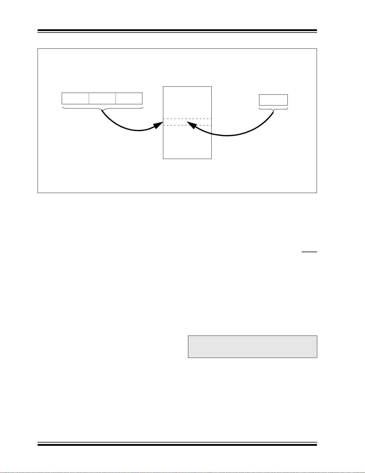
PIC18F6585/8585/6680/8680
FIGURE 5-2: TABLE WRITE OPERATION
Instruction: TBLWT*
Program Memory
Table Pointer
TBLPTRU
Note 1: Table Pointer actu ally points to one of eight holding registers, the address of which is determined by
TBLPTRH TBLPTRL
TBLPTRL<2:0>. The process for physically writing data to the program memory array is discussed in
Section 5.5 “Writing to Flash Program Memory”.
(1)
Program Memory
(TBLPTR)
Holding Registers
Table Latch (8-bit)
TABLAT
5.2 Control Registers
Several control registers are used in conjunction with
the TBLRD and TBLWT instructions. These include the:
• EECON1 register
• EECON2 register
• TABLAT register
• TBLPTR registers
5.2.1 EECON1 AND EECON2 REGISTERS
EECON1 is the control register for memory accesses.
EECON2 is not a physical register. Reading EECON2
will read all ‘0’s. The EECON2 register is used
exclusively in the memory write and erase sequences.
Control bit EEPGD determines if the access will be a
program or data EEPROM memory access. When
clear, any subsequent operations will operate on the
data EEPROM memory. When set, any subsequent
operations will operate on the program memory.
Control bit CFGS determin es if the access will be to the
configuration/calibration registers or to program
memory/data EEPROM memory. When set, subsequent operations will opera te on configuratio n registers
regardless of EEPGD (see Section 24.0 “Special
Features of the CPU”). W hen cle ar , memor y selec tion
access is determined by EEPGD.
The FREE bit, when set, will allow a program memory
erase operation. When the FREE bit is set, the erase
operation is initiated on the next WR command. When
FREE is clear , only wr ite s are enab led .
The WREN bit, when set, will allow a write operation.
On power-up, the WREN bit is c lear . T he WRERR bit is
set when a write operation is interrupted by a MCLR
Reset or a WDT Ti me-out Reset during normal operation. In these situations, the user can check the
WRERR bit and rewrite the location. It is necessary to
reload the data and address regi sters (EEDATA and
EEADR) due to Reset values of zero.
The WR control bit initiates write operations. The bit
cannot be cleared, only set in software; it is cleared in
hardware at the completion of the write operation. The
inability to clear the WR bit in software prevents the
accidental or premature termination of a write
operation.
Note: Interrupt flag bit, EEIF in the PIR2 registe r ,
is set when the write is complete. It must
be cleared in software.
DS30491C-page 84 2004 Microchip Technology Inc.

PIC18F6585/8585/6680/8680
REGISTER 5-1: EECON1 REGISTER (ADDRESS FA6h)
R/W-x R/W-x U-0 R/W-0 R/W-x R/W-0 R/S-0 R/S-0
EEPGD CFGS — FREE WRERR WREN WR RD
bit 7 bit 0
bit 7 EEPGD: Flash Program or Data EEPROM Memory Select bit
1 = Access Flash program memory
0 = Access data EEPROM memory
bit 6 CFGS: Flash Program/Data EEPROM or Configuration Select bit
1 = Access configuration registers
0 = Access Flash program or data EEPROM memory
bit 5 Unimplemented: Read as ‘0’
bit 4 FREE: Flash Row Erase Enable bit
1 = Erase the program memory row addressed by TBLPTR on the next WR command
(cleared by completion of erase operation)
0 = Perform write only
bit 3 WRERR: Flash Program/Data EEPROM Error Flag bit
1 = A write operation is prematurely terminated
(any Reset during self-timed programming in normal operation)
0 = The write operation completed
Note: When a WRERR occurs, the EEPGD and CFGS bits are not cleared. This allows
tracing of the error condition.
bit 2 WREN: Flash Program/Data EEPROM Write Enable bit
1 = Allows write cycles
0 = Inhibits write to the EEPROM
bit 1 WR: Write Control bit
1 = Initiates a data EEPROM erase/write cycle or a program memory erase cycle or write
cycle. (The operation is self-timed and the bit is cleared by hardware once write is
complete. The WR bit can only be set (not cleared) in software.)
0 = Write cycle to the EEPROM is complete
bit 0 RD: Read Control bit
1 = Initiates an EEPROM rea d. (R e ad t ak es one cy c le. RD is cl eare d i n ha rdw are . Th e RD b it
can only be set (not cleared) in software. RD bit cannot be set when EEPGD = 1.)
0 = Does not initiate an EEPROM read
Legend:
R = Readable bit U = Unimplemented bit, read as ‘0’
W = Writable bit S = Settable bit - n = Value after erase
‘1’ = Bit is set ‘0’ = Bit is cleared x = Bit is unknown
2004 Microchip Technology Inc. DS30491C-page 85

PIC18F6585/8585/6680/8680
5.2.2 TABLAT – TABLE LATCH REGISTER
The Table Latch (TABLAT) is an 8-bit register mapped
into the SFR space. The Table Latch is used to hold 8bit data during data transfers between program
memory and data RAM.
5.2.3 TBLPTR – TABLE POINTER REGISTER
The Table Pointer (TBLPTR) addresses a byte within
the program memory. The TBLPTR is comprised of
three SFR registers: Table Pointer Upper Byte, Table
Pointer High Byte and Table Pointer Low Byte
(TBLPTRU:TBLPTRH:TBLPTRL). These three registers join to form a 22-bit wide po inter. The low-o rder
21 bits allow the device to address up to 2 Mbytes of
program memory sp ace. Th e 22nd b it allow s acce ss to
the device ID, the user ID and the configuration bits.
The Table Pointer, TB LPTR, is used by the TBLRD and
TBLWT instructions. These instructions can update the
TBLPTR in one of four ways based on the table operation. These operations are shown in Table 5-1. These
operations on the TBLPTR only affect the low-order
21 bits.
5.2.4 TABLE POINTER BOUNDARIES
TBLPTR is used in reads, writes and erases of the
Flash program memory.
When a TBLRD is executed, all 22 bits of the table
pointer determine which byte is read from program
memory into TABLAT.
When a TBLWT is executed, th e three LSbs o f the Table
Pointer (TBLPTR<2:0>) determine which of the eight
program memory holding registers is written to. When
the timed write to pr ogram memor y (long write) begins ,
the 19 MSbs of the Table Pointer (TBLPTR<21:3>) will
determine which program memory block of 8 bytes is
written to. For mo re detail , see Secti on 5.5 “Writing to
Flash Program Memory”.
When an erase of program memory is executed, the
16 MSbs of the Table Pointer (TBLPTR<21:6>) poin t to
the 64-byte block that will be erased. The Least
Significant bits (TBLPTR<5:0>) are ignored.
Figure 5-3 describes the relevant boundaries of
TBLPTR based on Flash program memory operations.
TABLE 5-1: TABLE POINTER OPERATIONS WITH TBLRD AND TBLWT INSTRUCTIONS
Example Operation on Table Pointer
TBLRD*
TBLWT*
TBLRD*+
TBLWT*+
TBLRD*TBLWT*-
TBLRD+*
TBLWT+*
TBLPTR is incremented after the read/write
TBLPTR is decremented after the read/write
TBLPTR is incremented bef ore the read /write
TBLPTR is not modified
FIGURE 5-3: TABLE POINTER BOUNDARIES BASED ON OPERATION
21 16 15 87 0
DS30491C-page 86 2004 Microchip Technology Inc.
TBLPTRU
ERASE – TBLPTR<20:6>
TBLPTRH
WRITE – TBLPTR<21:3>
READ – TBLPTR<21:0>
TBLPTRL

PIC18F6585/8585/6680/8680
5.3 Reading the Flash Program Memory
The TBLRD instruction is used to retrieve data from
program memory and places it into data RAM. Table
reads from program memory are pe rformed one by te at
a time.
TBLPTR points to a byte address in program space.
Executing TBLRD places the byte pointed to into
TABLAT. In addition, TBLPTR can be modified
automatically for the next table read operation.
The internal program memory is typically organize d by
words. The Least Significant b it of th e address selects
between the high and low bytes of the word. Figure 5-4
shows the interface between the internal program
memory and the TABLAT.
FIGURE 5-4: READS FROM FLASH PROGRAM MEMORY
Program Memory
(Even Byte Address)
(Odd Byte Address)
TBLPTR = xxxxx1
Instruction Register
(IR)
FETCH
TBLRD
EXAMPLE 5-1: READING A FLASH PROGRAM MEMORY WORD
MOVLW upper(CODE_ADDR) ; Load TBLPTR with the base
MOVWF TBLPTRU ; address of the word
MOVLW high(CODE_ADDR)
MOVWF TBLPTRH
MOVLW low(CODE_ADDR_LOW)
MOVWF TBLPTRL
READ_WORD
TBLRD*+ ; read into TABLAT and increment
MOVF TABLAT, W ; get data
MOVWF LSB
TBLRD*+ ; read into TABLAT and increment
MOVF TABLAT, W ; get data
MOVWF MSB
TBLPTR = xxxxx0
TABLAT
Read Register
2004 Microchip Technology Inc. DS30491C-page 87

PIC18F6585/8585/6680/8680
5.4 Erasing Flash Program Memory
The minimum eras e block is 32 wo rds or 64 b ytes. Only
through the use of an external programmer or through
ICSP control can larger blocks of program memory be
bulk erased. Word erase in the Flash array is not
supported.
When initiating an erase sequence from the microcontroller itself, a blo ck of 64 bytes of program memo ry
is erased. The Most Significant 16 bits of the
TBLPTR<21:6> point to the block being erased.
TBLPTR<5:0> are ignored.
The EECON1 register comma nds the erase operation.
The EEPGD bit must be set to point to the Flash
program memory. The WREN bit must be set to enable
write operations. The F REE bit is set to select an erase
operation.
For protection, the wri te i ni tiat e s equ enc e f or EECO N2
must be used.
A long write is nec essa ry for erasin g the i nternal Flash.
Instruction execution is halted while in a long write
cycle. The long write will be terminated by the internal
programming timer.
5.4.1 FLASH PROGRAM MEMORY ERASE SEQUENCE
The sequence of events for erasing a block of internal
program memory location is:
1. Load table pointer with address of row being
erased.
2. Set the EECON1 register for the erase
operation:
• set EEPGD bit to point to program memory;
• clear the CFGS bit to access program memory;
• set WREN bit to enable writes;
• set FREE bit to enable the erase.
3. Disable interrupts.
4. Write 55h to EECON2.
5. Write 0AAh to EECON2.
6. Set the WR bit. This will begin the row erase
cycle.
7. The CPU will stall for duration of the erase
(about 2 ms using internal timer).
8. Execute a NOP.
9. Re-enable interrupts.
EXAMPLE 5-2: ERASING A FLASH PROGRAM MEMORY ROW
MOVLW upper(CODE_ADDR) ; load TBLPTR with the base
MOVWF TBLPTRU ; address of the memory block
MOVLW high(CODE_ADDR)
MOVWF TBLPTRH
MOVLW low(CODE_ADDR)
MOVWF TBLPTRL
ERASE_ROW
Required MOVLW 0AAh
Sequence MOVWF EECON2 ; write 0AAh
BSF EECON1, EEPGD ; point to Flash program memory
BCF EECON1, CFGS ; access Flash program memory
BSF EECON1, WREN ; enable write to memory
BSF EECON1, FREE ; enable Row Erase operation
BCF INTCON, GIE ; disable interrupts
MOVLW 55h
MOVWF EECON2 ; write 55h
BSF EECON1, WR ; start erase (CPU stall)
NOP
BSF INTCON, GIE ; re-enable interrupts
DS30491C-page 88 2004 Microchip Technology Inc.
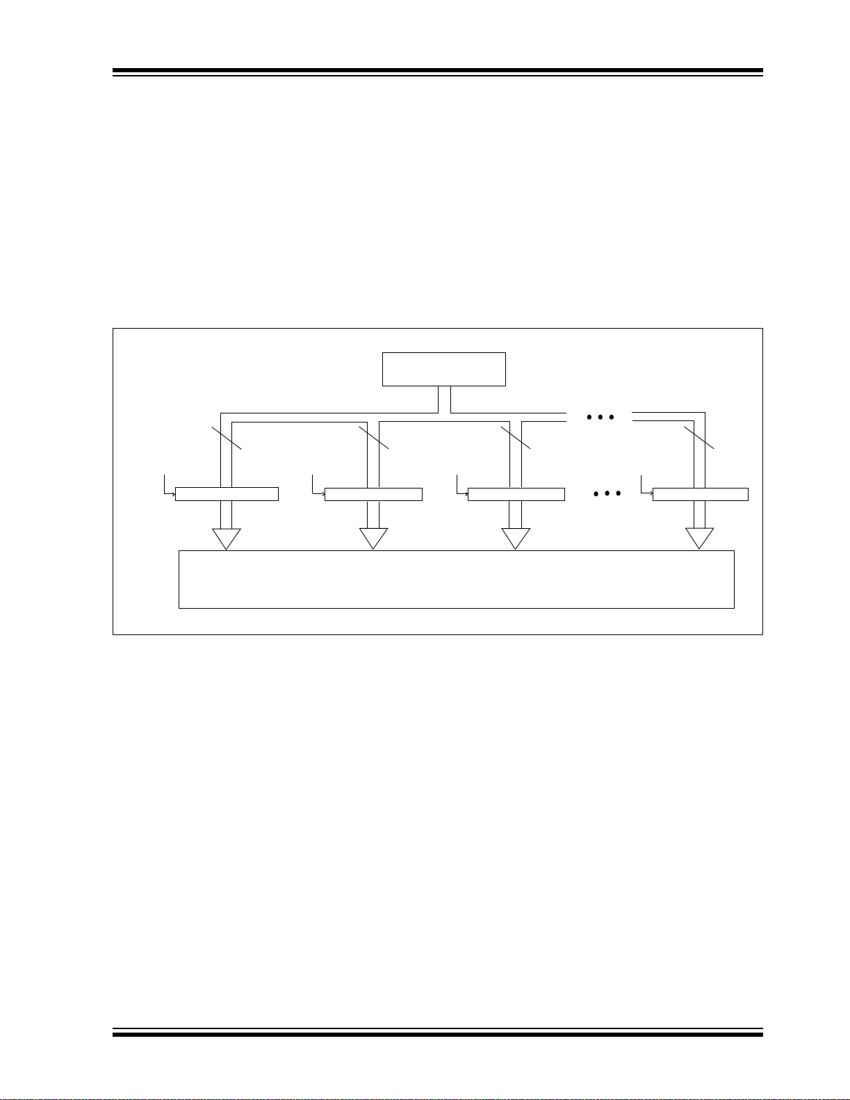
PIC18F6585/8585/6680/8680
5.5 Writing to Flash Program Memory
The minimum programmi ng block is 4 words or 8 bytes .
Word or byte programming is not supported.
Table writes are used internally to load the holding
registers needed to program the Flash memory. There
are eight holding registers used by the table writes for
programming.
Since the Table Latch (TABLAT) is only a single byte,
the TBLWT instruction has to be executed 8 times for
each programming operation. All of the table write
operations will e ssenti ally be sh ort wr ites bec ause only
the holding registers are w ritte n. At the end of upda ting
eight registers, the EECON1 register must be written
to, to start the programm ing operation with a lo ng write.
The long write is necessary for programming the internal Flash. Instruc tion exe cution is halted w hile in a long
write cycle. The long write will be terminated by the
internal programming timer.
The EEPROM on-chip timer controls the write time.
The write/erase voltages are generated by an on-chip
charge pump, rated to operate over the voltage range
of the device for byte or word operations.
FIGURE 5-5: TABLE WRITES TO FLASH PROGRAM MEMORY
TABLAT
Write Register
8 8 8
TBLPTR = xxxxx2
Holding Register
TBLPTR = xxxxx0
Holding Register
8
TBLPTR = xxxxx1
Holding Register
TBLPTR = xxxxx7
Holding Register
Program Memory
2004 Microchip Technology Inc. DS30491C-page 89

PIC18F6585/8585/6680/8680
5.5.1 FLASH PROGRAM MEMORY WRITE SEQUENCE
The sequence of events for program ming an internal
program memory location should be:
1. Read 64 bytes into RAM.
2. Update data values in RAM as necessary.
3. Load table pointer with address being erased.
4. Do the r ow erase procedure.
5. Load table pointer with address of first byte
being written.
6. Write the first 8 bytes into the holding registers
with auto-increment.
7. Set the EECON1 register for the w rite operation:
• set EEPGD bit to point to program memory;
8. Disable interrupts.
9. Write 55h to EECON2.
10. Write 0AAh to EECON2.
1 1. Set the WR bit. This will begin the write cycle.
12. The CPU will stall for d uration o f the w rite (abo ut
5 ms using internal timer).
13. Execute a NOP.
14. Re-enable interrupts.
15. Repeat steps 6-14 seven times to write 64 bytes.
16. Verify the memory (table read).
This procedure will require about 40 ms to update one
row of 64 bytes of memory. An example of the required
code is given in Example 5-3.
Note: Before setting the WR bit, the Table
• clear the CFGS bit to access program memory;
• set WREN to enable byte writes.
EXAMPLE 5-3: WRITING TO FLASH PROGRAM MEMORY
MOVLW D’64 ; number of bytes in erase block
MOVWF COUNTER
MOVLW high(BUFFER_ADDR) ; point to buffer
MOVWF FSR0H
MOVLW low(BUFFER_ADDR)
MOVWF FSR0L
MOVLW upper(CODE_ADDR) ; Load TBLPTR with the base
MOVWF TBLPTRU ; address of the memory block
MOVLW high(CODE_ADDR)
MOVWF TBLPTRH
MOVLW low(CODE_ADDR)
READ_BLOCK
MODIFY_WORD
MOVWF TBLPTRL
TBLRD*+ ; read into TABLAT, and inc
MOVF TABLAT, W ; get data
MOVWF POSTINC0 ; store data
DECFSZ COUNTER ; done?
BRA READ_BLOCK ; repeat
MOVLW high(DATA_ADDR) ; point to buffer
MOVWF FSR0H
MOVLW low(DATA_ADDR)
MOVWF FSR0L
MOVLW low(NEW_DATA) ; update buffer word
MOVWF POSTINC0
MOVLW high(NEW_DATA)
MOVWF INDF0
Pointer address needs to be within the
intended address range of the eight bytes
in the holding register.
DS30491C-page 90 2004 Microchip Technology Inc.

PIC18F6585/8585/6680/8680
EXAMPLE 5-3: WRITING TO FLASH PROGRAM MEMORY (CONTINUED)
ERASE_BLOCK
Required MOVLW 0AAh
Sequence MOVWF EECON2 ; write AAH
WRITE_BUFFER_BACK
PROGRAM_LOOP
WRITE_WORD_TO_HREGS
PROGRAM_MEMORY
Required MOVLW 0AAh
Sequence MOVWF EECON2 ; write 0AAh
MOVLW upper(CODE_ADDR) ; load TBLPTR with the base
MOVWF TBLPTRU ; address of the memory block
MOVLW high(CODE_ADDR)
MOVWF TBLPTRH
MOVLW low(CODE_ADDR)
MOVWF TBLPTRL
BSF EECON1, EEPGD ; point to Flash program memory
BCF EECON1, CFGS ; access Flash program memory
BSF EECON1, WREN ; enable write to memory
BSF EECON1, FREE ; enable Row Erase operation
BCF INTCON, GIE ; disable interrupts
MOVLW 55h
MOVWF EECON2 ; write 55H
BSF EECON1, WR ; start erase (CPU stall)
NOP
BSF INTCON, GIE ; re-enable interrupts
TBLRD*- ; dummy read decrement
MOVLW 8 ; number of write buffer groups of 8 bytes
MOVWF COUNTER_HI
MOVLW high(BUFFER_ADDR) ; point to buffer
MOVWF FSR0H
MOVLW low(BUFFER_ADDR)
MOVWF FSR0L
MOVLW 8 ; number of bytes in holding register
MOVWF COUNTER
MOVFW POSTINC0, W ; get low byte of buffer data
MOVWF TABLAT ; present data to table latch
TBLWT+* ; write data, perform a short write
; to internal TBLWT holding register.
DECFSZ COUNTER ; loop until buffers are full
BRA WRITE_WORD_TO_HREGS
BSF EECON1, EEPGD ; point to Flash program memory
BCF EECON1, CFGS ; access Flash program memory
BSF EECON1, WREN ; enable write to memory
BCF INTCON, GIE ; disable interrupts
MOVLW 55h
MOVWF EECON2 ; write 55h
BSF EECON1, WR ; start program (CPU stall)
NOP
BSF INTCON, GIE ; re-enable interrupts
DECFSZ COUNTER_HI ; loop until done
BRA PROGRAM_LOOP
BCF EECON1, WREN ; disable write to memory
2004 Microchip Technology Inc. DS30491C-page 91
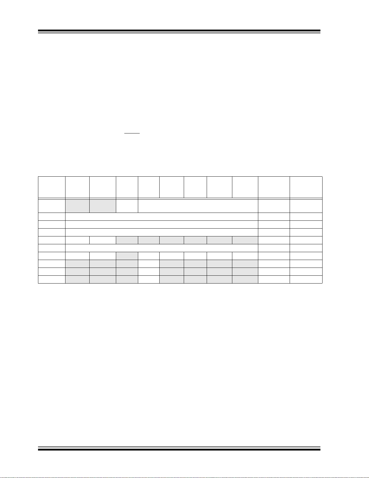
PIC18F6585/8585/6680/8680
5.5.2 WRITE VERIFY
Depending on the application, good programming
practice may dictate that the value written to the memory should be verified against the original value. This
should be used in applications where excessive writes
can stress bits near the specification limit.
5.5.3 UNEXPECTED TERMINATION OF WRITE OPERATION
5.5.4 PROTECTION AGAINST SPURIOUS WRITES
To protect against spurious writes to Flash program
memory, the write initiate sequence must also be
followed. See Section 24.0 “Sp eci al Fe atu res of the
CPU” for more detail.
5.6 Flash Program Operation During
Code Protection
If a write is termin ate d b y a n u np lan ned ev en t, s uc h a s
loss of power or an unexpected Reset, the memory
location just pr ogrammed shou ld be verifi ed and rep ro-
See Section 24.0 “Special Features of the CPU” for
details on code protection of Flash program memory.
grammed if needed. The WRERR bit is set when a
write operation is interrupted by a MCLR
Reset or a
WDT Time-o ut Reset duri ng normal operation. In these
situations, users can ch eck the WRERR bit and rewrite
the location.
TABLE 5-2: REGISTERS ASSOCIATED WITH PROGRAM FLASH MEMORY
Name Bit 7 Bit 6 Bit 5 Bit 4 Bit 3 Bit 2 Bit 1 Bit 0
TBLPTRU
TBPLTRH Program Memory Table Pointer High Byte (TBLPTR<15:8>) 0000 0000 0000 0000
TBLPTRL Program Memory Table Pointer High Byte (TBLPTR<7:0>) 0000 0000 0000 0000
TABLAT Program Memory Table Latch 0000 0000 0000 0000
INTCON GIE/GIEH P EIE/GIEL
EECON2 EEPROM Control Register 2 (not a physical register) — —
EECON1 EEPGD CFGS
IPR2
PIR2
PIE2
Legend: x = unknown, u = unchanged, r = reserved, – = unimplemented, read as ‘0’.
— — bit 21 Program Memory Table Pointer Upper Byte
(TBLPTR<20:16>)
TMR0IE INTE RBIE TMR0IF INTF RBIF 0000 0000 0000 0000
— FREE WRERR WREN WR RD xx-0 x000 uu-0 u000
— CMIP —EEIPBCLIP LVDIP TMR3IP CCP2 IP -1-1 1111 -1-1 1111
— CMIF —EEIFBCLIF LVDIF TMR3IF CCP2IF -0-0 0000 -0-0 0000
— CMIE —EEIEBCLIE LVDIE TMR3IE CCP2 IE -0-0 0000 -0-0 0000
Shaded cells are not used during Flash/EEPROM access.
Val ue on:
POR, BOR
--00 0000 --00 0000
Value o n
all other
Resets
DS30491C-page 92 2004 Microchip Technology Inc.

PIC18F6585/8585/6680/8680
6.0 EXTERNAL MEMORY INTERFACE
Note: The external memory interface is not
implemented on PIC18F6X8X (64/68-pin)
devices.
The external memory interface is a feature of the
PIC18F8X8X devices that allows the controller to
access external memory devices (such as Flash,
EPROM, SRAM, etc.) as program memory.
The physical implementation of the interface uses
27 pins. These pins are reserved for external address/
data bus functions; they are multiplexed with I/O port
pins on four ports. Three I/O por ts are multiplexed with
the address/data bus, while the fourth port is multiplexed with the bus control signals. The I/O port functions are enable d wh en the EBD IS bit in th e M E MCON
register is set (see Register 6-1). A list of the
multiplexed pins and their functions is provided in
Table 6-1.
As implemented in the PIC18F8X8X devices, the
interface operates in a similar manner to the external
memory interface introduced on PIC18C601/801
microcontrollers. The most notable difference is that
the interface on PIC18F8X8X devices only operates in
16-bit modes. The 8-bit mode is not supported.
For a more complete discussion of the operating modes
that use the external memory interface, refer to
Section 4.1.1 “PIC18F8X8X Program Memory
Modes”.
6.1 Program Memory Modes and the External Memory Interface
As previously noted, PIC18F8X8X controllers are
capable of operating in any one of four program memory modes using combinations of on-chip and external
program memory. The functions of the multi plexe d port
pins depend on the progra m memory mode selec ted as
well as the setting of the EBDIS bit.
In Microprocessor Mode, the external bus is always
active and the port pins have only the external bus
function.
In Microcontroller M ode, th e bus is no t acti ve an d the
pins have their port functions only. Writes to the
MEMCOM register are not permitted.
In Microprocessor with Boot Block or Extended
Microcontroller Mode, the external program memory
bus shares I/O port functions on the pins. When the
device is fetching or doing table read/table write
operations on the external program memory sp ace, th e
pins will have the external bus function. If the device is
fetching and accessing internal program memory
locations only, the EBDIS control bit will change the
pins from external memory to I/O port functions. When
EBDIS = 0, the pins function as the external bus. When
EBDIS = 1, the pins function as I/O ports.
2004 Microchip Technology Inc. DS30491C-page 93

PIC18F6585/8585/6680/8680
REGISTER 6-1: MEMCON REGISTER
R/W-0 U-0 R/W-0 R/W-0 U-0 U-0 R/W-0 R/W-0
(1)
EBDIS
bit 7 bit 0
—WAIT1WAIT0— —WM1WM0
bit 7 EBDIS: External Bus Disable bit
1 = External system bus disabled, all external bus drivers are mapped as I/O ports
0 = External system bus enabled and I/O ports are disabled
Note 1: This bit is ignored when device is accessing external memory either to fetch an
instruction or perform TBLRD/TBLWT.
bit 6 Unimplemented: Read as ‘0’
bit 5-4 WAIT<1:0>: Table Reads and Writes Bus Cycle Wait Count bits
11 = Table reads and writes will wait 0 T
10 = Table reads and writes will wait 1 TCY
01 = Table reads and writes will wait 2 TCY
00 = Table reads and writes will wait 3 TCY
bit 3-2 Unimplemented: Read as ‘0’
bit 1-0 WM<1:0>: TBLWT Operation with 16-bit Bus bits
1x = Word Write mode: LSB and MSB word output, WRH active when MSB written
01 = Byte Select mode: TABLAT data copied on both MS and LS Byte, WRH
will activate
00 = Byte Write mode: T ABLAT data copied on both M S and LS Byte, WRH
Legend:
R = Readable bit W = Writable bit U = Unimplemented bit, read as ‘0’
- n = Value at POR ‘1’ = Bit is set ‘0’ = Bit is cleared x = Bit is unknown
Note: The MEMCON register is held in Reset in Microcontroller mode.
(1)
CY
and (UB or LB)
or WRL will activate
DS30491C-page 94 2004 Microchip Technology Inc.

PIC18F6585/8585/6680/8680
If the device fetches or accesses external memory
while EBDIS = 1, the pins will switch to external bus. If
the EBDIS bit is set by a program executing from external memory, the action of setting the bit will be delayed
until the program branch es into the internal me mory. At
that time, the pins will change from external bus to I/O
ports.
When the device is executing out of internal memory
(with EBDIS = 0) in Microprocessor with Boot Block
mode or Extended Microcontroller mode, the control signals will be in inactive. They will go to a state where the
AD<15:0>, A<19:16> are tri-state; the OE
UB
and LB signals are ‘1’; and ALE and BA0 are ‘0’.
TABLE 6-1: PIC18F8X8X EXTERNAL BUS – I/O PORT FUNCTIONS
Name Port Bit Function
RD0/AD0 PORTD bit 0 Input/Output or System Bus Address bit 0 or Data bit 0
RD1/AD1 PORTD bit 1 Input/Output or System Bus Address bit 1 or Data bit 1
RD2/AD2 PORTD bit 2 Input/Output or System Bus Address bit 2 or Data bit 2
RD3/AD3 PORTD bit 3 Input/Output or System Bus Address bit 3 or Data bit 3
RD4/AD4 PORTD bit 4 Input/Output or System Bus Address bit 4 or Data bit 4
RD5/AD5 PORTD bit 5 Input/Output or System Bus Address bit 5 or Data bit 5
RD6/AD6 PORTD bit 6 Input/Output or System Bus Address bit 6 or Data bit 6
RD7/AD7 PORTD bit 7 Input/Output or System Bus Address bit 7 or Data bit 7
RE0/AD8 PORTE bit 0 Input/Output or System Bus Address bit 8 or Data bit 8
RE1/AD9 PORTE bit 1 Input/Output or System Bus Address bit 9 or Data bit 9
RE2/AD10 PORTE bit 2 Input/Output or System Bus Address bit 10 or Data bit 10
RE3/AD11 PORTE bit 3 Input/Output or System Bus Address bit 11 or Data bit 11
RE4/AD12 PORTE bit 4 Input/Output or System Bus Address bit 12 or Data bit 12
RE5/AD13 PORTE bit 5 Input/Output or System Bus Address bit 13 or Data bit 13
RE6/AD14 PORTE bit 6 Input/Output or System Bus Address bit 14 or Data bit 14
RE7/AD15 PORTE bit 7 Input/Output or System Bus Address bit 15 or Data bit 15
RH0/A16 PORTH bit 0 Input/Output or System Bus Address bit 16
RH1/A17 PORTH bit 1 Input/Output or System Bus Address bit 17
RH2/A18 PORTH bit 2 Input/Output or System Bus Address bit 18
RH3/A19 PORTH bit 3 Input/Output or System Bus Address bit 19
RJ0/ALE PORTJ bit 0 Input/Output or System Bus Address Latch Enable (ALE) Control pin
RJ1/OE
RJ2/WRL
RJ3/WRH
RJ4/BA0 PORTJ bit 4 Input/Output or System Bus Byte Address bit 0
RJ5/CE
RJ6/LB
RJ7/UB
PORTJ bit 1 Input/Output or System Bus Output Enable (OE) Control pin
PORTJ bit 2 Input/Output or System Bus Write Low (WRL) Control pin
PORTJ bit 3 Input/Output or System Bus Write High (WRH) Control pin
PORTJ bit 5 Input/Output or Chip Enable
PORTJ bit 6 Input/Output or System Bus Lower Byte Enable (LB) Control pin
PORTJ bit 7 Input/Output or System Bus Uppe r Byte Enable (UB) Control pin
, WRH, WRL,
2004 Microchip Technology Inc. DS30491C-page 95
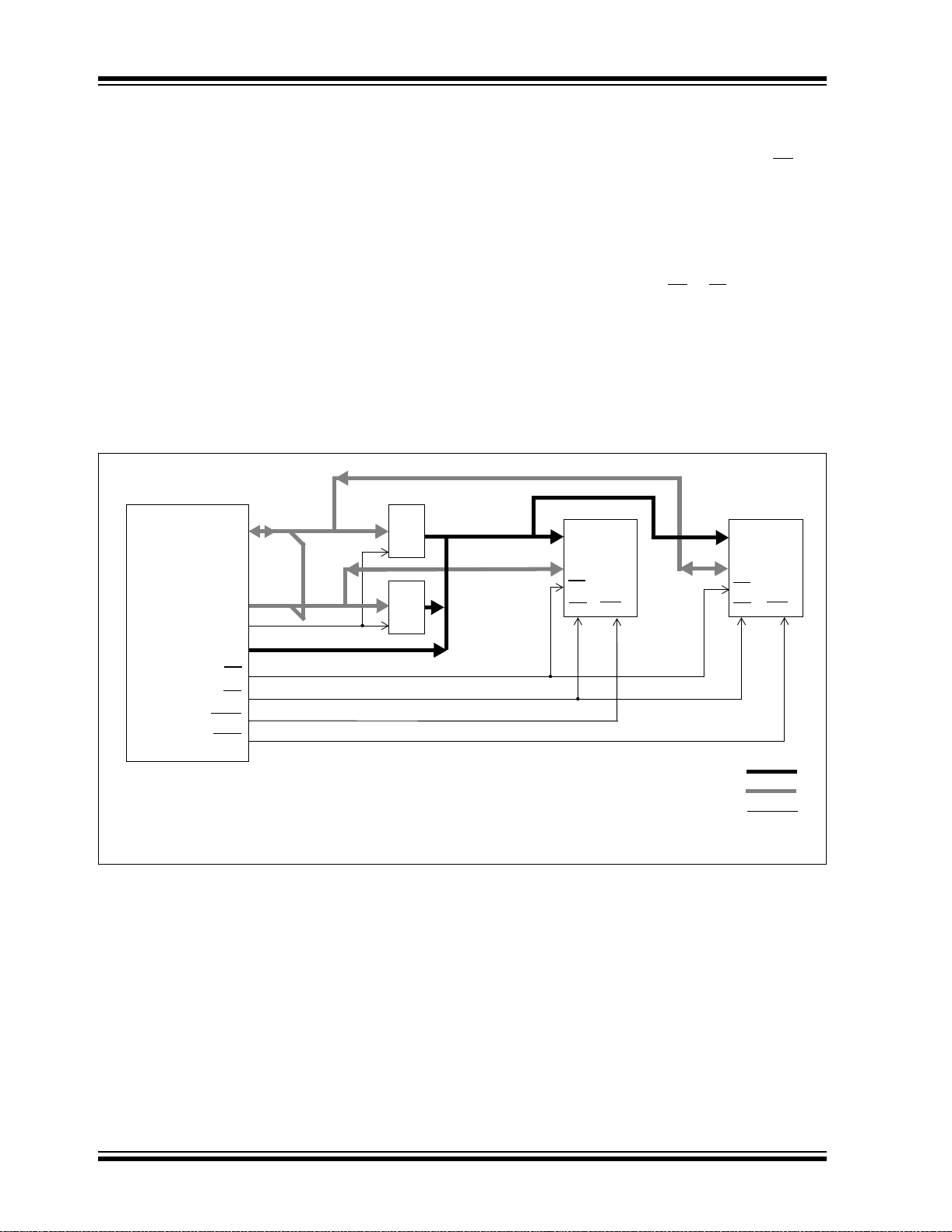
PIC18F6585/8585/6680/8680
6.2 16-bit Mode
The external memory interface implemented in
PIC18F8X8X devices operates only in 16-bit mode.
The mode selection is not software configurable but is
programmed via the configuration bits.
The WM<1:0> bits in the MEMCON register determine
three types of connections in 16-bit mode. They are
referred to as:
• 16-bit Byte Write
• 16-bit Word Write
• 16-bit Byte Select
These three different configurations allow the designer
maximum flexibility in using 8-bit and 16-bit memory
devices.
For all 16-bit modes, the Address Latch Enable (ALE)
pin indicates that the Address bits (A<15:0>) are available on the external memory interface bus. Following
the address latch, the Output Enable signal (OE
enable both bytes of program memory at once to form
a 16-bit instruction word.
In Byte Select mode, JEDEC st andard Flash me mories
will require BA0 for the byte address line, and one I/O
line to select between Byte and Word mode. The other
16-bit modes do not nee d BA0. J EDE C st a ndard static
RAM memories will use the UB
selection.
6.2.1 16-BIT BYTE WRITE MODE
Figure 6-1 shows an example of 16-bit Byte Write
mode for PIC18F8X8X devices.
FIGURE 6-1: 16-BIT BYTE WRITE MODE EXAMPLE
D<7:0>
PIC18F8X8X
AD<7:0>
AD<15:8>
A<19:16>
WRH
373
373
ALE
CE
OE
WRL
A<19:0>
D<15:8>
or LB signals for byte
(MSB)
A<x:0>
D<7:0>
CE
(1)
WR
OE OE
WR
D<7:0>
A<x:0>
D<7:0>
CE
(LSB)
) will
(1)
Address Bus
Data Bus
Control Lines
Note 1: This signal only applies to table writes. See Section 5.1 “Table Reads and T able Wri tes”.
DS30491C-page 96 2004 Microchip Technology Inc.

PIC18F6585/8585/6680/8680
6.2.2 16-BIT WORD WRITE MODE
Figure 6-2 shows an example of 16-bit Word Write
mode for PIC18F8X8X devices.
FIGURE 6-2: 16-BIT WORD WRITE MODE EXAMPLE
PIC18F8X8X
AD<7:0>
AD<15:8>
ALE
A<19:16>
CE
O
E
WRH
Note 1: This signal only applies to table writes. See Section 5.1 “Table Reads and Table Writes”.
373
373
A<20:1>
D<15:0>
A<x:0>
EPROM Memory
D<15:0>
Address Bus
Data Bus
Control Lines
JEDEC Word
OE
WR
(1)
CE
2004 Microchip Technology Inc. DS30491C-page 97
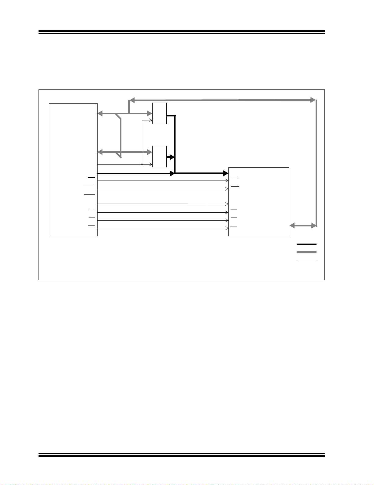
PIC18F6585/8585/6680/8680
6.2.3 16-BIT BYTE SELECT MODE
Figure 6-3 shows an example of 16-bit Byte Select
mode for PIC18F8X8X devices.
FIGURE 6-3: 16-BIT BYTE SELECT MODE EXAMPLE
PIC18F8X8X
AD<7:0>
AD<15:8>
ALE
A<19:16>
O
E
WRH
RL
W
BA0
CE
LB
UB
Note 1: This signal only applies to table writes. See Section 5.1 “Table Reads and Tab le Writes”.
373
373
A<20:1>
A<20:1>
A<x:1>
OE
(1)
WR
A0
CE
LB
UB
JEDEC Word
SRAM Memory
Address Bus
Data Bus
Control Lines
D<15:0>
D<15:0>
DS30491C-page 98 2004 Microchip Technology Inc.
 Loading...