


PIC18F6520/8520/6620/8620/6720/8720
Data Sheet
64/80-Pin High-Performance,
256 Kbit to 1 Mbit Enhanced Flash
Microcontrollers with A/D
2004 Microchip Technology Inc. DS39609B

Note the following details of the code protection feature on Microchip devices:
• Microchip products meet the specification contained in their particular Microchip Data Sheet.
• Microchip believes that its family of products is one of the most secure families of its kind on the market today, when used in the
intended manner and under normal conditions.
• There are dishonest and possibly illegal methods used to breach the code protection feature. All of these methods, to our
knowledge, require using the Microchip products in a manner outside the operating specifications contained in Microchip's Data
Sheets. Most likely, the person doing so is engaged in theft of intellectual property.
• Microchip is willing to work with the customer who is concerned about the integrity of their code.
• Neither Microchip nor any other semiconductor manufacturer can guarantee the security of their code. Code protection does not
mean that we are guaranteeing the product as “unbreakable.”
Code protection is constantly evolving. We at Microchip are committed to continuously impro ving the cod e protection features of our
products. Attempts to break Microchip’s code protection feature may be a violation of the Digital Millennium Copyright Act. If such acts
allow unauthorized access to your software or other copyrighted work, you may have a right to sue for relief under that Act.
Information contained in this publication regarding device
applications and the like is intended through suggestion only
and may be superseded by updates. It is your responsibility to
ensure that your application meets with your specifications.
No representation or warranty is given and no liability is
assumed by Microchip Technology Incorporated with respect
to the accuracy or use of such information, or infringement of
patents or other intellectual property rights arising from such
use or otherwise. Use of Microchip’s products as critical
components in life support systems is not authorized except
with express written approval by Microchip. No licenses are
conveyed, implicitly or otherwise, under any intellectual
property rights.
Trademarks
The Microchip name and logo, the Microchip logo, Accuron,
dsPIC, K
EELOQ, MPLAB, PIC, PICmic ro, PI C START,
PRO MATE and PowerSmart are registered trademarks of
Microchip Technology Incorporated in the U.S.A. and other
countries.
AmpLab, FilterLab, microID, MXDEV, MXLAB, PICMASTER,
SEEVAL, SmartShunt and The Embedded Control Solutions
Company are registered trademarks of Microchip Technology
Incorporated in the U.S.A.
Application Maestro, dsPICDEM, dsPICDEM.net,
dsPICworks, ECAN, ECONOMONITOR, FanSense,
FlexROM, fuzzyLAB, In-Circuit Serial Programming, ICSP,
ICEPIC, microPort, Migratable Memory, MPASM, MP LI B,
MPLINK, MPSIM, PICkit, PICDEM, PICDEM.net, PICtail,
PowerCal, PowerInfo, PowerMate, PowerTool, rfLAB, rfPIC,
Select Mode, SmartSensor, SmartTel and Total Endurance
are trademarks of Microchip Technology Incorporat ed in the
U.S.A. and other countries.
Serialized Quick Turn Programming (SQTP) is a service mark
of Microchip Technology Incorporated in the U.S.A.
All other trademarks mentioned herein are property of their
respective companies.
© 2004, Microchip Technology Incorporated, Printed in the
U.S.A., All Rights Reserved.
Printed on recycled paper.
Microchip re cei v ed I S O/T S - 16 949 : 20 02 qu ality system certificat io n f or
its worldwide headquarters, design and wafer fabrication facilities in
Chandler and Tempe, Arizona and Mountain View, California in October
2003. The Com pany’s quality sy stem proces ses and pro cedures are for
its PICmicro
EEPROMs, microperipherals, nonvolatile memory and analog
products. In addition, Microchip’s quality system for the design and
manufacture of development systems is ISO 9001:2000 certified.
®
8-bit MCUs, KEELOQ
®
code hopping devices, Serial
DS39609B-page ii 2004 Microchip Technology Inc.

PIC18F6520/8520/6620/
8620/6720/8720
64/80-Pin High-Performance, 256 Kbit to 1 Mbit
Enhanced Flash Microcontrollers with A/D
High-Performance RISC CPU:
• C compiler optimized architecture/instruction set:
- Source code compatible with the PIC16 and
PIC17 instruction sets
• Linear program memory addressing to 128 Kbytes
• Linear data memory addr essing to 3840 bytes
• 1 Kbyte of data EEPROM
• Up to 10 MIPs operation:
- DC – 40 MHz osc./clock input
- 4 MHz – 10 MHz os c./clock input with PLL ac ti v e
• 16-bit wide instructions, 8-bit wide data path
• Priority levels for interrupts
• 31-level, so ftware accessible hardware stack
• 8 x 8 Single Cycle Har dware Multiplier
External Memory Interface (PIC18F8X20 Devices Only):
• Address c apability of up to 2 Mbytes
• 16-bit interface
Peripheral Features:
• High current sink/source 25 mA/25 mA
• Four ext ernal inte rrupt pins
• Timer0 module: 8-bit/16-bit timer/counter
• Timer1 module: 16-bit timer/counter
• Timer2 module: 8-bit timer/counter
• Timer3 module: 16-bit timer/counter
• Timer4 module: 8-bit timer/counter
• Secondary oscillator clock option – Timer1/Timer3
• Five Capture/Compare/ PWM (CCP) modules:
- Capture is 16-bit, max. resolution 6.25 ns (T
- Compare is 16-bit, max. resolution 100 ns (T
- PWM output: PWM resolution is 1 to 10-bit
• Master Synchronous Serial Port (MSSP) module
with two modes of operation:
- 3-wire SPI™ (supports all 4 SPI modes)
2
-I
C™ Master and Slave mode
• Two Addressable USART modules:
- Supports RS-485 and RS-232
• Parallel Slave Port (PSP) module
CY/16)
CY)
Analog Features:
• 10-bit, up to 16-channel Analog-to-Digital
Converter (A/D):
- Conversion available during Sleep
• Programmable 16-level Low-Voltage Detection
(LVD) module:
- Supports interrupt on Low-Voltage Detection
• Programmable Brown-out Reset (PBOR)
• Dual analog comparators:
- Programmable input/output configuration
Special Microcontroller Features:
• 100,000 erase/write cycl e Enhan ced Flas h
program memory typical
• 1,000,000 erase/write cycle Data EEPROM
memory typical
• 1 second programming time
• Flash/Data EEPROM Retention: > 40 years
• Self-reprogrammable under software control
• Power-on Reset (POR), Power-up Timer (PWR T)
and Oscillator Start-up Timer (OST)
• Watchdog Timer (WDT) with its own On-Chip
RC Oscillator for reliable operation
• Programmable code protection
• Power sa ving Sleep mode
• Selectable oscillator options including:
- 4X Phase Lock Loop (of primary oscillator)
- Secondary Oscillator (32 kHz) clock input
• In-Circuit Serial Programming™ (ICSP™) via
two pins
• MPLAB
®
In-Circuit Debug (ICD) via two pins
CMOS Technology:
• Low-power, high-speed Flash technology
• Fully static design
• Wide operating voltage range (2.0V to 5.5V)
• Industrial and Extended temperature ranges
Program Memory Data Memory
Device
PIC18F6520 32K 16384 2048 1024 52 12 5 Y Y 2 2/3 N 40
PIC18F6620 64K 32768 3840 1024 52 12 5 Y Y 2 2/3 N 25
PIC18F6720 128K 65536 3840 1024 52 12 5 Y Y 2 2/3 N 25
PIC18F8520 32K 16384 2048 1024 68 16 5 Y Y 2 2/3 Y 40
PIC18F8620 64K 32768 3840 1024 68 16 5 Y Y 2 2/3 Y 25
PIC18F8720 128K 65536 3840 1024 68 16 5 Y Y 2 2/3 Y 25
2004 Microchip Technology Inc. DS39609B-page 1
Bytes
# Single-W ord
Instructions
SRAM
(bytes)
EEPROM
(bytes)
I/O
10-bit
A/D
(ch)
CCP
(PWM)
SPI
MSSP
Master
USART
2
I
C
Timers
8-bit/16-bit
Ext
Bus
Max
OSC
F
(MHz)

PIC18F6520/8520/6620/8620/6720/8720
Pin Diagrams
PIC18F6620
DS39609B-page 2 2004 Microchip Technology Inc.
PIC18F6520/8520/6620/8620/6720/8720
Pin Diagrams (Continued)
80-Pin TQFP
RH1/A17
RH0/A16
(2)
RE5/AD13
RE6/AD14
(3)
RE7/CCP2/AD15
(3)
RE2/CS/AD10
RE3/AD11
RE4/AD12
(3)
(3)
(3)
(3)
(3)
(3)
(3)
RD0/PSP0/AD0
VDD
VSS
RD1/PSP1/AD1
RD2/PSP2/AD2
RD3/PSP3/AD3
RD4/PSP4/AD4
RD5/PSP5/AD5
RD6/PSP6/AD6
RD7/PSP7/AD7
RJ0/ALE
RJ1/OE
RH2/A18
RH3/A19
RE1/WR/AD9
RE0/RD/AD8
RG0/CCP3
RG1/TX2/CK2
RG2/RX2/DT2
RG3/CCP4
MCLR
/VPP
RG4/CCP5
V
VDD
RF7/SS
RF6/AN11
RF5/AN10/CV
REF
RF4/AN9
RF3/AN8
RF2/AN7/C1OUT
RH7/AN15
RH6/AN14
(3)
(3)
SS
80
787776
79
75
74
1
2
3
4
5
6
7
8
9
10
11
12
13
14
15
16
17
18
19
20
2122232425262728293031
DD
AVSS
AV
RH4/AN12
RF0/AN5
RF1/AN6/C2OUT
RA3/AN3/VREF+
RH5/AN13
73
727170
69
PIC18F8520
PIC18F8620
PIC18F8720
32
SS
V
REF-
RA1/AN1
RA2/AN2/V
VDD
RA0/AN0
686766
333435
(1)
RA4/T0CKI
RA5/AN4/LVDIN
RC1/T1OSI/CCP2
65
646362
37
36
RC6/TX1/CK1
RC0/T1OSO/T13CKI
38
RC7/RX1/DT1
61
60
59
58
57
56
55
54
53
52
51
50
49
48
47
46
45
44
43
42
41
40
39
RJ5/CE
RJ4/BA0
RJ2/WRL
RJ3/WRH
RB0/INT0
RB1/INT1
RB2/INT2
RB3/INT3/CCP2
RB4/KBI0
RB5/KBI1/PGM
RB6/KBI2/PGC
V
SS
OSC2/CLKO/RA6
OSC1/CLKI
V
DD
RB7/KBI3/PGD
RC5/SDO
RC4/SDI/SDA
RC3/SCK/SCL
RC2/CCP1
RJ7/UB
RJ6/LB
(1)
Note 1: CCP2 is multiplexed with RC1 when CCP2MX is set.
2: CCP2 is multiplexed by default with RE7 when the device is configured in Microcontroller mode.
3: PSP is available only in Microcontroller mode.
2004 Microchip Technology Inc. DS39609B-page 3

PIC18F6520/8520/6620/8620/6720/8720
Table of Contents
1.0 Device Overview..........................................................................................................................................................................7
2.0 Oscillator Configurations ............................................................................................................................................................ 21
3.0 Reset .......................................................................................................................................................................................... 29
4.0 Memory Organization................................................................................................................................................................. 39
5.0 F la sh Program Memory.................... ......................... ................................................................................................................. 61
6.0 External Memory Interface......................................................................................................................................................... 71
7.0 Data EEPROM Memory........ ......................... ............................................................. ............................................................... 79
8.0 8 X 8 Hard ware Multiplier............................................................. ..............................................................................................85
9.0 Interrupts.................................................................................................................................................................................... 87
10.0 I/O Ports.............................. ......................... ................................................ ............................................................................103
11.0 Timer0 Module ......................................................................................................................................................................... 131
12.0 Timer1 Module ......................................................................................................................................................................... 135
13.0 Timer2 Module ......................................................................................................................................................................... 141
14.0 Timer3 Module ......................................................................................................................................................................... 143
15.0 Timer4 Module ......................................................................................................................................................................... 147
16.0 Capture/Compare/PWM (CCP) Modules .................................................................................................................................149
17.0 Master Synchronous Serial Port (MSSP) Module ....................................................................................................................157
18.0 Addressable Universal Synchronous Asynchronous Receiv er Transmitter (USA RT )..............................................................197
19.0 10-Bit Analog-to-Digital Converter (A/D) Module ..................................................................................................................... 213
20.0 Comparator Module............................................................................................. .. .... .... .. .........................................................223
21.0 Comparator Voltage Reference Module......................................... .. .... .. .... .. ....... .... .. .... .. ....... .... .. ............................................ 229
22.0 Low-Voltage Detect..................................................................................................................................................................233
23.0 Special Features of the CPU....................................................................................................................................................239
24.0 Instruction Set Summary..........................................................................................................................................................259
25.0 Development Support. .............................................................................................................................................................. 301
26.0 Electrical Characteristics ..........................................................................................................................................................307
27.0 DC and AC Characteristics Graphs and Tables.......................................................................................................................343
28.0 Packaging Information.............................. ................................................................................................................................357
Appendix A: Revision History.............................................................................................................................................................361
Appendix B: Device Differences......................................................................................................................................................... 361
Appendix C: Conversion Considerations .................................................................... .... .. .... .. .... ....................................................... 362
Appendix D: Migration from Mid-Range to Enhanced Devices.......................................................................................................... 362
Appendix E: Migration from High-End to Enhanced Devices.............................................................................................................363
Index .................................................................................................................................................................................................. 365
On-Line Support........................................................................ .... .. ......... .... .. .... .... ....... .... ................................................................. 375
Systems Information and Upgrade Hot Line......................................................................................................................................375
Reader Response.............................................................................................................................................................................. 376
PIC18F6520/8520/6620/8620/6720/8720 Product Identification System .......................................................................................... 377
DS39609B-page 4 2004 Microchip Technology Inc.

PIC18F6520/8520/6620/8620/6720/8720
TO OUR VALUED CUSTOMERS
It is our intention to provide our valued customers with the best documentation possible to ensure successful use of your Microchip
products. To this end, we will continue to improve our publications to bet ter suit your needs. Our publications will be refined and
enhanced as new volumes and updates are introduced.
If you have any questions or c omm ents regarding t his publication, p lease c ontact the M arket ing Co mmunications Department via
E-mail at docerrors@mail.microchip.com or fax the Reader Response Form in the back of this data sheet to (480) 792-4150.
We welcome your feedback.
Most Current Data Sheet
To obtain the most up-to-date version of this data sheet, please register at our Worldwide Web site at:
http://www.microchip.com
You can determine the version of a data sheet by examining its literature number found on the bottom outside corner of any page.
The last character of the literature number is the version number, (e.g., DS30000A is version A of document DS30000).
Errata
An errata sheet, describing minor operational differences from the data sheet and recommended workarounds, may exist for current
devices. As device/documentation issues become known to us, we will publish an errata sheet. The errata will specify the revision
of silicon and revision of document to which it applies.
To determine if an errata sheet exists for a particular device, please check with one of the following:
• Microchip’s Worldwide Web site; http://www.microchip.com
• Your local Microchip sales office (see last page)
• The Microchip Corporate Literature Center; U.S. FAX: (480) 792-7277
When contacting a sales office or the literature center, please specify which device, revision of silicon and data sheet (include liter-
ature number) you are using.
Customer Notification System
Register on our Web site at www.microchip.com/cn to receive the most current information on all of our products.
2004 Microchip Technology Inc. DS39609B-page 5

PIC18F6520/8520/6620/8620/6720/8720
NOTES:
DS39609B-page 6 2004 Microchip Technology Inc.

PIC18F6520/8520/6620/8620/6720/8720
1.0 DEVICE OVERVIEW
This documen t conta i ns dev ic e spec if i c in for m at i on fo r
the following devices:
• PIC18F6520 • PIC18F8520
• PIC18F6620 • PIC18F8620
• PIC18F6720 • PIC18F8720
This family offers the same advantages of all PIC18
microcontrollers – namely, high computational
performance at a n economic al price – wit h the additio n of
high endurance Enhanced Flash program memory. The
PIC18FXX20 fami ly al so pro vide s an enha nced rang e of
program memory options and versatile analog features
that make it ideal for complex, high-performance
applications.
1.1 Key Features
1.1.1 EXPANDED MEMORY
The PIC18FXX20 fami ly introd uces the w idest range of
on-chip, Enhanced Flash program memory available
on PICmic ro® microcontrollers – up to 128 Kbyte (or
65,536 words), the largest ever offered by Microchip.
For users with more modest code requirements, the
family also includes members with 32 Kbyte or
64 Kbyte.
Other memory features are:
• Data RAM and Data EEPROM: The
PIC18FXX20 family also provides plenty of room
for application data. Depending on the device,
either 2048 or 3840bytes of data RAM are
available. All devices have 1024bytes of data
EEPROM for long-term retention of nonvolatile
data.
• Memory Endurance: The Enhanced Flash cells
for both program memory and data EEPROM are
rated to last for many thousands of erase/write
cycles – up to 100,000 for program memory and
1,000,000 for EEPROM. Data retention without
refresh is conservatively estimated to be greater
than 40 years.
1.1.2 EXTERNAL MEMORY INTERFACE
In the event that 128 Kbytes of program memory is
inadequate for an application, the PIC18F8X20
members of the family also implement an External
Memory Interface. This allows the controller’s internal
program counter to address a memory space of up to
2 Mbytes, permitting a level of data access that few
8-bit devices can claim.
With the addition of new operat ing modes, the External
Memory Interface offers many new options, including:
• Operatin g the microcont roller entirel y from external
memory
• Using combinations of on-chip and external
memory, up to the 2-Mbyte limit
• Using external Flash memory for reprogrammable
application code, or large data tables
• Using external RAM devices for storing large
amounts of variable data
1.1.3 EASY MIGRATION
Regardless of the memory size, all devices share the
same rich set of peripherals, allowing for a smooth
migration path as applications grow and evolve.
The consistent pinout scheme used throughout the
entire family also aids in migrating to the next larger
device. This is true when moving between the 64-pin
members, between the 80-pin members, or even
jumping fr om 64-pin to 80-pin devices.
1.1.4 OTHER SPECIAL FEA TURES
• Communications: The PIC18FXX20 family
incorporates a range of serial communications
peripherals, includin g 2 independen t USARTs and
a Master SSP module, capable of both SPI and
I2C (Master and Slave) modes of operation. For
PIC18F8X20 device s, one of the genera l purpos e
I/O ports can be reconfigured as an 8-bit Parallel
Slave Port for direct processor-to-processor
communications.
• CCP Modules: All devices in the family
incorporate five Capt ure/Com par e/PWM mo dules
to maximize flexibility in control applications. Up
to four different time bases may be used to
perform several different operations at once.
• Analog Features: All devices in the family
feature 10-bit A/D converters, with up to 16 input
channels, as well as the ability to perform
conversions during Sleep mode. Also included
are dual analog comparators with programmable
input and output configuration, a programmable
Low-Voltage Detect module and a programmable
Brown-out Reset module.
• Self-programmability: These devices can write
to their own program memory spaces under internal software control. By us ing a bootloader routi ne
located in the protected Boot Block at the top of
program memory, it becomes possible to create
an application that can update itself in the field.
2004 Microchip Technology Inc. DS39609B-page 7

PIC18F6520/8520/6620/8620/6720/8720
1.2 Details on Individual Family Members
3. A/D channels (12 for PIC18F6X20 devices,
16 for PIC18F8X20)
4. I/O pins (52 on PIC18F6X20 devices, 68 on
The PIC18FXX 20 devices ar e available in 64-pin and
80-pin packages. They are differentiated from each
other in five ways:
1. Flash program memory (32 Kbytes for
PIC18FX520 devices, 64Kbytes for
PIC18FX620 devices and 128 Kbytes for
PIC18FX720 devices)
2. Data RAM (2048 bytes for PIC18FX520
devices, 3840 bytes for PIC18FX620 and
PIC18FX720 devices)
PIC18F8X20)
5. External program memory interface (present
only on PIC18F8X20 devices)
All other features for devic es in the PIC18FXX2 0 family
are identical. Thes e are summarized in Table 1-1.
Block diagra ms of the PIC1 8F6X20 and PIC 18F8X20
devices are provided in Figure 1-1 and Figure 1-2,
respectively. The pinouts for these device families are
listed in Table 1-2.
TABLE 1-1: PIC18FXX20 DEVICE FEATURES
Features PIC18F6520 PIC18F6620 PIC18F6720 PIC18F8520 PIC18F8620 PIC18F8720
Operating Frequency DC – 40 MHz DC – 25 MHz DC – 25 MHz DC – 40 MHz DC – 25 MHz DC – 25 MHz
Program Memory
(Bytes)
Program Memory
(Instructions)
Data Memory
(Bytes)
Data EEPROM
Memory (Bytes)
External Me mory
Interface
Interrupt Sources 17 17 17 18 18 18
I/O Ports Ports A, B, C,
Timers 5 5 5 5 5 5
Capture/Compare/
PWM Modules
Serial Communications MSSP,
Parallel Communications PSP PSP PSP PSP PSP PSP
10-bit Analog-to-Digital
Module
Resets (and Delays) POR, BOR,
Programmable
Low-Voltage Detect
Programmable
Brown-out Reset
Instruction Set 77 Instructions 77 Instructions 77 Instructions 77 Instructions 77 Instruct ions 77 Instructions
Package 64-pin TQFP 64-pin TQFP 64-pin TQFP 80-pin TQFP 80-pin TQFP 80-pin TQFP
32K 64K 128K 32K 64K 128K
16384 32768 65536 16384 32768 65536
2048 3840 3840 2048 3840 3840
1024 1024 1024 1024 1024 1024
No No No Yes Yes Yes
Ports A, B, C, D,
D, E, F, G
55 5555
Addressable
USART (2)
12 input
channels
RESET
Instruction,
Stack Full,
Stack Un derflow
(PWRT , OST)
Yes Yes Yes Yes Yes Yes
Yes Yes Yes Yes Yes Yes
E, F, G
MSSP,
Addressable
USART (2)
12 input
channels
POR, BOR,
RESET
Instruction,
Stack Ful l,
Stack Und erf low
(PWRT, OST)
Ports A, B, C, D,
E, F, G
MSSP,
Addressable
USART (2)
12 input
channels
POR, BOR,
RESET
Instruction,
Stack Full,
Stack Underflow
(PWRT, OST)
Ports A, B, C,
D, E, F, G, H, J
MSSP,
Addressable
USART (2)
16 input
channels
POR, BOR,
RESET
Instruction,
Stack Full,
Sta ck Underflow
(PWRT, OST)
Ports A, B, C,
D, E, F, G, H, J
MSSP,
Addressable
USART (2)
16 input
channels
POR, BOR,
RESET
Instruction,
Stack Full,
Stack Underflow
(PWRT, OST)
Ports A, B, C,
D, E, F, G, H, J
MSSP,
Addressable
USART (2)
16 input
channels
POR, BOR,
RESET
Instruction,
Stack Full,
Sta ck Underflow
(PWRT, OST)
DS39609B-page 8 2004 Microchip Technology Inc.
PIC18F6520/8520/6620/8620/6720/8720
FIGURE 1-1: PIC18F6X20 BLOCK DIAGRAM
Address Latch
Address<12>
Data Latch
Data RAM
12
PORTA
RA0/AN0
RA1/AN1
RA2/AN2/VREFRA3/AN3/VREF+
RA4/T0CKI
RA5/AN4/LVDIN
PORTB
RB0/INT0
RB1/INT1
OSC2/CLKO
OSC1/CLKI
Instruction
Decode &
Control
Timing
Generation
Power-up
Timer
Oscillator
Start-up Timer
Power-on
Reset
Watchdog
Timer
Brown-out
Reset
BSR
Decode
FSR0
FSR1
FSR2
inc/dec
logic
Bank0, F
PORTC
RC0/T1OSO/T13CKI
RC1/T1OSI/CCP2
RC2/CCP1
RC3/SCK/SCL
RC4/SDI/SDA
RC5/SDO
RC6/TX1/CK1
RC7/RX1/DT1
MCLR
/VPP
VDD, VSS
Synchronous
Serial Port
BOR
Comparator
USART1
2004 Microchip Technology Inc. DS39609B-page 9
PIC18F6520/8520/6620/8620/6720/8720
FIGURE 1-2: PIC18F8X20 BLOCK DIAGRAM
Address Latch
Program Memory
System Bus Interface
Data Latch
AD15:AD0, A19:A16
OSC2/CLKO
OSC1/CLKI
Synchronous
Serial Port
BOR
LVD
21
(1)
Instruction
Decode &
Control
Timing
Generation
Precision
Band Gap
Reference
Timer0
T able Pointer<21>
21
inc/dec logic
21
Table Latch
16
USART1
PCLATU
PCLATH
PCU
Program Counter
31 Level Stack
8
ROM Latch
IR
Power-up
Timer
Oscillator
Start-up Timer
Power-on
Reset
Watchdog
Timer
Brown-out
Reset
MCLR
/VPP
Timer1
8
PCH PCL
VDD, VSS
USART2
Timer2
8
4
BSR
Decode
BITOP
Timer3
3
8
EEPROM
Data Bus<8>
Data Latch
Data RAM
Address Latch
12
Address<12>
12 4
Bank0, F
FSR0
FSR1
FSR2
inc/dec
logic
PRODLPRODH
8 x 8 Multiply
WREG
8
8
ALU<8>
8
Data
Timer4
12
8
8
8
PORTA
PORTB
PORTC
PORTD
PORTE
PORTF
PORTG
PORTH
PORTJ
RA0/AN0
RA1/AN1
RA2/AN2/VREFRA3/AN3/VREF+
RA4/T0CKI
RA5/AN4/LVDIN
RA6
RB0/INT0
RB1/INT1
RB2/INT2
RB3/INT3/CCP2
RB4/KBI0
RB5/KBI1/PGM
RB6/KBI2/PGC
RB7/KBI3/PGD
RC0/T1OSO/T13CKI
RC1/T1OSI/CCP2
RC2/CCP1
RC3/SCK/SCL
RC4/SDI/SDA
RC5/SDO
RC6/TX1/CK1
RC7/RX1/DT1
RE0/RD/AD8
RE1/WR/AD9
RE2/CS/AD10
RE3/AD11
RE4/AD12
RE5/AD13
RE6/AD14
RE7/CCP2/AD15
RF0/AN5
RF1/AN6/C2OUT
RF2/AN7/C1OUT
RF3/AN8
RF4/AN9
RF5/AN10/CVREF
RF6/AN11
RF7/SS
RG0/CCP3
RG1/TX2/CK2
RG2/RX2/DT2
RG3/CCP4
RG4/CCP5
RJ0/ALE
RJ1/OE
RJ2/WRL
RJ3/WRH
RJ4/BA0
RJ5/CE
RJ6/LB
RJ7/UB
RD7/PSP7/AD7:
RD0/PSP0/AD0
RH3/AD19:RH0/AD16
RH7/AN15:RH4/AN12
Comparator
Note 1: External memory interface pins are physically multiplexed with PORTD (AD7:AD0), PORTE (AD15:AD8) and PORTH (A19:A16).
CCP1 CCP2 CCP3 CCP4 CCP5
10-bit
A/D
DS39609B-page 10 2004 Microchip Technology Inc.

PIC18F6520/8520/6620/8620/6720/8720
TABLE 1-2: PIC18FXX20 PINOUT I/O DESCRIPTIONS
Pin Name
Pin Number
PIC18F6X20 PIC18F8X20
Pin
Type
Buffer
Type
Description
/VPP
MCLR
MCLR
VPP
OSC1/CLKI
OSC1
CLKI
OSC2/CLKO/RA6
OSC2
CLKO
RA6
Legend: TTL = TTL compatible input CMOS = CMOS compatible input or output
ST = Schmitt Trigger input with CMOS levels Analog = Analog input
I = Input O = Output
P = Power OD = Open-Drain (no P diode to V
Note 1: Alternate assignment for CCP2 when CCP2MX is not selected (all operating modes except
Microcontroller).
2: Default assignment when CCP2MX is set.
3: External memory interface functions are only available on PIC18F8X20 devices.
4: CCP2 is multiplexed with this pin by default when configured in Microcontroller mode. Otherwise, it is
multiplexed with either RB3 or RC1.
5: PORTH and PORTJ are only available on PIC18F8X20 (80-pin) devices.
6: AV
DD must be connected to a positive supply and AVSS must be connected to a ground reference for
proper operation of the part in user or ICSP modes. See parameter D001A for details.
79
I
P
39 49
IICMOS/ST
40 50
O
O
I/O
ST
CMOS
—
—
TTL
Master Clear (input) or programming
voltage (output) .
Master Cl ear (Reset) input. This pin is
an active-low Reset to the device.
Programming voltage inpu t.
Oscillator crystal or external clock input.
Oscillator crystal input or external clock
source input. ST buf fe r when co nfigured
in RC mode; otherwise CMOS.
External cl ock source input. Always
associated with pin function OSC1
(see OSC1/CLKI, OSC2/ CLKO pins).
Oscillator crystal or clock output.
Oscillator crystal output.
Connects to crystal or resonator in
Crystal Oscillator mode.
In RC mode, OSC2 pin outputs CLKO,
which has 1/4 the frequency of OSC1
and denotes the instruction cycle rate.
General purpose I/O pin.
DD)
2004 Microchip Technology Inc. DS39609B-page 11

PIC18F6520/8520/6620/8620/6720/8720
TABLE 1-2: PIC18FXX20 PINOUT I/O DESCRIPTIONS (CONTINUED)
Pin Name
RA0/AN0
RA0
AN0
RA1/AN1
RA1
AN1
RA2/AN2/V
RA2
AN2
V
RA3/AN3/VREF+
RA3
AN3
V
RA4/T0CKI
RA4
T0CKI
RA5/AN4/LVDIN
RA5
AN4
LVDIN
RA6 See the OSC2/CLKO/RA6 pin.
Legend: TTL = TTL compatible input CMOS = CMOS compatible input or output
Note 1: Alternate assignment for CCP2 when CCP2MX is not selected (all operating modes except
REF-
REF-
REF+
ST = Schmitt Trigger input with CMOS levels Analog = Analog input
I = Input O = Output
P = Power OD = Open-Drain (no P diode to V
Microcontroller).
2: Default assignment when CCP2MX is set.
3: External memory interface functions are only available on PIC18F8X20 devices.
4: CCP2 is multiplexed with this pin by default when configured in Microcontroller mode. Otherwise, it is
multiplexed with either RB3 or RC1.
5: PORTH and PORTJ are only available on PIC18F8X20 (80-pin) devices.
6: AV
DD must be connected to a positive supply and AVSS must be connected to a ground reference for
proper operation of the part in user or ICSP modes. See parameter D001A for details.
PIC18F6X20 PIC18F8X20
Pin Number
24 30
23 29
22 28
21 27
28 34
27 33
Pin
Type
I/O
I/O
I/O
I/O
I/OIST/OD
I/O
Buffer
Type
TTL
I
Analog
TTL
I
Analog
TTL
I
Analog
I
Analog
TTL
I
Analog
I
Analog
ST
TTL
I
Analog
I
Analog
Description
PORTA is a bidirectional I/O port.
Digital I/O.
Analog input 0.
Digital I/O.
Analog input 1.
Digital I/O.
Analog input 2.
A/D reference voltage (Low) input.
Digital I/O.
Analog input 3.
A/D reference voltage (High) input.
Digital I/O – Open-drain when
configured as output.
Timer0 external clock input.
Digital I/O.
Analog input 4.
Low-Voltage Detect input.
DD)
DS39609B-page 12 2004 Microchip Technology Inc.

PIC18F6520/8520/6620/8620/6720/8720
TABLE 1-2: PIC18FXX20 PINOUT I/O DESCRIPTIONS (CONTINUED)
Pin Name
RB0/INT0
RB0
INT0
RB1/INT1
RB1
INT1
RB2/INT2
RB2
INT2
RB3/INT3/CCP2
RB3
INT3
(1)
CCP2
RB4/KBI0
RB4
KBI0
RB5/KBI1/PGM
RB5
KBI1
PGM
RB6/KBI2/PGC
RB6
KBI2
PGC
RB7/KBI3/PGD
RB7
KBI3
PGD
Legend: TTL = TTL compatible input CMOS = CMOS compatible input or output
ST = Schmitt Trigger input with CMOS levels Analog = Analog input
I = Input O = Output
P = Power OD = Open-Drain (no P diode to V
Note 1: Alternate assignment for CCP2 when CCP2MX is not selected (all operating modes except
Microcontroller).
2: Default assignment when CCP2MX is set.
3: External memory interface functions are only available on PIC18F8X20 devices.
4: CCP2 is multiplexed with this pin by default when configured in Microcontroller mode. Otherwise, it is
multiplexed with either RB3 or RC1.
5: PORTH and PORTJ are only available on PIC18F8X20 (80-pin) devices.
DD must be connected to a positive supply and AVSS must be connected to a ground reference for
6: AV
proper operation of the part in user or ICSP modes. See parameter D001A for details.
PIC18F6X20 PIC18F8X20
Pin Number
48 58
47 57
46 56
45 55
44 54
43 53
42 52
37 47
Pin
Type
I/O
I
I/O
I
I/O
I
I/O
I/O
I/O
I/O
I
I/O
I
I/O
I/O
I
I/O
I/O
I/O
Buffer
Type
TTL
ST
TTL
ST
TTL
ST
TTL
ST
ST
TTL
ST
TTL
ST
ST
TTL
ST
ST
TTL
ST
Description
PORTB is a bidirectional I/O port. PORTB
can be soft ware programmed for internal
weak pull-ups on all inputs.
Digital I/O.
External interrupt 0.
Digital I/O.
External interrupt 1.
Digital I/O.
External interrupt 2.
Digital I/O.
External interrupt 3.
Capture2 input, Compare2 output,
PWM2 output.
Digital I/O.
Interrupt-on-change pin.
Digital I/O.
Interrupt-on-change pin.
Low-V olt age ICSP Pro gramm ing enabl e
pin.
Digital I/O.
Interrupt-on-change pin.
In-Circuit Debugger and
ICSP programming clock.
Digital I/O.
Interrupt-on-change pin.
In-Circuit Debugger and
ICSP programming data.
DD)
2004 Microchip Technology Inc. DS39609B-page 13

PIC18F6520/8520/6620/8620/6720/8720
TABLE 1-2: PIC18FXX20 PINOUT I/O DESCRIPTIONS (CONTINUED)
Pin Name
RC0/T1OSO/T13CKI
RC0
T1OSO
T13CKI
RC1/T1OSI/CCP2
RC1
T1OSI
(2)
CCP2
RC2/CCP1
RC2
CCP1
RC3/SCK/SCL
RC3
SCK
SCL
RC4/SDI/SDA
RC4
SDI
SDA
RC5/SDO
RC5
SDO
RC6/TX1/CK1
RC6
TX1
CK1
RC7/RX1/DT1
RC7
RX1
DT1
Legend: TTL = TTL compatible input CMOS = CMOS compatible input or output
ST = Schmitt Trigger input with CMOS levels Analog = Analog input
I = Input O = Output
P = Power OD = Open-Drain (no P diode to V
Note 1: Alternate assignment for CCP2 when CCP2MX is not selected (all operating modes except
Microcontroller).
2: Default assignment when CCP2MX is set.
3: External memory interface functions are only available on PIC18F8X20 devices.
4: CCP2 is multiplexed with this pin by default when configured in Microcontroller mode. Otherwise, it is
multiplexed with either RB3 or RC1.
5: PORTH and PORTJ are only available on PIC18F8X20 (80-pin) devices.
6: AV
DD must be connected to a positive supply and AVSS must be connected to a ground reference for
proper operation of the part in user or ICSP modes. See parameter D001A for details.
PIC18F6X20 PIC18F8X20
Pin Number
30 36
29 35
33 43
34 44
35 45
36 46
31 37
32 38
Pin
Type
I/O
O
I
I/O
I
I/O
I/O
I/O
I/O
I/O
I/O
I/O
I
I/O
I/O
O
I/O
O
I/O
I/O
I
I/O
Buffer
Type
ST
—
ST
ST
CMOS
ST
ST
ST
ST
ST
ST
ST
ST
ST
ST
—
ST
—
ST
ST
ST
ST
Description
PORTC is a bidirectional I/O port.
Digital I/O.
Timer1 oscillator output.
Timer1/Timer3 external clock input.
Digital I/O.
Timer1 oscillator input.
Capture2 input/Compare2 output/
PWM2 output.
Digital I/O.
Capture1 input/Compare1 output/
PWM1 output.
Digital I/O.
Synchronous serial clock input/output
for SPI mode.
Synchronous serial clock input/output
2
C mode.
for I
Digital I/O.
SPI data in.
2
C data I/O .
I
Digital I/O.
SPI data out.
Digital I/O.
USART 1 asynchronous transmit.
USART 1 synchronous clock
(see RX1/DT1).
Digital I/O.
USART 1 asynchronous receive.
USART 1 synchronous data
(see TX1/CK1).
DD)
DS39609B-page 14 2004 Microchip Technology Inc.

PIC18F6520/8520/6620/8620/6720/8720
TABLE 1-2: PIC18FXX20 PINOUT I/O DESCRIPTIONS (CONTINUED)
Pin Name
Pin Number
PIC18F6X20 PIC18F8X20
RD0/PSP0/AD0
58 72
RD0
PSP0
(3)
AD0
RD1/PSP1/AD1
55 69
RD1
PSP1
(3)
AD1
RD2/PSP2/AD2
54 68
RD2
PSP2
(3)
AD2
RD3/PSP3/AD3
53 67
RD3
PSP3
(3)
AD3
RD4/PSP4/AD4
52 66
RD4
PSP4
(3)
AD4
RD5/PSP5/AD5
51 65
RD5
PSP5
(3)
AD5
RD6/PSP6/AD6
50 64
RD6
PSP6
(3)
AD6
RD7/PSP7/AD7
49 63
RD7
PSP7
(3)
AD7
Legend: TTL = TTL compatible input CMOS = CMOS compatible input or output
ST = Schmitt Trigger input with CMOS levels Analog = Analog input
I = Input O = Output
P = Power OD = Open-Drain (no P diode to V
Note 1: Alternate assignment for CCP2 when CCP2MX is not selected (all operating modes except
Microcontroller).
2: Default assignment when CCP2MX is set.
3: External memory interface functions are only available on PIC18F8X20 devices.
4: CCP2 is multiplexed with this pin by default when configured in Microcontroller mode. Otherwise, it is
multiplexed with either RB3 or RC1.
5: PORTH and PORTJ are only available on PIC18F8X20 (80-pin) devices.
DD must be connected to a positive supply and AVSS must be connected to a ground reference for
6: AV
proper operation of the part in user or ICSP modes. See parameter D001A for details.
Pin
Type
I/O
I/O
I/O
I/O
I/O
I/O
I/O
I/O
I/O
I/O
I/O
I/O
I/O
I/O
I/O
I/O
I/O
I/O
I/O
I/O
I/O
I/O
I/O
I/O
Buffer
Type
ST
TTL
TTL
ST
TTL
TTL
ST
TTL
TTL
ST
TTL
TTL
ST
TTL
TTL
ST
TTL
TTL
ST
TTL
TTL
ST
TTL
TTL
Description
PORTD is a bidirectional I/O port. These
pins have TTL input buffers when external
memory is enabled.
Digital I/O.
Parallel Slave Port data.
External memory address/data 0.
Digital I/O.
Parallel Slave Port data.
External memory address/data 1.
Digital I/O.
Parallel Slave Port data.
External memory address/data 2.
Digital I/O.
Parallel Slave Port data.
External memory address/data 3.
Digital I/O.
Parallel Slave Port data.
External memory address/data 4.
Digital I/O.
Parallel Slave Port data.
External memory address/data 5.
Digital I/O.
Parallel Slave Port data.
External memory address/data 6.
Digital I/O.
Parallel Slave Port data.
External memory address/data 7.
DD)
2004 Microchip Technology Inc. DS39609B-page 15
PIC18F6520/8520/6620/8620/6720/8720
TABLE 1-2: PIC18FXX20 PINOUT I/O DESCRIPTIONS (CONTINUED)
Pin Name
Pin Number
PIC18F6X20 PIC18F8X20
RE0/RD
/AD8
24
RE0
RD
(3)
AD8
RE1/WR
/AD9
13
RE1
WR
(3)
AD9
RE2/CS
/AD10
64 78
RE2
CS
(3)
AD10
RE3/AD11
RE3
AD1 1
RE4/AD12
(3)
63 77
62 76
RE4
AD12
RE5/AD13
RE5
(3)
AD13
RE6/AD14
RE6
(3)
AD14
RE7/CCP2/AD15
RE7
(1,4)
CCP2
(3)
AD15
61 75
60 74
59 73
Legend: TTL = TTL compatible input CMOS = CMOS compatible input or output
ST = Schmitt Trigger input with CMOS levels Analog = Analog input
I = Input O = Output
P = Power OD = Open-Drain (no P diode to V
Note 1: Alternate assignment for CCP2 when CCP2MX is not selected (all operating modes except
Microcontroller).
2: Default assignment when CCP2MX is set.
3: External memory interface functions are only available on PIC18F8X20 devices.
4: CCP2 is multiplexed with this pin by default when configured in Microcontroller mode. Otherwise, it is
multiplexed with either RB3 or RC1.
5: PORTH and PORTJ are only available on PIC18F8X20 (80-pin) devices.
6: AV
DD must be connected to a positive supply and AVSS must be connected to a ground reference for
proper operation of the part in user or ICSP modes. See parameter D001A for details.
Pin
Type
I/O
I
I/O
I/O
I
I/O
I/O
I
I/O
I/O
I/O
I/O
I/O
I/O
I/O
I/O
I/O
I/O
I/O
I/O
Buffer
Type
ST
TTL
TTL
ST
TTL
TTL
ST
TTL
TTL
ST
TTL
ST
TTL
ST
TTL
ST
TTL
ST
ST
TTL
Description
PORTE is a bidirectional I/O port.
Digital I/O.
Read control for Parallel Slave Port
R and CS pins).
(see W
External memory address/data 8.
Digital I/O.
Write control for Parallel Slave Port
S and RD pins).
(see C
External memory address/data 9.
Digital I/O.
Chip select control for Parallel Slave
Port (see RD
and WR).
External memory address/data 10.
Digital I/O.
External memory address/data 11.
Digital I/O.
External memory address/data 12.
Digital I/O.
External memory address/data 13.
Digital I/O.
External memory address/data 14.
Digital I/O.
Capture2 input/Compare2 output/
PWM2 output.
External memory address/data 15.
DD)
DS39609B-page 16 2004 Microchip Technology Inc.
PIC18F6520/8520/6620/8620/6720/8720
TABLE 1-2: PIC18FXX20 PINOUT I/O DESCRIPTIONS (CONTINUED)
Pin Name
RF0/AN5
RF0
AN5
RF1/AN6/C2OUT
RF1
AN6
C2OUT
RF2/AN7/C1OUT
RF2
AN7
C1OUT
RF3/AN8
RF1
AN8
RF4/AN9
RF1
AN9
RF5/AN10/CV
RF1
AN10
CV
RF6/AN11
RF6
AN1 1
RF7/SS
RF7
SS
Legend: TTL = TTL compatible input CMOS = CMOS compatible input or output
Note 1: Alternate assignment for CCP2 when CCP2MX is not selected (all operating modes except
2: Default assignment when CCP2MX is set.
3: External memory interface functions are only available on PIC18F8X20 devices.
4: CCP2 is multiplexed with this pin by default when configured in Microcontroller mode. Otherwise, it is
5: PORTH and PORTJ are only available on PIC18F8X20 (80-pin) devices.
6: AV
REF
REF
ST = Schmitt Trigger input with CMOS levels Analog = Analog input
I = Input O = Output
P = Power OD = Open-Drain (no P diode to V
Microcontroller).
multiplexed with either RB3 or RC1.
DD must be connected to a positive supply and AVSS must be connected to a ground reference for
proper operation of the part in user or ICSP modes. See parameter D001A for details.
PIC18F6X20 PIC18F8X20
Pin Number
18 24
17 23
16 18
15 17
14 16
13 15
12 14
11 13
Pin
Type
I/O
I
I/O
I
O
I/O
I
O
I/O
I
I/O
I
I/O
I
O
I/O
I
I/O
I
Buffer
Type
ST
Analog
ST
Analog
ST
ST
Analog
ST
ST
Analog
ST
Analog
ST
Analog
Analog
ST
Analog
ST
TTL
Description
PORTF is a bidirectional I/O port.
Digital I/O.
Analog input 5.
Digital I/O.
Analog input 6.
Comparator 2 output.
Digital I/O.
Analog input 7.
Comparator 1 output.
Digital I/O.
Analog input 8.
Digital I/O.
Analog input 9.
Digital I/O.
Analog input 10.
Comparator V
Digital I/O.
Analog input 11.
Digital I/O.
SPI slave select input.
REF output.
DD)
2004 Microchip Technology Inc. DS39609B-page 17

PIC18F6520/8520/6620/8620/6720/8720
TABLE 1-2: PIC18FXX20 PINOUT I/O DESCRIPTIONS (CONTINUED)
Pin Name
RG0/CCP3
RG0
CCP3
RG1/TX2/CK2
RG1
TX2
CK2
RG2/RX2/DT2
RG2
RX2
DT2
RG3/CCP4
RG3
CCP4
RG4/CCP5
RG4
CCP5
Legend: TTL = TTL compatible input CMOS = CMOS compatible input or output
ST = Schmitt Trigger input with CMOS levels Analog = Analog input
I = Input O = Output
P = Power OD = Open-Drain (no P diode to V
Note 1: Alternate assignment for CCP2 when CCP2MX is not selected (all operating modes except
Microcontroller).
2: Default assignment when CCP2MX is set.
3: External memory interface functions are only available on PIC18F8X20 devices.
4: CCP2 is multiplexed with this pin by default when configured in Microcontroller mode. Otherwise, it is
multiplexed with either RB3 or RC1.
5: PORTH and PORTJ are only available on PIC18F8X20 (80-pin) devices.
DD must be connected to a positive supply and AVSS must be connected to a ground reference for
6: AV
proper operation of the part in user or ICSP modes. See parameter D001A for details.
PIC18F6X20 PIC18F8X20
Pin Number
35
46
57
68
810
Pin
Type
I/O
I/O
I/O
O
I/O
I/O
I
I/O
I/O
I/O
I/O
I/O
Buffer
Type
ST
ST
ST
—
ST
ST
ST
ST
ST
ST
ST
ST
Description
PORTG is a bidirectional I/O port.
Digital I/O.
Capture3 input/Compare3 output/
PWM3 output.
Digital I/O.
USART 2 asynchronous transmit.
USART 2 synchronous clock
(see RX2/DT2).
Digital I/O.
USART 2 asynchronous receive.
USART 2 synchronous data
(see TX2/CK2).
Digital I/O.
Capture4 input/Compare4 output/
PWM4 output.
Digital I/O.
Capture5 input/Compare5 output/
PWM5 output.
DD)
DS39609B-page 18 2004 Microchip Technology Inc.

PIC18F6520/8520/6620/8620/6720/8720
TABLE 1-2: PIC18FXX20 PINOUT I/O DESCRIPTIONS (CONTINUED)
Pin Name
RH0/A16
RH0
A16
RH1/A17
RH1
A17
RH2/A18
RH2
A18
RH3/A19
RH3
A19
RH4/AN12
RH4
AN12
RH5/AN13
RH5
AN13
RH6/AN14
RH6
AN14
RH7/AN15
RH7
AN15
Legend: TTL = TTL compatible input CMOS = CMOS compatible input or output
ST = Schmitt Trigger input with CMOS levels Analog = Analog input
I = Input O = Output
P = Power OD = Open-Drain (no P diode to V
Note 1: Alternate assignment for CCP2 when CCP2MX is not selected (all operating modes except
Microcontroller).
2: Default assignment when CCP2MX is set.
3: External memory interface functions are only available on PIC18F8X20 devices.
4: CCP2 is multiplexed with this pin by default when configured in Microcontroller mode. Otherwise, it is
multiplexed with either RB3 or RC1.
5: PORTH and PORTJ are only available on PIC18F8X20 (80-pin) devices.
DD must be connected to a positive supply and AVSS must be connected to a ground reference for
6: AV
proper operation of the part in user or ICSP modes. See parameter D001A for details.
PIC18F6X20 PIC18F8X20
Pin Number
—79
—80
—1
—2
—22
—21
—20
—19
Pin
Type
I/O
O
I/O
O
I/O
O
I/O
O
I/O
I
I/O
I
I/O
I
I/O
I
Buffer
Type
ST
TTL
ST
TTL
ST
TTL
ST
TTL
ST
Analog
ST
Analog
ST
Analog
ST
Analog
Description
PORTH is a bidirectional I/O port
Digital I/O.
External memory address 16.
Digital I/O.
External memory address 17.
Digital I/O.
External memory address 18.
Digital I/O.
External memory address 19.
Digital I/O.
Analog input 12.
Digital I/O.
Analog input 13.
Digital I/O.
Analog input 14.
Digital I/O.
Analog input 15.
DD)
(5)
.
2004 Microchip Technology Inc. DS39609B-page 19

PIC18F6520/8520/6620/8620/6720/8720
RJ0/ALE
RJ0
ALE
RJ1/OE
RJ1
OE
RJ2/WRL
RJ2
WRL
RJ3/WRH
RJ3
WRH
RJ4/BA0
RJ4
BA0
RJ5/CE
RJ5
CE
RJ6/LB
RJ6
LB
RJ7/UB
RJ7
UB
VSS 9, 25,
V
DD 10, 26,
(6)
AV
SS
—62
—61
—60
—59
—39
—40
—41
—42
41, 56
38, 57
20 26 P — Ground reference for analoglogi411.2rence for anal2.6(r an)12TJ7(r an)4.9203 /L.9SS 57
11, 31,
51, 70
12, 32,
48, 71
PORTJ is a bidirectional I/O port
I/O
O
I/O
O
I/O
O
I/O
O
I/O
O
I/O
O
I/O
O
I/O
O
P — Ground reference for logic and I/O pins.
P — Positive supply for logic and I/O pins.
ST
TTL
ST
TTL
ST
TTL
ST
TTL
ST
TTL
ST
TTL
ST
TTL
ST
TTL
Digital I/O.
External memory address latch enable.
Digital I/O.
External memory output enable.
Digital I/O.
External memory write low control.
Digital I/O.
External memory write high control.
Digital I/O.
External memory Byte Address 0 control.
Digital I/O.
External memory chip enable control.
Digital I/O.
External memory low byte sele ct.
Digital I/O.
External memory high byte select.
(5)
.
DS39609B-page 20 2004 Microchip Technology Inc.
PIC18F6520/8520/6620/8620/6720/8720
2.0 OSCILLATOR CONFIGURATIONS
2.1 Oscillator Types
The PIC18FXX20 devices can be operated in eight
different oscillator modes. The user can program three
configuration bits (FOSC2, FOSC1 and FOSC0) to
select one o f these eight modes:
1. LP Low-Power Cry stal
2. XT Crystal/Resonator
3. HS High-Speed Crystal/Resonator
4. HS+PLL High-Speed Crys tal/Resonator
with PLL enabled
5. RC External Resistor/Capacitor
6. RCIO External Resistor/Capac ito r with
I/O pin enabled
7. EC External Clock
8. ECIO External Clock with I/O pin
enabled
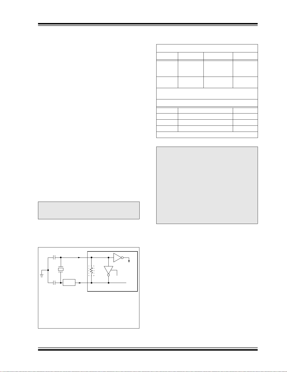
2.2 Crystal Oscillator/Ceramic Resonators
In XT, LP, HS or HS+PLL Oscill ato r m od es , a c ry st a l or
ceramic resonator is connected to the OSC1 and
OSC2 pins to establish oscillation. Figure 2-1 shows
the pin connections.
The PIC18FXX20 oscillator design requires the use of
a parallel cut crystal.
Note: Use of a series cut crystal may give a fre-
quency out of the crystal manufacturer ’s
specifications.
FIGURE 2-1: CRYSTAL/CERAMIC
RESONATOR OPERATION
(HS, XT OR LP
CONFIGURATION)
(1)
C1
C2
(1)
XTAL
(2)
RS
OSC1
OSC2
(3)
RF
PIC18FXX20
Sleep
To
Internal
Logic
T ABLE 2-1: CAPACITOR SELECTION FOR
CERAMIC RESONATORS
Ranges Tested:
Mode Freq C1 C2
XT 455 kHz
2.0 MHz
4.0 MHz
HS 8.0 MHz
16.0 MHz
These values are for design guidance only.
See notes following this table.
Resonators Used:
2.0 MHz Murata Erie CSA2.00MG ± 0.5%
4.0 MHz Murata Erie CSA4.00MG ± 0.5%
8.0 MHz Murata Erie CSA8.00MT ± 0.5%
16.0 MHz Murata Erie CSA16.00MX ± 0.5%
All resonators used di d not have built-in capac itors.
Note 1: Higher capac itance inc reases th e stabilit y
of the oscillator, but also increases the
start-up time.
2: When operating below 3V V
using certain ceramic resonators at any
voltage, it may be necessary to use high
gain HS mode, try a lower frequency
resonator, or switch to a crystal oscillator.
3: Since each resonator/crystal has its own
characteristics, the user should consult
the resonator/crystal manufacturer for
appropriate values of external
components, or verify oscillator
performance.
68-100 pF
15-68 pF
15-68 pF
10-68 pF
10-22 pF
68-100 pF
15-68 pF
15-68 pF
10-68 pF
10-22 pF
DD, or when
Note 1: See Table2-1 and Table 2-2 for recommended
2004 Microchip Technology Inc. DS39609B-page 21
values of C1 and C2.
2: A s eries resist or (R
strip cut crystals.
F varies with the oscillator mode chosen.
3: R
S) may be required for AT
PIC18F6520/8520/6620/8620/6720/8720
TABLE 2-2: CAPACITOR SELECTION FOR
CRYSTAL OSCILLATOR
Ranges T ested:
Mode Freq C1 C2
LP 32 kHz
200 kHz
XT 1 MHz
4 MHz
HS 4 MHz
20 MHz
Capacitor values are for design guidance only.
These capacitors were tested with the above crystal
frequencies for basic start-up and operation. These
values are not optimized.
Different capacitor values may be required to produce
acceptable oscillator operation. The user should test
the performance of the oscillator over the expected
DD and temperature range for the application.
V
See the notes following this table for additional
information.
Note 1: Higher capacit ance increa ses the st ability
of the oscillator, but also increases the
start-up time.
2: When operating below 3V V
using certain ceramic resonators at any
voltage, it may be necessary to use the
HS mode or switch to a crystal oscillator.
3: Since each resonator/crystal has its
own characteristics, the user should
consult the resonator/crystal manufacturer for appropriate values of external
components, or verify oscillator
performance.
S may be required to avoid overdriving
4: R
crystals with low driv e lev e l spe ci fic ati on.
5: Always verify oscillator performance over
DD and temperature range that is
the V
expected for the application.
An external clock sourc e may also be conne cted to th e
OSC1 pin in the HS, XT and LP modes, as shown in
Figure 2-2.
15-22 pF 15-22 pF
15-22 pF 15-22 pF
15-22 pF 15-22 pF8 MHz
DD, or when
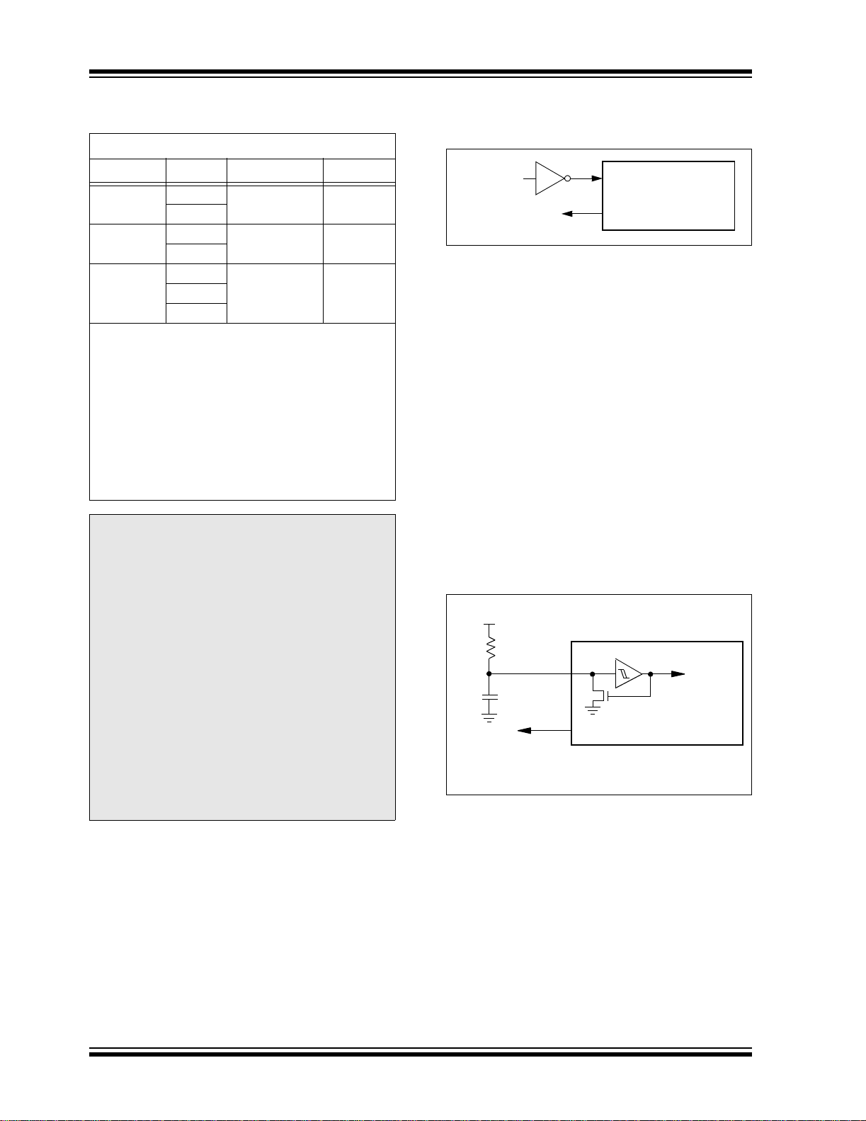
FIGURE 2-2: EXTERNAL CLOCK INPUT
OPERATION (HS, XT OR
LP OSC CONFIGURATION)
Clock from
Ext. System
Open
OSC1
PIC18FXX20
OSC2
2.3 RC Oscillator
For timing insensitive applications, the “RC” and
“RCIO” device options offer additional cost savings.
The RC oscillator frequency is a function of the supply
voltage, the resistor (R
ues and the operating temperature. In addition to this,
the oscillator frequency will vary from unit to unit, due
to normal process parameter variation. Furthermore,
the difference in lead frame cap acitance bet ween package types will also affect the oscillation frequency,
especially for low C
take into account variation due to tolerance of external
R and C components used. Figure 2-3 shows how the
R/C combination is connected.
In the RC Oscillator mode, the oscillator frequency
divided by 4 is available on the OSC2 pin. This signal
may be used f or t e st pu r pos es or t o sy nc hr o n iz e ot he r
logic.
FIGURE 2-3: RC OSCILLATOR MODE
VDD
REXT
CEXT
VSS
F
Recommended values: 3 kΩ ≤ REXT ≤ 100 kΩ
The RCIO Oscillato r mode f unc tions like t he RC m ode,
except that the OSC2 pin becomes an additional
general purpose I/O pin. The I/O pin becomes bit 6 of
PORTA (RA6).
EXT) and capacitor (CEXT) val-
EXT values. Th e user also needs to
OSC1
Internal
Clock
PIC18FXX20
OSC2/CLKO
OSC/4
EXT > 20 pF
C
DS39609B-page 22 2004 Microchip Technology Inc.
PIC18F6520/8520/6620/8620/6720/8720
2.4 External Clock Input
The EC and ECIO Oscillator mode s require an externa l
clock source to be connected to the OSC1 pin. The
feedback device between OSC1 and OSC2 is turned
off in these modes to save current. There is a maximum
1.5 µs start-up required after a Power-on Reset, or
wake-up from Sleep mo de.
In the EC Oscillator mode, the oscillator frequency
divided by 4 is available on the OSC2 pin. This signal
may be used f or t e st pu r pos es or t o sy nc hr o n iz e ot he r
logic. Figure 2-4 shows the pin connections for the EC
Oscillator mode.
FIGURE 2-4: EXTERNAL CLOCK INPUT
OPERATION
(EC CONFIGURATION)
Clock from
Ext. System
F
OSC/4
The ECIO Oscillator mode func ti ons li ke t he EC m od e,
except that the OSC2 pin becomes an additional general purpose I/O pin. The I/O pin becomes bit 6 of
PORTA (RA6). Figure 2-5 shows the pin connections
for the ECIO Oscillator mode.
OSC1
PIC18FXX20
OSC2
FIGURE 2-5: EXTERNAL CLOCK INPUT
OPERATION
(ECIO CONFIGURATION)
Clock from
Ext. System
RA6
OSC1
PIC18FXX20
I/O (OSC2)
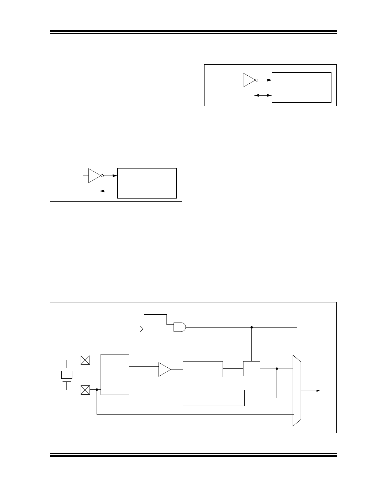
2.5 HS/PLL
A Phase Locked Loop circuit (PLL) is provided as a
programmable option for us ers that want to multip ly the
frequency of the incoming cry sta l oscil lator sig nal by 4.
For an input clock frequency of 10 MHz, the internal
clock frequency will be multiplied to 40 MHz. This is
useful for customers who are concerned with EMI due
to high-frequency crystals.
The PLL is one o f the modes of the FO SC<2:0> co nfiguration bits. The oscillator mode is specified during
device programming.
The PLL can only be enabled when the oscillator configuration bits are programmed for HS mode. I f they are
programmed for any other mode, the PLL is not
enabled and the system clock will come directly from
OSC1. Also, PLL operation cannot be changed “onthe-fly”. To enable or disable it, the controller must
either cycle through a Power-on Re set, or switch the
clock source from the main oscillator to the Timer1
oscillator and b ack again. See Se ction 2.6 “Oscillator
Switching Feature” for details on os cillator s witching.
A PLL lock timer is used to ensure that the PLL has
locked before device execution starts. The PLL lock
timer has a time-out that is called T
PLL.
FIGURE 2-6: PLL BLOCK DIAGRAM
(from Configuration
bit Register)
OSC2
OSC1
2004 Microchip Technology Inc. DS39609B-page 23
HS Osc
PLL Enable
Crystal
Osc
Phase
Comparator
FIN
FOUT
Loop
Filter
Divide by 4
VCO
SYSCLK
MUX
PIC18F6520/8520/6620/8620/6720/8720
2.6 Oscillator Switching Feature
The PIC18FXX20 devices inc lude a fea ture that a llow s
the system clock source to be switched from the main
oscillator to an alternate low-frequency clock source.
For the PIC18FXX20 devices, this alternate clock
source is the Timer1 oscillator. If a low-frequency
crystal (32 kHz, for ex am pl e ) ha s bee n at tac he d to the
Timer1 oscillator pins and the Timer1 oscillator has
been enabled, the device can switch to a low-power
FIGURE 2-7: DEVICE CLOCK SOURCES
PIC18FXX20
OSC2
OSC1
T1OSO
T1OSI
Main Oscillator
Sleep
Timer1 Oscillator
T1OSCEN
Enable
Oscillator
execution mode. Figure 2-7 shows a block diagram of
the system clock sources. The clock switching feature
is enabled by programming the Oscillator Switching
Enable (OSCSEN
) bit in Configuration Regis ter 1H to a
‘0’. Clock switching is disabled in an erased device.
See Section 12.0 “Timer1 Module” for further details
of the Timer1 oscillator. See Section 23.0 “Special
Features of the CPU” for Configuration register
details.
4 x PLL
TOSC
TT1P
TOSC/4
MUX
Clock
Source
TSCLK
Clock Source Option
for other Modules
DS39609B-page 24 2004 Microchip Technology Inc.

PIC18F6520/8520/6620/8620/6720/8720
2.6.1 SYSTEM CLOCK SWITCH BIT
The system clock sourc e sw it ching is performed under
software control. The system clock switch bit, SCS
(OSCCON<0>), controls the clock switching. When the
SCS bit is ‘0’, the system cloc k s our ce c om es fr om the
main oscillator that i s s el ec ted b y t he FO SC c onfiguration bits in Configuration Register 1H. When the SCS
bit is set, the system clock source will come from the
Timer1 o scillato r. The SCS bit is cleared on all forms of
Reset.
REGISTER 2-1: OSCCON REGISTER
U-0 U-0 U-0 U-0 U-0 U-0 U-0 R/W-1
— — — — — — —SCS
bit 7 bit 0
bit 7-1 Unimplemented: Read as ‘0’
bit 0 SCS: System Clock Switch bit
When OSCSEN Configuration bit = 0 and T1OSCEN bit is set:
1 = Switch to Timer1 oscillator/clock pin
0 = Use primary oscillator/clock input pin
When
OSCSEN and T1OSCEN are in other states:
Bit is forced clear.
Note: The Timer1 oscillator must be enabled
and operating to switch the system clock
source. The Timer1 oscillator is enabled
by setting the T1OSCEN bit in the Timer1
Control register (T1CON). If the Timer1
oscillator is not enabled, then any write to
the SCS bit will be ignored (S CS bit force d
cleared) and the main oscillator will
continue to be the system clock source.
Legend:
R = Readable bit W = Writable bit U = Unimplemented bit, read as ‘0’
- n = Value at POR ‘1’ = Bit is set ‘0’ = Bit is cleared x = Bit is unknown
2004 Microchip Technology Inc. DS39609B-page 25
PIC18F6520/8520/6620/8620/6720/8720
2.6.2 OSCILLATOR TRANSITIONS
PIC18FXX20 devices contain circuitry to prevent
“glitches” when switching between oscillator sources.
Essentially, the circuitry waits for eight rising edges of
the clock source that the processor is swit ching to. This
ensures that the n ew c lo ck s ourc e is s t able and that its
pulse width will not be less than the shortest pulse
width of the two clock sources.
A timing diagram indicating the transition from the main
oscillator to the Timer1 oscillator is s hown in Figure2-8.
The Timer1 oscillator is assumed to be running all the
time. After the SCS bit is set, the processor is frozen at
the next occurring Q1 cycle. After eight synchronization
cycles are counted from the Timer1 oscillator, operation
resumes. No additional delays are required after the
synchronization cycles.
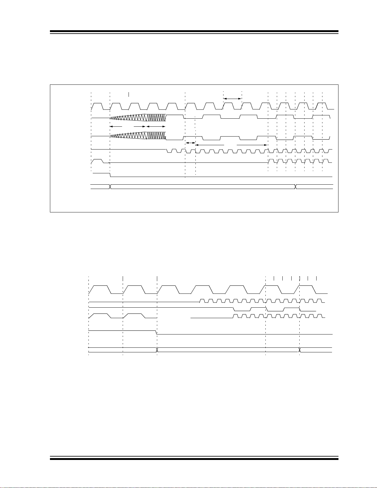
FIGURE 2-8: TIMING DIAGRAM FOR TRANSITION FROM OSC1 TO TIMER1 OSCILLATOR
Q1
T1OSI
OSC1
Internal
System
Clock
SCS
(OSCCON<0>)
Program
Counter
Note 1:Delay on internal system clock is eight oscillator cycles for synchronization.
Q1
TSCS
PC + 2PC
Q3Q2Q1Q4Q3Q2
Q4 Q1
PC + 4
The sequence of events that takes place when switching from the Timer1 oscillator to the main oscillator will
depend on the mode of the main oscillator. In addition
to eight clock cycles of the main oscillator, additional
delays may take place.
If the main oscillator is configured for an external
crystal (HS, XT, LP), then the transition will take place
after an oscillator start-up time (TOST) has occurred. A
timing diagram, indicating the transition from the
Timer1 oscillator to the main oscillator for HS, XT and
LP modes, is shown in Figure 2-9.
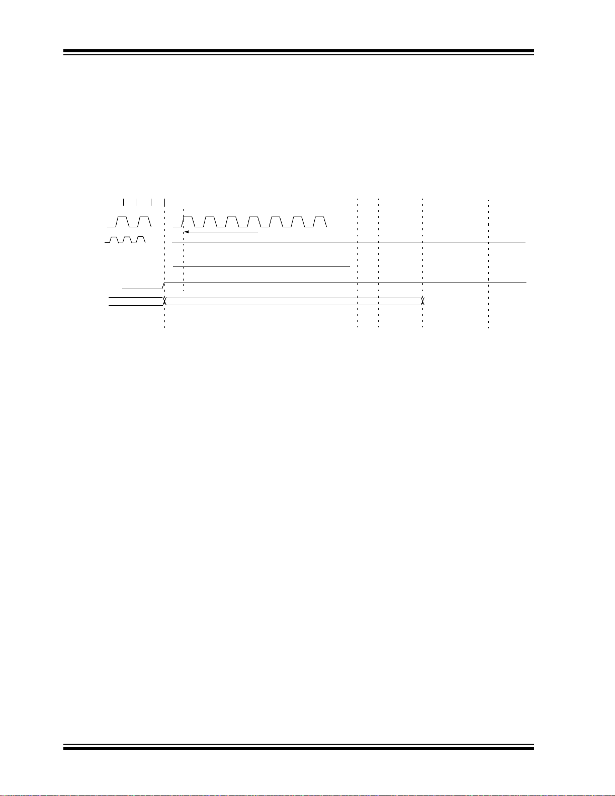
FIGURE 2-9: TIMING FOR TRANSITION BETWEEN TIMER1 AND OSC1 (HS, XT, LP)
DS39609B-page 26 2004 Microchip Technology Inc.
PIC18F6520/8520/6620/8620/6720/8720
If the main oscil lator is config ured for HS-P LL mode, an
oscillator start-up time (T
time-out (T
PLL), will occur. The PLL time-out is typica lly
OST), plus an additional PLL
frequency. A timing diagram, indicating the transition
from the Timer1 oscillator to the main oscillator for
HS-PLL mode, is shown in Figure 2-10.
2 ms and allows the PLL to lock to the main oscillator
FIGURE 2-10: TIMING FOR TRANSITION BETWEEN TIMER1 AND OSC1 (HS WITH PLL)
Q4 Q1
T1OSI
OSC1
TOST
OSC2
PLL Clock
Input
Internal System
Program Counter
Note 1:TOST = 1024 TOSC (drawing not to scale).
Clock
(OSCCON<0>)
SCS
PC PC + 2
TPLL
TT1P
TOSC
1 234 5678
TSCS
Q1 Q2 Q3 Q4 Q1 Q2
PC + 4
Q3
Q4
If the main oscillato r is c onfigur ed in th e RC, R CIO, EC
or ECIO modes, th ere is no os cillator start-up time-out.
Operation will resume after eight cycles of the main
indicating the trans ition from the T imer1 oscillator to th e
main oscillator for RC, RCIO, EC and ECIO modes, is
shown in Figure 2-11.
oscillator have been counted. A timing diagram,
FIGURE 2-11: TIMING FOR TRANSITION BETWEEN TIMER1 AND OSC1 (RC, EC)
Q3 Q4
T1OSI
OSC1
OSC2
Internal System
Clock
(OSCCON<0>)
Note 1:RC Oscillator mode assumed.
SCS
Program
Q1
PC PC + 2
Q1 Q2 Q3 Q4 Q1 Q2 Q3
PC + 4
2004 Microchip Technology Inc. DS39609B-page 27
PIC18F6520/8520/6620/8620/6720/8720
2.7 Effects of Sleep Mode on the On-Chip Oscillator
When the device e xecutes a SLEEP i nstructio n, the onchip clocks and oscillator are turn ed off and the device
is held at the beginning of an instruction cycle (Q1
state). With the oscillator off, the OSC1 and OSC2
signals will stop oscillating. Since all the transistor
switching currents have been removed, Sleep mode
achieves the lowest current consumption of the device
(only leakage currents). Enabling any on-chip feature
that will operate during Sleep will increase the current
consumed during Sleep. The user can wake from
Sleep through external Reset, Watchdog Timer Reset
or through an interrupt.
2.8 Power-up Delays
Power up delays are con trolled by two timers so that n o
external Reset circuitry is required for most
applications. The delays ensure that the device is kept
in Reset un til the device p ower supply and clock are
stable. For additional information on Reset operation,
see Section 3.0 “Reset”.
The first timer is the Power-up Timer (PWRT), which
optionally provides a fix ed del ay of 72 ms (nom in al) o n
power-up only (POR and BOR). The second timer is
the Oscillator Start-up Timer (OST), intended to keep
the chip in Reset until the crystal oscillator is stable.
With the PLL enabled (HS/PLL Oscillator mode), the
time-out sequenc e following a Power-on Reset is diff erent from other oscil lator modes. The time-out se quence
is as follows: First, the PWRT time-out is invoked after
a POR time delay has expired. Then, the Oscillator
Start-up Timer (OST) is invoked. However, this is still
not a sufficient amount of time to allow the PLL to lock
at high frequencies. The PWR T timer is used to provide
an additional fixed 2 ms (nominal) time-out to allow th e
PLL ample time to lock to the incoming cloc k frequency .
TABLE 2-3: OSC1 AND OSC2 PIN STATES IN SLEEP MODE
OSC Mode OSC1 Pin OSC2 Pin
RC Floating, external resistor should pull high At logic low
RCIO Floating, external resistor should pull high Configured as PORTA, bit 6
ECIO Floating Configured as PORTA, bit 6
EC Floating At logic low
LP, XT and HS Feedback inverter disabled at quiescent
voltage level
Note: See Table 3-1 in Section 3.0 “Reset” for time-outs due to Sleep and MCLR Reset.
Feedback inverter disabled at quiescent
voltage level
DS39609B-page 28 2004 Microchip Technology Inc.
PIC18F6520/8520/6620/8620/6720/8720
t
3.0 RESET
Most registers are not affected by a WDT wake-up,
since this is viewed as the resumption of normal
The PIC18FXX20 devices differentiate between
various kinds of Reset:
a) Power-on Reset (POR)
b) MCLR
Reset during normal operation
c) MCLR Reset during Sleep
d) Watchdog Timer (WDT) Reset (during normal
operation)
e) Programmable Brown-out Reset (PBOR)
f) RESET Instruction
g) Stack Full Reset
h) Stack Underflow Reset
operation. Status bits from the RCON register, RI, TO,
, POR and BOR, are set or cleared differently in
PD
different Reset situations, as indicated in Table 3-2.
These bits are use d in software to d etermine the n ature
of the Reset. See Table 3-3 for a full description of the
Reset states of all registers.
A simplified block di agram of the On-Chip Reset Circu it
is shown in Figure 3- 1.
The Enhanced MCU devices have a MCLR
in the MCLR
ignore small puls es. T he MC LR
Reset path. The filter will detect and
pin is not driv en lo w b y
any internal Resets, including the WDT.
Most registers are unaffected by a Reset. Their status
is unknown on POR and unchanged by all other
Resets. The other registers are forced to a “Reset
state” on Power-on Reset, MCL R
out Reset, MCLR
Reset during Sleep and by the
, WDT Reset, Brown-
RESET instruction.
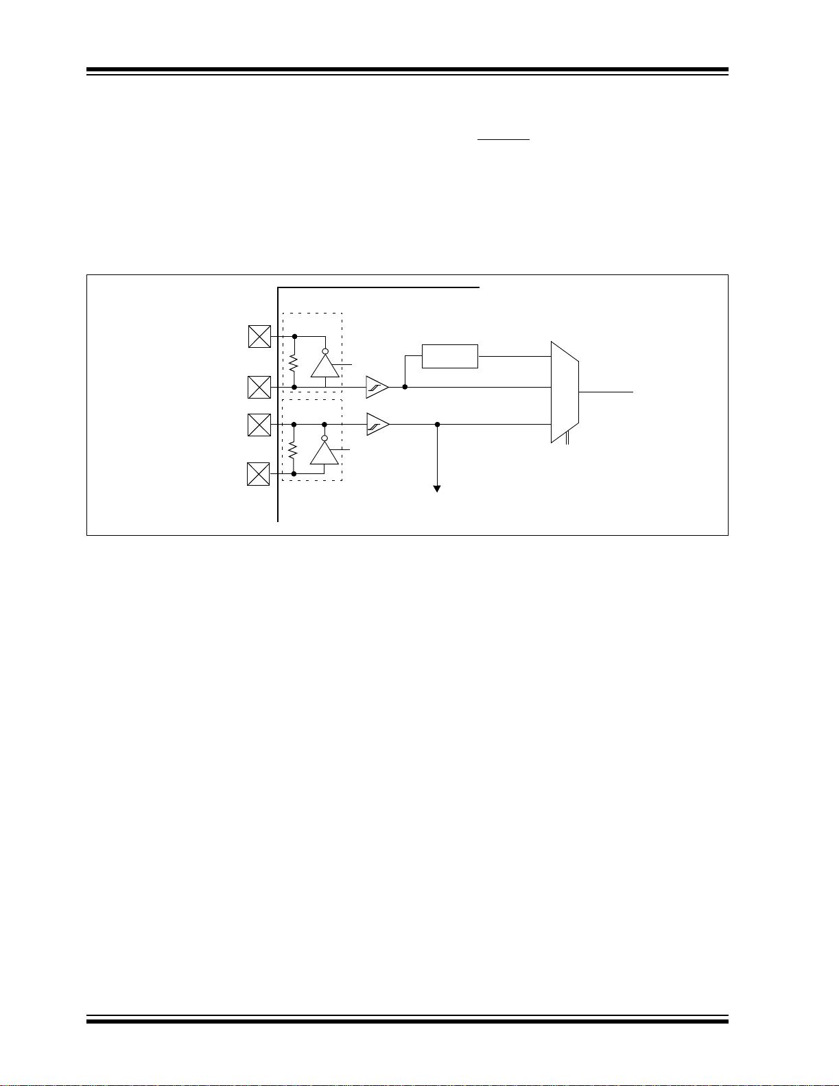
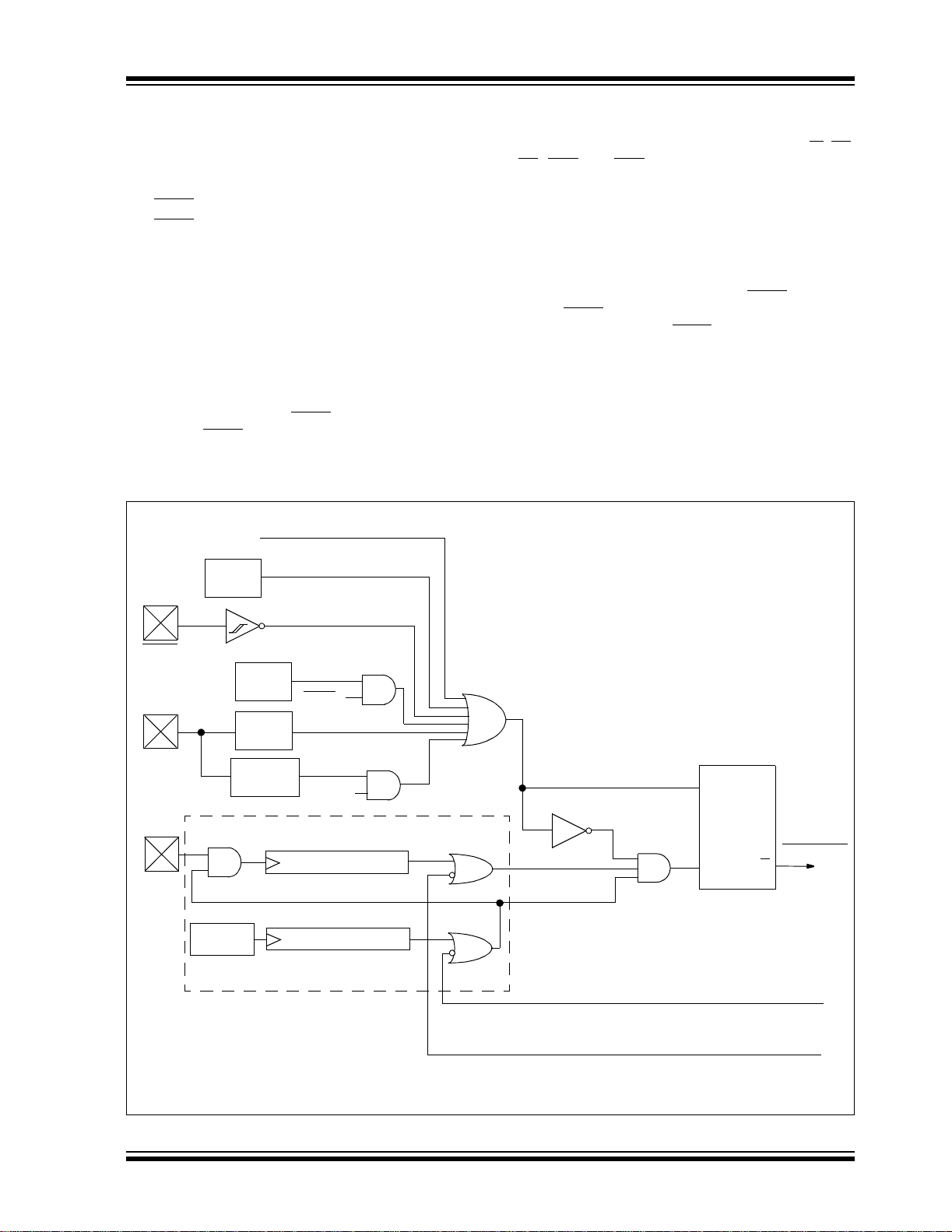
FIGURE 3-1: SIMPLIFIED BLOCK DIAGRAM OF ON-CHIP RESET CIRCUIT
RESETInstruction
noise filter
MCLR
VDD
OSC1
Stack
Pointer
OST/PWRT
On-chip
RC OSC
Stack Full/Underflow Reset
External Reset
WDT
Time-out
Reset
WDT
Module
DD Rise
V
Detect
Brown-out
Reset
(1)
Sleep
Power-on Reset
BOREN
OST
10-bit Ripple Counter
PWRT
10-bit Ripple Counter
S
R
Chip_Rese
Q
Enable PWRT
Enable OST
Note 1: This is a separate oscillator from the RC oscillator of the CLKI pin.
2: Se e Table 3-1 for time-out situations.
2004 Microchip Technology Inc. DS39609B-page 29
(2)

PIC18F6520/8520/6620/8620/6720/8720
.
t
l
3.1 Power-on Reset (POR)
A Power-on Reset pulse is generated on-chip when
DD rise is detected. To take advantage of the POR
V
circuitry, tie the MCLR
resistor to V
DD. This will eliminate external RC
pin through a 1 kΩ to 10 kΩ
components usually needed to create a Power-on
Reset delay. A minimum rise rate for V
DD is specified
(parameter D004) . For a s low rise t ime, see F igure 3-2.
When the device st arts normal operation (i.e., exits th e
Reset condition), device operating parameters (voltage, frequency, temperature, etc.) must be met to
ensure operation. If these conditions are not met, the
device must be held in Reset until the operating
conditions are met.
FIGURE 3-2: EXTERNAL POWER-ON
RESET CIRCUIT (FOR
SLOW V
DD
V
D
R
C
Note 1: External Power-on Reset circuit is required
only if the V
The diode D helps discharge the capacitor
quickly when V
2: R < 40 kΩ is recommended to make sure tha
the voltage drop across R does not violate
the device’s electrical specification.
3: R1 = 1 kΩ to 10 kΩ will limit any current flow-
ing into MCLR
the event of MCLR/
Electrostatic Discharge (ESD) or Electrica
Overstress (EOS).
DD power-up slope is too slow
DD POWER-UP)
R1
MCLR
PIC18FXX20
DD powers down.
from external capacitor C, in
VPP pin breakdown due to
3.2 Power-up Timer (PWRT)
The Power-up Ti mer provides a fixed nominal time-out
(parameter #33) only on power-up from the POR. The
Power-up Timer operates on an internal RC oscillator.
The chip is kept in Reset as long as the PWRT is active.
The PWRT’s t ime delay allows V
able level. A configuration bit is provided to enable/
disable the PWRT.
The power-up time delay will vary fr om chip-to-ch ip due
DD, temperature and process variation. See DC
to V
parameter #33 for details.
DD to rise to an accept-
3.3 Oscillator Start-up Timer (OST)
The Oscillator Start-up Timer (OST) provides 1024
oscillator cycles (from OSC1 input) delay after the
PWRT delay is over (para meter #32). Th is ensures th at
the crystal oscillator or resonator has started and
stabilized.
The OST time-out is invoked only for XT, LP and HS
modes and only on Power-on Reset, or wake-up from
Sleep.
3.4 PLL Lock Time-out
With the PLL enabled, the time-ou t sequen ce foll owin g
a Power-on Reset is different from other oscillator
modes. A portion of the Power-up Timer is used to
provide a fixed time-out that is sufficient for the PLL to
lock to the main oscillator frequency. This PLL lock
time-out (T
PLL) is typically 2 ms and follows the
oscillator start-up time-out.
3.5 Brown-out Reset (BOR)
A configuration bit, BOREN, can disable (if clear/
programmed), or enable (if set) the Brown-out Reset
circuitry. If V
DD falls below parameter D005 for greater
than parameter #35, the brown-out situation will reset
the chip. A Reset may not occur if VDD falls below
parameter D005 for less than p aram et er #35 . The chip
will remain in Brown-out Reset until VDD r ises above
DD. If the Power-up Timer is enabled, it will be
BV
invoked after V
DD rises above BVDD; it then will keep
the chip in Reset for an additional time delay (parameter #33). If VDD drops below BVDD while the Power-up
Timer is ru nni ng, the chip will go back into a Bro wn-o ut
Reset and the Power-up Timer will be initialized. Once
DD rises above BVDD, the Power-up Timer will
V
execute the additional time delay.
3.6 Time-out Sequence
On power-up, the time-out sequence is as follows:
First, PWRT time-out is invoked after the POR time
delay has expi red. Then, OST is activ ated. The total
time-out will vary based on oscillator configuration and
the status of th e PWRT. Fo r example, in RC mode with
the PWRT disabled, there will be no time-out at all.
Figures 3-3 through 3-7 depict time-out sequences on
power-up.
Since the time-outs occur from the POR pulse, the
time-outs will expire if MCLR
Bringing MCLR
high will begin execution immediately
(Figure 3-5). This is useful for testing purposes, or to
synchronize more than one PIC18FXX20 device
operating in parallel.
Table 3-2 shows the Reset conditio ns for some Special
Function Registers, while Table 3-3 shows the Reset
conditions for all of the registers.
is kept low long enough.
DS39609B-page 30 2004 Microchip Technology Inc.

PIC18F6520/8520/6620/8620/6720/8720
TABLE 3-1: TIME-OUT IN VARIOUS SITUATIONS
Oscillator
Configuration
HS with PLL enabled
PWRTE = 0 PWRTE = 1
(1)
72 ms + 1024 TOSC
Power-up
+ 2ms
HS, XT, LP 72 ms + 1024 T
EC 72 ms 1.5 µs72 ms
External RC 72 ms — 72 ms
Note 1: 2 ms is the nominal time required for the 4xPLL to lock.
2: 72 ms is the nominal power-up timer delay, if im plemented.
3: 1.5 µs is the recovery time from Sleep. There is no recovery time from oscillator switch.
REGISTER 3-1: RCON REGISTER BITS AND POSITIONS
R/W-0 U-0 U-0 R/W-1 R/W-1 R/W-1 R/W-1 R/W-1
IPEN
bit 7 bit 0
Note 1: Refer to Section 4.14 “RCON Register” for bit definitions.
— —RITO PD POR BOR
(2)
1024 TOSC
72 ms
+ 2 ms
OSC 1024 TOSC 72 ms
Brown-out
(2)
+ 1024 TOSC
+ 2 ms
(2)
+ 1024 TOSC 1024 TOSC
(2)
(2)
Wake-up from
Sleep or
Oscillator Switch
1024 TOSC + 2 ms
(3)
1.5 µs
—
TABLE 3-2: STATUS BITS, THEIR SIGNIFICANCE AND THE INITIALIZATION CONDITION FOR
RCON REGISTER
Condition
Program
Counter
Power-on Reset 0000h 0--1 1100 1 1 1 0 0 u u
Reset during normal
MCLR
0000h 0--u uuuu u u u u u u u
operation
Software Reset during normal
0000h 0--0 uuuu 0 u u u u u u
operation
Stack Full Reset during normal
0000h 0--u uu11 u u u u u u 1
operation
Stack Underflow Reset during
0000h 0--u uu11 u u u u u 1 u
normal operation
MCLR
Reset during Sleep
0000h 0--u 10uu u 1 0 u u u u
WDT Reset 0000h 0--u 01uu 1 0 1 u u u u
WDT Wake-up PC + 2 u--u 00uu u 0 0 u u u u
Brown-out Reset 0000h 0--1 11u0 1 1 1 1 0 u u
Interrupt wake-up from Sleep PC + 2
(1)
Legend: u = unchanged, x = unknown, – = unimplemented bit, read as ‘0’
Note 1: When the wake-up is due to an interrupt and the GIEH or GIEL bits are set, the PC is loaded with the
interrupt vector (0x000008h or 0x000018h).
RCON
Register
TO PD POR BOR STKFUL STKUNF
RI
u--u 00uu u 1 0 u u u u
2004 Microchip Technology Inc. DS39609B-page 31

PIC18F6520/8520/6620/8620/6720/8720
TABLE 3-3: INITIALIZATION CONDITIONS FOR ALL REGISTERS
Resets
MCLR
Register Applicable Devices
Power-on Reset,
Brown-o ut Reset
TOSU PIC18F6X20 PIC18F8X20 ---0 0000
TOSH PIC18F6X20 PIC18F8X20 0000 0000 0000 0000 uuuu uuuu
TOSL PIC18F6X20 PIC18F8X20 0000 0000 0000 0000 uuuu uuuu
STKPTR PIC18F6X20 PIC18F8X20 00-0 0000 uu-0 0000 uu-u uuuu
PCLATU PIC18F6X20 PIC18F8X20 ---0 0000 ---0 0000 ---u uuuu
PCLATH PIC18F6X20 PIC18F8X20 0000 0000 0000 0000 uuuu uuuu
PCL PIC18F6X20 PIC18F8X20 0000 0000 0000 0000 PC + 2
TBLPTRU PIC18F6X20 PIC18F8X20 --00 0000 --00 0000 --uu uuuu
TBLPTRH PIC18F6X20 PIC18F8X20 0000 0000 0000 0000 uuuu uuuu
TBLPTRL PIC18F6X20 PIC18F8X20 0000 0000 0000 0000 uuuu uuuu
TABLAT PIC18F6X20 PIC18F8X20 0000 0000 0000 0000 uuuu uuuu
PRODH PIC18F6X20 PIC18F8X20 xxxx xxxx uuuu uuuu uuuu uuuu
PRODL PIC18F6X20 PIC18F8X20 xxxx xxxx uuuu uuuu uuuu uuuu
INTCON PIC18F6X20 PIC18F8X20 0000 000x 0000 000u uuuu uuuu
INTCON2 PIC18F6X20 PIC18F8X20 1111 1111 1111 1111 uuuu uuuu
INTCON3 PIC18F6X20 PIC18F8X20 1100 0000 1100 0000 uuuu uuuu
INDF0 PIC18F6X20 PIC18F8X20 N/A N/A N/A
POSTINC0 PIC18F6X20 PIC18F8X20 N/A N/A N/A
POSTDEC0 PIC18F6X20 PIC18F8X20 N/A N/A N/A
PREINC0 PIC18F6X20 PIC18F8X20 N/A N/A N/A
PLUSW0 PIC18F6X20 PIC18F8X20 N/A N/A N/A
FSR0H PIC18F6X20 PIC18F8X20 ---- xxxx ---- uuuu ---- uuuu
FSR0L PIC18F6X20 PIC18F8X20 xxxx xxxx uuuu uuuu uuuu uuuu
WREG PIC18F6X20 PIC18F8X20 xxxx xxxx uuuu uuuu uuuu uuuu
INDF1 PIC18F6X20 PIC18F8X20 N/A N/A N/A
POSTINC1 PIC18F6X20 PIC18F8X20 N/A N/A N/A
POSTDEC1 PIC18F6X20 PIC18F8X20 N/A N/A N/A
PREINC1 PIC18F6X20 PIC18F8X20 N/A N/A N/A
PLUSW1 PIC18F6X20 PIC18F8X20 N/A N/A N/A
Legend: u = unchanged, x = unknown, - = unimplemented bit, read as ‘0’, q = value depends on condition.
Shaded cells indicate condi tions do not apply for the designated device.
Note 1: One or more bits in the INTCONx or PIRx registers will be affected (to cause wake-up).
2: When the wake-up is due to an interrupt and the GIEL or GIEH bit is set, the PC is loaded with the
interrupt vector (0008h or 0018h).
3: When the wake-up is due to an i nter r upt and the GIEL or GIEH bit is set, the TOSU, T O SH and TOSL are
updated with the current value of the PC. The STKPTR is modified to point to the next location in the
hardware stack.
4: See Table 3-2 for Reset value for specific condition.
5: Bit 6 of PORTA, LATA and TRISA are enabled in ECIO and RCIO Oscillator modes only. In all other
oscillator modes, they are disabled and read ‘0’.
6: Bit 6 of PORTA, LATA and TRISA are not available on all devices. When unimplemented, they are read ‘0’.
WDT Reset
RESET Instruction
Wake-up via WDT
or Interrupt
Stack Resets
---0 0000 ---0 uuuu
(3)
(3)
(3)
(3)
(2)
(1)
(1)
(1)
DS39609B-page 32 2004 Microchip Technology Inc.

PIC18F6520/8520/6620/8620/6720/8720
TABLE 3-3: INITIALIZATION CONDITIONS FOR ALL REGISTERS (CONTINUED)
Resets
MCLR
Register Applicable Devices
FSR1H PIC18F6X20 PIC18F8X20 ---- xxxx ---- uuuu ---- uuuu
FSR1L PIC18F6X20 PIC18F8X20 xxxx xxxx uuuu uuuu uuuu uuuu
BSR PIC18F6X20 PIC18F8X20 ---- 0000 ---- 0000 ---- uuuu
INDF2 PIC18F6X20 PIC18F8X20 N/A N/A N/A
POSTINC2 PIC18F6X20 PIC18F8X20 N/A N/A N/A
POSTDEC2 PIC18F6X20 PIC18F8X20 N/A N/A N/A
PREINC2 PIC18F6X20 PIC18F8X20 N/A N/A N/A
PLUSW2 PIC18F6X20 PIC18F8X20 N/A N/A N/A
FSR2H PIC18F6X20 PIC18F8X20 ---- xxxx ---- uuuu ---- uuuu
FSR2L PIC18F6X20 PIC18F8X20 xxxx xxxx uuuu uuuu uuuu uuuu
STATUS PIC18F6X20 PIC18F8X20 ---x xxxx ---u uuuu ---u uuuu
TMR0H PIC18F6X20 PIC18F8X20 0000 0000 uuuu uuuu uuuu uuuu
TMR0L PIC18F6X20 PIC18F8X20 xxxx xxxx uuuu uuuu uuuu uuuu
T0CON PIC18 F6X20 PIC18F8X20 1111 1111 1111 1111 uuuu uuuu
OSCCON PIC18F6X20 PIC18F8X20 ---- ---0 ---- ---0 ---- ---u
LVDCON PIC18F6X20 PIC18F8X20 --00 0101 --00 0101 --uu uuuu
WDTCON PIC18F6X20 PIC18F8X20 ---- ---0 ---- ---0 ---- ---u
(4)
RCON
TMR1H PIC18F6X20 PIC18F8X20 xxxx xxxx uuuu uuuu uuuu uuuu
TMR1L PIC18F6X20 PIC18F8X20 xxxx xxxx uuuu uuuu uuuu uuuu
T1CON PIC18 F6X20 PIC18F8X20 0-00 0000 u-uu uuuu u-uu uuuu
TMR2 PIC18F6X20 PIC18F8X20 0000 0000 0000 0000 uuuu uuuu
PR2 PIC18F6X20 PIC18F8X20 1111 1111 1111 1111 1111 1111
T2CON PIC18 F6X20 PIC18F8X20 -000 0000 -000 0000 -uuu uuuu
SSPBUF PIC18F6X20 PIC18F8X20 xxxx xxxx uuuu uuuu uuuu uuuu
SSPADD PIC18F6X20 PIC18F8X20 0000 0000 0000 0000 uuuu uuuu
SSPSTAT PIC18F6X20 PIC18F8X20 0000 0000 0000 0000 uuuu uuuu
SSPCON1 PIC18F6X20 PIC18F8X20 0000 0000 0000 0000 uuuu uuuu
SSPCON2 PIC18F6X20 PIC18F8X20 0000 0000 0000 0000 uuuu uuuu
Legend: u = unchanged, x = unknown, - = unimplemented bit, read as ‘0’, q = value depends on condition.
Note 1: One or more bits in the INTCONx or PIRx registers will be affected (to cause wake-up).
2: When the wake-up is due to an interrupt and the GIEL or GIEH bit is set, the PC is loaded with the
3: When the wake-up is due to an i nter r upt and the GIEL or GIEH bit is set, the TOSU, T O SH and TOSL are
4: See Table 3-2 for Reset value for specific condition.
5: Bit 6 of PORTA, LATA and TRISA are enabled in ECIO and RCIO Oscillator modes only. In all other
6: Bit 6 of PORTA, LATA and TRISA are not available on all devices. When unimple mented, they are read ‘0’.
PIC18F6X20 PIC18F8X20 0--q 11qq 0--q qquu u--u qquu
Shaded cells indicate condi tions do not apply for the designated device.
interrupt vector (0008h or 0018h).
updated with the current value of the PC. The STKPTR is modified to point to the next location in the
hardware stack.
oscillator modes, they are disabled and read ‘0’.
Power-on Reset,
Brown-o ut Reset
WDT Reset
RESET Instruction
Stack Resets
Wake-up via WDT
or Interrupt
2004 Microchip Technology Inc. DS39609B-page 33

PIC18F6520/8520/6620/8620/6720/8720
TABLE 3-3: INITIALIZATION CONDITIONS FOR ALL REGISTERS (CONTINUED)
Resets
MCLR
Register Applicable Devices
ADRESH PIC18F6X20 PIC18F8X20 xxxx xxxx uuuu uuuu uuuu uuuu
ADRESL PIC18F6X20 PIC18F8X20 xxxx xxxx uuuu uuuu uuuu uuuu
ADCON0 PIC18F6X20 PIC18F8X20 --00 0000 --00 0000 --uu uuuu
ADCON1 PIC18F6X20 PIC18F8X20 --00 0000 --00 0000 --uu uuuu
ADCON2 PIC18F6X20 PIC18F8X20 0--- -000 0--- -000 u--- -uuu
CCPR1H PIC18F6X20 PIC18F8X20 xxxx xxxx uuuu uuuu uuuu uuuu
CCPR1L PIC18F6X20 PIC18F8X20 xxxx xxxx uuuu uuuu uuuu uuuu
CCP1CON PIC18F6X20 PIC18F8X20 --00 0000 --00 0000 --uu uuuu
CCPR2H PIC18F6X20 PIC18F8X20 xxxx xxxx uuuu uuuu uuuu uuuu
CCPR2L PIC18F6X20 PIC18F8X20 xxxx xxxx uuuu uuuu uuuu uuuu
CCP2CON PIC18F6X20 PIC18F8X20 --00 0000 --00 0000 --uu uuuu
CCPR3H PIC18F6X20 PIC18F8X20 xxxx xxxx uuuu uuuu uuuu uuuu
CCPR3L PIC18F6X20 PIC18F8X20 xxxx xxxx uuuu uuuu uuuu uuuu
CCP3CON PIC18F6X20 PIC18F8X20 0000 0000 0000 0000 uuuu uuuu
CVRCON PIC18F6X20 PIC18F8X20 0000 0000 0000 0000 uuuu uuuu
CMCON PIC18F6X20 PIC18F8X20 0000 0000 0000 0000 uuuu uuuu
TMR3H PIC18F6X20 PIC18F8X20 xxxx xxxx uuuu uuuu uuuu uuuu
TMR3L PIC18F6X20 PIC18F8X20 xxxx xxxx uuuu uuuu uuuu uuuu
T3CON PIC18 F6X20 PIC18F8X20 0000 0000 uuuu uuuu uuuu uuuu
PSPCON PIC18F6X20 PIC18F8X20 0000 ---- 0000 ---- uuuu ----
SPBRG1 PIC18F6X20 PIC18F8X20 0000 0000 0000 0000 uuuu uuuu
RCREG1 PIC18F6X20 PIC18F8X20 0000 0000 0000 0000 uuuu uuuu
TXREG1 PIC18F6X20 PIC18F8X20 0000 0000 0000 0000 uuuu uuuu
TXSTA1 PIC18F6X20 PIC18F8X20 0000 -010 0000 -010 uuuu -uuu
RCSTA1 PIC18F6X20 PIC18F8X20 0000 000x 0000 000x uuuu uuuu
EEADRH PIC18F6X20 PIC18F8X20 ---- --00 ---- --00 ---- --uu
EEADR PIC18F6X20 PIC18F8X20 0000 0000 0000 0000 uuuu uuuu
EEDATA PIC18F6X20 PIC18F8X20 0000 0000 0000 0000 uuuu uuuu
EECON2 PIC18F6X20 PIC18F8X20 ---- ---- ---- ---- ---- ---EECON1 PIC18F6X20 PIC18F8X20 xx-0 x000 uu-0 u000 uu-0 u000
Legend: u = unchanged, x = unknown, - = unimplemented bit, read as ‘0’, q = value depends on condition.
Shaded cells indicate condi tions do not apply for the designated device.
Note 1: One or more bits in the INTCONx or PIRx registers will be affected (to cause wake-up).
2: When the wake-up is due to an interrupt and the GIEL or GIEH bit is set, the PC is loaded with the
interrupt vector (0008h or 0018h).
3: When the wake-up is due to an i nter r upt and the GIEL or GIEH bit is set, the TOSU, T O SH and TOSL are
updated with the current value of the PC. The STKPTR is modified to point to the next location in the
hardware stack.
4: See Table 3-2 for Reset value for specific condition.
5: Bit 6 of PORTA, LATA and TRISA are enabled in ECIO and RCIO Oscillator modes only. In all other
oscillator modes, they are disabled and read ‘0’.
6: Bit 6 of PORTA, LATA and TRISA are not available on all devices. When unimplemented, they are read ‘0’.
Power-on Reset,
Brown-o ut Reset
WDT Reset
RESET Instruction
Stack Resets
Wake-up via WDT
or Interrupt
DS39609B-page 34 2004 Microchip Technology Inc.

PIC18F6520/8520/6620/8620/6720/8720
TABLE 3-3: INITIALIZATION CONDITIONS FOR ALL REGISTERS (CONTINUED)
Resets
MCLR
Register Applicable Devices
Power-on Reset,
Brown-o ut Reset
IPR3 PIC18F6X20 PIC18F8X20 --11 1111 --11 1111 --uu uuuu
PIR3 PIC18F6X20 PIC18F8X20 --00 0000 --00 0000 --uu uuuu
PIE3 PIC18F6X20 PIC18F8X20 --00 0000 --00 0000 --uu uuuu
IPR2 PIC18F6X20 PIC18F8X20 -1-1 1111 -1-1 1111 -u-u uuuu
PIR2 PIC18F6X20 PIC18F8X20 -0-0 0000 -0-0 0000 -u-u uuuu
PIE2 PIC18F6X20 PIC18F8X20 -0-0 0000 -0-0 0000 -u-u uuuu
IPR1 PIC18F6X20 PIC18F8X20 0111 1111 0111 1111 uuuu uuuu
PIR1 PIC18F6X20 PIC18F8X20 0000 0000 0000 0000 uuuu uuuu
PIE1 PIC18F6X20 PIC18F8X20 0000 0000 0000 0000 uuuu uuuu
MEMCON
PIC18F6X20 PIC18F8X20 0-00 --00 0-00 --00 u-uu --uu
TRISJ PIC18F6X20 PIC18F8X20 1111 1111 1111 1111 uuuu uuuu
TRISH PIC18F6X20 PIC18F8X20 1111 1111 1111 1111 uuuu uuuu
TRISG PIC18F6X20 PIC18F8X20 ---1 1111 ---1 1111 ---u uuuu
TRISF PIC18F6X20 PIC18F8X20 1111 1111 1111 1111 uuuu uuuu
TRISE PIC18F6X20 PIC18F8X20 1111 1111 1111 1111 uuuu uuuu
TRISD PIC18F6X20 PIC18F8X20 1111 1111 1111 1111 uuuu uuuu
TRISC PIC18F6X20 PIC18F8X20 1111 1111 1111 1111 uuuu uuuu
TRISB PIC18F6X20 PIC18F8X20 1111 1111 1111 1111 uuuu uuuu
TRISA
(5,6)
PIC18F6X20 PIC18F8X20 -111 1111
(5)
LATJ PIC18F6X20 PIC18F8X20 xxxx xxxx uuuu uuuu uuuu uuuu
LATH PIC18F6X20 PIC18F8X20 xxxx xxxx uuuu uuuu uuuu uuuu
LATG PIC18F6X20 PIC18F8X20 ---x xxxx ---u uuuu ---u uuuu
LATF PIC18F6X20 PIC18F8X20 xxxx xxxx uuuu uuuu uuuu uuuu
LATE PIC18F6X20 PIC18F8X20 xxxx xxxx uuuu uuuu uuuu uuuu
LATD PIC18F6X20 PIC18F8X20 xxxx xxxx uuuu uuuu uuuu uuuu
LATC PIC18F6X20 PIC18F8X20 xxxx xxxx uuuu uuuu uuuu uuuu
LATB PIC18F6X20 PIC18F8X20 xxxx xxxx uuuu uuuu uuuu uuuu
LATA
(5,6)
PIC18F6X20 PIC18F8X20 -xxx xxxx
(5)
Legend: u = unchanged, x = unknown, - = unimplemented bit, read as ‘0’, q = value depends on condition.
Shaded cells indicate condi tions do not apply for the designated device.
Note 1: One or more bits in the INTCONx or PIRx registers will be affected (to cause wake-up).
2: When the wake-up is due to an interrupt and the GIEL or GIEH bit is set, the PC is loaded with the
interrupt vector (0008h or 0018h).
3: When the wake-up is due to an i nter r upt and the GIEL or GIEH bit is set, the TOSU, T O SH and TOSL are
updated with the current value of the PC. The STKPTR is modified to point to the next location in the
hardware stack.
4: See Table 3-2 for Reset value for specific condition.
5: Bit 6 of PORTA, LATA and TRISA are enabled in ECIO and RCIO Oscillator modes only. In all other
oscillator modes, they are disabled and read ‘0’.
6: Bit 6 of PORTA, LATA and TRISA are not available on all devices. When unimple mented, they are read ‘0’.
WDT Reset
RESET Instruction
Stack Resets
-111 1111
-uuu uuuu
(5)
(5)
Wake-up via WDT
or Interrupt
-uuu uuuu
-uuu uuuu
(1)
(1)
(5)
(5)
2004 Microchip Technology Inc. DS39609B-page 35

PIC18F6520/8520/6620/8620/6720/8720
TABLE 3-3: INITIALIZATION CONDITIONS FOR ALL REGISTERS (CONTINUED)
Resets
MCLR
Register Applicable Devices
PORTJ PIC18F6X20 PIC18F8X20 xxxx xxxx uuuu uuuu uuuu uuuu
PORTH PIC18F6X20 PIC18F8X20 0000 xxxx 0000 uuuu uuuu uuuu
PORTG PIC18F6X20 PIC18F8X20 ---x xxxx uuuu uuuu ---u uuuu
PORTF PIC18F6X20 PIC18F8X20 x000 0000 u000 0000 u000 0000
PORTE PIC18F6X20 PIC18F8X20 xxxx xxxx uuuu uuuu uuuu uuuu
PORTD PIC18F6X20 PIC18F8X20 xxxx xxxx uuuu uuuu uuuu uuuu
PORTC PIC18F6X20 PIC18F8X20 xxxx xxxx uuuu uuuu uuuu uuuu
PORTB PIC18F6X20 PIC18F8X20 xxxx xxxx uuuu uuuu uuuu uuuu
PORTA
TMR4 PIC18F6X20 PIC18F8X20 0000 0000 0000 0000 uuuu uuuu
PR4 PIC18F6X20 PIC18F8X20 1111 1111 1111 1111 uuuu uuuu
T4CON PIC18F6X20 PIC18F8X20 -000 0000 -000 0000 -uuu uuuu
CCPR4H PIC18F6X20 PIC18F8X20 xxxx xxxx uuuu uuuu uuuu uuuu
CCPR4L PIC18F6X20 PIC18F8X20 xxxx xxxx uuuu uuuu uuuu uuuu
CCP4CON PIC18F6X20 PIC18F8X20 0000 0000 0000 0000 uuuu uuuu
CCPR5H PIC18F6X20 PIC18F8X20 xxxx xxxx uuuu uuuu uuuu uuuu
CCPR5L PIC18F6X20 PIC18F8X20 xxxx xxxx uuuu uuuu uuuu uuuu
CCP5CON PIC18F6X20 PIC18F8X20 0000 0000 0000 0000 uuuu uuuu
SPBRG2 PIC18F6X20 PIC18F8X20 0000 0000 0000 0000 uuuu uuuu
RCREG2 PIC18F6X20 PIC18F8X20 0000 0000 0000 0000 uuuu uuuu
TXREG2 PIC18F6X20 PIC18F8X20 0000 0000 0000 0000 uuuu uuuu
TXSTA2 PIC18F6X20 PIC18F8X20 0000 -010 0000 -010 uuuu -uuu
RCSTA2 PIC18F6X20 PIC18F8X20 0000 000x 0000 000x uuuu uuuu
Legend: u = unchanged, x = unknown, - = unimplemented bit, read as ‘0’, q = value depends on condition.
Note 1: One or more bits in the INTCONx or PIRx registers will be affected (to cause wake-up).
(5,6)
PIC18F6X20 PIC18F8X20 -x0x 0000
Shaded cells indicate condi tions do not apply for the designated device.
2: When the wake-up is due to an interrupt and the GIEL or GIEH bit is set, the PC is loaded with the
interrupt vector (0008h or 0018h).
3: When the wake-up is due to an i nter r upt and the GIEL or GIEH bit is set, the TOSU, T O SH and TOSL are
updated with the current value of the PC. The STKPTR is modified to point to the next location in the
hardware stack.
4: See Table 3-2 for Reset value for specific condition.
5: Bit 6 of PORTA, LATA and TRISA are enabled in ECIO and RCIO Oscillator modes only. In all other
oscillator modes, they are disabled and read ‘0’.
6: Bit 6 of PORTA, LATA and TRISA are not available on all devices. When unimplemented, they are read ‘0’.
Power-on Reset,
Brown-o ut Reset
(5)
WDT Reset
RESET Instruction
Stack Resets
-u0u 0000
(5)
Wake-up via WDT
or Interrupt
-uuu uuuu
(5)
DS39609B-page 36 2004 Microchip Technology Inc.
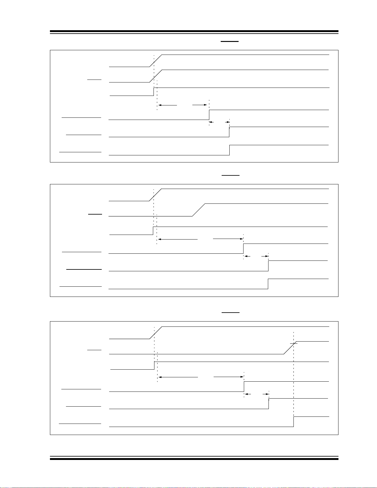
PIC18F6520/8520/6620/8620/6720/8720
FIGURE 3-3: TIME-OUT SEQUENCE ON POWER-UP (MCLR TIED TO VDD VIA 1 kΩ RESISTOR)
VDD
MCLR
INTERNAL POR
TPWRT
PWRT TIME-OUT
OST TIME-OUT
INTERNAL RESET
TOST
FIGURE 3-4: TIME-OUT SEQUENCE ON POWER-UP (MCLR
VDD
MCLR
INTERNAL POR
PWRT TI ME-OUT
OST TIME-OUT
INTERNAL RESET
TPWRT
NOT TIED TO VDD): CASE 1
TOST
FIGURE 3-5: TIME-OUT SEQUENCE ON POWER-UP (MCLR
VDD
MCLR
INTERNAL POR
TPWRT
PWRT TIME-OUT
OST TIME-OUT
INTERNAL RESET
2004 Microchip Technology Inc. DS39609B-page 37
NOT TIED TO VDD): CASE 2
TOST

PIC18F6520/8520/6620/8620/6720/8720
FIGURE 3-6: SLOW RISE TIME (MCLR TIED TO VDD VIA 1 kΩ RESISTOR)
5V
VDD
MCLR
INTERNAL POR
0V
PWRT
T
PWRT TIME-OUT
OST TIME-OUT
INTERNAL RES ET
TOST
FIGURE 3-7: TIME-OUT SEQUENCE ON POR W/PLL ENABLED
(MCLR
VDD
MCLR
IINTERNAL POR
PWRT TIME-OUT
OST TIME-OUT
TIED TO VDD VIA 1 kΩ RESISTOR)
TPWRT
TOST
TPLL
PLL TIME-OUT
INTERNAL RESET
Note: TOST = 1024 clock cycles.
PLL ≈ 2 ms max. First three stages of the PWRT timer.
T
DS39609B-page 38 2004 Microchip Technology Inc.

PIC18F6520/8520/6620/8620/6720/8720
4.0 MEMORY ORGANIZATION
There are three memory blocks in PIC18FXX20
devices. They are:
• Program Memory
• Data RAM
• Data EEPROM
Data and program memory use separate busses,
which allows for concurrent access of these blocks.
Additional detailed information for Flash program
memory and data EEPROM is pr ovide d in Section 5.0
“Flash Program Memory” and Section 7.0 “Data
EEPROM Memory”, respectively.
In addition to on-chip Flash, the PIC18F8X20 devices
are also capable of accessing external program memory through an external mem ory bus. Depending on the
selected operating mode (discussed in Section 4.1.1
“PIC18F8X20 Program Memory Modes”), the controllers may access either internal or external program
memory exclusive ly , or both internal and external mem ory in selected blocks. Additional information on the
External Memory Interface is provided in Section 6.0
“External Memory Interface”.
4.1 Program Memory Organization
A 21-bit program counter is capable of addressing the
2-Mbyte program memory space. Accessing a location
between the physically implemented memory and the
2-Mbyte address will cause a read of all ‘0’s (a NOP
instruction).
Devices in the PIC18FXX20 family can be divided into
three groups, based on program memory size. The
PIC18FX520 devices (PIC18F6520 and PIC18F8520)
have 32 Kbytes of on-chip Flash memory, equivalent to
16,384 single-word instructions. The PIC18FX620
devices (PIC18F6620 and PIC18F8620) have
64 Kbytes of on-chip Flash memory, equivalent to
32,768 single-word instructions. Finally, the
PIC18FX720 devices (PIC18F6720 and PIC18F8720)
have 128 Kbytes of on-chip Flash memory, equivalent
to 65,536 single-word instructions.
For all devices, the Reset vector address is at 0000h
and the interrupt vector addresses are at 0008h and
0018h.
The program memory maps for all of the PIC18FXX20
devices are compared in Figure 4-1.
4.1.1 PIC18F8X20 PROGRAM MEMORY MODES
PIC18F8X20 devices differ significantly from their
PIC18 predecessors in their utilization of program
memory . In addition t o availa ble on-ch ip Flash program
memory, these controllers can also address up to
2 Mbytes of external program memory through the
External Memory Interface. There are four distinct
operating modes available to the controllers:
• Microprocessor (MP)
• Microprocessor with Boot Block (MPBB)
• Extended Microcontroller (EMC)
• Microcontroller (MC)
The Program Memory mode is determined by setting
the two Least Significant bits of the CONFIG3L configuration byte, as shown in Register 4-1. (See also
Section 23.1 “Configuration Bits” for additional
details on the device configuration bits.)
The Program Memory modes operate as follows:
•The Microprocesso r Mod e permits access only
to external program memory; the contents of the
on-chip Flash memory are ignore d. The 21-bit
program counter permits access to a 2-Mbyte
linear program memory space.
•The Microprocesso r wit h Boot Block Mode
accesses on-chip Flash memory from addresses
000000h to 0007FFh for PIC18F8520 devices
and from 000000h to 0001FFh for PIC18F8620
and PIC18F8720 devices. Above this, external
program memory is accessed all the way up to
the 2-Mbyte limit. Program execution automatically switches between the tw o mem ori es , as
required.
•The Microcontroller Mode accesses only on-
chip Flash memory. Attempts to read above the
physical limit of the on-chip Flash (7FFFh for the
PIC18F8520, 0FFFFh for the PIC18F8620,
1FFFFh for the PIC18F8720) causes a read of all
‘0’s (a NOP instruction). The Microcon trol ler m od e
is also the only operating mode available to
PIC18F6X20 devices.
•The Extended Microcontroller Mode allows
access to both internal and external program
memories as a single block. The device can
access its entire on-chip Flash memory; above
this, the device accesses external program
memory up to the 2-Mbyte program space limit.
As with Boot Block mode, ex ecution a utomatica lly
switches between the two memories, as required.
In all modes, the microcontroller has complete ac cess
to data RAM and EEPROM.
Figure 4-2 compares the memory map s of the different
Program Memory modes. Th e differences between onchip and external memory access limitations are more
fully explained in Table 4-1.
2004 Microchip Technology Inc. DS39609B-page 39

PIC18F6520/8520/6620/8620/6720/8720
FIGURE 4-1: INTERNAL PROGRAM MEMORY MAP AND STACK FOR PIC18FXX20 DEVICES
On-Chip Flash
Program Memory
PC<20:0>
CALL,RCALL,RETURN
RETFIE,RETLW
Stack Level 1
Stack Level 31
000000h
000008h
000018h
007FFFh
008000h
On-Chip Flash
Program Memory
21
•
•
•
000000h
000008h
000018h
00FFFFh
010000h
On-Chip Flash
Program Memory
000000h
000008h
000018h
01FFFFh
020000h
Reset Vector
High Priority
Interrupt Vector
Low Priority
Interrupt Vector
User Memory Space
Read ‘0’ Read ‘0’
1FFFFFh
200000h
PIC18FX520 PIC18FX620 PIC18FX720
(32 Kbyt e ) (64 Kbyte) (128 Kbyte)
1FFFFFh
200000h
Read ‘0’
1FFFFFh
200000h
Note: Size of memory regions not to scale.
TABLE 4-1: MEMORY ACCESS FOR PIC18F8X20 PROGRAM MEMORY MODES
Internal Program Memory External Program Memory
Operating Mode
Microprocessor No Access No Access No Access Yes Yes Yes
Microprocessor
with Boot Block
Microcontroller Yes Yes Yes No Access No Access No Access
Extended
Microcontroller
Execution
From
Yes Yes Yes Yes Yes Yes
Yes Yes Yes Yes Yes Yes
Table Read
From
Table Write To
Execution
From
Table Read
From
Table Write To
DS39609B-page 40 2004 Microchip Technology Inc.
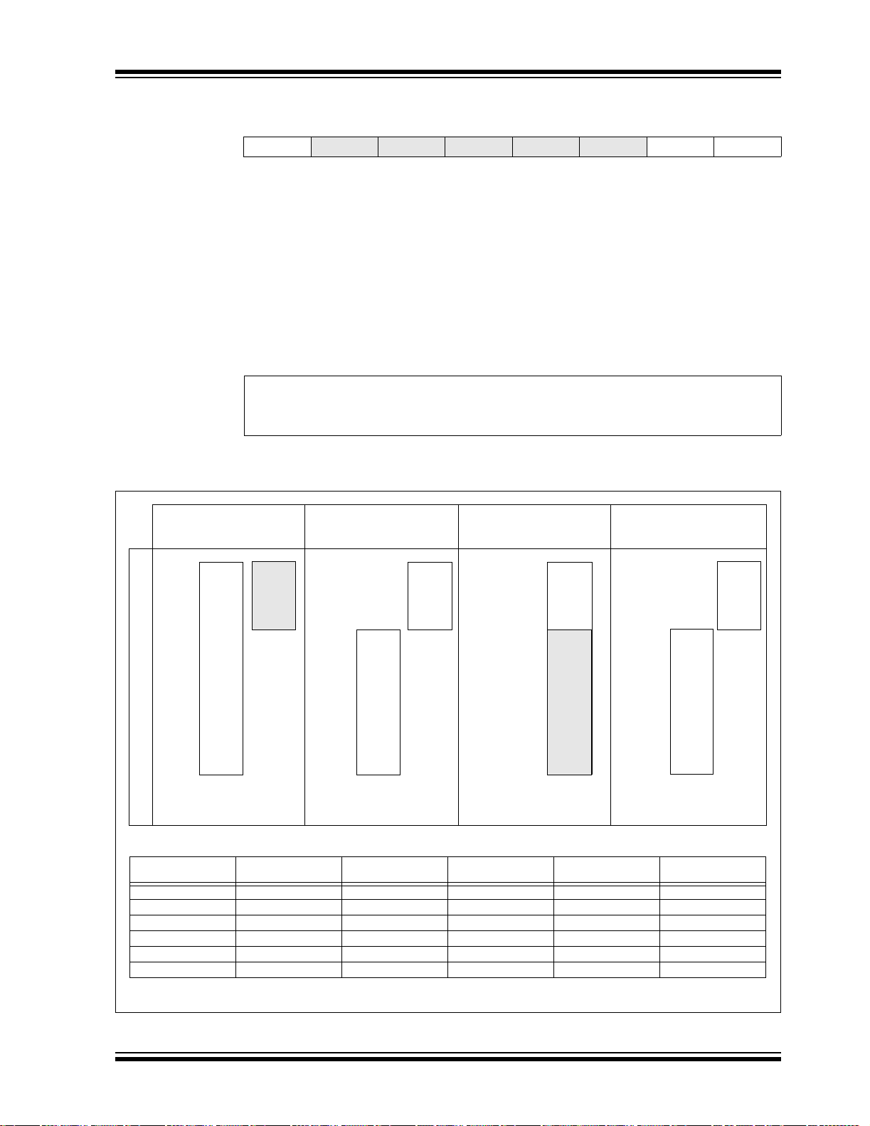
PIC18F6520/8520/6620/8620/6720/8720
REGISTER 4-1: CONFIG3L CONFIGURATION BYTE
R/P-1 U-0 U-0 U-0 U-0 U-0 R/P-1 R/P-1
WAIT — — — — —PM1PM0
bit 7 bit 0
bit 7 WAIT: External Bus Data Wait Enable bit
1 = Wait selections unavailable, device will not wait
0 = Wait programmed by WAIT1 and WAIT0 bits of MEMCOM register (MEMCOM<5:4>)
bit 6-2 Unimplemented: Read as ‘0’
bit 1-0 PM1:PM0: Processor Data Memory Mode Select bits
11 = Microcontroller mode
10 = Microprocessor mode
01 = Microcontroller with Boot Block mode
00 = Extended Microcontroller mode
Legend:
R = Readable bit P = Programmable bit U = Unimplemented bit, read as ‘0’
- n = Value after erase ‘1’ = Bit is set ‘0’ = Bit is cleared x = Bit is unknown
FIGURE 4-2: MEMORY MAPS FOR PIC18F8X20 PROGRAM MEMORY MODES
Extended
Microcontroll er
Mode (EMC)
External
Program
Memory
External On-Chip
Memory Flash
(1)
Memory Mode(s)
Available
000000h
Boot
Boot+1
1FFFFFh
Microprocessor
with Boot Block
Mode (MPBB)
External
Program
Memory
External
Memory Flash
On-Chip
Program
Memory
On-Chip
Microcontroll er
000000h
Boundary
Boundary+1
1FFFFFh
Mode (MC)
On-Chip
On-Chip
Program
Memory
Reads
‘0’s
Flash
000000h
Boundary
Boundary+1
1FFFFFh
Microprocessor
Mode (MP)
000000h
External
Program
Memory
Program Space Execution
1FFFFFh
External
Memory Flash
Boundary Values for Microprocessor with Boot Block, Microcontroller and Extended Microcontroller modes
Device Boot Boot+1 Boundary Boundary+1
PIC18F6520 0007FFh 000800h 007FFFh 008000h MC
PIC18F6620 0001FFh 000200h 00FFFFh 010000h MC
PIC18F6720 0001FFh 000200h 01FFFFh 020000h MC
PIC18F8520 0007FFh 000800h 007FFFh 008000h MP, MPBB, MC, EMC
PIC18F8620 0001FFh 000200h 00FFFFh 010000h MP, MPBB, MC, EMC
PIC18F8720 0001FFh 000200h 01FFFFh 020000h MP, MPBB, MC, EMC
Note 1: PIC18F6X20 devices are included here for completeness, to show the boundaries of their Boot Blocks and program memory spaces.
On-Chip
Program
Memory
(No
access)
On-Chip
On-Chip
Program
Memory
2004 Microchip Technology Inc. DS39609B-page 41

PIC18F6520/8520/6620/8620/6720/8720
4.2 Return Address Stack
The return address s tack allows any combination of up
to 31 program calls and interrupts to occur. The PC
(Program Counter) is pushed onto the stack when a
CALL or RCALL instruction is executed, or an interrupt
is Acknowledged. The PC value is pulled off the stack
on a RETURN, RETLW or a RETFIE instruction. PCLATU
and PCLATH are not affected by any of the RETURN or
CALL instructions.
The stack operates as a 31-word by 21-bit RAM and a
5-bit stack pointer, with the stack pointer initialized to
00000b after all Resets. There is no RAM associated
with stack pointer 00000b. This is only a Reset value.
During a CALL type instruc tion, causing a pu sh onto the
stack, the stack pointer is first incremented and the
RAM location pointed to by the stack pointer is written
with the contents of the PC. During a RETURN type
instruction, causing a pop from the stack, the contents
of the RAM location pointed to by the STKPTR are
transferred to the PC and then the stack pointer is
decremented.
The stack space is not part of either program or data
space. The stack po inter is r eadabl e and writabl e and
the address on the top of the stac k is readab le and writable through SFR registers. Data can also be pushed
to, or popped from the stack using the top-of-stack
SFRs. Status bits indicate if the stack pointer is at, or
beyond the 31 levels provided.
4.2.1 TOP-OF-STACK ACCESS
The top of the stack is readable and writable. Three
register locations, TOSU, TOSH and TOSL, hold the
contents of the stack location pointed to by the
STKPTR register. This allows users to implement a
software stack if necessary. After a CALL, RCALL or
interrupt, the software can read the pushed value by
reading the TOSU, TOSH and TOSL registers. These
values can be placed on a us er defined s oftware st ack.
At return time, the software can replace the TOSU,
TOSH and TOSL and do a return.
The user must disable the global interrupt enable bits
during this time to prevent inadvertent stack
operations.
4.2.2 RETURN STACK POINTER (STKPTR)
The STKPTR register contains the stack pointer value,
the STKFUL (Stack Full) status bit and the STKUNF
(Stack Underflow) status bits. Register 4-2 shows the
STKPTR register. The value of the stack pointer can be
0 through 31. The stack pointer increments when values are pushed onto the stack and decrements when
values are popped off the stack. At Reset, the stack
pointer value will be ‘0’. The user may read and write
the stack pointer value. This feature can be used by a
Real-Time Operating System for return stack
maintenance.
After the PC is pus hed on to the st ack 31 tim es (wi thout
popping any values off the stack), the STKFUL bit is
set. The STKFUL bit can on ly be cleared in so ftware or
by a POR.
The action that takes place when the stack becomes
full, depends on the state of the STVREN (Stack Overflow Reset Enable) configuration bit. Refer to
Section 24.0 “Instruction Set Summary” for a
description of the device configuration bits. If STVREN
is set (default), the 31st push will push the (PC + 2)
value onto the stack, set the STKFUL bit and reset the
device. The STKFUL bit will remain set and the stack
pointer will be set to ‘0’.
If STVREN is cleared, the STKFUL bit will be set on the
31st push and the stack pointer will increment to 31.
Any additional pushes will not overwrite the 31st push
and STKPTR will remain at 31.
When the stack has been popped enough times to
unload the stac k, the next pop will ret urn a value of zero
to the PC and sets the STKUNF bit, while the stack
pointer remains at ‘0’. The STKUNF bit will remain set
until cleared in software or a POR occurs.
Note: Returning a value of zero to the PC on an
underflow has the effect of vectoring the
program to the Reset vector, where the
stack conditions can be verified and
appropriate actions can be taken.
DS39609B-page 42 2004 Microchip Technology Inc.

PIC18F6520/8520/6620/8620/6720/8720
REGISTER 4-2: STKPTR REGISTER
R/C-0 R/C-0 U-0 R/W-0 R/W-0 R/W-0 R/W-0 R/W-0
(1)
STKFUL
bit 7 bit 0
bit 7 STKFUL: Stack Full Flag bit
1 = Stack became full or overflowed
0 = Stack has not become full or overflowed
bit 6 STKUNF: Stack Underflow Flag bit
1 = Stack underflow occurred
0 = Stack underflow did not occur
bit 5 Unimplemented: Read as ‘0’
bit 4-0 SP4:SP0: Stack Pointer Location bits
Note 1: Bit 7 and bit 6 can only be cleared in user software or by a POR.
Legend:
R = Readable bit W = Writable bit U = Unimplemented bit, read as ‘0’
- n = Value at POR ‘1’ = Bit is set ‘0’ = Bit is cleared x = Bit is unknown
STKUNF
(1)
— SP4 SP3 SP2 SP1 SP0
FIGURE 4-3: RETURN ADDRESS STACK AND ASSOCIATED REGISTERS
Return Address S t ac k
11111
11110
TOSLTOSHTOSU
0x340x1A0x00
Top-of-Stack
4.2.3 PUSH AND POP INSTRUCTIONS
Since the Top-of-St ac k (TOS) is readable and writable,
the ability to push valu es onto the stack and pull va lues
off the stack, without disturbing normal program
execution, is a des irable optio n. To push the current PC
value onto the stack, a PUSH instruction can be
executed. This wil l increment the s tack pointer and load
the current PC val ue onto the stack. TOSU, T OSH an d
TOSL can then be modified to place a return address
on the stack.
The ability to pull the TOS value off of the stack and
replace it with the value that was previously pushed
onto the stack, without disturbing normal execution, is
achieved by using the POP instruction. The POP
instruction discards th e current TOS by decrem enting
the stack pointer. The previous value pushed onto the
stack then becomes the TOS value.
11101
0x001A34
0x000D58
00011
00010
00001
00000
4.2.4 S TACK FULL/UNDERFLOW RESETS
These Resets are enabled by programming the
STVREN configuration bit. When the STVREN bit is
disabled, a full or underflow condition will set the
appropriate STKFUL or STKUNF bit, but not cause a
device Rese t. Wh en t he ST VRE N bit is en abl ed, a full
or underflow condition will set the appropriate STKFUL
or STKUNF bit and then cause a device Reset. The
STKFUL or STKUNF bits are only cleared by the user
software or a POR Reset.
STKPTR<4:0>
00010
2004 Microchip Technology Inc. DS39609B-page 43

PIC18F6520/8520/6620/8620/6720/8720
4.3 Fast Register Stack
A “fast interrupt return” optio n is available for in terrupts.
A Fast Register Stack is provided for the S tat us, WREG
and BSR registers and is only one in depth. The stack
is not readable or writable and is loaded with the
current value of the corresponding register when the
processor vectors for an interrupt. The values in the
registers are then loaded back into the working registers, if the FAST RETURN instruction is used to return
from the interrupt.
A low or high priority interrupt source will push values
into the stack registers. If both low and high priority
interrupts are enabled, the stack registers cannot be
used reliably for low priority interrupts. If a high priority
interrupt occurs while servicing a low priority interrupt,
the stack register values stored by the low priority
interrupt will be overwritten.
If high priority interrupts are not disabled during low
priority inte rr up ts, us e rs mu st save th e key r eg ist er s in
software during a low priority interrupt.
If no interrupts are used, the fast register stack can be
used to restore the S tatus, WR EG and BSR registers at
the end of a subroutine call. To use the fast register
stack for a subroutine call, a FAST CALL instruction
must be executed.
Example 4-1 shows a source code example that uses
the fast register stack.
EXAMPLE 4-1: FAST REGISTER STACK
CODE EXAMPLE
CALL SUB1, FAST ;STATUS, WREG, BSR
;SAVED IN FAST REGISTER
;STACK
•
•
SUB1 •
•
•
RETURN FAST ;RESTORE VALUES SAVED
;IN FAST REGISTER STACK
4.4 PCL, PCLATH and PCLATU
The program counter ( PC) spe ci fie s th e ad dre ss of th e
instruction to fetch for execution. The PC is 21 bits
wide. The low byte is called the PCL register; this register is readable and writable. The high byte is called
the PCH register. This register contains the PC<15:8>
bits and is not directly readable or writable; updates to
the PCH register may be performed through the
PCLATH register. The upper byte is called PCU. This
register contains th e PC<20 :16> bit s an d is not d irectly
readable or writable; updates to the PCU register may
be performed through the PCLATU register.
The PC addresses bytes in the program memory. To
prevent the PC from becoming misaligned with word
instructions, the LSB of the PCL is fixed to a value of
‘0’. The PC increments by 2 to address sequential
instructions in the program memo ry.
The CALL, RCALL, GOTO and program branch
instructions write to the program counter directly. For
these instructions, the contents of PCLATH and
PCLATU are not transferred to the program counter.
The contents of PCLATH and PCLATU will be transferred to the program counter by an operation that
writes PCL. Similarly, the upper two bytes of the
program counter will be transferred to PCLATH and
PCLATU by an operation that reads PCL. This is useful
for computed offsets to the PC (see Section 4.8.1
“Computed GOTO”).
4.5 Clocking Scheme/Instruction
Cycle
The clock input (from OSC1) is internally divided by
four to generate four non-overlapping quadrature
clocks, namely Q1, Q2, Q3 and Q4. Internally, the
program counter (PC) is incremented every Q1, the
instruction is fetched from the program memory and
latched into the instruction register in Q4. The instruction is decoded and executed during the following Q1
through Q4. The clocks and instruction execution flow
are shown in Figure4-4.
FIGURE 4-4: CLOCK/INSTRUCTION CYCLE
Q2 Q3 Q4
Q1
OSC1
Q1
Q2
Q3
Q4
PC
OSC2/CLKO
(RC mode)
DS39609B-page 44 2004 Microchip Technology Inc.
PC
Execute INST (PC-2)
Fetch INST (PC)
Q2 Q3 Q4
Q1
Execute INST (PC)
Fetch INST (PC+2)
PC+2
Q2 Q3 Q4
Q1
PC+4
Execute INST (PC+2)
Fetch INST (PC+4)
Internal
Phase
Clock

PIC18F6520/8520/6620/8620/6720/8720
4.6 Instruction Flow/Pipelining
An “Instruction Cycle” consists of four Q cycles (Q1,
2004 Microchip Technology Inc. DS39609B-page 45

PIC18F6520/8520/6620/8620/6720/8720
4.7.1 TW O-WORD INSTRUCTIONS
The PIC18FXX20 devices have four two-word instructions: MOVFF, CALL, GOTO and LFSR. The second word
of these instructions has the 4 MSBs set to ‘1’s and is
a special kind of NOP instruction. The lower 12 bits of
the second word cont ain dat a to be used by the instruction. If the first word of the instruction is executed, the
data in the second word is accessed. If the second
word of the instruction is executed by itself (first word
was skipped), it will execute as a NOP. This action is
necessary when the two-word instruction is preceded
by a conditional instruc tion that c hanges t he PC. A pr ogram example tha t demonstr ates this conc ept is show n
in Example 4-3. Refer to Section 24.0 “Instruction
Set Summary” for further details of the inst ruction se t.
EXAMPLE 4-3: TWO-WORD INSTRUCTIONS
CASE 1:
Object Code Source Code
0110 0110 0000 0000 TSTFSZ REG1 ; is RAM location 0?
1100 0001 0010 0011 MOVFF REG1, REG2 ; No, execute 2-word instruction
1111 0100 0101 0110 ; 2nd operand holds address of REG2
0010 0100 0000 0000 ADDWF REG3 ; continue code
CASE 2:
Object Code Source Code
0110 0110 0000 0000 TSTFSZ REG1 ; is RAM location 0?
1100 0001 0010 0011 MOVFF REG1, REG2 ; Yes
1111 0100 0101 0110 ; 2nd operand becomes NOP
0010 0100 0000 0000 ADDWF REG3 ; continue code
4.8 Look-up Tables
Look-up tables are implemented two ways. These are:
• Computed GOTO
• Table Reads
4.8.1 COMPUTED GOTO
A computed GOTO is accomplish ed by adding an offset
to the program counter (ADDWF PCL).
A look-up table can be formed with an ADDWF PCL
instruction and a group of RETLW 0xnn instructions.
WREG is loaded with an offset into the table before
executing a call to tha t t able. The first instruction of the
called routine is the ADDWF PCL instruction. The next
instruction executed will be one of the RETLW 0xnn
instructions, that returns the value 0xnn to the calling
function.
The offset value (va lue in WREG) specifie s the number
of bytes that the program counter should advance.
In this method, only one data byte may be stored in
each instruction location and room on the return
address stack is required.
4.8.2 TABLE READS /TABLE WRITES
A better method of storing data in program memory
allows 2 bytes of data to be stored in each instruction
location.
Look-up table data may be stored 2 bytes per program
word by using tab le reads and writes. The T ab le Pointer
(TBLPTR) specifies the byte address and the Table
Latch (TABLAT) contains the data that is read from, or
written to program memory. Data is transferred to/from
program memory, one byte at a time.
A description of the table read/table write operation is
shown in Section 5.0 “Flash Program Memory”.
DS39609B-page 46 2004 Microchip Technology Inc.

PIC18F6520/8520/6620/8620/6720/8720
4.9 Data Memory Organization
The data memory i s impl emented as static RAM. Each
register in the data memory has a 12-bit address,
allowing up to 4096 bytes of data memory. The data
memory map is in turn divided into 16 banks of
256 bytes each. The lower 4 bits of the Bank Sel ect
Register (BSR<3:0>) select which bank will be
accessed. The upper 4 bits of the BSR are not
implemented.
The data memory space contains both Special Function Registers (SFR) and General Purpose Registers
(GPR). The SFRs are used f or control and st atus of the
controller and peripheral functions, while GPRs are
used for data sto rage and scratch p ad operat ions in the
user’s application. The SFRs start at the la st location of
Bank 15 (0FFFh) and extend downwards . Any remai ning space beyond th e SFR s i n the Bank may be im pl emented as GPRs. GPRs start at the first location of
Bank 0 and grow upwards. Any read of an
unimplemented location will read as ‘0’s.
PIC18FX520 devices have 2048 bytes of data RAM,
extending from Bank 0 to Ba nk 7 (000 h throug h 7FFh).
PIC18FX620 and PIC18FX720 devices have
3840 bytes of data RAM, extending from Bank 0 to
Bank 14 (000h through EFFh). The organization of the
data memory space for these devices is shown in
Figure 4-6 and Figure 4-7.
The entire data memory may be accessed directly or
indirectly. Direct addressing may require the use of th e
BSR register. Indirect addressing requires the use of a
File Select Register (FSRn) and a corresponding Indirect File Operand (INDFn). Each FSR holds a 12-bit
address value that can be used to access any location
in the data memory map without banking.
The instruction set and architecture allow operations
across all banks. This m ay be accompli shed by indirec t
addressing, or by th e use of t he MOVFF inst ruction. Th e
MOVFF instruction is a two-word/two-cycle instruction
that moves a value from one register to another.
To ensure that commonly used registers (SFRs and
select GPRs) can be accessed in a single cycle,
regardless of the current BSR values, an Access Bank
is implemented. A s egment of Ban k 0 and a segm ent of
Bank 15 comprise the Access RAM. Section 4.10
“Access Bank” provides a detailed description of the
Access RAM.
4.9.1 GENERAL PURPOSE REGISTER FILE
The register file can b e access ed eithe r dire ctly o r indirectly. Indirect addressing operates using a File Select
Register and correspond ing Ind irect Fi le Ope rand. Th e
operation of indirect addressing is shown in
Section 4.12 “Indirect Addressing, INDF and FSR
Registers”.
Enhanced MCU devices may have banked memory in
the GPR area. GPRs are not initialized by a Power-on
Reset and are unchan ged on all other Resets.
Data RAM is available for use as General Purpose
Registers by all in structions. The top section of Ban k 15
(F60h to FFFh) contains SFRs. All other banks of data
memory contain GPR registers, starting with Bank 0.
4.9.2 SPECIAL FUNCTION REGISTERS
The Special Function Registers (SFRs) are registers
used by the CPU an d peripheral modul es for controllin g
2004 Microchip Technology Inc. DS39609B-page 47

PIC18F6520/8520/6620/8620/6720/8720
FIGURE 4-6: DATA MEMORY MAP FOR PIC18FX520 DEVICES
DS39609B-page 48 2004 Microchip Technology Inc.

PIC18F6520/8520/6620/8620/6720/8720
FIGURE 4-7: DATA MEMORY MAP FOR PIC18FX620 AND PIC18FX720 DEVICES
BSR<3:0>
= 0000
= 0001
= 0010
= 0011
= 0100
= 0101
•
•
•
= 1101
= 1110
= 1111
When a = 1,
the BSR is used to specify the
RAM location that the instruction
uses.
Bank 0
FFh
Bank 1
FFh
Bank 2
FFh
Bank 3
FFh
Bank 4
Bank 5
to
Bank 13
Bank 14
FFh
Bank 15
FFh
Data Memory Map
00h
Access RAM
GPRs
00h
00h
00h
00h
00h
GPRs
GPRs
GPRs
GPRs
GPRs
GPRs
Unused
SFRs
000h
05Fh
060h
0FFh
100h
1FFh
200h
2FFh
300h
3FFh
400h
4FFh
500h
DFFh
E00h
EFFh
F00h
F5Fh
F60h
FFFh
Access Bank
Access RAM Low
Access RAM High
(SFRs)
When a = 0,
the BSR is ignored and the
Access Bank is used.
The first 96 bytes are General
Purpose RAM (from Bank 0).
The second 160 bytes are
Special Function Registers
(from Bank 15).
00h
5Fh
60h
FFh
2004 Microchip Technology Inc. DS39609B-page 49

PIC18F6520/8520/6620/8620/6720/8720
TABLE 4-2: SPECIAL FUNCTION REGISTER MAP
Address Name Address Name Address Name Address Name
FFFh TOSU FDFh INDF2
FFEh TOSH FDEh POSTINC2
FFDh TOSL FDDh POSTDEC2
FFCh STKPTR FDCh PREINC2
FFBh PCLATU FDBh PLUSW2
(3)
(3)
(3)
(3)
(3)
FFAh PCLATH FDAh FSR2H FBAh CCP2CON F9Ah TRISJ
FF9h PCL FD9h FSR2L FB9h CCPR3H F99h TRISH
FF8h TBLPTRU FD8h STATUS FB8h CCPR3L F98h TRISG
FF7h TBLPTRH FD7h TMR0H FB7h CCP3CON F97h TRISF
FF6h TBLPTRL FD6h TMR0L FB6h —
FF5h TABLAT FD5h T0CON FB5h CVRCON F95h TRISD
FF4h PRODH FD4h —
(1)
FF3h PRODL FD3h OSCCON FB3h TMR3H F93h TRISB
FF2h INTCON FD2h LVDCON FB2h TMR3L F92h TRISA
FF1h INTCON2 FD1h WDTCON FB1h T3CON F91h LATJ
FF0h INTCON3 FD0h RCON FB0h PSPCON F90h LATH
(3)
FEFh INDF0
FEEh POSTINC0
FEDh POSTDEC0
FECh PREINC0
FEBh PLUSW0
FCFh TMR1H FAFh SPBRG1 F8Fh LATG
(3)
FCEh TMR1L FAEh RCREG1 F8Eh LATF
(3)
FCDh T1CON FADh TXREG1 F8Dh LATE
(3)
FCCh TMR2 FACh TXSTA1 F8Ch LATD
(3)
FCBh PR2 FABh RCSTA1 F8Bh LATC
FEAh FSR0H FCAh T2CON FAAh EEADRH F8Ah LATB
FE9h FSR0L FC9h SSPBUF FA9h EEADR F89h LATA
FE8h WREG FC8h SSPADD FA8h EEDATA F88h PORTJ
(3)
FE7h INDF1
FE6h POSTINC1
FE5h POSTDEC1
FE4h PREINC1
FE3h PLUSW1
FC7h SSPSTAT FA7h EECON2 F87h PORTH
(3)
FC6h SSPCON1 FA6h EECON1 F86h PORTG
(3)
FC5h SSPCON2 FA5h IPR3 F85h PORTF
(3)
FC4h ADRESH FA4h PIR3 F84h PORTE
(3)
FC3h ADRESL FA3h PIE3 F83h PORTD
FE2h FSR1H FC2h ADCON0 FA2h IPR2 F82h PORTC
FE1h FSR1L FC1h ADCON1 FA1h PIR2 F81h PORTB
FE0h BSR FC0h ADCON2 FA0h PIE2 F80h PORTA
FBFh CCPR1H F9Fh IPR1
FBEh CCPR1L F9Eh PIR1
FBDh CCP1CON F9Dh PIE1
FBCh CCPR2H F9Ch MEMCON
FBBh CCPR2L F9Bh —
(1)
F96h TRISE
FB4h CMCON F94h TRISC
(2)
(1)
Note 1: Unimplement ed registers are read as ‘0’.
2: This register is unused on PIC18F6X20 devices. Always maintain this register clear.
3: This is not a physical register.
DS39609B-page 50 2004 Microchip Technology Inc.

PIC18F6520/8520/6620/8620/6720/8720
TABLE 4-2: SPECIAL FUNCTION REGISTER MAP (CONTINUED)
Address Name Address Name Address Name Address Name
F7Fh —
F7Eh —
F7Dh —
F7Ch —
F7Bh —
F7Ah —
F79h —
(1)
(1)
(1)
(1)
(1)
(1)
(1)
F5Fh —
F5Eh —
F5Dh —
F5Ch —
F5Bh —
F5Ah —
F59h —
F78h TMR4 F58h —
F77h PR4 F57h —
F76h T4CON F56h —
F75h CCPR4H F55h —
F74h CCPR4L F54h —
F73h CCP4CON F53h —
F72h CCPR5H F52h —
F71h CCPR5L F51h —
F70h CCP5CON F50h —
F6Fh SPBRG2 F4Fh —
F6Eh RCREG2 F4Eh —
F6Dh TXREG2 F4Dh —
F6Ch TXSTA2 F4Ch —
F6Bh RCSTA2 F4Bh —
F6Ah —
F69h —
F68h —
F67h —
F66h —
F65h —
F64h —
F63h —
F62h —
F61h —
F60h —
(1)
(1)
(1)
(1)
(1)
(1)
(1)
(1)
(1)
(1)
(1)
F4Ah —
F49h —
F48h —
F47h —
F46h —
F45h —
F44h —
F43h —
F42h —
F41h —
F40h —
(1)
(1)
(1)
(1)
(1)
(1)
(1)
(1)
(1)
(1)
(1)
(1)
(1)
(1)
(1)
(1)
(1)
(1)
(1)
(1)
(1)
(1)
(1)
(1)
(1)
(1)
(1)
(1)
(1)
(1)
(1)
(1)
F3Fh —
F3Eh —
F3Dh —
F3Ch —
F3Bh —
F3Ah —
F39h —
F38h —
F37h —
F36h —
F35h —
F34h —
F33h —
F32h —
F31h —
F30h —
F2Fh —
F2Eh —
F2Dh —
F2Ch —
F2Bh —
F2Ah —
F29h —
F28h —
F27h —
F26h —
F25h —
F24h —
F23h —
F22h —
F21h —
F20h —
(1)
(1)
(1)
(1)
(1)
(1)
(1)
(1)
(1)
(1)
(1)
(1)
(1)
(1)
(1)
(1)
(1)
(1)
(1)
(1)
(1)
(1)
(1)
(1)
(1)
(1)
(1)
(1)
(1)
(1)
(1)
(1)
F1Fh —
F1Eh —
F1Dh —
F1Ch —
F1Bh —
F1Ah —
F19h —
F18h —
F17h —
F16h —
F15h —
F14h —
F13h —
F12h —
F11h —
F10h —
F0Fh —
F0Eh —
F0Dh —
F0Ch —
F0Bh —
F0Ah —
F09h —
F08h —
F07h —
F06h —
F05h —
F04h —
F03h —
F02h —
F01h —
F00h —
(1)
(1)
(1)
(1)
(1)
(1)
(1)
(1)
(1)
(1)
(1)
(1)
(1)
(1)
(1)
(1)
(1)
(1)
(1)
(1)
(1)
(1)
(1)
(1)
(1)
(1)
(1)
(1)
(1)
(1)
(1)
(1)
Note 1: Unimplement ed registers are read as ‘0’.
2: This register is not available on PIC18F6X20 devices.
3: This is not a physical register.
2004 Microchip Technology Inc. DS39609B-page 51

PIC18F6520/8520/6620/8620/6720/8720
TABLE 4-3: REGISTER FILE SUMMARY
File Name Bit 7 Bit 6 Bit 5 Bit 4 Bit 3 Bit 2 Bit 1 Bit 0
TOSU
TOSH Top-of-Stack High Byte (TOS<15:8>) 0000 0000 32, 42
TOSL Top-of-Stack Low Byte (TOS<7:0>) 0000 0000 32, 42
STKPTR STKFUL STKUNF
PCLATU
PCLATH Holding Register for PC<15:8> 0000 0000 32, 44
PCL PC Low Byte (PC<7:0>) 0000 0000 32, 44
TBLPTRU
TBLPTRH Program Memory Table Pointer High Byte (TBLPTR<15:8>) 0000 0000 32, 64
TBLPTRL Program Memory T able Pointer Low Byte (TBLPTR<7:0>) 0000 0000 32, 64
TABLAT Program Memory Table Latch 0000 0000 32, 64
PRODH Product Register High Byte xxxx xxxx 32, 85
PRODL Product Register Low Byte xxxx xxxx 32, 85
INTCON GIE/GIEH PEIE/GIEL TMR0IE INT0IE RBIE TMR0IF INT0IF RBIF 0000 0000 32, 89
INTCON2 RBPU INTEDG0 INTEDG1 INTEDG2 INTEDG3 TMR0IP INT3IP RBIP 1111 1111 32, 90
INTCON3 INT2IP INT1IP INT3IE INT2IE INT1IE INT3IF INT2IF INT1IF 1100 0000 32, 91
INDF0 Uses contents of FSR0 to address data memory – value of FSR0 not changed (not a physical register) n/a 57
POSTINC0 Uses contents of FSR0 to address data memory – value of FSR0 post-incremented
POSTDEC0 Uses contents of FSR0 to address data memory – value of FSR0 post-decremented
PREINC0 Uses contents of FSR0 to address data memory – value of FSR0 pre-incremented (not a physical register) n/a 57
PLUSW0 Uses contents of FSR0 to address data memory – value of FSR0 pre-incremented
FSR0H
FSR0L Indirect Data Memory Address Pointer 0 Low Byte xxxx xxxx 32, 57
WREG Working Register xxxx xxxx 32
INDF1 Uses contents of FSR1 to address data memory – value of FSR1 not changed (not a physical register) n/a 57
POSTINC1 Uses contents of FSR1 to address data memory – value of FSR1 post-incremented
POSTDEC1 Uses contents of FSR1 to address data memory – value of FSR1 post-decremented
PREINC1 Uses contents of FSR1 to address data memory – value of FSR1 pre-incremented
PLUSW1 Uses contents of FSR1 to address data memory – value of FSR1 pre-incremented
FSR1H
FSR1L Indirect Data Memory Address Pointer 1 Low Byte xxxx xxxx 33, 57
BSR
INDF2 Uses contents of FSR2 to address data memory – value of FSR2 not changed (not a physical register) n/a 57
POSTINC2 Uses contents of FSR2 to address data memory – value of FSR2 post-incremented
POSTDEC2 Uses contents of FSR2 to address data memory – value of FSR2 post-decremented
Legend: x = unknown, u = unchanged, – = unimplemented, q = value depends on condition
Note 1: RA6 and associated bits are configured as port pins in RCIO and ECIO Oscillator modes only and read ‘0’ in all other os cillator
2: Bit 21 of the TBLPTRU allows access to the device configuration bits.
3: These registers are unused on PIC18F6X20 devices ; always maintain these clear.
— — — Top-of-Stack Upper Byte (TOS<20:16>) ---0 0000 32, 42
— Return Stack Pointer 00-0 0000 32, 43
— — bit 21 Holding Register for PC<20:16> --10 0000 32, 44
— —bit 21
(not a physical register)
(not a physical register)
(not a physical register) – value of FSR0 offset by value in WREG
— — — — Indirect Data Memory Address Pointer 0 High Byte ---- 0000 32, 57
(not a physical register)
(not a physical register)
(not a physical register)
(not a physical register) – value of FSR1 offset by value in WREG
— — — — Indirect Data Memory Address Pointer 1 High Byte ---- 0000 33, 57
— — — — Bank Select Register ---- 0000 33, 56
(not a physical register)
(not a physical register)
modes.
(2)
Program Memory Table Pointer Upp er Byt e (TB LP T R<2 0:1 6> ) --00 0000 32, 64
Value on
POR, BOR
n/a 57
n/a 57
n/a 57
n/a 57
n/a 57
n/a 57
n/a 57
n/a 57
n/a 57
Details
on page:
DS39609B-page 52 2004 Microchip Technology Inc.

PIC18F6520/8520/6620/8620/6720/8720
TABLE 4-3: REGISTER FILE SUMMARY (CONTINUED)
File Name Bit 7 Bit 6 Bit 5 Bit 4 Bit 3 Bit 2 Bit 1 Bit 0
PREINC2 Uses contents of FSR2 to address data memory – value of FSR2 pre-incremented
PLUSW2 Uses contents of FSR2 to address data memory – value of FSR2 pre-incremented
FSR2H
FSR2L Indirect Data Memory Address Pointer 2 Low Byte xxxx xxxx 33, 57
STATUS
TMR0H Timer0 Register High Byte 0000 0000 33, 133
TMR0L Timer0 Register Low Byte xxxx xxxx 33, 133
T0CON TMR0ON T08BIT T0CS T0SE PSA T0PS2 T0PS1 T0PS0 1111 1111 33, 131
OSCCON
LVDCON
WDTCON
RCON IPEN
TMR1H Timer1 Register High Byte xxxx xxxx 33, 135
TMR1L Timer1 Register Low Byte xxxx xxxx 33, 135
T1CON RD16
TMR2 Timer2 Register 0000 0000 33, 141
PR2 Timer2 Period Register 1111 1111 33, 142
T2CON
SSPBUF SSP Receive Buffer/Transmit Register xxxx xxxx 33, 157
SSPADD SSP Address Register in I
SSPSTAT SMP CKE D/A
SSPCON1 WCOL SSPOV SSPEN CKP SSPM3 SSPM2 SSPM1 SSPM0 0000 0000 33, 168
SSPCON2 GCEN ACKSTAT ACKDT ACKEN RCEN PEN RSEN SEN 0000 0000 33, 169
ADRESH A/D Result Register High Byt e xxxx xxxx 34, 215
ADRESL A/D Result Register Low Byte xxxx xxxx 34, 215
ADCON0
ADCON1
ADCON2 ADFM
CCPR1H Capture/Compare/PWM Register 1 High Byte xxxx xxxx 34, 151,
CCPR1L Capture/Compare/PWM Register 1 Low Byte xxxx xxxx 34, 151,
CCP1CON
CCPR2H Capture/Compare/PWM Register 2 High Byte xxxx xxxx 34, 151,
CCPR2L Capture/Compare/PWM Register 2 Low Byte xxxx xxxx 34, 151,
CCP2CON
Legend: x = unknown, u = unchanged, – = unimplemented, q = value depends on condition
Note 1: RA6 and associated bits are configured as port pins in RCIO and ECIO Oscillator modes only and read ‘0’ in all other oscillator
(not a physical register)
(not a physical register) – value of FSR2 offset by value in WREG
— — — — Indirect Data Memory Address Pointer 2 High Byte ---- 0000 33, 57
— — —NOVZDCC---x xxxx 33, 59
— — — — — — —SCS---- ---0 25, 33
— — IRVST LVDEN LVDL3 LVDL2 LVDL1 LVDL0 --00 0101 33, 235
— — — — — — —SWDTE---- ---0 33, 250
— —RITO PD POR BOR 0--1 11qq 33, 60,
— T1CKPS1 T1CKPS0 T1OSCEN T1SYNC TMR1CS TMR1ON 0-00 0000 33, 135
— T2OUTPS3 T2OUTPS2 T2OUTPS1 T2OUTPS0 TMR2ON T2CKPS1 T2CKPS0 -000 0000 33, 141
2
C Slave mode. SSP Baud Rate Reload Register in I2C Master mode. 0000 0000 33, 166
PSR/WUA BF 0000 0000 33, 158
— — CHS3 CHS2 CHS1 CHS0 GO/DONE ADON --00 0000 34, 213
— — VCFG1 VCFG0 PCFG3 PCFG2 PCFG1 PCFG0 --00 0000 34, 214
— — — — ADCS2 ADCS1 ADCS0 0--- -000 34, 215
— — DC1B1 DC1B0 CCP1M3 CCP1M2 CCP1M1 CCP1M0 --00 0000 34, 149
— — DC2B1 DC2B0 CCP2M3 CCP2M2 CCP2M1 CCP2M0 --00 0000 34, 149
modes.
2: Bit 21 of the TBLPTRU allows access to the device configuration bits.
3: These registers are unused on PIC18F6X20 devices ; always maintain these clear.
Value on
POR, BOR
n/a 57
n/a 57
Details
on page:
101
152
152
152
152
2004 Microchip Technology Inc. DS39609B-page 53

PIC18F6520/8520/6620/8620/6720/8720
TABLE 4-3: REGISTER FILE SUMMARY (CONTINUED)
File Name Bit 7 Bit 6 Bit 5 Bit 4 Bit 3 Bit 2 Bit 1 Bit 0
CCPR3H Capture/Compare/PWM Register 3 High Byte xxxx xxxx 34, 151,
CCPR3L Capture/Compare/PWM Register 3 Low Byte xxxx xxxx 34, 151,
CCP3CON
CVRCON CVREN CVROE CVRR CVRSS CVR3 CVR2 CVR1 CVR0 0000 0000 34, 229
CMCON C2OUT C1OUT C2INV C1INV CIS CM2 CM1 CM0 0000 0000 34, 223
TMR3H Timer3 Register High Byte xxxx xxxx 34, 143
TMR3L Timer3 Register Low Byte xxxx xxxx 34, 143
T3CON RD16 T3CCP2 T3CKPS1 T3CKPS0 T3CCP1 T3SYNC
PSPCON IBF OBF IBOV PSPMODE
SPBRG1 USART1 Baud Rate Generator 0000 0000 34, 205
RCREG1 USART1 Receive Register 0000 0000 34, 206
TXREG1 USART1 Transmit Register 0000 0000 34, 204
TXSTA1 CSRC TX9 TXEN SYNC
RCSTA1 SPEN RX9 SREN CREN ADDEN FERR OERR RX9D 0000 000x 34, 199
EEADRH
EEADR Data EEPROM Address Register 0000 0000 34, 79
EEDATA Data EEPROM Data Register 0000 0000 34, 79
EECON2 Data EEPROM Control Register 2 (not a physical register) ---- ---- 34, 79
EECON1 EEPGD CFGS
IPR3
PIR3
PIE3
IPR2
PIR2
PIE2
IPR1 PSPIP ADIP RCIP TXIP SSPIP CCP1IP TMR2IP TMR1IP 0111 1111 35, 98
PIR1 PSPIF ADIF RCIF TXIF SSPIF CCP1IF TMR2IF TMR1IF 0000 0000 35, 92
PIE1 PSPIE ADIE RCIE TXIE SSPIE CCP1IE TMR2IE TMR1IE 0000 0000 35, 95
MEMCON
(3)
TRISJ
(3)
TRISH
TRISG
TRISF Data Direction Control Register for PORTF 1111 1111 35, 117
TRISE Data Direction Control Register for PORTE 1111 1111 35, 114
TRISD Data Direction Control Register for PORTD 1111 1111 35, 111
TRISC Data Direction Control Register for PORTC 1111 1111 35, 109
TRISB Data Direction Control Register for PORTB 1111 1111 35, 106
TRISA
Legend: x = unknown, u = unchanged, – = unimplemented, q = value depends on condition
Note 1: RA6 and associated bits are configured as port pins in RCIO and ECIO Oscillator modes only and read ‘0’ in all other os cillator
2: Bit 21 of the TBLPTRU allows access to the device configuration bits.
3: These registers are unused on PIC18F6X20 devices ; always maintain these clear.
— — DC3B1 DC3B0 CCP3M3 CCP3M2 CCP3M1 CCP3M0 --00 0000 34, 149
TMR3CS TMR3ON 0000 0000 34, 143
— — — — 0000 ---- 34, 129
—BRGHTRMTTX9D0000 -010 34, 198
— — — — — — EE Adr Register High ---- --00 34, 79
— FREE WRERR WREN WR RD xx-0 x000 34, 80
— — RC2IP TX2IP TMR4IP CCP5IP CCP4IP CCP3IP --11 1111 35, 100
— — RC2IF TX2IF TMR4IF CCP5IF CCP4IF CCP3IF --00 0000 35, 94
— — RC2IE TX2IE TMR4IE CCP5IE CCP4IE CCP3IE --00 0000 35, 97
—CMIP— EEIP BCLIP LVDIP TMR3IP CCP2IP -1-1 1111 35, 99
—CMIF— EEIF BCLIF LVDIF TMR3IF CCP2IF -0-0 0000 35, 93
—CMIE— EEIE BCLIE LVDIE TMR3IE CCP2IE -0-0 0000 35, 96
(3)
EBDIS —WAIT1WAIT0— —WM1WM00-00 --00 35, 71
Data Direction Control Register for PORTJ 1111 1111 35, 125
Data Direction Control Register for PORTH 1111 1111 35, 122
— — — Data Direction Control Register for PORTG ---1 1111 35, 120
— TRISA6
modes.
(1)
Data Direction Control Register for PORTA -111 1111 35, 103
Value on
POR, BOR
Details
on page:
152
152
DS39609B-page 54 2004 Microchip Technology Inc.

PIC18F6520/8520/6620/8620/6720/8720
(3)
LATJ
LATH
LATG
LATF Read PORTF Data Latch, Write PORTF Data Latch xxxx xxxx 35, 117
LATE Read PORTE Data Latch, Write PORTE Data Latch xxxx xxxx 35, 114
LATD Read PORTD Data Latch, Write PORTD Data Latch xxxx xxxx 35, 111
LATC Read PORTC Data Latch, Write PORTC Data Latch xxxx xxxx 35, 109
LATB Read PORTB Data Latch, Write PORTB Data Latch xxxx xxxx 35, 106
LATA
PORTJ
PORTH
PORTG
PORTF Read PORTF pins, Write PORTF Data Latch xxxx xxxx 36, 117
PORTE Read PORTE pins, Write PORTE Data Latch xxxx xxxx 36, 114
PORTD Read PORTD pins, Write PORTD Data Latch xxxx xxxx 36, 111
PORTC Read PORTC pins, Write PORTC Data Latch xxxx xxxx 36, 109
PORTB Read PORTB pins, Write PORTB Data Latch xxxx xxxx 36, 106
PORTA
TMR4 Timer4 Register 0000 0000 36, 148
PR4 Timer4 Period Register 1111 1111 36, 148
T4CON
CCPR4H Capture/Compare/PWM Register 4 High Byte xxxx xxxx 36, 151,
CCPR4L Capture/Compare/PWM Register 4 Low Byte xxxx xxxx 36, 151,
CCP4CON
CCPR5H Capture/Compare/PWM Register 5 High Byte xxxx xxxx 36, 151,
CCPR5L Capture/Compare/PWM Register 5 Low Byte xxxx xxxx 36, 151,
CCP5CON
SPBRG2 USART2 Baud Rate Generator 0000 0000 36, 205
Read PORTJ Data Latch, Write PORTJ Data Latch xxxx xxxx 35, 125
(3)
Read PORTH Data Latch, Write PORTH Data Latch xxxx xxxx 35, 122
— — — Read PORTG Data Latch, Write PORTG Data Latch ---x xxxx 35, 120
(3)
(3)
—LATA6
Read PORTJ pins, Write PORTJ Data Latch xxxx xxxx 36, 125
Read PORTH pins, Write PORTH Data Latch xxxx xxxx 36, 122
— — — Read PORTG pins, Write POR TG Data Latch ---x xxxx 36, 120
—RA6
— T4OUTPS3 T4OUTPS2 T4OUTPS1 T4OUTPS0 TMR4ON T4CKPS1 T4CKPS0 -000 0000 36, 147
— — DC4B1 DC4B0 CCP4M3 CCP4M2 CCP4M1 CCP4M0 0000 0000 36, 149
— — DC5B1 DC5B0 CCP5M3 CCP5M2 CCP5M1 CCP5M0 0000 0000 36, 149
(1)
Read PORT A Data Latch, Write PORTA Data Latch
(1)
Read PORT A pins, Write PORTA Data Latch
(1)
(1)
-xxx xxxx 35, 103
-x0x 0000 36, 103
152
152
152
152
2004 Microchip Technology Inc. DS39609B-page 55
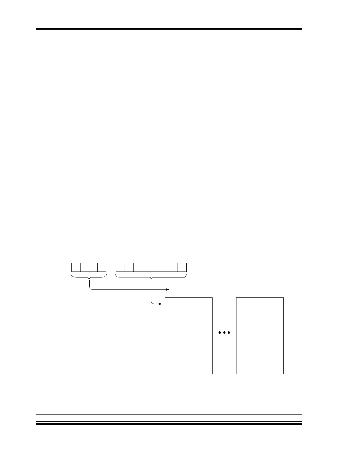
PIC18F6520/8520/6620/8620/6720/8720
4.10 Access Bank
The Access Bank is an architectural enhancement,
which is very useful for C compiler code optimization.
The techniques used by the C compiler may also be
useful for programs written in assembly.
This data memory region can be used for:
• Intermediate computational values
• Local variables of subroutines
• Faster context saving/switching of variables
• Common variables
• Faster evaluation/control of SFRs (no banking)
The Access Bank is comprised of the upper 160 bytes
in Bank 15 (SFRs) and the lower 96 bytes in Bank 0.
These two sections will be referred to as Access RAM
High and Access RAM Low, respectively. Figure 4-7
indicates the Access RAM areas.
A bit in the instruction word spec ifie s if the opera tion is
to occur in the bank spec ifi ed by the BSR register or in
the Access Bank. This bit is denoted by the ‘a’ bit (for
access bit).
When forced in the Access Bank (a = 0), the last
address in Access RAM Low is followed by the first
address in Access RAM High. Access RAM High maps
the Special Function Re gisters, so th at these r egisters
can be accessed without any software overhead. This is
useful for testing status flags and modifying control bits.
4.1 1 Bank Select Register (BSR)
The need for a large general purpose memory space
dictates a RAM banking scheme. The data memory is
partitioned into sixteen banks. When using direct
addressing, the BSR should be configured for the
desired bank.
BSR<3:0> holds the upper 4 bits of the 12-bit RAM
address. The BSR<7:4> bits will always read ‘0’s an d
writes will have no effect.
A MOVLB instruction has been provided in the
instruction set to assist in selecting banks.
If the currently selected bank is not implemented, any
read will return all ‘0’s and all writes are ignored. The
Stat us register bit s will be set/clea red as appropriate for
the instruction performed.
Each Bank extends up to FFh (256 bytes). All data
memory is implemented as static RAM.
A MOVFF instr uctio n igno res t he BSR, sinc e the 12-bit
addresses are embedded into the instruction word.
Section 4.12 “Indirect Addressing, INDF and FSR
Registers” provides a description of indirect address-
ing, which allows linear addressing of the entire RAM
space.
FIGURE 4-8: DIRECT ADDRESSING
Direct Addressing
BSR<3:0> 7
Bank Select
Note 1: For register file map detail, see Table 4-2.
(2)
2: The ac cess bit o f the instruct ion can be used to force an override of the selected bank ( BSR <3:0>) to the
registers of the Access Bank.
3: The MOVFF instruction embeds the entire 12-bit address in the instruction.
Location Select
From Opcode
Data
Memory
(3)
(1)
(3)
0
00h 01h 0Eh 0Fh
000h
0FFh
100h
1FFh
E00h
EFFh
Bank 0 Bank 1 Bank 14 Bank 15
F00h
FFFh
DS39609B-page 56 2004 Microchip Technology Inc.

PIC18F6520/8520/6620/8620/6720/8720
4.12 Indirect Addressing, INDF and FSR Registers
Indirect addressing is a mode of addressing dat a memory, where the data memory address in the instruction
is not fixed. An FSR regis ter i s u sed as a poi nte r to th e
data memory location that i s to be read or written. Since
this pointer is in RAM, the cont en t s c an be mo difi ed by
the program. This can be useful for data tables in the
data memory and for software stacks. Figure 4-9
shows the operation of indirect addressing. This shows
the moving of the value to the data memory address,
specified b y the value of the FSR regi ster.
Indirect addressing is possible by using one of the
INDF registers. Any ins tru cti on u si ng the IN DF reg ist er
actually accesses the register pointed to by the File
Select Register, FSR. Reading the INDF register itself,
indirectly (FSR = 0), will read 00h. Writing to the INDF
register indirectly, results in a no operation. The FSR
register contains a 12-bit address, which is shown in
Figure 4-10.
The INDFn register is not a physical register. Addressing INDFn actually addresses the register whose
address is contained in the FSRn register (FSRn is a
pointer). This is indirect addressing.
Example 4-4 shows a simple use of indirect add ressing
to clear the RAM in Bank 1 (locations 100h-1FFh) in a
minimum number of instructions.
EXAMPLE 4-4: HOW TO CLEAR RAM
(BANK 1) USING
INDIRECT ADDRESSING
LFSR FSR0 ,0x100 ;
NEXT CLRF POSTINC0 ; Clear INDF
; register and
; inc pointer
BTFSS FSR0H, 1 ; All done with
; Bank 1?
GOTO NEXT ; NO, clear next
CONTINUE ; YES, continue
There are three indirect addressing registers. To
address the entire data memory space (4096 bytes),
these registers are 12 bits wide. To store the 12 bits of
addressing information, two 8-bit registers are
required. These indirect addres si ng regi ste r s are:
1. FSR0: composed of FSR0H:FSR0L
2. FSR1: composed of FSR1H:FSR1L
3. FSR2: composed of FSR2H:FSR2L
In addition, there are registers INDF0, INDF1 and
INDF2, which are not physically implemented. Reading
or writing to these registers activates indirect addressing, with the value in the corresponding FSR register
being the a ddress of the data. If an instruction writes a
value to INDF0, th e v al ue will be w ritten to the address
pointed to by FSR 0H:FSR0L. A read f rom INDF 1 reads
the data from the address pointed to by
FSR1H:FSR1L. INDFn can be used in code anywhere
an operand can be used.
If INDF0, INDF1 or INDF2 are read indirectly via an
FSR, all ‘0’s are read (zero bit is set). Similarly, if
INDF0, INDF1 or INDF2 are written to indirectly, the
operation will be equivale nt to a NOP instruction and the
Status bits are not affected.
4.12.1 INDIRECT ADDRESSING OPERATION
Each FSR register has an INDF register associated
with it, plus four addition al register addresses. Perform ing an operation on one of these five registers
determines how the FSR will be modified during
indirect addressing.
When data access is done to one of the five INDFn
locations, the address selected will configure the FSRn
register to:
• Do nothing to FSRn after an indirect access
(no change) – INDFn.
• Auto-decrement FSRn after an in direct access
(post-decrement) – POSTDECn.
• Auto-increment FSRn after an indirect access
(post-increment) – POSTINCn.
• Auto-in crement FSRn before an indire ct access
(pre-increment) – PREINCn.
• Use the value in the WREG register as an offset
to FSRn. Do not mo dify the va lue of the WREG or
the FSRn register after an indirect access
(no change) – PLUSWn.
When using the auto-increment or auto-decrement
features, the effect on the FSR is not reflected in the
Status register. For example, if the indirect address
causes the FSR to equal ‘0’, the Z bit will not be set.
Incrementing or decrementing an FSR affects all 12
bits. That is, whe n FSRnL overflows from an increment,
FSRnH will be incremented automatically.
Adding these features allows the FSRn to be used as a
stack pointer, in addition to its uses for table operation s
in data memo ry.
Each FSR has an address associated with it that
performs an indexed indirect access. When a data
access to this INDFn location (PLUSWn) occurs, the
FSRn is configured to add the signed value in the
WREG register and the value in FSR to form the
address before an indirect access. The FSR value is
not changed.
If an FSR register contains a value that poin ts to one of
the INDFn, an indirect read will read 00h (zero bit is
set), while an indirect write will be equivalent to a NOP
(Status bits are not affected).
If an indirect addressing operation is done where the target address is an FSRnH or FSRnL register, the write
operation will dominate over the pre- or post-increment/
decrement functions.
2004 Microchip Technology Inc. DS39609B-page 57

PIC18F6520/8520/6620/8620/6720/8720
FIGURE 4-9: INDIRECT ADDRESSING OPERATION
Instruction
Executed
Opcode Address
12
File Address = Access of an Indirect Addressing Register
BSR<3:0>
Instruction
Fetched
Opcode
12
4
8
File
12
FIGURE 4-10: INDIRECT ADDRESSING
Indirect Addressing
FSR Register11
RAM
FSR
0h
FFFh
0
Location Select
0000h
Data
Memory
Note 1: For register file map detail, see Table 4-2.
(1)
0FFFh
DS39609B-page 58 2004 Microchip Technology Inc.

PIC18F6520/8520/6620/8620/6720/8720
4.13 Status Register
The Status register, shown in Register 4-3, contains the
arithmetic status of the ALU. The Status register can be
the destination for any instruction, as with any other register. If the Status register is the destination for an
instruction that affects the Z, DC, C, OV or N bits, then
the write to these five bits is disabled. These bits are set
or cleared according to the device logic. Therefore, the
result of an instruction with the Status register as
destination may be different than intended.
REGISTER 4-3: STATUS REGISTER
U-0 U-0 U-0 R/W-x R/W-x R/W-x R/W-x R/W-x
— — —NOVZDCC
bit 7 bit 0
bit 7-5 Unimplemented: Read as ‘0’
bit 4 N: Negative bit
This bit is used for signed arithmetic (2’s complement). It indicates whether the result was
negative (ALU MSB = 1).
1 = Result was negative
0 = Result was positive
bit 3 OV: Overflow bit
This bit is used for signed arithmetic (2’s complement). It indicates an overflow of the
7-bit magnitude, which causes the sign bit (bit 7) to change state.
1 = Overflow occurred for signed arithmetic (in this arithmetic operation)
0 = No overflow occurred
bit 2 Z: Zero bit
1 = The result of an arithmetic or logic operation is zero
0 = The result of an arithmetic or logic operation is not zero
bit 1 DC: Digit carry/borrow
For ADDWF, ADDLW, SUBLW and SUBWF instructions:
1 = A carry-out from the 4th low-order bit of the result occurred
0 = No carry-out from the 4th low-order bit of the result
Note: For borrow,
2’s complement of the second operand. For rotate (RRF, RLF) instructions, this bit
is loaded with either bit 4 or bit 3 of the source register.
bit 0 C: Carry/borrow
For ADDWF, ADDLW, SUBLW and SUBWF instructions:
1 = A carry-out from the Most Significant bit of the result occurred
0 = No carry-out from the Most Significant bit of the result occurred
Note: For borrow,
2’s complement of the second operand. For rotate (RRF, RLF) instructions, this bit
is loaded with either the high or low-order bit of the source register.
bit
the polarity is reversed. A subtraction is executed by adding the
bit
the polarity is reversed. A subtraction is executed by adding the
For exampl e, CLRF STATUS will clear the upper three
bits and set the Z bit. Thi s leav es the Status register as
000u u1uu (where u = unchanged).
It is recommended, therefore, that only BCF, BSF,
SWAPF, MOVFF and MOVWF instructions are used to alter
the Status register, because these instructions do not
affect the Z, C, DC, OV or N bits from the Status register. For other instructions not affecting any status bits,
see Table 24-1.
Note: The C and DC bits operate as a borrow
and digit borrow bit respectively, in
subtraction.
Legend:
R = Readable bit W = Writable bit U = Unimplemented bit, read as ‘0’
- n = Value at POR ‘1’ = Bit is set ‘0’ = Bit is cleared x = Bit is unkno wn
2004 Microchip Technology Inc. DS39609B-page 59
PIC18F6520/8520/6620/8620/6720/8720
4.14 RCON Register
The Reset Control (RCON) register contains flag bits
that allow differentiation between the sources of a
device Reset. These flags include the TO
BOR
and RI bits. This re gister is reada ble and w ritabl e.
REGISTER 4-4: RCON REGISTER
R/W-0 U-0 U-0 R/W-1 R/W-1 R/W-1 R/W-0 R/W-0
IPEN
bit 7 bit 0
bit 7 IPEN: Interrupt Priority Enable bi t
1 = Enable priority levels on interrupts
0 = Disable priority levels on interrupts (PIC16CXXX Compatibility mode)
bit 6-5 Unimplemented: Read as ‘0’
bit 4 RI
bit 3 TO
bit 2 PD
bit 1 POR
bit 0 BOR
: RESET Instruction Flag bit
1 = The RESET instruction was not executed
0 = The RESET instruction was executed causing a device Reset
(must be set in software after a Brown-out Reset occurs)
: Watchdog Time-out Flag bit
1 = After power-up, CLRWDT instruction, or SLEEP instruction
0 = A WDT time-out occurred
: Power-down Detection Flag bit
1 = After power-up or by the CLRWDT instruction
0 = By execution of the SLEEP instr uction
: Power-on Reset Status bit
1 = A Power-on Reset has not occurred
0 = A Power-on Reset occurred (must be set in software after a Power-on Reset occurs)
: Brown-out Reset Status bit
1 = A Brown-out Reset has not occurred
0 = A Brown-out Reset occurred (must be set in software after a Brown-out Reset occurs)
, PD, POR,
— —RITO PD POR BOR
Note 1: If the BOREN configuration bit is set
(Brown-out Reset enabled), the BOR
is ‘1’ on a Power-on Reset. After a Bro wnout Reset has occurred, the BOR bit will
be cleared and mu st be set by firmware to
indicate the occurrence of the next
Brown-out Reset.
2: It is recommended that the PO R
after a Power-on Reset has been
detected, so that subsequent Power-on
Resets may be detected.
bit
bit be set
Legend:
R = Readable bit W = Writable bit U = Unimplemented bit, read as ‘0’
- n = Value at POR ‘1’ = Bit is set ‘0’ = Bit is cleared x = Bit is unknown
DS39609B-page 60 2004 Microchip Technology Inc.
PIC18F6520/8520/6620/8620/6720/8720
5.0 FLASH PROGRAM MEMORY
The Flash program memory is readable, writable and
erasable, during normal operation over the entire V
range.
A read from program memory is executed on one byte
at a time. A write to program memory is executed on
blocks of 8 byt es at a time. Program memory is erased
in blocks of 64 bytes at a time. A bulk erase operation
may not be issued from user code.
Writing or erasing program memory will cease
instruction fetches until the operation is complete. The
program memory cannot be accessed during the write
or erase, therefore, code cannot execute. An internal
programming timer terminates program memory writes
and erases.
A value written to progra m memory does not nee d to be
a valid instruction. Executing a program memory
location that forms an invalid instruction results in a
NOP.
5.1 Table Reads and Table Writes
In order to read and write program memory, there are
two operati ons that all ow the pro cess o r to m ove by tes
between the program memory space and the data
RAM:
• Table Read (TBLRD)
• Table Write (TBLWT)
DD
The program memory space is 16 bits wide, while the
data RAM space is 8 bits wide. Table reads and table
writes move data between these two memory spaces
through an 8-bit register (TABLAT).
Table read operations retrieve data from program memory and place it into the data RAM space. Figure 5-1
shows the operation of a table read with program
memory and data RAM.
T abl e write ope rations sto re data from the dat a memor y
space into holding registers in program memory. The
procedure to write th e co ntents of the holding registers
into program memory is detailed in Section 5.5
“Writing to Flash Program Memory”. Figure 5-2
shows the operation of a table write with program
memory and data RAM.
Table operations work with byte entities. A table block
containing d ata, rather than prog ram instruct ions, is n ot
required to be word aligned. Therefore, a table block
can start and en d at any byte ad dress. If a table writ e is
being used to write executable code into program
memory, program instructions will need to be word
aligned.
FIGURE 5-1: TABLE READ OPER ATION
Table Pointer
TBLPTRU
Note 1: Table Pointer points to a byte in program memory.
TBLPTRH TBLPTRL
(1)
Program Memory
(TBLPTR)
Instruction: TBLRD*
Program Memory
Table Latch (8-bit)
TABLAT
2004 Microchip Technology Inc. DS39609B-page 61

PIC18F6520/8520/6620/8620/6720/8720
FIGURE 5-2: TABLE WRITE OPERATION
Instruction: TBLWT*
Program Memory
Table Pointer
TBLPTRU
Note 1: Table Pointer actually points to one of eight holding registers, the address of which is determined by
TBLPTRL<2:0>. The process for physically writing data to the Program Memory Array is discussed in
Section 5.5 “Writing to Flash Program Memory”.
TBLPTRH TBLPTRL
(1)
Program Memory
(TBLPTR)
Holding Registers
Table Latch (8-bit)
TABLAT
5.2 Control Registers
Several control registers are used in conjunction with
the TBLRD and TBLWT instructions. These include the:
• EECON1 register
• EECON2 register
• TABLAT register
• TBLPTR registers
5.2.1 EECON1 AND EECON2 REGISTERS
EECON1 is the control register for memory accesses.
EECON2 is not a physical register. Reading EECON2
will read all ‘0’s. The EECON2 register is used
exclusively in the memory write and erase sequences.
Control bit EEPGD determines if the ac cess will be a
program or data EEPROM memory access. When
clear, any subsequent operations will operate on the
data EEPROM memory. When set, any subsequent
operations will operate on the program memory.
Control bit CFGS determin es if the access will be to the
configuration/calibration registers, or to program
memory/data EEPROM memory. When set, subsequent operations will operate on configuration registers, regardless of EEPGD (s ee Section 23.0 “Special
Features of the CPU”). W hen cle ar , memor y selec tion
access is determined by EEPGD.
The FREE bit, when set, will allow a program memory
erase operation. When the FREE bit is set, the erase
operation is initiated on the next WR command. When
FREE is clear , only wr ite s are enab led .
The WREN bit, when set, will allow a write operation.
On power-up, the WREN bit is c lear . T he WRERR bit is
set when a write operation is interrupted by a MCLR
Reset, or a WDT Time-out Reset during normal operation. In these situations, the user can check the
WRERR bit and rewrite the location. It is necessary to
reload the data and address regi sters (EEDATA and
EEADR), due to Reset values of zero.
The WR control bit, initiates write operations. The bit
cannot be cleared, only set, in software; it is cleared in
hardware at the completion of the write operation. The
inability to clear the WR bit in software prevents the
accidental or premature termination of a write
operation.
Note: Interrupt flag bit, EEIF in the PIR2 r egister,
is set when the write is complete. It must
be cleared in software.
DS39609B-page 62 2004 Microchip Technology Inc.

PIC18F6520/8520/6620/8620/6720/8720
REGISTER 5-1: EECON1 REGISTER (ADDRESS FA6h)
R/W-x R/W-x U-0 R/W-0 R/W-x R/W-0 R/S-0 R/S-0
EEPGD CFGS — FREE WRERR WREN WR RD
bit 7 bit 0
bit 7 EEPGD: Flash Program or Data EEPROM Memory Select bit
1 = Access Flash program memory
0 = Access data EEPROM memory
bit 6 CFGS: Flash Program/Data EEPROM or Configuration Select bit
1 = Access configuration registers
0 = Access Flash program or data EEPROM memory
bit 5 Unimplemented: Read as ‘0’
bit 4 FREE: Flash Row Erase Enable bit
1 = Erase the program memory row addressed by TBLPTR on the next WR command
(cleared by completion of erase operation)
0 = Perform write only
bit 3 WRERR: Flash Program/Data EEPROM Error Flag bit
1 = A write operation is prematurely terminated
(any Reset during self-timed programming in normal operation)
0 = The write operation completed
Note: When a WRERR occurs, the EEPGD and CFGS bits are not cleared. This allows
tracing of the error condition.
bit 2 WREN: Flash Program/Data EEPROM Write Enable bit
1 = Allows write cycles to Flash program/data EEPROM
0 = Inhibits write cycles to Flash program/data EEPROM
bit 1 WR: Write Control bit
1 = Initiates a data EEPROM erase/write cycle or a program memory erase cy cle or write
cycle. (The operation is self-timed and the bit is cleared by hardware once write is
complete. The WR bit can only be set (not cleared) in software.)
0 = Write cycle to the EEPROM is complete
bit 0 RD: Read Control bit
1 = Initiates an EEPROM read (Read takes one cycle. RD is cleared in hardware. The RD bit
can only be set (not cleared) in software. RD bit cannot be set when EEPGD = 1.)
0 = Does not initiate an EEPROM read
Legend:
R = Readable bit W = Writable bit U = Unimplemented bit, read as ‘0’
- n = Value at POR ‘1’ = Bit is set ‘0’ = Bit is cleared x = Bit is unknown
2004 Microchip Technology Inc. DS39609B-page 63

PIC18F6520/8520/6620/8620/6720/8720
5.2.2 TABLAT – TABLE LATCH REGISTER
The Table Latch (TABLAT) is an 8-bit register mapped
into the SFR space. The Table Latch is used to hold
8-bit data during data transfers between program
memory and data RAM.
5.2.3 TBLPTR – TABLE POINTER REGISTER
The Table Pointer (TBLPTR) addresses a byte within
the program memory. The TBLPTR is comprised of
three SFR registers: Table Pointer Upper Byte, Table
Pointer High Byte and Table Pointer Low Byte
(TBLPTRU:TBLPTRH:TBLPTRL). These three registers join to f orm a 2 2-bi t w ide pointer. The low-orde r 2 1
bits allow the device to address up to 2 Mbytes of
program memory sp ace. Th e 22nd b it allow s acce ss to
the Device ID, the User ID and the configuration bits.
The Table Pointer, TBLPTR, is used by the TBLRD and
TBLWT instructions. These instructions can update the
TBLPTR in one of four ways, based on the table operation. These opera tio ns are s ho w n i n Table 5-1. These
operations on the TBLPTR only affect the low-order
21 bits.
5.2.4 TABLE POINTER BOUNDARIES
TBLPTR is used in reads, writes and erases of the
Flash program memory.
When a TBLRD is executed, all 22 bits of the Table
Pointer determine which byte is read from program
memory into TABLAT.
When a TBLWT is executed, th e three LSbs o f the Table
Pointer (TBLPTR<2:0>) determine which of the eight
program memory holding registers is written to. When
the timed write to pr ogram memor y (long write) begins ,
the 19 MSbs of the Table Pointer, TBLPTR
(TBLPTR<21:3>), will determine which program memory block of 8 bytes is written to. For more detail, see
Section 5.5 “Writing to Flash Program Memory”.
When an erase of program memory is executed, the
16 MSbs of the Table Pointer (TBLPTR<21:6>) poin t to
the 64-byte block that will be erased. The Least
Significant bits (TBLPTR<5:0>) are ignored.
Figure 5-3 describes the relevant boundaries of
TBLPTR based on Flash program memory operations.
TABLE 5-1: TABLE POINTER OPERATIONS WITH TBLRD AND TBLWT INSTRUCTIONS
Example Operation on Table Pointer
TBLRD*
TBLWT*
TBLRD*+
TBLWT*+
TBLRD*TBLWT*-
TBLRD+*
TBLWT+*
TBLPTR is not modified
TBLPTR is incremented after the read/write
TBLPTR is decremented after the read/write
TBLPTR is increm ented before the read/write
FIGURE 5-3: TABLE POINTER BOUNDARIES BASED ON OPERATION
21 16 15 87 0
DS39609B-page 64 2004 Microchip Technology Inc.
TBLPTRU
ERASE – TBLPTR<20:6>
TBLPTRH
WRITE – TBLPTR<21:3>
READ – TBLPTR<21:0>
TBLPTRL

PIC18F6520/8520/6620/8620/6720/8720
5.3 Reading the Flash Program Memory
The TBLRD instruction is used to retrieve data from
program memory and places it into data RAM. Table
reads from program me mory are perform ed one byte at
a time.
TBLPTR points to a byte address in program space.
Executing TBLRD places the byte pointed to into
TABLAT. In addition, TBLPTR can be modified
automatically for the next table read operation.
The internal program memory is typically organized by
words. The Least Significant bit of the address selects
between the high and low bytes of the word. Figure 5-4
shows the interface between the internal program
memory and the TABLAT.
FIGURE 5-4: READS FROM FLASH PROGRAM MEMORY
Program Memory
(Even Byte Address)
(Odd Byte Address)
TBLPTR = xxxxx1
Instruction Register
(IR)
FETCH
TBLRD
EXAMPLE 5-1: READING A FLASH PROGRAM MEMORY WORD
MOVLW CODE_ADDR_UPPER ; Load TBLPTR with the base
MOVWF TBLPTRU ; address of the word
MOVLW CODE_ADDR_HIGH
MOVWF TBLPTRH
MOVLW CODE_ADDR_LOW
READ_WORD
MOVWF TBLPTRL
TBLRD*+ ; read into TABLAT and increment
MOVF TABLAT, W ; get data
MOVWF WORD_EVEN
TBLRD*+ ; read into TABLAT and increment
MOVFW TABLAT, W ; get data
MOVWF WORD_ODD
TBLPTR = xxxxx0
TABLAT
Read Register
2004 Microchip Technology Inc. DS39609B-page 65

PIC18F6520/8520/6620/8620/6720/8720
5.4 Erasing Flash Program Memory
The minimum eras e block is 32 wo rds or 64 b ytes. Only
through the use of an external programmer, or through
ICSP control, can larger blocks of program memory be
bulk erased. Word erase in the Flash array is not
supported.
When initiating an erase sequence from the microcontroller itself, a blo ck of 64 bytes of program memo ry
is erased. The Most Significant 16 bits of the
TBLPTR<21:6> point to the block being erased.
TBLPTR<5:0> are ignored.
The EECON1 register comma nds the erase operation.
The EEPGD bit must be set to point to the Flash program memory. The WREN bit must be set to enable
write operations. The F REE bit is set to select an erase
operation.
For protection, the wri te i ni tiat e s equ enc e f or EECO N2
must be used.
A long write is nec essa ry for erasin g the i nternal Flash.
Instruction execution is halted while in a long write
cycle. The long write will be terminated by the internal
programming timer.
5.4.1 FLASH PROGRAM MEMORY ERASE SEQUENCE
The sequence of events for erasing a block of internal
program memory location is:
1. Load Table Pointer with address of row being
erased.
2. Set the EECON1 register for the erase
operation:
• set EEPGD bit to point to program memory;
• clear the CFGS bit to access program
memory;
• set WREN bit to enable writes;
• set FREE bit to enable the erase.
3. Disable interrupts.
4. Write 55h to EECON2.
5. Write AAh to EECON2.
6. Set the WR bit. This will begin the row erase
cycle.
7. The CPU will stall for duration of the erase
(about 2 ms using internal timer).
8. Execute a NOP.
9. Re-enable interrupts.
EXAMPLE 5-2: ERASING A FLASH PROGRAM MEMORY ROW
MOVLW CODE_ADDR_UPPER ; load TBLPTR with the base
MOVWF TBLPTRU ; address of the memory block
MOVLW CODE_ADDR_HIGH
MOVWF TBLPTRH
MOVLW CODE_ADDR_LOW
ERASE_ROW
Required MOVLW AAh
Sequence MOVWF EECON2 ; write AAH
MOVWF TBLPTRL
BSF EECON1, EEPGD ; point to Flash program memory
BCF EECON1, CFGS ; access Flash program memory
BSF EECON1, WREN ; enable write to memory
BSF EECON1, FREE ; enable Row Erase operation
BCF INTCON, GIE ; disable interrupts
MOVLW 55h
MOVWF EECON2 ; write 55H
BSF EECON1, WR ; start erase (CPU stall)
NOP
BSF INTCON, GIE ; re-enable interrupts
DS39609B-page 66 2004 Microchip Technology Inc.

PIC18F6520/8520/6620/8620/6720/8720
5.5 Writing to Flash Program Memory
The minimum programmi ng block is 4 words or 8 bytes .
Word or byte programming is not supported.
Table writes are used internally to load th e holdi ng registers needed to program the Flas h memory. There are
8 holding registers used by the table writes for
programming.
Since the Table Latch (TABLAT) is only a single byte,
the TBLWT instruction has to be executed 8 times for
each programming operation. All of the table write
operations will ess entially be sh ort writes, becaus e only
the holding registers are w ritte n. At the end of upda ting
8 registers, the EECON1 register must be w ritten to, to
start the programming operation with a long write.
The long write is necessary for programming the internal Flash. Instruc tion exe cution is halted w hile in a long
write cycle. The long write will be terminated by the
internal programming timer.
The EEPROM on-chip timer controls the write time.
The write/erase voltages are generated by an on-chip
charge pump, rated to operate over the voltage range
of the device for byte or word operations.
FIGURE 5-5: TABLE WRITES TO FLASH PROGRAM MEMORY
TABLAT
Write Register
8 8 8
TBLPTR = xxxxx2
Holding Register
TBLPTR = xxxxx0
Holding Register
8
TBLPTR = xxxxx1
Holding Register
TBLPTR = xxxxx7
Holding Register
Program Memory
5.5.1 FLASH PROGRAM MEMORY WRITE SEQUENCE
The sequence of events for programming an internal
program memory location should be:
1. Read 64 bytes in to RAM.
2. Update data values in RAM as necessary.
3. Load Table Pointer with address being erased.
4. Do the row erase procedure .
5. Load Table Pointer with address of first byte
being written.
6. Write the first 8 bytes into the holding registers
with auto-increment.
7. Set the EECON1 register for the write operation:
• set EEPGD bit to point to program memory
• clear the CFGS bit to access program
memory
• set WREN to enable byte writes
8. Disable interrupts.
9. Write 55h to EECON2.
10. Write AAh to EECON2.
1 1. Set the WR bit. This will beg in the write cy cl e.
12. The CPU will stall for dura tion of t he write (about
2 ms using internal timer).
13. Execute a NOP.
14. Re-enable interrupts.
15. Repeat steps 6-14 seven times, to write
64 bytes.
16. Verify the memory (table read).
This procedure will require about 18 ms to update one
row of 64 bytes of memory. An example of the required
code is given in Example 5-3.
Note: Before setting the WR bit, the Table
Pointer address needs to be within the
intended address range of the eight bytes
in the holding register.
2004 Microchip Technology Inc. DS39609B-page 67

PIC18F6520/8520/6620/8620/6720/8720
EXAMPLE 5-3: WRITING TO FLASH PROGRAM MEMORY
MOVLW D’64 ; number of bytes in erase block
MOVWF COUNTER
MOVLW BUFFER_ADDR_HIGH ; point to buffer
MOVWF FSR0H
MOVLW BUFFER_ADDR_LOW
MOVWF FSR0L
MOVLW CODE_ADDR_UPPER ; Load TBLPTR with the base
MOVWF TBLPTRU ; address of the memory block
MOVLW CODE_ADDR_HIGH
MOVWF TBLPTRH
MOVLW CODE_ADDR_LOW
MOVWF TBLPTRL
READ_BLOCK
MODIFY_WORD
ERASE_BLOCK
Required MOVLW AAh
Sequence MOVWF EECON2 ; write AAH
WRITE_BUFFER_BACK
PROGRAM_LOOP
WRITE_WORD_TO_HREGS
TBLRD*+ ; read into TABLAT, and inc
MOVF TABLAT, W ; get data
MOVWF POSTINC0 ; store data
DECFSZ COUNTER ; done?
BRA READ_BLOCK ; repeat
MOVLW DATA_ADDR_HIGH ; point to buffer
MOVWF FSR0H
MOVLW DATA_ADDR_LOW
MOVWF FSR0L
MOVLW NEW_DATA_LOW ; update buffer word
MOVWF POSTINC0
MOVLW NEW_DATA_HIGH
MOVWF INDF0
MOVLW CODE_ADDR_UPPER ; load TBLPTR with the base
MOVWF TBLPTRU ; address of the memory block
MOVLW CODE_ADDR_HIGH
MOVWF TBLPTRH
MOVLW CODE_ADDR_LOW
MOVWF TBLPTRL
BSF EECON1, EEPGD ; point to Flash program memory
BCF EECON1, CFGS ; access Flash program memory
BSF EECON1, WREN ; enable write to memory
BSF EECON1, FREE ; enable Row Erase operation
BCF INTCON, GIE ; disable interrupts
MOVLW 55h
MOVWF EECON2 ; write 55H
BSF EECON1, WR ; start erase (CPU stall)
NOP
BSF INTCON, GIE ; re-enable interrupts
TBLRD*- ; dummy read decrement
MOVLW 8 ; number of write buffer groups of 8 bytes
MOVWF COUNTER_HI
MOVLW BUFFER_ADDR_HIGH ; point to buffer
MOVWF FSR0H
MOVLW BUFFER_ADDR_LOW
MOVWF FSR0L
MOVLW 8 ; number of bytes in holding register
MOVWF COUNTER
MOVFF POSTINC0, WREG ; get low byte of buffer data
; present data to table latch
TBLWT+* ; write data, perform a short write
; to internal TBLWT holding register.
DECFSZ COUNTER ; loop until buffers are full
BRA WRITE_WORD_TO_HREGS
DS39609B-page 68 2004 Microchip Technology Inc.

PIC18F6520/8520/6620/8620/6720/8720
EXAMPLE 5-3: WRITING TO FLASH PROGRAM MEMORY (CONTINUED)
PROGRAM_MEMORY
Required MOVLW AAh
Sequence MOVWF EECON2 ; write AAH
BSF EECON1, EEPGD ; point to Flash program memory
BCF EECON1, CFGS ; access Flash program memory
BSF EECON1, WREN ; enable write to memory
BCF INTCON, GIE ; disable interrupts
MOVLW 55h
MOVWF EECON2 ; write 55H
BSF EECON1, WR ; start program (CPU stall)
NOP
BSF INTCON, GIE ; re-enable interrupts
DECFSZ COUNTER_HI ; loop until done
BRA PROGRAM_LOOP
BCF EECON1, WREN ; disable write to memory
5.5.2 WRITE VERIFY
Depending on the application, good programming
practice may dictate that the value written to the memory should be verified against the original value. This
should be used in applications where excessive writes
can stress bits near the specification limit.
5.5.3 UNEXPECTED TERMINATION OF WRITE OPERATION
5.5.4 PROTECTION AGAINST SPURIOUS WRITES
To protect against spurious writes to Flash program
memory, the write initiate sequence must also be
followed. See Section 23.0 “Sp eci al F eatu res of the
CPU” for more detail.
5.6 Flash Program Operation During
Code Protection
If a write is termin ate d b y a n u npl anned event, such as
loss of power or an unexpected Reset, the memory
location just pr ogrammed shou ld be verifi ed and rep ro-
See Section 23.0 “Special Features of the CPU” for
details on code protection of Flash program memory.
grammed if needed. The WRERR bit is set when a
write oper ation is interr upted by a MCLR
Reset, or a
WDT Time-o ut Reset duri ng normal operation. In these
situations, users can ch eck the WRERR bit and rewrite
the location.
TABLE 5-2: REGISTERS ASSOCIATED WITH PROGRAM FLASH MEMORY
Name Bit 7 Bit 6 Bit 5 Bit 4 Bit 3 Bit 2 Bit 1 Bit 0
TBLPTRU
TBPLTRH Program Memory Table Pointer High Byte (TBLPTR<15:8>) 0000 0000 0000 0000
TBLPTRL Program Memory Table Pointer High Byte (TBLPTR<7:0>) 0000 0000 0000 0000
TABLAT Program Memory Table Latch 0000 0000 0000 0000
INTCON GIE/GIEH PEIE/GIEL
EECON2 EEPROM Control Register 2 (not a physical register) — —
EECON1 EEPGD CFGS — FREE WRERR WREN WR
IPR2
— — bit 21 Program Memory Table Pointer Upper Byte
(TBLPTR<20:16>)
TMR0IE INTE RBIE TMR0IF INTF RBIF 0000 0000 0000 0000
RD xx-0 x000 uu-0 u000
— CMIP —EEIPBCLIP LVDIP TMR3IP CCP2IP
Val ue on
POR, BOR
--00 0000 --00 0000
Value o n
all other
Resets
2004 Microchip Technology Inc. DS39609B-page 69

PIC18F6520/8520/6620/8620/6720/8720
NOTES:
DS39609B-page 70 2004 Microchip Technology Inc.

PIC18F6520/8520/6620/8620/6720/8720
6.0 EXTERNAL MEMORY
INTERFACE
Note: The External Memory Interface is not
implemented on PIC18F6X20 (64-pin)
devices.
The External Memory Interface is a feature of the
PIC18F8X20 devices that allows the controller to
access external memory devices (such as Flash,
EPROM, SRAM, etc.) as program or data memory.
The physical implementation of the interface uses 27
pins. These pins are res erved for external ad dress/data
bus functions; they are multiplexed with I/O port pins on
four ports. Three I/O ports are multiplexed with the
address/data bus, while the fourth port is multiplexed
with the bus control signals. The I/O port functions are
enabled when the EBDIS bit in the MEMCON register
is set (see Register 6-1). A list of the multiplexed pins
and their functions is provided in Table 6-1.
As implemented in the PIC18F8X20 devices, the
interface operates in a similar manner to the external
memory interface introduced on PIC18C601/801
microcontrollers. The most notable difference is that
the interface on PIC18F8X20 devices only operates in
16-bit modes. The 8-bit mode is not supported.
For a more complete discussion of the operating modes
that use the external memory interface, refer to
Section 4.1.1 “PIC18F8X20 Program Memory
Modes”.
6.1 Program Memory Modes and the External Memory Interface
As previously noted, PIC18F8X20 controllers are
capable of operating in any one of four program
memory modes, using combinations of on-chip and
external program memory. The functions of the multiplexed port pins depend on the program memory
mode selected, as well as the setting of the EBDIS bit.
In Microprocessor Mode, the external bus is always
active and the port pins have only the external bus
function.
In Microcontroller Mode, the bus is not active and
the pins have their port functions only. Writes to the
MEMCOM register are not permitted.
In Microprocessor with Boot Block or Extended
Microcontroller Mode, the external program memory
bus shares I/O port functions on the pins. When the
device is fetching or doing table read/table write
operations on the external program memory space, the
pins will have the external bus function. If the device is
fetching and accessing internal program memory locations only, the EBDIS control bit will change the pins
from external memory to I/O port functions. When
EBDIS = 0, the pins function as the external bus.
When EBDIS = 1, the pins function as I/O ports.
Note: Maximum FOSC for the PIC18FX520 is
limited to 25 MHz when using the external
memory interface.
REGISTER 6-1: MEMCON REGISTER
R/W-0 U-0 R/W-0 R/W-0 U-0 U-0 R/W-0 R/W-0
EBDIS
bit7 bit0
bit 7 EBDIS: External Bus Disable bit
1 = External system bus disabled, all external bus drivers are mapped as I/O ports
0 = External system bus enabled and I/O ports are disabled
bit 6 Unimplemented: Read as ‘0’
bit 5-4 WAIT<1:0>: Table Reads and Writes Bus Cycle Wait Count bits
11 = Table reads and writes will wait 0 T
10 = Table reads and writes will wait 1 TCY
01 = Table reads and writes will wait 2 TCY
00 = Table reads and writes will wait 3 TCY
bit 3-2 Unimplemented: Read as ‘0’
bit 1-0 WM<1:0>: TBLWRT Operation with 16-bit Bus bits
1x = Word Write mode: TABLAT<0> and TABLAT<1> word output, WRH active when
TABL AT<1> written
01 = Byte Select mode: TABLAT data copied on both MSB and LSB, WRH and (UB or LB)
will activate
00 = Byte Write mode: TABLAT data copied on both MSB and LSB, WRH or WRL will activate
Legend:
R = Readable bit W = Writable bit U = Unimplemented bit, read as ‘0’
- n = Value at POR ‘1’ = Bit is set ‘0’ = Bit is cleared x = Bit is unknown
—WAIT1WAIT0— —WM1WM0
CY
2004 Microchip Technology Inc. DS39609B-page 71

PIC18F6520/8520/6620/8620/6720/8720
If the device fetches or accesses external memory
while EBDIS = 1, the pins will switch to external bus. If
the EBDIS bit is set by a program executing from
external memory, the action of setting the bit will be
delayed until the program branches into the internal
memory. At that time, the pins will change from
external bus to I/O ports.
When the device is exec uting out of internal memory
(EBDIS = 0) in Microprocessor with Boot Block mode,
or Extended Microcontroll er mode, the control signals
will NOT be active. They will go to a state where th e
AD<15:0> and A<19:16> are tri-state; the CE
WRH
, WRL, UB and LB signals are ‘1’ and ALE and
BA0 are ‘0’.
TABLE 6-1: PIC18F8X20 EXTERNAL BUS – I/O PORT FUNCTIONS
Name Port Bit Function
RD0/AD0 PORTD bit 0 Input/Output or System Bus Address bit 0 or Data bit 0.
RD1/AD1 PORTD bit 1 Input/Output or System Bus Address bit 1 or Data bit 1.
RD2/AD2 PORTD bit 2 Input/Output or System Bus Address bit 2 or Data bit 2.
RD3/AD3 PORTD bit 3 Input/Output or System Bus Address bit 3 or Data bit 3.
RD4/AD4 PORTD bit 4 Input/Output or System Bus Address bit 4 or Data bit 4.
RD5/AD5 PORTD bit 5 Input/Output or System Bus Address bit 5 or Data bit 5.
RD6/AD6 PORTD bit 6 Input/Output or System Bus Address bit 6 or Data bit 6.
RD7/AD7 PORTD bit 7 Input/Output or System Bus Address bit 7 or Data bit 7.
RE0/AD8 PORTE bit 0 Input/Output or System Bus Address bit 8 or Data bit 8.
RE1/AD9 PORTE bit 1 Input/Output or System Bus Address bit 9 or Data bit 9.
RE2/AD10 PORTE bit 2 Input/Output or System Bus Address bit 10 or Data bit 10.
RE3/AD11 PORTE bit 3 Input/Output or System Bus Address bit 11 or Data bit 11.
RE4/AD12 PORTE bit 4 Input/Output or System Bus Address bit 12 or Data bit 12.
RE5/AD13 PORTE bit 5 Input/Output or System Bus Address bit 13 or Data bit 13.
RE6/AD14 PORTE bit 6 Input/Output or System Bus Address bit 14 or Data bit 14.
RE7/AD15 PORTE bit 7 Input/Output or System Bus Address bit 15 or Data bit 15.
RH0/A16 PORTH bit 0 Input/Output or System Bus Address bit 16.
RH1/A17 PORTH bit 1 Input/Output or System Bus Address bit 17.
RH2/A18 PORTH bit 2 Input/Output or System Bus Address bit 18.
RH3/A19 PORTH bit 3 Input/Output or System Bus Address bit 19.
RJ0/ALE PORTJ bit 0 Input/Output or System Bus Address Latch Enable (ALE) Control pin.
RJ1/OE
RJ2/WRL
RJ3/WRH
RJ4/BA0 PORTJ bit 4 Input/Output or System Bus Byte Address bit 0.
RJ5/CE
RJ6/LB
RJ7/UB
PORTJ bit 1 Input/Output or System Bus Output Enable (OE) Control pin.
PORTJ bit 2 Input/Output or System Bus Write Low (WRL) Control pin.
PORTJ bit 3 Input/Output or System Bus Write High (WRH) Control pin.
PORTJ bit 5 Input/Output or System Bus Chip Enable (CE) Control pin.
PORTJ bit 6 Input/Output or System Bus Lower Byte Enable (LB) Control pin.
PORTJ bit 7 Input/Output or System Bus Upper Byte Enable (UB) Control pin.
, OE,
DS39609B-page 72 2004 Microchip Technology Inc.
PIC18F6520/8520/6620/8620/6720/8720
6.2 16-bit Mode
The External Memory Interface implemented in
PIC18F8X20 devices operates only in 16-bit mode.
The mode selection is not software configurable, but is
programmed via the configuration bits.
The WM<1:0> bits in the MEMCON register determine
three types of connections in 16-bit mode. They are
referred to as:
• 16-bit Byte Write
• 16-bit Word Write
• 16-bit Byte Select
These three different configurations allow the designer
maximum flexibility in using 8-bit and 16-bit memory
devices.
For all 16-bit modes, the Address Latch Enable (ALE)
pin indicates that the address bits A<15:0> are
available on the External Memory Interface bus.
Following the address latch, the Output Enable signal
) will enable both by tes of program memory at onc e
(OE
to form a 16-bit instruction word. The Chip Enable
signal (CE
accesses external memory, whether reading or writing;
it is inactive (asserted high) whenever the device is in
Sleep mode.
) is active at any time that the microcontroll er
In Byte Select mode, JEDEC st andard Flash me mories
will require BA0 for the byte address line and one I/O
line to select between Byte and Word mode. The other
16-bit modes do not nee d BA0. J EDE C st a ndard static
RAM memories will use the UB
or LB signals for byte
selection.
6.2.1 16-BIT BYTE WRITE MODE
Figure 6-1 shows an example of 16-bit Byte Write
mode for PIC18F8X20 devices. This mode is used for
two separate 8-bit memories connected for 16-bit operation. This genera lly in cludes basic EPROM and Flash
devices. It allows table writes to byte-wide external
memories.
During a TBLWT instruction cycle, the TABLAT data is
presented on the upper and lower bytes of the
AD15:AD0 bus. The appropriate WRH
line is strobed on the LSb of the TBLPTR.
or WRL control
FIGURE 6-1: 16-BIT BYTE WRITE MODE EXAMPLE
D<7:0>
PIC18F8X20
AD<7:0>
AD<15:8>
ALE
A<19:16>
CE
OE
WRH
WRL
Note 1: This signal only applies to table writes. See Section 5.1 “Table Reads and Table Writes”.
373
373
A<19:0>
D<15:8>
A<x:0>
D<7:0>
CE
WR
OE OE
(LSB)(MSB)
A<x:0>
D<7:0>
(1)
WR
Address Bus
Data Bus
Control Lines
D<7:0>
CE
(1)
2004 Microchip Technology Inc. DS39609B-page 73

PIC18F6520/8520/6620/8620/6720/8720
6.2.2 16-BIT WORD WRITE MODE
Figure 6-2 shows an example of 16-bit Word Write
mode for PIC18F8X20 devices. This mode is used for
word-wide memories, which includes some of the
EPROM and Flash type memories. This mode allows
opcode fetches and t able reads from all forms of 16-bit
memory and table writes to any type of word-wide
external memories. This method makes a distinction
between TBLWT cycles to even or odd addresses.
During a TBLWT cycle to an even address
(TBLPTR<0> = 0), the TABLAT data is transferred to a
holding latch and the external address data bus is
During a TBLWT cycle to an odd address
(TBLPTR<0> = 1), the TABLAT data is present ed on
the upper byte of the AD15:AD0 bus. The contents of
the holding latch are pre sented on the lower byte of the
AD15:AD0 bus.
The WRH
WRL
the LSb of TBLPTR, but it is left unconnected. Instead,
the UB
The obvious limitation to this method is that the table
write must be done in p airs on a speci fic word boundar y
to correctly write a word location.
tri-stated for the data portion of the bus cycle. No write
signals are activated.
FIGURE 6-2: 16-BIT WORD WRITE MODE EXAMPLE
PIC18F8X20
AD<15:8>
AD<7:0>
ALE
A<19:16>
CE
OE
WRH
373
373
A<20:1>
D<15:0>
signal is strobed for each write cycle; the
pin is unused. The signal on the BA0 pi n indicates
and LB signals are active to se lect b oth byte s.
A<x:0>
D<15:0>
Address Bus
Data Bus
Control Lines
JEDEC Word
EPROM Memory
WR
(1)
CE
OE
Note 1: T his signal only applies to table writes. See Section 5.1 “Table Reads and Table Writes”.
DS39609B-page 74 2004 Microchip Technology Inc.
PIC18F6520/8520/6620/8620/6720/8720
6.2.3 16-BIT BYTE SELECT MODE
Figure 6-3 shows an example of 16-bit Byte Select
mode for PIC18F8X20 devices. T his mod e allows t able
write operations to word-wide external memories with
byte selection capability. This generally includes both
word-wide Flash and SRAM devices.
During a TBLWT cycle, the TABLAT da ta is present ed
Flash and SRAM devices use different control signal
combinations to implement Byte Select mode. JEDEC
standard Flash memories require that a controller I/O
port pin be connected to the memory’s BY TE/WORD
pin to provide the select si gna l. The y als o use the BA0
signal from the controller as a byte address. JEDEC
standard static RAM memories, on the other hand, use
the UB
on the upper an d lower byte of th e AD1 5:AD0 b us. Th e
signal is strobed for each write cycle; the WRL
WRH
pin is not used. The BA0 or UB/LB signals are used to
select the byte to be written, based on the Least
Significant bit of the TBLPTR register.
FIGURE 6-3: 16-BIT BYTE SELECT MODE EXAMPLE
PIC18F8X20
AD<15:8>
A<19:16>
AD<7:0>
ALE
OE
WRH
WRL
BA0
I/O
LB
UB
373
373
A<20:1>
138
A<20:1>
or LB signals to select the byte.
A<x:1>
CE
A0
BYTE/WORD
A<x:1>
CE
LB
UB
JEDEC Word
Flash Memory
OE WR
JEDEC Word
SRAM Memory
WR
(1)
OE
D<15:0>
(1)
D<15:0>
D<15:0>
D<15:0>
Address Bus
Data Bus
Control Lines
Note 1: This signal only applies to table writes. See Section 5.1 “Table Reads and Table Writes”.
2004 Microchip Technology Inc. DS39609B-page 75
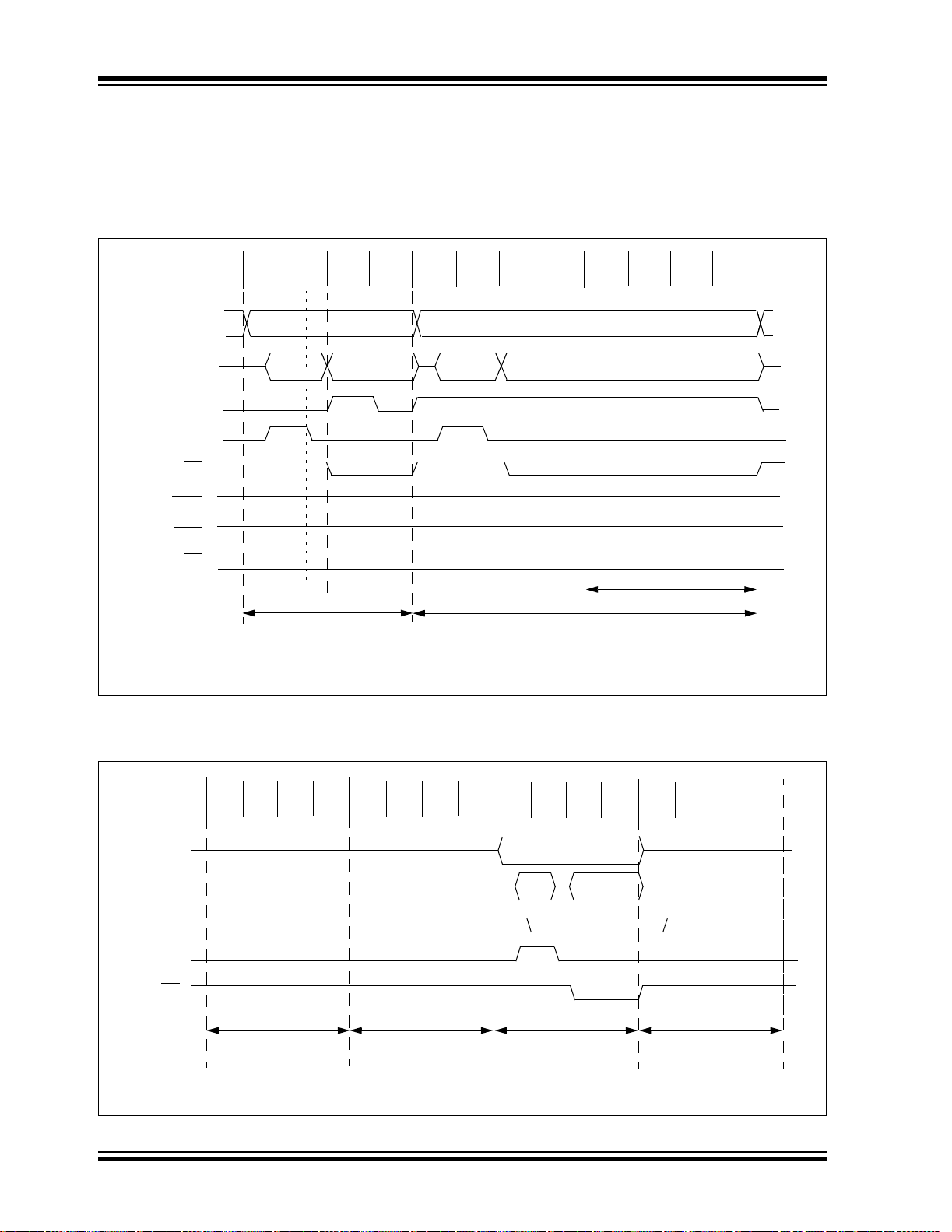
PIC18F6520/8520/6620/8620/6720/8720
6.2.4 16-BIT MODE TIMING
The presentation of control signals on the external
memory bus is different for the various operating
modes. Typical signal timing diagrams are shown in
Figure 6-4 through Figure 6-6.
FIGURE 6-4: EXTERNAL MEMORY BUS TIMING FOR TBLRD (MICROPROCESSOR MODE)
Apparent Q
Actual Q
A<19:16>
AD<15:0>
BA0
ALE
OE
WRH
WRL
CE
Memory
Cycle
Instruction
Execution
Q2Q1 Q3 Q4 Q2Q1 Q3 Q4 Q4Q4 Q4 Q4
Q2Q1 Q3 Q4 Q2Q1 Q3 Q4 Q2Q1 Q3 Q4
00h
3AABh
‘1’ ‘1’
‘1’
‘0’
Opcode Fetch
MOVLW 55h
from 007556h
TBLRD Cycle 1
0E55h
CF33h
from 199E67h
TBLRD Cycle 2
0Ch
Table Read
of 92h
9256h
1 T
CY Wait
‘1’
‘0’
FIGURE 6-5: EXTERNAL MEMORY BUS TIMING FOR
TBLRD (EXTENDED
MICROCONTROLLER MODE)
Q2Q1 Q3 Q4 Q2Q1 Q3 Q4
A<19:16>
AD<15:0>
CE
ALE
OE
Memory
Cycle
Instruction
Execution
DS39609B-page 76 2004 Microchip Technology Inc.
Opcode Fetch Opcode Fetch Opcode Fetch
TBLRD *
from 000100h
INST(PC-2)
MOVLW 55h
from 000102h
TBLRD Cycle 1
Q2Q1 Q3 Q4
0Ch
CF33h
TBLRD 92h
from 199E67h
TBLRD Cycle 2
9256h
Q2Q1 Q3 Q4
ADDLW 55h
from 000104h
MOVLW
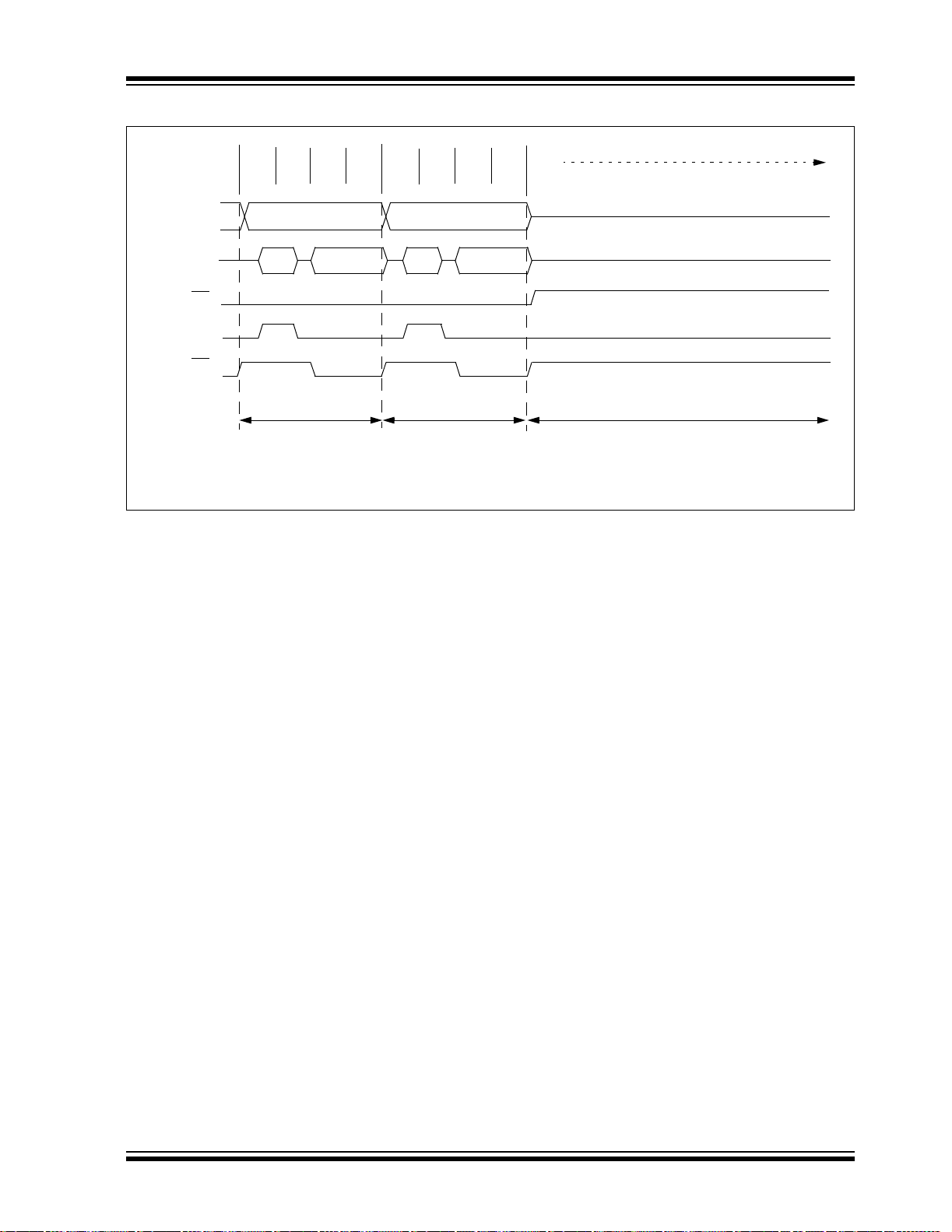
PIC18F6520/8520/6620/8620/6720/8720
FIGURE 6-6: EXTERNAL MEMORY BUS TIMING FOR SLEEP (MICROPROCESSOR MODE)
A<19:16>
AD<15:0>
CE
ALE
OE
Memory
Cycle
Instruction
Execution
Q2Q1 Q3 Q4 Q2Q1 Q3 Q4
00h
3AAAh
Opcode Fetch
SLEEP
from 007554h
INST(PC-2)
0003h
00h
3AABh
Opcode Fetch
MOVLW 55h
from 007556h
SLEEP
0E55h
Q1
Sleep Mode,
Bus Inactive
2004 Microchip Technology Inc. DS39609B-page 77

PIC18F6520/8520/6620/8620/6720/8720
NOTES:
DS39609B-page 78 2004 Microchip Technology Inc.

PIC18F6520/8520/6620/8620/6720/8720
7.0 DATA EEPROM MEMORY
The data EEPROM is readable and writable during
normal operation over the entire V
memory is not directly mapped in the register file
space. Instead, it is indirectly addressed through the
Special Function Registers (SFR).
There are five SFRs used to read and write the
program and data EEPROM memory. These registers
are:
• EECON1
• EECON2
• EEDAT A
• EEADRH
• EEADR
The EEPROM data memory allows byte read and write.
When interfacing to the data memory block, EEDATA
holds the 8-bit data for read/write. EEADR and
EEADRH hold the address of the EEPROM location
being accessed. These devices have 1024 bytes of
data EEPROM with an address range from 00h to
3FFh.
The EEPROM data memory is rated for high erase/
write cycles. A byt e write autom atically er ases the loc ation and writes the new data (erase-before-write). The
write time is controlled by an on-chip timer. The write
time will vary with vo ltag e and tempe rat ure, as wel l as
from chip to chip. Please refer to p ara me ter D12 2 (se e
Section 26.0 “Electrical Characteristics”) for exact
limits.
DD range. Th e data
7.1 EEADR and EEADRH
The address register pair can address up to a maximum of 1024 bytes of data EEPROM. The two Most
Significant bits of the address are stored in EEADRH,
while the remaining eight Least Significant bits are
stored in EEADR. The six Most Significant bits of
EEADRH are unused and are read as ‘0’.
7.2 EECON1 and EECON2 Registers
EECON1 is the control register for EEPROM memory
accesses.
EECON2 is not a physical register. Reading EECON2
will read all ‘0’s. The EECON2 register is used
exclusively in the EEPROM write sequence.
Control bits, R D an d WR, initiate read and write operations, respectively. These bits cannot be cleared, only
set, in software. They are cleared in hardware at the
completion of the read or write operation. The inability
to clear the WR bit in software prevents the accidental
or premature termination of a write operation.
The WREN bit, when set, will allow a write operation.
On power-up, the WREN bit is c lear . Th e WRERR bit is
set when a write operation is interrupted by a MCLR
Reset or a WDT Time-out Reset during normal operation. In these situations, the user can check the
WRERR bit and rewrite the location. It is necessary to
reload the data and address regi sters (EEDATA and
EEADR) due to the Reset condition forcing the
contents of the registers to zero.
Note: Interrupt flag bit, EEIF in the PIR2 r egister,
is set when write is complete. It must be
cleared in software.
2004 Microchip Technology Inc. DS39609B-page 79

PIC18F6520/8520/6620/8620/6720/8720
REGISTER 7-1: EECON1 REGISTER (ADDRESS FA6h)
R/W-x R/W-x U-0 R/W-0 R/W-x R/W-0 R/S-0 R/S-0
EEPGD CFGS — FREE WRERR WREN WR RD
bit 7 bit 0
bit 7 EEPGD: Flash Program/Data EEPROM Memory Select bit
1 = Access Flash program memory
0 = Access data EEPROM memory
bit 6 CFGS: Flash Program/Data EEPROM or Configuration Select bit
1 = Access configuration or calibration registers
0 = Access Flash program or data EEPROM memory
bit 5 Unimplemented: Read as ‘0’
bit 4 FREE: Flash Row Erase Enable bit
1 = Erase the program memory row addressed by TBLPTR on the next WR command
(cleared by completion of erase operation)
0 = Perform write only
bit 3 WRERR: Flash Program/Data EEPROM Error Flag bit
1 = A write operation is prematurely terminated
(any MCLR
0 = The write operation completed
Note: When a WRERR occurs, the EEPGD or FREE bits are not cleared. This allows
or any WDT Reset during self-timed programming in normal operation)
tracing of the error condition.
bit 2 WREN: Flash Program/Data EEPROM Write Enable bit
1 = Allows write cycles to Flash program/data EEPROM
0 = Inhibits write cycles to Flash program/data EEPROM
bit 1 WR: Write Control bit
1 = Initiates a data EEPROM erase/write cycle, or a program memory erase cycle or w rite cycle.
(The operation is self-tim ed and the bit is clea red by hardware on ce write is complete. The
WR bit can only be set (not cleared) in software.)
0 = Write cycle to the EEPROM is complete
bit 0 RD: Read Control bit
1 = Initiates an EEPROM read. (Read takes one cycle. RD is cleared i n ha rdw are . Th e RD b it
can only be set (not cleared) in software. RD bit cannot be set when EEPGD = 1.)
0 = Does not initiate an EEPROM read
Legend:
R = Readable bit W = Writable bit U = Unimplemented bit, read as ‘0’
- n = Value at POR ‘1’ = Bit is set ‘0’ = Bit is cleared x = Bit is unknown
DS39609B-page 80 2004 Microchip Technology Inc.

PIC18F6520/8520/6620/8620/6720/8720
7.3 Reading the Data EEPROM Memory
T o read a d ata memory loca tion, the user must write the
address to the EEADRH:EEADR register pair , clear the
EEPGD control bit (EECON1<7>), clear the CFGS
control bit (EECON1<6>) and then set the RD control
bit (EECON1<0>). The data is available for the very
next instruction cycle; therefore, the EEDATA register
can be read by the next instruction. EEDATA will hold
this value until another read operation, or until it is
written to by the user (during a write operation).
EXAMPLE 7-1: DATA EEPROM READ
MOVLW DATA_EE_ADDRH ;
MOVWF EEADRH ; Upper bits of Data Memory Address to read
MOVLW DATA_EE_ADDR ;
MOVWF EEADR ; Lower bits of Data Memory Address to read
BCF EECON1, EEPGD ; Point to DATA memory
BCF EECON1, CFGS ; Access EEPROM
BSF EECON1, RD ; EEPROM Read
MOVF EEDATA, W ; W = EEDATA
7.4 Writing to the Data EEPROM Memory
To write an EEPROM data location, the address must
first be written to the EEADRH:EEADR register pair
and the data written to the EEDATA register. Then the
sequence in Example7-2 must be followed to initiate
the write cycle.
The write will not initiate if the above sequence is not
exactly followed (write 55h to EECON2, write AAh to
EECON2, then set WR bit) for each byte. It is strongly
recommended that interrupts be disabled during this
code segment.
Additionally, the WREN bit in EECON1 must be set to
enable writes. This mechanism prevents accidental
writes to data EEPROM due to unexpected code
execution (i.e., runaway programs). The WREN bit
should be kept clear at all times , excep t whe n upda tin g
the EEPROM. The WREN bit is not cleared
by hardware
After a write sequence has been initiated, EECON1,
EEADRH, EEADR and EEDATA cannot be modified.
The WR bit will be inhibited from being set unless the
WREN bit is set. Both WR and WREN cannot be set
with the same instruction.
At the completion of the write cycle, the WR bit is
cleared in hardware and th e EEPROM Write Complete
Interrupt Flag bit (EEIF) is set. The user may either
enable this interrupt, or poll this bit. EEIF must be
cleared by software.
EXAMPLE 7-2: DATA EEPROM WRITE
MOVLW DATA_EE_ADDRH ;
MOVWF EEADRH ; Upper bits of Data Memory Address to write
MOVLW DATA_EE_ADDR ;
MOVWF EEADR ; Lower bits of Data Memory Address to write
MOVLW DATA_EE_DATA ;
MOVWF EEDATA ; Data Memory Value to write
BCF EECON1, EEPGD ; Point to DATA memory
BCF EECON1, CFGS ; Access EEPROM
Required MOVWF EECON2 ; Write 55h
Sequence MOVLW AAh ;
2004 Microchip Technology Inc. DS39609B-page 81
BSF EECON1, WREN ; Enable writes
BCF INTCON, GIE ; Disable Interrupts
MOVLW 55h ;
MOVWF EECON2 ; Write AAh
BSF EECON1, WR ; Set WR bit to begin write
BSF INTCON, GIE ; Enable Interrupts
; User code execution
BCF EECON1, WREN ; Disable writes on write complete (EEIF set)

PIC18F6520/8520/6620/8620/6720/8720
7.5 Write Verify
Depending on the application, good programming
practice may dictate that the value written to the memory should be verified against the original value. This
should be used in applications where excessive writes
can stress bits near the specification limit.
7.6 Protection Against Spurious Write
There are c onditions when the user may no t want to
write to the data EEPROM memory. To protect against
spurious EEPROM writes, various mechanism s have
been built -in. On powe r-up, the WR EN bit is cl eared.
Also, the Power-up Timer (72 ms duration) prevents
EEPROM write.
The write initiate se quence and the WREN bit together
help prevent an accidental write during brown-out,
power glitch, or software malfunction.
7.7 Operation During Code-Protect
Data EEPROM memory has its own code-protect
mechanism. External read and write operations are
disabled if either of these mechanisms are enabled.
The microcontroller i tself can both re ad and wr ite to the
internal data EEPROM, regardless of the state of the
code-protect configuration bit. Refer to Section 23.0
“Special Features of the CPU” for additional
information.
7.8 Using the Data EEPROM
The data EEPROM is a hi gh en dura nc e, byt e addressable array that has been optimized for the storage of
frequently changing information (e.g., program variables or other data that are updated often). Frequently
changing values will typically be updated more often
than specification D1 24. If this is not the ca se, an array
refresh must be performed. For this reason, variables
that change infrequently (such as constants, IDs,
calibration, etc.) should be stored in Flash program
memory.
A simple data EEPROM refresh routine is shown in
Example 7-3.
Note: If data EEPROM is only used to store
constants an d/or data that changes rarely,
an array refresh is li kely not required. See
specification D124.
EXAMPLE 7-3: DATA EEPROM REFRESH ROUTINE
CLRF EEADR ; Start at address 0
CLRF EEADRH ;
BCF EECON1, CFGS ; Set for memory
BCF EECON1, EEPGD ; Set for Data EEPROM
BCF INTCON, GIE ; Disable interrupts
Loop ; Loop to refresh array
BSF EECON1, WREN ; Enable writes
BSF EECON1, RD ; Read current address
MOVLW 55h ;
MOVWF EECON2 ; Write 55h
MOVLW AAh ;
MOVWF EECON2 ; Write AAh
BSF EECON1, WR ; Set WR bit to begin write
BTFSC EECON1, WR ; Wait for write to complete
BRA $-2
INCFSZ EEADR, F ; Increment address
BRA Loop ; Not zero, do it again
INCFSZ EEADRH, F ; Increment the high address
BRA Loop ; Not zero, do it again
BCF EECON1, WREN ; Disable writes
BSF INTCON, GIE ; Enable interrupts
DS39609B-page 82 2004 Microchip Technology Inc.

PIC18F6520/8520/6620/8620/6720/8720
TABLE 7-1: REGISTERS ASSOCIATED WITH DATA EEPROM MEMORY
Name Bit 7 Bit 6 Bit 5 Bit 4 Bit 3 Bit 2 Bit 1 Bit 0
INTCON GIE/GIEH PEIE/GIEL
EEADRH
EEADR EEPROM Address Register 0000 0000 0000 0000
EEDATA EEPROM Data Register 0000 0000 0000 0000
EECON2 EEPROM Control Register 2 (not a physical register) ---- ---- ---- ---EECON1 EEPGD
IPR2
PIR2
PIE2
Legend: x = unknown, u = unchanged, r = reserved, – = unimplemented, read as ‘0’.
— — — — — — EE Addr Register High ---- --00 ---- --00
CFGS — FREE WRERR WREN WR RD xx-0 x000 uu-0 u000
— CMIP —EEIPBCLIP LVDIP TMR3IP CCP2IP ---1 1111 ---1 1111
— CMIF —EEIFBCLIF LVDIF TMR3IF CCP2IF ---0 0000 ---0 0000
— CMIE —EEIEBCLIE LVDIE TMR3IE CCP2IE ---0 0000 ---0 0000
Shaded cells are not used during Flash/EEPROM access.
TMR0IE INT0IE RBIE TMR0IF INT0IF RBIF 0000 0000 0000 0000
Value on
POR, BOR
Val ue on
all other
Resets
2004 Microchip Technology Inc. DS39609B-page 83

PIC18F6520/8520/6620/8620/6720/8720
NOTES:
DS39609B-page 84 2004 Microchip Technology Inc.

PIC18F6520/8520/6620/8620/6720/8720
8.0 8 X 8 HARDWARE MULTIPLIER
8.1 Introduction
An 8 x 8 hardware multiplier is included in the ALU of
the PIC18FXX20 devices. By making the multiply a
hardware operatio n, i t co mp letes in a single instruction
cycle. This is an unsign ed multiply that gives a 16-bit
result. The result is store d in the 1 6-bit pro duct reg ister
pair (PRODH:PRODL). The multiplier does not affect
any flags in the ALUSTA register.
Making the 8 x 8 multiplier execute in a single cycle
gives the following advantages:
• Higher computational throughput
• Reduces code size require me nt s for multi ply
algorithms
The performance increas e allows the device to be used
in applications previously reserved for Digital Signal
Processors.
Table 8-1 shows a p erformance comparison between
enhanced devices using the single-cycle hardware
multiply and performing the same function without the
hardware multiply.
8.2 Operation
Example 8-1 shows the sequence to do an 8 x 8
unsigned multiply. Only one instruction is required
when one argument of the multiply is already loade d i n
the WREG register.
Example 8-2 shows the sequence to do an 8 x 8 signed
multiply. To account for the sign bits of the arguments,
each argument’s Most Significant bit (MSb) is tested
and the appropriate subtractions are done.
EXAMPLE 8-1: 8 x 8 UNSIGNED
MULTIPLY ROUTINE
MOVF ARG1, W ;
MULWF ARG2 ; ARG1 * ARG2 ->
; PRODH:PRODL
EXAMPLE 8-2: 8 x 8 SIGNED MULTIPLY
ROUTINE
MOVF ARG1, W ;
MULWF ARG2 ; ARG1 * ARG2 ->
; PRODH:PRODL
BTFSC ARG2, SB ; Test Sign Bit
SUBWF PRODH, F ; PRODH = PRODH
; - ARG1
MOVF ARG2, W ;
BTFSC ARG1, SB ; Test Sign Bit
SUBWF PRODH, F ; PRODH = PRODH
; - ARG2
TABLE 8-1: PERFORMANCE COMPARISON
Program
Routine Multiply Method
8 x 8 unsigned
8 x 8 signed
16 x 16 unsigned
16 x 16 signed
Without hardware multiply 13 69 6.9 µs27.6 µs69 µs
Hardware multiply 1 1 100 ns 400 ns 1 µs
Without hardware multiply 33 91 9.1 µs36.4 µs91 µs
Hardware multiply 6 6 600 ns 2.4 µs6 µs
Without hardware multiply 21 242 24.2 µs96.8 µs242 µs
Hardware multiply 28 28 2.8 µs 11.2 µs28 µs
Without hardware multiply 52 254 25.4 µs 102.6 µs254 µs
Hardware multiply 35 40 4.0 µs16.0 µs40 µs
Memory
(Words)
Cycles
(Max)
Time
@ 40 MHz @ 10 MHz @ 4 MHz
2004 Microchip Technology Inc. DS39609B-page 85

PIC18F6520/8520/6620/8620/6720/8720
Example 8-3 shows the sequence to do a 16 x 16
unsigned multiply. Equation 8-1 shows the algorithm
that is used. The 32-bit re sult is st ored in four re gisters,
RES3:RES0.
EQUATION 8-1: 16 x 16 UNSIGNED
MULTIPLICATION
ALGORITHM
RES3:RES0 = ARG1H:ARG1L • ARG2H:ARG2L
= (ARG1H • ARG2H • 2
(ARG1H • ARG2L • 2
(ARG1L • ARG2H • 2
(ARG1L • ARG2L)
16
) +
8
) +
8
) +
EXAMPLE 8-3: 16 x 16 UNSIGNED
MULTIPLY ROUTINE
MOVF ARG1L, W
MULWF ARG2L ; ARG1L * ARG2L ->
MOVFF PRODH, RES1 ;
MOVFF PRODL, RES0 ;
;
MOVF ARG1H, W
MULWF ARG2H ; ARG1H * ARG2H ->
MOVFF PRODH, RES3 ;
MOVFF PRODL, RES2 ;
;
MOVF ARG1L, W
MULWF ARG2H ; ARG1L * ARG2H ->
MOVF PRODL, W ;
ADDWF RES1, F ; Add cross
MOVF PRODH, W ; products
ADDWFC RES2, F ;
CLRF WREG ;
ADDWFC RES3, F ;
;
MOVF ARG1H, W ;
MULWF ARG2L ; ARG1H * ARG2L ->
MOVF PRODL, W ;
ADDWF RES1, F ; Add cross
MOVF PRODH, W ; products
ADDWFC RES2, F ;
CLRF WREG ;
ADDWFC RES3, F ;
Example 8-4 shows the sequence to do a 16 x 16
signed multiply. Equation 8-2 shows the algorithm
used. The 32-bit result is stored in four registers,
RES3:RES0. To account for the sign bits of the arguments, each argum ent p ai rs’ M ost S ign ificant bit (MSb)
is tested and the appropriate subtractions are done.
; PRODH:PRODL
; PRODH:PRODL
; PRODH:PRODL
; PRODH:PRODL
EQUATION 8-2: 16 x 16 SIGNED
MULTIPLICATION
ALGORITHM
RES3:RES0
= ARG1H:ARG1L • ARG2H:ARG2L
= (ARG1H • ARG2H • 2
(ARG1H • ARG2L • 2
(ARG1L • ARG2H • 2
(ARG1L • ARG2L) +
(-1 • ARG2H<7> • ARG1H:ARG1L • 2
(-1 • ARG1H<7> • ARG2H:ARG2L • 2
16
) +
8
) +
8
) +
EXAMPLE 8-4: 16 x 16 SIGNED
MULTIPLY ROUTINE
MOVF ARG1L, W
MULWF ARG2L ; ARG1L * ARG2L ->
MOVFF PRODH, RES1 ;
MOVFF PRODL, RES0 ;
;
MOVF ARG1H, W
MULWF ARG2H ; ARG1H * ARG2H ->
MOVFF PRODH, RES3 ;
MOVFF PRODL, RES2 ;
;
MOVF ARG1L, W
MULWF ARG2H ; ARG1L * ARG2H ->
MOVF PRODL, W ;
ADDWF RES1, F ; Add cross
MOVF PRODH, W ; products
ADDWFC RES2, F ;
CLRF WREG ;
ADDWFC RES3, F ;
;
MOVF ARG1H, W ;
MULWF ARG2L ; ARG1H * ARG2L ->
MOVF PRODL, W ;
ADDWF RES1, F ; Add cross
MOVF PRODH, W ; products
ADDWFC RES2, F ;
CLRF WREG ;
ADDWFC RES3, F ;
;
BTFSS ARG2H, 7 ; ARG2H:ARG2L neg?
BRA SIGN_ARG1 ; no, check ARG1
MOVF ARG1L, W ;
SUBWF RES2 ;
MOVF ARG1H, W ;
SUBWFB RES3
;
SIGN_ARG1
BTFSS ARG1H, 7 ; ARG1H:ARG1L neg?
BRA CONT_CODE ; no, done
MOVF ARG2L, W ;
SUBWF RES2 ;
MOVF ARG2H, W ;
SUBWFB RES3
;
CONT_CODE
:
; PRODH:PRODL
; PRODH:PRODL
; PRODH:PRODL
; PRODH:PRODL
16
) +
16
)
DS39609B-page 86 2004 Microchip Technology Inc.

PIC18F6520/8520/6620/8620/6720/8720
9.0 INTERRUPTS
The PIC18FXX20 devices have multiple interrupt
sources and an interrupt priority feature that allows
each interrupt source to be assigned a high or a low
priority level. The high priority interrupt vector is at
000008h, while the low priority interrupt vector is at
000018h. High priorit y interrupt event s will overrid e any
low priority interrupts that may be in progress.
There are t hirteen r egisters which are used to c ontrol
interrupt operation. They are:
• RCON
•INTCON
• INTCON2
• INTCON3
• PIR1, PIR2, PIR3
• PIE1, PIE2, PIE3
• IPR1, IPR2, IPR3
It is recommended that the Microchip header files,
supplied with MPLAB
names in these registers. This allows the assembler/
compiler to automatical ly ta ke care of the pla ceme nt of
these bits within the specified register.
Each interrupt source has three bits to control its
operation. The functions of these bits are:
• Flag bit to indicate that an interrupt event
occurred
• Enable bit that allo ws program execution to
branch to the interrupt vector address when the
flag bit is set
• Priority bit to select high priority or low priority
The interrupt priority feature is enabled by setting the
IPEN bit (RCON<7>). When interrupt priority is
enabled, there are two bits which enable interrupts
globally . Setti ng the GIEH bit (INTC ON<7>) enable s all
interrupts that hav e the priority bit set. Setting the GIEL
bit (INTCON<6>) enables all interrupts that have the
priority bit cleared. When the interrupt flag, enable bit
and appropriate global interrupt enable bit are set, the
interrupt will vec tor imm ediat ely to addre ss 00 0008h or
000018h, depending on the priority level. Individual
interrupts can be disabled through their corresponding
enable bits.
®
IDE, be used for the symbolic bit
When the IPEN bit is cleared (default state), the
interrupt priority feature is disabled and interrupts are
compatible with PICmicro
patibility mode, th e interrupt priority bits for each sourc e
have no effect. INTCON<6> is the PEIE bit, which
enables/disables all peripheral interrupt sources.
INTCON<7> is the GIE bit, which enables/disables all
interrupt sources. All interrupts branch to address
000008h in Compatibility mode.
When an interrupt is responded to, the Global Interrupt
Enable bit is cleared to disable further interrupts. If the
IPEN bit is cleared, this is the GIE bit. If interru pt priority
levels are used, this wi ll be either the GIEH or G IEL bit.
High priority interrupt sources can interrupt a low
priority interrupt.
The return address is pushed onto the stack and the
PC is loaded with the interrupt vector address
(000008h or 000018h). On ce in the Interrupt Service
Routine, the source(s) of the interrupt can be determined by polling the interrupt flag bits. The interrupt
flag bits must be cleared in s oftware be fore re-enab ling
interrupts to avoid recursive interrupts.
The “return from interrupt” instruction, RETFIE, exits
the interrupt routine and set s the GIE bit (GIEH or GI EL
if priority levels are used), which re-enables interrupts.
For external interrupt events, such as the INT pins or
the PORTB input chang e interrupt, the i nterrupt latenc y
will be three to four instruction cycles. The exact
latency is the same for one or two-cycle instructions.
Individual interrupt flag bits are set, regardless of the
status of their corresponding enable bit or the GIE bit.
®
mid-range device s. In Com-
2004 Microchip Technology Inc. DS39609B-page 87
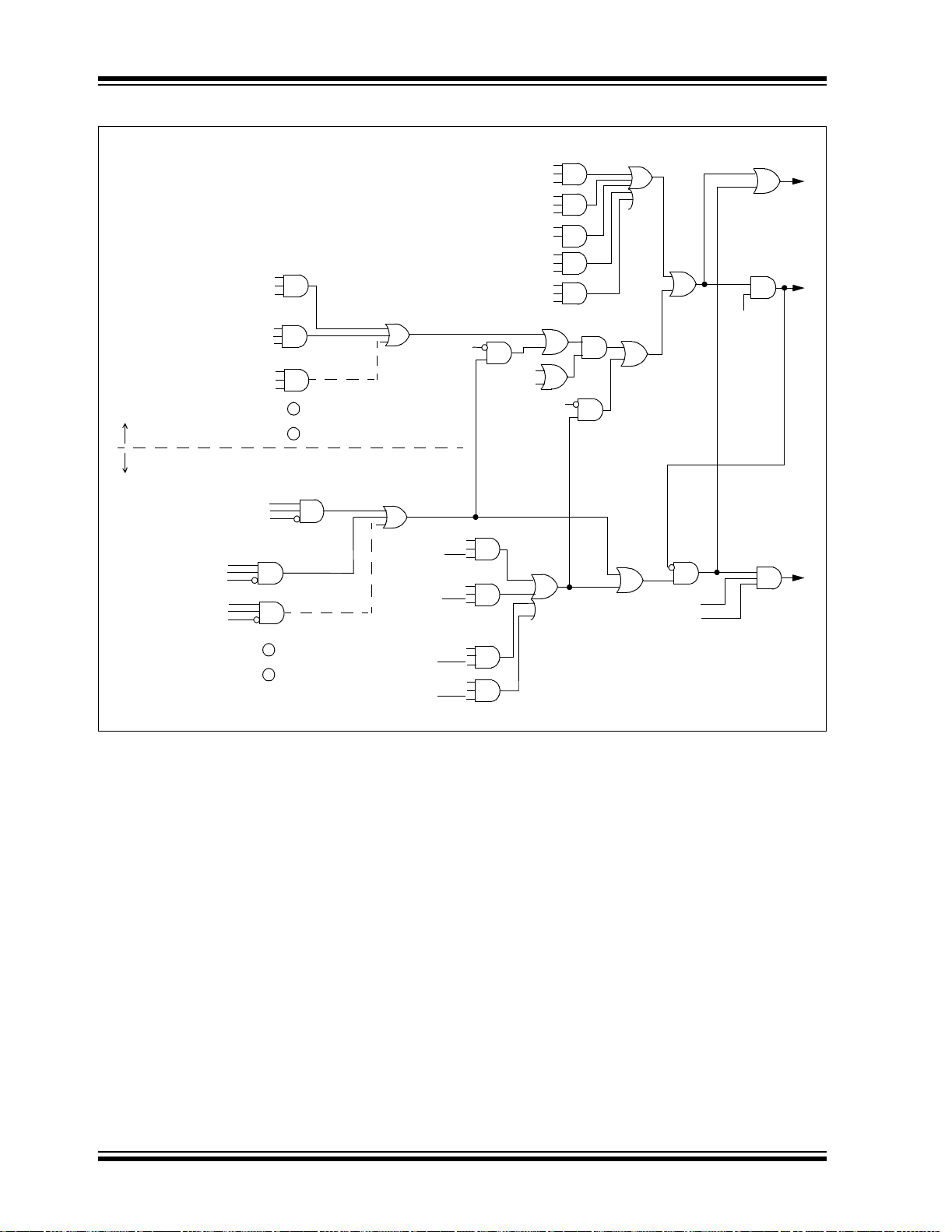
PIC18F6520/8520/6620/8620/6720/8720
FIGURE 9-1: INTERRUPT LOGIC
Peripheral Interrupt Flag bit
Peripheral Interrupt Enable bit
Peripheral Interrupt Priority bit
TMR1IF
TMR1IE
TMR1IP
XXXXIF
XXXXIE
XXXXIP
High Priority Interrupt Generation
Low Priority Interrupt Generation
Peripheral Interrupt Flag bit
Peripheral Interrupt Enable bit
Peripheral Interrupt Priority bit
TMR1IF
TMR1IE
TMR1IP
XXXXIF
XXXXIE
XXXXIP
Additional Peripheral Interrupts
Additional Peripheral Interrupts
IPEN
TMR0IF
TMR0IE
TMR0IP
RBIF
RBIE
RBIP
INT1IF
INT1IE
INT1IP
INT2IF
INT2IE
INT2IP
TMR0IF
TMR0IE
TMR0IP
INT0IF
INT0IE
INT1IF
INT1IE
INT1IP
INT2IF
INT2IE
INT2IP
IPEN
GIEL/PEIE
RBIF
RBIE
RBIP
IPEN
Wake-up if in Sleep mode
GIEL/PEIE
GIE/GEIH
Interrupt to CPU
Vector to Location
0008h
GIEH/GIE
Interrupt to CPU
Vector to Location
0018h
DS39609B-page 88 2004 Microchip Technology Inc.

PIC18F6520/8520/6620/8620/6720/8720
9.1 INTCON Registers
The INTCON registers are readable and writable
registers, which contain various enable, priority and
flag bits.
REGISTER 9-1: INTCON REGISTER
R/W-0 R/W-0 R/W-0 R/W-0 R/W-0 R/W-0 R/W-0 R/W-x
GIE/GIEH PEIE/GIEL TMR0IE INT0IE RBIE TMR0IF INT0IF RBIF
bit 7 bit 0
bit 7 GIE/GIEH: Global Interrupt Enable bit
When IPEN (RCON<7>) =
1 = Enables all unmasked interrupts
0 = Disables all interrupts
When IPEN (RCON<7>) = 1:
1 = Enables all high priority interrupts
0 = Disables all interrupts
bit 6 PEIE/GIEL: Peripheral Interrupt Enable bit
When IPEN (RCON<7>) =
1 = Enables all unmasked peripheral interrupts
0 = Disables all peripheral interrupts
When IPEN (RCON<7>) = 1:
1 = Enables all low priority peripheral interrupts
0 = Disables all low priority peripheral interrupts
bit 5 TMR0IE: TMR0 Overflow Interrupt Enable bit
1 = Enables the TMR0 overflow interrupt
0 = Disables the TMR0 overflow interrupt
bit 4 INT0IE: INT0 External Interrupt Enable bit
1 = Enables the INT0 external interrupt
0 = Disables the INT0 external interrupt
bit 3 RBIE: RB Port Change Interrupt Enable bit
1 = Enables the RB port change interrupt
0 = Disables the RB port change interrupt
bit 2 TMR0IF: TMR0 Overflow Interrupt Flag bit
1 = TMR0 register has overflowed (must be cleared in software)
0 = TMR0 register did not overflow
bit 1 INT0IF: INT0 External Interrupt Flag bit
1 = The INT0 external interrupt occurred (must be cleared in software)
0 = The INT0 external interrupt did not occur
bit 0 RBIF: RB Port Change Interrupt Flag bit
1 = At least one of the RB7:RB4 pins changed state (must be cleared in software)
0 = None of the RB7:RB4 pins have changed state
Note: A mismatch condition will continue to set this bit. Reading PORTB will end the
mismatch condition and allow the bit to be cleared.
0:
0:
Note: Interrupt flag bits are set w hen an inter rupt
condition occurs, rega rdless of the state of
its corresponding enable bit or the global
enable bit. User software should ensure
the appropriate interrupt flag bits are clear
prior to enabling an interrupt. This feature
allows for software polling.
Legend:
R = Readable bit W = Writable bit U = Unimplemented bit, read as ‘0’
- n = Value at POR ‘1’ = Bit is set ‘0’ = Bit is cleared x = Bit is unknown
2004 Microchip Technology Inc. DS39609B-page 89

PIC18F6520/8520/6620/8620/6720/8720
REGISTER 9-2: INTCON2 REGISTER
R/W-1 R/W-1 R/W-1 R/W-1 R/W-1 R/W-1 R/W-1 R/W-1
RBPU
bit 7 bit 0
INTEDG0 INTEDG1 INTEDG2 INTEDG3 TMR0IP INT3IP RBIP
bit 7 RBPU
bit 6 INTEDG0: External Interrupt 0 Edge Select bit
bit 5 INTEDG1: External Interrupt 1 Edge Select bit
bit 4 INTEDG2: External Interrupt 2 Edge Select bit
bit 3 INTEDG3: External Interrupt 3 Edge Select bit
bit 2 TMR0IP: TMR0 Overflow Interrupt Priority bit
bit 1 INT3IP: INT3 External Interrupt Priority bit
bit 0 RBIP: RB Port Change Interrupt Priority bit
: PORTB Pull-up Enable bit
1 = All PORTB pull-ups are disabled
0 = PORTB pull-ups are enabled by individual port latch values
1 = Interrupt on rising edge
0 = Interrupt on falling edge
1 = Interrupt on rising edge
0 = Interrupt on falling edge
1 = Interrupt on rising edge
0 = Interrupt on falling edge
1 = Interrupt on rising edge
0 = Interrupt on falling edge
1 = High priority
0 = Low priority
1 = High priority
0 = Low priority
1 = High priority
0 = Low priority
Legend:
R = Readable bit W = Writable bit U = Unimplemented bit, read as ‘0’
- n = Value at POR ‘1’ = Bit is set ‘0’ = Bit is cleared x = Bit is unknown
Note: Interrupt flag bits are set when an interrupt cond iti on oc c urs, rega rdle ss of the st a te
of its correspo nding en abl e bit or the globa l ena ble bi t. U ser so ftware s hould ensu re
the appropriate interrup t flag bits are clear prior to enab ling an interrupt. T his featu re
allows for software polling.
DS39609B-page 90 2004 Microchip Technology Inc.

PIC18F6520/8520/6620/8620/6720/8720
REGISTER 9-3: INTCON3 REGISTER
R/W-1 R/W-1 R/W-0 R/W-0 R/W-0 R/W-0 R/W-0 R/W-0
INT2IP INT1IP INT3IE INT2IE INT1IE INT3IF INT2IF INT1IF
bit 7 bit 0
bit 7 INT2IP: INT2 External Interrupt Priority bit
1 = High priority
0 = Low priority
bit 6 INT1IP: INT1 External Interrupt Priority bit
1 = High priority
0 = Low priority
bit 5 INT3IE: INT3 External Interrupt Enable bit
1 = Enables the INT3 external interrupt
0 = Disables the INT3 external interrupt
bit 4 INT2IE: INT2 External Interrupt Enable bit
1 = Enables the INT2 external interrupt
0 = Disables the INT2 external interrupt
bit 3 INT1IE: INT1 External Interrupt Enable bit
1 = Enables the INT1 external interrupt
0 = Disables the INT1 external interrupt
bit 2 INT3IF: INT3 External Interrupt Flag bit
1 = The INT3 external interrupt occurred (must be cleared in software)
0 = The INT3 external interrupt did not occur
bit 1 INT2IF: INT2 External Interrupt Flag bit
1 = The INT2 external interrupt occurred (must be cleared in software)
0 = The INT2 external interrupt did not occur
bit 0 INT1IF: INT1 External Interrupt Flag bit
1 = The INT1 external interrupt occurred (must be cleared in software)
0 = The INT1 external interrupt did not occur
Legend:
R = Readable bit W = Writable bit U = Unimplemented bit, read as ‘0’
- n = Value at POR ‘1’ = Bit is set ‘0’ = Bit is cleared x = Bit is unknown
Note: Interrupt flag bits are set when an interrupt cond iti on oc c urs , rega rdle ss of the st a te
of its correspo nding en abl e bit or the globa l ena ble bi t. U ser so ftware s hould ensu re
the appropriate interrup t flag bits are clear prior to enab ling an interrupt. T his featu re
allows for software polling.
2004 Microchip Technology Inc. DS39609B-page 91

PIC18F6520/8520/6620/8620/6720/8720
9.2 PIR Registers
The PIR registers conta in the ind ividu al flag bi ts fo r the
peripheral interrupts. Due to the number of peripheral
interrupt sources, there are three Peripheral Interrupt
Flag Registers (PIR1, PIR2 and PIR3).
Note 1: Interrupt flag bits are set whe n an interrupt
condition occurs, regardl ess of the state of
its corresponding enable bit or the global
enable bit, GIE (INTCON<7>).
2: User software should ensure the ap propri-
ate interrupt flag bits are cleared prior to
enabling an interrupt and after servicing
that interrupt.
REGISTER 9-4: PIR1: PERIPHERAL INTERRUPT REQUEST (FLAG) REGISTER 1
R/W-0 R/W-0 R-0 R-0 R/W-0 R/W-0 R/W-0 R/W-0
(1)
PSPIF
bit 7 bit 0
bit 7 PSPIF: Parallel Slave Port Read/Write Interrupt Flag bit
1 = A read or a write operation has taken place (must be cleared in software)
0 = No read or write has occurred
bit 6 ADIF: A/D Converter Interrupt Flag bit
1 = An A/D conversion completed (must be cl eared in software)
0 = The A/D conversion is not complete
bit 5 RC1IF: USART1 Receive Interrupt Flag bit
1 = The USART1 receive buffer, RCREG, is full (cleared when RCREG is read)
0 = The USART1 receive buffer is empty
bit 4 TX1IF: USART Transmit Interrupt Flag bit
1 = The USART1 transmit buffer, TXREG, is empty (cleared when TXREG is written)
0 = The USART1 transmit buffer is full
bit 3 SSPIF: Master Synchronous Serial Port Interrupt Flag bit
1 = The transmission/reception is complete (must be cleared in software)
0 = Waiting to transmit/receive
bit 2 CCP1IF: CCP1 Interrupt Flag bit
Capture mode:
1 = A TMR1 register capture occurre d (must be cleared in software)
0 = No TMR1 register capture occurred
Compare mode:
1 = A TMR1 register compare match occurred (must be cleared in software)
0 = No TMR1 register compare match occurred
PWM mode:
Unused in this mode.
bit 1 TMR2IF: TMR2 to PR2 Match Interrupt Flag bit
1 = TMR2 to PR2 match occurred (must be cleared in software)
0 = No TMR2 to PR2 match occurred
bit 0 TMR1IF: TMR1 Overflow Interrupt Flag bi t
1 = TMR1 register overflowed (must be cleared in software)
0 = TMR1 register did not overflow
ADIF RC1IF TX1IF SSPIF CCP1IF TMR2IF TMR1IF
(1)
Note 1: Enabled only in Microcontrolle r mode for PIC18F8X20 devices.
Legend:
R = Readable bit W = Writable bit U = Unimplemented bit, read as ‘0’
- n = Value at POR ‘1’ = Bit is set ‘0’ = Bit is cleared x = Bit is unknown
DS39609B-page 92 2004 Microchip Technology Inc.

PIC18F6520/8520/6620/8620/6720/8720
REGISTER 9-5: PIR2: PERIPHERAL INTERRUPT REQUEST (FLAG) REGISTER 2
U-0 R/W-0 U-0 R/W-0 R/W-0 R/W-0 R/W-0 R/W-0
—CMIF— EEIF BCLIF LVDIF TMR3IF CCP2IF
bit 7 bit 0
bit 7 Unimplemented: Read as ‘0’
bit 6 CMIF: Comparator Interrupt Flag bit
1 = The comparator input has changed (must be cleared in software)
0 = The comparator input has not changed
bit 5 Unimplemented: Read as ‘0’
bit 4 EEIF: Data EEPROM/Flash Write Operation Interrupt Flag bit
1 = The write operation is complete (must be cleared in software)
0 = The write operation is not complete, or has not been started
bit 3 BCLIF: Bus Collision Interrupt Flag bit
1 = A bus collision occurred while the SSP module (configured in I
was transmitting (must be cleared in softwar e)
0 = No bus collision occurred
bit 2 LVDIF: Low-Voltage Detect Interrupt Flag bit
1 = A low-voltage condition occurred (must be cleared in software)
0 = The device voltage is above the Low-Voltage Detect trip point
bit 1 TMR3IF: TMR3 Overflow Interrupt Flag bit
1 = TMR3 register overflowed (must be cleared in software)
0 = TMR3 register did not overflow
bit 0 CCP2IF: CCP2 Interrupt Flag bit
Capture mode:
1 = A TMR1 or T M R3 register capture o c curred (must be cleared in software)
0 = No TMR1 or TMR3 regist er capture occurred
Compare mode:
1 = A TMR1 or TMR3 register compare match occurred (must be cleared in software)
0 = No TMR1 or TMR3 register compare match occurred
PWM mode:
Unused in this mode.
2
C Master mode)
Legend:
R = Readable bit W = Writable bit U = Unimplemented bit, read as ‘0’
- n = Value at POR ‘1’ = Bit is set ‘0’ = Bit is cleared x = Bit is unknown
2004 Microchip Technology Inc. DS39609B-page 93

PIC18F6520/8520/6620/8620/6720/8720
REGISTER 9-6: PIR3: PERIPHERAL INTERRUPT REQUEST (FLAG) REGISTER 3
U-0 U-0 R-0 R-0 R/W-0 R/W-0 R/W-0 R/W-0
— — RC2IF TX2IF TMR4IF CCP5IF CCP4IF CCP3IF
bit 7 bit 0
bit 7- 6 Unimplemented: Read as ‘0’
bit 5 RC2IF: USART2 Receive Interrupt Flag bit
1 = The USART2 receive buffer, RCREG, is full (cleared when RCREG is read)
0 = The USART2 receive buffer is empty
bit 4 TX2IF: USART2 Transmit Interrupt Flag bit
1 = The USART2 transmit buffer, TXREG, is empty (cleared when TXREG is written)
0 = The USART2 transmit buffer is full
bit 3 TMR4IF: TMR3 Overflow Interrupt Flag bit
1 = TMR4 register overflowed (must be cleared in software)
0 = TMR4 register did not overflow
bit 2-0 CCPxIF: CCPx Interrupt Flag bit (CCP Modules 3, 4 and 5)
Capture mode:
1 = A TMR1 or T M R3 register capture o c curred (must be cleared in software)
0 = No TMR1 or TMR3 regist er capture occurred
Compare mode:
1 = A TMR1 or TMR3 register compare match occurred (must be cleared in software)
0 = No TMR1 or TMR3 register compare match occurred
PWM mode:
Unused in this mode.
Legend:
R = Readable bit W = Writable bit U = Unimplemented bit, read as ‘0’
- n = Value at POR ‘1’ = Bit is set ‘0’ = Bit is cleared x = Bit is unknown
DS39609B-page 94 2004 Microchip Technology Inc.

PIC18F6520/8520/6620/8620/6720/8720
9.3 PIE Registers
The PIE registers contain the individual enable bits for
the peripheral interrupts. Due to the number of
peripheral interrupt sourc es , th ere are thre e Peripheral
Interrupt Enable registers (PIE1, PIE2 and PIE3).
When the IPEN bit (RCON<7>) is ‘0’, the PEIE bit must
be set to enable any of these peripheral interrupts.
REGISTER 9-7: PIE1: PERIPHERAL INTERRUPT ENABLE REGISTER 1
R/W-0 R/W-0 R/W-0 R/W-0 R/W-0 R/W-0 R/W-0 R/W-0
(1)
PSPIE
bit 7 bit 0
ADIE RC1IE TX1IE SSPIE CCP1IE TMR2IE TMR1IE
bit 7 PSPIE: Parallel Slave Port Read/W ri te Interru pt Enab le bit
1 = Enables the PSP read/write interrupt
0 = Disables the PSP read/write interrupt
bit 6 ADIE: A/D Converter Interrupt Enable bit
1 = Enables the A/D interrupt
0 = Disables the A/D interrupt
bit 5 RC1IE: USART1 Receive Interrupt Enable bit
1 = Enables the USART1 receive interrupt
0 = Disables the USART1 receive interrupt
bit 4 TX1IE: USART1 Transmit Interrupt Enable bit
1 = Enables the USART1 transmit interrupt
0 = Disables the USART1 transmit interrupt
bit 3 SSPIE: Master Synchronous Serial Port Interrupt Enable bit
1 = Enables the MSSP interrupt
0 = Disables the MSSP interrupt
bit 2 CCP1IE: CCP1 Interrupt Enable bit
1 = Enables the CCP1 interrupt
0 = Disables the CCP1 interrupt
bit 1 TMR2IE: TMR2 to PR2 Match Interrupt Enable bit
1 = Enables the TMR2 to PR2 match interrupt
0 = Disables the TMR2 to PR2 match interrupt
bit 0 TMR1IE: TMR1 Overflow Interrupt Enable bit
1 = Enables the TMR1 ov erflow interrupt
0 = Disables the TMR1 overflow interrupt
(1)
Note 1: Enabled only in Microcontroller mode for PIC18F8X20 devices.
Legend:
R = Readable bit W = Writable bit U = Unimplemented bit, read as ‘0’
- n = Value at POR ‘1’ = Bit is set ‘0’ = Bit is cleared x = Bit is unknown
2004 Microchip Technology Inc. DS39609B-page 95

PIC18F6520/8520/6620/8620/6720/8720
REGISTER 9-8: PIE2: PERIPHERAL INTERRUPT ENABLE REGISTER 2
U-0 R/W-0 U-0 R/W-0 R/W-0 R/W-0 R/W-0 R/W-0
—CMIE— EEIE BCLIE LVDIE TMR3IE CCP2IE
bit 7 bit 0
bit 7 Unimplemented: Read as ‘0’
bit 6 CMIE: Comparator Interrupt Enable bit
1 = Enables the comparator interrupt
0 = Disables the comparator i nterrupt
bit 5 Unimplemented: Read as ‘0’
bit 4 EEIE: Data EEPROM/Flash Write Operation Interrupt Enable bit
1 = Enables the write operation interrupt
0 = Disables the write operation interrupt
bit 3 BCLIE: Bus Collision Interrupt Enable bit
1 = Enables the bus collision interrupt
0 = Disables the bus collision interrupt
bit 2 LVDIE: Low-Voltage Detect Interrupt Enable bit
1 = Enables the Low-Voltage Detect interrupt
0 = Disables the Low-Voltage Detect interrupt
bit 1 TMR3IE: TMR3 Overflow Interrupt Enable bit
1 = Enables the TMR3 overflow interrupt
0 = Disables the TMR3 overflow interrupt
bit 0 CCP2IE: CCP2 Interrupt Enable bit
1 = Enables the CCP2 interrupt
0 = Disables the CCP2 interrupt
Legend:
R = Readable bit W = Writable bit U = Unimplemented bit, read as ‘0’
- n = Value at POR ‘1’ = Bit is set ‘0’ = Bit is cleared x = Bit is unknown
DS39609B-page 96 2004 Microchip Technology Inc.

PIC18F6520/8520/6620/8620/6720/8720
REGISTER 9-9: PIE3: PERIPHERAL INTERRUPT ENABLE REGISTER 3
U-0 U-0 R/W-0 R/W-0 R/W-0 R/W-0 R/W-0 R/W-0
— — RC2IE TX2IE TMR4IE CCP5IE CCP4IE CCP3IE
bit 7 bit 0
bit 7-6 Unimplemented: Read as ‘0’
bit 5 RC2IE: USART2 Receive Interrupt Enable bit
1 = Enables the USART2 receive interrupt
0 = Disables the USART2 receive interrupt
bit 4 TX2IE: USART2 Transmit Interrupt Enable bit
1 = Enables the USART2 transmit interrupt
0 = Disables the USART2 transmit interrupt
bit 3 TMR4IE: TMR4 to PR4 Match Interrupt Enable bit
1 = Enables the TMR4 to PR4 match interrupt
0 = Disables the TMR4 to PR4 match interrupt
bit 2-0 CCPxIE: CCPx Interrupt Enable bit (CCP Modules 3, 4 and 5)
1 = Enables the CCPx interrupt
0 = Disables the CCPx interrupt
Legend:
R = Readable bit W = Writable bit U = Unimplemented bit, read as ‘0’
- n = Value at POR ‘1’ = Bit is set ‘0’ = Bit is cleared x = Bit is unknown
2004 Microchip Technology Inc. DS39609B-page 97

PIC18F6520/8520/6620/8620/6720/8720
9.4 IPR Registers
The IPR registers contain the individual priority bits for
the peripheral interrupts. Due to the number of
peripheral interrup t s ources , th ere are thre e Peripheral
Interrupt Priority Registers (IPR1, IPR2 and IPR3). The
operation of the priority bits requires that the Interrupt
Priority Enable (IPEN) bit be set.
REGISTER 9-10: IPR1: PERIPHERAL INTERRUPT PRIORITY REGISTER 1
R/W-1 R/W-1 R/W-1 R/W-1 R/W-1 R/W-1 R/W-1 R/W-1
(1)
PSPIP
bit 7 bit 0
bit 7 PSPIP: Parallel Slave Port Read/W ri te Interru pt Priori ty bit
1 = High priority
0 = Low priority
bit 6 ADIP: A/D Converter Interrupt Priority bit
1 = High priority
0 = Low priority
bit 5 RC1IP: USART1 Receive Interrupt Priority bit
1 = High priority
0 = Low priority
bit 4 TX1IP: USART1 Transmit Interrupt Priority bit
1 = High priority
0 = Low priority
bit 3 SSPIP: Master Synchronous Serial Port Interrupt Priority bit
1 = High priority
0 = Low priority
bit 2 CCP1IP: CCP1 Interrupt Priority bit
1 = High priority
0 = Low priority
bit 1 TMR2IP: TMR2 to PR2 Match Interrupt Priority bit
1 = High priority
0 = Low priority
bit 0 TMR1IP: TMR1 Overflow Interrupt Priority bit
1 = High priority
0 = Low priority
ADIP RC1IP TX1IP SSPIP CCP1IP TMR2IP TMR1IP
(1)
Note 1: Enabled only in Microcontroller mode for PIC18F8X20 devices.
Legend:
R = Readable bit W = Writable bit U = Unimplemented bit, read as ‘0’
- n = Value at POR ‘1’ = Bit is set ‘0’ = Bit is cleared x = Bit is unknown
DS39609B-page 98 2004 Microchip Technology Inc.
 Loading...