


PIC18F6310/6410/8310/8410
Data Sheet
64/80-Pin Flash Microcontrollers
with nanoWatt Technology
2004 Microchip Technology Inc. Preliminary DS39635A

Note the following details of the code protection feature on Microchip devices:
• Microchip products meet the specification contained in their particular Microchip Data Sheet.
• Microchip believes that its family of products is one of the most secure families of its kind on the market today, when used in the
intended manner and under normal conditions.
• There are dishonest and possibly illegal methods used to breach the code protection feature. All of these methods, to our
knowledge, require using the Microchip products in a manner outside the operating specifications contained in Microchip’s Data
Sheets. Most likely, the person doing so is engaged in theft of intellectual property.
• Microchip is willing to work with the customer who is concerned about the integrity of their code.
• Neither Microchip nor any other semiconductor manufacturer can guarantee the security of their code. Code protection does not
mean that we are guaranteeing the product as “unbreakable.”
Code protection is constantly evolving. We at Microchip are committed to continuously improving the code protection features of our
products. Attempts to break Microchip’s code protection feature may be a violation of the Digit al Millennium Copyright Act. If suc h a c t s
allow unauthorized access to your software or other copyrighted work, you may have a right to sue for relief under that Act.
Information contained in this publication regarding device
applications and the like is intended through suggestion only
and may be superseded by updates. It is your responsibility to
ensure that your application meets with your specifications.
No representation or warranty is given and no liability is
assumed by Microchip Technology Incorporated with respect
to the accuracy or use of such information, or infringement of
patents or other intellectual property rights arising from such
use or otherwise. Use of Microchip’s products as critical
components in life support systems is not authorized except
with express written approval by Microchip. No licenses are
conveyed, implicitly or otherwise, under any intellectual
property rights.
Trademarks
The Microchip name and logo, the Microchip logo, Accuron,
dsPIC, K
EELOQ, microID, MPLAB, PIC, PICmicro, PICSTART,
PRO MATE, PowerSmart, rfPIC, and SmartShunt are
registered trademarks of Microchip Technology Incorporated
in the U.S.A. and other countries.
AmpLab, FilterLab, MXDEV, MXLAB, PICMASTER, SEEVAL,
SmartSensor and The Embedded Control Solutions Company
are registered trademarks of Microchip Technology
Incorporated in the U.S.A.
Analog-for-the-Digital Age, Application Maestro, dsPICDEM,
dsPICDEM.net, dsPICworks, ECAN, ECONOMONITOR,
FanSense, FlexROM, fuzzyLAB, In-Circuit Serial
Programming, ICSP, ICEPIC, Migratable Memory, MPASM,
MPLIB, MPLINK, MPSIM, PICkit, PICDEM, PICDEM.net,
PICLAB, PICtail, PowerCal, PowerInfo, PowerMate,
PowerTool, rfLAB, rfPICDEM, Select Mode, Smart Serial,
SmartTel and Total Endurance are trademarks of Microchip
Technology Incorporated in the U.S.A. and other countries.
SQTP is a service mark of Microchip Technology Incorporated
in the U.S.A.
All other trademarks mentioned herein are property of their
respective companies.
© 2004, Microchip Technology Incorporated, Printed in the
U.S.A., All Rights Reserved.
Printed on recycled paper.
Microchip received ISO/TS-16949:2002 quality system certification for
its worldwide headquarters, design and wafer fabrication facilities in
Chandler and Tempe, Arizona and Mountain View, California in
October 2003. The Company’s quality system processes and
procedures are for its PICmicro
devices, Serial EEPROMs, microperipherals, nonvolatile memory and
analog products. In addition, Microchip’s quality system for the design
and manufacture of development systems is ISO 9001:2000 certified.
®
8-bit MCUs, KEELOQ
®
code hopping
DS39635A-page ii Preliminary 2004 Microchip Technology Inc.
PIC18F6310/6410/8310/8410
64/80-Pin Flash Microcontrollers with nanoWatt Technology
Power Managed Modes:
• Run: CPU on, peripheral s on
• Idle: CPU off, peripheral s on
• Sleep: CPU off, peripherals off
• Idle mode currents down to 5.8 µA typical
• Sleep mode currents down to 0.1 µA typical
• Timer1 Oscillator: 1.8 µA, 32 kHz, 2V
• Watchdog Timer: 2.1 µA
• T wo -Spe ed Os ci ll ator Start-up
Flexible Oscillator Struc ture:
• Four Crystal modes:
- LP: up to 200 kHz
- XT: up to 4 MHz
- HS: up to 40 MHz
- HSPLL: 4-10 MHz (16-40 MHz internal)
• 4x Phase Lock Loop (available for crystal and
internal oscillators)
• Two External RC modes, up to 4 MHz
• Two External Clock modes, up to 40 MHz
• Internal oscillator block:
- 8 user selectable frequencies, from 31 kHz to 8 MHz
- Provides a complete range of clock speeds
from 31 kHz to 32 MHz when used with PLL
- User-tunable to compensate for frequency drift
• Secondary oscillator using Timer1 @ 32 kHz
• Fail-Safe Clock Monitor:
- Allows for safe shut down of dev ice if prim ary
or secondary clock fails
External Memory Interface (PIC18F8310/8410 Devices only):
• Address capability of up to 2 Mbytes
• 16-bit/8-bit interface
Peripheral Highlight s:
• High current sink/source 25 mA/25 mA
• Four external interrupts
• Four input change interrupts
• Four 8-bit/16-bit Timer/Counter modules
• Up to 3 Capture/Compare/PWM (CCP) modules
• Master Synchronous Serial Port (MSSP) module
supporting 3-wire SPI™ (all 4 modes) and I
Master and Slave modes
• Addressable USART module:
- Supports RS-485 and RS-232
• Enhanced Addressable USART module:
- Supports RS-485, RS-232 and LIN 1.2
- Auto-Wake-up on Start bit
- Auto-Baud Detect
• 10-bit, up to 12-channel Analog-to-Digital
Converter module (A/D):
- Auto-acquisition capability
- Conversion available during Sleep
• Dual analog comparators with input multiplexing
2
C™
Special Microcontroller Features:
• C compiler optimized architecture:
- Optional extended instruct ion set designed to
optimize re-entrant code
• 1000 erase/write cycle Flash pr ogram memory typical
• Flash Retention: 100 years typical
• Priority levels for interrupts
• 8 x 8 Single-Cycle Hardware Multiplier
• Extended Watchdog Timer (WDT):
- Programmable period from 4 ms to 131s
- 2% stability over V
• In-Circuit Serial Programming ™ (ICSP™) via two pins
• In-Circuit Debug (ICD) via two pins
• Wide operating voltage range: 2.0V to 5.5V
DD and temperature
Program Memory
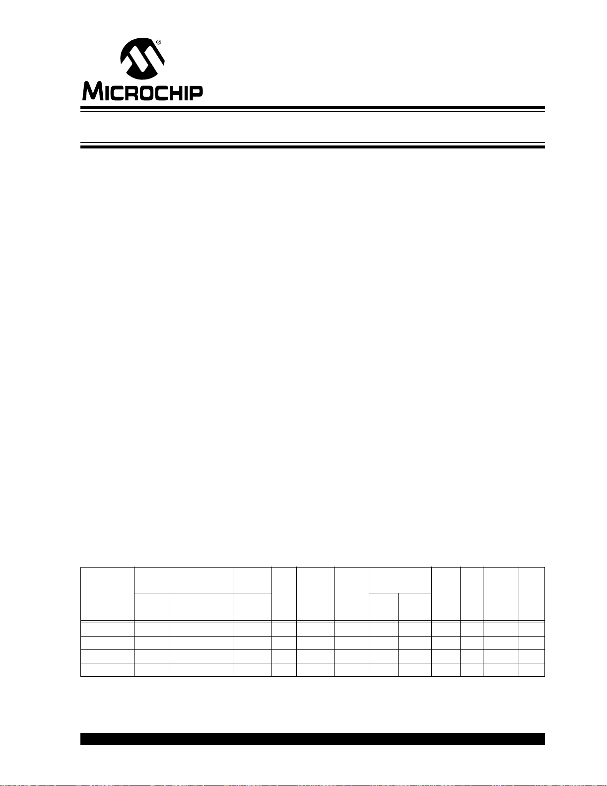
Device
PIC18F6310 8K/0 4096/0 768 54 12 3 Y Y 1/1 2 1/3 N
PIC18F6410 16K/0 8192/0 768 54 12 3 Y Y 1/1 2 1/3 N
PIC18F8310 8K/2M 4096/1M 768 70 12 3 Y Y 1/1 2 1/3 Y
PIC18F8410 16K/2M 8192/1M 768 70 12 3 Y Y 1/1 2 1/3 Y
2004 Microchip Technology Inc. Preliminary DS39635A-page 1
(On-Board/External)
Flash
(bytes)
# Single-Word
Instructions
Data
Memory
SRAM
(bytes)
I/O
10-bit
A/D (ch)
CCP
(PWM)
SPI™
MSSP
Master
I2C™
EUSART/
AUSART
Comparators
Timers
8/16-bit
Ext.
Bus
PIC18F6310/6410/8310/8410
Pin Diagrams
64-Pin TQFP
(1)
RE2/CS
RE3
RE4
RE5
RE6
RE7/CCP2
RD0/PSP0
VDDVSS
RD1/PSP1
RD2/PSP2
RD3/PSP3
RD4/PSP4
RD5/PSP5
RD6/PSP6
RD7/PSP7
RE1/WR
RE0/RD
RG0/CCP3
RG1/TX2/CK2
RG2/RX2/DT2
RG3
RG5/MCLR
RF5/AN10/CV
RF2/AN7/C1OUT
/VPP
RG4
VSS
VDD
RF7/SS
RF6/AN11
REF
RF4/AN9
RF3/AN8
64
63 62 61
1
2
3
4
5
6
7
8
9
10
11
12
13
14
15
16
17 18 19 20 21 22 23 24 25 26
RF0/AN5
RF1/AN6/C2OUT
DD
AV
AVSS
PIC18F6310
PIC18F6410
REF-
RA1/AN1
RA2/AN2/V
RA3/AN3/VREF+
RA0/AN0
54 53 52 5158 57 56 5560 59
27 28
SS
V
VDD
RA5/AN4/HLVDIN
29 30
(1)
RA4/T0CKI
50 49
31
RC0/T1OSO/T13CKI
RC1/T1OSI/CCP2
48
47
46
45
44
43
42
41
40
39
38
37
36
35
34
33
32
RC6/TX1/CK1
RC7/RX1/DT1
RB0/INT0
RB1/INT1
RB2/INT2
RB3/INT3
RB4/KBI0
RB5/KBI1
RB6/KBI2/PGC
SS
V
OSC2/CLKO/RA6
OSC1/CLKI/RA7
DD
V
RB7/KBI3/PGD
RC5/SDO
RC4/SDI/SDA
RC3/SCK/SCL
RC2/CCP1
Note 1: RE7 is the alternate pin for CCP2 multiplexing.
DS39635A-page 2 Preliminary 2004 Microchip Technology Inc.
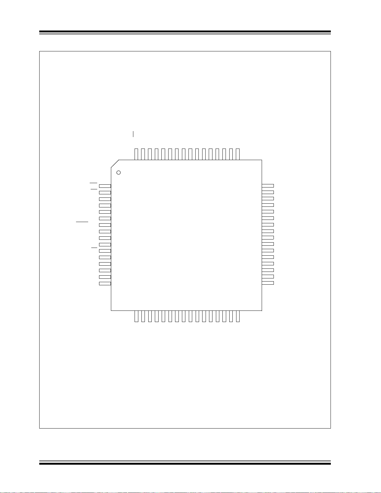
Pin Diagrams (Continued)
80-Pin TQFP
PIC18F6310/6410/8310/8410
/AD15
(1)
RH2/A18
RH3/A19
RE1/AD9/WR
RE0/AD8/RD
RG0/CCP3
RG1/TX2/CK2
RG2/RX2/DT2
RG3
RG5/MCLR
RF5/AN10/CV
RF2/AN7/C1OUT
/VPP
RG4
VSS
VDD
RF7/SS
RF6/AN11
REF
RF4/AN9
RF3/AN8
RH7
RH6
RE2/AD10/CS
RE3/AD11
RE4/AD12
RE5/AD13
RE6/AD14
RE7/CCP2
RH0/A16
RH1/A17
80
79
78
77 76 75
1
2
3
4
5
6
7
8
9
10
11
12
13
14
15
16
17
18
19
20
21 22 23 24 25 26 27 28 29 30 31 32
RD0/AD0/PSP0
PIC18F8310
PIC18F8410
DD
V
VSS
RD1/AD1/PSP1
RD2/AD2/PSP2
RD3/AD3/PSP3
RD4/AD4/PSP4
RD5/AD5/PSP5
RD6/AD6/PSP6
RD7/AD7/PSP7
RJ0/ALE
RJ1/OE
68 67 66 6572 71 70 6974 73
33 34
64 63 62 61
37
35 36 38
60
59
58
57
56
55
54
53
52
51
50
49
48
47
46
45
44
43
42
41
40
39
RJ2/WRL
RJ3/WRH
RB0/INT0
RB1/INT1
RB2/INT2
RB3/INT3/CCP2
RB4/KBI0
RB5/KBI1
RB6/KBI2/PGC
SS
V
OSC2/CLKO/RA6
OSC1/CLKI/RA7
DD
V
RB7/KBI3/PGD
RC5/SDO
RC4/SDI/SDA
RC3/SCK/SCL
RC2/CCP1
RJ7/UB
RJ6/LB
(1)
RH5
RH4
RA1/AN1
RA0/AN0
SS
V
DD
AV
RF0/AN5
RF1/AN6/C2OUT
REF-
AVSS
RA2/AN2/V
RA3/AN3/VREF+
VDD
RA5/AN4/HLVDIN
(1)
RA4/T0CKI
RC1/T1OSI/CCP2
RC0/T1OSO/T13CKI
RJ5/CE
RJ4/BA0
RC6/TX1/CK1
RC7/RX1/DT1
Note 1: RE7 is the alternate pin for CCP2 multiplexing.
2004 Microchip Technology Inc. Preliminary DS39635A-page 3

PIC18F6310/6410/8310/8410
Table of Contents
1.0 Device Overview .......................................................................................................................................................................... 7
2.0 Oscillator Configurations ............................................................................................................................................................ 29
3.0 Power Managed Modes ......................... .. .. .. .. .... ..... .. .. .. .. .... .. .. ..... .. .... .. .. .. .. .. ....... .. .. .. .. .. .. ....... .................................................... 39
4.0 Reset.......................................................................................................................................................................................... 49
5.0 Memory Organization................................................................................................................................................................. 61
6.0 Program Memory........................................................................................................................................................................ 85
7.0 External Memory Interface......................................................................................................................................................... 89
8.0 8 x 8 Hardware Multip lier.................... ................................. ................. ................. ..................................................................... 99
9.0 Interrupts.................................................................................................................................................................................. 101
10.0 I/O Ports.................................... ...............................................................................................................................................117
11.0 Timer0 Module .........................................................................................................................................................................143
12.0 Timer1 Module .........................................................................................................................................................................147
13.0 Timer2 Module .........................................................................................................................................................................153
14.0 Timer3 Module .........................................................................................................................................................................155
15.0 Capture/Compare/PWM (CCP) Modules ................................................................................................................................. 159
16.0 Master Synchronous Serial Port (MSSP) Module .................................................................................................................... 169
17.0 Enhanced Universal Synchronous Asynchronous Receiver Transmitter (EUSART)...............................................................209
18.0 Addressable Universal Synchronous Asynchronous Receiver Transmitter (AUS ART ) ........................................................... 231
19.0 10-Bit Analog-to-Digital Converter (A/D) Module .....................................................................................................................245
20.0 Comparator Module.......................................................................... .... .. .... ......... .. .... .... .. ......................................................... 255
21.0 Comparator Voltage Reference Module................................................................................................................................... 261
22.0 High/Low-Voltage Detect (HLVD).............................................................................................................................................265
23.0 Special Features of the CPU.............. ................ ................. ................. ................. ............... .................................................... 271
24.0 Instruction Set Summary.......................................................................................................................................................... 287
25.0 Development Support............................................................................................................................................................... 337
26.0 Electrical Characteristics.......................................................................................................................................................... 343
27.0 DC and AC Characteristics Graphs and Tables....................................................................................................................... 379
28.0 Packaging Informa tio n..... ................. ................ ................. ................. ................. ..................................................................... 381
Appendix A: Revision History............................................................................................................................................................. 385
Appendix B: Device Differences......................................................................................................................................................... 385
Appendix C: Conversion Considerations .................................................................... .... .. .... .. .... ....................................................... 386
Appendix D: Migration from Baseline to Enhanced Devices..............................................................................................................386
Appendix E: Migration from Mid-Range to Enhanced Devices ..........................................................................................................387
Appendix F: Migration from High-End to Enhanced Devices.............................................................................................................387
Index .................................................................................................................................................................................................. 389
On-Line Support.................................................................... .. .... .... .. ......... .. .... .... .. ......... .. .................................................................399
Systems Information and Upgrade Hot Line......................................................................................................................................399
Reader Response.............................................................................................................................................................................. 400
PIC18F6310/6410/8310/8410 Product Identification System ............................................................................................................401
DS39635A-page 4 Preliminary 2004 Microchip Technology Inc.

PIC18F6310/6410/8310/8410
TO OUR VALUED CUSTOMERS
It is our intention to provide our valued customers with the best documentation possible to ensure successful use of your Microchip
products. To this end, we will continue to improve our publications to better suit your needs. Our publications will be refined and
enhanced as new volumes and updates are introduced.
If you have any questions or c omm ents regarding t his publication, p lease c ontact the M arket ing Co mmunications Department via
E-mail at docerrors@mail.microchip.com or fax the Reader Response Form in the back of this data sheet to (480) 792-4150.
We welcome your feedback.
Most Current Data Sheet
To obtain the most up-to-date version of this data sheet, please register at our Worldwide Web site at:
http://www.microchip.com
You can determine the version of a data sheet by examining its literature number found on the bottom outside corner of any page.
The last character of the literature number is the version number, (e.g., DS30000A is version A of document DS30000).
Errata
An errata sheet, describing minor operational differences from the data sheet and recommended workarounds, may exist for current
devices. As device/documentation issues become known to us, we will publish an errata sheet. The errata will specify the revision
of silicon and revision of document to which it applies.
To determine if an errata sheet exists for a particular device, please check with one of the following:
• Microchip’s Worldwide Web site; http://www.microchip.com
• Your local Microchip sales office (see last page)
• The Microchip Corporate Literature Center; U.S. FAX: (480) 792-7277
When contacting a sales office or the literature center, please specify which device, revision of silicon and data sheet (include
literature number) you are using.
Customer Notification System
Register on our web site at www.microchip.com/cn to receive the most current information on all of our products.
2004 Microchip Technology Inc. Preliminary DS39635A-page 5

PIC18F6310/6410/8310/8410
NOTES:
DS39635A-page 6 Preliminary 2004 Microchip Technology Inc.

PIC18F6310/6410/8310/8410
1.0 DEVICE OVERVIEW
This documen t conta i ns dev ic e spec if i c in for m at i on fo r
the following devices:
• PIC18F6310 • PIC18LF6310
• PIC18F6410 • PIC18LF6410
• PIC18F8310 • PIC18LF8310
• PIC18F8410 • PIC18LF8410
This family offers the advantages of all PIC18
microcontrollers – namely, high computational
performance at an economical price. In addition to
these features, the PIC18F6310/6410/8310/8410
family introduces design enhancements that make
these microcontrollers a logical choice for many
high-performance, power sensitive applications.
1.1 New Core Features
1.1.1 nanoWatt TECHNOLOGY
All of the devices in the PIC18F6310/6410/8310/8410
family incorporate a range of features that can
significantly reduce power consumption during
operation. Key items include:
• Alternate Run Modes: By clocking the controller
from the Timer1 source or the internal oscillator
block, power consumption during code execution
can be reduced by as much as 90%.
• Multiple Idle Modes: The controller can also run
with its CPU core disabled, bu t the peripheral s still
active. In these st ates, powe r consumpt ion can be
reduced even further – t o as litt le as 4% of nor mal
operation requirements.
• On-the-Fly Mode Switching: The power
managed modes a re invo ked b y user code durin g
operation, allowing the user to incorporate
power-saving ideas into their application’s
software design.
• Lower Consumption in Key Modules: The
power requirements for both Timer1 and the
Watchdog Timer have been reduced by up to
80%, with typical values of 1.1 µA and 2.1 µA,
respectively.
1.1.2 MULTIPLE OSCILLATOR OPTIONS AND FEATURES
All of the devices in the PIC18F6310/6410/8310/8410
family offer nine different oscillator options, allowing
users a wide range o f choices i n develo ping applica tion
hardware. These include:
• Four Crystal modes, using crystals or ceramic
resonators.
• Two External Clock modes, offering the option of
using two pins (oscillator input and a divide-by-4
clock output) or one pin (oscillator input, with the
second pin reassigned as general I/O).
• Two External RC Oscillator modes, with the same
pin options as the External Clock modes.
• An internal oscillator block which provides an
8 MHz clock (±2% accuracy) and an INTRC
source (approximately 31kHz, stable over
temperature and V
user selectable cl oc k frequ enc ie s betw ee n
125 kHz to 4 MHz for a total of eight clock
frequencies. This option frees the two oscillator
pins for use as additional general purpose I/O.
• A Phase Lock Loop (PLL) frequency multiplier,
available to both the High-Speed Crystal and
Internal Oscillator modes, which allows clock
speeds of up to 40MHz. Used with the internal
oscillator, the PLL gives users a complete
selection of clock speeds from 31 kHz to 32 MHz
– all without using an external crystal or clock
circuit.
Besides its ava ilability as a cloc k source, the intern al
oscillator block pro vid es a s t ab le re fere nce source that
gives the family additional features for robust
operation:
• Fail-Safe Clock Monitor: This option constantly
monitors the main clock source against a
reference signal provided by the internal
oscillator. If a clock failure occurs, the controller i s
switched to the internal oscillator block, allowing
for continued low-speed operation or a safe
application shutdown.
• Two-Speed Start-up: This option allows the
internal oscillator to serve as the clock source
from Power-on Reset or wake-up from Sleep
mode until the primary clock source is available.
DD), as well as a range of six
2004 Microchip Technology Inc. Preliminary DS39635A-page 7

PIC18F6310/6410/8310/8410
1.2 Other Special Features
• Memory Endurance: The Flas h cells f or prog ram
memory are rated to last for approximately a
thousand erase/write cycles. Data retention
without refresh is conservatively estimated to be
greater than 100 years.
• External Memory Interface: For those
applications where mo re p r ogra m o r data storage
is needed, the PIC18F 8310/8 410 dev ices provid e
the ability to access external memory devices.
The memory interface is configurable for both
8-bit and 16-bit data widths and uses a standard
range of control signals to enable communication
with a wide range of memory devices. With their
21-bit program counters, the 80-pin dev ic es can
access a linear memory space of up to 2 Mbytes.
• Extended Instruction Set: The
PIC18F6310/6410/8310/8410 family introduces
an optional extension to th e PIC18 instr uction set,
which adds 8 new instructions and an Indexed
Addressing mode. This extension, enabled as a
device configuration option, has been specifically
designed to optimize re-entrant application code
originally developed in high-level languages such
as ‘C’.
• Enhanced Addressable USART: This serial
communication module is capable of standard
RS-232 operation an d provides support for th e LIN
bus protocol. Other enhancements include
Automatic Baud Rate Detec tion an d a 16-bit Baud
Rate Generator for improved resolu tion. When the
microcontroller is using the internal oscillator
block, the EUSART provides stable operation for
applications that talk to the outside world, without
using an external crystal (or its accompanying
power requirement).
• 10-bit A/D Converter: This module incorporates
programmable acquisition time, allowing for a
channel to be selected and a conversion to be
initiated withou t wai ting for a sampling period and
thus, reduces code overhead.
• Extended Watchdog Timer (WDT): This
enhanced version in corpora tes a 1 6-bit pre scale r,
allowing a time-out range from 4 ms to over
2 minutes that is stable across operating voltage
and temperature.
1.3 Details on Individual Family Members
Devices in the PIC18F 6310/6410 /8310/8410 famil y are
available in 64-pin (PIC18F6310/8310) and 80-pin
(PIC18F6410/8410) packages. Block diagrams for the
two groups are shown in Figure 1-1 and Figure 1-2,
respectively.
The devices are differentiated from each other in three
ways:
1. Flash Program Me mory: 8 Kbytes in PIC1 8FX310
devices, 16 Kbytes in PIC18FX410 devices.
2. I/O Ports: 7 bidirectional ports on 64-pin
devices, 9 bidirectional ports on 80-pin devices.
3. External Memory Interface: present on 80-pin
devices only.
All other features fo r device s in this family are identi cal.
These are summarized in Table 1-1.
The pinouts for all devices are listed in Table 1-2 and
Table 1-3.
Like all Microchip PIC18 devices, members of the
PIC18F6310/6410/8310/8410 family are available as
both standard and low-voltage devices. Standard
devices with Flash memory, designated with an “F” in
the part number (such a s PIC18F63 10), acc ommoda te
an operating V
parts, designated by “LF” (such as PIC18LF6410),
function over an extended V
DD range of 4.2V to 5.5V. Low-voltage
DD range of 2.0V to 5.5V.
DS39635A-page 8 Preliminary 2004 Microchip Technology Inc.
PIC18F6310/6410/8310/8410
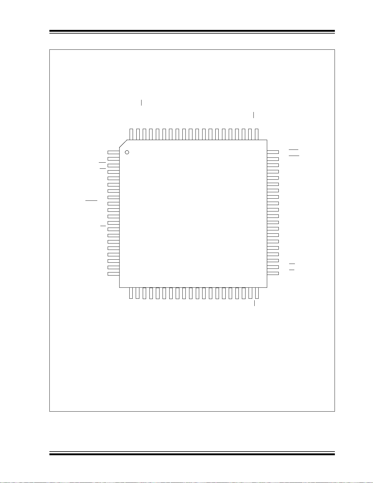
TABLE 1-1: DEVICE FEATURES
Features PIC18F6310 PIC18F6410 PIC18F8310 PIC18F8410
Operating Frequency DC – 40 MHz DC – 40 MHz DC – 40 MHz DC – 40 MHz
Program Memory (Bytes) 8K 16K 8K 16K
Program Memory (Instruction s) 4096 8192 4096 8192
Data Memory (Bytes) 768 768 768 768
External Memory Interface No No Yes Yes
Interrupt Sources 22 22 22 22
I/O Ports Ports A, B, C, D, E,
F, G
Timers 4444
Capture/Compare/PWM Modules 3 3 3 3
Serial Communications MSSP, AUSART
Enhanced USART
Parallel Communications PSP PSP PSP PSP
10-bit Analog-to-Digital Module 12 Input Channels 12 Input Channels 12 Input Channels 12 Input Channels
Resets (and Delays) POR, BOR, RESET
Instruction,
Stack Full,
Stack Underflow
(PWRT, OST),
(optional),
MCLR
WDT
Programmable Low-Voltage Detect Yes Yes Yes Yes
Programmable Brown-out Reset Yes Yes Yes Yes
Instruction Set 75 Instructions;
83 with Extended
Instruction Set
enabled
Packages 64-pin TQFP 64-pin TQFP 80-pin TQFP 80-pin TQFP
Ports A, B, C, D, E,
F, G
MSSP, AUSART
Enhanced USART
POR, BOR, RESET
Instruction,
Stack Full,
Stack Underflow
(PWRT, OST),
(optional),
MCLR
WDT
75 Instructions;
83 with Extended
Instruction Set
enabled
Ports A, B, C, D, E,
F, G, H, J
MSSP, AUSART
Enhanced USART
POR, BOR, RESET
Instruction,
Stack Full,
Stack Underflow
(PWRT, OST),
(optional),
MCLR
WDT
75 Instructions;
83 with Extended
Instruction Set
enabled
Ports A, B, C, D, E,
F, G, H, J
MSSP, AUSART
Enhanced USART
POR, BOR, RESET
Instruction,
Stack Full,
Stack Underflow
(PWRT, OST),
(optional),
MCLR
WDT
75 Instructions;
83 with Extended
Instruction Set
enabled
2004 Microchip Technology Inc. Preliminary DS39635A-page 9
PIC18F6310/6410/8310/8410
FIGURE 1-1: PIC18F6310/6410 (64-PIN) BLOCK DIAGRAM
Instruction
Decode and
Control
Data Latch
Data Memory
(8/16 Kbytes)
Address Latc h
Data Address< 12>
BSR
12
Access
PORTA
PORTB
PORTC
RA0/AN0
RA1/AN1
RA2/AN2/VREFRA3/AN3/VREF+
RA4/T0CKI
RA5/AN4/HLVDIN
RB0/INT0
RB1/INT1
RC0/T1OSO/T13CKI
RC1/T1OSI/CCP2
RC2/CCP1
RC3/SCK/SCL
RC4/SDI/SDA
RC5/SDO
RC6/TX1/CK1
RC7/RX1/DT1
(1)
DS39635A-page 10 Preliminary 2004 Microchip Technology Inc.
PIC18F6310/6410/8310/8410
FIGURE 1-2: PIC18F8310/8410 (80-PIN) BLOCK DIAGRAM
PORTA
PORTB
PORTC
PORTD
RA0/AN0
RA1/AN1
RA2/AN2/VREFRA3/AN3/VREF+
RA4/T0CKI
RA5/AN4/HLVDIN
OSC2/CLKO
OSC1/CLKI
RB0/INT0
RB1/INT1
RB2/INT2
RB3/INT3/CCP2
RB4/KBI0
RB5/KBI1
RB6/KBI2/PGC
RB7/KBI3/PGD
RC0/T1OSO/T13CKI
RC1/T1OSI/CCP2
RC2/CCP1
RC3/SCK/SCL
RC4/SDI/SDA
RC5/SDO
RC6/TX1/CK1
RC7/RX1/DT1
(3)
(3)
/RA7
/RA6
(1)
(1)
OSC1
OSC2
T1OSI
T1OSO
MCLR
V
VDD,
8
PORTE
PRODLPRODH
8 x 8 Multiply
3
BITOP
(3)
(3)
(2)
SS
Internal
Oscillator
Block
INTRC
Oscillator
8 MHz
Oscillator
Single-Supply
Programming
In-Circuit
Debugger
Power-up
Timer
Oscillator
Start-up Timer
Power-on
Reset
Watchdog
Timer
Brown-out
Reset
Fail-Safe
Clock Monitor
Precision
Band Gap
Reference
W
8
8
8
ALU<8>
8
8
8
8
PORTF
PORTH
RF0/AN5
RF1/AN6/C2OUT
RF2/AN7/C1OUT
RF3/AN8
RF4/AN9
RF5/AN10/CV
RF6/AN11
RF7/SS
RH3/AD19:RH0/AD16
RH7:RH4
REF
Note 1: CCP2 multiplexing is determined by the settings of the CCP2MX and PM1:PM0 configuration bits.
2: RG5 is only available when MCLR
3: OSC1/CLKI and OSC2/CLKO are only available in select oscillator modes and when these pins are not being used as digital I/O.
Refer to Section 2.0 “Oscillator Configurations ” for additional information.
functionality is disabled.
2004 Microchip Technology Inc. Preliminary DS39635A-page 11

PIC18F6310/6410/8310/8410
TABLE 1-2: PIC18F6310/6410 PINOUT I/O DESCRIPTIONS
Pin Name
Pin Number
TQFP
Pin
Type
Buffer
Type
Description
RG5/MCLR/VPP
RG5
MCLR
VPP
OSC1/CLKI/RA7
OSC1
CLKI
RA7
OSC2/CLKO/RA6
OSC2
CLKO
RA6
Legend: TTL = TTL compatible input CMOS = CMOS compatible input or output
ST = Schmitt Trigger input with CMOS levels Analog = Analog input
I = Input O = Output
P = Power OD = Open-Drain (no P diode to V
Note 1: Default assignment for CCP2 when configuration bit CCP2MX is set.
2: Alternate assignment for CCP2 when configuration bit CCP2MX is cleared.
39
40
7
I
I
P
I
I
CMOS
I/O
O
O
I/O
Master Clear (input) or programming voltage (input).
ST
ST
ST
TTL
—
—
TTL
Digital input.
Master Clear (Reset) input. This pin is an active-low
Reset to the device.
Programming voltage input.
Oscillator crystal or external clock input.
Oscillator crystal input or external clock source input.
ST buffer when configured in RC mode, CMOS
otherwise.
External clock source input. Always associated
with pin function OSC1. (See related OSC1/CLKI,
OSC2/CLKO pins.)
General purpose I/O pin.
Oscillator crystal or clock output.
Oscillator crystal output. Connects to crystal or
resonator in Crystal Oscillator mode.
In RC mode, OSC2 pin outputs CLKO, which has
1/4 the frequency of OSC1 and denotes the
instruction cycle rate.
General purpose I/O pin.
DD)
DS39635A-page 12 Preliminary 2004 Microchip Technology Inc.

PIC18F6310/6410/8310/8410
T ABLE 1-2: PIC18F6310/6410 PINOUT I/O DESCRIPTIONS (CONTINUED)
Pin Name
Pin Number
TQFP
Pin
Type
Buffer
Type
Description
PORTA is a bidirectional I/O port.
RA0/AN0
RA0
AN0
RA1/AN1
RA1
AN1
RA2/AN2/V
RA2
AN2
V
RA3/AN3/V
RA3
AN3
V
RA4/T0CKI
RA4
T0CKI
RA5/AN4/HLVDIN
RA5
AN4
HLVDIN
RA6 See the OSC2/CLKO/RA6 pin.
RA7 See the OSC1/CLKI/RA7 pin.
Legend: TTL = TTL compatible input CMOS = CMOS compatible input or output
Note 1: Default assignment for CCP2 when configuration bit CCP2MX is set.
REF-
REF-
REF+
REF+
ST = Schmitt Trigger input with CMOS levels Analog = Analog input
I = Input O = Output
P = Power OD = Open-Drain (no P diode to V
2: Alternate assignment for CCP2 when configuration bit CCP2MX is cleared.
24
23
22
21
28
27
I/O
I/O
I/O
I/O
I/OIST/OD
I/O
TTL
I
Analog
TTL
I
Analog
TTL
I
Analog
I
Analog
TTL
I
Analog
I
Analog
ST
TTL
I
Analog
I
Analog
Digital I/O.
Analog input 0.
Digital I/O.
Analog input 1.
Digital I/O.
Analog input 2.
A/D reference voltage (low) input.
Digital I/O.
Analog input 3.
A/D reference voltage (high) input.
Digital I/O. Open-drain when configured as output.
Timer0 external clock input.
Digital I/O.
Analog input 4.
High/Low-Voltage Detect input.
DD)
2004 Microchip Technology Inc. Preliminary DS39635A-page 13

PIC18F6310/6410/8310/8410
TABLE 1-2: PIC18F6310/6410 PINOUT I/O DESCRIPTIONS (CONTINUED)
Pin Name
RB0/INT0
RB0
INT0
RB1/INT1
RB1
INT1
RB2/INT2
RB2
INT2
RB3/INT3
RB3
INT3
RB4/KBI0
RB4
KBI0
RB5/KBI1
RB5
KBI1
RB6/KBI2/PGC
RB6
KBI2
PGC
Pin Number
TQFP
48
47
46
45
44
43
42
Pin
Type
I/O
I
I/O
I
I/O
I
I/O
I
I/O
I
I/O
I
I/O
I
I/O
Buffer
Type
TTL
ST
TTL
ST
TTL
ST
TTL
ST
TTL
TTL
TTL
TTL
TTL
TTL
ST
Description
PORTB is a bidirectional I/O port. PORTB can be software
programmed for internal weak pull-ups on all inputs.
Digital I/O.
External interrupt 0.
Digital I/O.
External interrupt 1.
Digital I/O.
External interrupt 2.
Digital I/O.
External interrupt 3.
Digital I/O.
Interrupt-on-change pin.
Digital I/O.
Interrupt-on-change pin.
Digital I/O.
Interrupt-on-change pin.
In-Circuit Debugger and ICSP™ programming clock pin.
RB7/KBI3/PGD
RB7
KBI3
PGD
Legend: TTL = TTL compatible input CMOS = CMOS compatible input or output
ST = Schmitt Trigger input with CMOS levels Analog = Analog input
I = Input O = Output
P = Power OD = Open-Drain (no P diode to V
Note 1: Default assignment for CCP2 when configuration bit CCP2MX is set.
2: Alternate assignment for CCP2 when configuration bit CCP2MX is cleared.
37
I/O
I/O
TTL
I
TTL
ST
Digital I/O.
Interrupt-on-change pin.
In-Circuit Debugger and ICSP programming data pin.
DD)
DS39635A-page 14 Preliminary 2004 Microchip Technology Inc.

PIC18F6310/6410/8310/8410
T ABLE 1-2: PIC18F6310/6410 PINOUT I/O DESCRIPTIONS (CONTINUED)
Pin Name
Pin Number
TQFP
Pin
Type
Buffer
Type
Description
PORTC is a bidirectional I/O port.
RC0/T1OSO/T13CKI
RC0
T1OSO
T13CKI
RC1/T1OSI/CCP2
RC1
T1OSI
(1)
CCP2
RC2/CCP1
RC2
CCP1
RC3/SCK/SCL
RC3
SCK
SCL
RC4/SDI/SDA
RC4
SDI
SDA
RC5/SDO
RC5
SDO
RC6/TX1/CK1
RC6
TX1
CK1
30
29
33
34
35
36
31
I/O
O
I/O
I/O
I/O
I/O
I/O
I/O
I/O
I/O
I/O
I/O
O
I/O
O
I/O
ST
—
I
I
I
ST
ST
CMOS
ST
ST
ST
ST
ST
ST
ST
ST
ST
ST
—
ST
—
ST
Digital I/O.
Timer1 oscillator output.
Timer1/Timer3 external clock input.
Digital I/O.
Timer1 oscillator input.
Capture 2 input/Compare 2 output/PWM 2 output.
Digital I/O.
Capture 1 input/Compare 1 output/PWM 1 output.
Digital I/O.
Synchronous serial clock input/output for SPI™ mode.
Synchronous serial clock input/output for I2C™ mode.
Digital I/O.
SPI data in.
2
C data I/O.
I
Digital I/O.
SPI data out.
Digital I/O.
EUSART1 asynchronous transmit.
EUSART1 synchronous clock (see related RX1/DT1).
RC7/RX1/DT1
RC7
RX1
DT1
Legend: TTL = TTL compatible input CMOS = CMOS compatible input or output
ST = Schmitt Trigger input with CMOS levels Analog = Analog input
I = Input O = Output
P = Power OD = Open-Drain (no P diode to V
Note 1: Default assignment for CCP2 when configuration bit CCP2MX is set.
2: Alternate assignment for CCP2 when configuration bit CCP2MX is cleared.
2004 Microchip Technology Inc. Preliminary DS39635A-page 15
32
I/O
I/O
ST
I
ST
ST
Digital I/O.
EUSART1 asynchronous receive.
EUSART1 synchronous data (see related TX1/CK1).
DD)

PIC18F6310/6410/8310/8410
TABLE 1-2: PIC18F6310/6410 PINOUT I/O DESCRIPTIONS (CONTINUED)
Pin Name
Pin Number
TQFP
Pin
Type
Buffer
Type
Description
PORTD is a bidirectional I/O port.
RD0/PSP0
RD0
PSP0
RD1/PSP1
RD1
PSP1
RD2/PSP2
RD2
PSP2
RD3/PSP3
RD3
PSP3
RD4/PSP4
RD4
PSP4
RD5/PSP5
RD5
PSP5
RD6/PSP6
RD6
PSP6
RD7/PSP7
RD7
PSP7
Legend: TTL = TTL compatible input CMOS = CMOS compatible input or output
ST = Schmitt Trigger input with CMOS levels Analog = Analog input
I = Input O = Output
P = Power OD = Open-Drain (no P diode to V
Note 1: Default assignment for CCP2 when configuration bit CCP2MX is set.
2: Alternate assignment for CCP2 when configuration bit CCP2MX is cleared.
58
55
54
53
52
51
50
49
I/O
I/O
I/O
I/O
I/O
I/O
I/O
I/O
I/O
I/O
I/O
I/O
I/O
I/O
I/O
I/O
ST
TTL
ST
TTL
ST
TTL
ST
TTL
ST
TTL
ST
TTL
ST
TTL
ST
TTL
Digital I/O.
Parallel Slave Port data.
Digital I/O.
Parallel Slave Port data.
Digital I/O.
Parallel Slave Port data.
Digital I/O.
Parallel Slave Port data.
Digital I/O.
Parallel Slave Port data.
Digital I/O.
Parallel Slave Port data.
Digital I/O.
Parallel Slave Port data.
Digital I/O.
Parallel Slave Port data.
DD)
DS39635A-page 16 Preliminary 2004 Microchip Technology Inc.

PIC18F6310/6410/8310/8410
T ABLE 1-2: PIC18F6310/6410 PINOUT I/O DESCRIPTIONS (CONTINUED)
Pin Name
Pin Number
TQFP
Pin
Type
Buffer
Type
Description
PORTE is a bidirectional I/O port.
RE0/RD
RE0
RD
RE1/WR
RE1
WR
RE2/CS
RE2
CS
RE3 63 I/O ST Digital I/O.
RE4 62 I/O ST Digital I/O.
RE5 61 I/O ST Digital I/O.
RE6 60 I/O ST Digital I/O.
RE7/CCP2
RE7
(2)
CCP2
Legend: TTL = TTL compatible input CMOS = CMOS compatible input or output
ST = Schmitt Trigger input with CMOS levels Analog = Analog input
I = Input O = Output
P = Power OD = Open-Drain (no P diode to V
Note 1: Default assignment for CCP2 when configuration bit CCP2MX is set.
2: Alternate assignment for CCP2 when configuration bit CCP2MX is cleared.
64
59
2
I/O
I
1
I/O
I
I/O
I
I/O
I/O
ST
TTL
ST
TTL
ST
TTL
ST
ST
Digital I/O.
Read control for Parallel Slave Port.
Digital I/O.
Write control for Parallel Slave Port.
Digital I/O.
Chip select control for Parallel Slave Port.
Digital I/O.
Capture 2 input/Compare 2 output/PWM 2 output.
DD)
2004 Microchip Technology Inc. Preliminary DS39635A-page 17

PIC18F6310/6410/8310/8410
TABLE 1-2: PIC18F6310/6410 PINOUT I/O DESCRIPTIONS (CONTINUED)
Pin Name
Pin Number
TQFP
Pin
Type
Buffer
Type
Description
PORTF is a bidirectional I/O port.
RF0/AN5
RF0
AN5
RF1/AN6/C2OUT
RF1
AN6
C2OUT
RF2/AN7/C1OUT
RF2
AN7
C1OUT
RF3/AN8
RF3
AN8
RF4/AN9
RF4
AN9
RF5/AN10/CV
RF5
AN10
CVREF
RF6/AN11
RF6
AN11
REF
18
17
16
15
14
13
12
I/O
I/O
O
I/O
O
I/O
I/O
I/O
O
I/O
ST
I
Analog
ST
I
Analog
—
ST
I
Analog
—
ST
I
Analog
ST
I
Analog
ST
I
Analog
Analog
ST
I
Analog
Digital I/O.
Analog input 5.
Digital I/O.
Analog input 6.
Comparator 2 output.
Digital I/O.
Analog input 7.
Comparator 1 output.
Digital I/O.
Analog input 8.
Digital I/O.
Analog input 9.
Digital I/O.
Analog input 10.
Comparator reference voltage output.
Digital I/O.
Analog input 11.
RF7/SS
RF7
SS
Legend: TTL = TTL compatible input CMOS = CMOS compatible input or output
ST = Schmitt Trigger input with CMOS levels Analog = Analog input
Pin Number
11
Pin
Type
I/O
ST
I
TTL
Digital I/O.
SPI slave select input.
DS39635A-page 18 Preliminary 2004 Microchip Technology Inc.
PIC18F6310/6410/8310/8410
T ABLE 1-2: PIC18F6310/6410 PINOUT I/O DESCRIPTIONS (CONTINUED)
Pin Name
Pin Number
TQFP
Pin
Type
Buffer
Type
Description
PORTG is a bidirectional I/O port.
RG0/CCP3
RG0
CCP3
RG1/TX2/CK2
RG1
TX2
CK2
RG2/RX2/DT2
RG2
RX2
DT2
RG3 6 I/O ST Digital I/O.
RG4 8 I/O ST Digital I/O.
RG5 See RG5/MCLR
VSS 9, 25, 41, 56 P — Ground reference for logic and I/O pins.
VDD 10, 26, 38, 57 P — Positive supply for logic and I/O pins.
SS 20 P — Ground refer ence for analog modules.
AV
AVDD 19 P — Positive supply for analog modules.
Legend: TTL = TTL compatible input CMOS = CMOS compatible input or output
ST = Schmitt Trigger input with CMOS levels Analog = Analog input
I = Input O = Output
P = Power OD = Open-Drain (no P diode to V
Note 1: Default assignment for CCP2 when configuration bit CCP2MX is set.
2: Alternate assignment for CCP2 when configuration bit CCP2MX is cleared.
3
I/O
I/O
4
I/O
O
I/O
5
I/O
I
I/O
ST
ST
ST
—
ST
ST
ST
ST
Digital I/O.
Capture 3 input/Compare 3 output/PWM 3 output.
Digital I/O.
AUSART2 asynchronous transmit.
AUSART2 synchronous clock (see related RX2/DT2).
Digital I/O.
AUSART2 asynchronous receive.
AUSART2 synchronous data (see related TX2/CK2).
/VPP pin.
DD)
2004 Microchip Technology Inc. Preliminary DS39635A-page 19

PIC18F6310/6410/8310/8410
TABLE 1-3: PIC18F8310/8410 PINOUT I/O DESCRIPTIONS
Pin Name
Pin Number
TQFP
Pin
Type
Buffer
Type
Description
RG5/MCLR/VPP
RG5
MCLR
VPP
OSC1/CLKI/RA7
OSC1
CLKI
RA7
OSC2/CLKO/RA6
OSC2
CLKO
RA6
Legend: TTL = TTL compatible input CMOS = CMOS compatible input or output
ST = Schmitt Trigger input with CMOS levels Analog = Analog input
I = Input O = Output
P = Power OD = Open-Drain (no P diode to V
Note 1: Alternate assignment for CCP2 when configuration bit CCP2MX is cleared (all operating modes except
Microcontroller mode).
2: Default assignment for CCP2 in all operating modes (CCP2MX is set).
3: Alternate assignment for CCP2 when CCP2MX is cleared (Microcontroller mode only).
49
50
9
I
I
P
I
I
CMOS
I/O
O
O
I/O
Master Clear (input) or programming voltage (input).
ST
ST
ST
TTL
—
—
TTL
Digital input.
Master Clear (Reset) input. This pin is an active-low
Reset to the device.
Programming voltage inp ut.
Oscillator crystal or external clock input.
Oscillator crystal input or external clock source input.
ST buffer when configured in RC mode, CMOS
otherwise.
External clock source input. Always associated with
pin function OSC1. (See related OSC1/CLKI,
OSC2/CLKO pins.)
General purpose I/O pin.
Oscillator crystal or clock output.
Oscillator crystal output. Connects to crystal or
resonator in Crystal Oscillator mode.
In RC mode, OSC2 pin outputs CLKO, which has
1/4 the frequency of OSC1 and denotes the
instruction cycle rate.
General purpose I/O pin.
DD)
DS39635A-page 20 Preliminary 2004 Microchip Technology Inc.

PIC18F6310/6410/8310/8410
T ABLE 1-3: PIC18F8310/8410 PINOUT I/O DESCRIPTIONS (CONTINUED)
PORTA is a bidirectional I/O port.
RA0/AN0
RA0
AN0
RA1/AN1
RA1
AN1
RA2/AN2/V
RA2
AN2
V
RA3/AN3/V
RA3
AN3
V
RA4/T0CKI
RA4
T0CKI
RA5/AN4/HLVDIN
RA5
AN4
HLVDIN
RA6 See the OSC2/CLKO/RA6 pin.
RA7 See the OSC1/CLKI/RA7 pin.
REF-
REF-
REF+
REF+
30
29
28
27
34
33
I/O
I/O
I/O
I/O
I/OIST/ODSTDigital I/O. Open-drain when configured as output.
I/O
TTL
I
Analog
TTL
I
Analog
TTL
I
Analog
I
Analog
TTL
I
Analog
I
Analog
TTL
I
Analog
I
Analog
Digital I/O.
Analog input 0.
Digital I/O.
Analog input 1.
Digital I/O.
Analog input 2.
A/D reference voltage (low) input.
Digital I/O.
Analog input 3.
A/D reference voltage (high) input.
Timer0 external clock input.
Digital I/O.
Analog input 4.
High/Low-Voltage Detect input.
2004 Microchip Technology Inc. Preliminary DS39635A-page 21

PIC18F6310/6410/8310/8410
TABLE 1-3: PIC18F8310/8410 PINOUT I/O DESCRIPTIONS (CONTINUED)
Pin Name
RB0/INT0
RB0
INT0
RB1/INT1
RB1
INT1
RB2/INT2
RB2
INT2
RB3/INT3/CCP2
RB3
INT3
(1)
CCP2
Pin Number
TQFP
58
57
56
55
Pin
Type
I/O
I
I/O
I
I/O
I
I/O
I
O
Buffer
Type
TTL
ST
TTL
ST
TTL
ST
TTL
ST
Analog
Description
PORTB is a bidirectional I/O port. PORTB can be software
programmed for internal weak pull-ups on all inputs.
Digital I/O.
External interrupt 0.
Digital I/O.
External interrupt 1.
Digital I/O.
External interrupt 2.
Digital I/O.
External interrupt 3.
Capture 2 input/Compare 2 output/PWM 2 output.
RB4/KBI0
RB4
KBI0
RB5/KBI1
RB5
KBI1
RB6/KBI2/PGC
RB6
KBI2
PGC
RB7/KBI3/PGD
RB7
KBI3
PGD
Legend: TTL = TTL compatible input CMOS = CMOS compatible input or output
ST = Schmitt Trigger input with CMOS levels Analog = Analog input
I = Input O = Output
P = Power OD = Open-Drain (no P diode to V
Note 1: Alternate assignment for CCP2 when configuration bit CCP2MX is cleared (all operating modes except
Microcontroller mode).
2: Default assignment for CCP2 in all operating modes (CCP2MX is set).
3: Alternate assignment for CCP2 when CCP2MX is cleared (Microcontroller mode only).
54
53
52
47
I/O
I/O
I/O
I/O
I/O
I/O
TTL
I
TTL
TTL
I
TTL
TTL
I
TTL
ST
TTL
I
TTL
ST
Digital I/O.
Interrupt-on-change pin.
Digital I/O.
Interrupt-on-change pin.
Digital I/O.
Interrupt-on-change pin.
In-Circuit Debugger and ICSP™ program mi ng clo ck pin.
Digital I/O.
Interrupt-on-change pin.
In-Circuit Debugger and ICSP programming data pin.
DD)
DS39635A-page 22 Preliminary 2004 Microchip Technology Inc.

PIC18F6310/6410/8310/8410
T ABLE 1-3: PIC18F8310/8410 PINOUT I/O DESCRIPTIONS (CONTINUED)
Pin Name
Pin Number
TQFP
Pin
Type
Buffer
Type
Description
PORTC is a bidirectional I/O port.
RC0/T1OSO/T13CKI
RC0
T1OSO
T13CKI
RC1/T1OSI/CCP2
RC1
T1OSI
(2)
CCP2
RC2/CCP1
RC2
CCP1
RC3/SCK/SCL
RC3
SCK
SCL
RC4/SDI/SDA
RC4
SDI
SDA
RC5/SDO
RC5
SDO
RC6/TX1/CK1
RC6
TX1
CK1
RC7/RX1/DT1
RC7
RX1
DT1
Legend: TTL = TTL compatible input CMOS = CMOS compatible input or output
ST = Schmitt Trigger input with CMOS levels Analog = Analog input
I = Input O = Output
P = Power OD = Open-Drain (no P diode to V
Note 1: Alternate assignment for CCP2 when configuration bit CCP2MX is cleared (all operating modes except
Microcontroller mode).
2: Default assignment for CCP2 in all operating modes (CCP2MX is set).
3: Alternate assignment for CCP2 when CCP2MX is cleared (Microcontroller mode only).
36
35
43
44
45
46
37
38
I/O
O
I/O
I/O
I/O
I/O
I/O
I/O
I/O
I/O
I/O
I/O
O
I/O
O
I/O
I/O
I/O
ST
—
I
I
I
I
ST
ST
CMOS
ST
ST
ST
ST
ST
ST
ST
ST
ST
ST
—
ST
—
ST
ST
ST
ST
Digital I/O.
Timer1 oscillator output.
Timer1/Timer3 external clock input.
Digital I/O.
Timer1 oscillator input.
Capture 2 input/Compare 2 output/PWM 2 output.
Digital I/O.
Capture 1 input/Compare 1 output/PWM 1 output.
Digital I/O.
Synchronous serial clock input/output for SPI™ mode.
Synchronous serial clock input/output for I
Digital I/O.
SPI data in.
I2C data I/O .
Digital I/O.
SPI data out.
Digital I/O.
EUSART1 asynchronous transmit.
EUSART1 synchronous clock (see related RX1/DT1).
Digital I/O.
EUSART1 asynchronous receive.
EUSART1 synchronous data (see related TX1/CK1).
2
C™ mode.
DD)
2004 Microchip Technology Inc. Preliminary DS39635A-page 23

PIC18F6310/6410/8310/8410
TABLE 1-3: PIC18F8310/8410 PINOUT I/O DESCRIPTIONS (CONTINUED)
Pin Name
Pin Number
TQFP
Pin
Type
Buffer
Type
Description
PORTD is a bidirectional I/O port.
RD0/AD0/PSP0
RD0
AD0
PSP0
RD1/AD1/PSP1
RD1
AD1
PSP1
RD2/AD2/PSP2
RD2
AD2
PSP2
RD3/AD3/PSP3
RD3
AD3
PSP3
RD4/AD4/PSP4
RD4
AD4
PSP4
RD5/AD5/PSP5
RD5
AD5
PSP5
72
69
68
67
66
65
I/O
I/O
I/O
I/O
I/O
I/O
I/O
I/O
I/O
I/O
I/O
I/O
I/O
I/O
I/O
I/O
I/O
I/O
ST
TTL
TTL
ST
TTL
TTL
ST
TTL
TTL
ST
TTL
TTL
ST
TTL
TTL
ST
TTL
TTL
Digital I/O.
External memory address/data 0.
Parallel Slave Port data.
Digital I/O.
External memory address/data 1.
Parallel Slave Port data.
Digital I/O.
External memory address/data 2.
Parallel Slave Port data.
Digital I/O.
External memory address/data 3.
Parallel Slave Port data.
Digital I/O.
External memory address/data 4.
Parallel Slave Port data.
Digital I/O.
External memory address/data 5.
Parallel Slave Port data.
RD6/AD6/PSP6
RD6
AD6
PSP6
RD7/AD7/PSP7
RD7
AD7
PSP7
Legend: TTL = TTL compatible input CMOS = CMOS compatible input or output
ST = Schmitt Trigger input with CMOS levels Analog = Analog input
I = Input O = Output
P = Power OD = Open-Drain (no P diode to V
Note 1: Alternate assignment for CCP2 when configuration bit CCP2MX is cleared (all operating modes except
Microcontroller mode).
2: Default assignment for CCP2 in all operating modes (CCP2MX is set).
3: Alternate assignment for CCP2 when CCP2MX is cleared (Microcontroller mode only).
64
63
I/O
I/O
I/O
I/O
I/O
I/O
ST
TTL
TTL
ST
TTL
TTL
Digital I/O.
External memory address/data 6.
Parallel Slave Port data.
Digital I/O.
External memory address/data 7.
Parallel Slave Port data.
DD)
DS39635A-page 24 Preliminary 2004 Microchip Technology Inc.

PIC18F6310/6410/8310/8410
T ABLE 1-3: PIC18F8310/8410 PINOUT I/O DESCRIPTIONS (CONTINUED)
Pin Name
Pin Number
TQFP
Pin
Type
Buffer
Type
Description
PORTE is a bidirectional I/O port.
RE0/AD8/RD
RE0
AD8
RD
RE1/AD9/WR
RE1
AD9
WR
RE2/AD10/CS
RE2
AD10
CS
RE3/AD11
RE3
AD11
RE4/AD12
RE4
AD12
RE5/AD13
RE5
AD13
RE6/AD14
RE6
AD14
78
77
76
75
74
4
I/O
I/O
I
3
I/O
I/O
I
I/O
I/O
I
I/O
I/O
I/O
I/O
I/O
I/O
I/O
I/O
ST
TTL
TTL
ST
TTL
TTL
ST
TTL
TTL
ST
TTL
ST
TTL
ST
TTL
ST
TTL
Digital I/O.
External memory address/data 8.
Read control for Parallel Slave Port.
Digital I/O.
External memory address/data 9.
Write control for Parallel Slave Port.
Digital I/O.
External memory address/data 10.
Chip Select control for Parallel Slave Port.
Digital I/O.
External memory address/data 11.
Digital I/O.
External memory address/data 12.
Digital I/O.
External memory address/data 13.
Digital I/O.
External memory address/data 14.
RE7/CCP2/AD15
RE7
(3)
CCP2
AD15
Legend: TTL = TTL compatible input CMOS = CMOS compatible input or output
ST = Schmitt Trigger input with CMOS levels Analog = Analog input
I = Input O = Output
P = Power OD = Open-Drain (no P diode to V
Note 1: Alternate assignment for CCP2 when configuration bit CCP2MX is cleared (all operating modes except
Microcontroller mode).
2: Default assignment for CCP2 in all operating modes (CCP2MX is set).
3: Alternate assignment for CCP2 when CCP2MX is cleared (Microcontroller mode only).
73
I/O
I/O
I/O
ST
ST
TTL
Digital I/O.
Capture 2 input/Compare 2 output/PWM 2 output.
External memory address/data 15.
DD)
2004 Microchip Technology Inc. Preliminary DS39635A-page 25

PIC18F6310/6410/8310/8410
TABLE 1-3: PIC18F8310/8410 PINOUT I/O DESCRIPTIONS (CONTINUED)
Pin Name
Pin Number
TQFP
Pin
Type
Buffer
Type
Description
PORTF is a bidirectional I/O port.
RF0/AN5
RF0
AN5
RF1/AN6/C2OUT
RF1
AN6
C2OUT
RF2/AN7/C1OUT
RF2
AN7
C1OUT
RF3/AN8
RF3
AN8
RF4/AN9
RF4
AN9
RF5/AN10/CV
RF5
AN10
CVREF
RF6/AN11
RF6
AN11
REF
24
23
18
17
16
15
14
I/O
ISTAnalog
I/O
I
O
I/O
I
O
I/O
ISTAnalog
I/O
ISTAnalog
I/O
I
O
I/O
ISTAnalog
ST
Analog
—
ST
Analog
—
ST
Analog
Analog
Digital I/O.
Analog input 5.
Digital I/O.
Analog input 6.
Comparator 2 output.
Digital I/O.
Analog input 7.
Comparator 1 output.
Digital I/O.
Analog input 8.
Digital I/O.
Analog input 9.
Digital I/O.
Analog input 10.
Comparator reference voltage output.
Digital I/O.
Analog input 11.
RF7/SS
RF7
SS
Legend: TTL = TTL compatible input CMOS = CMOS compatible input or output
ST = Schmitt Trigger input with CMOS levels Analog = Analog input
I = Input O = Output
P = Power OD = Open-Drain (no P diode to V
Note 1: Alternate assignment for CCP2 when configuration bit CCP2MX is cleared (all operating modes except
Microcontroller mode).
2: Default assignment for CCP2 in all operating modes (CCP2MX is set).
3: Alternate assignment for CCP2 when CCP2MX is cleared (Microcontroller mode only).
13
I/O
ST
I
TTL
Digital I/O.
SPI slave select input.
DD)
DS39635A-page 26 Preliminary 2004 Microchip Technology Inc.

PIC18F6310/6410/8310/8410
T ABLE 1-3: PIC18F8310/8410 PINOUT I/O DESCRIPTIONS (CONTINUED)
Pin Name
Pin Number
TQFP
Pin
Type
Buffer
Type
Description
PORTG is a bidirectional I/O port.
RG0/CCP3
RG0
CCP3
RG1/TX2/CK2
RG1
TX2
CK2
RG2/RX2/DT2
RG2
RX2
DT2
RG3 8 I/O ST Digital I/O.
RG4 10 I/O ST Digital I/O.
RG5 See RG5/MCLR
RH0/AD16
RH0
AD16
RH1/AD17
RH1
AD17
RH2/AD18
RH2
AD18
79
80
5
I/O
I/O
6
I/O
O
I/O
7
I/O
I
I/O
I/O
I/O
I/O
I/O
1
I/O
I/O
ST
ST
ST
—
ST
ST
ST
ST
ST
TTL
ST
TTL
ST
TTL
Digital I/O.
Capture 3 input/Compare 3 output/PWM 3 output.
Digital I/O.
AUSART2 asynchronous transmit.
AUSART2 synchronous clock (see related RX2/DT2).
Digital I/O.
AUSART2 asynchronous receive.
AUSART2 synchronous data (see related TX2/CK2).
PORTH is a bidirectional I/O port.
Digital I/O.
External memory address/data 16.
Digital I/O.
External memory address/data 17.
Digital I/O.
External memory address/data 18.
/VPP pin.
RH3/AD19
RH3
AD19
RH4 22 I/O ST Digital I/O.
RH5 21 I/O ST Digital I/O.
RH6 20 I/O ST Digital I/O.
RH7 19 I/O ST Digital I/O.
Legend: TTL = TTL compatible input CMOS = CMOS compatible input or output
ST = Schmitt Trigger input with CMOS levels Analog = Analog input
I = Input O = Output
P = Power OD = Open-Drain (no P diode to V
Note 1: Alternate assignment for CCP2 when configuration bit CCP2MX is cleared (all operating modes except
Microcontroller mode).
2: Default assignment for CCP2 in all operating modes (CCP2MX is set).
3: Alternate assignment for CCP2 when CCP2MX is cleared (Microcontroller mode only).
2
I/O
I/O
ST
TTL
Digital I/O.
External memory address/data 19.
DD)
2004 Microchip Technology Inc. Preliminary DS39635A-page 27

PIC18F6310/6410/8310/8410
TABLE 1-3: PIC18F8310/8410 PINOUT I/O DESCRIPTIONS (CONTINUED)
Pin Name
Pin Number
TQFP
Pin
Type
Buffer
Type
Description
PORTJ is a bidirectional I/O port.
RJ0/ALE
RJ0
ALE
RJ1/OE
RJ1
OE
RJ2/WRL
RJ2
WRL
RJ3/WRH
RJ3
WRH
RJ4/BA0
RJ4
BA0
RJ5/CE
RJ4
CE
RJ6/LB
RJ6
LB
RJ7/UB
RJ7
UB
VSS 11, 31, 51, 70 P — Ground reference for logic and I/O pins.
DD 12, 32, 48, 71 P — Positive supply for logic and I/O pins.
V
AVSS 26 P — Ground reference for analog modules.
AVDD 25 P — Positive supply for analog modules.
Legend: TTL = TTL compatible input CMOS = CMOS compatible input or output
ST = Schmitt Trigger input with CMOS levels Analog = Analog input
I = Input O = Output
P = Power OD = Open-Drain (no P diode to V
Note 1: Alternate assignment for CCP2 when configuration bit CCP2MX is cleared (all operating modes except
Microcontroller mode).
2: Default assignment for CCP2 in all operating modes (CCP2MX is set).
3: Alternate assignment for CCP2 when CCP2MX is cleared (Microcontroller mode only).
62
61
60
59
39
40
41
42
I/O
O
I/O
O
I/O
O
I/O
O
I/O
O
I/O
O
I/O
O
I/O
O
ST
—
ST
—
ST
—
ST
—
ST
—
ST
—
ST
—
ST
—
Digital I/O.
External memory address latch enable.
Digital I/O.
External memory output enable.
Digital I/O.
External memory write low control.
Digital I/O.
External memory write high control.
Digital I/O.
External memory Byte Address 0 control.
Digital I/O
External memory chip enable control.
Digital I/O.
External memory low byte control.
Digital I/O.
External memory high byte control.
DD)
DS39635A-page 28 Preliminary 2004 Microchip Technology Inc.
PIC18F6310/6410/8310/8410
2.0 OSCILLATOR CONFIGURATIONS
2.1 Oscillator Types
PIC18F6310/6410/831 0/8410 devices can be operated
in ten different o scillato r mo des. The user ca n progra m
the configuration bi ts, FOSC3:FOSC 0, in Configuratio n
Register 1H to select one of these ten modes:
1. LP Low-Power Crystal
2. XT Crystal/Resonator
3. HS High-Speed Crystal/Resonator
4. HSPLL High-Speed Crystal/Resonator
with PLL enabled
5. RC E xternal Resistor/Capacitor with
F
OSC/4 output on RA6
6. RCIO External Resisto r/Capacitor w ith I/O
on RA6
7. INTIO1 Internal Oscillator with F
on RA6 and I/O on RA7
8. INTIO2 Internal Oscillator with I/O on RA6
and RA7
9. EC External Clock with F
10. ECIO External Clock with I/O on RA6
OSC/4 output
OSC/4 output
FIGURE 2-1: CRYSTAL/CERAMIC
RESONATOR OPERATION
(XT, LP, HS OR HSPLL
CONFIGURATION)
(1)
C1
(1)
C2
Note 1: See Table 2-1 and T able 2-2 for initial values of
2: A series resistor (R
3: R
OSC1
XTAL
(2)
RS
OSC2
C1 and C2.
strip cut crystals.
F varies with the oscillator mode chosen.
(3)
RF
Sleep
PIC18FXXXX
S) may be required for AT
To
Internal
Logic
T ABLE 2-1: CAPACITOR SELECTION FOR
CERAMIC RESONATORS
Typical Capacitor Values Used:
Mode Freq OSC1 OSC2
2.2 Crystal Oscillator/Cer ami c Resonators
In XT, LP, HS or HSPLL Oscillator modes, a crystal or
ceramic resonator is connected to the OSC1 and
OSC2 pins to establish oscillation. Figure 2-1 shows
the pin connections.
The oscillator design requires the use of a parallel cut
crystal.
Note: Use of a series cut crystal may give a fre-
quency out of the crystal manufacturer’s
specifications.
XT 455 kHz
2.0 MHz
4.0 MHz
HS 8.0 MHz
16.0 MHz
56 pF
47 pF
33 pF
27 pF
22 pF
56 pF
47 pF
33 pF
27 pF
22 pF
Capacitor values are for design guidance only.
These capacitors were tested with the resonators
listed below for basic start-up and operation. These
values are not optimized.
Different cap acitor values may be required to prod uce
acceptable oscillator operation. The user should test
the performance of the oscillator over the expected
DD and temperature range for the application.
V
See the notes following Table 2-2 for additional
information.
Resonators Used:
455 kHz 4.0 MHz
2.0 MHz 8.0 MHz
16.0 MHz
2004 Microchip Technology Inc. Preliminary DS39635A-page 29

PIC18F6310/6410/8310/8410
TABLE 2-2: CAPACITOR SELECTION FOR
CRYSTAL OSCILLATOR
Osc T y pe
LP 32 kHz 33 pF 33 pF
XT 1 MHz 33 pF 33 pF
HS 4 MHz 27 pF 27 pF
Capacitor values are for design guidance only.
These capacitors were tested with the crystals listed
below for basic start-up and operation . These values
are not optimized.
Different capa citor values may be required to produc e
acceptable oscillator operation. The user should test
the performance of the oscillator over the expected
DD and temperature range for the application.
V
See the notes following this table for additional
information.
Note 1: Higher capacit ance increa ses the st ability
Crystal
Freq
200 kHz 15 pF 15 pF
4 MHz 27 pF 27 pF
8 MHz 22 pF 22 pF
20 MHz 15 pF 15 pF
Crystals Used:
32 kHz 4 MHz
200 kHz 8 MHz
1 MHz 20 MHz
of oscillator, but also increases the
start-up time.
2: When operating below 3V V
using certain ceramic resonators at any
voltage, it may be necessary to use the
HS mode or switch to a crystal oscillator.
3: Since each resonator/crystal has its own
characteristics, the user should consult
the resonator/crystal manufacturer for
appropriate values of external
components.
4: Rs may be requ ired to avoid overdrivi ng
crystals with low driv e lev e l spe ci fic ati on.
5: Always verify oscilla tor performance over
DD and temperature range that is
the V
expected for the application.
T ypical Cap acitor V alues
Tested:
C1 C2
DD, or when
An external clock source may also be connected to the
OSC1 pin in the HS mode, as shown in Figure 2-2.
FIGURE 2-2: EXTERNAL CLOCK
INPUT OPERATION
(HS OSCILLATOR
CONFIGURATION)
Clock from
Ext. System
Open
OSC1
OSC2
PIC18FXXXX
(HS Mode)
2.3 External Clock Input
The EC and ECIO Oscillator mode s require an externa l
clock source to be conn ected to the OSC1 pi n. There is
no oscillator start-up time required after a Power-on
Reset or after an exit from Sleep mode.
In the EC Oscillator mode, the oscillator frequency
divided by 4 is available on the OSC2 pin. This signal
may be used f or t e st pu r pos es or t o sy nc hr o n iz e ot he r
logic. Figure 2-3 shows the pin connections for the EC
Oscillator mode.
FIGURE 2-3: EXTERNAL CLOCK
INPUT OPERATION
(EC CONFIGURATION)
Clock from
Ext. System
F
OSC/4
The ECIO Oscillator mo de func tio ns lik e t he EC mod e,
except that the OSC2 pin becomes an additional general purpose I/O pin. The I/O pin becomes bit 6 of
PORTA (RA6). Figure 2-4 shows the pin connections
for the ECIO Oscillator mode.
FIGURE 2-4: EXTERNAL CLOCK
Clock from
Ext. System
RA6
OSC1/CLKI
PIC18FXXXX
OSC2/CLKO
INPUT OPERATION
(ECIO CONFIGURATION)
OSC1/CLKI
PIC18FXXXX
I/O (OSC2)
DS39635A-page 30 Preliminary 2004 Microchip Technology Inc.

PIC18F6310/6410/8310/8410
2.4 RC Oscillator
For timing insensitive applications, the “RC” and
“RCIO” device options offer additional cost savings.
The actual oscillator frequency is a function of several
factors:
• Supply voltage
• Values of the external resistor (R
capacitor (C
• Operating temperature
Given the same device, operating voltage and
temperature and component values, there will also be
unit-to-unit frequency variations. These are due to
factors such as:
• Normal manufacturing variation
• Difference in lead frame capacitance between
package types (especially for low C
• Variations within the tolerance of limits of REXT
and C
In the RC Oscillator mode, the oscillator frequency
divided by 4 is available on the OSC2 pin. This signal
may be used f or t e st pu r pos es or t o sy nc hr o n iz e ot he r
logic. Figure 2-5 shows how the R/C combination is
connected.
EXT)
EXT
EXT) and
EXT values)
2.5 PLL Frequency Multiplier
A Phase Locked Loop (PLL) circuit is provided as an
option for users who want to use a lower frequency
oscillator circuit, or to clock the device up to its highest
rated frequency from a crystal oscillator. This may be
useful for customers who are concerned with EMI due
to high-frequency crys tals, or users who require higher
clock speeds from an internal oscillator.
FIGURE 2-5: RC OSCILLATOR MODE
The RCIO Oscillator mode (Figure 2-6) functions like
the RC mode, except that the OSC2 pin becomes an
additional general purpose I/O pin. The I/O pin
becomes bit 6 of PORTA (RA6).
FIGURE 2-6: RCIO OSCILLATOR MODE
2004 Microchip Technology Inc. Preliminary DS39635A-page 31

PIC18F6310/6410/8310/8410
2.6 Internal Oscillator Block
The PIC18F6310/6410/8310/8410 devices include an
internal oscillator block, which generates two different
clock signals; either can be used as the microcontroller’s clock source. This may eliminate the need for
external oscillator circuits on the OSC1 and/or OSC2
pins.
The main output (INTOSC) is an 8 MHz clock source,
which can be used to directly drive the device clock. It
also drives a postscaler, which can provide a range of
clock frequencies from 31 kHz to 4 MHz. The INTOSC
output is enabled when a clock fre quency from 12 5 kHz
to 8 MHz is selected.
The other clock source is the internal RC oscillator
(INTRC), which provides a nominal 31 kHz output.
INTRC is enabled if it is selected as the device clock
source; it is also ena bled autom atically when an y of the
following are enabled:
• Power-up Timer
• Fail-Safe Clock Monitor
• Watchdog Timer
• Two-Speed Sta rt-up
These features are discussed in greater detail in
Section 2 3.0 “Special Features of the CPU”.
The clock source frequency (INTOSC direct, INTRC
direct or INTOSC postscaler) is selected by configuring
the IRCF bits of the OSCCON register (Register2-2).
2.6.1 INTIO MODES
Using the internal oscillator as the clock source eliminates the need for up to two external oscillator pins,
which can then be used for digital I/O. Two distinct
configurations are available:
• In INTIO1 mode, the OSC2 pin outputs F
while OSC1 functions as RA 7 fo r dig it a l in put a nd
output.
• In INTIO2 mode, OSC1 functions as RA7 and
OSC2 functions as RA6, both for digital input and
output.
2.6.2 INTOSC OUTPUT FREQUENCY
The internal oscillator block is calibrated at the factory
to produce an INTOSC output frequency of 8.0MHz.
The INTRC oscillator operates independently of the
INTOSC source. Any changes in INTOSC across
voltage and temperature are not necessarily reflected
by changes in INTRC and vice versa.
2.6.3 OSCTUNE REGISTER
The internal oscillator’s output has been calibrated at
the factory, but can be adjusted in the user’s application. This is do ne by writi ng to the OSC TUNE regi ster
(Register 2-1). The tuning sensitivity is constant
throughout the tuning range.
OSC/4,
When the OSCTUNE regis ter is mo di fied , the IN T O SC
and INTRC frequencies will begin shifting to the new
frequency. The INTRC clock will reach the new
frequency within 8 clock cycles (approximately
8*32µs = 256 µs). The INTOSC clock will stabilize
within 1 ms. Code execution continues during th is shi ft.
There is no indication that the shift has occurred.
The OSCTUNE register also implements the INTSRC
and PLLEN bits, which control certain features of the
internal oscillator block. The INTSRC bit allows users
to select which internal oscillator provides the clock
source when the 31 kHz frequency option is selected.
This is covered in greater detail in Section 2.7.1
“Oscillator Control Register”.
The PLLEN bit controls the operation of the frequency
multiplier, PLL, in internal oscillator modes.
2.6.4 PLL IN INTOSC MODES
The 4x frequency multiplier can be used with the
internal oscillator block to produce faster device clock
speeds than are normally possible with an internal
oscillator. When enabled, the PLL produces a clock
speed of up to 32MHz.
Unlike HSPLL mode, the PLL is controlled through
software. The control bit, PLLEN (OSCTUNE<6>), is
used to enable or disable its operation.
The PLL is availa ble when the device is configured to use
the internal oscillator block as its primary clock source
(FOSC3:FOSC0 = 1001 or 1000). Additionally, the PLL
will only function when the selected output frequency is
either 4 MHz or 8 MHz (OSCCON<6:4> = 111 or 110). If
both of these condit ions a re not m et, the PLL is disabl ed.
The PLLEN control bit is only functional in those internal oscillator modes where the PLL is available. In all
other modes, it is forced to ‘0’ and is effectively
unavailable.
2.6.5 INTOSC FREQUENCY DRIFT
The factory calibrates the internal oscillator block output (INTOSC) for 8 MH z. How ever, this frequen cy ma y
drift as VDD or temperature changes, which can affect
the controller operation in a variety of ways. It is possible to adjust the INTOSC frequency by modifying the
value in the OS TUNE registe r . This has no effe ct on th e
INTRC clock source frequency.
Tuning the INTOSC source requires knowing when to
make the adjustment, in which direction it should be
made and in some cases, how large a change is
needed. Three examples follow, but other techniques
may be used.
DS39635A-page 32 Preliminary 2004 Microchip Technology Inc.

PIC18F6310/6410/8310/8410
2.6.5.1 Compensating with the AUSART
An adjustment may be required when the AUSART
begins to generate frami ng errors or rec eive s dat a with
2004 Microchip Technology Inc. Preliminary DS39635A-page 33

PIC18F6310/6410/8310/8410
2.7 Clock Sources and
Oscillator Switching
Like previous PIC18 devices, the
PIC18F6310/6410/8310/8410 family includes a feature
that allows the device clock source to be switched from
the main oscillator to an alternate low-frequency clock
source. PIC18F6310/6410/8310/8410 devices offer two
alternate clock sources. When an alternate clock s ource
is enabled, the various power managed operating
modes are available.
Essentially, there are three clock sources for these
devices:
• Primary oscillators
• Secondary oscillators
• Internal oscillator block
The primary oscillators include the Ex ternal Crystal
and Resonator modes, the External RC modes, the
External Clock modes and the internal oscillator block.
The particular mode is defined by the FOSC3:FOSC0
configuration bits. The details of these modes are
covered earlier in this chapter.
The s econdary oscillators are those external sources
not connected to the OSC1 or OSC2 pins. These
sources may continue to operate even after the
controller is placed in a power managed mode.
PIC18F6310/6410/831 0/84 10 d ev ic es o f fe r the Timer1
oscillator as a secon dary oscilla tor . This osc illator , in all
power managed modes, is often the time base for
functions such as a real-time cloc k.
Most often, a 32.768 kHz watch crystal is connected
between the RC0/T1OSO/T13CKI and RC1/T1OSI
pins. Like the LP mode oscillator circuit, loading
capacitors are also connected from each pin to ground.
The Timer1 oscillator is discussed in greater detail in
Section 12.3 “Timer1 Oscillator”.
In addition to being a prim ary clock source, the internal
oscillator block is available as a power managed
mode clock source. T he IN TR C s ource is also used as
the clock source for several special features, such as
the WDT and Fail-Safe Clock Monitor.
The clock sources for the PIC18F6310/6410/8310/8410
devices are shown in Figure 2-8. See Section 23.0
“Special Features of the CPU” for configuration
register details.
FIGURE 2-8: PIC18F6310/6410/8310/8410 CLOCK DIAGRAM
PIC18F6X10/8X10
OSC2
OSC1
T1OSO
T1OSI
Sleep
Secondary Oscillator
T1OSCEN
Enable
Oscillator
4 x PLL
HSPLL
FOSC3:FOSC0
Clock Source Option
for other Modules
DS39635A-page 34 Preliminary 2004 Microchip Technology Inc.

PIC18F6310/6410/8310/8410
2.7.1 OSCILLATOR CONTROL REGISTER
The OSCCON register (Register 2-2) controls several
aspects of the device clock’s operation, both in full
power operation and in power managed modes.
The System Clock Select bits, SCS1:SCS0, select the
clock source. The available clock sources are the primary clock (defined by the FOSC: FOSC0 confi guration
bits), the secondary clock (Timer1 oscillator) and the
internal oscillator block. The clock source changes
immediately after one or more of the bits is written to,
following a brief clock transition interval. The SCS bits
are cleared on all forms of Reset.
The Internal Oscillator Frequency Select bits,
IRCF2:IRCF0, select the frequency output of the
internal oscillator block to drive the device clock. The
choices are the INTRC source, the INTOSC source
(8 MHz) or one of the frequencies derived from the
INTOSC postsca ler (31.25 kHz to 4 M Hz). If the internal
oscillator block is sup ply in g the de vi ce c loc k, changing
the states of these bits will have an immediate change
on the internal oscillator’s output.
When an output frequency of 31 kHz is selected
(IRCF2:IRCF0 = 000), users may choose which internal oscillator acts as the source. This is done with the
INTSRC bit in the OSCTUNE register (OSCTUNE<7>).
Setting this bit selects INTOSC as a 31.25 kHz clock
source by enabling the divide-by-256 output of the
INTOSC postscaler. Clearing INTSRC sel ects INTRC
(nominally 31 kHz) as the clock source.
This option allows users to select the tunable and more
precise INTOSC as a clock source, while maintaining
power savings with a ve ry low clock speed. R egardless
of the setting of INTSRC, INTRC always remains the
clock source for features such as the Watchdog Timer
and the Fail-Safe Clock Monitor.
The OSTS, IOFS and T1RUN bit s ind ic ate wh ich clock
source is currently providing the device clock. The
OSTS bit indicates that the Oscillator Start-up Timer
has timed out and the primary clock is providing the
device clock in primary clock modes. The IOFS bit indicates when t he internal oscillato r block has stabilized
and is providing the device clock in RC Clock modes.
The T1RUN bit (T1CON<6>) indicates when the
Timer1 oscillator is providing the device clock in
secondary clock modes. In power managed modes,
only one of these three bits will be set at any time. If
none of these bits are set, the INTRC is providing the
clock, or the internal oscillator block has just started
and is not yet stable.
The IDLEN bit dete rmines if th e dev ice go es in to Slee p
mode or one of the Idle modes when the SLEEP
instruction is executed.
The use of the flag and control bits in the OSCCON
register is discussed in more detail in Section 3.0
“Power Managed Modes”.
Note 1: The Timer1 oscillator must be enabled to
select the secondary clock source. The
Timer1 oscillator is enabled by setting the
T1OSCEN bit in the Timer1 Control register (T1CON<3>). If the Timer1 oscillator is
not enabled, then any attempt to select a
secondary clock source when executing a
SLEEP instruction will be ignored.
2: It is recommended that the Timer1
oscillator be operating and stable before
executing the SLEEP instr u ct ion or a very
long delay may occur while the Timer1
oscillator starts.
2.7.2 OSCILLATOR TRANSITIONS
PIC18F6310/6410/8310/8410 devices contain circuitry
to prevent clock “glitches” when switching between
clock sources. A short p ause in the device cl ock occurs
during the clock switch. The length of this pause is the
sum of two cycles of the old clock source and three to
four cycles of the new clock source. This formula
assumes that the new clock source is stable.
Clock transitions are discussed in greater detail in
Section 3 .1.2 “Entering Power Managed Modes”.
2004 Microchip Technology Inc. Preliminary DS39635A-page 35

PIC18F6310/6410/8310/8410
REGISTER 2-2: OSCCON: OSCILLATOR CONTROL REGISTER
R/W-0 R/W-1 R/W-0 R/W-0 R
IDLEN IRCF2 IRCF1 IRCF0 OSTS IOFS SCS1 SCS0
bit 7 bit 0
bit 7 IDLEN: Idle Enable bit
1 = Device enters Idle mode on SLEEP instruction
0 = Device enters Sleep mode on SLEEP instruction
bit 6-4 IRCF2:IRCF0: Internal Oscillator Frequency Select bits
111 = 8 M Hz (INTOSC drives clock directly)
110 = 4 MHz
101 = 2 MHz
100 = 1 MHz
011 = 500 kHz
010 = 250 kHz
001 = 125 kHz
000 = 31 kHz (from either INTOSC/256 or INTRC directly)
bit 3 OSTS: Oscillator Start-up Time-out Status bit
1 = Oscillator Start-up Timer time-out has expired; primary oscillator is running
0 = Oscillator Start-up Timer time-out is running; primary oscillator is not ready
bit 2 IOFS: INTOSC Frequency Stable bit
1 = INTOSC frequency is stable
0 = INTOSC frequency is not stable
bit 1-0 SCS1:SCS0: System Clock Select bits
1x = Internal oscillator block
01 = Timer1 oscillator
00 = Primary oscillator
(3)
(1)
(1)
(2)
R-0 R/W-0 R/W-0
Note 1: Depends on state of the IESO configuration bit.
2: Source selected by the INTSRC bit (OSCTUNE<7>), see
Section 2.6.3 “OSCTUNE Register”.
3: Default output frequency of INTOSC on Reset.
Legend:
R = Readable bit W = Writable bit U = Unimplemented bit, read as ‘0’
-n = Value at POR ‘1’ = Bit is set ‘0’ = Bit is cleared x = Bit is unknown
DS39635A-page 36 Preliminary 2004 Microchip Technology Inc.

PIC18F6310/6410/8310/8410
2.8 Effects of Power Managed Modes on the Various Clock Sources
When PRI_IDLE mode is selected, the designated
primary oscillator continues to run without interruption.
For all other power managed modes, the oscillator
using the OSC1 pin is disabled. The OSC1 pin (and
OSC2 pin, if used by the o scillat or) will sto p oscillat ing.
In Secondary Clock modes (SEC_RUN and
SEC_IDLE), the Timer1 oscillator is operating and
providing the device clock. The Timer1 oscillator may
also run in all power managed modes if required to
clock Timer1 or Timer3.
In Internal Oscillator modes (RC_RUN and RC_IDLE),
the internal oscillator block provides the device clock
source. The 31 kHz INTRC output can be used directly
to provide the clock and may be enabled to support various special features, regardless of the power managed
mode (see Section 23.2 “Watchdog Timer (WDT)”
through Section 23.4 “Fail-Safe Clock Monitor” for
more information on WDT, Fail-Safe Clock Monitor and
Two-Speed S tart-up). The INTOSC output at 8MHz may
be used directly to clock the device, or may be divided
down by the postscaler. The INTOSC output is disabled
if the clock is provided directly from the INTRC output.
If the Sleep mode is selected, all clock sources are
stopped. Since all the transistor switching currents
have been stopped, Sleep mode achieves the lowest
current consumption of the device (only leakage
currents).
Enabling any on-chip feature that will operate during
Sleep will increas e the current cons umed during S leep.
The INTRC is required to support WDT operation. The
Timer1 oscillator may be operating to support a
real-time clock. Other features may be operating that
do not require a device clock source (i.e., SSP slave,
PSP, INTn pins and others). Peripherals that may add
significant current consumption are listed in
Section 26.2 “DC Characteristics: Power-Down and
Supply Current”.
2.9 Power-up Delays
Power-up delays are controlled by two timers, s o that no
external Reset circuitry is required for most applications.
The delays ensure that the device is kept in Reset until
the device power supply is stable under normal
circumstances and the primary clock is operating and
stable. For additional information on power-up delays,
see Section 4.5 “Device Reset Timers”.
The first timer is the Power-up Timer (PWRT), which
provides a fixed delay on power-up (parameter 33,
Table 26-12). It is enabled by clearing (= 0) the
PWRTEN
The second timer is the Oscillator Start-up Timer
(OST), intended to keep the chip in Reset until the
crystal oscillator is stable (LP, XT and HS modes). The
OST does this by counting 1024 oscillator cycles
before allowing the oscillator to clock the device.
When the HSPLL Oscillator mode is selected, the
device is kept in Res et for an add iti onal 2ms, following
the HS mode OST delay, so the PLL can lock to the
incoming clock frequ enc y.
There is a delay of interval T
Table 26-12) following POR while the controller
becomes ready to execute instruc tions. This delay runs
concurrently with any other delays. This may be the
only delay that occurs when an y of the EC, RC or INTIO
modes are used as the primary clock source.
configuration bit.
CSD (parameter 38,
TABLE 2-3: OSC1 AND OSC2 PIN STATES IN SLEEP MODE
Oscillator Mode OSC1 Pin OSC2 Pin
RC, INTIO1 Floating, external resistor should pull high At logic low (clock/4 output)
RCIO, INTIO2 Floating, external resistor should pull high Configured as PORTA, bit 6
ECIO Floating, pulled by external clock Configured as PORTA, bit 6
EC Floating, pulled by external clock At logic low (clock/4 output)
LP, XT and HS Feedback inverter disabled at quiescent
voltage level
Note: See Table 4-2 in Section 4.0 “Reset” for time-outs due to Sleep and MCLR
2004 Microchip Technology Inc. Preliminary DS39635A-page 37
Feedback inverter disabled at quiescent
voltage level
Reset.

PIC18F6310/6410/8310/8410
NOTES:
DS39635A-page 38 Preliminary 2004 Microchip Technology Inc.

PIC18F6310/6410/8310/8410
3.0 POWER MANAGED MODES
PIC18F6310/6410/8310/8410 devices offer a total of
seven operating modes for more efficient power
management. These modes provide a variety of
options for selective p ower conservation i n applications
where resources may be limited (i.e., battery-powered
devices).
There are three categories of power managed modes:
• Sleep mode
• Idle modes
• Run modes
These categories define which portions of the device
are clocked and some times , what sp eed. The R un and
Idle modes may use any of the three available clock
sources (primary, secondary or INTOSC multiplexer);
the Sleep mode does not use a clock source.
The power managed modes include several
power-saving features. One of these is the clock
switching feature, offered in other PIC18 devices,
allowing the controller to use the Timer1 oscillator in
place of the primary oscillator. Also included is the
Sleep mode, offered by all PICmicro
all device clocks are stopped.
3.1 Selecting Power Managed Modes
Selecting a power managed mode requires deciding if
the CPU is to be clocked or not and selecting a clock
source. The IDLEN bit con trols CPU clocking , while the
SCS1:SCS0 bits select a clock source. The individual
modes, bit settings, clock sources and affected
modules are summarized in Table 3-1.
®
devices, where
3.1.1 CLOCK SOURCES
The SCS1:SCS0 bits allow the sele ction of one o f three
clock sources for power managed modes. They are:
• the primary clock, as defined by the
FOSC3:FOSC0 configuration bits
• the secondary clock (the Timer1 oscillator)
• the internal oscillator block (for RC modes)
3.1.2 ENTERING POWER MANAGED
MODES
Entering Power Managed Ru n mode, or s witching from
one power managed mode to another, begins by
loading the OSCCON register. The SCS1:SCS0 bits
select the clock source and determine which Run or
Idle mode is being used. Changing th ese bits causes
an immediate switch to the new clock source,
assuming that it is running. The sw itch may also be
subject to clock tra ns iti on delays. These are discus sed
in Section 3.1.3 “Clock Transitions and Status
Indicators” and subsequent sections.
Entry to the Power Managed Idle or Sleep modes is
triggered by the execution of a SLEEP instruction. The
actual mode that results depends on the status of the
IDLEN bit.
Depending on the current mode and the mode being
switched to, a ch ange t o a po wer man aged m ode d oes
not always require setti ng all of these bit s. Many tra nsitions may be done by changing the oscillator select
bits, or chang ing the IDL EN bit pri or to issuin g a SLEEP
instruction. If the IDLEN bit is already configured
correctly, it may only be necessa ry to perform a SLEEP
instruction to switch to the desired mode.
TABLE 3-1: POWER MANAGED MODES
OSCCON bits Module Clocking
Mode
Sleep 0 N/A Off Off None – All clocks are disabled
PRI_RUN N/A 00 Clocked Clocked Primary – LP, XT, HS, HSPLL, RC, EC, INTRC
SEC_RUN N/A 01 Clocked Clocked Secondary – Timer1 Oscillator
RC_RUN N/A 1x Clocked Clocked Internal Oscillator Block
PRI_IDLE 100Off Clocked Primary – LP, XT, HS, HSPLL, RC, EC
SEC_IDLE 101Off Clocked Secondary – Timer1 Oscillator
RC_IDLE 11xOff Clocked Internal Oscillator Block
Note 1: IDLEN reflects its value when the SLEEP instruction is executed.
2: Includes INTOSC and INTOSC postscaler, as well as the INTRC source.
2004 Microchip Technology Inc. Preliminary DS39635A-page 39
IDLEN
<7>
(1)
SCS1:SCS0
<1:0>
CPU Peripherals
Available Clock and Oscillator Source
(2)
This is the normal full power execution mode.
(2)
(2)

PIC18F6310/6410/8310/8410
3.1.3 CLOCK TRANSITIONS AND STATUS INDICATORS
The length of the transition between clock sources is
the sum of two cycles o f the old clo ck so urce an d three
to four cycl es of the new clock so urce. This formula
assumes that the new clock source is stable.
Three bits indicate the current clock source and its
status. They are:
• OSTS (OSCCON<3>)
• IOFS (OSCCON<2>)
• T1RUN (T1CON<6>)
In general, only one of these bits will be set while in a
given power managed mode. When the OSTS bit is
set, the primary clock is providing the device clock.
When the IOFS bit is s et, the I NTOSC output is providing a stable 8 MHz clock source to a divider that actually drives the device clock. When the T1RUN bit is set,
the Timer1 oscillator is providing the clock. If none of
these bits are set, then either the INTRC clock source
is clocking the device or the INTOSC source is not yet
stable.
If the internal oscillator block is configured as the
primary clock source by the FOSC3:FOSC0
configuration bits, then both the OSTS and IOFS bits
may be set when in PRI_RUN or PRI_IDLE modes.
This indicates that the primary clock (INTOSC output)
is generating a stable 8 MHz output. Entering another
Power Managed RC mode at the same frequency
would clear the OSTS bit.
Note 1: Caution should be used when m odifying a
single IRCF bit. I f V DD is less than 3V, it is
possible to select a higher clock speed
than is supported by the low V
Improper device operation may result if
DD/FOSC specifications are violated.
the V
2: Executing a SLEEP instruction does not
necessarily place the device into Sleep
mode. It acts as the trigger to place the
controller into either the Sleep mode or
one of the Idle modes, depending on the
setting of the IDLEN bit.
DD.
3.1.4 MULTIPLE SLEEP COMMANDS
The power managed mode that is invoked with the
SLEEP instruction is determined by the setting of the
IDLEN bit at the time the instruction is executed. If
another SLEEP instruction is executed, the device will
enter the power managed mode specified by IDLEN at
that time. If IDLEN has changed, the device will enter
the new power managed mode specified by the new
setting.
3.2 Run Modes
In the Run modes, clocks to both the core and
peripherals are active. The difference between these
modes is the clock source.
3.2.1 PRI_RUN MODE
The PRI_RUN mode is the normal full power execution
mode of the microcontroller. This is also the default
mode upon a device Reset un less Two-Speed S t art-u p
is enabled (see Section 23.3 “Two-Speed Start-up”
for details). In this m ode, the OSTS bi t is set. Th e IOFS
bit may be set if the internal oscillator block is the
primary clock source (see Section 2.7.1 “Oscillator
Control Register”).
3.2.2 SEC_RUN MODE
The SEC_RUN mode is the compatible mode to the
“clock switching” feature offered in other PIC18
devices. In this mode, the CPU and peripherals are
clocked from the T imer1 os cillator. This gives users the
option of lower power consumption while still using a
high accuracy clock source.
SEC_RUN mode is en tered by sett ing th e SCS1:SCS 0
bits to ‘01’. The device clock source is switched to the
Timer1 oscillator (see Figure 3-1), the primary
oscillator is shut down, the T1RUN bit (T1CON<6>) is
set and the OSTS bit is cleared.
Note: The Timer1 oscillator should already be
running prior to entering SEC_RU N mode.
If the T1OSCEN bit is not set when the
SCS1:SCS0 bits are set to ‘01’, entry to
SEC_RUN mode will not occur. If the
Timer1 oscillator is enabled, but not yet
running, peripheral clocks will be delayed
until the oscillator has started; in such
situations, initial oscillator operation is far
from stable and unpredictable operation
may result.
On transitions from SEC_RUN mode to PRI_RUN, the
peripherals and CPU continue to be clocked from the
Timer1 oscillator while the primary clock is started.
When the primary clo ck bec omes r eady, a clock switch
back to the primary clock occurs (see Figure 3-2).
When the clock switch is complete, the T1RUN bit is
cleared, the OSTS bit is set and the primary clock is
providing the clock. The IDLEN and SCS bits are not
affected by the wake-up; the Timer1 oscillator
continues to run.
DS39635A-page 40 Preliminary 2004 Microchip Technology Inc.
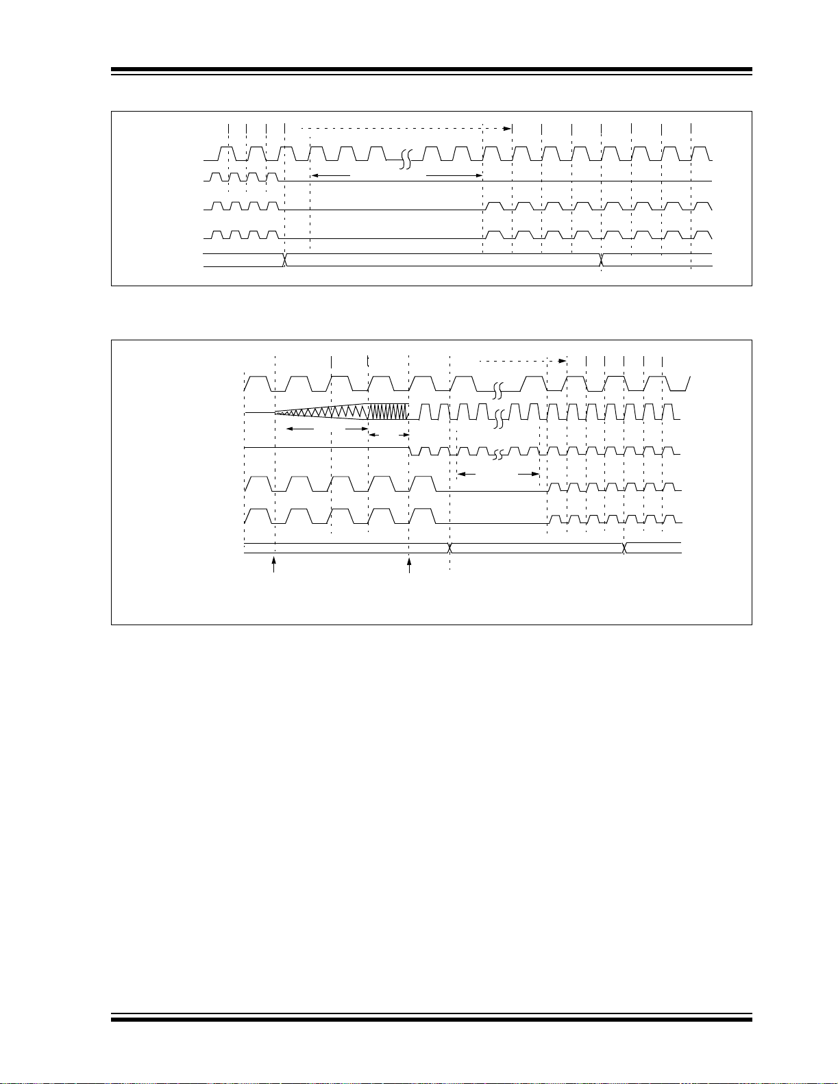
PIC18F6310/6410/8310/8410
FIGURE 3-1: TRANSITION TIMING FOR ENTRY TO SEC_RUN MODE
Q4Q3Q2
Q1
Q1
Q4Q3Q2 Q1 Q3Q2
T1OSI
OSC1
CPU
Clock
Peripheral
Clock
Program
Counter
123 n-1n
Clock Transition
PC + 2PC
PC + 4
FIGURE 3-2: TRANSITION TIMING FROM SEC_RUN MODE TO PRI_RUN MODE (HSPLL)
T1OSI
OSC1
PLL Clock
Output
CPU Clock
Peripheral
Clock
Program
Counter
Q1 Q3 Q4
(1)
TOST
PC
Q3 Q4 Q1
Q2 Q2 Q3
(1)
TPLL
12
n-1 n
Clock
Transition
PC + 2
Q1
Q2
PC + 4
SCS1:SCS0 bits Changed
Note 1: TOST = 1024 TOSC; TPLL = 2 ms (approx). These intervals are not shown to scale.
OSTS bit Set
2004 Microchip Technology Inc. Preliminary DS39635A-page 41
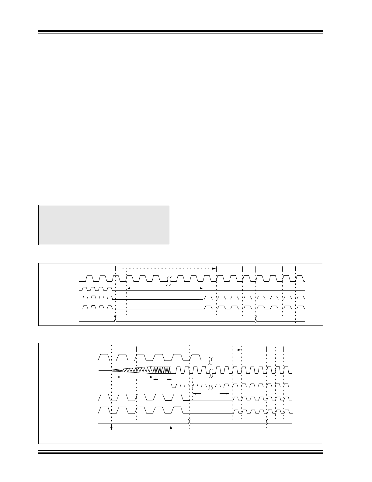
PIC18F6310/6410/8310/8410
3.2.3 RC_RUN MODE
In RC_RUN mode, the CPU and peripherals are
clocked from the internal oscillator block using the
INTOSC multiplexer and the primary clock is shut
down. When using the INTRC source, this mode
provides the best power conservation of all the Run
modes, while still executing code. It works well for user
applications whic h are not h ighly timin g sensiti ve, or do
not require high-speed clocks at all times.
If the primary clock source is the internal oscillator block
(either INTRC or INTOSC), there ar e no distinguishable
differences between PRI_RUN and RC_RUN modes during execution. However, a clock switch delay will occur
during entry to and exit from RC_RUN mode. Therefore,
if the primary clock source is the internal oscillator block,
the use of RC_RUN mode is not recommended.
This mode is entered by setting the SCS1 bit to ‘1’.
Although it is ignored, it is recom mended that the SCS0
bit also be cleared; this is to maintain software
compatibility with future devices. When the clock
source is switched to the INTOSC multiplexer (see
Figure 3-3), the primary oscillator is shut down and the
OSTS bit is cleared.The IRCF bits may be modified at
any time to immediately change the clock speed.
Note: Caution should be used when modifying a
single IRCF bit. If VDD is less than 3V, it is
possible to select a higher clock speed
than is supported by the low V
Improper device operation may result if
the V
DD/FOSC specifications are violated.
DD.
If the IRCF bits and the INTSRC bit are all clear, the
INTOSC output is not enabled and the IOFS bit will
remain clear; there will be no indication of the current
clock source. The INTRC source is providing the
device clocks.
If the IRCF bits are changed from all clear (thus,
enabling the INTOSC output), or if INTSRC is set, the
IOFS bit becomes set after the INTOSC output
becomes stable. Clocks to the device continue while
the INTOSC source stabilizes after an interval of
T
IOBST.
If the IRCF bits were prev io us ly at a non-zero value, or
if INTSRC was set before setting SCS1 and the
INTOSC source was already stable, the IOFS bit will
remain set.
On transitions from RC_RUN mode to PRI_RUN, the
device continues to be clocked from the INTOSC
multiplexer whil e the prim ary clock is st arted. W hen the
primary clock becomes ready, a clock switch to the
primary clock occurs (see Figure 3-4). When the clock
switch is complete, the IOFS bit is cleared, the OSTS
bit is set and the primary clock is providing the device
clock. The IDLEN and SCS bits are not af fe cte d by the
switch. The INTRC source will continue to run if either
the WDT or the Fail-Safe Clock Monitor is enabled.
FIGURE 3-3: TRANSITION TIMING TO RC_RUN MODE
Q4Q3Q2
Q1
123 n-1n
Clock Transition
PC + 2PC
Q4Q3Q2 Q1 Q3Q2
INTRC
OSC1
CPU
Clock
Peripheral
Clock
Program
Counter
Q1
FIGURE 3-4: TRANSITION TIMING FROM RC_RUN MODE TO PRI_RUN MODE
Q3 Q4
Q1
INTOSC
Multiplexer
OSC1
PLL Clock
Output
CPU Clock
Peripheral
Clock
Program
Counter
SCS1:SCS0 bits Changed
Note 1: TOST = 1024 TOSC; TPLL = 2 ms (approx). These intervals are not shown to scale.
TOST
(1)
PC
Q2
Q3
(1)
TPLL
OSTS bit Set
12 n-1n
Clock
Transition
PC + 2
Q1
Q4
Q2
Q1
PC + 4
PC + 4
Q2
Q3
DS39635A-page 42 Preliminary 2004 Microchip Technology Inc.

PIC18F6310/6410/8310/8410
3.3 Sleep Mode
The Power Managed Sleep mode in the
PIC18F6310/6410/8310/8410 devices is identical to
the Legacy Sleep mode offered in all other PICmicro
devices. It is entered by clearing the IDLEN bit (the
default state on device Reset) and executing the
SLEEP instruction. This shuts down the selected
oscillator (see Figure 3-5). All clock source status bits
are cleared.
Entering the Sleep m ode from any other mo de does not
require a clock switch. This is because no clocks are
needed once the controller has entered Sleep. If the
WDT is selected, the INTRC source will continue to
operate. If the Timer1 oscillator is enabled, it will also
continue to run.
When a wake ev ent occurs i n Sleep mo de (by int errupt,
Reset or WDT time-out), the device wil l not be clocke d
until the primary clock source becomes ready (see
Figure 3-6), or it will be clocked from the internal
oscillator block if either the Two-Speed Start-up or the
Fail-Safe Clock Monitor are enabl ed (see Section 23.0
“Special Features of the CPU”). In either case, the
OSTS bit is set whe n t he primary clock is providin g the
device clocks. The IDLEN and SCS bits are not
affected by the wake-up.
3.4 Idle Modes
The Idle modes allow the controller’s CPU to be
®
selectively shut down while the peripherals continue to
operate. Selecting a particular Idle mode allows users
to further manage power consumption.
If the IDLEN bit is set to a ‘1’ when a SLEEP instruction
is executed, the peripherals will be clocked from the
clock source selected using the SCS1:SCS0 bits;
however , the CPU will not be clocked. The cloc k source
status bits are not affected. Setting IDLEN and executing SLEEP provi des a quick method of swi tching from a
given Run mode to its corresponding Idle mode.
If the WDT is selected, the INTRC source will continue
to operate. If the T imer1 oscill ator is enable d, it will also
continue to run.
Since the CPU is not executing instructions, the only
exits from any of the Idle modes are by interrupt, WDT
time-out or a Reset. When a wak e even t occur s, CPU
execution is delayed by an interval of T
CSD
(parameter 38, Tab le 26-12), while it becomes ready to
execute code. When the CPU begins executing code,
it resumes with the same clock source for the current
Idle mode. For example, when waking from RC_IDLE
mode, the internal oscillator block will clock the CPU
and peripherals (in other words, RC_RUN mode). The
IDLEN and SCS bits are not affected by the wake-up.
While in any Idle mode or the Sleep mode, a WDT
time-out will resul t i n a WD T wake-up to the Run mode
currently specified by the SCS1:SCS0 bits.
FIGURE 3-5: TRANSITION TIMING FOR ENTRY TO SLEEP MODE
Q4Q3Q2
Q1Q1
OSC1
CPU
Clock
Peripheral
Clock
Sleep
Program
Counter
PC + 2PC
FIGURE 3-6: TRANSITION TIMING FOR WAKE FROM SLEEP (HSPLL)
OSC1
PLL Clock
Output
CPU Clock
Peripheral
Clock
Program
Counter
Note 1: T
Q1 Q2 Q3 Q4 Q1 Q2
(1)
TOST
Wake Event
OST = 1024 TOSC; TPLL = 2 ms (approx). These intervals are not shown to scale.
(1)
TPLL
PC
OSTS bit Set
Q3 Q4 Q1 Q2
PC + 2
Q3 Q4
PC + 4
Q1 Q2 Q3 Q4
PC + 6
2004 Microchip Technology Inc. Preliminary DS39635A-page 43

PIC18F6310/6410/8310/8410
3.4.1 PRI_IDLE MODE
This mode is unique among the three Low-Power Idle
modes, in that it does not disable the primary device
clock. For timing sensitive applications, this allows for
the fastest resump tion of devic e operation with its more
accurate pri mary clock source, si nce the cl ock source
does not have to “warm up” or transition from another
oscillator.
When a wake event occurs, the CPU is clocked from the
primary clock source. A delay of interval T
required between the wake event and when code
execution starts. This is required to allo w the CPU to
become ready to execute instructions. After the
wake-up, the OSTS bit remains set. The IDLEN and
SCS bits are not affected by the wake-up (see
Figure 3-8).
PRI_IDLE mode is entered from PRI_RUN mode by
setting the IDLEN bit and executing a SLEEP instruction. If the device is in another Run mode, set IDLEN
first, then clear the SCS bits and execute SLEEP.
Although the CPU is disab led, th e peri pherals c ontinu e
to be clocked from the primary clock source specified
by the FOSC3:FOSC0 config uration bit s. The OSTS bit
remains set (see Figure3-7).
FIGURE 3-7: TRANSITION TIMING FOR ENTRY TO PRI_IDLE MODE
Q1
Q4
OSC1
CPU Clock
Q1
Q2
Q3
CSD is
Peripheral
Clock
Program
Counter
PC PC + 2
FIGURE 3-8: TRANSITION TIMING FOR WAKE FROM IDLE TO RUN MODE
OSC1
CPU Clock
Peripheral
Clock
Program
Counter
Q1 Q3 Q4
TCSD
PC
Wake Event
Q2
DS39635A-page 44 Preliminary 2004 Microchip Technology Inc.

PIC18F6310/6410/8310/8410
3.4.2 SEC_IDLE MODE
In SEC_IDLE mode, the CPU is disabled, but the
peripherals continue to be clocked from the Timer1
oscillator. This mode is entered from SEC_RUN by setting the IDLEN bit and executi ng a SLEEP instru ction. If
the device is in anot her Run mode, se t IDLEN first, then
set SCS1:SCS0 to ‘01’ and execute SLEEP. When the
clock source is switched to the Timer1 oscil lator, the
primary oscillator is shut down, the OSTS bit is cleared
and the T1RUN bit is set.
When a wake event occ urs, the pe ripherals co ntinue to
be clocked from the Timer1 oscillator. After an interval
CSD following the wake event, the CP U begins exe-
of T
cuting code being cloc ked by the T i mer1 oscil lator. The
IDLEN and SCS bi ts are not affe cted by the w ake-up;
the Timer1 oscillator continues to run (see Figure 3-8).
Note: The Timer1 oscillator should already be
running prior to entering SEC_IDLE mod e.
If the T1OSCEN bit is not set when the
SLEEP instruction is executed, the SLEEP
instruction will be ignored and entry to
SEC_IDLE mode will not occur. If the
Timer1 oscillator is enabled, but not yet
running, peripheral clocks will be delayed
until the oscillator has started. In such
situations, initial oscillator operation is far
from stable and unpredictable operation
may result.
3.4.3 RC_IDLE MODE
In RC_IDLE mode, the CPU is di sabled, but the p eripherals continue to b e c loc ke d fro m th e i ntern al osc il lat or
block using the INTOSC multiplexer. This mode allows
for controllable pow er cons ervation duri ng Idle p eriods.
From RC_RUN, this mode is entered by setting the
IDLEN bit and executing a SLEEP instruction. If the
device is in an other Run mode, first s et IDLEN, th en set
the SCS1 bit and execute SLEEP. Although its value is
ignored, it is recomm ended that SC S0 also be cleare d;
this is to maintain software compatibility with future
devices. The INTOSC multiplexer may be used to
select a higher clock frequency by modifying the IRCF
bits before executing the SLEEP instruction. When the
clock source is sw itched to the IN TOSC multip lexer , the
primary oscillator is shut down and the OSTS bit is
cleared.
If the IRCF bits are set to any non-zero value, or the
INTSRC bit is set, the INTOSC output is enabled. The
IOFS bit becomes set after the INTOSC output
becomes stable, after an interval of T
(parameter 39, Table 26-12). Clocks to the peripherals
continue while the INTOSC source stabilizes. If the
IRCF bits were previously at a non-zero value, or
INTSRC was set before the SLEEP instruction was
executed and the INTOSC source was already stable,
the IOFS bit will remain set. If the IRCF bits and
INTSRC are all clear, the INTOSC output will not be
enabled; the IOF S bit will r emain cl ear and t here wil l be
no indication of the current clock source.
When a wake event occ urs, the pe ripherals continue to
be clocked from the INTOSC multiplexer. After a delay
CSD following the wake event, the CPU begi ns ex e-
of T
cuting code, being clo cked by the IN T OSC multi plexe r.
The IDLEN and SCS bits are not affected by the
wake-up. The INTRC source will continue to run if
either the WDT or the Fail-Safe Clock Monitor is
enabled.
IOBST
2004 Microchip Technology Inc. Preliminary DS39635A-page 45

PIC18F6310/6410/8310/8410
3.5 Exiting Idle and Sleep Modes
An exit from Sleep mode or any of the Idle modes is
triggered b y an interrupt , a Reset or a WD T time-out.
This section discusses the triggers that cause exits
from power managed modes. The clocking subsystem
actions are discussed in each of the power managed
modes (see Section 3.2 “Run Modes” through
Section 3.4 “Idle Modes”).
3.5.1 EXIT BY INTERRUPT
Any of the available interrupt sources can cause the
device to exit from an Idle or Sleep mode to a Run
mode. To enable this functionality, an interrupt source
must be enabled by setting its enable bit in one of the
INTCON or PIE registers. Th e exit sequ ence is initiate d
when the corresponding interrupt flag bit is set.
On all exits from Idl e or Sleep mod es by inte rrupt, code
execution branches to the interrupt vector if the
GIE/GIEH bit (INTCON<7>) is set. Otherwise, code
execution continues or resumes without branching
(see Section 9.0 “Interrupts”).
A fixed delay of in terval T
is required when leaving Sleep and Idle modes. This
delay is required for the CPU to prepare for execution.
Instructi on execution r esumes on th e first clock c ycle
following this delay.
3.5.2 EXIT BY WDT TIME-OUT
A WDT time-out will cause different actions depending
on which power managed mode the device is in when
the time-out occurs.
If the devic e is not exec uti ng co de (al l Id le mo des and
Sleep mode), the time-out w i ll re sul t in an ex it fro m th e
power managed mode (see Sec tion 3.2 “Run Modes”
and Section 3.3 “Sleep Mode”). If the device is
executing code (a ll R un mod es) , the time-o ut will resu lt
in a WDT Reset (se e Section 23.2 “Watchdog Timer
(WDT)”).
The WDT timer and postscaler are cleared by executing a SLEEP or CLRWDT instruction, lo sing a currently
selected clock source (if the Fail-Safe Clock Monitor is
enabled) and modifying the IRCF bits in the OSCCON
register if the internal os cillator block is the device clock
source.
CSD, following the wake event,
3.5.3 EXIT BY RESET
Normally, the device is held in Reset by the Oscillator
Start-up Timer (OST) until the primary clock becomes
ready. At that time, the OSTS bit is set and the device
begins executing code. If the internal oscillat or block is
the new clock source, the IOFS bit is set instead.
The exit delay time from Reset to the start of code
execution depends on both the clock sources before
and after the wake-up and the type of oscillator if the
new clock source is the primary clock. Exit delays are
summarized in Table 3-2.
Code execution can begin before the primary clock
becomes ready. If either the Two-Speed Start-up (see
Section 23.3 “Two-Speed Start-up”) or Fail-Safe
Clock Monitor (see Section 23.4 “Fail-Safe Clock
Monitor”) is enabled, the device may begin execution
as soon as the Reset source ha s cle are d. Execution is
clocked by the INTOSC multiplexer driven by the
internal oscillator block. Execution is clocked by the
internal oscillator block until either the primary clock
becomes ready, or a power managed mode is entered
before the primary clock becomes ready; the primary
clock is then shut down.
3.5.4 EXIT WITHOUT AN OSCILLATOR START-UP DELAY
Certain exits from power managed modes do not
invoke the OST at all. There are two cases:
• PRI_IDLE mode, where the primary clock source
is not stopped; and
• the primary clock source is not any of the LP, XT,
HS or HSPLL modes.
In these instances, the primary clock source either
does not require an oscillator start-up delay since it is
already running (PRI_IDLE), or normally does not
require an oscillator start-up delay (RC, EC and INTIO
Oscillator modes). However, a fixed delay of interval
CSD, following the wake event, is still required when
T
leaving Sleep and Idle modes to allow the CPU to
prepare for execution. Instruction execution resumes
on the first clock cycle following this delay.
DS39635A-page 46 Preliminary 2004 Microchip Technology Inc.

PIC18F6310/6410/8310/8410
TABLE 3-2: EXIT DELAY ON WAKE-UP BY RESET FROM SLEEP MODE OR ANY IDLE MODE
(BY CLOCK SOURCES)
Clock Source
before Wake-up
Clock Source
after Wake-up
Exit Delay
Clock Ready Status
bit (OSCCON)
Primary Device Clo ck
(PRI_IDLE mode)
T1OSC or INTRC
INTOSC
(1)
(3)
None
(Sleep mode)
LP, XT, HS
HSPLL
EC, RC, INTRC
INTOSC
(1)
(3)
LP, XT, HS TOST
HSPLL T
EC, RC, INTRC
INTOSC
(1)
(2)
LP, XT, HS TOST
HSPLL T
EC, RC, INTRC
INTOSC
(1)
(2)
LP, XT, HS T
HSPLL T
EC, RC, INTRC
INTOSC
(1)
(2)
(2)
T
CSD
(4)
TCSD
TCSD
(2)
(5)
(2)
(4)
rc
(5)
(4)
rc
OST + t
TIOBST
OST + t
None IOFS
(4)
OST
TCSD
(2)
(4)
rc
(5)
OST + t
TIOBST
OSTS
IOFS
OSTS
IOFS
OSTS
OSTS
IOFS
Note 1: In this instance, refers specifically to the 31 kHz INTRC clock source.
2: TCSD (parameter 38) is a requ ire d d ela y when waking from Sleep an d all Id le modes and runs conc urren t ly
with any other required delays (see Section 3.4 “Idle Modes”).
3: Includes both the INTOSC 8 MHz source and postscaler derived frequencies.
OST is the Oscillator Start-up Timer (parameter 32). t
4: T
also designated as T
PLL.
is the PLL Lock-out Timer (parameter F12); it is
rc
5: Execution continues during TIOBST (parameter 39), the INTOSC stabilization period.
—
—
—
—
2004 Microchip Technology Inc. Preliminary DS39635A-page 47

PIC18F6310/6410/8310/8410
NOTES:
DS39635A-page 48 Preliminary 2004 Microchip Technology Inc.

PIC18F6310/6410/8310/8410
4.0 RESET
The PIC18F6310/6410/8310/8410 devices differentiate
between various kinds of Reset:
a) Power-on Reset (POR)
b) MCLR
c) MCLR Reset during power managed modes
d) Watchdog Timer (WDT) Reset (during
e) Programmable Brown-out Reset (BOR)
f) RESET Instruction
g) Stack Full Reset
h) Stack Underflow Reset
This section discusses Resets generated by MCLR
Reset during normal operation
execution)
,
4.1 RCON Register
Device Reset events are tracked through the RCON
register (Register 4-1). The lower five bits of the
register indicate that a specific Reset event has
occurred. In most cases, these bits can only be set by
the event and must be cleared by the application after
the event. The state of these flag bits, taken together,
can be read to indicate the type of Reset that just
occurred. This is described in more detail in
Section 4.6 “Reset State of Registers”.
The RCON register also has control bits for setting
interrupt priority (IPEN) and software control of the
BOR (SBOREN). Interrupt priority is discussed in
Section 9.0 “Interrupts”. BOR is covered in
Section 4.4 “Brown-out Reset (BOR)”.
POR and BOR and covers the ope rati on o f the various
start-up timers. Stack Reset events are covered in
Section 5 .1.3.4 “Stack Full and Underflow Resets”.
WDT Resets are co v ere d i n Section 23.2 “Watchdog
Timer (WDT)”.
A simplified b lock di agram of the On -Chip Re set Ci rcuit
is shown in Figure 4-1.
FIGURE 4-1: SIMPLIFIED BLOCK DIAGRAM OF ON-CHIP RESET CIRCUIT
RESET
Instruction
Stack
Pointer
Stack Full/Underflow Reset
External Reset
Sleep
WDT
DD Rise
Reset
OST
PWRT
MCLRE
POR Pulse
BOREN
1024 Cycles
10-bit Ripple Counter
65.5 ms
11-bit Ripple Counter
S
Chip_Reset
R
Q
Enable PWRT
Enable OST
MCLR
VDD
OSC1
Note 1: This is the INTRC source from the internal oscillator block and is separate from the RC oscillator of the CLKI pin.
2: See Table 4-2 for time-out situations.
( )_IDLE
Time-out
V
Detect
Brown-out
OST/PWRT
32 µs
(1)
INTRC
(2)
2004 Microchip Technology Inc. Preliminary DS39635A-page 49

PIC18F6310/6410/8310/8410
REGISTER 4-1: RCON: RESET CONTROL REGISTER
R/W-0 R/W-1
IPEN SBOREN
bit 7 bit 0
bit 7 IPEN: Interrupt Priority Enable bit
1 = Enable priority levels on interrupts
0 = Disable priority levels on interrupts (PIC16CXXX Compatibility mode)
bit 6 SBOREN: BOR Software Enable bit
If BOREN1:BOREN0 =
1 = BOR is enabled
0 = BOR is disabled
If BOREN1:BOREN0 =
Bit is disabled and read as ‘0’.
Note 1: If SBOREN is enabled, its Reset state is ‘1’; otherwise, it is ‘0’.
bit 5 Unimplemented: Read as ‘0’
bit 4 RI
bit 3 TO
bit 2 PD
bit 1 POR
bit 0 BOR
: RESET Instruction Flag bit
1 = The RESET instruction was not executed (set by firmware only)
0 = The RESET instruction was executed causing a device Reset (must be set in software after
a Brown-out Reset occur s)
: Watchdog Timer Time-out Flag bit
1 = Se t by power-up, CLRWDT instruction or SLEEP instruction
0 = A WDT time-out occurred
: Power-Down Detection Flag bit
1 = Set by power-up or by the CLRWDT instructi on
0 = Se t by execution of the SLEEP instruction
: Power-on Reset Status bit
1 = A Power-on Reset has not occurred (set by firmware only)
0 = A Power-on Reset occurred (must be set in software after a Power-on Reset occurs)
: Brown-out Reset Status bit
1 = A Brown-out Reset has not occurred (set by firmware only)
0 = A Brown-out Reset occurred (must be set in software after a Brown-out Reset occurs)
(1)
01:
00, 10 or 11:
U-0 R/W-1 R-1 R-1 R/W-0 R/W-0
—RITO PD POR BOR
Legend:
R = Readable bit W = Writable bit U = Unimplemented bit, read as ‘0’
-n = Value at POR ‘1’ = Bit is set ‘0’ = Bit is cleared x = Bit is unknown
Note 1: It is recommended that the POR bit be set after a Power-on Reset has been
detected, so that subsequent Power-on Resets may be detected.
2: Brown-out Reset is said to have occurred when BOR is ‘0’ and POR is ‘1’ (assuming
that POR
DS39635A-page 50 Preliminary 2004 Microchip Technology Inc.
was set to ‘1’ by software immediately after POR).

PIC18F6310/6410/8310/8410
4.2 Master Clear (MCLR)
The MCLR pin provides a method for triggering a hard
external Reset of the device. A Reset is generated by
holding the pin low. PIC18 Extended MCU devices
have a noise filter in the MCLR
Reset path which
detects and ignores small pulses.
The MCLR
pin is not drive n low by any inter nal Reset s,
including the WDT.
In PIC18F6310/6410/8310/8410 devices, the MCLR
input can be disabl ed with the MCL RE configuratio n bit.
When MCLR
is disabled, the pin becomes a digital
input. See Section 10.7 “PORTG, TRISG and LATG
Registers” for more information.
4.3 Power-on Reset (POR)
A Power-on Reset pulse is generated on-chip
whenever V
allows the device to start in the initialized state when
VDD is adequate for operation.
To take advantage of the POR circuitry, tie the MCLR
pin throug h a resis tor (1 kΩ to 10 kΩ) to VDD. Thi s wi ll
eliminate external RC components usually needed to
create a Power-on Re set delay. A minimum rise rate for
DD is specified (parameter D004). For a slow rise
V
time, see Figure 4-2.
When the device st arts normal operation (i.e ., ex its the
Reset condition), device operating parameters
(voltage, frequency, temperature, etc.) must be met to
ensure operation. If these conditions are not met, the
device must be held in Reset until the operating
conditions are met.
POR events are captured by the POR
The state of the bit is set to ‘0’ whe never a POR occurs;
it does not change for any other Reset event. POR is
not reset to ‘1’ by any hardware event. To capture
multiple events, the user manually resets the bit to ‘1’
in software following any POR.
DD rises above a certain threshold. This
bit (RCON<1>).
FIGURE 4-2: EXTERNAL POWER-ON
RESET CIRCUIT (FOR
SLOW V
DD
VDD
Note 1: External Power-on Reset circuit is required
V
D
R
C
only if the V
The diode D helps discharge the capacitor
quickly when V
2: R < 40 kΩ is recommended to make sure that
the voltage drop across R does not violate
the device’s electrical specification.
3: R1 ≥ 1 kΩ will limit any current flowing into
MCLR
of MCLR
Electrostatic Discharge (ESD) or Electrical
Overstress (EOS).
DD power-up slope is too slow.
from external capacitor C, in the event
/VPP pin breakdown, due to
DD POWER-UP)
R1
MCLR
PIC18FXXXX
DD powers down.
2004 Microchip Technology Inc. Preliminary DS39635A-page 51

PIC18F6310/6410/8310/8410
4.4 Brown-out Reset (BOR)
PIC18F6310/6410/8310/8410 devices implement a
BOR circuit that provides the user with a number of
configuration and power-saving options. The BOR is
controlled by the BORV1:BORV0 and
BOREN1:BOREN0 configura tion b its . There are a tota l
of four BOR configurations, which are summarized in
Table 4-1.
The BOR threshold is set by the BORV1:BORV0 bits. If
BOR is enabled (any values of BOREN1:BOREN0
except ‘00’), any drop of V
(parameter D005) for greater than TBOR (parameter 35)
will reset the device. A Reset may or may not occur if
DD falls below VBOR for less than TBOR. The chip will
V
remain in Brown-out Reset until V
If the Power-up T imer is enabl ed, it will be inv oked after
DD rises above VBOR; it then will keep the chip in
V
Reset for an additional time delay, T
(parameter 33). If VDD drops below VBOR while the
Power-up Timer is running, the chip will go back into a
Brown-out Reset and the Power-up Timer will be
initialized. Once V
Timer will execute the additional time delay.
BOR and the Power-up Timer (PWRT) are
independently configured. Enabling the BOR Reset
does not automatically enable the PWRT.
DD rises above VBOR, the Power-up
4.4.1 SOFTWARE ENABLED BOR
When BOREN1:BOREN0 = 01, the BOR can be
enabled or disabled by the user in software. This is
done with the control bit, SBOREN (RCON<6>).
Setting SBOREN enables the BOR to function as
previously described. Clearing SBOREN disables the
BOR entirely. The SBOREN bit operates only in this
mode; otherwise, it is read as ‘0’.
DD below VBOR
DD rises above VBOR.
PWRT
Placing the BOR under software control gives the user
the additional flexibility of tailoring the application to its
environment withou t ha vi ng to reprogram the device to
change the BOR configuration. It also allows the user
to tailor device power consumption in software by
eliminating the incremental current that the BOR
consumes. While the BOR current is typically very
small, it may have some impact in low-power
applications.
Note: Even whe n BOR is u nder softwar e control,
the BOR Reset voltage level is still set by
the BORV1:BORV0 configuration bits. It
cannot be changed in software.
4.4.2 DETECTING BOR
When BOR is enab led, the BO R bit always resets to ‘0’
on any BOR or P OR event. This makes it diff icult to
determine if a BOR event has occurre d jus t by rea ding
the state of BOR
simultaneously check the state of both POR
This assumes th at the POR
immediately after any POR event. IF BOR
is ‘1’, it can be reliably assum ed that a BOR event
POR
has occurred.
alone. A more reliable method is to
and BOR.
bit is reset to ‘1’ in softwa re
is ‘0’ while
4.4.3 DISABLING BOR IN SLEEP MODE
When BOREN1:BOREN0 = 10, the BOR remains
under hardware control and operates as previously
described. Whenever the device enters Sleep mode,
however , the BOR is au tom ati ca lly dis abl ed . When the
device returns to any other operating mode, BOR is
automatically re-enabled.
This mode allows for applications to recover from
brown-out situations, while actively executing code,
when the device requires BOR protection the most. At
the same time, it save s additional po wer in Sleep mod e
by eliminating the small incremental BOR current.
TABLE 4-1: BOR CONFIGURATIONS
BOR Configuration Status of
BOREN1 BOREN0
00Unavailable BOR is disabled; must be enabled by reprogramming the configuration bits.
01Available BOR is enabled in software; operation controlled by SBOREN.
10Unavailable BOR is enabled in hardware and active during the Run and Idle modes,
11Unavailable BOR is enabled in hardware; must be disabled by reprogramming the
DS39635A-page 52 Preliminary 2004 Microchip Technology Inc.
SBOREN
(RCON<6>)
disabled during Sleep mode.
configuration bits.
BOR Operation

PIC18F6310/6410/8310/8410
4.5 Device Reset Timers
PIC18F6310/6410/8310/8410 devices incorporate
three separate on-chip timers that help regulate the
Power-on Reset process. Their main function is to
ensure that the device clock is stable before code is
executed. These timers are:
• Power-up Timer (PWRT)
• Oscillator Start-up Timer (OST)
• PLL Lock Time-out
4.5.1 POWER-UP TIMER (PWRT)
The Power-up Timer (PWRT) of the
PIC18F6310/6410/8310/8410 devices is an 11-bit
counter which uses the INTRC source as the clock
input. This yields an approximate time interval of
2048 x 32 µs = 65.6 ms. While the PWRT is counting,
the device is held in Reset.
The power-up time delay depe nd s on the INTRC cl oc k
and will vary from chip to chip due to temperature and
process variation. See DC parameter 33 for details.
The PWRT is enabled by clearing the PWRTEN
configuration bit.
4.5.2 OSCILLATOR START-UP TIMER (OST)
The Oscillator Start-up Timer (OST) provides a 1024
oscillator cycle (from OSC1 input) delay after the
PWRT delay is ov er (par a me t er 3 3 ). T h is en su re s t ha t
the crystal oscillator or resonator has started and is
stabilized.
The OST time-out is invoked only for XT, LP, HS and
HSPLL modes and only on Power-on Reset, or on exit
from most power managed modes.
4.5.3 PLL LOCK TIME-OUT
With the PLL enabled in its PLL mode, the time-out
sequence following a Power-on Reset is slightly
different from other oscillator modes. A separate timer
is used to provide a fixed time-out that is sufficient for
the PLL to lock to the main oscillator frequency. This
PLL lock time-out (T
the oscillator start-up time-out.
PLL) is typically 2 ms and follows
4.5.4 TIME-OUT SEQUENCE
On power-up, the time-out sequence is as follows:
1. After the POR pulse has cleared, PWRT
time-out is invoked (if enabled).
2. Then, the OST is activated.
The total time-out will vary based on oscillator
configuration and the status of the PWRT. Figure 4-3,
Figure 4-4, Figure 4-5, Figure 4-6 and Figure 4-7 all
depict time-out sequences on power-up, with the
Power-up Timer enabled and the device operating in
HS Oscillator mode. Figure s 4-3 through 4-6 also apply
to devices operating in XT or LP m odes. F or devi ces i n
RC mode and with the PWRT disabled, on the other
hand, there will be no time-out at all.
Since the time-outs occur from the POR pulse, if MC LR
is kept low long enough, all time-outs will expire.
Bringing MCLR
(Figure 4 -5). This is useful for testing purposes or to
synchronize more than one PIC18FXXXX device
operating in parallel.
high will begin execution immediately
TABLE 4-2: TIME-OUT IN VARIOUS SITUATIONS
Oscillator
Configuration
HSPLL 66 ms
HS, XT, LP 66 ms
EC, ECIO 66 ms
RC, RCIO 66 ms
INTIO1, INTIO2 66 ms
Note 1: 66 ms (65.5 ms) is the nominal Power-up Timer (PWRT) delay.
2: 2 ms is the nominal time required for the PLL to lock.
2004 Microchip Technology Inc. Preliminary DS39635A-page 53
PWRTEN = 0 PWRTEN = 1
(1)
+ 1024 TOSC + 2 ms
Power-up
(1)
+ 1024 TOSC 1024 TOSC 1024 TOSC
(1)
(1)
(1)
(2)
and Brown-out
(2)
1024 TOSC + 2 ms
Exit from
Power Managed Mode
(2)
——
——
——
1024 TOSC + 2 ms
(2)

PIC18F6310/6410/8310/8410
FIGURE 4-3: TIME-OUT SEQUENCE ON POWER-UP (MCLR TIED TO VDD, VDD RISE < TPWRT)
VDD
MCLR
INTERNAL POR
TPWRT
PWRT TIME-OUT
OST TIME-OUT
INTERNAL RESET
TOST
FIGURE 4-4: TIME-OUT SEQUENCE ON POWER-UP (MCLR
VDD
MCLR
INTERNAL POR
PWRT TI ME-OUT
OST TIME-OUT
INTERNAL RESET
TPWRT
NOT TIED TO VDD): CASE 1
TOST
FIGURE 4-5: TIME-OUT SEQUENCE ON POWER-UP (MCLR
VDD
MCLR
INTERNAL POR
TPWRT
PWRT TIME-OUT
OST TIME-OUT
INTERNAL RESET
DS39635A-page 54 Preliminary 2004 Microchip Technology Inc.
NOT TIED TO VDD): CASE 2
TOST

PIC18F6310/6410/8310/8410
FIGURE 4-6: SLOW RISE TIME (MCLR TIED TO VDD, VDD RISE > TPWRT)
5V
VDD
MCLR
INTERNAL POR
0V
PWRT
T
1V
PWRT TIME-OUT
OST TIME-OUT
INTERNAL RES ET
TOST
FIGURE 4-7: TIME-OUT SEQUENCE ON POR W/PLL ENABLED (MCLR TIED TO VDD)
VDD
MCLR
INTERNAL POR
TPWRT
PWRT TIME-OUT
OST TIME-OUT
PLL TIME-OUT
TOST
TPLL
INTERNAL RESET
Note: TOST = 1024 clock cycles.
T
PLL ≈ 2 ms max. First three stages of the PWRT timer.
2004 Microchip Technology Inc. Preliminary DS39635A-page 55

PIC18F6310/6410/8310/8410
4.6 Reset State of Registers
Most registers are unaffected by a Reset. Their status
is unknown on POR and unchanged by all other
Table 4-4 describes the Reset states for all of the
Special Function Registers. These are categorized by
Power-on and Brown-out Resets, Master Clear and
WDT Resets and WDT wake-ups.
Resets. The other registers are forced to a “Reset
state” depending on the type of Reset that occurred.
Most registers are not affected by a WDT wake-up,
since this is viewed as the resumption of normal
operation. Status bits from the RCON register, RI
PD
, POR and BOR, are set or cleared differently in
, TO,
different Reset situations, as indicated in Table 4-3.
These bits are use d in softwar e to determine the nature
of the Reset.
TABLE 4-3: STATUS BITS, THEIR SIGNIFICANCE AND THE INITIALIZATION CONDITION FOR
RCON REGISTER
Condition
Program
Counter
SBOREN RI
Power-on Reset 0000h 1 11100 0 0
RESET Instruction 0000h u
Brown-out Reset 0000h u
Reset during Power
MCLR
0000h u
(2)
(2)
(2)
Managed Run Modes
MCLR
Reset during Power
0000h u
(2)
Managed Idle Modes and Sleep
WDT Time-ou t during Full Power
0000h u
(2)
or Power Managed Run Modes
MCLR
Reset during Full Power
0000h u
(2)
Execution
Stack Full Reset (STVREN = 1) 0000h u
Stack Underflow Reset
0000h u
(2)
(2)
(STVREN = 1)
Stack Underflow Error (not an
0000h u
(2)
actual Reset, STVREN = 0)
WDT Time-out during Power
PC + 2 u
(2)
Managed Idle or Sleep Modes
Interrupt Exit from Power
PC + 2
(1)
(2)
u
Managed Modes
Legend: u = unchanged
Note 1: When the wake-up is due to an interrupt and the GIEH or GIEL bits are set, the PC is loaded with the
interrupt vector (008h or 0018h).
2: Reset state is ‘1’ for POR and unchanged for all other Resets when software BOR is enabled
(BOREN1:BOREN0 configuration bits = 01 and SBOREN = 1). Otherwise, the Re set state is ‘0’.
RCON Register STKPTR Register
TO PD POR BOR STKFUL STKUNF
0uuuu u u
111u0 u u
u1uuu u u
u10uu u u
u0uuu u u
uuuuu u u
uuuuu 1 u
uuuuu u 1
uuuuu u 1
u00uu u u
uu0uu u u
DS39635A-page 56 Preliminary 2004 Microchip Technology Inc.

PIC18F6310/6410/8310/8410
TABLE 4-4: INITIALIZATION CONDITIONS FOR ALL REGISTERS
MCLR
Resets
Register
Applicable
Devices
TOSU 6X10 8X10 ---0 0000 ---0 0000 ---0 uuuu
TOSH 6X10 8X10 0000 0000 0000 0000 uuuu uuuu
TOSL 6X10 8X10 0000 0000 0000 0000 uuuu uuuu
STKPTR 6X10 8X10 uu-0 0000 00-0 0000 uu-u uuuu
PCLATU 6X10 8X10 ---0 0000 ---0 0000 ---u uuuu
PCLATH 6X10 8X10 0000 0000 0000 0000 uuuu uuuu
PCL 6X10 8X10 0000 0000 0000 0000 PC + 2
TBLPTRU 6X10 8X10 --00 0000 --00 0000 --uu uuuu
TBLPTRH 6X10 8X10 0000 0000 0000 0000 uuuu uuuu
TBLPTRL 6X10 8X10 0000 0000 0000 0000 uuuu uuuu
TABLAT 6X10 8X10 0000 0000 0000 0000 uuuu uuuu
PRODH 6X10 8X10 xxxx xxxx uuuu uuuu uuuu uuuu
PRODL 6X10 8X10 xxxx xxxx uuuu uuuu uuuu uuuu
INTCON 6X10 8X10 0000 000x 0000 000u uuuu uuuu
INTCON2 6X10 8X10 1111 1111 1111 1111 uuuu uuuu
INTCON3 6X10 8X10 1100 0000 1100 0000 uuuu uuuu
INDF0 6X10 8X10 N/A N/A N/A
POSTINC0 6X10 8X10 N/A N/A N/A
POSTDEC0 6X10 8X10 N/A N/A N/A
PREINC0 6X10 8X10 N/A N/A N/A
PLUSW0 6X10 8X10 N/A N/A N/A
FSR0H 6X10 8X10 ---- xxxx ---- uuuu ---- uuuu
FSR0L 6X10 8X10 xxxx xxxx uuuu uuuu uuuu uuuu
WREG 6X10 8X10 xxxx xxxx uuuu uuuu uuuu uuuu
INDF1 6X10 8X10 N/A N/A N/A
POSTINC1 6X10 8X10 N/A N/A N/A
POSTDEC1 6X10 8X10 N/A N/A N/A
PREINC1 6X10 8X10 N/A N/A N/A
PLUSW1 6X10 8X10 N/A N/A N/A
FSR1H 6X10 8X10 ---- xxxx ---- uuuu ---- uuuu
FSR1L 6X10 8X10 xxxx xxxx uuuu uuuu uuuu uuuu
BSR 6X10 8X10 ---- 0000 ---- 0000 ---- uuuu
Legend: u = unchanged, x = unknown, - = unimplemented bit, read as ‘0’, q = value depends on condition.
Shaded cells indicate condi tions do not apply for the designated device.
Note 1: One or more bits in the INTCONx or PIRx registers will be affected (to cause wake-up).
2: When the wake-up is due to an interrupt a nd the GIEL or G IEH bit is se t, the PC is lo aded wit h the interru pt
vector (0008h or 0018h).
3: When the wake-up is due to an interrupt and the GIEL or GIEH bit is se t, the T O SU, TOSH and TOSL are
updated with the current value of the PC. The STKPTR is modified to point to the next location in the
hardware stack.
4: See Table 4-3 for Reset value for specific condition.
5: Bits 6 and 7 of PORTA, LATA and TRISA are enabled depending on the oscillator mode selected. When
not enabled as PORTA pins, they are disabled and read ‘0’.
Power-on Reset,
Brown-out Reset
WDT Reset
RESET Instruction
Stack Rese ts
Wake-up via WDT
or Interrupt
(3)
(3)
(3)
(3)
(2)
(1)
(1)
(1)
2004 Microchip Technology Inc. Preliminary DS39635A-page 57

PIC18F6310/6410/8310/8410
TABLE 4-4: INITIALIZATION CONDITIONS FOR ALL REGISTERS (CONTINUED)
Resets
MCLR
Register
INDF2 6X10 8X10 N/A N/A N/A
POSTINC2 6X10 8X10 N/A N/A N/A
POSTDEC2 6X10 8X10 N/A N/A N/A
PREINC2 6X10 8X10 N/A N/A N/A
PLUSW2 6X10 8X10 N/A N/A N/A
FSR2H 6X10 8X10 ---- xxxx ---- uuuu ---- uuuu
FSR2L 6X10 8X10 xxxx xxxx uuuu uuuu uuuu uuuu
STATUS 6X10 8X10 ---x xxxx ---u uuuu ---u uuuu
TMR0H 6X10 8X10 0000 0000 0000 0000 uuuu uuuu
TMR0L 6X10 8X10 xxxx xxxx uuuu uuuu uuuu uuuu
T0CON 6X10 8X10 1111 1111 1111 1111 uuuu uuuu
OSCCON 6X10 8X10 0100 q000 0100 00q0 uuuu uuqu
HL VDCON 6X10 8X10 --00 0101 --00 0101 --uu uuuu
WDTCON 6X10 8X10 ---- ---0 ---- ---0 ---- ---u
(4)
RCON
TMR1H 6X10 8X10 xxxx xxxx uuuu uuuu uuuu uuuu
TMR1L 6X10 8X10 xxxx xxxx uuuu uuuu uuuu uuuu
T1CON 6X10 8X10 0000 0000 u0uu uuuu uuuu uuuu
TMR2 6X10 8X10 0000 0000 0000 0000 uuuu uuuu
PR2 6X10 8X10 1111 1111 1111 1111 1111 1111
T2CON 6X10 8X10 -000 0000 -000 0000 -uuu uuuu
SSPBUF 6X10 8X10 xxxx xxxx uuuu uuuu uuuu uuuu
SSPADD 6X10 8X10 0000 0000 0000 0000 uuuu uuuu
SSPSTAT 6X10 8X10 0000 0000 0000 0000 uuuu uuuu
SSPCON1 6X10 8X10 0000 0000 0000 0000 uuuu uuuu
SSPCON2 6X10 8X10 0000 0000 0000 0000 uuuu uuuu
ADRESH 6X10 8X10 xxxx xxxx uuuu uuuu uuuu uuuu
ADRESL 6X10 8X10 xxxx xxxx uuuu uuuu uuuu uuuu
ADCON0 6X10 8X10 --00 0000 --00 0000 --uu uuuu
ADCON1 6X10 8X10 --00 0000 --00 0000 --uu uuuu
ADCON2 6X10 8X10 0-00 0000 0-00 0000 u-uu uuuu
Legend: u = unchanged, x = unknown, - = unimplemented bit, read as ‘0’, q = value depends on condition.
Shaded cells indicate condi tions do not apply for the designated device.
Note 1: One or more bits in the INTCONx or PIRx registers will be affected (to cause wake-up).
2: When the wake-up is due to an interrupt a nd the GIEL or G IEH bit is se t, the PC is lo aded wit h the interru pt
vector (0008h or 0018h).
3: When the wake-up is due to an interrupt and the GIEL or GIEH bit is se t, the T O SU, TOSH and TOSL are
updated with the current value of the PC. The STKPTR is modified to point to the next location in the
hardware stack.
4: See Table 4-3 for Reset value for specific condition.
5: Bits 6 and 7 of PORTA, LATA and TRISA are enabled depending on the oscillator mode selected. When
not enabled as PORTA pins, they are disabled and read ‘0’.
Applicable
Devices
6X10 8X10 0q-1 11q0 0q-q qquu uq-u qquu
Power-on Reset,
Brown-out Reset
WDT Reset
RESET Instruction
Stack Rese ts
Wake-up via WDT
or Interrupt
DS39635A-page 58 Preliminary 2004 Microchip Technology Inc.

PIC18F6310/6410/8310/8410
TABLE 4-4: INITIALIZATION CONDITIONS FOR ALL REGISTERS (CONTINUED)
Resets
MCLR
Register
CCPR1H 6X10 8X10 xxxx xxxx uuuu uuuu uuuu uuuu
CCPR1L 6X10 8X10 xxxx xxxx uuuu uuuu uuuu uuuu
CCP1CON 6X10 8X10 --00 0000 --00 0000 --uu uuuu
CCPR2H 6X10 8X10 xxxx xxxx uuuu uuuu uuuu uuuu
CCPR2L 6X10 8X10 xxxx xxxx uuuu uuuu uuuu uuuu
CCP2CON 6X10 8X10 --00 0000 --00 0000 --uu uuuu
CCPR3H 6X10 8X10 xxxx xxxx uuuu uuuu uuuu uuuu
CCPR3L 6X10 8X10 xxxx xxxx uuuu uuuu uuuu uuuu
CCP3CON 6X10 8X10 --00 0000 --00 0000 --uu uuuu
CVRCON 6X10 8X10 000- 0000 000- 0000 uuu- uuuu
CMCON 6X10 8X10 0000 0111 0000 0111 uuuu uuuu
TMR3H 6X10 8X10 xxxx xxxx uuuu uuuu uuuu uuuu
TMR3L 6X10 8X10 xxxx xxxx uuuu uuuu uuuu uuuu
T3CON 6X10 8X10 0000 0000 uuuu uuuu uuuu uuuu
PSPCON 6X10 8X10 0000 ---- 0000 ---- uuuu ----
SPBRG1 6X10 8X10 0000 0000 0000 0000 uuuu uuuu
RCREG1 6X10 8X10 0000 0000 0000 0000 uuuu uuuu
TXREG1 6X10 8X10 0000 0000 0000 0000 uuuu uuuu
TXSTA1 6X10 8X10 0000 0010 0000 0010 uuuu uuuu
RCSTA1 6X10 8X10 0000 000x 0000 000x uuuu uuuu
IPR3 6X10 8X10 --11 ---1 --11 ---1 --uu ---u
PIR3 6X10 8X10 --00 ---0 --00 ---0 --uu ---u
PIE3 6X10 8X10 --00 ---0 --00 ---0 --uu ---u
IPR2 6X10 8X10 11-- 1111 11-- 1111 uu-- uuuu
PIR2 6X10 8X10 00-- 0000 00-- 0000 uu-- uuuu
PIE2 6X10 8X10 00-- 0000 00-- 0000 uu-- uuuu
IPR1 6X10 8X10 1111 1111 1111 1111 uuuu uuuu
PIR1 6X10 8X10 0000 0000 0000 0000 uuuu uuuu
PIE1 6X10 8X10 0000 0000 0000 0000 uuuu uuuu
MEMCON 6X10 8X10 0-00 --00 0-00 --00 u-uu --uu
OSCTUNE 6X10 8X10 00-0 0000 00-0 0000 uu-u uuuu
TRISJ
TRISH 6X10 8X10 1111 1111 1111 1111 uuuu uuuu
Legend: u = unchanged, x = unknown, - = unimplemented bit, read as ‘0’, q = value depends on condition.
Shaded cells indicate condi tions do not apply for the designated device.
Note 1: One or more bits in the INTCONx or PIRx registers will be affected (to cause wake-up).
2: When the wake-up is due to an interrupt a nd the GIEL or G IEH bit is se t, the PC is lo aded wit h the interru pt
vector (0008h or 0018h).
3: When the wake-up is due to an interrupt and the GIEL or GIEH bit is se t, the T O SU, TOSH and TOSL are
updated with the current value of the PC. The STKPTR is modified to point to the next location in the
hardware stack.
4: See Table 4-3 for Reset value for specific condition.
5: Bits 6 and 7 of PORTA, LATA and TRISA are enabled depending on the oscillator mode selected. When
not enabled as PORTA pins, they are disabled and read ‘0’.
Applicable
Devices
6X10 8X10 1111 1111 1111 1111 uuuu uuuu
Power-on Reset,
Brown-out Reset
WDT Reset
RESET Instruction
Stack Rese ts
Wake-up via WDT
or Interrupt
(1)
(1)
(1)
2004 Microchip Technology Inc. Preliminary DS39635A-page 59
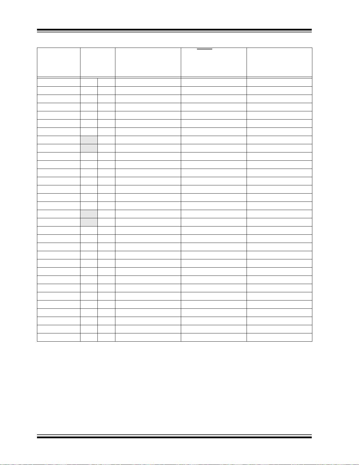
PIC18F6310/6410/8310/8410
TABLE 4-4: INITIALIZATION CONDITIONS FOR ALL REGISTERS (CONTINUED)
Resets
MCLR
Register
Applicable
Devices
TRISG 6X10 8X10 ---1 1111 ---1 1111 ---u uuuu
TRISF 6X10 8X10 1111 1111 1111 1111 uuuu uuuu
TRISE 6X10 8X10 1111 1111 1111 1111 uuuu uuuu
TRISD 6X10 8X10 1111 1111 1111 1111 uuuu uuuu
TRISC 6X10 8X10 1111 1111 1111 1111 uuuu uuuu
TRISB 6X10 8X10 1111 1111 1111 1111 uuuu uuuu
TRISA
(5)
6X10 8X10 1111 1111
LATJ 6X10 8X10 xxxx xxxx uuuu uuuu uuuu uuuu
LATH
6X10 8X10 xxxx xxxx uuuu uuuu uuuu uuuu
LATG 6X10 8X10 ---x xxxx ---u uuuu ---u uuuu
LATF 6X10 8X10 xxxx xxxx uuuu uuuu uuuu uuuu
LATE 6X10 8X10 xxxx xxxx uuuu uuuu uuuu uuuu
LATD 6X10 8X10 xxxx xxxx uuuu uuuu uuuu uuuu
LATC 6X10 8X10 xxxx xxxx uuuu uuuu uuuu uuuu
LATB 6X10 8X10 xxxx xxxx uuuu uuuu uuuu uuuu
LATA
(5)
6X10 8X10 xxxx xxxx
PORTJ 6X10 8X10 xxxx xxxx uuuu uuuu uuuu uuuu
PORTH
6X10 8X10 xxxx xxxx uuuu uuuu uuuu uuuu
PORTG 6X10 8X10 --xx xxxx --uu uuuu --uu uuuu
PORTF 6X10 8X10 xxxx xxxx uuuu uuuu uuuu uuuu
PORTE 6X10 8X10 xxxx xxxx uuuu uuuu uuuu uuuu
PORTD 6X10 8X10 xxxx xxxx uuuu uuuu uuuu uuuu
PORTC 6X10 8X10 xxxx xxxx uuuu uuuu uuuu uuuu
PORTB 6X10 8X10 xxxx xxxx uuuu uuuu uuuu uuuu
PORTA
(5)
6X10 8X10 xx0x 0000
SPBRGH1 6X10 8X10 0000 0000 0000 0000 uuuu uuuu
BAUDCON1 6X10 8X10 01-0 0-00 01-0 0-00 uu-u u-uu
SPBRG2 6X10 8X10 0000 0000 0000 0000 uuuu uuuu
RCREG2 6X10 8X10 0000 0000 0000 0000 uuuu uuuu
TXREG2 6X10 8X10 0000 0000 0000 0000 uuuu uuuu
TXSTA2 6X10 8X10 0000 0010 0000 0010 uuuu uuuu
RCSTA2 6X10 8X10 0000 000x 0000 000x uuuu uuuu
Legend: u = unchanged, x = unknown, - = unimplemented bit, read as ‘0’, q = value depends on condition.
Shaded cells indicate condi tions do not apply for the designated device.
Note 1: One or more bits in the INTCONx or PIRx registers will be affected (to cause wake-up).
2: When the wake-up is due to an interrupt a nd the GIEL or G IEH bit is se t, the PC is lo aded wit h the interru pt
vector (0008h or 0018h).
3: When the wake-up is due to an interrupt and the GIEL or GIEH bit is se t, the T O SU, TOSH and TOSL are
updated with the current value of the PC. The STKPTR is modified to point to the next location in the
hardware stack.
4: See Table 4-3 for Reset value for specific condition.
5: Bits 6 and 7 of PORTA, LATA and TRISA are enabled depending on the oscillator mode selected. When
not enabled as PORTA pins, they are disabled and read ‘0’.
Power-on Reset,
Brown-out Reset
(5)
(5)
(5)
WDT Reset
RESET Instruction
Stack Rese ts
1111 1111
uuuu uuuu
uu0u 0000
(5)
(5)
(5)
Wake-up via WDT
or Interrupt
uuuu uuuu
uuuu uuuu
uuuu uuuu
(5)
(5)
(5)
DS39635A-page 60 Preliminary 2004 Microchip Technology Inc.

PIC18F6310/6410/8310/8410
5.0 MEMORY ORGANIZATION
There are two types of memory in PIC18 Flash
Microcontroller devices:
• Program Memory
• Data RAM
As Harvard architecture dev ices, the dat a and progra m
memories use separate busses; this allows for
concurrent access of the two memory spaces.
Additional detailed information on the operation of the
Flash program memory is provided in Section 6.0
“Program Memory”.
5.1 Program Memory Organization
PIC18 microcontrollers implement a 21-bit program
counter, which is capable of addressing a 2-Mbyte
program memory sp ace. Accessi ng a loca tion betwee n
the upper boundary of the physically implemented
memory and the 2-Mbyte address will return all ‘0’s (a
NOP instruction).
The PIC18F6310 and PIC18F8310 each have
8 Kbytes of Flash memory and can store up to 4,096
single-word instructions. The PIC18F6410 and
PIC18F8410 each have 16 Kbytes of Flash memory
and can store up to 8,192 single-word instructions.
PIC18 devices have two interrupt vectors. The Reset
vector address is at 0000h and the interrupt vector
addresses are at 0008h and 0018h.
The program memory maps for the
PIC18F6310/6410/8310/8410 devices are shown in
Figure 5 -1.
FIGURE 5-1: PROGRAM MEMORY MAP AND ST ACK FOR PIC18F631 0/6410/83 10/8410 D EVICES
PIC18FX310
PC<20:0>
CALL,RCALL,RETURN
RETFIE,RETLW
Stack Level 1
Stack Level 31
21
•
•
•
CALL,RCALL,RETURN
RETFIE,RETLW
PIC18FX410
PC<20:0>
Stack Level 1
•
•
•
Stack Level 31
21
Reset Vector
High Priority Interrupt Vector
Low Priority Interrupt Vector
On-Chip
Program Memory
Read ‘0’
0000h
0008h
0018h
1FFFh
2000h
1FFFFFh
User Memory Space
Reset Vector
High Priority Interrupt Vector
Low Priority Interrupt Vector
On-Chip
Program Memory
Read ‘0’
0000h
0008h
0018h
3FFFh
4000h
User Memory Space
1FFFFFh
2004 Microchip Technology Inc. Preliminary DS39635A-page 61

PIC18F6310/6410/8310/8410
5.1.1 PIC18F8310/8410 PROGRAM MEMORY MODES
In addition to available on-chip FLASH program
memory, 80-pin device s i n t his fa mily can also address
up to 2 Mbytes of externa l program memor y through an
external memory interface. There are four distinct
operating modes available to the controllers:
• Microprocessor (MP)
• Microprocessor with Boot Block (MPBB)
• Extended Microcontroller (EMC)
• Microcontroller (MC)
The program memory mode is determined by setting
the two Least Significant bits of the CONFIG3L configuration byte, as shown in Register 5-1. (See also
Section 23.1 “Configuration Bits” for additional
details on the device configuration bits.)
The program memory modes operate as follows:
•The Microcontroller Mode accesses only on-chip
Flash memory. Attempts to read above the physical
limit of the on-chip Flash (3FFFh) ca uses a read of
all ‘0’s (a NOP instruction). The Microcontroller mode
is also the only operating mode available to
PIC18F6310 and PIC18F6410 devices.
•The Extended Microcontroller Mode allows
access to both internal and external program
memories as a single block. The device can
access its entire on-chip Flash memory; above
this, the device accesses external program
memory up to the 2-Mbyte program space limit.
As with Boot Block mode, ex ecution a utomaticall y
switches between the two memories as required.
•The Microprocesso r Mod e permits access only
to external program memory; the contents of the
on-chip Flash memory is ignored. The 21-bit
program counter permits access to the entire
2-Mbyte linear program memory space.
• The Microprocessor with Boot Block Mode
accesses on-chip Flash memory from addresses
000000h to 0007FFh. Above this, external program
memory is accessed all the way up to the 2-Mbyte
limit. Program execution automatically switches
between the two memories as required.
In all modes, the microcontroller has complete access
to data RAM.
Figure 5-2 compares the memory maps o f the different
program memory modes. The differences between
on-chip and external memory access limitations are
more fully explained in Table 5-1.
REGISTER 5-1: CONFIG3L: CONFIGURATION BYTE REGISTER 3 LOW
R/P-1 R/P-1 U-0 U-0 U-0 U-0 R/P-1 R/P-1
WAIT BW
bit 7 bit 0
bit 7 WAIT: External Bus Data Wait Enable bit
1 = Wait selections unavailable, device will not wait
0 = Wait programmed by WAIT1 and WAIT0 bits of MEMCOM register (MEMCOM<5:4>)
bit 6 BW: External Bus Data Width Select bit
1 = 16-bit external bus data width
0 = 8-bit external bus data width
bit 5-2 Unimplemented: Read as ‘0’
bit 1-0 PM1:PM0: Processor Data Memory Mode Select bits
11 = Microcontroller mode
10 = Microprocessor mode
01 = Microcontroller with Boot Block mode
00 = Extended Microcontroller mode
Note 1: This mode is available only on PIC18F8410 devices.
Legend:
R = Readable bit P = Programmable bit U = Unimplemented bit, read as ‘0’
-n = Value after erase ‘1’ = Bit is set ‘0’ = Bit is cleared x = Bit is unknown
— — — —PM1PM0
(1)
(1)
(1)
DS39635A-page 62 Preliminary 2004 Microchip Technology Inc.

PIC18F6310/6410/8310/8410
FIGURE 5-2: MEMORY MAPS FOR PIC18FX310/X410 PROGRAM MEMORY MODES
Microcontroller Mode
000000h
(Top of Memory)
(Top of Memory) + 1
(1)
On-Chip
Program
Memory
Reads
‘0’s
Extended Microcontroller Mode
000000h
(Top of Memory)
(Top of Memory) + 1
External
Program
Memory
(2)
On-Chip
Program
Memory
1FFFFFh
On-Chip
Flash
Microprocessor Mode
000000h
1FFFFFh
Legend: (Top of Memory) represents upper boundary of on-chip program memory space (1FFFh for PIC18FX310, 3FFFh
for PIC18FX410). Shaded areas represent unimplemented or inaccessible areas, depending on the mode.
Note 1: This mode is the only available mode on 64-pin devices and the default on 80-pin devices.
2: These modes are only available on 80-pin devices.
(2)
External
Program
Memory
External
Memory
On-Chip
Program
Memory
(No
access)
On-Chip
Flash
Microprocessor with Boot Block Mode
(Top of Memory) + 1
1FFFFFh
000000h
0007FFh
000800h
1FFFFFh
External
Memory
External
Program
Memory
External
Memory
On-Chip
Flash
(2)
On-Chip
Program
Memory
(No
access)
On-Chip
Flash
TABLE 5-1: MEMORY ACCESS FOR PIC18F8310/8410 PROGRAM MEMORY MODES
Operating
Mode
Execution
Microcontroller Yes Yes Yes No Access No Access No Access
Extended
Microcontroller
Microprocessor No Access No Access No Access Yes Yes Yes
Microprocessor
w/ Boot Block
2004 Microchip Technology Inc. Preliminary DS39635A-page 63
Internal Program Memory External Program Memory
From
Table Read
From
Table Write ToExecution
From
Table Read
From
Table Write
Yes Yes Yes Yes Yes Yes
Yes Yes Yes Yes Yes Yes
To

PIC18F6310/6410/8310/8410
5.1.2 PROGRAM COUNTER
The Program Counter (PC) specifies the address of the
instruction to fetch for execu tion. The PC is 21 bits wide
and is contained in three separate 8-bit registers. The
low byte, known as the PCL register, is both readable
and writable. The high byt e, or PCH re gister, contains
the PC<15:8> bits; i t is not directly re adable or writ able.
Updates to the PCH register are perfo rmed through the
PCLATH register. The upper byte is called PCU. This
register contains the PC<20:16> bits; it is also not
directly readable or writable. Updates to the PCU
register are performed through the PCLATU register.
The contents of PCLATH and PCLATU are transferred
to the program counter by any operation that writes
PCL. Similarly, the upper two bytes of the program
counter are transferred to P CLATH and PCLATU by an
operation that reads PCL. This is useful for computed
offsets to the PC (see Section 5.1.5.1 “Computed
GOTO”).
The PC addresses bytes in the program memory. To
prevent the PC from becoming misaligned with word
instructions, the Least Significant bit of PCL is fixed to
a value of ‘0’. The PC increments by 2 to address
sequential instructions in the program memory.
The CALL, RCALL, GOTO and program branch
instructions write to the program counter directly. For
these instructions, the contents of PCLATH and
PCLATU are not transferred to the program counter.
5.1.3 RETURN ADDRESS STACK
The return address s tack allows any combination of up
to 31 program calls and interrupts to occur. The PC is
pushed onto th e stac k when a CALL or RCALL instruction is executed, or an interrupt is Acknowledged. The
PC value is pulled of f the stack o n a RETURN, RETLW or
a RETFIE ins truction. PCLATU and PCLATH are not
affected by any of the RETURN or CALL instructions.
The stack operates as a 31-word by 21-bit RAM and a
5-bit Stack Pointer register, STKPTR. The stack space
is not part of either program or data space. The Stack
Pointer is readable and writable and the addres s on the
top of the stack is readable and writable through the
Top-of-Stack Special File Registers. Data can also be
pushed to or popped from the stack using these
registers.
A CALL type instru ctio n caus es a pus h ont o the stac k;
the Stack Pointer is first incremented and the location
pointed to by the Stack Pointer is written with the
contents of the PC (already pointing to the instruction
following the CALL). A RETURN ty pe ins truc ti on c au se s
a pop from the stack; the contents of the location
pointed to by the STKPTR are transferred to the PC
and then the Stack Pointer is decremented.
The Stack Pointer is initialized to ‘00000’ after all
Resets. There is no RAM associated with the location
corresponding to a Stack Pointer value of ‘00000’; this
is only a Reset value. Status bit s in dic ate if the stack is
full, has overflowed or has underflowed.
5.1.3.1 Top-of-Stack Access
Only the top of the return address stack (TOS) is
readable and writable. A set of three registers,
TOSU:TOSH:TOSL, hold the contents of the stack
location pointed to by the STKPTR register
(Figure 5-3). This allows us ers to i mplement a software
stack if necessary . After a CALL, RCALL or interrupt, the
software can read the pushed value by reading the
TOSU:TOSH:TOSL registers. These values can be
placed on a user defined software stack. At return time,
the software can return these values to
TOSU:TOSH:TOSL and do a return.
The user must disable the global interrupt enable bits
while accessing the stack to prevent inadvertent stack
corruption.
FIGURE 5-3: RETURN ADDRESS STACK AND ASSOCIATED REGISTERS
Return Address Stack <20:0>
Top-of-Stack Registers
TOSLTOSHTOSU
34h1Ah00h
Top-of-Stack
DS39635A-page 64 Preliminary 2004 Microchip Technology Inc.
001A34h
000D58h
11111
11110
11101
00011
00010
00001
00000
Stack Pointer
STKPTR<4:0>
00010

PIC18F6310/6410/8310/8410
5.1.3.2 Return Stack Pointer (STKPTR)
The STKPTR register (Reg ister 5-2) contains the Stac k
Pointer value, the STKFUL (Stack Full) status bit and
the STKUNF (Stack Underflow) st atus bit. The value of
the Stack Pointer can be 0 through 31. The Stack
Pointer increments before values are pushed onto the
stack and decrements after values are popped off the
stack. On Reset, the Stack Pointer value will be zero.
The user may read and write the Stack Pointer value.
This feature can be used by a Real-Time Operating
System for return stack maintenance.
After the PC is pus hed o nto the st ack 31 times (wi thout
popping any values off the stack), the STKFUL bit is
set. The STKFUL bit is cleared by software or by a
POR.
The action that takes place when the stack becomes
full depends on the state of the STVREN (Stack
Overflow Reset Enable) configuration bit. (Refer to
Section 23.1 “Configuration Bits” for a de scription of
the device configuration bits.) If STVREN is set
(default), the 31st push will push the (PC + 2) value
onto the stack, set the STKFUL bit and reset the
device. The STKFUL bit will remain set and the Stack
Pointer will be set to zero.
If STVREN is cleared, the STKFUL bi t will be set on the
31st push and the Stack Pointer will increment to 31.
Any additional pushes will not overwrite the 31st push
and STKPTR will remain at 31.
When the stack has been popped enough times to
unload the stac k, the next pop will ret urn a value of zero
to the PC and sets the STKUNF bit, while the Stack
Pointer remains at zero. The STKUNF bit will remain
set until cleared by software, or until a POR occurs.
Note: Returning a value of zero to the PC on an
underflow has the effect of vectoring the
program to the Reset vector where the
stack conditions can be verified and
appropriate actions can be taken. This is
not the same as a Reset, as the contents
of the SFRs are not affected.
5.1.3.3 PUSH and POP Instr uc tion s
Since the Top-of-Stack is readable and writable, the
ability to push value s on to the st ac k an d pul l va lues off
the stack, without disturbing normal program execution, is a desirable feature. The PIC18 instruction set
includes two instructions, PUSH and POP, that permit
the TOS to be manipulated under software control.
TOSU, TOSH and T OS L can be m odifie d to plac e dat a
or a return address on the stack.
The PUSH instruction places the current PC value onto
the stack. This increments the Stack Pointer and loads
the current PC value onto the stack.
The POP instruction discards the current TOS by
decrementing the Stack Pointer. The previous value
pushed onto the stack then becomes the TOS value.
REGISTER 5-2: STKPTR: STACK POINTER REGISTER
R/C-0 R/C-0 U-0 R/W-0 R/W-0 R/W-0 R/W-0 R/W-0
STKFUL STKUNF — SP4 SP3 SP2 SP1 SP0
bit 7 bit 0
bit 7 STKFUL: Stack Full Flag bit
1 = Stack became full or overflowed
0 = Stack has not become full or overflowed
bit 6 STKUNF: Stack Underflow Flag bit
1 = Stack underflow occurred
0 = Stack underflow did not occur
bit 5 Unimplemented: Read as ‘0’
bit 4-0 SP4:SP0: Stack Pointer Location bits
Note 1: Bit 7 and bit 6 are clea red by user software or by a POR.
Legend:
R = Readable bit W = Writable bit U = Unimplemented C = Clearable only bit
-n = Value at POR ‘1’ = Bit is set ‘0’ = Bit is cleared x = Bit is unknown
(1)
(1)
2004 Microchip Technology Inc. Preliminary DS39635A-page 65

PIC18F6310/6410/8310/8410
5.1.3.4 Stack Full and Underflow Resets
Device Resets on stack overflow and stack underflow
conditions are enabled by setting the STVREN bit in
Configuration Regist er 4L. When STVREN is set, a full
or underflow condition will set the appropriate STKFUL
or STKUNF bit and th en cause a devic e Reset . When
STVREN is cleared, a full or underflow condi tion will set
the appropriate STKFUL or STKUNF bit, but not cause
a device Reset. The STKFUL or STKUNF bits are
cleared by the user software or a Power-on Reset.
5.1.4 FAST REGISTER STACK
A fast register stack is provided for the Status, WREG
and BSR registers to provide a “fast return” option for
interrupts. This stack is only one level deep and is
neither readable nor writable. It is loaded with the
current value of the corresponding register when the
processor vectors for an interrupt. All interrupt sources
will push val ues into t he s tack re gist ers. The v alue s in
the registers are then loaded back into the working
registers if the RETFIE, FAST instruction is used to
return from the interrupt.
If both low and high priority interrupts are enabled, the
stack registers cannot be used reliably to return from
low priority interrupts. If a high priority interrupt occurs
while servicing a low priori ty interrupt, the stack register
values stored by the low priority interrupt will be
overwritten. In these cases, users must save the key
registers in software during a low priority interrupt.
If interrupt priority is not used, all interrupts ma y use the
fast register stack for returns from interrupt. If no
interrupts are used, the fast register stack can be use d
to restore the Status, WREG and BSR registers at the
end of a subroutine call. To use the fast register stack
for a subroutine call, a CALL label, FAST instruction
must be executed to save the Status, WREG and BSR
registers to the fast register stack. A RETURN, FAST
instruction is then executed to restore these registers
from the fast register stack.
Example 5-1 shows a source code example that uses
the fast register stack during a subroutine call and
return.
EXAMPLE 5-1: FAST REGISTER STACK
CODE EXAMPLE
CALL SUB1, FAST ;STATUS, WREG, BSR
;SAVED IN FAST REGISTER
;STACK
•
•
SUB1 •
•
RETURN FAST ;RESTORE VALUES SAVED
;IN FAST REGISTER STACK
5.1.5 LOOK-UP TABLES IN
PROGRAM MEMORY
There may be programming situations that require the
creation of data structures, or look-up tables, in
program memory. For PIC18 devices, look-up tables
can be implemented in two ways:
• Computed GOTO
• Table Reads
5.1.5.1 Computed GOTO
A computed GOTO is accomplished by adding an of fs et
to the program counter. An example is shown in
Example 5-2.
A look-up table can be formed with an ADDWF PCL
instruction and a group of RETLW nn instructions. The
W register is loaded with an of fs et into the table before
executing a call to tha t t a ble . The first instruction of the
called routine is the ADDWF PCL instruction. The next
instruction executed will be one of the RETLW nn
instructions that returns the value ‘nn’ to the calling
function.
The offset value (in WREG) specifies the number of
bytes that the program counter should advance and
should be multiples of 2 (LSb = 0).
In this method, only one data byte may be stored in
each instruction location and room on the return
address stack is required.
EXAMPLE 5-2: COMPUTED GOTO USING
AN OFFSET VALUE
MOVF OFFSET, W
CALL TABLE
ORG nn00h
TABLE ADDWF PCL
RETLW nnh
RETLW nnh
RETLW nnh
.
.
.
5.1.5.2 Table Reads
A better method of storing data in program memory
allows two bytes of dat a to be stored in each instruction
location.
Look-up table data may be stored two bytes per
program word while programming. The Table Pointer
(TBLPTR) register specifies the byte address and the
Table Latch (TABLAT) register contain s th e da t a th at i s
read from the program memory. Data is transferred
from program memory one byte at a time.
Table read operation is discussed further in
Section 6 .1 “Table Reads and Table Writes”.
DS39635A-page 66 Preliminary 2004 Microchip Technology Inc.

PIC18F6310/6410/8310/8410
5.2 PIC18 Instruction Cycle
5.2.1 CLOCKING SCHEME
The microcontroller clock input, whether from an
internal or external source, is internally divided by four
to generate four non-overlapping quadrature clocks
(Q1, Q2, Q3 and Q 4). Internall y, the program cou nter is
incremented on every Q1; the instruction is fetched
from the program memory and latched into the instruction register during Q4. The ins truc tion is decoded and
executed during the following Q1 through Q4. The
clocks and instruction execution flow are shown in
Figure 5-4.
FIGURE 5-4: CLOCK/INSTRUCTION CYCLE
Q2 Q3 Q4
OSC1
Q1
Q2
Q3
Q4
PC
OSC2/CLKO
(RC mode)
Q1
PC PC + 2 PC + 4
Execute INST (PC – 2)
Fetch INST (PC)
Q1
Execute INST (PC)
Fetch INST (PC + 2)
5.2.2 INSTRUCTION FLOW/PIPELINING
An “Instruction Cycle” consists of four Q cycles, Q1
through Q4. The instructio n fetch and execute ar e pipelined in such a manner that a fetch takes one instruction cycle, while the decode and execute take another
instructio n cy cle. H owe ver, due to the pip elini ng, each
instruction effectively executes in one cycle. If an
instruction causes the program counter to chan ge (e.g.,
GOTO), then two cycles are required to complete the
instruction (Example5-3).
A fetch cycle begins with the Program Counter (PC)
incrementing in Q1.
In the execution cy cle, the fetch ed instruction i s latched
into the Instruction Register (IR) in cycle Q1. This
instruction is then decoded and executed during the
Q2, Q3 and Q4 c ycles. Dat a m emory is read during Q2
(operand read) and written during Q4 (destination
write).
Q2 Q3 Q4
Q2 Q3 Q4
Q1
Execute INST (PC + 2)
Fetch INST (PC + 4)
Internal
Phase
Clock
EXAMPLE 5-3: INSTRUCTION PIPELINE FLOW
TCY0TCY1TCY2TCY3TCY4TCY5
1. MOVLW 55h
2. MOVWF PORTB
3. BRA SUB_1
4. BSF PORTA, BIT3 (Forced NOP)
5. Instruction @ address SUB_1
All instructions are single cycle, except for any program branche s. These take tw o cycles since the fetch instruction
is “flushed” from the pipeline, while the new instruction is being fetched and then executed.
2004 Microchip Technology Inc. Preliminary DS39635A-page 67
Fetch 1 Execute 1
Fetch 2 Execute 2
Fetch 3 Execute 3
Fetch 4 Flush (NOP)
Fetch SUB_1 Execute SUB_1

PIC18F6310/6410/8310/8410
5.2.3 INSTRUCTIONS IN PROGRAM MEMORY
The program memory is addressed in bytes. Instructions are stored as two bytes or four bytes in program
memory. The Least Significant Byte of an instruction
word is always stored in a program memory location
with an even address (LSb = 0). To maintain alignment
with instruction bo undaries , the PC incr ements in step s
of 2 and the LSb wi ll always read ‘0’ (see Section 5.1.2
“Program Counter”).
Figure 5-5 shows an example of how instruction w ord s
are stored in the program memory.
The CALL and GOTO instructions have the absolute
program memory address embedded into the instruction. Since instructions are always stored on word
boundaries, the data contained in the instruction is a
word address. The word address is written to PC<20:1>,
which accesses the desired byte address in program
memory. Instruction #2 in Figure 5-5 shows how the
instruction, GOTO 0006h, is encoded in the program
memory. Program branch instructions, which encode a
relative address offset, operate in the same ma nner. The
offset value stored in a br anch instruction represent s the
number of single-word instructions that the PC will be
offset by. Section 24.0 “Instruction Set Summary”
provides further details of the instruction set.
FIGURE 5-5: INS TRUCTIONS IN PROGRAM MEMORY
LSB = 1 LSB = 0 ↓
0Fh 55h 000008h
EFh 03h 00000Ah
F0h 00h 00000Ch
C1h 23h 00000Eh
F4h 56h 000010h
Instruction 1:
Instruction 2:
Instruction 3:
Program Memory
Byte Locations
MOVLW 055h
GOTO 0006h
MOVFF 123h, 456h
→
Word Address
000000h
000002h
000004h
000006h
000012h
000014h
5.2.4 TWO-WORD INSTRUCTIONS
The standard PIC18 instruction set has four two-word
instructions: CALL, MOVFF, GOTO and LSFR. In all
cases, the second word of the in struc tion s always has
‘1111’ as its four M ost Si gnifican t bit s; the other 12 bit s
are literal data, usually a data memory address.
The use of ‘1111’ in the 4 MSbs of an instruction
specifies a special form of NOP. If the instruction is
executed in proper sequence – immediately after the
first word – the data in the second word is accessed
and used by the instruction sequence. If the first word
is skipped for some reason and the second word is
executed by itself, a NOP is executed instead. This is
necessary for case s when the two-word ins truction is
preceded by a co nd i ti ona l in st ru ct i on t h at c han ge s t he
PC. Example 5-4 shows how this works.
Note: See Section 5.5 “Program Memory and
the Extended Instruction Set” for
information on two-word ins tructions in the
extended instruction set.
EXAMPLE 5-4: TWO-WORD INSTRUCTIONS
CASE 1:
Object Code Source Code
0110 0110 0000 0000 TSTFSZ REG1 ; is RAM location 0?
1100 0001 0010 0011 MOVFF REG1, REG2 ; No, skip this word
1111 0100 0101 0110 ; Execute this word as a NOP
0010 0100 0000 0000 ADDWF REG3 ; continue code
CASE 2:
Object Code Source Code
0110 0110 0000 0000 TSTFSZ REG1 ; is RAM location 0?
1100 0001 0010 0011 MOVFF REG1, REG2 ; Yes, execute this word
1111 0100 0101 0110 ; 2nd word of instruction
0010 0100 0000 0000 ADDWF REG3 ; continue code
DS39635A-page 68 Preliminary 2004 Microchip Technology Inc.

PIC18F6310/6410/8310/8410
5.3 Data Memory Organization
Note: The operation of some aspects of data
memory are changed when the PIC18
extended instruction set is enabled. See
Section 5.6 “Data Memory and the
Extended Instruction Set” for more
information.
The data memory in PIC18 devices is implemented as
static RAM. Each register in the data memory has a
12-bit address, allowing up to 4096 bytes of data
memory. The memory space is divided into as many as
16 banks that contain 256 bytes each.
PIC18F6310/6410/8310/8410 devices implement only
3 complete banks, for a total of 768 bytes. Figure 5-6
shows the data memory organization for the devices.
The data memory contains Special Function Registers
(SFRs) and General Purpose Registers (GPRs). The
SFRs are used for control and status of the controller
and peripheral functio ns, while GPRs are us ed for data
storage and scratchpad operations in the user’s
application. Any re ad of an unimpl emented location will
read as ‘0’s.
The instruction set and architecture allow operations
across all banks. The entire data memory may be
accessed by Direct, Indirect or Indexed Addressing
modes. Addressing modes are discussed later in this
section.
To ensure that commonly used registers (SFRs and
select GPRs) c an b e ac cess ed i n a si ngle cycle, PI C18
devices impl em ent an Ac ce ss Ba nk . Th is i s a 256-byte
memory space that pr ovid es fa st acces s to SFRs a nd
the lower portion of GPR Bank 0 without using the
BSR. Section 5.3.2 “Access Bank” provides a
detailed description of the Access RAM.
5.3.1 BANK SELECT REGISTER
Large areas of data memory require an efficient
addressing scheme to make rapid access to any
address possible. Ideally, this means that an entire
address does not need to be provided for each read or
write operation. For PIC18 devices, this is accomplished with a RAM banking scheme. This divides the
memory space into16 contiguous banks of 256 bytes.
Depending on the instruction, each location can be
addressed directly by its full 12-bit address, or an 8-bit
low-order address and a 4-bit bank pointer.
Most instruct ions in th e PIC18 in struct ion set ma ke use
of the bank poin ter, known as the Bank Select Reg ister
(BSR). This SFR holds the 4 Most Significant bits of a
location’s address; the instruction itself includes the
8 Least Significant bits. Only the four lower bits of the
BSR are implemented (BSR3:BSR0). The upper four
bits are unused; the y will always read ‘ 0’ and cannot be
written to. The BSR can be l oaded direc tly by using the
MOVLB instruction.
The value of the BSR indicates the bank in data
memory; the 8 bits in the instruction show the location
in the bank and can be thought of as an offset from the
bank’s lower boundary. The relationship between the
BSR’s value and the bank division in data memory is
shown in Figure 5-7.
Since up to 16 regis ters m ay share the s ame l ow-order
address, the user must alway s be careful to ensure that
the proper bank is selected before performing a data
read or write. For example, writing what should be
program data to an 8 -bi t ad dres s of F 9h w h ile th e BSR
is 0Fh will end up resetting the program counter.
While any bank can be s el ec ted, only those banks that
are actually implemented can be read or written to.
Writes to unimplemented banks are ignored, while
reads from unimplemented banks will return ‘0’s. Even
so, the Status register will still be affected as if the
operation was successful. The data memory map in
Figure 5-6 indicates which banks are implemented.
In the core PIC18 instruction set, only the MOVFF
instruction fully specifies the 12-bit address of the
source and target registers. This i nstruction ig nores the
BSR completely when it ex ecutes. All o ther instruction s
include only the low-order address as an operand and
must use either the BSR or the Access Bank to locate
their target registers.
2004 Microchip Technology Inc. Preliminary DS39635A-page 69

PIC18F6310/6410/8310/8410
FIGURE 5-6: DATA MEMORY MAP FOR PIC18F6310/6410/8310/8410 DEVICES
BSR<3:0>
= 0000
= 0001
= 0010
= 0011
= 1110
Bank 0
Bank 1
Bank 2
Bank 3
to
Bank 14
Data Memory Map
00h
FFh
00h
FFh
00h
FFh
00h
Access RAM
GPR
GPR
GPR
Unused
Read as 00h
000h
05Fh
060h
0FFh
100h
1FFh
200h
2FFh
300h
When a = 0:
The BSR is ignored and the
Access Bank is used.
The first 128 bytes are
general purpose RAM
(from Bank 0).
The second 128 bytes are
Special Function Registers
(from Bank 15).
When a = 1:
The BSR specifies the bank
used by the instruction.
Access Bank
Access RAM Low
Access RAM High
(SFRs)
00h
5Fh
60h
FFh
= 1111
Bank 15
FFh
00h
FFh
Unused
SFR
EFFh
F00h
F3Fh
F40h
FFFh
DS39635A-page 70 Preliminary 2004 Microchip Technology Inc.

PIC18F6310/6410/8310/8410
FIGURE 5-7: USE OF THE BANK SELECT REGISTER (DIRECT ADDRESSING)
(1)
7
0000
Bank Select
Note 1: The Access RAM bit of the instruction can be used to force an override of the selected bank (BSR<3:0>)
2: The MOVFF instruction embeds the entire 12-bit address in the instruction.
BSR
0010
(2)
to the registers of the Access Bank.
000h
0
100h
200h
300h
E00h
F00h
FFFh
Data Memory
Bank 0
Bank 1
Bank 2
Bank 3
through
Bank 13
Bank 14
Bank 15
00h
FFh
00h
FFh
00h
FFh
00h
FFh
00h
FFh
00h
FFh
7
111 11 111
From Opcode
11 111111
(2)
0
5.3.2 ACCESS BANK
While the use of the BSR with an embedded 8-bit
address allows users to address the entire range of
data memory, it also means th at the user must a lways
ensure that the correct bank is selected. Otherwise,
data may be read from or written to the wrong location.
This can be disastrous if a GPR is the intended target
of an operation but an SFR is written to instead.
Verifying and/or changing the BSR for each read or
write to data memory can become very inefficient.
T o stre amline acces s for the most commonl y used data
memory locations, the data memory is configured with
an Access Bank, which allows users to access a
mapped block of memory without specifying a BSR.
The Access Bank consists of the first 96 bytes of
memory (00h-5Fh) in Bank 0 and the last 160 bytes of
memory (60h-FFh) in Block 15 . The lower half is known
as the “Access RAM” and is composed of GPRs. This
upper half is where the device’s SFRs are mapped.
These two areas are mapped contiguously in the
Access Bank and can be addressed in a linear fashion
by an 8-bit address (Figure 5-6).
The Access Bank is used by core PIC18 instructions
that include the Access RAM bit (the ‘a’ parameter in
the instruction). When ‘a’ is equal to ‘1’, the inst ru ct i on
uses the BSR and the 8-bit address included in the
opcode for the data memory address. When ‘a’ is ‘0’,
however, the instruction is forced to use the Access
Bank address map; the current value of the BSR is
ignored entirely.
Using this “forced” addressing allows the instruction to
operate on a data address in a single cycle without
updating the BSR first. For 8-bit addresses of 80h and
above, this means th at use rs can ev aluate an d operate
on SFRs more efficiently. The Access RAM below 60h
is a good place for da ta values that the user might need
to access rapidly, such as immediate computational
results or common program variables. Access RAM
also allows for faster and more code efficient context
saving and switching of variables.
The mapping of the Access Bank is slightly different
when the extended instruction set is enabled (XINST
configuration bit = 1). This is discussed in more detail
in Section 5.6.3 “Mapping the Access Bank in
Indexed Literal Offset Mode”.
5.3.3 GENERAL PURPOSE REGISTER FILE
PIC18 devices may have banked memory in the GPR
area. This is dat a RAM, whic h is avai lable for us e by all
instructions. GPRs start at the bottom of Bank 0
(address 000h) and grow upwards towards the bottom
of the SFR area. GPRs are not initialized by a
Power-on Reset and are unchanged on all other
Resets.
2004 Microchip Technology Inc. Preliminary DS39635A-page 71

PIC18F6310/6410/8310/8410
5.3.4 SPECIAL FUNCTION REGISTERS
The Special Function Registers (SFRs) are registers
used by the CPU and p eripheral modul es for controllin g
the desired operation of the device. These reg isters are
implemented as static RAM. SFRs start at the top of
data memory (FF Fh) and extend downw ard to oc cupy
more than the top half of Bank 15 (F60h to FFF h). A list
of these registers is given in Table 5-2 and Table 5-3.
The SFRs can be classified into two sets: those
associated with the “core” device functionality (ALU,
Resets and interrupts) and those related to the
peripheral functions. The Reset and interrupt registers
are described in their respective chapters, while the
ALU’s Status register is described later in this section.
Registers related to the operation of the peripheral
features are described in the chapter for that
peripheral.
The SFRs are typically distributed among the
peripherals whose fun cti ons th ey c ontr ol. U nus ed SFR
locations are unimplemented and read as ‘0’s.
TABLE 5-2: SPECIAL FUNCTION REGISTER MAP FOR PIC18F6310/6410/8310/8410 DEVICES
Address Name Address Name Address Name Address Name Address Name
FFFh TOSU FDFh INDF2
FFEh TOSH FDEh POSTINC2
FFDh TOSL FDDh POSTDEC2
FFCh STKPTR FDCh PREINC2
FFBh PCLATU FDBh PLUSW2
FFAh PCLATH FDAh FSR2H FBAh CCP2CON F9Ah TRISJ
FF9h PCL FD9h FSR2L FB9h CCPR3H F99h TRISH
FF8h TBLPTRU FD8h STATUS FB8h CCPR3L F98h TRISG F78h —
FF7h TBLPTRH FD7h TMR0H FB7h CCP3CON F97h TRISF F77h —
FF6h TBLPTRL FD6h TMR0L FB6h —
FF5h TABLAT FD5h T 0CO N FB5h CVRCO N F95h TRISD F75h —
FF4h PRODH FD4h —
FF3h PRODL FD3h OSCCON FB3h TMR3H F93h TRISB F73h —
FF2h INTCON FD2h HLVDCON FB2h T MR3L F92h T RI SA F72h —
FF1h INTCON2 FD1h WDTCON FB1h T3CON F91h LATJ
FF0h INTCON3 FD0h RCON FB0h PSPCON F90h LATH
FEFh INDF0
FEEh POSTINC0
FEDh POSTDEC0
FECh PREINC0
FEBh PLUSW0
(1)
FCFh TMR1H FAFh SPBRG1 F8Fh LATG F6Fh SPBRG2
(1)
FCEh TMR1L FAEh RCREG1 F8Eh LATF F6Eh RCREG2
(1)
FCDh T1CON FADh TXREG1 F8Dh LATE F6Dh TXREG2
(1)
(1)
FCCh TMR2 FACh TXSTA1 F8Ch LATD F6Ch TXSTA2
FCBh PR2 FABh RCSTA1 F8Bh LATC F6Bh RCSTA2
FEAh FSR0H FCAh T2CON FAAh
FE9h FSR0L FC9h SSPBUF FA9h —
FE8h WREG FC8h SSPADD FA8h —
FE7h INDF1
FE6h POSTINC1
FE5h POSTDEC1
FE4h PREINC1
FE3h PLUSW1
(1)
(1)
(1)
FC7h SSPSTAT FA7h —
(1)
FC6h SSPCON1 FA6h —
(1)
FC5h SSPCON2 FA5h IPR3 F85h PORTF F65h —
FC4h ADRESH FA4h PIR3 F84h P ORTE F64h —
FC3h ADRESL FA3h PIE3 F83h PORTD F63h —
FE2h FSR1H FC2h ADCON0 FA2h IPR2 F82h PORTC F62h —
FE1h FSR1L FC1h ADCON1 FA1h PIR2 F81h PORTB F61h —
FE0h BSR FC0h ADCON2 FA0h PIE2 F80h PORTA F60h —
(1)
FBFh CCPR1H F9Fh IPR1 F7Fh SPBRGH1
(1)
FBEh CCPR1L F9Eh PIR1 F7Eh BAUDCON1
(1)
FBDh CCP1CON F9Dh PIE1 F7Dh —
(1)
(1)
(2)
FBCh CCPR2H F9Ch MEMCON
FBBh CCPR2L F9Bh OSCTUNE F7Bh —
(2)
F96h TRISE F76h —
FB4h CMCON F94h TRISC F 74h —
(2)
—
(2)
(2)
(2)
(2)
F8Ah LATB F6Ah —
F89h LATA F69h —
F88h PORTJ
F87h PORTH
F86h PORTG F66h —
(3)
F7Ch —
(3)
(3)
(3)
(3)
(3)
(3)
F7Ah —
F79h —
F71h —
F70h —
F68h —
F67h —
(2)
(2)
(2)
(2)
(2)
(2)
(2)
(2)
(2)
(2)
(2)
(2)
(2)
(2)
(2)
(2)
(2)
(2)
(2)
(2)
(2)
(2)
(2)
(2)
(2)
Note 1: This is not a physical register.
2: Unimplemented registers are read as ‘0’.
3: This register is not available on 64-pin devices.
DS39635A-page 72 Preliminary 2004 Microchip Technology Inc.

PIC18F6310/6410/8310/8410
T ABLE 5-3: REGISTER FILE SUMMARY (PIC18F6310/6410/8310/8410)
File Name Bit 7 Bit 6 Bit 5 Bit 4 Bit 3 Bit 2 Bit 1 Bit 0
TOSU
TOSH Top-of-Stack High Byte (TOS<15:8>) 0000 0000 57, 64
TOSL Top-of-Stack Low Byte (TOS<7:0>) 0000 0000 57, 64
STKPTR STKFUL
PCLATU
PCLATH Holding Register for PC<15:8> 0000 0000 57, 64
PCL PC Low Byte (PC<7:0>) 0000 0000 57, 64
TBLPTRU
TBLPTRH Program Memory Table Pointer High Byte (TBLPTR<15:8>) 0000 0000 57, 88
TBLPTRL Program Memory Table Pointer Low Byte (TBLPTR<7:0>) 0000 0000 57, 88
TABLAT Program Memory Table Latch 0000 0000 57, 88
PRODH Product Register High Byte xxxx xxxx 57, 99
PRODL Product Register Low Byte xxxx xxxx 57, 99
INTCON GIE/GIEH PEIE/GIEL TMR0IE INT0IE RBIE TMR0IF INT0IF RBIF 0000 000x 57, 103
INTCON2 RBPU
INTCON3 INT2IP INT1IP INT3IE INT2IE INT1IE INT3IF INT2IF INT1IF 1100 0000 57, 105
INDF0 Uses contents of FSR0 to address data memory – value of FSR0 not changed (not a physical register) N/A 57, 79
POSTINC0 Uses contents of FSR0 to address data memory – value of FSR0 post-incremented (not a physical register) N/A 57, 80
POSTDEC0 Uses contents of FSR0 to address data memory – value of FSR0 post-de cremented (not a physical register) N/A 57, 80
PREINC0 Uses contents of FSR0 to address data memory – value of FSR0 pre-incremented (not a physical register) N/A 57, 80
PLUSW0 Uses contents of FSR0 to address data memory – value of FSR0 pre-incremented (not a physical register),
FSR0H
FSR0L Indirect Data Memory Address Pointer 0 Low Byte xxxx xxxx 57, 79
WREG Working Regi st er xxxx xxxx 57
INDF1 Uses contents of FSR1 to address data memory – value of FSR1 not changed (not a physical register) N/A 57, 79
POSTINC1 Uses contents of FSR1 to address data memory – value of FSR1 post-incremented (not a physical register) N/A 57, 80
POSTDEC1 Uses contents of FSR1 to address data memory – value of FSR1 post-de cremented (not a physical register) N/A 57, 80
PREINC1 Uses contents of FSR1 to address data memory – value of FSR1 pre-incremented (not a physical register) N/A 57, 80
PLUSW1 Uses contents of FSR1 to address data memory – value of FSR1 pre-incremented (not a physical register),
FSR1H
FSR1L Indirect Data Memory Address Pointer 1 Low Byte xxxx xxxx 57, 79
BSR
INDF2 Uses contents of FSR2 to address data memory – value of FSR2 not changed (not a physical register) N/A 58, 79
POSTINC2 Uses contents of FSR2 to address data memory – value of FSR2 post-incremented (not a physical register) N/A 58, 80
POSTDEC2 Uses contents of FSR2 to address data memory – value of FSR2 post-de cremented (not a physical register) N/A 58, 80
PREINC2 Uses contents of FSR2 to address data memory – value of FSR2 pre-incremented (not a physical register) N/A 58, 80
PLUSW2 Uses contents of FSR2 to address data memory – value of FSR2 pre-incremented (not a physical register),
FSR2H
FSR2L Indirect Data Memory Address Pointer 2 Low Byte xxxx xxxx 58, 79
STATUS
Legend: x = unknown , u = unchanged, - = unimplemented, q = value depends on condition. Shaded locations are unimplemented, read as ‘0’.
Note 1: The SBOREN bit is only available when the BOREN1:BOREN0 configuration bits = 01; otherwise it is disabled and reads as ‘0’. See
2: These registers and/or bits are not implemented on 64-pin devices, read as ‘0’.
3: The PLLEN bit is only available in specific oscillator configuration; otherwise, it is disabled and reads as ‘0’. See Section 2.6.4 “PLL in
4: The RG5 bit is only available when Master Clear is disabled (MCLRE configuration bit = 0); otherwise, RG5 reads as ‘0’. This bit is
5: RA6/RA7 and their associated latch and direction bits are individually configured as port pins based on various primary oscillator modes.
6: STKFUL and STKUNF bits are cleared by user software or by a POR.
— — — T op-of-Stack Upper Byte (TOS<20:16>) ---0 0000 57, 64
(6)
— — — Holding Register for PC< 20: 16> ---0 0000 57, 64
— — bit 21 Program Memory Table Pointer Upper Byte (TBLPTR<20:16>) --00 0000 57, 88
value of FSR0 offset by W
— — — — Indirect Data Memory Address Pointer 0 High ---- xxxx 57, 79
value of FSR1 offset by W
— — — — Indirect Data Memory Address Pointer 1 High ---- xxxx 57, 79
— — — — Bank Select Register ---- 0000 57, 69
value of FSR2 offset by W
— — — — Indirect Data Memory Address Pointer 2 High ---- xxxx 58, 79
— — —NOVZDCC---x xxxx 58, 77
Section 4.4 “Brown-out Reset (BOR)”.
INTOSC Modes”.
read-only.
When disabled, these bits read as ‘0’.
(6)
STKUNF
INTEDG0 INTEDG1 INTEDG2 INTEDG3 TMR0IP INT3IP RBIP 1111 1111 57, 104
— Return Stack Pointer 00-0 0000 57, 65
Value on
POR, BOR
N/A 57, 80
N/A 57, 80
N/A 58, 80
Details
on page:
2004 Microchip Technology Inc. Preliminary DS39635A-page 73

PIC18F6310/6410/8310/8410
TABLE 5-3: REGISTER FILE SUMMARY (PIC18F6310/6410/8310/8410) (CONTINUED)
File Name Bit 7 Bit 6 Bit 5 Bit 4 Bit 3 Bit 2 Bit 1 Bit 0
TMR0H T imer0 Register High Byte 0000 0000 58, 145
TMR0L Timer0 Register Low Byte xxxx xxxx 58, 145
T0CON TMR0ON T08BIT T0CS T0SE PSA T0PS2 T0PS1 T0PS0 1111 1111 58, 143
OSCCON IDLEN IRCF2 IRCF1 IRCF0 OSTS IOFS SCS1 S CS0 0100 q000 36, 58
HLVDCON VDIRMAG
WDTCON
RCON IPEN SBOREN
TMR1H T imer1 Register High Byte xxxx xxxx 58, 151
TMR1L Timer1 Register Low Byte 0000 0000 58, 151
T1CON RD16 T1RUN T1CKPS1 T1CKPS0 T1OSCEN T1SYNC
TMR2 Timer2 Reg ister 1111 1111 58, 154
PR2 Timer2 Period Register -000 0000 58, 154
T2CON
SSPBUF SSP Receive Buffer/Transmit Regis ter 0000 0000 58, 170,
SSPADD SSP Address Register in I
SSPSTAT SMP CKE D/A
SSPCON1 WCOL SSPOV SSPEN CKP SSPM3 SSPM2 SSPM1 SSPM0 0000 0000 58, 171,
SSPCON2 GCEN ACKSTAT ACKDT ACKEN RCEN PEN RSEN SEN 0000 0000 58, 181
ADRESH A/D Result Register High Byte xxxx xxxx 58, 254
ADRESL A/D Result Register Low Byte 0000 0000 58, 254
ADCON0
ADCON1
ADCON2 ADFM
CCPR1H Cap tur e/Co mpare/PWM Register 1 High Byte xxxx xxxx 59, 160
CCPR1L Capture/Compare/PWM Register 1 Low Byte xxxx xxxx 59, 160
CCP1CON
CCPR2H Cap tur e/Co mpare/PWM Register 2 High Byte xxxx xxxx 59, 160
CCPR2L Capture/Compare/PWM Register 2 Low Byte 0000 0000 59, 160
CCP2CON
CCPR3H Cap tur e/Co mpare/PWM Register 3 High Byte xxxx xxxx 59, 160
CCPR3L Capture/Compare/PWM Register 3 Low Byte 0000 0000 59, 160
CCP3CON
CVRCON CVREN CVROE CVRR CVRSS CVR3 CVR2 CVR1 CVR0 0000 0000 59, 261
CMCON C2OUT C1OUT C2INV C1INV CIS CM2 CM1 CM0 0000 0111 59, 255
TMR3H T imer3 Register High Byte 0000 0000 59, 157
TMR3L Timer3 Register Low Byte 0000 0000 59, 157
T3CON RD16 T3CCP2 T3CKPS1 T3CKPS0 T3CCP1 T3SYNC
PSPCON IBF OBF IBOV PSPMODE
Legend: x = unknown , u = unchanged, - = unimplemented, q = value depends on condition. Shaded locations are unimplemented, read as ‘0’.
Note 1: The SBOREN bit is only available when the BOREN1:BOREN0 configuration bits = 01; otherwise it is disabled and reads as ‘0’. See
2: These registers and/or bits are not implemented on 64-pin devices, read as ‘0’.
3: The PLLEN bit is only available in specific oscillator configuration; otherwise, it is disabled and reads as ‘0’. See Section 2.6.4 “PLL in
4: The RG5 bit is only available when Master Clear is disabled (MCLRE configuration bit = 0); otherwise, RG5 reads as ‘0’. This bit is
5: RA6/RA7 and their associated latch and direction bits are individually configured as port pins based on various primary oscillator modes.
6: STKFUL and STKUNF bits are cleared by user software or by a POR.
— — — — — — —SWDTEN---- ---0 58, 280
— T2OUTPS3 T2OUTPS2 T2OUTPS1 T2OUTPS0 TMR2ON T2CKPS1 T2CKPS0 -000 0000 58, 153
— — CHS3 CHS2 CHS1 CHS0 GO/DONE ADON --00 0000 58, 245
— — VCFG1 VCFG0 PCFG3 PCFG2 PCFG1 PCFG0 --00 qqqq 58, 246
— — DC1B1 DC1B0 CCP1M3 CCP1M2 CCP1M1 CCP1M0 --00 0000 59, 159
— — DC2B1 DC2B0 CCP2M3 CCP2M2 CCP2M1 CCP2M0 --00 0000 59, 159
— — DC3B1 DC3B0 CCP3M3 CCP3M2 CCP3M1 CCP3M0 --00 0000 59, 159
Section 4.4 “Brown-out Reset (BOR)”.
INTOSC Modes”.
read-only.
When disabled, these bits read as ‘0’.
— IRVST HLVDEN HLVDL3 HLVDL2 HLVDL1 HLVDL0 0-00 0101 58, 265
(1)
—RITO PD POR BOR 0q-1 11q0 50, 58,
TMR1CS TMR1ON 0000 0000 58, 147
2
C™ Slave Mode. SSP Baud Rate Reload Register in I2C Master Mode. 0000 0000 58, 178
PSR/WUA BF 0000 0000 58, 170,
— ACQT2 ACQT1 ACQT0 ADCS2 ADCS1 A DCS0 0-00 0000 58, 247
TMR3CS TMR3ON 0000 0000 59, 155
— — — — 0000 ---- 59, 141
Value on
POR, BOR
Details
on page:
115
178
179
180
DS39635A-page 74 Preliminary 2004 Microchip Technology Inc.

PIC18F6310/6410/8310/8410
T ABLE 5-3: REGISTER FILE SUMMARY (PIC18F6310/6410/8310/8410) (CONTINUED)
File Name Bit 7 Bit 6 Bit 5 Bit 4 Bit 3 Bit 2 Bit 1 Bit 0
Value on
POR, BOR
SPBRG1 EUSART1 Baud Rate Generator 0000 0000 59, 213
RCREG1 EUSART1 Receive Register 0000 0000 59, 220
TXREG1 EUSART1 Transmit Register xxxx xxxx 59, 218
TXSTA1 CSRC TX9 TXEN SYNC SENDB BRGH TRMT TX9D xxxx xxxx 59, 210
RCSTA1 SPEN RX9 SREN CREN ADDEN FERR OERR RX9D 0000 0000 59, 211
IPR3
PIR3
PIE3
IPR2 OSCFIP CMIP
PIR2 OSCFIF CMIF
PIE2 OSCFIE CMIE
— — RC2IP TX2IP — — — CCP3IP --00 ---1 59, 114
— —RC2IFTX2IF— — — CCP3IF --00 ---1 59, 108
— — RC2IE TX2IE — — — CCP3IE --00 ---1 5 9, 111
— — BCLIP HLVDIP TMR3IP CCP2IP 11-- 1111 59, 113
— — BCLIF HLVDIF TMR3IF CCP2IF 00-- 0000 59, 107
— — BCLIE HLVDIE TMR3IE CCP2IE 00-- 0000 59, 110
IPR1 PSPIP ADIP RC1IP TX1IP SSPIP CCP1IP TMR2IP TMR1IP 1111 1111 59, 112
PIR1 PSPIF ADIF RC1IF TX1IF SSPIF CCP1IF TMR2IF TMR1IF 0000 0000 59, 106
PIE1 PSPIE ADIE RC1IE TX1IE SSPIE CCP1IE TMR2IE TMR1IE 0000 0000 59, 109
MEMCON
OSCTUNE INTSRC PLLEN
TRISJ
TRISH
TRISG
(2)
EBDIS —WAIT1WAIT0— —WM1WM00-00 --00 59, 89
(2)
Data Direction Control Register for PORTJ 1111 1111 59, 139
(2)
Data Direction Control Register for PORTH 1111 1111 59, 137
(3)
— TUN4 TUN3 TUN2 TUN1 TUN0 00-0 0000 33, 59
— — — Data Direction Control Register for PORTG ---1 1111 60, 135
TRISF Data Direction Control Register for PORTF 1111 1111 60, 133
TRISE Data Direction Control Register for PORTE 1111 1111 60, 131
TRISD Data Direction Control Register for PORTD 1111 1111 60, 128
TRISC Data Direction Control Register for PORTC 1111 1111 60, 125
TRISB Data Direction Control Register for PORTB 1111 1111 60, 122
TRISA TRISA7
(2)
LATJ
LATH
LATG
Read PORTJ Data Latch, Write PORTJ Data Latch xxxx xxxx 60, 139
(2)
Read PORTH Data Latch, Write PORTH Data Latch xxxx xxxx 60, 137
— — — Read PORTG Data Latch, Write PORTG Data Latch ---x xxxx 60, 135
(5)
TRISA6
(5)
Data Direction Control Register for PORTA 1111 1111 60, 119
LATF Read PORTF Data Latch, Wr ite PORTF Dat a Latch xxxx xxxx 60, 133
LATE Read PORTE Data Latch, Write PORTE Data Latch xxxx xxxx 60, 131
LATD Read PORTD Data Latch, Write PORTD Data Latch xxxx xxxx 60, 128
LATC Read PORTC Data Latch, Write PORTC Data Latch xxxx xxxx 60, 125
LATB Read PORTB Data Latch, Write PORTB Data Latch xxxx xxxx 60, 122
LATA LATA7
(2)
PORTJ
PORTH
PORTG
Read PORTJ pins, Write PORTJ Data Latch xxxx xxxx 60, 139
(2)
Read PORTH pins, Write PORTH Data Latch xxxx xxxx 60, 137
— —RG5
(5)
LATA6
(5)
Read PORTA Data Latch, Write PORTA Data Latch xxxx xxxx 60, 119
(4)
Read PORTG pins <4:0>, Write PORTG Data Latch <4:0> --xx xxxx 60, 135
PORTF Read PORTF pins, Write PORTF Data Latch xxxx xxxx 60, 133
PORTE Read PORTE pins, Write PORTE Data Latch xxxx xxxx 60, 131
PORTD Read PORTD pins, Write PORTD Data Latch xxxx xxxx 60, 128
PORTC Read PORTC pins, Write PORTC Data Latch xxxx xxxx 60, 125
PORTB Read PORTB pins, Write PORTB Data Latch xxxx xxxx 60, 122
PORTA RA7
(5)
RA6
(5)
Read PORTA pins, Write PORTA Data Latch xx0x 0000 60, 119
Legend: x = unknown , u = unchanged, - = unimplemented, q = value depends on condition. Shaded locations are unimplemented, read as ‘0’.
Note 1: The SBOREN bit is only available when the BOREN1:BOREN0 configuration bits = 01; otherwise it is disabled and reads as ‘0’. See
Section 4.4 “Brown-out Reset (BOR)”.
2: These registers and/or bits are not implemented on 64-pin devices, read as ‘0’.
3: The PLLEN bit is only available in specific oscillator configuration; otherwise, it is disabled and reads as ‘0’. See Section 2.6.4 “PLL in
INTOSC Modes”.
4: The RG5 bit is only available when Master Clear is disabled (MCLRE configuration bit = 0); otherwise, RG5 reads as ‘0’. This bit is
read-only.
5: RA6/RA7 and their associated latch and direction bits are individually configured as port pins based on various primary oscillator modes.
When disabled, these bits read as ‘0’.
6: STKFUL and STKUNF bits are cleared by user software or by a POR.
Details
on page:
2004 Microchip Technology Inc. Preliminary DS39635A-page 75

PIC18F6310/6410/8310/8410
TABLE 5-3: REGISTER FILE SUMMARY (PIC18F6310/6410/8310/8410) (CONTINUED)
File Name Bit 7 Bit 6 Bit 5 Bit 4 Bit 3 Bit 2 Bit 1 Bit 0
SPBRGH1 EUSART1 Baud Rate Generator High Byte 0000 0000 60, 213
BAUDCON1 ABDOVF RCIDL
SPBRG2 AUSART2 Baud Rate Generator 0000 0000 60, 234
RCREG2 AUSART2 Receive Register 0000 0000 60, 238
TXREG2 AUSART2 Transmit Register xxxx xxxx 60, 236
TXSTA2 CSRC TX9 TXEN SYNC
RCSTA2 SPEN RX9 SREN CREN ADDEN FERR OERR RX9D 0000 000x 60, 233
Legend: x = unknown , u = unchanged, - = unimplemented, q = value depends on condition. Shaded locations are unimplemented, read as ‘0’.
Note 1: The SBOREN bit is only available when the BOREN1:BOREN0 configuration bits = 01; otherwise it is disabled and reads as ‘0’. See
Section 4.4 “Brown-out Reset (BOR)”.
2: These registers and/or bits are not implemented on 64-pin devices, read as ‘0’.
3: The PLLEN bit is only available in specific oscillator configuration; otherwise, it is disabled and reads as ‘0’. See Section 2.6.4 “PLL in
INTOSC Modes”.
4: The RG5 bit is only available when Master Clear is disabled (MCLRE configuration bit = 0); otherwise, RG5 reads as ‘0’. This bit is
read-only.
5: RA6/RA7 and their associated latch and direction bits are individually configured as port pins based on various primary oscillator modes.
When disabled, these bits read as ‘0’.
6: STKFUL and STKUNF bits are cleared by user software or by a POR.
— SCKP BRG16 — WUE ABDEN 01-0 0-00 60, 212
— BRGH TRMT TX9D 0000 -010 60, 232
Value on
POR, BOR
Details
on page:
DS39635A-page 76 Preliminary 2004 Microchip Technology Inc.

PIC18F6310/6410/8310/8410
5.3.5 STATUS REGISTER
The St atus register , sho wn in Register5-3, contains the
arithmetic status of the ALU. As with any other SFR, it
can be the operand for any instruction.
If the St atus regis ter is the dest ination for an instructio n
that affect s the Z, DC, C, OV or N bit s, the re sults of the
instruction are not written; instead, the status is
updated according to t he i nstruc tion pe rformed . Therefore, the result of an instru cti on w i th the Status register
as its destinatio n may be dif ferent than intended . As an
example, CLRF STATUS, will set the Z bi t and leave the
remaining Status bits unchanged (‘000u u1uu’).
REGISTER 5-3: STATUS REGISTER
U-0 U-0 U-0 R/W-x R/W-x R/W-x R/W-x R/W-x
— — —NOVZDCC
bit 7 bit 0
bit 7-5 Unimplemented: Read as ‘0’
bit 4 N: Negative bit
This bit is used for signed arithmetic (2’s complement). It indicates whether the result was
negative (ALU MSB = 1).
1 = Result was negative
0 = Result was positive
bit 3 OV: Overflow bit
This bit is used for signed arithmetic (2’s complement). It indicates an overflow of the
7-bit magnitude, which causes the sign bit (bit 7) to change state.
1 = Overflow occurred for signed arit hmetic (in this arithmetic operation)
0 = No overflow occurred
bit 2 Z: Zero bit
1 = The result of an arithmetic or logic operation is zero
0 = The result of an arithmetic or logic operation is not zero
bit 1 DC: Digit carry/borrow
For ADDWF, ADDLW, SUBLW and SUBWF instruction s:
1 = A carry-out from the 4th low-order bit of the result occurred
0 = No carry-out from the 4th low-order bit of the result
Note: For borrow,
2’s complement of the second operand. For rotate (RRF, RLF) instructions, this bit
is loaded with either bit 4 or bit 3 of the source register.
bit 0 C: Carry/borrow bit
For ADDWF, ADDLW, SUBLW and SUBWF instruction s:
1 = A carry-out from the Most Significant bit of the result occurred
0 = No carry-out from the Most Significant bit of the result occurred
Note: For borrow,
2’s complement of the second operand. For rotate (RRF, RLF) instructions, this bit
is loaded with either the high or low-order bit of the source register.
bit
the polarity is reversed. A subtraction is executed by adding the
the polarity is reversed. A subtraction is executed by adding the
It is recommended that only BCF, BSF, SWAPF, MOVFF
and MOVWF instructions are used to alter the Status
register , b ecaus e thes e ins tructi ons d o not af fect t he Z,
C, DC, OV or N bits in the Status register.
For other instructions that do not affect Status bit s, see
the instruction set summaries in Table 24-2 and
Table 24-3.
Note: The C and DC bits operate as a borrow and
digit borrow
bit, respectively, in subtracti on.
Legend:
R = Readable bit W = Writable bit U = Unimplemented bit, read as ‘0’
-n = Value at POR ‘1’ = Bit is set ‘0’ = Bit is cleared x = Bit is unknown
2004 Microchip Technology Inc. Preliminary DS39635A-page 77

PIC18F6310/6410/8310/8410
5.4 Data Addressing Modes
Note: The execution of some instructions in the
core PIC18 instruction set are changed
when the PIC18 extended instruction set is
enabled. See Section 5.6 “Data Memory
and the Extended Instruction Set” for
more information.
While the program memory can be addressed in only
one way – through the program counter – information
in the data memory sp ace c an be a ddress ed in severa l
ways. For most instructions, the addressing mode is
fixed. Other instructions may use up to three modes,
depending on whic h operands are used and whe ther or
not the extended instruction set is enabled.
The addressing modes are:
• Inherent
• Literal
•Direct
•Indirect
An additional addressing mode, Indexed Literal Offset,
is available when the extended instruction set is
enabled (XINST configuration bit = 1). Its operation is
discussed in greater detail in Section 5.6.1 “Indexed
Addressing with Literal Offset”.
5.4.1 INHERENT AND LITERAL ADDRESSING
Many PIC18 control instructions do not need any
argument at all; they either perform an operation that
globally affec ts the dev ice, or they operat e implic itly on
one register. This addressing mode is known as
Inherent Addressing. Exa mp les includ e SLEEP, RESET
and DAW.
Other instructions work in a similar way but require an
additional explicit argument in the opcode. This is
known as Literal Addressing mode, because they
require some literal value as an argument. Examples
include ADDLW and MOVLW, which respectively, add or
move a literal value to the W register. Other examples
include CALL and GOTO, which include a 20-bit
program memory address.
5.4.2 DIRECT ADDRESSING
Direct addressing specifies all or part of the source
and/or destination address of the operation within the
opcode itself. The options are specified by the
arguments accompanying the instruction.
In the core PIC18 instruction set, bit-oriented and
byte-oriented instructions use some version of direct
addressing by default. All of these instructions include
some 8-bit literal address as their Least Significant
Byte. This address spec ifies either a re gister address in
one of the banks of d ata RAM ( Section 5.3.3 “General
Purpose Register File”), or a location in the Access
Bank (Section 5.3.2 “Access Bank”) as the data
source for the instruction.
The Access RAM bit ‘a’ de term in es ho w the address is
interpreted. When ‘a’ is ‘1’, the contents of the BSR
(Section 5.3.1 “Bank Select Register”) are used with
the address to determine the complete 12-bit address
of the register . When ‘a’ i s ‘0’, the address is interp reted
as being a regist er in the Access Bank. Address ing that
uses the Access RAM is sometimes also known as
Direct Forced Addressing mode.
A few instructions, such as MOVFF, include the entire
12-bit address (either source or destination) in their
opcodes. In these cases, the BSR is ignored entirely.
The destination of the operati on’s results is determine d
by the destination bit ‘d ’. Wh en ‘d’ is ‘1’, the results are
stored back in t he s o ur c e re g is ter, over wr iti n g i ts or i gi nal contents. When ‘d’ is ‘0’, the results are stored in
the W register. Instructions without the ‘d’ argument
have a destin ation th at is i mplicit in the instruc tion; the ir
destination is either the target register being operated
on, or the W r egister.
5.4.3 INDIRECT ADDRESSING
Indirect addressi ng allows the user to acces s a locatio n
in data memory without giving a fixed address in the
instruction. This is done by using File Select Registers
(FSRs) as pointers to the location s to be read or written
to. Since the FSRs are themselves located in RAM as
Special File Reg isters , they can also be directl y mani pulated under program control. This makes FSRs very
useful in imp lem ent ing data str uct ures , s uch as tabl es
and arrays in data memory.
The registers for indirect addressing are also
implemented with Indirect File Operands (INDFs) that
permit automatic mani pulati on of the poi nter value with
auto-incrementing, auto-decrementing or offsetting
with another value. This allows for efficient code using
loops, such as the example of clearing an entire RAM
bank in Example 5-5. It also enables users to perform
indexed addressing and othe r S t ack Pointer operation s
for program memory in data memory.
EXAMPLE 5-5: HOW TO CLEAR RAM
(BANK 1) USING
INDIRECT ADDRESSING
LFSR FSR0, 100h ;
NEXT CLRF POSTINC0 ; Clear INDF
; register then
; inc pointer
BTFSS FSR0H, 1 ; All done with
; Bank1?
BRA NEXT ; NO, clear next
CONTINUE ; YES, continue
DS39635A-page 78 Preliminary 2004 Microchip Technology Inc.

PIC18F6310/6410/8310/8410
5.4.3.1 FSR Register s and the
INDF Operand
At the core of indirect addressing are three sets of
registers: FSR0, FSR1 and FSR2. Each represents a
pair of 8-bit registers, FSRnH and FSRnL. The four
upper bits of the FSRnH register are not used, s o each
FSR pair holds a 12-bi t va lue. T his repre sen ts a value
that can address the entire range of the data memory
in a linear fashion. The FSR register pairs, then, serve
as pointers to data memory locations.
Indirect addressing is accomplished with a set of
Indirect File Operands, INDF0 through INDF2. These
can be thought of as “virtual” registers: they are
FIGURE 5-8: INDIR ECT ADDRESSING
Using an instruction with one of the
indirect addressing registers as the
operand....
...uses the 12-bit address stored in
the FSR pair associated with that
register....
xxxx111 1 1100 11 00
ADDWF, INDF1, 1
mapped in the SFR spa ce but are not physic ally im plemented. Reading or writing to a parti cular INDF register
actually accesses its corresponding FSR register pair.
A read from INDF1, for example, reads the data at the
address indicated by FSR1H:FSR1L. Instructions that
use the INDF registers as operands actually use the
contents of th eir corr espon ding FSR as a poin ter to th e
instruction’s target. The INDF operand is just a
convenient way of using the pointer.
Because indirect addres sing uses a full 1 2-bit a ddress ,
data RAM banking is not necessary. Thus, the current
contents of the BSR and the Access RAM bit have no
effect on determining the target address.
FSR1H:FSR1L
07
7
000h
Bank 0
100h
200h
300h
0
Bank 1
Bank 2
Bank 3
through
Bank 13
...to determine the data memory
location to be used in that operation.
In this case, the FSR1 pair contains
FCCh. This means the contents of
location FCCh will be added to that
of the W register and stored back in
FCCh.
E00h
F00h
FFFh
Bank 14
Bank 15
Data Memory
2004 Microchip Technology Inc. Preliminary DS39635A-page 79

PIC18F6310/6410/8310/8410
5.4.3.2 FSR Regist ers and PO STINC,
POSTDEC, PREINC and PLUSW
In addition to the INDF operand, each F SR register p air
also has four additional indirect operands. Like INDF,
these are “virtual” registers that cannot be indirectly
read or written to. Accessing these registers actually
accesses the associated FSR register pair, but also
performs a specif ic action on i ts stored v alue. They a re:
• POSTDEC: accesses the FSR value, then
automatically decrements it by ‘1’ afterwards
• POSTINC: accesses the FSR value, then
automatically increments it by ‘1’ afterwards
• PREINC: increments the FSR value by ‘1’, then
uses it in the operation
• PLUSW: adds the signed value of the W register
(range of -127 to 128) to that of the FSR and uses
the new value in the operation.
In this context, accessing an INDF register uses the
value in the FSR registers without changing them.
Similarly, accessing a PLUSW register gives the FSR
value offset by the value in the W register; neither value
is actually changed in the operation. Accessing the
other virtual registers changes the value of the FSR
registers.
Operations on the FSRs with POSTDEC, POSTINC
and PREINC affect the entire register pair; that is,
rollovers of the FSRnL register from FFh to 00h carry
over to the FSRnH register. On the other hand, results
of these operations do not change the value of any
flags in the Status register (e.g., Z, N, OV, etc.).
The PLUSW register can be used to implement a form
of indexed addressing in t he data memory space. By
manipulating the value in the W register, users can
reach addresses that are fixed offsets from pointer
addresses. In some applications, this can be used to
implement some powerful program control structure,
such as softw are stacks, insi de of data memory.
5.4.3.3 Operations by FSRs on FSRs
Indirect addressing operations that target other FSRs
or virtual registers represent special cases. For example, using an FSR to point to one of the virtual regis ters
will not result in successful operations. As a specific
case, assume that FSR0H:FSR0L contains FE7h, the
address of INDF1. Attempts to read the value of the
INDF1, using INDF0 as an operand, will return 00h.
Attempts to write to INDF1, using INDF0 as the
operand, will result in a NOP.
On the other hand, using the virtua l registers to write to
an FSR pair may not occu r as p lanned . In t hese cases,
the value will be written to the FSR p air , but without any
incrementing or decrementing. Thus, writing to INDF2
or POSTDEC2 will write the same value to the
FSR2H:FSR2L.
Since the FSRs are physical registers mapped in the
SFR space, they can be manipulated through all direct
operations. Users should proceed cautiously when
working on these registers, particularly if their code
uses indirect addressing.
Similarly, operations by indirect addressing are generally permitted on all other SFRs . Users sho uld exerc ise
the appropriate caution that they do not inadvertently
change settings that might affect the operation of the
device.
DS39635A-page 80 Preliminary 2004 Microchip Technology Inc.

PIC18F6310/6410/8310/8410
5.5 Program Memory and the Extended Instruction Set
The operation of progra m m emory is un affected by the
use of the extended instruction set.
Enabling the extended instruction set adds five
additional two-word commands to the existing PIC18
instruction set: ADDFSR, CALLW, MOVSF, MOVSS and
SUBFSR. These instructions are executed as described
in Section 5.2.4 “Two-Word Instructions”.
5.6 Data Memory and the Extended Instruction Set
Enabling the PIC18 extended instruction set (XINST
configuration bit = 1) significantly changes certain
aspects of data memory and its addressing. Specifically, the use of the Access Bank for many of the core
PIC18 instructions is different; this is due to the
introduction of a new addressing mode for the data
memory space. This mode also alters the behavior of
indirect addressing using FSR2 and its associated
operands.
What does not change is just as im po rtant. The size of
the data memory space is unchanged, as well as its
linear addressing. The SFR map remains the same.
Core PIC18 instructions can still operate in both Direct
and Indirect Addressing mode; inherent and literal
instructions do not change at all. Indirect addressing
with FSR0 and FSR1 also remain unchanged.
5.6.1 INDEXED ADDRESSING WITH
LITERAL OFFSET
Enabling the PIC18 extended instruction set changes
the behavior of indirect addressing using the FSR2
register pair a nd its a ssociated fil e operands. Under the
proper conditions, instructions that use the Access
Bank – that is, most bit-oriented and byte-oriented
instructions – can invoke a form of indexed addressing
using an offse t spe ci fied in the instruction. This s pec ia l
addressing mode is know n as I ndexed A ddressing with
Literal Offset, or Indexed Literal Offset mode.
When using the extended instruction set, this
addressing mode requires the following:
• The use of the Access Bank is forced (‘a’ = 0);
and
• The file address argument is less th an or equal to
5Fh.
Under these conditions, the file address of the
instruction is not interpreted as the lower byte of an
address (used with the BSR in direc t addressing), or a s
an 8-bit address in t he Acces s Bank. In stead, the value
is interpr eted as an offset value to an addres s pointe r
specified by FSR2. The offset and the contents of
FSR2 are added to obtain the target address of the
operation.
5.6.2 INSTRUCTIONS AFFECTED BY
INDEXED LITERAL OFFSET MODE
Any of the core PIC18 instructions that can use direct
addressing are potentially affected by the Indexed
Literal Offset Addressing mode. This includes all
byte-oriented and bit-oriented instructions, or almost
one-half of the standard PIC18 instruction set. Instructions that only use Inherent or Literal Addressing
modes are unaffecte d.
Additionally, byte-oriented and bit-oriented instructions
are not affected if they use the Access Bank (Access
RAM bit is ‘1’), or include a fi le address of 60h o r above.
Instructions meeting these criteria will continue to
execute as before. A comp aris on of the dif fere nt possible addressing modes when the extended instruction
set is enabled is shown in Figure 5-9.
Those who desire to use byte-oriented or bit-oriented
instructions in the Indexed Literal Offset mode should
note the changes to assembler syntax for this mode.
This is described in more detail in Section 24.2.1
“Extended Instruction Syntax”.
2004 Microchip Technology Inc. Preliminary DS39635A-page 81

PIC18F6310/6410/8310/8410
FIGURE 5-9: COMPARING ADDRESSING OPTIONS FOR BIT-ORIENTED AND
BYTE-ORIENTED INSTRUCTIONS (EXTENDED INSTRUCTION SET ENABLED)
EXAMPLE INSTRUCTION: ADDWF, f, d, a (Opcode: 0010 01da ffff ffff)
When a = 0 and f ≥ 60h:
The instruction executes in
Direct Forced mode. ‘f’ is
interpreted as a location in the
Access RAM between 060h
and FFFh. This is the same as
locations F60h to FFFh
(Bank 15) of data memory.
Locations below 060h are not
available in this addressing
mode.
When a = 0 and f ≤ 5Fh:
The instruction executes in
Indexed Literal Offset mode. ‘f’
is interpreted as an offset to the
address value in FSR2. The
two are added together to
obtain the address of the target
register for the instruction. The
address can be anywhere in
the data memory space.
Note that in this mode, the
correct syntax is now:
ADDWF [k], d
where ‘k’ is the same as ‘f’.
000h
060h
100h
F00h
F40h
FFFh
000h
060h
100h
F00h
F40h
FFFh
Bank 0
Bank 1
through
Bank 14
Bank 15
SFRs
Data Memory
Bank 0
Bank 1
through
Bank 14
Bank 15
SFRs
Data Memory
00h
60h
Access RAM
FSR2H FSR2L
FFh
ffffffff001001da
Valid Range
for ‘f’
BSR
00000000
ffffffff001001da
When a = 1 (all values of f):
The instruction executes in
Direct mode (also known as
Direct Long mode). ‘f’ is
interpreted as a location in
one of the 16 banks of the data
memory space. The bank is
designated by the Bank Sel ect
000h
060h
100h
Bank 0
Bank 1
through
Bank 14
Register (BSR). The address
can be in any implemented
bank in the data memory
space.
DS39635A-page 82 Preliminary 2004 Microchip Technology Inc.
F00h
F40h
FFFh
Bank 15
SFRs
Data Memory

PIC18F6310/6410/8310/8410
5.6.3 MAPPING THE ACCESS BANK IN INDEXED LITERAL OFFSET MODE
The use of Indexed Literal Offset Addressing mode
effectively changes how the lower part of A ccess RAM
(00h to 5Fh) is mapped . Rather th an cont aining just th e
contents of the bottom part of Bank 0, this mode maps
the contents from Bank 0 and a user defined “window”
that can be located anywhere in the data memory
space. The value o f FSR2 establish es the lower boundary of the addresses ma pped into the window , while the
upper boundary is defined by FSR2 plus 95 (5Fh).
Addresses in the Acces s RAM abo ve 5Fh are mapped
as previously described (see Section 5.3.2 “Access
Bank”). An example of Access Bank remappin g in this
addressing mode is shown in Figure 5-10.
Remapping of the Access Bank applies only to operations using the I ndexed Lite ral Offs et mode. Ope rations
that use the BSR (Access RAM bit is ‘1’) will continue
to use direct addressing as before. Any indirect or
indexed operation tha t explicitly uses an y of the indirect
file operands (including FSR2) will continue to operate
as standard indirect addressing. Any instruction that
uses the Access Bank, but includes a register address
of greater than 05Fh, w ill use di rect address ing and th e
normal Access Bank map.
5.6.4 BSR IN INDEXED LITERAL OFFSET MODE
Although the Access Bank is remapped when the
extended instruct ion set is enable d, the operation o f the
BSR remains unchanged. Direct addressing, using the
BSR to select the data memory bank, operates in the
same manner as previously described.
FIGURE 5-10: REMAPPING THE ACCESS BANK WITH INDEXED LITERAL
OFFSET ADDRESSING
Example Situation:
ADDWF f, d, a
FSR2H:FSR2L = 120h
Locations in the region
from the FSR2 pointer
(120h) to the pointer plus
05Fh (17Fh) are mapped
to the bottom of the
Access RAM (000h-05Fh).
Special File Registers at
F60h through FFFh are
mapped to 60h through
FFh, as usual.
Bank 0 addresses below
5Fh are not available in
this mode. They can still
be addressed by using the
BSR.
000h
05Fh
100h
120h
17Fh
200h
F00h
F60h
FFFh
Not Accessible
Bank 0
Window
Bank 1
Bank 2
through
Bank 14
Bank 15
SFRs
Data Memory
00h
Bank 1 “Window”
5Fh
60h
SFRs
FFh
Access Bank
2004 Microchip Technology Inc. Preliminary DS39635A-page 83

PIC18F6310/6410/8310/8410
NOTES:
DS39635A-page 84 Preliminary 2004 Microchip Technology Inc.

PIC18F6310/6410/8310/8410
6.0 PROGRAM MEMORY
For PIC18FX310/X410 devi ces, the on-chip prog ram
memory is implemented as read-only memory. It is
readable over the entire VDD range during normal
operation; it cannot be written to or erased. Read s from
program memory are executed one byte at a time.
PIC18F8410 devices also implement the ability to read,
write to and execute code from external memory
devices using the external memory interface. In this
implementation, external memory is used as all or part
of the program memory space. The operation of the
physical interface is discussed in Section 7.0 “External
Memory Interface”.
In all devices, a value written to the program memory
space does not need to be a valid instruction.
Executing a program memory location that forms an
invalid instruction results in a NOP.
6.1 Table Reads and Table Writes
To read and write to the prog ram memory space, there
are two operations that allow the processor to move
bytes between the program memory space and the
data RAM: t able read (TBLRD) and table wri te (TBLWT).
The program memory space is 16 bits wide, while the
data RAM space is 8 bits wide. Table reads and table
writes move data between these two memory spaces
through an 8-bit register (TABLAT).
Table read operations retrieve data from program
memory and places it into the data RAM space. Table
write operations place data from the data memory
space on the e xter nal data bus. T he a ctu al p roces s of
writing the data to the particular memory device is
determined by the requirements of the device itself.
Figure 6-1 shows the table operations as the y relate to
program memory and data RAM.
Table operations work with byte entities. A table block
2004 Microchip Technology Inc. Preliminary DS39635A-page 85

PIC18F6310/6410/8310/8410
6.2 Control Registers
Two control registers are used in conjunction with the
TBLRD and TBLWT instructions: the TABLAT register
and the TBLPTR register set.
6.2.1 TABLAT – TABLE LATCH REGISTER
The Table Latch (TABLAT) is an 8-bit register mapped
into the SFR space. The Table Latch register is used to
hold 8-bit data during data transfers between the
program memory space and data RAM.
6.2.2 TBLPTR – TABLE POINTER REGISTER
The Table Pointer regi st er (TBL PTR) addresses a byte
within the program memory. It is comprised of three
SFR registers: Table Pointer Upper Byte, T a ble Poin ter
High Byte and Table Pointer Low Byte
(TBLPTRU:TBLPTRH:TBLP TRL). Only the lower s ix bits
of TBLPTRU are used with TBLPTRH and TBLPTRL to
form a 22-bit wide pointer.
The contents of TBLP TR indic ate a locat ion in progra m
memory space. The low-order 21 bits allow the device
to address the full 2 Mbyte s of program memory sp ace.
The 22nd bit allows access to the configuration space,
including the device ID, user ID locations and the
configuration bit s.
The TBLPTR register set is updated when executing a
TBLRD or TBLWT operati on in o ne of four ways, based
on the instruction’s arguments. These are detailed in
T abl e 6-1. These operations on the TBLPTR only af fect
the low-order 21 bits.
When a TBLRD or TBLWT is executed, all 22 bits of the
TBLPTR determine which address in the program
memory space is to be read or written to.
TABLE 6-1: TABLE POINTER
OPERATIONS WITH TBLRD
AND TBLWT INSTRUCTIONS
Example Operation on Table Pointer
TBLRD*
TBLWT*
TBLRD*+
TBLWT*+
TBLRD*TBLWT*-
TBLRD+*
TBLWT+*
TBLPTR is not modified
TBLPTR is incremented after the
read/write
TBLPTR is decremented after the
read/write
TBLPTR is incremented before the
read/write
6.3 Reading the Flash Program Memory
The TBLRD instructi on is us ed to retri ev e d at a from th e
program memory space and places it into data RAM.
Table reads from program memory are performed one
byte at a time.
TBLPTR points to a byte address in program space.
Executing TBLRD places the byte pointed to into
TABLAT.
The internal program memory is typically organize d by
words. The Lea st Signif icant bit of the a ddress selects
between the high and low bytes of the word. Figure 6-2
shows the interface between the internal program
memory and the TABLA T.
A typical method for reading data from program memory
is shown in Example 6-1.
FIGURE 6-2: READS FROM PROGRAM MEMORY
Program Memory Space
(Even Byte Address)
Instruction Register
(IR)
DS39635A-page 86 Preliminary 2004 Microchip Technology Inc.
FETCH
(Odd Byte Address)
TBLPTR = xxxxx1
TBLRD
TBLPTR = xxxxx0
TABLAT
Read Register

PIC18F6310/6410/8310/8410
EXAMPLE 6-1: READING A FLASH PROGRAM MEMORY WORD
MOVLW CODE_ADDR_UPPER ; Load TBLPTR with the base
MOVWF TBLPTRU ; address of the word
MOVLW CODE_ADDR_HIGH
MOVWF TBLPTRH
MOVLW CODE_ADDR_LOW
MOVWF TBLPTRL
READ_WORD
TBLRD*+ ; read into TABLAT and increment
MOVF TABLAT, W ; get data
MOVWF WORD_EVEN
TBLRD*+ ; read into TABLAT and increment
MOVFW TABLAT, W ; get data
MOVF WORD_ODD
6.4 Writing to Program Memory Sp ace (PIC18F8310/8410 only)
The table write operation outputs the contents of the
TBLPTR and TABLA T regi sters to the extern al address
and data busses of the external memory interface.
Depending on the p rogram memory mode select ed, the
operation m ay tar get a ny by te ad dress in th e devi ce’s
memory space. What happens to this data depends
largely on the external memory device being used.
For PIC18 devices with Enhanced Flash memory, a
single algorithm is used for writing to the on-chip
program array. In the case of external devices, however,
the algorithm is determined by the type of memory
device and its requirements. In some cases, a spe cific
instruction sequence mu st be sent before data can be
written or erased. Address and data demultiplexing,
chip select operation and write time requirements must
all be considered in creating the appropriate code.
The connection of the data and address busses to the
memory device are dictated by the interface being
used, the data bus width and the target device. When
using a 16-bit data path, the algorithm must take into
account the width of the target memory.
Another important consideration is the write time
requirement of the target device. If this is longer than
the time that a TBLWT operation makes data available
on the interface, the algorithm must be adjusted to
lengthen this time. It may be possible, for example, to
buy enough time by increasing the length of the wait
state on table operations.
In all cases, it is important to remember that instructions in the program memory space are word-aligned,
with the Least Significa nt bit alway s being wr itten to an
even-numbered address (LSb = 0). If data is being
stored in the program memory space, wor d alignm ent
of the data is not required.
A complete overview of interface algorithms is beyond
the scope of this data sheet. The best place for timing
and instruction sequence requirements is the data
sheet of the memory device in question. For additional
information on algorithm design for the external
memory interface, refer to Microchip application note
AN869, “External Memory Interfacing Techniques for
the PIC18F8XXX” (DS00869).
6.4.1 WRITE VERIFY
Depending on the application, good programming
practice may dictate that the value written to the
memory should be verified against the original value.
This should be used in applications where excessive
writes can stress bits near the specification limit.
6.4.2 UNEXPECTED TERMINATION OF WRITE OPERATION
If a write is termin ated by an unplanned event , s uc h a s
loss of power or an unexpected Reset, the memory
location just pr ogramm ed sh ould be ver ifie d and reprogrammed if nee ded. I f t he ap plica tion wr ites to e xterna l
memory on a frequent basis, it may be necessary to
implement an error trapping routine to handle these
unplanned events .
6.5 Erasing External Memory
(PIC18F8310/8410 only)
Erasure is implemented in different ways on different
devices. In many cases, it is possible to erase all or part
of the memory by issuing a specific command. In some
devices, it may be necessary to write ‘0’s to the loca tions
to be erased. For specific information, consult the
external memory device’s dat a sheet for clarific ation.
6.6 Writing and Erasing On-Chip
Program Memory (ICSP Mode)
While the on-chip program memory is read-only in
normal operating mode, it can be written to and erased
as a function of In-Circuit Serial Programming (ICSP). In
this mode, the TBLWT operation is used in all devices to
write to blocks of 64 bytes (32 words) at one time. Write
blocks are boundary-aligned with the code protection
blocks. Special commands are used to erase one or
more code blocks of the program memory, or the entire
device.
2004 Microchip Technology Inc. Preliminary DS39635A-page 87
PIC18F6310/6410/8310/8410
The TBLWT operation on write blocks is somewhat
different than the word write operations for
PIC18F8310/8410 devices described here. A more
complete description of block write operations is
provided in the Microchip document “Programming
Specifications for PIC18FX410/X490 Flash MCUs”
(DS39624).
6.7 Flash Program Operation During Code Protection
See Section 23.5 “Program Verification and Code
Protection” for details on code protection of Flash
program memory.
TABLE 6-2: REGISTERS ASSOCIATED WITH FLASH PROGRAM MEMORY
Reset
Name Bit 7 Bit 6 Bit 5 Bit 4 Bit 3 Bit 2 Bit 1 Bit 0
TBLPTRU
TBLPTRH Program Memory Table Pointer High Byte (TBLPTR<15:8>) 57
TBLPTRL Program Memory Table Pointer Low Byte (TBLPTR<7:0>) 57
TABLAT Program Memory Table Latch 57
Legend: — = unimplemented, read as ‘0’. Shaded cells are not used during Flash/EEPROM access.
— — bit 21 Program Memory Table Pointer Upper Byte
(TBLPTR<20:16>)
Values on
Page
57
DS39635A-page 88 Preliminary 2004 Microchip Technology Inc.

PIC18F6310/6410/8310/8410
7.0 EXTERNAL MEMORY INTERFACE
Note: The external memory interface is not
implemented on PIC18F6310 and
PIC18F6410 (64-pin) devices.
The external memory interface allows the device to
access external memory devices (such as Flash,
EPROM, SRAM, etc.) as program or dat a memo ry. It is
implemented with 28 pins, multiplexed across four I/O
ports. Three ports (PORTD, PORTE and PORTH) are
multiplexed with the address/data bus for a total of 20
available lines, while PORTJ is multiplexed with the
bus control signals. A list of the pins and their fun ctions
is provided in Table 7-1.
As implemented here, the interface is similar to that
introduced on PIC18F8X20 mi croco ntrolle rs. The most
notable difference is that the interface on
PIC18F8310/8410 devices supports both 16-bit and
Multiplexed 8-bit Data Widt h modes; it does no t support
the 8-bit Demultiplexed mode. The bus width mode is
set by the BW configuration bit when the device is
programmed and cannot be changed in software.
The operation of the interface is controlled by the
MEMCON register (Register7-1). Clearing the EBDIS
bit (MEMCON<7>) enables the interface and disables
the I/O functions of th e po rt s , as w el l as an y o the r mu ltiplexed functions. Sett ing the bit disables the inte rfac e
and enables the ports.
For a more complete discussion of the operating
modes that use the external memory interface, refer to
Section 7.1 “Program Memory Modes and the
External Memory Interface”.
REGISTER 7-1: MEMCON: MEMORY CONTROL REGISTER
R/W-0 U-0 R/W-0 R/W-0 U-0 U-0 R/W-0 R/W-0
EBDIS —WAIT1WAIT0— —WM1WM0
bit7 bit0
bit 7 EBDIS: External Bus Disable bit
1 = External system bus disabled, all external bus drivers are mapped as I/O ports
0 = External system bus enabled, I/O ports are disabled
bit 6 Unimplemented: Read as ‘0’
bit 5-4 WAIT1:WAIT0: Table Reads and Writes Bus Cycle Wait Count bits
11 = Table reads and writes will wait 0 T
10 = Table reads and writes will wait 1 TCY
01 = Table reads and writes will wait 2 TCY
00 = Table reads and writes will wait 3 TCY
bit 3-2 Unimplemented: Read as ‘0’
bit 1-0 WM1:WM0: TBLWRT Operation with 16-bit Bus Width bits
1x = Word Write mode: TABLAT0 and TABLAT1 word output, WRH active when TABLAT1
is written
01 = Byte Select mode: TABLAT data copied on both MSB and LSB, WRH and (UB or LB)
will activate
00 = Byte Write mod e: TABLAT data co pie d o n b oth M SB an d LSB, WRH or WRL will activate
Legend:
R = Readable bit W = Writable bit U = Unimplemented bit, read as ‘0’
-n = Value at POR ‘1’ = Bit is set ‘0’ = Bit is cleared x = Bit is unknown
CY
2004 Microchip Technology Inc. Preliminary DS39635A-page 89

PIC18F6310/6410/8310/8410
TABLE 7-1: PIC18F8310/8410 EXTERNAL BUS – I/O PORT FUNCTIONS
Name Port Bit Function
RD0/AD0/PSP0 PORTD 0 Input/Output or System Bus Address bit 0 or Data bit 0 or Parallel Slave Port bit 0
RD1/AD1/PSP1 PORTD 1 Input/Output or System Bus Address bit 1 or Data bit 1 or Parallel Slave Port bit 1
RD2/AD2/PSP2 PORTD 2 Input/Output or System Bus Address bit 2 or Data bit 2 or Parallel Slave Port bit 2
RD3/AD3/PSP3 PORTD 3 Input/Output or System Bus Address bit 3 or Data bit 3 or Parallel Slave Port bit 3
RD4/AD4/PSP4 PORTD 4 Input/Output or System Bus Address bit 4 or Data bit 4 or Parallel Slave Port bit 4
RD5/AD5/PSP5 PORTD 5 Input/Output or System Bus Address bit 5 or Data bit 5 or Parallel Slave Port bit 5
RD6/AD6/PSP6 PORTD 6 Input/Output or System Bus Address bit 6 or Data bit 6 or Parallel Slave Port bit 6
RD7/AD7/PSP7 PORTD 7 Input/Output or System Bus Address bit 7 or Data bit 7 or Parallel Slave Port bit 7
RE0/AD8/RD
RE1/AD9/WR
RE2/AD10/CS
RE3/AD11 PORTE 3 Input/Output or System Bus Address bit 11 or Data bit 11
RE4/AD12 PORTE 4 Input/Output or System Bus Address bit 12 or Data bit 12
RE5/AD13 PORTE 5 Input/Output or System Bus Address bit 13 or Data bit 13
RE6/AD14 PORTE 6 Input/Output or System Bus Address bit 14 or Data bit 14
RE7/CCP2
RH0/AD16 PORTH 0 Input/Output or System Bus Address bit 16
RH1/AD17 PORTH 1 Input/Output or System Bus Address bit 17
RH2/AD18 PORTH 2 Input/Output or System Bus Address bit 18
RH3/AD19 PORTH 3 Input/Output or System Bus Address bit 19
RJ0/ALE PORTJ 0 Input/Output or System Bus Address Latch Enable (ALE) Contro l pin
RJ1/OE
RJ2/WRL
RJ3/WRH
RJ4/BA0 PORTJ 4 Input/Output or System Bus Byte Address bit 0
RJ5/CE
RJ6/LB
RJ7/UB
Note 1: Alternate assignment for CCP2 when CCP2MX configuration bit is cleared (all devices in Microcontroller mode).
(1)
/AD15 PORTE 7 Input/Output or Capture 2 Input/Compare 2 Output/PWM 2 Output pin or System Bus
PORTE 0 Input/Output or System Bus Address bit 8 or Data bit 8 or Parallel Slave Port Read Control pin
PORTE 1 Input/Output or System Bus Address bit 9 or Data bit 9 or Parallel Slave Port Write Control pin
PORTE 2 Input/Output or System Bus Address bit 10 or Data bit 10 or Parallel Slave Port Chip Select pin
Address bit 15 or Data bit 15
PORTJ 1 Input/Output or System Bus Output Enable (OE) Control pin
PORTJ 2 Input/Output or System Bus Write Low (WRL) Control pin
PORTJ 3 Input/Output or System Bus Write High (WRH) Control pin
PORTJ 5 I nput/O utpu t or System Bus Chip Enable (CE) Control pin
PORTJ 6 Input/Output or System Bus Lower Byte Enable (LB) Control pin
PORTJ 7 Input/Output or System Bus Upper Byte Enable (UB) Control pin
7.1 Program Memory Modes and the External Memory Interface
As previously noted, PIC18F8310/8410 devices are
capable of operating in any one of four program memory modes, using combi nations of on-c hip and externa l
program memory. The functions of the multiplexed port
pins depends on the program memory mode selected,
as well as the setting of the EBDIS bit.
In Microcontroller m ode, the bus is not a ctive and the
pins have their port functions only. Writes to the
MEMCOM register are not permitted.
In Microprocessor mode, the external bus is always
active and the port pins have only the external bus
function.
In Microprocessor with Boot Block or Extended
Microcontroller mode, the external program memory
bus shares I/O port functions on the pins. When the
device is fetching or doing table read/table write
DS39635A-page 90 Preliminary 2004 Microchip Technology Inc.
operations on the external program memory s pace , the
pins will have the external bus function. If the device is
fetching and accessing internal program memory
locations only, the EBDIS control bit will change the
pins from external memory to I/O port functions. When
EBDIS = 0, the pins function as the external bus . When
EBDIS = 1, the pins function as I/O ports.
If the device fetches or accesses external memory while
EBDIS = 1, the pins will switch to external bus. If the
EBDIS bit is set by a program executing from external
memory, the action of setting the bit will be dela yed until
the program branches into the internal memory. At that
time, the pins will change from external bus to I/O port s.
When the device is executing out of internal memory
(EBDIS = 0) in Microprocessor with Boot Block mode or
Extended Microcontroller mode, the control signals will
NOT be active. They will go to a state where the
AD<15:0> and A<19 :16> are tri- state; the CE
, UB and LB signals are ‘1’; ALE and BA0 are ‘0’.
WRL
, OE, WRH,

PIC18F6310/6410/8310/8410
7.2 16-Bit Mode
In 16-bit mode, the external memory interface can be
connected to external memories in three different
configurations:
• 16-bit Byte Write
• 16-bit Word Write
• 16-bit Byte Select
The configuration to be used is determined by the
WM1:WM0 bits in the MEMCON register
(MEMCON<1:0>). These three different configurations
allow the designer maximum flexibility in using both
8-bit and 16-bit devices with 16-bit data.
For all 16-bit modes, the Address Latch Enable (ALE)
pin indicates that the address bits, A<15:0>, are available on the external memory interface bus. Following the
address latch, the Output Enable signal (OE
both bytes of program memory at once to form a 16-bit
instruction word. The Chip Enable signal (CE) is active
) will enable
at any time that the microcontroller accesses external
memory, whether reading or writing; it is inactive
(asserted high) whenever the device is in Sleep mode.
In Byte Select mode, JEDEC standard Flash memories
will require BA0 for the byte address line and one I/O line
to select between Byte and Word mode. The other 16-bit
modes do not need BA0. JEDEC standard static RAM
memories will use the UB
7.2.1 16-BIT BYTE WRITE MODE
Figure 7-1 shows an example of 16-bit Byte Write
mode for PIC18F8310/8410 devices. This mode is
used for two separate 8-bit memories connected for
16-bit operation. Th is generall y include s basic EPROM
and Flash devices. It allows table writes to byte-wide
external memories.
During a TBLWT instruction cycle, the TABLAT data is
presented on the upper and lower bytes of the
AD15:AD0 bus. The appropriate WRH
line is strobed on the LSb of the TBLPTR.
FIGURE 7-1: 16-BIT BYTE WRITE MODE EXAMPLE
D<7:0>
PIC18F8410
AD<7:0>
AD<15:8>
ALE
A<19:16>
373
373
A<19:0>
D<15:8>
or LB signals for byte selec tion.
or WRL control
(MSB)
A<x:0>
D<7:0>
CE
(1)
WR
OE OE
WR
D<7:0>
A<x:0>
D<7:0>
CE
(LSB)
(1)
CE
OE
WRH
WRL
Address Bus
Data Bus
Control Lines
Note 1: This signal only applies to table writes. See Section 6.1 “Table Reads and Table Writes”.
2004 Microchip Technology Inc. Preliminary DS39635A-page 91
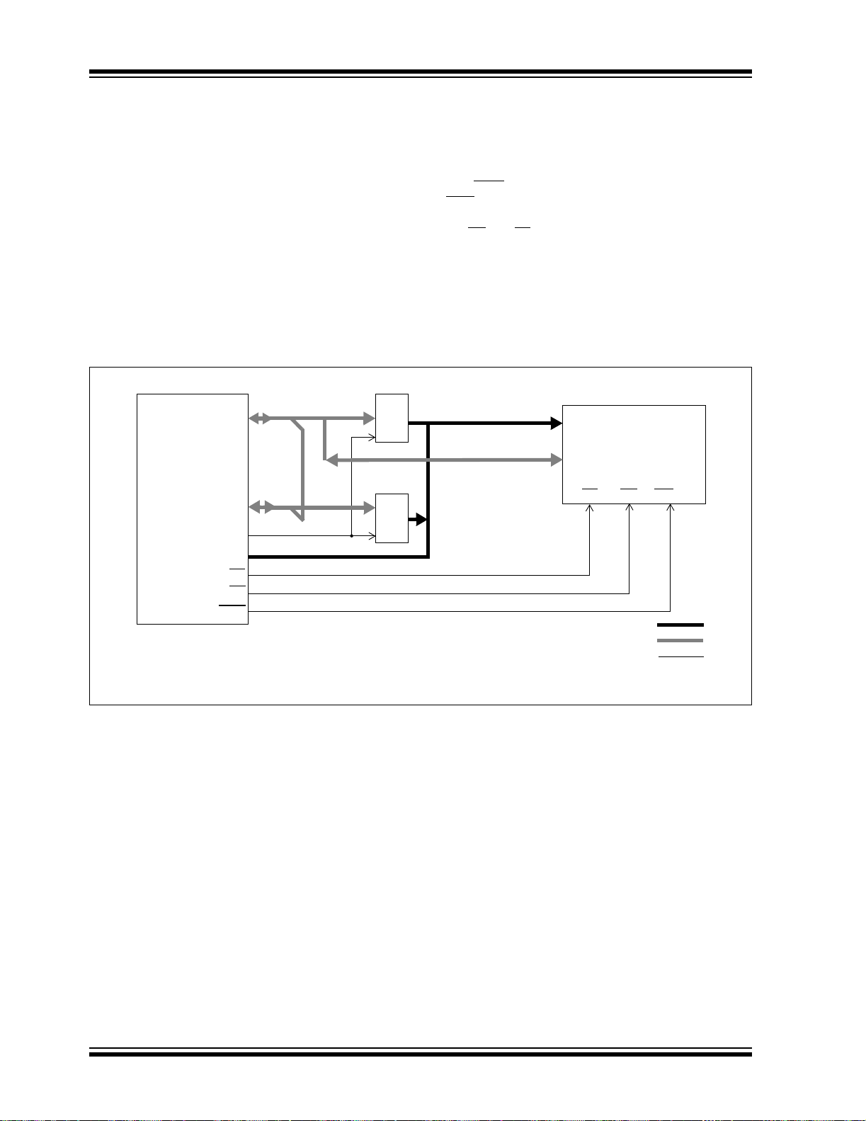
PIC18F6310/6410/8310/8410
7.2.2 16-BIT WORD WRITE MODE
Figure 7-2 shows an example of 16-bit Word Write
mode for PIC18F6410 devices. This mode is used for
word-wide memories, which includes some of the
EPROM and Flash type memories. This mode allows
opcode fetches and t a ble reads from all forms of 1 6-b it
memory and table writes to any type of word-wide
external memories. This method makes a distinction
between TBLWT cycles to even or odd addresses.
During a TBLWT cycle to an even address
(TBLPTR<0> = 0), the TABLAT data is transferr ed to a
holding latch and the external address data bus is
During a TBLWT cycle to an odd address
(TBLPTR<0> = 1), the TABLAT data is presen ted on
the upper byte of the AD15:AD0 bus. The contents of
the holding latch are pre sented on the lower byte of the
AD15:AD0 bus.
The WRH
WRL
the LSb of TBLPTR, but it is left unconnected. Instead,
the UB
The obvious limitation to this method is that the table
write must be done in pairs on a spe cific word boundar y
to correctly write a word location.
tri-stated for the data portion of the bus cycle. No write
signals are activated.
FIGURE 7-2: 16-BIT WORD WRITE MODE EXAMPLE
PIC18F8410
AD<7:0>
AD<15:8>
ALE
A<19:16>
CE
OE
WRH
373
373
A<20:1>
D<15:0>
signal is strobed for each write cycle; the
pin is unused. The signal on the BA0 pi n indicates
and LB signals are active to se lect b oth byte s.
A<x:0>
D<15:0>
Address Bus
Data Bus
Control Lines
JEDEC Word
EPROM Memory
(1)
WR
OE
CE
Note 1: This signal only applies to table writes. See Section 6.1 “Table Reads and Table Writes”.
DS39635A-page 92 Preliminary 2004 Microchip Technology Inc.

PIC18F6310/6410/8310/8410
7.2.3 16-BIT BYTE SELECT MODE
Figure 7-3 shows an example of 16-bit Byte Select
mode. This mode allows table write operations to
word-wide external memories with byte selection
capability. This generally includes both word-wide
Flash and SRAM devices.
During a TBLWT cycle, the TABLAT data is prese nted
Flash and SRAM devices use different control signal
combinations to implement Byte Select mode. JEDEC
standard Flash memories require that a controller I/O
port pin be connected to the memory’s BY TE/WORD
pin to provide the select si gna l. The y als o use the BA0
signal from the controller as a byte address. JEDEC
standard static RAM memories, on the other hand, use
the UB
on the upper an d lower byte of th e AD1 5:AD0 b us. Th e
signal is strobed for each write cycle; the WRL
WRH
pin is not used. The BA0 or UB/LB signals are used to
select the byte to be written, based on the Least
Significant bit of the TBLPTR register.
FIGURE 7-3: 16-BIT BYTE SELECT MODE EXAMPLE
PIC18F8410
AD<7:0>
AD<15:8>
ALE
A<19:16>
OE
WRH
WRL
BA0
I/O
LB
UB
373
373
A<20:1>
138
A<20:1>
(2)
or LB signals to select the byte.
A<x:1>
CE
A0
BYTE/WORD
A<x:1>
CE
LB
UB
JEDEC Word
FLASH Memory
D<15:0>
OE
JEDEC Word
SRAM Memory
D<15:0>
(1)
WR
OE
(1)
WR
D<15:0>
D<15:0>
Address Bus
Data Bus
Control Lines
Note 1: This signal only applies to table writes. See Section 6.1 “Table Reads and Table Writes”.
2: Demultiplexing is only required when multiple memory devices are accessed.
2004 Microchip Technology Inc. Preliminary DS39635A-page 93

PIC18F6310/6410/8310/8410
7.2.4 16-BIT MODE TIMING
The presentation of control signals on the external
memory bus is different for the various operating
modes. Typical signal timing diagrams are shown in
Figure 7-4 through Figure 7-6.
FIGURE 7-4: EXTERNAL MEMORY BUS TIMING FOR TBLRD (MICROPROCESSOR MODE)
Apparent Q
Actual Q
A<19:16>
AD<15:0>
BA0
ALE
OE
WRH
WRL
CE
Memory
Cycle
Instruction
Execution
Q2Q1 Q3 Q4 Q2Q1 Q3 Q4 Q4Q4 Q4 Q4
Q2Q1 Q3 Q4 Q2Q1 Q3 Q4 Q2Q1 Q3 Q4
00h
3AABh
‘1’ ‘1’
‘1’
‘0’
Opcode Fetch
MOVLW 55h
from 007556h
TBLRD Cycle 1
0E55h
CF33h
from 199E67h
TBLRD Cycle 2
0Ch
Table Read
of 92h
9256h
1 T
‘1’
‘0’
CY Wait
FIGURE 7-5: EXTERNAL MEMORY BUS TIMING FOR TBLRD (EXTENDED
MICROCONTROLLER MODE)
Q2Q1 Q3 Q4 Q2Q1 Q3 Q4
A<19:16>
AD<15:0>
CE
ALE
OE
Memory
Cycle
Instruction
Execution
DS39635A-page 94 Preliminary 2004 Microchip Technology Inc.
Opcode Fetch Opcode Fetch Opcode Fetch
TBLRD *
from 000100h
INST(PC – 2)
MOVLW 55h
from 000102h
TBLRD Cycle 1
Q2Q1 Q3 Q4
0Ch
CF33h
TBLRD 92h
from 199E67h
TBLRD Cycle 2
Q2Q1 Q3 Q4
9256h
ADDLW 55h
from 000104h
MOVLW

PIC18F6310/6410/8310/8410
FIGURE 7-6: EXTERNAL MEMORY BUS TIMING FOR SLEEP (MICROPROCESSOR M O DE)
A<19:16>
AD<15:0>
CE
ALE
OE
Memory
Cycle
Instruction
Execution
Q2Q1 Q3 Q4 Q2Q1 Q3 Q4
00h
3AAAh
Opcode Fetch
SLEEP
from 007554h
INST(PC – 2)
0003h
00h
3AABh
Opcode Fetch
MOVLW 55h
from 007556h
SLEEP
0E55h
Q1
Sleep Mode,
Bus Inactive
2004 Microchip Technology Inc. Preliminary DS39635A-page 95

PIC18F6310/6410/8310/8410
7.3 8-Bit Mode
The external memory interface implemented in
PIC18F6410 devices operate s only in Mu ltiple xed 8-b it
mode; data shares the 8 Least Significant bits of the
address bus.
Figure 7-1 shows an example of 8-bit Multiplexed
mode for PIC18F8310/8410 devices. This mode is
used for a single 8-bit memory connected for 16-bit
operation. The instructions will be fetched as two 8-bit
bytes on a shared data/address bus. The two bytes are
sequentially fetched within one instruction cycle (T
Therefore, the designer must choose external memory
devices according to timing calculations based on 1/2
CY (2 times the instruction rate). For proper memory
T
speed selection, glue logic propagation delay times
must be considered along with setup and hold times.
CY).
The Address Latch Enable (ALE) pin ind icate s that the
address bits A<15:0> are available on the external
memory interface bus. The Output Enable signal (OE
will enable one byte of pr ogram memory for a por tion of
the instruction cycle, then BA0 will change and the
second byte will be enabled to form the 16-bit instruction word. The Least Si gnificant bit of the address, BA0,
must be connected to the memory devices in this
mode. The Chip Enable signal (CE
time that the microcontroller accesses external
memory, whether reading or writing; it is inactive
(asserted high) whenever the device is in Sleep mode.
This generally includes basic EPROM and Flash devices.
It allows table writes to byte-wide external memories.
During a TBLWT instruction cycle, the TABLAT data is
presented on the upper and lower bytes of the
AD15:AD0 bus. The appropriate level of the BA0
control line is strobed on the LSb of the TBLPTR.
FIGURE 7-7: 8-BIT MULTIPLEXED MODE EXAMPLE
PIC18F8410
AD<7:0>
ALE
AD<15:8>
A<19:16>
373
D<7:0>
A<19:0>
D<15:8>
A<x:1>
A0
D<7:0>
CE
OE
) is active at any
(1)
WR
)
BA0
CE
OE
WRL
Address Bus
Data Bus
Control Lines
Note 1: This signal only applies to table writes. See Section 6.1 “Table Reads and Table Writes”.
DS39635A-page 96 Preliminary 2004 Microchip Technology Inc.

PIC18F6310/6410/8310/8410
7.3.1 8-BIT MODE TIMING
The presentation of control signals on the external
memory bus is different for the various operating
modes. Typical signal timing diagrams are shown in
Figure 7-4 through Figure 7-6.
FIGURE 7-8: EXTERNAL MEMORY BUS TIMING FOR TBLRD (MICROPROCESSOR MODE)
Apparent Q
Actual Q
A<19:16>
AD<15:8> CFh
AD<7:0>
BA0
ALE
OE
‘1’
WRL
CE
‘0’
Memory
Cycle
Instruction
Execution
Q2Q1 Q3 Q4 Q2Q1 Q3 Q4 Q4Q4 Q4 Q4
Q2Q1 Q3 Q4 Q2Q1 Q3 Q4 Q2Q1 Q3 Q4
00h
3Ah
ABh
Opcode Fetch
from 007556h
TBLRD Cycle 1
0Eh
MOVLW 55h
55h
33h
Table Read
from 199E67h
TBLRD Cycle 2
0Ch
of 92h
92h
1 T
‘1’
‘0’
CY Wait
FIGURE 7-9: EXTERNAL MEMORY BUS TIMING FOR TBLRD (EXTENDED
MICROCONTROLLER MODE)
Q2Q1 Q3 Q4 Q2Q1 Q3 Q4
A<19:16>
AD<15:8>
AD<7:0>
CE
ALE
OE
Memory
Cycle
Instruction
Execution
2004 Microchip Technology Inc. Preliminary DS39635A-page 97
Opcode Fetch Opcode Fetch Opcode Fetch
TBLRD *
from 000100h
INST(PC – 2)
MOVLW 55h
from 000102h
TBLRD Cycle 1
Q2Q1 Q3 Q4
0Ch
CFh
33h
TBLRD 92h
from 199E67h
TBLRD Cycle 2
92h
Q2Q1 Q3 Q4
ADDLW 55h
from 000104h
MOVLW

PIC18F6310/6410/8310/8410
FIGURE 7-10: EXTERNAL MEMORY BUS TIMING FOR SLEEP (MICROPROCESSOR MODE)
Q2Q1 Q3 Q4 Q2Q1 Q3 Q4
A<19:16>
AD<7:0>
CE
ALE
OE
AAh
00h
00h
DS39635A-page 98 Preliminary 2004 Microchip Technology Inc.
 Loading...