

Page 1
PIC18F57Q43 Curiosity Nano
PIC18F57Q43 Curiosity Nano Hardware User Guide
Preface
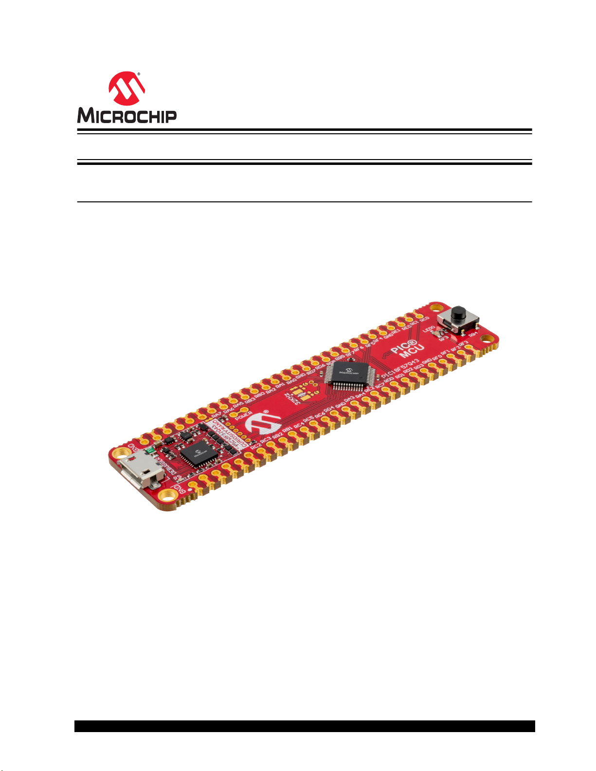
The PIC18F57Q43 Curiosity Nano Evaluation Kit is a hardware platform to evaluate microcontrollers in the PIC18Q43 family. This board has the PIC18F57Q43 microcontroller (MCU) mounted.
Supported by Microchip MPLAB® X Integrated Development Environment (IDE), the board provides easy access to
the features of the PIC18F57Q43 to explore how to integrate the device into a custom design.
The Curiosity Nano series of evaluation boards include an on-board debugger. No external tools are necessary to
program and debug the PIC18F57Q43.
• MPLAB® X IDE - Software to discover, configure, develop, program, and debug Microchip microcontrollers.
• Code examples on GitHub - Get started with code examples.
• PIC18F57Q43 website - Find documentation, data sheets, sample, and purchase microcontrollers.
• PIC18F57Q43 Curiosity Nano website - Find schematics, design files, and purchase this kit.
© 2020 Microchip Technology Inc.
DS40002186A-page 1
Page 2

PIC18F57Q43 Curiosity Nano
Table of Contents
Preface........................................................................................................................................................... 1
1. Introduction............................................................................................................................................. 3
1.1. Features....................................................................................................................................... 3
1.2. Kit Overview................................................................................................................................. 3
2. Getting Started........................................................................................................................................ 4
2.1. Quick Start....................................................................................................................................4
2.2. Design Documentation and Relevant Links................................................................................. 4
3. Curiosity Nano.........................................................................................................................................5
3.1. On-Board Debugger Overview..................................................................................................... 5
3.2. Curiosity Nano Standard Pinout................................................................................................. 10
3.3. Power Supply............................................................................................................................. 11
3.4. Low Power Measurement...........................................................................................................15
3.5. Programming External Microcontrollers..................................................................................... 16
3.6. Connecting External Debuggers................................................................................................ 19
4. Hardware User Guide........................................................................................................................... 21
4.1. Connectors.................................................................................................................................21
4.2. Peripherals................................................................................................................................. 22
5. Hardware Revision History and Known Issues..................................................................................... 24
5.1. Identifying Product ID and Revision........................................................................................... 24
5.2. Revision 3...................................................................................................................................24
6. Document Revision History...................................................................................................................25
7. Appendix............................................................................................................................................... 26
7.1. Schematic...................................................................................................................................26
7.2. Assembly Drawing......................................................................................................................28
7.3. Curiosity Nano Base for Click boards™...................................................................................... 29
7.4. Disconnecting the On-board Debugger......................................................................................30
The Microchip Website.................................................................................................................................32
Product Change Notification Service............................................................................................................32
Customer Support........................................................................................................................................ 32
Microchip Devices Code Protection Feature................................................................................................ 32
Legal Notice................................................................................................................................................. 32
Trademarks.................................................................................................................................................. 33
Quality Management System....................................................................................................................... 33
Worldwide Sales and Service.......................................................................................................................34
© 2020 Microchip Technology Inc.
DS40002186A-page 2
Page 3
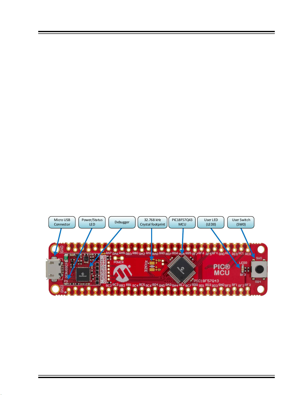
1. Introduction
Micro USB
Connector
Debugger
Power/Status
LED
32.768 kHz
Crystal footprint
User LED
(LED0)
User Switch
(SW0)
PIC18F57Q43
MCU
1.1 Features
• PIC18F57Q43-I/PT Microcontroller
• One Yellow User LED
• One Mechanical User Switch
• Footprint for 32.768 kHz Crystal
• On-Board Debugger:
– Board identification in Microchip MPLAB® X IDE
– One green power and status LED
– Programming and debugging
– Virtual serial port (CDC)
– One debug GPIO channel (DGI GPIO)
• USB Powered
• Adjustable Target Voltage:
– MIC5353 LDO regulator controlled by the on-board debugger
– 1.8-5.1V output voltage (limited by USB input voltage)
– 500 mA maximum output current (limited by ambient temperature and output voltage)
PIC18F57Q43 Curiosity Nano
Introduction
1.2 Kit Overview
The Microchip PIC18F57Q43 Curiosity Nano Evaluation Kit is a hardware platform to evaluate the PIC18F57Q43
microcontroller.
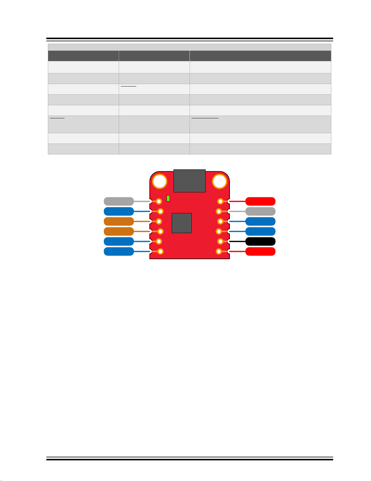
Figure 1-1. PIC18F57Q43 Curiosity Nano Evaluation Kit Overview
© 2020 Microchip Technology Inc.
DS40002186A-page 3
Page 4
2. Getting Started
2.1 Quick Start
Steps to start exploring the PIC18F57Q43 Curiosity Nano Board:
1. Download Microchip MPLAB® X IDE.
2. Launch Microchip MPLAB® X IDE.
3. Optional: Use MPLAB® Code Configurator to generate drivers and examples.
4. Write your application code.
5. Connect a USB cable (Standard-A to Micro-B or Micro-AB) between the PC and the debug USB port on the
board.
Driver Installation
When the board is connected to your computer for the first time, the operating system will perform a driver software
installation. The driver file supports both 32- and 64-bit versions of Microsoft® Windows® XP, Windows Vista®,
Windows 7, Windows 8, and Windows 10. The drivers for the board are included with Microchip MPLAB® X IDE.
Kit Window
Once the board is powered, the green status LED will be lit, and Microchip MPLAB® X IDE will auto-detect which
boards are connected. Microchip MPLAB® X IDE will present relevant information like data sheets and board
documentation. The PIC18F57Q43 device on the PIC18F57Q43 Curiosity Nano Board is programmed and debugged
by the on-board debugger and, therefore, no external programmer or debugger tool is required.
PIC18F57Q43 Curiosity Nano
Getting Started
Tip: The Kit Window can be opened in MPLAB X IDE through the menu bar Window > Kit Window.
2.2 Design Documentation and Relevant Links
The following list contains links to the most relevant documents and software for the PIC18F57Q43 Curiosity Nano
Board:
• MPLAB® X IDE - MPLAB X IDE is a software program that runs on a PC (Windows®, Mac OS®, Linux®) to
develop applications for Microchip microcontrollers and digital signal controllers. It is called an Integrated
Development Environment (IDE) because it provides a single integrated “environment” to develop code for
embedded microcontrollers.
• MPLAB® Code Configurator - MPLAB Code Configurator (MCC) is a free software plug-in that provides a
graphical interface to configure peripherals and functions specific to your application.
• Microchip Sample Store - Microchip sample store where you can order samples of devices.
• MPLAB Data Visualizer - MPLAB Data Visualizer is a program used for processing and visualizing data. The
Data Visualizer can receive data from various sources such as serial ports and on-board debugger’s Data
Gateway Interface, as found on Curiosity Nano and Xplained Pro boards.
• Microchip PIC® and AVR Examples - Microchip PIC and AVR Device Examples is a collection of examples
and labs that use Microchip development boards to showcase the use of PIC and AVR device peripherals.
• Microchip PIC® and AVR Solutions - Microchip PIC and AVR Device Solutions contains complete applications
for use with Microchip development boards, ready to be adapted and extended.
• PIC18F57Q43 Curiosity Nano website - Find schematics, design files, and purchase this kit.
• PIC18F57Q43 Curiosity Nano on microchipDIRECT - Purchase this kit on microchipDIRECT.
© 2020 Microchip Technology Inc.
DS40002186A-page 4
Page 5
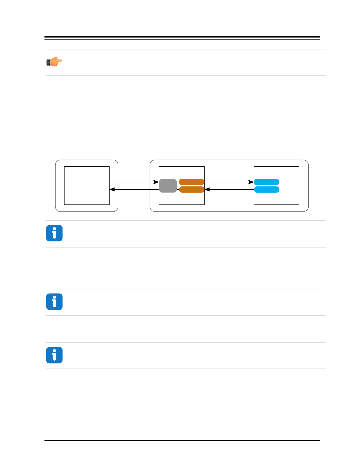
3. Curiosity Nano
Curiosity Nano is an evaluation platform of small boards with access to most of the microcontrollers I/Os. The
platform consists of a series of low pin count microcontroller (MCU) boards with on-board debuggers, which are
integrated with Microchip MPLAB® X IDE. Each board is identified in the IDE. When plugged in, a Kit Window is
displayed with links to key documentation, including relevant user guides, application notes, data sheets, and
example code. Everything is easy to find. The on-board debugger features a virtual serial port (CDC) for serial
communication to a host PC and a Data Gateway Interface (DGI) with debug GPIO pin(s).
3.1 On-Board Debugger Overview
PIC18F57Q43 Curiosity Nano contains an on-board debugger for programming and debugging. The on-board
debugger is a composite USB device consisting of several interfaces:
• A debugger that can program and debug the PIC18F57Q43 in Microchip MPLAB® X IDE
• A mass storage device that allows drag-and-drop programming of the PIC18F57Q43
• A virtual serial port (CDC) that is connected to a Universal Asynchronous Receiver/Transmitter (UART) on the
PIC18F57Q43, and provides an easy way to communicate with the target application through terminal software
• A Data Gateway Interface (DGI) for code instrumentation with logic analyzer channels (debug GPIO) to visualize
program flow
The on-board debugger controls a Power and Status LED (marked PS) on the PIC18F57Q43 Curiosity Nano Board.
The table below shows how the LED is controlled in different operation modes.
Table 3-1. On-Board Debugger LED Control
PIC18F57Q43 Curiosity Nano
Curiosity Nano
Operation Mode Power and Status LED
Boot Loader mode The LED blinks slowly during power-up.
Power-up The LED is ON.
Normal operation The LED is ON.
Programming Activity indicator: The LED blinks slowly during programming/debugging.
Drag-and-drop
programming
Fault The LED blinks rapidly if a power fault is detected.
Sleep/Off The LED is OFF. The on-board debugger is either in a sleep mode or powered down.
3.1.1 Debugger
The on-board debugger on the PIC18F57Q43 Curiosity Nano Board appears as a Human Interface Device (HID) on
the host computer’s USB subsystem. The debugger supports full-featured programming and debugging of the
PIC18F57Q43 using Microchip MPLAB® X IDE.
Success: The LED blinks slowly for 2 sec.
Failure: The LED blinks rapidly for 2 sec.
This can occur if the board is externally powered.
Info: Slow blinking is approximately 1 Hz, and rapid blinking is approximately 5 Hz.
© 2020 Microchip Technology Inc.
DS40002186A-page 5
Page 6
Remember: Keep the debugger’s firmware up-to-date. Firmware upgrades are done automatically when
Target MCU
UART TX
UART RX
Debugger
USB
CDC RX
CDC TX
PC
Terminal
Software
Target
Receive
Target
Send
Terminal
Receive
Terminal
Send
using Microchip MPLAB® X IDE.
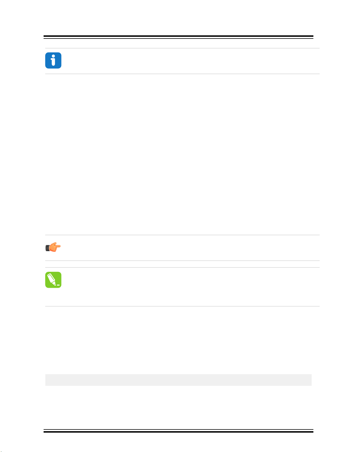
3.1.2 Virtual Serial Port (CDC)
The virtual serial port (CDC) is a general purpose serial bridge between a host PC and a target device.
3.1.2.1 Overview
The on-board debugger implements a composite USB device that includes a standard Communications Device Class
(CDC) interface, which appears on the host as a virtual serial port. The CDC can be used to stream arbitrary data in
both directions between the host computer and the target: All characters sent through the virtual serial port on the
host computer will be transmitted as UART on the debugger’s CDC TX pin, and UART characters captured on the
debugger’s CDC RX pin will be returned to the host computer through the virtual serial port.
Figure 3-1. CDC Connection
PIC18F57Q43 Curiosity Nano
Curiosity Nano
Info: As shown in Figure 3-1, the debugger’s CDC TX pin is connected to a UART RX pin on the target
for receiving characters from the host computer. Similarly, the debugger’s CDC RX pin is connected to a
UART TX pin on the target for transmitting characters to the host computer.
3.1.2.2 Operating System Support
On Windows machines, the CDC will enumerate as Curiosity Virtual COM Port and appear in the Ports section of the
Windows Device Manager. The COM port number can also be found there.
Info: On older Windows systems, a USB driver is required for CDC. This driver is included in installations
of Microchip MPLAB® X IDE.
On Linux machines, the CDC will enumerate and appear as /dev/ttyACM#.
Info: tty* devices belong to the “dialout” group in Linux, so it may be necessary to become a member of
that group to have permissions to access the CDC.
On MAC machines, the CDC will enumerate and appear as /dev/tty.usbmodem#. Depending on which terminal
program is used, it will appear in the available list of modems as usbmodem#.
© 2020 Microchip Technology Inc.
DS40002186A-page 6
Page 7
3.1.2.3 Limitations
Not all UART features are implemented in the on-board debugger CDC. The constraints are outlined here:
• Baud rate: Must be in the range of 1200 bps to 500 kbps. Any baud rate outside this range will be set to the
closest limit, without warning. Baud rate can be changed on-the-fly.
• Character format: Only 8-bit characters are supported.
• Parity: Can be odd, even, or none.
• Hardware flow control: Not supported.
• Stop bits: One or two bits are supported.
3.1.2.4 Signaling
During USB enumeration, the host OS will start both communication and data pipes of the CDC interface. At this
point, it is possible to set and read back the baud rate and other UART parameters of the CDC, but data sending and
receiving will not be enabled.
When a terminal connects on the host, it must assert the DTR signal. As this is a virtual control signal implemented
on the USB interface, it is not physically present on the board. Asserting the DTR signal from the host will indicate to
the on-board debugger that a CDC session is active. The debugger will then enable its level shifters (if available), and
start the CDC data send and receive mechanisms.
Deasserting the DTR signal will not disable the level shifters but disable the receiver so no further data will be
streamed to the host. Data packets that are already queued up for sending to the target will continue to be sent out,
but no further data will be accepted.
PIC18F57Q43 Curiosity Nano
Curiosity Nano
Info: For all operating systems: Be sure to use a terminal emulator that supports DTR signaling. See
3.1.2.4 Signaling.
Remember: Set up the terminal emulator to assert the DTR signal. Without the signal, the on-board
debugger will not send or receive any data through its UART.
Tip: The on-board debugger’s CDC TX pin will not be driven until the CDC interface is enabled by the
host computer. Also, there are no external pull-up resistors on the CDC lines connecting the debugger and
the target, which means that during power-up, these lines are floating. To avoid any glitches resulting in
unpredictable behavior like framing errors, the target device should enable the internal pull-up resistor on
the pin connected to the debugger’s CDC TX pin.
3.1.2.5 Advanced Use
CDC Override Mode
In normal operation, the on-board debugger is a true UART bridge between the host and the device. However, in
certain use cases, the on-board debugger can override the basic operating mode and use the CDC TX and RX pins
for other purposes.
Dropping a text file into the on-board debugger’s mass storage drive can be used to send characters out of the
debugger’s CDC TX pin. The filename and extension are trivial, but the text file must start with the characters:
CMD:SEND_UART=
The maximum message length is 50 characters – all remaining data in the frame are ignored.
The default baud rate used in this mode is 9600 bps, but if the CDC is already active or has been configured, the
previously used baud rate still applies.
© 2020 Microchip Technology Inc.
DS40002186A-page 7
Page 8

USB-Level Framing Considerations
Sending data from the host to the CDC can be done byte-wise or in blocks, which will be chunked into 64-byte USB
frames. Each such frame will be queued up for sending to the debugger’s CDC TX pin. Transferring a small amount
of data per frame can be inefficient, particularly at low baud rates, because the on-board debugger buffers frames
and not bytes. A maximum of four 64-byte frames can be active at any time. The on-board debugger will throttle the
incoming frames accordingly. Sending full 64-byte frames containing data is the most efficient method.
When receiving data on the debugger’s CDC RX pin, the on-board debugger will queue up the incoming bytes into
64-byte frames, which are sent to the USB queue for transmission to the host when they are full. Incomplete frames
are also pushed to the USB queue at approximately 100 ms intervals, triggered by USB start-of-frame tokens. Up to
eight 64-byte frames can be active at any time.
If the host (or the software running on it) fails to receive data fast enough, an overrun will occur. When this happens,
the last-filled buffer frame will be recycled instead of being sent to the USB queue, and a full frame of data will be
lost. To prevent this occurrence, the user must ensure that the CDC data pipe is being read continuously, or the
incoming data rate must be reduced.
3.1.3 Mass Storage Device
The on-board debugger includes a simple Mass Storage Device implementation, which is accessible for read/write
operations via the host operating system to which it is connected.
It provides:
• Read access to basic text and HTML files for detailed kit information and support
• Write access for programming Intel® HEX formatted files into the target device’s memory
• Write access for simple text files for utility purposes
PIC18F57Q43 Curiosity Nano
Curiosity Nano
3.1.3.1 Mass Storage Device Implementation
The on-board debugger implements a highly optimized variant of the FAT12 file system that has several limitations,
partly due to the nature of FAT12 itself and optimizations made to fulfill its purpose for its embedded application.
The Curiosity Nano USB Device is USB Chapter 9-compliant as a mass storage device but does not, in any way,
fulfill the expectations of a general purpose mass storage device. This behavior is intentional.
When using the Windows operating system, the on-board debugger enumerates as a Curiosity Nano USB Device
that can be found in the disk drives section of the device manager. The CURIOSITY drive appears in the file manager
and claims the next available drive letter in the system.
The CURIOSITY drive contains approximately one MB of free space. This does not reflect the size of the target
device’s Flash in any way. When programming an Intel® HEX file, the binary data are encoded in ASCII with
metadata providing a large overhead, so one MB is a trivially chosen value for disk size.
It is not possible to format the CURIOSITY drive. When programming a file to the target, the filename may appear in
the disk directory listing. This is merely the operating system’s view of the directory, which, in reality, has not been
updated. It is not possible to read out the file contents. Removing and replugging the board will return the file system
to its original state, but the target will still contain the application that has been previously programmed.
To erase the target device, copy a text file starting with “CMD:ERASE” onto the disk.
By default, the CURIOSITY drive contains several read-only files for generating icons as well as reporting status and
linking to further information:
• AUTORUN.ICO – icon file for the Microchip logo
• AUTORUN.INF – system file required for Windows Explorer to show the icon file
• KIT-INFO.HTM – redirect to the development board website
• KIT-INFO.TXT – a text file containing details about the board’s debugger firmware version, board name, USB
serial number, device, and drag-and-drop support
• STATUS.TXT – a text file containing the programming status of the board
© 2020 Microchip Technology Inc.
DS40002186A-page 8
Page 9
Info: STATUS.TXT is dynamically updated by the on-board debugger. The contents may be cached by
the OS and, therefore, do not reflect the correct status.
3.1.3.2 Configuration Words
Configuration Words (PIC® MCU Targets)
Configuration Word settings included in the project being programmed after program Flash is programmed. The
debugger will not mask out any bits in the Configuration Words when writing them, but since it uses Low-Voltage
Programming mode, it is unable to clear the LVP Configuration bit. If the incorrect clock source is selected, for
example, and the board does not boot, it is always possible to perform a bulk erase (always done before
programming) and restore the device to its default settings.
3.1.3.3 Special Commands
Several utility commands are supported by copying text files to the mass storage disk. The filename or extension is
irrelevant – the command handler reacts to content only.
Table 3-2. Special File Commands
Command Content Description
CMD:ERASE
CMD:SEND_UART=
CMD:RESET
CMD:POWERTOGGLE
CMD:0V
CMD:3V3
CMD:5V0
PIC18F57Q43 Curiosity Nano
Curiosity Nano
Executes a chip erase of the target
Sends a string of characters to the CDC UART. See “CDC Override Mode”.
Resets the target device by entering Programming mode and then exiting
Programming mode immediately thereafter. Exact timing can vary according to
the programming interface of the target device. (Debugger firmware v1.16 or
newer.)
Powers down the target and restores power after a 100 ms delay. If external
power is provided, this has no effect. (Debugger firmware v1.16 or newer.)
Powers down the target device by disabling the target supply regulator. If
external power is provided, this has no effect. (Debugger firmware v1.16 or
newer.)
Sets the target voltage to 3.3V. If external power is provided, this has no effect.
(Debugger firmware v1.16 or newer.)
Sets the target voltage to 5.0V. If external power is provided, this has no effect.
(Debugger firmware v1.16 or newer.)
Info: The commands listed here are triggered by the content being sent to the mass storage emulated
disk, and no feedback is provided in the case of either success or failure.
3.1.4 Data Gateway Interface (DGI)
Data Gateway Interface (DGI) is a USB interface for transporting raw and time-stamped data between on-board
debuggers and host computer-based visualization tools. MPLAB Data Visualizer is used on the host computer to
display debug GPIO data. It is available as a plug-in for MPLAB® X IDE or a stand-alone application that can be used
in parallel with Microchip MPLAB® X IDE.
Although DGI encompasses several physical data interfaces, the PIC18F57Q43 Curiosity Nano implementation
includes logic analyzer channels:
• One debug GPIO channel (also known as DGI GPIO)
© 2020 Microchip Technology Inc.
DS40002186A-page 9
Page 10
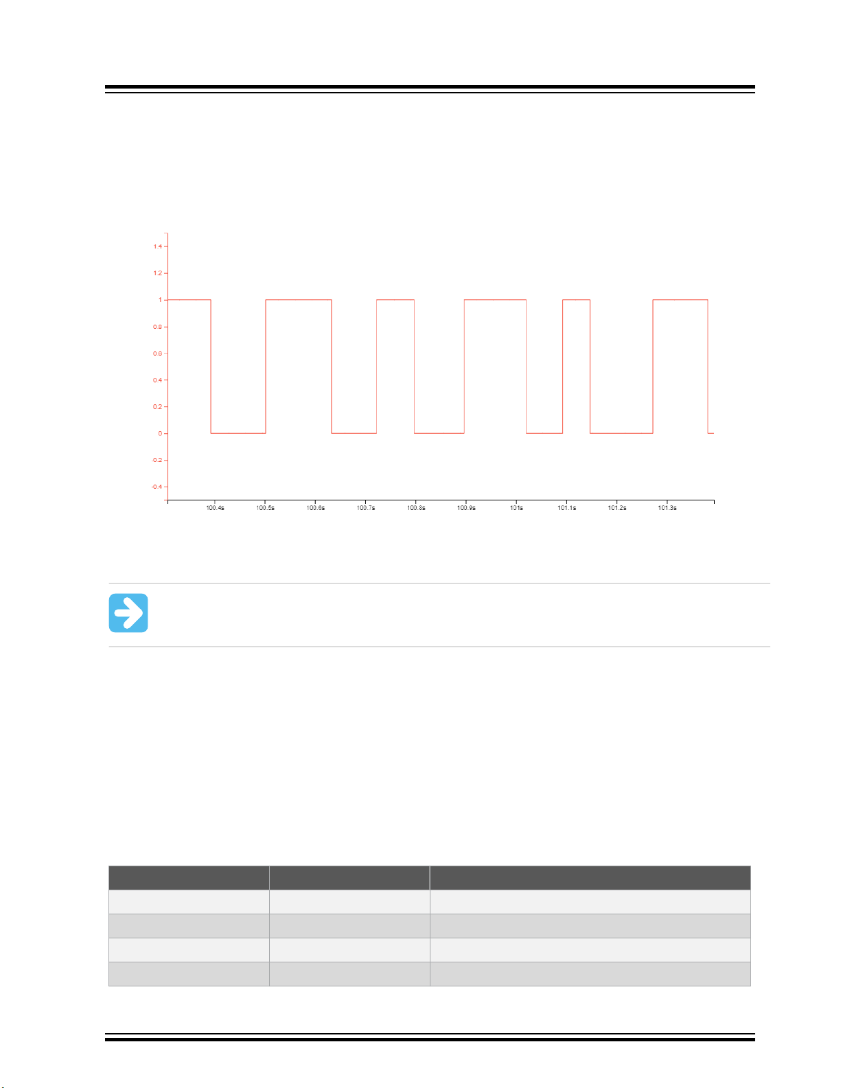
3.1.4.1 Debug GPIO
Debug GPIO channels are timestamped digital signal lines connecting the target application to a host computer
visualization application. They are typically used to plot the occurrence of low-frequency events on a time-axis – for
example, when certain application state transitions occur.
The figure below shows the monitoring of the digital state of a mechanical switch connected to a debug GPIO in
MPLAB Data Visualizer.
Figure 3-2. Monitoring Debug GPIO with MPLAB® Data Visualizer
PIC18F57Q43 Curiosity Nano
Curiosity Nano
Debug GPIO channels are timestamped, so the resolution of DGI GPIO events is determined by the resolution of the
DGI timestamp module.
Important: Although bursts of higher-frequency signals can be captured, the useful frequency range of
signals for which debug GPIO can be used is up to about 2 kHz. Attempting to capture signals above this
frequency will result in data saturation and overflow, which may cause the DGI session to be aborted.
3.1.4.2 Timestamping
DGI sources are timestamped as they are captured by the debugger. The timestamp counter implemented in the
Curiosity Nano debugger increments at 2 MHz frequency, providing a timestamp resolution of a half microsecond.
3.2 Curiosity Nano Standard Pinout
The 12 edge connections closest to the USB connector on Curiosity Nano boards have a standardized pinout. The
program/debug pins have different functions depending on the target programming interface, as shown in the table
and figure below.
Table 3-3. Curiosity Nano Standard Pinout
Debugger Signal Target MCU Description
ID — ID line for extensions
CDC TX UART RX USB CDC TX line
CDC RX UART TX USB CDC RX line
DBG0 ICSPDAT Debug data line
© 2020 Microchip Technology Inc.
DS40002186A-page 10
Page 11
USB
DEBUGGER
PS LED
NC
ID
CDC RX
CDC TX
DBG1
DBG2
VBUS
VOFF
DBG3
DBG0
GND
VTG
CURIOSITY NANO
PIC18F57Q43 Curiosity Nano
Curiosity Nano
...........continued
Debugger Signal Target MCU Description
DBG1 ICSPCLK Debug clock line
DBG2 GPIO0 debug GPIO0
DBG3 MCLR Reset line
NC — No connect
VBUS — VBUS voltage for external use
VOFF — Voltage Off input. Disables the target regulator and
target voltage when pulled low.
VTG — Target voltage
GND — Common ground
Figure 3-3. Curiosity Nano Standard Pinout
3.3 Power Supply
The board is powered through the USB port and contains two LDO regulators, one to generate 3.3V for the on-board
debugger, and an adjustable LDO regulator for the target microcontroller PIC18F57Q43 and its peripherals. The
voltage from the USB connector can vary between 4.4V to 5.25V (according to the USB specification) and will limit
the maximum voltage to the target. The figure below shows the entire power supply system on PIC18F57Q43
Curiosity Nano.
© 2020 Microchip Technology Inc.
DS40002186A-page 11
Page 12

Figure 3-4. Power Supply Block Diagram
USB
Target
MCU
Power source
Cut strap
Power consumer
P3V3
DEBUGGER
Power converter
DEBUGGER
Regulator
VUSB
Target
Regulator
Power
Supply
strap
Adjust
Level
shifter
VLVL
VREG
I/O
I/O
GPIO
straps
I/O
On/Off
Measure
On/Off
ID system
#VOFF
PTC
Fuse
Power protection
VBUS
Target
Power
strap
VTG
3.3.1 Target Regulator
The target voltage regulator is a MIC5353 variable output LDO. The on-board debugger can adjust the voltage output
supplied to the board target section by manipulating the MIC5353’s feedback voltage. The hardware implementation
is limited to an approximate voltage range from 1.7V to 5.1V. Additional output voltage limits are configured in the
debugger firmware to ensure that the output voltage never exceeds the hardware limits of the PIC18F57Q43
microcontroller. The voltage limits configured in the on-board debugger on PIC18F57Q43 Curiosity Nano are
1.8-5.1V.
PIC18F57Q43 Curiosity Nano
Curiosity Nano
Info: The target voltage is set to 3.3V when the board is manufactured. It can be changed through
MPLAB X IDE project properties. Any change to the target voltage is persistent, even through a power
toggle. The resolution is less than 5 mV but may be limited to 10 mV by the adjustment program.
Info: Voltage settings that are set up in Microchip MPLAB® X IDE are not immediately applied to the
board. The new voltage setting is applied to the board when the debugger is accessed in any way, like
pushing the Refresh Debug Tool Status button in the project dashboard tab, or programming/reading
program memory.
Info: There is a simple option to adjust the target voltage with a drag and drop command text file to the
board. This only supports settings of 0.0V, 3.3V, and 5.0V. See section 3.1.3.3 Special Commands for
further details.
The MIC5353 supports a maximum current load of 500 mA. It is an LDO regulator in a small package, placed on a
small printed circuit board (PCB), and the thermal shutdown condition can be reached at lower loads than 500 mA.
The maximum current load depends on the input voltage, the selected output voltage, and the ambient temperature.
The figure below shows the safe operating area for the regulator, with an input voltage of 5.1V and an ambient
temperature of 23°C.
© 2020 Microchip Technology Inc.
DS40002186A-page 12
Page 13

WARNING
WARNING
WARNING
PIC18F57Q43 Curiosity Nano
Curiosity Nano
Figure 3-5. Target Regulator Safe Operation Area
The voltage output of the target regulator is continuously monitored (measured) by the on-board debugger. If it is
more than 100 mV over/under the voltage setting value, an error condition will be flagged, and the target voltage
regulator will be turned off. This will detect and handle any short-circuit conditions. It will also detect and handle if an
external voltage which causes VCC_TARGET to move outside of the voltage setting monitoring window of ±100 mV
is suddenly applied to the VTG pin, without setting the VOFF pin low.
Info: If the external voltage is lower than the monitoring window lower limit (target voltage setting - 100
mV), the on-board debugger status LED will blink rapidly. If the external voltage is higher than the
monitoring window upper limit (target voltage setting + 100 mV), the on-board debugger status LED will
continue to shine. If the external voltage is removed, the status LED will start to blink rapidly until the onboard debugger detects the new situation and turns the target voltage regulator back on.
3.3.2 External Supply
PIC18F57Q43 Curiosity Nano can be powered by an external voltage instead of the on-board target regulator. When
the Voltage Off (VOFF) pin is shorted to ground (GND), the on-board debugger firmware disables the target regulator,
and it is safe to apply an external voltage to the VTG pin.
It is also safe to apply an external voltage to the VTG pin when no USB cable is plugged into the DEBUG connector
on the board.
The VOFF pin can be tied low/let go at any time. This will be detected by a pin-change interrupt to the on-board
debugger, which controls the target voltage regulator accordingly.
Applying an external voltage to the VTG pin without shorting VOFF to GND may cause permanent damage
to the board.
Do not apply any voltage to the VOFF pin. Let the pin float to enable the power supply.
Absolute maximum external voltage is 5.5V for the on-board level shifters, and the standard operating
condition of the PIC18F57Q43 is 1.8-5.5V. Applying a higher voltage may cause permanent damage to the
board.
© 2020 Microchip Technology Inc.
DS40002186A-page 13
Page 14

Info: If an external voltage is applied without pulling the VOFF pin low and an external supply pulls the
voltage lower than the monitoring window lower limit (target voltage setting - 100 mV), the on-board
debugger status LED will blink rapidly and shut the on-board regulator off. If an external voltage is
suddenly removed when the VOFF pin is not pulled low, the status LED will start to blink rapidly, until the
on-board debugger detects the new situation and switches the target voltage regulator back on.
Programming, debugging, and data streaming is still possible with an external power supply – the debugger and
signal level shifters will be powered from the USB cable. Both regulators, the debugger and the level shifters, are
powered down when the USB cable is removed.
Info: In addition to the power consumed by the PIC18F57Q43 and its peripherals, approximately 100 µA
will be drawn from any external power source to power the on-board level shifters and voltage monitor
circuitry when a USB cable is plugged in the DEBUG connector on the board. When a USB cable is not
plugged in, some current is used to supply the level shifters voltage pins, which have a worst-case current
consumption of approximately 5 µA. Typical values may be as low as 100 nA.
3.3.3 VBUS Output Pin
PIC18F57Q43 Curiosity Nano has a VBUS output pin that can be used to power external components that need a 5V
supply. The VBUS output pin has a PTC fuse to protect the USB against short circuits. A side effect of the PTC fuse
is a voltage drop on the VBUS output with higher current loads. The chart below shows the voltage versus the current
load of the VBUS output.
Figure 3-6. VBUS Output Voltage vs. Current
PIC18F57Q43 Curiosity Nano
Curiosity Nano
3.3.4 Power Supply Exceptions
This is a summary of most exceptions that can occur with the power supply.
Target Voltage Shuts Down
This can happen if the target section draws too much current at a given voltage. This will cause the thermal shutdown
safety feature of the MIC5353 regulator to kick in. To avoid this, reduce the current load of the target section.
Target Voltage Setting is Not Reached
The maximum output voltage is limited by the USB input voltage (specified to be between 4.4V to 5.25V), and the
voltage drop over the MIC5353 regulator at a given voltage setting and current consumption. If a higher output
voltage is needed, use a USB power source that can provide a higher input voltage or use an external voltage supply
on the VTG pin.
© 2020 Microchip Technology Inc.
DS40002186A-page 14
Page 15

PIC18F57Q43 Curiosity Nano
Curiosity Nano
Target Voltage is Different From Setting
This can be caused by an externally applied voltage to the VTG pin, without setting the VOFF pin low. If the target
voltage differ more than 100 mV over/under the voltage setting, it will be detected by the on-board debugger, and the
internal voltage regulator will be shut down. To fix this issue, remove the applied voltage from the VTG pin, and the
on-board debugger will enable the on-board voltage regulator when the new condition is detected. Note that the PS
LED will be blinking rapidly if the target voltage is below 100 mV of the setting, but will be lit normally when it is higher
than 100 mV above the setting.
No, Or Very Low Target Voltage, and PS LED is Blinking Rapidly
This can be caused by a full or partial short-circuit and is really a special case of the issue mentioned above. Remove
the short-circuit, and the on-board debugger will re-enable the on-board target voltage regulator.
No Target Voltage and PS LED is Lit 1
This occurs if the target voltage is set to 0.0V. To fix this, set the target voltage to a value within the specified voltage
range for the target device.
No Target Voltage and PS LED is Lit 2
This can be the issue if power jumper J100 and/or J101 is cut, and the target voltage regulator is set to a value within
the specified voltage range for the target device. To fix this, solder a wire/bridge between the pads for J100/J101, or
add a jumper on J101 if a pin header is mounted.
VBUS Output Voltage is Low or Not Present
This is most lightly caused by a high-current drain on VBUS, and the protection fuse (PTC) will reduce the current or
cut off completely. Reduce the current consumption on the VBUS pin to fix this issue.
3.4 Low Power Measurement
Power to the PIC18F57Q43 is connected from the on-board power supply and VTG pin through a 100 mil pin header
marked with “POWER” in silkscreen (J101). To measure the power consumption of the PIC18F57Q43 and other
peripherals connected to the board, cut the Target Power strap and connect an ammeter over the strap.
To measure the lowest possible power consumption follow these steps:
1. Cut the POWER strap with a sharp tool.
2. Solder a 1x2 100 mil pin header in the footprint.
3. Connect an ammeter to the pin header.
4. Write firmware that.
4.1. Tri-states any I/O connected to the on-board debugger.
4.2. Sets the microcontroller in its lowest power Sleep state.
5. Program the firmware into the PIC18F57Q43.
© 2020 Microchip Technology Inc.
DS40002186A-page 15
Page 16
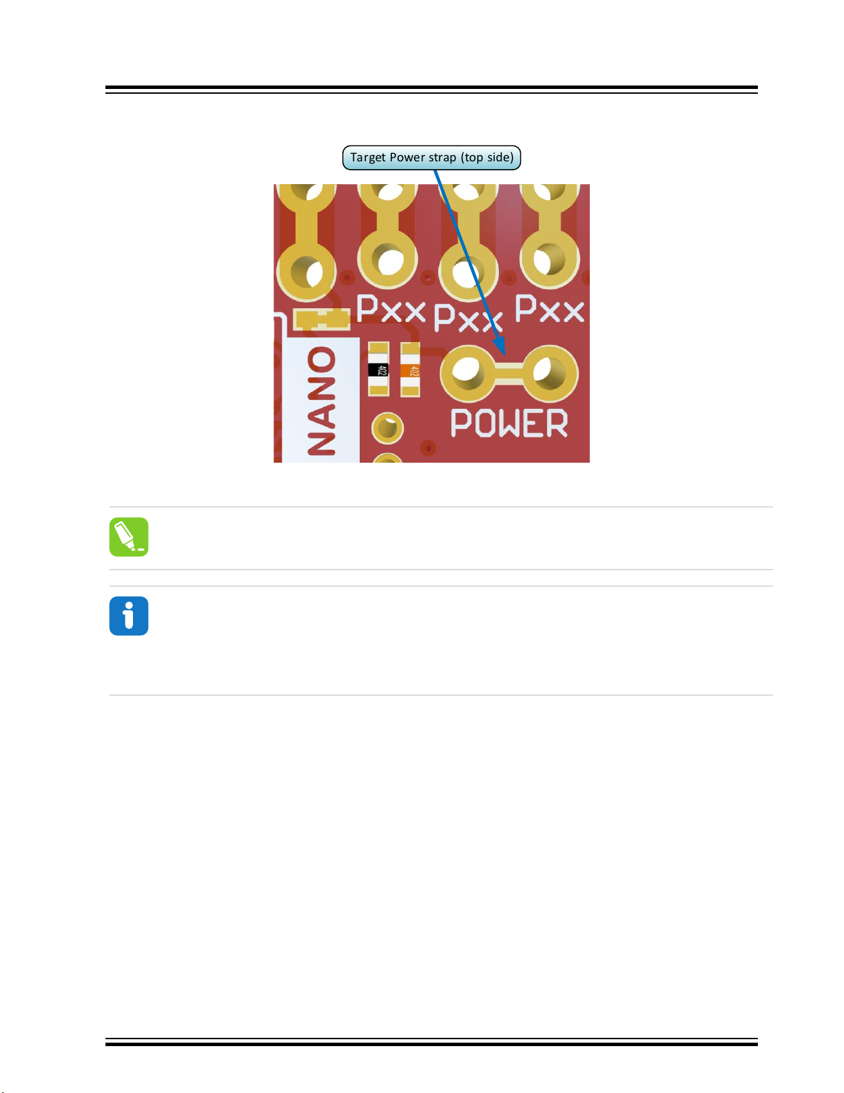
Figure 3-7. Target Power Strap
Target Power strap (top side)
PIC18F57Q43 Curiosity Nano
Curiosity Nano
Tip: A 100-mil pin header can be soldered into the Target Power strap (J101) footprint for easy
connection of an ammeter. Once the ammeter is no longer needed, place a jumper cap on the pin header.
Info: The on-board level shifters will draw a small amount of current even when they are not in use. A
maximum of 2 µA can be drawn from each I/O pin connected to a level shifter for a total of 10 µA. Keep
any I/O pin connected to a level shifter are tri-state to prevent leakage. All I/Os connected to the on-board
debugger is listed in 4.2.4.1 On-Board Debugger Connections. To prevent any leakage to the on-board
level shifters, they can be disconnected completely, as described in 7.4 Disconnecting the On-board
Debugger.
3.5 Programming External Microcontrollers
The on-board debugger on PIC18F57Q43 Curiosity Nano can be used to program and debug microcontrollers on
external hardware.
3.5.1 Supported Devices
All external AVR microcontrollers with the UPDI interface can be programmed and debugged with the on-board
debugger with Atmel Studio.
External SAM microcontrollers that have a Curiosity Nano Board can be programmed and debugged with the onboard debugger with Atmel Studio.
PIC18F57Q43 Curiosity Nano can program and debug external PIC18F57Q43 microcontrollers with MPLAB X IDE.
3.5.2 Software Configuration
No software configuration is required to program and debug the same device that is mounted on the board.
© 2020 Microchip Technology Inc.
DS40002186A-page 16
Page 17
PIC18F57Q43 Curiosity Nano
Curiosity Nano
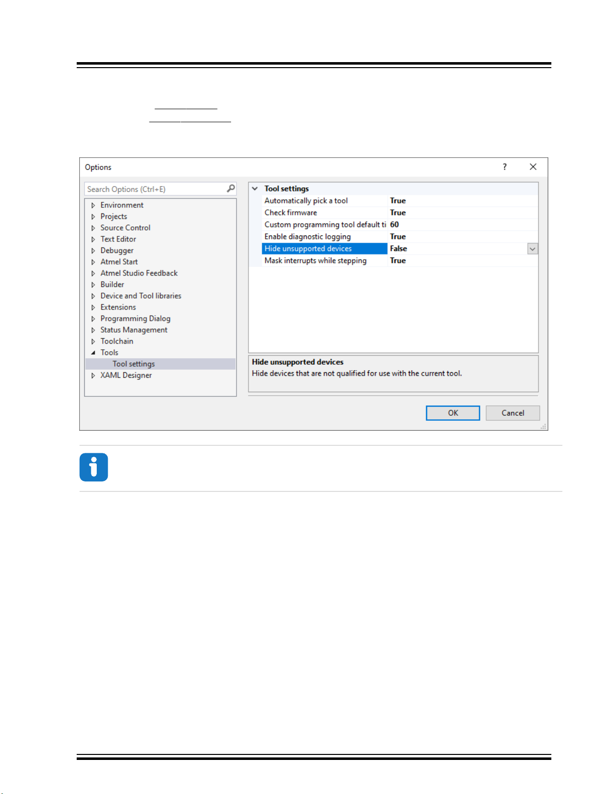
To program and debug a different microcontroller than what is mounted on the board, Atmel Studio must be
configured to allow free selection of devices and programming interfaces.
1. Navigate to Tools > Options through the menu system at the top of the application.
2. Select the Tools > Tool settings category in the options window.
3. Set the Hide unsupported devices option to False .
Figure 3-8. Hide Unsupported Devices
Info: Atmel Studio allows any microcontroller and interface to be selected when Hide unsupported
devices is set to False, also microcontrollers and interfaces which are not supported by the on-board
debugger.
3.5.3 Hardware Modifications
The on-board debugger is connected to the PIC18F57Q43 by default. These connections must be removed before
any external microcontroller can be programmed or debugged. Cut the GPIO straps shown in the figure below with a
sharp tool to disconnect the PIC18F57Q43 from the on-board debugger.
© 2020 Microchip Technology Inc.
DS40002186A-page 17
Page 18
GPIO straps (bottom side)
PIC18F57Q43 Curiosity Nano
Figure 3-9. Programming and Debugging Connections to Debugger
Curiosity Nano
Info: Cutting the connections to the debugger will disable programming, debugging, and data streaming
from the PIC18F57Q43 mounted on the board.
Tip: Solder in 0Ω resistors across the footprints or short-circuit them with solder to reconnect the signals
between the on-board debugger and the PIC18F57Q43.
3.5.4 Connecting to External Microcontrollers
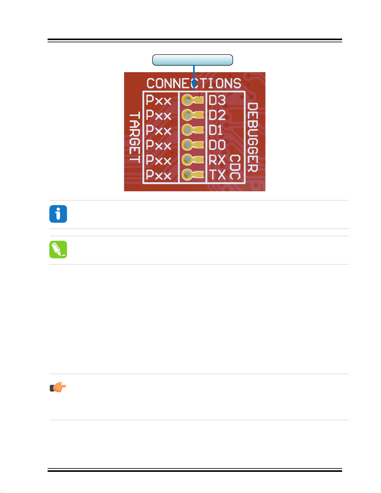
The figure and table below show where the programming and debugging signals must be connected to program and
debug external microcontrollers. The on-board debugger can supply power to the external hardware, or use an
external voltage as a reference for its level shifters. Read more about the power supply in 3.3 Power Supply.
The on-board debugger and level shifters actively drive data and clock signals (DBG0, DBG1, and DBG2) used for
programming and debugging, and in most cases, the external resistor on these signals can be ignored. Pull-down
resistors are required on the ICSP™ data and clock signals to debug PIC® microcontrollers.
DBG3 is an open-drain connection and requires a pull-up resistor to function.
PIC18F57Q43 Curiosity Nano has pull-down resistors R204 and R205 connected to the ICSP data and clock signal
(DBG0 and DBG1). There is also a pull-up resistor R200 connected to the #MCLR signal (DBG3). The location of pull
resistors is shown in the 7.2 Assembly Drawing in the appendix.
Remember:
• Connect GND and VTG to the external microcontroller
• Tie the VOFF pin to GND if the external hardware has its own power supply
• Make sure there are pull-down resistors on the ICSP data and clock signals (DBG0 and DBG1) to
support the debugging of PIC microcontrollers
© 2020 Microchip Technology Inc.
DS40002186A-page 18
Page 19

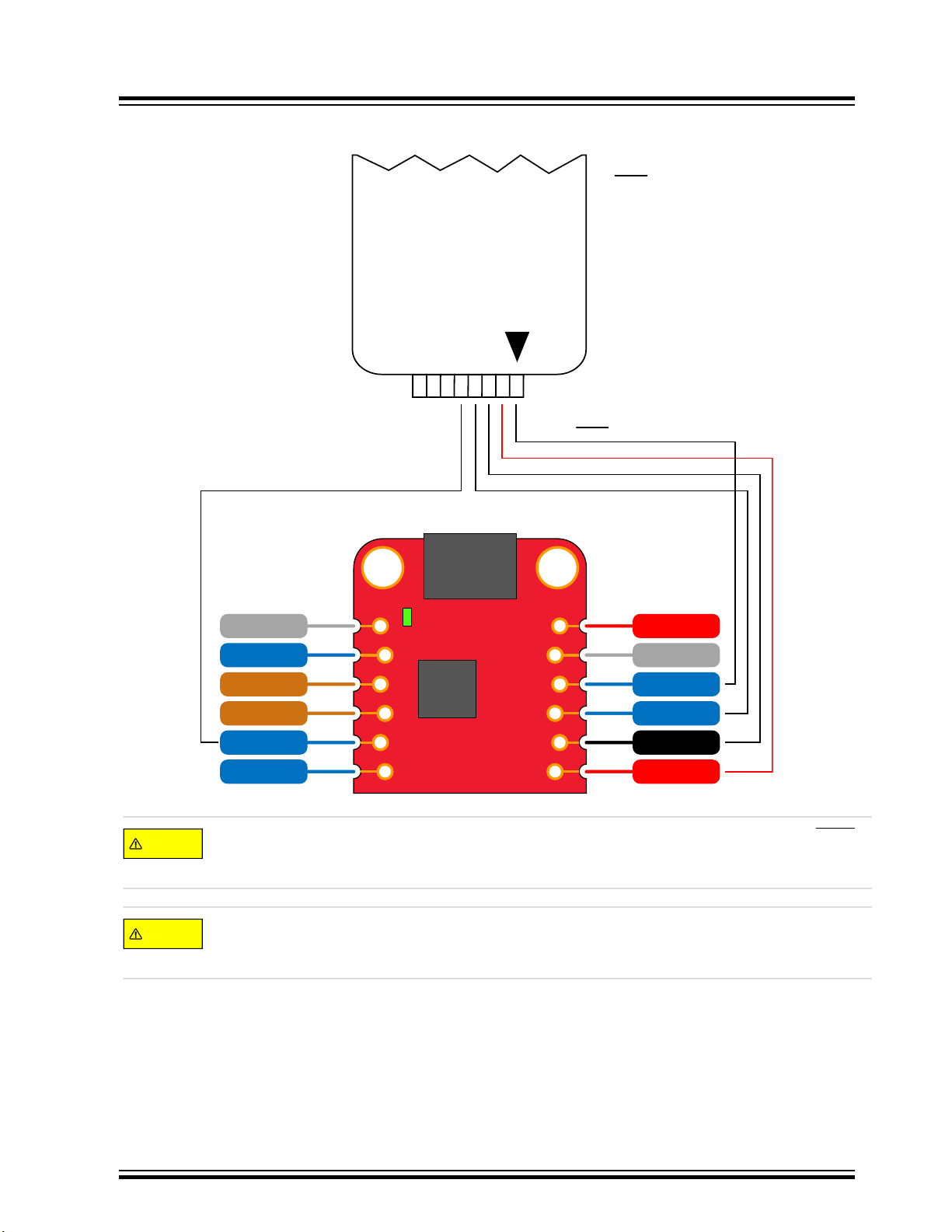
Figure 3-10. Curiosity Nano Standard Pinout
USB
DEBUGGER
PS LED
NC
ID
CDC RX
CDC TX
DBG1
DBG2
VBUS
VOFF
DBG3
DBG0
GND
VTG
CURIOSITY NANO
Table 3-4. Programming and Debugging Interfaces
PIC18F57Q43 Curiosity Nano
Curiosity Nano
Curiosity Nano Pin UPDI ICSP
DBG0 UPDI DATA SWDIO
DBG1 - CLK SWCLK
DBG2 - - -
DBG3 - #MCLR #RESET
3.6 Connecting External Debuggers
Even though there is an on-board debugger, external debuggers can be connected directly to the PIC18F57Q43
Curiosity Nano to program/debug the PIC18F57Q43. The on-board debugger keeps all the pins connected to the
PIC18F57Q43 and board edge in tri-state when not actively used. Therefore, the on-board debugger will not interfere
with any external debug tools.
™
SWD
© 2020 Microchip Technology Inc.
DS40002186A-page 19
Page 20
2
3
4
5
678
1
MCLR
VDD
Ground
DATA
CLOCK
3 = Ground
4 = PGD
5 = PGC
6 = Unused
7 = Unused
8 = Unused
2 = VDD
1 = MCLR
MPLAB® PICkit™ 4
USB
DEBUGGER
PS LED
NC
ID
CDC RX
CDC TX
DBG1
DBG2
VBUS
VOFF
DBG3
DBG0
GND
VTG
CURIOSITY NANO
CAUTION
CAUTION
PIC18F57Q43 Curiosity Nano
Curiosity Nano
Figure 3-11. Connecting the MPLAB® PICkit™ 4 In-Circuit Debugger/Programmer to PIC18F57Q43 Curiosity
Nano
The MPLAB PICkit 4 In-circuit Debugger/Programmer is capable of delivering high voltage on the MCLR
pin. R110 can be permanently damaged by the high voltage. If R110 is broken, the on-board debugger can
not enter Programming mode of the PIC18F57Q43, and will typically fail at reading the device ID.
To avoid contention between the external debugger and the on-board debugger, do not start any
programming/debug operation with the on-board debugger through Microchip MPLAB® X IDE or mass
storage programming while the external tool is active.
© 2020 Microchip Technology Inc.
DS40002186A-page 20
Page 21
4. Hardware User Guide
USB
DEBUGGER
PIC18F57Q43
SW0
LED0
PS LED
NC
NC
ID
ID
CDC RX
CDC RX
UART[1/3/5] TXRF0
CDC TX
CDC TX
UART[1/3/5] RXRF1
DBG1
DBG1
RB6ICSPCLK
DBG2
DBG2
RB4SW0
RC2
RC2
UART1 TX
RC3
RC3
UART1 RX
RB2
RB2
I2C1 SDA
RB1
RB1
I2C1 SCL
RC4
RC4
SPI1 MOSI
RC5
RC5
SPI1 MISO
RC6
RC6
SPI1 SCK
RD4
RD4
SPI1 SS
GND
GND
RA3
RA3
UART3 TX
RA4
RA4
UART3 RX
RE2
RE2
RC7
RC7
RD0
RD0
RD1
RD1
RD2
RD2
RD3
RD3
GND
GND
RF0
RF0
UART[1/3/5] TXCDC RX
RF1
RF1
UART[1/3/5] RXCDC TX
RF2
RF2
RF3
RF3
LED0
VBUS
VBUS
VOFF
VOFF
DBG3
DBG3
RE3 MCLR
DBG0
DBG0
RB7 ICSPDAT
GND
GND
VTG
VTG
RA7
RA7
ANA7
RA6
RA6
ANA6
RA5
RA5
ANA5
RB3
RB3
ANB3 PWM[2/3]
RB0
RB0
ANB0 PWM[2/3]
RA2
RA2
ANA2
RA1
RA1
ANA1
RA0
RA0
ANA0
GND
GND
RD7
RD7
RD6
RD6
RD5
RD5
RB5
RB5
RF7
RF7
RF6
RF6
RF5
RF5
RF4
RF4
GND
GND
RE1
RE1
RE0
RE0
RC1
RC1
(SOSCI)
RC0
RC0
(SOSCO)
DEBUGGER
PIC18F57Q43
Analog
Debug
I2C
SPI
UART
Peripheral
Port
PWM
Power
Ground
Shared pin
PIC18F57Q43
Curiosity Nano
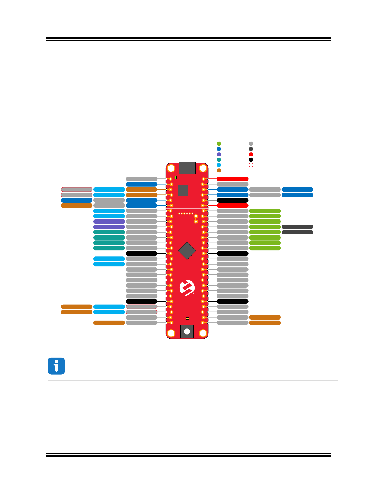
4.1 Connectors
4.1.1 PIC18F57Q43 Curiosity Nano Pinout
All the PIC18F57Q43 I/O pins are accessible at the edge connectors on the board. The image below shows the
board pinout.
Figure 4-1. PIC18F57Q43 Curiosity Nano Pinout
PIC18F57Q43 Curiosity Nano
Hardware User Guide
4.1.2 Using Pin Headers
The edge connector footprint on PIC18F57Q43 Curiosity Nano has a staggered design where each hole is shifted 8
mil (~0.2 mm) off-center. The hole shift allows the use of regular 100 mil pin headers on the board without soldering.
Once the pin headers are firmly in place, they can be used in normal applications like pin sockets and prototyping
boards without any issues.
© 2020 Microchip Technology Inc.
Info: Peripheral signals shown in the image above such as UART, I2C, SPI, ADC, PWM and others, are
shown at specific pins to comply with the Curiosity Nano Board standard. These signals can usually be
routed to alternate pins using the Peripheral Pin Select (PPS) feature in the PIC18F57Q43.
DS40002186A-page 21
Page 22
Tip: Start at one end of the pin header and gradually insert the header along the length of the board.
Once all the pins are in place, use a flat surface to push them in.
Tip: For applications where the pin headers will be used permanently, it is still recommended to solder
them in place.
Important: Once the pin headers are in place, they are hard to remove by hand. Use a set of pliers and
carefully remove the pin headers to avoid damage to the pin headers and PCB.
4.2 Peripherals
4.2.1 LED
There is one yellow user LED available on the PIC18F57Q43 Curiosity Nano Board that can be controlled by either
GPIO or PWM. The LED can be activated by driving the connected I/O line to GND.
Table 4-1. LED Connection
PIC18F57Q43 Curiosity Nano
Hardware User Guide
PIC18F57Q43 Pin Function Shared Functionality
RF3 Yellow LED0 Edge connector
4.2.2 Mechanical Switch
The PIC18F57Q43 Curiosity Nano has one mechanical switch. This is a generic user-configurable switch. When the
switch is pressed, it will drive the I/O line to ground (GND).
Tip: There is no externally connected pull-up resistor on the switch. To use the switch, make sure that an
internal pull-up resistor is enabled on pin RB4.
Table 4-2. Mechanical Switch
PIC18F57Q43 Pin Description Shared Functionality
RB4 User switch (SW0) Edge connector, On-board debugger
4.2.3 Crystal
The PIC18F57Q43 Curiosity Nano Board has a 32.768 kHz crystal footprint made for standard 3.2mm by 1.5mm
surface mount crystals with two terminals.
The crystal footprint is not connected to the PIC18F57Q43 by default, as the GPIOs are routed out to the edge
connector. To use the crystal, some hardware modifications are required. The two I/O lines routed to the edge
connector must be disconnected to reduce the chance of contention to the crystal, and to remove excessive
capacitance on the lines. This can be done by cutting the two straps on the bottom side of the board, marked RC0
and RC1, as shown in the figure below. Next, solder on a solder blob on each of the circular solder points next to the
crystal on the top side of the board, as shown in the figure below.
© 2020 Microchip Technology Inc.
DS40002186A-page 22
Page 23

Table 4-3. Crystal Connections
PIC18F57Q43 Pin Function Shared Functionality
RC0 SOSCO (Crystal output) Edge connector
RC1 SOSCI (Crystal input) Edge connector
Figure 4-2. Crystal Connection and Cut Straps
4.2.4 On-Board Debugger Implementation
PIC18F57Q43 Curiosity Nano features an on-board debugger that can be used to program and debug the
PIC18F57Q43 using ICSP. The on-board debugger also includes a virtual serial port (CDC) interface over UART and
debug GPIO. Microchip MPLAB® X IDE can be used as a front-end for the on-board debugger for programming and
debugging. MPLAB Data Visualizer can be used as a front-end for the CDC and debug GPIO.
PIC18F57Q43 Curiosity Nano
Hardware User Guide
4.2.4.1 On-Board Debugger Connections
The table below shows the connections between the target and the debugger section. All connections between the
target and the debugger are tri-stated as long as the debugger is not actively using the interface. Hence, since there
are little contaminations of the signals, the pins can be configured to anything the user wants.
For further information on how to use the capabilities of the on-board debugger, see 3.1 On-Board Debugger
Overview.
Table 4-4. On-board Debugger Connections
PIC18F57Q43 Debugger Function Shared Functionality
RF1 CDC TX UART RX (PIC18F57Q43 RX line) Edge connector
RF0 CDC RX UART TX (PIC18F57Q43 TX line) Edge connector
RB7 DBG0 ICSPDAT Edge connector
RB6 DBG1 ICSPCLK Edge connector
RB4 DBG2 GPIO Edge connector and SW0
RE3 DBG3 MCLR Edge connector
© 2020 Microchip Technology Inc.
DS40002186A-page 23
Page 24

PIC18F57Q43 Curiosity Nano
Hardware Revision History and Known Issues
5. Hardware Revision History and Known Issues
This user guide is written to provide information about the latest available revision of the board. The following
sections contain information about known issues, a revision history of older revisions, and how older revisions differ
from the latest revision.
5.1 Identifying Product ID and Revision
The revision and product identifier of the PIC18F57Q43 Curiosity Nano Board can be found in two ways: Either by
utilizing the Microchip MPLAB® X IDE Kit Window or by looking at the sticker on the bottom side of the PCB.
By connecting PIC18F57Q43 Curiosity Nano to a computer with Microchip MPLAB® X IDE running, the Kit Window
will pop up. The first six digits of the serial number, which is listed under kit information, contain the product identifier
and revision.
Tip: The Kit Window can be opened in MPLAB® X IDE through the menu bar Window > Kit Window.
The same information can be found on the sticker on the bottom side of the PCB. Most boards will have the identifier
and revision printed in plain text as A09-nnnn\rr, where “nnnn” is the identifier, and “rr” is the revision. Boards with
limited space have a sticker with only a data matrix code, containing the product identifier, revision, and serial
number.
The serial number string has the following format:
"nnnnrrssssssssss"
n = product identifier
r = revision
s = serial number
The product identifier for PIC18F57Q43 Curiosity Nano is A09-3290.
5.2 Revision 3
Revision 3 is the initially released version.
© 2020 Microchip Technology Inc.
DS40002186A-page 24
Page 25

6. Document Revision History
Doc. rev. Date Comment
A 03/2020 Initial document release.
PIC18F57Q43 Curiosity Nano
Document Revision History
© 2020 Microchip Technology Inc.
DS40002186A-page 25
Page 26

1
1
2
2
3
3
4
4
5
5
6
6
7
7
8
8
D D
C C
B B
A A
2 of 4
PIC18F 57Q43 Cur iosity Nano
2019-12-19
PIC18F57Q43_Curiosity_Nano_Target_MCU.SchDoc
Project Title
PCB Assembly Number: PCBA Revision:
File:
PCB Number: PCB Revi sion:
Designed with
Drawn By:
TF, PB
Sheet Title
Target MCU
Engineer:
TF, PB
A08-3021 3
Size
A3
A09-3290 3
Page:
Date:
Altium.com
GND
VCC_TARGET
GND
100n
C202
GND
VCC_TARGET
100n
C200
GND
32kHz CR YSTAL
1k
R203
USER LE D
VCC_TARGET
GND
USER BUTT ON
1k
R202
YELLOW LED
SML-D12Y1WT86
21
D200
TS604VM1-035CR
1 3
42
SW200
GND
VCC_EDGE
GNDGND
GND GND
J203
J201 J202
J204
J209
PIC18F57Q43
2.2uF
C205
VCC_EDGE
GND
CDC_TX
CDC_RX
DBG2
DEBUGGE R CONNE CTIONS
DBG1
DBG3
DBG0
ID_SYS
VOFF
TARGET BULK
VCC_TARGET
MCLR PULL-UP
VBUS
RC7
RD4_SPI1_SS
RD5
RD6
RD7
RB0_ANA3_PWM
RB1_I2C1_SCL
RB2_I2C1_SDA
RC0_SOSCO
RA6_ANA6
RA7_ANA7
RE2
RE1
RE0
RA5_ANA5
RA4_UART3_RX
RB3_ANA4_PWM
RB4_SW0
RB5
RB6_ICSPCLK
RB7_ICSPDAT
RE3_MCLR
RA0_ANA0
RA1_ANA1
RA2_ANA2
RA3_UART3_TX
RC6_SPI1_SCK
RC5_SPI1_MISO
RC4_SPI1_MOSI
RD3
RD2
RD0_UART4_TX
RD1_UART4_RX
RC3_UART1_RX
RC2_UART1_TX
RC1_SOSCI
RB6_ICSPCLK
RB4_SW0
RC2_UART1_TX
RC3_UART1_RX
RB2_I2C1_SDA
RB1_I2C1_SCL
RC4_SPI1_MOSI
RC5_SPI1_MISO
RC6_SPI1_SCK
RD4_SPI1_SS
RD0_UART4_TX
RD1_UART4_RX
RD2
RD3
RB0_ANA3_PWM
RB3_ANA4_PWM
RE2
RC7
RE3_MCLR
RB7_ICSPDAT
RA7_ANA7
RA6_ANA6
RA5_ANA5
RA2_ANA2
RA1_ANA1
RA0_ANA0
RD7
RD6
RD5
RB5
RE1
RE0
RB4_SW0
RF3_LED0
J205
J206
RC0_SOSCO
RC1_SOSCI
PROG /DEBUG PUL L
47k
R204
47k
R205
GND
DBG0DBG1
J210
J211
RE3_MCLR
PIC18F57Q43T-I/PT
RC71RD42RD53RD64RD75VSS6VDD7RB08RB19RB210RB311RF4
12
RF5
13
RF6
14
RF7
15
RB4
16
RB5
17
RB6/ICSPCLK
18
RB7/ICSPDAT
19
RE3/MCLR/VPP
20
RA0
21
RA1
22
RA2
23
RA3
24
RA425RA526RE027RE128RE229VDD30VSS
31
CLKIN/OSC1/RA7
32
CLKOUT/OSC2/RA6
33
SOSCO/RC0
34
SOSCIN/RC1
35
RF0
36
RF1
37
RF2
38
RF3
39
RC2
40
RC3
41
RD0
42
RD1
43
RD2
44
RD3
45
RC4
46
RC5
47
RC6
48
U200
RF7
RF6
RF5
RF1_UART5_RX
RF2
RF3_LED0
RF4
RF0_UART5_TX
CDC RX
3
CDC TX
4
DBG1
5
DBG2
6
0 TX
7
1 RX
8
2 SDA
9
3 SCL
10
4 MOSI
11
5 MISO
12
6 SCK
13
7 SS
14
GND
15
0 (TX)
16
1 (RX)
17
2
18
3
19
0
20
GND
24
DBG3
54
DBG0
53
GND
52
VCC
51
PWM 3
46
ADC 2
45
ADC 1
44
ADC 0
43
GND
42
4
38
4
34
GND
33
ADC 7
50
ADC 6
49
ADC 5
48
PWM 4
47
DEBUGGER
TARGET
ID
2
VOFF
55
1
21
2
22
3
23
0
25
1
26
2
27
3
28
4
29
5
30
6
31
7
32
5
35
6
36
7
37
5
39
6
40
7
41
RESERVED
1
VBUS
56
CNANO56-pin edge connector
J200
RF0_UART5_TX
RF1_UART5_RX
RF2
RF3_LED0
RF6
RF7
8.2p
C204
N.M.
8.2p
C203
N.M.
J207
J208
47k
R200
PIC18F 47Q43
ICSPDAT
ICSPCLK
GPIO0
MCLR
DBG0
DBG1
DBG2
DBG3
Debugger
CDC TX
CDC RX
UART RX
UART TX
VTG 1.8V - 5.5V
RB6
RB4
RE3
RB7
RF0
RF1
Name Pin
XC200
N.M.
32.768 kHz
RF4
RF5
RC1_SOSCI
RC0_SOSCO
RC1
RC0
RF0_UART5_TX
RF1_UART5_RX
RA4_UART3_RX
RA3_UART3_TX
TX
RX
UART
CDC_UART
DBG0
DBG3
DBG1
DBG2
VOFF
ID_SYS
RX/TX on the header denotes the
input/output direction of the signal
respective to it's source.
CDC TX is output from the DEBUGGER.
CDC RX is input to the DEBUGGER.
TX is output from the TARGET device.
RX is input to the TARGET device
PIC18F57Q43 Curiosity Nano
Appendix
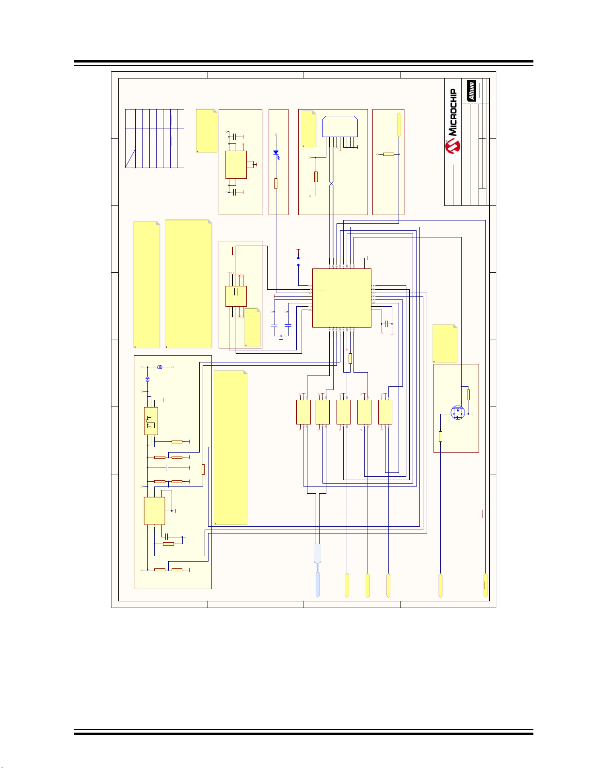
7. Appendix
7.1 Schematic
Figure 7-1. PIC18F57Q43 Curiosity Nano Schematic
© 2020 Microchip Technology Inc.
DS40002186A-page 26
Page 27
1
1
2
2
3
3
4
4
5
5
6
6
7
7
8
8
D D
C C
B B
A A
3 of 4
PIC18F 57Q43 Cur iosity Nano
2019-12-19
PIC18F57Q43_Curiosity_Nano_Debugger.SchDoc
Project Title
PCB Assembly Number: PCBA Revision:
File:
PCB Number: PCB Revi sion:
Designed with
Drawn By:
TF
Sheet Title
Debugger
Engineer:
TF
A08-3021 3
Size
A3
A09-3290 3
Page:
Date:
Altium.com
GND
USBD_P
USBD_N
100n
C107
100n
C108
RX
TX
UART
CDC_UART
1k
R107
VCC_P3V3
SRST
STATUS_LED
SHIELD
VCC_P3V3
GND
TP100
Testpoint Array
1 2
3 4
5 6
7 8
9 10
TCK
TDO
TMS
Vsup
TDI GND
TRST
SRST
VTref
GND
J102
GND
4.7uF
C100
DBG0
DBG0
21
GREEN LED
SML-P12MTT86R
D100
VBUS1D-2D+3GND5SHIELD16SHIELD27ID4SHIELD38SHIELD4
9
MU-MB0142AB2-269
J105
PAD
33
PA00
1
PA012PA023PA03
4
GND
10
VDDANA
9
PA045PA056PA067PA07
8
PA08
11
PA09
12
PA10
13
PA11
14
PA14
15
PA15
16
PA1617PA1718PA1819PA1920PA22
21
USB_SOF/PA23
22
USB_DM/PA2423USB_DP/PA25
24
PA27
25
RESETN
26
PA28
27
GND
28
VDDCORE
29
VDDIN
30
SWDCLK/PA30
31
SWDIO/PA31
32
SAMD21E18A-MUT
U100
VOUT1VOUT
2
GND
3
EN4VIN
6
NC
5
EP
7
MIC5528-3.3YMTU101VCC_VBUS VCC_P3V3
GND
USBD_P
USBD_N
GND
1u
C106
VCC_MCU_CORE
VCC_P3V3
VCC_P3V3
2.2uF
C101
GND
74LVC1T45FW4-7
VCCA
1
VCCB
6
A
3
GND
2
DIR5B
4
U103
VCC_P3V3
GND
74LVC1T45FW4-7
VCCA
1
VCCB
6
A
3
GND
2
DIR5B
4
U104
VCC_P3V3
GND
74LVC1T45FW4-7
VCCA
1
VCCB
6
A
3
GND
2
DIR5B
4
U105
VCC_P3V3
GND
GND
GND
GND
VCC_EDGE
GND
74LVC1T45FW4-7
VCCA
1
VCCB
6
A
3
GND
2
DIR5B
4
U107
VCC_P3V3
GND
DBG2
DBG3_CTRL
S1_0_TX
S1_1_RX
S0_2_TX
DAC
VTG_ADC
RESERVED
S0_3_CLK
DBG0_CTRL
CDC_TX_CTRL
BOOT
DEBUGGE R POWE R/STATUS LED
EN1BYP
6
VOUT
4
GND
2
VIN
3
NC/ADJ
5
GND
7
MIC5353U102
VCC_VBUS
100n
C102
GND
GND
47k
R101
27k
R104
GND
33k
R106
2.2uF
C103
GND
1k
R108
J100
VCC_LEVELVCC_REGULATOR
74LVC1T45FW4-7
VCCA
1
VCCB
6
A
3
GND
2
DIR5B
4
U106
VCC_P3V3
GND
DBG1
CDC_RX
CDC_TX
DBG3
DBG1_CTRL
DEBUGGE R REGUL ATOR
REG_ENABLE
REG_ENABLE
47k
R103
VCC_LEVEL
VCC_LEVEL
VCC_LEVEL
VCC_LEVEL
VCC_LEVEL
47k
R102
47k
R105
SWCLK
GND
47k
R100
GND
DBG2
S0_0_RX
DBG1_CTRL
DBG0_CTRL
DBG3 OPE N DRAIN
TARGET ADJUSTABLE REG ULATOR
SRST
DEBUGGE R TESTPO INTs
DBG2_CTRL
VOFF
CDC_RX_CTRL
47k
R109
DBG1
CDC_TX_CTRL
CDC_RX_CTRL
SWCLK
REG_ADJUST
DBG2_GPIO
DBG3_CTRL
DBG2_CTRL
UPDI
UPDI
GPIO
GPIO
RESET
Signal
DBG0
DBG1
DBG2
DBG3
ICSP
Interface
DAT
CLK
GPIO
MCLR
DBG3
CDC TX
CDC RX
UART RX
UART TX
UART RX
UART TX
TARGET TARGET
1k
R110
VBUS_ADC
DMN65D8LFB
1
2 3
Q101
VCC - -
ID_SYS
VOFF
1k
R112
VCC_P3V3
VTG_ADC
DAC
MIC94163
VIN
B2
VOUT
A1
VINA2EN
C2
GND
C1
VOUT
B1
U108
GND
ID_SYS
VTG_EN
VTG_EN
VBUS_ADC
SWDIO
ID_SYS
TP101
GND
SWDIO
VOFF
47k
R111
GND
ID PIN
DEBUGGE R USB MIC RO-B CONNE CTOR
VBUS
MC36213
F100
VCC_VBUS
J101
VCC_TARGET
47k
R113
Programming connector
for factory programming of
Debugger
MIC5528:
Vin: 2.5V to 5.5V
Vout: Fixed 3.3V
Imax: 500mA
Dropout: 260mV @ 500mA
MIC5353:
Vin: 2.6V to 6V
Vout: 1.25V to 5.1V
Imax: 500mA
Dropout (typical): 50mV@150mA, 160mV @ 500mA
Accuracy: 2% initial
Thermal shutdown and current limit
Maximum output voltage is limited by the input voltage and the dropout voltage in the regulator.
(Vmax = Vin - dropout)
J100:
- Cut-strap used for full separation of target power from the level shifters and on-board regulators.
- For current measurements using the on-board power supply, this strap must be cut and an
ammeter connected across.
- For current measurements using an external power supply, this strap could be cut for more
accurate measurements. Leakage back through the switch is in the micro ampere range.
PTC Resettable fuse:
Hold current: 500mA
Trip current: 1000mA
R113:
Pull down to prevent
DBG3_CTRL from
floating when debugger is
not powered.
Adjustable output and limitations:
- The DEBUGGER can adjust the output voltage of the regulator between 1.25V and 5.1V to the target.
- The voltage output is limited by the input (USB), which can vary between 4.40V to 5.25V
- The level shifters have a minimal voltage level of 1.65V and will limit the minimum operating voltage allowed for the
target to still allow communication.
- The MIC94163 has a minimal volatege level of 1.70V and will limit the minimum voltage delivered to the target.
- Firmware configuration will limit the voltage range to be within the the target specification.
PIC18F57Q43 Curiosity Nano
Appendix
© 2020 Microchip Technology Inc.
DS40002186A-page 27
Page 28

7.2 Assembly Drawing
PIC®
MCU
b
t
c
R
Figure 7-2. PIC18F57Q43 Curiosity Nano Assembly Drawing Top
Figure 7-3. PIC18F57Q43 Curiosity Nano Assembly Drawing Bottom
PIC18F57Q43 Curiosity Nano
Appendix
© 2020 Microchip Technology Inc.
DS40002186A-page 28
Page 29

USB
DEBUGGER
PIC18F57Q43
SW0
LED0
PS LED
NC
NC
ID
ID
CDC RX
CDC RX
UART[1/3/5] TXRF0
CDC TX
CDC TX
UART[1/3/5] RXRF1
DBG1
DBG1
RB6ICSPCLK
DBG2
DBG2
RB4SW0
RC2
RC2
UART1 TX
RC3
RC3
UART1 RX
RB2
RB2
I2C1 SDA
RB1
RB1
I2C1 SCL
RC4
RC4
SPI1 MOSI
RC5
RC5
SPI1 MISO
RC6
RC6
SPI1 SCK
RD4
RD4
SPI1 SS
GND
GND
RA3
RA3
UART3 TX
RA4
RA4
UART3 RX
RE2
RE2
RC7
RC7
RD0
RD0
RD1
RD1
RD2
RD2
RD3
RD3
GND
GND
RF0
RF0
UART[1/3/5] TXCDC RX
RF1
RF1
UART[1/3/5] RXCDC TX
RF2
RF2
RF3
RF3
LED0
VBUS
VBUS
VOFF
VOFF
DBG3
DBG3
RE3 MCLR
DBG0
DBG0
RB7 ICSPDAT
GND
GND
VTG
VTG
RA7
RA7
ANA7
RA6
RA6
ANA6
RA5
RA5
ANA5
RB3
RB3
ANB3 PWM[2/3]
RB0
RB0
ANB0 PWM[2/3]
RA2
RA2
ANA2
RA1
RA1
ANA1
RA0
RA0
ANA0
GND
GND
RD7
RD7
RD6
RD6
RD5
RD5
RB5
RB5
RF7
RF7
RF6
RF6
RF5
RF5
RF4
RF4
GND
GND
RE1
RE1
RE0
RE0
RC1
RC1
(SOSCI)
RC0
RC0
(SOSCO)
DEBUGGER
PIC18F57Q43
Analog
Debug
I2C
SPI
UART
Peripheral
Port
PWM
Power
Ground
Shared pin
PIC18F57Q43
Curiosity Nano
1
AN PWM
RST INT
CS RX
SCK TX
MISO SCL
MOSI SDA
+3.3V +5V
GND GND
2
AN PWM
RST INT
CS RX
SCK TX
MISO SCL
MOSI SDA
+3.3V +5V
GND GND
3
AN PWM
RST INT
CS RX
SCK TX
MISO SCL
MOSI SDA
+3.3V +5V
GND GND
Xplained Pro Extension
EXT1
1 2
19 20
Curiosity Nano Base
for click boards
TM
RA0 RB0
RA7 RA6
RD4 RC3
RC6 RC2
RC5 RB1
RC4 RB2
+3.3V +5V
GND GND
RA1 RB3
RC7 RE2
RD6 RA4
RC6 RA3
RC5 RB1
RC4 RB2
+3.3V +5V
GND GND
RA2 RA5
RD5 RB5
RD7 RC3
RC6 RC2
RC5 RB1
RC4 RB2
+3.3V +5V
GND GND
ID GND
RA1 RA2
RC7 RD5
RB3 RA5
RE2 RD7
RB2 RB1
RA4 RA3
RD6 RC4
RC5 RC6
GND +3.3V
PIC18F57Q43 Curiosity Nano
Appendix
7.3 Curiosity Nano Base for Click boards
Figure 7-4. PIC18F57Q43 Curiosity Nano Pinout Mapping
™
© 2020 Microchip Technology Inc.
DS40002186A-page 29
Page 30

7.4 Disconnecting the On-board Debugger
The on-board debugger and level shifters can be completely disconnected from the PIC18F57Q43.
The block diagram below shows all connections between the debugger and the PIC18F57Q43. The rounded boxes
represent connections to the board edge. The signal names shown are also printed in silkscreen on the bottom side
of the board.
To disconnect the debugger, cut the straps shown in Figure 7-6.
Attention: Cutting the GPIO straps to the on-board debugger will disable the virtual serial port,
programming, debugging, and data streaming. Cutting the power supply strap will disconnect the on-board
power supply.
Tip: Any connection that is cut can be reconnected using solder, alternatively, a 0Ω 0402 resistor can be
mounted.
Tip: When the debugger is disconnected, an external debugger can be connected to holes shown in
Figure 7-6. Details about connecting an external debugger are described in 3.6 Connecting External
Debuggers.
PIC18F57Q43 Curiosity Nano
Appendix
Figure 7-5. On-Board Debugger Connections Block Diagram
USB
VBUS
VBUS
VOFF
Power Supply strap Target Power strap
LDO
LDO
VCC_LEVEL
DBG0
DBG1
DBG2
DBG3
CDC TX
CDC RX
PA04/PA06
PA07
PA08
PA16
PA00
DEBUGGER
PA01
VCC_P3V3
Level-Shift
DIR x 5
CDC RX
CDC TX
VTG
VCC_EDGE
VCC_TARGET
GPIO straps
TARGET
UART RX
UART TX
DBG0
DBG1
© 2020 Microchip Technology Inc.
DBG2
DBG3
DS40002186A-page 30
Page 31

Figure 7-6. On-Board Debugger Connection Cut Straps
GPIO straps (bottom side) Power Supply strap (top side)
PIC18F57Q43 Curiosity Nano
Appendix
© 2020 Microchip Technology Inc.
DS40002186A-page 31
Page 32

PIC18F57Q43 Curiosity Nano
The Microchip Website
Microchip provides online support via our website at http://www.microchip.com/. This website is used to make files
and information easily available to customers. Some of the content available includes:
• Product Support – Data sheets and errata, application notes and sample programs, design resources, user’s
guides and hardware support documents, latest software releases and archived software
• General Technical Support – Frequently Asked Questions (FAQs), technical support requests, online
discussion groups, Microchip design partner program member listing
• Business of Microchip – Product selector and ordering guides, latest Microchip press releases, listing of
seminars and events, listings of Microchip sales offices, distributors and factory representatives
Product Change Notification Service
Microchip’s product change notification service helps keep customers current on Microchip products. Subscribers will
receive email notification whenever there are changes, updates, revisions or errata related to a specified product
family or development tool of interest.
To register, go to http://www.microchip.com/pcn and follow the registration instructions.
Customer Support
Users of Microchip products can receive assistance through several channels:
• Distributor or Representative
• Local Sales Office
• Embedded Solutions Engineer (ESE)
• Technical Support
Customers should contact their distributor, representative or ESE for support. Local sales offices are also available to
help customers. A listing of sales offices and locations is included in this document.
Technical support is available through the website at: http://www.microchip.com/support
Microchip Devices Code Protection Feature
Note the following details of the code protection feature on Microchip devices:
• Microchip products meet the specification contained in their particular Microchip Data Sheet.
• Microchip believes that its family of products is one of the most secure families of its kind on the market today,
when used in the intended manner and under normal conditions.
• There are dishonest and possibly illegal methods used to breach the code protection feature. All of these
methods, to our knowledge, require using the Microchip products in a manner outside the operating
specifications contained in Microchip’s Data Sheets. Most likely, the person doing so is engaged in theft of
intellectual property.
• Microchip is willing to work with the customer who is concerned about the integrity of their code.
• Neither Microchip nor any other semiconductor manufacturer can guarantee the security of their code. Code
protection does not mean that we are guaranteeing the product as “unbreakable.”
Code protection is constantly evolving. We at Microchip are committed to continuously improving the code protection
features of our products. Attempts to break Microchip’s code protection feature may be a violation of the Digital
Millennium Copyright Act. If such acts allow unauthorized access to your software or other copyrighted work, you
may have a right to sue for relief under that Act.
Legal Notice
Information contained in this publication regarding device applications and the like is provided only for your
convenience and may be superseded by updates. It is your responsibility to ensure that your application meets with
© 2020 Microchip Technology Inc.
DS40002186A-page 32
Page 33

PIC18F57Q43 Curiosity Nano
your specifications. MICROCHIP MAKES NO REPRESENTATIONS OR WARRANTIES OF ANY KIND WHETHER
EXPRESS OR IMPLIED, WRITTEN OR ORAL, STATUTORY OR OTHERWISE, RELATED TO THE INFORMATION,
INCLUDING BUT NOT LIMITED TO ITS CONDITION, QUALITY, PERFORMANCE, MERCHANTABILITY OR
FITNESS FOR PURPOSE. Microchip disclaims all liability arising from this information and its use. Use of Microchip
devices in life support and/or safety applications is entirely at the buyer’s risk, and the buyer agrees to defend,
indemnify and hold harmless Microchip from any and all damages, claims, suits, or expenses resulting from such
use. No licenses are conveyed, implicitly or otherwise, under any Microchip intellectual property rights unless
otherwise stated.
Trademarks
The Microchip name and logo, the Microchip logo, Adaptec, AnyRate, AVR, AVR logo, AVR Freaks, BesTime,
BitCloud, chipKIT, chipKIT logo, CryptoMemory, CryptoRF, dsPIC, FlashFlex, flexPWR, HELDO, IGLOO, JukeBlox,
KeeLoq, Kleer, LANCheck, LinkMD, maXStylus, maXTouch, MediaLB, megaAVR, Microsemi, Microsemi logo, MOST,
MOST logo, MPLAB, OptoLyzer, PackeTime, PIC, picoPower, PICSTART, PIC32 logo, PolarFire, Prochip Designer,
QTouch, SAM-BA, SenGenuity, SpyNIC, SST, SST Logo, SuperFlash, Symmetricom, SyncServer, Tachyon,
TempTrackr, TimeSource, tinyAVR, UNI/O, Vectron, and XMEGA are registered trademarks of Microchip Technology
Incorporated in the U.S.A. and other countries.
APT, ClockWorks, The Embedded Control Solutions Company, EtherSynch, FlashTec, Hyper Speed Control,
HyperLight Load, IntelliMOS, Libero, motorBench, mTouch, Powermite 3, Precision Edge, ProASIC, ProASIC Plus,
ProASIC Plus logo, Quiet-Wire, SmartFusion, SyncWorld, Temux, TimeCesium, TimeHub, TimePictra, TimeProvider,
Vite, WinPath, and ZL are registered trademarks of Microchip Technology Incorporated in the U.S.A.
Adjacent Key Suppression, AKS, Analog-for-the-Digital Age, Any Capacitor, AnyIn, AnyOut, BlueSky, BodyCom,
CodeGuard, CryptoAuthentication, CryptoAutomotive, CryptoCompanion, CryptoController, dsPICDEM,
dsPICDEM.net, Dynamic Average Matching, DAM, ECAN, EtherGREEN, In-Circuit Serial Programming, ICSP,
INICnet, Inter-Chip Connectivity, JitterBlocker, KleerNet, KleerNet logo, memBrain, Mindi, MiWi, MPASM, MPF,
MPLAB Certified logo, MPLIB, MPLINK, MultiTRAK, NetDetach, Omniscient Code Generation, PICDEM,
PICDEM.net, PICkit, PICtail, PowerSmart, PureSilicon, QMatrix, REAL ICE, Ripple Blocker, SAM-ICE, Serial Quad
I/O, SMART-I.S., SQI, SuperSwitcher, SuperSwitcher II, Total Endurance, TSHARC, USBCheck, VariSense,
ViewSpan, WiperLock, Wireless DNA, and ZENA are trademarks of Microchip Technology Incorporated in the U.S.A.
and other countries.
SQTP is a service mark of Microchip Technology Incorporated in the U.S.A.
The Adaptec logo, Frequency on Demand, Silicon Storage Technology, and Symmcom are registered trademarks of
Microchip Technology Inc. in other countries.
GestIC is a registered trademark of Microchip Technology Germany II GmbH & Co. KG, a subsidiary of Microchip
Technology Inc., in other countries.
All other trademarks mentioned herein are property of their respective companies.
©
2020, Microchip Technology Incorporated, Printed in the U.S.A., All Rights Reserved.
ISBN: 978-1-5224-5774-9
Quality Management System
For information regarding Microchip’s Quality Management Systems, please visit http://www.microchip.com/quality.
© 2020 Microchip Technology Inc.
DS40002186A-page 33
Page 34
Worldwide Sales and Service
AMERICAS ASIA/PACIFIC ASIA/PACIFIC EUROPE
Corporate Office
2355 West Chandler Blvd.
Chandler, AZ 85224-6199
Tel: 480-792-7200
Fax: 480-792-7277
Technical Support:
http://www.microchip.com/support
Web Address:
http://www.microchip.com
Atlanta
Duluth, GA
Tel: 678-957-9614
Fax: 678-957-1455
Austin, TX
Tel: 512-257-3370
Boston
Westborough, MA
Tel: 774-760-0087
Fax: 774-760-0088
Chicago
Itasca, IL
Tel: 630-285-0071
Fax: 630-285-0075
Dallas
Addison, TX
Tel: 972-818-7423
Fax: 972-818-2924
Detroit
Novi, MI
Tel: 248-848-4000
Houston, TX
Tel: 281-894-5983
Indianapolis
Noblesville, IN
Tel: 317-773-8323
Fax: 317-773-5453
Tel: 317-536-2380
Los Angeles
Mission Viejo, CA
Tel: 949-462-9523
Fax: 949-462-9608
Tel: 951-273-7800
Raleigh, NC
Tel: 919-844-7510
New York, NY
Tel: 631-435-6000
San Jose, CA
Tel: 408-735-9110
Tel: 408-436-4270
Canada - Toronto
Tel: 905-695-1980
Fax: 905-695-2078
Australia - Sydney
Tel: 61-2-9868-6733
China - Beijing
Tel: 86-10-8569-7000
China - Chengdu
Tel: 86-28-8665-5511
China - Chongqing
Tel: 86-23-8980-9588
China - Dongguan
Tel: 86-769-8702-9880
China - Guangzhou
Tel: 86-20-8755-8029
China - Hangzhou
Tel: 86-571-8792-8115
China - Hong Kong SAR
Tel: 852-2943-5100
China - Nanjing
Tel: 86-25-8473-2460
China - Qingdao
Tel: 86-532-8502-7355
China - Shanghai
Tel: 86-21-3326-8000
China - Shenyang
Tel: 86-24-2334-2829
China - Shenzhen
Tel: 86-755-8864-2200
China - Suzhou
Tel: 86-186-6233-1526
China - Wuhan
Tel: 86-27-5980-5300
China - Xian
Tel: 86-29-8833-7252
China - Xiamen
Tel: 86-592-2388138
China - Zhuhai
Tel: 86-756-3210040
India - Bangalore
Tel: 91-80-3090-4444
India - New Delhi
Tel: 91-11-4160-8631
India - Pune
Tel: 91-20-4121-0141
Japan - Osaka
Tel: 81-6-6152-7160
Japan - Tokyo
Tel: 81-3-6880- 3770
Korea - Daegu
Tel: 82-53-744-4301
Korea - Seoul
Tel: 82-2-554-7200
Malaysia - Kuala Lumpur
Tel: 60-3-7651-7906
Malaysia - Penang
Tel: 60-4-227-8870
Philippines - Manila
Tel: 63-2-634-9065
Singapore
Tel: 65-6334-8870
Taiwan - Hsin Chu
Tel: 886-3-577-8366
Taiwan - Kaohsiung
Tel: 886-7-213-7830
Taiwan - Taipei
Tel: 886-2-2508-8600
Thailand - Bangkok
Tel: 66-2-694-1351
Vietnam - Ho Chi Minh
Tel: 84-28-5448-2100
Austria - Wels
Tel: 43-7242-2244-39
Fax: 43-7242-2244-393
Denmark - Copenhagen
Tel: 45-4485-5910
Fax: 45-4485-2829
Finland - Espoo
Tel: 358-9-4520-820
France - Paris
Tel: 33-1-69-53-63-20
Fax: 33-1-69-30-90-79
Germany - Garching
Tel: 49-8931-9700
Germany - Haan
Tel: 49-2129-3766400
Germany - Heilbronn
Tel: 49-7131-72400
Germany - Karlsruhe
Tel: 49-721-625370
Germany - Munich
Tel: 49-89-627-144-0
Fax: 49-89-627-144-44
Germany - Rosenheim
Tel: 49-8031-354-560
Israel - Ra’anana
Tel: 972-9-744-7705
Italy - Milan
Tel: 39-0331-742611
Fax: 39-0331-466781
Italy - Padova
Tel: 39-049-7625286
Netherlands - Drunen
Tel: 31-416-690399
Fax: 31-416-690340
Norway - Trondheim
Tel: 47-72884388
Poland - Warsaw
Tel: 48-22-3325737
Romania - Bucharest
Tel: 40-21-407-87-50
Spain - Madrid
Tel: 34-91-708-08-90
Fax: 34-91-708-08-91
Sweden - Gothenberg
Tel: 46-31-704-60-40
Sweden - Stockholm
Tel: 46-8-5090-4654
UK - Wokingham
Tel: 44-118-921-5800
Fax: 44-118-921-5820
© 2020 Microchip Technology Inc.
DS40002186A-page 34
 Loading...