

Page 1
PIC17C7XX
High-Performance 8-Bit CMOS EPROM Microcontrollers with 10-bit A/D
Microcontroller Core Features:
• Only 58 single word instructions to learn
• All single cycle instructions (121 ns) except for
program branches and table reads/writes which
are two-cycle
• Operating speed:
- DC - 33 MHz clock input
- DC - 121 ns instruction cycle
• 8 x 8 Single-Cycle Hardware Multiplier
• Interrupt capability
• 16 level deep hardware stack
• Direct, indirect, and relative addressing modes
• Internal/external program memory execution,
Capable of addressing 64K x 16 program memory
space
Device
Program (x16) Data (x8)
Memory
PIC17C752 8K 678
PIC17C756A 16K 902
PIC17C762 8K 678
PIC17C766 16K 902
Peripheral Features:
• Up to 66 I/O pins with individual direction control
• 10-bit, multi-channel analog-to-digital converter
• High current sink/source for direct LED drive
• Four capture input pins
- Captures are 16-bit, max resolution 121 ns
• Three PWM outputs (resolution is 1- to 10-bits)
• TMR0: 16-bit timer/counter with
8-bit programmable prescaler
• TMR1: 8-bit timer/counter
• TMR2: 8-bit timer/counter
• TMR3: 16-bit timer/counter
• Two Universal Synchronous Asynchronous
Receiver Transmitters (USART/SCI) with Independent baud rate generators
• Synchronous Serial Port (SSP) with SPI™ and
2
I
C™ modes (including I2C master mode)
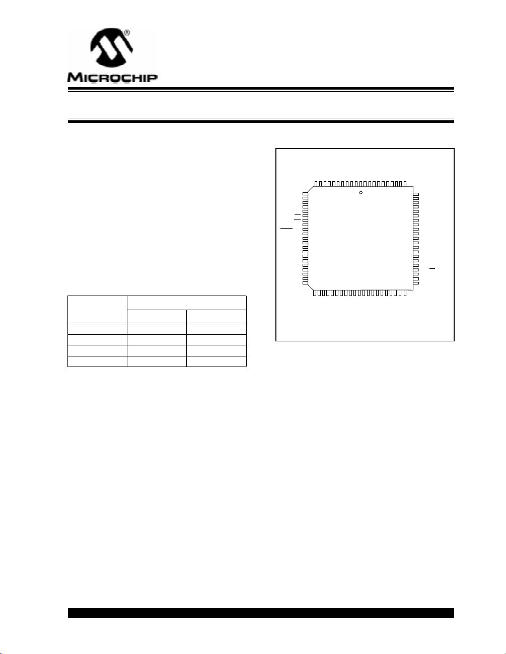
Pin Diagrams
84 LCC
VDDNC
VSSRC1/AD1
RC2/AD2
RC3/AD3
RC4/AD4
RC5/AD5
RC6/AD6
RC7/AD7
RJ7
RH2
RH3
RD1/AD9
RD0/AD8
RE0/ALE
RE1/OE
RE2/WR
RE3/CAP4
MCLR
/VPP
TEST
RF7/AN11
RF6/AN10
RF5/AN9
RF4/AN8
RF3/AN7
RF2/AN6
RH4/AN12
RH5/AN13
NC
V
SS
VDD
RH1
RD2/AD10
RD3/AD11
RH0
11
9876 54321
10
12
13
14
15
16
17
18
19
20
21
22
23
24
25
26
27
28
29
30
31
32
3435 36 37 38 39 40 41 42 43
33
DD
AV
RF1/AN5
RF0/AN4
RH6/AN14
RH7/AN15
RC0/AD0
RD4/AD12
RD5/AD13
RD6/AD14
RD7/AD15
84
PIC17C76X
44
SS
NC
V
REF-
AVSS
RG1/AN2
RG0/AN3
RG2/AN1/V
RG3/AN0/VREF+
83 82 81
45
VDD
46
47
RG4/CAP3
80
7978 77
4948
RG5/PWM3
RA5/TX1/CK1
RG7/TX2/CK2
RG6/RX2/DT2
RJ6
75
76
74
73
72
71
70
69
68
67
66
65
64
63
62
61
60
59
58
57
56
55
54
53525150
RJ1
RJ0
RA4/RX1/DT1
RJ5
RJ4
RA0/INT
RB0/CAP1
RB1/CAP2
RB3/PWM2
RB4/TCLK12
RB5/TCLK3
RB2/PWM1
V
SS
NC
OSC2/CLKOUT
OSC1/CLKIN
V
DD
RB7/SDO
RB6/SCK
RA3/SDI/SDA
RA2/SS
/SCL
RA1/T0CKI
RJ3
RJ2
Special Microcontroller Features:
• Power-on Reset (POR), Power-up Timer (PWRT)
and Oscillator Start-up Timer (OST)
• Watchdog Timer (WDT) with its own on-chip RC
oscillator for reliable operation
• Brown-out Reset
• Code-protection
• Power saving SLEEP mode
• Selectable oscillator options
CMOS Technology:
• Low-power, high-speed CMOS EPROM
technology
• Fully static design
• Wide operating voltage range (3.0V to 5.5V)
• Commercial and Industrial temperature ranges
• Low-power consumption
- < 5 mA @ 5V, 4 MHz
- 100 µA typical @ 4.5V, 32 kHz
- < 1 µA typical standby current @ 5V
1998 Microchip Technology Inc. DS30289A-page 1
Page 2
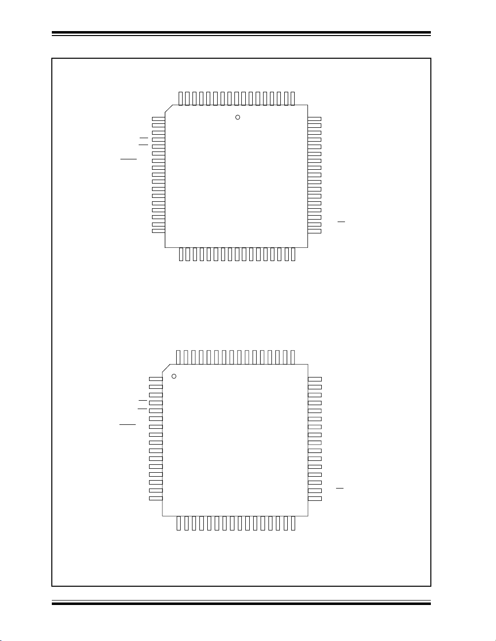
PIC17C7XX
Pin Diagrams cont.’d
68-Pin LCC
64-Pin TQFP
RD1/AD9
RD0/AD8
RE0/ALE
RE1/OE
RE2/WR
RE3/CAP4
/VPP
MCLR
TEST
NC
V
VDD
RF7/AN11
RF6/AN10
RF5/AN9
RF4/AN8
RF3/AN7
RF2/AN6
RD2/AD10
RD3/AD11
RD4/AD12
RD5/AD13
RD6/AD14
RD7/AD15
RC0/AD0
VDDNC
VSSRC1/AD1
RC2/AD2
RC3/AD3
RC4/AD4
RC5/AD5
RC6/AD6
RC7/AD7
987654321
10
11
12
13
14
15
16
17
18
19
SS
20
21
22
23
24
25
26
2728293031323334353637383940414243
RF1/AN5
RD2/AD10
DD
AVSS
AV
RF0/AN4
RD3/AD11
RD4/AD12
RD5/AD13
PIC17C75X
RG3/AN0/VREF+
RD6/AD14
NC
REF-
RG1/AN2
RG0/AN3
RG2/AN1/V
RD7/AD15
RC0/AD0
VDDVSS
68676665646362
SS
V
VDD
RG4/CAP3
RG5/PWM3
RG7/TX2/CK2
RG6/RX2/DT2
RC1/AD1
RC2/AD2
RC3/AD3
RC4/AD4
RC5/AD5
61
60
59
58
57
56
55
54
53
52
51
50
49
48
47
46
45
44
RA5/TX1/CK1
RA4/RX1/DT1
RC6/AD6
RC7/AD7
RA0/INT
RB0/CAP1
RB1/CAP2
RB3/PWM2
RB4/TCLK12
RB5/TCLK3
RB2/PWM1
V
SS
NC
OSC2/CLKOUT
OSC1/CLKIN
V
DD
RB7/SDO
RB6/SCK
RA3/SDI/SDA
RA2/SS
/SCL
RA1/T0CKI
DS30289A-page 2
RD1/AD9
RD0/AD8
RE0/ALE
RE1/OE
RE2/WR
RE3/CAP4
MCLR
/VPP
TEST
V
VDD
RF7/AN11
RF6/AN10
RF5/AN9
RF4/AN8
RF3/AN7
RF2/AN6
646362616059585756555453525150
1
2
3
4
5
6
7
8
9
SS
10
11
12
13
14
15
16
171819202122232425262728293031
RF1/AN5
DD
AV
RF0/AN4
PIC17C75X
REF-
AVSS
RG1/AN2
RG2/AN1/V
RG3/AN0/VREF+
SS
V
VDD
RG0/AN3
RG4/CAP3
RG5/PWM3
49
48
47
46
45
44
43
42
41
40
39
38
37
36
35
34
33
32
RA5/TX1/CK1
RA4/RX1/DT1
RG7/TX2/CK2
RG6/RX2/DT2
RA0/INT
RB0/CAP1
RB1/CAP2
RB3/PWM2
RB4/TCLK12
RB5/TCLK3
RB2/PWM1
V
SS
OSC2/CLKOUT
OSC1/CLKIN
DD
V
RB7/SDO
RB6/SCK
RA3/SDI/SDA
/SCL
RA2/SS
RA1/T0CKI
1998 Microchip Technology Inc.
Page 3
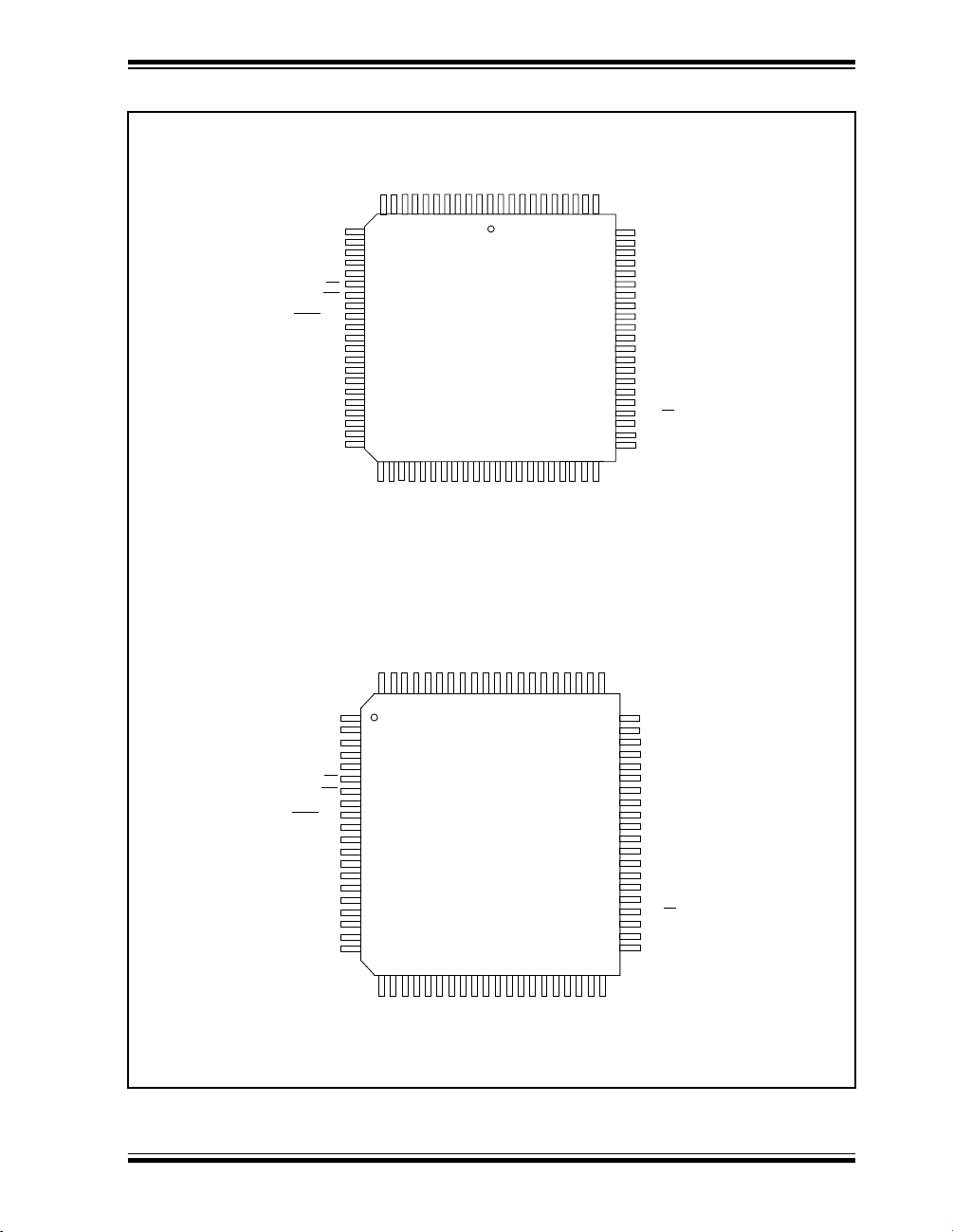
PIN DIAGRAMS cont.’d
84-pin LCC
RH2
RH3
RD1/AD9
RD0/AD8
RE0/ALE
RE1/OE
RE2/WR
RE3/CAP4
/VPP
MCLR
TEST
VSS
VDD
RF7/AN11
RF6/AN10
RF5/AN9
RF4/AN8
RF3/AN7
RF2/AN6
RH4/AN12
RH5/AN13
PIC17C7XX
DD
V
NC
VSSRC1/AD1
RC2/AD2
RC3/AD3
RC4/AD4
RC5/AD5
RC6/AD6
RC7/AD7
RJ7
797877
4948
RJ6
75
76
53525150
74
73
72
71
70
69
68
67
66
65
64
63
62
61
60
59
58
57
56
55
54
RJ5
RJ4
RA0/INT
RB0/CAP1
RB1/CAP2
RB3/PWM2
RB4/TCLK12
RB5/TCLK3
RB2/PWM1
V
SS
NC
OSC2/CLKOUT
OSC1/CLKIN
V
DD
RB7/SDO
RB6/SCK
RA3/SDI/SDA
/SCL
RA2/SS
RA1/T0CKI
RJ3
RJ2
RD3/AD11
RD4/AD12
RD5/AD13
RD6/AD14
PIC17C76X
RC0/AD0
RD7/AD15
44
84
838281
45
46
80
47
RH1
RD2/AD10
RH0
11
987654321
10
12
13
14
15
16
17
18
19
20
21
NC
22
23
24
25
26
27
28
29
30
31
32
34353637383940414243
33
80-Pin QFP
RH2
RH3
RD1/AD9
RD0/AD8
RE0/ALE
RE1/OE
RE2/WR
RE3/CAP4
MCLR
/VPP
TEST
V
VDD
RF7/AN11
RF6/AN10
RF5/AN9
RF4/AN8
RF3/AN7
RF2/AN6
RH4/AN12
RH5/AN13
RH6/AN14
RH7/AN15
RH0
RH1
80
79
1
2
3
4
5
6
7
8
9
10
11
SS
12
13
14
15
16
17
18
19
20
2122 23 24252627 2829303132
RH6/AN14
RH7/AN15
RF1/AN5
RF0/AN4
RD2/AD10
RD3/AD11
78
7776 75
RF1/AN5
RF0/AN4
DD
REF-
AVSS
AV
RG1/AN2
RG2/AN1/V
RG3/AN0/VREF+
RD4/AD12
RD5/AD13
RD6/AD14
RD7/AD15
PIC17C76X
DD
REF-
AVSS
AV
RG2/AN1/V
RG3/AN0/VREF+
SS
NC
V
RG0/AN3
RC0/AD0
VDDVSS
SS
V
RG1/AN2
RG0/AN3
VDD
RG4/CAP3
RG5/PWM3
RC1/AD1
RC2/AD2
RC3/AD3
6867 66657271 70697473
3334
VDD
RG4/CAP3
RG5/PWM3
RA5/TX1/CK1
RA4/RX1/DT1
RG7/TX2/CK2
RG6/RX2/DT2
RC4/AD4
RC5/AD5
RC6/AD6
6463 6261
37
3536
38
RA5/TX1/CK1
RG7/TX2/CK2
RG6/RX2/DT2
RJ1
RJ0
RC7/AD7
RJ7
RJ6
60
59
58
57
56
55
54
53
52
51
50
49
48
47
46
45
44
43
42
41
40
39
RJ1
RJ0
RA4/RX1/DT1
RJ5
RJ4
RA0/INT
RB0/CAP1
RB1/CAP2
RB3/PWM2
RB4/TCLK12
RB5/TCLK3
RB2/PWM1
SS
V
OSC2/CLKOUT
OSC1/CLKIN
DD
V
RB7/SDO
RB6/SCK
RA3/SDI/SDA
RA2/SS
/SCL
RA1/T0CKI
RJ3
RJ2
1998 Microchip Technology Inc. DS30289A-page 3
Page 4

PIC17C7XX
Table of Contents
1.0 Overview...........................................................................................................................................................5
2.0 Device Varieties................................................................................................................................................7
3.0 Architectural Overview......................................................................................................................................9
4.0 On-chip Oscillator Circuit................................................................................................................................15
5.0 Reset...............................................................................................................................................................21
6.0 Interrupts.........................................................................................................................................................31
7.0 Memory Organization......................................................................................................................................41
8.0 Table Reads and Table Writes .......................................................................................................................57
9.0 Hardware Multiplier.........................................................................................................................................65
10.0 I/O Ports..........................................................................................................................................................69
11.0 Overview of Timer Resources.........................................................................................................................93
12.0 Timer0.............................................................................................................................................................95
13.0 Timer1, Timer2, Timer3, PWMs and Captures...............................................................................................99
14.0 Universal Synchronous Asynchronous Receiver Transmitter (USART) Modules.........................................115
15.0 Master Synchronous Serial Port (MSSP) Module.........................................................................................131
16.0 Analog-to-Digital Converter (A/D) Module ....................................................................................................177
17.0 Special Features of the CPU ........................................................................................................................189
18.0 Instruction Set Summary...............................................................................................................................195
19.0 Development Support...................................................................................................................................231
20.0 PIC17C7XX Electrical Characteristics..........................................................................................................235
21.0 PIC17C7XX DC and AC Characteristics.......................................................................................................265
22.0 Packaging Information..................................................................................................................................277
Appendix A: Modifications..........................................................................................................................................283
Appendix B: Compatibility..........................................................................................................................................283
Appendix C: What’s New............................................................................................................................................284
Appendix D: What’s Changed....................................................................................................................................284
Appendix E: I
Appendix F: Status and Control Registers.................................................................................................................291
On-Line Support..........................................................................................................................................................321
Reader Response .......................................................................................................................................................322
PIC17C7XX Product Identification System .................................................................................................................323
2
C Overview.......................................................................................................................................285
To Our Valued Customers
Most Current Data Sheet
To obtain the most up-to-date version of this data sheet, please check our Worldwide Web site at:
http://www.microchip.com
You can determine the version of a data sheet by examining its literature number found on the bottom outside corner of any page.
The last character of the literature number is the version number. e.g., DS30000A is version A of document DS30000.
Errata
An errata sheet may exist for current devices, describing minor operational differences (from the data sheet) and recommended
workarounds. As device/documentation issues become kno wn to us, we will pub lish an errata sheet. The errata will specify the re vision of silicon and revision of document to which it applies.
To determine if an errata sheet exists for a particular device, please check with one of the following:
• Microchip’s Worldwide Web site; http://www.microchip .com
• Your local Microchip sales office (see last page)
• The Microchip Corporate Literature Center; U.S. FAX: (602) 786-7277
When contacting a sales office or the literature center, please specify which device, revision of silicon and data sheet (include lit-
erature number) you are using.
Corrections to this Data Sheet
We constantly strive to improve the quality of all our products and documentation. We have spent a great deal of time to ensure
that this document is correct. Howe ver, we realize that we ma y ha v e missed a few things. If y ou find an y inf ormation that is missing
or appears in error, please:
• Fill out and mail in the reader response form in the back of this data sheet.
• E-mail us at webmaster@microchip.com.
We appreciate your assistance in making this a better document.
DS30289A-page 4
1998 Microchip Technology Inc.
Page 5

PIC17C7XX
1.0 OVERVIEW
This data sheet covers the PIC17C7XX group of the
PIC17CXXX family of microcontrollers. The following
devices are discussed in this data sheet:
• PIC17C752
• PIC17C756A
• PIC17C762
• PIC17C766
The PIC17C7XX devices are 68/84-pin,
EPROM-based members of the versatile PIC17CXXX
family of low-cost, high-performance, CMOS,
fully-static, 8-bit microcontrollers.
All PICmicro™ microcontrollers employ an advanced
RISC architecture. The PIC17CXXX has enhanced
core features, 16-lev el deep stack, and multiple internal
and external interrupt sources. The separate instruction and data buses of the Harvard architecture allow a
16-bit wide instruction word with a separate 8-bit wide
data path. The two stage instruction pipeline allows all
instructions to execute in a single cycle, except for program branches (which require two cycles). A total of 58
instructions (reduced instruction set) are available.
Additionally, a large register set gives some of the
architectural innovations used to achieve a very high
performance. For mathematical intensive applications
all devices have a single cycle 8 x 8 Hardware Multiplier.
PIC17CXXX microcontrollers typically achieve a 2:1
code compression and a 4:1 speed improvement over
other 8-bit microcontrollers in their class.
PIC17C7XX devices have up to 902 b ytes of RAM and
66
pins. In addition, the PIC17C7XX adds several
I/O
peripheral features useful in many high performance
applications including:
• Four timer/counters
• Four capture inputs
• Three PWM outputs
• Two independent Universal Synchronous Asynchronous Receiver Transmitters (USARTs)
• An A/D converter (multi-channel, 10-bit resolution)
• A Synchronous Serial Port
(SPI and I
These special features reduce external components,
thus reducing cost, enhancing system reliability and
reducing power consumption.
There are four oscillator options, of which the single pin
RC oscillator provides a low-cost solution, the LF oscillator is for low frequency crystals and minimizes power
consumption, XT is a standard crystal, and the EC is for
external clock input.
The SLEEP (power-down) mode offers additional
power saving. Wake-up from SLEEP can occur
through several external and internal interrupts and
device resets.
2
C w/ Master mode)
A highly reliable Watchdog Timer with its own on-chip
RC oscillator provides protection against software malfunction.
There are four configuration options for the device
operational mode:
• Microprocessor
• Microcontroller
• Extended microcontroller
• Protected microcontroller
The microprocessor and extended microcontroller
modes allow up to 64K-words of external program
memory.
The device also has Brown-out Reset circuitry. This
allows a device reset to occur if the device V
below the Brown-out voltage trip point (BVDD). The
chip will remain in Brown-out Reset until VDD rises
above BV
A UV-erasable CERQUAD-packaged version (compatible with PLCC) is ideal for code dev elopment while the
cost-effective One-Time Programmable (OTP) version
is suitable for production in any volume.
The PIC17C7XX fits perfectly in applications that
require extremely fast execution of complex software
programs. These include applications ranging from
precise motor control and industrial process control to
automotive, instrumentation, and telecom applications.
The EPROM technology makes customization of application programs (with unique security codes, combinations, model numbers, parameter storage, etc.) f ast and
convenient. Small footprint package options (including
die sales) make the PIC17C7XX ideal for applications
with space limitations that require high performance.
High speed execution, powerful peripheral features,
flexible I/O, and low power consumption all at low cost
make the PIC17C7XX ideal for a wide range of embedded control applications.
1.1 F
The PIC17CXXX family of microcontrollers have architectural enhancements over the PIC16C5X and
PIC16CXX families. These enhancements allow the
device to be more efficient in software and hardware
requirements. Ref er to Appendix A for a detailed list of
enhancements and modifications. Code written for
PIC16C5X or PIC16CXX can be easily ported to
PIC17CXXX devices (Appendix B).
1.2 De
The PIC17CXXX family is supported by a full-featured
macro assembler, a software simulator, an in-circuit
emulator, a universal programmer, a “C” compiler, and
fuzzy logic support tools. For additional information
see Section 19.0.
DD
.
amily and Upward Compatibility
velopment Support
DD
falls
1998 Microchip Technology Inc. DS30289A-page 5
Page 6
PIC17C7XX
TABLE 1-1: PIC17CXXX FAMILY OF DEVICES
Features PIC17C42A PIC17C43 PIC17C44 PIC17C752 PIC17C756A PIC17C762 PIC17C766
Maximum Frequency
of Operation
Operating Voltage Range 2.5 - 6.0V 2.5 - 6.0V 2.5 - 6.0V 3.0 - 5.5V 3.0 - 5.5V 3.0 - 5.5V 3.0 - 5.5V
Program
Memory ( x16)
Data Memory (bytes) 232 454 454 678 902 678 902
Hardware Multiplier (8 x 8) Yes Yes Yes Yes Yes Ye s Yes
Timer0
(16-bit + 8-bit postscaler)
Timer1 (8-bit) Yes Yes Yes Yes Yes Ye s Yes
Timer2 (8-bit) Yes Yes Yes Yes Yes Ye s Yes
Timer3 (16-bit) Yes Yes Yes Yes Yes Ye s Yes
Capture inputs (16-bit) 2 2 24444
PWM outputs (up to 10-bit) 2 2 23333
USART/SCI 1 1 12222
A/D channels (10-bit) — — —12121616
SSP (SPI/I
mode)
Power-on Reset
Watchdog Timer Yes Yes Yes Yes Yes Ye s Yes
External Interrupts Yes Yes Yes Yes Yes Yes Yes
Interrupt Sources 11 11 11 18 18 18 18
Code Protect Yes Yes Yes Yes Yes Yes Yes
Brown-out Reset — — — Yes Yes Yes Yes
In-circuit Serial Program-
ming
I/O Pins 33 33 33 50 50 66 66
I/O High Cur-
rent Capability
Package Types
Note 1: Pins RA2 and RA3 can sink up to 60 mA.
(EPROM) 2K 4K 8K 8K 16K 8K 16K
(ROM) — — — — — — —
2
C w/Master
Source 25 mA 25 mA 25 mA 25 mA 25 mA 25 mA 25 mA
Sink
33 MHz 33 MHz 33 MHz 33 MHz 33 MHz 33 MHz 33 MHz
Yes Yes Yes Yes Yes Ye s Yes
— — — Yes Yes Yes Yes
Yes Yes Yes Yes Yes Ye s Yes
— — — Yes Yes Yes Yes
(1)
25 mA
40-pin DIP
44-pin PLCC
44-pin
MQFP
44-pin TQFP
(1)
25 mA
40-pin DIP
44-pin PLCC
44-pin
MQFP
44-pin TQFP
(1)
25 mA
40-pin DIP
44-pin PLCC
44-pin
MQFP
44-pin TQFP
(1)
25 mA
64-pin DIP
68-pin LCC
68-pin TQFP
(1)
25 mA
64-pin DIP
68-pin LCC
68-pin TQFP
(1)
25 mA
80-pin QFP
84-pin
PLCC
80-pin QFP
25 mA
84-pin
PLCC
(1)
DS30289A-page 6
1998 Microchip Technology Inc.
Page 7
PIC17C7XX
2.0 DEVICE V ARIETIES
Each device has a variety of frequency ranges and
packaging options. Depending on application and production requirements, the proper device option can be
selected using the information in the PIC17C7XX Product Selection System section at the end of this data
sheet. When placing orders, please use the
“PIC17C7XX Product Identification System” at the back
of this data sheet to specify the correct part number.
When discussing the functionality of the device, memory technology and voltage range does not matter.
There are three memory type options. These are specified in the middle characters of the part number.
1.C, as in PIC17C756A. These devices have
EPROM type memory.
2.CR, as in PIC17CR756A. These devices have
ROM type memory.
3.F, as in PIC17F756A. These devices have Flash
type memory.
All these devices operate over the standard voltage
range. Devices are also offered which operate over an
extended voltage range (and reduced frequency
range). Table 2-1 shows all possible memory types
and voltage range designators for a particular device.
These designators are in
TABLE 2-1: DEVICE MEMORY
Memory Type
EPROM PIC17CXXX PIC17LCXXX
ROM
Flash
Note:
Not all memory technologies are available
for a particular device.
bold
typeface.
VARIETIES
Voltage Range
Standard Extended
PIC17CRXXX PIC17
PIC17FXXX PIC17LFXXX
LCR
XXX
2.1 UV Erasab
The UV erasable version, offered in CERQUAD package, is optimal for prototype dev elopment and pilot programs.
The UV erasable version can be erased and reprogrammed to any of the configuration modes. Third
party programmers also are available; ref er to the
Party Guide
for a list of sources.
2.2 One-Time-Pr
le Devices
Third
ogrammable (OTP)
Devices
The availability of OTP devices is especially useful for
customers expecting frequent code changes and
updates.
The OTP devices, packaged in plastic packages, permit the user to program them once. In addition to the
program memory, the configuration bits must be programmed.
2.3 Quic
k-Turnaround-Production (QTP)
Devices
Microchip offers a QTP Programming Service for factory production orders. This service is made available
for users who choose not to program a medium to high
quantity of units and whose code patterns have stabilized. The devices are identical to the OTP de vices but
with all EPROM locations and configuration options
already programmed by the factory. Certain code and
prototype verification procedures apply before production shipments are available. Please contact your local
Microchip Technology sales office for more details.
2.4 Serializ
Microchip offers a unique programming service where
a few user-defined locations in each device are programmed with different serial numbers. The serial
numbers may be random, pseudo-random or sequential.
Serial programming allows each device to have a
unique number which can serve as an entry-code,
password or ID number.
ed Quick-Turnaround
Production (SQTP
SM
vices
) De
1998 Microchip Technology Inc. DS30289A-page 7
Page 8

PIC17C7XX
2.5 Read Onl
Microchip offers masked ROM versions of several of
the highest volume parts, thus giving customers a low
cost option for high volume, mature products.
ROM devices do not allow serialization information in
the program memory space.
For information on submitting ROM code, please contact your regional sales office.
Note:
2.6 Flash Memor
These devices are electrically erasable and, therefore,
can be offered in the low cost plastic package. Being
electrically erasable, these devices can be erased and
reprogrammed in-circuit. These devices are the same
for prototype development, pilot programs, as well as
production.
Note:
y Memory (ROM) Devices
Presently, NO ROM versions of the
PIC17C7XX devices are available.
y Devices
Presently, NO Flash versions of the
PIC17C7XX devices are available.
DS30289A-page 8
1998 Microchip Technology Inc.
Page 9

PIC17C7XX
3.0 ARCHITECTURAL OVERVIEW
The high performance of the PIC17CXXX can be attributed to a number of architectural features commonly
found in RISC microprocessors. To begin with, the
PIC17CXXX uses a modified Harvard architecture.
This architecture has the program and data accessed
from separate memories. So , the device has a progr am
memory bus and a data memory bus. This improves
bandwidth over traditional von Neumann architecture,
where program and data are fetched from the same
memory (accesses over the same bus). Separating
program and data memory further allows instructions
to be sized differently than the 8-bit wide data word.
PIC17CXXX opcodes are 16-bits wide, enabling single
word instructions. The full 16-bit wide program memory bus fetches a 16-bit instruction in a single cycle. A
two-stage pipeline overlaps fetch and execution of
instructions. Consequently, all instructions execute in a
single cycle (121 ns @ 33 MHz), except for program
branches and two special instructions that transfer data
between program and data memory.
The PIC17CXXX can address up to 64K x 16 of program memory space.
The
PIC17C752
EPROM program memory on-chip.
The
PIC17C756A
EPROM program memory on-chip.
A simplified block diagram is shown in Figure 3-1. The
descriptions of the device pins are listed in Table 3-1.
Program execution can be internal only (microcontrol-
ler or protected microcontroller mode), external only
(microprocessor mode) or both (extended microcontroller mode). Extended microcontroller mode does not
allow code protection.
The PIC17CXXX can directly or indirectly address its
register files or data memory. All special function registers, including the Program Counter (PC) and Working Register (WREG), are mapped in data memory.
The PIC17CXXX has an orthogonal (symmetrical)
instruction set that makes it possible to carry out any
operation on any register using any addressing mode.
This symmetrical nature and lack of ‘special optimal situations’ make programming with the PIC17CXXX simple yet efficient. In addition, the learning curve is
reduced significantly.
One of the PIC17CXXX family architectural enhancements from the PIC16CXX family allows two file registers to be used in some two operand instructions. This
allows data to be moved directly between two registers
without going through the WREG register. Thus
increasing performance and decreasing program
memory usage.
The PIC17CXXX devices contain an 8-bit ALU and
working register. The ALU is a general purpose arithmetic unit. It performs arithmetic and Boolean functions between data in the working register and any
register file.
and
and
PIC17C762
PIC17C766
integrate 8K x 16 of
integrate 16K x 16
The WREG register is an 8-bit working register used for
ALU operations.
All PIC17CXXX devices have an 8 x 8 hardware multiplier. This multiplier generates a 16-bit result in a single
cycle.
The ALU is 8-bits wide and capable of addition, subtraction, shift, and logical operations. Unless otherwise
mentioned, arithmetic operations are two's complement in nature.
Depending on the instruction executed, the ALU may
affect the values of the Carry (C), Digit Carry (DC),
Zero (Z) and overflow (O V) bits in the ALUSTA register.
The C and DC bits operate as a borro
out bit, respectively, in subtraction. See the
SUBWF
instructions for examples.
w and digit borrow
SUBLW
and
Signed arithmetic is comprised of a magnitude and a
sign bit. The overflow bit indicates if the magnitude
overflows and causes the sign bit to change state. That
is if the result of 8-bit signed operations is greater than
127 (7Fh) or less than -128 (80h).
Signed math can have greater than 7-bit values (magnitude), if more than one byte is used. The overflow bit
only operates on bit6 (MSb of magnitude) and bit7 (sign
bit) of each byte value in the ALU. That is, the overflow
bit is not useful if trying to implement signed math
where the magnitude, for example, is 11-bits.
If the signed math values are greater than 7-bits (such
as 15-, 24- or 31-bit), the algorithm must ensure that
the low order bytes of the signed value ignore the ov erflow status bit.
Example 3-1 shows an two cases of doing signed arith-
metic. The Carry (C) bit and the Overflow (OV) bit are
the most important status bits for signed math operations.
EXAMPLE 3-1: 8-BIT MATH ADDITION
Hex Value Signed Values Unsigned Values
FFh
01h
+
= 00h
C bit = 1
OV bit = 0
DC bit = 1
Z bit = 1
Hex Value Signed Values Unsigned Values
7Fh
+ 01h
= 80h
C bit = 0
OV bit = 1
DC bit = 1
Z bit = 0
-1
+ 1
= 0 (FEh)
C bit = 1
OV bit = 0
DC bit = 1
Z bit = 1
127
+ 1
= 128 → 00h
C bit = 0
OV bit = 1
DC bit = 1
Z bit = 0
255
+ 1
= 256 → 00h
C bit = 1
OV bit = 0
DC bit = 1
Z bit = 1
127
+ 1
= 128
C bit = 0
OV bit = 1
DC bit = 1
Z bit = 0
1998 Microchip Technology Inc. DS30289A-page 9
Page 10
PIC17C7XX
FIGURE 3-1: PIC17C752/756A BLOCK DIAGRAM
PORTA
RA0/INT
RA1/T0CKI
RA2/SS
/SCL
RA3/SDI/SDA
RA4/RX1/DT1
RA5/TX1/CK1
RB0/CAP1
RB1/CAP2
RB2/PWM1
RB3/PWM2
RB4/TCLK12
RB5/TCLK3
RB6/SCK
RB7/SDO
RC0/AD0
RC1/AD1
RC2/AD2
RC3/AD3
RC4/AD4
RC5/AD5
RC6/AD6
RC7/AD7
RD0/AD8
RD1/AD9
RD2/AD10
RD3/AD11
RD4/AD12
RD5/AD13
RD6/AD14
RD7/AD15
RE0/ALE
RE1/OE
RE2/WR
RE3/CAP4
RF0/AN4
RF1/AN5
RF2/AN6
RF3/AN7
RF4/AN8
RF5/AN9
RF6/AN10
RF7/AN11
PORTB
PORTC
PORTD
PORTE
PORTF
8 x 8 mult
PRODH PRODL
8
BSR <7:4>
Address
Buffer
Data RAM
17C756A
902 x 8
17C752
678 x 8
Data Latch
BSR
Timer0
WREG<8>
IR <7:0>
12
RAM
Literal
PCLATH<8>
PCH
Timer2 PWM1
BITOP
ALU
Shifter
16
Instruction
Decode
Control Outputs
Table
Latch <16>
PCL
16
USART1
Table Pointer<16>
Data Bus<8>
IR<16>
Read/write
Decode
for
Registers
Mapped
in Data
Space
Stack
16 x 16
16
Chip_reset
IR Latch <16>
8
ROM Latch <16>
PWM3
Q1, Q2,
Q3, Q4
& Other
Control
Signals
16
Capture2
8
Data Latch
Program
Memory
(EPROM)
17C756A
16K x 16
17C752
8K x 16
Address
Latch
16
10-bit
A/D
Clock
Generator
Power-on
Reset
Brown-out
Reset
Watchdog
Timer
Test Mode
Select
F1
F9
8
VDD, VSS
MCLR, VPP
Decode
AD<15:0>
PORTC,
PORTD
System Bus Interface
ALE,
WR
OE
PORTE
SSP
OSC1,
OSC2
Test
,
,
RG0/AN3
RG1/AN2
RG2/AN1/V
RG3/AN0/V
RG4/CAP3
RG5/PWM3
RG6/RX2/DT2
RG7/TX2/CK2
REF-
REF+
PORTG
Timer1 Timer3
USART2
PWM2
Capture1 Capture3
Capture4
Interrupt
Module
DS30289A-page 10 1998 Microchip Technology Inc.
Page 11
FIGURE 3-2: PIC17C762/766 BLOCK DIAGRAM
PORTA
RA0/INT
RA1/T0CKI
/SCL
RA2/SS
RA3/SDI/SDA
RA4/RX1/DT1
RA5/TX1/CK1
RB0/CAP1
RB1/CAP2
RB2/PWM1
RB3/PWM2
RB4/TCLK12
RB5/TCLK3
RB6/SCK
RB7/SDO
RC0/AD0
RC1/AD1
RC2/AD2
RC3/AD3
RC4/AD4
RC5/AD5
RC6/AD6
RC7/AD7
RD0/AD8
RD1/AD9
RD2/AD10
RD3/AD11
RD4/AD12
RD5/AD13
RD6/AD14
RD7/AD15
RE0/ALE
RE1/OE
RE2/WR
RE3/CAP4
RF0/AN4
RF1/AN5
RF2/AN6
RF3/AN7
RF4/AN8
RF5/AN9
RF6/AN10
RF7/AN11
RG0/AN3
RG1/AN2
RG2/AN1/V
RG3/AN0/V
RG4/CAP3
RG5/PWM3
RG6/RX2/DT2
RG7/TX2/CK2
RH4/AN12
RH5/AN13
RH6/AN14
RH7/AN15
REF-
REF+
RH0
RH1
RH2
RH3
PORTB
PORTC
PORTD
PORTE
PORTF
PORTG
PORTH
8 x 8 mult
PRODH PRODL
BSR <7:4>
8
IR <7:0>
12
RAM
Address
Buffer
Data RAM
17C766
902 x 8
and
17C762
678 x 8
Data Latch
BSR
PCLATH<8>
Timer0
Timer1 Timer3
WREG<8>
Literal
PCH
Timer2 PWM1
BITOP
ALU
Shifter
16
Instruction
Decode
Control Outputs
Table
Latch <16>
PCL
16
USART1
USART2
IR<16>
Read/write
Decode
for
Registers
Mapped
in Data
Space
Table Pointer<16>
Stack
16 x 16
16
Data Bus<8>
PWM2
IR Latch <16>
8
ROM Latch <16>
PWM3
Capture1
PIC17C7XX
Clock
Test Mode
Brown-out
8
FSR0
FSR1
Data Latch
Program
Memory
(EPROM)
17C766
16K x 16,
and
17C762
8K x 16
Address
Latch
16
PORTJ
Generator
Power-on
Reset
Watchdog
Timer
Select
Reset
8
System Bus Interface
Q1, Q2,
Q3, Q4
Chip_reset
& Other
Control
Signals
16
OSC1,
OSC2
VDD, VSS
MCLR, VPP
Test
AVDD, AVSS
Decode
AD<15:0>
PORTC,
PORTD
ALE,
WR
,
OE
,
PORTE
RJ0
RJ1
RJ2
RJ3
RJ4
RJ5
RJ6
RJ7
Interrupt
Module
SSP
10-bit
A/D
Capture2
Capture3
Capture4
1998 Microchip Technology Inc. DS30289A-page 11
Page 12
PIC17C7XX
TABLE 3-1: PINOUT DESCRIPTIONS
PIC17C75X PIC17C76X
Name
OSC1/CLKIN 47 50 39 62 49 I ST Oscillator input in crystal/resonator or RC oscillator
OSC2/CLKOUT 48 51 40 63 50 O — Oscillator output. Connects to crystal or resonator in
MCLR/VPP 15 16 7 20 9 I/P ST Master clear (reset) input or Programming Voltage
RA0/INT 56 60 48 72 58 I ST RA0 can also be selected as an external inter-
RA1/T0CKI 41 44 33 56 43 I ST RA1 can also be selected as an external inter-
RA2/SS/SCL 42 45 34 57 44
RA3/SDI/SDA 43 46 35 58 45
RA4/RX1/DT1 40 43 32 51 38
RA5/TX1/CK1 39 42 31 50 37
RB0/CAP1 55 59 47 71 57 I/O ST RB0 can also be the Capture1 input pin.
RB1/CAP2 54 58 46 70 56 I/O ST RB1 can also be the Capture2 input pin.
RB2/PWM1 50 54 42 66 52 I/O ST RB2 can also be the PWM1 output pin.
RB3/PWM2 53 57 45 69 55 I/O ST RB3 can also be the PWM2 output pin.
RB4/TCLK12 52 56 44 68 54 I/O ST RB4 can also be the external clock input to
RB5/TCLK3 51 55 43 67 53 I/O ST RB5 can also be the external clock input to
RB6/SCK 44 47 36 59 46 I/O ST RB6 can also be used as the master/slave clock
RB7/SDO 45 48 37 60 47 I/O ST RB7 can also be used as the data output for the
Legend: I = Input only; O = Output only; I/O = Input/Output;
Note 1: The output is only available by the peripheral operation.
2: Open Drain input/output pin. Pin forced to input upon any device reset.
DIP
PLCC
TQFP
PLCC
QFP
I/O/P
No.
No.
No.
No.
No.
P = Power; — = Not Used; TTL = TTL input; ST = Schmitt Trigger input.
Buffer
Type
Type
mode. External clock input in external clock mode.
crystal oscillator mode. In RC oscillator or external
clock modes OSC2 pin outputs CLKOUT which has
one fourth the frequency (F
denotes the instruction cycle rate.
(VPP) input. This is the active low reset input to the
device.
PORTA pins have individual differentiations that are
listed in the following descriptions:
rupt input. Interrupt can be configured to be on
positive or negative edge. Input only pin.
rupt input, and the interrupt can be configured
to be on positive or negative edge. RA1 can
also be selected to be the clock input to the
(2)
ST RA2 can also be used as the slave select input
I/O
(2)
ST RA3 can also be used as the data input for the
I/O
(1)
ST RA4 can also be selected as the USART1 (SCI)
I/O
(1)
ST RA5 can also be selected as the USART1 (SCI)
I/O
Timer0 timer/counter. Input only pin.
for the SPI or the clock input for the I
High voltage, high current, open drain port pin.
SPI or the data for the I
High voltage, high current, open drain port pin.
Asynchronous Receive or USART1 (SCI)
Synchronous Data.
Output available from USART only.
Asynchronous Transmit or USART1 (SCI)
Synchronous Clock.
Output available from USART only.
PORTB is a bi-directional I/O Port with software
configurable weak pull-ups.
Timer1 and Timer2.
Timer3.
for the SPI.
SPI.
Description
OSC/4) of OSC1 and
2
C bus.
2
C bus.
DS30289A-page 12 1998 Microchip Technology Inc.
Page 13
PIC17C7XX
TABLE 3-1: PINOUT DESCRIPTIONS
PIC17C75X PIC17C76X
Name
RC0/AD0 2 3 58 3 72 I/O TTL This is also the least significant byte (LSB) of
RC1/AD1 63 67 55 83 69 I/O TTL
RC2/AD2 62 66 54 82 68 I/O TTL
RC3/AD3 61 65 53 81 67 I/O TTL
RC4/AD4 60 64 52 80 66 I/O TTL
RC5/AD5 58 63 51 79 65 I/O TTL
RC6/AD6 58 62 50 78 64 I/O TTL
RC7/AD7 57 61 49 77 63 I/O TTL
RD0/AD8 10 11 2 15 4 I/O TTL This is also the most significant byte (MSB) of
RD1/AD9 9 10 1 14 3 I/O TTL
RD2/AD10 8 9 64 9 78 I/O TTL
RD3/AD11 7 8 63 8 77 I/O TTL
RD4/AD12 6 7 62 7 76 I/O TTL
RD5/AD13 5 6 61 6 75 I/O TTL
RD6/AD14 4 5 60 5 74 I/O TTL
RD7/AD15 3 4 59 4 73 I/O TTL
RE0/ALE 11 12 3 16 5 I/O TTL In microprocessor mode or extended microcon-
RE1/OE 12 13 4 17 6 I/O TTL In microprocessor or extended microcontroller
RE2/WR
RE3/CAP4 14 15 6 19 8 I/O ST RE3 can also be the Capture4 input pin.
RF0/AN4 26 28 18 36 24 I/O ST RF0 can also be analog input 4.
RF1/AN5 25 27 17 35 23 I/O ST RF1 can also be analog input 5.
RF2/AN6 24 26 16 30 18 I/O ST RF2 can also be analog input 6.
RF3/AN7 23 25 15 29 17 I/O ST RF3 can also be analog input 7.
RF4/AN8 22 24 14 28 16 I/O ST RF4 can also be analog input 8.
RF5/AN9 21 23 13 27 15 I/O ST RF5 can also be analog input 9.
RF6/AN10 20 22 12 26 14 I/O ST RF6 can also be analog input 10.
RF7/AN11 19 21 11 25 13 I/O ST RF7 can also be analog input 11.
Legend: I = Input only; O = Output only; I/O = Input/Output;
Note 1: The output is only available by the peripheral operation.
2: Open Drain input/output pin. Pin forced to input upon any device reset.
DIP
PLCC
TQFP
PLCC
QFP
I/O/P
No.
No.
No.
No.
No.
13 14 5 18 7 I/O TTL In microprocessor or extended microcontroller
P = Power; — = Not Used; TTL = TTL input; ST = Schmitt Trigger input.
Type
Buffer
Type
PORTC is a bi-directional I/O Port.
the 16-bit wide system bus in microprocessor
mode or extended microcontroller mode. In
multiplexed system bus configuration, these
pins are address output as well as data input or
output.
PORTD is a bi-directional I/O Port.
the 16-bit system bus in microprocessor mode
or extended microcontroller mode. In multiplexed system bus configuration these pins are
address output as well as data input or output.
PORTE is a bi-directional I/O Port.
troller mode, RE0 is the Address Latch Enable
(ALE) output. Address should be latched on the
falling edge of ALE output.
mode, RE1 is the Output Enable (OE) control
output (active low).
mode, RE2 is the Write Enable (WR) control
output (active low).
PORTF is a bi-directional I/O Port.
Description
1998 Microchip Technology Inc. DS30289A-page 13
Page 14
PIC17C7XX
TABLE 3-1: PINOUT DESCRIPTIONS
PIC17C75X PIC17C76X
Name
RG0/AN3 32 34 24 42 30 I/O ST RG0 can also be analog input 3.
RG1/AN2 31 33 23 41 29 I/O ST RG1 can also be analog input 2.
RG2/AN1/VREF- 30 32 22 40 28 I/O ST RG2 can also be analog input 1, or
RG3/AN0/VREF+ 29 31 21 39 27 I/O ST RG3 can also be analog input 0, or
RG4/CAP3 35 38 27 46 33 I/O ST RG4 can also be the Capture3 input pin.
RG5/PWM3 36 39 28 47 34 I/O ST RG5 can also be the PWM3 output pin.
RG6/RX2/DT2 38 41 30 49 36 I/O ST RG6 can also be selected as the USART2 (SCI)
RG7/TX2/CK2 37 40 29 48 35 I/O ST RG7 can also be selected as the USART2 (SCI)
RH0 — — — 10 79 I/O ST
RH1 — — — 11 80 I/O ST
RH2 — — — 12 1 I/O ST
RH3 — — — 13 2 I/O ST
RH4/AN12 — — — 31 19 I/O ST RH4 can also be analog input 12.
RH5/AN13 — — — 32 20 I/O ST RH5 can also be analog input 13.
RH6/AN14 — — — 33 21 I/O ST RH6 can also be analog input 14.
RH7/AN15 — — — 34 22 I/O ST RH7 can also be analog input 15.
RJ0 — — — 52 39 I/O ST
RJ1 — — — 53 40 I/O ST
RJ2 — — — 54 41 I/O ST
RJ3 — — — 55 42 I/O ST
RJ4 — — — 73 59 I/O ST
RJ5 — — — 74 60 I/O ST
RJ6 — — — 75 61 I/O ST
RJ7 — — — 76 62 I/O ST
TEST 16 17 8 21 10 I ST Test mode selection control input. Always tie to V
VSS 17, 33,
VDD 1, 18,
AVSS 28 30 20 38 26 P Ground reference for A/D converter.
AVDD 27 29 19 37 25 P Positive supply for A/D converter.
NC — 1, 18,
Legend: I = Input only; O = Output only; I/O = Input/Output;
Note 1: The output is only available by the peripheral operation.
2: Open Drain input/output pin. Pin forced to input upon any device reset.
DIP
PLCC
TQFP
PLCC
QFP
I/O/P
No.
No.
No.
No.
No.
19, 36,
9, 25,
23, 44,
49, 64
53, 68
41, 56
2, 20,
37, 49,
35, 52
10, 26,
38, 57
— 1, 22,
34, 46
P = Power; — = Not Used; TTL = TTL input; ST = Schmitt Trigger input.
65, 84
24, 45,
61, 2
43, 64
11, 31,
51, 70
12, 32,
48, 71
— No Connect. Leave these pins unconnected.
Buffer
Type
Type
PORTG is a bi-directional I/O Port.
the ground reference voltage
the positive reference voltage
Asynchronous Receive or USART2 (SCI)
Synchronous Data.
Asynchronous Transmit or USART2 (SCI)
Synchronous Clock.
PORTH is a bi-directional I/O Port. PORTH is only
available on the PIC17C76X devices
PORTJ is a bi-directional I/O Port. PORTJ is only
available on the PIC17C76X devices.
P Ground reference for logic and I/O pins.
P Positive supply for logic and I/O pins.
for normal operation.
This pin MUST be at the same potential as VSS.
This pin MUST be at the same potential as VDD.
Description
SS
DS30289A-page 14 1998 Microchip Technology Inc.
Page 15
PIC17C7XX
4.0 ON-CHIP OSCILLATOR CIRCUIT
The internal oscillator circuit is used to generate the
device clock. Four device clock periods generate an
internal instruction clock (T
There are four modes that the oscillator can operate in.
They are selected by the device configuration bits during device programming. These modes are:
• LF Low Frequency (F
• XT Standard Crystal/Resonator Frequency
(2 MHz <= F
• EC External Clock Input
(Default oscillator configuration)
• RC External Resistor/Capacitor
(F
OSC <= 4 MHz)
There are two timers that offer necessary delays on
power-up. One is the Oscillator Start-up Timer (OST),
intended to keep the chip in RESET until the crystal
oscillator is stable. The other is the Power-up Timer
(PWRT), which provides a fixed delay of 96 ms (nominal) on POR and BOR. The PWR T is designed to keep
the part in RESET while the power supply stabilizes.
With these two timers on-chip, most applications need
no external reset circuitry.
SLEEP mode is designed to offer a very low current
power-down mode. The user can wake from SLEEP
through external reset, Watchdog Timer Reset or
through an interrupt.
Several oscillator options are made available to allow
the part to better fit the application. The RC oscillator
option saves system cost while the LF crystal option
saves power. Configuration bits are used to select various options.
4.1 Oscillator Configurations
4.1.1 OSCILLATOR TYPES
The PIC17CXXX can be operated in four different oscillator modes. The user can program two configuration
bits (FOSC1:FOSC0) to select one of these four
modes:
• LF Low Power Crystal
• XT Crystal/Resonator
• EC External Clock Input
• RC Resistor/Capacitor
The main difference between the LF and XT modes is
the gain of the internal inverter of the oscillator circuit
which allows the different frequency ranges.
For more details on the device configuration bits, see
Section 17.0.
CY).
OSC <= 2 MHz)
OSC <= 33 MHz)
4.1.2 CRYSTAL OSCILLATOR / CERAMIC
RESONATORS
In XT or LF modes, a crystal or ceramic resonator is
connected to the OSC1/CLKIN and OSC2/CLKOUT
pins to establish oscillation (Figure 4-2). The
PIC17CXXX oscillator design requires the use of a parallel cut crystal. Use of a series cut crystal may give a
frequency out of the crystal manufacturers specifications.
For frequencies above 20 MHz, it is common for the
crystal to be an overtone mode crystal. Use of overtone mode crystals require a tank circuit to attenuate
the gain at the fundamental frequency. Figure 4-3
shows an example circuit.
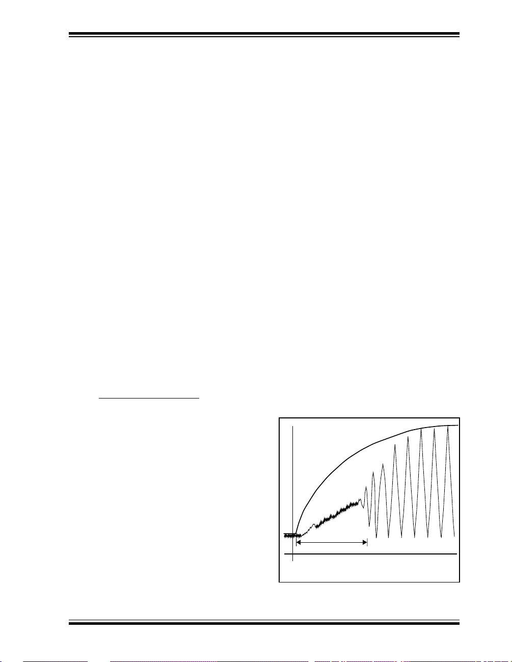
4.1.2.1 OSCILLATOR / RESONATOR START-UP
As the device voltage increases from Vss, the oscillator
will start its oscillations. The time required f or the oscillator to start oscillating depends on many factors.
These include:
• Crystal / resonator frequency
• Capacitor values used (C1 and C2)
• Device V
• System temperature
• Series resistor value (and type) if used
• Oscillator mode selection of device (which selects
Figure 4-1 shows an example of a typical oscillator/
resonator start-up. The peak-to-peak voltage of the
oscillator waveform can be quite low (less than 50% of
device V
(refer to parameter #D033 and parameter #D043 in the
electrical specification section).
DD rise time.
the gain of the internal oscillator inverter)
DD) when the waveform is centered at VDD/2
FIGURE 4-1: OSCILLATOR / RESONATOR
START-UP
CHARACTERISTICS
VDD
Crystal Start-up Time
Time
1998 Microchip Technology Inc. DS30289A-page 15
Page 16
PIC17C7XX
FIGURE 4-2: CRYSTAL OR CERAMIC
RESONATOR OPERATION (XT
OR LF OSC CONFIGURATION)
OSC1
C1
XTAL
OSC2
Note1
C2
PIC17CXXX
See Table 4-1 and Table 4-2 for recommended values of
C1 and C2.
SLEEP
RF
To internal
logic
Note 1: A series resistor (Rs) may be required for
AT strip cut crystals.
TABLE 4-1: CAPACITOR SELECTION
FOR CERAMIC
RESONATORS
Oscillator
Type
Resonator
Frequency
LF 455 kHz
2.0 MHz
XT 4.0 MHz
8.0 MHz
16.0 MHz
Higher capacitance increases the stability of the oscillator
but also increases the start-up time. These values are for
design guidance only. Since each resonator has its own
characteristics, the user should consult the resonator manufacturer for appropriate values of external components.
Note 1: These values include all board capacitances
on this pin. Actual capacitor value depends
on board capacitance
Resonators Used:
455 kHz Panasonic EFO-A455K04B ± 0.3%
2.0 MHz Murata Erie CSA2.00MG ± 0.5%
4.0 MHz Murata Erie CSA4.00MG ± 0.5%
8.0 MHz Murata Erie CSA8.00MT ± 0.5%
16.0 MHz Murata Erie CSA16.00MX ± 0.5%
Resonators used did not have built-in capacitors.
Capacitor Range
(1)
C1 = C2
15 - 68 pF
10 - 33 pF
22 - 68 pF
33 - 100 pF
33 - 100 pF
FIGURE 4-3: CRYSTAL OPERATION,
OVERTONE CRYSTALS (XT
OSC CONFIGURATION)
C1
C2
C3
0.1 µF
To filter the fundamental frequency
L*C2
Where f = tank circuit resonant frequency. This should be
midway between the fundamental and the 3rd overtone
frequencies of the crystal.
C3 handles current during charging of tank circuit.
OSC1
SLEEP
OSC2
PIC17CXXX
1
2
=
(2πf)
TAB LE 4-2: CAPACITOR SELECTION FOR
CRYSTAL OSCILLATOR
Osc
Type
LF 32 kHz
Freq
(1)
1 MHz
2 MHz
XT 2 MHz
4 MHz
(2)
8 MHz
16 MHz
25 MHz
(3)
32 MHz
Higher capacitance increases the stability of the oscillator
but also increases the start-up time and the oscillator current. These values are for design guidance only. RS may be
required in XT mode to avoid overdriving the crystals with
low drive level specification. Since each crystal has its own
characteristics, the user should consult the crystal manufacturer for appropriate values for external components.
Note 1: For VDD > 4.5V, C1 = C2 ≈ 30 pF is recom-
mended.
2: R
S of 330Ω is required for a capacitor com-
bination of 15/15 pF.
3: These v alues include all board capacitances
on this pin. Actual capacitor value depends
on board capacitance
Crystals Used:
32.768 kHz Epson C-001R32.768K-A ± 20 PPM
1.0 MHz ECS-10-13-1 ± 50 PPM
2.0 MHz ECS-20-20-1 ± 50 PPM
4.0 MHz ECS-40-20-1 ± 50 PPM
8.0 MHz ECS ECS-80-S-4
ECS-80-18-1
16.0 MHz ECS-160-20-1 TBD
25 MHz CTS CTS25M ± 50 PPM
32 MHz CRYSTEK HF-2 ± 50 PPM
(3)
C1
100-150 pF
10-33 pF
10-33 pF
47-100 pF
15-68 pF
15-47 pF
TBD
15-47 pF
10 pF
(3)
C2
100-150 pF
10-33 pF
10-33 pF
47-100 pF
15-68 pF
15-47 pF
TBD
15-47 pF
10 pF
± 50 PPM
DS30289A-page 16 1998 Microchip Technology Inc.
Page 17
PIC17C7XX
4.1.3 EXTERNAL CLOCK OSCILLATOR
In the EC oscillator mode, the OSC1 input can be
driven by CMOS drivers. In this mode, the
OSC1/CLKIN pin is hi-impedance and the
OSC2/CLKOUT pin is the CLKOUT output (4 T
OSC).
FIGURE 4-4: EXTERNAL CLOCK INPUT
OPERATION (EC OSC
CONFIGURATION)
Clock from
ext. system
CLKOUT
(F
OSC/4)
OSC1
PIC17CXXX
OSC2
4.1.4 EXTERNAL CRYSTAL OSCILLATOR
CIRCUIT
Either a prepackaged oscillator can be used or a simple
oscillator circuit with TTL gates can be built. Prepackaged oscillators provide a wide operating range and
better stability. A well-designed crystal oscillator will
provide good performance with TTL gates. Two types
of crystal oscillator circuits can be used: one with series
resonance, or one with parallel resonance.
Figure 4-5 shows implementation of a parallel resonant
oscillator circuit. The circuit is designed to use the fundamental frequency of the crystal. The 74AS04
inverter performs the 180-degree phase shift that a parallel oscillator requires. The 4.7 kΩ resistor provides
the negative feedback for stability. The 10 kΩ potentiometer biases the 74AS04 in the linear region. This
could be used for external oscillator designs.
FIGURE 4-5: EXTERNAL PARALLEL
RESONANT CRYSTAL
OSCILLATOR CIRCUIT
10kΩ
+5V
10 kΩ
4.7 kΩ
74AS04
XTAL
74AS04
10 kΩ
To Other
Devices
PIC17CXXX
OSC1
20 pF
20 pF
Figure 4-6 shows a series resonant oscillator circuit.
This circuit is also designed to use the fundamental frequency of the crystal. The inverter performs a
180-degree phase shift in a series resonant oscillator
circuit. The 330 Ω resistors provide the negative feedback to bias the inverters in their linear region.
FIGURE 4-6: EXTERNAL SERIES
RESONANT CRYSTAL
OSCILLATOR CIRCUIT
To Other
74AS04
Devices
PIC17CXXX
OSC1
330 Ω
74AS04
1998 Microchip Technology Inc. DS30289A-page 17
330 Ω
74AS04
0.1 µF
XTAL
Page 18
PIC17C7XX
4.1.5 RC OSCILLATOR
For timing insensitive applications, the RC device
option offers additional cost savings. RC oscillator frequency is a function of the supply voltage, the resistor
(Rext) and capacitor (Cext) values, and the operating
temperature. In addition to this, oscillator frequency
will vary from unit to unit due to normal process parameter variation. Furthermore, the difference in lead
frame capacitance between package types will also
affect oscillation frequency, especially for low Cext values. The user also needs to tak e into account v ariation
due to tolerance of external R and C components used.
Figure 4-7 shows how the R/C combination is con-
nected to the PIC17CXXX. For Rext values below
2.2 kΩ, the oscillator operation may become unstable,
or stop completely. For very high Rext values (e.g.
1 MΩ), the oscillator becomes sensitive to noise,
humidity and leakage. Thus, we recommend to keep
Rext between 3 kΩ and 100 kΩ.
Although the oscillator will operate with no external
capacitor (Cext = 0 pF), we recommend using values
above 20 pF for noise and stability reasons. With little
or no external capacitance, oscillation frequency can
vary dramatically due to changes in external capacitances, such as PCB trace capacitance or package
lead frame capacitance.
See Section 21.0 for RC frequency variation from part
to part due to normal process variation. The variation
is larger for larger R (since leakage current variation
will affect RC frequency more for large R) and for
smaller C (since variation of input capacitance will
affect RC frequency more).
See Section 21.0 for variation of oscillator frequency
due to V
DD for given Rext/Cext values as well as fre-
quency variation due to operating temperature for given
R, C, and V
DD values.
The oscillator frequency, divided by 4, is available on
the OSC2/CLKOUT pin, and can be used for test purposes or to synchronize other logic (see Figure 4-8 for
waveform).
FIGURE 4-7: RC OSCILLATOR MODE
VDD
Rext
OSC1
PIC17CXXX
Internal
clock
4.1.5.1 RC START-UP
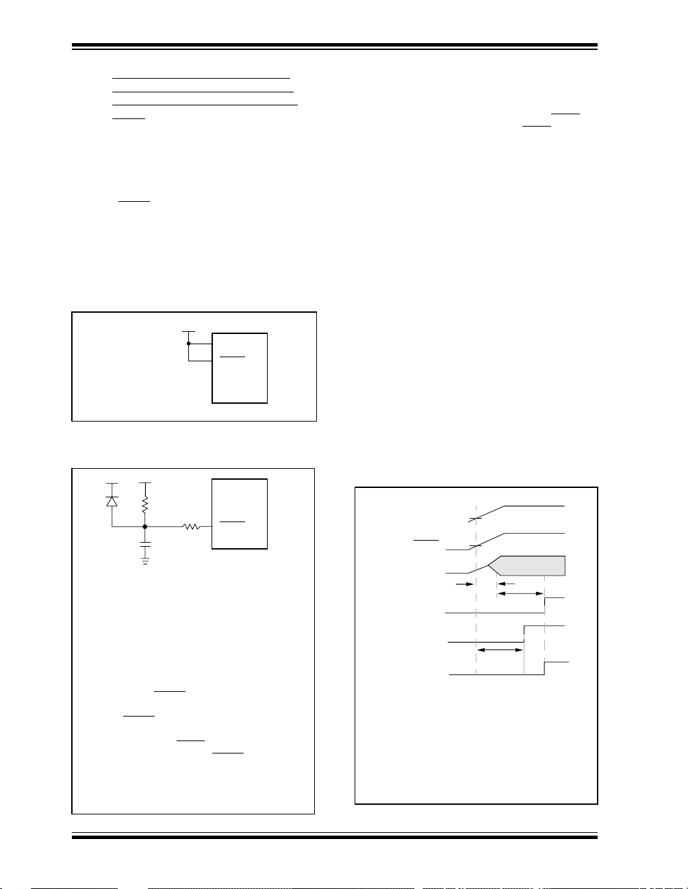
As the device voltage increases, the RC will immedi-
ately start its oscillations once the pin voltage levels
meet the input threshold specifications (parameter
#D032 and parameter #D042 in the electrical specifica-
tion section). The time required for the RC to start
oscillating depends on many factors. These include:
• Resistor value used
• Capacitor value used
• Device V
DD rise time
• System temperature
Cext
V
SS
DS30289A-page 18 1998 Microchip Technology Inc.
Fosc/4
OSC2/CLKOUT
Page 19
PIC17C7XX
4.2 Clocking Scheme/Instruction Cycle
The clock input (from OSC1) is internally divided by
four to generate four non-overlapping quadrature
clocks, namely Q1, Q2, Q3, and Q4. Internally, the program counter (PC) is incremented every Q1, and the
instruction is fetched from the program memory and
latched into the instruction register in Q4. The instruction is decoded and executed during the following Q1
through Q4. The clocks and instruction execution flow
are shown in Figure 4-8.
FIGURE 4-8: CLOCK/INSTRUCTION CYCLE
OSC1
Q2
Q3
Q4
PC
OSC2/CLKOUT
(RC mode)
Q1
Q2 Q3 Q4
Q1
PC PC+1 PC+2
Fetch INST (PC)
Execute INST (PC-1) Fetch INST (PC+1)
Q2 Q3 Q4
Q1
Execute INST (PC) Fetch INST (PC+2)
4.3 Instruction Flow/Pipelining
An “Instruction Cycle” consists of four Q cycles (Q1,
Q2, Q3, and Q4). The instruction fetch and e xecute are
pipelined such that fetch takes one instruction cycle
while decode and execute takes another instruction
cycle. However, due to the pipelining, each instruction
effectively executes in one cycle. If an instruction
causes the program counter to change (e.g. GOTO)
then two cycles are required to complete the instruction
(Example 4-1).
A fetch cycle begins with the program counter incrementing in Q1.
In the execution cycle, the f etched instruction is latched
into the “Instruction Register (IR)” in cycle Q1. This
instruction is then decoded and executed during the
Q2, Q3, and Q4 cycles. Data memory is read during
Q2 (operand read) and written during Q4 (destination
write).
Q2 Q3 Q4
Q1
Internal
phase
clock
Execute INST (PC+1)
EXAMPLE 4-1: INSTRUCTION PIPELINE FLOW
TCY0TCY1TCY2TCY3TCY4TCY5
1. MOVLW 55h
2. MOVWF PORTB
3. CALL SUB_1
4. BSF PORTA, BIT3 (Forced NOP)
5. Instruction @ address SUB_1
All instructions are single cycle, except for any program branches. These take two cycles since the fetched
instruction is “flushed” from the pipeline while the new instruction is being fetched and then executed.
1998 Microchip Technology Inc. DS30289A-page 19
Fetch 1 Execute 1
Fetch 2 Execute 2
Fetch 3 Execute 3
Fetch 4 Flush
Fetch SUB_1 Execute SUB_1
Page 20

PIC17C7XX
NOTES:
DS30289A-page 20 1998 Microchip Technology Inc.
Page 21
PIC17C7XX
5.0 RESET
The PIC17CXXX differentiates between various kinds
of reset:
• Power-on Reset (POR)
• Brown-out Reset
• MCLR
Reset
• WDT Reset
Some registers are not affected in any reset condition,
their status is unknown on POR and unchanged in any
other reset. Most other registers are forced to a “reset
state”. The T
in different reset situations as indicated in Table 5-3.
These bits, in conjunction with the POR
O and PD bits are set or cleared differently
and BOR bits,
When the device enters the "reset state" the Data
Direction registers (DDR) are forced set, which will
make the I/O hi-impendance inputs. The reset state of
some peripheral modules may force the I/O to other
operations, such as analog inputs or the system bus.
Note: While the device is in a reset state, the
internal phase clock is held in the Q1 state.
Any processor mode that allows external
execution will force the RE0/ALE pin as a
low output and the RE1/OE
pins as high outputs.
A simplified block diagram of the on-chip reset circuit is
shown in Figure 5-1.
are used in software to determine the nature of the
reset. See Table 5-4 for a full description of the reset
states of all registers.
FIGURE 5-1: SIMPLIFIED BLOCK DIAGRAM OF ON-CHIP RESET CIRCUIT
External
Reset
MCLR
BOR
Module
Brown-out
Reset
and RE2/WR
WDT
Module
V
DD rise
detect
VDD
OST/PWRT
OSC1
1998 Microchip Technology Inc. DS30289A-page 21
On-chip
RC OSC†
† This RC oscillator is shared with the WDT
when not in a power-up sequence.
WDT
Time_Out
Reset
Power_On_Reset
OST
10-bit Ripple counter
PWRT
10-bit Ripple counter
Enable PWRT
Enable OST
S
R
(Enable the PWRT timer
only during POR or BOR)
(If PWRT is invoked, or a Wake-up from
SLEEP and OSC type is XT or LF)
Chip_Reset
Q
Page 22
PIC17C7XX
5.1 Power-on Reset (POR), Power-up
Timer (PWRT), Oscillator Start-up
Timer (OST), and Brown-out Reset
(BOR)
5.1.1 POWER-ON RESET (POR)
The Power-on Reset circuit holds the device in reset
until V
DD is above the trip point (in the range of 1.4V -
2.3V). The devices produce an internal reset for both
rising and falling V
just tie the MCLR/
to V
DD. This will eliminate external RC components
DD. To take advantage of the POR,
VPP pin directly (or through a resistor)
usually needed to create Power-on Reset. A minimum
rise time for V
DD is required. See Electrical Specifica-
tions for details.
Figure 5-2 and Figure 5-3 show two possible POR cir-
cuits.
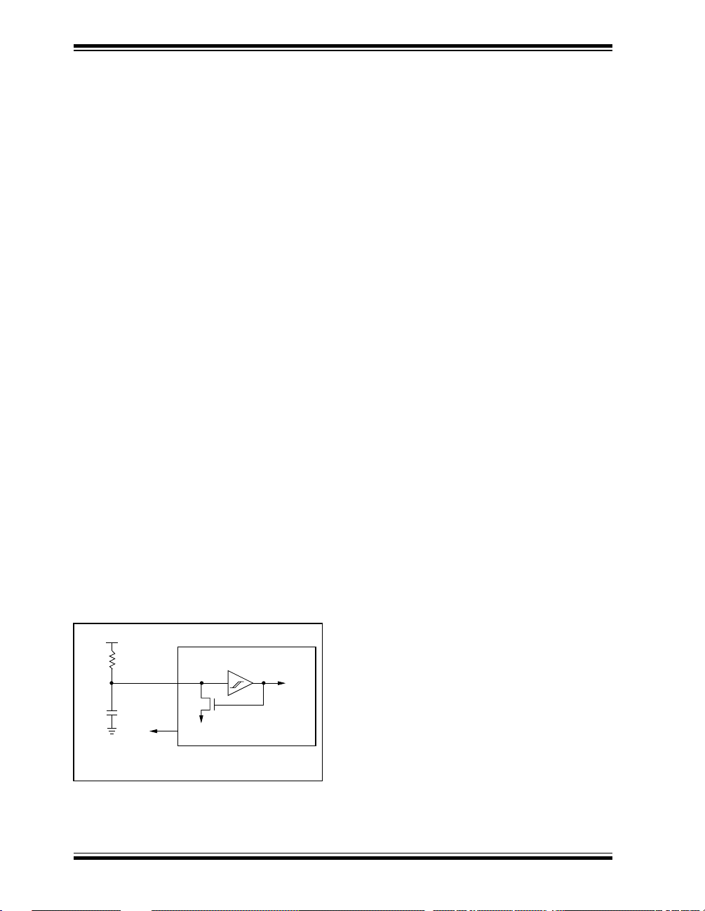
FIGURE 5-2: USING ON-CHIP POR
VDD
VDD
MCLR
PIC17CXXX
FIGURE 5-3: EXTERNAL POWER-ON
RESET CIRCUIT (FOR SLOW
DD POWER-UP)
V
V
DD
VDD
D
R
R1
MCLR
C
PIC17CXXX
5.1.2 POWER-UP TIMER (PWRT)
The Power-up Timer provides a fixed 96 ms time-out
(nominal) on power-up. This occurs from the rising
edge of the internal POR signal if V
tied, or after the first rising edge of MCLR
DD and MCLR are
(detected
high). The Power-up Timer operates on an internal RC
oscillator. The chip is kept in RESET as long as the
PWRT is active. In most cases the PWRT delay allows
V
DD to rise to an acceptable level.
The power-up time delay will vary from chip to chip and
DD and temperature. See DC parameters for
with V
details.
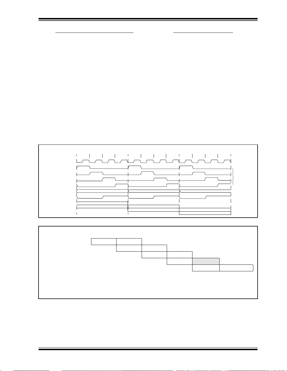
5.1.3 OSCILLATOR START-UP TIMER (OST)
The Oscillator Start-up Timer (OST) provides a 1024
oscillator cycle (1024T
OSC) delay whenever the PWRT
is invoked or a wak e-up from SLEEP event occurs in XT
or LF mode. The PWRT and OST operate in parallel.
The OST counts the oscillator pulses on the
OSC1/CLKIN pin. The counter only starts incrementing
after the amplitude of the signal reaches the oscillator
input thresholds. This delay allows the crystal oscillator
or resonator to stabilize before the device exits reset.
The length of the time-out is a function of the crystal/resonator frequency.
Figure 5-4 shows the operation of the OST circuit. In
this figure the oscillator is of such a low frequency that
although enabled simultaneously, the OST does not
time-out until after the Power-up Timer time-out.
FIGURE 5-4: OSCILLATOR START-UP
TIME (LOW FREQ)
POR or BOR Trip Point
VDD
MCLR
OSC2
OSC1
Note 1: An external Power-on Reset circuit is
required only if V
DD power-up time is too
OST TIME_OUT
T
T
OST
slow. The diode D helps discharge the
capacitor quickly when V
down.
2: R < 40 kΩ is recommended to ensure
that the voltage drop across R does not
exceed 0.2V (max. leakage current spec.
on the MCLR/
VPP pin is 5 µA). A larger
voltage drop will degrade V
MCLR/
VPP pin.
3: R1 = 100Ω to 1 kΩ will limit any current
flowing into MCLR
tor C in the event of MCLR/
down due to Electrostatic Discharge
(ESD) or Electrical Overstress (EOS).
DS30289A-page 22 1998 Microchip Technology Inc.
DD powers
IH level on the
from external capaci-
VPP pin break-
PWRT TIME_OUT
TPWRT
INTERNAL RESET
This figure shows in greater detail the timings
involved with the oscillator start-up timer. In this
example the low frequency crystal start-up time is
larger than power-up time (T
PWRT).
Tosc1 = time for the crystal oscillator to react to an
oscillation level detectable by the Oscillator
Start-up Timer (OST).
TOST = 1024TOSC.
Page 23
PIC17C7XX
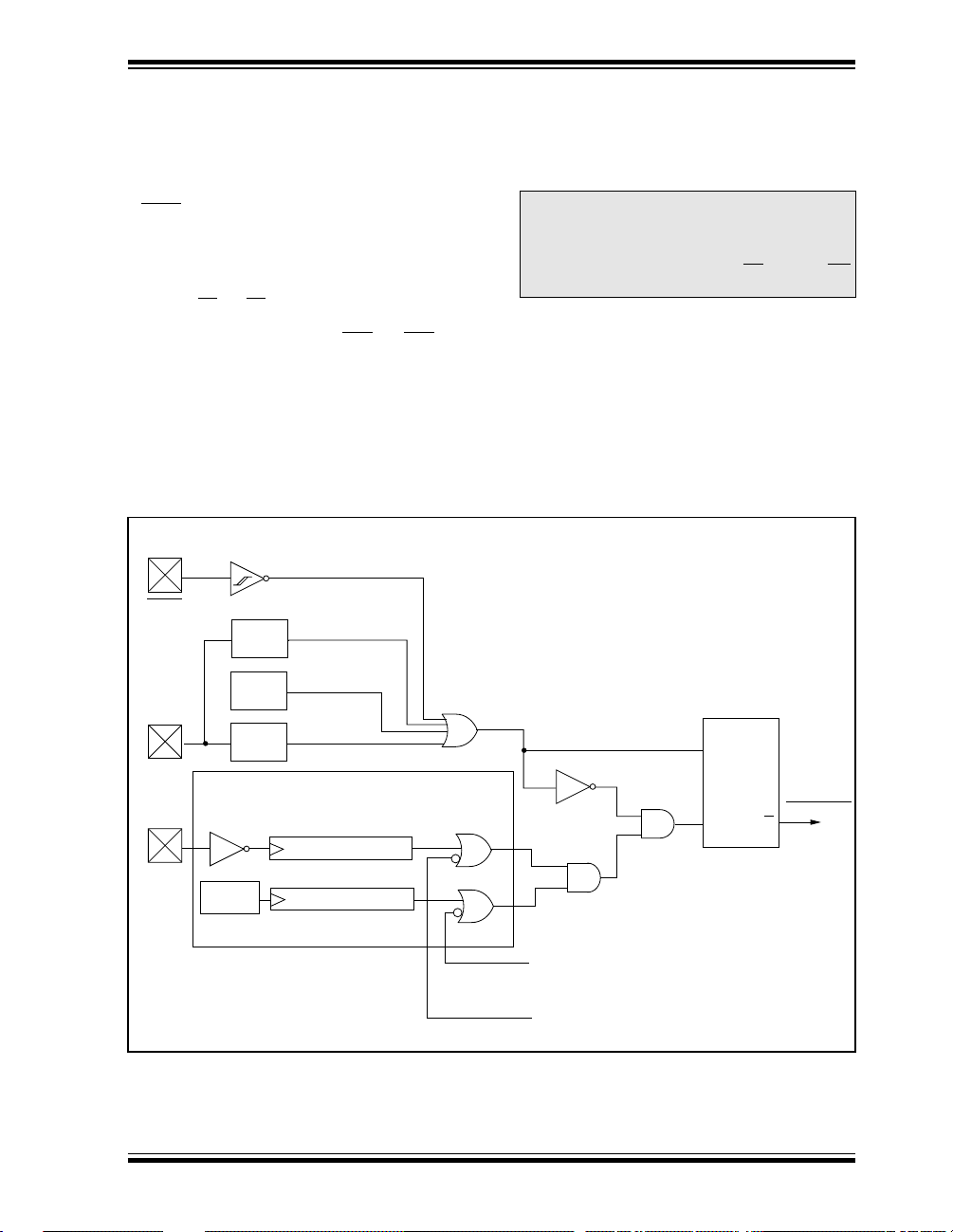
5.1.4 TIME-OUT SEQUENCE
On power-up the time-out sequence is as follows: First
the internal POR signal goes high when the POR trip
point is reached. If MCLR
is high, then both the OST
and PWRT timers start. In general the PWRT time-out
is longer, except with low frequency crystals/resonators. The total time-out also varies based on oscillator
configuration. Table 5-1 shows the times that are asso-
ciated with the oscillator configuration. Figure 5-5 and
Figure 5-6 display these time-out sequences.
If the device voltage is not within electrical specification
at the end of a time-out, the MCLR/
VPP pin must be
held low until the voltage is within the device specification. The use of an external RC delay is sufficient for
many of these applications.
The time-out sequence begins from the first rising edge
of MCLR
.
Table 5-3 shows the reset conditions for some special
registers, while Table 5-4 shows the initialization condi-
tions for all the registers.
TABLE 5-1: TIME-OUT IN VARIOUS SITUATIONS
Oscillator
Configuration
XT, LF Greater of: 96 ms or 1024TOSC 1024TOSC —
EC, RC Greater of: 96 ms or 1024T
POR, BOR Wake up from
SLEEP
OSC ——
MCLR Reset
TABLE 5-2: STATUS BITS AND THEIR SIGNIFICANCE
BOR
(1)
TO PD
Event
Power-on Reset
MCLR Reset during SLEEP or interrupt wake-up from SLEEP
WDT Reset during normal operation
WDT Wak e-up during SLEEP
MCLR Reset during normal operation
Brown-out Reset
Illegal, TO is set on POR
Illegal, PD is set on POR
CLRWDT instruction executed
POR
0011
1110
1101
1100
1111
1011
000x
00x0
xx11
Note 1: When BODEN is enabled, else the BOR status bit is unknown.
TAB LE 5-3: RESET CONDITION FOR THE PROGRAM COUNTER AND THE CPUST A REGISTER
Event PCH:PCL CPUSTA
(4)
Power-on Reset 0000h --11 1100 Ye s
Brown-out Reset 0000h --11 1110 Ye s
Reset during normal operation 0000h --11 1111 No
MCLR
Reset during SLEEP 0000h --11 1011
MCLR
WDT Reset during normal operation 0000h --11 0111 No
WDT Wake-up during SLEEP
(3)
0000h --11 0011
Interrupt wake-up from SLEEP GLINTD is set PC + 1 --11 1011
GLINTD is clear
PC + 1
(1)
--10 1011
Legend: u = unchanged, x = unknown, - = unimplemented read as '0'.
Note 1: On wake-up, this instruction is executed. The instruction at the appropriate interrupt vector is fetched and
then executed.
2: The OST is only active (on wake-up) when the Oscillator is configured for XT or LF modes.
3: The Program Counter = 0, that is, the device branches to the reset vector. This is different from the
mid-range devices.
4: When BODEN is enabled, else the BOR
status bit is unknown.
OST Active
(2)
Yes
(2)
Yes
(2)
Yes
(2)
Yes
1998 Microchip Technology Inc. DS30289A-page 23
Page 24
PIC17C7XX
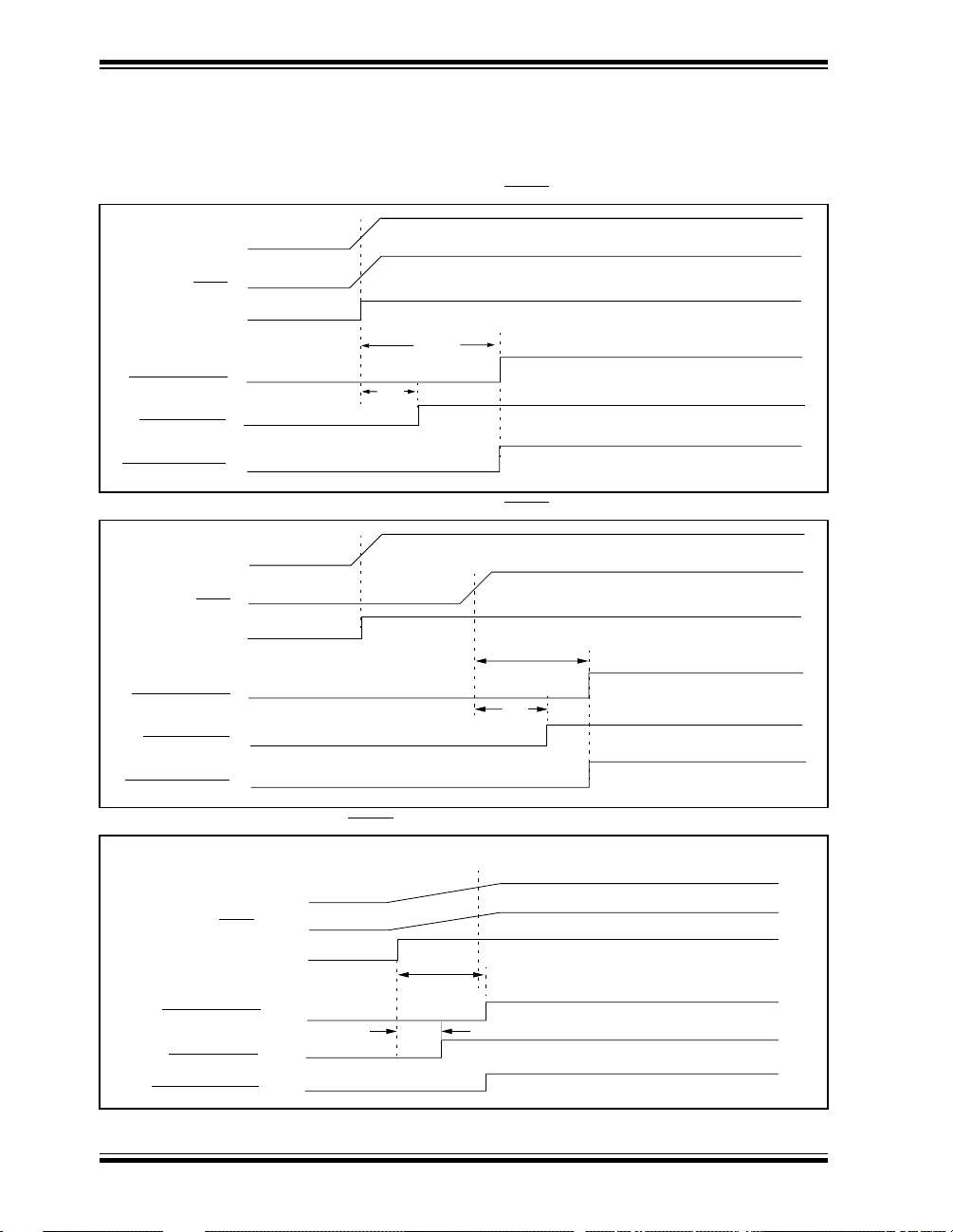
In Figure 5-5, Figure 5-6 and Figure 5-7, the TPWRT
timer timeout is greater then the TOST timer timeout, as
would be the case in higher frequency crystals. For
lower frequency crystals, (i.e., 32 kHz) T
greater.
FIGURE 5-5: TIME-OUT SEQUENCE ON POWER-UP (MCLR TIED TO VDD)
VDD
MCLR
INTERNAL POR
OST may be
TPWRT
PWRT TIME-OUT
OST TIME-OUT
INTERNAL RESET
TOST
FIGURE 5-6: TIME-OUT SEQUENCE ON POWER-UP (MCLR
VDD
MCLR
INTERNAL POR
TPWRT
PWRT TIME-OUT
OST TIME-OUT
INTERNAL RESET
FIGURE 5-7: SLOW RISE TIME (MCLR
VDD
MCLR
INTERNAL POR
T TIME-OUT
PWR
OST TIME-OUT
INTERNAL RESET
TIED TO VDD)
Minimum VDD operating voltage
0V
PWRT
T
TOST
5V
1V
TOST
NOT TIED TO VDD)
DS30289A-page 24 1998 Microchip Technology Inc.
Page 25

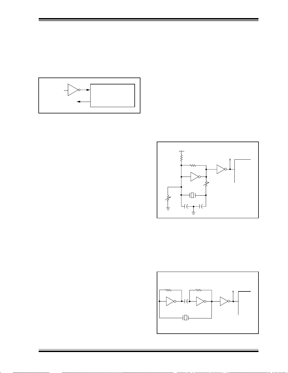
PIC17C7XX
TABLE 5-4: INITIALIZATION CONDITIONS FOR SPECIAL FUNCTION REGISTERS
Register Address
Power-on Reset
Brown-out Reset
Reset
MCLR
WDT Reset
Wake-up from SLEEP
through interrupt
Unbanked
INDF0 00h N.A. N.A. N.A.
FSR0 01h xxxx xxxx uuuu uuuu uuuu uuuu
PCL 02h 0000h 0000h
PC + 1
(2)
PCLATH 03h 0000 0000 uuuu uuuu uuuu uuuu
ALUSTA 04h 1111 xxxx 1111 uuuu 1111 uuuu
T0STA 05h 0000 000- 0000 000- 0000 000-
(3)
CPUSTA
INTSTA 07h 0000 0000 0000 0000
06h --11 11qq --11 qquu --uu qquu
uuuu uuuu
(1)
INDF1 08h N.A. N.A. N.A.
FSR1 09h xxxx xxxx uuuu uuuu uuuu uuuu
WREG 0Ah xxxx xxxx uuuu uuuu uuuu uuuu
TMR0L 0Bh xxxx xxxx uuuu uuuu uuuu uuuu
TMR0H 0Ch xxxx xxxx uuuu uuuu uuuu uuuu
TBLPTRL 0Dh 0000 0000 0000 0000 uuuu uuuu
TBLPTRH 0Eh 0000 0000 0000 0000 uuuu uuuu
BSR 0Fh 0000 0000 0000 0000 uuuu uuuu
Bank 0
PORTA
(4,6)
10h 0-xx 11xx 0-uu 11uu u-uu uuuu
DDRB 11h 1111 1111 1111 1111 uuuu uuuu
PORTB
(4)
12h xxxx xxxx uuuu uuuu uuuu uuuu
RCSTA1 13h 0000 -00x 0000 -00u uuuu -uuu
RCREG1 14h xxxx xxxx uuuu uuuu uuuu uuuu
TXSTA1 15h 0000 --1x 0000 --1u uuuu --uu
TXREG1 16h xxxx xxxx uuuu uuuu uuuu uuuu
SPBRG1 17h 0000 0000 0000 0000 uuuu uuuu
Legend: u = unchanged, x = unknown, - = unimplemented read as '0', q = value depends on condition.
Note 1: One or more bits in INTSTA, PIR1, PIR2 will be affected (to cause wake-up).
2: When the wake-up is due to an interrupt and the GLINTD bit is cleared, the PC is loaded with the interrupt
vector.
3: See Table 5-3 for reset value of specific condition.
4: This is the value that will be in the port output latch.
5: When the device is configured for microprocessor or externded microcontroller mode, the operation of this
port does not rely on these registers
6: On any device reset, these pins are configured as inputs.
1998 Microchip Technology Inc. DS30289A-page 25
Page 26
PIC17C7XX
TABLE 5-4: INITIALIZATION CONDITIONS FOR SPECIAL FUNCTION REGISTERS (Cont.’d)
Register Address
Power-on Reset
Brown-out Reset
Reset
MCLR
WDT Reset
Wake-up from SLEEP
through interrupt
Bank 1
(5)
DDRC
PORTC
DDRD
PORTD
DDRE
PORTE
(5)
(5)
(4, 5)
(4, 5)
(4, 5)
PIR1 16h x000 0010 u000 0010
10h 1111 1111 1111 1111 uuuu uuuu
11h xxxx xxxx uuuu uuuu uuuu uuuu
12h 1111 1111 1111 1111 uuuu uuuu
13h xxxx xxxx uuuu uuuu uuuu uuuu
14h ---- 1111 ---- 1111 ---- uuuu
15h ---- xxxx ---- uuuu ---- uuuu
uuuu uuuu
(1)
PIE1 17h 0000 0000 0000 0000 uuuu uuuu
Bank 2
TMR1 10h xxxx xxxx uuuu uuuu uuuu uuuu
TMR2 11h xxxx xxxx uuuu uuuu uuuu uuuu
TMR3L 12h xxxx xxxx uuuu uuuu uuuu uuuu
TMR3H 13h xxxx xxxx uuuu uuuu uuuu uuuu
PR1 14h xxxx xxxx uuuu uuuu uuuu uuuu
PR2 15h xxxx xxxx uuuu uuuu uuuu uuuu
PR3/CA1L 16h xxxx xxxx uuuu uuuu uuuu uuuu
PR3/CA1H 17h xxxx xxxx uuuu uuuu uuuu uuuu
Bank 3
PW1DCL 10h xx-- ---- uu-- ---- uu-- ---PW2DCL 11h xx0- ---- uu0- ---- uuu- ---PW1DCH 12h xxxx xxxx uuuu uuuu uuuu uuuu
PW2DCH 13h xxxx xxxx uuuu uuuu uuuu uuuu
CA2L 14h xxxx xxxx uuuu uuuu uuuu uuuu
CA2H 15h xxxx xxxx uuuu uuuu uuuu uuuu
TCON1 16h 0000 0000 0000 0000 uuuu uuuu
TCON2 17h 0000 0000 0000 0000 uuuu uuuu
Legend: u = unchanged, x = unknown, - = unimplemented read as '0', q = value depends on condition.
Note 1: One or more bits in INTSTA, PIR1, PIR2 will be affected (to cause wake-up).
2: When the wake-up is due to an interrupt and the GLINTD bit is cleared, the PC is loaded with the interrupt
vector.
3: See Table 5-3 for reset value of specific condition.
4: This is the value that will be in the port output latch.
5: When the device is configured for microprocessor or externded microcontroller mode, the operation of this
port does not rely on these registers
6: On any device reset, these pins are configured as inputs.
DS30289A-page 26 1998 Microchip Technology Inc.
Page 27
PIC17C7XX
TABLE 5-4: INITIALIZATION CONDITIONS FOR SPECIAL FUNCTION REGISTERS (Cont.’d)
Register Address
Bank 4
PIR2 10h 000- 0010 000- 0010
PIE2 11h 000- 0000 000- 0000 uuu- uuuu
Unimplemented
RCSTA2 13h 0000 -00x 0000 -00u uuuu -uuu
RCREG2 14h xxxx xxxx uuuu uuuu uuuu uuuu
TXSTA2 15h 0000 --1x 0000 --1u uuuu --uu
TXREG2 16h xxxx xxxx uuuu uuuu uuuu uuuu
SPBRG2 17h 0000 0000 0000 0000 uuuu uuuu
Bank 5
DDRF 10h 1111 1111 1111 1111 uuuu uuuu
(4)
PORTF
DDRG 12h 1111 1111 1111 1111 uuuu uuuu
PORTG
ADCON0 14h 0000 -0-0 0000 -0-0 uuuu uuuu
ADCON1 15h 000- 0000 000- 0000 uuuu uuuu
ADRESL 16h xxxx xxxx uuuu uuuu uuuu uuuu
ADRESH 17h xxxx xxxx uuuu uuuu uuuu uuuu
Bank 6
SSPADD 10h 0000 0000 0000 0000 uuuu uuuu
SSPCON1 11h 0000 0000 0000 0000 uuuu uuuu
SSPCON2 12h 0000 0000 0000 0000 uuuu uuuu
SSPSTAT 13h 0000 0000 0000 0000 uuuu uuuu
SSPBUF 14h xxxx xxxx uuuu uuuu uuuu uuuu
Unimplemented
Unimplemented
Unimplemented
Legend: u = unchanged, x = unknown, - = unimplemented read as '0', q = value depends on condition.
Note 1: One or more bits in INTSTA, PIR1, PIR2 will be affected (to cause wake-up).
(4)
2: When the wake-up is due to an interrupt and the GLINTD bit is cleared, the PC is loaded with the interrupt
vector.
3: See Table 5-3 for reset value of specific condition.
4: This is the value that will be in the port output latch.
5: When the device is configured for microprocessor or externded microcontroller mode, the operation of this
port does not rely on these registers
6: On any device reset, these pins are configured as inputs.
12h ---- ---- ---- ---- ---- ----
11h 0000 0000 0000 0000 uuuu uuuu
13h xxxx 0000 uuuu 0000 uuuu uuuu
15h ---- ---- ---- ---- ---- ---16h ---- ---- ---- ---- ---- ---17h ---- ---- ---- ---- ---- ----
Power-on Reset
Brown-out Reset
Reset
MCLR
WDT Reset
Wake-up from SLEEP
through interrupt
(1)
uuu- uuuu
1998 Microchip Technology Inc. DS30289A-page 27
Page 28
PIC17C7XX
TABLE 5-4: INITIALIZATION CONDITIONS FOR SPECIAL FUNCTION REGISTERS (Cont.’d)
Register Address
Bank 7
PW3DCL 10h xx0- ---- uu0- ---- uuu- ---PW3DCH 11h xxxx xxxx uuuu uuuu uuuu uuuu
CA3L 12h xxxx xxxx uuuu uuuu uuuu uuuu
CA3H 13h xxxx xxxx uuuu uuuu uuuu uuuu
CA4L 14h xxxx xxxx uuuu uuuu uuuu uuuu
CA4H 15h xxxx xxxx uuuu uuuu uuuu uuuu
TCON3 16h -000 0000 -000 0000 -uuu uuuu
Unimplemented
Bank 8
DDRH
(4)
PORTH
DDRJ
PORTJ
Unbanked
PRODL 18h xxxx xxxx uuuu uuuu uuuu uuuu
PRODH 19h xxxx xxxx uuuu uuuu uuuu uuuu
Legend: u = unchanged, x = unknown, - = unimplemented read as '0', q = value depends on condition.
Note 1: One or more bits in INTSTA, PIR1, PIR2 will be affected (to cause wake-up).
(4)
2: When the wake-up is due to an interrupt and the GLINTD bit is cleared, the PC is loaded with the interrupt
vector.
3: See Table 5-3 for reset value of specific condition.
4: This is the value that will be in the port output latch.
5: When the device is configured for microprocessor or externded microcontroller mode, the operation of this
port does not rely on these registers
6: On any device reset, these pins are configured as inputs.
17h ---- ---- ---- ---- ---- ----
10h 1111 1111 1111 1111 uuuu uuuu
11h xxxx xxxx uuuu uuuu uuuu uuuu
12h 1111 1111 1111 1111 uuuu uuuu
13h xxxx xxxx uuuu uuuu uuuu uuuu
Power-on Reset
Brown-out Reset
Reset
MCLR
WDT Reset
Wake-up from SLEEP
through interrupt
DS30289A-page 28 1998 Microchip Technology Inc.
Page 29
PIC17C7XX
5.1.5 BROWN-OUT RESET (BOR)
PIC17C7XX devices have on-chip Brown-out Reset cir-
cuitry. This circuitry places the device into a reset when
the device voltage falls below a trip point (BV
DD). This
ensures that the device does not continue program
execution outside the valid operation range of the
device. Brown-out resets are typically used in AC line
applications or large battery applications where large
loads may be switched in (such as automotive).
Note: Before using the on-chip brown-out for a
voltage supervisory function, please
review the electrical specifications to
ensure that they meet your requirements.
The BODEN configuration bit can disable (if clear/programmed) or enable (if set) the Brown-out Reset circuitry. If V
DD falls below BVDD (Typically 4.0V,
parameter #D005 in electrical specification section), for
greater than parameter #35, the brown-out situation will
reset the chip. A reset is not guaranteed to occur if V
DD
falls below BVDD for less than parameter #35. The chip
will remain in Brown-out Reset until V
BV
DD. The Power-up Timer and Oscillator Start-up
DD rises above
Timer will then be invoked. This will keep the chip in
reset the greater of 96 ms and 1024 T
below BV
DD while the Power-up Timer/Oscillator
OSC. If VDD drops
Start-up Timer is running, the chip will go back into a
Brown-out Reset. The Power-up Timer/Oscillator
Start-up Timer will be initialized. Once V
BV
DD, the Power-up Timer/Oscillator Start-up Timer
DD rises above
will start their time delays. Figure 5-10 shows typical
Brown-out situations.
In some applications, the Brown-out reset trip point of
the device may not be at the desired level. Figure 5-8
and Figure 5-9 are two examples of external circuitry
that may be implemented. Each needs to be e v aluated
to determine if they match the requirements of the
application.
FIGURE 5-8: EXTERNAL BROWN-OUT
PROTECTION CIRCUIT 1
VDD
DD
33k
10kΩ
40 kΩ
This circuit will activate reset when VDD goes below
(Vz + 0.7V) where Vz = Zener voltage.
V
MCLR
PIC17CXXX
FIGURE 5-9: EXTERNAL BROWN-OUT
PROTECTION CIRCUIT 2
DD
V
Q1
R1
VDD
MCLR
PIC17CXXX
= 0.7V
R1
R2
This brown-out circuit is less expensive, albeit less
accurate. Transistor Q1 turns off when VDD is below a
certain level such that:
VDD •
40 kΩ
R1 + R2
FIGURE 5-10: BROWN-OUT SITUATIONS
V
DD
Internal
Reset
V
DD
Internal
Reset
V
DD
Internal
Reset
1998 Microchip Technology Inc. DS30289A-page 29
Greater of 96 ms
< 96 ms
and 1024 Tosc
Greater of 96 ms
and 1024 Tosc
Greater of 96 ms
and 1024 Tosc
BV
DD Max.
DD Min.
BV
BVDD Max.
DD Min.
BV
BVDD Max.
DD Min.
BV
Page 30

PIC17C7XX
NOTES:
DS30289A-page 30 1998 Microchip Technology Inc.
Page 31

PIC17C7XX
6.0 INTERRUPTS
PIC17C7XX devices have 18 sources of interrupt:
• External interrupt from the RA0/INT pin
• Change on RB7:RB0 pins
• TMR0 Overflow
• TMR1 Overflow
• TMR2 Overflow
• TMR3 Overflow
• USART1 Transmit buffer empty
• USART1 Receive buffer full
• USART2 Transmit buffer empty
• USART2 Receive buffer full
• SSP Interrupt
2
• SSP I
C bus collision interrupt
• A/D conversion complete
• Capture1
• Capture2
• Capture3
• Capture4
• T0CKI edge occurred
There are six registers used in the control and status of
interrupts. These are:
• CPUST A
• INTST A
• PIE1
• PIR1
• PIE2
• PIR2
The CPUSTA register contains the GLINTD bit. This is
the Global Interrupt Disable bit. When this bit is set, all
interrupts are disabled. This bit is part of the controller
core functionality and is described in the Section 6.4.
When an interrupt is responded to, the GLINTD bit is
automatically set to disable any further interrupts, the
return address is pushed onto the stack and the PC is
loaded with the interrupt vector address. There are f our
interrupt vectors. Each vector address is for a specific
interrupt source (except the peripheral interrupts which
all vector to the same address). These sources are:
• External interrupt from the RA0/INT pin
• TMR0 Overflow
• T0CKI edge occurred
• Any peripheral interrupt
When program execution vectors to one of these inter-
rupt vector addresses (except for the peripheral interrupts), the interrupt flag bit is automatically cleared.
Vectoring to the peripheral interrupt vector address
does not automatically clear the source of the interrupt.
In the peripheral interrupt service routine, the source(s)
of the interrupt can be determined by testing the interrupt flag bits. The interrupt flag bit(s) must be cleared
in software before re-enabling interrupts to avoid infinite interrupt requests.
When an interrupt condition is met, that individual interrupt flag bit will be set regardless of the status of its corresponding mask bit or the GLINTD bit.
For external interrupt events, there will be an interrupt
latency. For two cycle instructions, the latency could
be one instruction cycle longer.
The “return from interrupt” instruction, RETFIE, can be
used to mark the end of the interrupt service routine.
When this instruction is executed, the stack is “POPed”,
and the GLINTD bit is cleared (to re-enable interrupts).
FIGURE 6-1: INTERRUPT LOGIC
RBIF
RBIE
TMR3IF
TMR3IE
TMR2IF
CA2IF
CA2IE
TX1IF
TX1IE
BCLIF
BCLIE
CA3IF
CA3IE
RC2IF
RC2IE
TMR2IE
RC1IF
RC1IE
ADIF
ADIE
INTSTA
T0IF
T0IE
INTF
INTE
T0CKIF
T0CKIE
PEIF
PEIE
Wake-up (If in SLEEP mode)
or terminate long write
Interrupt to CPU
GLINTD (CPUSTA<4>)
TMR1IF
TMR1IE
PIR1 / PIE1
CA1IF
CA1IE
SSPIF
SSPIE
CA4IF
CA4IE
PIR2 / PIE2
TX2IF
TX2IE
1998 Microchip Technology Inc. DS30289A-page 31
Page 32

PIC17C7XX
6.1 Interrupt Status Register (INTSTA)
The Interrupt Status/Control register (INTST A) contains
the flag and enable bits for non-peripheral interrupts.
The PEIF bit is a read only , bit wise OR of all the peripheral flag bits in the PIR registers (Figure 6-5 and
Figure 6-6).
Note: All interrupt flag bits get set by their speci-
fied condition, even if the corresponding
interrupt enable bit is clear (interrupt disabled) or the GLINTD bit is set (all interrupts disabled).
Care should be taken when clearing any of the INTSTA
register enable bits when interrupts are enabled
(GLINTD is clear). If any of the INTSTA flag bits (T0IF ,
INTF, T0CKIF, or PEIF) are set in the same instruction
cycle as the corresponding interrupt enable bit is
cleared, the device will vector to the reset address
(0x00).
Prior to disabling any of the INTSTA enable bits, the
GLINTD bit should be set (disabled).
FIGURE 6-2: INTSTA REGISTER (ADDRESS: 07h, UNBANKED)
R - 0 R/W - 0 R/W - 0 R/W - 0 R/W - 0 R/W - 0 R/W - 0 R/W - 0
PEIF T0CKIF T0IF INTF PEIE T0CKIE T0IE INTE
bit7 bit0
bit 7: PEIF: Peripheral Interrupt Flag bit
bit 6: T0CKIF: External Interrupt on T0CKI Pin Flag bit
bit 5: T0IF: TMR0 Overflow Interrupt Flag bit
bit 4: INTF: External Interrupt on INT Pin Flag bit
bit 3: PEIE: Peripheral Interrupt Enable bit
bit 2: T0CKIE: External Interrupt on T0CKI Pin Enable bit
bit 1: T0IE: TMR0 Overflow Interrupt Enable bit
bit 0: INTE: External Interrupt on RA0/INT Pin Enable bit
This bit is the OR of all peripheral interrupt flag bits AND’ed with their corresponding enable bits. The
interrupt logic forces program execution to address (20h) when a peripheral interrupt is pending.
1 =A peripheral interrupt is pending
0 =No peripheral interrupt is pending
This bit is cleared by hardware, when the interrupt logic forces program execution to address (18h).
1 =The software specified edge occurred on the RA1/T0CKI pin
0 =The software specified edge did not occur on the RA1/T0CKI pin
This bit is cleared by hardware, when the interrupt logic forces program execution to address (10h).
1 =TMR0 overflowed
0 =TMR0 did not overflow
This bit is cleared by hardware, when the interrupt logic forces program execution to address (08h).
1 =The software specified edge occurred on the RA0/INT pin
0 =The software specified edge did not occur on the RA0/INT pin
This bit acts as a global enable bit for the peripheral interrupts that have their corresponding enable bits
set.
1 =Enable peripheral interrupts
0 =Disable peripheral interrupts
1 =Enable software specified edge interrupt on the RA1/T0CKI pin
0 =Disable interrupt on the RA1/T0CKI pin
1 =Enable TMR0 overflow interrupt
0 =Disable TMR0 overflow interrupt
1 =Enable software specified edge interrupt on the RA0/INT pin
0 =Disable software specified edge interrupt on the RA0/INT pin
R = Readable bit
W = Writable bit
- n = Value at POR reset
DS30289A-page 32 1998 Microchip Technology Inc.
Page 33

6.2 Peripheral Interrupt Enable Register1
(PIE1) and Register2 (PIE2)
These registers contains the individual enable bits for
the peripheral interrupts.
FIGURE 6-3: PIE1 REGISTER (ADDRESS: 17h, BANK 1)
PIC17C7XX
R/W - 0 R/W - 0 R/W - 0 R/W - 0 R/W - 0 R/W - 0 R/W - 0 R/W - 0
RBIE TMR3IE TMR2IE TMR1IE CA2IE CA1IE TX1IE RC1IE
bit7 bit0
bit 7: RBIE: PORTB Interrupt on Change Enable bit
1 =Enable PORTB interrupt on change
0 =Disable PORTB interrupt on change
bit 6: TMR3IE: TMR3 Interrupt Enable bit
1 =Enable TMR3 interrupt
0 =Disable TMR3 interrupt
bit 5: TMR2IE: TMR2 Interrupt Enable bit
1 =Enable TMR2 interrupt
0 =Disable TMR2 interrupt
bit 4: TMR1IE: TMR1 Interrupt Enable bit
1 =Enable TMR1 interrupt
0 =Disable TMR1 interrupt
bit 3: CA2IE: Capture2 Interrupt Enable bit
1 =Enable Capture2 interrupt
0 =Disable Capture2 interrupt
bit 2: CA1IE: Capture1 Interrupt Enable bit
1 =Enable Capture1 interrupt
0 =Disable Capture1 interrupt
bit 1: TX1IE: USART1 Transmit Interrupt Enable bit
1 =Enable USART1 Transmit buffer empty interrupt
0 =Disable USART1 Transmit buffer empty interrupt
bit 0: RC1IE: USART1 Receive Interrupt Enable bit
1 =Enable USART1 Receive buffer full interrupt
0 =Disable USART1 Receive buffer full interrupt
R = Readable bit
W = Writable bit
-n = Value at POR reset
1998 Microchip Technology Inc. DS30289A-page 33
Page 34

PIC17C7XX
FIGURE 6-4: PIE2 REGISTER (ADDRESS: 11h, BANK 4)
R/W - 0 R/W - 0 R/W - 0 U - 0 R/W - 0 R/W - 0 R/W - 0 R/W - 0
SSPIE BCLIE ADIE
bit7 bit0
bit 7: SSPIE: Synchronous Serial Port Interrupt Enable bit
1 =Enable SSP Interrupt
0 = Disable SSP Interrupt
bit 6: BCLIE: Bus Collision Interrupt Enable bit
1 =Enable Bus Collision Interrupt
0 =Disable Bus Collision Interrupt
bit 5: ADIE: A/D Module Interrupt Enable bit
1 =Enable A/D Module Interrupt
0 =Disable A/D Module Interrupt
bit 4: Unimplemented: Read as ‘0’
bit 3: CA4IE: Capture4 Interrupt Enable bit
1 =Enable Capture4 Interrupt
0 =Disable Capture4 Interrupt
bit 2: CA3IE: Capture3 Interrupt Enable bit
1 =Enable Capture3 Interrupt
0 =Disable Capture3 Interrupt
bit 1: TX2IE: USART2 Transmit Interrupt Enable bit
1 =Enable USART2 Transmit Buffer Empty Interrupt
0 =Disable USART2 Transmit Buffer Empty Interrupt
bit 0: RC2IE: USART2 Receive Interrupt Enable bit
1 =Enable USART2 Receive Buffer Full Interrupt
0 =Disable USART2 Receive Buffer Full Interrupt
—
CA4IE CA3IE TX2IE RC2IE
R = Readable bit
W = Writable bit
-n = Value at POR reset
DS30289A-page 34 1998 Microchip Technology Inc.
Page 35

PIC17C7XX
6.3 Peripheral Interrupt Request
Register1 (PIR1) and Register2 (PIR2)
These registers contains the individual flag bits for the
peripheral interrupts.
Note: These bits will be set by the specified con-
dition, even if the corresponding interrupt
enable bit is cleared (interrupt disabled), or
the GLINTD bit is set (all interrupts disabled). Before enabling an interrupt, the
user may wish to clear the interrupt flag to
ensure that the program does not immediately branch to the peripheral interrupt service routine.
FIGURE 6-5: PIR1 REGISTER (ADDRESS: 16h, BANK 1)
R/W - x R/W - 0 R/W - 0 R/W - 0 R/W - 0 R/W - 0 R - 1 R - 0
RBIF TMR3IF TMR2IF TMR1IF CA2IF CA1IF TX1IF RC1IF
bit7 bit0
bit 7: RBIF: PORTB Interrupt on Change Flag bit
1 =One of the PORTB inputs changed (software must end the mismatch condition)
0 =None of the PORTB inputs have changed
bit 6: TMR3IF: TMR3 Interrupt Flag bit
If Capture1 is enab
1 =TMR3 overflowed
0 =TMR3 did not overflow
If Capture1 is disab
1 =TMR3 value has rolled over to 0000h from equalling the period register (PR3H:PR3L) value
0 =TMR3 value has not rolled over to 0000h from equalling the period register (PR3H:PR3L) value
bit 5: TMR2IF: TMR2 Interrupt Flag bit
1 =TMR2 value has rolled over to 0000h from equalling the period register (PR2) value
0 =TMR2 value has not rolled over to 0000h from equalling the period register (PR2) value
bit 4: TMR1IF: TMR1 Interrupt Flag bit
If
TMR1 is in 8-bit mode (T16 = 0)
1 =TMR1 value has rolled over to 0000h from equalling the period register (PR1) value
0 =TMR1 value has not rolled over to 0000h from equalling the period register (PR1) value
Timer1 is in 16-bit mode (T16 = 1)
If
1 =TMR2:TMR1 value has rolled over to 0000h from equalling the period register (PR2:PR1) value
0 =TMR2:TMR1 value has not rolled over to 0000h from equalling the period register (PR2:PR1) value
bit 3: CA2IF: Capture2 Interrupt Flag bit
1 =Capture event occurred on RB1/CAP2 pin
0 =Capture event did not occur on RB1/CAP2 pin
bit 2: CA1IF: Capture1 Interrupt Flag bit
1 =Capture event occurred on RB0/CAP1 pin
0 =Capture event did not occur on RB0/CAP1 pin
bit 1: TX1IF: USART1 Transmit Interrupt Flag bit (State controlled by hardware)
1 =USART1 Transmit buffer is empty
0 =USART1 Transmit buffer is full
bit 0: RC1IF: USART1 Receive Interrupt Flag bit (State controlled by hardware)
1 =USART1 Receive buffer is full
0 =USART1 Receive buffer is empty
led (CA1/PR3 = 1)
led (CA1/PR3 = 0)
R = Readable bit
W = Writable bit
-n = Value at POR reset
1998 Microchip Technology Inc. DS30289A-page 35
Page 36

PIC17C7XX
FIGURE 6-6: PIR2 REGISTER (ADDRESS: 10h, BANK 4)
R/W - 0 R/W - 0 R/W - 0 U - 0 R/W - 0 R/W - 0 R - 1 R - 0
SSPIF BCLIF ADIF
bit7 bit0
bit 7: SSPIF: Synchronous Serial Port (SSP) Interrupt Flag bit
bit 6: BCLIF: Bus Collision Interrupt Flag bit
bit 5: ADIF: A/D Module Interrupt Flag bit
bit 4: Unimplemented: Read as '0'
bit 3: CA4IF: Capture4 Interrupt Flag bit
bit 2: CA3IF: Capture3 Interrupt Flag bit
bit 1: TX2IF:USART2 Transmit Interrupt Flag bit (State controlled by hardware)
bit 0: RC2IF: USART2 Receive Interrupt Flag bit (State controlled by hardware)
1 = The SSP interrupt condition has occurred, and must be cleared in software before returning from the
interrupt service routine. The conditions that will set this bit are:
SPI
A transmission/reception has taken place.
2
I
C Slave / Master
A transmission/reception has taken place.
2
I
C Master
The initiated start condition was completed by the SSP module.
The initiated stop condition was completed by the SSP module.
The initiated restart condition was completed by the SSP module.
The initiated acknowledge condition was completed by the SSP module.
A start condition occurred while the SSP module was idle (Multimaster system).
A stop condition occurred while the SSP module was idle (Multimaster system).
0 = An SSP interrupt condition has NOT occurred.
1 =A bus collision has occurred in the SSP, when configured for I
0 =No bus collision has occurred
1 =An A/D conversion is complete
0 =An A/D conversion is not complete
1 =Capture event occurred on RE3/CAP4 pin
0 =Capture event did not occur on RE3/CAP4 pin
1 =Capture event occurred on RG4/CAP3 pin
0 =Capture event did not occur on RG4/CAP3 pin
1 =USART2 Transmit buffer is empty
0 = USART2 Transmit buffer is full
1 =USART2 Receive buffer is full
0 =USART2 Receive buffer is empty
—
CA4IF CA3IF TX2IF RC2IF
2
C master mode
R = Readable bit
W = Writable bit
-n = Value at POR reset
DS30289A-page 36 1998 Microchip Technology Inc.
Page 37
PIC17C7XX
6.4 Interrupt Operation
Global Interrupt Disable bit, GLINTD (CPUSTA<4>),
enables all unmasked interrupts (if clear) or disables all
interrupts (if set). Individual interrupts can be disabled
through their corresponding enable bits in the INTSTA
register. Peripheral interrupts need either the global
peripheral enable PEIE bit disabled, or the specific
peripheral enable bit disabled. Disabling the peripherals via the global peripheral enable bit, disables all
peripheral interrupts. GLINTD is set on reset (interrupts
disabled).
The RETFIE instruction clears the GLINTD bit while
forcing the Program Counter (PC) to the value loaded
at the Top of Stack.
When an interrupt is responded to, the GLINTD bit is
automatically set to disable any further interrupt, the
return address is pushed onto the stack and the PC is
loaded with the interrupt vector. There are four interrupt vectors which help reduce interrupt latency.
The peripheral interrupt vector has multiple interrupt
sources. Once in the peripheral interrupt service routine, the source(s) of the interrupt can be determined by
polling the interrupt flag bits. The peripheral interrupt
flag bit(s) must be cleared in software before
re-enabling interrupts to avoid continuous interrupts.
The PIC17C7XX devices have four interrupt vectors.
These vectors and their hardware priority are shown in
Table 6-1. If tw o enabled interrupts occur “at the same
time”, the interrupt of the highest priority will be serviced first. This means that the vector address of that
interrupt will be loaded into the program counter (PC).
TABLE 6-1: INTERRUPT
VECTORS/PRIORITIES
Address Vector Priority
0008h External Interrupt on
RA0/INT pin (INTF)
0010h TMR0 overflow interrupt
(T0IF)
0018h External Interrupt on T0CKI
(T0CKIF)
0020h Peripherals (PEIF) 4 (Lowest)
Note 1: Individual interrupt flag bits are set regard-
less of the status of their corresponding
mask bit or the GLINTD bit.
Note 2: Before disabling any of the INTSTA enable
bits, the GLINTD bit should be set
(disabled).
1 (Highest)
2
3
6.5 RA0/INT Interrupt
The external interrupt on the RA0/INT pin is edge triggered. Either the rising edge, if the INTEDG bit
(T0ST A<7>) is set, or the f alling edge, if the INTEDG bit
is clear. When a valid edge appears on the RA0/INT
pin, the INTF bit (INTSTA<4>) is set. This interrupt can
be disabled by clearing the INTE control bit
(INTSTA<0>). The INT interrupt can wake the processor from SLEEP. See Section 17.4 for details on
SLEEP operation.
6.6 T0CKI Interrupt
The external interrupt on the RA1/T0CKI pin is edge
triggered. Either the rising edge, if the T0SE bit
(T0STA<6>) is set, or the falling edge, if the T0SE bit is
clear. When a valid edge appears on the RA1/T0CKI
pin, the T0CKIF bit (INTSTA<6>) is set. This interrupt
can be disabled by clearing the T0CKIE control bit
(INTSTA<2>). The T0CKI interrupt can wake up the
processor from SLEEP. See Section 17.4 for details on
SLEEP operation.
6.7 Peripheral Interrupt
The peripheral interrupt flag indicates that at least one
of the peripheral interrupts occurred (PEIF is set). The
PEIF bit is a read only bit, and is a bit wise OR of all the
flag bits in the PIR registers AND’ed with the corresponding enable bits in the PIE registers. Some of the
peripheral interrupts can wake the processor from
SLEEP. See Section 17.4 for details on SLEEP operation.
6.8 Context Saving During Interrupts
During an interrupt, only the returned PC value is saved
on the stack. Typically, users ma y wish to sav e ke y registers during an interrupt; e.g. WREG, ALUSTA and the
BSR registers. This requires implementation in software.
Example 6-2 shows the saving and restoring of infor-
mation for an interrupt service routine. This is for a simple interrupt scheme, where only one interrupt may
occur at a time (no interrupt nesting). The SFRs are
stored in the non-banked GPR area.
Example 6-2 shows the saving and restoring of infor-
mation for a more complex interrupt service routine.
This is useful where nesting of interrupts is required. A
maximum of 6 levels can be done by this example. The
BSR is stored in the non-banked GPR area, while the
other registers would be stored in a particular bank.
Therefore 6 saves ma y be done with this routine (since
there are 6 non-banked GPR registers). These routines require a dedicated indirect addressing register,
FSR0 to be selected for this.
The PUSH and POP code segments could either be in
each interrupt service routine or could be subroutines
that were called. Depending on the application, other
registers may also need to be saved.
1998 Microchip Technology Inc. DS30289A-page 37
Page 38
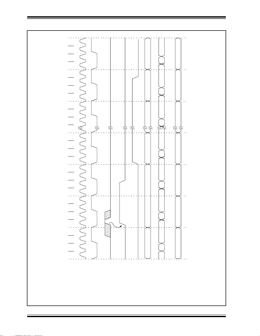
PIC17C7XX
FIGURE 6-7: INT PIN / T0CKI PIN INTERRUPT TIMING
PC + 1
YY YY + 1
Inst (YY + 1)
Addr
RETFIE
Addr
Inst (Vector)
Addr
Inst (PC+1)
Addr
Dummy
RETFIE
Fetched
Inst (PC) Dummy Dummy
Instruction
executed
Addr
PC PC + 1 Addr (Vector)
PC
PC Inst (PC) Inst (PC+1)
Instruction
System Bus
Q2Q1 Q3 Q4 Q2Q1 Q3 Q4 Q2Q1 Q3 Q4 Q2Q1 Q3 Q4 Q2Q1 Q3 Q4 Q2Q1 Q3 Q4 Q2Q1 Q3 Q4
OSC1
OSC2
DS30289A-page 38 1998 Microchip Technology Inc.
RA0/INT or
RA1/T0CKI
INTF or
T0CKIF
GLINTD
Page 39

PIC17C7XX
EXAMPLE 6-1: SAVING STATUS AND WREG IN RAM (SIMPLE)
; The addresses that are used to store the CPUSTA and WREG values must be in the data memory
; address range of 1Ah - 1Fh. Up to 6 locations can be saved and restored using the MOVFP
; instruction. This instruction neither affects the status bits, nor corrupts the WREG register.
;
UNBANK1 EQU 0x01A ; Address for 1st location to save
UNBANK2 EQU 0x01B ; Address for 2nd location to save
UNBANK3 EQU 0x01C ; Address for 3rd location to save
UNBANK4 EQU 0x01D ; Address for 4th location to save
UNBANK5 EQU 0x01E ; Address for 5th location to save
; (Label Not used in program)
UNBANK6 EQU 0x01F ; Address for 6th location to save
; (Label Not used in program)
;
: ; At Interrupt Vector Address
PUSH MOVFP ALUSTA, UNBANK1 ; Push ALUSTA value
MOVFP BSR, UNBANK2 ; Push BSR value
MOVFP WREG, UNBANK3 ; Push WREG value
MOVFP PCLATH, UNBANK4 ; Push PCLATH value
;
: ; Interrupt Service Routine (ISR) code
;
POP MOVFP UNBANK4, PCLATH ; Restore PCLATH value
MOVFP UNBANK3, WREG ; Restore WREG value
MOVFP UNBANK2, BSR ; Restore BSR value
MOVFP UNBANK1, ALUSTA ; Restore ALUSTA value
;
RETFIE ; Return from interrupt (enable interrupts)
1998 Microchip Technology Inc. DS30289A-page 39
Page 40

PIC17C7XX
EXAMPLE 6-2: SAVING STATUS AND WREG IN RAM (NESTED)
; The addresses that are used to store the CPUSTA and WREG values must be in the data memory
; address range of 1Ah - 1Fh. Up to 6 locations can be saved and restored using the MOVFP
; instruction. This instruction neither affects the status bits, nor corrupts the WREG register.
; This routine uses the FRS0, so it controls the FS1 and FS0 bits in the ALUSTA register.
;
Nobank_FSR EQU 0x40
Bank_FSR EQU 0x41
ALU_Temp EQU 0x42
WREG_TEMP EQU 0x43
BSR_S1 EQU 0x01A ; 1st location to save BSR
BSR_S2 EQU 0x01B ; 2nd location to save BSR (Label Not used in program)
BSR_S3 EQU 0x01C ; 3rd location to save BSR (Label Not used in program)
BSR_S4 EQU 0x01D ; 4th location to save BSR (Label Not used in program)
BSR_S5 EQU 0x01E ; 5th location to save BSR (Label Not used in program)
BSR_S6 EQU 0x01F ; 6th location to save BSR (Label Not used in program)
;
INITIALIZATION ;
CALL CLEAR_RAM ; Must Clear all Data RAM
;
INIT_POINTERS ; Must Initialize the pointers for POP and PUSH
CLRF BSR, F ; Set All banks to 0
CLRF ALUSTA, F ; FSR0 post increment
BSF ALUSTA, FS1
CLRF WREG, F ; Clear WREG
MOVLW BSR_S1 ; Load FSR0 with 1st address to save BSR
MOVWF FSR0
MOVWF Nobank_FSR
MOVLW 0x20
MOVWF Bank_FSR
:
: ; Your code
:
: ; At Interrupt Vector Address
PUSH BSF ALUSTA, FS0 ; FSR0 has auto-increment, does not affect status bits
BCF ALUSTA, FS1 ; does not affect status bits
MOVFP BSR, INDF0 ; No Status bits are affected
CLRF BSR, F ; Peripheral and Data RAM Bank 0 No Status bits are affected
MOVPF ALUSTA, ALU_Temp ;
MOVPF FSR0, Nobank_FSR ; Save the FSR for BSR values
MOVPF WREG, WREG_TEMP ;
MOVFP Bank_FSR, FSR0 ; Restore FSR value for other values
MOVFP ALU_Temp, INDF0 ; Push ALUSTA value
MOVFP WREG_TEMP, INDF0 ; Push WREG value
MOVFP PCLATH, INDF0 ; Push PCLATH value
MOVPF FSR0, Bank_FSR ; Restore FSR value for other values
MOVFP Nobank_FSR, FSR0 ;
;
: ; Interrupt Service Routine (ISR) code
;
POP CLRF ALUSTA, F ; FSR0 has auto-decrement, does not affect status bits
MOVFP Bank_FSR, FSR0 ; Restore FSR value for other values
DECF FSR0, F ;
MOVFP INDF0, PCLATH ; Pop PCLATH value
MOVFP INDF0, WREG ; Pop WREG value
BSF ALUSTA, FS1 ; FSR0 does not change
MOVPF INDF0, ALU_Temp ; Pop ALUSTA value
MOVPF FSR0, Bank_FSR ; Restore FSR value for other values
DECF Nobank_FSR, F ;
MOVFP Nobank_FSR, FSR0 ; Save the FSR for BSR values
MOVFP ALU_Temp, ALUSTA ;
MOVFP INDF0, BSR ; No Status bits are affected
;
RETFIE ; Return from interrupt (enable interrupts)
DS30289A-page 40 1998 Microchip Technology Inc.
Page 41

PIC17C7XX
7.0 MEMORY ORGANIZATION
There are two memory blocks in the PIC17C7XX; program memory and data memory. Each block has its
own bus, so that access to each block can occur during
the same oscillator cycle.
The data memory can further be broken down into
General Purpose RAM and the Special Function Registers (SFRs). The operation of the SFRs that control
the “core” are described here. The SFRs used to control the peripheral modules are described in the section
discussing each individual peripheral module.
7.1 Program Memory Organization
PIC17C7XX devices have a 16-bit program counter
capable of addressing a 64K x 16 program memory
space. The reset vector is at 0000h and the interrupt
vectors are at 0008h, 0010h, 0018h, and 0020h
(Figure 7-1).
7.1.1 PROGRAM MEMORY OPERATION
The PIC17C7XX can operate in one of four possible
program memory configurations. The configuration is
selected by configuration bits. The possible modes
are:
• Microprocessor
• Microcontroller
• Extended Microcontroller
• Protected Microcontroller
The microcontroller and protected microcontroller
modes only allow internal execution. Any access
beyond the program memory reads unknown data.
The protected microcontroller mode also enables the
code protection feature.
The extended microcontroller mode accesses both
the internal program memory as well as external program memory. Execution automatically switches
between internal and external memory. The 16-bits of
address allow a program memory range of 64K-words.
The microprocessor mode only accesses the exter-
nal program memory. The on-chip program memory is
ignored. The 16-bits of address allo w a prog ram memory range of 64K-words. Microprocessor mode is the
default mode of an unprogrammed device.
The different modes allow different access to the configuration bits, test memory, and boot ROM. Table 7-1
lists which modes can access which areas in memory.
Test Memory and Boot Memory are not required for
normal operation of the device. Care should be taken
to ensure that no unintended branches occur to these
areas.
FIGURE 7-1: PROGRAM MEMORY MAP
AND STACK
CALL, RETURN
RETFIE, RETLW
(1)
Space
User Memory
Space
Configuration Memory
Note 1: User memory space may be internal, external, or
both. The memory configuration depends on the
processor mode.
PC<15:0>
Stack Level 1
Stack Level 16
Reset Vector
INT Pin Interrupt Vector
Timer0 Interrupt Vector
T0CKI Pin Interrupt Vector
Peripheral Interrupt Vector
FOSC0
FOSC1
WDTPS0
WDTPS1
Reserved
Reserved
Reserved
BODEN
Test EPROM
Boot ROM
•
•
•
PM0
PM1
PM2
16
0000h
0008h
0010h
0018h
0020h
0021h
1FFFh
(PIC17C752
PIC17C762)
3FFFh
(PIC17C756A
PIC17C766)
FDFFh
FE00h
FE01h
FE02h
FE03h
FE04h
FE05h
FE06h
FE07h
FE08h
FE0Dh
FE0Eh
FE0Fh
FE10h
FF5Fh
FF60h
FFFFh
1998 Microchip Technology Inc. DS30289A-page 41
Page 42

PIC17C7XX
TABLE 7-1: MODE MEMORY ACCESS
The PIC17C7XX can operate in modes where the program memory is off-chip. They are the microprocessor
Operating
Mode
Internal
Program
Memory
Configuration Bits,
Test Memory,
Boot ROM
Microprocessor No Access No Access
Microcontroller Access Access
Extended
Microcontroller
Protected
Microcontroller
Access No Access
Access Access
and extended microcontroller modes. The microprocessor mode is the default for an unprogrammed
device.
Regardless of the processor mode, data memory is
always on-chip.
FIGURE 7-2: MEMORY MAP IN DIFFERENT MODES
External
Program
Memory
Extended
Microcontroller
Mode
01FFFh
PIC17C752/762
Microprocessor
Mode
0000h
External
Program
Memory
FFFFh
OFF-CHIP ON-CHIP OFF-CHIP ON-CHIP OFF-CHIP ON-CHIP
00h
2000h
FFFFh
120h
0000h
On-chip
Program
Memory
00h
120h
Microcontroller
Modes
0000h
01FFFh
2000h
FE00h
Test Memory
FFFFh
On-chip
Program
Memory
Config. Bits
Boot ROM
00h
120h
PROGRAM SPACEDATA SPACE
PIC17C756A/766
FFh 1FFh
ON-CHIP ON-CHIP ON-CHIP
0000h
External
Program
Memory
FFFFh
OFF-CHIP ON-CHIP OFF-CHIP ON-CHIP OFF-CHIP ON-CHIP
00h
120h
220h
FFh 1FFh
2FFh
ON-CHIP
320h
3FFh
4000h
FFFFh
External
Program
Memory
0000h
3FFFh
00h
120h
FFh 1FFh
FFh 1FFh
On-chip
Program
Memory
320h
220h
3FFh
2FFh
0000h
3FFFh
4000h
FE00h
FFFFh
00h
120h
FFh 1FFh
FFh 1FFh
On-chip
Program
Memory
Config. Bits
Test Memory
Boot ROM
320h
220h
3FFh
2FFh
ON-CHIPON-CHIP
PROGRAM SPACEDATA SPACE
DS30289A-page 42 1998 Microchip Technology Inc.
Page 43

PIC17C7XX
7.1.2 EXTERNAL MEMORY INTERFACE
When either microprocessor or extended microcontrol-
ler mode is selected, PORTC, PORTD and P ORTE are
configured as the system bus. P ORTC and PORTD are
the multiplexed address/data bus and PORTE<2:0> is
for the control signals. External components are
needed to demultiplex the address and data. This can
be done as shown in Figure 7-4. The waveforms of
address and data are shown in Figure 7-3. For complete timings, please refer to the electrical specification
section.
FIGURE 7-3: EXTERNAL PROGRAM
MEMORY ACCESS
WAVEFORMS
Q1 Q2 Q4Q3Q1 Q2 Q4
AD
<15:0>
Address out Data in
ALE
OE
'1'
WR
Q3
Read cycle
Address out
Write cycle
The system bus requires that there is no bus conflict
(minimal leakage), so the output value (address) will be
capacitively held at the desired value.
As the speed of the processor increases, external
EPROM memory with faster access time must be used.
Table 7-2 lists external memory speed requirements for
a given PIC17C7XX device frequency.
Q1
Data out
In extended microcontroller mode, when the device is
executing out of internal memory, the control signals
will continue to be active. That is, they indicate the
action that is occurring in the internal memory. The
external memory access is ignored.
This following selection is for use with Microchip
EPROMs. For interf acing to other manuf acturers memory, please refer to the electrical specifications of the
desired PIC17C7XX device, as well as the desired
memory device to ensure compatibility.
TABLE 7-2: EPROM MEMORY ACCESS
TIME ORDERING SUFFIX
PIC17C7XX
Oscillator
Frequency
8 MHz 500 ns -25
16 MHz 250 ns -15
20 MHz 200 ns -10
25 MHz 160 ns -70
33 MHz 121 ns (1)
Note 1: The access times for this requires the use of
The electrical specifications now include timing specifications for the memory interface with PIC17LCXXX
devices. These specifications reflect the capability of
the device by characterization. Please validate your
design with these timings.
Instruction
Cycle
Time (T
fast SRAMs.
CY) EPROM Suffix
FIGURE 7-4: TYPICAL EXTERNAL PROGRAM MEMORY CONNECTION DIAGRAM
AD15-AD0
(3)
Memory
AD7-AD0
373
A15-A0
(3)
PIC17CXXX
AD15-AD8
ALE
I/O(1)
OE
WR
Note 1: Use of I/O pins is only required for paged memory.
2: This signal is unused for ROM and EPROM devices.
3: 16-bit wide devices are now common and could be used instead of 8-bit wide devices.
1998 Microchip Technology Inc. DS30289A-page 43
373
(3)
138
(MSB)
Ax-A0
D7-D0
CE
WR WR
OE OE
(1)
Memory
(LSB)
Ax-A0
D7-D0
CE
(3)
(2)(2)
Page 44

PIC17C7XX
7.2 Data Memory Organization
Data memory is partitioned into two areas. The first is
the General Purpose Registers (GPR) area, and the
second is the Special Function Registers (SFR) area.
The SFRs control and provide status of device operation.
Portions of data memory are banked, this occurs in
both areas. The GPR area is banked to allow greater
than 232 bytes of general purpose RAM.
Banking requires the use of control bits for bank selection. These control bits are located in the Bank Select
Register (BSR). If an access is made to the unbanked
region, the BSR bits are ignored. Figure 7-5 shows the
data memory map organization.
Instructions MOVPF and MOVFP provide the means to
move values from the peripheral area (“P”) to any location in the register file (“F”), and vice-versa. The definition of the “P” range is from 0h to 1Fh, while the “F”
range is 0h to FFh. The “P” range has six more locations than peripheral registers which can be used as
General Purpose Registers. This can be useful in
some applications where variables need to be copied
to other locations in the general purpose RAM (such as
saving status information during an interrupt).
The entire data memory can be accessed either
directly or indirectly (through file select registers FSR0
and FSR1) (Section 7.4). Indirect addressing uses the
appropriate control bits of the BSR for accesses into
the banked areas of data memory. The BSR is
explained in greater detail in Section 7.8.
7.2.1 GENERAL PURPOSE REGISTER (GPR)
All devices have some amount of GPR area. The GPRs
are 8-bits wide. When the GPR area is greater than
232, it must be banked to allow access to the additional
memory space.
All the PIC17C7XX devices have banked memory in
the GPR area. To facilitate switching between these
banks, the MOVLR bank instruction has been added to
the instruction set. GPRs are not initialized by a
Power-on Reset and are unchanged on all other resets.
7.2.2 SPECIAL FUNCTION REGISTERS (SFR)
The SFRs are used by the CPU and peripheral func-
tions to control the operation of the device (Figure 7-5).
These registers are static RAM.
The SFRs can be classified into two sets, those associated with the “core” function and those related to the
peripheral functions. Those registers related to the
“core” are described here, while those related to a
peripheral feature are described in the section for each
peripheral feature.
The peripheral registers are in the banked portion of
memory, while the core registers are in the unbanked
region. To facilitate switching between the peripheral
banks, the MOVLB bank instruction has been provided.
DS30289A-page 44 1998 Microchip Technology Inc.
Page 45

FIGURE 7-5: PIC17C7XX REGISTER FILE MAP
Addr Unbanked
00h
01h
02h
03h
04h
05h
06h
07h
08h
09h
0Ah
0Bh
0Ch
0Dh
0Eh
0Fh
10h
11h
12h
13h
14h
15h
16h
17h
18h
19h
1Ah
1Fh
20h
INDF0
FSR0
PCL
PCLATH
ALUSTA
T0STA
CPUSTA
INTSTA
INDF1
FSR1
WREG
TMR0L
TMR0H
TBLPTRL
TBLPTRH
BSR
Bank 0 Bank 1
PORTA DDRC TMR1 PW1DCL PIR2 DDRF SSPADD PW3DCL DDRH
DDRB PORTC TMR2 PW2DCL PIE2 PORTF SSPCON1 PW3DCH PORTH
PORTB DDRD TMR3L PW1DCH
RCSTA1 PORTD TMR3H PW2DCH RCSTA2 PORTG SSPSTAT CA3H PORTJ
RCREG1 DDRE PR1 CA2L RCREG2 ADCON0 SSPBUF CA4L
TXSTA1 PORTE PR2 CA2H TXSTA2 ADCON1
TXREG1 PIR1 PR3L/CA1L TCON1 TXREG2 ADRESL
SPBRG1 PIE1 PR3H/CA1H TCON2 SPBRG2 ADRESH
Unbanked
PRODL
PRODH
General
Purpose
RAM
(2)
Bank 0
General
Purpose
RAM
Bank 1
General
Purpose
RAM
(1)
(2)
Bank 2
Bank 2
General
Purpose
RAM
(1)
(2, 3)
Bank 3
Bank 3
General
Purpose
RAM
(1)
(2, 3)
Bank 4
—
(1)
(1)
Bank 5
DDRG SSPCON2 CA3L DDRJ
PIC17C7XX
(1)
Bank 6
—
—
— — —
Bank 7
CA4H
TCON3
(1)
Bank 8
(1, 4)
—
—
—
FFh
Note 1: SFR file locations 10h - 17h are banked. The lower nibble of the BSR specifies the bank. All unbanked SFRs
ignore the Bank Select Register (BSR) bits.
2: General Purpose Registers (GPR) locations 20h - FFh, 120h - 1FFh, 220h - 2FFh, and 320h - 3FFh are
banked. The upper nibble of the BSR specifies this bank. All other GPRs ignore the Bank Select Register
(BSR) bits.
3: RAM bank 3 is not implemented on the PIC17C752 and the PIC17C762. Reading any unimplemented regis-
ter reads ‘0’s.
4: Bank 8 is only implemented on the PIC17C76X devices.
1998 Microchip Technology Inc. DS30289A-page 45
Page 46

PIC17C7XX
TABLE 7-3: SPECIAL FUNCTION REGISTERS
Address Name Bit 7 Bit 6 Bit 5 Bit 4 Bit 3 Bit 2 Bit 1 Bit 0
POR,
BOR
Unbanked
Value on
00h INDF0 Uses contents of FSR0 to address data memory (not a physical register) ---- ---- ---- ---01h FSR0 Indirect data memory address pointer 0 xxxx xxxx uuuu uuuu
02h PCL Low order 8-bits of PC 0000 0000 0000 0000
(1)
PCLATH Holding register for upper 8-bits of PC
03h
04h ALUSTA FS3 FS2 FS1 FS0 OV Z DC C 1111 xxxx 1111 uuuu
05h T0STA INTEDG T0SE T0CS T0PS3 T0PS2 T0PS1 T0PS0
(2)
CPUSTA
06h
07h INTSTA PEIF T0CKIF T0IF INTF PEIE T0CKIE T0IE INTE 0000 0000 0000 0000
08h INDF1 Uses contents of FSR1 to address data memory (not a physical register) ---- ---- ---- ---09h FSR1 Indirect data memory address pointer 1 xxxx xxxx uuuu uuuu
0Ah WREG Working register xxxx xxxx uuuu uuuu
0Bh TMR0L TMR0 register; low byte xxxx xxxx uuuu uuuu
0Ch TMR0H TMR0 register; high byte xxxx xxxx uuuu uuuu
0Dh TBLPTRL Low byte of program memory table pointer 0000 0000 0000 0000
0Eh TBLPTRH High byte of program memory table pointer 0000 0000 0000 0000
0Fh BSR Bank select register 0000 0000 0000 0000
— — STKAV GLINTD TO PD POR BOR --11 11qq --11 qquu
0000 0000 uuuu uuuu
— 0000 000- 0000 000-
Bank 0
PORTA
PORTB
(4,6)
(4)
RBPU
RB7/
SDO
10h
11h DDRB Data direction register for PORTB 1111 1111 1111 1111
12h
13h RCSTA1 SPEN RX9 SREN CREN
14h RCREG1 Serial port receive register xxxx xxxx uuuu uuuu
15h TXSTA1 CSRC TX9 TXEN SYNC
16h TXREG1 Serial Port Transmit Register (for USART1) xxxx xxxx uuuu uuuu
17h SPBRG1 Baud Rate Generator Register (for USART1) 0000 0000 0000 0000
—
RB6/
SCK
RA5/TX1/
CK1
RB5/
TCLK3
RA4/RX1/
DT1
RB4/
TCLK12
RA3/SDI/
SDA
RB3/
PWM2
— FERR OERR RX9D 0000 -00x 0000 -00u
— — TRMT TX9D 0000 --1x 0000 --1u
/
RA2/SS
RA1/T0CKI RA0/INT 0-xx 11xx 0-uu 11uu
SCL
RB2/
PWM1
RB1/
CAP2
RB0/
xxxx xxxx uuuu uuuu
CAP1
Bank 1
DDRC
PORTC
DDRD
PORTD
DDRE
PORTE
(5)
Data direction register for PORTC
RC7/
(4, 5)
(5)
Data direction register for PORTD
(4, 5)
(5)
Data direction register for PORTE
(4, 5)
RC6/
AD7
AD6
RD7/
RD6/
AD15
AD14
— — — —
RC5/
AD5
RD5/
AD13
RC4/
AD4
RD4/
AD12
RC3/
AD3
RD3/
AD11
RE3/
CAP4
RC2/
AD2
RD2/
AD10
RE2/WR
RC1/
AD1
RD1/
AD9
RE1/OE RE0/ALE ---- xxxx ---- uuuu
10h
11h
12h
13h
14h
15h
16h PIR1 RBIF TMR3IF TMR2IF TMR1IF CA2IF CA1IF TX1IF RC1IF x000 0010 u000 0010
17h PIE1 RBIE TMR3IE TMR2IE TMR1IE CA2IE CA1IE TX1IE RC1IE 0000 0000 0000 0000
1111 1111 1111 1111
RC0/
xxxx xxxx uuuu uuuu
AD0
1111 1111 1111 1111
RD0/
xxxx xxxx uuuu uuuu
AD8
---- 1111 ---- 1111
Legend: x = unknown, u = unchanged,- = unimplemented read as '0',q - value depends on condition.
Shaded cells are unimplemented, read as '0'.
Note1: The upper byte of the program counter is not directly accessible. PCLATH is a holding register for PC<15:8>
whose contents are updated from or transferred to the upper byte of the program counter.
2: The T
O and PD status bits in CPUSTA are not affected by a MCLR reset.
3: Bank 8 and associated registers are only implemented on the PIC17C76X devices.
4: This is the value that will be in the port output latch.
5: When the device is configured for microprocessor or extended microcontroller mode, the operation of this
port does not rely on these registers.
6: On any device reset, these pins are configured as inputs.
MCLR,
WDT
DS30289A-page 46 1998 Microchip Technology Inc.
Page 47

PIC17C7XX
TABLE 7-3: SPECIAL FUNCTION REGISTERS (Cont.’d)
Address Name Bit 7 Bit 6 Bit 5 Bit 4 Bit 3 Bit 2 Bit 1 Bit 0
POR,
BOR
Value on
Bank 2
10h TMR1 Timer1’s register xxxx xxxx uuuu uuuu
11h TMR2 Timer2’s register xxxx xxxx uuuu uuuu
12h TMR3L Timer3’s register; low byte xxxx xxxx uuuu uuuu
13h TMR3H Timer3’s register; high byte xxxx xxxx uuuu uuuu
14h PR1 Timer1’s period register xxxx xxxx uuuu uuuu
15h PR2 Timer2’s period register xxxx xxxx uuuu uuuu
16h PR3L/CA1L Timer3’s period register - low byte/capture1 register; low byte xxxx xxxx uuuu uuuu
17h PR3H/CA1H Timer3’s period register - high byte/capture1 register; high byte xxxx xxxx uuuu uuuu
Bank 3
10h PW1DCL DC1 DC0
11h PW2DCL DC1 DC0 TM2PW2
12h PW1DCH DC9 DC8 DC7 DC6 DC5 DC4 DC3 DC2 xxxx xxxx uuuu uuuu
13h PW2DCH DC9 DC8 DC7 DC6 DC5 DC4 DC3 DC2 xxxx xxxx uuuu uuuu
14h CA2L Capture2 low byte xxxx xxxx uuuu uuuu
15h CA2H Capture2 high byte xxxx xxxx uuuu uuuu
16h TCON1 CA2ED1 CA2ED0 CA1ED1 CA1ED0 T16 TMR3CS TMR2CS TMR1CS 0000 0000 0000 0000
17h
TCON2 CA2OVF CA1OVF PWM2ON PWM1ON CA1/PR3
Bank 4:
10h PIR2 SSPIF BCLIF ADIF — CA4IF CA3IF TX2IF RC2IF 000- 0010 000- 0010
11h PIE2 SSPIE BCLIE ADIE — CA4IE CA3IE TX2IE RC2IE 000- 0000 000- 0000
12h Unimple-
mented
13h RCSTA2 SPEN RX9 SREN CREN
14h RCREG2 Serial Port Receive Register for USART2 xxxx xxxx uuuu uuuu
15h TXSTA2 CSRC TX9 TXEN SYNC — — TRMT TX9D 0000 --1x 0000 --1u
16h TXREG2 Serial Port Transmit Register for USART2 xxxx xxxx uuuu uuuu
17h SPBRG2 Baud Rate Generator for USART2 0000 0000 0000 0000
Bank 5:
10h DDRF Data Direction Register for PORTF 1111 1111 1111 1111
11h PORTF
12h DDRG Data Direction Register for PORTG 1111 1111 1111 1111
13h PORTG
14h ADCON0 CHS3 CHS2 CHS1 CHS0
15h ADCON1 ADCS1 ADCS0 ADFM — PCFG3 PCFG2 PCFG1 PCFG0 000- 0000 000- 0000
16h ADRESL A/D Result Register low byte xxxx xxxx uuuu uuuu
17h ADRESH A/D Result Register high byte xxxx xxxx uuuu uuuu
— — — — — — — — ---- ---- ---- ----
(4)
RF7/
(4)
RG7/
TX2/CK2
AN11
RF6/
AN10
RG6/
RX2/DT2
— — — — — — xx-- ---- uu-- ----
RF5/
AN9
RG5/
PWM3
— — — — — xx0- ---- uu0- ----
TMR3ON TMR2ON TMR1ON 0000 0000 0000 0000
— FERR OERR RX9D 0000 -00x 0000 -00u
RF4/
RG4/
CAP3
AN8
RF3/
AN7
RG3/
AN0
RF2/
AN6
RG2/
AN1
— GO/DONE — ADON 0000 -0-0 0000 -0-0
RF1/
AN5
RG1/
AN2
RF0/
0000 0000 0000 0000
AN4
RG0/
xxxx 0000 uuuu 0000
AN3
Legend: x = unknown, u = unchanged,- = unimplemented read as '0',q - value depends on condition.
Shaded cells are unimplemented, read as '0'.
Note1: The upper byte of the program counter is not directly accessible. PCLATH is a holding register for PC<15:8>
whose contents are updated from or transferred to the upper byte of the program counter.
2: The T
O and PD status bits in CPUSTA are not affected by a MCLR reset.
3: Bank 8 and associated registers are only implemented on the PIC17C76X devices.
4: This is the value that will be in the port output latch.
5: When the device is configured for microprocessor or extended microcontroller mode, the operation of this
port does not rely on these registers.
6: On any device reset, these pins are configured as inputs.
MCLR,
WDT
1998 Microchip Technology Inc. DS30289A-page 47
Page 48

PIC17C7XX
TABLE 7-3: SPECIAL FUNCTION REGISTERS (Cont.’d)
Address Name Bit 7 Bit 6 Bit 5 Bit 4 Bit 3 Bit 2 Bit 1 Bit 0
POR,
BOR
Value on
Bank 6:
10h SSPADD SSP Address register in I2C slave mode. SSP baud rate reload register in I2C master mode. 0000 0000 0000 0000
11h SSPCON1 WCOL SSPOV SSPEN CKP SSPM3 SSPM2 SSPM1 SSPM0 0000 0000 0000 0000
12h SSPCON2 GCEN AKSTAT AKDT AKEN RCEN PEN RSEN SEN 0000 0000 0000 0000
13h SSPSTAT SMP CKE D/A
14h SSPBUF Synchronous Serial Port Receive Buffer/Transmit Register xxxx xxxx uuuu uuuu
15h Unimple-
mented
16h Unimple-
mented
17h Unimple-
mented
Bank 7:
10h PW3DCL DC1 DC0 TM2PW3
11h PW3DCH DC9 DC8 DC7 DC6 DC5 DC4 DC3 DC2 xxxx xxxx uuuu uuuu
12h CA3L Capture3 low byte xxxx xxxx uuuu uuuu
13h CA3H Capture3 high byte xxxx xxxx uuuu uuuu
14h CA4L Capture4 low byte xxxx xxxx uuuu uuuu
15h CA4H Capture4 high byte xxxx xxxx uuuu uuuu
16h TCON3 — CA4OVF CA3OVF CA4ED1 CA4ED0 CA3ED1 CA3ED0 PWM3ON -000 0000 -000 0000
17h Unimple-
mented
(3)
Bank 8:
(3)
10h
DDRH Data direction register for PORTH 1111 1111 1111 1111
(3)
11h
PORTH
(3)
DDRJ Data direction register for PORTJ 1111 1111 1111 1111
12h
(3)
13h
(3)
14h
(3)
15h
(3)
16h
(3)
17h
Unbanked
18h PRODL Low Byte of 16-bit Product (8 x 8 Hardware Multiply) xxxx xxxx uuuu uuuu
19h PRODH High Byte of 16-bit Product (8 x 8 Hardware Multiply) xxxx xxxx uuuu uuuu
PORTJ
Unimple-
mented
Unimple-
mented
Unimple-
mented
Unimple-
mented
(4)
— — — — — — — — ---- ---- ---- ----
— — — — — — — — ---- ---- ---- ----
— — — — — — — — ---- ---- ---- ----
— — — — — — — — ---- ---- ---- ----
(4)
RH7/
RJ7 RJ6 RJ5 RJ4 RJ3 RJ2 RJ1 RJ0 xxxx xxxx uuuu uuuu
RH6/
AN15
AN14
— — — — — — — — ---- ---- ---- ----
— — — — — — — — ---- ---- ---- ----
— — — — — — — — ---- ---- ---- ----
— — — — — — — — ---- ---- ---- ----
RH5/
AN13
P S R/W UA BF 0000 0000 0000 0000
- - - - - xx0- ---- uu0- ----
RH4/
AN12
RH3 RH2 RH1 RH0 xxxx xxxx uuuu uuuu
Legend: x = unknown, u = unchanged,- = unimplemented read as '0',q - value depends on condition.
Shaded cells are unimplemented, read as '0'.
Note1: The upper byte of the program counter is not directly accessible. PCLATH is a holding register for PC<15:8>
whose contents are updated from or transferred to the upper byte of the program counter.
2: The T
O and PD status bits in CPUSTA are not affected by a MCLR reset.
3: Bank 8 and associated registers are only implemented on the PIC17C76X devices.
4: This is the value that will be in the port output latch.
5: When the device is configured for microprocessor or extended microcontroller mode, the operation of this
port does not rely on these registers.
6: On any device reset, these pins are configured as inputs.
MCLR,
WDT
DS30289A-page 48 1998 Microchip Technology Inc.
Page 49

PIC17C7XX
7.2.2.1 ALU STATUS REGISTER (ALUSTA)
The ALUSTA register contains the status bits of the
Arithmetic and Logic Unit and the mode control bits for
the indirect addressing register.
As with all the other registers, the ALUSTA register can
be the destination for any instruction. If the ALUSTA
register is the destination for an instruction that affects
the Z, DC, C, or OV bits, then the write to these three
bits is disabled. These bits are set or cleared according
to the device logic. Therefore, the result of an instruction with the ALUSTA register as destination may be
different than intended.
For example, the CLRF ALUSTA, F instruction will clear
the upper four bits and set the Z bit. This leaves the
ALUST A register as 0000u1uu (where u = unchanged).
It is recommended, therefore, that only BCF, BSF , SWAPF
and MOVWF instructions be used to alter the ALUSTA
register because these instructions do not affect any
status bits. To see how other instructions affect the status bits, see the “Instruction Set Summary.”
Note 1: The C and DC bits operate as a borrow
and digit borrow bit, respectively, in subtraction. See the SUBLW and SUBWF
instructions for examples.
Note 2: The overflow bit will be set if the 2’s com-
plement result exceeds +127 or is less
than -128.
The Arithmetic and Logic Unit (ALU) is capable of carrying out arithmetic or logical operations on two operands or a single operand. All single operand
instructions operate either on the WREG register or the
given file register. For two operand instructions, one of
the operands is the WREG register and the other is
either a file register or an 8-bit immediate constant.
FIGURE 7-6: ALUSTA REGISTER (ADDRESS: 04h, UNBANKED)
R/W - 1 R/W - 1 R/W - 1 R/W - 1 R/W - x R/W - x R/W - x R/W - x
FS3 FS2 FS1 FS0 OV Z DC C
bit7 bit0
bit 7-6: FS3:FS2: FSR1 Mode Select bits
00 = Post auto-decrement FSR1 value
01 = Post auto-increment FSR1 value
1x = FSR1 value does not change
bit 5-4: FS1:FS0: FSR0 Mode Select bits
00 = Post auto-decrement FSR0 value
01 = Post auto-increment FSR0 value
1x = FSR0 value does not change
bit 3: OV: Overflow bit
This bit is used for signed arithmetic (2’s complement). It indicates an overflow of the 7-bit magnitude,
which causes the sign bit (bit7) to change state.
1 =Overflow occurred for signed arithmetic, (in this arithmetic operation)
0 =No overflow occurred
bit 2: Z: Zero bit
1 =The result of an arithmetic or logic operation is zero
0 =The results of an arithmetic or logic operation is not zero
bit 1: DC: Digit carry/borro
For ADDWF and ADDLW instructions.
1 =A carry-out from the 4th low order bit of the result occurred
0 =No carry-out from the 4th low order bit of the result
Note: For borrow the polarity is reversed.
bit 0: C: carry/borro
For ADDWF and ADDLW instructions. Note that a subtraction is executed by adding the two’s complement
of the second operand.
For rotate (RRCF, RLCF) instructions, this bit is loaded with either the high or low order bit of the source
register.
1 =A carry-out from the most significant bit of the result occurred
0 =No carry-out from the most significant bit of the result
Note: For borrow the polarity is reversed.
w bit
w bit
R = Readable bit
W = Writable bit
-n = Value at POR reset
(x = unknown)
1998 Microchip Technology Inc. DS30289A-page 49
Page 50

PIC17C7XX
7.2.2.2 CPU STATUS REGISTER (CPUSTA)
The CPUSTA register contains the status and control
bits for the CPU. This register has a bit that is used to
globally enable/disable interrupts. If only a specific
interrupt is desired to be enabled/disabled, please refer
to the INTerrupt STAtus (INTSTA) register and the
Peripheral Interrupt Enable (PIE) registers. The
CPUSTA register also indicates if the stack is available
and contains the Power-down (PD
bits. The T
These bits are set and cleared according to device
logic. Therefore, the result of an instruction with the
CPUSTA register as destination may be different than
intended.
O, PD, and STKAV bits are not writable.
) and Time-out (TO)
The POR
Power-on Reset, external MCLR
Reset. The BOR
occurred.
bit allows the differentiation between a
bit indicates if a Brown-out Reset
Note 1: The BOR status bit is a don’t care and is
not necessarily predictable if the
brown-out circuit is disabled (when the
BODEN bit in the Configuration word is
programmed).
FIGURE 7-7: CPUSTA REGISTER (ADDRESS: 06h, UNBANKED)
U - 0 U - 0 R - 1 R/W - 1 R - 1 R - 1 R/W - 0 R/W - 1
— — STKAV GLINTD TO PD POR BOR
bit7 bit0
bit 7-6: Unimplemented: Read as '0'
bit 5: STKAV: Stack Available bit
bit 4: GLINTD: Global Interrupt Disable bit
bit 3: T
bit 2: PD
bit 1: POR
bit 0: BOR
This bit indicates that the 4-bit stack pointer value is Fh, or has rolled over from Fh → 0h (stack o verflo w).
1 =Stack is available
0 =Stack is full, or a stack overflow may have occurred (Once this bit has been cleared by a
stack overflow, only a device reset will set this bit)
This bit disables all interrupts. When enabling interrupts, only the sources with their enable bits set can
cause an interrupt.
1 =Disable all interrupts
0 =Enables all un-masked interrupts
O: WDT Time-out Status bit
1 =After power-up or by a CLRWDT instruction
0 =A Watchdog Timer time-out occurred
: Power-down Status bit
1 =After power-up or by the CLRWDT instruction
0 =By execution of the SLEEP instruction
: Power-on Reset Status bit
1 =No Power-on Reset occurred
0 =A Power-on Reset occurred (must be set by software)
: Brown-out Reset Status bit
When BODEN confi
1 =No Brown-out Reset occurred
0 =A Brown-out Reset occurred (must be set by software)
When BODEN confi
Don’t care
guration bit is set (enabled):
guration bit is clear (disabled):
reset, or a WDT
R = Readable bit
W = Writable bit
U = Unimplemented bit,
Read as ‘0’
- n = Value at POR reset
DS30289A-page 50 1998 Microchip Technology Inc.
Page 51

PIC17C7XX
7.2.2.3 TMR0 STATUS/CONTROL REGISTER
This register contains various control bits. Bit7
(INTEDG) is used to control the edge upon which a signal on the RA0/INT pin will set the RA0/INT interrupt
flag. The other bits configure Timer0, it’s prescaler and
clock source.
(T0STA)
FIGURE 7-8: T0STA REGISTER (ADDRESS: 05h, UNBANKED)
R/W - 0 R/W - 0 R/W - 0 R/W - 0 R/W - 0 R/W - 0 R/W - 0 U - 0
INTEDG T0SE T0CS T0PS3 T0PS2 T0PS1 T0PS0
bit7 bit0
bit 7: INTEDG: RA0/INT Pin Interrupt Edge Select bit
This bit selects the edge upon which the interrupt is detected.
1 =Rising edge of RA0/INT pin generates interrupt
0 =Falling edge of RA0/INT pin generates interrupt
bit 6: T0SE: Timer0 External Clock Input Edge Select bit
This bit selects the edge upon which TMR0 will increment.
When
T0CS = 0 (External Clock)
1 =Rising edge of RA1/T0CKI pin increments TMR0 and/or sets the T0CKIF bit
0 =Falling edge of RA1/T0CKI pin increments TMR0 and/or sets a T0CKIF bit
When
T0CS = 1 (Internal Clock)
Don’t care
bit 5: T0CS: Timer0 Clock Source Select bit
This bit selects the clock source for Timer0.
1 =Internal instruction clock cycle (T
0 =External clock input on the T0CKI pin
bit 4-1: T0PS3:T0PS0: Timer0 Prescale Selection bits
These bits select the prescale value for Timer0.
T0PS3:T0PS0 Prescale Value
0000
0001
0010
0011
0100
0101
0110
0111
1xxx
1:1
1:2
1:4
1:8
1:16
1:32
1:64
1:128
1:256
CY)
—
R = Readable bit
W = Writable bit
U = Unimplemented,
reads as ‘0’
-n = Value at POR reset
bit 0: Unimplemented: Read as '0'
1998 Microchip Technology Inc. DS30289A-page 51
Page 52

PIC17C7XX
7.3 Stack Operation
PIC17C7XX devices have a 16 x 16-bit hardware stac k
(Figure 7-1). The stack is not part of either the program
or data memory space, and the stack pointer is neither
readable nor writable. The PC (Program Counter) is
“PUSHed” onto the stack when a CALL or LCALL
instruction is executed or an interrupt is acknowledged.
The stack is “POPed” in the event of a RETURN, RETLW,
or a RETFIE instruction execution. PCLATH is not
affected by a “PUSH” or a “POP” operation.
The stack operates as a circular buffer, with the stack
pointer initialized to '0' after all resets. There is a stack
available bit (STKAV) to allow software to ensure that
the stack will not overflow. The STKAV bit is set after a
device reset. When the stack pointer equals Fh, STKA V
is cleared. When the stack pointer rolls over from Fh to
0h, the STKAV bit will be held clear until a de vice reset.
Note 1: There is not a status bit for stack under-
flow. The STKAV bit can be used to detect
the underflow which results in the stack
pointer being at the top of stack.
Note 2: There are no instruction mnemonics
called PUSH or POP. These are actions
that occur from the execution of the CALL,
RETURN, RETLW, and RETFIE instructions, or the vectoring to an interrupt vector.
Note 3: After a reset, if a “POP” operation occurs
before a “PUSH” operation, the STKAV bit
will be cleared. This will appear as if the
stack is full (underflow has occurred). If a
“PUSH” operation occurs next (before
another “POP”), the STKAV bit will be
locked clear. Only a device reset will
cause this bit to set.
After the device is “PUSHed” sixteen times (without a
“POP”), the seventeenth push overwrites the value
from the first push. The eighteenth push ov erwrites the
second push (and so on).
DS30289A-page 52 1998 Microchip Technology Inc.
Page 53
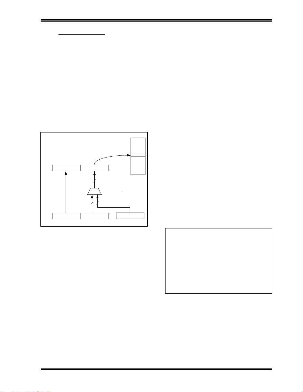
PIC17C7XX
7.4 Indirect Addressing
Indirect addressing is a mode of addressing data
memory where the data memory address in the
instruction is not fixed. That is, the register that is to
be read or written can be modified by the program.
This can be useful for data tables in the data memory.
Figure 7-9 shows the operation of indirect addressing.
This depicts the moving of the value to the data memory address specified by the value of the FSR register.
Example 7-1 shows the use of indirect addressing to
clear RAM in a minimum number of instructions. A
similar concept could be used to move a defined number of bytes (block) of data to the USART transmit register (TXREG). The starting address of the block of
data to be transmitted could easily be modified by the
program.
FIGURE 7-9: INDIRECT ADDRESSING
RAM
Instruction
Executed
Opcode Address
8
File = INDFx
8
Instruction
Fetched
Opcode
8
File
FSR
7.4.2 INDIRECT ADDRESSING OPERATION
The indirect addressing capability has been enhanced
over that of the PIC16CXX family. There are two control bits associated with each FSR register. These two
bits configure the FSR register to:
• Auto-decrement the value (address) in the FSR
after an indirect access
• Auto-increment the value (address) in the FSR
after an indirect access
• No change to the value (address) in the FSR after
an indirect access
These control bits are located in the ALUSTA register.
The FSR1 register is controlled by the FS3:FS2 bits
and FSR0 is controlled by the FS1:FS0 bits.
When using the auto-increment or auto-decrement
features, the effect on the FSR is not reflected in the
ALUSTA register. For example, if the indirect address
causes the FSR to equal '0', the Z bit will not be set.
If the FSR register contains a value of 0h, an indirect
read will read 0h (Zero bit is set) while an indirect write
will be equivalent to a NOP (status bits are not
affected).
Indirect addressing allows single cycle data transfers
within the entire data space. This is possible with the
use of the MOVPF and MOVFP instructions, where either
'p' or 'f' is specified as INDF0 (or INDF1).
If the source or destination of the indirect address is in
banked memory, the location accessed will be determined by the value in the BSR.
A simple program to clear RAM from 20h - FFh is
shown in Example 7-1.
EXAMPLE 7-1: INDIRECT ADDRESSING
7.4.1 INDIRECT ADDRESSING REGISTERS
The PIC17C7XX has four registers for indirect
addressing. These registers are:
• INDF0 and FSR0
• INDF1 and FSR1
Registers INDF0 and INDF1 are not physically imple-
mented. Reading or writing to these registers activates indirect addressing, with the value in the
corresponding FSR register being the address of the
data. The FSR is an 8-bit register and allows address-
MOVLW 0x20 ;
MOVWF FSR0 ; FSR0 = 20h
BCF ALUSTA, FS1 ; Increment FSR
BSF ALUSTA, FS0 ; after access
BCF ALUSTA, C ; C = 0
MOVLW END_RAM + 1 ;
LP CLRF INDF0, F ; Addr(FSR) = 0
CPFSEQ FSR0 ; FSR0 = END_RAM+1?
GOTO LP ; NO, clear next
: ; YES, All RAM is
: ; cleared
ing anywhere in the 256-byte data memory address
range. For banked memory, the bank of memory
accessed is specified by the value in the BSR.
If file INDF0 (or INDF1) itself is read indirectly via an
FSR, all '0's are read (Zero bit is set). Similarly, if
INDF0 (or INDF1) is written to indirectly, the operation
will be equivalent to a NOP, and the status bits are not
affected.
1998 Microchip Technology Inc. DS30289A-page 53
Page 54

PIC17C7XX
7.5 Table Pointer (TBLPTRL and
TBLPTRH)
File registers TBLPTRL and TBLPTRH form a 16-bit
pointer to address the 64K program memory space.
The table pointer is used by instructions TABLWT and
TABLRD.
The TABLRD and the TABLWT instructions allow transfer
of data between program and data space. The table
pointer serves as the 16-bit address of the data word
within the program memory. For a more complete
description of these registers and the operation of Table
Reads and Table Writes, see Section 8.0.
7.6 Table Latch (TBLATH, TBLATL)
The table latch (TBLAT) is a 16-bit register, with
TBLATH and TBLATL referring to the high and low
bytes of the register. It is not mapped into data or program memory. The table latch is used as a temporary
holding latch during data transfer between program
and data memory (see TABLRD, TABLWT, TLRD and
TLWT instruction descriptions). For a more complete
description of these registers and the operation of Table
Reads and Table Writes, see Section 8.0.
DS30289A-page 54 1998 Microchip Technology Inc.
Page 55

PIC17C7XX
7.7 Program Counter Module
The Program Counter (PC) is a 16-bit register. PCL, the
low byte of the PC, is mapped in the data memory . PCL
is readable and writable just as is any other register.
PCH is the high byte of the PC and is not directly
addressable. Since PCH is not mapped in data or program memory, an 8-bit register PCLATH (PC high
latch) is used as a holding latch for the high byte of the
PC. PCLATH is mapped into data memory. The user
can read or write PCH through PCLATH.
The 16-bit wide PC is incremented after each instruction fetch during Q1 unless:
• Modified by a GOTO, CALL, LCALL, RETURN, RETLW ,
or RETFIE instruction
• Modified by an interrupt response
• Due to destination write to PCL by an instruction
“Skips” are equivalent to a forced NOP cycle at the
skipped address.
Figure 7-10 and Figure 7-11 show the operation of the
program counter for various situations.
FIGURE 7-10: PROGRAM COUNTER
OPERATION
Internal data bus <8>
8
PCLATH
8
PCH PCL
8
FIGURE 7-11: PROGRAM COUNTER USING
THE CALL AND GOTO
INSTRUCTIONS
12 8 7 0
1315
From Instruction
3
5
4
PCLATH
8
PCH
5
0
87
8
PCL
PC<15:13>
7
15 0
Using Figure 7-10, the operations of the PC and
PCLATH for different instructions are as follows:
a) LCALL
instructions:
An 8-bit destination address is provided in the
instruction (opcode). PCLATH is unchanged.
PCLATH → PCH
Opcode<7:0> → PCL
b) Read instr
uctions on PCL:
Any instruction that reads PCL.
PCL → data bus → ALU or destination
PCH → PCLATH
c) Wr
ite instructions on PCL:
Any instruction that writes to PCL.
8-bit data → data bus → PCL
PCLATH → PCH
d) Read-Modify-Wr
ite instructions on PCL:
Any instruction that does a read-write-modify
operation on PCL, such as ADDWF PCL.
Read: PCL → data bus → ALU
Write: 8-bit result → data bus → PCL
PCLATH → PCH
e) RETURN
instruction:
Stack<MRU> → PC<15:0>
Using Figure 7-11, the operation of the PC and
PCLATH for GOTO and CALL instructions is as follows:
CALL, GOTO instructions:
A 13-bit destination address is provided in the
instruction (opcode).
Opcode<12:0> → PC<12:0>
PC<15:13> → PCLATH<7:5>
Opcode<12:8> → PCLATH<4:0>
The read-modify-write only affects the PCL with the
result. PCH is loaded with the value in the PCLATH.
For example, ADDWF PCL will result in a jump within the
current page. If PC = 03F0h, WREG = 30h and
PCLA TH = 03h bef ore instruction, PC = 0320h after the
instruction. To accomplish a true 16-bit computed
jump, the user needs to compute the 16-bit destination
address, write the high byte to PCLATH and then write
the low value to PCL.
The following PC related operations do not change
PCLATH:
a) LCALL, RETLW, and RETFIE instructions.
b) Interrupt vector is forced onto the PC.
c) Read-modify-write instructions on PCL
(e.g. BSF PCL).
1998 Microchip Technology Inc. DS30289A-page 55
Page 56
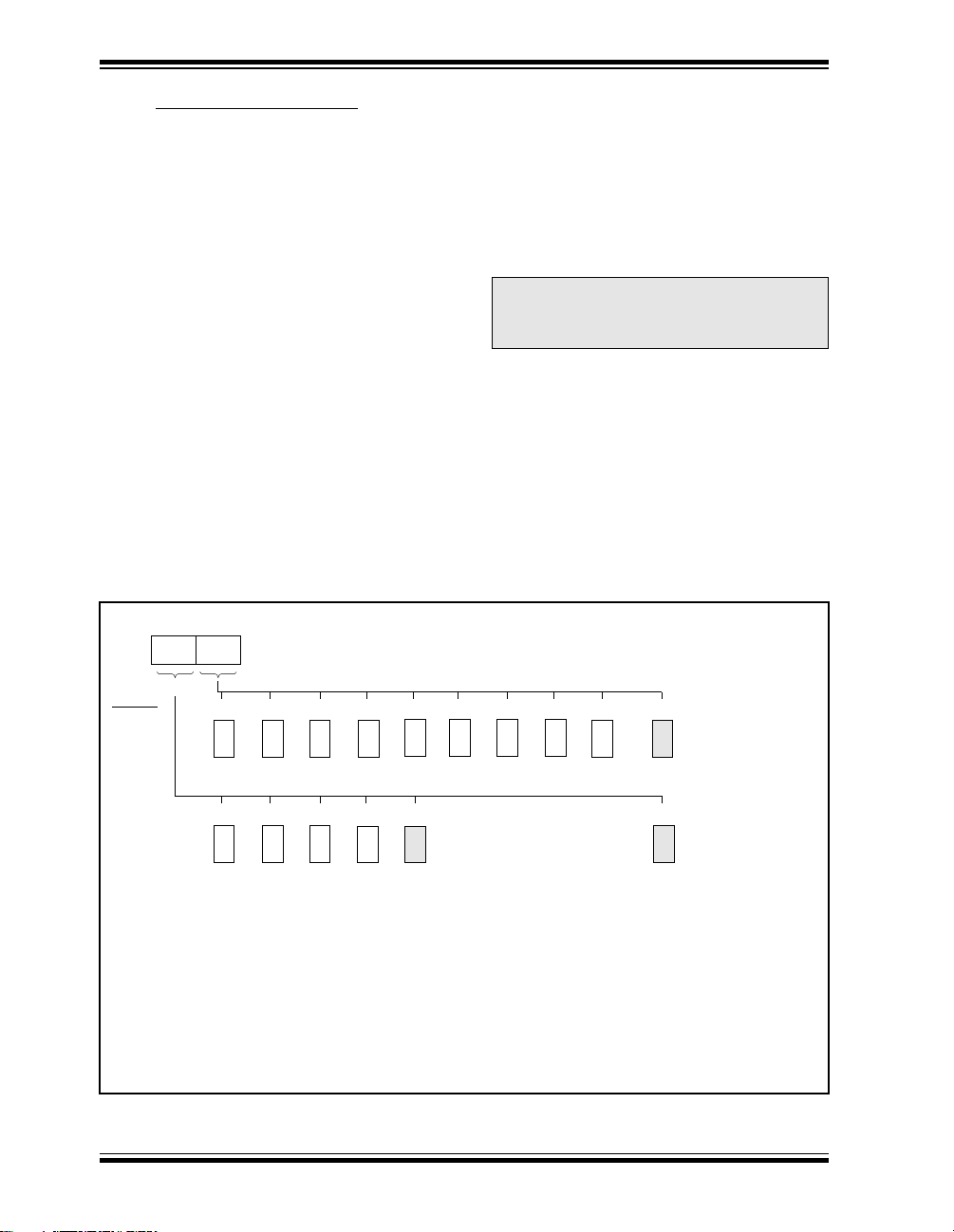
PIC17C7XX
7.8 Bank Select Register (BSR)
The BSR is used to switch between banks in the data
memory area (Figure 7-12). In the PIC17C7XX
devices, the entire byte is implemented. The lower nibble is used to select the peripheral register bank. The
upper nibble is used to select the general purpose
memory bank.
All the Special Function Registers (SFRs) are mapped
into the data memory space. In order to accommodate
the large number of registers, a banking scheme has
been used. A segment of the SFRs, from address 10h
to address 17h, is banked. The lower nibble of the bank
select register (BSR) selects the currently active
“peripheral bank.” Effort has been made to group the
peripheral registers of related functionality in one bank.
However , it will still be necessary to switch from bank to
bank in order to address all peripherals related to a single task. To assist this, a MOVLB bank instruction has
been included in the instruction set.
FIGURE 7-12: BSR OPERATION
BSR
7430
(2)
(1)
The need for a large general purpose memory space
dictated a general purpose RAM banking scheme. The
upper nibble of the BSR selects the currently active
general purpose RAM bank. To assist this, a MOVLR
bank instruction has been provided in the instruction
set.
If the currently selected bank is not implemented (such
as Bank 13), any read will read all '0's. Any write is
completed to the bit bucket and the ALU status bits will
be set/cleared as appropriate.
Note: Registers in Bank 15 in the Special Func-
tion Register area, are reserved for
Microchip use. Reading of registers in this
bank may cause random values to be read.
Address
Range
10h
17h
20h
FFh
0 123 8 15
Bank 3Bank 2Bank 1Bank 0
012
Bank 2Bank 1Bank 0
Bank 3
4 56 7
3
4
Bank 4
• • •
(Peripheral)
• • •
Bank 7Bank 6Bank 5Bank 4
Bank 15Bank 8
Bank 15
SFR
Banks
15
GPR
Banks
(RAM)
Note 1: For the SFRs only Banks 0 through 8 are implemented. Selection of an unimplemented bank is not recom-
mended. Bank 15 is reserved f or Micr ochip use, reading of register s in this bank ma y cause random
values to be read.
2: For the GPRs, bank 3 is unimplemented on the PIC17C752 and the PIC17C762. Selection of an unimple-
mented bank is not recommended.
3: SFR Bank 8 is only implemented on the PIC17C76X.
DS30289A-page 56 1998 Microchip Technology Inc.
Page 57
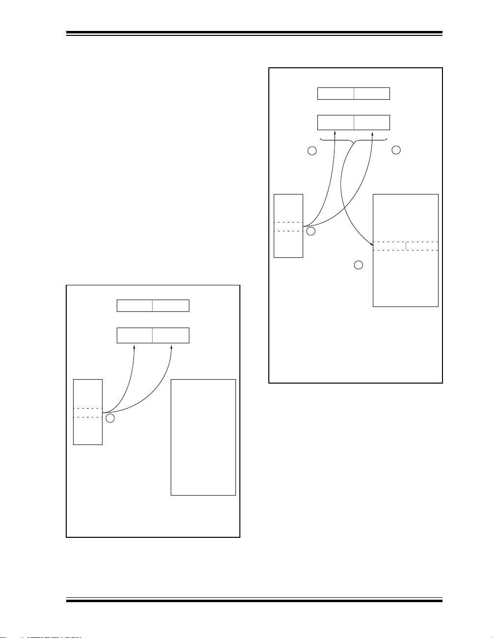
PIC17C7XX
8.0 TABLE READS AND TABLE WRITES
The PIC17C7XX has four instructions that allow the
processor to move data from the data memory space
to the program memory space, and vice versa. Since
the program memory space is 16-bits wide and the
data memory space is 8-bits wide, two operations are
required to move 16-bit values to/from the data memory.
The TLWT t,f and TABLWT t,i,f instructions are
used to write data from the data memory space to the
program memory space. The TLRD t,f and
TABLRD t,i,f instructions are used to write data
from the program memory space to the data memory
space.
The program memory can be internal or external. For
the program memory access to be external, the device
needs to be operating in microprocessor or extended
microcontroller mode.
Figure 8-1 through Figure 8-4 show the operation of
these four instructions. The steps show the sequence
of operation.
FIGURE 8-1: TLWT INSTRUCTION
Data
Memory
OPERATION
TABLE POINTER
TBLPTRH
TABLE LATCH (16-bit)
TABLATH TABLATL
TLWT 1,f TLWT 0,f
TBLPTRL
Program Memory
FIGURE 8-2: TABLWT INSTRUCTION
OPERATION
TABLE POINTER
TBLPTRH
TABLE LATCH (16-bit)
TABLATH TABLATL
3
TABLWT 1,i,f TABLWT 0,i,f
Data
Memory
f
1
Step 1: 8-bit value, from register 'f', loaded into the
high or low byte in TABLAT (16-bit).
2: 16-bit TABLAT value written to address Pro-
gram Memory (TBLPTR).
3: If “i” = 1, then TBLPTR = TBLPTR + 1,
If “i” = 0, then TBLPTR is unchanged.
TBLPTRL
Prog-Mem
(TBLPTR)
2
3
Program Memory
f
1
Step 1: 8-bit value, from register 'f', loaded into the
high or low byte in TABLAT (16-bit).
1998 Microchip Technology Inc. DS30289A-page 57
Page 58

PIC17C7XX
FIGURE 8-3: TLRD INSTRUCTION
OPERATION
TABLE POINTER
TBLPTRH TBLPTRL
TABLE LATCH (16-bit)
TABLATH TABLATL
TLRD 1,f
Data
Memory
f
1
Step 1: 8-bit value, from TABLAT (16-bit) high or
low byte, loaded into register 'f'.
TLRD 0,f
Program Memory
FIGURE 8-4: TABLRD INSTRUCTION
OPERATION
TABLE POINTER
TBLPTRH
TABLE LATCH (16-bit)
TABLATH TABLATL
3
TABLRD 1,i,f
Data
Memory
f
1
Step 1: 8-bit value, from TABLAT (16-bit) high or
low byte, loaded into register 'f'.
2: 16-bit value at Program Memory (TBLPTR)
loaded into TABLAT register.
3: If “i” = 1, then TBLPTR = TBLPTR + 1,
If “i” = 0, then TBLPTR is unchanged.
TBLPTRL
Prog-Mem
(TBLPTR)
2
3
TABLRD 0,i,f
Program Memory
DS30289A-page 58 1998 Microchip Technology Inc.
Page 59

PIC17C7XX
8.1 Table Writes to Internal Memory
A table write operation to internal memory causes a
long write operation. The long write is necessary for
programming the internal EPROM. Instruction execution is halted while in a long write cycle. The long write
will be terminated by any enabled interrupt. To ensure
that the EPROM location has been well programmed,
a minimum programming time is required (see specification #D114). Having only one interrupt enabled to
terminate the long write ensures that no unintentional
interrupts will prematurely terminate the long write.
The sequence of events for programming an internal
program memory location should be:
1. Disable all interrupt sources, except the source
to terminate EPROM program write.
2. Raise MCLR
age.
3. Clear the WDT.
4. Do the table write. The interrupt will terminate
the long write.
5. Verify the memory location (table read).
Note 1: Programming requirements must be
Note 2: If the V
/VPP pin to the programming volt-
met. See timing specification in electrical
specifications for the desired device.
Violating these specifications (including
temperature) may result in EPROM locations that are not fully programmed and
may lose their state over time.
PP requirement is not met, the
table write is a 2 cycle write and the program memory is unchanged.
8.1.1 TERMINATING LONG WRITES
An interrupt source or reset are the only events that
terminate a long write operation. Terminating the long
write from an interrupt source requires that the interrupt enable and flag bits are set. The GLINTD bit only
enables the vectoring to the interrupt address.
If the T0CKI, RA0/INT, or TMR0 interrupt source is
used to terminate the long write; the interrupt flag, of
the highest priority enabled interrupt, will terminate the
long write and automatically be cleared.
Note 1: If an interrupt is pending, the TABLWT is
aborted (an NOP is executed). The
highest priority pending interrupt, from
the T0CKI, RA0/INT, or TMR0 sources
that is enabled, has its flag cleared.
Note 2: If the interrupt is not being used for the
program write timing, the interrupt
should be disabled. This will ensure that
the interrupt is not lost, nor will it terminate the long write prematurely.
If a peripheral interrupt source is used to terminate the
long write, the interrupt enable and flag bits must be
set. The interrupt flag will not be automatically cleared
upon the vectoring to the interrupt vector address.
The GLINTD bit determines whether the program will
branch to the interrupt vector when the long write is
terminated. If GLINTD is clear, the program will vector, if GLINTD is set, the program will not vector to the
interrupt address.
TABLE 8-1: INTERRUPT - TABLE WRITE INTERACTION
Interrupt
Source
RA0/INT,
TMR0,
T0CKI
Peripheral 0
1998 Microchip Technology Inc. DS30289A-page 59
GLINTD
0
0
1
1
0
1
1
Enable
Bit
1
1
0
1
1
1
0
1
Flag
Bit
1
0
x
1
1
0
x
1
Action
Terminate long table write (to internal program memory),
branch to interrupt vector (branch clears flag bit).
None
None
Terminate long table write, do not branch to interrupt vector (flag is automatically cleared).
Terminate long table write, branch to interrupt vector.
None
None
Terminate table write, do not branch to interrupt vector
(flag remains set).
Page 60

PIC17C7XX
8.2 Table Writes to External Memory
Table writes to external memory are always two-cycle
instructions. The second cycle writes the data to the
external memory location. The sequence of events for
an external memory write are the same for an internal
write.
8.2.2 TABLE WRITE CODE
The “i” operand of the TABLWT instruction can specify
that the value in the 16-bit TBLPTR register is automatically incremented (for the next write). In
Example 8-1, the TBLPTR register is not automatically
incremented.
EXAMPLE 8-1: TABLE WRITE
Note: If an interrupt is pending or occurs during
the TABLWT, the two cycle table write
completes. The RA0/INT, TMR0, or
T0CKI interrupt flag is automatically
cleared or the pending peripheral interrupt is acknowledged.
CLRWDT ; Clear WDT
MOVLW HIGH (TBL_ADDR) ; Load the Table
MOVWF TBLPTRH ; address
MOVLW LOW (TBL_ADDR) ;
MOVWF TBLPTRL ;
MOVLW HIGH (DATA) ; Load HI byte
TLWT 1, WREG ; in TABLATH
MOVLW LOW (DATA) ; Load LO byte
TABLWT 0,0,WREG ; in TABLATL
; and write to
; program memory
; (Ext. SRAM)
FIGURE 8-5: TABLWT WRITE TIMING (EXTERNAL MEMORY)
Q1 Q2 Q3 Q4 Q1 Q2 Q3 Q4 Q1 Q2 Q3 Q4 Q1 Q2 Q3 Q4
AD15:AD0
PC PC+1 TBL PC+2Data out
Instruction
fetched
Instruction
executed
ALE
OE
WR
Note: If external write, and GLINTD = '1', and Enable bit = '1', then when '1' → Flag bit, Do table write.
The highest pending interrupt is cleared.
DS30289A-page 60 1998 Microchip Technology Inc.
TABLWT
INST (PC-1)
'1'
INST (PC+1)
TABLWT cycle1 TABLWT cycle2
Data write cycle
INST (PC+2)
INST (PC+1)
Page 61

PIC17C7XX
FIGURE 8-6: CONSECUTIVE TABLWT WRITE TIMING (EXTERNAL MEMORY)
Q1 Q2 Q3 Q4 Q1 Q2 Q3 Q4 Q1 Q2 Q3 Q4 Q1 Q2 Q3 Q4 Q1 Q2 Q3 Q4 Q1 Q2 Q3 Q4
TBL1
AD15:AD0
PC
PC+1
Data out 1 Data out 2
PC+2
TBL2
PC+3
Instruction
fetched
Instruction
executed
ALE
OE
WR
TABLWT1 TABLWT2 INST (PC+2)
INST (PC-1)
TABLWT1 cycle1
TABLWT1 cycle2 TABLWT2 cycle1
Data write cycle
TABLWT2 cycle2
Data write cycle
INST (PC+3)
INST (PC+2)
1998 Microchip Technology Inc. DS30289A-page 61
Page 62

PIC17C7XX
8.3 Table Reads
The table read allows the program memory to be read.
This allows constants to be stored in the program
memory space, and retrieved into data memory when
needed. Example 8-2 reads the 16-bit value at program memory address TBLPTR. After the dummy
byte has been read from the TABLATH, the TABLATH
is loaded with the 16-bit data from program memory
address TBLPTR, and then increments the TBLPTR
value. The first read loads the data into the latch, and
can be considered a dummy read (unknown data
loaded into 'f'). INDF0 should be configured for either
auto-increment or auto-decrement.
FIGURE 8-7: TABLRD TIMING
Q4
Q1 Q2
Q3
PC PC+1 TBL Data in
TABLRD cycle1
AD15:AD0
Instruction
fetched
Instruction
executed
ALE
OE
Q1 Q2
TABLRD INST (PC+1)
INST (PC-1)
EXAMPLE 8-2: TABLE READ
MOVLW HIGH (TBL_ADDR) ; Load the Table
MOVWF TBLPTRH ; address
MOVLW LOW (TBL_ADDR) ;
MOVWF TBLPTRL ;
TABLRD 0, 1, DUMMY ; Dummy read,
; Updates TABLATH
; Increments TBLPTR
TLRD 1, INDF0 ; Read HI byte
; of TABLATH
TABLRD 0, 1, INDF0 ; Read LO byte
; of TABLATL and
; Update TABLATH
; Increment TBLPTR
Q3
Q4
Q1 Q2
TABLRD cycle2 INST (PC+1)
Data read cycle
Q3
Q4
Q1 Q2
PC+2
INST (PC+2)
Q3
Q4
'1'
WR
FIGURE 8-8: TABLRD TIMING (CONSECUTIVE TABLRD INSTRUCTIONS)
Q1 Q2 Q3 Q4 Q1 Q2 Q3 Q4 Q1 Q2 Q3 Q4 Q1 Q2 Q3 Q4 Q1 Q2 Q3 Q4 Q1 Q2 Q3 Q4
AD15:AD0
Instruction
fetched
Instruction
executed
ALE
OE
WR
DS30289A-page 62 1998 Microchip Technology Inc.
PC
TABLRD1
INST (PC-1) TABLRD1 cycle1 TABLRD1 cycle2 TABLRD2 cycle1
'1'
PC+1
TABLRD2
Data in 1
TBL1
Data read cycle Data read cycle
PC+2
INST (PC+2) INST (PC+3)
TBL2 Data in 2
TABLRD2 cycle2
PC+3
INST (PC+2)
Page 63

PIC17C7XX
8.4 Operation with External Memory
Interface
When the table reads/writes are accessing external
memory (via the external system interface bus), the
table latch for the table reads is different from the table
latch for the table writes (see Figure 8-9).
This means that you cannot do a TABLRD instruction,
and use the values that were loaded into the table
latches for a TABLWT instruction. Any table write
sequence should use both the TLWT and then the
TABLWT instructions.
FIGURE 8-9: ACCESSING EXTERNAL MEMORY WITH TABLRD AND TABLWT INSTRUCTIONS
T ABLPTR
TABLATH (for Table Reads)
TABLATH (for Table Writes)
Program Memory
(In External Memory Space)
TABLRD
TABLWT
1998 Microchip Technology Inc. DS30289A-page 63
Page 64

PIC17C7XX
NOTES:
DS30289A-page 64 1998 Microchip Technology Inc.
Page 65
PIC17C7XX
9.0 HARDWARE MULTIPLIER
All PIC17C7XX devices have an 8 x 8 hardware multiplier included in the ALU of the device. By making the
multiply a hardware operation, it completes in a single
instruction cycle. This is an unsigned multiply that
gives a 16-bit result. The result is stored into the 16-bit
PRODuct register (PRODH:PRODL). The multiplier
does not affect any flags in the ALUSTA register.
Making the 8 x 8 multiplier execute in a single cycle
gives the following advantages:
• Higher computational throughput
• Reduces code size requirements for multiply algo-
rithms
The performance increase allows the device to be used
in applications previously reserved for Digital Signal
Processors.
Table 9-1 shows a performance comparison between
PIC17CXXX devices using the single cycle hardware
multiply, and performing the same function without the
hardware multiply.
Example 9-1 shows the sequence to do an 8 x 8
unsigned multiply. Only one instruction is required
when one argument of the multiply is already loaded in
the WREG register.
TABLE 9-1: PERFORMANCE COMPARISON
Example 9-2 shows the sequence to do an 8 x 8 signed
multiply. To account for the sign bits of the arguments,
each argument’s most significant bit (MSb) is tested
and the appropriate subtractions are done.
EXAMPLE 9-1: 8 x 8 UNSIGNED MULTIPLY
ROUTINE
MOVFP ARG1, WREG ;
MULWF ARG2 ; ARG1 * ARG2 ->
; PRODH:PRODL
EXAMPLE 9-2: 8 x 8 SIGNED MULTIPLY
ROUTINE
MOVFP ARG1, WREG
MULWF ARG2 ; ARG1 * ARG2 ->
; PRODH:PRODL
BTFSC ARG2, SB ; Test Sign Bit
SUBWF PRODH, F ; PRODH = PRODH
; - ARG1
MOVFP ARG2, WREG
BTFSC ARG1, SB ; Test Sign Bit
SUBWF PRODH, F ; PRODH = PRODH
; - ARG2
Routine Multiply Method
8 x 8 unsigned Without hardware multiply 13 69 8.364 µs 17.25 µs 34.50 µs
Hardware multiply 1 1 0.121 µs 0.25 µs 0.50 µs
8 x 8 signed Without hardware multiply — — — — —
Hardware multiply 6 6 0.727 µs 1.50 µs 3.0 µs
16 x 16 unsigned Without hardware multiply 21 242 29.333 µs 60.50 µs 121.0 µs
Hardware multiply 24 24 2.91 µs 6.0 µs 12.0 µs
16 x 16 signed Without hardware multiply 52 254 30.788 µs 63.50 µs 127.0 µs
Hardware multiply 36 36 4.36 µs 9.0 µs 18.0 µs
1998 Microchip Technology Inc. DS30289A-page 65
Program
Memory
(Words)
Cycles
(Max)
@ 33 MHz @ 16 MHz @ 8 MHz
Time
Page 66

PIC17C7XX
Example 9-3 shows the sequence to do a 16 x 16
unsigned multiply. Equation 9-1 shows the algorithm
that is used. The 32-bit result is stored in 4 registers
RES3:RES0.
EQUATION 9-1: 16 x 16 UNSIGNED
MULTIPLICATION
ALGORITHM
RES3:RES0 = ARG1H:ARG1L • ARG2H:ARG2L
= (ARG1H • ARG2H • 2
(ARG1H • ARG2L • 2
(ARG1L • ARG2H • 2
(ARG1L • ARG2L)
16
)+
8
)+
8
)+
EXAMPLE 9-3: 16 x 16 UNSIGNED
MULTIPLY ROUTINE
MOVFP ARG1L, WREG
MULWF ARG2L ; ARG1L * ARG2L ->
; PRODH:PRODL
MOVPF PRODH, RES1 ;
MOVPF PRODL, RES0 ;
;
MOVFP ARG1H, WREG
MULWF ARG2H ; ARG1H * ARG2H ->
; PRODH:PRODL
MOVPF PRODH, RES3 ;
MOVPF PRODL, RES2 ;
;
MOVFP ARG1L, WREG
MULWF ARG2H ; ARG1L * ARG2H ->
; PRODH:PRODL
MOVFP PRODL, WREG ;
ADDWF RES1, F ; Add cross
MOVFP PRODH, WREG ; products
ADDWFC RES2, F ;
CLRF WREG, F ;
ADDWFC RES3, F ;
;
MOVFP ARG1H, WREG ;
MULWF ARG2L ; ARG1H * ARG2L ->
; PRODH:PRODL
MOVFP PRODL, WREG ;
ADDWF RES1, F ; Add cross
MOVFP PRODH, WREG ; products
ADDWFC RES2, F ;
CLRF WREG, F ;
ADDWFC RES3, F ;
DS30289A-page 66 1998 Microchip Technology Inc.
Page 67

PIC17C7XX
Example 9-4 shows the sequence to do an 16 x 16
signed multiply. Equation 9-2 shows the algorithm
used. The 32-bit result is stored in four registers
RES3:RES0. To account for the sign bits of the arguments, each argument pairs most significant bit (MSb)
is tested and the appropriate subtractions are done.
EQUATION 9-2: 16 x 16 SIGNED
MULTIPLICATION
ALGORITHM
RES3:RES0
= ARG1H:ARG1L • ARG2H:ARG2L
= (ARG1H • ARG2H • 2
(ARG1H • ARG2L • 2
(ARG1L • ARG2H • 2
(ARG1L • ARG2L) +
(-1 • ARG2H<7> • ARG1H:ARG1L • 2
(-1 • ARG1H<7> • ARG2H:ARG2L • 2
16
)+
8
)+
8
)+
16
)+
16
)
EXAMPLE 9-4: 16 x 16 SIGNED MULTIPLY
ROUTINE
MOVFP ARG1L, WREG
MULWF ARG2L ; ARG1L * ARG2L ->
; PRODH:PRODL
MOVPF PRODH, RES1 ;
MOVPF PRODL, RES0 ;
;
MOVFP ARG1H, WREG
MULWF ARG2H ; ARG1H * ARG2H ->
; PRODH:PRODL
MOVPF PRODH, RES3 ;
MOVPF PRODL, RES2 ;
;
MOVFP ARG1L, WREG
MULWF ARG2H ; ARG1L * ARG2H ->
; PRODH:PRODL
MOVFP PRODL, WREG ;
ADDWF RES1, F ; Add cross
MOVFP PRODH, WREG ; products
ADDWFC RES2, F ;
CLRF WREG, F ;
ADDWFC RES3, F ;
;
MOVFP ARG1H, WREG ;
MULWF ARG2L ; ARG1H * ARG2L ->
; PRODH:PRODL
MOVFP PRODL, WREG ;
ADDWF RES1, F ; Add cross
MOVFP PRODH, WREG ; products
ADDWFC RES2, F ;
CLRF WREG, F ;
ADDWFC RES3, F ;
;
BTFSS ARG2H, 7 ; ARG2H:ARG2L neg?
GOTO SIGN_ARG1 ; no, check ARG1
MOVFP ARG1L, WREG ;
SUBWF RES2 ;
MOVFP ARG1H, WREG ;
SUBWFB RES3
;
SIGN_ARG1
BTFSS ARG1H, 7 ; ARG1H:ARG1L neg?
GOTO CONT_CODE ; no, done
MOVFP ARG2L, WREG ;
SUBWF RES2 ;
MOVFP ARG2H, WREG ;
SUBWFB RES3
;
CONT_CODE
:
1998 Microchip Technology Inc. DS30289A-page 67
Page 68

PIC17C7XX
NOTES:
DS30289A-page 68 1998 Microchip Technology Inc.
Page 69

PIC17C7XX
10.0 I/O PORTS
PIC17C75X devices have seven I/O ports, PORTA
through PORTG. PIC17C76X devices have nine I/O
ports, PORT A through POR TJ. POR TB through PORTJ
have a corresponding Data Direction Register (DDR),
which is used to configure the port pins as inputs or outputs. Some of these ports pins are multiplexed with
alternate functions.
PORTC, PORTD, and PORTE are multiplexed with the
system bus. These pins are configured as the system
bus when the device’ s configuration bits are selected to
Microprocessor or Extended Microcontroller modes. In
the two other microcontroller modes, these pins are
general purpose I/O.
PORT A, POR TB, POR TE<3>, PORTF, PORTG and the
upper four bits of PORTH are multiplexed with the
peripheral features of the device. These peripheral f eatures are:
• Timer modules
• Capture modules
• PWM modules
• USART/SCI modules
• SSP Module
• A/D Module
• External Interrupt pin
When some of these peripheral modules are turned on,
the port pin will automatically configure to the alternate
function. The modules that do this are:
• PWM module
• SSP module
• USART/SCI module
When a pin is automatically configured as an output by
a peripheral module, the pins data direction (DDR) bit
is unknown. After disabling the peripheral module, the
user should re-initialize the DDR bit to the desired configuration.
The other peripheral modules (which require an input)
must have their data direction bits configured appropriately.
Note: A pin that is a peripheral input, can be con-
figured as an output (DDRx<y> is cleared).
The peripheral events will be determined
by the action output on the port pin.
When the device enters the "reset state" the Data
Direction registers (DDR) are forced set which will
make the I/O hi-impendance inputs. The reset state of
some peripheral modules may force the I/O to other
operations, such as analog inputs or the system bus.
1998 Microchip Technology Inc. DS30289A-page 69
Page 70

PIC17C7XX
10.1 PORTA Register
PORTA is a 6-bit wide latch. PORTA does not have a
corresponding Data Direction Register (DDR). Upon a
device reset, the PORTA pins are forced to be high
impedance inputs. For the RA4 and RA5 pins the
peripheral module controls the output. When a device
reset occurs, the peripheral module is disabled, so
these pins are force to be high impedance inputs.
Reading PORTA reads the status of the pins.
The RA0 pin is multiplexed with the external interrupt,
INT. The RA1 pin is multiplexed with TMR0 clock input,
RA2 and RA3 are multiplexed with the SSP functions,
and RA4 and RA5 are multiplexed with the USART1
functions. The control of RA2, RA3, RA4 and RA5 as
outputs are automatically configured by their multiplexed peripheral module.
10.1.1 USING RA2, RA3 AS OUTPUTS
The RA2 and RA3 pins are open drain outputs. To use
the RA2 and/or the RA3 pin(s) as output(s), simply
write to the PORTA register the desired value. A '0' will
cause the pin to drive low, while a '1' will cause the pin
to float (hi-impedance). An external pull-up resistor
should be used to pull the pin high. Writes to the RA2
and RA3 pins will not affect the other PORTA pins.
Note: When using the RA2 or RA3 pin(s) as out-
put(s), read-modify-write instructions
(such as BCF, BSF, BTG) on PORTA are not
recommended.
Such operations read the port pins, do the
desired operation, and then write this value
to the data latch. This may inadvertently
cause the RA2 or RA3 pins to switch from
input to output (or vice-versa).
To avoid this possibility use a shadow register for PORTA. Do the bit operations on
this shadow register and then move it to
PORTA.
Example 10-1 shows an instruction sequence to initial-
ize PORTA. The Bank Select Register (BSR) must be
selected to Bank 0 for the port to be initialized. The following example uses the MOVLB instruction to load the
BSR register for bank selection.
EXAMPLE 10-1: INITIALIZING PORTA
MOVLB 0 ; Select Bank 0
MOVLW 0xF3 ;
MOVWF PORTA ; Initialize PORTA
; RA<3:2> are output low
; RA<5:4> and RA<1:0>
; are inputs
; (outputs floating)
FIGURE 10-1: RA0 AND RA1 BLOCK
DIAGRAM
DATA BUS
RD_PORTA
Note: Input pins have protection diodes to VDD and VSS.
FIGURE 10-2: RA2 BLOCK DIAGRAM
Peripheral data in
QD
EN
QD
Q
1
0
Note: I/O pin has protection diodes to VSS.
CK
Data Bus
RD_PORTA
WR_PORTA
SCL
out
I2C Mode enable
(Q2)
(Q2)
(Q4)
DS30289A-page 70 1998 Microchip Technology Inc.
Page 71
PIC17C7XX
FIGURE 10-3: RA3 BLOCK DIAGRAM
Peripheral data in
QD
EN
QD
Q
CK
'1'
Note: I/O pin has protection diodes to VSS.
Data Bus
RD_PORTA
WR_PORTA
SDA out
SSP Mode
(Q2)
(Q4)
FIGURE 10-4: RA4 AND RA5 BLOCK
DIAGRAM
Serial port input signal
RD_PORTA
Serial port output signals
= SPEN,SYNC,TXEN, CREN, SREN for RA4
OE
= SPEN (SYNC+SYNC,CSRC) for RA5
OE
Note: I/O pins have protection diodes to VDD and VSS.
Data Bus
TABLE 10-1: PORTA FUNCTIONS
Name Bit0 Buffer Type Function
RA0/INT bit0 ST Input or external interrupt input.
RA1/T0CKI bit1 ST Input or clock input to the TMR0 timer/counter, and/or an external interrupt
input.
RA2/SS
/SCL bit2 ST Input/Output or slave select input for the SPI or clock input for the I2C bus.
Output is open drain type.
RA3/SDI/SDA bit3 ST
Input/Output or data input for the SPI or data for the I
2
C bus.
Output is open drain type.
RA4/RX1/DT1 bit4 ST Input or USART1 Asynchronous Receive or
USART1 Synchronous Data.
RA5/TX1/CK1 bit5 ST Input or USART1 Asynchronous Transmit or
USART1 Synchronous Clock.
RBPU
bit7 — Control bit for PORTB weak pull-ups.
Legend: ST = Schmitt Trigger input.
TABLE 10-2: REGISTERS/BITS ASSOCIATED WITH PORTA
Address Name Bit 7 Bit 6 Bit 5 Bit 4 Bit 3 Bit 2 Bit 1 Bit 0
RA5/
RA4/
RA3/
10h, Bank 0
05h, Unbanked T0STA INTEDG T0SE
13h, Bank 0 RCSTA1 SPEN
15h, Bank 0 TXSTA1 CSRC
Legend: x = unknown, u = unchanged, - = unimplemented reads as '0'. Shaded cells are not used by PORTA.
Note 1: On any device reset, these pins are configured as inputs.
PORTA
(1)
RBPU —
TX1/CK1
RX1/DT1
T0CS T0PS3 T0PS2 T0PS1 T0PS0 — 0000 000- 0000 000-
RX9 SREN CREN — FERR OERR RX9D 0000 -00x 0000 -00u
TX9 TXEN SYNC — — TRMT TX9D 0000 --1x 0000 --1u
SDI/SDA
SS
RA2/
/SCL
RA1/T0CKI RA0/INT
Value on
POR,
BOR
0-xx 11xx 0-uu 11uu
MCLR
WDT
(Q2)
,
1998 Microchip Technology Inc. DS30289A-page 71
Page 72
PIC17C7XX
10.2 PORTB and DDRB Registers
PORTB is an 8-bit wide bi-directional port. The corresponding data direction register is DDRB. A '1' in DDRB
configures the corresponding port pin as an input. A '0'
in the DDRB register configures the corresponding port
pin as an output. Reading PORTB reads the status of
the pins, whereas writing to PORTB will write to the port
latch.
Each of the PORTB pins has a weak internal pull-up. A
single control bit can turn on all the pull-ups. This is
done by clearing the RBPU
pull-up is automatically turned off when the port pin is
configured as an output. The pull-ups are enabled on
any reset.
PORTB also has an interrupt on change feature. Only
pins configured as inputs can cause this interrupt to
occur (i.e. any RB7:RB0 pin configured as an output is
excluded from the interrupt on change comparison).
The input pins (of RB7:RB0) are compared with the
value in the PORTB data latch. The “mismatch” outputs of RB7:RB0 are OR’ed together to set the PORTB
Interrupt Flag bit, RBIF (PIR1<7>).
(PORTA<7>) bit. The weak
This interrupt can wake the device from SLEEP. The
user, in the interrupt service routine, can clear the interrupt by:
a) Read-Wr ite PORTB (such as; MOVPF PORTB,
PORTB). This will end mismatch condition.
b) Then, clear the RBIF bit.
A mismatch condition will continue to set the RBIF bit.
Reading then writing PORTB will end the mismatch
condition, and allow the RBIF bit to be cleared.
This interrupt on mismatch feature, together with software configurable pull-ups on this port, allows easy
interface to a keypad and make it possible for wake-up
on key-depression. For an example, refer to Application Note AN552, “Implementing Wake-up on Keystroke.”
The interrupt on change feature is recommended for
wake-up on operations where PORTB is only used for
the interrupt on change feature and key depression
operations.
Note: On a device reset, the RBIF bit is indeter-
minate since the value in the latch may be
different than the pin.
FIGURE 10-5: BLOCK DIAGRAM OF RB5:RB4 AND RB1:RB0 PORT PINS
Weak
Pull-Up
Port
Input Latch
Match Signal
from other
port pins
Peripheral Data in
RBPU
(PORTA<7>)
RBIF
Data Bus
RD_DDRB (Q2)
RD_PORTB (Q2)
OE
Port
Data
Note: I/O pins have protection diodes to VDD and VSS.
DS30289A-page 72 1998 Microchip Technology Inc.
D
Q
CK
D
Q
CK
WR_DDRB (Q4)
WR_PORTB (Q4)
Page 73
PIC17C7XX
Example 10-2 shows an instruction sequence to initial-
ize PORTB. The Bank Select Register (BSR) must be
selected to Bank 0 for the port to be initialized. The following example uses the MOVLB instruction to load the
BSR register for bank selection.
EXAMPLE 10-2: INITIALIZING PORTB
MOVLB 0 ; Select Bank 0
CLRF PORTB, F ; Init PORTB by clearing
; output data latches
MOVLW 0xCF ; Value used to initialize
; data direction
MOVWF DDRB ; Set RB<3:0> as inputs
; RB<5:4> as outputs
; RB<7:6> as inputs
FIGURE 10-6: BLOCK DIAGRAM OF RB3:RB2 PORT PINS
Weak
Pull-Up
Port
Input Latch
OE
Port
Data
D
Q
CK
Match Signal
from other
port pins
Q
CK
R
D
Peripheral Data in
(PORTA<7>)
RBPU
Data Bus
RD_DDRB (Q2)
RD_PORTB (Q2)
WR_DDRB (Q4)
WR_PORTB (Q4)
RBIF
Peripheral_output
Peripheral_enable
Note: I/O pins have protection diodes to VDD and Vss.
1998 Microchip Technology Inc. DS30289A-page 73
Page 74

PIC17C7XX
FIGURE 10-7: BLOCK DIAGRAM OF RB6 PORT PIN
Weak
Pull-Up
D
Q
EN
OE
P
N
Note: I/O pin has protection diodes to VDD and Vss.
0
1
Port
Data
Q
Q
FIGURE 10-8: BLOCK DIAGRAM OF RB7 PORT PIN
Weak
Pull-Up
Peripheral Data in
(PORTA<7>)
D
RBPU
Data Bus
RD_DDRB (Q2)
RD_PORTB (Q2)
WR_DDRB (Q4)
WR_PORTB (Q4)
SPI output
SPI output enable
Peripheral Data in
(PORTA<7>)
RBPU
RBIF
RBIF
Match Signal
from other
port pins
Q
CK
D
CK
Match Signal
from other
port pins
OE
P
0
1
N
Note: I/O pin has protection diodes to VDD and Vss.
QD
EN
D
Q
CK
Port
Data
Q
D
CK
Q
Data Bus
RD_DDRB (Q2)
RD_PORTB (Q2)
WR_DDRB (Q4)
SS output disable
WR_PORTB (Q4)
SPI output
SPI output enable
DS30289A-page 74 1998 Microchip Technology Inc.
Page 75

PIC17C7XX
TABLE 10-3: PORTB FUNCTIONS
Name Bit Buffer Type Function
RB0/CAP1 bit0 ST Input/Output or the Capture1 input pin. Software programmable weak
RB1/CAP2 bit1 ST Input/Output or the Capture2 input pin. Software programmable weak
RB2/PWM1 bit2 ST Input/Output or the PWM1 output pin. Software programmab le weak pull-up
RB3/PWM2 bit3 ST Input/Output or the PWM2 output pin. Software programmab le weak pull-up
RB4/TCLK12 bit4 ST Input/Output or the external clock input to Timer1 and Timer2. Software pro-
RB5/TCLK3 bit5 ST Input/Output or the external clock input to Timer3. Software programmable
RB6/SCK bit6 ST Input/Output or the master/slave clock for the SPI. Software programmable
RB7/SDO bit7 ST Input/Output or data output for the SPI. Software programmable weak
Legend: ST = Schmitt Trigger input.
TABLE 10-4: REGISTERS/BITS ASSOCIATED WITH PORTB
Address Name Bit 7 Bit 6 Bit 5 Bit 4 Bit 3 Bit 2 Bit 1 Bit 0
12h, Bank 0
11h, Bank 0 DDRB Data direction register for PORTB 1111 1111 1111 1111
10h, Bank 0 PORTA RBPU —
06h, Unbanked CPUSTA
07h, Unbanked INTSTA PEIF
16h, Bank 1 PIR1 RBIF
17h, Bank 1 PIE1 RBIE
16h, Bank 3 TCON1
17h, Bank 3 TCON2 CA2OVF CA1OVF PWM2ON PWM1ON CA1/PR3 TMR3ON TMR2ON TMR1ON 0000 0000 0000 0000
Legend: x = unknown, u = unchanged, - = unimplemented read as '0', q = Value depends on condition.
PORTB
Shaded cells are not used by PORTB.
RB7/
SDO
— — STKAV GLINTD TO PD POR BOR --11 11qq --11 qquu
T0CKIF T0IF INTF PEIE T0CKIE T0IE INTE 0000 0000 0000 0000
TMR3IF TMR2IF TMR1IF CA2IF CA1IF TX1IF RC1IF x000 0010 u000 0010
TMR3IE TMR2IE TMR1IE CA2IE CA1IE TX1IE RC1IE 0000 0000 0000 0000
CA2ED1 CA2ED0 CA1ED1 CA1ED0 T16 TMR3CS TMR2CS TMR1CS 0000 0000 0000 0000
pull-up and interrupt on change features.
pull-up and interrupt on change features.
and interrupt on change features.
and interrupt on change features.
grammable weak pull-up and interrupt on change features.
weak pull-up and interrupt on change features.
weak pull-up and interrupt on change features.
pull-up and interrupt on change features.
RB6/
SCK
RB5/
TCLK3
RA5/
TX1/CK1
RB4/
TCLK12
RA4/
RX1/DT1
RB3/
PWM2
RA3/
SDI/SDA
RB2/
PWM1
RA2/
SS
/SCL
RB1/
CAP2
RA1/T0CKI RA0/INT
Value on
POR,
BOR
RB0/
xxxx xxxx uuuu uuuu
CAP1
0-xx 11xx 0-uu 11uu
MCLR
WDT
,
1998 Microchip Technology Inc. DS30289A-page 75
Page 76

PIC17C7XX
10.3 PORTC and DDRC Registers
PORTC is an 8-bit bi-directional port. The corresponding data direction register is DDRC. A '1' in DDRC configures the corresponding port pin as an input. A '0' in
the DDRC register configures the corresponding port
pin as an output. Reading PORTC reads the status of
the pins, whereas writing to PORTC will write to the
port latch. PORTC is multiplexed with the system bus.
When operating as the system bus, PORTC is the low
order byte of the address/data bus (AD7:AD0). The timing for the system bus is shown in the Electrical Specifications section.
Note: This por t is configured as the system bus
when the device’s configuration bits are
selected to Microprocessor or Extended
Example 10-3 shows an instruction sequence to initial-
ize PORTC. The Bank Select Register (BSR) must be
selected to Bank 1 for the port to be initialized. The following example uses the MOVLB instruction to load the
BSR register for bank selection.
EXAMPLE 10-3: INITIALIZING PORTC
MOVLB 1 ; Select Bank 1
CLRF PORTC, F ; Initialize PORTC data
; latches before setting
; the data direction reg
MOVLW 0xCF ; Value used to initialize
; data direction
MOVWF DDRC ; Set RC<3:0> as inputs
; RC<5:4> as outputs
; RC<7:6> as inputs
Microcontroller modes. In the two other
microcontroller modes, this port is a general purpose I/O.
FIGURE 10-9: BLOCK DIAGRAM OF RC7:RC0 PORT PINS
TTL
Input
Buffer
to D_Bus → IR
INSTRUCTION READ
Data Bus
RD_PORTC
Port
0
Data
1
Note: I/O pins have protection diodes to VDD and Vss.
DS30289A-page 76 1998 Microchip Technology Inc.
D
Q
CK
D
Q
CK
R
S
WR_PORTC
RD_DDRC
WR_DDRC
EX_EN
DATA/ADDR_OUT
DRV_SYS
SYS BUS
Control
Page 77

PIC17C7XX
TABLE 10-5: PORTC FUNCTIONS
Name Bit Buffer T ype Function
RC0/AD0 bit0 TTL Input/Output or system bus address/data pin.
RC1/AD1 bit1 TTL Input/Output or system bus address/data pin.
RC2/AD2 bit2 TTL Input/Output or system bus address/data pin.
RC3/AD3 bit3 TTL Input/Output or system bus address/data pin.
RC4/AD4 bit4 TTL Input/Output or system bus address/data pin.
RC5/AD5 bit5 TTL Input/Output or system bus address/data pin.
RC6/AD6 bit6 TTL Input/Output or system bus address/data pin.
RC7/AD7 bit7 TTL Input/Output or system bus address/data pin.
Legend: TTL = TTL input.
TABLE 10-6: REGISTERS/BITS ASSOCIATED WITH PORTC
Address Name Bit 7 Bit 6 Bit 5 Bit 4 Bit 3 Bit 2 Bit 1 Bit 0
POR,
BOR
RC7/
RC6/
Value on
11h, Bank 1 PORTC
10h, Bank 1 DDRC Data direction register for PORTC 1111 1111 1111 1111
Legend: x = unknown, u = unchanged.
AD7
RC5/
AD6
AD5
RC4/
AD4
RC3/
AD3
RC2/
AD2
RC1/
AD1
RC0/
xxxx xxxx uuuu uuuu
AD0
MCLR
WDT
,
1998 Microchip Technology Inc. DS30289A-page 77
Page 78

PIC17C7XX
10.4 PORTD and DDRD Registers
PORTD is an 8-bit bi-directional port. The corresponding data direction register is DDRD. A '1' in DDRD configures the corresponding port pin as an input. A '0' in
the DDRD register configures the corresponding port
pin as an output. Reading PORTD reads the status of
the pins, whereas writing to PORTD will write to the
port latch. PORTD is multiplexed with the system bus.
When operating as the system bus, PORTD is the high
order byte of the address/data bus (AD15:AD8). The
timing for the system bus is shown in the Electrical
Specifications section.
Note: This por t is configured as the system bus
when the device’s configuration bits are
selected to Microprocessor or Extended
Example 10-4 shows an instruction sequence to initial-
ize PORTD. The Bank Select Register (BSR) must be
selected to Bank 1 for the port to be initialized. The following example uses the MOVLB instruction to load the
BSR register for bank selection.
EXAMPLE 10-4: INITIALIZING PORTD
MOVLB 1 ; Select Bank 1
CLRF PORTD, F ; Initialize PORTD data
; latches before setting
; the data direction reg
MOVLW 0xCF ; Value used to initialize
; data direction
MOVWF DDRD ; Set RD<3:0> as inputs
; RD<5:4> as outputs
; RD<7:6> as inputs
Microcontroller modes. In the two other
microcontroller modes, this port is a general purpose I/O.
FIGURE 10-10: BLOCK DIAGRAM OF RD7:RD0 PORT PINS (IN I/O PORT MODE)
to D_Bus → IR
INSTRUCTION READ
Data Bus
TTL
Input
Buffer
RD_PORTD
Port
0
Data
1
Note: I/O pins have protection diodes to VDD and Vss.
DS30289A-page 78 1998 Microchip Technology Inc.
D
Q
CK
D
Q
CK
R
S
WR_PORTD
RD_DDRD
WR_DDRD
EX_EN
DATA/ADDR_OUT
DRV_SYS
SYS BUS
Control
Page 79

PIC17C7XX
TABLE 10-7: PORTD FUNCTIONS
Name Bit Buffer Type Function
RD0/AD8 bit0 TTL Input/Output or system bus address/data pin.
RD1/AD9 bit1 TTL Input/Output or system bus address/data pin.
RD2/AD10 bit2 TTL Input/Output or system bus address/data pin.
RD3/AD11 bit3 TTL Input/Output or system bus address/data pin.
RD4/AD12 bit4 TTL Input/Output or system bus address/data pin.
RD5/AD13 bit5 TTL Input/Output or system bus address/data pin.
RD6/AD14 bit6 TTL Input/Output or system bus address/data pin.
RD7/AD15 bit7 TTL Input/Output or system bus address/data pin.
Legend: TTL = TTL input.
TABLE 10-8: REGISTERS/BITS ASSOCIATED WITH PORTD
Address Name Bit 7 Bit 6 Bit 5 Bit 4 Bit 3 Bit 2 Bit 1 Bit 0
POR,
BOR
RD7/
RD6/
Value on
13h, Bank 1 PORTD
12h, Bank 1 DDRD Data direction register for PORTD 1111 1111 1111 1111
Legend: x = unknown, u = unchanged.
AD15
AD14
RD5/
AD13
RD4/
AD12
RD3/
AD11
RD2/
AD10
RD1/
AD9
RD0/
xxxx xxxx uuuu uuuu
AD8
MCLR
WDT
,
1998 Microchip Technology Inc. DS30289A-page 79
Page 80
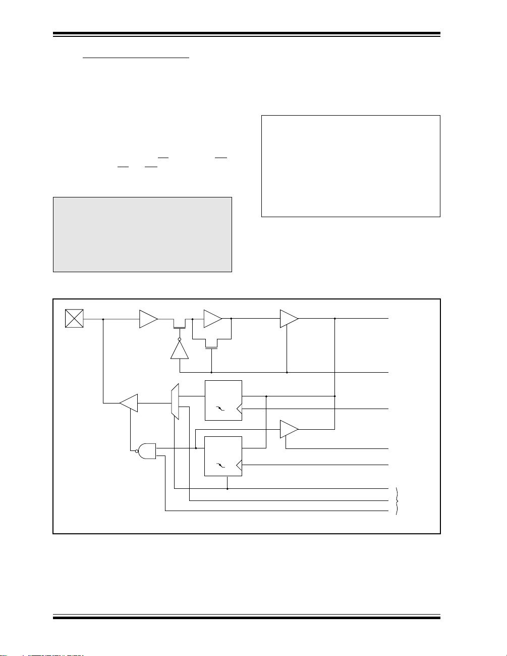
PIC17C7XX
10.5 PORTE and DDRE Register
PORTE is a 4-bit bi-directional port. The corresponding
data direction register is DDRE. A '1' in DDRE configures the corresponding port pin as an input. A '0' in the
DDRE register configures the corresponding port pin
as an output. Reading PORTE reads the status of the
pins, whereas writing to PORTE will write to the port
latch. PORTE is multiplexed with the system bus.
When operating as the system bus, PORTE contains
the control signals for the address/data bus
(AD15:AD0). These control signals are Address Latch
Enable (ALE), Output Enable (OE
The control signals OE
and WR are active low signals.
The timing for the system bus is shown in the Electrical
Specifications section.
Note: Three pins of this por t are configured as
), and Write (WR).
Example 10-5 shows an instruction sequence to initial-
ize PORTE. The Bank Select Register (BSR) must be
selected to Bank 1 for the port to be initialized. The following example uses the MOVLB instruction to load the
BSR register for bank selection.
EXAMPLE 10-5: INITIALIZING PORTE
MOVLB 1 ; Select Bank 1
CLRF PORTE, F ; Initialize PORTE data
; latches before setting
; the data direction
; register
MOVLW 0x03 ; Value used to initialize
; data direction
MOVWF DDRE ; Set RE<1:0> as inputs
; RE<3:2> as outputs
; RE<7:4> are always
; read as '0'
the system bus when the device’s configuration bits are selected to Microprocessor
or Extended Microcontroller modes. The
other pin is a general purpose I/O or
Capture4 pin. In the two other microcontroller modes, RE2:RE0 are general purpose I/O pins.
FIGURE 10-11: BLOCK DIAGRAM OF RE2:RE0 (IN I/O PORT MODE)
TTL
Input
Buffer
Data Bus
RD_PORTE
Port
0
Data
1
Note: I/O pins have protection diodes to VDD and Vss.
DS30289A-page 80 1998 Microchip Technology Inc.
D
Q
CK
D
Q
CK
R
S
WR_PORTE
RD_DDRE
WR_DDRE
EX_EN
CNTL
DRV_SYS
SYS BUS
Control
Page 81

FIGURE 10-12: BLOCK DIAGRAM OF RE3/CAP4 PORT PIN
PIC17C7XX
Peripheral In
QD
EN
EN
V
DD
P
Q
Port
N
Note: I/O pin has protection diodes to VDD and Vss.
Data
D
CK
Q
D
Q
CK
Q
S
TABLE 10-9: PORTE FUNCTIONS
Name Bit Buffer Type Function
RE0/ALE
RE1/OE
RE2/WR
bit2 TTL Input/Output or system bus Write (WR) control pin.
RE3/CAP4 bit3 ST Input/Output or Capture4 input pin
Legend: TTL = TTL input. ST = Schmitt Trigger input
bit0 TTL Input/Output or system bus Address Latch Enable (ALE) control pin.
bit1 TTL Input/Output or system bus Output Enable (OE) control pin.
Data Bus
RD_PORTE
WR_PORTE
RD_DDRE
WR_DDRE
TABLE 10-10: REGISTERS/BITS ASSOCIATED WITH PORTE
Address Name Bit 7 Bit 6 Bit 5 Bit 4 Bit 3 Bit 2 Bit 1 Bit 0
15h, Bank 1 PORTE — — — — RE3/CAP4 RE2/WR RE1/OE RE0/ALE ---- xxxx ---- uuuu
14h, Bank 1 DDRE Data direction register for PORTE ---- 1111 ---- 1111
14h, Bank 7 CA4L Capture4 low byte xxxx xxxx uuuu uuuu
15h, Bank 7 CA4H Capture4 high byte xxxx xxxx uuuu uuuu
16h, Bank 7 TCON3
Legend: x = unknown, u = unchanged, - = unimplemented read as '0'. Shaded cells are not used by PORTE.
1998 Microchip Technology Inc. DS30289A-page 81
— CA4OVF CA3OVF CA4ED1 CA4ED0 CA3ED1 CA3ED0 PWM3ON -000 0000 -000 0000
Value on
POR,
BOR
MCLR
WDT
,
Page 82
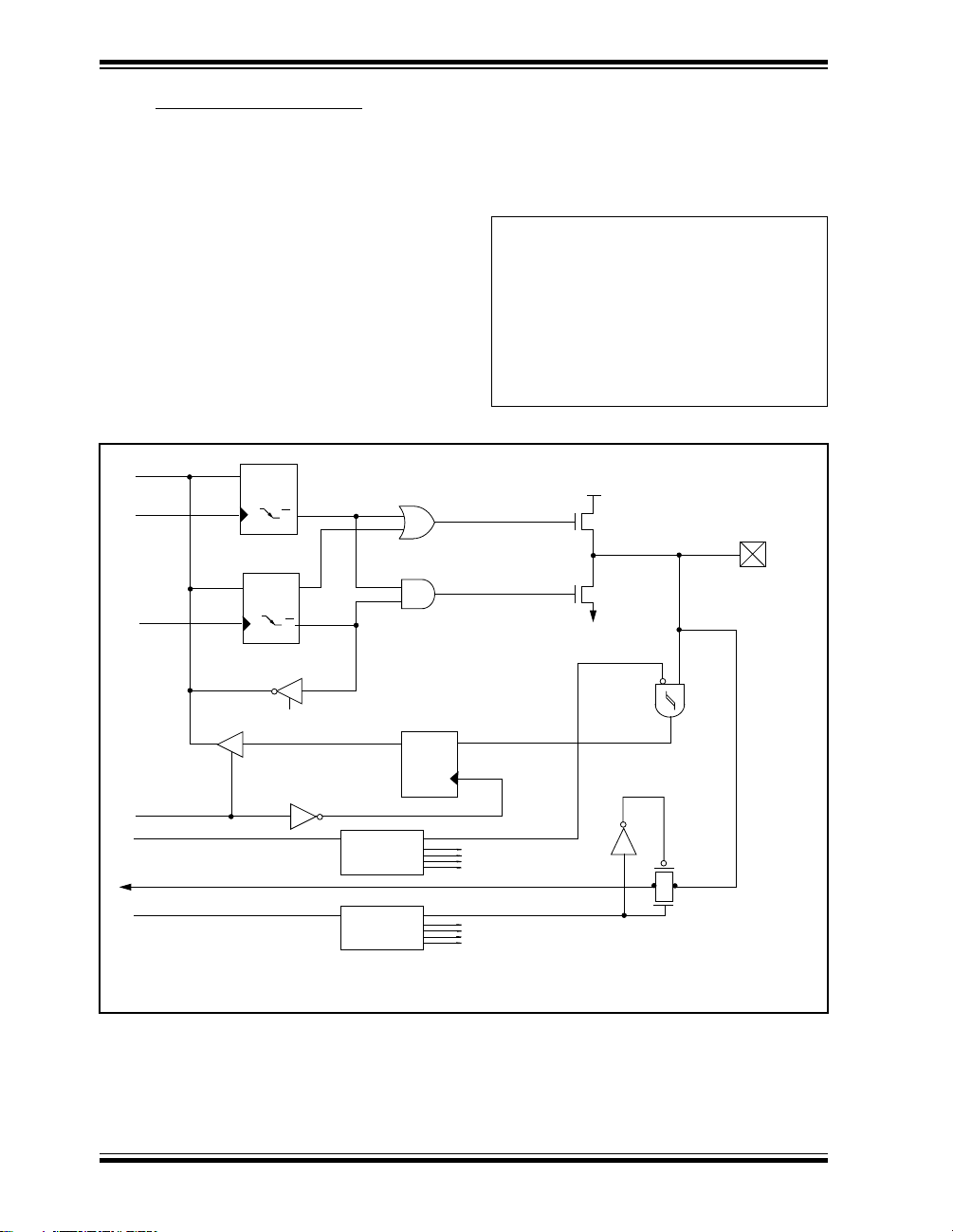
PIC17C7XX
10.6 PORTF and DDRF Registers
PORTF is an 8-bit wide bi-directional port. The corresponding data direction register is DDRF. A '1' in DDRF
configures the corresponding port pin as an input. A '0'
in the DDRF register configures the corresponding port
pin as an output. Reading PORTF reads the status of
the pins, whereas writing to PORTF will write to the
respective port latch.
All eight bits of PORTF are multiplex ed with 8 channels
of the 10-bit A/D converter.
Upon reset the entire Port is automatically configured
as analog inputs, and must be configured in software to
be a digital I/O.
FIGURE 10-13: BLOCK DIAGRAM OF RF7:RF0
Data bus
WR PORTF
WR DDRF
D
Q
Q
CK
Data Latch
D
Q
Q
CK
DDRF Latch
Example 10-6 shows an instruction sequence to initial-
ize PORTF. The Bank Select Register (BSR) must be
selected to Bank 5 for the port to be initialized. The following example uses the MOVLB instruction to load the
BSR register for bank selection.
EXAMPLE 10-6: INITIALIZING PORTF
MOVLB 5 ; Select Bank 5
MOVLW 0x0E ; Configure PORTF as
MOVPF ADCON1 ; Digital
CLRF PORTF, F ; Initialize PORTF data
; latches before
; the data direction
; register
MOVLW 0x03 ; Value used to init
; data direction
MOVWF DDRF ; Set RF<1:0> as inputs
; RF<7:2> as outputs
VDD
P
I/O pin
N
SS
V
ST
input
RD DDRF
QD
EN
EN
RD PORTF
PCFG3:PCFG0
VAIN
CHS3:CHS0
Note: I/O pins have protection diodes to VDD and VSS.
DS30289A-page 82 1998 Microchip Technology Inc.
To other pads
To other pads
buffer
Page 83
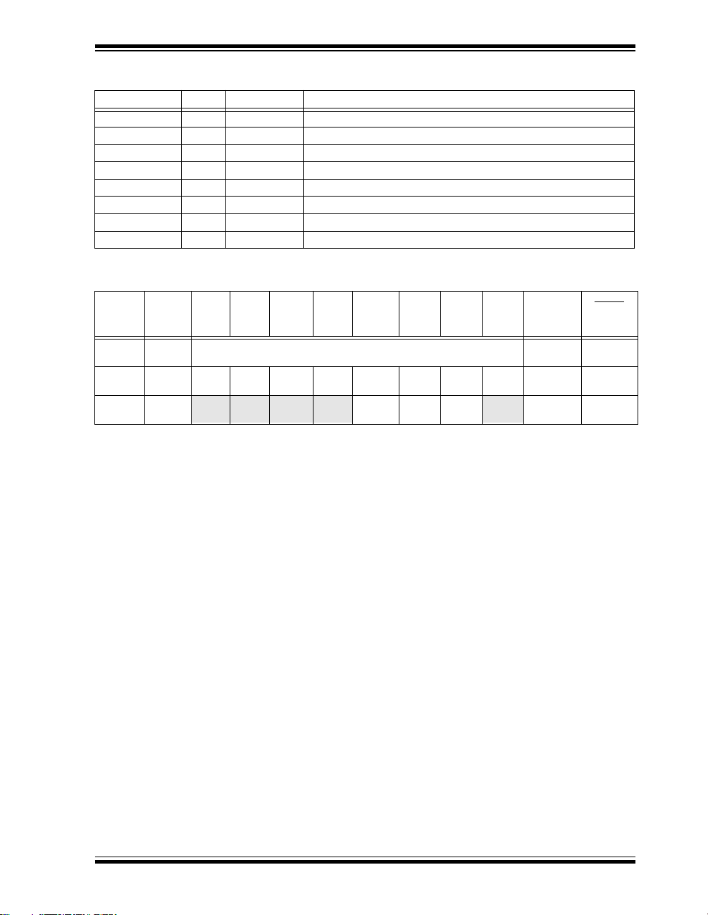
PIC17C7XX
TABLE 10-11: PORTF FUNCTIONS
Name Bit Buffer Type Function
RF0/AN4
bit0
RF1/AN5 bit1 ST
RF2/AN6 bit2 ST
RF3/AN7 bit3 ST
RF4/AN8 bit4 ST
RF5/AN9 bit5 ST
RF6/AN10 bit6 ST
RF7/AN11 bit7 ST
Legend: ST = Schmitt Trigger input.
TABLE 10-12: REGISTERS/BITS ASSOCIATED WITH PORTF
Address Name Bit 7 Bit 6 Bit 5 Bit 4 Bit 3 Bit 2 Bit 1 Bit 0
10h,
Bank 5
11h,
Bank 5
15h,
Bank 5
Legend: x = unknown, u = unchanged, - = unimplemented read as '0'. Shaded cells are not used by PORTF.
DDRF Data Direction Register for PORTF 1111 1111 1111 1111
PORTF RF7/
AN11
ADCON1 ADCS1 ADCS0 ADFM — PCFG3 PCFG2 PCFG1 PCFG0 000- 0000 000- 0000
RF6/
AN10
ST
Input/Output or analog input 4
Input/Output or analog input 5
Input/Output or analog input 6
Input/Output or analog input 7
Input/Output or analog input 8
Input/Output or analog input 9
Input/Output or analog input 10
Input/Output or analog input 11
RF5/
RF4/
AN9
AN8
RF3/
AN7
RF2/
AN6
RF1/
AN5
RF0/
0000 0000 0000 0000
AN4
Value on
POR,
BOR
MCLR
WDT
,
1998 Microchip Technology Inc. DS30289A-page 83
Page 84
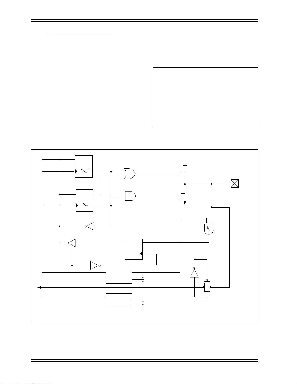
PIC17C7XX
10.7 PORTG and DDRG Registers
PORTG is an 8-bit wide bi-directional port. The corresponding data direction register is DDRG. A '1' in
DDRG configures the corresponding port pin as an
input. A '0' in the DDRG register configures the corresponding port pin as an output. Reading PORTG
reads the status of the pins, whereas writing to
PORTG will write to the port latch.
The lower four bits of PORTG are m ultiplexed with four
channels of the 10-bit A/D converter.
The remaining bits of PORTG are multiplexed with
peripheral output and inputs. RG4 is multiplexed with
the CAP3 input, RG5 is multiplexed with the PWM3
output, RG6 and RG7 are multiplexed with the
USART2 functions.
Upon reset RG3:RG0 is automatically configured as
analog inputs, and must be configured in software to
be a digital I/O.
FIGURE 10-14: BLOCK DIAGRAM OF RG3:RG0
Data bus
WR PORTG
WR DDRG
D
Q
Q
CK
Data Latch
D
Q
Q
CK
DDRG Latch
Example 10-7 shows the instruction sequence to initial-
ize PORTG. The Bank Select Register (BSR) must be
selected to Bank 5 for the port to be initialized. The following example uses the MOVLB instruction to load the
BSR register for bank selection.
EXAMPLE 10-7: INITIALIZING PORTG
MOVLB 5 ; Select Bank 5
MOVLW 0x0E ; Configure PORTG as
MOVPF ADCON1 ; digital
CLRF PORTG, F ; Initialize PORTG data
; latches before
; the data direction
; register
MOVLW 0x03 ; Value used to init
; data direction
MOVWF DDRG ; Set RG<1:0> as inputs
; RG<7:2> as outputs
VDD
P
I/O pin
N
SS
V
ST
input
RD DDRG
QD
EN
EN
RD PORTG
PCFG3:PCFG0
VAIN
CHS3:CHS0
Note: I/O pins have protection diodes to VDD and VSS.
DS30289A-page 84 1998 Microchip Technology Inc.
To other pads
To other pads
buffer
Page 85
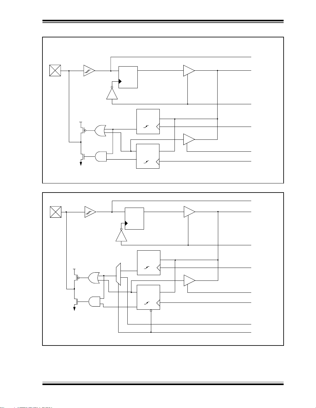
FIGURE 10-15: RG4 BLOCK DIAGRAM
PIC17C7XX
Peripheral Data In
Q
D
EN
EN
VDD
CK
P
N
Note: I/O pin has protection diodes to VDD and Vss.
Q
Q
Q
CK
FIGURE 10-16: RG7:RG5 BLOCK DIAGRAM
QD
EN
N
Data Bus
RD_PORTG
D
D
WR_PORTG
RD_DDRG
WR_DDRG
Peripheral Data In
Data Bus
RD_PORTG
V
DD
P
Port
Data
1
0
N
Note: I/O pins have protection diodes to VDD and Vss.
CK
Q
D
Q
CK
Q
R
WR_PORTG
RD_DDRG
WR_DDRG
OUTPUT
OUTPUT ENABLE
D
Q
1998 Microchip Technology Inc. DS30289A-page 85
Page 86
PIC17C7XX
TABLE 10-13: PORTG FUNCTIONS
Name Bit Buffer Type Function
RG0/AN3
bit0
RG1/AN2 bit1 ST
RG2/AN1/V
RG3/AN0/V
REF- bit2 ST
REF+ bit3 ST
RG4/CAP3 bit4 ST
RG5/PWM3 bit5 ST
RG6/RX2/DT2 bit6 ST
RG7/TX2/CK2 bit7 ST
Legend: ST = Schmitt Trigger input.
TABLE 10-14: REGISTERS/BITS ASSOCIATED WITH PORTG
Address Name Bit 7 Bit 6 Bit 5 Bit 4 Bit 3 Bit 2 Bit 1 Bit 0
12h, Bank 5 DDRG Data Direction Register for PORTG 1111 1111 1111 1111
13h, Bank 5 PORTG RG7/
15h, Bank 5 ADCON1
Legend: x = unknown, u = unchanged, - = unimplemented read as '0'. Shaded cells are not used by PORTG.
TX2/CK2
ADCS1 ADCS0 ADFM — PCFG3 PCFG2 PCFG1 PCFG0 000- 0000 000- 0000
ST
RG6/
RX2/DT2
Input/Output or analog input 3.
Input/Output or analog input 2.
Input/Output or analog input 1 or the ground reference voltage
Input/Output or analog input 0 or the positive reference voltage
Input/Output or the Capture3 input pin.
Input/Output or the PWM3 output pin.
Input/Output or the USART2 (SCI) Asynchronous Receive or USART2
(SCI) Synchronous Data.
Input/Output or the USART2 (SCI) Asynchronous Transmit or USART2
(SCI) Synchronous Clock.
Value on
POR,
BOR
RG5/
PWM3
RG4/
CAP3
RG3/
AN0
RG2/
AN1
RG1/
AN2
RG0/
xxxx 0000 uuuu 0000
AN3
MCLR
WDT
,
DS30289A-page 86 1998 Microchip Technology Inc.
Page 87
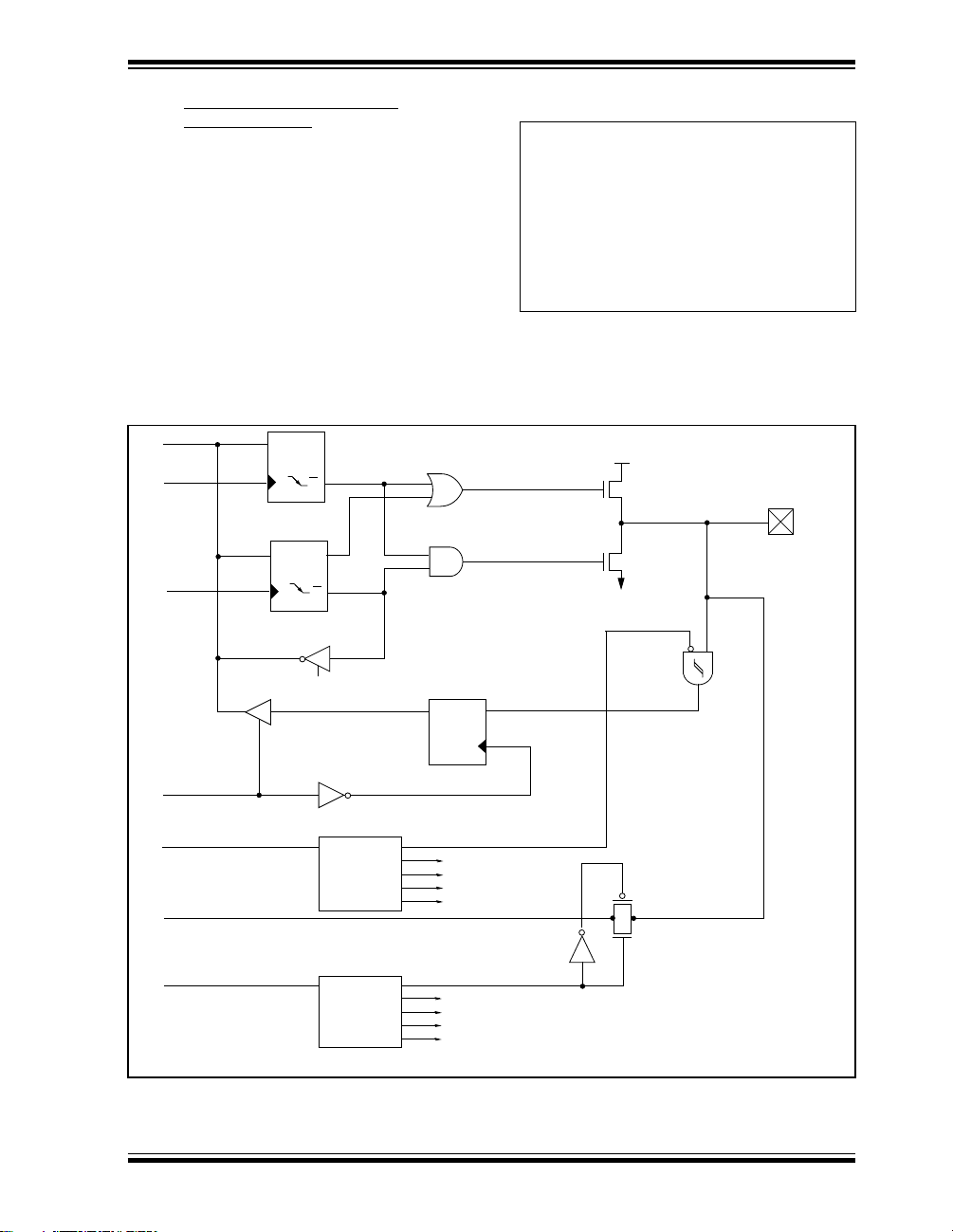
PIC17C7XX
10.8 PORTH and DDRH Registers
(PIC17C76X only)
PORTH is an 8-bit wide bi-directional port. The corresponding data direction register is DDRH. A '1' in
DDRH configures the corresponding port pin as an
input. A '0' in the DDRH register configures the corresponding port pin as an output. Reading PORTH
reads the status of the pins, whereas writing to
PORTH will write to the respective port latch.
The upper four bits of PORTH are multiplexed with
4 channels of the 10-bit A/D converter.
The remaining bits of PORTH are general purpose I/O.
Upon reset RH7:RH4 is automatically configured as
analog inputs, and must be configured in software to
be a digital I/O.
Figure 10-17: Block Diagram of RH7:RH4
Data bus
WR PORTH
WR DDRH
D
Q
Q
CK
Data Latch
D
Q
Q
CK
DDRH Latch
EXAMPLE 10-8: INITIALIZING PORTH
MOVLB 8 ; Select Bank 8
MOVLW 0x0E ; Configure PORTH as
MOVPF ADCON1 ; digital
CLRF PORTH, F ; Initialize PORTH data
; latches before
; the data direction
; register
MOVLW 0x03 ; Value used to init
; data direction
MOVWF DDRH ; Set RH<1:0> as inputs
; RH<7:2> as outputs
VDD
P
I/O pin
N
SS
V
ST
input
RD DDRH
QD
EN
EN
RD PORT
PCFG3:PCFG0
To other pads
VAIN
CHS3:CHS0
To other pads
Note: I/O pins have protection diodes to VDD and VSS.
1998 Microchip Technology Inc. DS30289A-page 87
buffer
Page 88
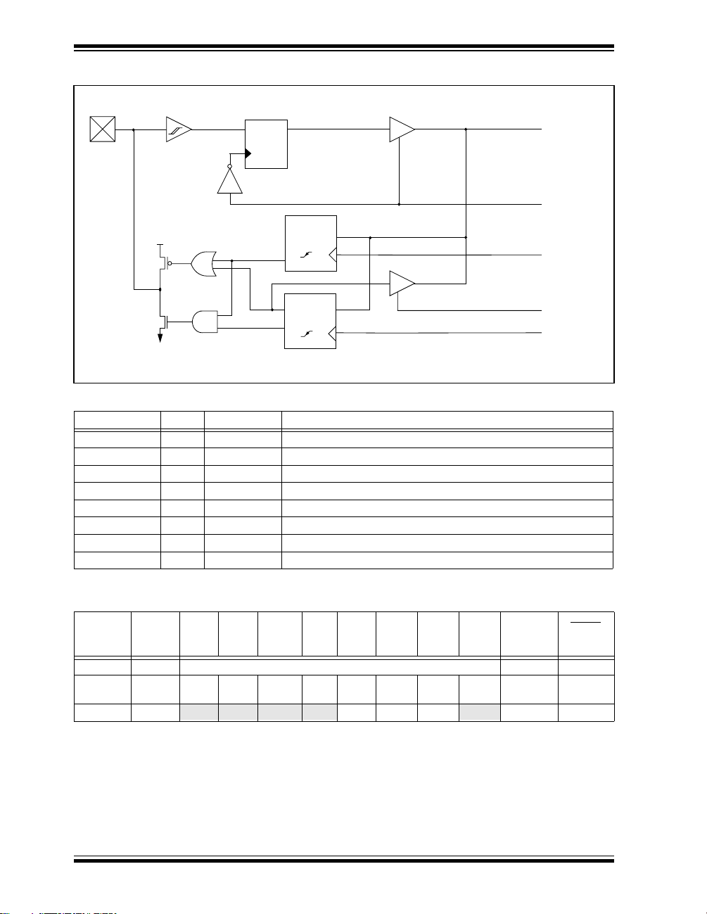
PIC17C7XX
Figure 10-18:RH3:RH0 Block Diagram
D
EN
EN
VDD
P
N
Note: I/O pins have protection diodes to VDD and Vss.
Q
D
CK
Q
D
Q
Q
CK
Data Bus
RD_PORTH
WR_PORTH
RD_DDRH
WR_DDRH
TABLE 10-1: PORTH FUNCTIONS
Name Bit Buffer Type Function
RH0
bit0
RH1 bit1 ST
RH2 bit2 ST
RH3 bit3 ST
RH4/AN12 bit4 ST
RH5/AN13 bit5 ST
RH6/AN14 bit6 ST
RH7/AN15 bit7 ST
ST
Input/Output
Input/Output
Input/Output
Input/Output
Input/Output or analog input 12
Input/Output or analog input 13
Input/Output or analog input 14
Input/Output or analog input 15
Legend: ST = Schmitt Trigger input.
TABLE 10-2: REGISTERS/BITS ASSOCIATED WITH PORTH
Address Name Bit 7 Bit 6 Bit 5 Bit 4 Bit 3 Bit 2 Bit 1 Bit 0
POR,
BOR
10h, Bank 8 DDRH Data Direction Register for PORTH 1111 1111 1111 1111
Value on
11h, Bank 8 PORTH RH7/
15h, Bank 5 ADCON1 ADCS1 ADCS0 ADFM — PCFG3 PCFG2 PCFG1 PCFG0 000- 0000 000- 0000
Legend: x = unknown, u = unchanged.
AN15
RH6/
AN14
RH5/
AN13
RH4/
RH3 RH2 RH1 RH0 0000 xxxx 0000 uuuu
AN12
MCLR
WDT
,
DS30289A-page 88 1998 Microchip Technology Inc.
Page 89

PIC17C7XX
10.9 PORTJ and DDRJ Registers
(PIC17C76X only)
PORTJ is an 8-bit wide bi-directional port. The corresponding data direction register is DDRJ. A '1' in
DDRJ configures the corresponding port pin as an
input. A '0' in the DDRJ register configures the corresponding port pin as an output. Reading PORTJ
reads the status of the pins, whereas writing to PORTJ
will write to the respective port latch.
PORTJ is a general purpose I/O port.
Figure 10-19:PORTJ Block Diagram
Q
D
EN
EN
VDD
P
D
CK
Q
EXAMPLE 10-1: INITIALIZING PORTJ
MOVLB 8 ; Select Bank 8
CLRF PORTJ, F ; Initialize PORTJ data
; latches before setting
; the data direction
; register
MOVLW 0xCF ; Value used to initialize
; data direction
MOVWF DDRJ ; Set RJ<3:0> as inputs
; RJ<5:4> as outputs
; RJ<7:6> as inputs
Data Bus
RD_PORTJ
WR_PORTJ
D
N
Note: I/O pins have protection diodes to VDD and Vss.
1998 Microchip Technology Inc. DS30289A-page 89
Q
Q
CK
RD_DDRJ
WR_DDRJ
Page 90

PIC17C7XX
TABLE 10-1: PORTJ FUNCTIONS
Name Bit Buffer Type Function
RJ0
RJ1 bit1 ST
RJ2 bit2 ST
RJ3 bit3 ST
RJ4 bit4 ST
RJ5 bit5 ST
RJ6 bit6 ST
RJ7 bit7 ST
Legend: ST = Schmitt Trigger input.
bit0
TABLE 10-2: REGISTERS/BITS ASSOCIATED WITH PORTJ
Address Name Bit 7 Bit 6 Bit 5 Bit 4 Bit 3 Bit 2 Bit 1 Bit 0
12h, Bank 8 DDRJ Data Direction Register for PORTJ 1111 1111 1111 1111
13h, Bank 8 PORTJ RJ7 RJ6 RJ5 RJ4 RJ3 RJ2 RJ1 RJ0 xxxx xxxx uuuu uuuu
Legend: x = unknown, u = unchanged.
ST
Input/Output
Input/Output
Input/Output
Input/Output
Input/Output
Input/Output
Input/Output
Input/Output
Value on,
POR,
BOR
MCLR
WDT
,
DS30289A-page 90 1998 Microchip Technology Inc.
Page 91

PIC17C7XX
10.10 I/O Programming Considerations
10.10.1 BI-DIRECTIONAL I/O PORTS
Any instruction which writes, operates internally as a
read followed by a write operation. For example, the
BCF and BSF instructions read the register into the
CPU, execute the bit operation, and write the result
back to the register. Caution must be used when these
instructions are applied to a port with both inputs and
outputs defined. For example, a BSF operation on bit5
of PORTB will cause all eight bits of PORTB to be read
into the CPU. Then the BSF operation takes place on
bit5 and PORTB is written to the output latches. If
another bit of PORTB is used as a bi-directional I/O pin
(e.g. bit0) and it is defined as an input at this time, the
input signal present on the pin itself would be read into
the CPU and re-written to the data latch of this particular pin, overwriting the previous content. As long as the
pin stays in the input mode, no problem occurs. However, if bit0 is switched into output mode later on, the
content of the data latch may now be unknown.
Reading a port reads the values of the port pins. Writing to the port register writes the value to the port latch.
When using read-modify-write instructions (BCF, BSF,
BTG, etc.) on a port, the value of the port pins is read,
the desired operation is performed with this value, and
the value is then written to the port latch.
Example 10-1 shows the possible effect of two sequen-
tial read-modify-write instructions on an I/O port.
EXAMPLE 10-1: READ MODIFY WRITE
INSTRUCTIONS ON AN
I/O PORT
; Initial PORT settings: PORTB<7:4> Inputs
; PORTB<3:0> Outputs
; PORTB<7:6> have pull-ups and are
; not connected to other circuitry
;
; PORT latch PORT pins
; ---------- --------;
BCF PORTB, 7 ; 01pp pppp 11pp pppp
BCF PORTB, 6 ; 10pp pppp 11pp pppp
BCF DDRB, 7 ; 10pp pppp 11pp pppp
BCF DDRB, 6 ; 10pp pppp 10pp pppp
;
; Note that the user may have expected the
; pin values to be 00pp pppp. The 2nd BCF
; caused RB7 to be latched as the pin value
; (High).
Note: A pin actively outputting a Low or High
should not be driven from external devices
in order to change the level on this pin (i.e.
“wired-or”, “wired-and”). The resulting high
output currents may damage the device.
1998 Microchip Technology Inc. DS30289A-page 91
Page 92

PIC17C7XX
10.10.2 SUCCESSIVE OPERATIONS ON I/O PORTS
The actual write to an I/O port happens at the end of an
instruction cycle, whereas for reading, the data must be
valid at the beginning of the instruction cycle
(Figure 10-20). Therefore, care must be exercised if a
write followed by a read operation is carried out on the
same I/O port. The sequence of instructions should be
such to allow the pin voltage to stabilize (load dependent) before executing the instruction that reads the
values on that I/O port. Otherwise, the previous state
of that pin may be read into the CPU rather than the
“new” state. When in doubt, it is better to separate
these instructions with a NOP or another instruction not
accessing this I/O port.
FIGURE 10-20: SUCCESSIVE I/O OPERATION
write to
PORTB
Q4
Q3
Q1 Q2
NOP
Port pin
sampled here
Instruction
fetched
RB7:RB0
Instruction
executed
Q4
Q3
Q1 Q2
PC PC + 1 PC + 2
MOVWF PORTB
write to
PORTB
Q1 Q2
MOVF PORTB,W
MOVWF PORTB
Figure 10-21 shows the I/O model which causes this
situation. As the effective capacitance (C) becomes
larger, the rise/fall time of the I/O pin increases. As the
device frequency increases or the effective capacitance increases, the possibility of this subsequent
PORTx read-modify-write instruction issue increases.
This effective capacitance includes the effects of the
board traces.
The best way to address this is to add an series resistor
at the I/O pin. This resistor allows the I/O pin to get to
the desired level before the next instruction.
The use of NOP instructions between the subsequent
PORTx read-modify-write instructions, is a lower cost
solution, but has the issue that the number of NOP
instructions is dependent on the effective capacitance
C and the frequency of the device.
Note:
Q4
Q3
Q1 Q2
Q3
PC + 3
NOP
NOPMOVF PORTB,W
Q4
This example shows a write to PORTB
followed by a read from PORTB.
Note that:
data setup time = (0.25TCY - TPD)
where TCY = instruction cycle
TPD = propagation delay
Therefore, at higher clock frequencies,
a write followed by a read may be problematic.
FIGURE 10-21: I/O CONNECTION ISSUES
PIC17CXXX
I/O
(1)
C
PORTx, PINy
BSF PORTx, PINy
Q2 Q3
VIL
Q4 Q1 Q2 Q3 Q4 Q1
Note 1: This is not a capacitor to ground, but the effective
capacitive loading on the trace.
DS30289A-page 92 1998 Microchip Technology Inc.
BSF PORTx, PINz
Read PORTx, PINy as low
BSF PORTx, PINz clears the value
to be driven on the PORTx, PINy pin.
Page 93

PIC17C7XX
11.0 OVERVIEW OF TIMER RESOURCES
The PIC17C7XX has four timer modules. Each module
can generate an interrupt to indicate that an event has
occurred. These timers are called:
• Timer0 - 16-bit timer with programmable 8-bit
prescaler
• Timer1 - 8-bit timer
• Timer2 - 8-bit timer
• Timer3 - 16-bit timer
For enhanced time-base functionality, four input Captures and three Pulse Width Modulation (PWM) outputs are possible. The PWMs use the Timer1 and
Timer2 resources and the input Captures use the
Timer3 resource.
11.1 Timer0 Overview
The Timer0 module is a simple 16-bit overflo w counter.
The clock source can be either the internal system
clock (Fosc/4) or an external clock.
When Timer0 uses an external clock source, it has the
flexibility to allow user selection of the incrementing
edge, rising or falling.
The Timer0 module also has a programmable prescaler. The T0PS3:T0PS0 bits (T0STA<4:1>) determine
the prescale value. TMR0 can increment at the following rates: 1:1, 1:2, 1:4, 1:8, 1:16, 1:32, 1:64, 1:128,
1:256.
Synchronization of the external clock occurs after the
prescaler. When the prescaler is used, the external
clock frequency may be higher than the device’s frequency. The maximum external frequency, on the
T0CKI pin, is 50 MHz, given the high and low time
requirements of the clock.
11.2 Timer1 Overview
The Timer1 module is an 8-bit timer/counter with an
8-bit period register (PR1). When the TMR1 value rolls
over from the period match value to 0h, the TMR1IF
flag is set, and an interrupt will be generated if
enabled. In counter mode, the clock comes from the
RB4/TCLK12 pin, which can also be selected to be the
clock for the Timer2 module.
TMR1 can be concatenated with TMR2 to form a
16-bit timer. The TMR1 register is the LSB and TMR2
is the MSB. When in the 16-bit timer mode, there is a
corresponding 16-bit period register (PR2:PR1). When
the TMR2:TMR1 value rolls over from the period
match value to 0h, the TMR1IF flag is set, and an
interrupt will be generated if enabled.
11.3 Timer2 Overview
The Timer2 module is an 8-bit timer/counter with an
8-bit period register (PR2). When the TMR2 value rolls
over from the period match value to 0h, the TMR2IF
flag is set, and an interrupt will be generated if
enabled. In counter mode, the clock comes from the
RB4/TCLK12 pin, which can also provide the clock for
the Timer1 module.
TMR2 can be concatenated with TMR1 to form a
16-bit timer. The TMR2 register is the MSB and TMR1
is the LSB. When in the 16-bit timer mode, there is a
corresponding 16-bit period register (PR2:PR1). When
the TMR2:TMR1 value rolls over from the period
match value to 0h, the TMR1IF flag is set, and an
interrupt will be generated if enabled.
11.4 Timer3 Overview
The Timer3 module is a 16-bit timer/counter with a
16-bit period register. When the TMR3H:TMR3L value
rolls over to 0h, the TMR3IF bit is set and an interrupt
will be generated if enabled. In counter mode, the
clock comes from the RB5/TCLK3 pin.
When operating in the four capture mode, the period
registers become the second (of four) 16-bit capture
registers.
11.5 Role of the Timer/Counters
The timer modules are general purpose, but have dedicated resources associated with them. TImer1 and
Timer2 are the time-bases for the three Pulse Width
Modulation (PWM) outputs, while Timer3 is the
time-base for the four input captures.
1998 Microchip Technology Inc. DS30289A-page 93
Page 94

PIC17C7XX
NOTES:
DS30289A-page 94 1998 Microchip Technology Inc.
Page 95

12.0 TIMER0
The Timer0 module consists of a 16-bit timer/counter,
TMR0. The high byte is register TMR0H and the low
byte is register TMR0L. A software programmable 8-bit
prescaler makes Timer0 an effective 24-bit overflow
timer. The clock source is software programmable as
either the internal instruction clock or an external clock
on the RA1/T0CKI pin. The control bits for this module
are in register T0STA (Figure 12-1).
FIGURE 12-1: T0STA REGISTER (ADDRESS: 05h, UNBANKED)
PIC17C7XX
R/W - 0 R/W - 0 R/W - 0 R/W - 0 R/W - 0 R/W - 0 R/W - 0 U - 0
INTEDG T0SE T0CS T0PS3 T0PS2 T0PS1 T0PS0
bit7 bit0
bit 7: INTEDG: RA0/INT Pin Interrupt Edge Select bit
This bit selects the edge upon which the interrupt is detected
1 =Rising edge of RA0/INT pin generates interrupt
0 =Falling edge of RA0/INT pin generates interrupt
bit 6: T0SE: Timer0 Clock Input Edge Select bit
This bit selects the edge upon which TMR0 will increment
When
T0CS = 0 (External Clock)
1 =Rising edge of RA1/T0CKI pin increments TMR0 and/or sets the T0CKIF bit
0 =Falling edge of RA1/T0CKI pin increments TMR0 and/or sets the T0CKIF bit
When
T0CS = 1 (Internal Clock)
Don’t care
bit 5: T0CS: Timer0 Clock Source Select bit
bit 4-1: T0PS3:T0PS0: Timer0 Prescale Selection bits
This bit selects the clock source for TMR0.
1 =Internal instruction clock cycle (T
0 =External Clock input on the T0CKI pin
These bits select the prescale value for TMR0.
T0PS3:T0PS0 Prescale Value
0000
0001
0010
0011
0100
0101
0110
0111
1xxx
1:1
1:2
1:4
1:8
1:16
1:32
1:64
1:128
1:256
CY)
—
R = Readable bit
W = Writable bit
U = Unimplemented,
Read as '0'
-n = Value at POR reset
bit 0: Unimplemented: Read as '0'
1998 Microchip Technology Inc. DS30289A-page 95
Page 96
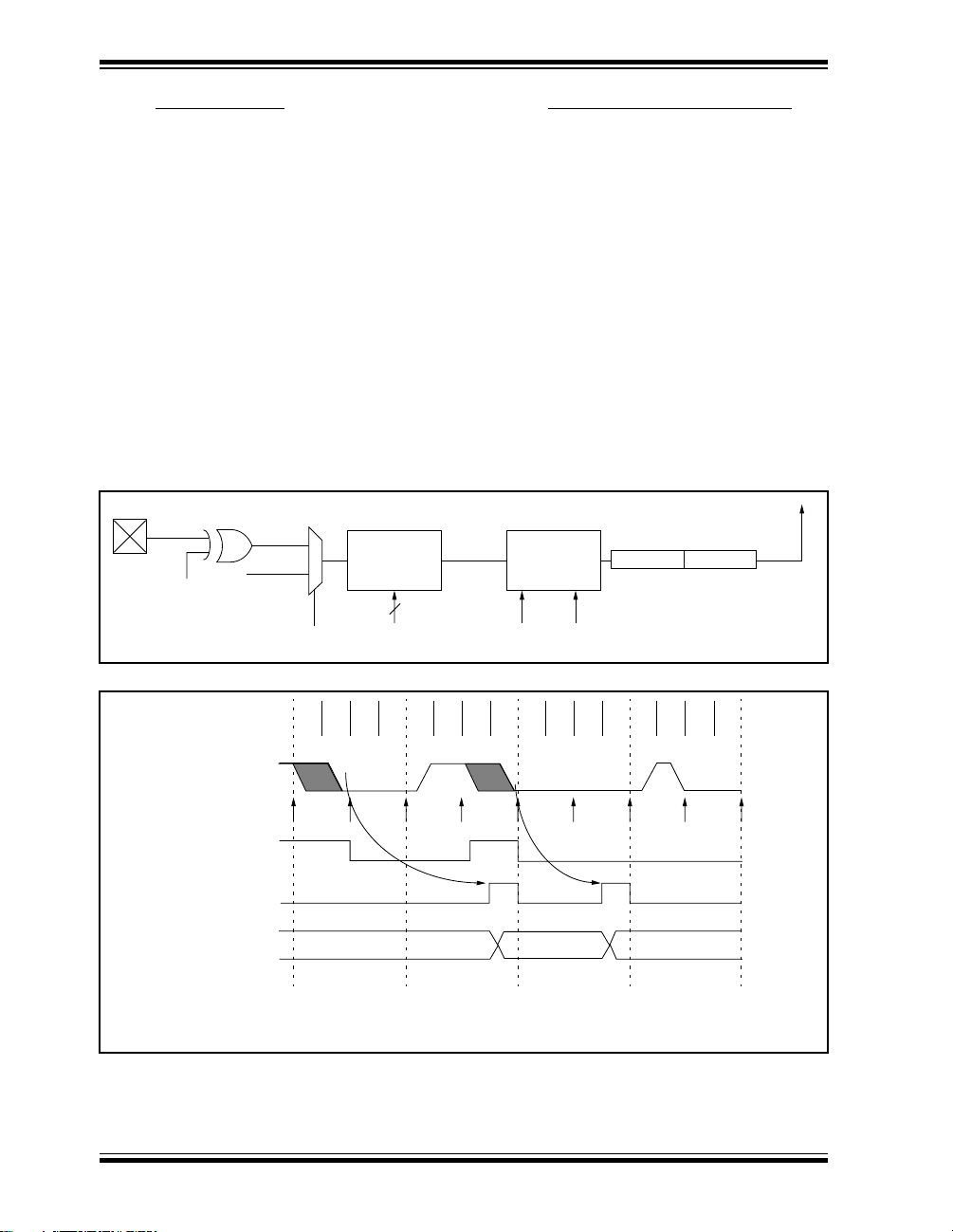
PIC17C7XX
12.1 Timer0 Operation
When the T0CS (T0STA<5>) bit is set, TMR0 increments on the internal clock. When T0CS is clear , TMR0
increments on the external clock (RA1/T0CKI pin). The
external clock edge can be selected in software. When
the T0SE (T0STA<6>) bit is set, the timer will increment
on the rising edge of the RA1/T0CKI pin. When T0SE
is clear, the timer will increment on the falling edge of
the RA1/T0CKI pin. The prescaler can be programmed
to introduce a prescale of 1:1 to 1:256. The timer increments from 0000h to FFFFh and rolls over to 0000h.
On overflow, the TMR0 Interrupt Flag bit (T0IF) is set.
The TMR0 interrupt can be masked by clearing the corresponding TMR0 Interrupt Enable bit (T0IE). The
TMR0 Interrupt Flag bit (T0IF) is automatically cleared
when vectoring to the TMR0 interrupt vector.
12.2 Using Timer0 with External Clock
When an external clock input is used for Timer0, it is
synchronized with the internal phase clocks.
Figure 12-3 shows the synchronization of the external
clock. This synchronization is done after the prescaler.
The output of the prescaler (PSOUT) is sampled twice
in every instruction cycle to detect a rising or a falling
edge. The timing requirements for the external clock
are detailed in the electrical specification section.
12.2.1 DELAY FROM EXTERNAL CLOCK EDGE
Since the prescaler output is synchronized with the
internal clocks, there is a small delay from the time the
external clock edge occurs to the time TMR0 is actually
incremented. Figure 12-3 shows that this delay is
between 3T
suring the interval between two edges (e.g. period) will
be accurate within ±4T
FIGURE 12-2: TIMER0 MODULE BLOCK DIAGRAM
Prescaler
0
RA1/T0CKI
T0SE
(T0STA<6>)
Fosc/4
(T0STA<5>)
T0CS
1
(8 stage
async ripple
counter)
4
T0PS3:T0PS0
(T0STA<4:1>)
PSOUT
OSC and 7TOSC. Thus, for example, mea-
OSC (±121 ns @ 33 MHz).
Interrupt on overflow
(INTST A<5>)
Synchronization
Q2 Q4
TMR0H<8> TMR0L<8>
sets T0IF
FIGURE 12-3: TMR0 TIMING WITH EXTERNAL CLOCK (INCREMENT ON FALLING EDGE)
Q1 Q2 Q3 Q4 Q1 Q2 Q3 Q4 Q1 Q2 Q3 Q4 Q1 Q2 Q3 Q4
Prescaler
output
(PSOUT)
Sampled
Prescaler
output
Increment
TMR0
TMR0
Note 1: The delay from the T0CKI edge to the TMR0 increment is 3Tosc to 7Tosc.
DS30289A-page 96 1998 Microchip Technology Inc.
(note 1)
T0 T0 + 1 T0 + 2
2: ↑ = PSOUT is sampled here.
3: The PSOUT high time is too short and is missed by the sampling circuit.
(note 3)
(note 2)
Page 97
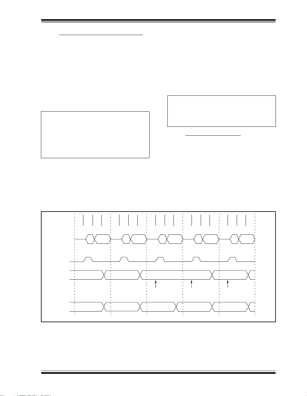
PIC17C7XX
12.3 Read/Write Consideration for TMR0
Although TMR0 is a 16-bit timer/counter, only 8-bits at
a time can be read or written during a single instruction
cycle. Care must be taken during any read or write.
12.3.1 READING 16-BIT VALUE
The problem in reading the entire 16-bit value is that
after reading the low (or high) byte, its value may
change from FFh to 00h.
Example 12-1 shows a 16-bit read. To ensure a proper
read, interrupts must be disabled during this routine.
EXAMPLE 12-1: 16-BIT READ
MOVPF TMR0L, TMPLO ;read low tmr0
MOVPF TMR0H, TMPHI ;read high tmr0
MOVFP TMPLO, WREG ;tmplo −> wreg
CPFSLT TMR0L ;tmr0l < wreg?
RETURN ;no then return
MOVPF TMR0L, TMPLO ;read low tmr0
MOVPF TMR0H, TMPHI ;read high tmr0
RETURN ;return
12.3.2 WRITING A 16-BIT VALUE TO TMR0
Since writing to either TMR0L or TMR0H will eff ectiv ely
inhibit increment of that half of the TMR0 in the next
cycle (following write), but not inhibit increment of the
other half, the user must write to TMR0L first and
TMR0H second in two consecutive instructions, as
shown in Example 12-2. The interrupt must be disabled. Any write to either TMR0L or TMR0H clears the
prescaler.
EXAMPLE 12-2: 16-BIT WRITE
BSF CPUSTA, GLINTD ; Disable interrupts
MOVFP RAM_L, TMR0L ;
MOVFP RAM_H, TMR0H ;
BCF CPUSTA, GLINTD ; Done, enable
; interrupts
12.4 Prescaler
Timer0 has an 8-bit prescaler. The prescaler selection
is fully under software control; i.e., it can be changed
“on the fly” during program execution. Clearing the
prescaler is recommended before changing its setting.
The value of the prescaler is “unknown,” and assigning
a value that is less than the present value makes it difficult to take this unknown time into account.
FIGURE 12-4: TMR0 TIMING: WRITE HIGH OR LOW BYTE
Q1 Q2 Q3 Q4 Q1 Q2 Q3 Q4 Q1 Q2 Q3 Q4 Q1 Q2 Q3 Q4 Q1 Q2 Q3 Q4
Assignments
AD15:AD0
ALE
TMR0L
Fetch
Instruction
executed
TMR0H
1998 Microchip Technology Inc. DS30289A-page 97
PC
T0 T0+1 New T0 (NT0) New T0+1
PC+1 PC+2 PC+3 PC+4
MOVFP W ,TMR0L
Write to TMR0L
MOVFP TMR0L,W
Read TMR0L
(Value = NT0)
MOVFP TMR0L,W
Read TMR0L
(Value = NT0)
MOVFP TMR0L,W
Read TMR0L
(Value = NT0 +1)
Page 98
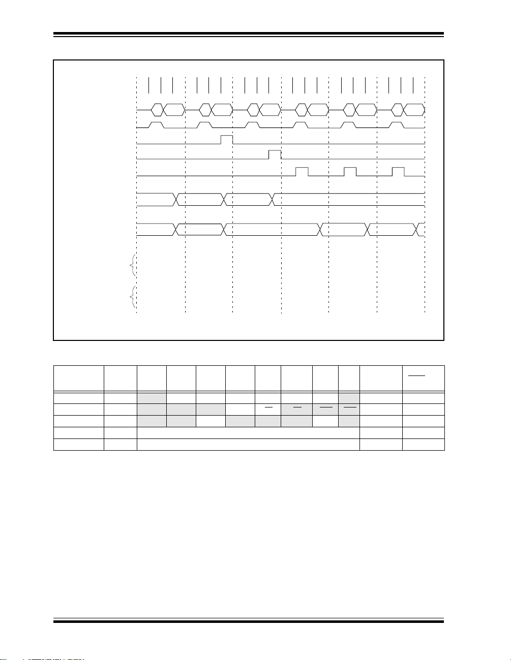
PIC17C7XX
FIGURE 12-5: TMR0 READ/WRITE IN TIMER MODE
Q1 Q2 Q3 Q4 Q1 Q2 Q3 Q4 Q1 Q2 Q3 Q4 Q1 Q2 Q3 Q4 Q1 Q2 Q3 Q4 Q1 Q2 Q3 Q4
AD15:AD0
ALE
WR_TRM0L
WR_TMR0H
RD_TMR0L
TMR0H
TMR0L
Instruction
fetched
Instruction
executed
12
FE
MOVFP
DATAL,TMR0L
Write TMR0L
Previously
Fetched
Instruction
In this example, old TMR0 value is 12FEh, new value of AB56h is written.
12
FF
MOVFP
DAT AH,TMR0H
Write TMR0H
MOVFP
DATAL,TMR0L
Write TMR0L
13
56
MOVPF
TMR0L,W
Read TMR0L
MOVFP
DAT AH,TMR0H
Write TMR0H
TABLE 12-1: REGISTERS/BITS ASSOCIATED WITH TIMER0
Address Name Bit 7 Bit 6 Bit 5 Bit 4 Bit 3 Bit 2 Bit 1 Bit 0
05h, Unbanked T0STA
06h, Unbanked CPUSTA — — STKAV GLINTD TO PD POR BOR --11 11qq --11 qquu
07h, Unbanked INTSTA PEIF T0CKIF T0IF INTF PEIE T0CKIE T0IE INTE 0000 0000 0000 0000
0Bh, Unbanked TMR0L TMR0 register; low byte xxxx xxxx uuuu uuuu
0Ch, Unbanked TMR0H TMR0 register; high byte xxxx xxxx uuuu uuuu
Legend: x = unknown, u = unchanged, - = unimplemented read as a '0', q - value depends on condition, Shaded cells are not used by Timer0.
INTEDG T0SE T0CS T0PS3 T0PS2 T0PS1 T0PS0 — 0000 000- 0000 000-
AB
MOVPF
TMR0L,W
Read TMR0L
MOVPF
TMR0L,W
Read TMR0L
57 58
MOVPF
TMR0L,W
Read TMR0L
MOVPF
TMR0L,W
Read TMR0L
Value on
MOVPF
TMR0L,W
Read TMR0L
MOVPF
TMR0L,W
Read TMR0L
POR,
BOR
MCLR, WDT
DS30289A-page 98 1998 Microchip Technology Inc.
Page 99
PIC17C7XX
13.0 TIMER1, TIMER2, TIMER3,
PWMS AND CAPTURES
The PIC17C7XX has a wealth of timers and time-based
functions to ease the implementation of control applications. These time-base functions include three PWM
outputs and four Capture inputs.
Timer1 and Timer2 are two 8-bit incrementing timers,
each with an 8-bit period register (PR1 and PR2
respectively) and separate overflow interrupt flags.
Timer1 and Timer2 can operate either as timers (increment on internal Fosc/4 clock) or as counters (increment on falling edge of external clock on pin
RB4/TCLK12). They are also software configurable to
operate as a single 16-bit timer/counter. These timers
are also used as the time-base for the PWM (Pulse
Width Modulation) modules.
Timer3 is a 16-bit timer/counter which uses the TMR3H
and TMR3L registers. Timer3 also has two additional
registers (PR3H/CA1H: PR3L/CA1L) that are configurable as a 16-bit period register or a 16-bit capture
register. TMR3 can be software configured to increment from the internal system clock (F
an external signal on the RB5/TCLK3 pin. Timer3 is the
time-base for all of the 16-bit captures.
OSC/4) or from
Six other registers comprise the Capture2, Capture3,
and Capture4 registers (CA2H:CA2L, CA3H:CA3L,
and CA4H:CA4L).
Figure 13-1, Figure 13-2, and Figure 13-3 are the con-
trol registers for the operation of Timer1, Timer2, and
Timer3, as well as PWM1, PWM2, PWM3, Capture1,
Capture2, Capture3, and Capture4.
Table 13-1 shows the Timer resource requirements for
these time-base functions. Each timer is an open
resource so that multiple functions may operate with it.
TABLE 13-1: TIME-BASE FUNCTION /
Time-base Function Timer Resource
PWM1 Timer1
PWM2 Timer1 or Timer2
PWM3 Timer1 or Timer2
Capture1 Timer3
Capture2 Timer3
Capture3 Timer3
Capture4 Timer3
FIGURE 13-1: TCON1 REGISTER (ADDRESS: 16h, BANK 3)
R/W - 0 R/W - 0 R/W - 0 R/W - 0 R/W - 0 R/W - 0 R/W - 0 R/W - 0
CA2ED1 CA2ED0 CA1ED1 CA1ED0 T16 TMR3CS TMR2CS TMR1CS
bit7 bit0
bit 7-6: CA2ED1:CA2ED0: Capture2 Mode Select bits
00 = Capture on every falling edge
01 = Capture on every rising edge
10 = Capture on every 4th rising edge
11 = Capture on every 16th rising edge
bit 5-4: CA1ED1:CA1ED0: Capture1 Mode Select bits
00 = Capture on every falling edge
01 = Capture on every rising edge
10 = Capture on every 4th rising edge
11 = Capture on every 16th rising edge
bit 3: T16: Timer2:Timer1 Mode Select bit
1 =Timer2 and Timer1 form a 16-bit timer
0 =Timer2 and Timer1 are two 8-bit timers
bit 2: TMR3CS: Timer3 Clock Source Select bit
1 =TMR3 increments off the falling edge of the RB5/TCLK3 pin
0 =TMR3 increments off the internal clock
bit 1: TMR2CS: Timer2 Clock Source Select bit
1 =TMR2 increments off the falling edge of the RB4/TCLK12 pin
0 =TMR2 increments off the internal clock
bit 0: TMR1CS: Timer1 Clock Source Select bit
1 =TMR1 increments off the falling edge of the RB4/TCLK12 pin
0 =TMR1 increments off the internal clock
RESOURCE
REQUIREMENTS
R = Readable bit
W = Writable bit
-n = Value at POR reset
1998 Microchip Technology Inc. DS30289A-page 99
Page 100

PIC17C7XX
FIGURE 13-2: TCON2 REGISTER (ADDRESS: 17h, BANK 3)
R - 0 R - 0 R/W - 0 R/W - 0 R/W - 0 R/W - 0 R/W - 0 R/W - 0
CA2OVF CA1OVF PWM2ON PWM1ON CA1/PR3
bit7 bit0
bit 7: CA2OVF: Capture2 Overflow Status bit
bit 6: CA1OVF: Capture1 Overflow Status bit
bit 5: PWM2ON: PWM2 On bit
bit 4: PWM1ON: PWM1 On bit
bit 3: CA1/PR3: CA1/PR3
bit 2: TMR3ON: Timer3 On bit
bit 1: TMR2ON: Timer2 On bit
bit 0: TMR1ON: Timer1 On bit
This bit indicates that the capture value had not been read from the capture register pair (CA2H:CA2L)
before the next capture ev ent occurred. The capture register retains the oldest unread capture value (last
capture before overflow). Subsequent capture events will not update the capture register with the TMR3
value until the capture register has been read (both bytes).
1 =Overflow occurred on Capture2 register
0 =No overflow occurred on Capture2 register
This bit indicates that the capture value had not been read from the capture register pair
(PR3H/CA1H:PR3L/CA1L) before the next capture event occurred. The capture register retains the oldest unread capture value (last capture before overflow). Subsequent capture events will not update the
capture register with the TMR3 value until the capture register has been read (both bytes).
1 =Overflow occurred on Capture1 register
0 =No overflow occurred on Capture1 register
1 =PWM2 is enabled
(The RB3/PWM2 pin ignores the state of the DDRB<3> bit)
0 =PWM2 is disabled
(The RB3/PWM2 pin uses the state of the DDRB<3> bit for data direction)
1 =PWM1 is enabled
(The RB2/PWM1 pin ignores the state of the DDRB<2> bit)
0 =PWM1 is disabled
(The RB2/PWM1 pin uses the state of the DDRB<2> bit for data direction)
1 =Enables Capture1
(PR3H/CA1H:PR3L/CA1L is the Capture1 register. Timer3 runs without a period register)
0 =Enables the Period register
(PR3H/CA1H:PR3L/CA1L is the Period register for Timer3)
1 =Starts Timer3
0 =Stops Timer3
This bit controls the incrementing of the TMR2 register. When TMR2:TMR1 form the 16-bit timer (T16 is
set), TMR2ON must be set. This allows the MSB of the timer to increment.
1 =Starts Timer2 (Must be enabled if the T16 bit (TCON1<3>) is set)
0 =Stops Timer2
When
T16 is set (in 16-bit Timer Mode)
1 =Starts 16-bit TMR2:TMR1
0 =Stops 16-bit TMR2:TMR1
Register Mode Select bit
TMR3ON TMR2ONTMR1ON
R = Readable bit
W = Writable bit
-n = Value at POR reset
When
T16 is clear (in 8-bit Timer Mode)
1 =Starts 8-bit Timer1
0 =Stops 8-bit Timer1
DS30289A-page 100 1998 Microchip Technology Inc.
 Loading...