

Page 1
M
8-bit CMOS EEPROM Microcontroller
High Performance RISC CPU Features:
•Only 35 single word instructions to learn
•All instructions single cycle (400 ns @ 10 MHz)
except for program branches which are two-cycle
•Operating speed:DC - 10 MHz clock input
DC - 400 ns instruction cycle
•14-bit wide instructions
•8-bit wide data path
•1K x 14 EEPROM program memory
•36 x 8 general purpose registers (SRAM)
•64 x 8 on-chip EEPROM data memory
•15 special function hardware registers
•Eight-level deep hardware stack
•Direct, indirect and relative addressing modes
•Four interrupt sources:
-External RB0/INT pin
-TMR0 timer overflow
-PORTB<7:4> interrupt on change
-Data EEPROM write complete
•1,000,000 data memory EEPROM
ERASE/WRITE cycles
•EEPROM Data Retention > 40 years
Peripheral Features:
•13 I/O pins with individual direction control
•High current sink/source for direct LED drive
-25 mA sink max. per pin
-20 mA source max. per pin
•TMR0: 8-bit timer/counter with 8-bit
programmable prescaler
Special Microcontroller Features:
•Power-on Reset (POR)
•Power-up Timer (PWRT)
•Oscillator Start-up Timer (OST)
•Watchdog Timer (WDT) with its own on-chip RC
oscillator for reliable operation
•Code protection
•Power saving SLEEP mode
•Selectable oscillator options
•Serial In-System Programming - via two pins
PIC16C84
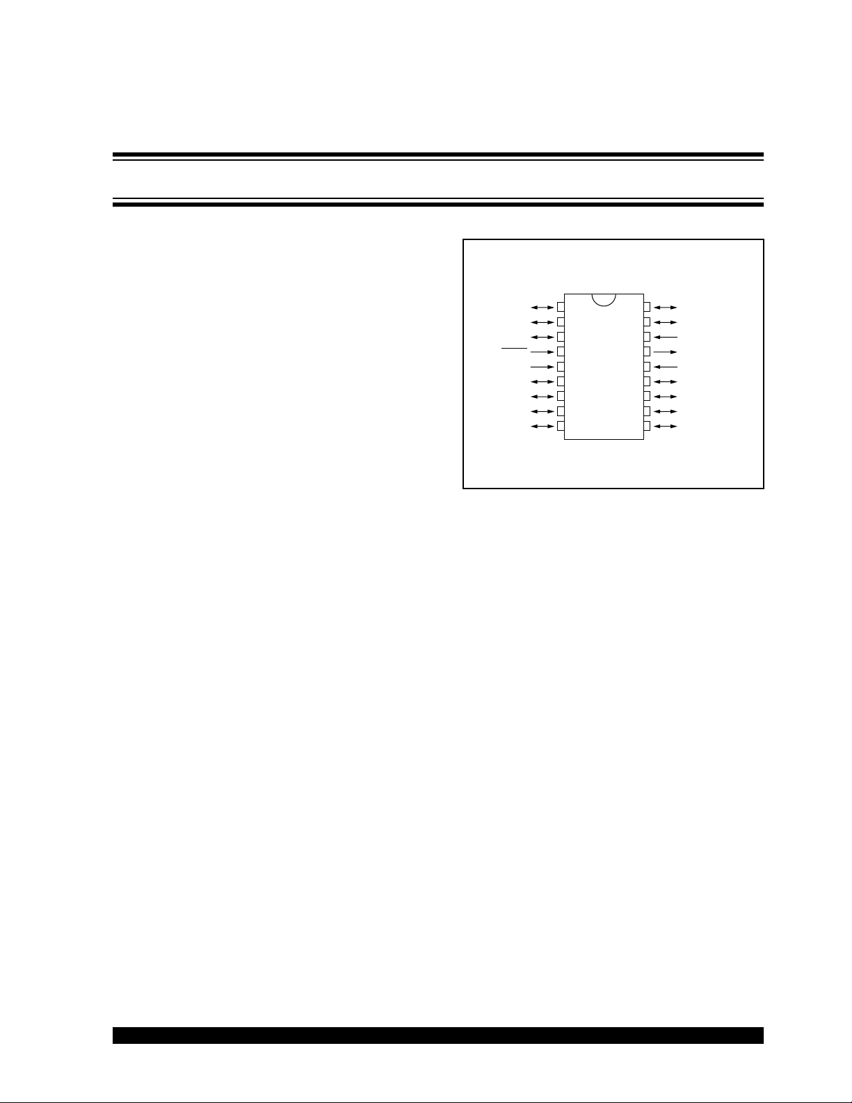
Pin Diagram
PDIP, SOIC
RA2
RA3
RA4/T0CKI
MCLR
VSS
RB0/INT
RB1
RB2
RB3
•1
2
3
4
5
6
7
8
9
18
17
PIC16C84
16
15
14
13
12
11
10
CMOS Technology:
•Low-power, high-speed CMOS EEPROM
technology
•Fully static design
•Wide operating voltage range:
-Commercial: 2.0V to 6.0V
-Industrial: 2.0V to 6.0V
•Low power consumption:
-< 2 mA typical @ 5V, 4 MHz
-60 µ A typical @ 2V, 32 kHz
-26 µ A typical standby current @ 2V
RA1
RA0
OSC1/CLKIN
OSC2/CLKOUT
V
DD
RB7
RB6
RB5
RB4
1997 Microchip Technology Inc. DS30445C-page 1
Page 2

PIC16C84
Table of Contents
1.0 General Description....................................................................................................................................................................... 3
2.0 PIC16C84 Device Varieties ........................................................................................................................................................... 5
3.0 Architectural Overview...................................................................................................................................................................7
4.0 Memory Organization................................................................................................................................................................... 11
5.0 I/O Ports....................................................................................................................................................................................... 19
6.0 Timer0 Module and TMR0 Register............................................................................................................................................. 25
7.0 Data EEPROM Memory............................................................................................................................................................... 31
8.0 Special Features of the CPU ....................................................................................................................................................... 35
9.0 Instruction Set Summary.............................................................................................................................................................. 51
10.0 Development Support.................................................................................................................................................................. 67
11.0 Electrical Characteristics for PIC16C84....................................................................................................................................... 71
12.0 DC & AC Characteristics Graphs/Tables for PIC16C84.............................................................................................................. 83
13.0 Packaging Information................................................................................................................................................................. 97
Appendix A: Feature Improvements - From PIC16C5X To PIC16C84............................................................................................ 99
Appendix B: Code Compatibility - from PIC16C5X to PIC16C84.................................................................................................... 99
Appendix C: What’s New In This Data Sheet................................................................................................................................. 100
Appendix D: What’s Changed In This Data Sheet......................................................................................................................... 100
Appendix E: Conversion Considerations - PIC16C84 to PIC16F83/F84 And PIC16CR83/CR84.................................................. 101
Index .................................................................................................................................................................................................. 103
On-Line Support................................................................................................................................................................................. 105
PIC16C84 Product Identification System........................................................................................................................................... 107
Sales and Support.............................................................................................................................................................................. 107
To Our Valued Customers
We constantly strive to improve the quality of all our products and documentation. We have spent a great deal of
time to ensure that these documents are correct. However, we realize that we may have missed a few things. If you
find any information that is missing or appears in error, please use the reader response form in the back of this data
sheet to inform us. We appreciate your assistance in making this a better document.
DS30445C-page 2
1997 Microchip Technology Inc.
Page 3

PIC16C84
1.0 GENERAL DESCRIPTION
The PIC16C84 is a low-cost, high-performance,
CMOS, fully-static, 8-bit microcontroller.
All PIC16/17 microcontrollers employ an advanced
RISC architecture. PIC16CXX devices have enhanced
core features, eight-le vel deep stack, and multiple internal and external interrupt sources. The separate
instruction and data buses of the Harvard architecture
allow a 14-bit wide instruction word with a separate
8-bit wide data bus. The two stage instruction pipeline
allows all instructions to execute in a single cycle,
except for program branches (which require two
cycles). A total of 35 instructions (reduced instruction
set) are available. Additionally, a large register set is
used to achieve a very high performance level.
PIC16CXX microcontrollers typically achieve a 2:1
code compression and up to a 2:1 speed improvement
(at 10 MHz) over other 8-bit microcontrollers in their
class.
The PIC16C84 has 36 bytes of RAM, 64 bytes of Data
EEPROM memory, and 13 I/O pins. A timer/counter is
also available.
The PIC16CXX family has special features to reduce
external components, thus reducing cost, enhancing
system reliability and reducing power consumption.
There are four oscillator options, of which the single pin
RC oscillator provides a low-cost solution, the LP
oscillator minimizes power consumption, XT is a
standard crystal, and the HS is for High Speed crystals.
The SLEEP (power-down) mode offers power savings.
The user can wake the chip from sleep through sev er al
external and internal interrupts and resets.
A highly reliable Watchdog Timer with its own on-chip
RC oscillator provides protection against software lockup.
The PIC16C84 EEPROM program memory allows the
same device package to be used for prototyping and
production. In-circuit reprogrammability allows the
code to be updated without the device being removed
from the end application. This is useful in the
development of many applications where the device
may not be easily accessible, but the prototypes may
require code updates. This is also useful for remote
applications where the code may need to be updated
(such as rate information).
Table 1-1 lists the features of the PIC16C84. A simplified block diagram of the PIC16C84 is shown in
Figure 3-1.
The PIC16C84 fits perfectly in applications ranging
from high speed automotive and appliance motor
control to low-power remote sensors, electronic locks,
security devices and smart cards. The EEPROM
technology makes customization of application
programs (transmitter codes, motor speeds, receiver
frequencies, security codes, etc.) extremely fast and
convenient. The small footprint packages make this
microcontroller series perfect for all applications with
space limitations. Low cost, low power, high
performance, ease of use and I/O flexibility make the
PIC16C84 very versatile even in areas where no
microcontroller use has been considered before
(e.g., timer functions, serial communication, capture
and compare, PWM functions and co-processor
applications).
The serial in-system programming feature (via two
pins) offers flexibility of customizing the product after
complete assembly and testing. This feature can be
used to serialize a product, store calibration data, or
program the device with the current firmware before
shipping.
1.1 F
Those users familiar with the PIC16C5X family of
microcontrollers will realize that this is an enhanced
version of the PIC16C5X architecture. Please refer to
Appendix A for a detailed list of enhancements. Code
written for PIC16C5X can be easily ported to the
PIC16C84 (Appendix B).
1.2 De
The PIC16CXX family is supported by a full-featured
macro assembler, a software simulator, an in-circuit
emulator, a low-cost development programmer and a
full-featured programmer. A “C” compiler and fuzzy
logic support tools are also available.
amily and Upward Compatibility
velopment Support
1997 Microchip Technology Inc. DS30445C-page 3
Page 4

PIC16C84
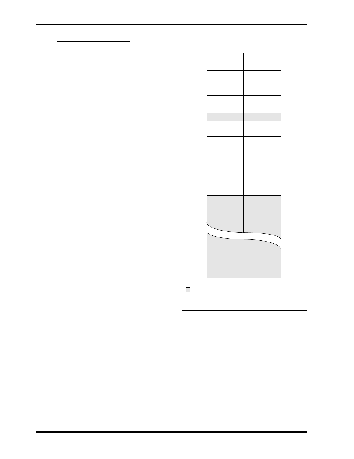
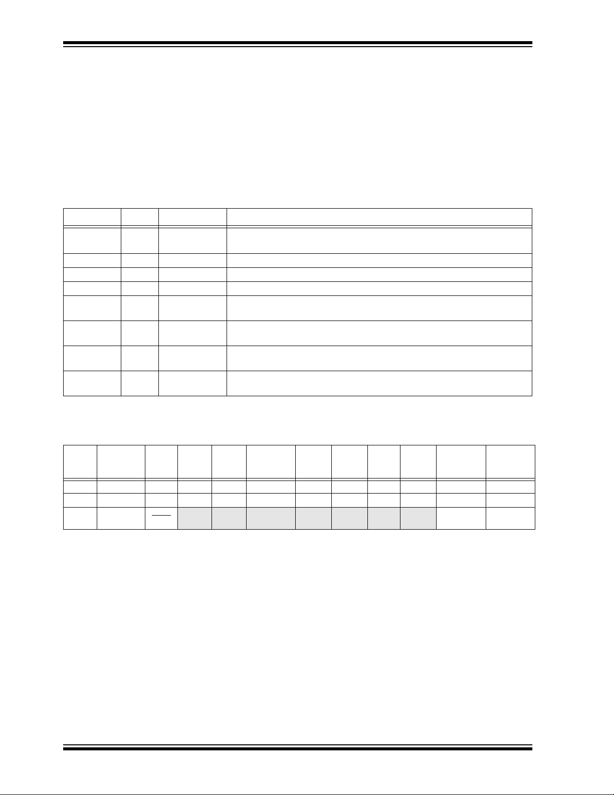
TABLE 1-1 PIC16C8X FAMILY OF DEVICES
PIC16F83
Clock
Memory
Peripherals Timer Module(s) TMR0 TMR0 TMR0 TMR0
Features
All PICmicro™ Family devices have P o w er-on Reset, selectable W atchdog Timer , selectable code protect and high I/O current capability. All PIC16C8X Family devices use serial programming with clock pin RB6 and data pin RB7.
Maximum Frequency
of Operation (MHz)
Flash Program Memory 512 — 1K —
EEPROM Program Memory — — — —
ROM Program Memory — 512 — 1K
Data Memory (bytes) 36 36 68 68
Data EEPROM (bytes) 64 64 64 64
Interrupt Sources 4 4 4 4
I/O Pins 13 13 13 13
Voltage Range (Volts) 2.0-6.0 2.0-6.0 2.0-6.0 2.0-6.0
Packages 18-pin DIP,
10 10 10 10
SOIC
PIC16CR83 PIC16F84 PIC16CR84
18-pin DIP,
SOIC
18-pin DIP,
SOIC
18-pin DIP,
SOIC
DS30445C-page 4
1997 Microchip Technology Inc.
Page 5

2.0 PIC16C84 DEVICE VARIETIES
A variety of frequency ranges and packaging options
are available . Depending on application and production
requirements the proper device option can be selected
using the information in this section. When placing
orders, please use the “PIC16C84 Product
Identification System” at the back of this data sheet to
specify the correct part number.
There are two device “types” as indicated in the device
number.
1. C , as in PIC16 C 84. These devices have
EEPROM program memory and operate over
the standard voltage range.
2. LC , as in PIC16 LC 84. These devices have
EEPROM program memory and operate over an
extended voltage range.
When discussing memory maps and other architectural
features, the use of C also implies the LC versions.
PIC16C84
2.1 Electricall
These devices are offered in the lower cost plastic
package, even though the device can be erased and
reprogrammed. This allows the same device to be used
for prototype development and pilot programs as well
as production.
A further advantage of the electrically erasable version
is that they can be erased and reprogrammed in-circuit,
or by device programmers, such as Microchip's
PICSTART
Plus or PRO MATE
y Erasable Devices
II programmers.
1997 Microchip Technology Inc. DS30445C-page 5
Page 6

PIC16C84
NOTES:
DS30445C-page 6
1997 Microchip Technology Inc.
Page 7

PIC16C84
3.0 ARCHITECTURAL OVERVIEW
The high performance of the PIC16CXX family can be
attributed to a number of architectural features
commonly found in RISC microprocessors. To begin
with, the PIC16CXX uses a Harvard architecture. This
architecture has the program and data accessed from
separate memories. So the device has a program
memory bus and a data memory bus. This improves
bandwidth over traditional von Neumann architecture
where program and data are fetched from the same
memory (accesses over the same bus). Separating
program and data memory further allows instructions
to be sized differently than the 8-bit wide data word.
PIC16CXX opcodes are 14-bits wide, enabling single
word instructions. The full 14-bit wide program memory
bus fetches a 14-bit instruction in a single cycle. A twostage pipeline overlaps fetch and execution of instructions (Example 3-1). Consequently , all instructions e xecute in a single cycle (400 ns @ 10 MHz) except for
program branches.
The PIC16C84 addresses 1K x 14 program memory.
All program memory is internal.
PIC16CXX devices can directly or indirectly address its
register files or data memory. All special function
registers including the program counter are mapped in
the data memory. An orthogonal (symmetrical)
instruction set that makes it possible to carry out any
operation on any register using any addressing mode.
This symmetrical nature and lack of ‘special optimal
situations’ make programming with the PIC16CXX
simple yet efficient. In addition, the learning curve is
reduced significantly.
The PIC16C84 has 36 x 8 SRAM and 64 x 8 EEPROM
data memory.
PIC16CXX devices contain an 8-bit ALU and working
register. The ALU is a general pur pose ar ithmetic unit.
It performs arithmetic and Boolean functions between
data in the working register and any register file.
The ALU is 8-bits wide and capable of addition,
subtraction, shift and logical operations. Unless
otherwise mentioned, arithmetic operations are two's
complement in nature. In two-operand instructions,
typically one operand is the working register
(W register), and the other operand is a file register or
an immediate constant. In single operand instructions,
the operand is either the W register or a file register.
The W register is an 8-bit working register used for ALU
operations. It is not an addressable register.
Depending on the instruction executed, the ALU may
affect the values of the Carry (C), Digit Carry (DC), and
Zero (Z) bits in the STATUS register. The C and DC bits
operate as a borro
respectively, in subtraction. See the SUBLW and SUBWF
instructions for examples.
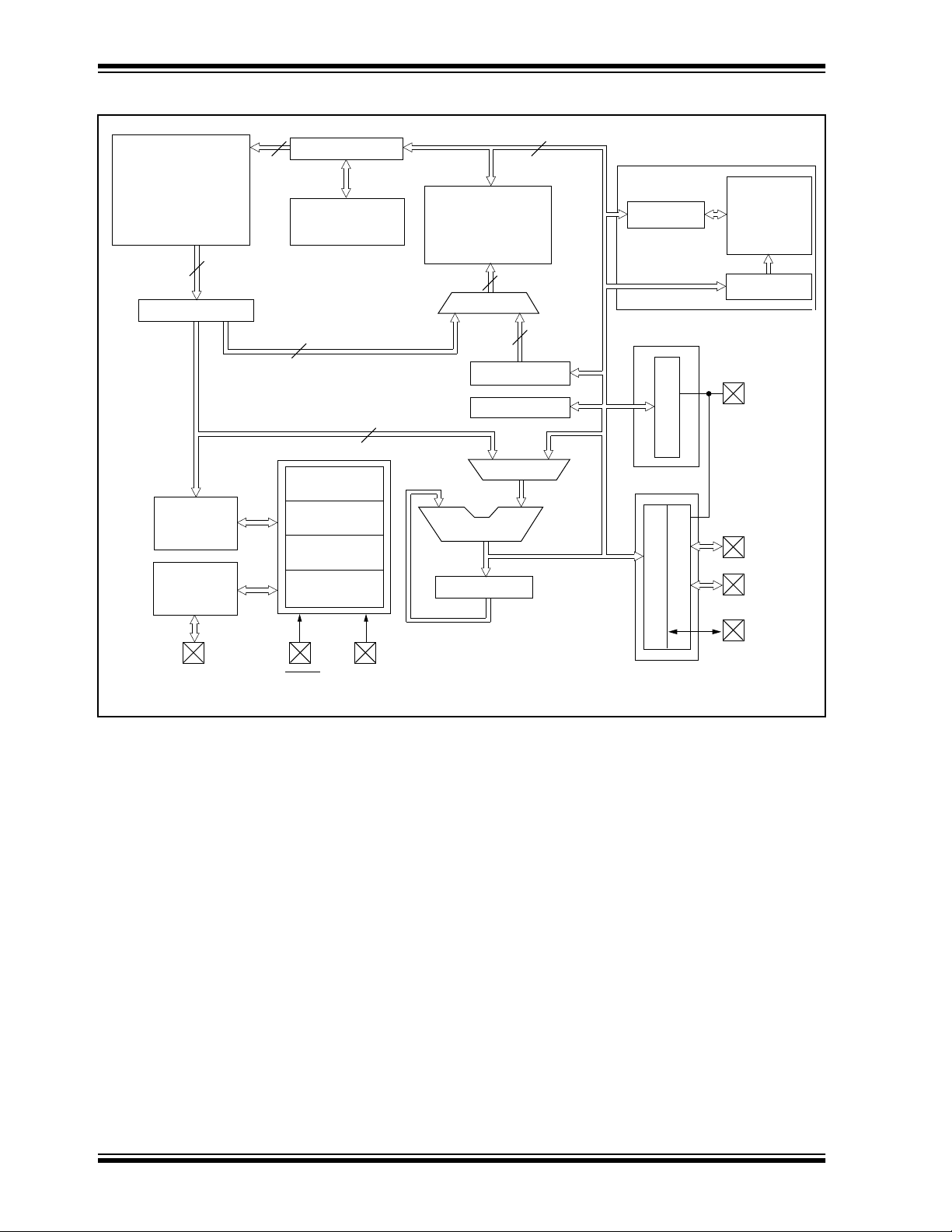
A simplified block diagram for the PIC16C84 is shown
in Figure 3-1, its corresponding pin description is
shown in Table 3-1.
w and digit borrow out bit,
1997 Microchip Technology Inc. DS30445C-page 7
Page 8
PIC16C84
FIGURE 3-1: PIC16C84 BLOCK DIAGRAM
EEPROM
Program
Memory
1K x 14
Program
Bus 14
Instruction reg
Instruction
Decode &
Control
Timing
Generation
13
Program Counter
8 Level Stack
5
Power-up
Timer
Oscillator
Start-up Timer
Power-on
Reset
Watchdog
Timer
(13-bit)
Direct Addr
8
Data Bus 8
RAM
File Registers
36 x 8
7
RAM Addr
Addr Mux
7
FSR reg
STATUS reg
MUX
ALU
W reg
Indirect
Addr
EEPROM Data Memory
EEDATA
TMR0
I/O Ports
EEPROM
Data Memory
64 x 8
EEADR
RA4/T0CKI
RA3:RA0
RB7:RB1
OSC2/CLKOUT
OSC1/CLKIN
MCLR
RB0/INT
VDD, VSS
DS30445C-page 8
1997 Microchip Technology Inc.
Page 9

2:
PIC16C84
TABLE 3-1 PIC16C8X PINOUT DESCRIPTION
DIP
Pin Name
OSC1/CLKIN 16 16 I ST/CMOS
OSC2/CLKOUT 15 15 O — Oscillator crystal output. Connects to crystal or resonator in crys-
MCLR
RA0 17 17 I/O TTL
RA1 18 18 I/O TTL
RA2 1 1 I/O TTL
RA3 2 2 I/O TTL
RA4/T0CKI 3 3 I/O ST Can also be selected to be the clock input to the TMR0 timer/
RB0/INT 6 6 I/O TTL RB0/INT can also be selected as an external interrupt pin.
RB1 7 7 I/O TTL
RB2 8 8 I/O TTL
RB3 9 9 I/O TTL
RB4 10 10 I/O TTL Interrupt on change pin.
RB5 11 11 I/O TTL Interrupt on change pin.
RB6 12 12 I/O TTL/ST
RB7 13 13 I/O TTL/ST
V
SS
V
DD
Legend: I= input O = output I/O = Input/Output P = power
Note 1: This buffer is a Schmitt Trigger input when configured in RC oscillator mode and a CMOS input otherwise.
This buffer is a Schmitt Trigger input when used in serial programming mode.
SOIC
No.
14 14 P — Positive supply for logic and I/O pins.
— = Not used TTL = TTL input ST = Schmitt Trigger input
No.
4 4 I/P ST Master clear (reset) input/programming voltage input. This pin is an
5 5 P — Ground reference for logic and I/O pins.
I/O/P
Type
Buffer
Type
(2)
(2)
Description
(1)
Oscillator crystal input/external clock source input.
tal oscillator mode. In RC mode , OSC2 pin outputs CLK OUT which
has 1/4 the frequency of OSC1, and denotes the instruction cycle
rate.
active low reset to the device.
PORTA is a bi-directional I/O port.
counter. Output is open drain type.
PORTB is a bi-directional I/O port. PORTB can be software programmed for internal weak pull-up on all inputs.
Interrupt on change pin. Serial programming clock.
Interrupt on change pin. Serial programming data.
1997 Microchip Technology Inc. DS30445C-page 9
Page 10
PIC16C84
3.1 Clocking Scheme/Instruction Cycle
The clock input (from OSC1) is internally divided by
four to generate four non-overlapping quadrature
clocks namely Q1, Q2, Q3 and Q4. Internally, the
program counter (PC) is incremented every Q1, the
instruction is fetched from the program memory and
latched into the instruction register in Q4. The
instruction is decoded and executed during the
following Q1 through Q4. The clocks and instruction
execution flow is shown in Figure 3-2.
FIGURE 3-2: CLOCK/INSTRUCTION CYCLE
Q2 Q3 Q4
OSC1
Q1
Q2
Q3
Q4
PC
OSC2/CLKOUT
(RC mode)
Q1
Fetch INST (PC)
Execute INST (PC-1)
PC
Q1
Execute INST (PC)
3.2 Instruction Flow/Pipelining
An “Instruction Cycle” consists of four Q cycles (Q1,
Q2, Q3 and Q4). The instruction fetch and execute are
pipelined such that fetch takes one instruction cycle
while decode and execute takes another instruction
cycle. However, due to the pipelining, each instruction
effectively executes in one cycle. If an instruction
causes the program counter to change (e.g., GOTO )
then two cycles are required to complete the instruction
(Example 3-1).
A fetch cycle begins with the Program Counter (PC)
incrementing in Q1.
In the execution cycle , the fetched instruction is latched
into the “Instruction Register” in cycle Q1. This
instruction is then decoded and executed during the
Q2, Q3, and Q4 cycles. Data memory is read during Q2
(operand read) and written during Q4 (destination
write).
Q2 Q3 Q4
PC+1 PC+2
Fetch INST (PC+1)
Q2 Q3 Q4
Q1
Fetch INST (PC+2)
Execute INST (PC+1)
Internal
phase
clock
EXAMPLE 3-1: INSTRUCTION PIPELINE FLOW
1. MOVLW 55h
2. MOVWF PORTB
3. CALL SUB_1
4. BSF PORTA, BIT3
All instructions are single cycle, except for any program branches. These take two cycles since the fetch
instruction is “flushed” from the pipeline while the new instruction is being fetched and then executed.
DS30445C-page 10
Fetch 1 Execute 1
Fetch 2 Execute 2
Fetch 3 Execute 3
Fetch 4 Flush
Fetch SUB_1 Execute SUB_1
1997 Microchip Technology Inc.
Page 11
PIC16C84
4.0 MEMORY ORGANIZATION
There are two memory blocks in the PIC16C84. These
are the program memory and the data memory. Each
block has its own b us, so that access to each b lock can
occur during the same oscillator cycle.
The data memory can further be broken down into the
general purpose RAM and the Special Function
Registers (SFRs). The operation of the SFRs that
control the “core” are described here. The SFRs used
to control the peripheral modules are described in the
section discussing each individual peripheral module.
The data memory area also contains the data
EEPROM memory . This memory is not directly mapped
into the data memory, but is indirectly mapped. That is
an indirect address pointer specifies the address of the
data EEPROM memory to read/write. The 64 bytes of
data EEPROM memory have the address range
0h-3Fh. More details on the EEPROM memory can be
found in Section 7.0.
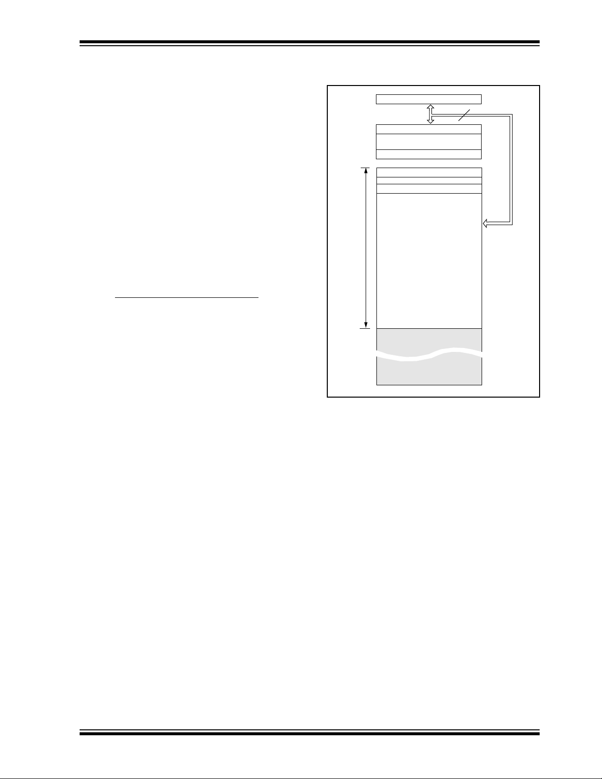
4.1 Pr
The PIC16CXX has a 13-bit program counter capable
of addressing an 8K x 14 program memory space. For
the PIC16C84, only the first 1K x 14 (0000h-03FFh) are
physically implemented (Figure 4-1). Accessing a location above the physically implemented address will
cause a wraparound. For example, locations 20h,
420h, 820h, C20h, 1020h, 1420h, 1820h, and 1C20h
will be the same instruction.
The reset vector is at 0000h and the interrupt vector is
at 0004h.
ogram Memory Organization
FIGURE 4-1: PROGRAM MEMORY MAP
AND STACK
PC<12:0>
CALL, RETURN
RETFIE, RETLW
Stack Level 1
Stack Level 8
Reset Vector
Peripheral Interrupt Vector
Space
User Memory
13
•
•
•
0000h
0004h
3FFh
1FFFh
1997 Microchip Technology Inc. DS30445C-page 11
Page 12
PIC16C84
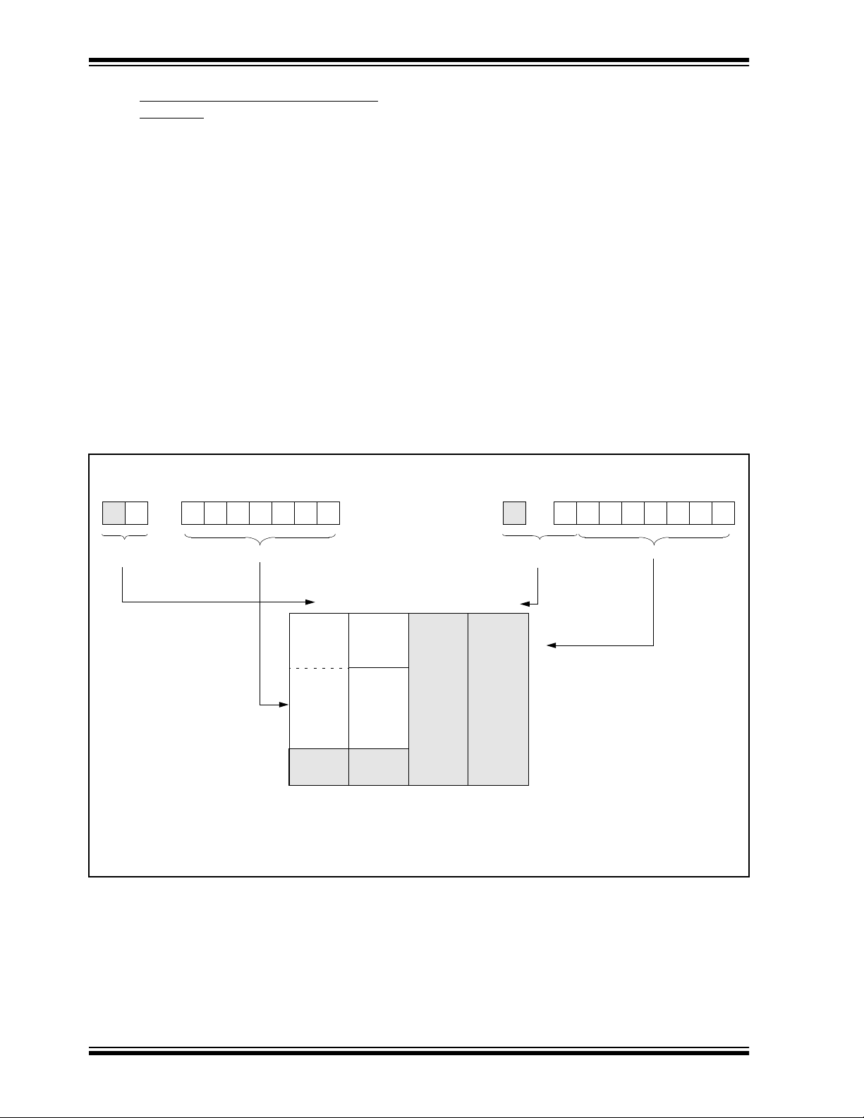
4.2 Data Memory Organization
The data memory is partitioned into two areas. The first
is the Special Function Registers (SFR) area, while the
second is the General Purpose Registers (GPR) area.
The SFRs control the operation of the device.
Portions of data memory are banked. This is for both
the SFR area and the GPR area. The GPR area is
banked to allow greater than 116 bytes of general
purpose RAM. The banked areas of the SFR are f or the
registers that control the peripheral functions. Banking
requires the use of control bits for bank selection.
These control bits are located in the STATUS Register.
Figure 4-2 shows the data memory map organization.
Instructions MOVWF and MOVF can move values from the
W register to any location in the register file (“F”), and
vice-versa.
The entire data memory can be accessed either
directly using the absolute address of each register file
or indirectly through the File Select Register (FSR)
(Section 4.5). Indirect addressing uses the present
value of the RP1:RP0 bits for access into the banked
areas of data memory.
Data memory is partitioned into two banks which
contain the general purpose registers and the special
function registers. Bank 0 is selected by clearing the
RP0 bit (STATUS<5>). Setting the RP0 bit selects
Bank 1. Each Bank extends up to 7Fh (128 bytes). The
first twelve locations of each Bank are reserved for the
Special Function Registers. The remainder are General Purpose Registers implemented as static RAM.
FIGURE 4-2: REGISTER FILE MAP
File Address
00h
01h
02h
03h
04h
05h
06h
07h
08h
09h
0Ah
0Bh
0Ch
2Fh
30h
Indirect addr.
TMR0 OPTION
STATUS
PORTA
PORTB
EEDATA
EEADR
PCLATH
INTCON
General
Purpose
registers
(SRAM)
(1)
PCL
FSR
36
Indirect addr.
PCL
STATUS
FSR
TRISA
TRISB
EECON1
EECON2
PCLATH
INTCON
Mapped
(accesses)
in Bank 0
File Address
(1)
(1)
80h
81h
82h
83h
84h
85h
86h
87h
88h
89h
8Ah
8Bh
8Ch
AFh
B0h
4.2.1 GENERAL PURPOSE REGISTER FILE All devices have some amount of General Purpose
Register (GPR) area. Each GPR is 8 bits wide and is
accessed either directly or indirectly through the FSR
(Section 4.5).
The GPR addresses in bank 1 are mapped to
addresses in bank 0. As an example, addressing location 0Ch or 8Ch will access the same GPR.
4.2.2 SPECIAL FUNCTION REGISTERS The Special Function Registers (Figure 4-2 and
Table 4-1) are used by the CPU and Peripheral
functions to control the device operation. These
registers are static RAM.
The special function registers can be classified into two
sets, core and peripheral. Those associated with the
core functions are described in this section. Those
related to the operation of the peripheral features are
described in the section for that specific feature.
7Fh
Unimplemented data memory location; read as '0'.
Note 1: Not a physical register.
Bank 0
Bank 1
FFh
DS30445C-page 12
1997 Microchip Technology Inc.
Page 13
TABLE 4-1 REGISTER FILE SUMMARY
PIC16C84
Address Name Bit 7 Bit 6 Bit 5 Bit 4 Bit 3 Bit 2 Bit 1 Bit 0
Bank 0
00h INDF Uses contents of FSR to address data memory (not a physical register)
01h TMR0 8-bit real-time clock/counter
02h PCL Low order 8 bits of the Program Counter (PC)
OPTION_
REG
(2)
IRP RP1 RP0
— — — RA4/T0CKI RA3 RA2 RA1 RA0 ---x xxxx ---u uuuu
— — — Write buffer for upper 5 bits of the PC
RBPU INTEDG T0CS T0SE PSA PS2 PS1 PS0
(2)
IRP RP1 RP0 TO PD Z DC C 0001 1xxx 000q quuu
— — — PORTA data direction register ---1 1111 ---1 1111
Unimplemented location, read as '0' ---- ---- ---- ----
03h STATUS
04h FSR Indirect data memory address pointer 0
05h PORTA
06h PORTB RB7 RB6 RB5 RB4 RB3 RB2 RB1 RB0/INT xxxx xxxx uuuu uuuu
07h Unimplemented location, read as '0' ---- ---- ---- ---08h EEDATA EEPROM data register xxxx xxxx uuuu uuuu
09h EEADR EEPROM address register xxxx xxxx uuuu uuuu
0Ah PCLATH
0Bh INTCON GIE EEIE T0IE INTE RBIE T0IF INTF RBIF 0000 000x 0000 000u
80h INDF Uses contents of FSR to address data memory (not a physical register) ---- ---- ---- ----
81h
82h PCL Low order 8 bits of Program Counter (PC) 0000 0000 0000 0000
83h STATUS
84h FSR Indirect data memory address pointer 0 xxxx xxxx uuuu uuuu
85h TRISA
86h TRISB PORTB data direction register 1111 1111 1111 1111
87h
88h EECON1 — — — EEIF WRERR WREN WR RD ---0 x000 ---0 q000
89h EECON2 EEPROM control register 2 (not a physical register) ---- ---- ---- ---0Ah PCLATH — — — Write buffer for upper 5 bits of the PC
0Bh INTCON GIE EEIE T0IE INTE RBIE T0IF INTF RBIF 0000 000x 0000 000u
TO
PD Z DC C
(1)
Bank 1
(1)
Value on
Power-on
Reset
---- ---- ---- ---xxxx xxxx uuuu uuuu
0000 0000 0000 0000
0001 1xxx 000q quuu
xxxx xxxx uuuu uuuu
---0 0000 ---0 0000
1111 1111 1111 1111
---0 0000 ---0 0000
Value on all
other resets
(Note3)
Legend: x = unknown, u = unchanged. - = unimplemented read as '0', q = value depends on condition.
Note 1: The upper byte of the program counter is not directly accessible. PCLATH is a slave register for PC<12:8>. The contents
of PCLATH can be transferred to the upper b yte of the program counter, but the contents of PC<12:8> is nev er transf erred
to PCLATH.
2: The T
O and PD status bits in the STATUS register are not affected by a MCLR reset.
3: Other (non power-up) resets include: external reset through MCLR and the Watchdog Timer Reset.
1997 Microchip Technology Inc. DS30445C-page 13
Page 14

PIC16C84
4.2.2.1 STATUS REGISTER
The STATUS register contains the arithmetic status of
the ALU, the RESET status and the bank select bit for
data memory.
As with any register, the STATUS register can be the
destination for any instruction. If the STA TUS register is
the destination for an instruction that affects the Z, DC
or C bits, then the write to these three bits is disabled.
These bits are set or cleared according to device logic.
Furthermore, the T
Therefore, the result of an instruction with the STATUS
register as destination may be different than intended.
For example, CLRF STATUS will clear the upper-three
bits and set the Z bit. This leaves the STATUS register
as 000u u1uu (where u = unchanged).
O and PD bits are not writable.
Only the BCF, BSF, SWAPF and MOVWF instructions
should be used to alter the ST ATUS register (T ab le 9-2)
because these instructions do not affect any status bit.
Note 1: The IRP and RP1 bits (ST ATUS<7:6>) are
Note 2: The C and DC bits operate as a borro
Note 3: When the STATUS register is the
FIGURE 4-3: STATUS REGISTER (ADDRESS 03h, 83h)
R/W-0 R/W-0 R/W-0 R-1 R-1 R/W-x R/W-x R/W-x
IRP RP1 RP0
bit7 bit0
bit 7: IRP: Register Bank Select bit (used for indirect addressing)
0 = Bank 0, 1 (00h - FFh)
1 = Bank 2, 3 (100h - 1FFh)
The IRP bit is not used by the PIC16C8X. IRP should be maintained clear.
bit 6-5: RP1:RP0: Register Bank Select bits (used for direct addressing)
00 = Bank 0 (00h - 7Fh)
01 = Bank 1 (80h - FFh)
10 = Bank 2 (100h - 17Fh)
11 = Bank 3 (180h - 1FFh)
Each bank is 128 bytes. Only bit RP0 is used by the PIC16C8X. RP1 should be maintained clear.
bit 4: TO: Time-out bit
1 = After power-up, CLRWDT instruction, or SLEEP instruction
0 = A WDT time-out occurred
bit 3: PD: Power-down bit
1 = After power-up or by the CLRWDT instruction
0 = By execution of the SLEEP instruction
bit 2: Z: Zero bit
1 = The result of an arithmetic or logic operation is zero
0 = The result of an arithmetic or logic operation is not zero
bit 1: DC: Digit carry/borro
1 = A carry-out from the 4th low order bit of the result occurred
0 = No carry-out from the 4th low order bit of the result
bit 0: C: Carry/borro
1 = A carry-out from the most significant bit of the result occurred
0 = No carry-out from the most significant bit of the result occurred
Note: For borro
the second operand. For rotate (RRF, RLF) instructions, this bit is loaded with either the high or
low order bit of the source register.
w bit (for ADDWF and ADDLW instructions)
TO PD
w bit (for ADDWF and ADDLW instructions) (For borrow the polarity is reversed)
w the polarity is reversed. A subtraction is executed by adding the two’s complement of
Z DC C R = Readable bit
not used by the PIC16C84 and should be
programmed as cleared. Use of these bits
as general purpose R/W bits is NOT
recommended, since this may affect
upward compatibility with future products.
w
and digit borrow out bit, respectively, in
subtraction. See the SUBLW and SUBWF
instructions for examples.
destination for an instruction that affects
the Z, DC or C bits, then the write to these
three bits is disabled. The specified bit(s)
will be updated according to device logic
W = Writable bit
U = Unimplemented bit,
read as ‘0’
- n = Value at POR reset
DS30445C-page 14 1997 Microchip Technology Inc.
Page 15

4.2.2.2 OPTION_REG REGISTER
The OPTION_REG register is a readable and writable
register which contains various control bits to configure
the TMR0/WDT prescaler, the external INT interrupt,
Note: When the prescaler is assigned to
the WDT (PSA = '1'), TMR0 has a 1:1
prescaler assignment.
TMR0, and the weak pull-ups on PORTB.
FIGURE 4-4: OPTION_REG REGISTER (ADDRESS 81h)
R/W-1 R/W-1 R/W-1 R/W-1 R/W-1 R/W-1 R/W-1 R/W-1
RBPU INTEDG T0CS T0SE PSA PS2 PS1 PS0 R = Readable bit
bit7 bit0
bit 7: RBPU: PORTB Pull-up Enable bit
1 = PORTB pull-ups are disabled
0 = PORTB pull-ups are enabled (by individual port latch values)
bit 6: INTEDG: Interrupt Edge Select bit
1 = Interrupt on rising edge of RB0/INT pin
0 = Interrupt on falling edge of RB0/INT pin
bit 5: T0CS: TMR0 Clock Source Select bit
1 = Transition on RA4/T0CKI pin
0 = Internal instruction cycle clock (CLKOUT)
bit 4: T0SE: TMR0 Source Edge Select bit
1 = Increment on high-to-low transition on RA4/T0CKI pin
0 = Increment on low-to-high transition on RA4/T0CKI pin
bit 3: PSA: Prescaler Assignment bit
1 = Prescaler assigned to the WDT
0 = Prescaler assigned to TMR0
bit 2-0: PS2:PS0: Prescaler Rate Select bits
Bit Value TMR0 Rate WDT Rate
000
001
010
011
100
101
110
111
1 : 2
1 : 4
1 : 8
1 : 16
1 : 32
1 : 64
1 : 128
1 : 256
1 : 1
1 : 2
1 : 4
1 : 8
1 : 16
1 : 32
1 : 64
1 : 128
W = Writable bit
U = Unimplemented bit,
read as ‘0’
- n = Value at POR reset
PIC16C84
1997 Microchip Technology Inc. DS30445C-page 15
Page 16

PIC16C84
4.2.2.3 INTCON REGISTER
The INTCON register is a readable and writable
register which contains the various enable bits for all
interrupt sources.
FIGURE 4-5: INTCON REGISTER (ADDRESS 0Bh, 8Bh)
R/W-0 R/W-0 R/W-0 R/W-0 R/W-0 R/W-0 R/W-0 R/W-x
GIE EEIE T0IE INTE RBIE T0IF INTF RBIF R = Readable bit
bit7 bit0
bit 7: GIE: Global Interrupt Enable bit
1 = Enables all un-masked interrupts
0 = Disables all interrupts
Note: For the operation of the interrupt structure, please refer to Section 8.5.
bit 6: EEIE: EE Write Complete Interrupt Enable bit
1 = Enables the EE write complete interrupt
0 = Disables the EE write complete interrupt
bit 5: T0IE: TMR0 Overflow Interrupt Enable bit
1 = Enables the TMR0 interrupt
0 = Disables the TMR0 interrupt
bit 4: INTE: RB0/INT Interrupt Enable bit
1 = Enables the RB0/INT interrupt
0 = Disables the RB0/INT interrupt
bit 3: RBIE: RB Port Change Interrupt Enable bit
1 = Enables the RB port change interrupt
0 = Disables the RB port change interrupt
bit 2: T0IF: TMR0 overflow interrupt flag bit
1 = TMR0 has overflowed (must be cleared in software)
0 = TMR0 did not overflow
bit 1: INTF: RB0/INT Interrupt Flag bit
1 = The RB0/INT interrupt occurred
0 = The RB0/INT interrupt did not occur
bit 0: RBIF: RB Port Change Interrupt Flag bit
1 = When at least one of the RB7:RB4 pins changed state (must be cleared in software)
0 = None of the RB7:RB4 pins have changed state
Note: Interrupt flag bits get set when an interrupt
condition occurs regardless of the state of
its corresponding enable bit or the global
enable bit, GIE (INTCON<7>).
W = Writable bit
U = Unimplemented bit,
- n = Value at POR reset
read as ‘0’
DS30445C-page 16 1997 Microchip Technology Inc.
Page 17
PIC16C84
4.3 Program Counter: PCL and PCLATH
The Program Counter (PC) is 13-bits wide. The low
byte is the PCL register, which is a readable and
writable register. The high byte of the PC (PC<12:8>) is
not directly readable nor writable and comes from the
PCLATH register . The PCLATH (PC latch high) register
is a holding register for PC<12:8>. The contents of
PCLATH are transferred to the upper byte of the
program counter when the PC is loaded with a new
value. This occurs during a CALL, GOTO or a wr ite to
PCL. The high bits of PC are loaded from PCLATH as
shown in Figure 4-6.
FIGURE 4-6: LOADING OF PC IN
DIFFERENT SITUATIONS
PCH PCL
12 8 7 0
PC
PCLATH<4:0>
5
PCLATH
PCH PCL
12 11 10 0
PC
2
8 7
PCLATH<4:3>
PCLATH
11
4.3.1 COMPUTED GOTO A computed GOT O is accomplished b y adding an offset
to the program counter (ADDWF PCL). When doing a
table read using a computed GOTO method, care
should be exercised if the table location crosses a PCL
memory boundary (each 256 word block). Refer to the
application note
“Implementing a Table Read”
8
INST with PCL
as dest
ALU result
GOTO, CALL
Opcode <10:0>
(AN556).
Note: The PIC16C84 ignores the PCLATH<4:3>
bits, which are used for program memory
pages 1, 2 and 3 (0800h - 1FFFh). The use
of PCLATH<4:3> as general purpose R/W
bits is not recommended since this may
affect upward compatibility with future
products.
4.4 Stack
The PIC16C84 has an 8 deep x 13-bit wide hardware
stack (Figure 4-1). The stack space is not part of either
program or data space and the stack pointer is not
readable or writable.
The entire 13-bit PC is “pushed” onto the stack when a
CALL instruction is executed or an interrupt is acknowledged. The stack is “popped” in the ev ent of a RETURN,
RETLW or a RETFIE instruction execution. PCLATH is
not affected by a push or a pop operation.
Note: There are no instruction mnemonics called
push or pop. These are actions that occur
from the execution of the CALL, RETURN,
RETLW, and RETFIE instructions, or the
vectoring to an interrupt address.
The stack operates as a circular buffer. That is, after the
stack has been pushed eight times, the ninth push ov erwrites the value that was stored from the first push. The
tenth push overwrites the second push (and so on).
If the stack is effectively popped nine times, the PC
value is the same as the value from the first pop.
Note: There are no status bits to indicate stack
overflow or stack underflow conditions.
4.3.2 PROGRAM MEMORY PAGING The PIC16C84 has 1K of program memory. The CALL
and GOTO instructions have an 11-bit address range.
This 11-bit address range allows a branch within a 2K
program memory page size. For future PIC16CXX
program memory expansion, there must be another
two bits to specify the program memory page. These
paging bits come from the PCLATH<4:3> bits
(Figure 4-6). When doing a CALL or a GOTO instruction,
the user must ensure that these page bits
(PCLATH<4:3>) are programmed to the desired
program memory page. If a CALL instruction (or
interrupt) is executed, the entire 13-bit PC is “pushed”
onto the stack (see next section). Therefore, manipulation of the PCLATH<4:3> is not required for the return
instructions (which “pops” the PC from the stack).
1997 Microchip Technology Inc. DS30445C-page 17
Page 18
PIC16C84
4.5 Indirect Addressing; INDF and FSR
Registers
The INDF register is not a physical register. Addressing INDF actually addresses the register whose
address is contained in the FSR register (FSR is a
pointer
). This is indirect addressing.
EXAMPLE 4-1: INDIRECT ADDRESSING
• Register file 05 contains the value 10h
• Register file 06 contains the value 0Ah
• Load the value 05 into the FSR register
• A read of the INDF register will return the value of
10h
• Increment the value of the FSR register by one
(FSR = 06)
• A read of the INDF register now will return the
value of 0Ah.
Reading INDF itself indirectly (FSR = 0) will produce
00h. Writing to the INDF register indirectly results in a
no-operation (although STATUS bits may be affected).
FIGURE 4-7: DIRECT/INDIRECT ADDRESSING
Direct Addressing
RP1 RP0 6
from opcode
0 IRP 7 (FSR) 0
A simple program to clear RAM locations 20h-2Fh
using indirect addressing is shown in Example 4-2.
EXAMPLE 4-2: HOW TO CLEAR RAM
USING INDIRECT
ADDRESSING
movlw 0x20 ;initialize pointer
movwf FSR ; to RAM
NEXT clrf INDF ;clear INDF register
incf FSR ;inc pointer
btfss FSR,4 ;all done?
goto NEXT ;NO, clear next
CONTINUE
: ;YES, continue
An effective 9-bit address is obtained b y concatenating
the 8-bit FSR register and the IRP bit (STATUS<7>), as
shown in Figure 4-7. However, IRP is not used in the
PIC16C84.
Indirect Addressing
bank select location select
Data
Memory
00 01 10 11
00h
not used
0Bh
0Ch
Addresses
map back
to Bank 0
2Fh
30h
7Fh
Bank 0 Bank 1 Bank 2 Bank 3
bank select location select
00h
not used
7Fh
DS30445C-page 18 1997 Microchip Technology Inc.
Page 19
PIC16C84
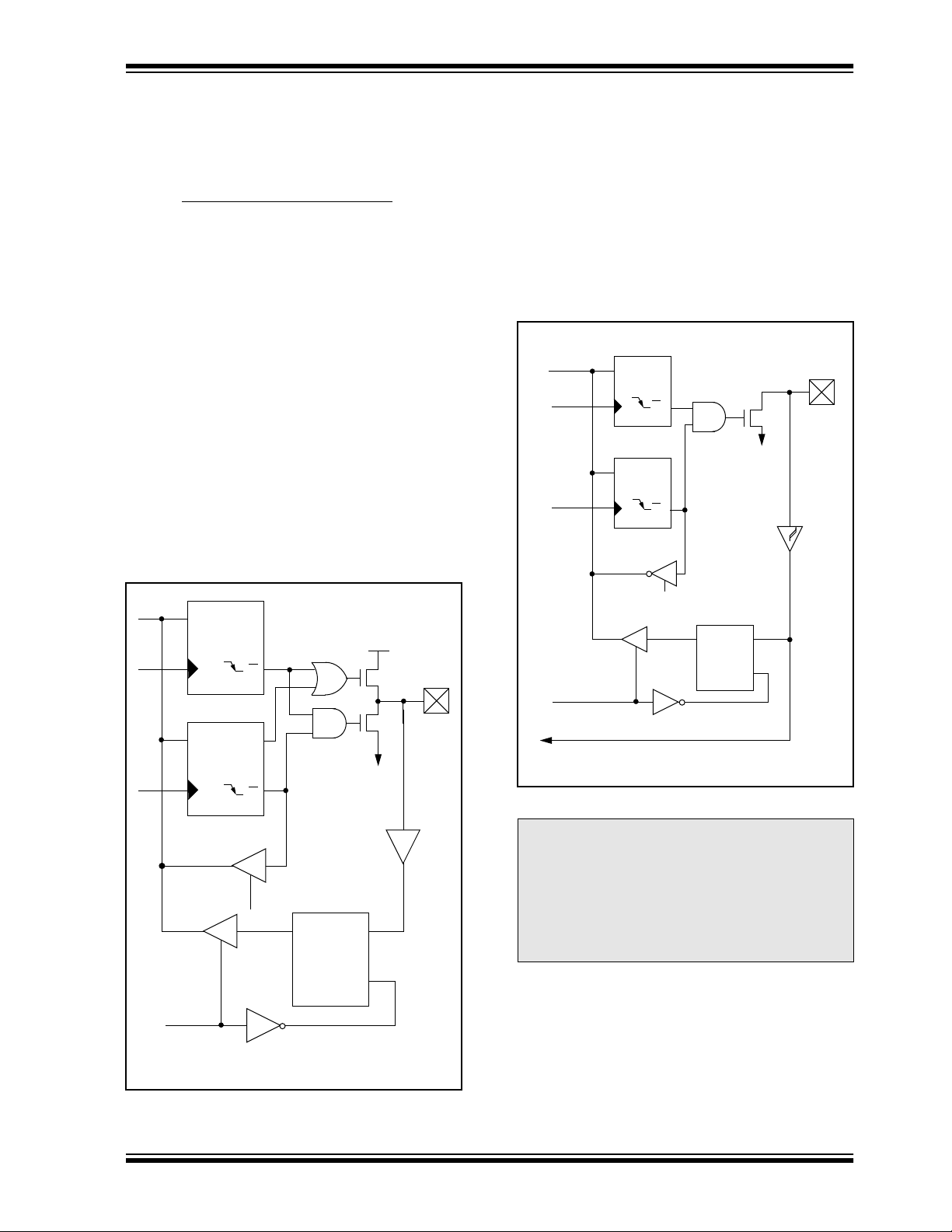
5.0 I/O PORTS
The PIC16C84 has two ports, PORTA and PORTB.
Some port pins are multiplexed with an alternate function for other features on the device.
5.1 PORTA and TRISA Registers
PORTA is a 5-bit wide latch. RA4 is a Schmitt Trigger
input and an open drain output. All other RA port pins
have TTL input levels and full CMOS output drivers. All
pins have data direction bits (TRIS registers) which can
configure these pins as output or input.
Setting a TRISA bit (=1) will make the corresponding
PORTA pin an input, i.e., put the corresponding output
driver in a hi-impedance mode. Clearing a TRISA bit
(=0) will make the corresponding PORTA pin an output,
i.e., put the contents of the output latch on the selected
pin.
Reading the PORTA register reads the status of the pins
whereas writing to it will write to the port latch. All write
operations are read-modify-write operations. So a write
to a port implies that the port pins are first read, then this
value is modified and written to the port data latch.
The RA4 pin is multiplexed with the TMR0 clock input.
FIGURE 5-1: BLOCK DIAGRAM OF PINS
RA3:RA0
Data
bus
WR
Port
WR
TRIS
CK
Data Latch
D
CK
TRIS Latch
QD
Q
Q
Q
RD TRIS
Q D
VDD
P
N
VSS
TTL
input
buffer
I/O pin
EXAMPLE 5-1: INITIALIZING PORTA
CLRF PORTA ; Initialize PORTA by
; setting output
; data latches
BSF STATUS, RP0 ; Select Bank 1
MOVLW 0x0F ; Value used to
; initialize data
; direction
MOVWF TRISA ; Set RA<3:0> as inputs
; RA4 as outputs
; TRISA<7:5> are always
; read as '0'.
FIGURE 5-2: BLOCK DIAGRAM OF PIN RA4
Data
bus
WR
PORT
WR
TRIS
RD PORT
TMR0 clock input
Note: I/O pin has protection diodes to V
Note: For crystal oscillator configurations
operating below 500 kHz, the device may
generate a spurious internal Q-clock when
PORTA<0> switches state. This does not
occur with an external clock in RC mode.
To avoid this, the RA0 pin should be kept
static, i.e. in input/output mode, pin RA0
should not be toggled.
QD
Q
CK
Data Latch
QD
Q
CK
TRIS Latch
RD TRIS
Schmitt
Trigger
input
buffer
Q D
EN
EN
N
V
SS
RA4 pin
SS only.
EN
RD PORT
Note: I/O pins have protection diodes to VDD and VSS.
1997 Microchip Technology Inc. DS30445C-page 19
Page 20

PIC16C84
TABLE 5-1 PORTA FUNCTIONS
Name Bit0 Buffer Type Function
RA0 bit0 TTL Input/output
RA1 bit1 TTL Input/output
RA2 bit2 TTL Input/output
RA3 bit3 TTL Input/output
RA4/T0CKI bit4 ST Input/output or external clock input for TMR0.
Output is open drain type.
Legend: TTL = TTL input, ST = Schmitt Trigger input
TABLE 5-2 SUMMARY OF REGISTERS ASSOCIATED WITH PORTA
Address Name Bit 7 Bit 6 Bit 5 Bit 4 Bit 3 Bit 2 Bit 1 Bit 0
05h PORT A
85h TRISA — — — TRISA4 TRISA3 TRISA2 TRISA1 TRISA0 ---1 1111 ---1 1111
Legend: x = unknown, u = unchanged, - = unimplemented read as '0'. Shaded cells are unimplemented, read as '0'
— — — RA4/T0CKI RA3 RA2 RA1 RA0 ---x xxxx ---u uuuu
Value on
Power-on
Reset
Value on all
other resets
DS30445C-page 20 1997 Microchip Technology Inc.
Page 21
PIC16C84
5.2 PORTB and TRISB Registers
PORTB is an 8-bit wide bi-directional port. The
corresponding data direction register is TRISB. A '1' on
any bit in the TRISB register puts the corresponding
output driver in a hi-impedance mode. A '0' on any bit
in the TRISB register puts the contents of the output
latch on the selected pin(s).
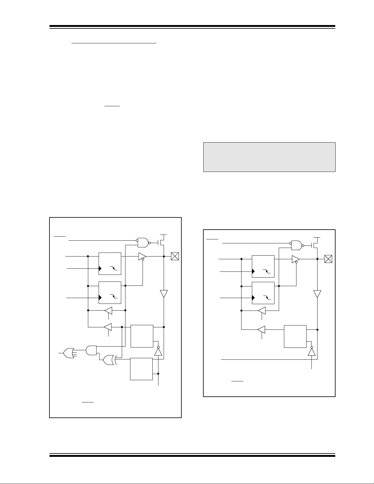
Each of the PORTB pins have a weak internal pull-up.
A single control bit can turn on all the pull-ups. This is
done by clearing the RBPU
(OPTION_REG<7>) bit.
The weak pull-up is automatically turned off when the
port pin is configured as an output. The pull-ups are
disabled on a Power-on Reset.
Four of PORTB’s pins, RB7:RB4, have an interrupt on
change feature. Only pins configured as inputs can
cause this interrupt to occur (i.e., any RB7:RB4 pin
configured as an output is excluded from the interrupt
on change comparison). The pins value in input mode
are compared with the old value latched on the last
read of PORTB. The “mismatch” outputs of the pins are
OR’ed together to generate the RB port
change interrupt.
FIGURE 5-3: BLOCK DIAGRAM OF PINS
RB7:RB4
DD
V
P
weak
pull-up
I/O
pin
TTL
Input
Buffer
(2)
RBPU
Data bus
WR Port
WR TRIS
(1)
Data Latch
QD
CK
TRIS Latch
QD
CK
This interrupt can wake the device from SLEEP. The
user, in the interrupt service routine, can clear the
interrupt in the following manner:
a) Read (or write) PORTB. This will end the mis-
match condition.
b) Clear flag bit RBIF.
A mismatch condition will continue to set the RBIF bit.
Reading PORTB will end the mismatch condition, and
allow the RBIF bit to be cleared.
This interrupt on mismatch feature, together with
software configurable pull-ups on these four pins allow
easy interface to a key pad and make it possible for
wake-up on key-depression (see AN552 in the
Embedded Control Handbook).
Note 1: If a change on the I/O pin should occur
when a read operation of PORTB is being
executed (start of the Q2 cycle), the RBIF
interrupt flag bit may not be set.
The interrupt on change feature is recommended for
wake-up on key depression operation and operations
where PORTB is only used for the interrupt on change
feature. Polling of PORTB is not recommended while
using the interrupt on change feature.
FIGURE 5-4: BLOCK DIAGRAM OF PINS
RB3:RB0
DD
(1)
RBPU
Data bus
WR Port
WR TRIS
Data Latch
QD
CK
TRIS Latch
QD
CK
V
P
weak
pull-up
I/O
pin
TTL
Input
Buffer
(2)
RD TRIS
RD Port
Set RBIF
From other
RB7:RB4 pins
Note 1: TRISB = '1' enables weak pull-up
2: I/O pins have diode protection to V
= '0' in the OPTION_REG register).
(if RBPU
Latch
Q D
EN
Q D
EN
DD and VSS.
RD Port
RD TRIS
RD Port
RB0/INT
Note 1: TRISB = '1' enables weak pull-up
2: I/O pins have diode protection to V
= '0' in the OPTION_REG register).
(if RBPU
Q D
EN
RD Port
DD and VSS.
1997 Microchip Technology Inc. DS30445C-page 21
Page 22
PIC16C84
EXAMPLE 5-1: INITIALIZING PORTB
CLRF PORTB ; Initialize PORTB by
; setting output
; data latches
BSF STATUS, RP0 ; Select Bank 1
MOVLW 0xCF ; Value used to
; initialize data
; direction
MOVWF TRISB ; Set RB<3:0> as inputs
; RB<5:4> as outputs
; RB<7:6> as inputs
TABLE 5-3 PORTB FUNCTIONS
Name Bit Buffer Type I/O Consistency Function
RB0/INT bit0 TTL Input/output pin or external interrupt input. Internal software
programmable weak pull-up.
RB1 bit1 TTL Input/output pin. Internal software programmable weak pull-up.
RB2 bit2 TTL Input/output pin. Internal software programmable weak pull-up.
RB3 bit3 TTL Input/output pin. Internal software programmable weak pull-up.
RB4 bit4 TTL Input/output pin (with interrupt on change). Internal software programma-
ble weak pull-up.
RB5 bit5 TTL Input/output pin (with interrupt on change). Internal software programma-
ble weak pull-up.
(1)
RB6 bit6 TTL/ST
RB7 bit7 TTL/ST
Legend: TTL = TTL input, ST = Schmitt Trigger.
Note 1: This buffer is a Schmitt Trigger input when used in serial programming mode.
Input/output pin (with interrupt on change). Internal software programma-
ble weak pull-up. Serial programming clock.
(1)
Input/output pin (with interrupt on change). Internal software programma-
ble weak pull-up. Serial programming data.
TABLE 5-4 SUMMARY OF REGISTERS ASSOCIATED WITH PORTB
Address Name Bit 7 Bit 6 Bit 5 Bit 4 Bit 3 Bit 2 Bit 1 Bit 0
06h PORTB RB7 RB6 RB5 RB4 RB3 RB2 RB1 RB0/INT xxxx xxxx uuuu uuuu
86h TRISB TRISB7 TRISB6 TRISB5 TRISB4 TRISB3 TRISB2 TRISB1 TRISB0 1111 1111 1111 1111
81h
Legend: x = unknown, u = unchanged. Shaded cells are not used by PORTB.
OPTION_
REG
RBPU
INTEDG T0CS T0SE PSA PS2 PS1 PS0
Value on
Power-on
Reset
1111 1111 1111 1111
Value on all
other resets
DS30445C-page 22 1997 Microchip Technology Inc.
Page 23
PIC16C84
5.3 I/O Programming Considerations
5.3.1 BI-DIRECTIONAL I/O PORTS Any instruction which writes, operates internally as a
read followed by a write operation. The BCF and BSF
instructions, for example, read the register into the
CPU, ex ecute the bit operation and write the result back
to the register. Caution must be used when these
instructions are applied to a port with both inputs and
outputs defined. For example, a BSF operation on bit5
of PORTB will cause all eight bits of PORTB to be read
into the CPU. Then the BSF operation takes place on
bit5 and PORTB is written to the output latches. If
another bit of PORTB is used as a bi-directional I/O pin
(i.e., bit0) and it is defined as an input at this time, the
input signal present on the pin itself would be read into
the CPU and rewritten to the data latch of this particular
pin, overwriting the previous content. As long as the pin
stays in the input mode, no problem occurs. However,
if bit0 is switched into output mode later on, the content
of the data latch is unknown.
Reading the port register, reads the values of the port
pins. Writing to the port register writes the value to the
port latch. When using read-modify-write instructions
(i.e., BCF, BSF , etc.) on a port, the value of the port pins
is read, the desired operation is done to this value, and
this value is then written to the port latch.
A pin actively outputting a Low or High should not be
driven from external devices at the same time in order
to change the level on this pin (“wired-or”, “wired-and”).
The resulting high output current may damage the chip.
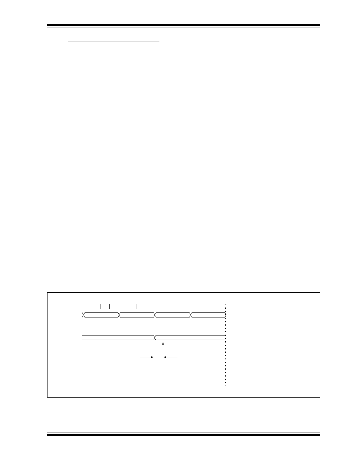
5.3.2 SUCCESSIVE OPERATIONS ON I/O PORTS The actual write to an I/O port happens at the end of an
instruction cycle, whereas for reading, the data must be
valid at the beginning of the instruction cycle (Figure 5-
5). Therefore , care must be e x ercised if a write follo wed
by a read operation is carried out on the same I/O port.
The sequence of instructions should be such that the
pin voltage stabilizes (load dependent) before the next
instruction which causes that file to be read into the
CPU is executed. Otherwise, the previous state of that
pin may be read into the CPU rather than the new state .
When in doubt, it is better to separate these instructions with a NOP or another instruction not accessing
this I/O port.
Example 5-1 shows the effect of two sequential readmodify-write instructions (e.g., BCF, BSF, etc.) on an
I/O port.
EXAMPLE 5-1: READ-MODIFY-WRITE
INSTRUCTIONS ON AN
I/O PORT
;Initial PORT settings: PORTB<7:4> Inputs
; PORTB<3:0> Outputs
;PORTB<7:6> have external pull-ups and are
;not connected to other circuitry
;
; PORT latch PORT pins
; ---------- -------- BCF PORTB, 7 ; 01pp ppp 11pp ppp
BCF PORTB, 6 ; 10pp ppp 11pp ppp
BSF STATUS, RP0 ;
BCF TRISB, 7 ; 10pp ppp 11pp ppp
BCF TRISB, 6 ; 10pp ppp 10pp ppp
;
;Note that the user may have expected the
;pin values to be 00pp ppp. The 2nd BCF
;caused RB7 to be latched as the pin value
;(high).
FIGURE 5-5: SUCCESSIVE I/O OPERATION
Q3
PC + 3
NOP
NOP
Q4
Note:
This example shows a write to PORTB
followed by a read from PORTB.
Note that:
data setup time = (0.25TCY - TPD)
where TCY = instruction cycle
TPD = propagation delay
Therefore, at higher clock frequencies,
a write followed by a read may be
problematic.
NOP
Q3
Q4
Q1 Q2
Q4
Q1 Q2
PC
Instruction
fetched
RB7:RB0
Instruction
executed
1997 Microchip Technology Inc. DS30445C-page 23
MOVWF PORTB
Q3
PC PC + 1 PC + 2
write to
PORTB
Q1 Q2
MOVF PORTB,W
MOVWF PORTB
write to
PORTB
Q3
Q4
Q1 Q2
Port pin
sampled here
TPD
MOVF PORTB,W
Page 24

PIC16C84
NOTES:
DS30445C-page 24 1997 Microchip Technology Inc.
Page 25
PIC16C84
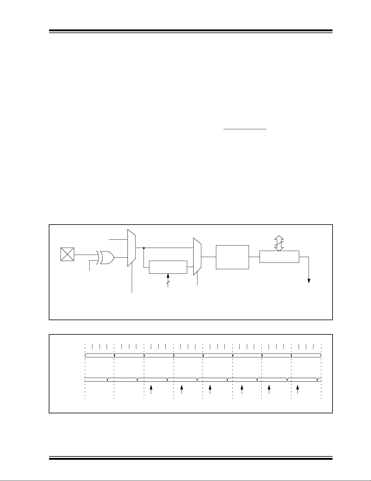
6.0 TIMER0 MODULE AND TMR0
REGISTER
The Timer0 module timer/counter has the following
features:
• 8-bit timer/counter
• Readable and writable
• 8-bit software programmable prescaler
• Internal or external clock select
• Interrupt on overflow from FFh to 00h
• Edge select for external clock
Timer mode is selected by clearing the T0CS bit
(OPTION<5>). In timer mode, the Timer0 module
(Figure 6-1) will increment every instruction cycle
(without prescaler). If the TMR0 register is written, the
increment is inhibited for the following two cycles
(Figure 6-2 and Figure 6-3). The user can w ork around
this by writing an adjusted value to the TMR0 register.
Counter mode is selected by setting the T0CS bit
(OPTION<5>). In this mode TMR0 will increment either
on every rising or falling edge of pin RA4/T0CKI. The
incrementing edge is determined by the T0 source
FIGURE 6-1: TMR0 BLOCK DIAGRAM
edge select bit, T0SE (OPTION<4>). Clearing bit T0SE
selects the rising edge. Restrictions on the external
clock input are discussed in detail in Section 6.2.
The prescaler is shared between the Timer0 Module
and the Watchdog Timer. The prescaler assignment is
controlled, in software, by control bit PSA
(OPTION<3>). Clearing bit PSA will assign the
prescaler to the Timer0 Module. The prescaler is not
readable or writable. When the prescaler (Section 6.3)
is assigned to the Timer0 Module, the prescale value
(1:2, 1:4, ..., 1:256) is software selectable.
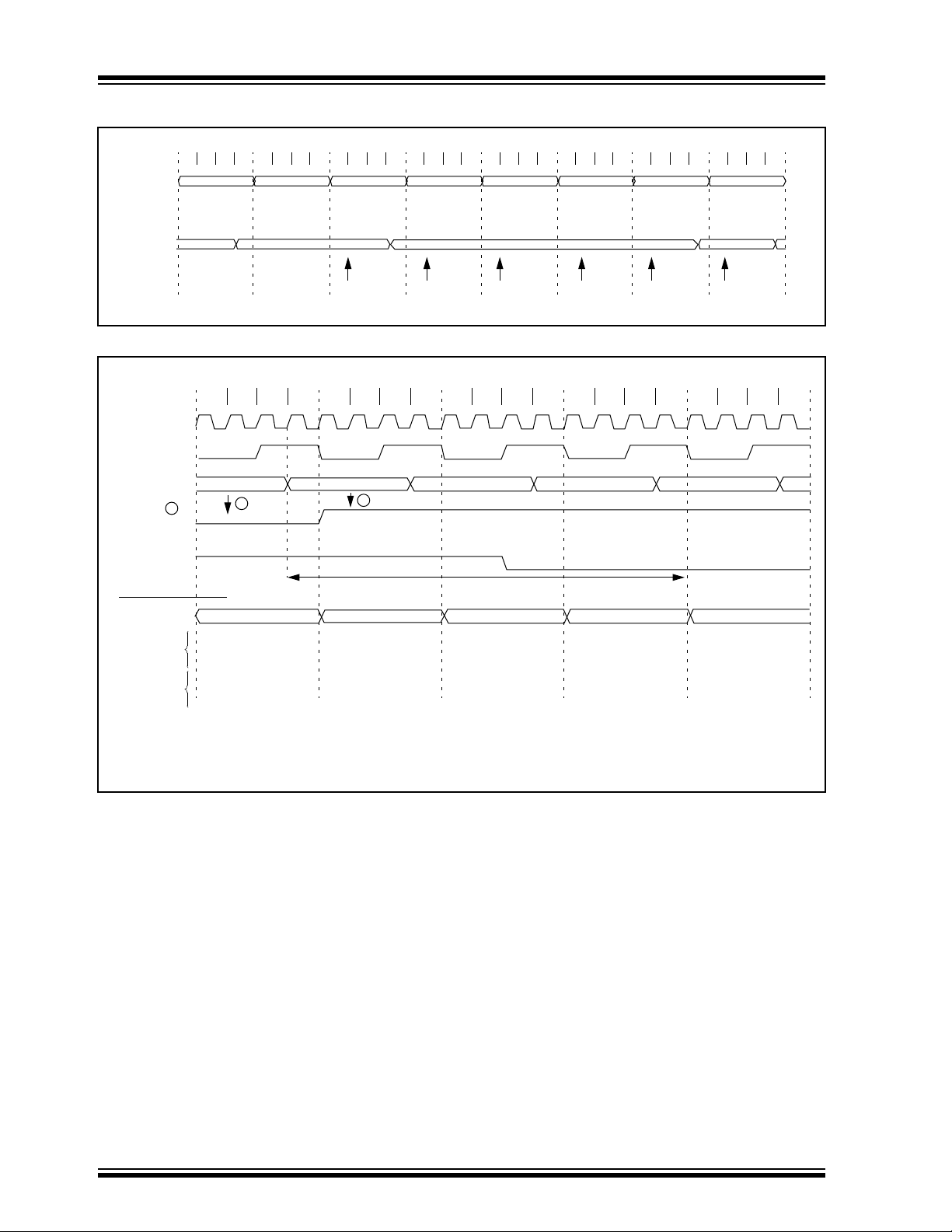
6.1 TMR0 Interrupt
The TMR0 interrupt is generated when the TMR0
register overflows from FFh to 00h. This overflow sets
the T0IF bit (INTCON<2>). The interrupt can be
masked by clearing enable bit T0IE (INTCON<5>). The
T0IF bit must be cleared in software by the Timer0
Module interrupt service routine before re-enabling this
interrupt. The TMR0 interrupt (Figure 6-4) cannot wake
the processor from SLEEP since the timer is shut off
during SLEEP.
0
1
T0CS
Programmable
Prescaler
3
PS2, PS1, PS0
1
0
PSA
PSout
Sync with
Internal
clocks
(2 cycle delay)
RA4/T0CKI
pin
FOSC/4
T0SE
Note 1: Bits T0CS, T0SE, PS2, PS1, PS0 and PSA are located in the OPTION register.
2: The prescaler is shared with the Watchdog Timer (Figure 6-6)
FIGURE 6-2: TMR0 TIMING: INTERNAL CLOCK/NO PRESCALER
Q1 Q2 Q3 Q4 Q1 Q2 Q3 Q4 Q1 Q2 Q3 Q4 Q1 Q2 Q3 Q4 Q1 Q2 Q3 Q4 Q1 Q2 Q3 Q4 Q1 Q2 Q3 Q4
PC PC+1 PC+2
MOVWF TMR0
T0+1 T0+2 NT0 NT0 NT0
MOVF TMR0,W
Write TMR0
executed
MOVF TMR0,W MOVF TMR0,W MOVF TMR0,W MOVF TMR0,W
Read TMR0
reads NT0
PC+3
Read TMR0
reads NT0
PC+4
Read TMR0
reads NT0
Instruction
Fetch
TMR0
Instruction
Executed
PC
Q1 Q2 Q3 Q4
PC-1
T0
PSout
Data bus
8
TMR0 register
PC+5 PC+6
NT0+1 NT0+2
Read TMR0
reads NT0 + 1
Read TMR0
reads NT0 + 2
Set bit T0IF
on Overflow
T0
1997 Microchip Technology Inc. DS30445C-page 25
Page 26
PIC16C84
FIGURE 6-3: TMR0 TIMING: INTERNAL CLOCK/PRESCALE 1:2
Q1 Q2 Q3 Q4 Q1 Q2 Q3 Q4 Q1 Q2 Q3 Q4 Q1 Q2 Q3 Q4 Q1 Q2 Q3 Q4 Q1 Q2 Q3 Q4 Q1 Q2 Q3 Q4
PC PC+1 PC+2 PC+3 PC+4 PC+5 PC+6
MOVWF TMR0
MOVF TMR0,W MOVF TMR0,W MOVF TMR0,W MOVF TMR0,W MOVF TMR0,W
T0+1
Write TMR0
executed
PC
Instruction
Fetch
TMR0
Instruction
Execute
Q1 Q2 Q3 Q4
PC-1
T0 NT0+1
FIGURE 6-4: TMR0 INTERRUPT TIMING
Q2Q1 Q3 Q4Q2Q1 Q3 Q4 Q2Q1 Q3 Q4 Q2Q1 Q3 Q4 Q2Q1 Q3 Q4
OSC1
(3)
CLKOUT
TMR0 timer
4
T0IF bit
(INTCON<2>)
GIE bit
(INTCON<7>)
UCTION FLOW
INSTR
Instruction
fetched
PC
FEh
1
PC
Inst (PC)
FFh 00h 01h 02h
1
PC +1 PC +1 0004h
Inst (PC+1)
Read TMR0
reads NT0
Read TMR0
reads NT0
Interrupt Latency
NT0
(2)
Read TMR0
reads NT0
Read TMR0
reads NT0
Inst (0004h) Inst (0005h)
Read TMR0
reads NT0 + 1
0005h
Instruction
executed
Inst (PC-1)
Inst (PC)
Inst (0004h)Dummy cycle Dummy cycle
Note 1: T0IF interrupt flag is sampled here (every Q1).
2: Interrupt latency = 3.25Tcy, where Tcy = instruction cycle time.
3: CLKOUT is available only in RC oscillator mode.
4: The timer clock (after the synchronizer circuit) which increments the timer from FFh to 00h immediately sets the T0IF bit.
The TMR0 register will roll over 3 Tosc cycles later.
DS30445C-page 26 1997 Microchip Technology Inc.
Page 27
PIC16C84
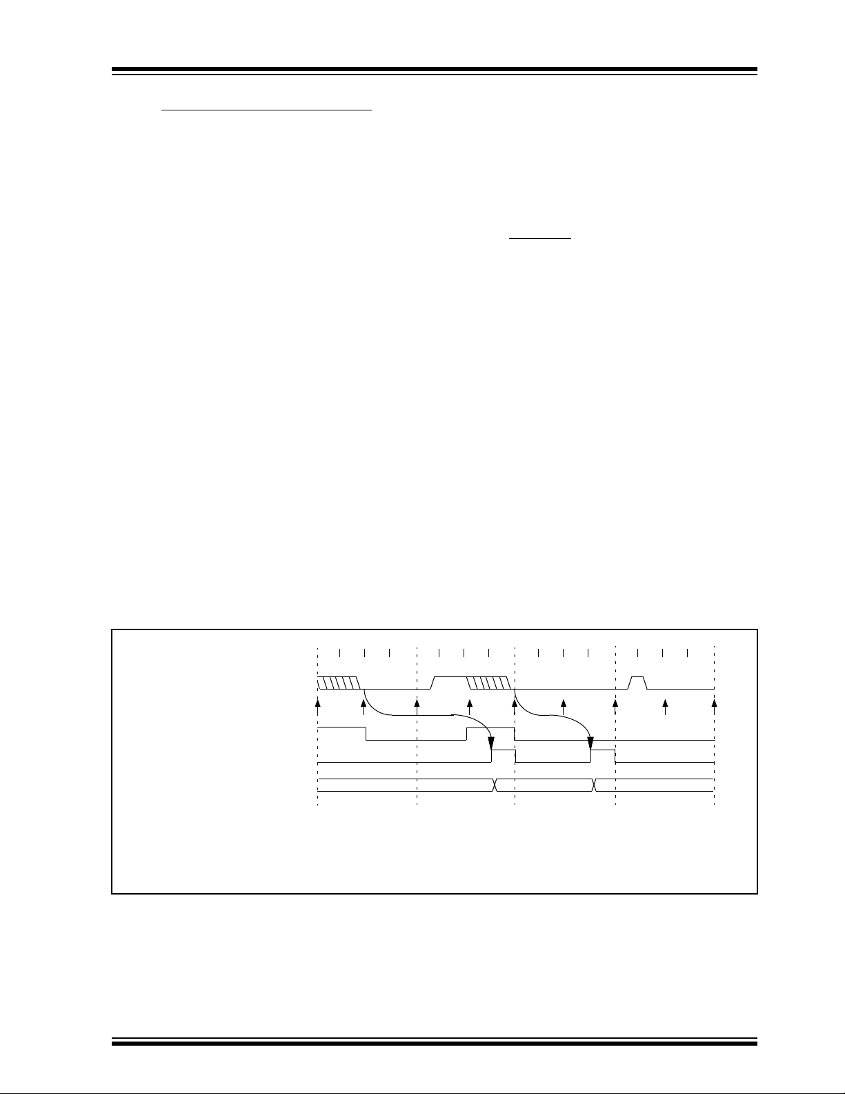
6.2 Using TMR0 with External Clock
When an external clock input is used for TMR0, it must
meet certain requirements. The external clock
requirement is due to internal phase clock (T
synchronization. Also, there is a delay in the actual
incrementing of the TMR0 register after
synchronization.
6.2.1 EXTERNAL CLOCK SYNCHRONIZATION
When no prescaler is used, the external clock input is
the same as the prescaler output. The synchronization
of pin RA4/T0CKI with the internal phase clocks is
accomplished by sampling the prescaler output on the
Q2 and Q4 cycles of the internal phase clocks
(Figure 6-5). Therefore, it is necessary for T0CKI to be
high for at least 2Tosc (plus a small RC delay) and low
for at least 2Tosc (plus a small RC delay). Refer to the
electrical specification of the desired device.
When a prescaler is used, the external clock input is
divided by an asynchronous ripple counter type
prescaler so that the prescaler output is symmetrical.
For the external clock to meet the sampling
requirement, the ripple counter must be taken into
account. Therefore, it is necessary for T0CKI to have a
period of at least 4Tosc (plus a small RC delay) divided
by the prescaler value. The only requirement on T0CKI
high and low time is that they do not violate the
minimum pulse width requirement of 10 ns. Refer to
parameters 40, 41 and 42 in the AC Electrical
Specifications of the desired device.
OSC)
6.2.2 TMR0 INCREMENT DELAY Since the prescaler output is synchronized with the
internal clocks, there is a small delay from the time the
external clock edge occurs to the time the Timer0
Module is actually incremented. Figure 6-5 shows the
delay from the external clock edge to the timer
incrementing.
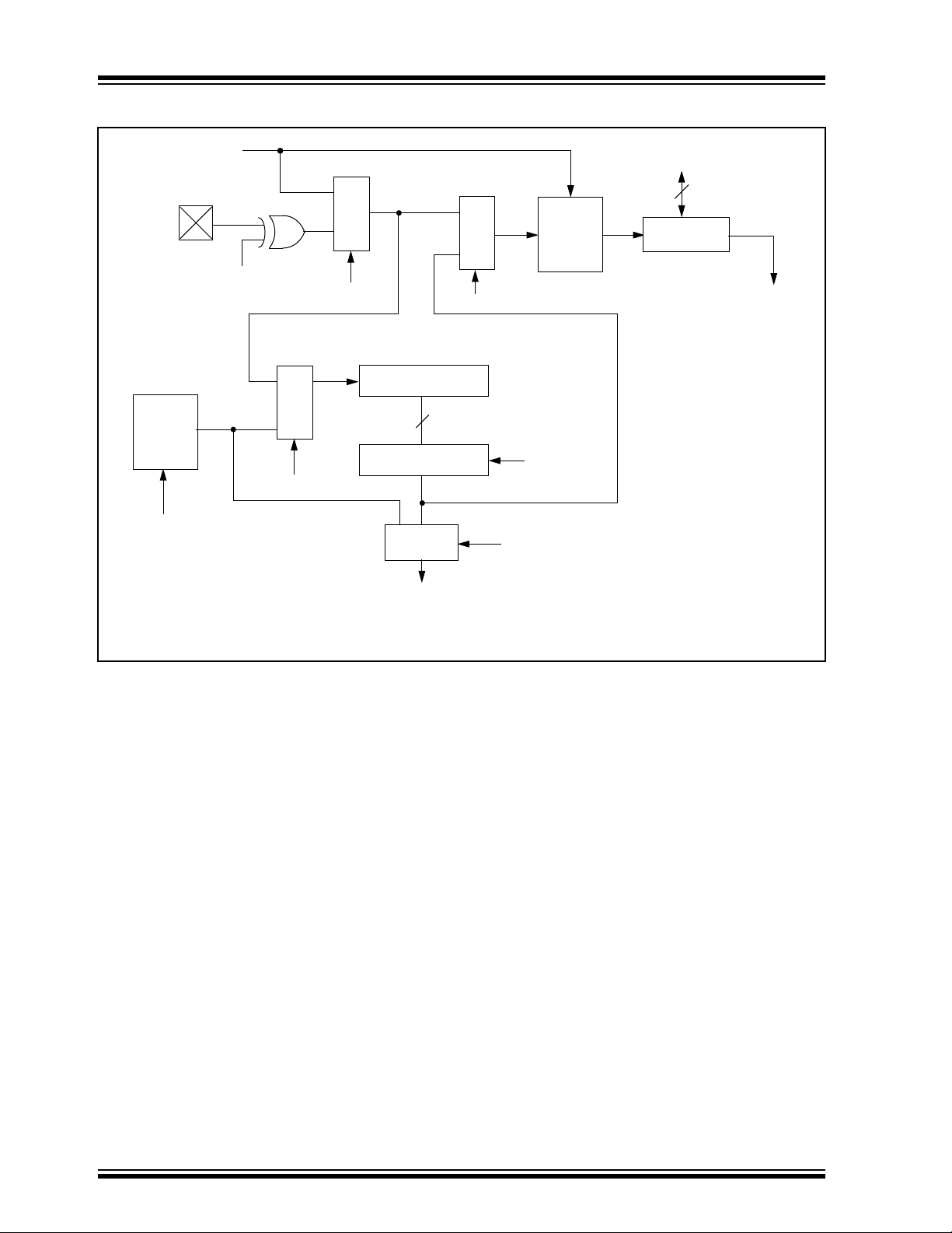
6.3 Prescaler
An 8-bit counter is available as a prescaler for the
Timer0 Module, or as a postscaler for the Watchdog
Timer (Figure 6-6). For simplicity, this counter is being
referred to as “prescaler” throughout this data sheet.
Note that there is only one prescaler available which is
mutually exclusive betw een the Timer0 Module and the
Watchdog Timer . Thus, a prescaler assignment for the
Timer0 Module means that there is no prescaler for the
Watchdog Timer , and vice-versa.
The PSA and PS2:PS0 bits (OPTION<3:0>) determine
the prescaler assignment and prescale ratio.
When assigned to the Timer0 Module, all instructions
writing to the Timer0 Module (e.g., CLRF 1, MOVWF 1,
BSF 1,x ....etc.) will clear the prescaler. When
assigned to WDT, a CLRWDT instruction will clear the
prescaler along with the Watchdog Timer. The
prescaler is not readable or writable.
FIGURE 6-5: TIMER0 TIMING WITH EXTERNAL CLOCK
Q1 Q2 Q3 Q4 Q1 Q2 Q3 Q4 Q1 Q2 Q3 Q4 Q1 Q2 Q3 Q4
Note 1:
2:
3:
Ext. Clock Input or
Prescaler Out (Note 2)
Ext. Clock/Prescaler
Output After Sampling
Increment TMR0 (Q4)
TMR0
Delay from clock input change to TMR0 increment is 3Tosc to 7Tosc. (Duration of Q = Tosc).
Therefore, the error in measuring the interval between two edges on TMR0 input = ± 4Tosc max.
External clock if no prescaler selected, Prescaler output otherwise.
The arrows ↑ indicate where sampling occurs. A small clock pulse may be missed by sampling.
T0 T0 + 1 T0 + 2
(Note 3)
1997 Microchip Technology Inc. DS30445C-page 27
Page 28
PIC16C84
FIGURE 6-6: BLOCK DIAGRAM OF THE TMR0/WDT PRESCALER
CLKOUT (= Fosc/4)
RA4/T0CKI
pin
Watchdog
Timer
WDT Enable bit
T0SE
Data Bus
M
0
U
X
1
T0CS
0
M
U
1
X
PSA
8-bit Prescaler
8 - to - 1MUX
0
time-out
8
M U X
WDT
1
M
U
0
X
PSA
1
SYNC
2
Cycles
PS2:PS0
PSA
8
TMR0 register
Set bit T0IF
on overflow
Note: T0CS, T0SE, PSA, PS2:PS0 are bits in the OPTION register.
DS30445C-page 28 1997 Microchip Technology Inc.
Page 29
PIC16C84
6.3.1 SWITCHING PRESCALER ASSIGNMENT
The prescaler assignment is fully under software
control (i.e., it can be changed “on the fly” during
program execution).
Note: To avoid an unintended de vice RESET, the
following instruction sequence
(Example 6-1) must be executed when
changing the prescaler assignment from
EXAMPLE 6-1: CHANGING PRESCALER
(TIMER0→WDT)
BCF STATUS, RP0 ;Bank 0
CLRF TMR0 ;Clear TMR0
; and Prescaler
BSF STATUS, RP0 ;Bank 1
CLRWDT ;Clears WDT
MOVLW b'xxxx1xxx' ;Select new
MOVWF OPTION ; prescale value
BCF STATUS, RP0 ;Bank 0
Timer0 to the WDT. This sequence m ust be
taken even if the WDT is disabled. To
change prescaler from the WDT to the
Timer0 module use the sequence shown in
Example 6-2.
EXAMPLE 6-2: CHANGING PRESCALER
(WDT→TIMER0)
CLRWDT ;Clear WDT and
; prescaler
BSF STATUS, RP0 ;Bank 1
MOVLW b'xxxx0xxx' ;Select TMR0, new
; prescale value
’ and clock source
MOVWF OPTION ;
BCF STATUS, RP0 ;Bank 0
TABLE 6-1 REGISTERS ASSOCIATED WITH TIMER0
Address Name Bit 7 Bit 6 Bit 5 Bit 4 Bit 3 Bit 2 Bit 1 Bit 0
Value on
Power-on
Reset
Value on all
other resets
01h TMR0 Timer0 module’s register xxxx xxxx uuuu uuuu
0Bh INTCON GIE
81h OPTION
85h TRISA — — — TRISA4 TRISA3 TRISA2 TRISA1 TRISA0 ---1 1111 ---1 1111
Legend: x = unknown, u = unchanged. - = unimplemented read as '0'. Shaded cells are not associated with Timer0.
RBPU INTEDG T0CS T0SE PSA PS2 PS1 PS0 1111 1111 1111 1111
EEIE T0IE INTE RBIE T0IF INTF RBIF 0000 000x 0000 0000
1997 Microchip Technology Inc. DS30445C-page 29
Page 30

PIC16C84
NOTES:
DS30445C-page 30 1997 Microchip Technology Inc.
Page 31

PIC16C84
7.0 DATA EEPROM MEMORY
The EEPROM data memory is readable and writable
during normal operation (full V
is not directly mapped in the register file space. Instead
it is indirectly addressed through the Special Function
Registers. There are four SFRs used to read and write
this memory. These registers are:
• EECON1
• EECON2
• EEDATA
• EEADR
EEDATA holds the 8-bit data for read/write, and EEADR
holds the address of the EEPROM location being
accessed. PIC16C84 devices have 64 bytes of data
EEPROM with an address range from 0h to 3Fh.
The EEPROM data memory allows byte read and write.
A byte write automatically erases the location and
writes the new data (erase before write). The EEPR OM
data memory is rated for high erase/write cycles. The
write time is controlled by an on-chip timer. The writetime will vary with voltage and temperature as well as
from chip to chip. Please refer to AC specifications for
exact limits.
DD range). This memory
When the device is code protected, the CPU may
continue to read and write the data EEPROM memory .
The device programmer can no longer access
this memory.
7.1 EEADR
The EEADR register can address up to a maximum of
256 bytes of data EEPROM. Only the first 64 bytes of
data EEPROM are implemented.
The upper two bits are address decoded. This means
that these two bits must always be '0' to ensure that the
address is in the 64 byte memory space.
FIGURE 7-1: EECON1 REGISTER (ADDRESS 88h)
U U U R/W-0 R/W-x R/W-0 R/S-0 R/S-x
— — — EEIF WRERR WREN WR RD R = Readable bit
bit7 bit0
bit 7:5 Unimplemented: Read as '0'
bit 4 EEIF: EEPROM Write Operation Interrupt Flag bit
1 = The write operation completed (must be cleared in software)
0 = The write operation is not complete or has not been started
bit 3 WRERR: EEPROM Error Flag bit
1 = A write operation is prematurely terminated
(any MCLR
0 = The write operation completed
bit 2 WREN: EEPROM Write Enable bit
1 = Allows write cycles
0 = Inhibits write to the data EEPROM
bit 1 WR: Write Control bit
1 = initiates a write cycle. (The bit is cleared by hardware once write is complete. The WR bit can only
be set (not cleared) in software.
0 = Write cycle to the data EEPROM is complete
bit 0 RD: Read Control bit
1 = Initiates an EEPROM read (read takes one cycle. RD is cleared in hardware. The RD bit can only
be set (not cleared) in software).
0 = Does not initiate an EEPROM read
reset or any WDT reset during normal operation)
W = Writable bit
S = Settable bit
U = Unimplemented bit,
- n = Value at POR reset
read as ‘0’
1997 Microchip Technology Inc. DS30445C-page 31
Page 32

PIC16C84
7.2 EECON1 and EECON2 Registers
EECON1 is the control register with five low order bits
physically implemented. The upper-three bits are nonexistent and read as '0's.
Control bits RD and WR initiate read and write,
respectively. These bits cannot be cleared, only set, in
software. They are cleared in hardware at completion of
the read or write operation. The inability to clear the WR
bit in software prevents the accidental, premature termination of a write operation.
The WREN bit, when set, will allow a write operation.
On power-up, the WREN bit is clear. The WRERR bit is
set when a write operation is interrupted by a MCLR
reset or a WDT time-out reset during normal operation.
In these situations, following reset, the user can check
the WRERR bit and rewrite the location. The data and
address will be unchanged in the EEDATA and
EEADR registers.
Interrupt flag bit EEIF is set when write is complete. It
must be cleared in software.
EECON2 is not a physical register. Reading EECON2
will read all '0's. The EECON2 register is used
exclusively in the Data EEPROM write sequence.
7.3 Reading the EEPROM Data Memory
To read a data memory location, the user must write
the address to the EEADR register and then set control
bit RD (EECON1<0>). The data is av ailable , in the v ery
next cycle, in the EEDATA register; therefore it can be
read in the next instruction. EED AT A will hold this v alue
until another read or until it is written to by the user
(during a write operation).
EXAMPLE 7-1: DATA EEPROM READ
BCF STATUS, RP0 ; Bank 0
MOVLW CONFIG_ADDR ;
MOVWF EEADR ; Address to read
BSF STATUS, RP0 ; Bank 1
BSF EECON1, RD ; EE Read
BCF STATUS, RP0 ; Bank 0
MOVF EEDATA, W ; W = EEDATA
7.4 Writing to the EEPROM Data Memory
To write an EEPROM data location, the user must first
write the address to the EEADR register and the data
to the EEDATA register. Then the user must follow a
specific sequence to initiate the write for each byte.
EXAMPLE 7-1: DATA EEPROM WRITE
BSF STATUS, RP0 ; Bank 1
BCF INTCON, GIE ; Disable INTs.
BSF EECON1, WREN ; Enable Write
MOVLW 55h ;
MOVWF EECON2 ; Write 55h
MOVLW AAh ;
MOVWF EECON2 ; Write AAh
BSF EECON1,WR ; Set WR bit
; begin write
Required
Sequence
BSF INTCON, GIE ; Enable INTs.
The write will not initiate if the above sequence is not
exactly followed (write 55h to EECON2, write AAh to
EECON2, then set WR bit) for each byte. We strongly
recommend that interrupts be disabled during this
code segment.
Additionally, the WREN bit in EECON1 must be set to
enable write. This mechanism prevents accidental
writes to data EEPROM due to errant (unexpected)
code execution (i.e., lost programs). The user should
keep the WREN bit clear at all times, except when
updating EEPROM. The WREN bit is not cleared
by hardware
After a write sequence has been initiated, clearing the
WREN bit will not affect this write cycle. The WR bit will
be inhibited from being set unless the WREN bit is set.
At the completion of the write cycle, the WR bit is
cleared in hardware and the EE Write Complete
Interrupt Flag bit (EEIF) is set. The user can either
enable this interrupt or poll this bit. EEIF must be
cleared by software.
Note: The data EEPROM memory E/W cycle
time may occasionally exceed the 10 ms
specification (typical). To ensure that the
write cycle is complete, use the EE
interrupt or poll the WR bit (EECON1<1>).
Both these events signify the completion of
the write cycle.
DS30445C-page 32 1997 Microchip Technology Inc.
Page 33

PIC16C84
7.5 Write Verify
Depending on the application, good programming
practice may dictate that the value written to the Data
EEPROM should be verified (Example 7-1) to the
desired value to be written. This should be used in
applications where an EEPROM bit will be stressed
near the specification limit. The Total Endurance disk
will help determine your comfort level.
Generally the EEPROM write failure will be a bit which
was written as a '1', but reads back as a '0' (due to
leakage off the bit).
EXAMPLE 7-1: WRITE VERIFY
BCF STATUS, RP0 ; Bank 0
: ; Any code can go here
: ;
MOVF EEDATA, W ; Must be in Bank 0
BSF STATUS, RP0 ; Bank 1
READ
BSF EECON1, RD ; YES, Read the
; value written
BCF STATUS, RP0 ; Bank 0
;
; Is the value written (in W reg) and
; read (in EEDATA) the same?
;
SUBWF EEDATA, W ;
BTFSS STATUS, Z ; Is difference 0?
GOTO WRITE_ERR ; NO, Write error
: ; YES, Good write
: ; Continue program
7.6 Protection Against Spurious Writes
There are conditions when the device may not want to
write to the data EEPROM memory. To protect against
spurious EEPROM writes, various mechanisms have
been built in. On power-up, WREN is cleared. Also, the
Pow er-up Timer (72 ms duration) prevents
EEPROM write.
The write initiate sequence and the WREN bit together
help prevent an accidental write during brown-out,
power glitch, or software malfunction.
7.7 Data EEPROM Operation during Code
Protect
When the device is code protected, the CPU is able to
read and write unscrambled data to the Data
EEPROM.
For ROM devices, there are two code protection bits
(Section 8.1). One for the ROM program memory and
one for the Data EEPROM memory.
7.8 Power Consumption Considerations
Note: It is recommended that the EEADR<7:6>
bits be cleared. When either of these bits is
set, the maximum I
higher than when both are cleared. The
specification is 400 µA. With EEADR<7:6>
cleared, the maximum is approximately
150 µA.
DD for the device is
TABLE 7-1 REGISTERS/BITS ASSOCIATED WITH DATA EEPROM
Address Name Bit 7 Bit 6 Bit 5 Bit 4 Bit 3 Bit 2 Bit 1 Bit 0
08h EEDA TA EEPROM data register xxxx xxxx uuuu uuuu
09h EEADR EEPROM address register xxxx xxxx uuuu uuuu
88h EECON1
89h EECON2 EEPROM control register 2 ---- ---- ---- ----
Legend: x = unknown, u = unchanged, - = unimplemented read as '0', q = value depends upon condition. Shaded cells are not
used by Data EEPROM.
— — — EEIF WRERR WREN WR RD ---0 x000 ---0 q000
Value on
Power-on
Reset
Value on all
other resets
1997 Microchip Technology Inc. DS30445C-page 33
Page 34

PIC16C84
NOTES:
DS30445C-page 34 1997 Microchip Technology Inc.
Page 35

PIC16C84
8.0 SPECIAL FEATURES OF THE
CPU
What sets a microcontroller apart from other
processors are special circuits to deal with the needs of
real time applications. The PIC16C84 has a host of
such features intended to maximize system reliability,
minimize cost through elimination of external
components, provide power saving operating modes
and offer code protection. These features are:
• OSC selection
• Reset
- Power-on Reset (POR)
- Power-up Timer (PWRT)
- Oscillator Start-up Timer (OST)
• Interrupts
• Watchdog Timer (WDT)
• SLEEP
• Code protection
• ID locations
• In-circuit serial programming
The PIC16C84 has a Watchdog Timer which can be
shut off only through configuration bits. It runs off its
own RC oscillator for added reliability. There are two
timers that offer necessary delays on power-up. One is
the Oscillator Start-up Timer (OST), intended to keep
the chip in reset until the crystal oscillator is stable. The
other is the Pow er-up Timer (PWRT), which provides a
fixed delay of 72 ms (nominal) on power-up only. This
design keeps the device in reset while the pow er supply
stabilizes. With these two timers on-chip, most
applications need no external reset circuitry.
SLEEP mode offers a very low current power-down
mode. The user can wake-up from SLEEP through
external reset, Watchdog Timer time-out or through an
interrupt. Several oscillator options are provided to
allow the part to fit the application. The RC oscillator
option saves system cost while the LP crystal option
saves power. A set of configuration bits are used to
select the various options.
8.1 Configuration Bits
The configuration bits can be programmed (read as '0')
or left unprogrammed (read as '1') to select various
device configurations. These bits are mapped in
program memory location 2007h.
Address 2007h is beyond the user program memory
space and it belongs to the special test/configuration
memory space (2000h - 3FFFh). This space can only
be accessed during programming.
To find out how to program the PIC16C84, refer to
PIC16C84 EEPROM Memory Programming Specification
(DS30189).
FIGURE 8-1: CONFIGURATION WORD
U-1 U-1 U-1 U-1 U-1 U-1 U-1 U-1 U-1 R/P-u R/P-u R/P-u R/P-u R/P-u
— — — — — — — — — CP PWRTE WDTE FOSC1 FOSC0
bit13 bit0
R = Readable bit
P = Programmable bit
U = Unimplemented bit,
read as ‘1’
- n = Value at POR reset
u = unchanged
bit 13:5 Unimplemented: Read as '1'
bit 4 CP: Code Protection bit
1 = Code protection off
0 = All memory is code protected
bit 3 PWRTE: Power-up Timer Enable bit
1 = Power-up timer is enabled
0 = Power-up timer is disabled
bit 2 WDTE: Watchdog Timer Enable bit
1 = WDT enabled
0 = WDT disabled
bit 1:0 FOSC1:FOSC0: Oscillator Selection bits
11 =RC oscillator
10 = HS oscillator
01 = XT oscillator
00 = LP oscillator
1997 Microchip Technology Inc. DS30445C-page 35
Page 36

PIC16C84
8.2 Oscillator Configurations
8.2.1 OSCILLATOR TYPES The PIC16C84 can be operated in four different
oscillator modes. The user can program two
configuration bits (FOSC1 and FOSC0) to select one of
these four modes:
• LP Low Power Crystal
• XT Crystal/Resonator
• HS High Speed Crystal/Resonator
• RC Resistor/Capacitor
8.2.2 CRYSTAL OSCILLATOR / CERAMIC
RESONATORS
In XT, LP or HS modes a crystal or ceramic resonator
is connected to the OSC1/CLKIN and OSC2/CLKOUT
pins to establish oscillation (Figure 8-2).
FIGURE 8-2: CRYSTAL/CERAMIC
RESONATOR OPERATION
(HS, XT OR LP OSC
CONFIGURATION)
(1)
C1
C2
(1)
XTAL
(2)
RS
OSC1
OSC2
RF
(3)
To
internal
logic
SLEEP
PIC16CXX
Note1: See Table 8-1 and Table 8-2 for recom-
mended values of C1 and C2.
2: A series resistor (RS) may be required for
AT strip cut crystals.
3: RF varies with the crystal chosen.
The PIC16C84 oscillator design requires the use of a
parallel cut crystal. Use of a series cut crystal may give
a frequency out of the crystal manufacturers
specifications. When in XT , LP or HS modes , the device
can have an external clock source to drive the OSC1/
CLKIN pin (Figure 8-3).
FIGURE 8-3: EXTERNAL CLOCK INPUT
OPERATION (HS, XT OR LP
OSC CONFIGURATION)
Clock from
ext. system
Open
OSC1
PIC16CXX
OSC2
TABLE 8-1 CAPACITOR SELECTION
FOR CERAMIC RESONATORS
Ranges Tested:
Mode Freq OSC1/C1 OSC2/C2
XT 455 kHz
2.0 MHz
4.0 MHz
HS 8.0 MHz
10.0 MHz
Note: Recommended values of C1 and C2 are identical to
the ranges tested table.
Higher capacitance increases the stability of the
oscillator but also increases the start-up time.
These values are for design guidance only. Since
each resonator has its own characteristics, the user
should consult the resonator manufacturer for the
appropriate values of external components.
47 - 100 pF
15 - 33 pF
15 - 33 pF
15 - 33 pF
15 - 33 pF
47 - 100 pF
15 - 33 pF
15 - 33 pF
15 - 33 pF
15 - 33 pF
Resonators Tested:
455 kHz Panasonic EFO-A455K04B ± 0.3%
2.0 MHz Murata Erie CSA2.00MG ± 0.5%
4.0 MHz Murata Erie CSA4.00MG ± 0.5%
8.0 MHz Murata Erie CSA8.00MT ± 0.5%
10.0 MHz Murata Erie CSA10.00MTZ ± 0.5%
None of the resonators had built-in capacitors.
TABLE 8-2 CAPACITOR SELECTION
FOR CRYSTAL OSCILLATOR
Mode Freq OSC1/C1 OSC2/C2
LP 32 kHz
200 kHz
XT 100 kHz
2 MHz
4 MHz
HS 4 MHz
10 MHz
Note: Higher capacitance increases the stability of
oscillator but also increases the start-up time.
These values are for design guidance only. Rs may
be required in HS mode as well as XT mode to
avoid overdriving crystals with low drive level specification. Since each crystal has its own
characteristics, the user should consult the crystal
manufacturer for appropriate values of external
components.
For VDD > 4.5V, C1 = C2 ≈ 30 pF is recommended.
Crystals Tested:
32.768 kHz Epson C-001R32.768K-A ± 20 PPM
100 kHz Epson C-2 100.00 KC-P ± 20 PPM
200 kHz STD XTL 200.000 KHz ± 20 PPM
1.0 MHz ECS ECS-10-13-2 ± 50 PPM
2.0 MHz ECS ECS-20-S-2 ± 50 PPM
4.0 MHz ECS ECS-40-S-4 ± 50 PPM
10.0 MHz ECS ECS-100-S-4 ± 50 PPM
68 - 100 pF
15 - 33 pF
100 - 150 pF
15 - 33 pF
15 - 33 pF
15 - 33 pF
15 - 33 pF
68 - 100 pF
15 - 33 pF
100 - 150 pF
15 - 33 pF
15 - 33 pF
15 - 33 pF
15 - 33 pF
DS30445C-page 36 1997 Microchip Technology Inc.
Page 37

PIC16C84
8.2.3 EXTERNAL CRYSTAL OSCILLATOR
CIRCUIT
Either a prepackaged oscillator can be used or a simple
oscillator circuit with TTL gates can be built.
Prepackaged oscillators provide a wide operating
range and better stability. A well-designed crystal
oscillator will provide good performance with TTL
gates. Two types of crystal oscillator circuits are
available; one with series resonance, and one with
parallel resonance.
Figure 8-4 shows a parallel resonant oscillator circuit.
The circuit is designed to use the fundamental
frequency of the crystal. The 74AS04 in verter performs
the 180-degree phase shift that a parallel oscillator
requires. The 4.7 kΩ resistor provides negative
feedback for stability. The 10 kΩ potentiometer biases
the 74AS04 in the linear region. This could be used for
external oscillator designs.
FIGURE 8-4: EXTERNAL PARALLEL
RESONANT CRYSTAL
OSCILLATOR CIRCUIT
+5V
10k
4.7k
74AS04
10k
XTAL
10k
20 pF
20 pF
Figure 8-5 shows a series resonant oscillator circuit.
This circuit is also designed to use the fundamental
frequency of the crystal. The inverter performs a 180degree phase shift. The 330 kΩ resistors provide the
negative feedback to bias the inverters in their linear
region.
74AS04
To Other
Devices
PIC16CXX
CLKIN
FIGURE 8-5: EXTERNAL SERIES
RESONANT CRYSTAL
OSCILLATOR CIRCUIT
To Other
74AS04
Devices
PIC16CXX
CLKIN
330 kΩ
74AS04
330 kΩ
74AS04
0.1 µF
XTAL
8.2.4 RC OSCILLATOR For timing insensitive applications the RC de vice option
offers additional cost savings. The RC oscillator
frequency is a function of the supply voltage, the
resistor (Rext) values, capacitor (Cext) values, and the
operating temperature. In addition to this, the oscillator
frequency will vary from unit to unit due to normal
process parameter variation. Furthermore, the
difference in lead frame capacitance between package
types also affects the oscillation frequency, especially
for low Cext values. The user needs to take into
account variation due to tolerance of the external
R and C components. Figure 8-6 shows how an R/C
combination is connected to the PIC16C84. For Rext
values below 2.2 kΩ, the oscillator operation may
become unstable, or stop completely. For very high
Rext values (e.g., 1 MΩ), the oscillator becomes
sensitive to noise, humidity and leakage. Thus, we
recommend keeping Rext between 3 kΩ and 100 kΩ.
Although the oscillator will operate with no external
capacitor (Cext = 0 pF), we recommend using values
above 20 pF for noise and stability reasons. With little
or no external capacitance, the oscillation frequency
can vary dramatically due to changes in external
capacitances, such as PCB trace capacitance or
package lead frame capacitance.
See the electrical specification section for RC
frequency variation from part to part due to normal
process variation. The variation is larger for larger R
(since leakage current variation will affect RC
frequency more for large R) and for smaller C (since
variation of input capacitance has a greater affect on
RC frequency).
See the electrical specification section for variation of
oscillator frequency due to V
DD for given Rext/Cext
values as well as frequency variation due to
operating temperature.
The oscillator frequency, divided by 4, is available on
the OSC2/CLKOUT pin, and can be used for test
purposes or to synchronize other logic (see Figure 3-2
for waveform).
FIGURE 8-6: RC OSCILLATOR MODE
VDD
Rext
OSC1
Cext
VSS
Fosc/4
Recommended values: 3 kΩ ≤ Rext ≤ 100 kΩ
OSC2/CLKOUT
Cext > 20pF
Note: When the device oscillator is in RC mode,
do not drive the OSC1 pin with an external
clock or you may damage the device.
Internal
clock
PIC16CXX
1997 Microchip Technology Inc. DS30445C-page 37
Page 38

PIC16C84
8.3 Reset
Some registers are not affected in any reset condition;
their status is unknown on a POR reset and unchanged
The PIC16C84 differentiates between various kinds
of reset:
• Power-on Reset (POR)
• MCLR
• MCLR
reset during normal operation
reset during SLEEP
• WDT Reset (during normal operation)
• WDT Wake-up (during SLEEP)
Figure 8-7 shows a simplified block diagram of the on-
chip reset circuit. The electrical specifications state the
pulse width requirements for the MCLR
pin.
in any other reset. Most other registers are reset to a
“reset state” on POR, MCLR
normal operation and on MCLR
They are not affected by a WDT reset during SLEEP,
since this reset is viewed as the resumption of normal
operation.
Table 8-3 gives a description of reset conditions for the
program counter (PC) and the STATUS register.
Table 8-4 gives a full description of reset states for all
registers.
The T
O and PD bits are set or cleared differently in different reset situations (Section 8.7). These bits are
used in software to determine the nature of the reset.
FIGURE 8-7: SIMPLIFIED BLOCK DIAGRAM OF ON-CHIP RESET CIRCUIT
External
Reset
MCLR
SLEEP
WDT
Time_Out
Reset
Power_on_Reset
OST
10-bit Ripple counter
PWRT
10-bit Ripple counter
VDD
OSC1/
CLKIN
Module
V
OST/PWRT
On-chip
RC OSC
WDT
DD rise
detect
(1)
or WDT reset during
reset during SLEEP.
S
Chip_Reset
R
Q
Enable PWRT
Note 1: This is a separate oscillator from the
RC oscillator of the CLKIN pin.
DS30445C-page 38 1997 Microchip Technology Inc.
Enable OST
See Table 8-5
Page 39

PIC16C84
TABLE 8-3 RESET CONDITION FOR PROGRAM COUNTER AND THE STATUS REGISTER
Condition
Program Counter STATUS Register
Power-on Reset 000h 0001 1xxx
Reset during normal operation 000h 000u uuuu
MCLR
Reset during SLEEP 000h 0001 0uuu
MCLR
WDT Reset (during normal operation) 000h 0000 1uuu
WDT Wake-up PC + 1 uuu0 0uuu
Interrupt wake-up from SLEEP PC + 1
(1)
uuu1 0uuu
Legend: u = unchanged, x = unknown.
Note 1: When the wake-up is due to an interrupt and the GIE bit is set, the PC is loaded with the interrupt vector
(0004h).
TABLE 8-4 RESET CONDITIONS FOR ALL REGISTERS
Reset during:
MCLR
– normal operation
Register Address Power-on Reset
– SLEEP
WDT Reset during normal operation
W — xxxx xxxx uuuu uuuu uuuu uuuu
INDF 00h ---- ---- ---- ---- ---- ---TMR0 01h xxxx xxxx uuuu uuuu uuuu uuuu
PCL 02h 0000h 0000h PC + 1
STATUS 03h 0001 1xxx 000q quuu
(3)
FSR 04h xxxx xxxx uuuu uuuu uuuu uuuu
PORTA 05h ---x xxxx ---u uuuu ---u uuuu
PORTB 06h xxxx xxxx uuuu uuuu uuuu uuuu
EEDATA 08h xxxx xxxx uuuu uuuu uuuu uuuu
EEADR 09h xxxx xxxx uuuu uuuu uuuu uuuu
PCLATH 0Ah ---0 0000 ---0 0000 ---u uuuu
INTCON 0Bh 0000 000x 0000 000u uuuu uuuu
INDF 80h ---- ---- ---- ---- ---- ---OPTION_REG 81h 1111 1111 1111 1111 uuuu uuuu
PCL 82h 0000h 0000h PC + 1
STATUS 83h 0001 1xxx 000q quuu
(3)
FSR 84h xxxx xxxx uuuu uuuu uuuu uuuu
TRISA 85h ---1 1111 ---1 1111 ---u uuuu
TRISB 86h 1111 1111 1111 1111 uuuu uuuu
EECON1 88h ---0 x000 ---0 q000 ---0 uuuu
EECON2 89h ---- ---- ---- ---- ---- ---PCLATH 8Ah ---0 0000 ---0 0000 ---u uuuu
INTCON 8Bh 0000 000x 0000 000u uuuu uuuu
Legend: u = unchanged, x = unknown, - = unimplemented bit read as '0',
q = value depends on condition.
Note 1: One or more bits in INTCON will be affected (to cause wake-up).
2: When the wake-up is due to an interrupt and the GIE bit is set, the PC is loaded with the interrupt vector
(0004h).
3: Table 8-3 lists the reset value for each specific condition.
Wake-up from SLEEP:
– through interrupt
– through WDT time-out
(2)
uuuq quuu
uuuq quuu
(3)
(1)
(3)
(1)
1997 Microchip Technology Inc. DS30445C-page 39
Page 40

PIC16C84
8.4 Power-on Reset (POR)
A Power-on Reset pulse is generated on-chip when
V
DD rise is detected (in the range of 1.2V - 1.7V). To
take advantage of the POR, just tie the MCLR
directly (or through a resistor) to V
DD. This will eliminate
pin
external RC components usually needed to create
Power-on Reset. A minimum rise time for V
DD must be
met for this to operate properly. See Electrical Specifications for details.
When the device starts normal operation (exits the
reset condition), device operating parameters (v oltage ,
frequency, temperature, ...) must be meet to ensure
operation. If these conditions are not met, the device
must be held in reset until the operating conditions
are met.
For additional information, refer to Application Note
AN607,
Power-up Trouble Shooting
.
The POR circuit does not produce an internal reset
when V
DD declines.
8.5 Power-up Timer (PWRT)
The Power-up Timer (PWRT) provides a fixed 72 ms
nominal time-out (T
Figure 8-10, Figure 8-11 and Figure 8-12). The Powerup Timer operates on an internal RC oscillator. The
chip is kept in reset as long as the PWRT is active . The
PWRT delay allows the V
level (Possible exception shown in Figure 8-12).
A configuration bit, PWRTE, can enable/disable the
PWRT (Figure 8-1).
The power-up time delay T
chip due to V
DD, temperature, and process variation.
See DC parameters for details.
PWRT) from POR (Figure 8-9,
DD to rise to an acceptable
PWRT will vary from chip to
FIGURE 8-8: EXTERNAL POWER-ON
RESET CIRCUIT (FOR SLOW
VDD POWER-UP)
V
VDD
Note 1: External Pow er-on Reset circuit is required
2: R < 40 kΩ is recommended to make sure
3: R1 = 100Ω to 1 kΩ will limit any current
DD
D
R
only if V
R1
C
DD power-up rate is too slow. The
MCLR
PIC16CXX
diode D helps discharge the capacitor
quickly when V
DD powers down.
that voltage drop across R does not exceed
0.2V (max leakage current spec on MCLR
pin is 5 µA). A larger v oltage drop will
degrade V
flowing into MCLR
IH level on the MCLR pin.
from external
capacitor C in the event of an MCLR
breakdown due to ESD or EOS.
pin
8.6 Oscillator Start-up Timer (OST)
The Oscillator Start-up Timer (OST) provides a 1024
oscillator cycle delay (from OSC1 input) after the
PWRT delay ends (Figure 8-9, Figure 8-10, Figure 811 and Figure 8-12). This ensures the crystal oscillator
or resonator has started and stabilized.
The OST time-out (T
HS modes and only on Power-on Reset or wake-up
from SLEEP.
When V
T
V
DD rises very slowly, it is possible that the
PWRT time-out and TOST time-out will expire before
DD has reached its final value. In this case (Figure 8-
12), an external power-on reset circuit may be necessary (Figure 8-8).
DS30445C-page 40 1997 Microchip Technology Inc.
OST) is invoked only f or XT, LP and
Page 41

PIC16C84
FIGURE 8-9: TIME-OUT SEQUENCE ON POWER-UP (MCLR NOT TIED TO VDD): CASE 1
VDD
MCLR
INTERNAL POR
TPWRT
PWR
T TIME-OUT
OST TIME-OUT
INTERNAL RESET
FIGURE 8-10: TIME-OUT SEQUENCE ON POWER-UP (MCLR NOT TIED TO VDD): CASE 2
VDD
TOST
MCLR
INTERNAL POR
PWR
T TIME-OUT
OST TIME-OUT
INTERNAL RESET
TPWRT
TOST
1997 Microchip Technology Inc. DS30445C-page 41
Page 42

PIC16C84
FIGURE 8-11: TIME-OUT SEQUENCE ON POWER-UP (MCLR TIED TO VDD): FAST VDD RISE TIME
VDD
MCLR
INTERNAL POR
TPWRT
PWRT TIME-OUT
OST TIME-OUT
INTERNAL RESET
FIGURE 8-12: TIME-OUT SEQUENCE ON POWER-UP (MCLR
VDD
MCLR
INTERNAL POR
TPWRT
PWRT TIME-OUT
OST TIME-OUT
INTERNAL RESET
TOST
TIED TO VDD): SLO W VDD RISE TIME
V1
TOST
When VDD rises very slowly, it is possible that the TPWRT time-out and TOST time-out will expire before VDD
has reached its final value. In this example, the chip will reset properly if, and only if, V1 ≥ VDD min.
DS30445C-page 42 1997 Microchip Technology Inc.
Page 43

PIC16C84
8.7 Time-out Sequence and Power Down
Status Bits (TO/PD)
On power-up (Figure 8-9, Figure 8-10, Figure 8-11 and
Figure 8-12) the time-out sequence is as follows: First
PWRT time-out is invoked after a POR has expired.
Then the OST is activated. The total time-out will vary
based on oscillator configuration and PWRTE
configuration bit status. For example, in RC mode with
the PWRT disabled, there will be no time-out at all.
TABLE 8-5 TIME-OUT IN VARIOUS
SITUATIONS
Oscillator
Configuration
XT, HS, LP 72 ms +
RC 72 ms — —
Since the time-outs occur from the POR reset pulse, if
MCLR
is kept low long enough, the time-outs will
expire. Then bringing MCLR
immediately (Figure 8-9). This is useful for testing
purposes or to synchronize more than one PIC16CXX
device when operating in parallel.
Table 8-6 sho ws the significance of the T
T ab le 8-3 lists the reset conditions for some special
registers, while Table 8-4 lists the reset conditions for
all the registers.
Power-up Wake-up
PWRT
Enabled
1024TOSC
PWRT
Disabled
1024TOSC 1024TOSC
high, execution will begin
from
SLEEP
O and PD bits.
TABLE 8-6 STATUS BITS AND THEIR
SIGNIFICANCE
TO PD Condition
1 1 Power-on Reset
0 x Illegal, T
x 0 Illegal, PD is set on POR
0 1 WDT Reset (during normal operation)
0 0 WDT Wake-up
1 1 MCLR
1 0 MCLR
wake-up from SLEEP
O is set on POR
Reset during normal operation
Reset during SLEEP or interrupt
8.8 Reset on Brown-Out
A brown-out is a condition where device power (VDD)
dips below its minimum value, b ut not to z ero , and then
recovers. The device should be reset in the event of a
brown-out.
To reset PIC16C84 devices when a brown-out occurs,
external brown-out protection circuits may be built, as
shown in Figure 8-13 and Figure 8-14.
FIGURE 8-13: BROWN-OUT PROTECTION
CIRCUIT 1
VDD
DD
V
33k
10k
This circuit will activate reset when VDD goes below
(Vz + 0.7V) where Vz = Zener voltage.
40k
MCLR
PIC16CXX
FIGURE 8-14: BROWN-OUT PROTECTION
CIRCUIT 2
V
DD
VDD
R1
Q1
MCLR
R2
This brown-out circuit is less expensive, although less
accurate. Transistor Q1 turns off when VDD is below a
certain level such that:
40k
PIC16CXX
VDD •
1997 Microchip Technology Inc. DS30445C-page 43
R1
R1 + R2
= 0.7V
Page 44

PIC16C84
8.9 Interrupts
The PIC16C84 has 4 sources of interrupt:
• External interrupt RB0/INT pin
• TMR0 overflow interrupt
• PORTB change interrupts (pins RB7:RB4)
• EEPROM write complete interrupt
The interrupt control register (INTCON) records
individual interrupt requests in flag bits. It also contains
the individual and global interrupt enable bits.
The global interrupt enable bit, GIE (INTCON<7>)
enables (if set) all un-masked interrupts or disables (if
cleared) all interrupts. Individual interrupts can be
disabled through their corresponding enable bits in
INTCON register. Bit GIE is cleared on reset.
The “return from interrupt” instruction, RETFIE, exits
interrupt routine as well as sets the GIE bit, which reenable interrupts.
The RB0/INT pin interrupt, the RB port change interrupt and the TMR0 overflow interrupt flags are contained in the INTCON register.
When an interrupt is responded to; the GIE bit is
cleared to disable any further interrupt, the return
address is pushed onto the stack and the PC is loaded
with 0004h. For external interrupt events, such as the
RB0/INT pin or PORTB change interrupt, the interrupt
latency will be three to four instruction cycles. The exact
latency depends when the interrupt event occurs
(Figure 8-16). The latency is the same for both one and
two cycle instructions. Once in the interrupt service
routine the source(s) of the interrupt can be determined
by polling the interrupt flag bits. The interrupt flag bit(s)
must be cleared in software before re-enabling
interrupts to avoid infinite interrupt requests.
Note 1: Individual interrupt flag bits are set
regardless of the status of their
corresponding mask bit or the GIE bit.
Note 2: If an interrupt occurs while the Global
Interrupt Enable (GIE) bit is being cleared,
the GIE bit may unintentionally be
re-enabled by the user’s Interrupt Service
Routine (the RETFIE instruction). The
events that would cause this to occur are:
1. An instruction clears the GIE bit while
an interrupt is acknowledged
2. The program branches to the
Interrupt vector and executes the
Interrupt Service Routine.
3. The Interrupt Service Routine
completes with the execution of the
RETFIE instruction. This causes the
GIE bit to be set (enables interrupts),
and the program returns to the
instruction after the one which was
meant to disable interrupts.
The method to ensure that interrupts are
globally disabled is:
1. Ensure that the GIE bit is cleared by
the instruction, as shown in the
following code:
LOOP BCF INTCON,GIE ;Disable All
; Interrupts
BTFSC INTCON,GIE ;All Interrupts
; Disabled?
GOTO LOOP ;NO, try again
; Yes, continue
; with program
; flow
DS30445C-page 44 1997 Microchip Technology Inc.
Page 45

FIGURE 8-15: INTERRUPT LOGIC
PIC16C84
T0IF
T0IE
INTF
INTE
RBIF
RBIE
EEIF
EEIE
GIE
FIGURE 8-16: INT PIN INTERRUPT TIMING
Q2Q1 Q3 Q4 Q2Q1 Q3 Q4 Q2Q1 Q3 Q4 Q2Q1 Q3 Q4 Q2Q1 Q3 Q4
OSC1
CLKOUT
INT pin
INTF flag
(INTCON<1>)
GIE bit
(INTCON<7>)
INSTR
PC
Instruction
fetched
3
UCTION FLOW
1
PC
Inst (PC)
4
1
5
PC+1
Inst (PC+1)
Interrupt Latency
PC+1
—
Wake-up
(If in SLEEP mode)
Interrupt to CPU
2
0004h
Inst (0004h)
0005h
Inst (0005h)
Instruction
executed
Note
1: INTF flag is sampled here (every Q1).
2: Interrupt latency = 3-4Tcy where Tcy = instruction cycle time.
Latency is the same whether Inst (PC) is a single cycle or a 2-cycle instruction.
3: CLKOUT is available only in RC oscillator mode.
4: For minimum width of INT pulse, refer to AC specs.
5: INTF is enabled to be set anytime during the Q4-Q1 cycles.
Inst (PC-1)
Inst (PC)
Dummy Cycle
Dummy Cycle
Inst (0004h)
1997 Microchip Technology Inc. DS30445C-page 45
Page 46

PIC16C84
8.9.1 INT INTERRUPT External interrupt on RB0/INT pin is edge triggered:
either rising if INTEDG bit (OPTION_REG<6>) is set,
or falling, if INTEDG bit is clear. When a valid edge
appears on the RB0/INT pin, the INTF bit
(INTCON<1>) is set. This interrupt can be disabled by
clearing control bit INTE (INTCON<4>). Flag bit INTF
must be cleared in software via the interrupt service
routine before re-enabling this interrupt. The INT
interrupt can wake the processor from SLEEP
(Section 8.12) only if the INTE bit was set prior to going
into SLEEP. The status of the GIE bit decides whether
the processor branches to the interrupt vector
following wake-up.
8.9.2 TMR0 INTERRUPT An overflow (FFh → 00h) in TMR0 will set flag bit T0IF
(INTCON<2>). The interrupt can be enabled/disabled
by setting/clearing enable bit T0IE (INTCON<5>)
(Section 6.0).
8.9.3 PORT RB INTERRUPT An input change on PORTB<7:4> sets flag bit RBIF
(INTCON<0>). The interrupt can be enabled/disabled
by setting/clearing enable bit RBIE (INTCON<3>)
(Section 5.2).
8.10 Context Saving During Interrupts
During an interrupt, only the return PC value is saved
on the stack. Typically, users wish to save key register
values during an interrupt (e.g., W register and STA TUS
register). This is implemented in software.
Example 8-1 stores and restores the STATUS and W
register’s v alues. The User defined registers, W_TEMP
and STATUS_TEMP are the temporary storage
locations for the W and STATUS registers values.
Example 8-1 does the following:
a) Stores the W register.
b) Stores the STATUS register in STATUS_TEMP.
c) Executes the Interrupt Service Routine code.
d) Restores the STATUS (and bank select bit)
register.
e) Restores the W register.
Note 1: If a change on an I/O pin should occur
when a read operation of PORTB is being
executed (start of the Q2 cycle), the RBIF
interrupt flag bit may not get set.
EXAMPLE 8-1: SAVING STATUS AND W REGISTERS IN RAM
PUSH MOVWF W_TEMP ; Copy W to TEMP register,
SWAPF STATUS, W ; Swap status to be saved into W
MOVWF STATUS_TEMP ; Save status to STATUS_TEMP register
ISR : :
: ; Interrupt Service Routine
: ; should configure Bank as required
: ;
POP SWAPF STATUS_TEMP, W ; Swap nibbles in STATUS_TEMP register
; and place result into W
MOVWF STATUS ; Move W into STATUS register
; (sets bank to original state)
SWAPF W_TEMP, F ; Swap nibbles in W_TEMP and place result in W_TEMP
SWAPF W_TEMP, W ; Swap nibbles in W_TEMP and place result into W
DS30445C-page 46 1997 Microchip Technology Inc.
Page 47

PIC16C84
8.11 Watchdog Timer (WDT)
part (see DC specs). If longer time-out periods are
desired, a prescaler with a division ratio of up to 1:128
The Watchdog Timer is a free running on-chip RC
oscillator which does not require any external
components. This RC oscillator is separate from the
RC oscillator of the OSC1/CLKIN pin. That means that
the WDT will run even if the clock on the OSC1/CLKIN
and OSC2/CLKOUT pins of the device has been
stopped, for example, by execution of a SLEEP
instruction. During normal operation a WDT time-out
generates a device RESET. If the device is in SLEEP
mode, a WDT Wake-up causes the device to wake-up
and continue with normal operation. The WDT can be
permanently disabled by programming configuration bit
WDTE as a '0' (Section 8.1).
8.11.1 WDT PERIOD The WDT has a nominal time-out period of 18 ms, (with
can be assigned to the WDT under software control by
writing to the OPTION_REG register. Thus, time-out
periods up to 2.3 seconds can be realized.
The CLRWDT and SLEEP instructions clear the WDT and
the postscaler (if assigned to the WDT) and prevent it
from timing out and generating a device
RESET condition.
The T
a WDT time-out.
8.11.2 WDT PROGRAMMING CONSIDERATIONS It should also be taken into account that under worst
case conditions (V
WDT prescaler) it may take several seconds before a
WDT time-out occurs.
no prescaler). The time-out periods vary with
temperature, V
DD and process variations from part to
FIGURE 8-17: WATCHDOG TIMER BLOCK DIAGRAM
From TMR0 Clock Source
(Figure 6-6)
O bit in the STATUS register will be cleared upon
DD = Min., Temperature = Max., max.
0
WDT Timer
WDT
Enable Bit
M
1
•
U
X
PSA
Postscaler
8 - to -1 MUX
0
MUX
WDT
Time-out
8
PS2:PS0
•
1
To TMR0 (Figure 6-6)
PSA
Note: PSA and PS2:PS0 are bits in the OPTION_REG register.
TABLE 8-7 SUMMARY OF REGISTERS ASSOCIATED WITH THE WATCHDOG TIMER
Address Name Bit 7 Bit 6 Bit 5 Bit 4 Bit 3 Bit 2 Bit 1 Bit 0
2007h Config. bits
81h
Legend: x = unknown. Shaded cells are not used by the WDT.
OPTION_
REG
— — — CP PWRTE WDTE FOSC1 FOSC0
RBPU INTEDG T0CS T0SE PSA PS2 PS1 PS0
Value on
Power-on
Reset
1111 1111 1111 1111
Value on all
other resets
1997 Microchip Technology Inc. DS30445C-page 47
Page 48

PIC16C84
8.12 Power-down Mode (SLEEP)
A device may be powered down (SLEEP) and later
powered up (Wake-up from SLEEP).
8.12.1 SLEEP
The Power-down mode is entered by executing the
SLEEP instruction.
If enabled, the Watchdog Timer is cleared (but keeps
running), the PD
(ST ATUS<4>) is set, and the oscillator driver is turned
off. The I/O ports maintain the status they had before
the SLEEP instruction was executed (driving high, low,
or hi-impedance).
For the lowest current consumption in SLEEP mode,
place all I/O pins at either at V
external circuitry drawing current from the I/O pins, and
disable external clocks. I/O pins that are hi-impedance
inputs should be pulled high or low externally to avoid
switching currents caused by floating inputs. The
T0CKI input should also be at V
contribution from on-chip pull-ups on PORTB should be
considered.
The MCLR
It should be noted that a RESET generated by a WDT
time-out does not drive the MCLR
bit (ST ATUS<3>) is cleared, the T O bit
DD or VSS, with no
DD or VSS. The
pin must be at a logic high level (VIHMC).
pin low.
8.12.2 WAKE-UP FROM SLEEP The device can wake-up from SLEEP through one of
the following events:
1. External reset input on MCLR
pin.
2. WDT Wake-up (if WDT was enabled).
3. Interrupt from RB0/INT pin, RB por t change, or
data EEPROM write complete.
Peripherals cannot generate interrupts during SLEEP,
since no on-chip Q clocks are present.
The first event (MCLR
reset) will cause a device reset.
The two latter events are considered a continuation of
program ex ecution. The T
determine the cause of a device reset. The PD
O and PD bits can be used to
bit,
which is set on power-up, is cleared when SLEEP is
invoked. The T
O bit is cleared if a WDT time-out
occurred (and caused wake-up).
While the SLEEP instruction is being executed, the ne xt
instruction (PC + 1) is pre-fetched. For the device to
wake-up through an interrupt event, the corresponding
interrupt enable bit must be set (enabled). Wake-up
occurs regardless of the state of the GIE bit. If the GIE
bit is clear (disabled), the device continues e xecution at
the instruction after the SLEEP instruction. If the GIE bit
is set (enabled), the device executes the instruction
after the SLEEP instruction and then branches to the
interrupt address (0004h). In cases where the
execution of the instruction following SLEEP is not
desirable, the user should have a NOP after the
SLEEP instruction.
FIGURE 8-18: WAKE-UP FROM SLEEP THROUGH INTERRUPT
Q1 Q2 Q3 Q4 Q1 Q2 Q3 Q4 Q1 Q1 Q2 Q3 Q4 Q1 Q2 Q3 Q4 Q1 Q2 Q3 Q4 Q1 Q2 Q3 Q4
OSC1
OST(2)
CLKOUT(4)
INT pin
INTF flag
(INTCON<1>)
GIE bit
(INTCON<7>)
UCTION FLOW
INSTR
PC
Instruction
fetched
Instruction
executed
Note 1: XT, HS or LP oscillator mode assumed.
2: T
3: GIE = '1' assumed. In this case after wake- up, the processor jumps to the interrupt routine. If GIE = '0', execution will continue in-line.
4: CLKOUT is not available in these osc modes, but shown here for timing reference.
PC PC+1 PC+2
Inst(PC) = SLEEP
Inst(PC - 1)
OST = 1024TOSC (drawing not to scale) This delay will not be there for RC osc mode.
Inst(PC + 1)
SLEEP
Processor in
SLEEP
T
Interrupt Latency
(Note 2)
PC+2
Inst(PC + 2)
Inst(PC + 1)
Dummy cycle
PC + 2 0004h 0005h
Inst(0004h)
Dummy cycle
Inst(0005h)
Inst(0004h)
DS30445C-page 48 1997 Microchip Technology Inc.
Page 49

PIC16C84
8.12.3 WAKE-UP USING INTERRUPTS When global interrupts are disabled (GIE cleared) and
any interrupt source has both its interrupt enable bit
and interrupt flag bit set, one of the following will occur:
• If the interrupt occurs before the execution of a
SLEEP instruction, the SLEEP instruction will
complete as a NOP. Therefore, the WDT and WDT
postscaler will not be cleared, the T
be set and PD
bits will not be cleared.
O bit will not
• If the interrupt occurs during or after the execution of a SLEEP instruction, the device will immediately wake up from sleep . The SLEEP
instruction will be completely executed before the
wake-up. Therefore, the WDT and WDT
postscaler will be cleared, the T
and the PD
bit will be cleared.
O bit will be set
Even if the flag bits were checked before executing a
SLEEP instruction, it may be possible for flag bits to
become set before the SLEEP instruction completes.
To determine whether a SLEEP instruction executed,
test the PD
bit. If the PD bit is set, the SLEEP instruc-
tion was executed as a NOP.
To ensure that the WDT is cleared, a CLR WDT instruc-
tion should be executed before a SLEEP instruction.
8.13 Program Verification/Code Protection
If the code protection bit(s) have not been
programmed, the on-chip program memory can be
read out for verification purposes.
Note: Microchip does not recommend code pro-
tecting windowed devices..
8.14 ID Locations
Four memory locations (2000h - 2003h) are designated
as ID locations to store checksum or other code
identification numbers. These locations are not
accessible during normal execution but are readable
and writable only during program/verify. Only the
4 least significant bits of ID location are usable.
For ROM devices, these values are submitted along
with the ROM code.
8.15 In-Circuit Serial Programming
PIC16C84 microcontrollers can be serially
programmed while in the end application circuit. This is
simply done with two lines for clock and data, and three
other lines for power, ground, and the programming
voltage. Customers can manufacture boards with
unprogrammed devices, and then program the
microcontroller just before shipping the product,
allowing the most recent firmware or custom firmware
to be programmed.
The device is placed into a program/verify mode by
holding the RB6 and RB7 pins low, while raising the
MCLR
pin from VIL to VIHH (see
Memory Programming Specification
PIC16C84 EEPROM
(DS30189)). RB6
becomes the programming clock and RB7 becomes
the programming data. Both RB6 and RB7 are Schmitt
Trigger inputs in this mode.
After reset, to place the device into programming/verify
mode, the program counter (PC) points to location 00h.
A 6-bit command is then supplied to the device, 14-bits
of program data is then supplied to or from the device,
using load or read-type instructions. For complete
details of serial programming, please refer to the
cuit Serial Programming Guide
(DS30277).
In-Cir-
For ROM de vices, both the program memory and Data
EEPROM memory may be read, but only the Data
EEPROM memory may be programmed.
FIGURE 8-19: TYPICAL IN-SYSTEM SERIAL
PROGRAMMING
CONNECTION
To Normal
External
Connector
Signals
+5V
0V
VPP
CLK
Data I/O
Connections
PIC16CXX
DD
V
VSS
MCLR/VPP
RB6
RB7
VDD
To Normal
Connections
1997 Microchip Technology Inc. DS30445C-page 49
Page 50

PIC16C84
NOTES:
DS30445C-page 50 1997 Microchip Technology Inc.
Page 51

PIC16C84
9.0 INSTRUCTION SET SUMMARY
Each PIC16CXX instruction is a 14-bit word divided
into an OPCODE which specifies the instruction type
and one or more operands which further specify the
operation of the instruction. The PIC16CXX instruction
set summary in Table 9-2 lists byte-oriented, bit-ori-
ented, and literal and control operations. Table 9-1
shows the opcode field descriptions.
For byte-oriented instructions, 'f' represents a file register designator and 'd' represents a destination designator. The file register designator specifies which file
register is to be used by the instruction.
The destination designator specifies where the result of
the operation is to be placed. If 'd' is zero, the result is
placed in the W register . If 'd' is one , the result is placed
in the file register specified in the instruction.
For bit-oriented instructions, 'b' represents a bit field
designator which selects the number of the bit affected
by the operation, while 'f' represents the number of the
file in which the bit is located.
For literal and control operations, 'k' represents an
eight or eleven bit constant or literal value.
TABLE 9-1 OPCODE FIELD
DESCRIPTIONS
Field Description
f Register file address (0x00 to 0x7F)
W Working register (accumulator)
b Bit address within an 8-bit file register
k Literal field, constant data or label
x Don't care location (= 0 or 1)
The assembler will generate code with x = 0. It is the
recommended form of use for compatibility with all
d Destination select; d = 0: store result in W,
label Label name
TOS Top of Stack
PC Program Counter
PCLATH
GIE Global Interrupt Enable bit
WDT Watchdog Timer/Counter
TO
PD Power-down bit
dest Destination either the W register or the specified
[ ] Options
( )
→
< >
∈
i
talics
Microchip software tools.
d = 1: store result in file register f.
Default is d = 1
Program Counter High Latch
Time-out bit
register file location
Contents
Assigned to
Register bit field
In the set of
User defined term (font is courier)
The instruction set is highly orthogonal and is grouped
into three basic categories:
• Byte-oriented operations
• Bit-oriented operations
• Literal and control operations
All instructions are executed within one single instruc-
tion cycle, unless a conditional test is true or the program counter is changed as a result of an instruction.
In this case, the execution takes two instruction cycles
with the second cycle executed as a NOP. One instruction cycle consists of four oscillator periods. Thus, for
an oscillator frequency of 4 MHz, the normal instruction
execution time is 1 µs . If a conditional test is true or the
program counter is changed as a result of an instruction, the instruction execution time is 2 µs.
Table 9-2 lists the instructions recognized by the
MPASM assembler.
Figure 9-1 shows the general formats that the instructions can have.
Note: To maintain upward compatibility with
future PIC16CXX products, do not use
the
OPTION and TRIS instructions.
All examples use the following format to represent a
hexadecimal number:
0xhh
where h signifies a hexadecimal digit.
FIGURE 9-1: GENERAL FORMAT FOR
INSTRUCTIONS
Byte-oriented file register operations
13 8 7 6 0
OPCODE d f (FILE #)
d = 0 for destination W
d = 1 for destination f
f = 7-bit file register address
Bit-oriented file register operations
13 10 9 7 6 0
OPCODE b (BIT #) f (FILE #)
b = 3-bit bit address
f = 7-bit file register address
Literal and control operations
General
13 8 7 0
OPCODE k (literal)
k = 8-bit immediate value
CALL and GOTO instructions only
13 11 10 0
OPCODE k (literal)
k = 11-bit immediate value
1998 Microchip Technology Inc. DS30445C-page 51
Page 52

PIC16C84
TABLE 9-2 PIC16CXX INSTRUCTION SET
Mnemonic,
Operands
ADDWF
ANDWF
CLRF
CLRW
COMF
DECF
DECFSZ
INCF
INCFSZ
IORWF
MOVF
MOVWF
NOP
RLF
RRF
SUBWF
SWAPF
XORWF
BCF
BSF
BTFSC
BTFSS
ADDLW
ANDLW
CALL
CLRWDT
GOTO
IORLW
MOVLW
RETFIE
RETLW
RETURN
SLEEP
SUBLW
XORLW
Note 1: When an I/O register is modified as a function of itself ( e.g., MOVF PORTB, 1), the value used will be that value present
f, d
f, d
f
f, d
f, d
f, d
f, d
f, d
f, d
f, d
f
f, d
f, d
f, d
f, d
f, d
f, b
f, b
f, b
f, b
k
k
k
k
k
k
k
-
k
k
on the pins themselves. For example, if the data latch is '1' for a pin configured as input and is driven low by an external
device, the data will be written back with a '0'.
2: If this instruction is executed on the TMR0 register (and, where applicable , d = 1), the prescaler will be cleared if assigned
to the Timer0 Module.
3: If Program Counter (PC) is modified or a conditional test is true, the instruction requires two cycles. The second cycle is
executed as a NOP.
Description Cycles 14-Bit Opcode Status
MSb LSb
BYTE-ORIENTED FILE REGISTER OPERATIONS
Add W and f
AND W with f
Clear f
Clear W
Complement f
Decrement f
Decrement f, Skip if 0
Increment f
Increment f, Skip if 0
Inclusive OR W with f
Move f
Move W to f
No Operation
Rotate Left f through Carry
Rotate Right f through Carry
Subtract W from f
Swap nibbles in f
Exclusive OR W with f
BIT-ORIENTED FILE REGISTER OPERATIONS
Bit Clear f
Bit Set f
Bit Test f, Skip if Clear
Bit Test f, Skip if Set
LITERAL AND CONTROL OPERATIONS
Add literal and W
AND literal with W
Call subroutine
Clear Watchdog Timer
Go to address
Inclusive OR literal with W
Move literal to W
Return from interrupt
Return with literal in W
Return from Subroutine
Go into standby mode
Subtract W from literal
Exclusive OR literal with W
1
1
1
1
1
1
1(2)
1
1(2)
1
1
1
1
1
1
1
1
1
1
1
1 (2)
1 (2)
1
1
2
1
2
1
1
2
2
2
1
1
1
00
00
00
00
00
00
00
00
00
00
00
00
00
00
00
00
00
00
01
01
01
01
11
11
10
00
10
11
11
00
11
00
00
11
11
0111
0101
0001
0001
1001
0011
1011
1010
1111
0100
1000
0000
0000
1101
1100
0010
1110
0110
00bb
01bb
10bb
11bb
111x
1001
0kkk
0000
1kkk
1000
00xx
0000
01xx
0000
0000
110x
1010
dfff
dfff
lfff
0xxx
dfff
dfff
dfff
dfff
dfff
dfff
dfff
lfff
0xx0
dfff
dfff
dfff
dfff
dfff
bfff
bfff
bfff
bfff
kkkk
kkkk
kkkk
0110
kkkk
kkkk
kkkk
0000
kkkk
0000
0110
kkkk
kkkk
ffff
ffff
ffff
xxxx
ffff
ffff
ffff
ffff
ffff
ffff
ffff
ffff
0000
ffff
ffff
ffff
ffff
ffff
ffff
ffff
ffff
ffff
kkkk
kkkk
kkkk
0100
kkkk
kkkk
kkkk
1001
kkkk
1000
0011
kkkk
kkkk
Affected
C,DC,Z
Z
Z
Z
Z
Z
Z
Z
Z
C
C
C,DC,Z
Z
C,DC,Z
Z
O,PD
T
Z
TO,PD
C,DC,Z
Z
Notes
1,2
1,2
2
1,2
1,2
1,2,3
1,2
1,2,3
1,2
1,2
1,2
1,2
1,2
1,2
1,2
1,2
1,2
3
3
DS30445C-page 52 1998 Microchip Technology Inc.
Page 53

9.1 Instruction Descriptions
PIC16C84
ADDLW Add Literal and W
label
Syntax: [
] ADDLW k
Operands: 0 ≤ k ≤ 255
Operation: (W) + k → (W)
Status Affected: C, DC, Z
Encoding:
Description:
11 111x kkkk kkkk
The contents of the W register are
added to the eight bit literal 'k' and the
result is placed in the W register
.
Words: 1
Cycles: 1
Q Cycle Activity: Q1 Q2 Q3 Q4
Example:
Decode Read
literal 'k'
ADDLW 0x15
Process
data
Write to
W
Before Instruction
W = 0x10
After Instruction
W = 0x25
ANDLW AND Literal with W
label
Syntax: [
] ANDLW k
Operands: 0 ≤ k ≤ 255
Operation: (W) .AND. (k) → (W)
Status Affected: Z
Encoding:
Description:
11 1001 kkkk kkkk
The contents of W register are
AND’ed with the eight bit literal 'k'. The
result is placed in the W register
.
Words: 1
Cycles: 1
Q Cycle Activity: Q1 Q2 Q3 Q4
Example
Decode Read
literal "k"
ANDLW 0x5F
Process
data
Write to
W
Before Instruction
W = 0xA3
After Instruction
W = 0x03
ADDWF Add W and f
label
Syntax: [
] ADDWF f,d
Operands: 0 ≤ f ≤ 127
d ∈ [0,1]
Operation: (W) + (f) → (destination)
Status Affected: C, DC, Z
Encoding:
Description:
00 0111 dfff ffff
Add the contents of the W register with
register 'f'. If 'd' is 0 the result is stored
in the W register. If 'd' is 1 the result is
stored back in register 'f'
.
Words: 1
Cycles: 1
Q Cycle Activity: Q1 Q2 Q3 Q4
Example
Decode Read
register
ADDWF FSR, 0
Process
data
'f'
Write to
destination
Before Instruction
W = 0x17
FSR = 0xC2
After Instruction
W = 0xD9
FSR = 0xC2
ANDWF AND W with f
label
Syntax: [
] ANDWF f,d
Operands: 0 ≤ f ≤ 127
d ∈ [0,1]
Operation: (W) .AND. (f) → (destination)
Status Affected: Z
Encoding:
Description:
00 0101 dfff ffff
AND the W register with register 'f'. If 'd'
is 0 the result is stored in the W regis-
ter. If 'd' is 1 the result is stored back in
register 'f'
.
Words: 1
Cycles: 1
Q Cycle Activity: Q1 Q2 Q3 Q4
Example
Decode Read
register
ANDWF FSR, 1
Process
data
'f'
Write to
destination
Before Instruction
W = 0x17
FSR = 0xC2
After Instruction
W = 0x17
FSR = 0x02
1998 Microchip Technology Inc. DS30445C-page 53
Page 54

PIC16C84
BCF Bit Clear f
label
Syntax: [
] BCF f,b
Operands: 0 ≤ f ≤ 127
0 ≤ b ≤ 7
Operation: 0 → (f<b>)
Status Affected: None
Encoding:
01 00bb bfff ffff
Description: Bit 'b' in register 'f' is cleared.
Words: 1
Cycles: 1
Q Cycle Activity: Q1 Q2 Q3 Q4
Example
Decode Read
register
BCF FLAG_REG, 7
Process
data
'f'
Write
register 'f'
Before Instruction
FLAG_REG = 0xC7
After Instruction
FLAG_REG = 0x47
BTFSC Bit Test, Skip if Clear
label
Syntax: [
] BTFSC f,b
Operands: 0 ≤ f ≤ 127
0 ≤ b ≤ 7
Operation: skip if (f<b>) = 0
Status Affected: None
Encoding:
Description:
01 10bb bfff ffff
If bit 'b' in register 'f' is '1' then the next
instruction is executed.
If bit 'b', in register 'f', is '0' then the next
instruction is discarded, and a NOP is
executed instead, making this a 2TCY
instruction
.
Words: 1
Cycles: 1(2)
Q Cycle Activity: Q1 Q2 Q3 Q4
Decode Read
register 'f'
Process
data
No-Operat
ion
If Skip: (2nd Cycle)
Q1 Q2 Q3 Q4
No-Operat
No-OperationNo-Opera
ion
tion
No-Operat
ion
BSF Bit Set f
label
Syntax: [
] BSF f,b
Operands: 0 ≤ f ≤ 127
0 ≤ b ≤ 7
Operation: 1 → (f<b>)
Status Affected: None
Encoding:
Description:
01 01bb bfff ffff
Bit 'b' in register 'f' is set.
Words: 1
Cycles: 1
Q Cycle Activity: Q1 Q2 Q3 Q4
Example
Decode Read
register
BSF FLAG_REG, 7
Process
data
'f'
Write
register 'f'
Before Instruction
FLAG_REG = 0x0A
After Instruction
FLAG_REG = 0x8A
Example
HERE
FALSE
TRUE
BTFSC
GOTO
•
•
•
Before Instruction
PC = address HERE
After Instruction
if FLAG<1> = 0,
PC = address TRUE
if FLAG<1>=1,
PC = address FALSE
FLAG,1
PROCESS_CODE
DS30445C-page 54 1998 Microchip Technology Inc.
Page 55

PIC16C84
BTFSS Bit Test f, Skip if Set
label
Syntax: [
] BTFSS f,b
Operands: 0 ≤ f ≤ 127
0 ≤ b < 7
Operation: skip if (f<b>) = 1
Status Affected: None
Encoding:
Description:
01 11bb bfff ffff
If bit 'b' in register 'f' is '0' then the next
instruction is executed.
If bit 'b' is '1', then the next instruction is
discarded and a NOP is executed
instead, making this a 2TCY instruction.
Words: 1
Cycles: 1(2)
Q Cycle Activity: Q1 Q2 Q3 Q4
Decode Read
register 'f'
Process
data
No-Operat
ion
If Skip: (2nd Cycle)
Q1 Q2 Q3 Q4
Example
No-Operat
ion
HERE
FALSE
TRUE
No-OperationNo-Opera
BTFSC
GOTO
•
•
•
FLAG,1
PROCESS_CODE
tion
No-Operat
ion
Before Instruction
PC = address HERE
After Instruction
if FLAG<1> = 0,
PC = address FALSE
if FLAG<1> = 1,
PC = address TRUE
CALL Call Subroutine
label
Syntax: [
] CALL k
Operands: 0 ≤ k ≤ 2047
Operation: (PC)+ 1→ TOS,
k → PC<10:0>,
(PCLATH<4:3>) → PC<12:11>
Status Affected: None
Encoding:
Description:
10 0kkk kkkk kkkk
Call Subroutine. First, return address
(PC+1) is pushed onto the stack. The
eleven bit immediate address is loaded
into PC bits <10:0>. The upper bits of
the PC are loaded from PCLATH. CALL
is a two cycle instruction.
Words: 1
Cycles: 2
Q Cycle Activity: Q1 Q2 Q3 Q4
Example
1st Cycle
2nd Cycle
Decode Read
No-Opera
HERE CALL THERE
tion
literal 'k',
Push PC
to Stack
No-Opera
tion
Process
data
No-Opera
tion
Write to
PC
No-Operat
ion
Before Instruction
PC = Address HERE
After Instruction
PC = Address THERE
TOS= Address HERE+1
1998 Microchip Technology Inc. DS30445C-page 55
Page 56

PIC16C84
CLRF Clear f
label
Syntax: [
] CLRF f
Operands: 0 ≤ f ≤ 127
Operation: 00h → (f)
1 → Z
Status Affected: Z
Encoding:
Description:
00 0001 1fff ffff
The contents of register 'f' are cleared
and the Z bit is set.
Words: 1
Cycles: 1
Q Cycle Activity: Q1 Q2 Q3 Q4
Example
Decode Read
register
CLRF FLAG_REG
Process
data
'f'
Write
register 'f'
Before Instruction
FLAG_REG = 0x5A
After Instruction
FLAG_REG = 0x00
Z = 1
CLRW Clear W
label
Syntax: [
] CLRW
Operands: None
Operation: 00h → (W)
1 → Z
Status Affected: Z
Encoding:
Description:
00 0001 0xxx xxxx
W register is cleared. Zero bit (Z) is
set.
Words: 1
Cycles: 1
Q Cycle Activity: Q1 Q2 Q3 Q4
Example
Decode No-Opera
CLRW
tion
Process
data
Write to
W
Before Instruction
W = 0x5A
After Instruction
W = 0x00
Z = 1
CLRWDT Clear Watchdog Timer
label
Syntax: [
] CLRWDT
Operands: None
Operation: 00h → WDT
0 → WDT prescaler,
O
1 → T
1 → PD
Status Affected: TO, PD
Encoding:
Description:
00 0000 0110 0100
CLRWDT instruction resets the Watch-
dog Timer. It also resets the prescaler
of the WDT. Status bits TO and PD are
set.
Words: 1
Cycles: 1
Q Cycle Activity: Q1 Q2 Q3 Q4
Example
Decode No-Opera
CLRWDT
tion
Process
data
Clear
WDT
Counter
Before Instruction
WDT counter = ?
After Instruction
WDT counter = 0x00
WDT prescaler= 0
TO = 1
PD = 1
DS30445C-page 56 1998 Microchip Technology Inc.
Page 57

PIC16C84
COMF Complement f
label
Syntax: [
] COMF f,d
Operands: 0 ≤ f ≤ 127
d ∈ [0,1]
Operation: (f
) → (destination)
Status Affected: Z
Encoding:
Description:
00 1001 dfff ffff
The contents of register 'f' are complemented. If 'd' is 0 the result is stored in
W. If 'd' is 1 the result is stored back in
register 'f'.
Words: 1
Cycles: 1
Q Cycle Activity: Q1 Q2 Q3 Q4
Example
Decode Read
register
COMF REG1,0
Process
data
'f'
Write to
destination
Before Instruction
REG1 = 0x13
After Instruction
REG1 = 0x13
W = 0xEC
DECF Decrement f
label
Syntax: [
] DECF f,d
Operands: 0 ≤ f ≤ 127
d ∈ [0,1]
Operation: (f) - 1 → (destination)
Status Affected: Z
Encoding:
Description:
00 0011 dfff ffff
Decrement register 'f'. If 'd' is 0 the
result is stored in the W register . If 'd' is
1 the result is stored back in register 'f'
Words: 1
Cycles: 1
Q Cycle Activity: Q1 Q2 Q3 Q4
Decode Read
register
Process
data
'f'
Write to
destination
DECFSZ Decrement f, Skip if 0
label
Syntax: [
] DECFSZ f,d
Operands: 0 ≤ f ≤ 127
d ∈ [0,1]
Operation: (f) - 1 → (destination);
skip if result = 0
Status Affected: None
Encoding:
Description:
00 1011 dfff ffff
The contents of register 'f' are decre-
mented. If 'd' is 0 the result is placed in the
W register. If 'd' is 1 the result is placed
back in register 'f'.
If the result is 1, the next instruction, is
executed. If the result is 0, then a NOP is
executed instead making it a 2T
tion.
CY instruc-
Words: 1
Cycles: 1(2)
Q Cycle Activity: Q1 Q2 Q3 Q4
Decode Read
register 'f'
Process
data
Write to
destination
If Skip: (2nd Cycle)
Q1 Q2 Q3 Q4
Example
No-Operat
No-Opera
ion
HERE DECFSZ CNT, 1
GOTO LOOP
CONTINUE •
•
•
tion
No-Operat
ion
No-Operati
on
Before Instruction
PC = address HERE
After Instruction
CNT = CNT - 1
.
if CNT = 0,
PC = address CONTINUE
if CNT ≠ 0,
PC = address HERE+1
Example
DECF CNT, 1
Before Instruction
CNT = 0x01
Z = 0
After Instruction
CNT = 0x00
Z = 1
1998 Microchip Technology Inc. DS30445C-page 57
Page 58

PIC16C84
GOTO Unconditional Branch
label
Syntax: [
] GOTO k
Operands: 0 ≤ k ≤ 2047
Operation: k → PC<10:0>
PCLATH<4:3> → PC<12:11>
Status Affected: None
Encoding:
Description:
10 1kkk kkkk kkkk
GOTO is an unconditional branch. The
eleven bit immediate value is loaded
into PC bits <10:0>. The upper bits of
PC are loaded from PCLATH<4:3>.
GOTO is a two cycle instruction.
Words: 1
Cycles: 2
Q Cycle Activity: Q1 Q2 Q3 Q4
Example
1st Cycle
2nd Cycle
Decode Read
No-Operat
GOTO THERE
ion
literal 'k'
No-Operat
ion
Process
data
No-Opera
tion
Write to
PC
No-Operat
ion
After Instruction
PC = Address THERE
INCF Increment f
label
Syntax: [
] INCF f,d
Operands: 0 ≤ f ≤ 127
d ∈ [0,1]
Operation: (f) + 1 → (destination)
Status Affected: Z
Encoding:
Description:
00 1010 dfff ffff
The contents of register 'f' are incre-
mented. If 'd' is 0 the result is placed in
the W register. If 'd' is 1 the result is
placed back in register 'f'.
Words: 1
Cycles: 1
Q Cycle Activity: Q1 Q2 Q3 Q4
Example
Decode Read
register
INCF CNT, 1
Process
data
'f'
Write to
destination
Before Instruction
CNT = 0xFF
Z = 0
After Instruction
CNT = 0x00
Z = 1
DS30445C-page 58 1998 Microchip Technology Inc.
Page 59

PIC16C84
INCFSZ Increment f, Skip if 0
label
Syntax: [
] INCFSZ f,d
Operands: 0 ≤ f ≤ 127
d ∈ [0,1]
Operation: (f) + 1 → (destination),
skip if result = 0
Status Affected: None
Encoding:
Description:
00 1111 dfff ffff
The contents of register 'f' are incre-
mented. If 'd' is 0 the result is placed in
the W register. If 'd' is 1 the result is
placed back in register 'f'.
If the result is 1, the next instruction is
executed. If the result is 0, a NOP is exe-
cuted instead making it a 2TCY instruc-
tion
.
Words: 1
Cycles: 1(2)
Q Cycle Activity: Q1 Q2 Q3 Q4
Decode Read
register 'f'
Process
data
Write to
destination
If Skip: (2nd Cycle)
Q1 Q2 Q3 Q4
No-Operat
No-Opera
ion
tion
No-Opera
tion
No-Operati
on
IORLW Inclusive OR Literal with W
label
Syntax: [
] IORLW k
Operands: 0 ≤ k ≤ 255
Operation: (W) .OR. k → (W)
Status Affected: Z
Encoding:
Description:
11 1000 kkkk kkkk
The contents of the W register is
OR’ed with the eight bit literal 'k'. The
result is placed in the W register
.
Words: 1
Cycles: 1
Q Cycle Activity: Q1 Q2 Q3 Q4
Example
Decode Read
literal 'k'
IORLW 0x35
Process
data
Write to
W
Before Instruction
W = 0x9A
After Instruction
W = 0xBF
Z = 1
Example
HERE INCFSZ CNT, 1
GOTO LOOP
CONTINUE •
•
•
Before Instruction
PC = address HERE
After Instruction
CNT = CNT + 1
if CNT= 0,
PC = address CONTINUE
if CNT≠ 0,
PC = address HERE +1
1998 Microchip Technology Inc. DS30445C-page 59
Page 60

PIC16C84
IORWF Inclusive OR W with f
label
Syntax: [
] IORWF f,d
Operands: 0 ≤ f ≤ 127
d ∈ [0,1]
Operation: (W) .OR. (f) → (destination)
Status Affected: Z
Encoding:
Description:
00 0100 dfff ffff
Inclusive OR the W register with regis-
ter 'f'. If 'd' is 0 the result is placed in the
W register. If 'd' is 1 the result is placed
back in register 'f'.
Words: 1
Cycles: 1
Q Cycle Activity: Q1 Q2 Q3 Q4
Example
Decode Read
register
IORWF RESULT, 0
Process
data
'f'
Write to
destination
Before Instruction
RESULT = 0x13
W = 0x91
After Instruction
RESULT = 0x13
W = 0x93
Z = 1
MOVLW Move Literal to W
label
Syntax: [
] MOVLW k
Operands: 0 ≤ k ≤ 255
Operation: k → (W)
Status Affected: None
Encoding:
Description:
11 00xx kkkk kkkk
The eight bit literal 'k' is loaded into W
register
. The don’t cares will assemble
as 0’s.
Words: 1
Cycles: 1
Q Cycle Activity: Q1 Q2 Q3 Q4
Example
Decode Read
literal 'k'
MOVLW 0x5A
Process
data
Write to
W
After Instruction
W = 0x5A
MOVF Move f
label
Syntax: [
] MOVF f,d
Operands: 0 ≤ f ≤ 127
d ∈ [0,1]
Operation: (f) → (destination)
Status Affected: Z
Encoding:
Description:
00 1000 dfff ffff
The contents of register f is moved to a
destination dependant upon the status
of d. If d = 0, destination is W register . If
d = 1, the destination is file register f
itself. d = 1 is useful to test a file regis-
ter since status flag Z is affected.
Words: 1
Cycles: 1
Q Cycle Activity: Q1 Q2 Q3 Q4
Example
Decode Read
register
MOVF FSR, 0
Process
data
'f'
Write to
destination
After Instruction
W = value in FSR register
Z = 1
MOVWF Move W to f
label
Syntax: [
] MOVWF f
Operands: 0 ≤ f ≤ 127
Operation: (W) → (f)
Status Affected: None
Encoding:
Description:
00 0000 1fff ffff
Move data from W register to register
'f'
.
Words: 1
Cycles: 1
Q Cycle Activity: Q1 Q2 Q3 Q4
Example
Decode Read
register
MOVWF OPTION_REG
Process
data
'f'
Write
register 'f'
Before Instruction
OPTION = 0xFF
W = 0x4F
After Instruction
OPTION = 0x4F
W = 0x4F
DS30445C-page 60 1998 Microchip Technology Inc.
Page 61
PIC16C84
NOP No Operation
label
Syntax: [
] NOP
Operands: None
Operation: No operation
Status Affected: None
Encoding:
Description:
00 0000 0xx0 0000
No operation.
Words: 1
Cycles: 1
Q Cycle Activity: Q1 Q2 Q3 Q4
Example
Decode No-Opera
NOP
tion
No-Opera
tion
No-Operat
ion
OPTION Load Option Register
Syntax: [
label
] OPTION
Operands: None
Operation: (W) → OPTION
Status Affected: None
Encoding:
Description:
00 0000 0110 0010
The contents of the W register are
loaded in the OPTION register. This
instruction is supported for code compatibility with PIC16C5X products.
Since OPTION is a readable/writable
register, the user can directly address
it.
Words: 1
Cycles: 1
Example
To maintain upward compatibility
with future PIC16CXX products,
do not use this instruction.
RETFIE Return from Interrupt
label
Syntax: [
] RETFIE
Operands: None
Operation: TOS → PC,
1 → GIE
Status Affected: None
Encoding:
Description:
00 0000 0000 1001
Return from Interrupt. Stack is POPed
and Top of Stack (TOS) is loaded in the
PC. Interrupts are enabled by setting
Global Interrupt Enable bit, GIE
(INTCON<7>). This is a two cycle
instruction.
Words: 1
Cycles: 2
Q Cycle Activity: Q1 Q2 Q3 Q4
Example
1st Cycle
2nd Cycle
Decode No-Opera
No-Operat
ion
RETFIE
tion
No-Opera
tion
Set the
GIE bit
No-Opera
tion
Pop from
the Stack
No-Operat
ion
After Interrupt
PC = TOS
GIE = 1
1998 Microchip Technology Inc. DS30445C-page 61
Page 62

PIC16C84
RETLW Return with Literal in W
label
Syntax: [
] RETLW k
Operands: 0 ≤ k ≤ 255
Operation: k → (W);
TOS → PC
Status Affected: None
Encoding:
Description:
11 01xx kkkk kkkk
The W register is loaded with the eight
bit literal 'k'. The program counter is
loaded from the top of the stack (the
return address). This is a two cycle
instruction.
Words: 1
Cycles: 2
Q Cycle Activity: Q1 Q2 Q3 Q4
Example
1st Cycle
2nd Cycle
TABLE
Decode Read
No-Operat
CALL TABLE ;W contains table
;offset value
• ;W now has table value
•
•
ADDWF PC ;W = offset
RETLW k1 ;Begin table
RETLW k2 ;
•
•
•
RETLW kn ; End of table
ion
literal 'k'
No-Opera
tion
No-Opera
tion
No-Opera
tion
Write to W ,
Pop from
the Stack
No-Operat
ion
Before Instruction
W = 0x07
After Instruction
W = value of k8
RETURN Return from Subroutine
label
Syntax: [
] RETURN
Operands: None
Operation: TOS → PC
Status Affected: None
Encoding:
Description:
00 0000 0000 1000
Return from subroutine. The stack is
POPed and the top of the stack (TOS)
is loaded into the program counter. This
is a two cycle instruction.
Words: 1
Cycles: 2
Q Cycle Activity: Q1 Q2 Q3 Q4
Example
1st Cycle
2nd Cycle
Decode No-Opera
No-Operat
RETURN
No-Opera
ion
tion
tion
No-Opera
tion
No-Opera
tion
Pop from
the Stack
No-Opera
tion
After Interrupt
PC = TOS
DS30445C-page 62 1998 Microchip Technology Inc.
Page 63

PIC16C84
Register fC
RLF Rotate Left f through Carry
label
Syntax: [
] RLF f,d
Operands: 0 ≤ f ≤ 127
d ∈ [0,1]
Operation: See description below
Status Affected: C
Encoding:
Description:
00 1101 dfff ffff
The contents of register 'f' are rotated
one bit to the left through the Carry
Flag. If 'd' is 0 the result is placed in the
W register. If 'd' is 1 the result is stored
back in register 'f'.
Register fC
Words: 1
Cycles: 1
Q Cycle Activity: Q1 Q2 Q3 Q4
Example
Decode Read
register
RLF REG1,0
Process
data
'f'
Write to
destination
Before Instruction
REG1 = 1110 0110
C = 0
After Instruction
REG1 = 1110 0110
W = 1100 1100
C = 1
RRF Rotate Right f through Carry
label
Syntax: [
] RRF f,d
Operands: 0 ≤ f ≤ 127
d ∈ [0,1]
Operation: See description below
Status Affected: C
Encoding:
Description:
00 1100 dfff ffff
The contents of register 'f' are rotated
one bit to the right through the Carry
Flag. If 'd' is 0 the result is placed in the
W register. If 'd' is 1 the result is placed
back in register 'f'.
Words: 1
Cycles: 1
Q Cycle Activity: Q1 Q2 Q3 Q4
Example
Decode Read
register
RRF REG1,0
Process
data
'f'
Write to
destination
Before Instruction
REG1 = 1110 0110
C = 0
After Instruction
REG1 = 1110 0110
W = 0111 0011
C = 0
1998 Microchip Technology Inc. DS30445C-page 63
Page 64

PIC16C84
SLEEP
Syntax: [
label
] SLEEP
Operands: None
Operation: 00h → WDT,
0 → WDT prescaler,
O,
1 → T
0 → PD
Status Affected: TO, PD
Encoding:
Description:
00 0000 0110 0011
The power-down status bit, PD is
cleared. Time-out status bit, TO is
set. Watchdog Timer and its prescaler
are cleared.
The processor is put into SLEEP
mode with the oscillator stopped. See
Section 14.8 for more details.
Words: 1
Cycles: 1
Q Cycle Activity: Q1 Q2 Q3 Q4
Decode No-Opera
tion
No-Opera
tion
Go to
Sleep
Example: SLEEP
SUBLW Subtract W from Literal
label
Syntax: [
] SUBLW k
Operands: 0 ≤ k ≤ 255
Operation: k - (W) → (W)
Status Affected: C, DC, Z
Encoding: 11 110x kkkk kkkk
Description:
The W register is subtracted (2’s complement method) from the eight bit literal 'k'.
The result is placed in the W register.
Words: 1
Cycles: 1
Q Cycle Activity: Q1 Q2 Q3 Q4
Decode Read
literal 'k'
Process
data
Write to W
Example 1: SUBLW 0x02
Before Instruction
W = 1
C = ?
Z = ?
After Instruction
W = 1
C = 1; result is positive
Z = 0
Example 2: Before Instruction
W = 2
C = ?
Z = ?
After Instruction
W = 0
C = 1; result is zero
Z = 1
Example 3: Before Instruction
W = 3
C = ?
Z = ?
After Instruction
W = 0xFF
C = 0; result is negative
Z = 0
DS30445C-page 64 1998 Microchip Technology Inc.
Page 65

PIC16C84
SUBWF Subtract W from f
label
Syntax: [
] SUBWF f,d
Operands: 0 ≤ f ≤ 127
d ∈ [0,1]
Operation: (f) - (W) → (destination)
Status Affected: C, DC, Z
Encoding: 00 0010 dfff ffff
Description:
Subtract (2’s complement method) W reg-
ister from register 'f'. If 'd' is 0 the result is
stored in the W register. If 'd' is 1 the
result is stored back in register 'f'.
Words: 1
Cycles: 1
Q Cycle Activity: Q1 Q2 Q3 Q4
Decode Read
register 'f'
Process
data
Write to
destination
Example 1: SUBWF REG1,1
Before Instruction
REG1 = 3
W = 2
C = ?
Z = ?
After Instruction
REG1 = 1
W = 2
C = 1; result is positive
Z = 0
Example 2: Before Instruction
REG1 = 2
W = 2
C = ?
Z = ?
After Instruction
REG1 = 0
W = 2
C = 1; result is zero
Z = 1
Example 3: Before Instruction
REG1 = 1
W = 2
C = ?
Z = ?
After Instruction
REG1 = 0xFF
W = 2
C = 0; result is negative
Z = 0
SWAPF Swap Nibbles in f
label
Syntax: [
] SWAPF f,d
Operands: 0 ≤ f ≤ 127
d ∈ [0,1]
Operation: (f<3:0>) → (destination<7:4>),
(f<7:4>) → (destination<3:0>)
Status Affected: None
00
Encoding:
Description:
The upper and lower nibbles of register
'f' are exchanged. If 'd' is 0 the result is
placed in W register. If 'd' is 1 the result
is placed in register 'f'.
1110 dfff ffff
Words: 1
Cycles: 1
Q Cycle Activity: Q1 Q2 Q3 Q4
Example
Decode Read
register 'f'
SWAPF REG, 0
Process
data
Write to
destination
Before Instruction
REG1 = 0xA5
After Instruction
REG1 = 0xA5
W = 0x5A
TRIS Load TRIS Register
Syntax: [
label
] TRIS f
Operands: 5 ≤ f ≤ 7
Operation: (W) → TRIS register f;
Status Affected: None
Encoding:
Description:
00
0000 0110 0fff
The instruction is supported for code
compatibility with the PIC16C5X products. Since TRIS registers are readable and writable, the user can directly
address them.
Words: 1
Cycles: 1
Example
To maintain upward compatibility
with future PIC16CXX products,
do not use this instruction.
1998 Microchip Technology Inc. DS30445C-page 65
Page 66

PIC16C84
XORLW Exclusive OR Literal with W
Syntax: [
label
] XORLW k
Operands: 0 ≤ k ≤ 255
Operation: (W) .XOR. k → (W)
Status Affected: Z
Encoding: 11 1010 kkkk kkkk
Description:
The contents of the W register are
XOR’ed with the eight bit literal 'k'.
The result is placed in the W register.
Words: 1
Cycles: 1
Q Cycle Activity: Q1 Q2 Q3 Q4
Decode Read
literal 'k'
Process
data
Write to
W
Example: XORLW 0xAF
Before Instruction
W = 0xB5
After Instruction
W = 0x1A
XORWF Exclusive OR W with f
label
Syntax: [
] XORWF f,d
Operands: 0 ≤ f ≤ 127
d ∈ [0,1]
Operation: (W) .XOR. (f) → (destination)
Status Affected: Z
Encoding:
Description:
00 0110 dfff ffff
Exclusive OR the contents of the W
register with register 'f'. If 'd' is 0 the
result is stored in the W register . If 'd' is
1 the result is stored back in register 'f'.
Words: 1
Cycles: 1
Q Cycle Activity: Q1 Q2 Q3 Q4
Decode Read
register
Example XORWF
'f'
REG 1
Process
data
Write to
destination
Before Instruction
REG = 0xAF
W = 0xB5
After Instruction
REG = 0x1A
W = 0xB5
DS30445C-page 66 1998 Microchip Technology Inc.
Page 67

PIC16C84
10.0 DEVELOPMENT SUPPORT
10.1 Development Tools
The PICmicrο microcontrollers are supported with a
full range of hardware and software dev elopment tools:
• PICMASTER
In-Circuit Emulator
• ICEPIC Low-Cost PIC16C5X and PIC16CXXX
In-Circuit Emulator
• PRO MATE
• PICSTART
Programmer
• PICDEM-1 Low-Cost Demonstration Board
• PICDEM-2 Low-Cost Demonstration Board
• PICDEM-3 Low-Cost Demonstration Board
• MPASM Assembler
• MPLAB SIM Software Simulator
• MPLAB-C (C Compiler)
• Fuzzy Logic Development System
(
fuzzy
TECH−MP)
10.2 PICMASTER: High Performance
Universal In-Circuit Emulator with
MPLAB IDE
The PICMASTER Universal In-Circuit Emulator is
intended to provide the product development engineer
with a complete microcontroller design tool set for all
microcontrollers in the SX, PIC14C000, PIC16C5X,
PIC16CXXX and PIC17CXX families. PICMASTER is
supplied with the MPLAB Integrated Development
Environment (IDE), which allows editing, “make” and
download, and source debugging from a single environment.
Interchangeable target probes allow the system to be
easily reconfigured for emulation of different processors. The universal architecture of the PICMASTER
allows expansion to support all new Microchip microcontrollers.
The PICMASTER Emulator System has been
designed as a real-time emulation system with
advanced features that are generally found on more
expensive development tools. The PC compatible 386
(and higher) machine platform and Microsoft Windows
3.x environment were chosen to best make these fea-
tures available to you, the end user.
A CE compliant version of PICMASTER is availab le for
European Union (EU) countries.
/PICMASTER CE Real-Time
II Universal Programmer
Plus Entry-Level Prototype
10.3 ICEPIC: Low-Cost PICmicro™
In-Circuit Emulator
ICEPIC is a low-cost in-circuit emulator solution for the
Microchip PIC12CXXX, PIC16C5X and PIC16CXXX
families of 8-bit OTP microcontrollers.
ICEPIC is designed to operate on PC-compatible
machines ranging from 286-AT
based machines under Windows 3.x environment.
ICEPIC features real time, non-intrusive emulation.
through Pentium
10.4 PRO MATE II: Universal Programmer
The PRO MATE II Universal Programmer is a full-featured programmer capable of operating in stand-alone
mode as well as PC-hosted mode.
The PRO MATE II has programmable V
supplies which allows it to verify programmed memory
at V
DD min and VDD max for maximum reliability. It has
an LCD display for displaying error messages, keys to
enter commands and a modular detachable socket
assembly to support various package types. In standalone mode the PRO MATE II can read, verify or program PIC12CXXX, PIC14C000, PIC16C5X,
PIC16CXXX and PIC17CXX devices. It can also set
configuration and code-protect bits in this mode.
DD and VPP
10.5 PICSTART Plus Entry Level
Development System
The PICSTART programmer is an easy-to-use, lowcost prototype programmer. It connects to the PC via
one of the COM (RS-232) ports. MPLAB Integrated
Development Environment software makes using the
programmer simple and efficient. PICSTART Plus is
not recommended for production programming.
PICSTART Plus supports all PIC12CXXX, PIC14C000,
PIC16C5X, PIC16CXXX and PIC17CXX devices with
up to 40 pins. Larger pin count devices such as the
PIC16C923 and PIC16C924 may be supported with an
adapter socket.
1997 Microchip Technology Inc. DS30445A - page 67
Page 68

PIC16C84
10.6 PICDEM-1 Low-Cost PICmicro
Demonstration Board
The PICDEM-1 is a simple board which demonstrates
the capabilities of several of Microchip’s microcontrollers. The microcontrollers supported are: PIC16C5X
(PIC16C54 to PIC16C58A), PIC16C61, PIC16C62X,
PIC16C71, PIC16C8X, PIC17C42, PIC17C43 and
PIC17C44. All necessary hardware and software is
included to run basic demo programs. The users can
program the sample microcontrollers provided with
the PICDEM-1 board, on a PRO MATE II or
PICSTART-Plus programmer, and easily test firmware. The user can also connect the PICDEM-1
board to the PICMASTER emulator and download
the firmware to the emulator for testing. Additional prototype area is available for the user to build some additional hardware and connect it to the microcontroller
socket(s). Some of the features include an RS-232
interface, a potentiometer for simulated analog input,
push-button switches and eight LEDs connected to
PORTB.
10.7 PICDEM-2 Low-Cost PIC16CXX
Demonstration Board
The PICDEM-2 is a simple demonstration board that
supports the PIC16C62, PIC16C64, PIC16C65,
PIC16C73 and PIC16C74 microcontrollers. All the
necessary hardware and software is included to
run the basic demonstration programs. The user
can program the sample microcontrollers provided
with the PICDEM-2 board, on a PRO MATE II programmer or PICSTART-Plus, and easily test firmware.
The PICMASTER emulator may also be used with the
PICDEM-2 board to test firmware. Additional prototype
area has been provided to the user for adding additional hardware and connecting it to the microcontroller
socket(s). Some of the f eatures include a RS-232 interface, push-button switches, a potentiometer for simulated analog input, a Serial EEPROM to demonstrate
usage of the I
tion to an LCD module and a keypad.
2
C bus and separate headers for connec-
10.8 PICDEM-3 Low-Cost PIC16CXXX
Demonstration Board
The PICDEM-3 is a simple demonstration board that
supports the PIC16C923 and PIC16C924 in the PLCC
package. It will also support future 44-pin PLCC
microcontrollers with a LCD Module. All the necessary hardware and software is included to run the
basic demonstration programs. The user can program the sample microcontrollers provided with
the PICDEM-3 board, on a PRO MATE II programmer or PICSTART Plus with an adapter socket, and
easily test firmware. The PICMASTER emulator may
also be used with the PICDEM-3 board to test firmware. Additional prototype area has been provided to
the user for adding hardware and connecting it to the
microcontroller socket(s). Some of the f eatures include
an RS-232 interface, push-button switches, a potentiometer for simulated analog input, a thermistor and
separate headers for connection to an external LCD
module and a keypad. Also provided on the PICDEM-3
board is an LCD panel, with 4 commons and 12 segments, that is capable of displaying time, temperature
and day of the week. The PICDEM-3 provides an additional RS-232 interface and Windows 3.1 software for
showing the demultiplex ed LCD signals on a PC. A simple serial interface allows the user to construct a hardware demultiplexer for the LCD signals.
10.9 MPLAB™ Integrated Development
Environment Software
The MPLAB IDE Software brings an ease of software
development previously unseen in the 8-bit microcontroller market. MPLAB is a windows based application
which contains:
• A full featured editor
• Three operating modes
- editor
- emulator
- simulator
• A project manager
• Customizable tool bar and key mapping
• A status bar with project information
• Extensive on-line help
MPLAB allows you to:
• Edit your source files (either assembly or ‘C’)
• One touch assemble (or compile) and download
to PICmicro tools (automatically updates all
project information)
• Debug using:
- source files
- absolute listing file
• Transfer data dynamically via DDE (soon to be
replaced by OLE)
• Run up to four emulators on the same PC
The ability to use MPLAB with Microchip’s simulator
allows a consistent platform and the ability to easily
switch from the low cost simulator to the full featured
emulator with minimal retraining due to development
tools.
10.10 Assembler (MPASM)
The MPASM Universal Macro Assembler is a PChosted symbolic assembler. It supports all microcontroller series including the PIC12C5XX, PIC14000,
PIC16C5X, PIC16CXXX, and PIC17CXX families.
MPASM offers full featured Macro capabilities, conditional assembly , and se ver al source and listing formats.
It generates various object code formats to support
Microchip's development tools as well as third party
programmers.
MPASM allows full symbolic debugging from
PICMASTER, Microchip’s Universal Emulator System.
DS30445A - page 68 1997 Microchip Technology Inc.
Page 69

PIC16C84
MPASM has the follo wing features to assist in developing software for specific use applications.
• Provides translation of Assembler source code to
object code for all Microchip microcontrollers.
• Macro assembly capability.
• Produces all the files (Object, Listing, Symbol,
and special) required for symbolic debug with
Microchip’s emulator systems.
• Supports Hex (default), Decimal and Octal source
and listing formats.
MPASM provides a rich directive language to support
programming of the PICmicro. Directives are helpful in
making the development of y our assemble source code
shorter and more maintainable.
10.11 Software Simulator (MPLAB-SIM)
The MPLAB-SIM Software Simulator allows code
development in a PC host environment. It allows the
user to simulate the PICmicro series microcontrollers
on an instruction level. On any given instruction, the
user may examine or modify any of the data areas or
provide external stimulus to any of the pins. The input/
output radix can be set by the user and the execution
can be performed in; single step , ex ecute until break, or
in a trace mode.
MPLAB-SIM fully supports symbolic debugging using
MPLAB-C and MPASM. The Software Simulator offers
the low cost flexibility to develop and debug code outside of the laboratory environment making it an excellent multi-project software development tool.
10.12 C Compiler (MPLAB-C)
10.14 MP-DriveWay – Application Code
Generator
MP-DriveWay is an easy-to-use Windows-based Application Code Generator. With MP-DriveWay you can
visually configure all the peripherals in a PICmicro
device and, with a click of the mouse, generate all the
initialization and many functional code modules in C
language. The output is fully compatible with Microchip’s MPLAB-C C compiler. The code produced is
highly modular and allows easy integration of your o wn
code. MP-DriveWay is intelligent enough to maintain
your code through subsequent code generation.
10.15 SEEVAL Evaluation and
Programming System
The SEEVAL SEEPROM Designer’s Kit supports all
Microchip 2-wire and 3-wire Serial EEPROMs. The kit
includes everything necessary to read, write, erase or
program special features of any Microchip SEEPROM
product including Smart Serials and secure serials.
The Total Endurance Disk is included to aid in tradeoff analysis and reliability calculations. The total kit can
significantly reduce time-to-market and result in an
optimized system.
10.16 KEELOQ Evaluation and
Programming Tools
KEELOQ evaluation and programming tools support
Microchips HCS Secure Data Products. The HCS ev aluation kit includes an LCD display to show changing
codes, a decoder to decode transmissions, and a programming interface to program test transmitters.
The MPLAB-C Code Development System is a
complete ‘C’ compiler and integrated development
environment for Microchip’s PICmicro™ family of
microcontrollers. The compiler provides powerful integration capabilities and ease of use not found with
other compilers.
For easier source level debugging, the compiler provides symbol information that is compatible with the
MPLAB IDE memory display.
10.13 Fuzzy Logic Development System
(
fuzzy
TECH-MP)
fuzzy
TECH-MP fuzzy logic development tool is available in two versions - a low cost introductory version,
MP Explorer, for designers to gain a comprehensive
working knowledge of fuzzy logic system design; and a
full-featured version,
menting more complex systems.
Both versions include Microchip’s
stration board for hands-on experience with fuzzy logic
systems implementation.
fuzzy
TECH-MP, edition for imple-
fuzzy
LAB demon-
1997 Microchip Technology Inc. DS30445A - page 69
Page 70

PIC16C84
TABLE 10-1: DEVELOPMENT TOOLS FROM MICROCHIP
HCS200
HCS300
HCS301
24CXX
25CXX
93CXX
3Q97
Available
✔
✔
✔
✔
✔
PIC12C5XX PIC14000 PIC16C5X PIC16CXXX PIC16C6X PIC16C7XX PIC16C8X PIC16C9XX PIC17C4X PIC17C75X
/
✔ ✔ ✔ ✔ ✔ ✔ ✔ ✔ ✔
✔ ✔ ✔ ✔ ✔ ✔
✔ ✔ ✔ ✔ ✔ ✔ ✔ ✔ ✔ ✔
✔ ✔ ✔ ✔ ✔ ✔ ✔ ✔ ✔ ✔
-MP
TECH
✔ ✔ ✔ ✔ ✔ ✔ ✔ ✔ ✔
✔ ✔ ✔ ✔ ✔ ✔
✔ ✔
✔ ✔ ✔ ✔
✔ ✔ ✔ ✔ ✔ ✔ ✔ ✔ ✔ ✔
✔ ✔ ✔ ✔ ✔ ✔ ✔ ✔ ✔ ✔ ✔ ✔
II
✔ ✔ ✔ ✔
Explorer/Edition
Fuzzy Logic
PICMASTER-CE
In-Circuit Emulator
PICMASTER
DS30445A - page 70 1997 Microchip Technology Inc.
ICEPIC Low-Cost
In-Circuit Emulator
MPLAB
Integrated
Development
Emulator Products
Environment
MPLAB C
Compiler
fuzzy
Dev. Tool
MP-DriveWay
Applications
Code Generator
Software Tools
Total Endurance
Software Model
PICSTART
Lite Ultra Low-Cost
Dev. Kit
PICSTART
Plus Low-Cost
Universal Dev. Kit
PRO MATE
KEELOQ
Universal
Programmer
Programmer
Programmers
SEEVAL
Designers Kit
PICDEM-1
PICDEM-2
PICDEM-3
Demo Boards
KEELOQ
Evaluation Kit
Page 71

PIC16C84
11.0 ELECTRICAL CHARACTERISTICS FOR PIC16C84
Absolute Maximum Ratings †
Ambient temperature under bias.............................................................................................................-55°C to +125°C
Storage temperature.............................................................................................................................. -65°C to +150°C
Voltage on V
Voltage on MCLR
Voltage on all other pins with respect to V
Total power dissipation
Maximum current out of V
Maximum current into V
Input clamp current, I
Output clamp current, I
Maximum output current sunk by any I/O pin..........................................................................................................25 mA
Maximum output current sourced by any I/O pin ....................................................................................................20 mA
Maximum current sunk by PORTA ..........................................................................................................................80 mA
Maximum current sourced by PORTA.....................................................................................................................50 mA
Maximum current sunk by PORTB........................................................................................................................150 mA
Maximum current sourced by PORTB...................................................................................................................100 mA
Note 1: Power dissipation is calculated as follows: Pdis = V
Note 2: Voltage spik es below V
† NOTICE: Stresses above those listed under “Absolute Maximum Ratings” may cause permanent damage to the
device. This is a stress rating only and functional operation of the device at those or any other conditions above
those indicated in the operation listings of this specification is not implied. Exposure to maximum rating conditions f or
extended periods may affect device reliability.
DD with respect to VSS ............................................................................................................ -0.3 to +7.5V
with respect to VSS
(1)
.....................................................................................................................................800 mW
SS pin ...........................................................................................................................150 mA
DD pin..............................................................................................................................100 mA
IK (VI < 0 or VI > VDD).....................................................................................................................± 20 mA
OK (VO < 0 or VO >VDD)..............................................................................................................± 20 mA
a series resistor of 50-100Ω should be used when applying a “low” le vel to the MCLR
this pin directly to V
(2)
...................................................................................................... -0.3 to +14V
SS ..................................................................................-0.6V to (VDD + 0.6V)
DD x {IDD - ∑ IOH} + ∑ {(VDD-VOH) x IOH} + ∑(VOl x IOL)
SS at the MCLR pin, inducing currents greater than 80 mA, may cause latch-up . Thus,
pin rather than pulling
SS.
1997 Microchip Technology Inc. DS30445C-page 71
Page 72

PIC16C84
TABLE 11-1 CROSS REFERENCE OF DEVICE SPECS FOR OSCILLATOR CONFIGURATIONS
AND FREQUENCIES OF OPERATION (COMMERCIAL DEVICES)
OSC PIC16C84-04 PIC16C84-10 PIC16LC84-04
RC VDD: 4.0V to 6.0V
IDD: 4.5 mA max. at 5.5V
IPD: 100 µA max. at 4.0V WDT dis
Freq: 4.0 MHz max.
XT V
HS VDD: 4.5V to 5.5V
LP
The shaded sections indicate oscillator selections which are tested for functionality, but not for MIN/MAX specifications. It is
recommended that the user select the device type that ensures the specifications required.
DD: 4.0V to 6.0V
IDD: 4.5 mA max. at 5.5V
IPD: 100 µA max. at 4.0V WDT dis
Freq: 4.0 MHz max.
IDD: 4.5 mA typ. at 5.5V
IPD: 40.0 µA typ. at 4.5V WDT dis
Freq: 4.0 MHz max.
VDD: 4.0V to 6.0V
IDD: 60 µA typ. at 32 kHz, 2.0V
IPD: 26 µA typ. at 2.0V WDT dis
Freq: 200 kHz max.
VDD: 4.5V to 5.5V
IDD: 1.8 mA typ. at 5.5V
IPD: 40.0 µA typ. at 4.5V WDT dis
Freq: 4.0 MHz max.
VDD: 4.5V to 5.5V
IDD: 1.8 mA typ. at 5.5V
IPD: 40.0 µA typ. at 4.5V WDT dis
Freq: 4.0 MHz max.
VDD: 4.5V to 5.5V
IDD: 10 mA max. at 5.5V typ.
IPD: 40.0 µA typ. at 4.5V WDT dis
Freq: 10 MHz max.
Do not use in LP mode VDD: 2.0V to 6.0V
VDD: 2.0V to 6.0V
IDD: 4.5 mA max. at 5.5V
IPD: 100 µA max. at 4V WDT dis
Freq: 2.0 MHz max.
VDD: 2.0V to 6.0V
IDD: 4.5 mA max. at 5.5V
IPD: 100 µA max. at 4V WDT dis
Freq: 2.0 MHz max.
Do not use in HS mode
IDD: 400 µA max. at 32 kHz, 2.0V
IPD: 100 µA max. at 4.0V WDT dis
Freq: 200 kHz max.
DS30445C-page 72 1997 Microchip Technology Inc.
Page 73

11.1 DC CHARACTERISTICS: PIC16C84-04 (Commercial, Industrial)
PIC16C84-10 (Commercial, Industrial)
PIC16C84
DC Characteristics
Power Supply Pins
Parame-
ter No.
D001
Sym Characteristic Min Typ† Max Units Conditions
V
DD Supply Voltage 4.0
D001A
D002 V
D003 V
DR RAM Data Retention
POR VDD start voltage to
Voltage
(1)
Standard Operating Conditions (unless otherwise stated)
Operating temperature 0°C ≤ T
-40°C ≤ T
6.0
4.5——
5.5VV
A ≤ +70°C (commercial)
A ≤ +85°C (industrial)
XT, RC and LP osc configuration
HS osc configuration
1.5* — — V Device in SLEEP mode
— VSS — V See section on Power-on Reset for details
ensure internal
Power-on Reset signal
D004 S
VDD VDD rise rate to ensure
0.05* — — V/ms See section on Power-on Reset for details
internal Power-on
Reset signal
D010
D010A
DD Supply Current
I
(2)
—
—
1.8
7.3
4.5
10
RC and XT osc configuration
mA
mA
FOSC = 4 MHz, VDD = 5.5V
F
OSC = 4 MHz, VDD = 5.5V
(4)
(During EEPROM programming)
HS osc configuration (PIC16C84-10)
D013
D020
D021
D021A
I
PD Power-down Current
(3)
—
—
—
—
5.0
40
38
38
10
100
100
100
mA
µA
µA
µA
F
OSC = 10 MHz, VDD = 5.5V
VDD = 4.0V, WDT enabled, industrial
V
DD = 4.0V, WDT disabled, commercial
V
DD = 4.0V, WDT disabled, industrial
* These parameters are characterized but not tested.
† Data in "Typ" column is at 5.0V, 25°C unless otherwise stated. These parameters are for design guidance only
and are not tested.
Note 1: This is the limit to which V
DD can be lowered in SLEEP mode without losing RAM data.
2: The supply current is mainly a function of the operating voltage and frequency. Other factors such as I/O pin
loading and switching rate, oscillator type, internal code execution pattern, and temperature also have an
impact on current consumption.
The test conditions for all I
OSC1 = external square wave, from rail to rail; all I/O pins tristated, pulled to V
MCLR
= VDD; WDT enabled/disabled as specified.
DD measurements in active operation mode are:
DD, T0CKI = VDD,
3: The power down current in SLEEP mode does not depend on the oscillator type. Power-down current is
measured with the part in SLEEP mode, with all I/O pins in hi-impedance state and tied to V
DD or VSS.
4: For RC osc configuration, current through Rext is not included. The current through the resistor can be
estimated by the formula I
R = VDD/2Rext (mA) with Rext in kOhm.
1997 Microchip Technology Inc. DS30445C-page 73
Page 74

PIC16C84
11.2 DC CHARACTERISTICSPIC16LC84-04 (Commercial, Industrial)
DC Characteristics
Power Supply Pins
Parameter
No.
D001 V
D002 V
D003 V
Sym Characteristic Min Typ† Max Units Conditions
DD Supply Voltage 2.0 — 6.0 V XT, RC, and LP osc configuration
DR RAM Data Retention
POR VDD start voltage to
Voltage
(1)
Standard Operating Conditions (unless otherwise stated)
Operating temperature 0°C ≤ T
-40°C ≤ T
A ≤ +70°C (commercial)
A ≤ +85°C (industrial)
1.5 * — — V Device in SLEEP mode
— VSS — V See section on Power-on Reset for details
ensure internal
Power-on Reset signal
D004 S
VDD VDD rise rate to ensure
0.05* — — V/ms See section on Power-on Reset for details
internal Power-on
Reset signal
D010
D010A
DD Supply Current
I
(2)
—
—
1
7.3
10
RC and XT osc configuration
4
mA
mA
FOSC = 2 MHz, VDD = 5.5V
F
OSC = 2 MHz, VDD = 5.5V
(4)
(During EEPROM programming)
LP osc configuration
D014
—
60
400
µA
F
OSC = 32 kHz, VDD = 2.0V,
WDT disabled
D020
D021
D021A
I
PD Power-down Current
(3)
—
—
—
26
26
26
100
100
100
µA
VDD = 2.0V, WDT enabled, industrial
µA
V
DD = 2.0V, WDT disabled, commercial
µA
V
DD = 2.0V, WDT disabled, industrial
* These parameters are characterized but not tested.
† Data in "Typ" column is at 5.0V, 25°C unless otherwise stated. These parameters are for design guidance only
and are not tested.
Note 1: This is the limit to which V
DD can be lowered in SLEEP mode without losing RAM data.
2: The supply current is mainly a function of the operating voltage and frequency. Other factors such as I/O pin
loading and switching rate, oscillator type, internal code execution pattern, and temperature also have an
impact on the current consumption.
The test conditions for all I
OSC1=external square wave, from rail to rail; all I/O pins tristated, pulled to V
MCLR
= VDD; WDT enabled/disabled as specified.
DD measurements in active operation mode are:
DD, T0CKI = VDD,
3: The power down current in SLEEP mode does not depend on the oscillator type. Power-down current is
measured with the part in SLEEP mode, with all I/O pins in hi-impedance state and tied to V
DD or VSS.
4: For RC osc configuration, current through Rext is not included. The current through the resistor can be
estimated by the formula I
R = VDD/2Rext (mA) with Rext in kOhm.
DS30445C-page 74 1997 Microchip Technology Inc.
Page 75

PIC16C84
11.3 DC CHARACTERISTICS: PIC16C84-04 (Commercial, Industrial)
PIC16C84-10 (Commercial, Industrial)
PIC16LC84-04 (Commercial, Industrial)
Standard Operating Conditions (unless otherwise stated)
DC Characteristics
All Pins Except
Power Supply Pins
Parameter
No.
Sym Characteristic Min Typ† Max Units Conditions
Input Low Voltage
IL I/O ports
V
D030 with TTL buffer V
D030A V
D031 with Schmitt Trigger buffer VSS — 0.2VDD V entire range
D032 MCLR
, RA4/T0CKI, OSC1
(RC mode)
D033 OSC1 (XT, HS and LP modes)
Input High Voltage
V
IH I/O ports
D040 with TTL buffer 0.36V
D040A 0.48V
D041 with Schmitt Trigger buffer 0.45VDD — VDD entire range
D042 MCLR
, RA4/T0CKI, OSC1
(RC mode)
D043 OSC1 (XT, HS and LP modes)
D070 I
PURB PORTB weak pull-up current 50* 250* 400* µA VDD = 5V, VPIN = VSS
Input Leakage Current
(2,3)
D060 IIL I/O ports — — ±1 µA Vss ≤ VPIN ≤ VDD,
D061 MCLR
, RA4/T0CKI — — ±5 µA Vss ≤ VPIN ≤ VDD
D063 OSC1/CLKIN — — ±5 µA Vss ≤ VPIN ≤ VDD, XT, HS and LP
Output Low Voltage
D080 V
OL I/O ports — — 0.6 V IOL = 8.5 mA, VDD = 4.5V
D083 OSC2/CLKOUT — — 0.6 V I
(RC osc configuration)
Output High Voltage
D090 V
OH I/O ports
(3)
D093 OSC2/CLKOUT V
(RC osc configuration)
* These parameters are characterized but not tested.
† Data in “Typ” column is at 5.0V, 25°C unless otherwise stated. These parameters are for design guidance only
and are not tested.
Note 1: In RC oscillator configuration, the OSC1/CLKIN pin is a Schmitt Trigger input. It is not recommended that the
PIC16C84 be driven with external clock in RC mode.
2: The leakage current on the MCLR
pin is strongly dependent on the applied voltage lev el. The specified lev els
represent normal operating conditions. Higher leakage current may be measured at different input voltages.
3: Negative current is defined as coming out of the pin.
4: The user may use better of the two specs.
Operating temperature 0°C ≤ T
-40°C ≤ T
Operating voltage V
DD range as described in DC spec
A ≤ +70°C (commercial)
A ≤ +85°C (industrial)
Section 11-1 and Section 11.2.
SS — 0.8 V 4.5 ≤ VDD ≤ 5.5V
SS — 0.16VDD V entire range
(4)
Vss — 0.2VDD V
(1)
Vss — 0.3VDD V
DD — VDD V 4.5 ≤ VDD ≤ 5.5V
DD entire range
(4)
0.85VDD — VDD V
(1)
0.7VDD — VDD V
Pin at hi-impedance
osc configuration
OL = 1.6 mA, VDD = 4.5V
VDD - 0.7 — — V IOH = -3.0 mA, VDD = 4.5V
DD - 0.7 — — V IOH = -1.3 mA, VDD = 4.5V
1997 Microchip Technology Inc. DS30445C-page 75
Page 76

PIC16C84
11.4 DC CHARACTERISTICS: PIC16C84-04 (Commercial, Industrial)
PIC16C84-10 (Commercial, Industrial)
PIC16LC84-04 (Commercial, Industrial)
Standard Operating Conditions (unless otherwise stated)
DC Characteristics
All Pins Except
Power Supply Pins
Parameter
No.
Sym Characteristic Min Typ† Max Units Conditions
Capacitive Loading Specs
on Output Pins
D100 C
D101 C
OSC2 OSC2/CLKOUT pin — — 15 pF In XT, HS and LP modes when
IO All I/O pins and OSC2
(RC mode)
Data EEPROM Memory
D120 E
D121 V
D122 T
D Endurance 1M 10M
DRW VDD for read/write VMIN — 6.0 V VMIN = Minimum operating
DEW Erase/Write cycle time
(1)
Program EEPROM Memory
D130 E
D131 V
D132 V
D133 T
P Endurance 100 1000 — E/W
PR VDD for read VMIN — 6.0 V VMIN = Minimum operating
PEW VDD for erase/write 4.5 — 5.5 V
PEW Erase/Write cycle time
(1)
* These parameters are characterized but not tested.
† Data in “Typ” column is at 5.0V, 25°C unless otherwise stated. These parameters are for design guidance only
and are not tested.
Note 1: The user should use interrupts or poll the EEIF or WR bits to ensure the write cycle has completed.
Operating temperature 0°C ≤ T
-40°C ≤ T
Operating voltage V
DD range as described in DC spec Section 11-1
and Section 11.2.
— — 50 pF
—
E/W 25°C at 5V
— 10 20* ms
— 10 — ms
A ≤ +70°C (commercial)
A ≤ +85°C (industrial)
external clock is used to drive
OSC1.
voltage
voltage
DS30445C-page 76 1997 Microchip Technology Inc.
Page 77

TABLE 11-2 TIMING PARAMETER SYMBOLOGY
The timing parameter symbols have been created following one of the following formats:
1. TppS2ppS
2. TppS
T
F Frequency T Time
Lowercase symbols (pp) and their meanings:
pp
2 to os,osc OSC1
ck CLKOUT ost oscillator start-up timer
cy cycle time pwrt power-up timer
io I/O port rbt RBx pins
inp INT pin t0 T0CKI
mc MCLR
Uppercase symbols and their meanings:
S
F Fall P Period
H High R Rise
I Invalid (Hi-impedance) V Valid
L Low Z Hi-impedance
wdt watchdog timer
PIC16C84
FIGURE 11-1: PARAMETER MEASUREMENT INFORMATION
DD XTAL
0.7 V
0.8 VDD RC
0.3 V
DD XTAL
0.15 V
DD RC
OSC1 Measurement Points I/O Port Measurement Points
(High)
(Low)
All timings are measured between high and low measurement points as indicated in the figure.
FIGURE 11-2: LOAD CONDITIONS
Load Condition 1 Load Condition 2
VDD/2
L
R
Pin
RL = 464Ω
L = 50 pF for all pins except OSC2.
C
15 pF for OSC2 output.
CL
VSS
Pin
VSS
CL
2.0 VDD (High)
0.2 V
DD (Low)
1997 Microchip Technology Inc. DS30445C-page 77
Page 78

PIC16C84
11.5 Timing Diagrams and Specifications
FIGURE 11-3: EXTERNAL CLOCK TIMING
OSC1
CLKOUT
Q4
Q1 Q2
1 3 3 4 4
2
Q3 Q4 Q1
TABLE 11-3 EXTERNAL CLOCK TIMING REQUIREMENTS
Parameter
No. Sym Characteristic Min Typ† Max Units Conditions
(1)
(1)
(1)
(1)
DC — 2 MHz XT, RC osc PIC16LC84-04
DC — 4 MHz XT, RC osc PIC16C84-04
DC — 10 MHz HS osc PIC16C84-10
DC — 200 kHz LP osc PIC16LC84-04
DC — 2 MHz RC osc PIC16LC84-04
DC — 4 MHz RC osc PIC16C84-04
0.1 — 2 MHz XT osc PIC16LC84-04
0.1 — 4 MHz XT osc PIC16C84-04
1 — 10 MHz HS osc PIC16C84-10
DC — 200 kHz LP osc PIC16LC84-04
500 — — ns XT, RC osc PIC16LC84-04
250 — — ns XT, RC osc PIC16C84-04
100 — — ns HS osc PIC16C84-10
5 — — µs LP osc PIC16LC84-04
500
250
500 — 10,000 ns XT osc PIC16LC84-04
250 — 10,000 ns XT osc PIC16C84-04
100 — 1,000 ns HS osc PIC16C84-10
0.4 4/Fosc DC µs
60 * — — ns XT osc PIC16LC84-04
50 * — — ns XT osc PIC16C84-04
2 * — — µs LP osc PIC16LC84-04
35 * — — ns HS osc PIC16C84-10
50 * — — ns LP osc PIC16LC84-04
15 * — — ns HS osc PIC16C84-10
—
—
5 — — µs LP osc PIC16LC84-04
—
—
nsnsRC osc PIC16LC84-04
RC osc PIC16C84-04
FOSC External CLKIN Frequency
Oscillator Frequency
1 Tosc External CLKIN Period
Oscillator Period
2 TCY Instruction Cycle Time
3 TosL,
4 TosR,
* These parameters are characterized but not tested.
† Data in "Typ" column is at 5.0V, 25˚C unless otherwise stated. These parameters are for design guidance only and are not
tested.
Note 1: Instruction cycle period (TCY) equals four times the input oscillator time base period. All specified values are based on
characterization data for that particular oscillator type under standard operating conditions with the device ex ecuting code.
Exceeding these specified limits may result in an unstable oscillator operation and/or higher than expected current
consumption. All devices are tested to operate at "min." values with an external clock applied to the OSC1 pin.
When an external clock input is used, the "Max." cycle time limit is "DC" (no clock) for all devices.
Clock in (OSC1) High or Low
TosH
Time
Clock in (OSC1) Rise or Fall Time 25 * — — ns XT osc PIC16C84-04
TosF
(1)
DS30445C-page 78 1997 Microchip Technology Inc.
Page 79

FIGURE 11-4: CLKOUT AND I/O TIMING
PIC16C84
13
17
14
Q1
22
23
19
20, 21
OSC1
CLKOUT
I/O Pin
(input)
I/O Pin
(output)
Q4
10
old value
Note: All tests must be done with specified capacitive loads (Figure 11-2) 50 pF on I/O pins and CLKOUT.
TABLE 11-4 CLKOUT AND I/O TIMING REQUIREMENTS
Parameter
No. Sym Characteristic Min Typ† Max Units Conditions
10 TosH2ckL OSC1↑ to CLKOUT↓ PIC16C84 — 15 30 * ns Note 1
10A PIC16LC84 — 15 120 * ns Note 1
11 TosH2ckH OSC1↑ to CLKOUT↑ PIC16C84 — 15 30 * ns Note 1
11A PIC16LC84 — 15 120 * ns Note 1
12 TckR CLKOUT rise time PIC16C84 — 15 30 * ns Note 1
12A PIC16LC84 — 15 100 * ns Note 1
13 TckF CLKOUT fall time PIC16C84 — 15 30 * ns Note 1
13A PIC16LC84 — 15 100 * ns Note 1
14 TckL2ioV CLKOUT ↓ to Port out valid — — 0.5T
15 TioV2ckH Port in valid before PIC16C84 0.30TCY + 30 * — — ns Note 1
CLKOUT ↑ PIC16LC84 0.30TCY + 80 * — — ns Note 1
16 TckH2ioI Port in hold after CLKOUT ↑ 0 * — — ns Note 1
17 TosH2ioV OSC1↑ (Q1 cycle) to PIC16C84 — — 125 * ns
Port out valid PIC16LC84 — — 250 * ns
18 TosH2ioI OSC1↑ (Q2 cycle) to Port input invalid
(I/O in hold time)
19 TioV2osH Port input valid to OSC1↑
(I/O in setup time)
20 TioR Port output rise time PIC16C84 — 10 25 * ns
20A PIC16LC84 — 10 60 * ns
21 TioF Port output fall time PIC16C84 — 10 25 * ns
21A PIC16LC84 — 10 60 * ns
22 Tinp INT pin high PIC16C84 20 * — — ns
22A or low time PIC16LC84 55 * — — ns
23 Trbp RB7:RB4 change INT PIC16C84 20 * — — ns
23A high or low time PIC16LC84 55 * — — ns
* These parameters are characterized but not tested.
† Data in "Typ" column is at 5.0V, 25˚C unless otherwise stated. These parameters are for design guidance only and are not
tested.
Note 1: Measurements are taken in RC Mode where CLKOUT output is 4 x TOSC.
Q2 Q3
11
18
15
CY +20 * ns Note 1
TBD — — ns
TBD — — ns
12
16
new value
1997 Microchip Technology Inc. DS30445C-page 79
Page 80

PIC16C84
FIGURE 11-5: RESET, WATCHDOG TIMER, OSCILLATOR START-UP TIMER AND POWER-UP
TIMER TIMING
VDD
MCLR
34
30
31
34
Internal
POR
PWRT
Time-out
OSC
Time-out
Internal
RESET
Watchdog
Timer
RESET
I/O Pins
33
32
TABLE 11-5 RESET, WATCHDOG TIMER, OSCILLATOR START-UP TIMER AND POWER-UP
TIMER REQUIREMENTS
Parameter
No.
30 TmcL MCLR Pulse Width (low) 350 *
31 Twdt Watchdog Timer Time-out Period
32 Tost Oscillation Start-up Timer Period — 1024TOSC — ms TOSC = OSC1 period
33 Tpwrt Power-up Timer Period 28 * 72 132 * ms VDD = 5.0V
34 TIOZ I/O Hi-impedance from MCLR Low
* These parameters are characterized but not tested.
† Data in "Typ" column is at 5.0V, 25°C unless otherwise stated. These parameters are for design guidance only and are not
tested.
Sym Characteristic Min Typ† Max Units Conditions
(No Prescaler)
or reset
—
150 *
7 * 18 33 * ms VDD = 5V
— — 100 * ns
—
—
nsns2.0V ≤ VDD ≤ 3.0V
—
3.0V ≤ VDD ≤ 6.0V
DS30445C-page 80 1997 Microchip Technology Inc.
Page 81

FIGURE 11-6: TIMER0 CLOCK TIMINGS
RA4/T0CKI
PIC16C84
40 41
42
TABLE 11-6 TIMER0 CLOCK REQUIREMENTS
Parameter
No.
40
41 Tt0L T0CKI Low Pulse Width No Prescaler 0.5TCY + 20 * — — ns
42 Tt0P T0CKI Period TCY + 40 *N— — ns N = prescale value
* These parameters are characterized but not tested.
† Data in "Typ" column is at 5.0V, 25°C unless otherwise stated. These parameters are for design guidance only and are not
Sym Characteristic Min Typ† Max Units Conditions
Tt0H T0CKI High Pulse Width No Prescaler 0.5TCY + 20 * — — ns
With Prescaler 50 *
With Prescaler 50 *
tested.
30 *
20 *
————nsns2.0V ≤ VDD ≤ 3.0V
3.0V ≤ VDD ≤ 6.0V
————nsns2.0V ≤ VDD ≤ 3.0V
3.0V ≤ VDD ≤ 6.0V
(2, 4, ..., 256)
1997 Microchip Technology Inc. DS30445C-page 81
Page 82

PIC16C84
NOTES:
DS30445C-page 82 1997 Microchip Technology Inc.
Page 83

PIC16C84
12.0 DC & AC CHARACTERISTICS GRAPHS/TABLES FOR PIC16C84
The graphs and tables provided in this section are for design guidance and are not tested or guaranteed.
In some graphs or tables, the data presented are outside specified operating range (i.e., outside specified V
range). This is for information only and devices are guaranteed to operate properly only within the specified range.
The data presented in this section is a statistical summary of data collected on units from different lots over a period
of time and matrix samples. 'Typical' represents the mean of the distribution at 25°C, while 'max' or 'min' represents
(mean + 3σ) and (mean - 3σ) respectively, where σ is standard deviation.
FIGURE 12-1: TYPICAL RC OSCILLATOR FREQUENCY vs. TEMPERATURE
DD
FOSC
FOSC (25°C)
1.10
1.08
1.06
1.04
1.02
1.00
0.98
0.96
0.94
0.92
0.90
0.88
Frequency Normalized To +25°C
Rext ≥ 10 kΩ
Cext = 100 pF
VDD = 5.5V
VDD = 3.5V
0 10 20 25 30 40 50 60 70
T(°C)
TABLE 12-1 RC OSCILLATOR FREQUENCIES *
Cext Rext
20 pF 3.3k 4.68 MHz ± 27%
5.1k 3.94 MHz ± 25%
10k 2.34 MHz ± 29%
100k 250.16 kHz ± 33%
100 pF 3.3k 1.49 MHz ± 25%
5.1k 1.12 MHz ± 25%
10k 620.31 kHz ± 30%
100k 90.25 kHz ± 26%
300 pF 3.3k 524.24 kHz ± 28%
5.1k 415.52 kHz ± 30%
10k 270.33 kHz ± 26%
100k 25.37 kHz ± 25%
*Measured in PDIP Packages.The percentage variation indicated here is part to part variation due to nor mal process
distribution. The variation indicated is ±3 standard deviation from average value.
1997 Microchip Technology Inc. DS30445C-page 83
Average
Fosc @ 5V, 25°C
Page 84

PIC16C84
FIGURE 12-2: TYPICAL RC OSCILLATOR FREQUENCY vs. VDD (Cext = 20 pF)
5.5
5.0
4.5
4.0
3.5
3.0
2.5
FOSC (MHz)
2.0
1.5
1.0
0.5
0.0
2.0 2.5
Rext = 3.3k
Rext = 5k
T = 25°C
Rext = 10k
Rext = 100k
3.0 3.5 4.0 4.5 5.0 5.5 6.0
VDD (Volts)
DS30445C-page 84 1997 Microchip Technology Inc.
Page 85

PIC16C84
FIGURE 12-3: TYPICAL RC OSCILLATOR FREQUENCY vs. VDD (Cext = 100 pF)
2.2
2.0
1.8
Rext = 3.3k
1.6
1.4
1.2
1.0
FOSC (MHz)
Rext = 5k
0.8
0.6
0.4
0.2
0.0
2.0 2.5
T = 25°C
3.0 3.5 4.0 4.5 5.0 5.5 6.0
VDD (Volts)
Rext = 10k
Rext = 100k
FIGURE 12-4: TYPICAL RC OSCILLATOR FREQUENCY vs. V
1.1
1.0
0.9
0.8
T = 25°C
0.7
Rext = 3.3k
0.6
DD (Cext = 300 pF)
0.5
FOSC (MHz)
0.4
0.3
0.2
0.1
0.0
2.0 2.5
1997 Microchip Technology Inc. DS30445C-page 85
3.0 3.5 4.0 4.5 5.0 5.5 6.0
VDD (Volts)
Rext = 5k
Rext = 10k
Rext = 100k
Page 86

PIC16C84
FIGURE 12-5: TYPICAL IPD vs. VDD WATCHDOG DISABLED (25˚C)
60
50
40
30
IPD (µA)
20
10
0
3.5 4.0 4.5 5.0 5.5
6.03.02.52.0
VDD (Volts)
FIGURE 12-6: TYPICAL IPD vs. VDD WATCHDOG ENABLED (25˚C)
60
50
40
30
IPD(µA)
20
10
0
3.5 4.0 4.5 5.0 5.5
6.03.02.52.0
VDD (Volts)
DS30445C-page 86 1997 Microchip Technology Inc.
Page 87

FIGURE 12-7: MAXIMUM IPD vs. VDD WATCHDOG DISABLED
120
100
PIC16C84
Max. Temp. = 85°C
Typ. Temp. = 25°C
Min. Temp. = -40°C
3.5 4.0 4.5 5.0 5.5
VDD (Volts)
IPD(µA)
80
60
40
20
0
FIGURE 12-8: MAXIMUM IPD vs. VDD WATCHDOG ENABLED*
120
100
6.03.02.52.0
80
60
IPD(µA)
40
20
0
* IPD, with W atchdog Timer enab led, has two components: The leakage current which increases with higher temperature
and the operating current of the Watchdog Timer logic which increases with lower temperature. At -40°C, the latter
dominates explaining the apparently anomalous behavior.
Max. Temp. = 85°C
Typ. Temp. = 25°C
Min. Temp. = -40°C
3.5 4.0 4.5 5.0 5.5
VDD (Volts)
6.03.02.52.0
1997 Microchip Technology Inc. DS30445C-page 87
Page 88

PIC16C84
FIGURE 12-9: VTH (INPUT THRESHOLD VOLTAGE) OF I/O PINS vs. VDD
2.0
1.8
Max (-40°C to +85°C)
1.6
Typ @ 25°C
1.4
1.2
VTH(Volts)
1.0
0.8
0.6
2.5
3.0 3.5 4.0 4.5 5.0 5.5 6.0
VDD (Volts)
Min (-40°C to +85°C)
FIGURE 12-10: VTH (INPUT THRESHOLD VOLTAGE) OF OSC1 INPUT (IN XT, HS, AND LP MODES)
vs. VDD
3.4
3.2
3.0
2.8
2.6
VTH (Volts)
2.4
2.2
Max (-40°C to +85°C)
Typ (25°C)
2.0
1.8
1.6
1.4
1.2
1.0
2.5 3.0 3.5 4.0 4.5 5.0 5.5
VDD (Volts)
DS30445C-page 88 1997 Microchip Technology Inc.
Min (-40°C to +85°C)
6.0
Page 89

FIGURE 12-11: VIH, VIL OF MCLR, T0CKI and OSC1 (IN RC MODE) vs. VDD
PIC16C84
VIH, VIL(volts)
5.0
4.5
4.0
3.5
3.0
2.5
2.0
1.5
1.0
0.5
0.0
2.0
VIH, max (-40°C to +85°C)
VIH, typ (25°C)
VIH, min (-40°C to +85°C)
VIL, max (-40°C to +85°C)
VIL, typ (25°C)
VIL, min (-40°C to +85°C)
2.5 3.0 3.5 4.0 4.5 5.0 5.5
VDD (Volts)
6.0
1997 Microchip Technology Inc. DS30445C-page 89
Page 90

PIC16C84
FIGURE 12-12: TYPICAL IDD vs. FREQ (EXT CLOCK, 25˚C)
10,000
1,000
IDD (µA)
6.0V
100
5.5V
5.0V
4.5V
4.0V
3.5V
3.0V
2.5V
2.0V
10
10k 100k 1M 10M 100M
External Clock Frequency (Hz)
FIGURE 12-13: MAXIMUM IDD vs. FREQ (EXT CLOCK, -40˚ TO +85˚C)
10,000
1,000
6.0V
5.5V
IDD (µA)
5.0V
4.5V
4.0V
100
3.5V
3.0V
2.5V
2.0V
10
10k 100k 1M 10M 100M
External Clock Frequency (Hz)
DS30445C-page 90 1997 Microchip Technology Inc.
Page 91

FIGURE 12-14: WDT TIME-OUT PERIOD vs. VDD
70
60
Max. 85°C
50
Max. 70°C
40
Typ. 25°C
30
WDT Time-out Period (ms)
20
Min. -40°C
Min. 0°C
PIC16C84
10
0
2.5 3.5 4.0 4.5 5.0
3.02.0
DD (Volts)
V
FIGURE 12-15: TRANSCONDUCTANCE (gm) OF HS OSCILLATOR vs. VDD
10000
9000
8000
7000
6000
gm(µA/V)
5000
4000
3000
2000
Max @ -40°C
5.5 6.0
Typ @ 25°C
Min @ 85°C
1000
0
2.0 3.5 3.0 3.5 4.0 4.5
VDD (Volts)
1997 Microchip Technology Inc. DS30445C-page 91
5.0 5.5
Page 92

PIC16C84
FIGURE 12-16: TRANSCONDUCTANCE (gm) OF LP OSCILLATOR vs. VDD
250
225
200
gm(µA/V)
175
150
125
100
75
50
25
0
2.0 2.5 3.0 3.5 4.0 4.5
Max @ -40°C
VDD (Volts)
FIGURE 12-17: TRANSCONDUCTANCE (gm) OF XT OSCILLATOR vs. VDD
2000
1800
1600
1400
1200
Max @ -40°C
Typ @ 25°C
Min @ 85°C
5.0 5.5
Typ @ 25°C
1000
800
gm(µA/V)
600
400
200
0
2.0 2.5 3.0 3.5 4.0 4.5
VDD (Volts)
DS30445C-page 92 1997 Microchip Technology Inc.
Min @ 85°C
5.0 5.5
Page 93

FIGURE 12-18: IOH vs. VOH, VDD = 3V
0
-2
-4
-6
Min @ 85°C
IOH (mA)
-8
-10
PIC16C84
-12
-14
-16
-18
0.0 0.5 1.0 1.5 2.0 2.5
Max @ -40°C
Typ @ 25°C
FIGURE 12-19: IOH vs. VOH, VDD = 5V
0
-5
-10
-15
-20
-25
-30
IOH (mA)
-35
Typ @ 25°C
3.0
VOH (Volts)
Min @ 85°C
Max @ -40°C
-40
-45
0.0 0.5 1.0 1.5 2.0 2.5
VOH (Volts)
1997 Microchip Technology Inc. DS30445C-page 93
3.0
3.5 4.0 4.5 5.0
Page 94
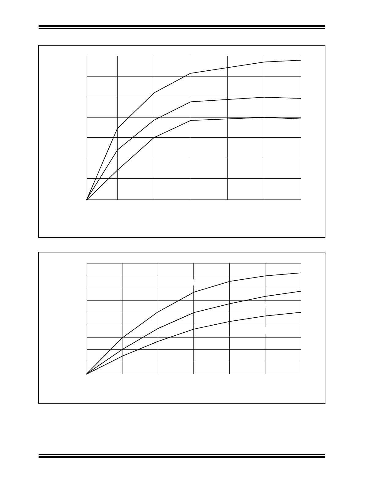
PIC16C84
FIGURE 12-20: IOL vs. VOL, VDD = 3V
35
30
25
20
IOL (mA)
15
10
5
Max. -40°C
Typ. 25°C
Min. +85°C
0
0.0 0.5 1.0 1.5 2.0
FIGURE 12-21: IOL vs. VOL, VDD = 5V
90
80
70
60
50
IOL (mA)
40
30
20
10
0
0.0 0.5 1.0 1.5 2.0 2.5
OL (Volts)
V
Max @ -40°C
2.5 3.0
Typ @ 25°C
Min @ +85°C
3.0
VOL (Volts)
DS30445C-page 94 1997 Microchip Technology Inc.
Page 95
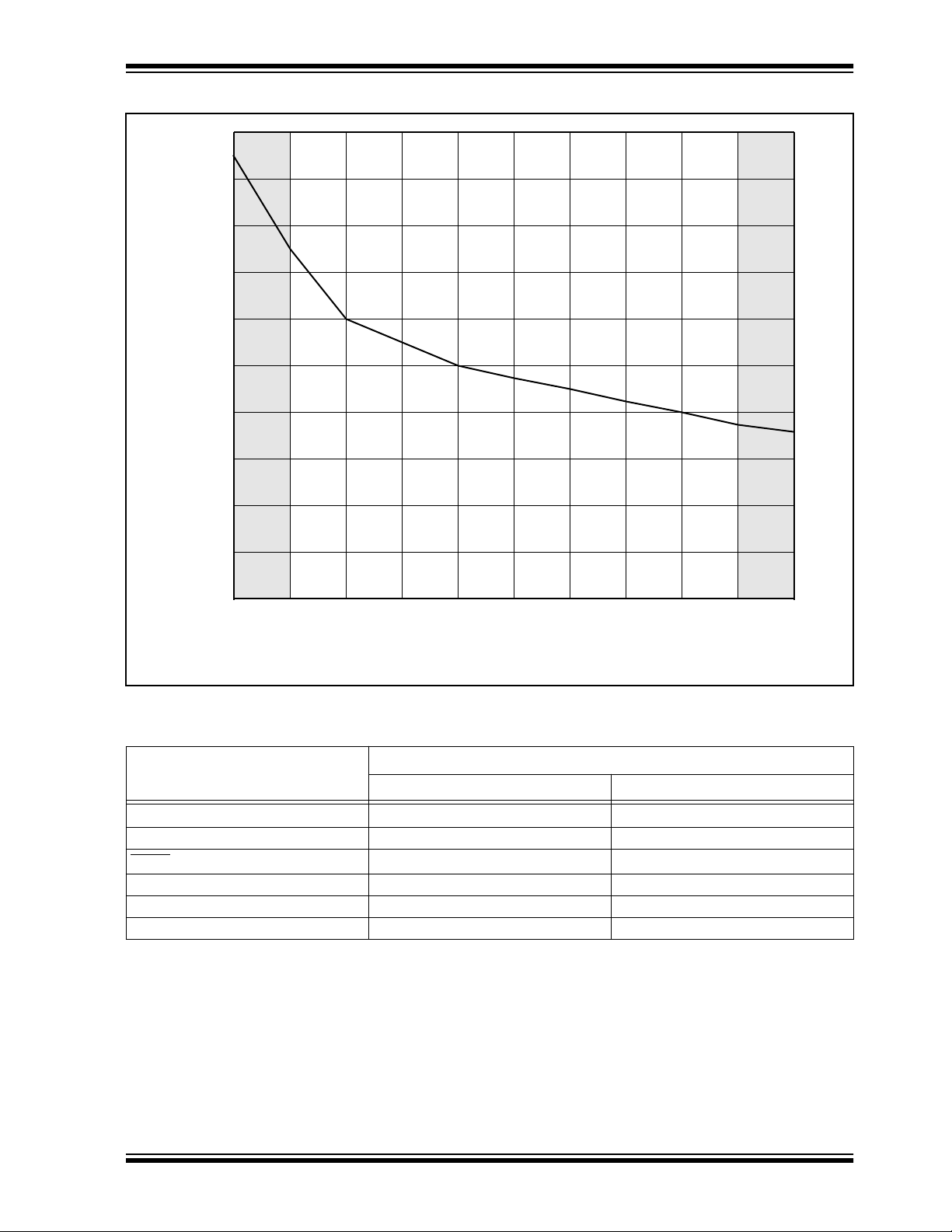
PIC16C84
FIGURE 12-22: MAXIMUM DATA MEMORY ERASE/WRITE CYCLE TIME VS. VDD
20
18
16
14
12
10
8
6
DMEM Max. E/W Cycle Time (ms)
4
2
0
2.5 3.0 3.5 4.0 4.5 5.0 5.5 6.0
VDD (Volts)
Shaded areas are beyond recommended range.
TABLE 12-2 INPUT CAPACITANCE*
Pin Name
18L PDIP 18L SOIC
PORTA 5.0 4.3
PORTB 5.0 4.3
MCLR
17.0 17.0
OSC1/CLKIN 4.0 3.5
OSC2/CLKOUT 4.3 3.5
T0CKI 3.2 2.8
* All capacitance values are typical at 25°C. A part to part variation of ±25% (three standard deviations) should
be taken into account.
Typical Capacitance (pF)
6.51.5 2.0
1997 Microchip Technology Inc. DS30445C-page 95
Page 96

PIC16C84
NOTES:
DS30445C-page 96 1997 Microchip Technology Inc.
Page 97

13.0 PACKAGING INFORMATION
13.1 K04-007 18-Lead Plastic Dual In-line (P) – 300 mil
E
D
2
n
1
PIC16C84
α
E1
A
R
β
eB
Units INCHES* MILLIMETERS
Dimension Limits MIN NOM MAX MIN NOM MAX
PCB Row Spacing 0.300 7.62
Number of Pins n 18 18
Pitch p 0.100 2.54
Lower Lead Width B 0.013 0.018 0.023 0.33 0.46 0.58
Upper Lead Width
Shoulder Radius R 0.000 0.005 0.010 0.00 0.13 0.25
Lead Thickness c 0.005 0.010 0.015 0.13 0.25 0.38
Top to Seating Plane A 0.110 0.155 0.155 2.79 3.94 3.94
Top of Lead to Seating Plane A1 0.075 0.095 0.115 1.91 2.41 2.92
Base to Seating Plane A2 0.000 0.020 0.020 0.00 0.51 0.51
Tip to Seating Plane L 0.125 0.130 0.135 3.18 3.30 3.43
Package Length
Molded Package Width
Radius to Radius Width E1 0.230 0.250 0.270 5.84 6.35 6.86
Overall Row Spacing eB 0.310 0.349 0.387 7.87 8.85 9.83
Mold Draft Angle Top
Mold Draft Angle Bottom
* Controlling Parameter.
†
Dimension “B1” does not include dam-bar protrusions. Dam-bar protrusions shall not exceed
0.003” (0.076 mm) per side or 0.006” (0.152 mm) more than dimension “B1.”
‡
Dimensions “D” and “E” do not include mold flash or protrusions. Mold flash or protrusions shall
not exceed 0.010” (0.254 mm) per side or 0.020” (0.508 mm) more than dimensions “D” or “E.”
B1
D
E
α
β
c
A2
†
‡
‡
0.055 0.060 0.065 1.40 1.52 1.65
0.890 0.895 0.900 22.61 22.73 22.86
0.245 0.255 0.265 6.22 6.48 6.73
5 10 15 5 10 15
5 10 15 5 10 15
B1
B
p
A1
L
1997 Microchip Technology Inc. DS30445C-page 97
Page 98

PIC16C84
13.2 K04-051 18-Lead Plastic Small Outline (SO) – Wide, 300 mil
E1
p
B
n
E
D
2
1
°
45
c
β
Units
Dimension Limits
Pitch
Overall Pack. Height
Shoulder Height
Standoff
Molded Package Length
Molded Package Width
Outside Dimension
Chamfer Distance
Shoulder Radius
Gull Wing Radius
Foot Length
Foot Angle
Radius Centerline
Lead Thickness
Lower Lead Width
Mold Draft Angle Top
Mold Draft Angle Bottom
*
Controlling Parameter.
†
Dimension “B” does not include dam-bar protrusions. Dam-bar protrusions shall not exceed 0.003”
(0.076 mm) per side or 0.006” (0.152 mm) more than dimension “B.”
‡
Dimensions “D” and “E” do not include mold flash or protrusions. Mold flash or protrusions shall not
exceed 0.010” (0.254 mm) per side or 0.020” (0.508 mm) more than dimensions “D” or “E.”
X
R1
p
nNumber of Pins
A
A1
A2
D
E
E1
X
R1
R2
L
φ
L1
c
B
α
β
α
L
R2
A
φ
L1
INCHES*
MIN
0.093
0.048
‡
‡
†
0.004
0.450
0.292
0.394
0.010
0.005
0.005
0.011
0
0.010
0.009
0.014
0
0
A2
NOM MAX
0.050
0.099
0.058
0.008
0.456
0.296
0.407
0.020
0.005
0.005
0.016
0.015
0.011
0.017
0.104
0.068
0.011
0.462
0.299
0.419
0.029
0.010
0.010
0.021
4
0.020
0.012
0.019
12
12
MILLIMETERS
MIN NOM MAX
2.36
1.22
0.10
11.43
7.42
10.01
0.25
0.13
0.13
0.28
8
15
15
0
0.25
0.23
0.36
0
0
1.27
1818
2.50
1.47
0.19
11.58
7.51
10.33
0.50
0.13
0.13
0.41
4 8
0.38
0.27
0.42
12
12
A1
2.64
1.73
0.28
11.73
7.59
10.64
0.74
0.25
0.25
0.53
0.51
0.30
0.48
15
15
DS30445C-page 98 1997 Microchip Technology Inc.
Page 99

PIC16C84
APPENDIX A: FEATURE
IMPROVEMENTS FROM PIC16C5X TO
PIC16C84
The following is the list of feature improvements over
the PIC16C5X microcontroller family:
1. Instruction word length is increased to 14 bits.
This allows larger page sizes both in program
memory (2K now as opposed to 512 before) and
the register file (128 bytes now versus 32 bytes
before).
2. A PC latch register (PCLATH) is added to handle
program memory paging. PA2, PA1 and P A0 bits
are removed from the status register and placed
in the option register.
3. Data memor y paging is redefined slightly. The
STATUS register is modified.
4. Four new instructions have been added:
RETURN, RETFIE, ADDLW, and SUBLW. Two
instructions, TRIS and OPTION, are being
phased out although they are kept for
compatibility with PIC16C5X.
5. OPTION and TRIS registers are made
addressable.
6. Interrupt capability is added. Interrupt vector is
at 0004h.
7. Stack size is increased to 8 deep.
8. Reset vector is changed to 0000h.
9. Reset of all registers is revisited. Five different
reset (and wake-up) types are recognized.
Registers are reset differently.
10. Wake up from SLEEP through interrupt is
added.
11. Two separate timers, the Oscillator Start-up
Timer (OST) and Power-up Timer (PWRT), are
included for more reliable power-up. These
timers are invoked selectively to avoid
unnecessary delays on power-up and wake-up.
12. PORTB has weak pull-ups and interrupt on
change features.
13. T0CKI pin is also a port pin (RA4/T0CKI).
14. FSR is a full 8-bit register.
15. "In system programming" is made possible. The
user can program PIC16CXX devices using only
five pins: V
(data in/out).
DD, VSS, VPP, RB6 (clock) and RB7
APPENDIX B: CODE COMPATIBILITY
- FROM PIC16C5X TO
PIC16C84
To convert code written for PIC16C5X to PIC16C84,
the user should take the following steps:
1. Remove any program memory page select
operations (PA2, PA1, PA0 bits) for CALL, GOTO .
2. Revisit any computed jump operations (write to
PC or add to PC, etc.) to make sure page bits
are set properly under the new scheme.
3. Eliminate any data memory page switching.
Redefine data variables for reallocation.
4. Verify all writes to STATUS, OPTION, and FSR
registers since these have changed.
5. Change reset vector to 0000h.
1997 Microchip Technology Inc. DS30445C-page 99
Page 100

PIC16C84
APPENDIX C: WHAT’S NEW IN THIS
DATA SHEET
No new information has been added to this data sheet.
For information on upgrade devices from the
PIC16C84, please refer to the PIC16F8X data sheet.
APPENDIX D: WHAT’S CHANGED IN
THIS DATA SHEET
Here’s what’s changed in this data sheet:
1. Some sections have been rearranged for clarity
and consistency.
2. Errata information has been included.
DS30445C-page 100 1997 Microchip Technology Inc.
 Loading...