


PIC16C781/782
Data Sheet
8-Bit CMOS Microcontrollers with A/D,
D/A, OPAMP, Comparators and PSMC
2001 Microchip Technology Inc. Preliminary DS41171A

Note the following details of the code protection feature on PICmicro® MCUs.
• The PICmicro family meets the specifications contained in the Microchip Data Sheet.
• Microchip believes that its family of PICmicro microcontrollers is one of the most secure products of its kind on the market today,
when used in the intended manner and under normal conditions.
• There are dishonest and possibly illegal methods used to breach the code protection feature. All of these methods, to our knowledge, require using the PICmicro microcontroller in a manner outside the operating specifications contained in the data sheet.
The person doing so may be engaged in theft of intellectual property.
• Microchip is willing to work with the customer who is concerned about the integrity of their code.
• Neither Microchip nor any other semiconductor manufacturer can guarantee the security of their code. Code protection does not
mean that we are guaranteeing the product as “unbreakable”.
• Code protection is constantly evolving. We at Microchip are committed to continuously improving the code protection features of
our product.
If you have any further questions about this matter, please contact the local sales office nearest to you.
Information contained in this publication regarding device
applications and the like is intended through suggestion only
and may be superseded by updates. It is your responsibility to
ensure that your application meets with your specifications.
No representation or warranty is given and no liability is
assumed by Microchip Technology Incorporated with respect
to the accuracy or use of such information, or infringement of
patents or other intellectual property rights arising from such
use or otherwise. Use of Microchip’s products as critical components in life support systems is not authorized except with
express written approval by Microchip. No licenses are conveyed, implicitly or otherwise, under any intellectual property
rights.
Trademarks
The Microchip name and logo, the Microchip logo, PIC, PICmicro,
PICMASTER, PICSTART, PRO MATE, K
EELOQ, SEEVAL,
MPLAB and The Embedded Control Solutions Company are registered tradem arks of Micr ochip Technology Incorporated in the
U.S.A. and other countries.
Total Endurance, ICSP, In-Circuit Serial Programming, FilterLab, MXDEV, microID, FlexROM, fuzzyLAB, MPASM,
MPLINK, MPLIB, PICC, PICDEM, PICDEM.net, ICEPIC,
Migratable Memory, FanSense, ECONOMONITOR, Select
Mode and microPort are trademarks of Microchip Technology
Incorporated in the U.S.A.
Serialized Quick T erm Programming (SQTP) is a service mark
of Microchip Technology Incorporated in the U.S.A.
All other trademarks mentioned herein are property of their
respective companies.
© 2001, Microchip Technology Incorporated, Printed in the
U.S.A., All Rights Reserved.
Printed on recycled paper.
Microchip received QS-9000 quality system
certification for its worldwide headquarters,
design and wafer fabrication facilities in
Chandler and Tempe, Arizona in July 1999. The
Company’s quality system processes and
procedures are QS-9000 compliant for its
PICmicro
devices, Serial EEPROMs and microperipheral
products. In addition, Microchip’s quality
system for the design and manufacture of
development systems is ISO 9001 certified.
®
8-bit MCUs, KEELOQ
®
code hoppin g
DS41171A - page ii Preliminary 2001 Microchip Technology Inc.
PIC16C781/782
8-Bit CMOS Microcontrollers with A/D, D/A, OPAMP,
Comparators and PSMC
Microcontroller Core Features:
• High performance RISC CPU
• Only 35 single word instructions to learn
• All single cycle instructions except for program
branches which are two cycle
• Direct, indirect and relative addressing modes
- Operating speed: DC - 20 MHz clock input
DC - 200 ns instruction cycle
Program
Device
Memory
X14
PIC16C781 1K 128
PIC16C782 2K 128
• 8-level deep hardware stack
• Interrupt capability (up to 8 internal/external
interrupt sources)
• 16 I/O pins:
- Individual direction control (13 pins)
- Input only (3 pins), low leakage (2 pins)
- Digital/Analog inputs (8 pins)
• Programmable PORTB interrupt-on-change (8 pins)
• Programmable PORTB weak pull-ups (8 pins)
• Power-on Reset (POR)
• Power-up Timer (PWRT) and
Oscillator Start-up Timer (OST)
• Watchdog Timer (WDT) with a software enabled
option and its own on-chip RC oscillator for
reliable operation
• Programmable Brown-out Reset (BOR)
• Programmable Low Voltage Detection (LVD)
• Internal/external MCLR
• Programmable code protection
• Power saving SLEEP mode
• Selectable oscillator options:
HS, XT, LP, EC, RC, INTRC (4 MHz/37 kHz)
• In-Circuit Serial Programming™ (ISCP™)
• Program Memory Read (PMR) capability
• Four user programmable ID locations
• Wide operating voltage range:
- 2.5V to 5.5V for commercial and industrial
temperature ranges
- Extended temperature range available
Data Memory
X8
Microcontroller Core Features (Continued):
• Low power, high speed CMOS EPROM
technology
• Fully static design
• Low power consumption:
- < 2mA @ 5V, 4MHz
-< 1 µA typical standby current.
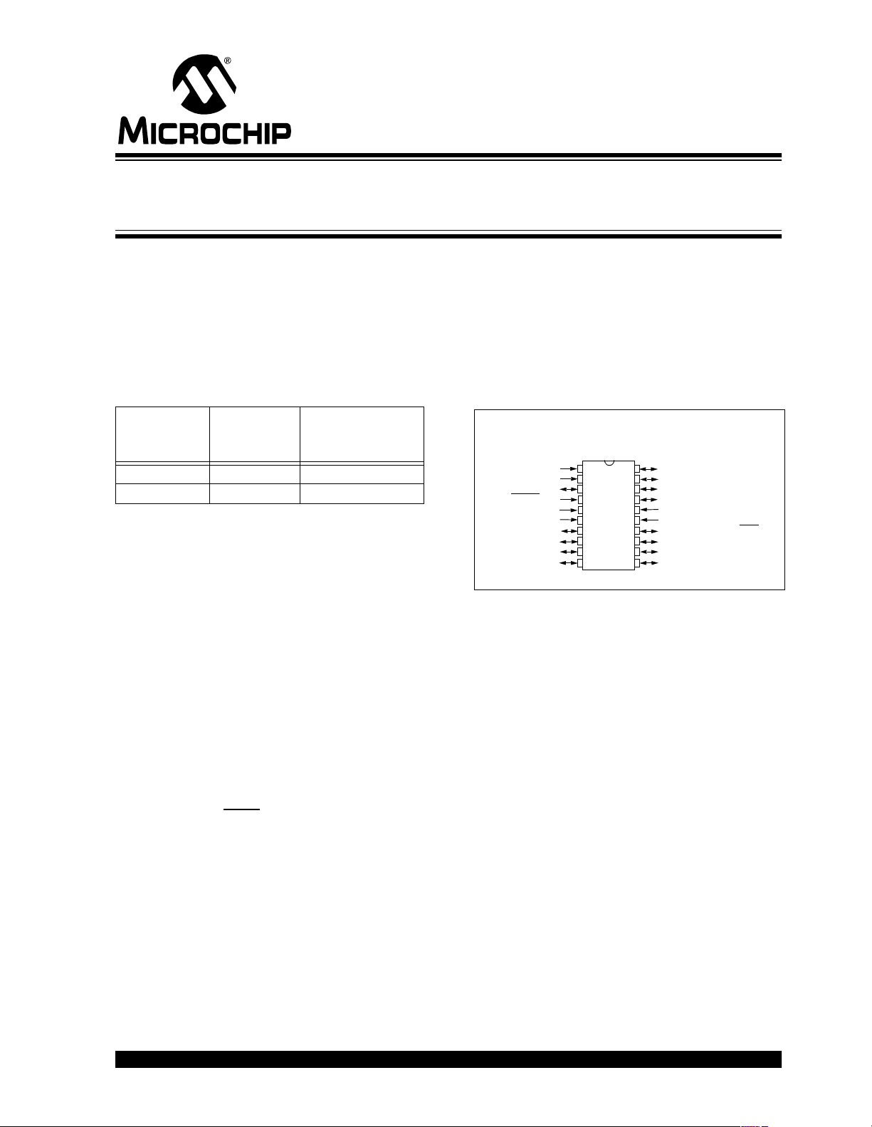
Pin Diagram
PDIP, Windowed CERDIP, SOIC, SSOP
RA0/AN0/OPA+
RA1/AN1/OPA-
RA4/T0CKI
RA5/MCLR
RA2/AN2/VREF2
RA3/AN3/V
RB0/INT/AN4/V
RB1/AN5/VDAC
/VPP
VSS
AVSS
REF1
R
20
•1
1
PIC16C781/782
2
2
3
3
4
4
5
5
6
6
7
7
8
8
9
9
10
10
RB3/AN7/OPA
20
RB2/AN6
19
19
RA7/OSC1/CLKIN
18
18
RA6/OSC2/CLKOUT/T1CKI
17
17
16
16
15
15
14
14
13
13
12
12
11
11
DD
V
AVDD
RB7/C2/PSMC1B/T1G
RB6/C1/PSMC1A
RB5
RB4
Peripheral Features:
• Timer0: 8-bit timer/counter with 8-bit prescaler
• Enhanced Timer1:
- 16-bit timer/counter with prescaler
- External Gate Input mode
- Option to use OSC1 and OSC2 in LP mode
as Timer1 osci llator, if INTRC oscillator m ode
selected
• Analog-to-Digital Converter (ADC):
- 8-bit resolution
- Programmable 8-channel input
- Internal voltages available for self-
diagnostics
• Digital-to-Analog Converter (DAC):
- 8-bit resolution
- Reference from AV
- Output configurable to V
tors, and ADC reference
• Operational Amplifier module (OPA):
- Firmware initiated input offset voltage Auto
Calibration module
- Low leakage inputs
- Programmable Gain Bandwidth Product
(GBWP)
DD, VREF1, or VR module
DAC pin, Compara-
2001 Microchip Technology Inc. Preliminary DS41171A-page 1

PIC16C781/782
Peripheral Features (Continued):
• Dual Analog Comparator module with:
- Individual enable and interrupt bits
- Programmable speed and output polarity
- Fully configurabl e inputs and outputs
- Reference from DAC, or V
- Low input offset voltage.
• V
R voltage reference module :
- 3.072V +/- 0.7% @25°C, AV
- Configurable output to ADC reference, DAC
reference, and V
- 5 mA sink/sourc e
Key Features
PICmicro™ Mid-Range
Reference Manual
Operating Frequency DC - 20 MHz DC - 20 MHZ
RESETS (and Delays) POR, BOR, MCLR
Program Memory (14 bit words) 1K 2K
Data Memory (bytes) 128 128
Interrupts 8 8
I/O Ports 13 + 3 Input only 13 + 3 Input only
Timers 2 2
Programmable Switch Mode Controller 1 1
8-bit Analog-to-Digital Module 1 1
ADC channels 8 External, 2 Internal 8 External, 2 Internal
8-bit Digital-to-Analog Module 1 1
Comparators 2 2
Comparator Channels 4 (AN<7:4>) 4 (AN<7:4>)
Operational Amplifier 1 1
Voltage Reference 1 1
Brown-out Reset Yes Yes
Programmable Low Voltage Detect Yes Yes
Instructi on Set 35 Instr uctions 35 Instruct ions
R pin
(DS33023)
REF1/VREF2
DD = 5V
PIC16C781 PIC16C782
• Programmable Switch Mode Controller module:
- PWM and PSM modes
- Programmable switching frequency
- Configurable for either single or dual
feedback inputs
- Configurable single or dual outputs
- Slope compensation output available in
single output mode
, WDT (PWRT , OST) POR, BOR, MCLR, WDT (PWRT, OST)
DS41171A-page 2 Preliminary 2001 Microchip Technology Inc.

PIC16C781/782
Table of Contents
1.0 Device Overview ......................................................................................................................................................................... 5
2.0 Memory Organization ................................................................................................................................................................11
3.0 I/O Ports ................... ................. ................ ................. ................. ................. ............................................................................. 25
4.0 Program Memory Read (PMR) . ................................................................................................................................................. 47
5.0 Timer0 Module .......................................................................................................................................................................... 51
6.0 Timer1 Module with Gate Control .............................................................................................................................................. 55
7.0 Voltage Reference Module (V
8.0 Programmable Low Voltage Detect Module (PLVD) ................................................................................................................. 63
9.0 Analog-to-Digital Converter (ADC) Module ...............................................................................................................................69
10.0 Digital-to-Analog Converter (DAC) Module ...............................................................................................................................79
11.0 Operational Amplifier (OPA) Module ......................................................................................................................................... 83
12.0 Comparator Module ................................................................................................................................................................... 89
13.0 Programmable Switch Mode Contr o lle r (PSMC) ............ .................................. .................................. ....................................... 99
14.0 Special Features of The CPU ....................................... .................................. ......................................................................... 117
15.0 Instruction Set Summary ......................................................................................................................................................... 133
16.0 Development Support .............................................................................................................................................................. 141
17.0 Electrical Characteristics ......................................................................................................................................................... 147
18.0 DC and AC Characteristics Graphs and Tables ...................................................................................................................... 167
19.0 Packaging Information ................... ................. ................ ................. ........................................................................................ 169
Index ..................................................................................................................................................................................................175
On-Line Support.................................................................................................................................................................................181
Reader Response.............................................................................................................................................................................. 182
PIC16C781/782 Product Identification System................................................................... ......... .. .... ................................................183
R) ................................................................................................................................................ 61
TO OUR VALUED CUSTOMERS
It is our intention to provide our valued customers with the best documentation possible to ensure successful use of your Microchip
products. To this end, we will continue to improve our publications to better suit your needs. Our publications will be refined and
enhanced as new volumes and updates are introduced.
If you have any questions or c omm ents regarding th is publication, p lease c ontact the M a rketing Communications Department via
E-mail at docerrors@mail.microchip.com or fax the Reader Response Form in the back of this data sheet to (480) 792-4150.
We welcome your feedback.
Most Current Data Sheet
To obtain the most up-to-date version of this data sheet, please register at our Worldwide Web site at:
http://www.microchip.com
You can determine the version of a data sheet by examining its literature number found on the bottom outside corner of any page.
The last character of the literature number is the version number, (e.g., DS30000A is version A of document DS30000).
Errata
An errata sheet, describing minor operational differences from the data sheet and recommended workarounds, may exist for current
devices. As device/documentation issues become known to us, we will publish an errata sheet. The errata will specify the revision
of silicon and revision of document to which it applies.
To determine if an errata sheet exists for a particular device, please check with one of the following:
• Microchip’s Worldwide Web site; http://www.microchip.com
• Your local Microchip sales office (see last page)
• The Microchip Corporate Literature Center; U.S. FAX: (480) 792-7277
When contacting a sales office or the literature center, please specify which device, revision of silicon and data sheet (include literature number) you are using.
Customer Notification System
Register on our web site at www.microchip.com/cn to receive the most current information on all of our products.
2001 Microchip Technology Inc. Preliminary DS41171A-page 3

PIC16C781/782
NOTES:
DS41171A-page 4 Preliminary 2001 Microchip Technology Inc.
PIC16C781/782
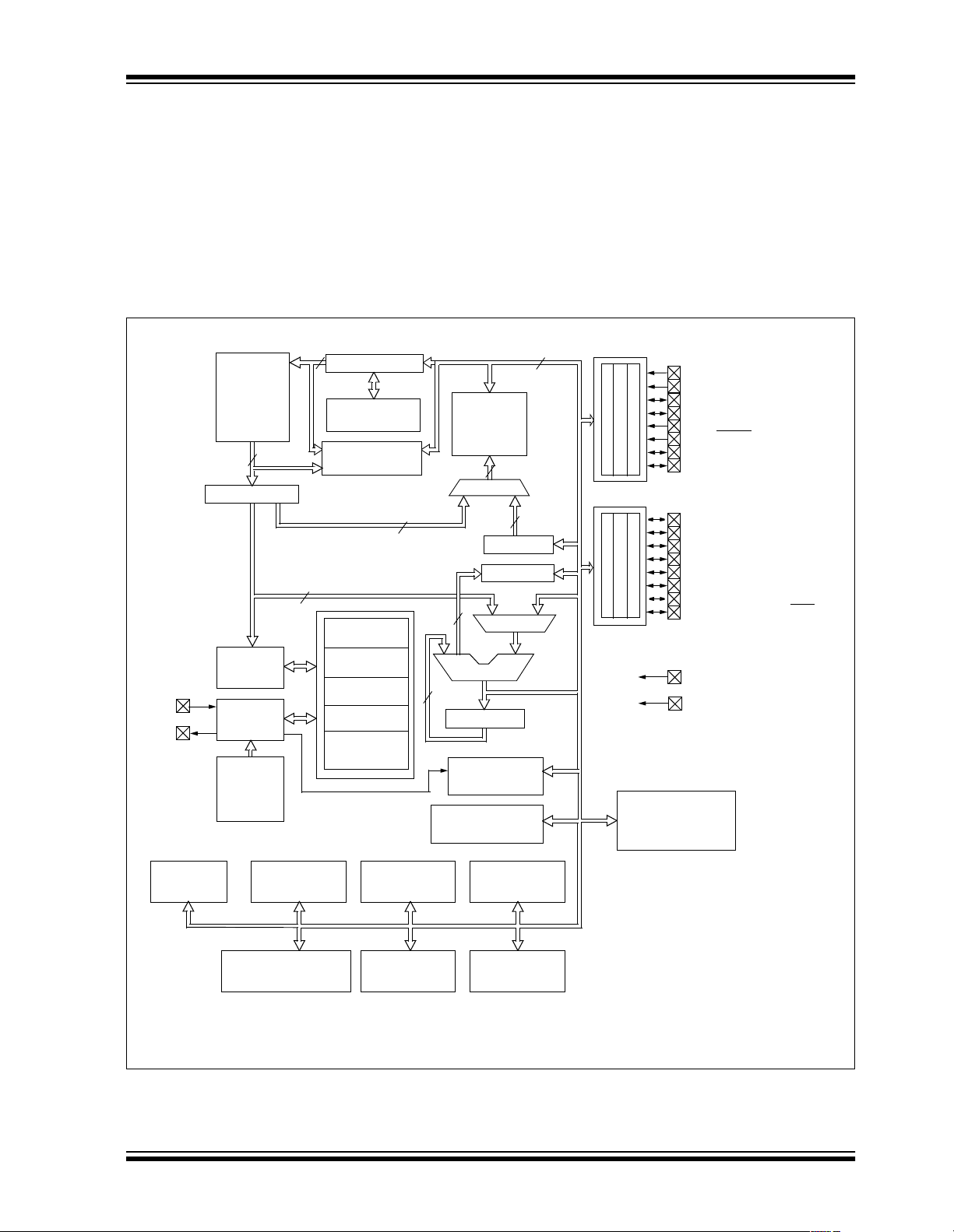
1.0 DEVICE OVERVIEW
This document contains device-specific information.
Additional information m ay be found in the PICm ic ro™
Mid-Range Reference Manual (DS33023), which may
be obtained from your local Microchip Sales Representative or downloaded from the Microchip website. The
Reference manual should be considered a complementary document to this data sheet. The Reference
FIGURE 1-1: PIC16C781 BLOCK DIAGRAM
Program
Bus
OSC1/
CLKIN
OSC2/
CLKOUT
EPROM
Program
Memory
1K x 14
14
Instruction reg
Instruction
Decode &
Control
Timing
Generation
Internal
RC
Oscillator
INTRC
13
Program Counter
8 Level Stack
(13-bit)
Program Memory
Read (PMR)
Direct Addr
8
Power-up
Timer
Oscillator
Start-up Timer
Power-on
Reset
Watchdog
Timer
Brown-out
Reset
7
Data Bus
RAM
File
Registers
128 x 8
RAM
Addr
Addr MUX
3
ALU
8
W reg
Timer1
(TMR1)
Voltage Reference
(VR) Module
manual is highly recommended reading for a better
understanding o f the d ev ic e arc hi tec ture a nd operation
of the peripheral modules.
This data sheet covers two devices: PIC16C781 and
PIC16C782. Both devices come in a variety of 20-pin
packages.
The following figures are block diagrams of the
PIC16C781 and the PIC16C782.
8
9
Indirect
8
Addr
FSR reg
STATUS r eg
MUX
PORTA
PORTB
Programmable
Low Voltage Detect
(PLVD)
RA0/AN0/OPA+
RA1/AN1/OPARA2/AN2/VREF2
RA3/AN3/VREF1
RA4/T0CKI
RA5/MCLR
RA6/OSC2/CLKOUT/T1CKI
RA7/OSC1/CLKIN
RB0/INT/AN4/VR
RB1/AN5/VDAC
RB2/AN6
RB3/AN7/OPA
RB4
RB5
RB6/C1/PSMC1A
RB7/C2/PSMC1B/T1G
AVDD, AVSS
DD, VSS
V
/VPP
(1)
Timer0
(TMR0)
Note 1: AVDD and AVSS pins are used by the following modules: C1, C2, OPA, DAC, ADC, and VR.
2001 Microchip Technology Inc. Preliminary DS41171A-page 5
Comparator
(C1)
Programmable Switch
Mode Controller
(PSMC)
Comparator
(C2)
OPAMP
(OPA)
8-bit ADC
8-bit
DAC
PIC16C781/782
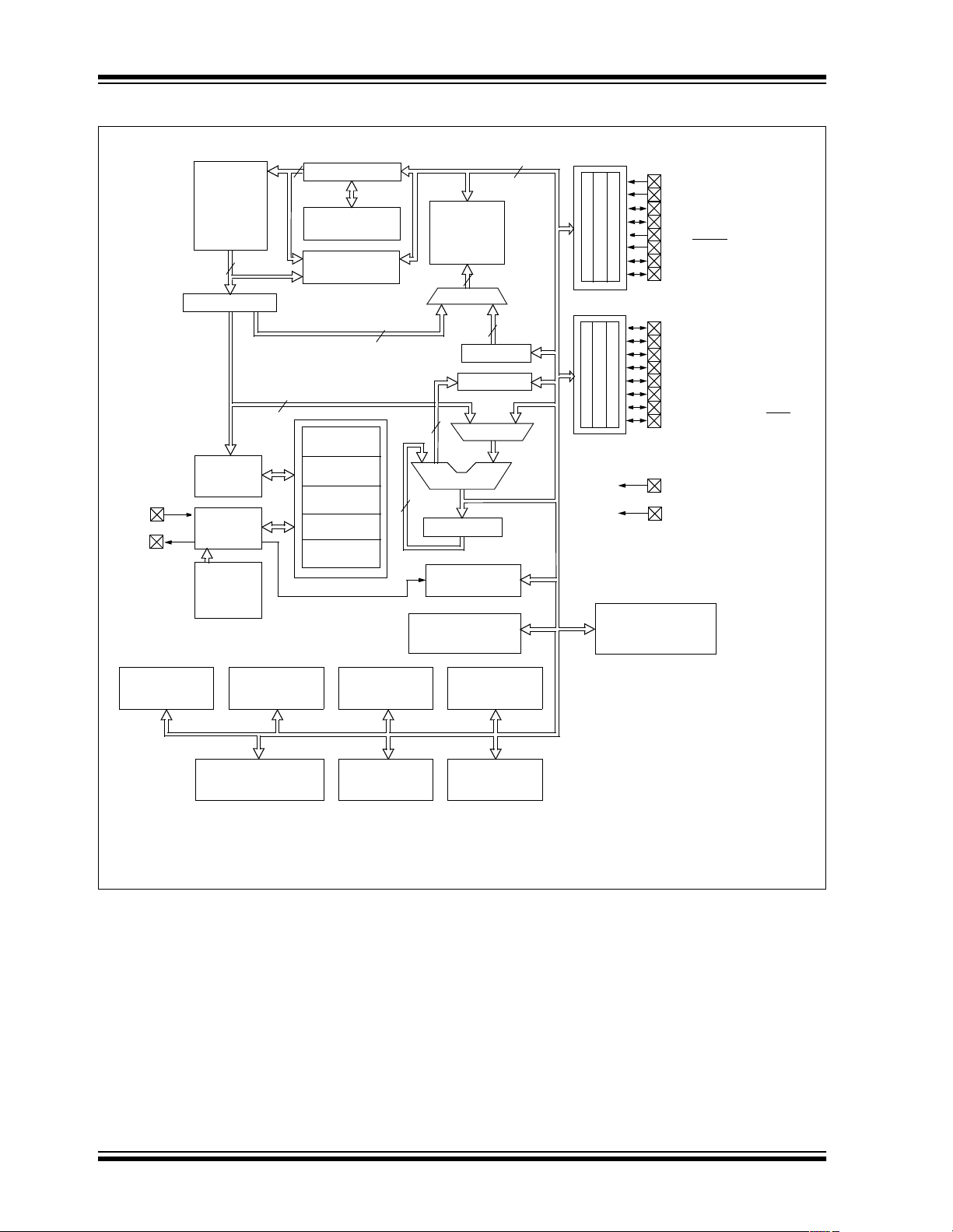
FIGURE 1-2: PIC16C782 BLOCK DIAGRAM
Program
Bus
OSC1/
CLKIN
OSC2/
CLKOUT
EPROM
Program
Memory
2K x 14
14
Instruction reg
Instruction
Decode &
Control
Timing
Generation
Internal
RC
Oscillator
INTRC
13
Program Counter
8 Level Stack
(13-bit)
Program Memory
Read (PMR)
Direct Addr
8
Power-up
Timer
Oscillator
Start-up Timer
Power-on
Reset
Watchdog
Timer
Brown-out
Reset
RAM
Addr
7
3
8
Voltage Reference
Data Bus
RAM
File
Registers
128 x 8
Addr MUX
FSR reg
STATUS reg
ALU
W reg
Timer1
(TMR1)
Module
R)
(V
9
8
MUX
8
Indirect
Addr
PORTA
PORTB
Programmable
Low Voltage Detect
PLVD
RA0/AN0/OPA+
RA1/AN1/OPARA2/AN2/VREF2
RA3/AN3/VREF1
RA4/T0CKI
RA5/MCLR
RA6/OSC2/CLKOUT/T1CKI
RA7/OSC1/CLKIN
RB0/INT/AN4/VR
RB1/AN5/VDAC
RB2/AN6
RB3/AN7/OPA
RB4
RB5
RB6/C1/PSMC1A
RB7/C2/PSMC1B/T1G
AVSS, AVSS
DD, VSS
V
/VPP
(1)
Timer0
TMR0
Note 1: AVDD and AVSS pins are used for the following modules: C1, C2, OPA, DAC, ADC, and VR.
Comparator
C1
Programmable Switch
Mode Controller
PSMC
Comparator
C2
OPAMP
OPA
8-bit ADC
8-bit
DAC
DS41171A-page 6 Preliminary 2001 Microchip Technology Inc.
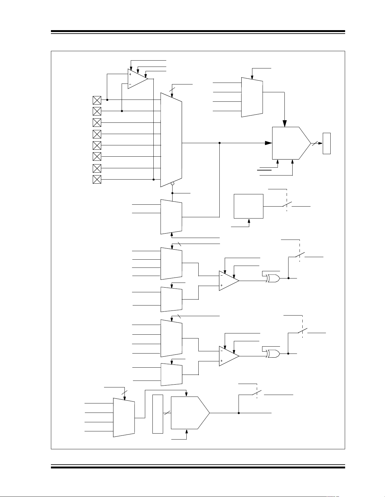
FIGURE 1-3: ANALOG SIGNAL MULTIPLEXING DIAGRAM
PIC16C781/782
RA0/AN0/OPA+
RA1/AN1/OPA-
RA2/AN2/V
RA3/AN3/V
REF2
REF1
RB0/INT/AN4/V
RB1/AN5/VDAC
RB2/AN6
RB3/AN7/OPA
AV
VREF1
V
N/C
R
DARS<1:0>
DD
R
OPAON
CMPEN
VCFG<1:0>
GBWP
OPA
CHS<2:0>
3
0
1
DD
AV
VREF1
R
V
V
DAC
0
1
2
3
2
3
4
ADCREF
ADC
8
ADRES
5
ADON
GO/DONE
VR
REFERENCE
VROE & VREN
AN4
R
V
VDAC
6
EN
7
CHS3
EN
0
1
VREN
2
C1CH<1:0>
AN4
AN5
AN6
AN7
V
REF1
DAC
V
AN4
AN5
AN6
AN7
V
REF2
DAC
V
0
1
2
3
C1R
C1
C1ON
C1SP
0
1
2
C2CH<1:0>
0
1
C2ON
C2SP
2
3
C2R
C2
0
1
DAON & DAOE
2
DAC
CHS0
0
1
8
REF
DAC
C1OE
RB6/C1/
PSMC1A
C1POL
C1OUT
C2OE
RB7/C2
PSMC1B
C2POL
C2OUT
AN4
VDAC
2
3
DAC REGISTER
DAON
2001 Microchip Technology Inc. Preliminary DS41171A-page 7

PIC16C781/782
TABLE 1-1: PIC16C781/782 PINOUT DESCRIPTION
Name Function
Input
Type
Output
Type
RA0 ST N/A Port Input
RA0/AN0/OPA+
AN0 AN
OPA+ AN
— ADC Input
— OPAMP Non-inverting I nput
RA1 ST N/A Port Input
RA1/AN1/OPA-
AN1 AN
OPA- AN
— ADC Input
— OPAMP Inverting Input
RA2 ST CMOS Bi-directional I/O
RA2/AN2/V
REF2
AN2 AN
REF2AN — Comparator 2 Voltage Refere nc e Input
V
— ADC Input
RA3 ST CMOS Bi-directional I/O
RA3/AN3/V
REF1
AN3 AN
REF1AN — Comparator 1, ADC, DACREF Input
V
— ADC Input
RA4/T0CKI RA4 ST OD Bi-directional I/O
TOCKI ST — Timer0 Clock Input
RA5 ST N/A Port Input
RA5/MCLR
/VPP
MCLR ST — Master Clear Input
VPP Power — Programming Voltage
RA6 ST CMOS Bi-directional I/O
RA6/OSC2/CLKOUT/T1CKI
OSC2
CLKOUT — CMOS Fosc/4 Output
T1CKI ST
— XTAL Crystal/Resonator
— Timer1 Clock Input
RA7 ST CMOS Bi-directional I/O
RA7/OSC1/CLKIN
OSC1 XTAL — Crystal/Resonator
CLKIN ST
— External Clock Input
RB0 TTL CMOS Bi-directional I/O
RB0/INT/AN4/VR
INT ST — External Interrupt
AN4 AN
— ADC, Compara tor Input
VR — AN Internal Voltage Reference Output
RB1 TTL CMOS Bi-directional I/O
RB1/AN5/V
DAC
AN5 AN
— ADC, Compara tor Input
VDAC — AN DAC Output
RB2/AN6
RB2 TTL CMOS Bi-directional I/O
AN6 AN
— ADC, Compara tor Input
RB3 TTL CMOS Bi-directional I/O
RB3/AN7/OPA
AN7 AN — ADC, Comparator Input
OPA
— AN OPAMP Output
RB4 RB4 TTL CMOS Bi-directional I/O
RB5 RB5 TTL CMOS Bi-directional I/O
RB6 TTL CMOS Bi-directional I/O
RB6/C1/PSMC1A
C1
— CMOS Comparator 1 Output
PSMC1A — CMOS PSMC Output 1A
Description
DS41171A-page 8 Preliminary 2001 Microchip Technology Inc.
PIC16C781/782
TABLE 1-1: PIC16C781/782 PINOUT DESCRIPTION (CONTINUED)
Name Function
RB7 TTL CMOS Bi-directional I/O
RB7/C2/PSMC1B/T1G
DD AVDD Power — Positive Supply for Analog
AV
SS AVSS Power — Ground Reference for Analog
AV
VDD VDD Power — Positive Supply for Logic and I/O pins
SS VSS Power — Ground Reference for Logic and I/O pins
V
Legend: ST = Schmitt Trigger AN = Analog OD = open drain TTL = Logic Level
XTAL = Crystal CMOS = CMOS Output Power = Power Supply
C2 — CMOS Comparator 2 Output
PSMC1B
T1G ST — Timer 1 Gate Input
Input
Type
Output
Type
— CMOS PSMC Output 1B
Description
2001 Microchip Technology Inc. Preliminary DS41171A-page 9

PIC16C781/782
NOTES:
DS41171A-page 10 Preliminary 2001 Microchip Technology Inc.
PIC16C781/782
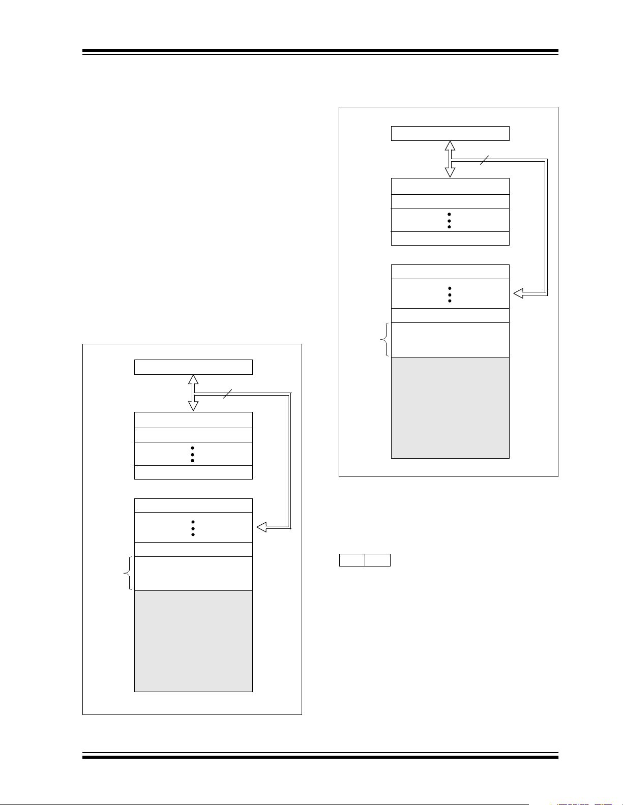
2.0 MEMORY ORGANIZATION
There are two memory blocks in each of these
PICmicro
data memory) has its own bus, so that concurrent
access can occur.
Additional informa tion on devi ce memory may be found
in the PICmicro™ Mid-Range Reference Manual,
(DS33023).
2.1 Program Memory Organization
The PIC16C781/782 devices have a 13-bit program
counter capable of addressing an 8K x 14 program
memory space. The PIC16C781 has 1K x 14 words of
program memo ry. The PIC16C 782 has 2K x 14 w ords
of program memory. Accessing a location above the
physically i mplemented addr ess ca uses a wrap aroun d.
The RESET vector is at 0000h and the interrupt vector
is at 0004h.
FIGURE 2-1: PIC16C781 PROGRAM
®
microcontrollers. Each block (program and
MEMORY MAP AND
STACK
PC<12:0>
FIGURE 2-2: PIC16C782 PROGRAM
MEMORY MAP AND
STACK
PC<12:0>
CALL, RETURN
RETFIE, RETLW
On-Chip
Program
Memory
Stac k Lev el 1
Stack Level 2
Stack Level 8
RESET Vector
Interrupt Vector
Page 0
13
0000h
0004h
0005h
07FFh
0800h
CALL, RETURN
RETFIE, RETLW
On-Chip
Program
Memory
13
Stack Level 1
Stack Le vel 2
Stac k Lev el 8
RESET Vector
Interrupt Vector
Page 0
0000h
0004h
0005h
03FFh
0400h
1FFFh
1FFFh
2.2 Data Memory Organization
The data memory is partitioned into multiple banks,
which contain the General Purpose Registers and the
Special Function Registers. Bits RP0 and RP1 are
bank select bits.
RP1 RP0 (STATUS<6:5>)
= 00 → Bank0
= 01 → Bank1
= 10 → Bank2
= 11 → Bank3
Each bank extends up to 7Fh (128 bytes). The lower
locations of each bank are reserved for the Special
Function Registers. Above the Special Function Registers are th e Genera l Purpos e Regist ers, im plement ed
as static RAM. All implemented banks contain Special
Function Registers. Some frequently used Special
Function Registers from one bank are mirrored in
another bank for code reduction and quicker access.
2001 Microchip Technology Inc. Preliminary DS41171A-page 11
PIC16C781/782
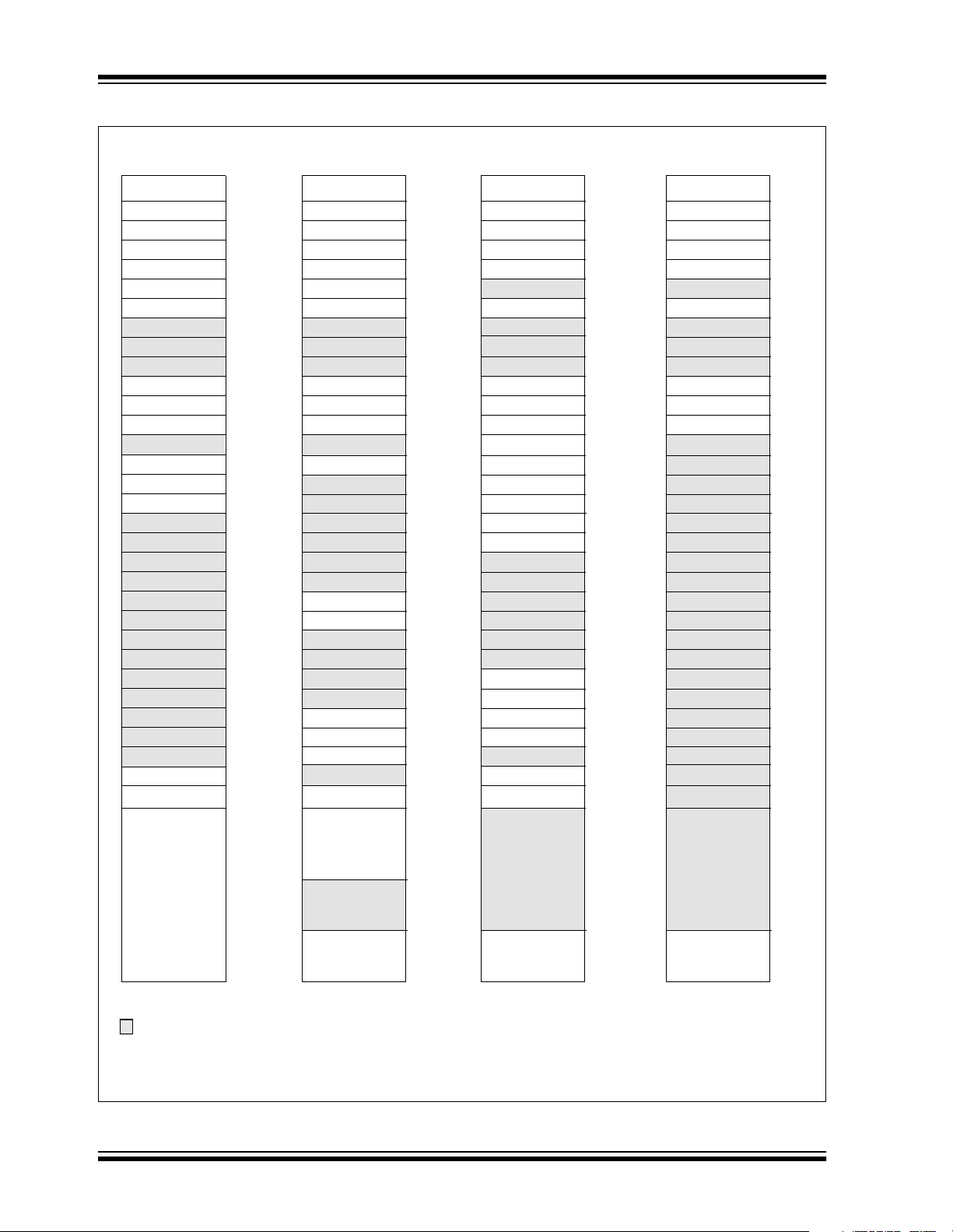
FIGURE 2-3: REGISTER FILE MAP
File
Address
Indirect addr.
TMR0
PCL
STATUS
FSR
PORTA
PORTB
PCLATH
INTCON
PIR1
TMR1L
TMR1H
T1CON
ADRES
ADCON0
General
Purpose
Register
96 Bytes
Bank 0 Bank 1
(*)
00h
01h
02h
03h
04h
05h
06h
07h
08h
09h
0Ah
0Bh
0Ch
0Dh
0Eh
0Fh
10h
11h
12h
13h
14h
15h
16h
17h
18h
19h
1Ah
1Bh
1Ch
1Dh
1Eh
1Fh
20h
7Fh
Indirect addr.
OPTION_REG
REFCON
LVDCON
ADCON1
General
Purpose
Register
32 Bytes
accesses
70h-7Fh
PCL
STATUS
FSR
TRISA
TRISB
PCLATH
INTCON
PIE1
PCON
WPUB
IOCB
ANSEL
File
Address
(*)
80h
81h
82h
83h
84h
85h
86h
87h
88h
89h
8Ah
8Bh
8Ch
8Dh
8Eh
8Fh
90h
91h
92h
93h
94h
95h
96h
97h
98h
99h
9Ah
9Bh
9Ch
9Dh
9Eh
9Fh
A0h
BFh
EFh
F0h
FFh
Indirect addr.
TMR0
PCL
STATUS
FSR
PORTB
PCLATH
INTCON
PMDATL
PMADRL
PMDATH
PMADRH
CALCON
PSMCCON0
PSMCCON1
CM1CON0
CM2CON0
CM2CON1
OPACON
DAC
DACON0
accesses
70h-7Fh
Bank 2
File
Address
(*)
100h
101h
102h
103h
104h
105h
106h
107h
108h
109h
10Ah
10Bh
10Ch
10Dh
10Eh
10Fh
110h
111h
112h
113h
114h
115h
116h
117h
118h
119h
11Ah
11Bh
11Ch
11Dh
11Eh
11Fh
120h
170h
17Fh
Indirect addr.
OPTION_REG
PCL
STATUS
FSR
TRISB
PCLATH
INTCON
PMCON1
accesses
70h-7Fh
Bank 3
File
Address
(*)
180h
181h
182h
183h
184h
185h
186h
187h
188h
189h
18Ah
18Bh
18Ch
18Dh
18Eh
18Fh
190h
191h
192h
193h
194h
195h
196h
197h
198h
199h
19Ah
19Bh
19Ch
19Dh
19Eh
19Fh
1A0h
1F0h
1FFh
Unimplemented data memory locations, read as ’0’.
* Not a physical register.
DS41171A-page 12 Preliminary 2001 Microchip Technology Inc.
PIC16C781/782
2.2.1 GENERAL PURPOSE REGISTER FILE
The register file can be acces sed either directly, or indirectly, through the File Select Register (FSR).
2.2.2 SPECIAL FUNCTION REGISTERS
The Special Function Registers are registers used by
the CPU and Peripheral Modules for controlling the
desired operation of the device. These registers are
implemented as static RAM. A list of these registers is
given in Table 2-1.
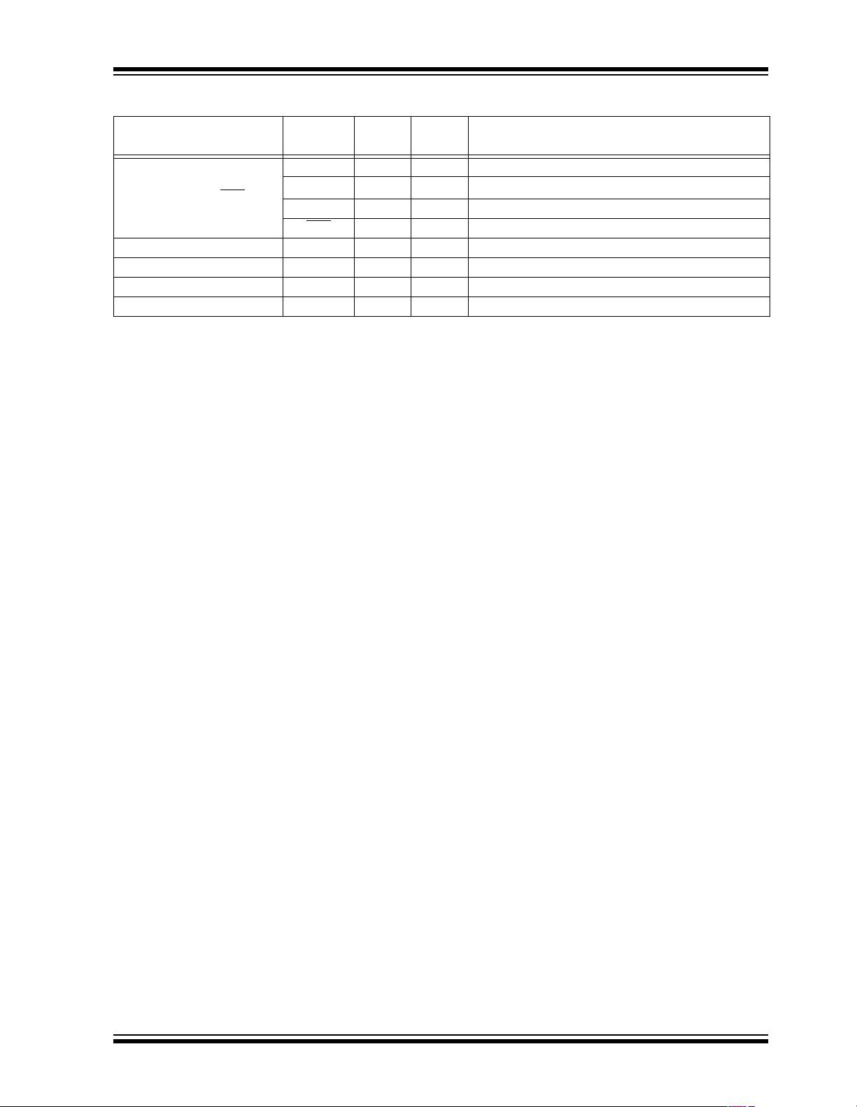
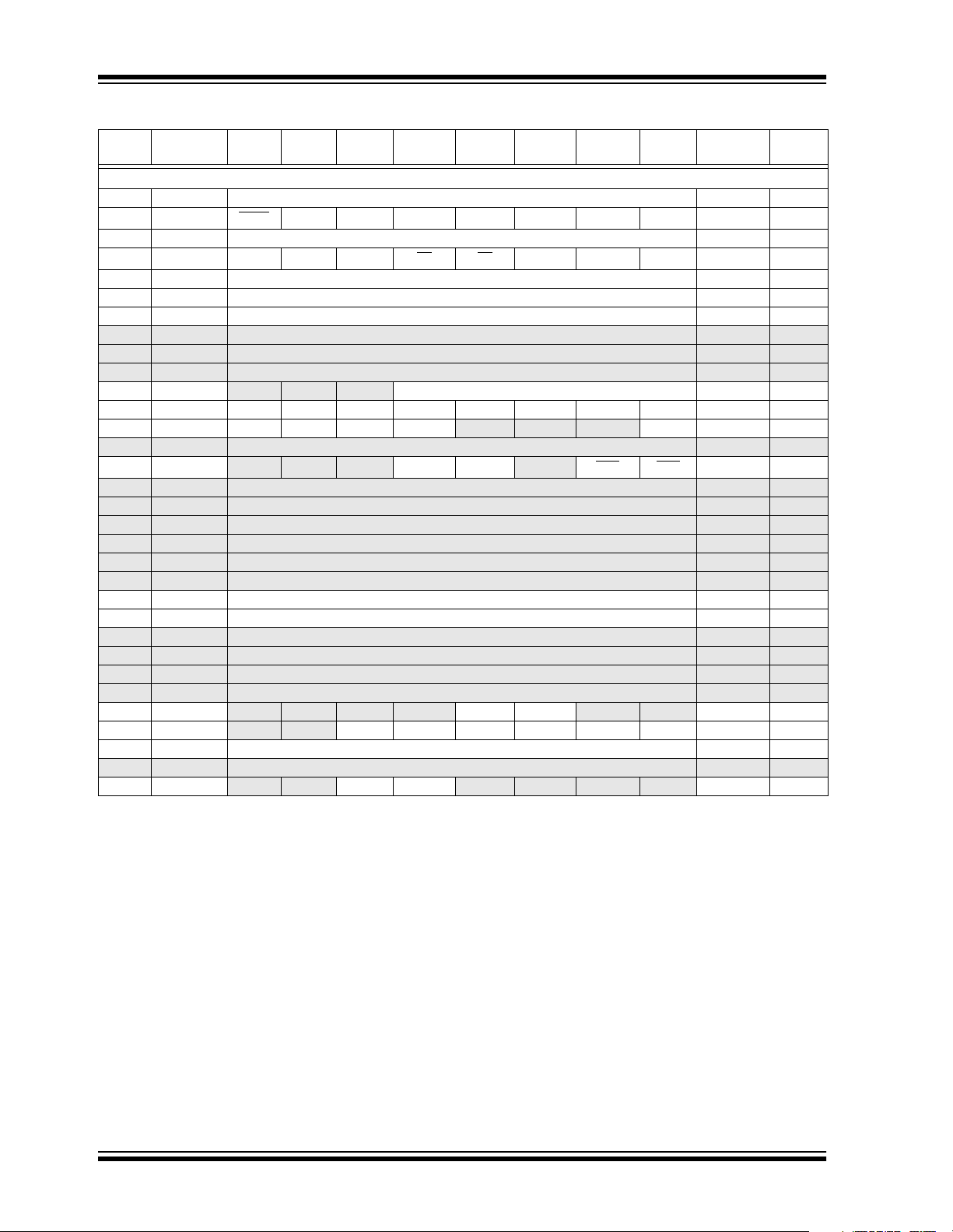
TABLE 2-1: PIC16C781/782 SPECIAL FUNCTION REGISTER SUMMARY
Address Name Bit 7 Bit 6 Bit 5 Bit 4 Bit 3 Bit 2 Bit 1 Bit 0
Bank 0
(2)
00h
01h TMR0 Timer0 Module’s Register
02h
03h
04h
05h PORTA RA7 RA6 RA5 RA4 RA3 RA2 RA1 RA0
06h PORTB RB7 RB6 RB5 RB4 RB3 RB2 RB1 RB0
07h — Unimplemented — —
08h — Unimplemented — —
09h — Unimplemented — —
0Ah
0Bh
0Ch PIR1 LVDIF ADIF C2IF C1IF
0Dh — Un implemented — —
0Eh TMR1L Holding register for the Least Significant Byte of the 16-bit TMR1 Register
0Fh TMR1H Holding register for the Most Significant Byte of the 16-bit TMR1 Register
10h T1CON
11h — Un implemented — —
12h — Unimplemented — —
13h — Unimplemented — —
14h — Unimplemented — —
15h — Unimplemented — —
16h — Unimplemented — —
17h — Unimplemented — —
18h — Unimplemented — —
19h — Unimplemented — —
1Ah — Unimplemented — —
1Bh — Unimplemented — —
1Ch — Un implemented — —
1Dh — Un implemented — —
1Eh ADRES ADC Result Register
1Fh ADCON0 AD CS1 ADCS0 CHS2 CHS1 CHS0 GO/DONE
Legend:
Note 1: The upper byte of the program counter is not directly accessible. PCLATH is a holding register for the PC<12:8> whose contents are trans-
INDF Addressing this location uses contents of FSR to address data memory (not a physical register) 0000 0000 23
(2)
PCL Program Counter's (PC) Least Significant Byte 0000 0000 23
(2)
STATUS IRP RP1 RP0
(2)
FSR Indirect Data Memory Address Pointer xxxx xxxx 23
(1, 2)
PCLATH — — — Write Buffer for the upper 5 bits of the Program Counter ---0 0000 23
(2)
INTCON GIE PEIE T0IE INTE RBIE T0IF INTF RBIF 0000 000x 19
— TMR1GE T1CKPS1 T1CKPS0 T1OSCEN T1SYNC TMR1CS TMR1ON -000 0000 57
x = unknown, u = unchanged, q = value depends on condition, - = unimplemented, read as '0'.
Shaded locations are unimplemented, read as ‘0’.
ferred to the upper byte of the program counter. See Section 2.9 for more detail.
2: These registers can be addressed from any bank.
TO
PD
— — — TMR1IF 0000 ---0 21
ZDCC0001 1xxx 17
CHS3 ADON 0000 0000 70
Value on:
POR, BOR
xxxx xxxx 51
xxxx 0000 26
xxxx 0000 35
xxxx xxxx 55
xxxx xxxx 55
xxxx xxxx 71
Details on
Page:
2001 Microchip Technology Inc. Preliminary DS41171A-page 13
PIC16C781/782
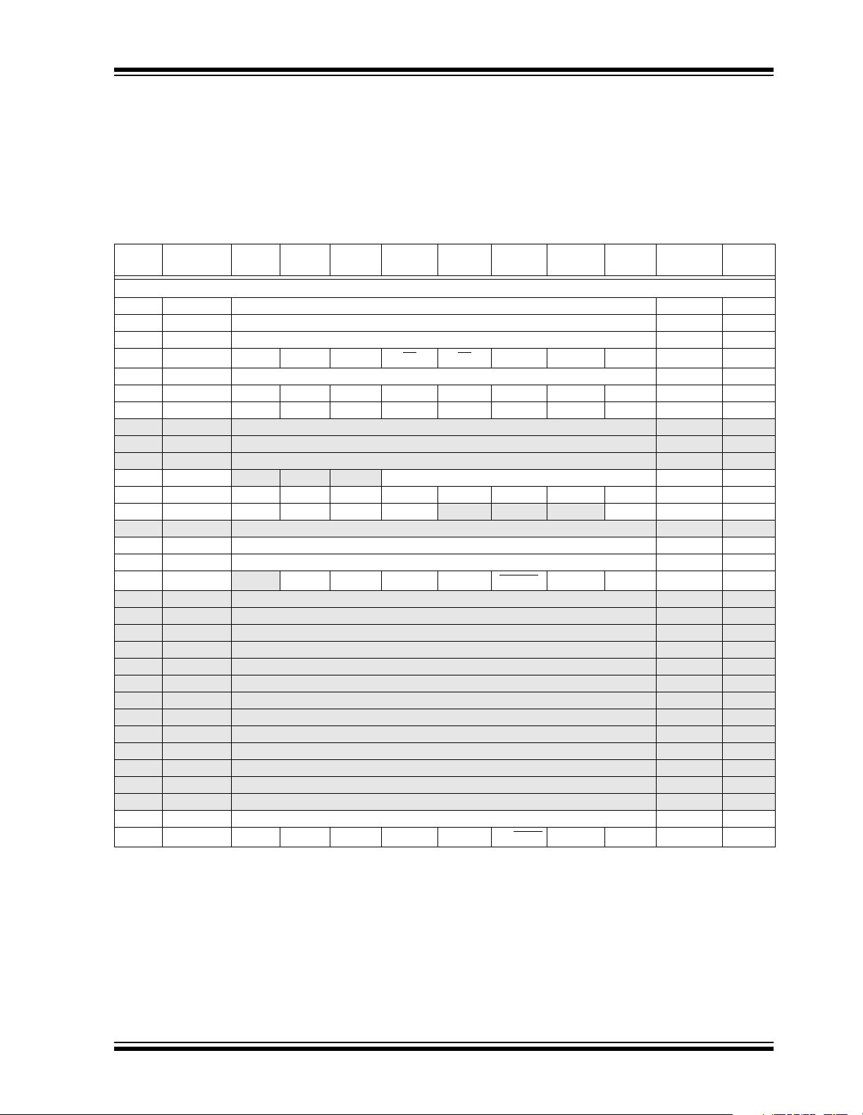
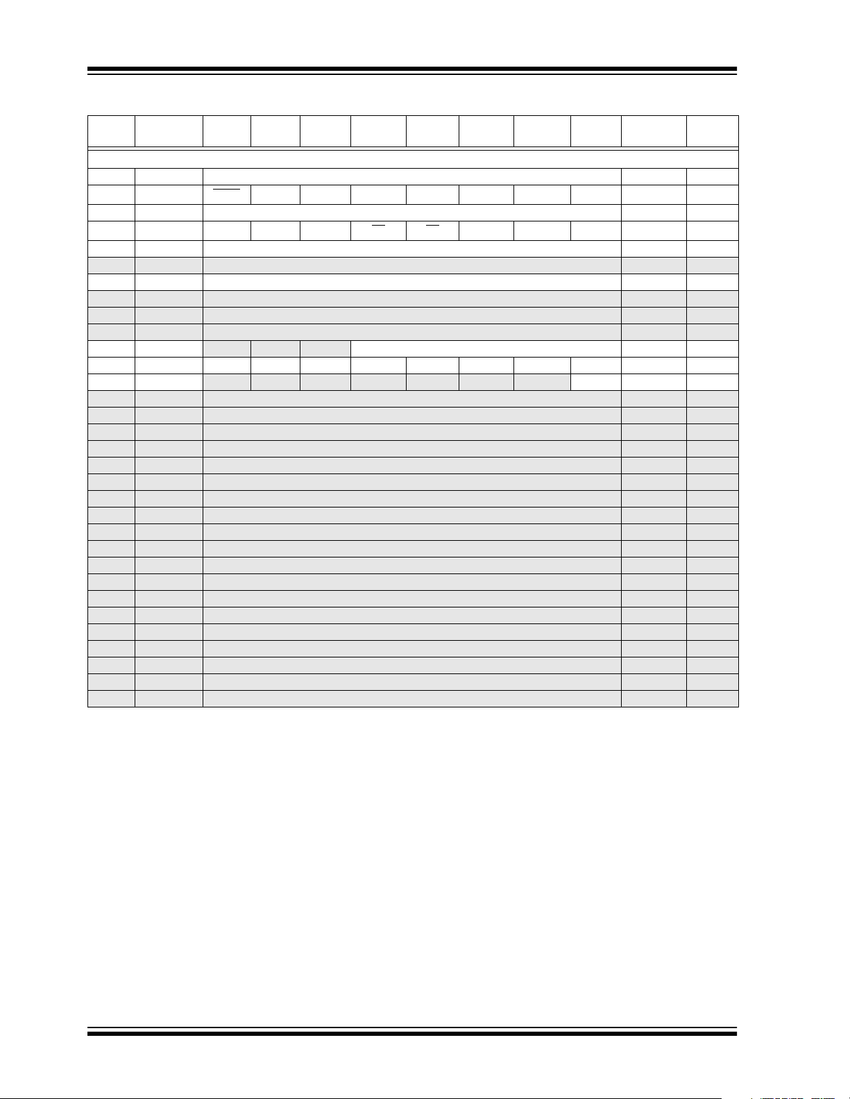
TABLE 2-1: PIC16C781/782 SPECIAL FUNCTION REGISTER SUMMARY (CONTINUED)
Address Name Bit 7 Bit 6 Bit 5 Bit 4 Bit 3 Bit 2 Bit 1 Bit 0
Bank 1
(2)
80h
81h OPTION_REG RBPU
82h
83h
84h
85h TRISA PORTA Data Direction Register
86h TRISB PORTB Data Direction Register
87h — Unimplemented — —
88h — Unimplemented — —
89h — Unimplemented — —
8Ah
8Bh
8Ch PIE1 LVDIE ADIE C2IE C1IE
8Dh — Un implemented
8Eh PCON
8Fh Unimplemented — —
90h — Unimplemented — —
91h — Unimplemented — —
92h — Unimplemented — —
93h — Unimplemented — —
94h — Unimplemented — —
95h WPUB PORTB Weak Pull-up Control
96h IOCB PORTB Interrupt-on-Change Control
97h — Unimplemented — —
98h — Unimplemented — —
99h — Unimplemented — —
9Ah — Unimplemented — —
9Bh REFCON
9Ch LVDCON
9Dh ANSEL Analog Channel Select
9Eh — Unimplemented — —
9Fh ADCON1
Legend:
Note 1: The upper byte of the program counter is not directly accessible. PCLATH is a holding register for the PC<12:8> whose contents are trans-
INDF Addressing this location uses contents of FSR to address data memory (not a physical register) 0000 0000 23
(2)
PCL Program Counter’s (PC) Least Significant Byte 0000 0000 23
(2)
STATUS IRP RP1 RP0 TO PD ZDCC0001 1xxx 17
(2)
FSR Indirect Data Memory Address Pointer xxxx xxxx 23
(1,2)
PCLATH — — — Write Buffer for the upper 5 bits of the Program Counter ---0 0000 23
(2)
INTCON GIE PEIE T0IE INTE RBIE T0IF INTF RBIF 0000 000x 19
x = unknown, u = unchanged, q = value depends on condition, - = unimplemented, read as '0'.
Shaded locations are unimplemented, read as ‘0’.
ferred to the upper byte of the program counter. See Section 2.9 for more detail.
2: These registers can be addressed from any bank.
INTEDG T0CS T0SE PSA PS2 PS1 PS0 1111 1111 18
— — — TMR1IE 0000 ---0 20
— — — WDTON OSCF — POR BOR ---q 1-qq 22, 120
— — — — VREN VROE — ---- 00-- 61
— — BGST LVDEN LV3 LV2 LV1 LV0 --00 0101 66
— — VCFG1 VCFG0 — — — — --00 ---- 71
Value on:
POR, BOR
1111 1111 26
1111 1111 35
1111 1111 36
1111 0000 36
1111 1111 25
Details on
Page:
DS41171A-page 14 Preliminary 2001 Microchip Technology Inc.

Bank 2
(2)
100h
101h TMR0 Time r0 Mod ul e ’s Register
102h
103h
INDF Addressing this location uses contents of FSR to address data memory (not a physical register) 0000 0000 23
(2)
PCL Program Counter's (PC) Least Significant Byte 0000 0000 23
(2)
STATUS IRP RP1 RP0 6.18Tc0.001 .52 981/F9st88Q(P1)-3216.1(99( C)-5.2)-14.9(am)-14.9( C)-5.2(o)1.2(u)-16.1(n1(e. )1069 )iuinaOED 01nt Byte
PIC16C781/782
xxxx xxxx 51
2001 Microchip Technology Inc. Preliminary DS41171A-page 15
PIC16C781/782
TABLE 2-1: PIC16C781/782 SPECIAL FUNCTION REGISTER SUMMARY (CONTINUED)
Address Name Bit 7 Bit 6 Bit 5 Bit 4 Bit 3 Bit 2 Bit 1 Bit 0
Bank 3
(2)
180h
181h OPTION_REG RBPU
182h
183h
184h
185h — Un implemented — —
186h TRISB PORTB Data Direction Register
187h — Un implemented — —
188h — Un implemented — —
189h — Un implemented — —
18Ah
18Bh
18Ch PMCON1
18Dh — Unimplemented — —
18Eh — Unimplemented — —
18Fh — Unimplemented — —
190h — Un implemented — —
191h — Un implemented — —
192h — Un implemented — —
193h — Un implemented — —
194h — Un implemented — —
195h — Un implemented — —
196h — Un implemented — —
197h — Un implemented — —
198h — Un implemented — —
199h — Un implemented — —
19Ah — Unimplemented — —
19Bh — Unimplemented — —
19Ch — Unimplemented — —
19Dh — Unimplemented — —
19Eh — Unimplemented — —
19Fh — Unimplemented — —
Legend:
Note 1: The upper byte of the program counter is not directly accessible. PCLATH is a holding register for the PC<12:8> whose contents are trans-
INDF Addressing this location uses contents of FSR to address data memory (not a physical register) 0000 0000 23
(2)
PCL Program Counter’s (PC) Least Significant Byte 0000 0000 23
(2)
STATUS IRP RP1 RP0 TO PD ZDCC0001 1xxx 17
(2)
FSR Indirect Data Memory Address Pointer xxxx xxxx 23
(1,2)
PCLATH — — — Write Buffer for the upper 5 bits of the Program Counter ---0 0000 23
(2)
INTCON GIE PEIE T0IE INTE RBIE T0IF INTF RBIF 0000 000x 19
Reserved — — — — — — RD 1--- ---0 47
x = unknown, u = unchanged, q = value depends on condition, - = unimplemented, read as '0'.
Shaded locations are unimplemented, read as ‘0’.
ferred to the upper byte of the program counter. See Section 2.9 for more detail.
2: These registers can be addressed from any bank.
INTEDG T0CS T0SE PSA PS2 PS1 PS0 1111 1111 18
Value on:
POR, BOR
1111 1111 35
Details on
Page:
DS41171A-page 16 Preliminary 2001 Microchip Technology Inc.

PIC16C781/782
2.3 STATUS Register
The STATUS register, shown in Register 2-1, contains
the arithmetic st atus of th e ALU, the RE SET statu s and
the bank select bits for data memory.
The STATUS register can be the destination for any
instruction, as with any other register. If the STATUS
register is the destination for an instruction that affects
the Z, DC, or C bits, the write to these three bits is disabled. These bits are set or cleared according to the
device logic. The TO
Therefore, the result of an instruction with the STATUS
register as the destination may be different than
intended.
and PD bits are not writable.
For example, CLRF STATUS cle ars the upper thr ee bit s
and sets the Z bit. This leaves the STA T US register a s
000u u1uu (where u = unchanged).
It is recommended, therefore, that only BCF, BSF,
SWAPF and MOVWF instructions are used to alter the
STATUS register, since these instructions do not affect
the Z, C, or DC bits fro m the ST A TUS registe r. Fo r other
instructions not affecting any status bits, see the
"Instruction Set Summary."
Note: The C and DC bits operate as a borrow
and digit borrow bit, respectively, in subtraction. See the SUBLW and SUBWF
instructions for examples.
REGISTER 2-1: STATUS REGISTER (STATUS: 03h, 83h, 103h, 183h)
R/W-0 R/W-0 R/W-0 R-1 R-1 R/W-x R/W-x R/W-x
IRP RP1 RP0 TO
bit7 bit0
bit 7 IRP: Register Bank Select bit (used for indirect addressing)
1 = Bank 2, 3 (100h - 1FFh)
0 = Bank 0, 1 (00h - FFh)
bit 6-5 RP<1:0>: Register Bank Select bits (used for direct addressing)
11 = Bank 3 (180h - 1FFh)
10 = Bank 2 (100h - 17Fh)
01 = Bank 1 (80h - FFh)
00 = Bank 0 (00h - 7Fh)
Each bank is 128 bytes
bit 4 TO
bit 3 PD
bit 2 Z: Zero bit
bit 1 DC: Digit carry/borrow
bit 0 C: Carry/borrow
: Time-out bit
1 = After power-up, CLRWDT instruction, or SLEEP instruction
0 = A WDT time-out occurred
: Power-down bit
1 = After power-up or by the CLRWDT instruction
0 = By execution of the SLEEP instruction
1 = The result of an arithmetic or logic operation is zero
0 = The result of an arithmetic or logic operation is not zero
bit (ADDWF, ADDLW,SUBLW,SUBWF instructio ns) (for borrow, the polarity
is reversed)
1 = A carry-out from the 4th low order bit of the result occurred
0 = No carry-out from the 4th low order bit of the result
bit (ADDWF, ADDLW, SUBLW, SUBWF instructions)
1 = A carry-out from the Most Significant bit of the result occurred
0 = No carry-out from the Most Significant bit of the result occurred
PD ZDCC
Note: For bo rrow, the polarity is reversed. A subtraction is executed by adding the two’s
compleme nt of th e sec ond ope rand . For rotate (RRF, RLF) instructions, this bit is
loaded with either the high or low order bit of the source register.
Legend:
R = Readable bit W = Writable bit U = Unimplemented bit, read as ‘0’
- n = Value at POR ’1’ = Bit is set ’0’ = Bit is cleared x = Bit is unknown
2001 Microchip Technology Inc. Preliminary DS41171A-page 17

PIC16C781/782
2.4 OPTION_REG Register
The OPTION_REG register is a readable and writable
register which contains various control bits to configure:
• TMR0 prescaler/WDT postscaler (single assignable register known also as the prescaler)
• External INT interrupt
• TMR0
• Weak pull-ups on PORTB
REGISTER 2-2: OPTION REGISTER (OPTION_REG: 81h, 181h)
R/W-1 R/W-1 R/W-1 R/W-1 R/W-1 R/W-1 R/W-1 R/W-1
RBPU
bit7 bit0
bit 7 RBPU
1 = PORTB weak pull-ups are disabled
0 = PORTB weak pull-ups are enabled by the WPUB register
bit 6 INTEDG: Interrupt Edge Select bit
1 = Interrupt on rising edge of RB0/INT pin
0 = Interrupt on falling edge of RB0/INT pin
bit 5 T0CS: TMR0 Clock Source Select bit
1 = Transition on RA4/T0CKI pin
0 = Internal instruction cycle clock ( F
bit 4 T0SE: TMR0 Source Edge Select bit
1 = Increment on high-to-low transition on RA4/T0CKI pin
0 = Increment on low-to-high transition on RA4/T0CKI pin
bit 3 PSA: Prescaler Assignment bit
1 = Prescaler is assigned to the WDT
0 = Prescaler is assigned to the Timer0 module
bit 2-0 PS<2:0>: Prescaler Rate Select bits
INTEDG T0CS T0SE PSA PS2 PS1 PS0
: PORTB Pull-up Enable bit
Bit Value TMR0 Rate WDT Rate
000
001
010
011
100
101
110
111
1 : 2
1 : 4
1 : 8
1 : 16
1 : 32
1 : 64
1 : 128
1 : 256
(1)
Note: To achieve a 1:1 prescaler assignment for
the TMR0 register, assign the prescaler to
the Watchdog Timer.
OSC/4)
1 : 1
1 : 2
1 : 4
1 : 8
1 : 16
1 : 32
1 : 64
1 : 128
Note 1: Individual weak pull-up s on RB pi ns can be e nabled/disa bled from the weak pul l-up
PORTB register (WPUB).
Legend:
R = Readable bit W = Writable bit U = Unimplemented bit, read as ‘0’
- n = Value at POR ’1’ = Bit is set ’0’ = Bit is cleared x = Bit is unknown
DS41171A-page 18 Preliminary 2001 Microchip Technology Inc.

PIC16C781/782
2.5 INTCON Register
The INTCON register is a readable and writable register which contains:
• Enable and interrupt flag bits for TMR0 register
overflow
• Enable and interrupt flag bits for the external
interrupt (INT)
• Enable and interrupt flag bits for PORTB
Interrupt-on-Change (IOCB)
• Peripheral interrupt enable bit
• Global interrupt enable bit
Note: Interrupt flag bits are se t w he n an interrupt
condition occurs, re gardless of the state of
its corresponding enable bit, or the global
enable bit, GIE (INTCON<7>). User software should ensure the appropriate interrupt flag bits are clear prior to enabling an
interrupt.
REGISTER 2-3: INTERRUPT CONTROL REGISTER (INTCON: 0Bh, 8Bh, 10Bh, 18Bh)
R/W-0 R/W-0 R/W-0 R/W-0 R/W-0 R/W-0 R/W-0 R/W-x
GIE PEIE T01E INTE RBIE T0IF INTF RBIF
bit 7 bit 0
bit 7 GIE: Global Interrupt Enable bit
1 = Enables all unmasked interrupts
0 = Disables all interrupts
bit 6 PEIE: Peripheral Interrupt Enable bit
1 = Enables all unmasked peripheral interrupts
0 = Disables all peripheral interrupts
bit 5 T0IE: TMR0 Overflow Interrupt Enable bit
1 = Enables the TMR0 interrupt
0 = Disables the TMR0 interrupt
bit 4 INTE: RB0/INT External Interrupt Enable bit
1 = Enables the RB0/INT external interrupt
0 = Disables the RB0/INT external interrupt
bit 3 RBIE: RB Port Change Interrupt Enable bit
1 = Enables the RB port change interrupt
0
(1)
2001 Microchip Technology Inc. Preliminary DS41171A-page 19

PIC16C781/782
2.6 PIE1 Register
The PIE1 register cont ains the ind ividual enab le bits for
the periph eral interrupts.
REGISTER 2-4: PERIPHERAL INTERRUPT ENABLE REGISTER (PIE1: 8Ch)
R/W-0 R/W-0 R/W-0 R/W-0 U-0 U-0 U-0 R/W-0
LVDIE ADIE C2IE C1IE
bit7 bit0
bit 7 LVDIE: Low Voltage Detect Interrupt Enable bit
1 = LVD interrupt is enabled
0 = LVD interrupt is disabled
bit 6 ADIE: Analog-to-Digital Converter Interrupt Enable bit
1 = Enables the Analog-to-Digital Converter interrupt
0 = Disables the Analog-to-Digital Converter interrupt
bit 5 C2IE: Comparator C2 Interrupt Enable bit
1 = Enables the Comparator C2 interrupt
0 = Disables the Comparator C2 interrupt
bit 4 C1IE: Comparator C1 Interrupt Enable bit
1 = Enables the Comparator C1 interrupt
0 = Disables the Comparator C1 interrupt
bit 3-1 Unimplemented: Read as '0'
bit 0 TMR1IE: TMR1 Overflow Interrupt Enable bit
1 = Enables the TMR1 overflow interrupt
0 = Disables the TMR1 overflow interrupt
Note: Bit PEIE (INTCON<6>) must be set to
enable any peripheral interrupt (see
Register 2-3).
— — — TMR1IE
Legend:
R = Readable bit W = Writable bit U = Unimplemented bit, read as ‘0’
- n = Value at POR ’1’ = Bit is set ’0’ = Bit is cleared x = Bit is unknown
DS41171A-page 20 Preliminary 2001 Microchip Technology Inc.

PIC16C781/782
2.7 PIR1 Register
This register contains the individual flag bits for the
peripheral interrupts.
Note: Interrupt flag bits are se t w he n an interrupt
condition occurs, re gardless of the state of
its corresponding enable bit, or the global
enable bit, GIE (INTCON<7>). User software should ensure the appropriate interrupt flag bits are clear prior to enabling an
interrupt.
REGISTER 2-5: PERIPHERAL INTERRUPT REGISTER (PIR1 0Ch)
R/W-0 R/W-0 R/W-0 R/W-0 U-0 U-0 U-0 R/W-0
LVDIF ADIF C2IF C1IF
bit7 bit 0
bit 7 LVDIF: Low Voltage Detect Interrupt Flag bit
1 = The supply volt age has fall en below t he spe cified LVD volt age (m ust be cle ared in s oftwa re)
0 = The supply voltage is greater than the specified LVD voltage
bit 6 ADIF: Analog-to-Digital Converter Interrupt Flag bit
1 = An ADC conversion completed (must be cleared in software)
0 = The ADC conversion is not complete
bit 5 C2IF: Comparator C2 Interrupt Flag bit
1 = Comparator C2 input has crossed the threshold (must be cleared in software)
0 = Comparator C2 input has not crossed the threshold
bit 4 C1IF: Comparator C1 Interrupt Flag bit
1 = Comparator C1 input has crossed the threshold (must be cleared in software)
0 = Comparator C1 input has not crossed the threshold
bit 3-1 Unimplemented: Read as ‘0’
bit 0 TMR1IF: TMR1 Overflow Interrupt Flag bit
1 = TMR1 register overflowed (must be cleared in software)
0 = TMR1 register did not overflow
— — — TMR1IF
Legend:
R = Readable bit W = Writable bit U = Unimplemented bit, read as ‘0’
- n = Value at POR ’1’ = Bit is set ’0’ = Bit is cleared x = Bit is unknown
2001 Microchip Technology Inc. Preliminary DS41171A-page 21

PIC16C781/782
2.8 PCON Register
The Power Control (PCON) register contains two flag
bits to allow determination of the source of the most
recent RESET:
• Power-on Reset (POR
• External MCLR Reset
• Power Supply Brown-out (BOR
The Power Control register also contains frequency
select bits for the INTRC oscillator and the WDT software enable bit.
Note: BOR is unknown on Power-on Reset. It
must then be set by the user and checked
on subsequent RESETS to see if BOR
clear , indic ating a brow n-out has occurred.
The BOR status bit is a don't care and is
not necessarily predic table if the brown-o ut
circuit is disabled (by clearing the BODEN
bit in the Configuration word).
)
) Reset
is
Direction of Change
4 MHz → 37 kHz 100 µs 300 µs
37 kHz→4 MHz 1.25 µs 3.25 µs
Note: When changing the internal oscillator
speed (i.e., the OSCF bit, INTRC mode),
the processor will be inactive during the
oscillator frequency change.
REGISTER 2-6: POWER CONTROL REGISTER (PCON: 8Eh)
U-0 U-0 U-0 R/W-q R/W-1 U-0 R/W-q R/W-q
— — — WDTON OSCF — POR BOR
bit 7 bit 0
bit 7-5 Unimplemented: Read as '0'
bit 4 WDTON: WDT Software Enable bit
If WDTE bit (Configuration Word <3>) = 1:
This bit is not writable, always reads ‘1’
Typical Time Inactive
Minimum Maximum
If WDTE bit (Configuration Word <3>) = 0:
1 = WDT is enabled
0 = WDT is disabled
bit 3 OSCF: Oscillator Speed INTRC Mode bit
1 = 4 MHz typical
0 = 37 kHz typical
All other oscillator modes (X = Ignored)
bit 2 Unimplemented: Read as '0'
bit 1 POR
bit 0 BOR
: Power-on Reset Status bit
1 = No Power-on Reset occurred
0 = A Power-on Reset occurred (must be set in software after a Power-on Reset occurs)
: Brown-out Reset Status bit
1 = No Brown-out Reset occurred
0 = A Brown-out Reset occurred
Legend:
q = Value depends on conditions
R = Readable bit W = Writable bit U = Unimplemented bit, read as ‘0’
- n = Value at POR ’1’ = Bit is set ’0’ = Bit is cleared x = Bit is unknown
DS41171A-page 22 Preliminary 2001 Microchip Technology Inc.

2.9 PCL and PCLATH
The program counter (PC) s pec ifi es the add res s o f the
instruction to fetch for execution. The PC is 13-bits
wide. The low byte is call ed th e PCL reg is ter. This register is readable and writable. The high byte is called
PIC16C781/782
2001 Microchip Technology Inc. Preliminary DS41171A-page 23
PIC16C781/782
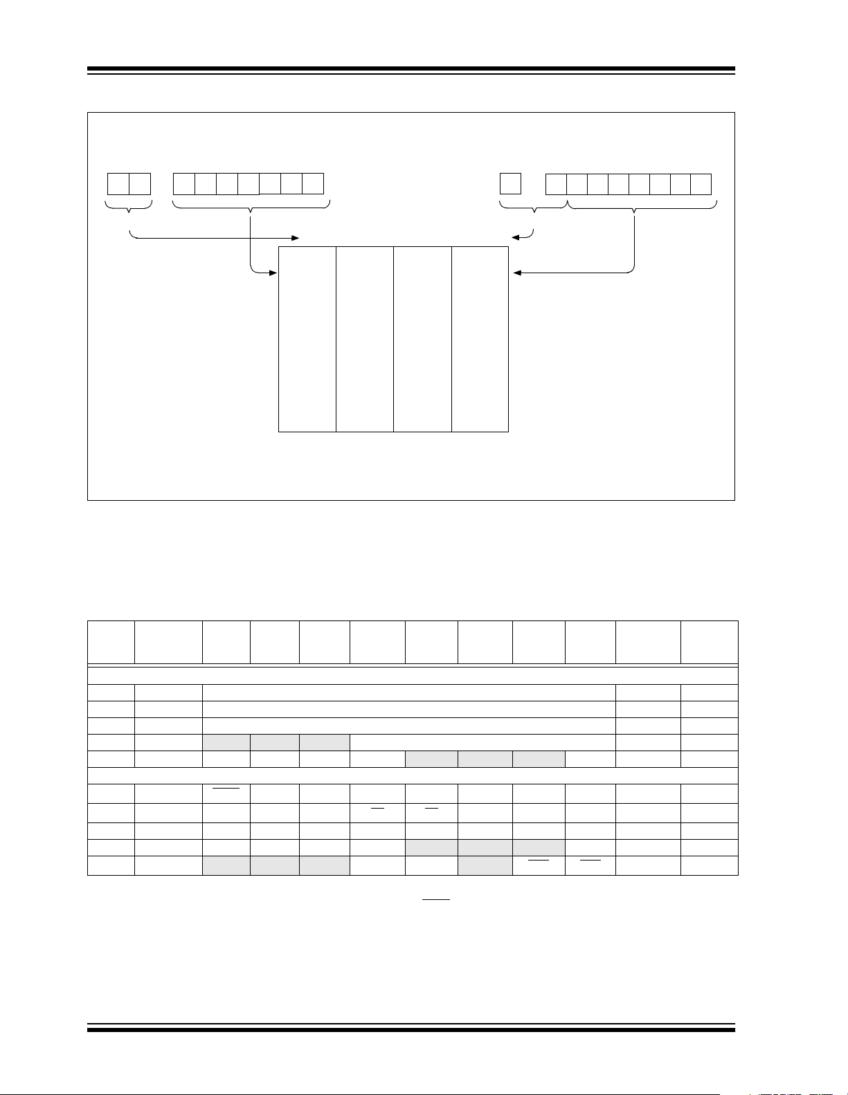
FIGURE 2-5: DIRECT/INDI RECT ADDRESSING
RP1:RP 0 6
From Opcode
0
Indirect AddressingDirect Addressing
IRP FSR Register
7
0
Bank Select Location Select
Bank Select
Location Select
00 01 10 11
80h
FFh
100h
17Fh
180h
1FFh
Data
Memory
00h
(1)
7Fh
Bank 0 Bank 1 Bank 2 Bank 3
Note 1: For register file map detail, see Figure 2-3.
2.12 Effect of RESET on Core Registers
Refer to Table 2-2 for the effect of a RESET operation
on core registers.
TABLE 2-2: EFFECT OF RESET ON CORE REGISTERS
Address Name Bit 7 Bit 6 Bit 5 Bit 4 Bit 3 Bit 2 Bit 1 Bit 0
Bank 0
00h INDF Addressing this location uses contents of FSR to address data memory (not a physical register)
02h PCL Program Counter’s (PC) Least Significant Byte 0000 0000 0000 0000
04h FSR Indirect Data Memory Address Pointer xxxx xxxx uuuu uuuu
0Ah PCLATH — — — Write Buffer for the upper 5 bits of the Program Counter ---0 0000 ---0 0000
0Ch PIR1 LVDIF ADIF C2IF C1IF — — — TMR1IF 0000 ---0 0000 ---0
Bank 1
81h OPTION_REG RBPU
83h STATUS IRP RP1 RP0 TO PD ZDCC0001 1xxx 000q quuu
8Bh INTCON GIE PEIE T0IE INTE RBIE T0IF INTF RBIF 0000 000x 0000 000u
8Ch PIE1 LVDIE ADIE C2IE C1IE — — — TMR1IE 0000 ---0 0000 ---0
8Eh PCON — — — WDTON OSCF — POR BOR ---q 1-qq ---q 1-qq
Legend: x = unknown, u = unchanged, q = value depends on condition, - = unimplemented, read as '0'.
Note 1: Other (non power-up) RESETS include external RESET through MCLR
Shaded locations are unimplemented, read as ‘0’.
INTEDG T0CS T0SE PSA PS2 PS1 PS0 xxxx xxxx 1111 1111
and Watchdog Timer Reset.
Value on:
POR, BOR
0000 0000 0000 0000
Value on
all other
RESETS
(1)
DS41171A-page 24 Preliminary 2001 Microchip Technology Inc.

PIC16C781/782
3.0 I/O PORTS
Most pins for the I/O p orts are mu ltiplexed w ith an alternate function for the peripheral features on the device.
In general, when a peripheral is enabled, that pin may
not be used as a general purpose I/O pin.
Additional inform atio n o n I/O ports may be f oun d i n th e
PICmicro™ Mid-Range Reference Man ual (DS33023 )
3.1 I/O Port Analog/Digital Mode
The PIC16C781/782 has two I/O ports: PORTA and
PORTB. Some of these po rt pins are mixed si gnal (can
be digital or anal og). When an analog signal is present
on a pin, the pin mus t be c onfigu red as an an alo g inp ut
to prevent unnecessary current drawn from the power
supply. The Analog Select regist er (ANSEL) a llo w s th e
user to individually select the Digital/Analog mode on
these pins. When the Analog mode is active, the port
pin always reads as a logic 0.
Note 1: On a Power-on Reset, the ANSEL regis-
ter configures these mixed signal pins as
Analog mode: RA<3:0>, RB<3:0>.
2: If a pin is configured as Anal og mode, the
pin always reads '0', even if th e digital ou tput is active.
REGISTER 3-1: ANALOG SELECT REGISTER (ANSEL: 9Dh)
R/W-1 R/W-1 R/W-1 R/W-1 R/W-1 R/W-1 R/W-1 R/W-1
ANS7 ANS6 ANS5 ANS4 ANS3 ANS2 ANS1 ANS0
bit 7 bit 0
bit 7-0 ANS<7:0>: Select Analog Input Function on AN<7:0> bits
1 = Analog input
0 = Digital I/O
Note: Setting a pin to an analog input disables the digital input buffer. The corresponding
TRIS bit should be set to input mode when using pins as analog inputs.
Legend:
R = Readable bit W = Writable bit U = Unimplemented bit, read as ‘0’
- n = Value at POR ’1’ = Bit is set ’0’ = Bit is cleared x = Bit is unknown
2001 Microchip Technology Inc. Preliminary DS41171A-page 25

PIC16C781/782
3.2 PORTA and the TRISA Register
PORTA is an 8-bit wide, bi-directional port with the
exception of RA0, RA1 and RA5, w hich are inputs only.
The corresponding data direction register is TRISA.
Setting a TRISA bit (= 1) makes the corresponding
PORTA pin an input (i.e., disables the digital output).
Clearing a TRISA bit (= 0) makes the corresponding
PORTA pin an output (i.e., disables the digital output).
Reading the PORTA register reads the status of the
pins, whereas writing to it, writes to the port latch. All
write operations are read-modify-write operations.
Therefore, a write to a port implies that the port pins are
read, this value is then modified and written to the port
data latch.
Pins RA<3:0> are multiplexed with analog functions:
• Analog inputs AN<3:0> to the A/D Converter.
REF1 and VREF2 inputs to the comparators .
• V
• OPAMP inverting/non-inverting inputs.
Note:
Pins RA<7:4> are multiplexed with digital functions:
• Pin RA4 is multiplexed with the TMR0 module
clock input.
• Pin RA5 is multiplexed with the device RESET
(MCLR
) and programming input (VPP) function.
• Pins RA6 and RA7 are multiplexed with the
oscillator/clock I/O functions. RA6 can also be
configured as the TMR1 clock input.
PORTA has the following I/O characteristics:
• RA0, RA1, and RA5 are input only.
• RA4 is an open drain output. All other PORTA
pins have full CMOS buffer outputs.
• All PORTA pins have Schmitt trigger inputs.
EXAMPLE 3-1: INITIALIZING PORTA
;* This code block will configure PORTA
;* as follows
;* RA<7:4> digital outputs
;* RA<3:2> digital inputs
;* RA<1:0> analog inputs
;* RB<3:0> digital I/O
;* Note 1: RB<3:0> configured as digital I/O
;* Note 2: RA<7:6> availability depends on
;* the oscillator selection
BANKSEL PORTA ; Select Bank 0
CLRF PORTA ; Preset PORTA data
; reg
BANKSEL TRISA ; Select Bank 1
MOVLW B’00001111’; Digital I/O
; config data
MOVWF TRISA ; Configure PORTA
; digital
MOVLW B’00000011’; Analog I/O config
; data
MOVWF ANSEL ; Configure PORTA
; analog
3.2.1 TRISA, ANSEL, AND CONTROL PRECEDENCE
The ANSEL and TRISA registers are the primary software controls for the configuration of PORTA pins.
TRISA bits tri-state the output drivers of PORTA, and
ANSEL register bits control the digital input buffers. It is
important to program bo th registers when configu ring a
mixed signal port pin, as most peripherals cann ot override the TRISA and ANSEL registers control. Even if a
peripheral has the ability to override control of the
TRISA and ANSEL registers, it is good programming
practice to program both registers appropriately.
There are specific cases in which the TRISA and
ANSEL registers can be overridden by a peripheral or
a configuration bit, see Figures 3-1 through 3-8 for
details.
DS41171A-page 26 Preliminary 2001 Microchip Technology Inc.
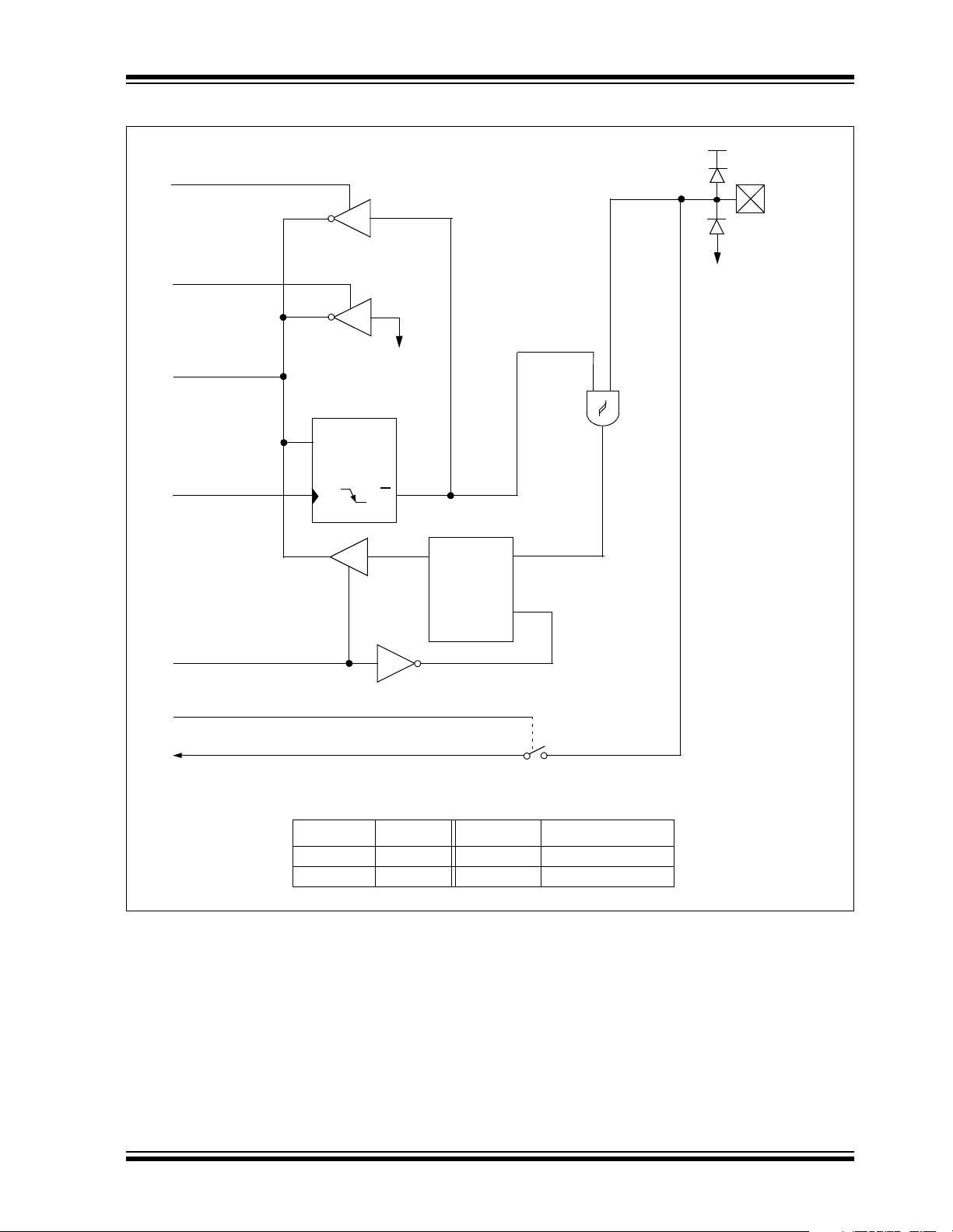
FIGURE 3-1: BLOCK DIAGRAM OF RA0/AN0/OPA+ PIN
PIC16C781/782
VDD
RD
ANSEL
RD TRISA
Data Bus
WR ANSEL
ANSEL Reg.
D
CK
RA0/AN0/OPA+
VSS
V
SS
Q
Q
Data Reg.
QD
EN
RD PORTA
Analog Function Enable
AN0/OPA+ (see Figure 1-3)
ANSEL<0> TRISA<0> FUNCTION PORTA<0> READ
0 x Digital In Pin
1 x Analog In 0
2001 Microchip Technology Inc. Preliminary DS41171A-page 27
PIC16C781/782
FIGURE 3-2: BLOCK DIAGRAM OF RA1/AN1/OPA- PIN
VDD
RD ANSEL
RD TRISA
Data Bus
WR ANSEL
ANSEL Reg.
CK
RA1/AN1/OPA-
VSS
V
SS
QD
Q
Data Reg.
Q
D
EN
RD PORTA
Analog Function Enable
AN1/OPA- (see Figure 1-3)
ANSEL<1> TRISA<1> FUNCTION PORTA<1> READ
0 x Digital In Pin
1 x Analog In 0
DS41171A-page 28 Preliminary 2001 Microchip Technology Inc.

FIGURE 3-3: BLOCK DIAGRAM OF RA2/AN2/VREF2 PIN
RD ANSEL
Data Bus
Data Reg.
WR PORTA
D
CK
TRIS Reg.
D
Q
VDD
Q
Q
P
N
PIC16C781/782
VDD
V
RA2/AN2/
REF2
WR TRISA
RD TRISA
WR ANSEL
RD PORT A
Analog Function Enable
AN2/VREF2 (see Figure 1-3)
SS
CK
ANSEL Reg.
CK
ANSEL<2> TRISA<2> FUNCTION PORTA<2> READ
0 1 Digital In Pin
0 0 Digital Out Pin
1 x Analog In 0
Q
QD
Q
Data Reg.
Q
D
EN
V
VSS
2001 Microchip Technology Inc. Preliminary DS41171A-page 29

PIC16C781/782
FIGURE 3-4: BLOCK DIAGRAM OF RA3/AN3/VREF1 PIN
Data Bus
WR PORTA
WR TRISA
RD TRISA
WR ANSEL
Data Reg.
D
CK
TRIS Reg.
D
CK
ANSEL Reg.
D
CK
Q
VDD
Q
Q
Q
Q
Q
P
N
SS
V
RD PORTA
AN3/VREF1 (see Figure 1-3)
DS41171A-page 30 Preliminary 2001 Microchip Technology Inc.

FIGURE 3-5: BLOCK DIAGRAM OF RA4/T0CKI PIN
Data Reg.
Data Bus
D
Q
PIC16C781/782
WR PORTA
WR TRISA
RD TRISA
RD PORTA
TMR0 Clock Input
CK
TRIS Reg.
D
CK
Q
Q
Q
Data Reg.
Q
N
Vss
D
EN
RA4/T0CKI
Vss
TRISA<4> PORTA<4> FUNCTION PORTA<4> READ
1 x Digital In Pin
0 0 0 Output Pin
0 1 Hi-Z Output Pin
2001 Microchip Technology Inc. Preliminary DS41171A-page 31

PIC16C781/782
FIGURE 3-6: BLOCK DIAGRAM OF RA5/MCLR/VPP PIN
MCLRE
To MCLR Circuit
MCLR Filter
RA5/MCLR/VPP
Program Mode
Data Bus
RD TRISA
RD PORTA
HV Detect
VSS
Data Reg.
Q
VSS
D
EN
(1)
MCLRE
Internal x Digital In Pin
External x MCLR
Note 1: See Configuration Word <5>, Register 14-1.
DS41171A-page 32 Preliminary 2001 Microchip Technology Inc.
TRISA<5> FUNCTION PORTA<5> READ
0

PIC16C781/782
FIGURE 3-7: BLOCK DIAGRAM OF RA6/OSC2/CLKOUT/T1CKI PIN
(INTRC w/ CLKOUT) or (RC w/ CLKOUT)
Data Bus
WR PORTA
WR TRISA
RD TRISA
Data Reg.
CK
TRIS Reg.
D
CK
OSC1
1
0
QD
Q
Q
Q
Oscillator
Circuit
VDD
P
N
V
SS
RD PORTA
2001 Microchip Technology Inc. Preliminary DS41171A-page 33

PIC16C781/782
FIGURE 3-8: BLOCK DIAGRAM OF RA7/OSC1/CLKIN PIN
Data Bus
WR PORTA
WR TRISA
RD TRISA
Data Reg.
CK
TRIS Reg.
D
CK
OSC2
To Chip Clock Drivers
QD
Q
Q
Q
VDD
P
N
VSS
(INTRC w/o CLKOUT)
Oscillator
Circuit
EC Mode
DQ
RD PORTA
TABLE 3-1: SUMMARY OF REGISTERS ASSOCIATED WITH PORTA
DS41171A-page 34 Preliminary 2001 Microchip Technology Inc.

PIC16C781/782
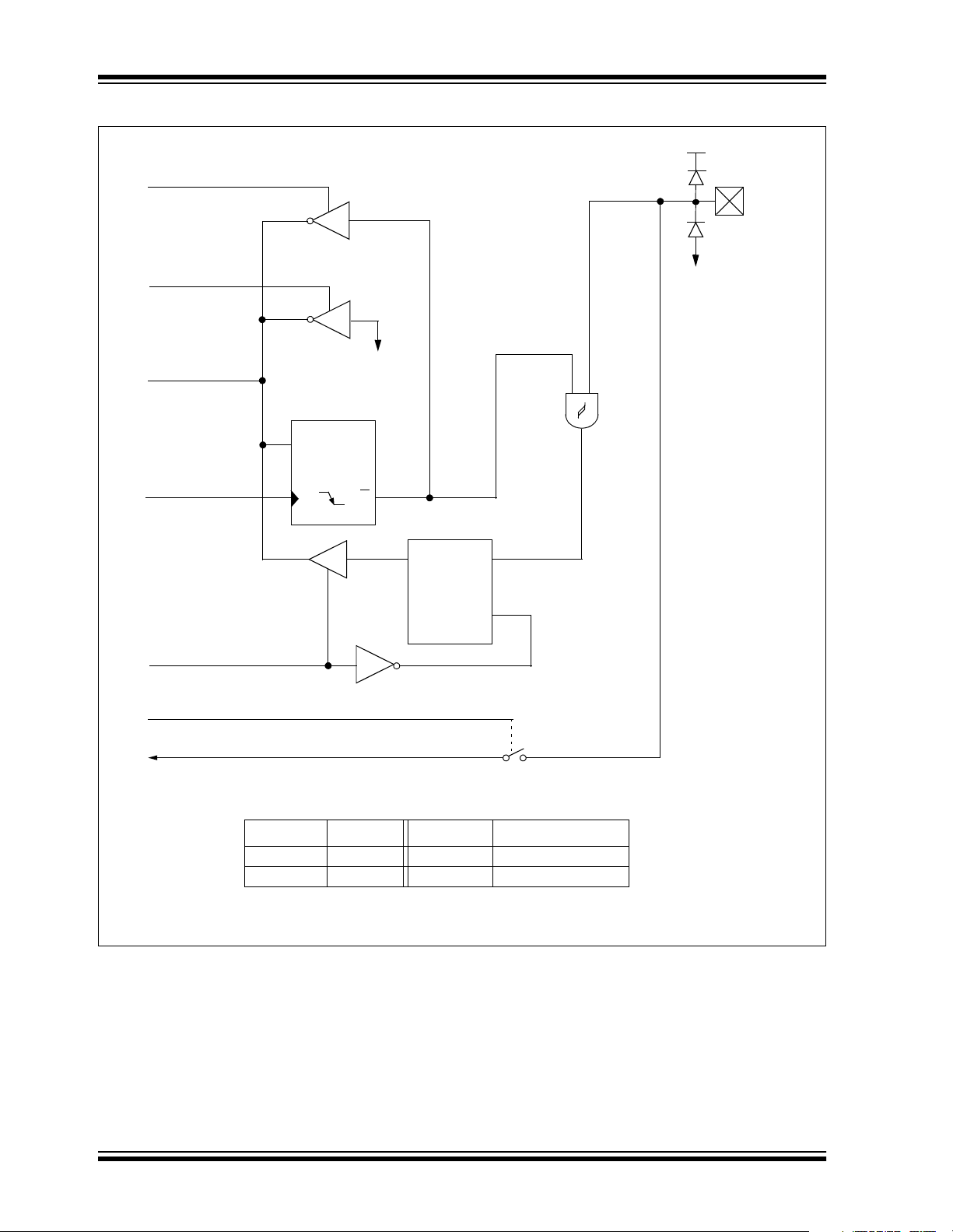
3.3 PORTB and the TRISB Register
PORTB is an 8-bit wide, bi-directional port. The corresponding data direction register is TRISB. Setting a
TRISB bit (= 1) makes the corr esponding PORTB pin
an input (i.e., puts the corresponding output driver into
a Hi-Impedance mode). Clearing a TRISB bit (= 0)
makes the corresponding PORTB pin an output (i.e.,
puts the contents of the output latch on the selected
pin.
EXAMPLE 3-2: INITIALIZING PORTB
;* This code block will configure PORT B
;* as follows
;* RB<7:6> analog inputs
;* RB<5:4> digital inputs
;* RB<3:2> digital inputs
;* RB<1:0> digital inputs
;* RA<3:0> digital I/O
BANKSEL PORTB ; Select Bank 0
CLRF PORTB ; Preset PORTB data
; reg.
BANKSEL TRISB ; Select Bank 1
MOVLW B’11001111’ ; Digital I/O
; config data
MOVWF TRISB ; Configure PORTB
; digital
MOVLW B’00000011’ ; Analog I/O config
; data
MOVWF ANSEL ; Configure PORTB
; analog
Pin RB2 is multiplexed with the analog function ADC/
Comparator Input AN6. When the pin is used as an
analog input, the ANSEL register must have bit 6 to
select the Analog mode for the pin.
The RB3 pin is multiplexed with two analog functions:
ADC/Comparator Analog Input AN7, and the output of
the OPA module. When the pin is used as analog I/O,
the ANSEL register must have bit 7 set to select the
Analog mode of the pin.
Pins RB<7:6> are multiplexed with the outputs of the
two on-board comparators, the outputs of the PSMC
module, and the clock gate input for Timer1. Note,
when enabled, these peripherals override the PORTB
data register; however, TRISB retains control of output
drivers. Therefore, TRISB<7:6> must be programmed
appropriately for Comparator and PSMC outputs to
operate.
3.3.1 PORTB WEAK PULL-UP
Each of the PORTB pins has an internal weak pull-up
resistance, which can be individually enabled from the
WPUB register. A single global enable bit, RBPU
(OPTION_REG<7>), can turn on/off all of the selected
pull-ups. Clearing the RBPU
bit (OPTION_REG<7>)
enables the weak pull-up resistors (see Register 3-2).
The weak pull-up is automatically turned off when the
port pin is configu red as an outpu t. The pull-up s are disabled on a Power-on Reset.
3.3.2 PORTB INTERRUPT-ON-CHANGE
The RB0 pin can be configured as:
• Digital I/O
• ADC/Comparator Analog Input (AN4)
• External Interrupt (INT)
• Volt a ge R efere nc e Output (VR)
When the pin is u sed as an analo g I/O, th e ANSEL re gister must have bit 4 set to config ure the RB0 pi n as an
analog input.
Pin RB1 is multiplexed with two analog function s: ADC/
Comparator Analog Input AN5, and the output of the
DAC. When the pin is used as an analog I/O, the
ANSEL register must have bit 5 set to configure the
RB1 pin as an analog I/O.
Each of the POR TB pin s, if con figured a s input, has th e
ability to generate an interrupt-on-change. To enable
the interrupt-on-change feature, the corresponding bit
must be set in the IOCB register (see Register 3-3).
The RBIE bit in the INTCON re gister functio ns as a global enable bit to turn on/off the interrupt-on-change feature. The select ed input s are comp ared to the old value
latched on the last read of PORTB. The ”mismatch”
outputs are OR -ed together to gen erate the RB Port
Change Interrupt with flag bit RBIF (INTCON<0>).
The IOCB interrupt can also awaken the device from
SLEEP. The user, in the Interrupt Service Routine,
must clear the interrupt in the following manner:
a) A read or write to PORTB. This copies the cur-
rent state into the latch and ends the mismatch
condition.
b) Clear flag bit RBIF.
2001 Microchip Technology Inc. Preliminary DS41171A-page 35

PIC16C781/782
REGISTER 3-2: WEAK PULL-UP PORTB REGISTER (WPUB: 95h)
R/W-1 R/W-1 R/W-1 R/W-1 R/W-1 R /W-1 R/W-1 R/W-1
WPUB7 WPUB6 WPUB5 WPUB4 WPUB3 WPUB2 WPUB1 WPUB0
bit7 bit0
bit 7-0 WPUB<7:0>: PORTB Weak Pull-Up Control bits
1 = Weak pull-up enabled for corresponding pin
0 = Weak pull-up disabled for corresponding pin
REGISTER 3-3:
bit 7-0 IOCB<7:0>: Interrupt-on-Change PORTB Control bits
Note 1: For the WPUB register setting to take effect, the RBPU
register must be cleared.
2: The weak pull-up device is automatically disabled if the pin is in output mode, i.e.,
(TRISB = 0) for corresponding pin.
Legend:
R = Readable bit W = Writable bit U = Unimplemented bit, read as ‘0’
- n = Value at POR ’1’ = Bit is set ’0’ = Bit is cleared x = Bit is unknown
bit in the OPTION_REG
INTERRUPT-ON-CHANGE PORTB REGISTER (IOCB: 96h)
R/W-1 R/W-1 R/W-1 R/W-1 R/W-0 R/W-0 R/W-0 R/W-0
IOCB7 IOCB6 IOCB5 IOCB4 IOCB3 IOCB2 IOCB1 IOCB0
bit7 bit0
1 = Interrupt-on-change enabled for corresponding pin
0 = Interrupt-on-change disabled for corresponding pin
Note 1: The interrupt enable bits, GIE and RBIE in the INTCON regi ste r, must be set for indi-
vidual interrupts to be recognized.
Legend:
R = Readable bit W = Writable bit U = Unimplemented bit, read as ‘0’
- n = Value at POR ’1’ = Bit is set ’0’ = Bit is cleared x = Bit is unknown
3.3.3 TRISB, ANSEL, AND CONTROL PRECEDENCE
The ANSEL and TRISB registers are the primary controls for the configuration of PORTB pins. TRISB tristates the output drivers of PORTB, and the ANSEL
register disable s the in put buf fers. It is im portan t to program both registers when configuring a port pin, since
most peripherals do not have precedence over the
TRISB and ANSEL registers’ control of the pin. Even if
a peripheral has the ability to override the control of the
TRISB and ANSEL registers, it is good practice to program both registers appropriately.
DS41171A-page 36 Preliminary 2001 Microchip Technology Inc.
Note 1: Upon RESET , the ANSEL r egiste r config-
ures the RB<3:0> pins as analog inputs.
2: When programmed as analog inputs,
RB<3:0> pins will read as ‘0’.
3: There are specific cases in which the
functions of the TRISB and ANSEL registers can be overridden by a peripheral or
configuration word (see Figure 3-9
through Figure 3-16 for details).

FIGURE 3-9: BLOCK DIAGRAM OF RB0/INT/AN4/VR PIN
VREN
VROE
VR Output
PIC16C781/782
Data Bus
WR WPUB
RD WPUB
WR PORTB
WR TRISB
RD TRISB
WR ANSEL
WPUB Reg.
D
Q
CK
Q
PORTB Reg.
D
Q
CK
Q
TRIS Reg.
D
Q
CK
Q
ANSEL Reg.
QD
CK
Q
RBPU
VDD
P
N
VSS
VDD
P
Weak
Pull-up
VDD
RB0/INT/AN4/VR
VSS
RD ANSEL
IOCB Reg .
WR IOCB
RD IOCB
RD PORTB
INT Input
Analog Function Enable
AN4/VR
VREN & VROE ANSEL<4> TRISB<0> FUNCTION PORTB<0> READ
TTL
D
Q
Set
CK
RBIF
Q
...
From other
RB<7:0> pins
QD
EN
EN
Q
D
EN
Q
D
EN
0 0 1 Digital In Pin
0 0 0 Digital Out Pin
0 1 x Analog In 0
1 x x Analog Out 0
Q1
Q3
2001 Microchip Technology Inc. Preliminary DS41171A-page 37

PIC16C781/782
FIGURE 3-10: BLOCK DIAGRAM OF RB1/AN5/VDAC PIN
Data Bus
PORTB Reg.
D
Q
WR PORTB
WR TRISB
RD TRISB
RD PORT B
CK
TRIS Reg.
D
Q
CK
Q
D
EN
EN
DS41171A-page 38 Preliminary 2001 Microchip Technology Inc.

FIGURE 3-11: BLOCK DIAGRAM OF RB2/AN6 PIN
PIC16C781/782
Data Bus
WR WPUB
RD WPUB
WR PORTB
WR TRISB
RD TRISB
WR ANSEL
RD ANSEL
WR IOCB
RD IOCB
RD PORTB
WPUB Reg.
D
Q
CK
Q
PORTB Reg.
D
Q
CK
Q
TRIS Reg.
D
Q
CK
Q
ANSEL Reg.
D
Q
CK
Q
IOCB Reg.
D
Q
CK
Q
Set
RBIF
RBPU
...
From other
RB<7:0> pins
QD
EN
EN
VDD
P
N
VSS
VDD
Weak
P
Pull-up
VDD
RB2/AN6
VSS
TTL
Q
D
EN
Q
D
EN
Q1
Q3
Analog Function Enable
AN6
ANSEL<6> TRISB<2> FUNCTION PORTB<2> READ
0 1 Digital In Pin
0 0 Digital Out Pin
1 x Analog In 0
2001 Microchip Technology Inc. Preliminary DS41171A-page 39

PIC16C781/782
FIGURE 3-12: BLOCK DIAGRAM OF RB3/AN7/OPA PIN
Data Bus
WR WPUB
WR PORTB
WR TRISB
RD TRISB
WPUB Reg.
D
Q
CK
PORTB Reg.
D
Q
CK
TRIS Reg.
D
Q
CK
Q
RBPU
VDD
P
N
VSS
Weak
Pull-up
RD PORTB
AN7/OPA
IOCB Reg.
D
Q
Q
CK
QD
EN
EN
D
EN
Q
D
EN
OPA MODULE
ANSEL<7> ADC/C1/C2 INPUT FUNCTION PORTB<3> READ
OPAON CAL_ACTIVE
0 x 0 Digital Digital I/O Pin
0 x 1 Analog Analog In 0
1 0 1 Analog OPA Output 0
1 1 1 Analog HI-Z Calibration 0
Analog HI-Z = No internal drive on pin (analog input) during calibration.
DS41171A-page 40 Preliminary 2001 Microchip Technology Inc.

FIGURE 3-13: BLOCK DIAGRAM OF RB4 PIN
PIC16C781/782
Data Bus
WR WPUB
RD WPUB
WR PORTB
WR TRISB
RD TRISB
RD IOCB
WR IOCB
WPUB Reg.
D
Q
CK
Q
PORTB Reg.
D
Q
CK
Q
TRIS Reg.
D
Q
CK
Q
IOCB Reg.
D
Q
CK
Q
Set
RBIF
RBPU
...
From other
RB<7:0> pins
VDD
Weak
P
VDD
P
Pull-up
VDD
RB4
N
VSS
VSS
TTL
Q
D
EN
Q1
RD PORTB
QD
EN
EN
TRISB<4> FUNCTION P ORTB<4> READ
0 Digital Out Pin
1 Digital In Pin
Q
D
EN
Q3
2001 Microchip Technology Inc. Preliminary DS41171A-page 41

PIC16C781/782
FIGURE 3-14: BLOCK DIAGRAM OF RB5 PIN
Data Bus
WR WPUB
RD WPUB
WR PORTB
WR TRISB
RD TRISB
RD IOCB
WR IOCB
WPUB Reg.
D
Q
CK
Q
PORTB Reg.
D
Q
CK
Q
TRIS Reg.
D
Q
CK
Q
IOCB Reg.
D
Q
CK
Q
Set
RBIF
RBPU
...
From other
RB<7:0> pins
VDD
Weak
P
VDD
P
Pull-up
VDD
RB5
N
VSS
VSS
TTL
Q
D
EN
Q1
Q
D
EN
EN
RD PORTB
Q
D
EN
Q3
TRISB<5> FUNCTION P ORTB<5> READ
0 Digital Out Pin
1 Digital In Pin
DS41171A-page 42 Preliminary 2001 Microchip Technology Inc.

FIGURE 3-15: BLOCK DIAGRAM OF RB6/C1/PSMC1A PIN
C1OE
SMCON
PSMC1A
C1OUT
WPUB Reg.
Data Bus
WR WPUB
RD WPUB
WR PORTB
D
Q
CK
Q
Data Reg.
D
Q
CK
Q
RBPU
PIC16C781/782
VDD
Weak Pull-up
P
VDD
P
VDD
RB6/C1/PSMC1A
WR TRISB
RD TRISB
RD PORTB
RD IOCB
WR IOCB
Serial Programming Clock
TRIS Reg.
D
CK
IOCB Reg.
D
Q
CK
Q
EN
N
SS
V
TTL
V
Q1
SS
Q
Q
QD
Set RBIF
From other
RB<7:0> pins
PSMC SMCON COMPARATOR C1OE PORTB TRISB<6> FUNCTION
x x 1 Digital In
0 0 0 Digital Out
01 0 C1OUT
1x 0 PSMC1A
2001 Microchip Technology Inc. Preliminary DS41171A-page 43
Q
EN
D
RD Port
Q3

PIC16C781/782
FIGURE 3-16: BLOCK DIAGRAM OF RB7/C2/PSMC1B/T1G PIN
C2OE
SCEN
SMCOM
SMCON
RD WPUB
Data Bus
WPUB Reg.
D
Q
RBPU
VDD
Weak Pull-up
P
VDD
RB7/C2/PSMC1B/T1G
WR WPUB
WR PORTB
WR TRISB
RD TRISB
RD IOCB
RD PORTB
WR IOCB
CK
Data Reg.
D
CK
TRIS Reg.
D
CK
IOCB Reg.
D
Q
CK
Q
Q
VSS
Q
Q
Q
Q
C2OUT
PSMC1B
SC Switch
VDD
P
N
VSS
TTL
Serial Programming Data
and Timer1 Gate
Set RBIF
From other
RB<7:0> pins
PSMC MODULE
SMCON SMCOM SCEN
Q
Q
COMPARATOR
C2OE
D
EN
D
EN
Q1
RD Port
Q3
PORTB TRISB<7> FUNCTION
x x x x 1 Digital In
0 x x 0 0 Digital Out
1 0 0 0 0 Digital Out
0xx1 0 C2OUT
1001 0 C2OUT
1 0 1 x 0 Slope Compensation
11xx 0 PSMC1B
DS41171A-page 44 Preliminary 2001 Microchip Technology Inc.

PIC16C781/782
TABLE 3-2: SUMMARY OF REGISTERS ASSOCIATED WITH PORTB
Address Name Bit 7 Bit 6 Bit 5 Bit 4 Bit 3 Bit 2 Bit 1 Bit 0
06h PORTB RB7 RB6 RB5 RB4 RB3 RB2 RB1 RB0 xxxx 0000 uuuu 0000
86h
81h OPTION_REG RBPU INTEDG T0CS T0SE PSA PS2 PS1 PS0 1111 1111 1111 1111
95h
96h
9Dh
Legend: x = unknown, u = unchanged, - = unimplemented, read as ’0’. Shaded cells are not used by PORTB.
TRISB PORTB Data Direction Register 1111 1111 1111 1111
WPUB PORTB Weak Pull-up Control 1111 1111 1111 1111
IOCB PORTB Interrupt-on-Change Control 1111 0000 1111 0000
ANSEL AN7 AN6 AN5 AN4
AN3 AN2 AN1 AN0 1111 1111 1111 1111
Value on:
POR, BOR
Value on
all other
RESETS
2001 Microchip Technology Inc. Preliminary DS41171A-page 45

PIC16C781/782
NOTES:
DS41171A-page 46 Preliminary 2001 Microchip Technology Inc.

PIC16C781/782
4.0 PROGRAM MEMORY READ (PMR)
Program memory is readable during normal operation
DD range). It is read by indirect addressing
(full V
through the following Special Function Registers:
• PMCON1: Control
• PMDATH: Data High
• PMDATL: Data Low
• PMADRH: Address High
• PMADRL: Address Low
When interfacing to the program memory block, the
PMDATH and PMDATL registers for m a 2-byte wor d,
which holds the 14-bit data. The PMADRH and
PMADRL registers form a 2-b yte word, w hich holds th e
12-bit address of the program memory location being
accessed. Mid -range devi ces have up to 8K words o f
program EPROM with an address range from 0h to
3FFFh. When the device contains less memory than
the full address range of the PMADRH:PMARDL registers, the Most Significant bits of the PMADRH register
are ignored.
4.1 PMCON1 Register
PMCON1 is the control register for program memory
accesses.
Control bit RD initiates a rea d operation. This bit ca nnot
be cleared, only set, in software. It is cleared in hardware at completion of the read operation.
4.2 PMDATH and PMDATL Registers
The PMDATH:PMDATL registers are loaded with the
contents of program memory addressed by the
PMADRH and PMADRL registers upon completion of a
Program Memory Read command.
REGISTER 4-1: PROGRAM MEMORY READ CONTROL REGISTER 1 (PMCON1: 18Ch)
R-1 U-0 U-0 U-0 U-0 U-0 U-0 R/S-0
Reserved — — — — — — RD
bit7 bit0
bit 7 Reserved: Read as ‘1’
bit 6-1 Unimplemented: Read as '0
bit 0 RD: Read Control bit
1 = Initiates a Program memory read (read takes 2 cycles, RD is cleared in hardware)
0 = Reserved
Legend:
S = Settable bit
R = Readable bit W = Writable bit U = Unimplemented bit, read as ‘0’
- n = Value at POR ’1’ = Bit is set ’0’ = Bit is cleared x = Bit is unknown
REGISTER 4-2: PROGRAM MEMORY DATA HIGH (PMDATH: 10Eh)
U-0 U-0 R/W-0 R/W-0 R/W-0 R/W-0 R/W-0 R/W-0
— — PMD13 PMD12 PMD11 PMD10 PMD9 PMD8
bit7 bit0
bit 7-6 Unimplemented: Read as '0
bit 5-0 PMD<13:8>: Program Memory Data bits
The value of the program memory word pointed to by PMADRH and PMADRL after a program
memory read command.
Legend:
R = Readable bit W = Writable bit U = Unimplemented bit, read as ‘0’
- n = Value at POR ’1’ = Bit is set ’0’ = Bit is cleared x = Bit is unknown
2001 Microchip Technology Inc. Preliminary DS41171A-page 47

PIC16C781/782
REGISTER 4-3: PROGRAM MEMORY DA TA LOW (PMDATL: 10Ch)
R/W-0 R/W-0 R/W-0 R/W-0 R/W-0 R/W-0 R/W-0 R/W-0
PMD7 PMD6 PMD5 PMD4 PMD3 PMD2 PMD1 PMD0
bit7 bit0
bit 7-0 PMD<7:0>: Program Memory Data bits
The value of the program memory word pointed to by PMADRH and PMADRL after a program
memory read command.
Legend:
R = Readable bit W = Writable bit U = Unimplemented bit, read as ‘0’
- n = Value at POR ’1’ = Bit is set ’0’ = Bit is cleared x = Bit is unknown
REGISTER 4-4: PROGRAM MEMORY ADDRESS HIGH (PMADRH: 10Fh)
U-0 U-0 U-0 R/W-x R/W-x R/W-x R/W-x R/W-x
— — — Reserved Reserved PMA10 PMA9 PMA8
bit7 bit0
bit 7-5 Unimplemented: Read as '0'
bit 4-3 Reserved: Read state is not guaranteed
bit 2-0 PMA<10:8>: PMR Address bits
Legend:
R = Readable bit W = Writable bit U = Unimplemented bit, read as ‘0’
- n = Value at POR ’1’ = Bit is set ’0’ = Bit is cleared x = Bit is unknown
REGISTER 4-5: PROGRAM MEMORY ADDRESS LOW (PMADRL: 10Dh)
R/W-x R/W-x R/W-x R/W-x R/W-x R/W-x R/W-x R/W-x
PMA7 PMA6 PMA5 PMA4 PMA3 PMA2 PMA1 PMA0
bit7 bit0
bit 7-0 PMA<7:0>: PMR Address bits
Legend:
R = Readable bit W = Writable bit U = Unimplemented bit, read as ‘0’
- n = Value at POR ’1’ = Bit is set ’0’ = Bit is cleared x = Bit is unknown
DS41171A-page 48 Preliminary 2001 Microchip Technology Inc.

PIC16C781/782
4.3 Reading the EPROM Program Memory
To read a program memory location, the user must
write 2 bytes of the address to the PMADRH and
PMADRL registers, then set control bit RD
(PMCON1<0>). Once the read control bit is set, the
Program Memory Read (PMR) controller uses th e second instruction cy cle after to read the dat a. This cause s
the second instruction immediately following the “BSF
PMCON1,RD” instruction to be ignored. The data is
available, in the very next cycle, in the PMDATH and
PMDA TL registers. Therefore, it can be read as 2 b ytes
EXAMPLE 4-1: OTP PROGRAM MEMORY READ
;* This code block will read 1 word of program
;* memory at the memory address:
;* PROG_ADDR_HI : PROG_ADDR_LO
;* data will be returned in the variables;
;* PROG_DATA_HI, PROG_DATA_LO
BANKSEL PMADRL ; Select Bank 2
MOVLW PROG_ADDR_LO ;
MOVWF PMADRL ; Store LSB of address
MOVLW PROG_ADDR_HI ;
MOVWF PMADRH ; Store MSB of address
BANKSEL PMCON1 ; Select Bank 3
CLEAR GIE
BCF INTCON, GIE ; Turn off INTs
BSF PMCON1,RD ; Initiate read
NOP ; Executed (Fig 4-1)
NOP ; Ignored (Fig 4-1)
BSF INTCON, GIE ; Turn on INTs
MOVF PMDATL,W ; Get LSB of word
MOVWF PROG_DATA_LO
MOVF PMDATH,W ; Get MSB of word
MOVWF PROG_DATA_HI
in the following instructions. PMDATH and PMDATL
registers hold this value until another read or until
RESET.
Note 1: Interrupts must be disabled during the
time from setting PMCON1<0> (RD) to
the second instruction thereafter.
2: The following instructions should not be
used following the start of a PMR read
cycle: CALL, GOTO, BTFSS, BTFSC,
RETFIE, RETURN, SLEEP.
2001 Microchip Technology Inc. Preliminary DS41171A-page 49

PIC16C781/782
4.4 Program Memory Read With Code Protect Set
When the device is code protected, the CPU can still
perform the program memory read function.
TABLE 4-1: SUMMARY OF REGISTERS ASSOCIATED WITH PMR
Address Name Bit 7 Bit 6 Bit 5 Bit 4 Bit 3 Bit 2 Bit 1 Bit 0
10Ch PMDATL PMD7 PMD6 PMD5 PMD4 PMD3 PMD2 PMD1 PMD0 0000 0000 0000 0000
10Dh PMADRL PMA7 PMA6 PMA5 PMA4 PMA3 PMA2 PMA1 PMA0 xxxx xxxx uuuu uuuu
10Eh PMDATH
10Fh PMADRH
18Ch PMCON1 Reserved
Legend:
x = unknown, u = unchanged, - = unimplemented, read as '0'. Shaded cells are not used by PMR.
— — PMD13 PMD12 PMD11 PMD10 PMD9 PMD8 --00 0000 --00 0000
— — — Reserved Reserved PMA10 PMA9 PMA8 ---x xxxx ---u uuuu
— — — — — — RD 1--- ---0 1--- ---0
Value on:
POR, BOR
Val ue on
all other
RESETS
FIGURE 4-1: PROGRAM MEMORY READ CYCLE EXECUTION
Q1 Q2 Q3 Q4 Q1 Q2 Q3 Q4 Q1 Q2 Q3 Q4 Q1 Q2 Q3 Q4 Q1 Q2 Q3 Q4 Q1 Q2 Q3 Q4
Program
Memory
ADDR
RD bit
PC PC+1
INSTR(PC-1)
Executed here
BSF PMCON1,RD
Executed here
PMADRH,PMADRL
INSTR(PC+1)
Executed here
PC+3 PC+4
PC+3
Forced NOP
Executed here
Executed here
INSTR(PC+3)
PC+5
INSTR(PC+4)
Executed here
PMDATH
PMDATL
Register
DS41171A-page 50 Preliminary 2001 Microchip Technology Inc.

PIC16C781/782
5.0 TIMER0 MODULE
The Timer0 module timer/counter has the following
features:
• 8-bit timer/counter
• Readable and writable
• Internal or external clock select
• Edge select for external clock
• 8-bit software programmable prescaler
• Interrupt on overflow from FFh to 00h
Figure 5-1 is a simplified block diagram of the Timer0
module.
Additional information on timer modules is available in
the PICmicro™ Mid-Range Reference Manual,
(DS33023).
5.1 Timer0 Operation
Timer0 can operate as either a timer or a counter.
Programming Timer0 is via the OPTION register (see
Register 2-2).
Timer0 mode is selected by clearing/setting the bit
T0CS (OPTION_REG<5>). In T imer mode (T0CS = 0),
the Timer0 module increments every instruction cycle
(without prescaler). If the TMR0 register is written, the
increment is inhibited for the following two instruction
cycles. The user can work around this by writing an
adjusted value to the TMR0 register.
Counter mode is selected by setting bit T0CS
(OPTION_REG<5>). In Counter mode, Timer0
increments either on every rising, or falling edge of pin
RA4/T0CKI. The incrementing edge is determined by
the Timer0 Source Edge Select bit T0SE
(OPTION_REG<4>). Clearing bit T0SE selects the rising edge, setting selects the falling edge. Restrictions
on the external clock input are discussed below.
When an external clock input i s used for T ime r0, it must
meet certain requirements. The requirements ensure
the external clock can be synchronized w ith the internal
system clock. Also, there is a delay in the actual incrementing of Timer0 after synchronization.
Additional information on external clock requirements
is available in the PICmicro™ Mid-Range Reference
Manual, (DS33023).
EXAMPLE 5-1: INITIALIZING TIMER0
;* This code block will configure Timer0
;* for Polling, internal clock & 1:16
;* prescaler
;*
;* Wait for TMR0 overflow code included
BANKSEL TMR0 ; Select Bank 0
CLRF TMR0 ; Clear Timer0
; Register
BANKSEL OPTION_REG ; Select Bank 1
MOVLW B’11000011’ ; INT on L2H
MOVWF OPTION_REG ; Internal clk,
; pscaler 1:16
********************************************
;* Wait for TMR0 overflow
;*
T0_OVFL_WAIT
TBFSS INTCON,T0IF ; Check for TMR0
; overflow
GOTO T0_OVFL_WAIT ; If clear, test
; again
BCF INTCON,T0IF ; Clear interrupt
FIGURE 5-1: TIMER0 BLOCK DIAGRAM
Data Bus
FOSC/4
RA4/T0CKI
pin
Note 1: T0CS, T0SE, PSA, PS<2:0> (OPTION_REG<5:0>).
2001 Microchip Technology Inc. Preliminary DS41171A-page 51
T0SE
2: The prescaler is shared with Watchdog Timer (refer to Figure 5-2 for detailed block diagram).
0
1
T0CS
Programmable
Prescaler
3
PS<2:0>
1
0
PSA
PSOUT
Sync with
Internal
Clocks
(2 TCY Delay)
8
TMR0
PSOUT
Set Interrupt
Flag bit T0IF
on Overflow

PIC16C781/782
5.2 Prescaler
An 8-bit counter is available as a prescaler for the
Timer0 module, or as a postscaler for the Watchdog
Timer, respectively (Figure5-2). For simplicity, this
counter is referred to as “prescaler” throughout this
data sheet.
Note: There is only one prescaler available
which is mutually exclusively shared
between the Timer0 module and the
Watchdog Timer . Thu s, a prescaler assignment for the Timer0 module means that
there is no prescaler for the Watchdog
Timer, and vice-versa.
The prescaler is not readable or writable.
The PSA and PS<2:0> bits (OPTION_REG<3:0>)
determine the prescale r assignment and presc ale ratio.
Clearing bit PSA assigns the prescaler to the Timer0
module. When the prescaler is assigned to the Timer0
module, prescale values of 1:2, 1:4, ..., 1:256 are
selectable.
Setting bit PSA assigns the prescaler to the Watchdog
Timer (WDT). When the prescaler is assigned to the
WDT , prescale values of 1:1, 1:2, ..., 1:128 are selectable.
When assigned to the Timer0 module, all instructions
writing to the TMR0 register (e.g., CLRF TMR0,
MOVWF TMR0, BSF TMR0, x....etc.) will clear th e
prescaler. When assigned to WDT, a CLRWDT instruction clears the prescaler along with the WDT.
5.2.1 SWITCHING PRESCALER ASSIGNMENT
The prescaler assignment is fully under software control, i.e., it can be changed “on-the-fly” during program
execution.
Note: To avoid an unintended device RESET, a
specific instructio n sequence (shown in the
PICmicro™ Mid-Range Reference Manual, DS33023) must be executed when
changing the prescaler assignment from
Timer0 to the WDT. This sequence must
be followed even if the WDT is disabled.
5.3 Timer0 Interrupt
The TMR0 interrupt is generated when the TMR0 register overflows from FFh to 00h. This overflow sets bit
T0IF (INTCON<2>). The interrupt can be masked by
clearing bit T0IE (INTCON<5>). Bit T0IF must be
cleared in soft ware by the T imer0 mo dule Interrupt Service Routine before re-enabling this interrupt. The
TMR0 interrupt cannot awaken the processor from
SLEEP, since the timer is shut-off during SLEEP.
5.4 Effects of RESET
A device RESET will program Timer0 for an external
clock input on RA4/T0CKI, Hi-Low edge, and no prescaler. The TMR0 register is not cleared.
Note: Writing to TMR0 when the prescaler is
assigned to Timer0 clears the prescaler
count, but does not change the prescaler
assignment.
DS41171A-page 52 Preliminary 2001 Microchip Technology Inc.

PIC16C781/782
FIGURE 5-2: BLOCK DIAGRAM OF THE TIMER0/WDT PRESCALER
RA4/T0CKI
pin
Watchdog
Timer
WDT Enable bit
FOSC/4
T0SE
0
1
PSA
0
1
T0CS
8-bit Prescaler
8
8 - to - 1 MUX
1
0
WDT
Time-out
1
0
PSA
(2 T
PS<2:0>
PSA
Sync
with
Internal
Clocks
CY Delay)
Data Bus
8
TMR0 reg
Set Interrupt Flag bit
T0IF on Overflow
Note: T0CS, T0SE, PSA, PS<2:0> are (OPTION_REG<5:0>).
TABLE 5-1: REGISTERS ASSOCIATED WITH TIMER0
Address Name Bit 7 Bit 6 Bit 5 Bit 4 Bit 3 Bit 2 Bit 1 Bit 0
01h,101h TMR0 Timer0 Register
0Bh,8Bh,
10Bh,18Bh
81h,181h OPTION_REG RBPU INTEDG T0CS T0SE PSA PS2 PS1 PS0 1111 1111 1111 1111
Legend: x = unknown, u = unchanged, - = unimplemented, read as ’0’. Shaded cells are not used by Timer0.
INTCON GIE ADIF T0IE INTE RBIE T0IF INTF RBIF 0000 000x 0000 000u
Value on:
POR, BOR
xxxx xxxx uuuu uuuu
Value on
all other
RESETS
2001 Microchip Technology Inc. Preliminary DS41171A-page 53

PIC16C781/782
NOTES:
DS41171A-page 54 Preliminary 2001 Microchip Technology Inc.

PIC16C781/782
6.0 TIMER1 MODULE WITH GATE CONTROL
The Timer1 module timer/counter has the following
features:
• 16-bit timer/counter
(two 8-bit registers:TMR1H and TMR1L)
• Readable and writable (both registers)
• Internal or external clock select
• Interrupt on overflow from FFFFh to 0000h
• External enable input (T1G
• Option for Timer1 to use LP oscillator if device is
configured to use INTRC w/o CLKOUT
Timer1 Control regis ter (T1CON) is shown in Register6-1.
Figure 6-2 is a simplified block diagram of the Timer1
module.
6.1 Timer1 Operation
Timer1 can operate in one of three modes:
1. 16-bit timer with prescaler.
2. 16-bit synchronous counter.
3. 16-bit asynchronous counter.
In Timer mode, Timer1 is incremented on every instruc-
tion cycle. In Counter mode, Timer1 is incremented on
the rising edge of the ex terna l c loc k i npu t T1 CKI (RA6/
OSC2/CLKOUT/T1CKI). In additi on, the Coun ter mode
clock can be synchronized to the microcontroller clock
or run asynchronously.
In Counter and Timer modes, the counter/timer clock
can be gated by the T1G
If an external c loc k os ci lla tor is ne eded (and the microcontroller is using INTRC w/o CLKOUT), Timer1 can
use the LP oscillator as a clock source.
pin with TMR1GE bit = 1)
input.
EXAMPLE 6-1: TIMER1 INITIALIZATION
;* This code block will configure Timer1 for
;* Polling, Ext gate of int clk (Fosc/4), &
;* 1:1 prescaler.
;*
;* Wait for TMR1 overflow code included
;*
BANKSEL TMR1L ; Select Bank 0
CLRF TMR1L ; Clear TMR1 LSB
CLRF TMR1H ; Clear TMR1 MSB
MOVLW B’01000000’ ; Gate, Ps 1:1
MOVWF T1CON ; Int clk
BSF T1CON,TMR1ON ; Enable timer
;********************************************
;* Wait for TMR1 overflow
T1_OVFL_WAIT
BANKSEL PIR1 ; Select Bank 0
T1_WAIT ;
TBFSS PIR1,TMR1IF ; Overflow?
GOTO T1_WAIT ; If 0, again
BCF PIR1,TMR1IF ; Clear flag
Note 1: In Counter mode, the counter increments
on the rising edge of the clock.
2001 Microchip Technology Inc. Preliminary DS41171A-page 55

PIC16C781/782
6.2 Control Register T1CON
Control and configuration of Timer1 is by means of the
T1CON register shown in Register 6-1.
Timer1 is enabled by setting the TMR1ON bit
(T1CON<0>). Clearing TMR1ON stops the timer, but
does not clear the Timer1 register.
The TMR1CS bit (T1CON<1>) determines the Timer
mode. When TMR1CS is set, the timer is configure d as
a counter and receives its clock from RA6/OSC2/
CLKOUT/T1CKI. When cleare d, the timer is configure d
as a timer and its clock is derived from F
The T1SYNC
chronization. If cleared, the timer clock is synchronized
to the system clock. If set, the timer is asynchronous.
The Timer1 clock gate function is enabled by setting
the TMR1GE bit (T1CON<6>). When TMR1GE is set,
the T1G
counter. A low on the T1G
increment at the clock rate, a high will hold the ti mer at
its present value.
The T1OSCEN bit (T1CON<3>) enables the LP oscillator as a clock source for Timer1. This mode is a
replacement for the regular external oscillator.
bit (T1CON<2>) determines Timer1’s syn-
input will control the clock input to the timer/
input will cause Timer1 to
OSC/4.
T1CKPS<1:0> determines the prescaler value for the
timer. Available prescaler values are:
T1CKPS<1:0>
Prescaler Value
Bit 1 Bit 0
11 1:8
10 1:4
01 1:2
00 1:1
Note: To use the LP oscillator as the Timer1
oscillator:
1. TMR1CS must be set.
2. T1OSCEN must be set.
3. The Configuration Word must select
INTRC w/o CLKOUT.
DS41171A-page 56 Preliminary 2001 Microchip Technology Inc.

PIC16C781/782
REGISTER 6-1: TIMER1 CONTROL REGISTER (T1CON: ADDRESS 10h)
U-0 R/W-0 R/W-0 R/W-0 R/W-0 R/W-0 R/W-0 R/W-0
— TMR1GE T1CKPS1 T1CKPS0 T1OSCEN T1SYNC
bit 7 bit 0
bit 7 Unimplemented: Read as '0'
bit 6 TMR1GE: Timer1 Gate Enab le bit
If TMR1ON = 0:
This bit is ignored
If TMR1ON = 1:
1 = Timer1 is on if T1G pin is low
0 = Timer1 is on
bit 5-4 T1CKPS<1:0>: Timer1 Input Clock Prescale Select bits
11 = 1:8 Prescale value
10 = 1:4 Prescale value
01 = 1:2 Prescale value
00 = 1:1 Prescale value
bit 3 T1OSCEN: LP Oscillator Enable Cont rol bit
If INTRC w/o CLKOUT is selected in the configuration word, oscillator is active:
1 = LP oscillator is enabled for Timer1 clock
0 = LP oscillator is off
Else:
This bit is ignored
bit 2 T1SYNC: Timer1 External Clo ck Input Sync hro ni zat ion Cont rol bit
TMR1CS = 1:
1 = Do not synchronize external clock input
0 = Synchronize external clock input
TMR1CS = 0:
This bit is ignored. Timer1 uses the internal clock when TMR1CS = 0.
bit 1 TMR1CS: Timer1 Clock Source Select bit
1 = External clock from pin RA6/OSC2/CLKOUT/T1CKI (on the rising edge)
0 = Internal clock (F
bit 0 TMR1ON: Timer1 On bit
1 = Enables Timer1
0 = Stops Timer1
OSC/4)
TMR1CS TMR1ON
Legend:
R = Readable bit W = Writable bit U = Unimplemented bit, read as ‘0’
- n = Value at POR ’1’ = Bit is set ’0’ = Bit is cleared x = Bit is unknown
2001 Microchip Technology Inc. Preliminary DS41171A-page 57

PIC16C781/782
FIGURE 6-1: TIMER1 INCREMENTING EDGE
T1CKI = 1
when TMR1
Enabled
T1CKI = 0
when TMR1
Enabled
1: Arrows indicate counter increments.
Note
2: In Counter mode, a falling edge must be registered by the counter prior to the first incrementing rising edge
of the clock.
FIGURE 6-2: TIMER1 ON THE PIC16C781/782 BLOCK DIAGRAM
Set Flag bit
TMR1IF on
Overflow
RA7/OSC1/CLKIN
RA6/OSC2/
CLKOUT/
INTRC
w/o CLKOUT Mode
T1CKI
T1OSCEN
LPEN
TMR1
TMR1H TMR1L
LP OSCILLATOR
F
OSC/4
Internal
Clock
To C2 Comparator
Module
TMR1 Clock
1
0
TMR1CS
0
1
T1SYNC
Prescaler
1, 2, 4, 8
2
T1CKPS<1:0>
TMR1ON
TMR1GE
TMR1ON
TMR1GE
Synchronized
Clock Input
Synchronize
det
SLEEP Input
RB7/C2/
PSMC1B/T1G
DS41171A-page 58 Preliminary 2001 Microchip Technology Inc.

PIC16C781/782
6.3 Timer1 Oscillator for the PIC16C781/782
When the micro controller is using IN TRC w/o CLKOU T,
Timer1 can enable and use the LP oscillator as the
Timer1 oscillator. When enabled, Timer1 oscillator
operation is solely controlled by the T1OSCEN bit. The
oscillator will operate independently of the TMR1ON
bit, allowing the programmer to start and stop the
Timer/Counter using the TMR1ON bit. The oscillator
will also operate during SLEEP, allowing continuous
timekeeping with Timer1. The electrical requirements
for the LP o scill ator, when us ed as t he Timer1 oscil lator, are the same as when the oscillator is used in LP
mode.
Note: The oscillator requires a startup and stabi-
lization time before use. Therefore,
T1OSCEN should be set, and a suitable
delay observed, prior to enabling Timer1
(see Section 14.2).
6.4 Timer1 Interrupt
The TMR1 register pair (TMR1H and TMR1L) increments from 0000h to FFFFh and then rolls over to
0000h. When Timer1 rolls over, the TMR1IF bit
(PIR1<0>) is set. To enable an interrupt, the TMR1IE
bit (PIE1<0>), the GIE (INTCON<7>) and the PEIE bit
(INTCON<6>) must be set prior to rollov er. To clear the
interrupt, the TMR1IF m ust be cleared by so ftware prior
to re-enabling interrupts.
Note: When enabling the Timer1 interrupt, the
user should clear both TMR 1 registe rs and
the TMR1IF prior to enabling interrupts.
6.5 Effects of RESET
Only POR and BOR Resets clear T1CON, disabling
Timer1. All other RESETS do not affect Timer1.
TABLE 6-1: SUMMARY OF REGISTERS ASSOCIATED WITH TIMER1
Address Name Bit 7 Bit 6 Bit 5 Bit 4 Bit 3 Bit 2 Bit 1 Bit 0
0Bh INTCON GIE PEIE
0Ch PIR1 LVDIF ADIF C2IF C1IF — — — TMRIF 0000 ---0 0000 ---0
8Ch PIE1 LVDIE ADIE C2IE C1IE — — — TMRIE 0000 ---0 0000 ---0
0Eh TMR1L Least Significant Byte of the 16-bit TMR1 Register xxxx xxxx uuuu uuuu
0Fh TMR1H Most Significant Byte of the 16-bit TMR1 Register xxxx xxxx uuuu uuuu
10h T1CO N — TMR1GE T1CKPS1 T1CKPS0 T1OSCEN T1SYNC TMR1CS TMR1ON -000 0000 -uuu uuuu
Legend: x = unknown, u = unchanged, - = unimplemented, read as '0'. Shaded cells are not used by Timer1.
T0IE INTE RBIE T0IF INTF RBIF 0000 000X 0000 000u
Value on:
POR,
BOR
Value on
all other
RESETS
2001 Microchip Technology Inc. Preliminary DS41171A-page 59

PIC16C781/782
NOTES:
DS41171A-page 60 Preliminary 2001 Microchip Technology Inc.

PIC16C781/782
7.0 VOLTAGE REFERENCE
MODULE (V
The Voltage Reference module provides an on-chip
nominal 3.072V reference voltage for the following:
• ADC converter
• DAC converter
• VR output on the RB0/INT/AN4/VR pin
The source for the reference voltage comes from a
bandgap reference.
The control register for this module is the REFCON
register shown in Register 7-1.
Note 1: If the VR module is to be used by the
DAC, ADC, or V
must be enabled using VREN
(REFCON<3>).
2: When VREN = 1 and VROE = 1, the out-
put driver for RB0/INT/AN4/V
driven tri-state and the analog driver for
the VR output will be enabled. A read of
RB0 will return a ‘0’.
R)
R output:, the VR module
R will be
Setting the VREN flag (REFCON<3>), enables the
module. Following i nitial sta rt-up, the mo dule should b e
allowed to stabil ize for best accurac y . See Sect ion 17.0
for information concerning stabilization times and
conditions.
To route the reference volt age to the exter nal RB0/INT/
R pin, the VROE flag (REFCON<2>) must be
AN4/V
set.
7.1 Effects of RESET
A device RESET clears the REFCON register, disabling the voltage reference.
7.2 Registers Associated with VR
A summary of the registers associated with VR is
shown in Table7-1.
REGISTER 7-1: VOLTAGE REFERENCE CONTROL REGISTER (REFCON: 9Bh)
U-0 U-0 U-0 U-0 R/W-0 R/W-0 U-0 U-0
— — — — VREN VROE — —
bit 7 bit 0
bit 7-4 Unimplemented: Read as ‘0’
bit 3 VREN: Voltage Reference Enable bit (V
1 = VR reference is enabled
R reference is disabled
0 = V
bit 2 VROE: Voltage Reference Output Enable bit
If VREN = 1:
1 = Enabled, VR voltage reference is output on RB0
0 = Voltage reference is not available externally
If VREN = 0:
This bit is ignored
bit 1-0 Unimplemented: Read as ‘0’
Legend:
R = Readable bit W = Writable bit U = Unimplemented bit, read as ‘0’
- n = Value at POR ’1’ = Bit is se t ’0’ = Bit is cleared x = Bit is unknown
R = 3.072V nominal)
TABLE 7-1: SUMMARY OF REGISTERS ASSOCIATED WITH V
R
Value on:
Address Name Bit 7 Bit 6 Bit 5 Bit 4 Bit 3 Bit 2 Bit 1 Bit 0
09Bh REFCON
2001 Microchip Technology Inc. Preliminary DS41171A-page 61
— — — — VREN VROE — — ---- 00-- ---- 00--
POR,
BOR
Value on
all other
RESETS

PIC16C781/782
NOTES:
DS41171A-page 62 Preliminary 2001 Microchip Technology Inc.

PIC16C781/782
8.0 PROGRAMMABLE LOW VOLTAGE DETECT MODULE (PLVD)
The PLVD module monitors the VDD power supply of
the microcontroller and signals the microcontroller
whenever V
acts as an ‘early warning’ of power-down, allowing the
microcontroller to finish any critical ‘housekeeping’
tasks prior to completing power-down.
Figure 8-1 demonstrates a potential application of the
PLVD module (typical battery operation). At time T
DD supply voltag e (VA) has falle n belo w the PLVD ref-
V
erence voltage. The PLVD voltage comparator then
sets the LVDIF bit (PIR<7>), indicating a low voltage
DD drops below its trip voltage. The signal
A, the
condition. The time between TA a nd TB is then avail able
to the microcontrol ler for c ompletin g a ‘graceful’ powerdown before V
Figure 8-2 is a simplified block diagram for the PLVD
module, showing the V
ter, and voltage comparator.
Note: For low power applications, current drain
DD falls below VB.
can be minimized by enabling the module
only during regular polled testing. When
not in use, the module is di sabled by clearing the LVDEN bit (LVDCON<4>), which
also powers down the resistor ladder
between V
FIGURE 8-1: TYPICAL LOW VOLTAGE DETECT APPLICATION
VA
VB
DD resistor ladder, control regis-
DD and Vss.
Voltage
Time
TA
8.1 Control Register
The PLVD module is controlled via the LVDCON register shown in Register 8-1.
To enable the module for testing, the LVDEN bit
(LVDCON<4>) must be set. This will enable the onboard volta ge referenc e and conne ct the resist or ladder between V
the module and disconnect the resistor ladder from
Vss.
DD and Vss. Clearing LVDEN will dis able
TB
Legend:
VA = PLVD trip point
B = Minimum valid device
V
operating voltage
The trip voltage is set by programming the LVDL<3:0>
bit (LVDCON<3.0>). The voltages available are listed
in Register 8-1. Note that voltages below 2.5V and
above 4.75V are n ot av ail abl e and s hould not be used.
The BGST bit (LVDCON<5>) is a status bit indicating
that the internal reference voltage bandgap has stabilized. No test should be performed until this bit is set.
The low voltage outpu t flag for the PLVD modul e is the
L VDI F bit (PIR1<6>).
2001 Microchip Technology Inc. Preliminary DS41171A-page 63

PIC16C781/782
8.2 Operation
The PLVD indicates a low voltage condition by setting
the LVDIF bit in the PIR1 register. Once set by the
PLVD module, the LVDIF bit will remain set until
cleared by softw are. Fo r prope r in dication of a lo w vo ltage condition, the user should clear this bit prior to
testing.
To test for a low voltage condition, the PLVD module
compares the di vided output o f V
bandgap reference. The PLVD module automatically
DD against an internal
enables this reference whenever it is enabled and provides a stability bit, BGST, to indicate when it has stabilized. The bandgap reference is also enabled by
other modules within the PIC16C781/782 as part of
their operation. Other modules using the bandgap
include the following:
R module
• V
• BOR module
• OP A ca lib rati on module
FIGURE 8-2: LOW VOLTAGE DETECT BLOCK DIAGRAM
VDD
PLVD Control
Register
LVDIF
LVDEN
16 to 1 MUX
Internally Generated
Reference Voltage
DS41171A-page 64 Preliminary 2001 Microchip Technology Inc.

PIC16C781/782
If another module has enabled the bandgap, then the
reference will be stable when the PLVD module is
enabled and the BGST flag can be ignored. However,
if the bandgap has not been previously enabled, the
L VD IF bit will not be v ali d unt il the BGST bit is set (see
Figure 8-3). Systems using the PLVD interrupt should
not enable the interrupt until after the reference is stable to prevent spurious interrupts.
8.2.1 SETTING UP THE PLVD MODULE
The following steps are needed to set up the PLVD
Module:
1. Write the value to the LV3:LV0 bits (LVDCON
register), which selects the desired PLVD Trip
Point.
2. Ensure that PLVD interrupts are disabled (the
LVDIE bit is cleared, or the GIE bit is cleared).
3. Enable the PLVD module (set the LVDEN bit in
the LVDCON register).
4. Wait for the PLVD module to stabiliz e (the BGST
bit to become set).
5. Clear the PLVD interrupt flag, which may have
falsely become set until the PLVD module has
stabilized (clear the LVDIF bit).
6. Enable the PLVD interrupt (set the LVDIE and
the GIE bits).
FIGURE 8-3: LOW VOLTAGE DETECT WAVEFORMS
DD
V
LVDIF
.
VLVD
2001 Microchip Technology Inc. Preliminary DS41171A-page 65

PIC16C781/782
REGISTER 8-1: PROGRAMMABLE LOW VOLTAGE DETECT REGISTER (LVDCON: 9Ch)
U-0 U-0 R-0 R/W-0 R/W-0 R/W-1 R/W-0 R/W-1
— — BGST LVDEN LV3 LV2 LV1 LV0
bit 7 bit 0
bit 7-6 Unimplemented: Read as '0'
bit 5 BGST: Internal Refer ence Voltage Stable Flag bit
1 = Reference is stable
0 = Reference is not stable
bit 4 LVDEN: Low Voltage Detect Power Enable bit
1 = Enables PLVD, powers up LVD circuit
0 = Disables PLVD, powers down LVD circuit.
bit 3-0 LV<3:0>: Low Voltage Detection Limit bits
1111 = Reserved
1110 = 4.5V typical
1101 = 4.2V typical
1100 = 4.0V typical
1011 = 3.8V typical
1010 = 3.6V typical
1001 = 3.5V typical
1000 = 3.3V typical
0111 = 3.0V typical
0110 = 2.8V typical
0101 = 2.7V typical
0100 = 2.5V typical
0011 = Below valid operating voltage
0010 = Below valid operating voltage
0001 = Below valid operating voltage
0000 = Below valid operating voltage
Legend:
R = Readable bit W = Writable bit U = Unimplemented bit, read as ‘0’
- n = Value at POR ‘1’ = Bit is set ‘0’ = Bit is cleared x = Bit is unknown
DS41171A-page 66 Preliminary 2001 Microchip Technology Inc.

Example 8-1 shows t he configuration o f the PL VD module and a sample polli ng routi ne to moni tor for low vo ltage conditi ons.
EXAMPLE 8-1: PLVD EXAMPLE
;************************************************
;* This code block will configure the PLVD for polling
;* and set the trip point for 4.2 to 4.4 volts
;* Includes polling routine
;*
BANKSEL LVDCON ; Select Bank 1
BCF PIE1,LVDIE ; Disable PLVD interrupt
MOVLW B’00011101’
MOVWF LVDCON ; Enable PLVD, 4.2-4.4V trip
WRM_UP
BTFSS LVDCON,BGST ;
GOTO WRM_UP ;
BANKSEL PIR1 ; Select Bank 0
BCF PIR1,LVDIF ; Clear PLVD interrupt flag
;**************************************************
;* Test for PLVD trip
PIC16C781/782
BANKSEL PIR1 ; Select Bank 0
BTFSC PIR1,LVDIF ; Test for PLVD trip
GOTO LO_V_DET ; If tripped save 4 pwrfail
8.3 Operation During SLEEP
When enabled, the PLVD circuitry co ntinues to op erate
during SLEEP. If the device voltage crosses the trip
8.4 Effects of a RESET
A device RESET forces all registers to their RESET
state. This forces the PLVD module to be disabled.
point, the L VDI F bit is set and the device awaken s from
SLEEP. Device execution continues from the interrupt
vector address, if interrupts have been globally
enabled.
8.5 Low Voltage Detect Registers
The registers associ ated with Programm able L ow Volt-
age Detect are shown in Table 8-1.
TABLE 8-1: SUMMARY OF REGISTERS ASSOCIATED WITH LOW VOLTAGE DETECT
Address Name Bit 7 B it 6 Bit 5 Bit 4 Bit 3 Bit 2 Bit 1 Bit 0
09Ch LVDCON
08Ch PIE1 LVDIE ADIE C2IE C2IE — — — TMR1IE 0000 ---0 0000 ---0
08Ch PIR 1 LVDIF ADIF C2IF C2IF — — — TMR1IF 0000 ---0 0000 ---0
— — BGST LVDEN LV3 LV2 LV1 LV0 --00 0101 --00 0101
Val ue on:
POR, BOR
Value on
all other
RESETS
2001 Microchip Technology Inc. Preliminary DS41171A-page 67

PIC16C781/782
NOTES:
DS41171A-page 68 Preliminary 2001 Microchip Technology Inc.

PIC16C781/782
9.0 ANALOG-TO-DIGITAL
CONVERTER (ADC) MODULE
The 8-bit ADC module, shown in Figure 9-1, has 10
inputs in the PIC16C781/ 782 :
• 8 external channels, AN<7:0> (RA<3:0> and
RB<3:0>)
• 2 internal channels, V
The ADC allows con version of a n analog inpu t signal to
a corresponding 8-bit digital value. The desired channel is connected to a Sample-and-Hold by the input
multiplexers. The output of the Sample-and-Hold cap-
FIGURE 9-1: ADC MODULE BLOCK DIAGRAM
R and VDAC
VOLTAGE COMPARATOR MODULE
OPA MODULE
tures a snapshot of the voltage and holds it for the
ADC. The ADC then generates the 8-b it resu lt vi a suc -
cessive approximation.
The analog reference voltage (ADC
REF) is software
selectable from the follow i ng opti ons :
• The analog positive supply: AV
DD
• The reference input for Comparator C1: VREF1
• The Voltage Reference module output: V
R
• The DAC Converter module output: VDAC
The ADC has the unique feature of bei ng able to op er-
ate while the device is in SLEEP mode. To operate in
SLEEP, the ADC conversion clock must be derived
from the ADC’s dedicated internal RC oscillator.
RA0/AN0/OPA+
RA1/AN1/OPA-
RA2/AN2/V
RA3/AN3/V
RB0/INT/AN4/V
RB1/AN5/VDAC
RB3/AN7/OPA
REF2
REF1
RB2/AN6
CHS<3:0>
4
0
DD
1
2
3
R
4
5
6
7
8
9
AV
VREF1
R
V
V
DAC
DAC MODULE
V
R MODULE
0
1
2
3
VCFG<1:0>
Sample
and
Hold
ADON
GO/DONE
ADCREF
ADC
8
ADRES
2001 Microchip Technology Inc. Preliminary DS41171A-page 69

PIC16C781/782
9.1 Control Registers
The ADC module has three registers. These registers
are:
• ADC Result Register: ADRES
• ADC Control Register 0: ADCON0
• ADC Control Register 1: ADCON1
The ADCON0 register, shown in Register 9-1, controls
the operations and input c hanne l sele ction for the ADC
module. The ADCON1 register, shown in Register 9-3,
selects the vo ltage refere nce used by th e ADC module.
The ADRES register, shown in Register 9-2, holds the
8-bit result of the conversion.
Additional informa tion on using th e ADC module can b e
found in the PICmicro™
erence Manual (DS33023) and in Application Note
AN546 (DS00546).
Mid-Range MCU Family Ref-
9.1.1 ADCON0 REGISTER
The ADCON0 register, shown in Register9-1, controls
the following:
• Clock source and prescaler
• Input channel
• Conversion start/stop
• Enabling of the ADC module
Setting the ADON bit, ADCON0<0>, enables the ADC
module. Clearing ADON disables the module and terminates any conversi on in pr oc es s.
The ADCS<1:0> bits (ADCON0<7:6>) determine the
clock source used by the ADC module.
The CHS<3:0> bits (ADCON0<5:3,1>) determine the
input channel to t he ADC module. C HS<3> specifi cally
determines whether the source is internal or external.
Setting the GO/DONE
conversion process. The ADC clears this bit at the
completion of the conversion process.
REGISTER 9-1: ADC CONTROL REGISTER 0 (ADCON0: 1Fh)
R/W-0 R/W-0 R/W-0 R/W-0 R/W-0 R/S-0 R/W-0 R/W-0
ADCS1 ADCS0 CHS2 CHS1 CHS0 GO/DONE CHS3 ADON
bit 7 bit 0
bit (ADCON0<2>) initiates the
bit 7-6 ADCS<1:0>: ADC Conversion Clock Select bits
00 = FOSC/2
OSC/8
01 = F
10 = F
OSC/32
11 = ADRC (clock derived from a dedicated RC oscillator)
bit 5-3 CHS<2:0>: Analog Channel Select bits (select which channel to convert)
If CHS3 = 0:
000 = channel 0 (AN0) 000 = VR
001 = channel 1 (AN1) 001 = VDAC
010 = channel 2 (AN2) 010 = Reserved. Do not use.
011 = channel 3 (AN3) 011 = Reserved. Do not use.
100 = channel 4 (AN4) 100 = Reserved. Do not use.
101 = channel 5 (AN5) 101 = Reserved. Do not use.
110 = channel 6 (AN6) 110 = Reserved. Do not use.
111 = channel 7 (AN7) 111 = Reserved. Do not use.
bit 2 GO/DONE
1 = ADC conversion cycle in progress. Setting this bit starts an ADC conversion cycle.
0 = ADC conversion is not in progress (this bit is cleared by hardware when conversion is complete)
bit 1 CHS3: Analog Channel Select bit
1 = Internal channel selected for conversion
0 = External channel selected for conversion
bit 0 ADON: ADC On bit
1 = ADC enabled
0 = ADC disabled
: ADC Conversion Status bit
If CHS3 = 1:
Legend:
S = Settable bit
R = Readable bit W = Writable bit U = Unimplemented bit, read as ‘0’
- n = Value at POR ’1’ = Bit is set ’0’ = Bit is cleared x = Bit is unknown
DS41171A-page 70 Preliminary 2001 Microchip Technology Inc.

PIC16C781/782
9.1.2 ADCON1 REGISTER
The ADCON1 register, shown in Register9-3, controls
the reference voltage selection for the ADC module.
Bits VCFG<1:0> select the reference voltage
REF).
(ADC
9.1.3 ADRES REGISTER
The ADRES register, shown in Register 9-2, contains
the 8-bit result of the conversion. At the completion of
the ADC conversion:
• 8-bit result is loaded into ADRES.
• GO/DONE bit (ADOCN0<2>) is cleared.
• ADC interrupt flag bit ADIF (INTCON<6> and
PIR1<6>) are set.
• If the ADC interrupt is enab led, an inte rrupt is also
generated.
REGISTER 9-2: ADC RESULT REGISTER (ADRES: 1Eh)
R/W-x R/W-x R/W-x R/W-x R/W-x R/W-x R/W-x R/W-x
AD7 AD6 AD5 AD4 AD3 AD2 AD1 AD0
bit 7 bit 0
bit 7-0 AD<7:0>: ADC Conversion Results bits
Legend:
R = Readable bit W = Writable bit U = Unimplemented bit, read as ‘0’
- n = Value at POR ’1’ = Bit is set ’0’ = Bit is cleared x = Bit is unknown
REGISTER 9-3: ADC CONTROL REGISTER 1 (ADCON1: 9Fh)
U-0 U-0 R/W-0 R/W-0 U-0 U-0 U-0 U-0
— — VCFG1 VCFG0 — — — —
bit 7 bit 0
bit 7-6 Unimplemented: Read as ’0’
bit 5-4 VCFG<1:0>: Voltage Reference Configuration bits
00 = AV
01 = VREF1
10 = V
11 = VDAC
bit 3-0 Unimplemented: Read as ’0’
Legend:
R = Readable bit W = Writable bit U = Unimplemented bit, read as ‘0’
- n = Value at POR ’1’ = Bit is set ’0’ = Bit is cleared x = Bit is unknown
DD
R
2001 Microchip Technology Inc. Preliminary DS41171A-page 71

PIC16C781/782
9.2 Configuring the ADC Module
9.2.1 CONFIGURING ANALOG PORT PINS
The ANSEL and TRISB registers control the operation
of the ADC port pins. The port pins to be used as analog inputs must have their corresponding TRISB bits
set (= 1). The proper ANSEL bits must als o be set (analog input) to disable the digital input buffer.
Note 1: The ADC operation is independent of the
state of the TRISB or ANSEL bits. These
bits must be configured by the firmware
prior to initiation of an ADC conversion.
2: When reading the PORTA or PORTB reg-
isters, all pins configured as analog input
channels will read as a ‘0’.
3: Analog levels on any pin that is defin ed as
a digital input, including AN<7:0>, may
cause the input buffer to consume excess
supply current.
9.2.2 CONFIGURING THE REFERENCE VOLTAGES
The VCFG<5:4> bits in the ADCON1 register configure
the ADC module reference voltage input, ADC
REF. The
reference input can come from any of the following:
• Internal voltage reference (V
• External comparator C1 refer ence (V
R)
REF1)
• DAC output (VDAC)
• Analog positive supply (A
If an external reference is c hosen for the ADC
VDD)
REF input,
the port pin that multiplexes with the inc om in g ext erna l
reference must also be configured as an analog inpu t.
9.2.3 SELECTING THE ADC CONVERSION CLOCK
The ADC conversi on cycle requires 9.5TAD. The source
of the ADC conversion clock is software selectable.
The four possible options for ADC clock are:
OSC/2
• F
• FOSC/8
• FOSC/32
• ADRC (clock derived from a dedicated internal
RC oscillator)
For correct ADC conv ersion, the ADC con version clock
(TAD) must be selected to ensure a minimum TAD time
of 1.6 µsec. Table 9-1 shows the resultant T
derived from the device operating frequencies and the
ADC clock source selected.
AD times
TABLE 9-1: TAD vs. DEVICE OPERATING FREQUENCIES: PIC16C781/782
ADC Clock Source (TAD) Device Frequency
Operation ADCS1:ADCS0 20 MHz 5 MHz 1.25 MHz 333.33kHz
2 TOSC 00
8 T
OSC 01 400 ns 1.6 µs6.4 µs 24 µs
100 ns
(2)
32 TOSC 10 1.6 µs6.4 µs25.6 µs
RC 11 2 - 6 µs
(1,4)
2 - 6 µs
Legend: Shaded cells are outside of recommended range.
Note 1: The RC source has a typical T
2: These values violate the minimum required T
AD time of 4 µs.
AD time.
3: For faster conversion times, the selection of another clock source is recommended.
4: When device frequency is greater than 1 MHz, the RC ADC conversion clock source is recommended for
SLEEP operation only.
400 ns
(2)
(1,4)
1.6 s 6 µs
(3)
2 - 6 µs
(1,4)
96 µs
2 - 6 µs
(3)
(3)
(1)
DS41171A-page 72 Preliminary 2001 Microchip Technology Inc.

PIC16C781/782
9.2.4 INITIATING A CONVERSION
The Analog- to-Di gital conver sion is ini tiated by set ting
the GO/DONE
bit in ADCON0 register. When the con-
version is complete, the ADC module:
• Clears the GO/DONE
bit
• Sets the ADIF flag in the PIR1 register
• Generates an interrupt if th e ADIE, PEIE, and GIE
bits are set.
If the conversion must be aborted, the GO/DONE
bit
can be cleared in softw are. The ADRES register wi ll not
be updated with the partially completed ADC conversion sample. Ins tead, the ADR ES will cont ain the v alue
from the last completed conversion. After an aborted
conversion, a 2T
AD delay is required before another
acquisition/conversion can be initiated. Following the
delay, an input acquisition is automatically started on
the selected channel.
Note: The GO/DONE bit should NOT be set in
the same instructio n that turns on the ADC.
9.3 ADC Acquisition Requirements
For the ADC module to meet its specified accuracy, the
internal Sample-and-Hold capacitor (C
allowed to charge to within ½ LSb of the voltage present
on the input channel (see analog input model in Figure
9-2). The analog source resistance (R
sampling switch resistance (R
time required to charge C
SS) will directly affect the
HOLD. In addition, RSS will vary
over the power supply voltage range (A V
affect the input offset volt age at the analo g input (due to
pin leakage current). Therefore:
1. The maximum recommended impedance for
any analog sources is 10 kOhms.
2. Following any change in the analog input chan-
nel selection, a minimu m acqui sitio n dela y must
be observed before another conversion can
begin (see Equation9-1).
To calculate the minimum acquisition time, Equation9-1
may be used. This equation calculates the acquisition
time to within ½ LSb error, assuming an 8-bit conversion (512 steps for the PIC16C781/782 ADC). The ½
LSb error is the maximum error allowed for th e ADC to
meet its specified accuracy.
HOLD) must be
S) and the internal
DD), and RS will
Example 9-1 shows the calculation of the minimum
required acquisition time T
ACQ. This calculation is
based on the following system assumptions.
C
HOLD = 51.2 pF
RS = 10kΩ
1/2 LSb error
R
SS = 7kΩ @ VDD = 5V
Note 1: The reference voltage (ADCREF) has no
effect on the equation, since it cancels
itself out.
2: The charge holding capacitor (C
HOLD) is
not discharged after each conversion.
3: The maximum rec omm en de d imp edance
for analog sources is 10
kΩ. This is
required to meet the pin leakage specification.
4: After a conversion has completed, a
AD delay must be completed before
1.0T
acquisition can begin again. During this
time the holding capacitor is n ot connected
to the selected ADC input channel.
EXAMPLE 9-1: CALCULATING THE
MINIMUM REQUIRED
ACQUISITION TIME
TACQ = Amplifier Setting Time +
Holding Capacitor Charging Time +
Temperature Coefficient
ACQ =5 µs + TCAP + [(Temp - 25°C)(0.05 µs/°C)]
T
CAP =-CHOLD (RIC + RSS + RS) In(1/511)
T
-51.2 pF (1
-51.2 pF (18
-0.921 µs (-6.2364)
5.747 µs
ACQ =5 µs + 5.747 µs + [(50°C -25°C)(0.05µs/°C)]
T
10.747 µs + 1.25 µs
11.997 µs
kΩ + 7kΩ + 10kΩ) In(0.0020)
kΩ) In(0.0020)
EQUATION 9-1: ADC MINIMUM
CHARGING TIME
VHOLD = (ADCREF-(ADCREF/512))•(1-e
Given: V
The above equati on re duces to:
T
2001 Microchip Technology Inc. Preliminary DS41171A-page 73
HOLD = (ADCREF/512), for 1/2LSb resolution
CAP = -(51.2 pF)(1 kΩ + RSS + RS) Ln(1/511)
-TCAP/CHOLD(RIC+Rss+Rs)
)

PIC16C781/782
FIGURE 9-2: ANALOG INPUT MODEL
VDD
S
R
VA
Legend:CPIN
VT
ILEAKAGE
RIC
SS
C
HOLD
ANx
CPIN
5 pF
= input capacitance
= threshold voltage
= leakage current at the pin due to
various junctions
= interconnect resistance
= sampling switch
= sample/hold capacitance (from DAC)
VT = 0.6V
VT = 0.6V
9.4 ADC Configuration and Conversion
Example 9-2 demonstrates an ADC conversion. The
RA0/AN0 pin is conf igured as the an alog input. T he reference voltage selected is the device AVDD. The ADC
interrupt is enabled, and the ADC conversion clock is
ADRC.
Clearing the GO/DONE
the current conversion. The ADRES register is NOT
updated wit h the partially completed ADC conversion
sample. That is, the ADRES register continues to contain the value of the last completed conversion (or the
last value written to t he ADRES register). After t he ADC
conversion is aborted, a 2T
before th e next acquisition is started. After thi s 2T
wait perio d, an acquis ition is aut omatically s tarted on
the selected channel.
bit during a conversion aborts
AD wait period is required
AD
Sampling
Switch
RIC ≤ 1k
I
LEAKAGE
± 500 nA
SS
RSS
CHOLD
= DAC capacitance
= 51.2 pF
SS
V
6V
5V
V
DD
4V
3V
2V
567891011
Sampling Switch
( kΩ )
EXAMPLE 9-2: ADC CONVERSION
;********************************************
;* This code block will configure the ADC
;* for polling, AVDD as reference, RC clock
;* and RA0 input.
;*
;* Conversion start & wait for complete
;* polling code included.
;*
BANKSEL ADCON1
CLRF ADCON1 ; AVDD as VREF
BSF TRISA,0 ; Set RA0 as input
BSF ANSEL,0 ; Set RA0 as analog
BANKSEL ADCON0 ; Select Bank0
MOVLW B’11000001’
MOVWF ADCON0 ; RC, Ch 0, ADC on
;********************************************
;* Start & Wait for ADC complete, assumes
;* minimum acquisition delay from
;* configuration.
; Select Bank 1
ADC_CNVRT
BANKSEL ADCON0 ; Select Bank 0
BSF ADCON0,GO ; Start convert
ADC_CN_LOOP
BTFSC ADCON0,GO ; Test for end
GOTO ADC_CN_LOOP ; If not, wait
MOVF ADRES,W ; Get result
DS41171A-page 74 Preliminary 2001 Microchip Technology Inc.

PIC16C781/782
9.4.1 FASTER CONVERSION/LOWER RESOLUTION TRADE-OFF
Not all applicatio ns require a result ha ving 8-bi ts of re solution. Some may in ste ad, requi re a faste r conver sion
time. The ADC module allows users to make a trade-of f
of conversion speed for resolution. Regardless of the
resolution requi red, the acquisi tion tim e is th e same. To
speed up the conversion, the clock source of the ADC
module may be switch ed during the conv ersion, so that
AD time violates the minimum specified time (see
the T
the applicable Electri cal S pecification ). Once the switch
is made, all the following ADC result bits are invalid
(see ADC Conversion Timing in the Electrical Specifications section). The clock source may only be
switched between the t hree oscil lator optio ns (it cann ot
be switched from/to RC). The equation to determine
the time before the oscillator must be switched for a
desired resolution is as follows:
Conversion time = 2T
Where: N = number of bits of resolution required.
Since the T
must employ some method (such as a timer, software
loop, etc.) to determine when the ADC oscillator must
be changed.
AD is based on the device osci llator , the user
AD + N • TAD + (8 - N)(2TOSC)
9.5 ADC Operation During SLEEP
The ADC module can operate during SLEEP mode.
This requires t hat the ADC clock so urce be se t to RC
(ADCS1:ADCS0 = 11). When the R C clock sourc e is
selected, the ADC module waits one instruction cycle
before starting the conversion. This allows the SLEEP
instruction to be executed, which eliminates all digital
switching noise fro m the convers ion. When th e conversion is completed the GO/DONE
result is loaded into the ADRES register. If the ADC
interrupt is enabled, the device awakens from SLEEP.
If the ADC interrupt is not enabled, the ADC module is
turned off, although the ADON bit remains set.
When the ADC clock source is another clock option
(not RC), a SLEEP instruction causes the present conversion to be aborted and the ADC m odule to be t urned
off. The ADON bit remains set.
Turning off the ADC places the ADC module in its lowest current consumpti on state.
Note: For the ADC module to operate in SLEEP,
the A/D clock source must be set to RC
(ADCS1:ADCS0 = 11). T o perform an ADC
conversion in SLEEP, ensure the SLEEP
instruction imme dia t el y fo llo w s the ins tru ction that sets the GO/DONE
bit is cleared, and the
bit.
9.6 ADC Accuracy/Error
The absolute accuracy (absolute error) speci fied for the
ADC converter includes the sum of all contributions for:
• Offset error
• Gain error
• Quantization error
• Integral non-linearity error
• Differential non-linearity error
• Monotonicity
The absolute error is defined as the maximum deviation from an actual transition versus an ideal transition
for any code. The absolute error of the ADC converter
is specified as < ±1 LSb for ADC
device’s specified operating range). However, the
accuracy of the ADC converter degrades as VDD
diverges from VREF.
For a given range of analog inputs, the output digital
code will be the same . This is due to the quantization of
the analog input to a digital code. Quantization error
is typically ± 1/2 LSb and is inherent in the analog to
digital conversion process. The only way to reduce
quantization error is to use an AD C with greate r resolution of the ADC converter.
Offset error measures the first actual transition of a
code versus the first ideal transition of a code. Offset
error shifts the entire transfer function. Offset error can
be calibrated out of a system, or introduced into a system, through the interacti on of the total leakage current
and source impedance at the analog input.
Gain error measures the maximum deviation of the
last actual transition and the last ideal transition
adjusted for offset error. This error appears as a
change in slope o f th e transfer function. The difference
in gain error to f ull s ca le erro r is t hat ful l sc ale does not
take offset error into account. Gain error can be calibrated out in software.
Linearity error refers to the uniformity of the code
changes. Linearity errors cannot be calibrated out of
the system. Integral n on-linearit y error measures the
actual code transition versus the ideal code transition,
adjusted by the gain error for each code. Differential
non-linearity measures the maximum actual code
width versus the ideal code width. This measure is
unadjusted.
If the linearity errors are very large, the ADC may
become non-monotonic. This occurs when the digital
values for one or more input v ol tages are less than the
value for a lower input voltage.
REF = VDD (over the
2001 Microchip Technology Inc. Preliminary DS41171A-page 75

PIC16C781/782
9.6.1 CLOCK NOISE
In systems where the device frequency is low, use of
the ADC RC clock is preferred. At moderate to high frequencies, T
lator. T
≤ 8 µs for preferred operation. This is because T
when derived from T
AD should be derived from the devi ce os ci l-
AD must not violate the minimum and should be
AD,
OSC, is kept away from on-chip
phase clock transitio ns. This redu ces, to a large exten t,
the effects of digital switching noise. This is not possible with the RC deri ved clock. The loss of accuracy du e
to digital switching noise can be significant if many I/O
pins are active.
In systems where the devic e enters SLEEP m ode af ter
the start of the ADC conversion, the RC clock source
selection is required. In this mode, the digital noise
from the modules in SLEEP is stopped. This method
gives high accuracy.
9.7 Effects of a RESET
A device RESET forces all registers to their RESET
state. This forces the ADC m odule to be turned of f, and
any conversion is aborted.
The value that is in the ADRES regi ste r is not mod ifie d
for a Power-on Reset. The ADRES register contains
unknown data after a Power-on Reset.
9.8 Connection Considerations
If the input volt age exceeds th e rail values (V SS or VDD)
by greater than 0.2V, then the accuracy of the conversion is out of specification.
Note: Care must be taken when using the RB2/
AN6 pin in ADC conversions due to its
proximity to the OSC1 pin.
An external RC filter is sometimes added for antialiasing of the in put signal. T he R component s hould be
selected to ensure that the total source impedance is
kept under the 10 kΩ recommended specification. Any
external components connected (via hi-impedance) to
an analog input pi n (capacitor , ze ner diode, etc.) sh ould
have very little leakage current at the pin.
9.9 Transfer Function
The ideal transfer function of the ADC converter is as
follows: the first transition occurs when the analog inp ut
voltage (V
AIN) is Analog ADCREF/256 (Figure 9-3).
9.10 References
A good reference for ADC converters is the "AnalogDigital Conversion Handbook" third edition, published
by Prentice Hall (ISBN 0-13-03-2848-0).
FIGURE 9-3: ADC TRANSFER
FUNCTION
FFh
FEh
04h
Digital Code Output
03h
02h
01h
00h
1 LSb
2 LSb
3 LSb
0.5 LSb
4 LSb
Analog Input Voltage
255 LSb
256 LSb
Full Scale)
(
DS41171A-page 76 Preliminary 2001 Microchip Technology Inc.

FIGURE 9-4: FLOW CHART OF ADC OPERATION
ADON = 0
PIC16C781/782
ADON = 0?
Selected Channel
ADC Clock
Device in
Finish Conversion
ADIF = 1
Yes
No
Acquire
GO = 0?
No
Yes
= RC?
No
SLEEP?
No
GO = 0
Yes
Conversion Delayed
1 Instruction Cycle
Yes
Abort Conversion
Power-down A/D
Start of ADC
GO = 0
ADIF = 0
SLEEP
SLEEP
Instruction
Finish Conversion
GO = 0
ADIF = 1
Wait 2T
Yes
?
No
AD
Finish Conversion
GO = 0
ADIF = 1
Wake-up
SLEEP?
Stay in SLEEP
Power-down ADC
Yes
From
No
Wait 2TAD
Wait 2TAD
TABLE 9-2: REGISTERS/BITS ASSOCIATED WITH ADC, PIC16C781/782
Address Name Bit 7 Bit 6 Bit 5 Bit 4 Bit 3 Bit 2 Bit 1 Bit 0
POR,
BOR
Value on:
0Bh INTCON GIE PEIE
T0IE INTE RB IE T0IF INTF RBIF 0000 000x 0000 000u
8Ch PIE1 LVDIE ADIE C2IE C1IE — — — TMR1IE 0000 ---0 0000 ---0
0Ch PIR1 LVDIF ADIF C2IF C1IF — — — TMR1IF 0000 ---0 0000 ---0
1Eh ADRES ADC Result Register xxxx xxxx uuuu uuuu
1Fh ADCON0 ADCS1 ADCS0 CHS2 CHS1 CHS0 GO/DONE CHS3 ADON 0000 0000 0000 0000
9Fh ADCON1 — — VCFG1 VCFG0 — — — — --00 ---- --00 ----
05h PORTA RA7 RA6 RA5 RA4 RA3 RA2 RA1 RA0 xxxx 0000 uuuu 0000
06h PORTB RB7 RB6 RB5 RB4 RB3 RB2 RB1 RB0 xxxx 0000 uuuu 0000
9Dh ANSEL Analog Channel Select 1111 1111 1111 1111
Legend: x = unknown, u = unchanged, - = unimplemented, read as '0'. Shaded cells are not used for ADC conversion.
Value on
all other
RESETS
2001 Microchip Technology Inc. Preliminary DS41171A-page 77

PIC16C781/782
NOTES:
DS41171A-page 78 Preliminary 2001 Microchip Technology Inc.

PIC16C781/782
10.0 DIGITAL-TO-ANALOG CONVERTER (DAC) MODULE
The Digital-to-Analog Converter (DAC) module generates an output voltage proportional to the value in the
8-bit DAC register (see Figure 10-1).
The output of the DAC module can be configured to
drive:
• The reference input to the ADC module
• The reference input to Comparators C1 and C2
• An analog output on pin RB1/AN5/V
The voltage reference input to the DAC can be
selected from:
• Analog supply AV
• Comparator C1 VREF1
• Volt age reference VR
DD
DAC
10.1 Control Registers
The DAC module is controlled via two special function
registers: DACON0 and DAC. The DACON0 register,
shown in Register 10-1:
• Enables DAC
• Enables output on RB1/AN5/V
• Selects reference voltage
The DAC register , shown in Regist er 10-2, sets the output of the DAC.
DAC
REGISTER 10-1: DIGITAL-TO- ANALOG CONVERTER CONTROL REGISTER0 (DACON0: 11Fh)
R/W-0 R/W-0 U-0 U-0 U-0 U-0 R/W-0 R/W-0
DAON DAOE — — — — DARS1 DARS0
bit 7 bit 0
bit 7 DAON: Digital-to-Analog Converter Enable bit
1 = DAC enabled
0 = DAC disabled
bit 6 DAOE: Digital-to-Analog Converter Output Enable bit
1 = Output on the V
0 = Output is not available for external use
bit 5-2 Unimplemented: Read as ’0’
bit 1-0 DARS<1:0>: Digital-to-Analog Converter Voltage Reference Select bits, DAC
00 = Analog supply, AVDD
01 = Comparator reference, VREF1 pin
10 = Voltage reference, V
11 = Reserved, do not use
DAC pin
REF
R
Legend:
R = Readable bit W = Writable bit U = Unimplemented bit, read as ‘0’
- n = Value at POR ’1’ = Bit is set ’0’ = Bit is cleared x = Bit is unknown
REGISTER 10-2: DIGITAL-TO-ANALOG CONVERTER REGISTER (DAC: 11Eh)
R/W-0 R/W-0 R/W-0 R/W-0 R/W-0 R/W-0 R/W-0 R/W-0
DA7 DA6 DA5 DA4 DA3 DA2 DA1 DA0
bit 7 bit 0
bit 7-0 DA<7:0>: Digital-to-Analog Converter Digital Input bits
Legend:
R = Readable bit W = Writable bit
- n = Value at POR ’1’ = Bit is set ’0’ = Bit is cleared
2001 Microchip Technology Inc. Preliminary DS41171A-page 79

PIC16C781/782
10.2 Control Register
The DAC module is enabled by setting the DAON bit
(DACON0<7>).
Bits DARS<1:0> (DACON0<1:0>) determine the voltage reference for the DAC module.
To output the DAC voltage, the DAOE bit
(DACON0<6>) and DAON must be set. To use the
DAC output internally, the appropriate reference select
bits in the destination module must be set.
FIGURE 10-1: DAC CONVERTER BLOCK DIAGRAM
Note 1: To en able the DAC outpu t as a reference
for the ADC module, VCFG<1:0> in
ADCON1 must be set.
2: To enable the DAC output as a refer ence
for the Comparator module, C1R/C2R bits
(CM1CON0<2>/CM2CON0<2>) must be
set.
AV
V
V
N/C
DD
REF1
R
0
1
2
3
DARS<1:0>
DAC Register
8
DACREF EN
DAC
Converter
DAON
DAOE & DAON
VDAC pin
DAC
V
Voltage
for ADC
and
Comparators
Reference
DS41171A-page 80 Preliminary 2001 Microchip Technology Inc.

PIC16C781/782
10.3 DAC Configuration
Example 10-1 shows a sample configuration for the
DAC module. The port pin is configured, AV
DD is
selected for the voltage reference, and the DAC output
is enabled.
EXAMPLE 10-1: DAC CONFIGURATION
;* This code block will configure the DAC
;* for AVDD Voltage Ref, and RB1/AN5/VDAC as
;* output.
BANKSEL TRISB ; Select bank 1
BSF TRISB,1 ; Set RB1 input
BSF ANSEL,1 ; Set RB1 as analog
BANKSEL DACON0 ; Select Bank 2
CLRF DAC ; DAC to 00
MOVLW B’11000000’ ; Enable DAC output
MOVWF DACON0 ; Set REF = VDD
MOVLW DAC_VALUE
MOVWF DAC ; Set DAC output
10.4 Effects of RESET
A device RESET forces all registers to their RESET
state. This forces the following conditions:
• DAC module is off
• Reference input to AV
DD
• Output disabled
• DAC register is cleared
10.5 DAC Module Accuracy/Error
The accuracy/error specified for the DAC includes:
• Integral non-linearity error
• Differential non-linearity error
• Gain error
• Offset error
• Monotonicity
FIGURE 10-2: DAC TRANSFER
FUNCTION
FFh
FEh
04h
Digital Code Input
03h
02h
01h
00h
1 LSb
0.5 LSb
Offset error measures the first actual transition of a
code versus the first ideal transition of a code. Offset
error shifts the entire transfer function. Offset error can
be calibrated out of a system or introduced into a system through the interaction of the output drive capability with the load impedance.
Gain error measures the maximum deviation of the
last actual transition and the last ideal transition
adjusted for offset error. This error appears as a
change in slope o f th e transfer function. The difference
in gain error to f ull s ca le erro r is t hat ful l sc ale does not
take offset error into account. Gain error can be calibrated out by adjusting the reference voltage.
Linearity error refers to the uniformity of the voltage
change with code change. Linearity errors cannot be calibrated out of the system. Integral non-linearity error
measures the actual voltage output versus the ideal voltage output adjusted by the gain error for each code.
Differential non-linearity error measures the maximum actual voltage step versus the ideal voltage step.
This measure is unadjusted.
4 LSb
2 LSb
3 LSb
Analog Output Voltage
255 LSb
256 LSb
full scale)
(
TABLE 10-1: REGISTERS/BITS ASSOCIATED WITH DAC
Value on:
Address Name Bit 7 Bit 6 Bit 5 Bit 4 Bit 3 Bit 2 Bit 1 Bit 0
POR,
BOR
11Fh DACON0 DAON DAOE
— — — — DARS1 DARS0 00-- --00 00-- --00
11Eh DAC DA7 DA6 DA5 DA4 DA3 DA2 DA1 DA0 0000 0000 0000 0000
86h TRISB RB7 RB6 RB5 RB4 RB3 RB2 RB1 RB0 1111 1111 1111 1111
9Dh ANSEL
AN7 AN6 AN5 AN4 AN3 AN2 AN1 AN0 1111 1111 1111 1111
Legend: x = unknown, u = unchanged, - = unimplemented, read as '0'. Shaded cells are not used for DAC conversion.
2001 Microchip Technology Inc. Preliminary DS41171A-page 81
Value on
All Other
RESETS

PIC16C781/782
NOTES:
DS41171A-page 82 Preliminary 2001 Microchip Technology Inc.

PIC16C781/782
11.0 OPERATIONAL AMPLIFIER (OPA) MODULE
The Operational Ampli fier (OP A) Module can be confi gured as either an OPAMP or Voltage Comparator. The
OPA module has the following features:
• External connections to all ports
• Gain Bandwidth Product selectable:
-70 kHz nom.
- 2 MHz nom.
• Low leakage inputs
• Input Offset V oltage Automatic Cal ibration Mod ule
(ACM)
• Input Offset Voltage calibration at a programma-
ble common mode voltage using the DAC
• Interrupt-on-change in Comparator mode using
IOCB
11.1 Control Registers
The OPACON register, shown in Register 11-1, controls
the OPA module. The CALCON register, shown in
Register 1 1-2, controls the Automatic Calibration Module.
11.1.1 OPACON REG ISTER
The OPA module is enabled by setting the OPAON bit
(OPACON<7>). When enabled, the OPA forces the
output driver of RB3/AN7/OPA into tri-state to prevent
contention between the driver and the OPA output.
Clearing the CMPEN bit (OPACON,6>) configures the
module as an OPAMP. Setting CMPEN configures the
module as a voltage comparator.
The GBWP bit (OP ACON<0 >) controls the speed of the
module in both comp arator and OPAMP conf igurations.
Setting GBWP results in a Gain Bandwidth Product
(GBWP) of 2 MHz typical. Clearing G BWP0 result s in a
GBWP of the OPA of 70 kHz typical.
Note 1: When the OPA module is enabled, the
RB3/AN7/OPA pin is driven by the
OP AMP o utp ut, not by the PORTB driver.
Refer to the Electrical specifications for
the OPAMP output drive capability.
2: In Comparator mode (CMPEN = 1), an
interrupt can be generated using the
IOCB feature of RB3. RB3 must be programmed as a digital input with IOCB
enabled.
FIGURE 11-1: OPA MODULE BLOCK DIAGRAM
RA0/AN0/OPA+
RA1/AN1/OPA-
RB3/AN7/OPA
OPA
OPAON
CMPEN
GBWP
TO ADC MUX
2001 Microchip Technology Inc. Preliminary DS41171A-page 83

PIC16C781/782
REGISTER 11-1: OPAMP CONTROL REGISTER (OPACON: 11Ch)
R/W-0 R/W-0 U-0 U-0 U-0 U-0 U-0 R/W-0
OPAON CMPEN — — — — — GBWP
bit 7 bit 0
bit 7 OPAON: OPAMP Enable bit
1 = OPAMP is enabled
0 = OPAMP is disabled
bit 6 CMPEN: Comparator Mode Enable bit
1 = Comparator mode
0 = OPAMP mode
bit 5-1 Unimplemented: Read as ’0’
bit 0 GBWP: Gain Bandwidth Product Select bits
1 = 2 MHz typ. (fast mode)
0 = 70 kHz typ. (slow mode)
Legend:
R = Readable bit W = Writable bit U = Unimplemented bit, read as ‘0’
- n = Value at POR ’1’ = Bit is set ’0’ = Bit is cleared x = Bit is unknown
11.1.2 CALCON REGISTER
The Automatic Calibrat ion Module (ACM) is an int ernal
state machine which performs an input offset voltage
calibration (trim) o n the OPA module (see F igure1 1 -2).
Calibration is initiated by setting the CAL bit
(CALCON<7>). Upon completion of the calibration
sequence, the ACM will clear the CAL bit.
If a problem arises in the calibration process, the
CALERR flag (CALCON<6>) will be set to indicate the
failure to calibrate.
Setting CA LR EF (C A LC ON < 5>) f orc es ca li b r at io n a t a
common mode voltage specified by the output of the
DAC module. The DAC module must be enabled prior
to calibration. Clearing CALREF will perform the calibration with a common mode voltage of 1.2V. The output pin floats during calibration.
Note 1: Auto Calibration must be performed whil e
the module is configured as an OPAMP
(CMPEN = 0). Performing Auto Calibration function in the Comparator mode
may yield unpredictable results.
2: If the internal 1.2V reference is used for
the common mode voltage during Auto
Calibration, CALREF = 0 (CALCON<5>),
a delay for reference stabili zation mus t be
observed before start of calibration.
3: The OPA module shares pins with the
ADC module. Performing ADC conversions on the OPA+ or OPA- pins may
affect OPAMP stability.
4: When using the DAC as a reference for
calibration, CALREF = 1 (CALCON<5>),
DAC voltage m ust be within the spec-
the V
ified common mode voltage for the
OPAMP.
DS41171A-page 84 Preliminary 2001 Microchip Technology Inc.

PIC16C781/782
2001 Microchip Technology Inc. Preliminary DS41171A-page 85

PIC16C781/782
11. 2 Configuration as OPAMP or Comparator
The following exampl e demo nstrate s calibrat ion of the
OPA module as an Operational Amplifier.
EXAMPLE 11-1: CALIBRATION FOR
OPAMP MODE
;* This code block will configure the OPA
;* module as an Op Amp, 2 MHz GBWP, and
;* calibrated for a common mode voltage of
;* 1.2V. Routine returns w=0 if
;* calibration good.
BANKSEL OPACON ; Select Bank 2
MOVLW B’10000001’ ; Op Amp mode &
MOVWF OPACON ; 2 MHz GBWP
BCF CALCON,CALREF; Set 1.2V
BSF CALCON,CAL ; Start
CAL_LOOP
BTFSC CALCON,CAL ; Test for end
GOTO CAL_LOOP ; If not, wait
MOVLW ERROR_FLAG
BTFSS CALCON,CALERR; Test for error
CLRW ; If no, return 0
RETURN
The following example de monstrates how t o configure
and calibrate the OPA module as a Voltage Comparator .
EXAMPLE 11-2: CALIBRATION FOR
COMPARATOR MODE
;* This code block will configure the OPA
;* module as a voltage comparator, slow
;* speed, and calibrated for a common mode
;* voltage of 2.5 V (assumes VDD=5V).
;* Routine returns w=0 if calibration good.
BANKSEL OPACON ; Select Bank 2
MOVLW B’10000000’
MOVWF OPACON ; Op Amp mode,
; slow
BSF CALCON,CALREF; Common mode=DAC
MOVLW H’0x80’
MOVWF DAC ; DAC at VDD/2
MOVLW B’10000000’
MOVWF DACON0 ; enable DAC,
; VDD ref
BSF CALCON,CAL ; Start
CAL_LOOP
BTFSC CALCON,CAL ; Test for end
GOTO CAL_LOOP ; If not, wait
11. 3 Effects of RESET
A device RESET forces all registers to their RESET
state. This disables the OPA module and clears any
calibration.
11.4 OPA Module Performance
Common AC and DC performance specifications for
the OPA module:
• Common Mode Voltage Range
• Leakage Current
• Input Offset Voltage
• Open Loop Gain
• Gain Bandwidth Product
Common mode volta ge range is the specified vol tage
range for the OP A+ and OP A- inp uts, for which the OPA
module will perform to within its specifications. The
OP A mod ule is de signe d to opera te with input vo lta ge s
between 0 and V
voltages greater than V
guaranteed.
Leakage current is a measure of the small source or
sink currents on the OPA+ and OPA- inputs. To minimize the effect o f leakage current s, the effectiv e impedances connected to the OPA+ and OPA- inputs should
be kept as small as possible and equal.
Input offset volt age is a me asure o f th e vol tag e dif ference between the OPA+ and OPA- inputs in a closed
loop circuit with the OPA in its linear region. The offset
voltage will a ppear as a DC of fset in the output equal to
the input offse t volt age, mult iplied by the gain o f the circuit. The input offset voltage is also affected by the
Common mode voltage. The OPA has an automatic
calibratio n modu le whi ch ca n minimi ze th e in put offse t
voltage of the module.
Open loop gain is the ratio of th e output volt age to th e
differential input voltage, (OPA+) - (OPA-). The gain is
greatest at DC and falls off with frequency.
Gain Bandwidth Product or GBWP is the frequency
at which the open loop gain falls off to 0 dB. The lower
GBWP is optimized for systems requiring low frequency response and low power consumption.
DD-1.4V. Behavior for Common mode
DD-1.4V, or below 0V, are not
MOVLW ERROR_FLAG
BTFSS CALCON,CALERR; Test for error
CLRW ; If no, return 0
BSF OPACON,CMPEN ; Comparator mode
RETURN
DS41171A-page 86 Preliminary 2001 Microchip Technology Inc.

TABLE 11-1: REGISTERS ASSOCIATED WITH THE OPA MODULE
PIC16C781/782
Address Name Bit 7 Bit 6 Bit 5 Bit 4 Bit 3 Bit 2 Bit 1 Bit 0
11Ch OPACON OPAON CMPEN
110h CALCON CAL CALERR CALREF — — — — — 000- ---- 000- ----
9Dh ANSEL AN7
86h TRISB PORTB Data Direction Register 1111 1111 1111 1111
85h TRISA PORTA Data Direction Register 1111 1111 1111 1111
11Eh DAC DA7 DA6 DA5 DA4 DA3 DA1 DA1 DA0 0000 0000 0000 0000
11Fh DACON0 DAON DAOE
Legend: x = unknown, u = unchan ged , - = uni mplem ented , read as '0'. Sha ded cel ls are not us ed for the OPA module.
AN6 AN5 AN4 AN3 AN2 AN1 AN0 1111 1111 1111 1111
— — — — — GBWP 00-- ---0 00-- ---0
— — — — DARS1 DARS0 00-- --00 00-- --00
Value on:
POR, BOR
Value on
all other
RESETS
2001 Microchip Technology Inc. Preliminary DS41171A-page 87

PIC16C781/782
NOTES:
DS41171A-page 88 Preliminary 2001 Microchip Technology Inc.

PIC16C781/782
12.0 COMPARATOR MODULE
The comparator modu le has two separa te voltage com parators: Comparator C1 and Comparator C2 (see
Figure 12-1).
Each comparator offers the following list of features:
• Control and configuration register
• Comparator output available externally
• Programmable output polarity
• Interrupt-on-change flags
• Wake-up from SLEEP
• Configurable as feedback input to the PSMC
• Programmable four input multiplexer
• Programmable reference selections
• Programmable speed
• Output synchronization to Timer1 clock input
(Comparator C2 only)
12.1 Control Registers
Both comparators have separate control and configuration registers: C M1CON0 for C1 an d CM2CON0 for C2.
In addition, Compara tor C2 has a seco nd control regi ster, CM2CON1, for synchronization control and simultaneous reading of both comparator outputs.
Setting C1R (CM1CON0<2>) selects the output of the
DAC module as the re ferenc e volt age fo r the c omp arator. Clearing C1R selects the V
REF1 pin.
AN3/V
The output of th e co mpara t or is av ai l abl e in t e rna ll y via
the C1OUT flag (CM1CON0<6>). To make the output
available for an external connection, the C1OE flag
(CM1CON0<5>) must be set. If the mo dul e is disa bled
with C1OE set , the output will be dr iven as shown in
Table 12-2:
The polarity of the comparator output can be inverted
by setting the C1POL flag (CM1CON0<4>). Clearing
C1POL results in a non-inverted output. A complete
table showing th e output state vers us input cond itions
and the polarity bit is shown in Table 12-2.
REF1 input on the RA3/
TABLE 12-1: OUTPUT STATE VERSUS
INPUT CONDITIONS
Input Condition C1POL C1OUT
C1VN > C1VP 0 0
C1VN < C1VP 0 1
C1VN > C1VP 1 1
C1VN < C1VP 1 0
12.1.1 COMPARATOR C1 CONTROL REGISTER
The CM1CON0 register (shown in Register 12-1) contains the control and status bits for the following:
• Comparator enable
• Comparator input selection
• Comparator reference selection
• Output mode
• Comparator speed
Setting C1ON (CM1CON0<7>) enables Comparator
C1 for operation.
Bits C1CH<1:0> (CM1CON0<1:0>) select the comparator input from the four analog pins AN<7:4>.
Note: To use AN<7:4> as analog inputs, the
appropriate bits must be programmed in
the ANSEL register.
Note 1: The internal output of the comparator is
latched at the end of each instruction
cycle. Exte rnal outputs a re not latched.
2: The C1 interrupt will operate correctly
with C1OE set or cleared.
3: For the output of C1 on RB6/C1/
PSMC1A, the PSMC must be disabled
and TRISB<6> must be ‘0’.
C1SP (CM1CON0<3>) configures the speed of the
comparator. When C1SP is set, the comparator operates at its normal speed. Clearing C1SP operates the
comparator in a slower, low power mode.
2001 Microchip Technology Inc. Preliminary DS41171A-page 89

PIC16C781/782
FIGURE 12-1: COMPARATOR C1 SIMPLIFIED BLOCK DIAGRAM
C1CH<1:0>
RB0/INT/AN4/VR
RB1/AN5/VDAC
RB2/AN6
2
0
1
2
C1VN
C1VP
C1ON
C1SP
C1
To Interrupt and
PSMC Logic
C1OUT
C1OE
RB6/C1/PSMC1A
RB3/AN7/OPA
RA3/AN3/V
REF1
VDAC
3
C1R
0
1
C1POL
FIGURE 12-2: COMPARATOR C2 SIMPLIFIED BLOCK DIAGRAM
C2CH<1:0>
RB0/INT/AN4/VR
RB1/AN5/VDAC
RB2/AN6
RB3/AN7/OPA
2
0
1
2
3
C2ON
C2SP
C2
C2POL
To Interrupt and
PSMC Logic
C2OUT
C2SYNC
0
1
C2R
RA2/AN2/VREF2
0
VDAC
DS41171A-page 90 Preliminary 2001 Microchip Technology Inc.
1

PIC16C781/782
REGISTER 12-1: COMPARATOR C1 CONTROL REGISTER0 (CM1CON0: 119h)
R/W-0 R-0 R/W-0 R/W-0 R/W-0 R/W-0 R/W-0 R/W-0
C1ON C1OUT C1OE C1POL C1SP C1R C1CH1 C1CH0
bit 7 bit 0
bit 7 C1ON: Comparator C1 Enable bit
1 = C1 Comparator is enabled
0 = C1 Comparator is disabled
bit 6 C1OUT: Comparator C1 Output bit
If C1POL =
C1OUT = 1, C1VP < C1VN
C1OUT = 0, C1VP > C1VN
If C1POL =
C1OUT = 1, C1VP > C1VN
C1OUT = 0, C1VP < C1VN
bit 5 C1OE: Comparator C1 Output Enable bit
1 = C1OUT is present on the RB6/C1/PSMC1A pin
0 = C1OUT is internal only
bit 4 C1POL: Comparator C1 Output Polarity Select bit
1 = C1OUT logic is inverted
0 = C1OUT logic is not inverted
bit 3 C1SP: Comparator C1 Speed Select bit
1 = C1 operates in normal speed mode
0 = C1 operates in low power, slow speed mode
bit 2 C1R: Comparator C1 Referen c e Select bits (non-inverting input)
1 = C1VP connects to V
0 = C1VP connects to V
bit 1-0 C1CH<1:0>: Comparator C1 Channel Select bits
00 = C1VN of C1 connects to AN4
01 = C1VN of C1 connects to AN5
10 = C1VN of C1 connects to AN6
11 = C1VN of C1 connects to AN7
1 (inverted polarity):
0 (non-inverted polarity):
DAC output
REF1
(1)
Note 1: C1OUT will only drive RB6/C1/PSMC1A if:
(C2OE = 1) & (C2ON = 1) & (TRISB<7> = 0) & ((SMCON = 0)
or ((SMCOM = 0) & (SCEN = 0))).
Legend:
R = Readable bit W = Writable bit U = Unimplemented bit, read as ‘0’
- n = Value at POR ’1’ = Bit is set ’0’ = Bit is cleared x = Bit is unknown
2001 Microchip Technology Inc. Preliminary DS41171A-page 91

PIC16C781/782
12.1.2 COMPARATOR C2 CONTROL REGISTERS
The CM2CON0 register is a functional copy of the
CM1CON0 register des cribed in Sectio n 12.1.1. A second control register, CM2CON1, is also present for
control of an additional synchronizing feature, as well
as mirrors of both comparator outputs.
12.1.2.1 Control Register CM2CON0
The CM2CON0 register, shown in Register12-2, contains the control and status bits for Comparator C2.
Setting C2ON (CM2CON0<7>) enables Comparator
C2 for operation.
Bits C2CH<1:0> (CM2CON0<1:0>) select the comparator input from the four analog pins, AN<7:4>.
Note 1: To use AN<7:4> as analog inputs, the
appropriat e bits must be programmed in
the ANSEL register.
C2R (CM2CON0<2>) selects the reference to be used
with the comparator. Setting C2R (CM2CON0<2>)
selects the output of the DAC module as the reference
for the comparator. Clearing C2R selects the V
input on the RA2/AN2/V
REF2 pin.
REF2
The output of the comparator is available internally via
the C2OUT bit (CM2CON0<6>). To make the output
available for an external connection, the C2OE bit
(CM2CON0<5>) must be set.
Note 1: The internal output of the comparator is
latched at the end of each instruction
cycle. Exte rnal outputs a re not latched.
2: The C2 interrupt will operate correctly
with C2OE set or cleared. An external
output is not requ ired fo r the C2 interrupt.
3: For C2 output on RB7/C2/PSMC1B/T1G
(C2OE=1) & (C2ON=1) & (TRISB<7>=0)
& ((SMCON=0) or ((SMCOM=0) &
(SCEN=0))).
The comparator output, C2OUT, can be inverted by
setting the C2POL bit (CM2CON0<4>). Clearing
C2POL results in a non-inverted output. A complete
table showing th e output state vers us input cond itions
and the polarity bit is shown in Table 12-3.
C2SP (CM2CON0<3>) configures the speed of the
comparator. When C2SP is set, the comparator operates at its normal speed. Clearing C2SP operates the
comparator in low power mode.
:
DS41171A-page 92 Preliminary 2001 Microchip Technology Inc.

PIC16C781/782
REGISTER 12-2: COMPARATOR C2 CONTROL REGISTER0 (CM2CON0: 11Ah)
R/W-0 R-0 R/W-0 R/W-0 R/W-0 R/W-0 R/W-0 R/W-0
C2ON C2OUT C2OE C2POL C2SP C2R C2CH1 C2CH0
bit 7 bit 0
bit 7 C2ON: Comparator C2 Enable bit
1 = C2 Comparator is enabled
0 = C2 Comparator is disabled
bit 6 C2OUT: Comparator C2 Output bit
If C2POL =
C2OUT = 1, C2VP < C2VN
C2OUT = 0, C2VP > C2VN
If C2POL =
C2OUT = 1, C2VP > C2VN
C2OUT = 0, C2VP < C2VN
bit 5 C2OE: Comparator C2 Output Enable bit
1 = C2OUT is present on RB7/C2/PSMC1B/T1G
0 = C2OUT is internal only
bit 4 C2POL: Comparator C2 Output Polarity Select bit
1 = C2OUT logic is inverted
0 = C2OUT logic is not inverted
bit 3 C2SP: Comparator C2 Speed Select bit
1 = C2 operates in normal speed mode
0 = C2 operates in low power, slow speed mode.
bit 2 C2R: Comparator C2 Reference Select bits (non-inverting input)
1 = C2VP connects to VDAC
0 = C2VP connects to VREF2
bit 1-0 C2CH<1:0>: Comparator C2 Channel Select bits
00 = C2VN of C2 connects to AN4
01 = C2VN of C2 connects to AN5
10 = C2VN of C2 connects to AN6
11 = C2VN of C2 connects to AN7
1 (inverted polarity):
0 (non-inverted polarity):
(1)
Note 1: C2OUT will only drive RB7/C2/PSMC1B/T1G
(C2OE = 1) & (C2ON = 1) & (TRISB<7> = 0) & ((SMCON = 0) or
((SMCOM = 0) & (SCEN = 0))).
Legend:
R = Readable bit W = Writable bit U = Unimplemented bit, read as ‘0’
- n = Value at POR ’1’ = Bit is set ’0’ = Bit is cleared x = Bit is unknown
2001 Microchip Technology Inc. Preliminary DS41171A-page 93
if:

PIC16C781/782
12.1.2.2 Control Register CM2CON1
Comparator C2 has one additional feature: its output
can be synchronized to the Timer1 clock input. Setting
C2SYNC (CM2CON1<0>) synchronizes the output of
Comparator 2 to the falling edg e of T imer 1’s clock input
(see Figure 12-1 and Register 12-3).
The CM2CON1 register also contains mirror copies of
both comparator outputs, MC1OUT and MC2OUT
(CM2CON1<7:6>). The ability to read both outputs
simultaneously from a single register eliminates the
timing skew of reading separate registers.
REGISTER 12-3: COMPARATOR C2 CONTROL REGISTER1 (CM2CON1: 11Bh)
R-0 R-0 U-0 U-0 U-0 U-0 U-0 R/W-0
MC1OUT MC2OUT — — — — — C2SYNC
bit 7 bit 0
bit 7 MC1OUT: Mirror Copy of C1OUT (CM1CON0<6>)
bit 6 MC2OUT: Mirror Copy of C2OUT (CM2CON0<6>)
bit 5-1 Unimplemented: Read as ’0’
bit 0 C2SYNC: C2 Output Synchronous Mode bit
1 = C2 output is synchronous to falling edge of TMR1 clock
0 = C2 output is asynchronous
Legend:
R = Readable bit W = Writable bit U = Unimplemented bit, read as ‘0’
- n = Value at POR ’1’ = Bit is set ’0’ = Bit is cleared x = Bit is unknown
DS41171A-page 94 Preliminary 2001 Microchip Technology Inc.

PIC16C781/782
12.2 Comparator Configuration
The following examp le s sh ow th e us e of th e Com p arator module in:
• A simple voltage comparator configuration synchronized to the Timer 1 clock input.
• A comparator input to the PSMC with a programmable DAC reference.
• A low power window comparator configuration
with interrupt-on-change.
12.2.1 EXAMPLE: C2 SYNCHRONIZED TO T1CKI
In this example, Com para tor C 2 is conf igur ed as a n ormal voltage comparator synchronized to the T1CKI
input. A block diagram of the comparator with external
connections is shown in Figure 12-2.
FIGURE 12-3: COMPARATOR C2 CONFIGURATION WITH OUTPUT SYNCHRONIZED TO T1CKI
PIC16C78X
C2POL
RB2/AN6
INPUT
External Reference
RA2/AN2/V
-
C2
+
REF2
D
CK
Q
CM2CON0<6>
Q
RA6/OSC2/CLKOUT/T1CKI
External Oscillator
EXAMPLE 12-1: C2 CONFIGURATION
PROGRAM
;* This code block will configure C2
;* for normal speed and output polarity,
;* input on AN6, Reference from VREF2, and
;* output synchronization to TMR1 clock.
;*
BANKSEL TRISA ; Select Bank 1
BSF TRISA,RA2 ; RA2 as input
BSF TRISA,RA6 ; RA6 as input
BSF TRISB,RB2 ; RB2 as input
BSF ANSEL,AN2 ; AN2 as analog
BSF ANSEL,AN6 ; AN6 as analog
BANKSEL CM2CON0 ; Select Bank 2
MOVLW B’10001010’ ; Set C2; no out
MOVWF CM2CON0 ; VREF2, AN6
BSF CM2CON1,C2SYNC ; CLK sync
12.2.2 EXAMPLE: C1 INPUT TO PSMC W/ DAC AS REFERENCE
In this example, Comp arator C1 i s configured as a noninverting normal spee d volta ge comparator i nput to the
PSMC, with a programmable reference voltage. A
block diagram of the comparator with external connections is shown in Figure 12-3.
2001 Microchip Technology Inc. Preliminary DS41171A-page 95

PIC16C781/782
FIGURE 12-4: CONFIGURATION OF COMPARATOR C1 WITH DAC
PIC16C78X
C1POL = 0
RB3/AN7/OPA
INPUT
-
C1
+
C1OUT
PSMC
VDAC
DAC
EXAMPLE 12-2: PROGRAMMING C1 FOR
PSMC FEEDBACK
;* This code block will configure Comparator
;* C1 for normal speed and output polarity,
;* input on AN7, and Reference from the DAC
BANKSEL TRISA ; Select Bank 1
BSF TRISB,RB3 ; RB3 as input
BSF ANSEL,AN7 ; Set RB3 as analog
BANKSEL DACON0 ; Select Bank 2
CLRF DAC ; DAC=00h
MOVLW B’10000000’ ; Enable, no out
MOVWF DACON0 ; DACREF = VDD
MOVLW DAC_VALUE
MOVWF DAC ; Trip Level
MOVLW B’10001111’ ; C1; no out,
MOVWF CM1CON0 ; VREF1, AN7
12.2.3 EXAMPLE: LOW POWER WINDOW COMPARATOR WITH INTERRUPT
To form a low power window compara tor, Compar ator s
C1 & C2 are configured as follows:
• Common input RB0/INT/AN4/V
• Separate external reference voltag es
• Programmed for slow speed operation
In addition, the output of comparator C2 must be
inverted for common polarity with C1.
A block diagram of the window comparator with external connections is shown in Figure 12-4.
REF
FIGURE 12-5: WINDOW COMPARATOR WITH INTERRUPT
PIC16C78X
INPUT
VOLTAGE REFERENCE
DS41171A-page 96 Preliminary 2001 Microchip Technology Inc.
AN4
VREF2
V
REF1
C2
+
C1
+
CM2CON1<6>
CLPOL=1
CM2CON1<7>
CLPOL=0

EXAMPLE 12-3: WINDOW COMPARATOR
;* Example of Low Power Window Comparator C1
;* This code block will configure Comparator
;* C1 and C2 for slow speed, C1 non invert,
;* C2 invert, input on AN4, and external
;* References
;*
;* Interrupt service routine included
;*
BANKSEL TRISA ; Select Bank 1
BSF TRISA,2 ; RA2 input
BSF TRISA,3 ; RA3 input
BSF TRISB,0 ; Set RB0
BSF ANSEL,AN2 ; RA2 analog
BSF ANSEL,AN3 ; RA3 analog
BSF ANSEL,AN4 ; RB4 analog
BANKSEL CM1CON0 ; Select Bank 2
MOVLW B’10000000’ ; C1: no output
MOVWF CM1CON0 ; VREF1, AN4
MOVLW B’10010000’ ; C2: no output
MOVWF CM2CON0 ; invert,VREF1,AN4
BANKSEL PIE1 ; Select Bank 1
BCF INTCON,GIE ; Disable Int
BSF PIE1,C1IE ; Enabl C1&C2 Ints
BSF PIE1,C2IE
BSF INTCON,PEIE
BSF INTCON,GIE ; Enabl Global Ints
;********************************************
;* WINDOW COMPARATOR ISR with context save
PIC16C781/782
WC_INT_SRV_R
MOVWF W_SAVE ; Save W & STATUS
SWAPF STATUS,W
MOVWF STATUS_SAV
BANKSEL PIR1 ; Select Bank 0
MOVLW B’00110000’ ; Save Int
ANDWF PIR1,W
MOVWF WIN_INT
;*** CLEAR C1 INTERRUPT
BTFSS WIN_INT,C1IF; C1 Int ?
GOTO TST_C2_INT
BANKSEL CM1CON0 ; Select Bank 2
MOVF CM1CON0,F ; Clear C2 mismatch
BANKSEL PIR1 ; Select Bank 0
BCF PIR1,C1IF ; Clear C2 Int
;*** CLEAR C2 INTERRUPT
TXT_C2_INT
BTFSS WIN_INT,C2IF; C2 int?
GOTO USER_ISR
BANKSEL CM2CON0 ; Select Bank 2
MOVF CM2CON0,F ; Clear C2 mismatch
BANKSEL PIR1 ; Select Bank 0
BCF PIR1,C1IF ; Clear C2 int
USER_ISR
;*** USER INTERRUPT ROUTING
;*
SWAPF STATUS_SAVE,W; Restore W &
MOVWF STATUS
SWAPF W_SAVE,F
SWAPF W_SAVE,W
RETFIE ; Return
2001 Microchip Technology Inc. Preliminary DS41171A-page 97
; STATUS

PIC16C781/782
12.3 Effects of RESET
A RESET forces all registers to th eir RESET state. This
disables both comparators.
TABLE 12-2: REGISTERS ASSOCIATED WITH THE COMPARATOR MODULE
Address N a me Bit 7 Bit 6 Bit 5 Bit 4 Bit 3 Bit 2 Bit 1 Bit 0
119h CM1CON0 C1ON C1OUT C1OE C1POL C1SP C1R C1CH1 C1CH0
11Ah CM2CON0 C2ON C2OUT C2OE C2POL C2SP C2R C2CH1 C2CH0 0000 0000 0000 0000
11Bh CM2CON1 MC1OUT MC2OUT — — — — — C2SYNC 00-- ---0 00-- ---0
85h TRISA PO RTA Data Direction Register 1111 1111 1111 1111
86h TRISB PO RTB Data Direction Register 1111 1111 1111 1111
05h PORTA RA7 RA6 RA5 RA4 RA3 RA2 RA1 RA0 xxxx 0000 uuuu 0000
06h PORTB RB7 RB6 RB5 RB4 RB3 RB2 RB1 RB0 xxxx 0000 uuuu 0000
9Dh ANSEL AN7 AN6 AN5 AN4 AN3 AN2 AN1 AN0 1111 1111 1111 1111
0Ch PIR1 LVDIF ADIF C2IF C1IF — — — TM R1ON 0000 ---0 0000 ---0
8Ch PIE1 LVDIE ADIE C2IE C1IE — — — TMR1IE 0000 ---0 0000 ---0
Legend: x = unknown, u = unchanged, - = unimplemented, read as '0'. Shaded cells are not used for comparator.
Value on:
POR, BOR
0000 0000 0000 0000
Val ue on
all other
RESETS
DS41171A-page 98 Preliminary 2001 Microchip Technology Inc.
 Loading...