

Page 1
查询PIC16C773-04/JW供应商
28/40-Pin, 8-Bit CMOS Microcontrollers w/ 12-Bit A/D
PIC16C77X
Microcontroller Core Features:
• High-performance RISC CPU
• Only 35 single word instructions to learn
• All single cycle instructions except for program
branches which are two cycle
• Operating speed: DC - 20 MHz clock input
DC - 200 ns instruction cycle
• 4K x 14 words of Program Memory,
256 x 8 bytes of Data Memory (RAM)
• Interrupt capability (up to 14 internal/external
interrupt sources)
• Eight level deep hardware stack
• Direct, indirect, and relative addressing modes
• Power-on Reset (POR)
• Power-up Timer (PWRT) and
Oscillator Start-up Timer (OST)
• Watchdog Timer (WDT) with its own on-chip RC
oscillator for reliable operation
• Programmable code-protection
• Power saving SLEEP mode
• Selectable oscillator options
• Low-power, high-speed CMOS EPROM
technology
• Fully static design
• In-Circuit Serial Programming (ISCP)
• Wide operating voltage range: 2.5V to 5.5V
• High Sink/Source Current 25/25 mA
• Commercial and Industrial temperature ranges
• Low-power consumption:
- < 2 mA @ 5V, 4 MHz
- 22.5 µA typical @ 3V, 32 kHz
-< 1 µA typical standby current
Enhanced features
*
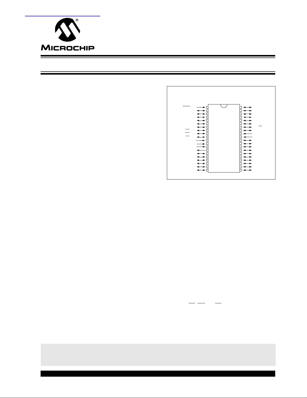
Pin Diagram
600 mil. PDIP, Windowed CERDIP
MCLR/VPP
RA0/AN0
RA1/AN1
RA2/AN2/V
REF-/VRL
RA3/AN3/V
REF+/VRH
RA4/T0CKI
RA5/AN4
RE0/RD
RE1/WR
RE2/CS
OSC1/CLKIN
OSC2/CLKOUT
RC0/T1OSO/T1CKI
RC1/T1OSI/CCP2
RC2/CCP1
RC3/SCK/SCL
RD0/PSP0
RD1/PSP1
/AN5
/AN6
/AN7
AV
AVSS
1
2
3
4
5
6
7
8
9
DD
10
11
12
13
14
15
16
17
18
19
20
40
39
38
37
36
35
34
33
32
31
30
29
28
27
PIC16C774
26
25
24
23
22
21
RB7
RB6
RB5
RB4
RB3/AN9/LVDIN
RB2/AN8
RB1/SS
RB0/INT
V
VSS
RD7/PSP7
RD6/PSP6
RD5/PSP5
RD4/PSP4
RC7/RX/DT
RC6/TX/CK
RC5/SDO
RC4/SDI/SDA
RD3/PSP3
RD2/PSP2
Peripheral Features:
• Timer0: 8-bit timer/counter with 8-bit prescaler
• Timer1: 16-bit timer/counter with prescaler,
can be incremented during sleep via external
crystal/clock
• Timer2: 8-bit timer/counter with 8-bit period
register, prescaler and postscaler
• Two Capture, Compare, PWM modules
• Capture is 16-bit, max. resolution is 12.5 ns,
Compare is 16-bit, max. resolution is 200 ns,
PWM max. resolution is 10-bit
• 12-bit multi-channel Analog-to-Digital converter
*
• On-chip absolute bandgap voltage reference
*
generator
• Synchronous Serial Port (SSP) with SPI
*
Mode) and I
• Universal Synchronous Asynchronous Receiver
*
Transmitter, supports high/low speeds and 9-bit
2C
address mode (USART/SCI)
• Paralle l Slave Po rt (PSP) 8-bits wide, with
external RD
• Programmable Brown-out detection circuitry for
*
Brown-out Reset (BOR)
• Programmable Low-voltage detection circuitry
*
, WR and CS controls
(Master
DD
This is an advanced copy of the data sheet and therefore the contents and
specifications are subject to change based on device characterization.
1999 Microchip Technology Inc. Advance Information DS30275A-page 1
Page 2
PIC16C77X
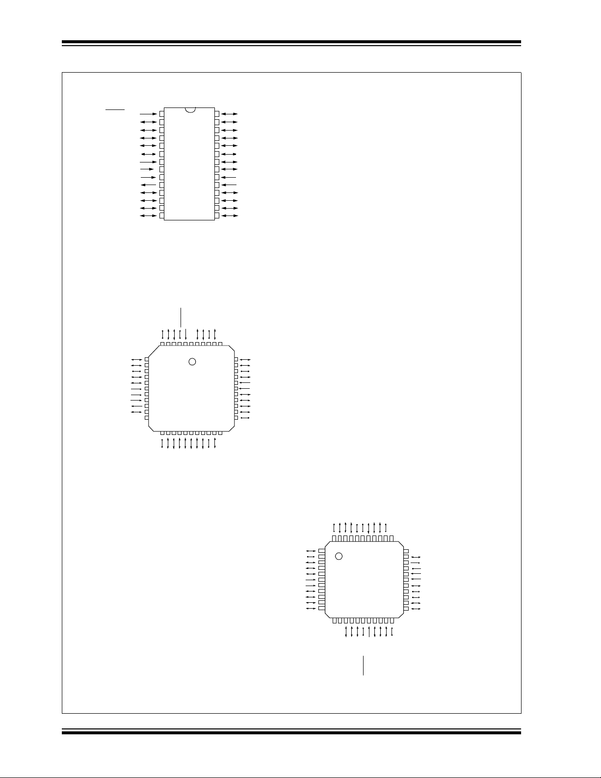
Pin Diagrams
300 mil. SDIP, SOIC, Windowed CERDIP, SSOP
MCLR/VPP
RA0/AN0
RA1/AN1
RA2/AN2/V
RA3/AN3/VREF+/VRH
RC0/T1OSO/T1CKI
REF-/VRL
RA4/T0CKI
AV
AVSS
OSC1/CLKIN
OSC2/CLKOUT
RC1/T1OSI/CCP2
RC2/CCP1
RC3/SCK/SCL
PLCC
RA4/T0CKI
RA5/AN4
RE0/RD/AN5
RE1/WR/AN6
RE2/CS/AN7
OSC1/CLKIN
OSC2/CLKOUT
RC0/T1OSO/T1CKI
AV
AVSS
NC
DD
DD
• 1
2
3
4
5
6
7
8
9
10
11
12
13
14
REF-/VRL
RA3/AN3/VREF+/VRH
RA2/AN2/V
RA1/AN1
65432
7
8
9
10
11
12
PIC16C774
13
14
15
16
17
RA0/AN0
PIC16C773
/VPP
NC
MCLR
1
28
27
26
25
24
23
22
21
20
19
18
17
16
15
RB7
RB6
RB5
RB4
4443424140
RB7
RB6
RB5
RB4
RB3/AN9/LVDIN
RB2/AN8
RB1/SS
RB0/INT
V
DD
VSS
RC7/RX/DT
RC6/TX/CK
RC5/SDO
RC4/SDI/SDA
NC
39
38
37
36
35
34
33
32
31
30
29
2827262524232221201918
RB3/AN9/LVDIN
RB2/AN8
RB1/SS
RB0/INT
DD
V
VSS
RD7/PSP7
RD6/PSP6
RD5/PSP5
RD4/PSP4
RC7/RX/DT
NC
RC2/CCP1
RC3/SCK/SCL
RC1/T1OSI/CCP2
RC6/TX/CK
RC4/SDI/SDA
MQFP
TQFP
RC7/RX/DT
RD4/PSP4
RD5/PSP5
RD6/PSP6
RD7/PSP7
V
SS
VDD
RB0/INT
RB1/SS
RB2/AN8
RB3/AN9/LVDIN
RC4/SDI/SDA
RC6/TX/CK
RC5/SDO
RD3/PSP3
RD2/PSP2
4443424140393837363534
1
2
3
4
5
6
PIC16C774
7
8
9
10
11
NC
NC
RB6
RB5
RB4
RD1/PSP1
RD0/PSP0
RB7
/VPP
MCLR
NC
RC3/SCK/SCL
RC2/CCP1
RC1/T1OSI/CCP2
33
32
31
30
29
28
27
26
25
24
23
2221201918171615141312
REF-/VRL
RA1/AN1
RA0/AN0
RA2/AN2/V
RA3/AN3/VREF+/VRH
NC
RC0/T1OSO/T1CKI
OSC2/CLKOUT
OSC1/CLKIN
SS
AV
AVDD
RE2/CS/AN7
RE1/WR/AN6
RE0/RD/AN5
RA5/AN4
RA4/T0CKI
RC5/SDO
RD3/PSP3
RD2/PSP2
RD1/PSP1
RD0/PSP0
DS30275A-page 2 Advance Information 1999 Microchip Technology Inc.
Page 3

PIC16C77X
Key Features
PICmicro™ Mid-Range Reference Manual
(DS33023)
Operating Frequency DC - 20 MHz DC - 20 MHz
Resets (and Delays) POR, BOR, MCLR, WDT
(PWRT, OST)
Program Memory (14-bit words) 4K 4K
Data Memory (bytes) 256 256
Interrupts 13 14
I/O Ports Ports A,B,C Ports A,B,C,D,E
Timers 3 3
Capture/Compare/PWM modules 2 2
Serial Communications MSSP, USART MSSP, USART
Parallel Communications — PSP
12-bit Analog-to-Digital Module 6 input channels 10 input channels
Instruction Set 35 Instructions 35 Instructions
PIC16C773 PIC16C774
POR, BOR, MCLR, WDT
(PWRT, OST)
1999 Microchip Technology Inc. Advance Information DS30275A-page 3
Page 4

PIC16C77X
Table of Contents
1.0 Device Overview............................................................................................................................................................................5
2.0 Memory Organization ................................................................................................................................................................... 11
3.0 I/O Ports..................... .................................................................................. ................. ...............................................................27
4.0 Timer0 Module............................................................................................................................................................................. 39
5.0 Timer1 Module............................................................................................................................................................................. 41
6.0 Timer2 Module............................................................................................................................................................................. 45
7.0 Capture/Compare/PWM (CCP) Module(s)...................................................................................................................................47
8.0 Master Synchronous Serial Port (MSSP) Module........................................................................................................................53
9.0 Addressable Universal Synchronous Asynchronous Receiver Transmitter (USA RT ) .................................................................97
10.0 Voltage Reference Module and Low-voltage Detect....................................................... .. .. ....... .. .. .. ..........................................113
11.0 Analog-to-Digital Converter (A/D) Module ................................................................................................................................. 117
12.0 Special Features of the CPU.....................................................................................................................................................127
13.0 Instruction Set Summary............................................................................................................................................................ 143
14.0 Development Support ................................................................................................................................................................ 145
15.0 Electrical Characteristics............................................................................................................................................................ 151
16.0 DC and AC Characteristics Graphs and Tables ....................................................... .. .... .... ......... .. ............................................173
17.0 Packaging Infor mation...................................................... ....................................................... .............. ............... ..................... 175
Appendix A: Revision History......................................................................................................................................................... 187
Appendix B: Device Differences..................................................................................................................................................... 187
Appendix C: Conversion Considerations............................................................ ..... .... .. .... .. .. ....... .... .............................................. 187
Index .................................................................. .. .. .. .. .. ..... .. .. .. .... .. .. .. ..... .. .. .. .. .. .. .. .. ............................................................................ 189
Bit/Register Cross-Reference List......................................................................................................................................................196
On-Line Support.................................................................... .. .... .... .. ......... .... .. .... .. ......... ...................................................................197
Reader Response.............................................................................................................................................................................. 198
PIC16C77X Product Identification System.................................................................................. ....................................................... 199
To Our Valued Customers
Most Current Data Sheet
To obtain the most up-to-date version of this data sheet, please check our Worldwide Web site at:
http://www.microchip.com
You can determine the version of a data sheet by examining its literature number found on the bottom outside corner of any page.
The last character of the literature number is the version number. e.g., DS30000A is version A of document DS30000.
Errata
An errata sheet may exist for current devices, describing minor operational differences (from the data sheet) and recommended
workarounds. As device/documentation issues become known to us, w e will pub lish an errata sheet. The errata will specify the re vision of silicon and revision of document to which it applies.
To determine if an errata sheet exists for a particular device, please check with one of the following:
• Microchip’s Worldwide Web site; http://www .microchip.com
• Your local Microchip sales office (see last page)
• The Microchip Corporate Literature Center; U.S. FAX: (602) 786-7277
When contacting a sales office or the literature center, please specify which device, revision of silicon and data sheet (include liter-
ature number) you are using.
Corrections to this Data Sheet
We constantly strive to improve the quality of all our products and documentation. We have spent a great deal of time to ensure
that this document is correct. However, we realize that we may have missed a few things. If you find any information that is missin g
or appears in error, please:
• Fill out and mail in the reader response form in the back of this data sheet.
• E-mail us at webmaster@microchip.com.
We appreciate your assistance in making this a better document.
DS30275A-page 4 Advance Information 1999 Microchip Technology Inc.
Page 5
PIC16C77X
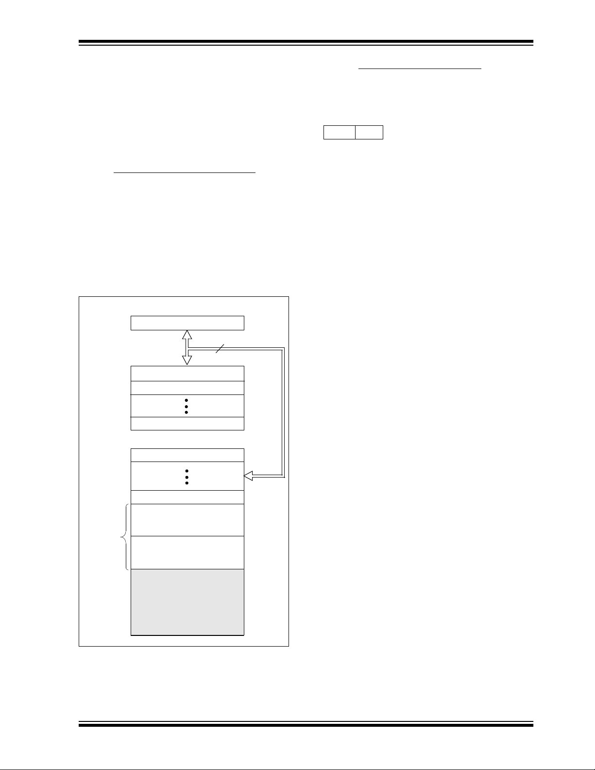
1.0 DEVICE OVERVIEW
This document contains device-specific information.
Additional information ma y be foun d in the PIC m icro™
Mid-Range Reference Manual, (DS33023), which may
be obtained from your local Microchip Sales Representative or downloaded from the Microchip website. The
Reference Manual should be considered a complementary document to this data she et, and is h ighly recommended reading for a better understanding of the
device architecture and operation of the peripheral
modules.
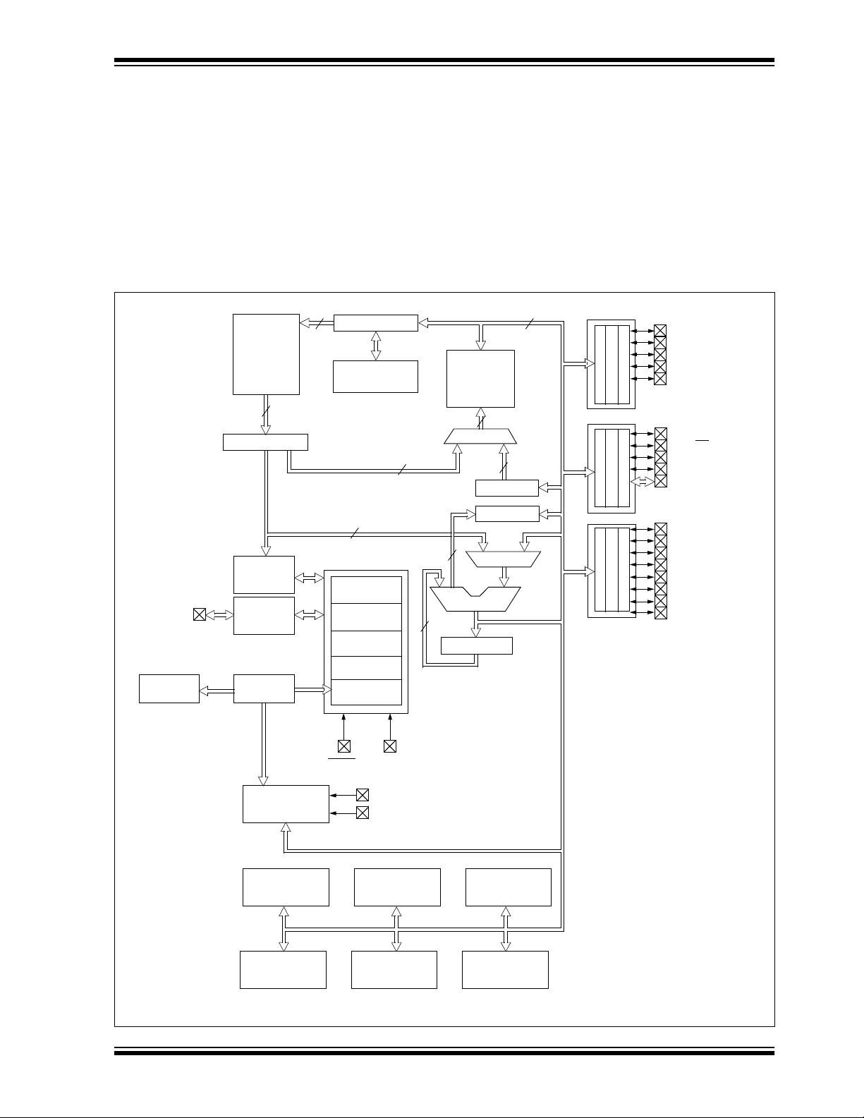
FIGURE 1-1: PIC16C773 BLOCK DIAGRAM
13
Program Counter
8 Level Stack
(13-bit)
Direct Addr
7
Program
Bus
EPROM
Program
Memory
4K x 14
14
Instruction reg
RAM Addr
There a two devices (PIC16C773 and PIC16C774)
covered by this datasheet. The PIC16C773 devices
come in 28-pin packages and the PIC16C774 devices
come in 40-pin packages. The 28-pin devices do not
have a Parallel Slave Port implemented.
The following two figures are device block diagrams
sorted by pin number; 28-pin for Figure 1-1 and 40-pin
for Figure 1-2. The 28-pin and 40-pin pinouts are listed
in T able 1-1 and Table 1-2, respectively.
Data Bus
RAM
File
Registers
256 x 8
(1)
Addr MUX
FSR reg
9
8
8
Indirect
Addr
PORTA
RA0/AN0
RA1/AN1
RA2/AN2/VREF-/VRL
RA3/AN3/VREF+/VRH
RA4/T0CKI
PORTB
RB0/INT
RB1/SS
RB2/AN8
RB3/AN9/LVDIN
RB7:RB4
OSC1/CLKIN
OSC2/CLKOUT
Low-voltage
Detect
8
Instruction
Decode &
Control
Timing
Generation
Precision
Reference
12-bit
ADC
Timer0 Timer1 Timer2
Power-up
Timer
Oscillator
Start-up Timer
Power-on
Reset
Watchdog
Timer
Brown-out
Reset
VDD, VSS
MCLR
AVDD
AVSS
3
8
STATUS reg
ALU
W reg
MUX
PORTC
RC0/T1OSO/T1CKI
RC1/T1OSI/CCP2
RC2/CCP1
RC3/SCK/SCL
RC4/SDI/SDA
RC5/SDO
RC6/TX/CK
RC7/RX/DT
CCP1,2
Synchronous
Serial Port
USART
Note 1: Higher order bits are from the STATUS register.
1999 Microchip Technology Inc. Advance Information DS30275A-page 5
Page 6
PIC16C77X
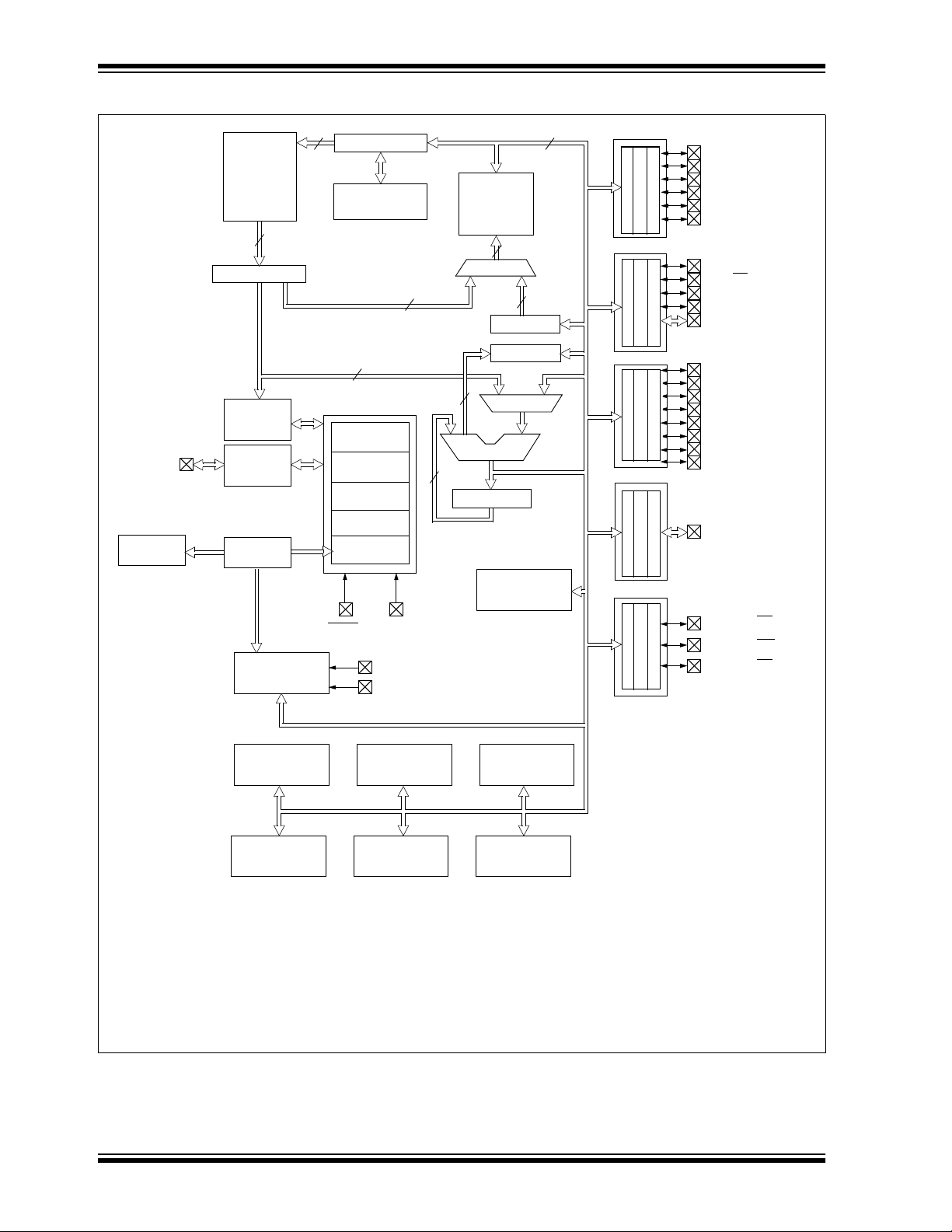
FIGURE 1-2: PIC16C774 BLOCK DIAGRAM
13
Program Counter
8 Level Stack
(13-bit)
Direct Addr
7
Program
Bus
EPROM
Program
Memory
4K x 14
14
Instruction reg
RAM Addr
Data Bus
RAM
File
Registers
256 x 8
(1)
Addr MUX
FSR reg
9
8
8
Indirect
Addr
PORTA
RA0/AN0
RA1/AN1
RA2/AN2/VREF-/VRL
RA3/AN3/VREF+/VRH
RA4/T0CKI
RA5/AN4
PORTB
RB0/INT
RB1/SS
RB2/AN8
RB3/AN9/LVDIN
RB7:RB4
OSC1/CLKIN
OSC2/CLKOUT
Low-voltage
Detect
8
Instruction
Decode &
Control
Timing
Generation
Precision
Reference
12-bit
ADC
Timer0 Timer1 Timer2
Power-up
Timer
Oscillator
Start-up Timer
Power-on
Reset
Watchdog
Timer
Brown-out
Reset
VDD, VSS
MCLR
AVDD
AVSS
3
8
STATUS reg
MUX
ALU
W reg
Parallel Slave Port
PORTC
PORTD
PORTE
RC0/T1OSO/T1CKI
RC1/T1OSI/CCP2
RC2/CCP1
RC3/SCK/SCL
RC4/SDI/SDA
RC5/SDO
RC6/TX/CK
RC7/RX/DT
RD7/PSP7:RD0/PSP0
RE0/AN5/RD
RE1/AN6/WR
RE2/AN7/CS
CCP1,2
Synchronous
Serial Port
USART
Note 1: Higher order bits are from the STATUS register.
DS30275A-page 6 Advance Information 1999 Microchip Technology Inc.
Page 7

PIC16C77X
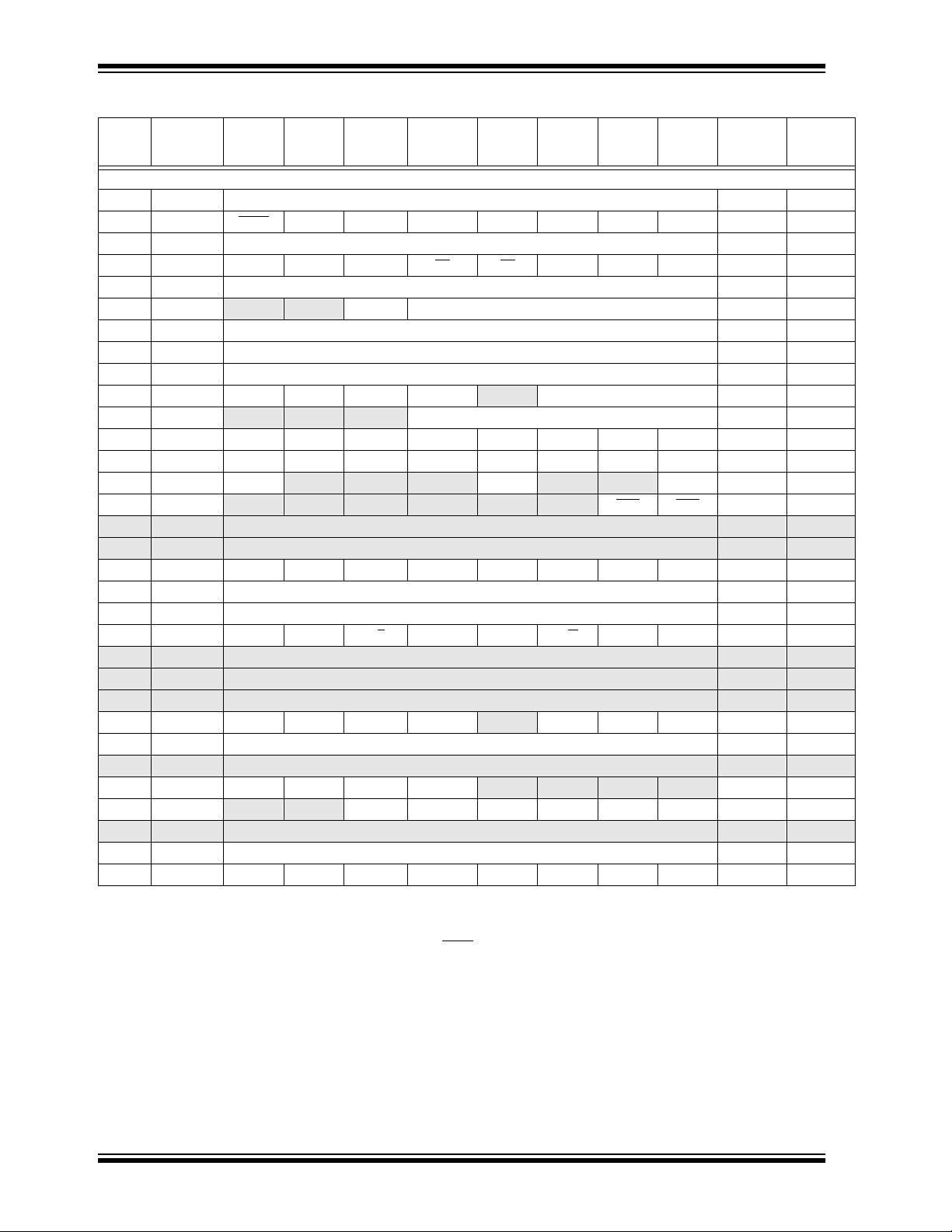
TABLE 1-1 PIC16C773 PINOUT DESCRIPTION
DIP,
Pin Name
SSOP,
SOIC
I/O/P
Type
Pin#
OSC1/CLKIN 9 I
OSC2/CLKOUT 10 O — Oscillator crystal output. Connects to crystal or resonator in crystal
MCLR
/VPP
1 I/P ST Master clear (reset) input or programming voltage input. This pin is an
RA0/AN0 2 I/O TTL RA0 can also be analog input0
RA1/AN1 3 I/O TTL RA1 can also be analog input1
RA2/AN2/V
RA3/AN3/V
REF-/VRL 4 I/O TTL RA2 can also be analog input2 or negative analog reference voltage
REF+/VRH 5 I/O TTL RA3 can also be analog input3 or positive analog reference voltage
RA4/T0CKI 6 I/O ST RA4 can also be the clock input to the Timer0 module. Output is
RB0/INT 21 I/O TTL/ST
RB1/SS
22 I/O TTL/ST
RB2/AN8 23 I/O TTL RB2 can also be analog input8
RB3/AN9/LVDIN 24 I/O TTL RB3 can also be analog input9 or the low voltage detect input
RB4 25 I/O TTL Interrupt on change pin.
RB5 26 I/O TTL Interrupt on change pin.
RB6 27 I/O TTL/ST
RB7 28 I/O TTL/ST
RC0/T1OSO/T1CKI 11 I/O ST RC0 can also be the Timer1 oscillator output or Timer1 clock input.
RC1/T1OSI/CCP2 12 I/O ST RC1 can also be the Timer1 oscillator input or Capture2 input/
RC2/CCP1 13 I/O ST RC2 can also be the Capture1 input/Compare1 output/PWM1
RC3/SCK/SCL 14 I/O ST RC3 can also be the synchronous serial clock input/output for both
RC4/SDI/SDA 15 I/O ST RC4 can also be the SPI Data In (SPI mode) or
RC5/SDO 16 I/O ST RC5 can also be the SPI Data Out (SPI mode).
RC6/TX/CK 17 I/O ST RC6 can also be the USART Asynchronous Transmit or
RC7/RX/DT 18 I/O ST RC7 can also be the USART Asynchronous Receive or
SS 8 P Ground reference for A/D converter
AV
DD 7 P Positive supply for A/D converter
AV
SS 19 P — Ground reference for logic and I/O pins.
V
DD 20 P — Positiv e supply for logic and I/O pins.
V
Legend: I = input O = output I/O = input/output P = power
— = Not used TTL = TTL input ST = Schmitt Trigger input
Note 1: This buffer is a Schmitt Trigger input when configured for the multiplexed function.
2: This buffer is a Schmitt Trigger input when used in serial programming mode.
3: This buffer is a Schmitt Trigger input when configured in RC oscillator mode and a CMOS input otherwise.
Buffer
Type
ST/CMOS
Description
(3)
Oscillator crystal input/external clock source input.
oscillator mode. In RC mode, the OSC2 pin outputs CLKOUT which has
1/4 the frequency of OSC1, and denotes the instruction cycle rate.
active low reset to the device.
PORTA is a bi-directional I/O port.
input or internal voltage reference low
input or internal voltage reference high
open drain type.
PORTB is a bi-directional I/O port. PORTB can be software programmed for internal weak pull-up on all inputs.
(1)
(1)
RB0 can also be the external interrupt pin.
RB1 can also be the SSP slave select
reference
(2)
(2)
Interrupt on change pin. Serial programming clock.
Interrupt on change pin. Serial programming data.
PORTC is a bi-directional I/O port.
Compare2 output/PWM2 output.
output.
2
SPI and I
data I/O (I
C modes.
2
C mode).
Synchronous Clock.
Synchronous Data.
1999 Microchip Technology Inc. Advance Information DS30275A-page 7
Page 8

PIC16C77X
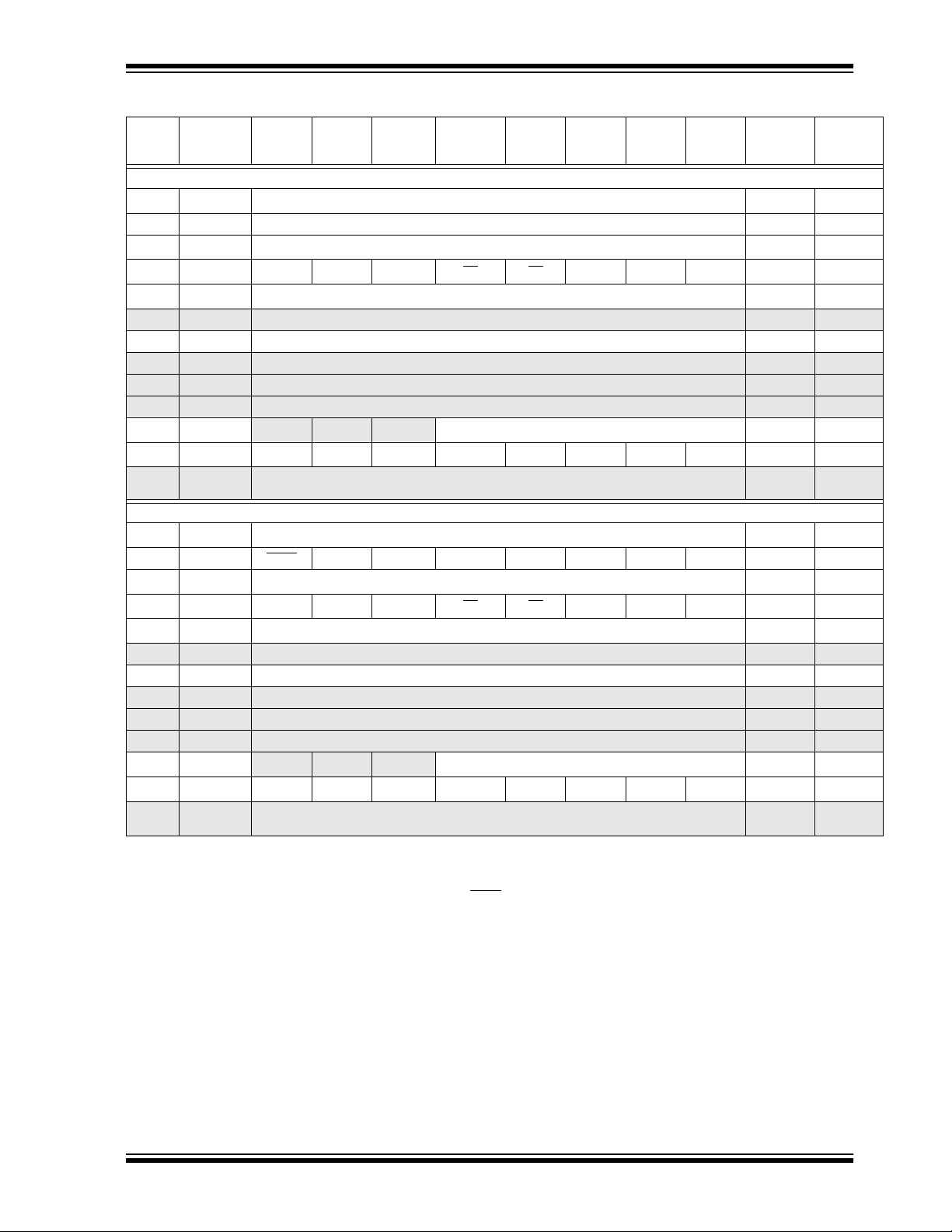
TABLE 1-2 PIC16C774 PINOUT DESCRIPTION
DIP
Pin Name
OSC1/CLKIN 13 14 30 I ST/CMOS
OSC2/CLKOUT 14 15 31 O — Oscillator crystal output. Connects to crystal or resonator
/VPP 1 2 18 I/P ST Master clear (reset) input or programming voltage input.
MCLR
RA0/AN0 2 3 19 I/O TTL RA0 can also be analog input0
RA1/AN1 3 4 20 I/O TTL RA1 can also be analog input1
RA2/AN2/V
RA3/AN3/V
RA4/T0CKI 6 7 23 I/O ST RA4 can also be the clock input to the Timer0 timer/
RA5/AN4 7 8 24 I/O TTL RA5 can also be analog input4
RB0/INT 33 36 8 I/O TTL/ST
RB1/SS
RB2/AN8 35 38 10 I/O TTL RB2 can also be analog input8
RB3/AN9/LVDIN 36 39 11 I/O TTL RB3 can also be analog input9 or input reference for
RB4 37 41 14 I/O TTL Interrupt on change pin.
RB5 38 42 15 I/O TTL Interrupt on change pin.
RB6 39 43 16 I/O TTL/ST
RB7 40 44 17 I/O TTL/ST
Legend: I = input O = output I/O = input/output P = power
Note 1: This buffer is a Schmitt Trigger input when configured for the multiplexed function.
REF-/VRL 4 5 21 I/O TTL
REF+/VRH 5 6 22 I/O TTL
— = Not used TTL = TTL input ST = Schmitt Trigger input
2: This buffer is a Schmitt Trigger input when used in serial programming mode.
3: This buffer is a Schmitt Trigger input when configured as general purpose I/O and a TTL input when used in the Parallel
Slave Port mode (for interfacing to a microprocessor bus).
4: This buffer is a Schmitt Trigger input when configured in RC oscillator mode and a CMOS input otherwise.
PLCC
Pin#
Pin#
34 37 9 I/O TTL/ST
QFP
Pin#
I/O/P
Type
Buffer
Type
Description
(4)
Oscillator crystal input/external clock source input.
in crystal oscillator mode. In RC mode, OSC2 pin outputs
CLKOUT which has 1/4 the frequency of OSC1, and
denotes the instruction cycle rate.
This pin is an active low reset to the device.
PORTA is a bi-directional I/O por t.
RA2 can also be analog input2 or negative analog
reference voltage input or internal voltage reference
low
RA3 can also be analog input3 or positive analog
reference voltage input or internal voltage reference
high
counter. Output is open drain type.
PORTB is a bi-directional I/O port. PORTB can be software programmed for internal weak pull-up on all inputs.
(1)
(1)
(2)
(2)
RB0 can also be the external interrupt pin.
RB1 can also be the SSP slave select
low voltage detect
Interrupt on change pin. Serial programming clock.
Interrupt on change pin. Serial programming data.
DS30275A-page 8 Advance Information 1999 Microchip Technology Inc.
Page 9
PIC16C77X
TABLE 1-2 PIC16C774 PINOUT DESCRIPTION (Cont.’d)
DIP
Pin Name
Pin#
PLCC
Pin#
RC0/T1OSO/T1CKI 15 16 32 I/O ST RC0 can also be the Timer1 oscillator output or a
RC1/T1OSI/CCP2
RC2/CCP1
RC3/SCK/SCL
RC4/SDI/SDA
RC5/SDO
RC6/TX/CK
RC7/RX/DT
16 18 35 I/O ST RC1 can also be the Timer1 oscillator input or
17 19 36 I/O ST RC2 can also be the Capture1 input/Compare1
18 20 37 I/O S T RC3 can also be the synchronous serial clock input/
23 25 42 I/O ST RC4 can also be the SPI Data In (SPI mode) or
24 26 43 I/O ST RC5 can also be the SPI Data Out
25 27 44 I/O ST RC6 can also be the USART Asynchronous
26 29 1 I/O ST RC7 can also be the USART Asynchronous Receive
RD0/PSP0 19 21 38 I/O ST/TTL
RD1/PSP1 20 22 39 I/O ST/TTL
RD2/PSP2 21 23 40 I/O ST/TTL
RD3/PSP3 22 24 41 I/O ST/TTL
RD4/PSP4 27 30 2 I/O ST/TTL
RD5/PSP5 28 31 3 I/O ST/TTL
RD6/PSP6 29 32 4 I/O ST/TTL
RD7/PSP7 30 33 5 I/O ST/TTL
/AN5 8 9 25 I/O ST/TTL
RE0/RD
RE1/WR
RE2/CS
/AN6 9 10 26 I/O ST/TTL
/AN7 10 11 27 I/O ST/TTL
AVss 12 13 29 P
DD 11 12 28 P
AV
SS 31 34 6 P — Ground reference for logic and I/O pins.
V
DD 32 35 7 P — Positive supply for logic and I/O pins.
V
NC — 1,17,28,4012,13,
Legend: I = input O = output I/O = input/output P = power
— = Not used TTL = TTL input ST = Schmitt Trigger input
Note 1: This buffer is a Schmitt Trigger input when configured for the multiplexed function.
2: This buffer is a Schmitt Trigger input when used in serial programming mode.
3: This buffer is a Schmitt Trigger input when configured as general purpose I/O and a TTL input when used in the Parallel
Slave Port mode (for interfacing to a microprocessor bus).
4: This buffer is a Schmitt Trigger input when configured in RC oscillator mode and a CMOS input otherwise.
QFP
Pin#
33,34
I/O/P
Type
Buffer
Type
Description
PORTC is a bi-directional I/O port.
Timer1 clock input.
Capture2 input/Compare2 output/PWM2 output.
output/PWM1 output.
output for both SPI and I
2
data I/O (I
C mode).
2
C modes.
(SPI mode).
Transmit or Synchronous Clock.
or Synchronous Data.
PORTD is a bi-directional I/O port or parallel slave port
when interfacing to a microprocessor bus.
(3)
(3)
(3)
(3)
(3)
(3)
(3)
(3)
PORTE is a bi-directional I/O port.
(3)
RE0 can also be read control for the parallel slave
port, or analog input5.
(3)
RE1 can also be write control for the parallel slave
port, or analog input6.
(3)
RE2 can also be select control for the parallel slave
port, or analog input7.
Ground reference for A/D converter
Positive supply for A/D converter
— These pins are not internally connected. These pins
should be left unconnected.
1999 Microchip Technology Inc. Advance Information DS30275A-page 9
Page 10

PIC16C77X
NOTES:
DS30275A-page 10 Advance Information 1999 Microchip Technology Inc.
Page 11
PIC16C77X
2.0 MEMORY ORGANIZATION
There are two memory blocks in each of these
PICmicro
gram Memory and Data Memory) has its own bus
so that concurrent access can occur.
Additional information on de vice memo ry may be foun d
in the PICmicro Mid-Range Reference Manual,
(DS33023).
2.1 Program Memory Organization
The PIC16C77X PICmicros have a 13-bit program
counter capable of addressing an 8K x 14 program
memory space. Each de vi ce has 4K x 14 w ords of program memory. Accessing a location above the physically implemented address will cause a wraparound.
The reset vector is at 0000h and the interrupt vector is
at 0004h.
FIGURE 2-1: PROGRAM MEMORY MAP
®
microcontrollers. Each block (Pro-
AND STACK
PC<12:0>
CALL, RETURN
RETFIE, RETLW
13
2.2 Data Memory Organization
The data memory is partitioned into multiple banks
which contain the General Purpose Registers and the
Special Function Registers. Bits RP1 and RP0 are the
bank select bits.
RP1 RP0 (STATUS<6:5>)
= 00 → Bank0
= 01 → Bank1
= 10 → Bank2
= 11 → Bank3
Each bank extends up to 7Fh (128 bytes). The lower
locations of each bank are reserved for the Special
Function Registers . Abo v e the Spec ial Fun ction Re gisters are General Purpose Registers, implemented as
static RAM. All implemented banks contain special
function registers. Some “high use” special function
registers from one bank may be mirrored in another
bank for code reduction and quicker access.
2.2.1 GENERAL PURPOSE REGISTER FILE
The register file can be a ccessed ei ther direc tly, or indi-
rectly through the File Select Register FSR.
On-chip
Program
Memory
Stack Level 1
Stack Level 2
Stack Level 8
Reset Vector
Interrupt Vector
Page 0
Page 1
0000h
0004h
0005h
07FFh
0800h
0FFFh
1000h
3FFFh
1999 Microchip Technology Inc. Advance Information DS30275A-page 11
Page 12
PIC16C77X
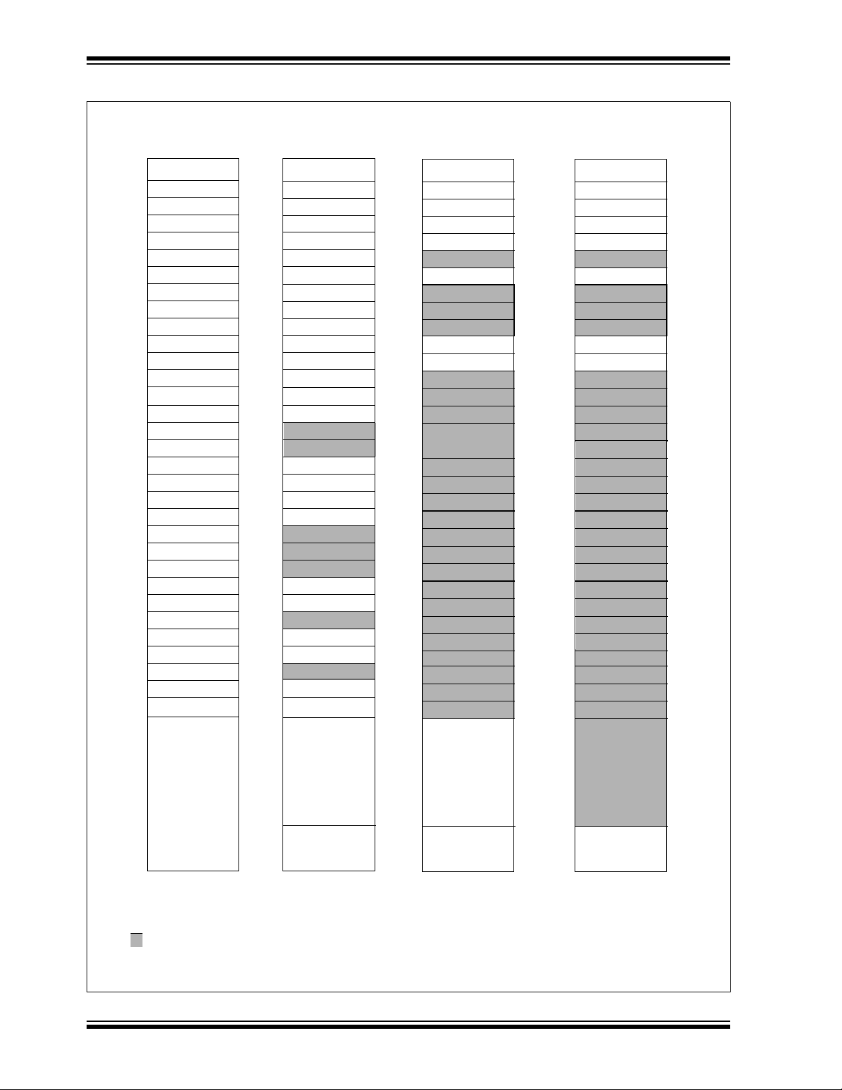
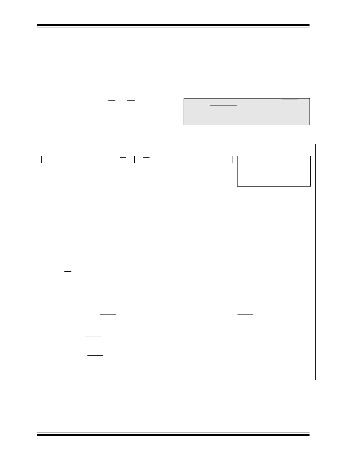
FIGURE 2-2: REGISTER FILE MAP
Indirect addr.
TMR0
PCL
STATUS
FSR
PORTA
PORTB
PORTC
PORTD
PORTE
PCLATH
INTCON
PIR1
PIR2
TMR1L
TMR1H
T1CON
TMR2
T2CON
SSPBUF
SSPCON
CCPR1L
CCPR1H
CCP1CON
RCSTA
TXREG
RCREG
CCPR2L
CCPR2H
CCP2CON
ADRESH
ADCON0
Address
(*)
(1)
(1)
File
00h
01h
02h
03h
04h
05h
06h
07h
08h
09h
0Ah
0Bh
0Ch
0Dh
0Eh
0Fh
10h
11h
12h
13h
14h
15h
16h
17h
18h
19h
1Ah
1Bh
1Ch
1Dh
1Eh
1Fh
20h
Indirect addr.
OPTION_REG
PCL
STATUS
FSR
TRISA
TRISB
TRISC
(1)
TRISD
(1)
TRISE
PCLATH
INTCON
PIE1
PIE2
PCON
SSPCON2
PR2
SSPADD
SSPSTAT
TXSTA
SPBRG
REFCON
LVDCON
ADRESL
ADCON1
File
Address
(*)
80h
81h
82h
83h
84h
85h
86h
87h
88h
89h
8Ah
8Bh
8Ch
8Dh
8Eh
8Fh
90h
91h
92h
93h
94h
95h
96h
97h
98h
99h
9Ah
9Bh
9Ch
9Dh
9Eh
9Fh
A0h
Indirect addr.
TMR0
PCL
STATUS
FSR
PORTB
PCLATH
INTCON
Address
(*)
File
100h
101h
102h
103h
104h
105h
106h
107h
108h
109h
10Ah
10Bh
10Ch
10Dh
10Eh
10Fh
110h
111h
112h
113h
114h
115h
116h
117h
118h
119h
11Ah
11Bh
11Ch
11Dh
11Eh
11Fh
120h
Indirect addr.
OPTION_REG
PCL
STATUS
FSR
TRISB
PCLATH
INTCON
File
Address
(*)
180h
181h
182h
183h
184h
185h
186h
187h
188h
189h
18Ah
18Bh
18Ch
18Dh
18Eh
18Fh
190h
191h
192h
193h
194h
195h
196h
197h
198h
199h
19Ah
19Bh
19Ch
19Dh
19Eh
19Fh
1A0h
General
Purpose
Register
96 Bytes
7Fh
Bank 0 Bank 1
(1) Not implemented on PIC16C773.
Unimplemented data memory locations, read as ’0’.
* Not a physical register.
DS30275A-page 12 Advance Information 1999 Microchip Technology Inc.
General
Purpose
Register
80 Bytes
accesses
70h-7Fh
EFh
F0h
FFh
General
Purpose
Register
80 Bytes
accesses
70h - 7Fh
Bank 2
6Fh
70h
17Fh
accesses
70h - 7Fh
Bank 3
1EFh
1F0h
1FFh
Page 13
PIC16C77X
2.2.2 SPECIAL FUNCTION REGISTERS
The special fu nction re gisters can b e classifi ed into two
sets; core (CPU) and periphe ral. Those registers asso-
The Special Function Registers are registers used by
the CPU and Peripheral Modules for controlling the
desired operation of the device. These registers are
implemented as static RAM. A list of these registers is
given in Table 2-1.
ciated with the core functions are described in detail in
this section. Those related to the operation of the
peripheral features are described in detail in that
peripheral feature section.
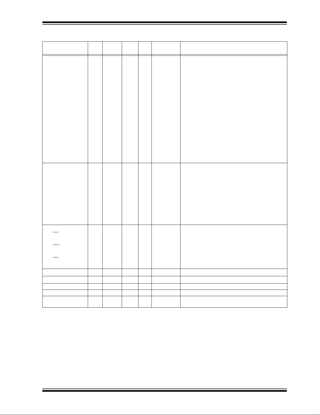
TABLE 2-1 PIC16C77X SPECIAL FUNCTION REGISTER SUMMARY
Address Name Bit 7 Bit 6 Bit 5 Bit 4 Bit 3 Bit 2 Bit 1 Bit 0
Bank 0
(4)
00h
01h TMR0 Timer0 module’s register xxxx xxxx uuuu uuuu
02h
03h
04h
05h PORTA
06h PORTB PORTB Data Latch when written: PORTB pins when read xxxx 11xx uuuu 11uu
07h PORTC PORTC Data Latch when written: PORTC pins when read xxxx xxxx uuuu uuuu
08h
09h
0Ah
0Bh
0Ch PIR1 PSPIF
0Dh PIR2 LVDIF
0Eh TMR1L Holding register for the Least Significant Byte of the 16-bit TMR1 register xxxx xxxx uuuu uuuu
0Fh TMR1H Holding register for the Most Significant Byte of the 16-bit TMR1 register xxxx xxxx uuuu uuuu
10h T1CON
11h TMR2 Timer2 module’s register 0000 0000 0000 0000
12h T2CON
13h SSPBUF Synchronous Serial Port Receive Buffer/Transmit Register xxxx xxxx uuuu uuuu
14h SSPCON WCOL SSPOV SSPEN CKP SSPM3 SSPM2 SSPM1 SSPM0 0000 0000 0000 0000
15h CCPR1L Capture/Compare/PWM Register1 (LSB) xxxx xxxx uuuu uuuu
16h CCPR1H Capture/Compare/PWM Register1 (MSB) xxxx xxxx uuuu uuuu
17h CCP1CON
18h RCSTA SPEN RX9 SREN CREN ADDEN FERR OERR RX9D 0000 000x 0000 000x
19h TXREG USART Transmit Data Register 0000 0000 0000 0000
1Ah RCREG USART Receive Data Register 0000 0000 0000 0000
1Bh CCPR2L Capture/Compare/PWM Register2 (LSB) xxxx xxxx uuuu uuuu
1Ch CCPR2H Capture/Compare/PWM Register2 (MSB) xxxx xxxx uuuu uuuu
1Dh CCP2CON
1Eh ADRESH A/D High Byte Result Register xxxx xxxx uuuu uuuu
1Fh ADCON0 ADCS1 ADCS0 CHS2 CHS1 CHS0 GO/DONE
Legend: x = unknown, u = unchanged, q = value depends on condition, - = unimplemented read as '0'.
Note 1: The upper byte of the program counter is not directly accessible. PCLATH is a holding register for the PC<12:8> whose contents are transferred to
INDF Addressing this location uses contents of FSR to address data memory (not a physical register) 0000 0000 0000 0000
(4)
PCL Program Counter's (PC) Least Significant Byte 0000 0000 0000 0000
(4)
STATUS IRP RP1 RP0 TO PD ZDCC0001 1xxx 000q quuu
(4)
FSR Indirect data memory address pointer xxxx xxxx uuuu uuuu
— —PORTA5
(5)
PORTD PORTD Data Latch when written: PORTD pins when read xxxx xxxx uuuu uuuu
(5)
PORTE — — — — — RE2 RE1 RE0 ---- -000 ---- -000
(1,4)
PCLATH — — — Write Buffer for the upper 5 bits of the Program Counter ---0 0000 ---0 0000
(4)
INTCON GIE PEIE T0IE INTE RBIE T0IF INTF RBIF 0000 000x 0000 000u
(3)
ADIF RCIF TXIF SSPIF CCP1IF TMR2IF TMR1IF 0000 0000 0000 0000
— — –BCLIF— — CCP2IF 0--- 0--0 0--- 0--0
— — T1CKPS1 T1CKPS0 T1OSCEN T1SYNC TMR1CS TMR1ON --00 0000 --uu uuuu
— TOUTPS3 TOUTPS2 TOUTPS1 TOUTPS0 TMR2ON T2CKPS1 T2CKPS0 -000 0000 -000 0000
— — CCP1X CCP1Y CCP1M3 CCP1M2 CCP1M1 CCP1M0 --00 0000 --00 0000
— — CCP2X CCP2Y CCP2M3 CCP2M2 CCP2M1 CCP2M0 --00 0000 --00 0000
Shaded locations are unimplemented, read as ‘0’.
the upper byte of the program counter.
2: Other (non power-up) resets include external reset through MCLR
3: Bits PSPIE and PSPIF are reserved on the 28-pin devices, always maintain these bits clear.
4: These registers can be addressed from any bank.
5: These registers/bits are not implemented on the 28-pin devices read as '0'.
(5)
PORTA Data Latch when written: PORTA<4:0> pins when read --0x 0000 --0u 0000
CHS3 ADON 0000 0000 0000 0000
and Watchdog Timer Reset.
Value on:
POR,
BOR
Value on all
other resets
(2)
1999 Microchip Technology Inc. Advance Information DS30275A-page 13
Page 14
PIC16C77X
TABLE 2-1 PIC16C77X SPECIAL FUNCTION REGISTER SUMMARY (Cont.’d)
Address Name Bit 7 Bit 6 Bit 5 Bit 4 Bit 3 Bit 2 Bit 1 Bit 0
Bank 1
(4)
80h
81h OPTION_REG RBPU
82h
83h
84h
85h TRISA
86h TRISB PORTB Data Direction Register 1111 1111 1111 1111
87h TRISC PORTC Data Direction Register 1111 1111 1111 1111
88h
89h
8Ah
8Bh
8Ch PIE1 PSPIE
8Dh PIE2 LVDIE
8Eh PCON
8Fh — Unimplemented — —
90h — Unimplemented — —
91h SSPCON2 GCEN AKSTAT AKDT AKEN RCEN PEN RSEN SEN 0000 0000 0000 0000
92h PR2 Timer2 Period Register 1111 1111 1111 1111
93h SSPADD Synchronous Serial Port (I
94h SSPSTAT SMP CKE D /A
95h — Unimplemented — —
96h — Unimplemented — —
97h — Unimplemented — —
98h TXSTA CSRC TX9 TXEN SYNC
99h SPBRG Baud Rate Generator Register 0000 0000 0000 0000
9Ah — Unimplemented — —
9Bh REFCON VRHEN VRLEN VRHOEN VRLOEN
9Ch LVDCON
9Ah — Unimplemented — —
9Eh ADRESL A/D Low Byte Result Register xxxx xxxx uuuu uuuu
9Fh ADCON1 ADFM VCFG2 VCFG1 VCFG0 PCFG3 PCFG2 PCFG1 PCFG0 0000 0000 0000 0000
Legend: x = unknown, u = unchanged, q = value depends on condition, - = unimplemented read as ’0’.
Note 1: The upper byte of the program counter is not directly accessible. PCLATH is a holding register for the PC<12:8> whose contents are transferred to
INDF Addressing this location uses contents of FSR to address data memory (not a physical register) 0000 0000 0000 0000
INTEDG T0CS T0SE PSA PS2 PS1 PS0 1111 1111 1111 1111
(4)
PCL Program Counter’s (PC) Least Significant Byte 0000 0000 0000 0000
(4)
STATUS IRP RP1 RP0 TO PD ZDCC0001 1xxx 000q quuu
(4)
FSR Indirect data memory address pointer xxxx xxxx uuuu uuuu
— —bit5
(5)
TRISD PORTD Data Direction Register 1111 1111 1111 1111
(5)
TRISE IBF OBF IBOV PSPMODE — PORTE Data Direction Bits 0000 -111 0000 -111
(1,4)
PCLATH — — — Write Buffer for the upper 5 bits of the Program Counter ---0 0000 ---0 0000
(4)
INTCON GIE PEIE T0IE INTE RBIE T0IF INTF RBIF 0000 000x 0000 000u
(3)
ADIE RCIE TXIE SSPIE CCP1IE TMR2IE TMR1IE 0000 0000 0000 0000
— — —BCLIE— — CCP2IE 0--- 0--0 0--- 0--0
— — — — — —PORBOR ---- --qq ---- --uu
— — BGST LVDEN LV3 LV2 LV1 LV0 --00 0101 --00 0101
Shaded locations are unimplemented, read as ‘0’.
the upper byte of the program counter.
2: Other (non power-up) resets include external reset through MCLR
3: Bits PSPIE and PSPIF are reserved on the 28-pin devices, always maintain these bits clear.
4: These registers can be addressed from any bank.
5: These registers/bits are not implemented on the 28-pin devices read as '0'.
(5)
PORTA Data Direction Register --11 1111 --11 1111
2
C mode) Address Register 0000 0000 0000 0000
PSR/WUA BF 0000 0000 0000 0000
— B RGH TRMT TX9D 0000 -010 0000 -010
— — — — 0000 ---- 0000 ----
and Watchdog Timer Reset.
Value on:
POR,
BOR
Value on all
other resets
(2)
DS30275A-page 14 Advance Information 1999 Microchip Technology Inc.
Page 15
PIC16C77X
TABLE 2-1 PIC16C77X SPECIAL FUNCTION REGISTER SUMMARY (Cont.’d)
Address Name Bit 7 Bit 6 Bit 5 Bit 4 Bit 3 Bit 2 Bit 1 Bit 0
Bank 2
(4)
100h
101h TMR0 Timer0 module’s register xxxx xxxx uuuu uuuu
102h
103h
104h
105h — Unimplemented — —
106h PORTB PORTB Data Latch when written: PORTB pins when read xxxx 11xx uuuu 11uu
107h — Unimplemented — —
108h — Unimplemented — —
109h — Unimplemented — —
10Ah
10Bh
10Ch10Fh
Bank 3
180h
181h OPTION_REG RBPU
182h
183h
184h
185h — Unimplemented — —
186h TRISB PORTB Data Direction Register 1111 1111 1111 1111
187h — Unimplemented — —
188h — Unimplemented — —
189h — Unimplemented — —
18Ah
18Bh
18Ch18Fh
Legend: x = unknown, u = unchanged, q = value depends on condition, - = unimplemented read as ’0’.
Note 1: The upper byte of the program counter is not directly accessible. PCLATH is a holding register for the PC<12:8> whose contents are transferred to
INDF Addressing this location uses contents of FSR to address data memory (not a physical register) 0000 0000 0000 0000
(4)
PCL Program Counter's (PC) Least Significant Byte 0000 0000 0000 0000
(4)
STAT US IRP RP1 RP0 TO PD ZDCC0001 1xxx 000q quuu
(4)
FSR Indirect data memory address pointer xxxx xxxx uuuu uuuu
(1,4)
PCLATH — — — Write Buffer for the upper 5 bits of the Program Counter ---0 0000 ---0 0000
(4)
INTCON GIE PEIE T0IE INTE RBIE T0IF INTF RBIF 0000 000x 0000 000u
— Unimplemented — —
(4)
INDF Addressing this location uses contents of FSR to address data memory (not a physical register) 0000 0000 0000 0000
INTEDG T0CS T0SE PSA PS2 PS1 PS0 1111 1111 1111 1111
(4)
PCL Program Counter's (PC) Least Significant Byte 0000 0000 0000 0000
(4)
STAT US IRP RP1 RP0 TO PD ZDCC0001 1xxx 000q quuu
(4)
FSR Indirect data memory address pointer xxxx xxxx uuuu uuuu
(1,4)
PCLATH — — —
(4)
INTCON GIE PEIE T0IE INTE RBIE T0IF INTF RBIF 0000 000x 0000 000u
— Unimplemented — —
Shaded locations are unimplemented, read as ‘0’.
the upper byte of the program counter.
2: Other (non power-up) resets include external reset through MCLR
3: Bits PSPIE and PSPIF are reserved on the 28-pin devices, always maintain these bits clear.
4: These registers can be addressed from any bank.
5: These registers/bits are not implemented on the 28-pin devices read as '0'.
Write Buffer for the upper 5 bits of the Program Counter
and Watchdog Timer Reset.
Value on:
POR,
BOR
---0 0000 ---0 0000
Value on all
other resets
(2)
1999 Microchip Technology Inc. Advance Information DS30275A-page 15
Page 16
PIC16C77X
2.2.2.1 STATUS REGISTER
The STATUS register, shown in Figure 2-3, contains
the arithmetic status of th e ALU , the RE SET status an d
the bank select bits for data memory.
The STATUS register can be the destination for any
instruction, as with any other register. If the STATUS
register is the destination for an instruction that affects
the Z, DC or C bits, then the write to these three bits is
disabled. The se bi ts ar e set or c leared accordi ng to the
device logic. Fur th er more, the TO
writable. Therefore, the result of an instruction with the
STATUS register as destination may be different than
intended.
and PD bits are not
For example, CLRF STATUS will clear th e up p er- t hr ee
bits and set th e Z bi t. T his l ea v es the STATUS register
as 000u u1uu (where u = unchanged).
It is recommended, therefore, that only BCF, BSF,
SWAPF and MOVWF instructions are used to alter the
STATUS register because these instructions do not
affect the Z, C o r DC b its from th e STATUS register. F or
other instructions, not affecting any sta tus bit s , s ee th e
"Instruction Set Summary."
Note 1: The C and DC bits oper ate as a borro w and
digit borrow
See the SUBLW and SUBWF instructions for
examples.
FIGURE 2-3: STATUS REGISTER (ADDRESS 03h, 83h, 103h, 183h)
R/W-0 R/W-0 R/W-0 R-1 R-1 R/W-x R/W-x R/W-x
IRP RP1 RP0 TO
bit7 bit0
bit 7: IRP: Register Bank Select bit (used for indirect addressing)
1 = Bank 2, 3 (100h - 1FFh)
0 = Bank 0, 1 ( 00h - FFh)
bit 6-5: RP1:RP0: Register Bank Select bits (used for direct addressing)
11 = Bank 3 (180h - 1FFh)
10 = Bank 2 (100h - 17Fh)
01 = Bank 1 (80h - FFh)
00 = Bank 0 (00h - 7Fh)
Each bank is 128 bytes
bit 4: TO
bit 3: PD
bit 2: Z: Zero bit
bit 1: DC: Digit carry/borrow
bit 0: C: Carry/borrow
: Time-out bit
1 = After power-up, CLRWDT instruction, or SLEEP instruction
0 = A WDT time-out occurred
: Power-down bit
1 = After power-up or by the CLRWDT instruction
0 = By execution of the SLEEP instruction
1 = The result of an arithmetic or logic operation is zero
0 = The result of an arithmetic or logic operation is not zero
bit (ADDWF, ADDLW,SUBLW,SUBWF instructions) (for borrow the po larity i s reversed)
1 = A carry-out from the 4th low order bit of the result occurred
0 = No carry-out from the 4th low order bit of the result
bit (ADDWF, ADDLW,SUBLW,SUBWF instructions)
1 = A carry-out from the most significant bit of the result occurred
0 = No carry-out from the most significant bit of the result occurred
Note: For borrow
second operand. For rotate (RRF, RLF) instructions, this bit is loaded with either the high or low order bit of
the source register.
the polarity is reversed. A subtraction is executed by adding the two’s complement of the
PD Z DC C R = Readable bit
bit, respectively , in subtraction.
W = Writable bit
U = Unimplemented bit,
read as ‘0’
- n = Value at POR reset
DS30275A-page 16 Advance Information 1999 Microchip Technology Inc.
Page 17

2.2.2.2 OPTION_REG REGISTER
Note: To achieve a 1:1 prescaler assignment for
The OPTION_REG register is a readable and writable
register which co ntains v arious control bits to conf igure
the TMR0 register, assign the prescaler to
the Watchdog Timer.
the TMR0 prescaler/WDT postscaler (single assignable regist er kno wn also as the prescale r), the Ext ernal
INT Interrupt, TMR0, and the weak pull-up s on PORTB.
FIGURE 2-4: OPTION_REG REGISTER (ADDRESS 81h, 181h)
R/W-1 R/W-1 R/W-1 R/W-1 R/W-1 R/W-1 R/W-1 R/W-1
RBPU
bit7 bit0
bit 7: RBPU: PORTB Pull-up Enable bit
bit 6: INTEDG: Interrupt Edge Select bit
bit 5: T0CS: TMR0 Clock Source Select bit
bit 4: T0SE: TMR0 Source Edge Select bit
bit 3: PSA: Prescaler Assignment bit
bit 2-0: PS2:PS0: Prescaler Rate Select bits
INTEDG T0CS T0SE PSA PS2 PS1 PS0 R = Readable bit
1 = PORTB pull-ups are disabled
0 = PORTB pull-ups are enab led b y ind iv idu al port latch va lue s
1 = Interrupt on rising edge of RB0/INT pin
0 = Interrupt on falling edge of RB0/INT pin
1 = Transition on RA4/T0CKI pin
0 = Internal instruction cycle clock (CLKOUT)
1 = Increment on high-to-low transition on RA4/T0CKI pin
0 = Increment on low-to-high transition on RA4/T0CKI pin
1 = Prescaler is assigned to the WDT
0 = Prescaler is assigned to the Timer0 module
Bit Value TMR0 Rate WDT Rate
000
001
010
011
100
101
110
111
1 : 2
1 : 4
1 : 8
1 : 16
1 : 32
1 : 64
1 : 128
1 : 256
1 : 1
1 : 2
1 : 4
1 : 8
1 : 16
1 : 32
1 : 64
1 : 128
PIC16C77X
W = Writable bit
U = Unimplemented bit,
read as ‘0’
- n = Value at POR reset
1999 Microchip Technology Inc. Advance Information DS30275A-page 17
Page 18

PIC16C77X
2.2.2.3 INTCON REGISTER
The INTCON Regi ster i s a rea dab le a nd w ritabl e regi s-
ter which contains various enable and flag bits for the
TMR0 register overflow, RB Port change and External
RB0/INT pin interrupts.
Note: Interrupt flag bits get set when an interrupt
condition occurs regardless of the state of
its corresponding enable bit or the global
enable bit, GIE (INTCON<7>). User software should ensure the appropriate interrupt flag bits are clear prior to enabling an
interrupt.
FIGURE 2-5: INTCON REGISTER (ADDRESS 0Bh, 8Bh, 10Bh, 18Bh)
R/W-0 R/W-0 R/W-0 R/W-0 R/W-0 R/W-0 R/W-0 R/W-x
GIE PEIE T0IE INTE RBIE T0IF INTF RBIF R = Readable bit
bit7 bit0
bit 7: GIE: Global Interrupt Enable bit
1 = Enables all un-masked interrupts
0 = Disables all interrupts
bit 6: PEIE: Peripheral Interrupt Enable bit
1 = Enables all un-masked peripheral interrupts
0 = Disables all peripheral interrupts
bit 5: T0IE: TMR0 Overflow Interrupt Enable bit
1 = Enables the TMR0 interrupt
0 = Disables the TMR0 interrupt
bit 4: IINTE: RB0/INT External Interrupt Enable bit
1 = Enables the RB0/INT external interrupt
0 = Disables the RB0/INT external interrupt
bit 3: RBIE: RB Port Change Interrupt Enable bit
1 = Enables the RB port change interrupt
0 = Disables the RB port change interrupt
bit 2: T0IF: TMR0 Overflow Interrupt Flag bit
1 = TMR0 register has overflowed (must be cleared in software)
0 = TMR0 register did not overflow
bit 1: INTF: RB0/INT External Interrupt Flag bit
1 = The RB0/INT external interrupt occurred (must be cleared in software)
0 = The RB0/INT external interrupt did not occur
bit 0: RBIF: RB Port Change Interrupt Flag bit
1 = At least one of the RB7:RB4 pins changed state (must be cleared in software)
0 = None of the RB7:RB4 pins have changed state
W = Writable bit
U = Unimplemented bit,
- n = Value at POR reset
read as ‘0’
DS30275A-page 18 Advance Information 1999 Microchip Technology Inc.
Page 19

PIC16C77X
2.2.2.4 PIE1 R EGISTER
This register contains the individual enable bits for the
Note: Bit PEIE (INTCON<6>) must be set to
enable any peripheral interrupt.
peripheral interrupts.
FIGURE 2-6: PIE1 REGISTER (ADDRESS 8Ch)
R/W-0 R/W-0 R/W-0 R/W-0 R/W-0 R/W-0 R/W-0 R/W-0
(1)
PSPIE
bit7 bit0
bit 7: PSPIE
bit 6: ADIE: A/D Converter Interrupt Enable bit
bit 5: RCIE: USART Receive Interrupt Enable bit
bit 4: TXIE: USART Transmit Interrupt Enable bit
bit 3: SSPIE: Synchronous Serial Port Interrupt Enable bit
bit 2: CCP1IE: CCP1 Interrupt Enable bit
bit 1: TMR2IE: TMR2 to PR2 Match Interrupt Enable bit
bit 0: TMR1IE: TMR1 Overflow Interrupt Enable bit
ADIE RCIE TXIE SSPIE CCP1IE TMR2IE TMR1IE R = Readable bit
(1)
: Parallel Slave Port Read/Write Interrupt Enable bit
1 = Enables the PSP read/write interrupt
0 = Disables the PSP read/write interrupt
1 = Enables the A/D interrupt
0 = Disables the A/D interrupt
1 = Enables the USART receive interrupt
0 = Disables the USART receive interrupt
1 = Enables the USART transmit interrupt
0 = Disables the USART transmit interrupt
1 = Enables the SSP interrupt
0 = Disables the SSP interrupt
1 = Enables the CCP1 interrupt
0 = Disables the CCP1 interrupt
1 = Enables the TMR2 to PR2 match interrupt
0 = Disables the TMR2 to PR2 match interrupt
1 = Enables the TMR1 overflow interrupt
0 = Disables the TMR1 overflow interrupt
W = Writable bit
U = Unimplemented bit,
read as ‘0’
- n = Value at POR reset
Note 1: PSPIE is reserved on the 28-pin devices, always maintain this bit clear.
1999 Microchip Technology Inc. Advance Information DS30275A-page 19
Page 20

PIC16C77X
2.2.2.5 PIR1 REGISTER
This register contains the individual flag bits for the
peripheral interrupts.
Note: Interrupt flag bits get set when an interrupt
condition occurs regardless of the state of
its corresponding enable bit or the global
enable bit, GIE (INTCON<7>). User software should ensure the appropriate interrupt flag bits are clear prior to enabling an
interrupt.
FIGURE 2-7: PIR1 REGISTER (ADDRESS 0Ch)
R/W-0 R/W-0 R-0 R-0 R/W-0 R/W-0 R/W-0 R/W-0
(1)
PSPIF
bit7 bit0
bit 7: PSPIF
bit 6: ADIF: A/D Converter Interrupt Flag bit
bit 5: RCIF: USART Receive Interrupt Flag bit
bit 4: TXIF: USART Transmit Interrupt Flag bit
bit 3: SSPIF: Synchronous Serial Port Interrupt Flag bit
bit 2: CCP1IF: CCP1 Interrupt Flag bit
bit 1: TMR2IF: TMR2 to PR2 Match Interrupt Flag bit
bit 0: TMR1IF: TMR1 Overflow Interrupt Flag bit
ADIF RCIF TXIF SSPIF CCP1IF TMR2IF TMR1IF R = Readable bit
(1)
: Parallel Slave Port Read/Write Interrupt Flag bit
1 = A read or a write operation has taken place (must be cleared in software)
0 = No read or write has occurred
1 = An A/D conversion completed (must be cleared in software)
0 = The A/D conversion is not complete
1 = The USART receive buffer is full (cleared by reading RCREG)
0 = The USART receive buffer is empty
1 = The USART transmit buffer is empty (cleared by writing to TXREG)
0 = The USART transmit buffer is full
1 = The transmission/reception is complete (must be cleared in software)
0 = Waiting to transmit/receive
Capture Mode
1 = A TMR1 re gister capture occurred (must be cleared in software)
0 = No TMR1 register capture occurred
Compare Mode
1 = A TMR1 register compare match occurred (must be cleared in software)
0 = No TMR1 register compare match occurred
PWM Mode
Unused in this mode
1 = TMR2 to PR2 match occurred (must be cleared in software)
0 = No TMR2 to PR2 match occurred
1 = TMR1 register overflowed (must be cleared in software)
0 = TMR1 register did not overflow
W = Writable bit
U = Unimplemented bit,
read as ‘0’
- n = Value at POR reset
Note 1: PSPIF is reserved on the 28-pin devices, always maintain this bit clear.
DS30275A-page 20 Advance Information 1999 Microchip Technology Inc.
Page 21

2.2.2.6 PIE2 R EGISTER
This register contains the individual enable bits for the
CCP2, SSP bus collision, and low voltage detect interrupts.
FIGURE 2-8: PIE2 REGISTER (ADDRESS 8Dh)
R/W-0 U-0 U-0 U-0 R/W-0 U-0 U-0 R/W-0
LVDIE
bit7 bit0
bit 7 LVDIE: Low-voltage Detect Interrupt Enable bit
bit 6-4: Unimplemented: Read as ’0’
bit 3: BCLIE: Bus Collision Interrupt Enable bit
bit 2-1: Unimplemented: Read as ’0’
bit 0: CCP2IE: CCP2 Interrupt Enable bit
— — —BCLIE — — CCP2IE R = Readable bit
1 = LVD Interrupt is enabled
0 = LVD Interrupt is disabled
1 = Bus Collision interrupt is enabled
0 = Bus Collision interrupt is disabled
1 = Enables the CCP2 interrupt
0 = Disables the CCP2 interrupt
PIC16C77X
W = Writable bit
U = Unimplemented bit,
read as ‘0’
- n = Value at POR reset
1999 Microchip Technology Inc. Advance Information DS30275A-page 21
Page 22

PIC16C77X
2.2.2.7 PIR2 REGISTER
This register contains the CCP2, SSP Bus Collision,
and Low-voltage detect interrupt flag bits.
.
Note: Interrupt flag bits get set when an interrupt
condition occurs regardless of the state of
its corresponding enable bit or the global
enable bit, GIE (INTCON<7>). User software should ensure the appropriate interrupt flag bits are clear prior to enabling an
interrupt.
FIGURE 2-9: PIR2 REGISTER (ADDRESS 0Dh)
R/W-0 U-0 U-0 U-0 R/W-0 U-0 U-0 R/W-0
LVDIF
bit7 bit0
bit 7: LVDIF: Low-voltage Detect Interrupt Flag bit
bit 6-4: Unimplemented: Read as ’0’
bit 3: BCLIF: Bus Collision Interrupt Flag bit
bit 2-1: Unimplemented: Read as ’0’
bit 0: CCP2IF: CCP2 Interrupt Flag bit
— — —BCLIF — — CCP2IF R = Readable bit
1 = The supply voltage has fallen below the specified LVD voltage (must be cleared in software)
0 = The supply voltage is greater than the specified LVD voltage
1 = A bus collision has occurred while the SSP module configured in I
(must be cleared in software)
0 = No bus collision occurred
W = Writable bit
U = Unimplemented bit,
read as ‘0’
- n = Value at POR reset
2
C Master was transmitting
Capture Mode
1 = A TMR1 re gister capture occurred (must be cleared in software)
0 = No TMR1 register capture occurred
Compare Mode
1 = A TMR1 register compare match occurred (must be cleared in software)
0 = No TMR1 register compare match occurred
PWM Mode
Unused
DS30275A-page 22 Advance Information 1999 Microchip Technology Inc.
Page 23
PIC16C77X
2.2.2.8 PCON REGISTER
The Power Control (PCON) register contains a flag bit
to allow differentiation between a Power-on Reset
(POR) to an external MCLR Reset or WDT Reset.
Those devices with brown-out detection circuitry contain an additional bit to differentiate a Brown-out Reset
condition from a Power-on Reset condition.
Note: BOR is unknown on Power-on Reset. It
must then be set by the user and checked
on subsequent resets to see if BOR is
clear , i ndi ca ting a brown-out has occurre d.
The BOR status bit is a don’t care and is
not necessarily predictab le if the brow n-out
circuit is disabled (by clearing the BODEN
bit in the Configuration word).
FIGURE 2-10: PCON REGISTER (ADDRESS 8Eh)
U-0 U-0 U-0 U-0 U-0 U-0 R /W-0 R/W-1
— — — — — —PORBOR R = Readable bit
bit7 bit0
bit 7-2: Unimplemented: Read as ’0’
bit 1: POR
bit 0: BOR
: Power-on Reset Status bit
1 = No Power-on Reset occurred
0 = A Power-on Reset occurred (must be set in software after a Power-on Reset occurs)
: Brown-out Reset Status bit
1 = No Brown-out Reset occurred
0 = A Brown-out Reset occurred (must be set in software after a Brown-out Reset occurs)
W = Writable bit
U = Unimplemented bit,
- n = Value at POR reset
read as ‘0’
1999 Microchip Technology Inc. Advance Information DS30275A-page 23
Page 24

PIC16C77X
2.3 PCL and PCLATH
The program counter (PC) specifies the address of the
instruction to fetch for execution. The PC is 13 bits
wide. The low byte is called the PCL register. This register is readable and writable. The high byte is called
the PCH register. This register contains the PC<12:8>
bits and is not dir ect ly read able or writable . All updates
to the PCH register go through the PCLATH register.
2.3.1 STACK
The stack a llows a co mbination o f up to 8 pr ogram c alls
and interrupts to occur. The stack contains the return
address from this branch in program execution.
Midrange devices have an 8 level deep x 1 3-bit wide
hardware stack. T he stack space is not part of either
program or data space and the stack pointer is not
readable or writab le. The PC is PUSHed onto the stac k
when a CALL instruction is executed or an interrupt
causes a branch. The stack is POPed in the event of a
RETURN, RETLW or a RETFIE instruction execution.
PCLATH is not modified when the stack is PUSHed or
POPed.
After the stac k has been PUSHe d eight t imes, th e ninth
push overw rites th e value that was stored from the first
push. The tenth push overwrites the second push (and
so on).
2.4 Program Memory Paging
PIC16C77X devices are capable of addressing a continuous 8K wor d block of progra m memor y. The CALL
and GOTO instructions provide only 11 bits of address
to allow branching within any 2K program memory
page. When doing a CALL or GOTO instruction the
upper 2 bits of the address are provided by
PCLATH<4:3>. When doing a CALL or GOTO instruction, the user must ensure that the page select bits are
programmed so that the desired program memory
page is addressed. If a return from a CALL instruction
(or interrupt) is ex ecute d, the entire 1 3-bit PC is pus hed
onto the stack. Therefore, manipulation of the
PCLATH<4:3> bits are not required for the return
instructions (which POPs the address from the stack).
DS30275A-page 24 Advance Information 1999 Microchip Technology Inc.
Page 25
PIC16C77X
The INDF register is not a physical r e gis ter. Addressing INDF actually addresses the register whose
address is contained in the FSR register (FSR is a
pointer
). This is indirect ad dressi ng .
Reading INDF itself indirectly (FSR = 0) will produce
00h. Writing to the INDF register indirectly results in a
no-operation (although STATUS bits may be affected).
A simple program to clear RAM locations 20h-2Fh
using indirect addressing is shown in Example 2-1.
FIGURE 2-11: DIRECT/INDIRECT ADDRESSING
RP1:RP0 6
bank select location select
from opcode
0
00 01 10 11
00h
80h
EXAMPLE 2-1: HOW TO CLEAR RAM
USING INDIRECT
ADDRESSING
movlw 0x20 ;initialize pointer
movwf FSR ; to RAM
NEXT clrf INDF ;clear INDF register
incf FSR ;inc pointer
btfss FSR,4 ;all done?
goto NEXT ;NO, clear next
CONTINUE
: ;YES, continue
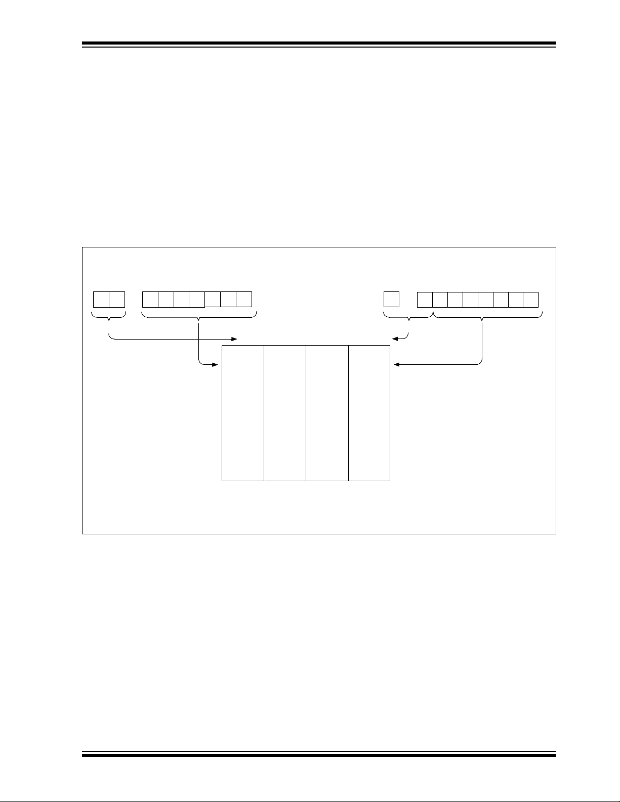
An effective 9-bit address is obtained by c on ca tena tin g
the 8-bit FSR register an d the IRP b it (STATUS<7>), as
shown in Figure 2-11.
Indirect AddressingDirect Addressing
7
location select
100h
IRP FSR register
bank select
180h
0
Data
Memory(1)
7Fh
FFh
17Fh
Bank 0 Bank 1 Bank 2 Bank 3
Note 1: For register file map detail see Figure 2-2.
1FFh
1999 Microchip Technology Inc. Advance Information DS30275A-page 25
Page 26

PIC16C77X
NOTES:
DS30275A-page 26 Advance Information 1999 Microchip Technology Inc.
Page 27
PIC16C77X
3.0 I/O PORTS
Some pins for these I/O ports are multiplexed with an
alternate function for the peripheral features on the
device. In general, when a peripheral is enabled, that
pin may not be used as a general purpose I/O pin.
Additional information on I/O ports may b e found in the
PICmicro™ Mid-Range Reference Manual,
(DS33023).
3.1 PORTA and the TRISA Register
PORTA is a 6-bit wide bi-directional port for the 40/44
pin devices and is 5-bits wide for the 28-pin devices.
PORTA<5> is not on the 28-pin devices. The corresponding data direction register is TRISA. Setting a
TRISA bit (=1) will m ake the correspondi ng PORTA pin
an input, i.e., put the corresponding output driver in a
hi-impedance mode. Clearing a TRISA bit (=0) will
make the corre sp ond ing PORTA pin an o utpu t, i .e., put
the contents of the output latch on the selected pin.
Reading the PORTA register reads the status of the
pins whereas writing to it will write to the port latch. All
write operations are read-modify-write operations.
Therefore a write to a port implies that th e port pins are
read, this val ue is modifie d, and then written to th e port
data latch.
Pin RA4 is multiplexed with the Timer0 module clock
input to become the RA4/T0CKI pin. The RA4/T0CKI
pin is a Schmitt Trigger input and an open drain output.
All other RA port pins have TTL input levels and full
CMOS output drivers.
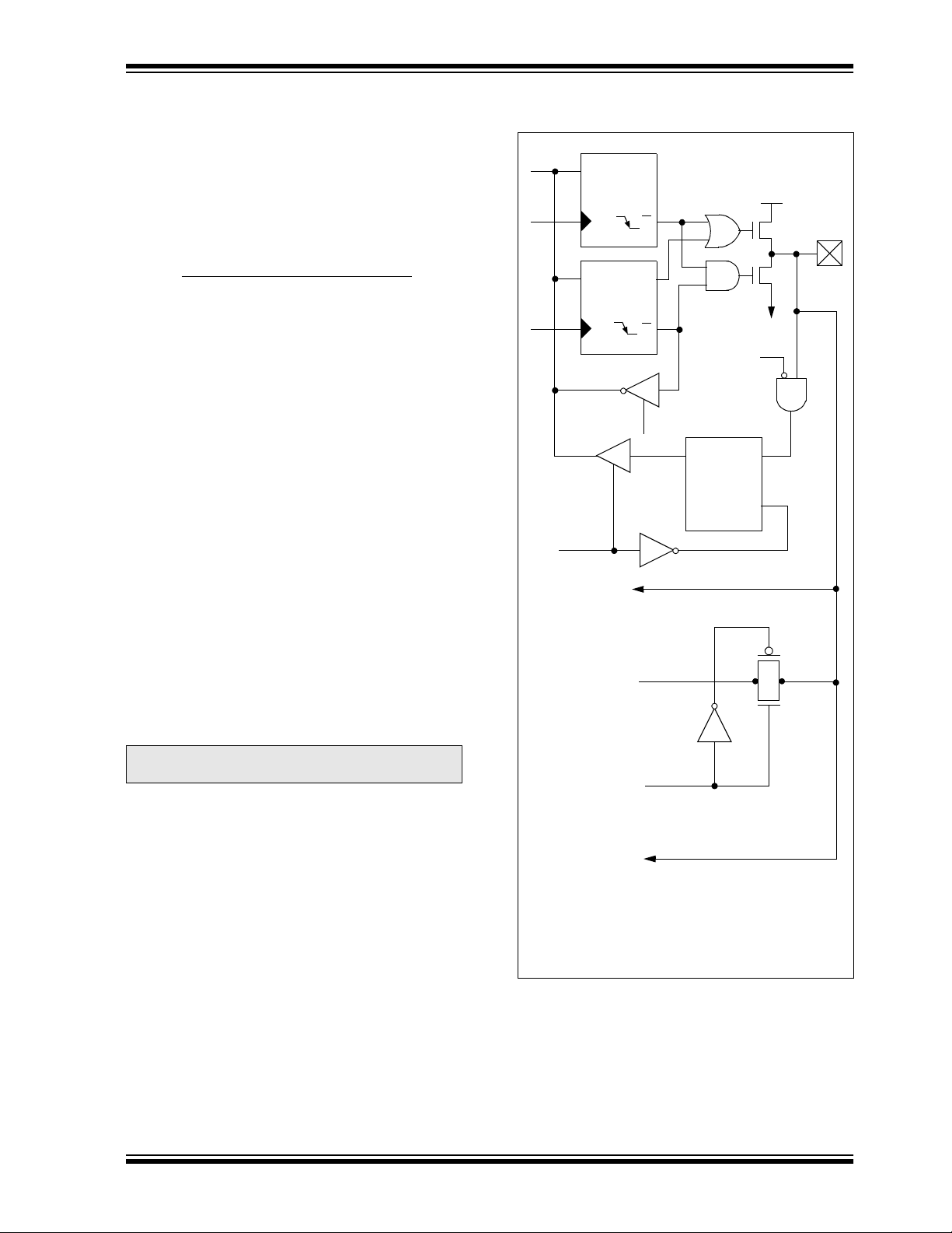
Other PORTA pins are multiplexed with analog inputs
and analog V
ences (VRL/VRH). The operation of each pin is
selected by clearing/setting the control bits in the
ADCON1 register (A/D Control Register1).
Note: On a Power-on Reset, these pins are con-
The TRISA register controls the direction of the RA
pins, even when they are being used as analog inputs.
The user must ensure the bits in the TRISA registe r are
maintained set when using them as analog inputs.
EXAMPLE 3-1: INITIALIZING PORTA
BCF STATUS, RP0 ;
CLRF PORTA ; Initialize PORTA by
; clearing output
; data latches
BSF STATUS, RP0 ; Select Bank 1
MOVLW 0xCF ; Value used to
; initialize data
; direction
MOVWF TRISA ; Set RA<3:0> as inputs
; RA<5:4> as outputs
; TRISA<7:6> are always
; read as ’0’.
REF inputs and precis ion on-boa rd refer-
figured as analog inputs and read as '0'.
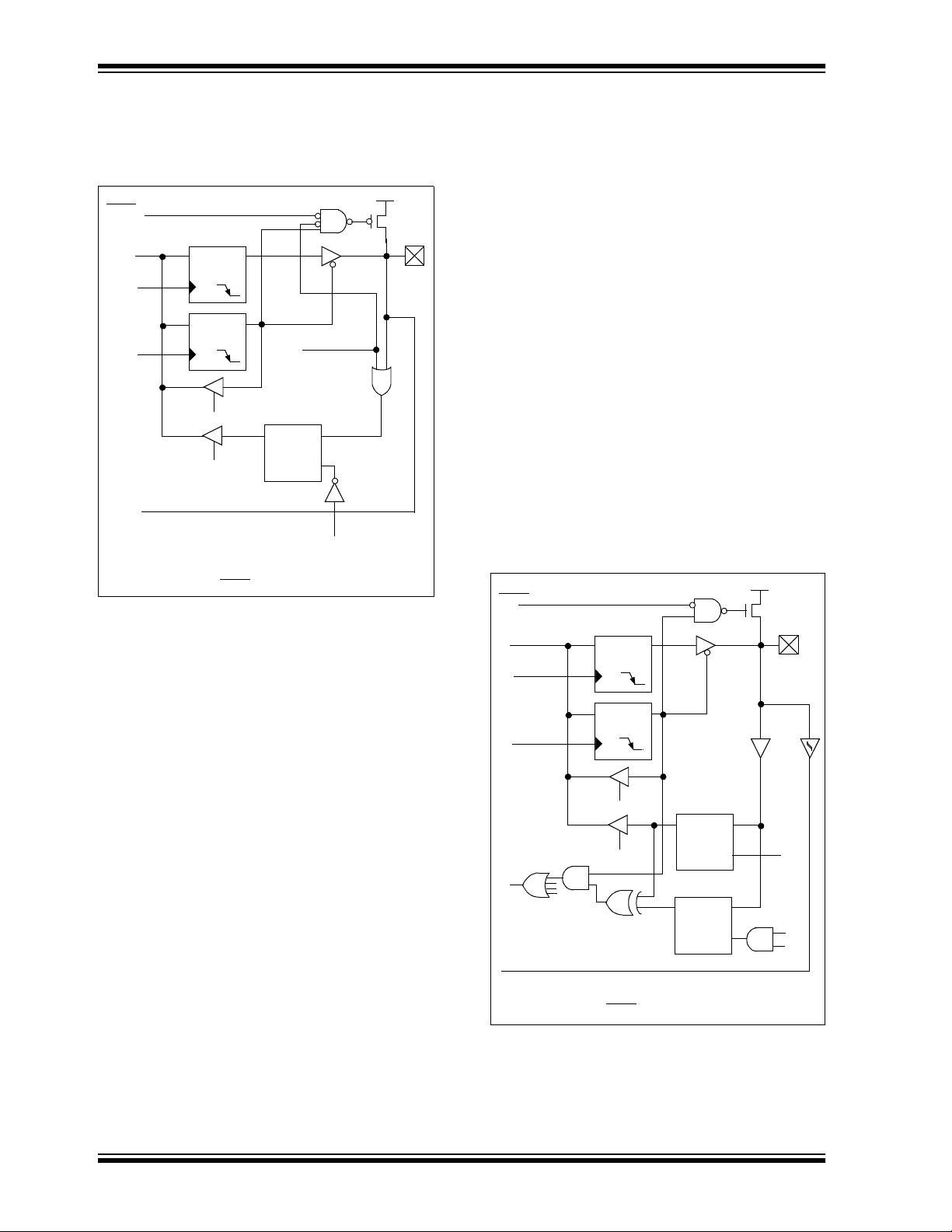
FIGURE 3-1: BLOCK DIAGRAM OF
RA3:RA2 PINS
Data
bus
WR
Port
WR
TRIS
RD PORT
To A/D Converter
VRH, VRL
VRHOEN, VRLOEN
Sense input for
VRO+, VRO- amplifier
Note 1: I/O pins have protection diodes to VDD and
CK
Data Latch
CK
TRIS Latch
SS.
V
QD
Q
QD
Q
RD TRIS
VDD
P
N
SS
V
Analog
input
mode
QD
EN
I/O pin
TTL
input
buffer
(1)
1999 Microchip Technology Inc. Advance Information DS30275A-page 27
Page 28
PIC16C77X
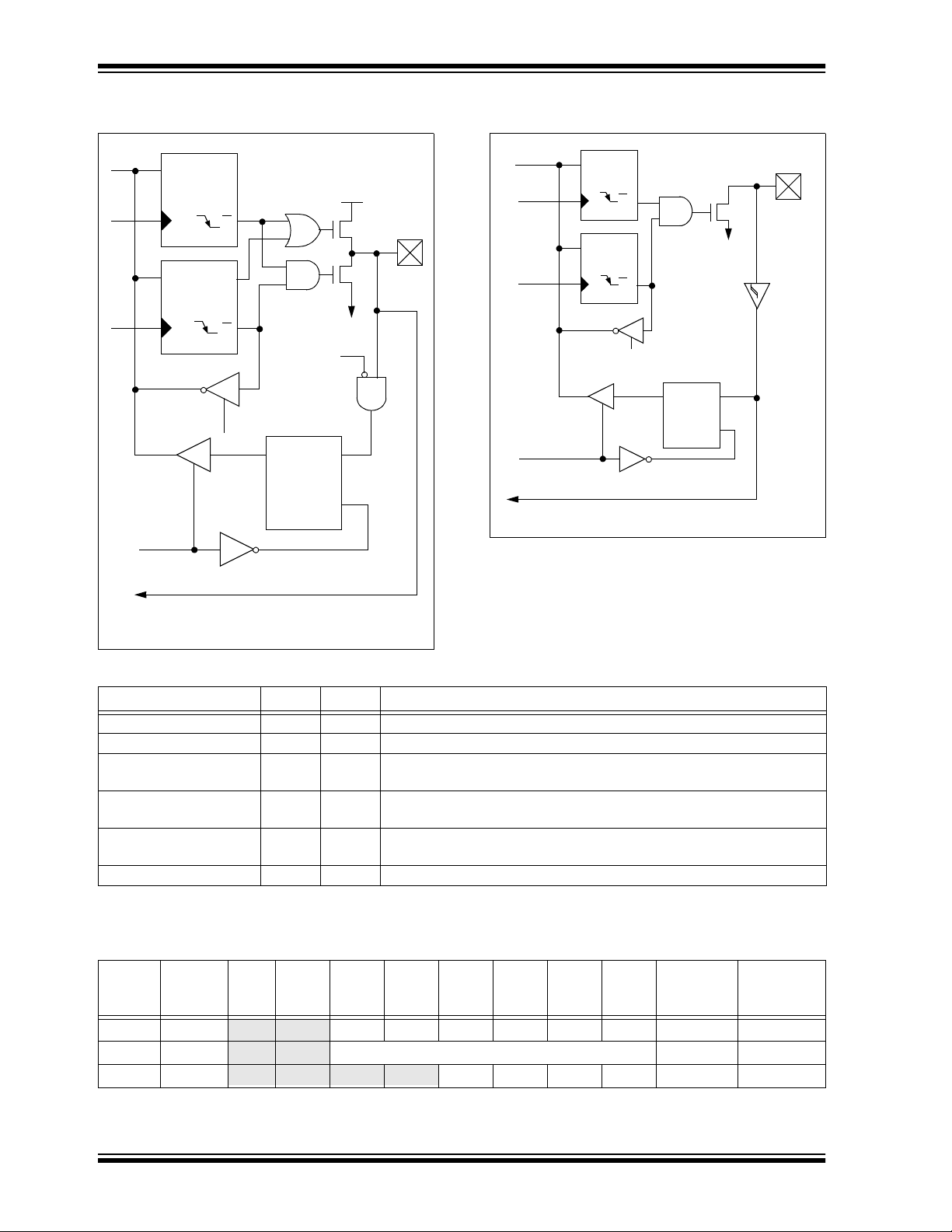
FIGURE 3-2: BLOCK DIAGRAM OF
RA1:RA0 AND RA5 PINS
Data
bus
WR
Port
WR
TRIS
RD PORT
CK
Data Latch
CK
TRIS Latch
QD
Q
QD
Q
RD TRIS
VDD
P
N
SS
V
Analog
input
mode
QD
EN
I/O pin
TTL
input
buffer
FIGURE 3-3: BLOCK DIAGRAM OF
RA4/T0CKI PIN
Data
bus
WR
PORT
(1)
WR
TRIS
RD PORT
TMR0 clock input
Note 1: I/O pin has protection diodes to V
QD
Q
CK
Data Latch
QD
Q
CK
TRIS Latch
RD TRIS
N
SS
V
Schmitt
Trigger
input
buffer
QD
EN
EN
I/O pin
SS only.
(1)
To A/D Converter
Note 1: I/O pins have protection diodes to VDD and
SS.
V
TABLE 3-1 PORTA FUNCTIONS
Name Bit# Buffer Function
RA0/AN0 bit0 TTL Input/output or analog input0
RA1/AN1 bit1 TTL Input/output or analog input1
RA2/AN2/VREF-/VRL bit2 TTL Input/output or analog input2 or VREF- input or internal reference
voltage low
RA3/AN3/V
REF+/VRH bit3 TTL Input/output or analog input or VREF+ input or output of internal
reference voltage high
RA4/T0CKI bit4 ST Input/output or external clock input for Timer0
Output is open drain type
RA5/AN4
(1)
bit5 TTL Input/output or analog input
Legend: TTL = TTL input, ST = Schmitt Trigger input
Note 1: RA5 is reserved on the 28-pin devices, maintain this bit clear.
TABLE 3-2 SUMMARY OF REGISTERS ASSOCIATED WITH PORTA
Address Name Bit 7 Bit 6 Bit 5 Bit 4 Bit 3 Bit 2 Bit 1 Bit 0
(1)
05h PORTA
85h TRISA
9Fh ADCON1
Legend: x = unknown, u = unchanged, - = unimplemented locations read as '0'. Shaded cells are not used by PORTA.
Note 1: PORTA<5>, TRISA<5> are reserved on the 28-pin devices, maintain these bits clear.
— — RA5 RA4 RA3 RA2 RA1 RA0 --0x 0000 --0u 0000
(1)
— — PORTA Data Direction Register --11 1111 --11 1111
ADFM VCFG2 VCFG1 VCFG0 PCFG3 PCFG2 PCFG1 PCFG0 0000 0000 0000 0000
Value on:
POR,
BOR
Value on all
other resets
DS30275A-page 28 Advance Information 1999 Microchip Technology Inc.
Page 29
PIC16C77X
3.2 PORTB and the TRISB Register
PORTB is an 8-bit wide bi-directional port. The corresponding data direction register is TRISB. Setting a
TRISB bit (=1) will make the correspon ding POR TB pin
an input, i.e., put the corresponding output driver in a
hi-impedance mode. Clearing a TRISB bit (=0) will
make the corr espond ing PO R TB pi n an outpu t, i.e . , put
the contents of the output latch on the selected pin.
EXAMPLE 3-1: INITIALIZING PORTB
BCF STATUS, RP0 ;
CLRF PORTB ; Initialize PORTB by
; clearing output
; data latches
BSF STATUS, RP0 ; Select Bank 1
MOVLW 0xCF ; Value used to
; initialize data
; direction
MOVWF TRISB ; Set RB<3:0> as inputs
; RB<5:4> as outputs
; RB<7:6> as inputs
Each of the PORTB pins has a weak internal pull-up. A
single control bit ca n turn on all the pull-u ps. This is performed by clearing bit RBPU (OPTION_REG<7>). The
weak pull-up i s autom atically tur ned off when the po rt
pin is configured as an output. The pull-ups are disabled on a Power-on Reset.
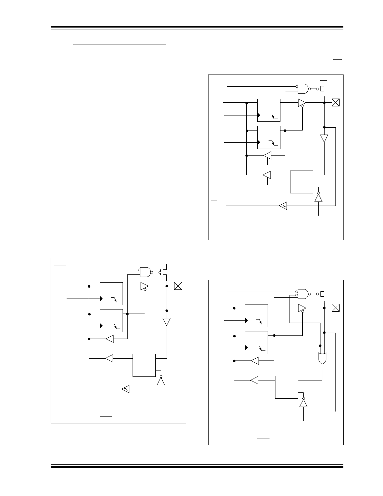
The RB0 pin is multiplexed with the external interrupt
(RB0/INT).
FIGURE 3-4: BLOCK DIAGRAM OF RB0 PIN
V
TTL
Input
Buffer
EN
DD
weak
P
pull-up
RD Port
I/O
pin
(1)
(2)
RBPU
Data bus
WR Port
WR TRIS
RB0/INT
Note 1: I/O pins have diode protection to V
2: To enable weak pull-ups, set the appropriate TRIS bit(s)
and clear the RBPU
Data Latch
QD
CK
TRIS Latch
QD
CK
RD TRIS
RD Port
Schmitt Trigger
Buffer
bit (OPTION_REG<7>).
QD
DD and VSS.
The RB1 pin is multiplexed with the SSP module slave
select (RB1/SS
).
FIGURE 3-5: BLOCK DIAGRAM OF RB1/SS
PIN
V
TTL
Input
Buffer
EN
DD
weak
P
pull-up
RD Port
I/O
pin
(1)
(2)
RBPU
Data bus
WR Port
WR TRIS
SS input
Note 1: I/O pins have diode protection to V
2: To enable weak pull-ups, set the appropriate TRIS bit(s)
and clear the RBPU
Data Latch
QD
CK
TRIS Latch
QD
CK
RD TRIS
RD Port
Schmitt Trigger
Buffer
bit (OPTION_REG<7>).
QD
DD and VSS.
The RB2 pin is multiplexed with analog channel 8
(RB2/AN8).
FIGURE 3-6: BLOCK DIAGRAM OF
RB2/AN8 PIN
V
TTL
Input
Buffer
RD Port
DD
P
weak
pull-up
I/O
pin
(1)
(2)
RBPU
Data bus
WR Port
WR TRIS
To A/D converter
Data Latch
CK
TRIS Latch
CK
RD TRIS
RD Port
QD
QD
Analog
input mode
QD
EN
Note 1: I/O pins have diode protection to V
2: To enable weak pull-ups, set the appropriate TRIS bit(s)
and clear the RBPU
bit (OPTION_REG<7>).
DD and VSS.
1999 Microchip Technology Inc. Advance Information DS30275A-page 29
Page 30
PIC16C77X
The RB3 pin is multiplexed with analog channel 9 and
the low voltage detect input (RB3/AN9/LVDIN)
FIGURE 3-7: BLOCK DIAGRAM OF
RB3/AN9/LVDIN PIN
V
TTL
Input
Buffer
RD Port
DD
P
weak
pull-up
I/O
pin
(1)
(2)
RBPU
Data bus
WR Port
WR TRIS
To A/D converter and LVD reference input
Note 1: I/O pins have diode protection to V
2: To enable weak pull-ups, set the appropriate TRIS bit(s)
Data Latch
QD
CK
TRIS Latch
QD
CK
RD TRIS
RD Port
and clear the RBPU
Analog
input mode
or LVD input
mode
QD
EN
DD and VSS.
bit (OPTION_REG<7>).
Four of PORTB’s pins, RB7:RB4, have an interrupt on
change feature. Only pins configured as inputs can
cause this interrupt to oc cur (i.e . any RB7:RB4 pin configured as an output is excluded from the interrupt on
change comparison). The input pins (of RB7:RB4) are
compared with the old va lue latc hed on the la st read of
PORTB. The “mismatch” outputs of RB7:RB4 are
OR’ed together to generate the RB Port Change Interrupt with flag bit RBIF (INTCON<0>).
This interrupt can wake the device from SLEEP. The
user, i n the interrupt service routine , can clea r the interrupt in the following manner:
a) Any read or write of PORTB. This will end the
mismatch condition.
b) Clear flag bit RBIF.
A mismatch condition will continue to set flag bit RBIF.
Reading PORTB will end the mismatch condition, and
allow flag bit RBIF to be cleared.
The interrupt on change feature is recommended for
wake-up on key depression operation and opera tions
where PORTB is only used for the interrupt on change
feature. Polling of PORTB is not recommended while
using the interrupt on change feature.
FIGURE 3-8: BLOCK DIAGRAM OF
RB7:RB4 PINS
V
TTL
Input
Buffer
DD
P
weak
pull-up
I/O
pin
Buffer
(1)
ST
RBPU
Data bus
WR Port
WR TRIS
(2)
Data Latch
QD
CK
TRIS Latch
QD
CK
RD TRIS
Set RBIF
From other
RB7:RB4 pins
RB7:RB6 in serial programming mode
Note 1: I/O pins have diode protection to VDD and VSS.
2: To enable weak pull-ups, set the appropriate TRIS bit(s)
and clear the RBPU
RD Port
bit (OPTION_REG<7>).
Latch
QD
EN
QD
EN
Q1
RD Port
Q3
DS30275A-page 30 Advance Information 1999 Microchip Technology Inc.
Page 31

PIC16C77X
TABLE 3-3 PORTB FUNCTIONS
Name Bit# Buffer Function
TTL/ST
(1)
Input/output pin or external interrupt input. Internal software
programmable weak pull-up .
(3)
Input/output pin or SSP slave select. Internal software programmable
weak pull-up.
weak pull-up.
software programmable weak pull-up.
programmable weak pull-up .
programmable weak pull-up .
(2)
Input/output pin (with interrupt on change). Internal software
programmable weak pull-up. Serial programming clock.
(2)
Input/output pin (with interrupt on change). Internal software
programmable weak pull-up. Serial programming data.
RB0/INT bit0 TTL/ST
RB1/SS
bit1
RB2/AN8 bit2 TTL Input/output pin or analog input8. Internal software programmable
RB3/AN9/LVDIN bit3 TTL Input/output pin or analog input9 or Low-voltage detect input. Internal
RB4 bit4 TTL Input/output pin (with interrupt on change). Internal software
RB5 bit5 TTL Input/output pin (with interrupt on change). Internal software
RB6 bit6 TTL/ST
RB7 bit7 TTL/ST
Legend: TTL = TTL input, ST = Schmitt Trigger input
Note 1: This buffer is a Schmitt Trigger input when configured as the external interrupt.
2: This buffer is a Schmitt Trigger input when used in serial programming mode.
3: This buffer is a Schmitt Trigger input when used as the SSP slave select.
TABLE 3-4 SUMMARY OF REGISTERS ASSOCIATED WITH PORTB
Value on:
Address Name Bit 7 Bit 6 Bit 5 Bit 4 Bit 3 Bit 2 Bit 1 Bit 0
06h, 106h PORTB RB7 RB6 RB 5 RB4 RB3 RB2 RB1 RB0 xxxx 11xx uuuu 11uu
86h, 186h TRISB P O RTB Data Direction Register 1111 1111 1111 1111
81h, 181h OPTION_RE G RBPU
9Fh ADCON1
Legend: x = unknown, u = unchanged. Shaded cells are not used by PORTB.
INTEDG T0CS T0SE PSA PS2 PS1 PS0 1111 1111 1111 1111
ADFM VCFG2 VCFG1 VCFG0 PCFG3 PCFG2 PCFG1 PCFG0 0000 0000 0000 0000
POR,
BOR
Value on all
other resets
1999 Microchip Technology Inc. Advance Information DS30275A-page 31
Page 32

PIC16C77X
3.3 PORTC and the TRISC Register
PORTC is an 8-bit wide bi-directional port. The corresponding data direction register is TRISC. Setting a
TRISC bit (=1) will mak e the corres ponding POR TC pin
an input, i.e., put the corresponding output driver in a
hi-impedance mode. Clearing a TRISC bit (=0) will
make the corresponding PORTC pin an output, i.e., put
the contents of the output latch on the selected pin.
PORTC is mul tiple x ed with se v eral peripheral fun ctions
(Table 3-5). PORTC pins have Schmitt Trigger input
buffers.
When enabling peripheral functions, care should be
taken in defining TRIS bits for each PORTC pin. Some
periphe rals override the TRIS bit to make a pin an output, while other peripherals override the TRIS bit to
make a pin an input. Since the TRIS bit override is in
effect while the peripheral is enabled, read-modify-write instructions (BSF, BCF, XOR WF) with TRISC
as destination sho uld be av oided. The user should re fer
to the corresponding peripheral section for the correct
TRIS bit settings.
EXAMPLE 3-1: INITIALIZING PORTC
BCF STATUS, RP0 ; Select Bank 0
CLRF PORTC ; Initialize PORTC by
; clearing output
; data latches
BSF STATUS, RP0 ; Select Bank 1
MOVLW 0xCF ; Value used to
; initialize data
; direction
MOVWF TRISC ; Set RC<3:0> as inputs
; RC<5:4> as outputs
; RC<7:6> as inputs
FIGURE 3-9: PORTC BLOCK DIAGRAM
(PERIPHERAL OUTPUT
OVERRIDE)
PORT/PERIPHERAL Select
Peripheral Data Out
Data bus
WR
PORT
WR
TRIS
Peripheral
(3)
OE
Peripheral input
Note 1: I/O pins have diode protection to VDD and VSS.
2: Port/Peripheral select signal selects between port
3: Peripheral OE (output enable) is only activated if
CK
Data Latch
CK
TRIS Latch
RD TRIS
RD
PORT
data and peripheral output.
peripheral select is active.
(2)
V
0
QD
1
Q
QD
Q
QD
EN
DD
P
I/O
pin
N
VSS
Schmitt
Trigger
(1)
DS30275A-page 32 Advance Information 1999 Microchip Technology Inc.
Page 33

PIC16C77X
TABLE 3-5 PORTC FUNCTIONS
Name Bit# Buffer Type Function
RC0/T1OSO/T1CKI
RC1/T1OSI/CCP2 bit1 ST Input/output port pin or Timer1 oscillator input or Capture2
RC2/CCP1 bit2 ST Input/output port pin or Capture1 input/Compare1 output/PWM1
RC3/SCK/SCL bit3 ST
RC4/SDI/SDA bit4 ST
RC5/SDO bit5 ST Input/output port pin or Synchronous Serial Port data output
RC6/TX/CK bit6 ST Input/output port pin or USART Asynchronous transmit or
RC7/RX/DT bit7 ST Input/output port pin or USART Asynchronous receive or
Legend: ST = Schmitt Trigger input
TABLE 3-6 SUMMARY OF REGISTERS ASSOCIATED WITH PORTC
bit0
ST Input/output port pin or Timer1 oscillator output/Timer1 clock input
input/Compare2 output/PWM2 output
output
RC3 can also be the synchronous serial clock for both SPI and I
modes.
2
RC4 can also be the SPI Data In (SPI mode) or data I/O (I
Synchronous cloc k
Synchronous data
C mode).
2
C
Address Name Bit 7 Bit 6 Bit 5 Bit 4 B it 3 Bit 2 Bit 1 Bit 0
07h PORTC RC7 RC6 RC5 RC4 RC3 RC2 RC1 RC0 xxxx xxxx uuuu uuuu
87h TRISC PORTC Data Direction Register 1111 1111 1111 1111
Legend: x = unknown, u = unchanged.
Value on:
POR,
BOR
Value on all
other resets
1999 Microchip Technology Inc. Advance Information DS30275A-page 33
Page 34

PIC16C77X
3.4 PORTD and TRISD Registers
This section is ap plica b le to the 4 0/44-pi n de v ices on ly.
PORTD is an 8-bit port with Schmitt Trigger input buff-
ers. Each pin is individually configurable as an input or
output.
PORTD can be configured as an 8-bit wide microprocessor por t (parallel slave por t) by setting control bit
PSPMODE (TRISE<4>). In this mode , the input buffe rs
are TTL.
TABLE 3-7 PORTD FUNCTIONS
FIGURE 3-10: PORTD BLOCK DIAGRAM (IN
I/O PORT MODE)
Data
bus
WR
PORT
Data Latch
WR
TRIS
TRIS Latch
RD PORT
Note 1: I/O pins have protection diodes to VDD and VSS.
CK
CK
RD TRIS
QD
QD
Schmitt
Trigger
input
buffer
QD
EN
EN
I/O pin
(1)
Name Bit# Buffer Type Function
RD0/PSP0 bit0 ST/TTL
RD1/PSP1 bit1 ST/TTL
RD2/PSP2 bit2 ST/TTL
RD3/PSP3 bit3 ST/TTL
RD4/PSP4 bit4 ST/TTL
RD5/PSP5 bit5 ST/TTL
RD6/PSP6 bit6 ST/TTL
RD7/PSP7 bit7 ST/TTL
(1)
(1)
(1)
(1)
(1)
(1)
(1)
(1)
Input/output port pin or parallel slave port bit0
Input/output port pin or parallel slave port bit1
Input/output port pin or parallel slave port bit2
Input/output port pin or parallel slave port bit3
Input/output port pin or parallel slave port bit4
Input/output port pin or parallel slave port bit5
Input/output port pin or parallel slave port bit6
Input/output port pin or parallel slave port bit7
Legend: ST = Schmitt Trigger input TTL = TTL input
Note 1: Input buffers are Schmitt Triggers when in I/O mode and TTL buffer when in Parallel Slave Port Mode.
TABLE 3-8 SUMMARY OF REGISTERS ASSOCIATED WITH PORTD
Address Name Bit 7 Bit 6 Bit 5 Bit 4 Bit 3 Bit 2 Bit 1 Bit 0
08h PORTD RD7 RD6 RD5 RD4 RD3 RD2 RD1 RD0 xxxx xxxx uuuu uuuu
88h TRISD PORTD Data Direction Register 1111 1111 1111 1111
89h TRISE
Legend: x = unknown, u = unchanged, - = unimplemented read as '0'. Shaded cells are not used by PORTD.
IBF OBF IBOV PSPMODE — PORTE Data Direction Bits 0000 -111 0000 -111
Value on:
POR,
BOR
Val ue on all
other resets
DS30275A-page 34 Advance Information 1999 Microchip Technology Inc.
Page 35

PIC16C77X
3.5 PORTE and TRISE Register
This section is applicab le to the 40/44-pin devi ces only.
PORTE has three pins RE0/RD
and RE2/CS
/AN7, which are individually configurable
/AN5, RE1/WR/AN6
as inputs or outputs. These pins have Schmitt Trigger
input buffers.
I/O PORTE becomes control inputs for the microprocessor port when bit PSPMODE (TRISE<4>) is set. In
this mode, the user must make sure that the
TRISE<2:0> bits are set (pins are configured as digital
inputs). Ensure ADCON1 is configu red for digital I/O . In
this mode the input buffers are TTL.
Figure 3-12 show s th e TRIS E r e gi ste r, which also con-
trols the parallel slave port operation.
PORTE pins are multiplexed with analog inputs. When
selected as an an alog input, the se pins will r ead as ’ 0’ s.
TRISE controls the direction of th e RE pins, e v en when
they are being used as analog inputs. The user must
make sure to keep the pins configured as inputs when
using them as analog inputs.
Note: On a Power-on Reset these pins are con-
figured as analog inputs.
FIGURE 3-12: TRISE REGISTER (ADDRESS 89h)
FIGURE 3-11: PORTE BLOCK DIAGRAM (IN
I/O PORT MODE)
Data
bus
WR
PORT
WR
TRIS
RD PORT
Note 1: I/O pins have protection diodes to VDD and VSS.
QD
CK
Data Latch
QD
CK
TRIS Latch
RD TRIS
Schmitt
Trigger
input
buffer
QD
EN
EN
I/O pin
(1)
R-0 R-0 R/W-0 R/W-0 U-0 R/W-1 R/W-1 R/W-1
IBF OBF IBOV PSPMODE
bit7 bit0
bit 7 : IBF: Input Buffer Full Status bit
1 = A word has been received and is waiting to be read by the CPU
0 = No word has been received
bit 6: OBF: Output Buffer Full Status bit
1 = The output buffer still holds a previously written word
0 = The output buffer has been read
bit 5: IBOV: Input Buffer Overflow Detect bit (in microprocessor mode)
1 = A write occurred when a previously input word has not been read (must be cleared in software)
0 = No overflow occurred
bit 4: PSPMODE: Parallel Slave Port Mode Select bit
1 = Parallel slave port mode
0 = General purpose I/O mode
bit 3: Unimp lemented: Read as '0'
— bit2 bit1 bit0 R = Readable bit
PORTE Data Direction Bits
bit 2: Bit2: Direction Control bit for pin RE2/CS/AN7
bit 1: Bit1: Direction Control bit for pin RE1/WR
bit 0: Bit0: Direction Control bit for pin RE0/RD
1 = Input
0 = Output
/AN6
1 = Input
0 = Output
/AN5
1 = Input
0 = Output
W = Writable bit
U = Unimplemented bit,
read as ‘0’
- n = Value at POR reset
1999 Microchip Technology Inc. Advance Information DS30275A-page 35
Page 36

PIC16C77X
TABLE 3-9 PORTE FUNCTIONS
Name Bit# Buffer Type Function
RE0/RD
RE1/WR
/AN5 bit0 ST/TTL
/AN6 bit1 ST/TTL
RE2/CS/AN7 bit2 ST/TTL
Legend: ST = Schmitt Trigger input TTL = TTL input
Note 1: Input buffers are Schmitt Triggers when in I/O mode and TTL buffers when in Parallel Slave Port Mode.
TABLE 3-10 SUMMARY OF REGISTERS ASSOCIATED WITH PORTE
(1)
Input/output port pin or read control input in p ar all el s lave port mode or
analog input:
RD
1 = Not a read operation
0 = Read operation. Reads PORTD register (if chip selected)
(1)
Input/output port pin or write con trol input in par alle l sla v e port mode or
analog input:
WR
1 = Not a write operation
0 = Write operation. Writes PORTD register (if chip selected)
(1)
Input/output port pin or chip select control input in parallel slave port
mode or analog input:
CS
1 = Device is not selected
0 = Device is selected
Addr Name Bit 7 Bit 6 Bit 5 Bit 4 Bit 3 Bit 2 Bit 1 Bit 0
09h PORTE
89h TRISE IBF OBF IBOV PSPMODE
9Fh ADCON1
Legend: x = unknown, u = unchanged, - = unimplemented read as '0'. Shaded cells are not used by PORTE.
— — — — —RE2RE1RE0---- -xxx ---- -uuu
— P ORTE Data Direction Bits 0000 -111 0000 -111
ADFM VCFG2 VCFG1 VCFG0 PCFG3 PCFG2 PCFG1 PCFG0 0000 0000 0000 0000
Value on:
POR,
BOR
Value on all
other resets
DS30275A-page 36 Advance Information 1999 Microchip Technology Inc.
Page 37

PIC16C77X
3.6 Parallel Slave Port
The Parallel Slave Port is implemented on the
40/44-pin devices only.
PORTD operates as an 8-bit wide Parallel Slave Port,
or microprocessor port when control bit PSPMODE
(TRISE<4>) i s set. I n slave mode it is as ynchrono usly
readable and writab le by the external world thro ugh RD
control input pin RE0/RD and WR control input pin
RE1/WR
It can directly interface to an 8-bit microprocessor data
bus. The e x ternal micro processo r can read or write the
PORTD latch as an 8-bit latch. Setting bit PSPMODE
enables port pin RE0/RD
to be the WR input and RE2/CS to be the CS (chip
select) input. For this functionality, the corresponding
data direction bits of the TRISE register (TRISE<2:0>)
must be conf igured as i nputs (set) . The config uration
bits, PCFG3:PCFG0 (ADCON1<3:0>) must be configured to make pins RE2:RE0 as digital I/O.
A write to the PSP occurs when both the CS
lines are first detec ted lo w . A read from t he PSP occu rs
when both the CS
.
to be the RD input, RE1/WR
and WR
and RD lines are first detected low.
FIGURE 3-13: PORTD AND PORTE BLOCK
DIAGRAM (PARALLEL SLAVE
PORT)
Data bus
WR
PORT
RD
PORT
One bit of PORTD
Set interrupt flag
PSPIF (PIR1<7>)
QD
CK
QD
EN
EN
TTL
Read
Chip Select
Write
TTL
TTL
TTL
RDx
pin
RD
CS
WR
Note: I/O pin has protection diodes to VDD and VSS.
FIGURE 3-14: PARALLEL SLAVE PORT WRITE WAVEFORMS
Q1 Q2 Q3 Q4CSQ1 Q2 Q3 Q4 Q1 Q2 Q3 Q4
WR
RD
PORTD<7:0>
IBF
OBF
PSPIF
1999 Microchip Technology Inc. Advance Information DS30275A-page 37
Page 38

PIC16C77X
FIGURE 3-15: PARALLEL SLAVE PORT READ WAVEFORMS
Q1 Q2 Q3 Q4CSQ1 Q2 Q3 Q4 Q1 Q2 Q3 Q4
WR
RD
PORTD<7:0>
IBF
OBF
PSPIF
TABLE 3-11 REGISTERS ASSOCIATED WITH PARALLEL SLAVE PORT
Value on:
Address Name Bit 7 Bit 6 Bit 5 Bit 4 Bit 3 Bit 2 Bit 1 Bit 0
08h PORTD Port data latch when written: Port pins when read xxxx xxxx uuuu uuuu
09h PORTE
89h TRISE IBF OBF IBOV PSPMODE
0Ch PIR1 PSPIF
8Ch PIE1 PSPIE
9Fh ADCON1
Legend: x = unknown, u = unchanged, - = unimplemented read as '0'. Shaded cells are not used by the Parallel Slave Port.
— — — — — RE2 RE1 RE0 ---- -xxx ---- -uuu
— PORTE Data Direction Bits 0000 -111 0000 -111
ADIF RCIF TXIF SSPIF CCP1IF TMR2IF TMR1IF 0000 0000 0000 0000
ADIE RCIE TXIE SSPIE CCP1IE TMR2IE TMR1IE 0000 0000 0000 0000
ADFM VCFG2 VCFG1 VCFG0 PCFG3 PCFG2 PCFG1 PCFG0 0000 0000 0000 0000
POR,
BOR
Value on all
other resets
DS30275A-page 38 Advance Information 1999 Microchip Technology Inc.
Page 39

PIC16C77X
4.0 TIMER0 MODULE
The Timer0 module timer/counter ha s the follo wing features:
• 8-bit timer/counter
• Readable and writable
• Internal or external clock select
• Edge select for external clock
• 8-bit software programmable prescaler
• Interrupt on overflow from FFh to 00h
Figure 4-1 is a simplifi ed block diagram of the Tim er0
module.
Additional information on timer modules is available in
the PICmicro™ Mid-Range Reference Manual,
(DS33023).
4.1 Timer0 Operation
Timer0 can operate as a timer or as a counter.
Timer mode is selected by clearing bit T0CS
(OPTION_REG<5>). In timer mode, the Timer0 module will increment every instruction cycle (without prescaler). If the TMR0 register is written, the increment is
inhibited for the following two instruction cycles. The
user can work around this by writing an adjusted value
to the TMR0 register.
Counter mode is selected by setting bit T0CS
(OPTION_REG<5>). In counter mode, Timer0 will
increment either on every rising or falling edge of pin
RA4/T0CKI. The incrementing edge is determined by
the Timer0 Source Edge Select bit T0SE
(OPTION_REG<4>). Clearing bit T0 SE sel ec ts the rising edge. Restrictions on the external clock input are
discussed in below.
When an e xternal clock i nput is use d for Timer0, it must
meet certain requirements. The requirements ensure
the external c lock can be synchron ized w ith the int ernal
phase clock (T
incrementing of Timer0 after synchronization.
OSC). Also, there is a delay in the actual
Additional information on external clock requirements
is available in the PICmicro™ Mid-Range Reference
Manual, (DS33023).
4.2 Prescaler
An 8-bit counter is available as a prescaler for the
Timer0 modul e, or as a postscaler fo r the Watchdog
Timer, respectively (Figure 4-2). For simplicity, this
counter is being referred to as “prescaler” throughout
this data sheet. Note that there is only one prescaler
avail able which is m utually exclusively shared between
the Timer0 module and the Watchdog Timer. Thus, a
prescaler assignment for the Timer0 module means
that there is no prescaler for the Watchdog Timer, and
vice-versa.
The prescaler is not readable or writable.
The PSA and PS2:PS0 bits (OPTION_REG<3:0>)
determine the prescaler a ssignment an d prescale ratio .
Clearing bit PSA will assign the prescale r to the Time r0
module. When the prescaler is assigned to the Timer0
module, prescale values of 1:2, 1:4, ..., 1:256 are
selectable.
Setting bit PSA will assign the prescaler to the Watchdog Timer (WDT). When the prescaler is assigned to
the WDT, prescale values of 1:1, 1:2, ..., 1:128 are
selectable.
When assigned to the Timer0 module, all instructions
writing to the TMR0 register (e.g . CLRF 1, MOVWF 1,
BSF 1,x....etc.) will clear the prescaler. When
assigned to WDT, a CLRWDT instruction will clear the
prescaler along with the WDT.
Note: Writing to TMR0 when the prescaler is
assigned to Timer0 will clear the prescaler
count, but will not change the prescaler
assignment.
FIGURE 4-1: TIMER0 BLOCK DIAGRAM
Data bus
FOSC/4
RA4/T0CKI
pin
T0SE
Note 1: T0CS, T0SE, PSA, PS2:PS0 (OPTION_REG<5:0>).
2: The prescaler is shared with Watchdog Timer (refer to Figure 4-2 for detailed block diagram).
1999 Microchip Technology Inc. Advance Information DS30275A-page 39
0
1
T0CS
Programmable
Prescaler
3
PS2, PS1, PS0
1
0
PSA
PSout
Sync with
Internal
clocks
(2 cycle delay)
8
TMR0
PSout
Set interrupt
flag bit T0IF
on overflow
Page 40

PIC16C77X
4.2.1 SWITCHING PRESCALER ASSIGNMENT
The prescaler assignment is fully under software con-
trol, i.e., it can be changed “on the fly” during program
ex ec utio n.
Note: To avoid an unintended device RESET, a
specific instructio n sequence (show n in the
PICmicro™ Mid-Range Reference Manual, DS33023) must be executed when
changing the prescaler assignment from
4.3 Timer0 Interr upt
The TMR0 interrupt is generated when the TMR0 register overflows from FFh to 00 h. This overflow sets bit
T0IF (INTC ON<2>). The inter rupt can be mas ked by
clearing bit T0IE (INTCON<5>). Bit T0IF must be
cleared in softwa re b y the T imer0 mo dule interrupt s ervice routine before re-enabling this interrupt. The
TMR0 interrupt cannot awaken the processor from
SLEEP since the timer is shut off during SLEEP.
Timer0 to the WDT. This sequence must
be followed even if the WDT is disabled.
FIGURE 4-2: BLOCK DIAGRAM OF THE TIMER0/WDT PRESCALER
CLKOUT (=Fos c/ 4)
RA4/T0CKI
pin
T0SE
0
1
T0CS
M
U
X
1
M
U
0
X
PSA
SYNC
2
Cycles
Data Bus
8
TMR0 reg
Set flag bit T0IF
on Overflow
0
M
U
1
Watchdog
Timer
WDT Enable bit
Note: T0CS, T0SE, PSA, PS2:PS0 are (OPTION_REG<5:0>).
X
PSA
8-bit Prescaler
8
8 - to - 1MUX
0
M U X
WDT
Time-out
PS2:PS0
1
PSA
TABLE 4-1 REGISTERS ASSOCIATED WITH TIMER0
Address Name Bit 7 Bit 6 Bit 5 Bit 4 Bit 3 Bit 2 Bit 1 Bit 0
01h,101h TMR0 Timer0 module’s register xxxx xxxx uuuu uuuu
0Bh,8Bh,
10Bh,18Bh
81h,181h OPTION_REG
85h TRISA
Legend: x = unknown, u = unchanged, - = unimplemented locations read as '0'. Shaded cells are not used by Timer0.
INTCON GIE
RBPU INTEDG T0CS T0SE PSA PS2 PS1 PS0 1111 1111 1111 1111
PEIE T0IE INTE RBIE T0IF INTF RBIF 0000 000x 0000 000u
— — PORTA Data Direction Register --11 1111 --11 1111
Value on:
POR,
BOR
Value on all
other resets
DS30275A-page 40 Advance Information 1999 Microchip Technology Inc.
Page 41

PIC16C77X
5.0 TIMER1 MODULE
The Timer1 module timer/counter ha s the follo wing features:
• 16-bit timer/counter
(Two 8-bit registers; TMR1H and TMR1L)
• Readable and writable (Both registers)
• Internal or external clock select
• Interrupt on overflow from FFFFh to 0000h
• Reset from CCP module trigger
Timer1 has a control register, shown in Figure 5-1.
Timer1 can be enabled/disabled by setting/clearing
control bit TMR1ON (T1CON<0>).
Figure 5-3 is a simplifi ed block diagram of the Tim er1
module.
Additional information on timer modules is available in
the PICmicro™ Mid-Range Reference Manual,
(DS33023).
5.1 Timer1 Operation
Timer1 can operate in one of these modes:
•As a timer
• As a synchronous counter
• As an asynchronous counter
The operating mode is determined by the clock select
bit, TMR1CS (T1CON<1>).
In timer mode, Timer1 increments every instruction
cycle. In coun ter mo de, it in crement s on every risi ng
edge of the external clock input.
When the Timer1 oscillator is enabled (T1OSCEN is
set), the RC1/T1OSI and RC0/T1OSO/T1CKI pins
become inputs. That is, the TRISC<1:0> value is
ignored.
Timer1 also has an in ternal “reset input ”. This reset can
be generated by the CCP module (Section 7.0).
FIGURE 5-1: T1CON: TIMER1 CONTROL REGISTER (ADDRESS 10h)
U-0 U-0 R/W-0 R/W-0 R/W-0 R/W-0 R/W-0 R/W-0
— — T1CKPS1 T1CKPS0 T1OSCEN T1SYNC TMR1CS TMR1ON
bit7 bit0
bit 7-6: Unimplemented: Read as ’0’
bit 5-4: T1CKPS1:T1CKPS0: Timer1 Input Clock Prescale Select bits
11 = 1:8 Prescale value
10 = 1:4 Prescale value
01 = 1:2 Prescale value
00 = 1:1 Prescale value
bit 3: T1OSCEN: Timer1 Oscillator Enable Control bit
1 = Oscillator is enabled
0 = Oscillator is shut off
Note: The oscillator inverter and feedback resistor are turned off to eliminate power drain
bit 2: T1SYNC
: Timer1 External Clock Input Synchronization Control bit
R = Readable bit
W = Writable bit
U = Unimplemented bit,
read as ‘0’
- n = Value at POR reset
TMR1CS = 1
1 = Do not synchronize external clock input
0 = Synchronize external clock input
TMR1CS = 0
This bit is ignored. Timer1 uses the internal clock when TMR1CS = 0.
bit 1: TMR1CS: Timer1 Clock Source Select bit
1 = External clock from pin RC0/T1OSO/T1CKI (on the rising edge)
0 = Internal clock (F
bit 0: TMR1ON: Timer1 On bit
1 = Enables Timer1
0 = Stops Timer1
1999 Microchip Technology Inc. Advance Information DS30275A-page 41
OSC/4)
Page 42

PIC16C77X
5.1.1 TIMER1 COUNTER OPERATION
In this mode, Timer1 is being in cremented via an e xter-
nal source. Increments occur on a rising edge. After
Timer1 is enabled in counter mode, the module must
first have a falling edge before the counter begins to
increment.
FIGURE 5-2: TIMER1 INCREMENTING EDGE
T1CKI
(Default high)
T1CKI
(Default low)
Note: Arrows indicate counter increments.
FIGURE 5-3: TIMER1 BLOCK DIAGRAM
Set flag bit
TMR1IF on
Overflow
RC0/T1OSO/T1CKI
RC1/T1OSI
Note 1: When the T1OSCEN bit is cleared, the inverter and feedback resistor are turned off. This eliminates power drain.
TMR1H
T1OSC
TMR1
TMR1L
T1OSCEN
Enable
Oscillator
(1)
FOSC/4
Internal
Clock
TMR1ON
on/off
1
0
T1CKPS1:T1 CKPS0
TMR1CS
0
1
T1SYNC
Prescaler
1, 2, 4, 8
2
Synchronized
clock input
Synchronize
det
SLEEP input
DS30275A-page 42 Advance Information 1999 Microchip Technology Inc.
Page 43

PIC16C77X
5.2 Timer1 Oscillator
A crystal oscillator circuit is b uilt in betw een pins T1OSI
(input) and T1OSO (amplifier output). It is enabled by
setting control bit T1OSCEN (T 1CON<3>). The oscill ator is a low power oscillator rated up to 200 kHz. It will
continue to run during SLEEP. It is primarily intended
for a 32 kHz crystal. Ta b le 5 -1 shows the capacitor
selection for the Timer1 oscillator.
The Timer1 oscillator is identical to the LP oscillator.
The user must provide a software time delay to ensure
proper oscillator start-up.
TABLE 5-1 CAPACITOR SELECTION FOR
THE TIMER1 OSCILLATOR
Osc Type Freq C1 C2
LP 32 kHz 33 pF 33 pF
100 kHz 15 pF 15 pF
200 kHz 15 pF 15 pF
These values are for design guidance only.
Crystals Tested:
32.768 kHz Epson C-001R32.768K-A ± 20 PPM
100 kHz Epson C-2 100.00 KC-P ± 20 PPM
200 kHz STD XTL 200.000 kHz ± 20 PPM
Note 1: Higher capacitance increases the stability
of oscillator but also increases the start-up
time.
2: Since each resonator/crystal has its own
characteristics, the user should consult the
resonator/crystal manufacturer for appropriate values of external components.
5.3 Timer1 Interr upt
The TMR1 Register pair (TMR1H:TMR1L) increments
from 0000h to FFFFh and rolls over to 0000h. The
TMR1 Interrupt, if enabled, is generated on overflow
which is latched in interrupt flag bit TMR1IF (PI R1<0>).
This interrupt can be enab led/d isab led by se tting/cle aring TMR1 interrupt enable bit TMR1IE (PIE1<0>).
5.4 Resetting Timer1 using a CCP T rigger
Output
If the CCP module is configured in compare mode to
generate a “special event trigger" (CCP1M3:CCP1M0
= 1011), this signal will reset Timer1 and start an A/D
conversion (if the A/D module is enabled).
Note: The special event triggers from the CCP1
module will not set interrupt flag bit
TMR1IF (PIR1<0>).
Timer1 must be c on f i gur ed fo r ei th er ti me r or sy nc hr onized counter mo de to tak e adv antag e of this f eature. If
Timer1 is running in asynchronous counter mode, this
reset operation may not work.
In the ev ent that a write to Timer1 coinc ides with a sp ecial event trigger from CCP1, the write will take precedence.
In this mode of operati on, the CC PR1H:CCPR 1L regis ters pair effectively becomes the period register for
Timer1.
TABLE 5-2 REGISTERS ASSOCIATED WITH TIMER1 AS A TIMER/COUNTER
Address Name Bit 7 Bit 6 Bit 5 Bit 4 Bit 3 Bit 2 Bit 1 Bit 0
0Bh,8Bh,
10Bh,18Bh
0Ch PIR1
8Ch PIE1
0Eh TMR1L Holding register for the Least Significant Byte of the 16-bit TMR1 register
0Fh TMR1H Holding register for the Most Significant Byte of the 16-bit TMR1 register
10h T1CON
Legend: x = unknown, u = unchanged, - = unimplemented read as '0'. Shaded cells are not used by the Timer1 module.
Note 1: These bits are reserved on the 28-pin devices, always maintain these bits clear.
INTCON GIE PEIE
(1)
PSPIF
PSPIE
ADIF RCIF TXIF SSPIF CCP1IF TMR2IF TMR1IF
(1)
ADIE RCIE TXIE SSPIE CCP1IE TMR2IE TMR1IE
— — T1CKPS1 T1CKPS0 T1OSCEN T1SYNC TMR1CS TMR1ON
T0IE INTE RBIE T0IF INTF RBIF
Value on:
POR,
BOR
0000 000x 0000 000u
0000 0000 0000 0000
0000 0000 0000 0000
xxxx xxxx uuuu uuuu
xxxx xxxx uuuu uuuu
--00 0000 --uu uuuu
Value on
all other
resets
1999 Microchip Technology Inc. Advance Information DS30275A-page 43
Page 44

PIC16C77X
NOTES:
DS30275A-page 44 Advance Information 1999 Microchip Technology Inc.
Page 45

PIC16C77X
6.0 TIMER2 MODULE
The Timer2 module timer has the following features:
• 8-bit timer (TMR2 register)
• 8-bit period register (PR2)
• Readable and writable (Both registers)
• Software programmable prescaler (1:1, 1:4, 1:16)
• Software programmable postscaler (1:1 to 1:16)
• Interrupt on TMR 2 match of PR2
• SSP module optional use of TMR2 output to generate clock shif t
Timer2 has a control register, shown in Figure 6-1.
Timer2 can be s hut off by clearing control b it T MR 2ON
(T2CON<2>) to minimize power consumption.
Figure 6-2 is a simplifi ed block diagram of the Tim er2
module.
Additional information on timer modules is available in
the PICmicro™ Mid-Range Reference Manual,
(DS33023).
6.1 Timer2 Operation
Timer2 can be used as the PWM time-base for PWM
mode of the CCP module.
The TMR2 register is readable and writable, and is
cleared on any device reset.
The input clock (F
1:4 or 1:16, selected by control bits
T2CKPS1:T2CKPS0 (T2CON<1:0>).
The match output of TMR2 goes through a 4-bit
postscaler (which gives a 1:1 to 1:16 scaling inclusive)
to generate a TMR2 interrupt (latched in flag bit
TMR2IF, (PIR1<1>)).
The prescaler and postscaler counters are cleared
when any of the following occurs:
• a write to the TMR2 register
• a write to the T2CON register
• any device reset (Power-on Reset, MCLR
Watchdog Timer reset, or Brown-out Reset)
OSC/4) has a prescale option of 1:1,
TMR2 is not cleared when T2CON is written.
FIGURE 6-1: T2CON: TIMER2 CONTROL REGISTER (ADDRESS 12h)
U-0 R/W-0 R/W-0 R/W-0 R/W-0 R/W-0 R/W-0 R/W-0
— TOUTPS3 TOUTPS2 TOUTPS1 TOUTPS0 TMR2ON T2CKPS1 T2CKPS0 R = Readable bit
bit7 bit0
bit 7: Unimplemented: Read as '0'
bit 6-3: TOUTPS3:TOUTPS0: Timer2 Output Postscale Select bits
0000 = 1:1 Postscale
0001 = 1:2 Postscale
•
•
•
1111 = 1:16 Postscale
bit 2: TMR2ON: Timer2 On bit
1 = Timer2 is on
0 = Timer2 is off
bit 1-0: T2CKPS1: T2CKPS0: Timer2 Clock Prescale Select bits
00 = Prescaler is 1
01 = Prescaler is 4
1x = Prescaler is 16
W = Writable bit
U = Unimplemented bit,
- n = Value at POR reset
reset,
read as ‘0’
1999 Microchip Technology Inc. Advance Information DS30275A-page 45
Page 46

PIC16C77X
6.2 Timer2 Interrup t
The Timer2 module has an 8-bit period register PR2.
Timer2 increments from 00h until it matches PR2 and
FIGURE 6-2: TIMER2 BLOCK DIAGRAM
Sets flag
bit TMR2IF
TMR2
output
(1)
then resets to 00h on the next increment cycle. PR2 is
a readable a nd writable regi ster . The PR2 register is ini-
Reset
TMR2 reg
tialized to FFh upon reset.
6.3 Output of TMR2
The output of T MR2 (before th e postsca ler) is fed to the
Postscaler
1:1 1:16
to
4
EQ
Comparator
PR2 reg
Synchronous Serial Port module which optionally use s
it to generate shift clock.
Note 1: TMR2 register output can be software selected
by the SSP Module as a baud clock.
TABLE 6-1 REGISTERS ASSOCIATED WITH TIMER2 AS A TIMER/COUNTER
Address Name Bit 7 Bit 6 Bit 5 Bit 4 Bit 3 Bit 2 Bit 1 Bit 0
0Bh,8Bh,
10Bh,18Bh
0Ch PIR1
8Ch PIE1
11h TMR2 Timer2 module’s register
12h T2CON
92h PR2 Timer2 Period Register
Legend: x = unknown, u = unchanged, - = unimplemented read as '0'. Shaded cells are not used by the Timer2 module.
Note 1: These bits are reserved on the 28-pin, always maintain these bits clear.
INTCON GIE PEIE
(1)
PSPIF
PSPIE
— TOUTPS3 TOUTPS2 TOUTPS1 TOUTPS0 TMR2ON T2CKPS1 T2CKPS0
ADIF RCIF TXIF SSPIF CCP1IF TMR2IF TMR1IF
(1)
ADIE RCIE TXIE SSPIE CCP1IE TMR2IE TMR1IE
T0IE INTE RBIE T0IF INTF RBIF
Prescaler
1:1, 1:4, 1:16
Value on:
POR,
BOR
0000 000x 0000 000u
0000 0000 0000 0000
0000 0000 0000 0000
0000 0000 0000 0000
-000 0000 -000 0000
1111 1111 1111 1111
2
Value on
all other
F
OSC/4
resets
DS30275A-page 46 Advance Information 1999 Microchip Technology Inc.
Page 47

PIC16C77X
7.0 CAPTURE/COMPARE/PWM
(CCP) MODULE(S)
Each CCP (Capture/Compare/PWM) module contains
a 16-bit register which can operate as a 16-bit capture
register, as a 16-bit compare register or as a PWM
master/slave Duty Cycle register. Table 7-1 shows t he
timer resources of the CCP module modes.
The operation of CCP1 is id entical to that of CCP2, wi th
the exception of the special trigger. Therefore, operation of a CCP module in the following sections is
described with respect to CCP1.
Table 7-2 shows the interaction of the CCP modules.
CCP1 Module
Capture/Compare/PWM Register1 (CCPR1) is comprised o f two 8-bit regis ters: CCPR1L (l ow byte) and
CCPR1H (high byte). The CCP1CON register controls
the operation of CCP1. All are readable and writable.
CCP2 Module
Capture/Compare/PWM Register2 (CCPR2) is comprised of two 8-bit registers: CCPR2L (low byte) and
CCPR2H (high byte). The CCP2CON register controls
the operation of CCP2. All are readable and writable.
Additional information on the CCP module is available
in the PICmicro™ Mid-Range Reference Manual,
(DS33023).
TABLE 7-1 CCP MODE - TIMER
RESOURCE
CCP Mode Timer Resource
Capture
Compare
PWM
Timer1
Timer1
Timer2
TABLE 7-2 INTERACTION OF TWO CCP MODULES
CCPx Mode CCPy Mode Interaction
Capture Capture Same TMR1 time-base.
Capture Compare The compare should be configured for the special event trigger, which clears TMR1.
Compare Compare The compare(s) should be configured for the special event trigger, which clears TMR1.
PWM PWM The PWMs will have the same frequency, and update rate (TMR2 interrupt).
PWM Capture None
PWM Compare None
FIGURE 7-1: CCP1CON REGISTER (ADDRESS 17h) / CCP2CON REGISTER (ADDRESS 1Dh)
U-0 U-0 R/W-0 R/W-0 R/W-0 R/W-0 R/W-0 R/W-0
— — CCPxX CCPxY CCPxM3 CCPxM2 CCPxM1 CCPxM0 R = Readable bit
bit7 bit0
bit 7-6: Unimplemented: Read as '0'
bit 5-4: CCPxX:CCPxY: PWM Least Significant bits
Capture Mode: Unused
Compare Mode: Unused
PWM Mode: These bits are the two LSbs of t he P W M duty c ycle. The eight MSbs a re fo un d in C CP RxL .
bit 3-0: CCPxM3:CCPxM0: CCPx Mode Select bits
0000 = Capture/Compare/PWM off (resets CCPx module)
0100 = Capture mode, every falling edge
0101 = Capture mode, every rising edge
0110 = Capture mode, every 4th rising edge
0111 = Capture mode, every 16th rising edge
1000 = Compare mode, set output on match (CCPxIF bit is set)
1001 = Compare mode, clear output on match (CCPxIF bit is set)
1010 = Compare mo de, g enerate softw are inte rrupt on match (CC PxIF bit is set , CCPx p in is u naffected )
1011 = Compare mode, trigger special e ven t (CCPxIF bit is set; CCP1 resets TMR1; CCP2 resets TMR1
and starts an A/D conversion (if A/D module is enabled))
11xx = PWM mode
W =Writable bit
U = Unimplemented bit, read
as ‘0’
- n =Value at POR reset
1999 Microchip Technology Inc. Advance Information DS30275A-page 47
Page 48

PIC16C77X
7.1 Cap tu re Mod e
In Capture mode, CCPR1H:CCPR1L captures the
16-bit value of th e TMR1 register wh en an ev ent oc curs
on pin RC2/CCP1. An event is defined as:
• every falling edge
• every rising edge
• every 4th r ising edge
• every 16th rising edge
An event is selected by control bits CCP1M3:CCP1M0
(CCP1CON<3:0>). When a capture is made, the interrupt request flag bit CCP1IF (PIR1<2>) is set. It must
be cleared in softw are. If another capt ure occurs b efore
the value in register CCPR1 is read, the old captured
value will be lost.
7.1.1 CCP PIN CONFIGURATION
In Capture mode, the R C2/C CP 1 p in s hou ld b e co nfi g-
ured as an input by setting the TRISC<2> bit.
Note: If the RC2/CCP1 is configured as an out-
put, a write to the port can cause a captu re
condition.
FIGURE 7-2: CAPTURE MODE OPERATION
BLOCK DIAGRAM
7.1.4 CCP PRESCALER
There are four prescaler settings, specified by bits
CCP1M3:CCP1M0. Whenever the CCP module is
turned off, or the CCP module is not in capture mode,
the prescaler counter is cleared. This means that any
reset will clear the prescaler counter.
Switching from one capture prescaler to another may
generate an interrupt. Also, the prescaler counter will
not be clea re d, th er e for e th e f i rs t c ap t ure m ay be f ro m
a non-zero prescaler. Example 7 -1 shows the recom-
mended method for switching between capture prescalers. This example also clears the prescaler counter
and will not generate the “false” interrupt.
EXAMPLE 7-1: CHANGING BETWEEN
CAPTURE PRESCALERS
CLRF CCP1CON ;Turn CCP module off
MOVLW NEW_CAPT_PS ;Load the W reg with
; the new prescaler
; mode value and CCP ON
MOVWF CCP1CON ;Load CCP1CON with this
; value
Set flag bit CCP1IF
(PIR1<2>)
CCPR1H CCPR1L
Capture
Enable
TMR1H TMR1L
RC2/CCP1
Pin
Prescaler
÷ 1, 4, 16
and
edge detect
CCP1CON<3:0>
Q’s
7.1.2 TIMER1 MODE SELECTION
Timer1 must be runni ng in tim er mode or s ynch roniz ed
counter mode for the CCP module to use the capture
feature. In asynchronous counter mode, the capture
operation may not work.
7.1.3 SOFTWARE INTERRUPT
When the Capture mode is changed, a false capture
interrupt may be generated. The user should keep bit
CCP1IE (PIE1<2>) clear to avoid false interrupts and
should clear the flag bit CCP1IF following any such
change in operating mode.
DS30275A-page 48 Advance Information 1999 Microchip Technology Inc.
Page 49

PIC16C77X
7.2 Compare Mode
In Compare mode, the 16-bit CCPR1 register value is
constantly compared against the TMR1 register pair
value. When a match occurs, the RC2/CCP1 pin is:
•driven High
• driven Low
• remains Unchanged
The action on the pin is based on the value of control
bits CCP1M3:CCP1M0 (CCP1CON<3:0>). At the
same time, interrupt flag bit CCP1IF is set.
FIGURE 7-3: COMPARE MODE
OPERATION BLOCK
DIAGRAM
Special event trigger will:
reset Timer1, but not set inte rr u pt flag bit T M R1IF (P IR1 <0>) ,
and set bit GO/DONE
which starts an A/D conversion
RC2/CCP1
Pin
TRISC<2>
Output Enable
(ADCON0<2>)
Special Event Trigger (CCP2 only)
Set flag bit CCP1IF
(PIR1<2>)
QS
Output
Logic
R
CCP1CON<3:0>
Mode Select
match
CCPR1H CCPR1L
Comparator
TMR1H TMR1L
7.2.1 CCP PIN CONFIGURATION
The user must configure the RC2/CCP1 pin as an out-
put by clearing the TRISC<2> bit.
Note: Clearing the CCP1CON register will force
the RC2/CCP1 comp are output latc h to the
default low level. This is not the data latch.
7.2.2 TIMER1 MODE SELECTION
Timer1 must be running in Timer mode or Synchro-
nized Counter mode if the CCP module is using the
compare feature. In Asynchronous Counter mode, the
compare operation may not work.
7.2.3 SOFTWARE INTERRUPT MODE
When generate software interrupt is chosen the CCP1
pin is not affected. Only a CCP interrupt is gene rated (if
enabled).
7.2.4 SPECIAL EVENT TRIGGER
In this mode, an internal hardware trigger is generated
which may be used to initiate an action.
The special event trigger output of CCP1 resets the
TMR1 register pair. This allows the CCPR1 register to
effectively b e a 16-bi t prog ram mab le period reg ister f or
Timer1.
The special trigger output of CCP2 resets the TMR1
register pair, and starts an A/D conversion (if the A/D
module is enabled).
Note: The special event trigger from the CCP2
module will not set interrupt flag bit
TMR1IF (PIR1<0>).
TABLE 7-3 REGISTERS ASSOCIATED WITH CAPTURE, COMPARE, AND TIMER1
Value on:
Address Name Bit 7 Bit 6 Bit 5 Bit 4 Bit 3 Bit 2 Bit 1 Bit 0
0Bh,8Bh,
10Bh,18Bh
0Ch PIR1
8Ch PIE1
87h TRISC PORTC Data Direction Register 1111 1111 1111 1111
0Eh TMR1L Holding register for the Least Significant Byte of the 16-bit TMR1 register xxxx xxxx uuuu uuuu
0Fh TMR1H Holding register for the Most Significant Byte of the 16-bit TMR1register xxxx xxxx uuuu uuuu
10h T1CON
15h CCPR1L Capture/Compare/PWM register1 (LSB) xxxx xxxx uuuu uuuu
16h CCPR1H Capture/Compare/PWM register1 (MSB) xxxx xxxx uuuu uuuu
17h CCP1CON
Legend: x = unknown, u = unchanged, - = unimplemented read as ’0’. Shaded cells are not used by Capture and Timer1.
Note 1: B its PSPI E and PSP IF are reserved on the 28-pin, always maintain these bits clear.
INTCON GIE PEIE T0IE INTE RBIE T0IF INTF RBIF 0000 000x 0000 000u
(1)
PSPIF
PSPIE
ADIF RCIF TXIF SSPIF CCP1IF TMR2IF TMR1IF 0000 0000 0000 0000
(1)
ADIE RCIE TXIE SSPIE CCP1IE TMR2IE TMR1IE 0000 0000 0000 0000
— — T1CKPS1 T1CKPS0 T1OSCEN T1SYNC TMR1CS TMR1ON --00 0000 --uu uuuu
— — CCP1X CCP1Y CCP1M3 CCP1M2 CCP1M1 CCP1M0 --00 0000 --00 0000
POR,
BOR
Value on
all other
resets
1999 Microchip Technology Inc. Advance Information DS30275A-page 49
Page 50

PIC16C77X
7.3 PWM Mode
In Pulse Width Modulation (PWM) mode, the CCP1 pin
produces up to a 10-bit resolution PWM output. Since
the CCP1 pin is multiple xed with the PORTC data latch,
the TRISC<2> bit must be cleared to make the CCP1
pin an output.
Note: Clearing the CCP1CON register will force
the CCP1 PWM output latch to the default
low level. This is not the PORTC I/O data
latch.
Figure 7-4 shows a s implified b lock diagr am of the CCP
module in PWM mode.
For a step b y step pro cedure on ho w t o set up the CCP
module for PWM operation, see Section 7.3.3.
FIGURE 7-4: SIMPLIFIED PWM BLOCK
DIAGRAM
Duty cycle registers
CCPR1L
CCPR1H (Slave)
Comparator
TMR2
Comparator
PR2
Note 1: 8-bit timer is concatenated with 2-bit internal Q clock
or 2 bits of the prescaler to cr eate 10-bit time-base.
(Note 1)
Clear Timer,
CCP1 pin and
latch D.C.
A PWM output (Figure 7-5) has a time base (period)
and a time that the output stays high (duty cycle). The
frequency of the PWM is the inverse of the period (1/
period).
CCP1CON<5:4>
R
S
Q
RC2/CCP1
TRISC<2>
FIGURE 7-5: PWM OUTPUT
Period
Duty Cycle
7.3.1 PWM PERIOD
The PWM period is specified by writing to the PR2 reg-
ister. The PWM period can be calculated using the following formula:
PWM period = [(PR2) + 1] • 4 • T
OSC •
(TMR2 prescale value)
PWM frequency is defined as 1 / [PWM period].
When TMR2 is equal t o PR2, the foll owing three ev ents
occur on the next increment cycle:
•TMR2 is cleared
• The CCP1 pin is set (exception: if PWM duty
cycle = 0%, the CCP1 pin will not be set)
• The PWM duty cycle is latc hed from CC PR1L into
CCPR1H
Note: The Timer2 postscale r (s ee Se ction6.0) is
not used in t he deter m inati on of th e PWM
frequency. The postscaler could be us ed to
have a servo update rate at a different frequency than the PWM output.
7.3.2 PWM DUTY CYCLE
The PWM duty cycle is specified by writing to the
CCPR1L register and to the CCP1CON<5:4> bits. Up
to 10-bit resolution is available: the CCPR1L contains
the eight MSbs and the CCP1CON<5:4> contains the
two LSbs. This 10-bit value is represented by
CCPR1L:CCP1CON<5:4>. The following equation is
used to calculate the PWM duty cycle in time:
PWM duty cycle = (CCPR1L:CCP1CON<5:4>) •
Tosc • (TMR2 prescale value)
CCPR1L and CCP1CO N<5:4> c an be writ ten to at an y
time, but the duty cycle value is not latched into
CCPR1H until after a match between PR2 and TMR2
occurs (i.e., the period is complete). In PWM mode,
CCPR1H is a read-only register.
The CCPR1H register and a 2-bit internal latch are
used to doub le b u ffe r the PWM du ty cy cl e . Thi s d ouble
buffering is essential for glitchless PWM operation.
When the CCPR1H and 2-bit latch match TMR2 concatenated with an internal 2-bit Q clock or 2 bits of the
TMR2 prescaler, the CCP1 pin is cleared.
Maximum PWM reso lution (bits) for a given PWM
frequency:
OSC
F
F
PWM
)
bits
log(
=
log(2)
TMR2 = PR2
TMR2 = Duty Cycle
Note: If the PWM duty cycle value is longer than
the PWM period the CCP1 pin will not be
cleared.
TMR2 = PR2
For an example PWM period and duty cycle calcu-
lation, see the PICmicro™ Mid-Range Reference
Manual, (DS33023).
DS30275A-page 50 Advance Information 1999 Microchip Technology Inc.
Page 51

PIC16C77X
7.3.3 SET-UP FOR PWM OPERATION
The following steps should be taken when configuring
the CCP module for PWM operation:
1. Set the PWM period by writing to t he PR2 regi ster.
2. Set the PWM duty cycle by writing to the
CCPR1L register and CCP1CON<5:4> bits.
3. Make the CCP 1 pin an output by clearing the
TRISC<2> bit.
4. Set the TMR2 prescale v alue and enab le Timer2
by writing to T2CON.
5. Configure the CCP1 module for PWM operation.
TABLE 7-4 EXAMPLE PWM FREQUENCIES AND RESOLUTIONS AT 20 MHz
PWM Frequency 1.22 kHz 4.88 kHz 19.53 kHz 78.12 kHz 156.3 kHz 208.3 kHz
Timer Prescaler (1, 4, 16) 16 4 1 1 1 1
PR2 Value 0xFF 0xFF 0xFF 0x3F 0x1F 0x17
Maximum Resolution (bits) 10 10 10 8 7 5.5
TABLE 7-5 REGISTERS ASSOCIATED WITH PWM AND TIMER2
Add ress Name Bit 7 Bit 6 Bit 5 Bit 4 Bit 3 Bit 2 Bit 1 Bit 0
0Bh,8Bh,
10Bh,18Bh
0Ch PIR1
8Ch PIE1
87h TRISC PORTC Data Direction Register 1111 1111 1111 1111
11h TMR2 Timer2 module’s register 0000 0000 0000 0000
92h PR2 Timer2 module’s period register 1111 1111 1111 1111
12h T2CON
15h CCPR1L Capture/Compare/PWM register1 ( LSB) xxxx xxxx uuuu uuuu
16h CCPR1H Capture/Compare/PWM regis ter1 ( MSB) xxxx xxxx uuuu uuuu
17h CCP1CON
Legend: x = unknown, u = unchanged, - = unimplemented read as '0'. Shaded cells are not used by PWM and Timer2.
Note 1: B its PSPI E and PSP IF are reserved on the 28-pin, always maintain these bits clear.
INTCON GIE PEIE
(1)
PSPIF
PSPIE
— TOUTPS3 TOUTPS2 TOUTPS1 TOUTPS0 TMR2ON T2CKPS1 T2CKPS0 -000 0000 -000 0000
— — CCP1X CCP1Y CCP1M3 CCP1M2 CCP1M1 CCP1M0 --00 0000 --00 0000
ADIF RCIF TXIF SSPIF CCP1IF TMR2IF TMR1IF 0000 0000 0000 0000
(1)
ADIE RCIE TXIE SSPIE CCP1IE TMR2IE TMR1IE 0000 0000 0000 0000
T0IE INTE RBIE T0IF INTF RBIF 0000 000x 0000 000u
Value on:
POR,
BOR
Value on
all other
resets
1999 Microchip Technology Inc. Advance Information DS30275A-page 51
Page 52

PIC16C77X
NOTES:
DS30275A-page 52 Advance Information 1999 Microchip Technology Inc.
Page 53

8.0 MASTER SYNCHRONOUS
SERIAL PORT (MSSP)
MODULE
The Master Synchronous Serial P ort (MSSP) module is
a serial interface useful for communicating with other
peripheral or microco ntrolle r de vices . Th ese periphe ra l
devices may be serial EEPROMs, shift registers, display drivers, A/D converters, etc. The MSSP module
can operate in one of two mode s:
• Serial Peripheral Interface (SPI)
• Inter-Integrated Circuit (I
2
C™)
PIC16C77X
1999 Microchip Technology Inc. Advance Information DS30275A-page 53
Page 54

PIC16C77X
FIGURE 8-1: SSPSTAT: SYNC SERIAL PORT STATUS REGISTER (ADDRESS: 94h)
R/W-0 R/W-0 R-0 R-0 R-0 R-0 R-0 R-0
SMP CKE D/A PSR/WUA BF R =Readable bit
bit7 bit0
bit 7: SMP: Sample bit
SPI Master Mode
1 = Input data sampled at end of data output time
0 = Input data sampled at middle of data output time
SPI Slave Mode
SMP must be cleared when SPI is used in slave mode
2
In I
C master or slave mode:
1= Slew rate control disabled for standard speed mode (100 kHz and 1 MHz)
0= Slew rate control enabled for high speed mode (400 kHz)
bit 6: CKE: SPI Clock Edge Select (Figure8-6, Figure 8-8, and Figure 8-9)
CKP = 0
1 = Data transmitted on rising edge of SCK
0 = Data transmitted on falling edge of SCK
CKP = 1
1 = Data transmitted on falling edge of SCK
0 = Data transmitted on rising edge of SCK
bit 5: D/A: Data/Address
1 = Indicates that the last byte received or transmitted was data
0 = Indicates that the last byte received or transmitted was address
bit 4: P: Stop bit
bit 3: S: Start bit
bit 2: R/W: Read/Write bit information (I
bit 1: UA: Update Address (10-bit I
bit 0: BF: Buffer Full Status bit
2
C mode only. This bit is cleared when the MSSP module is disabled, SSPEN is cleared)
(I
1 = Indicates that a stop bit has been detected last (this bit is '0' on RESET)
0 = Stop bit was not detected last
2
C mode only. This bit is cleared when the MSSP module is disabled, SSPEN is cleared)
(I
1 = Indicates that a start bit has been detected last (this bit is '0' on RESET)
0 = Start bit was not detected last
This bit holds the R/W bit information following the last address match. This bit is only valid from the
address match to the next start bit, stop bit, or not ACK bit.
2
C slave mode:
In I
1 = Read
0 = Write
In I2C master mode:
1 = Transmit is in progress
0 = Transmit is not in progress.
Or’ing this bit with SEN, RSEN, PEN, RCEN, or AKEN will indicate if the MSSP is in IDLE mode
1 = Indicates that the user needs to update the address in the SSPADD register
0 = Address does not need to be updated
Receive (SPI and I
1 = Receive complete, SSPBUF is full
0 = Receive not complete, SSPBUF is empty
Transmit (I2C mode only)
1 = Data Transmit in progress (does not include the ACK and stop bits), SSPBUF is full
0 = Data Transmit complete (does not include the ACK
bit (I2C mode only)
2
C mode only)
2
C mode only)
2
C modes)
and stop bits), SSPBUF is empty
W =Writable bit
U =Unimplemented bit, read
as ‘0’
- n =Value at POR reset
DS30275A-page 54 Advance Information 1999 Microchip Technology Inc.
Page 55

PIC16C77X
FIGURE 8-2: SSPCON: SYNC SERIAL PORT CONTROL REGISTER (ADDRESS 14h)
R/W-0 R/W-0 R/W-0 R/W-0 R/W-0 R/W-0 R/W-0 R/W-0
WCOL SSPOV SSPEN CKP SSPM3 SSPM2 SSPM1 SSPM0 R = Readable bit
bit7 bit0
bit 7: WCOL: Write Collision Detect bit
Master Mode:
1 = A write to the SSPBUF register was attempted while the I
transmission to be started
0 = No collision
Slave Mode:
1 = The SSPBUF register is written while it is still transmitting the previous word
(must be cleared in software)
0 = No collision
bit 6: SSPOV: Receive Overflow Indicator bit
In SPI mode
1 = A new byte i s received while t he SSPBUF register is still holding the pre vious data. In case of ov erflow ,
the data in SSPSR is lost. Overflow can only occur in sla ve mode . In sla v e mode , the us er must rea d the
SSPBUF, even if only transmitting data, to avoid setting overflow. In master mode, the overflow bit is not
set since each new reception (and transmission) is initiated by writing to the SSPBUF register. (Must be
cleared in software).
0 = No overflow
2
C mode
In I
1 = A byte is received while the SSPBUF register is still holding the pre vious byte . SSPOV i s a "don’t care"
in transmit mode. (Must be cleared in software).
0 = No overflow
bit 5: SSPEN: Synchronous Serial Port Enable bit
In both modes, when enabled, these pins must be properly configured as input or output.
In SPI mode
1 = Enables serial port and configures SCK, SDO, SDI, and SS as the source of the serial port pins
0 = Disables serial port and configures these pins as I/O port pins
In I2C mode
1 = Enables the serial port and configures the SDA and SCL pins as the source of the serial port pins
0 = Disables serial port and configures these pins as I/O port pins
bit 4: CKP: Clock Polarity Select bit
In SPI mode
1 = Idle state for clock is a high level
0 = Idle state for clock is a low level
In I2C slave mode
SCK release control
1 = Enable clock
0 = Holds clock low (clock stretch) (Used to ensure data setup time)
2
C master mode
In I
Unused in this mode
bit 3-0: SSPM3:SSPM0: Synchronous Serial Port Mode Select bits
0000 = SPI master mode, clock = F
0001 = SPI master mode, clock = F
0010 = SPI master mode, clock = F
OSC/4
OSC/16
OSC/64
0011 = SPI master mode, clock = TMR2 output/2
0100 = SPI slave mode, clock = SCK pin. SS
0101 = SPI slave mode, clock = SCK pin. SS
0110 = I
0111 = I
1000 = I
2
C slave mode, 7-bit address
2
C slave mode, 10-bit address
2
C master mode, clock = FOSC / (4 * (SSPADD+1) )
pin control enabled.
pin control disabled. SS can be used as I/O pin
1xx1 = Reserved
1x1x = Reserved
2
C conditions were not valid for a
W = Writable bit
- n =Value at POR reset
1999 Microchip Technology Inc. Advance Information DS30275A-page 55
Page 56

PIC16C77X
FIGURE 8-3: SSPCON2: SYNC SERIAL PORT CONTROL REGISTER2 (ADDRESS 91h)
R/W-0 R/W-0 R/W-0 R/W-0 R/W-0 R/W-0 R/W-0 R/W-0
GCEN AKSTAT AKDT AKEN RCEN PEN RSEN SEN R =Readable bit
bit7 bit0
2
bit 7: GCEN: General Call Enable bit (In I
C slave mode only)
1 = Enable interrupt when a general call address (0000h) is received in the SSPSR.
0 = General call address disabled.
2
bit 6: AKSTAT: Acknowledge Status bit (In I
C master mode only)
In master transmit mode:
1 = Acknowledge was not received from slave
0 = Acknowledge was r eceived from slave
2
bit 5: AKDT: Acknowledge Data bit (In I
C master mode only)
In master receive mode:
Value that will be transmitted when the user initiates an Acknowledge sequence at the end of a receive.
1 = Not Acknowledge
0 = Acknowledge
2
bit 4: AKEN: Acknowledge Sequence Enable bit (In I
C master mode only).
In master receive mode:
1 = Initiate Acknowledge sequence on SDA and SCL pins, and transmit AKDT data bit. Automatically
cleared by hardware.
0 = Acknowledge sequence idle
2
bit 3: RCEN: Receive Enable bit (In I
1 = Enables Receive mode for I
C master mode only).
2
C
0 = Receive idle
bit 2: PEN: Stop Condition Enable bit (In I2C master mode only).
SCK release control
1 = Initiate Stop condition on SDA and SCL pins. Automatically cleared by hardware.
0 = Stop condition idle
2
bit 1: RSEN: Repeated Start Condition Enabled bit (In I
C master mode only)
1 = Initiate Repeated Start condition on SDA and SCL pins. Automatically cleared by hardware.
0 = Repeated Start condition idle.
2
bit 0: SEN: Start Condition Enabled bit (In I
C master mode only)
1 = Initiate Start condition on SDA and SCL pins. Automatically cleared by hardware.
0 = Start condition idle.
2
Note: For bits AKEN, RCEN, PEN, RSEN, SEN: If the I
C module is not in the idle mode, this bit may not be
set (no spooling), and the SSPBUF may not be written (or writes to the SSPBUF are disabled).
W =Writable bit
U =Unimplemented bit,
Read as ‘0’
- n =Value at POR reset
DS30275A-page 56 Advance Information 1999 Microchip Technology Inc.
Page 57

PIC16C77X
8.1 SPI Mode
The SPI mode allows 8-bits of data to be synchronously transmitted and received simultaneously. All
four modes of SPI are supported. To accomplish communication, typically three pins are used:
• Serial Data Out (SDO)
• Serial Data In (SDI)
• Serial Clock (SCK)
Additionally, a fourth pin may be used when in a slave
mode of operation:
•Slave Select (SS
8.1.1 OPERATION
When initializing the SPI, several options need to be
specified. This is don e by pr ogramming the appropriate
control bits (SSPCON<5:0> and SSPSTAT<7:6>).
These control bits allow the following to be specified:
• Master Mode (SCK is the clock output)
• Slave Mode (SCK is the clock input)
• Clock Polarity (Idle state of SCK)
• Data input sample phase
(middle or end of data output time)
• Clock edge
(output data on rising/falling edge of SCK)
• Clock Rate (Master mode only)
• Slave Select Mode (Slave mode only)
Figure 8-4 shows the b lo c k diagr am of the MSSP mo d-
ule when in SPI mode.
)
FIGURE 8-4: MSSP BLOCK DIAGRAM
(SPI MODE)
Internal
data bus
Read Write
SSPBUF reg
SSPSR reg
2
shift
clock
TMR2 output
Prescaler
4, 16, 64
2
SDI
SDO
SS
SCK
bit0
Control
SS
Enable
Edge
Select
Clock Select
SSPM3:SSPM0
SMP:CKE
Edge
Select
4
2
Data to TX/RX in SSPSR
Data direction bit
T
OSC
The MSSP consists of a transmit/rece ive Shift Reg ister
(SSPSR) and a buffer re gister (SSPBUF). The SSPSR
shifts the data in and out of the device, MSb first. The
SSPBUF holds the data that w as written to the SSPSR,
until the received data is ready. Once the 8-bits of data
have been rec eiv ed, that b yte is mov ed to the SSPBUF
register. Then the buffer full detect bit BF
(SSPSTAT<0>) and the interrupt flag bit SSPIF
(PIR1<3>) are set. This double buffering of the
received data (SSPBUF) allows the next byte to start
reception before reading the data that was just
received. Any write to the SSPBUF register during
transmissio n/r ece ptio n of da ta wil l be ig nor ed, and the
write collision detect bit WCOL (SSPCON<7>) will be
set. User software must clear the WCOL bit so that it
can be determined if the following write(s) to the SSPBUF register completed successfully.
When the application software is expecting to receive
valid data, the SSPBUF s hould be read b efore th e ne x t
byte of data to transfer is written to the SSPBUF. Buffer
full bit, BF (SSPSTAT<0>), indicates when the SSPBUF has been load ed with the receiv ed dat a (tra nsmission is complete). When the SSPBUF is read, bit BF is
cleared. This data may be irrelevant if the SPI is only a
transmitter. Generally the MSSP Interrupt is used to
1999 Microchip Technology Inc. Advance Information DS30275A-page 57
Page 58

PIC16C77X
determine when the transmission/reception has completed. The SSPBUF mus t be read and/or written. If the
interrupt method is not go ing to be used, then software
polling can be done to ensure that a write collision does
not occur. Example 8-1 shows the loading of the
SSPBUF (SSPSR) for data transmission.
EXAMPLE 8-1: LOADING THE SSPBUF
(SSPSR) REGISTER
BSF STATUS, RP0 ;Specify Bank 1
LOOP BTFSS SSPSTAT, BF ;Has data been
;received
;(transmit
;complete)?
GOTO LOOP ;No
BCF STATUS, RP0 ;Specify Bank 0
MOVF SSPBUF, W ;W reg = contents
;of SSPBUF
MOVWF RXDATA ;Save in user RAM
MOVF TXDATA, W ;W reg = contents
; of TXDATA
MOVWF SSPBUF ;New data to xmit
The SSPSR is not direc tly readabl e or writable, and can
only be accessed by addressing the SSPBUF register.
Additionally, the MSSP status register (SSPSTAT) indicates the various status conditions.
8.1.2 ENABLING SPI I/O
To enable the serial port, MSSP Enable bit, SSPEN
(SSPCON<5>) must be set. To reset or reconfigure SPI
mode, clear bit SSPEN, re-initialize the SSPCON registers, and then set bit SSPEN. This configures the
SDI, SDO, SCK, and SS
pins as serial port pins. F or the
pins to behave as the serial port function, some must
have their data direction bits (in the TRIS register)
appropriately programmed. That is:
• SDI is automatically co ntrolled by the SPI modu le
• SDO must have TRISC<5> cleared
• SCK (Master mode) must have TRISC<3>
cleared
• SCK (Slave mode) must have TRISC<3> set
•SS
must have TRISA<5> set
Any serial port function that is n ot desired m ay be ov erridden by programming the corresponding data direction (TRIS) register to the opposite value.
8.1.3 TYPICAL CONNECTION
Figure 8-5 shows a typical connection between two
microcontrollers. The master controller (Processor 1)
initiates the data transfer by sending the SCK signal.
Data is shifted out of both shift registers on their programmed cloc k edge, and latched on the opp osite edge
of the clock. Bo th processo rs should b e progr ammed to
same Clock Polarity (CKP), then both controllers would
send and receive data at the same time. Whether the
data is meaningful (or dummy data) depends on the
application software. This leads to three scenarios for
data transmissio n:
• Master sends data — Slave sends dummy data
• Master sends data — Slave sends data
• Master sends dummy data — Slave sends data
FIGURE 8-5: SPI MASTER/SLAVE CONNECTION
SPI Master SSPM3:SSPM0 = 00xxb
SDO
Serial Input Buffer
(SSPBUF)
Shift Register
(SSPSR)
MSb
PROCESSOR 1
LSb
SDI
SCK
Serial Clock
SPI Slave SSPM3:SSPM0 = 010xb
SDI
Serial Input Buffer
(SSPBUF)
SDO
SCK
Shift Register
(SSPSR)
MSb
PROCESSOR 2
LSb
DS30275A-page 58 Advance Information 1999 Microchip Technology Inc.
Page 59

PIC16C77X
8.1.4 MASTER MODE
Figure 8-6, Figure 8-8, and Figure 8-9 where the MSb
is transmitted first. In master mode, the SPI clock rate
The master can initiate the data transfer at any time
because it controls the SCK. The master determines
when the slave (Processor 2, Figure 8-5) is to broadcast data by the software protocol.
In master mode the data is transmitted/received as
soon as the SSPBUF register is written to. If the SPI
module is only going to receive, the SDO output could
be disabled (programmed as an input). The SSPSR
register will co ntinue to s hift in the si gnal present o n the
SDI pin at the programmed clock rate. As each byte is
received, it wil l be lo ad e d i nt o t he S SPB UF r e gis te r as
if a normal received byte (interrupts and status bits
appropriately set). This could be useful in receiver
applications as a “line activity monitor”.
The clock polari ty is selected b y appropriately pr ogram-
(bit rate) is user programmable to be one of the following:
OSC/4 (or TCY)
•F
•F
OSC/16 (or 4 • TCY)
•FOSC/64 (or 16 • TCY)
• Timer2 output/2
This allows a maxim um bit cloc k frequen cy (at 20 MHz)
of 8.25 MHz.
Figure 8-6 shows the waveforms for Master mode.
When CKE = 1, the SDO data is valid before there is a
clock edge on SCK. The change of the input sample is
shown based on the state of the SMP bit. The time
when the SSPBUF is loaded with the received data is
shown.
ming bit CKP (SSPCON<4>). This then would give
waveforms for SPI communication as shown in
FIGURE 8-6: SPI MODE WAVEFORM (MASTER MODE)
Write to
SSPBUF
SCK
(CKP = 0
CKE = 0)
SCK
(CKP = 1
CKE = 0)
SCK
(CKP = 0
CKE = 1)
SCK
(CKP = 1
CKE = 1)
SDO bit7
(CKE = 0)
SDO bit7
(CKE = 1)
SDI
(SMP = 0)
Input
Sample
(SMP = 0)
SDI
(SMP = 1)
Input
Sample
(SMP = 1)
SSPIF
SSPSR to
SSPBUF
bit7
bit7
bit6
bit6
bit5 bit4
bit5 bit4
bit3
bit3
bit2
bit2
bit1 bit0
bit1 bit0
bit0
bit0
4 clock
modes
Next Q4 cycle
after Q2↓
1999 Microchip Technology Inc. Advance Information DS30275A-page 59
Page 60

PIC16C77X
8.1.5 SLAVE MODE
In slave mode, the data is transmitted and received as
the external clock pulses appear on SCK. When the
SDO pin is no longer driven, even if in the middle of
a transmitted byte, and becomes a floating output.
External pull-up/ pull-down resistors may be desirable,
depending on the application.
last bit is latched the interrupt flag bit SSPIF (PIR1<3>)
is set.
Note: When the SPI module is in Slave Mode
While in slave mode the external clock is supplied by
the external cloc k sou rce o n the SCK p in. Th is external
clock must meet th e minimum high and low times as
specified in the electrical specifications.
Note: If the SPI is used in Slave Mode with
While in sleep mode, the slave can transmit/receive
data. When a byte is received the device will wake-up
from sleep.
When the SPI module resets, the bit counter is forced
to 0. This can be done by either forcing the SS
8.1.6 SLAVE SELECT SYNCHRONIZATION
The SS
SPI must be in slave mode with SS
pin allows a synchronous slave mode. The
pin control
enabled (SSPCON<3:0> = 0100). The pin must not
be driven low for the SS pin to function as an input.
TRISA<5> must be set. When the SS
pin is low,
transmission and reception are enabled and the
high leve l or clearing the SSPEN bit.
To emulate two-wire communication, the SDO pin can
be connected to the SDI pin. When the SPI needs to
operate as a receiv er the SDO pin ca n be configured as
an input. This disables transmissions from the SDO.
The SDI can always be left as an input (SDI function)
since it cannot create a bus conflict.
SDO pin is driven. When the SS pin goes high, the
FIGURE 8-7: SLAVE SYNCHRONIZATION WAVEFORM
with SS
pin control enabled, (SSPCON<3:0> = 0100) the SPI module will
reset if the SS
pin is set to VDD.
CKE = ’1’, then SS pin control must be
enabled.
pin to a
SS
SCK
(CKP = 0
CKE = 0)
SCK
(CKP = 1
CKE = 0)
Write to
SSPBUF
SDO
SDI
(SMP = 0)
Input
Sample
(SMP = 0)
SSPIF
Interrupt
Flag
SSPSR to
SSPBUF
bit7
bit7
bit6 bit7
bit7
bit0
bit0
Next Q4 cycle
after Q2↓
DS30275A-page 60 Advance Information 1999 Microchip Technology Inc.
Page 61

FIGURE 8-8: SPI SLAVE MODE WAVEFORM (CKE = 0)
SS
optional
SCK
(CKP = 0
CKE = 0)
SCK
(CKP = 1
CKE = 0)
Write to
SSPBUF
PIC16C77X
SDO bit7
SDI
(SMP = 0)
Input
Sample
(SMP = 0)
SSPIF
Interrupt
Flag
SSPSR to
SSPBUF
bit7
bit6
bit5 bit4
FIGURE 8-9: SPI SLAVE MODE WAVEFORM (CKE = 1)
SS
not optional
SCK
(CKP = 0
CKE = 1)
SCK
(CKP = 1
CKE = 1)
Write to
SSPBUF
bit3
bit2
bit1 bit0
bit0
Next Q4 cycle
after Q2↓
SDO bit7
SDI
(SMP = 0)
Input
Sample
(SMP = 0)
SSPIF
Interrupt
Flag
SSPSR to
SSPBUF
1999 Microchip Technology Inc. Advance Information DS30275A-page 61
bit7
bit6
bit5 bit4
bit3
bit2
bit1 bit0
bit0
Next Q4 cycle
after Q2↓
Page 62

PIC16C77X
8.1.7 SLEEP OPERATION
In master mode all module clocks are halted, and the
transmission/rec eption wil l rema in in t hat sta te unti l the
8.1.8 EFFECTS OF A RESET
A reset disables the MSSP module and terminates the
current transfer.
device wakes from sleep. After the device returns to
normal mode, the module will continue to transmit/
receive data.
In slave mode, the SPI transmit/receive shift register
operates asy nch ron ous ly to the devi ce. This allow s th e
device to be placed in sleep mode, and data to be
shifted into the SPI transmit/receive shift register.
When all 8-bits ha ve been received, th e MSSP interrupt
flag bit will be set and if enabled will wake the device
from sleep.
TABLE 8-1 REGISTERS ASSOCIATED WITH SPI OPERATION
Address Name Bit 7 Bit 6 Bit 5 Bit 4 Bit 3 Bit 2 Bit 1 Bit 0 POR, BOR MCLR, WDT
0Bh, 8Bh,
10Bh,18Bh
0Ch PIR1
8Ch PIE1
13h SSPBUF Synchronous Serial Port Receive Buffer/Transmit Register xxxx xxxx uuuu uuuu
14h SSPCON WCOL SSPOV SSPEN CKP SSPM3 SSPM2 SSPM1 SSPM0 0000 0000 0000 0000
94h SSPSTAT SMP CKE
Legend: x = unknown, u = unchanged, - = unimplemented read as ’0’. Shaded cells are not used by the SSP in SPI mode.
Note 1: These bits are reserved on the 28-pin devices, always maintain these bits clear.
INTCON GIE PEIE
(1)
PSPIF
PSPIE
ADIF RCIF TXIF SSPIF CCP1IF TMR2IF TMR1IF 0000 0000 0000 0000
(1)
ADIE RCIE TXIE SSPIE CCP1IE TMR2IE TMR1IE 0000 0000 0000 0000
T0IE INTE RBIE T0IF INTF RBIF 0000 000x 0000 000u
D/A P S R/W UA BF 0000 0000 0000 0000
DS30275A-page 62 Advance Information 1999 Microchip Technology Inc.
Page 63
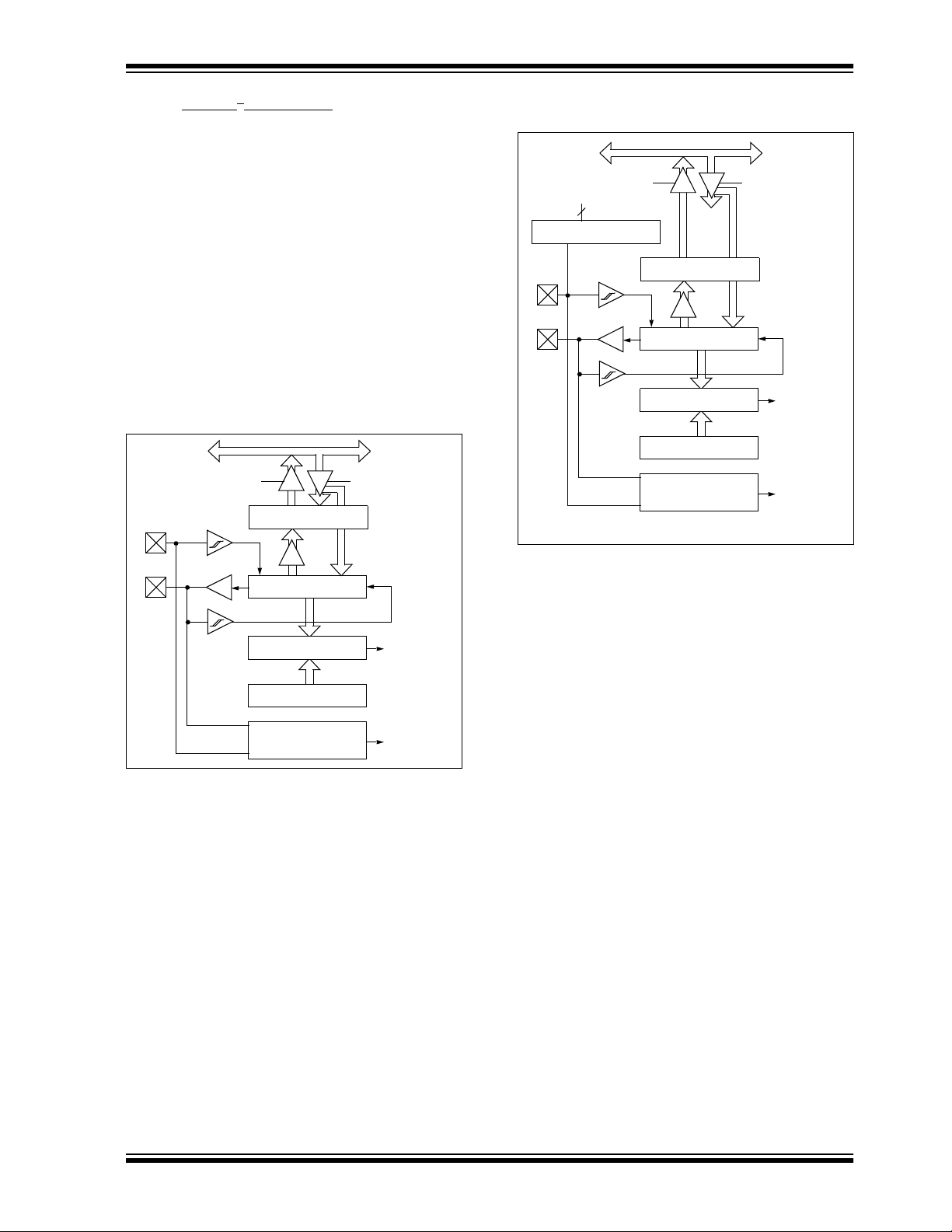
PIC16C77X
8.2 MSSP I2C Operation
The MSSP module in I2C mode fully implements all
master and slave functions (including general call support) and provides interrupts on start and stop bits in
hardware to determine a free bus (multi-master function). The MSSP module implements the standard
mode specificatio ns as well as 7 -bit and 10-bit addressing.
Refer to Application Note AN578,
Module in the I
2
C Multi-Master Environm ent. "
"Use of the SSP
A "glitch" filter is on the SCL and SDA pins whe n the pin
is an input. This filter operates in both the 10 0 k Hz an d
400 kHz modes. In the 10 0 kHz mode, w hen these pins
are an output, there is a sle w ra te control of the pin that
is independant of device frequency.
FIGURE 8-10: I2C SLAVE MODE BLOCK
DIAGRAM
Internal
data bus
Read Write
shift
clock
MSb
SSPBUF reg
SSPSR reg
Match detect
SSPADD reg
Start and
Stop bit detect
LSb
(SSPSTAT reg)
Addr Match
Set, Reset
S, P bits
SCL
SDA
FIGURE 8-11: I
2
C MASTER MODE BLOCK
DIAGRAM
Internal
data bus
Read Write
SSPADD<6:0>
7
Baud Rate Generator
SCL
SDA
Two pins are used for data transfer. These are the SCL
pin, which is the clock, and the SDA pin, which is the
data. The SDA and SCL pins that are automatically
configured when the I
module functions are enabled by setting SSP Enable
bit SSPEN (SSPCON<5>).
The MSSP module has six registers for I
They are the:
• SSP Control Register (SSPCON)
• SSP Control Register2 (SSPCON2)
• SSP Status Register (SSPSTAT )
• Serial Receive/Transmit Buffer (SSPBUF)
• SSP Shift Register (SSPSR) - Not directly accessible
• SSP Address Register (SSPADD)
The SSPCON register allows control of the I
tion. Four mode selection bits (SSPCON<3:0>) allow
one of the following I2C modes to be selected:
2
C Slave mode (7-bit address)
•I
2
C Slave mode (10-bit address)
•I
2
C Master mode, clock = OSC/4 (SSPADD +1)
•I
Before selecting any I
must be programmed to inputs by setting the appropriate TRIS bits. Selecting an I2C mode, by setting the
SSPEN bit, enables the SCL and SDA pins to be used
as the clock and data lines in I2C mode.
SSPBUF reg
shift
clock
SSPSR reg
MSb
Match detect
SSPADD reg
Start and Stop bit
detect / generate
2
C mode is enabled. The SSP
2
C mode, the SCL and SDA pins
LSb
Addr Match
Set/Clear S bit
and
Clear/Set P bit
(SSPSTAT reg)
and Set SSPIF
2
C operation.
2
C opera-
1999 Microchip Technology Inc. Advance Information DS30275A-page 63
Page 64

PIC16C77X
The SSPSTAT register gives the status of the data
transfer. This information includes detection of a
START (S) or STOP (P) bit, specifies if the received
byte was data or add ress if the ne xt by te is the completion of 10-bit address, and if this will be a read or write
data transfer.
SSPBUF is the register to which the transfer data is
written to or read from. The SSPSR register shifts the
data in or out of the device. In receive operations, the
SSPBUF and SSPSR create a doubled buffered
receiver. This allows reception of the next byte to b egin
before reading the las t b yte o f rece iv ed data. W hen th e
complete byte is received, it is transferred to the
SSPBUF register and flag bit SSPIF is set. If another
complete byte is received before the SSPBUF register
is read, a receiver overflow has occurred and bit
SSPOV (SSPCON<6>) is set and the byte in the
SSPSR is lost.
The SSPADD register holds the sl av e address . In 10-bit
mode, the user needs to write the high byte of the
address (1111 0 A9 A8 0). Following the high byte
address match, the low byte of the address needs to be
loaded (A7:A0).
8.2.1 S LAVE MODE
In slave mode, the SCL and SDA pins must be config-
ured as inputs. The MSSP module will override the
input state with the output data when required (slavetransmitter).
When an address is matched or the data transfer after
an address match is received, the hardware automatically will generate the acknowledge (ACK
then load the SSPBUF register with the received value
currently in the SSPSR register.
There are certain conditions that will cause the MSSP
module not to give this ACK
(or both):
a) The buffer full bit BF (SSPSTAT<0>) was set
before the transfer was received.
b) The overflow bit SSPO V (SSPCON<6>) was set
before the transfer was received.
If the BF bit is set, the SSPSR register value is not
loaded into the SSPBUF, but bit SSPIF and SSPO V are
set. Table 8-2 shows what happens when a data tr an sfer byte is received, given the status of bits BF and
SSPOV. The shaded cells show the condition where
user software did not pro perly clea r the o v erfl ow c ondition. Flag bit B F is cleare d b y reading th e SSPBUF re gister while bit SSPOV is cleared through software.
The SCL clock input must have a minimum high and
low time for proper operation. The high and low times
2
of the I
MSSP module is shown in timing parameter #100 and
parameter #101 of the Electrical Specifications.
C specification as well as t he requirement of th e
pulse. These are if either
) pulse, and
8.2.1.1 ADDRESSING
Once the MSSP module has been enabled, it waits for
a START condition to occur . Following the START condition, the 8-bits are shifted in to the SSPSR register . All
incoming bits are sampled with the rising edge of the
clock (SCL) line. The value of register SSPSR<7:1> is
compared to the value of the SSPADD register. The
address is compared on the falling edge of the eighth
clock (SCL) pulse. If the addresses match, and the BF
and SSPOV bits are clear, the following events occur:
a) The SSPSR register value is loaded into the
SSPBUF register on the falling edge of the 8th
SCL pulse.
b) The buffer full bit, BF is set on th e falling edge of
the 8th SCL pulse.
c) An ACK
d) SSP interrupt flag bit, SSPIF (PIR1<3>) is set
(interrupt is genera ted i f enab le d) - o n the fallin g
edge of the 9th SCL pulse.
In 10-bit address mode, two address bytes need to be
received by the slave. The five Most Significant bits
(MSbs) of the first address b yte sp ecify if this is a 1 0-bit
address. Bit R/W
so the slave device will receive the second address
byte. For a 10-bit address the firs t byte would equal
‘1111 0 A9 A8 0’, where A9 and A8 are the two MSbs
of the address. The sequence of events for a 10-bit
address is as follows, with steps 7- 9 for slave-transmitter:
1. Receive first (high) byte of Address (bits SSPIF,
BF, and bit UA (SSPSTAT<1>) are set).
2. Update the SSPADD register with second (low)
byte of Address (clears bit UA and releases the
SCL line).
3. Read the SSPBUF register (clears bit BF) and
clear flag bit SSPIF.
4. Receive second (low) byte of Address (bits
SSPIF, BF, and UA are set).
5. Update the SSPADD register with the first (high)
byte of Address. This will clear bit UA and
release the SCL line.
6. Read the SSPBUF register (clears bit BF) and
clear flag bit SSPIF.
7. Receive Repeated Start condition.
8. Receive first (high) byte of Address (bits SSPIF
and BF are set).
9. Read the SSPBUF register (clears bit BF) and
clear flag bit SSPIF.
Note: Following the Repeated Start condition
pulse is generated.
(SSPSTAT<2>) must specify a write
(step 7) in 10-bit mode, the user only
needs to match the first 7-bit addre ss. Th e
user does not update the SSPADD for the
second half of the address.
DS30275A-page 64 Advance Information 1999 Microchip Technology Inc.
Page 65

PIC16C77X
8.2.1.2 SLAVE RECEPTION
An SSP interrupt is generated for each data transfer
byte. Flag b it SSPIF (PIR1<3 >) must be cleared in soft-
When the R/W bit of the address byte is clear and an
address match occurs, the R/W
bit of the SSPSTAT
ware. The SSPSTAT register is used to determine the
status of the received byte.
register is cleared. The rece iv ed ad dress i s loade d into
the SSPBUF register.
When the address byte overflow condition exists, then
no acknowled ge (ACK
) pulse is given. An overflow condition is defined as either bit BF (SSPSTAT<0>) is set
or bit SSPOV (SSPCON<6>) is set.
Note: The SSPBUF will be loaded if the SSPOV
bit is set and the BF flag is cleared. If a
read of the SSPBUF was performed, but
the user did not clear the state of the
SSPOV bit before the next receive
occured. The ACK
is not sent and the SSP-
BUF is updated.
TABLE 8-2 DATA TRANSFER RECEIVED BYTE ACTIONS
Status Bits as Data
Transfer is Received
Generate ACK
BF SSPOV
SSPSR
→ SSPBUF
Pulse
00 Yes Yes Yes
1 0 No No Yes
1 1 No No Yes
0 1 Yes No Yes
Note 1: Shaded cells show the conditions where the user software did not properly clear the overflow condition.
8.2.1.3 SLAVE TRANSMISSION
An SSP interrupt is generated for each data transfer
byte. The SSPIF flag bit must be cleared in software,
When the R/W
and an address match occurs, the R/W
SSPSTAT register is set. The received address is
loaded into the SSPBUF register. The ACK pulse will
be sent on the ninth bit, and the SCL pin is held low.
The transmit data must be loaded into the SSPBUF
register , which also loads the SSPSR register . Then the
SCL pin should be enabled by setting bit CKP (SSPCON<4>). The master must monitor the SCL pin prior
to asserting another clock pulse. The slave devices
may be holding off the master by stretchi ng the cl ock.
The eight data bits are sh ifted out on the falling edg e of
the SCL input. This ensures that the SDA signal is valid
during the SCL high time (Figure 8-13).
bit of the inc oming ad dress byte is set
bit of the
and the SSPSTA T register is us ed to determine the status of the byte tranfer. The SSPIF flag bit is set on the
falling edge of the ninth clock pulse.
As a slave-transmitter, the ACK
receiver is latched on the rising edge of the ninth SCL
input pulse. If t he SDA lin e was high (not A CK
data transfer is co mplete . Wh en the no t A CK
by the slave, the slave logic is reset and the slave then
monitors for another occurren ce of the START bit. If the
SDA line was low (ACK
loaded into the SSPBUF register, which also loads the
SSPSR register. Then the SCL pin should be enabled
by setting the CKP bit.
Set bit SSPIF
(SSP Interrupt occurs
if enabled)
pulse from the master-
), the transmit data must be
), then the
is latched
FIGURE 8-12: I2C WAVEFORMS FOR RECEPTION (7-BIT ADDRESS)
Receiving Address
A7 A6 A5 A4
1234
S
SCL
SSPIF
BF (SSPSTAT<0>)
SSPOV (SSPCON<6>)
1999 Microchip Technology Inc. Advance Information DS30275A-page 65
A3 A2 A1SDA
5
R/W=0
ACK
7
6
9
8
Receiving Data
D5
D6D7
1234
Cleared in software
SSPBUF register is read
Bit SSPOV is set because the SSPBUF register is still full.
D2
D3D4
56
D1
7
ACK
D0
89
Receiving Data
D5
D6D7
123
D2
D3D4
5
4
ACK is not sent.
D1
Not
ACK
D0
9
8
76
P
Bus Master
terminates
transfer
Page 66

PIC16C77X
FIGURE 8-13: I2C WAVEFORMS FOR TRANSMISSION (7-BIT ADDRESS)
R/W
SDA
Receiving Address
A7 A6 A5 A4 A3 A2 A1
= 1
ACK
D7 D6 D5 D4 D3 D2 D1 D0
Transmitting Data
R/W
= 0
Not ACK
SCL
SSPIF
BF (SSPSTAT<0>)
CKP (SSPCON<4>)
S
123456789 123456789
Data in
sampled
SCL held low
while CPU
responds to SSPIF
cleared in software
SSPBUF is written in software
Set bit after writing to SSPBUF
(the SSPBUF must be written-to
before the CKP bit can be set)
From SSP interrupt
service routine
P
DS30275A-page 66 Advance Information 1999 Microchip Technology Inc.
Page 67

FIGURE 8-14: I2C SLAVE-TRANSMITTER (10-BIT ADDRESS)
P
Bus Master
terminates
transfer
ACK
D0
Transmit is complete
Master sends NACK
6
D2
PIC16C77X
Transmitting Data Byte
D7 D6 D5 D4 D3 D1
ACK
R/W=1
A9
Receive First Byte of Address
ACK
Receive Second Byte of Address
Clock is held low until
update of SSPADD has
taken place
ACK
R/W = 0
CKP has to be set for clock to be released
12345 789
6
Sr
Cleared in software
initiates transmit
Write of SSPBUF
Cleared in software
Dummy read of SSPBUF
to clear BF flag
Cleared by hardware when
SSPADD is updated.
UA is set indicating that
SSPADD needs to be
updated
Cleared in softwar e
Dummy read of SSPBUF
to clear BF flag
Cleared by hardware when
SSPADD is updated.
SSPBUF is written with
contents of SSPSR
UA is set indicating that
the SSPADD needs to be
updated
Receive First Byte of Address
11110A9A8 A7 A6A5A4A3A2A1A0 11110 A8
SDA
123456789 1 2345 6789 12345 789
SCL
S
SSPIF
BF (SSPSTAT<0>)
(PIR1<3>)
UA (SSPSTAT<1>)
1999 Microchip Technology Inc. Advance Information DS30275A-page 67
Page 68

PIC16C77X
FIGURE 8-15: I2C SLAVE-RECEIVER (10-BIT ADDRESS)
Bus Master
P
terminates
transfer
ACK
R/W = 1
6
D2
Receive Data Byte
Cleared in software
ACK
Read of SSPBUF
clears BF flag
Dummy read of SSPBUF
to clear BF flag
Cleared by hardware when
SSPADD is updated with high
byte of address.
UA is set indicating that
SSPADD needs to be
updated
Receive Second Byte of Address
Clock is held low until
update of SSPADD has
taken place
ACK
R/W = 0
Receive First Byte of Address
123456 789 1 2345 6789 1 2345 789
1 1 1 1 0 A9A8 A7 A6A5A4A3A2A1A0 D7D6D5D4D3 D1D0
S
SDA
SCL
Cleared in software
Cleared by hardware when
SSPADD is updated with low
byte of address.
Dummy read of SSPBUF
to clear BF flag
SSPBUF is written with
contents of SSPSR
UA is set indicating that
the SSPADD needs to be
updated
SSPIF
BF (SSPSTAT< 0>)
(PIR1<3>)
UA (SSPSTAT<1>)
DS30275A-page 68 Advance Information 1999 Microchip Technology Inc.
Page 69

PIC16C77X
8.2.2 GENERAL CALL ADDRESS SUPPORT
If the general call address matches, the SSPSR is
transfered to the SSPB UF, the BF flag is set (eighth bit),
The addressing procedure for the I2C bus is such that
the first byte after the START condition usually determines which device will be the slave addressed by the
master . The excepti on is the general call address whic h
can address all de vices. When thi s address is used, all
devices should, in theory, respond with an acknowledge.
The general call address is one of eight addresses
reserved f or specifi c purpos es by the I
consists of all 0’s with R/W
= 0
2
C protocol. It
The general call address is recognized when the General Call Enable bi t (GCEN) is en abled (SSPCON2<7>
is set). Following a start-bit detect, 8-bits are shifted
into SSPSR and the address is compared against
and on the falling edge of the ninth bit (ACK
SSPIF flag is set.
When the interrupt is serviced. The source for the
interrupt can be check ed b y readi ng the contents of the
SSPBUF to determine if the address was device specific or a general call address.
In 10-bit mode, the SSPADD is required to be updated
for the second half of the ad dress to mat ch, and th e U A
bit is set (SSPSTAT<1>). If the general call address is
sampled when GCEN is set while the slave is configured in 10-bit address mode, then the second half of
the address is not ne cessary, the UA bit will not be set,
and the slave will begin receiving data after the
acknowledge (Figure 8-16).
bit) the
SSPADD, and is also compared to the general call
address, fixed in hardware.
FIGURE 8-16: SLAVE MODE GENERAL CALL ADDRESS SEQUENCE (7 OR 10-BIT MODE)
Address is compared to General Call Address
after ACK, set interrupt flag
SDA
General Call Address
R/W
= 0
Receiving data
ACK
D7 D6 D5 D4 D3 D2 D1 D0
ACK
SCL
SSPIF
BF
(SSPSTAT<0>)
SSPOV
(SSPCON<6>)
GCEN
(SSPCON2<7>)
123456789123456789
S
Cleared in software
SSPBUF is read
’0’
’1’
1999 Microchip Technology Inc. Advance Information DS30275A-page 69
Page 70

PIC16C77X
8.2.3 SLEEP OPERATION
2
While in sleep mode, the I
C module can receive
addresses or data, and when an address match or
8.2.4 EFFECTS OF A RESET
A reset diables the SSP module and terminates the
current transfer.
complete byte tr ansfer occurs wak e the process or from
sleep (if the SSP interrupt is enabled).
TABLE 8-3 REGISTERS ASSOCIATED WITH I2C OPERATION
Address Name Bit 7 Bit 6 Bit 5 Bit 4 Bit 3 Bit 2 Bit 1 Bit 0 POR, BOR MCLR, WDT
0Bh, 8Bh,
10Bh,18Bh
0Ch PIR1
8Ch PIE1
0Dh PIR2
8Dh PIE2
13h SSPBUF Synchronous Serial Port Receive Buffer/Transmit Register xxxx xxxx uuuu uuuu
14h SSPCON WCOL SSPOV SSPEN CKP SSPM3 SSPM2 SSPM1 SSPM0 0000 0000 0000 0000
91h SSPCON2 GCEN AKSTAT AKDT AKEN RCEN PEN RSEN SEN 0000 0000 0000 0000
94h SSPSTAT SM P CKE D/A
Legend: x = unknown, u = unchanged, - = unimplemented read as '0'. Shaded cells are not used by the SSP in I
Note 1: These bits are reserved on the 28-pin devices, always maintain these bits clear.
INTCON GIE PEIE
(1)
PSPIF
PSPIE
LVDIF — — —BCLIF — — CCP2IF 0--- 0--0 0--- 0--0
LVDIE — — —BCLIE — — CCP2IE 0--- 0--0 0--- 0--0
2: These bits are reserved on these devices, always maintain these bits clear.
ADIF RCIF TXIF SSPIF CCP1IF TMR2IF TMR1IF 0000 0000 0000 0000
(1)
ADIE RCIE TXIE SSPIE CCP1IE TMR2IE TMR1IE 0000 0000 0000 0000
T0IE INTE RBIE T0IF INTF RBIF 0000 000x 0000 000u
PSR/WUA BF 0000 0000 0000 0000
2
C mode.
DS30275A-page 70 Advance Information 1999 Microchip Technology Inc.
Page 71

PIC16C77X
8.2.5 MASTER MODE
In master mode, the SCL and SDA lines are manipulated by the MSSP hardware .
Master mode of operation is supported by interrupt
generation on the detection of the START and STOP
conditions. The STOP (P) and START (S) bits are
cleared from a reset or when the MSSP module is disabled. Control of th e I2C bus ma y be taken when the P
bit is set, o r the bus is id le with bot h the S and P bits
clear.
The following events will cause SSP Interrupt Flag bit,
SSPIF, to be set (SSP Interrupt if enabled):
• START condition
• STOP condition
• Data transfer byte transmitted/received
• Acknowled ge tra ns mi t
• Repeated Start
FIGURE 8-17: SSP BLOCK DIAGRAM (I2C MASTER MODE)
Internal
data bus
Read Write
SSPBUF
SDA
SCL
SDA in
SSPSR
MSb
Start bit, Stop bit,
Acknowledge
Generate
Receive Enable
shift
clock
LSb
SSPM3:SSPM0,
SSPADD<6:0>
Baud
rate
generator
clock cntl
clock arbitrate/WCOL detect
(hold off clock source)
SCL in
Bus Collision
Start bit detect,
Stop bit detect
Write collision detect
Clock Arbitration
State counter for
end of XMIT/RCV
Set/Reset, S, P, WCOL (SSPSTAT)
Set SSPIF, BCLIF
Reset AKSTAT, PEN (SSPCON2)
1999 Microchip Technology Inc. Advance Information DS30275A-page 71
Page 72

PIC16C77X
8.2.6 MULTI-MASTER OPERATION
In multi-master mode, the interrupt generation on the
detection of the START and STOP conditions allows
the determination of when the bus is free. The STOP
(P) and START (S) bits are cleared from a reset or
when the MSSP module is disabled. Con trol of th e I
bus may be taken when bit P (SSPSTAT<4>) is set, or
the bus is idle with both the S and P bits clear. When
the bus is busy, enabling the SSP Interrupt will generate the interrupt when the STOP condition occurs.
In multi-master operation, the SDA line must be monitored, for abitration, to see if the signal level is the
expected outp ut level. This che c k is pe rformed in hardware, with the result placed in the BCLIF bit.
The states where arbitration can be lost are:
• Address Transfer
• Data Transfer
• A Start Condition
• A Repeated Start Condition
• An Acknowledge Condition
2
8.2.7 I
Master Mode is enabled by setting and clearing the
appropriate SSPM bits in SSPCON and by setting the
SSPEN bit. Once master mode is enabled, the user
has six options.
Note: The MSSP Module, w hen conf igured in I2C
C MASTER OPERATION SUPPORT
- Assert a start condition on SDA and SCL.
- Assert a Repeated Start condition on SDA and
SCL.
- Write to the SSPBUF register initiating transmission of data/address.
- Generate a stop condition on SDA and SCL.
- Configure the I
- Generate an Ac kno wledg e con dition at the en d
of a received byte of data.
Master Mode, does not allow queueing of
events. For instance: The user is not
allowed to initiate a start condition, and
immediately write the SSPBUF register to
initiate transmission before the START
condition is complete. In this case the
SSPBUF will not be written to, and the
WCOL bit will be s et, in dicat ing t hat a wri te
to the SSPBUF did not occur.
2
C port to receive data.
2
2
8.2.7.4 I
The master device generates all of the serial clock
pulses and the START and STOP conditions. A transfer is ended with a STOP condition or with a Repeated
Start condition. Since the Repeated Start condition is
C
also the beginning of the next serial transfer, the I
bus will not be released.
In Master Transmitter mode, serial data is output
through SDA, while SCL outputs the serial clock. The
first byte transmitted contains the slave address of the
receiving device (7 bits) and the Read/Write (R/W
In this case, the R/W
transmitted 8 bits at a time. After each byte is transmitted, an acknow l edg e bit is recei ved. START and STOP
conditions are output to indicate the beginning and the
end of a serial transfer.
In Master receive mode the first byte transmitted contains the slave address of the transmitting device
(7 bits) and the R/W
logic '1'. Thus the first byte transmitted is a 7-bit slave
address followed by a '1' to indicate receive bit. Serial
data is received via SDA while SCL outputs the serial
clock. Serial data is receiv ed 8 bits at a time . After each
byte is received, an acknowledge bit is transmitted.
START and STOP conditions indicate the beginning
and end of transmission.
The baud rate generator used for SPI mode operation
is now used t o set the SCL clock f requency for eit her
100 kHz, 400 kHz, or 1 MHz I
rate generator reload value is contained in the lower 7
bits of the SSPADD register. The baud rate generator
will automatically begin coun ting on a write to the SSPBUF. Once the given operation is complete (i.e. transmission of the last data bit is followed by ACK), the
internal clock will automatically stop counting and the
SCL pin will remain in its last state
A typical transmit sequence would go as follows:
a) The user generates a Start Condition by setting
the START enable bit (SEN) in SSPCON2.
b) SSPIF is set. The module will wait the required
start time before any other operation takes
place.
c) The user loads the SSPBUF with address to
transmit.
d) Address is shifted out the SDA pin until all 8 bits
are transmitted.
e) The MSSP Module shifts in the ACK bit from the
slave device, and writes its value into the
SSPCON2 register ( SSPCON2<6>).
f) The module generates an interrupt at the end of
the ninth clock cycle by setting SSPIF.
g) The user loads the SSPBUF with eight bits of
data.
h) DATA is shifted out the SDA pin until all 8 bits
are transmitted.
C MASTER MODE OPERATION
bit will be logic '0'. Serial data is
bit. In this case the R/W bit will be
2
C operation. The baud
2
) bit.
C
DS30275A-page 72 Advance Information 1999 Microchip Technology Inc.
Page 73

PIC16C77X
i) The MSSP Module shifts in the AC K bit from the
slave device, and writes its value into the
SSPCON2 register ( SSPCON2<6>).
j) The MSSP module generates an interrupt at the
In I2C master mode, the BRG is rel oaded automa tically.
If Clock Arbitration is taking place for instance, the BRG
will be reloaded when the SCL pin is sampled high
(Figure 8-19).
end of the ninth cloc k cycle b y set ting the SSPIF
bit.
k) The user generates a ST OP con dition b y settin g
the STOP enable bit PEN in SSPCON2.
l) Interrupt is generated once the STOP condition
FIGURE 8-18: BAUD RATE GENERATOR
BLOCK DIAGRAM
SSPM3:SSPM0
SSPADD<6:0>
is complete.
8.2.8 BAUD RATE GENERATOR
2
In I
C master mode, the reload value for the BRG is
SSPM3:SSPM0
SCL
Reload
Control
located in the lower 7 bits of the SSPADD register
(Figure 8-18). When the BRG is loaded with this v alue ,
CLKOUT
BRG Down Counter
the BRG counts down to 0 and stops until another
reload has tak en place. The BRG count is decremente d
twice per instruction cycle (T
CY) on the Q2 and Q4
clock.
FIGURE 8-19: BAUD RATE GENERATOR TIMING WITH CLOCK ARBITRATION
SDA
SCL de-asserted but slave holds
SCL low (clock arbitration)
SCL
DX-1DX
SCL allowed to transition high
Reload
Fosc/4
BRG
value
BRG
reload
BRG decrements
(on Q2 and Q4 cycles)
03h 02h 01h 00h (hold off) 03h 02h
SCL is sampled high, reload takes
place, and BRG starts its count.
1999 Microchip Technology Inc. Advance Information DS30275A-page 73
Page 74

PIC16C77X
8.2.9 I2C MASTER MODE START CONDITION
TIMING
To initiate a START condition, the user sets the start
condition enable bit, SEN (SSPCON2<0>). If the SDA
and SCL pins are sampled hi gh, the baud rate generator is re-loaded with the contents of SSPADD<6:0>,
and starts its count. If SCL and SDA are both sampled
high when the baud rate generator times out (T
BRG
the SDA pin is driven low. The action of the SDA being
driven low whil e SCL is high i s the START condition,
and causes the S bit (SSPSTAT<3>) to be set. Following this, the baud rate generator is reloaded with the
contents of SSPADD<6:0> and resumes its count.
When the baud rate generator times out (T
BRG
), the
SEN bit (SSPCON2<0>) will be automatically cleared
by hardware, the baud rate generator is suspended
leaving the SDA line held low, and the START conditio n
is complete.
Note: If at the beginning of START condition the
SDA and SCL pins are already sampled
low, or if during th e START condition t he
SCL line is sampled low before the SDA
line is driven low , a b us collision o ccurs, the
Bus Collision Interrupt Flag (BCLIF) is set,
the START condition is aborted, and the
2
C module is reset into its IDLE state.
I
8.2.9.5 WCOL STATUS FLAG
If the user writes the SSPBUF when an START
sequence is in progress, then WCOL is set and the
contents of the b uffer are unc hanged (the w rite doesn ’t
occur).
Note: Because queueing of events is not
),
allowed, writing to the lower 5 bits of
SSPCON2 is disabled until the START
condition is complete.
FIGURE 8-20: FIRST START BIT TIMING
Write to SEN bit occurs here.
SDA
SCL
SDA = 1,
SCL = 1
T
BRG
Set S bit (SSPSTAT<3>)
At completion of start bit,
Hardware clears SEN bit
and sets SSPIF bit
T
BRG
S
Write to SSPBUF occurs here
1st Bit
T
BRG
2nd Bit
T
BRG
DS30275A-page 74 Advance Information 1999 Microchip Technology Inc.
Page 75

FIGURE 8-21: START CONDITION FLOWCHART
SSPEN = 1,
SSPCON<3:0> = 1000
Idle Mode
SEN (SSPCON2<0> = 1)
PIC16C77X
Bus collision detected,
Set BCLIF,
Release SCL,
Clear SEN
No
Yes
SCL= 0?
No
SDA = 0?
Yes
Reset BRG
No
SDA = 1?
SCL = 1?
Load BRG with
SSPADD<6 :0>
No
BRG
Rollover?
Force SDA = 0,
Load BRG with
SSPADD<6:0>,
Set S bit.
Yes
Yes
No
SCL = 0?
Yes
Reset BRG
No
BRG
rollover?
Yes
Force SCL = 0,
Start Condition Done,
Clear SEN
and set SSPIF
1999 Microchip Technology Inc. Advance Information DS30275A-page 75
Page 76

PIC16C77X
8.2.10 I2C MASTER MODE REPEATED START
CONDITION TIMING
A Repeated Start condition occurs when the RSEN bit
(SSPCON2<1>) is programmed high and the I
2
C module is in the idle state. When the RSEN bit is set, the
SCL pin is asserted low. When the SCL pin is sampled
low , the baud ra te genera tor is loaded with the contents
of SSPADD<6:0>, and begins counting. The SDA pin
is released (brought high) for one baud rate generator
count (T
). When the baud r ate ge nera tor time s out,
BRG
if SDA is sampled high, the SCL pi n will be de-asserted
(brought high). When SCL is sampled high the baud
rate generator is re-loaded with the contents of
SSPADD<6:0> and begins counting. SDA and SCL
must be sampled high fo r one T
. This action is then
BRG
followed by asser tio n of the SDA pin (SDA is low) for
one T
while SCL is high. F ollo wing this , th e RSEN
BRG
bit in the SSPCON2 register will be automatically
cleared, and the baud rate generator is not reloaded,
leaving the SDA pin held low. As soon as a start condition is detected on the SDA and SCL pins, the S bit
(SSPSTA T<3>) will b e set. T he SSPIF bi t will not be set
until the baud rate generator has timed-out.
Note 1: If RSEN is programme d while any other
event is in progress, it will not take effect.
Note 2: A bus collision during the Repeated Start
condition occurs if:
• SDA is sam pled lo w when SC L goes from lo w to
high.
• SCL goes low before SDA is asserted low. This
may indicate that another master is attempting
to transmit a data "1".
Immediately following the SSPIF bit getting set, the
user may write the SSPBUF with the 7-bit address in
7-bit mode, or the default first address in 10-bit mode.
After the first eight bits are transmitted and an ACK is
received, the user may then transmit an additional eight
bits of address (10-bit mode) or eight bits of data (7-bit
mode).
8.2.10.6 WCOL STATUS FLAG
If the user writes the SSPBUF when a Repeated Start
sequence is in progress, then WCOL is set and the
contents of the b uffer are unc hanged (the w rite doesn ’t
occur).
Note: Because queueing of events is not
allowed, writing of the lower 5 bits of
SSPCON2 is disabled until the Repeated
Start condition is complete.
FIGURE 8-22: REPEAT START CONDITION WAVEFORM
Write to SSPCON2
occurs here.
SDA = 1,
SCL(no change)
SDA
Falling edge of ninth clock
End of Xmit
SCL
SDA = 1,
SCL = 1
T
BRGTBRG
T
BRG
Sr = Repeated Start
Set S (SSPSTAT<3>)
At completion of start bit,
hardware clear RSEN bit
and set SSPIF
1st Bit
Write to SSPBUF occurs here.
T
BRG
T
BRG
DS30275A-page 76 Advance Information 1999 Microchip Technology Inc.
Page 77

FIGURE 8-23: REPEATED START CONDITION FLOWCHART (PAGE 1)
Start
Idle Mode,
B
SSPEN = 1,
SSPCON<3:0> = 1000
RSEN = 1
Force SCL = 0
PIC16C77X
SCL = 0?
Yes
Release SDA,
Load BRG with
SSPADD<6:0>
BRG
rollover?
Yes
Release SCL
SCL = 1?
Yes
No
No
(Clock Arbitration)
No
Bus Collision,
Set BCLIF,
Release SDA,
Clear RSEN
C
1999 Microchip Technology Inc. Advance Information DS30275A-page 77
No
SDA = 1?
Load BRG with
SSPADD<6:0>
A
Yes
Page 78

PIC16C77X
FIGURE 8-24: REPEATED START CONDITION FLOWCHART (PAGE 2)
B
C
No
SCL = 1?
No
Yes
SCL = ’0’?
Yes
Reset BRG
No
SDA = 0?
Reset BRG
Yes
A
No
BRG
rollover?
Force SDA = 0,
Load BRG with
SSPADD<6:0>
Set S
No
BRG
rollover?
Force SCL = 0,
Repeated Start
condition done,
Clear RSEN,
Set SSPIF.
Yes
Yes
DS30275A-page 78 Advance Information 1999 Microchip Technology Inc.
Page 79

PIC16C77X
8.2.11 I2C MASTER MODE TRANSMISSION
Transmission of a data byte, a 7-bit address, or either
half of a 10-bit address is accomplished by simply writing a value to SSPBUF registe r . This action will set the
buffer full flag (BF) a nd allow the ba ud rate gen erator to
begin counting and start the next transmission. Each
bit of address/data will be shifted out onto the SDA pin
after the falling ed ge of SCL is asserted (see data hold
time spec). SCL is held low for one baud rate generator roll over co unt (T
SCL is released high (see Data setup time spec).
When the SCL pin is released high, it is held that way
for T
for that duration and some hold time after the next falling edge of SCL. After the eighth bit is shifted out (the
falling edge of the eighth clock), the BF flag is cleared
and the master r elease s SDA allowing the slave d e vic e
being addressed to respo nd with an AC K
ninth bit time, if an a ddress m atch occu rs or i f data wa s
received prop erly. The status of ACK
AKDT on the falling edge of the n inth cloc k. If the ma ster receives an acknowledge, the acknowledge status
bit (AKSTAT) is cleared. If not, the bit is set. After the
ninth clock the SSPIF is set, and the master clock
(baud rate generator) is suspended until the next data
byte is loaded into the SSPBUF leaving SCL low and
SDA unchanged (Figure 8-26).
After the write to the SSPBUF, each bit of address will
be shifted out on the falling edge of SCL until all seven
address bits and the R/W
ing edge of th e eighth clo ck the master wi ll de-asser t
the SDA pin allowing the slave to respond with an
acknowle dge. On the falling edg e o f th e ninth clock the
master will sample the SDA pin to see if the address
was recogniz ed b y a sl ave. The status of the ACK bit is
loaded into the AKSTA T status bit (SSPCON2<6 >). Following the fall ing edge of the ninth cl ock transmissi on
of the address, the SSPIF is set, the BF fla g is cleare d,
and the baud rate generator is turned off until another
write to the SSPBUF takes place, hold ing SCL low and
allowing SDA to float.
, the data on the SDA pin must remain stable
BRG
). Data should be valid before
BRG
bit during the
is read into the
bit are completed. On the fall-
8.2.11.7 BF STATUS FLAG
In transmit mode, the BF bit (SSPSTAT<0>) is set when
the CPU writes to SSPBUF and is cleared when all 8
bits are shifted out.
8.2.11.8 WCOL STATUS FLAG
If the user writes the SSPBUF when a transmit is
already in progress (i.e. SSPSR is still shifting out a
data byte), then WCOL is set and the contents of the
buffer are unchanged (the write doesn’t occur).
WCOL must be cleared in software.
8.2.11.9 AKSTAT STATUS FLAG
In transmit mode, the AKSTAT bit (SSPCON2<6>) is
cleared when the slave has sent an acknowledge
= 0), and is set when the sla ve does n ot acknow l-
(ACK
edge (ACK
it has recognized its address (including a general call),
or when the slave has properly received its data.
= 1). A slave sends an acknowledge when
1999 Microchip Technology Inc. Advance Information DS30275A-page 79
Page 80

PIC16C77X
FIGURE 8-25: MASTER TRANSMIT FLOWCHART
Idle Mode
Write SSPBUF
Num_Clocks = 0,
BF = 1
Force SCL = 0
Num_Clocks
= 8?
No
Load BRG with
SSPADD<6:0>,
start BRG count,
SDA = Current Data bit
BRG
rollover?
Yes
Stop BRG,
Force SCL = 1
SCL = 1?
SDA =
Data bit?
Load BRG with
SSPADD<6:0>,
count SCL h igh time
No
Yes
No
Yes
Yes
No
(Clock Arbitration)
Bus collision detected
Set BCLIF, hold prescale off,
Clear XMIT enable
Yes
(Clock Arbitration)
Read SDA and place into
AKSTAT bit (SSPCON2<6>)
Release SDA so
slave can drive ACK,
Force BF = 0
Load BRG with
SSPADD<6:0>,
start BRG count
BRG
rollover?
Yes
Force SCL = 1,
Stop BRG
SCL = 1?
Yes
Load BRG with
SSPADD<6:0>,
count high time
Rollover?
No
No
No
BRG
rollover?
Yes
Num_Clocks
= Num_Clocks + 1
No
SCL = 0?
Yes
Reset BRG
No
SDA =
Data bit?
No
Yes
Force SCL = 0,
Set SSPIF
DS30275A-page 80 Advance Information 1999 Microchip Technology Inc.
Page 81

PIC16C77X
FIGURE 8-26: I2C MASTER MODE TIMING (TRANSMISSION, 7 OR 10-BIT ADDRESS)
P
AKSTAT in
SSPCON2 = 1
ACK
Cleared in software
From slave clear AKSTAT bit SSPCON2<6>
Write SSPCON2<0> SEN = 1
START condition begins
cleared in software service routine
Transmitting Data or Second Half
of 10-bit Address
SCL held low
while CPU
responds to SSPIF
= 0Transmit Address to Slave
R/W
123456789 123456789
SSPBUF written with 7 bit address and R/W
start transmit
A7 A6 A5 A4 A3 A2 A1 ACK = 0 D7D6D5D4D3D2D1D0
SEN = 0
S
From SSP interrupt
cleared in software
SSPBUF is written in software
SSPBUF written
After start condition SEN cleared by hardware.
SDA
SCL
SSPIF
BF (SSPSTAT<0>)
SEN
PEN
R/W
1999 Microchip Technology Inc. Advance Information DS30275A-page 81
Page 82

PIC16C77X
8.2.12 I2C MASTER MODE RECEPTION
Master mode rece pti on is enabled by program m ing th e
receive enable bit, RCEN (SSPCON2<3>).
Note: The SSP Module must be in an IDLE
STATE before the RCEN bit is set, or the
RCEN bit will be disregarded.
The baud rate gen erator begins cou nting, and on each
rollover, the state of the SCL pin changes (high to low/
low to high) and data is shifted into the SSPSR. After
the falling edge of the eighth clock, the receive enable
flag is automatically cleared, the contents of the
SSPSR are loaded into the SSPBUF, the BF flag is set,
the SSPIF is set, and the baud rate generator is suspended from counting, holding SCL low. The SSP is
now in IDLE state, awaiting the next command. When
the buffer is read by the CPU, the BF flag is automatically cleared. The user c an th en send an acknowl edg e
bit at the end of reception, by setting the acknowledge
sequence enable bit, AKEN (SSPCON2<4>).
8.2.12.10 BF STATUS FLAG
In receive operat ion, BF is set w hen an address or data
byte is loaded into SSPBUF from SSPSR. It is cleared
when SSPBUF is read.
8.2.12.11 SSPOV STATUS FLAG
In receive operation, SSPOV is set when 8 bits are
received into the SSPSR, and the BF flag is already set
from a previous reception.
8.2.12.12 WCOL STATUS FLAG
If the user writes the SSPBUF when a receive is
already in progress (i.e . SSPSR is still shifti ng in a data
byte), then WCOL is set and the contents of the buffer
are unchanged (the write doesn’t occur).
DS30275A-page 82 Advance Information 1999 Microchip Technology Inc.
Page 83

FIGURE 8-27: MASTER RECEIVER FLOWCHART
Idle mode
RCEN = 1
Num_Clocks = 0,
Release SDA
Force SCL=0,
Load BRG w/
SSPADD<6:0>,
start count
PIC16C77X
BRG
rollov er?
Yes
Release SCL
SCL = 1?
Yes
Sample SDA,
Shift data into SSPSR
Load BRG with
SSPADD<6:0>,
start count.
BRG
rollover?
Yes
No
(Clock Arbitration)
No
No
SCL = 0?
Yes
No
Num_Clocks
= Num_Clocks + 1
No
Num_Clocks
= 8?
Yes
Force SCL = 0,
Set SSPIF,
Set BF.
Move contents of SSPSR
into SSPBUF,
Clear RCEN.
1999 Microchip Technology Inc. Advance Information DS30275A-page 83
Page 84

PIC16C77X
FIGURE 8-28: I2C MASTER MODE TIMING (RECEPTION 7-BIT ADDRESS)
Bus Master
terminates
transfer
Set SSPIF interrupt
at end of acknow-
ledge sequence
Set P bit
(SSPSTAT<4>)
sequence
and SSPIF
Cleared in
software
SSPOV is set because
SSPBUF is still full
Cleared in softwar e
Last bit is shifted into SSPSR and
contents are unloaded into SSPBUF
Write to SSPCON2<4>
to start acknowledge sequence
SDA = AKDT (SSPCON2<5>) = 0
SDA = AKDT = 1
Set AKEN start acknowledge sequence
ACK from Master
SDA = AKDT = 0
P
PEN bit = 1
written here
ACK is not sent
9
of receive
Set SSPIF at end
87
6
5
RCEN cleared
automatically
ACK
D0
D1
D2
D3D4
D5
D6D7
Receiving Data from Slave
RCEN = 1 start
next receive
ACK
1234
Data shifted in on falling edge of CLK
Set SSPIF interrupt
at end of acknowledge
D0
D1
RCEN cleared
automatically
D2
D3D4
D5
D6D7
Receiving Data from Slave
Master configured as a receiver
by programming SSPCON2<3>, (RCEN = 1)
ACK
R/W = 1
ACK from Slave
678 9
5
4
3
12
9
8
7
Cleared in software
Set SSPIF interrupt
at end of receive
Cleared in software
6
A3 A2 A1
5
4
3
Transmit Address to Slave
Start XMIT
Write to SSPBUF occu rs here
A7 A6 A5 A4
SEN = 0
12
Cleared in software
S
Write to SSPCON2<0> (SEN = 1)
Begin Start Condition
responds to SSPIF
while CPU
SDA
SCL
SDA = 0, SCL = 1
SSPIF
BF
(SSPSTAT<0>)
SSPOV
AKEN
DS30275A-page 84 Advance Information 1999 Microchip Technology Inc.
Page 85

PIC16C77X
8.2.13 ACKNOWLEDGE SEQUENCE TIMING
rate generator counts for T
pulled low. Following this, the AKEN bit is automati-
An acknowledge sequence is enabled by setting the
acknowledge sequence enable bit, AKEN
(SSPCON2<4>). When this bit is set, the SCL pin is
cally cleared, t he baud ra te generator is turned off, an d
the SSP module then goes into IDLE mode. (Figure 8-
29)
pulled low and the contents of the acknowledge data
bit is presented on the SDA pin. If the user wishes to
8.2.13.13 WCOL STATUS FLAG
generate an ac knowle dge, then the AKDT bit shou ld be
cleared. If not, the user shoul d set the AKDT bit before
starting an acknowledge sequence. The baud rate
generator then counts for one rollover period (T
BRG
and the SCL pin is de-asse rted (pulled high). When the
),
If the user writes the SSPBUF when an acknowledege
sequence is in progress, then WCOL is set and the
contents of the b uffer are unc hanged (the w rite doesn ’t
occur).
SCL pin is sampled high (clock arbitration), the baud
FIGURE 8-29: ACKNOWLEDGE SEQUENCE WAVEFORM
Acknowledge sequence starts here,
SDA
SCL
SSPIF
Write to SSPCON2
AKEN = 1, AKDT = 0
D0
8
ACK
T
BRG
9
T
BRG
. The SCL pin is t hen
BRG
AKEN automatically cleared
Set SSPIF at the end
of receive
Note: T
= one baud rate generator period.
BRG
Cleared in
software
Cleared in
software
Set SSPIF at the end
of acknowledge sequence
1999 Microchip Technology Inc. Advance Information DS30275A-page 85
Page 86

PIC16C77X
FIGURE 8-30: ACKNOWLEDGE FLOWCHART
Idle mode
Set AKEN
No
No
No
(Clock Arbitration)
Force SCL = 0
SCL = 0?
Yes
Drive AKDT bit
(SSPCON2<5>)
onto SDA pin,
Load BRG with
SSPADD<6:0>,
start count.
BRG
rollover?
Yes
Force SCL = 1
SCL = 1?
Yes
BRG
rollover?
No
SCL = 0?
No
No
AKDT = 1?
Yes
SDA = 1?
Bus collision detected,
Set BCLIF,
Release SCL,
Clear AKEN
Yes
Yes
Yes
No
Reset BRG
Force SCL = 0,
Clear AKEN,
Set SSPIF
Load BRG with
SSPADD <6:0>,
start count.
DS30275A-page 86 Advance Information 1999 Microchip Technology Inc.
Page 87

PIC16C77X
8.2.14 STOP CONDITION TIMING
A stop bit is asserted on the SDA pin at the end of a
receive/transmit by setting the Stop Sequence Enable
bit PEN (SSPCON2<2>). At the end of a receiv e/tr ansmit the SCL line is held low after the falling edge of the
ninth clock. When the PEN bit is set, the master will
assert the SDA line low . When the SDA line is sampled low, the baud rate generator is reloaded and
counts down to 0 . Wh en th e bau d r ate g enera tor ti mes
out, the SCL pin will be brought high, and one T
BRG
(baud rate generator rollover count) later, the SDA pin
will be de-asse rted. When the SD A pin is sample d high
while SCL is high, the P bit (SSPSTAT<4>) is set. A
BRG later the PEN bit is cleared and the SSPIF bit is
T
set (Figure 8-31).
Whenever the firmware decides to take control of the
bus, it will firs t det ermine if th e bus is busy by checking
the S and P bits in the SSPSTAT register. If the bus is
busy, then the CPU can be interrupted (notified) when
a Stop bit is detected (i.e. bus is free).
8.2.14.14 WCOL STATUS FLAG
If the user writes the SSPBUF when a ST OP sequence
is in progress , then WCOL is set and the con tents of the
buffer are unchanged (the write doesn’t occur).
FIGURE 8-31: STOP CONDITION RECEIVE OR TRANSMIT MODE
Write to SSPCON2
Falling edge of
9th clock
SCL
Set PEN
SCL = 1 for T
after SDA sampled high. P bit (SSPSTAT<4>) is set
T
BRG
, followed by SDA = 1 for T
BRG
PEN bit (SSPCON2<2>) is cleared by
hardware and the SSPIF bit is set
BRG
SDA
ACK
Note: T
T
BRG
SDA asserted low before rising edge of clock
to setup stop condition.
= one baud rate generator period.
BRG
T
BRG
SCL brought high after T
P
T
BRG
BRG
1999 Microchip Technology Inc. Advance Information DS30275A-page 87
Page 88

PIC16C77X
FIGURE 8-32: STOP CONDITION FLOWCHART
Idle Mode,
SSPEN = 1,
SSPCON<3:0> = 1000
SCL doesn’t change
(Clock Arbitration)
PEN = 1
Force SDA = 0
SDA = 0?
Yes
Start BRG
BRG
rollover?
Yes
De-assert SCL,
SCL = 1
SCL = 1?
No
No
No
Start BRG
BRG
rollover?
Yes
Release SDA,
Start BRG
BRG
rollover?
Yes
P bit Set?
SDA going from
0 to 1 while SCL = 1
Set SSPIF,
Stop Condition done
PEN cleared.
No
Yes
No
No
Bus Collision detected,
Set BCLIF,
Clear PEN
Yes
DS30275A-page 88 Advance Information 1999 Microchip Technology Inc.
Page 89

PIC16C77X
8.2.15 CLOCK ARBITRATION
Clock arbitration occurs when the master, during any
receive, transm it, or re peated star t/st op cond ition, deasserts the SCL pin (SCL allow ed to fl oat high). When
the SCL pin is allowed to float high, the baud rate gen-
8.2.16 SLEEP OPERATION
While in sleep mode, the I
2
addresses or data, and when an address match or
complete byte tr ansfer occurs w ake th e processor from
sleep ( if the SSP interrupt is enabled).
erator (BRG) is susp ended f rom cou nting u ntil th e SCL
pin is actually sampled h igh. When the SCL p in is sampled high, the baud rate generator is reloaded with the
contents of SSPADD<6:0> and begins counting. This
ensures that the SCL high time will always be at least
8.2.17 EFFECTS OF A RESET
A reset disables the SSP module and terminates the
current transfer.
one BRG rollover count in the event that the clock is
held low by an external device (Figure 8-33).
FIGURE 8-33: CLOCK ARBITRATION TIMING IN MASTER TRANSMIT MODE
BRG overf l ow,
Release SCL,
If SCL = 1 Load BRG with
SSPADD<6:0>, and start count
to measure high time interval
SCL
BRG overf l ow occur s,
Release SCL, Slave device holds SCL low.
SCL line sampled once every machine cycle (T
Hold off BRG until SCL is sampled high.
SCL = 1 BRG starts counting
clock high interval.
C module can receive
• 4).
osc
SDA
T
BRG
T
BRG
T
BRG
1999 Microchip Technology Inc. Advance Information DS30275A-page 89
Page 90

PIC16C77X
8.2.18 MULTI -MASTER COMMUNICATION, BUS
COLLISION, AND BUS ARBITRATION
Multi-Master mode support is achieved by bus arbitration. When the master outputs address/data bits onto
the SDA pin, arbitration takes place when the master
outputs a ’1’ on SDA by letting SDA float high and
another master as s erts a ’0’. When the SC L pin fl oats
high, data should be stable. If the expected data on
SDA is a ’ 1’ and the data sa mpled on the SDA pin = ’0’ ,
then a bus collision has taken place. The master will
set the Bus Collision Interrupt Flag, BCLIF and reset
2
C port to its IDLE state. (Figure 8-34).
the I
If a transmit was in progress when the bus collision
occurred, the transmission is halted, the BF flag is
cleared, the SDA and SCL lines are de-asserted, and
the SSPBUF can be written to . When the user services
the bus colli sion i nterrupt service rou tine , and if the I
bus is free, the user can resume communication by
asserting a START conditi on.
2
C
If a START, Repeated Start, STOP, or Acknowledge
condition was in progress when the bus collision
occurred, t he condition is abor ted, the SDA and SCL
lines are de-asserted, and t he res pective control bits in
the SSPCON2 register are cleared. When the user
services the bus collision interrupt service routine, and
2
C bus is free, the user can resume communica-
if the I
tion by asserting a START condition.
The Master will continue to monitor the SDA and SCL
pins, and if a ST OP co nditio n occurs , the S SPIF bit will
be set.
A write to the SSPBUF will start the transmission of
data at the first data bit, regardless of where the transmitter left off when bus collision occurred.
In multi-master mode, the interrupt generation on the
detection of start and stop conditions allows the determination of when th e bus is free. Control of the I
can be taken when the P bit is set in the SSPSTAT register, or the bu s is idle a nd the S and P bits are cleared.
FIGURE 8-34: BUS COLLISION TIMING FOR TRANSMIT AND ACKNOWLEDGE
Data changes
while SCL = 0
SDA line pulled low
by another source
SDA released
by master
Sample SDA. While SCL is high
data doesn’t match what is driven
by the master.
Bus collision has occurred.
2
C bus
SDA
SCL
BCLIF
Set bus collision
interrupt.
DS30275A-page 90 Advance Information 1999 Microchip Technology Inc.
Page 91

PIC16C77X
8.2.18.15 BUS COLLISION DURING A START
CONDITION
During a START condition, a bus collision occurs if:
a) SDA or SCL are sampled lo w at the beginnin g of
the START condition (Figure 8-35).
b) SCL is sampled low before SDA is asserted low.
(Figure 8-36).
During a START condition both the SDA and the SCL
pins are monitored.
If:
the SDA pin is already low
the SCL pin is already low,
or
then:
the START condition is aborted,
the BCLIF flag is set,
and
the SSP module is reset to its IDLE state
and
(Figure 8-35).
The START condition begins with the SDA and SCL
pins de-asserted. When the SDA pin is sampled high,
the baud rate generator is loaded from SSPADD<6:0>
and counts down to 0. If the SCL pin is sampled low
while SDA is high, a bus collision occurs, because it is
assumed that another master is attempting to drive a
data ’1’ during the START condition.
If the SDA pin is sampled low during this count, the
BRG is reset and the SDA line is asserted early
(Figure 8-37). If however a ’1’ is sampled on the SDA
pin, the SDA pin is asserted low at the end of the BRG
count. The baud rate generator is then reloaded and
counts down to 0, and during this time, if the SCL pins
is sampled as ’0’, a b us coll ision does no t occ ur. At the
end of the BRG count the SCL pin is asserted low.
Note: The reason that bus co llision is not a f actor
during a START condition is that no two
bus masters can assert a ST ART condition
at the exact same time. Therefore, one
master will always asser t SDA before the
other. T his cond ition d oes not ca use a b us
collision because the two masters must be
allowed to arbitrate the firs t address f ollow ing the START condition, and if the
address is the same, arbitration must be
allowed to continue into the data portion,
REPEATED START, or STOP conditions.
FIGURE 8-35: BUS COLLISION DURING START CONDITION (SDA ONLY)
SDA
SCL
SEN
BCLIF
S
SSPIF
SDA goes low before the SEN bit is set.
Set BCLIF,
S bit and SSPIF set because
SDA = 0, SCL = 1
Set SEN, enable start
condition if SDA = 1, SCL=1
SDA sampled low before
START condition.
S bit and SSPIF set because
SDA = 0, SC L = 1
Set BCLIF.
SEN cleared automatically because of bus collision.
SSP module reset into idle state.
SSPIF and BCLIF are
cleared in software.
SSPIF and BCLIF are
cleared in software.
1999 Microchip Technology Inc. Advance Information DS30275A-page 91
Page 92

PIC16C77X
FIGURE 8-36: BUS COLLISION DURING START CONDITION (SCL = 0)
SDA = 0, SCL = 1
T
BRG
T
BRG
SDA
SCL
SEN
Set SEN, enable start
sequence if SDA = 1, SCL = 1
SCL = 0 before BRG time out,
Bus collision occurs, Set BCLIF.
SCL = 0 before SDA = 0,
Bus collision occurs, Set BCLIF.
BCLIF
Interru p ts c l e a re d
in software.
S
SSPIF
’0’
’0’
’0’
’0’
FIGURE 8-37: BRG RESET DUE TO SDA COLLISION DURING START CONDITION
SDA = 0, SCL = 1
SDA
Less than T
SDA pulled low by other master.
Reset BRG and assert SDA
BRG
Set S
T
BRG
Set SSPIF
SCL
SEN
BCLIF
S
SSPIF
S
SCL pulled low after BRG
Timeout
Set SEN, enable start
’0’
sequence if SDA = 1, SCL = 1
SDA = 0, SCL = 1
Set SSPIF
Interrupts cleared
in software.
DS30275A-page 92 Advance Information 1999 Microchip Technology Inc.
Page 93

PIC16C77X
8.2.18.16 BUS COLLISION DURING A REPEATED
START CONDITION
During a Repeated Start condition, a bus collision
occurs if:
a) A low level is sampled on SDA when SCL goes
from low level to high level.
b) SC L goe s low b efo r e SDA is as se rted l ow, indi-
cating that anothe r master is attemp ting to trans-
mit a data ’1’.
When the user de-asserts SDA and the pin is allowed
to float high, the BRG is loaded with SSPADD<6:0>,
and counts down to 0. The SCL pin is then deasserted, and when sampled high, the SD A pin is sampled. If SDA is low, a bus collision has occurred (i.e.
another master is attempting to transmit a data ’0’). If
however SDA is sampled high then the BRG is
reloaded and begins counting. If SDA goes from high
to low before the BRG times out, no bus collision
occurs, because no two masters can assert SDA at
exactly the same time.
If, howe v er, SCL goes from high to low before the BRG
times out and SD A has not already been ass erted, then
a bus collision occurs. In this case, another master is
attempting to transmit a data ’1’ during the Repeated
Start condition.
If at the end of th e BRG time out b oth SCL and SD A a re
still high, the SDA pin is driven low, the BRG is
reloaded, and begi ns counting. At the end of the count,
regardless of the status of the SCL pin, the SCL pin is
driven low and the Repeated Start condition is complete (Figure 8-38).
FIGURE 8-38: BUS COLLISION DURING A REPEATED START CONDITION (CASE 1)
SDA
SCL
Sample SDA when SCL goes high.
If SDA = 0, set BCLIF and release SDA and SCL
RSEN
BCLIF
Cleared in software
’0’
’0’
S
SSPIF
’0’
’0’
FIGURE 8-39: BUS COLLISION DURING REPEATED START CONDITION (CASE 2)
TBRG TBRG
SDA
SCL
SCL goes low before SDA,
BCLIF
RSEN
S
SSPIF
’0’
’0’
Set BCLIF. Release SDA and SCL
Interrupt cleared
in software
’0’
’0’
1999 Microchip Technology Inc. Advance Information DS30275A-page 93
Page 94

PIC16C77X
8.2.18.17 BUS COLLISION DURING A STOP
CONDITION
The STOP condition begins with SDA asserted low.
When SDA is sampl ed lo w , the SCL pin is allo w to f loat.
When the pin is sampled high (clock arbitration), the
Bus collision occurs during a STOP condition if:
a) After the SDA pin has been de-asserted and
allowed to float high, SDA is sampled low after
the BRG has timed out.
b) After the SCL pin is de-asserted, SCL is sam-
pled low before SDA goes high.
baud rate generator is loaded with SSPADD<6:0> and
counts down to 0. After the BRG times out SD A is sampled. If SDA is sampled low, a bus collision has
occurred. This is due to another master attempting to
drive a data ’0’. If the SCL pin is sampled low before
SDA is allowed to float high, a bus collision occurs.
This is another case of another master attempting to
drive a data ’0’ (Figure8-40).
FIGURE 8-40: BUS COLLISION DURING A STOP CONDITION (CASE 1)
TBRG TBRG TBRG
SDA
SCL
PEN
BCLIF
P
’0’
SDA asserted low
SDA sampled
low after T
Set BCLIF
’0’
BRG,
SSPIF
’0’
FIGURE 8-41: BUS COLLISION DURING A STOP CONDITION (CASE 2)
TBRG TBRG TBRG
SDA
SCL goes low before SDA goes high
Set BCLIF
SCL
PEN
BCLIF
P
SSPIF
Assert SDA
’0’
’0’
’0’
DS30275A-page 94 Advance Information 1999 Microchip Technology Inc.
Page 95

PIC16C77X
8.3 Connection Considerations for I2C
Bus
For standard-mode I2C bus devices, the values of
R
R
resistors
parameters
• Supply voltage
• Bus capacitance
• Number of connected devices
(input current + leakage current).
The supply vol tag e limi ts the m inim um value of resistor
R
due to the specified minimum sink current of 3 mA
p
OL max = 0.4V for the specified output stages.
at V
in Figure 8-42 depends on the f ollowing
p
s
For
example, with a supply voltage of V
OL max = 0.4V at 3 mA, R
V
1.7 kΩ. V
DD as a function of
The desired noise margin of 0.1V
limits the maximum value of
optional and used to improve ESD susceptibility.
The bus capacitance is the total capacitance of wire,
connections, an d pins. This capac itance lim its the maximum value of
(Figure 8-42).
The SMP bit is the sl ew rate c ontrol enab led bit. T his bit
is in the SSPSTAT register, and controls the slew rate
of the I/O pins when in I
FIGURE 8-42: SAMPLE DEVICE CONFIGURATION FOR I2C BUS
VDD + 10%
R
R
p
p
DEVICE
DD = 5V+10% and
= (5.5-0.4)/0.003 =
p min
R
is shown in Figure 8-42.
p
DD for the low level
R
. Series resistors are
s
R
due to the specified rise time
p
2
C mode (master or slave).
SDA
SCL
NOTE: I2C devices with input levels related to V
line to which the pull up resistor is also connected.
R
R
DD must have one common supply
s
s
Cb=10 - 400 pF
1999 Microchip Technology Inc. Advance Information DS30275A-page 95
Page 96

PIC16C77X
NOTES:
DS30275A-page 96 Advance Information 1999 Microchip Technology Inc.
Page 97

PIC16C77X
9.0 ADDRESSABLE UNIVERSAL
SYNCHRONOUS
ASYNCHRONOUS RECEIVER
T RANSMITTER (USART)
The Universal Synchronous Asynchronous Receiver
Transmitter (USART) module is one of the two serial
I/O modules. (USART is also known as a Serial Communications Inte rface or SC I). The USAR T c an be configured as a full duplex asynchronous system that can
communicate with peripheral devices such as CRT t erminals and personal computers , or it can be co nfigured
as a half duple x sy nc hro nou s sy s tem that c an communicate with peripher al devices such as A/D or D/A integrated circuits, Serial EEPR OMs etc.
The USART can be configured in the following modes:
• Asynchronous (full duplex)
• Synchronous - Master (half duplex)
• Synchronous - Slave (half duplex)
Bit SPEN (RCSTA<7>), and bits TRISC<7:6>, have to
be set in order to configure pins RC6/TX/CK and RC7/
RX/DT as the Universal Synchronous Asynchronous
Receiver Transmitter.
The USART module a lso has a multi- processor communication capability using 9-bit address detection.
FIGURE 9-1: TXSTA: TRANSMIT STATUS AND CONTROL REGISTER (ADDRESS 98h)
R/W-0 R/W-0 R/W-0 R/W-0 U-0 R/W-0 R-1 R/W-0
CSRC TX9 TXEN SYNC — BRGH TRMT TX9D R = Readable bit
bit7 bit0
bit 7: CSRC: Clock Source Select bit
Asynchronous mode
Don’t care
Synchronous mode
1 = Master mode (Clock generated internally from BRG)
0 = Slave mode (Clock from external source)
bit 6: TX9: 9-bit Transmit Enable bit
1 = Selects 9-bit transmission
0 = Selects 8-bit transmission
bit 5: TXEN: Transmit Enable bit
1 = Transmit enabled
0 = Transmit disabled
Note: SREN/CREN overrides TXEN in SYNC mode.
bit 4: SYNC: USART Mode Select bit
1 = Synchronous mode
0 = Asynchronous mode
bit 3: Unimplemented: Read as '0'
bit 2: BRGH: High Baud Rate Select bit
Asynchronous mode
1 = High speed
0 = Low speed
Synchronous mode
Unused in this mode
bit 1: TRMT: Transmit Shift Register Status bit
1 = TSR empty
0 = TSR full
bit 0: TX9D: 9th bit of transmit data. Can be parity bit.
W = Writable bit
U = Unimplemented bit,
read as ‘0’
- n =Value at POR reset
1999 Microchip Technology Inc. Advance Information DS30275A-page 97
Page 98

PIC16C77X
FIGURE 9-2: RCSTA: RECEIVE STATUS AND CONTROL REGISTER (ADDRESS 18h)
R/W-0 R/W-0 R/W-0 R/W-0 R/W-0 R-0 R-0 R-x
SPEN RX9 SREN CREN ADDEN FERR OERR RX9D R = Readab le bit
bit7 bit0
bit 7: SPEN: Serial Po rt Enable bit
1 = Serial port enabled (Configures RC7/RX/DT and RC6/TX/CK pins as serial port pins)
0 = Serial port disabled
bit 6: RX9: 9-bit Receive Enable bit
1 = Selects 9-bit reception
0 = Selects 8-bit reception
bit 5: SREN: Single Receive Enable bit
Asynchronous mode
Don’t care
Synchronous mode - master
1 = Enables single receive
0 = Disables single receive
This bit is cleared after reception is complete.
Synchronous mode - slave
Unused in this mode
bit 4: CREN: Continuous Receive Enable bit
Asynchronous mode
1 = Enables continuou s receive
0 = Disables continuous receive
Synchronous mode
1 = Enables continuous receive until enable bit CREN is cleared (CREN overrides SREN)
0 = Disables continuous receive
bit 3: ADDEN: Address Detect Enable bit
Asynchronous mode 9-bit (RX9 = 1)
1 = Enables address detection, enable interrupt and load of the receive buffer when RSR<8> is set
0 = Disables address detection, all bytes are received, and ninth bit can be used as parity bit
bit 2: FERR: Framing Error bit
1 = Framing error (Can be updated by reading RCREG register and receive next valid byte)
0 = No framing error
bit 1: OERR: Overrun Error bit
1 = Overrun error (Can be cleared by clearing bit CREN)
0 = No overrun error
bit 0: RX9D: 9th bit of received d ata (Can be parity bit)
W = Writable bit
U = Unimplemented bit,
read as ‘0’
- n =Value at POR reset
DS30275A-page 98 Advance Information 1999 Microchip Technology Inc.
Page 99

PIC16C77X
9.1 USART Baud Rate Generator (BRG)
The BRG supports both the Asynchronous and Synchronous modes of the USART. It is a dedicated 8-bit
baud rate generator. The SPBRG register controls the
period of a free running 8-bit timer. In asynchronous
mode bit BRGH (TXSTA<2>) also controls the baud
rate. In synchronous mode bit BRGH is ignored.
Table 9-1 shows the formula for computation of the
baud rate for different USART modes which only appl y
in master mode (internal clock).
Given the d esired b aud rat e and F o sc, the nearest integer value for the SPBRG register can be calculated
using the formula in Table 9-1. From this, the error in
baud rate can be determined.
Example 9-1 shows the calculation of the baud rate
error for the following conditions:
OSC = 16 MHz
F
Desired Baud Rate = 9600
BRGH = 0
SYNC = 0
EXAMPLE 9-1: CALCULATING BAUD RATE
ERROR
Desired Baud rate = Fosc / (64 (X + 1))
9600 = 16000000 /(64 (X + 1))
X=25.042 = 25
Calculated Baud Rate=16000000 / (64 (25 + 1))
=9615
Error = (Calculated Baud Rat e - D e s ired Baud Rate)
= (9615 - 9600) / 9600
=0.16%
It may be advantageous to use the high baud rate
(BRGH = 1) even for slower baud clocks. This is
because the F
baud rate error in some ca ses.
Writing a new value to the SPBRG register causes the
BRG timer to be reset (or cleared). This ensures the
BRG does not wait for a timer overflow before outputting the new baud rate.
9.1.1 SAMPLING
The data on the RC7/RX/DT pi n is sampled three ti mes
by a majority detect circuit to determine if a high or a
low level is present at the RX pin.
Desired Baud Rate
OSC/(16(X + 1)) equation can reduc e th e
TABLE 9-1 BAUD RATE FORMULA
SYNC BRGH = 0 (Low Speed) BRGH = 1 (High Speed)
0
1
(Asynchronous) Baud Rate = FOSC/(64(X+1))
(Synchronous) Baud Rate = F
OSC/(4(X+1))
Baud Rate= F
OSC/(16(X+1))
NA
X = value in SPBRG (0 to 255)
TABLE 9-2 REGISTERS ASSOCIATED WITH BAUD RATE GENERATOR
Valu e on:
Address Name Bit 7 Bit 6 Bit 5 Bit 4 Bit 3 Bit 2 Bit 1 Bit 0
98h TXSTA
CSRC TX9 TXEN SYNC —BRGHTRMT TX9D
18h RCSTA SPEN RX9 SREN CREN ADDEN FERR OERR RX9D
99h SPBRG Baud Rate Generator Register
Legend: x = unknown, - = unimplemented read as '0'. Shaded cells are not used by the BRG.
POR,
BOR
0000 -010 0000 -010
0000 000x 0000 000x
0000 0000 0000 0000
Value on all
other resets
1999 Microchip Technology Inc. Advance Information DS30275A-page 99
Page 100

PIC16C77X
TABLE 9-3 BAUD RATES FOR SYNCHRONOUS MODE
FOSC = 20 MHz
BAUD
RATE
KBAUD
(K)
0.3NA- -NA- -NA- -NA- -
1.2NA- -NA- -NA- -NA- -
2.4NA- -NA- -NA- -NA- -
9.6 NA - - NA - - 9.766 +1.73 255 9.622 +0.23 185
19.2 19.53 +1.73 255 19.23 +0.16 207 19.23 +0.16 129 19.24 +0.23 92
76.8 76 .92 + 0 .16 64 76.92 +0.16 51 75.76 -1.36 32 77.82 +1.32 22
96 96.15 +0 .16 51 95.24 -0.7 9 41 96.15 +0.16 25 94.20 -1.88 18
300 294.1 -1.96 16 307.69 +2.56 12 312.5 +4.17 7 298.3 -0.57 5
500 500 0 9 500 0 7 500 0 4 NA - -
HIGH 5000 - 0 4000 - 0 2500 - 0 1789.8 - 0
LOW 19.53 - 255 15.625 - 255 9.766 - 255 6.991 - 255
%
ERROR
(decimal)
FOSC = 5.0688 MHz
BAUD
RATE
KBAUD %
(K)
0.3NA- - NA- - NA- - NA- -0.303+1.1426
1.2 NA - - NA - - NA - - 1.202 +0.16 207 1. 170 -2.48 6
2.4 NA - - NA - - NA - - 2.404 +0.16 103 NA - -
9.6 9.6 0 131 9.615 +0.16 103 9.622 +0.23 92 9.615 +0.16 25 NA - -
19.2 19.2 0 65 19.231 +0.16 51 19.04 -0.83 46 19.24 +0.16 12 NA - -
76.8 79.2 +3.13 15 76.923 +0.16 12 74.57 -2.90 11 83.34 +8.51 2 NA - 96 97.48 +1.54 12 1000 +4.17 9 99.43 +3.57 8 NA - - NA - -
300 316.8 +5.60 3 NA - - 298.3 -0.57 2 NA - - NA - 500NA- - NA- - NA- - NA- - NA- -
HIGH 1267 - 0 100 - 0 894.9 - 0 250 - 0 8.192 - 0
LOW 4.950 - 255 3.906 - 255 3.496 - 255 0.9766 - 255 0.032 - 255
ERROR
SPBRG
value
(decimal)
SPBRG
value
16 MHz
KBAUD
4 MHz
KBAUD %
ERROR
%
ERROR
SPBRG
value
(decimal)
SPBRG
value
(decimal)
10 MHz
KBAUD
3.579545 MHz
KBAUD %
ERROR
%
ERROR
SPBRG
(decimal)
value
SPBRG
value
(decimal)
1 MHz
KBAUD %
7.15909 MHz
KBAUD
ERROR
ERROR
%
SPBRG
value
(decimal)
SPBRG
value
(decimal)
32.768 kHz
KBAUD %
ERROR
SPBRG
value
(decimal)
TABLE 9-4 BAUD RATES FOR ASYNCHRONOUS MODE (BRGH = 0)
FOSC = 20 MHz
BAUD
RATE
(K)
0.3NA--NA --NA --NA--
1.2 1.221 +1.73 255 1.202 +0.16 207 1.202 +0.16 129 1.203 +0.23 92
2.4 2.404 +0.16 129 2.404 +0.16 103 2.404 +0.16 64 2.380 -0.83 46
9.6 9.469 -1.36 32 9.615 +0.16 25 9.766 +1.73 15 9.322 -2.90 11
19.2 19.53 +1.73 15 19.23 +0.16 12 19.53 +1.73 7 18.64 -2.90 5
76.8 78.13 +1.73 3 83.33 +8.51 2 78.13 +1.73 1 NA - 96 104.2 +8.51 2 NA - - NA - - NA - -
300 312.5 +4.17 0 NA - - NA - - NA - 500NA- -NA- -NA- -NA- -
HIGH 312.5 - 0 250 - 0 156.3 - 0 111.9 - 0
LOW 1.221 - 255 0.977 - 255 0.6104 - 255 0.437 - 255
(decimal)
FOSC = 5.0688 MHz
BAUD
RATE
(K)
0.3 0.31 +3.13 255 0.3005 -0.17 207 0.301 +0.23 185 0.300 +0.16 51 0.256 -14.67 1
1.2 1.2 0 65 1.202 +1.67 51 1.190 -0.83 46 1.202 +0.16 12 NA - -
2.4 2.4 0 32 2.404 +1.67 25 2.432 +1.32 22 2.232 -6.99 6 NA - -
9.6 9.9 +3.13 7 NA - - 9.322 -2.90 5 NA - - NA - -
19.2 19.8 +3.13 3 NA - - 18.64 -2.90 2 NA - - NA - -
76.8 79.2 +3.13 0 NA - - NA - - NA - - NA - 96NA--NA--NA--NA--NA--
300NA- - NA- - NA- - NA- -NA- 500NA- - NA- - NA- - NA- -NA- -
HIGH 79.2 - 0 62.500 - 0 55.93 - 0 15.63 - 0 0.512 - 0
LOW 0.3094 - 255 3.906 - 255 0.2185 - 255 0.0610 - 255 0.0020 - 255
SPBRG
value
(decimal) KBAUD%ERROR KBAUD%ERROR KBAUD%ERROR KBAUD%ERROR
SPBRG
value
16 MHz
4 MHz
SPBRG
value
(decimal)
SPBRG
value
(decimal)
10 MHz
3.579545 MHz
(decimal)
SPBRG
value
(decimal)
SPBRG
value
1 MHz
7.15909 MHz
SPBRG
value
(decimal)
SPBRG
value
(decimal)KBAUD%ERROR KBAUD%ERROR KBAUD%ERROR KBAUD%ERROR
32.768 kHz
SPBRG
value
(decimal)KBAUD%ERROR
DS30275A-page 100 Advance Information 1999 Microchip Technology Inc.
 Loading...