

Page 1
查询PIC16C717供应商
18/20-Pin, 8-Bit CMOS Microcontrollers with 10/12-Bit A/D
PIC16C717/770/771
Microcontroller Core Features:
• High-performance RISC CPU
• Only 35 single word instructions to learn
• All single cycle instructions except for program
branches which are two cycle
• Operating speed: DC - 20 MHz clock input
DC - 200 ns instruction cycle
Memory
Device
PIC16C717 2K 256 18, 20 10 bits 6
PIC16C770 2K 256 20 12 bits 6
PIC16C771 4K 256 20 12 bits 6
Program
x14
Data
x8
Pins
• Interrupt capability (up to 10 internal/external
interrupt sources)
• Eight level deep hardware stack
• Direct, indirect and relative addressing modes
• Power-on Reset (POR)
• Power-up Timer (PWRT) and
Oscillator Start-up Timer (OST)
• Watchdog Timer (WDT) with its own on-chip RC
oscillator for reliable operation
• Selectable oscillator options:
- INTRC - Internal RC, dual speed (4MHz and
37KHz) dynamically switchable for pow er savings
- ER - External resistor, dual speed (user
selectable frequency and 37KHz) dynamically switchable for power savings
- EC - External clock
- HS - High speed crystal/resonator
- XT - Crystal/resonator
- LP - Low power crystal
• Low-power, high-speed CMOS EPROM
technology
• In-Circuit Serial Programming™ (ISCP)
• Wide operating voltage range: 2.5V to 5.5V
• 15 I/O pins with individual control for:
- Direction (15 pins)
- Digital/Analog input (6 pins)
- PORTB interrupt on change (8 pins)
- PORTB weak pull-up (8 pins)
- High voltage open drain (1 pin)
• Commercial and Industrial temperature ranges
• Low-power consumption:
- < 2 mA @ 5V, 4 MHz
- 22.5 µA typical @ 3V, 32 kHz
-< 1 µA typical standby current
A/D
Resolution
A/D
Channels
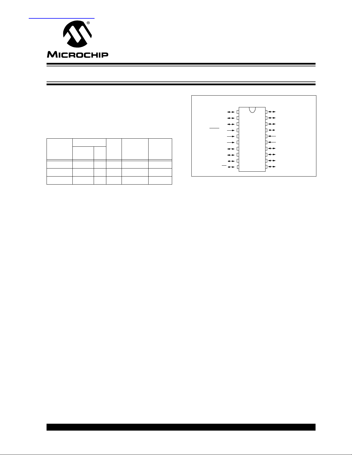
Pin Diagram
20-Pin PDIP, SOIC, SSOP
20
RA0/AN0
RA1/AN1/LVDIN
RA4/T0CKI
RA5/MCLR/VPP
VSS
AVSS
RA2/AN2/VREF-/VRL
RA3/AN3/VREF+/VRH
RB0/AN4/INT
RB1/AN5/SS
1
2
PIC16C770/771
3
4
5
6
7
8
9
10
19
18
17
16
15
14
13
12
11
RB3/CCP1/P1A
RB2/SCK/SCL
RA7/OSC1/CLKIN
RA6/OSC2/CLKOUT
VDD
AVDD
RB7/T1OSI/P1D
RB6/T1OSO/T1CKI/P1C
RB5/SDO/P1B
RB4/SDI/SDA
Peripheral Features:
• Timer0: 8-bit timer/counter with 8-bit prescaler
• Timer1: 16-bit timer/counter with prescaler,
can be incremented during sleep via external
crystal/clock
• Timer2: 8-bit timer/counter with 8-bit period
register, prescaler and postscaler
• Enhanced Capture, Compare, PWM (ECCP)
module
- Capture is 16 bit, max. resolution is 12.5 ns
- Compare is 16 bit, max. resolution is 200 ns
- PWM max. resolution is 10 bit
- Enhanced PWM:
- Single, Half-Bridge and Full-Bridge output
modes
- Digitally prog rammable dea dba nd del ay
• Analog-to-Digital converter:
- PIC16C770/771 12-bit resolution
- PIC16C717 10-bit resolution
• On-chip absolute bandgap voltage reference
generator
• Programmable Brown-out Reset (PBOR)
circuitry
• Programmable Low-Voltage Detection (P LVD)
circuitry
• Master Synchronous Serial Port (MSSP) with two
modes of operation:
- 3-wire SPI™ (supports all 4 SPI modes)
2
C™ compatible including master mode
-I
support
• Program Memory Read (PMR) capability for lookup table, character string storage and checksum
calculation purposes
1999 Microchip Technology Inc.
Advanced Information DS41120A-page 1
Page 2
PIC16C717/770/771
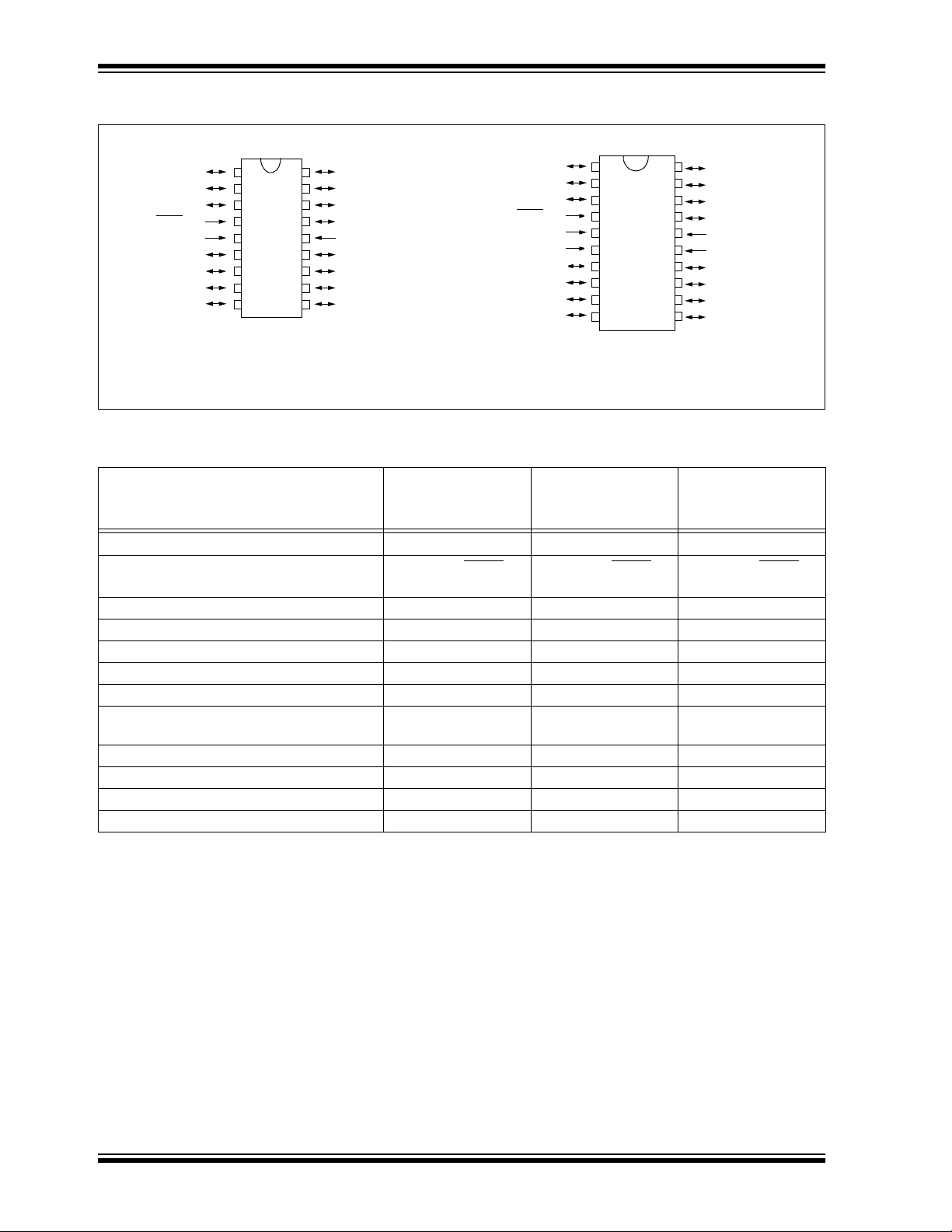
Pin Diagrams
18-Pin PDIP, SOIC
RA0/AN0
RA1/AN1/LVDIN
RA4/T0CKI
RA5/MCLR/VPP
VSS
RA2/AN2/VREF-/VRL
RA3/AN3/VREF+/VRH
RB0/AN4/INT
RB1/AN5/SS
18
1
17
2
PIC16C717
16
3
15
4
14
5
13
6
12
7
11
8
10
9
RB3/CCP1/P1A
RB2/SCK/SCL
RA7/OSC1/CLKIN
RA6/OSC2/CLKOUT
VDD
RB7/T1OSI/P1D
RB6/T1OSO/T1CKI/P1C
RB5/SDO/P1B
RB4/SDI/SDA
20-Pin SSOP
RA0/AN0
RA1/AN1/LVDIN
RA4/T0CKI
RA5/MCLR/VPP
VSS
VSS
RA2/AN2/VREF-/VRL
RA3/AN3/VREF+/VRH
RB0/AN4/INT
RB1/AN5/SS
PIC16C717
20
19
18
17
16
15
14
13
12
11
RB3/CCP1/P1A
RB2/SCK/SCL
RA7/OSC1/CLKIN
RA6/OSC2/CLKOUT
(2)
VDD
(2)
VDD
RB7/T1OSI/P1D
RB6/T1OSO/T1CKI/P1C
RB5/SDO/P1B
RB4/SDI/SDA
1
2
3
(1)
(1)
4
5
6
7
8
9
10
Note 1: VSS pins 5 and 6 must be tied together.
2: V
DD pins 15 and 16 must be tied together.
Key Features
PICmicroTM Mid-Range Reference Manual
PIC16C717 PIC16C770 PIC16C771
(DS33023)
Operating Frequency DC - 20 MHz DC - 20 MHz DC - 20 MHz
Resets (and Delays)
POR, BOR, MCLR,
WDT (PWRT, OST)
POR, BOR, MCLR,
WDT (PWRT, OST)
POR, BOR, MCLR,
WDT (PWRT, OST)
Program Memory (14-bit words) 2K 2K 4K
Data Memory (bytes) 256 256 256
Interrupts 10 10 10
I/O Ports Ports A,B Ports A,B Ports A,B
Timers 333
Enhanced Capture/Compare/PWM (ECCP)
111
modules
Serial Communications MSSP MSSP MSSP
12-bit Analog-to-Digital Module 6 input channels 6 input channels
10-bit Analog-to-Digital Module 6 input channels
Instruction Set 35 Instructions 35 Instructions 35 Instructions
DS41120A-page 2 Advanced Information
1999 Microchip Technology Inc.
Page 3

PIC16C717/770/771
Table of Contents
1.0 Device Overv iew......................................................................................... ...... ..... ....................................... ...... ..5
2.0 Memory Organization..........................................................................................................................................11
3.0 I/O Ports..............................................................................................................................................................27
4.0 Program Memory Read (PMR)...........................................................................................................................43
5.0 Timer0 Module....................................................................................................................................................47
6.0 Timer1 Module....................................................................................................................................................49
7.0 Timer2 Module....................................................................................................................................................53
8.0 Enhanced Capture/Compare/PWM(ECCP) Modules .........................................................................................55
9.0 Master Synchronous Serial Port (MSSP) Module...............................................................................................67
10.0 Voltage Reference Module and Low-voltage Detect.........................................................................................109
11.0 Analog-to-Digital Converter (A/D) Module ........................................................................................................113
12.0 Special Features of the CPU............................................................................................................................125
13.0 Instruction Set Summary...................................................................................................................................141
14.0 Development Support.......................................................................................................................................149
15.0 Electrical Characteristics................................................. ...... ..... ...... ................................. ...... ..........................155
16.0 DC and AC Characteristics Graphs and Tables...............................................................................................177
17.0 Packaging Information......................................................................................................................................179
Revision History ........................................................................................................................................................189
Device Differences ............................................................. ...... ...... ..... ...... ................................. ...... ..........................189
Index .......................................................................................................................................................................... 191
On-Line Support..........................................................................................................................................................197
Reader Response.......................................................................................................................................................198
PIC16C717/770/771 Product Identification System....................................................................................................199
To Our Valued Customers
Most Current Data Sheet
To obtain the most up-to-date version of this data sheet, please register at our Worldwide Web site at:
http://www.microchip.com
You can determine the version of a data sheet by examining its literature number found on the bottom outside corner of any page.
The last character of the literature number is the version number. e.g., DS30000A is version A of document DS30000.
New Customer Notification System
Register on our web site (www.microchip.com/cn) to receive the most current information on our products.
Errata
An errata sheet may exist for current devices, describing minor operational differences (from the data sheet) and recommended
workarounds. As device/documentation issues become known to us, w e will pub lish an errata sheet. The errata will specify the re vision of silicon and revision of document to which it applies.
To determine if an errata sheet exists for a particular device, please check with one of the fo llowing:
• Microchip’s Worldwide Web site; http://www.microchip.com
• Your local Microchip sales office (see last page)
• The Microchip Corporate Literature Center; U.S. FAX: (480) 786-7277
When contacting a sales office or the literature center, please specify which device, revision of silicon and data sheet (include liter-
ature number) you are using.
Corrections to this Data Sheet
We constantly strive to improve the quality of all our products and documentation. We have spent a great deal of time to ensure
that this document is correct. However , w e realize that we ma y have missed a few things. If you fi nd any inf ormation that is missing
or appears in error, please:
• Fill out and mail in the reader response form in the back of this data sheet.
• E-mail us at webmaster@microchip.com.
We appreciate your assistance in making this a better document.
1999 Microchip Technology Inc.
Advanced Information DS41120A-page 3
Page 4

PIC16C717/770/771
NOTES:
DS41120A-page 4 Advanced Information
1999 Microchip Technology Inc.
Page 5
PIC16C717/770/771
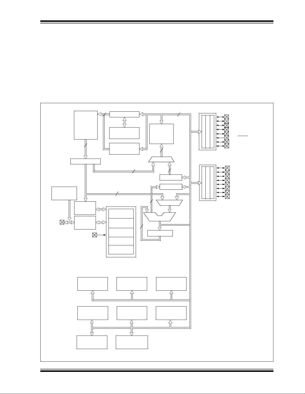
1.0 DEVICE OVERVIEW
This document contains device-specific information.
Additional information may be found in the PICmicro
Mid-Range Reference Manual, (DS33023), which may
be obtained from your local Microchip Sales Representative or downloaded from the Microchip website. The
Reference Manual should be considered a complementary document to this data she et, and is h ighly recommended reading for a better understanding of the
device architecture and operation of the peripheral
modules.
FIGURE 1-1: PIC16C717 BLOCK DIAGRAM
13
Program Counter
8 Level Stack
(13-bit)
Program Memory
Read (PMR)
Direct Addr
8
Power-up
Timer
Oscillator
Start-up Tim er
Power-on
Reset
Watchdog
Timer
Brown-out
Reset
Program
Bus
Internal
4MHz, 37KHz
and ER mode
OSC1/CLKIN
OSC2/CLKOUT
EPROM
Program
Memory
2K x 14
14
Instruction reg
Instruction
Decode &
Control
Timing
Generation
DD, VSS
V
TM
7
3
8
There are three devices (PIC16C717, PIC16C770 and
PIC16C771) covered by this datasheet. The
PIC16C717 device comes in 18/20-pin packages and
the PIC16C770/771 devices come in 20-pin packages.
The following two fig u r es ar e device block di agr am s o f
the PIC16C717 and the PIC16C770/771.
Data Bus
RAM
File
Registers
256 x 8
9
Addr MUX
FSR reg
STATUS reg
ALU
W reg
8
MUX
RAM
Addr
Indirect
Addr
8
(1)
PORTA
PORTB
RA0/AN0
RA1/AN1/LVDIN
RA2/AN2/VREF-/VRL
RA3/AN3/VREF+/VRH
RA4/T0CKI
RA5/MCLR/VPP
RA6/OSC2/CLKOUT
RA7/OSC1/CLKIN
RB0/AN4/INT
RB1/AN5/SS
RB2/SCK/SCL
RB3/CCP1/P1A
RB4/SDI/SDA
RB5/SDO/P1B
RB6/T1OSO/T1CKI/P1C
RB7/T1OSI/P1O
10-bit
ADC
Timer0 Timer1 Timer2
Enhanced CCP
(ECCP1)
Synchronous
Serial Port (MSSP)
Note 1: Higher order bits are from the STATUS register.
1999 Microchip Technology Inc.
Bandgap
Reference
Master
Low-voltage
Detect
Advanced Information DS41120A-page 5
Page 6
PIC16C717/770/771
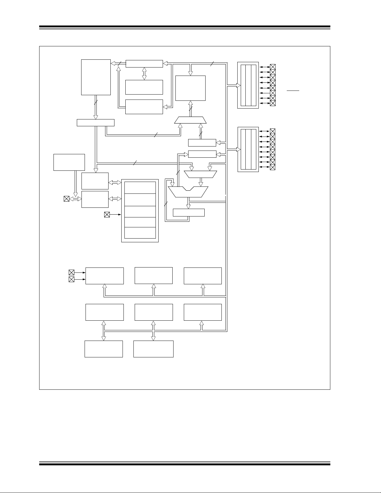
FIGURE 1-2: PIC16C7 70/7 71 BLOCK DIAGRAM
Program
Bus
Internal
4MHz, 37KHz
and ER mode
OSC1/CLKIN
OSC2/CLKOUT
EPROM
Program
(2)
Memory
14
Instruction reg
Instruction
Decode &
Control
Timing
Generation
DD, VSS
V
13
Program Counter
8 Level Stack
Program Memory
Read (PMR)
Direct Addr
8
Power-up
Timer
Oscillator
Start-up Timer
Power-on
Reset
Watchdog
Timer
Brown-out
Reset
(13-bit)
9
8
MUX
RAM
Addr
Indirect
Addr
8
(1)
Data Bus
RAM
File
Registers
256 x 8
Addr MUX
7
FSR reg
STATUS reg
3
ALU
8
W reg
PORTA
RA0/AN0
RA1/AN1/LVDIN
RA2/AN2/VREF-/VRL
RA3/AN3/VREF+/VRH
RA4/T0CKI
RA5/MCLR/VPP
RA6/OSC2/CLKOUT
RA7/OSC1/CLKIN
PORTB
RB0/AN4/INT
RB1/AN5/SS
RB2/SCK/SCL
RB3/CCP1/P1A
RB4/SDI/SDA
RB5/SDO/P1B
RB6/T1OSO/T1CKI/P1C
RB7/T1OSI/P1O
AVDD
AVSS
12-bit
ADC
Timer0 Timer1 Ti m e r2
Enhanced CCP
(ECCP1)
Bandgap
Reference
Master
Synchronous
Serial Port (MSSP)
Low-voltage
Detect
Note 1: Higher order bits are from the STATUS register.
2: Program memory for PIC16C770 is 2K x 14. Program memory for PIC16C771 is 4K x 14.
DS41120A-page 6 Advanced Information
1999 Microchip Technology Inc.
Page 7

TABLE 1-1: PIC16C770/771 PINOUT DESCRIPTION
Name Function
RA0/AN0
RA0 ST CMOS Bi-directional I/O
AN0 AN A/D input
RA1 ST CMOS Bi-directional I/O
RA1/AN1/LVDIN
AN1 AN A/D input
LVDIN AN LVD input reference
RA2 ST CMOS Bi-directional I/O
RA2/AN2/V
REF-/VRL
AN2 AN A/D input
REF- AN Negative analog reference input
V
VRL AN Internal voltage reference low output
RA3 ST CMOS Bi-directional I/O
RA3/AN3/V
REF+/VRH
AN3 AN A/D input
REF+ AN Positive analog reference input
V
VRH AN Internal voltage reference high output
RA4/T0CKI
RA4 ST OD Bi-directional I/O
T0CKI ST TMR0 clock input
RA5 ST Input port
RA5/MCLR
/VPP
MCLR
PP Power Programming voltage
V
RA6 ST CMOS Bi-directional I/O
RA6/OSC2/CLKOUT
OSC2 XTAL Crystal/resonator
CLKOUT CMOS F
RA7 ST CMOS Bi-directional I/O
RA7/OSC1/CLKIN
OSC1 XTA L Crystal/resonator
CLKIN ST External clock input/ER resistor connection
RB0 TTL CMOS Bi-directional I/O
RB0/AN4/INT
AN4 AN A/D input
INT ST Interrupt input
RB1 TTL CMOS Bi-directional I/O
RB1/AN5/SS
AN5 AN A/D input
SS
RB2 TTL CMOS Bi-directional input
RB2/SCK/SCL
SCK ST CMOS Serial clock I/O for SPI
SCL ST OD Serial clock I/O for I
RB3 TTL CMOS Bi-directional input
RB3/CCP1/P1A
CCP1 ST CMOS Capture 1 input/Compare 1 output
P1A CMOS PWM P1A output
RB4 TTL CMOS Bi-directional input
RB4/SDI/SDA
SDI ST Serial data in for SPI
SDA ST OD Serial data I/O for I
RB5 ST CMOS Bi-directional I/O
RB5/SDO/P1B
SDO CMOS Serial data out for SPI
P1B CMOS PWM P1B output
Note 1: Bit programmable pull-ups.
Input
Type
ST Master clear
ST SSP slave select input
Output
Type
OSC/4 output
PIC16C717/770/771
Description
(1)
(1)
(1)
2
C
(1)
(1)
2
C
(1)
1999 Microchip Technology Inc.
Advanced Information DS41120A-page 7
Page 8

PIC16C717/770/771
TABLE 1-1: PIC16C770/771 PINOUT DESCRIPTION (CONTINUED)
Name Function
RB6 TTL CMOS Bi-directional I/O
RB6/T1OSO/T1CKI/P1C
RB7/T1OSI/P1D
SS VSS Power Ground reference for logic and I/O pins
V
DD VDD Power Positive supply for logic and I/O pins
V
SS AVSS Power Ground reference for analog
AV
DD AVDD Power Positive supply for analog
AV
Note 1: Bit programmable pull-ups.
T1OSO XTAL Crystal/Resonator
T1CKI ST TMR1 clock input
P1C CMOS PWM P1C output
RB7 TTL CMOS Bi-directional I/O
T1OSI XTAL TMR1 crystal/resonator
P1D CMOS PWM P1D output
Input
Type
Output
Type
(1)
(1)
Description
DS41120A-page 8 Advanced Information
1999 Microchip Technology Inc.
Page 9

TABLE 1-2: PIC16C717 PINOUT DESCRIPTION
Name Function
RA0/AN0
RA0 ST CMOS Bi-directional I/O
AN0 AN A/D input
RA1 ST CMOS Bi-directional I/O
RA1/AN1/LVDIN
AN1 AN A/D input reference
LVDIN AN LVD input reference
RA2 ST CMOS Bi-directional I/O
RA2/AN2/V
REF-/VRL
AN2 AN A/D input
REF- AN Negative analog reference input
V
VRL AN Internal voltage reference low output
RA3 ST CMOS Bi-directional I/O
RA3/AN3/V
REF+/VRH
AN3 AN A/D input
REF+ AN Positive analog reference high output
V
VRH AN Internal voltage reference high output
RA4/T0CKI
RA4 ST OD Bi-directional I/O
T0CKI ST TMR0 clock input
RA5 ST Input port
RA5/MCLR
/VPP
MCLR
PP Power Programming Voltage
V
RA6 ST CMOS Bi-directional I/O
RA6/OSC2/CLKOUT
OSC2 XTAL Crystal/Resonator
CLKOUT CMOS F
RA7 ST CMOS Bi-directional I/O
RA7/OSC1/CLKIN
OSC1 XTAL Crystal/Resonator
CLKIN ST External clock input/ER resistor connection
RB0 TTL CMOS Bi-directional I/O
RB0/AN4/INT
AN4 AN A/D input
INT ST Interrupt input
RB1 TTL CMOS Bi-directional I/O
RB1/AN5/SS
AN5 AN A/D input
SS
RB2 TTL CMOS Bi-directional input
RB2/SCK/SCL
SCK ST CMOS Serial clock I/O for SPI
SCL ST OD Serial clock I/O for I
RB3 TTL CMOS Bi-directional input
RB3/CCP1/P1A
CCP1 ST CMOS Capture 1 input/Compare 1 output
P1A CMOS PWM P1A output
RB4 TTL CMOS Bi-directional input
RB4/SDI/SDA
SDI ST Serial data in for SPI
SDA ST OD Serial data I/O for I
RB5 ST CMOS Bi-directional I/O
RB5/SDO/P1B
SDO CMOS Serial data out for SPI
P1B CMOS PWM P1B output
Note 1: Bit programmable pull-ups.
Input
Type
ST Master Clear
ST SSP slave select input
Output
Type
PIC16C717/770/771
Description
OSC/4 output
(1)
(1)
(1)
2
C
(1)
(1)
2
C
(1)
1999 Microchip Technology Inc.
Advanced Information DS41120A-page 9
Page 10

PIC16C717/770/771
TABLE 1-2: PIC16C717 PINOUT DESCRIPTION (CONTINUED)
Name Function
RB6 TTL CMOS Bi-directional I/O
RB6/T1OSO/T1CKI/P1C
RB7/T1OSI/P1D
SS VSS Power Ground
V
DD VDD Power Positive Supply
V
Note 1: Bit programmable pull-ups.
T1OSO XTAL TMR1 Crystal/Resonator
T1CKI ST TMR1 Clock input
P1C CMOS PWM P1C output
RB7 TTL CMOS Bi-directional I/O
T1OSI XTAL TMR1 Crystal/Resonator
P1D CMOS PWM P1D output
Input
Type
Output
Type
Description
(1)
(1)
DS41120A-page 10 Advanced Information
1999 Microchip Technology Inc.
Page 11
PIC16C717/770/771
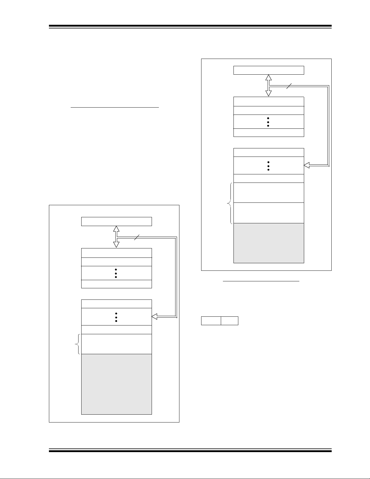
2.0 MEMORY ORGANIZATION
There are two memory blocks in each of these
PICmicro
gram Memory and Data Memory) has its own bu s,
so that concurrent access can occur.
Additional inf ormation on de vice m emory may be f ound
in the PICmicro Mid-Range Reference Manual,
(DS33023).
2.1 Program Memory Organization
The PIC16C717/770/771 devices have a 13-bit program counter capable of addressing an 8K x 14 program memory space. The PIC16C717 and the
PIC16C770 have 2K x 14 words of program memory.
The PIC16C771 has 4K x 14 words of program memory. Accessing a location above the physically implemented address will cause a wraparound.
The reset vector is at 0000h and the interrupt vector is
at 0004h.
FIGURE 2-1: PROGRAM MEMORY MAP
®
microcontrollers. Each block (Pro-
AND STACK OF THE
PIC16C717 AND PIC16C770
PC<12:0>
CALL, RETURN
RETFIE, RETLW
13
FIGURE 2-2: PROGRAM MEMORY MAP
AND STACK OF THE
PIC16C771
PC<12:0>
CALL, RETURN
RETFIE, RETLW
On-chip
Program
Memory
Stack Level 1
Stack Level 2
Stack Level 8
Reset Vector
Interrupt Vector
Page 0
Page 1
13
0000h
0004h
0005h
07FFh
0800h
0FFFh
1000h
On-chip
Program
Memory
Stack Level 1
Stack Level 2
Stack Level 8
Reset Vector
Interrupt Vector
Page 0
0000h
0004h
0005h
07FFh
3FFFh
3FFFh
2.2 Data Memory Organization
The data memory is partitioned into multiple banks,
which contain the General Purpose Registers and the
Special Function Registers. Bits RP1 and RP0 are the
bank select bits.
RP1 RP0 (STATUS<6:5>)
= 00 → Bank0
= 01 → Bank1
= 10 → Bank2
= 11 → Bank3
Each bank extends up to 7Fh (128 bytes). The lower
locations of each bank are reserved for the Special
Function Registers . Abo v e the Spec ial Fun ction Re gisters are General Purpose Registers, implemented as
static RAM. All implemented banks contain special
function registers. Some frequently used special function registers from one bank are mirrored in another
bank for code reduction and quicker access.
2.2.1 GENERAL PURPOSE REGISTER FILE
1999 Microchip Technology Inc.
The register file can be a ccessed ei ther direc tly, or indirectly, through the File Select Register FSR.
Advanced Information DS41120A-page 11
Page 12
PIC16C717/770/771
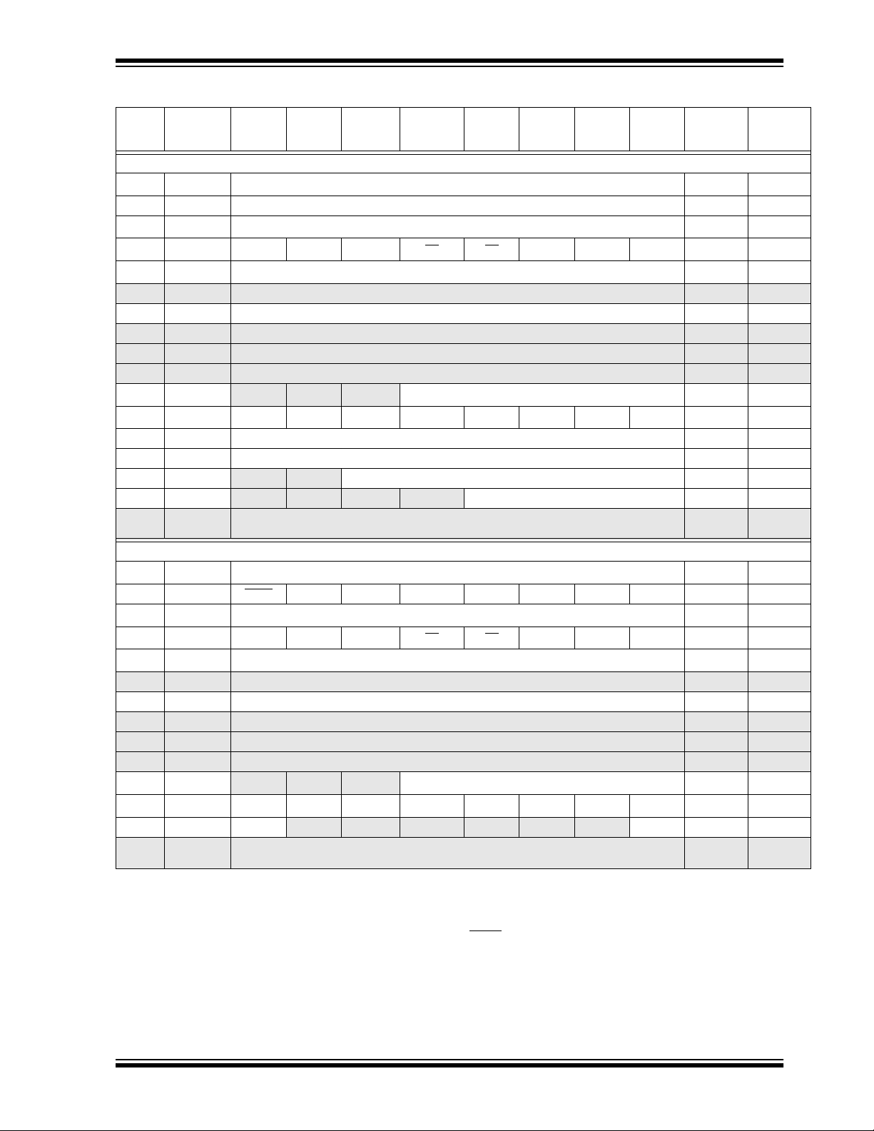
FIGURE 2-3: REGISTER FILE MAP
File
Address
Indirect addr.
TMR0
PCL
STATUS
FSR
PORTA
PORTB
PCLATH
INTCON
PIR1
PIR2
TMR1L
TMR1H
T1CON
TMR2
T2CON
SSPBUF
SSPCON
CCPR1L
CCPR1H
CCP1CON
ADRESH
ADCON0
General
Purpose
Register
96 Bytes
Bank 0 Bank 1
(*)
00h
Indirect addr.
01h
02h
03h
04h
05h
06h
07h
08h
09h
0Ah
0Bh
0Ch
0Dh
0Eh
0Fh
10h
11h
12h
13h
14h
15h
16h
17h
18h
19h
1Ah
1Bh
1Ch
1Dh
1Eh
1Fh
20h
7Fh
OPTION_REG
PCLATH
INTCON
SSPCON2
SSPADD
SSPSTAT
REFCON
LVDCON
ADRESL
ADCON1
General
Purpose
Register
80 Bytes
accesses
70h-7Fh
PCL
STATUS
FSR
TRISA
TRISB
PIE1
PIE2
PCON
PR2
WPUB
IOCB
P1DEL
ANSEL
File
Address
(*)
80h
81h
82h
83h
84h
85h
86h
87h
88h
89h
8Ah
8Bh
8Ch
8Dh
8Eh
8Fh
90h
91h
92h
93h
94h
95h
96h
97h
98h
99h
9Ah
9Bh
9Ch
9Dh
9Eh
9Fh
A0h
EFh
F0h
FFh
Indirect addr.
TMR0
PCL
STATUS
FSR
PORTB
PCLATH
INTCON
PMDATL
PMADRL
PMDATH
PMADRH
General
Purpose
Register
80 Bytes
accesses
70h - 7Fh
Bank 2
Address
(*)
File
100h
101h
102h
103h
104h
105h
106h
107h
108h
109h
10Ah
10Bh
10Ch
10Dh
10Eh
10Fh
110h
111h
112h
113h
114h
115h
116h
117h
118h
119h
11Ah
11Bh
11Ch
11Dh
11Eh
11Fh
120h
6Fh
70h
17Fh
Indirect addr.
OPTION_REG
PCL
STATUS
FSR
TRISB
PCLATH
INTCON
PMCON1
accesses
70h - 7Fh
Bank 3
File
Address
(*)
180h
181h
182h
183h
184h
185h
186h
187h
188h
189h
18Ah
18Bh
18Ch
18Dh
18Eh
18Fh
190h
191h
192h
193h
194h
195h
196h
197h
198h
199h
19Ah
19Bh
19Ch
19Dh
19Eh
19Fh
1A0h
1EFh
1F0h
1FFh
Unimplemented data memory locations, read as ’0’.
* Not a physical register.
DS41120A-page 12 Advanced Information
1999 Microchip Technology Inc.
Page 13
PIC16C717/770/771
2.2.2 SPECIAL FUNCTION REGISTERS
The special fu nction re gisters can b e classifi ed into two
sets; core (CPU) and periphe ral. Those registers asso-
The Special Function Registers are registers used by
the CPU and Peripheral Modules for controlling the
desired operation of the device. These registers are
implemented as static RAM. A list of these registers is
given in Table 2-1.
ciated with the core functions are described in detail in
this section. Those related to the operation of the
peripheral features are described in detail in that
peripheral feature section.
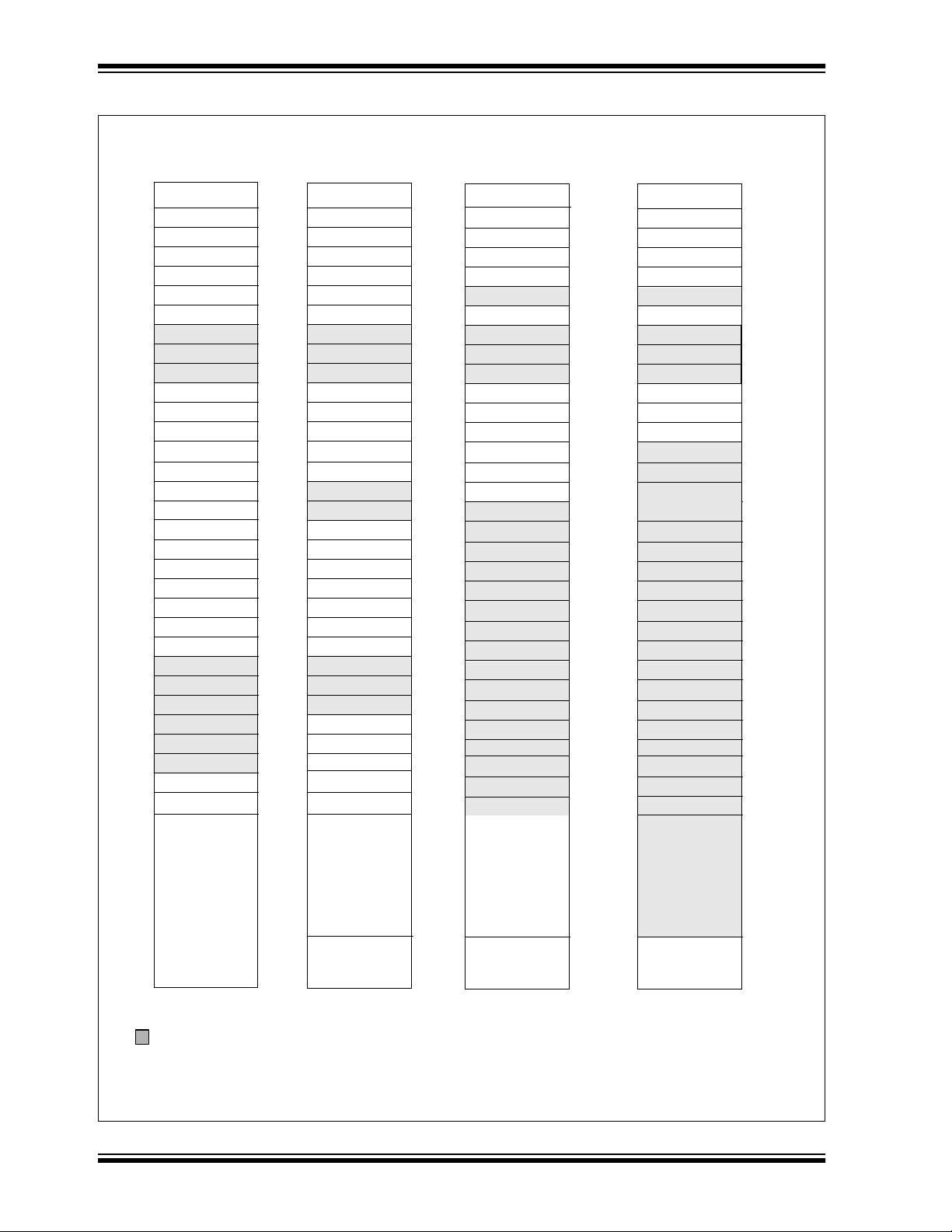
TABLE 2-1: PIC16C717/770/771 SPECIAL FUNCTION REGISTER SUMMARY
Address Name Bit 7 Bit 6 Bit 5 Bit 4 Bit 3 Bit 2 Bit 1 Bit 0
Value on:
POR,
BOR
Bank 0
(3)
00h
01h TMR0 Timer0 module’s register xxxx xxxx uuuu uuuu
02h
03h
04h
05h PORTA RA7 RA6 RA5 RA4 RA3 RA2 RA1 RA0 xxxx 0000 uuuu 0000
06h PORTB RB7 RB6 RB5 RB4 RB3 RB2 RB1 RB0 xxxx xx00 uuuu uu00
07h — Unimplemented — —
08h — Unimplemented — —
09h — Unimplemented — —
0Ah
0Bh
0Ch PIR1
0Dh PIR2 LVDIF
0Eh TMR1L Holding register for the Least Significant Byte of the 16-bit TMR1 register xxxx xxxx uuuu uuuu
0Fh TMR1H Holding register for the Most Significant Byte of the 16-bit TMR1 register xxxx xxxx uuuu uuuu
10h T1CON
11h TMR2 Timer2 module’s register 0000 0000 0000 0000
12h T2CON
13h SSPBUF Synchronous Serial Port Receive Buffer/Transmit Register xxxx xxxx uuuu uuuu
14h SSPCON WCOL SSPOV SSPEN CKP SSPM3 SSPM2 SSPM1 SSPM0 0000 0000 0000 0000
15h CCPR1L Capture/Compare/PWM Register1 (LSB) xxxx xxxx uuuu uuuu
16h CCPR1H Capture/Compare/PWM Register1 (MSB) xxxx xxxx uuuu uuuu
17h CCP1CON PWM1M1 PWM1M0 DC1B1 DC1B0 CCP1M3 CCP1M2 CCP1M1 CCP1M0 0000 0000 0000 0000
18h — Unimplemented — —
19h — Unimplemented — —
1Ah — Unimplemented — —
1Bh — Unimplemented — —
1Ch — Unimplemented — —
1Dh — Unimplemented — —
1Eh ADRESH A/D High Byte Result Register xxxx xxxx uuuu uuuu
1Fh ADCON0 ADCS1 ADCS0 CHS2 CHS1 CHS0 GO/DONE
Legend:x = unknown, u = unchanged, q = value depends on condition, - = unimplemented read as ’0’.
Note 1: The upper byte of the program counter is not directly accessible. PCLATH is a holding register for the PC<12:8> whose con-
INDF Addressing this location uses contents of FSR to address data memory (not a physical register) 0000 0000 0000 0000
(3)
PCL Program Counter's (PC) Least Significant Byte 0000 0000 0000 0000
(3)
ST ATUS IRP RP1 RP0 TO PD ZDCC0001 1xxx 000q quuu
(3)
FSR Indirect data memory address pointer xxxx xxxx uuuu uuuu
(1,3)
PCLATH — — — Write Buffer for the upper 5 bits of the Program Counter ---0 0000 ---0 0000
(3)
INTCON GIE PEIE T0IE INTE RBIE T0IF INTF RBIF 0000 000x 0000 000u
—ADIF— — SSPIF CCP1IF TMR2IF TMR1IF -0-- 0000 -0-- 0000
— — —BCLIF— — — 0--- 0--- 0--- 0---
— — T1CKPS1 T1CKPS0 T1OSCEN T1SYNC TMR1CS TMR1ON --00 0000 --uu uuuu
— TOUTPS3 TOUTPS2 TOUTPS1 TOUTPS0 TMR2ON T2CKPS1 T2CKPS0 -000 0000 -000 0000
CHS3 ADON 0000 0000 0000 0000
Shaded locations are unimplemented, read as ‘0’.
tents are transferred to the upper byte of the program counter.
2: Other (non power-up) resets include external reset through MCLR
and Watchdog Timer Reset.
3: These registers can be addressed from any bank.
Value on all
other resets
(2)
1999 Microchip Technology Inc.
Advanced Information DS41120A-page 13
Page 14
PIC16C717/770/771
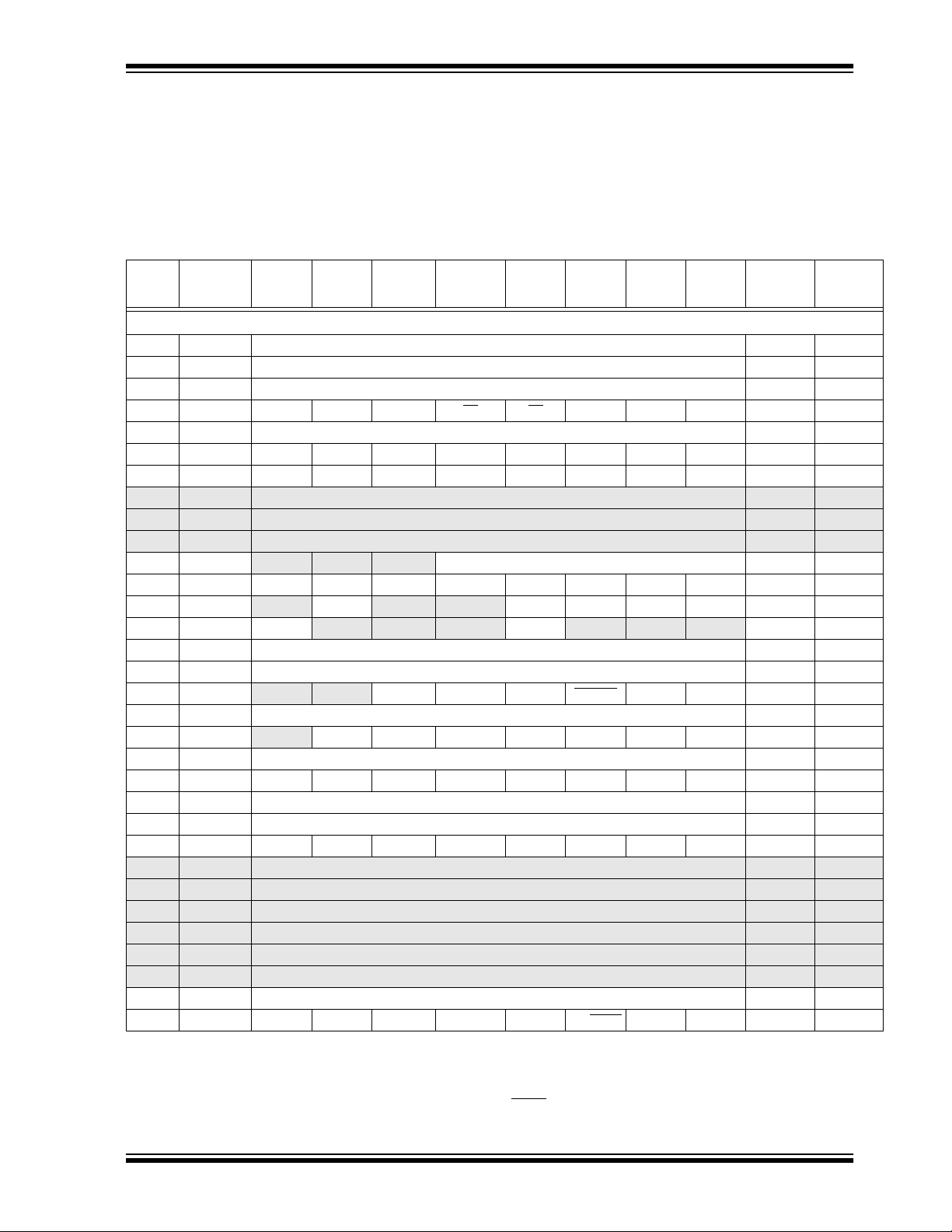
TABLE 2-1: PIC16C717/770/771 SPECIAL FUNCTION REGISTER SUMMARY (CONTINUED)
Address Name Bit 7 Bit 6 Bit 5 Bit 4 Bit 3 Bit 2 Bit 1 Bit 0
Bank 1
(3)
80h
81h OPTION_REG RBPU
82h
83h
84h
85h TRISA PORTA Data Direction Register 1111 1111 1111 1111
86h TRISB PORTB Data Direction Register 1111 1111 1111 1111
87h — Unimplemented — —
88h — Unimplemented — —
89h — Unimplemented — —
8Ah
8Bh
8Ch PIE1
8Dh PIE2 LVDIE
8Eh PCON
8Fh — Unimplemented — —
90h — Unimplemented — —
91h SSPCON2 GCEN ACKSTAT ACKDT ACKEN RCEN PEN RSEN SEN 0000 0000 0000 0000
92h PR2 Timer2 Period Register 1111 1111 1111 1111
93h SSPADD Synchronous Serial Port (I
94h SSPSTAT SMP CKE D/A
95h WPUB PORTB Weak Pull-up Control 1111 1111 1111 1111
96h IOCB PORTB Interrupt on Change Control 1111 0000 1111 0000
97h P1DEL PWM 1 Delay value 0000 0000 0000 0000
98h — Unimplemented — —
99h — Unimplemented — —
9Ah — Unimplemented — —
9Bh REFCON VRHEN VRLEN VRHOEN VRLOEN
9Ch LVDCON
9Dh ANSEL
9Eh ADRESL A/D Low Byte Result Register xxxx xxxx uuuu uuuu
9Fh ADCON1 ADFM VCFG2 VCFG1 VCFG0
INDF Addressing this location uses contents of FSR to address data memory (not a physical register) 0000 0000 0000 0000
INTEDG T0CS T0SE PSA PS2 PS1 PS0 1111 1111 1111 1111
(3)
PCL Program Counter’s (PC) Least Significant Byte 0000 0000 0000 0000
(3)
ST ATUS IRP RP1 RP0 TO PD ZDCC0001 1xxx 000q quuu
(3)
FSR Indirect data memory address pointer xxxx xxxx uuuu uuuu
(1,3)
PCLATH — — — Write Buffer for the upper 5 bits of the Program Counter ---0 0000 ---0 0000
(3)
INTCON GIE PEIE T0IE INTE RBIE T0IF INTF RBIF 0000 000x 0000 000u
—ADIE — — SSPIE CCP1IE TMR2IE TMR1IE -0-- 0000 -0-- 0000
— — —BCLIE— — — 0--- 0--- 0--- 0---
— — — —OSCF—PORBOR ---- 1-qq ---- 1-uu
2
C mode) Address Register 0000 0000 0000 0000
PSR/WUA BF 0000 0000 0000 0000
— — — — 0000 ---- 0000 ----
— — BGST LVDEN LVV3 LVV2 LVV1 LVV0 --00 0101 --00 0101
Analog Channel Select
Value on:
POR,
BOR
1111 1111 1111 1111
0000 0000 0000 0000
Legend:x = unknown, u = unchanged, q = value depends on condition, - = unimplemented read as ’0’.
Shaded locations are unimplemented, read as ‘0’.
Note 1: The upper byte of the program counter is not directly accessible. PCLATH is a holding register for the PC<12:8> whose con-
tents are transferred to the upper byte of the program counter.
2: Other (non power-up) resets include external reset through MCLR
and Watchdog Timer Reset.
3: These registers can be addressed from any bank.
Value on all
other resets
(2)
DS41120A-page 14 Advanced Information
1999 Microchip Technology Inc.
Page 15
PIC16C717/770/771
TABLE 2-1: PIC16C717/770/771 SPECIAL FUNCTION REGISTER SUMMARY (CONTINUED)
Address Name Bit 7 Bit 6 Bit 5 Bit 4 Bit 3 Bit 2 Bit 1 Bit 0
Bank 2
(3)
100h
101h TMR0 Timer0 module’s register xxxx xxxx uuuu uuuu
102h
103h
104h
105h — Unimplemented — —
106h PORTB PORTB Data Latch when written: PORTB pins when read xxxx xx00 uuuu uu00
107h — Unimplemented — —
108h — Unimplemented — —
109h — Unimplemented — —
10Ah
10Bh
10Ch PMDATL Program memory read data low xxxx xxxx uuuu uuuu
10Dh PMADRL Program memory read address low xxxx xxxx uuuu uuuu
10Eh PMDATH
10Fh PMADRH
110h-
11Fh
INDF Addressing this location uses contents of FSR to address data memory (not a physical register) 0000 0000 0000 0000
(3)
PCL Program Counter's (PC) Least Significant Byte 0000 0000 0000 0000
(3)
STATUS IRP RP1 RP0 TO PD Z DC C 0001 1xxx 000q quuu
(3)
FSR Indirect data memory address pointer xxxx xxxx uuuu uuuu
(1,3)
PCLATH — — — Write Buffer for the upper 5 bits of the Program Counter ---0 0000 ---0 0000
(3)
INTCON GIE PEIE T0IE INTE RBIE T0IF INTF RBIF 0000 000x 0000 000u
— — Program memory read data high --xx xxxx --uu uuuu
— — — — Program memory read address high ---- xxxx ---- uuuu
— Unimplemented — —
Value on:
POR,
BOR
Bank 3
(3)
180h
181h OPTION_REG RBPU
182h
183h
184h
185h — Unimplemented — —
186h TRISB PORTB Data Direction Register 1111 1111 1111 1111
187h — Unimplemented — —
188h — Unimplemented — —
189h — Unimplemented — —
18Ah
18Bh
18Ch PMCON1 Reserved
18Dh-
18Fh
INDF Addressing this location uses contents of FSR to address data memory (not a physical register) 0000 0000 0000 0000
INTEDG T0CS T0SE PSA PS2 PS1 PS0 1111 1111 1111 1111
(3)
PCL Program Counter's (PC) Least Significant Byte 0000 0000 0000 0000
(3)
STATUS IRP RP1 RP0 TO PD Z DC C 0001 1xxx 000q quuu
(3)
FSR Indirect data memory address pointer xxxx xxxx uuuu uuuu
(1,3)
PCLATH — — —
(3)
INTCON GIE PEIE T0IE INTE RBIE T0IF INTF RBIF 0000 000x 0000 000u
— — — — — — RD 1--- ---0 1--- ---0
— Unimplemented — —
Write Buffer for the upper 5 bits of the Program Counter
---0 0000 ---0 0000
Legend:x = unknown, u = unchanged, q = value depends on condition, - = unimplemented read as ’0’.
Shaded locations are unimplemented, read as ‘0’.
Note 1: The upper byte of the program counter is not directly accessible. PCLATH is a holding register for the PC<12:8> whose con-
tents are transferred to the upper byte of the program counter.
2: Other (non power-up) resets include external reset through MCLR
and Watchdog Timer Reset.
3: These registers can be addressed from any bank.
Value on all
other resets
(2)
1999 Microchip Technology Inc.
Advanced Information DS41120A-page 15
Page 16

PIC16C717/770/771
2.2.2.1 STATUS REGISTER
The STATUS register, shown in Register 2-1, contains
the arithmetic status of th e ALU , the RE SET status an d
the bank select bits for data memory.
The STATUS register can be the destination for any
instruction, as with any other register. If the STATUS
register is the destination for an instruction that affects
the Z, DC or C bits, then the write to these three bits is
disabled. The se bi ts ar e set or c leared accordi ng to the
device logic. Fur th er more, the TO
writable. Therefore, the result of an instruction with the
STATUS regi ster as destina tion may be different th an
intended.
and PD bits are not
For example, CLRF STATUS will clear the up p er- t h ree
bits and set th e Z bi t. T his l ea v es the STATUS register
as 000u u1uu (where u = unchanged).
It is recommended, therefore, that only BCF, BSF,
SWAPF and MOVWF instructions are used to alter the
STATUS register, because these instructions do not
affect the Z, C or DC b its from the STA TU S regist er . F or
other instructions not affecting any status bits, see the
"Instruction Set Summary."
Note 2: The C and DC bits oper ate as a borro w and
digit borrow
See the SUBLW and SUBWF instructions for
examples.
REGISTER 2-1: STATUS REGISTER (STATUS: 03h, 83h, 103h, 183h)
R/W-0 R/W-0 R/W-0 R-1 R-1 R/W-x R/W-x R/W-x
IRP RP1 RP0 TO
bit7 bit0
bit 7: IRP: Register Bank Select bit (used for indirect addressing)
1 = Bank 2, 3 (100h - 1FFh)
0 = Bank 0, 1 (00h - FFh)
bit 6-5: RP<1:0>: Register Bank Select bits (used for direct addressing)
11 = Bank 3 (180h - 1FFh)
10 = Bank 2 (100h - 17Fh)
01 = Bank 1 (80h - FFh)
00 = Bank 0 (00h - 7Fh)
Each bank is 128 bytes
bit 4: TO
bit 3: PD
bit 2: Z: Zero bit
bit 1: DC: Digit carry/borrow
bit 0: C: Carry/borrow
: Time-out bit
1 = After power-up, CLRWDT instruction, or SLEEP instruction
0 = A WDT time-out occurred
: Power-down bit
1 = After power-up or by the CLRWDT instruction
0 = By execution of the SLEEP instruction
1 = The result of an arithmetic or logic operation is zero
0 = The result of an arithmetic or logic operation is not zero
bit (ADDWF, ADDLW,SUBLW,SUBWF instructions) (for borrow the p ol arity is reversed)
1 = A carry-out from the 4th low order bit of the result occurr ed
0 = No carry-out from the 4th low order bit of the result
bit (ADDWF, ADDLW,SUBLW,SUBWF instructions)
1 = A carry-out from the most significant bit of the result occurred
0 = No carry-out from the most significant bit of the result occurred
PD Z DC C R = Readable bit
bit, respectively , in subtraction.
W = Writable bit
U = Unimplemented bit,
read as ‘0’
- n = Value at POR reset
Note: For borrow, the polarity is reversed. A subtraction is executed by adding the two’s complement of the sec-
ond operand. For rotate (RRF, RLF) instructions, this bit is loaded with either the high or low order bit of
the source register.
DS41120A-page 16 Advanced Information
1999 Microchip Technology Inc.
Page 17

PIC16C717/770/771
2.2.2.2 OPTION_REG REGISTER
The OPTION_REG register is a readable and writable
register , which contai ns various c ontrol bits to c onfigure
the TMR0 prescaler/WDT postscaler (single assignable regist er kno wn also as the prescale r), the Ext ernal
INT Interrupt, TMR0 and the w eak pul l-ups on PO R TB .
REGISTER 2-2: OPTION REGISTER (OPTION_REG: 81h, 181h)
R/W-1 R/W-1 R/W-1 R/W-1 R/W-1 R/W-1 R/W-1 R/W-1
RBPU
bit7 bit0
bit 7: RBPU: PORTB Pull-up Enable bit
bit 6: INTEDG: Interrupt Edge Select bit
bit 5: T0CS: TMR0 Clock Source Select bit
bit 4: T0SE: TMR0 Source Edge Select bit
bit 3: PSA: Prescaler Assignment bit
bit 2-0: PS<2:0>: Prescaler Rate Select bits
INTEDG T0CS T0SE PSA PS2 PS1 PS0 R = Readable bit
(1)
1 = PORTB weak pull-ups are disabled
0 = PORTB weak pull-ups are enabled by the WPUB register
1 = Interrupt on rising edge of RB0/INT pin
0 = Interrupt on falling edge of RB0/INT pin
1 = Transition on RA4/ T0CKI pin
0 = Internal instructio n cycle clock (CLKOUT)
1 = Increment on high-to-low transition on RA4/T0CKI pin
0 = Increment on low-to-h igh transition on RA4/T0CKI pin
1 = Prescaler is assigned to the WDT
0 = Prescaler is assigned to the Timer0 module
Bit Value TMR0 Rate WDT Rate
000
001
010
011
100
101
110
111
1 : 2
1 : 4
1 : 8
1 : 16
1 : 32
1 : 64
1 : 128
1 : 256
1 : 1
1 : 2
1 : 4
1 : 8
1 : 16
1 : 32
1 : 64
1 : 128
Note: To achieve a 1:1 prescaler assignme nt for
the TMR0 register, assign the prescaler to
the Watchdog Timer.
W = Writable bit
U = Unimplemented bit,
read as ‘0’
- n = Value at POR reset
Note 1: Individual weak pull-up on RB pins can be enabled/disabled from the weak pull-up PORTB Register
(WPUB).
1999 Microchip Technology Inc.
Advanced Information DS41120A-page 17
Page 18

PIC16C717/770/771
2.2.2.3 INTCON REGISTER
The INTCON Regi ster i s a rea dab le a nd w ritabl e regi s-
ter, which contains various enable and flag bits for the
TMR0 register overflow, RB Port change and External
RB0/INT pin interrupts.
Note: Interrupt flag bits get set when an interrupt
condition occurs , regardless of the sta te of
its corresponding enable bit or the global
enable bit, GIE (INTCON<7>). User software should ensure the appropriate interrupt flag bits are clear prior to enabling an
interrupt.
REGISTER 2-3: INTERRUPT CONTROL REGISTER (INTCON: 0Bh, 8Bh, 10Bh, 18Bh)
R/W-0 R/W-0 R/W-0 R/W-0 R/W-0 R/W-0 R/W-0 R/W-x
GIE PEIE T0IE INTE RBIE T0IF INTF RBIF R = Readable bit
bit7 bit0
bit 7: GIE: Global Interrupt Enable bit
1 = Enables all un-masked interrupts
0 = Disables all interrupts
bit 6: PEIE: Peripheral Interrupt Enable bit
1 = Enables all un-masked peripheral interrupts
0 = Disables all peripheral interrupts
bit 5: T0IE: TMR0 Overflow Interrupt Enable bit
1 = Enables the TMR0 interrupt
0 = Disables the TMR0 interrupt
bit 4: INTE: RB0/INT External Interrupt Enable bit
1 = Enables the RB0/INT external interrupt
0 = Disables the RB0/INT external interrupt
bit 3: RBIE: RB Port Change Interrupt Enable bit
(1)
1 = Enables the RB port change interrupt
0 = Disables the RB port change interrupt
bit 2: T0IF: TMR0 Overflow Interrupt Flag bit
1 = TMR0 register has overflowed (must be cleared in software)
0 = TMR0 register did not overflow
bit 1: INTF: RB0/INT External Interrupt Flag bit
1 = The RB0/INT external interrupt occurred (must be cleared in software)
0 = The RB0/INT external interrupt did not occur
bit 0: RBIF : RB Port Change Interrupt Flag bit
(1)
1 = At least one of the RB<7:0> pins changed state (must be cleared in software)
0 = None of the RB<7:0> pins have changed state
W = Writable bit
U = Unimplemented bit,
read as ‘0’
- n = Value at POR reset
Note 1: Individual RB pin interrupt on change can be enabled/disabled from the Interrupt on Change PORTB register (IOCB).
DS41120A-page 18 Advanced Information
1999 Microchip Technology Inc.
Page 19

PIC16C717/770/771
2.2.2.4 PIE1 REGISTER
This register contains the individual enable bits for the
peripheral interrupts.
Note: Bit PEIE (INTCON<6>) must be set to
enable any peripheral interrupt.
REGISTER 2-4: PERIPHERAL INTERRUPT ENABLE REGISTER 1 (PIE1: 8Ch)
U-0 R/W-0 U-0 U-0 R/W-0 R/W-0 R/W-0 R/W-0
—ADIE— — SSPIE CCP1IE TMR2IE TMR1IE R = Readable bit
bit7 bit0
bit 7: Unimplemented: Read as ’0’
bit 6: ADIE: A/D Converter Interrupt Enable bit
1 = Enables the A/D interrupt
0 = Disables the A/D interrupt
bit 5-4: Unimplemented: Read as ’0’
bit 3: SSPIE: Synchronous Serial Port Interrupt Enable bit
1 = Enables the SSP interrupt
0 = Disables the SSP interrupt
bit 2: CCP1 IE: CCP1 Interrupt Enable bit
1 = Enables the CCP1 interrupt
0 = Disables the CCP1 interrupt
bit 1: TMR2IE: TMR2 to PR2 Match Interrupt Enable bit
1 = Enables the TMR2 to PR2 match interrupt
0 = Disables the TMR2 to PR2 match interrupt
bit 0: TMR1IE: TMR1 Overflow Interrupt Enable bit
1 = Enables the TMR1 overflow interrupt
0 = Disables the TMR1 overflow interrupt
W = Writable bit
U = Unimplemented bit,
read as ‘0’
- n = Value at POR reset
1999 Microchip Technology Inc.
Advanced Information DS41120A-page 19
Page 20

PIC16C717/770/771
2.2.2.5 PIR1 R EGISTER
This register contains the individual flag bits for the
peripheral interrupts.
Note: Interrupt flag bits get set when an interrupt
condition occurs , regardless of the sta te of
its corresponding enable bit or the global
enable bit, GIE (INTCON<7>). User software should ensure the appropriate interrupt flag bits are clear prior to enabling an
interrupt.
REGISTER 2-5: PERIPHERAL INTERRUPT REGISTER 1 (PIR1: 0Ch)
U-0 R/W-0 U-0 U-0 R/W-0 R/W-0 R/W-0 R/W-0
—
bit7 bit0
ADIF
— —
bit 7: Unimplemen ted: Read as ‘0’.
bit 6: ADIF : A/D Converter Interrupt Flag bit
1 = An A/D conversion completed
0 = The A/D conversion is not complete
bit 5-4: Unimplemented: Read as ‘0’.
bit 3: SSPIF: Synchronous Serial Port (SSP) Interrupt Flag
1 = The SSP interrupt condition has o ccurred, an d mu st be clea red in s oftw are bef o re returning from the
interrupt service routine. The conditions that will set this bit are:
SPI
A transmission/reception has taken place.
2
C Slave / Master
I
A transmission/reception has taken place.
I2C Master
The initiated start condition was completed by the SSP module.
The initiated stop condition was completed by the SSP module.
The initiated restart condition was completed by the SSP module.
The initiated acknowledge condition was completed by the SSP module.
A start condition occurred while the SSP module was idle (Multimaster system).
A stop condition occurred while the SSP module was idle (Multimaster system).
0 = No SSP interrupt condition has occurred.
bit 2: CCP1 IF: CCP1 Interrupt Flag bit
Capture Mode
1 = A TMR1 register capture occurred (must be cleared in software)
0 = No TMR1 register captur e occurred
ompare Mode
C
1 = A TMR1 register compare match occurred (must be cleared in software)
0 = No TMR1 register compare match occurred
WM Mode
P
Unused in this mode
bit 1: TMR2IF: TMR2 to PR2 Match Interrupt Flag bit
1 = TMR2 to PR2 match occur red (must be cleared in sof tware)
0 = No TMR2 to PR2 match occurred
bit 0: TMR1IF: TMR1 Overflow Interrupt Flag bit
1 = TMR1 register overflowed (must be cleared in software)
0 = TMR1 register did not overflow
SSPIF CCP1IF TMR2IF TM R1IF R = Readable bit
W = Writable bit
U = Unimplemented bit,
read as ‘0’
- n = Value at POR reset
DS41120A-page 20 Advanced Information
1999 Microchip Technology Inc.
Page 21

PIC16C717/770/771
2.2.2.6 PIE2 REGISTER
This register contains the individual enable bits for the
SSP bus collision and low voltage detect interrupts.
REGISTER 2-6: PERIPHERAL INTERRUPT REGISTER 2 (PIE2: 8Dh)
R/W-0 U-0 U-0 U-0 R/W-0 U-0 U-0 U-0
LVDIE
bit7 bit0
bit 7: LVDIE: Low-voltage Detect Interrupt Enable bit
bit 6-4: Unimplemented: Read as ’0’
bit 3: BCLI E: Bus Collision Interrupt Enable bit
bit 2-0: Unimplemented: Read as ’0’
— — —BCLIE — — — R = Readable bit
1 = LVD Interrupt is enabled
0 = LVD Interrupt is disabled
1 = Bus Collision interrupt is enabled
0 = Bus Collision interrupt is disabled
W = Writable bit
U = Unimplemented bit,
read as ‘0’
- n = Value at POR reset
1999 Microchip Technology Inc.
Advanced Information DS41120A-page 21
Page 22

PIC16C717/770/771
2.2.2.7 PIR2 R EGISTER
This register contains the SSP Bus Collision and low-
voltage detect interrupt flag bits.
.
Note: Interrupt flag bits get set when an interrupt
condition occurs , regardless of the sta te of
its corresponding enable bit or the global
enable bit, GIE (INTCON<7>). User software should ensure the appropriate interrupt flag bits are clear prior to enabling an
interrupt.
REGISTER 2-7: PERIPHERAL INTERRUPT REGISTER 2 (PIR2: 0Dh)
R/W-0 U-0 U-0 U-0 R/W-0 U-0 U-0 U-0
LVDIF
bit7 bit0
bit 7: LVDIF: Low-voltage Detect Interrupt Flag bit
bit 6-4: Unimplemented: Read as ’0’
bit 3: BCLI F: Bus Collision Interrupt Flag bit
bit 2-0: Unimplemented: Read as ’0’
— — —BCLIF — — — R = Readable bit
1 = The supply voltage has fallen below the specified LVD voltage (must be cleared in software)
0 = The supply voltage is greater than the specified LVD voltage
1 = A bus collision has occurred while the SSP module configured in I
(must be cleared in software)
0 = No bus collision occurred
W = Writable bit
U = Unimplemented bit,
read as ‘0’
- n = Value at POR reset
2
C Master was transmitting
DS41120A-page 22 Advanced Information
1999 Microchip Technology Inc.
Page 23

PIC16C717/770/771
2.2.2.8 PCON REGISTER
The Power Control (PCON) register contains a flag bit
to allow differentiation between a Power-on Reset
(POR) to an external MCLR Reset or WDT Reset.
Those devices with brown-out detection circuitry contain an additional bit to differentiate a Brown-out Reset
condition from a Power-on Reset condition.
The PCON register also contains the frequency select
bit of the INTRC or ER oscillator.
Note: BOR is unknown on Power-on Reset. It
must then be set by the user and checked
on subsequent resets to see if BOR is
clear , i ndi ca ting a brown-out has o ccurre d.
The BOR status bit is a don’t care and is
not necessarily predictab le if the brow n-out
circuit is disabled (by clearing the BODEN
bit in the Configuration word).
REGISTER 2-8: POWER CONTROL REGISTER (PCON: 8Eh)
U-0 U-0 U-0 U-0 R/W-1 U-0 R/W-q R/W-q
— — — — OSCF —PORBOR R = Readable bit
bit7 bit0
bit 7-4,2:Unimplemented: Read as ’0’
bit 3: OSCF: Oscillator speed
INTRC Mode
1 = 4 MHz nominal
0 = 37 KHz nominal
ER Mode
1 = Oscillator frequency depends on the external resistor value on the OSC1 pin.
0 = 37 KHz nominal
All other modes
x = Ignored
bit 1: POR
bit 0: BO
: Power-on Reset Status bit
1 = No Power-on Reset occurred
0 = A Power-on Reset occurred (must be set in software after a Power-on Reset occurs)
R: Brown-out Reset Status bit
1 = No Brown-ou t Reset occurr ed
0 = A Brown-out Reset occurred (must be set in softwar e after a Brown- out Reset occurs)
W = Writable bit
U = Unimplemented bit,
- n = Value at POR reset
read as ‘0’
1999 Microchip Technology Inc.
Advanced Information DS41120A-page 23
Page 24

PIC16C717/770/771
2.3 PCL and PCLATH
The program counter (PC) specifies the address of the
instruction to fetch for execution. The PC is 13 bits
wide. The low byte is called the PCL register. This register is readable and writable. The high byte is called
the PCH register. This register contains the PC<12:8>
bits and is not dir ect ly read able or writable. All updates
to the PCH register occ ur through the PCLATH register .
2.3.1 PROGRAM MEMORY PAGING
PIC16C717/770/771 devices are capable of address-
ing a continuous 8K word block of program memory.
The CALL and GOTO instructions prov ide only 11 bits of
address to allow branching within any 2K program
memory page. When doing a CALL or GOTO instruction,
the upper 2 bits of the address are provided by
PCLATH<4:3>. Wh en doing a CALL or GOTO instruction, the user must ensure that the page select bits are
programmed so that the desired program memory
page is addressed. A return instruction pops a PC
address off the stack onto the PC register. Therefore,
manipulation of the PCLA TH<4:3> bits are not required
for the return instructions (which POPs the address
from the stack).
2.4 Stack
The stack al lows a co mbinatio n of up to 8 pro gram ca lls
and interrupts to occur. The stack contains the return
address from this branch in program execution.
Mid-range devices have an 8-level deep x 13-bit wide
hardware stack. The stack space is not part of either
program or data space and the stack pointer is not
readable or writab le. The PC is PUSHed onto the stac k
when a CALL instruction is executed or an interrupt
causes a branch. The stack is POPed in the event of a
RETURN, RETLW or a RETFIE instruction execution.
PCLATH is not modified when the stack is PUSHed or
POPed.
After the stack has been PUSHed eight times, the ninth
push ov erwrites th e value that was stored from the first
push. The tenth push overwrites the sec ond pus h (an d
so on).
DS41120A-page 24 Advanced Information
1999 Microchip Technology Inc.
Page 25
PIC16C717/770/771
The INDF register is not a physical r e gis ter. Addressing INDF actually addresses the register whose
address is contained in the FSR register (FSR is a
pointer
). This is indirect ad dressi ng .
Reading INDF itself indirectly (FSR = 0) will produce
00h. Writing to the INDF register indirectly results in a
no-operation (although STATUS bits may be affected).
A simple program to clear RAM locations 20h-2Fh
using indirect addressing is shown in Example 2-1.
FIGURE 2-4: DIRECT/INDIRECT ADDRESSING
RP1:RP0 6
bank select location select
from opcode
0
00 01 10 11
00h
80h
EXAMPLE 2-1: HOW TO CLEAR RAM
USING INDIRECT
ADDRESSING
movlw 0x20 ;initialize pointer
movwf FSR ; to RAM
NEXT clrf INDF ;clear INDF register
incf FSR ;inc pointer
btfss FSR,4 ;all done?
goto NEXT ;NO, clear next
CONTINUE
: ;YES, continue
An effective 9-bit add res s is obtained by c on ca tena tin g
the 8-bit FSR register an d the IRP b it (STATUS<7>), as
shown in Figure 2-4.
Indirect AddressingDirect Addressing
7
location select
100h
IRP FSR register
bank select
180h
0
Data
(1)
Memory
7Fh
Bank 0 Bank 1 Bank 2 Bank 3
Note 1: For register file map detail see Figure 2-3.
FFh
17Fh
1FFh
1999 Microchip Technology Inc.
Advanced Information DS41120A-page 25
Page 26

PIC16C717/770/771
NOTES:
DS41120A-page 26 Advanced Information
1999 Microchip Technology Inc.
Page 27

PIC16C717/770/771
3.0 I/O PORTS
Some pins for these I/O ports are multiplexed with an
alternate function for the peripheral features on the
device. In general, when a peripheral is enabled, that
pin may not be used as a general purpose I/O pin.
Additional information on I/O ports ma y be found i n th e
PICmicro™ Mid-Range Reference Manual,
(DS33023).
3.1 I/O Port Analog/Digital Mode
The PIC16C717/770/771 have two I/O ports: PORTA
and PORTB . Some of thes e port pins are mix ed-si gnal
(can be digital or analog). When an analog signal is
present on a pin, the pin must be co nfigured as an analog input to prev e nt unneces sary current dr a w from the
power supply. The Analog Select Register (ANSEL)
allows the user to individually select the digital/analog
mode on these pins. When the analog mode is active,
the port pin will always read 0.
Note 1: On a P o wer-on Reset , the ANSEL reg ister
configures these mixed-signal pins as
analog mode.
2: If a pin is configured as analog mode, the
pin will always read '0', even if the digital
output is active.
REGISTER 3-1: ANALOG SELECT REGISTER (ANSEL: 9Dh)
R/W-1 R/W-1 R/W-1 R/W-1 R/W-1 R/W-1 R/W-1 R/W-1
ANS5 ANS4 ANS3 ANS2 ANS1 ANS0 R = Readable bit
bit7 bit0
bit 7-6: Reserved: Do not use
bit 5-0: ANS<5:0>: Analog Select between analog or digital function on pins AN<5:0>, respectively.
0 = Digital I/O. Pin is assigned to port or special function.
1 = Analog Input. Pin is assigned as analog input.
W = Writable bit
U = Unimplemented bit, read as
‘0’
-n = Value at POR reset
Note: Setting a pin to an analog input disables digital inputs and any pull-up that may be present. The corre-
sponding TRIS bit should be set to input mode when using pins as analog inputs.
3.2 PORTA and the TRISA Register
PORTA is a 8-bit wide bi-directional port. The corresponding data direction register is TRISA. Setting a
TRISA bit (=1) will m ake the correspo ndi ng PO RTA pin
an input, i.e., put the corresponding output driver in a
hi-impedance mode. Clearing a TRISA bit (=0) will
make the corre sp ond ing PORTA pin an output, i.e., p ut
the contents of the output latch on the selected pin.
Reading the PORTA register reads the status of the
pins, whereas writing to it will write to th e p ort latch. All
write operations are read-modify-write operations.
Therefore , a write to a port implies that the port pins are
read, this val ue is modifie d, and then written to th e port
data latch.
Pins RA<3:0> are multiplexed with analog functions,
such as analog inputs to the A/D converter, analog
VREF inputs, and the on-board b andgap ref erence outputs. When the analog peripherals are using any of
these pins as analog input/output, the ANSEL register
must have the proper value to individually select the
analog mode of the corresponding pins.
Note: Upon reset, the ANSEL register configures
the RA<3:0> pins as analog inputs. All
RA<3:0> pins will read as ’0’.
Pin RA4 is multiplexed with the Timer0 module clock
input to become the RA4/T0CKI pin. The RA4/T0CKI
pin is a Schmitt Trigger input and an open d ra in output.
Pin RA5 is multiplexed with the device reset (MCLR
and programming input (V
/VPP input only pin has a Schmitt Trigger input
MCLR
buffer . All other RA port pins hav e Schmitt Trigger input
buffers and full CMOS output buffers.
Pins RA6 and RA7 are multiplexed with the oscillator
input and output functions.
The TRISA register controls the direction of the RA
pins, even when they are being used as analog inputs.
The user must ensure the bi ts in the TRISA registe r are
maintained set when using them as analog inputs.
PP) functions. The RA5/
)
1999 Microchip Technology Inc.
Advanced Information DS41120A-page 27
Page 28
PIC16C717/770/771
EXAMPLE 3-1: INITIALIZING PORTA
BCF STATUS, RP0 ; Select Bank 0
CLRF PORTA ; Initialize PORTA by
; clearing output
; data latches
BSF STATUS, RP0 ; Select Bank 1
MOVLW 0Fh ; Value used to
; initialize data
; direction
MOVWF TRISA ; Set RA<3:0> as inputs
; RA<7:4> as outputs. RA<7:6>availability depends on oscillator selection.
MOVLW 03 ; Set RA<1:0> as analog inputs, RA<7:2> are digital I/O
MOVWF ANSEL
BCF STATUS, RP0 ; Return to Bank 0
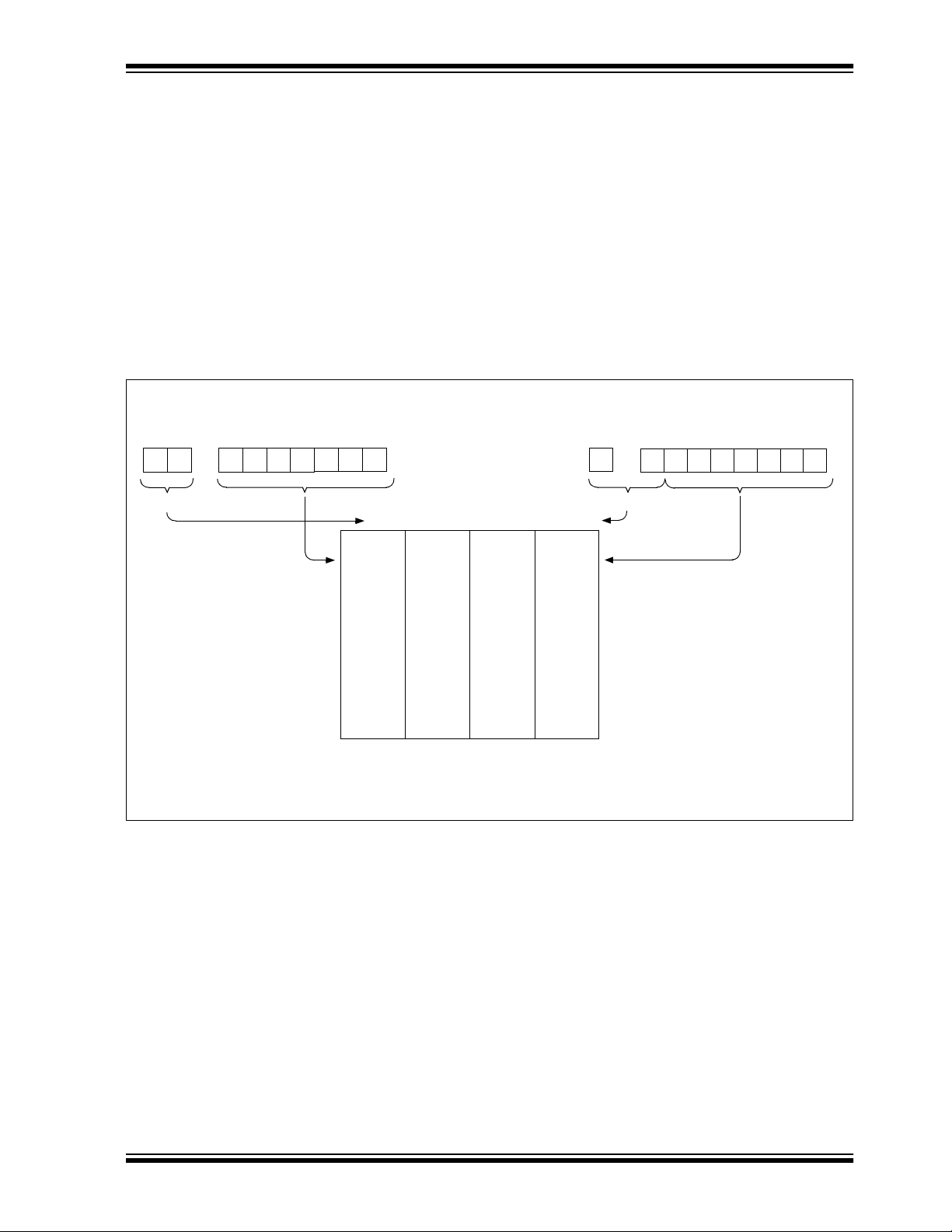
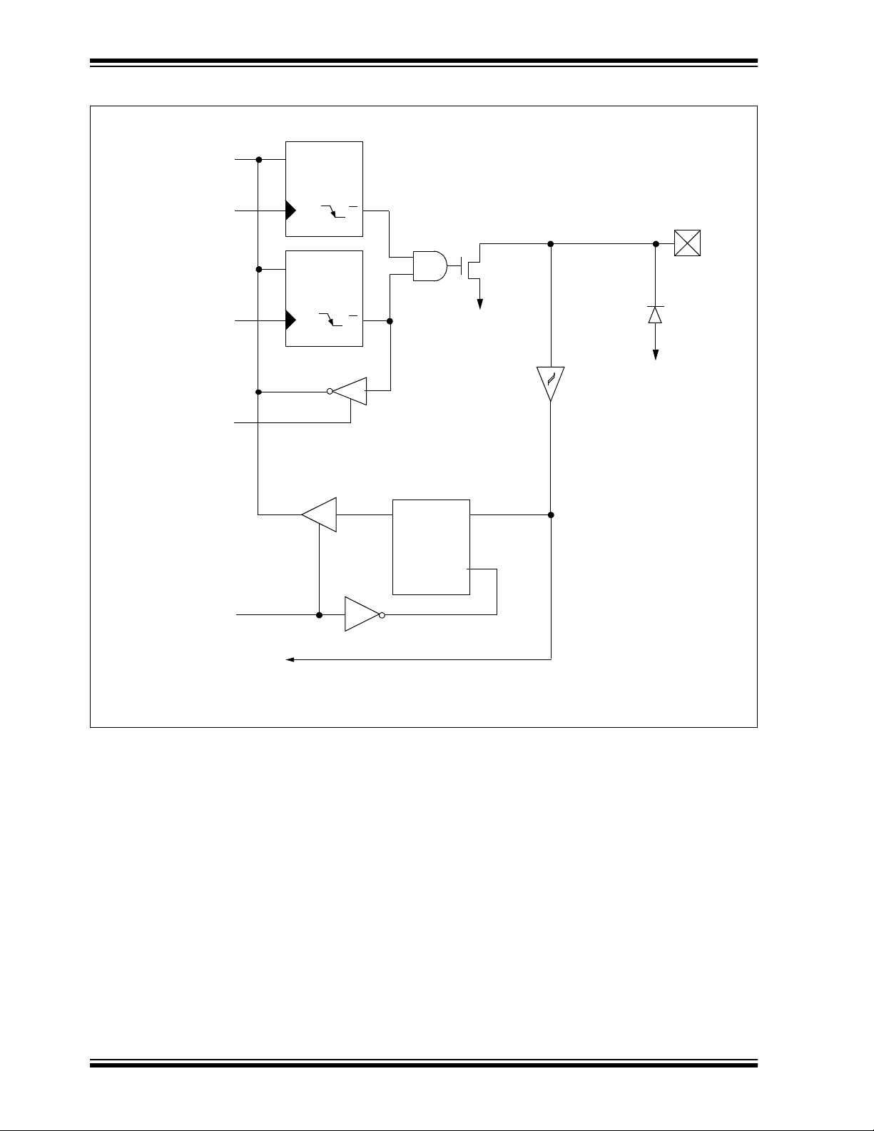
FIGURE 3-1: BLOCK DIAGRAM OF RA0/AN0, RA1/AN1/LVDIN
Data
Bus
WR
PORT
WR
TRIS
RD
TRIS
WR
ANSEL
Data Latch
CK
TRIS Mode
CK
Analog Select
CK
Q
Q
Q
QD
VDD
P
QD
QD
N
SS
V
Schmitt
Trigger
VDD
VSS
QD
EN
RD
PORT
To A/D Converter input or LVD Module input
DS41120A-page 28 Advanced Information
1999 Microchip Technology Inc.
Page 29
PIC16C717/770/771
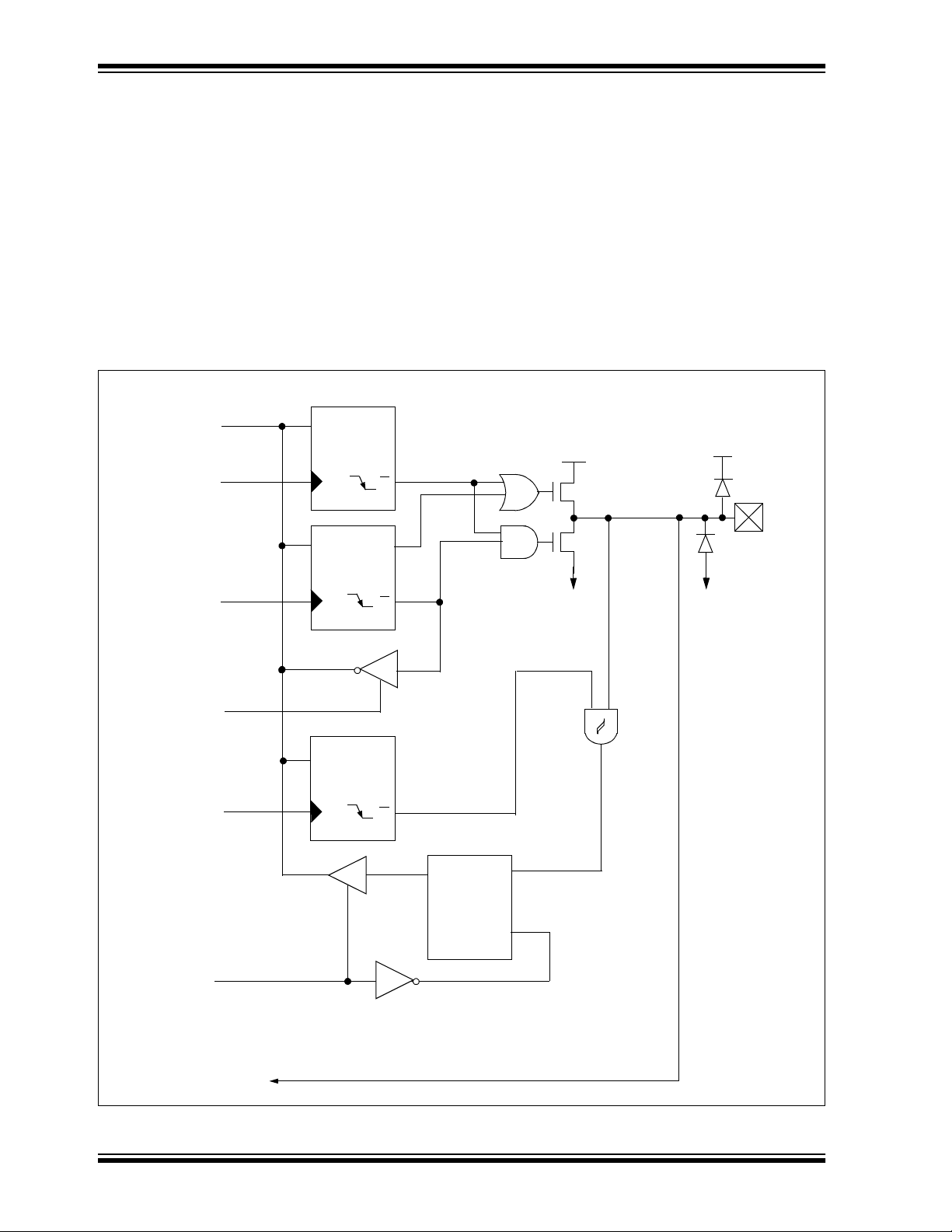
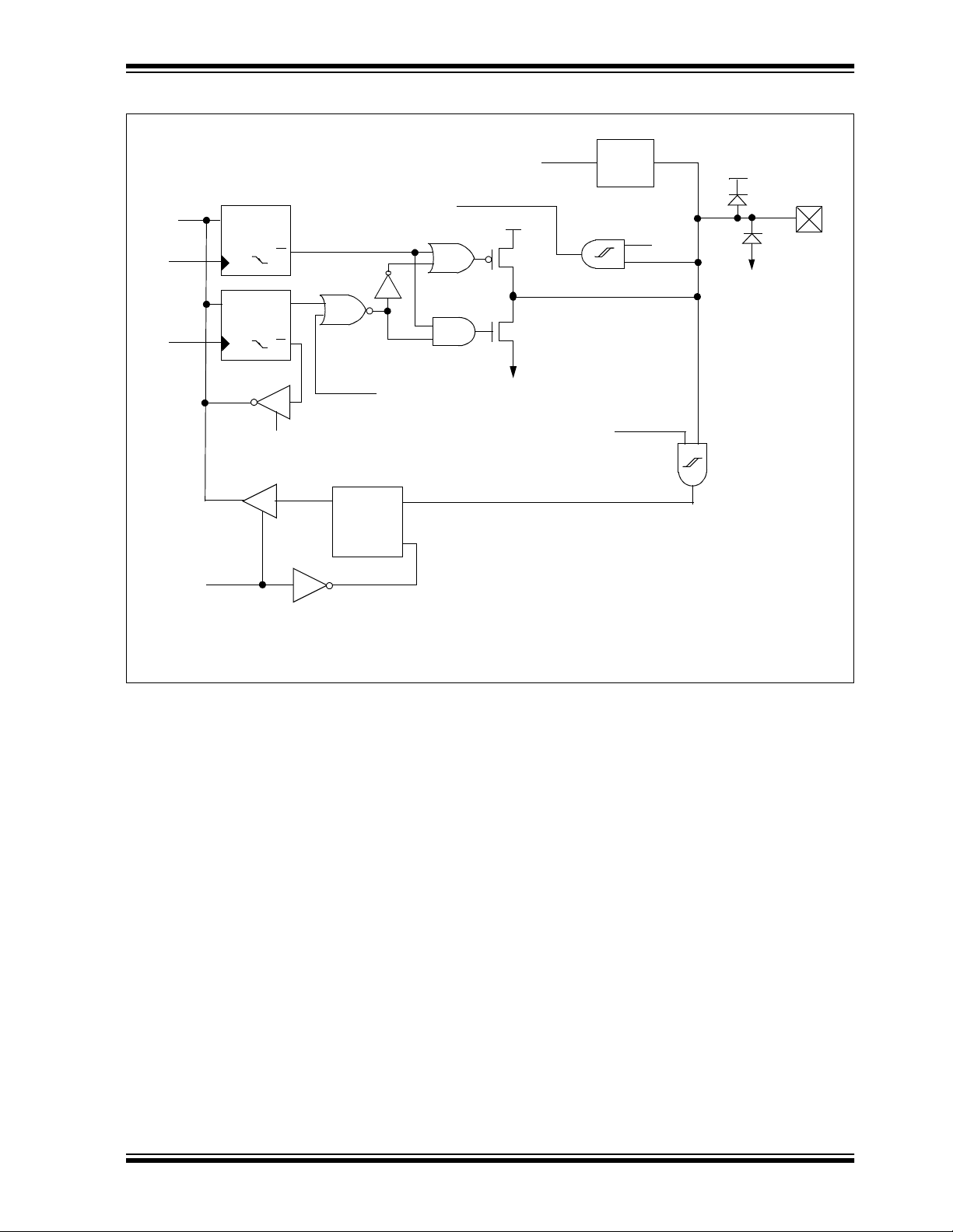
FIGURE 3-2: BLOCK DIAGRAM OF RA2/AN2/VREF-/VRL AND RA3/AN3/VREF+/VRH
Data
Bus
WR
PORT
WR
TRIS
RD
TRIS
WR
ANSEL
RD
PORT
Data Latch
CK
TRIS Mode
CK
Analog Select
CK
Q
Q
Q
QD
VDD
P
QD
QD
QD
EN
N
SS
V
Schmitt
Trigger
VDD
VSS
To A/D Converter input
and Vref+, Vref- inputs
1999 Microchip Technology Inc.
VRH, VRL outputs
(From Vref-LVD-BO R Module)
VRH, VRL output enable
Sense input for
VRH, VRL amplifier
Advanced Information DS41120A-page 29
Page 30
PIC16C717/770/771
FIGURE 3-3: BLOCK DIAGRAM OF RA4/T0CKI
Data
Bus
WR
Port
WR
TRIS
RD
TRIS
Data Latch
CK
TRIS Latch
CK
QD
Q
QD
Q
QD
N
SS
V
VSS
Schmitt Trigger
Input Buffer
RD
PORT
TMR0 clock input
EN
DS41120A-page 30 Advanced Information
1999 Microchip Technology Inc.
Page 31

FIGURE 3-4: BLOCK DIAGRAM OF RA5/MCLR/VPP
PIC16C717/770/771
To MCLR Circuit
Program Mode
Data
Bus
RD
TRIS
MCLR Filter
HV Detect
VSS
VSS
Schmitt
Trigger
QD
EN
RD PORT
1999 Microchip Technology Inc.
Advanced Information DS41120A-page 31
Page 32

PIC16C717/770/771
FIGURE 3-5: BLOCK DIAGRAM OF RA6/OSC2/CLKOUT PIN
INTRC or ER with CLKOUT
CLKOUT (FOSC/4)
Data
Bus
WR
PORTA
WR
TRISA
CK
Data Latch
D
CK
TRIS Latch
RD TRISA
1
0
QD
Q
INTRC or ER
Q
Q
INTRC or ER with CLKOUT
EN
From OSC1
DQ
VDD
P
N
V
Oscillator
Circuit
INTRC or ER without CLKOUT
SS
VDD
VSS
Schmitt Trigger
Input Buffer
RD PORTA
DS41120A-page 32 Advanced Information
1999 Microchip Technology Inc.
Page 33
PIC16C717/770/771
FIGURE 3-6: BLOCK DIAGRAM OF RA7/OSC1/CLKIN PIN
Data
Bus
WR
PORTA
WR
TRISA
CK
Data Latch
D
CK
TRIS Latch
RD PORTA
QD
Q
Q
Q
RD TRISA
INTRC
EN
To OSC2
To Chip Clock Drivers
VDD
P
N
SS
V
DQ
Oscillator
Circuit
Schmitt Trigger
Input Buffer
EC Mode
INTRC
VDD
Schmitt Trigger
Input Buffer
1999 Microchip Technology Inc.
Advanced Information DS41120A-page 33
Page 34

PIC16C717/770/771
TABLE 3-1: PORTA FUNCTIONS
Name Function
RA0/AN0
RA1/AN1/LVDIN
RA2/AN2/V
RA3/AN3/V
RA5/MCLR
RA6/OSC2/CLKOUT
RA7/OSC1/CLKIN
REF-/VRL
REF+/VRH
RA4/T0CKI
/VPP
Input
Type
RA0 ST CMOS Bi-directional I/O
AN0 AN A/D input
RA1 ST CMOS Bi-directional I/O
AN1 AN A/D input
LVDIN AN LVD input reference
RA2 ST CMOS Bi-directional I/O
AN2 AN A/D input
REF- AN Negative analog reference input
V
VRL AN Internal voltage reference low output
RA3 ST CMOS Bi-directional I/O
AN3 AN A/D input
V
REF+ AN Positive analog reference input
VRH AN Internal voltage reference high output
RA4 ST OD Bi-directional I/O
T0CKI ST TMR0 clock input
RA5 ST Input port
MCLR
PP Power Programming voltage
V
RA6 ST CMOS Bi-directional I/O
OSC2 XTAL Crystal/resonator
CLKOUT CMOS F
RA7 ST CMOS Bi-directional I/O
OSC1 XTAL Crystal/resonator
CLKIN ST External clock input/ER resistor connection
ST Master clear
Output
Type
Description
OSC/4 output
DS41120A-page 34 Advanced Information
1999 Microchip Technology Inc.
Page 35

PIC16C717/770/771
TABLE 3-2: SUMMARY OF REGISTERS ASSOCIATED WITH PORTA
Address Name Bit 7 Bit 6 Bit 5 Bit 4 Bit 3 Bit 2 Bit 1 Bit 0
05h PORTA RA7 RA6 RA5 RA4 RA3 RA2 RA1 RA0
85h TRISA PORTA Data Direction Register
9Dh ANSEL
Legend: x = unknown, u = unchanged, - = unimplemented locations read as ’0’. Shaded cells are not used by PORTA.
3.3 P
ORTB and the TRISB Register
ANS5 ANS4 ANS3 ANS2 ANS1 ANS0 1111 1111 1111 1111
enables the w ea k pull-up resist ors . Th e weak pull-u p is
Value on:
POR,
BOR
xxxx 0000 uuuu 0000
1111 1111 1111 1111
automatically turned off when the port pin is confi gured
PORTB is an 8-bit wide bi-directional port. The corresponding data direction register is TRISB. Setting a
TRISB bit (=1) will make the correspon ding POR TB pin
an input, i.e., put the corresponding output driver in a
hi-impedance mode. Clearing a TRISB bit (=0) will
make the corr espond ing PO R TB pi n an outpu t, i.e . , put
the contents of the output latch on the selected pin.
EXAMPLE 3-2: INITIALIZING PORTB
BCF STATUS, RP0 ;
CLRF PORTB ; Initialize PORTB by
; clearing output
; data latches
BSF STATUS, RP0 ; Select Bank 1
MOVLW 0xCF ; Value used to
; initialize data
; direction
MOVWF TRISB ; Set RB<3:0> as inputs
; RB<5:4> as outputs
; RB<7:6> as inputs
MOVLW 03 ; Set RB<1:0> as analog
inputs
MOVWF ANSEL ;
BCF STATUS, RP0 ; Return to Bank 0
Each of the PORTB pins has an internal pull-up, which
can be individually enabled from the WPUB register. A
single global en able bit can turn on/off the ena bled pul lups. Clearing the R
BPU bit, (OPTION_REG<7>),
as an output. The pull-ups are disabled on a Power-on
Reset.
Each of the PORTB pins, if configured as input, also
has an interrupt on change feature, which can be individually selected from the IOCB register. The RBIE bit
in the INTCON registe r fun cti ons a s a global enabl e b it
to turn on/off the interrupt on change feature. The
selected inputs are compared to the old value latched
on the last read of PO RTB . The "mi smatch" output s are
OR’ed together to generate the RB Port Change Interrupt with flag bit RBIF (INTCON<0>).
This interrupt can wake the device from SLEEP. The
user, i n the interrupt service routine , can clea r the interrupt in the following manner:
a) Any read or write of PORTB. This will end the
mismatch condition.
b) Clear flag bit RBIF.
A mismatch condition will continue to set flag bit RBIF.
Reading PORTB will end the mismatch condition and
allow flag bit RBIF to be cleared.
The interrupt on change feature is recommended for
wake-up on key depression operation and opera tions
where PORTB is only used for the interrupt on change
feature. Polling of PORTB is not recommended while
using the interrupt on change feature.
Value on all
other resets
REGISTER 3-2: WEAK PULL UP PORTB REGISTER (WPUB: 95h)
R/W-1 R/W-1 R/W-1 R/W-1 R/W-1 R/W-1 R/W-1 R/W-1
WPUB7 WPUB6 WPUB5 WPUB4 WPUB3 WPUB2 WPUB1 WPUB0 R = Readable bit
bit7 bit0
bit 7-0: WPUB<7:0>: PORTB Weak Pull-Up Control
Note 1: For the WPUB register setting to take effect, the RBPU
1999 Microchip Technology Inc.
1 = Weak pull up enabled.
0 = Weak pull up disabled
bit in the OPTION_REG Register must be cleared.
2: The weak pull up device is automatically disabled if the pin is in output mode (TRIS = 0).
Advanced Information DS41120A-page 35
W = Writable bit
U = Unimplemented bit, read
as ‘0’
-n = Value at POR reset
Page 36

PIC16C717/770/771
REGISTER 3-3: INTERRUPT ON CHANGE PORTB REGISTER (IOCB: 96h)
R/W-1 R/W-1 R/W-1 R/W-1 R/W-0 R/W-0 R/W-0 R/W-0
IOCB7 IOCB6 IOCB5 IOCB4 IOCB3 IOCB2 IOCB1 IOCB0 R = Readable bit
bit7 bit0
bit 7-0: IOCB<7:0>: Interrupt on Change POR TB Control
1 = Interrupt on change enabled.
0 = Interrupt on change disabled.
Note 1: The interrupt enable bits GIE and RBIE in the INTCON Register must be set for individual interrupts to be
recognized.
W = Writable bit
U = Unimplemented bit, read
as ‘0’
-n = Value at POR reset
DS41120A-page 36 Advanced Information
1999 Microchip Technology Inc.
Page 37

PIC16C717/770/771
The RB0 pin is multipl e x ed with the A/D con v e rter analog input 4 an d the exter nal inter rupt inp ut (RB0/A N4/
INT). When the pin is us ed as analog i nput, the AN SEL
register must have the proper value to select the RB0
pin as analog mode.
The RB1 pin is multiplexed wi th the A/D con v e rter analog input 5 and the MSSP module slave select input
(RB1/AN5/SS). When the pin is used as analog input,
the ANSEL register must have the proper value to
select the RB1 pin as analog mode.
Note: Upon reset, the ANSEL register configures
the RB1 and RB0 pins as analog inputs.
Both RB1 and RB0 pins will read as ’0’.
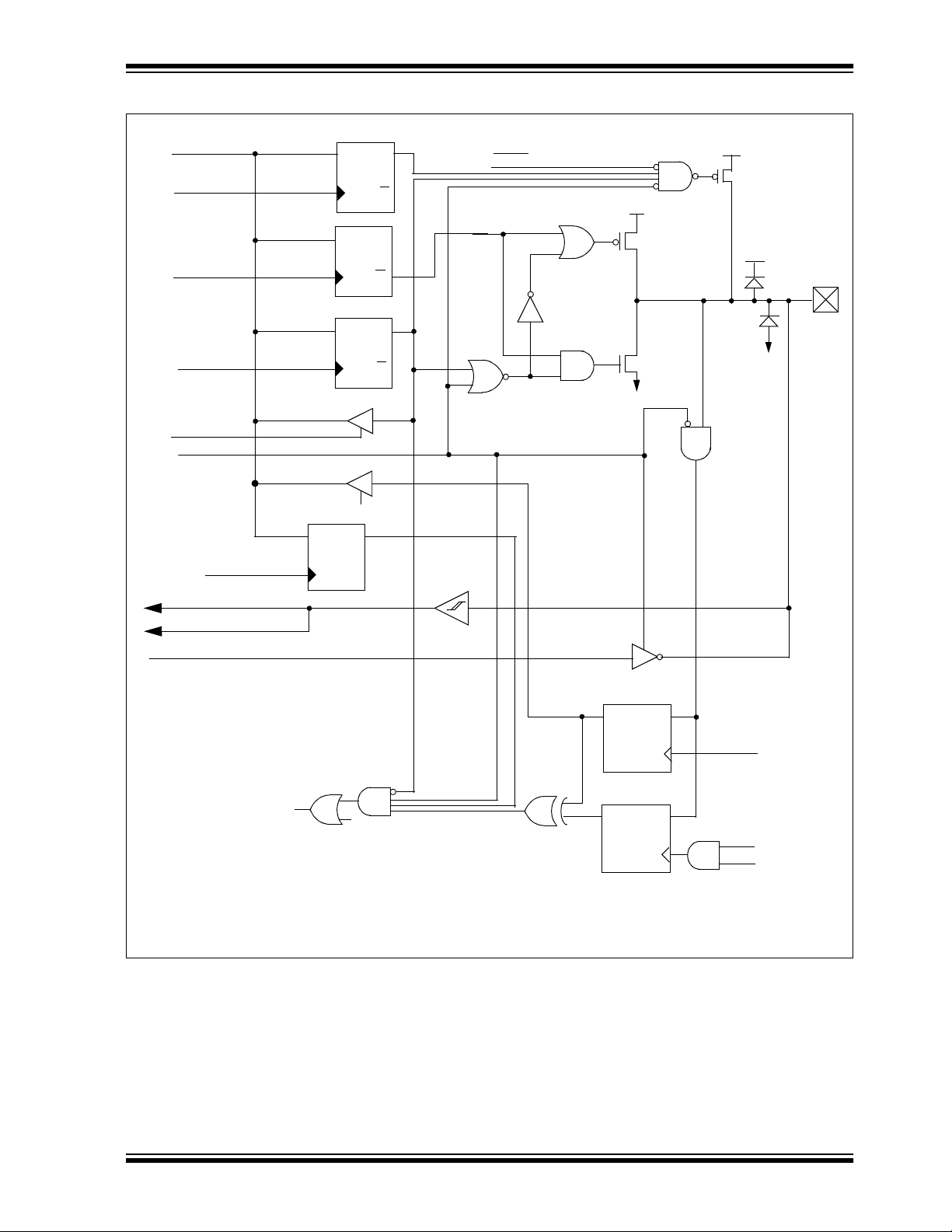
FIGURE 3-7: BLOCK DIAGRAM OF RB0/AN4/INT, RB1/AN5/SS PIN
Data Bus
WR
WPUB
WR
PORT
WR
TRIS
WPUB Reg
Q
D
CK
Q
PORTB Reg
D
Q
Q
CK
TRIS Reg
D
Q
CK
Q
RBPU
VDD
P
N
VSS
VDD
P
weak
pull-up
V
DD
RD
TRIS
Analog Select
WR
ANSEL
WR
IOCB
RD
PORT
To INT input or MSSP modu le
To A/D Converter
CK
IOCB Reg
D
CK
VSS
QD
Q
TTL
Q
Set
RBIF
Q
...
From
RB<7:0> pins
QD
EN
EN
Q
D
EN
Q
D
EN
Schmitt
Trigger
Q1
Q3
1999 Microchip Technology Inc.
Advanced Information DS41120A-page 37
Page 38

PIC16C717/770/771
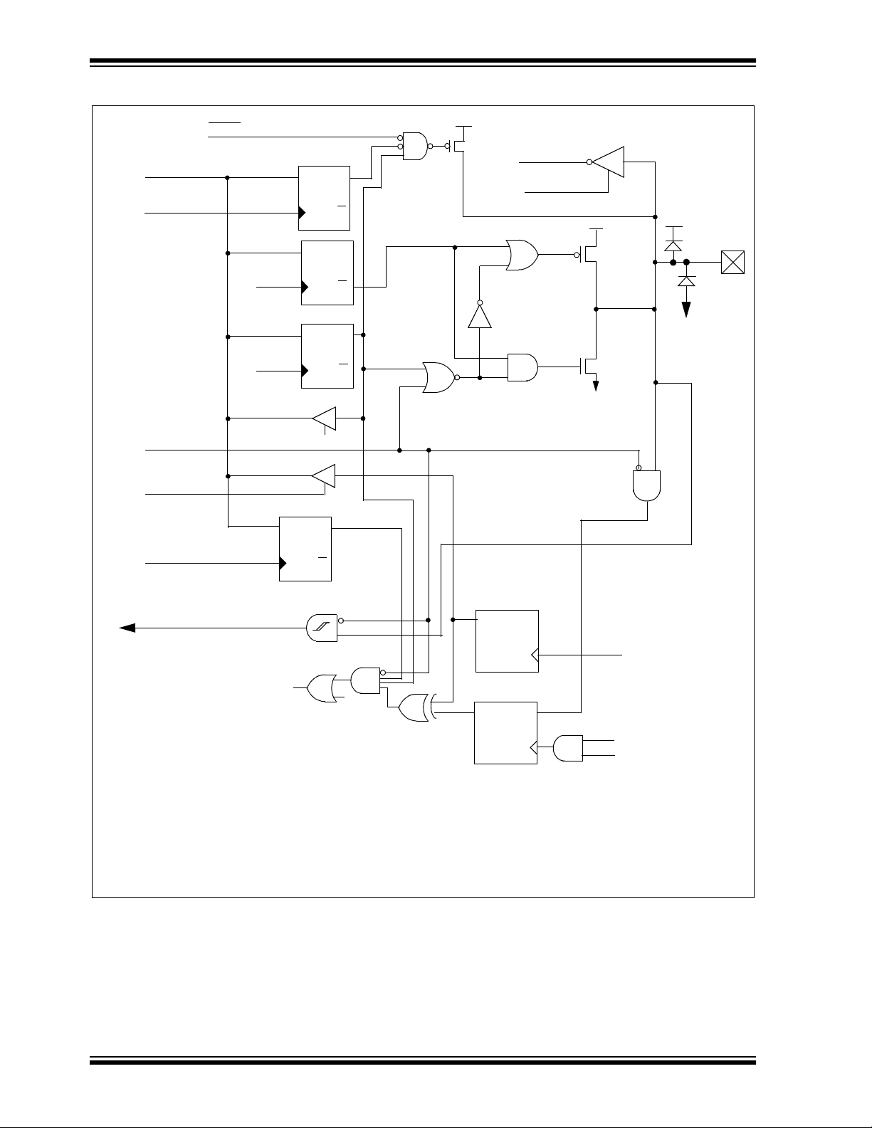
FIGURE 3-8: BLOCK DIAGRAM OF RB2/SCK/SCL, RB3/CCP1/P1A, RB4/SDI/SDA,
RB5/SDO/P1B
Data Bus
WR
WPUB
Spec. Func En.
SDA, SDO, SCK, CCPL, P1A, P1B
WR
PORT
WR
TRIS
RD
TRIS
WR
IOCB
WPUB Reg
D
CK
PORTB Reg
D
CK
TRIS Reg
D
CK
IOCB Reg
D
CK
Q
Q
RBPU
1
Q
0
Q
Q
Q
Q
Set
RBIF
Q
...
From
RB<7:0> pins
VDD
P
N
VSS
Q
EN
VDD
V
weak
P
pull-up
TTL
D
Q1
DD
VSS
Schmitt
Trigger
RD
PORT
SCK, SCL, CC, SDI, SDA inputs
QD
EN
EN
Q
D
EN
Q3
DS41120A-page 38 Advanced Information
1999 Microchip Technology Inc.
Page 39
PIC16C717/770/771
FIGURE 3-9: BLOCK DIAGRAM OF RB6/T1OSO/T1CKI/P1C
Data Bus
WR
WPUB
WR PORTB
WR TRISB
RD TRISB
T1OSCEN
WR
IOCB
TMR1 Clock
Serial programming clock
From RB 7
WPUB Reg
D
CK
D
CK
Data Latch
D
CK
TRIS Latch
RD PORTB
IOCB Reg
D
CK
Q
Q
Q
Q
Q
Q
Q
Q
Schmitt
Trigger
RBPU
VDD
P
N
SS
V
VDD
P
weak pull-up
VDD
TTL
Input
Buffer
TMR1 Oscillator
QD
EN
Set RBIF
...
From
RB<7:0> pins
Note: The TMR1 oscillator enable (T1OSCEN = 1) overrides the RB6 I/O port and P1C functions.
QD
EN
Q1
RD Port
Q3
1999 Microchip Technology Inc.
Advanced Information DS41120A-page 39
Page 40
PIC16C717/770/771
FIGURE 3-10: BLOCK DIAGRAM OF THE RB7/T1OSI/P1D
VDD
weak pull-up
P
Data Bus
WR
WPUB
RBPU
WPUB Reg
D
Q
Q
CK
D
Q
To RB6
T1OSCEN
TMR1 Oscillator
VDD
P
VDD
WR PORTB
WR TRISB
T10SCEN
RD PORTB
WR
IOCB
Serial programming input
CK
Data Latch
D
CK
TRIS Latch
RD TRISB
IOCB Reg
D
Q
CK
Q
Schmitt Trigger
Set RBIF
From
RB<7:0> pins
Q
Q
Q
QD
EN
...
QD
EN
N
SS
V
RD Port
TTL
Input
Buffer
Q1
Q3
Note: The TMR1 oscillator enable (T1OSCEN = 1) overrides the RB7 I/O port and P1D functions.
DS41120A-page 40 Advanced Information
1999 Microchip Technology Inc.
Page 41
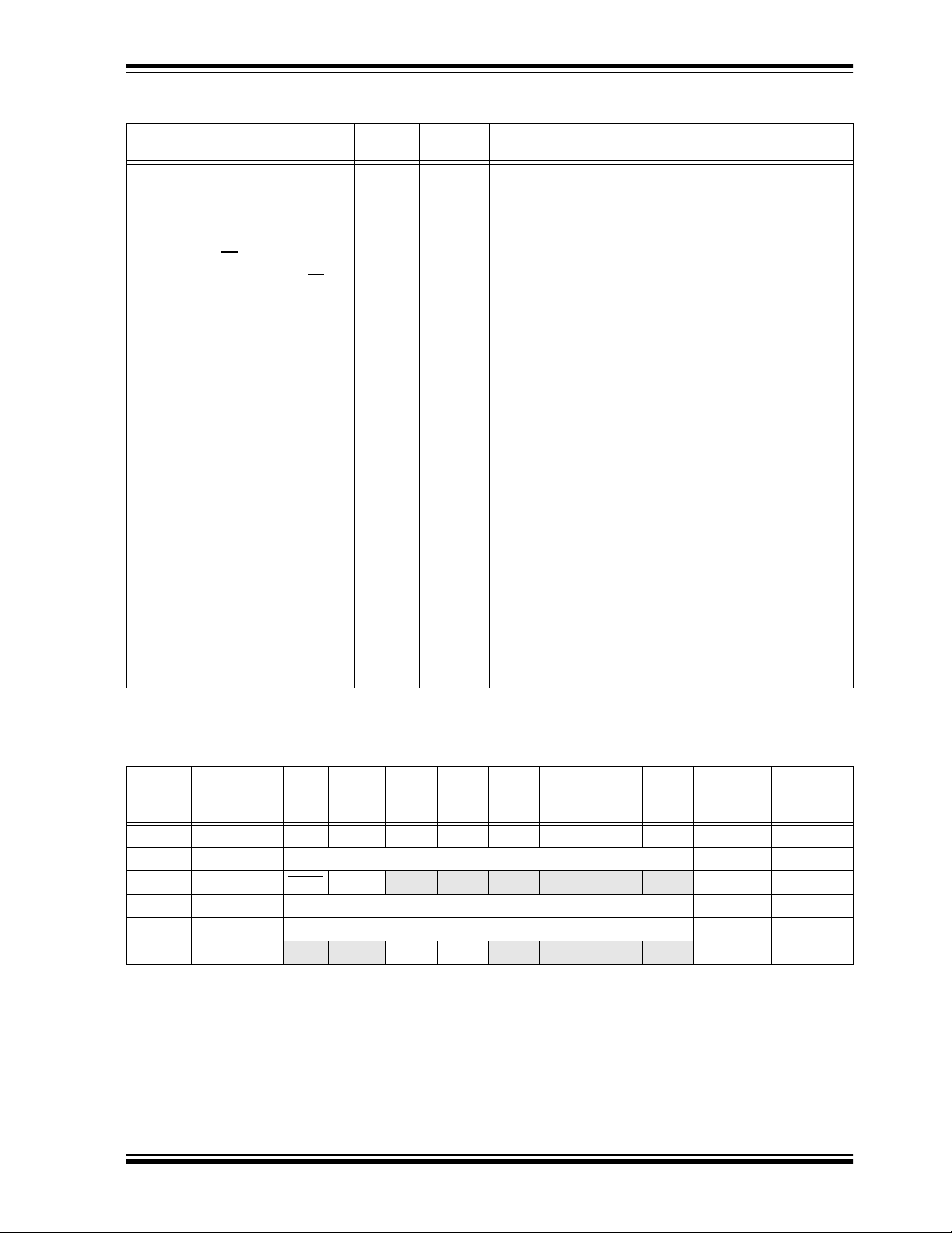
TABLE 3-3: PORTB FUNCTIONS
PIC16C717/770/771
Name Function
RB0 TTL CMOS Bi-directional I/O
RB0/AN4/INT
RB1/AN5/SS
RB2/SCK/SCL
RB3/CCP1/P1A
RB4/SDI/SDA
RB5/SDO/P1B
RB6/T1OSO/T1CKI/P1C
RB7/T1OSI/P1D
Note 1: Bit programmable pull-ups.
AN4 AN A/D input
INT ST Interrupt input
RB1 TTL CMOS Bi-directional I/O
AN5 AN A/D input
SS
RB2 TTL CMOS Bi-directional input
SCK ST CMOS Serial clock I/O for SPI
SCL ST OD Serial clock I/O for I
RB3 TTL CMOS Bi-directional input
CCP1 ST CMOS Capture 1 input/Compare 1 output
P1A CMOS PWM P1A output
RB4 TTL CMOS Bi-directional input
SDI ST Serial data in for SPI
SDA ST OD Serial data I/O for I
RB5 ST CMOS Bi-directional I/O
SDO CMOS Serial data out for SPI
P1B CMOS PWM P1B output
RB6 TTL CMOS Bi-directional I/O
T1OSO XTAL Crystal/Resonator
T1CKI ST TMR1 clock input
P1C CMOS PWM P1C output
RB7 TTL CMOS Bi-directional I/O
T1OSI XTAL TMR1 crystal/resonator
P1D CMOS PWM P1D output
Input
Type
ST SSP slave select input
Output
Type
(1)
(1)
(1)
(1)
(1)
(1)
(1)
(1)
2
2
C
C
Description
TABLE 3-4: SUMMARY OF REGISTERS ASSOCIATED WITH PORTB
Address Name Bit 7 Bit 6 Bit 5 Bit 4 Bit 3 Bit 2 Bit 1 Bit 0
06h, 106h PORTB RB7 RB6 RB5 RB4 RB3 RB2 RB1 RB 0
86h, 186h TRISB PORTB Data Direction Register
81h, 181h OPTION_RE G RBPU
95h WPUB PORTB Weak Pull-up Control
96h IOCB PORTB Interrupt on Change Control
9Dh ANSEL
Legend: x = unknown, u = unchanged. Shaded cells are not used by PORTB.
1999 Microchip Technology Inc.
INTEDG T0CS T0SE PSA PS2 PS1 PS0
ANS5 ANS4 ANS3 ANS2 ANS1 ANS0
Advanced Information DS41120A-page 41
Value on:
POR,
BOR
xxxx xx00 uuuu uu00
1111 1111 1111 1111
1111 1111 1111 1111
1111 1111 1111 1111
1111 0000 1111 0000
1111 1111 1111 1111
Value on all
other resets
Page 42

PIC16C717/770/771
NOTES:
DS41120A-page 42 Advanced Information
1999 Microchip Technology Inc.
Page 43

PIC16C717/770/771
4.0 PROGRAM MEMORY READ
(PMR)
Program memory is readable during normal operation
DD range). It is indirectly addressed through the
(full V
Special Function Registers:
•PMCON1
•PMDATH
•PMDATL
• PMADRH
• PMADRL
When interfacing the program memory block, the
PMDATH & PMDATL registers form a 2-byte word,
which holds the 14-bit data. The PMADRH & PMADRL
registers form a 2-byte word, which holds the 12-bit
address of the program memory location being
accessed. Mid -range devices have up to 8K words of
program EPROM with an address range from 0h to
3FFFh. When the device contains less memory than
the full address range of the PMADRH:PMARDL registers, the most significant bits of the PMADRH register
are ignored.
4.0.1 PMCON1 REGISTER
PMCON1 is the control register for program memory
accesses.
Control bit RD in itiates a read oper ation. This bit cann ot
be cleared, only set, in software. It is cleared in hardware at completion of the read operation.
REGISTER 4-1: PROGRAM MEMORY READ CONTROL REGISTER 1 (PMCON1: 18Ch)
R-1 U-0 U-0 U-0 U-0 U-0 U-0 R/S-0
Reserved — — — — — — RD R = Readable bit
bit7 bit0
bit 7: Reserved: Read as ‘1’
bit 6-1: Unimplemented: Read as '0 '
bit 0: RD: Read Control bit
1 = Initiates a Program memory read (read takes 2 cycles. RD is cleared in hardware.
0 = Reserved
W = Writable bit
S = Settable bit
U = Unimplemented bit,
read as ‘0’
- n = Value at POR reset
4.0.2 PMDATH AND PMDATL REGISTERS
The PMDATH:PMDATL registers are loaded with the
contents of program memory addressed by the
PMADRH and PMADRL registers upon completion of a
Program Memory Read co mmand.
1999 Microchip Technology Inc.
Advanced Information DS41120A-page 43
Page 44

PIC16C717/770/771
REGISTER 4-2: PROGRAM MEMORY DATA HIGH (PMDATH: 10Eh)
U-0 U-0 R-x R-x R-x R-x R-x R-x
— — PMD13 PMD12 PMD11 PMD10 PMD9 PMD8 R = Readable bit
bit7 bit0
bit 7-6: Unimplemented: Read as '0 '
bit 5-0: PMD<13:8>: The value of the program memory word pointed to by PMADRH and PMADRL after a
program memory read command.
REGISTER 4-3: PROGRAM MEMORY DATA LOW (PMDATL: 10Ch)
R-x R-x R-x R-x R-x R-x R-x R-x
PMD7 PMD6 PMD5 PMD4 PMD3 PMD2 PMD1 PMD0 R = Readable bit
bit7 bit0
W = Writable bit
S = Settable bit
U = Unimplemented bit,
read as ‘0’
- n = Value at POR reset
W = Writable bit
S = Settable bit
U = Unimplemented bit,
read as ‘0’
- n = Value at POR reset
bit 7-0: PMD<7:0>: The value of the program memory word pointed to by PMADRH and PMADRL after a
program memory read command.
REGISTER 4-4: PROGRAM MEMORY ADDRESS HIGH (PMADRH: 10Fh)
U-0 U-0 U-0 U-0 R/W-x R/W-x R/W-x R/W-x
— — — — PMA11 PMA10 PMA9 PMA8 R = Readable bit
bit7 bit0
bit 7-4: Unimplemented: Read as '0 '
bit 3-0: PMA<11:8>: PMR Address bits
REGISTER 4-5: PROGRAM MEMORY ADDRESS LOW (PMADRL: 10Dh)
R/W-x R/W-x R/W-x R/W-x R/W-x R/W-x R/W-x R/W-x
PMA7 PMA6 PMA5 PMA4 PMA3 PMA2 PMA1 PMA0 R = Readable bit
bit7 bit0
bit 7-0: PMA<7:0>: PMR Address bits
W = Writable bit
S = Settable bit
U = Unimplemented bit,
read as ‘0’
- n = Value at POR reset
W = Writable bit
S = Settable bit
U = Unimplemented bit,
read as ‘0’
- n = Value at POR reset
DS41120A-page 44 Advanced Information
1999 Microchip Technology Inc.
Page 45

PIC16C717/770/771
4.0.3 READING THE EPROM PROGRAM
MEMORY
To read a program memory location, the user must
write 2 bytes of the address to the PMADRH and
PMADRL registers, then set control bit RD
(PMCON1<0>). Once the read control bit is set, the
causes the second instruction immediately following
BSF PMCON1,RD” instruction to be ignored. The data
the “
is available, in the very next cycle, in the PMDATH and
PMDATL registers; therefore it can be read as 2 bytes
in the following instructions. PMDATH and PMDATL
registers will hold th is v alue u ntil ano ther read or un til it
is written to by the user.
Program Memory Read (PMR) controller will use the
second instruction cycle after to read the data. This
EXAMPLE 4-1: OTP PROGRAM MEMORY READ
BSF STATUS, RP1 ;
BCF STATUS, RP0 ; Bank 2
MOVLW MS_PROG_PM_ADDR ;
MOVWF PMADRH ; MS Byte of Program Memory Address to read
MOVLW LS_PROG_PM_ADDR ;
MOVWF PMADRL ; LS Byte of Program Memory Address to read
BSF STATUS, RP0 ; Bank 3
BSF PMCON1, RD ; Program Memory Read
NOP ; This instruction is executed
NOP ; This instruction must be a NOP
next instruction ; PMDATH:PMDATL now has the data
4.0.4 OPERATION DURING CODE PROTECT
When the device is code protected, the CPU can still
perform the program memory read function.
FIGURE 4-1: PROGRAM MEMORY READ CYCLE EXECUTION
Q1 Q2 Q3 Q4 Q1 Q2 Q3 Q4 Q1 Q2 Q3 Q4 Q1 Q2 Q3 Q4 Q1 Q2 Q3 Q4 Q1 Q2 Q3 Q4
Program
Memory
ADDR
RD bit
PMDATH
PMDATL
register
PC PC+1
INSTR(PC-1)
Executed here
BSF PMCON1,RD
Executed here
PMADRH,PMADRL
INSTR(PC+1)
Executed here
PC+3 PC+4
PC+3
Forced NOP
Executed here
INSTR(PC+3)
Executed here
PC+5
INSTR(PC+4)
Executed here
1999 Microchip Technology Inc.
Advanced Information DS41120A-page 45
Page 46

PIC16C717/770/771
NOTES:
DS41120A-page 46 Advanced Information
1999 Microchip Technology Inc.
Page 47

PIC16C717/770/771
5.0 TIMER0 MODUL E
The Timer0 module ti mer/count er has the f ollo wing f eatures:
• 8-bit timer/counter
• Readable and writable
• Internal or external clock select
• Edge select for external clock
• 8-bit software programmable prescaler
• Interrupt on overflow from FFh to 00h
Figure 5-1 is a simplifi ed block diagram of the Tim er0
module.
Additional information on timer modules is available in
the PICmicro™ Mid-Range Reference Manual,
(DS33023).
5.1 Timer0 Operation
Timer0 can operate as a timer or as a counter.
Timer mode is selected by clearing bit T0CS
(OPTION_REG<5>). In timer mode, the Timer0 module will increment every instruction cycle (without prescaler). If the TMR0 register is written, the increment is
inhibited for the following two instruction cycles. The
user can work around this by writing an adjusted value
to the TMR0 register.
Counter mode is selected by setting bit T0CS
(OPTION_REG<5>). In counter mode, Timer0 will
increment either on every rising or falling edge of pin
RA4/T0CKI. The incrementing edge is determined by
the Timer0 Source Edge Select bit T0SE
(OPTION_REG<4>). Clearing bit T0 SE sel ec ts the rising edge. Restrictions on the external clock input are
discussed in below.
When an ex ternal clock i nput is used f or Timer0 , it must
meet certain requirements. The requirements ensure
the external c lock can be synchron ized w ith the int ernal
phase clock (T
incrementing of Timer0 after synchronization.
OSC). Also, there is a delay in the actual
Additional information on external clock requirements
is available in the PICmicro™ Mid-Range Reference
Manual, (DS33023).
5.2 Prescaler
An 8-bit counter is available as a prescaler for the
Timer0 module, or as a postscaler for the Watchdog
Timer, respectively (Figure 5-2). For simplicity, this
counter is being referred to as “prescaler” throughout
this data sheet. Note that there is only one prescaler
avail able which i s m utually e xc lu si vely shared b etween
the Timer0 module and the Watchdog Timer. Thus, a
prescaler assignment for the Timer0 module means
that there is no prescaler for the Watchdog Timer, and
vice-versa.
The prescaler is not readable or writable.
The PSA and PS<2:0> bits (OPTION_REG<3:0>)
determine the prescaler a ssignment an d prescale ratio .
Clearing bit PSA will assign the prescale r to the Time r0
module. When the prescaler is assigned to the Timer0
module, prescale values of 1:2, 1:4, ..., 1:256 are
selectable.
Setting bit PSA will assign the prescaler to the Watchdog Timer (WDT). When the prescaler is assigned to
the WDT, prescale values of 1:1, 1:2, ..., 1:128 are
selectable.
When assigned to the Timer0 module, all instructions
writing to the TMR0 register (e.g . CLRF 1, MOVWF 1,
BSF 1, x....etc.) will clear the prescaler. When
assigned to WDT, a CLRWDT instruction will clear the
prescaler along with the WDT.
Note: Writing to TMR0 when the prescaler is
assigned to Timer0 will clear the prescaler
count, but will not change the prescaler
assignment.
FIGURE 5-1: TIMER0 BLOCK DIAGRAM
FOSC/4
RA4/T0CKI
pin
Note 1: T0CS, T0SE, PSA, PS<2:0> (OPTION_REG<5:0>).
1999 Microchip Technology Inc.
T0SE
2: The prescaler is shared with Watchdog Timer (refer to Figure 5-2 for detailed block diagram).
0
1
Programmable
Prescaler
3
PS2, PS1, PS0
T0CS
Advanced Information DS41120A-page 47
1
0
PSA
PSout
Sync with
Internal
clocks
CY delay)
(2 T
Data Bus
8
TMR0
PSout
Set interrupt
flag bit T0IF
on overflow
Page 48
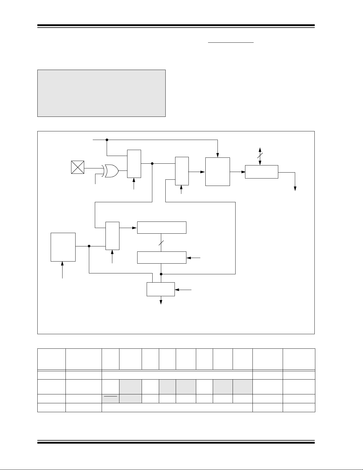
PIC16C717/770/771
5.2.1 SWITCHING PRESCALER ASSIGNMENT
The prescaler assignment is fully under software con-
trol, i.e., it can be changed “on-the-fly” during program
ex ec utio n.
Note: To avoid an unintended device RESET, a
specific instructio n sequence (show n in the
PICmicro™ Mid-Range Reference Manual, DS33023) must be executed when
changing the prescaler assignment from
5.3 Timer0 Interrupt
The TMR0 interrupt is generated when the TMR0 register overflows from FFh to 00 h. This overflow sets bit
T0IF (INTC ON<2>). The inter rupt can be mas ked by
clearing bit T0IE (INTCON<5>). Bit T0IF must be
cleared in softwa re b y the T imer0 mo dule interrupt s ervice routine before re-enabling this interrupt. The
TMR0 interrupt cannot awaken the processor from
SLEEP since the timer is shut off during SLEEP.
Timer0 to the WDT. This sequence must
be followed even if the WDT is disabled.
FIGURE 5-2: BLOCK DIAGRAM OF THE TIMER0/WDT PRESCALER
CLKOUT (= F
RA4/T0CKI
Pin
OSC/4)
T0SE
0
1
T0CS
M
U
X
1
M
U
0
X
PSA
SYNC
2
Cycles
Data Bus
8
TMR0 reg
Set flag bit T0IF
on Overflow
0
M
U
1
Watchdog
Timer
WDT Enable Bit
Note: T0CS, T0SE, PSA, PS<2:0> are (OPTION_REG<5:0>).
X
PSA
8-bit Prescaler
8
8 - to - 1MUX
0
M U X
WDT
Time-out
PS<2:0>
1
PSA
TABLE 5-1: REGISTERS ASSOCIATED WITH TIMER0
Address Name Bit 7 Bit 6 Bit 5 Bit 4 Bit 3 Bit 2 Bit 1 Bit 0
01h,101h TMR0 Timer0 register xxxx xxxx uuuu uuuu
0Bh,8Bh,
10Bh,18Bh
81h,181h OPTION_REG
85h TRISA PORTA Data Direction Register 1111 1111 1111 1111
Legend: x = unknown, u = unchanged, - = unimplemented locations read as ’0’. Shaded cells are not used by Timer0.
INTCON GIE
RBPU INTEDG T0CS T0SE PSA PS2 PS1 PS0 1111 1111 1111 1111
PEIE T0IE INTE RBIE T0IF INTF RB IF 0000 000x 0000 000u
Value on:
POR,
BOR
Value on all
other resets
DS41120A-page 48 Advanced Information
1999 Microchip Technology Inc.
Page 49

PIC16C717/770/771
6.0 TIMER1 MODUL E
The Timer1 module timer/co unter has th e fol lowing f eatures:
• 16-bit timer/counter
(Two 8-bit registers; TMR1H and TMR1L)
• Readable and writable (Both registers)
• Internal or external clock select
• Interrupt on overflow from FFFFh to 0000h
• Reset from ECCP module trigger
Timer1 has a control regist er, shown in Regi ster 6-1.
Timer1 can be enabled/disabled by setting/clearing
control bit TMR1ON (T1CON<0>).
Figure 6-2 is a simplifi ed block diagram of the Tim er1
module.
Additional information on timer modules is available in
the PICmicro™ Mid-Range Reference Manual,
(DS33023).
6.1 Timer1 Operation
Timer1 can operate in one of these modes:
•As a timer
• As a synchronous counter
• As an asynchronous counter
The operating mode is determined by the clock select
bit, TMR1CS (T1CON<1>).
In timer mode, Timer1 increments every instruction
cycle. In coun ter mo de, it in crement s on every risi ng
edge of the external clock input.
When the Timer1 oscillator is enabled (T1OSCEN is
set), the RB7/T1OSI/P1D and RB6/T1OSO/T1CKI/
P1C pins are no longer available as I/O ports or PWM
outputs. That is, the TRISB<7:6> value is ignored.
Timer1 also has an in ternal “reset input ”. This reset can
be generated by the ECCP module (Section 7.0).
REGISTER 6-1: TIMER1 CONTROL REGISTER (T1CON: 10h)
U-0 U-0 R/W-0 R/W-0 R/W-0 R/W-0 R/W-0 R/W-0
— — T1CKPS1 T1CKPS0 T1OSCEN T1SYNC TMR1CS TMR1ON
bit7 bit0
bit 7-6: Unimplemented: Read as ’0’
bit 5-4: T1CKPS<1:0>: Timer1 Input Clock Prescale Select bits
11 = 1:8 Prescale value
10 = 1:4 Prescale value
01 = 1:2 Prescale value
00 = 1:1 Prescale value
bit 3: T1OSCEN: Timer1 Oscillator Enable Control bit
1 = Oscillator is enabled
0 = Oscillator is shut off
Note: The oscillator inverter and feedback resistor are turned off to eliminate power drain
bit 2: T1SYNC
: Timer1 External Clock Input Synchronization Control bit
R = Readable bit
W = Writable bit
U = Unimplemented bit,
read as ‘0’
- n = Value at POR reset
TMR1CS = 1
1 = Do not synchronize external clock input
0 = Synchronize external clock input
TMR1CS = 0
This bit is ignored. Timer1 uses the internal clock when TMR1CS = 0.
bit 1: TMR1CS: Timer1 Clock Source Select bit
1 = External clock from pin RB6/T1OSO/T1CKI /P1C(on the rising edge)
0 = Internal clock (F
bit 0: TMR1ON: Timer1 On bit
1 = Enables Timer1
0 = Stops Timer1
1999 Microchip Technology Inc.
OSC/4)
Advanced Information DS41120A-page 49
Page 50
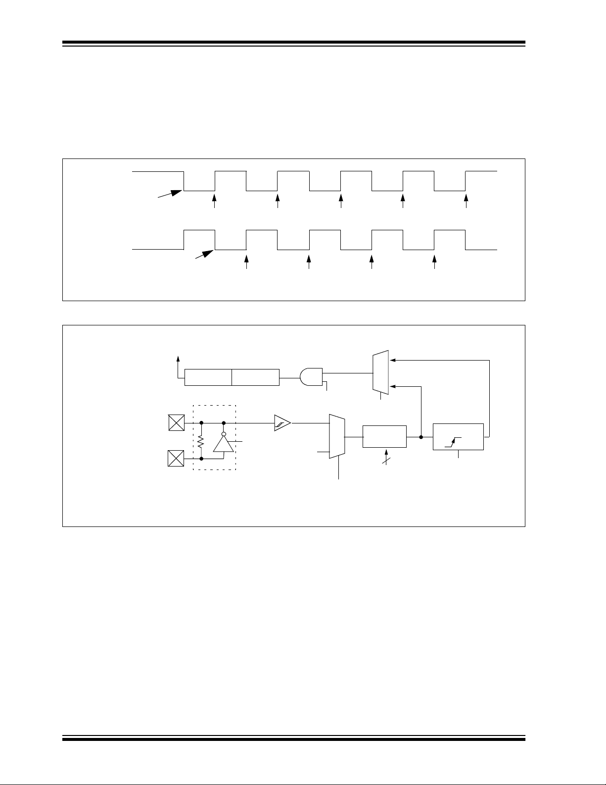
PIC16C717/770/771
6.1.1 TIMER1 COUNTER OPERATION
In this mode, Timer1 is being in cremented via an e xter-
nal source. Increments occur on a rising edge. After
Timer1 is enabled in counter mode, the module must
first have a falling edge before the coun ter begins to
increment.
FIGURE 6-1: TIMER1 INCREMENTING EDGE
T1CKI
(Initially high)
First falling edge
of the T1ON enabled
T1CKI
(Initially low)
First falling edge
of the T1ON enabled
Note: Arrows indicate counter increments.
FIGURE 6-2: TIMER1 BLOCK DIAGRAM
Set flag bit
TMR1IF on
Overflow
RB6/T1OSO/T1CKI/P1C
RB7/T1OSI/P1D
Note 1: When the T1OSCEN bit is cleared, the inverter and feedback resistor are turned off. This eliminates power drain.
TMR1H
T1OSC
TMR1
TMR1L
T1OSCEN
Enable
Oscillator
(1)
FOSC/4
Internal
Clock
TMR1ON
on/off
1
0
T1CKPS<1:0>
TMR1CS
0
1
T1SYNC
Prescaler
1, 2, 4, 8
2
Synchronized
clock input
Synchronize
det
SLEEP input
DS41120A-page 50 Advanced Information
1999 Microchip Technology Inc.
Page 51

PIC16C717/770/771
6.2 Timer1 Oscillator
A crystal oscillator circuit is b uilt in betw een pins T1OSI
(input) and T1OSO (amplifier output). It is enabled by
setting control bit T1OSCEN (T 1CON<3>). The oscill ator is a low power oscillator rated up to 200 kHz. It will
continue to run during SLEEP. It is primarily intended
for a 32 kHz crystal. Ta b le 6 -1 shows the capacitor
selection for the Timer1 osci llator.
The Timer1 oscillator is identical to the LP oscillator.
The user must provide a software time delay to ensure
proper oscillator start-up.
TABLE 6-1: CAPACITOR SELECTION FOR
THE TIMER1 OSCILLATOR
Osc Type Freq C1 C2
LP 32 kHz 33 pF 33 pF
100 kHz 15 pF 15 pF
200 kHz 15 pF 15 pF
These values are for design guidanc e only.
Note 1: Higher capacitance increases the stability of
oscillator but also increases the start-up time.
2: Since each resonator/crystal has its own charac-
teristics, the user should consult the resonator/
crystal manufacturer for appropriate values of
external components.
6.3 Timer1 Interrupt
The TMR1 Register pair (TMR1H:TMR1L) increments
from 0000h to FFFFh and rolls over to 0000h. The
TMR1 Interrupt, if enabled, is generated on overflow
which is latched in interrupt flag bit TMR1IF (PI R1<0>).
This interrupt can be enab led/d isab led by se tting/cle aring TMR1 interrupt enable bit TMR1IE (PIE1<0>).
6.4 Resetting Timer1 using a CCP Trigger
Output
If the ECCP module is configured in compare mode to
generate a “special event trigger" (CCP1M<3:0> =
1011), this signal will reset Timer1 and start an A/D
conversion (if the A/D module is enabled).
Note: The special event triggers from the CCP1
module will not set interrupt flag bit
TMR1IF (PIR1<0>).
Timer1 must be configured for either timer or synchronized counter mode to tak e adv antage of this fea ture . If
Timer1 is running in asynchronous counter mode, this
reset operation may not work.
In the ev ent that a write to Timer1 coinc ides with a sp ecial ev ent trigger from ECCP1, the write will tak e precedence.
In this mode of operati on, the CC PR1H:CCPR 1L regis ters pair effectively becomes the period register for
Timer1.
TABLE 6-2: REGISTERS ASSOCIATED WITH TIMER1 AS A TIMER/COUNTER
Address Name Bit 7 Bit 6 Bit 5 Bit 4 Bit 3 Bit 2 Bit 1 Bit 0
0Bh,8Bh,
10Bh,18Bh
0Ch PIR1
8Ch PIE1
0Eh TMR1L Holding register for the Least Significant Byte of the 16-bit TMR1 register
0Fh TMR1H Holding register for the Most Significant Byte of the 16-bit TMR1 register
10h T1CON
Legend: x = unknown, u = unchanged, - = unimplemented read as ’0’. Shaded cells are not used by the Timer1 module.
INTCON GIE PEIE
— ADIF — — SSPIF CCP1IF TMR2IF TMR1IF
— ADIE — — SSPIE CCP1IE TMR2IE TMR1IE
— — T1CKPS1 T1CKPS0 T1OSCEN T1SYNC TMR1CS TMR1ON
T0IE INTE RBIE T0IF INTF RBIF
Value on:
POR,
BOR
0000 000x 0000 000u
-0-- 0000 -0-- 0000
-0-- 0000 -0-- 0000
xxxx xxxx uuuu uuu u
xxxx xxxx uuuu uuu u
--00 0000 --uu uuuu
Value on
all other
resets
1999 Microchip Technology Inc.
Advanced Information DS41120A-page 51
Page 52

PIC16C717/770/771
NOTES:
DS41120A-page 52 Advanced Information
1999 Microchip Technology Inc.
Page 53

PIC16C717/770/771
7.0 TIMER2 MODUL E
The Timer2 module timer has the following features:
• 8-bit timer (TMR2 register)
• 8-bit period register (PR2)
• Readable and writable (Both registers)
• Software programmable prescaler (1:1, 1:4, 1:16)
• Software programmable postscaler (1:1 to 1:16)
• Interrupt on TMR2 match of PR2
• SSP module optional use of TMR2 output to generate clock shif t
Timer2 has a control register, shown in Register 7-1.
Timer2 can be s hut off by clearing co ntrol b it T MR 2O N
(T2CON<2>) to minimize power consumption.
Figure 7-1 is a simplifi ed block diagram of the Tim er2
module.
Additional information on timer modules is available in
the PICmicro™ Mid-Range Reference Manual,
(DS33023).
7.1 Timer2 Operation
Timer2 can be used as the PWM time-base for PWM
mode of the ECCP module.
The TMR2 register is readable and writable, and is
cleared on any device reset.
The input clock (F
1:4 or 1:16, selected by control bits T2CKPS<1:0>
(T2CON<1:0>).
The match output of TMR2 goes through a 4-bit
postscaler (which gives a 1:1 to 1:16 scaling inclusive)
to generate a TMR2 interrupt (latched in flag bit
TMR2IF, (PIR1<1>)).
The prescaler and postscaler counters are cleared
when any of the following occurs :
• a write to the TMR2 register
• a write to the T2CON register
• any device reset (Power-on Reset, MCLR
Watchdog Timer Reset, or Brown-out Reset)
TMR2 is not cleared when T2CON is written.
OSC/4) has a prescale option of 1:1,
REGISTER 7-1: TIMER2 CONTROL REGISTER (T2CON1: 12h)
U-0 R/W-0 R/W-0 R/W-0 R/W-0 R/W-0 R/W-0 R/W-0
— TOUTPS3 TOUTPS2 TOUTPS1 TOUTPS0 TMR2ON T2CKPS1 T2CKPS0 R = Readable bit
bit7 bit0
bit 7: Unimplemented: Read as ’0’
bit 6-3: TOUTPS<3:0>: Timer2 Output Postscale Select bits
0000 = 1:1 Postscale
0001 = 1:2 Postscale
•
•
•
1111 = 1:16 Postscale
bit 2: TMR2ON: Timer2 On bit
1 = Timer2 is on
0 = Timer2 is off
bit 1-0: 2CKPS<1:0>: Timer2 Clock Prescale Select bits
00 = Prescaler is 1
01 = Prescaler is 4
1x = Prescaler is 16
W = Writable bit
U = Unimplemented bit,
- n = Value at POR reset
Reset,
read as ‘0’
1999 Microchip Technology Inc.
Advanced Information DS41120A-page 53
Page 54

PIC16C717/770/771
7.2 Timer2 Interrupt
The Timer2 module has an 8-bit period register PR2.
Timer2 increments from 00h until it matches PR2 and
FIGURE 7-1: TIMER2 BLOCK DIAGRAM
Sets flag
bit TMR2IF
TMR2
output
(1)
then resets to 00h on the next increment cycle. PR2 is
a readable a nd writable regi ster . The PR2 register is initialized to FFh upon reset.
7.3 Output of TMR2
The output of TMR2 (b efore th e postscaler) i s fed to the
Postscaler
1:1 1:16
to
4
Reset
EQ
TMR2 reg
Comparator
PR2 reg
Prescaler
1:1, 1:4, 1:16
2
Synchronous Serial Port module which optionally use s
it to generate shift clock.
Note 1: TMR2 register output can be software selected
by the SSP Module as a baud clock.
TABLE 7-1: REGISTERS ASSOCIATED WITH TIMER2 AS A TIMER/COUNTER
Address Name Bit 7 Bit 6 Bit 5 Bit 4 Bit 3 Bit 2 Bit 1 Bit 0
0Bh,8Bh,
10Bh,18Bh
0Ch PIR1
8Ch PIE1
11h TMR2 Timer2 register
12h T2CON
92h PR2 Timer2 Period Register
INTCON GIE PEIE
— ADIF — — SSPIF CCP1IF TMR2IF TMR1IF
— ADIE — — SSPIE CCP1IE TMR2IE TMR1IE
— TOUTPS3 TOUTPS2 TOUTPS1 TOUTPS0 TMR2ON T2CKPS1 T2CKPS0
T0IE INTE RBIE T0IF INTF RBIF
Legend: x = unknown, u = unchanged, - = unimplemented read as ’0’. Shaded cells are not used by the Timer2 module.
Value on:
POR,
BOR
0000 000x 0000 000u
-0-- 0000 -0-- 0000
-0-- 0000 -0-- 0000
0000 0000 0000 0000
-000 0000 -000 0000
1111 1111 1111 1111
F
OSC/4
Value on
all other
resets
DS41120A-page 54 Advanced Information
1999 Microchip Technology Inc.
Page 55

PIC16C717/770/771
8.0 ENHANCED CAPTURE/
COMPARE/PWM(ECCP)
MODULES
The ECCP (Enhanced Capture/Compare/PWM)
module contains a 16 -bit registe r which c an ope rate a s
a 16-bit capture register, as a 16-bit compare register
or as a PWM master/slave Duty Cycle register.
Table 8-1 shows the timer resources of the ECCP mod-
ule modes.
REGISTER 8-1: CCP1 CONTROL REGISTER (CCP1CON: 17h)
R/W-0 R/W-0 R/W-0 R/W-0 R/W-0 R/W-0 R/W-0 R/W-0
PWM1M1 PWM1M0 DC1B1 DC1B0 CCP1M3 CCP1M2 CCP1M1 CCP1M0 R = Readable bit
bit7 bit0
bit 7-6: PWM1M<1:0>: PWM Output Configuration
IF CCP1M<3:2> = 00, 01, 10
xx - P1A assigned as Capture/Compare input. P1B, P1C, P1D assigned as Port pins.
IF CCP1M<3:2> = 11
00 - Single output. P1A modulated. P1B, P1C, P1D assigned as Port pins.
01 - Full-bridge output forward. P1D modulated. P1A active. P1B, P1C inactive.
10 - Half-bridge output. P1A, P1B modulated with deadband control. P1C, P1D assigned as Port pins.
11 - Full-bridge output reverse. P1B modulated. P1C active. P1A, P1D inactive.
bit 5-4: DC1B<1:0>: PWM Duty Cycle Least Significant bits
Capture Mode: Unused
Compare Mode: Unused
PWM Mode: These bits are the two LSbs of the PWM duty cycle. The eight MSbs are found in CCPRnL.
bit 3-0: CCP1M<3:0>: ECCP1 Mode Select bits
0000 = Capture/Compare/PWM off (resets ECCP module)
0001 = Unused (reserved)
0010 = Compare mode, toggle output on match (CCP1IF bit is set)
0011 = Unused (reserved)
0100 = Capture mode, every falling edge
0101 = Capture mode, every rising edge
0110 = Capture mode, every 4th rising edge
0111 = Capture mode, every 16th rising edge
1000 = Compare mode, set output on match (CCP1IF bit is set)
1001 = Compare mode, clear out put on mat ch (CCP1IF bit is set)
1010 = Compare mode, generate software interrupt on match (CCP1IF bit is set, CCP1 pin is
unaffected)
1011 = Compare mode, trigger special event (CCP1IF bit is set; ECCP resets TMR1, and starts an
A/D conversion, if the A/D module is enabled.)
1100 = PWM mode. P1A, P1C active high. P1B, P1D active high.
1101 = PWM mode. P1A, P1C active high. P1B, P1D active low.
1110 = PWM mode. P1A, P1C active low. P1B, P1D active high.
1111 = PWM mode. P1A, P1C active low. P1B, P1D active low.
Capture/Compare/PWM Register1 (CCPR1) is comprised of two 8-bit registers: CCPR1L (low byte) and
CCPR1H (high byte). The CCP1CON and P1DEL registers control the operation of ECCP. All are readable
and writable.
W= Writable bit
U = Unimplemented bit,
read as ‘0’
- n = Value at POR reset
1999 Microchip Technology Inc.
Advanced Information DS41120A-page 55
Page 56
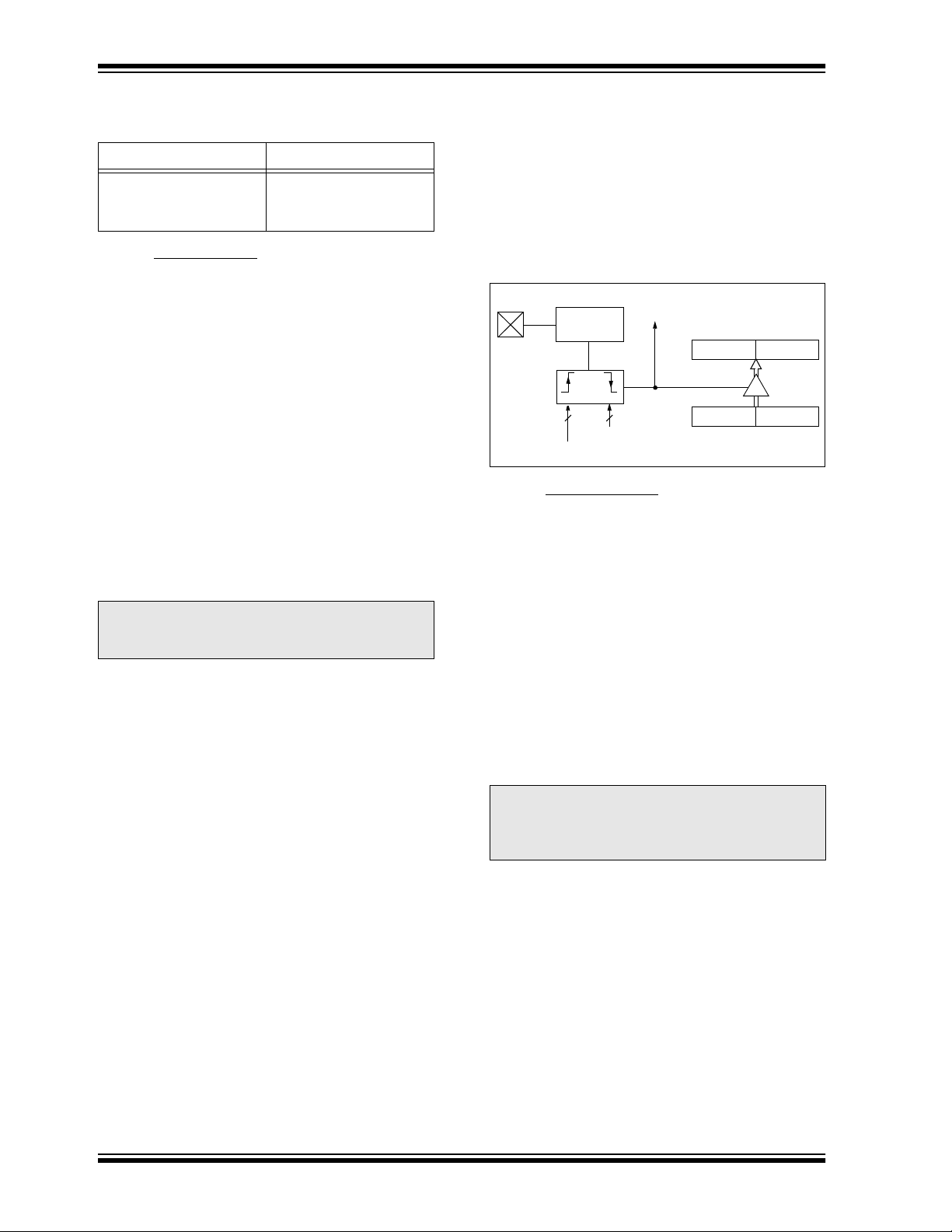
PIC16C717/770/771
TABLE 8-1: ECCP MODE - TIMER
RESOURCE
ECCP1 Mode Timer Resource
Capture
Compare
PWM
Timer1
Timer1
Timer2
8.1 Capture Mode
In Capture mode, CCPR1H:CCPR1L captures the 16bit value of the TMR1 re gister when an e v ent occu rs on
pin CCP1. An event is defined as:
• every falling edge
• every rising edge
• every 4th ri sing edge
• every 16th rising edge
An event is selected by control bits CCP1M<3:0>
(CCP1CON<3:0>). When a capture is made, the interrupt request flag bit CCP1IF (PIR1<2>) is set. It must
be cleared in softw are. If anot her capture oc curs bef ore
the value in register CCPR1 is read, the old captured
value will be lost.
8.1.1 CCP1 PIN CONFIGURATION
In Capture mode, the CCP1 pin should be configured
as an input by setting the TRISB<3> bit.
Note: I f the RB 3/CC P1/P1 A pin is config ured as
an output, a write to the port can cause a
capture condition.
8.1.2 TIMER1 MODE SELECTION
Timer1 must be runni ng in tim er mode or s ynch roniz ed
counter mode. In asynchronous counter mode, the
capture operation may not work.
8.1.3 SOFTWARE INTERRUPT
When the Capture mode is changed, a false capture
interrupt may be generated. The user should keep bit
CCP1IE (PIE1<2>) clear to avoid false interrupts and
should clear the flag bit CCP1IF following any such
change in operating mode.
8.1.4 ECCP PRESCALER
There are four prescaler settings, specified by bits
CCP1M<3:0>. Whenever the ECCP module is turned
off or the ECCP1 module is not in capture mode, the
prescaler counter is c leared. Thi s means that a ny res et
will clear the prescaler counter.
Switching from one capture prescaler to another may
generate an interrupt. Also, the prescaler counter will
not be cleared, therefore the first capture may be from
a non-zero presc aler. Example 8-1 show s the recommended method for switching between capture prescalers. This example also clears the prescaler counter
and will not generate the “false” interrupt.
EXAMPLE 8-1: CHANGIN G BETWEEN
CAPTURE PRESCALERS
CLRF CCP1CON, F ; Turn ECCP module off
MOVLW NEW_CAPT_PS ; Load WREG with the
MOVWF CCP1CON ; Load CCP1CON with
; new prescaler mode
; value and ECCP ON
; this value
FIGURE 8-1: CAPTURE MODE OPERATION
BLOCK DIAGRAM
Set flag bit CCP1IF
(PIR1<2>)
CCPR1H CCPR1L
Capture
Enable
TMR1H TMR1L
RB3/CCP1/
P1A Pin
Prescaler
1, 4, 16
÷
and
edge detect
CCP1CON<3:0>
Q’s
8.2 Compare Mode
In Compare mode, the 16-bit CCPR1 register value is
constantly compared against the TMR1 register pair
value. When a match occurs, the CCP1 pin is:
•driven High
• driven Low
• toggle output (High to Low or Low to High)
• remains Unchanged
The action on the pin is based on the value of control
bits CCP1M<3:0>. At the same time, interrupt flag bit
CCP1IF is set.
8.2.1 CCP1 PIN CONFIGURATION
The user must configure the C CP1 pin as an outp ut by
clearing the appropriate TRISB bit.
Note: C learing the CCP1C ON regis ter will force
the CCP1 compare output latch to the
default low level. This is not the port data
latch.
8.2.2 TIMER1 MODE SELECTION
Timer1 must be running in Timer mode or Synchro-
nized Counter mode if the ECCP module is using the
compare feature. In Asynchronous Counter mode, the
compare operation may not work.
8.2.3 SOFTWARE INTERRUPT MODE
When generate s oftwa re inte rrupt is chosen, the CCP1
pin is not aff ected. Only an ECCP int errupt is generate d
(if enabled).
DS41120A-page 56 Advanced Information
1999 Microchip Technology Inc.
Page 57

PIC16C717/770/771
8.2.4 SPECIAL EVENT TRIGGER
In this mode, an i nternal hardw a re trigger is g ener ated,
which may be used to initiate an action.
The special event trigger output of ECCP resets the
TMR1 register pair. This allows the CCPR1 register to
FIGURE 8-2: COMPARE MODE
OPERATION BLOCK
DIAGRAM
Special event trigger will:
reset Timer1, but not set interrupt flag bit TMR1IF (PIR1<0>).
effectiv el y be a 16-b it prog ram mab le pe riod regist er f or
Timer1.
The special event trigger output of ECCP module will
Special Event Trigger
also start an A/D conversion if the A/D module is
enabled.
Note: The special event trigger will not set the
interrupt flag bit TMR1IF (PIR1<0>).
RB3/CCP1/
P1A Pin
Output Enable
QS
R
TRISB<3>
Set flag bit CCP1IF
(PIR1<2>)
Output
Logic
match
CCP1CON<3:0>
Mode Select
CCPR1H CCPR1L
Comparator
TMR1H TMR1L
TABLE 8-2: REGISTERS ASSOCIATED WITH CAPTURE, COMPARE AND TIMER1
Name Bit 7 Bit 6 Bit 5 Bit 4 Bit 3 Bit 2 Bit 1 Bit 0
INTCON GIE PEIE T0IE INTE RBIE T0IF INTF RBIF 0000 000x 0000 000u
PIR1
PIE1
TRISB PORTB Data Direction Register 1111 1111 1111 1111
TMR1L Holding register for the Least Significant Byte of the 16-bit TMR1 register xxxx xxxx uuuu uuuu
TMR1H Holding register for the Most Signif i cant Byte of the 16-bit TMR1regi st er xxxx xxxx uuuu uuuu
T1CON
CCPR1L Capture/Compare/PWM register1 (LSB) xxxx xxxx uuuu uuuu
CCPR1H Capture/Compare/PWM register1 (MSB) xxxx xxxx uuuu uuuu
CCP1CON
Legend: x = unknown, u = unchanged, - = unimplemented read as ’0’. Shaded cells are not used by Capture and Timer1.
(1)
PSPIF
PSPIE
— — T1CKPS1 T1CKPS0 T1OSCEN T1SYNC TMR1CS TMR1ON --00 0000 --uu uuuu
PWM1M1 PWM1M0 DC1B1 DC1B0 CCP1M3 CCP1M2 CCP1M1 CCP1M0 0000 0000 0000 0000
ADIF RCIF TXIF SSPIF CCP1IF TMR2IF TMR1IF 0000 0000 0000 0000
(1)
ADIE RCIE TXIE SSPIE CCP1IE TMR2IE TMR1IE 0000 0000 0000 0000
Value on
POR,
BOR
Val ue on
all other
resets
1999 Microchip Technology Inc.
Advanced Information DS41120A-page 57
Page 58

PIC16C717/770/771
8.3 PWM Mode
In Pulse Width Modulation (PWM) mode, the ECCP
module produces up to a 10-bit res olution PWM outpu t.
Figure 8-3 shows the simplified PWM block diagram.
FIGURE 8-3: SIMPLIFIED PWM BLOCK DIAGRAM
2
CCP1/P1A
OUTPUT
P1DEL
CCP1M<3:0>
4
TRISB<3>
P1B
TRISB<5>
P1C
TRISB<6>
P1D
TRISB<7>
Q
PWM1M1<1:0>
CONTROLLER
Duty cycle registers
CCPR1L
CCPR1H (Slave)
Comparator
TMR2
Comparat or
PR2
Note: 8-bit timer TMR2 is concatenated with 2-bit internal Q clock or 2 bits of the prescaler to create 10-bit time-base.
(Note 1)
CCP1CON<5:4>
Clear Timer,
CCP1 pin and
latch D.C.
R
S
8.3.1 PWM PERIOD
The PWM period is specified by writing to the PR2 reg-
ister. The PWM period can be calculated using the following formula:
PERIOD = (PR2) + 1] • 4 • TOSC •
PWM
PRESCALE VALUE)
(TMR2
PWM frequency is defined as 1 / [PWM period].
When TMR2 is equal to PR2, th e follo wing three e v ents
occur on the next increment cycle:
• TMR2 is cleared
• The CCP1 pin is set (exception: if PWM duty
cycle = 0%, the CCP1 pin will not be set)
• The PWM duty cycle is latched fro m CCPR1L i nto
CCPR1H
Note: The Timer2 postscaler (see Section 7.0) is
not used in th e deter mi nati on of the PWM
frequency . The postscaler could be used to
have a servo update rate at a different frequency than the PWM output.
RB3/CCP1/P1A
RB5/SDO/P1B
RB6/T1OSO/T1CKI/
P1C
RB7/T1OSI/P1D
DS41120A-page 58 Advanced Information
1999 Microchip Technology Inc.
Page 59
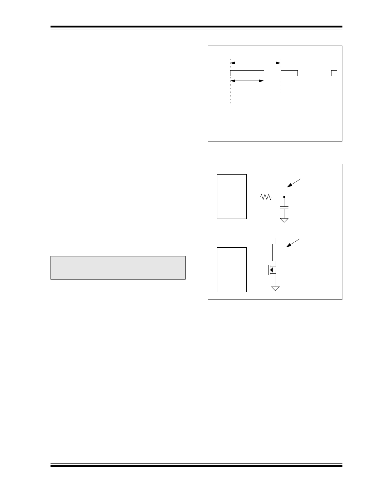
PIC16C717/770/771
8.3.2 PWM DUTY CYCLE
The PWM duty cycle is specified by writing to the
CCPR1L register and to the CCP1CON<5:4> bits. Up
to 10-bit res olu tio n is available. Th e CCP R1L co nta ins
the eight MSbs and the CC P1CON<5: 4> cont ains the
two LSbs. This 10-bit value is represented by
CCPR1L:CCP1CON<5:4>. The following equation is
used to calculate the PWM duty cycle in time:
PWM duty cycle = (CCPR1L:CCP1CON<5:4>) •
OSC • (TMR2 prescale value)
T
CCPR1L and CCP1CO N<5:4> c an be w ritten to a t an y
time, but the duty cycle value is not latched into
CCPR1H until af ter a match bet ween PR2 and TMR 2
occurs (i.e., the period is complete). In PWM mode,
CCPR1H is a read-only register.
The CCPR1H register and a 2-bit internal latch are
used to double buffer th e PWM du ty c yc le. This doubl e
buffering is essential for glitchless PWM operation.
When the CCPR1H and 2-bit latch match TMR2 concatenated with an internal 2-bit Q clock or 2 bits of the
TMR2 prescaler, the CCP1 pin is cleared.
Maximum PWM re solution (bits) for a given PWM frequency:
FOSC
---------------
log
FPWM
-----------------------------
bits=
2()log
Note: If the PWM duty cycle value is longer than
the PWM period, the CCP1 pin will not be
cleared.
FIGURE 8-4: SINGLE PWM OUTPUT
Period
(2)
CCP1
Duty Cycle
(1)
Note 1: At this time, the TMR2 register is equal to the PR2 register.
2: Output signal is shown as asserted high.
(1)
FIGURE 8-5: EXAMPLE OF SINGLE
OUTPUT APPLICATION
PIC16C717/770/771
CCP1
PIC16C717/770/771
CCP1
R
V+
L
O
A
D
Using PWM as
a D/A Converter
V
C
Using PWM to
Drive a Power
Load
OUT
8.3.3 PWM OUTPUT CONFIGURATIONS
The PWM1M1 bits in the CCP1CON register allows
one of the following configurations:
• Single output
• Half-Bridge output
• Full-Br idge output, Forward mode
• Full-Bridge outp ut, Reverse mode
In the Single Output mode, the RB3/CCP1/P1A pin is
used as the PWM output. Since th e CCP1 output is
multiplexed with the PORTB<3> data latch, the
TRISB<3> bit must be cleared to make the CCP1 pin
an output.
In the Half-Bridge output mode, two pins are used as
outputs. The RB3/CCP1/P1A pin has the PWM output
signal, while the RB5/SDO/P1B pin has the complementary PWM output signal. This mode can be used
for half-bridge applic ations , as sh ow n on Figure 8-7, or
for full-bridge applications, where four power switches
are being modulated with two PWM signal.
Since the P1A and P1B outputs are multiplexed with
the PORTB<3> and PORTB<5> data latches, the
TRISB<3> and TRISB<5> bits m u st b e c lea red to co nfigure P1A and P1B as outputs.
In Half-Bridge output mode, the programmable deadband delay can be used to prevent shoot-through current in bridge power devices. See Section 8.3.5 for
more details of the deadband delay operations.
1999 Microchip Technology Inc.
Advanced Information DS41120A-page 59
Page 60

PIC16C717/770/771
8.3.4 OUTPUT POLARITY CONFIGURATION
The CCP1M<1:0> bits in the CCP1CON register allow
user to cho ose the logic conventions (asserted h igh/
low) for each of the outputs. See Register8-1 for further details.
FIGURE 8-6: HALF-BRIDG E PWM OUTPUT
Period
Duty Cycle
(2)
P1A
td
(2)
P1B
(1)
Note 1: At this time, the TMR2 register is equal to the PR2 register.
2: Output signals are shown as as serted high.
td
(1)
td = Deadband Delay
Period
(1)
The PWM output po larities m ust be s elected bef ore the
PWM outputs are enabled. Charging the polarity configuration w h ile t h e PWM o ut p uts ar e a cti ve is no t r ecommended, since it may result in unpredictable
operation.
DS41120A-page 60 Advanced Information
1999 Microchip Technology Inc.
Page 61

PIC16C717/770/771
FIGURE 8-7: EXAMPLE OF HALF-BRIDGE OUTPUT MODE APPLICATIONS
V+
PIC16C717/770/771
PIC16C717/770/771
P1A
P1A
P1B
FET
DRIVER
FET
DRIVER
FET
DRIVER
+
V
-
+ -
LOAD
+
V
-
V-
V+
FET
DRIVER
P1B
FET
DRIVER
+ -
LOAD
V-
FET
DRIVER
1999 Microchip Technology Inc.
Advanced Information DS41120A-page 61
Page 62

PIC16C717/770/771
In Full-Bridge output mode, four pins are used as outputs; however, only two outputs are active at a time. In
the Forwa r d m ode, RB3/CCP1/P1A pin is co ntinuously
active, and RB7/T1OSI/P1D pin is modulated. In the
Reverse mode, RB6/T1OSO/T1CKI/P1C pin is continuously active, and RB5/SDO/P1B pin is modulated.
FIGURE 8-8: FULL-BRIDGE PWM OUTPUT
FORWARD MODE
Period
1
(2)
P1A
P1B
P1C
P1D
0
1
(2)
0
1
(2)
0
1
(2)
0
Duty Cycle
(1)
P1A, P1B, P1C and P1D outputs are multiplexed with
PORTB<3> and POR TB< 5:7> data latch es. TRISB<3 >
and TRISB<5:7> bits mu st be cleared to mak e the P1A,
P1B, P1C, and P1D pins output.
(1)
REVERSE MODE
Period
Duty Cycle
1
(2)
P1A
P1B
P1C
P1D
Note 1: At this time, the TMR2 register is equal to the PR2 register.
2: Outpu t signal is shown as asser ted high.
0
1
(2)
0
1
(2)
0
1
(2)
0
(1)
(1)
DS41120A-page 62 Advanced Information
1999 Microchip Technology Inc.
Page 63

PIC16C717/770/771
FIGURE 8-9: EXAMPL E OF FULL-BRIDGE APPLICATION
V+
PIC16C717/770/771
P1D
P1C
P1A
P1B
FET
DRIVER
FET
DRIVER
FET
DRIVER
+ -
LOAD
FET
DRIVER
V-
1999 Microchip Technology Inc.
Advanced Information DS41120A-page 63
Page 64
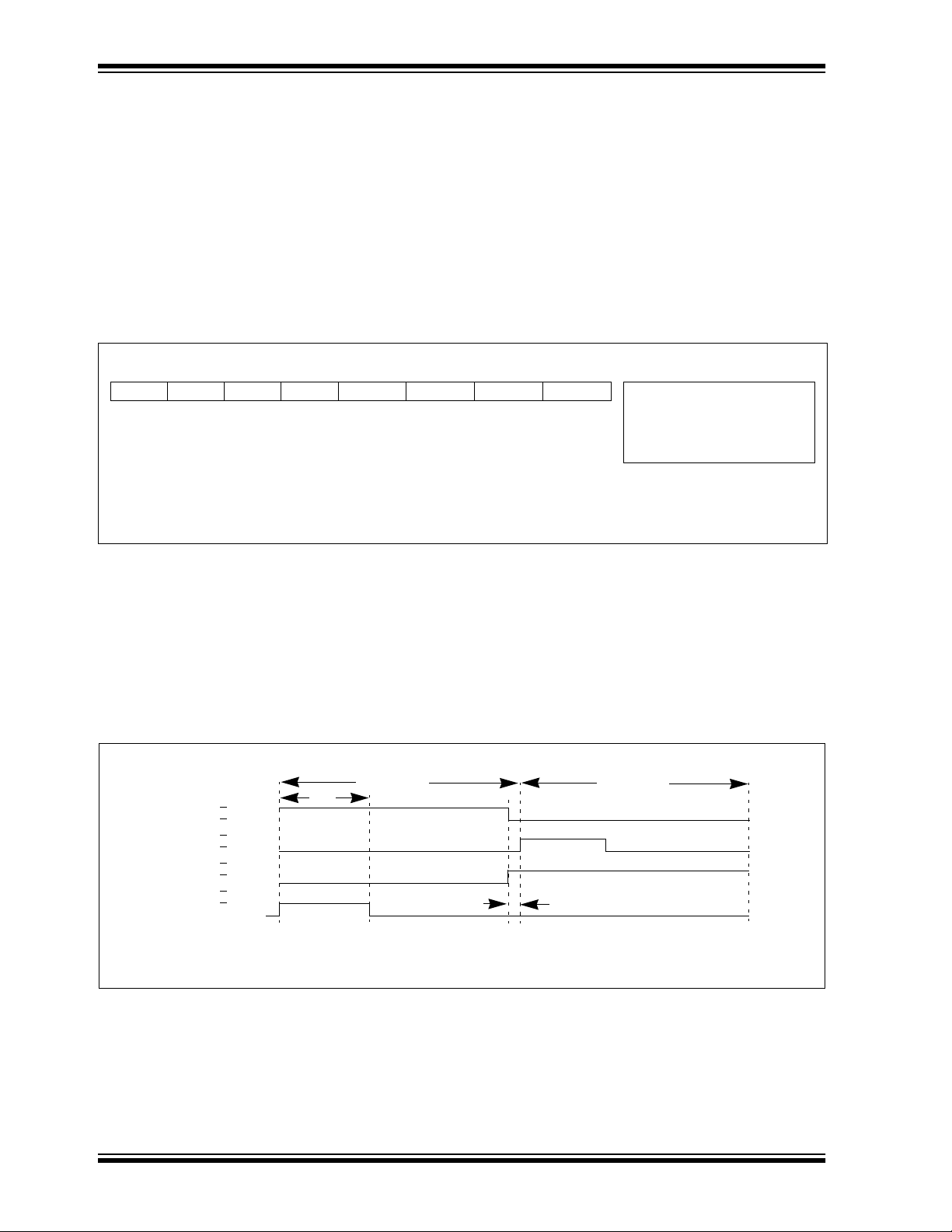
PIC16C717/770/771
8.3.5 PROGRAMMABLE DEADBAND DELAY
In half-bridge or full-bridge applications, where all
power switches are modulat ed at th e PWM f requency
at all time, the power switches normally require longer
time to turn off than to turn on. If both the upper and
lower power switches are switched at t he same time
(one turned on, and the other turned of f), both s witc hes
will be on for a short period of time, until one switch
completely turns off. During this time, a very high current, called shoot-through current, will flow through
both power switches, shorting the bridge supply. To
REGISTER 8-2: PWM DELAY REGISTER (P1DEL: 97H)
R/W-0 R/W-0 R/W-0 R/W-0 R/W-0 R/W-0 R/W-0 R/W-0
bit7 bit0
avoid this potentially destructive shoot-through current
from flowing during switching, turning on the power
switch is normally delayed to allow the other switch to
completely turn off.
In the Half-Bridge Output mode, a digitally programmable deadband delay is available to avoid shootthrough current from destroying the bridge power
switches . The de lay occurs at the s ignal tr ansi tion from
the non-active state to the active state. See Figure 8-6
for illustration. The P1DEL register sets the amount of
delay.
R = Readable bit
W = Writable bit
U = Unimplemented bit, read as
‘0’
- n = Value at POR reset
bit 7-0: P1DEL<7:0>: PWM Delay count for Half-Bridge output mode: Number of FOSC/4 (Tosc•4) cycles
between the P1A transition and the P1B transition.
8.3.6 DIRECTION CHANGE IN FULL-BRIDGE
OUTPUT MODE
modulated outputs , P1A and P1C signals , will transi tion
to the new direction TOSC, 4
•TOSC or 16•TO S C ( fo r
Timer2 presale T2 CKRS<1:0 > = 00 , 01 a nd 1x respec -
In the Full-Bridge Output mo de, the PWM 1M1 bit in the
CCP1CON register allows user to control the Forward/
Reverse direction. When the application firmware
changes this direction control bit, the ECCP module w ill
assume the new direction on the next PWM cycle. The
tively) earlier, before the end of the period. During this
transition cycle, the modulated outputs, P1B and P1D,
will go to the inactive state. See Figure 8-10 for illustration.
current PWM cycle still continues, however, the non-
FIGURE 8-10: PWM DIRECT ION CHANG E
(1)
SIGNAL
P1A (Active High)
P1B (Active High)
P1C (Active High)
P1D (Active High)
Note 1: The Direction bit in the ECCP Control Register (CCP1CON.PWM1M1) is written anytime during the PWM cycle.
2: The P1A and P1C signals switch T
changing direction. The modulated P1B and P1D signals are inactive at this time.
DC
PERIOD
(2)
OSC, 4*Tosc or 16*TOSC depending on the Timer2 prescaler value earlier when
PERIOD
DS41120A-page 64 Advanced Information
1999 Microchip Technology Inc.
Page 65

PIC16C717/770/771
Note that in the Full-Bridge output mode, the ECCP
module does not provide any deadband delay. In general, since only one output is modulated at all time,
deadband dela y is not required. Ho we v er , the re is a situation where a deadban d dela y might be requi red. This
situation occurs whe n all of the f oll owing co nditions are
true:
1. The direction of the PWM output changes when
the duty cycle of the output is at or near 100%.
2. The turn off time of the power switch, including
the power device and driver circuit, is greater
than turn on time.
Figure 8-11 shows an example, where the PWM direc-
tion changes from forward to reverse at a near 100%
duty cycle. At time t1, the output P1A and P1D become
example , si nce the turn off time of th e po w er de vi ce s is
longer than the turn on time, a shoot-through current
flows through the power devices, QB and QD, for the
duration of t= t
. The same phenomenon will occur
off-ton
to power devices, QC and QB, for PWM direction
change from reverse to forward.
If changing PWM direction at high duty cycle is required
for the user’s application, one of the following requirements must be met:
1. Avoid changi ng PWM out put direct ion at or ne ar
100% duty cycle.
2. Use switch drivers that compensate the slow
turn off of the powe r devices. The t otal tur n off
time (t
) of the power device and the driver
off
must be less than the turn on time (t
inactive, while output P1C becomes active. In this
FIGURE 8-11: PWM DIRECTION CHANGE AT NEAR 100% DUTY CYCLE
P1A
P1B
FORW ARD PERIOD
1
0
1
0
REVERSE PERIOD
(PWM)
).
on
1
P1C
0
1
P1D
External Switch C
External Switch D
Potential
Shoot Through
Current
0
1
0
1
0
1
0
(PWM)
Note 1: All signals are shown as active high.
is the turn on delay of power switch and driver.
2: t
on
is the turn off delay of power switch and driver.
3: t
off
t
on
t
off
t = t
- t
off
on
t
1
1999 Microchip Technology Inc.
Advanced Information DS41120A-page 65
Page 66

PIC16C717/770/771
8.3.7 SYSTEM IMPLEMENTATION
When the ECCP m odule i s used i n the PWM mode , the
application hardw are must use the proper e xternal pullup and/or pull-down resistors on the PWM output pins.
When the microcontroller powers up, all of the I/O pins
are in the high-impedance state. The external pull-up
and pull-down resistors must keep the power switch
devices in the off state until the microcontroller drives
the I/O pins with the proper signal levels, or activates
the PWM output(s).
8.3.8 START-UP CONSIDERATIONS
Prior to enabling the PWM out puts , the P1 A, P1B , P1C
and P1D latches may not be in the proper states.
Enabling the TRISB bits for output at the same time
with the CCP module m ay cause damag e to t he p o wer
switch devices. The CCP1 module must be enabled in
the proper output mode with the TR ISB bits enab led as
inputs. Once th e CCP1 completes a full PWM cycle , the
P1A, P1B, P1C and P1D output latches are properly
initialized. At this time, the TRISB bits can be enabled
for outputs to start driving the power switch devices.
The completion of a full PWM cycle is indicated by the
TMR2IF bit going from a ’0’ to a ’1’.
8.3.9 SET UP FOR PWM OPERATION
The following step s should be taken when co nfigur ing
the ECCP module for PWM operation:
1. Configure the PWM module:
a) Disable the CCP1/P1A, P1B, P1C and/or
P1D outputs by setting the respective
TRISB bits.
b) Set the PWM period by loading the PR2
register.
c) Set the PWM duty cycle by loading the
CCPR1L register and CCP1CON<5:4>
bits.
d) Configure the ECCP m odule f or the desired
PWM operation by loading the CCP1CON
register. With the CCP1M<3:0> bits select
the active high/low levels for each PWM
output. With the PWM1M<1:0> bits select
one of the available output modes: Single,
Half-Bridge, Full-Bridge, Forward or FullBridge Reverse.
e) For Half-Bridge output mode, set the dead-
band delay by loading the P1DEL register.
2. Configure and start TMR2:
a) Clear the TMR2 interrupt flag bit by clearing
the TMR2IF bit in the PIR1 register.
b) Set the TMR2 prescale v alue b y loading the
T2CKPS<1:0> bits in the T2CON register.
c) Ena ble Timer2 by se tting the T MR2ON bit
in the T2CON register.
3. Enable PWM outputs after a new cycle has
started:
a) Wait until TMR2 overflows (TMR2IF bit
becomes a ’1’). The new PWM cycle begin s
here.
b) Enable the CCP1/P1A, P1B, P1C and/or
P1D pin outputs by clearing the respective
TRISB bits.
TABLE 8-3: REGISTERS ASSOCIATED WITH PWM
Address Name Bit 7 Bit 6 Bit 5 Bit 4 Bit 3 Bit 2 Bit 1 Bit 0
0Bh, 8Bh,
10Bh,
18Bh
0Ch PIR1
8Ch PIE1
86h, 186h TRISB PORTB Data Direction Register 1111 1111 1111 1111
11h TMR2 Timer2 register 0000 0000 0000 0000
92h PR2 Timer2 period register 1111 1111 1111 1111
12h T2CON — TOUTPS3 TOUTPS2 TOUTPS1 TOUTPS0 TMR2ON T2CKPS1 T2CKPS0 -000 0000 -000 0000
15h CCPR1L Capture/Compare/PWM register1 (LSB) xxxx xxxx uuuu uuuu
17h CCP1CON
97h P1DEL PWM1 Delay value 0000 0000 0000 0000
Legend: Legend: x = unknown, u = unchanged, - = unimplemented read as ’0’. Shaded cells are not used by Capture and Timer1.
DS41120A-page 66 Advanced Information
INTCON GIE PEIE
— ADIF — — SSPIF CCP1IF TMR2IF TMR1IF -0-- 0000 -0-- 0000
— ADIE — — SSPIE CCP1IE TMR2IE TMR1IE -0-- 0000 -0-- 0000
PWM1M1 PWM1M0 DC1B1 DC1B0 CCP1M3 CCP1M2 CCP1M1 CCP1M0 0000 0000 0000 0000
T0IE INTE RBIE T0IF INTF RBIF 0000 000x 0000 000u
1999 Microchip Technology Inc.
Value on
POR,
BOR
Value on
all other
resets
Page 67

9.0 MASTER SYNCHRONOUS
SERIAL PORT (MSSP)
MODULE
The Master Synchronous Serial P ort (MSSP) module is
a serial interface useful for communicating with other
peripheral or microco ntrolle r de vices . Th ese periphe ra l
devices may be serial EEPROMs, shift registers, display drivers , etc. The MSSP modul e can operate in on e
of two modes:
• Serial Peripheral Interface (SPI™)
• Inter-Integrated Circuit (I
2
C™)
PIC16C717/770/771
1999 Microchip Technology Inc.
Advanced Information DS41120A-page 67
Page 68

PIC16C717/770/771
REGISTER 9-1: SYNC SERIAL PORT STATUS REGISTER (SSPSTAT: 94h)
R/W-0 R/W-0 R-0 R-0 R-0 R-0 R-0 R-0
SMP CKE D/A
bit7 bit0
bit 7: SMP: Sample bit
SPI Master Mode
1 = Input data sampled at end of data output time
0 = Input data sampled at middle of data output time
SPI Slave Mode
SMP must be cleared when SPI is used in slave mode
2
In I
C master or slave mode:
1= Slew rate control disabled for standard speed mode (100 kHz and 1 MHz)
0= Slew rate control enabled for high speed mode (400 kHz)
bit 6: CKE: SPI Clock Edge Select (Figure 9-3, Figure 9-5, and Figure 9-6)
CKP = 0
1 = Data transmitted on rising edge of SCK
0 = Data transmitted on falling edge of SCK
CKP = 1
1 = Data transmitted on falling edge of SCK
0 = Data transmitted on rising edge of SCK
bit 5: D/A: Data/Address
1 = Indicates that the last byte received or transmitted was data
0 = Indicates that the last byte received or transmitted was address
bit 4: P: Stop bit
2
C mode only. This bit is cleared when the MSSP module is disabled, SSPEN is cleared)
(I
1 = Indicates that a stop bit has been detected last (this bit is ’0’ on RESET)
0 = Stop bit was not detected last
bit 3: S: Start bit
2
C mode only. This bit is cleared when the MSSP module is disabled, SSPEN is cleared)
(I
1 = Indicates that a start bit has been detected last (this bit is ’0’ on RESET)
0 = Start bit was not detected last
bit 2: R/W: Read/Write bit information (I
This bit holds the R/W bit information following the last address match. This bit is only valid from the
address match to the next start bit, stop bit, or not ACK bit.
2
C slave mode:
In I
1 = Read
0 = Write
In I2C master mode:
1 = Transmit is in progress
0 = Transmit is not in progress.
Or’ing this bit with SEN, RSEN, PEN, RCEN, or AKEN will indicate if the MSSP is in IDLE mode
bit 1: UA: Update Address (10-bit I
1 = Indicates that the user needs to update the address in the SSPADD register
0 = Address does not need to be updated
bit 0: BF: Buffer Full Status bit
Receive (SPI and I
1 = Receive complete, SSPBUF is full
0 = Receive not complete, SSPBUF is empty
Transmit (I2C mode only)
1 = Data Transmit in progress (does not include the ACK and stop bits), SSPBUF is full
0 = Data Transmit complete (does not include the ACK
PSR/WUA BF R = Readable bit
W = Writable bit
U = Unimplemented bit, read
as ‘0’
- n = Value at POR reset
bit (I2C mode only)
2
C mode only)
2
C mode only)
2
C modes)
and stop bits), SSPBUF is empty
DS41120A-page 68 Advanced Information
1999 Microchip Technology Inc.
Page 69

PIC16C717/770/771
REGISTER 9-2: SYNC SERIAL PORT CONTROL REGISTER (SSPCON: 14h)
R/W-0 R/W-0 R/W-0 R/W-0 R/W-0 R/W-0 R/W-0 R/W-0
WCOL SSPOV SSPEN CKP SSPM3 SSPM2 SSPM1 SSPM0 R = Readable bit
bit7 bit0
bit 7: WCOL: Write Collision Detect bit
Master Mode:
1 = A write to the SSPBUF register was attempted while the I
2
C conditions were not valid for a
transmission to be started
0 = No collision
Slave Mode:
1 = The SSPBUF register is written while it is still transmitting the previous word
(must be cleared in software)
0 = No collision
bit 6: SSPO V: Receive Overflow Indicator bit
In SPI mode
1 = A new byte is received whi le the SSPBUF regist er is still holding the previou s data. In case of o verflo w ,
the data in SSPSR is lost. Overflow can only occur in sla ve mode . In sla v e mode , the us er must rea d the
SSPBUF, even if only transmitting data, to avoid setting overflow. In master mode, the overflow bit is not
set since each new reception (and transmission) is initiated by writing to the SSPBUF register. (Must be
cleared in software).
0 = No overflow
2
C mode
In I
1 = A byte is receive d while the SSPBUF register is st ill holding the pre vious byte . SSPO V is a "don’t care"
in transmit mode. (Must be cleared in software).
0 = No overflow
bit 5: SSPEN: Synchronous Serial Port Enable bit
In both modes, when enabled, these pins must be properly configured as input or output.
In SPI mode
1 = Enables serial port and configures SCK, SDO, SDI, and SS as the source of the serial port pins
0 = Disables serial port and configures these pins as I/O port pins
In I2C mode
1 = Enables the serial port and configures the SDA and SCL pins as the source of the serial port pins
0 = Disables serial port and configures these pins as I/O port pins
bit 4: CKP: Clock Polarity Select bit
In SPI mode
1 = Idle state for clock is a high level
0 = Idle state for clock is a low level
In I2C slave mode
SCK release control
1 = Enable clock
0 = Holds clock low (clock stretch) (Used to ensure data setup time)
2
C master mode
In I
Unused in this mode
bit 3-0: SSPM<3:0>: Synchronous Serial Port Mode Select bits
0000 = SPI master mode, clock = F
0001 = SPI master mode, clock = F
0010 = SPI master mode, clock = F
OSC/4
OSC/16
OSC/64
0011 = SPI master mode, clock = TMR2 output/2
0100 = SPI slave mode, clock = SCK pin. SS
0101 = SPI slave mode, clock = SCK pin. SS
0110 = I
0111 = I
1000 = I
2
C slave mode, 7-bit address
2
C slave mode, 10-bit address
2
C master mode, clock = FOSC / (4 • (SSPADD+1) )
pin control enabled.
pin control disabled. SS can be used as I/O pin
1xx1 = Reserved
1x1x = Reserved
W = Writable bit
- n = Value at POR reset
1999 Microchip Technology Inc.
Advanced Information DS41120A-page 69
Page 70

PIC16C717/770/771
REGISTER 9-3: SYNC SERIAL PORT CONTROL REGISTER2 (SSPCON2: 91h)
R/W-0 R/W-0 R/W-0 R/W-0 R/W-0 R/W-0 R/W-0 R/W-0
GCEN ACKSTAT ACKDT ACKEN RCEN PEN RSEN SEN R = Readable bit
bit7 bit0
bit 7: GCEN : General Call Enable bit (In I2C slave mode only)
1 = Enable interrupt when a general call address (0000h) is received in the SSPSR.
0 = General call address disabled.
2
bit 6: ACKSTAT: Acknowledge Status bit (In I
C master mode only)
In master transmit mode:
1 = Acknowledge was not received from slave
0 = Acknowledge was received from slave
2
bit 5: ACKDT: Acknowledge Data bit (In I
C master mode only)
In master receive mode:
Value that will be transmitted when the user initiates an Acknowledge sequence at the end of a receive.
1 = Not Acknowledge
0 = Acknowledge
2
bit 4: ACKEN: Acknowledge Sequence Enable bit (In I
C master mode only).
In master receive mode:
1 = Initiate Acknowledge sequence on SDA and SCL pins, and transmit ACKDT data bit. Automatically
cleared by hardware.
0 = Acknowledge sequence idle
2
bit 3: RCEN: Receiv e Enable bit (In I
1 = Enables Receive mode for I
C master mode only).
2
C
0 = Receive idle
bit 2: PEN: Stop Condition Enable bit (In I2C master mode only).
SCK release control
1 = Initiate Stop condition on SDA and SCL pins. Automatically cleared by hardware.
0 = Stop condition idle
2
bit 1: RSEN: Repeated Start Condition Enabled bit (In I
C master mode only)
1 = Initiate Repeated Start condition on SDA and SCL pins. Automatically cleared by hardware.
0 = Repeated Start condition idle.
2
bit 0: SEN: Start Condition Enabled bit (In I
C master mode only)
1 = Initiate Start condition on SDA and SCL pins. Automatically cleared by hardware.
0 = Start condition idle.
Note: For bits ACKEN, RCEN , PEN, RSEN, SE N: If the I2C module is not in the idle mode, this bit may not be set (no
spooling) and the SSPBUF may not be written (or writes to the SSPBUF are disabled).
W = Writable bit
U = Unimplemented bit, Read
as ‘0’
- n = Value at POR reset
DS41120A-page 70 Advanced Information
1999 Microchip Technology Inc.
Page 71
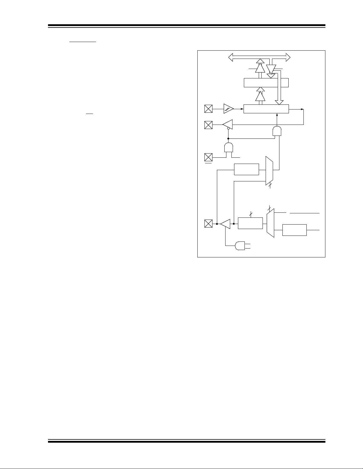
PIC16C717/770/771
9.1 SPI Mode
The SPI mode allows 8 bits of da ta to be synchronously
transmitted and received simultaneously. All four
modes of SPI are supported. To accomplish communication, typically three pins are used:
• Serial Data Out (SDO)
• Serial Data In (SDI)
• Serial Clock (SCK)
Additionally, a fourth pin may be used when in a slave
mode of operation:
•Slave Select (SS
9.1.1 OPERATION
When initializing the SPI, several options need to be
specified. This is don e by pr ogramming the appropriate
control bits (SSPCON<5:0> and SSPSTAT<7:6>).
These control bits allow the following to be specified:
• Master Mode (SCK is the clock output)
• Slave Mode (SCK is the clock input)
• Clock Polarity (Idle state of SCK)
• Data input sample phase
(middle or end of data output time)
• Clock edge
(output data on rising/falling edge of SCK)
• Clock Rate (Master mode only)
• Slave Select Mode (Slave mode only)
Figure 9-1 shows the b lo ck d iagr am of the MSSP mo d-
ule when in SPI mode.
)
FIGURE 9-1: MSSP BLOCK DIAGRAM
(SPI MODE)
Internal
Data Bus
Read Write
SSPBUF reg
SSPSR reg
2
Shift
Clock
TMR2 Output
2
Prescaler
4, 16, 64
SDI
SDO
SS
SCK
bit0
Control
SS
Enable
Edge
Select
Clock Select
SSPM<3:0>
SMP:CKE
Edge
Select
4
2
Data to TX/RX in SSPSR
Data direction bit
Tosc
The MSSP consists of a transmit/rece ive Shift Reg ister
(SSPSR) and a Buffer Register (SSPBUF). The
SSPSR shifts the data in and out of the device, MSb
first. The SSPBUF holds the data that w as written to the
SSPSR, until the receiv ed data is ready. Once the 8 bits
of data have been received, that byte is moved to the
SSPBUF register. Then the buffer full detect bit, BF
(SSPSTAT<0>), and the interrupt flag bit, SSPIF
(PIR1<3>), are set. This double buffering of the
received data (SSPBUF) allows the next byte to start
reception before reading the data that was just
received. Any write to the SSPBUF register during
transmissio n/r ece ptio n of da ta wil l be ig nor ed, and the
write collision detect bit WCOL (SSPCON<7>) will be
set. User software must clear the WCOL bit so that it
can be determined if the following write(s) to the SSPBUF register completed successfully.
When the application software is expecting to receive
valid data, t he SSPBUF s hould be read bef ore t he ne x t
byte of data to tr ansf er i s written to th e SSPBUF. Buff er
full bit, BF (SSPSTAT<0>), indicates when the SSPBUF has been load ed with the receiv ed dat a (tra nsmission is complete). When the SSPBUF is read, bit BF is
cleared. This data may be irrelevant if the SPI is only a
transmitter. Generally the MSSP Interrupt is used to
1999 Microchip Technology Inc.
Advanced Information DS41120A-page 71
Page 72
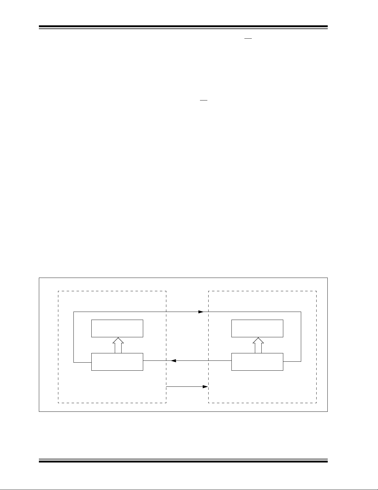
PIC16C717/770/771
determine when the transmission/reception has completed. The SSPBUF mus t be read and/or written. If the
interrupt method is not go ing to be used, then software
polling can be done to ensure that a write collision does
not occur. Example 9-1 shows the loading of the
SSPBUF (SSPSR) for data transmission.
EXAMPLE 9-1: LOADING THE SSPBUF
(SSPSR) REGISTER
BSF STATUS, RP0 ;Specify Bank 1
LOOP BTFSS SSPSTAT, BF ;Has data been
;received
;(transmit
;complete)?
GOTO LOOP ;No
BCF STATUS, RP0 ;Specify Bank 0
MOVF SSPBUF, W ;W reg = contents
;of SSPBUF
MOVWF RXDATA ;Save in user RAM
MOVF TXDATA, W ;W reg = contents
; of TXDATA
MOVWF SSPBUF ;New data to xmit
The SSPSR is not direc tly readabl e or writable, and can
only be accessed by addressing the SSPBUF register.
Additionally, the MSSP status register (SSPSTAT) indicates the various status conditions.
9.1.2 ENABLING SPI I/O
To enable the serial port, MSSP Enable bit, SSPEN
(SSPCON<5>) must be set. To reset or reconfigure SPI
mode, clear bit SSPEN, re-initialize the SSPCON registers, and then set bit SSPEN. This configures the
SDI, SDO, SCK and SS
pins as serial port pins. F or th e
pins to behave as the serial port function, some must
have their data direction bits (in the TRIS register)
appropriately programmed. That is:
• SDI is automatically co ntrolled by the SPI mo du le
• SDO must have TRISB<5> cleared
• SCK (Master mode) must h a v e TRISB<2> cleare d
• SCK (Slave mode) must have TRISB<2> set
must have TRISB<1> set, and ANSEL<5>
•SS
cleared
Any serial port function that is n ot desired m ay be ov erridden by programming the corresponding data direction (TRIS) register to the opposite value.
9.1.3 TYPICAL CONNECTION
Figure 9-2 shows a typical connection between two
microcontrollers. The master controller (Processor 1)
initiates the data transfer by sending the SCK signal.
Data is shifted out of both shift registers on their programmed cloc k edge, and latched on the opp osite edge
of the clock. Bo th processo rs should b e progr ammed to
same Clock Polarity (CKP), then both controllers would
send and receive data at the same time. Whether the
data is meaningful (or dummy data) depends on the
application software. This leads to three scenarios for
data transmissio n:
• Master sends data — Slave sends dummy data
• Master sends data — Slave sends data
• Master sends dummy data — Slave sends data
FIGURE 9-2: SPI MASTER/SLAVE CONNECTION
SPI Master SSPM<3:0> = 00xxb
SDO
Serial Input Buffer
(SSPBUF)
Shift Register
(SSPSR)
MSb
PROCESSOR 1
LSb
SDI
SCK
Serial Clock
SPI Slave SSPM<3:0> = 010xb
SDI
Serial Input Buffer
(SSPBUF)
SDO
SCK
Shift Register
(SSPSR)
MSb
PROCESSOR 2
LSb
DS41120A-page 72 Advanced Information
1999 Microchip Technology Inc.
Page 73

PIC16C717/770/771
9.1.4 MASTER MODE
Figure 9-3, Figure 9-5 and Figure9-6, where the MSb
is transmitted first. In master mode, the SPI clock rate
The master can initiate the data transfer at any time
because it controls the SCK. The master determines
when the slave (Processor 2, Figure 9-2) is to broadcast data by the software protocol.
In master mode, the data is transmitted/received as
soon as the SSPBUF register is written to. If the SPI
module is only going to receive, the SDO output could
be disabled (programmed as an input). The SSPSR
register will co ntinue to s hift in the si gnal present o n the
SDI pin at the programmed clock rate. As each byte is
received, it wil l be lo ad e d i nt o t he S SPB UF r e gis te r as
if a normal received byte (interrupts and status bits
appropriately set). This could be useful in receiver
applications as a “line activity monitor”.
The clock polari ty is selected b y appropriately pr ogram-
(bit rate) is user programmable to be one of the following:
OSC/4 (or TCY)
•F
•F
OSC/16 (or 4 • TCY)
•FOSC/64 (or 16 • TCY)
• Timer2 output/2
This allows a maxim um bit cloc k frequen cy (at 20 MHz)
of 8.25 MHz.
Figure 9-3 shows the waveforms for Master mode.
When CKE = 1, the SDO data is valid before there is a
clock edge on SCK. The change of the input sample is
shown based on the state of the SMP bit. The time
when the SSPBUF is loaded with the received data is
shown.
ming bit CKP (SSPCON<4>). This then would give
waveforms for SPI communication as shown in
FIGURE 9-3: SPI MODE WAVEFORM (MASTER MODE)
Write to
SSPBUF
SCK
(CKP = 0
CKE = 0)
SCK
(CKP = 1
CKE = 0)
SCK
(CKP = 0
CKE = 1)
SCK
(CKP = 1
CKE = 1)
SDO bit7
(CKE = 0)
SDO b it7
(CKE = 1)
SDI
(SMP = 0)
Input
Sample
(SMP = 0)
SDI
(SMP = 1)
Input
Sample
(SMP = 1)
SSPIF
SSPSR to
SSPBUF
bit7
bit7
bit6
bit6
bit5 bit4
bit5 bit4
bit3
bit3
bit2
bit2
bit1 bit0
bit1 bit0
bit0
bit0
4 clock
modes
Next Q4 cycle
after Q2↓
1999 Microchip Technology Inc.
Advanced Information DS41120A-page 73
Page 74

PIC16C717/770/771
9.1.5 SLAVE MODE
In slave mode, the data is transmitted and received as
the external clock pulses appear on SCK. When the
SDO pin is no longer driven, even if in the middle of
a transmitted byte, and becomes a floating output.
External pull-up/ pull-down resistors may be desirable,
depending on the application.
last bit is latched the interrupt flag bit SSPIF (PIR1<3>)
is set.
Note 1: When the SPI module is in Slave Mode
While in slave mode, the external clock is supplied by
the external cloc k sou rce o n the SCK p in. Th is external
clock must meet th e minimum high and low times as
specified in the electrical specifications.
While in sleep mode, the slave can transmit/receive
data. When a byt e i s r e cei ved, t he d evice w il l wake- up
from sleep.
When the SPI module resets, the bit counter is forced
to 0. This can be done by either forcing the SS
9.1.6 SLAVE SELECT SYNCHRONIZATION
The SS
SPI must be in slave mode with SS
pin allows a synchronous slave mode. The
pin control
enabled (SSPCON<3:0> = 0100). The pin must not
be driven low for the SS pin to function as an input.
TRISB<1> must be set. When the SS
pin is low,
transmission and reception are enabled and the
high leve l or clearing the SSPEN bit.
To emulate two-wire communication, the SDO pin can
be connected to the SDI pin. When the SPI needs to
operate as a receiver, the SDO pin can be configured
as an input. This disabl es transm issions from the SDO .
The SDI can always be left as an input (SDI function)
since it cannot create a bus conflict.
SDO pin is driven. When the SS pin goes high, the
FIGURE 9-4: SLAVE SYNCHRONIZATION WAVEFORM
with SS
pin control enabled, (SSPCON<3:0> = 0100) the SPI module will
reset if the SS
pin is set to VDD.
2: If the SPI is used in Slave Mode with
CKE = ’1’, then SS pin control must be
enabled.
pin to a
SS
SCK
(CKP = 0
CKE = 0)
SCK
(CKP = 1
CKE = 0)
Write to
SSPBUF
SDO
SDI
(SMP = 0)
Input
Sample
(SMP = 0)
SSPIF
Interrupt
Flag
SSPSR to
SSPBUF
bit7
bit7
bit6 bit7
bit7
bit0
bit0
Next Q4 cycle
after Q2Ø
DS41120A-page 74 Advanced Information
1999 Microchip Technology Inc.
Page 75
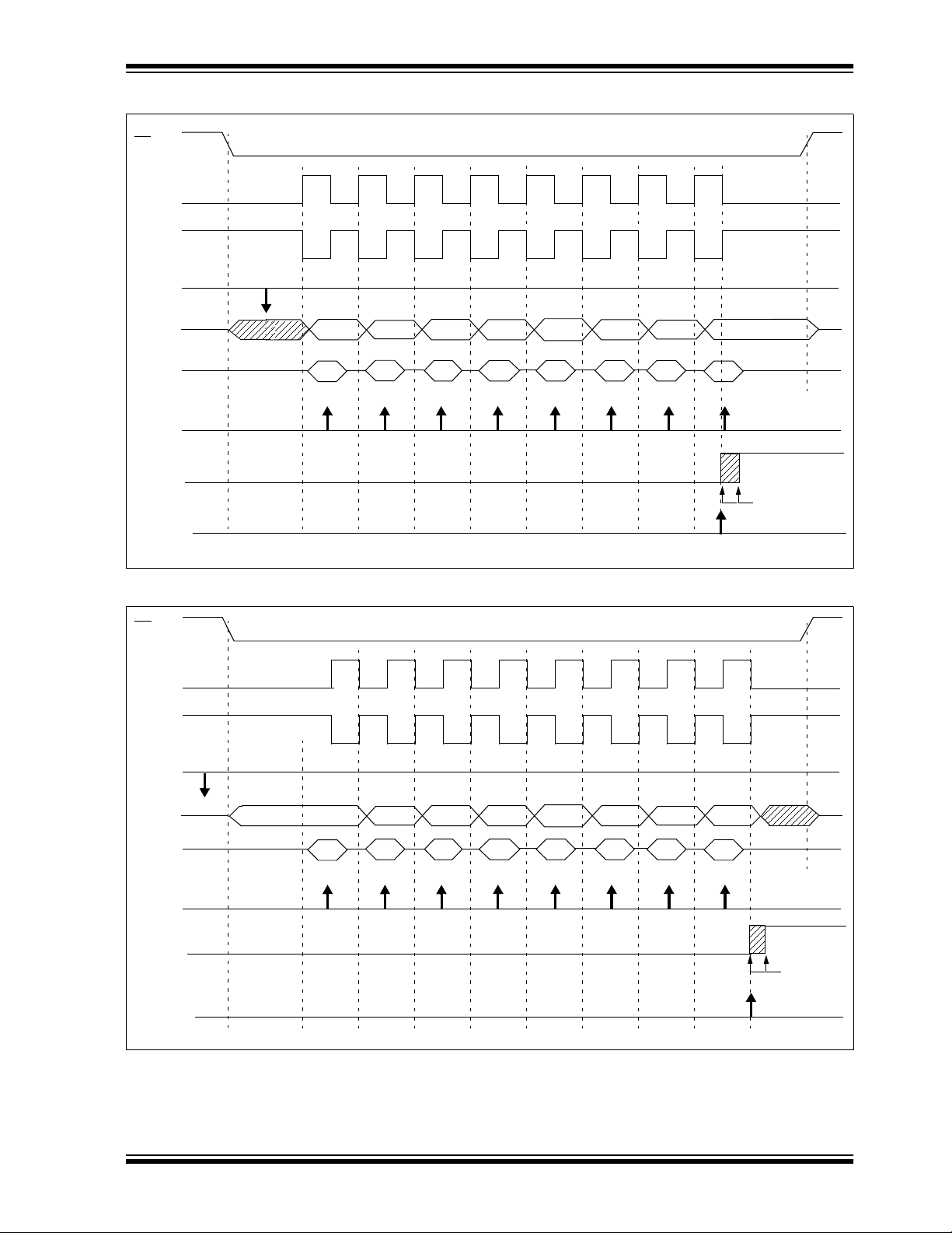
PIC16C717/770/771
FIGURE 9-5: SPI SLAVE MODE WAVEFORM (CKE = 0)
SS
optional
SCK
(CKP = 0
CKE = 0)
SCK
(CKP = 1
CKE = 0)
Write to
SSPBUF
SDO bit7
SDI
(SMP = 0)
Input
Sample
(SMP = 0)
SSPIF
Interrupt
Flag
SSPSR to
SSPBUF
bit7
bit6
bit5 bit4
FIGURE 9-6: SPI SLAVE MODE WAVEFORM (CKE = 1)
SS
not optional
SCK
(CKP = 0
CKE = 1)
SCK
(CKP = 1
CKE = 1)
Write to
SSPBUF
bit3
bit2
bit1 bit0
bit0
Next Q4 cycle
after Q2Ø
SDO bit7
SDI
(SMP = 0)
Input
Sample
(SMP = 0)
SSPIF
Interrupt
Flag
SSPSR to
SSPBUF
1999 Microchip Technology Inc.
bit7
bit6
bit5 bit4
bit3
bit2
bit1 bit0
bit0
Next Q4 cycle
after Q2Ø
Advanced Information DS41120A-page 75
Page 76

PIC16C717/770/771
9.1.7 SLEEP OPERATION
In master mode, all module clocks are halted and the
transmission/rec eption wil l rema in in t hat sta te unti l the
9.1.8 EFFECTS OF A RESET
A reset disables the MSSP module and terminates the
current transfer.
device wakes from sleep. After the device returns to
normal mode, the module will continue to transmit/
receive data.
In slave mode, the SPI transmit/receive shift register
operates asy nch ron ous ly to the de vi ce. This allows the
device to be placed in sleep mode and data to be
shifted into the SPI transmit/receive shift register.
When all 8 bits ha ve b een receiv ed, the MSSP in terrupt
flag bit will be set and if enabled will wake the device
from sleep.
TABLE 9-1: REGISTERS ASSOCIATED WITH SPI OPERATION
Address Name Bit 7 Bit 6 Bit 5 Bit 4 Bit 3 Bit 2 Bit 1 Bit 0 POR, BOR MCLR, WDT
0Bh, 8Bh,
10Bh,18Bh
0Ch PIR1
8Ch PIE1
13h SSPBUF Synchronous Serial Port Receive Buffer/Transmit Register xxxx xxxx uuuu uuuu
14h SSPCON WCOL SSPOV SSPEN CKP SSPM3 SSPM2 SSPM1 SSPM0 0000 0000 0000 0000
94h SSPSTAT SMP CKE
Legend: x = unknown, u = unchanged, - = unimplemented read as ’0’. Shaded cells are not used by the MSSP in SPI mode.
INTCON GIE PEIE
— ADIF — — SSPIF CCP1IF TMR2IF TMR1IF -0-- 0000 -0-- 0000
— ADIE — —SSPIECCP1IE TMR2IE TMR1IE -0-- 0000 -0-- 0000
T0IE INTE RBIE T0IF INTF RBIF 0000 000x 0000 000u
D/A P S R/W UA BF 0000 0000 0000 0000
DS41120A-page 76 Advanced Information
1999 Microchip Technology Inc.
Page 77

PIC16C717/770/771
9.2 MSSP I2C Operation
The MSSP module in I2C mode fully implements all
master and slave functions (including general call support) and provides interrupts on start and stop bits in
hardware to determine a free bus (multi-master function). The MSSP module implements the standard
mode specifications, as well as 7-bit and 10-bit
addressing.
Refer to Application Note AN578,
Module in the I
2
C Multi-Master Environment."
"Use of the SSP
A "glitch" filter is on the SCL and SDA pins whe n the pin
is an input. This filter operates in b oth the 10 0 k Hz an d
400 kHz modes. In the 10 0 kHz mode, w hen these pins
are an output, there is a sle w ra te control of the pin that
is independent of device frequency.
FIGURE 9-7: I2C SLAVE MODE BLOCK
DIAGRAM
Internal
Data Bus
Read Write
Shift
MSb
SSPBUF reg
SSPSR reg
Match detect
SSPADD reg
Start and
Stop bit detect
LSb
(SSPSTAT reg)
Addr Match
Set, Reset
S, P bits
SCL
Clock
SDA
FIGURE 9-8: I
2
C MASTER MODE BLOCK
DIAGRAM
Internal
Data Bus
Read Write
SSPADD<6:0>
7
Baud Rate Generator
SCL
Clock
SDA
Two pins are used f or dat a t r a ns fer. These are the SCL
pin, which is the clock, and the SDA pin, which is the
data. The MSSP module functions are enabled by setting SSP Enable bit SSPEN (SSPCON<5>).
The MSSP module has six registers for I
They are the:
• SSP Control Register (SSPCON)
• SSP Control Register2 (SSPCON2)
• SSP Status Register (SSPSTAT)
• Serial Receive/Transmit Buffer (SSPBUF)
• SSP Shift Register (SSPSR) - Not directly accessible
• SSP Address Register (SSPADD)
The SSPCON register allows control of the I
tion. Four mode selection bits (SSPCON<3:0>) allow
one of the following I2C modes to be sele cted:
2
C Slave mode (7-bit address)
•I
2
C Slave mode (10-bit address)
•I
2
•I
C Master mode, clock = OSC/4 (SSPADD +1)
Before selecting any I
must be programmed to inputs by setting the appropriate TRIS bits. Selecting an I
SSPEN bit, enables the SCL and SDA pins to be used
as the clock and data lines in I2C mode.
The SSPSTAT register gives the status of the data
transfer. This information includes detection of a
START (S) or STOP (P) bit, specifies if the received
byte was data or add ress if the ne xt by te is the completion of 10-bit address, and if this will be a read or write
data transfe r.
SSPBUF reg
Shift
SSPSR reg
MSb
Match detect
SSPADD reg
Start and Stop bit
detect / generate
2
C mode, the SCL and SDA pins
LSb
2
C mode, by setting the
Addr Match
Set/Clear S bit
and
Clear/Set P bit
(SSPSTAT reg)
and Set SSPIF
2
C operation.
2
C opera-
1999 Microchip Technology Inc.
Advanced Information DS41120A-page 77
Page 78

PIC16C717/770/771
SSPBUF is the register to which the transfer data is
written to or read from. The SSPSR register shifts the
data in or out of the device. In receive operations, the
SSPBUF and SSPSR create a doubled buffered
receiver. This allows reception of the next byte to begi n
before reading the last byte of received data. When the
complete byte is received, it is transferred to the
SSPBUF register and flag bit SSPIF is set. If another
complete byte is received before the SSPBUF register
is read, a receiver overflow has occurred and bit
SSPOV (SSPCON<6>) is set and the byte in the
SSPSR is lost.
The SSPADD register holds the sl av e address . In 10-bit
mode, the user needs to write the high byte of the
address (1111 0 A9 A8 0). Following the high byte
address match, the low byte of the address needs to be
loaded (A7:A0).
9.2.1 SLAVE MODE
In slave mode, the SCL and SDA pins must be config-
ured as inputs. The MSSP module will override the
input state with the output data when required (slavetransmitter).
When an address is matched or the data transfer after
an address match is received, the hardware automatically will generate the acknowledge (ACK
then load the SSPBUF register with the received value
currently in the SSPSR register.
There are certain conditions that will cause the MSSP
module not to give this ACK
(or both):
a) The buffer full bit BF (SSPSTAT<0>) was set
before the transfer was received.
b) The overfl ow bit SSPO V (SSPCON<6>) w as set
before the transfer was received.
If the BF bit is set, the SSPSR register value is not
loaded into the SSPBUF, but bit SSPIF and SSPO V are
set. Table 9-2 shows what happens whe n a data transfer byte is received, given the status of bits BF and
SSPOV. The shaded cells show the condition where
user software did not pro perly clea r the o v erfl ow c ondition. Flag bit B F is cleare d b y reading th e SSPBUF re gister while bit SSPOV is cleared through software.
The SCL clock input must have a minimum high and
low time for proper operation. The high and low times
2
of the I
MSSP module is shown in timing parameter #100 and
parameter #101 of the Electrical Specifications.
C specification as well as t he requirement of th e
pulse. These are if either
) pulse, and
9.2.1.1 ADDRESSING
Once the MSSP module has been enabled, it waits for
a START condition to occur . Following the START condition, the 8-bits are shifted in to the SSPSR register . All
incoming bits are sampled with the rising edge of the
clock (SCL) line. The value of register SSPSR<7:1> is
compared to the value of the SSPADD register. The
address is compared on the falling edge of the eighth
clock (SCL) pulse. If the addresses match, and the BF
and SSPOV bits are clear, the following events occur:
a) The SSPSR register value is loaded into the
SSPBUF register on the falling edge of the 8th
SCL pulse.
b) The buff er full bit, BF is set on the f alling edge of
the 8th SCL pulse.
c) An ACK
d) SSP interrupt flag bit, SSPIF (PIR1<3>) is set
(interrupt is generate d if enab le d) - on t he f al ling
edge of the 9th SCL pulse.
In 10-bit address mode, two address bytes need to be
received by the slave. The five Most Significant bits
(MSbs) of the first address b yte sp ecify if this is a 1 0-bit
address. Bit R/W
so the slave device will receive the second address
byte. For a 10-bit address the firs t byte would equal
‘1111 0 A9 A8 0’, where A9 and A8 are the two MSbs
of the address. The sequence of events for a 10-bit
address is as f ollows , with steps 7- 9 f or sla v e-tr ansmitter:
1. Receive first (high) byte of Address (bits SSPIF,
BF, and bit UA (SSPSTAT<1>) are set).
2. Update the SSPADD register with second (low)
byte of Address (clears bit UA and releases the
SCL line).
3. Read the SSPBUF register (clears bit BF) and
clear flag bit SSPIF.
4. Receive second (low) byte of Address (bits
SSPIF, BF, and UA are set).
5. Update the SSPADD register with the first (high)
byte of Address. This will clear bit UA and
release the SCL line.
6. Read the SSPBUF register (clears bit BF) and
clear flag bit SSPIF.
7. Receive Repeated Start condition.
8. Receive first (high) byte of Address (bits SSPIF
and BF are set).
9. Read the SSPBUF register (clears bit BF) and
clear flag bit SSPIF.
Note: Following the Repeated Start condition
pulse is generated.
(SSPSTAT<2>) must specify a write
(step 7) in 10-bit mode, the user only
needs to match the first 7-bit addre ss. Th e
user does not update the SSPADD for the
second half of the address.
DS41120A-page 78 Advanced Information
1999 Microchip Technology Inc.
Page 79

PIC16C717/770/771
9.2.1.2 SLAVE RECEPTION
When the R/W bit of the address byte is clear and an
address match occurs, the R/W
register is cleared. The rece iv ed ad dress i s loade d into
the SSPBUF register.
When the address byte overflow condition exists, then
no acknowled ge (ACK
dition is defined as either bit BF (SSPSTAT<0>) or bit
SSPOV (SSPCON<6>) and is set.
) pulse is given. An overflow con-
bit of the SSPSTAT
A MSSP interrupt is generated for each data transfer
byte. Flag b it SSPIF (PIR1<3 >) must be cleared in soft-
ware. The SSPSTAT register is used to determine the
status of the received byte.
Note: The SSPBUF will be loaded if the SSPOV
bit is set and the BF flag is cleared. If a
read of the SSPBUF was performed, but
the user did not clear the state of the
SSPOV bit before the next receive
occurred, the ACK
BUF is updated.
is not sent and the SSP-
TABLE 9-2: DATA TRANSFER RECEIVED BYTE ACTIONS
Status Bits as Data
Transfer is Received
BF SSPOV
00 Yes Yes Yes
1 0 No No Yes
1 1 No No Yes
0 1 Yes No Yes
Note 1: Shaded cells show the conditions where the user software did not properly clear the overflow condition.
9.2.1.3 SLAVE TRANSMISSION
When the R/W bit of the incoming address byte is set
and an address match occurs, the R/W
SSPSTAT register is set. The received address is
loaded into the SSPBUF register. The ACK
be sent on the ninth bit, and the SCL pin is held low.
The transmit data must be loaded into the SSPBUF
register , which also loads the SSPSR register . Then the
SCL pin should be enabled by setting bit CKP (SSPCON<4>). The master must monitor the SCL pin prior
to asserting another clock pulse. The slave devices
may be holding off the master by stretchi ng the cl ock.
The eight data bits are shifte d out on the f alling edg e of
the SCL input. This ensures that the SDA signal is valid
during the SCL high time (Figure 9-10).
SSPSR
→ SSPBUF
bit of the
pulse will
Generate ACK
Pulse
A MSSP interrupt is generated for each data transfer
byte. The SSPIF flag bit must be cleared in software,
and the SSPSTA T register is us ed to determine the sta-
tus of the byte tr an sfer. The SSPIF flag bit is set on the
falling edge of the ninth clock pulse.
As a slave-transmitter, the ACK
receiver is latched on the rising edge of the ninth SCL
input pulse. If t he SDA lin e was high (not A CK), then the
data transfer is comple te . When the not ACK
by the slave, the slave logic is reset and the slave then
monitors for anoth er occurrence of the START bit. If the
SDA line was low (ACK
loaded into the SSPBUF register, which also loads the
SSPSR register. Then the SCL pin should be enabled
by setting the CKP bit.
Set bit SSPIF
(SSP Interrupt occurs
if enabled)
pulse from the master-
), the transmit data must be
is latched
1999 Microchip Technology Inc.
Advanced Information DS41120A-page 79
Page 80
PIC16C717/770/771
FIGURE 9-9: I2C WAVEFORMS FOR RECEPTION (7-BIT ADDRESS)
Receiving Address
A7 A6 A5 A4
A3 A2 A1SDA
R/W=0
ACK
Receiving Data
D5
D6D7
ACK
D0
D2
D3D4
D1
Receiving Data
D5
D6D7
Not
ACK
D0
D2
D1
D3D4
1234
S
SCL
SSPIF
BF (SSPSTAT<0>)
SSPOV (SSPCON<6>)
FIGURE 9-10: I
SDA
SCL
SSPIF
BF (SSPSTAT<0>)
CKP (SSPCON<4>)
A7 A6 A5 A4 A3 A2 A1
123456789 123456789
S
7
6
5
2
C WAVEFORMS FOR TRANSMISSION (7-BIT ADDRESS)
Receiving Address
Data in
sampled
8
1234
9
Cleared in software
SSPBUF register is read
Bit SSPOV is set because the SSPBUF register is still full.
R/W = 1
ACK
SCL held low
while CPU
responds to SSPIF
56
7
89
123
D7 D6 D5 D4 D3 D2 D1 D0
cleared in software
SSPBUF is written in software
Set bit after writing to SSPBUF
(the SSPBUF must be written-to
before the CKP bit can be set)
5
6
4
ACK is not sent.
From SSP interrupt
service routine
9
8
7
Not ACKTransmitting Data
R/W = 0
P
Bus Master
terminates
transfer
P
DS41120A-page 80 Advanced Information
1999 Microchip Technology Inc.
Page 81
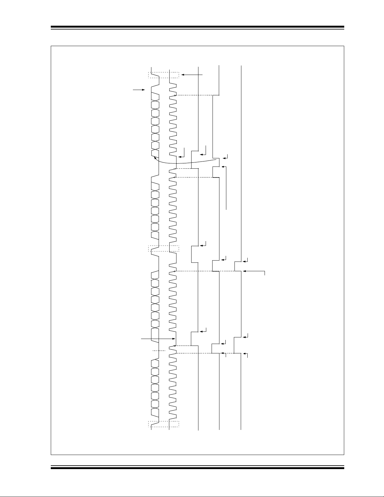
PIC16C717/770/771
FIGURE 9-11: I2C SLAVE-TRANSMITTER (10-BIT ADDRESS)
P
Bus Master
terminates
transfer
ACK
D0
Transmit is complete
Master sends NACK
6
D2
Clock is held low until
update of SSPADD has
Transmitting Data Byte
D7 D6 D5 D4 D3 D1
ACK
R/W=1
A9
Receive First Byte of Address
ACK
Receive Second Byte of Address
taken place
ACK
R/W = 0
12345 789
6
Sr
CKP has to be set for clock to be released
Cleared in software
initiates transmit
Write of SSPBUF
Cleared in software
Dummy read of SSPBUF
to clear BF flag
Cleared in software
Dummy read of SSPBUF
to clear BF flag
Cleared by hardware when
SSPADD is updated.
UA is set indicating that
SSPADD needs to be
Cleared by hardware when
SSPADD is updated.
updated
1999 Microchip Technology Inc.
SSPBUF is written with
contents of SSPSR
UA is set indicating that
the SSPADD needs to be
updated
Receive First Byte of Address
11110A9A8 A7 A6A5A4A3A2A1A0 11110 A8
SDA
123456789 123456789 12345 789
SCL
S
SSPIF
BF (SSPSTAT<0>)
(PIR1<3>)
UA (SSPSTAT<1>)
Advanced Information DS41120A-page 81
Page 82

PIC16C717/770/771
FIGURE 9-12: I2C SLAVE-RECEIVER (10-BIT ADDRESS)
terminates
transfer
Bus Master
P
ACK
R/W = 1
6
D2
Receive Data Byte
Cleared in software
ACK
Read of SSPBUF
clears BF flag
Dummy read of SSPBUF
to clear BF flag
Cleared by hardware when
SSPADD is updated with high
byte of address.
UA is set indicating that
SSPADD needs to be
updated
Receive Second Byte of Address
Clock is held low until
update of SSPADD has
taken place
R/W = 0
Receive First Byte of Address
ACK
1 1 1 1 0 A9A8 A7 A6A5A4A3A2A1A0 D7D6D5D4D3 D1D0
SDA
123456 789 1 2345 6789 1 2345 789
S
SCL
SSPIF
(PIR1<3>)
Cleared in software
Dummy read of SSPBUF
to clear BF flag
SSPBUF is written with
contents of SSPSR
BF (SSPSTAT<0>)
Cleared by hardware when
SSPADD is updated with low
byte of address.
UA is set indicating that
the SSPADD needs to be
updated
UA (SSPSTAT<1>)
DS41120A-page 82 Advanced Information
1999 Microchip Technology Inc.
Page 83
PIC16C717/770/771
9.2.2 GENERAL CALL ADDRESS SUPPORT
If the general call address matches, the SSPSR is
transferred to the SSPBUF, the BF flag is set (eighth
The addressing procedure for the I2C bus is such that
the first byte after the START condition usually determines which device will be the slave addressed by the
master. The exception is the general call address,
which can address all devices. When this address is
used, all devices should, in theory, respond with an
acknowledge.
The general call address is one of eight addresses
reserved for specific purposes by the I
consists of all 0’s with R/W
= 0
2
C protocol. It
The general call address is recognized when the General Call Enable bi t (GCEN) is en abled (SSPCON2<7>
is set). Following a start-bit detect, 8 bits are shifted
into SSPSR and the address is compared against
bit), and on the f alling edg e of the ninth bi t (ACK
SSPIF flag is set.
When the interrupt is serviced, the so urc e for the inter-
rupt can be checked by reading the contents of the
SSPBUF to determine if the address was device spe-
cific or a general call address.
In 10-bit mode, the SSPADD is required to be updated
for the seco nd half of th e address to match, and th e U A
bit is set (SSPSTAT<1>). If the general call address is
sampled when GCEN is set while the slave is config-
ured in 10-bit address mode, then the second half of
the address is not ne cessary, the UA bit will no t be se t,
and the slave will begin receiving data after the
acknowledge (Figure 9-13).
bit), the
SSPADD. It is also compared to the general call
address, fixed in hardware.
FIGURE 9-13: SLAVE MODE GENERAL CALL ADDRESS SEQUENCE (7 OR 10-BIT MODE)
Address is compared to General Call Address
after ACK, set interrupt flag
SDA
General Call Address
R/W = 0
Receiving data
ACK
D7 D6 D5 D4 D3 D2 D1 D0
ACK
SCL
SSPIF
BF
(SSPSTAT<0>)
SSPOV
(SSPCON<6>)
GCEN
(SSPCON2<7>)
123456789123456789
S
Cleared in software
SSPBUF is read
’0’
’1’
1999 Microchip Technology Inc.
Advanced Information DS41120A-page 83
Page 84

PIC16C717/770/771
9.2.3 SLEEP OPERATION
2
While in sleep mode, the I
C module can receive
addresses or data, and when an address match or
complete byte transf er occurs, w ake the pr ocessor from
sleep (if the SSP interrupt bit is enabled).
from a reset or when the MSSP module is disabled.
Control of the I
set, or the bus is idle with both the S and P bits clear.
In master mode, the SCL and SDA lines are manipulated by the MSSP hardware .
The following events will cause SSP Interrupt Flag bit,
9.2.4 EFFECTS OF A RESET
A reset disables the MSSP module and terminates the
current transfer.
9.2.5 MASTER MODE
SSPIF, to be set (SSP Interrupt if enabled):
• START condition
• STOP condition
• Data transfer byte transmitted/received
• Acknowledge transmit
Master mode operation is supported by interrupt gen-
• Repeated Start
eration on the detection of the START and STOP conditions. The STOP (P) and START (S) bits are cleared
FIGURE 9-14: MSSP BLOCK DIAGRAM (I2C MASTER MODE)
Internal
Data Bus
Read Write
SSPBUF
LSb
Shift
Clock
SDA
SDA in
SSPSR
MSb
2
C bus may be taken when the P bit is
SSPM<3:0>,
SSPADD<6:0>
Baud
Rate
Generator
SCL
Receive Enable
SCL in
Bus Collision
Start bit, Stop bit,
Acknowledge
Generate
Start bit detect,
Stop bit detect
Write collision detect
Clock Arbitration
State counter for
end of XMIT/RCV
clock cntl
clock arbitrate/WCOL detect
Set/Reset, S, P, WCOL (SSPSTAT)
Set SSPIF, BCLIF
Reset ACKSTAT, PEN (SSPCON2)
(hold off clock source)
DS41120A-page 84 Advanced Information
1999 Microchip Technology Inc.
Page 85

PIC16C717/770/771
9.2.6 MULTI-MASTER OPERATION
In multi-master mode, the interrupt generation on the
detection of the START and STOP conditions allows
the determination of when the bus is free. The STOP
(P) and START (S) bits are cleared from a reset or
when the MSSP module is disabled. Cont rol of th e I2C
bus may be taken when bit P (SSPSTAT<4>) is set, or
the bus is idle with both the S and P bits clear. When
the bus is busy, enabling the SSP Interrupt will generate the interrupt when the STOP condition occurs.
In multi-master operation, the SDA line must be monitored for arbitration to see if the signal level is the
expected ou tpu t l evel. Th is c he ck is perf o rmed in ha rdware, with the result placed in the BCLIF bit.
The states where arbitration can be lost are:
• Address Transfer
• Data Transfer
• A Start Condition
• A Repeated Start Condition
• An Acknowledge Condition
2
9.2.7 I
Master Mode is enabled by setting and clearing the
appropriate SSPM bits in SSPCON and by setting the
SSPEN bit. Once master mode is enabled, the user
has six options.
Note: The MSSP Module, when conf igured in I2C
C MASTER OPERATION SUPPORT
- Assert a start condition on SDA and SCL.
- Assert a Repeated Start condition on SD A an d
SCL.
- Write to the SSPBUF register initiating transmission of data/address.
- Generate a stop condition on SDA and SCL.
- Configure the I
- Generate an Ack nowl edge c ondit ion at the en d
of a received byte of data.
Master Mode, does not allow queueing of
events. For instance, the user is not
allowed to initiate a start condition and
immediately write the SSPBUF register to
initiate transmission before the START
condition is complete. In this case, the
SSPBUF will not be written to, and the
WCOL bit will be s et, in dicat ing t hat a wri te
to the SSPBUF did not occur.
2
C port to receive data.
2
9.2.7.1 I
The master device generates all of the serial clock
pulses and the START and STOP conditions. A transfer is ended with a STOP condition or with a Repeated
Start condition. Since the Repeated Start condition is
also the beginning of the next serial transfer, the I2C
bus will not be released.
In Master Transmitter mode, serial data is output
through SDA, while SCL outputs the serial clock. The
first byte transmitted contains the slave address of the
receiving device (7 bits) and the Read/Write (R/W
In this case, the R/W
transmitted 8 bits at a time. After each byte is transmitted, an acknow le dg e bit is recei ved. START and STOP
conditions are output to indicate the beginning and the
end of a serial transfer.
In Master receive mode, the first byte transmitted contains the slave address of the transmitting device
(7 bits) and the R/W
logic '1'. Thus the first byte transmitted is a 7-bit slave
address followed by a '1' to indicate receive bit. Serial
data is received via SDA while SCL outputs the serial
clock. Serial data is receiv ed 8 bits at a time . After each
byte is received, an acknowledge bit is transmitted.
START and STOP conditions indicate the beginning
and end of transmission.
The baud rate generator used for SPI mode operation
is now used to set the SCL clock frequency for either
100 kHz, 400 kHz, or 1 MHz I
rate generator reload value is contained in the lower 7
bits of the SSPADD register. The baud rate generator
will automatically begin coun ting on a write to the SSPBUF. Once the given operation is complete (i.e. transmission of the last data bit is followed by ACK), the
internal clock will automatically stop counting and the
SCL pin will remain in its last state
A typical transmit sequence would go as follows:
a) The user generates a Start Condition by setting
the START enable bit (SEN) in SSPCON2.
b) SSPIF is set. The module will wait the required
start time before any other operation takes
place.
c) The user loads the SSPBUF with address to
transmit.
d) Address is shif ted out the SD A pi n until all 8 bit s
are transmitted.
e) The MSSP Module shifts in the A CK bit from the
slave device, and writes its value into the
SSPCON2 register ( SSPCON2<6>).
f) The module gener ates an interrupt a t th e end of
the ninth clock cycle by setting SSPIF.
g) The user loads the SSPBUF with eight bits of
data.
h) DATA is shifted out the SDA pin until all 8 bits
are transmitted.
C MASTER MODE OPERATION
bit will be logic '0'. Serial data is
bit. In this case the R/W bit will be
2
C operation. The baud
) bit.
1999 Microchip Technology Inc.
Advanced Information DS41120A-page 85
Page 86
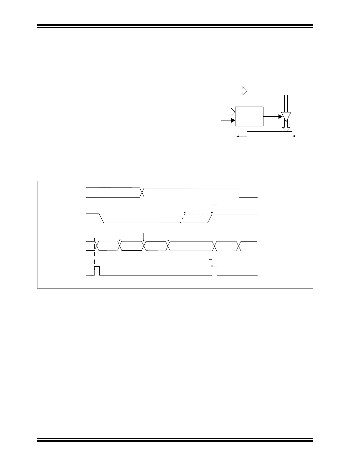
PIC16C717/770/771
i) The MSSP Module shifts in the ACK bit from the
slave device and writes its value into the
SSPCON2 register ( SSPCON2<6>).
j) The MSSP module generates an interrupt at the
In I2C master mode, the BRG is rel oaded automa tically.
If Clock Arbitration is taking place for instance, the BRG
will be reloaded when the SCL pin is sampled high
(Figure 9-16).
end of the ninth cloc k cycle b y set ting the SSPIF
bit.
k) The user generates a STO P condition by se tting
the STOP enable bit PEN in SSPCON2.
l) Interrupt is generated once the STOP condition
FIGURE 9-15: BAUD RATE GENERATOR
BLOCK DIAGRAM
SSPM<3:0>
SSPADD<6:0>
is complete.
9.2.8 BAUD RATE GENERATOR
2
C master mode, the reload value for the BRG is
In I
SSPM<3:0>
SCL
Reload
Control
Reload
located in the lower 7 bits of the SSPADD register
(Figure 9-15). When th e BRG is loaded with this v alue ,
CLKOUT
BRG Down Counter
the BRG counts down to 0 and stops until another
reload has tak en place. The BRG count is decremente d
twice per instruction cycle (T
CY) on the Q2 and Q4
clock.
FIGURE 9-16: BAUD RATE GENERATOR TIMING WITH CLOCK ARBITRATION
SDA
SCL de-asserted but slave holds
SCL low (clock arbitration)
SCL
DX-1DX
SCL allowed to transition high
F
OSC/4
BRG
value
BRG
reload
BRG decrements
(on Q2 and Q4 cycles)
03h 02h 01h 00h (hold off) 03h 02h
SCL is sampled high, reload takes
place, and BRG starts its count.
DS41120A-page 86 Advanced Information
1999 Microchip Technology Inc.
Page 87

PIC16C717/770/771
9.2.9 I2C MASTER MODE START CONDITION
TIMING
To initiate a START condition, the user sets the start
condition enable bit, SEN (SSPCON2<0>). If the SDA
and SCL pins are sampled hi gh, the baud rate gener ator is re-loaded with the contents of SSPADD<6:0>,
and starts its count. If SCL and SDA are both sampled
high when the baud rate generator times out (T
BRG
the SDA pin is driven low. The action of the SDA being
driven low whil e SCL is high i s the START condition,
and causes the S bit (SSPSTAT<3>) to be set. Following this, the baud rate generator is reloaded with the
contents of SSPADD<6:0> and resumes its count.
When the baud rate generator times out (T
BRG
), the
SEN bit (SSPCON2<0>) will be automatically cleared
by hardware, the baud rate generator is suspended
leaving the SDA line held low, and the START conditio n
is complete.
Note: If at the beginning of START condition, the
SDA and SCL pins are already sampled
low, or if during the START condition, the
SCL line is s ampled low before the SDA
line is driven low , a b us collision o ccurs, the
Bus Collision Interrupt Flag (BCLIF) is set,
the START condition is aborted, and the
2
C module is reset into its IDLE state.
I
9.2.9.1 WCOL STATUS FLAG
If the user writes the SSPBUF when an START
sequence is in progress, then WCOL is set and the
contents of the b uff er are u nchan ged (the w rite doesn ’t
occur).
Note: Because queueing of events is not
),
allowed, writing to the lower 5 bits of
SSPCON2 is disabled until the START
condition is complete.
FIGURE 9-17: FIRST START BIT TIMING
Write to SEN bit occurs here.
SDA
SCL
SDA = 1,
SCL = 1
TBRG
Set S bit (SSPSTAT<3>)
At completion of start bit,
Hardware clears SEN bit
and sets SSPIF bit
TBRG
S
Write to SSPBUF occurs here
1st Bit
TBRG
2nd Bit
TBRG
1999 Microchip Technology Inc.
Advanced Information DS41120A-page 87
Page 88

PIC16C717/770/771
FIGURE 9-18: START CONDITION FLOWCHART
SSPEN = 1,
SSPCON <3:0> = 1000
Idle Mode
SEN (SSPCON2<0> = 1)
Bus collision detected,
Set BCLIF,
Release SCL,
Clear SEN
No
Yes
SCL= 0?
No
SDA = 0?
Yes
Reset BRG
No
SDA = 1?
SCL = 1?
Yes
Load BRG with
SSPADD<6:0>
No
BRG
Rollover?
Yes
Force SDA = 0,
Load BRG with
SSPADD<6:0>,
Set S bit.
BRG
No
SCL = 0?
Yes
Reset BRG
DS41120A-page 88 Advanced Information
No
rollover?
Yes
Force SCL = 0,
Start Condition Done,
Clear SEN
and set SSPIF
1999 Microchip Technology Inc.
Page 89
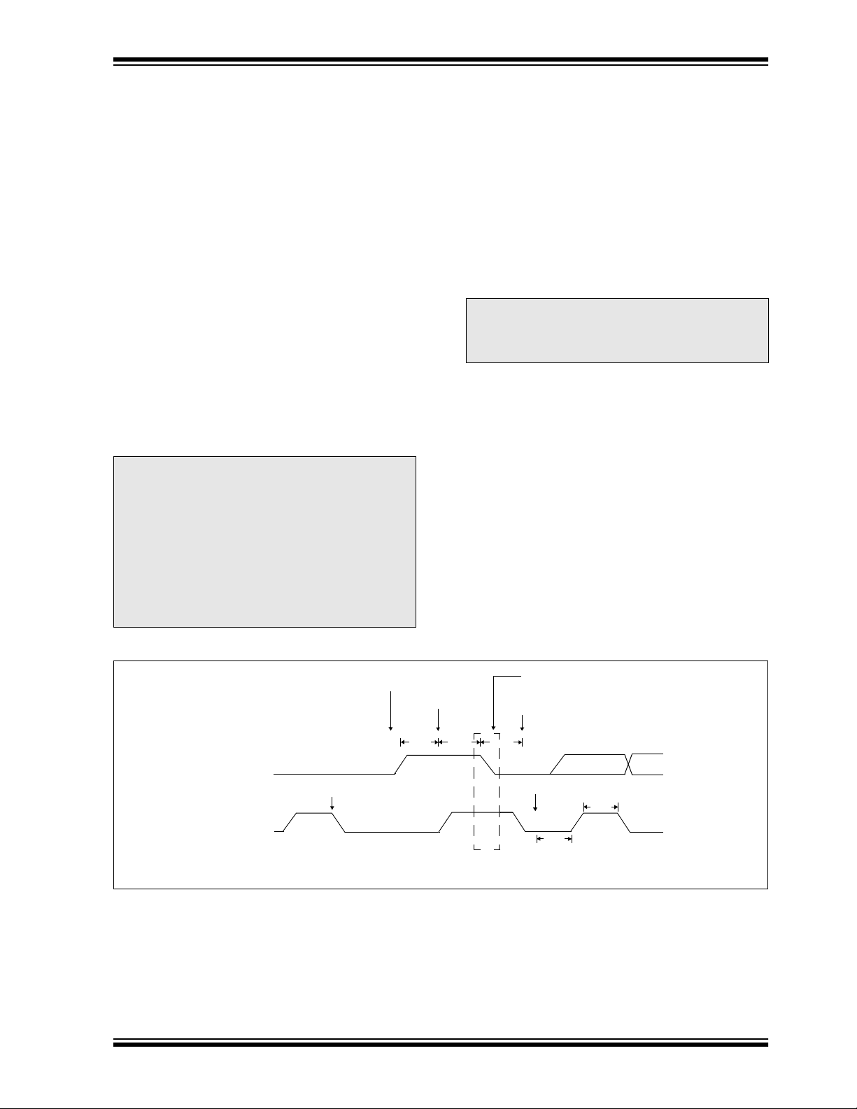
PIC16C717/770/771
9.2.10 I2C MASTER MODE REPEATED START
CONDITION TIMING
A Repeated Start condition occurs when the RSEN bit
(SSPCON2<1>) is set high and the I
2
C module is in the
idle state. When the RSEN bit is set, the SCL pin is
asserted low. When the SCL pin is sampled low, the
baud rate generator is loaded with the contents of
SSPADD<6:0>, and begins counting. The SDA pin is
released (brought high) for one baud rate generator
count (T
). When the baud r ate ge nerat or time s ou t,
BRG
if SDA is sampled high, the SCL pi n will be de-asserted
(brought high). When SCL is sampled high the baud
rate generator is re-loaded with the contents of
SSPADD<6:0> and begins counting. SDA and SCL
must be sample d high f or one T
. This action is then
BRG
followed by assertion of the SDA pin (SDA is low) for
one T
while SCL is high. F ollo wing this , th e RSEN
BRG
bit in the SSPCON2 register will be automatically
cleared, and the baud rate generator is not reloaded,
leaving the SDA pin held low. As soon as a start condition is detected on the SDA and SCL pins, the S bit
(SSPSTA T<3>) will b e set. T he SSPIF bi t will not be set
until the baud rate generator has timed-out.
Note 1: If RSEN is set while any ot her event is in
progress, it will not take effect.
Note 2: A bus collision during the Repeated Start
condition occurs if:
• SDA is sampled low when SCL goes
from low to high.
• SCL goes low bef ore SD A is asserted
low. This may indicate that another
master is attempting to transmit a
data "1".
Immediately following the SSPIF bit getting set, the
user may write the SSPBUF with the 7-bit address in
7-bit mode, or the default first address in 10-bit mode.
After the first eight bits are transmitted and an ACK is
received, the user may then transmit an additional eight
bits of address (10-bit mode) or eight bits of data (7-bit
mode).
9.2.10.1 WCOL STATUS FLAG
If the user writes the SSPBUF when a Repeated Start
sequence is in progress, then WCOL is set and the
contents of the b uff er are u nchan ged (the w rite doesn ’t
occur).
Note: Because queueing of events is not
allowed, writing of the lower 5 bits of
SSPCON2 is disabled until the Repeated
Start condition is complete.
FIGURE 9-19: REPEAT START CONDITION WAVEFORM
Write to SSPCON2
occurs here.
SDA = 1,
SCL (no change)
SDA
Falling edge of ninth clock
End of Xmit
SCL
SDA = 1,
SCL = 1
TBRG TBRG
TBRG
Sr = Repeated Start
Set S (SSPSTAT<3>)
At completion of start bit,
hardware clear RSEN bit
and set SSPIF
1st Bit
Write to SSPBUF occurs here.
TBRG
TBRG
1999 Microchip Technology Inc.
Advanced Information DS41120A-page 89
Page 90
PIC16C717/770/771
FIGURE 9-20: REPEATED START CONDITION FLOWCHART (PAGE 1)
Start
Idle Mode,
B
SSPEN = 1,
SSPCON<3:0> = 1000
RSEN = 1
Force SCL = 0
SCL = 0?
Yes
Release SDA,
Load BRG with
SSPAD D<6:0>
BRG
rollover?
Yes
Release SCL
SCL = 1?
Yes
No
No
(Clock Arbitration)
No
Bus Collision,
Set BCLIF,
Release SDA,
Clear RSEN
C
DS41120A-page 90 Advanced Information
No
SDA = 1?
Yes
Load BRG with
SSPADD<6:0>
A
1999 Microchip Technology Inc.
Page 91
PIC16C717/770/771
FIGURE 9-21: REPEATED START CONDITION FLOWCHART (PAGE 2)
B
C
No
No
Yes
SCL = 1?
SCL = ’0’?
Reset BRG
Yes
No
SDA = 0?
Reset BRG
Yes
A
No
BRG
rollover?
Force SDA = 0,
Load BRG with
SSPADD<6:0>
Set S
BRG
No
rollover?
Yes
Force SCL = 0,
Repeated Start
condition done,
Clear RSEN,
Set SSPIF.
Yes
1999 Microchip Technology Inc.
Advanced Information DS41120A-page 91
Page 92

PIC16C717/770/771
9.2.11 I2C MASTER MODE TRANSMISSION
Transmission of a data byte, a 7-bit address, or either
half of a 10-bit address is accomplished by simply writing a value to the SSPBUF regis ter . This actio n will set
the buff e r fu ll fl ag (BF) and allow th e b au d r ate generator to begin counting and start the next transmission.
Each bit of address/data will be shifted out onto the
SDA pin after the falling edge of SCL is asserted (see
data hold time spec). SCL is held low for one baud
rate generator roll over count (T
valid before SCL is released high (see data setup time
spec). When the SCL pin is released high, it is held that
way for T
stable for that duration and some hold time after the
next falling edge of SCL. After the eighth bit is shifted
out (the falling edge of the eighth clock), the BF flag is
cleared and the master releases SDA allowing the
slave device being addressed to respond with an ACK
bit during the ninth bit time, i f an addres s match oc curs
or if data was received properly. The status of ACK
read into the ACKDT on the falling edge of the ninth
clock. If the master receives an acknowledge, the
acknowledge st atus bit (ACKSTAT) is clea red. If not,
the bit is set. After the n inth cloc k the SSPIF is s et, and
the master clock (baud rate generator) is suspended
until the next d ata byte is loaded into th e SSPBUF lea ving SCL low and SDA unchanged (Figure 9-23).
After the write to the SSPBUF, each bit of address will
be shifted out on the falling edge of SCL until all seven
address bits and t he R/W
ing edge of the eighth clock, the master will de-assert
the SDA pin allowing the slave to respond with an
acknowle dge. O n the f all ing edge of the ninth cl ock, th e
master will sample the SDA pin to see if the address
was recogniz ed b y a sl ave. The status of the ACK bit is
loaded into the ACKSTAT status bit (SSPCON2<6>).
Following the falling edge of the ninth clock transmission of the address, the SSPIF is set, the BF flag is
cleared, and the baud rate generator is turned off until
another write to the SSPBUF takes place, holding SCL
low and allowing SDA to float.
, the data on the SDA pin must remain
BRG
bit are complet ed. On the fall-
). Data shou ld be
BRG
9.2.11.3 ACKSTAT STATUS FLAG
In transmit mode, the ACKSTAT bit (SSPCON2<6>) is
cleared when the slave has sent an acknowledge
= 0), and is set when the sla ve does not ac knowl-
(ACK
edge (ACK
it has recognized its address (including a general call),
or when the slave has properly received its data.
is
= 1). A slave sends an acknowledge when
9.2.11.1 BF STATUS FLAG
In transmit mode, the BF bit (SSPSTAT<0>) is set when
the CPU writes to SSPBUF and is cleared when all 8
bits are shifted out.
9.2.11.2 WCOL STATUS FLAG
If the user writes the SSPBUF when a transmit is
already in progress (i.e. SSPSR is still shifting out a
data byte), then WCOL is set and the contents of the
buffer are unchanged (the write doesn’t occur).
WCOL must be cleared in software.
DS41120A-page 92 Advanced Information
1999 Microchip Technology Inc.
Page 93

FIGURE 9-22: MASTER TRANSMIT FLOWCHART
Idle Mode
Write SSPBUF
Num_Clocks = 0,
BF = 1
Force SCL = 0
PIC16C717/770/771
Num_Clocks
= 8?
No
Load BRG with
SSPADD<6:0>,
start BRG count,
SDA = Current Data bit
BRG
rollover?
Stop BRG,
Force SCL = 1
SCL = 1?
SDA =
Data bit?
Load BRG with
SSPADD<6:0>,
count SCL high time
No
Yes
No
Yes
No
Yes
Yes
(Clock Arbitration)
Bus collision detected
Set BCLIF, hold prescale off,
Clear XMIT enable
Yes
slave can drive ACK,
(Clock Arbitration)
Read SDA and place into
ACKSTAT bit (SSPCON2<6>)
Release SDA so
Force BF = 0
Load BRG with
SSPADD<6:0>,
start BRG count
BRG
rollover?
Yes
Force SCL = 1,
Stop BRG
SCL = 1?
Yes
Load BRG with
SSPADD<6:0>,
count high time
Rollover?
No
No
No
rollover?
Num_Clocks
= Num_Clocks + 1
1999 Microchip Technology Inc.
BRG
Yes
No
SCL = 0?
Yes
Reset BRG
No
SDA =
Data bit?
No
Yes
Force SCL = 0,
Set SSPIF
Advanced Information DS41120A-page 93
Page 94
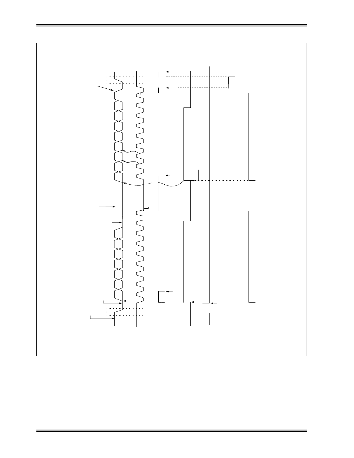
PIC16C717/770/771
FIGURE 9-23: I2C MASTER MODE TIMING (TRANSMISSION, 7 OR 10-BIT ADDRESS)
P
ACKSTAT in
SSPCON2 = 1
ACK
Cleared in software
From slave clear ACKSTAT bit SSPCON2<6>
Write SSPCON2<0> SEN = 1
START condition begins
Transmitting Data or Second Half
of 10-bit Address
R/W = 0Transmit Address to Slave
SEN = 0
cleared in software service routine
From SSP interrupt
SCL held low
while CPU
responds to SSPIF
cleared in software
123456789 123456789
SSPBUF written with 7 bit address and R/W
start transmit
A7 A6 A5 A4 A3 A2 A1 ACK = 0 D7 D6 D5 D4 D3 D2 D1 D0
S
SSPBUF is written in software
SSPBUF written
After start condition SEN cleared by hardware.
SDA
SCL
SSPIF
BF (SSPSTAT<0>)
SEN
PEN
DS41120A-page 94 Advanced Information
R/W
1999 Microchip Technology Inc.
Page 95

9.2.12 I2C MASTER MODE RECEPTION
Master mode reception is enabled by setting the
receive enable bit, RCEN (SSPCON2<3>).
Note: The MSSP Module must be in an IDLE
STATE before the RCEN bit is set, or the
RCEN bit will be disregarded.
The baud rate gen erator begins cou nting, and on each
rollover, the state of the SCL pin changes (high to low/
low to high) and data is shifted into the SSPSR. After
the falling edge of the eighth clock, the receive enable
flag is automatically cleared, the contents of the
SSPSR are loaded into the SSPBUF, the BF flag is set,
the SSPIF is set, and the baud rate generator is suspended from counting, holding SCL low. The SSP is
now in IDLE state, awaiting the next command. When
the buffer is read by the CPU, the BF flag is automatically cleared. The user c an th en send an acknow l edg e
bit at the end of reception, by setting the acknowledge
sequence enable bit, ACKEN (SSPCON2<4>).
9.2.12.1 BF STATUS FLAG
PIC16C717/770/771
In receive operat ion, BF i s set w hen an address or data
byte is loaded into SSPBUF from SSPSR. It is cleared
when SSPBUF is read.
9.2.12.2 SSPOV STATUS FLAG
In receive operation, SSPOV is set when 8 bits are
received into the SSPSR, and the BF flag is already set
from a previous recepti on.
9.2.12.3 WCOL STATUS FLAG
If the user writes the SSPBUF when a receive is
already in progress (i.e . SSPSR is still sh ifting in a data
byte), then WCOL is set and the contents of the buffer
are unchanged (the write doesn’t occur).
1999 Microchip Technology Inc.
Advanced Information DS41120A-page 95
Page 96

PIC16C717/770/771
FIGURE 9-24: MASTER RECEIVER FLOWCHART
Idle mode
RCEN = 1
Num_Clocks = 0,
Release SDA
Force SCL=0,
Load BRG w/
SSPADD<6:0>,
start count
BRG
rollover?
Release SCL
SCL = 1?
Sample SDA,
Shift data into SSPSR
Load BRG with
SSPADD<6:0>,
start count.
BRG
rollover?
No
Yes
No
Yes
No
Yes
(Clock Arbitration)
SCL = 0?
Yes
No
Num_Clocks
= Num_Clocks + 1
No
Num_Clocks
= 8?
Yes
Force SCL = 0,
Set SSPIF,
Move contents of SSPSR
DS41120A-page 96 Advanced Information
Set BF.
into SSPBUF ,
Clear RCEN.
1999 Microchip Technology Inc.
Page 97

PIC16C717/770/771
FIGURE 9-25: I2C MASTER MODE TIMING (RECEPTION 7-BIT ADDRESS)
Bus Master
terminates
transfer
Set SSPIF interrupt
at end of acknow-
ledge sequence
Set P bit
(SSPSTAT<4>)
P
PEN bit = 1
written here
ACK
SDA = ACKDT = 1
Set ACKEN start acknowledge sequence
ACK from Master
SDA = ACKDT = 0
Write to SSPCON2<4>
to start acknowledge sequence
SDA = ACKDT (SSPCON2<5>) = 0
D0
D1
RCEN cleared
automatically
D2
D3D4
D5
D6D7
Receiving Data from Slave
RCEN = 1 start
next receive
ACK
D0
9
ACK is not sent
Set SSPIF at end
of receive
87
6
5
Set SSPIF interrupt
1234
at end of acknowledge
Data shifted in on falling edge of CLK
and SSPIF
Cleared in
software
SSPOV is set because
SSPBUF is still full
Cleared in software
sequence
Last bit is shifted into SSPSR and
contents are unloaded into SSPBUF
D1
RCEN cleared
automatically
D2
D3D4
D5
D6D7
Receiving Data from Slave
Master con figured as a receiver
by programming SSPCON2<3>, (RCE N = 1)
SEN = 0
Write to SSPCON2<0>, (SEN = 1)
Begin Start Condit io n
ACK
R/W = 1
ACK from Slave
A3 A2 A1
Transmit Address to Slave
Start XMIT
Write to SSPBUF occurs here
A7 A6 A5 A4
678 9
5
4
3
12
9
8
7
6
5
4
3
12
S
Cleared in software
Set SSPIF interrupt
at end of receive
Cleared in software
Cleared in software
1999 Microchip Technology Inc.
while CPU
responds to S SPIF
SDA = 0, SCL = 1
SDA
SCL
SSPIF
BF
(SSPSTAT<0>)
SSPOV
ACKEN
Advanced Information DS41120A-page 97
Page 98
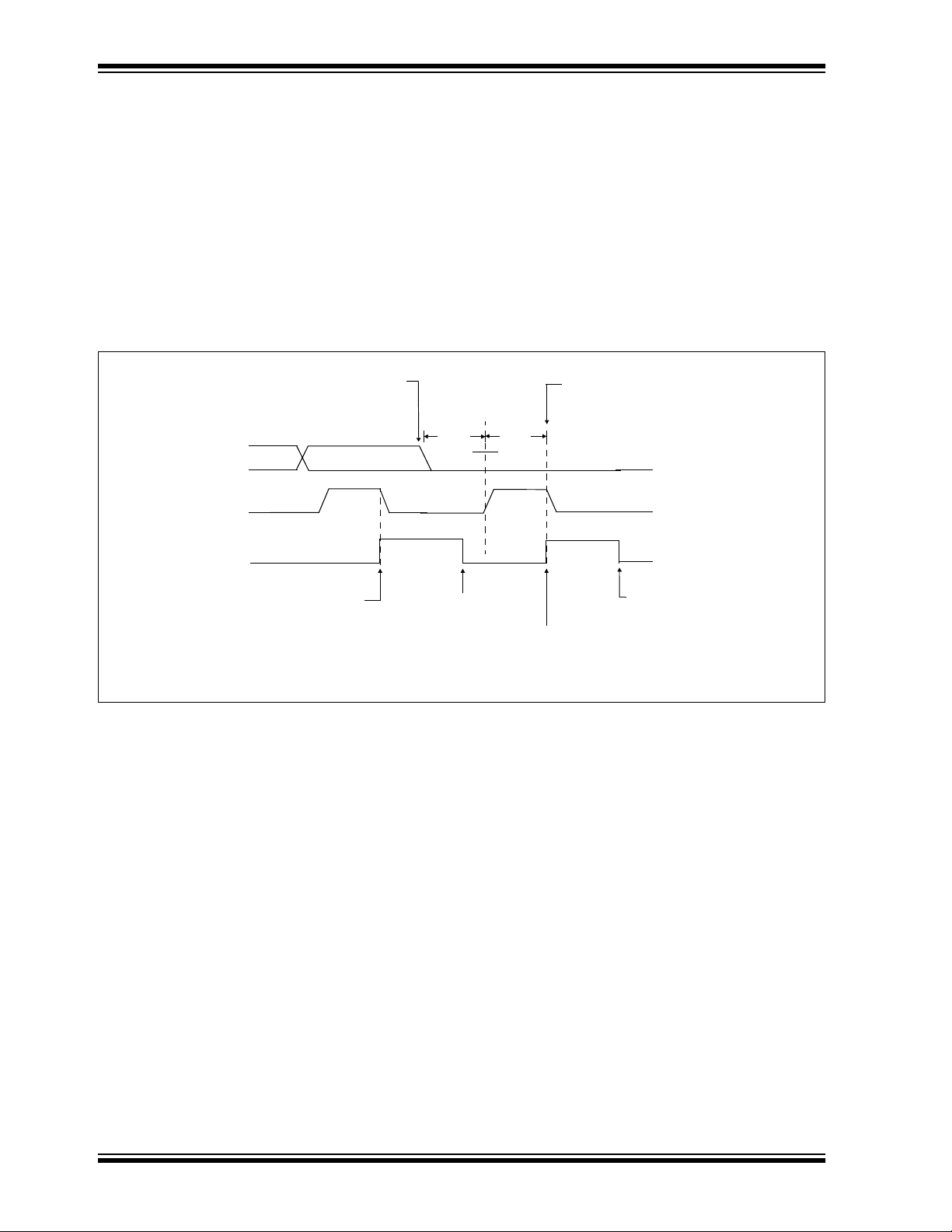
PIC16C717/770/771
9.2.13 ACKNOWLEDGE SEQUENCE TIMING
An acknowledge sequence is enabled by setting the
acknowledge sequence enable bit, ACKEN
(SSPCON2<4>). When this bit is set, the SCL pin is
pulled low and the contents of the acknowledge data
bit is presented on the SDA pin. If the user wishes to
generate an acknowledge, then the ACKDT bit should
be cleared. If not, the user should set the ACKDT bit
before starting an acknowledge sequence. The baud
rate generator then counts for one rollover period
BRG), and the SCL pin is de-asserted (pulled high).
(T
the baud rate gene r ator coun ts for T
is then pulled low. Following this, the ACKEN bit is
automatically cle ared, the baud r ate gener ator is turned
off, and the MSSP module then goes into IDLE mode.
(Figure 9-26)
9.2.13.1 WCOL STATUS FLAG
If the user writes the SSPBUF when an acknowledged
sequence is in progress, then WCOL is set and the
contents of the b uff er are u nchan ged (the w rite doesn ’t
occur).
When the SCL pin is sampled high (clock arbitration),
FIGURE 9-26: ACKNOWLEDGE SEQUENCE WAVEFORM
Acknowledge sequence starts here,
SDA
SCL
SSPIF
Write to SSPCON2
ACKEN = 1, AC KDT = 0
D0
8
TBRG
TBRG
ACK
9
BRG . The SCL pin
ACKEN automatically cleared
Set SSPIF at the end
of receive
Note: TBRG = one baud rate generator period.
Cleared in
software
Cleared in
software
Set SSPIF at the end
of acknowledge sequence
DS41120A-page 98 Advanced Information
1999 Microchip Technology Inc.
Page 99

FIGURE 9-27: ACKNOWLEDGE FLOWCHART
Idle mode
Set ACKEN
PIC16C717/770/771
No
No
No
(Clock Arbitration)
Force SCL = 0
SCL = 0?
Yes
Drive ACKDT bit
(SSPCON2<5>)
onto SDA pin,
Load BRG with
SSPADD<6:0>,
start count.
BRG
rollover?
Yes
Force SCL = 1
SCL = 1?
Yes
BRG
rollover?
No
SCL = 0?
No
No
ACKDT = 1?
Yes
SDA = 1?
Bus collision detected,
Set BCLIF,
Release SCL,
Clear ACKEN
Yes
Yes
Yes
No
Reset BRG
Force SCL = 0,
Clear ACKEN,
Set SSPIF
Load BRG with
SSPADD <6:0>,
start count.
1999 Microchip Technology Inc.
Advanced Information DS41120A-page 99
Page 100
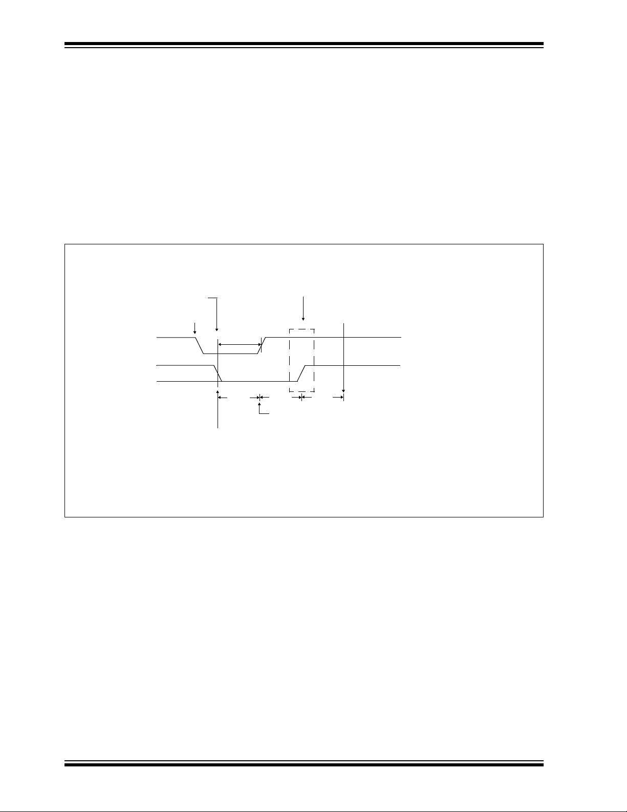
PIC16C717/770/771
9.2.14 STOP CONDITION TIMING
A stop bit is asserted on the SDA pin at the end of a
receive/transmit by setting the Stop Sequence Enable
bit PEN (SSPCON2<2>). At the end of a receiv e/tr ansmit, the SCL line is held lo w afte r the falling edge of the
ninth clock. When the PEN bit is set, the master will
assert the SDA line low . When the SDA line is sampled low, the baud rate generator is reloaded and
counts down to 0 . Wh en th e bau d r ate g enera tor ti mes
out, the SCL pin will be brought high and one T
BRG
(baud rate generator rollover count) later, the SDA pin
will be de-asse rted. When the SD A pin is sample d high
while SCL is high, the P bit (SSPSTAT<4>) is set. A
BRG later the PEN bit is cleared and the SSPIF bit is
T
set (Figure 9-28).
Whenever the firmware decides to take control of the
bus, it will firs t determine if the bus is b u sy by checking
the S and P bits in the SSPSTAT register. If the bus is
busy, then the CPU can be interrupted (notified) when
a Stop bit is detected (i.e. bus is free).
9.2.14.1 WCOL STATUS FLAG
If the user writes the SSPBUF when a ST OP sequence
is in progress , then WCOL is set and the con tents of the
buffer are unchanged (the write doesn’t occur).
FIGURE 9-28: STOP CONDITION RECEIVE OR TRANSMIT MODE
Write to SSPCON2
Set PEN
Falling edge of
9th clock
SCL
T
SCL = 1 for T
after SDA sampled high. P bit (SSPSTAT<4>) is set
BRG
BRG, followed by SDA = 1 for TBRG
PEN bit (SSPCON2<2>) is cleared by
hardware and the SSPIF bit is set
SDA
ACK
BRG
T
SDA asserted low before rising edge of clock
to setup stop condition.
Note: TBRG = one baud rate generator period.
P
T
BRG
SCL brought high after T
TBRG
BRG
DS41120A-page 100 Advanced Information
1999 Microchip Technology Inc.
 Loading...