

PIC16C745/765
8-Bit CMOS Microcontrollers with USB
Devices included in this data sheet:
• PIC16C745 • PIC16C765
Microcontroller Core Features:
• High-performance RISC CPU
• Only 35 single word instructions
Memory
Device
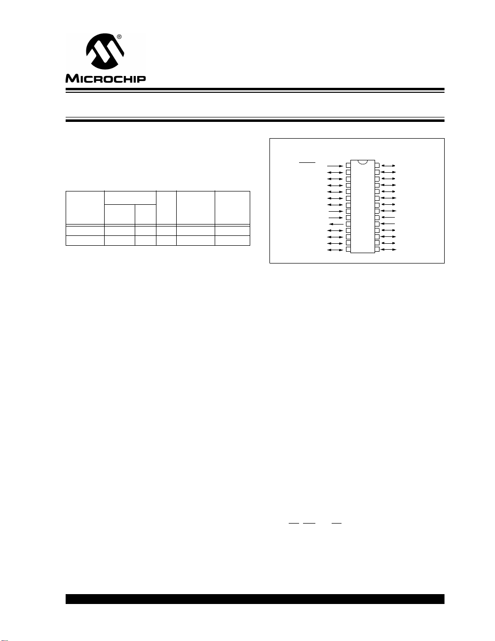
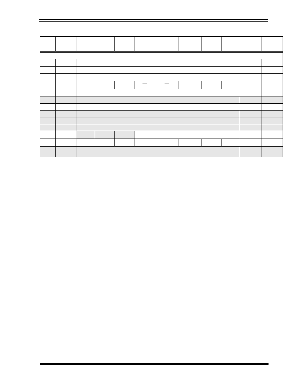
PIC16C745 8K 256 28 8 5
PIC16C765 8K 256 40 8 8
Program
x14
Data
x8
Pins
• All single cycle instructions except for program
branches which are two cycle
• Interrupt capability (up to 12 internal/external
interrupt sources)
• Eight level deep hardware stack
• Direct, indirect and relative addressing modes
• Power-on Reset (POR)
• Power-up Timer (PWRT) and Oscillator Start-up
Timer (OST)
• Watchdog Timer (WDT) with its own on-chip RC
oscillator for reliable operation
• Brown-out detection circuitry for
Brown-out Reset (BOR)
• Programmable code-protection
• Power saving SLEEP mode
• Selectable oscillator options
- EC - External clock (24 MHz)
- E4 - External clock with PLL (6 MHz)
- HS - Crystal/Resonator (24 MHz)
- H4 - Crystal/Resonator with PLL (6 MHz)
• Processor clock of 24 MHz derived from 6 MHz
crystal or resonator
• Fully static low-power, high-speed CMOS
• In-Circuit Serial Programming (ICSP)
• Operating voltage range
- 4.35 to 5.25V
• High Sink/Source Current 25/25 mA
• Wide temperature range
- Industrial (-40°C - 85°C)
• Low-power consumption:
- ~ 16 mA @ 5V, 24 MHz
-100 µA typical standby current
A/D
Resolution
Channels
A/D
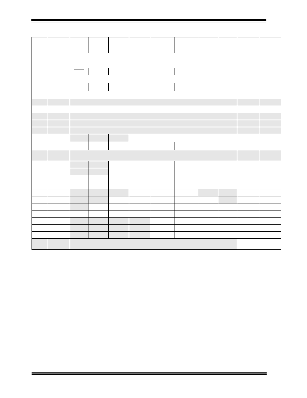
Pin Diagrams
28-Pin DIP, SOIC
MCLR/VPP
RA0/AN0
RA1/AN1
RA2/AN2
RA3/AN3/V
REF
RA4/T0CKI
RA5/AN4
Vss
OSC1/CLKIN
OSC2/CLKOUT
RC0/T1OSO/T1CKI
RC1/T1OSI/CCP2
RC2/CCP1
V
USB
• 1
2
3
4
5
6
7
8
9
10
11
12
13
14
28
27
26
25
24
23
22
21
20
PIC16C745
19
18
17
16
15
RB7
RB6
RB5
RB4
RB3
RB2
RB1
RB0/INT
V
DD
Vss
RC7/RX/DT
RC6/TX/CK
D+
D-
Peripheral Features:
• Universal Serial Bus (USB 1.1)
- Soft attach/detach
• 64 bytes of USB dual port RAM
• 22 (PIC16C745) or 33 (PIC16C765) I/O pins
- Individual direction control
- 1 high voltage open drain (RA4)
- 8 PORTB pins with:
- Interrupt-on-change control (RB<7:4> only)
- Weak pull-up control
- 3 pins dedicated to USB
• Timer0: 8-bit timer/counter with 8-bit prescaler
• Timer1: 16-bit timer/counter with prescaler
can be incremented during SLEEP via external
crystal/clock
• Timer2: 8-bit timer/counter with 8-bit period
register, prescaler and postscaler
• 2 Capture, Compare and PWM modules
- Capture is 16-bit, max. resolution is 10.4 ns
- Compare is 16-bit, max. resolution is 167 ns
- PWM maximum resolution is 10-bit
• 8-bit multi-channel Analog-to-Digital converter
• Universal Synchronous Asynchronous Receiver
Transmitter (USART/SCI)
• Parallel Slave Port (PSP) 8-bits wide, with external RD
, WR and CS controls (PIC16C765 only)
2000 Microchip Technology Inc. Preliminary DS41124C-page 1
PIC16C745/765
REF
PP
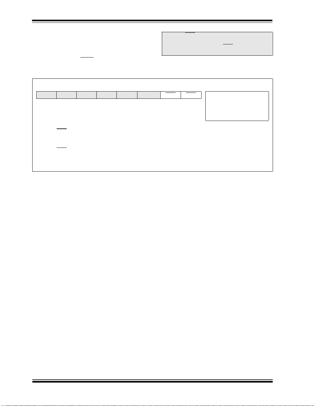
44-Pin PLCC
RA4/T0CKI
RA5/AN4
RE0/RD/AN5
RE1/WR/AN6
RE2/CS/AN7
V
VSS
OSC1/CLKIN
OSC2/CLKOUT
RC0/T1OSO/T1CKI
NC
40-Pin DIP
MCLR/VPP
RA0/AN0
RA1/AN1
RA2/AN2
RA3/AN3/V
RA4/T0CKI
RA5/AN4
RE0/RD/AN5
RE1/WR/AN6
RE2/CS/AN7
OSC1/CLKIN
OSC2/CLKOUT
RC0/T1OSO/T1CKI
RC1/T1OSI/CCP2
RC2/CCP1
RD0/PSP0
RD1/PSP1
7
8
9
10
11
DD
12
13
14
15
16
17
REF
V
DD
VSS
V
USB
/V
MCLR
RA3/AN3/V
RA2/AN2
RA1/AN1
RA0/AN0
65432
PIC16C765
USB
V
RD1/PSP1
RD0/PSP0
RC2/CCP1
RC1/T1OSI/CCP2
1
2
3
4
5
6
7
8
9
10
11
12
13
14
15
16
17
18
19
20
NC
RB7
RB6
1
4443424140
D-
RD3/PSP3
RD2/PSP2
PIC16C765
44-Pin TQFP
RB5
RB4
NC
RC6/TX/CK
RB3
39
RB2
38
RB1
37
RB0/INT
36
V
DD
35
VSS
34
RD7/PSP7
33
RD6/PSP6
32
RD5/PSP5
31
RD4/PSP4
30
RC7/RX/DT
29
2827262524232221201918
D+
NC
RC6/TX/CK
40
RB7
RB6
39
38
RB5
37
RB4
RB3
36
RB2
35
34
RB1
33
RB0/INT
V
32
31
30
29
28
27
26
25
24
23
22
21
DD
VSS
RD7/PSP7
RD6/PSP6
RD5/PSP5
RD4/PSP4
RC7/RX/DT
RC6/TX/CK
D+
DRD3/PSP3
RD2/PSP2
RC7/RX/DT
RD4/PSP4
RD5/PSP5
RD6/PSP6
RD7/PSP7
V
VDD
RB0/INT
RB1
RB2
RB3
SS
4443424140393837363534
1
2
3
4
5
6
7
8
9
10
11
NC
USB
D+D-RD3/PSP3
RD2/PSP2
RD1/PSP1
RD0/PSP0
V
PIC16C765
PP
NC
RB7
RB6
RB5
RB4
/V
RA0/AN0
MCLR
NC
RC2/CCP1
RC1/T1OSI/CCP2
33
NC
32
RC0/T1OSO/T1CKI
31
OSC2/CLKOUT
30
OSC1/CLKIN
29
V
SS
28
VDD
27
RE2/CS/AN7
26
RE1/WR/AN6
25
RE0/RD/AN5
24
RA5/AN4
23
RA4/T0CKI
2221201918171615141312
REF
RA2/AN2
RA1/AN1
RA3/AN3/V
Key Features
PICmicro
TM
Mid-Range Reference Manual
PIC16C745 PIC16C765
(DS33023)
Operating Frequency 6 MHz or 24 MHz 6 MHz or 24 MHz
Resets (and Delays) POR, BOR (PWRT, OST) POR, BOR (PWRT, OST)
Program Memory (14-bit words) 8K 8K
Data Memory (bytes) 256 256
Dual Port Ram 64 64
Interrupt Sources 11 12
I/O Ports 22 (Ports A, B, C) 33 (Ports A, B, C, D, E)
Timers 3 3
Capture/Compare/PWM modules 2 2
Analog-to-Digital Converter Module 5 channel x 8 bit 8 channel x 8 bit
Parallel Slave Port — Yes
Serial Communication USB, USART/SCI USB, USART/SCI
Brown-out Detect Reset Yes Yes
DS41124C-page 2 Preliminary 2000 Microchip Technology Inc.

PIC16C745/765
Table of Contents
1.0 General Description .............................................................................................................................................. 5
2.0 PIC16C745/765 Device Varieties .................................... ............. .............. ............. .............. ...............................7
3.0 Architectural Overview.......................................................................................................................................... 9
4.0 Memory Organization.......................................................................................................................................... 15
5.0 I/O Ports....... .............. ............. .............. ............. .............. ............. .............. ........................................................ 31
6.0 Timer0 Module.................................................................................................................................................... 43
7.0 Timer1 Module.................................................................................................................................................... 45
8.0 Timer2 Module.................................................................................................................................................... 49
9.0 Capture/Compare/PWM Modules.......................................................................................................................51
10.0 Universal Serial Bus................ .............. ............. .............. ............. .............. ............. ........................................... 57
11.0 Universal Synchronous Asynchronous Receiver Transmitter (USART) .............................................................77
12.0 Analog-to-Digital Converter (A/D) Module .......................................................................................................... 91
13.0 Special Features of the CPU .............................................................................................................................. 99
14.0 Instruction Set Summary................................................................................................................................... 113
15.0 Development Support ....................................................................................................................................... 121
16.0 Electrical Characteristics................................................................................................................................... 127
17.0 DC and AC Characteristics Graphs and Tables ............................................................................................... 145
18.0 Packaging Information...................................................................................................................................... 147
Index .......................................................................................................................................................................... 157
On-Line Support.......................................................................................................................................................... 161
Reader Response ....................................................................................................................................................... 162
Product Identification System ..................................................................................................................................... 163
To Our Valued Customers
Most Current Data Sheet
To obtain the most up-to-date version of this data sheet, please register at our Worldwide Web site at:
http://www.microchip.com
You can determine the version of a data sheet by examining its literature number found on the bottom outside corner of any page.
The last character of the literature number is the version number. e.g., DS30000A is version A of document DS30000.
New Customer Notification System
Register on our web site (www.microchip.com/cn) to receive the most current information on our products.
Errata
An errata sheet may exist fo r current devic es, describin g minor opera tional difference s (from the data sheet) and reco mmended
workarounds. As device/documentation issues become known to us, we will publish an errata sheet. The errata will specify the revision of silicon and revision of document to which it applies.
To determine if an errata sheet exists for a particular device, please check with one of the following:
• Microchip’s Worldwide Web site; http://www.microchip.com
• Your local Microchip sales office (see last page)
• The Microchip Corporate Literature Center; U.S. FAX: (480) 786-7277
When contacting a sales office or the literature center, please specify which device, revision of silicon and data sheet (include literature number) you are using.
Corrections to this Data Sheet
We constantly strive t o impro ve the qualit y of all our pro ducts and do cumen tation. We have spent a grea t deal o f time to ens ure
that this document is correct. However, we realize that we may have missed a few things. If you find any information that is missing
or appears in error, please:
• Fill out and mail in the reader response form in the back of this data sheet.
• E-mail us at webmaster@microchip.com.
We appreciate your assistance in making this a better document.
2000 Microchip Technology Inc. Preliminary DS41124C-page 3

PIC16C745/765
NOTES:
DS41124C-page 4 Preliminary 2000 Microchip Technology Inc.

PIC16C745/765
1.0 GENERAL DESCRIPTION
The PIC16C745/765 devices are low cost, high-perfor-
mance, CMOS, fully-static, 8-bit microcontrollers in the
PIC16CXX mid-range family.
All PICmicro
RISC architecture. The PIC16C745 /765 microcontroller family has enhanced core features, eight-level deep
stack and multiple internal and external interrupt
sources. The separate instruction and data bu ses of
the Harvard architecture allow a 14-bit wide instruction
word with the separate 8-bit wide data. The two stage
instruction pipeline allows all instructio ns to exec ute in
a single cycle, except for program branches, which
require two cycles. A total of 35 instructions (reduced
instruction set) are available. Additionally, a large register set gives some of the architectural innovations
used to achieve a very high performance.
The PIC16C745 device has 22 I/O pins. The
PIC16C765 device has 33 I/O pins. Ea ch device has
256 bytes of RAM. In addition, sev eral peripheral features are available including: three timer/counters, two
Capture/Compare/PWM modules and two serial ports.
The Universal Serial Bus (USB 1.1) low speed peripheral provides bus communications. The Universal
Synchronous Asynchronous Receiver Transmitter
(USART) is also known as the Serial Communications
Interface or SCI. Also, a 5- channel high-speed 8-bit
A/D is provided on the PIC16C745, while the
PIC16C765 offers 8 channels. The 8-bit res olution is
ideally sui t ed f or ap pl i c at i on s r e qu i ri n g a lo w c o s t an alog interface (e.g. , thermosta t control, press ure sensing, etc.).
The PIC16C745/765 devices have special features to
reduce external components, thus reducing cost,
enhancing system reliability and r educing power consumption. There are 4 oscillator options, of which EC is
for the external regulated clock source, E4 is for the
external regulated clock source with the PLL enabled,
HS is for the high speed crystal s/resona tors an d H 4 is
for high speed crystals/resonators with the PLL
enabled. The SLEEP (power-down) feature provides a
power-saving mode. The user can wake-up the chip
from SLEEP through several external and internal
interrupts and RESETS.
®
microcontrollers employ an advanced
A highly reliable Watchdog Timer (WDT), with a dedicated on-chip RC oscillator, provides protection against
software lock-up, and also provides one way of waking
the device from SLEEP.
A UV erasable CERDIP packaged version is ideal for
code development, while the cost-effective One- TimeProgrammable (OTP) version is suitable for production
in any volume.
The PIC16C745/765 devices fit nicely in many applications ranging from security and re mote sensors to appl iance controls and automotives. The EPROM
technology makes customization of application programs (data loggers, industrial controls, UPS)
extremely fast and conveni ent. The small footp rint packages make this microcontroller series perfect for all
applications with space limitations. Low-cost, lowpower, high-per fo rmanc e, ease of us e and I/O fl exibility
make the PIC16C745/765 devices very versatile, even
in areas where no microcontroll er use ha s been consid ered before (e.g., timer functions , serial communicati on,
capture and compare, PWM fun ct ions a nd c oproc esso r
applications).
1.1 Family and Upward Compatibility
Users familiar with the PIC16C5X microcontroller family will realize that this is an enhanced version of the
PIC16C5X architecture. Code written for the
PIC16C5X can be easily ported to the PIC16C745/765
family of devices.
1.2 Development Support
PICmicro® devices are supported by the comp lete l ine
of Microchip Development tools.
Please refer to Section 15.0 for more details about
Microchip’s development tools.
2000 Microchip Technology Inc. Preliminary DS41124C-page 5

PIC16C745/765
NOTES:
DS41124C-page 6 Preliminary 2000 Microchip Technology Inc.

PIC16C745/765
2.0 PIC16C745/765 DEVICE VARIETIES
A variety of frequency ranges and packaging options
are available. Depending on application and production
requirements, the proper device option can be selected
using the information in the PIC16C7 45/765 Product
Identification System section at the end o f this data
sheet. When placing orders, please use that page of
the data sheet to specify the correct part number.
2.1 UV Erasable Devices
The UV erasable version, offered in windowed CERDIP
packages, is optimal for prototype development and
pilot programs. This version can be erased and
reprogrammed to any of the supported oscillator
modes.
Microchip’s PICSTART
programmers both support programming of the
PIC16C745/765.
2.2 One-Time-Programmable (OTP) Devices
The availability of OTP devices is especially useful for
customers who need the flexibility for frequent code
updates and small volume applications.
The OTP devices, packaged in plastic pack ages, permit the user to program them once. In addition to the
program memory, the configuration bits must also be
programmed.
Plus and PRO MATEII
2.3 Quick-Turnaround-Production (QTP) Devices
Microchip offers a QTP Programming Service for factory production orders. This service is made available
for users who choose not to program a medium to high
quantity of units and whose code patter ns have stabilized. The devices are identical to the OTP devices but
with all EPROM locations and configuration options
already programmed by the factory. Certain code and
prototype verification procedures apply before pr oduction shipments are available. Please contact your local
Microchip Technology sales office for more details.
2.4 Serialized Quick-Turnaround Production (SQTPSM) Devices
Microchip offers a unique programming service where
a few user-defined locations in each device are programmed with different serial numbers. The serial numbers may be random, pseudo-random or sequential.
Serial programming allows each device to have a
unique number, which can serve as an entry-code,
password or ID number.
2000 Microchip Technology Inc. Preliminary DS41124C-page 7

PIC16C745/765
NOTES:
DS41124C-page 8 Preliminary 2000 Microchip Technology Inc.

PIC16C745/765
3.0 ARCHITECTURAL OVERVIEW
The high performance of the PIC16C745/765 family
can be attributed to a number of architectural features
commonly found in RISC microprocessors. To begin
with, the PIC16C745/765 uses a Harvard architecture,
in which program and data are accessed from separate
memories using separate buses. This improves bandwidth over traditional von Neumann architecture in
which program and data are fetched from the same
memory using the same bus. Separating pr ogram and
data buses further allows instructions to be sized differently than the 8-bit wide data word. Instruction opcodes
are 14-bits wide making it possible to have all sing le
word instructions. A 14-bit wide program memory
access bus fetches a 14-bit instr uction in a single cycl e.
A two-stage pipeline overlaps fetch and execution of
instructions (Example 3-1). Consequently, most
instructions execute in a sin gle cycle (166.6667 ns @
24 MHz) except for program branches.
Memory
Device
PIC16C745 8K 256 28 8 5
PIC16C765 8K 256 40 8 8
Program
x14
Data
x8
The PIC16C745/765 can directly or indirectly address
its register files or data memory. All special function
registers, including the program counter, are mapped in
the data memory. The PIC16C745/765 has an orthogonal (symmetrical ) instructi on set that make s it possibl e
to carry out any operation on any register using any
addressing mode. This symmetrical nature and lack of
‘special optimal situations’ make programming with the
PIC16C745/765 simple yet efficient. In addition, the
learning curve is reduced significantly.
Pins
A/D
Resolution
A/D
Channels
PIC16C745/765 devices contain an 8-bit ALU and
working register. The ALU is a general purpose arithmetic unit. It performs arithmetic and Boolean functions
between the data in the working register and any register file.
The ALU is 8-bits wide and ca pable of addition, subtraction, shift and logical operations. Unless otherwise
mentioned, arithmetic operations are two's complement in nature. In two-operand instructions, typi cally
one operand is the working register (W register). The
other operand is a file register or an immediate constant. In single operand instructions, the operand is
either the W register or a file register.
The W register is an 8-bit working register used for ALU
operations. It is not an addressable register.
Depending on the instruction executed, the ALU may
affect the values of the Carry (C), Digit Carry (DC), and
Zero (Z) bits in the STA TUS register . The C and DC bits
operate as a borrow
bit and a digit borrow out bit,
respectively, in subtraction. See the SUBLW and SUBWF
instructions for examples.
2000 Microchip Technology Inc. Preliminary DS41124C-page 9
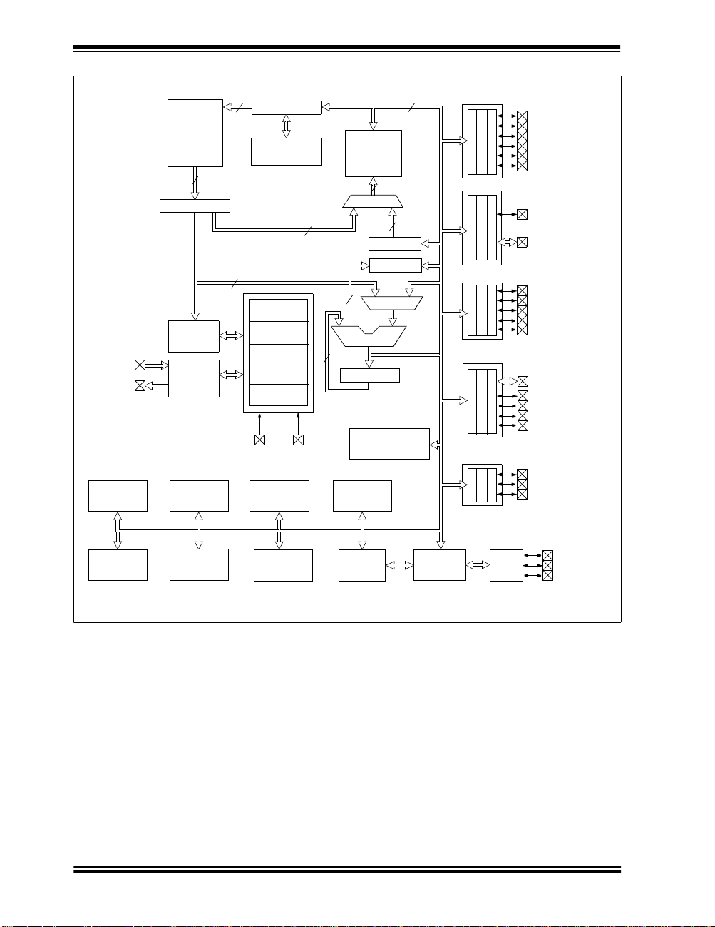
PIC16C745/765
FIGURE 3-1: PIC16C745/765 BLOCK DIAGRAM
OSC1/
CLKIN
OSC2/
CLKOUT
Program
Bus
EPROM
Program
Memory
8K x 14
14
Instruction reg
Instruction
Decode &
Control
Timing
Generation
x4 PLL
13
Program Counter
Direct Addr
8
Start-up Timer
MCLR
8 Level Stack
(13 bit)
Power-up
Timer
Oscillator
Power-on
Reset
Watchdog
Timer
Brown-out
Reset
VDD, VSS
RAM Addr(1)
7
Data Bus
RAM
File
Registers
256 x 8
Addr MUX
STATUS reg
3
ALU
8
W reg
Parallel Slave Port
8-bit A/DTimer0 Timer1 Timer2
9
8
FSR reg
MUX
8
Indirect
Addr
PORTA
RA0/AN0
RA1/AN1
RA2/AN2
RA3/AN3/VREF
RA4/T0CKI
RA5/AN4
PORTB
RB0/INT
RB<7:1>
PORTC
PORTD
(2)
PORTE
RC0/T1OSO/T1CKI
RC1/T1OSI/CCP2
RC2/CCP1
RC6/TX/CK
RC7/RX/DT
RD3:0/PSP3:0
RD4/PSP4
RD5/PSP5
RD6/PSP6
RD7/PSP7
RE0/AN5/RD
RE1/AN6/WR
RE2/AN7/CS
(2)
(2)
(2)
(2)
(2)
(2)
(2)
(2)
CCP2
CCP1
USART
Dual Port
RAM
64 x 8
USB
XCVR
V
USB
DD+
Note 1: Higher order bits are from the STATUS register.
2: Not available on PIC16C745.
DS41124C-page 10 Preliminary 2000 Microchip Technology Inc.

TABLE 3-1: PIC16C745/765 PINOUT DESCRIPTION
Name Function
/VPP
MCLR
OSC1/CLKIN
OSC2/CLKOUT
Input
Type
MCLR ST — Master Clear
V
PP Power — Programming Voltage
OSC1 Xtal — Crystal/Resonator
CLKIN ST — Exter nal Clo ck Inpu t
OSC2 — Xtal Crystal/Resonator
CLKOUT — CMOS Internal Clock (F
Output
Type
PIC16C745/765
Description
INT/4) Output
RA0/AN0
RA1/AN1
RA2/AN2
RA0 ST CMOS Bi-directional I/O
AN0 AN — A/D Input
RA1 ST CMOS Bi-directional I/O
AN1 AN — A/D Input
RA2 ST CMOS Bi-directional I/O
AN2 AN — A/D Input
RA3 ST CMOS Bi-directional I/O
RA3/AN3/V
RA4/T0CKI
RA5/AN4
RB0/INT
REF
AN3 AN — A/D Input
V
REF AN — A/D Positive Reference
RA4 ST OD Bi-directional I/O
T0CKI ST — Timer 0 Clock Input
RA5 ST Bi-directional I/O
AN4 AN — A/D Input
RB0 TTL CMOS Bi-directional I/O
INT ST — Interrupt
RB1 RB1 TTL CMOS Bi-directional I/O
RB2 RB2 TTL CMOS Bi-directional I/O
RB3 RB3 TTL CMOS Bi-directional I/O
RB4 RB4 TTL CMOS Bi-directional I/O with Interrupt-on-Change
RB5 RB5 TTL CMOS Bi-directional I/O with Interrupt-on-Change
RB6/ICSPC
RB7/ICSPD
RB6 TTL CMOS Bi-directional I/O with Interrupt-on-Change
ICSPC ST In-Circuit Serial Programming Clock Input
RB7 TTL CMOS Bi-directional I/O with Interrupt-on-Change
ICSPD ST CMOS In-Circuit Serial Programming Data I/O
RC0 ST CMOS Bi-directional I/O
RC0/T1OSO/T1CKI
T1OSO — Xtal T1 Oscillator Output
T1CKI ST — T1 Clock Input
RC1 ST CMOS Bi-directional I/O
RC1/T1OSI/CCP2
(1)
T1OSI Xtal — T1 Oscillator Input
CCP2 Capture In/Compare Out/PWM Out 2
RC2/CCP1
V
USB VUSB Power Regulator Output Voltage
RC2 ST CMOS Bi-directional I/O
CCP1 Capture In/Compare Out/PWM Out 1
D- D- USB USB U SB Differentia l Bus
D+ D+ USB USB USB Differential Bus
Legend: OD = open drain, ST = Schmitt Trigger
Note 1: Weak pull-ups. PORT B pull-ups are byte wide programmable.
2: PIC16C765 only.
(1)
(1)
(1)
(1)
(1)
(1)
(1)
(1)
2000 Microchip Technology Inc. Preliminary DS41124C-page 11

PIC16C745/765
TABLE 3-1: PIC16C745/765 PINOUT DESCRIPTION (CONTINUED)
Name Function
RC6/TX/CK
RC7/RX/DT
Input
Type
RC6 ST CMOS Bi-directional I/O
TX — CMOS USART Async Transmit
CK ST CMOS USART Master Out/Slave In Clock
RC7 ST CMOS Bi-directional I/O
RX ST — USART Async Receive
DT ST CMOS USART Data I/O
Output
Type
Description
RD0/PSP0
RD1/PSP1
RD2/PSP2
RD3/PSP3
RD4/PSP4
RD5/PSP5
RD6/PSP6
RD7/PSP7
RE0/RD/AN5
RE1/WR/AN6
RE2/CS/AN7
RD0 TTL CMOS Bi-directional I/O
(2)
PSP0 TTL — Parallel Slave Port Data Input
RD1 TTL CMOS Bi-directional I/O
(2)
PSP1 TTL — Parallel Slave Port Data Input
RD2 TTL CMOS Bi-directional I/O
(2)
PSP2 TTL — Parallel Slave Port Data Input
RD3 TTL CMOS Bi-directional I/O
(2)
PSP3 TTL — Parallel Slave Port Data Input
RD4 TTL CMOS Bi-directional I/O
(2)
PSP4 TTL — Parallel Slave Port Data Input
RD5 TTL CMOS Bi-directional I/O
(2)
PSP5 TTL — Parallel Slave Port Data Input
RD6 TTL CMOS Bi-directional I/O
(2)
PSP6 TTL — Parallel Slave Port Data Input
RD7 TTL CMOS Bi-directional I/O
(2)
PSP7 TTL — Parallel Slave Port Data Input
RE0 ST CMOS Bi-directional I/O
(2)
RD TTL — Parallel Slave Port Control Input
AN5 AN — A/D Input
RE1 ST CMOS Bi-directional I/O
(2)
(2)
WR TTL — Parallel Slave Port Control Input
AN6 AN — A/D Input
RE2 ST CMOS Bi-directional I/O
(2)
(2)
CS TTL — Parallel Slave Port Data Input
AN7 AN — A/D Input
(2)
(2)
(2)
(2)
(2)
(2)
(2)
(2)
(2)
(2)
(2)
(2)
VDD VDD Power — Power
V
SS VSS Power — Ground
Legend: OD = open drain, ST = Schmitt Trigger
Note 1: Weak pull-ups. PORT B pull-ups are byte wide programmable.
2: PIC16C765 only.
DS41124C-page 12 Preliminary 2000 Microchip Technology Inc.
PIC16C745/765
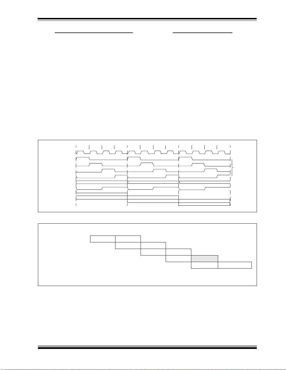
3.1 Clocking Scheme/Instruction Cycle
The clock input feeds either an on-chip PLL, or directly
INT). The clock output from either the PLL or
drives (F
direct drive (F
INT) is internally divided by four to gener-
ate four non-overlapping quadrature clocks namely,
Q1, Q2, Q3 and Q4. Internally, the program counter
(PC) is incremented every Q1, the instruction is fetched
from the program memory and latched into the instruction register in Q4. The instruction is decoded and executed during the following Q1 through Q4. The clocks
and instruction execution flow is shown in Figure 3-2.
FIGURE 3-2: CLOCK/INSTRUCTION CYCLE
Q2 Q3 Q4
OSC2/CLKOUT
(EC mode)
FINT
Q1
Q1
Q2
Q3
Q4
PC
PC PC+1 PC+2
Fetch INST (PC)
Execute INST (PC- 1) Fetch INST (PC+1)
Q1
3.2 Instruction Flow/Pipelining
An “Instruction Cycle” consists of four Q cycles (Q1,
Q2, Q3 and Q4). The instruction fetch and execute are
pipelined such that fetch takes one instruction cycle,
while decode and execute takes another instruction
cycle. However, due to the pipelining, each instruction
effectively executes in one cycle. If an instruction
causes the program counter to c hange (e.g., GOTO),
then two cycles are required to complete the instruction
(Example 3-1).
A fetch cycle begins with the pr ogram counter (PC)
incrementing in Q1.
In the execution cycle, the fetched instruction is latched
into the “Instruction Register" (IR) in cycle Q1. This
instruction is then decoded and executed during the
Q2, Q3 and Q4 cycles. Data memory is read during Q2
(operand read) and written during Q4 (destination
write).
Q2 Q3 Q4
Execute INST (PC ) Fetch INST (PC+2)
Q2 Q3 Q4
Q1
Execute INST (PC+1)
Internal
phase
clock
EXAMPLE 3-1: INSTRUCTION PIPELINE FLOW
TCY0TCY1TCY2TCY3TCY4TCY5
1. MOVLW 55h
2. MOVWF PORTB
3. CALL SUB_1
4. BSF PORTA, BIT3 (Forced NOP)
5. Instruction @ address SUB_1
Note: All instructions are single cycle, except for any program branches. These take two cycles, since the fetch
instruction is “flushed” from the pipeline, while the new instruction is being fetched and then executed.
2000 Microchip Technology Inc. Preliminary DS41124C-page 13
Fetch 1 Execute 1
Fetch 2 Execute 2
Fetch 3 Exe cute 3
Fetch 4 Flush
Fetch SUB_1 Execute SUB_1

PIC16C745/765
NOTES:
DS41124C-page 14 Preliminary 2000 Microchip Technology Inc.
PIC16C745/765
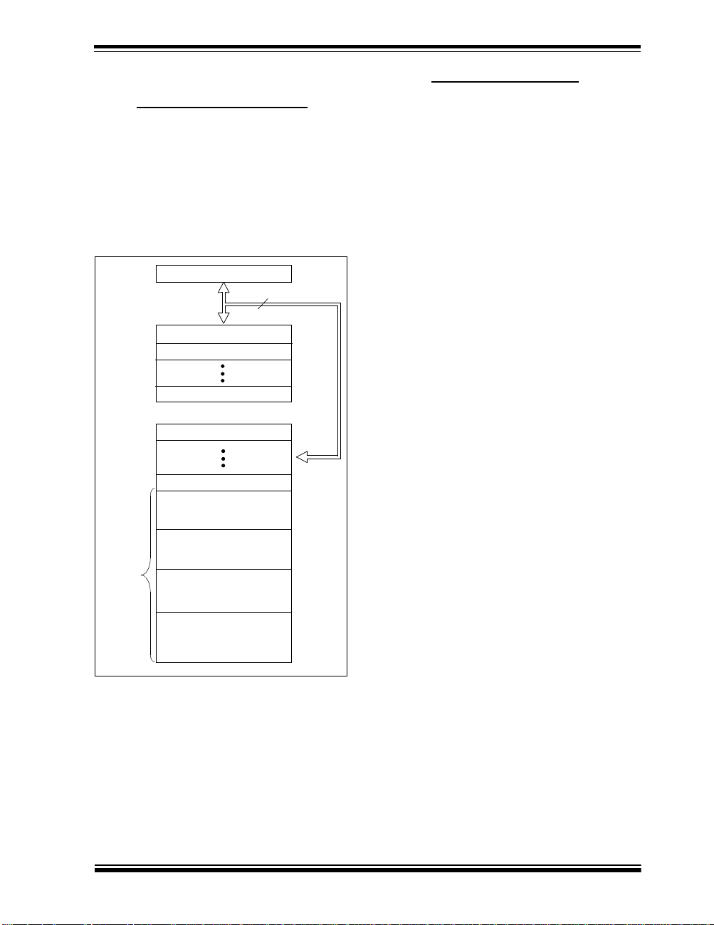
4.0 MEMORY ORGANIZATION
4.1 Program Memory Organization
The PIC16C745/765 has a 13-bit program counter
capable of addressing an 8K x 14 program memory
space. All devices covered by this data sheet have 8K
x 14 bits of program memory. The address range is
0000h - 1FFFh for all devices.
The reset vector is at 0000h and the interrupt vector is
at 0004h.
FIGURE 4-1: PIC16C745/765 PROGRAM
CALL, RETURN
RETFIE, RETLW
On-chip
Program
Memory
MEMORY MAP AND ST ACK
PC<12:0>
13
Stack Level 1
Stack Level 2
Stack Level 8
Reset Vector
Interrupt Vector
Page 0
Page 1
Page 2
Page 3
0000h
0004h
0005h
07FFh
0800h
0FFFh
1000h
17FFh
1800h
4.2 Data Memory Organization
The data memory is partitioned into multiple banks
which contain the General Purpose Registers (GPR)
and the Special Function Registers (SFR). Bits RP1
and RP0 are the bank select bits.
RP<1:0> (STATUS<6:5>)
= 00 → Bank0
= 01 → Bank1
= 10 → Bank2
= 11 → Bank3
Each bank extends up to 7Fh (128 bytes). The lower
locations of each bank are reserved for the SFRs.
Above the SFRs are GPRs, implemented as static
RAM.
All implemented banks contain SFRs. Some “high use”
SFRs from one bank may be mirrored in another bank
for code reduction and quicker access.
4.2.1 GEN ERAL PURPOSE REGISTER FILE The register file can be accessed either directly or indi-
rectly through the File Select Register (FSR)
(Section 4.5).
1FFFh
2000 Microchip Technology Inc. Preliminary DS41124C-page 15
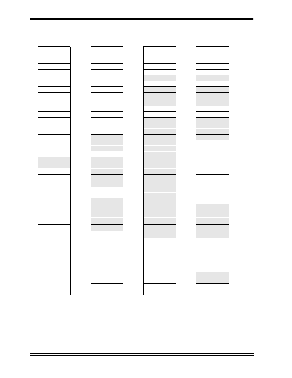
PIC16C745/765
FIGURE 4-2: DATA MEMORY MAP FOR PIC16C745/765
Bank 0 File
Indirect addr.(*) 00h Indirect addr.(*) 80h Indirect addr.(*) 100h Indirect add r.(*) 180h
TMR0 01h OPTION_REG 81h TMR0 101h OPTION_REG 181h
PCL 02h PCL 82h PCL 102h PCL 182h
STATUS 03h STATUS 83h STATUS 103h STATUS 183h
FSR 04h FSR 84h FSR 104h FSR 184h
PORTA 05h TRISA 85h
PORTB 06h TRISB 86h PORTB 106h TRISB 186h
PORTC 07h TRISC 87h
(2)
PORTD
(2)
PORTE
PCLATH 0Ah PCLATH 8Ah PCLATH 10Ah PCLATH 18Ah
INTCON 0Bh INTCON 8Bh INTCON 10Bh INTCON 18Bh
PIR1 0Ch PIE1 8Ch
PIR2 0Dh PIE2 8Dh
TMR1L 0Eh PCON 8Eh
TMR1H 0Fh
T1CON 10h
TMR2 11h
T2CON 12h PR2 92h
CCPR1L 15h
CCPR1H 16h
CCP1CON 17h
RCSTA 18h TXSTA 98h
TXREG 19h SPBRG 99h
RCREG 1Ah
CCPR2L 1Bh
CCPR2H 1Ch 9Ch 11Ch
CCP2CON 1Dh 9Dh 11Dh
ADRES 1Eh 9Eh 11Eh
ADCON0 1Fh ADCON1 9Fh 11Fh
General
Purpose
Register
96 Bytes
Address
08h
09h
13h 93h 113h UEIE 193h
14h 94h 114h USTAT 194h
20h General
Bank 1 File
(2)
TRISD
(2)
TRISE
Purpose
Register
80 Bytes
Address
88h 108h 188h
89h 109h 189h
8Fh 10Fh 18Fh
90h 110h UIR 190h
91h 111h UIE 191h
95h 115h UCTRL 195h
96h 116h UADDR 196h
97h 117h
9Ah 11Ah UEP2 19Ah
9Bh 11Bh
A0h General
Bank 2 File
Address
105h 185h
107h 187h
10Ch 18Ch
10Dh 18Dh
10Eh 18Eh
112h UEIR 192h
118h UEP0 198h
119h UEP1 199h
120h USB Dual Port
Purpose
Register
80 Bytes
Bank 3 File
USWSTAT
Memory
64 Bytes
(1)
Address
197h
(1)
19Bh
(1)
19Ch
(1)
19Dh
(1)
19Eh
(1)
19Fh
1A0h
1DFh
accesses
7Fh FFh 17Fh 1FFh
Unimplemented data memory locations, read as ‘0’.
*Not a physical register.
Note 1: Reserved registers may contain USB state information.
2: Parallel slave ports (PORTD and PORTE) not implemented on PIC16C745; always maintain these bits clear.
DS41124C-page 16 Preliminary 2000 Microchip Technology Inc.
70h-7Fh
EFh 16Fh 1EFh
F0h accesses
70h-7Fh
170h accesses
70h-7Fh
1E0h
1F0h
PIC16C745/765
4.2.2 SPECIAL FUNCTION REGISTERS The Special Function Registers are registers used by
the CPU and Peripheral Modules for controlling the
desired operation of the devic e. These registers are
implemented as static RAM.
The Special Function Registers can be classified into
two sets (core and peripheral). Those registers associated with the “core” functions are described in this section, and those related to the operation of the peripheral
features are described in the section of that p eripher al
feature.
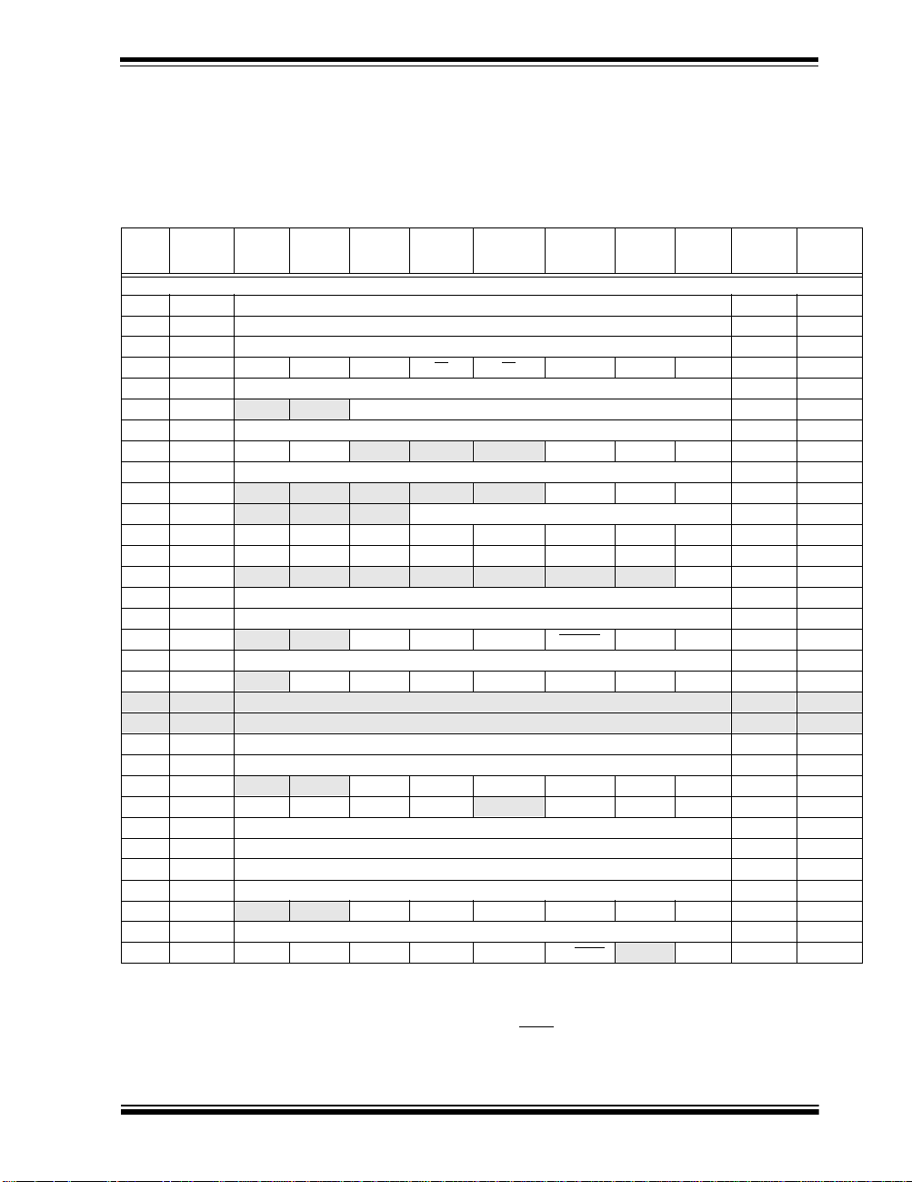
TABLE 4-1: SPECIAL FUNCTION REGISTER SUMMARY
Address Name Bit 7 Bit 6 Bit 5 Bit 4 Bit 3 Bit 2 Bit 1 Bit 0
Value on:
Bank 0
(3)
00h INDF
01h TMR0 Timer0 module’s register xxxx xxxx uuuu uuuu
02h PCL
03h STATUS
04h FSR
05h PORTA
06h PORTB PORTB Data Latch when written: PORTB pins when read xxxx xxxx uuuu uuuu
07h PORTC
08h PORTD
09h PORTE
0Ah PCLATH
0Bh INTCON
0Ch PIR1 PSPIF
0Dh PIR2
0Eh TMR1L Holding register for the Least Significant Byte of the 16-bit TMR1 register xxxx xxxx uuuu uuuu
0Fh TMR1H Holding register for the Most Significant Byte of the 16-bit TMR1 register xxxx xxxx uuuu uuuu
10h T1CON
11h TMR2 Timer2 module’s register 0000 0000 0000 0000
12h T2CON
13h — Unimplemented — —
14h — Unimplemented — —
15h CCPR1L Capture/Compare/PWM Register1 (LSB) xxxx xxxx uuuu uuuu
16h CCPR1H Capture/Compare/PWM Register1 (MSB) xxxx xxxx uuuu uuuu
17h CCP1CON
18h RCSTA SPEN RX9 SREN CREN
19h TXREG USART Transmit Data Register 0000 0000 0000 0000
1Ah RCREG USART Receive Data Register 0000 0000 0000 0000
1Bh CCPR2L Capture/Compare/PWM Register2 (LSB) xxxx xxxx uuuu uuuu
1Ch CCPR2H Capture/Compare/PWM Register2 (MSB) xxxx xxxx uuuu uuuu
1Dh CCP2CON
1Eh ADRES A/D Result Register xxxx xxxx uuuu uuuu
1Fh ADCON0 ADCS1 ADCS0 CHS2 CHS1 CHS0 GO/DONE
Addressing th is location u ses contents of FSR to address d ata memory (not a physical register) 0000 0000 0000 0000
(3)
Program Counter's (PC) Least Significant Byte 0000 0000 0000 0000
(3)
(2)
IRP
(3)
Indirect data memory address pointer xxxx xxxx uuuu uuuu
— — PORTA Data Latch when written: POR TA pins when read --0x 0000 --0u 0000
RC7 RC6
(4)
PORTD Data Latch when written: PORTD pins when read xxxx xxxx uuuu uuuu
(4)
— — — — — RE2 RE1 RE0 ---- -xxx ---- -uuu
(1,3)
— — — Write Buffer for the upper 5 bits of the Program Co unter ---0 0000 ---0 0000
(3)
GIE PEIE T0IE INTE RBIE T0IF INTF RBIF 0000 000x 0000 000u
— — — – — — — CCP2IF ---- ---0 ---- ---0
— — T1CKPS1 T1CKPS0 T1OSCEN T1SYNC TMR1CS TMR1ON --00 0000 --uu uuuu
— TOUTPS3 TOUTPS2 TOUTPS1 TOUTPS0 TMR2ON T2CKPS1 T2CKPS0 -000 0000 -000 0000
— — DC1B1 DC1B0 CCP1M3 CCP1M2 CCP1M1 CCP1M0 --00 0000 --00 0000
— — DC2B1 DC2B1 CCP2M3 CCP2M2 CCP2M1 CCP2M0 --00 0000 --00 0000
(2)
RP1
(4)
ADIF RCIF TXIF USBIF CCP1IF TMR2IF TMR1IF 0000 0000 0000 0000
RP0 TO PD ZDCC0001 1xxx 000q quuu
— — —
— FERR OERR RX9D 0000 -00x 0000 -00x
RC2 RC1 RC0
— ADON 0000 00-0 0000 00-0
xx-- -xxx uu-- -uuu
Legend: x = unknown, u = unchanged, q = value depends on condition, - = unimplemented read as ’0’.
Shaded locations are unimplemented, read as ‘0’.
Note 1: The upper byte of the program counter is not directly accessible. PCLATH is a holding register for the PC<12:8> whose contents
are transferred to the upper byte of the program counter.
2: Other (non power-up) RESETS include external RESET through MCLR
and Watchdog Timer Reset.
3: These registers can be addressed from any bank.
4: The Parallel Slave Port (PORTD and PORTE) is not implemented on the PIC16C745, always maintain these bits clear.
POR,
BOR
Value on all
other resets
(2)
2000 Microchip Technology Inc. Preliminary DS41124C-page 17
PIC16C745/765
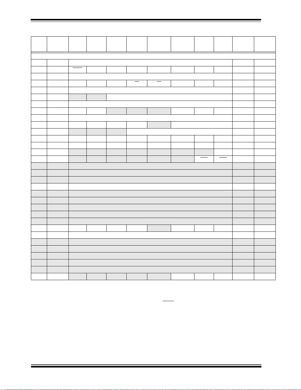
TABLE 4-1: SPECIAL FUNCTION REGISTER SUMMARY (CONTINUED)
Address Name Bit 7 Bit 6 Bit 5 Bit 4 Bit 3 Bit 2 Bit 1 Bit 0
Bank 1
80h INDF
81h OPTION RBPU
82h PCL
83h STATUS
84h FSR
85h TRISA
86h TRISB PORTB Data Direction Register 1111 1111 1111 1111
87h TRISC
88h TRISD
89h TRISE
8Ah PCLATH
8Bh INTCON
8Ch PIE1 PSPIE
8Dh PIE2
8Eh PCON
8Fh — Unimplemented — —
90h — Unimplemented — —
91h — Unimplemented — —
92h PR2 Timer2 Period Register 1111 1111 1111 1111
93h — Unimplemented — —
94h — Unimplemented — —
95h — Unimplemented — —
96h — Unimplemented — —
97h — Unimplemented — —
98h TXSTA CSRC TX9 TXEN SYNC
99h SPBRG Baud Rate Generator Register 0000 0000 0000 0000
9Ah — Unimplemented — —
9Bh — Unimplemented — —
9Ch — Unimplemented — —
9Dh — Unimplemented — —
9Eh — Unimplemented — —
9Fh ADCON1
(3)
Addressing th is location u ses contents of FSR to address d ata memory (not a physical register) 0000 0000 0000 0000
(3)
Program Counte r’s (PC) Least Significant Byte 0000 0000 0000 0000
(3)
(3)
Indirect data memory address pointer xxxx xxxx uuuu uuuu
TRISC7 TRISC8
(4)
PORTD Data Direction Regi s ter 1111 1111 1111 1111
(4)
(1,3)
(3)
INTEDG T0CS T0SE PSA PS2 PS1 PS0 1111 1111 1111 1111
IRP RP1 RP0 TO PD ZDCC0001 1xxx 000q quuu
— — PORTA Data Direction Register --11 1111 --11 1111
— — —
IBF OBF IBOV PSPMODE — PORTE Data Directio n Bits 0000 -111 0000 -111
— — — Write Buffer for the upper 5 bits of the Program Co unter ---0 0000 ---0 0000
GIE PEIE T0IE INTE RBIE T0IF INTF RBIF 0000 000x 0000 000u
(4)
ADIE RCIE TXIE USBIE CCP1IE TMR2IE TMR1IE 0000 0000 0000 0000
— — — — — — — CCP2IE ---- ---0 ---- ---0
— — — — — — POR BOR ---- --qq ---- --uu
— BRGH TRMT TX9D 0000 -010 0000 -010
— — — — — PCFG2 PCFG1 PCFG0 ---- -000 ---- -000
TRISC2 TRISC1 TRISC0
Value on:
11-- -111 11-- -111
Legend: x = unknown, u = unchanged, q = value depends on condition, - = unimplemented read as ’0’.
Shaded locations are unimplemented, read as ‘0’.
Note 1: The upper byte of the program counter is not directly accessible. PCLATH is a holding register for the PC<12:8> whose contents
are transferred to the upper byte of the program counter.
2: Other (non power-up) RESETS include external RESET through MCLR
and Watchdog Timer Reset.
3: These registers can be addressed from any bank.
4: The Parallel Slave Port (PORTD and PORTE) is not implemented on the PIC16C745, always maintain these bits clear.
POR,
BOR
Value on all
other resets
(2)
DS41124C-page 18 Preliminary 2000 Microchip Technology Inc.
PIC16C745/765
TABLE 4-1: SPECIAL FUNCTION REGISTER SUMMARY (CONTINUED)
Address Name Bit 7 Bit 6 Bit 5 Bit 4 Bit 3 Bit 2 Bit 1 Bit 0
Bank 2
100h
101h TMR0 Timer0 module’s register xxxx xxxx uuuu uuuu
102h
103h
104h
105h — Unimplemented — —
106h PORTB PORTB Data Latch when written: PORTB pins when read xxxx xxxx uuuu uuuu
107h — Unimplemented — —
108h — Unimplemented — —
109h — Unimplemented — —
10Ah
10Bh
10Ch-
11Fh
(3)
INDF
PCL
STATUS
FSR
PCLATH
INTCON
Addressing th is location u ses contents of FSR to address d ata memory (not a physical register) 0000 0000 0000 0000
(3)
Program Counter's (PC) Least Significant Byte 0000 0000 0000 0000
(3)
IRP RP1 RP0 TO PD ZDCC0001 1xxx 000q quuu
(3)
Indirect data memory address pointer xxxx xxxx uuuu uuuu
(1,3)
— — — Write Buffer for the upper 5 bits of the Program Co unter ---0 0000 ---0 0000
(3)
GIE PEIE T0IE INTE RBIE T0IF INTF RBIF 0000 000x 0000 000u
— Unimplemented — —
Value on:
Legend: x = unknown, u = unchanged, q = value depends on condition, - = unimplemented read as ’0’.
Shaded locations are unimplemented, read as ‘0’.
Note 1: The upper byte of the program counter is not directly accessible. PCLATH is a holding register for the PC<12:8> whose contents
are transferred to the upper byte of the program counter.
2: Other (non power-up) RESETS include external RESET through MCLR
and Watchdog Timer Reset.
3: These registers can be addressed from any bank.
4: The Parallel Slave Port (PORTD and PORTE) is not implemented on the PIC16C745, always maintain these bits clear.
POR,
BOR
Value on all
other resets
(2)
2000 Microchip Technology Inc. Preliminary DS41124C-page 19
PIC16C745/765
TABLE 4-1: SPECIAL FUNCTION REGISTER SUMMARY (CONTINUED)
Address Name Bit 7 Bit 6 Bit 5 Bit 4 Bit 3 Bit 2 Bit 1 Bit 0
Bank 3
(3)
180h
INDF
181h OPTION_REG RBPU
182h
PCL
183h
STATUS
184h
FSR
185h — Unimplemented — —
186h TRISB PORTB Data Direction Register 1111 1111 1111 1111
187h — Unimplemented — —
188h — Unimplemented — —
189h — Unimplemented — —
18Ah
PCLATH
18Bh
INTCON
18Ch-
18Fh
190h UIR
191h UIE
192h UEIR BTS_ERR OWN_ERR WRT_ERR BTO_ERR DFN8 CRC16 CRC5 PID_ERR 0000 0000 0000 0000
193h UEIE BTS_ERR OWN_ERR WRT_ERR BTO_ERR DFN8 CRC16 CRC5 PID_ERR 0000 0000 0000 0000
194h USTAT
195h UCTRL
196h UADDR
197h USWSTAT SWSTAT7 SWSTAT6 SWSTAT5 SWSTAT4 SWSTAT 3 SWSTAT2 SWSTAT1 SWSTAT0 0000 0000 0000 0000
198h UEP0
199h UEP1
19Ah UEP2
19Bh-
Reserved Reserved, do not use. 0000 0000 0000 0000
19Fh
Addressing th is location u ses contents of FSR to address d ata memory (not a physical register) 0000 0000 0000 0000
INTEDG T0CS T0SE PSA PS2 PS1 PS0 1111 1111 1111 1111
(3)
Program Counte r’s (PC) Least Significant Byte 0000 0000 0000 0000
(3)
IRP RP1 RP0 TO PD ZDCC0001 1xxx 000q quuu
(3)
Indirect data memory address pointer xxxx xxxx uuuu uuuu
(1,3)
— — —
(3)
GIE PEIE T0IE INTE RBIE T0IF INTF RBIF 0000 000x 0000 000u
— Unimplemented — —
— — STALL UIDLE TOK_DNE ACTIVITY UERR USB_RST --00 0000 --00 0000
— — STALL UIDLE TOK_DNE ACTIVITY UERR USB_RST --00 0000 --00 0000
— — — ENDP1 ENDP0 IN — — ---x xx-- ---u uu--
— — SEO PKT_DIS DEV_ATT RESUME SUSPND — --x0 000- --xq qqq-
— ADDR6 ADDR5 ADDR4 ADDR3 ADDR2 ADDR1 ADDR0 -000 0000 -000 0000
— — — — EP_CTL_DIS EP_OUT_EN EP_IN_EN EP_STALL ---- 0000 ---- 0000
— — — — EP_CTL_DIS EP_OUT_EN EP_IN_EN EP_STALL ---- 0000 ---- 0000
— — — — EP_CTL_DIS EP_OUT_EN EP_IN_EN EP_STALL ---- 0000 ---- 0000
Write Buffer for the upper 5 bits of the Program Counter
Value on:
---0 0000 ---0 0000
Legend: x = unknown, u = unchanged, q = value depends on condition, - = unimplemented read as ’0’.
Shaded locations are unimplemented, read as ‘0’.
Note 1: The upper byte of the program counter is not directly accessible. PCLATH is a holding register for the PC<12:8> whose contents
are transferred to the upper byte of the program counter.
2: Other (non power-up) RESETS include external RESET through MCLR
and Watchdog Timer Reset.
3: These registers can be addressed from any bank.
4: The Parallel Slave Port (PORTD and PORTE) is not implemented on the PIC16C745, always maintain these bits clear.
POR,
BOR
Value on all
other resets
(2)
DS41124C-page 20 Preliminary 2000 Microchip Technology Inc.

PIC16C745/765
TABLE 4-2: USB DUAL PORT RAM
Address Name Bit 7 Bit 6 Bit 5 Bit 4 Bit 3 Bit 2 Bit 1 Bit 0
UOWN
1A0h BD0OST
1A1h BD0OBC
1A2h BD0OAL Buffer Address Low xxxx xxxx uuuu uuuu
1A3h
1A4h BD0IST
1A5h BD0IBC
1A6h BD0IAL Buffer Address Low xxxx xxxx uuuu uuuu
1A7h
1A8h BD1OST
1A9h BD1OBC
1AAh BD1OAL Buffer Address Low xxxx xxxx uuuu uuuu
1ABh
1ACh BD1IST
1ADh BD1IBC
1AEh BD1IAL Buffer Address Low xxxx xxxx uuuu uuuu
1AFh
1B0h BD2OST
1B1h BD2OBC
1B2h BD2OAL Buffer Address Low xxxx xxxx uuuu uuuu
1B3h
1B4h BD2IST
1B5h BD2IBC
1B6h BD2IAL Buffer Address Low xxxx xxxx uuuu uuuu
1B7h
1B8h-
1DFh
— Reserved — —
— Reserved — —
— Reserved — —
— Reserved — —
— Reserved — —
— Reserved — —
40 byte USB Buffer xxxx xxxx uuuu uuuu
DATA0/1
UOWN
DATA0/1
— — — — Byte Count xxxx xxxx uuuu uuuu
UOWN
DATA0/1
UOWN
DATA0/1
— — — — Byte Count xxxx xxxx uuuu uuuu
UOWN
DATA0/1
UOWN
DATA0/1
— — — — Byte Count xxxx xxxx uuuu uuuu
UOWN
DATA0/1
UOWN
DATA0/1
— — — — Byte Count xxxx xxxx uuuu uuuu
UOWN
DATA0/1
UOWN
DATA0/1
— — — — Byte Count xxxx xxxx uuuu uuuu
UOWN
DATA0/1
UOWN
DATA0/1
— — — — Byte Count xxxx xxxx uuuu uuuu
PID3—PID2
PID3—PID2
PID3—PID2
PID3—PID2
PID3—PID2
PID3—PID2
—
—
—
—
—
—
PID1
DTS
PID1
DTS
PID1
DTS
PID1
DTS
PID1
DTS
PID1
DTS
PID0
BSTALL
PID0
BSTALL
PID0
BSTALL
PID0
BSTALL
PID0
BSTALL
PID0
BSTALL
—
—
—
—
—
—
—
—
—
—
—
—
Value on:
—
xxxx xxxx uuuu uuuu
—
—
xxxx xxxx uuuu uuuu
—
—
xxxx xxxx uuuu uuuu
—
—
xxxx xxxx uuuu uuuu
—
—
xxxx xxxx uuuu uuuu
—
—
xxxx xxxx uuuu uuuu
—
Legend: x = unknown, u = unchanged, q = value depends on condition, - = unimplemented read as ’0’.
Shaded locations are unimplemented, read as ‘0’.
Note 1: Other (non power-up) RESETS include external RESET through MCLR and Watchdog Timer Reset.
POR,
BOR
Value on all
other resets
(1)
2000 Microchip Technology Inc. Preliminary DS41124C-page 21

PIC16C745/765
4.2.2.1 STATUS REGISTER
The STATUS register, shown in Register 4-1, contains
the arithmetic status of the ALU, the RESET status and
the bank select bits for data memory.
The STATUS register can be the destination for any
instruction, as with any other r egister. If the STATUS
register is the destination for an instruction that affects
the Z, DC or C bits, then the write to these three bits is
disabled. These bits are set or cleared according to the
device logic. Furthermore, the TO
writable. Therefore, the result of an instruction with the
STATUS register as destination may be different than
intended.
and PD bits are not
For example, CLRF STATUS will clear the upper three
bits and set the Z bit. This leaves the ST ATUS register
as 000u u1uu (where u = unchanged).
It is recommended that only BCF, BSF, SWAPF and
MOVWF instructions be used to alter the STATUS register. These instructions do not affect the Z, C or DC bits
in the STATUS register. For other instructions which do
not affect status bits, see the "Instruction Set Summary."
Note 1: The C and DC bits operate as borrow and
digit borrow
tion. See the SUBLW and SUBWF instructions for examples.
REGISTER 4-1: STATUS REGISTER (STATUS: 03h, 83h, 103h, 183h)
R/W-0 R/W-0 R/W-0 R-1 R-1 R/W-x R/W-x R/W-x
IRP RP1 RP0 TO
bit7 bit0
bit 7: IRP: Register Bank Select bit (used for indirect addressing)
1 = Bank 2, 3 (100h - 1FFh)
0 = Bank 0, 1 (00h - FFh)
bit 6-5: RP<1:0>: Register Bank Select bits (used for direct addressing)
00 = Bank 0 (00h - 7Fh)
01 = Bank 1 (80h - FFh)
10 = Bank 2 (100h - 17Fh)
11 = Bank 3 (180h - 1FFh)
bit 4: TO
bit 3: PD
bit 2: Z: Zero bit
bit 1: DC: Digit carry/borrow
bit 0: C: Carry/borrow
: Time-out bit
1 = After power-up, CLRWDT instruction, or SLEEP instruction
0 = A WDT time-out occurred
: Power-down bit
1 = After power-up or by the CLRWDT instruction
0 = By execution of the SLEEP instruction
1 = The result of an arithmetic or logic operation is zero
0 = The result of an arithmetic or logic operation is not zero
bit (ADDWF, ADDLW,SUBLW,SUBWF instructions)
1 = A carry-out from the 4th low order bit of the result occurred
0 = No carry-out from the 4th low o rder bit of the result
bit (ADDWF, ADDLW,SUBLW,SUBWF instructions)
1 = A carry-out from the most significant bit of the result occurred
0 = No carry-out from the most significant bit of the result occurred
PD ZDC
(1)
C
(1)
bits, respectively, in subtrac-
R = Readable bit
W = Writable bit
U = Unimplemented bit,
read as ‘0’
- n = Value at POR reset
(1)
Note1: For borrow
ond operand. For rotate (RRF, RLF) instructions, this bit is loaded with either the high or low order bit of the
source register.
DS41124C-page 22 Preliminary 2000 Microchip Technology Inc.
the polarity is reversed. A subtraction is executed by adding the two’s complement of the sec-

PIC16C745/765
4.2.2.2 OPTION REGISTER
The OPTION_REG register is a readable and writable
register, which contains various control bits to configure
Note: To achieve a 1:1 prescaler assignment for
the TMR0 register, assign the prescaler to
the Watchdog Timer.
the TMR0/WDT prescaler, the external INT Interrupt,
TMR0 and the weak pull-ups on PORTB.
REGISTER 4-2: OPTION REGISTER (OPTION_REG: 81h, 181h)
R/W-1 R/W-1 R/W-1 R/W-1 R/W-1 R/W-1 R/W-1 R/W-1
RBPU
INTEDG T0CS T0SE PSA PS2 PS1 PS0 R = Readable bit
bit7 bit0
bit 7: RBPU
bit 6: INTEDG: Interrupt Edge Select bit
bit 5: T0CS: TMR0 Clock Source Select bit
bit 4: T0SE: TMR0 Source Edge Select bit
bit 3: PSA: Prescaler Assignment bit
bit 2-0: PS<2:0>: Prescaler Rate Select bits
: PORTB Pull-up Enable bit
1 = PORTB pull-ups are disabled
0 = PORTB pull-ups are enabled by individual port latch values
1 = Interrupt on rising edge of RB0/INT pin
0 = Interrupt on falling edge of RB0/INT pin
1 = Transition on RA4/T0CKI pin
0 = Internal instruction cycle clock (CLKOUT)
1 = Increment on high-to-low transition on RA4/T0CKI pin
0 = Increment on low-to-high transition on RA4/T0CKI pin
1 = Prescaler is assigned to the WDT
0 = Prescaler is assigned to the Timer0 module
Bit Value TMR0 Rate WDT Rate
000
001
010
011
100
101
110
111
1 : 2
1 : 4
1 : 8
1 : 16
1 : 32
1 : 64
1 : 128
1 : 256
1 : 1
1 : 2
1 : 4
1 : 8
1 : 16
1 : 32
1 : 64
1 : 128
W = Writable bit
U = Unimplemented bit,
read as ‘0’
-n = Value at POR reset
2000 Microchip Technology Inc. Preliminary DS41124C-page 23

PIC16C745/765
4.2.2.3 INTCON REGISTER
The INTCON register is a readable and wr itabl e regis-
ter, which contains various enable and flag bits for the
TMR0 register overflow, RB Port change and external
RB0/INT pin interrupts.
Note: Interrupt flag bits are set when an interrupt
condition occurs, regardless of the state of
its corresponding enable bit or the global
enable bit, GIE (INTCON<7>). User software should ensure the appropriate interrupt flag bits are clear prior to enabling an
interrupt
.
REGISTER 4-3: INTERRUPT CONTROL REGISTER (INTCON: 10Bh, 18Bh)
R/W-0 R/W-0 R/W-0 R/W-0 R/W-0 R/W-0 R/W-0 R/W-x
GIE PEIE T0IE INTE RBIE T0IF INTF RBIF
bit7 bit0
bit 7: GIE:
bit 6: PEIE: Peripheral Interrupt Enable bit
bit 5: T0IE: TMR0 Overflow Interrupt Enable bit
bit 4: INTE: RB0/INT External Interrupt Enable bit
bit 3: RBIE: RB Port Change Interrupt Enable bit
bit 2: T0IF: TMR0 Overflow Interrupt Flag bi t
bit 1: INTF: RB0/INT External Interrupt Flag bit
bit 0: RBIF: RB Port Change Interrupt Flag bit
Global Interrupt Enable bit
1 = Enables all un-masked interrupts
0 = Disables all interrupts
1 = Enables all un-masked peripheral interrupts
0 = Disables all peripheral interrupts
1 = Enables the TMR0 interrupt
0 = Disables the TMR0 interrupt
1 = Enables the RB0/INT external interrupt
0 = Disables the RB0/INT external interrupt
1 = Enables the RB port change interrupt
0 = Disables the RB port change interrupt
1 = TMR0 register has overflowed (must be cleared in software)
0 = TMR0 register did not overflow
1 = The RB0/INT external interrupt occurred (must be cleared in software)
0 = The RB0/INT external interrupt did not occur
1 = At least one of the RB<7:4> pins changed state (must be cleared in software)
0 = None of the RB<7:4> pins have changed state
R = Readable bit
W = Writable bit
U = Unimplemented bit,
-n = Value at POR reset
read as ‘0’
DS41124C-page 24 Preliminary 2000 Microchip Technology Inc.

PIC16C745/765
4.2.2.4 PIE1 REGISTER
This register contains the individual enable bits for the
peripheral interrupts.
Note: Bit PEIE (INTCON<6>) must be set to
enable any peripheral interrupt.
REGISTER 4-4: PERIPHERAL INTERRUPT ENABLE1 REGISTER (PIE1: 8Ch)
R/W-0 R/W-0 R/W-0 R/W-0 R/W-0 R/W-0 R/W-0 R/W-0
(1)
PSPIE
bit7 bit0
bit 7: PSPIE
bit 6: ADIE: A/D Converter Interrupt Enable bit
bit 5: RCIE: USART Receive Interrupt Enable bit
bit 4: TXIE: USART Transmit Interrupt Enable bit
bit 3: USBIE: Universal Serial Bus Interrupt Enable bit
bit 2: CCP1IE: CCP1 Interrupt Enable bit
bit 1: TMR2IE: TMR2 to PR2 Match Interrupt Enable bit
bit 0: TMR1IE: TMR1 Overflow Interrupt Enable bit
ADIE RCIE TXIE USBIE CCP1IE TMR2IE TMR1IE
(1)
: Parallel Slave Port Read/Write Interrupt Enable bit
1 = Enables the PSP read/write interrupt
0 = Disables the PSP read/write interrupt
1 = Enables the A/D interrupt
0 = Disables the A/D interrupt
1 = Enables the USART receive interrupt
0 = Disables the USART receive interrupt
1 = Enables the USART transmit interrupt
0 = Disables the USART transmit interrupt
1 = Enables the USB interrupt
0 = Disables the USB interrupt
1 = Enables the CCP1 interrupt
0 = Disables the CCP1 interrupt
1 = Enables the TMR2 to PR2 match interrupt
0 = Disables the TMR2 to PR2 match interrupt
1 = Enables the TMR1 overflow interrupt
0 = Disables the TMR1 overflow interrupt
R = Readable bit
W = Writable bit
U = Unimplemented bit,
-n = Value at POR reset
read as ‘0’
Note 1: Parallel slave ports not implemented on the PIC16C745; always maintain this bit clear.
2000 Microchip Technology Inc. Preliminary DS41124C-page 25

PIC16C745/765
4.2.2.5 PIR1 REGISTER
This register contains the individual flag bits for the
peripheral interrupts.
Note: Interrupt flag bits are set when an interrupt
condition occurs, regardless of the state of
its corresponding enable bit or the global
enable bit, GIE (INTCON<7>). User software should ensure the appropriate interrupt flag bits are clear prior to enabling an
interrupt.
REGISTER 4-5: PERIPHERAL INTERRUPT REGISTE R1 (PIR1: 0Ch)
R/W-0 R/W-0 R-0 R-0 R/W-0 R/W-0 R/W-0 R/W-0
(1)
PSPIF
bit7 bit0
bit 7: PSPIF
bit 6: ADIF: A/D Converter Interrupt Flag bit
bit 5: RCIF: USART Receive Interrupt Flag bit
bit 4: TXIF: USART Transmit Interrupt Flag bit
bit 3: USBIF: Universal Serial Bus (USB) Interrupt Flag
bit 2: CCP1IF: CCP1 Interrupt Flag bit
bit 1: TMR2IF: TMR2 to PR2 Match Interrupt Flag bit
bit 0: TMR1IF: TMR1 Overflow Interrupt Flag bit
ADIF RCIF TXIF USBIF CCP1IF TMR2IF TMR1IF
(1)
: Parallel Slave Port Read/Write Interrupt Flag bit
1 = A read or a write operation has taken place (must be cleared in software)
0 = No read or write has occurred
1 = An A/D conversion completed (must be cleared in software)
0 = The A/D conversion is not complete
1 = The USART receive buffer is full (clear by reading RCREG)
0 = The USART receive buffer is empty
1 = The USART transmit buffer is empty (clear by writing to TXREG)
0 = The USART transmit buffer is full
1 = A USB interrupt condition has occurred. The specific cause can be found by examining the contents
of the UIR and UIE registers.
0 = No USB interrupt conditions that are enabled have occurred.
Capture Mode
1 = A TMR1 register capture occurred (must be cleared in software)
0 = No TMR1 register capture occurred
Compare Mode
1 = A TMR1 register compare match occurred (must be cleared in software)
0 = No TMR1 register compare match occurred
PWM Mode
Unused in this mode
1 = TMR2 to PR2 match occurred (must be cleared in software)
0 = No TMR2 to PR2 match occurred
1 = TMR1 register overflowed (must be cleared in software)
0 = TMR1 register did not overflow
R = Readable bit
W = Writable bit
U = Unimplemented bit,
read as ‘0’
-n = Value at POR reset
Note 1: Parallel slave ports not implemented on the PIC16C745; always maintain this bit clear.
DS41124C-page 26 Preliminary 2000 Microchip Technology Inc.

PIC16C745/765
4.2.2.6 PIE2 REGISTER
This register contains the individual enable bit for the
CCP2 peripheral interrupt.
REGISTER 4-6: PERIPHERAL INTERRUPT ENABLE 2 REGISTER (PIE2: 8Dh)
U-0 U-0 U-0 U-0 U-0 U-0 U-0 R/W-0
— — — — — — — CCP2IE R = Readable bit
bit7 bit0
bit 7-1: Unimplemented: Read as '0'
bit 0: CCP2IE: CCP2 Interrupt Enable bit
1 = Enables the CCP2 interrupt
0 = Disables the CCP2 interrupt
4.2.2.7 PIR2 REGISTER
This register contains the CCP2 interrupt flag bit.
Note: Interrupt flag bits are set when an interrupt
condition occurs, regardless of the state of
its corresponding enable bit or the global
enable bit, GIE (INTCON<7>). User software should ensure the appropriate interrupt flag bits are clear prior to enabling an
interrupt.
W = Writable bit
U = Unimplemented bit,
-n = Value at POR reset
read as ‘0’
REGISTER 4-7: PERIPHERAL INTERRUPT REGISTER 2 (PIR2: 0Dh)
U-0 U-0 U-0 U-0 U-0 U-0 U-0 R/W-0
— — — — — — — CCP2IF R = Readable bit
bit7 bit0
bit 7-1: Unimplemented: Read as '0'
bit 0: CCP2IF: CCP2 Interrupt Flag bit
Capture Mode
1 = A TMR1 register capture occurred (must be cleared in software)
0 = No TMR1 register capture occurred
Compare Mode
1 = A TMR1 register compare match occurred (must be cleared in software)
0 = No TMR1 register compare match occurred
PWM Mode
Unused
2000 Microchip Technology Inc. Preliminary DS41124C-page 27
W = Writable bit
U = Unimplemented bit,
read as ‘0’
-n = Value at POR reset
PIC16C745/765
4.2.2.8 PCON REGISTER
The Power Control (PCON) register contains flag bits
to allow differentiation between a Power-on Reset
(POR), a Brown-out Reset (BOR), a Watchdog Reset
(WDT) and an external MCLR
Reset.
Note: BOR is unknown on POR. It must be set by
the user and checked on subsequent
RESETS to see if BOR
a brown-out has occurred.
REGISTER 4-8: POWER CONTR OL REGISTER REGISTER (PCON: 8Eh)
U-0 U-0 U-0 U-0 U-0 U-0 R/W-0 R/W-q
— — — — — —
bit7 bit0
bit 7-2: Unimplemented: Read as '0'
bit 1: POR
bit 0: BO
: Power-on Reset Status bit
1 = No Power-on Reset occurred
0 = A Power-on Reset occurred (must be set in software after a Power-on Reset occurs)
R: Brown-out Reset Status bit
1 = No Brown-out Reset occurred
0 = A Brown-out Reset occurred (must be set in software after a Brown-out Reset occurs)
POR
BOR
is clear, indicating
R = Readable bit
W = Writable bit
U = Unimplemented bit,
read as ‘0’
-n = Value at POR reset
DS41124C-page 28 Preliminary 2000 Microchip Technology Inc.
PIC16C745/765
4.3 PCL and PCLATH
The program counter (PC) is 13-bits wide. The low byte
comes from the PCL register, which is a readable and
writable register. The upper bits (PC<12:8>) are not
readable, but are indirectly writable through the
PCLATH register. On any RESET, the upper bits of the
PC will be cleared. Figure 4-3 shows the two situations
for the loading of the PC. The upper example in the figure shows how the PC is loaded on a write to PCL
(PCLATH<4:0> → PCH). The lower example in the figure shows how the PC is loaded during a CALL or GOTO
instruction (PCLATH<4:3> → PCH).
FIGURE 4-3: LOADING OF PC IN
DIFFERENT SITUATIONS
PCH PCL
12 8 7 0
PC
PCLATH<4:0>
5
PCLATH
PCH PCL
12 11 10 0
PC
2
87
PCLATH<4:3>
PCLATH
4.3.1 COMPUTED GOTO A computed GOTO is accomplished by adding an offset
to the program counter ( ADDWF PCL). When doing a
table read using a computed GOTO method, care
should be exercised if the table location crosses a PCL
memory boundary (each 256 byte block). Refer to the
application note “Implementing a Table Read" (AN556).
4.3.2 STACK The PIC16C745/765 family has an 8-le vel deep x 13-
bit wide hardware stack. The stack space is not part of
either program or data space and the stack pointer is
not readable or writable. The PC is PUSHed onto the
stack when a CALL instruction i s exec uted or a n i nterrupt causes a branch. The stack is POPed in the event
of a RETURN,RETLW or a RETFIE instruction execution. PCLATH is not affected by a PUSH or POP operation.
The stack operates as a circular buffer. This means that
after the stack has been PUSHed eight times, the ninth
push overwrites the value that was stored from the first
push. The tenth push overwrites the second push (and
so on).
11
8
Instruction with
PCL as
Destination
ALU
GOTO,CALL
Opcode <10:0>
Note 1: There are no status bits to indicate stack
overflow or stack underflow conditions.
2: There are no instructions/mnemonics
called PUSH or POP. These are actions that
occur from the execution of the CALL,
RETURN, RETLW, and RETFIE instructions, or the vectoring to an interrupt
address.
4.4 Program Memory Paging
PIC16CXX devices are capable of addressing a continuous 8K word block of program memory. The CALL and
GOTO instructions provide only 11 bits of address to
allow branching within any 2K program memory page.
When doing a CALL or GOTO instruction, the upper 2
bits of the address are provided by PCLATH<4:3>.
When doing a CALL or GOTO instruction, the user must
ensure that the page select bits are programmed so
that the desired program memory page is addressed. If
a return from a CALL instruction (or interrupt) is executed, the entire 13-bit PC is p ushed onto the stack.
Therefore, manipulation of the PCLATH<4:3> bits is
not required for the return instructions (which POPs the
address from the stack).
Example 4-1 shows the calling of a subroutine in
page 1 of the program memory. This example assumes
that PCLATH is saved and restored by the interrupt service routine
(if interrupts are used).
EXAMPLE 4-1: CALL OF A SUBROUTINE IN
PAGE 1 FROM PAGE 0
ORG 0x500
BSF PCLATH,3 ;Select page 1 (800h-FFFh)
CALL SUB1_P1 ;Call subroutine in
: ;page 1 (800h-FFFh)
:
ORG 0x900 ;page 1 (800h-FFFh)
SUB1_P1
: ;called subroutine
: ;page 1 (800h-FFFh)
:
RETURN ;return to Call subroutine
;in page 0 (000h-7FFh)
2000 Microchip Technology Inc. Preliminary DS41124C-page 29

PIC16C745/765
4.5 Indirect Addressing, INDF and FSR Registers
The INDF register is not a physical register. Addressing
the INDF register will cause indirect addressing.
Indirect addressing is possible by using the INDF register. Any instruction using the INDF register actually
accesses the register pointed to by the File Select Register, FSR. Reading the INDF register itself indirectly
(FSR = ’0’) will read 00h. Writing to the INDF register
indirectly results in a no-operation (although status bits
may be affected). An effective 9-bit address is obtained
by concatenating the 8-bit FSR register and the IRP bit
(STATUS<7>), as shown in Figure 4-4.
A simple program to clear RAM locations 20h-2Fh
using indirect addressing is shown in Example 4-2.
FIGURE 4-4: DIRECT/INDIRECT ADDRESSING
RP<1:0> 6
bank select location select
from opcode
0
00 01 10 11
00h
80h
EXAMPLE 4-2: INDIRECT ADDRESSING
movlw 0x20 ;initialize pointer
NEXT clrf INDF ;clear INDF register
CONTINUE
100h
movwf FSR ;to RAM
incf FSR,F ;inc pointer
btfss FSR,4 ;all done?
goto NEXT ;no clear next
: ;yes continue
Indirect AddressingDirect Addressing
IRP FSR register
180h
7
bank select
0
location select
Data
Memory
7Fh
FFh
17Fh
1FFh
Bank 0 Bank 1 Bank 2 Bank 3
Note: For register file map detail see Figure 4-2.
DS41124C-page 30 Preliminary 2000 Microchip Technology Inc.
PIC16C745/765
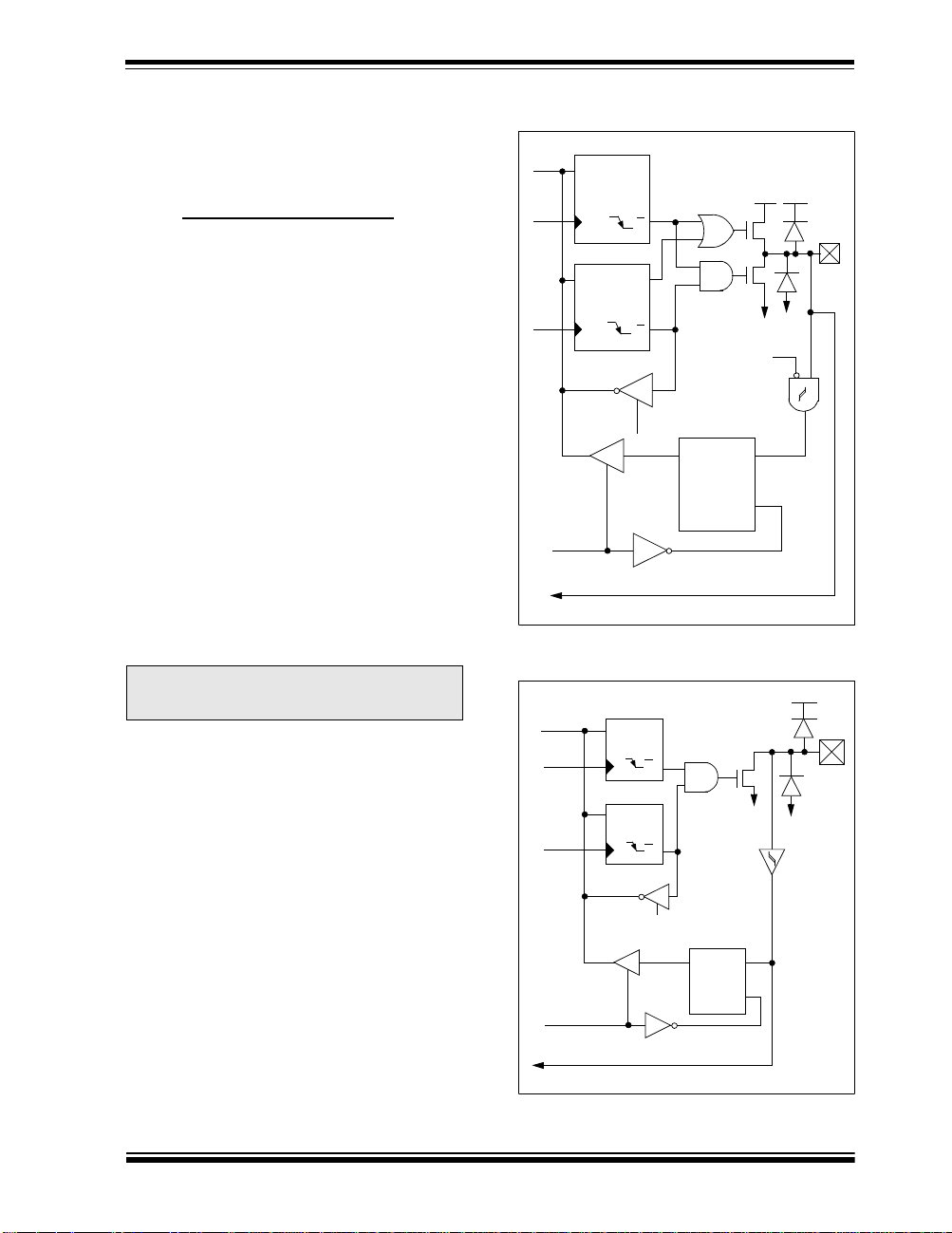
5.0 I/O PORTS
Some pins for these I/O ports are multiplexed with an
alternate function for the peripheral features on the
device. In general, when a p eripheral is enabled, that
pin may not be used as a general purpose I /O pin.
5.1 PORTA and TRISA Registers
PORTA is a 6-bit latch.
The RA4/T0CKI pin is a Schmitt Trigger input and an
open drain output. All other RA port pins have TTL
input levels and full CMOS output drivers. All pins have
data direction bits (TRIS registers), which c an configure these pins as output or input.
Setting a TRISA register bit puts the corresponding output driver in a hi-impedance mode. Clearing a bit in the
TRISA register puts the contents of the output latch on
the selected pin(s).
Reading the PORTA register reads the status of the
pins, whereas writing to it will write to the port latch. All
write operations are read-modify-write operations.
Therefore, a write to a port implies that the port pins are
read, the value is modified, and then written to the port
data latch.
Pin RA4 is multiplexed with the Timer0 module clock
input to become the RA4/T0CKI pin.
On the PIC16C745/765, PORTA pins are multiplexed
with analog inputs and analog V
tion of each pin is selected by clearing/setting the control bits in the ADCON1 register (A/D Control
Register1).
Note: On all RESETS, pins with analog and digi-
tal functions are configured as analog
inputs.
The TRISA register controls the direction of the RA
pins, even when they are being used as analog inputs.
The user must ensure the bits in the TRISA register are
maintained set when using them as analog inputs.
EXAMPLE 5-1: INITIALIZING PORTA
(PIC16C745/765)
BCF STATUS, RP1 ;
BCF STATUS, RP0 ;
CLRF PORTA ; Initialize PORTA by
BSF STATUS, RP0 ; Select Bank 1
MOVLW 0x06 ; Configure all pins
MOVWF ADCON1 ; as digital inputs
MOVLW 0xCF ; Value used to
MOVWF TRISA ; Set RA<3:0> as inputs
REF input. The opera-
; clearing output
; data latches
; initialize data
; direction
; RA<5:4> as outputs
; TRISA<7:6> are always
; read as ’0’.
FIGURE 5-1: BLOCK DIAGRAM OF RA<3:0>
AND RA5 PINS
Data
Bus
WR
Port
WR
TRIS
RD Port
To A/D Converter
CK
Data Latch
CK
TRIS Latch
QD
Q
QD
Q
RD TRIS
QD
VDD
P
N
V
SS
Analog
Input
Mode
Schmitt Trigger
Input Buffer
EN
VDD
I/O Pin
FIGURE 5-2: BLOCK DIAGRAM OF
RA4/T0CKI PIN
Data
Bus
WR
Port
Data Latch
WR
TRIS
TRIS Latch
RD Port
TMR0 Clock Input
CK
CK
RD TRIS
QD
Q
QD
Q
Schmitt
Trigger
Input
Buffer
QD
EN
EN
VDD
N
V
I/O pin
SS
2000 Microchip Technology Inc. Preliminary DS41124C-page 31

PIC16C745/765
TABLE 5-1: PORTA FUNCTIONS
Name Function
RA0/AN0
RA1/AN1
RA2/AN2
RA3/AN3/V
Legend: OD = open drain, ST = Schmitt Trigger
REF
RA4/T0CKI
RA5/AN4
RA0 ST CMOS Bi-directional I/O
AN0 AN — A/D Input
RA1 ST CMOS Bi-directional I/O
AN1 AN — A/D Input
RA2 ST CMOS Bi-directional I/O
AN2 AN — A/D Input
RA3 ST CMOS Bi-directional I/O
AN3 AN — A/D Input
V
REF AN — A/D Positive Reference
RA4 ST OD Bi-directional I/O
T0CKI ST — Timer 0 Clock Input
RA5 ST Bi-directional I/O
AN4 AN — A/D Input
Input
Type
TABLE 5-2: SUMMARY OF REGISTERS ASSOCIATED WITH PORTA
Address Name Bit 7 Bit 6 Bit 5 Bit 4 Bit 3 Bit 2 Bit 1 Bit 0
05h PORTA
85h TRISA
9Fh ADCON1
Legend: x = unknown, u = unchanged, - = unimplemented locations read as '0'. Shaded cells are not used by PORTA.
— — RA5 RA4 RA3 RA2 RA1 RA0 --0x 0000 --0u 0000
— — PORTA Data Direction Register --11 1111 --11 1111
— — — — — PCFG2 PCFG1 PCFG0 ---- -000 ---- -000
Output
Type
Description
Value on:
POR,
BOR
Value on all
other resets
DS41124C-page 32 Preliminary 2000 Microchip Technology Inc.

PIC16C745/765
5.2 PORTB and TRISB Registers
PORTB is an 8-bit wide bi-directional port. The c orresponding data direction register is TRISB. Setting a bit
in the TRISB register puts the corresponding output
driver in a hi-impedance input mode. Clearing a bit in
the TRISB register puts the contents of the output latch
on the selected pin(s).
Each of the PORTB pins has a weak internal pull-up. A
single control bit can turn on all the pull-ups. This is performed by clearing bit RBPU
(OPTION_REG<7>). The
weak pull-up is automatically turned off when the port
pin is configured as an output. The pull-ups are disabled on a Power-on Reset.
FIGURE 5-3: BLOCK DIAGRAM OF RB<3:0>
PINS
V
TTL
Input
Buffer
EN
DD
P
(1)
RBPU
Data
Bus
WR
Port
WR
TRIS
RB0/INT
Note 1: To enable weak pull-ups, set the appropriate TRIS bit(s)
Data Latch
QD
CK
TRIS Latch
QD
CK
RD TRIS
RD Port
Schmitt Trigger
Buffer
and clear the RBPU
QD
bit (OPTION_REG<7>).
Four of PORTB’s pins, RB<7:4>, have an interrupt-onchange feature. Only pins configured as inputs can
cause this interrupt to occur (i.e., any RB<7:4> pin configured as an output is excluded from the interrupt-onchange comparison). The input pins (of RB<7:4>) are
compared with the value latched on the last read of
PORTB. The “mismatch” outputs of RB<7:4> are
OR’ed together to generate the RB Port Change Interrupt with flag bit RBIF (INTCON<0>).
This interrupt can wake the device from SLEEP. The
user, in the interrupt service routine, can clear the interrupt in the following manner:
a) Any read or write of PORTB. This will end the
mismatch condition.
b) Clear flag bit RBIF.
weak
pull-up
RD Port
VDD
I/O
pin
A mismatch condition will continue to set flag bit R BIF.
Reading PORTB will end the mismatch condition, and
allow flag bit RBIF to be cleared.
This interrupt-on-mismatch feature, together with s oftware configureable pull-ups on these four pins, allow
easy interface to a keypad and make it possible for
wake-up on key depression. Refer to the Embedded
Control Handbook, “Implementing Wake-Up on Key
Stroke” (AN552).
The interrupt-on-change feature is recommended for
wake-up on key depression operation and operations
where PORTB is only used for the interrupt-on-change
feature. Polling of PORTB is not recommended while
using the interrupt-on-change feature.
RB0/INT is an external interrupt input pin and is configured using the INTEDG bit (OPTION_REG<6>).
RB0/INT is discussed in detail in Section 13.5.1.
FIGURE 5-4: BLOCK DIAGRAM OF
RB<7:4> PINS
V
DD
(1)
RBPU
Data Bus
WR Port
WR TRIS
Set RBIF
From other
RB<7:4> pins
RB<7:6> in serial programming mode
Note 1: To enable weak pull-ups, set the appropriate TRIS bit(s)
Data Latch
QD
CK
TRIS Latch
QD
CK
RD TRIS
RD Port
and clear the RBPU
TTL
Input
Buffer
Latch
QD
EN
QD
EN
bit (OPTION_REG<7> ).
P
weak
pull-up
RD Port
Buffer
Q1
VDD
ST
Q3
I/O
pin
2000 Microchip Technology Inc. Preliminary DS41124C-page 33

PIC16C745/765
TABLE 5-3: PORTB FUNCTIONS
Name Function
RB0/INT
RB1 RB1 TTL CMOS Bi-directional I/O
RB2 RB2 TTL CMOS Bi-directional I/O
RB3 RB3 TTL CMOS Bi-directional I/O
RB4 RB4 TTL CMOS Bi-directional I/O with Interrupt-on-Change
RB5 RB5 TTL CMOS Bi-directional I/O with Interrupt-on-Change
RB6/ICSPC
RB7/ICSPD
Legend: OD = open drain, ST = Schmitt Trigger
RB0 TTL CMOS Bi-directional I/O
INT ST — Interrupt
RB6 TTL CMOS Bi-directional I/O with Interrupt-on-Change
ICSPC ST In-Circuit Serial Programming Clock input
RB7 TTL CMOS Bi-directional I/O with Interrupt-on-Change
ICSPD ST CMOS In-Circuit Serial Programming Data I/O
Input
Type
TABLE 5-4: SUMMARY OF REGISTERS ASSOCIATED WITH PORTB
Address Name Bit 7 Bit 6 Bit 5 Bit 4 Bit 3 Bit 2 Bit 1 Bit 0
06h, 106h PORTB RB7 RB6 RB5 RB4 RB3 RB2 RB1 RB0 xxxx xxxx
86h, 186h TRISB PORTB Data Direction Register 1111 1111 1111 1111
81h, 181h OPTION_REG RBPU
Legend: x = unknown, u = unchanged. Shaded cells are not used by PORTB.
INTEDG T0CS T0SE PSA PS2 PS1 PS0 1111 1111 1111 1111
Output
Type
Description
Value on:
POR,
BOR
Value on all
other resets
uuuu uuuu
DS41124C-page 34 Preliminary 2000 Microchip Technology Inc.

PIC16C745/765
5.3 PORTC and TRISC Registers
PORTC is a 5-bit bi-directional port. Each pin is individually configureable as an i nput or output through the
TRISC register. PORTC is multiplexed with several
peripheral functions (Table 5-5). PORTC pins have
Schmitt Trigger input buffers.
When enabling peripheral functions, care should be
taken in defining TRIS bits for each PORTC pin. Some
peripherals override the TRIS bit to make a pin an output, while other peripherals override the TRIS bit to
make a pin an input. Since the TRIS bi t override is in
effect while the peripheral is enabled, read-modifywrite instructions (BSF, BCF, XORWF) with TRISC as
destination should be avoided. The user should refer to
the corresponding peripheral section for the correct
TRIS bit settings.
FIGURE 5-5: PORTC BLOCK DIAGRAM
Port/Peripheral Select
Peripheral Data Out
Data Bus
WR
Port
WR
TRIS
Peripheral
(2)
OE
RD
Port
Peripheral Input
Note 1: Port/Peripheral select signal selects between port
2: Peripheral OE (output enable) is only activated if
(1)
0
QD
1
Q
CK
Data Latch
QD
Q
CK
TRIS Latch
RD TRIS
QD
EN
data and peripheral output.
peripheral select is active.
Schmitt
Trigger
VSS
V
DD
VDD
P
N
I/O
pin
2000 Microchip Technology Inc. Preliminary DS41124C-page 35

PIC16C745/765
TABLE 5-5: PORTC FUNCTIONS
Name Function
RC0 ST CMOS Bi-directional I/O
RC0/T1OSO/T1CKI
RC1/T1OSI/CCP2
RC2/CCP1
RC6/TX/CK
RC7/RX/DT
Legend: OD = open drain, ST = Schmitt Trigger
T1OSO — Xtal T1 Oscillator Output
T1CKI ST — T1 Clock Input
RC1 ST CMOS Bi-directional I/O
T1OSI Xtal — T1 Oscillator Input
CCP2 ——Capture In/Compare Out/PWM Out 2
RC2 ST CMOS Bi-directional I/O
CCP1 ——Capture In/Compare Out/PWM Out 1
RC6 ST CMOS Bi-directional I/O
TX — CMOS USART Async Transmit
CK ST CMOS USART Master Out/Slave In Clock
RC7 ST CMOS Bi-directional I/O
RX ST — USART Async Receive
DT ST CMOS USART Data I/O
Input
Type
TABLE 5-6: SUMMARY OF REGISTERS ASSOCIATED WITH PORTC
Address Name Bit 7 Bit 6 Bit 5 Bit 4 Bit 3 Bit 2 Bit 1 Bit 0
07h PORTC RC7 RC6
87h TRISC TRISC7 TRISC6
Legend: x = unknown, u = unchanged.
— — — RC2 RC1 RC0 xx-- -xxx
— — — TRISC2 TRISC1 TRISC0 11-- -111
Output
Type
Description
Value on:
POR,
BOR
Value on all
other resets
uu-- -uuu
11-- -111
DS41124C-page 36 Preliminary 2000 Microchip Technology Inc.

PIC16C745/765
5.4 PORTD and TRISD Registers
Note: The PIC16C745 does not provide PORTD.
The PORTD and TRISD registers are
reserved. Always maintain these bits clear.
PORTD is an 8-bit port with Schmitt Trigger input buffers. Each pin is individually configured as an inpu t or
output.
PORTD can be configured as an 8-bit wide mi croprocessor port (parallel slave port) by setting control bit
PSPMODE (TRISE<4>). In this mode, the input buffers
are TTL.
TABLE 5-7: PORTD
Name Function
RD0/PSP0
RD1/PSP1
RD2/PSP2
RD3/PSP3
RD4/PSP4
RD5/PSP5
RD6/PSP6
RD7/PSP7
Legend: OD = open drain, ST = Schmitt Trigger
Note 1: PIC16C765 only.
FUNCTIONS
Input
Type
RD0 TTL CMOS Bi-directional I/O
PSP0 TTL — Parallel Slave Port Data Input
RD1 TTL CMOS Bi-directional I/O
PSP1 TTL — Parallel Slave Port Data Input
RD2 TTL CMOS Bi-directional I/O
PSP2 TTL — Parallel Slave Port Data Input
RD3 TTL CMOS Bi-directional I/O
PSP3 TTL — Parallel Slave Port Data Input
RD4 TTL CMOS Bi-directional I/O
PSP4 TTL — Parallel Slave Port Data Input
RD5 TTL CMOS Bi-directional I/O
PSP5 TTL — Parallel Slave Port Data Input
RD6 TTL CMOS Bi-directional I/O
PSP6 TTL — Parallel Slave Port Data Input
RD7 TTL CMOS Bi-directional I/O
PSP7 TTL — Parallel Slave Port Data Input
FIGURE 5-6: PORTD BLOCK DIAGRAM
Data
Output
Type
Bus
WR
Port
WR
TRIS
RD Port
CK
Data Latch
QD
CK
TRIS Latch
RD TRIS
(1)
(1)
(1)
(1)
(1)
(1)
(1)
(1)
QD
Description
Schmitt
Trigger
Input
Buffer
QD
EN
EN
(1)
(1)
(1)
(1)
(1)
(1)
(1)
(1)
VDD
I/O pin
TABLE 5-8: SUMMARY OF REGISTERS ASSOCIATED WITH PORTD
Address Name Bit 7 Bit 6 Bit 5 Bit 4 Bit 3 Bit 2 Bit 1 Bit 0
POR,
BOR
Value on:
(1)
08h
88h
PORTD
TRISD
(1)
RD7 RD6 RD5 RD4 RD3 RD2 RD1 RD0 xxxx xxxx uuuu uuuu
PORTD Data Direction Register 1111 1111 1111 1111
Legend: x = unknown, u = unchanged, - = unimplemented read as '0'. Shaded cells are not used by PORTD.
Note 1: PIC16C765 only.
2000 Microchip Technology Inc. Preliminary DS41124C-page 37
Value on all
other resets
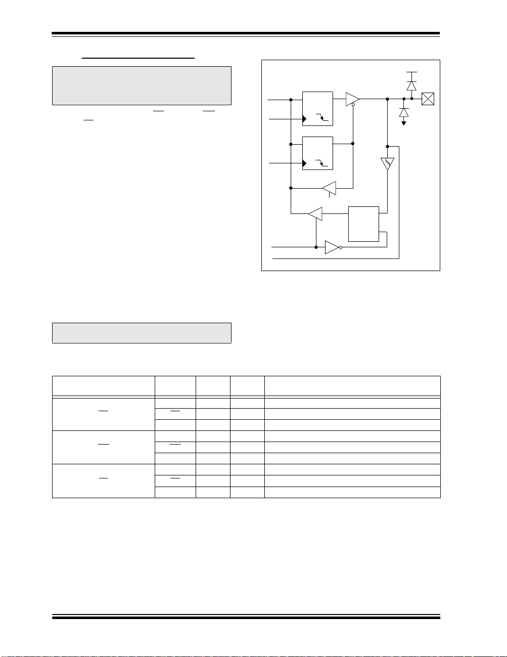
PIC16C745/765
5.5 PORTE and TRISE Registers
Note 1: The PIC16C745 does not provide
PORTE. The PORTE and TRISE registers
are reserved. Always maintain these bits
clear.
PORTE has three pins, RE0/RD/AN5, RE1/WR/AN6
and RE2/CS
inputs or outputs. These pins have Schmitt Trigger
input buffers.
I/O PORTE becomes control inputs for the microprocessor port when bit PSPMODE (TRISE<4>) is set. In
this mode, the user must make sure that the
TRISE<2:0> bits are set (pins are configured as digital
inputs) and that register ADCON1 is configured for digital I/O. In this mode, the input buffers are TTL.
Register 5-1 shows the TRISE register, which also controls the parallel slave port operation.
PORTE pins may be multiplexed wi th analog inputs
(PIC16C765 only). The operation of these pins is
selected by control bits in the ADCON1 register. When
selected as an analog input, these pins will read as ’0’s.
TRISE controls the direction of the RE pins, even when
they are being used as analog inputs. The user must
make sure to keep the pins configured as inputs when
using them as analog inputs.
TRISE bits are used to control the parallel slave port.
Note: On a Power-on Reset, these pins are con-
/AN7, which are individually configured as
figured as analog inputs.
FIGURE 5-7: PORTE BLOCK DIA GRAM
VDD
Data
Bus
WR
Port
WR
TRIS
RD Port
To A/D Converter
QD
CK
Data Latch
QD
CK
TRIS Latch
RD TRIS
Schmitt
Trigger
Input
Buffer
QD
EN
EN
I/O pin
TABLE 5-9: PORTE
Name Function
/AN5
RE0/RD
RE1/WR/AN6
RE2/CS/AN7
Legend: OD = open drain, ST = Schmitt Trigger
Note 1: PIC16C765 only.
DS41124C-page 38 Preliminary 2000 Microchip Technology Inc.
(1)
FUNCTIONS
Input
Type
RE0 ST CMOS Bi-directional I/O
RD TTL — Parallel Slave Port Control Input
AN5 AN — A/D Input
RE1 ST CMOS Bi-directional I/O
WR TTL — Parallel Slave Port Control Input
AN6 AN — A/D Input
RE2 ST CMOS Bi-directional I/O
CS TTL — Parallel Slave Port Data Input
AN7 AN — A/D Input
Output
Type
(1)
(1)
(1)
Description
(1)
(1)
(1)
(1)
(1)
(1)

PIC16C745/765
REGISTER 5-1: PORTE DATA DIRECTION CONTROL REGISTER
R-0 R-0 R/W-0 R/W-0 U-0 R/W-1 R/W-1 R/W-1
IBF OBF IBOV PSPMODE
bit7 bit0
bit 7 : IBF: Input Buffer Full Status bit
1 = A word has been received and is waiting to be read by the CPU
0 = No word has been received
bit 6: OBF: Output Buffer Full Status bit
1 = The output buffer still holds a previously written word
0 = The output buffer has been read
bit 5: IBOV: Input Buffer Overflow Detect bit (in microprocessor mode)
1 = A write occurred when a previously input word has not been read (must be cleared in software)
0 = No overflow occurred
bit 4: PSPMODE: Parallel Slave Port Mode Select bit
1 = Parallel slave port mode
0 = General purpose I/O mode
bit 3: Unimplemented: Read as '0'
PORTE Data Direction Bits
bit 2: TRISE2: Direction Control bit for pin RE2/CS/AN7
1 = Input
0 = Output
bit 1: TRISE1: Direction Control bit for pin RE1/WR
1 = Input
0 = Output
bit 0: TRISE0: Direction Control bit for pin RE0/RD
1 = Input
0 = Output
— TRISE2 TRISE1 TRISE0 R = Readable bit
/AN6
/AN5
(1)
(TRISE: 89h)
W = Writable bit
U = Unimplemented bit,
- n = Value at POR reset
read as ‘0’
Note 1: PIC16C765 only.
TABLE 5-10: SUMMARY OF REGISTERS ASSOCIATED WITH PORTE
Address Name Bit 7 Bit 6 Bit 5 Bit 4 Bit 3 Bit 2 Bit 1 Bit 0
(1)
09h
89h
9Fh ADCON1
Legend: x = unknown, u = unchanged, - = unimplemented read as '0'. Shaded cells are not used by PORTE.
2000 Microchip Technology Inc. Preliminary DS41124C-page 39
PORTE
TRISE
Note 1: PIC16C765 only.
— — — — — RE2 RE1 RE0 ---- -xxx ---- -uuu
(1)
IBF OBF IBOV PSPMODE — PORTE Data Direction Bits 0000 -111 0000 -111
— — — — — PCFG2 PCFG1 PCFG0 ---- -000 ---- -000
Value on:
POR,
BOR
Value on all
other resets

PIC16C745/765
5.6 Parallel Slave Port (PSP)
Note: The PIC16C745 does not provi de a paral-
lel slave port. The PORTD, PORTE, TRISD
and TRISE registers are reserved. Always
maintain these bits clear.
PORTD operates as an 8-bit wide Parallel Slave Port
(PSP), or microprocessor port when control bit PSPMODE (TRISE<4>) is set. In slave mode, it is asynchronously readable and writable by the external world
through RD
control input pin RE1/WR/AN6.
It can directly interface to an 8-bit microprocessor data
bus. The external microprocessor can read or write t he
PORTD latch as an 8-bit latch. Setting bit PSPMODE
enables port p in RE0/RD
WR
the CS
corresponding data direction bits of the TRISE register
(TRISE<2:0>) m ust be c onfigured as inpu ts (set) and
the A/D port configuration bits PCFG<2:0>
(ADCON1<2:0> ) must be se t, whic h will config ure pins
RE<2:0> as digital I/O.
There are actually two 8-bit latches; one fo r data-out
(from the PICmicro
input. The user writes 8-bit data to PORTD data latch
and reads data from the port pin latch (note that they
have the same address). In this mode, the TRISD register is ignored, since the microprocessor is controlling
the direction of data flow.
A write to the PSP occurs when both the CS
lines are first detected low. When either the CS or WR
lines become high (level triggered), then the Input
Buffer Full (IBF) status flag bit (TRISE<7>) is set on the
Q4 clock cycle, following the next Q2 cycle, to signal
the write is complete (Figure 5-9). The interrupt flag bit
PSPIF (PIR1<7>) is also set on the same Q4 clock
cycle. IBF can only be cleared by rea ding the PORTD
input latch. The Input Buffer Overflow (IBOV) status
flag bit (TRISE<5>) is set if a second write to the PSP
is attempted when the previous byte has not been read
out of the buffer.
A read from the PSP occurs when both the CS
lines are first detected low. The Output Buffer Full
(OBF) status flag bit (TRISE<6>) is cleared immediately (Figure 5-10) indicating that the PORTD latch is
waiting to be read by the external bus. When either the
CS
rupt flag bit PSPIF is set on the Q4 clock cycle, following the next Q2 cycle, indicating that the read is
complete. OBF remains low until data is written to
PORTD by the user firmware.
When not in PSP mode, the IBF and OBF bits are held
clear. However, if flag bit IBOV was previously set, it
must be cleared in firmware.
control input pin RE0/RD/AN5 and WR
/AN5 to be the RD input, RE1/
/AN6 to be the WR input and RE2/CS/AN7 to be
(chip select) input. For this functionality, the
®
microcontroller) and one for data
and WR
and RD
or RD pin becomes high (level triggered), the inter-
An interrupt is generated and latched into flag bit
PSPIF when a read or write operation is completed.
PSPIF must be cleared by the user in firmware and the
interrupt can be disabled by clearing the interrupt
enable bit PSPIE (PIE1<7>).
FIGURE 5-8: PORTD AND PORTE BLOCK
DIAGRAM (PARALLEL SLAVE
PORT)
VDD
Data Bus
WR
Port
RD
Port
One bit of PORTD
Set interrupt flag
PSPIF (PIR1<7>)
QD
CK
QD
EN
EN
TTL
Read
Chip Select
Write
TTL
TTL
TTL
RD
CS
WR
RDx
pin
DS41124C-page 40 Preliminary 2000 Microchip Technology Inc.

FIGURE 5-9: PARALLEL SLAVE PO RT WRITE WAVEFORMS
Q1 Q2 Q3 Q4CSQ1 Q2 Q3 Q4 Q1 Q2 Q3 Q4
WR
RD
PORTD<7:0>
IBF
OBF
PSPIF
FIGURE 5-10: PARALLEL SLAVE PORT READ WAVEFORMS
Q1 Q2 Q3 Q4CSQ1 Q2 Q3 Q4 Q1 Q2 Q3 Q4
WR
RD
PIC16C745/765
PORTD<7:0>
IBF
OBF
PSPIF
TABLE 5-11: REGISTERS ASSOCIATED WITH PARALLEL SLAVE PORT
Address Name Bit 7 Bit 6 Bit 5 Bit 4 Bit 3 Bit 2 Bit 1 Bit 0
(2)
08h PORTD
09h PORTE
89h TRISE
0Ch PIR1 PSPIF
8Ch PIE1 PSPIE
9Fh ADCON1
0Bh INTCON GIE PEIE T0IE INTE RBIE T0IF INTF RBIF 0000 000x 0000 000u
Legend: x = unknown, u = unchanged, - = unimplemented read as '0'. Shaded cells are not used by the Parallel Slave Port.
Note 1: Bit s PSPI E and PSP IF are reserv ed on the PIC 16C 74 5. Always mainta in the se bits clea r.
2: PIC16C765 only.
2000 Microchip Technology Inc. Preliminary DS41124C-page 41
Port data latch when written: Port pins when read xxxx xxxx uuuu uuuu
(2)
— — — — — RE2 RE1 RE0 ---- -xxx ---- -uuu
(2)
IBF OBF IBOV PSPMODE — PORTE Data Direction Bits 0000 -111 0000 -111
(1)
ADIF RCIF TXIF USBIF CCP1IF TMR2IF TMR1IF 0000 0000 0000 0000
(1)
ADIE RCIE TXIE USBIE CCP1IE TMR2IE TMR1IE 0000 0000 0000 0000
— — — — — PCFG2 PCFG1 PCFG0 ---- -000 ---- -000
Value on:
POR,
BOR
Value on all
other resets

PIC16C745/765
NOTES:
DS41124C-page 42 Preliminary 2000 Microchip Technology Inc.

PIC16C745/765
6.0 TIMER0 MODULE
The Timer0 module timer/counter has the following features:
• 8-bit timer/counter
• Readable and writable
• 8-bit software programmable prescaler
• Internal or external clock select
• Interrupt-on-overflow from FFh to 00h
• Edge select for external clock
Figure 6-1 is a block diagram of the Timer0 modu le and
the prescaler shared with the WDT.
Additional information on the Timer0 module is available in the PICmicro™ Mid-Range MCU Family Reference Manual (DS33023).
Timer mode is selected by clearing bit T0CS
(OPTION_REG<5>). In timer mode, the Timer0 module will increment every instruction cycle (without prescaler). If the TMR0 register is written , the increm ent is
inhibited for the following two instruction c ycles. The
user can work around this by writing an adjusted value
Counter mode is selected by setting bit T0CS
(OPTION_REG<5>). In counter mode, Timer0 will
increment either on every rising or falling edge of pin
RA4/T0CKI. The incrementing edge is determ ined by
the Timer0 Source Edge Select bit T0SE
(OPTION_REG<4>). Clearing bit T0SE selects the rising edge. Restrictions on the external c lock input are
discussed in detail in Section 6.2.
The prescaler is mutually exclusively s hared between
the Timer0 module and the watchdog timer. The prescaler is not readable or writable. Section 6.3 details the
operation of the prescaler.
6.1 Timer0 Interrupt
The TMR0 interrupt is ge nerated w hen the TMR 0 register overflows from FFh to 00h. This overflow sets bit
T0IF (INTCON<2>). The interrupt can be masked by
clearing bit T0IE (INTCON<5>). Bit T0IF must be
cleared in software by the Timer0 module interrupt service routine before re-enabling this interrupt. The
TMR0 interrupt cannot awaken the processor from
SLEEP, since the timer is shut off during SLEEP.
to the TMR0 register.
FIGURE 6-1: BLOCK DIAGRAM OF THE TIMER0/WDT PRESCALER
F
INT
RA4/T0CKI
Pin
T0SE
0
1
TOCS
M
U
X
1
M
U
0
X
PSA
PRESCALER
SYNC
2
Cycles
Data Bus
TMR0 reg
8
Set flag bit T0IF
on Overflow
0
M
U
1
Watchdog
Timer
WDT Enable bit
Note: T0CS, T0SE, PSA, PS<2:0> are (OPTION_REG<5:0>).
2000 Microchip Technology Inc. Preliminary DS41124C-page 43
X
PSA
8-bit Prescaler
8
8 - to - 1MUX
0
M U X
WDT
Time-out
PS<2:0>
1
PSA
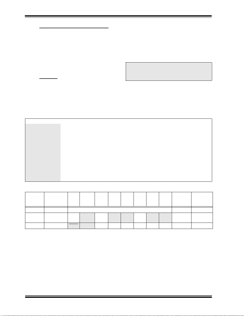
PIC16C745/765
6.2 Using Timer0 with an External Clock
When no prescaler is used, the external clock input is
the same as the prescaler output. The synchronization
of T0CKI with the internal phase clocks is accomplished by sampling the prescaler output on the Q2 and
Q4 cycles of the internal phase clocks. Therefore, it is
necessary for T0CKI to be high for at least 2Tosc (and
a small RC delay of 20 ns) and low for at least 2Tosc
(and a small RC delay of 20 ns). Refer to the electrical
The PSA and PS<2:0> bits (OPTION_REG<3:0>) determine the prescaler assignment and prescale ratio.
When assigned to the Timer0 module, all instructions
writing to the TMR0 register (e.g. CLRF
BSF
1,x....etc.) will clear the prescaler. When assigned
to WDT, a CLRWDT instruction will clear the prescaler
along with the watchdog timer. The prescaler is not
readable or writable.
Note: Writing to TMR0, when the prescaler is
specification of the desired device.
6.3 Prescaler
There is only one prescaler available which is mutually
exclusively shared between the Timer0 module and the
watchdog timer. A prescaler assignment for the Timer0
module means that there is no prescaler for the watchdog timer, and vice-versa. This prescaler is not readable
or writable (see Fig ure6-1).
To avoid an unintended device RESET, the following
instruction sequence (shown in Example 6-1) must be
executed when changing the prescaler assignment
from Timer0 to the WDT. This sequence must be followed even if the WDT is disabled.
EXAMPLE 6-1: CHANGING PRESCALER (TIMER0→WDT)
Lines 2 and 3 do
NOT have to be
included if the final
desired prescale
value is other than
1:1. If 1:1 is the final
desired value, then a
temporary prescale
value is set in lines 2
and 3 and the final
prescale value will
be set in lines 10
and 11.
1) BSF STATUS, RP0 ;Bank1
2) MOVLW b’xx0x0xxx’ ;Select clock source and prescale value of
3) MOVWF OPTION_REG ;other than 1:1
4) BCF STATUS, RP0 ;Bank0
5) CLRF TMR0 ;Clear TMR0 and prescaler
6) BSF STATUS, RP1 ;Bank1
7) MOVLW b’xxxx1xxx’ ;Select WDT, do not change prescale value
8) MOVWF OPTION_REG ;
9) CLRWDT ;Clears WDT and prescaler
10) MOVLW b’xxxx1xxx’ ;Select new prescale value and WDT
11) MOVWF OPTION_REG ;
12) BCF STATUS, RP0 ;Bank0
1, MOVWF 1,
assigned to Timer0, will clear the prescaler
count, but will not change the prescaler
assignment.
TABLE 6-1: REGISTERS ASSOCIATED WITH TIMER0
Address Name Bit 7 Bit 6 Bit 5 Bit 4 Bit 3 Bit 2 Bit 1 Bit 0
01h,101h TMR0 Timer0 module’s register xxxx xxxx uuuu uuuu
0Bh,8Bh,
10Bh,18Bh
81h,181h OPTION_REG
Legend: x = unknown, u = unchanged, - = unimplemented locations read as '0'. Shaded cells are not used by Timer0.
DS41124C-page 44 Preliminary 2000 Microchip Technology Inc.
INTCON GIE
RBPU INTEDG T0CS T0SE PSA PS2 PS1 PS0 1111 1111 1111 1111
PEIE T0IE INTE RBIE T0IF INTF RBIF 0000 000x 0000 000u
Value on:
POR,
BOR
Value on all
other resets

PIC16C745/765
7.0 TIMER1 MODULE
The Timer1 module is a 16-bit timer/counter consisting
of two 8-bit registers (TMR1H and TMR1L) , which are
readable and writable. The TMR1 Register pair
(TMR1H:TMR1L) increments from 0000h to FFFFh
and rolls over to 0000h. The TMR1 interrupt, if enabled,
is generated on overflow, which is latched in interrupt
flag bit TMR1IF (PIR1<0>). This interrupt can be
enabled/disabled by setting/clearing TMR1 interrupt
enable bit TMR1IE (PIE1<0>).
Timer1 can operate in one of two modes:
• As a timer
• As a counter
The operating mode is determined by the clock select
bit, TMR1CS (T1CON<1>).
In timer mode, Timer1 increments every instruction
cycle. In counter mode, it increments on every rising
edge of the external clock input.
Timer1 can be enabled/disabled by setting/clearing
control bit TMR1ON (T1CON<0>).
Timer1 also has an internal “RESET input”. This
RESET can be generated by either of the two CCP
modules (Section 9.0) . Register 7-1 shows the Timer1
control register.
When the Timer1 oscillator is enabled (T1OSCEN is
set), the RC1/T1OSI/CCP2 and RC0/T1OSO/T1CKI
pins become inputs. That is, the TRISC <1:0> value is
ignored.
Additional information on timer modules is available in
the PICmicro™ Mid-Range MCU Family Reference
Manual (DS33023).
REGISTER 7-1: TIMER1 CONTROL REGISTER (T1CON: 10h)
U-0 U-0 R/W-0 R/W-0 R/W-0 R/W-0 R/W-0 R/W-0
— — T1CKPS1 T1CKPS0 T1OSCEN T1SYNC TMR1CS TMR1ON
bit7 bit0
bit 7-6: Unimplemented: Read as '0'
bit 5-4: T1CKPS<1:0>: Timer1 Input Clock Prescale Select bits
11 = 1:8 Prescale value
10 = 1:4 Prescale value
01 = 1:2 Prescale value
00 = 1:1 Prescale value
bit 3: T1OSCEN: Timer1 Oscillator Enable Control bit
1 = Oscillator is enabled
0 = Oscillator is shut off (The oscillator inverter is turned off to eliminate power drain)
bit 2: T1SYNC
bit 1: TMR1CS: Timer1 Clock Source Select bit
bit 0: TMR1ON: Timer1 On bit
: Timer1 External Clock Input Synchronization Control bit
MR1CS = 1
T
1 = Do not synchronize external clock input
0 = Synchronize external clock input
MR1CS = 0
T
This bit is ignored. Timer1 uses the internal clock when TMR1CS = 0.
1 = External clock from pin RC0/T1OSO/T1CKI
0 = Internal clock (F
1 = Enables Timer1
0 = Stops Timer1
INT)
(1)
or RC1/T1OSI/CCP2
R = Readable bit
W = Writable bit
U = Unimplemented bit,
read as ‘0’
- n = Value at POR reset
Note 1: On the rising edge after the first falling edge.
2000 Microchip Technology Inc. Preliminary DS41124C-page 45

PIC16C745/765
7.1 Timer1 Operation in Timer Mode
Timer mode is selected by clearing the TMR1CS
(T1CON<1>) bit. In this mode, the input clock to the
timer is F
INT. The synchronize control bit T1SYNC
(T1CON<2>) has no effect since the internal clock is
always in sync.
FIGURE 7-1: TIMER1 BLOCK DIAGRAM
Set flag bit
TMR1IF on
Overflow
RC0/T1OSO/T1CKI
RC1/T1OSI/CCP2
TMR1H
T1OSC
TMR1
TMR1L
T1OSCEN
Enable
Oscillator
(1)
Internal
Clock
FINT
7.2 Timer1 Operation in Synchronized Counter Mode
Counter mode is selected by setting bit TMR1CS. In
this mode, the timer increments on every rising edge of
clock input on pin RC1/T1OSI/CCP2, when bit
T1OSCEN is set, or on pin RC0/T1OSO /T1CKI, when
bit T1OSCEN is cleared.
If T1SYNC
synchronized with internal phase clocks. The syn chronization is done after the prescaler stage. The prescaler stage is an asynchronous ripple-counter.
In this configuration, during SLEEP mode, Timer1 will
not increment even if the external clock is present,
since the synchronization circuit is shut off. The prescaler however will continue to increment.
TMR1ON
on/off
1
0
TMR1CS
is cleared, then the external clock input is
0
1
T1SYNC
Prescaler
1, 2, 4, 8
T1CKPS<1:0>
2
Synchronized
clock input
Synchronize
det
SLEEP input
Note 1: When the T1OSCEN bit is cleared, the inverter is turned off. This eliminates power drain.
DS41124C-page 46 Preliminary 2000 Microchip Technology Inc.

PIC16C745/765
7.3 Timer1 Operation in Asynchronous Counter Mode
If control bit T1SYNC (T1CON<2>) is set, the external
clock input is not synchronized. The timer continues to
increment asynchronous to the internal phase clocks.
The timer will continue to run during SLEEP and can
generate an interrupt-on-overflow, which will wake-up
the processor. However, special precautions in software are needed to read/write the timer (Section 7.3.1).
In asynchronous counter mode, T imer1 can not be used
as a time-base for capture or compare operations.
7.3.1 READING AND WRITING TIMER1 IN ASYNCHRONOUS COUNTER MODE
Reading TMR1H or TMR1L while the t imer is running
from an external asynchronous clock wil l guarantee a
valid read (taken care of in har dware). However, the
user should keep in mind that reading the 16-bit timer
in two 8-bit values itself poses certain problems, since
the timer may overflow between the rea ds.
For writes, it is recommended that the user simply stop
the timer and write the desired v alues. A write con tention may occur by writing to the timer registers, whi le
the register is incrementing. This may produce an
unpredictable value in the timer register.
Reading the 16 -bi t val u e requires some care. Example s
12-2 and 12-3 in th e PICm icro™ Mi d-Ra nge MCU Family Reference Manual (DS33023) show how to read and
write Timer1 when it is running in asynchronous mode.
7.4 Timer1 Oscillator
A crystal oscillator circuit is built-in between pins T1OSI
(input) and T1OSO (amplifier output). It is enabled by
setting control bit T1OSCEN (T1CON<3>). The oscillator is a low power oscillator r ated up to 200 k H z. It wi ll
continue to run during SLEEP. It is primarily intended
for use with a 32 kHz crystal. Table 7-1 shows the
capacitor selection for the Timer1 oscillator.
TABLE 7-1: CAPACITOR SELECTION FOR
THE TIMER1 OSCILLATOR
Osc Type Freq C1 C2
LP 32 kHz 33 pF 33 pF
100 kHz 15 pF 15 pF
200 kHz 15 pF 15 pF
These values are for design guidance only.
Crystals Tested:
32.768 kHz Epson C-001R32.768K-A ± 20 PPM
100 kHz Epson C-2 100.00 KC-P ± 20 PPM
200 kHz STD XTL 200.000 kHz ± 20 PPM
Note 1: Higher capacitance increases the stability
of oscillator but also increases the start-up
time.
2: Since each resonator/crystal has its own
characteristics, the user should consult the
resonator/crystal manufacturer for appropriate values of external components.
7.5 Resetting Timer1 using a CCP Trigger Output
If the CCP1 or CCP2 module is configured in compare
mode to generate a “special event trigger”
(CCP1M<3:0> = 1011), this signal will reset Timer1.
Note: The special event triggers from the CCP1
and CCP2 modules will not set interrupt
flag bit TMR1IF (PIR1<0>).
Timer1 must be configured for either timer or s ynchronized counter mode to take advanta ge of this feature.
If Timer1 is running in asynchronous counter mode, this
RESET operation may not work.
In the event that a write to Timer1 coincides with a special event trigger from CCP1 or C CP2, the write will
take precedence.
In this mode of operation, the CCPRxH:CCPRxL register pair effectively becomes the period register for
Timer1.
7.6 Resetting of Timer1 Register Pair (TMR1H, TMR1L)
TMR1H and TMR1L registers are not reset to 00h on a
POR or any other RESET except by the CCP1 and
CCP2 special event triggers.
T1CON register is reset to 00h on a Power-on Reset or
a Brown-out Reset, which shuts off the timer and
leaves a 1:1 prescale. In all other RESETS, the register
is unaffected.
7.7 Timer1 Prescaler
The prescaler counter is cleared on writes to the
TMR1H or TMR1L registers.
2000 Microchip Technology Inc. Preliminary DS41124C-page 47

PIC16C745/765
TABLE 7-2: REGISTERS ASSOCIATED WITH TIMER1 AS A TIMER/COUNTER
Address Name Bit 7 Bit 6 Bit 5 Bit 4 Bit 3 Bit 2 Bit 1 Bit 0
0Bh,8Bh,
10Bh,
18Bh
0Ch PIR1
8Ch PIE1
0Eh TMR1L Holding register for the Least Significant Byte of the 16-bit TMR1 register xxxx xxxx uuuu uuuu
0Fh TMR1H Holding register for the Most Significant Byte of the 16-bit TMR1 register xxxx xxxx uuuu uuuu
10h T1CON
Legend: x = unknown, u = unchanged, - = unimplemented read as '0'. Shaded cells are not used by the Timer1 module.
Note 1: Bits PSPIE and PSPIF are reserved on the PIC16C745; always maintain these bits clear.
INTCON GIE PEIE
(1)
PSPIF
(1)
PSPIE
— — T1CKPS1 T1CKPS0 T1OSCEN T1SYNC TMR1CS TMR1ON --00 0000 --uu uuuu
T0IE INTE RBIE T0IF INTF RBIF 0000 000x 0000 000u
ADIF RCIF TXIF USBIF CCP1IF TMR2IF TMR1IF 0000 0000 0000 0000
ADIE RCIE TXIE USBIE CCP1IE TMR2IE TMR1IE 0000 0000 0000 0000
Value on:
POR,
BOR
Value on
all other
resets
DS41124C-page 48 Preliminary 2000 Microchip Technology Inc.

PIC16C745/765
8.0 TIMER2 MODULE
Timer2 is an 8-bit timer with a prescaler and a
postscaler. It can be used as the PWM time-base for
the PWM mode of the CCP module(s). The TMR2 register is readable and writable, and is cleared on any
device RESET.
The input clock (F
1:4 or 1:16, selected by control bits T2CKPS<1:0>
(T2CON<1:0>).
The Timer2 module has an 8-bit perio d register PR2.
Timer2 increments from 00h until it matches PR2 and
INT/4) has a prescale o ption of 1:1,
8.1 Timer2 Prescaler and Postscaler
The prescaler and postscaler counters are cleared
when any of the following occurs:
• a write to the TMR2 register
• a write to the T2CON register
• any device RESET (POR, MCLR
Reset or BOR)
TMR2 is not cleared when T2CON is written.
FIGURE 8-1: TIMER2 BLOCK DIAGRAM
then resets to 00h on the next increment cycle. PR2 is
a readable and writable register. The PR2 register is
initialized to FFh upon RESET.
Sets flag
bit TMR2IF
The match output of TMR2 goes through a 4-bit
postscaler (which gives a 1:1 to 1:16 scaling inclusive)
to generate a TMR2 interrupt (latched in flag bit
TMR2IF, (PIR1<1>)).
Timer2 can be shut off by clearing control bit TMR2ON
Postscaler
1:1 1:16
(T2CON<2>) to minimize power consumption.
Register 8-1 shows the Timer2 control register.
T2OUTPS<3:0>
Additional information on timer modul es is a vailable in
the PICmicro™ Mid-Range MCU Family Reference
Manual (DS33023).
REGISTER 8-1: TIMER2 CONTROL REGISTER (T2CON: 12h)
Reset, WDT
TMR2
output
RESET
TMR2 reg
EQ
Comparator
PR2 reg
to
4
Prescaler
1:1, 1:4, 1:16
2
T2CKPS<1:0>
F
INT
U-0 R/W-0 R/W-0 R/W-0 R/W-0 R/W-0 R/W-0 R/W-0
— TOUTPS3 TOUTPS2 TOU TPS 1 TOUTPS0 TMR2ON T2CKPS1 T2CKPS0 R = Readable bit
bit7 bit0
bit 7: Unimplemented: Read as '0'
bit 6-3: TOUTPS<3:0>: Timer2 Output Postscale Select bits
0000 = 1:1 Postscale
0001 = 1:2 Postscale
0010 = 1:3 Postscale
•
•
•
1111 = 1:16 Postscale
bit 2: TMR2ON: Timer2 On bit
1 = Timer2 is on
0 = Timer2 is off
bit 1-0: T2CKPS<1:0>: Timer2 Clock Prescale Select bits
00 = Prescaler is 1
01 = Prescaler is 4
1x = Prescaler is 16
2000 Microchip Technology Inc. Preliminary DS41124C-page 49
W= Writable bit
U = Unimplemente d bit,
read as ‘0’
- n = Value at POR reset

PIC16C745/765
TABLE 8-1: REGISTERS ASSOCIATED WITH TIMER2 AS A TIMER/COUNTER
Address Name Bit 7 Bit 6 Bit 5 Bit 4 Bit 3 Bit 2 Bit 1 Bit 0
0Bh,8Bh,
10Bh,18Bh
0Ch PIR1
8Ch PIE1
11h TMR2 Timer2 module’s register
12h T2CON
92h PR2 Timer2 Period Register
Legend: x = unknown, u = unchanged, - = unimplemented read as '0'. Shaded cells are not used by the Timer2 module.
Note 1: Bits PSPIE and PSP IF are reserved on the PIC 16 C7 4 5; al wa y s maint ai n th es e bi ts cl ea r.
INTCON GIE PEIE
(1)
PSPIF
PSPIE
ADIF RCIF TXIF USBIF CCP1IF TMR2IF TMR1IF
(1)
ADIE RCIE TXIE USBIE CCP1IE TMR2IE TMR1IE
— TOUTPS3 TOUTPS2 TOUTPS1 TOUTPS0 TMR2ON T2CKPS1 T2CKPS0
T0IE INTE RBIE T0IF INTF RBIF
Value on:
POR,
BOR
0000 000x 0000 000u
0000 0000 0000 0000
0000 0000 0000 0000
0000 0000 0000 0000
-000 0000 -000 0000
1111 1111 1111 1111
Value on
all other
resets
DS41124C-page 50 Preliminary 2000 Microchip Technology Inc.

PIC16C745/765
9.0 CAPTURE/COMPARE/PWM MODULES
Each Capture/Compare/PWM (CCP) mo dule contains
a 16-bit register which can operate as a:
• 16-bit capture register
• 16-bit compare register
• PWM master/slave Duty Cycle register
Both the CCP1 and CCP2 modules are identical in
operation, with the exception being the operation of the
special event trigger. Table 9-1 and T able9-2 show the
resources and interactions of the CCP module(s). In
the following sections, the operation of a CCP module
is described with respect to CCP1. CCP2 operates the
same as CCP1, except where noted.
CCP1
Module:
Capture/Compare/PWM Register1 (CCPR1) is comprised of two 8-bit registers: CCPR1L (low byte) and
CCPR1H (high byte). The CCP1CON register controls
the operation of CCP1. The special event trigger is
generated by a compare match and will reset Timer1.
CCP2 Module:
Capture/Compare/PWM Register1 (CCPR2) is comprised of two 8-bit registers: CCPR2L (low byte) and
CCPR2H (high byte). The CCP2CON register cont rols
the operation of CCP2. The special event trigger is
generated by a compare match and will reset Timer1
and start an A/D conversion (if the A/D module is
enabled).
Additional information on CCP modules is available in
the PICmicro™ Mid-Range MCU Family Reference
Manual (DS33023) and in “Using the CCP Modu les”
(AN594).
TABLE 9-1: CCP MODE - TIMER
RESOURCES REQUIRED
CCP Mode Timer Resource
Capture
Compare
PWM
TABLE 9-2: INTERACTION OF TWO CCP MODULES
CCPx Mode CCPy Mode Interaction
Capture Capture Same TMR1 time-base.
Capture Compare The compare should be configured for the special event trigger, which clears TMR1.
Compare Compare The compare(s) should be configured for the special event trigger, which clears TMR1.
PWM PWM The PWMs will have the same frequency and update rate (TMR2 interrupt).
PWM Capture None.
PWM Compare None.
Timer1
Timer1
Timer2
2000 Microchip Technology Inc. Preliminary DS41124C-page 51

PIC16C745/765
REGISTER 9-1: CAPTURE/COMPARE/PWM CONTROL REGISTER
(CCP1CON: 17H, CCP2CON: 1Dh)
U U R/W-0 R/W-0 R/W-0 R/W-0 R/W-0 R/W-0
— — DCnB1 DCnB0 CCPnM3 CCPnM2 CCPnM1 CCPnM0 R = Readable bit
bit7 bit0
bit 7-6: Unimplemented: Read as '0'
bit 5-4: DCnB<1:0>: PWM Least Significant bits
Capture Mode: Unused
Compare Mode: Unused
PWM Mode: These bits are the two LSbs of the PWM duty cycle. The eight MSbs are found in CCPRnL.
bit 3-0: CCPnM<3:0>: CCPx Mode Select bits
0000 = Capture/Compare/PWM off (resets CCPn module)
0100 = Capture mode, every falling edge
0101 = Capture mode, every rising edge
0110 = Capture mode, every 4th rising edge
0111 = Capture mode, every 16th rising edge
1000 = Compare mode, set output on match (CCPnIF bit is set)
1001 = Compare mode, clear output on match (CCPnIF bit is set)
1010 = Compare mode, generate software interrupt on match (CCPnIF bit is set, CCPn pin is unaffected)
1011 = Compare mode, trigger special event (CCPnIF bit is set; CCPn resets TMR1or TMR3)
11xx = PWM mode
W = Writable bit
U = Unimplemented bit,
read as ‘0’
- n = Value at POR reset
DS41124C-page 52 Preliminary 2000 Microchip Technology Inc.

PIC16C745/765
9.1 Capture Mode
In Capture mode, CCPR1H:CCPR1L captures the
16-bit value of the TMR1 register when an event occurs
on pin RC2/CCP1. An event is defin ed as:
• Every falling edge
• Every rising edge
• Every 4th rising edge
• Every 16th rising edge
An event is selected by control bits CCP1M<3:0>
(CCP1CON<3:0>). When a capture is made, the interrupt request flag bit CCP1IF (PIR1<2>) is set. The
interrupt flag must be cleared in softw are. If another
capture occurs before the value i n register CCPR1 is
read, the old captured value will be lost.
9.1.1 CCP PIN CONFIGURATION
In Capture mode, the RC2/CCP1 pin should be configured as an input by setting the TRISC<2> bit.
Note: If the RC2/CCP1 pin is configured as an
output, a write to the port can cause a capture condition.
FIGURE 9-1: CAPTURE MODE OPERATION
BLOCK DIAGRAM
Set flag bit CCP1IF
(PIR1<2>)
CCP1CON<3:0>
CCPR1H CCPR1L
Capture
Enable
TMR1H TMR1L
RC2/CCP1
Pin
Prescaler
÷ 1, 4, 16
and
edge detect
Q’s
9.1.2 TIMER1 MODE SELECTION Timer1 must be running in timer mode or synchronized
counter mode for the CCP module to use the ca pture
feature. In asynchronous counter mode, the capture
operation may not work.
9.1.3 SOFTWARE INTERRUPT When the capture mode is changed, a false capture
interrupt may be generated. The user shou ld keep bit
CCP1IE (PIE1<2>) clear to avoid false interrupts and
should clear the flag bit CCP1IF fol lowing any such
change in operating mode.
9.1.4 CCP PRESCALER There are four prescaler settings, specified by bits
CCP1M<3:0>. Whenever the CC P module is turned
off, or the CCP module is not in capture mode, the prescaler counter is cleared. Any RESET will clear the prescaler counter.
Switching from one capture prescaler to anot her may
generate an interrupt. Also, the prescaler counter will
not be cleared, therefore, the first capture may be from
a non-zero prescaler. Example 9-1 shows the recommended method for switching between capture prescalers. This example also clears the prescale r counter
and will not generate the “false” interrupt.
EXAMPLE 9-1: CHANGING BETWEEN
CAPTURE PRESCALE RS
CLRF CCP1CON ;Turn CCP module off
MOVLW NEW_CAPT_PS ;Load the W reg with
; the new precscaler
; move value and CCP ON
MOVWF CCP1CON ;Load CCP1CON with this
; value
2000 Microchip Technology Inc. Preliminary DS41124C-page 53

PIC16C745/765
9.2 Compare Mode
In Compare mode, the 16-bit CCPR1 register value is
constantly compared against the TMR1 r egister pair
value. When a match occurs, the RC2/CCP1 pin is:
• Driven high
• Driven low
• Remains unchanged
The action on the pin is based on the value of contr ol
bits CCP1M<3:0> (CCP1CON<3:0>). At the same
time, interrupt flag bit CCP1IF is set.
FIGURE 9-2: COMPARE MODE OPERATION
BLOCK DIAGRAM
Special event trigger will:
reset Timer1, but not set interrupt flag bit TMR1IF (PIR1<0>),
and set bit GO/DO NE
RC2/CCP1
Pin
TRISC<2>
Output Enable
9.2.1 CCP PIN CONFIGURATION The user must configure the RC2/CCP1 pin as an out-
put by clearing the TRISC<2> bit.
Note: Clearing the CCP1CON register will force
the RC2/CCP1 compare output latch to the
default low level. This is not the data latch.
9.2.2 TIMER1 MODE SELECTION Timer1 must be running in Timer mode or Synchro-
nized Counter mode if the CCP module is using the
compare feature. In Asynchronous Counter mode, the
compare operation may not work.
9.2.3 SOFTWARE INTERRUPT MODE When Generate Software Interrupt mode is chosen, the
CCP1 pin is not affected. The CCPIF bit is set causing
a CCP interrupt (if enabled).
9.2.4 SPECIAL EVENT TRIGGER
In this mode, an internal hardware trigger is generated,
which may be used to initiate an action.
The special event trigger output of CCP1 resets the TMR1
register pair. This al lows the CCPR1 register to ef fectively
be a 16-bit programmable period register for Timer1.
(ADCON0<2>).
Special Event Trigger
QS
Output
Logic
R
CCP1CON<3:0>
Mode Select
Set flag bit CCP1IF
(PIR1<2>)
CCPR1H CCPR1L
match
TMR1H TMR1L
Comparator
The special event trigger output of CCP2 starts an A/D
conversion (if the A/D module is on) and resets the
TMR1 register pair and starts an A/D conversion (if the
A/D module is enabled).
Note: The special event trigger from the
CCP1and CCP2 modules will not set interrupt flag bit TMR1IF (PIR1<0>).
9.3 PWM Mode (PWM)
In pulse width modulation mode, the C CPx pin produces up to a 10-bit resolution PWM output. Since the
CCP1 pin is multiplexed with the PORTC data latch, the
TRISC<2> bit must be cleare d to make the CCP1 pin
an output.
Note: Clearing the CCP1CON register wi ll force
the CCP1 PWM output latch to the default
low level. Th is is n ot the PO RTC I/O d ata
latch.
Figure 9-3 shows a simplified block diagram of the
CCP module in PWM mode.
For a step by step procedure on how to set up the CCP
module for PWM operation, see Section 9.3.3.
FIGURE 9-3: SIMPLIFIED PWM BLOCK
DIAGRAM
Duty Cycle Registers
CCPR1L
CCPR1H (Slav e)
Comparator
TMR2
Comparator
Note 1: 8-bit timer is concatenated with 2-bit internal Q clock
(Note 1)
PR2
or 2 bits of the prescaler to create 10-bit time base.
A PWM output (Figure 9-4) has a time base (period) and
a time that the output stays high (duty cycle). The frequency of the PWM is the inverse of the period (1/period).
CCP1CON<5:4>
Clear Timer,
CCP1 pin and
latch D.C.
Q
R
RC2/CCP1
S
<2>
TRISC
DS41124C-page 54 Preliminary 2000 Microchip Technology Inc.

PIC16C745/765
FIGURE 9-4: PWM OUTPUT
Period
(2)
CCP1
Duty Cycle
(1)
Note 1: At this time, the TMR2 register is equal to the PR2 register.
2: Output signal is shown as asserted high.
9.3.1 PWM PERIOD
The PWM period is specified by writing to the PR2 register. The PWM period can be calculated using the following formula:
PWM period = [(PR2) + 1] • 4 • T
(TMR2 prescale value)
PWM frequency is defined as 1 / [PWM period].
When TMR2 is equal to PR2, the following three events
occur on the next increment cycle:
• TMR2 is cleared
• The CCP1 pin is set (exception: if PWM duty
cycle = 0%, the CCP1 pin will not be set)
• The PWM duty cycle is latched from CCPR1L into
CCPR1H
(1)
OSC •
When the CCPR1H and 2- bit latch match TMR2 concatenated with an internal 2-bit Q clock or 2 bits of the
TMR2 prescaler, the CCP1 pin is cleared.
Maximum PWM resolution (bits) for a given PWM
frequency:
F
INT
Resolution
Note: If the PWM duty cycle value is longer than
the PWM period, the CCP1 pin will not be
cleared.
9.3.3 SET-UP FOR PWM OPERATION The following steps should be taken when configuring
the CCP module for PWM operation:
1. Set the PWM period by writing to the PR2 register.
2. Set the PWM duty cycle by writing to the
CCPR1L register and CCP1CON<5:4> bits.
3. Make the CCP1 pin an output by clearing the
TRISC<2> bit.
4. Set the TMR2 prescale value and enable Timer2
by writing to T2CON.
5. Configure the CCP1 module for PWM operation.
log(
=
FPWM
log(2)
)
bits
Note: The Timer2 postscaler (see Section 8.1) is
not used in the determination of the PWM
frequency. The postscaler could be used to
have a servo update rate at a different frequency than the PWM output.
9.3.2 PWM DUTY CYCLE The PWM duty cycle is specified by writing to the
CCPR1L register and to the CCP1CON< 5:4> bits. Up
to 10-bit resolution is available. The CCPR1L contains
the eight MSbs and the CCP1CON<5:4> contai ns the
two LSbs. This 10-bit value is represented by
CCPR1L:CCP1CON<5:4>. The following equation is
used to calculate the PWM duty cycle in time:
PWM duty cycle = (CCPR1L:CCP1CON<5:4>) •
CCPR1L and CCP1CON<5:4> can be written to at any
time, but the duty cycle value is not latched into
CCPR1H until after a match between PR2 and TMR2
occurs (i.e., the period is complete). In PWM mode,
CCPR1H is a read-only register.
The CCPR1H register and a 2-bit internal latch are
used to double buffer the PWM duty cycle. This double
buffering is essential for glitchless PWM operation.
2000 Microchip Technology Inc. Preliminary DS41124C-page 55
Tosc • (TMR2 prescale val ue)

PIC16C745/765
TABLE 9-3: REGISTERS ASSO CIATED WITH CAPTURE, COMPARE, AND TIMER1
Address Name Bit 7 Bit 6 Bit 5 Bit 4 Bit 3 Bit 2 Bit 1 Bit 0
0Bh,8Bh,
10Bh,18Bh
0Ch PIR1
0Dh PIR2
8Ch PIE1
8Dh PIE2
87h TRISC PORTC Data Direction Register 1111 1111 1111 1111
0Eh TMR1L Holding regis ter for the Least Significant Byte of the 16-bit TMR1 register xxxx xxxx uuuu uuuu
0Fh TMR1H Holding re gis t er for the Most Sig ni fi ca nt Byte of the 16-bit TMR1 register xxxx xxxx uuuu uuuu
10h T1CON
15h CCPR1L Capture/Compare/PW M re gis t er 1 (LSB) xxxx xxxx uuuu uuuu
16h CCPR1H Capture/Compa re/PWM register1 ( MS B) xxxx xxxx uuuu uuuu
17h CCP1CON
1Bh CCPR2L Capture/Compare/PWM re gi s ter2 (LSB) xxxx xxxx uuuu uuuu
1Ch CCPR2H Capture/Compare/PWM register2 (MSB) xxxx xxxx uuuu uuuu
1Dh CCP2CON
Legend: x = unknown, u = unchanged, - = unimplemented read as ’0’. Shaded cells are not used by Capture and Timer1.
Note 1: The PSP is not implemented on the PIC16C745; always maintain these bits clear.
INTCON GIE PEIE T0IE INTE RBIE T0IF INTF RBIF 0000 000x 0000 000u
(1)
PSPIF
PSPIE
ADIF RCIF TXIF USBIF CCP1IF TMR2IF TMR1IF 0000 0000 0000 0000
— — — — — — — CCP2IF ---- ---0 ---- ---0
(1)
ADIE RCIE TXIE USBIE CCP1IE TMR2IE TMR1IE 0000 0000 0000 0000
— — — — — — — CCP2IE ---- ---0 ---- ---0
— — T1CKPS1 T1CKPS0 T1OSCEN T1SYNC TMR1CS TMR1ON --00 0000 --uu uuuu
— — DCnB1 DCnB0 CCP1M3 CCP1M2 CCP1M1 CCP1M0 --00 0000 --00 0000
— — DCnB1 DCnB0 CCP2M3 CCP2M2 CCP2M1 CCP2M0 --00 0000 --00 0000
Value on:
POR,
BOR
Value on
all other
resets
TABLE 9-4: REGISTERS ASSOCIATED WITH PWM AND TIMER2
Address Name Bit 7 Bit 6 Bit 5 Bit 4 Bit 3 Bit 2 Bit 1 Bit 0
0Bh,8Bh,
10Bh,18Bh
0Ch PIR1 PSPIF
0Dh PIR2 — — — — — — — CCP2IF
8Ch PIE1 PSPIE
8Dh PIE2 — — — — — — — CCP2IE
87h TRISC PORTC Data Direction Register 1111 1111 1111 1111
11h TMR2 Timer2 modul e’s register
92h PR2 Timer2 module’s period register
12h T2CON — TOUTPS3 TOUTPS2 TOUTPS1 TOUTPS0 TMR2ON T2CKPS1 T2CKPS0
15h CCPR1L Capture/Compare/PWM register1 (LSB)
16h CCPR1H Capture/Compare/PWM register1 (MSB)
17h CCP1CON — —
1Bh CCPR2L Capture/Compare/PWM register2 (LSB)
1Ch CCPR2H Capture/Compare/PWM register2 (MSB)
1Dh CCP2CON — —
Legend: x = unknown, u = unchanged, - = unimplemented read as '0'. Shaded cells are not used by PWM and Timer2.
Note 1: Bits PSPIE and PSPIF are reserved on the PIC16C745; always maintain these bits clear.
INTCON GIE PEIE
(1)
ADIF RCIF TXIF USBIF CCP1IF TMR2IF TMR1IF
(1)
ADIE RCIE TXIE USBIE CCP1IE TMR2IE TMR1IE
T0IE INTE RBIE T0IF INTF RBIF
DCnB1 DCnB0
DCnB1 DCnB0
CCP1M3 CCP1M2 CCP1M1 CCP1M0
CCP2M3 CCP2M2 CCP2M1 CCP2M0
Value on:
POR,
BOR
0000 000x 0000 000u
0000 0000 0000 0000
---- ---0 ---- ---0
0000 0000 0000 0000
---- ---0 ---- ---0
0000 0000 0000 0000
1111 1111 1111 1111
-000 0000 -000 0000
xxxx xxxx uuuu uuuu
xxxx xxxx uuuu uuuu
--00 0000 --00 0000
xxxx xxxx uuuu uuuu
xxxx xxxx uuuu uuuu
--00 0000 --00 0000
Value on
all other
resets
DS41124C-page 56 Preliminary 2000 Microchip Technology Inc.

PIC16C745/765
10.0 UNIVERSAL SERIAL BUS
10.1 Overview
This section introduces a minimum amount of information on USB. If you already have basic knowledge of
USB, you can safely skip this section. If terms like
Enumeration, Endpoint, IN/OUT Transactions, Transfers and Low Speed/Full Speed are foreign to you,
read on.
USB was developed to address the increased connectivity needs of PC’s in the PC 2000 specification.
There was a base requirement to incre ase the bandwidth and number of devices, which could be
attached. Also desired were the ability for hot swapping, user friendly operation, robust communications
and low cost. The primary promoter s of U SB ar e Int el,
Compaq, Microsoft and NEC.
USB is implemented as a Tiered Star topology, with
the host at the top, hubs in the middle, spreading out
to the individual devices at the end. USB is limited to
127 devices on the bus, and the tree cannot be more
than 6 levels deep.
USB is a host centric architecture. The host is always
the master. Devices are not allowed to “speak” unless
“spoken to” by the host.
Transfers take place at one of two speeds. Full Speed
is 12 Mb/s and Low Speed is 1.5 Mb/s. Full Speed
covers the middle ground of data intensive audio and
compressed video applications, while low speed supports less data intensive applications.
10.1.1 TRANSFER PROTOCOLS Full speed supports four transfer types: Is ochronous,
Bulk, Interrupt and Control. Low speed suppo rts two
transfer types: Interrupt and Control. The four transfer
types are described below.
- Isochronous Transfers, meaning equal
time, guarantee a fixed amount of data at a
fixed rate. This mode trades off guaranteed
data accuracy for guaranteed timeliness.
Data validity is not checked because there
isn’t time to re-send bad packets anyway and
the consequences of bad data are not
catastrophic.
- Bulk Transfers are the converse of Isochronous. Data accuracy is guaranteed, but
timeliness is not.
- Interrupt Transfers are designed to communicate with devices which have a moderate
data rate requirement. Human Interface
Devices like keyboards are but one example.
For Interrupt Transfers, the key is the desire
to transfer data at regular intervals. USB periodically polls these devices at a fixed rate to
see if there is data to transfer.
- Control Transfers are used for configuration
purposes.
10.1.2 FRAMES Information communicated on the bu s is grouped in a
format called Frames. Each Frame is 1 ms in duration
and is composed of multiple transfers. Each transfer
type can be repeated more than once within a frame.
10.1.3 POWER Power has always be en a concern with any device.
With USB, 5 volt powe r is now available directly from
the bus. Devices may be self-powered or buspowered. Self-powered devices will draw power from
a wall adapter or power brick. On the othe r hand, buspowered devices will draw power directly from the
USB bus itself . There are limits to ho w much power
can be drawn from th e USB bus. Power is ex pressed
in terms of “unit loads” (≤100 mA). All devices, including Hubs, are guaranteed at least 1 unit load (low
power), but must negotiate with the host for up to 5
unit loads (hi g h po we r). If the host determines that the
bus as currently configured cannot support a device’s
request for more unit loads, the device will be denied
the extra unit l oads and must r emain in a low po wer
configuration.
10.1.4 END POINTS At the lowest level, each device controls one or more
endpoints. An endpoint can be thought of as a virtual
port. Endpoints are used to communicate with a
device’s functions. Each endpoint is a source or sink of
data. Endpoints have both an In and Out direction
associated with it. Each device must implement endpoint 0 to support Control Transfers for configuration.
There are a maximum of 15 e ndpoints available for
use by each full speed device and 6 endpoints for
each slow speed device. Remember that the bus is
host centric, so In/Out is with respect to the host and
not the device.
10.1.5 ENUMERATION Prior to communicating on the bus, the host must see
that a new device has been connected and then go
through an “enumeration process”. This process
allows the host to ask the d evice to introduce itself,
and negotiate performance parameters, such as
power consumption, transfer protocol and poll ing rate.
The enumeration process is initiated by the host when
it detects that a new device has attached itself to the
bus. This takes place completely in the background
from the application process.
10.1.6 DESCRIPTORS The USB specification requires a number of different
descriptors to provide information necessary to identify
a device, specify its endpoints, and each endpoint’s
function. The five general categories of descriptors are
Device, Configuration, Interface, End Point and String.
2000 Microchip Technology Inc. Preliminary DS41124C-page 57

PIC16C745/765
The Device descriptor provides general information
such as manufacturer, product number, serial number,
USB device class the product falls under, and the
number of different configurations supported. There
can only be one Device descriptor for any given application.
The Configuration descriptor provides infor mation on
the power requirements of the device and how many
different interfaces are supported when in this configuration. There may be more than one configuration for
each device, (i.e., a high power device may also support a low power configuration).
The Interface descriptor details the number of endpoints used in this interface, as well as the class driver
to use should the device support functions in more
than just one device class. There can only be one
Interface descriptor for each configuration.
The Endpoint descriptor details the actual registers for
a given function. Information is stored about the tr ansfer types supported, direction (In/Out), bandwidth
requirements and polling interval. There may be more
than one endpoint in a device, and endpoints may be
shared between different interfaces.
Many of the four descriptors listed above will reference
or index different String descriptors. String descriptors
are used to provide vendor specific or application specific information. They may be optional and are
encoded in “Unicode” format.
10.1.7 DEVICE CLASSES/CLASS DRIVERS Operating systems provide drivers which group func-
tions together by common device types called classes.
Examples of device classes include, but are not limited
to, storage, audio, communic ations and HID (Human
Interface). Class drivers for a given application are referenced in both the Device descriptor and Interface
descriptor. Most applications can find a Class Driver
which supports the majority of their function/command
needs. Vendors who have a requirement for specific
commands which are not supported by any of the
standard class drivers may provide a vendor specific
“.inf” file or driver for extra support.
10.1.8 SUMMARY While a complete USB overview is beyond the scope
of this document, a few key concepts mus t be noted.
Low speed communication is designed for devices,
which in the past, used an interrupt to c ommunicate
with the host. In the USB scheme, devices do not
directly interrupt the processor when they have data.
Instead the host periodically polls each device to see if
they have any data. This polling rate is negotiated
between the device and host, giving the system a
guaranteed latency.
For more details on USB, see the USB V1.1 spec,
available from the USB website at www.usb.org.
10.2 Introduction
The PIC16C745/765 USB peripheral module supports
Low Speed control and interrupt (IN and OUT) transfers only. The implementation supports 3 endpoint
numbers (0, 1, 2) for a total of 6 endpoints.
The following terms are used in the descripti on of the
USB module:
• MCU - The core processor and corresponding
firmware
• SIE - Serial Interface Engine: That part of the
USB that performs functions such as CRC generation and clocking of the D+ and D- signals.
• USB - The USB module including SIE and
registers
• Bit Stuffing - forces insertion of a transition on D+
and D- to maintain clock synchronization
• BD - Buffer Descriptor
• BDT - Buffer Descriptor Table
• EP - Endpoint (combination of endpoint number
and direction)
• IN - Packet transfer into the host
• OUT - Packet transfer out of the host
10.3 USB Transaction
When the USB transmits or receives data th e SIE will
first check that the corresponding endpoint an d direction Buffer Description UOWN bit equals 1. The USB
will move the data to or from the correspo nding buffer.
When the TOKEN is complete, the USB will update the
BD status and change the UOWN bit to 0. The USTAT
register is updated and the TOK_DNE interrupt is set.
When the MCU processes the TOK_DNE interrupt it
reads the USTAT regi ster, which gi ves the MCU the
information it needs to process the endpoint. At thi s
point the MCU will process the data and set the c orresponding UOWN bit. Figu re 10- 1 shows a time line of
how a typical USB token would be processed.
10.4 Firmware Support
Microchip provides a comprehensive support library of
standard chapter 9 USB commands. These libraries
provide a software layer to insulate the application
software from having to handle the complexiti es of the
USB protocol. A simple Put/Get interface is implemented to allow most of the USB processing to take
place in the background within the USB interrupt service routine. Applications are encouraged to use the
provided libraries during both enumeration and configured operation.
DS41124C-page 58 Preliminary 2000 Microchip Technology Inc.

FIGURE 10-1: USB TOKENS
USB RESET
USB_RST
Interrupt Generated
= Host
= Device
PIC16C745/765
ACKSETUP TOKEN DATA
TOK_DNE
Interrupt Generated
ACKIN TOKEN DATA
TOK_DNE
Interrupt Generated
ACKOUT TOKEN DATA
TOK_DNE
Interrupt Generated
2000 Microchip Technology Inc. Preliminary DS41124C-page 59

PIC16C745/765
10.5 USB Register Map
The USB Control Registers, Buffer Descriptors and
Buffers are located in Bank 3.
10.5.1 CONTROL AND STATUS REGISTERS The USB module is controlled by 7 registers, plus
those that control each endpoint and endpoint/
direction buffer.
10.5.1.1 USB Interrupt Register (UIR)
The USB Interrupt Status Register (UIR) contains flag
bits for each of the interrupt sources within the USB.
Each of these bits are qualified with their respective
interrupt enable bits (see the Interrupt Enable Register
UIE). All bits of the register are logically OR’ed
together to form a single interrupt source for the microprocessor interrupt found in PIR1 (USBIF). Once an
interrupt bit has been set, it must be cleared by writing
a zero.
REGISTER 10-1: USB INTERRUPT FLAGS REGISTER (UIR: 190h)
U-0 U-0 R/C-0 R/C-0 R/C-0 R/C-0 R/C-0 R/C-0
— — STALL UIDLE TOK_DNE ACTIVITY UERR USB_RST R = Readable bit
bit7 bit0
bit 7-6: Unimplemented: Read as '0'
bit 5: STALL: A STALL handshake was sent by the SIE
bit 4: UIDLE: This bit is set if the USB has detected a constant idle on the USB bus signals for 3 ms. The idle
timer is reset by activity on the USB bus. Once a IDLE condition has been detected, the user may wish
to place the USB module in SUSPEND by setting the SUSPEND bit in the UCTRL register.
bit 3: TOK_DNE: This bit is set when the current token being processed is complete. The microprocessor
should immediately read the USTAT register to determine the Endpoint number and direction used for
this token. Clearing this bit causes the USTAT register to be cleared or the USTAT holding register to be
loaded into the STAT register if another token has been processed.
bit 2: ACTIVITY: Activity on the D+/D- lines will cause the SIE to set this bit. Typically this bit is unmasked
following detection of SLEEP. Users must enable the activity interrupt in the USB Interrupt Register
(UIE: 191h) prior to en teri n g sus pe nd .
bit 1: UERR: This bit is set when any of the error conditions within the ERR_STAT register has occurred. The
MCU must then read the ERR_STAT register to determine the source of the error.
bit 0: USB_RST: This b it is set when the USB has decoded a val id USB Reset. This w ill inform the MCU to
write 00h into the address register and enable endpoint 0. USB_RST is set once a USB Reset has been
detected for 2.5 microseconds. It will not be asserted again unti l the USB Reset condition has been
removed, and then reasserted.
C = Clearable bit
U = Uni mplemented bit,
read as ‘0’
-n = Value at POR reset
Note1: Bits can only be modified when UCTRL.SUSPND = 0.
DS41124C-page 60 Preliminary 2000 Microchip Technology Inc.

PIC16C745/765
10.5.1.2 USB Interrupt Enable Register (UIE)
The USB Interrupt Enable Register (UIE) contains
enable bits for each of the interrupt sources within the
USB. Setting any of these bits will enable the respective interrupt source in the UIR re gister. The values in
the UIE register only affect the propagation of an interrupt condition to the PIE1 regi ster. Interrupt conditions
can still be polled and serviced.
REGISTER 10-2: USB INTERRUPT ENABLE REGISTER (UIE: 191h)
U-0 U-0 R/W-0 R/W-0 R/W-0 R/W-0 R/W-0 R/W-0
— — STALL UIDLE TOK_DNE ACTIVITY UERR USB_RST R = Readable bit
bit7 bit0
bit 7-6: Unimplemented: Read as '0'
bit 5: STALL: Set to enable STALL interrupts
1 = STALL interrupt enabled
0 = STALL interrupt disabled
bit 4: UIDLE: Set to enable IDLE interrupts
1 = IDLE interrupt enabled
0 = IDLE interrupt disabled
bit 3: TOK_DNE: Set to enable TOK_DNE interrupts
1 = TOK_DNE interrupt enabled
0 = TOK_DNE interrupt disabled
(1)
bit 2
: ACTIVITY: Set to enable ACTIVITY interrupts
1 = ACTIVITY interrupt enabled
0 = ACTIVITY interrupt disabled
bit 1: UERR: Set to enable ERROR interrupts
1 = ERROR interrupt enabled
0 = ERROR interrupt disabled
bit 0: USB_RST: Set to enable USB_RST interrupts
1 = USB_RST interrupt enabled
0 = USB_RST interrupt disabled
W = Writable bit
U = Uni mplemented bit,
-n = Value at POR reset
read as ‘0’
Note 1: This interrupt is the only interrupt active during UCTRL.SUSPEND = 1.
2000 Microchip Technology Inc. Preliminary DS41124C-page 61

PIC16C745/765
10.5.1.3 USB Error Interrupt Status Register (UEIR)
The USB Error Interrupt Status Register (UEIR) con-
tains bits for each of the error sources within the USB.
Each of these bits are enabled by their respective
error enable bits (UEIE). The result is OR’ed together
and sent to the ERROR bit of the UIR register. Once
an interrupt bit has been set it must be cleared by writing a zero to the respective interrupt bit. Each bit is set
as soon as the error condition is detected. Thus , the
interrupt will typically not correspond with the end of a
token being processed.
REGISTER 10-3: USB ERROR INTERRUPT FLAGS STATUS REGISTER (UEIR: 192h)
R/C-0 R/C-0 R/C-0 R/C-0 R/C-0 R/C-0 R/C-0 R/C-0
BTS_ERR OWN_ERR WRT_ERR BTO_ERR DFN8 CRC16 CRC5 PID_ERR R = Readable bit
bit7 bit0
bit 7: BTS_ERR: A bit stuff error has been detected
bit 6: OWN_ERR: This bit is set if the USB is processing a token and the OW N bit within the BDT is equal to 0
(signifying that the microprocessor owns the BDT and the SIE does not have access to the BDT). If processing an IN TOKEN this would cause a transmit data underflow condition. Processing an OUT or SETUP
TOKEN would cause a receive data overflow condition.
bit 5: WRT_ERR: Write Error
A write by the MCU to t he U SB Buffer Des criptor Table or Buffer area was unsuccessful. This error occu rs
when the MCU attempts to write to the same location that is currently being written to by the SIE.
bit 4: BTO_ERR: This bit is set if a bus turnaround time-out error has occurred. This USB uses a bus turnaround
timer to keep track of the amount of time elapsed between th e token and dat a phas es of a SETU P or OUT
TOKEN or the data and handshake phases of a IN TOKEN. If more than 1 7-bit ti mes are counted from th e
previous EOP before a transition from IDLE, a bus turnaround time-out error will occur.
bit 3: DFN8: The data field received was not 8 bits. The USB Specification 1.1 specifies that data field must be an
integral number of bytes. If the data field was not an integral number of bytes this bit will be set.
bit 2: CRC16: The CRC16 failed
bit 1: CRC5: This interrupt wi ll detect CRC5 error in the token packets generated by the host. If set the token
packet was rejected due to a CRC5 er ror.
bit 0: PID_ERR: The PID check field failed
C = Clearable bit
U = Unimplemented
bit, read as ‘0’
-n = Value at POR
reset
Note1: Bits can only be modified when UCTRL.SUSPND = 0.
DS41124C-page 62 Preliminary 2000 Microchip Technology Inc.

PIC16C745/765
10.5.1.4 Error Interrupt Enable Register (UEIE)
The USB Error Interrupt Enable Register (UEIE) con-
tains enable bits for each of the error interrupt sources
within the USB. Setting any of these bits will enable
the respective error interrupt source in the UEIR register.
REGISTER 10-4: USB ERROR INTERRUPT ENABLE REGISTER (UEIE: 193h)
R/W-0 R/W-0 R/W-0 R/W-0 R/W-0 R/W-0 R/W-0 R/W-0
BTS_ERR OWN_ERR WRT_ERR BTO_ERR DFN8 CRC16 CRC5 PID_ERR
bit7 bit0
bit 7: BTS_ERR: Set this bit to enable BTS_ERR interrupts
1 = BTS_ERR interrupt enabled
0 = BTS_ERR interrupt disabled
bit 6: OWN_ERR: Set this bit to enable OWN_ERR interrupts
1 = OWN_ERR interrupt enabled
0 = OWN_ERR interrupt disabled
bit 5: WRT_ERR: Set this bit to enable WRT_ERR interrupts
1 = WRT_ERR interrupt enabled
0 = WRT_ERR interrupt disabled
bit 4: BTO_ERR: Set this bit to enable BTO_ERR interrupts
1 = BTO_ERR interrupt enabled
0 = BTO_ERR interrupt disabled
bit 3: DFN8: Set this bit to enable DFN8 interrupts
1 = DFN8 interrupt enabled
0 = DFN8 interrupt disabled
bit 2: CRC16: Set this bit to enable CRC16 interrupts
1 = CRC16 interrupt enabled
0 = CRC16 interrupt disabled
bit 1: CRC5: Set this bit to enable CRC5 interrupts
1 = CRC5 interrupt enabled
0 = CRC5 interrupt disabled
bit 0: PID_ERR: Set this bit to enable PID_ERR interrupts
1 = PID_ERR interrupt enabled
0 = PID_ERR interrupt disabled
R = Readable bit
W = Writable bit
U = Unimplemented bit,
read as ‘0’
-n = Value at POR reset
2000 Microchip Technology Inc. Preliminary DS41124C-page 63

PIC16C745/765
10.5.1.5 Status Register (USTAT)
The USB Status Register reports the transaction s ta-
tus within the USB. When the MCU recognizes a
TOK_DNE interrupt, this register should be read to
determine the status of the previous endpoint comm unication. The data in the status register is valid when
the TOK_DNE interrupt bit is asserted.
The USTAT regis ter is actually a read window into a
status FIFO maintained by the USB. When the USB
uses a BD, it updates the status register. If another
USB transaction is performed before the TOK_DNE
interrupt is serviced the USB will store the status of the
next transaction in the STAT FIFO. Thus, the STAT
register is actually a four byte FIFO which allows the
MCU to process one transaction while the SIE i s processing the next. Clearing the TOK_DNE bit in the
INT_STAT register causes the SIE to update the STAT
register with the contents of the next STAT value. If the
data in the STAT holding register is valid, the SIE will
immediately reassert the TOK_DNE interrupt.
REGISTER 10-5: USB STATUS REGISTER (USTAT: 194h)
U-0 U-0 U-0 R-X R-X R-X U-0 U-0
— — —
bit7 bit0
bit 7-5: Unimplemented: Read as ’0’
bit 4-3: ENDP<1:0>: These b its encode the endpoint addr ess that received or tran smitted the previous token.
This allows the microprocessor to determine which BDT entry was updated by the last USB transaction.
bit 2: IN: This bit indicates the direction of the last BD that was updated
1 = The last transaction was an IN TOKEN
0 = The last transaction was an OUT or SETUP TOKEN
bit 1-0: Unimplemented: Read as ’0’
ENDP1 ENDP0 IN
— — R = Readable bit
W = Writable bit
U = Unimplemented bit,
read as ‘0’
-n = Value at POR reset
X = Don’t care
DS41124C-page 64 Preliminary 2000 Microchip Technology Inc.

PIC16C745/765
10.5.1.6 USB Control Register (UCTRL)
The control register provides various control and con-
figuration information for the USB.
REGISTER 10-6: USB CONTROL REGISTER (UCTRL: 195h)
U-0 U-0 R-X R/C-0 R/W-0 R/W-0 R/W-0 U-0
— —
bit7 bit0
bit 7-6: Unimplemented: Read as ’0’
bit 5: SE0: Live Single Ended Zero
This status bit indicates that the D+ and D- lines are both pulled to low.
1 = Single ended zero being received
0 = Single ended zero not being received
bit 4 PKT_DIS: The PKT_DIS bit informs the MCU that the SIE has disabled packet transmission and recep-
tion. Clearing this bit allows the SIE to continue token processing. This bit is set by the SIE when a Setup
T oken is received allowing software to dequeue any pending packet transactions in the BDT before resuming token processing. The PKT_DIS bit is set under certain conditions such as back to back SETUP
tokens. This bit is not set on every SETUP token and can be modified only when UCTRL.SUSPND = 0.
bit 3: DEV_ATT: Device Attach
Enables the 3.3V output.
1 = When DEV_ATT is set, the V
0 = The V
bit 2: RESUME: Setting this bit will allow the USB to execute resume signaling. This will allow the USB to
perform remote wake-up. Software must set RESUME to 1 for 10 mS then c lear it to 0 to enable remote
wake-up. For more information on RESUME signaling, see Section 7.1.7.5, 11.9 and 11.4.4 in the USB 1.1
specification.
1 = Perform RESUME signaling
0 = Normal operation
bit 1: SUSPND: Suspends USB operation and clocks and places the m odule in lo w power mo de. This bit will
generally be set in response to a UIDLE interrupt. It will generally be reset after an ACTIVITY inte rrupt.
V
USB regulation will be different between suspend and non-suspend modes. The VUSB pin will still be
driven, however the transceiver outputs are disabl ed.
1 = USB module in power conserve mode
0 = USB module normal operation
bit 0: Unimplemented: Read as ’0’
SE0 PKT_DIS DEV_ATT RESUME SUSPND
USB pin will be driven with 3.3V (nominal)
USB pins (D+ and D-) will be in a high impedance state
— R = Readable bit
W = Writable bit
C = Clearable bit
U = Unimplemented bit,
read as ‘0’
-n = Value at POR reset
X = Don’t care
2000 Microchip Technology Inc. Preliminary DS41124C-page 65

PIC16C745/765
10.5.1.7 USB Address Register (UADDR)
The Address Register (UADDR) contai ns the unique
USB address that the USB will decode. The register is
reset to 00h after the RESET input has gone active or
the USB has decoded a USB Reset signaling. That will
initialize the address register to decode address 00h
as required by the USB specification. The USB
address must be written by the MCU during the USB
SETUP phase.
REGISTER 10-7: USB ADDRESS REGISTER (UADDR: 196h)
U-0 R/W-0 R/W-0 R/W-0 R/W-0 R/W-0 R/W-0 R/W-0
ADDR6 ADDR5 ADDR4 ADDR3 ADDR2 ADDR1 ADDR0
—
bit7 bit0
bit 7: Unimplemented: Read as ’0’
bit 6-0: ADDR<6:0>: This 7-bit value defines the USB address that the USB will decode
10.5.1.8 USB Software Status Register (USWSTAT)
This register is used by the USB firmware libraries for
USB status.
Warning: Writing to this register may cause the
SIE to drop off the Bus.
R = Readable bit
W = Writable bit
U = Unimplemented bit,
read as ‘0’
-n = Value at POR reset
REGISTER 10-8: RESERVED SOFTWARE LIBRARY REGISTER (USWSTAT: 197H):.
R/W-0 R/W-0 R/W-0 R/W-0 R/W-0 R/W-0 R/W-0 R/W-0 R = Readable bit
7
bit 7-2
bit 1-0: W Enumeration Status <1:0>: Status of USB peripher al during enumeration
Note 1: Application should not modify these bits.
DS41124C-page 66 Preliminary 2000 Microchip Technology Inc.
6 5 4 3 21 0
Reserved for CH9 Firmware Enumeration Status
(1)
:Reserved: Read as “X’
00 = Powered
01 = Default
10 = Addressed
11 = Configured
W = Writable bit
U = Uni mplemented bit,
read as ‘0’
-n = Value at POR reset

PIC16C745/765
10.5.1.9 Endpoint Registers
Each endpoint is controlled by an Endpoint Control
Register. The PIC16C745/765 supports Buffer
Descriptors (BD) for the following endpoints:
- EP0 Out
- EP0 In
- EP1 Out
- EP1 In
- EP2 Out
- EP2 In
The user will be required to disable unused Endpoints
and directions using the Endpoint Control Registers.
10.5.1.10 USB Endpoint Control Register (EPCn)
The Endpoint Control Register contains the endpo int
control bits for each of the 6 endpoints available on
USB for a decoded address. These four bits define the
control necessary for any one endpoint. Endpoint 0
(ENDP0) is associated with control pipe 0 which is
required by USB for all functions (IN, OUT, and
SETUP). Therefore, after a USB_RST interrupt has
been received, the microprocessor should set UEP0 to
contain 06h.
Note: These registers are initialized in response
to a RESET from the host. The user
must modify function USBReset in
USB_CH9.ASM to configure the endpoints
as needed for the application.
REGISTER 10-9: USB ENDPOINT CONTROL REGISTER (UEPn: 198H-19Ah)
U-0 U-0 U-0 U-0 R/W-0 R/W-0 R/W-0 R/W-0
— — — —
bit7 bit0
bit 7-4: Unimplemented: Read as ’0’
bit 3-1: EP_CTL_DIS, EP_OUT_EN, EP_IN_EN: These three bits define if an endpoint is enabled and the direc-
tion of the endpoint. The endpoint enable/di rection control is defined as follows:
EP_CTL_DIS EP_OUT_EN EP_IN_EN EP_STALL
R = Readable bit
W = Writable bit
U = Unim p lemented bit,
read as ‘0’
-n = Value at POR reset
EP_CTL_DIS EP_OUT_EN EP_IN_EN Endpoint Enable/Direction Control
X 0 0 Disable Endpoint
X 0 1 Enable Endpoint for IN tokens only
X 1 0 Enable Endpoint for OUT tokens only
1 1 1 Enable Endpoint for IN and OUT tokens
0 1 1 Enable Endpoint for IN, OUT, and SETUP tokens
bit 0: EP_STALL: When this bit is set it indicates that the endpoint is stalled. This bit has priority over all other
control bits in the Endpoint Enable register, but is only valid if EP_IN_EN=1 or EP_OUT_EN=1. Any access
to this endpoint will cause the USB to return a STALL handshake. The EP_STALL bit can be set or cleared
by the SIE. Refer to the USB 1.1 Specification, Sections 4.4.4 and 8.5.2 for more details on the STALL
protocol.
2000 Microchip Technology Inc. Preliminary DS41124C-page 67

PIC16C745/765
10.6 Buffer Descriptor Table (BDT)
To efficiently manage USB endpoint communications
the USB implements a Buffer Descriptor Table (BDT)
in register space. Every endpoint requires a 4 byte
Buffer Descriptor (BD) entry. Because the buffers are
shared between the MCU and the USB, a simple
semaphore mechanism is used to disti nguish which is
allowed to update the BD and buffers in system memory. The UOWN bit is cleared when the BD entry is
“owned” by the MCU. When the UOWN bit is set to 1,
the BD entry and the buffer in system memory is
owned by the USB. The MCU should not modify the
BD or its corresponding data buffer.
The Buffer Descriptors provide endpoint buffer control
information for the USB and MCU. The Buffer Descriptors have different meaning based on the value of the
UOWN bit.
The USB Controller uses the data stored in the BDs
when UOWN = 1 to determine:
• Data0 or Data1 PID
• Data toggle synchronization enable
• Number of bytes to be transmitted or received
• Starting location of the buffer
The MCU uses the data stored in the BDs when
UOWN = 0 to determine:
• Data0 or Data1 PID
• The received TOKEN PID
• Number of bytes transmitted or received
Each endpoint has a 4 byte Buffer Descriptor and
points to a data buffer in the USB dual port register
space. Control of the BD and buffer would typically be
handled in the following fashion:
• The MCU verifies UOWN = 0, sets the BDndAL to
point to the start of a buffer, if necessary fills the
buffer, then sets the BDndST byte to the desired
value with UOWN = 1.
• When the host commands an in or out transaction, the Serial Interface Engine (SIE) performs
the following:
- Get the buffer address
- Read or write the buffer
- Update the USTAT register
- Update the buffer descriptors with the packet
ID (PID) value
- Set the data 0/1 bit
- Update the byte count
- Clear the UOWN bit
• The MCU i s interrupted and reads the USTAT,
translates that value to a BD, where th e UOWN,
PID, Data 0/1, and byte count values are
checked.
Warning: The bit entries should be written as a
whole word instead of using BSF , BCF to
affect individual bits. This is because of
the dual meaning of the bits. Bit sets and
clears may leave other bits set incorrectly and present incorrect data to the
SIE.
DS41124C-page 68 Preliminary 2000 Microchip Technology Inc.

PIC16C745/765
REGISTER 10-10: BUFFER DESCRIPTOR STATUS REGISTER. BITS WRITTEN BY THE MCU
(BDndST: 1A0h, 1A4h, 1A8h, 1ACh, 1B0h, 1B4h)
W-X W-X U-X U-X W-X W-X U-X U-X
UOWN DATA0/1
bit7 bit0
bit 7: UOWN: USB Own
This UOWN bit determines who currently owns the buffer. The SIE writes a 0 to this bit when it has completed a token. This byte of the BD should always be the la st byte the MCU updates whe n it initializes a
BD. Once the BD has been assigned to the USB, the MCU should not change it in any way.
1 = USB has exclusive access to the BD. The MCU should not modify the BD or buffer.
0 = The MCU has exclusive access to the BD. Th e USB ignores all other fields in the BD.
bit 6: DATA0/1: This bit defines the type of data toggle packet that was transmitted or received
1 = Data 1 packet
0 = Data 0 packet
bit 5-4: Reserved: Read as ’X’
bit 3: DTS: Setting this bit will enable the USB to perform Data Toggle Synchronization. If a packet arrives with
an incorrect DTS, it will be ignored and the buffer will remain unchanged.
1 = Data Toggle Synchronization is performed
0 = No Data Toggle Synchronization is performed
bit 2: BSTALL: Buffer Stall
Setting this bit will cause the USB to issue a STALL handshake if a token is received by the SIE that would
use the BD in this location. The BD is not consumed b y the SIE (th e own b it remains and the rest of th e
BD are unchanged) when a BSTALL bit is set.
bit 1-0: Reserved: Read as ’X’
— — DTS BSTALL — — R = Readable bit
W = Writable bit
U = Unimplemented bit,
read as ‘0’
-n = Value at POR reset
X = Don’t care
Note: Recommend that users not use BSF, BCF due to the dual functionality of this register.
2000 Microchip Technology Inc. Preliminary DS41124C-page 69

PIC16C745/765
REGISTER 10-11: BUFFER DESCRIPTOR S TATUS. BITS READ BY THE MCU
(BDndST: 1A0h, 1A4h, 1A8h, 1ACh, 1B0h, 1B4h)
R/W-0 R/W-X R/W-X R/W-X R/W-X R/W-X U-X U-X
UOWN DATA0/1 PID3 PID2 PID1 PID0
bit7 bit0
bit 7: UOWN: USB Own
This UOWN bit determines who currently owns the buffer. The SIE writes a 0 to this bit when it has completed a token. This byte of the BD should always be the la st byte the MCU updates whe n it initializes a
BD. Once the BD has been assigned to the USB, the MCU should not change it in any way.
1 = USB has exclusive access to the BD. The MCU should not modify the BD or buffer.
0 = The MCU has exclusive access to the BD. The USB ignores all other fields in the BD.
bit 6: DATA0/1: This bit defines the type of data toggle packet that was transmitted or received
1 = Data 1 packet
0 = Data 0 packet
bit 5-2: PID<3:0>: Packet Identifier
The received token PID value.
bit 1-0: Reserved: Read as 'X'
Note: Recommend that users not use BSF, BCF due to the dual functionality of this register.
— — R = Readable bit
W = Writable bit
U = Unimplemented bit,
-n = Value at POR reset
X = Don’t care
REGISTER 10-12: BUFFER DESCRIPTOR BYTE COUNT
(BDndBC: 1A1h, 1A5h, 1A9h, 1ADh, 1B1h, 1B5h)
read as ‘0’
U-X U-X U-X U-X R/W-X R/W-X R/W-X R/W-X
— — — — BC3 BC2 BC1 BC0 R = Readable bit
bit7 bit0
bit 7-4: Reserved: Read as ’X’
bit 3-0: BC<3:0>: The Byte Count bits represent the number of bytes that will be transmitted for an IN TOKEN or
received during an OUT TOKEN. Valid byte counts are 0 - 8. The SIE will change this field upon the completion of an OUT or SETUP token with the actual byte count of the data received.
DS41124C-page 70 Preliminary 2000 Microchip Technology Inc.
W = Writable bit
U = Unimplemented bit,
read as ‘0’
-n = Value at POR reset
X = Don’t care

PIC16C745/765
REGISTER 10-13: BUFFER DESCRIPTOR A DDRESS LOW
(BDndAL: 1A2h, 1A6h, 1AAh, 1AEh, 1B2h, 1B6h)
R/W-XR/W-XR/W-XR/W-XR/W-XR/W-XR/W-XR/W-X
BA7 BA6 BA5 BA4 BA3 BA2 BA1 BA0 R = Readable bit
bit7 bit0
W = Writable bit
U = Unimplemented bit,
read as ‘0’
-n = Value at POR reset
X = Don’t care
bit 7-0: BA<7:0>: Buffer Address
The base address of the buffer controlled by this endpoint. The upper order bit address (BA8) of the
9-bit address is assumed to be 1h. This value must point to a location within the dual port memory
space, Bank 3 (1B8h - 1DFh).
Note 1: This register should always contain a value between B8h-DFh.
10.6.1 ENDPOINT BUFFERS Endpoint buffers are located in the Dual Port RAM
area. The starting location of an endpoint buffer is
FIGURE 10-2: EXTERNAL CIRCUITRY
APPLICATION
PIC16C745/765
determined by the Buffer Descriptor.
10.7 Tr ansceiver
An on-chip integrated transceiver is included to dr ive
the D+/D- physical layer of the USB.
10.7.1 REGULATOR A 3.3V regulator provides the D+/D- drives with power,
USB
V
D-
D+
200 nF
1.5K
as well as an external pin. This pin is intended to be
used to power a 1.5kΩ +
line to signal a low speed devi ce, as specified by the
USB 1.1 Specification. A +
required on V
USB for regulator stability.
5% pull-up resistor on the D-
20% 200nF capacitor is
Note: The PIC16C745/765 requires an external resistor and
capacitor to communicate with a host over USB.
10.7.1.1 VUSB Output
USB provides a 3.3V nominal output. This drive
The V
current is sufficient for a pull-up only.
10.8 USB Software Libraries
Microchip Technology provides a comprehensive set
of Chapter 9 Standard requests functions to aid developers in implementing their designs. See Microchip
Technology’s website for the latest version of the software libraries.
Host
Controller/HUB
TABLE 10-1: USB PORT FUNCTIONS
Name Function
USB VUSB — Power Regulator Output Voltage
V
D- D- USB USB USB Differential Bus
D+ D+ U SB USB USB Differential Bus
Legend: OD = open drain, ST = Schmitt Trigger
2000 Microchip Technology Inc. Preliminary DS41124C-page 71
Input
Type
Output
Type
Description

PIC16C745/765
10.9 USB Firmware Users Guide
10.9.1 INTRODUCING THE USB SOFTWARE
Microchip provides a layer of software that handles the
lowest level interface so your application won’t have
to. This provides a simple Put/Get interface for communication. Most of the USB processing takes place in
the background through the Interrupt Service Routine.
From the application viewpoint, the enumer ation process and data communication takes p lace without further interaction. However, substantial setup is required
in the form of generating appropriate descriptors.
INTERFACE
FIGURE 10-3: USB SOFTWARE INTERFACE
Main Application
Put Get Init
USB USB
USB Peripheral
10.9.2 INTEGRATING USB INTO YOUR
The latest version of the USB interface software
is available on Microchip's website (see
http://www.microchip.com/).
The interface to the applicatio n is packaged in 3 func tions: InitUSB, PutUSB and GetUSB. InitUSB initializes the USB peripheral, allowing the host to
enumerate the device. Then, for normal data communications, function PutUSB sends data to the host and
GetUSB receives data from the host.
However, there's a fair amount of setup work that must
be completed. USB depends heavily on the descriptors. These are the software parameters that are communicated to the host to let it know what the device is,
and how to communicate with it. See USB V1.1 spec
section 9.5 for more details.
Also, code must be added to give meaning to the
SetConfiguration command. The Chapter 9 commands call SetConfiguration when it receives the
command. Both the descriptors and SetConfigura-
tion are in DESCRIPT.ASM.
InitUSB enables the USB interrupt so enumeration
can begin. The actual enumeration proces s occurs in
the background, driven by the hos t and the Interrupt
Service Routine. Macro ConfiguredUSB waits until
the device is in the CONFIGURED state. The time
required to enumerate is completely dependent on the
host and bus loading.
APPLICATION
USB
USB
10.9.3 INTERRUPT STRUCTURE CONC ERNS
10.9.3.1 Processor Resources
Most of the USB processing occurs via the interrupt and
thus is invisible to application. However, it still consumes processor resources. These include ROM, RAM,
Common RAM and St ack Le v els. This s ec tion att em pts
to quantify the impact on each of these resources, and
shows ways to avoid conflicts.
If you write your own Interrupt Service Routine: W,
Status, FSR and PCLATH may be corrupted by servicing the USB interrupt and must be saved.
USB_MAIN.ASM provides a skeleton ISR which does
this for you, and includes tests for each of the possible
interrupt bits. This provides a good starting point if you
haven't already written your own.
10.9.3.2 Stack Levels
The hardware stack on the PIC micro
levels deep. So the worst case call between the application and ISR can only be 8 levels. The enumeration process requires 4 levels, so it’s best if the main application
holds off on any process ing until enumeration is complete. ConfiguredUSB is a macro that waits until the
enumeration process is complete for exactly this purpose, by testing the lower two bits of USWSTAT
(0x197).
10.9.3.3 ROM
The code required to support the USB interrupt,
including the chapter 9 interface calls, but not including the descriptor tables, is about 1kW. The descriptor
and string descriptor tables can each tak e up to an
additional 256W. The location of these parts is not
restricted.
10.9.3.4 RAM
With the exception of Common RAM discussed below,
servicing the USB interrupt requires ~40 bytes of
RAM in Bank 2. That leaves all the General Purpose
RAM in banks zero and one, plus half of bank two,
available for your application to use.
10.9.3.5 Common RAM Usage
The PIC16C745/765 has 16 bytes of common RAM.
These are the last 16 addresses in each bank and all
refer to the same 16 bytes of memory, without regard
to which register bank is currently addressed by the
RP0, RP1 and IRP bits.
These are parti cularly u seful when respondin g to interrupts. When an interrupt occurs, the ISR doesn’t immediately know which bank is addressed. With devices
that don’t support common RAM, the W register must
be provided for in each bank. The 16C745/765 can
save the appropriate registers in Common RAM and not
have to waste a byte in each bank for W register.
®
MCU is on ly 8
DS41124C-page 72 Preliminary 2000 Microchip Technology Inc.

PIC16C745/765
10.9.3.6 Buffer Allocation
The PIC16C745/765 has 64 bytes of Dual Port RAM.
24 are used for the Buffer Descriptor Table (BDT),
leaving 40 bytes for buffers.
Endpoints 0 IN and OUT need dedicated buffers since
a setup transaction can never be NAKed. That leaves
three buffers for four possible Endpoints, but the USB
spec requires that low speed devices are o nly allowed
2 endpoints (USB 1.1 paragraph 5.3.1.2), where an
endpoint is a simplex connection that is defined by the
combination of Endpoint number and direction.
10.9.3.7 Vendor Specific Commands
Vendor specific commands are defined by the vendor.
These are parsed out, but are not processed. Instead,
control is passed to function CheckVendor where
they can be processed.
10.9.4 FILE PACKAGING The software interface is packaged into four files,
designed to simplify the integration with your application.
File USB_CH9.ASM con tains the interface and core
functions needed to enumerate the bus.
DESCRIPT.ASM contains the device, config, interface, endpoint and string descriptors. Both of these
files must be linked in with your application.
HIDCLASS.ASM provides some HID Class specific
functions. Currently only GetReportDescriptor is supported. Other class specific functions can be implemented in a similar fashion. When a token done
interrupt determines that it’s a class specific command
on the basis that ReportType bit 6 is set, control is
passed to function ClassSpecific. If you’re working
with a different class, this is your interface between the
core functions and the class specific functions.
USB_MAIN.ASM is useful as a starting point on a new
application and as an example of how an existing
application needs to service the USB interrupt and
communicate with the core functions.
10.9.5 FUNCTION CALL REFERENCE Interface between the Application and Protocol layer
takes place in three main functions: InitUSB, PutUSB
and GetUSB.
InitUSB should be called by the main program immediately upon power-up. It enables the USB perip he r al a nd
USB Reset inte rru pt, a nd tr ansit ion s th e pa rt to the p owered state to prepare the device for enumeration. See
Section 10.9.6 “Behind the Scenes” for details on the
enumeration pro c es s.
DeInitUSB d isables the U SB periphera l, removing the
device from the bus. An application might call
DeInitUSB if it was finished communi cating t o the hos t
and didn't want to be pol l e d an y mor e .
PutUSB (Buffer pointer, Buffer size, Endpoint) sends
data up to the host. The pointer to the block of data to
transmit is in the FSR/IRP, and the block size and endpoint is passed in W register. If the IN buffer is available
for that endp oint, PutUSB copies the buffer, flips the
Data 0/1 bit and sets the OWNS bit. A buffer not available would occur when it has been previously loaded
and the host has not requested that the USB peripheral
transmit it. In this case, a failure code would be returned
so the applicati on ca n try ag ain la te r.
GetUSB (Buffer Pointer, Endpoint) returns data sent
from the host. If the out buffer pointed to by the endpoint
number is ready, as indicated by the OWNS bit, the
buffer is copied from dual port RAM to the locations
pointed to by the buffer pointer, and resets the endpoint
for the next out transaction from the host. If no data is
available, it returns a failure code. Thus the functions of
polling for buffer ready and copying the data are combined into the one fu nc t i on .
ServiceUSBInt handles all interrupts generated by the
USB peripheral. First, it copies the active buffer to common RAM, w hich provides a quick tu rn around on the
buffer in dual port RAM and also avoids having to
switch banks during processing of the buffer. File
USB_MAIN.ASM gives an example of how
ServiceUSBInt would be invoked.
StallUSBEP/UnstallUSBEP sets or clears t he stall bit
in the endpoi n t co nt r ol r e gist er. The st all bit indicates to
the host that user intervention is required and until such
interventio n is made, further attempts to commun icate
with the endpoint will not be successful. Once the user
interventio n ha s been mad e, UnstallUSBEP clears the
bit allowing communication to take place. These calls
are useful to signal to the host that user intervention is
required. An exa mple of this might be a printer out of
paper.
SoftDetachUSB clears the DEV_ATT bit, electrically
disconnecting th e device fr om the bus, then recon necting, so it can be re-enum erated by the host. This process takes approximately 50 mS, to ensure that the host
has seen the device disconnect and reattach to the bus.
CheckSleep tests the UCTRL.UIDL E bit if se t, indicat ing that the re h as be en n o a c ti vi ty on th e bu s f or 3 m S.
If set, the devic e can be put to S LEEP, which puts the
part into a low power standby mode, until wakened by
bus activity. This has to be handled outside the ISR
because we need the interrupt to wake us from SLEEP,
and also because the application may not be ready to
SLEEP when the interrupt occurs. Instead, the application should periodically call this function to poll the bit,
when the device is i n a go od pl ace to SL E EP.
Prior to putting the device to SLEEP, it enables the
activity interrupt so the device will be awakened by the
first transition on the bus. The PICmicro device will
immediately jump to the ISR, recognize the activity
interrupt, whi c h t he n dis a bl e s the in te rr u pt and res u me s
processing with the instruction following the
CheckSleep call.
2000 Microchip Technology Inc. Preliminary DS41124C-page 73

PIC16C745/765
ConfiguredUSB (Macro) continuously polls the enu-
meration status bits and waits until the device has been
configured b y the host. This s hould be used afte r the
call to InitUSB and prior to the first time your application
attempts to commu ni cate on the bus.
SetConfiguration is a callback function that allows
your applicat ion to associate some me aning to a Set
Configuratio n command from the host. The CH9 software stores the value in USB_Curr_Config so it can be
reported back on a Get Configuration call. This function is also called, passing the new configuration in W.
This function is called from within the ISR, so it should
be kept as short as possible.
10.9.6 BEHIND THE SCENES InitUSB clears the error counters and enables the
3.3V regulator and the USB Reset interrupt. This
implements the requirement to prevent the PICmicro
device from responding to commands until the device
has been RESET.
The host sees the device and resets the device, to
begin the enumeration process. The RESET then initializes the Buffer Descriptor Table (BDT), EndPoint
Control Registers and enables the remaining USB
interrupt sources.
The Interrupt transfers control to the interrupt v ector
(address 0x0004). Any Interrupt Service Routine
must preserve the processor state by saving the FSRs
that might change during interrupt processing. We recommend saving W, STATUS, PCLATH and FSR. W
can be stored in unbanked RAM to avoid banking
issues. Then it starts polling the Interrupt flags to see
what triggered the interrupt. The U SB interrupts are
serviced by calling ServiceUSBInt which further tests
the USB interrupt sources to determine how to process the interrupt.
Then, the host sends a setup token requesting the
device descriptor. The USB Peripheral receives the
Setup transaction, places the data po rtion in the EP0
OUT buffer, loads the UST AT register to indicate which
endpoint received the data and triggers the Token
Done (TOK_DNE) interrupt. The Chapter 9 commands
then interpret the Setup token and sets up the data to
respond to the request in the EP0 IN buffer, then sets
the UOWN bit to tell the SIE there is data available.
Then, the host sends an IN transaction to rece ive the
data from the setup transaction. The SIE sends the
data from the EP0 IN buffer and then sets the Token
Done interrupt to notify us that the data has been sent.
If there is additional data, the next buffer is setup in
EP0 IN buffer.
This token processing sequence holds true for the
entire enumeration sequence, which walks through the
flow chart starting chapter 9 of the USB spec. The
device starts off in the powered state, transitions to
default via the Reset interrupt, transitions to
ADDRESSED via the SetAddress command, and
transitions to CONFIGURED via a SetConfiguration
command.
The USB peripheral detects several different errors
and handles most internally. The USB_ERR interrupt
notifies the PICmicro device that an error has
occurred. No action is required by t he devic e wh en an
error occurs. Instead, the er rors are simply acknowledged and counted. There is no mechanism to pull the
device off the bus if there are too many errors. If this
behavior is desired, it must be implemented in the
application.
The Activity interrupt is left disabled until the USB
peripheral detects no bus activity for 3 mS. Then it
suspends the USB peripheral and enables the activity
interrupt. The activity interrupt then reactivates the
USB peripheral when bus activity resumes, so processing may continue.
CheckSleep is a separate call that takes the bus idle
one step further and puts the PICmicro device to
SLEEP, i f the USB peripheral has detected no ac tivity
on the bus. This powers down most of the device to
minimal current draw. This call should be made at a
point in the main loop where all other processing is
complete.
DS41124C-page 74 Preliminary 2000 Microchip Technology Inc.

PIC16C745/765
10.9.7 EXAMPLE This example shows how the USB functions are us ed.
This example first initializes the USB peripheral, which
allows the host to enumerate the device . The enumer ation process occurs in the background , via an Inter-
enumeration is complete, and then pol ls EP1 OUT to
see if there is any data available. When a buffer is
available, it is copied to the IN buffer. Presumably
your application would do somethin g more interesting
with the data than this example.
rupt Service Routine. This function waits until
; ******************************************************************
; Demo program that initializes the USB peripheral, allows the Host
; to Enumerate, then copies buffers from EP1OUT to EP1IN.
; ******************************************************************
main
call InitUSB ; Set up everything so we can enumerate
ConfiguredUSB ; wait here until we have enumerated.
CheckEP1 ; Check Endpoint 1 for an OUT transaction
bankisel buffer ; point to lower banks
movlw buffer
movwf FSR ; point FSR to our buffer
movlw 1 ; check end point 1
call GetUSB ; If data is ready, it will be copied.
btfss STATUS,C ; was there any data for us?
goto PutBuffer ; Nope, check again.
; Code host to process out buffer from host
PutBuffer
bankisel buffer ; point to lower banks
movlw buffer
movwf FSR ; point FSR to our buffer
movlw 0x81 ; put 8 bytes to Endpoint 1
call PutUSB
btfss STATUS,C ; was it successful?
goto PutBuffer ; No: try again until successful
goto idleloop ; Yes: restart loop
end
10.9.8 ASSEMBLING THE CODE The code is designed to be used with the linker. There
is no provision for includable files. The code comes
packaged as several different files:
• USB_CH9.ASM - handles all the Chapter 9 com-
mand processing.
• USB_DEFS.INC - #Defines used throughout the
code.
• USB_MAIN.ASM - Sample interrupt service
routine.
• HIDCLASS.ASM - Handles the HID class specific
commands.
; save buffer length
10.9.8.1 Assembly Options
There are two #defines at the top of the code that con-
trol assembly options.
10.9.8.2 #define ERRORCOUNTERS
This define includes code to count the number of
errors that occur, by type of error. This requires extra
code and RAM locations to implement the counters.
10.9.8.3 #define FUNCTIONIDS
This is useful for debug. It encodes the upper 6 bits of
USWSTAT (0 x197) to indicate which function is executing. See the defines in USB_DEFS.INC for the
codes that will be encoded.
2000 Microchip Technology Inc. Preliminary DS41124C-page 75

PIC16C745/765
NOTES:
DS41124C-page 76 Preliminary 2000 Microchip Technology Inc.

PIC16C745/765
11.0 UNIVERSAL SYNCHRONOUS
ASYNCHRONOUS RECEIVER
TRANSMITTER (USART)
The Universal Synchronous Asynchronous Receiver
Transmitter (USART) module is one of the two serial
I/O modules. (USART is also known as a Serial Communications Interface or SCI). The USART can be configured as a full duplex asynchronous system that can
communicate with peripheral devices, such as CRT terminals and personal computers, or it can be configured
as a half duplex synchronous system that can communicate with peripheral devices, such as A/D or D/A integrated circuits, Serial EEPROMs, etc.
The USART can be configured in the following modes:
• Asynchronous (full duplex)
• Synchronous - Master (half duplex)
• Synchronous - Slave (half duplex)
Bits SPEN (RCSTA<7>) and TRISC<7:6> have to be
set in order to configure pins RC6/TX/CK and RC7/RX/
DT as the Universal Synchronous Asynchronous
Receiver transmitter.
REGISTER 11-1: TRANSMIT STATUS AND CONTROL REGISTER (TXSTA: 98h)
R/W-0 R/W-0 R/W-0 R/W-0 U-0 R/W-0 R-1 R/W-0
CSRC TX9 TXEN SYNC
bit7 bit0
bit 7: CSRC: Clock Source Select bit
Asynchronous mode
Don’t care
Synchronous mode
1 = Master mode (Clock generated internally from BRG)
0 = Slave mode (Clock from external source)
bit 6: TX9: 9-bit Transmit Enable bit
1 = Selects 9-bit transmission
0 = Selects 8-bit transmission
bit 5: TXEN: Transmit Enable bit
1 = Transmit enabled
0 = Transmit disabled
Note: SREN/CREN overrides TXEN in SYNC mode.
bit 4: SYNC: USART Mode Select bit
1 = Synchronous mode
0 = Asynchronous mode
bit 3: Unimplemented: Read as '0'
bit 2: BRGH: High Baud Rate Select bit
Asynchronous mode
1 = High speed
0 = Low speed
Synchronous mode
Unused in this mode
bit 1: TRMT: Transmit Shift Register Status bit
1 = TSR empty
0 = TSR full
bit 0: TX9D: 9th bit of transmit data. (Can be used for parity.)
— BRGH TRMT TX9D
R = Readable bit
W = Writable bit
U = Unimplemented bit,
- n = Value at POR reset
read as ‘0’
2000 Microchip Technology Inc. Preliminary DS41124C-page 77

PIC16C745/765
REGISTER 11-2: RECEIVE STATUS AND CONTROL REGISTER (RCSTA: 18h)
R/W-0 R/W-0 R/W-0 R/W-0 U-0 R-0 R-0 R-x
SPEN RX9 SREN CREN
bit7 bit0
bit 7: SPEN: Serial Port Enable bit
1 = Serial port enabled (Configures RC7/RX/DT and RC6/TX/CK pins as serial port pins)
0 = Serial port disabled
bit 6: RX9: 9-bit Receive Enable bit
1 = Selects 9-bit reception
0 = Selects 8-bit reception
bit 5: SREN: Single Receive Enable bit
Asynchronous mode
Don’t care
Synchronous mode - master
1 = Enables single receive
0 = Disables single receive
This bit is cleared after reception is complete.
Synchronous mode - slave
Unused in this mode
bit 4: CREN: Continuous Receive Enable bit
Asynchronous mode
1 = Enables continuous receive
0 = Disables continuous receive
Synchronous mode
1 = Enables continuous receive until enable bit CREN is c leared (CREN overrides SREN)
0 = Disables continuous receive
bit 3: Unimplemented: Read as '0'
bit 2: FERR: Framing Error bit
1 = Framing error (Can be updated by reading RCREG register and receive next valid byte)
0 = No framing error
bit 1: OERR: Overrun Error bit
1 = Overrun error (Can be cleared by clearing bit CREN)
0 = No overrun error
bit 0: RX9D: 9th bit of received data. (Can be used for parity.)
— FERR OERR RX9D
R = Readable bit
W = Writable bit
U = Unimplemented bit,
- n = Value at POR reset
read as ‘0’
DS41124C-page 78 Preliminary 2000 Microchip Technology Inc.

PIC16C745/765
11.1 USART Baud Rate Generator (BRG)
The BRG supports both the Asynchronous and Synchronous modes of the USART. It is a dedicated 8-bit
baud rate generator. The SPBRG register controls the
period of a free running 8-bit timer. In Asynchronous
mode, bit BRGH (TXSTA<2>) also controls the baud
rate. In Synchronous mode, bit BRGH is ignored.
Table 11-1 shows the formula for computation o f the
baud rate for different USART modes which only apply
in Master mode (internal clock).
Given the desired baud rate and F
ger value for the SPBRG register can be calculated
using the formula in Table11-1. From this, the error in
baud rate can be determined.
INT, the nearest inte-
It may be advantageous to use the high baud rate
(BRGH = 1) even for slower baud clocks. This is
because the F
baud rate error in some cases.
Writing a new value to the SPBRG register causes the
BRG timer to be reset (or cleared). This ensures the
BRG does not wait for a timer overflow before outputting the new baud rate.
11.1.1 SAMPLING The data on the RC7/RX/DT pin is sampled three times
near the center of each bit time by a majority detect circuit to determine if a high or a low level is present at the
RX pin.
INT/(16(X + 1)) equation can reduce the
TABLE 11 -1: BAUD RATE FORMULA
SYNC BRGH = 0 (Low Speed) BRGH = 1 (High Speed)
0
1
TABLE 11-2: BAUD RATES FOR
Desired
Baud
300
1200
2400
4800
9600
19200
38400 38461.54 0.16 155
57600 57692.31 0.16 103
115200 115384.62 0.16 51
230400 230769.23 0.16 25
460800 461538.46 0.16 12
921600 1000000.00 8.51 5
(Asynchronous) Baud Rate = FINT/(64(SPBRG+1))
(Synchronous) Baud Rate = F
INT/(4(SPBRG+1))
TABLE 11 -3: BAUD RATES FOR
SYNCHRONOUS MODE
24 MHz
Actual
Baud
% of Error SPBRG
Baud Rate = F
INT/(16(SPBRG+1))
NA
ASYNCHRONOUS MODE
(BRGH = 0)
Desired
Baud
1200
2400 2403.85 0.16 155
4800 4807.69 0.16 77
9600 9615.38 0.16 38
19200 19736.84 2.80 18
38400 41666.67 8.51 8
57600 62500.00 8.51 5
115200 125000.00 8.51 2
230400
460800
921600
Actual
Baud
300
24 MHz
% of Error SPBRG
2000 Microchip Technology Inc. Preliminary DS41124C-page 79

PIC16C745/765
TABLE 11-4: BAUD RATES FOR
ASYNCHRONOUS MODE
(BRGH = 1)
Desired
Baud
1200
2400
4800
9600 9615.38 0.16 155
19200 19230.77 0.16 77
38400 38461.54 0.16 38
57600 57692.31 0.16 25
115200 115384.62 0.16 12
230400 250000.00 8.51 5
460800 500000.00 8.51 2
921600
Actual
Baud
300
24 MHz
% of Error SPBRG
TABLE 11-5: REGISTERS ASSOCIATED WITH BAUD RATE GENERATOR
Address Name Bit 7 Bit 6 Bit 5 Bit 4 Bit 3 Bit 2 Bit 1 Bit 0
98h TXSTA
18h RCSTA SPEN RX9 SREN CREN — FERR OERR RX9D
99h SPBRG Baud Rate Generator Register
Legend: x = unknown, - = unimplemented read as '0'. Shaded cells are not used by the BRG .
CSRC TX9 TXEN SYNC — BRGH TRMT TX9D
Value on:
0000 -010 0000 -010
0000 -00x 0000 -00x
0000 0000 0000 0000
POR,
BOR
Value on all
other resets
DS41124C-page 80 Preliminary 2000 Microchip Technology Inc.

PIC16C745/765
11.2 USART Asynchronous Mode
In this mode, the USART uses standard n onreturn-tozero (NRZ) format (one start bit, eight or nine data bits,
and one stop bit). The most common d ata format is 8
bits. An on-chip, dedicated, 8-bit baud rate generator
can be used to derive standard baud rate frequencies
from the oscillator. The USART transmits and receives
the LSb first. The USART’s transmitter and receiver are
functionally independent, but use the same data format
and baud rate. The baud rate generator produ ces a
clock either x16 or x64 of the bit shift rate, depending
on bit BRGH (TXSTA<2>). Parity is not supported by
the hardware, but can be implemented in software (and
stored as the ninth data bit). Asynchronous mode is
stopped during SLEEP.
Asynchronous mode is selected by clearing bit SYNC
(TXSTA<4>).
The USART Asynchronous module consists of th e following important elements:
• Baud Rate Generator
• Sampling Circuit
• Asynchronous Transmitter
• Asynchronous Receiver
11.2.1 USART ASYNCHRONOUS TRANSMITTER The USART transmitter block diagram is shown in
Figure 11-1. The heart of the transmitter is the transmit
(serial) shift register (TSR). The shift register obtains its
data from the read/write transmit buffer, TXREG. The
TXREG register is loaded with data in software. The
TSR register is not loaded until the STOP bit has been
transmitted from the previous load. As soon as the
STOP bit is transmitted, the TSR is loaded with new
data from the TXREG register (if available). O nce the
TXREG register transfers the data to the TSR register
(occurs in one T
flag bit TXIF (PIR1<4>) is set. This interrupt can be
enabled/disabled by setting/clearing enable bit TXIE
CY), the TXREG register is empty and
( PIE1<4>). Flag bit TXIF will b e set regardless of the
state of enable bit TXIE and cannot be c lear ed in s oftware. It will reset only when new data is loaded into the
TXREG register. While flag bit TXIF indicated the status of the TXREG register, another bit TRMT
(TXSTA<1>) shows the status of the TSR register. Status bit TRMT is a read only bit, which is set when the
TSR register is empty. No interrupt logic is tied to this
bit, so the user has to poll this bit in order to determine
if the TSR register is empty.
Note 1: The TSR register is not mapped in data
memory, so it is not available to the user.
2: Flag bit TXIF is set when enable bit TXEN
is set. TXIF is cleared by loading TXREG.
Transmission is enabled by setting enable bit TXEN
(TXSTA<5>). The actual transmission will not occur
until the TXREG register has been loaded with data
and the baud rate generator (BRG) has produced a
shift clock (Figure 11-2). The transmission can also be
started by first loading the TXREG register and then
setting enable bit TXEN. Normally, when transmission
is first started, the TSR register is empty. At that point,
transfer to the TXREG register will result in an immediate transfer to TSR, resulting in an empty TXREG. A
back-to-back transfer is thus possible (Figure 11-3).
Clearing enable bit TXEN during a transmission will
cause the transmission to be aborted and will reset the
transmitter. As a result, the RC6/TX/CK pin will revert
to hi-impedance.
In order to select 9-bit transmission, transmit bi t TX9
(TXSTA<6>) should be set and the ninth bit should be
written to TX9D (TXSTA<0>). The ninth bit must be
written before writing the 8-bit data to the TXR EG register. This is because a data write to the TXREG register can result in an immediate transfer of the data to the
TSR register (if the TSR is empty). In suc h a case, an
incorrect ninth data bit may be loaded in the TSR
register.
FIGURE 11-1: USART TRANSMIT BLOCK DIAGRAM
Data Bus
TXIF
TXIE
MSb
(8)
Interrupt
TXEN
Baud Rate CLK
SPBRG
Baud Rate Generato r
2000 Microchip Technology Inc. Preliminary DS41124C-page 81
TXREG Register
• • •
TSR Register
TX9
TX9D
8
LSb
TRMT
Pin Buffer
and Control
SPEN
RC6/TX/CK pin
0

PIC16C745/765
Steps to follow when setting up an Asynchronous
Transmission:
1. Initialize the SPBRG register for the appropriate
baud rate. If a high speed ba ud rate is desired,
set bit BRGH. (Section 11.1)
2. Enable the asynchronous serial port by clearing
bit SYNC and setting bit SPEN.
3. If interrupts are desired, then set enable bit
4. If 9-bit transmission is desired, then set transmit
bit TX9.
5. Enable the transmission by setting bit TXEN,
which will also set bit TXIF.
6. If 9-bit transmission is selected, the ninth bit
should be loaded in bit TX9D.
7. Load data to the TXREG register (starts trans mission).
TXIE.
FIGURE 11-2: ASYNCHRONOUS MASTER TRANSMISSION
Write to TXREG
BRG output
(shift clock)
RC6/TX/CK (pin)
TXIF bit
(Transmit buffer
reg. empty flag)
TRMT bit
(Transmit shift
reg. empty flag)
Word 1
Start Bit Bit 0 Bit 1 Bit 7/8
WORD 1
Transmit Shift Reg
WORD 1
FIGURE 11-3: ASYNCHRONOUS MASTER TRANSMISSION (BACK TO BACK)
Write to TXREG
BRG output
(shift clock)
RC6/TX/CK (pin)
TXIF bit
(interrupt reg. flag)
Word 1
Word 2
Start Bit
Bit 0 Bit 1
WORD 1
Bit 7/8 Bit 0
Stop Bit
Stop Bit
Start Bit
WORD 2
TRMT bit
(Transmit shift
reg. empty flag)
WORD 1
Transmit Shift Reg.
Note: This timing diagram shows two consecutive transmissions.
WORD 2
Transmit Shift Reg.
TABLE 11-6: REGISTERS ASSOCIATED WITH ASYNCHRONOUS TRANSMISSION
Address Name
Bit 7
Bit 6 Bit 5 Bit 4 Bit 3 Bit 2 Bit 1 Bit 0
POR,
BOR
Value on:
0Ch PIR1
18h RCSTA
19h TXREG
8Ch PIE1
98h TXSTA
PSPIF
SPEN RX9 SREN CREN — FERR OERR RX9D 0000 -00x 0000 -00x
USART Transmit Register 0000 0000 0000 0000
PSPIE
CSRC TX9 TXEN SYNC — BRGH TRMT TX9D 0000 -010 0000 -010
ADIF RCIF TXIF USBIF CCP1IF TMR2IF TMR1IF 0000 0000 0000 0000
(1)
ADIE RCIE TXIE USBIE CCP1IE TMR2IE TMR1IE 0000 0000 0000 0000
(1)
99h SPBRG Baud Rate Generator Register 0000 0000 0000 0000
Legend: x = unknown, - = unimplemented locations read as '0'. Shaded cells are not used for asynchronous transmission.
Note 1: Bits PSPIE and PSPIF are reserved on the PIC16C745; always maintain these bits clear.
DS41124C-page 82 Preliminary 2000 Microchip Technology Inc.
Value on
all other
Resets

PIC16C745/765
11.2.2 USART ASYNCHRONOUS RECEIVER The receiver block diagram is shown in Figure 11-4.
The data is received on the RC7/RX/DT pin and drives
the data recovery block. The data recovery block is
actually a high speed shifter operating at x16 times the
baud rate, whereas the main receive serial shifter operates at the bit rate or at F
INT.
Once Asynchronous mode is selected, reception is
enabled by setting bit CREN (RCSTA<4>).
The heart of the receiver is the receive (serial) shift register (RSR). After sampling the STOP bit, the received
data in the RSR is transferred to the RCREG register (if
it is empty). If the transfer is complete, flag bit RC IF
(PIR1<5>) is set. The actual interrupt can be enabled/
disabled by setting/clearing enable bit RCIE
(PIE1<5>). Flag bit RCIF is a read only bit which i s
cleared by the hardware. It is cleared when the RCREG
register has been read and is empty. The RCREG is a
double buffered register, i.e., it is a two deep FIFO. It is
FIGURE 11-4: USART RECEIVE BLOCK DIAGRAM
CREN
SPBRG
Baud Rate Generator
RC7/RX/DT
Pin Buffer
and Control
Data
Recovery
possible for two bytes of data to be received and transferred to the RCREG FIFO and a third byte to begin
shifting to the RSR register. On the detection of the
STOP bit of the third byte, if the RCREG register is still
full, then overrun error bit OERR (RCSTA<1>) will be
set. The word in the RSR will be lost. The RCREG register can be read twice to re trieve the two bytes i n the
FIFO. Overrun bit OERR has to be cleared in software.
This is done by resetting the receive logic (CREN is
cleared and then set). If bit OERR is set, transfers from
the RSR register to the RCREG register are inhibited,
so it is essential to cl ear error bit O ERR if it is set. F raming error bit FERR (RCSTA<2>) is set if a stop bit is
detected as clear. Bit FERR and the 9th receive bit are
buffered the same way as the receive data. Reading
the RCREG, will load bits RX9D a nd FERR with new
values, therefore it is essential for the user to re ad the
RCSTA register before
reading RCREG register in
order not to lose the old FERR and RX9D information.
OERR
MSb
Stop Start(8) 7 1 0
RX9
RSR Register
FERR
LSb
• • •
SPEN
Interrupt
RX9D
RCIF
RCIE
RCREG Register
8
Data Bus
FIFO
FIGURE 11-5: ASYNCHRONOUS RECEPTION
RX (pin)
Rcv shift
reg
Rcv buffer reg
Read Rcv
buffer reg
RCREG
RCIF
(interrupt flag)
OERR bit
CREN
Note: This timing diagram shows three words appearing on the RX input. The RCREG (receive buffer) is read after the third word,
Start
bit
causing the OERR (overrun) bit to be set.
bit1bit0
bit7/8 bit0Stop
bit
Start
bit
WORD 1
RCREG
bit7/8
WORD 2
RCREG
2000 Microchip Technology Inc. Preliminary DS41124C-page 83
Stop
bit
Start
bit
bit7/8
Stop
bit

PIC16C745/765
Steps to follow when setting up an Asynchronous
Reception:
1. Initialize the SPBRG register for the appropriate
baud rate. If a high speed ba ud rate is desired,
set bit BRGH. (Section 11.1).
2. Enable the asynchronous serial port by clearing
bit SYNC, and setting bit SPEN.
3. If interrupts are desired, then set enable bit
RCIE.
4. If 9-bit reception is desired, then set bit RX9.
6. Flag bit RCIF will be set when reception is complete and an interrupt will be generated if enable
bit RCIE was set.
7. Read the RCSTA register to get the ninth bit (if
enabled) and determine if any error occurred
during reception.
8. Read the 8-bit received data by reading the
RCREG register.
9. If any error occurred, clear the error by clearing
enable bit CREN.
5. Enable the reception by setting bit CREN.
TABLE 11-7: REGISTERS ASSOCIATED WITH ASYNCHRONOUS RECEPTION
Address Name Bit 7 Bit 6 Bit 5 Bit 4 Bit 3 Bit 2 Bit 1 Bit 0
(1)
0Ch PIR1
18h RCSTA SPEN RX9
1Ah RCREG USART Receive Register 0000 0000 0000 0000
8Ch PIE1
98h TXSTA
99h SPBRG Baud Rate Generator Register 0000 0000 0000 0000
Legend: x = unknown, - = unimplemented locations read as '0'. Shaded cells are not used for asynchronous reception.
Note 1: Bits PSPIE and PSPIF are reserved on the PIC16C745; always maintain these bits clear.
PSPIF
PSPIE
CSRC TX9 TXEN SYNC — BRGH TRMT TX9D 0000 -010 0000 -010
ADIF RCIF TXIF USBIF CCP1IF TMR2IF TMR1IF 0000 0000 0000 0000
SREN CREN — FERR OERR RX9D 0000 -00x 0000 -00x
(1)
ADIE RCIE TXIE USBIE CCP1IE TMR2IE TMR1IE 0000 0000 0000 0000
Value on:
POR,
BOR
Value on
all other
Resets
DS41124C-page 84 Preliminary 2000 Microchip Technology Inc.

PIC16C745/765
11.3 USART Synchronous Master Mode
In Synchronous Master mode, the data is transmitted in
a half-duplex manner, i.e., transmission and reception
do not occur at the same time. When transmitting data,
the reception is inhibited and vice versa . Synchrono us
mode is entered by setting bit SYN C (TXSTA<4>). In
addition, enable bit SPEN (RCSTA<7>) is set in order
to configure the RC6/TX/CK and RC7/RX/DT I/O pins
to CK (clock) and DT (data) lines, respectively. The
Master mode indicates that the processor transmits the
master clock on the CK line. The Master mode is
entered by setting bit CSRC (TXSTA<7>).
11.3.1 USART SYNCHRONOUS MASTER TRANSMISSION
The USART transmitter block diagram is shown in
Figure 11-1. The heart of the transmitter is the transmit
(serial) shift register (TSR). The shift register obtains its
data from the read/write transmit buffer register
TXREG. The TXREG register is loaded with data in
software. The TSR register is not loaded until the last
bit has been transmitted from the previous load. As
soon as the last bit is transmitted, the TSR is loaded
with new data from the TXREG (if available). Once the
TXREG register transfers the data to the TSR register
(occurs in one Tcycle), the TXREG is empty and interrupt bit TXIF (PIR1<4>) is set. The interrupt can be
enabled/disabled by setting/clearing enable bit TXIE
(PIE1<4>). Flag bit TXIF will be set regardless of the
state of enable bit TXIE and cannot be c leare d in software. It will reset only when new data is loaded into the
TXREG register. While flag bit TXIF indicates the status
of the TXREG register, another bit TRMT (TXSTA<1>)
shows the status of the TSR reg ister. TRMT is a read
only bit which is set when the TSR is empty. No interrupt logic is tied to this bit, so the user has to poll this
bit in order to determine if the TSR register is empty.
The TSR is not mapped in data memory, so it is not
available to the user.
Transmission is enabled by setting enable bit TXEN
(TXSTA<5>). The actual transmission will not occur
until the TXREG register has been loaded with data.
The first data bit will be shifted out on the next available
rising edge of the clock on the CK line. Data out is stable around the falling edge of the synchronous clock
(Figure 11-6). The transmission can also be started by
first loading the TXREG register and then s etting bit
TXEN (Figure 11-7). This is advantageous when slow
baud rates are selected, since the BRG is kept in
RESET when bits TXEN, CREN and SREN are clear.
Setting enable bit TXEN will start the BRG, creating a
shift clock immediately. Normally, when transmission is
first started, the TSR register is empty, so a transfer to
the TXREG register will result in an immediate transfer
to TSR resulting in an emp ty TXREG. Back-to-back
transfers are possible.
Clearing enable bit TXEN, during a transmission, will
cause the transmission to be aborted and will reset the
transmitter. The DT and CK pins will revert to hiimpedance. If either bit CREN or bit SREN is set during
a transmission, the transmission is aborted and the DT
pin reverts to a hi-impedance state (for a reception).
The CK pin will remain an output if bit CSRC is set
(internal clock). The transmitter logic, howev er, is not
reset, although it is disconnected from the pins. In order
to reset the transmitter, the user has to clear bit TXEN.
If bit SREN is set (to interrupt an on-going transmission
and receive a single word), then after the single word is
received, bit SREN will be cleared and the serial port
will revert back to transmitting, since bit TXEN is still
set. The DT line will immediately switch from hi-impedance receive mode to transmit and start driving. To
avoid this, bit TXEN should be cleared.
In order to select 9-bit transmission, the TX9
(TXSTA<6>) bit should be set and the ninth bit should
be written to bit TX9D (TXSTA<0>). The ninth bit must
be written before writing th e 8-bit data to the TXRE G
register. This is because a data write to the TXREG can
result in an immediate transfer of the data to the TSR
register (if the TSR is empty). If the TSR was empty and
the TXREG was written before writing the “new” TX9D,
the “present” value of bit TX9D is loaded.
Steps to follow when setting up a Synchronous Master
Transmission:
1. Initialize the SPBRG register for the appropriate
baud rate (Section 11.1).
2. Enable the synchronous master serial port by
setting bits SYNC, SPEN and CSRC.
3. If interrupts are desired, set enable bit TXIE.
4. If 9-bit transmission is desired, set bit TX9.
5. Enable the transmission by setting bit TXEN.
6. If 9-bit transmission is selected, the ninth bit
should be loaded in bit TX9D.
7. Start transmission by loading data to the
TXREG register.
2000 Microchip Technology Inc. Preliminary DS41124C-page 85

PIC16C745/765
TABLE 11-8: REGISTERS ASSOCIATED WITH SYNCHRONOUS MASTER TRANSMISSION
Address Name Bit 7 Bit 6 Bit 5 Bit 4 Bit 3 Bit 2 Bit 1 Bit 0
POR,
BOR
Value on:
(1)
0Ch PIR1
PSPIF
18h RCSTA SPEN
ADIF RCIF TXIF USBIF CCP1IF TMR2IF TMR1IF 0000 0000 0000 0000
RX9 SREN CREN — FERR OERR RX9D 0000 -00x 0000 -00x
19h TXREG USART Transmit Register 0000 0000 0000 0000
(1)
8Ch PIE1
PSPIE
98h TXSTA CSRC TX9 TXEN SYNC
ADIE RCIE TXIE USBIE CCP1IE TMR2IE TMR1IE 0000 0000 0000 0000
— BRGH TRMT TX9D 0000 -010 0000 -010
99h SPBRG Baud Rate Generator Register 0000 0000 0000 0000
Legend: x = unknown, - = unimplemented, read as '0'. Shaded cells are not used for synchronous master transmission.
Note 1: Bits PSPIE and PSPIF are reserved on the PIC16C745; always maintain these bits clear.
FIGURE 11-6: SYNCHRONOUS TRANSMISSION
Q1Q2Q3Q4Q1Q2Q3Q4Q1Q2Q3Q4Q1Q2Q3Q4Q1Q2Q3Q4 Q3Q4 Q1Q2Q3Q4Q1Q2Q3Q4Q1Q2Q3Q4Q1Q2Q3Q4Q1Q2Q3Q4Q1Q2Q3Q4
RC7/RX/DT pin
RC6/TX/CK pin
Write to
TXREG reg
TXIF bit
(Interrupt flag)
TRMT bit
Write word1
bit 0 bit 1 bit 7
Write word2
bit 2 bit 0 bit 1 bit 7
WORD 1
WORD 2
Value on all
other Resets
TXEN bit
’1’ ’1’
Note: Sync Master mode; SPBRG = ’0’. Continuous transmission of two 8- b it wor ds.
FIGURE 11-7: SYNCHRONOUS TRANSMISSION (THROUGH TXEN)
RC7/RX/DT pin
RC6/TX/CK pin
Write t o
TXREG reg
TXIF bit
TRMT bit
TXEN bit
bit0
bit1
bit2
bit6 bit7
DS41124C-page 86 Preliminary 2000 Microchip Technology Inc.

PIC16C745/765
11.3.2 USART SYNCHRONOUS MASTER RECEPTION
Once Synchronous mode is selected, reception is
enabled by setting either enable bit SREN
(RCSTA<5>) or enable bit CREN (RCSTA<4>). Data is
sampled on the RC7/RX/DT pin o n the falling edge of
the clock. If enable bit SREN is set, then only a sing le
word is received. If enable bit CREN is set, the reception is continuous until CREN is cleared. If both bits are
set, CREN takes precedence. After clocking the last bit,
the received data in the Receive Shi ft Register (RSR)
is transferred to the RCREG register (if it is empty).
When the transfer is complete, interrupt flag bit RCIF
(PIR1<5>) is set. The actual interrupt can be enabled/
disabled by setting/clearing enable bit RCIE
(PIE1<5>). Flag bit RCIF is a read only bit, which is
reset by the hardware. In this case, it is reset when the
RCREG register has been read and is empty. The
RCREG is a double buffered regis ter, i.e., it is a two
deep FIFO. It is possible for two bytes of data to be
received and transferred to the RCREG F IFO and a
third byte to begin shifting into the RSR register. On the
clocking of the last bit of the third byte, if the RCREG
register is still full, then overrun error bit OERR
(RCSTA<1>) is set. The word in the RSR will be lost.
The RCREG register can be read twice to retrieve the
two bytes in the FIFO. Bit OERR has to be cleared in
software (by clearing bit CREN). If bit OERR is set,
transfers from the RSR to the RCREG are inhibited, so
it is essential to clear bit OERR if it is set. The ni nth
receive bit is buffered the same way as the receive
data. Reading the RCREG register w ill load bit RX9D
with a new value, therefore it is essential for the user to
read the RCSTA register before reading RCREG in
order not to lose the old RX9D information.
Steps to follow when setting up a Synchronous Master
Reception:
1. Initialize the SPBRG register for the appropriate
baud rate (Section 11.1).
2. Enable the synchronous master serial port by
setting bits SYNC, SPEN, and CSRC.
3. Ensure bits CREN and SREN are clear.
4. If interrupts are desire d, then set en able bit RCIE.
5. If 9-bit reception is desired, then set bit RX9.
6. If a single reception is required, set bit SREN.
For continuous reception set bit CREN.
7. Interrupt flag bit RCIF will be set when reception
is complete and an interrupt will be generated if
enable bit RCIE was set.
8. Read the RCSTA register to get the ninth bit (if
enabled) and determine if any error occurred
during reception.
9. Read the 8-bit received data by reading the
RCREG register.
10. If any error occurred, clear the er ror by c learing
bit CREN.
TABLE 11-9: REGISTERS ASSOCIATED WITH SYNCHRONOUS MASTER RECEPTION
Address Name Bit 7 Bit 6 Bit 5 Bit 4 Bit 3 Bit 2 Bit 1 Bit 0
0Ch PIR1
18h RCSTA SPEN RX9
1Ah RCREG USART Receive Register 0000 0000 0000 0000
8Ch PIE1
98h TXSTA CSRC
99h SPBRG Baud Rate Generator Register 0000 0000 0000 0000
Legend: x = unknown, - = unimplemented read as '0'. Shaded cells are not used for synchronous master reception.
Note 1: Bits PSPIE and PSPIF are reserved on the PIC16C745; always maintain these bits clear.
PSPIF
PSPIE
(1)
ADIF RCIF TXIF USBIF CCP1IF TMR2IF TMR1IF 0000 0000 0000 0000
SREN CREN — FERR OERR RX9D 0000 -00x 0000 -00x
(1)
ADIE RCIE TXIE USBIE CCP1IE TMR2IE TMR1IE 0000 0000 0000 0000
TX9 TXEN SYNC — BRGH TRMT TX9D 0000 -010 0000 -010
Value on:
POR,
BOR
Value on all
other Resets
2000 Microchip Technology Inc. Preliminary DS41124C-page 87

PIC16C745/765
FIGURE 11-8: SYNCHRONOUS RECEPTION (MASTER MODE, SREN)
Q3Q4Q1Q2Q3Q4Q1 Q2 Q3 Q4Q2 Q1 Q2 Q3 Q4Q1 Q2Q3 Q4 Q1Q2Q3 Q4Q1 Q2Q3 Q4 Q1Q2Q3Q4Q1Q2Q3Q4 Q1 Q2 Q3Q4
RC7/RX/DT pin
RC6/TX/CK pin
Write t o
bit SREN
bit0 bit1 bit2 bit3 bit4 bit5 bit6 bit7
Q1Q2Q3Q4
SREN bit
CREN bit
RCIF bit
(interrupt)
Read
RXREG
’0’
Note: Timing diagram demonstrates Sync Master mode with bit SREN = ’1’ and bit BRG = ’0’.
’0’
DS41124C-page 88 Preliminary 2000 Microchip Technology Inc.

PIC16C745/765
11.4 USART Synchronous Slave Mode
Synchronous Slave mode differs from the Master mode
in the fact that the shi ft clock is supplied externally at
the RC6/TX/CK pin (instead of being supplied internally
in Master mode). This allows the device to transfer or
receive data while in SLEEP mode. Slave mode is
entered by clearing bit CSRC (TXSTA<7>).
11.4.1 USART SYNCHRONOUS SLAVE TRANSMIT
The operation of the Synchronous Master and Slave
modes are identical, except in the case of the SLEEP
mode.
If two words are written to the TXREG and then the
SLEEP instruction is executed, the following will occur:
a) The fi rst word will immediately transfer to the
TSR register and transmit.
b) The second word will remain in TXREG register.
c) Flag bit TXIF will not be set.
d) When the first word has been shifted out of TSR,
the TXREG register will transfer the second
word to the TSR and flag b it TXIF will now be
set.
e) If e nable bit TXIE is set, the interrupt will wake
the chip from SLEEP and if the global interrupt
is enabled, the program will branc h to the inter-
rupt vector (0004h).
Steps to follow when setting up a Synchronous Sla ve
Transmission:
1. Enable the synchronous slave serial port by set-
ting bits SYNC and SPEN and clearing bit
CSRC.
2. Clear bits CREN and SREN.
3. If interrupts are desired, then set enable bit
TXIE.
4. If 9-bit transmission is desired, set bit TX9.
5. Enable the transmission by setting enable bit
TXEN.
6. If 9-bit transmission is selected, the ninth bit
should be loaded in bit TX9D.
7. Start transmission by loading data to the
TXREG register.
11.4.2 USART SYNCHRONOUS SLAVE RECEPTION
The operation of the Synchronous Master and Slave
modes is identical, except in the case of the SLEEP
mode. Also, bit SREN is a don’t care in Slave mode.
If receive is enabled by setting bit CREN prior to the
SLEEP instruction, a word may be received during
SLEEP. On completely receiving the word, the RSR
register will transfer the data to the RCREG register
and if enable bit RCIE bit is set, the interrupt generated
will wake the chip from SLEEP. If the global interrupt is
enabled, the program will branch to the interrupt vector
(0004h).
Steps to follow when setting up a Synchronous Sla ve
Reception:
1. Enable the synchronous master serial port by
setting bits SYNC and SPEN and clearing bit
CSRC.
2. If interrupts are desired, set enable bit RCIE.
3. If 9-bit reception is desired, set bit RX9.
4. To enable reception, set enable bit CREN.
5. Flag bit RCIF will be set when reception is com-
plete and an interrupt will be generated, if
enable bit RCIE was set.
6. Read the RCSTA register to get the ninth bit (if
enabled) and determine if any error occurred
during reception.
7. Read the 8-bit received data by reading the
RCREG register.
8. If any error occurred, clear the error by clearing
bit CREN.
2000 Microchip Technology Inc. Preliminary DS41124C-page 89

PIC16C745/765
TABLE 11-10: REGISTERS ASSOCIATED WITH SYNCHRONOUS SLAVE TRANSMISSION
Address Name Bit 7 Bit 6 Bit 5 Bit 4 Bit 3 Bit 2 Bit 1 Bit 0
(1)
0Ch PIR1
18h RCSTA SPEN
19h TXREG USART Transmit Register 0000 0000 0000 0000
8Ch PIE1
98h TXSTA CSRC TX9 TXEN SYNC
99h SPBRG Baud Rate Generator Register 0000 0000 0000 0000
Legend: x = unknown, - = unimplemented read as '0'. Shaded cells are not used for synchronous slave transmission.
Note 1: Bits PSPIE and PSPIF are reserved on the PIC16C745; always maintain these bits clear.
PSPIF
PSPIE
ADIF RCIF TXIF USBIF CCP1IF TMR2IF TMR1IF 0000 0000 0000 0000
RX9 SREN CREN — FERR OERR RX9D 0000 -00x 0000 -00x
(1)
ADIE RCIE TXIE USBIE CCP1IE TMR2IE TMR1IE 0000 0000 0000 0000
— BRGH TRMT TX9D 0000 -010 0000 -010
Value on:
POR,
BOR
TABLE 11-11: REGISTERS ASSOCIATED WITH SYN CHRONOUS SLAVE RECEPTION
Address Name Bit 7 Bit 6 Bit 5 Bit 4 Bit 3 Bit 2 Bit 1 Bit 0
(1)
0Ch PIR1
18h RCSTA SPEN RX9
1Ah RCREG USART Receive Register 0000 0000 0000 0000
8Ch PIE1
98h TXSTA CSRC
99h SPBRG Baud Rate Generator Register 0000 0000 0000 0000
Legend: x = unknown, - = unimplemented read as '0'. Shaded cells are not used for synchronous slave reception.
Note 1: Bits PSPIE and PSPIF are reserved on the PIC16C745; always maintain these bits clear.
PSPIF
PSPIE
ADIF RCIF TXIF USBIF CCP1IF TMR2IF TMR1IF 0000 0000 0000 0000
SREN CREN — FERR OERR RX9D 0000 -00x 0000 -00x
(1)
ADIE RCIE TXIE USBIE CCP1IE TMR2IE TMR1IE 0000 0000 0000 0000
TX9 TXEN SYNC — BRGH TRMT TX9D 0000 -010 0000 -010
Value on:
POR,
BOR
Value on all
other Resets
Value on all
other Resets
DS41124C-page 90 Preliminary 2000 Microchip Technology Inc.

PIC16C745/765
12.0 ANALOG-TO-DIGITAL CONVERTER (A/D) MODULE
The 8-bit Analog-To-Digital (A/D) converter module has
five inputs for the PIC16C745 and eight for the
PIC16C765.
The A/D allows conversion of an analog input signal to
a corresponding 8-bit digital value. The output of the
sample and hold is the input into the converter, which
generates the result via successive approximation. The
analog reference voltage is software selectable to
either the device’s positive supply voltage (V
voltage level on the RA3/AN3/V
The A/D converter has a unique feature of being able
to operate while the device is in SLEEP mode. To operate in sleep, the A/D conversion clock must be derived
from the A/D’s dedicated internal RC oscillator.
REF pin.
DD) or the
The A/D module has three registers. These re gisters
are:
• A/D Result Register (ADRES)
• A/D Control Register 0 (ADCON0)
• A/D Control Register 1 (ADCON1)
The ADCON0 register, shown in Register 12-1, controls the operation of the A/D module. The ADCON1
register, shown in Register 12-2, configures the functions of the port pins. The port pins can be configured
as analog inputs (RA3 can also be a voltage reference)
or as digital I/O.
Additional information on using the A/D module can be
found in the PICmicro™ Mid-Range MCU Family Reference Manual (DS33023) and in Application Note,
AN546.
Note: In order to maintain 8-bit A/D accuracy,
ADCS<1:0> must be set to either F
F
RC. Choosing FINT/8 or FINT/2 will cause
loss of accuracy, due to t he USB mod ule’s
requirement of running at 24 MHz.
INT/32 or
2000 Microchip Technology Inc. Preliminary DS41124C-page 91

PIC16C745/765
REGISTER 12-1: A/D CONTROL REGISTER (ADCON0: 1Fh)
R/W-0 R/W-0 R/W-0 R/W-0 R/W-0 R/W-0 U-0 R/W-0
ADCS1 ADCS0 CHS2 CHS1 CHS0 GO/DONE
bit7 bit0
bit 7-6: ADCS<1:0>: A/D Conversion Clock Select bits
00 = F
INT/2
01 = F
INT/8
INT/32
(2)
10 = F
11 = FRC (clock derived from dedicated internal oscillator)
bit 5-3: CHS<2:0>: Analog Channel Select bits
000 = channel 0, (RA0/AN0)
001 = channel 1, (RA1/AN1)
010 = channel 2, (RA2/AN2)
011 = channel 3, (RA3/AN3)
100 = channel 4, (RA5/AN4)
101 = channel 5, (RE0/AN5)
110 = channel 6, (RE1/AN6)
111 = channel 7, (RE2/AN7)
(1)
(1)
(1)
bit 2: GO/DONE: A/D Conversion Status bit
If ADON = 1
1 = A/D conversion in progress (setting this bit starts the A/D conversion)
0 = A/D conversion not in progress (This bit is automatically cleared by hardware when the A/D
conversion is complete)
bit 1: Unimplemented: Read as '0'
bit 0: ADON: A/D On bit
1 = A/D converter module is operating
0 = A/D converter module is shutoff and consumes no operating current
— ADON R =Readable bit
(2)
W =Writable bit
U =Unimplemented bit,
read as ‘0’
- n = Value at POR Reset
Note 1: A/D channels 5, 6 and 7 are implemented on the PIC16C765 only.
2: Choose F
DS41124C-page 92 Preliminary 2000 Microchip Technology Inc.
INT/32 or FRC to maintain 8-bit A/D accuracy at 24 MHz.

PIC16C745/765
REGISTER 12-2: A/D CONTROL REGISTER 1 (ADCON1: 9Fh )
U-0 U-0 U-0 U-0 U-0 R/W-0 R/W-0 R/W-0
— — — — — PCFG2 PCFG1 PCFG0 R = Readable bit
bit7 bit0
bit 7-3: Unimplemented: Read as '0'
bit 2-0: PCFG<2:0>: A/D Port Configuration Control bits
W =Writable bit
U = Unimplemented bit,
- n =Value at POR
read as ‘0’
Reset
PCFG<2:0>
000 A AAAAAAAVDD
001 AAAAVREF AAARA3
010 D DDAAAAAV
011 DDDAVREF AAAAN3
100 D DDDADAAV
101 AAAAVREF AAAAN3
11x D DDDDDDDV
A = Analog input
D = Digital I/O
Note 1: A/D channels 5, 6 and 7 are implemented on the PIC16 C765 only.
AN7
(1)
AN6 AN5 AN4 AN3 AN2 AN1 AN0 VREF
DD
DD
DD
2000 Microchip Technology Inc. Preliminary DS41124C-page 93

PIC16C745/765
The following steps should be followed for doing a n A/D
conversion:
1. Configure the A/D module:
• Configure analog pins / voltage reference /
and digital I/O (ADCON1)
• Select A/D input channel (ADCON0)
• Select A/D conversion clock (ADCON0)
• Turn on A/D module (ADCON0)
2. Configure A/D interrupt (if desired):
• Clear ADIF bit
• Set ADIE bit
• Set GIE bit
3. Wait the required acquisition time.
FIGURE 12-1: A/D BLOCK DIAGRAM
V
IN
(Input voltage)
A/D
Converter
VREF
(Reference
voltage)
PCFG<2:0>
Note 1: Not available on PIC16C745.
4. Start conversion:
• Set GO/DONE
bit (ADCON0)
5. Wait for A/D conversion to complete, by either:
• Polling for the GO/DONE
bit to be cleared
OR
• Waiting for the A/D interrupt
6. Read A/D result register (ADRES), clear bit
ADIF if required.
7. For next conversion, go to step 1 or step 2 as
required. The A/D conversion time per bit is
defined as T
AD. A minimum wait of 2TAD is
required before next acquisition starts.
CHS<2:0>
111
110
101
100
011
010
001
V
DD
000 or
010 or
100 or
11x
001 or
011 or
101
000
RE2/AN7(1)
RE1/AN6(1)
RE0/AN5(1)
RA5/AN4
RA3/AN3/V
RA2/AN2
RA1/AN1
RA0/AN0
REF
DS41124C-page 94 Preliminary 2000 Microchip Technology Inc.

PIC16C745/765
12.1 A/D Acquisition Requirements
For the A/D converter to meet its specified accuracy,
the charge holding capacitor (C
HOLD) must be allowed
to fully charge to the input channel voltage level. The
analog input model is shown in Figure 12-2. The
source impedance (R
switch (R
SS) impedance directly affect the time
required to charge the capacitor C
switch (R
SS) impedance varies over the device voltage
(V
DD), Figure 12-2. The so urce impedance affects the
S) and the internal sampling
HOLD. The sampling
offset voltage at the analog input (due to pin leakage
current).
FIGURE 12-2: ANAL OG INPUT MODEL
VDD
VT = 0.6V
V
T = 0.6V
Legend CPIN
VT
I leakage
IC
R
SS
HOLD
C
ANx
Rs
VA
CPIN
5 pF
= input capacitance
= threshold voltage
= leakage current at the pin due to
various junctions
= interconnect resistance
= sampling switch
= sample/hold capacitance (from DAC)
The maximum recommended impedance f or analog sources is 10 kΩ. After the analog input channel is
selected (changed), the acquisition must pass b efore
the conversion can be started.
To calculate the minimum acquisition time,
Equation 12-1 may be used. Thi s equation assumes
that 1/2 LSb error is used (512 steps fo r the A/D). The
1/2 LSb error is the maximum error allowed for the A/D
to meet its specified resolution.
To calculate the minimum acquisition time, T
ACQ, see
the PICmicro™ Mid-Range MCU Family Reference
Manual (DS33023). In general, however, given a max
of 10kΩ and a worst case temperature of 100°C, T
will be no more than 16µsec.
Sampling
Switch
IC ≤ 1k
SS
SS
R
CHOLD
= DAC capacitance
= 51.2 pF
SS
V
6V
5V
V
DD
4V
3V
2V
567891011
Sampling Switch
(kΩ)
R
I leakage
± 500 nA
ACQ
EQUATION 12-1: ACQUISITION TIME
TACQ ==Amplifier Settling Time +
2000 Microchip Technology Inc. Preliminary DS41124C-page 95
Hold Capacitor Charging Time +
Temperature Coefficient
T
AMP + TC + TCOFF
TAMP = 5µS
T
C = - (51.2pF)(1kΩ + RSS + RS) In(1/511)
T
COFF = (Temp -25°C)(0.05µS/°C)

PIC16C745/765
12.2 Selecting the A/D Conversion Clock
The A/D conversion time per bit is defined as TAD. The
A/D conversion requires 9.5T
AD per 8-bit conversion.
The source of the A/D conversion clock is software
selectable. The four possible options for T
• 2T
OSC
AD are:
• 8TOSC
• 32TOSC
• Dedicated Internal RC oscillator
For correct A/D conversions, the A/D conversion clock
(T
AD) must be selected to ensure a minimum TAD time
of 1.6 µs.
TABLE 12-1: TAD vs. DEVICE OPERATING
FREQUENCIES
AD Clock Source (T
AD)
Operation ADCS1:ADCS0 24 MHz
2T
OSC 00 83.3 ns
8T
OSC 01 333.3 ns
32T
OSC 10 1.333 µ
RC 11 2 - 6 µs
Note 1: The RC source has a typical T AD time of 4 µs.
2: For device frequencies above 1 MHz, the
device must be in SLEEP for the entire conversion, or the A/D accuracy may be out of
specification.
12.3 C
onfiguring Analog Port Pins
The ADCON1, TRISA and TRISE registers contr ol the
operation of the A/D port pins. The port pins that are
desired as analog inputs must have their corresponding TRIS bits set (input). If the TRIS bit is cleared (output), the digital output level (V
converted.
The A/D operation is independent of the state of the
CHS<2:0> bits and the TRIS bits.
Note 1: When reading the port register, all pins
configured as analog input channels will
read as cleared (a low level). Pins configured as digital inputs will convert an analog input. Analog levels on a digitally
configured input will not affect the conversion accuracy.
2: Analog levels on any pin that is defined as
a digital input, but not as an analog input,
may cause the input buffer to consume
current that is out of specification.
3: The TRISE register is not provided on the
PIC16C745.
Device
Frequency
(1,2)
OH or VOL) will be
12.4 A/D Conversions
Note: The GO/DO NE bit should NOT be set in
the same instruction that turns on the A/D.
Clearing the GO/DONE bit during a conversion will
abort the current conversion. The ADRES register will
NOT be updated with the partially completed A/D c onversion sample. That is, the ADRES register will continue to contain the value of the last completed
conversion (or the last value written to the ADRES register). After the A/D conversion is aborted, a 2T
AD wait
is required before the next acquisition i s started. After
this 2T
AD wait, an acquisition is automatically started on
the selected channel.
12.5 A/D Operation During Sleep
The A/D module can operate during SLEEP mode.
This requires that the A/D clock source be set to RC
(ADCS<1:0> = 11). When the RC clock source is
selected, the A/D module waits one instruction cycle
before starting the conversion. This allows the SLEEP
instruction to be executed, which eliminates all digital
switching noise from the conversion. When the conversion is completed, the GO/DONE
bit will be
cleared, and the result loaded into the ADRES register. If the A/D interrupt is enabled, the device will
wake-up from SLEEP. If the A/D interrupt is not
enabled, the A/D module will then be turned off,
although the ADON bit will remain set.
When the A/D clock source is another clock option (not
RC), a SLEEP instruction will cause the present conversion to be aborted and the A/D module to be turned off,
though the ADON bit will remain set.
Turning off the A/D places the A/D module in its lowest
current consumption state.
Note: For the A/D module to operate in SLEEP,
the A/D clock source must be set to RC
(ADCS<1:0> = 11). To perform an A/D
conversion in SLEEP, ensure the SLEEP
instruction immedi at ely fol lo ws the inst ruction that sets the GO/DONE
bit.
12.6 Effects of a RESET
A device RESET forces all registers to their RESET
state. The A/D module is disabled and any convers ion
in progress is aborted. All pins with analog functions
are configured as available inputs.
The ADRES register will contain unknown data after a
Power-on Reset.
DS41124C-page 96 Preliminary 2000 Microchip Technology Inc.

PIC16C745/765
12.7 Use of the CCP Trigger
An A/D conversion can be started by the “special event
trigger” of the CCP2 module. This requires that the
CCP2M<3:0> bits (CCP2CON<3:0>) be programmed as
1011 and that the A/D module is enabled (ADON bit is
set). When the trigger occurs, the GO/DONE
set, starting the A/D conversion, and the Timer1 counter
bit will be
overhead (moving the ADRES to the desired location).
The appropriate analog input channel must be selected
and the minimum acquisition done before the “special
event trigger” sets the GO/DONE
bit (starts a conversion).
If the A/D module is not enabled (ADON is cleared),
then the “special event trigger” will be ignored by the
A/D module, but will still reset the Timer1 counter.
will be reset to zero. Timer1 is reset to automatically
repeat the A/D acquisition period with minimal software
TABLE 12-2: SUMMARY OF A/D REGISTERS
Address Name Bit 7 Bit 6 Bit 5 Bit 4 Bit 3 Bit 2 Bit 1 Bit 0
0Bh,8Bh,
10Bh,18Bh
0Ch
8Ch
1Eh
1Fh
9Fh
05h PORTA
85h TRISA
09h PORTE
89h TRISE
Legend: x = unknown, u = unchanged, - = unimplemented read as '0'. Shaded cells are not used for A/D conversion.
Note 1: These bits are reserved on the PIC6C745; always maintain these bits clear.
INTCON GIE PEIE
PIR1
PIE1
ADRES A/D Result Register xxxx xxxx uuuu uuuu
ADCON0 ADCS1 ADCS0 CHS2 CHS1 CHS0 GO/
ADCON1
(1)
PSPIF
(1)
PSPIE
— — — — — PCFG2 PCFG1 PCFG0 ---- -000 ---- -000
— — RA5 RA4 RA3 RA2 RA1 RA0
— — PORTA Data Direction Register
— — — — —
(1)
IBF
OBF
T0IE INTE RBIE T0IF INTF RBIF 0000 000x 0000 000u
ADIF RCIF TXIF USBIF CCP1IF TMR2IF TMR1IF 0000 0000 0000 0000
ADIE RCIE TXIE USBIE CCP1IE TMR2IE TMR1IE 0000 0000 0000 0000
DONE
(1)
IBOV
(1)
PSP-MODE
(1)
—
RE2
PORTE
— ADON 0000 00-0 0000 00-0
(1)
(1)
RE1
(1)
Data Direction Bits
Value on:
POR,
BOR
--0x 0000 --0u 0000
--11 1111 --11 1111
(1)
---- -xxx ---- -uuu
RE0
0000 -111 0000 -111
Valu e o n al l
other
Resets
2000 Microchip Technology Inc. Preliminary DS41124C-page 97

PIC16C745/765
NOTES:
DS41124C-page 98 Preliminary 2000 Microchip Technology Inc.

PIC16C745/765
13.0 SPECIAL FEATURES OF THE CPU
What sets a microcontroller apart from other processors are special circuits to deal with the needs of realtime applications. The PIC16C745/765 family has a
host of such features intended to maximize system reliability, minimize cost through elimination of external
components, provide power sav ing operating modes
and offer code protection. These are:
• Oscillator selection
• Reset
- Power-on Reset (POR)
- Power-up Timer (PWRT)
- Oscillator Start-up Timer (OST)
- Brown-out Reset (BOR)
• Interrupts
• Watchdog Timer (WDT)
• SLEEP
• Code protection
• ID locations
• In-Circuit Serial Programming™ (ICSP)
The PIC16C745/765 has a Watchdog T i mer, which can
be shut off only through configuration bits. It runs off its
own dedicated RC oscillator for added reliability. There
are two timers that of fer necessary del ays on power-up.
REGISTER 13-1: CONFIGURATION WORD
One is the Oscillator Start-up Timer (OST), intended to
keep the chip in RESET until the crystal os cillator is sta ble. The other is the Power-up Timer (PWRT), which
provides a fixed delay of 72 ms (nominal) on power-up
only and is designed to keep the part in RESET, while
the power supply stabilizes. With these two timers onchip, most applications need no external RESET
circuitry.
SLEEP mode is designed to offer a very low current
power-down mode. The user can wake-up from SLEEP
through external RESET, WDT wake-up or through an
interrupt. Several oscillator options are also made
available to allow the part to fit the application. The EC
oscillator allows the user to directly drive the microcontroller, while the HS oscillator allows the use of a high
speed crystal/resonator. A set of configuration bits are
used to select various options.
13.1 Configuration Bits
The configuration bits can be programmed (read as '0')
or left unprogrammed (read as '1') to select various
device configurations. These bits are mapped in program memory location 2007h.
The user will note that addre ss 2007h is beyond the user
program memory spac e. In fact , it belon gs to the spe cial
test/configuration memory space (2000h - 3FFFh),
which can be accessed only during programming.
CP1 CP0 CP1 CP0 CP1 CP0 — — CP1 CP0 PWRTE WDTE FOSC1 FOSC0
bit13 bit0
bit 13-12: CP<1:0>: Code Protection bits
11-10:00 = All memory is code protected
9-8: 01 = Upper 3/4th of program memory code protected
5-4: 10 = Upper half of program memory code protected
bit 7-6: Unimplemented: Read as ’1’
bit 3: PWRTE
bit 2: WDTE: Watchdog Timer Enable bit
bit 1-0: FOSC<1:0>: Oscillator Selection
Note1: All of the CP<1:0> pairs have to be given the same value to enable the code protection scheme listed.
2000 Microchip Technology Inc. Preliminary DS41124C-page 99
11 = Code protection off
: Power-up Timer Enable bit
1 = PWRT disabled • No delay after Power-up Reset or Brown-out Reset
0 = PWRT enabled • A delay of 4x WDT (72 ms) is present after Power-up and Brown-out
1 = WDT enabled
0 = WDT disabled
00 = HS - HS osc
01 = EC - External clock. CLKOUT on OSC2 pin
10 = H4 - HS osc with 4x PLL enabled
11 = E4 - External clock with 4x PLL enabled. CLKOUT on OSC2 pin
(1)
Register: CONFIG
Address 2007h

PIC16C745/765
13.2 Oscillator Configurations
13.2.1 OSCILLATOR TYPES The PIC16C745/765 can be operated in four different
oscillator modes. The user can program a configuration
bit (FOSC0) to select one of these four modes:
• EC External Clock
• E4 External Clock with internal PLL enabled
• HS High Speed Crystal/Resonator
• H4 High Speed Crystal/Resonator with
internal PLL enabled
13.2.2 CRYSTAL OSCILLATOR/CERAMIC RESONATORS
In HS mode, a crystal or ceramic resonator is connected to the OSC1/CLKIN and OSC2/CLKOUT pins to
establish oscillation (Figure 13-1). The PIC16C745/
765 oscillator design requires the use of a parallel cut
crystal. Use of a series cut crystal may give a frequency
out of the crystal manufacturers specifications. When in
HS mode, the device can have an external clock
source to drive the OSC1/CLKIN pin (Figure 13-2). In
this mode, the oscillator start-up timer is active for a
period of 1024*T
OSC. See the PICmicro™ Mid-Range
MCU Reference Manual (DS33023) for details on
building an external oscillator.
FIGURE 13-1: CRYSTAL /CERAMIC
RESONATOR OPERATION
(HS OSC CONFIGURATION)
OSC1
C1
XTAL
OSC2
Rs
Note1
C2
Note 1: A series resistor may be required for AT strip cut
crystals.
Rf
To internal
logic
SLEEP
PIC16C745/765
TABLE 13-1: CERAMIC RESONATORS
Ranges Tested:
Mode Freq OSC1 OSC2
HS 6.0 MHz 10 - 68 pF 10 - 68 pF
These values are for design guidance only. See notes at
bottom of page.
TABLE 13-2: CAPACITOR SELECTION FOR
CRYSTAL OSCILLATOR
Osc Type Crystal
HS 6.0 MHz
These values are for design guidance only. See notes at
bottom of page.
Freq
Note 1: Higher capacitance increases the stability
of the oscillator, but also increases the startup time.
2: Since each resonator/crystal has its own
characteristics, the user should consult the
resonator/crystal manufacturer for appropriate values of external components.
3: Rs may be required in HS mode to avoid
overdriving crystals with low drive level
specification.
4: When migrating from other PICmicro
devices, oscillator performance should be
verified.
5: Users should consult the USB Specification
1.1 to ensure their resonator/crystal oscillator meets the required jitter limits for USB
operation.
13.2.3 H4 MODE In H4 mode, a PLL m odule is switched on in-line w ith
the clock provided across OSC1 and OCS2. The output
of the PLL drives F
13.2.4 PLL An on-board 4x PLL provides a cheap means of gener-
ating a stable 24 MHz F
resonator. After power-up, a PLL settling time of less
than T
PLLRT is required.
Cap. Range C1Cap. Range
C2
15 - 33 pF 15 - 33 pF
INT.
INT, using an external 6 MHz
DS41124C-page 10 0 Preliminary 2000 Microchip Technology Inc.
 Loading...