

PIC16C712/716
8-Bit CMOS Microcontrollers with A/D Converter
and Capture/Compare/PWM
Devices included in this Data Sheet:
• PIC16C712 • PIC16C716
Microcontroller Core Features:
• High-performance RISC CPU
• Only 35 single word instructions to learn
• All single cycle instructions except for program
branches which are two cycle
• Operating speed: DC - 20 MHz clock input
DC - 200 ns instruction cycle
Device
PIC16C712 1K 128
PIC16C716 2K 128
• Interrupt capability
(up to 7 internal/external interrupt sources)
• Eight level deep hardware stack
• Direct, indirect and relative addressing modes
• Power-on Reset (POR)
• Power-up Timer (PWRT) and
Oscillator Start-up Timer (OST)
• Watchdog Timer (WDT) with its own on-chip RC
oscillator for reliable operation
• Brown-out detection circuitry for
Brown-out Reset (BOR)
• Programmable code-protection
• Power saving SLEEP mode
• Selectable oscillator options
• Low-power, high-speed CMOS EPROM
technology
• Fully static design
• In-Circuit Serial Programming (ICSP)
• Wide operating voltage range: 2.5V to 5.5V
• High Sink/Source Current 25/25 mA
• Commercial, Indust rial and Extended temp erature
ranges
• Low-power consumption:
- < 2 mA @ 5V, 4 MHz
- 22.5 µA typical @ 3V, 32 kHz
-< 1 µA typical standby current
Program
Memory
Data Memory
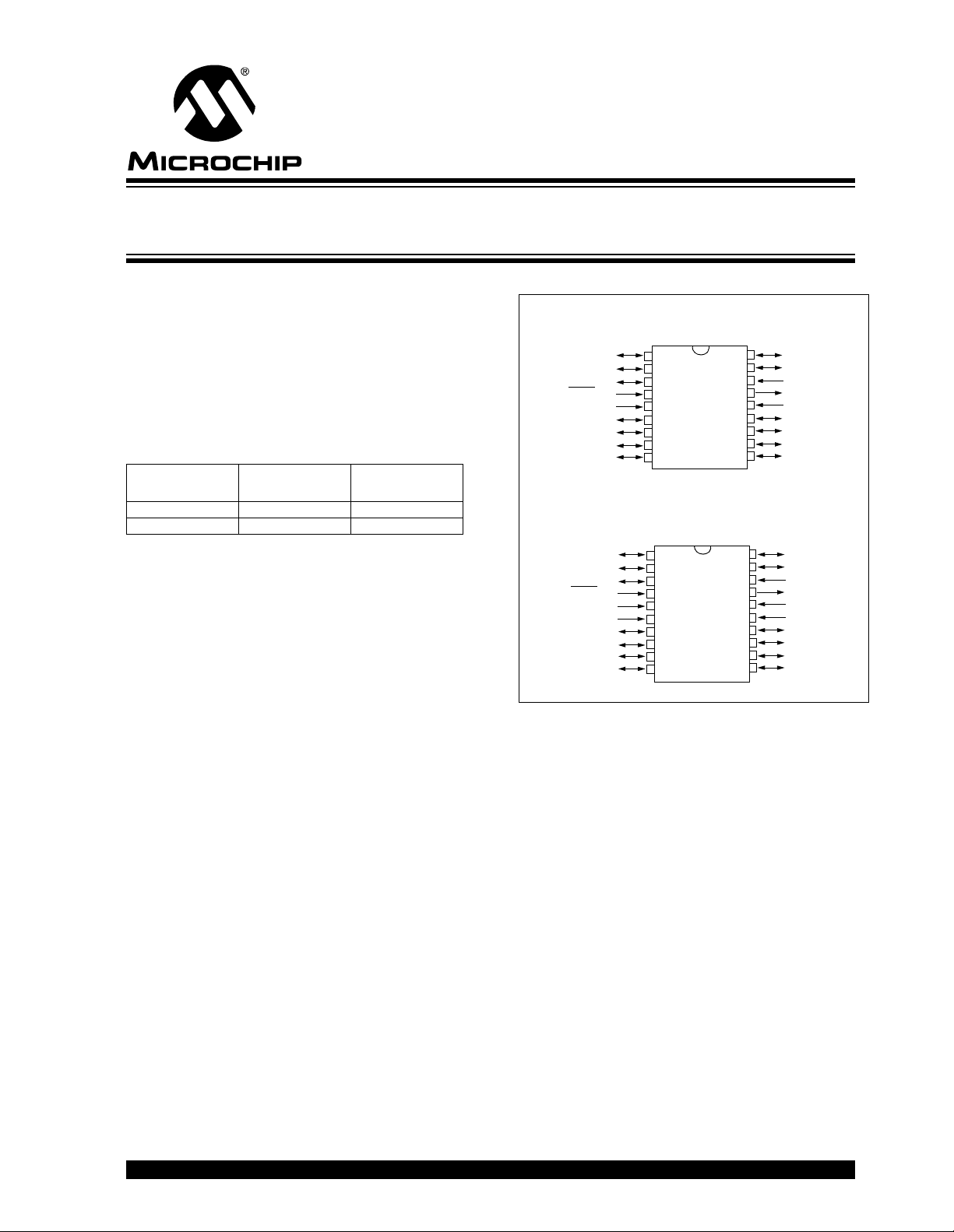
Pin Diagrams
18-pin PDIP, SOIC, Windowed CERDIP
RA2/AN2
RA3/AN3/VREF
RA4/T0CKI
MCLR/VPP
VSS
RB0/INT
RB1/T1OSO/T1CKI
RB2/T1OSI
RB3/CCP1
PIC16C716
PIC16C712
18
17
16
15
14
13
12
11
10
1
2
3
4
5
6
7
8
9
RA1/AN1
RA0/AN0
OSC1/CLKIN
OSC2/CLKOUT
VDD
RB7
RB6
RB5
RB4
20-pin SSOP
RA2/AN2
RA3/AN3/VREF
RA4/T0CKI
MCLR/VPP
VSS
VSS
RB0/INT
RB1/T1OSO/T1CKI
RB2/T1OSI
RB3/CCP1
1
2
3
4
5
6
7
8
9
10
PIC16C712
PIC16C716
20
19
18
17
16
15
14
13
12
11
RA1/AN1
RA0/AN0
OSC1/CLKIN
OSC2/CLKOUT
VDD
VDD
RB7
RB6
RB5
RB4
Peripheral Features:
• Timer0: 8-bit timer/counter with 8-bit prescaler
• Timer1: 16-bit timer/counter with prescaler
can be incremented during sleep via external
crystal/clock
• Timer2: 8-bit timer/counter with 8-bit period
register, prescaler and postscaler
• Capture, Compare, PWM module
• Capture is 16-bit, max. resolution is 12.5 ns,
Compare is 16-bit, max. resolution is 200 ns,
PWM maximum reso lution is 10-bit
• 8-bit multi-channel Analo g-to-Digital converter
1999 Microchip Technology Inc.
Preliminary DS41106A-page 1

PIC16C712/716
Key Features
PICmicro
™
Mid-Range Reference Manual
(DS33023)
Operating Frequency DC - 20 MHz DC - 20 MHz
Resets (and Delays) POR, BOR (PWRT, OST) POR, BOR (PWRT, OST)
Program Memory (14-bit words) 1K 2K
Data Memory (bytes) 128 128
Interrupts 7 7
I/O Ports Ports A,B Ports A,B
Timers 3 3
Capture/Compare/PWM modules 1 1
8-bit Analog-to-Digital Module 4 input channels 4 input channels
PIC16C7XX FAMILY OF DEVICES
PIC16C710 PIC16C71 PIC16C711 PIC16C712 PIC16C715 PIC16C716 PIC16C72A PIC16C73B
Clock
Memory
Peripherals
Features
Maximum Frequency
of Operation (MHz)
EPROM Program
Memory
(x14 words)
Data Memor y (bytes) 36 36 68 128 128 128 128 192
Timer Module(s) TMR0 TMR0 TMR0 TMR0
Capture/Compare/
PWM Module(s)
Serial Port(s)
2
C, USART)
(SPI/I
A/D Converter (8-bit)
Channels
Interrupt Sources 4 4 4 7 4 7 8 11
I/O Pins 13 13 13 13 13 13 22 22
Voltage Range (Volts) 2.5-6.0 3.0-6.0 2.5-6.0 2.5-5.5 2.5-5.5 2.5-5.5 2.5-5.5 2.5-5.5
In-Circuit Serial
Programming
Brown-out Reset Yes — Yes Yes Yes Yes Yes Yes
Packages 18-pin DIP,
20 20 20 20 20 20 20 20
512 1K 1K 1K 2K 2K 2K 4K
——— 1 — 1 1 2
— — — — — — SPI/I
444 4 4 4 55
Yes Yes Yes Yes Yes Yes Yes Yes
SOIC;
20-pin SSOP
18-pin DIP,
SOIC
18-pin DIP,
SOIC;
20-pin SSOP
PIC16C712 PIC16C716
TMR1
TMR2
18-pin DIP,
SOIC;
20-pin SSOP
TMR0 TMR0
18-pin DIP,
SOIC;
20-pin SSOP
TMR1
TMR2
18-pin DIP,
SOIC;
20-pin SSOP
TMR0
TMR1
TMR2
28-pin SDIP,
SOIC, SSOP
2
CSPI/I2C,
TMR0
TMR1
TMR2
USART
28-pin SDIP,
SOIC
DS41106A-page 2 Preliminary
1999 Microchip Technology Inc.

PIC16C712/716
Table of Contents
1.0 Device Overview............................................................ ...... ..... ...... ..... ...... .................................. ..... ...... ..... ...... ..5
2.0 Memory Organization..........................................................................................................................................9
3.0 I/O Ports ............................................................................................................................................................21
4.0 Timer0 Module...................................................................................................................................................29
5.0 Timer1 Module...................................................................................................................................................31
6.0 Timer2 Module...................................................................................................................................................36
7.0 Capture/Compare/PWM (CCP) Module(s)........................................................................................................39
8.0 Analog-to-Digital Converter (A/D) Module.........................................................................................................45
9.0 Special Features of the CPU.............................................................................................................................51
10.0 Instruction Set Summary...................................................................................................................................67
11.0 Development Support........................................................................................................................................69
12.0 Electrical Characteristics..................................................... ..... ...... ..... ...... .................................. ..... ...... ..... ......75
13.0 DC and AC Characteristics Graphs and Tables................................................................................................91
14.0 Packaging Information.......................................................................................................................................93
Revision History ...........................................................................................................................................................99
Conversion Consideration s ...................................................... ...... ................................. ...... .. ... ...... ...... ..... .................99
Migration from Base-line to Mid-Range Devices ..........................................................................................................99
Index...........................................................................................................................................................................101
On-Line Support..........................................................................................................................................................105
Reader Response.......................................................................................................................................................106
PIC16C712/716 Product Identification System...........................................................................................................107
To Our Valued Customers
Most Current Data Sheet
To obtain the most up-to-date version of this data sheet, please register at our Worldwide Web site at:
http://www.microchip.c om
You can determine the version of a data sheet by examining its literature number found on the bottom outside corner of any page.
The last character of the literature number is the version number. e.g., DS30000A is version A of document DS30000.
New Customer Notification System
Register on our web site (www.microchip.com/cn) to receive the most current information on our products.
Errata
An errata sheet may exist for current devices, describing minor operational differences (from the data sheet) and recommended
workarounds. As device/documentation issues become known to us, w e will pub lish an errata sheet. The errata will specify the re vision of silicon and revision of document to which it applies.
To determine if an errata sheet exists for a particular device, please check with one of the following:
• Microchip’s Worldwide Web site; http://www.microchip.com
• Your local Microchip sales office (see last page)
• The Microchip Corporate Literature Center; U.S. FAX: (480) 786-7277
When contacting a sales office or the literature center, please specify which device, revision of silicon and data sheet (include liter-
ature number) you are using.
Corrections to this Data Sheet
We constantly strive to improve the quality of all our products and documentation. We have spent a great deal of time to ensure
that this document is correct. However , w e realize that we ma y have missed a few things. If you fi nd any inf ormation that is missing
or appears in error, please:
• Fill out and mail in the reader response form in the back of this data sheet.
• E-mail us at webmaster@microchip.com.
We appreciate your assistance in making this a better document.
1999 Microchip Technology Inc.
Preliminary DS41106A-page 3

PIC16C712/716
NOTES:
DS41106A-page 4 Preliminary
1999 Microchip Technology Inc.
PIC16C712/716
1.0 DEVICE OVERVIEW
This document contains device-specific information.
Additional information may be found in the PICmicro™
Mid-Range Reference Manual, (DS33023), which may
be obtained from your local Microchip Sales Representative or downloaded from the Microchip website. The
Reference Manual should be considered a complementary document to this data she et, and is h ighly rec-
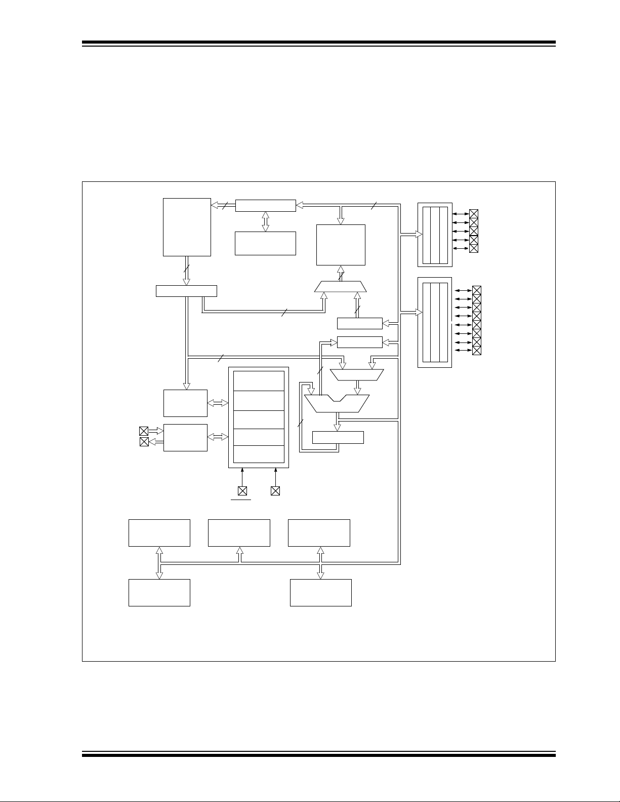
FIGURE 1-1: PIC16C712/716 BLOCK DIAGRAM
13
Program Counter
8 Level Stack
Direct Addr
8
(13-bit)
RAM Addr
7
Program
Bus
EPROM
1K X 14
or
2K x 14
Program
Memory
14
Instruction reg
ommended reading for a better understanding of the
device architecture and operation of the peripheral
modules.
There are two devices (PIC16C712, PIC16C716) covered by this datasheet.
Figure 1- 1 is the block diagram for both devices. T he
pinouts are listed in Table 1-1.
Data Bus
RAM
128 x 8
File
Registers
(1)
Addr MUX
FSR reg
STATUS reg
8
9
Indirect
8
Addr
PORTA
PORTB
RA0/AN0
RA1/AN1
RA2/AN2
RA3/AN3/VREF
RA4/T0CKI
RB0/INT
RB1/T1OSO/T1CKI
RB2/T1OSI
RB3/CCP1
RB4
RB5
RB6
RB7
Power-up
Timer
Oscillator
Start-up Timer
Power-on
Reset
Watchdog
Timer
Brown-out
Reset
VDD, VSS
MCLR
OSC1/CLKIN
OSC2/CLKOUT
Instruction
Decode &
Control
Timing
Generation
Timer0 Timer1 Timer2
CCP1
Note 1: Higher order bits are from the STATUS register.
3
8
A/D
MUX
ALU
W reg
1999 Microchip Technology Inc.
Preliminary DS41106A-page 5

PIC16C712/716
TABLE 1-1 PIC16C712/716 PINOUT DESCRIPTION
Pin PIC16C712/716 Pin Buffer
Name DIP, SOIC SSOP Type Type Description
MCLR/VPP
MCLR
VPP
OSC1/CLKIN
OSC1
CLKIN
44
I
P
16 18
I
I
ST Master clear (reset) input. This pin is an
active low reset to the device.
Programming voltage input
ST
CMOS
Oscillator crystal input or external clock
source input. ST buffer when configured in
RC mode. CMOS otherwi se.
External clock source input.
OSC2/CLKOUT
OSC2
CLKOUT
RA0/AN0
RA0
AN0
RA1/AN1
RA1
AN1
RA2/AN2
RA2
AN2
RA3/AN3/V
RA4/T0CKI
Legend: TTL = TTL-compatible input CMOS = CMOS compatible input or output
REF
RA3
AN3
VREF
RA4
T0CKI
ST = Schmitt Trigger input with CMOS levels
OD = Open drain output
SM = SMBus compatible input. An external resistor is required if this pin is used as an output
NPU = N-channel pull-up PU = Weak internal pull-up
No-P diode = No P-diode to V
I = input O = output
P = Power L = LCD Driver
15 17
17 19
18 20
11
22
33
DD AN = Analog input or output
O
O
I/O
I/O
I/O
I/O
I/O
—
—
TTL
I
I
I
I
I
I
Analog
TTL
Analog
TTL
Analog
TTL
Analog
Analog
ST/OD
ST
Oscillator crystal output. Connects to
crystal or resonator in crystal oscillator
mode.
In RC mode, OSC2 pin outputs CLKOUT
which has 1/4 the frequenc y of OSC1, and
denotes the instruction cycle rate.
PORTA is a bi-directional I/O port.
Digital I/O
Analog input 0
Digital I/O
Analog input 1
Digital I/O
Analog input 2
Digital I/O
Analog input 3
A/D Reference Voltage input.
Digital I/O. Open drain when configured
as output.
Timer0 external clock input
DS41106A-page 6 Preliminary
1999 Microchip Technology Inc.

PIC16C712/716
TABLE 1-1 PIC16C712/716 PINOUT DESCRIPTION (Cont.’d)
Pin PIC16C712/716 Pin Buffer
Name DIP, SOIC SSOP Type Type Description
PORTB is a bi-directional I/O port. PORTB
can be software programmed for internal
weak pull-ups on all inputs .
RB0/INT
RB0
INT
RB1/T1OSO/T1CKI
RB1
T1OSO
T1CKI
RB2/T1OSI
RB2
T1OSI
RB3/CCP1
RB3
CCP1
RB4 10 12 I/O TTL Digital I/O
RB5 11 12 I/O TTL Digital I/O
RB6 12 13 I/O
RB7 13 14 I/O
SS 5 5, 6 P — Ground reference for logic and I/O pins.
V
DD 14 15, 16 P — Positive supply for logic and I/O pins.
V
Legend: TTL = TTL-compatible input CMOS = CMOS compatible input or output
ST = Schmitt Trigger input with CMOS levels
OD = Open drain output
SM = SMBus compatible input. An external resistor is required if this pin is used as an output
NPU = N-channel pull-up PU = Weak internal pull-up
No-P diode = No P-diode to V
I = input O = output
P = Power L = LCD Driver
67
78
89
910
DD AN = Analog input or output
I/O
I/O
O
I/O
I/O
I/O
I/O
TTL
I
I
I
I
ST
TTL
—
ST
TTL
—
TTL
ST
TTL
ST
TTL
ST
Digital I/O
External Interrupt
Digital I/O
Timer1 oscillator output. Connects to
crystal in oscillator mode.
Timer1 external clock input.
Digital I/O
Timer1 oscillator input. Connects to
crystal in oscillator mode.
Digital I/O
Capture1 input, Compa re1 output, PWM1
output.
Interrupt on change pin.
Interrupt on change pin.
Digital I/O
Interrupt on change pin.
ICSP programming clock.
Digital I/O
Interrupt on change pin.
ICSP programming data.
1999 Microchip Technology Inc.
Preliminary DS41106A-page 7

PIC16C712/716
NOTES:
DS41106A-page 8 Preliminary
1999 Microchip Technology Inc.
PIC16C712/716
2.0 MEMORY ORGANIZATION
There are two memory blocks in each of these
PICmicro
gram Memor y and Data Memor y) has its own bus so
that concurrent access can occur.
Additional inf ormation on de vice m emory may be f ound
in the PICmicro Mid-Range Reference Manual,
(DS33023).
2.1 Program Memory Organization
The PIC16C712/716 has a 13-bit program counter
capable of addressing an 8K x 14 program memory
space. PIC16C712 has 1K x 14 words of program
memory and PIC16C716 has 2K x 14 words of progr am
memory. Accessing a location above the physically
implemented address will cause a wraparound.
The reset vector is at 0000h and the interrupt vector is
at 0004h.
FIGURE 2-1: PROGRAM MEMORY MAP
®
microcontr oller devices. Each blo ck (Pro-
AND STACK OF THE
PIC16C712
PC<12:0>
CALL, RETURN
RETFIE, RETLW
13
FIGURE 2-2: PROGRAM MEMORY MAP
AND STACK OF PIC16C716
PC<12:0>
CALL, RETURN
RETFIE, RETLW
Space
User Memory
On-chip Program
Stack Level 1
Stack Level 8
Reset Vector
Interrupt Vector
Memory
13
0000h
0004h
0005h
07FFh
0800h
Stack Level 1
Stack Level 8
Reset Vector
Interrupt Vector
Space
User Memory
On-chip Program
Memory
0000h
0004h
0005h
03FFh
0400h
1FFFh
1FFFh
1999 Microchip Technology Inc.
Preliminary DS41106A-page 9
PIC16C712/716
2.2 Data Memory Organization
The data memory is partitioned into multiple banks
which contain the General Purpose Registers and the
Special Function Registers. Bits RP1 and RP0 are the
bank select bits.
(1)
RP1
= 00 → Bank0
= 01 → Bank1
= 10 → Bank2 (not implemented)
= 11 → Bank3 (not implemented)
Note 1: Maintain this bit clear to ensure upward compati-
Each bank extends up to 7Fh (128 bytes). The lower
locations of each bank are reserved for the Special
Function Registers . Abo v e the Sp ecial Functi on Regi sters are General Purpose Registers, implemented as
static RAM. All implemented banks contain special
function registers. Some “high use” special function
registers from one bank may be mirrored in another
bank for code reduction and quicker access.
2.2.1 GENERAL PURPOSE REGISTER FILE The register file can be accessed either directly, or indi-
rectly through the File Select Register FSR
(Section 2.5).
RP0 (STATUS<6:5>)
bility with future products.
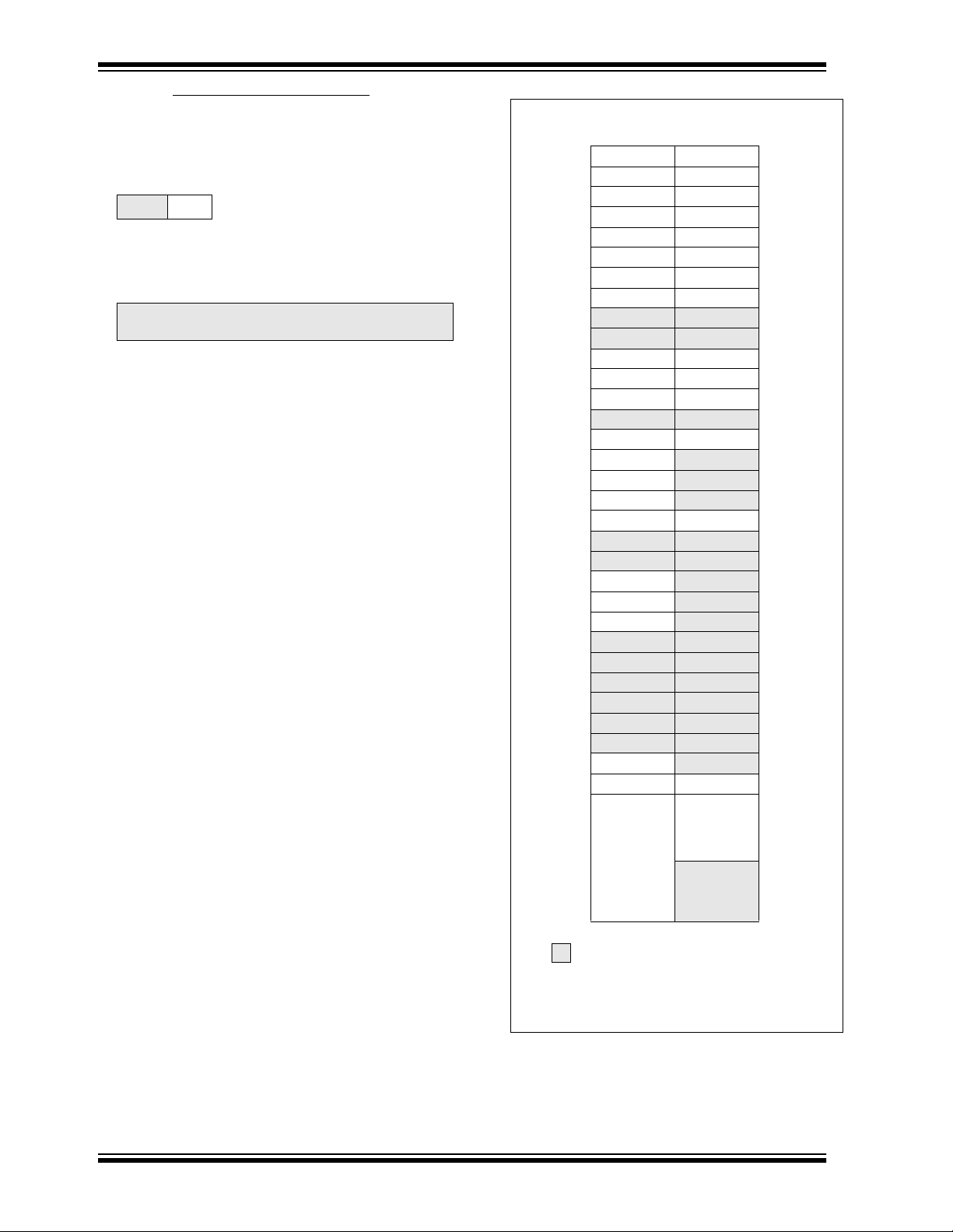
FIGURE 2-3: REGISTER FILE MAP
File
Address
00h INDF
01h TMR0
02h PCL PCL 82h
03h STATU S S TATUS 83h
04h FSR FSR 84h
05h PORTA TRISA 85h
06h PORTB TRISB 86h
07h DATACCP TRISCCP 87h
08h
09h
0Ah PCLATH PCLATH 8Ah
0Bh INTCON INTCON 8Bh
0Ch PIR1 PIE1 8Ch
0Dh
0Eh TMR1L PCON 8Eh
0Fh TRM1H
10h T1CON
11h TRM2
12h T2CON PR2 92h
13h
14h
15h CCPR1L
16h CCPR1H
17h CCP1CON
18h
19h
1Ah
1Bh
1Ch
1Dh
1Eh ADRES
1Fh ADCON0 ADCON1 9Fh
20h
(1)
General
Purpose
Registers
96 Bytes
(1)
INDF
OPTION_REG
General
Purpose
Registers
32 Bytes
80h
81h
88h
89h
8Dh
8Fh
90h
91h
93h
94h
95h
96h
97h
98h
99h
9Ah
9Bh
9Ch
9Dh
9Eh
A0h
BFh
C0h
File
Address
7Fh FFh
Bank 0 Bank 1
Unimplemented data memory locations,
read as ’0’.
Note 1: Not a physical register.
DS41106A-page 10 Preliminary
1999 Microchip Technology Inc.
PIC16C712/716
2.2.2 SPECIAL FUNCTION REGISTERS
The special fu nction re gisters can b e classifi ed into two
sets; core (CPU) and periphe ral. Those registers asso-
The Special Function Registers are registers used by
the CPU and Peripheral Modules for controlling the
desired operation of the device. These registers are
implemented as static RAM. A list of these registers is
give in Table 2-1.
ciated with the core functions are described in detail in
this section. Those related to the operation of the
peripheral features are described in detail in that
peripheral feature section.
TABLE 2-1 SPECIAL FUNCTION REGISTER SUMMARY
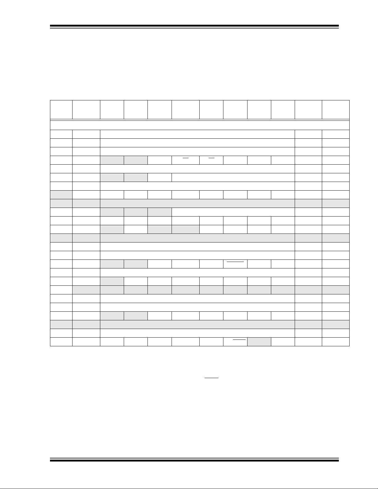
Addr Name Bit 7 Bit 6 Bit 5 Bit 4 Bit 3 Bit 2 Bit 1 Bit 0
Value on:
POR,
BOR
Bank 0
(1)
00h INDF
01h TMR0 Timer0 module’s register xxxx xxxx uuuu uuuu
02h PCL
03h STATUS
04h FSR
05h PORTA
06h PORTB
07h DATACCP —
08h-09h — Unimplemented — —
0Ah PCLATH
0Bh INTCON
0Ch PIR1
0Dh — Unimplemented — —
0Eh TMR1L Holding register for th e Least Significant Byte of the 16-bit TMR1 register xxxx xxxx uuuu uuuu
0Fh TMR1H Holding register for the Most Significant Byte of the 16-bit TMR1 register xxxx xxxx uuuu uuuu
10h T1CON
11h TMR2 Timer2 module’s register 0000 0000 0000 0000
12h T2CON
13h-14h
15h CCPR1L Capture/Compare/PWM Register1 (LSB) xxxx xxxx uuuu uuuu
16h CCPR1H Capture/Compare/PWM Register1 (MSB) xxxx xxxx uuuu uuuu
17h CCP1CON
18h-1Dh — Unimplemented — —
1Eh ADRES A/D Result Register xxxx xxxx uuuu uuuu
1Fh ADCON0 ADCS1 ADCS0 CHS2 CHS1 CHS0 GO/DONE
Legend: x = unknown, u = unchanged, q = value depends on condition, - = unimplemented, read as ’0’,
Shaded locations are unimplemented, read as ’0’.
Note 1: These registers can be addressed from either bank.
2: The upper byte of the program counter is not directly accessible. PCLATH is a holding register for PC<12:8> whose contents
are transferred to the upper byte of the program counter.
3: Other (non power-up) resets include: external reset through MCLR
4: The IRP and RP1 bits are reserved. Always maintain these bits clear .
5: On any device reset, these pins are configured as inputs.
6: This is the value that will be in the port output latch.
7: Reserved bits; Do Not Use.
Addressing this location uses contents of FSR to address data memory (not a physical register) 0000 0000 0000 0000
(1)
Program Counter's (PC) Least Significant Byte 0000 0000 0000 0000
(1)
(1)
(5,6)
(5,6)
(1,2)
(1)
(4)
IRP
Indirect data memory address pointer xxxx xxxx uuuu uuuu
— ——
PORTB Data Latch when written: PORTB pins when read xxxx xxxx uuuu uuuu
(7)
— — — Write Buffer for the upper 5 bits of the Program Counter ---0 0000 ---0 0000
GIE PEIE T0IE INTE RBIE T0IF INTF RBIF 0000 000x 0000 000u
—ADIF— — — CCP1IF TMR2IF TMR1IF -0-- 0000 -0-- 0000
— — T1CKPS1 T 1CKPS0 T1OSCEN T1SYNC TMR1CS TMR1ON --00 0000 --uu uuuu
— TOUTPS3 TOUTPS2 TOUTPS1 TOUTPS0 TMR2ON T2CKPS1 T2CKPS0 -000 0000 -000 0000
— — DC1B1 DC1B0 CCP1M3 CCP1M2 CCP1M1 CCP1M0 --00 0000 --00 0000
RP1
—
(4)
RP0 TO PD ZDCCrr01 1xxx rr0q quuu
(7)
PORTA Data Latch when written: PORTA pins when read --xx xxxx --xu uuuu
(7)
(7)
—
(7)
—
(7)
—
DCCP
(7)
—
—ADON0000 00-0 0000 00-0
DT1CK
xxxx xxxx xxxx xuxu
and the Watchdog Timer Reset.
Value on all
other resets
(4)
1999 Microchip Technology Inc.
Preliminary DS41106A-page 11
PIC16C712/716
TABLE 2-1 SPECIAL FUNCTION REGISTER SUMMARY (Cont.’d)
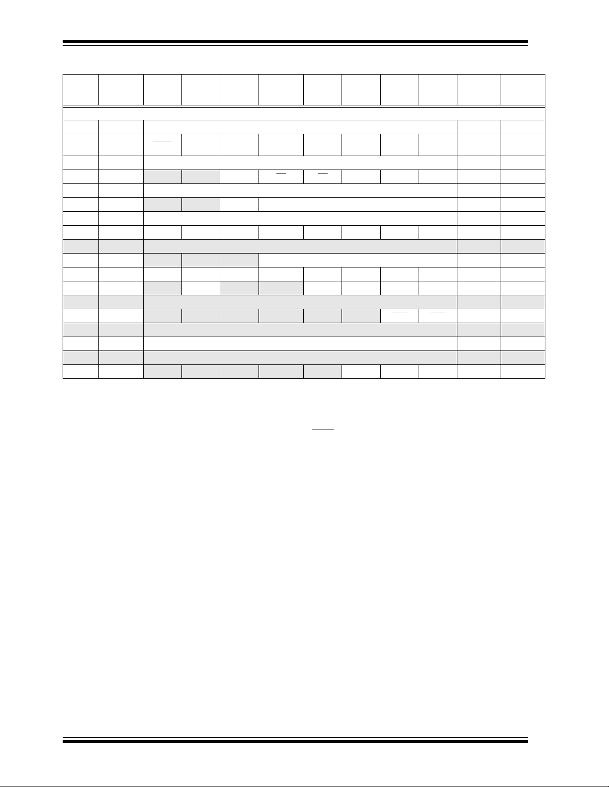
Addr Name Bit 7 Bit 6 Bit 5 Bit 4 Bit 3 Bit 2 Bit 1 Bit 0
Bank 1
(1)
80h INDF
81h
82h PCL
83h STATUS
84h FSR
85h TRISA
86h TRISB PORTB Data Direction Register 1111 1111 1111 1111
87h TRISCCP —
88h-89h — Unimplemented — —
8Ah PCLATH
8Bh INTCON
8Ch PIE1
8Dh — Unimplemented — —
8Eh PCON
8Fh-91h — Unimplemented — —
92h PR2 Timer2 Period Register 1111 1111 1111 1111
93h-9Eh — Unimplemented — —
9Fh ADCON1
OPTION_
REG
Addressing this location uses contents of FSR to address data memory (not a physical register) 0000 0000 0000 0000
RBPU
(1)
Program Counter’s (PC) Least Significant Byte 0000 0000 0000 0000
(1)
IRP
(1)
Indirect data memory address pointer xxxx xxxx uuuu uuuu
(1,2)
(1)
GIE PEIE T0IE INTE RBIE T0IF INTF RBIF 0000 000x 0000 000u
INTEDG T0CS T0SE PSA PS2 PS1 PS0 1111 1111 1111 1111
(4)
— ——
(7)
— — — Write Buffer for the upper 5 bits of the Program Counter ---0 0000 ---0 0000
—ADIE— — — CCP1IE TMR2IE TMR1IE -0-- -000 -0-- -000
— — — — — —PORBOR ---- --qq ---- --uu
— — — — — PCFG2 PCFG1 PCFG0 ---- -000 ---- -000
RP1
—
(4)
RP0 TO PD ZDCCrr01 1xxx rr0q quuu
(7)
PORTA Data Direction Register --x1 1111 --x1 1111
(7)
(7)
—
(7)
—
(7)
—
TCCP
(7)
—
TT1CK
Value on:
POR,
BOR
xxxx x1x1 xxxx x1x1
Legend: x = unknown, u = unchanged, q = value depends on condition, - = unimplemented, read as ’0’,
Shaded locations are unimplemented, read as ’0’.
Note 1: These registers can be addressed from either bank.
2: The upper byte of the program counter is not directly accessible. PCLATH is a holding register for PC<12:8> whose contents
are transferred to the upper byte of the program counter.
3: Other (non power-up) resets include: external reset through MCLR
and the Watchdog Timer Reset.
4: The IRP and RP1 bits are reserved. Always maintain these bits clear .
5: On any device reset, these pins are configured as inputs.
6: This is the value that will be in the port output latch.
7: Reserved bits; Do Not Use.
Value on all
other resets
(4)
DS41106A-page 12 Preliminary
1999 Microchip Technology Inc.

PIC16C712/716
2.2.2.1 STATUS REGISTER
The STATUS register, shown in Figure 2-4, contains
the arithmetic status of th e ALU , the RE SET status an d
the bank select bits for data memory.
The STATUS register can be the destination for any
instruction, as with any other register. If the STATUS
register is the destination for an instruction that affects
the Z, DC or C bits, then the write to these three bits is
disabled. The se bi ts ar e set or c leared accordi ng to the
device logic. Fur th er more, the TO
writable. Therefore, the result of an instruction with the
STATUS re gister as desti nation may be different t han
intended.
For example, CLRF STATUS will clear th e up p er -t h ree
bits and set the Z bi t. T his lea v e s the STATUS register
as 000u u1uu (where u = unchanged).
and PD bits are not
It is recommended, therefore, that only BCF, BSF,
SWAPF and MOVWF instructions are used to alter the
STATUS register because these instructions do not
affect the Z, C or DC b its from the STATUS register. F or
other instructions, not affecting any status bits, see the
"Instruction Set Summary."
Note 1: These devices do not use bits IRP and
RP1 (STATUS<7:6>). Maintain these bits
clear to ensure upward compatibility with
future products.
Note 2: The C and DC bits operate as a borrow
and digit borrow bit, respectively, in subtraction. See the SUBLW and SUBWF
instructions for examples.
FIGURE 2-4: STATUS REGISTER (ADDRESS 03h, 83h)
R/W-0 R/W-0 R/W-0 R-1 R-1 R/W-x R/W-x R/W-x
IRP RP1 RP0 TO PD Z DC C R = Readable bit
bit7 bit0
bit 7: IRP: Register Bank Select bit (used for indirect add ressing)
1 = Bank 2, 3 (100h - 1FFh) - not implemented, maintain clear
0 = Bank 0, 1 (00h - FFh) - not implemented, maintain clear
bit 6-5: RP1:RP0: Register Bank Select bits (used for direct addressing)
01 = Bank 1 (80h - FFh)
00 = Bank 0 (00h - 7Fh)
Each bank is 128 bytes
Note: RP1 = not implemented, maintain clear
bit 4: TO
bit 3: PD
bit 2: Z: Zero bit
bit 1: DC: Digit carry/borrow
bit 0: C: Carry/borrow
: Time-out bit
1 = After power-up, CLRWDT instruction, or SLEEP instruction
0 = A WDT time-out occurred
: Power-down bit
1 = After power-up or by the CLRWDT instruction
0 = By execution of the SLEEP instruction
1 = The result of an arithmetic or logic operation is zero
0 = The result of an arithmetic or logic operation is not zero
bit (ADDWF, ADDLW,SUBLW,SUBWF instructions) (for borro w the polarity is reversed)
1 = A carry-out from the 4th low order bit of the result occurred
0 = No carry-out from the 4th low order bit of the result
bit (ADDWF, ADDLW,SUBLW,SUBWF instructions)
1 = A carry-out from the most significant bit of the result occurred
0 = No carry-out from the most significant bit of the result occurred
Note: For borrow
second operand. For rotate (RRF, RLF) instructions, this bit is loaded with either the high or low order bit of
the source register.
the polarity is reversed. A subtract io n is execut ed by adding the two’s complement of the
W = Writable bit
U = Unimplemented bit,
read as ‘0’
- n = Value at POR reset
1999 Microchip Technology Inc.
Preliminary DS41106A-page 13

PIC16C712/716
2.2.2.2 OPTION_REG REGISTER
The OPTION_REG register is a readable and writable
register , which contai ns various c ontrol bits to c onfigure
the TMR0 prescaler/WDT postscaler (single assignable regist er kno wn also as the prescale r), the Ext ernal
INT Interrupt, TMR0 and the w eak pull-up s on PORTB.
FIGURE 2-5: OPTION_REG REGISTER (ADDRESS 81h)
R/W-1 R/W-1 R/W-1 R/W-1 R/W-1 R/W-1 R/W-1 R/W-1
RBPU
bit7 bit0
bit 7: RBPU: PORTB Pull-up Enable bit
bit 6: INTEDG: Interrupt Edge Select bit
bit 5: T0CS: TMR0 Clock Source Select bit
bit 4: T0SE: TMR0 Source Edge Select bit
bit 3: PSA: Prescaler Assignment bit
bit 2-0: PS2:PS0: Prescaler Rate Select bits
INTEDG T0CS T0SE PSA PS2 PS1 PS0 R = Readable bit
1 = PORTB pull-ups are disabled
0 = PORTB pull-ups are enab led b y ind iv idu al port latch va lue s
1 = Interrupt on rising edge of RB0/INT pin
0 = Interrupt on falling edge of RB0/INT pin
1 = Transition on RA4/T0CKI pin
0 = Internal instruction cycle clock (CLKOUT)
1 = Increment on high-to-low transition on RA4/T0CKI pin
0 = Increment on low-to-high transition on RA4/T0CKI pin
1 = Prescaler is assigned to the WDT
0 = Prescaler is assigned to the Timer0 module
Bit Value TMR0 Rate WDT Rate
000
001
010
011
100
101
110
111
1 : 2
1 : 4
1 : 8
1 : 16
1 : 32
1 : 64
1 : 128
1 : 256
1 : 1
1 : 2
1 : 4
1 : 8
1 : 16
1 : 32
1 : 64
1 : 128
Note: To achieve a 1:1 prescaler as signmen t for
the TMR0 register, assign the prescaler to
the Watchdog Timer.
W = Writable bit
U = Unimplemented bit,
read as ‘0’
- n = Value at POR reset
DS41106A-page 14 Preliminary
1999 Microchip Technology Inc.

PIC16C712/716
2.2.2.3 INTCON REGISTER
The INTCON Regi ster i s a rea dab le a nd w ritabl e regi s-
ter which contains various enable and flag bits for the
TMR0 register overflow, RB Port change and External
RB0/INT pin interrupts.
Note: Interrupt flag bits get set when an interrupt
condition occurs , re ga rdless of the state of
its corresponding enable bit or the global
enable bit, GIE (INTCON<7>). User software should ensure the appropriate interrupt flag bits are clear prior to enabling an
interrupt.
FIGURE 2-6: INTCON REGISTER (ADDRESS 0Bh, 8Bh)
R/W-0 R/W-0 R/W-0 R/W-0 R/W-0 R/W-0 R/W-0 R/W-x
GIE PEIE T0IE INTE RBIE T0IF INTF RBIF R = Readable bit
bit7 bit0
bit 7: GIE: Global Interrupt Enable bit
1 = Enables all un-masked interrupts
0 = Disables all interrupts
bit 6: PEIE: Peripheral Interrupt Enable bit
1 = Enables all un-masked peripheral interrupts
0 = Disables all peripheral interrupts
bit 5: T0IE: TMR0 Overflow Interrupt Enable bit
1 = Enables the TMR0 interrupt
0 = Disables the TMR0 interrupt
bit 4: IINTE: RB0/INT External Interrupt Enable bit
1 = Enables the RB0/INT external interrupt
0 = Disables the RB0/INT external interrupt
bit 3: RBIE: RB Port Change Interrupt Enable bit
1 = Enables the RB port change interrupt
0 = Disables the RB port change interrupt
bit 2: T0IF: TMR0 Overflow Interrupt Flag bit
1 = TMR0 register has overflowed (must be cleared in software)
0 = TMR0 register did not overflow
bit 1: INTF: RB0/INT External Interrupt Flag bit
1 = The RB0/INT external interrupt occurred (must be cleared in software)
0 = The RB0/INT external interrupt did not occur
bit 0: RBIF: RB Port Change Interrupt Flag bit
1 = At least one of the RB7:RB4 pins changed state (must be cleared in software)
0 = None of the RB7:RB4 pins have changed state
W = Writable bit
U = Unimplemented bit,
- n = Value at POR reset
read as ‘0’
1999 Microchip Technology Inc.
Preliminary DS41106A-page 15

PIC16C712/716
2.2.2.4 PIE1 REGISTER
This register contains the individual enable bits for the
peripheral interrupts.
Note: Bit PEIE (INTCON<6>) must be set to
enable any peripheral interrupt.
FIGURE 2-7: PIE1 REGISTER (ADDRESS 8Ch)
U-0 R/W-0 U-0 U-0 R/W-0 R/W-0 R/W-0 R/W-0
— ADIE — — — CCP1IE TMR2IE TMR1IE R = Readable bit
bit7 bit0
bit 7: Unimplemented: Read as ‘0’
bit 6: ADIE: A/D Converter Interrupt Enable bit
1 = Enables the A/D interrupt
0 = Disables the A/D interrupt
bit 5-3: Unimplemented: Read as ‘0’
bit 2: CCP1IE: CCP1 Interrupt Enable bit
1 = Enables the CCP1 interrupt
0 = Disables the CCP1 interrupt
bit 1: TMR2IE: TMR2 to PR2 Match Interrupt Enable bit
1 = Enables the TMR2 to PR2 match interrupt
0 = Disables the TMR2 to PR2 match interrupt
bit 0: TMR1IE: TMR1 Overflow Interrupt Enable bit
1 = Enables the TMR1 overflow interrupt
0 = Disables the TMR1 overflow interrupt
W = Writable bit
U = Unimplemented bit,
- n = Value at POR reset
read as ‘0’
DS41106A-page 16 Preliminary
1999 Microchip Technology Inc.

PIC16C712/716
2.2.2.5 PIR1 REGI STER
This register contains the individual flag bits for the
peripheral interrupts.
Note: Interrupt flag bits get set when an interrupt
condition occurs , re ga rdless of the state of
its corresponding enable bit or the global
enable bit, GIE (INTCON<7>). User software should ensure the appropriate interrupt flag bits are clear prior to enabling an
interrupt.
FIGURE 2-8: PIR1 REGISTER (ADDRESS 0Ch)
U-0 R/W-0 U-0 U-0 R/W-0 R/W-0 R/W-0 R/W-0
— ADIF — — — CCP1IF TMR2IF TMR1IF R = Readable bit
bit7 bit0
bit 7: Unimplemen ted: Read as ‘0’
bit 6: ADIF: A/D Converter Interrupt Flag bit
1 = An A/D conversion completed (must be cleared in software)
0 = The A/D conversion is not complete
bit 5-3: Unimplemented: Read as ‘0’
bit 2: CCP1IF: CCP1 Interrupt Flag bit
Capture Mode
1 = A TMR1 re gister capture occurred (must be cleared in software)
0 = No TMR1 register capture occurred
Compare Mode
1 = A TMR1 register compare match occurred (must be cleared in software)
0 = No TMR1 register compare match occurred
PWM Mode
Unused in this mode
bit 1: TMR2IF: TMR2 to PR2 Match Interrupt Flag bit
1 = TMR2 to PR2 match occurred (must be cleared in software)
0 = No TMR2 to PR2 match occurred
bit 0: TMR1IF: TMR1 Overflow Interrupt Flag bit
1 = TMR1 register overflowed (must be cleared in software)
0 = TMR1 register did not overflow
W = Writable bit
U = Unimplemented bit,
- n = Value at POR reset
read as ‘0’
1999 Microchip Technology Inc.
Preliminary DS41106A-page 17

PIC16C712/716
2.2.2.6 PCON REGISTER
The Power Control (PCON) register contains a flag bit
to allow differentiation between a Power-on Reset
(POR) to an external MCLR
These devices contain an additional bit to differentiate
a Brown-out Reset condition from a Power-on Reset
condition.
Reset or WDT Reset.
Note: If the BODEN configuration bit is set, BOR
is ’1’ on Power-on Reset. If the BODEN
configuration bit is clear, BOR
on Power-on Reset.
The BOR status bit is a "don't care" and is
not necessarily predictab le if the brow n-out
circuit is disabled (the BOD EN configuration bit is clear). BOR
the user and checked on subsequent
resets to see if it is clear, indicating a
brown-out has occurred.
FIGURE 2-9: PCON REGISTER (ADDRESS 8Eh)
U-0 U-0 U-0 U-0 U-0 U-0 R/W-0 R/W-q
— — — — — —PORBOR R = Readable bit
bit7 bit0
bit 7-2: Unimplemented: Read as ’0’
bit 1: POR
bit 0: BOR
: Power-on Reset Status bit
1 = No Power-on Reset occurred
0 = A Power-on Reset occurred (must be set in software after a Power-on Reset occurs)
: Brown-out Reset Status bit
1 = No Brown-out Reset occurred
0 = A Brown-out Reset occurred (must be set in software after a Brown-out Reset occurs)
W = Writable bit
U = Unimplemented bit,
- n = Value at POR reset
is unknown
must then be set by
read as ‘0’
DS41106A-page 18 Preliminary
1999 Microchip Technology Inc.

PIC16C712/716
2.3 PCL and PCLATH
The program counter (PC) specifies the address of the
instruction to fetch for execution. The PC is 13 bits
wide. The low byte is called the PCL register. This register is readable and writable. The high byte is called
the PCH register. This register contains the PC<12:8>
bits and is not dir ect ly read able or writable. All updates
to the PCH register go through the PCLATH register.
2.3.1 STACK The stack a llows a co mbination o f up to 8 pr ogram ca lls
and interrupts to occur. The stack contains the return
address from this branch in program execution.
Midrange devices have an 8 level deep x 1 3-bit wide
hardware stack. T he stack space is not part of either
program or data space and the stack pointer is not
readable or writab le. The PC is PUSHed onto the stac k
when a CALL instruction is executed or an interrupt
causes a branch. The stack is POPed in the event of a
RETURN, RETLW or a RETFIE instruction execution.
PCLATH is not modified when the stack is PUSHed or
POPed.
After the stac k has been PUSHe d eight t imes, th e ninth
push overw rites th e value that was stored from the first
push. The tenth push overwrites the second pus h (an d
so on).
2.4 Program Memory Paging
The CALL and GOTO instructions provide 11 bits of
address to allow branching within any 2K program
memory page. When doing a CALL or GOTO instruction,
the upper bit of the address is provided by
PCLATH<3>. When doing a CALL or GOTO instruction,
the user must ensure that the page select bit is programmed so th at th e des ire d pr ogram memory page is
addressed. If a return from a CALL instruction (or interrupt) is executed, the entire 1 3-bit PC is pushed onto
the stack. Therefore, manipulation of the PCLATH<3>
bit is not required for the return instructions (which
POPs the address from the stack).
1999 Microchip Technology Inc.
Preliminary DS41106A-page 19
PIC16C712/716
2.5 Indirect Addressing, INDF and FSR Registers
The INDF register is not a physical r e gis ter. Addressing INDF actually addresses the register whose
address is contained in the FSR register (FSR is a
pointer
). This is indirect ad dressi ng .
EXAMPLE 2-1: INDIRECT ADDRESSING
• Register file 05 contains the value 10h
• Register file 06 contains the value 0Ah
• Load the value 05 into the FSR register
• A read of the INDF register will return the v alue of
10h
• Increment the value of the FSR register by one
(FSR = 06)
• A read of the INDR register now will return the
value of 0Ah.
Reading INDF itself indirectly (FSR = 0) will produce
00h. Writing to the INDF register indirectly results in a
no-operation (although STATUS bits may be affected).
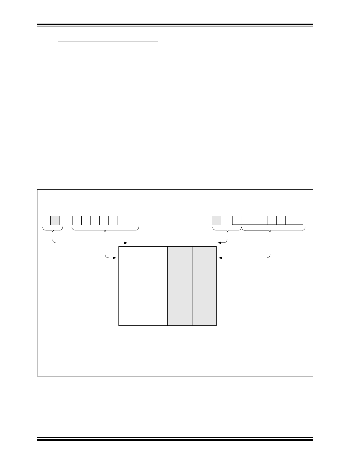
FIGURE 2-10: DIRECT/INDIRECT ADDRESSING
RP1:RP0 6
(2)
from opcode
0
A simple program to clear RAM locations 20h-2Fh
using indirect addressing is shown in Example 2-2.
EXAMPLE 2-2: HOW TO CLEAR RAM
USING INDIRECT
ADDRESSING
movlw 0x20 ;initialize pointer
movwf FSR ; to RAM
NEXT clrf INDF ;clear INDF register
incf FSR ;inc pointer
btfss FSR,4 ;all done?
goto NEXT ;NO, clear next
CONTINUE
: ;YES, continue
An effective 9-bit addres s is o btai ne d by concatenatin g
the 8-bit FSR register an d the IRP b it (STATUS<7>), as
shown in Figure 2-10. However, IRP is not used in the
PIC16C712/716.
Indirect AddressingDirect Addressing
IRP FSR register
7
(2)
0
bank select location select
00 01 10 11
00h
80h
Data
Memory(1)
7Fh
FFh
Bank 0 Bank 1 Bank 2 Bank 3
Note 1: For register file map detail see Figure 2-3.
2: Maintain clear for upward compatibility with future products.
3: Not implemented.
100h
(3) (3)
17Fh
180h
1FFh
bank select
location select
DS41106A-page 20 Preliminary
1999 Microchip Technology Inc.
PIC16C712/716
3.0 I/O PORTS
Some pins for these I/O ports are multiplexed with an
alternate function for the peripheral features on the
device. In general, when a peripheral is enabled, that
pin may not be used as a general purpose I/O pin.
Additional information on I/O ports ma y b e found in the
PICmicro™ Mid-Range Reference Manual,
(DS33023).
3.1 PORTA and the TRISA Register
PORTA is a 5-bit wide bi-directional port. The corresponding data direction register is TRISA. Setting a
TRISA bit (=1) will m ake the correspondi ng PORTA pin
an input, (i.e., put the corresponding output driver in a
hi-impedance mode). Clearing a TRISA bit (=0) will
make the corre sponding POR TA pin an output, (i .e., put
the contents of the output latch on the selected pin).
Reading the PORTA register reads the status of the
pins whereas writing to it will write to the port latch. All
write operations are read-modify-write operations.
Therefore a write to a port implies that the port pins are
read, the val ue is mod ifi ed, and then written to the port
data latch.
Pin RA4 is multiplexed with the Timer0 module clock
input to become the RA4/T0CKI pin. The RA4/T0CKI
pin is a Schmitt Trigger input and an open drain output.
All other RA port pins have TTL input levels and full
CMOS output drivers .
PORTA pins, RA3:0, are m ultiplex ed with ana log inputs
and analog V
REF input. The operation of each pin is
selected by clearing/setting the control bits in the
ADCON1 register (A/D Control Register1).
Note: On a Power-on Reset, these pins are con-
figured as analog inputs and read as '0'.
The TRISA register controls the direction of the RA
pins, even when they are being used as analog inputs.
The user must ensure the bi ts in the TRISA registe r are
maintained set when using them as analog inputs.
EXAMPLE 3-1: INITIALIZING PORTA
BCF STATUS, RP0 ;
CLRF PORTA ; Initialize PORTA by
; clearing output
; data latches
BSF STATUS, RP0 ; Select Bank 1
MOVLW 0xEF ; Value used to
; initialize data
; direction
MOVWF TRISA ; Set RA<3:0> as inputs
; RA<4> as outputs
BCF STATUS, RP0 ; Return to Bank 0
FIGURE 3-1: BLOCK DIAGRAM OF RA3:RA0
DATA
BUS
WR
PORT
WR
TRIS
CK
Data Latch
CK
TRIS Latch
RD PORT
QD
Q
QD
Q
RD TRIS
QD
EN
VDD
P
N
SS
V
Analog
input
mode
VSS
VDD
I/O pin
TTL
Input
Buffer
1998 Microchip Technology Inc.
To A/D Conver ter
Preliminary DS41106A-page 21
PIC16C712/716
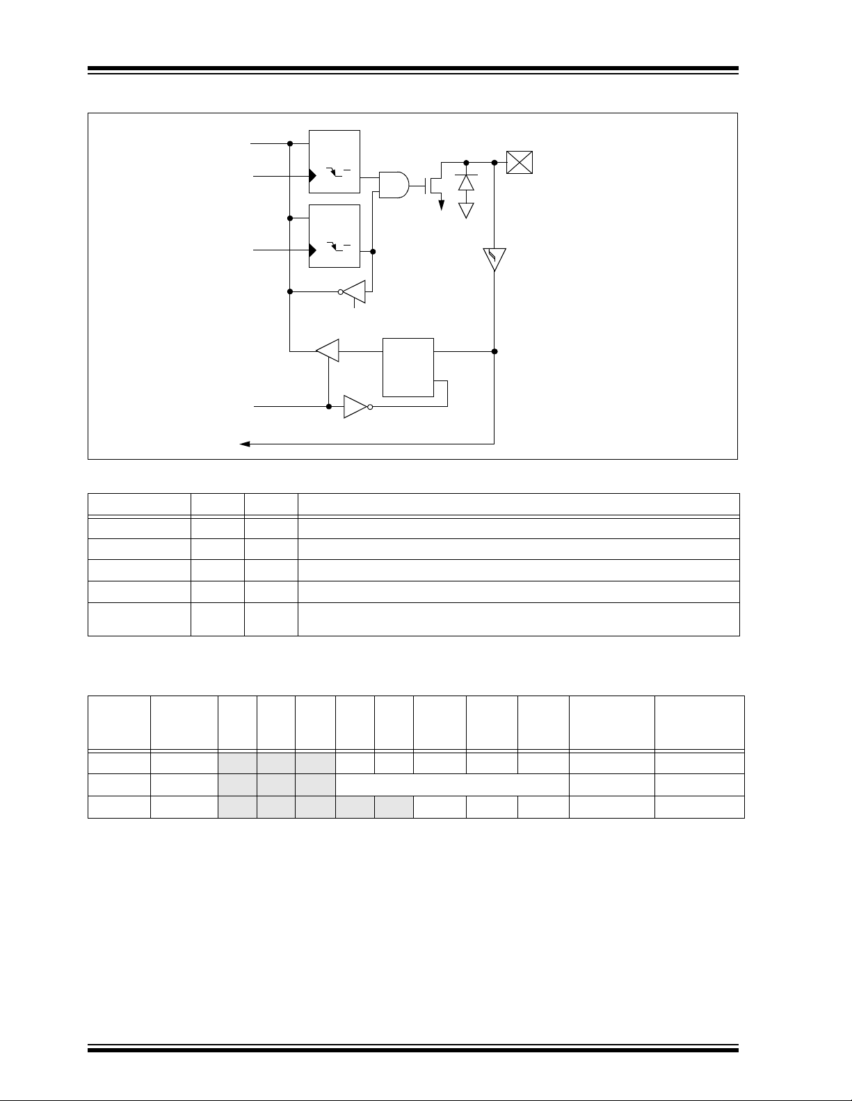
FIGURE 3-2: BLOCK DIAGRAM OF RA4/T0CKI PIN
DA TA
BUS
WR
PORT
WR
TRIS
RD PORT
TMR0 Clock Input
QD
Q
CK
Data Latch
QD
Q
CK
TRIS Latch
RD TRIS
N
V
QD
EN
EN
TABLE 3-1 PORTA FUNCTIONS
Name Bit# Buffer Function
RA0/AN0 bit0 TTL Input/output or analog input
RA1/AN1 bit1 TTL Input/output or analog input
RA2/AN2 bit2 TTL Input/output or analog input
RA3/AN3/V
RA4/T0CKI bit4 ST
Legend: TTL = TTL input, ST = Schmitt Trigger input
REF bit3 TTL Input/output or analog input or VREF
Input/output or external clock input for Timer0
Output is open drain type
SS
VSS
Schmitt
Trigger
Input
Buffer
I/O Pin
TABLE 3-2 SUMMARY OF REGISTERS ASSOCIATED WITH PORTA
Value on
Address Name Bit 7 Bit 6 Bit 5 Bit 4 Bit 3 Bit 2 Bit 1 Bit 0
POR,
BOR
05h PORTA
85h TRISA
9Fh ADCON1
— — —
— — —
— — — — — PCFG2 PCFG1 PCFG0 ---- -000 ---- -000
(1)
RA4 RA3 RA2 RA1 RA0 --xx xxxx --xu uuuu
(1)
PORTA Data Direction Register --11 1111 --11 1111
Legend: x = unknown, u = unchanged, - = unimplemented locations read as '0'. Shaded cells are not used by
PORTA.
Note 1: Reserved bits; Do Not Use.
DS41106A-page 22 Preliminary
1998 Microchip Technology Inc.
Value on all
other resets
PIC16C712/716
3.2 PORTB and the TRISB Register
PORTB is an 8-bit wide bi-directional port. The corresponding data direction register is TRISB. Setting a
TRISB bit (=1) will make the correspon ding POR TB pin
an input, (i.e., put the corresponding output driver in a
hi-impedance mode). Clearing a TRISB bit (=0) will
make the corresponding PORTB pin an output, (i.e.,
put the contents of the output latch on the selected pin).
EXAMPLE 3-1: INITIALIZING PORTB
BCF STATUS, RP0 ;
CLRF PORTB ; Initialize PORTB by
; clearing output
; data latches
BSF STATUS, RP0 ; Select Bank 1
MOVLW 0xCF ; Value used to
; initialize data
; direction
MOVWF TRISB ; Set RB<3:0> as inputs
; RB<5:4> as outputs
; RB<7:6> as inputs
FIGURE 3-3: BLOCK DIAGRAM OF RB0 PIN
(1)
RBPU
DATA BUS
WR PORT
WR TRIS
Data Latch
QD
CK
TRIS Latch
QD
CK
Each of the PORTB pins has a weak internal pull-up. A
single control bit can turn on all the pull-u ps. This is performed by clea ring bi t RBPU
(OPTION_REG<7>). The
weak pull-u p is auto matical ly tur ned off when the p or t
pin is configured as an output. The pull-ups are disabled on a Power-on Reset.
V
DD
VDD
weak
P
pull-up
I/O
pin
TTL
Input
Buffer
VSS
RB0/INT
Note 1: To enable weak pull-ups, set the appropriate TRIS bit(s) and clear the RBPU bit (OPTION_REG<7>).
1999 Microchip Technology Inc.
RD TRIS
RD PORT
Schmitt Trigger
Buffer
QD
EN
RD PORT
Preliminary DS41106A-page 23
PIC16C712/716
PORTB pins RB3:RB1 are multiplexed with several
peripheral functions (T able 3-3). PORTB pins RB3:RB0
have Schmitt Trigger input buffers.
When enabling peripheral functions, care should be
taken in defining TRIS bits for each PORTB pin. Some
periphe rals override the TRIS bit to make a pin an output, while other peripherals override the TRIS bit to
make a pin an input. Since the TRIS bit override is in
effect while the peripheral is enabled, read-modifywrite instructions (BSF, BCF, XORWF) with TRISB as
destination shou ld be a voi ded. The us er should refe r to
the corresponding peripheral section for the correct
TRIS bit settings.
Four of PORTB’s pins, RB7:RB4, have an interrupt on
change feature. Only pins configured as inputs can
cause this interrupt to oc cur (i.e . any RB7:RB4 pin configured as an output is excluded from the interrupt on
change comparison). The input pins, RB7:RB4, are
PORTB. The “mismatch” outputs of RB7:RB4 are
OR’ed together to generate the RB Port Change Interrupt with flag bit RBIF (INTCON<0>).
This interrupt can wake the device from SLEEP. The
user, i n the interrupt service routine , can clea r the interrupt in the following manner:
a) Any read or write of PORTB will end the mis-
match condition.
b) Clear flag bit RBIF.
A mismatch condition will continue to set flag bit RBIF.
Reading PORTB will end the mismatch condition and
allow flag bit RBIF to be cleared.
The interrupt on change feature is recommended for
wake-up on key depression operation and opera tions
where PORTB is only used for the interrupt on change
feature. Polling of PORTB is not recommended while
using the interrupt on change feature.
compared with th e o ld value latche d o n the la st read of
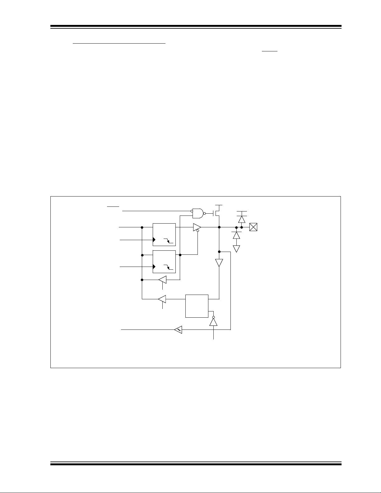
FIGURE 3-4: BLOCK DIAGRAM OF RB1/T1OSO/T1CKI PIN
(1)
RBPU
T1OSCEN
T1CS
DATA BUS
RD
DATACCP
WR
DATACCP
WR
TRISCCP
WR
PORTB
WR TRISB
T1OSCEN
TMR1CS
DATACCP<0>
QD
Q
CK
TRISCCP<0>
QD
Q
CK
PORTB<1>
QD
Q
CK
TRISB<1>
QD
Q
CK
1
0
1
0
V
DD
P
weak
pull-up
VDD
RB1/T1OSO/T1CKI
VSS
1
TTL Buffer
RD PORTB
Note 1: To enable weak pull-ups, set the appropriate TRIS bit(s) and clear the RBPU bit (OPTION_REG<7>).
DS41106A-page 24 Preliminary
0
T1CLKIN
ST
Buffer
1999 Microchip Technology Inc.
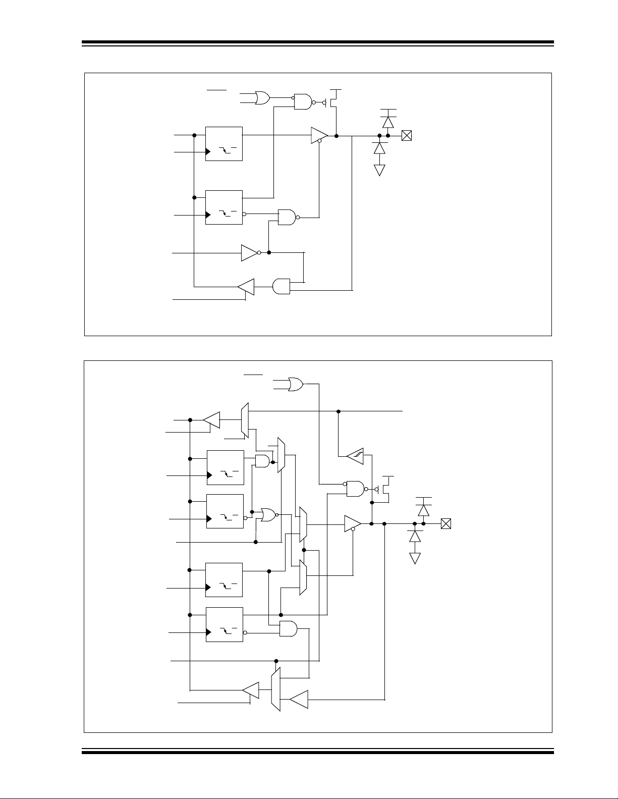
FIGURE 3-5: BLOCK DIAGRAM OF RB2/T1OSI PIN
(1)
RBPU
T1OSCEN
DATA B US
WR PORTB
PORTB<2>
QD
Q
CK
V
P
DD
weak
pull-up
PIC16C712/716
VDD
RB1/T1OSO/T1CKI
TRISB<2>
QD
WR TRISB
T1OSCEN
RD PORTB
Note 1: To enable weak pull-ups, set the appropriate TRIS bit(s) and clear the RBPU bit (OPTION_REG<7>).
CK
Q
TTL Buffer
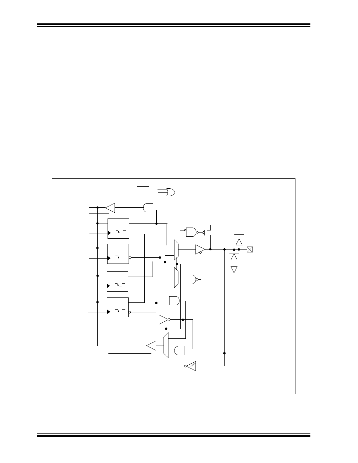
FIGURE 3-6: BLOCK DIAGRAM OF RB3/CCP1 PIN
(1)
RBPU
CCPON
CCPON
CK
CK
1
0
CCPOUT
1
QD
Q
QD
Q
0
1
0
QD
Q
QD
Q
1
0
DATA BUS
RD
DATACCP
WR
DATACCP
WR
TRISCCP
CCP
Output
Mode
WR
PORTB
WR
TRISB
DATACCP<2>
TRISCCP<2>
PORTB<3>
CK
TRISB<3>
CK
VSS
V
DD
P
CCPIN
weak
pull-up
VDD
RB3/CCP1
VSS
CCPON
RD PORTB
1999 Microchip Technology Inc.
1
0
TTL Buffer
Note 1: To enable weak pull-ups, set the appropr iate TRIS b it(s)
and clear the RBPU bit (OPTION_REG<7>).
Preliminary DS41106A-page 25
PIC16C712/716
FIGURE 3-7: BLOCK DIAGRAM OF RB7:RB4 PINS
(1)
RBPU
DATA BUS
WR PORT
WR TRIS
Data Latch
QD
CK
TRIS Latch
QD
CK
TTL
Buffer
V
P
DD
weak
pull-up
ST
Buffer
VDD
I/O
pin
VSS
RD TRIS
Set RBIF
From other
RB7:RB4 pins
RB7:RB6 in serial programming mode
Note 1: To enable weak pull-ups, set the appropriate TRIS bit(s) and clear the RBPU bit (OPTION_REG<7>).
RD PORT
Latch
QD
EN
QD
EN
Q1
RD PORT
Q3
TABLE 3-3 PORTB FUNCTIONS
Name Bit# Buffer Function
RB0/INT bit0 TTL/ST
RB1/T1OS0/
bit1
TTL/ST
T1CKI
RB2/T1OSI bit2
RB3/CCP1 bit3
TTL/ST
TTL/ST
RB4 bit4 TTL Input/output pin (with interrupt on chang e). Internal so ftware prog ra mmab le
RB5 bit5 TTL Input/output pin (with interrupt on chang e). Internal so ftware prog ra mmab le
RB6 bit6 TTL/ST
RB7 bit7 TTL/ST
Legend: TTL = TTL input, ST = Schmitt Trigger input
Note1: This buffer is a Schmitt Trigger input when configured as the external interrupt or peripheral input.
2: This buffer is a Schmitt Trigger input when used in serial programming mode.
(1)
Input/output pin or external interrupt input. Internal software
programmable weak pull-up.
(1)
Input/output pin or Timer 1 os cilla tor outpu t, or Tim er 1 cl oc k inp ut. Inte rnal
software programmable weak pull-up. See Timer1 section for detailed
operation.
(1)
Input/output pin or T imer 1 os cilla tor in put. Internal s oftw are prog ram mab le
weak pull-up. See Timer1 section for detailed operation.
(1)
Input/output pin or Captu re 1 input , or Com pare 1 outp ut, or PWM1 output.
Internal software programmable weak pull-up. See CCP1 section for
detailed operation.
weak pull-up .
weak pull-up .
(2)
Input/output pin (with in terrupt on ch ange). In ternal softw are prog ramm ab le
weak pull-up. Serial programming clock.
(2)
Input/output pin (with in terrupt on ch ange). In ternal softw are prog ramm ab le
weak pull-up. Serial programming data.
DS41106A-page 26 Preliminary
1999 Microchip Technology Inc.

PIC16C712/716
TABLE 3-4 SUMMARY OF REGISTERS ASSOCIATED WITH PORTB
Address Name Bit 7 Bit 6 Bit 5 Bit 4 Bit 3 Bit 2 Bit 1 Bit 0
06h PORTB RB7 RB6 RB5 RB4 RB3 RB2 RB1 RB0 xxxx xxxx uuuu uuuu
86h TRISB PORTB Data Direction Register 1111 1111 1111 1111
81h OPTION_REG RBPU
Legend: x = unknown, u = unchanged. Shaded cells are not used by PORTB.
INTEDG T0CS T0SE PSA PS2 PS1 PS0 1111 1111 1111 1111
Value on:
POR,
BOR
Value on all
other resets
1999 Microchip Technology Inc.
Preliminary DS41106A-page 27

PIC16C712/716
NOTES:
DS41106A-page 28 Preliminary
1999 Microchip Technology Inc.
PIC16C712/716
4.0 TIMER0 MODUL E
The Timer0 module ti mer/count er has the f ollo wing f eatures:
• 8-bit timer/counter
• Readable and writable
• Internal or external clock select
• Edge select for external clock
• 8-bit software programmable prescaler
• Interrupt on overflow from FFh to 00h
Figure 4-1 is a simplified block diagram of the Timer0
module.
Additional information on timer modules is available in
the PICmicro™ Mid-Range Reference Manual,
(DS33023).
4.1 Timer0 Operation
Timer0 can operate as a timer or as a counter.
Timer mode is selected by clearing bit T0CS
(OPTION_REG<5>). In timer mode, the Timer0 module will increment every instruction cycle (without prescaler). If the TMR0 register is written, the increment is
inhibited for the following two instruction cycles. The
user can work around this by writing an adjusted value
to the TMR0 register.
Counter mode is selected by setting bit T0CS
(OPTION_REG<5>). In counter mode, Timer0 will
increment on every rising or falling edge of pin
RA4/T0CKI. The incrementing edge is determined by
the Timer0 Source Edge Select bit T0SE
(OPTION_REG<4>). Clearing bit T0 SE sel ec ts the rising edge. Restrictions on the external clock input are
discussed be low.
When an ex ternal clock i nput is used f or Timer0 , it must
meet certain requirements. The requirements ensure
the external c lock can be synchron ized w ith the int ernal
phase clock (T
incrementing of Timer0 after synchronization.
OSC). Also, there is a delay in the actual
Additional information on external clock requirements
is available in the PICmicro™ Mid-Range Reference
Manual, (DS33023).
4.2 Prescaler
An 8-bit counter is available as a prescaler for the
Timer0 module or as a postscaler for the Watchdog
Timer, respectively (Figure 4-2). For simplicity, this
counter is being referred to as “prescaler” throughout
this data sheet. Note that there is only one prescaler
avail able, w hich is mutually exclus ively sha red between
the Timer0 module and the Watchdog Timer. Thus, a
prescaler assignment for the Timer0 module means
that there is no prescaler for the Watchdog Timer and
vice-versa.
The prescaler is not readable or writable.
The PSA and PS2:PS0 bits (OPTION_REG<3:0>)
determine the prescaler a ssignment an d prescale ratio .
Clearing bit PSA will assign the prescale r to the Time r0
module. When the prescaler is assigned to the Timer0
module, prescale values of 1:2, 1:4, ..., 1:256 are
selectable.
Setting bit PSA will assign the prescaler to the Watchdog Timer (WDT). When the prescaler is assigned to
the WDT, prescale values of 1:1, 1:2, ..., 1:128 are
selectable.
When assigned to the Timer0 module, all instructions
writing to the TMR0 register (e.g . CLRF 1, MOVWF 1,
BSF 1,x....etc.) will clear the prescaler. When
assigned to WDT, a CLRWDT instruction will clear the
prescaler along with the WDT.
Note: Writing to TMR0 when the prescaler is
assigned to Timer0 will clear the prescaler
count, but will not change the prescaler
assignment.
FIGURE 4-1: TIMER0 BLOCK DIAGRAM
FOSC/4
RA4/T0CKI
pin
T0SE
(1)
Note 1: T0CS, T0SE, PSA, PS2:PS0 (OPTION_REG<5:0>).
2: The prescaler is shared with Watchdog Timer (refer to Figure 4-2 for detailed block diagram).
1999 Microchip Technology Inc.
0
1
T0CS
Programmable
PS2, PS1, PS0
(1)
Prescaler
(2)
3
(1)
Preliminary DS41106A-page 29
PSA
1
0
PSout
(1)
Sync with
Internal
clocks
(2 cycle delay)
Data Bus
8
TMR0
PSout
Set interrupt
flag bit T0IF
on overflow
PIC16C712/716
4.2.1 SWITCHING PRESCALER ASSIGNMENT The prescaler assignment is fully under software con-
trol, i.e., it can be changed “on the fly” during program
ex ec utio n.
Note: To avoid an unintended d evice RESET, a
specific instruction sequence (shown in
the PICmicro™ Mid-Range Reference
Manual, DS33023) must be executed
when changing the prescaler a ssignment
4.3 Timer0 Interrupt
The TMR0 interrupt is generated when the TMR0 register overflows from FFh to 00 h. This overflow sets bit
T0IF (INTC ON<2>). The inter rupt can be mas ked by
clearing bit T0IE (INTCON<5>). Bit T0IF must be
cleared in softwa re b y the T imer0 mo dule interrupt s ervice routine before re-enabling this interrupt. The
TMR0 interrupt cannot awaken the processor from
SLEEP since the timer is shut off during SLEEP.
from Timer0 to the WDT. This sequence
must be followed even if the WDT is disabled.
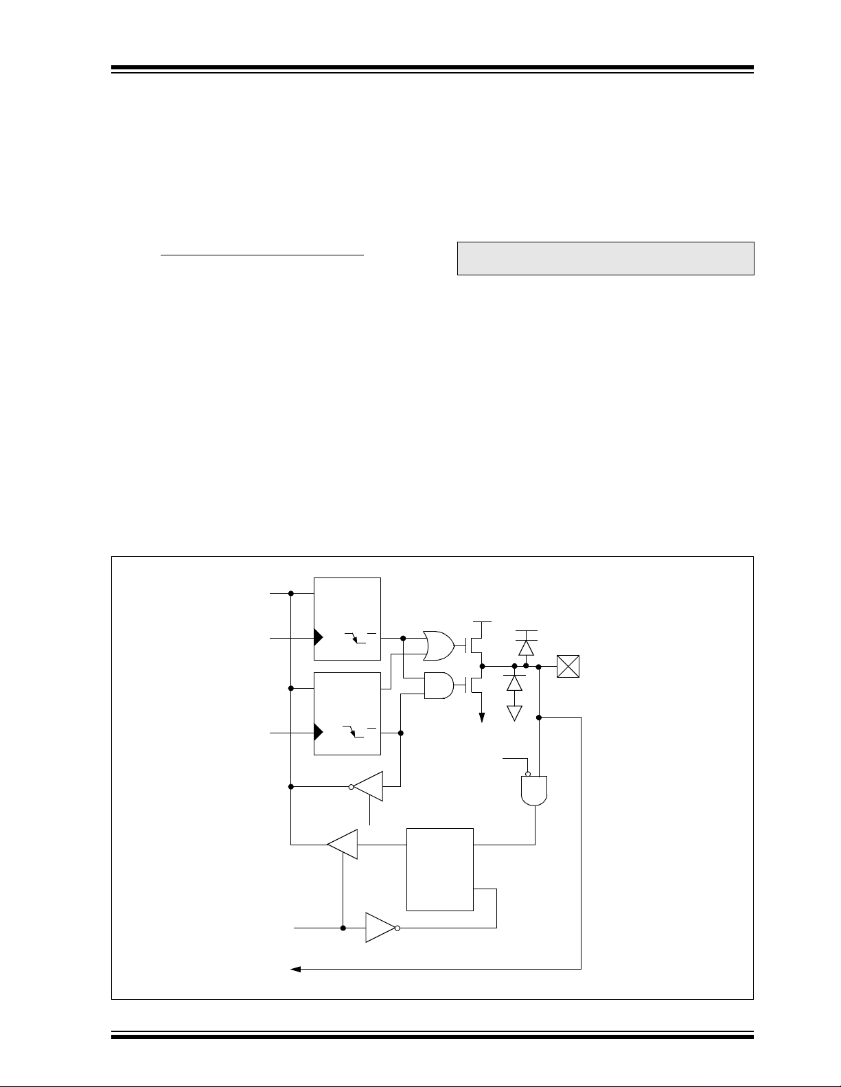
FIGURE 4-2: BLOCK DIAGRAM OF THE TIMER0/WDT PRESCALER
CLKOUT (=Fos c/ 4)
RA4/T0CKI
pin
T0SE
0
1
T0CS
M
U
X
1
M
U
0
X
PSA
SYNC
2
Cycles
Data Bus
8
TMR0 reg
Set flag bit T0IF
on Overflow
0
M
U
1
Watchdog
Timer
WDT Enable bit
Note: T0CS, T0SE, PSA, PS2:PS0 are (OPTION_REG<5:0>).
X
PSA
8-bit Prescaler
8
8 - to - 1MUX
0
M U X
WDT
Time-out
PS2:PS0
1
PSA
TABLE 4-1 REGISTERS ASSOCIATED WITH TIMER0
Address Name Bit 7 Bit 6 Bit 5 Bit 4 Bit 3 Bit 2 Bit 1 Bit 0
01h TMR0 Timer0 module’s register xxxx xxxx uuuu uuuu
0Bh,8Bh INTCON GIE
81h OPTION_REG
85h TRISA
Legend: x = unknown, u = unchanged, - = unimplemented locations read as '0'. Shaded cells are not used by Timer0.
RBPU INTEDG T0CS T0SE PSA PS2 PS1 PS0 1111 1111 1111 1111
PEIE T0IE INTE RBIE T0IF INTF RBIF 0000 000x 0000 000u
— — —
(1)
Bit 4 PORTA Data Direction Register --11 1111 --11 1111
Value on:
POR,
BOR
Note 1: Reserved bit; Do Not Use.
Value on all
other resets
DS41106A-page 30 Preliminary
1999 Microchip Technology Inc.

PIC16C712/716
5.0 TIMER1 MODUL E
The Timer1 module timer/co unter has th e fol lowing f eatures:
• 16-bit timer/counter
(Two 8-bit registers; TMR1H and TMR1L)
• Readable and writable (Both registers)
• Internal or external clock select
• Interrupt on overflow from FFFFh to 0000h
• Reset from CCP module trigger
Timer1 has a control register, shown in Figure 5-1.
Timer1 can be enabled/disabled by setting/clearing
control bit TMR1ON (T1CON<0>).
Figure 5-2 is a simplified block diagram of the Timer1
module.
Additional information on timer modules is available in
the PICmicro™ Mid-Range Reference Manual,
(DS33023).
5.1 Timer1 Operation
Timer1 can operate in one of these modes:
•As a timer
• As a synchronous counter
• As an asynchronous counter
The operating mode is determined by the clock select
bit, TMR1CS (T1CON<1>).
In timer mode, Timer1 increments every instruction
cycle. In coun ter mo de, it in crement s on every risi ng
edge of the external clock input.
When the Timer1 oscillator is enabled (T1OSCEN is
set), the RB2/T1OSI and RB1/T1OSO/T1CKI pins
become inputs. That is, the TRISB<2:1> value is
ignored.
Timer1 also has an in ternal “reset input ”. This reset can
be generated by the CCP module (Section 7.0).
FIGURE 5-1: T1CON: TIMER1 CONTROL REGISTER (ADDRESS 10h)
U-0 U-0 R/W-0 R/W-0 R/W-0 R/W-0 R/W-0 R/W-0
— — T1CKPS1 T1CKPS0 T1OSCEN T1SYNC TMR1CS TMR1ON
bit7 bit0
bit 7-6: Unimplemented: Read as ’0’
bit 5-4: T1CKPS1:T1CKPS0: Timer1 Input Clock Prescale Select bits
11 = 1:8 Prescale value
10 = 1:4 Prescale value
01 = 1:2 Prescale value
00 = 1:1 Prescale value
bit 3: T1OSCEN: Timer1 Oscillator Enable Control bit
1 = Oscillator is enabled
0 = Oscillator is shut off
Note: The oscillator inverter and feedback resistor are turned off to eliminate power drain
bit 2: T1SYNC
: Timer1 External Clock Input Synchronization Control bit
R = Readable bit
W = Writable bit
U = Unimplemented bit,
read as ‘0’
- n = Value at POR reset
TMR1CS = 1
1 = Do not synchronize external clock input
0 = Synchronize external clock input
TMR1CS = 0
This bit is ignored. Timer1 uses the internal clock when TMR1CS = 0.
bit 1: TMR1CS: Timer1 Clock Source Select bit
1 = External clock from pin RB1/T1OSO/T1CKI (on the rising edge)
0 = Internal clock (F
bit 0: TMR1ON: Timer1 On bit
1 = Enables Timer1
0 = Stops Timer1
1999 Microchip Technology Inc.
OSC/4)
Preliminary DS41106A-page 31

PIC16C712/716
FIGURE 5-2: TIMER1 BLOCK DIAGRAM
Set flag bit
TMR1IF on
Overflow
RB1/T1OSO/T1CKI
RB2/T1OSI
Note 1: When the T1OSCEN bit is cleared, the inverter and feedback resistor are turned off. This eliminates power drain.
TMR1H
T1OSC
TMR1
TMR1L
T1OSCEN
Enable
Oscillator
(1)
FOSC/4
Internal
Clock
TMR1ON
on/off
1
0
T1CKPS1:T1CKPS0
TMR1CS
0
1
T1SYNC
Prescaler
1, 2, 4, 8
2
5.2 Timer1 Module and PORTB Operation
Synchronized
clock input
Synchronize
det
SLEEP input
When Timer1 is configured as timer running from the
main oscillator, PORTB<2:1> operate as normal I/O
lines. When Timer1 is configured to function as a
counter however, the clock source selection may affect
the operation of PORTB<2:1>. Multiplexing details of
the Timer1 clock sel ection on POR TB are shown in Figure 3-4 and Figure 3-5.
The clock source for Timer1 in the counter mode can
be from one of the following:
1. External circuit connected to the
RB1/T1OSO/T1CKI pin
2. Firmware controlled DATACCP<0> bit, DT1CKI
3. Timer1 oscillator
Table 5-1 shows the detail s of Timer1 mod e selecti ons,
control bit settings, TMR1 and PORTB operations.
DS41106A-page 32 Preliminary
1999 Microchip Technology Inc.

PIC16C712/716
TABLE 5-1 TMR1 MODULE AND PORTB OPERATION
TMR1
Module
Mode
Off N/A T1CON = --xx 0x00 Off PORTB<2:1> function as normal
Timer Fosc/4 T1CON = -- xx 0x01 TMR1 module uses the main
Counter
Clock Source Control Bits TMR1 Module Operation PORTB<2:1> Operation
I/O
PORTB<2:1> function as normal
oscillator as clock source.
TMR1ON can turn on or turn off
Timer1.
External circuit T1CON = --xx 0x11
TR1SCCP = ---- -x-1
Firmware T1CON = --xx 0x11
TR1SCCP = ---- -x-0
Timer1 oscillator T1CON = --xx 1x11 RB1/T1OSO /T1CKI and
TMR1 module uses the external
signal on the
RB1/T1OSO/T1CKI pin as a
clock source. TMR1ON can turn
on or turn off Timer1. DT1CK
can read the signal on the
RB1/T1OSO/T1CKI pin.
DATACCP<0> bit drives
RB1/T1OSO/T1CKI and produces the TMR1 clock source.
TMR1ON can turn on or turn off
Timer1. The DATACCP<0> bit,
DT1CK, can read and write to
the RB1/T1OSO/T1CKI pin.
RB2/T1OSI are configured as a
2 pin crystal oscillator.
RB1/T1OSI/T1CKI is the clock
input for TMR1. TMR1ON can
turn on or turn off Timer1.
DATACCP<1> bit, DT1CK,
always rea ds 0 as in put and ca n
not write to the
RB1/T1OSO/T1CK1 pin .
I/O
PORTB<2> functions as normal
I/O. PORTB<1> always reads 0
when configured as input . If
PORTB<1> is configured as out-
put, reading POR TB< 1> w i ll r ead
the data latch. Writing to
PORTB<1> will always store the
result in the data latch, but not to
the RB1/T1OSO/T1CKI pin. If
the TMR1CS bit is cleared
(TMR1 reverts to the timer
mode), then pin PORTB<1> will
be driven with the value in the
data latch.
PORTB<2:1> always read 0
when configured as inputs. If
PORTB<2:1> are config ured as
outputs, reading PORTB<2:1>
will read the data latche s. Writing
to PORTB<2:1> will always store
the result in the data latches, but
not to the RB2/T1OSI and
RB1/T1OSO/T1CKI pins. If the
TMR1CS and T1OSCEN bits are
cleared (TMR1 reverts to the
timer mode and TMR1 oscillator
is disabled), then pin
PORTB<2:1> will be driven with
the value in the data latches.
1999 Microchip Technology Inc.
Preliminary DS41106A-page 33

PIC16C712/716
5.3 Timer1 Oscillator
A crystal oscillator circuit is b uilt in betw een pins T1OSI
(input) and T1OSO (amplifier output). It is enabled by
setting control bit T1OSCEN (T 1CON<3>). The oscill ator is a low power oscillator rated up to 200 kHz. It will
continue to run during SLEEP. It is primarily intended
for a 32 kHz crystal. Table 5-2 shows the capacitor
selection for the Timer1 osci llator.
The Timer1 oscillator is identical to the LP oscillator.
The user must provide a software time delay to ensure
proper oscillator start-up.
TABLE 5-2 CAPACITOR SELECTION FOR
THE TIMER1 OSCILLATOR
Osc Type Freq C1 C2
LP 32 kHz 33 pF 33 pF
100 kHz 15 pF 15 pF
200 kHz 15 pF 15 pF
These values are for design guidanc e only.
Note 1: Higher capacitance increases the stability
of oscillator but also increases the sta rt-up
time.
2: Since each reso nator/crystal has its own
characteristics, the user should consult the
resonator/crystal manufacturer for app ropri ate values of external components.
5.4 Timer1 Interrupt
The TMR1 Register pair (TMR1H:TMR1L) increments
from 0000h to FFFFh and rolls over to 0000h. The
TMR1 interrupt, if enabled, is generated on overflow
which is latched in interrupt flag bit TMR1IF (P IR1<0>).
This interrupt can be enab led/d isab led by se tting/cle aring TMR1 interrupt enable bit TMR1IE (PIE1<0>).
5.5 Resetting Timer1 using a CCP T rigger Output
If the CCP module is configured in compare mode to
generate a “special event trigger" (CCP1M3:CCP1M0
= 1011), this signal will reset Timer1 and start an A/D
conversion (if the A/D module is enabled).
Note: The special event triggers from the CCP1
module will not set interrupt flag bit
TMR1IF (PIR1<0>).
Timer1 must be configured for either timer or synchronized counter mode to tak e adv antage of this fea ture . If
Timer1 is running in asynchronous counter mode, this
reset operation may not work.
In the ev ent that a write to Timer1 coinc ides with a sp ecial event trigger from CCP1, the write will take precedence.
In this mode of operati on, the CC PR1H:CCPR 1L regis ters pair effectively becomes the period register for
Timer1.
TABLE 5-3 REGISTERS ASSOCIATED WITH TIMER1 AS A TIMER/COUNTER
Address Name Bit 7 Bit 6 Bit 5 Bit 4 Bit 3 Bit 2 Bit 1 Bit 0
0Bh,8Bh INTCON GIE PEIE
0Ch PIR1
8Ch PIE1
0Eh TMR1L Holding register for the Least Significant Byte of the 16-bit TMR1 register
0Fh TMR1H Holding register for the Most Significant Byte of the 16-bit TMR1 register
10h T1CON
07h DATACCP
87h TRISCCP
Legend: x = unknown, u = unchanged, - = unimplemented read as '0'. Shaded cells are not used by the Timer1 module.
— ADIF — — — CCP1IF TMR2IF TMR1IF
— ADIE — — — CCP1IE TMR2IE TMR1IE
— — T1CKPS1 T1CKPS0 T1OSCEN T1SYNC TMR1CS TMR1ON
— — — — — DCCP —DT1CK
— — — — — TCCP —TT1CK
T0IE INTE RBIE T0IF INTF RBIF
Value on
POR,
BOR
0000 000x 0000 000u
-0-- -000 -0-- -000
-0-- -000 -0-- -000
xxxx xxxx uuuu uuuu
xxxx xxxx uuuu uuuu
--00 0000 --uu uuuu
---- -x-x ---- -u-u
---- -1-1 ---- -1-1
Val ue on
all other
resets
DS41106A-page 34 Preliminary
1999 Microchip Technology Inc.

NOTES:
PIC16C712/716
1999 Microchip Technology Inc.
Preliminary DS41106A-page 35

PIC16C712/716
6.0 TIMER2 MODULE
The Timer2 module timer has the following features:
• 8-bit timer (TMR2 register)
• 8-bit period register (PR2)
• Readable and writable (Both registers)
• Software programmable prescaler (1:1, 1:4, 1:16)
• Software programmable postscaler (1:1 to 1:16)
Timer2 has a control register, shown in Figure 6-1.
Timer2 can be shut off by clearing con trol bi t T MR 2ON
(T2CON<2>) to minimize power consumption.
Figure 6-2 is a simplified block diagram of the Timer2
module.
Additional information on timer modules is available in
the PICmicro™ Mid-Range Reference Manual,
(DS33023).
• Interrupt on TMR 2 match of PR2
FIGURE 6-1: T2CON: TIMER2 CONTROL REGISTER (ADDRESS 12h)
U-0 R/W-0 R/W-0 R/W-0 R/W-0 R/W-0 R/W-0 R/W-0
— TOUTPS3 TOUTPS2 TOUTPS1 T OUTPS0 TMR2ON T2CKPS1 T2CKPS0 R = Readable bit
bit7 bit0
bit 7: Unimplemented: Read as '0'
bit 6-3: TOUTPS3:TOUTPS0: Timer2 Output Postscale Select bits
0000 = 1:1 Postscale
0001 = 1:2 Postscale
0010 = 1:3 Postscale
0011 = 1:4 Postscale
0100 = 1:5 Postscale
0101 = 1:6 Postscale
0110 = 1:7 Postscale
0111 = 1:8 Postscale
1000 = 1:9 Postscale
1001 = 1:10 Postscale
1010 = 1:11 Postscale
1011 = 1:12 Postscale
1100 = 1:13 Postscale
1101 = 1:14 Postscale
1110 = 1:15 Postscale
1111 = 1:16 Postscale
bit 2: TMR2ON: Timer2 On bit
1 = Timer2 is on
0 = Timer2 is off
bit 1-0: T2CKPS1:T2CKPS0: Timer2 Clock Prescale Select bits
00 = Prescaler is 1
01 = Prescaler is 4
1x = Prescaler is 16
W = Writable bit
U = Unimplemented bit,
- n = Value at POR reset
read as ‘0’
FIGURE 6-2: TIMER2 BLOCK DIAGRAM
Sets flag
bit TMR2IF
Postscaler
1:1 1:16
DS41106A-page 36 Preliminary
TMR2
output
Reset
to
4
EQ
TMR2 reg
Comparator
PR2 reg
Prescaler
1:1, 1:4, 1:16
2
F
OSC/4
1999 Microchip Technology Inc.

PIC16C712/716
6.1 Timer2 Operation
Timer2 can be used as the PWM time-base for PWM
mode of the CCP module.
The TMR2 register is readable and writable, and is
cleared on any device reset.
The input clock (F
OSC/4) has a prescale option of 1:1,
6.2 Timer2 Interrupt
The Timer2 module has an 8-bit period register PR2.
Timer2 increments from 00h until it matches PR2 and
then resets to 00h on the next increment cycle. PR2 is
a readable a nd writable regi ster. The PR2 regist er is initialized to FFh upon reset.
1:4 or 1:16, selected by control bits
T2CKPS1:T2CKPS0 (T2CON<1:0>).
The match output of TMR2 goes through a 4-bit
postscaler (which gives a 1:1 to 1:16 scaling inclusive)
to generate a TMR2 interrupt (latched in flag bit
TMR2IF, (PIR1<1>)).
The prescaler and postscaler counters are cleared
when any of the following occurs:
• a write to the TMR2 register
• a write to the T2CON register
• any device reset (Power-on Reset, MCLR
reset,
Watchdog Timer reset, or Brown-out Reset)
TMR2 is not cleared when T2CON is written.
TABLE 6-1 REGISTERS ASSOCIATED WITH TIMER2 AS A TIMER/COUNTER
Address Name Bit 7 Bit 6 Bit 5 Bit 4 Bit 3 Bit 2 Bit 1 Bit 0
0Bh,8Bh INTCON GIE PEIE
0Ch PIR1
8Ch PIE1
11h TMR2 Timer2 module’s register
12h T2CON
92h PR2 Timer2 Period Register
Legend: x = unknown, u = unchanged, - = unimplemented read as '0'. Shaded cells are not used by the Timer2 module.
— ADIF — —
— ADIE — —
— TOUTPS3 TOUTPS2 TOUTPS1 TOUTPS0 TMR2ON T2CKPS1 T2CKPS0
T0IE INTE RBIE T0IF INTF RBIF
CCP1IF TMR2IF TMR1IF
—
CCP1IE TMR2IE TMR1IE
—
Value on
POR,
BOR
0000 000x 0000 000u
-00- -000 0000 -000
-0-- -000 0000 -000
0000 0000 0000 0000
-000 0000 -000 0000
1111 1111 1111 1111
Value on
all other
resets
1999 Microchip Technology Inc.
Preliminary DS41106A-page 37

PIC16C712/716
NOTES:
DS41106A-page 38 Preliminary
1999 Microchip Technology Inc.

PIC16C712/716
7.0 CAPTURE/COMPARE/PWM (CCP) MODULE(S)
Each CCP (Capture/Compare/PWM) module contains
a 16-bit register, which can operate as a 16-bit capture
register, as a 16-bit compare register or as a PWM
master/slave Duty Cycle register. Table 7-1 shows the
timer resources of the CCP module modes.
Capture/Compare/PWM Register 1 (CCPR1) is co mprised o f two 8-bit regis ters: CCPR1L (l ow byte) and
CCPR1H (high byte). The CCP1CON register controls
the operation of CCP1. All are readable and writable.
FIGURE 7-1: CCP1CON REGISTER (ADDRESS 17h)
U-0 U-0 R/W-0 R/W-0 R/W-0 R/W-0 R/W-0 R/W-0
— — DC1B1 DC1B0 CCP1M3 CCP1M2 CCP1M1 CCP1M0 R = Readable bit
bit7 bit0
bit 7-6: Unimplemented: Read as '0'
bit 5-4: DC1B1:DC1B0: PWM Least Significant bits
Capture Mode: Unused
Compare Mode: Unused
PWM Mode: These bi ts are the two LSbs of the PWM duty cycle. The e igh t M Sbs are found in CC PR 1L .
bit 3-0: CCP1M3:CCP1M0: CCP1 Mode Select bits
0000 = Capture/Compare/PWM off (resets CCP1 module)
0100 = Capture mode, every falling edge
0101 = Capture mode, every rising edge
0110 = Capture mode, every 4th rising edge
0111 = Capture mode, every 16th rising edge
1000 = Compare mode, set output on match (CCP1IF bit is set)
1001 = Compare mode, clear out put on mat ch (CCP1IF bit is set)
1010 = Compare mode , generat e software in terrupt on match (CCP1IF bit is set, C CP1 pin is unaff ected )
1011 = Compare mode, trigger special event (CCP1IF bit is set; CCP1 resets TMR1 and starts an A/D
conversion (if A/D module is enabled))
11xx = PWM mode
Additional information on the CCP module is available
in the PICmicro™ Mid-Range Reference Manual,
(DS33023).
TABLE 7-1 CCP MODE - TIMER
RESOURCE
CCP Mode Timer Resource
Capture
Compare
PWM
W =Writable bit
U = Unimplemented bit, read
as ‘0’
- n =Value at POR reset
Timer1
Timer1
Timer2
FIGURE 7-2: TRISCCP Register (ADDRESS 87h)
R/W-1 R/W-1 R/W-1 R/W-1 R/W - 1 R/W-1 R/W-1 R/W-1
———— —TCCP—TT1CKR =Readable bit
bit7 bit0
bit 7-3: R eserved bits; Do Not Use
bit 2: TCCP - T ri state control bit for CCP
bit 1: Reserved bit; Do Not Use
bit 0: TT1CK - Tri state control bit for T1CKI pin
1999 Microchip Technology Inc.
0 = Output pin driven
1 = Output pin tristated
0 = T1CKI pin is an output
1 = T1CKI pin is an input
Preliminary DS41106A-page 39
W =Writable bit
U = Unimplemented bit, read
as ‘0’
- n =Value at POR reset

PIC16C712/716
7.1 Capture Mode
In Capture mode, CCPR1H:CCPR1L captures the
16-bit value of th e TMR1 register wh en an ev ent oc curs
on pin RB3/CCP1. An event is defined as:
• every falling edge
• every rising edge
• every 4th r ising edge
• every 16th rising edge
An event is selected by control bits CCP1M3:CCP1M0
(CCP1CON<3:0>). When a capture is made, the interrupt request flag bit CCP1IF (PIR1<2>) is set. It must
be cleared in softw are. If anot her capture oc curs bef ore
the value in register CCPR1 is read, the old captured
value will be lost.
FIGURE 7-3: CAPTURE MODE OPERATION
BLOCK DIAGRAM
Set flag bit CCP1IF
(PIR1<2>)
CCPR1H CCPR1L
Capture
Enable
TMR1H TMR1L
RB3/CCP1
Pin
Prescaler
1, 4, 16
÷
and
edge detect
CCP1CON<3:0>
Q’s
7.1.4 CCP PRESCALER There are four prescaler settings, specified by bits
CCP1M3:CCP1M0. Whenever the CCP module is
turned off, or the CCP module is not in capture mode,
the prescaler counter is cleared. This means that any
reset will clear the prescaler counter.
Switching from one capture prescaler to another may
generate an interrupt. Also, the prescaler counter will
not be cleared, therefore the first capture may be from
a non-zero prescaler. Example 7-1 shows the recommended method for switching between capture prescalers. This example also clears the prescaler counter
and will not generate the “false” interrupt.
EXAMPLE 7-1: CHANGING BETWEEN
CAPTURE PRESCALERS
CLRF CCP1CON ;Turn CCP module off
MOVLW NEW_CAPT_PS ;Load the W reg with
; the new prescaler
; mode value and CCP ON
MOVWF CCP1CON ;Load CCP1CON with this
; value
7.1.1 CCP PIN CONFIGURATION In Capture mode, the CCP output must be disabled by
setting the TRISCCP<2> bit.
Note: If the RB3/CCP1 is configured as an output
by clearing the TRISCCP<2> bit, a write to
the DCCP bit can cause a capture condition.
7.1.2 TIMER1 MODE SELECTION Timer1 must be runni ng in tim er mode or s ynch roniz ed
counter mode for the CCP module to use the capture
feature. In asynchronous counter mode, the capture
operation may not work.
7.1.3 SOFTWARE INTERRUPT When the Capture mode is changed, a false capture
interrupt may be generated. The user should keep bit
CCP1IE (PIE1<2>) clear to avoid false interrupts and
should clear the flag bit CCP1IF following any such
change in operating mode.
DS41106A-page 40 Preliminary
1999 Microchip Technology Inc.

PIC16C712/716
7.2 Compare Mode
In Compare mode, the 16-bit CCPR1 register value is
constantly compared against the TMR1 register pair
value. When a match occurs, the RB3/CCP1 pin is
either:
•driven High
• driven Low
• remains Unchanged
The action on the pin is based on the value of control
bits CCP1M3:CCP1M0 (CCP1CON<3:0>). At the
same time, interrupt flag bit CCP1IF is set.
FIGURE 7-4: COMPARE MODE
OPERATION BLOCK
DIAGRAM
Special event trigger will:
reset Timer1, but not set inte rr u pt flag bit T M R1IF (P IR1 <0>) ,
and set bit GO/DONE
which starts an A/D conversion
RB3/CCP1
Pin
TRISCCP<2>
Output Enable
(ADCON0<2>)
Special Event Trigger
QS
Output
Logic
R
CCP1CON<3:0>
Mode Select
Set flag bit CCP1IF
(PIR1<2>)
CCPR1H CCPR1L
match
Comparator
TMR1H TMR1L
7.2.1 CCP PIN CONFIGURATION The user must confi gure the RB3/CCP1 p in as the CCP
output by clearing the TRISCCP<2> bit.
Note: Clear ing the CCP1CON re gister wi ll force
the RB3/CCP1 co mpare out put la tch to th e
default lo w le vel. This is neither the POR TB
I/O data latch nor the DATACCP latch.
7.2.2 TIMER1 MODE SELECTION Timer1 must be running in Timer mode or Synchro-
nized Counter mode if the CCP module is using the
compare feature. In Asynchronous Counter mode, the
compare operation may not work.
7.2.3 SOFTWARE INTERRUPT MODE When generate software interrupt is chosen the CCP1
pin is not aff ec ted. Only a CCP i nterrupt is gener ated (if
enabled).
7.2.4 SPECIAL EVENT TRIGGER
In this mode, an internal hardware trigger is generated
which may be used to initiate an action.
The special event trigger output of CCP1 resets the
TMR1 register pair. This allows the CCPR1 register to
effectiv el y be a 16-b it prog ram mab le period register f or
Timer1.
The special event trigger output of CCP1 also starts an
A/D conversion (if the A/D module is enabled).
Note: The special event trigger from the CCP1
module will not set interrupt flag bit
TMR1IF (PIR1<0>).
TABLE 7-2 REGISTERS ASSOCIATED WITH CAPTURE, COMPARE, AND TIMER1
Val ue on
Address Name Bit 7 Bit 6 Bit 5 Bit 4 Bit 3 Bit 2 Bit 1 Bit 0
07h DATACCP — — — — — DCCP — TT1CK xxxx xxxx xxxx xuxu
0Bh,8Bh INTCON GIE PEIE
0Ch PIR1
0Eh TMR1L Holding register for the Least Significant Byte of the 16-bit TMR1 register xxxx xxxx uuuu uuuu
0Fh TMR1H Holding register for the Most Significant Byte of the 16-bit TMR1register xxxx xxxx uuuu uuuu
10h T1CON
15h CCPR1L Capture/Compare/PWM register1 (LSB) xxxx xxxx uuuu uuuu
16h CCPR1H Capture/Compare/PWM register1 (MSB) xxxx xxxx uuuu uuuu
17h CCP1CON
87h TRISCCP
8Ch PIE1
Legend: x = unknown, u = unchanged, - = unimplemented read as ’0’. Shaded cells are not used by Capture and Timer1.
— ADIF — — — CCP1IF TMR2IF TMR1IF -0-- -000 -0-- -000
— — T1CKPS1 T1CKPS0 T1OSCEN T1SYNC TMR1CS TMR1ON --00 0000 --uu uuuu
— — DC1B1 DC1B0 CCP1M3 CCP1M2 CCP1M1 CCP1M0 --00 0000 --00 0000
— — — — — TCCP — TT1CK xxxx x1x1 xxxx x1x1
— ADIE — — — CCP1IE TMR2IE TMR1IE -0-- -000 -0-- -000
T0IE INTE RBIE T0IF INTF RBIF 0000 000x 0000 000u
POR,
BOR
Value on
all other
resets
1999 Microchip Technology Inc.
Preliminary DS41106A-page 41

PIC16C712/716
7.3 PWM Mode
In Pulse Width Modulation (PWM) mode, the CCP1 pin
produces up to a 10-bit resolution PWM output. Since
the CCP1 pin is m ultiple xed with the POR TB data l atch,
the TRISCCP<2> bit must be cleared to make the
CCP1 pin an output.
Note: Clearing the CCP1CON register will force
the CCP1 PWM output latch to the default
low level. This is neither the PORTB I/O
data latch nor the DATACCP latch.
Figure 7-5 shows a simplified bloc k diagram of the CCP
module in PWM mode.
For a step b y step pro cedure on ho w t o set up the CCP
module for PWM operation, see Section 7.3.3.
FIGURE 7-5: SIMPLIFIED PWM BLOCK
DIAGRAM
Duty cycle registers
CCPR1L
CCPR1H (Slave)
Comparator
TMR2
Comparator
PR2
Note 1: 8-bit timer is concatenated with 2-bit internal Q clock
or 2 bits of the prescaler to cr eate 10-bit time-base.
(Note 1)
Clear Timer,
CCP1 pin and
latch D.C.
A PWM output (Figure 7-6) has a time base (period)
and a time that the output stays high (duty cycle). The
frequency of the PWM is the inverse of the period
(1/period).
CCP1CON<5:4>
R
S
Q
RB3/CCP1
TRISCCP<2>
FIGURE 7-6: PWM OUTPUT
Period = PR2+1
Duty Cycle
TMR2 = PR2
TMR2 = Duty Cycle (CCPR1H)
TMR2 = PR2
7.3.1 PWM PERIOD The PWM period is specified by writing to the PR2 reg-
ister. The PWM period can be calculated using the following formula:
PWM period = [(PR2) + 1] • 4 • T
OSC •
(TMR2 prescale value)
PWM frequency is defined as 1 / [PWM period].
When TMR2 is equal to PR2, th e follo wing three e v ents
occur on the next increment cycle:
•TMR2 is cleared
• The CCP1 pin is set (exception: if PWM duty
cycle = 0%, the CCP1 pin will not be set)
• The PWM duty cycle is latc hed from CC PR1L into
CCPR1H
Note: The Timer2 postscaler (s ee Se cti on6.0) is
not used in t he deter m inati on of th e PWM
frequency. The postscaler could be us ed to
have a servo update rate at a different frequency than the PWM output.
7.3.2 PWM DUTY CYCLE
The PWM duty cycle is specified by writing to the
CCPR1L register and to the CCP1CON<5:4> bits. Up
to 10-bit res olu tio n is available. Th e CCP R1L co nt ains
the eight MSbs and the CCP1CON<5:4> contains the
two LSbs. This 10-bit value is represented by
CCPR1L:CCP1CON<5:4>. The following equation is
used to calculate the PWM duty cycle in time:
PWM duty cycle = (CCPR1L:CCP1CON<5:4>) •
Tosc • (TMR2 prescale value)
CCPR1L and CCP1CO N<5:4> c an be writ ten to at an y
time, but the duty cycle value is not latched into
CCPR1H until after a match between PR2 and TMR2
occurs (i.e., the period is complete). In PWM mode,
CCPR1H is a read-only register.
The CCPR1H register and a 2-bit internal latch are
used to double buffer th e PWM duty cycle. This d ouble
buffering is essential for glitchless PWM operation.
When the CCPR1H and 2-bit latch match TMR2 concatenated with an internal 2-bit Q clock or 2 bits of the
TMR2 prescaler, the CCP1 pin is cleared.
Maximum PWM reso lution (bits) for a given PWM
frequency:
FOSC
F
PWM
)
log(
bits=
log(2)
Note: If the PWM duty cycle value is longer than
the PWM period the CCP1 pin will not be
cleared.
For an example PWM period and duty cycle calcula-
tion, see the PICmicro™ Mid-Range Reference
Manual, (DS33023).
DS41106A-page 42 Preliminary
1999 Microchip Technology Inc.

PIC16C712/716
7.3.3 SET-UP FOR PWM OPERATION The following steps should be taken when con figur ing
the CCP module for PWM operation:
1. Set the PWM period by writing to t he PR2 re gister.
2. Set the PWM duty cycle by writing to the
CCPR1L register and CCP1CON<5:4> bits.
3. Make the CCP 1 pin an output by clearing t he
TRISCCP <2> bit.
4. Set the TMR2 prescale v alue and enab le Timer2
by writing to T2CON.
5. Configure the CCP1 module for PWM operation.
TABLE 7-3 EXAMPLE PWM FREQUENCIES AND RESOLUTIONS AT 20 MHz
PWM Frequency 1.22 kHz 4.88 kHz 19.53 kHz 78.12 kHz 156.3 kHz 208.3 kHz
Timer Prescaler (1, 4, 16) 16 4 1 1 1 1
PR2 Value 0xFF 0xFF 0xFF 0x3F 0x1F 0x17
Maximum Resolution (bits) 10 10 10 8 7 5.5
TABLE 7-4 REGISTERS ASSOCIATED WITH PWM AND TIMER2
Addre ss Name Bit 7 Bit 6 Bit 5 Bit 4 Bit 3 Bit 2 Bit 1 Bit 0
07h DATACCP
0Bh,8Bh INTCON GIE PEIE T0IE INTE RBIE T0IF INTF RBIF 0000 000x 0000 000u
0Ch PIR1
11h TMR2 Timer2 module’s register 0000 0000 0000 0000
12h T2CON
15h CCPR1L Capture/Compare/PWM register1 (LSB) xxxx xxxx uuuu uuuu
16h CCPR1H Capture/Compare/PWM register1 (MSB) xxxx xxxx uuuu uuuu
17h CCP1CON
87h TRISCCP
8Ch PIE1 — ADIE — — — CCP1IE TMR2IE TMR1IE -0-- -000 -0-- -000
92h PR2 Timer2 module’s period register 1111 1111 1111 1111
Legend: x = unknown, u = unchanged, - = unimplemented read as '0'. Shaded cells are not used by PWM and Timer2.
— — — — —
— ADIF — — — CCP1IF TMR2IF TMR1IF -0-- -000 -0-- -000
— TOUTPS3 TOUTPS2 TOUTPS1 TOUTPS0 TMR2ON T2CKPS1 T2CKPS0 -000 0000 -000 0000
— — DC1B1 DC1B0 CCP1M3 CCP1M 2 CCP1M1 CCP1M0 --00 0000 --00 0000
— — — — —
DCCP —DT1CK
TCCP
—
TT1CK xxxx x1x1 xxxx x1x1
Value on
POR,
BOR
xxxx xxxx xxxx xuxu
Value on
all other
resets
1999 Microchip Technology Inc.
Preliminary DS41106A-page 43

PIC16C712/716
7.4 CCP1 Module and PORTB Operation
When the CCP module is disabled, PORTB<3> operates as a normal I/O pin. When the CCP module is
enabled, PORTB<3> operation is affected. Multiplexing details of the CCP1 module are shown on
PORTB<3>, refer to Figure 3.6.
Table 7-5 below shows the effects of the CCP module
operation on PORTB<3>
TABLE 7-5 CCP1 MODULE AND PORTB OPERATION
CCP1
Module
Mode
Off CCP1CON = --xx 0000 Off PORTB<3> functions as normal I/O.
Capture CCP1CON = --xx 01xx
Compare CCP1CON = --xx 10xx
PWM CCP1CON = --xx 11xx
Control Bits CCP1 Module Operation PORTB<3> Operation
The CCP1 module will capture an event
TR1SCCP = ---- -1-x
CCP1CON = --xx 01xx
TR1SCCP = ---- -0-x
TR1SCCP = ---- -0-x
TR1SCCP = ---- -0-x
on the RB3/CCP1 pin which is driven by
an external circuit. The DCCP bit can
read the signal on the RB3/CCP1 pin.
The CCP1 module will capture an event
on the RB3/CCP1 pin which is driven by
the DCCP bit. The DCCP bit can read
the signal on the RB3/CCP1 pin.
The CCP1 module produces an output
on the RB3/CCP1 pin when a compare
event occurs. The DCCP bit can read
the signal on the RB3/CCP1 pin.
The CCP1 module produces the PWM
signal on the RB3/CCP1 pin. The DCCP
bit can read the signal on th e RB3/CC P1
pin.
.
PORTB<3> always reads 0 when configured as input. If PORTB<3> is configured as output, reading PORTB<3> will
read the data latch. Writing to
PORTB<3> w ill alw ays store th e res ult in
the data latch, but it does not drive the
RB3/CCP1 pin.
DS41106A-page 44 Preliminary
1999 Microchip Technology Inc.

PIC16C712/716
8.0 ANALOG-TO-DIGITAL
CONVERTER (A/D) MODULE
The analog-to-digital (A/D) converter module has four
inputs.
The A/D allows conversion of an analog input signal to
a corresponding 8-bit digital number (refer to Application Note AN546 for use of A/D Converter). The output
of the sample and hold is the input into the converter,
which generates the result via successive approximation. The analog reference voltage is software select-
able to either the de vi ce’s positive supply voltage (V
or the voltage level on the RA3/AN3/V
The A/D conv erter has a unique f eat ure of being ab le to
operate while the de vice is in SLEEP mode. To operate
in sleep, the A/D conversion clock must be derived from
the A/D’s internal RC oscillator.
REF pin.
DD)
Additional inf ormation on the A/D m odule i s av ai labl e in
the PICmicro™ Mid-Range Reference Manual,
(DS33023).
The A/D module has three registers. These registers
are:
• A/D Result Register (ADRES)
• A/D Control Register 0 (ADCON0)
• A/D Control Register 1 (ADCON1)
A device reset forces all registers to their reset state.
This forces the A/D module to be turned off, and any
conve rsi on is aborted.
The ADCON0 register, shown in Figure 8-1, controls
the operation of the A/D module. The ADCON1 register, sh own in Fi gure 8-2, configures the functions of the
port pins. The port pins can be configured as analog
inputs (RA3 can als o be a voltage reference) or as digital I/O.
FIGURE 8-1: ADCON0 REGISTER (ADDRESS 1Fh)
R/W-0 R/W-0 R/W-0 R/W-0 R/W-0 R/W-0 U-0 R/W-0
ADCS1 ADCS0 CHS2 CHS1 CHS0 GO/DONE
bit7 bit0
bit 7-6: ADCS1:ADCS0: A/D Conversion Clock Select bits
00 = F
OSC/2
OSC/8
01 = F
OSC/32
10 = F
11 = F
RC (clock derived from the internal ADC RC oscillator)
bit 5-3: CHS2:CHS0: Analog Channel Select bits
000 = channel 0, (RA0/AN0)
001 = channel 1, (RA1/AN1)
010 = channel 2, (RA2/AN2)
011 = channel 3, (RA3/AN3)
1xx = reserved, do not use
bit 2: GO/DONE
If ADON = 1
1 = A/D conversion in progress (setting this bit starts the A/D conversion)
0 = A/D conversion not in progress (This bit is automatically cleared by hardware when the A/D conver-
sion is complete)
bit 1: Unimplemen ted: Read as '0'
bit 0: ADON: A/D On bit
1 = A/D converter module is operating
0 = A/D converter module is shutoff and consumes no operating current
: A/D Conversion Status bit
—ADONR =Readable bit
W =Writable bit
U =Unimplemented bit,
read as ‘0’
- n = Value at POR reset
1999 Microchip Technology Inc.
Preliminary DS41106A-page 45

PIC16C712/716
FIGURE 8-2: ADCON1 REGISTER (ADDRESS 9Fh)
U-0 U-0 U-0 U-0 U-0 R/W-0 R/W-0 R /W-0
— — — — — PCFG2 PCFG1 PCFG0 R =Readable bit
bit7 bit0
bit 7-3: Unimplemented: Read as '0'
bit 2-0: PCFG2:PCFG0: A/D Port Configuration Control bits
W =Writable bit
U =Unimplemented bit,
- n = Value at POR
read as ‘0’
reset
PCFG2:PCFG0 RA0 RA1 RA2 RA3 V
0x0 AAAA VDD
0x1 AAAVREF RA3
100 AADA VDD
101 AADVREF RA3
11x DDDD VDD
A = Analog input
D = Digital I/O
REF
DS41106A-page 46 Preliminary
1999 Microchip Technology Inc.
PIC16C712/716
The ADRES register c ontains t he result of the A/D conversion. When the A/D conversion is complete, the
result is loaded into the ADRES registe r, the GO/DONE
bit (ADCON0< 2> ) is cl ear ed an d the A/D int err up t fl ag
bit ADIF is set. The block diagram of the A/D module is
shown in Figure8-3.
The value that is in th e ADRES register is not modified
for a Power-on R ese t. Th e ADR ES re gis ter will contain
unknown data after a Power-on Reset.
After the A/D module has been configured as desired,
the selected channel must be acquired before the conversion is started. The analog input channels must
have their corresponding TRIS bits selected as an
input. To determine acquisition time, see Section 8.1.
After this acquisitio n time has e lapse d, the A/D con version can be started. The following steps should be followed for doi ng an A/D conversion:
1. Configure the A/D module:
• Configure analog pins/voltage reference/
and digital I/O (ADCON1)
• Select A/D input channel (ADCON0)
• Select A/D conversion clock (ADCON0)
• Turn on A/D module (ADCON0)
2. Configure A/D interrupt (if desired):
• Clear ADIF bit
• Set ADIE bit
• Set GIE bit
3. Wait the required acqu is itio n tim e .
4. Start conversion:
• Set GO/DONE
bit (ADCON0)
5. Wait for A/D conversion to complete, by either:
• Polling for the GO/DONE bit to be cleared
OR
• Waiting for the A/D interrupt
6. Read A/D Result register (ADRES), clear bit
ADIF if required.
7. For the ne xt con vers ion, go to st ep 1 or step 2 as
required. The A/D conversion time per bit is
defined as T
AD. A minimum wait of 2TAD is
required before next acquisition starts.
FIGURE 8-3: A/D BLOCK DIAGRAM
(Input voltage)
A/D
Converter
VREF
(Reference
voltage)
PCFG2:PCFG0
CHS2:CHS0
V
IN
V
DD
000 or
010 or
100 or
110 or 111
001 or
011 or
101
011
010
001
000
RA3/AN3/V
RA2/AN2
RA1/AN1
RA0/AN0
REF
1999 Microchip Technology Inc.
Preliminary DS41106A-page 47

PIC16C712/716
8.1 A/D Acquisition Requirements
For the A/D converter to meet its specified accuracy,
the charge holding capacitor (C
HOLD) must be allowed
to fully charge to the input channel voltage level. The
analog input model is shown in Figure 8-4. The source
impedance (R
S) and the internal samp ling s wi tch (RSS)
impedance directly affect the time required to charge
the capacitor C
impedance varies over the device voltage (V
HOLD. The sampling switch (RSS)
DD). The
source impedan ce a ff e cts the of fset voltage at the analog input (due to pin leakage current). The maximum
recommended impedance for analog sources is 10
kΩ. After the analog input channel is selected
(changed) this acquisition must be done before the
conversion can be started.
FIGURE 8-4: ANALOG INPUT MODEL
VDD
VT = 0.6V
T = 0.6V
V
VA
Rs
ANx
CPIN
5 pF
To calculate the minimum acquisition time, T
ACQ, see
the PICmicro™ Mid-Range Reference Manual,
(DS33023). This equation calculates the acquisition
time to within 1/2 LSb error (51 2 steps f or the A/D). The
1/2 LSb error is the max imum error allowed for the A/D
to meet its specified accuracy.
Note: When the conversion is started, the hold-
ing capacitor is disconnected from the
input pin.
Sampling
Switch
R
IC
I leakage
500 nA
±
SS
1k
≤
SS
R
CHOLD
= DAC capacitance
= 51.2 pF
SS
V
Legend CPIN
VT
I leakage
IC
R
SS
HOLD
C
= input capacitance
= threshold voltage
= leakage cu rrent at the pin due to
various junctions
= interconnect resistance
= sampling switch
= sample/hold capacitance (from DAC)
6V
5V
DD
4V
V
3V
2V
567891011
Sampling Switch
(kΩ)
DS41106A-page 48 Preliminary
1999 Microchip Technology Inc.

PIC16C712/716
8.2 Selecting the A/D Conversion Clock
The A/D conversion time per bit is defined as TAD. The
A/D conversion re quires 9.5T
The source of the A/D conversion clock is software
selectable. The four possible options for TAD are:
OSC
•2T
•8TOSC
•32TOSC
• Internal RC oscil lator
For correct A/D conversions, the A /D co nversion clock
AD) must be sele cted t o ens ure a min imum TAD time
(T
of 1.6 µs.
Table 8-1 shows the resultant TAD times derived from
the device operating frequencies and the A/D clock
source selected.
AD per 8-bit conversion .
8.3 Configuring Analog Port Pins
The ADCON1 and TRISA registers control the operation of the A/D port pins. The port pins that are desire d
as analog inputs must have their corresponding TRIS
bits set (input). If the TRIS bit is cleared (output), the
digital output level (V
The A/D operation is independent of the state of the
CHS2:CHS0 bits and the TRIS bits.
Note 1: When reading the port register, all pins
configured as analog input channels will
read as cleared (a low level). Pins configured as digital inputs, will convert an analog input. Analog levels on a digitally
configured input will not affect the conversion accuracy.
Note 2: Analog l e v el s on an y pin that is d efined a s
OH or VOL) will be converted.
a digital input (including the AN3:AN0
pins), may cause the input buffer to consume current that is out of the devices
specification.
TABLE 8-1 TAD vs. DEVICE OPERATING FREQUENCIES
AD Clock Source (TAD) Device Frequency
Operation ADCS1:ADCS0 20 MHz 5 MHz 1.25 MHz 333.33 kHz
OSC 00
2T
8TOSC 01
100 ns
400 ns
(2)
(2)
32TOSC 10 1.6 µs6.4 µs
RC
(5)
11
2 - 6 µs
(1,4)
2 - 6 µs
Legend: Shaded cells are outside of recommended range.
Note1: The RC source has a typical T
2: These values violate the minimum required T
AD time of 4 µs.
AD time.
3: For faster conversion times, the selection of another clock source is recommended.
4: When device frequency is greater than 1 MHz, the RC A/D conversion clock source is recommended for
sleep operation only.
5: For extended voltage devices (LC), please refer to Electrical Specifications section.
400 ns
(2)
1.6 µs6 µs
1.6 µs6.4 µs
25.6 µs
(1,4)
2 - 6 µs
(3)
(1,4)
24 µs
96 µs
2 - 6 µs
(3)
(3)
(1)
1999 Microchip Technology Inc.
Preliminary DS41106A-page 49

PIC16C712/716
8.4 A/D Conversions
GO/DONE
bit will be set, starting the A/D conversion,
and the Timer1 counter will be reset to zero. Timer1 is
Note: The GO/DONE bit should NOT be set in
the same instruction that turns on the A/D.
reset to automat icall y repe at the A/D acqui sitio n period
with minimal softw are ov erhead (mo ving the ADRES to
the desired location). The appropriate analog input
8.5 Use of the CCP Trigger
An A/D conv ersi on can be sta rted by the “spec ial event
trigger” of the CCP1 module. This requires that the
CCP1M3:CCP1M0 bits (CCP1CON<3:0>) be programmed as 1011 and that th e A/D mod ul e is e nabled
(ADON bit is set). When the trigger occurs, the
channel must be sele cted an d the minimu m acqu isition
done before the “special event trigger” sets the
GO/DONE
bit (starts a conversion).
If the A/D module is not enabled (ADON is cleared),
then the “sp ecial event trigger” wi ll be ignored by the
A/D module, but will still reset the Timer1 counter.
TABLE 8-2 SUMMARY OF A/D REGISTERS
Address Name Bit 7 Bit 6 Bit 5 Bit 4 Bit 3 Bit 2 Bit 1 Bit 0
05h PORTA
0Bh,8Bh
0Ch
1Eh
1Fh
85h TRISA
8Ch
9Fh
Legend: x = unknown, u = unchanged, - = unimplemented read as '0'. Shaded cells are not used for A/D conversion.
INTCON GIE PEIE
PIR1
ADRES A/D Result Register xxxx xxxx uuuu uuuu
ADCON0 ADCS1 ADCS0 CHS2 CHS1 CHS0 GO/DONE
PIE1
ADCON1
— — —
—
— — —
—
— — — — — PCFG2 PCFG1 PCFG0 ---- -000 ---- -000
ADIF
ADIE
(1)
RA4 RA3 RA2 RA1 RA0
T0IE INTE RBIE T0IF INTF RBIF 0000 000x 0000 000u
— — — CCP1IF TMR2IF TMR1IF -0-- -000 -0-- -000
—ADON0000 00-0 0000 00-0
(1)
PORTA Data Direction Register
— — — CCP1IE TMR2IE TMR1IE -0-- -000 -0-- 0000
Note 1: Reserved bits; Do Not Use.
Val ue on
POR,
BOR
--xx xxxx --xu uuuu
---1 1111 ---1 1111
Value on all
other Resets
DS41106A-page 50 Preliminary
1999 Microchip Technology Inc.

PIC16C712/716
9.0 SPECIAL FEATURES OF THE CPU
The PIC16C 712/716 devices have a host of features
intended to maximize system r eliability, minimize cost
through elimination of external components, provide
power saving operating modes and offer code protection. These are:
• OSC Selection
• Reset
- Power-on Reset (POR)
- Powe r-up Timer (PWRT)
- Oscillator Start-up Timer (OST)
- Brown-out Reset (BOR)
• Interrupts
• Watchdog Timer (WDT)
• SLEEP
• Code protection
• ID locations
• In-Circuit Serial Programming™ (ICSP)
These devices have a Watchdog Timer, which can be
shut off only through configuration bits. It runs off its
own RC oscillator for added reliability. There are two
timers that offer necessary delays on powe r-up. One is
the Oscillator Start-up Timer (OST), intended to keep
the chip in reset un til the c rystal oscilla tor is st able . The
other is the Power-up Time r (P WRT), which provi des a
fixed delay on power-up only and is designed to keep
the part in reset while the po w er sup ply stab iliz es . Wi th
these two timers on-chip, most applications need no
external reset circuitry.
SLEEP mode is designed to offer a very low current
power-down m ode. The user can wake-u p from SLEEP
through external reset, Watchdog Timer Wake-up, or
through an interrupt. Se v er al oscill ator opti ons are also
made available to allow the part to fit the application.
The RC oscillator option saves system cost, while the
LP crystal option saves power. A set of configuration
bits are used to select various options.
Additional inf ormation on special f eatures is a vailab le in
the PICmicro™ Mid-Range Reference Manual,
(DS33023).
9.1 Configuration Bits
The configurati on bits can be prog ra mmed (read as '0')
or left unprogrammed (read as '1') to select various
device configurations. These bits are mapped in program memory location 2007h.
The user will note that address 2007h is beyond the
user program memory space. In fact, it belongs to the
special test/configuration memory space (2000h 3FFFh), whic h can be ac cessed only dur ing pro gramming.
1999 Microchip Technology Inc.
Preliminary DS41106A-page 51

PIC16C712/716
FIGURE 9-1: CONFIGURATION WORD
CP1 CP0 CP1 CP0 CP1 CP0 —BODENCP1CP0 PWRTE WDTE FOSC1 FOSC0
bit13 bit0
bit 13-8, 5-4: CP1:CP0: Code Protection bits
Code Protection for 2K Program memory (PIC16C716)
bit 13-8, 5-4:
Code Protection for 1K Program memory (PIC16C712)
bit 7: Unimplemented: Read as ’1’
bit 6: BODEN: Brown-out Reset Enable bit
bit 3: PWRTE
bit 2: WDTE: Watchdog Timer Enable bit
bit 1-0: FOSC1:FOSC0: Oscillator Selection bits
11 = Programming code protection off
10 = 0400h - 07FFh code protected
01 = 0200h - 07FFh code protected
00 = 0000h - 07FFh code protected
11 = Programming code protection off
10 = Programming code protection off
01 = 0200h - 03FFh code protected
00 = 0000h - 03FFh code protected
1 = BOR enabled
0 = BOR disabled
: Power-up Timer Enable bit
1 = PWRT disabled
0 = PWRT enabled
1 = WDT enabled
0 = WDT disabled
11 = RC oscillator
10 = HS oscillator
01 = XT oscillator
00 = LP oscillator
(2)
(1)
(1)
Register:CONFIG
Address2007h
Note 1:Enabling Brown-out Reset automatically enables Power-up Timer (PWRT) regardless of the value of bit PWRTE
Ensure the Power-up Timer is enabled anytime Brown-out Reset is enabled.
2:All of the CP1
:CP0 pairs have to be given the same value to enable the code protection scheme listed.
.
DS41106A-page 52 Preliminary
1999 Microchip Technology Inc.

PIC16C712/716
9.2 Oscillator Configurations
9.2.1 OSCILLATOR TYPES
The PIC16CXXX can be operat ed in four diff erent oscillator modes. The user can program two configuration
bits (FOSC1 and FOSC0) to select one of these four
modes:
• LP Low Power Crystal
• XT Crystal/Resonator
• HS High Speed Crystal/Resonator
• RC Resistor/Capacitor
9.2.2 CRYSTAL OSCILLATOR/CERAMIC RESONATORS
In XT, LP or HS modes, a crystal or ceramic resonator
is connected to the OSC1/CLKIN and OSC2/CLKOUT
pins to establish oscillation (Figure9-2). The
PIC16CXXX oscillator design requires the use of a parallel cut crystal. Use of a series cut crystal may give a
frequency out of the crystal manufacturers specifications. When in XT, LP or HS modes, the device can
have an external clock source to drive the
OSC1/CLKIN pin (Figure 9-3).
FIGURE 9-2: CRYSTAL/CERAMIC
RESONATOR OPERATION
(HS, XT OR LP
OSC CONFIGURATION)
(1)
C1
(1)
C2
Note 1: See Table 9-1 and Table 9-2 for recom-
mended values of C1 and C2.
2: A series resistor (RS) may be required for
AT strip cut crystals.
3: RF varies with the crystal chosen.
XTAL
(2)
RS
OSC1
OSC2
(3)
RF
SLEEP
PIC16C7XX
To
internal
logic
TABLE 9-1 CERAMIC RESONATORS
Ranges Tested:
Mode Freq OSC1 OSC2
XT 455 kHz
2.0 MHz
4.0 MHz
HS 8.0 MHz
16.0 MHz
These values are for design guidance only. See
notes at bottom of page.
68 - 100 pF
15 - 68 pF
15 - 68 pF
10 - 68 pF
10 - 22 pF
68 - 100 pF
15 - 68 pF
15 - 68 pF
10 - 68 pF
10 - 22 pF
TABLE 9-2 CAPACITOR SELECTION FOR
CRYSTAL OSCILLATOR
Osc Type
LP 32 kHz 33 pF 33 pF
XT 200 kHz 47-68 pF 47-68 pF
HS 4 MHz 15 pF 15 pF
These values are for design guidance only. See
notes at bottom of page.
Crystal
Freq
200 kHz 15 pF 15 pF
1 MHz 15 pF 15 pF
4 MHz 15 pF 15 pF
8 MHz 15-33 pF 15-33 pF
20 MHz 15-33 pF 15-33 pF
Note1: Recommended values of C1 and C2 are
identical to the ranges tested (Table 9-1).
2: Higher capacitance increases the stability
of the oscillator, but also increases the startup time.
3: Since each resonator/crystal has its own
characteristics, the user should consult the
resonator/crystal manufacturer for appropriate values of external components.
4: Rs may be required in HS mode, as well as
XT mode to avoid overdriving crystals with
low drive level specification.
Cap. Range C1Cap. Range
C2
FIGURE 9-3: EXTERNAL CLOCK INPUT
OPERATION (HS, XT OR LP
OSC CONFIGURATION)
Clock from
ext. system
Open
1999 Microchip Technology Inc.
OSC1
PIC16C7XX
OSC2
Preliminary DS41106A-page 53

PIC16C712/716
9.2.3 RC OSCILLATOR
For timing insensitive applications, the “RC” device
option offers additional cost savings. The RC oscillator
frequency is a function of the supply voltage, the resis-
EXT) and capacitor (CEXT) values and the operat-
tor (R
ing temperature. In addition to this, the oscillator
frequency will vary from unit to unit due to normal process parameter variation. Furthermore, the difference
in lead frame capacitance between package types will
also affect the oscillation frequency, especially for low
EXT values. The user also needs to take into account
C
variation due to tolerance of external R and C components used. Figure 9-4 shows how the R/C combination is connected to the PIC16CXXX.
FIGURE 9-4: RC OSCILLATOR MODE
VDD
Rext
OSC1
Cext
VSS
Fosc/4
Recommended values: 3 kΩ ≤ Rext ≤ 100 k
OSC2/CLKOUT
Cext > 20pF
Internal
clock
PIC16C7XX
Ω
9.3 Reset
The PIC16CXXX differentiates between various kinds
of reset:
• Power-on Reset (POR)
•MCLR
•MCLR reset during SLEEP
• WDT Reset (during normal operation)
• WDT Wake-up (during SLEEP)
• Brown-out Reset (BOR)
Some registers are not affected in any reset condition;
their status is unknown on POR and unchanged in an y
other reset. Most other registers are reset to a “reset
state” on Power-on Reset (POR), on the MCLR
WDT Reset, on MCLR
Brown-out Reset (BOR). They are not affected by a
WDT Wake-up, which is viewed as the resumption of
normal operation. The TO
cleared differently in different reset situations as indicated in Table 9-4. These bits are used in software to
determine the nature of t he reset. See Table 9-6 for a
full description of reset states of all registers.
A simplified bl ock diag ram of the on-ch ip res et circui t is
shown in Figure9-6.
The PICmicro microcontrollers have a MCLR
ter in the MCLR
ignore small pulses.
It should be noted that a WDT Reset does not drive
MCLR
reset during normal operation
and
reset during SLEEP and
and PD bits are set or
noise fil-
reset path. The filter will detect and
pin low.
DS41106A-page 54 Preliminary
1999 Microchip Technology Inc.

PIC16C712/716
9.4 Power-On Reset (POR)
A Power-on Reset pulse is generated on-chip when
V
DD rise is detected (to a level of 1.5V - 2.1V). To take
advantage of the POR, just tie the MCLR
through a resistor) to V
DD. This will eliminate external
pin directly (or
RC components usually needed to create a Power-on
Reset. A maximum rise time for VDD is specified
(parameter D004). F or a slo w rise time , see F igure 9-5.
When the device starts normal operation (exits the
reset condition), d evice operating p arameters (vol tage,
frequency , temperature ,...) must be met t o ensure operation. If these conditions are not met, the device must
be held in reset until the operating conditions are met.
Brown-out Reset ma y be used to meet the start-up conditions.
FIGURE 9-5: EXTERNAL POWER-ON
RESET CIRCUIT (FOR SLOW
DD POWER-UP)
V
V
DD
VDD
R
R1
MCLR
C
Note1: External Power-on Reset cir cuit is required
only if V
DD power-up slope i s too slow. The
diode D helps discharge the capacitor
quickly when V
DD powers down.
2: R < 40 kΩ is recommended to make sure
that voltag e drop across R does not violate
the device’s electrical specification.
3: R1 = 100Ω to 1 kΩ will limit any current
flowing into MCLR
C in the event of MCLR/
down due to Electrostatic D ischarge
(ESD) or Electrical Overstress (EOS).
PIC16C7XX
from external capacitor
VPP pin break-
9.5 Power-up Timer (PWRT)
The Power-up Timer provides a fixed nominal time-out
(parameter #33), on po w er-up onl y, from the POR. The
Power-up Timer operates on an internal RC oscillator.
The chip is ke pt in reset a s long as th e PWR T i s act iv e .
The PWRT’s time delay allows VDD to rise to an acceptable level. A configuration bit is provided to enable/disable the PWRT.
The power-up tim e dela y will vary from chip to chip du e
DD, temperature, and process variation. See DC
to V
parameters for details.
9.6 Oscillator Start-up Timer (OST)
The Oscillator Start-up Timer (OST) provides a 1024
oscillator cycle (from OSC1 input) delay after the
PWRT dela y is ov er (parameter #3 2). This ensures th at
the crystal oscillator or reso nator has started and stabilized.
The OST time-out is invoked only for XT, LP and HS
modes and only on Power-on Reset or wake-up from
SLEEP.
9.7 Brown-Out Reset (BOD)
The PIC16C712/716 memb ers hav e on-chip Brown-o ut
Reset circuitry . A configuratio n bit, BODEN, c an disabl e
(if clear/programmed) or enable (if set) the Brown-out
Reset circ uitry. If V
parameter D005(VBOR) for a time greater than parameter (T
BOR) in Table 12-6. The brown-out situation will
reset the chip . A reset is not guar anteed to oc cur if V
falls below 4.0V for less than parameter (TBOR).
On any reset (Power-on, Brown-out, Watchdog, etc.)
the chip will remain in Reset until VDD rises above
BOR. The Power-up Timer will now be i nv ok ed and wil l
V
keep the chip in reset an additional 72 ms.
DD drops below VBOR while the Power-up Timer is
If V
running, the chip will go back into a Brown-out Reset
and the P ow er-up Timer w ill be r e-initiali zed. Onc e VDD
rises above VBOR, the Power-Up Timer will execute a
72 ms reset. The Power-up Timer should always be
enabled when Brown-out Reset is enabled. Figure 9-7
shows typical Brown-out situations.
For operations where the desired brown-out voltage is
other than 4V, an external brown-out circuit must be
used. Figure 9-8, 9-9 and 9-10 s how e xamples o f e xternal brown-out protection circuits.
DD falls below 4.0V, refer to VBOR
DD
1999 Microchip Technology Inc.
Preliminary DS41106A-page 55

PIC16C712/716
FIGURE 9-6: SIMPLIFIED BLOCK DIAGRAM OF ON-CHIP RESET CIRCUIT
External
Reset
MCLR
SLEEP
WDT
Time-out
Reset
Power-on Reset
BODEN
OST
10-bit Ripple counter
PWRT
10-bit Ripple counter
VDD
OSC1
WDT
Module
V
DD rise
detect
Brown-out
Reset
OST/PWRT
(1)
On-chip
RC OSC
S
Chip_Reset
R
Q
Enable PWRT
Enable OST
Note 1: This is a separate oscillator from the RC oscillator of the CLKIN pin.
FIGURE 9-7: BROWN-OUT SITUATIONS
VDD
Internal
Reset
VDD
Internal
Reset
VDD
72 ms
<72 ms
72 ms
PWRT
BODEN
See Table 9-3 for time-out
situations.
V
BOR
VBOR
V
BOR
Internal
Reset
DS41106A-page 56 Preliminary
72 ms
1999 Microchip Technology Inc.

PIC16C712/716
FIGURE 9-8: EXTERNAL BROWN-OUT
PROTECTION CIRCUIT 1
VDD
33k
10k
Note1: This circuit will activ ate reset when VDD
goes below (Vz + 0.7V) where
Vz = Zener voltage.
2: Internal Brown-out Reset circuitry
should be disabled when using this circuit.
Q1
40k
V
DD
MCLR
PIC16C7XX
FIGURE 9-9: EXTERNAL BROWN-OUT
PROTECTION CIRCUIT 2
VDD
R1
R2
Note1: This brown-out circuit is less ex pensiv e,
albeit less acc ur ate. Transistor Q1 turns
off when VDD is below a certain level
such that:
VDD x
R1
R1 + R2
2: Internal brown-out rese t should be dis-
abled when using this circuit.
3: Resistors should be adjusted for the
characteristics of the transistor.
Q1
40k
V
DD
MCLR
PIC16C7XX
= 0.7 V
FIGURE 9-10: EXTERNAL BROWN-OUT
PROTECTION CIRCUIT 3
VDD
MCP809
Vss
RST
VDD
bypass
capacitor
VDD
MCLR
PIC16C7XX
This brown-out protection circuit employs
Microchip Technology’s MCP809 microcontroller
supervisor. The MCP8XX and MCP1XX families
of supervisors provide push-pull and open
collector outputs with both high and low active
reset pins. There are 7 different trip point
selections to accommodate 5V and 3V systems
9.8 Time-out Sequence
On power-up the time-o ut se que nce is as follows: First
PWRT time-ou t is in vok ed after the POR time dela y has
expired. Then OS T is a ctivate d. The total time -out wi ll
vary based on o scil lator configurati on an d the status of
the PWRT. For example, in RC mode with the PWRT
disabled, there will be no time-out at all. Figure 9-11,
Figure 9-12, and Figure 9-13 depict time-out
sequences on power-up.
Since the time-outs oc cur from the POR p ulse, if MC LR
is kept low lon g enoug h, the time -outs w ill e xpire . The n
bringing MCLR
high will begin execution immediately
(Figure 9-13). This is useful for testing purposes or to
synchronize more than one PIC16CXXX device ope rating in parallel.
Table 9-5 shows the reset conditions for some special
function registers , while Table 9-6 shows the reset conditions for all the registers.
9.9 Power Control/Status Register
(PCON)
The Power Control/Status Register, PCON has two
bits.
Bit0 is Brown-out Reset Status bit, BOR
configuration bit is set, BOR
is ’1’ on Power-on Reset.
If the BODEN configuration bit is clear, BOR
unknown on Power-on Reset.
The BOR
status bit is a "don't care" and is not necessarily predictable if the brown-out circu it is disabled (th e
BODEN configuration bit is clear). BOR must then be
set by the user and checked on subsequent resets to
see if it is clear, indicating a brown-out has occurred.
Bit1 is POR
(Power-on Reset Status bit). It is cleared on
a Power-on Reset and unaffected otherwise. The user
must set this bit following a Power-on Reset.
. If the BODEN
is
1999 Microchip Technology Inc.
Preliminary DS41106A-page 57

PIC16C712/716
TABLE 9-3 TIME-OUT IN VARIOUS SITUATIONS
Oscillator Configuration
XT, HS, LP 72 ms + 1024TOSC 1024TOSC 72 ms + 1024TOSC 1024TOSC
RC 72 ms —72 ms —
PWRTE
Power-up
= 0 PWRTE = 1
Brown-out
Wake-up from
SLEEP
TABLE 9-4 STATUS BITS AND THEIR SIGNIFICANCE
POR BOR TO PD
0x11Power-on Reset
0x0xIllegal, TO is set on POR
0xx0Illegal, PD is set on POR
1011Brown-out Reset
1101WDT Reset
1100WDT Wake-up
11uuMCLR
1110MCLR Reset during SLEEP or interrupt wake-up from SLEEP
Reset during normal operation
TABLE 9-5 RESET CONDITION FOR SPECIAL REGISTERS
Condition
Power-on Reset 000h 0001 1xxx ---- --0x
MCLR Reset during normal operation 000h 000u uuuu ---- --uu
Program
Counter
STATUS
Register
PCON
Register
MCLR
Reset during SLEEP 000h 0001 0uuu ---- --uu
WDT Reset 000h 0000 1uuu ---- --uu
WDT Wake-up PC + 1 uuu0 0uuu ---- --uu
Brown-out Reset 000h 0001 1uuu ---- --u0
Interrupt wake-up from SLEEP PC + 1
Legend: u = unchanged, x = unknown, - = unimplemented bit read as '0'.
Note 1: When the wake-up is due to an interrupt and the GIE bit is set, the PC is loaded with the interrupt vector (0004h).
(1)
uuu1 0uuu ---- --uu
DS41106A-page 58 Preliminary
1999 Microchip Technology Inc.

PIC16C712/716
TABLE 9-6 INITIALIZATION CONDITIONS FOR ALL REGISTERS OF THE PIC16C712/716
Register Power-on Reset,
Brown-out Reset
W xxxx xxxx uuuu uuuu uuuu uuuu
INDF N/A N/A N/A
TMR0 xxxx xxxx uuuu uuuu uuuu uuuu
PCL 0000h 0000h
STATUS 0001 1xxx
FSR xxxx xxxx uuuu uuuu uuuu uuuu
PORTA
PORTB
(4)
(5)
--0x 0000 --xx xxxx --xu uuuu
xxxx xxxx uuuu uuuu uuuu uuuu
DATACCP ---- -x-x ---- -u-u ---- -u-u
PCLATH ---0 0000 ---0 0000 ---u uuuu
INTCON 0000 -00x 0000 -00u
---- 0000 ---- 0000
PIR1
-0-- 0000 -0-- 0000
TMR1L xxxx xxxx uuuu uuuu uuuu uuuu
TMR1H xxxx xxxx uuuu uuuu uuuu uuuu
T1CON --00 0000 --uu uuuu --uu uuuu
TMR2 0000 0000 0000 0000 uuuu uuuu
T2CON -000 0000 -000 0000 -uuu uuuu
CCPR1L xxxx xxxx uuuu uuuu uuuu uuuu
CCPR1H xxxx xxxx uuuu uuuu uuuu uuuu
CCP1CON --00 0000 --00 0000 --uu uuuu
ADRES xxxx xxxx uuuu uuuu uuuu uuuu
ADCON0 0000 00-0 0000 00-0 uuuu uu-u
OPTION_REG 1111 1111 1111 1111 uuuu uuuu
TRISA --11 1111 --11 1111 --uu uuuu
TRISB 1111 1111 1111 1111 uuuu uuuu
TRISCCP xxxx x1x1 xxxx x1x1 xxxx xuxu
PIE1
---- 0000 ---- 0000 ---- uuuu
-0-- 0000 -0-- 0000 -u-- uuuu
PCON ---- --0q ---- --uq ---- --uq
PR2 1111 1111 1111 1111 1111 1111
ADCON1 ---- -000 ---- -000 ---- -uuu
Legend: u = unchanged, x = unknown, - = unimplemented bit, read as ’0’, q = value depends on condition
Note 1: One or more bits in INTCON and/or PIR1 will be affected (to cause wake-up).
2: When the wake-up is due to an interrupt and the GIE bit is set, the PC is loaded with the interrupt vector (0004h).
3: See Table 9-5 for reset value for specific condition.
4: On any de vice reset, these pins are configured as inputs.
5: This is the value that will be in the port output latch.
MCLR Resets
WDT Reset
000q quuu
(3)
Wake-up via WDT or
Interrupt
PC + 1
uuuq quuu
uuuu -uuu
---- uuuu
-u-- uuuu
(2)
(3)
(1)
(1)
(1)
1999 Microchip Technology Inc.
Preliminary DS41106A-page 59

PIC16C712/716
FIGURE 9-11: TIME-OUT SEQUENCE ON POWER-UP (MCLR TIED TO VDD)
VDD
MCLR
INTERNAL POR
TPWRT
PWRT TIME-OUT
OST TIME-OUT
INTERNAL RESET
TOST
FIGURE 9-12: TIME-OUT SEQUENCE ON POWER-UP (MCLR
VDD
MCLR
INTERNAL POR
TPWRT
PWRT TIME-OUT
OST TIME-OUT
INTERNAL RESET
NOT TIED TO VDD ): CASE 1
TOST
FIGURE 9-13: TIME-OUT SEQUENCE ON POWER-UP (MCLR
VDD
MCLR
INTERNAL POR
TPWRT
PWRT TIME-OUT
OST TIME-OUT
INTERNAL RESET
DS41106A-page 60 Preliminary
NOT TIED TO VDD ): CASE 2
TOST
1999 Microchip Technology Inc.
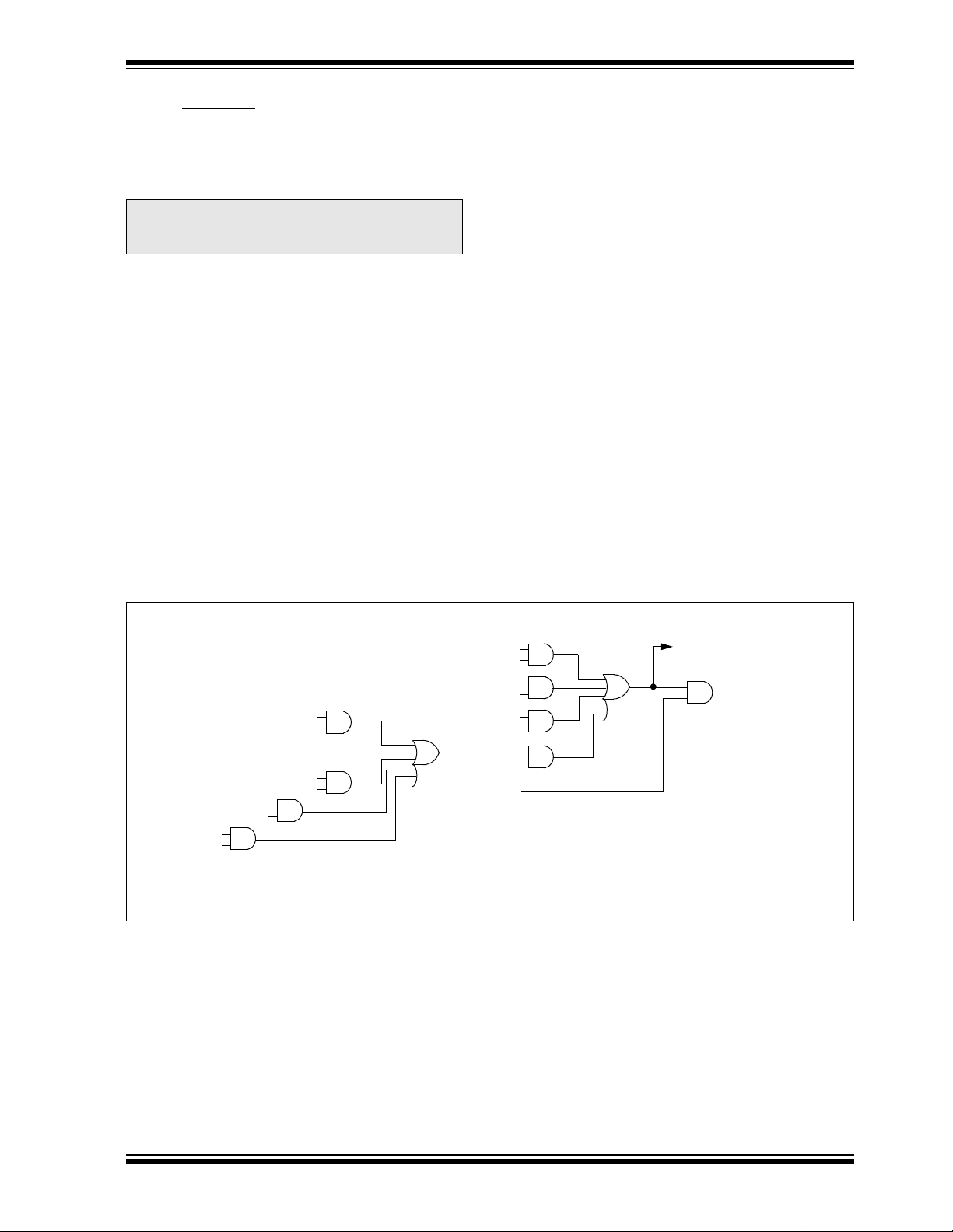
PIC16C712/716
9.10 Interrupts
The PIC16C712/716 devices have up to 7 sources of
interrupt. The interrupt control register (INTCON)
records individual interrupt requests in flag bits. It also
has individual and global interrupt enable bits.
Note: Individual interrupt flag bits are se t rega rd-
less of the status of the ir corresponding
mask bit or the GIE bit.
A global interrupt enable bit, GIE (INTCON<7>)
enables (if set) all un-masked interrupts or disables (if
cleared) all interrupts . W hen bit GIE is enab le d, and a n
interrupt’s flag bit and mask b it are set, the interrupt will
vector immediately. Individual interrupts can be disabled through their corresponding enable bits in various registers. Individual interrupt bits are set,
regardless of the status of the GIE bit. The GIE bit is
cleared on re set.
The “return from interrupt” instruction, RETFIE, exits
the interrupt routine, as well as sets the GIE bit, which
re-enables interrupts.
The RB0/INT pin interrupt, the RB port change interrupt
and the TMR0 overflow interrupt flags are contained in
the INTCON register.
The peripheral interrupt flags are contained in the special function regist ers, PIR1 and PIR 2. The corresponding interrupt enable bits are contained in special
function registers, PIE1 and PIE2, and the peripheral
interrupt enable bi t i s co nta ine d i n special function register, INTCON.
When an interrupt is responded to, the GIE bit is
cleared to disable any further interrupt, the return
address is pushed o nto the stack and the PC is loaded
with 0004h. Once in the interrupt service routine, the
source(s) of the interrupt can be determined by polling
the interrupt flag bits. The interrupt flag bit(s) must be
cleared in software before re-enabling interrupts to
avoid recursive interrupts.
For external interrupt events, such as the INT pin or
PORTB change interrupt, the interrupt latency will be
three or four instruction cycles. The exact latency
depends when the interrupt event occurs. The latency
is the same for one or two cycl e in structions. Individual
interrupt flag bits are set, regardless of the status of
their corresponding mask bit or the GIE bit.
FIGURE 9-14: INTERRUPT LOGIC
ADIF
ADIE
CCP1IF
CCP1IE
TMR2IF
TMR2IE
TMR1IF
TMR1IE
T0IF
T0IE
INTF
INTE
RBIF
RBIE
PEIE
GIE
Wake-up (If in SLEEP mode)
Interrupt to CPU
1999 Microchip Technology Inc.
Preliminary DS41106A-page 61

PIC16C712/716
9.10.1 INT INTERRUPT External interrupt on RB0/INT pin is edge triggered,
either rising if bit INTEDG (OPTION_REG<6>) is set,
or falling if the INTEDG bit is clear. When a valid edge
appears on the RB0/INT pin, flag bit INTF
(INTCON<1>) is set. This interrupt can be disabled by
clearing enable bit INTE (INTCON<4>). Flag bit INTF
must be cleared i n softw are in th e interrupt service routine before re-enabling this interrupt. The INT interrupt
can wake- up the process or from SLEEP, if bit INTE was
set prior to going into SLEEP. The status of global interrupt enable bit GIE decides whether or not the processor branches t o the i nte rr upt vector followin g wake-up.
See Section 9.13 for details on SLEEP mode.
9.10.2 TMR0 INTERRUPT An overflow (FFh → 00h) in the TMR0 register will set
flag bit T0IF (INTCON<2>). The interrupt can be
enabled/disabled by setting/clearing enable bit T0IE
(INTCON<5>). (Section 4.0)
9.10.3 PORTB INTCON CHANGE An input change on PORTB<7:4> sets flag bit RBIF
(INTCON<0> ). The interrup t can be enabled/di sabled
by setting/clearing enable bit RBIE (INTCON<4>).
(Section 3.2)
9.11 Context Saving During Interrupts
During an interrupt, only the return PC value is saved
on the stack. Typically, users may wish to save key registers during an interrupt, (i.e., W register and STATUS
register). This will have to be implemented in software.
Example 9- 1 stores and re stores the W an d STATUS
registers. The register, W_TEMP, must be defined in
each bank and mus t be define d at the same offs et from
the bank ba se address (i .e., if W_TEMP is d efined at
0x20 in bank 0, i t m u st als o b e defined at 0xA0 in ba nk
1).
The example:
a) Stores the W register.
b) Stores the STATUS register in bank 0.
c) Stores the PCLATH register.
d) Executes the interrupt service routine code
(User-generated).
e) Restores the STATUS register (and bank select
bit).
f) Restores the W and PCLATH registers.
EXAMPLE 9-1: SAVING STATUS, W, AND PCLATH REGISTERS IN RAM
MOVWF W_TEMP ;Copy W to TEMP register, could be bank one or zero
SWAPF STATUS,W ;Swap status to be saved into W
CLRF STATUS ;bank 0, regardless of current bank, Clears IRP,RP1,RP0
MOVWF STATUS_TEMP ;Save status to bank zero STATUS_TEMP register
MOVF PCLATH, W ;Only required if using pages 1, 2 and/or 3
MOVWF PCLATH_TEMP ;Save PCLATH into W
CLRF PCLATH ;Page zero, regardless of current page
BCF STATUS, IRP ;Return to Bank 0
MOVF FSR, W ;Copy FSR to W
MOVWF FSR_TEMP ;Copy FSR from W to FSR_TEMP
:
:(ISR)
:
MOVF PCLATH_TEMP, W ;Restore PCLATH
MOVWF PCLATH ;Move W into PCLATH
SWAPF STATUS_TEMP,W ;Swap STATUS_TEMP register into W
;(sets bank to original state)
MOVWF STATUS ;Move W into STATUS register
SWAPF W_TEMP,F ;Swap W_TEMP
SWAPF W_TEMP,W ;Swap W_TEMP into W
DS41106A-page 62 Preliminary
1999 Microchip Technology Inc.

PIC16C712/716
9.12 Watchdog Timer (WDT)
The Watchdog Timer is as a free running, on-chip, RC
oscillator which does not require any external components. This RC oscilla tor is s epar ate from the R C osci llator of the OSC1/CLKIN pin. Th at means that the WDT
will run, even if the clock on the OSC1/CLKIN and
OSC2/CLKOUT pins of the device have been stopped,
for example, by execution of a SLEEP instruction.
During normal operation, a WDT time-out generates a
device RESET (W atchdog Timer Reset). If the de vice is
in SLEEP mode, a WDT time-out causes the device to
wake-up and continue with normal operation (Watchdog Timer Wa ke-up). The T O
bit in the STA TUS register
will be cleared upon a Watchdog Timer time-out.
The WDT can be permanently disabled by clearing
configuration bit WDTE (Section 9.1).
FIGURE 9-15: WATCHDOG TIMER BLOCK DIAGRAM
From TMR0 Clock Source
(Figure 4-2)
0
M
1
WDT Timer
U
X
WDT time-out period values may be found in the Electrical Specifications section under T
WDT (parameter
#31). Values for the WDT prescaler (actually a
postscaler, but shared with the Timer0 prescaler) may
be assigned using the OPTION_REG register.
Note: The CLRWDT and SLEEP instructions clear
the WDT and the p ost sc al er, if assigned to
the WDT, and prevent it from timing out an d
generating a device RESET condition.
.
Note: When a CLRWDT instruction is executed
and the prescaler is assigned to the WDT,
the prescaler count will be cleared, but the
prescaler assignme nt is not chang ed.
Postscaler
8
WDT
Enable Bit
Note: PSA and PS2:PS0 are bits in the OPTION_REG register.
PSA
8 - to - 1 MUX
0
MUX
WDT
Time-out
1
PS2:PS0
To TMR0 (Figure 4-2)
PSA
FIGURE 9-16: SUMMARY OF WATCHDOG TIMER REGISTERS
Address Name Bits 13:8 Bit 7 Bit 6 Bit 5 Bit 4 Bit 3 Bit 2 Bit 1 Bit 0
2007h Config. bits (1) — BODEN
81h
OPTION_REG
N/A RBPU INTEDG T0CS T0SE PSA PS2 PS1 PS0
(1)
Legend: Shaded cells are not used by the Watchdog Timer.
Note1: See Figure 9-1 for operation of these bits.
CP1 CP0 PWRTE
(1)
WDTE FOSC1 FOSC0
1999 Microchip Technology Inc.
Preliminary DS41106A-page 63

PIC16C712/716
9.13 Power-down Mode (SLEEP)
Power-down mode is entered by executing a SLEEP
instruction.
If enabled, the Watchdog Timer will be cleared but
keeps running, the PD
(STATUS<4>) bit is set, and the oscillator driver is
TO
turned of f. The I/O por ts m aintai n the st atus they had,
before the SLEEP instruction was executed (driving
high, low, or hi-impedance).
For lowest current consumption in this mode, place all
I/O pins at e ither V
cuitry is drawing current from the I/O pin, power-down
the A/D and the dis able ex ternal clocks . Pull all I/O pins ,
that are hi-impedance inputs, high or low externally to
avoid switching currents ca us ed by floating inp uts. The
T0CKI input should also be at V
current consumption. The contribution from on-chip
pull-ups on PORTB should be considered.
The MCLR
9.13.1 WAKE-UP FROM SLEEP The device can wake up from SLEEP through one of
the following events:
1. External reset input on MCLR
2. Watchdog Timer Wake-up (if WDT was
3. Interrupt from INT pin, RB port change, or some
External MCLR
other events are considered a continuation of program
execution and cause a "wake-up". The TO
in the STATUS register can be used to determine the
cause of device reset. The PD bit, which is set on
power-up, is cleared when SLEEP is invoked. The TO
bit is cleared if a WDT time-out occurred (and caused
wake-up ) .
The following peripheral interrupts can wake the device
from SLEEP:
1. TMR1 interrupt. Timer1 must be operating as
2. CCP capture mode interrupt.
3. Special event trigger (Timer1 in asynchronous
pin must be at a logic high level (VIHMC).
enabled).
peripheral interrupts.
an asynchronous counter.
mode using an external clock) .
bit (STATU S< 3>) i s cl ea red, th e
DD or VSS, ensure no external cir-
DD or VSS for l owest
pin.
Reset will cause a device reset. All
and PD bits
Other peripherals cannot generate interrupts, since
during SLEEP, no on-chip clocks are present.
When the SLEEP inst ruction is bei ng e xe cuted, the n ext
instruction (PC + 1) is pre-fetched. For the device to
wake-up through an interrupt event, the corresponding
interrup t ena ble bit must be set (enabled ). Wake-up is
regardless of the state of the GIE bit. If the GIE bit is
clear (disabled), the device continues execution at the
instruction after the SLEEP instruction. If the GIE bit is
set (enabled), the device executes the instruction after
the SLEEP instruction and then branches to the interrupt addre ss (0 004 h). I n case s wher e the execution of
the instr uction following SLEEP is not desirable, the
user should have a NOP after the SLEEP instruction.
9.13.2 WAKE-UP USING INTERRUPTS When global interrupts are disabled (GIE cleared) and
any interrupt source has both its interrupt enable bit
and interrupt flag bit se t, one o f the f o llo win g will o ccur:
• If the interrupt occurs before the execution of a
SLEEP instruction, the SLEEP instruction will complete as a NOP. Therefore, the WDT and WDT
postscaler will not be cleared, the TO
be set and PD
• If the interrupt occurs during or after the execu-
tion of a SLEEP instruction, the device will immediately wak e up from sl eep . The SLEEP instruction
will be completely executed before the wake-up.
Therefore, the WDT and WDT postscaler will be
cleared, the TO
be cleared.
Even if the flag bits were checked before executing a
SLEEP instruction, it may be possible for flag bits to
become set bef ore the SLEEP inst ruction complete s. To
determine whether a SLEEP instruction executed, te st
bit. If the PD bit is set, the SLEEP instruction
the PD
was executed as a NOP.
To ensure that the WDT is cleared, a CLRWDT instruction should be executed before a SLEEP instruction.
bits will not be cleared.
bit will be set and the PD bit will
bit will not
DS41106A-page 64 Preliminary
1999 Microchip Technology Inc.

FIGURE 9-17: WAKE-UP FROM SLEEP THROUGH INTERRUPT
Q1 Q2 Q3 Q4 Q1 Q2 Q3 Q4 Q1 Q1 Q2 Q3 Q4 Q1 Q2 Q3 Q4 Q1 Q2 Q3 Q4 Q1 Q2 Q3 Q4
OSC1
CLKOUT(4)
INT pin
INTF flag
(INTCON<1>)
GIE bit
(INTCON<7>)
INSTRUCTION FLOW
PC
Instruction
fetched
Instruction
executed
Inst(PC) = SLEEP
Processor in
SLEEP
PC PC+1 PC+2
Inst(PC + 1)
Inst(PC - 1)
SLEEP
TOST(2)
PC+2
Inst(PC + 2)
Inst(PC + 1)
PIC16C712/716
Interrupt Latency
(Note 2)
PC + 2 0004h 0005h
Dummy cycle
Inst(0004h)
Dummy cycle
Inst(0005h)
Inst(0004h)
Note 1: XT, HS or LP oscillator mode assumed.
9.14 Program Verification/Code Protection
If the code protection bit(s) have not been programmed, the on-chip program memory can be read
out for verification purposes.
Note: Microchip does not recommend code pro-
9.15 ID Locations
Four memory locations (2000h - 2003h) are desig nated
as ID locations where the user can store checksum or
other code-identification numbers. These locations are
not accessible during normal execution, but are read-
OST = 1024TOSC (drawing not to scale) This delay will not be there for RC osc mode.
2: T
3: GIE = ’1’ assumed. In this case after wake- up, the processor jumps to the interrupt routine. If GIE = ’0’, execution will continue in-line.
4: CLKOUT is not available in these osc modes, but shown here for timing reference.
9.16 In-Circuit Serial Programming™
PIC16CXXX microcontrollers can be serially programmed while in the end application circuit. This is
simply done with tw o lin es f or cloc k and data, and three
other lines fo r power , ground and the programm ing volt-
tecting windowed devices.
age. This allo ws cus tomers to manuf ac ture boards w ith
unprogrammed devices, and then program the microcontroller just before shipping the product. This also
allows the most recent firmware or a custom firmware
to be programmed.
For complete details on serial programming, please
refer to the In-Circuit Serial Programming (ICSP™)
Guide, (DS30277).
able and writable during program/verify. It is recommended that only the 4 least significant bits of the ID
location are used.
For ROM devices, these values are submitted along
with the ROM code.
1999 Microchip Technology Inc.
Preliminary DS41106A-page 65

PIC16C712/716
NOTES:
DS41106A-page 66 Preliminary
1999 Microchip Technology Inc.

PIC16C712/716
10.0 INSTRUCTION SET SUMMARY
Each PIC16CXXX instruction is a 14-bit word divided
into an OPCODE which specifies the instruction type
and one or more operands which further specify the
operation of the instruction. The PIC16CXXX instruction set summary in Tab le 10-2 lists byte-oriented, bit-
oriented, and literal and contr ol operat ions. Table 101 shows the opcode field de scriptions.
For byte-oriented instructions, ’f’ represents a file register designator and ’d’ represents a destination designator. The file register designator specifies which file
register is to be used by the instruction.
The destination des ignator specifies w here the result of
the operation is to be placed. If ’d’ is zero, the result is
placed in the W registe r . If ’d ’ is one , the result is pl aced
in the file register specified in the instruction.
For bit-oriented instructions, ’b’ represents a bit field
designator which s el ec ts the number of th e b it a ffected
by the operation, while ’f’ represents the number of the
file in which the bit is located.
For literal and control operations, ’k’ represents an
eight or eleven bit constant or literal value.
TABLE 10-1 OPCODE FIELD
DESCRIPTIONS
Field Description
f Register file address (0x00 to 0x7F)
W Working register (accumulator)
b Bit address within an 8-bit file register
k Literal field, constant data or label
x Don’t care location (= 0 or 1)
The assembler will generate code with x = 0. It is the
recommended form of use for compatibility with all
Microchip software tools.
d Destination select; d = 0: store result in W,
d = 1: store result in file register f.
Default is d = 1
PC Program Counter
Time-out bit
TO
Power-down bit
PD
Z Zero bit
DC Digit Carry bit
C Carry bit
The instr uc tio n se t is hig hl y orthogon a l an d is grou p ed
into three basic categories:
• Byte-oriented operations
• Bit-oriented operations
• Literal and control operations
All instructions are executed within one single instruc-
tion cycle, unl ess a conditiona l test is tru e or the program counter is changed as a result of an instruction.
In this case, the execution t akes two ins tr ucti on cy cles
with the second cycle executed as a NOP. One instruction cycle consists of four oscillator periods. Thus, for
an oscillator frequ ency of 4 MHz, the normal instructio n
ex ecutio n time i s 1 µs . If a con dition al test is true or the
program counter is changed as a result of an instruction, the instruction execution time is 2 µs.
Table 10-2 lists the instructions recognized by the
MPASM assembler.
Figure 10-1 shows the general formats that th e instructions can have.
Note: To maintain upward compatibility with
future PIC16CXXX products, do not use
the OPTION and TRIS instructions.
All examples us e the following for mat to represent a
hexadecimal number:
0xhh
where h signifies a hexadecimal digit.
FIGURE 10-1: GENERAL FORMAT FOR
INSTRUCTIONS
Byte-oriented file register operations
13 8 7 6 0
OPCODE d f (FILE #)
d = 0 for destination W
d = 1 for destination f
f = 7-bit file register address
Bit-oriented file register operations
13 10 9 7 6 0
OPCODE b (BIT #) f (FILE #)
b = 3-bit bit address
f = 7-bit file register address
Literal and control operations
General
13 8 7 0
OPCODE k (literal)
k = 8-bit immediate value
CALL and GOTO instructions only
13 11 10 0
OPCODE k (literal)
k = 11-bit immediate value
A description of each instruction is available in the
PICmicro™ Mid-Range Reference Manual,
(DS33023).
1999 Microchip Technology Inc.
Preliminary DS41106A-page 67

PIC16C712/716
TABLE 10-2 PIC16CXXX INSTRUCTION SET
Mnemonic,
Operands
BYTE-ORIENTED FILE REGISTER OPERATIONS
ADDWF
ANDWF
CLRF
CLRW
COMF
DECF
DECFSZ
INCF
INCFSZ
IORWF
MOVF
MOVWF
NOP
RLF
RRF
SUBWF
SWAPF
XORWF
BIT-ORIENTED FILE REGISTER OPERATIONS
BCF
BSF
BTFSC
BTFSS
LITERAL AND CONTROL OPERATIONS
ADDLW
ANDLW
CALL
CLRWDT
GOTO
IORLW
MOVLW
RETFIE
RETLW
RETURN
SLEEP
SUBLW
XORLW
Note 1: When an I/O register is modified as a function of itself ( e.g., MOVF PORTB, 1), the value used will be that value present
on the pins themselves. For example, if the data latch is ’1’ for a pin configured as input and is driven low by an external
device, the data will be written back with a ’0’ .
2: If this instruction is executed on the TMR0 register (and, where applicable, d = 1), the prescaler will be cleared if assigned
to the Timer0 Module.
3: If Program Counter (PC) is modified or a conditional test is true, the instruction requires two cycles. The second cycle is
executed as a NOP.
Description Cycles 14-B it Opcod e Status
MSb LSb
f, d
Add W and f
f, d
AND W with f
f
Clear f
-
Clear W
f, d
Complement f
f, d
Decrement f
f, d
Decrement f, Skip if 0
f, d
Increment f
f, d
Increment f, Skip if 0
f, d
Inclusive OR W with f
f, d
Move f
f
Move W to f
-
No Operation
f, d
Rotate Left f through Carry
f, d
Rotate Right f through Carry
f, d
Subtract W from f
f, d
Swap nibbles in f
f, d
Exclusive OR W with f
f, b
Bit Clear f
f, b
Bit Set f
f, b
Bit Test f, Skip if Cle a r
f, b
Bit Test f, Skip if Set
Add literal and W
k
AND literal with W
k
Call subroutine
k
Clear Watchdog Timer
-
Go to address
k
Inclusive OR literal with W
k
Move literal to W
k
Return from interrupt
-
Return with literal in W
k
Return from Subroutine
-
Go into standby mode
-
Subtract W from literal
k
Exclusive OR literal with W
k
1
1
1
1
1
1
1(2)
1
1(2)
1
1
1
1
1
1
1
1
1
1
1
1 (2)
1 (2)
1
1
2
1
2
1
1
2
2
2
1
1
1
00
00
00
00
00
00
00
00
00
00
00
00
00
00
00
00
00
00
01
01
01
01
11
11
10
00
10
11
11
00
11
00
00
11
11
0111
0101
0001
0001
1001
0011
1011
1010
1111
0100
1000
0000
0000
1101
1100
0010
1110
0110
00bb
01bb
10bb
11bb
111x
1001
0kkk
0000
1kkk
1000
00xx
0000
01xx
0000
0000
110x
1010
dfff
dfff
lfff
0000
dfff
dfff
dfff
dfff
dfff
dfff
dfff
lfff
0xx0
dfff
dfff
dfff
dfff
dfff
bfff
bfff
bfff
bfff
kkkk
kkkk
kkkk
0110
kkkk
kkkk
kkkk
0000
kkkk
0000
0110
kkkk
kkkk
ffff
ffff
ffff
0011
ffff
ffff
ffff
ffff
ffff
ffff
ffff
ffff
0000
ffff
ffff
ffff
ffff
ffff
ffff
ffff
ffff
ffff
kkkk
kkkk
kkkk
0100
kkkk
kkkk
kkkk
1001
kkkk
1000
0011
kkkk
kkkk
Affected
C,DC,Z
Z
Z
Z
Z
Z
Z
Z
Z
C
C
C,DC,Z
Z
C,DC,Z
Z
,PD
TO
Z
,PD
TO
C,DC,Z
Z
Notes
1,2
1,2
2
1,2
1,2
1,2,3
1,2
1,2,3
1,2
1,2
1,2
1,2
1,2
1,2
1,2
1,2
1,2
3
3
DS41106A-page 68 Preliminary
1999 Microchip Technology Inc.

PIC16C712/716
11.0 DEVELOPMENT SUPPORT
11.1 Development Tools
The PICmicro microcontrollers are supported with a
full range of hardw are and softw are de velopment to ols:
• MPLAB -ICE Real-Tim e In-Circuit Emulator
• ICEPIC Low-Cost PIC16C5X and PIC16CXXX
In-Circuit Emulator
•PRO MATE
• PICSTART
Programmer
• SIMICE
• PICDEM-1 Low-Cost Demonstration Board
• PICDEM-2 Low-Cost Demonstration Board
• PICDEM-3 Low-Cost Demonstration Board
• MPASM Assembler
• MPLAB SIM Software Simulator
• MPLAB-C17 (C Compiler)
• Fuzzy Logic Developm ent System
(
fuzzy
•KEELOQ® Evaluation Kits and Programmer
11.2 MPLAB-ICE: High Performance
II Universal Programmer
Plus Entry-Level Prototype
TECH−MP)
Universal In-Circuit Emulator with
MPLAB IDE
11.3 ICEPIC: Low-Cost PICmicro In-Circuit Emulator
ICEPIC is a low-cost in-circuit emulator solution for the
Microchip PIC12CXXX, PIC16C5X and PIC16CXXX
families of 8-bit OTP microcontrollers.
ICEPIC is designed to operate on PC-compatible
machines ranging from 386 through Pentium based
machines under Windows 3.x, Windows 95, or Windows NT enviro nm en t. ICEPIC features real time, nonintrusive emulation.
11.4 PRO MATE II: Universal Programmer
The PRO MATE II Universal Programmer is a full-featured programmer capable of operating in stand-alone
mode as well as PC-hosted mode. PRO MATE II is CE
compliant.
The PRO MATE II has programmable V
supplies which allows it to verify programmed memory
at V
DD min and VDD max for maximum reliability. It has
an LCD display for displaying error messages, keys to
enter commands and a modular detachable socket
assembly to support various package types. In standalone mode th e PRO MAT E II can read , verify or pro gram PIC12CXXX, PIC14C000, PIC16C5X,
PIC16CXXX and PIC17CXX devices. It can also set
configuration and code-protect bits in this mode.
DD and VPP
The MPLAB-ICE Universal In-Circuit Emulator is
intended t o provid e the prod uct d evelopment engi nee r
with a complete microcontroller design tool set for
PICmicro microcontro llers (MCUs). M PLAB-ICE is supplied with the MPLAB Integrated Development Environ-
ment (IDE), which allows editing, “make” and
download, and source debugging from a single environment.
Interchangeable processor modules allow the system
to be easily reconfigured for emulation of different processors. The universal architecture of the MPLAB-ICE
allows expansion to support all new Microchip microcontrollers.
The MPLAB-ICE Emulator System has been designed
as a real-time emulation system with advanced features that are gen erally f ound on more expensi ve de velopment tools. The PC compatible 386 (and higher)
machine platform and Microsoft Windows
Windows 95 enviro nment were chosen to best make
these features available to you, the end user.
MPLAB-ICE is available in two versions.
MPLAB-ICE 1000 is a basic, low-cost emulator syst em
with simple trace ca pabilitie s. It shares process or modules with the MPLAB-ICE 2000. This is a full-featured
emulator system with enha nced tr ace, trigger , a nd data
monitoring features. Both systems will operate across
the entire operating s peed range of the PIC micro MCU .
3.x or
11.5 PICSTART Plus Entry Level Development System
The PICSTART programmer is an easy-to-use, lowcost prototype programmer. It connects to the PC via
one of the COM (RS-232) ports. MPLAB Integrated
Development Environm ent software makes using the
programmer s imple and efficie nt. PICSTART Plus is not
recommended for production programming.
PICSTART Plus supports all PIC12CXXX, PIC14C000,
PIC16C5X, PIC16CXXX and PIC17CXX devices with
up to 40 pins. Larger pin count devices such as the
PIC16C923, PIC16C924 and PIC17C756 may be supported with an adapter socket. PICSTART Plus is CE
compliant.
1999 Microchip Technology Inc.
Preliminary DS41106A-page 69

PIC16C712/716
11.6 SIMICE Entry-Level Hardware Simulator
SIMICE is an entry-level hardware development system designed to operate in a PC-based environment
with Microchip’s simulator MPLAB™-SIM. Both SIMICE and MPLAB-SIM run under Microchip Technology’s MPLAB Integrated Development Environment
(IDE) software. Speci fically, SIMICE provides hardware
simulation for Microchip’s PIC12C5XX, PIC12CE5XX,
and PIC16C5X f am ili es of PICm icr o 8-bit microcontrollers. SIMICE works in conjunction with MPLAB-SIM to
provide non-real-time I/O port emulation. SIMICE
enables a developer to run simulator code for driving
the target system. In addition, the target system can
provide input to the simulator code. This capability
allows for simple and interactive debugging without
having to manually generate MPLAB-SIM stimulus
files. SIMICE is a valuable debugging tool for entrylev el sy ste m developm en t.
11.7 PICDEM-1 Low-Cost PICmicro Demonstration Board
The PICDEM-1 is a simple board which demonstrates
the capabilities of several of Microchip’s microcontrollers. The microcontrollers supported are: PIC16C5X
(PIC16C54 to PIC16C58A), PIC16C61, PIC16C62X,
PIC16C71, PIC16C8X, PIC17C42, PIC17C43 and
PIC17C44. All necessary hardware and software is
included to run basic demo programs. The users can
program the sample microcontrollers provided with
the PICDEM-1 board, on a PRO MATE II or
PICSTART-Plus programmer, and easily test firmware. The user can also connect the PICDEM-1
board to the MPLAB-ICE emulator and downl o a d t h e
firmware to the emulator for testing. Addi tional proto type area is available for the user to build some additional hardware and connect it to the microcontroller
socket(s). Some of the features include an RS-232
interface, a potentiometer for simulated analog input,
push-button switches and eight LEDs connected to
PORTB.
11.8 PICDEM-2 Low-Cost PIC16CXX Demonstration Board
The PICDEM-2 is a simple demonstration board that
supports the PIC16C62, PIC16C64, PIC16C65,
PIC16C73 and PIC16C74 microcontrollers. All the
necessary hardware and software is included to
run the basic demonstration programs. The user
can program the sample microcontrollers provided
with the PICDEM-2 board, on a PRO MATE II programmer or PICSTART-Plus, and easily test firmware.
The MPLAB-ICE emulator may also be used with the
PICDEM-2 board to test firmware. Additional prototype
area has been provided to the user for adding additional hardware and connectin g it to the microc ontroller
socket(s). Some of th e f eatures inc lude a RS-232 interface, push-button switches, a potentiometer for simulated analog input, a Serial EEPROM to demonstrate
usage of the I
tion to an LCD module and a keypad.
2
C bus and separ ate heade rs fo r connec-
11.9 PICDEM-3 Low-Cost PIC16CXXX Demonstration Board
The PICDEM-3 is a simple demonstration board that
supports the PIC16C923 and PIC16C924 in the PLCC
package. It will also support future 44-pin PLCC
microcontrollers w ith a LCD Mo dul e . Al l the necessary hardware and software is included to run the
basic demonstration programs. The user can program the sample microcontrollers provided with
the PI CDEM -3 bo ard, on a P RO MATE II programmer o r PICSTART Plus with an adapter socket, and
easily test firmware. The MPLAB-ICE emulator may
also be used with the PICDEM-3 board to test firmware. Additional prototype area h as bee n pr ovided t o
the user for adding hard ware and con nec ting it to the
microcontroller socket(s). Some of the feat ures includ e
an RS-232 interface, push-button switches, a potentiometer for simulated analog input, a thermistor and
separate headers for connection to an external LCD
module and a ke y pad. Als o pro vide d on th e PICDEM -3
board is an LCD panel, with 4 commons and 12 segments, that is capable of displaying time, temperature
and day o f t he week. The PIC DE M-3 provides an additional RS-232 interface and Windows 3.1 software for
showing the dem ultiplex ed LCD si gnals on a PC . A simple serial interface allows the user to construct a hardware demultiplexer for the LCD signals.
DS41106A-page 70 Preliminary
1999 Microchip Technology Inc.

PIC16C712/716
11.10 MPLAB Integrated Development Environment Software
The MPLAB IDE Software brings an ease of software
development previously unseen in the 8-bit microcontroller market. MPLAB is a windows based application
which contains:
• A full featured editor
• Three operating modes
-editor
-emulator
- simulator
• A project manager
• Customizable tool bar and key mapping
• A status bar with project information
• Extensive on-l ine help
MPLAB allows you to:
• Edit your source files (either assembly or ‘C’)
• One touch assemble (or compile) and download
to PICmicro tools (automatically updates all
project information)
• Debug using:
- source files
- absolute listing file
The ability to use MPLAB with Microchip’s simulator
allows a consistent platform and the ability to easily
switch from the low cost simulator to the full featured
emulator with minimal retraining due to development
tools.
11.11 Assembler (MPASM)
The MPASM Universal Macro Assembler is a PChosted symbolic assembler. It supports all microcontroller series including the PIC12C5XX, PIC14000,
PIC16C5X, PIC16CXXX, and PIC17CXX families.
MPASM offers full featured Macro capabilities, conditional assemb ly, and sev er al sou rce and listing f ormats.
It generates various object code formats to support
Microchip's development tools as well as third party
programmers.
MPASM allows full symbolic debugging from MPLABICE, Microc hip’s Universal Emulator System.
MPASM has the following features to ass is t i n d eveloping software for specific use applications.
• Provides translation of Assembler source code to
object code for all Microchip microcontrollers.
• Macro assembly capability.
• Produces all the files (Object, Listing, Symbol, and
special) required for symbolic debug with
Microchip’s emulator systems.
• Supports Hex (default), Decimal and Octal source
and listing formats.
MPASM provides a rich directive language to support
programming of the PICmicro. Directives are helpful in
making the de velo pment of your asse mble source code
shorter and more maintainable.
11.12 Software Simulator (MPLAB-SIM)
The MPLAB-SIM Software Simulator allows code
development in a PC host environment. It allows the
user to simulate the PICmicro series microcontrollers
on an instruction level. On any given instruction, the
user may examine or modify any of the data areas or
provide external stimulus to any of the pins. The input/
output radix can be set by the user and the execution
can be performed in; single step , e xecute until brea k, or
in a trace mode.
MPLAB-SIM fully supports symbolic debugging using
MPLAB-C17 and MPASM. The Software Simulator
offers the lo w cost fle xibili ty to de v elop and deb ug cod e
outside of the laboratory environment making it an
excellent multi-project software development tool.
11.13 MPLAB-C17 Compiler
The MPLAB-C17 Code Development System is a
complete ANSI ‘C’ compiler and integrated development environment for M icrochip’ s PIC1 7CXXX fam ily of
microcontrollers. The compiler provides powerful integration capabilities and ease of use not found with
other compilers.
For easier source level debugging, the compiler provides symbol information that is compatible with the
MPLAB IDE memory display.
11.14 Fuzzy Logic Development System
(
fuzzy
TECH-MP)
fuzzy
TECH-MP fuzzy logic development tool is available in two versions - a low cost introductory version,
MP Explorer, for designers to gain a comprehensive
working know ledge of fuz zy l ogic sys tem d esign ; and a
full-featured version,
menting more complex systems.
Both versions include Microchip’s
stration board for hands-on experience with fuz zy lo gi c
systems implementa tion .
fuzzy
TECH-MP, Edition for imple-
fuzzy
LAB demon-
11.15 SEEVAL Evaluation and
Programming System
The SEEVAL SEEPROM Designer’s Kit supports all
Microchip 2-wire and 3-wire Serial EEPROMs. The kit
includes everything necessary to read, write, erase or
program special features of any Microchip SEEPROM
product including Smart Serials and secure serials.
The Total Endurance Disk is included to aid in tradeoff analysis and rel iabil ity ca lcula tions . The tota l kit ca n
significantly reduce time-to-market and result in an
optimized system.
1999 Microchip Technology Inc.
Preliminary DS41106A-page 71

PIC16C712/716
11.16 KEELOQ Evaluation and
Programming Tools
KEELOQ evaluation and programming tools support
Microchips HCS Secure Dat a Products . The HCS e v aluation kit includes an LCD display to show changing
codes, a decoder to decode transmissions, and a programming interface to program test transmitters.
DS41106A-page 72 Preliminary
1999 Microchip Technology Inc.

TABLE 11-1 DEVELOPMENT TOOLS FROM MICROCHIP
HCS200
HCS300
HCS301
PIC16C712/716
á
á
á
24CXX
25CXX
93CXX
á
á
á
á
á
á
á
á
á
á
á
á
á
á
á
á
á
á
á
á
á
á
á
á
á
á
á
á
á
á
á
á
á
á
á
á
á
á
á
á
á
á
á
á
á
PIC12C5XX PIC14000 PIC16C5X PIC16CXXX PIC16C6X PIC16C7XX PIC16C8X PIC16C9XX PIC17C4X PIC17C7XX
Low-Cost
MPLAB™-ICE
1999 Microchip Technology Inc.
ICEPIC
á
á
á
á
á
á
C17*
In-Circuit Emulator
MPLABIntegrated
Development
Environment
Emulator Products
MPLAB
á
á
á
á
-MP
TECH
Compiler
fuzzy
Explorer/Edition
Fuzzy Logic
Software Tools
Dev. Tool
Total EnduranceSoftware Model
Plus
PICSTART
á
á
á
á
Low-Cost
á
á
á
á
II
PRO MATE
Universal Dev. Kit
Universal
Programmer
KEELOQProgrammer
Programmers
SEEVALDesigners KitáSIMICE
á
á
á
á
PICDEM-14AáPICDEM-1
PICDEM-2
PICDEM-3áKEELOQ®Evaluation KitáKEELOQ
Demo Boards
Transponder Kit
Preliminary DS41106A-page 73

PIC16C712/716
NOTES:
DS41106A-page 74 Preliminary
1999 Microchip Technology Inc.

PIC16C712/716
12.0 ELECTRICAL CHARACTERISTICS
Absolute Maximum Ratings
Ambient temperature under bias.............................................................................................................-55°C to +125°C
Storage temperature.............................................................................................................................. -65°C to +150°C
Voltage on any pin with respect to V
Voltage on VDD with respect to VSS ......................................................................................................... -0.3V to +7.5V
Voltage on MCLR with respect to VSS (Note 2)..........................................................................................0V to +13.25V
Voltage on RA4 with respect to Vss...............................................................................................................0V to +8.5V
Total power dissipation (Note 1)(PDIP and SOIC)....................................................................................................1.0W
Total power dissipation (Note 1)(SSOP).................................................................................................................0.65W
Maximum current out of V
Maximum current into VDD pin ..............................................................................................................................250 mA
Input clamp current, IIK (VI < 0 or VI > VDD)......................................................................................................................±20 mA
Output clamp current, I
Maximum output current su nk by any I/O pin............................................. ..... ...... ...... ............................................25 mA
Maximum output current so urc ed b y an y I/O pin................................................................... ..... ...... .... ..................25 mA
Maximum current sunk by PORTA and PORTB (combined).................................................................................200 mA
Maximum current sourced by PORTA and PORTB (combined)............................................................................200 mA
Note 1: Power dissipation is calculated as follows: Pdis = V
Note 2: Voltage spikes below V
Thus, a series resistor of 50-100Ω should be used when applying a “low” level to the MCLR
than pulling this pin directly to V
† NOTICE: Stresses above those listed under “Absolute Maximum Ratings” may cause permanent damage to the
device. Th is is a s tress r ating o nly and functio nal ope ratio n of the device at those or any other conditions abo v e thos e
indicated in the operation listings of this specification is not implied. Exposure to maximum rating conditions for
extended periods may affect device reliability.
(†)
SS (except VDD, MCLR, and RA4)..........................................-0.3V to (VDD + 0.3V)
SS pin...........................................................................................................................300 mA
OK (VO < 0 or VO > VDD) ..............................................................................................................±20 mA
DD x {IDD - ∑ IOH} + ∑ {(VDD-VOH) x IOH} + ∑(VOl x IOL)
SS at the MCLR/VPP pin, in duc in g c urren ts greater than 80 mA , may cause latch-up.
/VPP pin rather
SS.
1999 Microchip Technology Inc.
Preliminary DS41106A-page 75

PIC16C712/716
FIGURE 12-1: PIC16C712/716 VOLTAGE-FREQUENCY GRAPH, -40°C < TA < +125°C
6.0
5.5
5.0
4.5
V
DD
(Volts)
4.0
3.5
3.0
2.5
2.0
0
410
Frequenc y (MH z )
20
25
Note 1: The shaded region indicates the permissible combinations of voltage and frequency.
FIGURE 12-2: PIC16LC712/716 VOLTAGE-FREQUENCY GRAPH, 0°C <
6.0
5.5
5.0
4.5
VDD
(Volts)
4.0
3.5
3.0
2.5
2.0
0
4 10
Frequenc y (MH z )
TA < +70°C
20
25
Note 1: The shaded region indicates the permissible combinations of voltage and frequency.
DS41106A-page 76 Preliminary
1999 Microchip Technology Inc.

PIC16C712/716
12.1 DC Characteristics: PIC16C712/716-04 (Commercial, Industrial, Extended)
PIC16C712/716-20 (Commercial, Industrial, Extended)
Standard Operating Conditions (unless otherwise stated)
DC CHARACTERISTICS
Operating temperature 0°C ≤ T
-40°C≤ T
-40°C≤ T
Param
Sym Characteristic Min Typ† Max Units Conditions
No.
-
D001
D001A
D002* V
D003 V
DD Supply Voltage 4.0
V
DR
RAM Data Retention Voltage
POR VDD Start Voltage to ensure inter-
(1)
BOR*
V
-1.5-V
-VSS - V See section on Power-on Reset for details
5.5
-
5.5VV BOR enabled (Note 7)
nal Power-on Reset signal
D004*
D004A*
D005 V
VDD VDD Rise Rate to ensure internal
S
Power-on Reset signal
BOR Brown-out Reset
0.05
TBD
-
--V/ms P WRT enabled (PWRTE bit clear)
-
3.65 - 4.35 V BODEN bit set
voltage trip point
D010
D013
D020
D021
D021B
D022*
D022A*
1A F
DD
I
PD
I
∆
∆
Supply Current
Power-down Current
Module Differential Current
WDT
I
Watchdog Timer
I
BOR
Brown-out Reset
OSC LP Oscillator Operating Frequency
RC Oscillator Operating Frequency
XT Oscillator Operating Frequency
HS Oscillator Operating Frequency
(2,5)
(3,5)
-
0.8
4.0
1.5
1.5
2.5
6.0
—
—
—
—
2.5
8.0mAmA
42
µ
16
µ
19
µ
19
µ
µ
µ
200
KHz
4
MHz
4
MHz
20
MHz
A
A
A
A
A
A
-
-
10.5
-
-
-
(6)
-
-
TBD20200
0
0
0
0
* These parameters are characterized but not tested.
† Data in "Typ" column is at 5V, 25°C unless otherwise stated. These parameters are for design guidance only and are not
tested.
Note1: This is the limit to which V
DD can be lowered without losing RAM data.
2: The supply current is mainly a function of the operating voltage and frequency. Other factors such as I/O pin loading and
switching rate, oscillator type, internal code execution pattern, and temperature also have an impact on the current consumption.
The test conditions for all I
DD measurements in active operation mode are:
OSC1 = external square wave, from rail to rail; all I/O pins tristated, pulled to V
= VDD; WDT enabled/disabled as specified.
MCLR
3: The power-down current in SLEEP mode does not depend on the oscillator type. Power-down current is measured with the
part in SLEEP mode, with all I/O pins in hi-impedance state and tied to V
DD and VSS.
4: For RC osc mode, current through Rext is not included. The current through the resistor can be estimated by the formula Ir =
DD/2Rext (mA) with Rext in kOhm.
V
5: Timer1 oscillator (when enabled) adds approximately 20 µA to the specification. This value is from characterization and is for
design guidance only. This is not tested.
6: The ∆ current is the additional current consumed when this peripheral is enabled. This current should be added to the base
DD or IPD measurement.
I
7: This is the voltage where the device enters the Brown-out Reset. When BOR is enabl ed, the device will operate correctly to
this trip point.
A
+70°C for commercial
≤
A
+85°C for industrial
≤
A
+125°C for extended
≤
PWRT disabled (PWRTE
bit set)
See section on Power-on Reset for details
FOSC = 4 MHz, VDD = 4.0V
OSC = 20 MHz, VDD = 4.0V
F
DD = 4.0V, WDT enabled,-40
V
DD = 4.0V, WDT disabled, 0
V
DD = 4.0V, WDT disabled,-40
V
DD = 4.0V, WDT disabled,-40
V
WDTE bit set, V
BODEN bit set, V
DD = 4.0V
DD = 5.0V
°
All temperatures
All temperatures
All temperatures
All temperatures
DD,
C to +85°C
°
C to +70°C
C to +85°C
°
C to +12 5°C
°
1999 Microchip Technology Inc.
Preliminary DS41106A-page 77

PIC16C712/716
12.2 DC Characteristics: PIC16LC712/716-04 (Commercial, Industrial)
DC CHARACTERISTICS
Param
Sym Characteri stic Min Typ† Max Units Conditions
Operating temperature 0°C ≤ TA
-40°C≤ T
A
+85°C for industrial
≤
+70°C for commercial
≤
No.
Standard Operating Conditions (unless otherwise stated)
-
D001 V
D002* V
D003 V
DD Supply Voltage 2.5
BOR*
V
DR
RAM Data Retention Voltage
POR VDD Start V oltage to ensure inter-
(1)
-1.5-V
-VSS - V See section on Power-on Reset for details
5.5
-
5.5VV BOR enabled (Note 7)
nal Power-on Reset signal
D004*
D004A*
VDD VDD Rise Rate to ensure inter nal
S
Power-on Reset signal
0.05
TBD
-
--V/ms PWRT enabled (PWRTE bit clear)
-
PWRT disabled (PWRTE
bit set)
See section on Power-on Reset for details
D005 V
BOR Brown-out Reset
3.65 - 4.35 V BODEN bit set
voltage trip point
D010
D010A
D020
D021
D021A
D022*
D022A*
1A F
DD
I
I
∆
∆
Supply Current
PD
Power-down Current
Module Differential Current
WDT
I
Watchdog Timer
I
BOR
Brown-out Reset
OSC LP Oscillator Operating Frequency
RC Oscillator Operating Frequency
XT Oscillator Operating Frequency
HS Oscillator Operating Frequency
(2,5)
(3,5)
-
2.0
3.848mA
-
22.5
7.5
-
0.9
-
0.9
-
(6)
-
6.0
-
TBD20200
0
0
0
0
30
5
5
—
200
—
4
—
4
—
20
XT, RC osc modes
OSC = 4 MHz, VDD = 3.0V (Note 4)
F
LP osc mode
A
µ
OSC = 32 kHz, VDD = 3.0V, WDT disabled
F
V
A
DD = 3.0V, WDT enabled, -40
µ
A
DD = 3.0V, WDT disabled, 0
V
µ
A
DD = 3.0V, WDT disabled, -40
V
µ
A
WDTE bit set, V
µ
BODEN bit set, V
A
µ
KHz
All temperatures
MHz
All temperatures
MHz
All temperatures
MHz
All temperatures
DD = 4.0V
DD = 5.0V
°
C to +70°C
°
°
* These parameters are characterized but not tested.
† Data in "Typ" column is at 5V, 25°C unless otherwise stated. These parameters are for design guidance only and are not
tested.
Note1: This is the limit to which V
DD can be lowered without losing RAM data.
2: The supply current is mainly a function of the operating voltage and frequency. Other factors such as I/O pin loading and
switching rate, oscillator type, internal code execution pattern, and temperature also have an impact on the current consumption.
The test conditions for all I
OSC1 = external square wave, from rail to rail; all I/O pins tristated, pulled to V
= VDD; WDT enabled/disabled as specified.
MCLR
DD measurements in active operation mode are:
DD,
3: The power-down current in SLEEP mode does not depend on the oscillator type. Power-down current is measured with the
part in SLEEP mode, with all I/O pins in hi-impedance state and tied to V
DD and VSS.
4: For RC osc mode, current through Rext is not included. The current through the resistor can be estimated by the formula Ir
DD/2Rext (mA) with Rext in kOhm.
= V
5: Timer1 oscillator (when enabled) adds approximately 20 µA to the specification. This value is from characterization and is
for design guidance only. This is not tested.
6: The ∆ current is the additional current consumed when this peripheral is enabled. This current should be added to the base
DD or IPD measurement.
I
7: This is the voltage where the device enters the Brown-out Reset. When BOR is enabled, the device will operate correctly to
this trip point.
C to +85°C
C to +85°C
DS41106A-page 78 Preliminary
1999 Microchip Technology Inc.

PIC16C712/716
12.3 DC Characteristics: PIC16C712/716-04 (Commercial, Industrial, Extended)
PIC16C712716-20 (Commercial, Industrial, Extended)
PIC16LC712/716-04 (Commercial, Industrial)
Standard Operating Conditions (unless otherwise stated)
Operating temperature 0°C ≤ T
DC CHARACTERISTICS
Operating voltage V
and Section 12.2
Param
Sym Characteristic Min Typ† Max Units Conditions
No.
Input Low Voltage
V
IL I/O ports
D030
D030A
D031 with Schmitt Trigger buffer V
D032 MCLR
D033 OSC1 (in XT, HS and LP
with TTL buffer V
SS
VSS
SS -0.2VDD V
-
-
0.15V
, OSC1 (in RC mode) Vss - 0.2VDD V
Vss - 0.3V
modes)
Input High Voltage
V
IH I/O ports -
D040 with TTL buffer 2.0 - V
D040A 0.25V
DD
-VDD Votherwise
+ 0.8V
-40°C ≤ T
-40°C ≤ T
DD range as described in DC spec Section 12.1
0.8V
DD
DD VNote1
DD V4.5V ≤ VDD ≤ 5.5V
A ≤ +70°C for commercial
A ≤ +85°C for industria l
A ≤ +125°C for extended
VV4.5V ≤ VDD ≤ 5.5V
otherwise
D041 with Schmitt Trigger buffer 0.8V
D042 MCLR
D042A OSC1 (XT, HS and LP modes) 0.7V
D043 OSC1 (in RC mode) 0.9V
DD -VDD V For entire VDD range
0.8VDD -VDD V
DD -VDD VNote1
DD -VDD V
Input Leakage Current (Notes
2, 3)
D060 I
IL I/O ports - - ±1 µAVss ≤ VPIN ≤ VDD,
Pin at hi-impedance
D061 MCLR, RA4/T0CKI - - ±5 µAVss ≤ VPIN ≤ VDD
D063 OSC1 - - ±5 µAVss ≤ VPIN ≤ VDD,
XT, HS and LP osc modes
D070 I
PURB PORTB weak pull-up current 50 250 400 µAVDD = 5V, VPIN = VSS
Output Low Voltage
D080 V
OL I/O ports - - 0.6 V IOL = 8.5 mA, VDD = 4.5V,
-40°C to +85°C
--0.6VIOL = 7.0 mA, VDD = 4.5V,
-40°C to +125°C
D083 OSC2/CLKOUT
(RC osc mode)
--0.6VIOL = 1.6 mA, VDD = 4.5V,
-40°C to +85°C
--0.6VI
OL = 1.2 mA, VDD = 4.5V,
-40°C to +125°C
* These parameters are characterized but not tested.
† Data in “Typ” column is at 5V, 25°C unless otherwise stated. These parameters are for design guidance only
and are not tested.
Note 1: In RC oscillator mode, the OSC1/CLKIN pin is a Schmitt Trigger input. It is not recommended that the PICmi-
cro be driven with external clock in RC mode.
2: The leakage current on the MCLR
/VPP pin is strongly dependent on the applied voltage level. The specified
levels represent normal operating conditions. Higher leakage current may be measured at different input voltages.
3: Negative current is defined as current sourced by the pin.
1999 Microchip Technology Inc.
Preliminary DS41106A-page 79

PIC16C712/716
Standard Operating Conditions (unless otherwise stated)
Operating temperature 0°C ≤ TA ≤ +70°C for commercial
DC CHARACTERISTICS
Operating voltage V
-40°C ≤ T
-40°C ≤ T
DD range as described in DC spec Section 12.1
and Section 12.2
Param
Sym Characteristic Min Typ† Max Units Conditions
No.
Output High Voltage
D090 V
D092 OSC2/CLKOUT (RC osc
OH I/O ports (Note 3) VDD-0.7 - - V IOH = -3.0 mA, VDD = 4.5V,
V
DD-0.7 - - V IOH = -2.5 mA, VDD = 4.5V,
VDD-0.7 - - V IOH = -1.3 mA, VDD = 4.5V,
mode)
VDD-0.7 - - V IOH = -1.0 mA, VDD = 4.5V,
D150* V
OD Open-Drain High Voltage - - 8.5 V RA4 pin
Capacitive Loading Specs
on Output Pins
D100 C
D101 C
OSC2 OSC2 pin - - 15 pF In XT, HS and LP modes when
IO All I/O pins and OSC2 (in RC
--50pF
mode)
* These parameters are characterized but not tested.
† Data in “Typ” column is at 5V, 25°C unless otherwise stated. These parameters are for design guidance only
and are not tested.
Note 1: In RC oscillator mode, the OSC1/CLKIN pin is a Schmitt Trigger input. It is not recommended that the PICmi-
cro be driven with external clock in RC mode.
2: The leakage current on the MCLR/VPP pin is strongly dependent on the applied voltage level. The specified
levels represent normal operating conditions. Higher leakage current may be measured at different input voltages.
3: Negative current is defined as current sourced by the pin.
A ≤ +85°C for industria l
A ≤ +125°C for extended
-40°C to +85°C
-40°C to +125°C
-40°C to +85°C
-40°C to +125°C
external clock is used to drive
OSC1.
DS41106A-page 80 Preliminary
1999 Microchip Technology Inc.

PIC16C712/716
12.4 AC (Timing) Characteristics
12.4.1 TIMING PARAMETER SYMBOLOGY The timing parameter symbols have been created
using one of the following formats:
1. TppS2ppS
2. TppS
T
FFrequency TTime
Lowercase letters (pp) and their meanings:
pp
cc CCP1 osc OSC1
ck CLKOUT rd RD
cs CS rw RD or WR
di SDI sc SCK
do S DO ss SS
dt Da ta in t0 T0CKI
io I/O port t1 T1CKI
mc MCLR
Uppercase letters and their meanings:
S
FFall PPeriod
HHigh RRise
I Invalid (Hi-impedance) V Valid
L Low Z Hi-impedance
wr WR
1999 Microchip Technology Inc.
Preliminary DS41106A-page 81

PIC16C712/716
12.4.2 TIMING CONDITIONS The temperatu re and voltages specif ied in Table 12-1
apply to all timing specifications, unless otherwise
noted. Figure 12-1 specifies the load conditions for the
timing specificati on s .
TABLE 12-1 TEMPERATURE AND VOLTAGE SPECIFICATIONS - AC
Standard Operating Conditions (unless otherwise stated)
Operating temperature 0°C ≤ T
AC CHARACTERISTICS
Operating voltage V
LC parts operate for commercial/industrial temp’s only.
-40°C≤ T
-40°C≤ T
DD range as described in DC spec Section 12.1 and Section 12.2.
FIGURE 12-1: LOAD CONDITIONS FOR DEVICE TIMING SPECIFICATIONS
A
+70°C for commercial
≤
A
+85°C for industrial
≤
A
+125°C for extended
≤
Load condition 1
Pin
VDD/2
VSS
RL
CL
Load condition 2
Pin
CL
VSS
RL =464Ω
L = 50 pF for all pins except OSC2/CLKOUT
C
15 pF for OSC2 output
DS41106A-page 82 Preliminary
1999 Microchip Technology Inc.

12.4.3 TIMING DIAGRAMS AND SPECIFICATIONS
FIGURE 12-2: EXTERNAL CLOCK TIMING
Q4
OSC1
CLKOUT
Q1 Q2 Q3 Q4
1
3
2
TABLE 12-2 EXTERNAL CLOCK TIMING REQUIREMENTS
PIC16C712/716
Q1
3
4
4
Param
No.
1A F
3* TosL,
4* TosR,
Sym Characteristic Min Typ† Max Units Conditions
OSC External CLKIN Frequency
(Note 1)
Oscillator Frequency
(Note 1)
OSC External CLKIN Period
1T
2T
TosH
TosF
(Note 1)
Oscillator Period
(Note 1)
CY Instruction Cycle Time (Note 1) 200 — DC ns TCY = 4/FOSC
External Clock in (OSC1) High or
Low Time
External Clock in (OSC1) Rise or
Fall Time
DC — 4 MHz RC and XT osc modes
DC — 4 MHz HS osc mode (-04)
DC — 20 MHz HS osc mode (-20)
DC — 200 kHz LP osc mode
DC — 4 MHz RC osc mode
0.1 — 4 MHz XT osc mode
4 — 20 MHz HS osc mode
5 — 200 kHz LP osc mode
250 — — ns RC and XT osc modes
250 — — ns HS osc mode (-04)
50 — — ns HS osc mode (-20)
5— —µs LP osc mode
250 — — ns RC osc mode
250 — 10,000 ns XT osc mode
250 — 250 ns HS osc mode (-04)
50 — 250 ns HS osc mode (-20)
5— —µs LP osc mode
100 — — ns XT oscillator
2.5 — —
15 — — ns HS oscillator
— — 25 ns XT oscillator
— — 50 ns LP oscillator
— — 15 ns HS oscillator
µ
s LP oscillator
* These parameters are characterized but not tested.
† Data in "Typ" column is at 5 V, 25°C unless oth erw i se sta ted . These parameters are for design guid anc e only
and are not tested.
Note1: Instruction cycle period (T
CY) equals fo ur ti me s th e in put o sc il lat or tim e-b as e pe riod . All sp eci fie d values are
based on charac terization dat a f or tha t particular oscil lator ty pe unde r stand ard oper a ting co nditio ns with th e
device executing code. Exceedi ng these specified li mi ts m ay result in an unstable oscillato r ope r ati on and/or
higher than e xpected current c onsumpt ion. All devices are tested to oper ate at " min." values with an external
clock applied to the OSC1/CLKIN pin.
When an external clock input is used, the "Max." cycle time limit is "DC" (no clock) for all devices.
1999 Microchip Technology Inc.
Preliminary DS41106A-page 83

PIC16C712/716
FIGURE 12-3: CLKOUT AND I/O TIMING
Q4
OSC1
Q1
Q2 Q3
11
12
16
new value
CLKOUT
I/O Pin
(input)
I/O Pin
(output)
Note: Refer to Figure 12-1 for load conditions.
old value
10
13
17
14
20, 21
19
18
15
TABLE 12-3 CLKOUT AND I/O TIMING REQUIREMENTS
Param
18A* Extended (LC) 200 — — ns
20A* Extended (LC) — — 80 ns
21A* Extended (LC) — — 80 ns
22††* T
23††* T
Note1: Measurements are taken in RC Mode where CLKOUT output is 4 x T
Sym Characteristic Min Typ† Max Units Conditions
No.
10* TosH2ckL OSC1↑ to CLKOUT↓ — 75 200 ns Note 1
11* TosH2ckH OSC1↑ to CLKOUT↑ — 75 200 ns Note 1
12* TckR CLKOUT rise time — 35 100 ns Note 1
13* TckF CLKOUT fall time — 35 100 ns Note 1
14* TckL2ioV CLKOUT ↓ to Port out valid — — 0.5T
15* TioV2ckH Port in valid before CLKOUT ↑ Tosc + 200 — — ns Note 1
16* TckH2ioI Port in hold after CLKOUT ↑ 0 — — ns Note 1
17* TosH2ioV OSC1↑ (Q1 cycle) to Port out valid — 50 150 ns
18* TosH2ioI OSC1↑ (Q2 cycle) to Port input
invalid (I/O in hold time)
19* TioV2osH Port input valid to OSC1↑ (I/O in setup time) 0 — — ns
20* TioR Port output rise time Standard — 10 40 ns
21* TioF Port output fall time Standard — 10 40 ns
INP INT pin high or low time TCY ——ns
RBP RB7:RB4 change INT high or low time TCY ——ns
Standard 100 — — ns
CY + 20 ns Note 1
* These parameter s are characterized but not tested.
† Data in "T yp" co lumn is at 5V, 25°C unless otherwi se stat ed. Thes e para meters are f o r design guidan ce only
and are not tested.
†† These parameters are asynchronous events not related to any internal clock edge.
OSC.
DS41106A-page 84 Preliminary
1999 Microchip Technology Inc.

PIC16C712/716
FIGURE 12-4: RESET, WATCHDOG TIMER, OSCILLATOR START-UP TIMER AND POWER-UP
TIMER TIMING
VDD
MCLR
Internal
POR
PWRT
Time-out
OSC
Time-out
Internal
RESET
Watchdog
Timer
RESET
I/O Pins
Note: Refer to Figure 12-1 for load conditions.
33
32
FIGURE 12-5: BROWN-OUT RESET TIMING
VDD
BVDD
34
30
35
31
34
TABLE 12-4 RESET, WATCHDOG TIMER, OSCILLATOR START-UP TIMER, POWER-UP TIMER,
AND BROWN-OUT RESET REQUIREMENTS
Parameter
No.
30 TmcL MCLR
31* T
32 T
33* T
34 T
35 T
* These parameters are characterized but not tested.
† Data in "Typ" column is at 5V, 25°C unless otherwise stated. These parameters are for design guidance only and are not
1999 Microchip Technology Inc.
Sym Characteristic Min Typ† Max Units Conditions
Pulse Width (low) 2 ——
WDT Watchdog Timer Time-out Period
(No Prescaler)
OST Oscillation Start-up Timer Period — 1024 TOSC ——
PWRT Power-up Timer Period 28 72 132 ms
IOZ I/O Hi-impedance from MCLR
Low or WDT reset
BOR Brown-out Reset Pulse Width 100 — —
tested.
71833ms
——2.1
µs VDD = 5V, -40°C to +125°C
VDD = 5V, -40°C to +125°C
TOSC = OSC1 period
VDD = 5V, -40°C to +125°C
µs
DD
BVDD (D005)
V
µs
≤
Preliminary DS41106A-page 85

PIC16C712/716
FIGURE 12-6: TIMER0 AND TIMER1 EXTERNAL CLOCK TIMINGS
T0CKI
40
41
42
T1OSO/T1CKI
45
47
46
48
TMR0 or
TMR1
Note: Refer to Figure 12-1 for load conditions.
TABLE 12-5 TIMER0 AND TIMER1 EXTERNAL CLOCK REQUIREMENTS
Param
No.
40* Tt0H T0CKI High Pulse Width No Prescaler 0.5T
41* Tt0L T0CKI Low Pulse Width No Prescaler 0.5T
42* Tt0P T0CKI Period
45* Tt1H T1CKI High Time Synchronous, Prescaler = 1 0.5T
46* Tt1L T1CKI Low Time Synchronous, Prescaler = 1 0.5T
47* Tt1P T1CKI input period Synchronous
48 TCKEZtmr1 Delay from external clock edge to timer increment 2Tosc — 7Tosc —
Sym Characteristic Min Typ† Max Units Conditions
With Prescaler 10 — — ns
With Prescaler 10 — — ns
No Prescaler
With Prescaler
Synchronous,
Prescaler =
2,4,8
Asynchronous
Standard
Extended (LC)
Standard
Extended (LC)
Synchronous,
Prescaler =
2,4,8
Asynchronous
Standard
Extended (LC)
Standard
Extended (LC)
Standard
Extended (LC)
Asynchronous
Standard
Extended (LC)
Ft1 Timer1 oscillator input frequency range
(oscillator enabled by setting bit T1OSCEN)
CY + 20 — — ns Must also meet
CY + 20 — — ns Must also meet
TCY + 40 — — ns
Greater of:
CY + 40
20 or T
N
CY + 20 — — ns Must also meet
15 — — ns
25 — — ns
30 — — ns
50 — — ns
CY + 20 — — ns Must also meet
15 — — ns
25 — — ns
30 — — ns
50 — — ns
Greater of:
30 OR TCY + 40
N
Greater of:
50 OR TCY + 40
N
60 — — ns
100 — — ns
DC — 200 kHz
— — ns N = prescale value
— — ns N = prescale value
parameter 42
parameter 42
(2, 4,..., 256)
parameter 47
parameter 47
(1, 2, 4, 8)
N = prescale value
(1, 2, 4, 8)
* These parameters are characterized but not tested.
† Data in "Typ" column is at 5V, 25°C unless otherwise stated. These parameters are for design guidance only and are not
tested.
DS41106A-page 86 Preliminary
1999 Microchip Technology Inc.

FIGURE 12-7: CAPTURE/COMPARE/PWM TIMINGS
PIC16C712/716
(Capture Mode)
(Compare or PWM Mode)
CCP1
50 51
CCP1
53
Note: Refer to Figure 12-1 for load conditions.
52
54
TABLE 12-6 CAPTURE/COMPARE/PWM REQUIREMENTS
Param
No.
50*
51* TccH
52* Tcc P
53* TccR CCP1 output rise time Standard — 10 25 ns
54* TccF CCP1 output fall time Standard — 10 25 ns
Sym Characteristic Min Typ† Max Units Conditions
TccL CCP1 input low
time
CCP1 input high
time
CCP1 input period
* These parameters are characterized but not tested.
† Data in "Typ" column is at 5V, 25°C unless otherwise stated. These parameters are for design guidance only and are not
tested.
No Prescaler 0.5T
With Prescaler Standard 10 — — ns
Extended (LC) 20 — — ns
No Prescaler 0.5T
With Prescaler Standard 10 — — ns
Extended (LC) 20 — — ns
Extended (LC) — 25 45 ns
Extended (LC) — 25 45 ns
CY + 20 ——ns
CY + 20 — — ns
3T
CY + 40
N
— — ns N = prescale value
(1,4, or 16)
1999 Microchip Technology Inc.
Preliminary DS41106A-page 87

PIC16C712/716
TABLE 12-7 A/D CONVERTER CHARACTERISTICS:
PIC16C712/716-04 (COMMERCIAL, INDUSTRIAL, EXTENDED)
PIC16C712/716-20 (COMMERCIAL, INDUSTRIAL, EXTENDED)
PIC16LC712/716-04 (COMMERCIAL, INDUSTRIAL)
Param
Sym Characteristic Min Typ† Max Units Conditions
No.
A01 N
A02 EABS Total Absolute error
A03 EIL Integral linearity error — —
A04 EDL Differential linearity error — —
A05 EFS Full scale error — —
A06 EOFF Offset error — —
A10 — Monotonicity — guaranteed
R Resolution — — 8-bits bit VREF = VDD = 5.12V,
——
< ± 1 LSb
< ± 1 LSb
< ± 1 LSb
< ± 1 LSb
< ± 1 LSb
——VSS ≤ VAIN ≤ VREF
(Note 3)
A20 VREF Reference voltage 2.5V — VDD + 0.3 V
A25 V
A30 Z
AIN Analog input voltage VSS - 0.3 — VREF + 0.3 V
AIN Recommended impedance of
— — 10.0 k
analog voltage source
A40 I
A50 I
AD A/D conversion current
DD)
(V
REF VREF input current (Note 2) 10
Standard — 180 —
Extended (LC) — 90 —
—
1000
SS
VAIN ≤ VREF
V
≤
REF = VDD = 5.12V,
V
SS
VAIN ≤ VREF
V
≤
VREF = VDD = 5.12V,
SS
VAIN ≤ VREF
V
≤
VREF = VDD = 5.12V,
SS
VAIN ≤ VREF
V
≤
VREF = VDD = 5.12V,
SS
VAIN ≤ VREF
V
≤
VREF = VDD = 5.12V,
SS
VAIN ≤ VREF
V
≤
Ω
A Average current consump-
µ
tion when A/D is on.
A
µ
(Note 1)
During V
A
µ
AIN acquisition.
Based on differential of
HOLD to VAIN to charge
V
HOLD, see Sectio n9.1.
C
During A/D Conversion
—
—
10
A
µ
cycle
2: * These parameters are characterized but not tested.
3: † Data in “Typ” column is at 5V, 25°C unless otherwise stated. These parameters are
for design guidance only and are not tested.
Note 1: When A/D is off, it will not consume any current other than minor leakage current.
The power-down current spec includes any such leakage from the A/D module.
REF current is from RA3 pin or VDD pin, whichever is selected as reference input.
2: V
3: The A/D conv ersion result never decreases with an increase in the Input Voltage, and has no missing codes.
DS41106A-page 88 Preliminary
1999 Microchip Technology Inc.

FIGURE 12-8: A/D CONVERSION TIMING
PIC16C712/716
BSF ADCON0, GO
Q4
A/D CLK
A/D DATA
ADRES
ADIF
GO
SAMPLE
134
132
(1)
OSC/2)
(T
7 6543210
OLD_DATA
131
130
SAMPLING STOPPED
1 Tcy
NEW_DATA
DONE
Note1: If the A/D clock source is selected as RC, a time of TCY is added before the A/D clock starts. This
allows the SLEEP instruction to be executed.
TABLE 12-8 A/D CONVERSION REQUIREMENTS
Param
Sym Characteristic Min Typ† Max Units Conditions
No.
130 T
131 T
AD A/D clock period
CNV Conversion time (not including S/H time)
Standard
1.6 ——µsTOSC based, VREF ≥ 3.0V
Extended (LC) 2.0 — —
Standard 2.0 4.0 6.0
Extended (LC) 3.0 6.0 9.0
11 — 11 TAD
OSC based, VREF full range
sT
µ
s A/D RC Mode
µ
s A/D RC Mode
µ
(Note 1)
132 TACQ Acquisition time Note 25*20
—
s
µ
—
—
s The minimum time is the amplifier
µ
settling time. This may be used if
the "new" input voltage has not
changed by more than 1 LSb (i.e.,
20.0 mV @ 5.12V) from the last
sampled voltage (as stated on
HOLD).
C
134 T
GO Q4 to A/D clock start — TOSC/2 § — — If the A/D clock source is selected
as RC, a time of T
CY is added
before the A/D clock starts. This
allows the SLEEP instruction to be
executed.
135 T
SWC Switching from convert
sample time 1.5 § — — TAD
→
: * These parameters are characterized but not tested.
: † Data in “Typ” column is at 5V , 25°C unless otherwise stated. These parameters are for design guidance only and are not
tested.
: § This specification ensured by design.
Note 1: ADRES register may be read on the following T
CY cycle.
2: See Section 9.1 for min conditions.
1999 Microchip Technology Inc.
Preliminary DS41106A-page 89

PIC16C712/716
NOTES:
DS41106A-page 90 Preliminary
1999 Microchip Technology Inc.

PIC16C712/716
13.0 DC AND AC CHARACTERISTICS GRAPHS AND TABLES
The graphs and tables provided in this section are for design guidance and are not tested.
In some graphs or tables, the data presented are outside specified operating range (i.e., outside specified V
range). This is for information only and devices are guaranteed to operate properly only within the specified range.
The data presented in this section is a statistical summary of data collected on units from different lots over a period
of time and matrix samples. ’Typical’ represents the mean of the distribution at 25°C. ’Max’ or ’min’ represents
(mean + 3σ) or (mean - 3σ) respectively, where σ is standard deviation, over the whole temperature range.
Graphs and Tables not available at this time.
DD
1999 Microchip Technology Inc.
Preliminary DS41106A-page 91

PIC16C712/716
NOTES:
DS41106A-page 92 Preliminary
1999 Microchip Technology Inc.

14.0 PACKAGING INFORMATION
14.1 Package Marking Information
18-Lead PDIP Example
PIC16C712/716
XXXXXXXXXXXXXXX XX
XXXXXXXXXXXXXXX XX
AABBCDE
18-Lead SOIC
XXXXXXXXXXXX
XXXXXXXXXXXX
XXXXXXXXXXXX
AABBCDE
20-Lead SSOP
XXXXXXXXXX
XXXXXXXXXX
AABBCDE
XXXXXXXX
XXXXXXXX
AABBCDE
PIC16C716-04/P
9917HAT
Example18-Lead CERDIP Windowed
16C716
/JW
9917CAT
Example
PIC16C712
-20/SO
9910/SAA
Example
PIC16C712
-20I/SS025
9917SBP
Legend: MM...M Microchip part number information
XX...X Customer specific information*
AA Year code (last 2 digits of calendar year)
BB Week code (week of January 1 is week ‘01’)
C Facility code of the plant at which wafer is manufactured
O = Outside Vendor
C = 5” Line
S = 6” Line
H = 8” Line
D Mask revision number
E Assembly code of the plant or country of origin in which
part was assembled
Note: In the event the full Micr ochip part number c annot be mark ed on one line ,
it will be carried over to the next line thus limiting the number of available
characters for customer specific information.
* Standard OTP marking consists of Microchip part number, year code, week code, facility code, mask
rev#, and assembly code. For OTP marking beyond this, certain price adders apply. Please check with
your Microchip Sales Office. For QTP devices, any special marking adders are included in QTP price.
1999 Microchip Technology Inc.
Preliminary DS41106A-page 93

PIC16C712/716
Package Type: K04-007 18-Lead Plastic Dual In-line (P) – 300 mil
E
D
2
n
1
α
E1
A
R
β
eB
Units INCHES* MILLIMETERS
Dimension Limits MIN NOM MAX MIN NOM MAX
PCB Row Spacing 0.300 7.62
Number of Pins n 18 18
Pitch p 0.100 2.54
Lower Lead Width B 0.013 0.018 0.023 0.33 0.46 0.58
Upper Lead Width B1
Shoulder Radius R 0.000 0.005 0.010 0.00 0.13 0.25
Lead Thickness c 0.005 0.010 0.015 0.13 0.25 0.38
Top to Seating Plane A 0.110 0.155 0.155 2.79 3.94 3.94
Top of Lead to Seating Plane A1 0.075 0.095 0.115 1.91 2.41 2.92
Base to Seating Plane A2 0.000 0.020 0.020 0.00 0.51 0.51
Tip to Seating Plane L 0.125 0.130 0.135 3.18 3.30 3 .43
Package Length D
Molded Package Width E
Radius to Radius Width E1 0.230 0.250 0.270 5.84 6.35 6.86
Overall Row Spacing eB 0.310 0.349 0.387 7.87 8.85 9.83
Mold Draft Angle Top
Mold Draft Angle Bottom
* Controlling Parameter .
†
Dimension “B1” does not include dam-bar protrusions. Dam-bar protrusions shall not exceed 0.003”
(0.076 mm) per side or 0.006” (0.152 mm) more than dimension “B1.”
‡
Dimensions “D” and “E” do not include mold flash or protrusions. Mold flash or protrusions shall not
JEDEC equivalent: MS-001 AC
exceed 0.010” (0.254 mm) per side or 0.020” (0.508 mm) more than dimensions “D” or “E.”
c
A2
†
‡
‡
α
β
0.055 0.060 0.065 1.40 1.52 1.65
0.890 0.895 0.900 22.61 22.73 22.86
0.245 0.255 0.265 6.22 6.48 6.73
5 10 15 5 10 15
5 10 15 5 10 15
B1
B
p
A1
L
DS41106A-page 94 Preliminary
1999 Microchip Technology Inc.

PIC16C712/716
Package Type: K04-010 18-Lead Ceramic Dual In-line with Window (JW) – 300 mil
E
W2
2
n
W1
E1
R
eB
Units
Dimension Limits
PCB Row Spacing
Number of Pins
Pitch
Lower Lead Width
Upper Lead Width
Shoulder Radius
Lead Thickness
Top to Seating Plane
Top of Lead to Seating Plane
Base to Seating Plane
Tip to Seating Plane
Package Length
Package Width
Radius to Radius Width
Overall Row Spacing
Window Width
Window Length
* Controlling Parameter.
JEDEC equivalent: MO-036 AE
1
n
p
B
B1
R
c
A
A1
A2
L
D
E
E1
eB
W1
W2
D
A
c
A2
INCHES*
MIN
0.098
0.016
0.050
0.010
0.008
0.175
0.091
0.015
0.125
0.880
0.285
0.255
0.345
0.130
0.190
NOM
0.300
0.100
0.019
0.055
0.013
0.010
0.183
0.111
0.023
0.138
0.900
0.298
0.270
0.385
0.140
0.200
18
B1
B
MAX
0.102
0.021
0.060
0.015
0.012
0.190
0.131
0.030
0.150
0.920
0.310
0.285
0.425
0.150
0.210
MIN
2.49
0.41
1.27
0.25
0.20
4.45
2.31
0.00
3.18
22.35
7.24
6.48
8.76
0.13
0.19
A1
p
MILLIMETERS
NOM
7.62
18
2.54
0.47
1.40
0.32
0.25
4.64
2.82
0.57
3.49
22.86
7.56
6.86
9.78 10.80
0.14
0.2
L
MAX
2.59
0.53
1.52
0.38
0.30
4.83
3.33
0.76
3.81
23.37
7.87
7.24
0.15
0.21
1999 Microchip Technology Inc.
Preliminary DS41106A-page 95

PIC16C712/716
Package Type: K04-051 18-Lead Plastic Small Outline (SO) – Wide, 300 mil
E1
p
B
n
E
D
2
1
X
°
45
c
R1
β
Units
Dimension Limits
Pitch
Overall Pack. Height
Shoulder Height
Standoff
Molded Package Length
Molded Package Width
Outside Dimension
Chamfer Distance
Shoulder Radius
Gull Wing Radius
Foot Length
Foot Angle
Radius Centerline
Lead Thickness
Lower Lead Width
Mold Draft Angle Top
Mold Draft Angle Bottom
*
Controlling Parameter.
†
Dimension “B” does not include dam-bar protrusions. Dam-bar protrusions shall not exceed 0.003”
(0.076 mm) per side or 0.006” (0.152 mm) more than dimension “B.”
‡
Dimensions “D” and “E” do not include mold flash or protrusions. Mold flash or protrusions shall not
JEDEC equivalent: MS-013 AB
exceed 0.010” (0.254 mm) per side or 0.020” (0.508 mm) more than dimensions “D” or “E.”
p
nNumber of Pins
A
A1
A2
D
E
E1
X
R1
R2
L
φ
L1
c
B
α
β
α
L
R2
A
φ
L1
INCHES*
MIN
0.093
0.048
‡
‡
†
0.004
0.450
0.292
0.394
0.010
0.005
0.005
0.011
0
0.010
0.009
0.014
0
0
A2
NOM MAX
0.050
0.099
0.058
0.008
0.456
0.296
0.407
0.020
0.005
0.005
0.016
0.015
0.011
0.017
12
12
0.104
0.068
0.011
0.462
0.299
0.419
0.029
0.010
0.010
0.021
4
0.020
0.012
0.019
MILLIMETERS
MIN NOM MAX
2.36
1.22
0.10
11.43
7.42
10.01
0.25
0.13
0.13
0.28
8
15
15
0
0.25
0.23
0.36
0
0
1.27
1818
2.50
1.47
0.19
11.58
7.51
10.33
0.50
0.13
0.13
0.41
48
0.38
0.27
0.42
12
12
A1
2.64
1.73
0.28
11.73
7.59
10.64
0.74
0.25
0.25
0.53
0.51
0.30
0.48
15
15
DS41106A-page 96 Preliminary
1999 Microchip Technology Inc.

PIC16C712/716
Package Type: K04-072 20-Lead Plastic Shrink Small Outine (SS) – 5.30 mm
E1
p
B
n
c
β
Units
Dimension Limits
Number of Pins
Overall Pack. Height
Shoulder Height
Standoff
Molded Package Length
Molded Package Width
Outsi de Dimens ion
Shoulder Radius
Gull Wing Radius
Foot Length
Foot Angle
Radius Centerline
Lead Thickness
Lower Lead Width
Mold Draft Angle Top
Mold Draft Angle Bottom
*
Controlling Parameter.
†
Dimension “B” does not include dam-bar protrusions. Dam-bar protrusions shall not exceed 0.003”
(0.076 mm) per side or 0.006” (0.152 mm) more than dimension “B.”
‡
Dimensions “D” and “E” do not include mold flash or protrusions. Mold flash or protrusions shall not
JEDEC equivalent: MO-150 AE
exceed 0.010” (0.254 mm) per side or 0.020” (0.508 mm) more than dimensions “D” or “E.”
E
R1
pPitch
n
A
A1
A2
D
E
E1
R1
R2
L
φ
L1
c
B
α
β
D
2
1
L
R2
A
φ
L1
MIN
0.068
0.026
‡
‡
†
0.002
0.278
0.205
0.301
0.005
0.005
0.015
0
0.000
0.005
0.010
0
0
INCHES
NOM
0.073
0.036
0.005
0.283
0.208
0.306
0.005
0.005
0.020
0.005
0.007
0.012
A2
MAX NOM
20
0.078
0.046
0.008
0.289
0.212
0.311
0.010
0.010
0.025
48
0.010
0.009
0.015
5
510
MIN MAX
10
MILLIMETERS*
0.650.026
20
1.73
0.66
0.05
7.07
5.20
7.65
0.13
0.13
0.38
0
0.00
0.13
0.25
0
05
1.86
0.91
0.13
7.20
5.29
0.13
0.13
0.51
4
0.13
0.18
0.32
510
α
A1
1.99
1.17
0.21
7.33
5.38
7.907.78
0.25
0.25
0.64
8
0.25
0.22
0.38
10
1999 Microchip Technology Inc.
Preliminary DS41106A-page 97

NOTES:
PIC16C712/716
1999 Microchip Technology Inc.
Preliminary DS41106A-page 98

PIC16C712/716
APPENDIX A: REVISION HISTORY
Version Date Revision Description
A 2/99 This is a new data sheet. However,
the devices described in this data
sheet are the upgrades to the
devices found in the
Data Sheet
PIC16C7X Data Sheet
, DS30234, and the
PIC16C6X
, DS30390.
APPENDIX B: CONVERSION
CONSIDERATIONS
There are no previous versions of this device.
APPENDIX C: MIGRATION FROM
BASE-LINE TO
MID-RANGE DEVICES
This section discusses how to migrate from a baseline
device (i.e., PIC16C5X) to a mid-range device (i.e.,
PIC16CXXX).
The following are the list of modifications over the
PIC16C5X microcontroller family:
1. Instruction word length is increased to 14-bits.
This allows larger page sizes both in program
memory (2K now as opposed t o 512 bef ore) and
register file (128 bytes now versus 32 bytes
before).
2. A PC high latch register (PCLATH) is added to
handle program memory paging. Bits PA2, PA1,
PA0 are removed from STATUS register.
3. Data memory paging is redefined slightly.
STATUS register is modified.
4. Four new instructions have been added:
RETURN, RETFIE, ADDLW, and SUBLW.
Two i nstructions TRIS and OPTION are being
phased out although they are kept for compatibility with PIC16C5X.
5. OPTION_REG and TRIS registers are made
addressable.
6. Interrupt capability is added. Interrupt vector is
at 0004h.
7. Stack size is increased to 8 deep.
8. Reset vector is changed to 0000h.
9. Reset of all registers is revisited. Five different
reset (and wake-up) types are re cog ni z e d. Re gisters are reset differently.
10. Wake up from SLEEP through interrupt is
added.
11. Two separate timers, Oscillator Start-up Timer
(OST) and Power-up Timer (PWRT) are
included for more reliable power-up. These timers are inv oke d selecti vely to a v oid unnec essary
delays on power-up and wake-up.
12. PORTB has weak pull-ups and interrupt on
change feature.
13. T0CKI pin is also a port pin (RA4) now.
14. FSR is made a f ull eight bit register.
15. “In-circuit serial programming” is made possib le .
The user can progr am PIC16CXX de vi ces usin g
only five pins: V
and RB7 (data in/out).
16. PCON status register is added with a Power-on
Reset status bit (POR
17. Code protection scheme is enhanced such that
portions of the program memory can be protected, while the remainder is unprotected.
18. Brown-out protection circuitry has been added.
Controlled by configuration word bit BODEN.
Brown-out reset ensures the device is placed in
a reset condition if V
point.
To convert code written for PIC16C5X to PIC16CXXX,
the user should take the following steps:
1. Remove any program memory page select
operations (PA2, PA1, PA0 bits ) f or CALL, GOTO .
2. Revisit any computed jump operations (write to
PC or add to PC, etc.) to make sure page bits
are set properly under the new scheme.
3. Eliminate any data memory page switching.
Redefine data variables to reallocate them.
4. Verify all writes to STATUS, OPTION, and FSR
registers since these have changed.
5. Change reset vector to 0000h.
DD, VSS, MCLR/VPP, RB6 (clock)
).
DD dips below a fi xed set-
1999 Microchip Technology Inc.
Preliminary DS41106A-page 99

PIC16C712/716
NOTES:
DS41106A-page 100 Preliminary
1999 Microchip Technology Inc.
 Loading...