

PIC16C63A/65B/73B/74B
8-Bit CMOS Microcontrollers with A/D Converter
Devices included in this data sheet:
• PIC16C63A • PIC16C73B
• PIC16C65B • PIC16C74B
PIC16CXX Microcontroller Core Feature s:
• High performance RISC CPU
• Only 35 single word instructions to learn
• All single cycle instructions except for program
branches which are two cycle
• Operating speed: DC - 20 MHz clock input
DC - 200 ns instruction cycle
• 4 K x 14 words of Program Memory,
192 x 8 bytes of Data Memory (RAM)
• Interrupt capability
• Eight-level deep hardware stack
• Direct, indirect and relative addressing modes
• Power-on Reset (POR)
• Power-up Timer (PWRT) and Oscillator Start-up
Timer (OST)
• Watchdog Timer (WDT) with its own on-chip RC
oscillator for reliable operation
• Programmable code protection
• Power-saving SLEEP mode
• Selectable oscillator options
• Low power, high speed CMOS EPROM
technology
• Wide operating voltage range: 2.5V to 5.5V
• High Sink/Source Current 25/25 mA
• Commercial, Industrial and Automotive
temperature ranges
• Low power consumption:
- < 5 mA @ 5V, 4 MHz
-23 µA typical @ 3V, 32 kHz
-< 1.2 µA typical standby current
Devices
I/O
Pins
PIC16C63A 22 - No 10
PIC16C65B 33 - Yes 11
PIC16C73B 22 5 No 11
PIC16C74B 33 8 Yes 12
A/D
Chan.
PSP Interrupts
PIC16C7X Peripheral Features:
• Timer0: 8-bit timer/counter with 8-bit prescaler
• Timer1: 16-bit timer/counter with prescaler
can be incremented during SLEEP via external
crystal/clock
• Timer2: 8-bit timer/counter with 8-bit period
register, prescaler and postscaler
• Capture, Compare, PWM mo dul es
- Capture is 16-bit, max. resolution is 200 ns
- Compare is 16-bit, max. resolution is 200 ns
- PWM max. resolution is 10-bit
• 8-bit multichannel Analog-to-Digital converter
• Synchronous Serial Port (SSP) with SPI
2
TM
C
and I
TM
• Universal Synchronous Asynchronous Receiver
Transmitter (USART/SCI)
• Parallel Slave Port (PSP), 8-bits wide with
external RD
, WR and CS controls
• Brown-out detection circuitr y for Brow n -out Reset
(BOR)
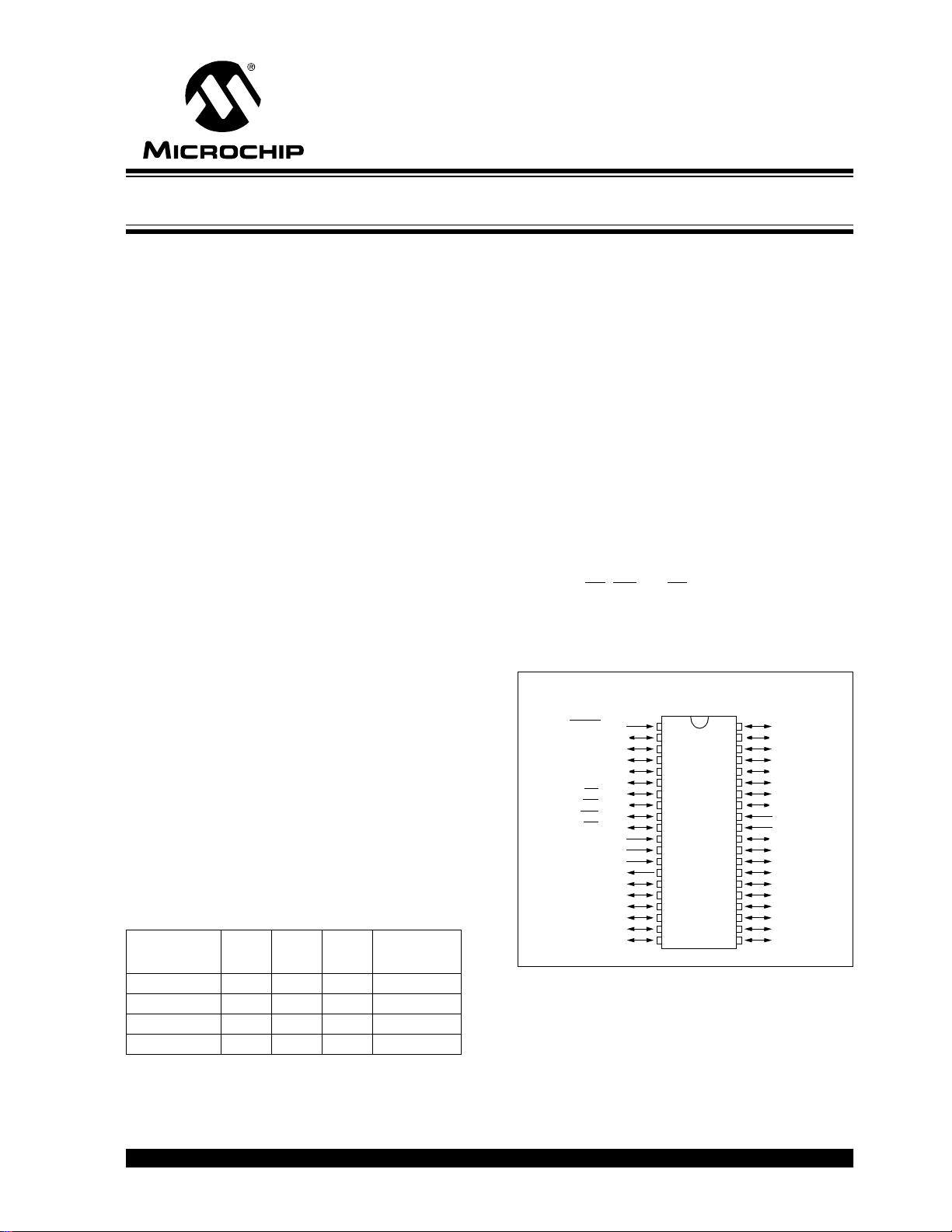
Pin Diagram:
PDIP, Windowed CERDIP
MCLR/VPP
RA0/AN0
RA1/AN1
RA2/AN2
RA3/AN3/V
RE1/WR
OSC2/CLKOUT
RC0/T1OSO/T1CKI
RC1/T1OSI/CCP2
RC3/SCK/SCL
REF
RA4/T0CKI
/AN4
RA5/SS
RE0/RD
/AN5
/AN6
RE2/CS
/AN7
V
VSS
OSC1/CLKIN
RC2/CCP1
RD0/PSP0
RD1/PSP1
1
2
3
4
5
6
7
8
9
10
DD
11
12
13
14
15
16
17
18
19
20
40
39
38
37
36
35
34
33
32
31
30
29
PIC16C65B
PIC16C74B
28
27
26
25
24
23
22
21
RB7
RB6
RB5
RB4
RB3
RB2
RB1
RB0/INT
DD
V
VSS
RD7/PSP7
RD6/PSP6
RD5/PSP5
RD4/PSP4
RC7/RX/DT
RC6/TX/CK
RC5/SDO
RC4/SDI/SDA
RD3/PSP3
RD2/PSP2
2000 Microchip Technology Inc. DS30605C-page 1
PIC16C63A/65B/73B/74B
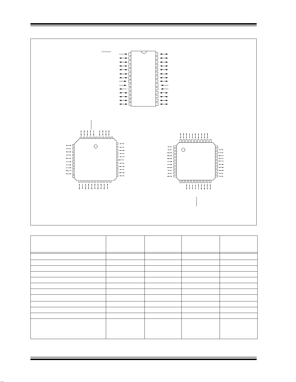
SDIP, SOIC, Windowed CERDIP
PLCC
RA4/T0CKI
RA5/SS/AN4
RE0/RD/AN5
RE1/WR/AN6
RE2/CS/AN7
V
DD
VSS
OSC1/CLKIN
OSC2/CLKOUT
RC0/T1OSO/T1CKI
NC
RA3/AN3/VREF
RA2/AN2
65432
7
8
9
10
PIC16C65B
11
12
PIC16C74B
13
14
15
16
17
MCLR/VPP
RA0/AN0
RA1/AN1
RA2/AN2
RA3/AN3/V
OSC1/CLKIN
OSC2/CLKOUT
RC0/T1OSO/T1CKI
RC1/T1OSI/CCP2
RC3/SCK/SCL
REF
RA4/T0CKI
RA5/SS/AN4
V
RC2/CCP1
/VPP
NC
RA1/AN1
RA0/AN0
MCLR
RB7
RB6
RB5
RB4
NC
1
4443424140
39
38
37
36
35
34
33
32
31
30
29
2827262524232221201918
SS
• 1
2
3
4
5
6
7
8
9
10
11
12
13
14
RB3
RB2
RB1
RB0/INT
DD
V
VSS
RD7/PSP7
RD6/PSP6
RD5/PSP5
RD4/PSP4
RC7/RX/DT
PIC16C63A
PIC16C73B
RC7/RX/DT
RD4/PSP4
RD5/PSP5
RD6/PSP6
RD7/PSP7
28
27
26
25
24
23
22
21
20
19
18
17
16
15
MQFP
TQFP
V
VDD
RB0/INT
RB1
RB2
RB3
RB7
RB6
RB5
RB4
RB3
RB2
RB1
RB0/INT
V
VSS
RC7/RX/DT
RC6/TX/CK
RC5/SDO
RC4/SDI/SDA
SS
DD
RC6/TX/CK
RC5/SDO
RC4/SDI/SDA
RD3/PSP3
4443424140393837363534
1
2
3
4
5
PIC16C65B
6
7
PIC16C74B
8
9
10
11
RD2/PSP2
RD1/PSP1
RD0/PSP0
RC3/SCK/SCL
RC2/CCP1
RC1/T1OSI/CCP2
NC
33
32
31
30
29
28
27
26
25
24
23
2221201918171615141312
NC
RC0/T1OSO/T1CKI
OSC2/CLKOUT
OSC1/CLKIN
VSS
VDD
RE2/CS/AN7
RE1/WR/AN6
RE0/RD/AN5
RA5/SS/AN4
RA4/T0CKI
NC
NC
RB5
RB4
RB6
RB7
/VPP
RA2/AN2
RA1/AN1
RA0/AN0
MCLR
RA3/AN3/VREF
RC2/CCP1
RC3/SCK/SCL
RD1/PSP1
RD0/PSP0
RD3/PSP3
RD2/PSP2
RC4/SDI/SDA
RC5/SDO
RC6/TX/CK
NC
RC1/T1OSI/CCP2
Key Features
PICmicro™ Mid-Range MCU Family
PIC16C63A PIC16C65B PIC16C73B PIC16C74B
Reference Manual (DS33023)
Program Memory (EPROM) x 14 4 K 4 K 4 K 4 K
Data Memory (Bytes) x 8 192 192 192 192
Pins 28 40 28 40
Parallel Slave Port — Yes — Yes
Capture/Compare/PWM Modules 2 2 2 2
Timer Modules 3 3 3 3
A/D Channels —— 58
2
Serial Communication SPI/I
C, USART SPI/I2C, USART SPI/I2C, USART SPI/I2C, USART
In-Circuit Serial Programming Yes Yes Yes Yes
Brown-out Reset Yes Yes Yes Yes
Interrupt Sources 10 11 11 12
Packages 28-pin SDIP, SOIC,
SSOP,
Windowed CERDIP
40-pin PDIP;
44-pin PLCC,
MQFP, TQFP,
Windowed CERDIP
28-pin SDIP, SOIC,
SSOP,
Windowed CERDIP
40-pin PDIP;
44-pin PLCC,
MQFP, TQFP,
Windowed CERDIP
DS30605C-page 2 2000 Microchip Technology Inc.

PIC16C63A/65B/73B/74B
Table of Contents
1.0 General Description............................................................................ ....... .... .. .... .. .... ...................................................................5
2.0 PIC16C63A/65B/7 3 B/74B Device Varieties................................................................................................................................. 7
3.0 Architectural Overview................................................................................................................................................................. 9
4.0 Memory Organization.................................................................................................................................................................15
5.0 I/O Ports................ ..................................... ...................................... ..........................................................................................29
6.0 Timer0 Module ........................................................................................................................................................................... 39
7.0 Timer1 Module ........................................................................................................................................................................... 43
8.0 Timer2 Module ........................................................................................................................................................................... 47
9.0 Capture/Compare/PWM Modules ............................................................... .... .... .. .... ....... .... .... .. ................................................ 49
10.0 Synchronous Serial Port (SSP) Module .....................................................................................................................................55
11.0 Addressable Universal Synchronous Asynchronous Receiv er Transmitter (USA RT )................................................................ 65
12.0 Analog-to-Digital Converter (A/D) Module ................................................................................................................................. 79
13.0 Special Features of the CPU...................................................................................................................................................... 85
14.0 Instruction Set Summary............................................................................................................................................................ 99
15.0 Development Support............................................................................................................................................................... 107
16.0 Electrical Characteristics.......................................................................................................................................................... 113
17.0 DC and AC Characteristics Graphs and Tables.......................................................................................................................139
18.0 Packaging Information. ............................................................... ...................................... ........................................................ 153
Appendix A: Revision History ........................................................................................................................................................ 165
Appendix B: Device Differences...................................................................................... ....... .... ....................................................165
Appendix C: Device Migrations - PIC16C63/65A/73A/74A → PIC16C63A/65B/73B/74B .............................................................166
Appendix D: Migration from Baseline to Mid-Range Devices......................................................................................................... 168
On-Line Support................................................................................................................................................................................. 175
Reader Response.............................................................................................................................................................................. 176
Product Identification System............................................................................................................................................................ 177
TO OUR VALUED CUSTOMERS
It is our intention to provide our valued customers with the best documentation possible to ensure successful use of your Microchip
products. To this end, we will continue to improve our publications to better suit your needs. Our publications will be refined and
enhanced as new volumes and updates are introduced.
If you have any questions or c omm ents regarding th is publication, p lease c ontact the M a rketing Communications Department via
E-mail at docerrors@mail.microchip.com or fax the Reader Response Form in the back of this data sheet to (480) 792-4150.
We welcome your feedback.
Most Current Data Sheet
To obtain the most up-to-date version of this data sheet, please register at our Worldwide Web site at:
http://www.microchip.com
You can determine the version of a data sheet by examining its literature number found on the bottom outside corner of any page.
The last character of the literature number is the version number, (e.g., DS30000A is version A of document DS30000).
Errata
An errata sheet, describing minor operational differences from the data sheet and recommended workarounds, may exist for current
devices. As device/documentation issues become known to us, we will publish an errata sheet. The errata will specify the revision
of silicon and revision of document to which it applies.
To determine if an errata sheet exists for a particular device, please check with one of the following:
• Microchip’s Worldwide Web site; http://www.microchip.com
• Your local Microchip sales office (see last page)
• The Microchip Corporate Literature Center; U.S. FAX: (480) 792-7277
When contacting a sales office or the literature center, please specify which device, revision of silicon and data sheet (include literature number) you are using.
Customer Notification System
Register on our web site at www.microchip.com/cn to receive the most current information on all of our products.
2000 Microchip Technology Inc. DS30605C-page 3

PIC16C63A/65B/73B/74B
NOTES:
DS30605C-page 4 2000 Microchip Technology Inc.

PIC16C63A/65B/73B/74B
1.0 GENERAL DESCRIPTION
The PIC16C63A/65B/73B/74B devices are low cost,
high performance, CMOS, fully-static, 8-bit microcontrollers in the PIC16CXX mid-range family.
®
All PICmicro
RISC architecture. The PIC16CXX microcontroller
family has enhanced core features, eight-level deep
stack and multiple internal and external interrupt
sources. The separate instruction and data buses of
the Harvard architecture allow a 14- bit w ide ins truc tio n
word with the separate 8-bit wide data. The two stage
instruction pipeline allows all instructions to execute in
a single cycle, except for program branches, which
require two cycles. A total of 35 instructions (reduced
instruction set) are available. Additionally, a large register set gives some of the architectural innovations
used to achieve a very high performance.
The PIC16C63A/73B devices have 22 I/O pins. The
PIC16C65B/74B devices have 33 I/O pins. Each
device has 192 bytes of RAM. In addition, several
peripheral features ar e available, includi ng: three timer/
counters, two Capture/Compare/PWM modules, and
two serial ports. The Synchronous Serial Port (SSP)
can be configured as either a 3-wire Serial Peripheral
Interface (SPI) or the two-wire Inter-Integrated Circuit
2
C) bus. The Universal Synchronous Asynchronous
(I
Receiver Transmitter (USART) is also known as the
Serial Communications Interface or SCI. Also, a 5channel high speed 8-bit A/D is provided on the
PIC16C73B, while the PIC16C74B offers 8 channels.
The 8-bit resolution is ideally suited for applications
requiring low cost analog interface, e.g., thermostat
control, pressure sensing, etc.
The PIC16C63A/65B/73B/74B devices have special
features to reduce ex ternal com ponent s, th us redu cing
cost, enhancing system reliability and reducing power
consumption. Th ere are four osci llator options, of which
the single pin RC oscillator prov ides a low cost s olution,
the LP oscillator minimizes power consumption, XT is
a standard crystal, and the HS is for high speed crystals. The SLEEP (power-down) feature provides a
power-saving mode. The user can wake-up the chip
from SLEEP through several external and internal
interrupts and RESETS.
microcontrollers employ an advanced
A highly reliable Watchdog Timer (WDT), with its own
on-chip RC oscillator, provides protection against software lockup, and also provides one way of waking the
device from SLEEP.
A UV erasable CERDIP packaged version is ideal for
code development, while the cost effective One-TimeProgrammable (OTP) versi on is suit a ble for pro duction
in any volume.
The PIC16C63A/65B/73B/74B devices fit nicely in
many applications ranging from security and remote
sensors to appliance control and automotive. The
EPROM technology makes customization of application programs (transmitter codes, motor speeds,
receiver frequencies, etc.) extremely fast and convenient. The small foo tprint p acka ges ma ke this microcontroller series perfect for all applications with space
limitations. Low cost, low power, high performance,
ease of use and I/O flexibility make the PIC16C63A/
65B/73B/74B devices very versatile, even in areas
where no microcontroller use has been considered
before (e.g., timer functions, serial communication,
capture and compar e, PWM functions and copro cessor
applications).
1.1 Family and Upward Compatibility
Users familiar with the PIC16C5X microcontroller family will realize that this is an enhanced version of the
PIC16C5X architecture. Please refer to Appendi x A f or
a detailed list of enhancements. Code written for the
PIC16C5X can be easily po rted to th e PIC 16 CXX fam ily of devices (Appendix B).
1.2 Development Support
PICmicro® devices are supported by the complete line
of Microchip Develo pme nt tool s.
Please refer to Section 15.0 for more details about
Microchip’s development tools.
2000 Microchip Technology Inc. DS30605C-page 5

PIC16C63A/65B/73B/74B
NOTES:
DS30605C-page 6 2000 Microchip Technology Inc.

PIC16C63A/65B/73B/74B
2.0 PIC16C63A/65B/73B/74B DEVICE VARIETIES
A variety of frequency ranges and packaging options
are available. Depen ding on applicati on and production
requirements, t he proper devic e option can be s elected
using the information in the PIC16C63A/65B/73B/74B
Product Identification Sys tem sectio n at the end of this
data sheet. When placing orders, please use that page
of the data sheet to specify the correct part number.
For the PIC16C7X family, there are two device “types”
as indicated in the device number:
1. C, as in PIC16C74. These devices have
EPROM type memory and operate over the
standard voltage range.
2. LC, as in PIC16LC74. These devices have
EPROM type memory and operate over an
extended voltage range.
2.1 UV Erasable Devices
The UV erasable vers ion, offered i n windowed CERDIP
packages, is optimal for prototype development and
pilot programs. This version can be erased and
reprogrammed to any of the oscillator modes.
Microchip's PICSTART
programmers both support programming of the
PIC16C63A/65B/73B/74B.
Plus and PRO MATEII
2.3 Quick-Turnaround-Production (QTP) Devices
Microchip o ffers a QTP Progr amming Servic e for factory production orders. This service is made available
for users who choose not to program a medium to high
quantity of units and whose code patterns have stabilized. The device s are identical to the OTP devices but
with all EPROM locations and configuration options
already programmed by the factory. Certain code and
prototype verification procedures apply before production shipments are ava il abl e. Plea se co ntact your local
Microchip Technology sales office for more details.
2.4 Serialized Quick-Turnaround
Production (SQTP
Microchip offers a unique programming service where
a few user-defined locations in each device are programmed with dif ferent ser ial numbers. The serial numbers may be random, pseudo-random or sequential.
Serial programming allows each device to have a
unique number, which can serve as an entry code,
password or ID number.
SM
) Devices
2.2 One-Time-Programmable (OTP) Devices
The availability of OTP devices is especially useful for
customers who need the flexibility for frequent code
updates and small volume applications.
The OTP devic es, packaged in plas tic packag es, permit the user to program them once. In addition to the
program memory, the configuration bits must also be
programmed.
2000 Microchip Technology Inc. DS30605C-page 7

PIC16C63A/65B/73B/74B
NOTES:
DS30605C-page 8 2000 Microchip Technology Inc.

PIC16C63A/65B/73B/74B
3.0 ARCHITECTURAL OVERVIEW
The high performance of the PIC16CXX family can be
attributed to a number of architectural features commonly found in RISC microprocessors. To begin with,
the PIC16CXX uses a Harvard architecture, in which
program and data are accessed from separate memories using separate buses. This improves bandwidth
over traditional von Neumann architecture, in which
program and data are fetched from the same memory
using the same bus. Separating program and data
buses furthe r all ow s inst r uct i on s to be si ze d diffe ren t ly
than the 8-bit wide data word. Instruction opcodes are
14-bits wide, making it possible to have all single word
instructions. A 14-bit wide program memory access
bus fetches a 14-bit instruction in a single cycle. A
two-stage pipeline overlaps fetch and execution of
instructions (Example 3-1). Consequently, most
instructions execute in a single cycle (200 ns @
20 MHz) except for program branches.
All devices covered by this data sheet contain
4K x 14-bit program memory and 192 x 8-bit data
memory.
The PIC16CXX can directly, or indirectly, address its
register files or dat a memory. All Special Funct ion Registers, including the program counter, are mapped in
the data memory. The PIC16CXX has an orthogonal
(symmetrica l) instruct ion set that m akes it possib le to
carry out any operation on any register using any
addressing mode. This symmetrical nature and lack of
‘special optimal situations’ make programming with the
PIC16CXX simple yet effic ient. In addi tion, the learnin g
curve is reduced significantly.
PIC16CXX devices contain an 8-bit ALU and working
register. The ALU is a general purpose arithmetic unit.
It performs arithmetic and Boolean functions between
the data in the working register and any register file.
The ALU is 8-bits wide and capable of addition, subtraction, shift and logical operations. Unless otherwise
mentioned, arithmetic operations are two's complement in nature. In two-operand instructions, typically
one operand is the working register (W register). The
other operand is a file register or an immediate constant. In single operand instructions, the operand is
either the W register or a file register.
The W register is an 8-bit workin g register used for ALU
operations. It is not an addressable register.
Depending on the instruction executed, the ALU may
affect the values of the Carry (C), Digit Carry (DC), and
Zero (Z) bits in the ST ATUS register. The C and DC bits
operate as a borrow
respectively, in subtraction. See the SUBLW and SUBWF
instructions for examples.
bit and a digit borrow out bit,
2000 Microchip Technology Inc. DS30605C-page 9
PIC16C63A/65B/73B/74B
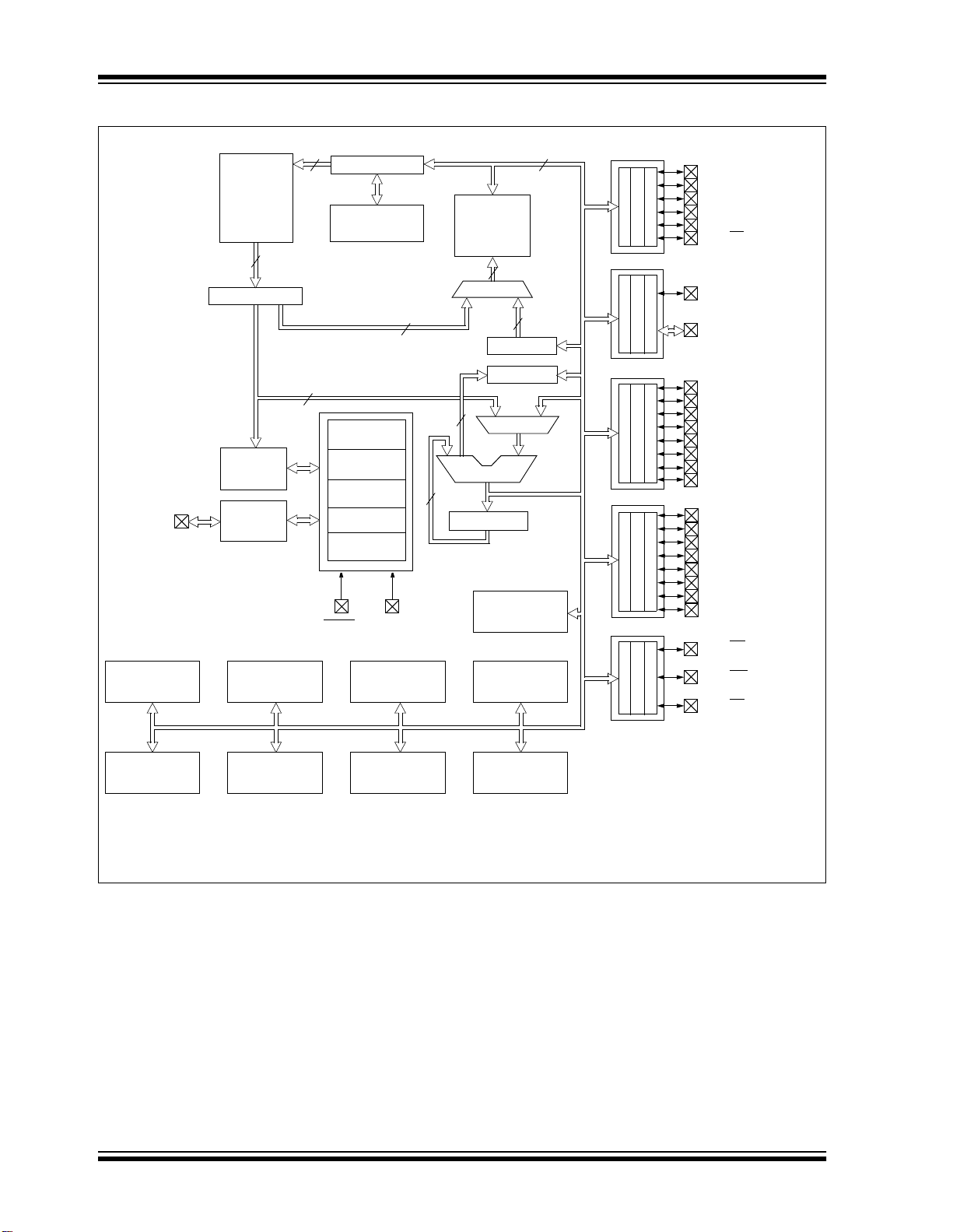
FIGURE 3-1: PIC16C63A/65B/73B/74B BLOCK DIAGRAM
13
Program Counter
EPROM
Program
Memory
Program
OSC1/CLKIN
OSC2/CLKOUT
Timer0 Timer1 Timer2
Bus
14
Instruction reg
Instruction
Decode &
Control
Timing
Generation
Direct Addr
8
MCLR
8 Level Stack
(13-bit)
Power-up
Timer
Oscillator
Start-up Timer
Power-on
Reset
Watchdog
Timer
Brown-out
Reset
VDD, VSS
RAM Addr
7
Data Bus
RAM
File
Registers
(1)
Addr MUX
3
ALU
8
W reg
Parallel Slave Port
9
Indirect
8
Addr
FSR reg
STATUS reg
MUX
(3)
(2)
A/D
8
PORTA
PORTB
PORTC
PORTD
PORTE
(2)
RA0/AN0
(2)
RA1/AN1
(2)
RA2/AN2
RA3/AN3/VREF
RA4/T0CKI
RA5/SS
RB0/INT
RB7:RB1
RC0/T1OSO/T1CKI
RC1/T1OSI/CCP2
RC2/CCP1
RC3/SCK/SCL
RC4/SDI/SDA
RC5/SDO
RC6/TX/CK
(3)
(3)
RC7/RX/DT
RD0/PSP0
RD1/PSP1
RD2/PSP2
RD3/PSP3
RD4/PSP4
RD5/PSP5
RD6/PSP6
RD7/PSP7
RE0/RD
RE1/WR/AN6
RE2/CS/AN7
/AN4
/AN5
(2)
(2)
(2,3)
(2,3)
(2,3)
CCP1 CCP2
Synchronous
Serial Port
USART
Note 1: Higher order bits are from the STATUS register.
2: A/D is not available on the PIC16C63A/65B.
3: PSP and Ports D and E are not available on PIC16C63A/73B.
DS30605C-page 10 2000 Microchip Technology Inc.

PIC16C63A/65B/73B/74B
TABLE 3-1: PIC16C63A/73B PINOUT DESCRIPTION
Pin Name
DIP
Pin#
OSC1/CLKIN 9 9 I ST/CMOS
OSC2/CLKOUT 10 10 O — Oscillator crystal output. Connects to crystal or resonator in
/VPP 1 1 I/P ST Master clear (RESET) input or programming voltage input.
MCLR
RA0/AN0
RA1/AN1
RA2/AN2
RA3/AN3/V
(4)
(4)
(4)
(4)
REF
RA4/T0CKI 6 6 I/O ST RA4 can also be the clock input to the Timer0 module.
RA5/SS/AN4
(4)
RB0/INT 21 21 I/O TTL/ST
RB1 22 22 I/O TTL
RB2 23 23 I/O TTL
RB3 24 24 I/O TTL
RB4 25 25 I/O TTL Interrupt-on-change pin.
RB5 26 26 I/O TTL Interrupt-on-change pin.
RB6 27 27 I/O TTL/ST
RB7 28 28 I/O TTL/ST
RC0/T1OSO/T1CKI 11 11 I/O ST RC0 can also be the Timer1 oscillator output or Timer1
RC1/T1OSI/CCP2 12 12 I/O S T RC1 can also be the Timer1 oscillator input or Capture2
RC2/CCP1 13 13 I/O S T RC2 can also be the Capture1 input/Compare1
RC3/SCK/SCL 14 14 I/O ST RC3 can also be the synchronous serial clock input/output
RC4/SDI/SDA 15 15 I/O ST RC4 can also be the SPI Data In (SPI mode) or
RC5/SDO 16 16 I/O ST RC5 can also be the SPI Data Out (SPI mode).
RC6/TX/CK 17 17 I/O S T RC6 can also be the USART Asynchronous Transmit
RC7/RX/DT 18 18 I/O ST RC7 can also be the USART Asynchronous Receive
SS 8, 19 8, 19 P — Ground reference for logic and I/O pins.
V
DD 20 20 P — Positive supply for logic and I/O pins.
V
Legend: I = input O = output I/O = input/output P = power
— = Not used TTL = TTL input ST = Schmitt Trigger input
Note 1: This buffer is a Schmitt Trigger input when configured as the external interrupt.
2: This buffer is a Schmitt Trigger input when used in Serial Programming mode.
3: This buffer is a Schmitt Trigger input when configured in RC oscillator mode and a CMOS input otherwise.
4: A/D module is not available in the PIC16C63A.
SOIC
Pin#
I/O/P
Type
Buffer
Type
Description
(3)
Oscillator crystal input/external clock source input.
crystal oscillator mode. In RC mode, the OSC2 pin outputs
CLKOUT which has 1/4 the frequency of OSC1, and denotes
the instruction cycle rate.
This pin is an active low RESET to the device.
PORTA is a bi-directional I/O port.
2 2 I/O TTL RA0 can also be analog input 0
3 3 I/O TTL RA1 can also be analog input 1
4 4 I/O TTL RA2 can also be analog input 2
5 5 I/O TTL RA3 can also be analog input 3 or analog reference
voltage
(4)
.
(4)
.
(4)
.
(4)
.
Output is open drain type.
7 7 I/O TTL RA5 can also be analog input 4
(4)
or the slave select for
the synchronous serial port.
PORTB is a bi-directional I/O port. PORTB can be software
programmed for internal weak pull-up on all inputs.
(1)
(2)
(2)
RB0 can also be the external interrupt pin.
Interrupt-on-change pin. Serial programming clock.
Interrupt-on-change pin. Serial programming data.
PORTC is a bi-directional I/O port.
clock input.
input/Compare2 output/PWM2 output.
output/PWM1 output.
2
2
C mode).
C modes.
for both SPI and I
data I/O (I
or Synchronous Clock.
or Synchronous Data.
2000 Microchip Technology Inc. DS30605C-page 11

PIC16C63A/65B/73B/74B
TABLE 3-2: PIC16C65B/74B PINOUT DESCRIPTION
DIP
Pin Name
Pin#
PLCC
Pin#
OSC1/CLKIN 13 14 30 I ST/CMOS
OSC2/CLKOUT 14 15 31 O — Oscillator crystal output. Connects to crystal or resonator in
/VPP 1 2 18 I/P ST Master clear (RESET) input or programming voltage input.
MCLR
RA0/AN0
RA1/AN1
RA2/AN2
RA3/AN3/V
(5)
(5)
(5)
(5)
REF
2 3 19 I/O TTL RA0 can also be analog input 0
3 4 20 I/O TTL RA1 can also be analog input 1
4 5 21 I/O TTL RA2 can also be analog input 2
5 6 22 I/O TTL RA3 can also be analog input 3 or analog reference
RA4/T0CKI 6 7 23 I/O ST RA4 can also be the clock input to the Timer0 timer/
/AN4
(5)
7 8 24 I/O TTL RA5 can also be analog input 4
RA5/SS
RB0/INT 33 36 8 I/O TTL/ST
RB1 34 37 9 I/O TTL
RB2 35 38 10 I/O TTL
RB3 36 39 11 I/O TTL
RB4 37 41 14 I/O TTL Interrupt-on-change pin.
RB5 38 42 15 I/O TTL Interrupt-on-change pin.
RB6 39 43 16 I/O TTL/ST
RB7 40 44 17 I/O TTL/ST
Legend: I = input O = output I/O = input/output P = power
— = Not used TTL = TTL input ST = Schmitt Trigger input
Note 1: This buffer is a Schmitt Trigger input when configured as the external interrupt.
2: This buffer is a Schmitt Trigger input when used in Serial Programming mode.
3: This buffer is a Schmitt Trigger input when configured as general purpose I/O and a TTL input when used in the Parallel
Slave Port mode (for interfacing to a microprocessor bus).
4: This buffer is a Schmitt Trigger input when configured in RC oscillator mode and a CMOS input otherwise.
5: A/D is not available on the PIC16C65B.
TQFP
MQFP
Pin#
I/O/P
Type
Buffer
Type
Description
(4)
Oscillator crystal input/external clock source input.
crystal oscillator mode. In RC mode, OSC2 pin outputs
CLKOUT which has 1/4 the frequency of OSC1, and
denotes the instruction cycle rate.
This pin is an active low RESET to the device.
PORTA is a bi-directional I/O port.
(5)
.
(5)
.
(5)
.
(5)
voltage
.
counter. Output is open drain type.
(5)
or the slave select for
the synchronous serial port.
PORTB is a bi-directional I/O port. PORTB can be software
programmed for internal weak pull-up on all inputs.
(1)
(2)
(2)
RB0 can also be the external interrupt pin.
Interrupt-on-change pin. Serial programming clock.
Interrupt-on-change pin. Serial programming data.
DS30605C-page 12 2000 Microchip Technology Inc.

PIC16C63A/65B/73B/74B
TABLE 3-2: PIC16C65B/74B PINOUT DESCRIPTION (CONTINUED)
DIP
Pin Name
Pin#
PLCC
Pin#
RC0/T1OSO/T1CKI 15 16 32 I/O ST RC0 can also be the Timer1 oscillator output or a
RC1/T1OSI/CCP2 16 18 35 I/O ST RC1 can also be the Timer1 oscillator input or Capture2
RC2/CCP1 17 19 36 I/O ST RC2 can also be the Capture1 input/Compare1 output/
RC3/SCK/SCL 18 20 37 I/O ST RC3 can also be the synchronous serial clock input/
RC4/SDI/SDA 23 25 42 I/O ST RC4 can also be the SPI Data In (SPI mode) or
RC5/SDO 24 26 43 I/O ST RC5 can also be the SPI Data Out
RC6/TX/CK 25 27 44 I/O ST RC6 can also be the USART Asynchronous Transmit or
RC7/RX/DT 26 29 1 I/O ST RC7 can also be the USART Asynchronous Receive or
RD0/PSP0 19 21 38 I/O ST/TTL
RD1/PSP1 20 22 39 I/O ST/TTL
RD2/PSP2 21 23 40 I/O ST/TTL
RD3/PSP3 22 24 41 I/O ST/TTL
RD4/PSP4 27 30 2 I/O ST/TTL
RD5/PSP5 28 31 3 I/O ST/TTL
RD6/PSP6 29 32 4 I/O ST/TTL
RD7/PSP7 30 33 5 I/O ST/TTL
(5)
/AN5
RE0/RD
(5)
RE1/WR
RE2/CS
V
V
/AN6
(5)
/AN7
SS 12,31 13,34 6,29 P — Ground reference for logic and I/O pins.
DD 11,32 12,35 7,28 P — Positive supply for logic and I/O pins.
8925I/OST/TTL
91026I/OST/TTL
10 11 27 I/O ST/TTL
NC — 1,17,28,4012,13,
Legend: I = input O = output I/O = input/output P = power
— = Not used TTL = TTL input ST = Schmitt Trigger input
Note 1: This buffer is a Schmitt Trigger input when configured as the external interrupt.
2: This buffer is a Schmitt Trigger input when used in Serial Programming mode.
3: This buffer is a Schmitt Trigger input when configured as general purpose I/O and a TTL input when used in the Parallel
Slave Port mode (for interfacing to a microprocessor bus).
4: This buffer is a Schmitt Trigger input when configured in RC oscillator mode and a CMOS input otherwise.
5: A/D is not available on the PIC16C65B.
TQFP
MQFP
Pin#
33,34
I/O/P
Type
Buffer
Type
Description
PORTC is a bi-directional I/O port.
Timer1 clock input.
input/Compare2 output/PWM2 output.
PWM1 output.
output for both SPI and I
data I/O (I
2
C mode).
2
C modes.
(SPI mode).
Synchronous Clock.
Synchronous Data.
PORTD is a bi-directional I/O port or parallel slave port
when interfacing to a microprocessor bus.
(3)
(3)
(3)
(3)
(3)
(3)
(3)
(3)
PORTE is a bi-directional I/O port.
(3)
(3)
(3)
RE0 can also be read control for the parallel slave port,
or analog input 5
RE1 can also be write control for the parallel slave port,
or analog input 6
RE2 can also be select control for the parallel slave
port, or analog input 7
(5)
.
(5)
.
(5)
.
— These pins are not internally connected. These pins should
be left unconnected.
2000 Microchip Technology Inc. DS30605C-page 13

PIC16C63A/65B/73B/74B
3.1 Clocking Scheme/Instruction Cycle
The clock input (from OSC1) is internally divided by
four to generate four non-overlapping quadrature
clocks, namely Q1, Q2, Q3 and Q4. Internally, the program counter (PC) is incremented every Q1, the
instruction is fetched from the program memory and
latched into the instruction register in Q4. The instruction is decoded and executed during the following Q1
through Q4. The clocks and instruction execution flow
is shown in Figure 3-2.
FIGURE 3-2: CLOCK/INSTRUCTION CYCLE
Q2 Q3 Q4
OSC1
Q1
Q2
Q3
Q4
PC
OSC2/CLKOUT
(RC mode)
Q1
PC PC+1 PC+2
Fetch INST (PC)
Execute INST (PC-1) Fetch INST (PC+1)
Q1
Execute INST (PC) Fetch INST (PC+2)
3.2 Instruction Flow/Pipelining
An “Instruction Cycle” consists of four Q cycles (Q1,
Q2, Q3 and Q4). The instruc tio n fetch and execute are
pipelined such that fetch takes one instruction cycle,
while decode and execute takes another instruction
cycle. However, due to the pipelining, each instruction
effectively executes in one cycle. If an instruction
causes the program counter to change (e.g., GOTO),
then two cycles are req uired to c omplete the ins truction
(Example 3-1).
A fetch cycle begins with the program counter (PC)
incrementing in Q1.
In the execution cy cle, the fetched instruction i s latched
into the “Instruction Register" (IR) in cycle Q1. This
instruction is then decoded and executed during the
Q2, Q3 and Q4 c ycles. Dat a m emory is read during Q2
(operand read) and written during Q4 (destination
write).
Q2 Q3 Q4
Q2 Q3 Q4
Q1
Execute INST (PC+1)
Internal
phase
clock
EXAMPLE 3-1: INSTRUCTION PIPELINE FLOW
TCY0TCY1TCY2TCY3TCY4TCY5
1. MOVLW 55h
2. MOVWF PORTB
3. CALL SUB_1
4. BSF PORTA, BIT3 (Forced NOP)
5. Instruction @ address SUB_1
Note: All instructions are single cycle, except for any program branches. These take two cycles, since the fetch instruc tion is
“flushed” from the pipeline, while the new instruction is being fetched and then executed.
DS30605C-page 14 2000 Microchip Technology Inc.
Fetch 1 Execute 1
Fetch 2 Execute 2
Fetch 3 Execute 3
Fetch 4 Flush
Fetch SUB_1 Execute SUB_1
PIC16C63A/65B/73B/74B
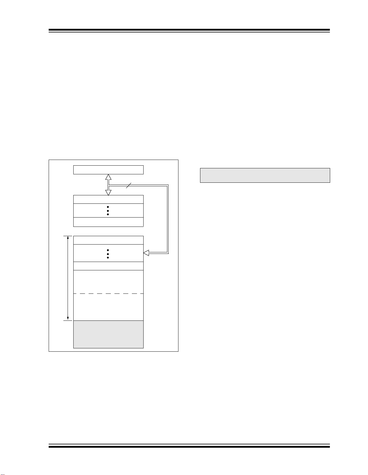
4.0 MEMORY ORGANIZATION
4.1 Program Memory Organization
The PIC16C63A/65B/73B/74B has a 13-bit program
counter capable of addressing an 8K x 14 program
memory space. All devices covered by this data sheet
have 4K x 14 bits of program memory. The address
range is 0000h - 0FFFh for all devices.
Accessing a location above 0FFFh will cause a wraparound.
The RESET vector is at 0000h and the interrupt vector
is at 0004h.
FIGURE 4-1: PIC16C63A/65B/73B/74B
PROGRAM MEMORY MAP
AND STACK
PC<12:0>
CALL,RETURN
RETFIE,RETLW
Stack Level 1
Stack Level 8
13
4.2 Data Memory Organization
The data memory is partitioned into multiple banks
which contain the General Purpose Registers (GPR)
and the Special Function Registers (SFR). Bits RP1
and RP0 are the bank select bits.
RP1:RP0 (STATUS<6:5>)
= 00 → Bank0
= 01 → Bank1
= 10 → Bank2
= 11 → Bank3
Each bank extends up to 7Fh (128 bytes). The lower
locations of each bank are reserved for the SFRs.
Above the SFRs are GPRs, implemented as static
RAM.
All implemented banks con t ai n SFR s. Frequently used
SFRs from one bank may be mirrored in another bank
for code reduction and quicker access.
Note: Maintain the IRP and RP1 bits clear in
these devices.
4.2.1 GENERAL PURPOSE REGISTER FILE
The register file can be acces sed either directly, or indirectly, through the File Select Register (FSR)
(Section 4.5).
RESET Vector
Interrupt Vector
On-chip Program
Space
User Memory
Memory (Page 0)
On-chip Program
Memory (Page 1)
0000h
0004h
0005h
07FFh
0800h
0FFFh
1000h
1FFFh
2000 Microchip Technology Inc. DS30605C-page 15
PIC16C63A/65B/73B/74B
FIGURE 4-2: REGISTER FILE MAP 4.2.2 SPECIAL FUNCTION REGISTERS
File
Address
00h
01h
02h
03h
04h
05h
06h
07h
08h
09h
0Ah
0Bh
0Ch
0Dh
0Eh
0Fh
10h
11h
12h
13h
14h
15h
16h
17h
18h
19h
1Ah
1Bh
1Ch
1Dh
1Eh
1Fh
(1)
INDF
TMR0
PCL
STATUS
FSR
PORTA
PORTB
PORTC
PORTD
PORTE
(2)
(2)
PCLATH
INTCON
PIR1
PIR2
TMR1L
TMR1H
T1CON
TMR2
T2CON
SSPBUF
SSPCON
CCPR1L
CCPR1H
CCP1CON
RCSTA
TXREG
RCREG
CCPR2L
CCPR2H
CCP2CON
ADRES
(3)
ADCON0
OPTION_REG
(3)
(1)
INDF
PCL
STATUS
FSR
TRISA
TRISB
TRISC
TRISD
TRISE
PCLATH
INTCON
PIE1
PIE2
PCON
PR2
SSPADD
SSPSTAT
TXSTA
SPBRG
ADCON1
20h A0h
(2)
(2)
(3)
File
Address
80h
81h
82h
83h
84h
85h
86h
87h
88h
89h
8Ah
8Bh
8Ch
8Dh
8Eh
8Fh
90h
91h
92h
93h
94h
95h
96h
97h
98h
99h
9Ah
9Bh
9Ch
9Dh
9Eh
9Fh
The Special Function Registers are registers used by
the CPU and Peripheral Modules for controlling the
desired operation of the device. These registers are
implemented as static RAM.
The Special Function Registers can be classified into
two sets (core and peripheral). Those registers associated with the “core” fun ction s are des cribe d in this section, and those related to the operation o f the peripheral
features are described in the section of that peripheral
feature.
General
Purpose
Register
7Fh
General
Purpose
Register
FFh
Bank 0 Bank 1
Unimplemented data memory locations, read as ’0’.
Note 1: Not a physical register.
2: These registers are not implemented on the
PIC16C63A/73B, read as '0'.
3: These registers are not implemented on the
PIC16C63A/65B, read as '0'.
DS30605C-page 16 2000 Microchip Technology Inc.
PIC16C63A/65B/73B/74B
TABLE 4-1: SPECIAL FUNCTION REGISTER SUMMARY
Address Name Bit 7 Bit 6 Bit 5 Bit 4 Bit 3 Bit 2 Bit 1 Bit 0
Bank 0
00h INDF
01h TMR0 Timer0 module’s register xxxx xxxx uuuu uuuu
02h PCL
03h STATUS
04h FSR
05h PORTA — — PORTA Data Latch when written: PORTA pins when read --0x 0000 --0u 0000
06h PORTB PORTB Data Latch when written: PORTB pins when read xxxx xxxx uuuu uuuu
07h PORTC PORTC Data Latch when written: PORTC pins when read xxxx xxxx uuuu uuuu
08h PORTD
09h PORTE
0Ah PCLATH
0Bh INTCON
0Ch PIR1 PSPIF
0Dh PIR2 — — — – — — — CCP2IF ---- ---0 ---- ---0
0Eh TMR1L Holding register for the Least Significant Byte of the 16-bit TMR1 register xxxx xxxx uuuu uuuu
0Fh TMR1H Holding register for the Most Significant Byte of the 16-bit TMR1 register xxxx xxxx uuuu uuuu
10h T1CON — — T1CKPS1 T1CKPS0 T1OSCEN T1SYNC TMR1CS TMR1ON --00 0000 --uu uuuu
11h TMR2 Timer2 module’s register 0000 0000 0000 0000
12h T2CON — TOUTPS3 TOUTPS2 TOUTPS1 TOUTPS0 TMR2ON T2CKPS1 T2CKPS0 -000 0000 -000 0000
13h SSPBUF Synchronous Serial Port Receive Buffer/Transmit Register xxxx xxxx uuuu uuuu
14h SSPCON WCOL SSPOV SSPEN CKP SSPM3 SSPM2 SSPM1 SSPM0 0000 0000 0000 0000
15h CCPR1L Capture/Compare/PWM Register1 (LSB) xxxx xxxx uuuu uuuu
16h CCPR1H Capture/Compare/PWM Register1 (MSB) xxxx xxxx uuuu uuuu
17h CCP1CON — — CCP1X CCP1Y CCP1M3 CCP1M2 CCP1M1 CCP1M0 --00 0000 --00 0000
18h RCSTA SPEN RX9 SREN CREN — FERR OERR RX9D 0000 -00x 0000 -00x
19h TXREG USART Transmit Data register 0000 0000 0000 0000
1Ah RCREG USART Receive Data register 0000 0000 0000 0000
1Bh CCPR2L Capture/Compare/PWM Register2 (LSB) xxxx xxxx uuuu uuuu
1Ch CCPR2H Capture/Compare/PWM Register2 (MSB) xxxx xxxx uuuu uuuu
1Dh CCP2CON — — CCP2X CCP2Y CCP2M3 CCP2M2 CCP2M1 CCP2M0 --00 0000 --00 0000
1Eh ADRES
1Fh ADCON0
(4)
(4)
(4)
Addressing this location uses contents of FSR to address data memory (not a physical register) 0000 0000 0000 0000
Program Counter's (PC) Least Significant Byte 0000 0000 0000 0000
(4)
(5)
(5)
(1,4)
(4)
(6)
(6)
(2)
IRP
Indirect data memory address pointer xxxx xxxx uuuu uuuu
PORTD Data Latch when written: PORTD pins when read xxxx xxxx uuuu uuuu
— — — — — RE2 RE1 RE0 ---- -xxx ---- -uuu
— — — W rite Buffer for the upper 5 bits of the Program Counter ---0 0000 ---0 0000
GIE PEIE T0IE INTE RBIE T0IF INTF RBIF 0000 000x 0000 000u
(5)
A/D Result register xxxx xxxx uuuu uuuu
ADCS1 ADCS0 CHS2 CHS1 CHS0 GO/DONE — ADON 0000 00-0 0000 00-0
RP1
ADIF
(2)
RP0 TO PD ZDCC0001 1xxx 000q quuu
(6)
RCIF TXIF SSPIF CCP1IF TMR2IF TMR1IF 0000 0000 0000 0000
Value on:
POR, BOR
Legend: x = unknown, u = unchanged, q = value depends on condition, - = unimplemented, read as ’0’.
Shaded locations are unimplemented, read as ‘0’.
Note 1: The upper byte of the program counter is not directly accessible. PCLATH is a holding register for the PC<12:8>.
2: The IRP and RP1 bits are reserved; always maintain these bits clear.
3: Other (non power-up) RES ETS include external RESET through MCLR
and Watchdog Timer Reset.
4: These registers can be addressed from either bank.
5: PORTD, PORTE and the parallel slave port are not implemented on the PIC16C63A/73B; always maintain these bits and
registers clear.
6: The A/D is not implemented on the PIC16C63A/65B; always maintain these bits and registers clear.
Value on
all other
RESETS
(3)
2000 Microchip Technology Inc. DS30605C-page 17
PIC16C63A/65B/73B/74B
TABLE 4-1: SPECIAL FUNCTION REGISTER SUMMARY (CONTINUED)
Address Name Bit 7 Bit 6 Bit 5 Bit 4 Bit 3 Bit 2 Bit 1 Bit 0
Bank 1
80h INDF
81h OPTION_REG RBPU INTEDG T0CS T0SE PSA PS2 PS1 PS0 1111 1111 1111 1111
82h PCL
83h STATUS
84h FSR
85h TRISA — — PORTA Data Direction Register --11 1111 --11 1111
86h TRISB PORTB Data Direction register 1111 1111 1111 1111
87h TRISC PORTC Data Direction register 1111 1111 1111 1111
88h TRISD
89h TRISE
8Ah PCLATH
8Bh INTCON
8Ch PIE1 PSPIE
8Dh PIE2 — — — — — — — CCP2IE ---- ---0 ---- ---0
8Eh PCON — — — — — — POR BOR ---- --qq ---- --uu
8Fh — Unimplemented — —
90h — Unimplemented — —
91h — Unimplemented — —
92h PR2 Timer2 Pe riod register
93h SSPADD Synchronous Serial Port (I2C mode) Address register 0000 0000 0000 0000
94h SSPSTAT — — D/A PSR/WUA BF --00 0000 --00 0000
95h — Unimplemented — —
96h — Unimplemented — —
97h — Unimplemented — —
98h TXSTA CSRC TX9 TXEN SYNC
99h SPBRG Baud Rate Generator register 0000 0000 0000 0000
9Ah — Unimplemented — —
9Bh — Unimplemented — —
9Ch — Unimplemented — —
9Dh — Unimplemented — —
9Eh — Unimplemented — —
9Fh ADCON1
(4)
(4)
(4)
Addressing this location uses contents of FSR to address data memory (not a physical register) 0000 0000 0000 0000
Program Counter’s (PC) Least Significant Byte 0000 0000 0000 0000
(4)
(5)
(5)
(1,4)
(4)
(6)
(2)
IRP
Indirect data memory address pointer xxxx xxxx uuuu uuuu
PORTD Data Direction register 1111 1111 1111 1111
IBF OBF IBOV PSPMODE — PORTE Data Direction bits 0000 -111 0000 -111
— — — Write Buffer for the upper 5 bits of the Program Counter ---0 0000 ---0 0000
GIE PEIE T0IE INTE RBIE T0IF INTF RBIF 0000 000x 0000 000u
(5)
— — — — — PCFG2 PCFG1 PCFG0 ---- -000 ---- -000
RP1
ADIE
(2)
RP0 TO PD ZDCC0001 1xxx 000q quuu
(6)
RCIE TXIE SSPIE CCP1IE TMR2IE TMR1IE 0000 0000 0000 0000
— BRGH TRMT TX9D 0000 -010 0000 -010
Value on:
POR, BOR
1111 1111 1111 1111
Legend: x = unknown, u = unchanged, q = value depends on condition, - = unimplemented, read as ’0’.
Shaded locations are unimplemented, read as ‘0’.
Note 1: The upper byte of the program counter is not directly accessible. PCLATH is a holding register for the PC<12:8>.
2: The IRP and RP1 bits are reserved; always maintain these bits clear.
3: Other (non power-up) RESETS include external RESET through MCLR
and Watchdog Timer Reset.
4: These registers can be addressed from either bank.
5: PORTD, PORTE and the parallel slave port are not implemented on the PIC16C63A/73B; always maintain these bits and
registers clear.
6: The A/D is not implemented on the PIC16C63A/65B; always maintain these bits and registers clear.
Value on
all other
RESETS
(3)
DS30605C-page 18 2000 Microchip Technology Inc.
PIC16C63A/65B/73B/74B
4.2.2.1 STATUS Register
The STATUS register, shown in Register 4-1, contains
the arithmetic st atus of th e ALU, the RE SET statu s and
the bank select bits for data memory.
The STATUS register can be the destination for any
instruction, as with any other r egister. If the STATUS register is the destination for an instruction that affects the Z,
DC or C bits, then the write to thes e three bits is disabled.
These bits are set or cleared according to the device
logic. Furt her mo r e, th e TO
Therefore, the result of an instruction with the STATUS
register as destination may be different than intended.
For example, CLRF STATUS will clear the upper three
bits and set the Z bit. Thi s leaves th e STATUS register
as 000u u1uu (where u = unchanged).
and PD bits are not writable.
It is recommended that only BCF, BSF, SWAPF and
MOVWF instructions be used to alter the STATUS register. The se in structions do not affec t the Z, C or DC bits
in the STATUS register . For other i nstruction s whic h do
not affect status bits, see the "Instruction Set Summary."
Note 1: These devices do not use bits IRP and
RP1 (STATUS<7:6>), maintain these bits
clear to ensure upward comp atib il ity w i th
future products.
2: The C and DC bits operate a s borrow
digit borrow
tion. See the SUBLW and SUBWF instructions for examples.
REGISTER 4-1: STATUS REGISTER (ADDRESS 03h, 83h)
R/W-0 R/W-0 R/W-0 R-1 R-1 R/W-x R/W-x R/W-x
(1)
IRP
bit 7 bit 0
bit 7 IRP
bit 6-5 RP1
bit 4 TO
bit 3 PD: Power-down bit
bit 2 Z: Zero bit
bit 1 DC: Digit carry/borrow bit (ADDWF,ADDLW,SUBLW,SUBWF instructions) (for borrow the polarity
bit 0 C
(1)
: Register Bank Select bit (used for indirect addressing)
1 = Bank 2, 3 (100h - 1FFh)
0 = Bank 0, 1 (00h - FFh)
(1)
:RP0: Register Bank Select bits (used for direct addressing)
11 = Bank 3 (180h - 1FFh)
10 = Bank 2 (100h - 17Fh)
01 = Bank 1 (80h - FFh)
00 = Bank 0 (00h - 7Fh)
Each bank is 128 bytes
: Time-out bit
1 = After power-up, CLRWDT instruction, or SLEEP instruction
0 = A WDT time-out occurred
1 = After power-up or by the CLRWDT instruction
0 = By execution of the SLEEP instruction
1 = The result of an arithmetic or logic operation is zero
0 = The result of an arithmetic or logic operation is not zero
is reversed)
1 = A carry-out from the 4th low order bit of the result occurred
0 = No carry-out from the 4th low order bit of the result
(2)
: Carry/borrow bit (ADDWF,ADDLW,SUBLW,SUBWF instructions)
1 = A carry-out from the most significant bit of the result occurred
0 = No carry-out from the most significant bit of the result oc curred
RP1
(1)
RP0 TO PD Z DC C
and
bits, respectively, in subtrac-
(2)
Note 1: Maintain the IRP and RP1 bits clear.
2: For borrow
adding the two’s complement of the s econd operand. For rotate (RRF,RLF) instructions, this bit is loaded with either the high or low order bit of the source register.
Legend:
R = Readable bit W = Writable bit U = Unimplemented bit, read as ‘0’
-n = Value at POR ’1’ = Bit is set ’0’ = Bit is cleared x = Bit is unknown
2000 Microchip Technology Inc. DS30605C-page 19
and digit borrow, the polarity is reversed. A subtraction is executed by

PIC16C63A/65B/73B/74B
4.2.2.2 OPTION Register
The OPTION_REG register is a readable and writable
register , which cont ains various contr ol bits to conf igure
Note: To achieve a 1:1 prescaler assignment for
the TMR0 register, assign the prescaler to
the watchdog timer.
the TMR0/WDT prescaler, the external INT Interrupt,
TMR0 and the weak pull-ups on PORTB.
REGISTER 4-2: OPTION_REG REGISTER (ADDRESS 81h)
R/W-1 R/W-1 R/W-1 R/W-1 R/W-1 R/W-1 R/W-1 R/W-1
RBPU
bit 7 bit 0
bit 7 RBPU
1 = PORTB pull-ups are disabled
0 = PORTB pull-ups are enabled by individual port latch values
bit 6 INTEDG: Interrupt Edge Select bit
1 = Interrupt on rising edge of RB0/INT pin
0 = Interrupt on falling edge of RB0/INT pin
bit 5 T0CS: TMR0 Clock Source Select bit
1 = Transition on RA4/T0CKI pin
0 = Internal instruction cycle clock (CLKOUT)
bit 4 T0SE: TMR0 Source Edge Select bit
1 = Increment on high-to-low transition on RA4/T0CKI pin
0 = Increment on low-to-high transition on RA4/T0CKI pin
bit 3 PSA: Prescaler Assignment bit
1 = Prescaler is assigned to the WDT
0 = Prescaler is assigned to the Timer0 module
bit 2-0 PS2:PS0: Prescaler Rate Select bits
Bit Value TMR0 Rate WDT Rate
INTEDG T0CS T0SE PSA PS2 PS1 PS0
: PORTB Pull-up Enable bit
000
001
010
011
100
101
110
111
1 : 2
1 : 4
1 : 8
1 : 16
1 : 32
1 : 64
1 : 128
1 : 256
1 : 1
1 : 2
1 : 4
1 : 8
1 : 16
1 : 32
1 : 64
1 : 128
Legend:
R = Readable bit W = Writable bit U = Unimplemented bit, read as ‘0’
-n = Value at POR ’1’ = Bit is set ’0’ = Bit is cleared x = Bit is unknown
DS30605C-page 20 2000 Microchip Technology Inc.

PIC16C63A/65B/73B/74B
4.2.2.3 INTCON Register
The INTCON register is a readable and writable register, which contains various enable and flag bits for the
TMR0 register overflow, RB Port change and external
RB0/INT pin interrupts.
Note: Interrupt flag bits are se t w he n an in terru pt
condition occurs, re gardless of the sta te of
its corresponding enable bit, or the global
enable bit, GIE (INTCON<7>). User software should ensure the appropriate interrupt flag bits are clear prior to enabling an
interrupt
REGISTER 4-3: INTCON REGISTER (ADDRESS 0Bh, 8Bh)
R/W-0 R/W-0 R/W-0 R/W-0 R/W-0 R/W-0 R/W-0 R/W-x
GIE PEIE T0IE INTE RBIE T0IF INTF RBIF
bit 7 bit 0
bit 7 GIE:
bit 6 PEIE: Peripheral Interrupt Enable bit
bit 5 T0IE: TMR0 Overflow Interrupt Enable bit
bit 4 INTE: RB0/INT External Interrupt Enable bit
bit 3 RBIE: RB Port Change Interrupt Enable bit
bit 2 T0IF: TMR0 Overflow Interrupt Flag bit
bit 1 INTF: RB0/INT External Interrupt Flag bit
bit 0 RBIF: RB Port Change Interrupt Flag bit
Global Interrupt Enable bit
1 = Enables all unmasked interrupts
0 = Disables all interrupts
1 = Enables all unmasked peripheral interrupts
0 = Disables all peripheral interrupts
1 = Enables the TMR0 interrupt
0 = Disables the TMR0 interrupt
1 = Enables the RB0/INT external interrupt
0 = Disables the RB0/INT external interrupt
1 = Enables the RB port change interrupt
0 = Disables the RB port change interrupt
1 = TMR0 register has overflowed (must be cleared in software)
0 = TMR0 register did not overflow
1 = The RB0/INT external interrupt occurred (must be cleared in software)
0 = The RB0/INT external interrupt did not occur
1 = At least one of the RB7:RB4 pins changed state
0 = None of the RB7:RB4 pins have changed state
(1)
.
Note 1: A mismatch condition will exist until PORTB is read. After reading PORTB, the RBIF
flag bit can be cleared.
Legend:
R = Readable bit W = Writable bit U = Unimplemented bit, read as ‘0’
-n = Value at POR ’1’ = Bit is set ’0’ = Bit is cleared x = Bit is unknown
2000 Microchip Technology Inc. DS30605C-page 21

PIC16C63A/65B/73B/74B
4.2.2.4 PIE1 Register
This register contains the individual enable bits for the
peripheral interrupts.
Note: Bit PEIE (INTCON<6>) must be set to
REGISTER 4-4: PIE1 REGISTER (ADDRESS 8Ch)
R/W-0 R/W-0 R/W-0 R/W-0 R/W-0 R/W-0 R/W-0 R/W-0
(1)
PSPIE
bit 7 bit 0
bit 7 PSPIE
bit 6 ADIE
bit 5 RCIE: USART Receive Interrupt Enable bit
bit 4 TXIE: USART Transmit Interrupt Enable bit
bit 3 SSPIE: Synchronous Serial Port Interrupt Enable bit
bit 2 CCP1IE: CCP1 Interrupt Enable bit
bit 1 TMR2IE: TMR2 to PR2 Match Interrupt Enable bit
bit 0 TMR1IE: TMR1 Overflow Interrupt Enable bit
(1)
: Parallel Slave Port Read/Write Interrupt Enable bit
1 = Enables the PSP read/write interrupt
0 = Disables the PSP read/write interrupt
(2)
: A/D Converter Interrupt Enable bit
1 = Enables the A/D interrupt
0 = Disables the A/D interrupt
1 = Enables the USART receive interrupt
0 = Disables the USART receive interrupt
1 = Enables the USART transmit interrupt
0 = Disables the USART transmit interrupt
1 = Enables the SSP interrupt
0 = Disables the SSP interrupt
1 = Enables the CCP1 interrupt
0 = Disables the CCP1 interrupt
1 = Enables the TMR2 to PR2 match interrupt
0 = Disables the TMR2 to PR2 match interrupt
1 = Enables the TMR1 overflow interrupt
0 = Disables the TMR1 overflow interrupt
ADIE
(2)
RCIE TXIE SSPIE CCP1IE TMR2IE TMR1IE
enable any peripheral interrupt.
Note 1: PIC 16C63A/73B devices do not have a pa rallel slave port imp lemented; always
maintain this bit clear.
2: PI C16C63A/65B devices do not have an A/D implemented; always maintain this bit
clear.
Legend:
R = Readable bit W = Writable bit U = Unimplemented bit, read as ‘0’
-n = Value at POR ’1’ = Bit is set ’0’ = Bit is cleared x = Bit is unknown
DS30605C-page 22 2000 Microchip Technology Inc.

PIC16C63A/65B/73B/74B
4.2.2.5 PIR1 Register
This register contains the individual flag bits for the
peripheral interrupts.
Note: Interrupt flag bits are se t w he n an in terru pt
REGISTER 4-5: PIR1 REGISTER (ADDRESS 0Ch)
R/W-0 R/W-0 R-0 R-0 R/W-0 R/W-0 R/W-0 R/W-0
(1)
PSPIF
bit 7 bit 0
bit 7 PSPIF
bit 6 ADIF
bit 5 RCIF: USART Receive Interrupt Flag bit
bit 4 TXIF: USART Transmit Interrupt Flag bit
bit 3 SSPIF: Synchronous Serial Port Interrupt Flag bit
bit 2 CCP1IF: CCP1 Interrupt Flag bit
bit 1 TMR2IF: TMR2 to PR2 Match Interrupt Flag bit
bit 0 TMR1IF: TMR1 Overflow Interrupt Flag bit
(1)
: Parallel Slave Port Read/Write Interrupt Flag bit
1 = A read or a write operation has taken place (must be cleared in software)
0 = No read or write has occurred
(2)
: A/D Converter Interrupt Flag bit
1 = An A/D conversion completed (must be cleared in software)
0 = The A/D conversion is not complete
1 = The USART receive buffer is full (clear by reading RCREG)
0 = The USART receive buffer is empty
1 = The USART transmit buffer is empty (clear by writing to TXREG)
0 = The USART transmit buffer is full
1 = The transmission/reception is complete (must be cleared in software)
0 = Waiting to transmit/receive
Capture mode:
1 = A TMR1 register capture occurred (must be cleared in software)
0 = No TMR1 register capture occurred
Compare mode:
1 = A TMR1 register compare match occurred (must be cleared in software)
0 = No TMR1 register compare match occurred
PWM mode:
Unused in this mode
1 = TMR2 to PR2 match occurred (must be cleared in software)
0 = No TMR2 to PR2 match occurred
1 = TMR1 register overflowed (must be cleared in software)
0 = TMR1 register did not overflow
ADIF
(2)
RCIF TXIF SSPIF CCP1IF TMR2IF TMR1IF
condition occurs, re gardless of the sta te of
its corresponding enable bit, or the global
enable bit, GIE (INTCON<7>). User software should ensure the appropriate interrupt flag bits are clear prior to enabling an
interrupt
.
Note 1: PIC16C63A/73B devices do n ot have a p aral lel slav e port imple mente d. This b it loc a-
tion is reserved on these devices.
2: PIC16C63A/65B devices do not have an A/D implemented. This bit location is
reserved on these devices.
Legend:
R = Readable bit W = Writable bit U = Unimplemented bit, read as ‘0’
-n = Value at POR ’1’ = Bit is set ’0’ = Bit is cleared x = Bit is unknown
2000 Microchip Technology Inc. DS30605C-page 23

PIC16C63A/65B/73B/74B
4.2.2.6 PIE2 Register
This register contains the individual enable bit for the
CCP2 peripheral interrupt.
REGISTER 4-6: PIE2 REGISTER (ADDRESS 8Dh)
U-0 U-0 U-0 U-0 U-0 U-0 U-0 R/W-0
— — — — — — — CCP2IE
bit 7 bit 0
bit 7-1 Unimplemented: Read as '0'
bit 0 CCP2IE: CCP2 Interrupt Enable bit
1 = Enables the CCP2 interrupt
0 = Disables the CCP2 interrupt
Legend:
R = Readable bit W = Writable bit U = Unimplemented bit, read as ‘0’
-n = Value at POR ’1’ = Bit is set ’0’ = Bit is cleared x = Bit is unknown
4.2.2.7 PIR2 Register
This register contains the CCP2 interrupt flag bit.
Note: Interrupt flag bit s ar e se t whe n an in terru pt
REGISTER 4-7: PIR2 REGISTER (ADDRESS 0Dh)
U-0 U-0 U-0 U-0 U-0 U-0 U-0 R/W-0
— — — — — — — CCP2IF
bit 7 bit 0
bit 7-1 Unimplemented: Read as '0'
bit 0 CCP2IF: CCP2 Interrupt Flag bit
Capture mode:
1 = A TMR1 register capture occurred (must be cleared in software)
0 = No TMR1 register capture occurred
Compare mode:
1 = A TMR1 register compare match occurred (must be cleared in software)
0 = No TMR1 register compare match occurred
PWM mode:
Unused
condition occurs, re gardless of the sta te of
its corresponding enable bit, or the global
enable bit, GIE (INTCON<7>). User software should ensure the appropriate interrupt flag bits are clear prior to enabling an
interrupt
.
Legend:
R = Readable bit W = Writable bit U = Unimplemented bit, read as ‘0’
-n = Value at POR ’1’ = Bit is set ’0’ = Bit is cleared x = Bit is unknown
DS30605C-page 24 2000 Microchip Technology Inc.

PIC16C63A/65B/73B/74B
4.2.2.8 PCON Register
The Power Control (PCON) register contains flag bits
to allow differentiation between a Power-on Reset
(POR), a Brown-out Reset (BOR), a Watchdog Reset
(WDT) and an external MCLR
Reset.
Note: BOR is unknown on P OR. It must be set by
REGISTER 4-8: PCON REGISTER (ADDRESS 8Eh)
U-0 U-0 U-0 U-0 U-0 U-0 R/W-0 R/W-q
— — — — — — POR BOR
bit 7 bit 0
bit 7-2 Unimplemented: Read as '0'
bit 1 POR
bit 0 BOR
: Power-on Reset Status bit
1 = No Power-on Reset occurred
0 = A Power-on Reset occurred (must be set in software after a Power-on Reset occurs)
: Brown-out Reset Status bit
1 = No Brown-out Reset occurred
0 = A Brown-out Reset occurred (must be set in software after a Brown-out Reset occurs)
Legend:
R = Readable bit W = Writable bit U = Unimplemented bit, read as ‘0’
-n = Value at POR ’1’ = Bit is set ’0’ = Bit is cleared x = Bit is unknown
the user and checked on subsequent
RESETS to see if BOR
a brown-out has occurre d. The BOR
bit is a “don't care” and is not predi ctable if
the brown-out circuit is disabled (by clearing the BODEN bit in the configuration
word).
is clear, indicati ng
status
2000 Microchip Technology Inc. DS30605C-page 25
PIC16C63A/65B/73B/74B
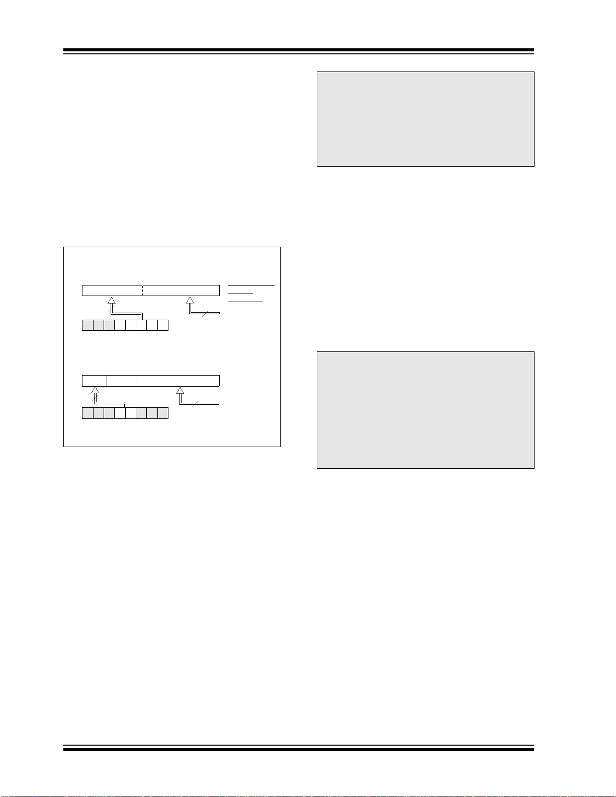
4.3 PCL and PCLATH
The program counter (PC) is 13-bits wid e. The low byte
comes from the PCL register, which is a readable and
writable register. The upper bits (PC<12:8>) are not
readable, but are indirectly writable through the
PCLA TH reg is ter. On any RESET, the up per bi t s of the
PC will be cleared. Fig ure4-3 shows the two situations
for the loading of the PC. The up per ex ample in th e figure shows how the PC is loaded on a write to PCL
(PCLATH<4:0> → PCH). The lower exam pl e i n th e fi gure shows how the PC is loaded during a CALL or GOTO
instruction (PCLATH<4:3> → PCH).
FIGURE 4-3: LOADING OF PC IN
DIFFERENT SITUATIONS
PCH PCL
12 8 7 0
PC
PCLATH<4:0>
5
PCLATH
PCH PCL
12 11 10 0
PC
2
87
PCLATH<4:3>
PCLATH
11
4.3.1 COMPUTED GOTO
A computed GOTO is accomplish ed by adding an offs et
to the progr am counter (ADDWF PCL). When doing a
table read using a computed GOTO method, care
should be exercise d i f the t able loca tio n cros ses a PCL
memory boundary (each 256 byte block). Refer to the
application note “Im plementing a Table Read" (AN556).
4.3.2 STACK
The PIC16CXX family has an 8-level deep x 13-bit wide
hardware s tack. The stack space is not part of either
program or data space and the stack pointer is not
readable or writabl e. The PC i s PUSHed onto th e stac k
when a CALL instruction is executed, or an interrupt
causes a branch. The st ac k is POPed in the ev en t of a
RETURN,RETLW or a RETFIE instruction execution.
PCLATH is not affected by a PUSH or POP operation.
The stack opera tes as a circular buf fer . This means that
after the st ack h as be en PUSHed ei ght ti mes, th e nin th
push overwrites the v alue tha t was stored fro m the first
push. The tenth pus h ov erwri t es the se co nd p us h (an d
so on).
8
Instruction with
PCL as
Destination
ALU
GOTO,CALL
Opcode <10:0>
Note 1: There are no status bits to indicate stack
overflow or stack underflow conditions.
2: There are no instructions/mnemonics
called PUSH or POP. These are actions
that occur from the execution of the
CALL, RETURN, RETLW, and RETFIE
instructions, or the vectoring to an interrupt address.
4.4 Program Memory Paging
PIC16CXX devices are capable o f addressing a continuous 8K word block of program memory. The CALL and
GOTO instructions provide only 11 bits of address to
allow branching within any 2K program memory page.
When executing a CALL or GOTO ins truc tio n, t he upper
2 bits of the address are provided by PCLATH<4:3>.
When doing a CALL or GOTO instruct ion, the user must
ensure that the page select bits are programmed, so
that the desired prog ram memory pa ge is addre ssed. If
a return from a CALL instruction (or interrupt) is executed, the entire 13-bit PC is popped from the stack.
Therefore, manipulation of the PCLATH<4:3> bits are
not required for the return instruction s (which POPs the
address from the stack).
Note 1: The contents of PCLATH are unchanged
after a return or RETFIE instruction is
executed. The user must set up PCLATH
for any subsequent CALL’s or GOTO’s
2: PCLATH<4> is not used in these
PICmicro
PCLATH<4> as a general purpose r ead/
write bit is not recommended, since this
may affect upward compatibility with
future products.
Example 4-1 shows the calling of a subroutine in
page 1 of the program memory . Thi s example as sumes
that PCLATH is saved and restored by the Interrupt
Service Routine
EXAMPLE 4-1: CALL OF A SUBROUTINE
ORG 0x500
BSF PCLATH,3 ;Select page 1 (800h-FFFh)
CALL SUB1_P1 ;Call subroutine in
: ;page 1 (800h-FFFh)
:
ORG 0x900 ;page 1 (800h-FFFh)
SUB1_P1
: ;called subroutine
: ;page 1 (800h-FFFh)
:
RETURN ;return to Call subroutine
®
devices. The use of
(if interrupts are used).
IN PAGE 1 FROM PAGE 0
;in page 0 (000h-7FFh)
DS30605C-page 26 2000 Microchip Technology Inc.
PIC16C63A/65B/73B/74B
4.5 Indirect Addressing, INDF and FSR Registers
The INDF register is not a physi cal register. Addressing
the INDF register will cause indirect addressing.
Indirect addressing is possible by using the INDF register. Any instruc tion using the INDF register actual ly
accesses the register pointed to by the File Sele ct Register, FSR. Reading the INDF register itself indirectly
(FSR = ’0’) will read 00h. Writing to the INDF register
indirectly result s in a no-operation (altho ug h s t atus bits
may be affected ). An ef fective 9- bit add ress is obt ained
by concatenating the 8 -bit FSR regi ster and the IRP b it
(STATUS<7>), as shown in Figur e 4-4.
A simple program to clear RAM locations 20h-2Fh
using indirect addressing is shown in Example 4 -2.
FIGURE 4-4: DIRECT/INDIRECT ADDRESSING
RP1:RP0 6
0
bank select location select
from opcode
0
00 01 10 11
00h
80h
100h
EXAMPLE 4-2: INDIRECT ADDRESSING
movlw 0x20 ;initialize pointer
NEXT clrf INDF ;clear INDF register
CONTINUE
Note: Maintain the IRP and RP1 bits clear.
180h
movwf FSR ;to RAM
incf FSR,F ;inc pointer
btfss FSR,4 ;all done?
goto NEXT ;no clear next
: ;yes continue
Indirect AddressingDirect Addressing
IRP FSR register
0
bank select
7
location select
0
Data
not used
Memory
7Fh
FFh
17Fh
1FFh
Bank 0 Bank 1 Bank 2 Bank 3
Note 1: For register file map detail, see Figure 4-2.
2: Shaded portions are not implemented; maintain the IRP and RP1 bits clear.
2000 Microchip Technology Inc. DS30605C-page 27

PIC16C63A/65B/73B/74B
NOTES:
DS30605C-page 28 2000 Microchip Technology Inc.
PIC16C63A/65B/73B/74B
5.0 I /O PORTS
Some pins for th ese I/O ports are multiplexed with an
alternate function for the peripheral features on the
device. In general, when a peripheral is enabled, that
pin may not be used as a general purpose I/O pin.
5.1 PORTA and TRISA Registers
PORTA is a 6-bit latch.
The RA4/T0CKI pin is a Schmitt Trigger input and an
open drain output. All other RA port pins have TTL
input levels and full C MOS output drivers. All pi ns have
data direction bits (TRIS registers), which can configure these pins as output or input.
Setting a TRISA register bit puts the corresponding output driver in a hi-im pedan ce mo de. Clea ring a b it in th e
TRISA register puts the contents of the output latch on
the selected pin(s).
Reading the PORTA register reads the status of the
pins, whereas writing to i t will wri te to th e po rt latch. All
write operations are read-modify-write operations.
Therefore, a write to a port implies that the port pins are
read, the value is modified and then written to the port
data latch.
Pin RA4 is multiplexed with the Timer0 module clock
input to become the RA4/T0CKI pin.
On the PIC16C73B/74B, PORTA pins are multiplexed
with analog inputs and analog V
tion of each pin is selected by clearing/setting the control bits in the ADCON1 register (A/D Control
Register1).
REF input. The opera-
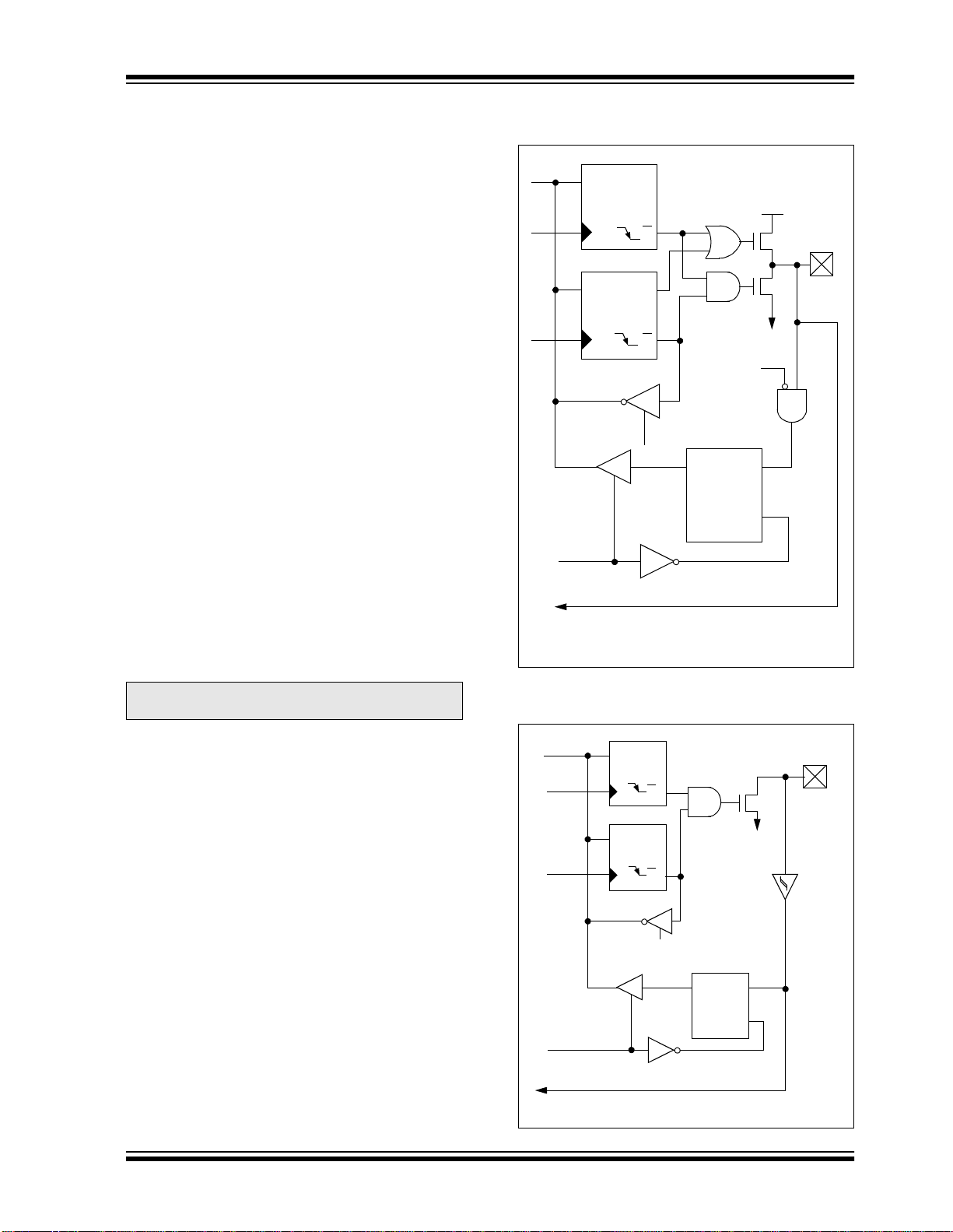
FIGURE 5-1: BLOCK DIAGRAM OF
RA3:RA0 AND RA5 PINS
Data
Bus
WR
Port
WR
TRIS
RD Port
To A/D Converter
Note 1: I/O pins have protection diodes to VDD and VSS.
CK
Data Latch
CK
TRIS Latch
QD
Q
QD
Q
RD TRIS
VDD
P
N
V
SS
Analog
Input
mode
QD
EN
I/O pin
TTL
Input
Buffer
(1)
Note: On all RESETS, pins with analog function s
are configured a s analog a nd digit al input s.
The TRISA register controls the direction of the RA
pins, even when they are be ing us ed as ana lo g inputs.
The user must ensure the bits in the TRISA regi ster are
maintained set when using them as analog inputs.
EXAMPLE 5-1: INITIALIZING PORTA
(PIC16C73B/74B)
BCF STATUS, RP0 ;
CLRF PORTA ; Initialize PORTA by
; clearing output
; data latches
BSF STATUS, RP0 ; Select Bank 1
MOVLW 0x06 ; Configure all pins
MOVWF ADCON1 ; as digital inputs
MOVLW 0xCF ; Value used to
; initialize data
; direction
MOVWF TRISA ; Set RA<3:0> as inputs
; RA<5:4> as outputs
; TRISA<7:6> are always
; read as ’0’.
FIGURE 5-2: BLOCK DIAGRAM OF
RA4/T0CKI PIN
Data
Bus
WR
Port
WR
TRIS
RD Port
TMR0 Clock Input
Note 1: I/O pins have protection diodes to VDD and VSS.
QD
Q
CK
Data Latch
QD
Q
CK
TRIS Latch
RD TRIS
N
SS
V
Schmitt
Trigger
Input
Buffer
QD
EN
EN
I/O pin
(1)
2000 Microchip Technology Inc. DS30605C-page 29

PIC16C63A/65B/73B/74B
TABLE 5-1: PORTA FUNCTIONS
Name Bit# Buffer Function
RA0/AN0
RA1/AN1
RA2/AN2
RA3/AN3/V
(1)
(1)
(1)
REF
bit0 TTL Digital input/output or analog input.
bit1 TTL Digital input/output or analog input.
bit2 TTL Digital input/output or analog input.
(1)
bit3 TTL Digital input/output or analog input or VREF.
RA4/T0CKI bit4 ST
(1)
RA5/SS
/AN4
bit5 TTL Input/output or slave select input for synchronous serial port or analog input.
Digital input/output or external clock input for Timer0.
Output is open drain type.
Legend: TTL = TTL input, ST = Schmitt Trigger input
Note 1: The A/D is not implemented on the PIC16C63A/65B. Pins will operate as digital I/O only. ADCON1 is not
implemented; maintain this register clear.
TABLE 5-2: SUMMARY OF REGISTERS ASSOCIATED WITH PORTA
Address Name Bit 7 Bit 6 Bit 5 B it 4 Bit 3 Bit 2 Bit 1 Bit 0
05h PORTA
85h TRISA — — PORTA Data Direction Register --11 1111 --11 1111
9Fh
Legend: x = unknown, u = unchanged, - = unimplemented locations read as '0'. Shaded cells are not used by PORTA.
ADCON1
Note 1: The A/D is not implemented on the PIC16C63A/65B. Pins will operate as digital I/O only. ADCON1 is not implemented;
maintain this register clear.
— — RA5 RA4 RA3 RA2 RA1 RA0 --0x 0000 --0u 0000
(1)
— — — — — PCFG2 PCFG1 PCFG0 ---- -000 ---- -000
Val ue on:
POR,
BOR
Val ue on
all other
RESETS
DS30605C-page 30 2000 Microchip Technology Inc.

PIC16C63A/65B/73B/74B
5.2 PORTB and TRISB Registers
PORTB is an 8-bit wide, bi-directional port. The corresponding data direction register is TRISB. Setting a bit
in the TRISB register puts the corresponding output
driver in a hi-impedance input mode. Clearing a bit in
the TRISB register puts the c ontents of the ou tput latch
on the selected pin(s).
Each of the PORTB pi ns has a w eak i nternal pul l-up. A
single control bit can turn on all the pull-ups. This is performed by clearing bit RBPU
weak pull-up is automatically turned off when the port
pin is configured as an output. The pull-ups are disabled on a Power-on Reset.
FIGURE 5-3: BLOCK DIAGRAM OF
(2)
RBPU
Data Bus
WR Port
WR TRIS
RB0/INT
Note 1: I/O pins have diode protection to V
2: To enable weak pull-ups, set the appropriate TRIS
Four of PORTB’s pins, RB7:RB4, have an
interrupt-on-change feature. Only pins configured as
inputs can cause this interrupt to occur (i.e., any
RB7:RB4 pin configur ed as an output is excluded from
the interrupt-on-change comparison). The input pins (of
RB7:RB4) are compared with the value latched on the
last read of PORTB. The “mismatch” outputs of
RB7:RB4 are OR’d together to generate the RB Port
Change Interrupt with flag bit RBIF (INTCON<0>).
Data Latch
CK
TRIS Latch
CK
RD TRIS
RD Port
bit(s) and clear the RBPU bit (OPTION_REG<7>).
(OPTION_REG<7>). The
RB3:RB0 PINS
QD
QD
Schmitt Trigger
Buffer
TTL
Input
Buffer
QD
EN
DD and VSS.
VDD
Weak
P
Pull-up
I/O pin
RD Port
(1)
This interrupt can wake the device from SLEEP. The
user, in the Interrupt Service Routine, can clear the
interrupt in the following manner:
a) Any read or write of PORTB. This will end the
mismatch condition.
b) Clear flag bit RBIF.
A mismatch c ond it i on wi ll cont i n ue to s et f lag bi t RB IF.
Reading PORTB will end the mismatch condition, and
allow flag bit RBIF to be cleared.
This interrupt-on-mismatch feature, together with software configurable pull-ups on these four pins, allow
easy interface to a keypad and make it possible for
wake-up on key depression. Refer to the Embedded
Control Handbook, “Implementing Wake-up on Key
Stroke” (AN552).
The interrupt-on-change feature is recommended for
wake-up on key depression operation and operations
where PORTB is only used for the interrupt-on-change
feature. Polling of PORTB is not recommended while
using the interrupt-on-change feature.
RB0/INT is an ext ernal i nterrupt input pin a nd is confi gured using the INTEDG bit (OPTION_REG<6>).
RB0/INT is discussed in detail in Section 13.5.1.
FIGURE 5-4: BLOCK DIAGRAM OF
RB7:RB4 PINS
EN
EN
TTL
Input
Buffer
VDD
Weak
P
Pull-up
I/O pin
Buffer
RD Port
DD and VSS.
(1)
ST
Q1
Q3
(2)
RBPU
Data Bus
WR Port
WR TRIS
Set RBIF
From other
RB7:RB4 pins
RB7:RB6 in Serial Programming mode
Note 1: I/O pins have diode protection to V
2: To enable weak pull-ups, set the appropriate TRIS
Data Latch
QD
CK
TRIS Latch
QD
CK
RD TRIS
RD Port
bit(s) and clear the RBPU bit (OPTION_REG<7>).
Latch
QD
QD
2000 Microchip Technology Inc. DS30605C-page 31

PIC16C63A/65B/73B/74B
TABLE 5-3: PORTB FUNCTIONS
Name Bit# Buffer Function
RB0/INT bit0 TTL/ST
RB1 bit1 TTL Input /output pin. Internal software programmable weak pull-up.
RB2 bit2 TTL Input /output pin. Internal software programmable weak pull-up.
RB3 bit3 TTL Input /output pin. Internal software programmable weak pull-up.
RB4 bit4 TTL Input/output pin (with interrupt-on-change). Internal software programmable weak
RB5 bit5 TTL Input/output pin (with interrupt-on-change). Internal software programmable weak
RB6 bit6 TTL/ST
RB7 bit7 TTL/ST
Legend: TTL = TTL input, ST = Schmitt Trigger input
Note 1: This buffer is a Schmitt Trigger input when configured as the external interrupt.
2: This buffer is a Schmitt Trigger input when used in Serial Programming mode.
(1)
Input/output pin or external interrupt input. Internal software
programmable weak pull-up.
pull-up.
pull-up.
(2)
Input/output pin (with interrupt-on-change). Internal software programmable weak
pull-up. Serial programming clock.
(2)
Input/output pin (with interrupt-on-change). Internal software programmable weak
pull-up. Serial programming data.
TABLE 5-4: SUMMARY OF REGISTERS ASSOCIATED WITH PORTB
Val ue on:
Address Name Bit 7 Bit 6 Bit 5 Bit 4 Bit 3 Bit 2 Bit 1 Bit 0
06h PORTB RB7 RB6 RB5 RB4 RB3 RB2 RB1 RB0
86h TRISB PO RTB Data Direction register 1111 1111 1111 1111
81h OPTION_REG RBPU INTEDG T0CS T0SE PSA PS2 PS1 PS0 1111 1111 1111 1111
Legend: x = unknown, u = unchanged. Shaded cells are not used by PORTB.
POR,
BOR
xxxx xxxx
Value on
all other
RESETS
uuuu uuuu
DS30605C-page 32 2000 Microchip Technology Inc.

PIC16C63A/65B/73B/74B
5.3 PORTC and TRISC Registers
PORTC is an 8-bit bi-directional port. Each pin is individually configurable as an input or output through the
TRISC register. PORTC is multiplexed with several
peripheral functions (Table 5-5). PORTC pins have
Schmitt Trigger input buffers.
When enabling peripheral functions, care should be
taken in defining TRIS bit s fo r each POR TC pin. Some
peripherals override the TRIS bit to make a pin an output, while other peripherals override the TRIS bit to
make a pin an input. Since the TRIS bit override is in
effect while the peripheral is enabled, read-modify-write
instructions (BSF, BCF, XORWF) with TRISC as destination should be avoi ded. The user shou ld refer to the
correspondi ng peripher al section for the cor rect TRIS
bit settings.
FIGURE 5-5: PORTC BLOCK DIAGRAM
PORT/PERIPHERAL Select
Peripheral Data Out
Data Bus
WR
Port
WR
TRIS
Peripheral
(3)
OE
Peripheral Input
Note 1 : I/O pins have diode protection to VDD and VSS.
CK
Data Latch
CK
TRIS Latch
RD TRIS
RD
Port
2: Port/Peripheral select signal selects between port
data and peripheral output.
3: Peripheral OE (output enable) is only activated if
peripheral select is active.
(2)
QD
Q
QD
Q
0
1
QD
EN
Schmitt
Trigger
P
N
VSS
DD
V
(1)
I/O pin
TABLE 5-5: PORTC FUNCTIONS
Name Bit# Buffer Type Function
RC0/T1OSO/T1CKI bit0 ST Input/output port pin or Timer1 oscillator output/Timer1 clock input.
RC1/T1OSI/CCP2 bit1 ST Input/output port pin or Timer1 oscillator input or Capture2 input/Compare2
output/PWM2 output.
RC2/CCP1 bit2 ST Input/output port pin or Capture1 input/Compare1 output/PWM1 output.
2
2
C mode).
C modes.
RC3/SCK/SCL bit3 ST RC3 can also be the Synchronous Serial Clock for both SPI and I
RC4/SDI/SDA bit4 ST RC4 can also be the SPI Data In (SPI mode) or Data I/O (I
RC5/SDO bit5 ST Input/output port pin or Synchronous Serial Port Data output.
RC6/TX/CK bit6 ST Input/output port pin or USART Asynchronous Transmit, or USART
Synchronous Clock.
RC7/RX/DT bit7 ST Input/output port pin or USART Asynchronous Receive, or USART
Synchronous Data.
Legend: ST = Schmitt Trigger input
TABLE 5-6: SUMMARY OF REGISTERS ASSOCIATED WITH PORTC
Address Name Bit 7 Bit 6 B i t 5 Bit 4 Bit 3 Bit 2 Bit 1 Bit 0
POR,
BOR
07h PORTC RC7 RC6 RC5 RC4 RC3 RC2 RC1 RC0 xxxx xxxx
87h TRISC PORTC Data Direction register 1111 1111
Legend: x = unknown, u = unchanged
Value on:
Value on
all other
RESETS
uuuu uuuu
1111 1111
2000 Microchip Technology Inc. DS30605C-page 33

PIC16C63A/65B/73B/74B
5.4 PORTD and TRISD Registers
Note: The PIC16C63A and PIC16C73B do not
provide PORTD . The PORTD and TR ISD
registers are not implemented.
PORTD is an 8-bit port with Schmitt Trigger input buffers. Each pin is individually configured as an input or
output.
PORTD can be configured as an 8-bit wide microprocessor port (parallel slave p ort) by setting c ontrol bit
PSPMODE (TRISE<4>). In this mode, the input buffers
are TTL.
FIGURE 5-6: PORTD BLOCK DIAGRAM
Data
Bus
WR
Port
Data Latch
WR
TRIS
TRIS Latch
RD Port
Note 1: I/O pins have protection diodes to VDD and VSS.
CK
CK
RD TRIS
QD
QD
Schmitt
Trigger
Input
Buffer
QD
EN
EN
TABLE 5-7: PORTD FUNCTIONS
Name Bit# Buffer Type Function
RD0/PSP0 bit0 ST/TTL
RD1/PSP1 bit1 ST/TTL
RD2/PSP2 bit2 ST/TTL
RD3/PSP3 bit3 ST/TTL
RD4/PSP4 bit4 ST/TTL
RD5/PSP5 bit5 ST/TTL
RD6/PSP6 bit6 ST/TTL
RD7/PSP7 bit7 ST/TTL
Legend: ST = Schmitt Trigger input, TTL = TTL input
Note 1: Input buffers are Schmitt Triggers when in I/O mode and TTL buffer when in Parallel Slave Port mode.
(1)
(1)
(1)
(1)
(1)
(1)
(1)
(1)
Input/output port pin or parallel slave port bit0
Input/output port pin or parallel slave port bit1
Input/output port pin or parallel slave port bit2
Input/output port pin or parallel slave port bit3
Input/output port pin or parallel slave port bit4
Input/output port pin or parallel slave port bit5
Input/output port pin or parallel slave port bit6
Input/output port pin or parallel slave port bit7
I/O pin
(1)
TABLE 5-8: SUMMARY OF REGISTERS ASSOCIATED WITH PORTD
Value on:
Address Name Bit 7 Bit 6 B it 5 Bit 4 Bi t 3 Bit 2 Bit 1 Bit 0
08h PORTD RD7 RD6 RD5 RD4 RD3 RD2 RD1 RD0 xxxx xxxx uuuu uuuu
88h TRISD PORTD Data Direction register 1111 1111 1111 1111
89h TRISE IBF OBF IBOV PSPMODE — PORTE Data Direction bits 0000 -111 0000 -111
Legend: x = unknown, u = unchanged, - = unimplemented, read as '0'. Shaded cells are not used by PORTD.
DS30605C-page 34 2000 Microchip Technology Inc.
POR,
BOR
Val ue on
all other
RESETS

PIC16C63A/65B/73B/74B
5.5 PORTE and TRISE Register
Note 1: The PIC16C63A and PIC16C73B do not
provide PORTE. The PORTE and TRISE
registers are not implemented.
2: The PIC16C63A/65B does not p rovide an
A/D module. A/D functions are not implemented.
PORTE has three pins: RE0/RD/AN5, RE1/WR/AN6
and RE2/CS
inputs or outputs. These pins have Schmitt Trigger
input buffers.
I/O PORTE becomes control inputs for the microprocessor port when bit PSPMODE (TRISE<4>) is set. In
this mode, the user must make sure that the
TRISE<2:0> bits are set (pins are configured as digital
inputs) and t hat reg ister ADCON1 is con figur ed fo r digital I/O. In this mode, the input buffers are TTL.
Register 5-1 shows the TRISE register, wh ich also controls the parallel slave port operat ion.
PORTE pins may be multiplexed with analog inputs
(PIC16C74B only). The operation of these pins is
selected by control bits in the ADCON1 register. When
selected as an anal og input, these pins wi ll read as ’0’s.
TRISE controls the direction of the RE pins, even when
they are being used as analog inputs. The user must
make sure to keep the pins configured as inputs when
using them as analog inputs.
/AN7, which are individ ua lly con fig ured as
FIGURE 5-7: PORTE BLOCK DIAGRAM
Data
Bus
WR
Port
WR
TRIS
RD Port
Note 1: I/O pins have protection diodes to VDD and VSS.
QD
CK
Data Latch
QD
CK
TRIS Latch
RD TRIS
Schmitt
Trigger
Input
Buffer
QD
EN
EN
I/O pin
(1)
Note: On a Power-on Reset, these pins are con-
figured as analog inputs and read as ‘0’s.
TABLE 5-9: PORTE FUNCTIONS
Name Bit# Buffer Type Function
RE0/RD
/AN5 bit0 ST/TTL
RE1/WR
RE2/CS
Legend: ST = Schmitt Trigger input, TTL = TTL input
Note 1: Input buffers are Schmitt Triggers when in I/O mode and TTL buffers when in Parallel Slave Port mode.
/AN6 bit1 ST/TTL
/AN7 bit2 ST/TTL
(1)
Input/output port pin or read control input in Parallel Slave Port mode or analog
input:
RD
1 = Idle
0 = Read operation. Contents of PORTD register is output to PORTD
I/O pins (if chip selected).
(1)
Input/output port pin or write control input in Parallel Slave Port mode or analog
input:
WR
1 = Idle
0 = Write operation. Value of PORTD I/O pins is latched into PORTD
register (if chip selected).
(1)
Input/output port pin or chip select control input in Parallel Slave Port mode or
analog input:
CS
1 = Device is not selected
0 = Device is selected
2000 Microchip Technology Inc. DS30605C-page 35

PIC16C63A/65B/73B/74B
REGISTER 5-1: TRISE REGISTER (ADDRESS 89h)
R-0 R-0 R/W-0 R/W-0 U-0 R/W-1 R/W-1 R/W-1
IBF OBF IBOV PSPMODE — TRISE2 TRISE1 TRISE0
bit 7 bit 0
bit 7 IBF: Input Buffer Full Status bit
1 = A word has been received and is waiting to be read by the CPU
0 = No word has been received
bit 6 OBF: Output Buffer Full Status bit
1 = The output buffer still holds a previously written word
0 = The output buffer has been read
bit 5 IBOV: Input Buffer Overflow Detect bit (in Microprocessor mode)
1 = A write occurred when a previously input word has not been read (must be cleared in
software)
0 = No overflow occurred
bit 4 PSPMODE: Parallel Slave Port Mode Select bit
1 = Parall el Slave Port mode
0 = General purpose I/O mode
bit 3 Unimplemented: Read as '0'
bit 2 TRISE2: Direction Control bit for pin RE2/CS
1 = Input
0 = Output
bit 1 TRISE1: Direction Control bit for pin RE1/WR/AN6
1 = Input
0 = Output
bit 0 TRISE0: Direction Control bit for pin RE0/RD/AN5
1 = Input
0 = Output
/AN7
Legend:
R = Readable bit W = Writable bit U = Unimplemented bit, read as ‘0’
-n = Value at POR ’1’ = Bit is set ’0’ = Bit is cleared x = Bit is unknown
TABLE 5-10: SUMMARY OF REGISTERS ASSOCIATED WITH PORTE
Val ue on:
Address Name Bit 7 Bit 6 Bit 5 Bit 4 Bit 3 Bit 2 Bit 1 Bit 0
09h P O RTE — — — — — RE2 R E1 RE0 ---- -xxx ---- -uuu
89h TRISE IBF OBF IBOV PSPMODE — PORTE Data Direction bits 0000 -111 0000 -111
9Fh ADCON1 — — — — — PCFG2 PCFG1 PCFG0 ---- -000 ---- -000
Legend: x = unknown, u = unchanged, - = unimplemented, read as '0'. Shaded cells are not used by PORTE.
POR,
BOR
Value on
all other
RESETS
DS30605C-page 36 2000 Microchip Technology Inc.

PIC16C63A/65B/73B/74B
5.6 Parallel Slave Port (PSP)
Note: The PIC16C63A and PIC16C73B do not
provide a par allel sla ve po rt . The P ORTD,
PORTE, TRISD and TRISE registers are
not implemented.
PORTD operates as an 8-bit wide Parallel Slave Port
(PSP), or microprocessor port when control bit PSPMODE (TRISE<4>) is set. In Slave mode, it is asynchronously readable and writable by the ex ternal world,
through RD
control input pin RE1/WR/AN6.
It can directly interface to an 8-bit mic rop roc es sor dat a
bus. The external mic roproc essor c an rea d or write th e
PORTD latch as an 8-bit latch. Setting bit PSPMODE
enables port pin RE0/RD
RE1/WR
be the CS
corresponding data direction bits of the TRISE register
(TRISE<2:0>) must be configured as inputs (set) and
the A/D port configuration bits PCFG2:PCFG0
(ADCON1<2:0>) must be s et, w hic h wi ll c onfigure pins
RE2:RE0 as digital I/O.
There are actually two 8-bit latches, one for data out
(from the PICmicro
user writes 8-bit data to PORTD data latch and reads
data from the port pin latch (note that they have the
same address). In this mode, the TRISD register is
ignored since the external device is controlling the
direction of data flow.
A write to the PSP occurs when both the CS
lines are first detected low. When either the CS or WR
lines become high (level triggered), then the Input
Buffer Full (IBF) status flag bit (TRISE<7>) is set on the
Q4 clock cycle, following the next Q2 cycle, to signal
the write is complete (Figure 5-9). The interrupt flag bit
PSPIF (PIR1<7>) is also set on the same Q4 clock
cycle. IBF can o nly be cl eared by reading the PORTD
input latch. The Input Buffer Overflow (IBOV) status
flag bit (TRISE<5>) is set if a second write to the PSP
is attempted when the pr evious by te has not be en read
out of the buffer.
A read from the PSP occurs when both the CS
lines are first detected low. The Output Buffer Full
(OBF) status flag bit (TRISE<6>) is cleared immediately (Figure 5-10), indicating that the PORTD latch is
waiting to be read by the ext ernal bus . When ei ther the
CS or RD pin becomes high ( level triggered), the interrupt flag bit PSPIF is set on the Q4 clock cycle, following the next Q2 cycle, indicating that the read is
complete. OBF remains low until data is written to
PORTD by the user firmware.
control input pin RE0/RD/AN5 and WR
/AN5 to be the RD input,
/AN6 to be the WR input and RE2/CS/AN7 to
(chip select) input. For this functionality, the
®
MCU) and one for data input. The
and WR
and RD
When not in PSP mode, the IBF and OBF bits are hel d
clear. However, if flag bit IBOV was previously set, it
must be cleared in firmware.
An interrupt is generated and latched into flag bit
PSPIF when a read or write operation is completed.
PSPIF must be cleared by the user in fi rmware an d the
interrupt can be disabled by clearing the interrupt
enable bit PSPIE (PIE1<7>).
FIGURE 5-8: PORTD AND PORTE
BLOCK DIAGRAM
(PARALLEL SLAVE
PORT)
Data Bus
WR
Port
RD
Port
One bit of PORTD
Set Interrupt Flag
PSPIF (PIR1<7>)
Note 1: I/O pins have protection diodes to VDD and VSS.
QD
CK
QD
EN
EN
TTL
Read
Chip Select
Write
TTL
TTL
TTL
RDx
pin
RD
CS
WR
2000 Microchip Technology Inc. DS30605C-page 37

PIC16C63A/65B/73B/74B
FIGURE 5-9: PARALLEL SLAVE PORT WRITE WAVEFORMS
Q1 Q2 Q3 Q4CSQ1 Q2 Q3 Q4 Q1 Q2 Q3 Q4
WR
RD
PORTD<7:0>
IBF
OBF
PSPIF
FIGURE 5-10: PARALLEL SLAVE PORT READ WAVEFORMS
Q1 Q2 Q3 Q4
Q1 Q2 Q3 Q4
Q1 Q2 Q3 Q4
CS
WR
RD
PORTD<7:0>
IBF
OBF
PSPIF
TABLE 5-11: REGISTERS ASSOCIATED WITH PARALLEL SLAVE PORT
Address Name Bit 7 Bit 6 Bit 5 Bit 4 Bit 3 Bit 2 Bit 1 Bit 0
08h PORTD Port data latch when written, Port pins when read xxxx xxxx uuuu uuuu
09h PORTE — — — — — RE2 RE 1 RE0 ---- -xxx ---- -uuu
0Bh, 8Bh INTCON GIE PEIE T0IE INTE RBIE T0IF INTF RBIF 0000 000x 0000 000u
89h TRISE IBF OBF IBOV PSPMODE — PORTE Data Direction Bits 0000 -111 0000 -111
0Ch PIR1 PSPIF ADIF RCIF TXIF SSPIF CCP1IF TMR2IF TMR1IF 0000 0000 0000 0000
8Ch PIE1 PSPIE ADIE RCIE TXIE SSPIE CCP1IE TMR2IE TMR1IE 0000 0000 0000 0000
9Fh ADCON1 — — — — — PCFG2 PCFG1 PCFG0 ---- -000 ---- -000
Legend: x = unknown, u = unchanged, - = unimplemented, read as '0'. Shaded cells are not used by the Parallel Slave Port.
Value on:
POR,
BOR
Value on
all other
RESETS
DS30605C-page 38 2000 Microchip Technology Inc.

PIC16C63A/65B/73B/74B
6.0 TIMER0 MODULE
Counter mode is selected by setting bit T0CS
(OPTION_REG<5>). In counter mode, Timer0 will
The Timer0 module timer/co unter has the follow ing features:
• 8-bit time r/counter
• Readable and writable
• 8-bit software programmable prescaler
• Internal or external clock select
• Interrupt on overflow from FFh to 00h
• Edge select for external clock
Figure 6-1 is a bloc k diagram o f the T imer0 mod ule and
increment, either on every rising, or falling edge of pin
RA4/T0CKI. The incrementing edge is determined by
the Timer0 Source Edge Select bit T0SE
(OPTION_REG<4>). Clearing bit T0SE selects the rising edge. Restrictions on the external clock input are
discussed in detail in Section6.2.
The prescaler is mutually exclusively shared between
the Timer0 module and the watchdog timer. The
prescaler is not readable or writable. Section 6.3
details the operation of the prescaler.
the prescaler shared with the WDT.
Additional information on the Timer0 module is
available in the PICmicro™ Mid-Range MCU Family
Reference Manual (DS33023).
Timer mode is selected by clearing bit T0CS
(OPTION_REG<5>). In Timer mode, the Timer0
module will increment every instruction cycle (without
prescaler). If the TMR0 register is written, the increment is inhibited for the foll owing two instructi on cycles.
The user can work around this by writing an adjusted
6.1 Timer0 Interrupt
The TMR0 interrupt is generated when the TMR0 register overflows from FFh to 00h. This overflow sets bit
T0IF (INTCON<2>). The interrupt can be masked by
clearing bit T0IE (INTCON<5>). Bit T0IF must be
cleared in soft ware by the T imer0 mo dule Interrupt Service Routine before re-enabling this interrupt. The
TMR0 interrupt cannot awaken the processor from
SLEEP, since the timer is shut-off during SLEEP.
value to the TMR0 register.
FIGURE 6-1: BLOCK DIAGRAM OF THE TIMER0/WDT PRESCALER
CLKOUT (= F
RA4/T0CKI
pin
Watchdog
Timer
WDT Enable bit
OSC/4)
T0SE
Data Bus
M
0
U
X
1
T0CS
0
M
U
1
X
PSA
8-bit Prescaler
8 - to - 1MUX
0
Time-out
PRESCALER
8
M U X
WDT
1
M
U
0
X
PSA
1
PSA
SYNC
2
Cycles
PS2:PS0
8
TMR0 reg
Set Flag bit T0IF
on Overflow
Note: T0CS, T0SE, PSA, PS2:PS0 are (OPTION_REG<5:0>).
2000 Microchip Technology Inc. DS30605C-page 39

PIC16C63A/65B/73B/74B
6.2 Using Timer0 with an External Clock
The synchronization of T0CKI with the internal phase
clocks is accomplished by sampling the synchronized
input on the Q2 and Q4 cycles of the internal phase
clocks. Therefore, it is necessary for T0CKI to be high
for at least 2 T
low for at least 2 T
Refer to the electrical specification for the desired
device.
OSC (and a small RC delay of 20ns) and
OSC (and a small RC delay of 20 ns).
module means that ther e is no pres caler for the W atchdog Timer, and vice-versa. This prescaler is not readable or writable (see Figure 6-1).
The PSA and PS2:PS0 bits (OPTION_REG<3:0>)
determine the prescaler assignment and pre scale ratio.
When assigned to the Timer0 module, all instructions
writing to the TMR0 r egiste r (e.g., CLRF
BSF
to WDT, a CLRWDT instru ction will clear t he prescaler
along with the Watchdog Timer. The prescaler is not
readable or writable.
6.3 Prescaler
There is only one pr esc al er av ai lab le wh ich is m utu all y
exclusively sha red between the T imer0 mod ule and the
watchdog timer. A prescaler assignment for the Ti mer0
REGISTER 6-1: OPTION_REG REGISTER
R/W-1 R/W-1 R/W-1 R/W-1 R/W-1 R/W-1 R/W-1 R/W-1
RBPU
bit 7 bit 0
bit 7 RBPU
bit 6 INTEDG
bit 5 T0CS: TMR0 Clock Source Select bit
1 = Transition on T0CKI pin
0 = Internal instruction cycle clock (CLKOUT)
bit 4 T0SE: TMR0 Source Edge Select bit
1 = Increment on high-to-low transition on T0CKI pin
0 = Increment on low-to-high transition on T0CKI pin
bit 3 PSA: Prescaler Assignment bit
1 = Prescaler is assigned to the WDT
0 = Prescaler is assigned to the Timer0 module
bit 2-0 PS2:PS0: Prescaler Rate Select bits
Bit Value TMR0 Rate WDT Rate
000
001
010
011
100
101
110
111
INTEDG T0CS T0SE PSA PS2 PS1 PS0
1 : 2
1 : 4
1 : 8
1 : 16
1 : 32
1 : 64
1 : 128
1 : 256
1 : 1
1 : 2
1 : 4
1 : 8
1 : 16
1 : 32
1 : 64
1 : 128
1, MOVWF 1,
1,x.. ..etc.) will clear the pre scaler . When assi gned
Note: Writing to TMR0, when the prescaler is
assigned to T imer0, will clear the pre scaler
count, but will not change the prescaler
assignment.
Legend:
R = Readable bit W = Writable bit U = Unimplemented bit, read as ‘0’
-n = Value at POR ’1’ = Bit is set ’0’ = Bit is cleared x = Bit is unknown
Note: T o av oid an unintended device RESET, the instruction sequence s hown in the PICmic ro™ Mid-Range MC U
Family Reference Manual (DS33023, Section 11.6) must be executed when changing the prescaler assignment from Timer0 to the WDT. This sequence must be followed even if the WDT is disabled.
DS30605C-page 40 2000 Microchip Technology Inc.

PIC16C63A/65B/73B/74B
TABLE 6-1: REGISTERS ASSOCIATED WITH TIMER0
Address Name Bit 7 Bit 6 Bit 5 Bit 4 Bit 3 Bit 2 Bit 1 Bit 0
Value on:
POR,
BOR
Val ue on
all other
RESETS
01h TMR0 Timer0 Module’s register
0Bh,8Bh INTCON GIE PEIE T0IE INTE RBIE T0IF INTF RBIF 0000 000x 0000 000u
81h OPTION_REG RBPU INTEDG T0CS T0SE PSA PS2 PS1 PS0 1111 1111 1111 1111
Legend: x = unknown, u = unchanged, - = unimplemented locations read as '0'. Shaded cells are not used by Timer0.
xxxx xxxx uuuu uuuu
2000 Microchip Technology Inc. DS30605C-page 41

PIC16C63A/65B/73B/74B
NOTES:
DS30605C-page 42 2000 Microchip Technology Inc.

PIC16C63A/65B/73B/74B
7.0 TIMER1 MODULE
The Timer1 mod ule is a 16-bi t timer/c ou nter c ons isting
of two 8-bit registers (TMR1H and TMR1L), which are
readable and writable. The TMR1 Register pair
(TMR1H:TMR1L) increments from 0000h to FFFFh
and rolls over to 0000 h. The TMR1 Inte rrupt, if enabled,
is generated on overflow, which is latched in interrupt
flag bit TMR1IF (PIR1<0>). This interrupt can be
enabled/disabled by setting/clearing TMR1 interrupt
enable bit TMR1IE (PIE1<0>).
Timer1 can operate in one of two modes:
• As a timer
• As a counter
The operating mode is determined by the clock select
bit, TMR1CS (T1CON<1>).
In Timer mode, Timer1 increments every instruction
cycle. In Counter mode, it increments on every rising
edge of the external clock input.
Timer1 can be enabled/disabled by setting/clearing
control bit TMR1ON (T1CON<0> ) .
Timer1 also has an internal “RESET input”. This
RESET can be generated by either of the two CCP
modules (Section 9.0) using the special event trigger.
Register 7-1 shows the Timer1 control register.
When the Timer1 oscillator is enabled (T1OSCEN is
set), the RC1/T1OSI/CCP2 and RC0/T1OSO/T1CKI
pins become inputs. That is, the TRISC<1:0> value is
ignored, and these pins read as ‘0’.
Additional information on timer modules is available in
the PICmicro™ Mid-range MCU Family Reference
Manual (DS33023).
REGISTER 7-1: T1CON: TIMER1 CONTROL REGISTER (ADDRESS 10h)
U-0 U-0 R/W-0 R/W-0 R/W-0 R/W-0 R/W-0 R/W-0
— — T1CKPS1 T1CKPS0 T1OSCEN T1SYNC TMR1CS TMR1ON
bit 7 bit 0
bit 7-6 Unimplemented: Read as '0'
bit 5-4 T1CKPS1:T1CKPS0: Timer1 Input Clock Prescale Select bits
11 = 1:8 Prescale value
10 = 1:4 Prescale value
01 = 1:2 Prescale value
00 = 1:1 Prescale value
bit 3 T1OSCEN: Timer1 Oscillator Enable Control bit
1 = Oscillator is enabled
0 = Oscillator is shut-off (The oscillator inverter is turned off to eliminate power drain)
bit 2 T1SYNC
TMR1CS = 1:
1 = Do not synchronize external clock input
0 = Synchronize external clock input
TMR1CS = 0:
This bit is ignored. Timer1 uses the internal clock when TMR1CS = 0.
bit 1 TMR1CS: Timer1 Clock Source Select bit
1 = External clock from pin RC0/T1OSO/T1CKI (on the rising edge)
0 = Internal clock (FOSC/4)
bit 0 TMR1ON: Timer1 On bit
1 = Enables Timer1
0 = Stops Timer1
: Timer1 External Clock Input Synchronization Control bit
Legend:
R = Readable bit W = Writable bit U = Unimplemented bit, read as ‘0’
-n = Value at POR ’1’ = Bit is set ’0’ = Bit is cleared x = Bit is unknown
2000 Microchip Technology Inc. DS30605C-page 43

PIC16C63A/65B/73B/74B
7.1 Timer1 Operation in Timer Mode
Timer mode is selected by clearing the TMR1CS
(T1CON<1>) bit. In this mode, the input clock to the
timer is F
(T1CON<2>) has no effect since t he internal clo ck is
always in sync.
FIGURE 7-1: TIMER1 BLOCK DIAGRAM
OSC/4. The synchronize control bit T1SYNC
Set Flag bit
TMR1IF on
Overflow
RC0/T1OSO/T1CKI
RC1/T1OSI/CCP2
(2)
TMR1H
T1OSC
TMR1
TMR1L
T1OSCEN
Enable
Oscillator
(1)
7.2 Timer1 Operation in Synchronized Counter Mode
Counter mode is selected by setting bit TMR 1CS. In
this mode, the timer increments on every rising edge of
clock input on pin RC1/T1OSI/CCP2, when bit
T1OSCEN is set, or on pin RC0/T1OSO/T1CKI, when
bit T1OSCEN is cleared.
If T1SYNC
synchronized with internal phase clocks. The synchronization is done after the prescaler stage. The
prescaler stage is an asynchronous ripple counter.
In this configuration during SLEEP mode, Timer1 will
not increment even if the external clock is present,
since the synchronization circuit is shut-off. The
prescaler, however, will continue to increment.
TMR1ON
On/Off
(2)
FOSC/4
Internal
Clock
TMR1CS
is cleared, the n the externa l clock input is
Synchronized
Clock Input
Synchronize
det
SLEEP Input
T1SYNC
1
0
Prescaler
1, 2, 4, 8
T1CKPS1:T1CKPS0
0
1
2
Note 1: When the T1OSCEN bit is cleared, the inverter is turned off. This eliminates power drain.
2: For the PIC16C65B/73B/74B, the Schmitt Trigger is not implemented in External Clock mode.
DS30605C-page 44 2000 Microchip Technology Inc.

PIC16C63A/65B/73B/74B
7.3 Timer1 Operation in Asynchronous Counter Mode
If control bit T1SYNC (T1CON<2>) is set, the external
clock input is not synchronized. The timer continues to
increment asynchronous to the internal phase clocks.
The timer will continue to run during SLEEP and can
generate an interrupt-on-overflow, which will wake-up
the processor. However, special precautions in software are needed to read/write the time r (Section 7.3.1).
In Asynchronous Counter mode, Timer1 can not be
used as a time-base for capture or compare operations.
7.3.1 READING AND WRITING TIMER1 IN
ASYNCHRONOUS COUNTER
MODE
Reading TMR1H or TMR1L while the timer is running
from an external asynchronous clock will guarantee a
valid read (taken care of in hardware). However, the
user shoul d keep i n mind that r eadin g the 16-bit time r
in two 8-bit values itself poses certain problems, since
the timer may overflow between the reads.
For writes, it is recomm ended that the us er simply stop
the timer and write the desired values. A write contention may occur by writing to the timer registers, while
the register is incrementing. This may produce an
unpredictable value in the timer register.
Reading the 16-bit value requires some care. Examples 12-2 and 12-3 in the PICmicr o™ M id - Rang e MCU
Family Reference Manual (DS33023) show how to
read and write Timer1 when it is running in Asynchronous mode.
7.4 Timer1 Oscillator
A crystal oscillator ci rcuit is built-in betwee n pins T1OSI
(input) and T1OSO (amplifier output). It is enabled by
setting control bit T1OSCEN (T 1CON<3>). The oscill ator is a low power oscillator rated up to 200 kHz. It will
continue to run during SLEEP. It is primarily intended
for use with a 32 kHz crystal. Table 7-1 shows the
capacitor selection for the Timer1 oscillator.
The Timer1 oscillator is identical to the LP oscillator.
The user must provide a so f t ware time delay to ensure
proper oscillator start-up.
T ABLE 7-1: CAPACITOR SELECTION FOR
THE TIMER1 OSCILLATOR
Osc Ty pe Freq C1 C2
LP 32 kHz 33 pF 33 pF
100 kHz 15 pF 15 pF
200 kHz 15 pF 15 pF
These values are for design guidance only.
Crystals Tested:
32.768 kHz Epson C-001R32.768K-A ± 20 PPM
100 kHz Epson C-2 100.00 KC-P ± 20 PPM
200 kHz STD XTL 200.000 kHz ± 20 PPM
Note 1: Higher capacitance increases the stability
of oscillator , b ut also inc rease s the st art-up
time.
2: Sin ce each resonator/crystal has its own
characteristics, the u ser shoul d consult th e
resonator/crystal manufacturer for appropriate values of external components.
7.5 Resetting Timer1 using a CCP Trigger Output
If the CCP1 or CCP2 module is config ured in C omp are
mode to generate a “special event trigger”
(CCP1M3:CCP1M0 = 1011), this signal will reset
Timer1.
Note: The special event triggers from the CCP1
and CCP2 modules will not set interrupt
flag bit TMR1IF (PIR1<0>).
Timer1 must be configured for either timer or Synchronized Counter mode to take advantage of this feature.
If Timer1 is running in Asynchronous Counter mode,
this RESET operation may not work.
In the event that a write t o T imer1 coinc ides with a sp ecial event trigger from CCP1 or CCP2, the write will
take precedence.
In this mode of ope rati on, the CCPRxH :CCPRx L regis ter pair effectively becomes the period register for
Timer1.
7.6 Resetting of Timer1 Register Pair (TMR1H, TMR1L)
TMR1H and TMR1L regist ers are not reset to 00h on a
POR, or any other RESET, except by the CCP1 and
CCP2 special event triggers.
T1CON register is reset to 00h on a Power-on Reset or a
Brown-out Reset, which shuts off the timer and leaves a
1:1 prescale. In all other re sets, the register is unaffected .
7.7 Timer1 Prescaler
The prescaler counter is cleared on writes to the
TMR1H or TMR1L registers.
2000 Microchip Technology Inc. DS30605C-page 45

PIC16C63A/65B/73B/74B
TABLE 7-2: REGISTERS ASSOCIATED WITH TIMER1 AS A TIMER/COUNTER
Address Name Bit 7 Bit 6 Bit 5 Bit 4 Bit 3 Bit 2 Bit 1 Bit 0
0Bh,8Bh INTCON GIE PEIE
0Ch PIR1 PSPIF
8Ch PIE1 PSPIE
0Eh TMR1L Holding register for the Least Significant Byte of the 16-bit TMR1 register xxxx xxxx uuuu uuuu
0Fh TMR1H Holding register for the Most Significant Byte of the 16-bit TMR1 register xxxx xxxx uuuu uuuu
10h T1CON — — T1CKPS1 T1CKPS0 T1OSCEN T1SYNC TMR1CS TMR1ON --00 0000 --uu uuuu
(1)
ADIF
(1)
ADIE
T0IE INTE RBIE T0IF INTF RBIF 0000 000x 0000 000u
(2)
RCIF TXIF SSPIF CCP1IF TMR2IF TMR1IF 0000 0000 0000 0000
(2)
RCIE TXIE SSPIE CCP1IE TMR2IE TMR1IE 0000 0000 0000 0000
Value on:
POR,
BOR
Legend: x = unknown, u = unchanged, - = unimplemented, read as ’0’. Shaded cells are not used by the Timer1 module.
Note 1: Bits PSPIE and PSPIF are reserved on the PIC16C63A/73B; always maintain these bits clear.
2: Bits ADIE and ADIF are reserved on the PIC16C63A/65B; always maintain these bits clear.
Value on
all other
RESETS
DS30605C-page 46 2000 Microchip Technology Inc.

PIC16C63A/65B/73B/74B
8.0 TIMER2 MODULE
Timer2 is an 8-bit timer with a prescaler and a
postscaler. It can be used as the PW M time-base fo r
the PWM mode of the CCP mod ule (s). The T MR2 re gister is readable and writable, and is cleared on any
device RESET.
The input clock (F
1:4, or 1:16, selected by control bits
T2CKPS1:T2CKPS0 (T2CON<1:0>).
The Timer2 module has an 8-bit period register, PR2.
Timer2 increments from 00h until it matches PR2 and
then resets to 00h on the next increment cycle. PR2 is
a readable and writable register. The PR2 register is
initialized to FFh upon RESET.
The match output of TMR2 goes through a 4-bit
postscaler (which gives a 1:1 to 1:16 scaling inclusive)
to generate a TMR2 interrupt (latched in flag bit
TMR2IF, (PIR1<1>)).
Timer2 c an b e s hu t-off by clearing control bit TMR2ON
(T2CON<2>) to minimize power consumption.
Register 8-1 shows the Timer2 control register.
Additional information on timer modules is available in
the PICmicro™ Mid-Range MCU Family Reference
Manual (DS33023).
OSC/4) has a prescale option of 1:1,
8.1 Timer2 Prescaler and Postscaler
The prescaler and postscaler counters are cleared
when any of the following occurs:
• a write to the TMR2 register
• a write to the T2CON register
• any device RESET (POR, BOR, MCLR
Reset, or
WDT Reset)
TMR2 is not cleared when T2CON is written.
8.2 Output of TMR2
The output of TMR2 (before the post scaler) is fed to the
SSP module, which optionally uses it to generate the
shift clock.
FIGURE 8-1: TIMER2 BLOCK DIAGRAM
Sets Flag
bit TMR2IF
Postscaler
1:1 1:16
T2OUTPS3:
T2OUTPS0
Note 1 : TMR2 register output can be software selected by the
TMR2
(1)
Output
RESET
to
4
SSP module as a baud clock.
EQ
TMR2 reg
Comparator
PR2 reg
Prescaler
1:1, 1:4, 1:16
2
T2CKPS1:
T2CKPS0
F
OSC/4
REGISTER 8-1: T2CON: TIMER2 CONTROL REGISTER (ADDRESS 12h)
U-0 R/W-0 R/W-0 R/W-0 R/W-0 R/W-0 R/W-0 R/W-0
— TOUTPS3 TOUTPS2 TOUTPS1 TOUTPS0 TMR2ON T2CKPS1 T2CKPS0
bit 7 bit 0
bit 7 Unimplemented: Read as '0'
bit 6-3 TOUTPS3:TOUTPS0: Timer2 Output Postscale Select bits
0000 = 1:1 Postscale
0001 = 1:2 Postscale
0010 = 1:3 Postscale
•
•
•
1111 = 1:16 Postscale
bit 2 TMR2ON: Timer2 On bit
1 = Timer2 is on
0 = Timer2 is off
bit 1-0 T2CKPS1:T2CKPS0: Timer2 Clock Prescale Select bits
00 = Prescaler is 1
01 = Prescaler is 4
1x = Prescaler is 16
Legend:
R = Readable bit W = Writable bit U = Unimplemented bit, read as ‘0’
-n = Value at POR ’1’ = Bit is set ’0’ = Bit is cleared x = Bit is unknown
2000 Microchip Technology Inc. DS30605C-page 47

PIC16C63A/65B/73B/74B
TABLE 8-1: REGISTERS ASSOCIATED WITH TIMER2 AS A TIMER/COUNTER
Address Name Bit 7 Bit 6 Bit 5 Bit 4 Bit 3 Bit 2 Bit 1 Bit 0
0Bh,8Bh INTCON GIE PEIE T0IE INTE RBIE T0IF INTF RBIF
0Ch PIR1 PSPIF
8Ch PIE1 PSPIE
11h TMR2 Timer2 Module ’s register
12h T2CON — TOUTPS3 TOUTPS2 TOUTPS1 TOUTPS0 TMR2ON T2CKPS1 T2CKPS0
92h PR2 Timer2 Peri o d register
(1)
(1)
ADIF
ADIE
(2)
RCIF TXIF SSPIF CCP1IF TMR2IF TMR1IF
(2)
RCIE TXIE SSPIE CCP1IE TMR2IE TMR1IE
Legend: x = unknown, u = unchanged, - = unimplemented, read as ’0’. Shaded cells are not used by the Timer2 module.
Note 1: Bits PSPIE and PSPIF are reserved on the PIC16C63A/73B; always maintain these bits clear.
2: Bits ADIE and ADIF are reserved on the PIC16C63A/65B; always maintain these bits clear.
Value on:
POR,
BOR
0000 000x 0000 000u
0000 0000 0000 0000
0000 0000 0000 0000
0000 0000 0000 0000
-000 0000 -000 0000
1111 1111 1111 1111
Value on
all other
RESETS
DS30605C-page 48 2000 Microchip Technology Inc.

PIC16C63A/65B/73B/74B
9.0 CAPTURE/COMPARE/PWM MODULES
Each Capture/Compare/PWM (CCP) module contains
a 16-bit register which can operate as a:
• 16-bit Capture register
• 16-bit Compar e register
• PWM Master/Slave Duty Cycle register
Both the CCP1 and CCP2 modules are identical in
operation, with the e xception being the operation of the
special event trigg er. Table9-1 and Table 9-2 show the
resources and interactions of the CCP module(s). In
the following sections, the operation of a CCP module
is described with respect to CCP1. CCP2 operates the
same as CCP1, except where noted.
CCP1 Module:
Capture/Compare/PWM Register1 (CCPR1) is comprised of two 8-bit registers: CCPR1L (low byte) and
CCPR1H (high byte). The CCP1CON register controls
the operation of CCP1. The special event trigger is
generated by a compare match and will reset Timer1.
CCP2 Module:
Capture/Compare/PWM Register2 (CCPR2) is comprised of tw o 8-bit registers: CCPR2L (low byte) and
CCPR2H (high byte). The CCP2CON register controls
the operation of CCP2. The special event trigger is
generated by a compare match and will reset Timer1
and start an A/D conversion (if the A/D module is
enabled).
Additional information on CCP modules is available in
the PICmicro™ Mid-Range MCU Family Reference
Manual (DS33023) and in “Using the CCP Modules”
(AN594).
TABLE 9-1: CCP MODE - TIMER
CCP Mode Timer Resource
Capture
Compare
PWM
TABLE 9-2: INTERACTION OF TWO CCP MODULES
CCPx Mode CCPy Mode Interaction
RESOURCES REQUIRED
Timer1
Timer1
Timer2
Capture Capture Same TMR1 time-base.
Capture Compare The compare should be configured for the special event trigger, which clears TMR1.
Compare Compare The compare(s) should be configured for the special event trigger, which clears TMR1.
PWM PWM The PWMs will have the same frequency and update rate (TMR2 interrupt).
PWM Capture None.
PWM Compare None.
2000 Microchip Technology Inc. DS30605C-page 49

PIC16C63A/65B/73B/74B
REGISTER 9-1: CCP1CON REGISTER/CCP2CON REGISTER
U-0 U-0 R/W-0 R/W-0 R/W-0 R/W-0 R/W-0 R/W-0
— — CCPxX CCPxY CCPxM3 CCPxM2 CCPxM1 CCPxM0
bit 7 bit 0
bit 7-6 Unimplemented: Read as '0'
bit 5-4 CCPxX:CCPxY: PWM Least Significant bits
Capture mode:
Unused
Compare mode:
Unused
PWM mode:
These bits are the two LSbs of the PWM duty cycle. The eight MSbs are found in CCPRxL.
bit 3-0 CCPxM3:CCPxM0: CCPx Mode Select bits
0000 = Capture/Compare/PWM disabled (resets CCPx module)
0100 = Capture mode, every falling edge
0101 = Capture mode, every rising edge
0110 = Capture mode, every 4th rising edge
0111 = Capture mode, every 16th rising edg e
1000 = Compare mode, set output on match (CCPxIF bit is set)
1001 = Compare mode, clear output on match (CCPxIF bit is set)
1010 = Compare mode, generate software interrupt on match (CCPxIF bit is set, CCPx pin is
unaffected)
1011 = Compare mode, trigger special event (CCPxIF bit is set, CCPx pin is unaffected);
CCP1 resets TMR1; CCP2 resets TMR1 and starts an A/D conversion (if A/D module
is enabled)
11xx =PWM mode
Legend:
R = Readable bit W = Writable bit U = Unimplemented bit, read as ‘0’
-n = Value at POR ’1’ = Bit is set ’0’ = Bit is cleared x = Bit is unknown
DS30605C-page 50 2000 Microchip Technology Inc.

PIC16C63A/65B/73B/74B
9.1 Capture Mode
In Capture mode, CCPR1H:CCPR1L captures the
16-bit value of the TMR1 r egister wh en an eve nt occurs
on pin RC2/CCP1. An ev ent is defined as on e of the following and is configured using CCPxCON<3:0>:
• Every falling edge
• Every rising edge
• Every 4th rising edge
• Every 16th rising edge
An event is selected by control bits CCP1M3:CCP1M0
(CCP1CON<3:0>). When a capture is made, the interrupt request flag bit CCP1IF (PIR1<2>) is set. The
interrupt flag must be cleared in software. If another
capture occurs before the value in register CCPR1 is
read, the previous captured value is overwritten by the
new captured value.
9.1.1 CCP PIN CONFIGURATION
In Capture mode, the R C2/ CCP 1 pin sh oul d b e configured as an input by setting the TRIS C<2> bit.
Note: If the RC2/CCP1 pin is configured as an
output, a write to the port can cause a
capture condition.
FIGURE 9-1: CAPTURE MODE
OPERATION BLOCK
DIAGRAM
Set Flag bit CCP1IF
(PIR1<2>)
CCPR1H CCPR1L
Capture
Enable
TMR1H TMR1L
RC2/CCP1
pin
Prescaler
÷ 1, 4, 16
and
Edge Detect
CCP1CON<3:0>
Q’s
9.1.2 TIMER1 MODE SELECTION
Timer1 must be running in Timer mode or Synchronized Counter mode for the CCP module to use the
capture feature. In Asynchronous Counter mode, the
capture operation may not work.
9.1.3 SOFTWARE INTERRUPT
When the Capture mode is changed, a false capture
interrupt may be generated. The user should keep bit
CCP1IE (PIE1<2>) clear to avoid false interrupts and
should clear the flag bit CCP1IF following any such
change in operating mode.
9.1.4 CCP PRESCALER
There are four prescaler settings, specified by bits
CCP1M3:CCP1M0. Whenever the CCP module is
turned off, or the CCP module is not in Capture mode,
the prescaler counter is cleared. Any RESET will clear
the prescaler counter.
Switching from one capture prescaler to another may
generate an interrupt. Also, the prescaler counter will
not be cleared, therefore, the first cap ture may be from
a non-zero prescaler. Example 9-1 shows the recommended method for switching between capture prescalers. This example also clears the prescaler counter
and will not generate the “false” interrupt.
EXAMPLE 9-1: CHANGING BETWEEN
CAPTURE PRESCALERS
CLRF CCP1CON ; Turn CCP module off
MOVLW NEW_CAPT_PS ; Load the W reg with
; the new prescaler
; move value and CCP ON
MOVWF CCP1CON ; Load CCP1CON with this
; value
2000 Microchip Technology Inc. DS30605C-page 51

PIC16C63A/65B/73B/74B
9.2 Compare Mode
In Compare mo de, th e 16- bit CCP R1 re gist er valu e is
constantly compared against the TMR1 register pair
value. When a match occurs, the RC2/C CP 1 pin is:
• Driven high
• Driven low
• Remains unchanged
The action on the pin is based on the value of control
bits CCP1M3:CCP1M0 (CCP1CON<3:0>). At the
same time, interrupt flag bit CCP1IF is set.
FIGURE 9-2: COMPARE MODE
OPERATION BLOCK
DIAGRAM
Special event trigger will:
reset Timer1, but not set interrupt flag bit TMR1IF (PIR1<0>),
and set bit GO/DONE
QS
RC2/CCP1
pin
TRISC<2>
Output Enable
(ADCON0<2>).
Special Event Trigger
Set Flag bit CCP1IF
(PIR1<2>)
Output
Logic
R
CCP1CON<3:0>
Mode Select
Match
CCPR1H CCPR1L
Comparator
TMR1H TMR1L
9.2.4 SPECIAL EVENT TRIGGER
In this mode, an internal hardware trigger is gene rated,
which may be used to initiate an action.
The special event trigger output of CCP1 resets the
TMR1 regist er pai r. This al lows the CCPR 1 re gis ter to
effectively b e a 16-bit progra mmable period registe r for
Timer1.
The special event trigger output of CCP2 resets the
TMR1 register pai r and starts an A/D conversion (if the
A/D module i s enabled).
Note: The special event trigger from the
CCP1and CCP2 modul es w ill not set int errupt flag bit TMR1IF (PIR1<0>).
9.3 PWM Mode (PWM)
In Pulse Width Mo dulation mode, the CCPx pin produces up to a 10-bit resolution PWM output. Since the
CCP1 pin is multiplexed with the PORTC data latch, the
TRISC<2> bit must be cleared to make the CCP1 pin
an output.
Note: Clearing the CCP1CON register will force
the CCP1 PWM output latch to the default
low level. This is not the PORTC I/O data
latch.
Figure 9-3 shows a simplified block diagram of the
CCP module in PWM mode.
For a step-by-step proc edure on how to set up the CC P
module for PWM operation, see Section9.3.3.
9.2.1 CCP PIN CONFIGURATION
The user must configure the RC2/CCP1 pin as an output by clearing the TRISC<2> bit.
Note: Clearing the CCP1CON register will force
the RC2/CCP1 compare outp ut latch to the
default low level. This is not the PORTC
I/O data latch.
9.2.2 TIMER1 MODE SELECTION
Timer1 must be running in Timer mode or Synchronized Counter mode if the CCP module is using the
compare feature. In Asynchronous Counter mode, the
compare operation may not work.
9.2.3 SOFTWARE INTERRUPT MODE
When Generate Softwa re Interrupt mode is c hosen, the
CCP1 pin is not affected. The CCPIF bit is set, causing
a CCP interrupt (if enabled).
FIGURE 9-3: SIMPLIFIED PWM BLOCK
DIAGRAM
Duty Cycle Registers
CCPR1L
CCPR1H (Slave)
Comparator
TMR2
Comparator
PR2
Note 1: 8-bit timer is concatenated with 2-bit internal Q clock,
or 2 bits of the prescale, to create 10-bit time-base.
(Note 1)
Clear Timer,
CCP1 pin and
latch D.C.
CCP1CON<5:4>
Q
R
S
TRISC<2>
RC2/CCP1
DS30605C-page 52 2000 Microchip Technology Inc.

PIC16C63A/65B/73B/74B
A PWM output (Figure 9-4) has a time-base (period)
and a time that the output stays high (duty cycle). The
frequency of the PWM is the inverse of the period
(1/period).
FIGURE 9-4: PWM OUTPUT
Period
Duty Cycle
TMR2 = PR2(Timer2 RESET)
TMR2 = Duty Cycle
TMR2 = PR2
(Timer2 RESET)
9.3.1 PWM PERIOD
The PWM period is specified by writing to the PR2
register. The PWM period can be calculated using the
following formula:
PWM period = [(PR2) + 1] • 4 • T
(TMR2 prescale value)
PWM frequency is defined as 1 / [PWM period].
When TMR2 is eq ual to PR2, the followi ng three ev ents
occur on the next increment cycle:
• TMR2 is cleared
• The CCP1 pin is set (exception: if PWM duty
cycle = 0%, the CCP1 pin will not be set)
• The PWM duty cycle is lat ched from CC PR1L into
CCPR1H
OSC •
9.3.2 PWM DUTY CYCLE
The PWM duty cycle is specified by writing to the
CCPR1L register and to the CCP1CON<5:4> bits. Up
to 10-bit resolution is available: the CCPR1L contains
the eight MSbs and the CCP1CON<5:4> contains the
two LSbs. This 10-bit value is represented by
CCPR1L:CCP1CON<5:4>. The following equation is
used to calculate the PWM duty cycle in time:
PWM duty cycle = (CCPR1L:CCP1CON<5:4>) •
OSC • (TMR2 prescale value)
T
CCPR1L and CCP1CON<5:4> can be written to at any
time, but the duty cycle value is not latched into
CCPR1H until after a match between PR2 and TMR2
occurs (i.e., the period is complete). In PWM mode,
CCPR1H is a read-only register.
The CCPR1H register and a 2-bit internal latch are
used to double buf fer the PWM duty cycle. Thi s doubl e
buffering is essential for glitchless PWM operation.
When the CCPR 1H and 2 -bit latch match T MR2, con catenated with an internal 2-b it Q clo ck, or 2 bits of the
TMR2 prescaler, the CCP1 pin is cleared.
Maximum PWM resolution (bits) for a given PWM
frequency:
F
OSC
FPWM
log(2)
)
bits
log(
Resolution
Note: If the PWM duty cycle value is longer than
=
the PWM period, the CCP1 pin will not be
cleared.
9.3.3 SET-UP FOR PWM OPERATION
Note: The Timer2 postscaler (see Section 8.1) is
not used in the determination of the PWM
frequency . T he posts caler coul d be used to
have a servo update rate at a different frequency than the PWM output.
The following steps should be taken when configuring
the CCP module for PWM operation:
1. Set the PWM period by writing to the PR2 register.
2. Set the PWM duty cycle by writing to the
CCPR1L register and CCP1CON<5:4> bits.
3. Make the CCP1 pin an output by clearing the
TRISC<2> bit.
4. Set the TMR2 presca le value and enable T ime r2
by writing to T2CON.
5. Configure the CCP1 mo dule for PWM operatio n.
TABLE 9-3: EXAMPLE PWM FREQUENCIES AND RESOLUTIONS AT 20 MHz
PWM Frequency 1.22 kHz 4.88 kHz 19.53 kHz 78.12 kHz 156.3 kHz 208.3 kHz
Timer Prescaler (1, 4, 16) 16 4 1 1 1 1
PR2 Value 0xFF 0xFF 0xFF 0x3F 0x1F 0x17
Maximum Resolution (bits) 10 10 10 8 7 5.5
2000 Microchip Technology Inc. DS30605C-page 53

PIC16C63A/65B/73B/74B
TABLE 9-4: REGISTERS ASSOCIATED WITH CAPTURE, COMPARE, AND TIMER1
Address Name Bit 7 Bit 6 Bit 5 Bit 4 Bit 3 Bit 2 Bit 1 Bit 0
POR,
BOR
Val ue on:
0Bh,8Bh INTCON GIE PEIE T0IE INTE RBIE T0IF INTF RBIF 0000 000x 0000 000u
0Ch PIR1 PSPIF
0Dh PIR2 — — — — — — — CCP2IF ---- ---0 ---- ---0
8Ch PIE1 PSPIE
8Dh PIE2 — — — — — — — CCP2IE ---- ---0 ---- ---0
87h TRISC PORTC Data Direction register 1111 1111 1111 1111
0Eh TMR1L Holding register for the Least Significant Byte of the 16-bit TMR1 register xxxx xxxx uuuu uuuu
0Fh TMR1H Holding register for the Most Significant Byte of the 16-bit TMR1 register xxxx xxxx uuuu uuuu
10h T1CON — — T1CKPS1 T1CKPS0 T1OSCEN T1SYNC TMR1CS TMR1ON --00 0000 --uu uuuu
15h CCPR1L Capture/Compare/PWM register1 (LSB) xxxx xxxx uuuu uuuu
16h CCPR1H Capture/Compare/PWM register1 (MSB) xxxx xxxx uuuu uuuu
17h CCP1CON — — CCP1X CCP1Y CCP1M3 CCP1M2 CCP1M1 CCP1M0 --00 0000 --00 0000
1Bh CCPR2L Capture/Compare/PWM register2 (LSB) xxxx xxxx uuuu uuuu
1Ch CCPR2H Capture/Compare/PWM register2 (MSB) xxxx xxxx uuuu uuuu
1Dh CCP2CON — — CCP2X CCP2Y CCP2M3 CCP2M2 CCP2M1 CCP2M0 --00 0000 --00 0000
(1)
(1)
ADIF
ADIE
(2)
RCIF TXIF SSPIF CCP1IF TMR2IF TMR1IF 0000 0000 0000 0000
(2)
RCIE TXIE SSPIE CCP1IE TMR2IE TMR1IE 0000 0000 0000 0000
Legend: x = unknown, u = unchanged, - = unimplemented, read as ’0’. Shaded cells are not used by Capture and Timer1.
Note 1: The PSP is not implemented on the PIC16C63A/73B; always maintain these bits clear.
2: The A/D is not implemented on the PIC16C63A/65B; always maintain these bits clear.
Val ue on
all other
RESETS
TABLE 9-5: REGISTERS ASSOCIATED WITH PWM AND TIMER2
Address Name Bit 7 Bit 6 Bit 5 Bit 4 Bit 3 Bit 2 Bit 1 Bit 0
0Bh,8Bh INTCON GIE PEIE
0Ch PIR1 PSPIF
0Dh PIR2 — — — — — — — CCP2IF ---- ---0 ---- ---0
8Ch PIE1 PSPIE
8Dh PIE2 — — — — — — — CCP2IE ---- ---0 ---- ---0
87h TRISC PORTC Data Direction register 1111 1111 1111 1111
11h TMR2 Timer2 Module’s register 0000 0000 0000 0000
92h PR2 Time r2 Module’s Period register 1111 1111 1111 1111
12h T2CON — TOUTPS3 TOUTPS2 TOUTPS1 TOUTPS0 TMR2ON T2CKPS1 T2CKPS0 -000 0000 -000 0000
15h CCPR1L Capture/Co mpare/P W M reg ister 1 (LS B) xxxx xxxx uuuu uuuu
16h CCPR1H Cap tur e/Co mpar e/P WM reg i ster 1 (MSB ) xxxx xxxx uuuu uuuu
17h CCP1CON — — CCP1X CCP1Y CCP1M3 CCP1M2 CCP1M1 CCP1M0 --00 0000 --00 0000
1Bh CC PR 2 L Capture/Compar e/P WM reg i ster 2 (LSB ) xxxx xxxx uuuu uuuu
1Ch CCPR2H Captur e/Co mpar e/P WM reg i ster 2 (MSB ) xxxx xxxx uuuu uuuu
1Dh CCP2CON — — CCP2X CCP2Y CCP2M3 CCP2M2 CCP2M1 CCP2M0 --00 0000 --00 0000
Legend: x = unknown, u = unchanged, - = unimplemented, read as '0'. Shaded cells are not used by PWM and Timer2.
Note 1: Bits PSPIE and PSPIF are reserved on the PIC16C63A/73B; always maintain these bits clear.
2: Bits ADIE and ADIF are reserved on the PIC16C63A/65B; always maintain these bits clear.
(1)
ADIF
(1)
ADIE
T0IE INTE RBIE T0IF INTF RBIF 0000 000x 0000 000u
(2)
RCIF TXIF SSPIF CCP1IF TMR2IF TMR1IF 0000 0000 0000 0000
(2)
RCIE TXIE SSPIE CCP1IE TMR2IE TMR1IE 0000 0000 0000 0000
Value on:
POR,
BOR
Value on
all other
RESETS
DS30605C-page 54 2000 Microchip Technology Inc.

PIC16C63A/65B/73B/74B
10.0 SYNCHRONOUS SERIAL PORT (SSP) MODULE
10.1 SSP Module Overview
The Synchronous Serial Port (SSP) module is a serial
interface useful for communicating with other peripheral or microcontroller devices. These peripheral
devices may be Serial EEPROMs, shift registers, display drivers, A/D conv erte rs, et c. The SSP m odu le ca n
operate in one of two modes:
• Serial Peripheral Interface (SPI)
• Inter-Integrated Circuit (I
2
An overview of I
C operations and additional information on the SSP module can be found in the PICmicro™
Mid-Range MCU Family Reference Manual
(DS33023).
Refer to Application Note AN578, “Use of the SSP
Module in the I
2
C Multi-Master Environment.”
10.2 SPI Mode
This section contains register definitions and operational characteristics of the SPI module.
SPI mode allows 8 bits of data to be synchronously
transmitted and received simultaneously. To accomplish communication, typically three pins are used:
• Serial Data Out (SDO) RC5/SDO
• Serial Data In (SDI) RC4/SDI/SDA
• Serial Clock (SCK) RC3/SCK/SCL
Additionally, a fourth pin may be used when in a Slave
mode of operation:
• Slave Select (SS
When initializing the SPI, several options need to be
specified. This is done by pro gramming th e appropriate
control bits in the SSPCON register (SSPCON<5:0>)
and SSPSTAT<7:6>. These control bits allow the following to be specified:
• Master mode (SCK is the clock output)
• Slave mode (SCK is the clock input)
• Clock Polarity (Idle state of SCK)
• Clock edge (output data on rising/falling edge of
SCK)
• Clock Rate (Master mode only)
• Slave Select mode (Slave mode only)
) RA5/SS/AN4
2
C)
FIGURE 10-1: SSP BLOCK DIAGRAM
(SPI MODE)
Internal
Data Bus
Read Write
SSPBUF reg
SSPSR reg
RC4/SDI/SDA
RC5/SDO
/AN4
RA5/SS
RC3/SCK/
SCL
bit0
Control
SS
Enable
Edge
Select
SSPM3:SSPM0
Edge
Select
TRISC<3>
Clock Select
4
To enable the serial port, SSP enable bit, SSPEN
(SSPCON<5>) must be set. T o res et or reconfigure SPI
mode, clear bit SSPEN, re-initialize the SSPCON register, and then set bit SSPEN. This configures the SDI,
SDO, SCK, and SS
pins as serial port pins. For the pins
to behave as the serial port function, they must have
their data direction bits (in the TRISC register) appropriately programmed. That is:
• SDI must have TRISC<4> set
• SDO must have TRISC<5> cleared
• SCK (Master mode) must have TRISC<3> cleared
• SCK (Slave mode) must have TRISC<3> set
must have TRISA<5> set
• SS
• ADCON1 must configure RA5 as a digital I/O pin.
.
Note 1: When the SPI is in Slave mode with SS
pin control enabled (SSPCON<3:0> =
0100), the SPI module will re set if th e SS
pin is set to VDD.
2: If the SPI is used in Slave mode with
CKE = '1', then the SS
pin control must b e
enabled.
2
TMR2 Output
Prescaler
4, 16, 64
Shift
Clock
2
T
CY
2000 Microchip Technology Inc. DS30605C-page 55

PIC16C63A/65B/73B/74B
REGISTER 10-1: SSPSTAT: SYNC SERIAL PORT STATUS REGISTER (ADDRESS 94h)
R/W-0 R/W-0 R-0 R-0 R-0 R-0 R-0 R-0
SMP CKE D/A PSR/WUA BF
bit 7 bit 0
bit 7 SMP: SPI Data Input Sample Phase
SPI Master mode:
1 = Input data sampled at end of data output time
0 = Input data sampled at middle of data output time (Microwire
SPI Slave mode:
SMP must be cleared when SPI is used in Slave mode
I2 C mode:
This bit must be maintained clear
bit 6 CKE: SPI Clock Edge Select (see Figure 10-2, Figure 10-3, and Figure 10-4)
SPI mode:
CKP = 0:
1 = Data transmitted on rising edge of SCK (Microwire alternate)
0 = Data transmitted on falling edge of SCK
CKP = 1:
1 = Data transmitted on falling edge of SCK (Microwire default)
0 = Data transmitted on rising edge of SCK
2
C mode:
I
This bit must be maintained clear
bit 5 D/A
bit 4 P: STOP bit (I
bit 3 S: START bit (I
bit 2 R/W
bit 1 UA: Update Address (10-bit I2C mode only)
bit 0 BF: Buffer Full Status bit
: Data/Address bit (I2C mode only)
1 = Indicates that the last byte received or transmitted was data
0 = Indicates that the last byte received or transmitted was address
2
C mode only). This b it is cleare d when the SSP module is disabled, or when the
START bit is detected last. SSPEN is cleared.
1 = Indicates that a STOP bit has been detected last (this bit is ’0’ on RESET)
0 = STOP bit was not detected last
2
C mode only). This bit is cleared when the SSP module is disabled, or when
the STOP bit is detected last. SSPEN is cleared.
1 = Indicates that a START bit has been detected last (this bit is ’0’ on RESET)
0 = START bit was not detected last
: Read/Write bit information (I2C mode only). This bit holds the R/W bit information follow-
ing the last address match. Thi s bit is only valid from the address matc h to the next START bit,
STOP bit, or ACK bit.
1 =Read
0 =Write
1 = Indicates that the user needs to update the address in the SSPADD register
0 = Address does not need to be updated
2
Receive (SPI and I
1 =Receive complete, SSPBUF is full
0 =Receive not complete, SSPBUF is empty
Transmit (I
1 = Transmit in progress, SSPBUF is full
0 = Transmit complete, SSPBUF is empty
2
C mode only):
C modes):
®
)
Legend:
R = Readable bit W = Writable bit U = Unimplemented bit, read as ‘0’
-n = Value at POR ’1’ = Bit is set ’0’ = Bit is cleared x = Bit is unknown
DS30605C-page 56 2000 Microchip Technology Inc.

PIC16C63A/65B/73B/74B
REGISTER 10-2: SSPCON: SYNC SERIAL PORT CONTROL REGISTER (ADDRESS 14h)
R/W-0 R/W-0 R/W-0 R/W-0 R/W-0 R/W-0 R/W-0 R/W-0
WCOL SSPOV SSPEN CKP SSPM3 SSPM2 SSPM1 SSPM0
bit 7 bit 0
bit 7 WCOL: Write Collision Flag bit
1 = The SSPBUF register was written while still transmitting the previous word (must be
cleared in software)
0 = No collision
bit 6 SSPOV: Synchronous Serial Port Overflow Flag bit
In SPI mode:
1 = A new byte was received while the SSPBUF register is still holding the previous unread
data. In case of overflow, the data in SSPSR is lost. Overflow can only occur in Slave
mode. The user must read the SSPBUF, even if only transmitting data, to avoid setting
overflow. In Master mode , th e ov erflo w b it is no t s et since each new rec epti on (an d trans mission) is initiated by writing to the SSPBUF register.
0 = No overflow
2
C mode:
In I
1 = A byte was received while the SSPBUF register is still holding the previous unread byte.
SSPOV is a "don’t care" in transmit mode. SSPOV must be cleared in software in either
mode.
0 = No overflow
bit 5 SSPEN: Synchronous Serial Port Enable bit. When enabled, the SSP pins must be properly
configured as input or output.
In SPI mode:
1 = Enables serial port and configures SCK, SDO, and SDI as serial port pins
0 = Disables serial port and configures these pins as I/O port pins
In I2 C mode:
1 = Enables the serial port and configures the SDA and SCL pins as serial port pins
0 = Disables serial port and configures these pins as I/O port pins
bit 4 CKP: Clock Polarity Select bit
In SPI mode:
1 = Idle state for clock is a high level (Microwire default)
0 = Idle state for clock is a low level (Microwire alternate)
In I2 C mode:
SCK release control
1 = Enable clock
0 = Holds clock low (clock stretch). (Used to ensure data setup time.)
bit 3-0 SSPM3:SSPM0: Synchronous Serial Port Mode Select bits
0000 = SPI Master mode, clock = F
0001 = SPI Master mode, clock = F
0010 = SPI Master mode, clock = F
0011 = SPI Master mode, clock = TMR2 output/2
0100 = SPI Slave mode, clock = SCK pin. SS pin control enabled.
0101 = SPI Slave mode, clock = SCK pin. SS
0110 = I
0111 = I
1011 = I
1110 = I
1111 = I
2
C Slave mode, 7-bit address
2
C Slave mode, 10-bit address
2
C firmware controlled Master mode (Slave idle)
2
C Slave mode, 7-bit address with START and STOP bit interrupts enabled
2
C Slave mode, 10-bit address with START and STOP bit interrupts enabl ed
OSC/4
OSC/16
OSC/64
pin control disabled. SS ca n be used as I/O pin.
Legend:
R = Readable bit W = Writable bit U = Unimplemented bit, read as ‘0’
-n = Value at POR ’1’ = Bit is set ’0’ = Bit is cleared x = Bit is unknown
2000 Microchip Technology Inc. DS30605C-page 57

PIC16C63A/65B/73B/74B
FIGURE 10-2: SPI MODE TIMING, MASTER MODE
SCK (CKP = 0,
CKE = 0)
SCK (CKP = 0,
CKE = 1)
SCK (CKP = 1,
CKE = 0)
SCK (CKP = 1,
CKE = 1)
SDO
SDI (SMP = 0)
SDI (SMP = 1)
SSPIF
bit7
bit7
bit7 bit0
bit6 bit5
bit4
bit3
FIGURE 10-3: SPI MODE TIMING (SLAVE MODE WITH CKE = 0)
SS (optional)
SCK (CKP = 0)
SCK (CKP = 1)
SDO
SDI (SMP = 0)
bit7
bit6 bit5
bit4
bit3
bit2
bit2
bit1 bit0
bit0
bit1 bit0
bit7 bit0
SSPIF
DS30605C-page 58 2000 Microchip Technology Inc.

PIC16C63A/65B/73B/74B
FIGURE 10-4: SPI MODE TIMING (SLAVE MODE WITH CKE = 1)
SS
SCK (CKP = 0)
SCK (CKP = 1)
SDO
SDI (SMP = 0)
SSPIF
bit7
bit7 bit0
bit6 bit5
bit4
bit3
TABLE 10-1: REGISTERS ASSOCIATED WITH SPI OPERATION
Address Name Bit 7 Bit 6 Bit 5 Bit 4 Bit 3 Bit 2 Bit 1 Bit 0
0Bh,8Bh INTCON GIE PEIE
0Ch PIR1
8Ch PIE1
87h TRISC PORTC Data Direction register 1111 1111 1111 1111
13h SSPBUF Synchronous Serial Port Receive Buffer/Transmit register xxxx xxxx uuuu uuuu
14h SSPCON WCOL SSPOV SSPEN CKP SSPM3 SSPM2 SSPM1 S SPM0 0000 0000 0000 0000
85h TRISA
94h SSPSTAT SMP CKE
Legend:
Note 1: Bits PSPIE and PSPIF are reserved on the PIC16C63A/73B; always maintain these bits clear.
x = unknown, u = unchanged, - = unimplemented, read as '0'. Shaded cells are not used by the SSP in SPI mode.
2: Bits ADIE and ADIF are reserved on the PIC16C63A/65B; always maintain these bits clear.
(1)
PSPIF
PSPIE
ADIF
(1)
ADIE
— — PORTA Data Direction register --11 1111 --11 1111
T0IE INTE RBIE T0IF INTF RBIF 0000 000x 0000 000u
(2)
RCIF TXIF SSPIF CCP1IF TMR2IF TMR1IF 0000 0000 0000 0000
(2)
RCIE TXIE SSPIE CCP1IE TMR2IE TMR1IE 0000 0000 0000 0000
D/A P S R/W UA BF 0000 0000 0000 0000
bit2
bit1 bit0
Value on:
POR,
BOR
Value on
all other
RESETS
2000 Microchip Technology Inc. DS30605C-page 59

PIC16C63A/65B/73B/74B
10.3 SSP I2C Operation
The SSP module in I2C mode fully imp lements all slave
functions, except general call support, and provides
interrupts on START and STOP bits in hardware to
facilitate firmware implementation of the master functions. The SSP module im plement s the st andard m ode
specifications as well as 7-bit and 10-bit addressing.
Two pins are used for data transfer, the RC3/SCK/SCL
pin, which is the clock (SCL), and the RC4/SDI/SDA
pin, which is the data (SDA). The user must configure
these pins as inputs or outputs through the
TRISC<4:3> bits. Extern al pull-up re sistors for th e SCL
and SDA pins must be provided in the application circuit for proper operation of the I
The SSP module function s are enabl ed by settin g SSP
enable bit SSPEN (SSPCON<5>).
FIGURE 10-5: SSP BLOCK DIAGRAM
(I
Read Write
RC3/SCK/SCL
Shift
Clock
RC4/SDI/
SDA
The SSP module has five registers for I2C operation.
These are the:
• SSP Control Register (SSPCON)
• SSP Status Register (SSPSTAT)
• Serial Receive/Transmit Buffer (SSPBUF)
• SSP Shift Register (SSPSR) - not directly accessible
• SSP Address Register (SSPADD)
MSb
2
C module.
2
C MODE)
SSPBUF reg
SSPSR reg
Match Detect
SSPADD reg
START and
STOP bit Detect
Internal
Data Bus
LSb
Addr Match
Set, Reset
S, P bits
(SSPSTAT reg)
The SSPCON register allows control of the I
tion. Four mode selection bits (SSPCON<3:0>) allow
one of the following I
2
C Slave mode (7-bit address)
• I
2
• I
C Slave mode (10-bit address)
2
C modes to be selected:
2
C opera-
• I2C Slave mode (7-bit address), with START and
STOP bit interrupts enabled to support firmware
Master mode
2
• I
C Slave mode (10-bit ad dress), with ST ART and
STOP bit interrupts enabled to support firmware
Master mode
2
• I
C START and STOP bit interrupts enabled to
support firmware Master mode, Slave is idle
2
Selection of any I
C mode with the SSPEN bit set,
forces the SCL and SDA pins to be open drain, provided these pins are programmed to inputs by setting
the appropriate TRISC bits.
2
Additional information on SSP I
C operation can be
found in the PICmicro™ Mid-Range MCU Family Reference Manual (DS33023).
10.3.1 SLAVE MODE
In Slave mode, the SCL and SDA pins must be confi gured as inputs (TRISC<4:3> set). The SSP module will
override the input state with the output data when
required (slave-transmitter).
When an address is matched or the data transfer after
an address match is received, the hardware automatically generates the acknowledge (ACK
then loads the SSPBUF register with the received
value currently in the SSPSR register.
There are certain conditions that will cause the SSP
module not to give this ACK
pulse. They include (either
or both):
a) The buffer full bit BF (SSPSTAT<0>) was set
before the transfer was received.
b) The overflow bit SSPOV (SSPCON<6>) was set
before the transfer was received.
In this case, the SSPSR register value is not loaded
into the SSPBUF, but bit SSPIF (PIR1<3>) is set.
Table 10-2 shows what happens when a data transfer
byte is received, given the status of bits BF and
SSPOV. The shaded cells show the condition where
user softwar e did no t pr operly clear th e o verflo w cond ition. Flag bit BF is cleared by reading the SSPBUF
register while bit SSPOV is cleared through software.
The SCL clock input must have minimum high and low
times for proper operation. The high and low times of
2
C specification, as well as the requirement of the
the I
SSP module, is shown in timing parameter #100 and
parameter #101.
) pulse, and
DS30605C-page 60 2000 Microchip Technology Inc.

PIC16C63A/65B/73B/74B
10.3.1.1 Addressing
Once the SSP module has been enabled, it waits for a
ST AR T conditi on to occu r. Following the START condition, 8-bits are shifted into the SSPSR register. All
incoming bits are sampled with the rising edge of the
clock (SCL) line. The value of register SSPSR<7:1> is
compared to the value of the SSPADD register. The
address is compared on the falling edge of the eighth
clock (SCL) pulse. If the addresses match, and the BF
and SSPOV bits are clear, the following events occur:
a) The SSPSR register value is loaded into the
SSPBUF register.
b) The buffer full bit, BF is set.
c) An ACK
d) SSP interrupt flag bit, SSPIF (PIR1<3>) is set
(interrupt is genera ted if e nabled ) - on the fallin g
edge of the ninth SCL pulse.
In 10-bit address mode, two address bytes need to be
received by the slave (Figure 10-7). The five Most Significant bits (MSbs) of the first address byte specify if
this is a 10 -bit add ress. Bit R/W
specify a write so the s la ve d e v ice will receive the second address byte. For a 10-bit address, the first byte
would equal ‘1111 0 A9 A8 0’, where A9 and A8 are
the two MSbs of the address. The sequence of events
for 10-bit address is as follows, with steps 7 - 9 for
slave-transmitter:
pulse is generated.
(SSPSTAT<2>) must
1. Receive first (high) byte of address (bits SSPIF,
BF, and bit UA (SSPSTAT<1>) are set).
2. Update the SSPADD register with second (low)
byte of Address (clears bit UA and releases the
SCL line).
3. Read the SSPBUF register (clears bit BF) and
clear flag bit SSPIF.
4. Receive second (low) byte of address (bits
SSPIF, BF, and UA are set).
5. Update the SSPADD register with the first (high)
byte of address, if match releases SCL line, thi s
will clear bit UA.
6. Read the SSPBUF register (clears bit BF) and
clear flag bit SSPIF.
7. Receive Repeated START condition.
8. Receive first (high) byte of address (bits SSPIF
and BF are set).
9. Read the SSPBUF register (clears bit BF) and
clear flag bit SSPIF.
TABLE 10-2: DATA TRANSFER RECEIVED BYTE ACTIONS
Status Bits as Data
Transfer is Received
BF SSPOV
0 0 Yes Yes Yes
1 0 No No Yes, SSPOV is set
1 1 No No Yes
0 1 No No Yes
Note: Shaded cells show the conditions where the user software did not properly clear the overflow condition.
SSPSR → SSPBUF
Generate ACK
Pulse
Set bit SSPIF
(SSP Interrupt occurs
if enabled)
2000 Microchip Technology Inc. DS30605C-page 61

PIC16C63A/65B/73B/74B
10.3.1.2 Reception
When the R/W bit of the address byte is clear and an
address match occurs, the R/W
register is cleare d. The re ceive d addre ss is loa ded in to
the SSPBUF register.
When the address byte overflow condition exists, then
no acknowledge (ACK
) pulse is given. An overflow condition is defined as any situa tion w here a rec eive d byte
in SSPBUF is overwritten by the next received byte
before it has been read. An overflow has occurred
bit of the SSPSTAT
a) The Buffer Full flag bit, BF(SSPSTAT<0>) was
set, indicating that the byte in SSPBUF was
waiting to be read when another byte was
received. This sets the SSPOV flag.
b) The overflow flag, SSPOV (SSPCON1<6>) wa s
set.
An SSP interrupt is generated for each data transfer
byte. Flag bit SSPIF (PIR1<3>) must be cleared in sof tware. The SSPSTAT register is used to determine the
status of the byte.
when:
FIGURE 10-6: I2C WAVEFORMS FOR RECEPTION (7-BIT ADDRESS)
Receiving Address
A7 A6 A5 A4
1234
S
SCL
SSPIF (PIR1<3>)
BF (SSPSTAT<0>)
SSPOV (SSPCON<6>)
R/W=0
A3 A2 A1SDA
6
5
ACK
7
9
8
Receiving Data
D5
D6D7
1234
Cleared in software
SSPBUF register is read
Bit SSPOV is set because the SSPBUF register is still full
D2
D3D4
56
D1
7
ACK
D0
89
Receiving Data
D5
D6D7
123
D2
D3D4
5
6
4
ACK is not sent
D1
ACK
D0
9
8
7
P
Bus Master
terminates
transfer
DS30605C-page 62 2000 Microchip Technology Inc.

PIC16C63A/65B/73B/74B
10.3.1.3 Transmission
When the R/W bit of the incoming address byte is set
and an address match occurs, the R/W
SSPSTAT register is set. The received address is
loaded into the SSPBUF register. The ACK
be sent on the nin th bit and pin RC3/SC K/SCL is held
low. The transmit data must be loaded into the
SSPBUF register, which also loads the SSPSR register. Th en p in RC3 /SCK/SC L s ho uld be ena ble d by s etting bit CKP (SSPCON<4>). The master must monitor
the SCL pin prior to asse rtin g another clock pulse. Th e
slave devices may be holding off the master by stretching the clock. The eight data bits are shifted out on the
falling edge of the SCL input. This ensures that the
SDA signal is valid during the SCL high time
(Figure 10-7).
bit of the
pulse will
An SSP interrupt is generated for each data transfer
byte. Flag bit SSPIF must be cleared in software, and
the SSPSTAT register is used to determine the status
of the byte. Flag bit SSPIF is set on the falling edge of
the ninth clock pulse.
As a slave-transmitter, the ACK
master-receiver is latched on the rising edge of the
ninth SCL input pulse. If the SDA line was high (not
), then the data transfer is complete. When the
ACK
ACK
is latched by the slave, the slave logic is reset
(resets SSPSTAT register) and the s lave then mon itors
for another occurrence o f the ST AR T bit. If th e SDA line
was low (ACK
), the transmit data must be loaded into
the SSPBUF register , which also loads the SSPSR register. Then pin RC3/SCK/SCL should be enabled by
setting bit CKP.
FIGURE 10-7: I2C WAVEFORMS FOR TRANSMISSION (7-BIT ADDRESS)
Transmitting DataR/W = 1Receiving Address
SDA
SCL
SSPIF (PIR1<3>)
BF (SSPSTAT<0>)
CKP (SSPCON<4>)
A7 A6 A5 A4 A3 A2 A1 ACK
123456789 123456789
S
Data in
sampled
SCL held low
while CPU
responds to SSPIF
D7 D6 D5 D4 D3 D2 D1 D0
Cleared in software
SSPBUF is written in software
Set bit after writing to SSPBUF
(the SSPBUF must be written to
before the CKP bit can be set)
pulse from the
ACK
From SSP Interrupt
Service Routine
P
2000 Microchip Technology Inc. DS30605C-page 63

PIC16C63A/65B/73B/74B
10.3.2 MASTER MODE
Master mode of operation is supported in firmware
using interrupt generation on the detection of the
START and STOP conditions. The STOP (P) and
ST ART (S) bit s are cle ared from a RESET, or when the
SSP module is disabled. The ST OP (P) and ST ART (S)
bits will toggle based on the START and STOP conditions. Control of the I
bit is set, or th e bus is idle and bo th the S and P b its a re
clear.
In Master mode, the SCL and SDA lines are manipulated by clearing the c orresp onding TRISC<4 :3> bit(s ).
The output level is always low, irrespective of the
value(s) in PORT C <4:3 >. So wh en transmitting dat a, a
’1’ data bit must have the TRISC<4> bit set (input) and
a ’0’ dat a bit must have the TRISC<4> bit clea red (o utput). The same scenario is true for the SCL li ne with the
TRISC<3> bit.
The following events will cause SSP Interrupt Flag bit,
SSPIF, to be set (an SSP Interrupt will occur, if
enabled):
• START condition
• STOP condition
• Data transfer byte transmitted/received
Master mode of operation can be done with either the
Slave mode idle (SSPM3:SSPM0 = 1011), or with the
slave active. When both Master and Slave modes are
enabled, the software needs to differentiate the
source(s) of the interrupt.
2
C bus may be taken when the P
10.3.3 MULTI-MASTER MODE
In Multi-Master mode, the interrupt generation on the
detection of the START and STOP conditions allows
the determination of when the bus is free. The STOP
(P) and START (S) bits are cleared from a RESET or
when the SSP module is disabled. The STOP (P) and
START (S) bits will toggle based on the START and
STOP conditions. Control of the I
when bit P (SSPSTAT<4>) is set, or the bus is idle an d
both the S and P bits clear. When the bus is busy,
enabling the SSP Interrupt will generate the interrupt
when the STOP condition occurs.
In Multi-Master operation, the SDA line must be monitored to see if the signal level is the expected output
level. This check only needs to be done when a high
level is output. If a h igh level is exp ected and a low le vel
is present , the device need s to release th e SDA and
SCL lines (set TRISC<4:3>). There are two stages
where this arbitration can be lost, these are:
• Address Transfer
• Data Transfer
When the slave log ic is enab led, the s lave co nti nues to
receive. If arbitrati on was los t during the address transfer stage, communication to the device may be in
progress. If addressed, an ACK
ated. If arbitration was lost during the data transfer
stage, the device will need to re-transfer the data at a
later time.
2
C bus may be taken
pulse will be gener-
TABLE 10-3: REGISTERS ASSOCIATED WITH I2C OPERATION
Value on:
Address Name Bit 7 Bit 6 Bit 5 Bit 4 Bit 3 Bit 2 Bit 1 Bit 0
0Bh, 8Bh INTCON GIE PEIE
0Ch PIR1
8Ch PIE1
13h SSPBUF Synchronous Serial Port Receive Buffer/Transmit register
93h SSPADD Synchronous Serial Port (I
14h SSPCON WCOL SSPOV SSPEN CKP SSPM3 SSPM2 SSPM1 SSPM0
94h SSPSTAT SMP
87h TRISC PORTC Data Direction register 1111 1111 1111 1111
Legend:
Note 1: PSPIF and PSPIE are reserved on the PIC16C63A/73B; always maintain these bits clear.
x = unknown, u = unchanged, - = unimplemented locations read as ’0’.
Shaded cells are not used by SSP module in I
2: ADIF and ADIE are reserved on the PIC16C63A/65B; always maintain these bits clear.
3: Maintain these bits clear in I
PSPIF
PSPIE
(1)
ADIF
(1)
ADIE
(3)
CKE
2
T0IE INTE RBIE T0IF INTF RBIF 0000 000x 0000 000u
(2)
RCIF TXIF SSPIF CCP1IF TMR2IF TMR1IF
(2)
RCIE TXIE SSPIE CCP1IE TMR2IE TMR1IE
2
C mode) Address register
(3)
D/A PSR/WUA BF
2
C mode.
C mode.
POR,
BOR
0000 0000 0000 0000
0000 0000 0000 0000
xxxx xxxx uuuu uuuu
0000 0000 0000 0000
0000 0000 0000 0000
0000 0000 0000 0000
Value on
all other
RESETS
DS30605C-page 64 2000 Microchip Technology Inc.

PIC16C63A/65B/73B/74B
1 1.0 ADDRESSABLE UNIVERSAL
SYNCHRONOUS
ASYNCHRONOUS RECEIVER
T RANSMITTER (USART)
The Universal Synchronous Asynchronous Receiver
Transmitter (USART) module is one of the two serial
I/O modules . (USA RT is als o know n as a S erial Communications Interface or SCI.) The USART can be configured as a full duplex asynchronous system that can
communicate with pe ripheral devices , such as CRT t erminals and perso nal comp uters, or it can be configure d
as a half duplex s ynchro nous system that can com m unicate with periphe ral devices , such a s A/D or D/A integrated circuits, Serial EEPROMs etc.
The USART can be configured in the following modes:
• Asynchronous (full duplex)
• Synchronous - Master (half duplex)
• Synchronous - Slave (half duplex)
Bits SPEN (RCSTA<7>) and TRISC<7:6> have to be
set in order to configure pins RC6/TX/CK and
RC7/RX/DT as the universal synchronous asynchronous receiver transmitter.
REGISTER 11-1: TXSTA: TRANSMIT STATUS AND CONTROL REGISTER (ADDRESS 98h)
R/W-0 R/W-0 R/W-0 R/W-0 U-0 R/W-0 R-1 R/W-0
CSRC TX9 TXEN SYNC
bit 7 bit 0
bit 7 CSRC: Clock Source Select bit
Asynchronous mode:
Don’t care
Synchronous mode:
1 =Master mode (Clock generated internally from BRG)
0 = Slave mode (Clock from external source)
bit 6 TX9: 9-bit Transmit Enable bit
1 = Selects 9-bit transmission
0 = Selects 8-bit transmission
bit 5 TXEN: Transmit Enable bit
1 = Transmit enabled
0 = Transmit disabled
Note: SREN/CREN overrides TXEN in SYNC mode.
bit 4 SYNC: USART Mode Select bit
1 =Synchronous mode
0 =Asynchronous mode
bit 3 Unimplemented: Read as '0'
bit 2 BRGH: High Baud Rate Select bit
Asynchronous mode:
1 =High speed
0 =Low speed
Synchronous mode:
Unused in this mode
bit 1 TRMT: Transmit Shift Register Status bit
1 = TSR empty
0 = TSR full
bit 0 TX9D: 9th bit of Transmit Data. Can be parity bit.
— BRGH TRMT TX9D
Legend:
R = Readable bit W = Writable bit U = Unimplemented bit, read as ‘0’
-n = Value at POR ’1’ = Bit is set ’0’ = Bit is cleared x = Bit is unknown
2000 Microchip Technology Inc. DS30605C-page 65

PIC16C63A/65B/73B/74B
REGISTER 11-2: RCSTA: RECEIVE STATUS AND CONTROL REGISTER (ADDRESS 18h)
R/W-0 R/W-0 R/W-0 R/W-0 U-0 R-0 R-0 R-x
SPEN RX9 SREN CREN — FERR OERR RX9D
bit 7 bit 0
bit 7 SPEN: Serial Port Enable bit
1 = Serial port enabled (configures RC7/RX/DT and RC6/TX/CK pins as serial port pins)
0 = Serial port disabled
bit 6 RX9: 9-bit Receive Enable bit
1 = Selects 9-bit reception
0 = Selects 8-bit reception
bit 5 SREN: Single Receive Enable bit
Asynchronous mode:
Don’t care
Synchronous mode - Master:
1 = Enables single receive
0 = Disables single receive
This bit is cleared after reception is complete.
Synchronous mode - Slave:
Don’t care
bit 4 CREN: Continuous Receive Enable bit
Asynchronous mode:
1 = Enables continuous receive
0 = Disables continuous receive
Synchronous mode:
1 = Enables continuous receive until enable bit CREN is cleared (CREN overrides SREN)
0 = Disables continuous receive
bit 3 Unimplemented: Read as '0'
bit 2 FERR: Framing Error bit
1 = Framing error (can be updated by reading RCREG register and receive next valid byte)
0 = No framing error
bit 1 OERR: Overrun Error bit
1 = Overrun error (can be cleared by clearing bit CREN)
0 = No overrun error
bit 0 RX9D: 9th bit of Received Data. (Can be parity bit. Calculated by firmware.)
Legend:
R = Readable bit W = Writable bit U = Unimplemented bit, read as ‘0’
-n = Value at POR ’1’ = Bit is set ’0’ = Bit is cleared x = Bit is unknown
DS30605C-page 66 2000 Microchip Technology Inc.

PIC16C63A/65B/73B/74B
11.1 USART Baud Rate Generator
(BRG)
The BRG supports both the Asynchronous and Synchronous modes of the USART. It is a dedicated 8-bit
baud rate generator. The SPBRG register controls the
period of a free running 8-bit timer. In Asynchronous
mode, bit BRGH (TXSTA<2>) also controls the baud
rate. In Synchronous mode, bit BRGH is ignored.
Table 11-1 shows the formula for computation of the
baud rate for dif ferent USAR T mo des, whic h only a pply
in Master mode (internal clock).
Given the desir ed baud rate an d Fosc, the n earest in teger value for the SPBRG register can be calculated
using the formula in Table 11-1. From this, the error in
It may be advantageous to use the high baud rate
(BRGH = 1) even for slower baud clocks. This is
because the F
OSC/(16(X + 1)) equat ion c an red uce th e
baud rate error in some cases.
Writing a new value to the SPBRG register causes the
BRG timer to be reset (or cleared). This ensures the
BRG does not wait for a timer overflow before outputting the new baud rate.
11.1.1 SAMPLING
The data on the RC7/RX/D T pin is sampled three times
near the center of each bit ti me by a majority detect circuit to determine if a high or a low leve l is present at the
RX pin.
baud rate can be determined.
TABLE 11-1: BAUD RATE FORMULA
SYNC BRGH = 0 (Low Speed) BRGH = 1 (High Speed)
0
1
(Asynchronous) Baud Rate = F
(Synchronous) Baud Rate = F
OSC/(64(SPBRG+1))
OSC/(4(SPBRG+1))
Baud Rate = F
OSC/(16(SPBRG+1))
N/A
TABLE 11-2: REGISTERS ASSOCIATED WITH BAUD RATE GENERATOR
Address Name Bit 7 Bit 6 Bit 5 Bit 4 Bit 3 Bit 2 Bit 1 Bit 0
98h TXSTA
18h RCSTA SPEN RX9 SREN CREN — FERR OERR RX9D 0000 -00x 0000 -00x
99h SPBRG Baud Rate Generator register 0000 0000 0000 0000
Legend: x = unknown, - = unimplemented, read as '0'. Shaded cells are not used by the BRG.
CSRC TX9 TXEN SYNC — BRGH TRMT TX9D 0000 -010 0000 -010
Value on:
POR,
BOR
Value on
all other
RESETS
2000 Microchip Technology Inc. DS30605C-page 67

PIC16C63A/65B/73B/74B
11.2 USART Asynchronous Mode
In this mode, the USART uses standard nonreturn-to-zero (NRZ) format (one START bit, eight or
nine data bits, and one STOP bit). The most common
data format is 8 bits. An on-chip, dedicated, 8-bit baud
rate generator can be used to derive standard baud
rate frequencies from the oscillato r. The USART transmits and receives the LSb first. The USART’s transmitter and receiver are functionally independent, but use
the same data format and baud rate. The baud rate
generator produces a clock, either x16 or x64 of the bit
shift rate, depending on bit BRGH (TXSTA<2>). Parity
is not supported by the hardware, but can be implemented in software (and stored as the ninth data bit).
Asynchronous mode is stopped during SLEEP.
Asynchronous mode is selected by clearing bit SYNC
(TXSTA<4>).
The USART Asynchronous module consists of the following important elements:
• Baud Rate Generator
• Sampling Circuit
• Asynchronous Transmitter
• Asynchronous Receiver
11.2.1 USART ASYNCHRONOUS TRANSMITTER
The USART transmitter block diagram is shown in
Figure 11-1. The heart of th e t rans m itte r is the transmit
(serial) shift register (TSR). The shif t register obta ins its
data from the read/write transmit buffer, TXREG. The
TXREG register is loaded with data in software. The
TSR register is not loaded until the STOP bit has been
transmitted from the previous load. As soon as the
STOP bit is transmitted, the TSR is loaded with new
data from the TXREG register (if available). Once the
TXREG register transfers the data to the TSR register
(occurs in one T
the USART Transmit Flag bit TXIF (PIR1<4>) is set.
CY), the TXR EG re gist er i s em pty and
This interrupt ca n be enab led/disa bled by setting/c learing the USART Transmit Enable bit TXIE (PIE1<4>).
The flag bit TXIF will be set, regardless of the state of
enable bit TXIE and cannot be cleared in software. It
will reset only when new data is loaded in to the TXREG
register. While flag bit TXIF indicates the status of the
TXREG register, another bit TRMT (TXSTA<1>) shows
the status of the TSR register . Status bit TRMT is a read
only bit, which is set when the TSR register is empty . No
interrupt logic is tied to this bit, so the user h as to poll this
bit in order to determine if the TSR register is empty.
Note 1: The TSR register is not mapped in data
memory, so it is not available to the user.
2: Flag bit TXIF is set when enabl e bit TXEN
is set. TXIF is cleared by loadi ng TXRE G.
Transmission is enabled by setting enable bit TXEN
(TXSTA<5>). The actual transmission will not occur
until the TXREG register has been loaded with data
and the baud rate generator (BRG) has produced a
shift clock (Figure 11-2). The transmission can also be
started by first loading the TXREG register and then
setting enable bit TXEN. Normally, w hen transmission
is first started, the TSR register is empty. At that point,
transfer to the TXREG register will result in an immediate transfe r to TSR, result ing in an empty TXR EG. A
back-to-back transfer is thus possible (Figure 11-3).
Clearing enable bit TXEN during a transmission will
cause the transmis s ion to be ab orte d a nd will reset the
transmitter. As a result, the RC6/TX/CK pin will revert
to hi-impedance.
In order to select 9-bit transmission, transmit bit TX9
(TXSTA<6>) should be set and the ninth bit should be
written to TX9D (TXSTA<0>). The ninth bit must be
written before writing the 8-bit data to the TXREG register. This is because a data write to the TXREG register can result in an immedi ate transfer of the da ta to the
TSR register (if the TSR is empty). In such a case, an
incorrect ninth data bit may be loaded in the TSR
register.
FIGURE 11-1: USART TRANSMIT BLOCK DIAGRAM
Data Bus
TXIE
Interrupt
DS30605C-page 68 2000 Microchip Technology Inc.
TXIF
TXEN
Baud Rate CLK
SPBRG
Baud Rate Generator
MSb
(8)
TXREG register
• • •
TSR register
TX9
TX9D
8
LSb
0
TRMT
Pin Buffer
and Control
SPEN
RC6/TX/CK pin

PIC16C63A/65B/73B/74B
Steps to follow when setting up an Asynchronous
Transmission:
1. Initialize the SPBRG registe r for the appropriate
baud rate. If a high speed baud rate is desired,
set bit BRGH. (Section 11.1)
2. Enable the asynchronous serial port by clearing
bit SYNC and setting bit SPEN.
3. If interrupts are desired, set interrupt enable bits
4. If 9-bit transmission is desired, then set transmit
bit TX9.
5. Enable the transmission by setting bit TXEN,
which will also set flag bit TXIF.
6. If 9-bit transmission is selected, the ninth bit
should be loaded in bit TX9D.
7. Load data to the TXREG register (starts transmission).
TXIE (PIE1<4>), PEIE (INTCON<6>), and GIE
(INTCON<7>), as required.
FIGURE 11-2: ASYNCHRONOUS MASTER TRANSMISSION
Write to TXREG
BRG output
(shift clock)
RC6/TX/CK (pin)
TXIF bit
(Transmit buffer
reg. empty flag)
TRMT bit
(Transm it shift
reg. empty flag)
Word 1
START Bit Bit 0 Bit 1 Bit 7/8
Word 1
Transmit Shift Reg
Word 1
STOP Bit
FIGURE 11-3: ASYNCHRONOUS MASTER TRANSMISSION (BACK TO BACK)
Write to TXREG
BRG output
(shift clock)
RC6/TX/CK (pin)
TXIF bit
(interrupt reg. flag)
TRMT bit
(Transmit shift
reg. empty flag)
Note: This timing diagram shows two consecutive transmissions.
Word 1
Word 1
Transmit Shift Reg.
Word 2
START Bit
Bit 0 Bit 1
Word 1
Bit 7/8 Bit 0
STOP Bit
Word 2
Transmit Shift Reg.
START Bit
Word 2
TABLE 11-3: REGISTERS ASSOCIATED WITH ASYNCHRONOUS TRANSMISSION
Address Name Bit 7 Bit 6 Bit 5 Bit 4 Bit 3 Bit 2 Bit 1 Bit 0
POR,
BOR
Value on:
0Bh,8Bh INTCON GIE PEIE
(1)
0Ch PIR1
PSPIF
ADIF
T0IE INTE RBIE T0IF INTF RBIF 0000 000x 0000 000u
(2)
RCIF TXIF SSPIF CCP1IF TMR2IF TMR1IF 0000 0000 0000 0000
18h RCSTA SPEN RX9 SREN CREN — FERR OERR RX9D 0000 -00x 0000 -00x
19h TXREG USART Transmit Register 0000 0000 0000 0000
8Ch PIE1 PSPIE
(1)
ADIE
(2)
RCIE TXIE SSPIE CCP1IE TMR2IE TMR1IE 0000 0000 0000 0000
98h TXSTA CSRC TX9 TXEN SYNC — BRGH TRMT TX9D 0000 -010 0000 -010
99h SPBRG B aud Rate Generator Register 0000 0000 0000 0000
Legend: u = unchanged, x = unknown, - = unimplemented locations read as '0'.
Shaded cells are not used for asynchronous transmission.
Note 1: Bits PSPIE and PSPIF are reserved on the PIC16C63A/73B; always maintain these bits clear.
2: Bits ADIE and ADIF are reserved on the PIC16C63A/65B; always maintain these bits clear.
Value on
all other
RESETS
2000 Microchip Technology Inc. DS30605C-page 69

PIC16C63A/65B/73B/74B
11.2.2 USART ASYNCHRONOUS RECEIVER
ered register, i.e., it is a two-deep FIFO. It is possible
for two bytes of data to be received and transferred to
the RCREG FIFO and a third byte to begin shifting to
The receiver block diagram is shown in Figure 11-4.
The data is received on th e R C7/R X/DT p in an d dri ve s
the data recovery block. The data recovery block is
actually a high sp ee d s hifter operating at x 16 tim es th e
baud rate, whereas the main receive serial shif ter operates at the bit rate or at F
OSC.
Once Asynchronous mode is selected, reception is
enabled by setting bit CREN (RCSTA<4>).
The heart of the recei ver is the receiv e (serial) sh ift register (RSR). After sampling the STOP bit, the received
data in the RSR i s transferred to the RCREG register (if
it is empty). If the transfer is comp lete, USART Receive
Flag bit RCIF (PIR1<5>) is set. This interrupt can be
enabled/disabled by setting/clearing the USART
Receive Enable bit RCIE (PIE1<5>).
Flag bit RCIF is a read only bi t, whic h is cle are d by the
hardware. It is cleared when the RCREG register has
the RSR register. On the detection of the STOP bit of
the third byte, if the RCREG register is still full, then
overrun error bit OERR (RCSTA<1>) will be set. The
word in the RSR will be lost. The RCREG register can
be read twice to retrieve the two bytes in the FIFO.
Overrun bit OERR has t o be cl eare d in s oftware. This
is done by rese tti ng the rec ei ve lo gic (C RE N i s cl eare d
and then set). If bit OERR is set, transfers from the
RSR register to the RCREG register are inhibited, and
no further data will be rece ived; therefore, it is essential
to clear error bit OERR if it is set. Framing error bit
FERR (RCSTA<2>) is set if a STOP bit is detected as
clear . Bit FERR and the 9th rece ive bi t are buf fer ed the
same way as th e receive data. Rea ding the RCREG
will load bits RX9D and FERR with new values, therefore, it is essential for the user to read the RCSTA register before
lose the old FERR and RX9D information.
been read and is empty. The RCREG is a double buff-
FIGURE 11-4: USA RT RECEIVE BLOCK DIAGRAM
x64 Baud Rate CLK
CREN
FOSC
SPBRG
Baud Rate Generator
÷ 64
or
÷ 16
reading the RCREG register, in order not to
FERR
1
0
LSb
STA RT
MSb
STOP
(8)
OERR
7
RSR Register
• • •
RC7/RX/DT
Pin Buffer
and Control
SPEN
Data
Recovery
Interrupt
RX9
RCIF
RCIE
RX9D
RCREG Register
8
Data Bus
FIFO
DS30605C-page 70 2000 Microchip Technology Inc.

PIC16C63A/65B/73B/74B
Steps to follow when setting up an Asynchronous
Reception:
1. Initialize the SPBRG registe r for the appropriate
baud rate. If a high speed baud rate is desired,
set bit BRGH. (Section 11.1).
2. Enable the asynchronous serial port by clearing
bit SYNC, and setting bit SPEN.
3. If interrupts are desired, set interrupt enable bits
RCIE (PIE1<5>), PEIE (INTCON<6>), and GIE
(INTCON<7>), as required.
4. If 9-bit reception is desired, then set bit RX9.
FIGURE 11-5: ASYNCHR ONOUS RECEPTION
RX (pin)
Rcv shift
reg
Rcv buffer reg
Read Rcv
buffer reg
RCREG
RCIF
(interrupt flag)
OERR bit
CREN
START
bit
bit1bit0
bit7/8 bit0STOP
bit
START
Word 1
RCREG
5. Enable the reception by setting bit CREN.
6. Flag bit RCIF will b e se t whe n rec ept ion is complete and an interru pt will be g enerated i f enable
bit RCIE was set.
7. Read the RCSTA register to get the ninth bit (if
enabled) and determine if any error occurred
during reception.
8. Read the 8-bit received data by reading the
RCREG register.
9. If any error occurred, clear the error by clearing
enable bit CREN.
START
bit
STOP
bit
bit7/8
Word 2
RCREG
bit
bit7/8
STOP
bit
Note: This timing diagram shows three words appearing on the RX input. The RCREG (receive buffer) is read after the
third word, causing the OERR (overrun) bit to be set. An overrun error indicates an error in user’s firmware.
TABLE 11-4: REGISTERS ASSOCIATED WITH ASYNCHRONOUS RECEPTION
Address Name Bit 7 Bit 6 Bit 5 Bit 4 Bit 3 Bit 2 Bit 1 Bit 0
0Bh,8Bh INTCON GIE PEIE
0Ch PIR1
18h RCSTA SPEN RX9 SREN CREN — FERR OERR RX9D 0000 -00x 0000 -00x
1Ah RCREG USART Receive register 0000 0000 0000 0000
8Ch PIE1 PSPIE
98h TXSTA CSRC TX9 TXEN SYNC — BRGH TRMT TX9D 0000 -010 0000 -010
99h SPBRG Baud Rate Generator register 0000 0000 0000 0000
Legend: u = unchanged, x = unknown, - = unimplemented locations read as '0'.
Shaded cells are not used for asynchronous reception.
Note 1: Bits PSPIE and PSPIF are reserved on the PIC16C73/73A/76; always maintain these bits clear.
2: Bits ADIE and ADIF are reserved on the PIC16C63A/65B; always maintain these bits clear.
PSPIF
(1)
ADIF
(1)
ADIE
T0IE INTE RBIE T0IF INTF RBIF 0000 000x 0000 000u
(2)
RCIF TXIF SSPIF CCP1IF TMR2IF TMR1IF 0000 0000 0000 0000
(2)
RCIE TXIE SSPIE CCP1IE TMR2IE TMR1IE 0000 0000 0000 0000
Value on:
POR,
BOR
Val ue on
all other
RESETS
2000 Microchip Technology Inc. DS30605C-page 71

PIC16C63A/65B/73B/74B
11.2.3 USART SYNCHRONOUS MASTER
MODE
In Synchronous Ma ster mode, the dat a is trans mitted in
a half-duplex manner, i.e., transmission and reception
do not occur at the s ame ti me. Wh en tran smitting dat a,
the reception is inhibited and vice versa. Synchronous
mode is entered by setting bit SYNC (TXSTA<4>). In
addition, enable bit SPEN (RCSTA<7>) is set in order
to configure the RC6/TX/CK and RC7/RX/DT I/O pins
to CK (clock) and DT (data) lines, respectively. The
Master mode ind icates t hat the pr ocessor transmit s the
master clock on the CK line. The Master mode is
entered by setting bit CSRC (TXSTA<7>).
11.2.4 USART SYNCHRONOUS MASTER TRANSMISSION
The USART transmitter block diagram is shown in
Figure 11-1. The heart of th e t rans m itte r is the transmit
(serial) shift register (TSR). The shif t register obta ins its
data from the read/write transmit buffer register,
TXREG. The TXREG register is loaded with data in
software. The TSR register is not loaded until the last
bit has been transmitted from the previous load. As
soon as the last bit is transmitted, the TSR is loaded
with new data from the TXREG (if available). Once the
TXREG register transfers the data to the TSR register
(occurs in one T
rupt flag bit TXIF (PIR1<4>) is s et. The interrupt c an be
enabled/disabled by setting/clearing enable bit TXIE
(PIE1<4>). Flag bit TXIF will be set, regardless of the
state of enable bit TXIE and cannot be cleared in software. It will reset o nly when ne w dat a i s loa ded i nto the
TXREG register . While fla g bit TXIF indicates th e status
of the TXREG r egi st e r, another b it T RMT (T X STA<1>)
shows the status of the TSR register. TRMT is a read
only bit which is set when the TSR is empty. No interrupt logic is tied to this bit, so the user has to poll this
bit in orde r to determine if the TSR regis ter is empty.
The TSR is not mapped in data memory, so it is not
available to the user.
Transmission is enabled by setting enable bit TXEN
(TXSTA<5>). The actual transmission will not occur
until the TXREG register has been loaded with data.
The first data bit will be shifted out on th e next available
rising edge of the clock on the CK line. Data out is stable around the falling edge of the synchronous clock
(Figure 11-6). The transmission can also be started by
first loading the TXREG register and then setting bit
TXEN (Figure 11-7). This is advantageous when slow
baud rates are selected, since the BRG is kept in
RESET when bits TXEN, CREN and SREN are clear.
Setting enable bit TXEN will start the BRG, creating a
shift clock i mmediate ly. Normally , w hen tran smissi on i s
first started, the TSR register is empty, so a transfer to
the TXREG register will re su lt i n an immediate transfer
to TSR resulting in an empty TXREG. Back-to-back
transfers are possible.
CYCLE), the TXREG is empty an d inter-
Clearing en able bit TXEN, du ring a transmissi on, will
cause the transmis s ion to be ab orte d a nd will reset the
transmitter. The DT and CK pins will revert to
hi-impedance. If either bit CREN, or bit SREN is set
during a transmission, the transmission is aborted and
the DT pin rever ts to a hi -impe dance st ate (for a re ception). The CK pin will remai n an output if bit CSR C is set
(internal clock). The transmitter logic, however, is not
reset, although it i s disconnected fro m the pins. In order
to reset the transmitter, the user has to clear bit TXEN.
If bit SREN is set (to i nterrupt an on-goin g transm ission
and receive a si ngle word), then af ter the single wo rd is
received, bit SREN will be cleared and the serial port
will revert back to transmitting, since bit TXEN is still
set. The DT line will immediately switch from
Hi-impedance Receiv e mode to tra nsmit and st art driv ing. To avoid this, bit TXEN should be cleared.
In order to select 9-bit transmission, the TX9
(TXSTA<6>) bit should be set and the ninth bit should
be written to bit TX9D (TXSTA<0>). The ninth bit must
be written before writing the 8-bit data to the TXREG
register . This is because a da ta write to the TXREG ca n
result in an immediate transfer of the data to the TSR
register (if the TSR i s empty). If the TSR was empty and
the TXREG was written before writing the “new” TX9D,
the “present” value of bit TX9D is loaded.
Steps to follow when setting up a Synchronous Master
Transmission:
1. Initialize the SPBRG register for the appropriate
baud rate (Section 11.1).
2. Enable the synchronous master serial port by
setting bits SYNC, SPEN and CSRC.
3. If interrupts ar e desired , set in terrupt e nable bit s
TXIE (PIE1<4>), PEIE (INTCON<6>), and GIE
(INTCON<7>), as required.
4. If 9-bit transmission is desired, set bit TX9.
5. Enable the transmission by setting bit TXEN.
6. If 9-bit transmission is selected, the ninth bit
should be loaded in bit TX9D.
7. St art transmissi on by loading dat a to the TXREG
register.
DS30605C-page 72 2000 Microchip Technology Inc.

PIC16C63A/65B/73B/74B
TABLE 11-5: REGISTERS ASSOCIATED WITH SYNCHRONOUS MASTER TRANSMISSION
Address Name Bit 7 Bit 6 Bit 5 Bit 4 Bit 3 Bit 2 Bit 1 Bit 0
POR,
BOR
Value on:
0Bh,8Bh INTCON GIE PEIE
0Ch PIR1
PSPIF
(1)
ADIF
T0IE INTE RBIE T0IF INTF RBIF 0000 000x 0000 000u
(2)
RCIF TXIF SSPIF CCP1IF TMR2IF TMR1IF 0000 0000 0000 0000
18h RCSTA SPEN RX9 SREN CREN — FERR OERR RX9D 0000 -00x 0000 -00x
19h TXREG USART T ransmi t Register 0000 0000 0000 0000
8Ch PIE1 PSPIE
(1)
ADIE
(2)
RCIE TXIE SSPIE CCP1IE TMR2IE TMR1IE 0000 0000 0000 0000
98h TXSTA CSRC TX9 TXEN SYNC — BRGH TRMT TX9D 0000 -010 0000 -010
99h SPBRG Baud Rate Generator Register 0000 0000 0000 0000
Legend: u = unchanged, x = unknown, - = unimplemented, read as '0'.
Shaded cells are not used for synchronous master transmission.
Note 1: Bits PSPIE and PSPIF are reserved on the PIC16C63A/73B; always maintain these bits clear.
2: Bits ADIE and ADIF are reserved on the PIC16C63A/65B; always maintain these bits clear.
FIGURE 11-6: SYNCHRONOUS TRANSMISSION
Q1Q2 Q3Q4 Q1 Q2Q3 Q4Q1 Q2Q3 Q4Q1 Q2Q3 Q4Q1 Q2 Q3Q4 Q3Q4 Q1Q2 Q3Q4 Q1Q2 Q3 Q4 Q1 Q2 Q3 Q4Q1 Q2 Q3 Q4 Q1 Q2Q3 Q4Q1 Q2Q3 Q4
Val ue on
all other
RESETS
RC7/RX/DT
pin
RC6/TX/CK
pin
Write to
TXREG reg
TXIF bit
(Interrupt Flag)
TRMT
TRMT bit
TXEN bit
Note: Sync Master mode; SPBRG = ’0’. Continuous transmission of two 8-bit words.
Write word1
’1’ ’1’
bit 0 bit 1 bit 7
Word 1
Write word2
bit 2 bit 0 bit 1 bit 7
Word 2
FIGURE 11-7: SYNCHRONOUS TRANSMISSION (THROUGH TXEN)
RC7/RX/DT pin
RC6/TX/CK pin
Write to
TXREG reg
bit0
bit1
bit2
bit6 bit7
TXIF bit
TRMT bit
TXEN bit
2000 Microchip Technology Inc. DS30605C-page 73

PIC16C63A/65B/73B/74B
11.2.5 USART SYNCHRONOUS MASTER
RECEPTION
Once Synchronous mode is selected, reception is
enabled by setting either enable bit SREN
(RCST A<5>), or enable bit CREN (RCST A<4> ). Data is
sampled on the RC7/RX/DT pin on the falling edge of
the clock. If enable bit SREN is set, then only a single
word is received. If enable bit CREN is set, the reception is continuous unt il CREN is cle ared. If both bi ts are
set, CREN takes preceden ce. After clockin g the last bit,
the receiv ed data in t he Receiv e Shift Re gister (RSR)
is transferred to the RCREG register (if it is empty).
When the transfer is complete, interrupt flag bit RCIF
(PIR1<5>) is set. The interrupt from the USART can be
enabled/disabled by setting/clearing enable bit RCIE
(PIE1<5>). Flag bit RCIF is a read only bit, which is
reset by the hardware. In thi s c ase, it i s r ese t whe n th e
RCREG register has been read and is empty. The
RCREG is a double buffered register, i.e., it is a
two-deep FIFO. It is possible for two bytes of da ta to b e
received and transferred to the RCREG FIFO and a
third byte to begin s hifting i nto the RSR re gister. On the
clocking of the last bit of the third byte, if the RCREG
register is still full, then overrun error bit OERR
(RCSTA<1>) is set. The word in the RSR will be lost.
The RCREG register can be read twice to retrieve the
two bytes in the FIFO. Bit OERR has to be cleared in
software (by clearing bit CREN). If bit OERR is set,
transfers from the RSR to the RCREG are inhibited,
and no further data will be received; therefore, it is
essential to clear bit OER R if it is set. The ninth receive
bit is buffered the same way as the receive data. Reading the RCREG register will load bit RX9D with a new
value, therefore it is essential for the user to read the
RCSTA register before reading RCREG in order not to
lose the old RX9D information.
Steps to follow when setting up a Synchronous Master
Reception:
1. Initialize the SPBRG register for the appropriate
baud rate. (Section 11.1)
2. Enable the synchronous master serial port by
setting bits SYNC, SPEN, and CSRC.
3. Ensure bits CREN and SREN are clear.
4. If interrupts ar e desired , set in terrupt e nable bit s
RCIE (PIE1<5>), PEIE (INTCON<6>), and GIE
(INTCON<7>), as required.
5. If 9-bit reception is desired, then set bit RX9.
6. If a single reception is required, set bit SREN.
For continuous reception set bit CREN.
7. Interrupt flag bit RCIF will be se t when recept ion
is complete and an interrupt will be generated if
enable bit RCIE was set.
8. Read the RCSTA register to get the ninth bit (if
enabled) and determine if any error occurred
during reception.
9. Read the 8-bit received data by reading the
RCREG register.
10. If any error occurred, clear the error by clearing
bit CREN.
DS30605C-page 74 2000 Microchip Technology Inc.

PIC16C63A/65B/73B/74B
TABLE 11-6: REGISTERS ASSOCIATED WITH SYNCHRONOUS MASTER RECEPTION
Address Name Bit 7 Bit 6 Bit 5 Bit 4 Bit 3 Bit 2 Bit 1 Bit 0
0Bh,8Bh INTCON GIE PEIE
0Ch PIR1
18h RCSTA SPEN RX9 SREN CREN — FERR OERR RX9D 0000 -00x 0000 -00x
1Ah RCREG USART Receive register 0000 0000 0000 0000
8Ch PIE1 PSPIE
98h TXSTA CSRC TX9 TXEN SYNC — BRGH TRMT TX9D 0000 -010 0000 -010
99h SPBRG Baud Rate Generator register 0000 0000 0000 0000
Legend: u = unchanged, x = unknown, - = unimplemented, read as '0'.
Shaded cells are not used for synchronous master reception.
Note 1: Bits PSPIE and PSPIF are reserved on the PIC16C63A/73B; always maintain these bits clear.
2: Bits ADIE and ADIF are reserved on the PIC16C63A/65B; always maintain these bits clear.
PSPIF
(1)
ADIF
(1)
ADIE
T0IE INTE RBIE T0IF INTF RBIF 0000 000x 0000 000u
(2)
RCIF TXIF SSPIF CCP1IF TMR2IF TMR1IF 0000 0000 0000 0000
(2)
RCIE TXIE SSPIE CCP1IE TMR2IE TMR1IE 0000 0000 0000 0000
Val ue on:
POR,
BOR
FIGURE 11-8: SYNCHRONOUS RECEPTION (MASTER MODE, SREN)
Val ue on
all other
RESETS
Q3Q4 Q1Q2Q3 Q4 Q1Q2 Q3 Q4Q2 Q1Q2Q3 Q4Q1 Q2Q3Q4 Q1 Q2Q3 Q4Q1Q2 Q3Q4 Q1Q2Q3 Q4Q1Q2Q3 Q4Q1 Q2Q3Q4
RC7/RX/DT pin
RC6/TX/CK pin
Write to
bit SREN
SREN bit
CREN bit
RCIF bit
(interrupt)
Read
RXREG
Note: Timing diagram demonstrates SYNC Master mode with bit SREN = '1' and bit BRG = '0'.
'0'
bit0 bit1 bit2 bit3 bit4 bit5 bit6 bit7
Q1Q2 Q3Q4
'0'
2000 Microchip Technology Inc. DS30605C-page 75

PIC16C63A/65B/73B/74B
11.3 USART Synchronous Slave Mode
Synchronous Slave mode di ffers from the Ma ster mode
in the fact that the shift clock is supplied externally at
the RC6/TX/CK pin (instead of being supplied in ternally
in Master mode). This allows the device to transfer or
receive data while in SLEEP mode. Slave mode is
entered by clearing bit CSRC (TXSTA<7>).
11.3.1 USART SYNCHRONOUS SLAVE TRANSMIT
The operation of the Synchronous Master and Slave
modes are identical, except in the case of the SLEEP
mode.
If two words are written to the TXREG and then the
SLEEP instruction is executed, the following will occur:
a) The first word will immediately transfer to the
TSR register and transmit.
b) The second word will remain in TXREG register.
c) Flag bit TXIF will not be set.
d) When the first word has been shif ted out of TSR,
the TXREG register will transfer the second
word to the TSR and flag bit TXIF will now be
set.
e) If interrupt enable bits TXIE and PEIE are set,
the interrupt will wake the chip from SLEEP. If
GIE is set, the program will branch to the inter-
rupt vector (0004h), otherwise execution will
resume from the instructi on follow ing the SLEEP
instruction.
Steps to follow when setting up a Synchronous Slave
Transmission:
1. Enable the synchro nous slave s erial port b y set-
ting bits SYNC and SPEN and clearing bit
CSRC.
2. Clear bits CREN and SREN.
3. If interrupts are desired, set interrupt enable bits
TXIE (PIE1<4>), PEIE (INTCON<6>), and GIE
(INTCON<7>), as required.
4. If 9-bit transmission is desired, set bit TX9.
5. Enable the transmission by setting enable bit
TXEN.
6. If 9-bit transmission is selected, the ninth bit
should be loaded in bit TX9D.
7. St art transmissi on by loading d ata to the TXREG
register.
11.3.2 USART SYNCHRONOUS SLAVE
RECEPTION
The operation of the synchronous Master and Slave
modes is identical, except in the case of the SLEEP
mode. Also, bit SREN is a “don't care” in Slave mode.
If receive is enabled by setting bit CREN prior to the
SLEEP instruction, a word may be received during
SLEEP. On completely receiving the word, the RSR
register will transfer the data to the RCREG register. If
interrupt enable bits RCIE and PEIE are set, the interrupt generated will wake the chip from SLEEP. If the
global interrupt is enabled, the program will branch to
the interrupt vector (0004h), otherwise execution will
resume from the instruction following the SLEEP
instruction.
Steps to follow when setting up a Synchronous Slave
Reception:
1. Enable the synchronous master serial port by
setting bits SYNC and SPEN and clearing bit
CSRC.
2. If interrupts ar e desired , set in terrupt e nable bit s
RCIE (PIE1<5>), PEIE (INTCON<6>), and GIE
(INTCON<7>), as required.
3. If 9-bit reception is desired, set bit RX9.
4. To enable reception, set enable bit CREN.
5. Flag bit RCIF will b e se t whe n rec ept ion is com-
plete and an interrupt will be generated, if
enable bit RCIE was set.
6. Read the RCSTA register to get the ninth bit (if
enabled) and determine if any error occurred
during reception.
7. Read the 8-bit received data by reading the
RCREG register.
8. If any error occurred, clear the error by clearing
bit CREN.
DS30605C-page 76 2000 Microchip Technology Inc.

PIC16C63A/65B/73B/74B
TABLE 11-7: REGISTERS ASSOCIATED WITH SYNCHRONOUS SLAVE TRANSMISSION
Address Na m e Bit 7 Bit 6 Bit 5 Bit 4 Bit 3 B it 2 Bit 1 Bit 0
0Bh,8Bh INTCON GIE PEIE
0Ch PIR1
18h RCSTA SPEN RX9 SREN CREN — FERR OERR RX9D
19h TXREG USART Transmit register
8Ch PIE1 PSPIE
98h TXSTA CSRC TX9 TXEN SYNC — BRGH TRMT TX9D
99h SPBRG Baud Rate Generator register
Legend: u = unchanged, x = unknown, - = unimplemented, read as '0'.
Shaded cells are not used for synchronous slave transmission.
Note 1: Bits PSPIE and PSPIF are reserved on the PIC16C63A/73B; always maintain these bits clear.
2: Bits ADIE and ADIF are reserved on the PIC16C63A/65B; always maintain these bits clear.
PSPIF
(1)
ADIF
(1)
ADIE
T0IE INTE RBIE T0IF INTF RBIF 0000 000x 0000 000u
(2)
RCIF TXIF SSPIF CCP1IF TMR2IF TMR1IF
(2)
RCIE TXIE SSPIE CCP1IE TMR2IE TMR1IE
Value on:
POR,
BOR
0000 0000 0000 0000
0000 -00x 0000 -00x
0000 0000 0000 0000
0000 0000 0000 0000
0000 -010 0000 -010
0000 0000 0000 0000
TABLE 11-8: REGISTERS ASSOCIATED WITH SYNCHRONOUS SLAVE RECEPTION
Value on:
Address Name Bit 7 Bit 6 Bit 5 Bit 4 Bit 3 Bit 2 Bit 1 Bit 0
0Bh,8Bh INTCON GIE PEIE
0Ch PIR1
18h RCSTA SPEN RX9 SREN CREN — FERR OERR RX9D 0000 -00x 0000 -00x
1Ah RCREG USART Receive register 0000 0000 0000 0000
8Ch PIE1 PSPIE
98h TXSTA CSRC TX9 TXEN SYNC — BRGH TRMT TX9D 0000 -010 0000 -010
99h SPBRG Baud Rate Generator register 0000 0000 0000 0000
Legend: u = unchanged, x = unknown, - = unimplemented, read as '0'.
Shaded cells are not used for synchronous slave reception.
Note 1: Bits PSPIE and PSPIF are reserved on the PIC16C63A/73B; always maintain these bits clear.
2: Bits ADIE and ADIF are reserved on the PIC16C63A/65B; always maintain these bits clear.
PSPIF
(1)
ADIF
(1)
ADIE
T0IE INTE RBIE T0IF INTF RBIF 0000 000x 0000 000u
(2)
RCIF TXIF SSPIF CCP1IF TMR2IF TMR1IF 0000 0000 0000 0000
(2)
RCIE TXIE SSPIE CCP1IE TMR2IE TMR1IE 0000 0000 0000 0000
POR,
BOR
Value on
all other
RESETS
Value on
all other
RESETS
2000 Microchip Technology Inc. DS30605C-page 77

PIC16C63A/65B/73B/74B
NOTES:
DS30605C-page 78 2000 Microchip Technology Inc.

PIC16C63A/65B/73B/74B
12.0 ANALOG-TO-DIGITAL CONVERTER (A/D) MODULE
Note: The PIC16C63A and PIC16C65B do not
include A/D modules. ADCON0, ADCON1
and ADRES registers are not implemented. ADIF and ADIE bits are reserved
and should be maintained clear.
The 8-bit Analog-to-D ig it a l (A/D) converter module has
five inputs for the PIC16C73B and eight for the
PIC16C74B.
The A/D allows conversi on of an anal og inp ut signal to
a corresponding 8-bit digital number. The output of the
sample and hold is the input into the converter, which
generates the result via successive approximation. The
analog reference voltage is software selectable to
either the device’s positive supply voltage (V
voltage level on the RA3/AN3/V
REF pin.
DD), or the
The A/D converter has a unique feature of being able
to operate while the d evice is i n SLEEP mode. To operate in SLEEP, the A/D conversion clock must be
derived from the A/D’s internal RC oscillat or.
The A/D module ha s three registers. Thes e registers
are:
• A/D Result Register (ADRES)
• A/D Control Register 0 (ADCON0)
• A/D Control Register 1 (ADCON1)
The ADCON0 register, shown in Register 12-1, controls the operation of the A/D module. The ADCON1
register, shown in Register 12-2, configures the functions of the port pins. The port pins can be configured
as analog input s (RA3 can als o be a voltag e reference),
or as digital I/O.
Additional informa tion on usi ng the A/D module can b e
found in the PICmicro™ Mid-Range MCU Family Reference Manual (DS33023) and in Application Note,
AN546.
REGISTER 12-1: ADCON0 REGISTER (ADDRESS 1Fh)
R/W-0 R/W-0 R/W-0 R/W-0 R/W-0 R/W-0 U-0 R/W-0
ADCS1 ADCS0 CHS2 CHS1 CHS0 GO/DONE — ADON
bit 7 bit 0
bit 7-6 ADCS1:ADCS0: A/D Conversion Clock Select bits
OSC/2
00 =F
01 =F
OSC/8
OSC/32
10 =F
RC (clock derived from the internal A/D module RC oscillator)
11 =F
bit 5-3 CHS2:CHS0: Analog Channel Select bits
000 = channel 0, (RA0/AN0)
001 = channel 1, (RA1/AN1)
010 = channel 2, (RA2/AN2)
011 = channel 3, (RA3/AN3)
100 = channel 4, (RA5/AN4)
101 = channel 5, (RE0/AN5)
110 = channel 6, (RE1/AN6)
111 = channel 7, (RE2/AN7)
bit 2 GO/DONE: A/D Conversion Status bit
If ADON = 1:
1 =A/D conversion in progress (setting this bit starts the A/D conversion)
0 = A/D conversion not in progres s (thi s b it is au tom ati ca lly cle ared by h ardw a re when the A/D
conversion is complete)
bit 1 Unimplemented: Read as '0'
bit 0 ADON: A/D On bit
1 = A/D converter module is operating
0 = A/D converter module is shut-off and consumes no operating current
Note 1: A/D channels 5, 6 and 7 are implemented on the PIC16C74B only.
Legend:
R = Readable bit W = Writable bit U = Unimplemented bit, read as ‘0’
-n = Value at POR ’1’ = Bit is set ’0’ = Bit is cleared x = Bit is unknown
(1)
(1)
(1)
2000 Microchip Technology Inc. DS30605C-page 79

PIC16C63A/65B/73B/74B
REGISTER 12-2: ADCON1 REGISTER (ADDRESS 9Fh)
U-0 U-0 U-0 U-0 U-0 R/W-0 R/W-0 R/W-0
— — — — — PCFG2 PCFG1 PCFG0
bit 7 bit 0
bit 7-3 Unimplemented: Read as '0'
bit 2-0 PCFG2:PCFG0: A/D Port Configuration Control bits
PCFG2:PCFG0 RA0 RA1 RA2 RA5 RA3 RE0
000 AAAAAAAAVDD
001 AAAAVREF AAARA3
010 AAAAADDDV
011 AAAAVREF DDDRA3
100 AADD A DDDV
101 A A D D VREF DDDRA3
11x DDDDDDDDVDD
A = Analog input D = Digital I/O
Note 1: RE0, RE1 and RE2 are implemented on the PIC16C74B only.
Legend:
R = Readable bit W = Writable bit U = Unimplemented bit, read as ‘0’
-n = Value at POR ’1’ = Bit is set ’0’ = Bit is cleared x = Bit is unknown
(1)
RE1
(1)
RE2
(1)
VREF
DD
DD
DS30605C-page 80 2000 Microchip Technology Inc.

PIC16C63A/65B/73B/74B
The following step s should be fol lowed for doing an A/D
conversion:
1. Configure the A/D module:
• Configure analog pins, voltage reference,
and digital I/O (ADCON1)
• Select A/D input channel (ADCON0)
• Select A/D conversion clock (ADCON0)
• Turn on A/D module (ADCON0)
2. Configure A/D interrupt (if desired):
• Clear ADIF bit (PIR1<6>)
• Set ADIE bit (PIE1<6>)
• Set PEIE bit (INTCON<6>)
• Set GIE bit (INTCON<7>)
FIGURE 12-1: A/D BLOCK DIAGRAM
IN
V
(Input Voltage)
A/D
Converter
VREF
(Reference
Voltage)
PCFG2:PCFG0
Note 1: Not available on PIC16C73B.
V
3. Wait the required acquisition time.
4. Set GO/DONE
bit (ADCON0) to start conversion.
5. Wait for A/D conversion to complete, by either:
Polling for the GO/DONE
bit to be cleared (if
interrupts are disabled);
OR
Waiting for the A/D interrupt.
6. Read A/D result register (ADRES), clear bit
ADIF if required.
7. For next conversion, go to step 1 or step 2 as
required. The A/D conversion time per bit is
defined as T
AD. A minimum wait of 2 TAD is
required before next acquisition starts.
CHS2:CHS0
111
110
101
100
011
010
001
DD
000 or
010 or
100 or
11x
001 or
011 or
101
000
RE2/AN7
RE1/AN6
RE0/AN5
RA5/AN4
RA3/AN3/V
RA2/AN2
RA1/AN1
RA0/AN0
(1)
(1)
(1)
REF
2000 Microchip Technology Inc. DS30605C-page 81

PIC16C63A/65B/73B/74B
12.1 A/D Acquisition Requirements
For the A/D co nverter to meet its s pecified accuracy,
the charge holding capacitor (C
to fully charge to the input channel voltage level. The
analog input model is shown in Figure 12-2. The
source impedance (R
switch (R
SS) impedance directly affect the time
S) and the internal sampling
required to charge the capacitor C
switch (R
(V
SS) impedance varies over the devic e volt age
DD), Figure 12-2. The source impedance affects the
offset voltage at the analog input (due to pin leakage
current).
FIGURE 12-2: ANALOG INPUT MODEL
VA
Legend: CPIN
HOLD) must be allowed
HOLD. The sampling
ANx
Rs
CPIN
5 pF
= input capacitance
VT
I leakage
R
SS
C
= threshold voltage
= leakage current at the pin due to
various junctions
IC
= interconnect resistance
= sampling switch
HOLD
= sample/hold capacitance (from DAC)
VDD
VT = 0.6 V
VT = 0.6 V
The maximum recommended impedance for analog sources is 10 kΩ. After the analog input c hannel is
selected (changed), the acquisition time (T
ACQ) must
pass before the conversion can be started.
To calculate the minimum acquisition time,
Equation 12-1 may be used. This equation assumes
that 1/2 LSb error is used (512 steps for the A/D). The
1/2 LSb error is the maximu m error all owed for the A/D
to meet its specified resolution.
For more information, see the PICmicro™ Mid-Range
MCU Family Reference Manual (DS33023). In general,
however, given a maximum source impedance of
10 kΩ and a worst case temperature of 100°C, T
will be no more than 16 µsec.
Sampling
Switch
R
IC £ 1k
I leakage
± 500 nA
SS
R
SS
CHOLD
= DAC capacitance
= 51.2 pF
SS
V
6V
5V
DD
4V
V
3V
2V
567891011
Sampling Switch
(kΩ)
ACQ
EQUATION 12-1: ACQUISITION TIME
TACQ ==Amplifier Settling Time +
Hold Capacitor Charging Time +
Temperature Coefficient
AMP + TC + TCOFF
T
TAMP = 5 µS
T
C = - (51.2 pF)(1 kΩ + RSS + RS) In(1/511)
COFF = (Temp -25°C)(0.05 µS/°C)
T
DS30605C-page 82 2000 Microchip Technology Inc.

PIC16C63A/65B/73B/74B
12.2 Selecting the A/D Conversion Clock
The A/D conversion time per bit is defined as TAD. The
A/D conversion requires 9.5 T
The source of the A/D conversion clock is software
selectable. The four possible options for T
OSC
• 2 T
• 8 TOSC
• 32 TOSC
• Internal RC oscillator (2 - 6 µS)
For correct A/D conversions, the A/D conversion clock
(T
AD) must be selected to ensure a minimum TAD time
(parameter #130).
AD per 8-bit conversion.
AD are:
12.3 Configuring Analog Port Pins
The ADCON1, TRISA and TRISE registers control the
operation of the A/D port pins. The port pins that are
desired as analog inputs must have their corresponding TRIS bits set (input). If the TRIS bit is cleared (output), the digital output level (V
converted.
The A/D operation is independent of the state of the
CHS2:CHS0 bits and the TRIS bits.
Note 1: When reading the port register, all pins
configured as analog input channels will
read as cleared (a l ow l ev el). Pin s co nfi gured as digital inputs will convert an analog input. Analog levels on a digitally
configured inpu t will not af fect t he conv ersion accuracy.
2: Analog levels on a ny pin that is define d as
a digital input, but not as an analog input,
may cause the input buffer to consume
current that is out of the devices specification.
3: The TRISE register is not provide d on the
PIC16C73B.
OH or VOL) will be
12.4 A/D Conversions
Note: The GO/DONE bit should NOT be set in
the same instruction that turns on the A/D.
Clearing the GO/DONE bit during a conversion will
abort the current conversion. The ADRES register will
NOT be updated with the partially completed A/D conversion sample. That is, the ADRES register will continue to contain the value of the last completed
conversion (or the las t value w ritten to the AD RES register). After the A /D co nv ers ion is a borte d, a 2T
is required before the next acquisition is started. After
AD wait, an acquisition is automatically started
this 2 T
on the selecte d channel. The GO /DONE
be set to start another conversion.
AD wait
bit can then
12.5 A/D Operation During SLEEP
The A/D module can ope rate during SLEEP mode. This
requires that the A/D clock source be set to RC
(ADCS1:ADCS0 = 11). When the RC clock source is
selected, the A/D module waits one instruction cycle
before starting the conversion. This allows the SLEEP
instruction to be executed, which eliminates all digital
switching noise fro m the convers ion. When th e conversion is completed, the GO/DONE
and the result loaded into the ADRES register. If the
A/D interrupt is enabled, the device will wake-up from
SLEEP . If the A/D interru pt is not enabled , the A/D module will then be turned off, although the ADON bit will
remain set.
When the A/D clock s ource is anothe r cloc k op tion (n ot
RC), a SLEEP instruction will cause the present conversion to be aborted and the A /D m odule to b e turn ed of f,
though the ADON bit will remain set.
Turning off the A/D places the A/D module in its lowest
current consumption state.
Note: For the A/D module to operate in SLEEP,
the A/D clock source must be set to RC
(ADCS1:ADCS0 = 11). To perform an A/D
conversion in SLEEP, ensure the SLEEP
instruction immediately follows the instruction that sets the GO/DONE
bit will be clea red,
bit.
12.6 Effects of a RESET
A device RESET forces all registers to their RESET
state. The A/D module is disabled and any conversion
in progress is aborted. All pins with analog functions
are configured as analog inputs.
The ADRES register will contain unknown data after a
Power-on Reset.
12.7 Use of the CCP Trigger
An A/D conversion can be st arted by the “special event
trigger” of the CCP2 module. This requires that the
CCP2M3:CCP2M0 bits (CCP2CON<3:0>) be programmed as 1011 and th at th e A/D m od ule is ena bled
(ADON bit is set). When the trigger occurs, the
GO/DONE
and the Timer1 counter will be reset to zero. Timer1 is
reset to automatical ly rep eat th e A/D ac quisi tion p eriod
with minimal sof tware overh ead (moving the ADRES to
the desired location). The appropriate analog input
channel must be s elected an d the minim um acqu isition
done before the “special event trigger” sets the
GO/DONE
If the A/D module is not enabled (ADON is cleared),
then the “special event t rigger” will be ignored by the
A/D module, but will still reset the Timer1 counter.
bit will be set, s tarting t he A/D conversi on,
bit (starts a conversion).
2000 Microchip Technology Inc. DS30605C-page 83

PIC16C63A/65B/73B/74B
TABLE 12-1: SUMMARY OF A/D REGISTERS (PIC16C73B/74B ONLY)
Address Name Bit 7 Bit 6 Bit 5 Bit 4 Bit 3 Bit 2 Bit 1 Bit 0
0Bh,8Bh
0Ch
8Ch
0Dh
8Dh
1Eh
1Fh
9Fh
05h PORTA — — RA5 RA4 RA3 RA2 RA1 RA0
85h TRISA — — PORTA Data Direction register
09h PORTE
89h TRISE IBF OBF IBOV PSPMODE
INTCON GIE PEIE
PIR1
PIE1
PIR2
PIE2
ADRES A/D Result register
ADCON0 ADCS1 ADCS0 CHS2 CHS1 CHS0 GO/DONE
ADCON1
(1)
PSPIF
PSPIE
— — — — — — — CCP1IF ---- ---0 ---- ---0
— — — — — — — CCP1IE ---- ---0 ---- ---0
— — — — — PCFG2 PCFG1 PCFG0 ---- -000 ---- -000
— — — — —
ADIF RCIF TXIF SSPIF CCP1IF TMR2IF TMR1IF 0000 0000 0000 0000
(1)
ADIE RCIE TXIE SSPIE CCP1IE TMR2IE TMR1IE 0000 0000 0000 0000
T0IE INTE RBIE T0IF INTF RBIF 0000 000x 0000 000u
— ADON 0000 00-0 0000 00-0
RE2 RE1 RE0
—
PORTE Data Direction bits
Legend: x = unknown, u = unchanged, - = unimplemented, read as ’0’. Shaded cells are not used for A/D conversion.
Note 1: Bits PSPIE and PSPIF are reserved on the PIC6C63A/73B; always maintain these bits clear.
Value on:
POR,
BOR
xxxx xxxx uuuu uuuu
--0x 0000 --0u 0000
--11 1111 --11 1111
---- -xxx ---- -uuu
0000 -111 0000 -111
Value on
all other
RESETS
DS30605C-page 84 2000 Microchip Technology Inc.

PIC16C63A/65B/73B/74B
13.0 SPECIAL FEATURES OF THE CPU
What sets a mic rocontroller apart from other processors are special circuits to deal with the needs of realtime applications. The PIC16CXX family has a host of
such features intended to maximize system reliability,
minimize cost through elimination of external components, provide p ower saving opera ting mode s and offer
code protection. These are:
• Oscillator selection
• RESET
- Power-on Reset (POR)
- Power-up Timer (PWRT)
- Oscillator Start-up Timer (OST)
- Brown-out Reset (BOR)
• Interrupts
• Watchdog Timer (WDT)
• SLEEP
• Code protection
• ID locations
• In-Circuit Serial Programming (ICSP)
The PIC16CXX has a Watchdog Timer which can be
shut off only through configuration bits. It runs off its
own RC oscillator for added reliability. There are two
timers that offer neces sary de lays on power-up . One i s
the Oscillator S tart-up T imer (OST), intend ed to keep the
chip in RESET until the crystal oscillator is stable. The
other is the Power-up Timer (PWRT), which provides a
fixed delay of 72 ms (nominal) on power-up only and is
designed to keep the part in RESET, while the power
supply stabilizes. With these two timers on-chip, most
applications need no external RESET circuitry.
SLEEP mode is designed to offer a very low current
power-down mode. The user can w ake-up from SLEEP
through external RESET, WDT wake-up or through an
interrupt.
Several oscillator options are also made available to
allow the part to fit the application. The RC oscillator
option saves system cost, while the LP crystal option
saves power. A set of configuration bits are used to
select various options.
13.1 Configuration Bits
The configuration bit s ca n be program med (r ead as '0')
or left unprogrammed (read as '1') to select various
device configurations. These bits are mapped in program memory location 2007h.
The user will note that address 2007h is beyond the
user program memory space, and can be accessed
only during programming.
REGISTER 13-1: CONFIGURATION WORD (CONFIG 2007h)
CP1 CP0 CP1 CP0 CP1 CP0 — BODEN CP1 CP0 PWRTE WDTE FOSC1 FOSC0
bit 13 bit 0
bits 13-8,
5-4
bit 7 Unimplemented: Read as '1'
bit 6 BODEN: Brown-out Reset Enable bit
bit 3 PWRTE
bit 2 WDTE: Watchdog Timer Enable bit
bit 1-0 FOSC1:FOSC0: Oscillator Selection bits
CP1:CP0: Code Protection bits
11 = Code protection off
10 = Upper half of program memory code protected
01 = Upper 3/4th of program memory code protected
00 = All memory is code protected
1 = BOR enabled
0 = BOR disabled
: Power-up Timer Enable bit
1 = PWRT disabled
0 = PWRT enabled
1 = WDT enabled
0 = WDT disabled
11 = RC oscillator
10 = HS oscillator
01 = XT oscillator
00 = LP oscillator
(2)
(1)
(1)
Note 1: Enabling Brown-out Reset automatically enables Power-up Timer (PWRT), regardless of the value of
PWRTE
2: All of the CP1:CP0 pairs have to be given the same value to enable the code protection scheme listed.
2000 Microchip Technology Inc. DS30605C-page 85
.

PIC16C63A/65B/73B/74B
13.2 Oscillator Configurations
13.2.1 OSCILLATOR TYPES
The PIC16CXX can be operated in four different oscillator modes. The user can program two configuration
bits (FOSC1 and FOSC0) to select one of these four
modes:
• LP Low Power Crystal
• XT Crystal/Resonator
• HS High Speed Crystal/Resonator
• RC Resistor/Capacitor
13.2.2 CRYSTAL OSCILLATOR/CERAMIC RESONATORS
In XT, LP, or HS modes, a crystal or ceramic resonator
is connected to the OSC1/CLKIN and OSC2/CLKOUT
pins to establish oscillation (Figure13-1). The
PIC16CXX oscillator design requires the use of a parallel cut cr ystal . Use of a ser ies c ut crystal may gi ve a
frequency out of the crystal manufacturers specifications. When in XT, LP or HS modes, the device can
have an external clock source to drive the OSC1/
CLKIN pin (Figure 13-2). See the PICmicro™ MidRange MCU Reference Manual (DS33023) for details
on building an external oscillator.
FIGURE 13-1: CRYSTAL/CERAMIC
RESONATOR OPERATION
(HS, XT OR LP
OSC CONFIGURATION)
OSC1
C1
XTAL
OSC2
C2
See Table 13 -1 and Table 13-2 fo r recommended values of C1
and C2.
Note 1: A series resis tor may be requi red fo r AT strip cut crystals.
RS
(Note 1)
RF
To internal
logic
SLEEP
PIC16CXX
FIGURE 13-2: EXTERNAL CLOCK INP UT
OPERATION (HS, XT OR
LP OSC CONFIGURATION)
Clock from
ext. system
Open
OSC1
PIC16CXX
OSC2
DS30605C-page 86 2000 Microchip Technology Inc.

PIC16C63A/65B/73B/74B
TABLE 13-1: CERAMIC RESONATORS
Ranges Tested:
Mode Freq OSC1 OSC2
XT 455 kHz
2.0 MHz
4.0 MHz
HS 8.0 MHz
16.0 MHz
Note: These values are for design guidance only.
See notes following Table 13-1 and Table 13-2.
Resonators Used:
455 kHz Panasonic EFO-A455K04B ± 0.3%
2.0 MHz Murata Erie CSA2.00MG ± 0.5%
4.0 MHz Murata Erie CSA4.00MG ± 0.5%
8.0 MHz Murata Erie CSA8.00MT ± 0.5%
16.0 MHz Murata Erie CSA16.00MX ± 0.5%
Note: Resonators used did not have built-in capacitors.
68 - 100 pF
15 - 68 pF
15 - 68 pF
10 - 68 pF
10 - 22 pF
68 - 100 pF
15 - 68 pF
15 - 68 pF
10 - 68 pF
10 - 22 pF
TABLE 13-2: CAPACITOR SELECTION FOR
CRYSTAL OSCILLATOR
Osc Type Crystal
Freq
LP 32 kHz 33 pF 33 pF
200 kHz 15 pF 15 pF
XT 200 kHz 47-68 pF 47-68 pF
1 MHz 15 pF 15 pF
4 MHz 15 pF 15 pF
HS 4 MHz 15 pF 15 pF
8 MHz 15-33 pF 15-33 pF
20 MHz 15-33 pF 15-33 pF
Note: These values are for design guidance only.
See notes following Table 13-1 and T able13-2.
Crystals Used:
32 kHz Epson C-001R32.768K-A ± 20 PPM
200 kHz STD XTL 200.000KHz ± 20 PPM
1 MHz ECS ECS-10-13-1 ± 50 PPM
4 MHz ECS ECS-40-20-1 ± 50 PPM
8 MHz EPSON CA-301 8.000M-C ± 30 PPM
20 MHz EPSON CA-301 20.000M-C ± 30 PPM
Cap. Range C1Cap. Range
C2
Note 1: Higher capacitance increase s the stabi lity
of the oscillator, but also increases the
start-up time.
2: Since each resonator/crystal has its own
characteristics, the user should consult
the resonator/crystal manufacturer for
appropriate values of external components.
3: Rs may be required in HS mode, as well
as XT mode, to avoid overdrivi ng cryst al s
with low drive level specificati on.
4: Oscillator performance shou ld be verified
at the expected voltage and temperature
extremes in which the application is
expected to operate.
13.2.3 RC OSCILLATOR
For timing insensitive applications, the “RC” device
option offers additi ona l cos t sav in gs . The RC osc il lat or
frequency is a function of the supply volt a ge, the re sis -
EXT) and capacitor (CEXT ) v alues, a nd the opera t-
tor (R
ing temperature. The o scillator frequency will vary from
unit to unit due to normal process variation. The difference in lead frame capacitance between package
types will also affect the oscillation frequency, especially for low C
EXT values. The user also needs to take
into account variation due to tolerance of external R
and C components used. Figure13-3 shows how the
R/C combination is connected to the PIC16CXX.
The oscillator frequency, divided by 4, is available on
the OSC2/CLKOUT pin, and can be used for test purposes or to synchronize other logic (see Figure 3-2 for
waveform).
FIGURE 13-3: RC OSCILLATOR MODE
VDD
REXT
OSC1
CEXT
VSS
OSC2/CLKOUT
OSC/4
F
Recommended Values: REXT = 3 kW to 100 kW
EXT = 20 pf to 30 pF
C
Internal
Clock
PIC16CXX
2000 Microchip Technology Inc. DS30605C-page 87

PIC16C63A/65B/73B/74B
13.3 RESET
The PIC16CXX diff eren tia tes bet w een va riou s k in ds of
RESET:
• Power-on Reset (POR)
• MCLR
• MCLR
• WDT Reset (normal operation)
• Brown-out Reset (BOR)
Some registers are not affected in any RESET condition; their stat us is unk nown on PO R and unch anged in
any other RESET. Most other registers are reset to a
“RESET state” on POR, on the MCLR
Reset during normal operation
Reset during SLEEP
and WDT Reset,
on MCLR
and PD bits are set or clea red differently in differ ent
RESET situations, as indicated in Table 13-4. These
bits are used i n software to determin e the nature of the
RESET. See Table 13-6 for a full description of RESET
states of all registers.
A simplified block diagram of the on-chip RESET ci rcuit
is shown in Figure 13-4 .
The PICmicro devi ces have a M CLR
MCLR
small pulses.
It should be noted that internal RESET sources do not
drive MCLR
Reset during SLEEP, and on BOR. The TO
Reset path. The filter will detect and ignore
pin low.
FIGURE 13-4: SIMPLIFIED BLOCK DIAGRAM OF ON-CHIP RESET CIRCUIT
External
RESET
MCLR
VDD
OSC1
WDT
Module
V
DD Rise
Detect
Brown-out
Reset
OST/PWRT
OST
SLEEP
WDT
Time-out
Reset
Power-on Reset
BODEN
10-bit Ripple Counter
S
R
noise filter in the
Chip Reset
Q
(Note 1)
On-chip
RC OSC
Note 1: This is a separate oscillator from the RC oscillator of the CLKIN pin.
DS30605C-page 88 2000 Microchip Technology Inc.
PWRT
10-bit Ripple Counter
Enable PWRT
Enable OST

PIC16C63A/65B/73B/74B
13.4 RESETS
13.4.1 POWER-ON RESET (POR)
A Power-on Reset pulse is generated on-chip when
DD rise is detected (parameters D003 and D004, in
V
the range of 1.5V - 2.1V). To take advantage of the
POR, just tie the MCLR
tor) to V
DD. This will eliminate ex ternal R C compon ents
usually needed to create a POR.
When the device starts normal operation (exits the
RESET condition), device operating parameters (voltage, frequency, temperature) must be met to ensure
operation. If these cond itions are not met, the d evice
must be held in RESET until the operating conditions
are met. The dev ice may be held in RESET by k eepin g
at Vss.
MCLR
For additional information, refer to Application Note
AN607, “Power-up Trouble Shooting.”
13.4.2 POWER-UP TIMER (PWRT)
The Power-up Timer provides a fixed 72 ms nominal
time-out on power-up from the POR. The PWRT operates on an internal RC oscillator. The device is kept in
RESET as long as the PWRT is active. The PWRT’s
time delay allows V
configuration bit is provided to enable/disable the
PWRT.
The power-up time delay wi ll vary from chip to chi p, due
DD, temperature and process variation. See DC
to V
parameters for details (T
13.4.3 OSCILLATOR START-UP TIMER (OST)
The Oscillator Start-up Timer provides a delay of 1024
oscillator cycles (from OSC1 input) after the PWRT
delay, if enabled. Thi s helps t o ensur e that th e crystal
oscillator or resonator has started and stabilized.
The OST time-out is invoked only for XT, LP and HS
modes and only on Power-on Reset or wake-up from
SLEEP.
pin directly (or through a resis-
DD to rise to an acceptable level. A
PWRT, parameter #33).
13.4.4 BROWN-OUT RESET (BOR)
The configuration bit, BODEN, can enable or disable
the Brown-out Reset circuit. If V
DD falls be low VBOR
(parameter D005, about 4V) for longer than TBOR
(parameter #35, abo ut 10 0µS), the brown-o ut s ituatio n
will reset the device. If V
than T
BOR, a RESET may not occur.
DD falls below VBOR for less
Once the brown-out occurs, the device will remain in
Brown-out Reset until V
DD rises above VBOR. The
Power-up Timer then keeps the device in RESET for
T
PWRT (parameter #33, a bout 72mS). I f VDD should fall
below V
cess will restar t when V
BOR during TPWRT, the Brown-out Reset pro-
DD rises above VBOR with the
Power-up Timer Reset. The Power-up Timer is always
enabled when the Brown-out Reset circuit is enabled,
regardless of the state of the PWRT configuration bit.
13.4.5 TIME-OUT SEQUENCE
On power-up, the time-out sequence is as follows: the
PWRT delay starts (if enabled) when a POR occurs.
Then, OST start s c oun tin g 102 4 os ci ll ator cycles when
PWRT ends (LP, XT, HS). When the OST ends, the
device comes out of RESET.
If MCLR
expire. Bringing MCLR
is kept low long enough, the time-outs will
high will begin execution immediately. This is useful for testing purposes or to synchronize more than one PIC16CXX device operating in
parallel.
Table 13-5 shows the RESET conditions for the
STATUS, PCON and PC registers, while Table 13-6
shows the RESET conditions for all the registers.
13.4.6 POWER CONTROL/STATUS
REGISTER (PCON)
The Brown-out Reset S t atus bit, BOR, is unknown on a
POR. It must be set by the user and checked on subsequent RESETS to see if bit BOR was cleared, indicating a BOR occurred. The BOR
if the Brown-out Reset circuitry is disabled.
The Power-on Reset Status bit, POR, is cleared on a
POR and unaffected otherwise. The user must set this
bit following a POR and check it on subsequent
RESETS to see if it has been cleared.
bit is not predictable
2000 Microchip Technology Inc. DS30605C-page 89

PIC16C63A/65B/73B/74B
TABLE 13-3: TIME-OUT IN VARIOUS SITUATIONS
Oscillator Configuration
XT, HS, LP 72 ms + 1024T
RC 72 ms — 72 ms —
PWRTE
TABLE 13-4: STATUS BITS AND THEIR SIGNIFICANCE
POR BOR TO PD
0x11Power-on Reset
0x0xIllegal, TO
0xx0Illegal, PD is set on POR
1011Brown-out Reset
1101WDT Reset
1100WDT Wake-up
11uuMCLR
1110MCLR
Legend: x = don’t car e, u = unchanged
Power-up
= 0 PWRTE = 1
OSC 1024TOSC 72 ms + 1024TOSC 1024TOSC
is set on POR
Reset during normal operation
Reset during SLEEP or interrupt wake-up from SLEEP
Brown-out Wake-up from SLEEP
TABLE 13-5: RESET CONDITION FOR SPECIAL REGISTERS
Condition
Power-on Reset 000h 0001 1xxx ---- --0x
MCLR
Reset during normal operation 000h 000u uuuu ---- --uu
MCLR
Reset during SLEEP 000h 0001 0uuu ---- --uu
WDT Reset 000h 0000 1uuu ---- --uu
WDT Wake-up PC + 1 uuu0 0uuu ---- --uu
Brown-out Reset 000h 000x xuuu ---- --u0
Interrupt wake-up from SLEEP PC + 1
Legend: u = unchanged, x = unknown, - = unimplemented bit, read as '0'
Note 1: When the wake-up is due to an interrupt and the GIE bit is set, the PC is loaded with the interrupt vector
(0004h).
Program
Counter
(1)
STATUS
Register
uuu1 0uuu ---- --uu
PCON
Register
REGISTER 13-2: STATUS REGISTER
IRP RP1 RP0 TO PD Z DC C
REGISTER 13-3: PCON REGISTER
— — — — — — POR BOR
DS30605C-page 90 2000 Microchip Technology Inc.

PIC16C63A/65B/73B/74B
TABLE 13-6: INITIALIZATION CONDITIONS FOR ALL REGISTERS
Register Applicable Devices
Power-on Reset
Brown-out Reset
Resets
MCLR
WDT Reset
Wake-up via WDT or
Interrupt
W 63A 65B 73B 74B xxxx xxxx uuuu uuuu uuuu uuuu
INDF 63A 65B 73B 74B N/A N/A N/A
TMR0 63A 65B 73B 74B xxxx xxxx uuuu uuuu uuuu uuuu
PCL 63A 65B 73B 74B 0000h 0000h
STATUS 63A 65B 73B 74B 0001 1xxx
000q quuu
(3)
PC + 1
uuuq quuu
(2)
FSR 63A 65B 73B 74B xxxx xxxx uuuu uuuu uuuu uuuu
PORTA 63A 65B 73B 74B --0x 0000 --0u 0000 --uu uuuu
PORTB 63A 65B 73B 74B xxxx xxxx uuuu uuuu uuuu uuuu
PORTC 63A 65B 73B 74B xxxx xxxx uuuu uuuu uuuu uuuu
PORTD
PORTE
63A 65B 73B 74B xxxx xxxx uuuu uuuu uuuu uuuu
63A 65B 73B 74B ---- -xxx ---- -uuu ---- -uuu
PCLATH 63A 65B 73B 74B ---0 0000 ---0 0000 ---u uuuu
INTCON 63A 65B 73B 74B 0000 000x 0000 000u
63A 65B 73B 74B -0-- 0000 -0-- 0000
63A 65B 73B 74B -000 0000 -000 0000
PIR1
63A 65B 73B 74B 0000 0000 0000 0000
63A 65B 73B 74B 0000 0000 0000 0000
PIR2 63A 65B 73B 74B ---- ---0 ---- ---0
uuuu uuuu
-u-- uuuu
-uuu uuuu
uuuu uuuu
uuuu uuuu
---- ---u
TMR1L 63A 65B 73B 74B xxxx xxxx uuuu uuuu uuuu uuuu
TMR1H 63A 65B 73B 74B xxxx xxxx uuuu uuuu uuuu uuuu
T1CON 63A 65B 73B 74B --00 0000 --uu uuuu --uu uuuu
TMR2 63A 65B 73B 74B 0000 0000 0000 0000 uuuu uuuu
T2CON 63A 65B 73B 74B -000 0000 -000 0000 -uuu uuuu
SSPBUF 63A 65B 73B 74B xxxx xxxx uuuu uuuu uuuu uuuu
SSPCON 63A 65B 73B 74B 0000 0000 0000 0000 uuuu uuuu
CCPR1L 63A 65B 73B 74B xxxx xxxx uuuu uuuu uuuu uuuu
CCPR1H 63A 65B 73B 74B xxxx xxxx uuuu uuuu uuuu uuuu
CCP1CON 63A 65B 73B 74B --00 0000 --00 0000 --uu uuuu
RCSTA 63A 65B 73B 74B 0000 -00x 0000 -00x uuuu -uuu
TXREG 63A 65B 73B 74B 0000 0000 0000 0000 uuuu uuuu
RCREG 63A 65B 73B 74B 0000 0000 0000 0000 uuuu uuuu
CCPR2L 63A 65B 73B 74B xxxx xxxx uuuu uuuu uuuu uuuu
CCPR2H 63A 65B 73B 74B xxxx xxxx uuuu uuuu uuuu uuuu
CCP2CON 63A 65B 73B 74B 0000 0000 0000 0000 uuuu uuuu
ADRES
63A 65B 73B 74B xxxx xxxx uuuu uuuu uuuu uuuu
Legend: u = unchanged, x = unknown, - = unimplemented bit, read as ’0’, q = value depends on condition
Note 1: One or more bits in INTCON, PIR1 and/or PIR2 will be affected (to cause wake-up).
2: When the wake-up is due to an interrupt and the GIE bit is set, the PC is loaded with the interrupt vector
(0004h).
3: See Table 13-5 for RESET value for specific condition.
(3)
(1)
(1)
(1)
(1)
(1)
(1)
2000 Microchip Technology Inc. DS30605C-page 91

PIC16C63A/65B/73B/74B
TABLE 13-6: INITIALIZATION CONDITIONS FOR ALL REGISTERS (CONTINUED)
Register Applicable Devices
ADCON0 63A 65B 73B 74B 0000 00-0 0000 00-0 uuuu uu-u
OPTION_REG 63A 65B 73B 74B 1111 1111 1111 1111 uuuu uuuu
TRISA 63A 65B 73B 74B --11 1111 --11 1111 --uu uuuu
TRISB 63A 65B 73B 74B 1111 1111 1111 1111 uuuu uuuu
TRISC 63A 65B 73B 74B 1111 1111 1111 1111 uuuu uuuu
TRISD
TRISE
PIE1
PIE2 63A 65B 73B 74B ---- ---0 ---- ---0 ---- ---u
PCON
PR2 63A 65B 73B 74B 1111 1111 1111 1111 1111 1111
SSPADD 63A 65B 73B 74B 0000 0000 0000 0000 uuuu uuuu
SSPSTAT 63A 65B 73B 74B --00 0000 --00 0000 --uu uuuu
TXSTA 63A 65B 73B 74B 0000 -010 0000 -010 uuuu -uuu
SPBRG 63A 65B 73B 74B 0000 0000 0000 0000 uuuu uuuu
ADCON1
Legend: u = unchanged, x = unknown, - = unimplemented bit, read as ’0’, q = value depends on condition
Note 1: One or more bits in INTCON, PIR1 and/or PIR2 will be affected (to cause wake-up).
2: When the wake-up is due to an interrupt and the GIE bit is set, the PC is loaded with the interrupt vector
(0004h).
3: See Table 13-5 for RESET value for specific condition.
63A 65B 73B 74B 1111 1111 1111 1111 uuuu uuuu
63A 65B 73B 74B 0000 -111 0000 -111 uuuu -uuu
63A 65B 73B 74B --00 0000 --00 0000 --uu uuuu
63A 65B 73B 74B 0-00 0000 0-00 0000 u-uu uuuu
63A 65B 73B 74B -000 0000 -000 0000 -uuu uuuu
63A 65B 73B 74B 0000 0000 0000 0000 uuuu uuuu
63A 65B 73B 74B
63A 65B 73B 74B ---- -000 ---- -000 ---- -uuu
Power-on Reset
Brown-out Reset
---- --0q
(3)
Resets
MCLR
WDT Reset
---- --uu ---- --uu
Wake-up via WDT or
Interrupt
DS30605C-page 92 2000 Microchip Technology Inc.

PIC16C63A/65B/73B/74B
13.5 Interrupts
The Interrupt Control register (INTCON) records individual interrupt requests in flag bits. It also has individual and global interrupt enable bits.
Note: Individual interrupt fl ag bits are set, regard-
less of the status of their corresponding
mask bit, or the GIE bit.
A global interrupt enable bit, GIE (INTCON<7>),
enables (if set) all unmasked interrupts, or disables (if
cleared) all interr upts . When bit GIE i s enab led, a nd an
interrupt’s fl ag bit and mask bi t are set, the interrup t will
vector immediately. Individual interrupts can be disabled through their corresponding enable bits in various registers. Individual interrupt bits are set,
regardless of the status of the GIE bit. The GIE bit is
cleared on RESET.
The “return from interrupt” instruction, RETFIE, exits
the interrupt routine, as well as sets the GIE bit, which
re-enables interrupts.
The RB0/INT pin interrupt, th e RB port change interrupt
and the TMR0 overflow interrupt flags are contained in
the INTCON register.
The peripheral interrupt flag s are co nt a ine d in the sp ecial function regist ers PI R1 and PIR2. The corres ponding interrupt enable bits are contained in special
function registers PIE1 and PIE2 and the peripheral
interrupt enable bit is cont ain ed in spec ial func tion register INTCON.
When an interrupt is responded to, the GIE bit is
cleared to disable any further interrupt, the return
address is pushed onto the s tack , and the PC is loade d
with 0004h. Once in the Interrupt Service Routine, the
source(s) of the interrupt can be determined by polling
the interrupt flag bits. The interrupt flag bit(s) must be
cleared in software before re-enabling interrupts to
avoid recursive interrupts.
For external interrupt events, such as the INT pin or
PORTB change interrupt, the interrupt latency will be
three or four instruction cycles. The exact latency
depends when the interrupt event occurs. The latency
is the same fo r on e o r tw o c ycle instructions. Indi vi dua l
interrupt flag bits are set, regardless of the status of
their corresponding mask bit, PEIE bit, or the GIE bit.
Note: If an interrupt occurs whil e the Global Inter-
rupt Enable (GIE) bit is being cleared, the
GIE bit may unintentionally be re-enabled
by the user’s Interrupt Service Routine (the
RETFIE instruction). The events that
would cause this to occur are:
1. An instruction clears the GIE bi t while an
interrupt is acknowledge d.
2. The program branches to the interrupt
vector and executes the Interrupt
Service Routine.
3. The Interrupt Service Routine c ompletes
the execution of the RETFIE instruction.
This causes the GIE bit to be set
(enables interrupts), and the program
returns to the instruction after the one
which was meant to disable interrupts.
Perform the following to ensure that interrupts are globally disabled:
LOOP BCF INTCON, GIE ; Disable global
; interrupt bit
BTFSC INTCON, GIE
; disabled?
GOTO LOOP ; NO, try again
: ; Yes, continue
; with program
; flow
; Global interrupt
2000 Microchip Technology Inc. DS30605C-page 93

PIC16C63A/65B/73B/74B
FIGURE 13-5: INTERRUPT LOGIC
PSPIF
PSPIE
CCP2IF
CCP2IE
The following table shows which devices have which interrupts.
PIC16C63A Yes Yes Yes ––Yes Yes Yes Yes Yes Yes Yes
PIC16C65B Yes Yes Yes Yes – Yes Yes Yes Yes Yes Yes Yes
PIC16C73B Yes Yes Yes – Yes Yes Yes Yes Yes Yes Yes Yes
PIC16C74B Yes Yes Yes Yes Yes Yes Yes Yes Yes Yes Yes Yes
ADIF
ADIE
RCIF
RCIE
TXIF
TXIE
SSPIF
SSPIE
CCP1IF
CCP1IE
TMR2IF
TMR2IE
TMR1IF
TMR1IE
Device T0IF INTF RBIF PSPIF AD IF RCIF TXIF SSPIF CCP1IF TMR2IF TMR1IF CCP2IF
T0IF
T0IE
INTF
INTE
RBIF
RBIE
PEIE
GIE
Wake-up (If in SLEEP mode)
Interrupt to CPU
13.5.1 INT INTERRUPT
The external interrupt on RB0/INT pin is edge triggered: eit her risin g if bit INTE DG (OPTION_R EG<6>)
is set, or falling if the INTEDG bit is clea r. When a valid
edge appears on the RB0/INT pin, flag bit INTF
(INTCON<1>) is set. This interrupt can be disabled by
clearing enable bit INTE (INTCON<4>). Flag bit INTF
must be cleared in software in the Interrupt Service
Routine before re-enablin g this interrupt. The INT in terrupt can wake-up the pro cessor from SLEEP, if bit INTE
was set prior to going into SLEEP. The status of global
interrupt enable bi t GIE dec ides wheth er or not th e processor branches to the in terru pt vecto r followin g wak eup. See Section 13.8 for details on SLEEP mode.
13.5.2 TMR0 INTERRUPT
An overflow (FFh → 00h) in the TMR0 register will set
flag bit T0IF (INTCON<2>). The interrupt can be
enabled/disabled by setting/clearing enable bit T0IE
(INTCON<5>) (see Section 6.0).
13.5.3 PORTB INTERRUPT-ON-CHANGE
An input change on PORTB<7:4> sets flag bit RBIF
(INTCON<0>). The interrupt can be enabled/disabled
by setting/clearing enable bit RBIE (INTCON<4>).
(Section 5.2)
Note: If a change on the I/O pin should occur
when the read operatio n is b eing ex ecute d
(start of the Q2 cycle), then the RBIF interrupt flag may not get set.
DS30605C-page 94 2000 Microchip Technology Inc.

PIC16C63A/65B/73B/74B
13.6 Context Saving During Interrupts
During an interrupt, only the return PC value is saved
on the stack. Users may wish to save key registers during an interrupt i.e., W register and STATUS register.
This will have to be implemented in software.
Example 13-1 stores and restores the ST ATUS, W, and
PCLATH registers. The register W_TEMP must be
defined in ea ch bank and must be defined at the same
offset from the bank base address (i.e., if W_TEMP is
defined at 0x20 in bank 0, it m ust also be defi ned at
0xA0 in bank 1).
The example:
a) Stores the W register.
b) Stores the STATUS register in bank 0.
c) Stores the PCLATH register.
d) Executes the ISR code.
e) Restores the STA TU S regi ste r
(and bank select bit).
f) Restores the W and PCLATH registers.
EXAMPLE 13-1: SAVING STATUS, W, AND PCLATH REGISTERS IN RAM
MOVWF W_TEMP ;Copy W to TEMP register, could be bank one or zero
SWAPF STATUS,W ;Swap status to be saved into W
CLRF STATUS ;bank 0, regardless of current bank, Clears IRP,RP1,RP0
MOVWF STATUS_TEMP ;Save status to bank zero STATUS_TEMP register
MOVF PCLATH, W ;Only required if using pages 1, 2 and/or 3
MOVWF PCLATH_TEMP ;Save PCLATH into W
:
(ISR) ;User ISR code goes here
:
MOVF PCLATH_TEMP, W ;Restore PCLATH
MOVWF PCLATH ;Move W into PCLATH
SWAPF STATUS_TEMP, W ;Swap STATUS_TEMP register into W
;(sets bank to original state)
MOVWF STATUS ;Move W into STATUS register
SWAPF W_TEMP,F ;Swap W_TEMP
SWAPF W_TEMP,W ;Swap W_TEMP into W
13.7 Watchdog Timer (WDT)
The Watch dog Tim er is a free running on -chip RC oscillator , whi ch doe s not require any ex ternal comp onent s.
This RC oscillator is separate from the RC oscillator of
the OSC1/CLKIN pin. The WDT will run, even if the
clock on the OSC1/CLKIN an d OSC2 /C LKOU T pin s of
the device has been stopped, for example, by execution of a SLEEP instruction .
During normal operation, a WDT time-out generates a
device RESET (Wat chdog Tim er Reset). If the device is
in SLEEP mode, a WDT time-out causes the device to
wake-up and resume normal operation (Watchdog
Timer Wake-up).
The WDT can be permanently disabled by clearing
configuration bit WDTE (Section 13.1).
13.7.1 WDT PERIOD
The WDT has a nominal time-out period of 18 ms
(parameter #31, T
temperature, V
time-out periods a re desired, a p rescaler wi th a division
ratio of up to 1:128 can be assigned t o the WDT und er
software control, by writing to the OPTION register.
Time-out periods up to 128 TWDT can be realized.
The CLRWDT and SLEEP instructions clear the WDT
and the postsca ler, if assigned to the WDT. In addition,
the SLEEP instructio n pre ve nt s the W D T from generating a RESET, but will allow the WDT to wake the dev ice
from SLEEP mode.
The TO
a WDT time-out.
bit in the ST ATUS register will be cleared upon
WDT). The time-out periods vary with
DD, and process variations. If longer
2000 Microchip Technology Inc. DS30605C-page 95

PIC16C63A/65B/73B/74B
13.7.2 WDT PROGRAMMIN G CONSIDERATIONS
It should also be taken into account that under worst
case conditions (V
max. WDT prescaler), it may take several seconds
before a WDT time-out occurs.
Note: When a CLRWDT instruction is executed
FIGURE 13-6: WATCHDOG TIMER BLOCK DIAGRAM
DD = Min., Temperature = Max., and
and the prescaler is assigned to the WDT,
the prescaler count will be cleare d, bu t the
prescaler assignment is not changed.
From TMR0 Clock Source
(Figure 6-1)
0
M
1
WDT Timer
WDT
Enable Bit
Note: PSA and PS2:PS0 are bits in the OPTION register.
U
X
PSA
Postscaler
8 - to - 1 MUX
0
MUX
WDT
Time-out
8
PS2:PS0
To TMR0 MUX (Figure 6-1)
1
PSA
TABLE 13-7: SUMMARY OF WATCHDOG TIMER REGISTERS
Address Name Bit 7 Bit 6 Bit 5 Bit 4 Bit 3 Bit 2 Bit 1 Bit 0
2007h Config. bits –
81h OPTION_REG
RBPU INTEDG T0CS T0SE PSA PS2 PS1 PS0
BODEN
(1)
CP1 CP0
Legend: Shaded cells are not used by the W atchdog Timer.
Note 1: See Register 13-1 for operation of these bits.
PWRTE
(1)
WDTE FOSC1 FOSC0
DS30605C-page 96 2000 Microchip Technology Inc.

PIC16C63A/65B/73B/74B
13.8 Power-down Mode (SLEEP)
Power-down mode is entered by exec uting a SLEEP
instruction.
If enabled, the WDT will be cleared but keeps running,
bit (STATUS<3>) is cleared, the TO (STA-
the PD
TUS<4>) bit is set, and the oscillator driver is turned off.
The I/O ports maintain the status they had, before the
SLEEP instructio n was executed (driving high, low, or
hi-impedance).
For lowest cur rent cons umpt ion in thi s mode , plac e all
I/O pins at either V
cuitry is draw ing cu rrent from th e I/O pi n, powe r-down
the A/D, and disable external clocks. Pull all I/O pins
that are hi-impedance inputs, high or low externally, to
avoid switching curre nts caus ed by fl oating input s. Th e
T0CKI input should also be at V
current consumption. The contribution from on-chip
pull-ups on PORTB should also be considered.
The MCLR
pin must be at a logic high level (VIHMC).
13.8.1 WAKE-UP FROM SLEEP
The device can wake up from SLEEP through one of
the following events:
1. External RESET input on MCLR
2. Watchdog Timer Wake-up (if WDT was
enabled).
3. Interrupt from INT pin, RB port change or a
Peripheral Interrupt.
External MCLR
other events are considered a continuation of program
execution and cause a “wake-up”. The T O and PD bits
in the STATUS register can be used to determine the
cause of device RESET. The PD
power-up, is cleared when SLEEP is invoked. The TO
bit is cleared if a WDT time-out occurred (and caused
wake-up).
The following periph eral interrupt s can wake the device
from SLEEP:
1. TMR1 interrupt. T imer1 must be ope rating as a n
asynchronous counter.
2. SSP (START/STOP) bit detect interrupt.
3. SSP transmit or receive in Slave mode
4. CCP Capture mode interrupt.
5. Parallel Slave port read or write
6. A/D conversion (when A/D clock source is RC).
7. USART TX or RX (Synchronous Slave mode).
2
C).
(SPI/I
(PIC16C65B/74B only).
DD or VSS, ensure no external cir-
DD or VSS for lowest
pin.
Reset will cause a device RESET. All
bit, which i s set on
Other peripherals cannot g enerate interrup ts since during SLEEP, no on-chip Q clocks are present.
When the SLEEP instruc tion is being e xecuted, the next
instruction (PC + 1) is pre-fetched. For the device to
wake-up through an interrup t eve nt, the co rres pon din g
interrupt enable bit must be set (enabled). Wake-up is
regardless of the state of the GIE bit. If the GIE bit is
clear (disabled), the device continues execution at the
instructi on afte r the SLEEP instruction. If the GIE bit is
set (enabled), the device execut es the instruction afte r
the SLEEP instruction and then branches to the interrupt address (0004h). In cases where the execution of
the instruction following SLEEP is not desirable, the
user should have a NOP after the SLEEP instruction.
13.8.2 WAKE-UP USING INTERRUPTS
When global interrupts are disabled (GIE cleared) and
any interrupt source has both its interrupt enable bit
and interrupt flag bi t set, one of the fo llow ing wil l occu r:
• If the interrupt occurs before the execution of a
SLEEP instruction, the SLEEP instruction will complete as a NOP. Therefore, the WDT and WDT
postscaler will not be cleared, the TO
be set and PD
• If the interrupt occurs during or after the execu-
tion of a SLEEP instruction, the device wi ll immediately wake up from sleep. The SLEEP
instruction will be completely executed before the
wake-up. Therefore, the WDT and WDT
postscaler will be cleared, the TO
and the PD
Even if the flag bits were checked before executing a
SLEEP instruction, it may be possible for flag bits to
become set befo re the SLEEP instruct ion completes . To
determine whether a SLEEP instruction exe cuted, te st
bit. If the PD bit is set, the SLEEP instruction
the PD
was executed as a NOP.
To ensure that the WDT is cleared, a CLRWDT instruction should be executed before a SLEEP instruction.
bit will not be cleared.
bit will be cleared.
bit will not
bit will be set
2000 Microchip Technology Inc. DS30605C-page 97

PIC16C63A/65B/73B/74B
FIGURE 13-7: WAKE-UP FROM SLEEP THROUGH INTERRUPT
Q1 Q2 Q3 Q4 Q1 Q2 Q3 Q4 Q1 Q1 Q2 Q3 Q4 Q1 Q2 Q3 Q4 Q1 Q2 Q3 Q4 Q1 Q2 Q3 Q4
OSC1
(4)
CLKOUT
INT pin
INTF Flag
(INTCON<1>)
GIE bit
(INTCON<7>)
INSTRUCTION FLOW
PC
Instruction
Fetched
Instruction
Executed
Inst(PC) = SLEEP
Processor in
SLEEP
PC PC+1 PC+2
Inst(PC + 1)
Inst(PC - 1)
SLEEP
TOST
(2)
PC+2
Inst(PC + 2)
Inst(PC + 1)
Interrupt Latency
PC + 2 0004h 0005h
Dummy cycle
(2)
Inst(0004h)
Dummy cycle
Inst(0005h)
Inst(0004h)
Note 1: XT, HS or LP oscillator mode assumed.
OST = 1024Tosc (drawing not to scale). This delay is not present in RC osc mode.
2: T
3: GIE = ’1’ assumed. After wake- up, the processor jumps to the interrupt routine. If GIE = ’0’, execution will continue in-line.
4: CLKOUT is not available in these osc modes, but shown here for timing reference.
13.9 Program Verification/Code Protection
If the code protection bit(s) have not been programmed, the on-chip program memory can be read
out for verification purposes.
Note: Microchip does not recommend code pro-
tecting windowed devices. Devices that
are code protected ma y be eras ed, but n ot
programmed again.
13.10 ID Locations
Four memory locations (2000h - 2003h) are desig nated
as ID locations where the user can store checksum or
other code identification numbers. These locations are
not accessible during normal execution, but are readable and writable during program/verify. It is recommended that only the four least sig nificant bi ts of the ID
location are used.
13.1 1 In-Circuit Serial Programming
PIC16CXX microcontrollers can be serially programmed while in the end application circuit. This is
simply done with two lines fo r clock and data, an d three
other lines for power, ground and the programming
voltage. This allows customers to manufacture boards
with unprogrammed devices, and then program the
microcontroller just before shipping the product. This
also allows the most recent firmware or a custom firmware to be programmed.
The device i s placed into a Program/ Ver ify mode by
holding the RB6 and RB7 pins low, while raising the
(VPP) pin from VIL to VIHH (see programming
MCLR
specification). RB6 becomes the programming clock
and RB7 becomes the programming data. Both RB6
and RB7 are Schmitt Trigger inputs in this mode.
After RESET, to place the device into Programming/
Verify mode, the program counter (PC) is at location
00h. A 6-bit command is then supplied to the device.
Depending on the command, 14 b its of program data are
then supplied to or from the device, depending if the
command was a load or a read. For complete details of
serial programming, please refer to the PIC16C6X/7X
Programming Specification s (Literature #DS30228).
FIGURE 13-8: TYPICAL IN-CIRCUIT
SERIAL PROGRAMMING
CONNECTION
To Normal
External
Connector
Signals
+5V
0V
PP
V
CLK
Data I/O
Connections
To Normal
Connections
PIC16CXX
V
DD
VSS
MCLR/VPP
RB6
RB7
VDD
DS30605C-page 98 2000 Microchip Technology Inc.

PIC16C63A/65B/73B/74B
14.0 INSTRUCTION SET SUMMARY
Each PIC16CXX instruction is a 14-bit word divided
into an OPCODE, which specifies the instruction type
and one or more operands, which further specify the
operation of the instruction. The PIC16CXX instruction
set summary in Table 14-2 lists byte-oriented, bit-ori-
ented, and literal and control operations. Table 14-1
shows the opcode field descriptions.
For byte-oriented instructions, ’f’ represents a file re gister designator and ’d’ represents a destination desig-
nator. The file regi ster designator s pecifies which fi le
register is to be used by the instruction.
The destination des ignator specifies w here the result of
the operation is to be placed. If ’d’ is zero, the result is
placed in the W register. If ’d’ is one , the result is pl aced
in the file register specified in the instruction.
For bit-oriented instructions , ’b’ represents a bit field
designator which selects the nu mb er of the bit affe cte d
by the operation, while ’f’ represents the address of th e
file in which the bit is located.
For literal and control operations, ’k’ represents an
eight or eleven bit constant or literal value.
TABLE 14-1: OPCODE FIELD
DESCRIPTIONS
Field Description
f Register file address (0x00 to 0x7F)
W Working register (accumulator)
b Bit address within an 8-bit file register
k Literal field, constant data or label
Don’t care location (= 0 or 1)
The assembler will generate code with x = 0. It is the
x
recommended form of use for compatibility with all
Microchip software tools.
Destination select; d = 0: store result in W,
d
d = 1: store result in file register f.
Default is d = 1
label Label name
TOS Top-of- Stack
PC Program Counter
PCLATH
Program Counter High Latch
GIE Global Interrupt Enable bit
WDT Watchdog Timer/Counter
TO Time-out bit
PD Power-down bit
Destination either the W register or the specified
dest
register file location
[ ] Options
Contents
( )
Assigned to
→
Register bit field
< >
In the set of
∈
User defined term (font is courier)
italics
The instruction set is highly orthogonal and is grouped
into three basic categories:
• Byte-oriented operations
• Bit-oriented operations
• Literal and control operations
All instructions are executed within one single instruction cycle , unless a conditio nal test i s true or the program counter is changed as a result of an instruction.
In this case, the ex ec u ti o n tak es tw o in s tru ct i o n cy cl es
with the second cycle executed as a NOP. One instruc-
tion cycle consists of four oscillator periods. Thus, for
an oscillator freq uency o f 4 MH z, the normal i nstructio n
execution time is 1 µs. If a con dition al tes t is tr ue or th e
program counter is changed as a result of an instruction, the instruction execution time is 2 µs.
Table 14-2 lists the instructions recognized by the
TM
MPASM
assembler.
Figure 14-1 shows the general formats that the ins tructions can have.
Note: To maintain upward compatibility with
future PIC16CXX products, do not use
the
OPTION and TRIS instructions.
All examples use the following format to represent a
hexadecimal number:
0xhh
where h signifies a hexadecimal digit.
FIGURE 14-1: GENERAL FORMAT FOR
INSTRUCTIONS
Byte-oriented file register operations
13 8 7 6 0
OPCODE d f (FILE #)
d = 0 for destination W
d = 1 for destination f
f = 7-bit file register address
Bit-oriented file register operations
13 10 9 7 6 0
OPCODE b (BIT #) f (FILE #)
b = 3-bit bit address
f = 7-bit file register address
Literal and control operations
General
13 8 7 0
OPCODE k (literal)
k = 8-bit immediate value
CALL and GOTO instructions only
13 11 10 0
OPCODE k (literal)
k = 11-bit immediate value
2000 Microchip Technology Inc. DS30605C-page 99

PIC16C63A/65B/73B/74B
TABLE 14-2: PIC16CXX INSTRUCTION SET
Mnemonic,
Operands
BYTE-ORIENTED FILE REGISTER OPERATIONS
ADDWF
ANDWF
CLRF
CLRW
COMF
DECF
DECFSZ
INCF
INCFSZ
IORWF
MOVF
MOVWF
NOP
RLF
RRF
SUBWF
SWAPF
XORWF
BIT-ORIENTED FILE REGISTER OPERATIONS
BCF
BSF
BTFSC
BTFSS
LITERAL AND CONTROL OPERATIONS
ADDLW
ANDLW
CALL
CLRWDT
GOTO
IORLW
MOVLW
RETFIE
RETLW
RETURN
SLEEP
SUBLW
XORLW
Note 1: When an I/O register is modified as a function of itself ( e.g.,
on the pins themselves. For example, if the data latch is ’1’ for a pin configured as input and is driven low by an external
device, the data will be written back with a ’0’.
2: If this instruction is executed on the TMR0 register (and, where applicable, d = 1), the prescaler will be cleared if
assigned to the Timer0 Module.
3: If Program Counter (PC) is modified or a conditional test is true, the instruction requires two cycles. The second cycle is
executed as a
Description Cycles 14-Bit Opcode Status
MSb LSb
f, d
Add W and f
f, d
AND W with f
f
Clear f
-
Clear W
f, d
Complement f
f, d
Decrement f
f, d
Decrement f, Skip if 0
f, d
Increment f
f, d
Increment f, Skip if 0
f, d
Inclusive OR W with f
f, d
Move f
f
Move W to f
-
No Operation
f, d
Rotate Left f through Carry
f, d
Rotate Right f through Carry
f, d
Subtract W from f
f, d
Swap nibbles in f
f, d
Exclusive OR W with f
f, b
Bit Clear f
f, b
Bit Set f
f, b
Bit Test f, Skip if Clear
f, b
Bit Test f, Skip if Set
k
Add literal and W
k
AND literal with W
k
Call subroutine
-
Clear Watchdog Timer
k
Go to address
k
Inclusive OR literal with W
k
Move literal to W
-
Return fr o m interrupt
k
Return with literal in W
-
Return from Subroutine
-
Go into standby mode
k
Subtract W from literal
k
Exclusive OR literal with W
NOP.
MOVF PORTB, 1), the value used will be that value present
1
1
1
1
1
1
1(2)
1
1(2)
1
1
1
1
1
1
1
1
1
1
1
1 (2)
1 (2)
1
1
2
1
2
1
1
2
2
2
1
1
1
00
00
00
00
00
00
00
00
00
00
00
00
00
00
00
00
00
00
01
01
01
01
11
11
10
00
10
11
11
00
11
00
00
11
11
0111
0101
0001
0001
1001
0011
1011
1010
1111
0100
1000
0000
0000
1101
1100
0010
1110
0110
00bb
01bb
10bb
11bb
111x
1001
0kkk
0000
1kkk
1000
00xx
0000
01xx
0000
0000
110x
1010
dfff
dfff
lfff
0000
dfff
dfff
dfff
dfff
dfff
dfff
dfff
lfff
0xx0
dfff
dfff
dfff
dfff
dfff
bfff
bfff
bfff
bfff
kkkk
kkkk
kkkk
0110
kkkk
kkkk
kkkk
0000
kkkk
0000
0110
kkkk
kkkk
ffff
ffff
ffff
0011
ffff
ffff
ffff
ffff
ffff
ffff
ffff
ffff
0000
ffff
ffff
ffff
ffff
ffff
ffff
ffff
ffff
ffff
kkkk
kkkk
kkkk
0100
kkkk
kkkk
kkkk
1001
kkkk
1000
0011
kkkk
kkkk
Affected
C,DC,Z
Z
Z
Z
Z
Z
Z
Z
Z
C
C
C,DC,Z
Z
C,DC,Z
Z
,PD
TO
Z
,PD
TO
C,DC,Z
Z
Notes
1,2
1,2
2
1,2
1,2
1,2,3
1,2
1,2,3
1,2
1,2
1,2
1,2
1,2
1,2
1,2
1,2
1,2
3
3
Note: Additional information on the mid-range instruction set is available in the PICmicroTM Mid-Range MCU
Family Reference Manual (DS33023).
DS30605C-page 100 2000 Microchip Technology Inc.
 Loading...