


PIC16C62X
Data Sheet
EPROM-Based 8-Bit
CMOS Microcontrollers
2003 Microchip Technology Inc. DS30235J

Note the following details of the code protection feature on Microchip devices:
• Microchip products meet the specification contained in their particular Microchip Data Sheet.
• Microchip believes that its family of products is one of the most secure families of its kind on the market today, when used in the
intended manner and under normal conditions.
• There are dishonest and possibly illegal methods used to breach the code protection feature. All of these methods, to our
knowledge, require using the Microchip products in a manner outside the operating specifications contained in Microchip's Data
Sheets. Most likely, the person doing so is engaged in theft of intellectual property.
• Microchip is willing to work with the customer who is concerned about the integrity of their code.
• Neither Microchip nor any other semiconductor manufacturer can guarantee the security of their code. Code protection does not
mean that we are guaranteeing the product as “unbreakable.”
Code protection is constantly evolving. We at Microchip are committed to continuously improving the code protection features of our
products. Attempts to break microchip’s code protection feature may be a violation of the Digital Millennium Copyright Act. If such acts
allow unauthorized access to your software or other copyrighted work, you may have a right to sue for relief under that Act.
Information contained in this publication regarding device
applications and the like is intended through suggestion only
and may be superseded by updates. It is your responsibility to
ensure that your application meets with your specifications. No
representation or warranty is given and no liability is assumed by
Microchip Technology Incorporated with respect to the accuracy
or use of such information, or infringement of patents or other
intellectual property rights arising from such use or otherwise.
Use of Microchip’s products as critical components in life
support systems is not authorized except with express written
approval by Microchip. No licenses are conveyed, implicitly or
otherwise, under any intellectual property rights.
Trademarks
The Microchip name and logo, the Microchip logo, KEELOQ,
MPLAB, PIC, PICmicro, PICSTART, PRO MATE and
PowerSmart are registered trademarks of Microchip Technology
Incorporated in the U.S.A. and other countries.
FilterLab, microID, MXDEV, MXLAB, PICMASTER, SEEVAL
and The Embedded Control Solutions Company are registered
trademarks of Microchip Technology Incorporated in the U.S.A.
Accuron, Application Maestro, dsPIC, dsPICDEM,
dsPICDEM.net, ECONOMONITOR, FanSense, FlexROM,
fuzzyLAB, In-Circuit Serial Programming, ICSP, ICEPIC,
microPort, Migratable Memory, MPASM, MPLIB, MPLINK,
MPSIM, PICC, PICkit, PICDEM, PICDEM.net, PowerCal,
PowerInfo, PowerMate, PowerTool, rfLAB, rfPIC, Select Mode,
SmartSensor, SmartShunt, SmartTel and Total Endurance are
trademarks of Microchip Technology Incorporated in the U.S.A.
and other countries.
Serialized Quick Turn Programming (SQTP) is a service mark of
Microchip Technology Incorporated in the U.S.A.
All other trademarks mentioned herein are property of their
respective companies.
© 2003, Microchip Technology Incorporated, Printed in the
U.S.A., All Rights Reserved.
Printed on recycled paper.
Microchip received QS-9000 quality system
certification for its worldwide headquarters,
design and wafer fabrication facilities in
Chandler and Tempe, Arizona in July 1999
and Mountain View, California in March 2002.
The Company’s quality system processes and
procedures are QS-9000 compliant for its
PICmicro
devices, Serial EEPROMs, microperipherals,
non-volatile memory and analog products. In
addition, Microchip’s quality system for the
design and manufacture of development
systems is ISO 9001 certified.
®
8-bit MCUs, KEELOQ
®
code hopping
DS30235J - page ii 2003 Microchip Technology Inc.
PIC16C62X
EPROM-Based 8-Bit CMOS Microcontrollers
Devices included in this data sheet:
Referred to collectively as PIC16C62X.
• PIC16C620 • PIC16C620A
• PIC16C621 • PIC16C621A
• PIC16C622 • PIC16C622A
• PIC16CR620A
High Performance RISC CPU:
• Only 35 instructions to learn
• All single cycle instructions (200 ns), except for
program branches which are two-cycle
• Operating speed:
- DC - 40 MHz clock input
- DC - 100 ns instruction cycle
Device
PIC16C620
PIC16C620A
PIC16CR620A
PIC16C621
PIC16C621A
PIC16C622
PIC16C622A
Program
Memory
512 80
512 96
512 96
1K 80
1K 96
2K 128
2K 128
Data
Memory
• Interrupt capability
• 16 special function hardware registers
• 8-level deep hardware stack
• Direct, Indirect and Relative addressing modes
Peripheral Features:
• 13 I/O pins with individual direction control
• High current sink/source for direct LED drive
• Analog comparator module with:
- Two analog comparators
- Programmable on-chip voltage reference
REF) module
(V
- Programmable input multiplexing from device
inputs and internal voltage reference
- Comparator outputs can be output signals
• Timer0: 8-bit timer/counter with 8-bit
programmable prescaler
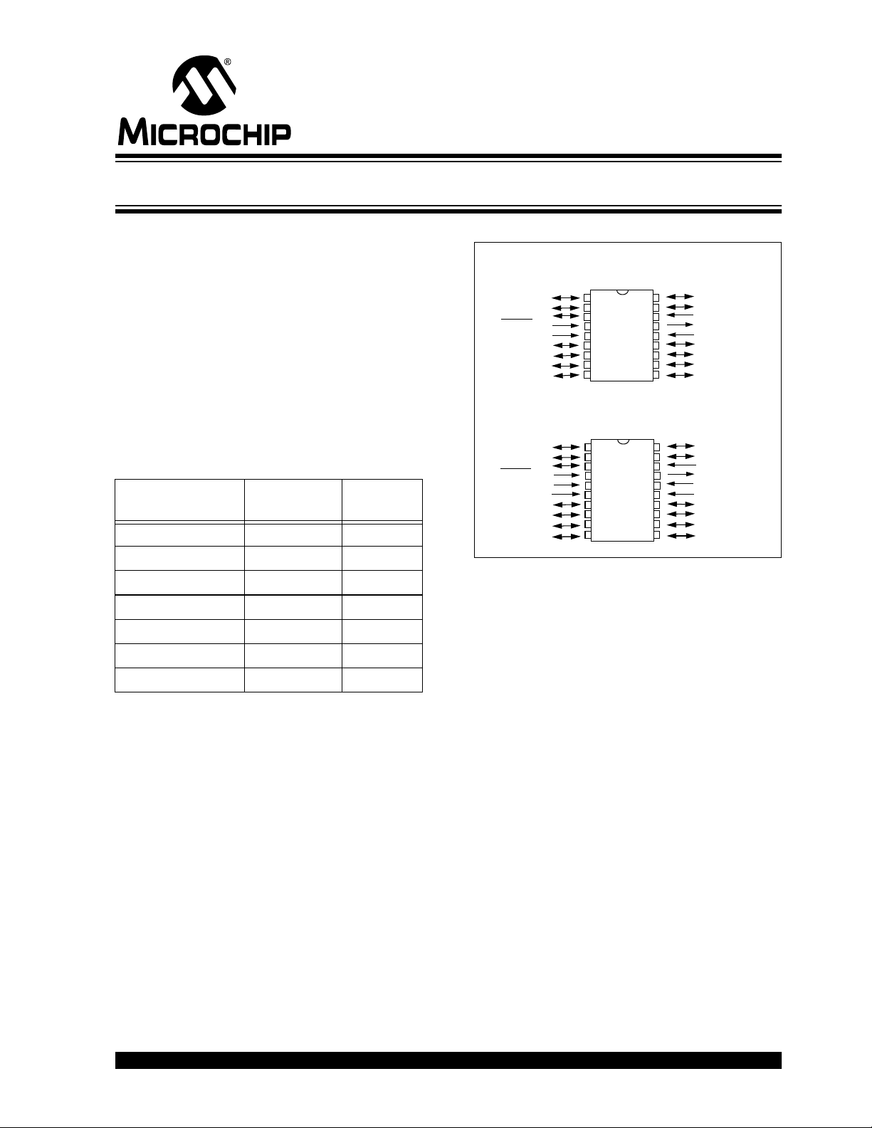
Pin Diagrams
PDIP, SOIC, Windowed CERDIP
RA2/AN2/V
RA3/AN3
RA4/T0CKI
MCLR/
RB0/INT
REF
VPP
VSS
RB1
RB2
RB3
•1
2
3
4
5
6
7
8
9
18
PIC16C62X
17
16
15
14
13
12
11
10
RA1/AN1
RA0/AN0
OSC1/CLKIN
OSC2/CLKOUT
DD
V
RB7
RB6
RB5
RB4
SSOP
RA2/AN2/V
RA3/AN3
RA4/T0CKI
MCLR/
RB0/INT
REF
VPP
VSS
VSS
RB1
RB2
RB3RB3
•1
2
3
4
5
6
7
8
9
10
20
19
PIC16C62X
18
17
16
15
14
13
12
11
RA1/AN1
RA0/AN0
OSC1/CLKIN
OSC2/CLKOUT
V
DD
V
DD
RB7
RB6
RB5
RB4
Special Microcontroller Features:
• Power-on Reset (POR)
• Power-up Timer (PWRT) and Oscillator Start-up
Timer (OST)
• Brown-out Reset
• Watchdog Timer (WDT) with its own on-chip RC
oscillator for reliable operation
• Programmable code protection
• Power saving SLEEP mode
• Selectable oscillator options
• Serial in-circuit programming (via two pins)
• Four user programmable ID locations
CMOS Technology:
• Low power, high speed CMOS EPROM
technology
• Fully static design
• Wide operating range
- 2.5V to 5.5V
• Commercial, industrial and extended temperature range
• Low power consumption
- < 2.0 mA @ 5.0V, 4.0 MHz
-15 µA typical @ 3.0V, 32 kHz
-< 1.0 µA typical standby current @ 3.0V
2003 Microchip Technology Inc. DS30235J-page 1
PIC16C62X
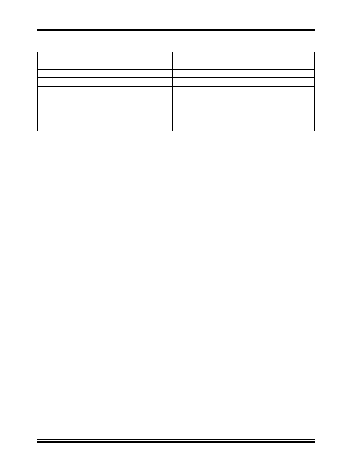
Device Differences
Device Voltage Range Oscillator
PIC16C620
PIC16C621
PIC16C622
PIC16C620A
PIC16CR620A
PIC16C621A
PIC16C622A
Note 1: If you change from this device to another device, please verify oscillator characteristics in your application.
(3)
(3)
(3)
(4)
(2)
(4)
(4)
2: For ROM parts, operation from 2.5V - 3.0V will require the PIC16LCR62X parts.
3: For OTP parts, operation from 2.5V - 3.0V will require the PIC16LC62X parts.
4: For OTP parts, operations from 2.7V - 3.0V will require the PIC16LC62XA parts.
2.5 - 6.0 See Note 1 0.9
2.5 - 6.0 See Note 1 0.9
2.5 - 6.0 See Note 1 0.9
2.7 - 5.5 See Note 1 0.7
2.5 - 5.5 See Note 1 0.7
2.7 - 5.5 See Note 1 0.7
2.7 - 5.5 See Note 1 0.7
Process Technology
(Microns)
DS30235J-page 2 2003 Microchip Technology Inc.

PIC16C62X
Table of Contents
1.0 General Description .................................................................................................................................................................. 5
2.0 PIC16C62X Device Varieties.................................................................................................................................................... 7
3.0 Architectural Overview.............................................................................................................................................................. 9
4.0 Memory Organization ............................................................................................................................................................. 13
5.0 I/O Ports.................................................................................................................................................................................. 25
6.0 Timer0 Module........................................................................................................................................................................ 31
7.0 Comparator Module ................................................................................................................................................................ 37
8.0 Voltage Reference Module ..................................................................................................................................................... 43
9.0 Special Features of the CPU .................................................................................................................................................. 45
10.0 Instruction Set Summary ........................................................................................................................................................ 61
11.0 Development Support ............................................................................................................................................................. 75
12.0 Electrical Specifications .......................................................................................................................................................... 81
13.0 Device Characterization Information ..................................................................................................................................... 109
14.0 Packaging Information .......................................................................................................................................................... 113
Appendix A: Enhancements.............................................................................................................................................................. 119
Appendix B: Compatibility ................................................................................................................................................................. 119
Index ............................................................................................................................................................................................... 121
On-Line Support ................................................................................................................................................................................ 123
Systems Information and Upgrade Hot Line ..................................................................................................................................... 123
Reader Response ............................................................................................................................................................................. 124
Product Identification System ........................................................................................................................................................... 125
TO OUR VALUED CUSTOMERS
It is our intention to provide our valued customers with the best documentation possible to ensure successful use of your Microchip products. To this end, we will continue to improve our publications to better suit your needs. Our publications will be refined
and enhanced as new volumes and updates are introduced.
If you have any questions or comments regarding this publication, please contact the Marketing Communications Department via
E-mail at docerrors@mail.microchip.com or fax the Reader Response Form in the back of this data sheet to (480) 792-4150.
We welcome your feedback.
Most Current Data Sheet
To obtain the most up-to-date version of this data sheet, please register at our Worldwide Web site at:
http://www.microchip.com
You can determine the version of a data sheet by examining its literature number found on the bottom outside corner of any page.
The last character of the literature number is the version number, (e.g., DS30000A is version A of document DS30000).
Errata
An errata sheet, describing minor operational differences from the data sheet and recommended workarounds, may exist for current
devices. As device/documentation issues become known to us, we will publish an errata sheet. The errata will specify the revision
of silicon and revision of document to which it applies.
To determine if an errata sheet exists for a particular device, please check with one of the following:
• Microchip’s Worldwide Web site; http://www.microchip.com
• Your local Microchip sales office (see last page)
• The Microchip Corporate Literature Center; U.S. FAX: (480) 792-7277
When contacting a sales office or the literature center, please specify which device, revision of silicon and data sheet (include
literature number) you are using.
Customer Notification System
Register on our web site at www.microchip.com/cn to receive the most current information on all of our products.
2003 Microchip Technology Inc. DS30235J-page 3

PIC16C62X
NOTES:
DS30235J-page 4 2003 Microchip Technology Inc.

PIC16C62X
1.0 GENERAL DESCRIPTION
The PIC16C62X devices are 18 and 20-Pin ROM/
EPROM-based members of the versatile PICmicro
family of low cost, high performance, CMOS, fullystatic, 8-bit microcontrollers.
All PICmicro microcontrollers employ an advanced
RISC architecture. The PIC16C62X devices have
enhanced core features, eight-level deep stack, and
multiple internal and external interrupt sources. The
separate instruction and data buses of the Harvard
architecture allow a 14-bit wide instruction word with
the separate 8-bit wide data. The two-stage instruction
pipeline allows all instructions to execute in a single
cycle, except for program branches (which require two
cycles). A total of 35 instructions (reduced instruction
set) are available. Additionally, a large register set
gives some of the architectural innovations used to
achieve a very high performance.
PIC16C62X microcontrollers typically achieve a 2:1
code compression and a 4:1 speed improvement over
other 8-bit microcontrollers in their class.
The PIC16C620A, PIC16C621A and PIC16CR620A
have 96 bytes of RAM. The PIC16C622(A) has 128
bytes of RAM. Each device has 13 I/O pins and an 8bit timer/counter with an 8-bit programmable prescaler.
In addition, the PIC16C62X adds two analog comparators with a programmable on-chip voltage reference
module. The comparator module is ideally suited for
applications requiring a low cost analog interface (e.g.,
battery chargers, threshold detectors, white goods
controllers, etc).
PIC16C62X devices have special features to reduce
external components, thus reducing system cost,
enhancing system reliability and reducing power consumption. There are four oscillator options, of which the
single pin RC oscillator provides a low cost solution, the
LP oscillator minimizes power consumption, XT is a
standard crystal, and the HS is for High Speed crystals.
The SLEEP (Power-down) mode offers power savings.
The user can wake-up the chip from SLEEP through
several external and internal interrupts and RESET.
A highly reliable Watchdog Timer with its own on-chip
RC oscillator provides protection against software
lock- up.
A UV-erasable CERDIP-packaged version is ideal for
code development while the cost effective One-TimeProgrammable (OTP) version is suitable for production
in any volume.
Table 1-1 shows the features of the PIC16C62X midrange microcon troller families.
A simplified block diagram of the PIC16C62X is shown
in Figure 3-1.
The PIC16C62X series fits perfectly in applications
ranging from battery chargers to low power remote
sensors. The EPROM technology makes
customization of application programs (detection
levels, pulse generation, timers, etc.) extremely fast
®
and convenient. The small footprint packages make
this microcontroller series perfect for all applications
with space limitations. Low cost, low power, high
performance, ease of use and I/O flexibility make the
PIC16C62X very versatile.
1.1 Family and Upward Compatibility
Those users familiar with the PIC16C5X family of
microcontrollers will realize that this is an enhanced
version of the PIC16C5X architecture. Please refer to
Appendix A for a detailed list of enhancements. Code
written for the PIC16C5X can be easily ported to
PIC16C62X family of devices (Appendix B). The
PIC16C62X family fills the niche for users wanting to
migrate up from the PIC16C5X family and not needing
various peripheral features of other members of the
PIC16XX mid-range microcontroller family.
1.2 Development Support
The PIC16C62X family is supported by a full-featured
macro assembler, a software simulator, an in-circuit
emulator, a low cost development programmer and a
full-featured programmer. Third Party “C” compilers are
also available.
2003 Microchip Technology Inc. DS30235J-page 5
PIC16C62X
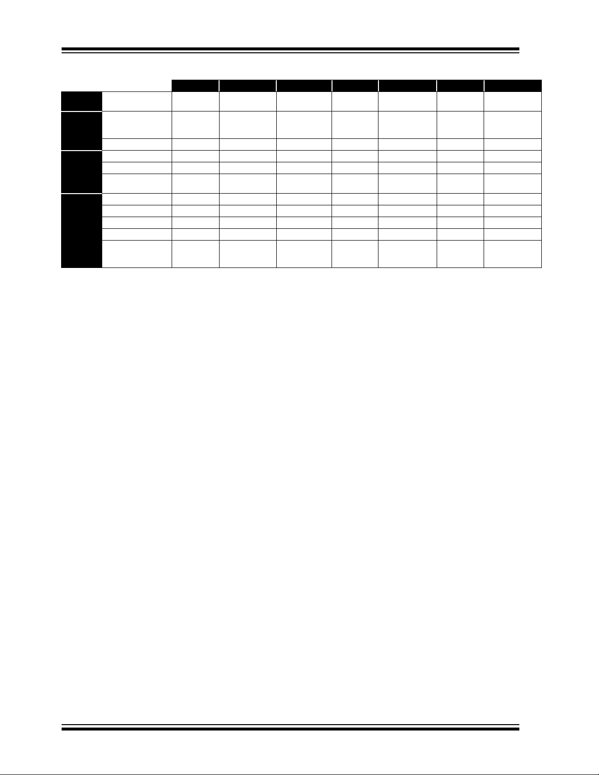
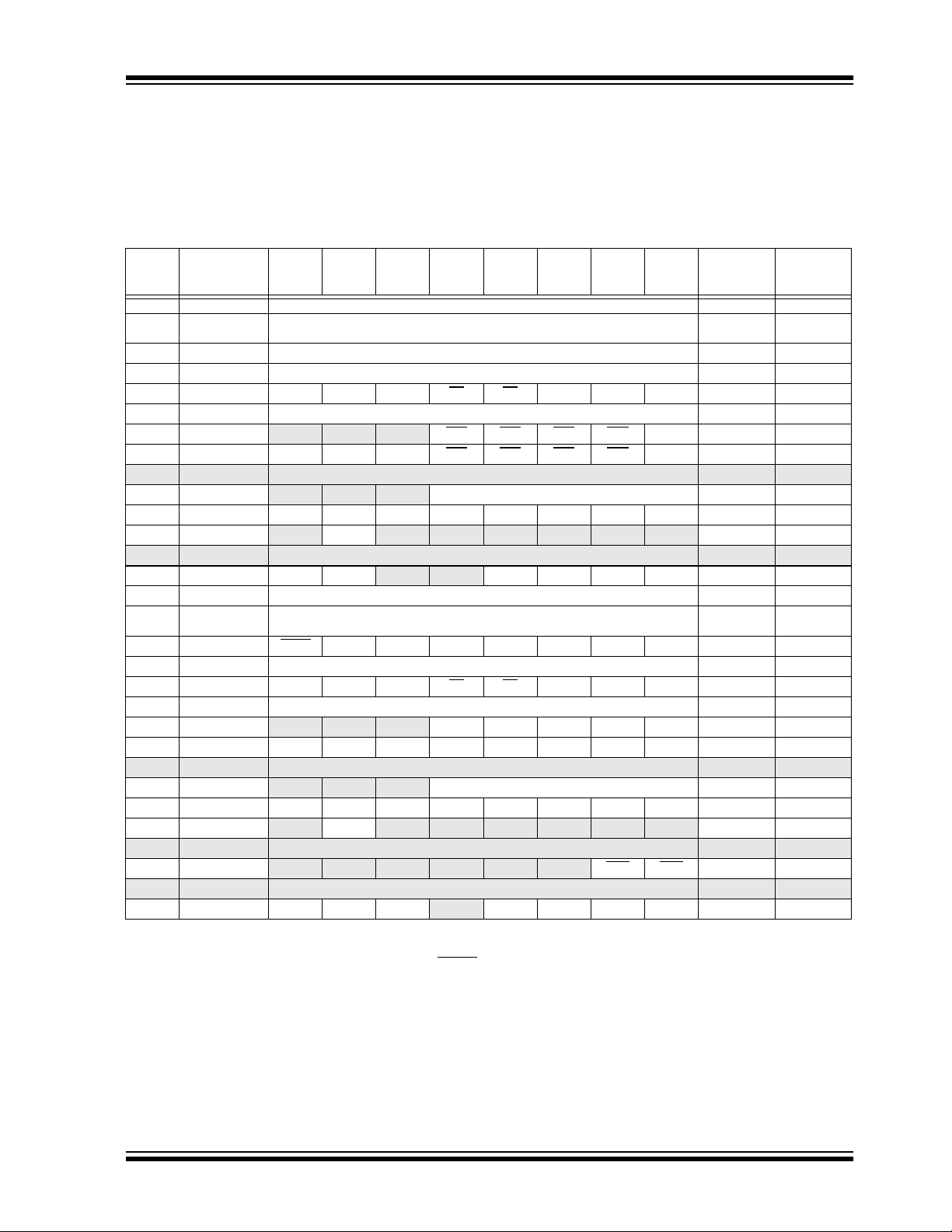
TABLE 1-1: PIC16C62X FAMILY OF DEVICES
PIC16C620
Clock Maximum Frequency
Memory EPROM Program
Peripherals Timer Module(s) TMR0 TMR0 TMRO TMR0 TMR0 TMR0 TMR0
Features Interrupt Sources 4 4 4 4 4 4 4
of Operation (MHz)
Memory
(x14 words)
Data Memory (bytes) 80 96 96 80 96 128 128
Comparators(s) 2 2 2 2 2 2 2
Internal Reference
Voltage
I/O Pins 13 13 13 13 13 13 13
Voltage Range (Volts) 2.5-6.0 2.7-5.5 2.5-5.5 2.5-6.0 2.7-5.5 2.5-6.0 2.7-5.5
Brown-out Reset Yes Yes Yes Yes Yes Yes Yes
Packages 18-pin DIP,
20 40 20 20 40 20 40
512 512 512 1K 1K 2K 2K
Yes Yes Yes Yes Yes Yes Yes
SOIC;
20-pin SSOP
(3)
PIC16C620A
18-pin DIP,
SOIC;
20-pin SSOP
All PICmicro® Family devices have Power-on Reset, selectable Watchdog Timer, selectable code protect and high
I/O current capability. All PIC16C62X Family devices use serial programming with clock pin RB6 and data pin RB7.
Note 1: If you change from this device to another device, please verify oscillator characteristics in your application.
2: For ROM parts, operation from 2.0V - 2.5V will require the PIC16LCR62XA parts.
3: For OTP parts, operation from 2.5V - 3.0V will require the PIC16LC62X part.
4: For OTP parts, operation from 2.7V - 3.0V will require the PIC16LC62XA part.
(1)(4)
PIC16CR620A
18-pin DIP,
SOIC;
20-pin SSOP
(2)
PIC16C621
18-pin DIP,
SOIC;
20-pin SSOP
(3)
PIC16C621A
18-pin DIP,
SOIC;
20-pin SSOP
(1)(4)
PIC16C622
18-pin DIP,
SOIC;
20-pin SSOP
(3)
PIC16C622A
18-pin DIP,
SOIC;
20-pin SSOP
(1)(4)
DS30235J-page 6 2003 Microchip Technology Inc.

PIC16C62X
2.0 PIC16C62X DEVICE VARIETIES
A variety of frequency ranges and packaging options
are available. Depending on application and production
requirements, the proper device option can be selected
using the information in the PIC16C62X Product
Identification System section at the end of this data
sheet. When placing orders, please use this page of
the data sheet to specify the correct part number.
2.1 UV Erasable Devices
The UV erasable version, offered in CERDIP package,
is optimal for prototype development and pilot
programs. This version can be erased and
reprogrammed to any of the Oscillator modes.
Microchip's PICSTART and PRO MATE
programmers both support programming of the
PIC16C62X.
Note: Microchip does not recommend code
protecting windowed devices.
2.2 One-Time-Programmable (OTP) Devices
The availability of OTP devices is especially useful for
customers who need the flexibility for frequent code
updates and small volume applications. In addition to
the program memory, the configuration bits must also
be programmed.
2.3 Quick-Turnaround-Production (QTP) Devices
Microchip offers a QTP programming service for
factory production orders. This service is made
available for users who chose not to program a medium
to high quantity of units and whose code patterns have
stabilized. The devices are identical to the OTP
devices, but with all EPROM locations and configuration options already programmed by the factory.
Certain code and prototype verification procedures
apply before production shipments are available.
Please contact your Microchip Technology sales office
for more details.
2.4 Serialized Quick-TurnaroundProduction
Microchip offers a unique programming service where
a few user-defined locations in each device are
programmed with different serial numbers. The serial
numbers may be random, pseudo-random or
sequential.
Serial programming allows each device to have a
unique number, which can serve as an entry-code,
password or ID number.
SM
(SQTPSM) Devices
2003 Microchip Technology Inc. DS30235J-page 7

PIC16C62X
NOTES:
DS30235J-page 8 2003 Microchip Technology Inc.

PIC16C62X
3.0 ARCHITECTURAL OVERVIEW
The high performance of the PIC16C62X family can be
attributed to a number of architectural features
commonly found in RISC microprocessors. To begin
with, the PIC16C62X uses a Harvard architecture, in
which, program and data are accessed from separate
memories using separate busses. This improves
bandwidth over traditional von Neumann architecture,
where program and data are fetched from the same
memory. Separating program and data memory further
allows instructions to be sized differently than 8-bit
wide data word. Instruction opcodes are 14-bits wide
making it possible to have all single word instructions.
A 14-bit wide program memory access bus fetches a
14-bit instruction in a single cycle. A two-stage pipeline
overlaps fetch and execution of instructions.
Consequently, all instructions (35) execute in a single
cycle (200 ns @ 20 MHz) except for program branches.
The PIC16C620(A) and PIC16CR620A address
512 x 14 on-chip program memory. The PIC16C621(A)
addresses 1K x 14 program memory. The
PIC16C622(A) addresses 2K x 14 program memory.
All program memory is internal.
The PIC16C62X can directly or indirectly address its
register files or data memory. All special function
registers including the program counter are mapped in
the data memory. The PIC16C62X has an orthogonal
(symmetrical) instruction set that makes it possible to
carry out any operation on any register using any
Addressing mode. This symmetrical nature and lack of
‘special optimal situations’ make programming with the
PIC16C62X simple yet efficient. In addition, the
learning curve is reduced significantly.
The PIC16C62X devices contain an 8-bit ALU and
working register. The ALU is a general purpose
arithmetic unit. It performs arithmetic and Boolean
functions between data in the working register and any
register file.
The ALU is 8-bits wide and capable of addition,
subtraction, shift and logical operations. Unless
otherwise mentioned, arithmetic operations are two's
complement in nature. In two-operand instructions,
typically one operand is the working register
(W register). The other operand is a file register or an
immediate constant. In single operand instructions, the
operand is either the W register or a file register.
The W register is an 8-bit working register used for ALU
operations. It is not an addressable register.
Depending on the instruction executed, the ALU may
affect the values of the Carry (C), Digit Carry (DC), and
Zero (Z) bits in the STATUS register. The C and DC bits
operate as a Borrow
respectively, bit in subtraction. See the SUBLW and
SUBWF instructions for examples.
A simplified block diagram is shown in Figure 3-1, with
a description of the device pins in Table 3-1.
and Digit Borrow out bit,
2003 Microchip Technology Inc. DS30235J-page 9
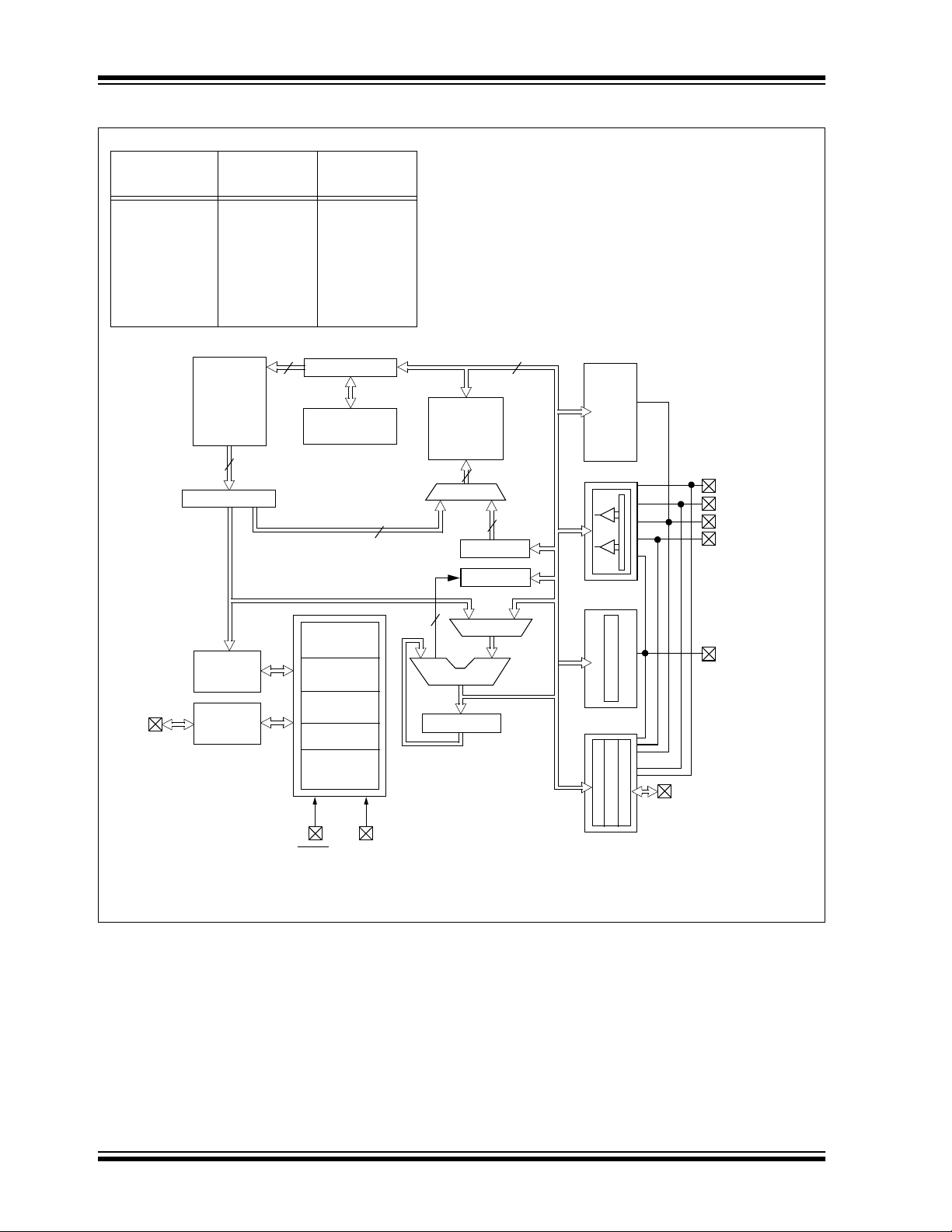
PIC16C62X
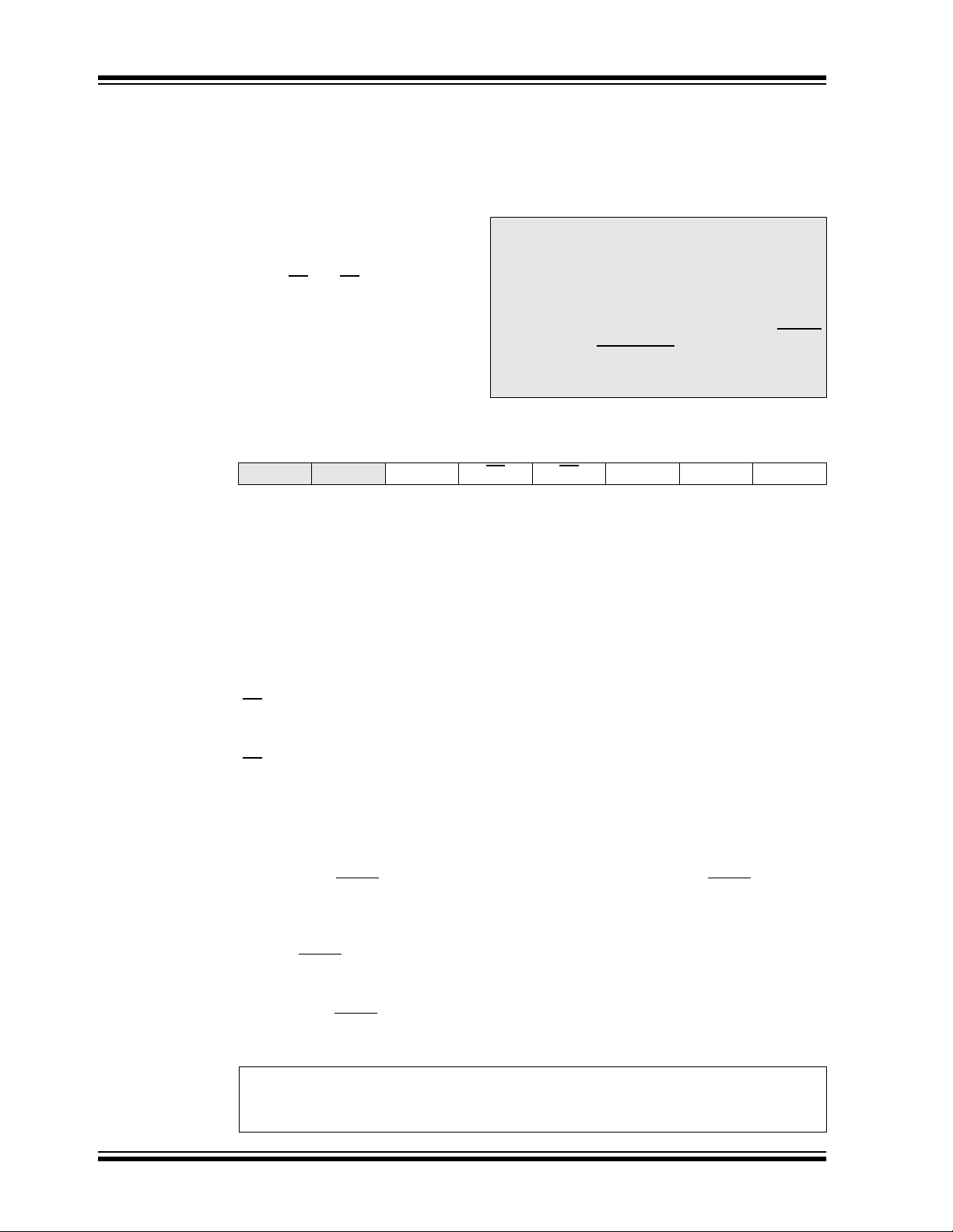
FIGURE 3-1: BLOCK DIAGRAM
Device
PIC16C620
PIC16C620A
PIC16CR620A
PIC16C621
PIC16C621A
PIC16C622
PIC16C622A
Program
Bus
OSC1/CLKIN
OSC2/CLKOUT
Program
Memory
512 x 14
512 x 14
512 x 14
1K x 14
1K x 14
2K x 14
2K x 14
EPROM
Program
Memory
14
Instruction reg
Instruction
Decode &
Control
Timing
Generation
Data Memory
13
Program Counter
8-Level Stack
Direct Addr
Power-up
Oscillator
Start-up Timer
Power-on
Watchdog
Brown-out
128 x 8
128 x 8
(13-bit)
Timer
Reset
Timer
Reset
(RAM)
80 x 8
96 x 8
96 x 8
80 x 8
96 x 8
RAM Addr
7
Data Bus
Registers
(1)
Addr MUX
3
RAM
File
FSR reg
STATUS reg
ALU
W reg
9
8
MUX
8
Indirect
Addr
Voltage
Reference
Comparator
+
+
TMR0
I/O Ports
RA0/AN0
RA1/AN1
RA2/AN2/VREF
RA3/AN3
RA4/T0CKI
PORTB
VDD, VSS
MCLR
Note 1: Higher order bits are from the STATUS register.
DS30235J-page 10 2003 Microchip Technology Inc.

TABLE 3-1: PIC16C62X PINOUT DESCRIPTION
PIC16C62X
Name
OSC1/CLKIN
OSC2/CLKOUT
MCLR/VPP
RA0/AN0
RA1/AN1
RA2/AN2/VREF
RA3/AN3
RA4/T0CKI
RB0/INT
RB1
RB2
RB3
RB4
RB5
RB6
RB7
VSS
VDD
Legend: O = output I/O = input/output P = power
Note 1: This buffer is a Schmitt Trigger input when configured as the external interrupt.
2: This buffer is a Schmitt Trigger input when used in Serial Programming mode.
DIP/SOIC
Pin #
16 18 I ST/CMOS
15 17 O —
4 4 I/P ST
17 19 I/O ST
18 20 I/O ST
1 1 I/O ST
2 2 I/O ST
3 3 I/O ST
6 7 I/O
7 8 I/O TTL
8 9 I/O TTL
9 10 I/O TTL
10 11 I/O TTL
11 12 I/O TTL
12 13 I/O
13 14 I/O
5 5,6 P —
14 15,16 P —
— = Not used I = Input ST = Schmitt Trigger input
TTL = TTL input
SSOP
Pin #
I/O/P Type
Buffer
Type
TTL/ST
TTL/ST
TTL/ST
Oscillator crystal input/external clock source input.
Oscillator crystal output. Connects to crystal or resonator
in Crystal Oscillator mode. In RC mode, OSC2 pin outputs CLKOUT, which has 1/4 the frequency of OSC1
and denotes the instruction cycle rate.
Master Clear (Reset) input/programming voltage input.
This pin is an Active Low Reset to the device.
PORTA is a bi-directional I/O port.
Analog comparator input
Analog comparator input
Analog comparator input or VREF output
Analog comparator input /output
Can be selected to be the clock input to the Timer0
timer/counter or a comparator output. Output is
open drain type.
PORTB is a bi-directional I/O port. PORTB can be
software programmed for internal weak pull-up on all
inputs.
(1)
(2)
(2)
RB0/INT can also be selected as an external
interrupt pin.
Interrupt-on-change pin.
Interrupt-on-change pin.
Interrupt-on-change pin. Serial programming clock.
Interrupt-on-change pin. Serial programming data.
Ground reference for logic and I/O pins.
Positive supply for logic and I/O pins.
Description
2003 Microchip Technology Inc. DS30235J-page 11
PIC16C62X
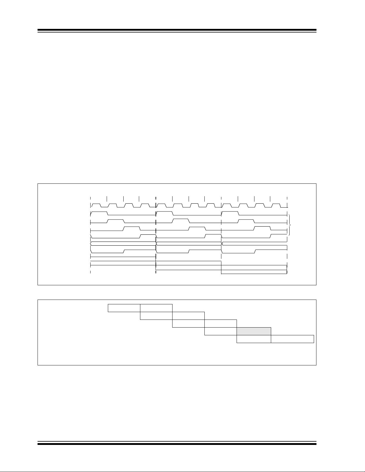
3.1 Clocking Scheme/Instruction Cycle
The clock input (OSC1/CLKIN pin) is internally divided
by four to generate four non-overlapping quadrature
clocks namely Q1, Q2, Q3 and Q4. Internally, the
program counter (PC) is incremented every Q1, the
instruction is fetched from the program memory and
latched into the instruction register in Q4. The
instruction is decoded and executed during the
following Q1 through Q4. The clocks and instruction
execution flow is shown in Figure 3-2.
FIGURE 3-2: CLOCK/INSTRUCTION CYCLE
Q2 Q3 Q4
OSC1
Q1
Q2
Q3
Q4
PC
OSC2/CLKOUT
(RC mode)
Q1
PC PC+1 PC+2
Fetch INST (PC)
Execute INST (PC-1)
Q1
3.2 Instruction Flow/Pipelining
An “Instruction Cycle” consists of four Q cycles (Q1,
Q2, Q3 and Q4). The instruction fetch and execute are
pipelined such that fetch takes one instruction cycle
while decode and execute takes another instruction
cycle. However, due to the pipelining, each instruction
effectively executes in one cycle. If an instruction
causes the program counter to change (e.g., GOTO)
then two cycles are required to complete the instruction
(Example 3-1).
A fetch cycle begins with the program counter (PC)
incrementing in Q1.
In the execution cycle, the fetched instruction is latched
into the “Instruction Register (IR)” in cycle Q1. This
instruction is then decoded and executed during the
Q2, Q3 and Q4 cycles. Data memory is read during Q2
(operand read) and written during Q4 (destination
write).
Q2 Q3 Q4
Fetch INST (PC+1)
Execute INST (PC)
Q2 Q3 Q4
Q1
Fetch INST (PC+2)
Execute INST (PC+1)
Internal
phase
clock
EXAMPLE 3-1: INSTRUCTION PIPELINE FLOW
1. MOVLW 55h
2. MOVWF PORTB
3. CALL SUB_1
4. BSF PORTA, BIT3
Note: All instructions are single cycle, except for any program branches. These take two cycles since the fetch instruction
is “flushed” from the pipeline, while the new instruction is being fetched and then executed.
DS30235J-page 12 2003 Microchip Technology Inc.
Fetch 1 Execute 1
Fetch 2 Execute 2
Fetch 3 Execute 3
Fetch 4
Flush
Fetch SUB_1 Execute SUB_1
PIC16C62X
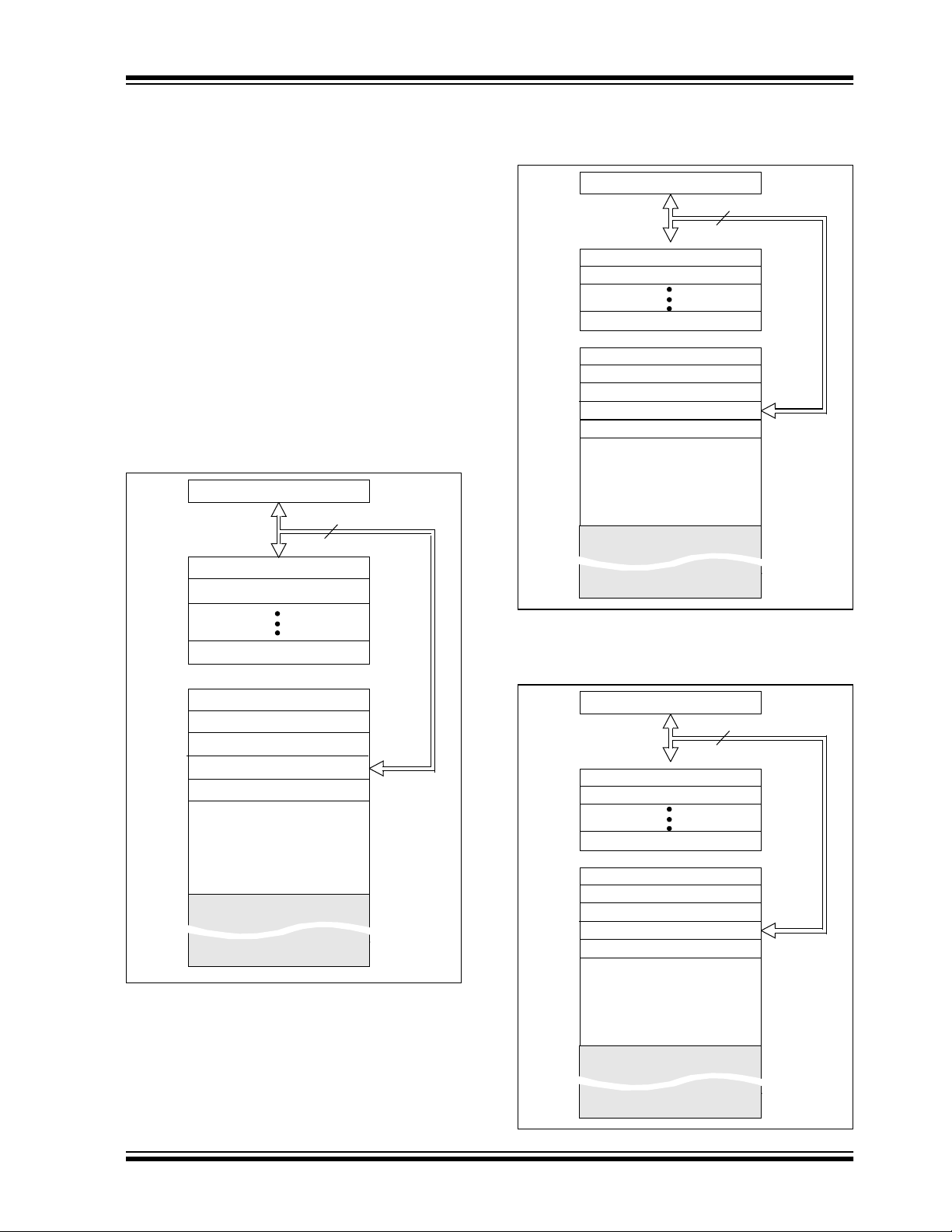
4.0 MEMORY ORGANIZATION
4.1 Program Memory Organization
The PIC16C62X has a 13-bit program counter capable
of addressing an 8K x 14 program memory space. Only
the first 512 x 14 (0000h - 01FFh) for the
PIC16C620(A) and PIC16CR620, 1K x 14 (0000h 03FFh) for the PIC16C621(A) and 2K x 14 (0000h 07FFh) for the PIC16C622(A) are physically
implemented. Accessing a location above these
boundaries will cause a wrap-around within the first
512 x 14 space (PIC16C(R)620(A)) or 1K x 14 space
(PIC16C621(A)) or 2K x 14 space (PIC16C622(A)).
The RESET vector is at 0000h and the interrupt vector
is at 0004h (Figure 4-1, Figure 4-2, Figure 4-3).
FIGURE 4-1: PROGRAM MEMORY MAP
AND STACK FOR THE
PIC16C620/PIC16C620A/
PIC16CR620A
PC<12:0>
CALL, RETURN
RETFIE, RETLW
Stack Level 1
Stack Level 2
13
FIGURE 4-2: PROGRAM MEMORY MAP
AND STACK FOR THE
PIC16C621/PIC16C621A
PC<12:0>
CALL, RETURN
RETFIE, RETLW
Stack Level 1
Stack Level 2
Stack Level 8
RESET Vector
Interrupt Vector
On-Chip Program
Memory
13
000h
0004
0005
03FFh
0400h
1FFFh
Stack Level 8
RESET Vector
Interrupt Vector
On-Chip Program
Memory
000h
0004
0005
01FFh
0200h
1FFFh
FIGURE 4-3: PROGRAM MEMORY MAP
AND STACK FOR THE
PIC16C622/PIC16C622A
PC<12:0>
CALL, RETURN
RETFIE, RETLW
Stack Level 1
Stack Level 2
Stack Level 8
RESET Vector
Interrupt Vector
On-Chip Program
Memory
13
000h
0004
0005
07FFh
0800h
1FFFh
2003 Microchip Technology Inc. DS30235J-page 13

PIC16C62X
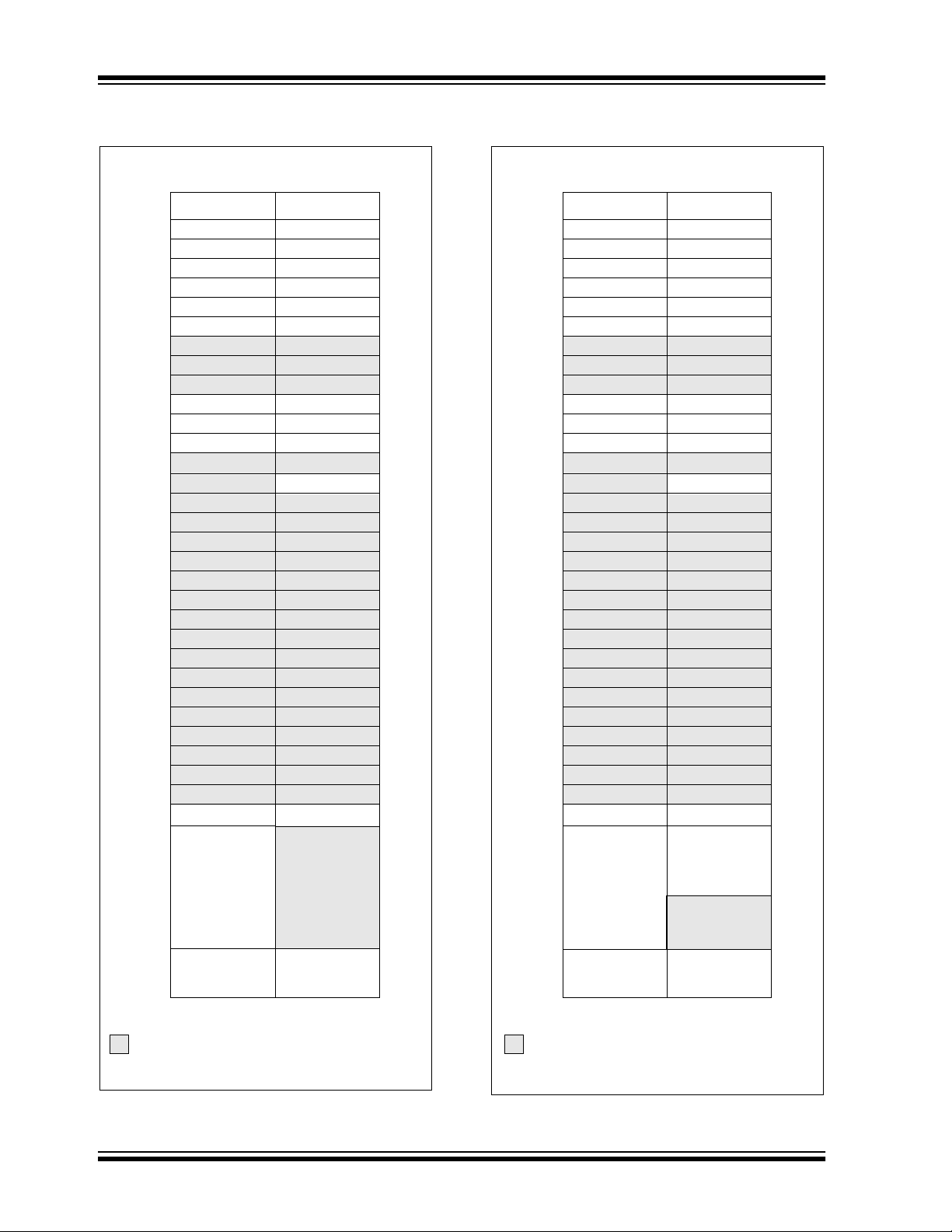
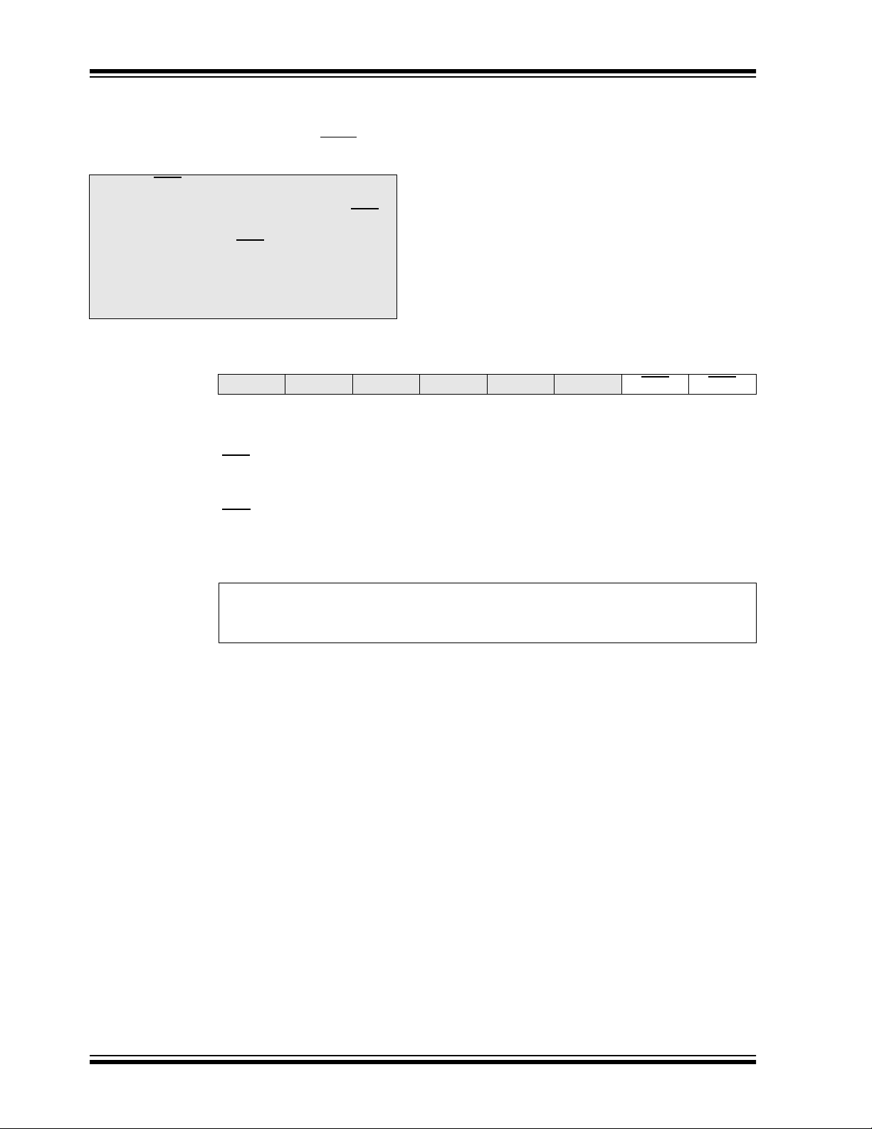
4.2 Data Memory Organization
The data memory (Figure 4-4, Figure 4-5, Figure 4-6
and Figure 4-7) is partitioned into two banks, which
contain the General Purpose Registers and the Special
Function Registers. Bank 0 is selected when the RP0
bit is cleared. Bank 1 is selected when the RP0 bit
(STATUS <5>) is set. The Special Function Registers
are located in the first 32 locations of each bank.
Register locations 20-7Fh (Bank0) on the
PIC16C620A/CR620A/621A and 20-7Fh (Bank0) and
A0-BFh (Bank1) on the PIC16C622 and PIC16C622A
are General Purpose Registers implemented as static
RAM. Some Special Purpose Registers are mapped in
Bank 1.
Addresses F0h-FFh of bank1 are implemented as
common ram and mapped back to addresses 70h-7Fh
in bank0 on the PIC16C620A/621A/622A/CR620A.
4.2.1 GENERAL PURPOSE REGISTER
FILE
The register file is organized as 80 x 8 in the
PIC16C620/621, 96 x 8 in the PIC16C620A/621A/
CR620A and 128 x 8 in the PIC16C622(A). Each is
accessed either directly or indirectly through the File
Select Register FSR (Section 4.4).
DS30235J-page 14 2003 Microchip Technology Inc.
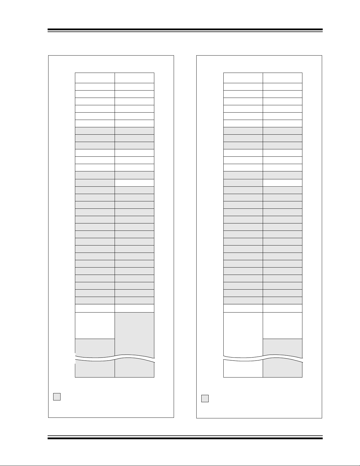
PIC16C62X
FIGURE 4-4: DATA MEMORY MAP FOR
THE PIC16C620/621
File
Address
00h
01h
02h
03h
04h
05h
06h
07h
08h
09h
0Ah
0Bh
0Ch
0Dh
0Eh
0Fh
10h
11h
12h
13h
14h
15h
16h
17h
18h
19h
1Ah
1Bh
1Ch
1Dh
1Eh
1Fh
20h
6Fh
70h
(1)
INDF
TMR0
PCL
STATUS
FSR
PORTA
PORTB
PCLATH
INTCON
PIR1
CMCON
General
Purpose
Register
(1)
INDF
OPTION
PCL
STATUS
FSR
TRISA
TRISB
PCLATH
INTCON
PIE1
PCON
VRCON
File
Address
80h
81h
82h
83h
84h
85h
86h
87h
88h
89h
8Ah
8Bh
8Ch
8Dh
8Eh
8Fh
90h
91h
92h
93h
94h
95h
96h
97h
98h
99h
9Ah
9Bh
9Ch
9Dh
9Eh
9Fh
A0h
FIGURE 4-5: DATA MEMORY MAP FOR
THE PIC16C622
File
Address
00h
01h
02h
03h
04h
05h
06h
07h
08h
09h
0Ah
0Bh
0Ch
0Dh
0Eh
0Fh
10h
11h
12h
13h
14h
15h
16h
17h
18h
19h
1Ah
1Bh
1Ch
1Dh
1Eh
1Fh
20h
(1)
INDF
TMR0
PCL
STATUS
FSR
PORTA
PORTB
PCLATH
INTCON
PIR1
CMCON
General
Purpose
Register
(1)
INDF
OPTION
PCL
STATUS
FSR
TRISA
TRISB
PCLATH
INTCON
PIE1
PCON
VRCON
General
Purpose
Register
File
Address
80h
81h
82h
83h
84h
85h
86h
87h
88h
89h
8Ah
8Bh
8Ch
8Dh
8Eh
8Fh
90h
91h
92h
93h
94h
95h
96h
97h
98h
99h
9Ah
9Bh
9Ch
9Dh
9Eh
9Fh
A0h
BFh
C0h
7Fh
Unimplemented data memory locations, read as '0'.
Note 1: Not a physical register.
2003 Microchip Technology Inc. DS30235J-page 15
Bank 0 Bank 1
FFh
7Fh
Unimplemented data memory locations, read as '0'.
Note 1: Not a physical register.
Bank 0 Bank 1
FFh
PIC16C62X
FIGURE 4-6: DATA MEMORY MAP FOR THE
PIC16C620A/CR620A/621A
File
Address
00h
01h
02h
03h
04h
05h
06h
07h
08h
09h
0Ah
0Bh
0Ch
0Dh
0Eh
0Fh
10h
11h
12h
13h
14h
15h
16h
17h
18h
19h
1Ah
1Bh
1Ch
1Dh
1Eh
1Fh
20h
(1)
INDF
TMR0
PCL
STATUS
FSR
PORTA
PORTB
PCLATH
INTCON
PIR1
CMCON
General
Purpose
Register
(1)
INDF
OPTION
PCL
STATUS
FSR
TRISA
TRISB
PCLATH
INTCON
PIE1
PCON
VRCON
File
Address
80h
81h
82h
83h
84h
85h
86h
87h
88h
89h
8Ah
8Bh
8Ch
8Dh
8Eh
8Fh
90h
91h
92h
93h
94h
95h
96h
97h
98h
99h
9Ah
9Bh
9Ch
9Dh
9Eh
9Fh
A0h
FIGURE 4-7: DATA MEMORY MAP FOR
THE PIC16C622A
File
Address
00h
01h
02h
03h
04h
05h
06h
07h
08h
09h
0Ah
0Bh
0Ch
0Dh
0Eh
0Fh
10h
11h
12h
13h
14h
15h
16h
17h
18h
19h
1Ah
1Bh
1Ch
1Dh
1Eh
1Fh
20h
(1)
INDF
TMR0
PCL
STATUS
FSR
PORTA
PORTB
PCLATH
INTCON
PIR1
CMCON
General
Purpose
Register
(1)
INDF
OPTION
PCL
STATUS
FSR
TRISA
TRISB
PCLATH
INTCON
PIE1
PCON
VRCON
General
Purpose
Register
File
Address
80h
81h
82h
83h
84h
85h
86h
87h
88h
89h
8Ah
8Bh
8Ch
8Dh
8Eh
8Fh
90h
91h
92h
93h
94h
95h
96h
97h
98h
99h
9Ah
9Bh
9Ch
9Dh
9Eh
9Fh
A0h
BFh
C0h
6Fh
70h
7Fh
Unimplemented data memory locations, read as '0'.
Note 1: Not a physical register.
DS30235J-page 16 2003 Microchip Technology Inc.
General
Purpose
Register
Bank 0 Bank 1
Accesses
70h-7Fh
F0h
FFh
6Fh
70h
7Fh
Unimplemented data memory locations, read as '0'.
Note 1: Not a physical register.
General
Purpose
Register
Bank 0 Bank 1
Accesses
70h-7Fh
F0h
FFh
PIC16C62X
4.2.2 SPECIAL FUNCTION REGISTERS
The Special Function Registers are registers used by
the CPU and Peripheral functions for controlling the
desired operation of the device (Table 4-1). These
registers are static RAM.
The Special Function Registers can be classified into
two sets (core and peripheral). The Special Function
Registers associated with the “core” functions are
described in this section. Those related to the operation
of the peripheral features are described in the section
of that peripheral feature.
TABLE 4-1: SPECIAL REGISTERS FOR THE PIC16C62X
Address Name Bit 7 Bit 6 Bit 5 Bit 4 Bit 3 Bit 2 Bit 1 Bit 0
Bank 0
00h INDF Addressing this location uses contents of FSR to address data memory (not a physical
01h TMR0 Timer0 Module’s Register
02h PCL Program Counter's (PC) Least Significant Byte
03h STAT US IRP
04h FSR Indirect data memory address pointer
05h PORTA — — — RA4 RA3 RA2 RA1 RA0
06h PORTB RB7 RB6 RB5 RB4 RB3 RB2 RB1 RB0
07h-09h Unimplemented
0Ah PCLATH — — — Write buffer for upper 5 bits of program counter
0Bh INTCON GIE PEIE T0IE INTE RBIE T0IF INTF RBIF
0Ch PIR1 — CMIF — — — — — —
0Dh-1Eh Unimplemented
1Fh CMCON C2OUT C1OUT — — CIS CM2 CM1 CM0
Bank 1
80h INDF Addressing this location uses contents of FSR to address data memory (not a physical
81h OPTION RBPU INTEDG T0CS T0SE PSA PS2 PS1 PS0
82h PCL Program Counter's (PC) Least Significant Byte
83h STAT US IRP
84h FSR Indirect data memory address pointer
85h TRISA — — — TRISA4 TRISA3 TRISA2 TRISA1 TRISA0
86h TRISB TRISB7 TRISB6 TRISB5 TRISB4 TRISB3 TRISB2 TRISB1 TRISB0
87h-89h Unimplemented
8Ah PCLATH — — — Write buffer for upper 5 bits of program counter
8Bh INTCON GIE PEIE T0IE INTE RBIE T0IF INTF RBIF
8Ch PIE1 — CMIE — — — — — —
8Dh Unimplemented
8Eh PCON — — — — — — POR BOR
8Fh-9Eh Unimplemented
9Fh VRCON VREN VROE VRR — VR3 VR2 VR1 VR0
Legend: — = Unimplemented locations read as ‘0’, u = unchanged, x = unknown,
q = value depends on condition, shaded = unimplemented
Note 1: Other (non Power-up) Resets include MCLR
normal operation.
2: IRP & RP1 bits are reserved; always maintain these bits clear.
register)
(2)
register)
(2)
RP1
RP1
(2)
RP0 TO PD Z DC C
(2)
RP0 TO PD Z DC C
Reset, Brown-out Reset and Watchdog Timer Reset during
Value on
POR Reset
xxxx xxxx xxxx xxxx
xxxx xxxx uuuu uuuu
0000 0000 0000 0000
0001 1xxx 000q quuu
xxxx xxxx uuuu uuuu
---x 0000 ---u 0000
xxxx xxxx uuuu uuuu
— —
---0 0000 ---0 0000
0000 000x 0000 000u
-0-- ---- -0-- ----
— —
00-- 0000 00-- 0000
xxxx xxxx xxxx xxxx
1111 1111 1111 1111
0000 0000 0000 0000
0001 1xxx 000q quuu
xxxx xxxx uuuu uuuu
---1 1111 ---1 1111
1111 1111 1111 1111
— —
---0 0000 ---0 0000
0000 000x 0000 000u
-0-- ---- -0-- ----
— —
---- --0x ---- --uq
— —
000- 0000 000- 0000
Value on all
other
RESETS
(1)
2003 Microchip Technology Inc. DS30235J-page 17
PIC16C62X
4.2.2.1 STATUS Register
The STATUS register, shown in Register 4-1, contains
the arithmetic status of the ALU, the RESET status and
the bank select bits for data memory.
The STATUS register can be the destination for any
instruction, like any other register. If the STATUS
register is the destination for an instruction that affects
the Z, DC or C bits, then the write to these three bits is
disabled. These bits are set or cleared according to the
device logic. Furthermore, the TO
writable. Therefore, the result of an instruction with the
STATUS register as destination may be different than
intended.
For example, CLRF STATUS will clear the upper-three
bits and set the Z bit. This leaves the STATUS register
as 000uu1uu (where u = unchanged).
and PD bits are not
It is recommended, therefore, that only BCF, BSF,
SWAPF and MOVWF instructions are used to alter the
STATUS register, because these instructions do not
affect any STATUS bit. For other instructions not
affecting any STATUS bits, see the “Instruction Set
Summary”.
Note 1: The IRP and RP1 bits (STATUS<7:6>)
are not used by the PIC16C62X and
should be programmed as ’0'. Use of
these bits as general purpose R/W bits is
NOT recommended, since this may affect
upward compatibility with future products.
2: The C and DC bits operate as a Borrow
and Digit Borrow out bit, respectively, in
subtraction. See the SUBLW and SUBWF
instructions for examples.
REGISTER 4-1: STATUS REGISTER (ADDRESS 03H OR 83H)
Reserved Reserved R/W-0 R-1 R-1 R/W-x R/W-x R/W-x
IRP RP1 RP0 TO PD ZDCC
bit 7 bit 0
bit 7 IRP: Register Bank Select bit (used for indirect addressing)
1 = Bank 2, 3 (100h - 1FFh)
0 = Bank 0, 1 (00h - FFh)
The IRP bit is reserved on the PIC16C62X; always maintain this bit clear.
bit 6-5 RP<1:0>: Register Bank Select bits (used for direct addressing)
01 = Bank 1 (80h - FFh)
00 = Bank 0 (00h - 7Fh)
Each bank is 128 bytes. The RP1 bit is reserved on the PIC16C62X; always maintain this bit
clear.
bit 4 TO
bit 3 PD
bit 2 Z: Zero bit
bit 1 DC: Digit carry/borrow
bit 0 C: Carry/borrow
: Time-out bit
1 = After power-up, CLRWDT instruction, or SLEEP instruction
0 = A WDT time-out occurred
: Power-down bit
1 = After power-up or by the CLRWDT instruction
0 = By execution of the SLEEP instruction
1 = The result of an arithmetic or logic operation is zero
0 = The result of an arithmetic or logic operation is not zero
bit (ADDWF, ADDLW,SUBLW,SUBWF instructions)(for borrow the polarity
is reversed)
1 = A carry-out from the 4th low order bit of the result occurred
0 = No carry-out from the 4th low order bit of the result
bit (ADDWF, ADDLW,SUBLW,SUBWF instructions)
1 = A carry-out from the Most Significant bit of the result occurred
0 = No carry-out from the Most Significant bit of the result occurred
Note: For borrow
complement of the second operand. For rotate (RRF, RLF) instructions, this bit is
loaded with either the high or low order bit of the source register.
Legend:
R = Readable bit W = Writable bit U = Unimplemented bit, read as ‘0’
- n = Value at POR ’1’ = Bit is set ’0’ = Bit is cleared x = Bit is unknown
the polarity is reversed. A subtraction is executed by adding the two’s
DS30235J-page 18 2003 Microchip Technology Inc.
4.2.2.2 OPTION Register
The OPTION register is a readable and writable
register, which contains various control bits to configure
the TMR0/WDT prescaler, the external RB0/INT
interrupt, TMR0 and the weak pull-ups on PORTB.
Note: To achieve a 1:1 prescaler assignment for
TMR0, assign the prescaler to the WDT
(PSA = 1).
REGISTER 4-2: OPTION REGISTER (ADDRESS 81H)
R/W-1 R/W-1 R/W-1 R/W-1 R/W-1 R/W-1 R/W-1 R/W-1
RBPU INTEDG T0CS T0SE PSA PS2 PS1 PS0
bit 7 bit 0
PIC16C62X
bit 7 RBPU
: PORTB Pull-up Enable bit
1 = PORTB pull-ups are disabled
0 = PORTB pull-ups are enabled by individual port latch values
bit 6 INTEDG: Interrupt Edge Select bit
1 = Interrupt on rising edge of RB0/INT pin
0 = Interrupt on falling edge of RB0/INT pin
bit 5 T0CS: TMR0 Clock Source Select bit
1 = Transition on RA4/T0CKI pin
0 = Internal instruction cycle clock (CLKOUT)
bit 4 T0SE: TMR0 Source Edge Select bit
1 = Increment on high-to-low transition on RA4/T0CKI pin
0 = Increment on low-to-high transition on RA4/T0CKI pin
bit 3 PSA: Prescaler Assignment bit
1 = Prescaler is assigned to the WDT
0 = Prescaler is assigned to the Timer0 module
bit 2-0 PS<2:0>: Prescaler Rate Select bits
Bit Value TMR0 Rate WDT Rate
000
001
010
011
100
101
110
111
1 : 2
1 : 4
1 : 8
1 : 16
1 : 32
1 : 64
1 : 128
1 : 256
1 : 1
1 : 2
1 : 4
1 : 8
1 : 16
1 : 32
1 : 64
1 : 128
Legend:
R = Readable bit W = Writable bit U = Unimplemented bit, read as ‘0’
- n = Value at POR ’1’ = Bit is set ’0’ = Bit is cleared x = Bit is unknown
2003 Microchip Technology Inc. DS30235J-page 19

PIC16C62X
4.2.2.3 INTCON Register
The INTCON register is a readable and writable
register, which contains the various enable and flag bits
for all interrupt sources except the comparator module.
See Section 4.2.2.4 and Section 4.2.2.5 for a
description of the comparator enable and flag bits.
Note: Interrupt flag bits get set when an interrupt
condition occurs, regardless of the state of
its corresponding enable bit or the global
enable bit, GIE (INTCON<7>).
REGISTER 4-3: INTCON REGISTER (ADDRESS 0BH OR 8BH)
R/W-0 R/W-0 R/W-0 R/W-0 R/W-0 R/W-0 R/W-0 R/W-x
GIE PEIE T0IE INTE RBIE T0IF INTF RBIF
bit 7 bit 0
bit 7 GIE: Global Interrupt Enable bit
1 = Enables all un-masked interrupts
0 = Disables all interrupts
bit 6 PEIE: Peripheral Interrupt Enable bit
1 = Enables all un-masked peripheral interrupts
0 = Disables all peripheral interrupts
bit 5 T0IE: TMR0 Overflow Interrupt Enable bit
1 = Enables the TMR0 interrupt
0 = Disables the TMR0 interrupt
bit 4 INTE: RB0/INT External Interrupt Enable bit
1 = Enables the RB0/INT external interrupt
0 = Disables the RB0/INT external interrupt
bit 3 RBIE: RB Port Change Interrupt Enable bit
1 = Enables the RB port change interrupt
0 = Disables the RB port change interrupt
bit 2 T0IF: TMR0 Overflow Interrupt Flag bit
1 = TMR0 register has overflowed (must be cleared in software)
0 = TMR0 register did not overflow
bit 1 INTF: RB0/INT External Interrupt Flag bit
1 = The RB0/INT external interrupt occurred (must be cleared in software)
0 = The RB0/INT external interrupt did not occur
bit 0 RBIF: RB Port Change Interrupt Flag bit
1 = When at least one of the RB<7:4> pins changed state (must be cleared in software)
0 = None of the RB<7:4> pins have changed state
Legend:
R = Readable bit W = Writable bit U = Unimplemented bit, read as ‘0’
- n = Value at POR ’1’ = Bit is set ’0’ = Bit is cleared x = Bit is unknown
DS30235J-page 20 2003 Microchip Technology Inc.

4.2.2.4 PIE1 Register
This register contains the individual enable bit for the
comparator interrupt.
REGISTER 4-4: PIE1 REGISTER (ADDRESS 8CH)
U-0 R/W-0 U-0 U-0 U-0 U-0 U-0 U-0
— CMIE — — — — — —
bit 7 bit 0
bit 7 Unimplemented: Read as '0'
bit 6 CMIE: Comparator Interrupt Enable bit
1 = Enables the Comparator interrupt
0 = Disables the Comparator interrupt
bit 5-0 Unimplemented: Read as '0'
Legend:
R = Readable bit W = Writable bit U = Unimplemented bit, read as ‘0’
- n = Value at POR ’1’ = Bit is set ’0’ = Bit is cleared x = Bit is unknown
4.2.2.5 PIR1 Register
This register contains the individual flag bit for the
comparator interrupt.
PIC16C62X
Note: Interrupt flag bits get set when an interrupt
condition occurs, regardless of the state of
its corresponding enable bit or the global
enable bit, GIE (INTCON<7>). User
software should ensure the appropriate
interrupt flag bits are clear prior to enabling
an interrupt.
REGISTER 4-5: PIR1 REGISTER (ADDRESS 0CH)
U-0 R/W-0 U-0 U-0 U-0 U-0 U-0 U-0
— CMIF — — — — — —
bit 7 bit 0
bit 7 Unimplemented: Read as '0'
bit 6 CMIF: Comparator Interrupt Flag bit
1 = Comparator input has changed
0 = Comparator input has not changed
bit 5-0 Unimplemented: Read as '0'
Legend:
R = Readable bit W = Writable bit U = Unimplemented bit, read as ‘0’
- n = Value at POR ’1’ = Bit is set ’0’ = Bit is cleared x = Bit is unknown
2003 Microchip Technology Inc. DS30235J-page 21
PIC16C62X
4.2.2.6 PCON Register
The PCON register contains flag bits to differentiate
between a Power-on Reset, an external MCLR
WDT Reset or a Brown-out Reset.
Note: BOR is unknown on Power-on Reset. It
must then be set by the user and checked
on subsequent RESETS to see if BOR
cleared, indicating a brown-out has
occurred. The BOR
care" and is not necessarily predictable if
the brown-out circuit is disabled (by
programming BODEN bit in the
Configuration word).
STATUS bit is a "don't
REGISTER 4-6: PCON REGISTER (ADDRESS 8Eh)
U-0 U-0 U-0 U-0 U-0 U-0 R/W-0 R/W-0
— — — — — —PORBOR
bit 7 bit 0
bit 7-2 Unimplemented: Read as '0'
bit 1 POR
bit 0 BOR
: Power-on Reset STATUS bit
1 = No Power-on Reset occurred
0 = A Power-on Reset occurred (must be set in software after a Power-on Reset occurs)
: Brown-out Reset STATUS bit
1 = No Brown-out Reset occurred
0 = A Brown-out Reset occurred (must be set in software after a Brown-out Reset occurs)
Reset,
is
Legend:
R = Readable bit W = Writable bit U = Unimplemented bit, read as ‘0’
- n = Value at POR ’1’ = Bit is set ’0’ = Bit is cleared x = Bit is unknown
DS30235J-page 22 2003 Microchip Technology Inc.
PIC16C62X
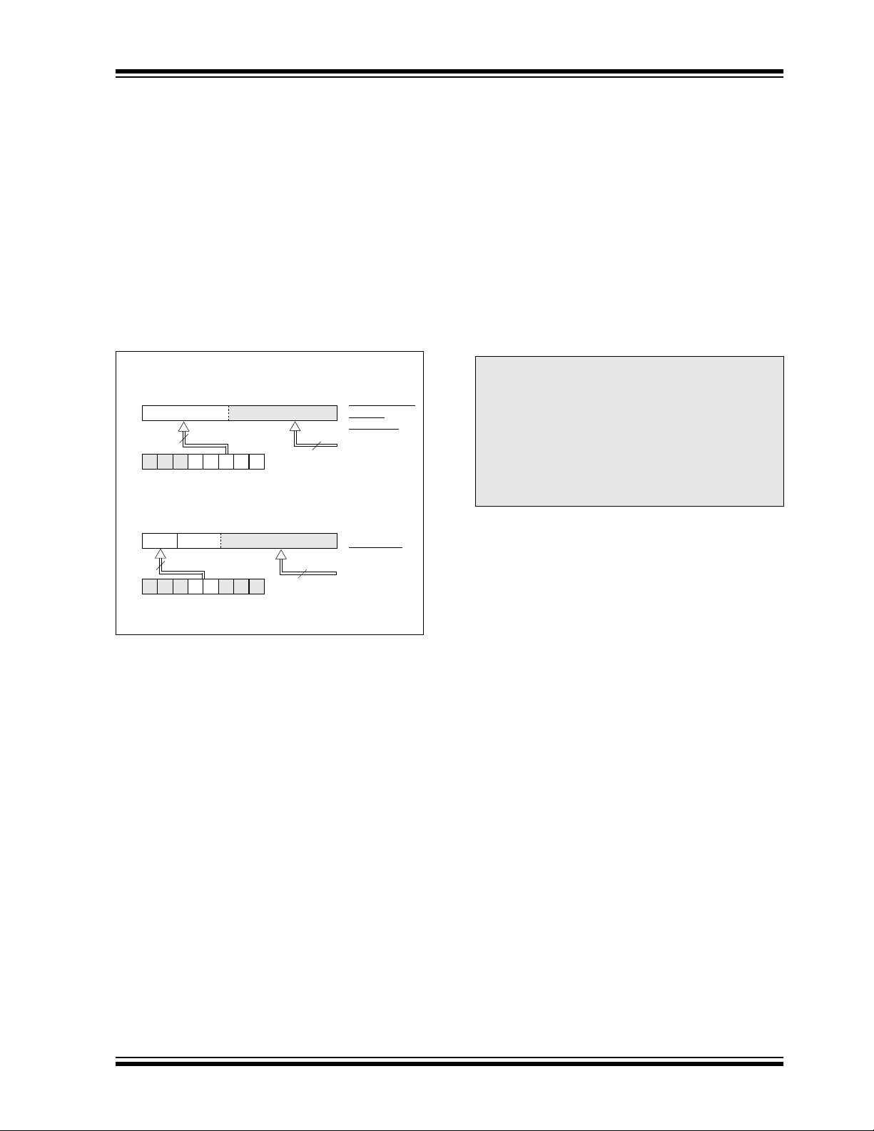
4.3 PCL and PCLATH
The program counter (PC) is 13-bits wide. The low byte
comes from the PCL register, which is a readable and
writable register. The high byte (PC<12:8>) is not
directly readable or writable and comes from PCLATH.
On any RESET, the PC is cleared. Figure 4-8 shows
the two situations for the loading of the PC. The upper
example in the figure shows how the PC is loaded on a
write to PCL (PCLATH<4:0> → PCH). The lower
example in the figure shows how the PC is loaded
during a CALL or GOTO instruction (PCLATH<4:3> →
PCH).
FIGURE 4-8: LOADING OF PC IN
DIFFERENT SITUATIONS
PCH PCL
12 8 7 0
PC
PCLATH<4:0>
5
PCLATH
PCH PCL
12 11 10 0
PC
2
87
PCLATH<4:3>
11
8
Instruction with
PCL as
Destination
ALU result
GOTO,CALL
Opcode <10:0>
4.3.2 STACK
The PIC16C62X family has an 8-level deep x 13-bit
wide hardware stack (Figure 4-2 and Figure 4-3). The
stack space is not part of either program or data space
and the stack pointer is not readable or writable. The
PC is PUSHed onto the stack when a CALL instruction
is executed or an interrupt causes a branch. The stack
is POPed in the event of a RETURN, RETLW or a
RETFIE instruction execution. PCLATH is not affected
by a PUSH or POP operation.
The stack operates as a circular buffer. This means that
after the stack has been PUSHed eight times, the ninth
push overwrites the value that was stored from the first
push. The tenth push overwrites the second push (and
so on).
Note 1: There are no STATUS bits to indicate
stack overflow or stack underflow
conditions.
2: There are no instructions/mnemonics
called PUSH or POP. These are actions
that occur from the execution of the
CALL, RETURN, RETLW and RETFIE
instructions, or the vectoring to an
interrupt address.
PCLATH
4.3.1 COMPUTED GOTO
A computed GOTO is accomplished by adding an
offset to the program counter (ADDWF PCL). When
doing a table read using a computed GOTO method,
care should be exercised if the table location crosses a
PCL memory boundary (each 256 byte block). Refer to
the application note, “Implementing a Table Read"
(AN556).
2003 Microchip Technology Inc. DS30235J-page 23
PIC16C62X
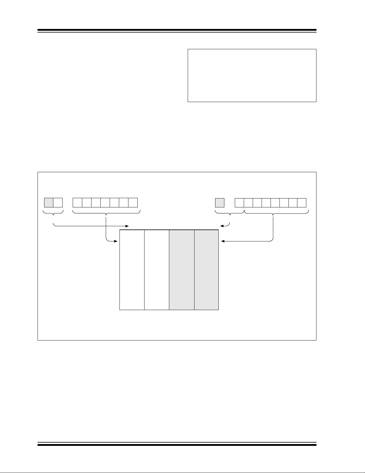
4.4 Indirect Addressing, INDF and FSR Registers
The INDF register is not a physical register. Addressing
the INDF register will cause indirect addressing.
Indirect addressing is possible by using the INDF
register. Any instruction using the INDF register
actually accesses data pointed to by the File Select
Register (FSR). Reading INDF itself indirectly will
EXAMPLE 4-1: INDIRECT ADDRESSING
movlw 0x20 ;initialize pointer
movwf FSR ;to RAM
NEXT clrf INDF ;clear INDF register
incf FSR ;inc pointer
btfss FSR,7 ;all done?
goto NEXT ;no clear next
CONTINUE:
produce 00h. Writing to the INDF register indirectly
results in a no-operation (although STATUS bits may
be affected). An effective 9-bit address is obtained by
concatenating the 8-bit FSR register and the IRP bit
(STATUS<7>), as shown in Figure 4-9. However, IRP
is not used in the PIC16C62X.
A simple program to clear RAM location 20h-7Fh using
indirect addressing is shown in Example 4-1.
FIGURE 4-9: DIRECT/INDIRECT ADDRESSING PIC16C62X
RP1 RP0
bank select location select
(1)
6
from opcode
00h
0
00 01 10 11
(1)
IRP
bank select
180h
;yes continue
Indirect AddressingDirect Addressing
7
FSR register
location select
0
Data
not used
Memory
7Fh
1FFh
Bank 0 Bank 1 Bank 2 Bank 3
For memory map detail see (Figure 4-4, Figure 4-5, Figure 4-6 and Figure 4-7).
Note 1: The RP1 and IRP bits are reserved; always maintain these bits clear.
DS30235J-page 24 2003 Microchip Technology Inc.

PIC16C62X
5.0 I/O PORTS
The PIC16C62X have two ports, PORTA and PORTB.
Some pins for these I/O ports are multiplexed with an
alternate function for the peripheral features on the
device. In general, when a peripheral is enabled, that
pin may not be used as a general purpose I/O pin.
5.1 PORTA and TRISA Registers
PORTA is a 5-bit wide latch. RA4 is a Schmitt Trigger
input and an open drain output. Port RA4 is multiplexed
with the T0CKI clock input. All other RA port pins have
Schmitt Trigger input levels and full CMOS output
drivers. All pins have data direction bits (TRIS registers), which can configure these pins as input or output.
A '1' in the TRISA register puts the corresponding output driver in a Hi-impedance mode. A '0' in the TRISA
register puts the contents of the output latch on the
selected pin(s).
Reading the PORTA register reads the status of the
pins, whereas writing to it will write to the port latch. All
write operations are read-modify-write operations. So a
write to a port implies that the port pins are first read,
then this value is modified and written to the port data
latch.
The PORTA pins are multiplexed with comparator and
voltage reference functions. The operation of these
pins are selected by control bits in the CMCON
(comparator control register) register and the VRCON
(voltage reference control register) register. When
selected as a comparator input, these pins will read
as '0's.
Note: On RESET, the TRISA register is set to all
inputs. The digital inputs are disabled and
the comparator inputs are forced to ground
to reduce excess current consumption.
TRISA controls the direction of the RA pins, even when
they are being used as comparator inputs. The user
must make sure to keep the pins configured as inputs
when using them as comparator inputs.
The RA2 pin will also function as the output for the
voltage reference. When in this mode, the V
REF pin is a
very high impedance output and must be buffered prior
to any external load. The user must configure
TRISA<2> bit as an input and use high impedance
loads.
In one of the Comparator modes defined by the
CMCON register, pins RA3 and RA4 become outputs
of the comparators. The TRISA<4:3> bits must be
cleared to enable outputs to use this function.
EXAMPLE 5-1: INITIALIZING PORTA
CLRF PORTA ;Initialize PORTA by setting
MOVLW 0X07 ;Turn comparators off and
MOVWF CMCON ;enable pins for I/O
BSF STATUS, RP0 ;Select Bank1
MOVLW 0x1F ;Value used to initialize
MOVWF TRISA ;Set RA<4:0> as inputs
;output data latches
;functions
;data direction
;TRISA<7:5> are always
;read as '0'.
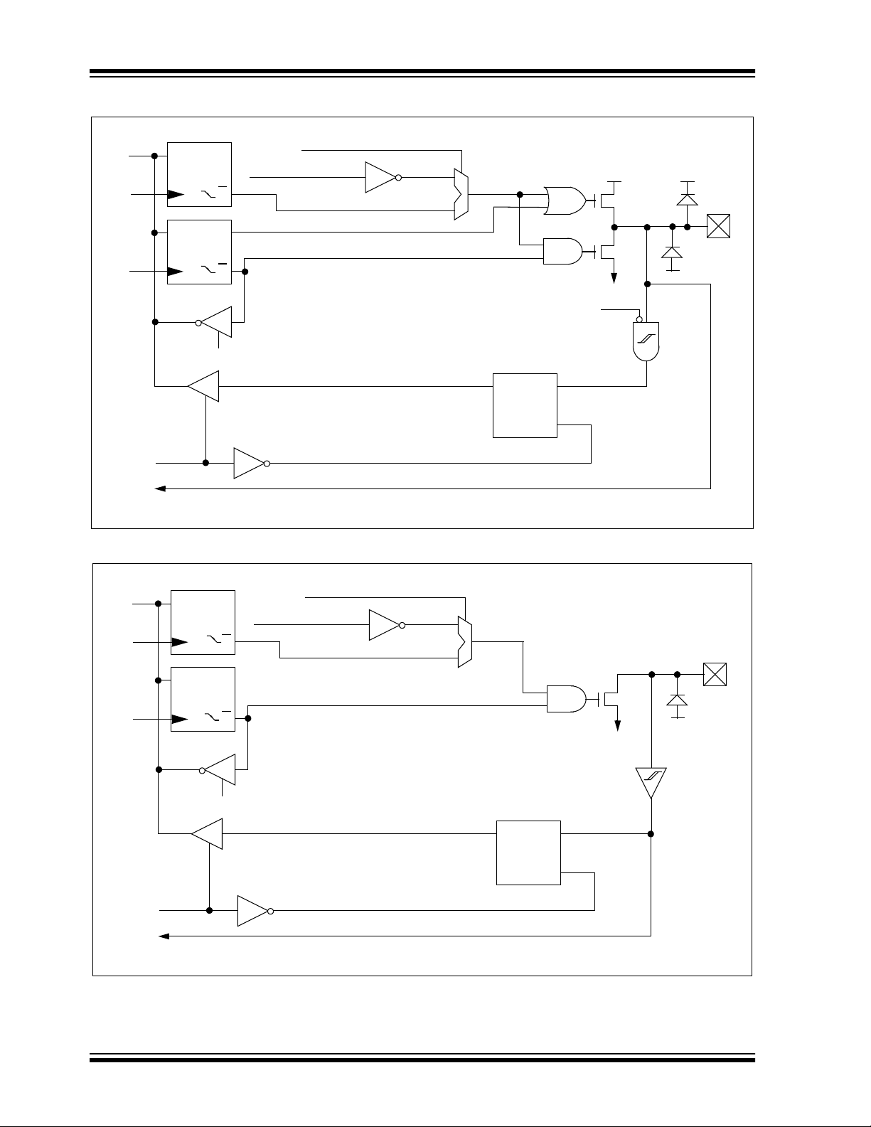
FIGURE 5-1: BLOCK DIAGRAM OF
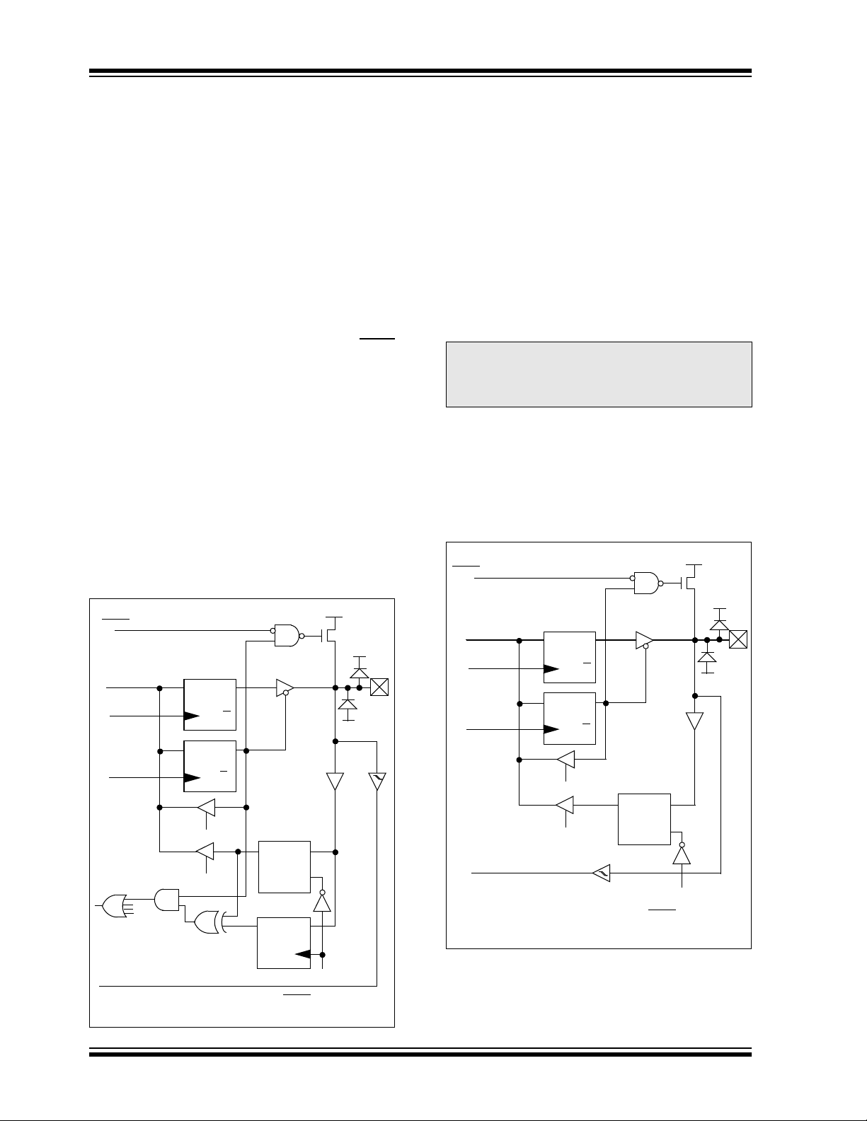
RA1:RA0 PINS
Data
Bus
WR
PORTA
WR
TRISA
Data Latch
TRIS Latch
RD PORTA
To Comparator
CK
CK
RD TRISA
QD
Q
QD
Q
VDD
V
Analog
Input Mode
Schmitt Trigger
Input Buffer
EN
VDD
P
N
VSS
SS
DQ
I/O
Pin
FIGURE 5-2: BLOCK DIAGRAM OF RA2 PIN
Data
Bus
WR
PORTA
WR
TRISA
RD PORTA
To Comparator
CK
Data Latch
CK
TRIS Latch
RD TRISA
VROE
VREF
QD
Q
QD
Q
Analog
Input Mode
Schmitt Trigger
Input Buffer
EN
VDD
P
N
V
SS
DQ
VSS
VDD
RA2
Pin
2003 Microchip Technology Inc. DS30235J-page 25
PIC16C62X
FIGURE 5-3: BLOCK DIAGRAM OF RA3 PIN
Data
Bus
WR
PORTA
WR
TRISA
CK
Data Latch
CK
TRIS Latch
RD PORTA
To Comparator
QD
Q
QD
Q
RD TRISA
Comparator Output
Comparator Mode = 110
Input Mode
DQ
EN
VDD
P
N
V
Analog
Schmitt Trigger
SS
Input Buffer
VDD
RA3 Pin
VSS
FIGURE 5-4: BLOCK DIAGRAM OF RA4 PIN
Data
Bus
WR
PORTA
WR
TRISA
CK
Data Latch
CK
TRIS Latch
RD TRISA
RD PORTA
TMR0 Clock Input
QD
Comparator Output
Q
QD
Q
Comparator Mode = 110
DQ
EN
N
V
SS
Schmitt Trigger
Input Buffer
RA4 Pin
VSS
DS30235J-page 26 2003 Microchip Technology Inc.
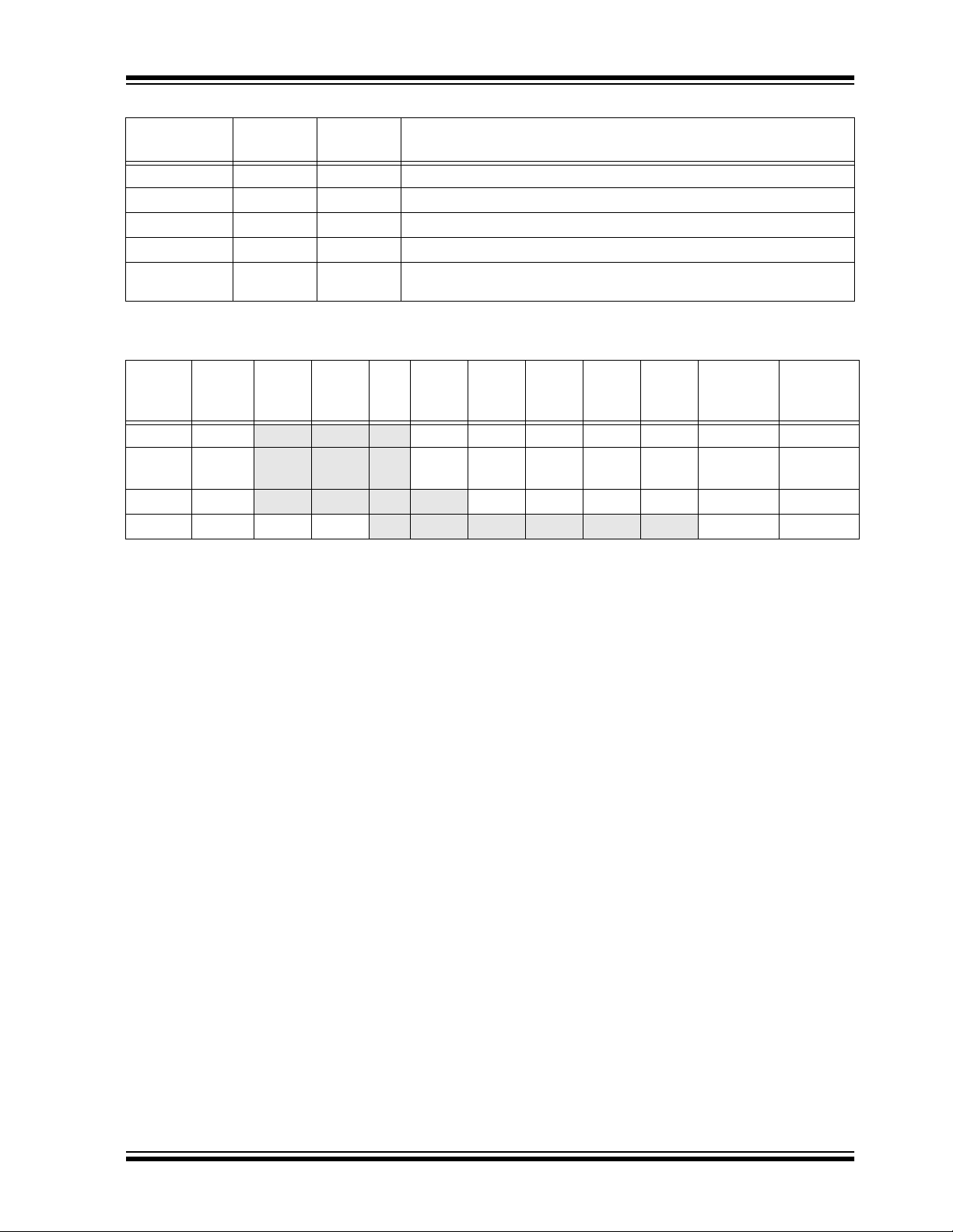
TABLE 5-1: PORTA FUNCTIONS
Name Bit #
RA0/AN0
RA1/AN1
RA2/AN2/V
RA3/AN3
RA4/T0CKI
Legend: ST = Schmitt Trigger input
REF
bit0 ST
bit1 ST
bit2 ST
bit3 ST
bit4 ST
Buffer
Type
Function
Input/output or comparator input
Input/output or comparator input
Input/output or comparator input or V
Input/output or comparator input/output
Input/output or external clock input for TMR0 or comparator output.
Output is open drain type.
REF output
TABLE 5-2: SUMMARY OF REGISTERS ASSOCIATED WITH PORTA
Address Name Bit 7 Bit 6 Bit 5 Bit 4 Bit 3 Bit 2 Bit 1 Bit 0
05h PORTA
85h TRISA
1Fh CMCON
9Fh VRCON
Legend: — = Unimplemented locations, read as ‘0’, u = unchanged, x = unknown
Note: Shaded bits are not used by PORTA.
— — — RA4 RA3 RA2 RA1 RA0
— — —
C2OUT C1OUT — — CIS CM2 CM1 CM0
VREN VROE
TRISA4TRISA3TRISA2TRISA1TRISA
VRR — VR3 VR2 VR1 VR0
PIC16C62X
Value on
POR
---x 0000 ---u 0000
---1 1111 ---1 1111
0
00-- 0000 00-- 0000
000- 0000 000- 0000
Value on
All Other
RESETS
2003 Microchip Technology Inc. DS30235J-page 27
PIC16C62X
5.2 PORTB and TRISB Registers
PORTB is an 8-bit wide, bi-directional port. The
corresponding data direction register is TRISB. A '1' in
the TRISB register puts the corresponding output driver
in a High Impedance mode. A '0' in the TRISB register
puts the contents of the output latch on the selected
pin(s).
Reading PORTB register reads the status of the pins,
whereas writing to it will write to the port latch. All write
operations are read-modify-write operations. So a write
to a port implies that the port pins are first read, then
this value is modified and written to the port data latch.
Each of the PORTB pins has a weak internal pull-up
(≈200 µA typical). A single control bit can turn on all the
pull-ups. This is done by clearing the RBPU
(OPTION<7>) bit. The weak pull-up is automatically
turned off when the port pin is configured as an output.
The pull-ups are disabled on Power-on Reset.
Four of PORTB’s pins, RB<7:4>, have an interrupt on
change feature. Only pins configured as inputs can
cause this interrupt to occur (e.g., any RB<7:4> pin
configured as an output is excluded from the interrupt
on change comparison). The input pins (of RB<7:4>)
are compared with the old value latched on the last
read of PORTB. The “mismatch” outputs of RB<7:4>
are OR’ed together to generate the RBIF interrupt (flag
latched in INTCON<0>).
FIGURE 5-5: BLOCK DIAGRAM OF
RB<7:4> PINS
DD
TTL
Input
Buffer
V
P
weak
pull-up
VCC
VSS
ST
Buffer
I/O
pin
(1)
RBPU
Data Bus
WR PORTB
WR TRISB
Data Latch
QD
Q
CK
TRIS Latch
QD
Q
CK
This interrupt can wake the device from SLEEP. The
user, in the interrupt service routine, can clear the
interrupt in the following manner:
a) Any read or write of PORTB. This will end the
mismatch condition.
b) Clear flag bit RBIF.
A mismatch condition will continue to set flag bit RBIF.
Reading PORTB will end the mismatch condition and
allow flag bit RBIF to be cleared.
This interrupt on mismatch feature, together with
software configurable pull-ups on these four pins allow
easy interface to a key pad and make it possible for
wake-up on key-depression. (See AN552, “Implementing Wake-Up on Key Strokes.)
Note: If a change on the I/O pin should occur
when the read operation is being executed
(start of the Q2 cycle), then the RBIF interrupt flag may not get set.
The interrupt-on-change feature is recommended for
wake-up on key depression operation and operations
where PORTB is only used for the interrupt on change
feature. Polling of PORTB is not recommended while
using the interrupt-on-change feature.
FIGURE 5-6: BLOCK DIAGRAM OF
RB<3:0> PINS
DD
TTL
Input
Buffer
V
P
weak
pull-up
VCC
VSS
I/O
pin
(1)
RBPU
Data Bus
WR PORTB
WR TRISB
Data Latch
CK
D
CK
RD TRISB
QD
Q
Q
Q
QD
RD TRISB
Set RBIF
From other
RB<7:4> pins
RB<7:6> in Serial Programming mode
Note 1: TRISB = 1 enables weak pull-up if RBPU
(OPTION<7>).
RD PORTB
Latch
QD
EN
QD
EN
RD PORTB
= '0'
RD PORTB
RB0/INT
ST
Buffer
Note 1: TRISB = 1 enables weak pull-up if RBPU
(OPTION<7>).
EN
RD PORTB
= '0'
DS30235J-page 28 2003 Microchip Technology Inc.
PIC16C62X
TABLE 5-3: PORTB FUNCTIONS
Name Bit # Buffer Type Function
RB0/INT bit0 TTL/ST
RB1 bit1 TTL Input/output pin. Internal software programmable weak pull-up.
RB2 bit2 TTL Input/output pin. Internal software programmable weak pull-up.
RB3 bit3 TTL Input/output pin. Internal software programmable weak pull-up.
RB4 bit4 TTL Input/output pin (with interrupt-on-change). Internal software programmable
RB5 bit5 TTL Input/output pin (with interrupt-on-change). Internal software programmable
RB6 bit6 TTL/ST
RB7 bit7 TTL/ST
Legend: ST = Schmitt Trigger, TTL = TTL input
Note 1: This buffer is a Schmitt Trigger input when configured as the external interrupt.
2: This buffer is a Schmitt Trigger input when used in Serial Programming mode.
TABLE 5-4: SUMMARY OF REGISTERS ASSOCIATED WITH PORTB
Address Name Bit 7 Bit 6 Bit 5 Bit 4 Bit 3 Bit 2 Bit 1 Bit 0
06h PORTB
86h TRISB
81h OPTION
Legend: u = unchanged, x = unknown
Note 1: Shaded bits are not used by PORTB.
RB7 RB6 RB5RB4RB3RB2RB1RB0
TRISB7 TRISB6 TRISB5 TRISB4 TRISB3 TRISB2 TRISB1 TRISB0
RBPU
(1)
Input/output or external interrupt input. Internal software programmable
weak pull-up.
weak pull-up.
weak pull-up.
(2)
Input/output pin (with interrupt-on-change). Internal software programmable
weak pull-up. Serial programming clock pin.
(2)
Input/output pin (with interrupt-on-change). Internal software programmable
weak pull-up. Serial programming data pin.
INTEDG T0CS T0SE PSA PS2 PS1 PS0
Value on
POR
xxxx xxxx uuuu uuuu
1111 1111 1111 1111
1111 1111 1111 1111
Value on
All Other
RESETS
2003 Microchip Technology Inc. DS30235J-page 29

PIC16C62X
5.3 I/O Programming Considerations
5.3.1 BI-DIRECTIONAL I/O PORTS
Any instruction which writes, operates internally as a
read followed by a write operation. The BCF and BSF
instructions, for example, read the register into the
CPU, execute the bit operation and write the result
back to the register. Caution must be used when these
instructions are applied to a port with both inputs and
outputs defined. For example, a BSF operation on bit5
of PORTB will cause all eight bits of PORTB to be read
into the CPU. Then the BSF operation takes place on
bit5 and PORTB is written to the output latches. If
another bit of PORTB is used as a bi-directional I/O pin
(e.g., bit0) and it is defined as an input at this time, the
input signal present on the pin itself would be read into
the CPU and re-written to the data latch of this
particular pin, overwriting the previous content. As long
as the pin stays in the Input mode, no problem occurs.
However, if bit0 is switched into Output mode later on,
the content of the data latch may now be unknown.
Reading the port register reads the values of the port
pins. Writing to the port register writes the value to the
port latch. When using read-modify-write instructions
(ex. BCF, BSF, etc.) on a port, the value of the port pins
is read, the desired operation is done to this value, and
this value is then written to the port latch.
Example 5-2 shows the effect of two sequential readmodify-write instructions (ex., BCF, BSF, etc.) on an
I/O port.
A pin actively outputting a Low or High should not be
driven from external devices at the same time in order
to change the level on this pin (“wired-or”, “wired-and”).
The resulting high output currents may damage
the chip.
EXAMPLE 5-2: READ-MODIFY-WRITE
INSTRUCTIONS ON AN I/O
PORT
;;Initial PORT settings: PORTB<7:4> Inputs
; PORTB<3:0> Outputs
;;PORTB<7:6> have external pull-up and are not
connected to other circuitry
;
; PORT latch PORT pins
; ---------- ---------
BCF PORTB, 7 ; 01pp pppp 11pp pppp
BCF PORTB, 6 ; 10pp pppp 11pp pppp
BSF STATUS,RP0 ;
BCF TRISB, 7 ; 10pp pppp 11pp pppp
BCF TRISB, 6 ; 10pp pppp 10pp pppp
;
; Note that the user may have expected the pin
; values to be 00pp pppp. The 2nd BCF caused
; RB7 to be latched as the pin value (High).
-
5.3.2 SUCCESSIVE OPERATIONS ON I/O
PORTS
The actual write to an I/O port happens at the end of an
instruction cycle, whereas for reading, the data must be
valid at the beginning of the instruction cycle (Figure 5-7).
Therefore, care must be exercised if a write followed by a
read operation is carried out on the same I/O port. The
sequence of instructions should be such to allow the pin
voltage to stabilize (load dependent) before the next
instruction which causes that file to be read into the CPU
is executed. Otherwise, the previous state of that pin may
be read into the CPU rather than the new state. When in
doubt, it is better to separate these instructions with a NOP
or another instruction not accessing this I/O port.
FIGURE 5-7: SUCCESSIVE I/O OPERATION
Q1 Q2 Q3 Q4 Q1 Q2 Q3 Q4 Q1 Q2 Q3 Q4 Q1 Q2 Q3 Q4
Q1 Q2 Q3 Q4 Q1 Q2 Q3 Q4 Q1 Q2 Q3 Q4 Q1 Q2 Q3 Q4
PC
PC
Instruction
Instruction
fetched
fetched
RB<7:0>
RB <7:0>
PC
PC
MOVWF, PORTB
MOVWF PORTB
Write to
Write to
PORTB
PORTB
PC+1
PC + 1 PC + 2 PC + 3
MOVF, PORTB, W
Read PORTB
Read PORTB
TPD
T
PD
Execute
Execute
MOVWF
MOVWF
PORTB
PORTB
PC+2 PC+3
NOP
Port pin
Port pin
sampled here
sampled here
Execute
Execute
MOVF
MOVF
PORTB, W
PORTB, W
Execute
Execute
NOPNOPMOVF PORTB, W
NOP
NOP
NOP
DS30235J-page 30 2003 Microchip Technology Inc.
Note:
This example shows write to PORTB
followed by a read from PORTB.
Note that:
data setup time = (0.25 T
CY = instruction cycle and
where T
TPD = propagation delay of Q1
cycle to output valid.
Therefore, at higher clock frequencies, a write followed by a read may
be problematic.
CY - TPD)

PIC16C62X
6.0 TIMER0 MODULE
The Timer0 module timer/counter has the following
features:
• 8-bit timer/counter
• Readable and writable
• 8-bit software programmable prescaler
• Internal or external clock select
• Interrupt on overflow from FFh to 00h
• Edge select for external clock
Figure 6-1 is a simplified block diagram of the Timer0
module.
Timer mode is selected by clearing the T0CS bit
(OPTION<5>). In Timer mode, the TMR0 will increment
every instruction cycle (without prescaler). If Timer0 is
written, the increment is inhibited for the following two
cycles (Figure 6-2 and Figure 6-3). The user can work
around this by writing an adjusted value to TMR0.
Counter mode is selected by setting the T0CS bit. In
this mode, Timer0 will increment either on every rising
or falling edge of pin RA4/T0CKI. The incrementing
edge is determined by the source edge (T0SE) control
bit (OPTION<4>). Clearing the T0SE bit selects the
rising edge. Restrictions on the external clock input are
discussed in detail in Section 6.2.
The prescaler is shared between the Timer0 module
and the Watchdog Timer. The prescaler assignment is
controlled in software by the control bit PSA
(OPTION<3>). Clearing the PSA bit will assign the
prescaler to Timer0. The prescaler is not readable or
writable. When the prescaler is assigned to the Timer0
module, prescale value of 1:2, 1:4, ..., 1:256 are
selectable. Section 6.3 details the operation of the
prescaler.
6.1 TIMER0 Interrupt
Timer0 interrupt is generated when the TMR0 register
timer/counter overflows from FFh to 00h. This overflow
sets the T0IF bit. The interrupt can be masked by
clearing the T0IE bit (INTCON<5>). The T0IF bit
(INTCON<2>) must be cleared in software by the
Timer0 module interrupt service routine before reenabling this interrupt. The Timer0 interrupt cannot
wake the processor from SLEEP, since the timer is shut
off during SLEEP. See Figure 6-4 for Timer0 interrupt
timing.
FIGURE 6-1: TIMER0 BLOCK DIAGRAM
RA4/T0CKI
pin
FOSC/4
T0SE
0
1
T0CS
Programmable
Prescaler
PS<2:0>
1
0
PSA
PSout
Sync with
Internal
clocks
(2 Tcy delay)
PSout
Note 1: Bits T0SE, T0CS, PS2, PS1, PS0 and PSA are located in the OPTION register.
2: The prescaler is shared with Watchdog Timer (Figure 6-6).
Data Bus
TMR0
FIGURE 6-2: TIMER0 (TMR0) TIMING: INTERNAL CLOCK/NO PRESCALER
PC
(Program
Counter)
Instruction
Fetch
TMR0
Instruction
Executed
Q1 Q2 Q3 Q4
PC-1
T0
Q1 Q2 Q3 Q4 Q1 Q2 Q3 Q4 Q1 Q2 Q3 Q4 Q1 Q2 Q3 Q4 Q1 Q2 Q3 Q4 Q1 Q2 Q3 Q4 Q1 Q2 Q3 Q4
PC PC+1 PC+2 PC+3 PC+4 PC+5 PC+6
MOVWF TMR0
T0+1 T0+2
MOVF TMR0,WMOVF TMR0,WMOVF TMR0,WMOVF TMR0,WMOVF TMR0,W
Write TMR0
executed
Read TMR0
reads NT0
NT0
Read TMR0
reads NT0
Read TMR0
reads NT0
NT0+1 NT0+2
Read TMR0
reads NT0 + 1
8
Set Flag bit T0IF
on Overflow
Read TMR0
reads NT0 + 2
T0
2003 Microchip Technology Inc. DS30235J-page 31

PIC16C62X
FIGURE 6-3: TIMER0 TIMING: INTERNAL CLOCK/PRESCALE 1:2
PC
(Program
Counter)
Instruction
Fetch
TMR0
Instruction
Execute
Q1 Q2 Q3 Q4
PC-1
T0 NT0+1
Q1 Q2 Q3 Q4 Q1 Q2 Q3 Q4 Q1 Q2 Q3 Q4 Q1 Q2 Q3 Q4 Q1 Q2 Q3 Q4 Q1 Q2 Q3 Q4 Q1 Q2 Q3 Q4
PC PC+1 PC+2 PC+3 PC+4 PC+5 PC+6
MOVWF TMR0
T0+1
MOVF TMR0,WMOVF TMR0,WMOVF TMR0,WMOVF TMR0,WMOVF TMR0,W
Write TMR0
executed
Read TMR0
reads NT0
FIGURE 6-4: TIMER0 INTERRUPT TIMING
Q2Q1 Q3 Q4Q2Q1 Q3 Q4 Q2Q1 Q3 Q4 Q2Q1 Q3 Q4 Q2Q1 Q3 Q4
OSC1
CLKOUT(3)
TMR0 timer
T0IF bit
(INTCON<2>)
GIE bit
(INTCON<7>)
INSTRUCTION FLOW
PC
Instruction
fetched
FEh
1
PC
Inst (PC)
FFh 00h 01h 02h
1
PC +1 PC +1 0004h 0005h
Inst (PC+1)
NT0
Read TMR0
reads NT0
Interrupt Latency Time(2)
Read TMR0
reads NT0
Read TMR0
reads NT0
Inst (0004h) Inst (0005h)
Read TMR0
reads NT0 + 1
Instruction
executed
Inst (PC-1)
Note 1: T0IF interrupt flag is sampled here (every Q1).
2: Interrupt latency = 3T
3: CLKOUT is available only in RC Oscillator mode.
Inst (PC)
CY, where TCY = instruction cycle time.
Inst (0004h)Dummy cycle Dummy cycle
DS30235J-page 32 2003 Microchip Technology Inc.

PIC16C62X
6.2 Using Timer0 with External Clock
When an external clock input is used for Timer0, it must
meet certain requirements. The external clock
requirement is due to internal phase clock (T
synchronization. Also, there is a delay in the actual
incrementing of Timer0 after synchronization.
6.2.1 EXTERNAL CLOCK
SYNCHRONIZATION
When no prescaler is used, the external clock input is
the same as the prescaler output. The synchronization
of T0CKI with the internal phase clocks is
accomplished by sampling the prescaler output on the
Q2 and Q4 cycles of the internal phase clocks
(Figure 6-5). Therefore, it is necessary for T0CKI to be
high for at least 2T
and low for at least 2T
20 ns). Refer to the electrical specification of the
OSC (and a small RC delay of 20 ns)
OSC (and a small RC delay of
OSC)
When a prescaler is used, the external clock input is
divided by the asynchronous ripple-counter type
prescaler, so that the prescaler output is symmetrical.
For the external clock to meet the sampling
requirement, the ripple-counter must be taken into
account. Therefore, it is necessary for T0CKI to have a
period of at least 4T
divided by the prescaler value. The only requirement
on T0CKI high and low time is that they do not violate
the minimum pulse width requirement of 10 ns. Refer to
parameters 40, 41 and 42 in the electrical specification
of the desired device.
6.2.2 TIMER0 INCREMENT DELAY
Since the prescaler output is synchronized with the
internal clocks, there is a small delay from the time the
external clock edge occurs to the time the TMR0 is
actually incremented. Figure 6-5 shows the delay from
the external clock edge to the timer incrementing.
desired device.
FIGURE 6-5: TIMER0 TIMING WITH EXTERNAL CLOCK
Q1 Q2 Q3 Q4 Q1 Q2 Q3 Q4 Q1 Q2 Q3 Q4 Q1 Q2 Q3 Q4
External Clock Input or
Prescaler output
External Clock/Prescaler
Output after sampling
Increment Timer0 (Q4)
(2)
(1)
(3)
OSC (and a small RC delay of 40 ns)
Small pulse
misses sampling
Timer0
Note 1: Delay from clock input change to Timer0 increment is 3Tosc to 7Tosc. (Duration of Q = Tosc).
Therefore, the error in measuring the interval between two edges on Timer0 input = ±4Tosc max.
2: External clock if no prescaler selected, Prescaler output otherwise.
3: The arrows indicate the points in time where sampling occurs.
T0 T0 + 1 T0 + 2
2003 Microchip Technology Inc. DS30235J-page 33

PIC16C62X
6.3 Prescaler
An 8-bit counter is available as a prescaler for the
Timer0 module, or as a postscaler for the Watchdog
Timer, respectively (Figure 6-6). For simplicity, this
counter is being referred to as “prescaler” throughout
this data sheet. Note that there is only one prescaler
available which is mutually exclusive between the
Timer0 module and the Watchdog Timer. Thus, a
The PSA and PS<2:0> bits (OPTION<3:0>) determine
the prescaler assignment and prescale ratio.
When assigned to the Timer0 module, all instructions
writing to the TMR0 register (e.g., CLRF 1,
MOVWF 1, BSF 1,x....etc.) will clear the prescaler.
When assigned to WDT, a CLRWDT instruction will clear
the prescaler along with the Watchdog Timer. The
prescaler is not readable or writable.
prescaler assignment for the Timer0 module means
that there is no prescaler for the Watchdog Timer and
vice-versa.
FIGURE 6-6: BLOCK DIAGRAM OF THE TIMER0/WDT PRESCALER
CLKOUT (= Fosc/4)
T0CKI
pin
T0SE
0
1
T0CS
M
U
X
1
M
U
0
X
PSA
SYNC
2
Cycles
Data Bus
8
TMR0 reg
Set flag bit T0IF
on Overflow
0
M
U
1
Watchdog
Timer
WDT Enable bit
Note: T0SE, T0CS, PSA, PS<2:0> are bits in the OPTION register.
X
PSA
8-bit Prescaler
8
8-to-1MUX
0
M U X
WDT
Time-out
1
PS<2:0>
PSA
DS30235J-page 34 2003 Microchip Technology Inc.

PIC16C62X
6.3.1 SWITCHING PRESCALER
ASSIGNMENT
The prescaler assignment is fully under software
control (i.e., it can be changed “on-the-fly” during
program execution). To avoid an unintended device
RESET, the following instruction sequence
(Example 6-1) must be executed when changing the
prescaler assignment from Timer0 to WDT.)
EXAMPLE 6-1: CHANGING PRESCALER
(TIMER0→WDT)
1.BCF STATUS, RP0 ;Skip if already in
2.CLRWDT ;Clear WDT
3.CLRF TMR0 ;Clear TMR0 & Prescaler
4.BSF STATUS, RP0 ;Bank 1
5.MOVLW '00101111’b; ;These 3 lines (5, 6, 7)
6.MOVWF OPTION ;are required only if
7.CLRWDT ;000 or 001
8.MOVLW '00101xxx’b ;Set Postscaler to
9.MOVWF OPTION ;desired WDT rate
10.BCF STATUS, RP0 ;Return to Bank 0
;Bank 0
;desired PS<2:0> are
To change prescaler from the WDT to the TMR0
module, use the sequence shown in Example 6-2. This
precaution must be taken even if the WDT is disabled.
EXAMPLE 6-2: CHANGING PRESCALER
(WDT→TIMER0)
CLRWDT ;Clear WDT and
BSF STATUS, RP0
MOVLW b'xxxx0xxx' ;Select TMR0, new
MOVWF OPTION_REG
BCF STATUS, RP0
;prescaler
;prescale value and
;clock source
TABLE 6-1: REGISTERS ASSOCIATED WITH TIMER0
Address Name Bit 7 Bit 6 Bit 5 Bit 4 Bit 3 Bit 2 Bit 1 Bit 0
01h TMR0 Timer0 module register xxxx xxxx uuuu uuuu
0Bh/8Bh INTCON
81h OPTION
85h TRISA
GIE
RBPU INTEDG T0CS T0SE PSA PS2 PS1 PS0
— — — TRISA4 TRISA3 TRISA2 TRISA1 TRISA0
PEIE T0IE INTE RBIE T0IF INTF RBIF
Value on
POR
0000 000x 0000 000u
1111 1111 1111 1111
---1 1111 ---1 1111
Legend: — = Unimplemented locations, read as ‘0’, u = unchanged, x = unknown
Note: Shaded bits are not used by TMR0 module.
Value on
All Other
RESETS
2003 Microchip Technology Inc. DS30235J-page 35

PIC16C62X
NOTES:
DS30235J-page 36 2003 Microchip Technology Inc.

PIC16C62X
7.0 COMPARATOR MODULE
The CMCON register, shown in Register 7-1, controls
the comparator input and output multiplexers. A block
The comparator module contains two analog
diagram of the comparator is shown in Figure 7-1.
comparators. The inputs to the comparators are
multiplexed with the RA0 through RA3 pins. The OnChip Voltage Reference (Section 8.0) can also be an
input to the comparators.
REGISTER 7-1: CMCON REGISTER (ADDRESS 1Fh)
R-0 R-0 U-0 U-0 R/W-0 R/W-0 R/W-0 R/W-0
C2OUT C1OUT
bit 7 bit 0
bit 7 C2OUT: Comparator 2 output
1 = C2 V
0 = C2 V
IN+ > C2 VININ+ < C2 VIN-
bit 6 C1OUT: Comparator 1 output
1 = C1 V
0 = C1 V
IN+ > C1 VININ+ < C1 VIN-
bit 5-4 Unimplemented: Read as ‘0’
bit 3 CIS: Comparator Input Switch
When CM<2:0>: = 001:
1 = C1 V
0 = C1 V
IN- connects to RA3
IN- connects to RA0
When CM<2:0> = 010:
1 = C1 V
C2 V
0 = C1 V
C2 V
IN- connects to RA3
IN- connects to RA2
IN- connects to RA0
IN- connects to RA1
bit 2-0 CM<2:0>: Comparator mode.
— — CIS CM2 CM1 CM0
Legend:
R = Readable bit W = Writable bit U = Unimplemented bit, read as ‘0’
- n = Value at POR ’1’ = Bit is set ’0’ = Bit is cleared x = Bit is unknown
2003 Microchip Technology Inc. DS30235J-page 37

PIC16C62X
7.1 Comparator Configuration
There are eight modes of operation for the
comparators. The CMCON register is used to select
the mode. Figure 7-1 shows the eight possible modes.
mode is changed, the comparator output level may not
be valid for the specified mode change delay shown
in Table 12-2.
Note: Comparator interrupts should be disabled
The TRISA register controls the data direction of the
comparator pins for each mode. If the Comparator
FIGURE 7-1: COMPARATOR I/O OPERATING MODES
RA0/AN0
RA3/AN3
RA1/AN1
RA2/AN2
A
A
A
A
Comparators Reset
RA0/AN0
RA3/AN3
RA1/AN1
RA2/AN2
A
A
A
A
Two Independent Comparators
VIN-
V
VIN-
V
VIN-
IN+
V
VIN-
V
IN+
IN+
IN+
C1
+
C2
+
Off
(Read as '0')
Off
(Read as '0')
RA0/AN0
RA3/AN3
RA1/AN1
RA2/AN2
CM<2:0> = 000
Comparators Off
C1
+
C1OUT
-
C2
+
C2OUT
RA0/AN0
RA3/AN3
RA1/AN1
RA2/AN2
CM<2:0> = 100
Four Inputs Multiplexed to
Two Comparators
during a Comparator mode change otherwise a false interrupt may occur.
D
D
D
D
VIN-
IN+
V
VIN-
IN+
V
C1
+
C2
+
Off
(Read as '0')
Off
(Read as '0')
CM<2:0> = 111
A
CIS=0
VIN-
A
CIS=1
A
CIS=0
A
CIS=1
IN+
V
VIN-
V
IN+
C1
+
C1OUT
C2
+
C2OUT
From VREF Module
CM<2:0> = 010
RA0/AN0
RA3/AN3
RA1/AN1
RA2/AN2
A
D
A
A
VIN-
IN+
V
VIN-
V
IN+
C1
+
C1OUT
-
C2
+
C2OUT
CM<2:0> = 011
Two Common Reference Comparators
RA0/AN0
RA3/AN3
RA1/AN1
RA2/AN2
D
D
A
A
VIN-
IN+
V
VIN-
IN+
V
C1
+
(Read as '0')
C2
+
CM<2:0> = 101
One Independent Comparator
A = Analog Input, Port Reads Zeros Always
D = Digital Input
CIS = CMCON<3>, Comparator Input Switch
Off
C2OUT
RA0/AN0
RA3/AN3
RA1/AN1
RA2/AN2
A
D
A
A
VIN-
V
IN+
VIN-
IN+
V
C1
+
C1OUT
C2
+
C2OUT
RA4 Open Drain
CM<2:0> = 110
Two Common Reference Comparators with Outputs
A
RA0/AN0
RA3/AN3
RA1/AN1
RA2/AN2
CIS=0
VIN-
-
CIS=1
A
A
A
V
VIN-
V
IN+
IN+
C1
+
C2
+
C1OUT
C2OUT
CM<2:0> = 001
Three Inputs Multiplexed to
Two Comparators
DS30235J-page 38 2003 Microchip Technology Inc.

PIC16C62X
The code example in Example 7-1 depicts the steps
required to configure the comparator module. RA3 and
RA4 are configured as digital output. RA0 and RA1 are
configured as the V- inputs and RA2 as the V+ input to
both comparators.
EXAMPLE 7-1: INITIALIZING
COMPARATOR MODULE
MOVLW 0x03 ;Init comparator mode
MOVWF CMCON ;CM<2:0> = 011
CLRF PORTA ;Init PORTA
BSF STATUS,RP0 ;Select Bank1
MOVLW 0x07 ;Initialize data direction
MOVWF TRISA ;Set RA<2:0> as inputs
;RA<4:3> as outputs
;TRISA<7:5> always read ‘0’
BCF STATUS,RP0 ;Select Bank 0
CALL DELAY 10 ;10µs delay
MOVF CMCON,F ;Read CMCON to end change condition
BCF PIR1,CMIF ;Clear pending interrupts
BSF STATUS,RP0 ;Select Bank 1
BSF PIE1,CMIE ;Enable comparator interrupts
BCF STATUS,RP0 ;Select Bank 0
BSF INTCON,PEIE ;Enable peripheral interrupts
BSF INTCON,GIE ;Global interrupt enable
7.3 Comparator Reference
An external or internal reference signal may be used
depending on the comparator Operating mode. The
analog signal that is present at V
signal at V
IN+, and the digital output of the comparator
is adjusted accordingly (Figure 7-2).
FIGURE 7-2: SINGLE COMPARATOR
V
IN–
VIN-
VIN+
V
IN+
Output
utput
VIN+
V
IN-
+
–
IN- is compared to the
Output
7.2 Comparator Operation
A single comparator is shown in Figure 7-2 along with
the relationship between the analog input levels and
the digital output. When the analog input at V
than the analog input V
IN-, the output of the comparator
is a digital low level. When the analog input at V
greater than the analog input V
IN-, the output of the
comparator is a digital high level. The shaded areas of
the output of the comparator in Figure 7-2 represent
the uncertainty due to input offsets and response time.
IN+ is less
IN+ is
7.3.1 EXTERNAL REFERENCE SIGNAL
When external voltage references are used, the
comparator module can be configured to have the
comparators operate from the same or different
reference sources. However, threshold detector
applications may require the same reference. The
reference signal must be between V
SS and VDD, and
can be applied to either pin of the comparator(s).
7.3.2 INTERNAL REFERENCE SIGNAL
The comparator module also allows the selection of an
internally generated voltage reference for the
comparators. Section 10, Instruction Sets, contains a
detailed description of the Voltage Reference Module
that provides this signal. The internal reference signal
is used when the comparators are in mode
CM<2:0>=010 (Figure 7-1). In this mode, the internal
voltage reference is applied to the V
comparators.
IN+ pin of both
2003 Microchip Technology Inc. DS30235J-page 39
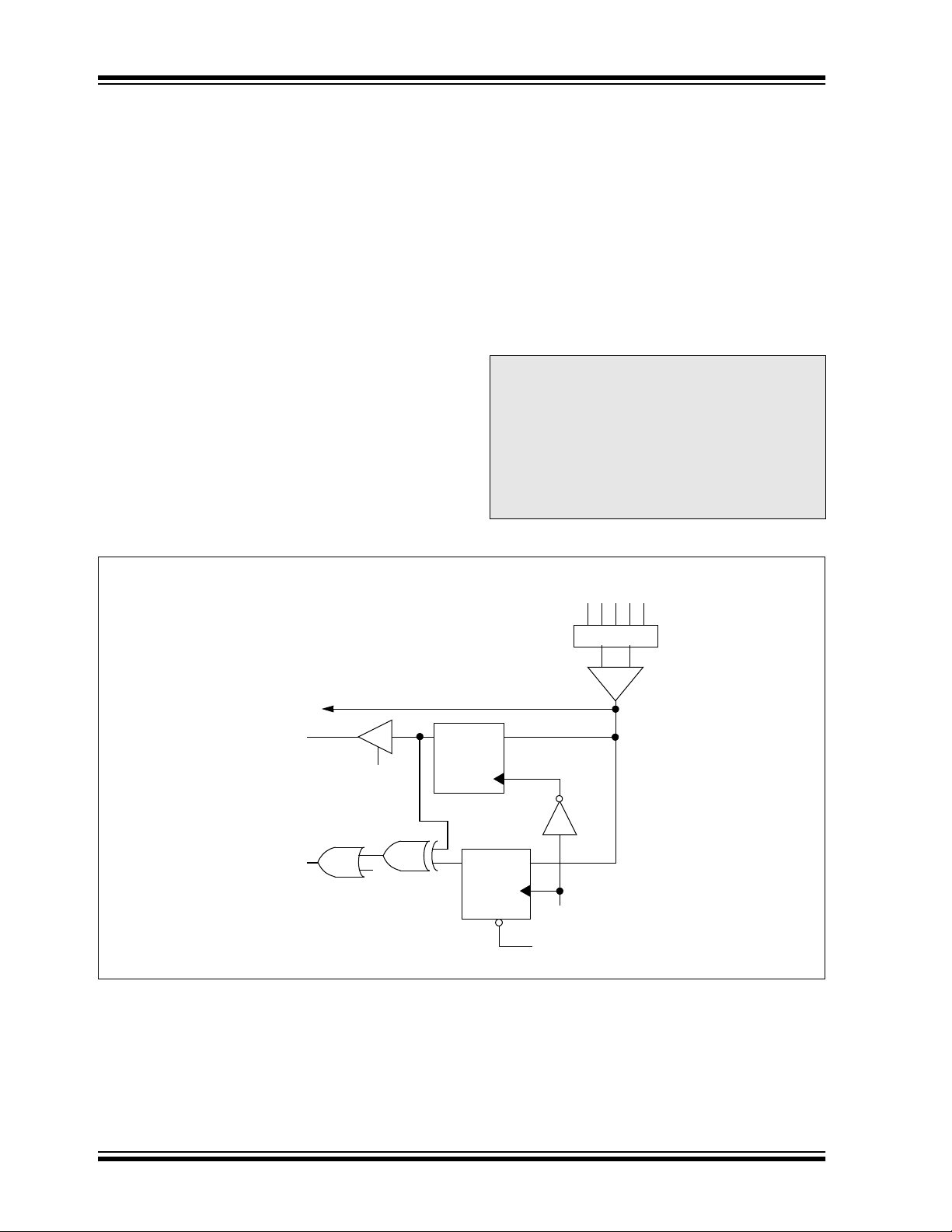
PIC16C62X
7.4 Comparator Response Time
Response time is the minimum time, after selecting a
new reference voltage or input source, before the
comparator output has a valid level. If the internal
reference is changed, the maximum delay of the
internal voltage reference must be considered when
using the comparator outputs. Otherwise the maximum
delay of the comparators should be used (Table 12-2).
7.5 Comparator Outputs
The comparator outputs are read through the CMCON
register. These bits are read only. The comparator
outputs may also be directly output to the RA3 and RA4
I/O pins. When the CM<2:0> = 110, multiplexors in the
output path of the RA3 and RA4 pins will switch and the
output of each pin will be the unsynchronized output of
the comparator. The uncertainty of each of the
comparators is related to the input offset voltage and the
response time given in the specifications. Figure 7-3
shows the comparator output block diagram.
The TRISA bits will still function as an output enable/
disable for the RA3 and RA4 pins while in this mode.
Note 1: When reading the PORT register, all pins
FIGURE 7-3: COMPARATOR OUTPUT BLOCK DIAGRAM
configured as analog inputs will read as a
‘0’. Pins configured as digital inputs will
convert an analog input according to the
Schmitt Trigger input specification.
2: Analog levels on any pin that is defined as
a digital input may cause the input buffer
to consume more current than is
specified.
To RA3 or
RA4 Pin
Bus
Data
Set
CMIF
Bit
RD CMCON
ROM
F
OTHER
COMPARATOR
EN
DQ
CL
PORT PINS
MULTIPLEX
-+
DQ
EN
RD CMCON
NRESET
DS30235J-page 40 2003 Microchip Technology Inc.
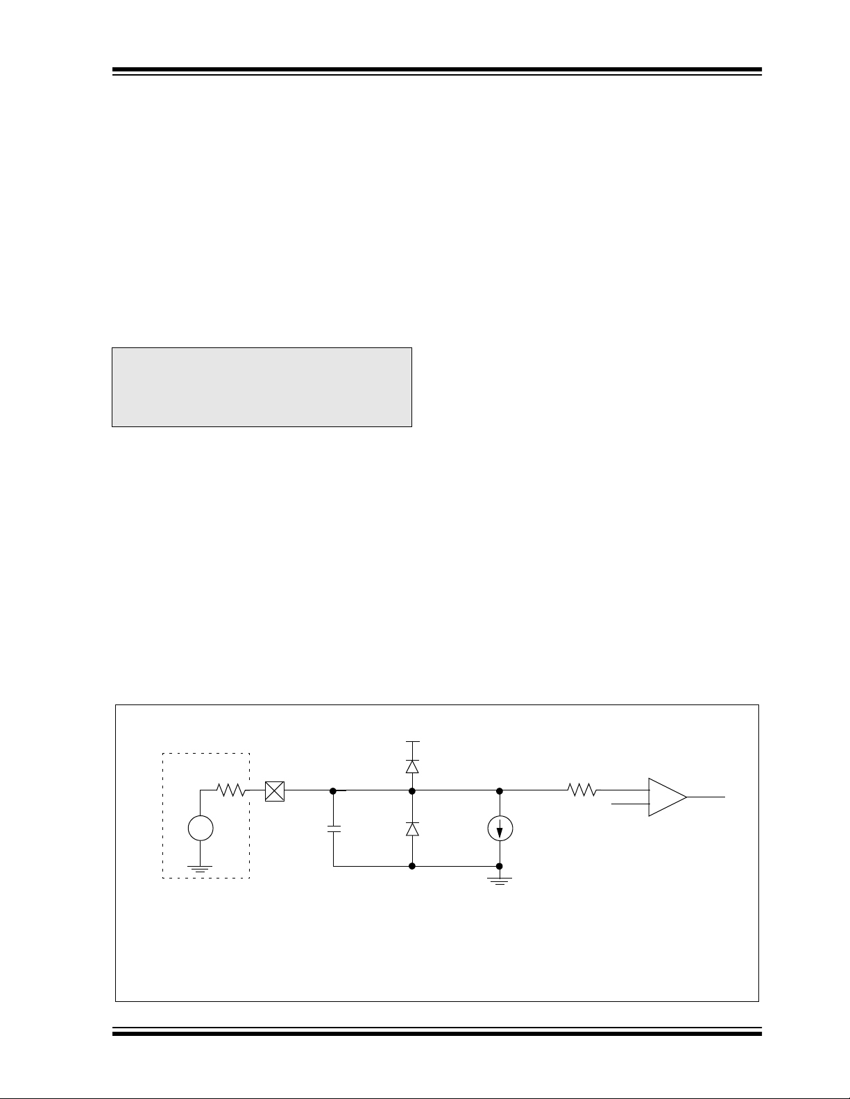
PIC16C62X
7.6 Comparator Interrupts
The comparator interrupt flag is set whenever there is
a change in the output value of either comparator.
Software will need to maintain information about the
status of the output bits, as read from CMCON<7:6>, to
determine the actual change that has occurred. The
CMIF bit, PIR1<6>, is the comparator interrupt flag.
The CMIF bit must be RESET by clearing ‘0’. Since it is
also possible to write a '1' to this register, a simulated
interrupt may be initiated.
The CMIE bit (PIE1<6>) and the PEIE bit
(INTCON<6>) must be set to enable the interrupt. In
addition, the GIE bit must also be set. If any of these
bits are clear, the interrupt is not enabled, though the
CMIF bit will still be set if an interrupt condition occurs.
Note: If a change in the CMCON register
(C1OUT or C2OUT) should occur when a
read operation is being executed (start of
the Q2 cycle), then the CMIF (PIR1<6>)
interrupt flag may not get set.
The user, in the interrupt service routine, can clear the
interrupt in the following manner:
a) Any read or write of CMCON. This will end the
mismatch condition.
b) Clear flag bit CMIF.
A mismatch condition will continue to set flag bit CMIF.
Reading CMCON will end the mismatch condition and
allow flag bit CMIF to be cleared.
7.7 Comparator Operation During SLEEP
When a comparator is active and the device is placed
in SLEEP mode, the comparator remains active and
the interrupt is functional if enabled. This interrupt will
wake up the device from SLEEP mode when enabled.
While the comparator is powered-up, higher SLEEP
currents than shown in the power-down current
specification will occur. Each comparator that is
operational will consume additional current as shown in
the comparator specifications. To minimize power
consumption while in SLEEP mode, turn off the
comparators, CM<2:0> = 111, before entering SLEEP.
If the device wakes up from SLEEP, the contents of the
CMCON register are not affected.
7.8 Effects of a RESET
A device RESET forces the CMCON register to its
RESET state. This forces the comparator module to be
in the comparator RESET mode, CM<2:0> = 000. This
ensures that all potential inputs are analog inputs.
Device current is minimized when analog inputs are
present at RESET time. The comparators will be
powered-down during the RESET interval.
7.9 Analog Input Connection Considerations
A simplified circuit for an analog input is shown in
Figure 7-4. Since the analog pins are connected to a
digital output, they have reverse biased diodes to V
and VSS. The analog input therefore, must be between
SS and VDD. If the input voltage deviates from this
V
range by more than 0.6V in either direction, one of the
diodes is forward biased and a latchup may occur. A
maximum source impedance of 10 kΩ is
recommended for the analog sources. Any external
component connected to an analog input pin, such as
a capacitor or a Zener diode, should have very little
leakage current.
DD
FIGURE 7-4: ANALOG INPUT MODEL
V
DD
S < 10K
R
A
IN
VA
Legend CPIN = Input Capacitance
2003 Microchip Technology Inc. DS30235J-page 41
CPIN
5 pF
T = Threshold Voltage
V
LEAKAGE = Leakage Current at the pin due to various junctions
I
R
IC = Interconnect Resistance
S = Source Impedance
R
VA = Analog Voltage
VT = 0.6V
V
T = 0.6V
ILEAKAGE
±500 nA
V
SS
IC
R

PIC16C62X
TABLE 7-1: REGISTERS ASSOCIATED WITH COMPARATOR MODULE
Address Name Bit 7 Bit 6 Bit 5 Bit 4 Bit 3 Bit 2 Bit 1 Bit 0
Value on
POR
Value on
All Other
RESETS
1Fh CMCON C2OUT C1OUT
9Fh VRCON VREN VROE VRR
0Bh INTCON GIE PEIE
0Ch PIR1
8Ch PIE1
85h TRISA
— CMIF — — — — — — -0-- ---- -0-- ----
— CMIE — — — — — — -0-- ---- -0-- ----
— — — TRISA4 TRISA3 TRISA2 TRISA1 TRISA0 ---1 1111 ---1 1111
— — CIS CM2 CM1 CM0 00-- 0000 00-- 0000
— VR3 VR2 VR1 VR0 000- 0000 000- 0000
T0IE INTE RBIE T0IF INTF RBIF 0000 000x 0000 000u
Legend: x = unknown, u = unchanged, - = unimplemented, read as "0"
DS30235J-page 42 2003 Microchip Technology Inc.
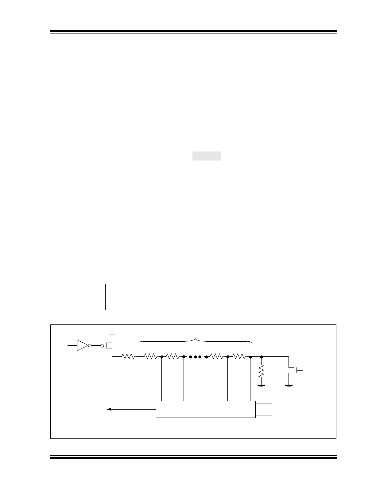
PIC16C62X
8.0 VOLTAGE REFERENCE MODULE
The Voltage Reference is a 16-tap resistor ladder
network that provides a selectable voltage reference.
The resistor ladder is segmented to provide two ranges
REF values and has a power-down function to
of V
conserve power when the reference is not being used.
The VRCON register controls the operation of the
reference as shown in Register 8-1. The block diagram
is given in Figure 8-1.
8.1 Configuring the Voltage Reference
The Voltage Reference can output 16 distinct voltage
levels for each range. The equations used to calculate
the output of the Voltage Reference are as follows:
if VRR = 1: VREF = (VR<3:0>/24) x VDD
if VRR = 0: VREF = (VDD x 1/4) + (VR<3:0>/32) x VDD
The setting time of the Voltage Reference must be
considered when changing the V
Example 8-1 shows an example of how to configure the
Voltage Reference for an output voltage of 1.25V with V
= 5.0V.
REGISTER 8-1: VRCON REGISTER(ADDRESS 9Fh)
R/W-0 R/W-0 R/W-0 U-0 R/W-0 R/W-0 R/W-0 R/W-0
V
REN VROE VRR —VR3VR2VR1VR0
bit 7 bit 0
bit 7 V
bit 6 V
bit 5 V
bit 4 Unimplemented: Read as '0'
bit 3-0 V
REN: VREF Enable
REF circuit powered on
1 = V
REF circuit powered down, no IDD drain
0 = V
ROE: VREF Output Enable
REF is output on RA2 pin
1 = V
REF is disconnected from RA2 pin
0 = V
RR: VREF Range selection
1 = Low Range
0 = High Range
R<3:0>: VREF value selection 0 ≤ VR [3:0] ≤ 15
when V
RR = 1: VREF = (VR<3:0>/ 24) * VDD
when VRR = 0: VREF = 1/4 * VDD + (VR<3:0>/ 32) * VDD
REF output (Table 12-1).
DD
Legend:
R = Readable bit W = Writable bit U = Unimplemented bit, read as ‘0’
- n = Value at POR ’1’ = Bit is set ’0’ = Bit is cleared x = Bit is unknown
FIGURE 8-1: VOLTAGE REFERENCE BLOCK DIAGRAM
16 Stages
VREN
VREF
8R
Note: R is defined in Table 12-2.
2003 Microchip Technology Inc. DS30235J-page 43
R
R
R
16-1 Analog Mux
R
8R
V
R3
(From VRCON<3:0>)
R0
V
VRR
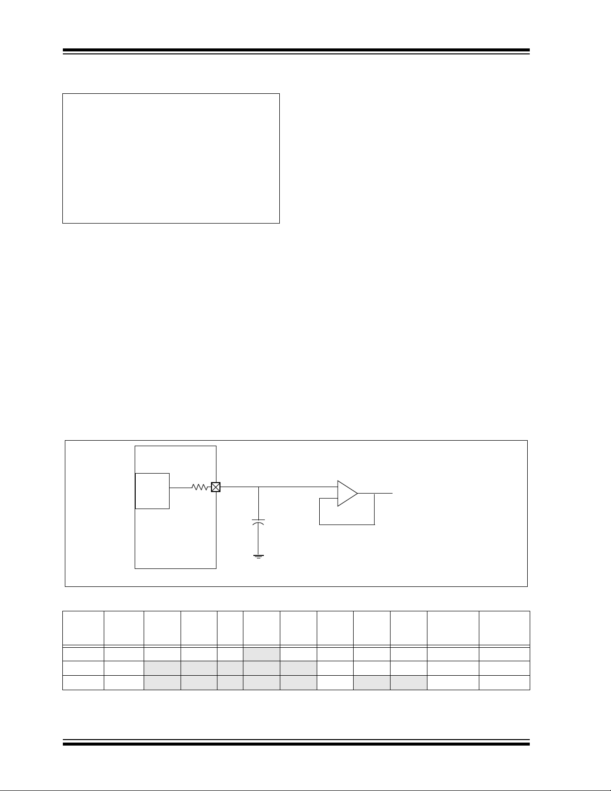
PIC16C62X
EXAMPLE 8-1: VOLTAGE REFERENCE
CONFIGURATION
MOVLW 0x02 ; 4 Inputs Muxed
MOVWF CMCON ; to 2 comps.
BSF STATUS,RP0 ; go to Bank 1
MOVLW 0x0F ; RA3-RA0 are
MOVWF TRISA ; inputs
MOVLW 0xA6 ; enable V
MOVWF VRCON ; low range
; set V
BCF STATUS,RP0 ; go to Bank 0
CALL DELAY10 ; 10µs delay
REF
R<3:0>=6
8.2 Voltage Reference Accuracy/Error
The full range of VSS to VDD cannot be realized due to the
construction of the module. The transistors on the top
and bottom of the resistor ladder network (Figure 8-1)
REF from approaching VSS or VDD. The voltage
keep V
reference is V
changes with fluctuations in V
DD derived and therefore, the VREF output
DD. The tested absolute
accuracy of the voltage reference can be found in
Table 12-2.
8.3 Operation During SLEEP
8.4 Effects of a RESET
A device RESET disables the voltage reference by
clearing bit V
REN (VRCON<7>). This reset also
disconnects the reference from the RA2 pin by clearing
bit V
ROE (VRCON<6>) and selects the high voltage
range by clearing bit V
RR (VRCON<5>). The VREF
value select bits, VRCON<3:0>, are also cleared.
8.5 Connection Considerations
The voltage reference module operates independently
of the comparator module. The output of the reference
generator may be connected to the RA2 pin if the
TRISA<2> bit is set and the V
set. Enabling the voltage reference output onto the
RA2 pin with an input signal present will increase
current consumption. Connecting RA2 as a digital
output with V
REF enabled will also increase current
consumption.
The RA2 pin can be used as a simple D/A output with
limited drive capability. Due to the limited drive
capability, a buffer must be used in conjunction with the
voltage reference output for external connections to
REF. Figure 8-2 shows an example buffering
V
technique.
ROE bit, VRCON<6>, is
When the device wakes up from SLEEP through an
interrupt or a Watchdog Timer time-out, the contents of
the VRCON register are not affected. To minimize
current consumption in SLEEP mode, the voltage
reference should be disabled.
FIGURE 8-2: VOLTAGE REFERENCE OUTPUT BUFFER EXAMPLE
(1)
VREF
R
Module
Voltage
Reference
Output
Impedance
RA
•
+
–
•
VREF Output
Note 1: R is dependent upon the Voltage Reference Configuration VRCON<3:0> and VRCON<5>.
TABLE 8-1: REGISTERS ASSOCIATED WITH VOLTAGE REFERENCE
Address Name Bit 7 Bit 6 Bit 5 Bit 4 Bit 3 Bit 2 Bit 1 Bit 0
9Fh VRCON
1Fh CMCON
85h TRISA
VREN VROE VRR
C2OUT C1OUT — — CIS CM2 CM1 CM0 00-- 0000 00-- 0000
— — — TRISA4 TRISA3 TRISA2 TRISA1 TRISA0 ---1 1111 ---1 1111
— VR3 VR2 VR1 VR0 000- 0000 000- 0000
Note: - = Unimplemented, read as "0"
Val ue O n
POR
Val ue O n
All Other
RESETS
DS30235J-page 44 2003 Microchip Technology Inc.

PIC16C62X
9.0 SPECIAL FEATURES OF THE CPU
Special circuits to deal with the needs of real-time
applications are what sets a microcontroller apart from
other processors. The PIC16C62X family has a host of
such features intended to maximize system reliability,
minimize cost through elimination of external components, provide power saving operating modes and offer
code protection.
These are:
1. OSC selection
2. RESET
Power-on Reset (POR)
Power-up Timer (PWRT)
Oscillator Start-up Timer (OST)
Brown-out Reset (BOR)
3. Interrupts
4. Watchdog Timer (WDT)
5. SLEEP
6. Code protection
7. ID Locations
8. In-Circuit Serial Programming™
The PIC16C62X devices have a Watchdog Timer
which is controlled by configuration bits. It runs off its
own RC oscillator for added reliability. There are two
timers that offer necessary delays on power-up. One is
the Oscillator Start-up Timer (OST), intended to keep
the chip in RESET until the crystal oscillator is stable.
The other is the Power-up Timer (PWRT), which
provides a fixed delay of 72 ms (nominal) on power-up
only, designed to keep the part in RESET while the
power supply stabilizes. There is also circuitry to
RESET the device if a brown-out occurs, which provides at least a 72 ms RESET. With these three
functions on-chip, most applications need no external
RESET circuitry.
The SLEEP mode is designed to offer a very low
current Power-down mode. The user can wake-up from
SLEEP through external RESET, Watchdog Timer
wake-up or through an interrupt. Several oscillator
options are also made available to allow the part to fit
the application. The RC oscillator option saves system
cost, while the LP crystal option saves power. A set of
configuration bits are used to select various options.
2003 Microchip Technology Inc. DS30235J-page 45

PIC16C62X
9.1 Configuration Bits
The configuration bits can be programmed (read as '0')
or left unprogrammed (read as '1') to select various
device configurations. These bits are mapped in
The user will note that address 2007h is beyond
the user program memory space. In fact, it belongs
to the special test/configuration memory space
(2000h – 3FFFh), which can be accessed only during
programming.
program memory location 2007h.
REGISTER 9-1: CONFIGURATION WORD (ADDRESS 2007h)
CP1
CP0
(2)
CP1
CP0
(2)
CP1
CP0
(2)
BODEN
CP1
CP0
bit 13 bit 0
bit 13-8,
5-4:
CP<1:0>: Code protection bit pairs
Code protection for 2K program memory
(2)
11 = Program memory code protection off
10 = 0400h-07FFh code protected
01 = 0200h-07FFh code protected
00 = 0000h-07FFh code protected
Code protection for 1K program memory
11 = Program memory code protection off
10 = Program memory code protection off
01 = 0200h-03FFh code protected
00 = 0000h-03FFh code protected
(2)
PWRTE
WDTE F0SC1 F0SC0
Code protection for 0.5K program memory
11 = Program memory code protection off
10 = Program memory code protection off
01 = Program memory code protection off
00 = 0000h-01FFh code protected
bit 7 Unimplemented: Read as ‘0’
bit 6 BODEN: Brown-out Reset Enable bit
(1)
1 = BOR enabled
0 = BOR disabled
bit 3 PWRTE
: Power-up Timer Enable bit
(1, 3)
1 = PWRT disabled
0 = PWRT enabled
bit 2 WDTE: Watchdog Timer Enable bit
1 = WDT enabled
0 = WDT disabled
bit 1-0 FOSC1:FOSC0: Oscillator Selection bits
11 = RC oscillator
10 = HS oscillator
01 = XT oscillator
00 = LP oscillator
Note 1: Enabling Brown-out Reset automatically enables Power-up Timer (PWRT) regardless of the
value of bit PWRTE
. Ensure the Power-up Timer is enabled anytime Brown-out Detect Reset is
enabled.
2: All of the CP<1:0> pairs have to be given the same value to enable the code protection scheme
listed.
3: Unprogrammed parts default the Power-up Timer disabled.
Legend:
R = Readable bit W = Writable bit U = Unimplemented bit, read as ‘0’
-n = Value at POR 1 = bit is set 0 = bit is cleared x = bit is unknown
DS30235J-page 46 2003 Microchip Technology Inc.

PIC16C62X
9.2 Oscillator Configurations
9.2.1 OSCILLATOR TYPES
The PIC16C62X devices can be operated in four
different oscillator options. The user can program two
configuration bits (FOSC1 and FOSC0) to select one of
these four modes:
• LP Low Power Crystal
• XT Crystal/Resonator
• HS High Speed Crystal/Resonator
• RC Resistor/Capacitor
9.2.2 CRYSTAL OSCILLATOR / CERAMIC
RESONATORS
In XT, LP or HS modes, a crystal or ceramic resonator
is connected to the OSC1 and OSC2 pins to establish
oscillation (Figure 9-1). The PIC16C62X oscillator
design requires the use of a parallel cut crystal. Use of
a series cut crystal may give a frequency out of the
crystal manufacturers specifications. When in XT, LP or
HS modes, the device can have an external clock
source to drive the OSC1 pin (Figure 9-2).
FIGURE 9-1: CRYSTAL OPERATION
(OR CERAMIC
RESONATOR) (HS, XT OR
LP OSC
CONFIGURATION)
OSC1
C1
C2
XTAL
RS
See Note
OSC2
RF
See Table 9-1 and Table 9-2 for recommended
values of C1 and C2.
Note: A series resistor may be required for
AT strip cut crystals.
To internal logic
SLEEP
PIC16C62X
TABLE 9-1: CAPACITOR SELECTION FOR
CERAMIC RESONATORS
Ranges Characterized:
Mode Freq OSC1(C1) OSC2(C2)
XT 455 kHz
2.0 MHz
4.0 MHz
HS 8.0 MHz
16.0 MHz
Higher capacitance increases the stability of the oscil-
lator but also increases the start-up time. These
values are for design guidance only. Since each
resonator has its own characteristics, the user
should consult the resonator manufacturer for
appropriate values of external components.
22 - 100 pF
15 - 68 pF
15 - 68 pF
10 - 68 pF
10 - 22 pF
22 - 100 pF
15 - 68 pF
15 - 68 pF
10 - 68 pF
10 - 22 pF
TABLE 9-2: CAPACITOR SELECTION FOR
CRYSTAL OSCILLATOR
Mode Freq OSC1(C1) OSC2(C2)
LP
32 kHz
200 kHz
100 kHz
XT
2 MHz
4 MHz
8 MHz
HS
10 MHz
20 MHz
Higher capacitance increases the stability of the
oscillator but also increases the start-up time.
These values are for design guidance only. Rs may
be required in HS mode as well as XT mode to
avoid overdriving crystals with low drive level
specification. Since each crystal has its own
characteristics, the user should consult the crystal
manufacturer for appropriate values of external
components.
68 - 100 pF
15 - 30 pF
68 - 150 pF
15 - 30 pF
15 - 30 pF
15 - 30 pF
15 - 30 pF
15 - 30 pF
68 - 100 pF
15 - 30 pF
150 - 200 pF
15 - 30 pF
15 - 30 pF
15 - 30 pF
15 - 30 pF
15 - 30 pF
FIGURE 9-2: EXTERNAL CLOCK INPUT
OPERATION (HS, XT OR
LP OSC
CONFIGURATION)
clock from
ext. system
Open
2003 Microchip Technology Inc. DS30235J-page 47
OSC1
PIC16C62X
OSC2

PIC16C62X
9.2.3 EXTERNAL CRYSTAL OSCILLATOR
CIRCUIT
Either a prepackaged oscillator can be used or a simple
oscillator circuit with TTL gates can be built.
Prepackaged oscillators provide a wide operating
range and better stability. A well-designed crystal
oscillator will provide good performance with TTL
gates. Two types of crystal oscillator circuits can be
used; one with series resonance or one with parallel
resonance.
Figure 9-3 shows implementation of a parallel resonant
oscillator circuit. The circuit is designed to use the
fundamental frequency of the crystal. The 74AS04
inverter performs the 180° phase shift that a parallel
oscillator requires. The 4.7 kΩ resistor provides the
negative feedback for stability. The 10 kΩ
potentiometers bias the 74AS04 in the linear region.
This could be used for external oscillator designs.
FIGURE 9-3: EXTERNAL PARALLEL
RESONANT CRYSTAL
OSCILLATOR CIRCUIT
+5V
10k
4.7k
74AS04
10k
XTAL
10k
20 pF
20 pF
Figure 9-4 shows a series resonant oscillator circuit.
This circuit is also designed to use the fundamental
frequency of the crystal. The inverter performs a 180°
phase shift in a series resonant oscillator circuit. The
330 kΩ resistors provide the negative feedback to bias
the inverters in their linear region.
74AS04
To Other
Devices
PIC16C62X
CLK
IN
9.2.4 RC OSCILLATOR
For timing insensitive applications the “RC” device
option offers additional cost savings. The RC oscillator
frequency is a function of the supply voltage, the
resistor (R
EXT) and capacitor (CEXT) values, and the
operating temperature. In addition to this, the oscillator
frequency will vary from unit to unit due to normal
process parameter variation. Furthermore, the
difference in lead frame capacitance between package
types will also affect the oscillation frequency,
especially for low C
EXT values. The user also needs to
take into account variation due to tolerance of external
R and C components used. Figure 9-5 shows how the
R/C combination is connected to the PIC16C62X. For
EXT values below 2.2 kΩ, the oscillator operation may
R
become unstable or stop completely. For very high
EXT values (e.g., 1 MΩ), the oscillator becomes
R
sensitive to noise, humidity and leakage. Thus, we
recommend to keep R
EXT between 3 kΩ and 100 kΩ.
Although the oscillator will operate with no external
capacitor (C
EXT = 0 pF), we recommend using values
above 20 pF for noise and stability reasons. With no or
small external capacitance, the oscillation frequency
can vary dramatically due to changes in external
capacitances, such as PCB trace capacitance or
package lead frame capacitance.
See Section 13.0 for RC frequency variation from part
to part due to normal process variation. The variation is
larger for larger R (since leakage current variation will
affect RC frequency more for large R) and for smaller
C (since variation of input capacitance will affect RC
frequency more).
See Section 13.0 for variation of oscillator frequency
due to V
DD for given REXT/CEXT values, as well as
frequency variation due to operating temperature for
given R, C and V
DD values.
The oscillator frequency, divided by 4, is available on
the OSC2/CLKOUT pin, and can be used for test
purposes or to synchronize other logic (Figure 3-2 for
waveform).
FIGURE 9-5: RC OSCILLATOR MODE
FIGURE 9-4: EXTERNAL SERIES
RESONANT CRYSTAL
OSCILLATOR CIRCUIT
To Other
74AS04
Devices
PIC16C62X
CLKIN
330 kΩ
74AS04
DS30235J-page 48 2003 Microchip Technology Inc.
330 kΩ
74AS04
0.1 µF
XTAL
REXT
CEXT
VDD
VDD
F
OSC/4
PIC16C62X
OSC1
Internal Clock
OSC2/CLKOUT

PIC16C62X
Reset, WDT Reset and MCLR Reset during
9.3 RESET
The PIC16C62X differentiates between various kinds
of RESET:
a) Power-on Reset (POR)
b) MCLR
c) MCLR
d) WDT Reset (normal operation)
e) WDT wake-up (SLEEP)
f) Brown-out Reset (BOR)
Some registers are not affected in any RESET
condition Their status is unknown on POR and
unchanged in any other RESET. Most other registers
are reset to a “RESET state” on Power-on Reset,
FIGURE 9-6: SIMPLIFIED BLOCK DIAGRAM OF ON-CHIP RESET CIRCUIT
MCLR/
V
Reset during normal operation
Reset during SLEEP
PP Pin
WDT
Module
V
DD rise
detect
DD
V
Brown-out
Reset
External
RESET
SLEEP
WDT
Time-out
Reset
Power-on Reset
BODEN
MCLR
SLEEP. They are not affected by a WDT wake-up,
since this is viewed as the resumption of normal
operation. TO
and PD bits are set or cleared differently
in different RESET situations as indicated in Table 9-2.
These bits are used in software to determine the nature
of the RESET. See Table 9-5 for a full description of
RESET states of all registers.
A simplified block diagram of the on-chip RESET circuit
is shown in Figure 9-6.
The MCLR Reset path has a noise filter to detect and
ignore small pulses. See Table 12-5 for pulse width
specification.
S
Q
OST/PWRT
OST
10-bit Ripple-counter
OSC1/
CLKIN
Pin
On-chip
RC OSC
PWRT
(1)
10-bit Ripple-counter
Enable PWRT
Enable OST
See Table 9-1 for time-out situations.
Note 1: This is a separate oscillator from the RC oscillator of the CLKIN pin.
R
Chip_Reset
Q
2003 Microchip Technology Inc. DS30235J-page 49

PIC16C62X
9.4 Power-on Reset (POR), Power-up
Timer (PWRT), Oscillator Start-up
Timer (OST) and Brown-out Reset
(BOR)
9.4.1 POWER-ON RESET (POR)
The on-chip POR circuit holds the chip in RESET until
DD has reached a high enough level for proper
V
operation. To take advantage of the POR, just tie the
pin through a resistor to VDD. This will eliminate
MCLR
external RC components usually needed to create
Power-on Reset. A maximum rise time for V
required. See Electrical Specifications for details.
The POR circuit does not produce an internal RESET
DD declines.
when V
When the device starts normal operation (exits the
RESET condition), device operating parameters (voltage, frequency, temperature, etc.) must be met to
ensure operation. If these conditions are not met, the
device must be held in RESET until the operating
conditions are met.
For additional information, refer to Application Note
AN607, “Power-up Trouble Shooting”.
9.4.2 POWER-UP TIMER (PWRT)
The Power-up Timer provides a fixed 72 ms (nominal)
time-out on power-up only, from POR or Brown-out
Reset. The Power-up Timer operates on an internal RC
oscillator. The chip is kept in RESET as long as PWRT
is active. The PWRT delay allows the V
acceptable level. A configuration bit, PWRTE
disable (if set) or enable (if cleared or programmed) the
Power-up Timer. The Power-up Timer should always
be enabled when Brown-out Reset is enabled.
DD to rise to an
DD is
can
The Power-up Time delay will vary from chip-to-chip
and due to V
DD, temperature and process variation.
See DC parameters for details.
9.4.3 OSCILLATOR START-UP TIMER
(OST)
The Oscillator Start-Up Timer (OST) provides a 1024
oscillator cycle (from OSC1 input) delay after the
PWRT delay is over. This ensures that the crystal
oscillator or resonator has started and stabilized.
The OST time-out is invoked only for XT, LP and HS
modes and only on Power-on Reset or wake-up from
SLEEP.
9.4.4 BROWN-OUT RESET (BOR)
The PIC16C62X members have on-chip Brown-out
Reset circuitry. A configuration bit, BODEN, can
disable (if clear/programmed) or enable (if set) the
Brown-out Reset circuitry. If V
BOR parameter D005 (VBOR) for greater than
to V
parameter (T
BOR) in Table 12-5. The brown-out situa-
tion will RESET the chip. A RESET won’t occur if V
falls below 4.0V for less than parameter (TBOR).
On any RESET (Power-on, Brown-out, Watchdog, etc.)
the chip will remain in RESET until V
DD. The Power-up Timer will now be invoked and will
BV
keep the chip in RESET an additional 72 ms.
If VDD drops below BVDD while the Power-up Timer is
running, the chip will go back into a Brown-out Reset
and the Power-up Timer will be re-initialized. Once V
rises above BVDD, the Power-Up Timer will execute a
72 ms RESET. The Power-up Timer should always be
enabled when Brown-out Reset is enabled. Figure 9-7
shows typical Brown-out situations.
DD falls below 4.0V refer
DD
DD rises above
DD
FIGURE 9-7: BROWN-OUT SITUATIONS
VDD
INTERNAL
RESET
VDD
INTERNAL
RESET
VDD
INTERNAL
RESET
DS30235J-page 50 2003 Microchip Technology Inc.
72 ms
<72 ms
72 ms
72 ms
DD
BV
BVDD
BV
DD

PIC16C62X
9.4.5 TIME-OUT SEQUENCE
On power-up the time-out sequence is as follows: First
PWRT time-out is invoked after POR has expired. Then
OST is activated. The total time-out will vary based on
oscillator configuration and PWRTE
example, in RC mode with PWRTE
disabled), there will be no time-out at all. Figure 9-8,
Figure 9-9 and Figure 9-10 depict time-out sequences.
Since the time-outs occur from the POR pulse, if MCLR
is kept low long enough, the time-outs will expire. Then
bringing MCLR
(see Figure 9-9). This is useful for testing purposes or
to synchronize more than one PIC16C62X device
operating in parallel.
Table 9-4 shows the RESET conditions for some
special registers, while Table 9-5 shows the RESET
conditions for all the registers.
high will begin execution immediately
bit status. For
bit erased (PWRT
TABLE 9-1: TIME-OUT IN VARIOUS SITUATIONS
Power-up
Oscillator Configuration
PWRTE
XT, HS, LP 72 ms + 1024 T
= 0 PWRTE = 1
OSC 1024 TOSC 72 ms + 1024 TOSC 1024 TOSC
9.4.6 POWER CONTROL (PCON)/
STATUS REGISTER
The power control/STATUS register, PCON (address
8Eh), has two bits.
Bit0 is BOR (Brown-out). BOR is unknown on Poweron Reset. It must then be set by the user and checked
on subsequent RESETS to see if BOR
that a brown-out has occurred. The BOR
a don’t care and is not necessarily predictable if the
brown-out circuit is disabled (by setting BODEN bit = 0
in the Configuration word).
Bit1 is POR (Power-on Reset). It is a ‘0’ on Power-on
Reset and unaffected otherwise. The user must write a
‘1’ to this bit following a Power-on Reset. On a
subsequent RESET, if POR
Power-on Reset must have occurred (V
gone too low).
Brown-out Reset
is ‘0’, it will indicate that a
= 0, indicating
STATUS bit is
DD may have
Wake-up
from SLEEP
RC 72 ms — 72 ms —
TABLE 9-2: STATUS/PCON BITS AND THEIR SIGNIFICANCE
POR BOR TO PD
0X11Power-on Reset
0X0XIllegal, TO
0XX0Illegal, PD is set on POR
10XXBrown-out Reset
110uWDT Reset
1100WDT Wake-up
11uuMCLR
1110MCLR
Legend: u = unchanged, x = unknown
is set on POR
Reset during normal operation
Reset during SLEEP
TABLE 9-3: SUMMARY OF REGISTERS ASSOCIATED WITH BROWN-OUT
Address Name Bit 7 Bit 6 Bit 5 Bit 4 Bit 3 Bit 2 Bit 1 Bit 0
83h STATUS
8Eh PCON
Legend: u = unchanged, x = unknown, - = unimplemented bit, reads as ‘0’, q = value depends on condition.
Note 1: Other (non Power-up) Resets include MCLR
normal operation.
— — — — — —PORBOR ---- --0x ---- --uq
TO PD 0001 1xxx 000q quuu
Reset, Brown-out Reset and Watchdog Timer Reset during
Value on
POR Reset
Value on all
other
RESETS
(1)
2003 Microchip Technology Inc. DS30235J-page 51

PIC16C62X
TABLE 9-4: INITIALIZATION CONDITION FOR SPECIAL REGISTERS
Condition
Program
Counter
STATUS
Register
PCON
Register
Power-on Reset 000h 0001 1xxx ---- --0x
MCLR
Reset during normal operation 000h 000u uuuu ---- --uu
Reset during SLEEP 000h 0001 0uuu ---- --uu
MCLR
WDT Reset 000h 0000 uuuu ---- --uu
WDT Wake-up PC + 1 uuu0 0uuu ---- --uu
Brown-out Reset 000h 000x xuuu ---- --u0
Interrupt Wake-up from SLEEP PC + 1
Legend:
u = unchanged, x = unknown, - = unimplemented bit, reads as ‘0’.
(1)
uuu1 0uuu ---- --uu
Note 1: When the wake-up is due to an interrupt and global enable bit, GIE is set, the PC is loaded with the
interrupt vector (0004h) after execution of PC+1.
TABLE 9-5: INITIALIZATION CONDITION FOR REGISTERS
• MCLR
• MCLR
Register Address Power-on Reset
W
INDF
TMR0
PCL
STATUS
FSR
PORTA
PORTB
CMCON
PCLATH
INTCON
PIR1
OPTION
TRISA
TRISB
PIE1
PCON
VRCON
Legend: u = unchanged, x = unknown, - = unimplemented bit, reads as ‘0’,q = value depends on condition.
Note 1: If V
DD goes too low, Power-on Reset will be activated and registers will be affected differently.
2: One or more bits in INTCON, PIR1 and/or PIR2 will be affected (to cause wake-up).
3: When the wake-up is due to an interrupt and the GIE bit is set, the PC is loaded with the interrupt vector (0004h).
4: See Table 9-4 for RESET value for specific condition.
5: If wake-up was due to comparator input changing, then bit 6 = 1. All other interrupts generating a wake-up will cause
bit 6 = u.
6: If RESET was due to brown-out, then bit 0 = 0. All other RESETS will cause bit 0 = u.
— xxxx xxxx uuuu uuuu uuuu uuuu
00h — — —
01h xxxx xxxx uuuu uuuu uuuu uuuu
02h 0000 0000 0000 0000
03h 0001 1xxx
04h xxxx xxxx uuuu uuuu uuuu uuuu
05h ---x xxxx ---u uuuu ---u uuuu
06h xxxx xxxx uuuu uuuu uuuu uuuu
1Fh 00-- 0000 00-- 0000 uu-- uuuu
0Ah ---0 0000 ---0 0000 ---u uuuu
0Bh 0000 000x 0000 000u
0Ch -0-- ---- -0-- ----
81h 1111 1111 1111 1111 uuuu uuuu
85h ---1 1111 ---1 1111 ---u uuuu
86h 1111 1111 1111 1111 uuuu uuuu
8Ch -0-- ---- -0-- ---- -u-- ----
8Eh ---- --0x
9Fh 000- 0000 000- 0000 uuu- uuuu
• WDT Reset
• Brown-out Reset
Reset during
normal operation
Reset during
SLEEP
000q quuu
---- --uq
(4)
(1,6)
(1)
• Wake-up from SLEEP
through interrupt
• Wake-up from SLEEP
through WDT time-out
(3)
PC + 1
uuuq quuu
uuuu uqqq
-q-- ----
---- --uu
(2,5)
(4)
(2)
DS30235J-page 52 2003 Microchip Technology Inc.

PIC16C62X
FIGURE 9-8: TIME-OUT SEQUENCE ON POWER-UP (MCLR NOT TIED TO VDD): CASE 1
VDD
MCLR
INTERNAL POR
TPWRT
PWRT TIME-OUT
OST TIME-OUT
INTERNAL RESET
FIGURE 9-9: TIME-OUT SEQUENCE ON POWER-UP (MCLR
VDD
MCLR
INTERNAL POR
T
PWRT
PWRT TIME-OUT
OST TIME-OUT
INTERNAL RESET
TOST
NOT TIED TO VDD): CASE 2
TOST
FIGURE 9-10: TIME-OUT SEQUENCE ON POWER-UP (MCLR
VDD
MCLR
INTERNAL POR
TPWRT
PWRT TIME-OUT
OST TIME-OUT
INTERNAL RESET
2003 Microchip Technology Inc. DS30235J-page 53
TOST
TIED TO VDD)

PIC16C62X
FIGURE 9-11: EXTERNAL POWER-ON
RESET CIRCUIT (FOR
SLOW V
V
DD
R
C
Note 1: External Power-on Reset circuit is
2: < 40 kΩ is recommended to make sure
3: R1 = 100Ω to 1 kΩ will limit any current
VDD
D
required only if V
too slow. The diode D helps discharge
the capacitor quickly when V
down.
that voltage drop across R does not
violate the device’s electrical specification.
flowing into MCLR
tor C in the event of MCLR/
breakdown due to Electrostatic
Discharge (ESD) or Electrical Overstress (EOS).
DD POWER-UP)
R1
MCLR
PIC16C62X
DD power-up slope is
DD powers
from external capaci-
VPP pin
FIGURE 9-13: EXTERNAL BROWN-OUT
PROTECTION CIRCUIT 2
VDD
R1
Q1
R2
40k
Note 1: This brown-out circuit is less expen-
sive, albeit less accurate. Transistor
Q1 turns off when V
DD is below a
certain level such that:
R1
VDD x
R1 + R2
= 0.7V
2: Internal Brown-out Reset should be
disabled when using this circuit.
3: Resistors should be adjusted for the
characteristics of the transistor.
DD
V
MCLR
PIC16C62X
FIGURE 9-14: EXTERNAL BROWN-OUT
PROTECTION CIRCUIT 3
FIGURE 9-12: EXTERNAL BROWN-OUT
PROTECTION CIRCUIT 1
VDD
33k
10k
40k
Note 1: This circuit will activate RESET when
V
DD goes below (Vz + 0.7V) where
Vz = Zener voltage.
2: Internal Brown-out Reset circuitry should
be disabled when using this circuit.
V
DD
MCLR
PIC16C62X
VDD
Vss
MCP809
RST
V
DD
bypass
capacitor
VDD
MCLR
PIC16C62X
This brown-out protection circuit employs
Microchip Technology’s MCP809 microcontroller
supervisor. The MCP8XX and MCP1XX families
of supervisors provide push-pull and open
collector outputs with both high and low active
RESET pins. There are 7 different trip point
selections to accommodate 5V and 3V systems.
DS30235J-page 54 2003 Microchip Technology Inc.

PIC16C62X
9.5 Interrupts
The PIC16C62X has 4 sources of interrupt:
• External interrupt RB0/INT
• TMR0 overflow interrupt
• PORTB change interrupts (pins RB<7:4>)
• Comparator interrupt
The interrupt control register (INTCON) records
individual interrupt requests in flag bits. It also has
individual and global interrupt enable bits.
A global interrupt enable bit, GIE (INTCON<7>)
enables (if set) all un-masked interrupts or disables (if
cleared) all interrupts. Individual interrupts can be
disabled through their corresponding enable bits in
INTCON register. GIE is cleared on RESET.
The “return from interrupt” instruction, RETFIE, exits
interrupt routine, as well as sets the GIE bit, which reenable RB0/INT interrupts.
The INT pin interrupt, the RB port change interrupt and
the TMR0 overflow interrupt flags are contained in the
INTCON register.
The peripheral interrupt flag is contained in the special
register PIR1. The corresponding interrupt enable bit is
contained in special registers PIE1.
When an interrupt is responded to, the GIE is cleared
to disable any further interrupt, the return address is
pushed into the stack and the PC is loaded with 0004h.
Once in the interrupt service routine, the source(s) of
the interrupt can be determined by polling the interrupt
flag bits. The interrupt flag bit(s) must be cleared in
software before re-enabling interrupts to avoid RB0/
INT recursive interrupts.
For external interrupt events, such as the INT pin or
PORTB change interrupt, the interrupt latency will be
three or four instruction cycles. The exact latency
depends when the interrupt event occurs (Figure 9-16).
The latency is the same for one or two cycle
instructions. Once in the interrupt service routine, the
source(s) of the interrupt can be determined by polling
the interrupt flag bits. The interrupt flag bit(s) must be
cleared in software before re-enabling interrupts to
avoid multiple interrupt requests.
Note 1: Individual interrupt flag bits are set
regardless of the status of their
corresponding mask bit or the GIE bit.
2: When an instruction that clears the GIE
bit is executed, any interrupts that were
pending for execution in the next cycle
are ignored. The CPU will execute a NOP
in the cycle immediately following the
instruction which clears the GIE bit. The
interrupts which were ignored are still
pending to be serviced when the GIE bit
is set again.
FIGURE 9-15: INTERRUPT LOGIC
T0IF
T0IE
INTF
INTE
RBIF
RBIE
CMIF
CMIE
PEIE
GIE
Wake-up
(If in SLEEP mode)
Interrupt
to CPU
2003 Microchip Technology Inc. DS30235J-page 55
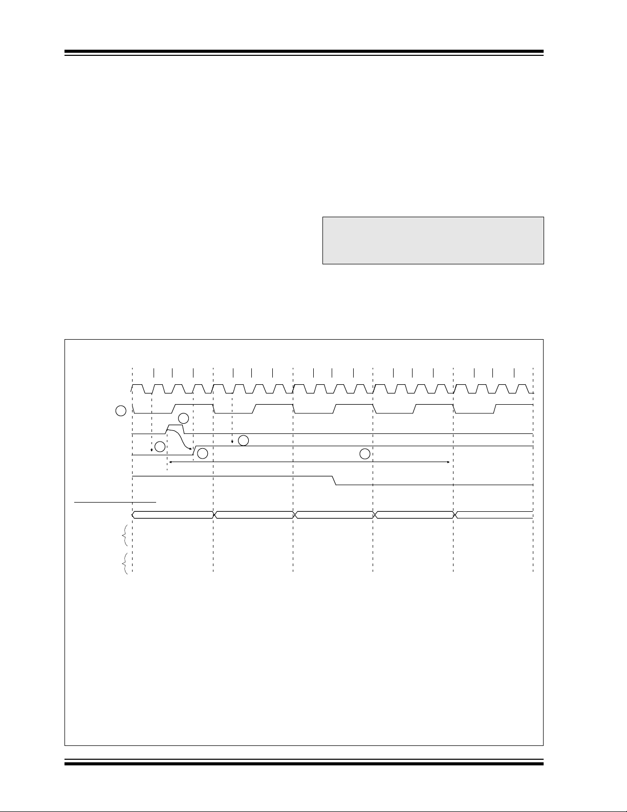
PIC16C62X
9.5.1 RB0/INT INTERRUPT
External interrupt on RB0/INT pin is edge triggered,
either rising if INTEDG bit (OPTION<6>) is set, or falling, if INTEDG bit is clear. When a valid edge appears
on the RB0/INT pin, the INTF bit (INTCON<1>) is set.
This interrupt can be disabled by clearing the INTE
control bit (INTCON<4>). The INTF bit must be cleared
in software in the interrupt service routine before reenabling this interrupt. The RB0/INT interrupt can
wake-up the processor from SLEEP, if the INTE bit was
set prior to going into SLEEP. The status of the GIE bit
decides whether or not the processor branches to the
interrupt vector following wake-up. See Section 9.8 for
details on SLEEP and Figure 9-18 for timing of wakeup from SLEEP through RB0/INT interrupt.
FIGURE 9-16: INT PIN INTERRUPT TIMING
9.5.2 TMR0 INTERRUPT
An overflow (FFh → 00h) in the TMR0 register will
set the T0IF (INTCON<2>) bit. The interrupt can
be enabled/disabled by setting/clearing T0IE
(INTCON<5>) bit. For operation of the Timer0 module,
see Section 6.0.
9.5.3 PORTB INTERRUPT
An input change on PORTB <7:4> sets the RBIF
(INTCON<0>) bit. The interrupt can be enabled/disabled by setting/clearing the RBIE (INTCON<4>) bit.
For operation of PORTB (Section 5.2).
Note: If a change on the I/O pin should occur
when the read operation is being executed
(start of the Q2 cycle), then the RBIF
interrupt flag may not get set.
9.5.4 COMPARATOR INTERRUPT
See Section 7.6 for complete description of comparator
interrupts.
Q2Q1 Q3 Q4 Q2Q1 Q3 Q4 Q2Q1 Q3 Q4 Q2Q1 Q3 Q4 Q2Q1 Q3 Q4
OSC1
CLKOUT
INT pin
INTF flag
(INTCON<1>)
GIE bit
(INTCON<7>)
INSTRUCTION FLOW
PC
Instruction
fetched
Instruction
executed
Note 1: INTF flag is sampled here (every Q1).
3
Inst (PC-1)
2: Asynchronous interrupt latency = 3-4 T
Latency is the same whether Inst (PC) is a single cycle or a two-cycle instruction.
3: CLKOUT is available only in RC Oscillator mode.
4: For minimum width of INT pulse, refer to AC specs.
5: INTF is enabled to be set anytime during the Q4-Q1 cycles.
1
PC
Inst (PC)
4
5
1
PC+1
Inst (PC+1)
Inst (PC)
Interrupt Latency
PC+1
—
Dummy Cycle
CY. Synchronous latency = 3 TCY, where TCY = instruction cycle time.
2
0004h
Inst (0004h)
Dummy Cycle
0005h
Inst (0005h)
Inst (0004h)
DS30235J-page 56 2003 Microchip Technology Inc.

TABLE 9-6: SUMMARY OF INTERRUPT REGISTERS
PIC16C62X
Address Name Bit 7 Bit 6 Bit 5 Bit 4 Bit 3 Bit 2 Bit 1 Bit 0
0Bh INTCON GIE PEIE T0IE INTE RBIE T0IF INTF RBIF
0Ch PIR1
8Ch PIE1
Note 1: Other (non Power-up) Resets include MCLR Reset, Brown-out Reset and Watchdog Timer Reset during normal
operation.
—CMIF— — — — — —
—CMIE— — — — — —
Value on POR
Reset
0000 000x 0000 000u
-0-- ---- -0-- ----
-0-- ---- -0-- ----
Value on all
RESETS
9.6 Context Saving During Interrupts
During an interrupt, only the return PC value is saved
on the stack. Typically, users may wish to save key
registers during an interrupt (e.g., W register and
STATUS register). This will have to be implemented in
software.
Example 9-3 stores and restores the STATUS and W
registers. The user register, W_TEMP, must be defined
in both banks and must be defined at the same offset
from the bank base address (i.e., W_TEMP is defined
at 0x20 in Bank 0 and it must also be defined at 0xA0
in Bank 1). The user register, STATUS_TEMP, must be
defined in Bank 0. The Example 9-3:
• Stores the W register
• Stores the STATUS register in Bank 0
• Executes the ISR code
• Restores the STATUS (and bank select bit
register)
• Restores the W register
other
(1)
EXAMPLE 9-3: SAVING THE STATUS
AND W REGISTERS IN
RAM
MOVWF W_TEMP ;copy W to temp register,
SWAPF STATUS,W ;swap status to be saved
BCF STATUS,RP0 ;change to bank 0 regardless
MOVWF STATUS_TEMP ;save status to bank 0
:
: (ISR)
:
SWAPF STATUS_TEMP,W;swap STATUS_TEMP register
MOVWF STATUS ;move W into STATUS register
SWAPF W_TEMP,F ;swap W_TEMP
SWAPF W_TEMP,W ;swap W_TEMP into W
;could be in either bank
into W
;of current bank
;register
;into W, sets bank to original
;state
2003 Microchip Technology Inc. DS30235J-page 57
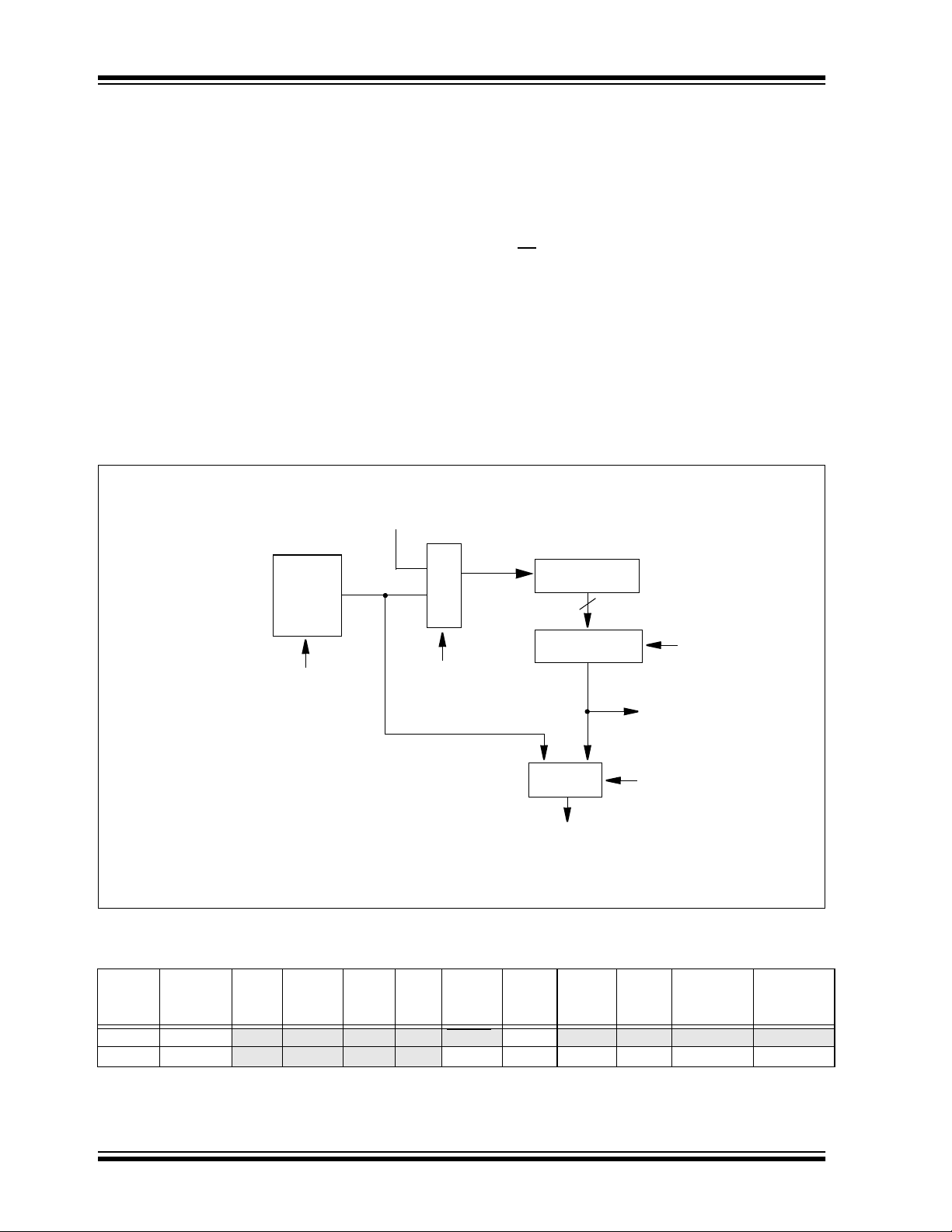
PIC16C62X
9.7 Watchdog Timer (WDT)
The Watchdog Timer is a free running on-chip RC oscillator which does not require any external components.
This RC oscillator is separate from the RC oscillator of
the CLKIN pin. That means that the WDT will run, even
if the clock on the OSC1 and OSC2 pins of the device
has been stopped, for example, by execution of a
SLEEP instruction. During normal operation, a WDT
time-out generates a device RESET. If the device is in
SLEEP mode, a WDT time-out causes the device to
DC specs). If longer time-out periods are desired, a
prescaler with a division ratio of up to 1:128 can be
assigned to the WDT under software control by writing
to the OPTION register. Thus, time-out periods up to
2.3 seconds can be realized.
The CLRWDT and SLEEP instructions clear the WDT
and the postscaler, if assigned to the WDT, and prevent
it from timing out and generating a device RESET.
The TO bit in the STATUS register will be cleared upon
a Watchdog Timer time-out.
wake-up and continue with normal operation. The WDT
can be permanently disabled by programming the
9.7.2 WDT PROGRAMMING
configuration bit WDTE as clear (Section 9.1).
9.7.1 WDT PERIOD
The WDT has a nominal time-out period of 18 ms, (with
no prescaler). The time-out periods vary with temperature, V
and process variations from part to part (see
DD
It should also be taken in account that under worst case
conditions (V
WDT prescaler) it may take several seconds before a
WDT time-out occurs.
FIGURE 9-17: WATCHDOG TIMER BLOCK DIAGRAM
From TMR0 Clock Source
(Figure 6-6)
0
M
Watchdog
Timer
1
U
X
CONSIDERATIONS
DD = Min., Temperature = Max., max.
Postscaler
8
8 - to -1 MUX
WDT
Enable Bit
Note: T0SE, T0CS, PSA, PS<2:0> are bits in the OPTION register.
PSA
0
Time-out
1
MUX
WDT
TABLE 9-7: SUMMARY OF WATCHDOG TIMER REGISTERS
Address Name Bit 7 Bit 6 Bit 5 Bit 4 Bit 3 Bit 2 Bit 1 Bit 0
2007h Config. bits
81h OPTION
Legend: Shaded cells are not used by the Watchdog Timer.
Note:
_
= Unimplemented location, read as “0”
+ = Reserved for future use
— BODEN CP1 CP0 PWRTE WDTE FOSC1 FOSC0 — —
RBPU INTEDG T0CS T 0S E P SA PS2 P S1 P S0 1111 1111 1111 1111
PS<2:0>
To TMR0 (Figure 6-6)
PSA
Value on
POR Reset
Value on all
other
RESETS
DS30235J-page 58 2003 Microchip Technology Inc.
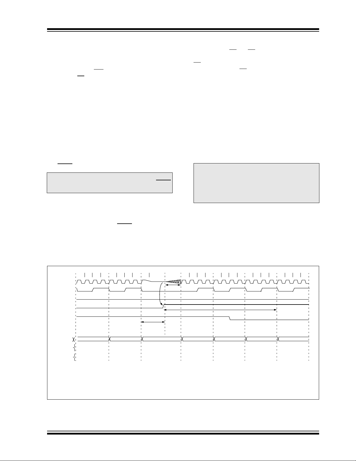
PIC16C62X
9.8 Power-Down Mode (SLEEP)
The Power-down mode is entered by executing a
SLEEP instruction.
If enabled, the Watchdog Timer will be cleared but
keeps running, the PD
cleared, the TO
bit is set, and the oscillator driver is
turned off. The I/O ports maintain the status they had,
before
SLEEP was executed (driving high, low, or hi-
impedance).
For lowest current consumption in this mode, all I/O
pins should be either at V
circuitry drawing current from the I/O pin and the
comparators and V
are hi-impedance inputs should be pulled high or low
externally to avoid switching currents caused by floating inputs. The T0CKI input should also be at V
V
SS for lowest current consumption. The contribution
from on chip pull-ups on PORTB should be considered.
The MCLR pin must be at a logic high level (VIHMC).
Note: It should be noted that a RESET generated
by a WDT time-out does not drive MCLR
pin low.
9.8.1 WAKE-UP FROM SLEEP
The device can wake-up from SLEEP through one of
the following events:
1. External RESET input on MCLR pin
2. Watchdog Timer Wake-up (if WDT was enabled)
3. Interrupt from RB0/INT pin, RB Port change, or
the Peripheral Interrupt (Comparator).
bit in the STATUS register is
DD or VSS with no external
REF should be disabled. I/O pins that
DD or
The first event will cause a device RESET. The two
latter events are considered a continuation of program
execution. The TO
and PD bits in the STATUS register
can be used to determine the cause of device RESET.
bit, which is set on power-up, is cleared when
PD
SLEEP is invoked. TO
bit is cleared if WDT wake-up
occurred.
When the SLEEP instruction is being executed, the
next instruction (PC + 1) is pre-fetched. For the device
to wake-up through an interrupt event, the corresponding interrupt enable bit must be set (enabled). Wake-up
is regardless of the state of the GIE bit. If the GIE bit is
clear (disabled), the device continues execution at the
instruction after the
SLEEP instruction. If the GIE bit is
set (enabled), the device executes the instruction after
the SLEEP instruction and then branches to the interrupt address (0004h). In cases where the execution of
the instruction following
user should have an
SLEEP is not desirable, the
NOP after the SLEEP instruction.
Note: If the global interrupts are disabled (GIE is
cleared), but any interrupt source has both
its interrupt enable bit and the corresponding interrupt flag bits set, the device will
immediately wake-up from SLEEP. The
SLEEP instruction is completely executed.
The WDT is cleared when the device wakes up from
SLEEP, regardless of the source of wake-up.
FIGURE 9-18: WAKE-UP FROM SLEEP THROUGH INTERRUPT
Q1 Q2 Q3 Q4 Q1 Q2 Q3 Q4 Q1 Q1 Q2 Q3 Q4 Q1 Q2 Q3 Q4 Q1 Q2 Q3 Q4 Q1 Q2 Q3 Q4
OSC1
CLKOUT(4)
INT pin
INTF flag
(INTCON<1>)
GIE bit
(INTCON<7>)
INSTRUCTION FLOW
PC
Instruction
fetched
Instruction
executed
Inst(PC) = SLEEP
PC PC+1 PC+2
Inst(PC + 1)
Inst(PC - 1)
SLEEP
Processor in
SLEEP
Note 1: XT, HS or LP Oscillator mode assumed.
OST = 1024TOSC (drawing not to scale) This delay will not be there for RC Osc mode.
2: T
3: GIE = '1' assumed. In this case, after wake-up, the processor jumps to the interrupt routine. If GIE = '0',
execution will continue in-line.
4: CLKOUT is not available in these Osc modes, but shown here for timing reference.
To st (2)
Interrupt Latency
(Note 2)
PC+2
Inst(PC + 2)
Inst(PC + 1)
PC + 2 0004h 0005h
Inst(0004h)
Dummy cycle
Dummy cycle
Inst(0005h)
Inst(0004h)
2003 Microchip Technology Inc. DS30235J-page 59
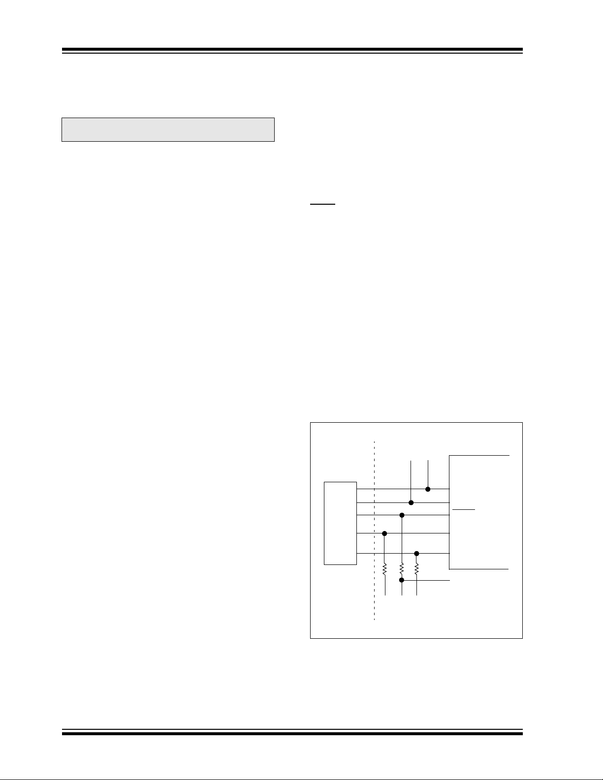
PIC16C62X
9.9 Code Protection
If the code protection bit(s) have not been
programmed, the on-chip program memory can be
read out for verification purposes.
Note: Microchip does not recommend code
protecting windowed devices.
9.10 ID Locations
Four memory locations (2000h-2003h) are designated
as ID locations where the user can store checksum or
other code identification numbers. These locations are
not accessible during normal execution, but are
readable and writable during Program/Verify. Only the
Least Significant 4 bits of the ID locations are used.
9.11 In-Circuit Serial Programming™
The PIC16C62X microcontrollers can be serially
programmed while in the end application circuit. This is
simply done with two lines for clock and data and three
other lines for power, ground and the programming
voltage. This allows customers to manufacture boards
with unprogrammed devices and then program the
microcontroller just before shipping the product. This
also allows the most recent firmware or a custom
firmware to be programmed.
The device is placed into a Program/Verify mode by
holding the RB6 and RB7 pins low, while raising the
MCLR
(VPP) pin from VIL to VIHH (see programming
specification). RB6 becomes the programming clock
and RB7 becomes the programming data. Both RB6
and RB7 are Schmitt Trigger inputs in this mode.
After RESET, to place the device into Programming/
Verify mode, the program counter (PC) is at location
00h. A 6-bit command is then supplied to the device.
Depending on the command, 14-bits of program data
are then supplied to or from the device, depending if
the command was a load or a read. For complete
details of serial programming, please refer to the
PIC16C6X/7X/9XX Programming Specification
(DS30228).
A typical In-Circuit Serial Programming connection is
shown in Figure 9-19.
FIGURE 9-19: TYPICAL IN-CIRCUIT
SERIAL PROGRAMMING
CONNECTION
To Normal
External
Connector
Signals
+5V
0V
V
PP
CLK
Data I/O
Connections
To Normal
Connections
PIC16C62X
V
DD
VSS
MCLR/VPP
RB6
RB7
DD
V
DS30235J-page 60 2003 Microchip Technology Inc.
PIC16C62X
10.0 INSTRUCTION SET SUMMARY
Each PIC16C62X instruction is a 14-bit word divided
into an OPCODE which specifies the instruction type
and one or more operands which further specify the
operation of the instruction. The PIC16C62X instruction set summary in Table 10-2 lists byte-oriented, bit-
oriented, and literal and control operations.
Table 10-1 shows the opcode field descriptions.
For byte-oriented instructions, 'f' represents a file
register designator and 'd' represents a destination
designator. The file register designator specifies which
file register is to be used by the instruction.
The destination designator specifies where the result of
the operation is to be placed. If 'd' is zero, the result is
placed in the W register. If 'd' is one, the result is placed
in the file register specified in the instruction.
For bit-oriented instructions, 'b' represents a bit field
designator which selects the number of the bit affected
by the operation, while 'f' represents the number of the
file in which the bit is located.
For literal and control operations, 'k' represents an
eight or eleven bit constant or literal value.
TABLE 10-1: OPCODE FIELD
DESCRIPTIONS
Field Description
f Register file address (0x00 to 0x7F)
W Working register (accumulator)
b Bit address within an 8-bit file register
k Literal field, constant data or label
x Don't care location (= 0 or 1)
The assembler will generate code with x = 0. It is the
recommended form of use for compatibility with all
Microchip software tools.
d Destination select; d = 0: store result in W,
d = 1: store result in file register f.
Default is d = 1
label Label name
TOS Top of Stack
PC Program Counter
PCLATHProgram Counter High Latch
GIE Global Interrupt Enable bit
WDT Watchdog Timer/Counter
TO Time-out bit
PD Power-down bit
dest Destination either the W register or the specified regis-
ter file location
[ ] Options
( ) Contents
→ Assigned to
< > Register bit field
∈ In the set of
italics User defined term (font is courier)
The instruction set is highly orthogonal and is grouped
into three basic categories:
• Byte-oriented operations
• Bit-oriented operations
• Literal and control operations
All instructions are executed within one single
instruction cycle, unless a conditional test is true or the
program counter is changed as a result of an
instruction. In this case, the execution takes two
instruction cycles with the second cycle executed as a
NOP. One instruction cycle consists of four oscillator
periods. Thus, for an oscillator frequency of 4 MHz, the
normal instruction execution time is 1 µs. If a
conditional test is true or the program counter is
changed as a result of an instruction, the instruction
execution time is 2 µs.
Table 10-1 lists the instructions recognized by the
MPASM™ assembler.
Figure 10-1 shows the three general formats that the
instructions can have.
Note: To maintain upward compatibility with
future PICmicro
®
products, do not use the
OPTION and TRIS instructions.
All examples use the following format to represent a
hexadecimal number:
0xhh
where h signifies a hexadecimal digit.
FIGURE 10-1: GENERAL FORMAT FOR
INSTRUCTIONS
Byte-oriented file register operations
13 8 7 6 0
OPCODE d f (FILE #)
d = 0 for destination W
d = 1 for destination f
f = 7-bit file register address
Bit-oriented file register operations
13 10 9 7 6 0
OPCODE b (BIT #) f (FILE #)
b = 3-bit bit address
f = 7-bit file register address
Literal and control operations
General
13 8 7 0
OPCODE k (literal)
k = 8-bit immediate value
CALL and GOTO instructions only
13 11 10 0
OPCODE k (literal)
k = 11-bit immediate value
2003 Microchip Technology Inc. DS30235J-page 61

PIC16C62X
TABLE 10-2: PIC16C62X INSTRUCTION SET
Mnemonic,
Operands
BYTE-ORIENTED FILE REGISTER OPERATIONS
ADDWF
ANDWF
CLRF
CLRW
COMF
DECF
DECFSZ
INCF
INCFSZ
IORWF
MOVF
MOVWF
NOP
RLF
RRF
SUBWF
SWAPF
XORWF
BIT-ORIENTED FILE REGISTER OPERATIONS
BCF
BSF
BTFSC
BTFSS
LITERAL AND CONTROL OPERATIONS
ADDLW
ANDLW
CALL
CLRWDT
GOTO
IORLW
MOVLW
RETFIE
RETLW
RETURN
SLEEP
SUBLW
XORLW
Note 1: When an I/O register is modified as a function of itself ( e.g., MOVF PORTB, 1), the value used will be that
value present on the pins themselves. For example, if the data latch is '1' for a pin configured as input and
is driven low by an external device, the data will be written back with a '0'.
2: If this instruction is executed on the TMR0 register (and, where applicable, d = 1), the prescaler will be
cleared if assigned to the Timer0 Module.
3: If Program Counter (PC) is modified or a conditional test is true, the instruction requires two cycles. The
second cycle is executed as a NOP.
Description Cycles 14-Bit Opcode Status
MSb LSb
f, d
Add W and f
f, d
AND W with f
f
Clear f
-
Clear W
f, d
Complement f
f, d
Decrement f
f, d
Decrement f, Skip if 0
f, d
Increment f
f, d
Increment f, Skip if 0
f, d
Inclusive OR W with f
f, d
Move f
f
Move W to f
-
No Operation
f, d
Rotate Left f through Carry
f, d
Rotate Right f through Carry
f, d
Subtract W from f
f, d
Swap nibbles in f
f, d
Exclusive OR W with f
f, b
Bit Clear f
f, b
Bit Set f
f, b
Bit Test f, Skip if Clear
f, b
Bit Test f, Skip if Set
k
Add literal and W
k
AND literal with W
k
Call subroutine
-
Clear Watchdog Timer
k
Go to address
k
Inclusive OR literal with W
k
Move literal to W
-
Return from interrupt
k
Return with literal in W
-
Return from Subroutine
-
Go into Standby mode
k
Subtract W from literal
k
Exclusive OR literal with W
1
1
1
1
1
1
1(2)
1
1(2)
1
1
1
1
1
1
1
1
1
1
1
1 (2)
1 (2)
1
1
2
1
2
1
1
2
2
2
1
1
1
00
00
00
00
00
00
00
00
00
00
00
00
00
00
00
00
00
00
01
01
01
01
11
11
10
00
10
11
11
00
11
00
00
11
11
0111
0101
0001
0001
1001
0011
1011
1010
1111
0100
1000
0000
0000
1101
1100
0010
1110
0110
00bb
01bb
10bb
11bb
111x
1001
0kkk
0000
1kkk
1000
00xx
0000
01xx
0000
0000
110x
1010
dfff
dfff
lfff
0000
dfff
dfff
dfff
dfff
dfff
dfff
dfff
lfff
0xx0
dfff
dfff
dfff
dfff
dfff
bfff
bfff
bfff
bfff
kkkk
kkkk
kkkk
0110
kkkk
kkkk
kkkk
0000
kkkk
0000
0110
kkkk
kkkk
ffff
ffff
ffff
0011
ffff
ffff
ffff
ffff
ffff
ffff
ffff
ffff
0000
ffff
ffff
ffff
ffff
ffff
ffff
ffff
ffff
ffff
kkkk
kkkk
kkkk
0100
kkkk
kkkk
kkkk
1001
kkkk
1000
0011
kkkk
kkkk
Affected
C,DC,Z
Z
Z
Z
Z
Z
Z
Z
Z
C
C
C,DC,Z
Z
C,DC,Z
Z
TO,PD
Z
TO,PD
C,DC,Z
Z
Notes
1,2
1,2
2
1,2
1,2
1,2,3
1,2
1,2,3
1,2
1,2
1,2
1,2
1,2
1,2
1,2
1,2
1,2
3
3
DS30235J-page 62 2003 Microchip Technology Inc.

10.1 Instruction Descriptions
ADDLW Add Literal and W
Syntax: [ label ] ADDLW k
Operands: 0 ≤ k ≤ 255
Operation: (W) + k → (W)
Status Affected: C, DC, Z
Encoding:
Description: The contents of the W register are
Words: 1
Cycles: 1
Example
11 111x kkkk kkkk
added to the eight bit literal 'k' and
the result is placed in the W
register.
ADDLW 0x15
Before Instruction
W = 0x10
After Instruction
W = 0x25
PIC16C62X
ANDLW AND Literal with W
Syntax: [ label ] ANDLW k
Operands: 0 ≤ k ≤ 255
Operation: (W) .AND. (k) → (W)
Status Affected: Z
Encoding:
Description: The contents of W register are
Words: 1
Cycles: 1
Example
11 1001 kkkk kkkk
AND’ed with the eight bit literal 'k'.
The result is placed in the W
register.
ANDLW 0x5F
Before Instruction
W= 0xA3
After Instruction
W = 0x03
ADDWF Add W and f
Syntax: [ label ] ADDWF f,d
Operands: 0 ≤ f ≤ 127
d ∈ [0,1]
Operation: (W) + (f) → (dest)
Status Affected: C, DC, Z
Encoding:
00 0111 dfff ffff
Description: Add the contents of the W register
with register 'f'. If 'd' is 0, the result
is stored in the W register. If 'd' is
1, the result is stored back in
register 'f'.
Words: 1
Cycles: 1
Example
ADDWF FSR,
0
Before Instruction
W = 0x17
FSR = 0xC2
After Instruction
W= 0xD9
FSR = 0xC2
ANDWF AND W with f
Syntax: [ label ] ANDWF f,d
Operands: 0 ≤ f ≤ 127
d ∈ [0,1]
Operation: (W) .AND. (f) → (dest)
Status Affected: Z
Encoding:
00 0101 dfff ffff
Description: AND the W register with register
'f'. If 'd' is 0, the result is stored in
the W register. If 'd' is 1, the result
is stored back in register 'f'.
Words: 1
Cycles: 1
Example
ANDWF FSR,
1
Before Instruction
W = 0x17
FSR = 0xC2
After Instruction
W = 0x17
FSR = 0x02
2003 Microchip Technology Inc. DS30235J-page 63

PIC16C62X
BCF Bit Clear f
Syntax: [ label ] BCF f,b
Operands: 0 ≤ f ≤ 127
0 ≤ b ≤ 7
Operation: 0 → (f<b>)
Status Affected: None
Encoding:
01 00bb bfff ffff
Description: Bit 'b' in register 'f' is cleared.
Words: 1
Cycles: 1
Example
BCF FLAG_REG, 7
Before Instruction
FLAG_REG = 0xC7
After Instruction
FLAG_REG = 0x47
BSF Bit Set f
Syntax: [ label ] BSF f,b
Operands: 0 ≤ f ≤ 127
0 ≤ b ≤ 7
Operation: 1 → (f<b>)
Status Affected: None
Encoding:
01 01bb bfff ffff
Description: Bit 'b' in register 'f' is set.
Words: 1
Cycles: 1
Example
BSF FLAG_REG, 7
Before Instruction
FLAG_REG = 0x0A
After Instruction
FLAG_REG = 0x8A
BTFSC Bit Test, Skip if Clear
Syntax: [ label ] BTFSC f,b
Operands: 0 ≤ f ≤ 127
0 ≤ b ≤ 7
Operation: skip if (f<b>) = 0
Status Affected: None
Encoding:
01 10bb bfff ffff
Description: If bit 'b' in register 'f' is '0', then the
next instruction is skipped.
If bit 'b' is '0', then the next instruction fetched during the current
instruction execution is discarded,
and a NOP is executed instead,
making this a two-cycle instruction.
Words: 1
Cycles: 1(2)
Example
HERE
FALSE
TRUE
BTFSC
GOTO
•
•
•
FLAG,1
PROCESS_CO
DE
Before Instruction
PC = address HERE
After Instruction
if FLAG<1> = 0,
PC = address TRUE
if FLAG<1>=1,
PC = address FALSE
DS30235J-page 64 2003 Microchip Technology Inc.

PIC16C62X
BTFSS Bit Test f, Skip if Set
Syntax: [ label ] BTFSS f,b
Operands: 0 ≤ f ≤ 127
0 ≤ b < 7
Operation: skip if (f<b>) = 1
Status Affected: None
Encoding:
01 11bb bfff ffff
Description: If bit 'b' in register 'f' is '1', then the
next instruction is skipped.
If bit 'b' is '1', then the next instruction fetched during the current
instruction execution, is discarded
and a NOP is executed instead,
making this a two-cycle instruction.
Words: 1
Cycles: 1(2)
Example
HERE
FALSE
TRUE
BTFSS
GOTO
•
•
•
FLAG,1
PROCESS_CO
DE
Before Instruction
PC = address HERE
After Instruction
if FLAG<1> = 0,
PC = address FALSE
if FLAG<1> = 1,
PC = address TRUE
CALL Call Subroutine
Syntax: [ label ] CALL k
Operands: 0 ≤ k ≤ 2047
Operation: (PC)+ 1→ TOS,
k → PC<10:0>,
(PCLATH<4:3>) → PC<12:11>
Status Affected: None
Encoding:
10 0kkk kkkk kkkk
Description: Call Subroutine. First, return
address (PC+1) is pushed onto
the stack. The eleven bit immediate address is loaded into PC bits
<10:0>. The upper bits of the PC
are loaded from PCLATH. CALL is
a two-cycle instruction.
Words: 1
Cycles: 2
Example
HERE CALL
THER
E
Before Instruction
PC = Address HERE
After Instruction
PC = Address THERE
TOS = Address HERE+1
CLRF Clear f
Syntax: [ label ] CLRF f
Operands: 0 ≤ f ≤ 127
Operation: 00h → (f)
1 → Z
Status Affected: Z
Encoding:
00 0001 1fff ffff
Description: The contents of register 'f' are
cleared and the Z bit is set.
Words: 1
Cycles: 1
Example
CLRF FLAG_REG
Before Instruction
FLAG_REG = 0x5A
After Instruction
FLAG_REG = 0x00
Z=1
2003 Microchip Technology Inc. DS30235J-page 65

PIC16C62X
CLRW Clear W
Syntax: [ label ] CLRW
Operands: None
Operation: 00h → (W)
1 → Z
Status Affected: Z
Encoding:
00 0001 0000 0011
Description: W register is cleared. Zero bit (Z)
is set.
Words: 1
Cycles: 1
Example
CLRW
Before Instruction
W = 0x5A
After Instruction
W = 0x00
Z=1
CLRWDT Clear Watchdog Timer
Syntax: [ label ] CLRWDT
Operands: None
Operation: 00h → WDT
0 → WDT prescaler,
1 → TO
1 → PD
Status Affected: TO, PD
Encoding:
00 0000 0110 0100
Description: CLRWDT instruction resets the
Watchdog Timer. It also resets the
prescaler of the WDT. STATUS
and PD are set.
bits TO
Words: 1
Cycles: 1
Example
CLRWDT
Before Instruction
WDT counter = ?
After Instruction
WDT counter = 0x00
WDT prescaler= 0
TO =1
PD =1
COMF Complement f
Syntax: [ label ] COMF f,d
Operands: 0 ≤ f ≤ 127
d ∈ [0,1]
Operation: (f) → (dest)
Status Affected: Z
Encoding:
00 1001 dfff ffff
Description: The contents of register 'f' are
complemented. If 'd' is 0, the
result is stored in W. If 'd' is 1, the
result is stored back in register 'f'.
Words: 1
Cycles: 1
Example
COMF REG1,0
Before Instruction
REG1 = 0x13
After Instruction
REG1 = 0x13
W=0xEC
DECF Decrement f
Syntax: [ label ] DECF f,d
Operands: 0 ≤ f ≤ 127
d ∈ [0,1]
Operation: (f) - 1 → (dest)
Status Affected: Z
Encoding:
00 0011 dfff ffff
Description: Decrement register 'f'. If 'd' is 0,
the result is stored in the W
register. If 'd' is 1, the result is
stored back in register 'f'.
Words: 1
Cycles: 1
Example
DECF CNT,
1
Before Instruction
CNT = 0x01
Z=0
After Instruction
CNT = 0x00
Z=1
DS30235J-page 66 2003 Microchip Technology Inc.

PIC16C62X
DECFSZ Decrement f, Skip if 0
Syntax: [ label ] DECFSZ f,d
Operands: 0 ≤ f ≤ 127
d ∈ [0,1]
Operation: (f) - 1 → (dest); skip if result = 0
Status Affected: None
Encoding:
00 1011 dfff ffff
Description: The contents of register 'f' are
decremented. If 'd' is 0, the result
is placed in the W register. If 'd' is
1, the result is placed back in
register 'f'.
If the result is 0, the next instruction, which is already fetched, is
discarded. A NOP is executed
instead making it a two-cycle
instruction.
Words: 1
Cycles: 1(2)
Example
HERE DECFSZ CNT, 1
GOTO LOOP
CONTINUE •
•
•
Before Instruction
PC = address HERE
After Instruction
CNT = CNT - 1
if CNT = 0,
PC = address CONTINUE
if CNT ≠ 0,
PC = address HERE+1
INCF Increment f
Syntax: [ label ] INCF f,d
Operands: 0 ≤ f ≤ 127
d ∈ [0,1]
Operation: (f) + 1 → (dest)
Status Affected: Z
Encoding:
00 1010 dfff ffff
Description: The contents of register 'f' are
incremented. If 'd' is 0, the result
is placed in the W register. If 'd' is
1, the result is placed back in
register 'f'.
Words: 1
Cycles: 1
Example
INCF CNT,
1
Before Instruction
CNT = 0xFF
Z=0
After Instruction
CNT = 0x00
Z=1
GOTO Unconditional Branch
Syntax: [ label ] GOTO k
Operands: 0 ≤ k ≤ 2047
Operation: k → PC<10:0>
PCLATH<4:3> → PC<12:11>
Status Affected: None
Encoding:
10 1kkk kkkk kkkk
Description: GOTO is an unconditional branch.
The eleven bit immediate value is
loaded into PC bits <10:0>. The
upper bits of PC are loaded from
PCLATH<4:3>. GOTO is a two-
cycle instruction.
Words: 1
Cycles: 2
Example
GOTO THERE
After Instruction
PC = Address THERE
2003 Microchip Technology Inc. DS30235J-page 67

PIC16C62X
INCFSZ Increment f, Skip if 0
Syntax: [ label ] INCFSZ f,d
Operands: 0 ≤ f ≤ 127
d ∈ [0,1]
Operation: (f) + 1 → (dest), skip if result = 0
Status Affected: None
Encoding:
00 1111 dfff ffff
Description: The contents of register 'f' are
incremented. If 'd' is 0 the result is
placed in the W register. If 'd' is 1,
the result is placed back in
register 'f'.
If the result is 0, the next instruction, which is already fetched, is
discarded. A NOP is executed
instead making it a two-cycle
instruction.
Words: 1
Cycles: 1(2)
Example
HERE INCFSZ CNT, 1
GOTO LOOP
CONTINUE •
•
•
Before Instruction
PC = address HERE
After Instruction
CNT = CNT + 1
if CNT= 0,
PC = address CONTINUE
if CNT≠ 0,
PC = address HERE +1
IORLW Inclusive OR Literal with W
Syntax: [ label ] IORLW k
Operands: 0 ≤ k ≤ 255
Operation: (W) .OR. k → (W)
Status Affected: Z
Encoding:
11 1000 kkkk kkkk
Description: The contents of the W register is
OR’ed with the eight bit literal 'k'.
The result is placed in the W
register.
Words: 1
Cycles: 1
Example
IORLW 0x35
Before Instruction
W = 0x9A
After Instruction
W= 0xBF
Z=1
IORWF Inclusive OR W with f
Syntax: [ label ] IORWF f,d
Operands: 0 ≤ f ≤ 127
d ∈ [0,1]
Operation: (W) .OR. (f) → (dest)
Status Affected: Z
Encoding:
00 0100 dfff ffff
Description: Inclusive OR the W register with
register 'f'. If 'd' is 0 the result is
placed in the W register. If 'd' is 1
the result is placed back in
register 'f'.
Words: 1
Cycles: 1
Example
IORWF
RESULT, 0
Before Instruction
RESULT = 0x13
W = 0x91
After Instruction
RESULT = 0x13
W = 0x93
Z=1
MOVLW Move Literal to W
Syntax: [ label ] MOVLW k
Operands: 0 ≤ k ≤ 255
Operation: k → (W)
Status Affected: None
Encoding:
11 00xx kkkk kkkk
Description: The eight bit literal 'k' is loaded
into W register. The don’t cares
will assemble as 0’s
.
Words: 1
Cycles: 1
Example
MOVLW 0x5A
After Instruction
W= 0x5A
DS30235J-page 68 2003 Microchip Technology Inc.

PIC16C62X
MOVF Move f
Syntax: [ label ] MOVF f,d
Operands: 0 ≤ f ≤ 127
d ∈ [0,1]
Operation: (f) → (dest)
Status Affected: Z
Encoding:
00 1000 dfff ffff
Description: The contents of register f is
moved to a destination dependent
upon the status of d. If d = 0,
destination is W register. If d = 1,
the destination is file register f
itself. d = 1 is useful to test a file
register since status flag Z is
affected.
Words: 1
Cycles: 1
Example
MOVF FSR,
0
After Instruction
W = value in FSR
register
Z= 1
MOVWF Move W to f
Syntax: [ label ] MOVWF f
Operands: 0 ≤ f ≤ 127
Operation: (W) → (f)
Status Affected: None
Encoding:
00 0000 1fff ffff
Description: Move data from W register to reg-
ister 'f'.
Words: 1
Cycles: 1
Example
MOVWF OPTION
Before Instruction
OPTION = 0xFF
W = 0x4F
After Instruction
OPTION = 0x4F
W = 0x4F
NOP No Operation
Syntax: [ label ] NOP
Operands: None
Operation: No operation
Status Affected: None
Encoding:
00 0000 0xx0 0000
Description: No operation.
Words: 1
Cycles: 1
Example
NOP
OPTION Load Option Register
Syntax: [ label ] OPTION
Operands: None
Operation: (W) → OPTION
Status Affected: None
Encoding:
00 0000 0110 0010
Description: The contents of the W register are
loaded in the OPTION register.
This instruction is supported for
code compatibility with PIC16C5X
products. Since OPTION is a readable/writable register, the user can
directly address it.
Words: 1
Cycles: 1
Example
To maintain upward compatibility with future PICmicro
®
products, do not use this
instruction.
2003 Microchip Technology Inc. DS30235J-page 69

PIC16C62X
RETFIE Return from Interrupt
Syntax: [ label ] RETFIE
Operands: None
Operation: TOS → PC,
1 → GIE
Status Affected: None
Encoding:
Description: Return from Interrupt. Stack is
Words: 1
Cycles: 2
Example
00 0000 0000 1001
POPed and Top of Stack (TOS) is
loaded in the PC. Interrupts are
enabled by setting Global
Interrupt Enable bit, GIE
(INTCON<7>). This is a two-cycle
instruction.
RETFIE
After Interrupt
PC = TOS
GIE = 1
RETLW Return with Literal in W
Syntax: [ label ] RETLW k
Operands: 0 ≤ k ≤ 255
Operation: k → (W);
TOS → PC
Status Affected: None
Encoding:
Description: The W register is loaded with the
Words: 1
Cycles: 2
Example
TABLE
11 01xx kkkk kkkk
eight bit literal 'k'. The program
counter is loaded from the top of
the stack (the return address).
This is a two-cycle instruction.
CALL TABLE;W contains
table
;offset value
• ;W now has table value
•
•
ADDWF PC ;W = offset
RETLW k1 ;Begin table
RETLW k2 ;
•
•
•
RETLW kn ; End of table
Before Instruction
W= 0x07
After Instruction
W = value of k8
RETURN Return from Subroutine
Syntax: [ label ] RETURN
Operands: None
Operation: TOS → PC
Status Affected: None
Encoding:
Description: Return from subroutine. The stack
Words: 1
Cycles: 2
Example
DS30235J-page 70 2003 Microchip Technology Inc.
00 0000 0000 1000
is POPed and the top of the stack
(TOS) is loaded into the program
counter. This is a two-cycle
instruction.
RETURN
After Interrupt
PC = TOS

PIC16C62X
RLF Rotate Left f through Carry
Syntax: [ label ] RLF f,d
Operands: 0 ≤ f ≤ 127
d ∈ [0,1]
Operation: See description below
Status Affected: C
Encoding:
00 1101 dfff ffff
Description: The contents of register 'f' are
rotated one bit to the left through
the Carry Flag. If 'd' is 0, the result
is placed in the W register. If 'd' is
1, the result is stored back in
register 'f'.
Register fC
Words: 1
Cycles: 1
Example
RLF REG1,0
Before Instruction
REG1 = 1110 0110
C=0
After Instruction
REG1 = 1110 0110
W = 1100 1100
C=1
RRF Rotate Right f through Carry
Syntax: [ label ] RRF f,d
Operands: 0 ≤ f ≤ 127
d ∈ [0,1]
Operation: See description below
Status Affected: C
Encoding:
00 1100 dfff ffff
Description: The contents of register 'f' are
rotated one bit to the right through
the Carry Flag. If 'd' is 0, the result
is placed in the W register. If 'd' is
1, the result is placed back in
register 'f'.
Register fC
Words: 1
Cycles: 1
Example
RRF
REG1,
0
Before Instruction
REG1 = 1110 0110
C=0
After Instruction
REG1 = 1110 0110
W = 0111 0011
C=0
SLEEP
Syntax: [ label ]SLEEP
Operands: None
Operation: 00h → WDT,
0 → WDT prescaler,
1 → TO,
0 → PD
Status Affected: TO, PD
Encoding:
00 0000 0110 0011
Description: The power-down STATUS bit,
is cleared. Time-out
PD
STATUS bit, TO
is set. Watchdog Timer and its prescaler are
cleared.
The processor is put into SLEEP
mode with the oscillator
stopped. See Section 9.8 for
more details.
Words: 1
Cycles: 1
Example: SLEEP
2003 Microchip Technology Inc. DS30235J-page 71

PIC16C62X
SUBLW Subtract W from Literal
Syntax: [ label ] SUBLW k
Operands: 0 ≤ k ≤ 255
Operation: k - (W) → (W)
Status
C, DC, Z
Affected:
Encoding:
11 110x kkkk kkkk
Description: The W register is subtracted (2’s
complement method) from the eight
bit literal 'k'. The result is placed in
the W register.
Words: 1
Cycles: 1
Example 1: SUBLW 0x02
Before Instruction
W= 1
C= ?
After Instruction
W= 1
C = 1; result is positive
Example 2: Before Instruction
W= 2
C= ?
After Instruction
W= 0
C = 1; result is zero
Example 3: Before Instruction
W= 3
C= ?
After Instruction
W= 0xFF
C = 0; result is negative
SUBWF Subtract W from f
Syntax: [ label ] SUBWF f,d
Operands: 0 ≤ f ≤ 127
d ∈ [0,1]
Operation: (f) - (W) → (dest)
Status
C, DC, Z
Affected:
Encoding:
00 0010 dfff ffff
Description: Subtract (2’s complement method)
W register from register 'f'. If 'd' is 0,
the result is stored in the W register.
If 'd' is 1, the result is stored back in
register 'f'.
Words: 1
Cycles: 1
Example 1: SUBWF REG1,1
Before Instruction
REG1= 3
W= 2
C= ?
After Instruction
REG1= 1
W= 2
C = 1; result is positive
Example 2: Before Instruction
REG1= 2
W= 2
C= ?
After Instruction
REG1= 0
W= 2
C = 1; result is zero
Example 3: Before Instruction
REG1= 1
W= 2
C= ?
After Instruction
REG1= 0xFF
W= 2
C = 0; result is negative
DS30235J-page 72 2003 Microchip Technology Inc.
PIC16C62X
SWAPF Swap Nibbles in f
Syntax: [ label ] SWAPF f,d
Operands: 0 ≤ f ≤ 127
d ∈ [0,1]
Operation: (f<3:0>) → (dest<7:4>),
(f<7:4>) → (dest<3:0>)
Status Affected: None
Encoding:
00 1110 dfff ffff
Description: The upper and lower nibbles of
register 'f' are exchanged. If 'd' is
0, the result is placed in W
register. If 'd' is 1, the result is
placed in register 'f'.
Words: 1
Cycles: 1
Example
SWAPF
REG, 0
Before Instruction
REG1 = 0xA5
After Instruction
REG1 = 0xA5
W = 0x5A
TRIS Load TRIS Register
Syntax: [ label ] TRIS f
Operands: 5 ≤ f ≤ 7
Operation: (W) → TRIS register f;
Status Affected: None
Encoding:
00 0000 0110 0fff
Description: The instruction is supported for
code compatibility with the
PIC16C5X products. Since TRIS
registers are readable and
writable, the user can directly
address them.
Words: 1
Cycles: 1
Example
To maintain upward compatibility with future PICmicro
®
products, do not use this
instruction.
XORLW Exclusive OR Literal with W
Syntax: [ label ]XORLW k
Operands: 0 ≤ k ≤ 255
Operation: (W) .XOR. k → (W)
Status Affected: Z
Encoding:
11 1010 kkkk kkkk
Description: The contents of the W register
are XOR’ed with the eight bit
literal 'k'. The result is placed in
the W register.
Words: 1
Cycles: 1
Example: XORLW 0xAF
Before Instruction
W= 0xB5
After Instruction
W = 0x1A
XORWF Exclusive OR W with f
Syntax: [ label ] XORWF f,d
Operands: 0 ≤ f ≤ 127
d ∈ [0,1]
Operation: (W) .XOR. (f) → (dest)
Status Affected: Z
Encoding:
00 0110 dfff ffff
Description: Exclusive OR the contents of the
W register with register 'f'. If 'd' is
0, the result is stored in the W
register. If 'd' is 1, the result is
stored back in register 'f'.
Words: 1
Cycles: 1
Example XORWF
REG
1
Before Instruction
REG = 0xAF
W=0xB5
After Instruction
REG = 0x1A
W=0xB5
2003 Microchip Technology Inc. DS30235J-page 73

PIC16C62X
NOTES:
DS30235J-page 74 2003 Microchip Technology Inc.

PIC16C62X
11.0 DEVELOPMENT SUPPORT
The PICmicro® microcontrollers are supported with a
full range of hardware and software development tools:
• Integrated Development Environment
- MPLAB
• Assemblers/Compilers/Linkers
-MPASM
- MPLAB C17 and MPLAB C18 C Compilers
-MPLINK
MPLIB
- MPLAB C30 C Compiler
- MPLAB ASM30 Assembler/Linker/Library
• Simulators
- MPLAB SIM Software Simulator
- MPLAB dsPIC30 Software Simulator
• Emulators
- MPLAB ICE 2000 In-Circuit Emulator
- MPLAB ICE 4000 In-Circuit Emulator
• In-Circuit Debugger
- MPLAB ICD 2
• Device Programmers
-PRO MATE
- PICSTART
• Low Cost Demonstration Boards
- PICDEM
- PICDEM.net
- PICDEM 2 Plus Demonstration Board
- PICDEM 3 Demonstration Board
- PICDEM 4 Demonstration Board
- PICDEM 17 Demonstration Board
- PICDEM 18R Demonstration Board
- PICDEM LIN Demonstration Board
- PICDEM USB Demonstration Board
• Evaluation Kits
-K
- PICDEM MSC
- microID
-CAN
- PowerSmart
-Analog
EELOQ
®
TM
TM
TM
®
®
IDE Software
Assembler
Object Linker/
Object Librarian
®
II Universal Device Programmer
®
Plus Development Programmer
TM
1 Demonstration Board
TM
Demonstration Board
®
11.1 MPLAB Integrated Development Environment Software
The MPLAB IDE software brings an ease of software
development previously unseen in the 8/16-bit microcontroller market. The MPLAB IDE is a Windows
based application that contains:
• An interface to debugging tools
- simulator
- programmer (sold separately)
- emulator (sold separately)
- in-circuit debugger (sold separately)
• A full-featured editor with color coded context
• A multiple project manager
• Customizable data windows with direct edit of
contents
• High level source code debugging
• Mouse over variable inspection
• Extensive on-line help
The MPLAB IDE allows you to:
• Edit your source files (either assembly or C)
• One touch assemble (or compile) and download
to PICmicro emulator and simulator tools
(automatically updates all project information)
• Debug using:
- source files (assembly or C)
- absolute listing file (mixed assembly and C)
- machine code
MPLAB IDE supports multiple debugging tools in a
single development paradigm, from the cost effective
simulators, through low cost in-circuit debuggers, to
full-featured emulators. This eliminates the learning
curve when upgrading to tools with increasing flexibility
and power.
11.2 MPASM Assembler
The MPASM assembler is a full-featured, universal
macro assembler for all PICmicro MCUs.
The MPASM assembler generates relocatable object
files for the MPLINK object linker, Intel
files, MAP files to detail memory usage and symbol
reference, absolute LST files that contain source lines
and generated machine code and COFF files for
debugging.
The MPASM assembler features include:
• Integration into MPLAB IDE projects
• User defined macros to streamline assembly code
• Conditional assembly for multi-purpose source
files
• Directives that allow complete control over the
assembly process
®
standard HEX
®
2003 Microchip Technology Inc. DS30235J-page 75

PIC16C62X
11.3 MPLAB C17 and MPLAB C18 C Compilers
The MPLAB C17 and MPLAB C18 Code Development
Systems are complete ANSI C compilers for
Microchip’s PIC17CXXX and PIC18CXXX family of
microcontrollers. These compilers provide powerful
integration capabilities, superior code optimization and
ease of use not found with other compilers.
For easy source level debugging, the compilers provide
symbol information that is optimized to the MPLAB IDE
debugger.
11.4 MPLINK Object Linker/ MPLIB Object Librarian
The MPLINK object linker combines relocatable
objects created by the MPASM assembler and the
MPLAB C17 and MPLAB C18 C compilers. It can link
relocatable objects from pre-compiled libraries, using
directives from a linker script.
The MPLIB object librarian manages the creation and
modification of library files of pre-compiled code. When
a routine from a library is called from a source file, only
the modules that contain that routine will be linked in
with the application. This allows large libraries to be
used efficiently in many different applications.
The object linker/library features include:
• Efficient linking of single libraries instead of many
smaller files
• Enhanced code maintainability by grouping
related modules together
• Flexible creation of libraries with easy module
listing, replacement, deletion and extraction
11.5 MPLAB C30 C Compiler
The MPLAB C30 C compiler is a full-featured, ANSI
compliant, optimizing compiler that translates standard
ANSI C programs into dsPIC30F assembly language
source. The compiler also supports many commandline options and language extensions to take full
advantage of the dsPIC30F device hardware capabilities, and afford fine control of the compiler code
generator.
MPLAB C30 is distributed with a complete ANSI C
standard library. All library functions have been
validated and conform to the ANSI C library standard.
The library includes functions for string manipulation,
dynamic memory allocation, data conversion, timekeeping, and math functions (trigonometric, exponential and hyperbolic). The compiler provides symbolic
information for high level source debugging with the
MPLAB IDE.
11.6 MPLAB ASM30 Assembler, Linker, and Librarian
MPLAB ASM30 assembler produces relocatable
machine code from symbolic assembly language for
dsPIC30F devices. MPLAB C30 compiler uses the
assembler to produce it’s object file. The assembler
generates relocatable object files that can then be
archived or linked with other relocatable object files and
archives to create an executable file. Notable features
of the assembler include:
• Support for the entire dsPIC30F instruction set
• Support for fixed-point and floating-point data
• Command line interface
• Rich directive set
• Flexible macro language
• MPLAB IDE compatibility
11.7 MPLAB SIM Software Simulator
The MPLAB SIM software simulator allows code development in a PC hosted environment by simulating the
PICmicro series microcontrollers on an instruction
level. On any given instruction, the data areas can be
examined or modified and stimuli can be applied from
a file, or user defined key press, to any pin. The execution can be performed in Single-Step, Execute Until
Break, or Trace mode.
The MPLAB SIM simulator fully supports symbolic
debugging using the MPLAB C17 and MPLAB C18
C Compilers, as well as the MPASM assembler. The
software simulator offers the flexibility to develop and
debug code outside of the laboratory environment,
making it an excellent, economical software
development tool.
11.8 MPLAB SIM30 Software Simulator
The MPLAB SIM30 software simulator allows code
development in a PC hosted environment by simulating
the dsPIC30F series microcontrollers on an instruction
level. On any given instruction, the data areas can be
examined or modified and stimuli can be applied from
a file, or user defined key press, to any of the pins.
The MPLAB SIM30 simulator fully supports symbolic
debugging using the MPLAB C30 C Compiler and
MPLAB ASM30 assembler. The simulator runs in either
a Command Line mode for automated tasks, or from
MPLAB IDE. This high speed simulator is designed to
debug, analyze and optimize time intensive DSP
routines.
DS30235J-page 76 2003 Microchip Technology Inc.

PIC16C62X
11.9 MPLAB ICE 2000 High Performance Universal In-Circuit Emulator
The MPLAB ICE 2000 universal in-circuit emulator is
intended to provide the product development engineer
with a complete microcontroller design tool set for
PICmicro microcontrollers. Software control of the
MPLAB ICE 2000 in-circuit emulator is advanced by
the MPLAB Integrated Development Environment,
which allows editing, building, downloading and source
debugging from a single environment.
The MPLAB ICE 2000 is a full-featured emulator
system with enhanced trace, trigger and data monitoring features. Interchangeable processor modules allow
the system to be easily reconfigured for emulation of
different processors. The universal architecture of the
MPLAB ICE in-circuit emulator allows expansion to
support new PICmicro microcontrollers.
The MPLAB ICE 2000 in-circuit emulator system has
been designed as a real-time emulation system with
advanced features that are typically found on more
expensive development tools. The PC platform and
Microsoft
chosen to best make these features available in a
simple, unified application.
®
Windows 32-bit operating system were
11.10 MPLAB ICE 4000 High Performance Universal In-Circuit Emulator
The MPLAB ICE 4000 universal in-circuit emulator is
intended to provide the product development engineer
with a complete microcontroller design tool set for highend PICmicro microcontrollers. Software control of the
MPLAB ICE in-circuit emulator is provided by the
MPLAB Integrated Development Environment, which
allows editing, building, downloading and source
debugging from a single environment.
The MPLAB ICD 4000 is a premium emulator system,
providing the features of MPLAB ICE 2000, but with
increased emulation memory and high speed performance for dsPIC30F and PIC18XXXX devices. Its
advanced emulator features include complex triggering
and timing, up to 2 Mb of emulation memory, and the
ability to view variables in real-time.
The MPLAB ICE 4000 in-circuit emulator system has
been designed as a real-time emulation system with
advanced features that are typically found on more
expensive development tools. The PC platform and
Microsoft Windows 32-bit operating system were
chosen to best make these features available in a
simple, unified application.
11.11 MPLAB ICD 2 In-Circuit Debugger
Microchip’s In-Circuit Debugger, MPLAB ICD 2, is a
powerful, low cost, run-time development tool,
connecting to the host PC via an RS-232 or high speed
USB interface. This tool is based on the FLASH
PICmicro MCUs and can be used to develop for these
and other PICmicro microcontrollers. The MPLAB
ICD 2 utilizes the in-circuit debugging capability built
into the FLASH devices. This feature, along with
Microchip’s In-Circuit Serial Programming
protocol, offers cost effective in-circuit FLASH debugging from the graphical user interface of the MPLAB
Integrated Development Environment. This enables a
designer to develop and debug source code by setting
breakpoints, single-stepping and watching variables,
CPU status and peripheral registers. Running at full
speed enables testing hardware and applications in
real-time. MPLAB ICD 2 also serves as a development
programmer for selected PICmicro devices.
TM
(ICSPTM)
11.12 PRO MATE II Universal Device Programmer
The PRO MATE II is a universal, CE compliant device
programmer with programmable voltage verification at
DDMIN and VDDMAX for maximum reliability. It features
V
an LCD display for instructions and error messages
and a modular detachable socket assembly to support
various package types. In Stand-Alone mode, the
PRO MATE II device programmer can read, verify, and
program PICmicro devices without a PC connection. It
can also set code protection in this mode.
11.13 PICSTART Plus Development Programmer
The PICSTART Plus development programmer is an
easy-to-use, low cost, prototype programmer. It
connects to the PC via a COM (RS-232) port. MPLAB
Integrated Development Environment software makes
using the programmer simple and efficient. The
PICSTART Plus development programmer supports
most PICmicro devices up to 40 pins. Larger pin count
devices, such as the PIC16C92X and PIC17C76X,
may be supported with an adapter socket. The
PICSTART Plus development programmer is CE
compliant.
2003 Microchip Technology Inc. DS30235J-page 77

PIC16C62X
11.14 PICDEM 1 PICmicro Demonstration Board
The PICDEM 1 demonstration board demonstrates the
capabilities of the PIC16C5X (PIC16C54 to
PIC16C58A), PIC16C61, PIC16C62X, PIC16C71,
PIC16C8X, PIC17C42, PIC17C43 and PIC17C44. All
necessary hardware and software is included to run
basic demo programs. The sample microcontrollers
provided with the PICDEM 1 demonstration board can
be programmed with a PRO MATE II device programmer, or a PICSTART Plus development programmer.
The PICDEM 1 demonstration board can be connected
to the MPLAB ICE in-circuit emulator for testing. A
prototype area extends the circuitry for additional
application components. Features include an RS-232
interface, a potentiometer for simulated analog input,
push button switches and eight LEDs.
11.15 PICDEM.net Internet/Ethernet Demonstration Board
The PICDEM.net demonstration board is an Internet/
Ethernet demonstration board using the PIC18F452
microcontroller and TCP/IP firmware. The board
supports any 40-pin DIP device that conforms to the
standard pinout used by the PIC16F877 or
PIC18C452. This kit features a user friendly TCP/IP
stack, web server with HTML, a 24L256 Serial
EEPROM for Xmodem download to web pages into
Serial EEPROM, ICSP/MPLAB ICD 2 interface connector, an Ethernet interface, RS-232 interface, and a
16 x 2 LCD display. Also included is the book and
CD-ROM “TCP/IP Lean, Web Servers for Embedded
Systems,” by Jeremy Bentham
11.17 PICDEM 3 PIC16C92X Demonstration Board
The PICDEM 3 demonstration board supports the
PIC16C923 and PIC16C924 in the PLCC package. All
the necessary hardware and software is included to run
the demonstration programs.
11.18 PICDEM 4 8/14/18-Pin Demonstration Board
The PICDEM 4 can be used to demonstrate the capabilities of the 8-, 14-, and 18-pin PIC16XXXX and
PIC18XXXX MCUs, including the PIC16F818/819,
PIC16F87/88, PIC16F62XA and the PIC18F1320
family of microcontrollers. PICDEM 4 is intended to
showcase the many features of these low pin count
parts, including LIN and Motor Control using ECCP.
Special provisions are made for low power operation
with the supercapacitor circuit, and jumpers allow onboard hardware to be disabled to eliminate current
draw in this mode. Included on the demo board are provisions for Crystal, RC or Canned Oscillator modes, a
five volt regulator for use with a nine volt wall adapter
or battery, DB-9 RS-232 interface, ICD connector for
programming via ICSP and development with MPLAB
ICD 2, 2x16 liquid crystal display, PCB footprints for HBridge motor driver, LIN transceiver and EEPROM.
Also included are: header for expansion, eight LEDs,
four potentiometers, three push buttons and a prototyping area. Included with the kit is a PIC16F627A and
a PIC18F1320. Tutorial firmware is included along with
the User’s Guide.
11.19 PICDEM 17 Demonstration Board
11.16 PICDEM 2 Plus Demonstration Board
The PICDEM 2 Plus demonstration board supports
many 18-, 28-, and 40-pin microcontrollers, including
PIC16F87X and PIC18FXX2 devices. All the necessary hardware and software is included to run the demonstration programs. The sample microcontrollers
provided with the PICDEM 2 demonstration board can
be programmed with a PRO MATE II device programmer, PICSTART Plus development programmer, or
MPLAB ICD 2 with a Universal Programmer Adapter.
The MPLAB ICD 2 and MPLAB ICE in-circuit emulators
may also be used with the PICDEM 2 demonstration
board to test firmware. A prototype area extends the
circuitry for additional application components. Some
of the features include an RS-232 interface, a 2 x 16
LCD display, a piezo speaker, an on-board temperature
sensor, four LEDs, and sample PIC18F452 and
PIC16F877 FLASH microcontrollers.
The PICDEM 17 demonstration board is an evaluation
board that demonstrates the capabilities of several
Microchip microcontrollers, including PIC17C752,
PIC17C756A, PIC17C762 and PIC17C766. A
programmed sample is included. The PRO MATE II
device programmer, or the PICSTART Plus development programmer, can be used to reprogram the
device for user tailored application development. The
PICDEM 17 demonstration board supports program
download and execution from external on-board
FLASH memory. A generous prototype area is
available for user hardware expansion.
DS30235J-page 78 2003 Microchip Technology Inc.

PIC16C62X
11.20 PICDEM 18R PIC18C601/801 Demonstration Board
The PICDEM 18R demonstration board serves to assist
development of the PIC18C601/801 family of Microchip
microcontrollers. It provides hardware implementation
of both 8-bit Multiplexed/De-multiplexed and 16-bit
Memory modes. The board includes 2 Mb external
FLASH memory and 128 Kb SRAM memory, as well as
serial EEPROM, allowing access to the wide range of
memory types supported by the PIC18C601/801.
11.21 PICDEM LIN PIC16C43X Demonstration Board
The powerful LIN hardware and software kit includes a
series of boards and three PICmicro microcontrollers.
The small footprint PIC16C432 and PIC16C433 are
used as slaves in the LIN communication and feature
on-board LIN transceivers. A PIC16F874 FLASH
microcontroller serves as the master. All three microcontrollers are programmed with firmware to provide
LIN bus communication.
11.22 PICkit
A complete "development system in a box", the PICkit
FLASH Starter Kit includes a convenient multi-section
board for programming, evaluation, and development
of 8/14-pin FLASH PIC
USB, the board operates under a simple Windows GUI.
The PICkit 1 Starter Kit includes the user's guide (on
CD ROM), PICkit
ous applications. Also included are MPLAB
(Integrated Development Environment) software, software and hardware "Tips 'n Tricks for 8-pin FLASH
®
Microcontrollers" Handbook and a USB Interface
PIC
Cable. Supports all current 8/14-pin FLASH PIC
microcontrollers, as well as many future planned
devices.
TM
1 FLASH Starter Kit
®
microcontrollers. Powered via
1 tutorial software and code for vari-
®
IDE
11.23 PICDEM USB PIC16C7X5 Demonstration Board
The PICDEM USB Demonstration Board shows off the
capabilities of the PIC16C745 and PIC16C765 USB
microcontrollers. This board provides the basis for
future USB products.
11.24 Evaluation and Programming Tools
In addition to the PICDEM series of circuits, Microchip
has a line of evaluation kits and demonstration software
for these products.
EELOQ evaluation and programming tools for
•K
Microchip’s HCS Secure Data Products
• CAN developers kit for automotive network
applications
• Analog design boards and filter design software
• PowerSmart battery charging evaluation/
calibration kits
®
•IrDA
• microID development and rfLab
• SEEVAL
• PICDEM MSC demo boards for Switching mode
Check the Microchip web page and the latest Product
Line Card for the complete list of demonstration and
evaluation kits.
development kit
TM
development
software
endurance calculations
power supply, high power IR driver, delta sigma
ADC, and flow rate sensor
®
designer kit for memory evaluation and
2003 Microchip Technology Inc. DS30235J-page 79

PIC16C62X
NOTES:
DS30235J-page 80 2003 Microchip Technology Inc.

PIC16C62X
12.0 ELECTRICAL SPECIFICATIONS
Absolute Maximum Ratings †
Ambient Temperature under bias.............................................................................................................. -40° to +125°C
Storage Temperature ................................................................................................................................ -65° to +150°C
Voltage on any pin with respect to VSS (except VDD and MCLR) .......................................................-0.6V to VDD +0.6V
Voltage on VDD with respect to VSS ................................................................................................................ 0 to +7.5V
Voltage on MCLR with respect to VSS (Note 2).................................................................................................0 to +14V
Voltage on RA4 with respect to VSS...........................................................................................................................8.5V
Total power Dissipation (Note 1)...............................................................................................................................1.0W
Maximum Current out of VSS pin ..........................................................................................................................300 mA
Maximum Current into VDD pin .............................................................................................................................250 mA
Input Clamp Current, IIK (VI <0 or VI> VDD) ......................................................................................................................±20 mA
Output Clamp Current, IOK (VO <0 or VO>VDD)................................................................................................................ ±20 mA
Maximum Output Current sunk by any I/O pin........................................................................................................25 mA
Maximum Output Current sourced by any I/O pin................................................................................................... 25 mA
Maximum Current sunk by PORTA and PORTB................................................................................................... 200 mA
Maximum Current sourced by PORTA and PORTB..............................................................................................200 mA
Note 1: Power dissipation is calculated as follows: PDIS = VDD x {IDD - ∑ IOH} + ∑ {(VDD-VOH) x IOH} + ∑(VOl x IOL).
2: Voltage spikes below V
a series resistor of 50-100Ω should be used when applying a "low" level to the MCLR
this pin directly to V
SS at the MCLR pin, inducing currents greater than 80 mA, may cause latchup. Thus,
pin rather than pulling
SS.
† NOTICE: Stresses above those listed under "Absolute Maximum Ratings" may cause permanent damage to the
device. This is a stress rating only and functional operation of the device at those or any other conditions above those
indicated in the operation listings of this specification is not implied. Exposure to maximum rating conditions for
extended periods may affect device reliability.
2003 Microchip Technology Inc. DS30235J-page 81

PIC16C62X
FIGURE 12-1: PIC16C62X VOLTAGE-FREQUENCY GRAPH, -40°C ≤ TA ≤ +125°C
6.0
5.5
5.0
4.5
V
DD
(Volts)
4.0
3.5
3.0
2.5
2.0
0
410
Frequency (MHz)
20
25
Note 1: The shaded region indicates the permissible combinations of voltage and frequency.
2: The maximum rated speed of the part limits the permissible combinations of voltage and frequency.
Please reference the Product Identification System section for the maximum rated speed of the parts.
FIGURE 12-2: PIC16LC62X VOLTAGE-FREQUENCY GRAPH, -40°C ≤ T
6.0
5.5
5.0
4.5
V
DD
(Volts)
4.0
3.5
3.0
2.5
2.0
0
410
Frequency (MHz)
20
A ≤ +125°C
25
Note 1: The shaded region indicates the permissible combinations of voltage and frequency.
2: The maximum rated speed of the part limits the permissible combinations of voltage and frequency.
Please reference the Product Identification System section for the maximum rated speed of the parts.
DS30235J-page 82 2003 Microchip Technology Inc.

PIC16C62X
FIGURE 12-3: PIC16C62XA VOLTAGE-FREQUENCY GRAPH, 0°C ≤ TA ≤ +70°C
6.0
5.5
5.0
V
(Volts)
Note 1: The shaded region indicates the permissible combinations of voltage and frequency.
2: The maximum rated speed of the part limits the permissible combinations of voltage and frequency.
FIGURE 12-4: PIC16C62XA VOLTAGE-FREQUENCY GRAPH, -40°C ≤ T
4.5
DD
4.0
3.5
3.0
2.5
2.0
0
Please reference the Product Identification System section for the maximum rated speed of the parts.
410
Frequency (MHz)
A ≤ 0°C, +70°C ≤ TA ≤
+125°C
6.0
5.5
20
25
5.0
V
(Volts)
Note 1: The shaded region indicates the permissible combinations of voltage and frequency.
2: The maximum rated speed of the part limits the permissible combinations of voltage and frequency.
2003 Microchip Technology Inc. DS30235J-page 83
4.5
DD
4.0
3.5
3.0
2.5
2.0
0
Please reference the Product Identification System section for the maximum rated speed of the parts.
410
Frequency (MHz)
20
25

PIC16C62X
FIGURE 12-5: PIC16LC620A/LC621A/LC622A VOLTAGE-FREQUENCY GRAPH,
-40°C ≤ T
6.0
5.5
5.0
4.5
V
DD
(Volts)
Note 1: The shaded region indicates the permissible combinations of voltage and frequency.
4.0
3.5
3.0
2.7
2.5
2.0
0
2: The maximum rated speed of the part limits the permissible combinations of voltage and frequency.
Please reference the Product Identification System section for the maximum rated speed of the parts.
A ≤ 0°C
410
Frequency (MHz)
20
25
FIGURE 12-6: PIC16LC620A/LC621A/LC622A VOLTAGE-FREQUENCY GRAPH,
0°C ≤ T
6.0
5.5
5.0
4.5
V
DD
(Volts)
Note 1: The shaded region indicates the permissible combinations of voltage and frequency.
4.0
3.5
3.0
2.5
2.0
0
2: The maximum rated speed of the part limits the permissible combinations of voltage and frequency.
Please reference the Product Identification System section for the maximum rated speed of the parts.
A ≤ +125°C
410
Frequency (MHz)
20
25
DS30235J-page 84 2003 Microchip Technology Inc.

PIC16C62X
FIGURE 12-7: PIC16CR62XA VOLTAGE-FREQUENCY GRAPH, 0°C ≤ TA ≤ +70°C
6.0
5.5
5.0
V
(Volts)
Note 1: The shaded region indicates the permissible combinations of voltage and frequency.
2: The maximum rated speed of the part limits the permissible combinations of voltage and frequency.
4.5
DD
4.0
3.5
3.0
2.5
2.0
0
Please reference the Product Identification System section for the maximum rated speed of the parts.
410
Frequency (MHz)
20
FIGURE 12-8: PIC16CR62XA VOLTAGE-FREQUENCY GRAPH, -40°C ≤ T
+70°C ≤ T
6.0
A ≤ +125°C
25
A ≤ 0°C,
5.5
5.0
4.5
V
DD
(Volts)
Note 1: The shaded region indicates the permissible combinations of voltage and frequency.
4.0
3.5
3.0
2.5
2.0
0
2: The maximum rated speed of the part limits the permissible combinations of voltage and frequency.
Please reference the Product Identification System section for the maximum rated speed of the parts.
410
Frequency (MHz)
20
25
2003 Microchip Technology Inc. DS30235J-page 85

PIC16C62X
FIGURE 12-9: PIC16LCR62XA VOLTAGE-FREQUENCY GRAPH, -40°C ≤ TA ≤ +125°C
6.0
5.5
5.0
4.5
V
DD
OLTS)
(V
Note 1: The shaded region indicates the permissible combinations of voltage and frequency.
4.0
3.5
3.0
2.5
2.0
0
2: The maximum rated speed of the part limits the permissible combinations of voltage and frequency.
Please reference the Product Identification System section for the maximum rated speed of the parts.
410
Frequency (MHz)
20
25
DS30235J-page 86 2003 Microchip Technology Inc.

PIC16C62X
FIGURE 12-10: PIC16C620A/C621A/C622A/CR620A - 40 VOLTAGE-FREQUENCY GRAPH,
V
DD
(Volts)
0°C ≤ T
6.0
5.5
5.0
4.5
4.0
3.5
3.0
2.5
A ≤ +70°C
0
Note 1: The shaded region indicates the permissible combinations of voltage and frequency.
2: The maximum rated speed of the part limits the permissible combinations of voltage and frequency.
Please reference the Product Identification System section for the maximum rated speed of the parts.
3: Operation between 20 to 40 MHz requires the following:
DD between 4.5V. and 5.5V
• V
• OSC1 externally driven
• OSC2 not connected
• HS mode
• Commercial temperatures
Devices qualified for 40 MHz operation have -40 designation (ex: PIC16C620A-40/P).
410
Frequency (MHz)
20
25
40
2003 Microchip Technology Inc. DS30235J-page 87
PIC16C62X
12.1 DC Characteristics: PIC16C62X-04 (Commercial, Industrial, Extended)
PIC16C62X-20 (Commercial, Industrial, Extended)
PIC16LC62X-04 (Commercial, Industrial, Extended)
Standard Operating Conditions (unless otherwise stated)
PIC16C62X
Operating temperature -40°C ≤ T
0°C ≤ T
-40°C ≤ T
Standard Operating Conditions (unless otherwise stated)
Operating temperature -40°C ≤ T
PIC16LC62X
0°C ≤ T
-40°C ≤ T
DD range is the PIC16C62X range.
Param.
Operating voltage V
Sym Characteristic Min Typ† Max Units Conditions
No.
D001 VDD Supply Voltage 3.0
D001 VDD Supply Voltage 2.5 — 6.0 V See Figures 12-1, 12-2, 12-3, 12-4, and 12-5
D002 V
D002 VDR RAM Data Retention Voltage
D003 V
D003 VPOR VDD start voltage to
D004 S
D004 SVDD VDD rise rate to ensure
D005 V
D005 VBOR Brown-out Detect Voltage 3.7 4.0 4.3 V BOREN configuration bit is cleared
D010 I
DR
RAM Data Retention Voltage
POR VDD start voltage to ensure
Power-on Reset
ensure Power-on Reset
VDD VDD rise rate to ensure
Power-on Reset
Power-on Reset
BOR Brown-out Detect Voltage 3.7 4.0 4.3 V BOREN configuration bit is cleared
DD
Supply Current
(2)
(1)
—
(1)
— 1.5* — V Device in SLEEP mode
—
— VSS — V See section on Power-on Reset for details
0.05*
0.05* — — V/ms See section on Power-on Reset for details
—
—
—
D010 IDD
D020 I
D020 IPD Power-down Current
* These parameters are characterized but not tested.
† Data in "Typ" column is at 5V, 25°C unless otherwise stated. These parameters are for design guidance only and are not
Note 1: This is the limit to which V
2: The supply current is mainly a function of the operating voltage and frequency. Other factors such as I/O pin loading and
3: The power-down current in SLEEP mode does not depend on the oscillator type. Power-down current is measured with
4: For RC osc configuration, current through R
5: The ∆ current is the additional current consumed when this peripheral is enabled. This current should be added to the
Supply Current
PD
Power-down Current
tested.
switching rate, oscillator type, internal code execution pattern, and temperature also have an impact on the current
consumption.
The test conditions for all I
OSC1 = external square wave, from rail to rail; all I/O pins tri-stated, pulled to V
= VDD; WDT enabled/disabled as specified.
MCLR
the part in SLEEP mode, with all I/O pins in hi-impedance state and tied to V
formula: Ir = V
DD or IPD measurement.
base I
(2)
(3)
(3)
DD can be lowered without losing RAM data.
DD measurements in Active Operation mode are:
DD/2REXT (mA) with REXT in kΩ.
——1.4262.553mAµAFOSC = 2.0 MHz, VDD = 3.0V, WDT disabled, XT
—
— 0.7 2 µA VDD=3.0V, WDT disabled
EXT is not included. The current through the resistor can be estimated by the
6.0 V See Figures 12-1, 12-2, 12-3, 12-4, and 12-5
—
1.5*
Vss
——
3.3
1.8
35
9.0
1.0 2.515µAµAVDD=4.0V, WDT disabled
V Device in SLEEP mode
—
V See section on Power-on Reset for details
—
V/ms See section on Power-on Reset for details
F
mA
mode, (Note 4)*
µA
70
20
mA
F
mode
F
mode
mode, (Note 4)
F
mode
(125°C)
A ≤ +85°C for industrial and
A ≤ +70°C for commercial and
A ≤ +125°C for extended
A ≤ +85°C for industrial and
A ≤ +70°C for commercial and
A ≤ +125°C for extended
OSC = 4 MHz, VDD = 5.5V, WDT disabled, XT
OSC = 32 kHz, VDD = 4.0V, WDT disabled, LP
OSC = 20 MHz, VDD = 5.5V, WDT disabled, HS
OSC = 32 kHz, VDD = 3.0V, WDT disabled, LP
DD,
DD or VSS.
DS30235J-page 88 2003 Microchip Technology Inc.

PIC16C62X
12.1 DC Characteristics: PIC16C62X-04 (Commercial, Industrial, Extended)
PIC16C62X-20 (Commercial, Industrial, Extended)
PIC16LC62X-04 (Commercial, Industrial, Extended) (CONT.)
Standard Operating Conditions (unless otherwise stated)
PIC16C62X
Operating temperature -40°C ≤ T
0°C ≤ T
-40°C ≤ T
Standard Operating Conditions (unless otherwise stated)
Operating temperature -40°C ≤ T
PIC16LC62X
0°C ≤ T
-40°C ≤ T
DD range is the PIC16C62X range.
Param
Operating voltage V
Sym Characteristic Min Typ† Max Units Conditions
. No.
D022
D022A
D023
D023A
D022
D022A
D023
D023A
1A F
1A FOSC LP Oscillator Operating Frequency
Note 1: This is the limit to which V
∆IWDT
∆IBOR
∆ICOM
P
∆IVREF
∆IWDT
∆IBOR
∆ICOM
P
∆IVREF
* These parameters are characterized but not tested.
† Data in "Typ" column is at 5V, 25°C unless otherwise stated. These parameters are for design guidance only and are not
tested.
2: The supply current is mainly a function of the operating voltage and frequency. Other factors such as I/O pin loading and
switching rate, oscillator type, internal code execution pattern, and temperature also have an impact on the current
consumption.
The test conditions for all I
OSC1 = external square wave, from rail to rail; all I/O pins tri-stated, pulled to V
MCLR
3: The power-down current in SLEEP mode does not depend on the oscillator type. Power-down current is measured with
the part in SLEEP mode, with all I/O pins in hi-impedance state and tied to V
4: For RC osc configuration, current through R
formula: Ir = V
5: The ∆ current is the additional current consumed when this peripheral is enabled. This current should be added to the
base I
WDT Current
Brown-out Reset Current
Comparator Current for each
Comparator
VREF Current
WDT Current
Brown-out Reset Current
Comparator Current for each
Comparator
VREF Current
OSC LP Oscillator Operating Frequency
RC Oscillator Operating Frequency
XT Oscillator Operating Frequency
HS Oscillator Operating Frequency
RC Oscillator Operating Frequency
XT Oscillator Operating Frequency
HS Oscillator Operating Frequency
= VDD; WDT enabled/disabled as specified.
DD or IPD measurement.
(5)
(5)
(5)
(5)
(5)
(5)
(5)
(5)
DD can be lowered without losing RAM data.
DD measurements in Active Operation mode are:
EXT is not included. The current through the resistor can be estimated by the
DD/2REXT (mA) with REXT in kΩ.
—
—
—
—
—
—
—
—
6.0
20
µA
V
25
350
425
100
—
300
—
6.0
15
350
425
100
—
300
—
—
—
—
—
—
—
—
—
200
4
4
20
200
4
4
20
0
0
0
0
0
0
0
0
µA
µA
µA
µA
µA
µA
µA
µA
kHz
MHz
MHz
MHz
kHz
MHz
MHz
MHz
DD or VSS.
(125°C)
BOD
V
V
VDD=3.0V
BOD
V
V
All temperatures
All temperatures
All temperatures
All temperatures
All temperatures
All temperatures
All temperatures
All temperatures
A ≤ +85°C for industrial and
A ≤ +70°C for commercial and
A ≤ +125°C for extended
A ≤ +85°C for industrial and
A ≤ +70°C for commercial and
A ≤ +125°C for extended
DD=4.0V
enabled, VDD = 5.0V
DD = 4.0V
DD = 4.0V
enabled, VDD = 5.0V
DD = 3.0V
DD = 3.0V
DD,
2003 Microchip Technology Inc. DS30235J-page 89
PIC16C62X
12.2 DC Characteristics: PIC16C62XA-04 (Commercial, Industrial, Extended)
PIC16C62XA-20 (Commercial, Industrial, Extended)
PIC16LC62XA-04 (Commercial, Industrial, Extended)
Standard Operating Conditions (unless otherwise stated)
PIC16C62XA
Operating temperature -40°C ≤ T
0°C ≤ T
-40°C ≤ T
Standard Operating Conditions (unless otherwise stated)
PIC16LC62XA
Operating temperature -40°C ≤ T
0°C ≤ T
-40°C ≤ T
Param.
Sym Characteristic Min Typ† Max Units Conditions
No.
D001 VDD Supply Voltage
D001 VDD Supply Voltage
D002 V
D002 VDR
D003 V
D003 VPOR VDD start voltage to
D004 S
D004 SVDD VDD rise rate to ensure
D005 V
D005 VBOR Brown-out Detect Voltage 3.7 4.0 4.35 V BOREN configuration bit is cleared
Note 1: This is the limit to which V
DR RAM Data Retention
POR VDD start voltage to
VDD VDD rise rate to ensure
BOR Brown-out Detect Voltage 3.7 4.0 4.35 V BOREN configuration bit is cleared
* These parameters are characterized but not tested.
† Data in "Typ" column is at 5V, 25°C unless otherwise stated. These parameters are for design guidance only and are not
tested.
2: The supply current is mainly a function of the operating voltage and frequency. Other factors such as I/O pin loading and
switching rate, oscillator type, internal code execution pattern, and temperature also have an impact on the current
consumption.
The test conditions for all I
OSC1 = external square wave, from rail to rail; all I/O pins tri-stated, pulled to V
= VDD; WDT enabled/disabled as specified.
MCLR
3: The power-down current in SLEEP mode does not depend on the oscillator type. Power-down current is measured with
the part in SLEEP mode, with all I/O pins in hi-impedance state and tied to V
4: For RC osc configuration, current through R
formula: Ir = V
5: The ∆ current is the additional current consumed when this peripheral is enabled. This current should be added to the
DD or IPD measurement.
base I
6: Commercial temperature range only.
(1)
Voltage
RAM Data Retention Voltage
ensure Power-on Reset
ensure Power-on Reset
Power-on Reset
Power-on Reset
DD can be lowered without losing RAM data.
DD measurements in Active Operation mode are:
DD/2REXT (mA) with REXT in kΩ.
3.0 — 5.5 V
2.5 — 5.5 V
— 1.5* — V Device in SLEEP mode
(1)
— 1.5* — V Device in SLEEP mode
—VSS — V See section on Power-on Reset for details
— VSS — V See section on Power-on Reset for details
0.05* — — V/ms See section on Power-on Reset for details
0.05* — — V/ms See section on Power-on Reset for details
EXT is not included. The current through the resistor can be estimated by the
See Figures 12-1, 12-2, 12-3, 12-4, and 12-5
See Figures 12-1, 12-2, 12-3, 12-4, and 12-5
A ≤ +85°C for industrial and
A ≤ +70°C for commercial and
A ≤ +125°C for extended
A ≤ +85°C for industrial and
A ≤ +70°C for commercial and
A ≤ +125°C for extended
DD,
DD or VSS.
DS30235J-page 90 2003 Microchip Technology Inc.
PIC16C62X
12.2 DC Characteristics: PIC16C62XA-04 (Commercial, Industrial, Extended)
PIC16C62XA-20 (Commercial, Industrial, Extended)
PIC16LC62XA-04 (Commercial, Industrial, Extended) (CONT.)
Standard Operating Conditions (unless otherwise stated)
PIC16C62XA
Operating temperature -40°C ≤ T
0°C ≤ T
-40°C ≤ T
Standard Operating Conditions (unless otherwise stated)
PIC16LC62XA
Operating temperature -40°C ≤ T
0°C ≤ T
-40°C ≤ T
Param.
Sym Characteristic Min Typ† Max Units Conditions
No.
D010 IDD Supply Current
D010 IDD Supply Current
D020 IPD
D020 IPD
Power-down Current
Power-down Current
(2, 4)
(2)
—
—
—
—
—
—
—
—
—
(3)
(3)
—
—
—
—
—
—
—
—
1.2
0.4
1.0
4.0
4.0
35
1.2
—
35
—
—
—
—
—
—
—
—
2.0
1.2
2.0
6.0
7.0
70
2.0
1.1
70
2.2
5.0
9.0
15
2.0
2.2
9.0
15
* These parameters are characterized but not tested.
† Data in "Typ" column is at 5V, 25°C unless otherwise stated. These parameters are for design guidance only and are not
tested.
Note 1: This is the limit to which V
DD can be lowered without losing RAM data.
2: The supply current is mainly a function of the operating voltage and frequency. Other factors such as I/O pin loading and
switching rate, oscillator type, internal code execution pattern, and temperature also have an impact on the current
consumption.
The test conditions for all I
DD measurements in Active Operation mode are:
OSC1 = external square wave, from rail to rail; all I/O pins tri-stated, pulled to V
= VDD; WDT enabled/disabled as specified.
MCLR
3: The power-down current in SLEEP mode does not depend on the oscillator type. Power-down current is measured with
the part in SLEEP mode, with all I/O pins in hi-impedance state and tied to V
4: For RC osc configuration, current through R
formula: Ir = V
DD/2REXT (mA) with REXT in kΩ.
EXT is not included. The current through the resistor can be estimated by the
5: The ∆ current is the additional current consumed when this peripheral is enabled. This current should be added to the
base I
DD or IPD measurement.
6: Commercial temperature range only.
F
mA
XT mode, (Note 4)*
mA
F
XT mode, (Note 4)*
mA
F
abled, HS mode, (Note 6)
mA
F
abled, HS mode
mA
F
abled*, HS mode
µA
F
abled, LP mode
mA
FOSC = 4 MHz, VDD = 5.5V, WDT disabled,
XT mode, (Note 4)*
mA
F
XT mode, (Note 4)
µA
F
abled, LP mode
V
µA
µA
V
µA
V
µA
V
VDD = 2.5V
µA
V
µA
V
µA
V
µA
DD or VSS.
A ≤ +85°C for industrial and
A ≤ +70°C for commercial and
A ≤ +125°C for extended
A ≤ +85°C for industrial and
A ≤ +70°C for commercial and
A ≤ +125°C for extended
OSC = 4 MHz, VDD = 5.5V, WDT disabled,
OSC = 4 MHz, VDD = 3.0V, WDT disabled,
OSC = 10 MHz, VDD = 3.0V, WDT dis-
OSC = 20 MHz, VDD = 4.5V, WDT dis-
OSC = 20 MHz, VDD = 5.5V, WDT dis-
OSC = 32 kHz, VDD = 3.0V, WDT dis-
OSC = 4 MHz, VDD = 2.5V, WDT disabled,
OSC = 32 kHz, VDD = 2.5V, WDT dis-
DD = 3.0V
DD = 4.5V*
DD = 5.5V
DD = 5.5V Extended Temp.
DD = 3.0V*
DD = 5.5V
DD = 5.5V Extended Temp.
DD,
2003 Microchip Technology Inc. DS30235J-page 91
PIC16C62X
12.2 DC Characteristics: PIC16C62XA-04 (Commercial, Industrial, Extended)
PIC16C62XA-20 (Commercial, Industrial, Extended)
PIC16LC62XA-04 (Commercial, Industrial, Extended (CONT.)
Standard Operating Conditions (unless otherwise stated)
PIC16C62XA
Operating temperature -40°C ≤ T
0°C ≤ T
-40°C ≤ T
Standard Operating Conditions (unless otherwise stated)
PIC16LC62XA
Operating temperature -40°C ≤ T
0°C ≤ T
-40°C ≤ T
Param.
Sym Characteristic Min Typ† Max Units Conditions
No.
D022
D022A
D023
D023A
D022
D022A
D023
D023A
1A F
1A FOSC LP Oscillator Operating Frequency
∆IWDT
∆IBOR
∆ICOMP
∆IVREF
∆IWDT
∆IBOR
∆ICOMP
∆IVREF
OSC LP Oscillator Operating Frequency
WDT Current
Brown-out Reset Current
Comparator Current for each
Comparator
VREF Current
WDT Current
Brown-out Reset Current
Comparator Current for each
Comparator
VREF Current
RC Oscillator Operating Frequency
XT Oscillator Operating Frequency
HS Oscillator Operating Frequency
RC Oscillator Operating Frequency
XT Oscillator Operating Frequency
HS Oscillator Operating Frequency
(5)
(5)
(5)
(5)
(5)
(5)
(5)
(5)
—
6.0
10
12
75
30
80
6.0
75
30
80
—
—
—
—
—
—
—
—
125
60
135
10
12
125
60
135
200
4
4
20
200
4
4
20
—
—
—
—
—
—
—
0
0
0
0
0
0
0
0
* These parameters are characterized but not tested.
† Data in "Typ" column is at 5V, 25°C unless otherwise stated. These parameters are for design guidance only and are not
tested.
Note 1: This is the limit to which V
DD can be lowered without losing RAM data.
2: The supply current is mainly a function of the operating voltage and frequency. Other factors such as I/O pin loading and
switching rate, oscillator type, internal code execution pattern, and temperature also have an impact on the current
consumption.
The test conditions for all I
DD measurements in Active Operation mode are:
OSC1 = external square wave, from rail to rail; all I/O pins tri-stated, pulled to V
= VDD; WDT enabled/disabled as specified.
MCLR
3: The power-down current in SLEEP mode does not depend on the oscillator type. Power-down current is measured with
the part in SLEEP mode, with all I/O pins in hi-impedance state and tied to V
4: For RC osc configuration, current through R
formula: Ir = V
DD/2REXT (mA) with REXT in kΩ.
EXT is not included. The current through the resistor can be estimated by the
5: The ∆ current is the additional current consumed when this peripheral is enabled. This current should be added to the
DD or IPD measurement.
base I
6: Commercial temperature range only.
µA
µA
µA
µA
µA
µA
µA
µA
µA
µA
kHz
MHz
MHz
MHz
kHz
MHz
MHz
MHz
V
(125°C)
BOD
V
V
VDD=4.0V
(125°C)
BOD
V
V
All temperatures
All temperatures
All temperatures
All temperatures
All temperatures
All temperatures
All temperatures
All temperatures
DD or VSS.
A ≤ +85°C for industrial and
A ≤ +70°C for commercial and
A ≤ +125°C for extended
A ≤ +85°C for industrial and
A ≤ +70°C for commercial and
A ≤ +125°C for extended
DD = 4.0V
enabled, VDD = 5.0V
DD = 4.0V
DD = 4.0V
enabled, VDD = 5.0V
DD = 4.0V
DD = 4.0V
DD,
DS30235J-page 92 2003 Microchip Technology Inc.
PIC16C62X
12.3 DC CHARACTERISTICS: PIC16CR62XA-04 (Commercial, Industrial, Extended)
PIC16CR62XA-20 (Commercial, Industrial, Extended)
PIC16LCR62XA-04 (Commercial, Industrial, Extended)
Standard Operating Conditions (unless otherwise stated)
PIC16CR62XA-04
PIC16CR62XA-20
PIC16LCR62XA-04
Param.
Sym Characteristic Min Typ† Max Units Conditions
No.
D001 VDD Supply Voltage 3.0 — 5.5 V See Figures 12-7, 12-8, 12-9
D001 VDD Supply Voltage 2.5 — 5.5 V See Figures 12-7, 12-8, 12-9
D002 V
D002 VDR RAM Data Retention
D003 V
D003 VPOR VDD start voltage to
D004 S
D004 SVDD VDD rise rate to ensure
D005 V
D005 VBOR Brown-out Detect Voltage 3.7 4.0 4.35 V BOREN configuration bit is cleared
D010 I
D010 IDD
DR RAM Data Retention
POR VDD start voltage to
VDD VDD rise rate to ensure
BOR Brown-out Detect Voltage 3.7 4.0 4.35 V BOREN configuration bit is cleared
DD
(1)
Voltage
(1)
Voltage
ensure Power-on Reset
ensure Power-on Reset
Power-on Reset
Power-on Reset
Supply Current
Supply Current
(2)
(2)
Operating temperature -40°C ≤ TA ≤ +85°C for industrial and
0°C ≤ T
-40°C ≤ T
A ≤ +70°C for commercial and
A ≤ +125°C for extended
Standard Operating Conditions (unless otherwise stated)
Operating temperature -40°C ≤ T
0°C ≤ T
-40°C ≤ T
— 1.5* — V Device in SLEEP mode
— 1.5* — V Device in SLEEP mode
—VSS — V See section on Power-on Reset for details
— VSS — V See section on Power-on Reset for details
0.05* — — V/ms See section on Power-on Reset for details
0.05* — — V/ms See section on Power-on Reset for details
—
1.2
1.7
mA
FOSC = 4 MHz, VDD = 5.5V, WDT disabled, XT mode,
(Note 4)*
—
500
900
µA
OSC = 4 MHz, VDD = 3.0V, WDT disabled, XT mode,
F
—
1.0
2.0
—
4.0
7.0
—
3.0
6.0
—
35
70
—
1.2
1.7
—
400
800
—
35
70
(Note 4)
mA
OSC = 10 MHz, VDD = 3.0V, WDT disabled, HS mode,
F
(Note 6)
mA
OSC = 20 MHz, VDD = 5.5V, WDT disabled*, HS
F
mA
mode
µA
OSC = 20 MHz, VDD = 4.5V, WDT disabled, HS mode
F
OSC = 32 kHz, VDD = 3.0V, WDT disabled, LP mode
F
mA
FOSC = 4.0 MHz, VDD = 5.5V, WDT disabled, XT
mode, (Note 4)*
µA
F
OSC = 4.0 MHz, VDD = 2.5V, WDT disabled, XT mode
(Note 4)
µA
OSC = 32 kHz, VDD = 2.5V, WDT disabled, LP mode
F
A ≤ +85°C for industrial and
A ≤ +70°C for commercial and
A ≤ +125°C for extended
2003 Microchip Technology Inc. DS30235J-page 93

PIC16C62X
Standard Operating Conditions (unless otherwise stated)
PIC16CR62XA-04
PIC16CR62XA-20
PIC16LCR62XA-04
Param.
Sym Characteristic Min Typ† Max Units Conditions
No.
* These parameters are characterized but not tested.
† Data in "Typ" column is at 5V, 25°C unless otherwise stated. These parameters are for design guidance only and are not
Note 1: This is the limit to which V
tested.
2: The supply current is mainly a function of the operating voltage and frequency. Other factors such as I/O pin loading and
switching rate, oscillator type, internal code execution pattern, and temperature also have an impact on the current
consumption.
The test conditions for all I
OSC1 = external square wave, from rail to rail; all I/O pins tri-stated, pulled to V
= VDD; WDT enabled/disabled as specified.
MCLR
3: The power-down current in SLEEP mode does not depend on the oscillator type. Power-down current is measured with
the part in SLEEP mode, with all I/O pins in hi-impedance state and tied to V
4: For RC osc configuration, current through R
formula: Ir = V
5: The ∆ current is the additional current consumed when this peripheral is enabled. This current should be added to the
base I
DD or IPD measurement.
6: Commercial temperature range only.
DD/2REXT (mA) with REXT in kΩ.
DD can be lowered without losing RAM data.
DD measurements in Active Operation mode are:
Operating temperature -40°C ≤ TA ≤ +85°C for industrial and
0°C ≤ T
-40°C ≤ T
A ≤ +70°C for commercial and
A ≤ +125°C for extended
Standard Operating Conditions (unless otherwise stated)
Operating temperature -40°C ≤ T
0°C ≤ T
-40°C ≤ T
EXT is not included. The current through the resistor can be estimated by the
A ≤ +85°C for industrial and
A ≤ +70°C for commercial and
A ≤ +125°C for extended
DD,
DD or VSS.
DS30235J-page 94 2003 Microchip Technology Inc.

PIC16C62X
12.3 DC CHARACTERISTICS: PIC16CR62XA-04 (Commercial, Industrial, Extended)
PIC16CR62XA-20 (Commercial, Industrial, Extended)
PIC16LCR62XA-04 (Commercial, Industrial, Extended)
(CONT.)
Standard Operating Conditions (unless otherwise stated)
PIC16CR62XA-04
PIC16CR62XA-20
PIC16LCR62XA-04
Param.
Sym Characteristic Min Typ† Max Units Conditions
No.
D020 IPD
D020 IPD
D022
D022A
D023
∆I
∆IBOR
∆ICOMP
Power-down Current
Power-down Current
WDT
WDT Current
Brown-out Reset Current
Comparator Current for each
Comparator
D023A
D022
D022A
D023
∆IVREF
∆IWDT
∆IBOR
∆ICOMP
VREF Current
WDT Current
Brown-out Reset Current
Comparator Current for each
Comparator
D023A
1A F
∆IVREF
OSC LP Oscillator Operating Frequency
VREF Current
RC Oscillator Operating Frequency
XT Oscillator Operating Frequency
HS Oscillator Operating Frequency
1A FOSC LP Oscillator Operating Frequency
RC Oscillator Operating Frequency
XT Oscillator Operating Frequency
HS Oscillator Operating Frequency
* These parameters are characterized but not tested.
† Data in "Typ" column is at 5V, 25°C unless otherwise stated. These parameters are for design guidance only and are not
tested.
Note 1: This is the limit to which V
2: The supply current is mainly a function of the operating voltage and frequency. Other factors such as I/O pin loading and
switching rate, oscillator type, internal code execution pattern, and temperature also have an impact on the current
consumption.
The test conditions for all I
OSC1 = external square wave, from rail to rail; all I/O pins tri-stated, pulled to V
= VDD; WDT enabled/disabled as specified.
MCLR
3: The power-down current in SLEEP mode does not depend on the oscillator type. Power-down current is measured with
the part in SLEEP mode, with all I/O pins in hi-impedance state and tied to V
4: For RC osc configuration, current through R
formula: Ir = V
DD/2REXT (mA) with REXT in kΩ.
5: The ∆ current is the additional current consumed when this peripheral is enabled. This current should be added to the
DD or IPD measurement.
base I
6: Commercial temperature range only.
(3)
(3)
(5)
(5)
(5)
(5)
(5)
(5)
(5)
(5)
DD can be lowered without losing RAM data.
DD measurements in Active Operation mode are:
Operating temperature -40°C ≤ TA ≤ +85°C for industrial and
0°C ≤ T
-40°C ≤ T
A ≤ +70°C for commercial and
A ≤ +125°C for extended
Standard Operating Conditions (unless otherwise stated)
Operating temperature -40°C ≤ T
0°C ≤ T
-40°C ≤ T
—
200
950
nA
V
—
0.400
—
0.600
—
—
—
—
0.600
—
—
5.0
200
200
5.0
6.0
1.8
2.2
9.0
850
950
2.2
9.0
10
12
75
30
80
6.0
125
60
135
10
—
—
—
—
12
—
75
125
—
30
60
—
80
135
0
—
200
0
—
4
0
—
4
0
—
20
0
—
200
0
—
4
0
—
0
EXT is not included. The current through the resistor can be estimated by the
4
—
20
µA
µA
µA
nA
nA
µA
µA
µA
µA
µA
µA
µA
µA
µA
µA
µA
µA
kHz
MHz
MHz
MHz
kHz
MHz
MHz
MHz
DD or VSS.
V
V
V
VDD = 2.5V
V
V
V
V
(125°C)
BOD
V
V
VDD=4.0V
(125°C)
BOD
V
V
All temperatures
All temperatures
All temperatures
All temperatures
All temperatures
All temperatures
All temperatures
All temperatures
A ≤ +85°C for industrial and
A ≤ +70°C for commercial and
A ≤ +125°C for extended
DD = 3.0V
DD = 4.5V*
DD = 5.5V
DD = 5.5V Extended Temp.
DD = 3.0V*
DD = 5.5V
DD = 5.5V Extended
DD=4.0V
enabled, VDD = 5.0V
DD = 4.0V
DD = 4.0V
enabled, VDD = 5.0V
DD = 4.0V
DD = 4.0V
DD,
2003 Microchip Technology Inc. DS30235J-page 95

PIC16C62X
12.4 DC Characteristics: PIC16C62X/C62XA/CR62XA (Commercial, Industrial, Extended)
PIC16LC62X/LC62XA/LCR62XA (Commercial, Industrial, Extended)
Standard Operating Conditions (unless otherwise stated)
PIC16C62X/C62XA/CR62XA
Operating temperature -40°C ≤ T
0°C ≤ T
-40°C ≤ T
Standard Operating Conditions (unless otherwise stated)
PIC16LC62X/LC62XA/LCR62XA
Operating temperature -40°C ≤ T
0°C ≤ T
-40°C ≤ T
Param.
D030 with TTL buffer V
D031 with Schmitt Trigger input VSS — 0.2 VDD V
D032 MCLR
D033 OSC1 (in XT and HS) Vss —
D030 with TTL buffer VSS — 0.8V
D031 with Schmitt Trigger input VSS — 0.2 VDD V
D032 MCLR, RA4/T0CKI,OSC1 (in RC mode) Vss — 0.2 VDD V (Note 1)
D033 OSC1 (in XT and HS) Vss —
D040 with TTL buffer 2.0V
D041 with Schmitt Trigger input 0.8 V
D042 MCLR RA4/T0CKI 0.8 VDD —
D043
D043A
Note 1:
Sym Characteristic Min Typ† Max Units Conditions
No.
VIL Input Low Voltage
I/O ports
, RA4/T0CKI,OSC1 (in RC mode) Vss — 0.2 VDD V (Note 1)
OSC1 (in LP) Vss —
VIL Input Low Voltage
I/O ports
OSC1 (in LP) Vss —
VIH Input High Voltage
I/O ports
OSC1 (XT, HS and LP)
OSC1 (in RC mode)
SS —0.8V
DD
0.25 V
+ 0.8V
DD —
0.7 V
DD
0.9 VDD
0.15 V
0.3 V
0.6 V
0.15 V
0.3 VDD
0.6 VDD-
—V
VDD
V
V
—
V
1.0
1.0
DD
DD
DD
DD
VVDD = 4.5V to 5.5V
DD
V
DD
V
DD-
V VDD = 4.5V to 5.5V
DD
V
V
VVDD = 4.5V to 5.5V
V
V
* These parameters are characterized but not tested.
† Data in "Typ" column is at 5V, 25°C unless otherwise stated. These parameters are for design guidance only and are not
tested.
In RC oscillator configuration, the OSC1 pin is a Schmitt Trigger input. It is not recommended that the PIC16C62X(A) be driven
with external clock in RC mode.
2: The leakage current on the MCLR pin is strongly dependent on applied voltage level. The specified levels represent normal
operating conditions. Higher leakage current may be measured at different input voltages
Negative current is defined as coming out of the pin.
3:
A ≤ +85°C for industrial and
A ≤ +70°C for commercial and
A ≤ +125°C for extended
A ≤ +85°C for industrial and
A ≤ +70°C for commercial and
A ≤ +125°C for extended
otherwise
otherwise
otherwise
(Note 1)
.
DS30235J-page 96 2003 Microchip Technology Inc.

PIC16C62X
12.4 DC Characteristics: PIC16C62X/C62XA/CR62XA (Commercial, Industrial, Extended)
PIC16LC62X/LC62XA/LCR62XA (Commercial, Industrial, Extended) (CONT.)
Standard Operating Conditions (unless otherwise stated)
PIC16C62X/C62XA/CR62XA
Operating temperature -40°C ≤ T
0°C ≤ T
-40°C ≤ T
Standard Operating Conditions (unless otherwise stated)
PIC16LC62X/LC62XA/LCR62XA
Operating temperature -40°C ≤ T
0°C ≤ T
-40°C ≤ T
Param.
Sym Characteristic Min Typ† Max Units Conditions
No.
VIH Input High Voltage
I/O ports
D040 with TTL buffer 2.0V
D041 with Schmitt Trigger input 0.8 VDD —
D042 MCLR RA4/T0CKI 0.8 VDD —
D043
D043A
D070 I
D070 IPURB PORTB weak pull-up current
D060 PORTA — —
D061 RA4/T0CKI — —
D063 OSC1, MCLR ——
D060 PORTA — —
D061 RA4/T0CKI — —
D063 OSC1, MCLR — —
D080 I/O ports — —
D083 OSC2/CLKOUT (RC only) — —
OSC1 (XT, HS and LP)
OSC1 (in RC mode)
PURB PORTB weak pull-up current
IIL Input Leakage Current
I/O ports (Except PORTA)
IIL Input Leakage Current
I/O ports (Except PORTA)
VOL Output Low Voltage
(2, 3)
(2, 3)
0.25 V
+ 0.8V
0.7 VDD
0.9 VDD
50 200 400 µA
50 200 400 µA
——
——
* These parameters are characterized but not tested.
† Data in "Typ" column is at 5V, 25°C unless otherwise stated. These parameters are for design guidance only and are not
tested.
Note 1:
In RC oscillator configuration, the OSC1 pin is a Schmitt Trigger input. It is not recommended that the PIC16C62X(A) be driven with
external clock in RC mode.
2: The leakage current on the MCLR pin is strongly dependent on applied voltage level. The specified levels represent normal
operating conditions. Higher leakage current may be measured at different input voltages
Negative current is defined as coming out of the pin.
3:
DD
—
VDD
VDD
VDD
VDD
—
VDD
±1.0
±0.5
±1.0
±5.0
±1.0
±0.5
±1.0
±5.0
0.6
0.6
0.6
0.6
V VDD = 4.5V to 5.5V
V
V
µAV
µAVss ≤ V
µAVss ≤ V
µAVss ≤ VPIN ≤ VDD, XT, HS and LP osc
µA VSS ≤ VPIN ≤ VDD, pin at hi-impedance
µA Vss ≤ VPIN ≤ VDD, pin at hi-impedance
µA Vss ≤ VPIN ≤ VDD
µA Vss ≤ VPIN ≤ VDD, XT, HS and LP osc
VI
VI
VI
VI
A ≤ +85°C for industrial and
A ≤ +70°C for commercial and
A ≤ +125°C for extended
A ≤ +85°C for industrial and
A ≤ +70°C for commercial and
A ≤ +125°C for extended
otherwise
(Note 1)
VDD = 5.0V, VPIN = VSS
VDD = 5.0V, VPIN = VSS
SS ≤ VPIN ≤ VDD, pin at hi-impedance
PIN ≤ VDD, pin at hi-impedance
PIN ≤ VDD
configuration
configuration
OL = 8.5 mA, VDD = 4.5V, -40° to +85°C
OL = 7.0 mA, VDD = 4.5V, +125°C
OL = 1.6 mA, VDD = 4.5V, -40° to +85°C
OL = 1.2 mA, VDD = 4.5V, +125°C
.
2003 Microchip Technology Inc. DS30235J-page 97

PIC16C62X
12.4 DC Characteristics: PIC16C62X/C62XA/CR62XA (Commercial, Industrial, Extended)
PIC16LC62X/LC62XA/LCR62XA (Commercial, Industrial, Extended) (CONT.)
Standard Operating Conditions (unless otherwise stated)
PIC16C62X/C62XA/CR62XA
Operating temperature -40°C ≤ T
0°C ≤ T
-40°C ≤ T
Standard Operating Conditions (unless otherwise stated)
PIC16LC62X/LC62XA/LCR62XA
Operating temperature -40°C ≤ T
0°C ≤ T
-40°C ≤ T
Param.
Sym Characteristic Min Typ† Max Units Conditions
No.
VOL Output Low Voltage
D080 I/O ports — —
— —
D083 OSC2/CLKOUT (RC only) — —
— —
OH Output High Voltage
V
D090 I/O ports (Except RA4) VDD-0.7 — — V IOH = -3.0 mA, VDD = 4.5V, -40° to +85°C
D092 OSC2/CLKOUT (RC only) V
VOH Output High Voltage
D090 I/O ports (Except RA4) VDD-0.7 — — V IOH = -3.0 mA, VDD = 4.5V, -40° to +85°C
D092 OSC2/CLKOUT (RC only) VDD-0.7 — — V IOH = -1.3 mA, VDD = 4.5V, -40° to +85°C
*D150 V
*D150 VOD Open-Drain High Voltage
D100 COSC2OSC2 pin
D101 C
D100 COSC2OSC2 pin
D101 CIO All I/O pins/OSC2 (in RC mode)
OD Open-Drain High Voltage
Capacitive Loading Specs on
Output Pins
IO All I/O pins/OSC2 (in RC mode)
Capacitive Loading Specs on
Output Pins
(3)
DD-0.7 — — V IOH = -2.5 mA, VDD = 4.5V, +125°C
V
DD-0.7 — — V IOH = -1.3 mA, VDD = 4.5V, -40° to +85°C
V
DD-0.7 — — V IOH = -1.0 mA, VDD = 4.5V, +125°C
(3)
VDD-0.7 — — V IOH = -2.5 mA, VDD = 4.5V, +125°C
VDD-0.7 — — V IOH = -1.0 mA, VDD = 4.5V, +125°C
0.6
0.6
0.6
0.6
10*
8.5*
10*
8.5*
* These parameters are characterized but not tested.
† Data in "Typ" column is at 5V, 25°C unless otherwise stated. These parameters are for design guidance only and are not
tested.
Note 1:
In RC oscillator configuration, the OSC1 pin is a Schmitt Trigger input. It is not recommended that the PIC16C62X(A) be driven
with external clock in RC mode.
2: The leakage current on the MCLR pin is strongly dependent on applied voltage level. The specified levels represent normal
operating conditions. Higher leakage current may be measured at different input voltages
Negative current is defined as coming out of the pin.
3:
V IOL = 8.5 mA, VDD = 4.5V, -40° to +85°C
V IOL = 7.0 mA, VDD = 4.5V, +125°C
V IOL = 1.6 mA, VDD = 4.5V, -40° to +85°C
V IOL = 1.2 mA, VDD = 4.5V, +125°C
V RA4 pin PIC16C62X, PIC16LC62X
V RA4 pin PIC16C62X, PIC16LC62X
pF In XT, HS and LP modes when external
15
pF
50
pF In XT, HS and LP modes when external
15
pF
50
A ≤ +85°C for industrial and
A ≤ +70°C for commercial and
A ≤ +125°C for extended
A ≤ +85°C for industrial and
A ≤ +70°C for commercial and
A ≤ +125°C for extended
RA4 pin PIC16C62XA, PIC16LC62XA,
PIC16CR62XA, PIC16LCR62XA
RA4 pin PIC16C62XA, PIC16LC62XA,
PIC16CR62XA, PIC16LCR62XA
clock used to drive OSC1.
clock used to drive OSC1.
.
DS30235J-page 98 2003 Microchip Technology Inc.
 Loading...