


PIC16C5X
Data Sheet
EPROM/ROM-Based 8-bit CMOS
Microcontroller Series
2002 Microchip Technology Inc. Preliminary DS30453D

Note the following details of the code protection feature on PICmicro® MCUs.
• The PICmicro family meets the specifications contained in the Microchip Data Sheet.
• Microchip believes that its family of PICmicro microcontrollers is one of the most secure products of its kind on the market today ,
when used in the intended manner and under normal conditions.
• There are dishonest and possibly illegal methods used to breach the code protection feature. All of these methods, to our knowledge, require using the PICmicro microcontroller in a manner outside the operating specifications contained in the data sheet.
The person doing so may be engaged in theft of intellectual property.
• Microchip is willing to work with the customer who is concerned about the integrity of their code.
• Neither Microchip nor any other semiconductor manufacturer can guarantee the security of their code. Code protection does not
mean that we are guaranteeing the product as “unbreakable”.
• Code protection is constantly evolving. We at Microchip are committed to continuously improving the code protection features o f
our product.
If you have any further questions about this matter, please contact the local sales office nearest to you.
Information contained in this publication regarding device
applications and the like is intended through suggestion only
and may be superseded by updates. It is your responsibility to
ensure that your application meets with your specifications.
No representation or warranty is given and no liability is
assumed by Microchip Technology Incorporated with respect
to the accuracy or use of such information, or infringement of
patents or other intellectual property rights arising from such
use or otherwise. Use of Microchip’s products as critical components in life support systems is not authorized except with
express written approval by Microchip. No licenses are conveyed, implicitly or otherwise, under any intellectual property
rights.
Trademarks
The Microchip name and logo, the Microchip logo, FilterLab,
K
EELOQ, microID, MPLAB, PIC, PICmicro, PICMASTER,
PICSTART, PRO MATE, SEEVAL and The Embedded Co ntrol
Solutions Com pany ar e regis tered tr ademarks of Microch ip Technology Incorporated in the U.S.A. and other countries.
dsPIC, ECONOMONITOR, FanSense, FlexROM, fuzzyLAB,
In-Circuit Serial Programming, ICSP, ICEPIC, microPort,
Migratable Memory, MPASM, MPLIB, MPLINK, MPSIM,
MXDEV, PICC, PICDEM, PICDEM.net, rfPIC, Select Mode
and T otal Endurance are trademarks of Microchip Technology
Incorporated in the U.S.A.
Serialized Quick Turn Programming (SQTP) is a service mark
of Microchip Technology Incorporated in the U.S.A.
All other trademarks mentioned herein are property of their
respective companies.
© 2002, Microchip Technology Incorporated, Printed in the
U.S.A., All Rights Reserved.
Printed on recycled paper.
Microchip received QS-9000 quality system
certification for its worldwid e head qu art ers,
design and wafer fabrication facilities in
Chandler and Tempe, Arizona in July 1999. The
Company’s quality system processes and
procedures are QS-9000 compliant for its
PICmicro
devices, Serial EEPROMs and microperipheral
products. In addition, Microchip’s quality
system for the design and manufacture of
development systems is ISO 9001 certified.
®
8-bit MCUs, KEELOQ
®
code hoppin g
DS30453D - page ii Preliminary 2002 Microchip Technology Inc.
PIC16C5X
EPROM/ROM-Based 8-bit CMOS Microcontroller Series
Devices Included in this Data Sheet:
•PIC16C54
• PIC16CR54
•PIC16C55
•PIC16C56
• PIC16CR56
•PIC16C57
• PIC16CR57
•PIC16C58
• PIC16CR58
Note: PIC16C5X refers to all revision s of the p art
(i.e., PIC16C54 refers to PIC16C54,
PIC16C54A, and PIC16C54C), unless
specifically called out otherwise.
High-Performance RISC CPU:
• Only 33 single word instructions to learn
• All instructions are single cycle except for pro-
gram branches which are two-cycle
• Operating speed: DC - 40 MHz clock input
DC - 100 ns instruction cycle
Device Pins I/O
PIC16C54 18 12 512 25
PIC16C54A 18 12 512 25
PIC16C54C 18 12 512 25
PIC16CR54A 18 12 512 25
PIC16CR54C 18 12 512 25
PIC16C55 28 20 512 24
PIC16C55A 28 20 512 24
PIC16C56 18 12 1K 25
PIC16C56A 18 12 1K 25
PIC16CR56A 18 12 1K 25
PIC16C57 28 20 2K 72
PIC16C57C 28 20 2K 72
PIC16CR57C 28 20 2K 72
PIC16C58B 18 12 2K 73
PIC16CR58B 18 12 2K 73
EPROM/
ROM
RAM
• 12-bit wi de instructions
• 8-bit wide data path
• Seven or eight special functi on hard ware regis ters
• Two-level deep hardware stack
• Direct, indirect and relative addressing modes for
data and instruction s
Peripheral Features:
• 8-bit real time clock/counter (TMR0) with 8-bit
programmable prescaler
• Power-on Reset (POR)
• Device Reset Timer (DRT)
• Watchdog Timer (WDT) with its own on-chip
RC oscillator for reliable operation
• Programmable Code Protection
• Power saving SLEEP mode
• Selectable oscillator options:
- RC: Low cost RC oscillator
- XT: Standard crystal/resonator
- HS: High speed crystal/resonator
- LP: Power saving, low frequency crystal
CMOS Technology:
• Low power, high speed CMOS EPROM/ROM technology
• Fully static design
• Wide operating voltage and temperature range:
- EPROM Commercial/Industrial 2.0V to 6.25V
- ROM Commercial/Industrial 2.0V to 6.25V
- EPROM Extended 2.5V to 6.0V
- ROM Extended 2.5V to 6.0V
• Low power consumption
- < 2 mA typical @ 5V, 4 MHz
-15 µA typical @ 3V, 32 kHz
- < 0.6 µA typical standby current
(with WDT disabled) @ 3V, 0°C to 70°C
Note: In this document, figure and table titles
refer to all varieties of the part nu mber indicated, (i.e., The title “Figure 15-1: Load
Conditions For Device Timing Specifications - PIC16C54A”, also refers to
PIC16LC54A and PIC16LV54A parts),
unless specifically called out otherwise.
2002 Microchip Technology Inc. Preliminary DS30453D-page 1
PIC16C5X
Pin Diagrams
PDIP, SOIC, Windowed CERDIP
•1
PIC16C58
PIC16C56
PIC16CR56
PIC16CR58
2
3
4
5
6
7
8
9
MCLR
RA2
RA3
T0CKI
/VPP
VSS
RB0
RB1
RB2
RB3
SSOP
MCLR
RA2
RA3
T0CKI
/VPP
VSS
VSS
RB0
RB1
RB2
RB3
•1
2
3
4
5
6
7
8
9
10
PIC16CR58
PIC16C58
PIC16CR56
PIC16CR54
PIC16C56
18
PIC16CR54
PIC16C54
17
16
15
14
13
12
11
10
20
19
PIC16C54
18
17
16
15
14
13
12
11
RA1
RA0
OSC1/CLKIN
OSC2/CLKOUT
DD
V
RB7
RB6
RB5
RB4
RA1
RA0
OSC1/CLKIN
OSC2/CLKOUT
DD
V
VDD
RB7
RB6
RB5
RB4
PDIP, SOIC, Windowed CERDIP
T0CKI
V
N/C
V
N/C
RA0
RA1
RA2
RA3
RB0
RB1
RB2
RB3
RB4
DD
SS
•1
2
3
4
5
6
7
8
9
10
11
12
13
14
PIC16CR57
PIC16C57
PIC16C55
28
27
26
25
24
23
22
21
20
19
18
17
16
15
SSOP
VSS
T0CKI
V
VDD
RA0
RA1
RA2
RA3
RB0
RB1
RB2
RB3
RB4
VSS
•1
2
DD
3
4
5
6
7
8
9
10
11
12
13
14
PIC16CR57
PIC16C55
PIC16C57
28
27
26
25
24
23
22
21
20
19
18
17
16
15
MCLR
/VPP
OSC1/CLKIN
OSC2/CLKOUT
RC7
RC6
RC5
RC4
RC3
RC2
RC1
RC0
RB7
RB6
RB5
MCLR/VPP
OSC1/CLKIN
OSC2/CLKOUT
RC7
RC6
RC5
RC4
RC3
RC2
RC1
RC0
RB7
RB6
RB5
Device Differences
Oscillator
Selection
(Program)
Oscillator
Device
Voltage
Range
PIC16C54 2.5-6.25 Factory See Note 1 1.2 PIC16CR54A No
PIC16C54A 2.0-6.25 User See Note 1 0.9 —No
PIC16C54C 2.5-5.5 User See Note 1 0.7 PIC16CR54C Y es
PIC16C55 2.5-6.25 Factory See Note 1 1.7 — No
PIC16C55A 2.5-5.5 User See Note 1 0.7 — Yes
PIC16C56 2.5-6.25 Factory See Note 1 1.7 — No
PIC16C56A 2.5-5.5 User See Note 1 0.7 PIC16CR56A Yes
PIC16C57 2.5-6.25 Factory See Note 1 1.2 — No
PIC16C57C 2.5-5.5 User See Note 1 0.7 PIC16CR57C Y es
PIC16C58B 2.5-5.5 User See Note 1 0.7 PIC16CR58B Yes
PIC16CR54A 2.5-6.25 Factory See Note 1 1.2 N/A Yes
PIC16CR54C 2.5-5.5 Factory See Note 1 0.7 N/A Yes
PIC16CR56A 2.5-5.5 Factory See Note 1 0.7 N/A Yes
PIC16CR57C 2.5-5.5 Factory See Note 1 0.7 N/A Yes
PIC16CR58B 2.5-5.5 Factory See Note 1 0.7 N/A Yes
Note 1: If you change from this device to another device, please verify oscillator characteristics in your application.
Note: The table shown abov e shows the generic names of the PIC16C5X devices. For device varieties, please
refer to Section 2.0.
Process
Technology
(Microns)
ROM
Equivalent
MCLR
Filter
DS30453D-page 2 Preliminary 2002 Microchip Technology Inc.

PIC16C5X
Table of Contents
1.0 General Description............. ............................ ........................... ........................... ..................... ......................... .........................5
2.0 PIC16C5X Device Varieties ................... ............................ ........................... ............................................................................... 7
3.0 Architectural Overview ................................................................................................................................................................9
4.0 Oscillator Configurations............................................................................................................................................................ 15
5.0 Reset.......................................................................................................................................................................................... 19
6.0 Memory Organization................................................................................................................................................................. 25
7.0 I/O Ports................................................................................. .............................................. ......................... ............................. 35
8.0 Timer0 Module and TMR0 Register........................................................................................................................................... 37
9.0 Special Features of the C PU...................................................................................................................................................... 43
10.0 Instruction Set Summary............................................................................................................................................................ 49
11.0 Development Support................................................................................................................................................................. 61
12.0 Electrical Characteristics - PIC16C54/55/56/57.........................................................................................................................67
13.0 Electrical Characteristics - PIC16CR54A................................................................................................................................... 79
14.0 Device Characterization - PIC16C54/55/56/57/CR54A.............................................................................................................. 91
15.0 Electrical Characteristics - PIC16C54A.................................................................................................................................... 103
16.0 Device Characterization - PIC16C54A.....................................................................................................................................117
17.0 Electrical Characteristics - PIC16C54C/CR54C/C55A/C56A/CR56A/C57C/CR57C/C58B/CR58B ........................................ 131
18.0 Device Characterization - PIC16C54C/CR54C/C55A/C56A/CR56A/C57C/CR57C/C58B/CR58B ..........................................145
19.0 Electrical Characteristics - PIC16C54C/C55A/C56A/C57C/C58B 40MHz............................................................................... 155
20.0 Device Characterization - PIC16C54C/C55A/C56A/C57C/C58B 40MHz................................................................................165
21.0 Packaging Information................ ........................... ........................... ............................ .................. .......................... ................ 171
Appendix A: Compatibility .............................................. ........................... ............................ ........................................................ 183
On-Line Support.................... ........................... ............................ ........................... ....................... ......................... ...........................189
Reader Response..............................................................................................................................................................................190
Product Identification System............................................................................................................................................................ 191
TO OUR VALUED CUSTOMERS
It is our intention to provide our valued customers with the best documentation possible to ensure successful use of your Microchip
products. To this end, we will continue to improve our publications to better suit your needs. Our publications will be refined and
enhanced as new volumes and updates are introduced.
If you have any questions or comments regarding this publication, p lease contact the M arketing Co mm unications Department via
E-mail at docerrors@mail.microchip.com or fax the Reader Response Form in the back of this data sheet to (480) 792-4150.
We welcome your feedback.
Most Current Data Sheet
To obtain the most up-to-date version of this data sheet, please register at our Worldwide Web site at:
http://www.microchip.com
You can determine the version of a data sheet by examining its literature number found on the bottom outside corner of any page.
The last character of the literature number is the version number, (e.g., DS30000A is version A of document DS30000).
Errata
An errata sheet, describing minor operational differences from the data sheet and recommended workarounds, may exist for current
devices. As device/documentation issues become known to us, we will publish an errata sheet. The errata will specify the revision
of silicon and revision of document to which it applies.
To determine if an errata sheet exists for a particular device, please check with one of the following:
• Microchip’s Worldwide Web site; http://www.microchip.com
• Your local Microchip sales office (see last page)
• The Microchip Corporate Literature Center; U.S. FAX: (480) 792-7277
When contacting a sales office or the literature center, please specify which device, revision of silicon and data sheet (include liter-
ature number) you are using.
Customer Notification System
Register on our web site at www.microchip.com/cn to receive the most current information on all of our products.
2002 Microchip Technology Inc. Preliminary DS30453D-page 3

PIC16C5X
NOTES:
DS30453D-page 4 Preliminary 2002 Microchip Technology Inc.

PIC16C5X
8-Bit EPROM/ROM-Based CMOS Microcontrollers
1.0 GENERAL DESCRIPTION
The PIC16C5X from Microchip Technology is a family
of low cost, high performance, 8-bit fully static,
EPROM/ROM-based CMOS microcontrollers. It
employs a R ISC a rc hi t ec t ure w i th onl y 33 si n gl e wor d /
single cycle instructions. All instructions are single
cycle except for program branches which take two
cycles. The PIC16C5X delivers performance in an
order of magnitude higher than its competitors in the
same price category. The 12-bit wide instructions are
highly symmetrical resulting in 2:1 code compression
over other 8- bit mic rocont rollers in its clas s. The ea sy
to use and easy to remember instruction set reduces
developmen t time significantly.
The PIC16C5X product s are equip ped with spe cial features that reduce sy stem cost and po wer requireme nts.
The Power-on Reset (POR) and Device Reset Timer
(DRT) eliminate the need for external RESET circuitry.
There are four oscill ator c onfigu rations to choo se from ,
including the power saving LP (Low Power) oscillator
and cost saving RC oscillator. Power saving SLEEP
mode, Watchdog Timer and Code Protection features
improve system cost, power and reliability.
The UV erasable CERDIP p ackage d version s are ideal
for code development, while the cost effective One
Time Programmable (OTP) versions are suitable for
productio n in any volu me. The custom er can take fu ll
advantage of Microchip’s price leadership in OTP
microcontrollers, while benefiting from the OTP’s
flexibility.
The PIC16C5X products are supported by a full featured macro as sembler, a software simulator, an in-circuit emulator, a low cost developmen t program mer and
a full featured programmer. All the tools are supported
on IBM
PC and compatible machines.
1.1 Applications
The PIC16C5X series fit s perfectly in a pplications rang-
ing from high speed automotive and appliance motor
control to low power remote transmitters/receivers,
pointing device s and te lecom p rocessors. T he EPROM
technology makes customizing application programs
(transmitter codes, motor speeds, receiver frequencies, etc.) extremely fast and convenient. The small
footprint packages, for through hole or surface mounting, make this mic rocontroller se ries perfect for a pplications with space limitations. Low cost, low power, high
performance ease of use and I/O flexibility make the
PIC16C5X series very v ersatile even in areas where no
microcontroller use has been considered before (e.g.,
timer functions, replacement of “glue” logic in larger
systems, co-processor applications).
2002 Microchip Technology Inc. Preliminary DS30453D-page 5
PIC16C5X
TABLE 1-1: PIC16C5X FAMILY OF DEVICES
Features PIC16C54 PIC16CR54 PIC16C55 PIC16C56 PIC16CR56
Maximum Operati on Frequency 40 MHz 20 MHz 40 MHz 40 MHz 20 MHz
EPROM Program Memory (x12 words) 512 — 512 1K —
ROM Program Memory (x12 words) — 512 — — 1K
RAM Data Memory (bytes) 2525242525
Timer Module(s) TMR0 TMR0 TMR0 TMR0 TMR0
I/O Pins 12 12 20 12 12
Number of Instructions 33 33 33 33 33
Packages 18-pin DIP,
SOIC;
20-pin SSOP
®
All PICmicro
I/O current capability.
Maximum Operation Frequency 40 MHz 20 MHz 40 MHz 20 MHz
EPROM Program Memory (x12 words) 2K —2K—
ROM Program Memory (x12 words) — 2K — 2K
RAM Data Memory (byte s) 72 72 73 73
Timer Module(s) TMR0 TMR0 TMR0 TMR0
I/O Pins 20 20 12 12
Number of Instructions 33 33 33 33
Packages 28-pin DIP , SOIC ;
All PICmicro
I/O current capability.
Family devices have Power-on Reset, selectable Watchdog Timer, selectable Code Protect and high
Features PIC16C57 PIC16CR57 PIC16C58 PIC16CR58
28-pin SSOP
®
Family devices have Power-on Reset, selectable Watchdog Timer, selectable Code Protect and high
18-pin DIP,
SOIC;
20-pin SSOP
28-pin DIP, SOIC;
28-pin SSOP
28-pin DIP,
SOIC;
28-pin SSOP
18-pin DIP, SOIC;
20-pin SSOP
18-pin DIP,
SOIC;
20-pin SSOP
18-pin DIP,
SOIC;
20-pin SSOP
18-pin DIP, SOIC;
20-pin SSOP
DS30453D-page 6 Preliminary 2002 Microchip Technology Inc.

PIC16C5X
2.0 PIC16C5X DEVICE VARIETIES
A variety of frequency ranges and packaging options
are available. Depen ding on applicati on and production
requirements, t he proper devic e option can b e selected
using the information in this section. When placing
orders, please use the PIC16C5X Product Identification System at the ba ck of this data s heet to spe cify the
correct part number.
For the PIC16C5X family of devices, there are four
device types, as indicated in the device number:
1. C, as in PIC16C54C. These devices have
EPROM program memory and operate over the
standard voltage range.
2. LC, as in PIC16LC54A. These devices have
EPROM program memory and operate over an
extended voltage range.
3. CR, as in PIC16CR54A. These devices have
ROM program memory and operate over the
standard voltage range.
4. LCR, as in PIC16LCR54A. These devices hav e
ROM program memory and operate over an
extended voltage range.
2.1 UV Erasable Devices (EPROM)
The UV erasable versions offered in CERDIP packages, are optimal for prototype development and pilot
programs.
UV erasable dev ices can be programmed for a ny of the
four oscillator configurations. Microchip’s
PICSTART
both support programming of the PIC16C5X. Third
party programmers also are available. Refer to the
Third Party Guide (DS00104) for a list of sources.
Plus
(1)
and PRO MATE programmers
2.3 Quick-Turnaround-Production (QTP) Devices
Microchip o ffers a QTP Prog ramming Serv ice for factory production orders. This service is made available
for users who choose not to program a medium to high
quantity of units and whose code patterns have stabilized. The device s are identical to the OTP devices but
with all EPROM locations and co nfiguration bit options
already programmed by the factory. Certain code and
prototype verification procedures apply before production shipments are available. Please contact your
Microchip Technology sales office for more details.
2.4 Serialized Quick-TurnaroundProduction (SQTP
Microchip offers the unique programming service
where a few user defined locations in each device are
programmed with different serial numbers. The serial
numbers may be random, pseudo-random or sequential. The devices are identical to the OTP devices but
with all EPROM locations and co nfiguration bit options
already programmed by the factory.
Serial programming allows each device to have a
unique number which can serve as an entry code,
password or ID number.
SM
) Devices
2.5 Read Only Memory (ROM) Devices
Microchip offe rs masked ROM vers ions of several of
the highest volume parts, giving the customer a low
cost option for high volume, mature products.
2.2 One-Time-Programmable (OTP) Devices
The availability of OTP devices is especially useful for
customers expecting frequent code changes and
updates, or small volume applications.
The OTP devic es, packaged in plas tic packages , permit the user to program them once. In addition to the
program memory, the configuration bits must be programmed.
Note 1: PIC16C55A and PIC16C57C devices
require OSC2 not to be connected while
programming with PICSTART® Plus
programmer .
2002 Microchip Technology Inc. Preliminary DS30453D-page 7

PIC16C5X
NOTES:
DS30453D-page 8 Preliminary 2002 Microchip Technology Inc.

PIC16C5X
3.0 ARCHITECTURAL OVERVIEW
The high performance of the PIC16C5X family can be
attributed to a number of architectural features commonly found in RISC microprocessors. To begin with,
the PIC16C5X uses a Harvard architecture in which
program and data are accessed on separate buses.
This improves bandwidth over traditional von Neumann
architecture where program and data are fetched on
the same bus. Separating program and data memory
further allows instructions to be sized differently than
the 8-bit wide data word. Instruction opcodes are 12
bits wide making it possible to have all single word
instructions. A 12-bit wide program memory access
bus fetches a 12-b it inst ructio n in a s ingle cycle. A twostage pipeline overlaps fetch and execution of instructions. Consequently, all instructions (33) execute in a
single cycle except for program branches.
The PIC16C54/CR54 and PIC16C55 address 512x 12
of program memory, the PIC16C56/CR56 address
1K x 12 of program memory, and the PIC16C57/CR57
and PIC16C58/CR58 address 2K x 12 of program
memory. All program memory is i nternal.
The PIC16C5X can directly or indirectly address its
register files an d dat a me mory. All special functio n registers including the program c ounter a re mapp ed in th e
data memory. The PIC16C5X has a highly orthogonal
(symmetrica l) instruct ion set that m akes it possib le to
carry out any operation on any register using any
addressing mode. This symmetrical nature and lack of
‘special optimal situations’ make programming with the
PIC16C5X simple yet ef fic ient. In add ition, the learnin g
curve is reduced significantly.
The PIC16C5X device cont ains an 8-bit ALU and working register. The ALU is a general purpose arithmetic
unit. It performs arithmetic and Boolean functions
between data in the working register and any register
file.
The ALU is 8 bits wide and capable of addition, subtraction, shift and logical operations. Unless otherwise
mentioned, arithmetic operations are two's complement in nature. In two-operand instructions, typically
one operand is the W (working) register. The other
operand is either a file register or an immediate constant. In single operand instructions, the operand is
either the W register or a file register.
The W register is an 8-bit working regi ster used for ALU
operations. It is not an addressable register.
Depending on the instruction executed, the ALU may
affect the values of the Carry (C), Digit Carry (DC), and
Zero (Z) bits in the ST ATUS register . The C and DC bit s
operate as a borrow
tively, in subtraction. See the SUBWF and ADDWF
instructions for examples.
A simplified block diagram is shown in Figure 3-1, with
the corresponding device pins described in Table 3-1
(for PIC16C54/56/58) and Table 3-2 (for PIC16C55/
57).
and digit borrow out bit, respec-
2002 Microchip Technology Inc. Preliminary DS30453D-page 9
PIC16C5X
FIGURE 3-1: PIC16C5X SERIES BLOCK DIAGRAM
EPROM/ROM
512 X 12 TO
2048 X 12
12
INSTRUCTION
REGISTER
12
INSTRUCTION
DECODER
8
LITERALS
W
9-11
PC
DIRECT ADDRESS
STATUS
ALU
“TRIS 5”
9-11
9
FROM W
TRISA PORTA
STACK 1
ST ACK 2
WDT TIME
OUT
8
DIRECT RAM
ADDRESS
4
TMR0
4
T0CKI
PIN
WA TCHDOG
WDT/TMR0
PRESCALER
OPTION REG.
DATA BUS
8
“TRIS 6”
CONFIGURATION WORD
“DISABLE”
TIMER
FROM W
TRISB
PROTECT”
CLKOUT
6
FROM W
8
PORTB
“CODE
5
8
“OSC
SELECT”
2
“OPTION”
5-7
FSR
“TRIS 7”
OSC1 OSC2 MCLR
OSCILLATOR/
TIMING &
CONTROL
“SLEEP”
GENERAL
PURPOSE
REGISTER
FILE
(SRAM)
24, 25, 72 or
73 Bytes
8
FROM W
8
TRISC
8
PORTC
4
RA<3:0> RB<7:0>
8
8
RC<7:0>
(28-Pin
Devices Only)
DS30453D-page 10 Preliminary 2002 Microchip Technology Inc.
PIC16C5X
TABLE 3-1: PINOUT DESCRIPTION - PIC16C54, PIC16CR54, PIC16C56, PIC16CR56, PIC16C58,
PIC16CR58
Pin Name
RA0
RA1
RA2
RA3
RB0
RB1
RB2
RB3
RB4
RB5
RB6
RB7
T0CKI 3 3 3 I ST Clock input to Tim er0. Must be tied to V
/VPP 4 4 4 I ST Master clear (RESET) input/programming voltage input.
MCLR
OSC1/CLKIN 16 16 18 I ST Oscillator crystal input/external clock source input.
OSC2/CLKOUT 15 15 17 O — Oscillator crystal output. Connects to crystal or resonator
DD 14 14 15,16 P — Positive supply for logic and I/O pins.
V
VSS 5 5 5,6 P — Ground reference for logic and I/O pins.
Legend: I = input, O = output, I/O = input/output, P = power, — = Not Used, TTL = TTL input, ST = Schmitt Trigger
input
Pin Number Pin Buffer
DIP SOIC SSOP
17
18
10
11
12
13
17
18
1
2
6
7
8
9
1
2
6
7
8
9
10
11
12
13
19
20
1
2
7
8
9
10
11
12
13
14
Type Type
I/O
I/O
I/O
I/O
I/O
I/O
I/O
I/O
I/O
I/O
I/O
I/O
Description
TTL
Bi-directional I/O port
TTL
TTL
TTL
TTL
Bi-directional I/O port
TTL
TTL
TTL
TTL
TTL
TTL
TTL
SS or VDD, if not in
use, to reduce current consumption.
This pin is an a ctive lo w RESET to the d evice. Voltage on
the MCLR/VPP pin must not exceed VDD to avoid unin-
tended entering of Programming mode.
in crystal Oscillator mode. In RC mode, OSC2 pin outputs
CLKOUT, which has 1/4 the frequency of OSC1 and
denotes the instruction cycle rate.
2002 Microchip Technology Inc. Preliminary DS30453D-page 11
PIC16C5X
TABLE 3-2: PINOUT DESCRIPTION - PIC16C55, PIC16C57, PIC16CR57
Pin Name
RA0
RA1
RA2
RA3
RB0
RB1
RB2
RB3
RB4
RB5
RB6
RB7
RC0
RC1
RC2
RC3
RC4
RC5
RC6
RC7
T0CKI 1 1 2 I ST Clock input to Timer0. Must be tied to V
MCLR
OSC1/CLKIN 27 27 27 I ST Oscillator crystal input/external clock source input.
OSC2/CLKOUT 26 26 26 O — Oscillator crystal output . Con nec ts to crystal or resonator
DD 2 2 3,4 P — Positive supply for logic and I/O pins.
V
VSS 4 4 1,14 P — Ground reference for logic and I/O pins.
N/C 3,5 3,5 — — — Unused, do not connect.
Legend: I = input, O = output, I/O = input/output, P = power, — = Not Used, TTL = TTL input, ST = Schmitt Trigger
input
Pin Number
DIP SOIC SSOP
6
7
8
9
10
11
12
13
14
15
16
17
18
19
20
21
22
23
24
25
28 28 28 I ST Master clear (RESET) input. This pin is an active low
6
7
8
9
10
11
12
13
14
15
16
17
18
19
20
21
22
23
24
25
10
11
12
13
15
16
17
18
19
20
21
22
23
24
25
Pin
Buffer
Type
Type
5
I/O
TTL
Bi-directional I/O port
6
I/O
TTL
7
I/O
TTL
8
I/O
TTL
9
I/O
TTL
Bi-directional I/O port
I/O
TTL
I/O
TTL
I/O
TTL
I/O
TTL
I/O
TTL
I/O
TTL
I/O
TTL
I/O
TTL
Bi-directional I/O port
I/O
TTL
I/O
TTL
I/O
TTL
I/O
TTL
I/O
TTL
I/O
TTL
I/O
TTL
use, to reduce current consumpti on.
RESET to the device.
in crystal Oscil lator mode. In RC mode, OSC 2 pin outpu ts
CLKOUT which has 1/4 the frequency of OSC1, and
denotes the instruction cycle rate.
Description
SS or VDD, if not in
DS30453D-page 12 Preliminary 2002 Microchip Technology Inc.
PIC16C5X
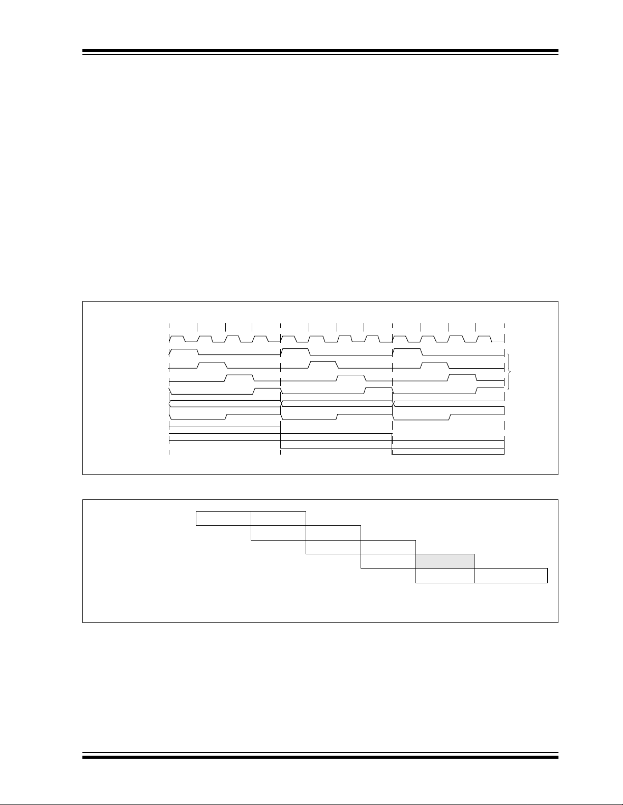
3.1 Clocking Scheme/Instruction Cycle
The clock input (OSC1/CLKIN pin) is internally divided
by four to generate four non-overlapping quadrature
clocks, namely Q1, Q2, Q3 and Q4. Internal ly, the program counter is i nc rem ente d ev ery Q 1 and th e instruction is fetched from program memory and latched into
the instruction register in Q4. It is decoded and executed during the following Q1 through Q4. The clocks
and instru c ti o n ex ecution fl ow are show n i n Fi g ure 3-2
and Example 3-1.
FIGURE 3-2: CLOCK/INSTRUCTION CYCLE
Q2 Q3 Q4
OSC1
Q1
Q2
Q3
Q4
PC
OSC2/CLKOUT
(RC mode)
Q1
PC PC+1 PC+2
Fetch INST (PC)
Execute INST (PC-1) Fetch INST (PC+1)
Q1
Execute INST (PC) Fetch INST (PC+2)
3.2 Instruction Flow/Pipelining
An Instruction Cycle consists of four Q cycles (Q1, Q2,
Q3 and Q4). The instruction fetch and execute are
pipelined such that fetch takes one instruction cycle,
while decode and execute takes another instruction
cycle. However, due to the pipelining, each instruction
effectively executes in one cycle. If an instruction
causes the program counter to change (e.g., GOTO),
then two cycles a re required to c omplete the i nstruction
(Example 3-1).
A fetch cycle begins with the program counter (PC)
incrementing in Q1.
In the execution cy cle, the fetched instruction i s latched
into the Inst ruction Regist er in cycle Q1. T his instruction is then decoded and executed during the Q2, Q3
and Q4 cycles. Data memory is read during Q2 (operand read) and written during Q4 (destination write).
Q2 Q3 Q4
Q2 Q3 Q4
Q1
Execute INST (PC+1)
Internal
phase
clock
EXAMPLE 3-1: INSTRUCTION PIPELINE FLOW
1. MOVLW H’55’
2. MOVWF PORTB
3. CALL SUB_1
4. BSF PORTA, BIT3
All instructions are sing le cycle, except fo r any program branches . These take two cycles since the fetch instruction
is “flushed” from the pipeline, while the new instruction is being fetched and then executed.
2002 Microchip Technology Inc. Preliminary DS30453D-page 13
Fetch 1 Execute 1
Fetch 2 Execute 2
Fetch 3 Execute 3
Fetch 4 Flush
Fetch SUB_1 Execute SUB_1

PIC16C5X
NOTES:
DS30453D-page 14 Preliminary 2002 Microchip Technology Inc.
PIC16C5X
4.0 O SCILLATOR CONFIGURATIONS
4.1 Oscillator Types
PIC16C5Xs can be operated in four different oscillator
modes. The user can program two configuration bits
(FOSC1:FOSC0) to select one of these four modes:
1. LP: Low Power Crystal
2. XT: Crystal/Resonator
3. HS: High Speed Crystal/Resonator
4. RC: Resistor/Capacitor
Note: Not all oscillator sele ct ion s av ail abl e for al l
parts. See Section 9.1.
4.2 Crystal Oscill ator/Ceramic Resonators
In XT, LP or HS modes, a crystal or ceramic resonator
is connected to the OSC1/CLKIN and OSC2/CLKOUT
pins to establish oscillation (Figure 4-1). The
PIC16C5X oscillator de sign requires the use of a p arallel cut crystal. Use of a series cut crystal may give a frequency out of the crystal manufacturers specifications.
When in XT, LP or HS modes, the device can have an
external clock source drive the OSC1/CLKIN pin
(Figure 4-2).
FIGURE 4-1: CRYSTAL/CERAMIC
RESONATOR OPERATION
(HS, XT OR LP OSC
CONFIGURATION)
(1)
C1
(1)
C2
Note 1: See Capacitor Selection tables for
recommended values of C1 and C2.
2: A series resistor (RS) may be required
for AT strip cut crystals.
3: RF varies with the Oscillator mode cho-
sen (approx. value = 10 MΩ).
XTAL
RS
(2)
OSC1
OSC2
RF
(3)
PIC16C5X
SLEEP
To internal
logic
FIGURE 4-2: EXTERNAL CLOCK INPUT
OPERATION (HS, XT OR
LP OSC
CONFIGURATION)
Clock from
ext. system
Open
OSC1
PIC16C5X
OSC2
TABLE 4-1: CAPACITOR SELECTION FOR
CERAMIC RESONATORS PIC16C5X, PIC16CR5X
Osc
Type
XT 455 kHz
HS 8.0 MHz
These values are for design guidance only. Since
each resonator has its own characteristics, the user
should consult the resonator manufacturer for
appropriate values of external components.
Resonator
Freq
2.0 MHz
4.0 MHz
16.0 MHz
Cap. RangeC1Cap. Range
C2
68-100 pF
15-33 pF
10-22 pF
10-22 pF
10 pF
68-100 pF
15-33 pF
10-22 pF
10-22 pF
10 pF
TABLE 4-2: CAPACITOR SELECTION FOR
CRYSTAL OSCILLATOR PIC16C5X, PIC16CR5X
Osc
Typ e
LP 32 kHz
XT 100 kHz
HS 4 MHz
Note 1: For V
These values are for design guidance only. Rs may
be required in HS mode as wel l as X T mode to avoid
overdriving cry st a ls w it h low driv e le vel specification.
Since each crystal has its own characteristics, the
user should consult the crystal manufacturer for
appropriate values of external components.
Crystal
Freq
200 kHz
455 kHz
1 MHz
2 MHz
4 MHz
8 MHz
20 MHz
DD > 4.5V, C1 = C2 ≈ 30 pF is
recommended.
(1)
Cap.Range
C1
15 pF 15 pF
15-30 pF
15-30 pF
15-30 pF
15-30 pF
15 pF
15 pF
15 pF
15 pF
15 pF
Cap. Range
C2
200-300 pF
100-200 pF
15-100 pF
15-30 pF
15 pF
15 pF
15 pF
15 pF
15 pF
Note: If you change from this device to another
device, please ve rify osci llator c har acter istics in your application.
2002 Microchip Technology Inc. Preliminary DS30453D-page 15
PIC16C5X
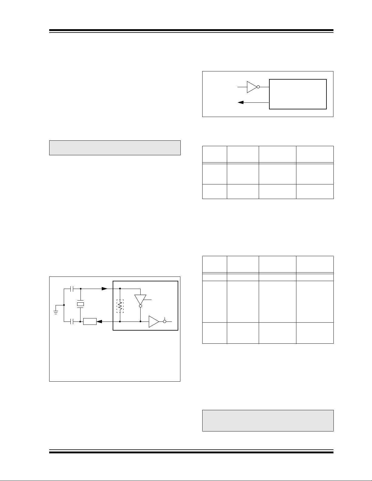
4.3 External Crystal Oscillator Circuit
Either a prepackaged oscillator or a simple oscillator
circuit with TTL gates c an be used as an external crystal oscillat or circ uit. Pre packaged oscilla tors pro vide a
wide operating range and better stability. A welldesigned crystal oscillator will provide good performance with TTL gates. Two types of crystal oscillator
circuits can be used: one with parallel resonance, or
one with series resonance.
Figure 4-3 shows an im plementation example of a parallel resonant oscillator circuit. The circuit is designed
to use the fundamental frequency of the crystal. The
74AS04 inverter performs the 180-degree phase shift
that a parallel oscillator requires. The 4.7 kΩ resistor
provides the negative feedback for stability. The 10 kΩ
potentiometers bias the 74AS04 in the linear region.
This circuit could be used for external oscillator
designs.
FIGURE 4-3: EXAMPLE OF EXTERNAL
PARALLEL RESONANT
CRYSTAL OSCILLATOR
CIRCUIT (USING XT, HS
OR LP OSCILLATOR
MODE)
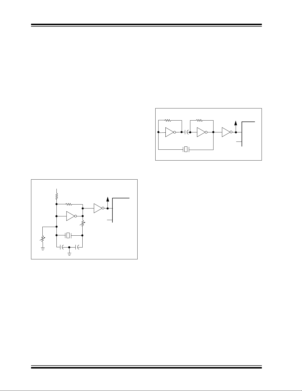
Figure 4-4 shows a series resonant oscillator circuit.
This circuit is also desi gned to use the funda mental fr equency of the crystal. The inverter performs a 180degree phase shift in a series resonant oscillator circuit. The 330kΩ resistors provide the negative feedback to bias the inverters in their linear region.
FIGURE 4-4: EXAMPLE OF EXTERNAL
SERIES RESONANT
CRYSTAL OSCILLATOR
CIRCUIT (USING XT, HS
OR LP OSCILLATOR
MODE)
To Other
74AS04
Devices
Open
PIC16C5X
CLKIN
OSC2
330K
74AS04
330K
74AS04
0.1 µF
XTAL
10K
+5V
10K
20 pF
4.7K
74AS04
XTAL
20 pF
74AS04
10K
Open
To Other
Devices
PIC16C5X
CLKIN
OSC2
DS30453D-page 16 Preliminary 2002 Microchip Technology Inc.
PIC16C5X
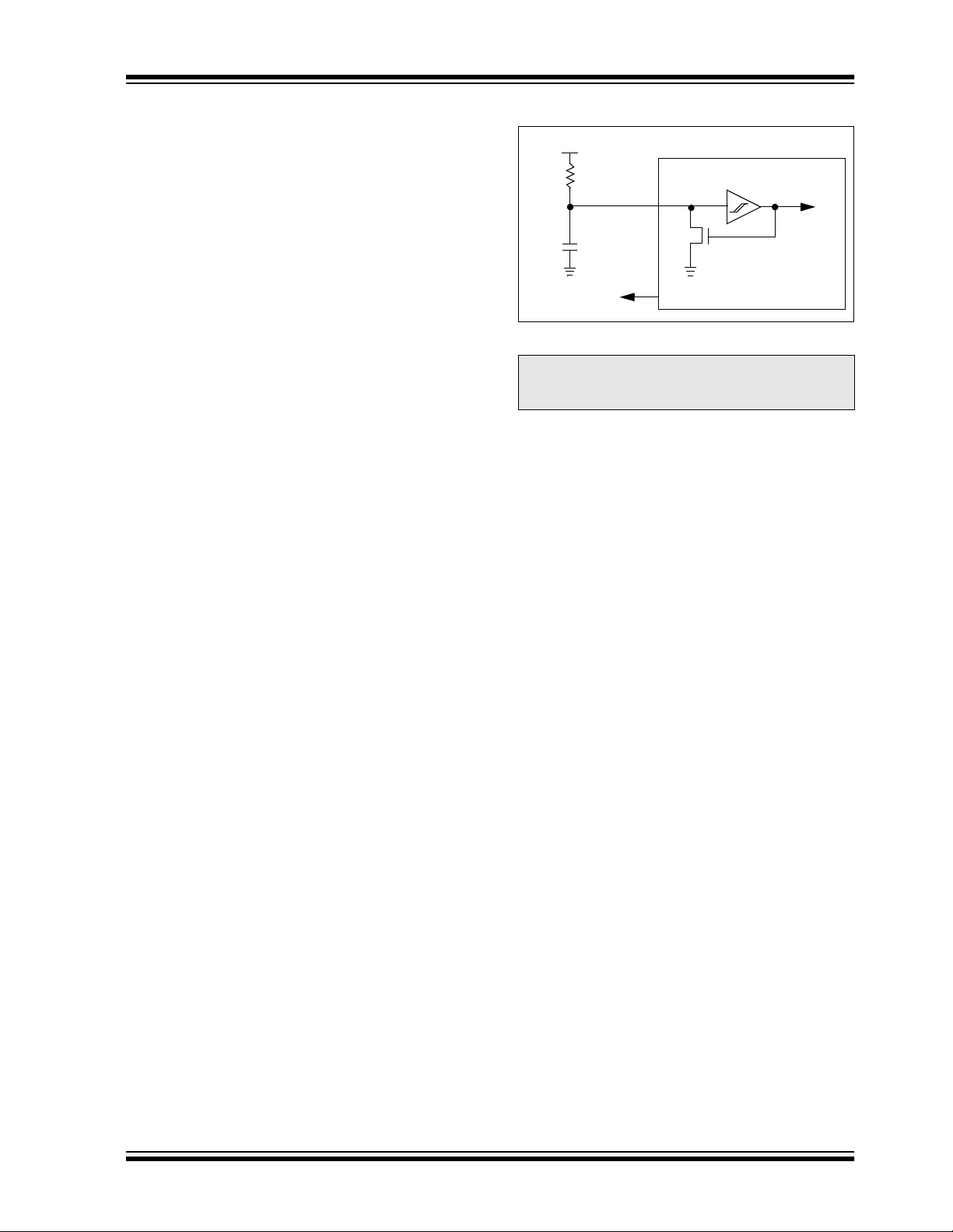
4.4 RC Oscillator
For timing insensitive applications, the RC device
option offers additional cost savings. The RC oscillator
frequency is a funct ion of the su ppl y vo ltage, the resis-
EXT) and capacitor (CEXT) v alues, and the oper at-
tor (R
ing temperature. In addition to this, the oscillator
frequency wi ll v ar y fr om u ni t to un i t du e to no r ma l pro cess parameter variation. Furthermore, the difference
in lead fra me ca pacita nce bet ween packa ge type s w ill
also affect the oscillation frequency, especially for low
EXT values. The user also needs to take into account
C
variation due to tolerance of external R and C components used.
Figure 4-5 shows how the R/C combination is connected to the PIC16C5X. For R
2.2 kΩ, the oscillator operation may become unstable,
or stop completely. For very high R
(e.g., 1 MΩ) the oscillator becomes sensitive to noise,
humidity and leakage. Thus, we recommend keeping
EXT between 3 kΩ and 100 kΩ.
R
Although the oscillator will operate with no external
capacitor (CEXT = 0 pF), we recommend us ing values
above 20 pF for noi se an d s tability reasons. With no or
small external capacitance, the oscillation frequency
can vary dramatically due to changes in external
capacitances, such as PCB trace capacitance or package lead frame capacitance.
The Electrical Specifications sections show RC frequency variation from part to part due to normal process variation. The variat ion is larger f or larger R (since
leakage current vari ation will af fect RC fre quency mo re
for large R) and for smaller C (since variation of input
capacitance will affect RC frequency more).
Also, see the Electrical Specifications sections for variation of oscilla tor frequ ency due to V
C
EXT values as well as freq uency varia tion due to op er-
ating temperature for given R, C, and V
The oscillator frequency, divided by 4, is available on
the OSC2/CLKOU T pin, and can be used f or test purposes or to synchronize other logic.
EXT values below
EXT values
DD for given REXT/
DD values.
FIGURE 4-5: RC OSCILLATOR MODE
VDD
REXT
OSC1
CEXT
VSS
Fosc/4
N
OSC2/CLKOUT
Note: If you change from this device to another
device, please ve rify osci llator c har acter istics in your application.
Internal
clock
PIC16C5X
2002 Microchip Technology Inc. Preliminary DS30453D-page 17

PIC16C5X
NOTES:
DS30453D-page 18 Preliminary 2002 Microchip Technology Inc.
PIC16C5X
and PD bits (STA TUS <4:3>) are set or cl eared
5.0 RESET
PIC16C5X devices may be RESET in one of the following ways:
• Power-On Reset (POR)
•MCLR
•MCLR Wake-up Reset (from SLEEP)
• WDT Reset (normal operation)
• WDT Wake-up Reset (from SLEEP)
Table 5-1 shows these RESET conditions for the PCL
and STATUS registers.
Some registers are not affected in any RESET condi-
tion. Their status is unknown on POR and unchanged
in any other RESET. Most other registers are reset to a
“RESET state” on Power-On Reset (POR), MCLR
WDT Reset. A MCLR
also results in a device RESET, and not a continuation
of operation before SLEEP.
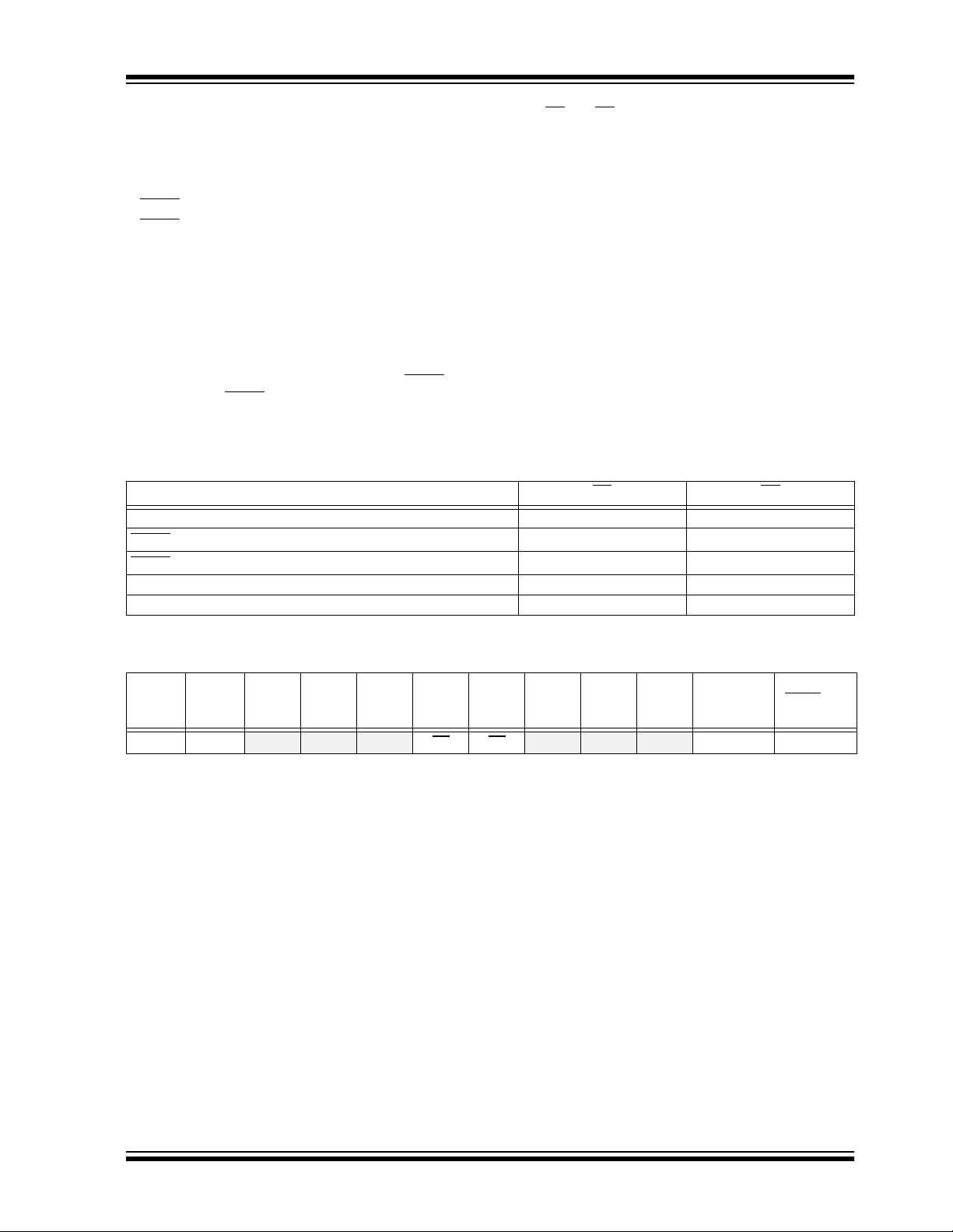
TABLE 5-1: STATUS BITS AND THEIR SIGNIFICANCE
Power-On Reset 11
MCLR
MCLR
WDT Reset (normal operation) 01
WDT Wake-up (from SLEEP) 00
Legend: u = unchanged, x = unknown, — = unimplemented read as ’0’.
Reset (normal operation)
or
or WDT wake-up from SLEEP
Condition TO PD
Reset (normal operation)
Wake-up (from SLEEP)
The TO
depending on the dif ferent RESET co nditio ns (Table 5-
1). These bits may be used to determine the nature of
the RESET.
Table 5-3 lists a full description of RESET states of all
registers. Figure 5-1 shows a simplified block diagram
of the On-chip Reset circuit.
uu
10
TABLE 5-2: SUMMARY OF REGISTERS ASSOCIATED WITH RESET
Address Name Bit 7 Bit 6 Bit 5 Bit 4 Bit 3 Bit 2 Bit 1 Bit 0
03h STATUS
Legend: u = unchanged, x = unknown, q = see Table 5-1 for possible values.
PA2 PA1 PA0 TO PD Z DC C 0001 1xxx 000q quuu
Value on
POR
Value on
MCLR and
WDT Reset
2002 Microchip Technology Inc. Preliminary DS30453D-page 19
PIC16C5X
TABLE 5-3: RESET CONDITIONS FOR ALL REGISTERS
Register Address Power-On Reset MCLR or WDT Reset
WN/Axxxx xxxx uuuu uuuu
TRIS N/A 1111 1111 1111 1111
OPTION N/A --11 1111 --11 1111
INDF 00h xxxx xxxx uuuu uuuu
TMR0 01h xxxx xxxx uuuu uuuu
PCL 02h 1111 1111 1111 1111
STATUS 03h 0001 1xxx 000q quuu
(1)
FSR
PORTA 05h ---- xxxx ---- uuuu
PORTB 06h xxxx xxxx uuuu uuuu
PORTC
(2)
General Purpose Register Files 07-7Fh xxxx xxxx uuuu uuuu
Legend: x = unknown u = unchanged - = unimplemented, read as ’0’
q = see tables in Table 5-1 for possible values.
Note 1: These values are valid for PIC16C57/CR57/C58/CR58. For the PIC16C54/CR54/C55/C56/CR56, the
value on RESET is 111x xxxx and for M CLR
2: General purpose register file on PIC16C54/CR54/C56/CR56/C58/CR58.
04h 1xxx xxxx 1uuu uuuu
07h xxxx xxxx uuuu uuuu
and WDT Reset, the value is 111u uuuu.
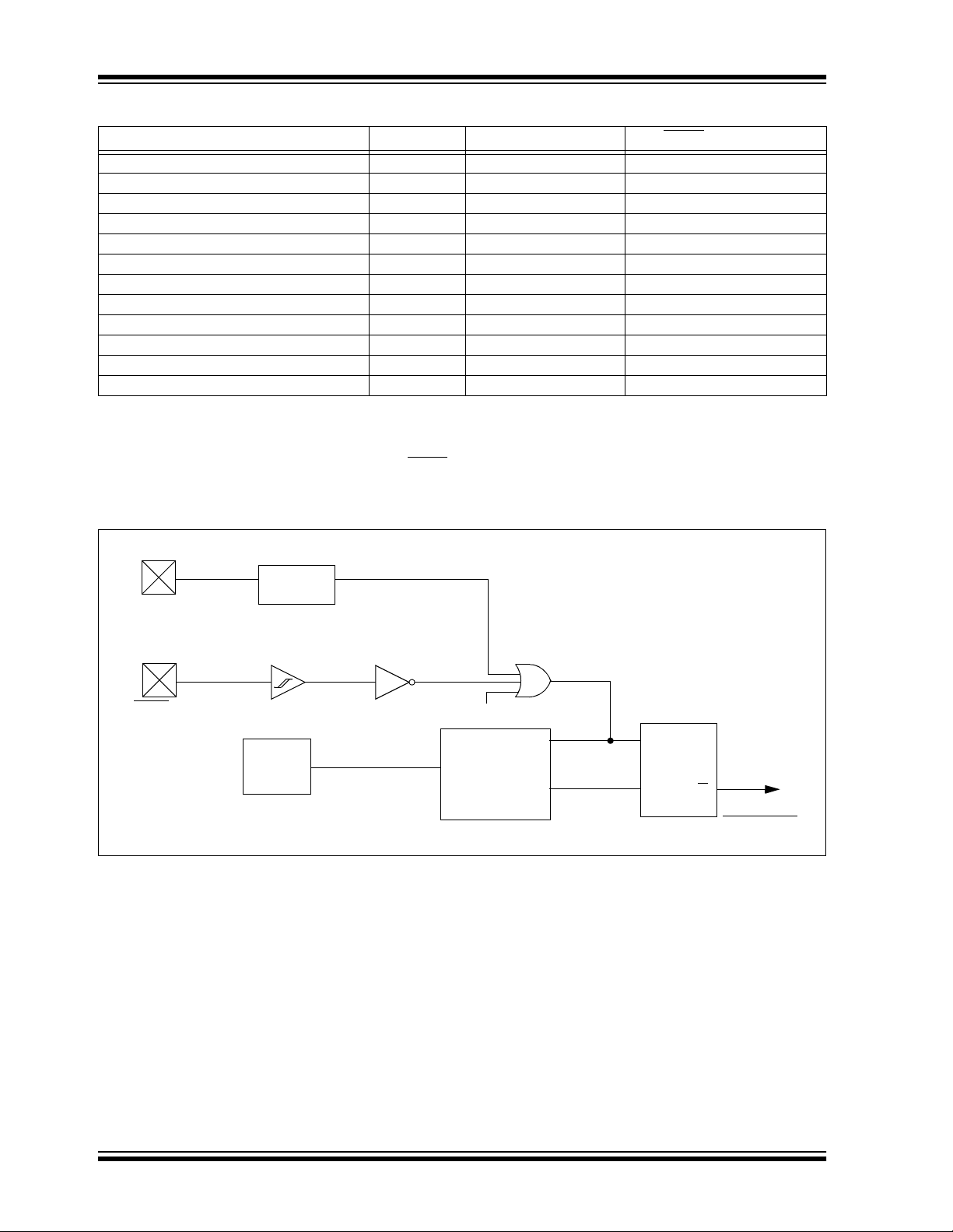
FIGURE 5-1: SIMPLIFIED BLOCK DIAGRAM OF ON-CHIP RESET CIRCUIT
Power-Up
Detect
VDD
MCLR/VPP pin
WDT
On-Chip
RC OSC
POR (Power-On Reset)
WDT Time-out
8-bit Asynch
Ripple Counter
(Device Reset
Timer)
RESET
SQ
R
Q
CHIP RESET
DS30453D-page 20 Preliminary 2002 Microchip Technology Inc.
PIC16C5X
5.1 Power-On Reset (POR)
The PIC16C5X family incorporates on-chip Power-On
Reset (POR) circuitry which provides an internal chip
RESET for most power-up situations. To use this feature, the user merely ties the MCLR
simplified block diagram of the on-chip Power-On
Reset circuit is shown in Figure 5-1.
The Power-On Reset circuit and the Device Reset
Timer (Section 5.2) circuit are closely related. On
power-up, the RESET latch is set and the DRT is
RESET. The DRT timer begins counting on ce it detect s
to be high . After the time -out period, wh ich is
MCLR
typically 18 ms, it will RESET the reset latch and thus
end the on-chip RESET signal.
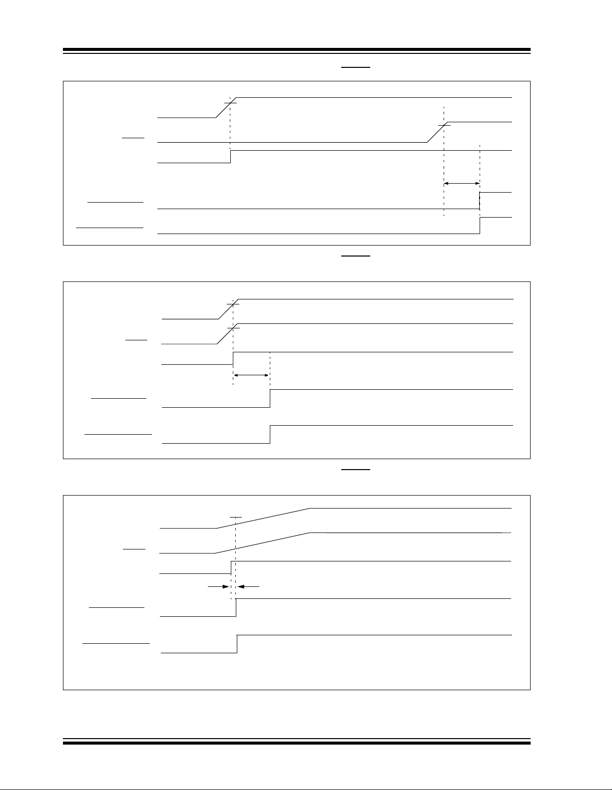
A power-up example where MCLR
shown in Figure 5-3. V
before bringing MCLR
out of reset T
In Figure 5-4, the on-chip P ower-On Reset featu re is
being used (MCLR and VDD are ti ed together). The VDD
is stable bef ore the st art-up tim er times out and the re is
no problem in getting a proper RESET. However,
Figure 5-5 depicts a probl em situati on where VDD rises
too slowly. The time between when the DRT senses a
high on the MCLR
pin (and VDD) actuall y reach th eir full valu e, is too long.
In this situation, when th e start-up timer times out, V
has not re ached the VDD (min) value and the chip is,
therefore, not guaranteed to function correctly. For
such situation s, we recommend that externa l RC circuits be used to achieve longer POR delay times
(Figure 5-2).
DRT msec after MCLR goes high.
DD is allowed to rise and stabilize
high. The chip will actual ly come
/VPP pin, and when the MCLR/VPP
/VPP pin to VDD. A
is not tied to VDD is
DD
FIGURE 5-2: EXTERNAL POWER-ON
RESET CIRCUIT (FOR
SLOW VDD POWER-UP)
VDDVDD
D
• External Power-On Reset circuit is required
only if V
helps discharge the capacitor quickly when
VDD powers down.
• R < 40 kΩ is recommended to make su re th at
voltage drop across R does not violate the
device electrical specification.
•R1 = 100Ω to 1 kΩ will limit any current flow-
ing into MCLR from external capacitor C in the
event of MCLR
static Discharge (ESD) or Electrical Overstress (EOS).
R
R1
C
DD power-up is too slow. The diode D
pin breakdown due to Electro-
MCLR
PIC16C5X
Note: When the device starts normal operation
(exits the RESET condition), device operating parameter s (v ol t age , fre que nc y, temperature, etc.) must be met to ensure
operation. If these conditions are not met,
the device must be hel d in RESET unti l the
operating conditions are met.
For more information on PIC16C5X POR, see
Up Consider ations
Handbook.
The POR circuit does not produce an internal RESET
DD declines.
when V
- AN522 in the Embedded Control
Power-
2002 Microchip Technology Inc. Preliminary DS30453D-page 21
PIC16C5X
FIGURE 5-3: TIME-OUT SEQUENCE ON POWER-UP (MCLR NOT TIED TO VDD)
VDD
MCLR
INTERNAL POR
TDRT
DRT TIME-OUT
INTERNAL RESET
FIGURE 5-4: TIME-OUT SEQUENCE ON POWER-UP (MCLR
TIME
VDD
MCLR
INTERNAL POR
DRT TIME-OUT
INTERNAL RESET
TDRT
FIGURE 5-5: TIME-OUT SEQUENCE ON POWER-UP (MCLR
TIME
V1
VDD
TIED TO VDD): FAST VDD RISE
TIED TO VDD): SLOW VDD RISE
MCLR
INTERNAL POR
DRT TIME-OUT
INTERNAL RESET
When VDD rises slowly, the TDRT time-out expires long before VDD has reached its final value. In
this example, the chip will RESET properly if, and only if, V1 ≥ VDD min
DS30453D-page 22 Preliminary 2002 Microchip Technology Inc.
TDRT
PIC16C5X
5.2 Device Reset Timer (DRT)
The Device Reset Timer (DRT) provides an 18 ms
nominal time-out on RESET regardless of Oscillator
mode used. The DR T operat es on an inte rnal RC os cillator. The processor is kept in RESET as long as the
DRT is active. The DRT delay allows V
DD min., and for the oscillator to stabilize.
V
DD to rise above
Oscillator circuit s ba sed on cryst als or cera mic res onators require a certain time after power-up to establish a
stable oscillati on. The on-chi p DRT ke ep s the device in
a RESET condition for approximately 18ms after the
voltage on the MCLR
IH) level. T hus, extern al RC network s connected t o
(V
the MCLR
input are not required in most cases, allow-
/VPP pin has reached a logic high
ing for savings in cost-sen sitive and /or space re stricted
applications.
The Device Reset time delay will vary from chip to chip
due to V
DD, temperature, and process variation. See
AC parameters for details.
The DRT will also be tri ggered upon a W atc hdog T im er
time-out. This is particularly important for applications
using the WDT to wake the PI C16C5X from SLEEP
mode automatically.
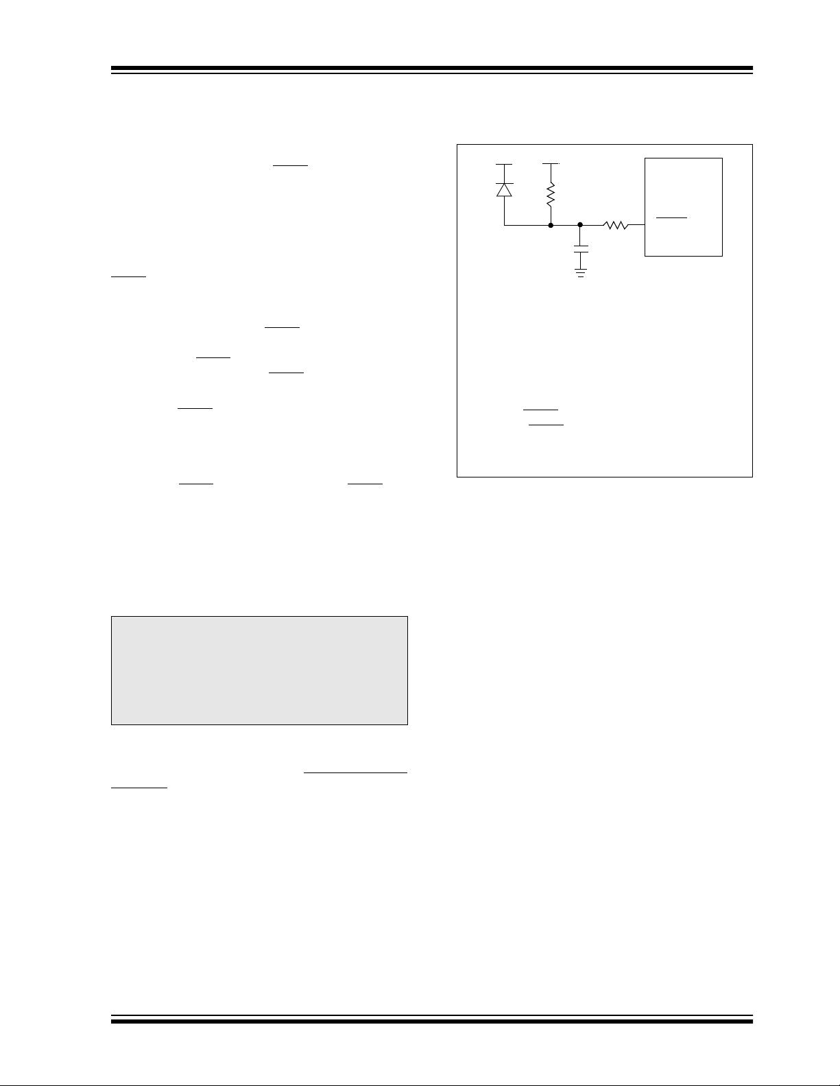
5.3 Reset on Brown-Out
A brown-out is a condition where device power (VDD)
dips below its minimum value, but no t to zero, and the n
recovers. The device should be RESET in the event of
a brown-out .
To RESET PIC16C5X devices when a brown-out
occurs, external brown-out protection circuits may be
built, as shown in Figu re 5-6, Figure 5-7 and Figure 5-
8.
FIGURE 5-6: EXTERNAL BROWN-OUT
PROTECTION CIRCUIT 1
VDD
DD
V
33K
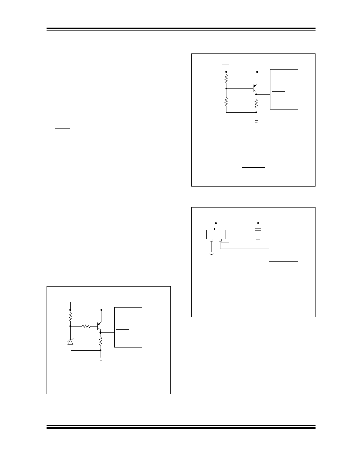
FIGURE 5-7: EXTERNAL BROWN-OUT
PROTECTION CIRCUIT 2
VDD
V
DD
R1
Q1
MCLR
R2
40K
PIC16C5X
This brown-out circuit is less expensive, althou gh
less accurate. Transistor Q1 turns off when V
DD
is below a certain level such that:
V
DD •
R1
R1 + R2
= 0.7V
FIGURE 5-8: EXTERNAL BROWN-OUT
PROTECTION CIRCUIT 3
VDD
bypass
capacitor
MCP809
Vss
V
DD
RST
This brown-out protection circuit employ s Micro-
chip Technology’s MCP809 microcontroller
supervisor. The MCP8XX and MCP1XX families
of supervisors provide push-pull and open collector outputs with both "active high and active low"
RESET pins. There are 7 differe nt trip point selec tions to accommodate 5V and 3V systems.
VDD
MCLR
PIC16C5X
10K
This circuit will activate RESET when VDD goes below Vz
+ 0.7V (where Vz = Zener voltage).
2002 Microchip Technology Inc. Preliminary DS30453D-page 23
Q1
40K
MCLR
PIC16C5X

PIC16C5X
NOTES:
DS30453D-page 24 Preliminary 2002 Microchip Technology Inc.
PIC16C5X
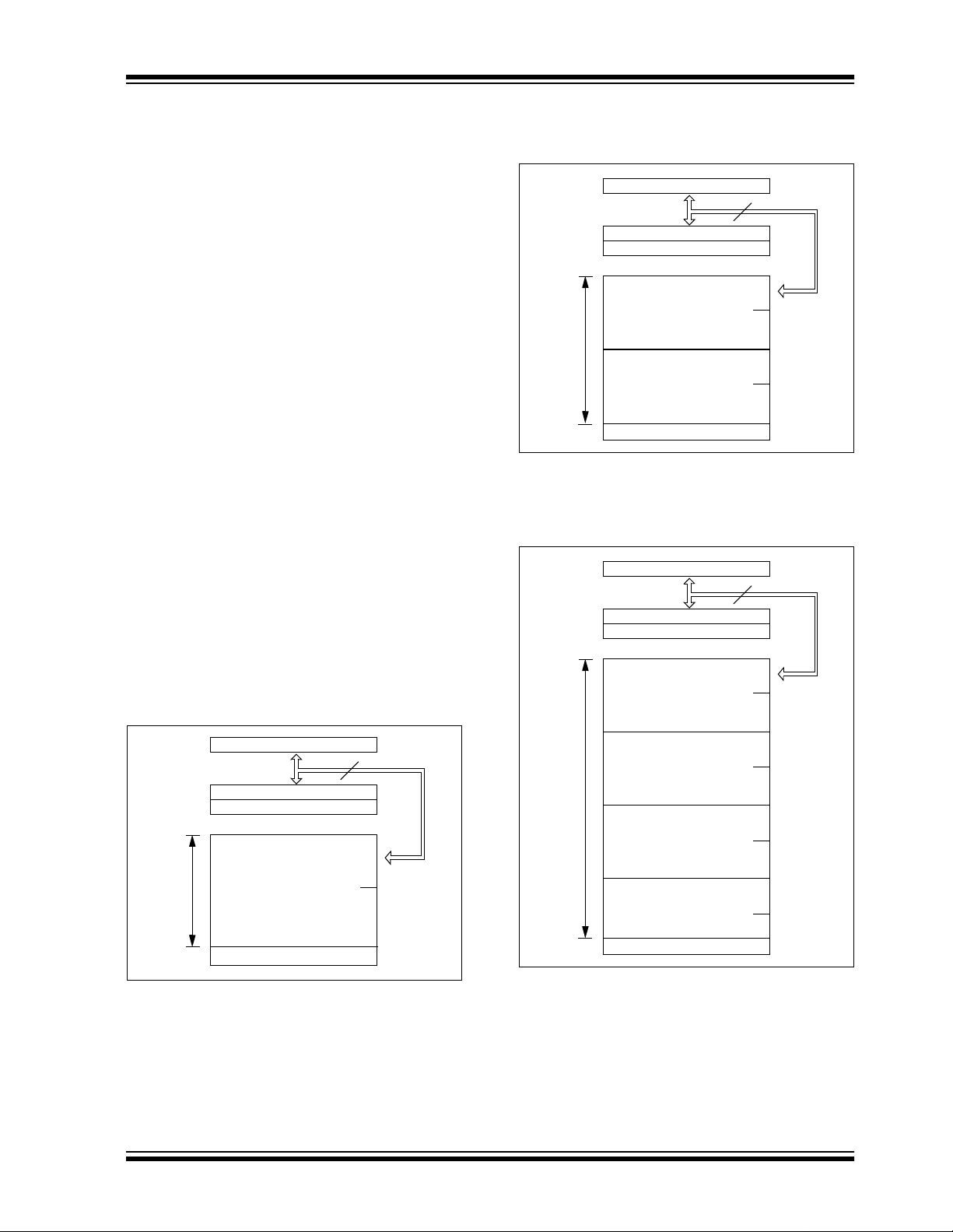
6.0 MEMORY ORGANIZATION
PIC16C5X memory is organiz ed into program memory
and data memory. For devices with more than 512
bytes of program memory, a paging scheme is used.
Program memory pages are accessed using o ne or two
ST ATUS Register bits. For devi ces with a d ata memor y
register file of more than 32 registers, a banking
scheme is used. Data memory banks are accessed
using the File Selection Register (FSR).
6.1 Program Memory Organization
The PIC16C54, PIC16CR54 and PIC16C55 have a 9bit Program Counter (PC ) capable of addressing a 512
x 12 program memory space (Figure 6-1). The
PIC16C56 and PIC16CR56 have a 10-bit Program
Counter (PC) capable of addressing a 1K x 12 program
memory space (Figure 6-2). The PIC16CR57,
PIC16C58 and PIC16CR58 have an 11-bit Program
Counter capable of addressing a 2K x 12 program
memory space (Figure6-3). Accessing a location
above the physicall y implem ented addre ss will ca use a
wraparound.
A NOP at the RESET vector location will caus e a rest art
at location 000h. The RESET ve ctor for the PIC16C5 4,
PIC16CR54 and PIC16C55 is at 1FFh. The RESET
vector for the PIC16C56 and PIC16CR56 is at 3FFh.
The RESET vector for the PIC16C57, PIC16CR57,
PIC16C58, and PIC16CR58 is at 7FFh. See
Section 6.5 for additional information using CALL and
GOTO instructions.
FIGURE 6-1: PIC16C54/CR54/C55
PROGRAM MEMORY MAP
AND STACK
PC<8:0>
CALL, RETLW
Space
User Memory
Stack Level 1
Stack Level 2
On-chip
Program
Memory
RESET Vector
9
000h
0FFh
100h
1FFh
FIGURE 6-2: PIC16C56/CR56
PROGRAM MEMO RY MAP
AND STACK
PC<9:0>
CALL, RETLW
Space
User Memory
Stack Level 1
Stack Level 2
On-chip Program
Memory (Page 0)
On-chip Program
Memory (Page 1)
RESET Vector
10
000h
0FFh
100h
1FFh
200h
2FFh
300h
3FFh
FIGURE 6-3: PIC16C57/CR57/C58/
CR58 PROGRAM
MEMORY MAP AND
STACK
PC<10:0>
CALL, RETLW
Space
User Memory
Stack Level 1
Stack Level 2
On-chip Program
Memory (Page 0)
On-chip Program
Memory (Page 1)
On-chip Program
Memory (Page 2)
On-chip Program
Memory (Page 3)
RESET Vector
11
000h
0FFh
100h
1FFh
200h
2FFh
300h
3FFh
400h
4FFh
500h
5FFh
600h
6FFh
700h
7FFh
2002 Microchip Technology Inc. Preliminary DS30453D-page 25

PIC16C5X
6.2 Data Memory Organization
Data memory is composed of registers, or bytes of
RAM. Therefore, data memory for a device is specified
by its register file. The register file is divided into two
functional groups: Special Function Registers and
General Purpose Registers.
The Special Function Registers include the TMR0 register, the Program Counter (PC), the Status Register,
the I/O registers (ports) and the File Select Register
(FSR). In addition, Special Purpose Registers are used
to control the I/O port configuration and prescaler
options.
The General Purpose Registers are used for data and
control information under command of the instructions.
For the PIC16C54, PIC16CR54, PIC16C56 and
PIC16CR56, the register file is composed of 7 Special
Function Registers and 25 General Purpose Registers
(Figure 6-4).
For the PIC16C55, the register file is composed of 8
Special Function Registers and 24 General Purpose
Registers.
For the PIC1 6C57 an d PIC1 6CR57 , the re gister file is
composed of 8 Spec ial F unctio n Re gister s, 24 Genera l
Purpose Registers and up to 48 additional General
Purpose Registers that may be addressed using a
banking scheme (Figure 6-5).
For the PIC1 6C58 an d PIC1 6CR58 , the re gister file is
composed of 7 Spec ial F unctio n Re gister s, 25 Genera l
Purpose Registers and up to 48 additional General
Purpose Registers that may be addressed using a
banking scheme (Figure 6-6).
FIGURE 6-4: PIC16C54, PIC16CR54,
PIC16C55, PIC16C56,
PIC16CR56 REGISTER
FILE MAP
File Address
(1)
00h
01h
02h
03h
04h
05h
06h
07h
08h
1Fh
Note 1: Not a physical register. See
Section 6.7.
2: PIC16C55 only , in all o ther devic es this
is implemented as a a gen eral pu rpose
register .
INDF
TMR0
PCL
STATUS
FSR
PORTA
PORTB
PORTC
General
Purpose
Registers
(2)
6.2.1 GENERAL PURPOSE REGISTER
FILE
The register file is accessed either directly or indirectly
through the File Select Register (FSR). The FSR Register is described in Sec tion 6.7.
DS30453D-page 26 Preliminary 2002 Microchip Technology Inc.
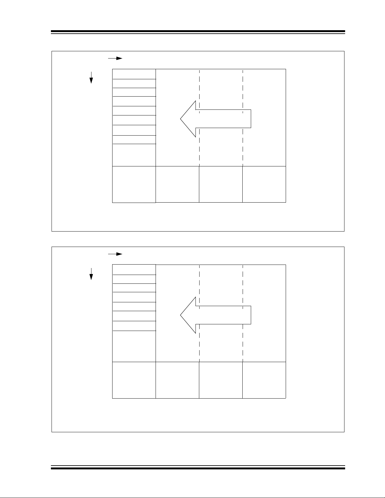
FIGURE 6-5: PIC16C57/CR57 REGISTER FILE MAP
FSR<6:5> 00 01 10 11
File Address
00h
01h
02h
03h
04h
05h
06h
07h
08h
0Fh
10h
1Fh
(1)
INDF
TMR0
PCL
STATUS
FSR
PORTA
PORTB
PORTC
General
Purpose
Registers
General
Purpose
Registers
Bank 0 Bank 1 Bank 2 Bank 3
20h
2Fh
30h
General
Purpose
Registers
3Fh
40h
Addresses map back to
addresses in Bank 0.
4Fh
50h
General
Purpose
Registers
5Fh
PIC16C5X
60h
6Fh
70h
General
Purpose
Registers
7Fh
Note 1 : Not a physical register. See Section 6.7.
FIGURE 6-6: PIC16C58/CR58 REGISTER FILE MAP
FSR<6:5> 00 01 10 11
File Address
00h
01h
02h
03h
04h
05h
06h
07h
0Fh
10h
1Fh
(1)
INDF
TMR0
PCL
STATUS
FSR
PORTA
PORTB
General
Purpose
Registers
General
Purpose
Registers
Bank 0 Bank 1 Bank 2 Bank 3
20h
2Fh
30h
General
Purpose
Registers
3Fh
40h
Addresses map back to
addresses in Bank 0.
4Fh
50h
General
Purpose
Registers
5Fh
60h
6Fh
70h
General
Purpose
Registers
7Fh
Note 1: Not a physical register. See Section 6.7.
2002 Microchip Technology Inc. Preliminary DS30453D-page 27
PIC16C5X
6.2.2 SPECIAL FUNCTION REGISTERS
The Special Function Registers are registers used by
the CPU and peripheral functions to control the operation of the device (Table 6-1).
The Special Registers ca n be classifi ed into two se ts.
The Special Function Registers associated with the
“core” functions are described in this section. Those
related to the operation of the peripheral features are
described in the section for each peripheral feature.
TABLE 6-1: SPECIAL FUNCTION REGISTER SUMMARY
Value on
Address Name Bit 7 Bit 6 Bit 5 Bit 4 Bit 3 Bit 2 Bit 1 Bit 0
Power-on
Reset
N/A TRIS I/O Control Registers (TRISA, TRISB, TRISC)
N/A OPTION Contains control bits to configure T imer0 and Timer0/WDT prescaler
00h INDF Uses contents of FSR to address data memory (not a physical register)
01h TMR0 Timer0 Module Register
(1)
02h
03h STATUS
04h FSR Indirect data memory address pointer
05h PORTA
06h PORTB RB7 RB6 RB5 RB4 RB3 RB2 RB1 RB0
(2)
07h
Legend: x = unknown, u = unchanged, – = unimplemented, read as '0' (if applicable). Shaded cells = unimplemented or unused
Note 1: The upper byte of the Program Counter is not directly accessible. See Section 6.5 for an explanation of how to access
PCL Low order 8 bits of PC
PA2 PA1 PA0 TO PD ZDCC
— — — — RA3 RA2 RA1 RA0
PORTC RC7 RC6 RC5 RC4 RC3 RC2 RC1 RC0
these bits.
2: File address 07h is a General Purpose Register on the PIC16C54, PIC16CR54, PIC16C56, PIC16CR56, PIC16C58 and
PIC16CR58.
3: These values are valid for PIC16C57/CR57/C58/CR58. For the PIC16C54/CR54/C55/C56/CR56, the value on RESET is
111x xxxx and for MCLR
and WDT Reset, the value is 111u uuuu.
1111 1111
- -11 1111
xxxx xxxx
xxxx xxxx
1111 1111
0001 1xxx
1xxx xxxx
---- xxxx
xxxx xxxx
xxxx xxxx
(3)
Details
on Page
35
30
32
38
31
29
32
35
35
35
DS30453D-page 28 Preliminary 2002 Microchip Technology Inc.

PIC16C5X
6.3 STATUS Register
This register contains the arithmetic status of the ALU,
the RESET status and the page preselect bits for program memories larger than 512 words.
The STATUS Register can be the destination for any
instruction, as with any other register. If the STATUS
Register is the destin ation for an in struction that af fect s
the Z, DC or C bits, then the write to these three bits is
disabled. These bit s are set or cleared ac cording to the
device logic. Furthermore, the TO
and PD bits are not
writable. Therefore, the result of an instruction with the
STATUS Regis ter as des tin atio n may be di ffer ent th an
intended.
For example, CLRF STATUS will clear the upper three
bits and se t the Z bit . This leav es t he STATU S R egist er
as 000u u1uu (where u = unchanged).
It is recommended, therefore, that only BCF, BSF and
MOVWF instructions be used to alter the STATUS Register because these instructions do not affect the Z, DC
or C bits from the STATUS Register. For other instructions which do affect STATUS Bits, see Section 10.0,
Instruction Set Summary.
REGISTER 6-1: STATUS REGISTER (ADDRESS: 03h)
R/W-0 R/W-0 R/W-0 R-1 R-1 R/W-x R/W-x R/W-x
PA2 PA1 PA0 TO PD ZDCC
bit 7 bit 0
bit 7: PA2: This bit unused at this time.
Use of the PA2 bit as a general purpose read/wri te bi t is no t recommended, since this may affect upw ard
compatibility with future products.
bit 6-5: PA<1:0>: Program page preselect bits (PIC16C56/CR56)(PIC16C57/CR57)(PIC16C58/CR58)
00 = Page 0 (000h - 1FFh) - PIC16C56/CR56, PIC16C57/CR57, PIC16C58/CR58
01 = Page 1 (200h - 3FFh) - PIC16C56/CR56, PIC16C57/CR57, PIC16C58/CR58
10 = Page 2 (400h - 5FFh) - PIC16C57/CR57, PIC16C58/CR58
11 = Page 3 (600h - 7FFh) - PIC16C57/CR57, PIC16C58/CR58
Each page is 512 words.
Using the PA<1:0> bits as general purpose read/write bits in devices which do not use them for program
page preselect is not recommended since this may affect upward compatibility with future products.
bit 4: TO
bit 3: PD
bit 2: Z: Zero bit
bit 1: DC: Digit carry/borrow
bit 0: C: Carry/borrow bit (for ADDWF, SUBWF and RRF, RLF instructions)
: Time-out bit
1 = After power-up, CLRWDT instruction, or SLEEP instruction
0 = A WDT time-out occurred
: Power-down bit
1 = After power-up or by the CLRWDT instruction
0 = By execution of the SLEEP instruction
1 = The result of an arithmetic or logic operation is zero
0 = The result of an arithmetic or logic operation is not zero
bit (for ADDWF and SUBWF instructions)
ADDWF
1 = A carry from the 4th low order bit of the result occurred
0 = A carry from the 4th low order bit of the result did not occur
SUBWF
1 = A borrow from the 4th low order bit of the result did not occur
0 = A borrow from the 4th low order bit of the result occurred
ADDWF SUBWF RRF or RLF
1 = A carry occurred 1 = A borrow did not occur Loaded with LSb or MSb, respectively
0 = A carry did not occur 0 = A borrow occurred
Legend:
R = Readable bit W = Writable bit U = Unimplemented bit, read as ‘0’
-n = Value at POR 1 = bit is set 0 = bit is cleared x = bit is unknown
2002 Microchip Technology Inc. Preliminary DS30453D-page 29

PIC16C5X
6.4 OPTION Register
The OPTION Register is a 6-bit wide, write-only register which contains various control bits to configure the
Timer0/WDT prescaler and Timer0.
By executin g the OPTION instruction, the contents of
the W Register will be transferred to the OPTION Register. A RESET sets the OPTION<5:0> bits.
REGISTER 6-2: OPTION REGISTER
U-0 U-0 W-1 W-1 W-1 W-1 W-1 W-1
— — T0CS TOSE PSA PS2 PS1 PS0
bit 7 bit 0
bit 7-6: Unimplemented: Read as ‘0’
bit 5: T0CS: Timer0 clock source select bit
1 = Transition on T0CKI pin
0 = Internal instruction cycle clock (CLKOUT)
bit 4: T0SE: Timer0 source edge select bit
1 = Increment on high-to-low transition on T0CKI pin
0 = Increment on low-to-high transition on T0CKI pin
bit 3: PSA: Prescaler assignment bit
1 = Prescaler assigned to the WDT
0 = Prescaler assigned to Timer0
bit 2-0: PS<2:0>: Prescaler rate select bits
Bit Value Timer0 Rate WDT Rate
000
001
010
011
100
101
110
111
1 : 2
1 : 4
1 : 8
1 : 16
1 : 32
1 : 64
1 : 128
1 : 256
1 : 1
1 : 2
1 : 4
1 : 8
1 : 16
1 : 32
1 : 64
1 : 128
Legend:
R = Readable bit W = Writable bit U = Unimplemented bit, read as ‘0’
-n = Value at POR 1 = bit is set 0 = bit is cleared x = bit is unknown
DS30453D-page 30 Preliminary 2002 Microchip Technology Inc.

PIC16C5X
6.5 Program Counter
As a program instruction is executed, the Program
Counter (PC) will contain the address of the next program instruction to be executed. The PC value is
increased by one, every instruction cycle, unless an
instruction changes the PC.
For a GOTO instruction, bits 8:0 of the PC are provided
by the GOTO ins tructio n word. Th e PC Latch (PCL) is
mapped to PC<7:0> (Figure 6-7, Figure 6-8 and
Figure 6-9).
For the PIC16C56, PIC16CR56, PIC16C57,
PIC16CR57, PIC16C58 and PIC16 CR58, a page num ber must be supplied as well. Bit5 and bit6 of the STATUS Register provide page information to bit9 and
bit10 of the PC (Figure6-8 and Figure 6-9).
For a CALL instruction, or any instruction where the
PCL is the destinatio n, bits 7:0 of the PC ag ain are provided by the instruction word. However, PC<8> does
not come from the instruction word, but is always
cleared (Figure 6-7 and Figure 6-8).
Instructions where the PCL is th e destinatio n, or modif y
PCL instructions, include MOVWF PCL, ADDWF PCL,
and BSF PCL,5.
For the PIC16C56, PIC16CR56, PIC16C57,
PIC16CR57, PIC16C58 and PIC16 CR58, a page num ber again must be supplied. Bit5 and bit6 of the STATUS Register provide page information to bit9 and
bit10 of the PC (Figure6-8 and Figure 6-9).
Note: Because PC<8> is cleared in the CALL
instruction, or any modify PCL instruction,
all subroutine calls or computed jumps are
limited to the first 256 locations of any program memory page (512 words long).
FIGURE 6-7: LOADING OF PC
BRANCH INSTRUCTIONS
- PIC16C54, PIC16CR54,
PIC16C55
GOTO Instruction
87 0
PC
PCL
FIGURE 6-8: LOADING OF PC
BRANCH INSTRUCTIONS
- PIC16C56/PIC16CR56
GOTO Instruction
87 0
910
0
PC
2
PA<1:0>
70
0
STATUS
PCL
Instruction Word
CALL or Modify PCL Instruction
87 0
910
0
PC
Reset to ‘0’
2
PA<1:0>
70
0
STATUS
PCL
Instruction Word
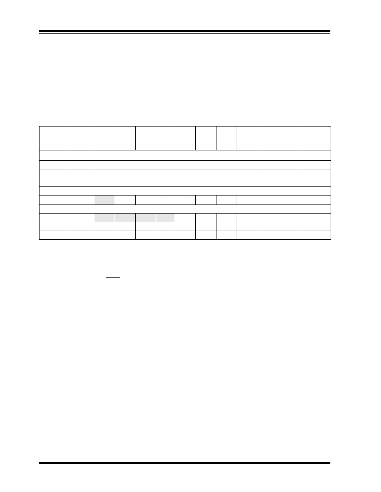
FIGURE 6-9: LOADING OF PC
BRANCH INSTRUCTIONS
- PIC16C57/PIC16CR57,
AND PIC16C58/
PIC16CR58
GOTO Instruction
87 0
910
PC
2
PA<1:0>
70
STATUS
PCL
Instruction Word
Instruction Word
CALL or Modify PCL Instruction
87 0
PC
Reset to ’0’
2002 Microchip Technology Inc. Preliminary DS30453D-page 31
PCL
Instruction Word
CALL or Modify PCL Instruction
87 0
910
PC
Reset to ‘0’
2
PA<1:0>
70
STATUS
PCL
Instruction Word

PIC16C5X
6.5.1 PAGING CONSIDERATIONS –
PIC16C56/CR56, PIC16C57/CR57
AND PIC16C58/CR58
If the Program Counter is poi nting to the last address of
a selected memory page, when it increments it will
cause the program to continue in the nex t highe r pag e.
However, the page preselect bits in the STATUS Register will not be updated. Therefore, the next GOTO,
CALL or modify PCL instruction will send the program
to the page spec ified by the p age prese lect bit s (PA0 or
P A<1:0>).
For example, a NOP at location 1FFh (page 0) increments the PC to 200h (page 1). A GOTO xxx at 200h
will return the program to address xxh on page 0
(assuming that PA<1:0> are clear).
To prevent this, the page preselect bits must be
updated under program control.
6.5.2 EFFECTS OF RESET
The Program Counter is set upon a RESET, which
means that the PC addresses the last location in the
last page (i.e., the RESET vector).
The STATUS Register page preselect bits are cleared
upon a RESET, which means that page 0 is preselected.
Therefore, upon a RESET, a GOTO instruction at the
RESET vector location wi ll automatically cause the program to jump to pag e 0.
6.6 Stack
PIC16C5X dev ices have a 10-bit or 11-bit wide, twolevel hardw are push/pop stack.
A CALL instruction will push the current value of stack
1 into stack 2 and then push the current program
counter value, incremented by one, into stack level 1. If
more than two sequential CALL’s are executed, only
the most recent two return addresses are stored.
A RETLW instruction will pop the contents of stack leve l
1 into the program counter and then copy stack level 2
contents into level 1. If more than two sequential
RETLW’s are executed, the stack will be filled with the
address previously stored in level 2. Note that the
W Register will be loaded with the literal value specified
in the instruction. This is particularly useful for the
implementation of data look-up tables within the program memory.
For the RETLW instruction, the PC is loaded with the
T op of S t ack (TO S) contents. All of the devices covere d
in this data sh eet hav e a two-l evel st ack. The sta ck has
the same bit width as the device PC, therefore, paging
is not an issue when returning from a subroutine.
DS30453D-page 32 Preliminary 2002 Microchip Technology Inc.

PIC16C5X
6.7 Indirect Data Addressing; INDF and FSR Registers
The INDF Register is not a physical register.
Addressing INDF actually addresses the register
whose address is contained in the FSR Register (FSR
pointer
is a
EXAMPLE 6-1: INDIRECT ADDRESSING
• Register file 08 contains the value 10h
• Register file 09 contains the value 0Ah
• Load the value 08 into the FSR Register
• A read of the INDF Register will return the value
of 10h
• Increment the value of the FSR Register by one
(FSR = 09h)
• A read of the INDF register now will return the
value of 0Ah.
Reading INDF itself indirectly (FSR = 0) will produce
00h. Writing to the INDF Register indirectly results in a
no-operation (although STATUS bits may be affected).
A simple program to clear RAM locations 10h-1Fh
using indirect addressing is shown in Example 6-2.
). This is indirect addressing.
EXAMPLE 6-2: HOW TO CLEAR RAM
USING INDIRECT
ADDRESSING
MOVLW H’10’ ;initialize pointer
MOVWF FSR ; to RAM
NEXT CLRF INDF ;clear INDF Register
INCF FSR,F ;inc pointer
BTFSC FSR,4 ;all done?
GOTO NEXT ;NO, clear next
CONTINUE
: ;YES, continue
The FSR is either a 5-bit (PIC16C54, PIC16CR54,
PIC16C55, PIC16C56, PIC16CR56) or 7-bit
(PIC16C57, PIC16CR57, PIC16C58, PIC16CR58)
wide register. It is used in conjunction with the INDF
Register to indirectly address the data memory area.
The FSR<4:0> bits are used to select data memory
addresses 00h to 1Fh.
PIC16C54, PIC16CR54, PIC16C55, PIC16C56,
PIC16CR56: These do not use banking . FSR<6:5> bit s
are unimplemented and read as '1's.
PIC16C57, PIC16CR57, PIC16C58, PIC16CR58:
FSR<6:5> are the bank select bits and are used to
select the bank to be addressed (00 = bank 0,
01 =bank 1, 10 = bank 2, 11 = bank 3).
FIGURE 6-10: DIRECT/INDIRECT ADDRESSING
Direct Addressing
(FSR)
5
6
bank select
Note 1: For register map detail see Section 6.2.
location select
3
Data
Memory
(opcode)
1
2
(1)
04
00h
Addresses map back to
addresses in Bank 0.
0Fh
10h
1Fh 3Fh 5Fh 7Fh
Bank 0 Bank 1 Bank 2 Bank 3
1000 01 11
Indirect Addressing
6
5
bank
(FSR)
3
4
location select
1
2
0
2002 Microchip Technology Inc. Preliminary DS30453D-page 33

PIC16C5X
NOTES:
DS30453D-page 34 Preliminary 2002 Microchip Technology Inc.

PIC16C5X
7.0 I/O PORTS
As with any other register, the I/O Registers can be
written and read under pro gram control. H owever, read
instructions (e.g., MOVF PORT B,W) always r ead t he I/O
pins independent of the pin’s input/output modes. On
RESET, all I/O ports are defined as input (inputs are at
hi-impeda nce) since th e I/O control r egisters (TR ISA,
TRISB, TRISC) are all set.
7.1 PORTA
PORTA is a 4-bit I/O Register . Only the low o rder 4 bit s
are used (RA<3:0>). Bits 7-4 are unimplemented and
read as '0's.
7.2 PORTB
PORTB is an 8-bit I/O Register (PORTB<7:0>).
7.3 PORTC
PORTC is an 8-bit I/O Register for PIC16C55,
PIC16C57 and PIC16CR57.
PORTC is a General Purpose Register for PIC16C54,
PIC16CR54, PIC16C56, PIC16CR56, PIC16C58 and
PIC16CR58.
7.4 TRIS Registers
The Output Driver Control Registers are loaded with
the contents of the W Register by executing the
TRIS f instruction. A '1' from a TRIS Register bit puts
the corresponding output driver in a hi-impedance
(input) mode. A '0' puts the contents of the output data
latch on the selected pins, ena bling the output buf fer.
7.5 I/O Interfacing
The equivalent circuit for an I/O port pin is shown in
Figure 7-1. All ports may be used for both input and
output operation. For input operations these ports are
non-latching. Any input must be present until read by
an input instruction (e.g., MOVF PORTB, W). The outputs are latche d and remain u nchanged unt il the output
latch is rewritte n. To use a port pin as o utput, the corresponding direction control bit (in TRISA, TRISB,
TRISC) must be cleared (= 0). For use as an input, the
corresponding TRIS bit must be set. Any I/O pin ca n be
programmed individually as input or output.
FIGURE 7-1: EQUIVALENT CIRCUIT
FOR A SINGLE I/O PIN
Data
Bus
WR
Port
W
Reg
TRIS ‘f’
CK
CK
RESET
Data
Latch
TRIS
Latch
QD
VDD
Q
QD
Q
P
N
V
SS
I/O
pin
(1)
Note: A read of t he ports rea ds t he pi ns, no t the
output data latches. That is, if an output
driver on a pin is enabled and driven high,
but the external system is holding it low, a
read of the port will indicate that the pin is
low.
Note 1: I/O pins have protection diodes to VDD and VSS.
RD Port
The TRIS Registers are “write-o nly” and are set (outp ut
drivers disabled) upon RESET.
TABLE 7-1: SUMMARY OF PORT REGISTERS
Value on
Address Name Bit 7 Bit 6 Bit 5 Bit 4 Bit 3 Bit 2 Bit 1 Bit 0
N/A T RIS I/O Control Registers (TRISA, TRISB, TRISC) 1111 1111 1111 1111
05h PORTA
06h PORTB RB 7 RB6 RB5 RB4 RB3 RB2 RB1 RB0 xxxx xxxx uuuu uuuu
07h PORTC RC7 RC 6 RC5 RC4 RC 3 RC2 RC1 RC0 xxxx xxxx uuuu uuuu
Legend: x = unknown, u = unchanged, — = unimplemented, read as '0', Shaded cells = unimplemented, read as ‘0’
— — — — RA3 RA2 RA1 RA0 ---- xxxx ---- uuuu
Power-On
Reset
Value on
MCLR and
WDT Reset
2002 Microchip Technology Inc. Preliminary DS30453D-page 35

PIC16C5X
7.6 I/O Programming Considerations
7.6.1 BI-DIRECTIONAL I/O PORTS
Some instructions operate internally as read followed
by write operations. The BCF and BSF instructions, for
example, read the entire port into the CPU, execute the
bit operation and re-write the result. Caution must be
used when these instructions are applied to a port
where one or more pins are used as input/ outputs. For
example, a BSF operation on bit5 of PORTB will cause
all eight bits of PORTB to be read into the CPU, bit5 to
be set and the PORT B value to be wr itten to the output
latches. If another bit of PORTB is used as a bi-directional I/O pin (say bit0) and it is defined as an input at
this time, the input signa l present on the pin it self woul d
be read into the CPU and rewritten to the data latch of
this particular pin, overwriting the previous content. As
long as the pin stays in the Input mode, no problem
occurs. Howe ver, if bit0 is swi tched int o Output mo de
later on, the content of the data latch may now be
unknown.
Example 7-1 shows the effect of two sequential readmodify-write instructions (e.g., BCF, BSF, etc.) on an
I/O port.
A pin actively outputting a high or a low should not be
driven from external devices at the same time in order
to change the level on this pin (“wired-or”, “wired-and”).
The resulting high output currents may damage the
chip.
EXAMPLE 7-1: RE AD-MODIFY -WRITE
INSTRUCTIONS ON AN I/O
PORT
;Initial PORT Settings
; PORTB<7:4> Inputs
; PORTB<3:0> Outputs
;PORTB<7:6> have external pull-ups and are
;not connected to other circuitry
;
; PORT latch PORT pins
; ---------- --------- BCF PORTB, 7 ;01pp pppp 11pp pppp
BCF PORTB, 6 ;10pp pppp 11pp pppp
MOVLW H’3F’ ;
TRIS PORTB ;10pp pppp 10pp pppp
;
;Note that the user may have expected the pin
;values to be 00pp pppp. The 2nd BCF caused
;RB7 to be latched as the pin value (High).
7.6.2 SUCCESSIVE OPERATIONS ON I/O
PORTS
The actual write to a n I/O port happe ns at the e nd of an
instruction cycle, whereas for reading, the data must be
valid at the begin ning of the ins tructio n cyc le (Fig ure 7-
2). Therefore, care must be exercised if a write followed
by a read operation is ca rried ou t on the s ame I/O po rt.
The sequence of instructions should allow the pin voltage to stabilize (load dependent) before the next
instructio n, which causes th at file to be read in to the
CPU, is executed. Otherwi se, the previo us st ate of that
pin may be read into the CPU rather than the new stat e.
When in do ubt, it is bette r to separate the se instructions with a NOP or another instruction not accessing
this I/O port.
FIGURE 7-2: SUCCESSIVE I/O OPERATION
Q4
Q1 Q2
Instruction
fetched
RB<7:0>
Instruction
executed
DS30453D-page 36 Preliminary 2002 Microchip Technology Inc.
MOVWF PORTB NOP
Q3
PC PC + 1 PC + 2
Q1 Q2
written here
MOVWF PORTB
(Write to
PORTB)
Q3
Port pin
Q4
Q1 Q2
sampled here
MOVF PORTB,W
(Read
PORTB)
Q3
Port pin
Q4
Q1 Q2
Q3
PC + 3
NOPMOVF PORTB,W
NOP
Q4
This example shows a write
to PORTB followed by a read
from PORTB.

PIC16C5X
8.0 TIMER0 MODULE AND TMR0 REGISTER
The Timer0 module has the following features:
• 8-bit timer/counter register, TMR0
- Readable and writable
• 8-bit software programmable prescaler
• Internal or external clock select
- Edge select for external clock
Figure 8-1 is a simplified block diagram of the Timer0
module, while Figure 8-2 shows the electrical structure
of the Timer0 input.
Timer mode is selected by clearing the T0CS bit
(OPTION<5>). In Timer mode, the Ti mer0 module will
increment every ins t ru cti on cy cl e (w i thout prescaler). If
TMR0 register is written, the increment is inhibited for
the following two cycles (Figure 8-3 and Figure 8-4).
The user can work around this by writing an adjusted
value to the TMR0 register.
FIGURE 8-1: TIMER0 BLOCK DIAGRAM
F
OSC
/4
T0CKI
pin
T0SE
(1)
Note 1: Bits T0CS, T0SE, PSA, PS2, PS1 and PS0 are located in the OPTION register
(Section 6.4).
2: The prescaler is shared with the Watchdog Timer (Figure 8-6).
0
T0CS
1
(1)
Programmable
Prescaler
PS2, PS1, PS 0
Counter mode is selected by setting the T0CS bit
(OPTION<5>). In this mode, Timer0 will increment
either on every rising or falling edge of pin T0CKI. The
incrementing edge is determined by the source edge
select bit T0SE (OPTION<4>). Clearing the T0SE bit
selects the rising edge. Restrictions on the external
clock input are discussed in detail in Section 8.1.
Note: The prescaler may be used by either the
Timer0 mo dule or the Watchdog Timer , but
not both.
The prescale r assignmen t is control led in soft ware by
the control bit PSA (OPTION<3>). Cl earing the PSA b it
will assign the pres caler to T imer0. The prescaler is not
readable or writable. Whe n the prescaler is assi gned to
the Timer0 module, prescale values of 1:2, 1:4,...,
1:256 are selectable. Section 8.2 details the operation
of the prescaler.
A summary of registers associated with the Timer0
module is found in Table 8-1.
Data Bus
PSout
1
(2)
3
0
PSA
(1)
(1)
Sync with
Internal
Clocks
(2 cycle delay)
TMR0 reg
PSout
Sync
8
FIGURE 8-2: ELECTRICAL STRUCTURE OF T0CKI PIN
RIN
T0CKI
pin
VSS
(1)
VSS
Note 1: ESD protection circuits.
2002 Microchip Technology Inc. Preliminary DS30453D-page 37
(1)
N
Schmitt Trigger
Input Buffer

PIC16C5X
0
FIGURE 8-3: TIMER0 TIMING: INTERNAL CLOCK/NO PRESCALER
PC
(Program
Counter)
Instruction
Fetch
Timer0
Instruction
Executed
Q1 Q2 Q3 Q4 Q1 Q2 Q3 Q4 Q1 Q2 Q3 Q4 Q1 Q2 Q3 Q4 Q1 Q2 Q3 Q4 Q1 Q2 Q3 Q4 Q1 Q2 Q3 Q4 Q1 Q2 Q3 Q4
PC-1
T0
PC PC+1 PC+2 PC+3 PC+4 PC+5 PC+6
MOVWF TMR0
T0+1 T0+2 NT0 NT0 NT0 NT0+1 NT0+2
MOVF TMR0,W MOVF TMR0,W MOVF TMR0,W MOVF TMR0,W MOVF TMR0,W
Write TMR0
executed
Read TMR0
reads NT0
Read TMR0
reads NT0
Read TMR0
reads NT0
Read TMR0
reads NT0 + 1
Read TMR0
reads NT0 + 2
FIGURE 8-4: TIMER0 TIMING: INTERNAL CLOCK/PRESCALER 1:2
PC
(Program
Counter)
Instruction
Fetch
Timer0
Instruction
Execute
Q1 Q2 Q3 Q4 Q1 Q2 Q3 Q4 Q1 Q2 Q3 Q4 Q1 Q2 Q3 Q4 Q1 Q2 Q3 Q4 Q1 Q2 Q3 Q4 Q1 Q2 Q3 Q4 Q1 Q2 Q3 Q4
PC-1
T0 NT0+1
PC PC+1 PC+2 PC+3 PC+4 PC+5 PC+6
MOVWF TMR0
MOVF TMR0,W MOVF TMR0,W MOVF TMR0,W MOVF TMR0,W MOVF TMR0,W
T0+1
Write TMR0
executed
Read TMR0
reads NT0
NT0
Read TMR0
reads NT0
Read TMR0
reads NT0
Read TMR0
reads NT0
Read TMR0
reads NT0 + 1
TABLE 8-1: REGISTERS ASSOCIATED WITH TIMER0
Address Name Bit 7 Bit 6 Bit 5 Bit 4 Bit 3 Bit 2 Bit 1 Bit 0
01h TMR0 Timer0 - 8-bit real-time clock/counter xxxx xxxx uuuu uuuu
N/A OPTION
— — T0CS T0SE PSA PS2 PS1 PS0 --11 1111 --11 1111
Legend:x = unknown, u = unchanged, - = unimplemented. Shaded cells not used by Timer0.
Value on
Power-on
Reset
MCLR
WDT Reset
T
Value on
and
DS30453D-page 38 Preliminary 2002 Microchip Technology Inc.

PIC16C5X
8.1 Using Timer0 with an External Clock
When an external clock inp ut is used f or Ti mer0, it mus t
meet certain requ ir em en ts. The ex t ern a l cl oc k req u ire ment is due to internal phase c lock (T OSC ) synchroniz ation. Also, there is a dela y in the ac tual inc remen ting of
Timer0 after synchronization.
8.1.1 EXTERNAL CLOCK
SYNCHRONIZATION
When no pres cal er is us ed, t he ex ternal cloc k inp ut is
the same as the prescaler output. The synchronization
of T0CKI with the internal phase clocks is accomplished by sampli ng the presc aler output on the Q2 and
Q4 cycles of the internal phase clocks (Figure 8-5).
Therefore, it is necessary for T0CKI to be high for at
least 2T
at least 2 T
to the electrical specification of the desired device.
OSC (and a small R C delay of 2 0 ns) and low for
OSC (and a small RC de lay of 20 ns). Refer
When a prescaler is used, the external clock input is
divided by the asynchronous ripple counter-type prescaler so tha t the prescal er output is symmetrical. For
the external clock to meet the sampling requirement,
the ripple counter must be taken into account. Therefore, it is necessary for T0CKI to have a period of at
least 4T
the prescaler value. The only requirement on T0CKI
high and low time is that they do not violate the minimum pulse width requirement of 10 ns. Refer to parameters 40, 41 and 42 in the ele ctr ica l s pec ification of the
desired device.
8.1.2 TIMER0 INCREMENT DELAY
Since the prescaler output is synchronized with the
internal clocks, there is a small delay from the time the
external clock edge o ccurs to the tim e the T imer0 mo dule is actually incremen ted. F igure 8-5 shows the delay
from the external cloc k edge to the timer incrementing.
FIGURE 8-5: TIMER0 TIMING WITH EXTERNAL CLOCK
Q1 Q2 Q3 Q4 Q1 Q2 Q3 Q4 Q1 Q2 Q3 Q4 Q1 Q2 Q3 Q4
External Clock Input or
Prescaler Output (1)
External Clock/Prescaler
Output After Sampling
(2)
(3)
OSC (and a small RC delay of 40 ns) divided by
Small pulse
misses sampling
Increment Timer0 (Q4)
Timer0
Note 1: External clock if no prescaler selected, prescaler output otherwise.
2: The arrows indicate the points in time where sampling occurs.
3: De lay from clock input c hange to T ime r0 incre ment is 3Tosc to 7Tosc (duration of Q = Tosc). Therefore,
the error in measuring the interval between two edges on Timer0 input = ± 4Tosc max.
T0 T0 + 1 T0 + 2
2002 Microchip Technology Inc. Preliminary DS30453D-page 39

PIC16C5X
8.2 Prescaler
An 8-bit counter is available as a prescaler for the
Timer0 module, or as a postscaler for the Watchdog
Timer (WD T) , respectively (Section 9.2.1). For simp lic-
ity, this counter is being referred to as “prescaler”
throughout this data she et. Note that the prescal er may
be used by either the Timer0 module or the WDT, but
not both. Thus, a prescaler assignment for the Timer0
module means that there is no prescaler for the WDT,
and vice-versa.
The PSA and PS<2:0> bits (OPTION<3:0>) determine
prescaler assignment and prescale ratio.
When assigned to the Timer0 module, all instructions
writing to the TMR0 register (e.g., CLRF 1,
MOVWF 1, BSF 1,x, etc.) will clear the prescaler.
When assigned to WDT, a CLRWDT instruction will clear
the prescaler alo ng with the WD T. The prescaler is neither readable nor writable. On a RESET, the prescaler
contains all '0's.
8.2.1 SWITCHING PRESCALER
ASSIGNMENT
The prescaler assignment is fully under software control (i.e., it can be changed “on the fly” during program
execution). To avoid an unintend ed dev ic e RESET, the
following instruction sequence (Example 8-1) must be
executed when changing the prescaler assignment
from Timer0 to the WDT.
EXAMPLE 8-1: CHANGING PRESCALER
(TIMER0→WDT)
CLRWDT ;Clear WDT
CLRF TMR0 ;Clear TMR0 & Prescaler
MOVLW B'00xx1111’ ;Last 3 instructions in
this example
OPTION ;are required only if
;desired
CLRWDT ;PS<2:0> are 000 or
;001
MOVLW B'00xx1xxx’ ;Set Prescaler to
OPTION ;desired WDT rate
To change prescaler from the WDT to the Timer0 module, use the sequence shown in Example 8-2. This
sequence must be us ed ev en if th e WDT is dis abled . A
CLRWDT instruction should be executed before switching the prescaler.
EXAMPLE 8-2: CHANGING PRESCALER
(WDT→TIMER0)
CLRWDT ;Clear WDT and
;prescaler
MOVLW B'xxxx0xxx' ;Select TMR0, new
;prescale value and
;clock source
OPTION
DS30453D-page 40 Preliminary 2002 Microchip Technology Inc.

FIGURE 8-6: BLOCK DIAGRAM OF THE TIMER0/WDT PRESCALER
PIC16C5X
TCY ( = FOSC/4)
T0CKI
pin
Watchdog
Timer
WDT Enable bit
T0SE
Data Bus
0
M
U
1
X
T0CS
0
M
U
X
1
PSA
8-bit Prescaler
8 - to - 1MUX
0
Time-Out
8
MUX
WDT
1
M
U
X
0
PSA
1
PSA
Sync
2
Cycles
PS<2:0>
8
TMR0 reg
Note: T0CS, T0SE, PSA, PS<2:0> are bits in the OPTION register.
2002 Microchip Technology Inc. Preliminary DS30453D-page 41

PIC16C5X
NOTES:
DS30453D-page 42 Preliminary 2002 Microchip Technology Inc.

9.0 SPECIAL FEATURES OF THE CPU
What sets a mic rocontroller apart f rom other processors are special circuits that deal with the needs of realtime applications. The PIC16C5X family of microcontrollers have a host of such features intended to maximize system reliability, minimize cost through
elimination of e xternal component s, provide p ower saving operating modes and offer code protection. These
features are:
• Oscillator Selection (Section 4.0)
• RESET (Section 5.0)
• Power-On Reset (Section 5.1)
• Device Reset Tim er (Sect io n 5.2)
• Watchdog Timer (WDT) (Section 9.2)
• SLEEP (Section 9.3)
• Code protection (Section 9.4)
• ID locations (Section9.5)
The PIC16C5X Family has a Watchdog Timer which
can be shut off only through configuration bit WDTE. It
runs off of its own RC oscillator for added reliability.
There is an 18 ms delay provided by the Device Reset
Timer (DRT), intended to keep the chip in RESET until
the crystal oscillator is stable. With this timer on-chip,
most applications need no external RESET circuitry.
The SLEEP mode is designed to offer a very low current Power-down mode. The user can wake up from
SLEEP through external RESET or through a Watchdog Timer time-out. Several oscillator options are also
made availab le to allow the par t to fit the appl ication.
The RC oscilla tor option sa ves system cos t while the
LP crystal option saves power. A set of configuration
bits are used to select various options.
PIC16C5X
2002 Microchip Technology Inc. Preliminary DS30453D-page 43

PIC16C5X
9.1 Configuration Bits
Configuration bit s can be program med to select various
device configurations. Two bits are for the selection of
the oscillator type and one bit is the Watchdog Timer
enable bit. Nine bits are code protection bits for the
PIC16C54A, PIC16CR54A, PIC16C54C,
PIC16CR54C, PIC16C55A, PIC16C56A,
PIC16CR56A, PIC16C57C, PIC16CR57C,
PIC16C58B, and PIC16CR5 8B devices (Regi ster 9-1).
One bit is for code protection for the PIC16C54,
PIC16C55, PIC16C56 and PIC16C57 devices
(Register 9-2).
QTP or ROM dev ices have t he os cilla tor c onf igu rati on
programmed at the factory and these parts are tested
accordingly (see "Product Identification System" diagrams in the back of this data sheet).
REGISTER 9-1: CONFIGURATION WORD FOR PIC16C54A/CR54A/C54C/CR54C/C55A/C56A/
CR56A/C57C/CR57C/C58B/CR58B
CP CP CP CP CP CP CP CP CP WDTE FOSC1 FOSC0
bit 11 bit 0
bit 11-3: CP: Code Protection Bit
1 = Code protection off
0 = Code protection on
bit 2: WDTE: Watchdog timer enable bit
1 = WDT enabled
0 = WDT disabled
bit 1-0: FOSC1:FOSC0: Oscillator Selection Bit
00 = LP oscillator
01 = XT oscillator
10 = HS oscillator
11 = RC oscillator
Note 1: Refer to the PIC16C5X Programming Specification (Literature Number DS30190) to determine how to
access the configuration word.
Legend:
R = Readable bit W = Writable bit U = Unimplemented bit, read as ‘0’
-n = Value at POR 1 = bit is set 0 = bit is cleared x = bit is unknown
DS30453D-page 44 Preliminary 2002 Microchip Technology Inc.

PIC16C5X
REGISTER 9-2: CONFIGURATION WORD FOR PIC16C54/C55/C56/C57
— — — — — — — — CP WDTE FOSC1 FOSC0
bit 11 bit 0
bit 11-4: Unimplemented: Read as ‘0’
bit 3: CP: Code protection bit.
1 = Code protection off
0 = Code protection on
bit 2: WDTE: Watchdog timer enable bit
1 = WDT enabled
0 = WDT disabled
bit 1-0: FOSC1:FOSC0: Oscillator selection bits
00 = LP oscillator
01 = XT oscillator
10 = HS oscillator
11 = RC oscillator
Note 1: Refer to the PIC16C5X Programming Specifications (Literature Number DS30190) to determine how to
access the co nfiguratio n word.
2: PIC16LV54A supports XT, RC and LP oscillator only.
(2)
Legend:
R = Readable bit W = Writable bit U = Unimplemented bit, read as ‘0’
-n = Value at POR 1 = bit is set 0 = bit is cleared x = bit is unknown
2002 Microchip Technology Inc. Preliminary DS30453D-page 45

PIC16C5X
9.2 Watchdog Timer (WDT)
The Watchdog Timer (WDT) is a free running on-chip
RC oscillator which does not require any external components. This RC oscillator is separate from the RC
oscillator of the OSC1/CLKIN pin. That means that the
WDT will run even if the clock on the OSC1/CLKIN and
OSC2/CLKOUT pins have been stopped, for example,
by execution of a SLEEP instruction. During normal
operation or SLEEP, a WDT Reset or Wake-up Reset
generates a device RESET.
bit (STA TUS<4>) will be cleared upon a Watch-
The TO
dog Timer Reset (Section 6.3).
The WDT can be permanently disabled by programming the configuration bit WDTE as a ’0’ (Section 9.1).
Refer to the PIC16C5X Programming Specifications
(Literature Number DS30190) to determine how to
access the configuration word .
9.2.1 WDT PERIOD
An 8-bit counter is available as a prescaler for the
Timer0 mod ule (Sec tio n8.2), or as a postscaler for the
Watchdog Timer (WDT), respectively. For simplicity,
this counter is bei ng referred to as “prescaler” throughout this data sheet. Note that the prescaler may be
used by either the Timer0 module or the WDT, but not
both. Thus, a prescaler assignment for the Timer0
module means that t here is no pre scale r for t he WDT,
and vice-versa.
The PSA and PS<2:0> bits (OPTION<3:0>) determine
prescaler assignment and prescale ratio (Section 6.4).
The WDT has a nominal time -out peri od of 18ms (with
no prescaler). If a longer time-out period is desired, a
prescaler with a division ratio of up to 1:128 can be
assigned to the WDT (under software control) by writing to the OPTION register. Thus, time -out a period of
a nominal 2.3 seconds can be realized. These periods
vary with temperature, V
DD and part-to-part process
variations (see Device Characterization).
Under worst case cond itions (V
DD = Min., Temperature
= Max., WDT prescaler = 1:128), it may take several
seconds before a WDT time-out occurs.
9.2.2 WDT PROGRAMMING
CONSIDERATIONS
The CLRWDT instructi on c lea rs th e WD T an d t he p rescaler, if assigned to the WDT, and prevents it from timing out and generating a device RESET.
The SLEEP instruction RESETS the WDT and the pres-
caler, if assigned to the WDT. This gives the maximum
SLEEP time before a WDT Wake-up Reset.
FIGURE 9-1: WATCHDOG TIMER BLOCK DIAGRAM
From TMR0 Clock Source
0
M
Watchdog
Timer
WDT Enable
EPROM Bit
Note: T0CS, T0SE, PSA, PS2:PS0 are bits in the
OPTION register.
1
U
X
PSA
Prescaler
8 - to - 1 MUX
0
MUX
WDT
Time-out
PS2:PS0
To TMR0
1
PSA
TABLE 9-1: SUMMARY OF REGISTERS ASSOCIATED WITH THE WATCHDOG TIMER
Value on
Address Name Bit 7 Bit 6 Bit 5 Bit 4 Bit 3 Bit 2 Bit 1 Bit 0
Power-On
Reset
Value on
MCLR and
WDT Reset
N/A OPTION
— — Tosc Tose PSA PS2 PS1 PS0 --11 1111 --11 1111
Legend: u = unchanged, - = unimplemented, read as '0'. Shaded cells not used by Watchdog Timer.
DS30453D-page 46 Preliminary 2002 Microchip Technology Inc.

PIC16C5X
9.3 Power-Down Mode (SLEEP)
A device may be powered down (SLEEP) and later
powered up (Wake-up from SLEEP).
9.3.1 SLEEP
The Power-down mode is entered by executing a
SLEEP instruction.
If enabled, the Watchdog Timer will be cleared but
keeps running, the TO
bit (STATUS<3>) is cleared and the oscillator driver is
turned off. The I/O ports maintain the status they had
before the SLEEP instruction was executed (driving
high, driv ing low, or hi-impedance).
It should be noted that a RESET generated by a WDT
time-out does not drive the MCLR
For lowest cur rent consumpt ion while powe red down,
the T0CKI input should be at V
/VPP pin must be at a logic high level
MCLR
(MCLR
= VIH).
9.3.2 WAKE-UP FROM SLEEP
The device can wake up from SLEEP through one of
the following events:
1. An external RESET input on MCLR
2. A Watchdog Timer Time-out Reset (if WDT was
enabled).
Both of these events cause a device RESET. The TO
and PD bits can be used to determine the cause of
device RESET. The TO
out occurred (and caus ed wa ke -up). The PD
is set on power-up, is cleared when SLEEP is invoked.
The WDT is cleared when the device wakes from
SLEEP, regardless of the wake-up source.
bit (STATUS<4>) is set, the PD
/VPP pin low.
DD or VSS and the
/VPP pin.
bit is cleared if a WDT time-
bit, which
9.4 Program Verification/Code Protection
If the code protection bit(s) have not been programmed, the on-chip program memory can be read
out for verification purposes.
Note: Microchip does not recommend code pro-
tecting windowed devices.
9.5 ID Locations
Four memory location s ar e d es i gn at e d as ID l o ca tio ns
where the user can store checksum or other code-identification numbers. These locations are not accessible
during normal execution but are readable and writable
during program/verify.
Use only the lower 4 bit s of the ID locati ons and al ways
program the upper 8 bits as ’1’s.
Note: Microchip will assign a unique pattern
number for QTP and SQTP requests and
for ROM devices. This pattern number will
be unique and traceable to the submitted
code.
2002 Microchip Technology Inc. Preliminary DS30453D-page 47

PIC16C5X
NOTES:
DS30453D-page 48 Preliminary 2002 Microchip Technology Inc.

PIC16C5X
10.0 INSTRUCTION SET SUMMARY
Each PIC16C5X instruct ion is a 12-bit word divid ed into
an OPCODE, w hich spec ifies t he instr uction t ype and
one or more operands which furt her specify the operation of the instruction. The PIC16C5X instruction set
summary in Table 10-2 groups the instructions into
byte-oriented, bit-orie nted, and literal and control operations. Table 10-1 shows the opco de fi eld descri ptions .
For byte-oriented instructions, ’f’ rep res ents a file register designator and ’d’ represents a destination designator. The file register designator is used to specify
which one of the 32 file registers in that bank is to be
used by the instruction.
The destination des ignator specifies w here the result of
the operat ion is to b e placed. I f ’d’ is ’0’, the result is
placed in the W register. If ’d’ is ’1’, the result is placed
in the file register specified in the instruction.
For bit-oriented instructions, ’b’ represents a bit field
designator which selects the number of the bit a f fe cte d
by the operation, while ’f’ represents the number of the
file in which the bit is located.
For literal and control operations, ’k’ represents an
8 or 9-bit constant or literal value .
TABLE 10-1: OPCODE FIELD
DESCRIPTIONS
Field Description
f Register file address (0x00 to 0x1F)
W Working r egi st er (accumulator)
b Bit addres s w i th in an 8- bi t file register
k Literal field, constant data or label
x Don’t care location (= 0 or 1)
The assembler will generate code with x = 0.
It is the recommend ed form of use for compatibility with all Microchip software tools.
d Destination select;
d = 0 (store result in W)
d = 1 (store result in file register ’f’)
Default is d = 1
label Label nam e
TOS Top of St ack
PC Program Counter
WDT Watchdog Timer Counter
TO
Time-out bit
PD
Power-down bit
dest Destination, either the W register or the
specified register file loc at io n
[ ] Options
( ) Contents
→ Assigned to
< > Register bit field
∈ In the set o f
italics
User defined term (font is courier)
All instructions are executed within one single instruction cycle, unless a condition al test is true or t he program counter is changed as a result of an instruction.
In this case, the execu tio n ta kes two i nstruc tion c ycles .
One instruction cycle consists of four oscillator periods.
Thus, for an oscillator frequency of 4 MHz, the normal
instruction execution time would be 1 µs. If a condi-
tional test is tru e o r th e pr ogra m counter is changed as
a result of an instru ction, the instruction execution time
would be 2 µs.
Figure 10-1 shows the three general formats that the
instructions can have. All examples in the figure use
the following format to represent a hexadecimal number:
0xhhh
where ’h’ signifies a hexadecimal digit.
FIGURE 10-1: GENERAL FORMAT FOR
INSTRUCTIONS
Byte-oriented file register operations
11 6 5 4 0
OPCODE d f (FILE #)
d = 0 for destination W
d = 1 for destination f
f = 5-bit file register address
Bit-oriented file register operations
11 8 7 5 4 0
OPCODE b (BIT #) f (FILE #)
b = 3-bit bit address
f = 5-bit file register address
Literal and control operations (except GOTO)
11 8 7 0
OPCODE k (literal)
k = 8-bit immediate value
Literal and control operations - GOTO instruction
11 9 8 0
OPCODE k (literal)
k = 9-bit immediate value
2002 Microchip Technology Inc. Preliminary DS30453D-page 49

PIC16C5X
TABLE 10-2: INSTRUCTION SET SUMMARY
Mnemonic,
Operands
ADDWF
ANDWF
CLRF
CLRW
COMF
DECF
DECFSZ
INCF
INCFSZ
IORWF
MOVF
MOVWF
NOP
RLF
RRF
SUBWF
SWAPF
XORWF
BIT-ORIENTED FILE REGISTER OPERATIONS
BCF
BSF
BTFSC
BTFSS
LITERAL AND CONTROL OPERATIONS
ANDLW
CALL
CLRWDT
GOTO
IORLW
MOVLW
OPTION
RETLW
SLEEP
TRIS
XORLW
Note 1: The 9th bit of the program counter will be forced t o a '0' by any ins truction th at writes to the PC except f or
f,d
f,d
f
–
f, d
f, d
f, d
f, d
f, d
f, d
f, d
f
–
f, d
f, d
f, d
f, d
f, d
f, b
f, b
f, b
f, b
k
k
k
k
k
k
k
k
–
f
k
GOTO (see Section 6 .5 for more on program counter).
2: When an I/O register is modified as a function of itself (e.g. MOVF PORTB, 1), the value used will be that
value present on the pins themselves. For example, if the data latch is '1' for a pin configured as input and
is driven low by an external device, the data will be written back with a '0'.
3: Th e instruction TRIS f, wh ere f = 5, 6 or 7 causes the conten ts of the W reg ister to be written t o t he trist at e
latches of PORTA, B or C respectively. A '1' forces the pin to a hi-impedance state and disables the output
buffers.
4: If this instruction is executed on the TMR0 register (and, where applicable, d = 1), the prescaler will be
cleared (if assigned to TMR0).
Add W and f
AND W with f
Clear f
Clear W
Complement f
Decrement f
Decrement f, Skip if 0
Increment f
Increment f, Skip if 0
Inclusive OR W with f
Move f
Move W to f
No Operation
Rotate left f through Carry
Rotate right f through Carry
Subtract W from f
Swap f
Exclusive OR W with f
Bit Clear f
Bit Set f
Bit Test f, Skip if Clear
Bit Test f, Skip if Set
AND literal with W
Call subroutine
Clear Watchdog Timer
Unconditional branch
Inclusive OR Literal with W
Move Literal to W
Load OPTION register
Return, place Literal in W
Go into standby mode
Load TRIS register
Exclusive OR Literal to W
Description Cycles
1
1
1
1
1
1
(2)
1
1
(2)
1
1
1
1
1
1
1
1
1
1
1
1
(2)
1
(2)
1
1
2
1
2
1
1
1
2
1
1
1
12-Bit Opcode
MSb LSb
0001
0001
0000
0000
0010
0000
0010
0010
0011
0001
0010
0000
0000
0011
0011
0000
0011
0001
0100
0101
0110
0111
1110
1001
0000
101k
1101
1100
0000
1000
0000
0000
1111
11df
01df
011f
0100
01df
11df
11df
10df
11df
00df
00df
001f
0000
01df
00df
10df
10df
10df
bbbf
bbbf
bbbf
bbbf
kkkk
kkkk
0000
kkkk
kkkk
kkkk
0000
kkkk
0000
0000
kkkk
ffff
ffff
ffff
0000
ffff
ffff
ffff
ffff
ffff
ffff
ffff
ffff
0000
ffff
ffff
ffff
ffff
ffff
ffff
ffff
ffff
ffff
kkkk
kkkk
0100
kkkk
kkkk
kkkk
0010
kkkk
0011
0fff
kkkk
Status
Affected
C,DC,Z
Z
Z
Z
Z
Z
None
Z
None
Z
Z
None
None
C
C
C,DC,Z
None
Z
None
None
None
None
Z
None
, PD
TO
None
Z
None
None
None
, PD
TO
None
Z
Notes
1,2,4
2,4
2,4
2,4
2,4
2,4
2,4
2,4
1,4
2,4
2,4
1,2,4
2,4
2,4
2,4
2,4
4
1
3
DS30453D-page 50 Preliminary 2002 Microchip Technology Inc.

PIC16C5X
ADDWF Add W and f
label
Syntax: [
Operands: 0 ≤ f ≤ 31
Operation: (W) + (f) → (dest)
Status Affected: C, DC, Z
Encoding: 0001 11df ffff
Description: Add the contents of the W register
Words: 1
Cycles: 1
Example: ADDWF TEMP_REG, 0
Before Instruction
W =0x17
TEMP_REG = 0xC2
After Instruction
W=0xD9
TEMP_REG = 0xC2
] ADDWF f,d
d ∈ [0,1]
and register ’f’. If ’d’ is 0 the result
is stored in the W register. If ’d’ is
’1’ the result is stored back in
register ’f’.
ANDWF AND W with f
label
Syntax: [
Operands: 0 ≤ f ≤ 31
Operation: (W) .AND. (f) → (dest)
Stat us Affected: Z
Encoding: 0001 01df ffff
Description: The contents of the W register are
Words: 1
Cycles: 1
Example: ANDWF TEMP_REG, 1
Before Instruction
W=0x17
TEMP_REG = 0xC2
After Instruction
W =0x17
TEMP_REG = 0x02
] ANDWF f,d
d ∈ [0,1]
AND’ed with register 'f'. If 'd' is 0
the result is stored in the W register. If 'd' is '1' the result is stored
back in register 'f'.
ANDLW AND literal with W
label
Syntax: [
Operands: 0 ≤ k ≤ 255
Operation: (W).AND. (k) → (W)
Status Affected: Z
Encoding: 1110 kkkk kkkk
Description: The contents of the W register are
Words: 1
Cycles: 1
Example: ANDLW H’5F’
Before Instruction
W=0xA3
After Instruction
W=0x03
] ANDLW k
AND’ed with the eight-bit literal 'k'.
The result is placed in the W register.
BCF Bit Clear f
label
Syntax: [
Operands: 0 ≤ f ≤ 31
Operation: 0 → (f<b>)
Stat us Affected: None
Encoding: 0100 bbbf ffff
Description: Bit 'b' in register 'f' is cleared.
Words: 1
Cycles: 1
Example: BCF FLAG_REG, 7
Before Instruction
FLAG_REG = 0xC7
After Instruction
FLAG_REG = 0x47
] BCF f,b
0 ≤ b ≤ 7
2002 Microchip Technology Inc. Preliminary DS30453D-page 51

PIC16C5X
BSF Bit Set f
Syntax: [
Operands: 0 ≤ f ≤ 31
Operation: 1 → (f<b>)
Status Affected: None
Encoding: 0101 bbbf ffff
Description: Bit ’b’ in register ’f’ is set.
Words: 1
Cycles: 1
Example: BSF FLAG_REG, 7
Before Instruction
FLAG_REG = 0x0A
After Instruction
FLAG_REG = 0x8A
BTFSC Bit Test f, Skip if Clear
Syntax: [
Operands: 0 ≤ f ≤ 31
Operation: skip if (f<b>) = 0
Status Affected: None
Encoding: 0110 bbbf ffff
Description: If bit ’b’ in register ’f’ is 0 then the
Words: 1
Cycles: 1(2)
Example: HERE
Before Instruction
PC = address (HERE)
After Instruction
if FLAG<1> = 0,
PC = address (TRUE);
if FLAG<1> = 1,
PC = address(FALSE)
label
] BSF f,b
0 ≤ b ≤ 7
label
] BTFSC f,b
0 ≤ b ≤ 7
next instruction is skipped.
If bit ’b’ is 0 then the next instruction fetched during the current
instruction execution is discarded,
and a NOP is executed instead,
making this a 2-cycle instruction.
FALSE
TRUE
BTFSC
GOTO
•
•
•
FLAG,1
PROCESS_CODE
BTFSS Bit Test f, Skip if Set
Syntax: [
Operands: 0 ≤ f ≤ 31
Operation: skip if (f<b>) = 1
Stat us Affected: None
Encoding: 0111 bbbf ffff
Description: If bit ’b’ in register ’f’ is ’1’ then the
Words: 1
Cycles: 1(2)
Example: HERE BTFSS FLAG,1
Before Instruction
PC = address (HERE)
After Instruction
If FLAG<1> = 0,
PC = address (FALSE);
if FLAG<1> = 1,
PC = address (TRUE)
label
] BTFSS f,b
0 ≤ b < 7
next instruction is skipped.
If bit ’b’ is ’1’, then the next instruction fetched during the current
instruction execution, is discarded
and a NOP is executed instead,
making this a 2-cycle instruction.
FALSE GOTO PROCESS_CODE
TRUE •
•
•
DS30453D-page 52 Preliminary 2002 Microchip Technology Inc.

PIC16C5X
CALL Subroutine Call
Syntax: [
Operands: 0 ≤ k ≤ 255
Operation: (PC) + 1→ TOS;
Status Affected: None
Encoding: 1001 kkkk kkkk
Description: Subroutine call. First, return
Words: 1
Cycles: 2
Example: HERE CALL THERE
Before Instruction
PC = address (HERE)
After Instruction
PC = address (THERE)
TOS = address (HERE + 1)
CLRF Clear f
Syntax: [
Operands: 0 ≤ f ≤ 31
Operation: 00h → (f);
Status Affected: Z
Encoding: 0000 011f ffff
Description: The contents of register ’f’ are
Words: 1
Cycles: 1
Example: CLRF FLAG_REG
Before Instruction
FLAG_REG = 0x5A
After Instruction
FLAG_REG = 0x00
Z=1
label
] CALL k
k → PC<7:0>;
(STATUS<6:5>) → PC<10:9>;
0 → PC<8>
address (PC+1) is push ed onto the
stack. The eight bit immediate
address is loaded into PC bits
<7:0>. The upper bits PC<10:9>
are loaded from STATUS<6:5>,
PC<8> is cleared. CALL is a twocycle instruction.
label
] CLRF f
1 → Z
cleared and the Z bit is set.
CLRW Clear W
Syntax: [
Operands: None
Operation: 00h → (W);
Stat us Affected: Z
Encoding: 0000 0100 0000
Description: The W register is cleared. Zero bit
Words: 1
Cycles: 1
Example: CLRW
Before Instruction
W=0x5A
After Instruction
W=0x00
Z=1
CLRWDT Clear Watchdog Timer
Syntax: [
Operands: None
Operation: 00h → WDT;
Stat us Affected: TO, PD
Encoding: 0000 0000 0100
Description: The CLRWDT instruction resets the
Words: 1
Cycles: 1
Example: CLRWDT
Before Instruction
WDT counter = ?
After Instruction
WDT counter = 0x00
WDT prescaler = 0
TO
PD
label
] CLRW
1 → Z
(Z) is set.
label
] CLRWDT
0 → WDT prescaler (if assi gned);
1 → TO;
1 → PD
WDT . It also resets the prescaler, if
the prescaler is assigned to the
WDT and not Timer0. Status bits
and PD are set.
TO
=1
=1
2002 Microchip Technology Inc. Preliminary DS30453D-page 53

PIC16C5X
COMF Complement f
Syntax: [
Operands: 0 ≤ f ≤ 31
Operation: (f
Status Affected: Z
Encoding: 0010 01df ffff
Description: The contents of register ’f’ are
Words: 1
Cycles: 1
Example: COMF REG1,0
Before Instruction
REG1 = 0x13
After Instruction
REG1 = 0x13
W=0xEC
DECF Decrement f
Syntax: [
Operands: 0 ≤ f ≤ 31
Operation: (f) – 1 → (dest)
Status Affected: Z
Encoding: 0000 11df ffff
Description: Decrement register 'f'. If 'd' is 0 th e
Words: 1
Cycles: 1
Example: DECF CNT, 1
Before Instruction
CNT = 0x01
Z=0
After Instruction
CNT = 0x00
Z=1
label
] COMF f,d
d ∈ [0,1]
) → (dest)
complemented. If ’d’ is 0 the result
is stored in the W registe r . If ’ d’ is 1
the result is stored back in
register ’f’ .
label
] DECF f,d
d ∈ [0,1]
result is stored in the W register. If
'd' is 1 the result is stored back in
register 'f'.
DECFSZ Decrement f, Skip if 0
Syntax: [
Operands: 0 ≤ f ≤ 31
Operation: (f) – 1 → d; skip if result = 0
Stat us Affected: None
Encoding: 0010 11df ffff
Description: The contents of register 'f' are dec-
Words: 1
Cycles: 1(2)
Example: HERE DECFSZ CNT, 1
Before Instruction
PC = address(HERE)
After Instruction
CNT = CNT - 1;
if CNT = 0,
PC = address (CONTINUE);
if CNT ≠ 0,
PC = address (HERE+1)
label
] DECFSZ f,d
d ∈ [0,1]
remented. If 'd' is 0 the result is
placed in the W register. If 'd' is 1
the result is placed back in
register 'f'.
If the result is 0, the next instruction, which is already fetched, is
discarded and a NOP is executed
instead making it a two-cycle
instruction.
GOTO LOOP
CONTINUE •
•
•
DS30453D-page 54 Preliminary 2002 Microchip Technology Inc.

PIC16C5X
GOTO Unconditional Branch
Syntax: [
Operands: 0 ≤ k ≤ 511
Operation: k → PC<8:0>;
Status Affected: None
Encoding: 101k kkkk kkkk
Description: GOTO is an unconditional branch.
Words: 1
Cycles: 2
Example: GOTO THERE
After Instruction
PC = address (THERE)
INCF Increment f
Syntax: [
Operands: 0 ≤ f ≤ 31
Operation: (f) + 1 → (dest)
Status Affected: Z
Encoding: 0010 10df ffff
Description: The contents of register ’f’ are
Words: 1
Cycles: 1
Example: INCF CNT, 1
Before Instruction
CNT = 0xFF
Z=0
After Instruction
CNT = 0x00
Z=1
label
] GOTO k
STATUS<6:5> → PC<10:9>
The 9-bit immediate value is
loaded into PC bits <8:0>. The
upper bits of PC are loaded from
STATUS<6:5>. GOTO is a twocycle instruction.
label
] INCF f,d
d ∈ [0,1]
incremented. If ’d’ is 0 the result is
placed in the W register. If ’d’ is 1
the result is placed back in
register ’f’ .
INCFSZ Increment f, Skip if 0
Syntax: [
Operands: 0 ≤ f ≤ 31
Operation: (f) + 1 → (dest), skip if result = 0
Stat us Affected: None
Encoding: 0011 11df ffff
Description: The contents of register ’f’ are
Words: 1
Cycles: 1(2)
Example: HERE INCFSZ CNT, 1
Before Instruction
PC = address (HERE)
After Instruction
CNT = CNT + 1;
if CNT = 0,
PC = address (CONTINUE);
if CNT ≠ 0,
PC = address (HERE +1)
label
] INCFSZ f,d
d ∈ [0,1]
incremented. If ’d’ is 0 the result is
placed in the W register. If ’d’ is 1
the result is placed back in
register ’f’ .
If the result is 0, then the next
instructi on, which is already
fetched, is discarded and a NOP is
executed instead maki ng it a twocycle instruction.
GOTO LOOP
CONTINUE •
•
•
2002 Microchip Technology Inc. Preliminary DS30453D-page 55

PIC16C5X
IORLW Inclusive OR literal with W
Syntax: [
Operands: 0 ≤ k ≤ 255
Operation: (W) .OR. (k) → (W)
Status Affected: Z
Encoding: 1101 kkkk kkkk
Description: The contents of the W register are
Words: 1
Cycles: 1
Example: IORLW 0x35
Before Instruction
W= 0x9A
After Instruction
W= 0xBF
Z=0
IORWF Inclusive OR W with f
Syntax: [
Operands: 0 ≤ f ≤ 31
Operation: (W).OR. (f) → (dest)
Status Affected: Z
Encoding: 0001 00df ffff
Descriptio n: Inclusive OR the W register w ith
Words: 1
Cycles: 1
Example: IORWF RESULT, 0
Before Instruction
RESUL T = 0x13
W = 0x91
After Instruction
RESULT = 0x13
W = 0x93
Z=0
label
] IORLW k
OR’ed with the eight bit literal 'k'.
The result is placed in the W register.
label
] IORWF f,d
d ∈ [0,1]
register 'f'. If 'd' is 0 the result is
placed in the W register. If 'd' is 1
the result is placed back in
register 'f'.
MOVF Move f
Syntax: [
Operands: 0 ≤ f ≤ 31
Operation: (f) → (dest)
Stat us Affected: Z
Encoding: 0010 00df ffff
Description: The contents of register 'f' is
Words: 1
Cycles: 1
Example: MOVF FSR, 0
After Instruction
W = value in FSR register
MOVLW Move Literal to W
Syntax: [
Operands: 0 ≤ k ≤ 255
Operation: k → (W)
Stat us Affected: None
Encoding: 1100 kkkk kkkk
Description: The eight bit literal 'k' is load ed into
Words: 1
Cycles: 1
Example: MOVLW 0x5A
After Instruction
W = 0x5A
label
] MOVF f,d
d ∈ [0,1]
moved to destination 'd'. If 'd' is 0,
destination is the W register. If 'd'
is 1, the destination is file
register 'f'. 'd' is 1 is usefu l to test a
file register since status flag Z is
affected.
label
] MOVLW k
the W register.
DS30453D-page 56 Preliminary 2002 Microchip Technology Inc.

PIC16C5X
MOVWF Move W to f
Syntax: [
Operands: 0 ≤ f ≤ 31
Operation: (W) → (f)
Status Affected: None
Encoding: 0000 001f ffff
Description: Move data from the W register to
Words: 1
Cycles: 1
Example: MOVWF TEMP_REG
Before Instruction
TEMP_REG = 0xFF
W = 0x4F
After Instruction
TEMP_REG = 0x4F
W = 0x4F
NOP No Operation
Syntax: [
Operands: None
Operation: No operation
Status Affected: None
Encoding: 0000 0000 0000
Description: No operation.
Words: 1
Cycles: 1
Example: NOP
label
] MOVWF f
register ’f’ .
label
] NOP
OPTION Load OPTION Register
label
Syntax: [
Operands: None
Operation: (W) → OPTION
Stat us Affected: None
Encoding: 0000 0000 0010
Description: The content of the W register is
Words: 1
Cycles: 1
Example OPTION
Before Instruction
W = 0x07
After Instruction
OPTION = 0x07
RETLW Return with Literal in W
Syntax: [
Operands: 0 ≤ k ≤ 255
Operation: k → (W);
Stat us Affected: None
Encoding: 1000 kkkk kkkk
Description: The W register is loaded with the
Words: 1
Cycles: 2
Example:
TABLE
Before Instruction
W=0x07
After Instruction
W = value of k8
] OPTION
loaded into the OPTION register.
label
] RETLW k
TOS → PC
eight bit literal ’k’. The program
counter is loaded from the top of
the stack (the return address). This
is a two-cycle instruction.
CALL TABLE ;W contains
;table offset
;value.
• ;W now has table
• ;value.
•
ADDWF PC ;W = offset
RETLW k1 ;Begin table
RETLW k2 ;
•
•
•
RETLW kn ; End of table
2002 Microchip Technology Inc. Preliminary DS30453D-page 57

PIC16C5X
RLF Rotate Left f through Carry
Syntax: [
Operands: 0 ≤ f ≤ 31
Operation: See description below
Status Affected: C
Encoding: 0011 01df ffff
Description: The contents of register ’f’ are
Words: 1
Cycles: 1
Example: RLF REG1,0
Before Instruction
REG1 = 1110 0110
C=0
After Instruction
REG1 = 1110 0110
W=1100 1100
C=1
label
] RLF f,d
d ∈ [0,1]
rotated one bit to the left through
the Carry Flag (STATUS<0>). If ’d’
is 0 the result is placed in the W
register. If ’d’ is 1 the result is
stored back in
register ’f’ .
C
register ’f’
RRF Rotate Right f through Carry
Syntax: [
Operands: 0 ≤ f ≤ 31
Operation: See description below
Stat us Affected: C
Encoding: 0011 00df ffff
Description: The contents of register ’f’ are
Words: 1
Cycles: 1
Example: RRF REG1,0
Before Instruction
REG1 = 1110 0110
C=0
After Instruction
REG1 = 1110 0110
W=0111 0011
C=0
label
] RRF f,d
d ∈ [0,1]
rotated one bit to the right through
the Carry Flag (STATUS<0>). If ’d’
is 0 the result is placed in the W
register. If ’d’ is 1 the result is
placed back in
register ’f’ .
C
register ’f’
SLEEP Enter SLEEP Mode
label
Syntax: [
Operands: None
Operation: 00h → WDT;
Stat us Affected: TO, PD
Encoding: 0000 0000 0011
Description: Time-out statu s bit (TO
Words: 1
Cycles: 1
Example: SLEEP
] SLEEP
0 → WDT prescaler; if assigned
1 → TO
0 → PD
power-down status bit (PD
cleared. The WDT and its prescaler are cleared.
The processor is put into SLEEP
mode with the oscillator stopped.
See section on SLEEP for more
details.
;
) is set. The
) is
DS30453D-page 58 Preliminary 2002 Microchip Technology Inc.

PIC16C5X
SUBWF Subtract W from f
Syntax: [
Operands: 0 ≤ f ≤ 31
Operation: (f) – (W) → (dest)
Status Affected: C, DC, Z
Encoding: 0000 10df ffff
Description: Subtract (2’s complement method)
Words: 1
Cycles: 1
Example 1
Example 2
Example 3
: SUBWF REG1, 1
Before Instruction
REG1 = 3
W=2
C=?
After Instruction
REG1 = 1
W=2
C = 1 ; result is positive
:
Before Instruction
REG1 = 2
W=2
C=?
After Instruction
REG1 = 0
W=2
C = 1 ; result is zero
:
Before Instruction
REG1 = 1
W=2
C=?
After Instruction
REG1 = 0xFF
W=2
C = 0 ; result is negative
label
] SUBWF f,d
d ∈ [0,1]
the W register from regis ter 'f'. If 'd'
is 0 the result is stored in the W
register. If 'd' is 1 the result is
stored back in register 'f'.
SWAPF Swap Nibbles in f
Syntax: [
Operands: 0 ≤ f ≤ 31
Operation: (f<3:0>) → (dest<7:4>);
Stat us Affected: None
Encoding: 0011 10df ffff
Description: The upper and lower nibbles of
Words: 1
Cycles: 1
Example SWAPF REG1, 0
Before Instruction
REG1 = 0xA5
After Instruction
REG1 = 0xA5
W = 0x5A
TRIS Load TRIS Register
Syntax: [
Operands: f = 5, 6 or 7
Operation: (W) → TRIS register f
Stat us Affected: None
Encoding: 0000 0000 0fff
Description: TRIS register 'f' (f = 5, 6, or 7) is
Words: 1
Cycles: 1
Example TRIS PORTB
Before Instruction
W=0xA5
After Instruction
TRISB = 0xA5
label
] SWAPF f,d
d ∈ [0,1]
(f<7:4>) → (dest<3:0>)
register 'f' are exchange d. If 'd' is 0
the result is placed in W reg ister. If
'd' is 1 the result is placed in
register 'f'.
label
] TRIS f
loaded with the content s of the W
register.
2002 Microchip Technology Inc. Preliminary DS30453D-page 59

PIC16C5X
XORLW Exclusive OR literal with W
Syntax: [
Operands: 0 ≤ k ≤ 255
Operation: (W) .XOR. k → (W)
Status Affected: Z
Encoding: 1111 kkkk kkkk
Description: The contents of the W register are
Words: 1
Cycles: 1
Example: XORLW 0xAF
Before Instruction
W=0xB5
After Instruction
W=0x1A
XORWF Exclusive OR W with f
Syntax: [
Operands: 0 ≤ f ≤ 31
Operation: (W) .XOR. (f) → (dest)
Status Affected: Z
Encoding: 0001 10df ffff
Description: Exclusive OR the contents of the
Words: 1
Cycles: 1
Example XORWF REG,1
Before Instruction
REG = 0xAF
W=0xB5
After Instruction
REG = 0x1A
W=0xB5
label
]XORLW k
XOR’ed with the eight bit literal 'k'.
The result is placed in the W register.
label
] XORWF f,d
d ∈ [0,1]
W register with register 'f'. If 'd' is 0
the result is stored in the W register. If 'd' is 1 the result is stored
back in register 'f'.
DS30453D-page 60 Preliminary 2002 Microchip Technology Inc.

PIC16C5X
11.0 DEVELOPMENT SUPPORT
The PICmicro® microcontrollers are supported with a
full range of ha rdware a nd softwa re develo pment to ols:
• Integrated Development Environment
- MPLAB
• Assemblers/Compilers/Linkers
- MPASMTM Assembler
- MPLAB C17 and MPLAB C18 C Compilers
- MPLINK
• Simulators
- MPLAB SIM Software Simulator
•Emulators
- MPLAB ICE 2000 In-Circuit Emulator
- ICEPIC™ In-Circuit Emulator
• In-Circuit Debugger
- MPLAB ICD
• Device Programmers
-PRO MATE
- PICSTAR T® Plus Entry-Level Development
• Low Cost Demonstration Boards
- PICDEM
- PICDEM 2 Demonstration Board
- PICDEM
- PICDEM 17 Demonstration Board
-K
11.1 MPLAB Integrated Development
The MPLAB IDE software brings an ease of so ftware
development previously unseen in the 8-bit microcontroller market. The MPLAB IDE is a Windows®-based
application that cont ai ns :
• An interf ace to debugging tools
- simulator
- programmer (sold separately)
- emulator (sold separately)
- in-circuit debugger (sold separately)
• A full-featured editor
• A project manager
• Customizable toolbar and key mapping
• A status bar
• On-line help
®
IDE Software
TM
Object Linker/
TM
MPLIB
Object Librarian
®
II Universal D evi ce Programmer
Programmer
TM
1 Demonstration Board
3 Demonstration Board
®
EELOQ
Demonstration Board
Environment Software
The MPLAB IDE allows you to:
• Edit your source files (either assembly or ‘C’)
• One touch assemble (or compile) and download
to PICmicro emulator and simulator tools (automatically updates all project information)
• Debug using:
- source files
- absolute listing file
- machine code
The ability to use MPLAB IDE with multiple debugging
tools allows users to easily switch from the costeffective simulator to a full-featured emulator with
minimal retraining.
11.2 MPASM Assembler
The MPASM assembler is a full-featured universal
macro assembler for all PICmicro MCU’s.
The MPASM assembler has a command line interface
and a Windows shell. It can be us ed as a stand-alone
application on a Windows 3.x or greater system, or it
can be used through MPL AB IDE. The MPASM assembler generates relocatable object files for the MPLINK
object linker, Intel
®
standard HEX files, MAP files to
detail memory usage and symbol reference, an absolute LST file that contains source lines and generated
machine code, and a COD file for debugging.
The MPASM assembler features include:
• Integration into MPLAB IDE projects.
• User-defined macros to streamline assembly
code.
• Conditional assembl y for mul ti-p urpose source
files.
• Directives that allow complete control over the
assembly process.
11. 3 MPLAB C17 and MPLAB C18
C Compilers
The MPLAB C17 and MPLAB C18 Code Development
Systems are complete ANSI ‘C’ compilers for
Microchip’s PIC17CXXX and PIC18CXXX family of
microcontrollers, respectively. These compile rs provide
powerful in tegration capabiliti es and ease of use not
found with other compilers.
For easier source level debugging, the compilers provide symbol information that is compatible with the
MPLAB IDE memory display.
2002 Microchip Technology Inc. Preliminary DS30453D-page 61

PIC16C5X
11. 4 MPLINK Object Linker / MPLIB Object Librarian
The MPLINK object linker combines relocatable
objects created by the MPASM assembler and the
MPLAB C17 and MPLAB C18 C compilers. It can also
link relocatable objects from pre-compiled libraries,
using directives from a linker script.
The MPLIB object librarian is a librarian for precompiled code to be used with the MPLINK object
linker. When a routine from a library is called from
another source file, only the modules that contain that
routine will be linked in with the appli cation. Th is allo ws
large libra ries to be used efficiently in man y different
applications. The MPLIB object librarian manages the
creation and modification of library files.
The MPLINK object linker features include:
• Integration with MPASM assembler and MPLAB
C17 and MPLAB C18 C compilers.
• Allows all memory areas t o be defined as sections
to provide link-time flex ibi lity.
The MPLIB object librarian features include:
• Easier linking because single libraries can be
included instead of many smaller files.
• Helps keep code maintainable by grouping
related modules together.
• Allows libraries to be created and modules to be
added, listed, replaced, deleted or extracted.
11. 5 MPLAB SIM Software Simulator
The MPLAB SIM softw are simulator allows code de velopment in a PC-hosted environment by simulating the
PICmicro series microcontrollers on an instruction
level. On any given instruction, the data areas can be
examined or modified and stimuli can be applied from
a file, or user-defined ke y press, to an y of the pins. The
execution can be performed in single step, execute
until break, or trace mode.
The MPLAB SIM simulator fully supports symbolic debugging using the MPLAB C17 and the MPLAB C18 C compilers and the MPASM assembler. The software simulator
offers the flexibility to develop and debug code outside of
the laboratory environmen t, making it an e xcellent mu ltiproject software development tool.
11.6 MPLAB ICE High Performance Universal In-Circuit Emulator with MPLAB IDE
The MPLAB ICE universal in-circuit emulator is intended
to provide the product development engineer with a
complete microcontroller design tool set for PICmicro
microcontrollers (MCUs). Software control of the
MPLAB ICE in-circuit emulator is provided by the
MPLAB Integrated Development Environment (IDE),
which allows editing, b uilding, do wnloadi ng and sourc e
debugging from a single environment.
The MPLAB ICE 2000 is a full-featured emulator system with enhanced trace, trigger and data monitoring
features. Interchang eable proces sor modules allow the
system to be easily reconfigured for emulation of different processors. The universal architecture of the
MPLAB ICE in-circuit emulator allows expansion to
support new PICmicro microcontrollers.
The MPLAB ICE in-circuit emulator system has been
designed as a real-time emulation system, with
advanced features that are generally found on more
expensive development tools. The PC platform and
Microsoft
make these features available to you, the end user.
®
Windows environment w ere chosen to best
11.7 ICEPIC In-Circuit Em u l a to r
The ICEPIC low cost, in-circuit emulator is a solution
for the Microchip Technology PIC16C5X, PIC16C6X,
PIC16C7X and PIC16CXXX families of 8-bit OneTime-Programmable (OTP) microcontrollers. The modular system can su pport dif ferent subset s of PIC16 C5X
or PIC16CXXX products through the use of interchangeable personality modules, or daughter boards.
The emulator is capable of emulating without target
application circuitry being present.
DS30453D-page 62 Preliminary 2002 Microchip Technology Inc.

PIC16C5X
11.8 MPLAB ICD In-Circuit Debugger
Microchip’ s In-Circuit D ebugger , MPLAB IC D, is a powerful, low cost, run-time development tool. This tool is
based on the FLASH PICmicro MCUs an d can be used
to develop for this and other PICmicro m icrocontrollers .
The MPLAB ICD utilize s th e in -circuit debugging capability built into the FLASH devices. This feature, along
with Microchip’s In-Circuit Serial Programming
col, offers cost-effective in-circuit FLASH debugging
from the graphical user interface of the MPLAB
Integrated Development Environment. This enables a
designer to develop and debug source code by watching variables, singl e-s tep pin g and setting break points.
Running at full speed enab les tes ting hardw are in rea ltime.
TM
proto-
11.9 PRO MATE II Universal Device Programmer
The PRO MATE II universal device programmer is a
full-featured programmer, capable of operating in
Stand-al one mode, as well as PC -hosted mode. The
PRO MATE II device program m er is CE compliant.
The PRO MATE II device programmer has programmable V
programmed memory at V
imum reliability. It has an LCD display for instructions
and error messages, keys to enter commands and a
modular detachable socket assembly to support various
package types. In Stand-alone mode, the PRO MATE II
device programmer can read, verify, or program
PICmicro devices. It can also set code protection in this
mode.
DD and VPP supplies, which allow it to verify
DD min and VDD max for max-
11. 10 PICSTART Plus Entry Level Development Programmer
The PICSTART Plus devel opment programme r is an
easy-to-use , low cost, prototype programmer. It connects to the PC via a COM (RS-232) port. MPLAB
Integrated D evel opment Envir onmen t soft ware m akes
using the programmer simple and efficient.
The PICSTART Plus development programmer supports all PICmicro dev ices with up to 40 pins . Larger pin
count devices, such as the PIC16C92X and
PIC17C76X, may be suppor ted with an a dapter socket.
The PICSTART Plus development programmer is CE
compliant.
11. 11 PICDEM 1 Low Cost PICmicro Demonstration Board
The PICDEM 1 demonstration board is a simple board
which demonstrates the capabilities of several of
Microchip’s m icroc ontrol lers. T he mi croco ntrolle rs su pported are: PIC16C5X (PIC16C54 to PIC16C58A),
PIC16C61, PIC16C62X, PIC16C71, PIC16C8X,
PIC17C42, PIC17C43 and PIC17C44. All necessary
hardware and software is included to run basic demo
programs. The user can program the sample microcontrollers provided with the PICDEM 1 demonstration
board on a PRO MATE II device programmer, or a
PICSTART Plus development programmer, and easily
test firmware. The user can also connect the
PICDEM 1 demonstration board to the MPLAB ICE incircuit emulator and downlo ad the firmware to the em ulator for testing. A prototype area is available for the
user to build some additional hardware and connect it
to the microcon troller sock et(s). Some of the features
include an RS-232 interface, a potentiometer for simulated analog input, push button switches and eight
LEDs connected to PORTB.
11. 12 PICDEM 2 Low Cost PIC16CXX Demonstration Board
The PICDEM 2 demonstration board is a simple demonstration board that supports the PIC16C62,
PIC16C64, PIC16C65, PIC16C73 and PIC16C74
microcontrollers. All the necessary hardware and software is included to run the basic demonstration programs. The user can program the sample
microcontrollers provided with the PICDEM 2 demonstration board on a PRO MATE II device programmer,
or a PICSTART Plus development programmer, and
easily test firmware. The MPLAB ICE in-circuit emulator may also be used with the PICDEM 2 dem onstration
board to test firmware. A prototype area has been provided to the user for adding additional hardware and
connecting it to the microcontroller socket(s). Some of
the features include a RS-232 interface, push button
switches, a potentiomet er for simula ted anal og inpu t, a
serial EEPROM to demonstrate usage o f the I
and separate headers for connection to an LCD
module and a keypad.
2
CTM bus
2002 Microchip Technology Inc. Preliminary DS30453D-page 63

PIC16C5X
11. 13 PICDEM 3 Low Cost PIC16CXXX Demonstration Board
The PICDEM 3 demonstration board is a simple demonstration board that supports the PIC16C923 and
PIC16C924 in the PLCC package. It will also support
future 44-pin PLCC microcontrollers with an LCD Mo dule. All the necessary hardware and software is
included to run the basic demons tration progra ms. Th e
user can program the sample microcontrollers provided with the PICDEM 3 demonstration board on a
PRO MA TE II devi ce programmer , o r a PICSTART Plus
development programmer with an adapter socket, and
easily test firmware. The MPLAB ICE in-circuit emulator may also be used with the PICDEM 3 demonstration
board to test firmware. A prototype area has been provided to the user for addin g hardwa re and con necting it
to the microc ontroller so cket(s). Som e of the featu res
include a RS-232 interface, push button switches, a
potentiometer for simulated analog input, a thermistor
and separate headers for connection to an external
LCD module and a keypad. Also provided on the
PICDEM 3 demonstration board is a LCD panel, with 4
commons and 12 se gm ent s , tha t is capable of displaying time, temperature and day of the week. The
PICDEM 3 demonstrat ion boa rd provi des an additi onal
RS-232 interface and Windows software for showing
the demultiplexed LCD signals on a PC. A simple serial
interface allows the user to construct a hardware
demultiplexer for the LC D signals.
11. 14 PICDEM 17 Demonstration Board
The PICDEM 17 de mo ns t r at i on bo ar d is an ev al u at i on
board that demonstrates the capabilities of several
Microchip microcontrollers, including PIC17C752,
PIC17C756A, PIC17C762 and PIC17C766. All necessary hardware is inclu ded to run b asic demo p rograms,
which are supplied on a 3.5-inch disk. A programmed
sample is included and the user may erase it and
program it with the other sample programs using the
PRO MATE II device programmer, or the PICSTART
Plus development programmer, and easily debug an d
test the sample code. In addition, the PICDEM 17 demonstration board supports down loading of programs to
and executing out of external FLASH memory on board.
The PICDEM 17 demonstration board is also usable
with the MPLAB ICE in-circuit emulator, or the
PICMASTER emulator and all o f the samp le pro grams
can be run and modified using either emulator. Additionally, a generous prototype area is available for user
hardware.
11.15 KEELOQ Evaluation and Programming Tools
KEELOQ evaluation and programming tools support
Microchip’s HCS Secure Data Products. The HCS evaluation kit includes a LCD display to show changing
codes, a decoder to decode transmissions and a programming interface to program test transmitters.
DS30453D-page 64 Preliminary 2002 Microchip Technology Inc.

TABLE 11-1: DEVELOPMENT TOOLS FROM MICROCHIP
PIC16C5X
MCP2510
MCRFXXX
HCSXXX
93CXX
25CXX/
24CXX/
PIC18FXXX
PIC18CXX2
PIC17C7XX
PIC17C4X
PIC16C9XX
PIC16F8XX
PIC16C8X
9
9
9
9
9
9
9
9
9
9
9
9
9
9
9
9
9
9
9
9
9
9
9
9
9
9
9
9
9
9
9
9
9
9
9
9
9
9
9
9
9
9
9
9
9
9
9
9
9
9
9
9
9
9
9
9
9
9
9
ICD In-Circuit Debugger (DV164001) with PIC16C62, 63, 64, 65, 72, 73, 74, 76, 77.
®
9
PIC16C7XX
9
PIC16C7X
9
PIC16F62X
9
PIC16CXXX
9
PIC16C6X
9
PIC16C5X
9
PIC14000
9
PIC12CXXX
9
Integrated
®
®
9
9
9
9
9
9
9
9
Object Linker
Assembler/
C17 C Compiler
C18 C Compiler
TM
TM
®
9
9
9
9
**
9
9
9
9
9
9
9
*
9
9
9
In-Circuit Emulator
ICE In-Circuit Emulator
®
TM
ICD In-Circuit
®
9
9
†
9
9
*
9
Plus Entry Level
®
9
**
**
9
9
9
9
9
9
9
9
9
9
9
9
II
®
†
9
9
9
†
9
9
9
TM
TM
1 Demonstration
2 Demonstration
3 Demonstration
14A Demonstration
TM
TM
TM
17 Demonstration
TM
TM
Programmer’s Kit
Evaluation Kit
Transponder Kit
TM
®
®
Developer’s Kit
TM
Universal Device Programmer
Board
Board
Board
Board
MPLAB
MPLAB
MPLAB
MPASM
MPLAB
ICEPIC
Development Environment
MPLINK
Software Tool s
MPLAB
Emulators
Development Programmer
PICSTART
PRO MATE
PICDEM
PICDEM
Debugger
Debugger
Programmers
PICDEM
PICDEM
Board
PICDEM
KEELOQ
KEELOQ
Developer’s Kit
microID
125 kHz microID
125 kHz Anticollision microID
13.56 MHz Anticollision
microID
Developer’s Kit
Demo Boards and Eval Kits
MCP2510 CAN Developer’s Kit
* Contact the Microchip Technology Inc. web site at www.microchip.com for information on how to use the MPLAB
2002 Microchip Technology Inc. Preliminary DS30453D-page 65
Development tool is available on select devices.
†
** Contact Microchip Technology Inc. for availability date.

PIC16C5X
NOTES:
DS30453D-page 66 Preliminary 2002 Microchip Technology Inc.

PIC16C5X
12.0 ELECTRICAL CHARACTERISTICS - PIC16C54/55/56/57
Absolute Maximum Ratings
Ambient Temperature under bias.....................................................................................................–55°C to +125°C
Storage Temperature ....................................................................................................................... –65°C to +150°C
Voltage on V
Voltage on MCLR
DD with respect to VSS ..........................................................................................................0V to +7.5V
with respect to VSS
Voltage on all other pins with respect to V
Total power dissipation
Max. current out of V
Max. current into V
SS pin...................................... ...... ..... ............................................................................ 150 mA
DD pin................................................................................................................................100 mA
Max. current into an input pin (T0CKI only).................... ..... ......................................................................... ..±500 µA
Input clamp current, I
IK (VI < 0 or VI > VDD) .................................................................................................... ±20 mA
Output clamp current, I
Max. output current sunk by any I/O pin...........................................................................................................25 mA
Max. output current sourced by any I/O pin......................................................................................................20 mA
Max. output current sourced by a single I/O port (PORTA, B or C) .................................................................. 40 mA
Max. output current sunk by a single I/O port (PORTA, B or C)........................................................................50 mA
Note 1: Voltage sp ikes below V
Thus, a series resistor of 50 to 100 Ω should be used wh en app lying a “lo w” leve l to th e MCLR
than pulling this pin directly to V
2: Power Dissipation is calculated as follows: Pdis = V
(†)
(1)
....................................................................................................0V to +14V
SS ............................................................................–0.6V to (VDD + 0.6V)
(2)
...............................................................................................................................800 mW
OK (VO < 0 or VO > VDD).............................................................................................±20 mA
SS at the MCLR pin, inducing currents greater than 80 mA, may cause latch-up.
pin rather
SS.
DD x {IDD – ∑ IOH} + ∑ {(VDD – VOH) x IOH} + ∑(VOL x IOL)
† NOTICE: Stre ss es abo ve those listed under “Maximum Ratings” may cau se perm an ent dam ag e to the device. This
is a stress rati ng only and functional operation of the device at those or any other conditions above those indicated in
the operation listings of this specificatio n is not implied. Exposure to maximum rating conditions for extended periods
may affect device reliability.
2002 Microchip Technology Inc. Preliminary DS30453D-page 67

PIC16C5X
12.1 DC Characteristics: PIC16C54/55/56/57-RC, XT, 10, HS, LP (Commercial)
PIC16C54/55/56/57-RC, XT, 10, HS, LP
(Commercial)
Param
D001 V
Symbol Characteristic/Device Min Typ† Max Units Conditions
No.
DD Supply Voltage
PIC16C5X-RC
PIC16C5X-XT
PIC16C5X-10
PIC16C5X-HS
PIC16C5X-LP
D002 V
D003 V
DR RAM Data Retention Voltage
POR VDD St a rt Voltage to ensure
Power-on Reset
D004 S
VDD VDD Rise Rate to ensure
Power-on Reset
D010 I
DD Supply Current
PIC16C5X-RC
(2)
(3)
PIC16C5X-XT
PIC16C5X-10
PIC16C5X-HS
PIC16C5X-HS
PIC16C5X-LP
Standard Operating Conditions (unless otherwise specified)
Operating Temperature 0°C ≤ T
3.0
3.0
4.5
4.5
2.5
(1)
—
—
—
—
—
6.25
6.25
5.5
5.5
6.25
1.5* — V Device in SLEEP Mode
A ≤ +70°C for commercial
V
V
V
V
V
VSS — V See Section 5.1 for details on
Power-on Reset
0.05* — — V/ms See Section 5.1 for details on
Power-on Reset
—
—
—
—
—
—
1.8
1.8
4.8
4.8
9.0
15
3.3
3.3
10
10
20
32
mA
mA
mA
mA
mA
µA
OSC = 4 MHz, VDD = 5.5V
F
OSC = 4 MHz, VDD = 5.5V
F
OSC = 10 MHz, VDD = 5.5V
F
F
OSC = 10 MHz, VDD = 5.5V
OSC = 20 MHz, VDD = 5.5V
F
OSC = 32 kHz, VDD = 3.0V,
F
WDT disabled
D020 IPD Power-down Current
(2)
—
—
4.0
0.6
12
µAµAVDD = 3.0V, WDT enabled
9
DD = 3.0V, WDT disabled
V
* These parameters are characterized but not tested.
† Data in “Typ” column is based on characterization results at 25°C. This data is for des ign guidance only and is
not tested.
Note 1: This is the limit to w hich VDD can be lowered in SLEEP mode without losing RAM data.
2: The supply current is mainly a func tion of the operating voltage and frequency. Other factors such as bus
loading, oscillator type, bus rate, internal code execution pattern and temperature also have an impact on
the current consumption.
a) The test conditions for all IDD measurements in active Operation mode are: OSC1 = external square
wave, from rail-to-rail; all I/O pins tristated, pulled to V
SS, T0CKI = VDD, MCLR = VDD; WDT
enabled/disabled as sp eci fie d.
b) For standby current measurements, the conditions are the same, except that the device is in SLEEP
mode. The power-down current in SLEEP mode does not depend on the oscillator type.
3: Does not include current through R
R =VDD/2REXT (mA) with REXT in kΩ.
I
EXT. The current through the resistor can be estimated by the formula:
DS30453D-page 68 Preliminary 2002 Microchip Technology Inc.

PIC16C5X
12.2 DC Characteristics:PIC16C54/55/56/57-RCI, XTI, 10I, HSI, LPI (Industrial)
PIC16C54/55/56/57-RCI, XTI, 10I, HSI, LPI
(Industrial)
Param
D001 V
Symbol Characteristic/Device Min Typ† Max Units Conditions
No.
DD Supply Voltage
PIC16C5X-RCI
PIC16C5X-XTI
PIC16C5X-10I
PIC16C5X-HSI
PIC16C5X-LPI
D002 V
D003 V
DR RAM Data Retention Voltage
POR VDD St a rt Voltage to ensure
Power-on Reset
D004 S
VDD VDD Rise Rate to ensure
Power-on Reset
D010 I
DD Supply Current
PIC16C5X-RCI
(2)
(3)
PIC16C5X-XTI
PIC16C5X-10I
PIC16C5X-HSI
PIC16C5X-HSI
PIC16C5X-LPI
Standard Operating Conditions (unless otherwise specified)
Operating Temperature –40°C ≤ T
3.0
3.0
4.5
4.5
2.5
(1)
— 1.5* — V Device in SLEEP mode
—
—
—
—
—
6.25
6.25
5.5
5.5
6.25
A ≤ +85°C for industrial
V
V
V
V
V
—VSS — V See Section 5.1 for details on
Power-on Reset
0.05* — — V/ms See Section 5.1 for details on
Power-on Reset
—
—
—
—
—
—
1.8
1.8
4.8
4.8
9.0
15
3.3
3.3
10
10
20
40
mA
mA
mA
mA
mA
µA
OSC = 4 MHz, VDD = 5.5V
F
OSC = 4 MHz, VDD = 5.5V
F
OSC = 10 MHz, VDD = 5.5V
F
F
OSC = 10 MHz, VDD = 5.5V
OSC = 20 MHz, VDD = 5.5V
F
OSC = 32 kHz, VDD = 3.0V,
F
WDT disabled
D020 IPD Power-down Current
(2)
—
—
4.0
0.6
14
12
µAµAVDD = 3.0V, WDT enabled
DD = 3.0V, WDT disabled
V
* These parameters are characterized but not tested.
† Data in “Typ” colu mn is based on ch aracteri zatio n resul t s at 25°C. This data is for design guidance only and is
not tested.
Note 1: This is the limit to w hich VDD can be lowered in SLEEP mode without losing RAM data.
2: The supply current is mainly a func tion of the operating voltage and frequency. Other factors such as bus
loading, oscillator type, bus rate, internal code execution pattern and temperature also have an impact on
the current consumption.
a) The test conditions for all IDD measurements in active Operation mode are: OSC1 = external square
wave, from rail-to-rail; all I/O pins tristated, pulled to V
SS, T0CKI = VDD, MCLR = VDD; WDT
enabled/disabled as sp eci fie d.
b) For standby current measurements, the conditions are the same, except that the device is in SLEEP
mode. The power-down current in SLEEP mode does not depend on the oscillator type.
3: Does not include current through R
R =VDD/2REXT (mA) with REXT in kΩ.
I
EXT. The current through the resistor can be estimated by the formula:
2002 Microchip Technology Inc. Preliminary DS30453D-page 69

PIC16C5X
12.3 DC Characteristics:PIC16C54/55/56/57-RCE, XTE, 10E, HSE, LPE (Extended)
PIC16C54/55/56/57-RCE, XTE, 10E, HSE, LPE
(Extended)
Param
D001 V
Symbol Characteristic/Device Min Typ† Max Units Conditions
No.
DD Supply Voltage
PIC16C5X-RCE
PIC16C5X-XTE
PIC16C5X-10E
PIC16C5X-HSE
PIC16C5X-LPE
D002 V
D003 V
DR RAM Data Retention Voltage
POR VDD Start Voltage to ensure
Power-on Reset
D004 S
VDD VDD Rise Rate to ensure
Power-on Reset
D010 I
DD Supply Current
PIC16C5X-RCE
(2)
(3)
PIC16C5X-XTE
PIC16C5X-10E
PIC16C5X-HSE
PIC16C5X-HSE
PIC16C5X-LPE
Standard Operating Conditions (unless otherwise specified)
Operating Temperature –40°C ≤ T
3.25
3.25
4.5
4.5
2.5
(1)
— 1.5* — V Device in SLEEP mode
—
—
—
—
—
6.0
6.0
5.5
5.5
6.0
A ≤ +125°C for extended
V
V
V
V
V
—VSS — V See Section 5.1 for details on
Power-on Reset
0.05* — — V/ms See Section 5.1 for details on
Power-on Reset
—
—
—
—
—
—
1.8
1.8
4.8
4.8
9.0
19
3.3
3.3
10
10
20
55
mA
mA
mA
mA
mA
µA
OSC = 4 MHz, VDD = 5.5V
F
OSC = 4 MHz, VDD = 5.5V
F
OSC = 10 MHz, VDD = 5.5V
F
F
OSC = 10 MHz, VDD = 5.5V
OSC = 16 MHz, VDD = 5.5V
F
OSC = 32 kHz, VDD = 3.25V,
F
WDT disabled
D020 IPD Power-down Current
(2)
—
—
5.0
0.8
22
18
µAµAVDD = 3.25V, WDT enabled
DD = 3.25V, WDT disabled
V
* These parameters are characterized but not tested.
† Data in “Typ” co lumn i s base d on ch aracter izatio n resul ts a t 25°C. This data is for design guidance only and is
not tested.
Note 1: This is the limit to w hich VDD can be lowered in SLEEP mode without losing RAM data.
2: The supply current is mainly a func tion of the operating voltage and frequency. Other factors such as bus
loading, oscillator type, bus rate, internal code execution pattern and temperature also have an impact on
the current consumption.
a) The test cond iti ons for al l IDD measurements in active Operation mode are: OSC1 = external square
wave, from rail-to-rail; all I/O pins tristated, pulled to V
SS, T0CKI = VDD, MCLR = VDD; WDT
enabled/disabled as sp eci fie d.
b) For standby current measurements, the conditions are the same, except that the device is in SLEEP
mode. The power-down current in SLEEP mode does not depend on the oscillator type.
3: Does not include current through R
R =VDD/2REXT (mA) with REXT in kΩ.
I
EXT. The current through the resistor can be estimated by the formula:
DS30453D-page 70 Preliminary 2002 Microchip Technology Inc.

PIC16C5X
12.4 DC Characteristics: PIC16C54/55/56/57-RC, XT, 10, HS, LP (Commercial)
PIC16C54/55/56/57-RCI, XTI, 10I, HS I, LPI (Industrial)
Standard Operat ing Conditi ons (unle ss othe rwis e speci fied)
DC CHARACTERISTICS
Param
Symbol Characteristic/Device Min Typ† Max Units Conditions
No.
Operating Temperature 0°C ≤ TA ≤ +70°C for commerc ial
–40°C ≤ T
A ≤ +85°C for industrial
D030 V
D040 V
D050 V
IL Input Low Voltage
I/O ports
MCLR (Schmitt Trigger)
T0CKI (Schmitt Trigger)
OSC1 (Schmitt Trigger)
OSC1 (Schmitt Trigger)
IH Input High Voltage
I/O ports
I/O ports
I/O ports
(Schmitt Trigger)
MCLR
T0CKI (Schmitt Trigger)
OSC1 (Schmitt Trigger)
OSC1 (Schmitt Trigger)
HYS Hysteresis of Schmitt
SS
V
VSS
VSS
VSS
VSS
DD
0.45 V
2.0
DD
0.36 V
0.85 VDD
0.85 VDD
0.85 VDD
0.7 VDD
—
—
—
—
—
—
—
—
—
—
—
—
DD
0.2 V
0.15 VDD
0.15 VDD
0.15 VDD
0.3 VDD
DD
V
VDD
VDD
VDD
VDD
VDD
VDD
V
V
V
V
V
V
V
V
V
V
V
V
0.15 VDD*— — V
Pin at hi-i mpedance
PIC16C5X-RC only
PIC16C5X-XT, 10, HS, LP
(4)
For all V
DD
4.0V < VDD ≤ 5.5V
VDD > 5.5V
PIC16C5X-RC only
PIC16C5X-XT, 10, HS, LP
Trigger inputs
D060 IIL Input Leakage Current
I/O ports
(1,2)
–1
0.5
+1
For V
µA
SS ≤ VPIN ≤ VDD,
V
DD ≤ 5.5V:
pin at hi-impedance
MCLR
MCLR
T0CKI
OSC1
–5
—
–3
–3
—
0.5
0.5
0.5
—
+5
+3
+3
µA
VPIN = VSS + 0.25V
PIN = VDD
µA
V
VSS ≤ VPIN ≤ VDD
µA
VSS ≤ VPIN ≤ VDD,
µA
PIC16C5X-XT, 10, HS, LP
D080 V
OL Output Low Voltage
I/O ports
OSC2/CLKOUT
—
—
—
—
0.6
0.6
OL = 8.7 mA, VDD = 4.5V
VVI
I
OL = 1.6 mA, VDD = 4.5V,
PIC16C5X-RC
D090 V
OH Output High Voltage
I/O ports
OSC2/CLKOUT
(2)
VDD – 0.7
V
DD – 0.7
—
—
—
—
OH = –5.4 mA, VDD = 4.5V
VVI
I
OH = –1.0 mA, VDD = 4.5V,
PIC16C5X-RC
* These parameters are characterized but not tested.
† Data in the Typic al (“T yp”) column is based on characterization res ults at 2 5°C. This data is for desi gn guidance
only and is not tested.
Note 1: The leakage current on the MCLR
/VPP pin is strongly dep end ent on the applied voltage level. The specified
levels represent normal operating conditions. Higher leakage current may be measured at different input
voltage.
2: Negative current is defined as coming out of the pin.
3: For PIC16C5X-RC devices, the OSC1/CLKIN pin is a Schmitt Trigger input. It is not recommended that the
PIC16C5X be driven with external clock in RC mode.
4: The user may use the better of the two specifications.
(3)
(4)
(3)
2002 Microchip Technology Inc. Preliminary DS30453D-page 71

PIC16C5X
12.5 DC Characteristics:PIC16C54/55/56/57-RCE, XTE, 10E, HSE, LPE (Extended)
DC CHARACTERISTICS
Param
D030 V
Symbol Characteristic Min Typ† Max Units Conditions
No.
IL Input Low Voltage
I/O ports
MCLR (Schmitt Trigger)
T0CKI (Schmitt Trigger)
OSC1 (Schmitt Trigger)
OSC1 (Schmitt Trigger)
D040 V
IH Input High Voltage
I/O ports
I/O ports
I/O ports
MCLR
T0CKI (Schmitt Trigger)
OSC1 (Schmitt Trigger)
OSC1 (Schmitt Trigger)
D050 V
HYS Hysteresis of Schmitt
(Schmitt Trigger)
Standard Operating Conditions (unless otherwise specified)
Operating Temperature –40°C ≤ T
Vss
Vss
Vss
Vss
Vss
DD
0.45 V
2.0
DD
0.36 V
0.85 VDD
0.85 VDD
0.85 VDD
0.7 VDD
—
—
—
—
—
—
—
—
—
—
—
—
0.15 V
0.15 VDD
0.15 VDD
0.15 VDD
0.3 VDD
DD
V
VDD
VDD
VDD
VDD
VDD
VDD
A ≤ +125°C for extended
DD
V
Pin at hi-impedance
V
V
V
PIC16C5X-RC only
PIC16C5X-XT, 10, HS, LP
V
V
For all V
V
4.0V < VDD ≤ 5.5V
V
VDD > 5.5 V
V
V
V
PIC16C5X-RC only
PIC16C5X-XT, 10, HS, LP
V
DD
(4)
0.15 VDD*— — V
Trigger inputs
D060 IIL Input Leakage Current
I/O ports
(1,2)
–1
0.5
+1
µA
DD ≤ 5.5 V:
For V
SS ≤ VPIN ≤ VDD,
V
pin at hi-impedance
MCLR
MCLR
T0CKI
OSC1
–5
—
–3
–3
—
0.5
0.5
0.5
—
+5
+3
+3
µA
VPIN = VSS + 0.25V
µA
µA
µA
PIN = VDD
V
VSS ≤ VPIN ≤ VDD
VSS ≤ VPIN ≤ VDD,
PIC16C5X-XT, 10, HS, LP
D080 V
OL Output Low Voltage
I/O ports
OSC2/CLKOUT
—
—
—
—
0.6
0.6
OL = 8.7 mA, VDD = 4.5V
VVI
I
OL = 1.6 mA, VDD = 4.5V,
PIC16C5X-RC
D090 V
OH Output High Voltage
I/O ports
OSC2/CLKOUT
(2)
VDD – 0.7
V
DD – 0.7
—
—
—
—
OH = –5.4 mA, VDD = 4.5V
VVI
I
OH = –1.0 mA, VDD = 4.5V,
PIC16C5X-RC
* These parameters are characterized but not tested.
† Data in the Typical (“Typ”) column is based on characterization results at 25°C. This data is for design gu idance
only and is not tested.
Note 1: The leakage current on the MCLR
/VPP pin is strongly dependent on the applied voltage level. The specified
levels represent normal operating conditions. Higher leakage current may be measured at different input
voltage.
2: Negative current is defined as coming out of the pin.
3: For PIC16C5X-RC devices, the OSC1/CLKIN pin is a Schmitt Trigger input. It is not recommended that the
PIC16C5X be driven with external clock in RC mode.
4: The user may use the better of the two specifications.
(3)
(4)
(3)
DS30453D-page 72 Preliminary 2002 Microchip Technology Inc.

12.6 Timing Parameter Symbology and Load Conditions
The timing parameter symbols have been created with one of the following formats:
1. TppS2ppS
2. TppS
T
F Frequency T Time
Lowercase letters (pp) and their meanings:
pp
2to mcMCLR
ck CLKOUT osc oscillator
cy cycle time os OSC1
drt device reset timer t0 T0CKI
io I/O port wdt watchdog timer
Uppercase letters and th eir meanings:
S
F Fall P Period
HHigh RRise
I Invalid (Hi-impedance) V Valid
L Low Z Hi-impedance
PIC16C5X
FIGURE 12-1: LOAD CONDITIONS FOR DEVICE TIMING SPECIFICATIONS - PIC16C54/55/56/57
Pin
CL
VSS
CL = 50 pF for all pins and OSC2 for RC mode
0 - 15 pF for OSC2 in XT, HS or LP modes when
external clock is used to drive OSC1
2002 Microchip Technology Inc. Preliminary DS30453D-page 73

PIC16C5X
12.7 Timing Diagrams and Specifications
FIGURE 12-2: EXTERNAL CLOCK TIMING - PIC16C54/55/56/57
OSC1
CLKOUT
Q4
Q1 Q2
133
2
Q3 Q4 Q1
44
TABLE 12-1: EXTERNAL CLOCK TIMING REQUIREMENTS - PIC16C54/55/56/57
Standard Opera ting Conditi ons (unle ss othe rwis e speci fied )
AC Characteristics
Param
No.
1A F
Symbol Characteristic Min Typ† Max Units Conditions
OSC External CLKIN Frequency
* These parameters are characterized but not tested.
† Data in the Typic al (“T yp”) co lumn is at 5.0V, 25°C unless otherwise sta ted. These p arameters are for des ign
guidance only and are not tested.
Note 1: All specified values are based on characterization data for that particular oscillator type under standard
operating conditions with the device executing code. Exceeding these specified limits may result in an
unstable oscillator operation and/or higher than expected current consumption.
When an external clock input is used, the “max” cycle time limit is “DC” (no clock) for all devices.
2: Instruction cycle period (T
Operating Temperature 0°C ≤ TA ≤ +70°C for commercial
–40°C ≤ T
–40°C ≤ T
(1)
A ≤ +85°C for industrial
A ≤ +125°C for extended
DC — 4.0 MHz XT OSC mode
DC — 10 MHz 10 MHz mode
DC — 20 MHz HS OSC mode (Comm/Ind)
DC — 16 MHz HS
DC — 40 kHz LP OSC mode
Oscillator Frequency
(1)
DC — 4.0 MHz RC OSC mode
0.1 — 4.0 MHz XT
4.0 — 10 MHz 10 MHz mode
4.0 — 20 MHz HS OSC mode (Comm/Ind)
4.0 — 16 MHz HS
DC — 40 kHz LP OSC mode
CY) equals four times the input oscillator time base period.
OSC mode (Ext)
OSC mode
OSC mode (Ext)
DS30453D-page 74 Preliminary 2002 Microchip Technology Inc.

PIC16C5X
TABLE 12-1: EXTERNAL CLOCK TIMING REQUIREMENTS - PIC16C54/55/56/57
Standard Opera ting Conditi ons (unle ss othe rwis e speci fied)
AC Characteristics
Operating Temperature 0°C ≤ T
–40°C ≤ T
–40°C ≤ T
Param
No.
1TOSC External CLKIN Period
2 Tcy Instruction Cycle Time
3 TosL,
4TosR,
Symbol Characteristic Min Typ† Max Units Conditions
(1)
Oscillator Period
(1)
(2)
Clock in (OSC1) Low or H igh
TosH
Time
Clock in (OSC1) Rise or Fall
TosF
Time
* These parameters are characterized but not tested.
† Data in the Typic al (“T yp”) co lumn is at 5.0V, 25°C unless otherwise sta ted. These p arameters are for des ign
guidance only and are not tested.
Note 1: All specified values are based on characterization data for that particular oscillator type under standard
operating conditions with the device executing code. Exceeding these specified limits may result in an
unstable oscillator operation and/or higher than expected current consumption.
When an external clock input is used, the “max” cycle time limit is “DC” (no clock) for all devices.
2: Instruction cycle period (T
CY) equals four times the input oscillator time base period.
A ≤ +70°C for commercial
A ≤ +85°C for industrial
A ≤ +125°C for extended
250 — — ns XT OSC mode
100 — — ns 10 MHz mode
50 — — ns HS
OSC mode (Comm/Ind)
62.5 — — ns HS OSC mode (Ext)
25 — — µsLP
OSC mode
250 — — ns RC OSC mode
250 — 10,000 ns XT OSC mode
100 — 250 ns 10 MHz mode
50 — 250 ns HS
OSC mode (Comm/Ind)
62.5 — 250 ns HS OSC mode (Ext)
25 — — µsLP
OSC mode
—4/FOSC ——
85* — — ns XT oscillator
20* — — ns HS o scillator
2.0* — — µs LP oscillator
— — 25* ns XT oscillator
— — 25* ns HS oscillator
— — 50* ns LP oscillator
2002 Microchip Technology Inc. Preliminary DS30453D-page 75

PIC16C5X
FIGURE 12-3: CLKOUT AND I/O TIMING - PIC16C54/55/56/57
Q4
OSC1
10
CLKOUT
13
I/O Pin
(input)
17
I/O Pin
(output)
Note: Please refer to Figure 12-1 for load conditions.
Old Value
14
20, 21
Q1
19
18
Q2 Q3
11
12
16
15
New Value
TABLE 12-2: CLKOUT AND I/O TIMING REQUIREMENTS - PIC16C54/55/56/57
Standard Operating Conditions (unless otherwise specified)
AC Characteristics
Param
No.
Symbol Characteristic Min Typ† Max Units
10 TosH2ckL OSC1↑ to CLKOUT↓
11 TosH2ckH OSC1↑ to CLKOUT↑
12 TckR CLKOUT rise time
13 TckF CLKOUT fall time
14 TckL2ioV CLKOUT↓ to Port out valid
15 TioV2ckH Port in valid before CLKOUT↑
16 TckH2ioI Port in hold after CLKOUT↑
17 TosH2ioV OSC1↑ (Q1 cycle) to Port out va lid
18 TosH2ioI OSC1↑ (Q2 cycle) to Port input invalid
19 TioV2osH Port input valid to OSC1↑
20 TioR Port output rise time
21 TioF
* These parameters are characterized but not tested.
** These parameters are design targets and are not tested. No characterization data available at this time.
† Data in the Typical (“Typ”) column is at 5.0V, 25°C unless otherwise stated. These parameters are for design
guidance only and are not tested.
Note 1: Measurements are taken in RC Mode where CLKOUT output is 4 x Tosc.
2: Pl ease refer to Figure 12-1 for lo ad conditio ns.
Operating Temperature 0°C ≤ TA ≤ +70°C for commercial
–40°C ≤ T
–40°C ≤ T
(1)
(1)
(1)
(1)
(1)
(1)
A ≤ +85°C for industrial
A ≤ +125°C for extended
(1)
0.25 TCY+30* — — ns
(2)
—1530** ns
—1530** ns
— 5.0 15** ns
— 5.0 15** ns
— — 40** ns
0* — — ns
— — 100* ns
TBD — — ns
(I/O in hold time)
TBD — — ns
(I/O in setup time)
Port output fall time
(2)
(2)
—1025** ns
—1025** ns
DS30453D-page 76 Preliminary 2002 Microchip Technology Inc.

PIC16C5X
FIGURE 12-4: RESET, WATCHDOG TIMER, AND DEVICE RESET TIMER TIMING -
PIC16C54/55/56/57
VDD
MCLR
30
Internal
POR
DRT
Time-out
Internal
RESET
Watchdog
Timer
Reset
32
32
32
31
34
I/O pin
(Note 1)
Note 1: Please refer to Figure 12-1 for load conditions.
34
TABLE 12-3: RESET, WATCHDOG TIMER, AND DEVICE RESET TIMER - PIC16C54/55/56/57
Standard Operating Conditions (unless otherwise specified)
AC Characteristics
Operating Temperature 0°C ≤ T
–40°C ≤ T
–40°C ≤ T
Param
No. Symbol Characteristic Min Typ† Max Units Conditions
30 TmcL MCLR
Pulse Width (low) 100* ——nsVDD = 5.0V
31 Twdt Watchdog Timer Time-out Period
(No Prescaler)
32 T
DRT Device Reset Timer Period 9.0* 18* 30* ms VDD = 5.0V (Comm)
34 TioZ I/O Hi-impedance from MCLR Low — — 100* ns
* These parameters are characterized but not tested.
† Data in the Typical (“Typ”) column is at 5.0V, 25°C unl ess otherwise stated. These parameters are for d es ign
guidance only and are not tested.
A ≤ +70°C for commercial
A ≤ +85°C for industrial
A ≤ +125°C for extended
9.0* 18* 30* ms V
DD = 5.0V (Comm)
2002 Microchip Technology Inc. Preliminary DS30453D-page 77

PIC16C5X
FIGURE 12-5: TIMER0 CLOCK TIMINGS - PIC16C54/55/56/57
T0CKI
40 41
Note: Please refer to Figure 12-1 for load conditions.
42
TABLE 12-4: TIMER0 CLOCK REQUIREMENTS - PIC16C54/55/56/57
Standard Operating Conditions (unless otherwise specified)
AC Characteristics
Operating Temperature 0°C ≤ T
–40°C ≤ T
–40°C ≤ T
Param
No.
Symbol Characteristic Min Typ† Max Units Conditions
40 Tt0H T0CKI High Pulse Wi dth
- No Prescaler 0.5 T
- With Prescaler 10* — — ns
41 Tt0L T0CKI Low Pulse Width
- No Prescaler 0.5 T
- With Prescaler 10* — — ns
42 Tt0P T0CKI Period 20 or T
N
* These parameters are characterized but not tested.
† Data in the Typic al (“Typ”) column is at 5.0V , 25°C unl ess oth erwise st ated . These p aram eters are fo r design
guidance only and are not tested.
A ≤ +70°C for commercial
A ≤ +85°C for industrial
A ≤ +125°C for extended
CY + 20* ——ns
CY + 20* — — ns
CY + 40*
— — ns Whichever is greater.
N = Prescale Value
(1, 2, 4,..., 256)
DS30453D-page 78 Preliminary 2002 Microchip Technology Inc.

PIC16C5X
13.0 ELECTRICAL CHARACTERISTICS - PIC16CR54A
Absolute Maximum Ratings
Ambient Temperature under bias.....................................................................................................–55°C to +125°C
Storage Temperature ....................................................................................................................... –65°C to +150°C
Voltage on V
Voltage on MCLR
Voltage on all other pins with respect to V
Total power dissipation
Max. current out of V
Max. current into V
Max. current into an input pin (T0CKI only)..............................................................................................................±500 µA
Input clamp current, I
Output clamp current, I
Max. output current sunk by any I/O pin...........................................................................................................25 mA
Max. output current sourced by any I/O pin......................................................................................................20 mA
Max. output current sourced by a single I/O port (PORTA or B).......................................................................40 mA
Max. output current sunk by a single I/O port (PORTA or B)............................................................................50 mA
Note 1: Voltage spikes below Vss at the MCLR
DD with respect to VSS ............................................................................................................0 to +7.5V
with respect to VSS
(2)
SS pin...................................... ...... ..... ............................................................................ 150 mA
DD pin..................................................................................................................................50 mA
IK (VI < 0 or VI > VDD)...............................................................................................................±20 mA
OK (V0 < 0 or V0 > VDD)........................................................................................................±20 mA
a series resistor of 50 to 100 Ω should be use d when apply ing a low level to th e MCLR
this pin directly to Vss.
2: Power Dissipation is calculated as follows: PDIS = VDD x {IDD - ∑ IOH} + ∑ {(VDD-V OH) x IOH} + ∑(VOL x IOL)
(†)
(1)
......................................................................................................0 to +14V
SS ............................................................................–0.6V to (VDD + 0.6V)
...............................................................................................................................800 mW
pin, inducing cu rrents grea ter than 80 mA may cause l atch-up. Thus ,
pin rather than pulling
† NOTICE: Stresses above those listed under "Maximum Ratings" may cause permanent damage to the device.
This is a stress rating only and funct ion al op eration of th e dev ice at tho se or any other condi tio ns ab ove t hose indicated in the operation listings of this specification is not implied. Exposure to maximum rating conditions for
extended periods may affect device reliability.
2002 Microchip Technology Inc. Preliminary DS30453D-page 79

PIC16C5X
13.1 DC Characteristics:PIC16CR54A-04, 10, 20, PIC16LCR54A-04 (Commercial)
PIC16CR54A-04I, 10I, 20I, PIC16LCR54A-04I (Industrial)
PIC16LCR54A-04
PIC16LCR54A-04I
(Commercial, Industrial)
PIC16CR54A-04, 10, 20
PIC16CR54A-04I, 10I, 20I
(Commercial, Industrial)
Param
No.
Symbol Characteristic/Device Min Typ† Max Units Conditions
DD Supply Voltage
V
Standard Operating Conditions (unless otherwise specified)
Operating Temperature 0°C ≤ TA ≤ +70°C for commercial
–40°C ≤ T
A ≤ +85°C for industrial
Standard Operating Conditions (unless otherwise specified)
Operating Temperature 0°C ≤ T
–40°C ≤ T
A ≤ +70°C for commercial
A ≤ +85°C for industrial
D001 PIC16LCR54A 2.0 —6.25V
D001
D001A
D002 V
DR RAM Data Retention
Voltage
D003 V
POR VDD St art Voltage to ensure
Power-on Reset
D004 S
VDD VDD Rise Rate to ensure
Power-on Reset
I
DD Supply Current
D005 PICLCR54A —
D005A
PIC16CR54A 2.5
(1)
(2)
PIC16CR54A —
4.5
——6.25
5.5
VVRC and XT modes
HS mode
— 1.5* — V Device in SLEEP mode
—VSS — V See Section 5.1 for details on
Power-on Reset
0.05* — — V/ms See Section 5.1 for detail s on
Power-on Reset
—
—
—
10
—
2.0
0.8
90
20
70
3.6
1.8
350
µAµAFosc = 32 kHz, VDD = 2.0V
Fosc = 32 kHz, V
(3)
RC
and XT modes:
mA
mA
µA
OSC = 4.0 MHz, VDD = 6.0V
F
F
OSC = 4.0 MHz, VDD = 3.0V
OSC = 200 kHz, VDD = 2.5V
F
HS mode:
—
—
4.8
9.0
10
20
mA
FOSC = 10 MHz, VDD = 5.5V
mA
OSC = 20 MHz, VDD = 5.5V
F
Legend: Rows with standard voltage device data only are shaded for improved readability.
* These parameters are characterized but not tested.
† Data in “Typ” column is at 5V, 25°C, unless othe rwise stated. T hese parame ters are for design gu idance only ,
and are not tested.
DD = 6.0V
Note 1: This is the limit to whic h V
DD can be lowered in SLEEP mode without losing RAM data.
2: The supply current is main ly a function of the operating voltage and frequency. Other factors such as bus
loading, oscillator type, bus rate, internal code execution pattern and temperature also have an impact on
the current consumption.
a) The test conditions for all IDD measurements in active Operation mode are: OSC1 = external square
wave, from rail-to-rail; all I/O pins tristated, pulled to V
SS, T0CKI = VDD, MCLR = VDD; WDT enabled/
disabled as specified.
b) For standby current measurements, the conditions are the same, except that the device is in SLEEP
mode. The power-down current in SLEEP mode does not depend on the oscillator type.
3: Doe s not inc lu de cur rent thro ugh R
R = VDD/2REXT (mA) with REXT in kΩ.
I
DS30453D-page 80 Preliminary 2002 Microchip Technology Inc.
EXT. The current through the resistor can be estimated by the formula:

PIC16C5X
13.1 DC Characteristics:PIC16CR54A-04, 10, 20, PIC16LCR54A-04 (Commercial)
PIC16CR54A-04I, 10I, 20I, PIC16LCR54A-04I (Industrial)
PIC16LCR54A-04
PIC16LCR54A-04I
(Commercial, Industrial)
PIC16CR54A-04, 10, 20
PIC16CR54A-04I, 10I, 20I
(Commercial, Industrial)
Param
No.
Symbol Characteristic/Device Min Typ† Max Units Conditions
IPD Power-down Current
(2)
D006 PIC16LCR54A-Commercial —
D006A PIC16CR54A-Commercial —
D007 PIC16LCR54A-Industrial —
D007A PIC16CR54A-Industrial —
Standard Operating Conditions (unless otherwise specified)
Operating Temperature 0°C ≤ TA ≤ +70°C for commercial
–40°C ≤ T
A ≤ +85°C for industrial
Standard Operating Conditions (unless otherwise specified)
Operating Temperature 0°C ≤ T
–40°C ≤ T
—
—
—
—
—
—
—
—
—
—
—
—
—
—
1.0
2.0
3.0
5.0
1.0
2.0
3.0
5.0
1.0
2.0
3.0
3.0
5.0
1.0
2.0
3.0
3.0
5.0
6.0
8.0*
15
25
6.0
8.0*
15
25
8.0
10*
20*
18
45
8.0
10*
20*
18
45
µA
µA
µA
µA
µA
µA
µA
µA
µA
µA
µA
µA
µA
µA
µA
µA
µA
µA
A ≤ +70°C for commercial
A ≤ +85°C for industrial
VDD = 2.5V, WDT disabled
DD = 4.0V, WDT disabled
V
V
DD = 6.0V, WDT disabled
DD = 6.0V, WDT enabled
V
VDD = 2.5V, WDT disabled
V
DD = 4.0V, WDT disabled
DD = 6.0V, WDT disabled
V
DD = 6.0V, WDT enabled
V
DD = 2.5V, WDT disabled
V
DD = 4.0V, WDT disabled
V
DD = 4.0V, WDT enabled
V
V
DD = 6.0V, WDT disabled
DD = 6.0V, WDT enabled
V
VDD = 2.5V, WDT disabled
V
DD = 4.0V, WDT disabled
DD = 4.0V, WDT enabled
V
DD = 6.0V, WDT disabled
V
V
DD = 6.0V, WDT enabled
Legend: Rows with standard voltage device data only are shaded for improved readability.
* These parameters are characterized but not tested.
† Data in “Typ” column is at 5V, 25°C, unless othe rwise stated. T hese parame ters are for design gu idance only ,
and are not tested.
Note 1: This is the limit to whic h V
DD can be lowered in SLEEP mode without losing RAM data.
2: The supply current is main ly a function of the operating voltage and frequency. Other factors such as bus
loading, oscillator type, bus rate, internal code execution pattern and temperature also have an impact on
the current consumption.
a) The test conditions for all I
wave, from rail-to-rail; all I/O pins tristated, pulled to V
DD measurements in active Operation mode are: OSC1 = external square
SS, T0CKI = VDD, MCLR = VDD; WDT enabled/
disabled as specified.
b) For standby current measurements, the conditions are the same, except that the device is in SLEEP
mode. The power-down current in SLEEP mode does not depend on the oscillator type.
3: Doe s not inc lu de cur rent thro ugh R
I
R = VDD/2REXT (mA) with REXT in kΩ.
2002 Microchip Technology Inc. Preliminary DS30453D-page 81
EXT. The current through the resistor can be estimated by the formula:

PIC16C5X
13.2 DC Characteristics:PIC16CR54A-04E, 10E, 20E (Extended)
PIC16CR54A-04E, 10E, 20E
(Extended)
Param
Symbol Characteristic Min Typ† Max Units Conditions
No.
Standard Operating Conditions (unless otherwise specified)
Operating Temperature –40°C ≤ TA ≤ +125°C for extended
D001 VDD Supply Voltage
D002 V
D003 V
D004 S
D010 I
D020 I
RC, XT and LP modes
HS mode
DR RAM Data Retention Voltage
POR VDD Start Voltage to ensure
Power-on Reset
VDD VDD Rise Rate to ensure Power-
on Reset
DD Supply Current
(3)
RC
and XT modes
(2)
HS mode
HS mode
PD Power-down Current
(2)
3.25
4.5
(1)
— 1.5* — V Device in SLEEP mode
—
—
6.0
5.5
V
V
—VSS — V See Section 5.1 for details on
Power-on Reset
0.05* — — V/ms See Section 5.1 for details on
Power-on Reset
—
—
—
—
—
1.8
4.8
9.0
5.0
0.8
3.3
10
20
22
18
mA
mA
mA
µAµAVDD = 3.25V, WDT enabled
OSC = 4.0 MHz, VDD = 5.5V
F
OSC = 10 MHz, VDD = 5.5V
F
OSC = 16 MHz, VDD = 5.5V
F
V
DD = 3.25V, WDT disabled
* These parameters are characterized but not tested.
† Data in the Typical (“Typ”) column is based on characterization results at 25°C. This data is for des ign
guidance only and is not tested.
Note 1: This is the limit to w hich VDD can be lowered in SLEEP mode without losing RAM data.
2: The supply current is mainly a func tion of the operating voltage and frequency. Other factors such as bus
loading, oscillator type, bus rate, internal code execution pattern and temperature also have an impact on
the current consumption.
a) The test conditions for all IDD measurements in activ e Operation mode are: OSC1 = external square
wave, from rail-to-rail; all I/O pins trist a ted, pulled to V
SS, T0CKI = VDD, MCLR = VDD; WDT enabled/
disabled as specified.
b) For st and by c urre nt mea sur ements, the conditions are the same, except that th e de vice is in SLEEP
mode.The power-down current in SLEEP mode does not depend on the oscillator type.
3: Does not include current through R
formula: I
R = VDD/2REXT (mA) with REXT in kΩ.
EXT. The current through the resistor can be estimated by the
DS30453D-page 82 Preliminary 2002 Microchip Technology Inc.

PIC16C5X
13.3 DC Characteristics:PIC16CR54A-04, 10, 20, PIC16LCR54A-04 (Commercial)
PIC16CR54A-04I, 10I, 20I, PIC16LCR54A-04I (Industrial)
Standard Opera ting Conditi ons (unle ss othe rwis e speci fied )
DC CHARACTERISTICS
Param
Symbol Characteristic Min Typ† Max Units Conditions
No.
Operating Temperature 0°C ≤ TA ≤ +70°C for commercial
–40°C ≤ T
A ≤ +85°C for industrial
D030 V
D040 V
D050 V
IL Input Low Voltage
I/O ports
MCLR (Schmitt Trigger)
T0CKI (Schmitt Trigger)
OSC1 (Schmitt Trigger)
OSC1
IH Input High Voltage
I/O ports
I/O ports
(Schmitt Trigger)
MCLR
T0CKI (Schmitt Trigger)
OSC1 (Schmitt Trigger)
OSC1
HYS Hysteresis of Schmitt
SS
V
VSS
VSS
VSS
VSS
2.0
0.6 V
DD
0.85 VDD
0.85 VDD
0.85 VDD
0.85 VDD
—
—
—
—
—
—
—
—
—
—
—
DD
0.2 V
0.15 VDD
0.15 VDD
0.15 VDD
0.15 VDD
VDD
VDD
VDD
VDD
VDD
VDD
V
V
V
V
V
V
V
V
V
V
V
0.15 VDD*— — V
Pin at hi-impedance
RC mode only
XT, HS and LP modes
VDD = 3.0V to 5.5V
Full VDD range
RC mode only
XT, HS and LP modes
Trigge r inputs
D060 I
IL Input Leakage Current
I/O ports
(1,2)
–1.0
—
+1.0
µA
DD ≤ 5.5V:
For V
V
SS ≤ VPIN ≤ VDD,
pin at hi-impedance
MCLR
MCLR
T0CKI
OSC1
–5.0
—
–3.0
–3.0
—
0.5
0.5
0.5
—
+5.0
+3.0
+3.0
µA
µA
µA
µA
PIN = VSS + 0.25V
V
V
PIN = VDD
VSS ≤ VPIN ≤ VDD
VSS ≤ VPIN ≤ VDD,
XT, HS and LP modes
D080 VOL Output Low Voltage
I/O ports
OSC2/CLKOUT
—
—
—
—
0.5
0.5
OL = 10 mA, VDD = 6.0V
VVI
OL = 1.9 mA, VDD = 6.0V,
I
RC mode only
D090 VOH Output High Voltage
I/O ports
OSC2/CLKOUT
(2)
DD – 0.5
V
DD – 0.5
V
—
—
—
—
VVI
OH = –4.0 mA, VDD = 6.0V
OH = –0.8 mA, VDD = 6.0V,
I
RC mode only
* These parameters are characterized but not tested.
† Data in the Typical (“Typ”) column is based on characterization results at 25°C. This data is for design guid-
ance only and is not tested.
Note 1: The leakage current on the M C LR
/VPP pin is strongly depe nde nt o n the applied voltage level. The specified
levels represent normal operating conditions. Higher leakage current may be measured at different input
voltage.
2: Negative current is defined as coming out of the pin.
3: For the RC mode, the OSC1/CLKIN pin is a Schmitt T rigger inpu t. It is not recommen ded that the PIC 16C5X
be driven with external clock in RC mode.
4: The user may use the better of the two specifications.
(3)
(4)
(4)
(3)
2002 Microchip Technology Inc. Preliminary DS30453D-page 83

PIC16C5X
13.4 DC Characteristics:PIC16CR54A-04E, 10E, 20E (Extended)
DC CHARACTERISTICS
Param
D030 V
Symbol Characteristic Min Typ† Max Units Conditions
No.
IL Input Low Voltage
I/O ports
MCLR (Schmitt Trigger)
T0CKI (Schmitt Trigger)
OSC1 (Schmitt Trigger)
OSC1
D040 V
IH Input High Voltage
I/O ports
I/O ports
I/O ports
MCLR
T0CKI (Schmitt Trigger)
OSC1 (Schmitt Trigger)
OSC1
D050 V
HYS Hysteresis of Schmitt
(Schmitt Trigge r)
Standard Operating Conditions (unless otherwise specified)
Operating Temperature –40°C ≤ T
Vss
Vss
Vss
Vss
Vss
DD
0.45 V
2.0
DD
0.36 V
0.85 VDD
0.85 VDD
0.85 VDD
0.7 VDD
—
—
—
—
—
—
—
—
—
—
—
—
DD
0.15 V
0.15 VDD
0.15 VDD
0.15 VDD
0.3 VDD
DD
V
VDD
VDD
VDD
VDD
VDD
VDD
A ≤ +125°C for extended
V
Pin at hi-impedance
V
V
V
RC mode only
XT, HS and LP modes
V
V
For all V
V
4.0V < VDD ≤ 5.5V
V
VDD > 5.5V
DD
(4)
V
V
V
RC mode only
XT, HS and LP modes
V
0.15 VDD*— — V
Trigger inputs
D060 IIL Input Leakage Current
I/O ports
(1,2)
–1.0
0.5
+1.0
µA
DD ≤ 5.5V:
For V
SS ≤ VPIN ≤ VDD,
V
pin at hi-impedance
MCLR
MCLR
T0CKI
OSC1
–5.0
—
–3.0
–3.0
—
0.5
0.5
0.5
—
+5.0
+3.0
+3.0
µA
VPIN = VSS + 0.25V
µA
µA
µA
PIN = VDD
V
VSS ≤ VPIN ≤ VDD
VSS ≤ VPIN ≤ VDD,
XT, HS and LP modes
D080 V
OL Output Low Voltage
I/O ports
OSC2/CLKOUT
—
—
—
—
0.6
0.6
OL = 8.7 mA, VDD = 4.5V
VVI
I
OL = 1.6 mA, VDD = 4.5V,
RC mode only
D090 V
OH Output High Voltage
I/O ports
OSC2/CLKOUT
(2)
VDD – 0.7
V
DD – 0.7
—
—
—
—
OH = –5.4 mA, VDD = 4.5V
VVI
I
OH = –1.0 mA, VDD = 4.5V,
RC mode only
* These parameters are characterized but not tested.
† Data in the Typical (“T yp ”) co lum n is based on characterization results at 25°C. This data is for design guid-
ance only and is not tested.
Note 1: The leakage current o n the MCLR
/VPP pin is strong ly dependent on the applied voltag e l ev el. The specified
levels represent normal operating conditions. Higher leakage current may be measured at different input
voltage.
2: Negative current is defined as coming out of the pin.
3: For the RC mode, the OSC1/CLKIN pin is a Schmitt T rigger inpu t. It is not re commended that the PIC 16C5X
be driven with external clock in RC mode.
4: The user may use the better of the two specifications.
(3)
(4)
(3)
DS30453D-page 84 Preliminary 2002 Microchip Technology Inc.

13.5 Timing Parameter Symbology and Load Conditions
The timing parameter symbols have been created with one of the following formats:
1. TppS2ppS
2. TppS
T
F Frequency T Time
Lowercase letters (pp) and their meanings:
pp
2to mcMCLR
ck CLKOUT osc oscillator
cy cycle time os OSC1
drt device reset timer t0 T0CKI
io I/O port wdt watchdog timer
Uppercase letters and th eir meanings:
S
F Fall P Period
HHigh RRise
I Invalid (Hi-impedance) V Valid
L Low Z Hi-impedance
PIC16C5X
FIGURE 13-1: LOAD CONDITIONS FOR DEVICE TIMING SPECIFICATIONS - PIC16CR54A
Pin
CL
VSS
CL = 50 pF for all pins and OSC2 for RC modes
0 -15 pF for OSC2 in XT, HS or LP modes when
external clock is used to drive OSC1
2002 Microchip Technology Inc. Preliminary DS30453D-page 85

PIC16C5X
13.6 Timing Diagrams and Specifications
FIGURE 13-2: EXTERNAL CLOCK TIMING - PIC16CR54A
OSC1
CLKOUT
Q4
Q1 Q2
133
2
Q3 Q4 Q1
44
TABLE 13-1: EXTERNAL CLOCK TIMING REQUIREMENTS - PIC16CR54A
Standard Operating Conditions (unless otherwise specified)
AC Characteristics
Operating Temperature 0°C ≤ T
–40°C ≤ T
–40°C ≤ T
Param
No.
Symbol Characteristic Min Typ† Max Units Conditions
FOSC External CLKIN Frequency
Oscillator Frequency
(1)
(1)
* These parameters are characterized but not tested.
† Data in the Typical (“Typ”) colu mn is based on ch aracter izatio n re sult s at 2 5°C. T his da t a is f or desi gn gui d-
ance only and is not tested.
Note 1: All specified values are based on charact erization data for that particular os cillator type under standard
operating conditions with the device executing code. Exceeding these specified limits may result in an
unstable oscillator operation and/or higher than expected current consumption.
When an external clock input is used, the “max” cycle time limit is “DC” (no clock) for all devices.
2: Instruction cycle period (T
CY) equals four times the input oscillator time base period.
A ≤ +70°C for commercial
A ≤ +85°C for industrial
A ≤ +125°C for extended
DC —4.0MHzXT OSC mode
DC — 4.0 MHz HS
DC — 10 MHz HS
DC — 20 MHz HS
DC — 200 kHz LP
OSC mode (04)
OSC mode (10)
OSC mode (20)
OSC mode
DC — 4.0 MHz RC OSC mode
0.1 — 4.0 MHz XT
4.0 — 4.0 MHz HS
4.0 — 10 MHz HS
4.0 — 20 MHz HS
5.0 — 200 kHz LP
OSC mode
OSC mode (04)
OSC mode (10)
OSC mode (20)
OSC mode
DS30453D-page 86 Preliminary 2002 Microchip Technology Inc.

PIC16C5X
TABLE 13-1: EXTERNAL CLOCK TIMING REQUIREMENTS - PIC16CR54A
Standard Operating Conditions (unless otherwise specified)
AC Characteristics
Operating Temperature 0°C ≤ T
–40°C ≤ T
–40°C ≤ T
Param
No.
1TOSC External CLKIN Period
2 Tcy Instruction Cycle Time
Symbol Characteristic Min Typ† Max Units Conditions
(1)
Oscillator Period
(1)
(2)
3 TosL, TosH Clock in (OSC1) Low or High
Time
4 TosR, TosF Clock in (OSC1) Rise or Fall
Time
* These parameters are characterized but not tested.
† Data in the Typical (“Typ”) colu mn is based on ch aracter izatio n re sult s at 2 5°C. T his da t a is f or desi gn gui d-
ance only and is not tested.
Note 1: All specified values are based on charact erization data for that particular oscillator type under standard
operating conditions with the device executing code. Exceeding these specified limits may result in an
unstable oscillator operation and/or higher than expected current consumption.
When an external clock input is used, the “max” cycle time limit is “DC” (no clock) for all devices.
2: Instruction cycle period (T
CY) equals four times the input oscillator time base period.
A ≤ +70°C for commercial
A ≤ +85°C for industrial
A ≤ +125°C for extended
250 — — ns XT OSC mode
250 — — ns HS
100 — — ns HS
50 — — ns HS
5.0 — — µsLP
OSC mode (04)
OSC mode (10)
OSC mode (20)
OSC mode
250 — — ns RC OSC mode
250 — 10,000 ns XT
250 — 250 ns HS
100 — 250 ns HS
50 — 250 ns HS
5.0 — 200 µsLP
OSC mode
OSC mode (04)
OSC mode (10)
OSC mode (20)
OSC mode
—4/FOSC ——
50* — — ns XT oscillator
20* — — ns HS oscillator
2.0* — — µs LP oscillator
— — 25* ns XT osci llator
— — 25* ns HS oscillator
— — 50* ns LP oscillator
2002 Microchip Technology Inc. Preliminary DS30453D-page 87

PIC16C5X
FIGURE 13-3: CLKOUT AND I/O TIMING - PIC16CR54A
Q4
Q1
Q2 Q3
OSC1
10
CLKOUT
13
14
19
18
I/O Pin
(input)
15
I/O Pin
(output)
17
Old Value
20, 21
Note: Please refer to Figure13.1 for load conditions.
TABLE 13-2: CLKOUT AND I/O TIMING REQUIREMENTS - PIC16CR54A
Standard Operating Conditions (unless otherwise specified)
AC Characteristics
Operating Temperature 0°C ≤ T
–40°C ≤ T
–40°C ≤ T
A ≤ +70°C for commercial
A ≤ +85°C for industrial
A ≤ +125°C for extended
11
12
16
New Value
Param
No.
10 TosH2ckL OSC1↑ to CLKOUT↓
11 T osH2ckH OSC1↑ to CLKOUT↑
12 TckR CLKOUT rise time
13 TckF CLKOUT fall time
14 TckL2ioV CLKOUT↓ to Port out valid
15 TioV2ckH Port in valid before CLKOUT↑
16 TckH2ioI Port in hold after CLKOUT↑
17 TosH2ioV OSC1↑ (Q1 cycle) to Port out valid
18 TosH2ioI OSC1↑ (Q2 cycle) to Port input invalid
Symbol Characteristic Min Typ† Max Units
(1)
(1)
(1)
(1)
(1)
(1)
(1)
(2)
—1530**ns
—1530**ns
—5.015**ns
—5.015**ns
——40**ns
0.25 TCY+30* — — ns
0* — — ns
— — 100* ns
TBD — — ns
(I/O in hold time)
19 TioV2osH Port input valid to OSC1↑
TBD — — ns
(I/O in setup time)
(2)
(2)
—1025**ns
—1025**ns
20 TioR
21 TioF
Port output rise time
Port output fall time
* These parameters are characterized but not tested.
** These parameters are design targets and are not tested. No characterization data available at this time .
† Data in the Typical (“T y p”) co lum n is ba sed on characterization results at 25°C. This data is for design guid-
ance only and is not tested.
Note 1: Measurements are taken in RC Mode where CLKOUT output is 4 x T
OSC.
2: Please refer to Figure 13.1 for load conditions.
DS30453D-page 88 Preliminary 2002 Microchip Technology Inc.

PIC16C5X
FIGURE 13-4: RESET, WATCHDOG TIMER, AND DEVICE RESET TIMER TIMING - PIC16CR54A
VDD
MCLR
30
Internal
POR
DRT
Time-out
Internal
RESET
Watchdog
Timer
RESET
I/O pin
(Note 1)
32
34
32
32
31
34
Note 1: Please refer to Figure 13.1 for load conditions.
TABLE 13-3: RESET, WATCHDOG TIMER, AND DEVICE RESET TIMER - PIC16CR54A
Standard Operating Conditions (unless otherwise specified)
AC Characteristics
Operating Temperature 0°C ≤ T
–40°C ≤ T
–40°C ≤ T
Param
No. Symbol Characteristic Min Typ† Max Units Conditions
30 TmcL MCLR
Pulse Width (low) 1.0* ——µsVDD = 5.0V
31 Twdt Watchdog Timer Time-out Period
(No Prescaler)
32 T
DRT Device Reset Timer Period 7.0* 18* 30* ms VDD = 5.0V (Comm)
34 TioZ I/O Hi-impedance from MCLR Low — — 1.0* µs
* These parameters are characterized but not tested.
† Data in the T ypical (“T yp”) co lumn is at 5.0V, 25°C unless otherwise st ated. These param eters are for desig n
guidance only and are not tested.
A ≤ +70°C for commercial
A ≤ +85°C for industrial
A ≤ +125°C for extended
7.0* 18* 40* ms V
DD = 5.0V (Comm)
2002 Microchip Technology Inc. Preliminary DS30453D-page 89

PIC16C5X
FIGURE 13-5: TIMER0 CLOCK TIMINGS - PIC16CR54A
T0CKI
40 41
Note: Please refer to Figure 13.1 for load conditions.
42
TABLE 13-4: TIMER0 CLOCK REQUIREMENTS - PIC16CR54A
Standard Operating Conditions (unless otherwise specified)
AC Characteristics
Param
Symbol Characteristic Min Typ† Max Units Conditions
No.
40 Tt0H T0CKI High Pulse Width
41 Tt0L T0CKI Low Pulse Width
42 Tt0P T0CKI Period 20 or T
* These parameters are characterized but not tested.
† Data in the T ypical (“T yp”) column i s at 5.0V, 25°C unless oth erwise sta ted. These p arameters are for design
guidance only and are not tested.
Operating Temperature 0°C ≤ T
–40°C ≤ T
–40°C ≤ T
- No Prescaler 0.5 T
CY + 20* ——ns
- With Prescaler 10* — — ns
- No Prescaler 0.5 T
CY + 20* — — ns
- With Prescaler 10* — — ns
CY + 40*
N
A ≤ +70°C for commercial
A ≤ +85°C for industrial
A ≤ +125°C for extended
— — ns Whichever is greater.
N = Prescale Value
(1, 2, 4,..., 256)
DS30453D-page 90 Preliminary 2002 Microchip Technology Inc.

PIC16C5X
14.0 DEVICE CHARACTER IZATION - PIC16C54/55/56/57/CR54A
The graphs and tabl es provide d following this note ar e a stati stical su mmary based o n a limited nu mber of sam ples and
are provided for informational purposes only. The performance characteristics listed herein are not tested or guaranteed. In some graphs or tab les, the data pre sented may be out side the spec ified operating ran ge (e.g., outsid e specified
power supply range) and therefore outside the warranted range.
“Typical” represents the mean of the distribution at 25°C. “Maximum” or “minimum” repres ents (mean + 3σ) or (mean
– 3σ) respectively, where σ is a standard deviation, over the whole temperature range.
FIGURE 14-1: TYPICAL RC OSCILLATOR FREQUENCY vs. TEMPERATURE
FOSC
FOSC (25°C)
1.10
1.08
1.06
1.04
1.02
1.00
0.98
0.96
0.94
0.92
0.90
0.88
Frequency normalized to +25°C
REXT ≥ 10 k
C
EXT = 100 pF
VDD = 3.5V
010 20253040506070
T(°C)
Ω
VDD = 5.5V
TABLE 14-1: RC OSCILLATOR FREQUENCIES
CEXT REXT
20 pF 3.3K 5 MHz
5K 3.8 MHz
10K 2.2 MHz
100K 262 kHz
100 pF 3.3K 1.6 MHz
5K 1.2 MHz
10K 684 kHz
100K 71 kHz
300 pF 3.3K 660 kHz
5.0K 484 kHz
10K 267 kHz
100K 29 kHz ± 19%
The frequencies are measured on DIP packages.
The percentage variation indicated here is part-to-part variation due to normal process distribution. The variation
indicated is ±3 standard deviations from the average value for V
2002 Microchip Technology Inc. Preliminary DS30453D-page 91
DD = 5V.
Average
F
OSC @ 5 V, 25
°
C
±
27%
±
21%
±
21%
±
31%
±
13%
±
13%
±
18%
±
25%
±
10%
±
14%
±
15%

PIC16C5X
FIGURE 14-2: TYPICAL RC OSC
FREQUENCY vs. V
CEXT = 20 PF
Typical: statistical mean @ 25°C
Maximum: mean + 3s (-40°C to 125°C)
Minimum: mean – 3s (-40°C to 125°C)
5.5
R = 3.3K
5.0
4.5
4.0
3.5
3.0
Fosc (MHz)
2.5
2.0
Measured on DIP Packages, T = 25°C
1.5
1.0
0.5
R = 5K
R = 10K
R = 100K
DD,
FIGURE 14-3: TYPICAL RC OSC
FREQUENCY vs. VDD,
CEXT = 100 PF
Typical: statistical mean @ 25°C
Maximum: mean + 3s (-40°C to 125°C)
Minimum: mean – 3s (-40°C to 125°C)
1.8
R = 3.3K
1.6
1.4
1.2
1.0
0.8
Fosc (MHz)
0.6
Measured on DIP Packages, T = 25°C
0.4
0.2
0.0
3.0 3.5 4 .0 4.5 5.0 5.5 6.0
DD
(Volts)
V
R = 5K
R = 10K
R = 100K
0.0
3.0 3.5 4.0 4.5 5.0 5.5 6.0
V
DD
(Volts)
DS30453D-page 92 Preliminary 2002 Microchip Technology Inc.

PIC16C5X
FIGURE 14-4: TYPICAL RC OSC
FREQUENCY vs. V
CEXT = 300 PF
Typical: statistical mean @ 25°C
Maximum: mean + 3s (-40°C to 125°C)
Minimum: mean – 3s (-40°C to 125°C)
800
700
600
500
400
Fosc (kHz)
300
200
Measured on DIP Packages, T = 25°C
100
0
3.0 3.5 4.0 4.5 5.0 5.5 6.0
V
DD
(Volts)
R = 3.3K
R = 5K
R = 10K
R = 100K
DD,
FIGURE 14-5: TYPICAL IPD vs. V
WATCHDOG DISABLED
Typical: statistical mean @ 25°C
Maximum: mean + 3s (-40°C to 125°C)
Minimum: mean – 3s (-40°C to 125°C)
2.5
2.0
T = 25°C
1.5
A)
µ
1.0
IPD (
0.5
0.0
2.5 3.0 3.5 4.0 4.5 5.0 5.5 6.0
VDD (Volts)
DD,
2002 Microchip Technology Inc. Preliminary DS30453D-page 93

PIC16C5X
FIGURE 14-6: MAXIMUM IPD vs. VDD,
WATCHDOG DISABLED
Typical: statistical mean @ 25°C
Maximum: mean + 3s (-40°C to 125°C)
Minimum: mean – 3s (-40°C to 125°C)
100
+125°C
+85°C
10
+70°C
0°C
A)
µ
Ipd (
–40°C
–55°C
1
FIGURE 14-8: MAXIMUM I
WATCHDOG ENABLED
Typical: statistical mean @ 25°C
Maximum: mean + 3s (-40°C to 125°C)
Minimum: mean – 3s (-40°C to 125°C)
60
50
40
–55°C
30
A)
µ
(
PD
I
20
10
+125°C
–40°C
°
C
0
PD vs. VDD,
+85°C
+70°C
0
2.5 3.0 3.5 4.0 4.5 5.0 5.5 6.0
VDD (Volts)
FIGURE 14-7: TYPICAL IPD vs. V
WATCHDOG ENABLED
Typical: statistical mean @ 25°C
Maximum: mean + 3s (-40°C to 125°C)
Minimum: mean – 3s (-40°C to 125°C)
20
18
16
14
12
10
A)
µ
8
IPD (
6
4
T = 25°C
6.5 7.0
DD,
0
2.5 3.0 3.5 4.0 4.5 5.0 5.5 6.0
VDD (Volts)
IPD, with WDT enabled, has two components:
The leakage current, which increases with higher temperature, and the operating current of the WDT logic, which
increases with lower temperature. At –40°C, the latter
dominates explaining the apparently anomalous behavior.
6.5 7.0
2
0
2.5 3.0 3.5 4.0 4.5 5.0 5.5 6.0
VDD (Volts)
DS30453D-page 94 Preliminary 2002 Microchip Technology Inc.

FIGURE 14-9: VTH (INPUT THRESHOLD VOLTAGE) OF I/O PINS vs. VDD
Typical: statistical mean @ 25°C
Maximum: mean + 3s (-40°C to 125°C)
Minimum: mean – 3s (-40°C to 125°C)
2.00
PIC16C5X
1.80
1.60
M
1.40
1.20
VTH (Volts)
1.00
C
°
0
4
–
(
x
a
p
y
T
0
4
–
(
in
M
C)
°
5
8
+
o
t
C)
°
5
2
+
(
C)
°
5
8
+
to
C
°
0.80
0.60
2.5 3.0 3.5 4.0 4.5 5.0
DD (Volts)
V
FIGURE 14-10: VIH, VIL OF MCLR, T0CKI AND OSC1 (RC MODE) vs. VDD
Typical: statistical mean @ 25°C
Maximum: mean + 3s (-40°C to 125°C)
Minimum: mean – 3s (-40°C to 125°C)
4.5
4.0
C
40°
–
(
3.5
3.0
2.5
x
a
m
H
I
V
H
I
V
2
+
p
y
t
H
I
V
m
°
0
–4
(
n
i
2.0
VIH, VIL (Volts)
1.5
L
I
V
1.0
C)
85°
+
o
t
C
°
5
C
m
V
C
°
5
8
+
o
t
°
0
4
–
(
x
a
+
p
y
t
H
I
5.5 6.0
)
C
°
5
8
+
o
t
C
C
°
5
2
)
C)
°
5
0.5
4
–
(
n
i
m
L
I
V
8
+
o
t
C
°
0
0.0
2.5 3.0 3.5 4.0 4.5 5.0
DD (Volts)
V
5.5 6.0
Note: These input pins have Schmitt Trigger input buffers.
2002 Microchip Technology Inc. Preliminary DS30453D-page 95

PIC16C5X
FIGURE 14-11: VTH (INPUT THRESHOLD VOLTAGE) OF OSC1 INPUT
(XT, HS, AND LP MODES) vs. V
3.4
3.2
3.0
2.8
2.6
2.4
2.2
2.0
VTH (Volts)
1.8
1.6
1.4
1.4
1.2
1.0
2.5 3.0 3.5 4.0 4.5 5.0
DD
M
V
DD (Volts)
Typical: statistical mean @ 25°C
Maximum: mean + 3s (-40°C to 125°C)
Minimum: mean – 3s (-40°C to 125°C)
)
C
°
5
8
+
o
t
C
°
0
4
–
(
x
a
Ty
M
)
C
°
5
2
(+
p
C
°
5
8
+
to
C
°
0
4
–
(
in
)
5.5 6.0
FIGURE 14-12: TYPICAL IDD VS. FREQUENCY (EXTERNAL CLOCK, 25°C)
Typical: statistical mean @ 25°C
Maximum: mean + 3s (-40°C to 125°C)
Minimum: mean – 3s (-40°C to 125°C)
10
1.0
IDD (mA)
0.1
0.01
7.0
6.5
6.0
5.5
5.0
4.5
4.0
3.5
3.0
2.5
10K 100K 1M 10M 100M
External Clock Frequency (Hz)
DS30453D-page 96 Preliminary 2002 Microchip Technology Inc.

PIC16C5X
FIGURE 14-13: MAXIMUM IDD VS. FREQUENCY (EXTERNAL CLOCK, –40°C TO +85°C)
Typical: statistical mean @ 25°C
Maximum: mean + 3s (-40°C to 125°C)
Minimum: mean – 3s (-40°C to 125°C)
10
1.0
IDD (mA)
0.1
7.0
6.5
6.0
5.5
5.0
4.5
4.0
3.5
3.0
2.5
0.01
10K 100K 1M 10M 100M
FIGURE 14-14: MAXIMUM I
10
1.0
External Clock Frequency (Hz)
DD vs. FREQUENCY (EXTERNAL CLOCK –55
Typical: statistical mean @ 25°C
Maximum: mean + 3s (-40°C to 125°C)
Minimum: mean – 3s (-40°C to 125°C)
°
C TO +125°C)
7.0
IDD (mA)
0.1
6.5
6.0
5.5
5.0
4.5
4.0
3.5
3.0
2.5
0.01
10K 100K 1M 10M 100M
External Clock Frequency (Hz)
2002 Microchip Technology Inc. Preliminary DS30453D-page 97

PIC16C5X
FIGURE 14-15: WDT TIMER TIME-OUT
PERIOD vs. V
Typical: statistical mean @ 25°C
Maximum: mean + 3s (-40°C to 125°C)
Minimum: mean – 3s (-40°C to 125°C)
50
45
40
35
30
25
WDT period (ms)
20
15
10
5
2.03.04.05.06.07.0
V
DD
(Volts)
Note 1: Prescaler set to 1:1.
(1)
DD
Max +85°C
Max +70°C
Typ +25°C
MIn 0°C
MIn –40°C
FIGURE 14-16: TRANSCONDUCTANCE
(gm) OF HS OSCILLATOR
vs. V
DD
Typical: statistical mean @ 25°C
Maximum: mean + 3s (-40°C to 125°C)
Minimum: mean – 3s (-40°C to 125°C)
9000
8000
7000
6000
5000
A/V)
µ
4000
gm (
3000
2000
100
0
2.0 3.0 4.0 5.0 6.0 7.0
Max –40°C
Typ +25°C
Min +85°C
VDD (Volts)
DS30453D-page 98 Preliminary 2002 Microchip Technology Inc.
 Loading...