

Page 1
M
PIC16C5X
EPROM/ROM-Based 8-Bit CMOS Microcontroller Series
Devices Included in this Data Sheet:
• PIC16C52
• PIC16C54s
• PIC16CR54s
• PIC16C55s
• PIC16C56s
• PIC16CR56s
• PIC16C57s
• PIC16CR57s
• PIC16C58s
• PIC16CR58s
Note: The letter "s" used following the part
numbers throughout this document
indicate plural, meaning there is more
than one part variety for the indicated
device.
High-Performance RISC CPU:
• Only 33 single word instructions to learn
• All instructions are single cycle (200 ns) except for
program branches which are two-cycle
• Operating speed: DC - 20 MHz clock input
Device Pins I/O
PIC16C52 18 12 384 25
PIC16C54 18 12 512 25
PIC16C54A 18 12 512 25
PIC16C54B 18 12 512 25
PIC16C54C 18 12 512 25
PIC16CR54A 18 12 512 25
PIC16CR54B 18 12 512 25
PIC16CR54C 18 12 512 25
PIC16C55 28 20 512 24
PIC16C55A 28 20 512 24
PIC16C56 18 12 1K 25
PIC16C56A 18 12 1K 25
PIC16CR56A 18 12 1K 25
PIC16C57 28 20 2K 72
PIC16C57C 28 20 2K 72
PIC16CR57B 28 20 2K 72
PIC16CR57C 28 20 2K 72
PIC16C58A 18 12 2K 73
PIC16C58B 18 12 2K 73
PIC16CR58A 18 12 2K 73
PIC16CR58B 18 12 2K 73
DC - 200 ns instruction cycle
EPROM/
ROM
RAM
• 12-bit wide instructions
• 8-bit wide data path
• Seven or eight special function hardware registers
• Two-level deep hardware stack
• Direct, indirect and relative addressing modes for
data and instructions
Peripheral Features:
• 8-bit real time clock/counter (TMR0) with 8-bit
programmable prescaler
• Power-On Reset (POR)
• Device Reset Timer (DRT)
• Watchdog Timer (WDT) with its own on-chip
RC oscillator for reliable operation
• Programmable code-protection
• Power saving SLEEP mode
• Selectable oscillator options:
- RC: Low-cost RC oscillator
- XT: Standard crystal/resonator
- HS: High-speed crystal/resonator
- LP: Power saving, low-frequency crystal
CMOS Technology:
• Low-power, high-speed CMOS EPROM/ROM
technology
• Fully static design
• Wide-operating voltage and temperature range:
- EPROM Commercial/Industrial 2.0V to 6.25V
- ROM Commercial/Industrial 2.0V to 6.25V
- EPROM Extended 2.5V to 6.0V
- ROM Extended 2.5V to 6.0V
• Low-power consumption
- < 2 mA typical @ 5V, 4 MHz
- 15 µA typical @ 3V, 32 kHz
- < 0.6 µA typical standby current
(with WDT disabled) @ 3V, 0°C to 70°C
Note: In this document, figure and table titles
refer to all varieties of the part number
indicated, (i.e., The title "Figure 14-1:
Load Conditions - PIC16C54A", also
refers to PIC16LC54A and PIC16LV54A
parts).
1998 Microchip Technology Inc.
Preliminary
DS30453B-page 1
Page 2
PIC16C5X
Pin Diagrams
PDIP, SOIC, Windowed CERDIP
•1
2
PIC16C58s
PIC16CR58s
3
4
5
6
7
8
9
MCLR
RA2
RA3
T0CKI
/VPP
VSS
RB0
RB1
RB2
RB3
PIC16CR54s
PIC16C54s
PIC16C56s
PIC16CR56s
PIC16C52s
18
17
16
15
14
13
12
11
10
RA1
RA0
OSC1/CLKIN
OSC2/CLKOUT
DD
V
RB7
RB6
RB5
RB4
PDIP, SOIC, Windowed CERDIP
T0CKI
V
N/C
V
N/C
RA0
RA1
RA2
RA3
RB0
RB1
RB2
RB3
RB4
DD
SS
•1
2
3
4
PIC16CR57s
5
6
7
8
9
10
11
12
13
14
28
27
26
25
PIC16C57s
PIC16C55s
24
23
22
21
20
19
18
17
16
15
MCLR
/VPP
OSC1/CLKIN
OSC2/CLKOUT
RC7
RC6
RC5
RC4
RC3
RC2
RC1
RC0
RB7
RB6
RB5
SSOP
MCLR
RA2
RA3
T0CKI
/VPP
VSS
VSS
RB0
RB1
RB2
RB3
•1
2
PIC16CR58s
3
4
5
6
7
8
9
10
PIC16CR54s
PIC16C58s
PIC16C56s
PIC16CR56s
20
19
PIC16C54s
18
17
16
15
14
13
12
11
RA1
RA0
OSC1/CLKIN
OSC2/CLKOUT
V
DD
VDD
RB7
RB6
RB5
RB4
SSOP
VSS
T0CKI
V
VDD
RA0
RA1
RA2
RA3
RB0
RB1
RB2
RB3
RB4
VSS
28
•1
2
3
DD
4
5
6
7
8
9
10
11
12
13
14
PIC16C57s
PIC16C55s
PIC16CR57s
27
26
25
24
23
22
21
20
19
18
17
16
15
MCLR/VPP
OSC1/CLKIN
OSC2/CLKOUT
RC7
RC6
RC5
RC4
RC3
RC2
RC1
RC0
RB7
RB6
RB5
DS30453B-page 2
Preliminary
1998 Microchip Technology Inc.
Page 3
PIC16C5X
Device Differences
Device
PIC16C52 3.0-6.25 User See Note 1 0.9 — No
PIC16C54 2.5-6.25 Factory See Note 1 1.2 PIC16CR54A No
PIC16C54A 2.0-6.25 User See Note 1 0.9 — No
PIC16C54B 2.5-5.5 User See Note 1 0.7 PIC16CR54B Yes
PIC16C54C 2.5-5.5 User See Note 1 0.7 PIC16CR54C Yes
PIC16C55 2.5-6.25 Factory See Note 1 1.7 — No
PIC16C55A 2.5-5.5 User See Note 1 0.7 — Yes
PIC16C56 2.5-6.25 Factory See Note 1 1.7 — No
PIC16C56A 2.5-5.5 User See Note 1 0.7 PIC16CR56A Yes
PIC16C57 2.5-6.25 Factory See Note 1 1.2 — No
PIC16C57C 2.5-5.5 User See Note 1 0.7 PIC16CR57C Yes
PIC16C58A 2.0-6.25 User See Note 1 0.9 PIC16CR58A
PIC16C58B 2.5-5.5 User See Note 1 0.7 PIC16CR58B Yes
PIC16CR54A 2.5-6.25 Factory See Note 1 1.2 N/A Yes
PIC16CR54B 2.5-5.5 Factory See Note 1 0.7 N/A Yes
PIC16CR54C 2.5-5.5 Factory See Note 1 0.7 N/A Yes
PIC16CR56A 2.5-5.5 Factory See Note 1 0.7 N/A Yes
PIC16CR57B 2.5-6.25 Factory See Note 1 0.9 N/A Yes
PIC16CR57C 2.5-5.5 Factory See Note 1 0.7 N/A Yes
PIC16CR58A 2.5-6.25 Factory See Note 1 0.9 N/A Yes
PIC16CR58B 2.5-5.5 Factory See Note 1 0.7 N/A Yes
Note 1:
If you change from this device to another device, please verify oscillator characteristics in your application.
Note 2:
In PIC16LV58A, MCLR
Voltage
Range
Oscillator
Selection
(Program)
Filter = Yes
Oscillator
Process
Technology
(Microns)
ROM
Equivalent
MCLR
Filter
No
(2)
1998 Microchip Technology Inc.
Preliminary
DS30453B-page 3
Page 4

PIC16C5X
Table of Contents
1.0 General Description.............................................................................................................................................5
2.0 PIC16C5X Device Varieties.................................................................................................................................7
3.0 Architectural Overview.........................................................................................................................................9
4.0 Memory Organization ........................................................................................................................................15
5.0 I/O Ports.............................................................................................................................................................25
6.0 Timer0 Module and TMR0 Register...................................................................................................................27
7.0 Special Features of the CPU.............................................................................................................................31
8.0 Instruction Set Summary ...................................................................................................................................43
9.0 Development Support........................................................................................................................................55
10.0 Electrical Characteristics - PIC16C52................................................................................................................59
11.0 Electrical Characteristics - PIC16C54/55/56/57.................................................................................................67
12.0 DC and AC Characteristics - PIC16C54/55/56/57.............................................................................................81
13.0 Electrical Characteristics - PIC16CR54A...........................................................................................................89
14.0 Electrical Characteristics - PIC16C54A...........................................................................................................103
15.0 Electrical Characteristics - PIC16CR57B.........................................................................................................117
16.0 Electrical Characteristics - PIC16C58A...........................................................................................................131
17.0 Electrical Characteristics - PIC16CR58A.........................................................................................................145
18.0 DC and AC Characteristics - PIC16C54A/CR57B/C58A/CR58A ....................................................................159
19.0 Electrical Characteristics -
PIC16C54B/C54C/CR54B/CR54C/C55A/C56A/CR56A/C57C/CR57C/C58B/CR58B....................................171
20.0 DC and AC Characteristics -
PIC16C54B/C54C/CR54B/CR54C/C55A/C56A/CR56A/C57C/CR57C/C58B/CR58B....................................183
21.0 Packaging Information.....................................................................................................................................195
Appendix A: Compatibility ...........................................................................................................................................207
Index .........................................................................................................................................................................209
On-Line Support..........................................................................................................................................................211
PIC16C5X Product Identification System....................................................................................................................213
PIC16C54/55/56/57 Product Identification System.....................................................................................................214
To Our Valued Customers
Most Current Data Sheet
To obtain the most up-to-date version of this data sheet, please check our Worldwide Web site at:
http://www.microchip.com
You can determine the version of a data sheet by examining its literature number found on the bottom outside corner of any page.
The last character of the literature number is the version number. e.g., DS30000A is version A of document DS30000.
Errata
An errata sheet may exist for current devices, describing minor operational differences (from the data sheet) and recommended
workarounds. As device/documentation issues become kno wn to us, we will pub lish an errata sheet. The errata will specify the re vision of silicon and revision of document to which it applies.
To determine if an errata sheet exists for a particular device, please check with one of the following:
• Microchip’s Worldwide Web site; http://www.microchip .com
• Your local Microchip sales office (see last page)
• The Microchip Corporate Literature Center; U.S. FAX: (602) 786-7277
When contacting a sales office or the literature center, please specify which device, revision of silicon and data sheet (include lit-
erature number) you are using.
Corrections to this Data Sheet
We constantly strive to improve the quality of all our products and documentation. We have spent a great deal of time to ensure
that this document is correct. Howe ver, we realize that we ma y ha v e missed a few things. If y ou find an y inf ormation that is missing
or appears in error, please:
• Fill out and mail in the reader response form in the back of this data sheet.
• E-mail us at webmaster@microchip.com.
We appreciate your assistance in making this a better document.
DS30453B-page 4
Preliminary
1998 Microchip Technology Inc.
Page 5

PIC16C5X
1.0 GENERAL DESCRIPTION
The PIC16C5X from Microchip Technology is a family
of low-cost, high performance, 8-bit, fully static,
EPROM/ ROM-based CMOS microcontrollers. It
employs a RISC architecture with only 33 single
word/single cycle instructions. All instructions are single cycle (200 ns) except for program branches which
take two cycles. The PIC16C5X delivers performance
an order of magnitude higher than its competitors in the
same price category. The 12-bit wide instructions are
highly symmetrical resulting in 2:1 code compression
over other 8-bit microcontrollers in its class. The easy
to use and easy to remember instruction set reduces
development time significantly.
The PIC16C5X products are equipped with special features that reduce system cost and power requirements.
The Power-On Reset (POR) and Device Reset Timer
(DRT) eliminate the need for external reset circuitry.
There are four oscillator configurations to choose from,
including the power-saving LP (Low Power) oscillator
and cost saving RC oscillator. Power saving SLEEP
mode, Watchdog Timer and code protection features
improve system cost, power and reliability.
The UV erasable CERDIP packaged versions are ideal
for code development, while the cost-effective One
Time Programmable (OTP) versions are suitable for
production in any volume. The customer can take full
advantage of Microchip’s price leadership in OTP
microcontrollers while benefiting from the OTP’s
flexibility.
The PIC16C5X products are supported by a
full-featured macro assembler , a software simulator, an
in-circuit emulator, a ‘C’ compiler, fuzzy logic support
tools, a low-cost development programmer, and a full
featured programmer. All the tools are supported on
IBM
PC and compatible machines.
1.1 Applications
The PIC16C5X series fits perfectly in applications ranging from high-speed automotive and appliance motor
control to low-power remote transmitters/receivers,
pointing devices and telecom processors. The EPROM
technology makes customizing application programs
(transmitter codes, motor speeds, receiver frequencies, etc.) extremely fast and convenient. The small
footprint packages, for through hole or surface mounting, make this microcontroller series perfect for applications with space limitations. Low-cost, low-power, high
performance, ease of use and I/O flexibility make the
PIC16C5X series very versatile even in areas where no
microcontroller use has been considered before (e.g.,
timer functions, replacement of “glue” logic in larger
systems, coprocessor applications).
1998 Microchip Technology Inc.
Preliminary
DS30453B-page 5
Page 6

PIC16C5X
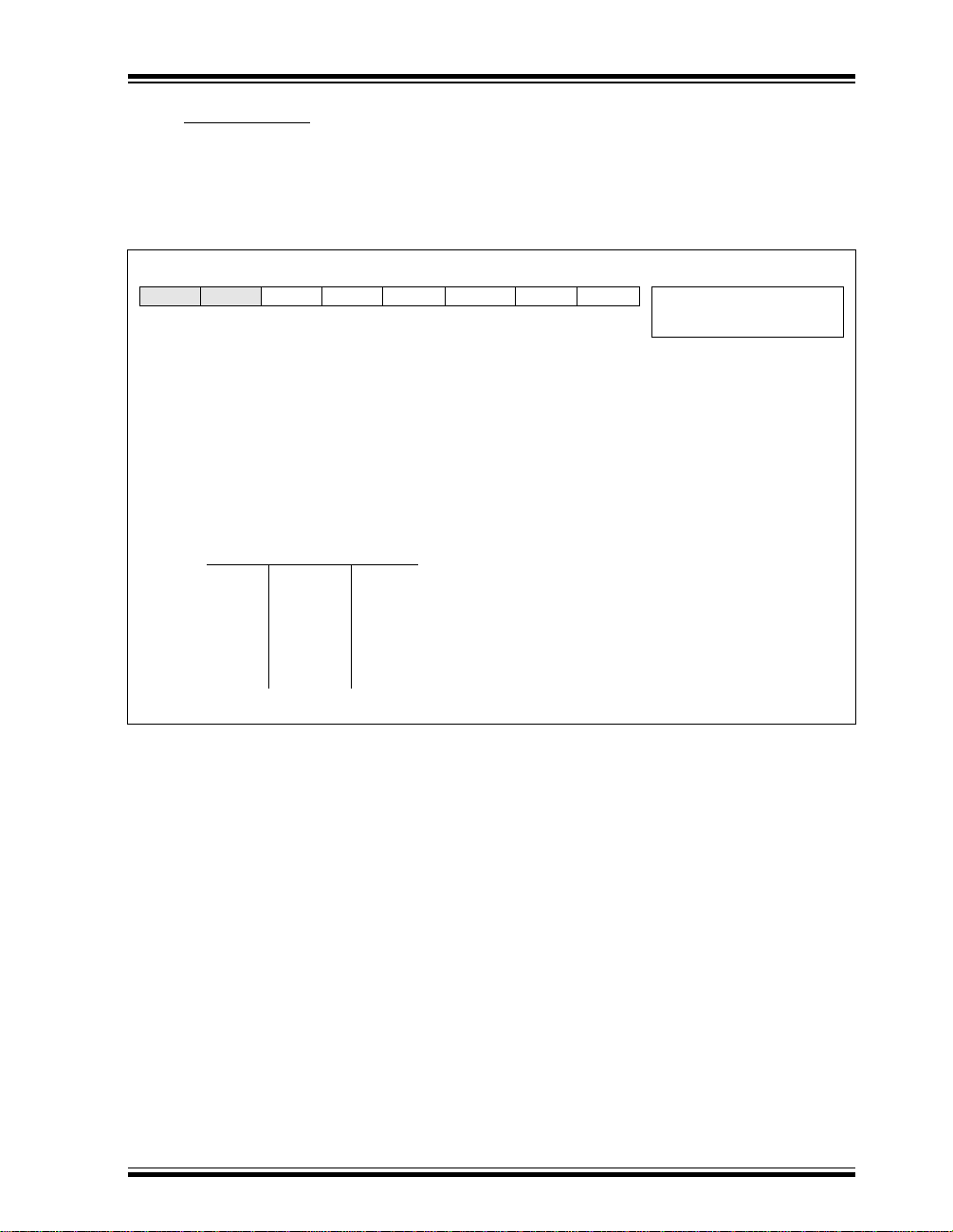
TABLE 1-1: PIC16C5X FAMILY OF DEVICES
PIC16C52
Clock
Memory
Peripherals
Features
Maximum Frequency
of Operation (MHz)
EPROM Program Memory
(x12 words)
ROM Program Memory
(x12 words)
RAM Data Memory (bytes) 25 25 25 24 25
Timer Module(s) TMR0 TMR0 TMR0 TMR0 TMR0
I/O Pins 12 12 12 20 12
Number of Instructions 33 33 33 33 33
Packages 18-pin DIP,
42020 2020
384 512 — 512 1K
— — 512 — —
SOIC
All PICmicro™ Family devices ha v e Power-on Reset, selectable Watchdog Timer (except PIC16C52), selectab le code
protect and high I/O current capability.
PIC16C54s PIC16CR54s PIC16C55s PIC16C56s
18-pin DIP,
SOIC;
20-pin SSOP
18-pin DIP,
SOIC;
20-pin SSOP
28-pin DIP,
SOIC;
28-pin SSOP
18-pin DIP,
SOIC;
20-pin SSOP
Clock
Memory
Peripherals
Features
PIC16CR56s
Maximum Frequency
of Operation (MHz)
EPROM Program Memory
(x12 words)
ROM Program Memory
(x12 words)
RAM Data Memory (bytes) 25 72 72 73 73
Timer Module(s) TMR0 TMR0 TMR0 TMR0 TMR0
20 20 20 20 20
— 2K — 2K —
1K — 2K — 2K
PIC16C57s PIC16CR57s PIC16C58s PIC16CR58s
DS30453B-page 6
Preliminary
1998 Microchip Technology Inc.
Page 7

PIC16C5X
2.0 PIC16C5X DEVICE VARIETIES
A variety of frequency ranges and packaging options
are available. Depending on application and
production requirements, the proper device option can
be selected using the information in this section. When
placing orders, please use the PIC16C5X Product
Identification System at the back of this data sheet to
specify the correct part number.
For the PIC16C5X family of devices, there are four
device types, as indicated in the device number:
1.C, as in PIC16C54. These devices have
EPROM program memory and operate over the
standard voltage range.
2.LC, as in PIC16LC54A. These devices have
EPROM program memory and operate over an
extended voltage range.
3.LV, as in PIC16LV54A. These devices have
EPROM program memory and operate over a
2.0V to 3.8V range.
4.CR, as in PIC16CR54A. These devices have
ROM program memory and operate over the
standard voltage range.
5.
LCR
, as in PIC16LCR54B. These devices have
ROM program memory and operate over an
extended voltage range.
2.1 U
The UV erasable versions, offered in CERDIP
packages, are optimal for prototype development and
pilot programs
UV erasable devices can be programmed for any of
the four oscillator configurations. Microchip's
PICSTART
support programming of the PIC16C5X. Third party
programmers also are available; refer to the Third
Party Guide for a list of sources.
2.2 One-Time-Pr
The availability of OTP devices is especially useful for
customers expecting frequent code changes and
updates.
The OTP devices, packaged in plastic packages,
permit the user to program them once. In addition to
the program memory, the configuration bits must be
programmed.
V Erasable Devices (EPROM)
and PRO MATE programmers both
ogrammable (OTP)
Devices
2.3 Quic
k-Turnaround-Production (QTP)
Devices
Microchip offers a QTP Programming Service for
factory production orders. This service is made
available for users who choose not to program a
medium to high quantity of units and whose code
patterns have stabilized. The devices are identical to
the OTP devices but with all EPROM locations and
configuration bit options already programmed by the
factory. Certain code and prototype verification
procedures apply before production shipments are
available. Please contact your Microchip Technology
sales office for more details.
2.4 Serializ
Microchip offers the unique programming service
where a few user-defined locations in each device are
programmed with different serial numbers. The serial
numbers may be random, pseudo-random or
sequential. The devices are identical to the OTP
devices but with all EPROM locations and
configuration bit options already programmed by the
factory.
Serial programming allows each device to have a
unique number which can serve as an entry code,
password or ID number.
2.5 Read Onl
Microchip offers masked ROM versions of several of
the highest volume parts, giving the customer a low
cost option for high volume, mature products.
ed
Quick-Turnaround-Production
SM
(SQTP ) Devices
y Memory (ROM) Devices
1998 Microchip Technology Inc.
Preliminary
DS30453B-page 7
Page 8

PIC16C5X
NOTES:
DS30453B-page 8
Preliminary
1998 Microchip Technology Inc.
Page 9

PIC16C5X
3.0 ARCHITECTURAL OVERVIEW
The high performance of the PIC16C5X family can be
attributed to a number of architectural features
commonly found in RISC microprocessors. To begin
with, the PIC16C5X uses a Harvard architecture in
which program and data are accessed on separate
buses. This improves bandwidth over traditional von
Neumann architecture where program and data are
fetched on the same bus. Separating program and
data memory further allows instructions to be sized
differently than the 8-bit wide data word. Instruction
opcodes are 12-bits wide making it possible to have all
single word instructions. A 12-bit wide program
memory access bus fetches a 12-bit instruction in a
single cycle. A two-stage pipeline overlaps fetch and
execution of instructions. Consequently , all instructions
(33) execute in a single cycle (200ns @ 20MHz)
except for program branches.
The PIC16C52 addresses 384 x 12 of program
memory, the PIC16C54s/CR54s and PIC16C55s
address 512 x 12 of program memory, the
PIC16C56s/CR56s address 1K X 12 of program
memory, and the PIC16C57s/CR57s and
PIC16C58s/CR58s address 2K x 12 of program
memory. All program memory is internal.
The PIC16C5X can directly or indirectly address its
register files and data memory. All special function
registers including the program counter are mapped in
the data memory. The PIC16C5X has a highly
orthogonal (symmetrical) instruction set that makes it
possible to carry out any operation on any register
using any addressing mode. This symmetr ical nature
and lack of ‘special optimal situations’ make
programming with the PIC16C5X simple yet efficient.
In addition, the learning curve is reduced significantly.
The PIC16C5X device contains an 8-bit ALU and
working register. The ALU is a general purpose
arithmetic unit. It performs arithmetic and Boolean
functions between data in the working register and any
register file.
The ALU is 8-bits wide and capable of addition,
subtraction, shift and logical operations. Unless
otherwise mentioned, arithmetic operations are two's
complement in nature. In two-operand instructions,
typically one operand is the W (working) register. The
other operand is either a file register or an immediate
constant. In single operand instructions, the operand
is either the W register or a file register.
The W register is an 8-bit working register used for
ALU operations. It is not an addressable register.
Depending on the instruction executed, the ALU may
affect the values of the Carry (C), Digit Carry (DC),
and Zero (Z) bits in the STATUS register. The C and
DC bits operate as a borr
respectively, in subtraction. See the
instructions for examples.
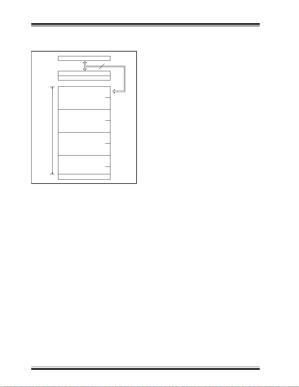
A simplified block diagram is shown in Figure 3-1, with
the corresponding device pins described in Table 3-1.
ow and digit borrow out bit,
SUBWF
and
ADDWF
1998 Microchip Technology Inc.
Preliminary
DS30453B-page 9
Page 10
PIC16C5X
FIGURE 3-1: PIC16C5X SERIES BLOCK DIAGRAM
EPROM/ROM
384 X 12 TO
2048 X 12
12
INSTRUCTION
REGISTER
12
INSTRUCTION
DECODER
8
LITERALS
W
9-11
PC
DIRECT ADDRESS
STATUS
ALU
“TRIS 5”
9-11
9
FROM W
TRISA PORTA
TMR0
T0CKI
DATA BUS
4
“TRIS 6”
4
PIN
PRESCALER
8
STACK 1
ST ACK 2
WDT TIME
OUT
8
DIRECT RAM
ADDRESS
4
RA3:RA0 RB7:RB0
CONFIGURA TION WORD
WA TCHDOG
TIMER
WDT/TMR0
OPTION REG.
FROM W
TRISB
“DISABLE”
6
FROM W
8
PORTB
“CODE
PROTECT”
CLKOUT
5
8
“TRIS 7”
8
“OSC
SELECT”
2
“OPTION”
5-7
FSR
OSC1 OSC2 MCLR
OSCILLA T OR/
TIMING &
CONTROL
“SLEEP”
GENERAL
PURPOSE
REGISTER
FILE
(SRAM)
24, 25, 72 or
73 Bytes
8
FROM W
TRISC
8
8
PORTC
RC7:RC0
(28-Pin
Devices Only)
8
DS30453B-page 10
Preliminary
1998 Microchip Technology Inc.
Page 11
PIC16C5X
TABLE 3-1: PINOUT DESCRIPTION - PIC16C52, PIC16C54s, PIC16CR54s, PIC16C56s,
PIC16CR56s, PIC16C58s, PIC16CR58s
Name
RA0
RA1
RA2
RA3
RB0
RB1
RB2
RB3
RB4
RB5
RB6
RB7
T0CKI 3 3 I ST Clock input to Timer0. Must be tied to V
MCLR
/V
OSC1/CLKIN 16 18 I ST Oscillator crystal input/external clock source input.
OSC2/CLKOUT 15 17 O — Oscillator crystal output. Connects to crystal or resonator in
V
DD
V
SS
Legend: I = input, O = output, I/O = input/output,
P = power, — = Not Used, TTL = TTL input,
ST = Schmitt Trigger input
DIP, SOIC
PP
SSOP
I/O/P
No.
17
18
10
11
12
13
14 15,16 P — Positive supply for logic and I/O pins.
No.
19
20
1
2
6
7
8
9
4 4 I ST Master clear (reset) input/programming voltage input. This
5 5,6 P — Ground reference for logic and I/O pins.
1
2
7
8
9
10
11
12
13
14
Type
I/O
I/O
I/O
I/O
I/O
I/O
I/O
I/O
I/O
I/O
I/O
I/O
Input
Levels
Bi-directional I/O port
TTL
TTL
TTL
TTL
Bi-directional I/O port
TTL
TTL
TTL
TTL
TTL
TTL
TTL
TTL
use, to reduce current consumption.
pin is an active low reset to the device. Voltage on the
MCLR
/V
PP
entering of programming mode.
crystal oscillator mode. In RC mode, OSC2 pin outputs
CLKOUT which has 1/4 the frequency of OSC1, and denotes
the instruction cycle rate.
pin must not exceed VDD to avoid unintended
Description
SS
or V
DD,
if not in
1998 Microchip Technology Inc.
Preliminary
DS30453B-page 11
Page 12
PIC16C5X
TABLE 3-2: PINOUT DESCRIPTION - PIC16C55s, PIC16C57s, PIC16CR57s
Name
RA0
RA1
RA2
RA3
RB0
RB1
RB2
RB3
RB4
RB5
RB6
RB7
RC0
RC1
RC2
RC3
RC4
RC5
RC6
RC7
T0CKI 1 2 I ST Clock input to Timer0. Must be tied to V
MCLR
OSC1/CLKIN 27 27 I ST Oscillator crystal input/external clock source input.
OSC2/CLKOUT 26 26 O — Oscillator crystal output. Connects to crystal or resonator in
V
DD
V
SS
N/C 3,5 — — — Unused, do not connect
Legend: I = input, O = output, I/O = input/output,
P = power, — = Not Used,
TTL = TTL input, ST = Schmitt Trigger input
DIP, SOIC
SSOP
I/O/P
No.
6
7
8
9
10
11
12
13
14
15
16
17
18
19
20
21
22
23
24
25
28 28 I ST Master clear (reset) input. This pin is an activ e low reset to the
2 3,4 P — Positive supply for logic and I/O pins.
4 1,14 P — Ground reference for logic and I/O pins.
No.
5
6
7
8
9
10
11
12
13
15
16
17
18
19
20
21
22
23
24
25
Type
I/O
I/O
I/O
I/O
I/O
I/O
I/O
I/O
I/O
I/O
I/O
I/O
I/O
I/O
I/O
I/O
I/O
I/O
I/O
I/O
Input
Levels
Bi-directional I/O port
TTL
TTL
TTL
TTL
Bi-directional I/O port
TTL
TTL
TTL
TTL
TTL
TTL
TTL
TTL
Bi-directional I/O port
TTL
TTL
TTL
TTL
TTL
TTL
TTL
TTL
to reduce current consumption.
device.
crystal oscillator mode. In RC mode, OSC2 pin outputs
CLKOUT which has 1/4 the frequency of OSC1, and denotes
the instruction cycle rate.
Description
or VDD if not in use
SS
DS30453B-page 12
Preliminary
1998 Microchip Technology Inc.
Page 13
PIC16C5X
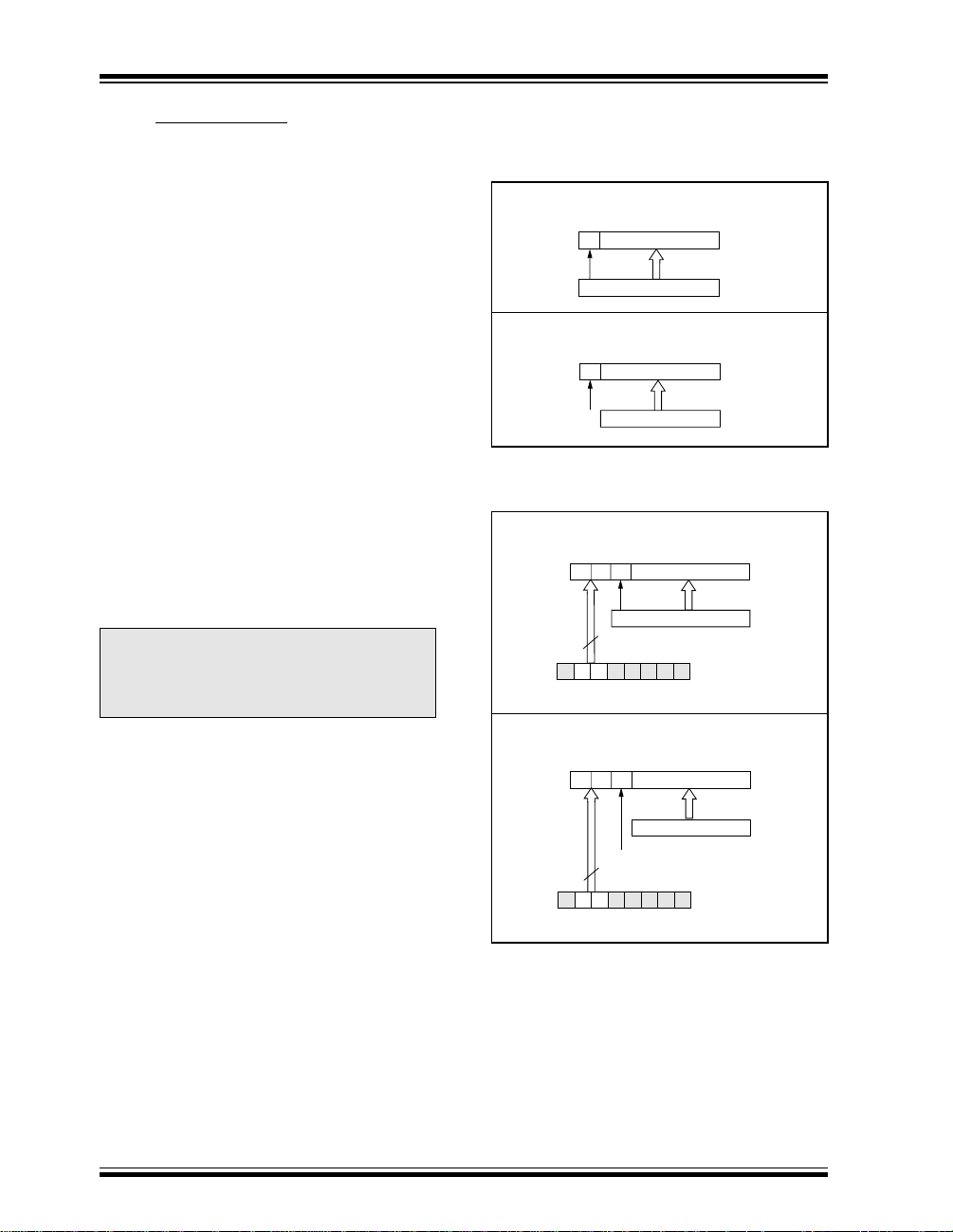
3.1 Cloc
king Scheme/Instruction Cycle
The clock input (OSC1/CLKIN pin) is internally divided
by four to generate four non-overlapping quadrature
clocks namely Q1, Q2, Q3 and Q4. Internally, the
program counter is incremented every Q1, and the
instruction is fetched from program memory and
latched into instruction register in Q4. It is decoded
and executed during the following Q1 through Q4. The
clocks and instruction execution flow is shown in
Figure 3-2 and Example 3-1.
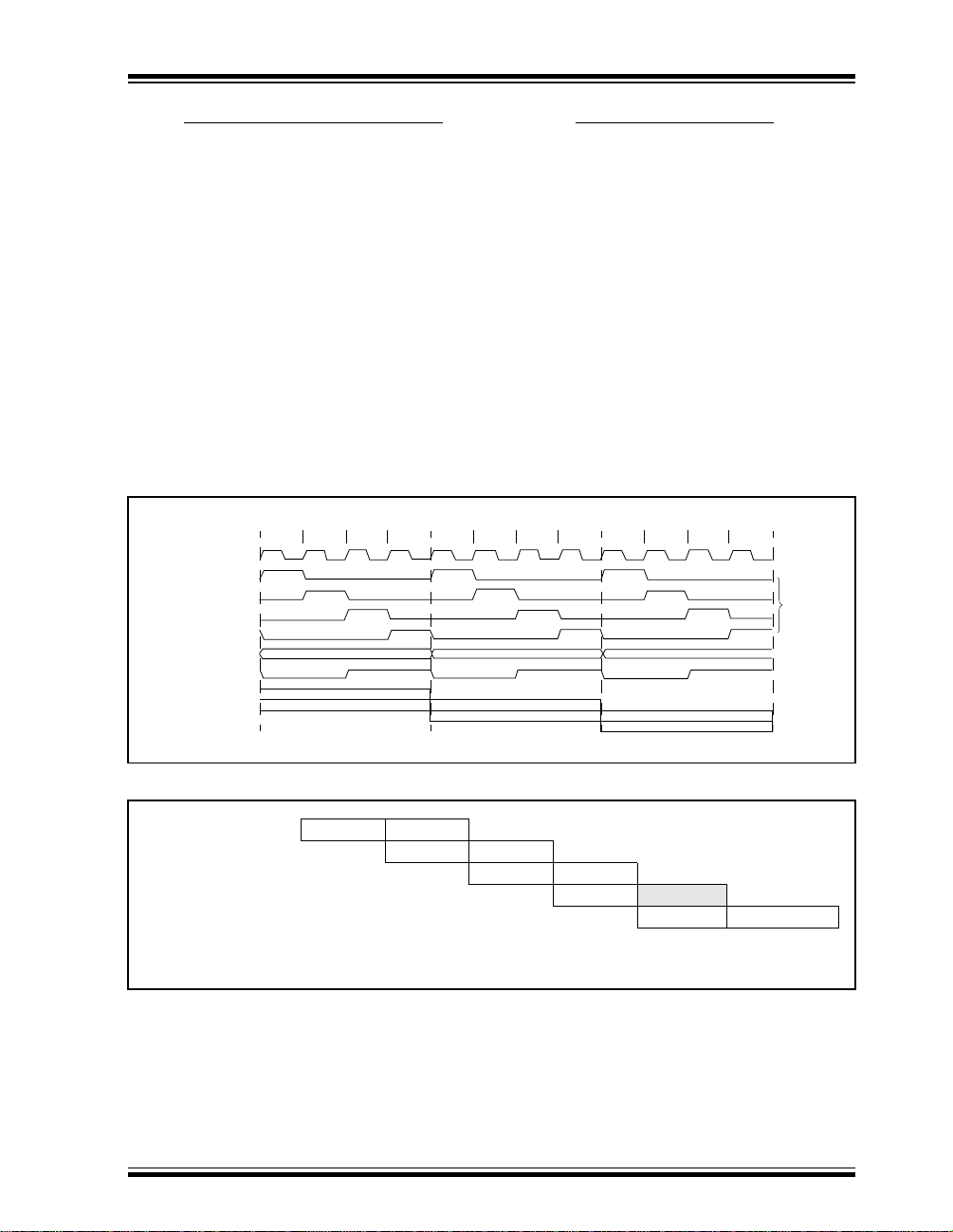
FIGURE 3-2: CLOCK/INSTRUCTION CYCLE
Q2 Q3 Q4
OSC1
Q2
Q3
Q4
PC
OSC2/CLKOUT
(RC mode)
Q1
Q1
PC PC+1 PC+2
Fetch INST (PC)
Execute INST (PC-1) Fetch INST (PC+1)
Q1
3.2 Instruction Flo
w/Pipelining
An Instruction Cycle consists of four Q cycles (Q1, Q2,
Q3 and Q4). The instruction fetch and execute are
pipelined such that fetch takes one instruction cycle
while decode and execute takes another instruction
cycle. However, due to the pipelining, each instruction
effectively executes in one cycle. If an instruction
causes the program counter to change (e.g.,
then two cycles are required to complete the
instruction (Example 3-1).
A fetch cycle begins with the program counter (PC)
incrementing in Q1.
In the execution cycle, the fetched instruction is
latched into the Instruction Register (IR) in cycle Q1.
This instruction is then decoded and executed during
the Q2, Q3, and Q4 cycles. Data memory is read
during Q2 (operand read) and written during Q4
(destination write).
Q2 Q3 Q4
Execute INST (PC) Fetch INST (PC+2)
Q2 Q3 Q4
Q1
Execute INST (PC+1)
Internal
phase
clock
GOTO
)
EXAMPLE 3-1: INSTRUCTION PIPELINE FLOW
1. MOVLW 55H
2. MOVWF PORTB
3. CALL SUB_1
4. BSF PORTA, BIT3
All instructions are single cycle, except for any program branches. These take two cycles since the fetch
instruction is “flushed” from the pipeline while the new instruction is being fetched and then executed.
1998 Microchip Technology Inc.
Fetch 1 Execute 1
Fetch 2 Execute 2
Preliminary
Fetch 3 Execute 3
Fetch 4 Flush
Fetch SUB_1 Execute SUB_1
DS30453B-page 13
Page 14

PIC16C5X
NOTES:
DS30453B-page 14 Preliminary 1998 Microchip Technology Inc.
Page 15
PIC16C5X
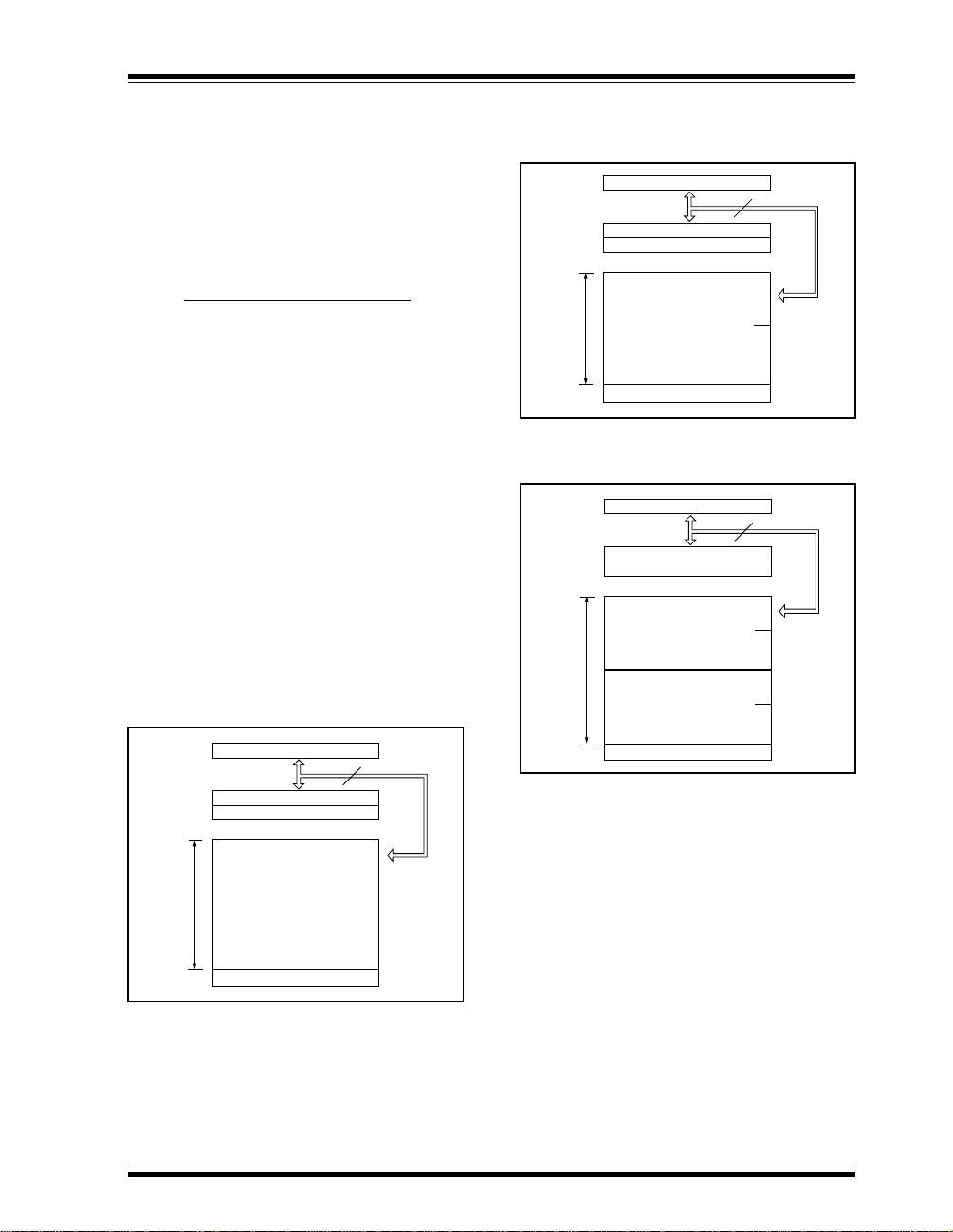
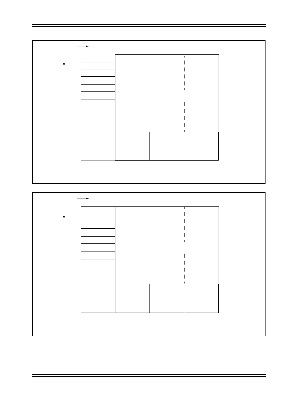
4.0 MEMORY ORGANIZATION
PIC16C5X memory is organized into program memory
and data memory. For devices with more than 512
bytes of program memory, a paging scheme is used.
Program memory pages are accessed using one or
two STATUS register bits. For devices with a data
memory register file of more than 32 registers, a
banking scheme is used. Data memory banks are
accessed using the File Selection Register (FSR).
4.1 Program Memory Organization
The PIC16C52 has a 9-bit Program Counter (PC)
capable of addressing a 384 x 12 program memory
space (Figure 4-1). The PIC16C54s, PIC16CR54s and
PIC16C55s have a 9-bit Program Counter (PC)
capable of addressing a 512 x 12 program memory
space (Figure 4-2). The PIC16C56s and PIC16CR56s
have a 10-bit Program Counter (PC) capable of
addressing a 1K x 12 program memory space
(Figure 4-3). The PIC16CR57s, PIC16C58s and
PIC16CR58s have an 11-bit Program Counter capable
of addressing a 2K x 12 program memory space
(Figure 4-4). Accessing a location abov e the physically
implemented address will cause a wraparound.
The reset vector for the PIC16C52 is at 17Fh. A NOP
at the reset vector location will cause a restart at
location 000h. The reset vector for the PIC16C54s,
PIC16CR54s and PIC16C55s is at 1FFh. The reset
vector for the PIC16C56s and PIC16CR56s is at
3FFh. The reset vector for the PIC16C57s,
PIC16CR57s, PIC16C58s, and PIC16CR58s is at
7FFh.
FIGURE 4-1: PIC16C52 PROGRAM
CALL, RETLW
MEMORY MAP AND STACK
PC<8:0>
Stack Level 1
Stack Level 2
9
000h
FIGURE 4-2: PIC16C54s/CR54s/C55s
PROGRAM MEMORY MAP
AND STACK
CALL, RETLW
Space
User Memory
PC<8:0>
Stack Level 1
Stack Level 2
On-chip
Program
Memory
Reset Vector
9
000h
0FFh
100h
1FFh
FIGURE 4-3: PIC16C56s/CR56s
PROGRAM MEMORY MAP
AND STACK
CALL, RETLW
Space
User Memory
PC<9:0>
Stack Level 1
Stack Level 2
On-chip Program
Memory (Page 0)
On-chip Program
Memory (Page 1)
Reset Vector
10
000h
0FFh
100h
1FFh
200h
2FFh
300h
3FFh
On-chip Program
Space
User Memory
1998 Microchip Technology Inc. Preliminary DS30453B-page 15
Memory
Reset Vector
17Fh
Page 16
PIC16C5X
FIGURE 4-4: PIC16C57s/CR57s/C58s/
CR58s PROGRAM MEMORY
MAP AND STACK
CALL, RETLW
Space
User Memory
PC<10:0>
Stack Level 1
Stack Level 2
On-chip Program
Memory (Page 0)
On-chip Program
Memory (Page 1)
On-chip Program
Memory (Page 2)
On-chip Program
Memory (Page 3)
Reset Vector
11
000h
0FFh
100h
1FFh
200h
2FFh
300h
3FFh
400h
4FFh
500h
5FFh
600h
6FFh
700h
7FFh
DS30453B-page 16 Preliminary 1998 Microchip Technology Inc.
Page 17

PIC16C5X
4.2 Data Memory Organization
Data memory is composed of registers, or bytes of
RAM. Therefore, data memory for a device is specified
by its register file. The register file is divided into two
functional groups: special function registers and
general purpose registers.
The special function registers include the TMR0
register, the Program Counter (PC), the Status
Register, the I/O registers (ports), and the File Select
Register (FSR). In addition, special purpose registers
are used to control the I/O port configuration and
prescaler options.
The general purpose registers are used for data and
control information under command of the instructions.
For the PIC16C52, PIC16C54s, PIC16CR54s,
PIC16C56s and PIC16CR56s, the register file is
composed of 7 special function registers and 25
general purpose registers (Figure 4-5).
For the PIC16C55s, the register file is composed of 8
special function registers and 24 general purpose
registers.
For the PIC16C57s and PIC16CR57s, the register file
is composed of 8 special function registers, 24 general
purpose registers and up to 48 additional general
purpose registers that may be addressed using a
banking scheme (Figure 4-6).
For the PIC16C58s and PIC16CR58s, the register file
is composed of 7 special function registers, 25 general
purpose registers and up to 48 additional general
purpose registers that may be addressed using a
banking scheme (Figure 4-7).
4.2.1 GENERAL PURPOSE REGISTER FILE The register file is accessed either directly or indirectly
through the file select register FSR (Section 4.7).
FIGURE 4-5: PIC16C52, PIC16C54s,
PIC16CR54s, PIC16C55s,
PIC16C56s, PIC16CR56s
REGISTER FILE MAP
File Address
(1)
00h
01h
02h
03h
04h
05h
06h
07h
0Fh
10h
1Fh
Note 1: Not a physical register. See Section 4.7
2: PIC16C55s only, others are a general
purpose register.
INDF
TMR0
PCL
STATUS
FSR
PORTA
PORTB
PORTC
General
Purpose
Registers
(2)
1998 Microchip Technology Inc. Preliminary DS30453B-page 17
Page 18
PIC16C5X
FIGURE 4-6: PIC16C57s/CR57s REGISTER FILE MAP
FSR<6:5> 00 01 10 11
File Address
00h
01h
02h
03h
04h
05h
06h
07h
08h
0Fh
10h
1Fh
FIGURE 4-7: PIC16C58s/CR58s REGISTER FILE MAP
FSR<6:5> 00 01 10 11
File Address
00h
01h
02h
03h
04h
05h
06h
07h
0Fh
10h
1Fh
(1)
INDF
TMR0
PCL
STATUS
FSR
PORTA
PORTB
PORTC
General
Purpose
Registers
General
Purpose
Registers
Bank 0 Bank 1 Bank 2 Bank 3
INDF
TMR0
PCL
STATUS
FSR
PORTA
PORTB
General
Purpose
Registers
General
Purpose
Registers
Bank 0 Bank 1 Bank 2 Bank 3
20h
2Fh
30h
General
Purpose
Registers
3Fh
Note 1: Not a physical register. See Section 4.7
(1)
20h
2Fh
30h
General
Purpose
Registers
3Fh
Note 1: Not a physical register. See Section 4.7
40h
Addresses map back to
addresses in Bank 0.
4Fh
50h
5Fh
40h
Addresses map back to
addresses in Bank 0.
4Fh
50h
5Fh
General
Purpose
Registers
General
Purpose
Registers
60h
6Fh
70h
General
Purpose
Registers
7Fh
60h
6Fh
70h
General
Purpose
Registers
7Fh
DS30453B-page 18 Preliminary 1998 Microchip Technology Inc.
Page 19
PIC16C5X
4.2.2 SPECIAL FUNCTION REGISTERS The Special Function Registers are registers used by
the CPU and peripheral functions to control the
operation of the device (Table 4-1).
The special registers can be classified into two sets.
The special function registers associated with the
“core” functions are described in this section. Those
related to the operation of the peripheral features are
described in the section for each peripheral feature.
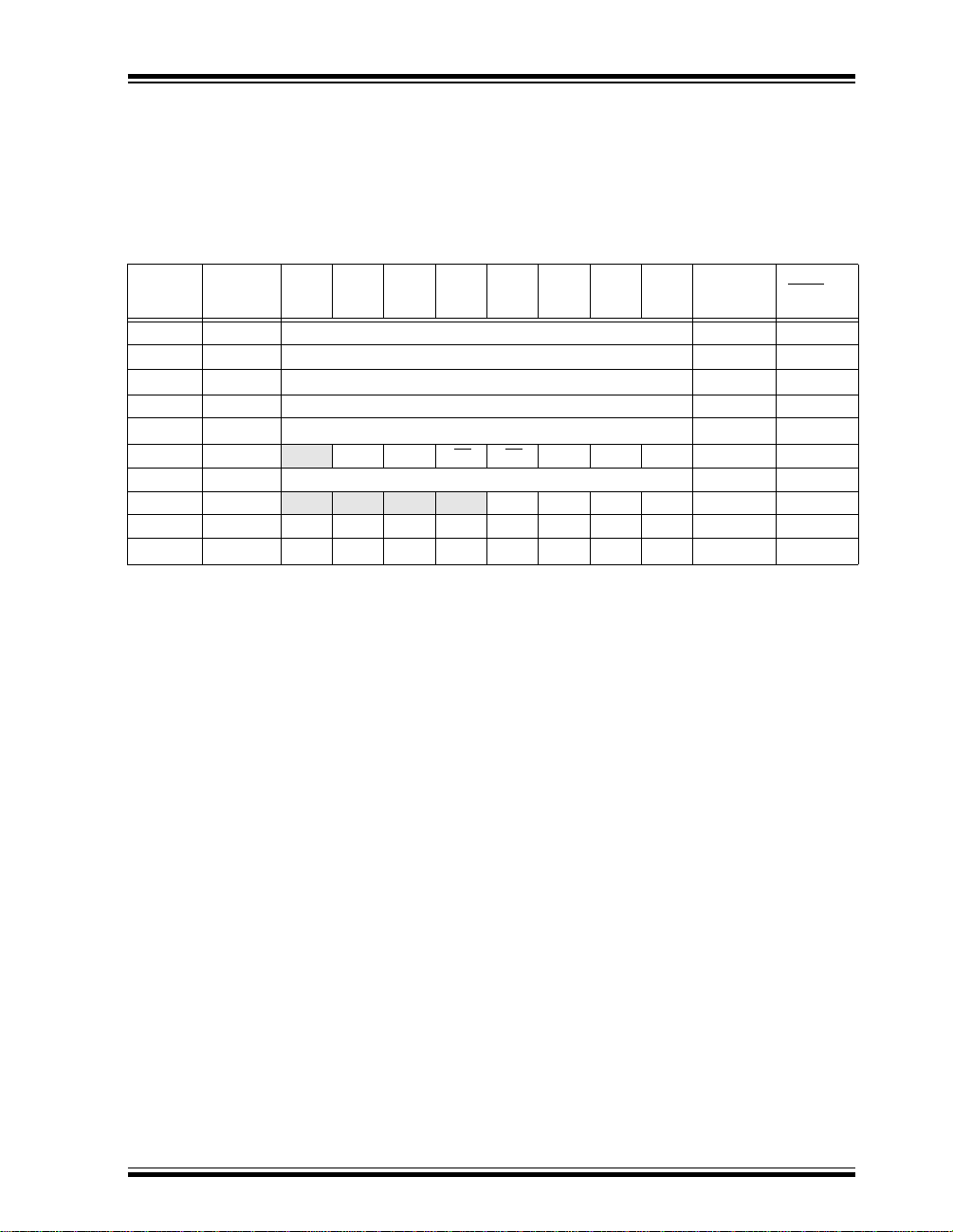
TABLE 4-1: SPECIAL FUNCTION REGISTER SUMMARY
Value on
Address Name Bit 7 Bit 6 Bit 5 Bit 4 Bit 3 Bit 2 Bit 1 Bit 0
N/A TRIS I/O control registers (TRISA, TRISB, TRISC) 1111 1111 1111 1111
N/A OPTION Contains control bits to configure Timer0 and Timer0/WDT prescaler --11 1111 --11 1111
00h INDF Uses contents of FSR to address data memory (not a physical register) xxxx xxxx uuuu uuuu
01h TMR0 8-bit real-time clock/counter xxxx xxxx uuuu uuuu
(1)
02h
03h STATUS PA2 PA1 PA0 TO PD ZDCC0001 1xxx 000q quuu
04h FSR Indirect data memory address pointer 1xxx xxxx 1uuu uuuu
05h PORTA — — — — RA3 RA2 RA1 RA0 ---- xxxx ---- uuuu
06h PORTB RB7 RB6 RB5 RB4 RB3 RB2 RB1 RB0 xxxx xxxx uuuu uuuu
07h
Legend: Shaded boxes = unimplemented or unused, – = unimplemented, read as '0' (if applicable)
Note 1: The upper byte of the Program Counter is not directly accessible. See Section 4.5
PCL Low order 8 bits of PC 1111 1111 1111 1111
(2)
PORTC RC7 RC6 RC5 RC4 RC3 RC2 RC1 RC0 xxxx xxxx uuuu uuuu
x = unknown, u = unchanged, q = see the tables in Section 7.7 for possible values.
for an explanation of how to access these bits.
2: File address 07h is a general purpose register on the PIC16C52, PIC16C54s, PIC16CR54s, PIC16C56s, PIC16CR56s,
PIC16C58s and PIC16CR58s.
Power-On
Reset
Value on
MCLR and
WDT Reset
1998 Microchip Technology Inc. Preliminary DS30453B-page 19
Page 20
PIC16C5X
4.3 STATUS Register
This register contains the arithmetic status of the ALU,
the RESET status, and the page preselect bits for
program memories larger than 512 words.
The STATUS register can be the destination for any
instruction, as with any other register. If the STATUS
register is the destination for an instruction that affects
the Z, DC or C bits, then the write to these three bits is
disabled. These bits are set or cleared according to
the device logic. Further more, the T
O and PD bits are
not writable. Therefore, the result of an instruction with
the STATUS register as destination may be different
than intended.
For example, CLRF STATUS will clear the upper three
bits and set the Z bit. This leaves the STATUS register
as 000u u1uu (where u = unchanged).
It is recommended, therefore, that only BCF, BSF and
MOVWF instructions be used to alter the STATUS
register because these instructions do not affect the Z,
DC or C bits from the STATUS register. For other
instructions, which do affect STATUS bits, see
Section 8.0, Instruction Set Summary.
FIGURE 4-8: STATUS REGISTER (ADDRESS:03h)
R/W-0 R/W-0 R/W-0 R-1 R-1 R/W-x R/W-x R/W-x
PA2 PA1 PA0 TO PD Z DC C R = Readable bit
bit7 6 5 4 3 2 1 bit0
bit 7: PA2: This bit unused at this time.
Use of the PA2 bit as a general purpose read/write bit is not recommended, since this may affect upward
compatibility with future products.
bit 6-5: PA1:PA0: Program page preselect bits (PIC16C56s/CR56s)(PIC16C57s/CR57s)(PIC16C58s/CR58s)
00 = Page 0 (000h - 1FFh) - PIC16C56s/CR56s, PIC16C57s/CR57s, PIC16C58s/CR58s
01 = Page 1 (200h - 3FFh) - PIC16C56s/CR56s, PIC16C57s/CR57s, PIC16C58s/CR58s
10 = Page 2 (400h - 5FFh) - PIC16C57s/CR57s, PIC16C58s/CR58s
11 = Page 3 (600h - 7FFh) - PIC16C57s/CR57s, PIC16C58s/CR58s
Each page is 512 words.
Using the PA1:PA0 bits as general purpose read/write bits in devices which do not use them for program
page preselect is not recommended since this may affect upward compatibility with future products.
bit 4: T
bit 3: PD: Power-down bit
bit 2: Z: Zero bit
bit 1: DC: Digit carry/borrow bit (for ADDWF and SUBWF instructions)
bit 0: C: Carry/borrow bit (for ADDWF, SUBWF and RRF, RLF instructions)
O: Time-out bit
1 = After power-up, CLRWDT instruction, or SLEEP instruction
0 = A WDT time-out occurred
1 = After power-up or by the CLRWDT instruction
0 = By execution of the SLEEP instruction
1 = The result of an arithmetic or logic operation is zero
0 = The result of an arithmetic or logic operation is not zero
ADDWF
1 = A carry from the 4th low order bit of the result occurred
0 = A carry from the 4th low order bit of the result did not occur
SUBWF
1 = A borrow from the 4th low order bit of the result did not occur
0 = A borrow from the 4th low order bit of the result occurred
ADDWF SUBWF RRF or RLF
1 = A carry occurred 1 = A borrow did not occur Load bit with LSb or MSb, respectively
0 = A carry did not occur 0 = A borrow occurred
W = Writable bit
- n = Value at POR reset
DS30453B-page 20 Preliminary 1998 Microchip Technology Inc.
Page 21
PIC16C5X
4.4 OPTION Register
The OPTION register is a 6-bit wide, write-only
register which contains various control bits to
By executing the OPTION instruction, the contents of
the W register will be transferred to the OPTION
register. A RESET sets the OPTION<5:0> bits.
configure the Timer0/WDT prescaler and Timer0.
FIGURE 4-9: OPTION REGISTER
U-0 U-0 W-1 W-1 W-1 W-1 W-1 W-1
— — T0CS T0SE PSA PS2 PS1 PS0 W = Writab le bit
bit7 6 5 4 3 2 1 bit0
bit 7-6: Unimplemented.
bit 5: T0CS: Timer0 clock source select bit
1 = Transition on T0CKI pin
0 = Internal instruction cycle clock (CLKOUT)
bit 4: T0SE: Timer0 source edge select bit
1 = Increment on high-to-low transition on T0CKI pin
0 = Increment on low-to-high transition on T0CKI pin
bit 3: PSA: Prescaler assignment bit
1 = Prescaler assigned to the WDT (not implemented on PIC16C52)
0 = Prescaler assigned to Timer0
bit 2-0: PS2:PS0: Prescaler rate select bits
Bit Value Timer0 Rate WDT Rate (not implemented on PIC16C52)
000
001
010
011
100
101
110
111
1 : 2
1 : 4
1 : 8
1 : 16
1 : 32
1 : 64
1 : 128
1 : 256
1 : 1
1 : 2
1 : 4
1 : 8
1 : 16
1 : 32
1 : 64
1 : 128
U = Unimplemented bit
- n = Value at POR reset
1998 Microchip Technology Inc. Preliminary DS30453B-page 21
Page 22
PIC16C5X
4.5 Program Counter
As a program instruction is executed, the Program
Counter (PC) will contain the address of the next
program instruction to be executed. The PC value is
increased by one every instruction cycle, unless an
instruction changes the PC.
For a GOTO instruction, bits 8:0 of the PC are provided
by the GOTO instruction word. The PC Latch (PCL) is
mapped to PC<7:0> (Figure 4-10 and Figure 4-11).
For the PIC16C56s, PIC16CR56s, PIC16C57s,
PIC16CR57s, PIC16C58s and PIC16CR58s, a page
number must be supplied as well. Bit5 and bit6 of the
STATUS register provide page information to bit9 and
bit10 of the PC (Figure 4-11 and Figure 4-12).
For a CALL instruction, or any instruction where the
PCL is the destination, bits 7:0 of the PC again are
provided by the instruction word. However, PC<8>
does not come from the instruction word, but is always
cleared (Figure 4-10 and Figure 4-11).
Instructions where the PCL is the destination, or
Modify PCL instructions, include MOVWF PC, ADDWF
PC, and BSF PC,5.
For the PIC16C56s, PIC16CR56s, PIC16C57s,
PIC16CR57s, PIC16C58s and PIC16CR58s, a page
number again must be supplied. Bit5 and bit6 of the
STATUS register provide page information to bit9 and
bit10 of the PC (Figure 4-11 and Figure 4-12).
Note: Because PC<8> is cleared in the CALL
instruction, or any Modify PCL instruction,
all subroutine calls or computed jumps are
limited to the first 256 locations of any program memory page (512 words long).
FIGURE 4-10: LOADING OF PC
BRANCH INSTRUCTIONS PIC16C52, PIC16C54s,
PIC16CR54s, PIC16C55s
GOTO Instruction
87 0
PC
PCL
Instruction Word
CALL or Modify PCL Instruction
87 0
PC
Reset to '0'
PCL
Instruction Word
FIGURE 4-11: LOADING OF PC
BRANCH INSTRUCTIONS PIC16C56s/PIC16CR56s
GOTO Instruction
910
PC
CALL or Modify PCL Instruction
PC
87 0
2
PA1:PA0
70
STATUS
910
87 0
PCL
Instruction Word
PCL
Instruction Word
Reset to ‘0’
2
PA1:PA0
70
STATUS
DS30453B-page 22 Preliminary 1998 Microchip Technology Inc.
Page 23
PIC16C5X
FIGURE 4-12: LOADING OF PC
BRANCH INSTRUCTIONS PIC16C57s/PIC16CR57s, AND
PIC16C58s/PIC16CR58s
GOTO Instruction
910
PC
CALL or Modify PCL Instruction
PC
87 0
2
PA1:PA0
70
STATUS
910
87 0
Reset to ‘0’
2
PA1:PA0
70
STATUS
PCL
Instruction Word
PCL
Instruction Word
4.5.1 PAGING CONSIDERATIONS –
PIC16C56
PIC16C58
s/CR56s, PIC16C57s/CR57s AND
s/CR58s
If the Program Counter is pointing to the last address
of a selected memory page, when it increments it will
cause the program to continue in the next higher page.
However, the page preselect bits in the STATUS
register will not be updated. Therefore, the next GOTO,
CALL, or Modify PCL instruction will send the program
to the page specified by the page preselect bits (PA0
or PA1:PA0).
For example, a NOP at location 1FFh (page 0)
increments the PC to 200h (page 1). A GOTO xxx at
200h will return the program to address 0xxh on page
0 (assuming that PA1:PA0 are clear).
To prevent this, the page preselect bits must be
updated under program control.
4.5.2 EFFECTS OF RESET
The Program Counter is set upon a RESET, which
means that the PC addresses the last location in the
last page i.e., the reset vector.
The STATUS register page preselect bits are cleared
upon a RESET, which means that page 0 is
pre-selected.
Therefore, upon a RESET, a GOTO instruction at the
reset vector location will automatically cause the
program to jump to page 0.
4.6 Stack
PIC16C5X devices have a 9-bit, 10-bit or 11-bit wide,
two-level hardware push/pop stack (Figure 4-2,
Figure 4-1, and Figure 4-3 respectively).
A CALL instruction will
1 into stack 2 and then push the current program
counter value, incremented by one, into stac k le v el 1. If
more than two sequential CALL’s are executed, only
the most recent two return addresses are stored.
A RETLW instruction will
1 into the program counter and then copy stack level 2
contents into level 1. If more than two sequential
RETLW’s are executed, the stack will be filled with the
address previously stored in level 2. Note that the
W register will be loaded with the literal value specified
in the instruction. This is particularly useful for the
implementation of data look-up tables within the
program memory.
For the RETLW instruction, the PC is loaded with the
Top Of Stack (TOS) contents. All of the devices
covered in this data sheet have a two-level stack. The
stack has the same bit width as the device PC.
push
the current value of stack
pop
the contents of stack level
1998 Microchip Technology Inc. Preliminary DS30453B-page 23
Page 24
PIC16C5X
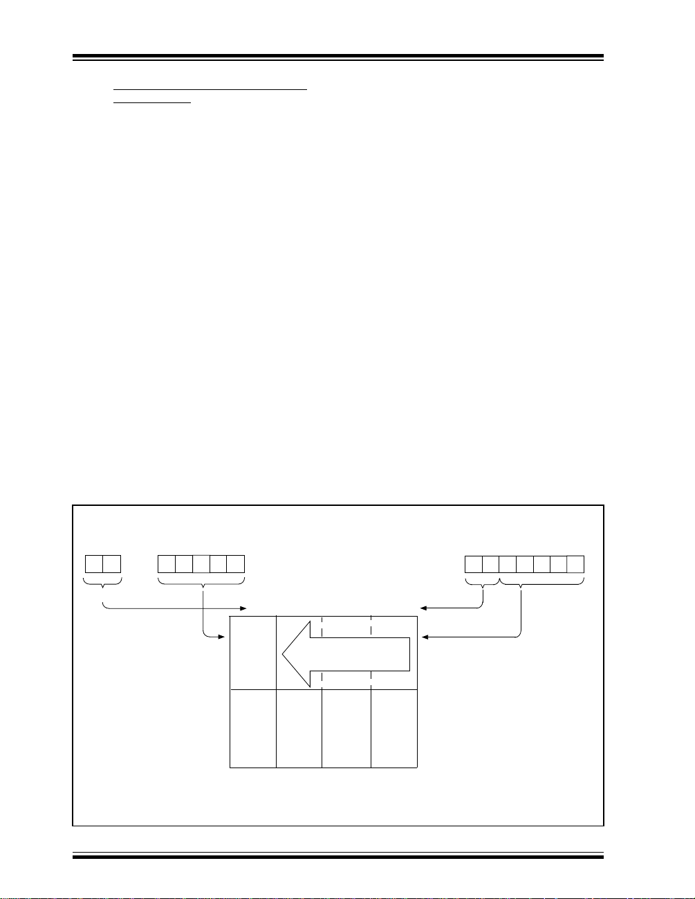
4.7 Indirect Data Addressing; INDF and
FSR Registers
The INDF register is not a physical register.
Addressing INDF actually addresses the register
whose address is contained in the FSR register (FSR
is a
pointer
). This is indirect addressing.
EXAMPLE 4-1: INDIRECT ADDRESSING
• Register file 05 contains the value 10h
• Register file 06 contains the value 0Ah
• Load the value 05 into the FSR register
• A read of the INDF register will return the value
of 10h
• Increment the value of the FSR register by one
(FSR = 06h)
• A read of the INDR register now will return the
value of 0Ah.
Reading INDF itself indirectly (FSR = 0) will produce
00h. Writing to the INDF register indirectly results in a
no-operation (although STATUS bits may be affected).
A simple program to clear RAM locations 10h-1Fh
using indirect addressing is shown in Example 4-2.
EXAMPLE 4-2: HOW TO CLEAR RAM
USING INDIRECT
ADDRESSING
movlw 0x10 ;initialize pointer
movwf FSR ; to RAM
NEXT clrf INDF ;clear INDF register
incf FSR,F ;inc pointer
btfsc FSR,4 ;all done?
goto NEXT ;NO, clear next
CONTINUE
: ;YES, continue
The FSR is either a 5-bit (PIC16C52, PIC16C54s,
PIC16CR54s, PIC16C55s), 6-bit (PIC16C56s,
PIC16CR56s), or 7-bit (PIC16C57s, PIC16CR57s,
PIC16C58s, PIC16CR58s) wide register. It is used in
conjunction with the INDF register to indirectly address
the data memory area.
The FSR<4:0> bits are used to select data memory
addresses 00h to 1Fh.
PIC16C52, PIC16C54s, PIC16CR54s, PIC16C55s:
These do not use banking. FSR<6:5> are
unimplemented and read as '1's.
PIC16C57s, PIC16CR57s, PIC16C58s,
PIC16CR58s: FSR<6:5> are the bank select bits and
are used to select the bank to be addressed (00 =
bank 0, 01 = bank 1, 10 = bank 2, 11 = bank 3).
FIGURE 4-13: DIRECT/INDIRECT ADDRESSING
Direct Addressing
(FSR)
5
6
bank select
location select
Data
Memory
(opcode) 04
00h
0Fh
(1)
10h
1Fh 3Fh 5Fh 7Fh
Bank 0 Bank 1 Bank 2 Bank 3
1000 01 11
Addresses map back
to addresses in Bank 0.
Note 1: For register map detail see Section 4.2.
DS30453B-page 24 Preliminary 1998 Microchip Technology Inc.
Indirect Addressing
(FSR)
5
4
6
location select
bank
0
Page 25
PIC16C5X
5.0 I/O PORTS
As with any other register, the I/O registers can be
written and read under program control. However, read
instructions (e.g., MOVF PORTB,W) always read the I/O
pins independent of the pin’s input/output modes. On
RESET, all I/O ports are defined as input (inputs are at
hi-impedance) since the I/O control registers (TRISA,
TRISB, TRISC) are all set.
5.1 PORTA
PORTA is a 4-bit I/O register. Only the low order 4 bits
are used (RA3:RA0). Bits 7-4 are unimplemented and
read as '0's.
5.2 PORTB
PORTB is an 8-bit I/O register (PORTB<7:0>).
5.3 PORTC
PORTC is an 8-bit I/O register for PIC16C55s,
PIC16C57s and PIC16CR57s.
PORTC is a general purpose register for PIC16C52,
PIC16C54s, PIC16CR54s, PIC16C56s, PIC16C58s
and PIC16CR58s.
5.4 TRIS Registers
The output driver control registers are loaded with the
contents of the W register by executing the TRIS f
instruction. A '1' from a TRIS register bit puts the
corresponding output driver in a hi-impedance mode.
A '0' puts the contents of the output data latch on the
selected pins, enabling the output buffer.
Note: A read of the ports reads the pins, not the
output data latches. That is, if an output
driver on a pin is enabled and driven high,
but the external system is holding it low, a
read of the port will indicate that the pin is
low.
The TRIS registers are “write-only” and are set (output
drivers disabled) upon RESET.
5.5 I/O Interfacing
The equivalent circuit for an I/O port pin is shown in
Figure 5-1. All ports may be used for both input and
output operation. For input operations these ports are
non-latching. Any input must be present until read by
an input instruction (e.g., MOVF PORTB, W). The
outputs are latched and remain unchanged until the
output latch is rewritten. To use a port pin as output,
the corresponding direction control bit (in TRISA,
TRISB) must be cleared (= 0). For use as an input, the
corresponding TRIS bit must be set. Any I/O pin can
be programmed individually as input or output.
FIGURE 5-1: EQUIVALENT CIRCUIT
FOR A SINGLE I/O PIN
Data
Bus
WR
Port
W
Reg
TRIS ‘f’
Note 1: I/O pins have protection diodes to VDD and VSS.
CK
CK
Reset
Data
Latch
TRIS
Latch
QD
VDD
Q
QD
Q
RD Port
P
N
VSS
I/O
pin
(1)
TABLE 5-1: SUMMARY OF PORT REGISTERS
Value on
Address Name Bit 7 Bit 6 Bit 5 Bit 4 Bit 3 Bit 2 Bit 1 Bit 0
N/A TRIS I/O control registers (TRISA, TRISB, TRISC) 1111 1111 1111 1111
05h PORTA — — — — RA3 RA2 RA1 RA0 ---- xxxx ---- uuuu
06h PORTB RB7 RB6 RB5 RB4 RB3 RB2 RB1 RB0 xxxx xxxx uuuu uuuu
07h PORTC RC7 RC6 RC5 RC4 RC3 RC2 RC1 RC0 xxxx xxxx uuuu uuuu
Legend: Shaded boxes = unimplemented, read as ‘0’,
– = unimplemented, read as '0', x = unknown, u = unchanged
1998 Microchip Technology Inc. Preliminary DS30453B-page 25
Power-On
Reset
Value on
MCLR and
WDT Reset
Page 26

PIC16C5X
5.6 I/O Programming Considerations
5.6.1 BI-DIRECTIONAL I/O PORTS
Some instructions operate internally as read followed
by write operations. The BCF and BSF instr uctions, for
example, read the entire port into the CPU, execute
the bit operation and re-write the result. Caution must
be used when these instructions are applied to a port
where one or more pins are used as input/outputs. For
example, a BSF operation on bit5 of PORTB will cause
all eight bits of PORTB to be read into the CPU, bit5 to
be set and the PORTB value to be written to the output
latches. If another bit of PORTB is used as a
bi-directional I/O pin (say bit0) and it is defined as an
input at this time, the input signal present on the pin
itself would be read into the CPU and rewritten to the
data latch of this particular pin, overwriting the
previous content. As long as the pin stays in the input
mode, no problem occurs. However, if bit0 is switched
into output mode later on, the content of the data latch
may now be unknown.
Example 5-1 shows the effect of two sequential
read-modify-write instructions (e.g., BCF, BSF , etc.) on
an I/O port.
A pin actively outputting a high or a low should not be
driven from external devices at the same time in order
to change the level on this pin (“wired-or”, “wired-and”).
The resulting high output currents may damage the
chip.
EXAMPLE 5-1: READ-MODIFY-WRITE
INSTRUCTIONS ON AN
I/O PORT
;Initial PORT Settings
; PORTB<7:4> Inputs
; PORTB<3:0> Outputs
;PORTB<7:6> have external pull-ups and are
;not connected to other circuitry
;
; PORT latch PORT pins
; ---------- --------- BCF PORTB, 7 ;01pp pppp 11pp pppp
BCF PORTB, 6 ;10pp pppp 11pp pppp
MOVLW 03Fh ;
TRIS PORTB ;10pp pppp 10pp pppp
;
;Note that the user may have expected the pin
;values to be 00pp pppp. The 2nd BCF caused
;RB7 to be latched as the pin value (High).
5.6.2 SUCCESSIVE OPERATIONS ON I/O PORTS
The actual write to an I/O port happens at the end of
an instruction cycle, whereas for reading, the data
DS30453B-page 26 Preliminary 1998 Microchip Technology Inc.
Page 27
PIC16C5X
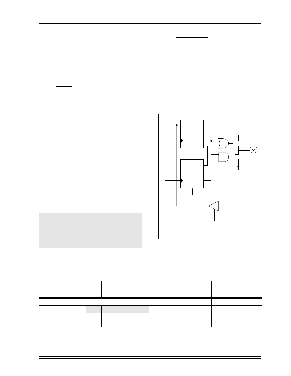
6.0 TIMER0 MODULE AND TMR0 REGISTER
The Timer0 module has the following features:
• 8-bit timer/counter register, TMR0
- Readable and writable
• 8-bit software programmable prescaler
• Internal or external clock select
- Edge select for external clock
Figure 6-1 is a simplified block diagram of the Timer0
module, while Figure 6-2 shows the electrical structure
of the Timer0 input.
Timer mode is selected by clearing the T0CS bit
(OPTION<5>). In timer mode, the Timer0 module will
increment every instruction cycle (without prescaler). If
TMR0 register is written, the increment is inhibited for
the following two cycles (Figure 6-3 and Figure 6-4).
The user can work around this by writing an adjusted
value to the TMR0 register.
FIGURE 6-1: TIMER0 BLOCK DIAGRAM
T0CS
0
1
(1)
Programmable
Prescaler
PS2, PS1, PS0
FOSC/4
T0CKI
pin
T0SE
(1)
Note 1: Bits T0CS, T0SE, PSA, PS2, PS1 and PS0 are located in the OPTION register.
2: The prescaler is shared with the Watchdog Timer (Figure 6-6).
Counter mode is selected by setting the T0CS bit
(OPTION<5>). In this mode, Timer0 will increment
either on every rising or falling edge of pin T0CKI. The
incrementing edge is determined by the source edge
select bit T0SE (OPTION<4>). Clearing the T0SE bit
selects the rising edge. Restrictions on the external
clock input are discussed in detail in Section 6.1.
The prescaler may be used by either the Timer0
module or the Watchdog Timer, but not both. The
prescaler assignment is controlled in software by the
control bit PSA (OPTION<3>). Clearing the PSA bit
will assign the prescaler to Timer0. The prescaler is
not readable or writable. When the prescaler is
assigned to the Timer0 module, prescale values of 1:2,
1:4,..., 1:256 are selectable. Section 6.2 details the
operation of the prescaler.
A summary of registers associated with the Timer0
module is found in Table 6-1.
Data bus
PSout
1
0
(2)
3
(1)
PSA
(1)
Sync with
Internal
Clocks
(2 cycle delay)
PSout
Sync
TMR0 reg
8
FIGURE 6-2: ELECTRICAL STRUCTURE OF T0CKI PIN
RIN
T0CKI
pin
(1)
VSS
Note 1: ESD protection circuits
1998 Microchip Technology Inc. Preliminary DS30453B-page 27
VSS
(1)
N
Schmitt T rigger
Input Buffer
Page 28
PIC16C5X
0
FIGURE 6-3: TIMER0 TIMING: INTERNAL CLOCK/NO PRESCALE
PC
(Program
Counter)
Instruction
Fetch
Timer0
Instruction
Executed
Q1 Q2 Q3 Q4
T0
Q1 Q2 Q3 Q4 Q1 Q2 Q3 Q4 Q1 Q2 Q3 Q4 Q1 Q2 Q3 Q4 Q1 Q2 Q3 Q4 Q1 Q2 Q3 Q4 Q1 Q2 Q3 Q4
PC-1
PC PC+1 PC+2 PC+3 PC+4 PC+5 PC+6
MOVWF TMR0
T0+1 T0+2 NT0 NT0 NT0 NT0+1 NT0+2
MOVF TMR0,W MOVF TMR0,W MOVF TMR0,W MOVF TMR0,W MOVF TMR0,W
Write TMR0
executed
Read TMR0
reads NT0
Read TMR0
reads NT0
Read TMR0
reads NT0
Read TMR0
reads NT0 + 1
Read TMR0
reads NT0 + 2
FIGURE 6-4: TIMER0 TIMING: INTERNAL CLOCK/PRESCALE 1:2
PC
(Program
Counter)
Instruction
Fetch
Timer0
Instruction
Execute
Q1 Q2 Q3 Q4
T0 NT0+1
Q1 Q2 Q3 Q4 Q1 Q2 Q3 Q4 Q1 Q2 Q3 Q4 Q1 Q2 Q3 Q4 Q1 Q2 Q3 Q4 Q1 Q2 Q3 Q4 Q1 Q2 Q3 Q4
PC-1
PC PC+1 PC+2 PC+3 PC+4 PC+5 PC+6
MOVWF TMR0
MOVF TMR0,W MOVF TMR0,W MOVF TMR0,W MO VF TMR0,W MOVF TMR0,W
T0+1
Write TMR0
executed
Read TMR0
reads NT0
NT0
Read TMR0
reads NT0
Read TMR0
reads NT0
Read TMR0
reads NT0
Read TMR0
reads NT0 + 1
TABLE 6-1: REGISTERS ASSOCIATED WITH TIMER0
Value on
Address Name Bit 7 Bit 6 Bit 5 Bit 4 Bit 3 Bit 2 Bit 1 Bit 0
Power-On
Reset
01h TMR0 Timer0 - 8-bit real-time clock/counter xxxx xxxx uuuu uuuu
N/A OPTION
Legend: Shaded cells: Unimplemented bits,
- = unimplemented, x = unknown, u = unchanged,
— — T0CS T0SE PSA PS2 PS1 PS0 --11 1111 --11 1111
Value on
MCLR and
WDT Reset
T
DS30453B-page 28 Preliminary 1998 Microchip Technology Inc.
Page 29
PIC16C5X
6.1 Using Timer0 with an External Clock
When an external clock input is used for Timer0, it
must meet certain requirements. The external clock
requirement is due to internal phase clock (T
synchronization. Also, there is a delay in the actual
incrementing of Timer0 after synchronization.
6.1.1 EXTERNAL CLOCK SYNCHRONIZATION When no prescaler is used, the external clock input is
the same as the prescaler output. The synchronization
of T0CKI with the internal phase clocks is
accomplished by sampling the prescaler output on the
Q2 and Q4 cycles of the internal phase clocks
(Figure 6-5). Therefore, it is necessary for T0CKI to be
high for at least 2T
and low for at least 2T
OSC (and a small RC delay of 20 ns)
OSC (and a small RC delay of
20 ns). Refer to the electrical specification of the
desired device.
OSC)
When a prescaler is used, the external clock input is
divided by the asynchronous ripple counter-type
prescaler so that the prescaler output is symmetrical.
For the external clock to meet the sampling
requirement, the ripple counter must be taken into
account. Therefore, it is necessary for T0CKI to have a
period of at least 4T
40 ns) divided by the prescaler value. The only
requirement on T0CKI high and low time is that they
do not violate the minimum pulse width requirement of
10 ns. Refer to parameters 40, 41 and 42 in the
electrical specification of the desired device.
6.1.2 TIMER0 INCREMENT DELAY Since the prescaler output is synchronized with the
internal clocks, there is a small delay from the time the
external clock edge occurs to the time the Timer0
module is actually incremented. Figure 6-5 shows the
delay from the external clock edge to the timer
incrementing.
FIGURE 6-5: TIMER0 TIMING WITH EXTERNAL CLOCK
External Clock Input or
Prescaler Output (2)
External Clock/Prescaler
Output After Sampling
Increment Timer0 (Q4)
Q1 Q2 Q3 Q4 Q1 Q2 Q3 Q4 Q1 Q2 Q3 Q4 Q1 Q2 Q3 Q4
(3)
Timer0
(1)
T0 T0 + 1 T0 + 2
OSC (and a small RC delay of
Small pulse
misses sampling
Note 1:
Delay from clock input change to Timer0 increment is 3Tosc to 7Tosc. (Duration of Q = Tosc).
Therefore, the error in measuring the interval between two edges on Timer0 input = ± 4Tosc max.
2:
External clock if no prescaler selected, Prescaler output otherwise.
3:
The arrows indicate the points in time where sampling occurs.
1998 Microchip Technology Inc. Preliminary DS30453B-page 29
Page 30
PIC16C5X
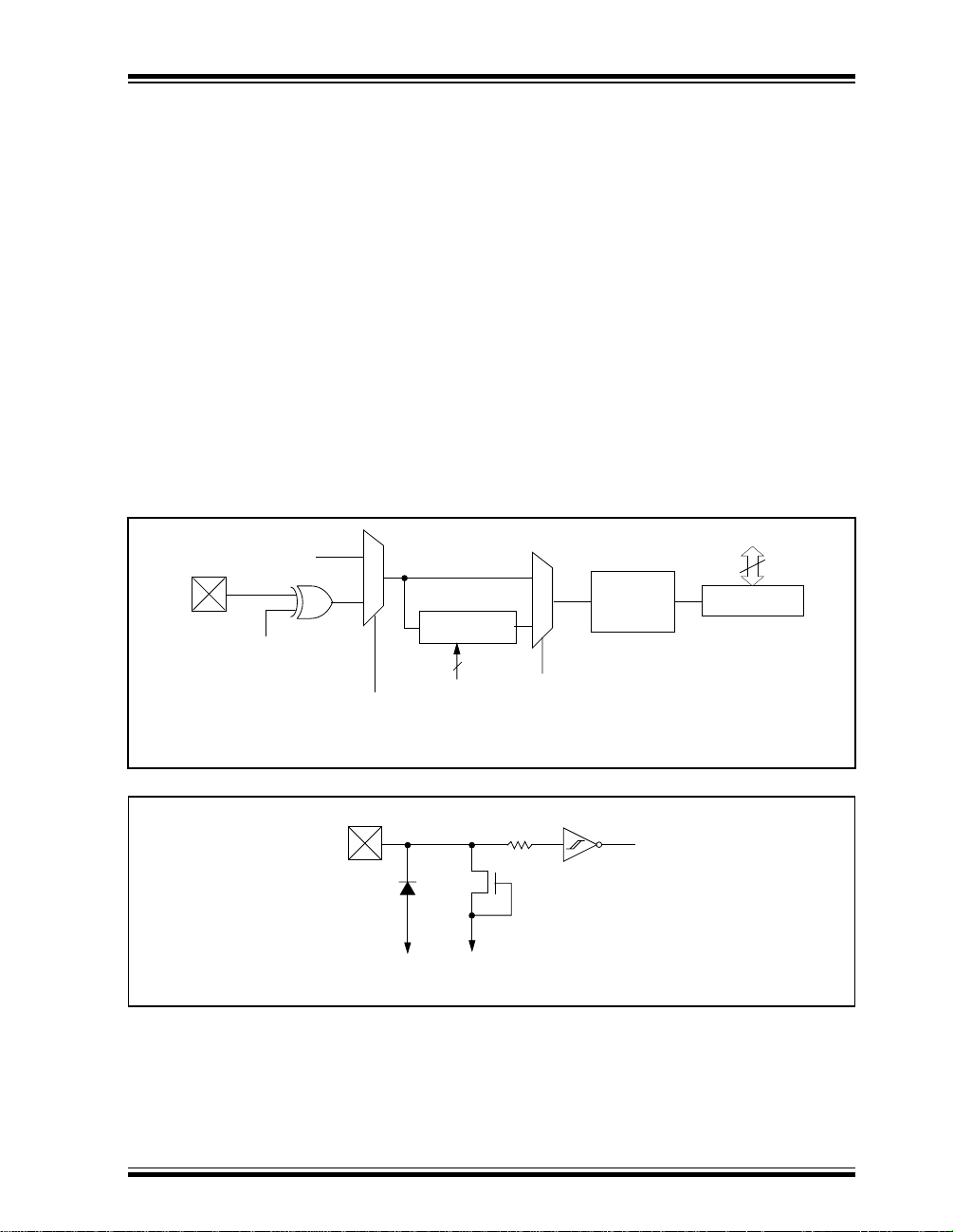
6.2 Prescaler
An 8-bit counter is available as a prescaler for the
Timer0 module, or as a postscaler for the Watchdog
Timer (WDT) (WDT postscaler not implemented on
PIC16C52), respectively (Section 6.1.2). For simplicity,
this counter is being referred to as “prescaler”
throughout this data sheet. Note that the prescaler
may be used by either the Timer0 module or the WDT,
but not both. Thus, a prescaler assignment for the
Timer0 module means that there is no prescaler for
the WDT, and vice-versa.
The PSA and PS2:PS0 bits (OPTION<3:0>) determine
prescaler assignment and prescale ratio.
When assigned to the Timer0 module, all instructions
writing to the TMR0 register (e.g., CLRF 1, MOVWF 1,
BSF 1,x, etc.) will clear the prescaler. When assigned
to WDT, a CLRWDT instr uction will clear the prescaler
along with the WDT. The prescaler is neither readable
nor writable. On a RESET, the prescaler contains all
'0's.
6.2.1 SWITCHING PRESCALER ASSIGNMENT The prescaler assignment is fully under software control
following instruction sequence (Example 6-1) must be
executed when changing the prescaler assignment from
Timer0 to the WDT.
EXAMPLE 6-1: CHANGING PRESCALER
1.CLRWDT ;Clear WDT
2.CLRF TMR0 ;Clear TMR0 & Prescaler
3.MOVLW '00xx1111’b ;These 3 lines (5, 6, 7)
4.OPTION ; are required only if
5.CLRWDT ;PS<2:0> are 000 or 001
6.MOVLW '00xx1xxx’b ;Set Postscaler to
7.OPTION ; desired WDT rate
To change prescaler from the WDT to the Timer0
module, use the sequence shown in Example 6-2. This
sequence must be used even if the WDT is disabled. A
CLRWDT instruction should be executed before switching
the prescaler.
EXAMPLE 6-2: CHANGING PRESCALER
CLRWDT ;Clear WDT and
MOVLW 'xxxx0xxx' ;Select TMR0, new
(i.e., it can be changed “on the fly” during program
execution). To avoid an unintended device RESET, the
OPTION
FIGURE 6-6: BLOCK DIAGRAM OF THE TIMER0/WDT PRESCALER
TCY ( = Fosc/4)
0
T0CKI
pin
T0SE
1
M
U
X
T0CS
1
M
U
X
0
PSA
Sync
2
Cycles
(TIMER0→WDT)
; desired
(WDT→TIMER0)
;prescaler
;prescale value and
;clock source
Data Bus
8
TMR0 reg
0
M
U
X
Watchdog
Timer
WDT Enable bit
Note: T0CS, T0SE, PSA, PS2:PS0 are bits in the OPTION register.
WDT not implemented on PIC16C52.
DS30453B-page 30 Preliminary 1998 Microchip Technology Inc.
1
PSA
8-bit Prescaler
8
8 - to - 1MUX
0
MUX
WDT
Time-Out
PS2:PS0
1
PSA
Page 31

PIC16C5X
7.0 SPECIAL FEATURES OF THE CPU
What sets a microcontroller apart from other
processors are special circuits that deal with the
needs of real-time applications. The PIC16C5X family
of microcontrollers has a host of such features
intended to maximize system reliability, minimize cost
through elimination of external components, provide
power saving operating modes and offer code
protection. These features are:
• Oscillator selection
• Reset
• Power-On Reset (POR)
• Device Reset Timer (DRT)
• Watchdog Timer (WDT)
(not implemented on PIC16C52)
• SLEEP
• Code protection
• ID locations (not implemented on PIC16C52)
The PIC16C5X Family has a Watchdog Timer which
can be shut off only through configuration bit WDTE. It
runs off of its own RC oscillator for added reliability.
There is an 18 ms delay provided by the Device Reset
Timer (DRT), intended to keep the chip in reset until
the crystal oscillator is stable. With this timer on-chip,
most applications need no external reset circuitry.
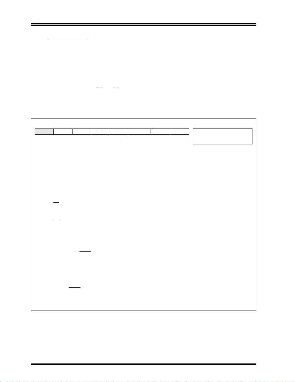
FIGURE 7-1: CONFIGURATION WORD FOR
PIC16CR54A/C54B/CR54B/C54C/CR54C/C55A/C56A/CR56A/C57C/
CR57B/CR57C/C58B/CR58A/CR58B
The SLEEP mode is designed to offer a very low
current power-down mode. The user can wake up from
SLEEP through external reset or through a Watchdog
Timer time-out. Several oscillator options are also
made available to allow the part to fit the application.
The RC oscillator option saves system cost while the
LP crystal option saves power. A set of configuration
bits are used to select various options.
7.1 Configuration Bits
Configuration bits can be programmed to select
various device configurations. Two bits are for the
selection of the oscillator type and one bit is the
Watchdog Timer enable bit. Nine bits are code
protection bits (Figure 7-1 and Figure 7-2) for the
PIC16C54, PIC16CR54, PIC16C56, PIC16CR56,
PIC16C58, and PIC16CR58 devices.
QTP or ROM devices have the oscillator configuration
programmed at the factory and these parts are tested
accordingly (see "Product Identification System"
diagrams in the back of this data sheet).
CP CP CP CP CP CP CP CP CP WDTE FOSC1 FOSC0 Register: CONFIG
bit11 10 987654321bit0
bit 11-3: CP: Code protection bits
1 = Code protection off
0 = Code protection on
bit 2: WDTE: Watchdog timer enable bit
1 = WDT enabled
0 = WDT disabled
bit 1-0: FOSC1:FOSC0: Oscillator selection bits
11 = RC oscillator
10 = HS oscillator
01 = XT oscillator
00 = LP oscillator
Note 1: Refer to the PIC16C5X Programming Specification (Literature Number DS30190) to deter-
mine how to access the configuration word.
1998 Microchip Technology Inc. Preliminary DS30453B-page 31
Address
(1)
: FFFh
Page 32

PIC16C5X
FIGURE 7-2: CONFIGURATION WORD FOR PIC16C52/C54/C54A/C55/C56/C57/C58A
— — — — — — — — CP WDTE FOSC1 FOSC0 Register: CONFIG
bit11 10 987654321bit0
bit 11-4: Unimplemented: Read as ’0’
bit 3: CP: Code protection bit.
1 = Code protection off
0 = Code protection on
bit 2: WDTE: Watchdog timer enable bit
1 = WDT enabled
0 = WDT disabled
bit 1-0: FOSC1:FOSC0: Oscillator selection bits
11 = RC oscillator
10 = HS oscillator
01 = XT oscillator
00 = LP oscillator
Note 1: Refer to the PIC16C5X Programming Specifications (Literature Number DS30190) to deter-
mine how to access the configuration word.
2: PIC16C52 supports XT and RC oscillator only.
PIC16LV54A supports XT, RC and LP oscillator only.
PIC16LV58A supports XT, RC and LP oscillator only.
(not implemented on PIC16C52)
(2)
Address
(1)
: FFFh
DS30453B-page 32 Preliminary 1998 Microchip Technology Inc.
Page 33

PIC16C5X
7.2 Oscillator Configurations
7.2.1 OSCILLATOR TYPES PIC16C5Xs can be operated in four different oscillator
modes. The user can program two configuration bits
(FOSC1:FOSC0) to select one of these four modes:
• LP: Low Power Crystal
• XT: Crystal/Resonator
• HS: High Speed Crystal/Resonator
• RC: Resistor/Capacitor
Note: Not all oscillator selections available for all
parts. See Section 7.1.
7.2.2 CRYSTAL OSCILLATOR / CERAMIC
RESONATORS
In XT, LP or HS modes, a crystal or ceramic resonator
is connected to the OSC1/CLKIN and OSC2/CLKOUT
pins to establish oscillation (Figure 7-3). The
PIC16C5X oscillator design requires the use of a
parallel cut crystal. Use of a series cut crystal may give
a frequency out of the crystal manufacturers
specifications. When in XT, LP or HS modes, the
device can have an external clock source drive the
OSC1/CLKIN pin (Figure 7-4).
FIGURE 7-3: CRYSTAL OPERATION
(OR CERAMIC RESONATOR)
(HS, XT OR LP OSC
CONFIGURATION)
(1)
C1
(1)
C2
Note 1: See Capacitor Selection tables for
recommended values of C1 and C2.
2: A series resistor (RS) may be required f or
AT strip cut crystals.
3: RF v aries with the crystal chosen (approx.
value = 10 MΩ).
XTAL
RS
OSC1
OSC2
(2)
RF
(3)
PIC16C5X
SLEEP
To internal
logic
FIGURE 7-4: EXTERNAL CLOCK INPUT
OPERATION (HS, XT OR LP
OSC CONFIGURATION)
Clock from
ext. system
Open
OSC1
PIC16C5X
OSC2
TABLE 7-1: CAPACITOR SELECTION
FOR CERAMIC RESONATORS
- PIC16C5X, PIC16CR5X
Osc
Resonator
Type
XT 455 kHz
HS 4.0 MHz
Note: These values are for design guidance only.
Freq
2.0 MHz
4.0 MHz
8.0 MHz
16.0 MHz
Since each resonator has its own characteristics, the user should consult the resonator manufacturer for appropriate values
of external components.
Cap. RangeC1Cap. Range
22-100 pF
15-68 pF
15-68 pF
15-68 pF
10-68 pF
10-22 pF
C2
22-100 pF
15-68 pF
15-68 pF
15-68 pF
10-68 pF
10-22 pF
TABLE 7-2: CAPACITOR SELECTION
FOR CRYSTAL OSCILLATOR
- PIC16C5X, PIC16CR5X
Osc
Resonator
Type
LP 32 kHz
XT 100 kHz
HS 4 MHz
Note 1: For V
Freq
100 kHz
200 kHz
200 kHz
455 kHz
1 MHz
2 MHz
4 MHz
8 MHz
20 MHz
DD > 4.5V, C1 = C2 ≈ 30 pF is
recommended.
2: These values are for design guidance only.
Rs may be required in HS mode as well as
XT mode to avoid overdriving crystals with
low drive level specification. Since each
crystal has its own characteristics, the user
should consult the crystal manufacturer for
appropriate values of external components.
(1)
Cap.Range
C1
15 pF
15-30 pF
15-30 pF
15-30 pF
15-30 pF
15-30 pF
15-30 pF
15-30 pF
15-47 pF
15-30 pF
15-30 pF
15-30 pF
Cap. Range
C2
15 pF
30-47 pF
15-82 pF
200-300 pF
100-200 pF
15-100 pF
15-30 pF
15-30 pF
15-47 pF
15-30 pF
15-30 pF
15-30 pF
Note: If you change from this device to
another device, please verify oscillator
characteristics in your application.
1998 Microchip Technology Inc. Preliminary DS30453B-page 33
Page 34

PIC16C5X
7.2.3 EXTERNAL CRYSTAL OSCILLATOR
CIRCUIT
Either a prepackaged oscillator or a simple oscillator
circuit with TTL gates can be used as an external
crystal oscillator circuit. Prepackaged oscillators
provide a wide operating range and better stability. A
well-designed crystal oscillator will provide good
performance with TTL gates. Two types of crystal
oscillator circuits can be used: one with parallel
resonance, or one with series resonance.
Figure 7-5 shows implementation of a parallel
resonant oscillator circuit. The circuit is designed to
use the fundamental frequency of the crystal. The
74AS04 inverter performs the 180-degree phase shift
that a parallel oscillator requires. The 4.7 kΩ resistor
provides the negative feedback for stability. The 10 kΩ
potentiometers bias the 74AS04 in the linear region.
This circuit could be used for external oscillator
designs.
FIGURE 7-5: EXTERNAL PARALLEL
RESONANT CRYSTAL
OSCILLATOR CIRCUIT
(USING XT, HS OR LP
OSCILLATOR MODE)
+5V
10k
4.7k
74AS04
XTAL
10k
20 pF
20 pF
Note: If you change from this device to
another device, please verify oscillator
characteristics in your application.
This circuit is also designed to use the fundamental
frequency of the crystal. The inverter performs a
180-degree phase shift in a series resonant oscillator
circuit. The 330 Ω resistors provide the negative
feedback to bias the inverters in their linear region.
74AS04
10k
To Other
Devices
100k
PIC16C5X
OSC1
OSC2
FIGURE 7-6: EXTERNAL SERIES
RESONANT CRYSTAL
OSCILLATOR CIRCUIT
(USING XT, HS OR LP
OSCILLATOR MODE)
To Other
74AS04
Devices
PIC16C5X
OSC1
OSC2
100k
330
74AS04
330
74AS04
0.1 µF
XTAL
Note: If you change from this device to
another device, please verify oscillator
characteristics in your application.
7.2.4 RC OSCILLATOR For timing insensitive applications, the RC device
option offers additional cost savings. The RC oscillator
frequency is a function of the supply voltage, the
resistor (Rext) and capacitor (Cext) values, and the
operating temperature. In addition to this, the oscillator
frequency will vary from unit to unit due to normal
process parameter variation. Furthermore, the
difference in lead frame capacitance between package
types will also affect the oscillation frequency,
especially for low Cext values. The user also needs to
take into account variation due to tolerance of external
R and C components used.
Figure 7-7 shows how the R/C combination is
connected to the PIC16C5X. For Rext values below
2.2 kΩ, the oscillator operation may become unstable,
or stop completely. For very high Rext values
(e.g., 1 MΩ) the oscillator becomes sensitive to noise,
humidity and leakage. Thus, we recommend keeping
Rext between 3 kΩ and 100 kΩ.
Although the oscillator will operate with no external
capacitor (Cext = 0 pF), we recommend using values
above 20 pF for noise and stability reasons. With no or
small external capacitance, the oscillation frequency
can vary dramatically due to changes in external
capacitances, such as PCB trace capacitance or
package lead frame capacitance.
DS30453B-page 34 Preliminary 1998 Microchip Technology Inc.
Page 35

PIC16C5X
The Electrical Specifications sections show RC
frequency variation from part to part due to normal
process variation.
Also, see the Electrical Specifications sections for
variation of oscillator frequency due to V
DD for given
Rext/Cext values as well as frequency variation due to
operating temperature for given R, C, and V
DD values.
The oscillator frequency, divided by 4, is available on
the OSC2/CLKOUT pin, and can be used for test
purposes or to synchronize other logic.
FIGURE 7-7: RC OSCILLATOR MODE
VDD
Rext
OSC1
Cext
SS
V
Fosc/4
N
OSC2/CLKOUT
Note: If you change from this device to
another device, please verify oscillator
characteristics in your application.
Internal
clock
PIC16C5X
7.3 Reset
PIC16C5X devices may be reset in one of the
following ways:
• Power-On Reset (POR)
•M
CLR reset (normal operation)
• MCLR
wake-up reset (from SLEEP)
• WDT reset (normal operation)
• WDT wake-up reset (from SLEEP)
Table 7-3 shows these reset conditions for the PCL
and STATUS registers.
Some registers are not affected in any reset condition.
Their status is unknown on POR and unchanged in
any other reset. Most other registers are reset to a
“reset state” on Power-On Reset (POR), MCLR
WDT reset. A MCLR
or WDT wake-up from SLEEP
also results in a device reset, and not a continuation of
operation before SLEEP.
The T
O and PD bits (STATUS <4:3>) are set or
cleared depending on the different reset conditions
(Section 7.7). These bits may be used to determine
the nature of the reset.
Table 7-4 lists a full description of reset states of all
registers. Figure 7-8 shows a simplified block diagram
of the on-chip reset circuit.
or
1998 Microchip Technology Inc. Preliminary DS30453B-page 35
Page 36

PIC16C5X
TABLE 7-3: RESET CONDITIONS FOR SPECIAL REGISTERS
Condition
PCL
Addr: 02h
STATUS
Addr: 03h
Power-On Reset 1111 1111 0001 1xxx
MCLR
reset (normal operation) 1111 1111 000u uuuu
MCLR wake-up (from SLEEP) 1111 1111 0001 0uuu
WDT reset (normal operation) 1111 1111 0000 uuuu
WDT wake-up (from SLEEP) 1111 1111 0000 0uuu
Legend: u = unchanged, x = unknown, - = unimplemented read as '0'.
Note 1: T
O and PD bits retain their last value until one of the other reset conditions occur.
2: The CLRWDT instruction will set the T
O and PD bits.
TABLE 7-4: RESET CONDITIONS FOR ALL REGISTERS
Register Address Power-On Reset MCLR
W N/A
TRIS N/A
OPTION N/A
INDF 00h
TMR0 01h
(1)
PCL
STATUS
(1)
02h
03h
FSR 04h
PORTA 05h
PORTB 06h
(2)
PORTC
07h
General Purpose Register Files 07-7Fh
xxxx xxxx uuuu uuuu
1111 1111 1111 1111
--11 1111 --11 1111
xxxx xxxx uuuu uuuu
xxxx xxxx uuuu uuuu
1111 1111 1111 1111
0001 1xxx 000q quuu
1xxx xxxx 1uuu uuuu
---- xxxx ---- uuuu
xxxx xxxx uuuu uuuu
xxxx xxxx uuuu uuuu
xxxx xxxx uuuu uuuu
Legend: u = unchanged, x = unknown, - = unimplemented, read as '0',
q = see tables in Section 7.7 for possible values.
Note 1: See Table 7-3 for reset value for specific conditions.
2: General purpose register file on PIC16C52/C54s/CR54s/C56s/CR56s/C58s/CR58s
or WDT Reset
FIGURE 7-8: SIMPLIFIED BLOCK DIAGRAM OF ON-CHIP RESET CIRCUIT
(1)
(2)
Power-Up
VDD
MCLR/VPP pin
DS30453B-page 36 Preliminary 1998 Microchip Technology Inc.
Detect
WDT
On-Chip
RC OSC
POR (Power-On Reset)
WDT Time-out
8-bit Asynch
Ripple Counter
(Start-Up Timer)
RESET
SQ
R
Q
CHIP RESET
Page 37

PIC16C5X
7.4 Power-On Reset (POR)
The PIC16C5X family incorporates on-chip Power-On
Reset (POR) circuitry which provides an internal chip
reset for most power-up situations. To use this feature,
the user merely ties the MCLR
simplified block diagram of the on-chip Power-On
Reset circuit is shown in Figure 7-8.
The Power-On Reset circuit and the Device Reset
Timer (Section 7.5) circuit are closely related. On
power-up, the reset latch is set and the DRT is reset.
The DRT timer begins counting once it detects MCLR
to be high. After the time-out period, which is typically
18 ms, it will reset the reset latch and thus end the
on-chip reset signal.
A power-up example where MCLR
shown in Figure 7-10. V
stabilize before bringing MCLR
actually come out of reset T
goes high.
In Figure 7-11, the on-chip Power-On Reset feature is
being used (MCLR
V
DD is stable before the start-up timer times out and
and VDD are tied together). The
there is no problem in getting a proper reset. However,
Figure 7-12 depicts a problem situation where V
rises too slowly. The time between when the DRT
senses a high on the MCLR
MCLR
/VPP pin (and VDD) actually reach their full value ,
is too long. In this situation, when the start-up timer
times out, V
DD has not reached the VDD (min) value
and the chip is, therefore, not guaranteed to function
correctly. For such situations, we recommend that
external RC circuits be used to achieve longer POR
delay times (Figure 7-9).
/VPP pin to VDD. A
is not tied to VDD is
DD is allowed to rise and
high. The chip will
DRT msec after MCLR
DD
/VPP pin, and when the
FIGURE 7-9: EXTERNAL POWER-ON
RESET CIRCUIT (FOR SLOW
VDD POWER-UP)
VDDVDD
D
R
• External Power-On Reset circuit is required
only if V
DD power-up is too slow. The diode D
helps discharge the capacitor quickly when
V
DD powers down.
• R < 40 kΩ is recommended to make sure that
voltage drop across R does not violate the
device electrical specification.
• R1 = 100Ω to 1 kΩ will limit any current
flowing into MCLR
in the event of MCLR
Electrostatic Discharge (ESD) or Electrical
Overstress (EOS).
R1
MCLR
C
PIC16C5X
from external capacitor C
pin breakdown due to
Note: When the device starts normal operation
(exits the reset condition), device operating parameters (voltage, frequency, temperature, etc.) must be meet to ensure
operation. If these conditions are not met,
the device must be held in reset until the
operating conditions are met.
For more information on PIC16C5X POR, see
Power-Up Considerations
- AN522 in the Embedded
Control Handbook.
The POR circuit does not produce an internal reset
DD declines.
when V
1998 Microchip Technology Inc. Preliminary DS30453B-page 37
Page 38

PIC16C5X
FIGURE 7-10: TIME-OUT SEQUENCE ON POWER-UP (MCLR NOT TIED TO VDD)
VDD
MCLR
INTERNAL POR
DRT TIME-OUT
INTERNAL RESET
TDRT
FIGURE 7-11: TIME-OUT SEQUENCE ON POWER-UP (MCLR
VDD
MCLR
INTERNAL POR
DRT TIME-OUT
INTERNAL RESET
TDRT
FIGURE 7-12: TIME-OUT SEQUENCE ON POWER-UP (MCLR
VDD
MCLR
INTERNAL POR
DRT TIME-OUT
V1
TDRT
TIED TO VDD): FAST VDD RISE TIME
TIED TO VDD): SLOW VDD RISE TIME
INTERNAL RESET
When VDD rises slowly, the TDRT time-out expires long before VDD has reached its final value. In
this example, the chip will reset properly if, and only if, V1 ≥ VDD min
DS30453B-page 38 Preliminary 1998 Microchip Technology Inc.
Page 39

PIC16C5X
7.5 Device Reset Timer (DRT)
The Device Reset Timer (DRT) provides a fixed 18 ms
nominal time-out on reset. The DRT operates on an
internal RC oscillator. The processor is kept in RESET
as long as the DRT is active. The DRT delay allows
V
DD to rise above VDD min., and for the oscillator to
stabilize.
Oscillator circuits based on crystals or ceramic
resonators require a certain time after power-up to
establish a stable oscillation. The on-chip DRT keeps
the device in a RESET condition for approximately 18
ms after the voltage on the MCLR
reached a logic high (V
networks connected to the MCLR
required in most cases, allowing for savings in
cost-sensitive and/or space restricted applications.
The Device Reset time delay will vary from device to
device due to V
variation. See AC parameters for details.
The DRT will also be triggered upon a W atchdog Timer
time-out. This is particularly impor tant for applications
using the WDT to wake the PIC16C5X from SLEEP
mode automatically.
IH) level. Thus, external RC
DD, temperature, and process
/VPP pin has
input are not
7.6 Watchdog Timer (WDT) (not
implemented on PIC16C52)
The Watchdog Timer (WDT) is a free running on-chip
RC oscillator which does not require any external
components. This RC oscillator is separate from the
RC oscillator of the OSC1/CLKIN pin. That means that
the WDT will run even if the clock on the OSC1/CLKIN
and OSC2/CLKOUT pins have been stopped, for
example, by execution of a SLEEP instruction. During
normal operation or SLEEP, a WDT reset or wake-up
reset generates a device RESET.
The T
O bit (STATUS<4>) will be cleared upon a
Watchdog Timer reset.
The WDT can be permanently disabled by
programming the configuration bit WDTE as a '0'
(Section 7.1). Refer to the PIC16C5X Programming
Specifications (Literature Number DS30190) to
determine how to access the configuration word.
7.6.1 WDT PERIOD
The WDT has a nominal time-out period of 18 ms,
(with no prescaler). If a longer time-out period is
desired, a prescaler with a division ratio of up to 1:128
can be assigned to the WDT (under software control)
by writing to the OPTION register. Thus, time-out a
period of a nominal 2.3 seconds can be realized.
These periods vary with temperature, V
part-to-part process variations (see DC specs).
Under worst case conditions (V
= Max., max. WDT prescaler), it may take several
seconds before a WDT time-out occurs.
7.6.2 WDT PROGRAMMING CONSIDERATIONS
The CLRWDT instruction clears the WDT and the
postscaler, if assigned to the WDT, and prevents it
from timing out and generating a device RESET.
The SLEEP instruction resets the WDT and the
postscaler, if assigned to the WDT. This gives the
maximum SLEEP time before a WDT wake-up reset.
DD = Min., Temperature
DD and
1998 Microchip Technology Inc. Preliminary DS30453B-page 39
Page 40

PIC16C5X
FIGURE 7-13: WATCHDOG TIMER BLOCK DIAGRAM
From TMR0 Clock Source
0
M
Watchdog
Timer
1
U
X
Postscaler
Postscaler
WDT Enable
EPROM Bit
Note: T0CS, T0SE, PSA, PS2:PS0
are bits in the OPTION register.
PSA
8 - to - 1 MUX
0
MUX
WDT
Time-out
1
PS2:PS0
T o TMR0
PSA
TABLE 7-5: SUMMARY OF REGISTERS ASSOCIATED WITH THE WATCHDOG TIMER
Value on
Address Name Bit 7 Bit 6 Bit 5 Bit 4 Bit 3 Bit 2 Bit 1 Bit 0
N/A OPTION — — T0CS T0SE PSA PS2 PS1 PS0 --11 1111 --11 1111
Legend: Shaded boxes = Not used by Watchdog Timer,
– = unimplemented, read as '0', u = unchanged
Power-On
Reset
Value on
MCLR and
WDT Reset
DS30453B-page 40 Preliminary 1998 Microchip Technology Inc.
Page 41

PIC16C5X
7.7 Time-Out Sequence and Power Down
Status Bits (TO/PD)
The TO and PD bits in the STATUS register can be
tested to determine if a RESET condition has been
caused by a power-up condition, a MCLR
Timer (WDT) reset, or a MCLR
or WDT wake-up reset.
or Watchdog
TABLE 7-6: TO/PD STATUS AFTER
RESET
TO PD RESET was caused by
11
uu
10
01
00
Legend: u = unchanged
Note 1: The TO and PD bits maintain their status (u) until
Power-up (POR)
MCLR reset (normal operation)
(1)
MCLR wake-up reset (from SLEEP)
WDT reset (normal operation)
WDT wake-up reset (from SLEEP)
a reset occurs. A low-pulse on the MCLR input
does not change the TO and PD status bits.
These STATUS bits are only affected by events listed
in Table 7-7.
TABLE 7-7: EVENTS AFFECTING TO/PD
STATUS BITS
Event TO PD Remarks
Power-up
WDT Time-out
SLEEP instruction
CLRWDT instruction
Legend: u = unchanged
Note: A WDT time-out will occur regardless of
the status of the T
tion will be executed, regardless of the status of the PD
Table 7-3 lists the reset conditions for the special
function registers, while Table 7-4 lists the reset
conditions for all the registers.
11
0u
10
11
No effect on PD
O bit. A SLEEP instruc-
bit.
7.8 Reset on Brown-Out
A brown-out is a condition where device power (VDD)
dips below its minimum value, but not to z ero , and then
recovers. The device should be reset in the event of a
brown-out.
To reset PIC16C5X devices when a brown-out occurs,
external brown-out protection circuits may be built, as
shown in Figure 7-14 and Figure 7-15.
FIGURE 7-14: BROWN-OUT PROTECTION
CIRCUIT 1
VDD
DD
Q1
40k
V
MCLR
PIC16C5X
33k
10k
This circuit will activate reset when VDD goes below Vz +
0.7V (where Vz = Zener voltage).
FIGURE 7-15: BROWN-OUT PROTECTION
CIRCUIT 2
VDD
Q1
40k
VDD
MCLR
PIC16C5X
R1
R2
This brown-out circuit is less expensive, although
less accurate. Transistor Q1 turns off when V
DD
is below a certain level such that:
R1
DD •
V
R1 + R2
1998 Microchip Technology Inc. Preliminary DS30453B-page 41
= 0.7V
Page 42

PIC16C5X
7.9 Power-Down Mode (SLEEP)
A device may be powered down (SLEEP) and later
powered up (Wake-up from SLEEP).
7.9.1 SLEEP
The Power-Down mode is entered by executing a
SLEEP instruction. If enabled, the Watchdog Timer will be cleared but
keeps running, the T
bit (STATUS<3>) is cleared and the oscillator driver is
turned off. The I/O ports maintain the status they had
before the SLEEP instruction was executed (driving
high, driving low, or hi-impedance).
It should be noted that a RESET generated by a WDT
time-out does not drive the MCLR
For lowest current consumption while powered down,
the T0CKI input should be at V
MCLR
/VPP pin must be at a logic high level.
7.9.2 WAKE-UP FROM SLEEP The device can wake up from SLEEP through one of
the following events:
1. An external reset input on MCLR
2. A Watchdog Timer time-out reset (if WDT was
enabled).
Both of these events cause a device reset. The T
PD
bits can be used to determine the cause of device
reset. The T
occurred (and caused wake-up). The PD
set on power-up, is cleared when SLEEP is invoked.
The WDT is cleared when the device wakes from
sleep, regardless of the wake-up source.
O bit (STATUS<4>) is set, the PD
/VPP pin low.
DD or VSS and the
/VPP pin.
O and
O bit is cleared if a WDT time-out
bit, which is
7.10 Program Verification/Code Protection
If the code protection bit(s) have not been
programmed, the on-chip program memory can be
read out for verification purposes.
Note: Microchip does not recommend code pro-
tecting windowed devices.
7.11 ID Locations (not implemented on
PIC16C52)
Four memory locations are designated as ID locations
where the user can store checksum or other
code-identification numbers. These locations are not
accessible during normal execution but are readable
and writable during program/verify.
Use only the lower 4 bits of the ID locations and
always program the upper 8 bits as '1's.
Note: Microchip will assign a unique pattern
number for QTP and SQTP requests and
for ROM devices. This pattern number will
be unique and traceable to the submitted
code.
DS30453B-page 42 Preliminary 1998 Microchip Technology Inc.
Page 43

PIC16C5X
8.0 INSTRUCTION SET SUMMARY
Each PIC16C5X instruction is a 12-bit word divided into an
OPCODE, which specifies the instruction type, and one or
more operands which further specify the operation of the
instruction. The PIC16C5X instruction set summary in
Table 8-2 groups the instructions into byte-oriented,
bit-oriented, and literal and control operations. Table 8-1
shows the opcode field descriptions.
For byte-oriented instructions, 'f' represents a file register
designator and 'd' represents a destination designator. The
file register designator is used to specify which one of the
32 file registers is to be used by the instruction.
The destination designator specifies where the result
of the operation is to be placed. If 'd' is '0', the result is
placed in the W register. If 'd' is '1', the result is placed
in the file register specified in the instruction.
For bit-oriented instructions, 'b' represents a bit field
designator which selects the number of the bit affected
by the operation, while 'f' represents the number of the
file in which the bit is located.
For literal and control operations, 'k' represents an
8 or 9-bit constant or literal value.
TABLE 8-1: OPCODE FIELD
Field Description
f Register file address (0x00 to 0x7F)
W Working register (accumulator)
b Bit address within an 8-bit file register
k Literal field, constant data or label
x
d
label Label name
TOS Top of Stack
PC Program Counter
WDT Watchdog Timer Counter
TO
PD Power-Down bit
dest
[ ]
( )
→
< >
∈
i
talics
DESCRIPTIONS
Don't care location (= 0 or 1)
The assembler will generate code with x = 0. It is
the recommended form of use for compatibility
with all Microchip software tools.
Destination select;
d = 0 (store result in W)
d = 1 (store result in file register 'f')
Default is d = 1
Time-Out bit
Destination, either the W register or the specified
register file location
Options
Contents
Assigned to
Register bit field
In the set of
User defined term (font is courier)
All instructions are executed within one single
instruction cycle, unless a conditional test is true or the
program counter is changed as a result of an
instruction. In this case, the execution takes two
instruction cycles. One instruction cycle consists of
four oscillator periods. Thus, for an oscillator frequency
of 4 MHz, the normal instruction execution time is 1 µs.
If a conditional test is true or the program counter is
changed as a result of an instruction, the instruction
execution time is 2 µs.
Figure 8-1 shows the three general formats that the
instructions can have. All examples in the figure use the
following format to represent a hexadecimal number:
0xhhh
where 'h' signifies a hexadecimal digit.
FIGURE 8-1: GENERAL FORMAT FOR
INSTRUCTIONS
Byte-oriented file register operations
11 6 5 4 0
OPCODE d f (FILE #)
d = 0 for destination W
d = 1 for destination f
f = 5-bit file register address
Bit-oriented file register operations
11 8 7 5 4 0
OPCODE b (BIT #) f (FILE #)
b = 3-bit bit address
f = 5-bit file register address
Literal and control operations (except GOTO)
11 8 7 0
OPCODE k (literal)
k = 8-bit immediate value
Literal and control operations - GOTO instruction
11 9 8 0
OPCODE k (literal)
k = 9-bit immediate value
1998 Microchip Technology Inc. Preliminary DS30453B-page 43
Page 44

PIC16C5X
TABLE 8-2: INSTRUCTION SET SUMMARY
1
1
1
1
1
1
1
1
1
1
1
1
1
1
1
1
1
1
1
2
1
2
1
1
1
2
1
1
1
12-Bit Opcode
11df
0001
01df
0001
011f
0000
0100
0000
01df
0010
11df
0000
11df
0010
10df
0010
11df
0011
00df
0001
00df
0010
001f
0000
0000
0000
01df
0011
00df
0011
10df
0000
10df
0011
10df
0001
bbbf
0100
bbbf
0101
bbbf
0110
bbbf
0111
kkkk
1110
kkkk
1001
0000
0000
kkkk
101k
kkkk
1101
kkkk
1100
0000
0000
kkkk
1000
0000
0000
0000
0000
kkkk
1111
ffff
ffff
ffff
0000
ffff
ffff
ffff
ffff
ffff
ffff
ffff
ffff
0000
ffff
ffff
ffff
ffff
ffff
ffff
ffff
ffff
ffff
kkkk
kkkk
0100
kkkk
kkkk
kkkk
0010
kkkk
0011
0fff
kkkk
Status
Affected NotesMSb LSb
C,DC,Z
None
None
None
None
C
C
C,DC,Z
None
None
None
None
None
None
T
O, PD
None
None
None
None
T
O, PD
None
1,2,4
Z
Z
Z
Z
Z
Z
Z
Z
1,2,4
Z
Z
Z
Z
Mnemonic,
Operands Description Cycles
Add W and f
ADDWF
ANDWF
CLRF
CLRW
COMF
DECF
DECFSZ
INCF
INCFSZ
IORWF
MOVF
MOVWF
NOP
RLF
RRF
SUBWF
SWAPF
XORWF
BIT-ORIENTED FILE REGISTER OPERATIONS
BCF
BSF
BTFSC
BTFSS
LITERAL AND CONTROL OPERATIONS
ANDLW
CALL
CLRWDT
GOTO
IORLW
MOVLW
OPTION
RETLW
SLEEP
TRIS
XORLW
Note 1: The 9th bit of the program counter will be forced to a '0' b y any instruction that writes to the PC except f or GOTO .
f,d
AND W with f
f,d
Clear f
f
Clear W
–
Complement f
f, d
Decrement f
f, d
Decrement f, Skip if 0
f, d
Increment f
f, d
Increment f, Skip if 0
f, d
Inclusive OR W with f
f, d
Move f
f, d
Move W to f
f
No Operation
–
Rotate left f through Carry
f, d
Rotate right f through Carry
f, d
Subtract W from f
f, d
Swap f
f, d
Exclusive OR W with f
f, d
Bit Clear f
f, b
Bit Set f
f, b
Bit Test f, Skip if Clear
f, b
Bit Test f, Skip if Set
f, b
AND literal with W
k
Call subroutine
k
Clear Watchdog Timer
k
Unconditional branch
k
Inclusive OR Literal with W
k
Move Literal to W
k
Load OPTION register
k
Return, place Literal in W
k
Go into standby mode
–
Load TRIS register
f
Exclusive OR Literal to W
k
(See individual device data sheets, Memory Section/Indirect Data Addressing, INDF and FSR Registers)
2: When an I/O register is modified as a function of itself (e.g. MOVF PORTB, 1), the value used will be that value
present on the pins themselves. For example, if the data latch is '1' for a pin configured as input and is driven
low by an external device, the data will be written back with a '0'.
3: The instruction TRIS f, where f = 5 or 6 causes the contents of the W register to be written to the tristate
latches of PORTA or B respectively. A '1' forces the pin to a hi-impedance state and disables the output buffers.
4: If this instruction is executed on the TMR0 register (and, where applicable, d = 1), the prescaler will be cleared
(if assigned to TMR0).
1(2)
1(2)
1 (2)
1 (2)
2,4
4
2,4
2,4
2,4
2,4
2,4
2,4
1,4
2,4
2,4
2,4
2,4
2,4
2,4
1
3
DS30453B-page 44 Preliminary 1998 Microchip Technology Inc.
Page 45

PIC16C5X
ADDWF Add W and f
label
Syntax: [
] ADDWF f,d
Operands: 0 ≤ f ≤ 31
d ∈ [0,1]
Operation: (W) + (f) → (dest)
Status Affected: C, DC, Z
Encoding:
Description:
0001 11df ffff
Add the contents of the W register and
register 'f'. If 'd' is 0 the result is stored
in the W register. If 'd' is '1' the result is
stored back in register 'f'
Words: 1
Cycles: 1
Example:
ADDWF FSR, 0
Before Instruction
W = 0x17
FSR = 0xC2
After Instruction
W = 0xD9
FSR = 0xC2
ANDLW And literal with W
label
Syntax: [
] ANDLW k
Operands: 0 ≤ k ≤ 255
Operation: (W).AND. (k) → (W)
Status Affected: Z
Encoding:
Description:
1110 kkkk kkkk
The contents of the W register are
AND’ed with the eight-bit literal 'k'. The
result is placed in the W register
Words: 1
Cycles: 1
Example:
ANDLW 0x5F
Before Instruction
W = 0xA3
After Instruction
W = 0x03
ANDWF AND W with f
label
Syntax: [
] ANDWF f,d
Operands: 0 ≤ f ≤ 31
d ∈ [0,1]
Operation: (W) .AND. (f) → (dest)
Status Affected: Z
Encoding:
Description:
.
0001 01df ffff
The contents of the W register are
AND’ed with register 'f'. If 'd' is 0 the
result is stored in the W register. If 'd' is
'1' the result is stored back in register 'f'
.
Words: 1
Cycles: 1
Example:
ANDWF FSR, 1
Before Instruction
W = 0x17
FSR = 0xC2
After Instruction
W = 0x17
FSR = 0x02
BCF Bit Clear f
label
Syntax: [
] BCF f,b
Operands: 0 ≤ f ≤ 31
0 ≤ b ≤ 7
Operation: 0 → (f<b>)
Status Affected: None
Encoding:
.
Description:
Words: 1
0100 bbbf ffff
Bit 'b' in register 'f' is cleared.
Cycles: 1
Example:
BCF FLAG_REG, 7
Before Instruction
FLAG_REG = 0xC7
After Instruction
FLAG_REG = 0x47
1998 Microchip Technology Inc. Preliminary DS30453B-page 45
Page 46

PIC16C5X
BSF Bit Set f
label
Syntax: [
] BSF f,b
Operands: 0 ≤ f ≤ 31
0 ≤ b ≤ 7
Operation: 1 → (f<b>)
Status Affected: None
Encoding:
Description:
0101 bbbf ffff
Bit 'b' in register 'f' is set.
Words: 1
Cycles: 1
Example:
BSF FLAG_REG, 7
Before Instruction
FLAG_REG = 0x0A
After Instruction
FLAG_REG = 0x8A
BTFSC Bit Test f, Skip if Clear
label
Syntax: [
] BTFSC f,b
Operands: 0 ≤ f ≤ 31
0 ≤ b ≤ 7
Operation: skip if (f<b>) = 0
Status Affected: None
Encoding: 0110
Description:
If bit 'b' in register 'f' is 0 then the next
instruction is skipped.
If bit 'b' is 0 then the next instruction
fetched during the current instruction
execution is discarded, and an NOP is
executed instead, making this a 2 cycle
instruction.
bbbf ffff
Words: 1
Cycles: 1(2)
HERE
BTFSC
Example:
FALSE
TRUE
GOTO
•
FLAG,1
PROCESS_CODE
•
•
Before Instruction
PC = address (HERE)
After Instruction
if FLAG<1> = 0,
PC = address (TRUE);
if FLAG<1> = 1,
PC = address(FALSE)
BTFSS Bit Test f, Skip if Set
label
Syntax: [
] BTFSS f,b
Operands: 0 ≤ f ≤ 31
0 ≤ b < 7
Operation: skip if (f<b>) = 1
Status Affected: None
Encoding:
Description:
0111 bbbf ffff
If bit 'b' in register 'f' is '1' then the next
instruction is skipped.
If bit 'b' is '1', then the next instruction
fetched during the current instruction
execution, is discarded and an NOP is
executed instead, making this a 2 cycle
instruction.
Words: 1
Cycles: 1(2)
Example:
HERE BTFSS FLAG,1
FALSE GOTO PROCESS_CODE
TRUE •
•
•
Before Instruction
PC = address (HERE)
After Instruction
If FLAG<1> = 0,
PC = address (FALSE);
if FLAG<1> = 1,
PC = address (TRUE)
DS30453B-page 46 Preliminary 1998 Microchip Technology Inc.
Page 47

PIC16C5X
CALL Subroutine Call
label
Syntax: [
] CALL k
Operands: 0 ≤ k ≤ 255
Operation: (PC) + 1→ Top of Stack;
k → PC<7:0>;
(STATUS<6:5>) → PC<10:9>;
0 → PC<8>
Status Affected: None
Encoding:
Description:
1001 kkkk kkkk
Subroutine call. First, return address
(PC+1) is pushed onto the stack. The
eight bit immediate address is loaded
into PC bits <7:0>. The upper bits
PC<10:9> are loaded from STA-
TUS<6:5>, PC<8> is cleared. CALL is
a two cycle instruction.
Words: 1
Cycles: 2
Example:
HERE CALL THERE
Before Instruction
PC = address (HERE)
After Instruction
PC = address (THERE)
TOS= address (HERE + 1)
CLRF Clear f
label
Syntax: [
] CLRF f
Operands: 0 ≤ f ≤ 31
Operation: 00h → (f);
1 → Z
Status Affected: Z
Encoding:
Description:
0000 011f ffff
The contents of register 'f' are cleared
and the Z bit is set.
Words: 1
Cycles: 1
Example:
CLRF FLAG_REG
Before Instruction
FLAG_REG = 0x5A
After Instruction
FLAG_REG = 0x00
Z=1
CLRW Clear W
label
Syntax: [
] CLRW
Operands: None
Operation: 00h → (W);
1 → Z
Status Affected: Z
Encoding:
Description:
0000 0100 0000
The W register is cleared. Zero bit (Z)
is set.
Words: 1
Cycles: 1
Example:
CLRW
Before Instruction
W = 0x5A
After Instruction
W = 0x00
Z=1
CLRWDT Clear W atchdog Timer
label
Syntax: [
] CLRWDT
Operands: None
Operation: 00h → WDT;
0 → WDT prescaler (if assigned);
O;
1 → T
1 → PD
Status Affected: TO, PD
Encoding:
Description:
0000 0000 0100
The CLRWDT instruction resets the
WDT. It also resets the prescaler, if the
prescaler is assigned to the WDT and
not Timer0. Status bits TO and PD are
set.
Words: 1
Cycles: 1
Example:
CLRWDT
Before Instruction
WDT counter = ?
After Instruction
WDT counter = 0x00
WDT prescale = 0
TO =1
PD =1
1998 Microchip Technology Inc. Preliminary DS30453B-page 47
Page 48

PIC16C5X
COMF Complement f
label
Syntax: [
] COMF f,d
Operands: 0 ≤ f ≤ 31
d ∈ [0,1]
Operation: (f
) → (dest)
Status Affected: Z
Encoding:
Description:
0010 01df ffff
The contents of register 'f' are complemented. If 'd' is 0 the result is stored in
the W register. If 'd' is 1 the result is
stored back in register 'f'.
Words: 1
Cycles: 1
Example:
COMF REG1,0
Before Instruction
REG1 = 0x13
After Instruction
REG1 = 0x13
W = 0xEC
DECF Decrement f
label
Syntax: [
] DECF f,d
Operands: 0 ≤ f ≤ 31
d ∈ [0,1]
Operation: (f) – 1 → (dest)
Status Affected: Z
Encoding:
Description:
0000 11df ffff
Decrement register 'f'. If 'd' is 0 the
result is stored in the W register. If 'd' is
1 the result is stored back in register 'f'.
Words: 1
Cycles: 1
Example:
DECF CNT,
Before Instruction
CNT = 0x01
Z=0
After Instruction
CNT = 0x00
Z=1
DECFSZ Decrement f, Skip if 0
label
Syntax: [
] DECFSZ f,d
Operands: 0 ≤ f ≤ 31
d ∈ [0,1]
Operation: (f) – 1 → d; skip if result = 0
Status Affected: None
Encoding:
Description:
0010 11df ffff
The contents of register 'f' are decre-
mented. If 'd' is 0 the result is placed in
the W register. If 'd' is 1 the result is
placed back in register 'f'.
If the result is 0, the next instruction,
which is already fetched, is discarded
and an NOP is executed instead mak-
ing it a two cycle instruction.
Words: 1
Cycles: 1(2)
Example:
HERE DECFSZ CNT, 1
GOTO LOOP
CONTINUE •
•
•
Before Instruction
PC = address (HERE)
After Instruction
CNT = CNT - 1;
if CNT = 0,
PC = address (CONTINUE);
if CNT ≠ 0,
PC = address (HERE+1)
GOTO Unconditional Branch
label
Syntax: [
] GOTO k
Operands: 0 ≤ k ≤ 511
1
Operation: k → PC<8:0>;
STATUS<6:5> → PC<10:9>
Status Affected: None
Encoding:
Description:
101k kkkk kkkk
GOTO is an unconditional branch. The
9-bit immediate value is loaded into PC
bits <8:0>. The upper bits of PC are
loaded from STATUS<6:5>. GOTO is a
two cycle instruction.
Words: 1
Cycles: 2
Example:
GOTO THERE
After Instruction
PC = address (THERE)
DS30453B-page 48 Preliminary 1998 Microchip Technology Inc.
Page 49

PIC16C5X
INCF Increment f
label
Syntax: [
] INCF f,d
Operands: 0 ≤ f ≤ 31
d ∈ [0,1]
Operation: (f) + 1 → (dest)
Status Affected: Z
Encoding:
Description:
0010 10df ffff
The contents of register 'f' are incre-
mented. If 'd' is 0 the result is placed in
the W register. If 'd' is 1 the result is
placed back in register 'f'.
Words: 1
Cycles: 1
Example:
INCF CNT,
1
Before Instruction
CNT = 0xFF
Z=0
After Instruction
CNT = 0x00
Z=1
INCFSZ Increment f, Skip if 0
label
Syntax: [
] INCFSZ f,d
Operands: 0 ≤ f ≤ 31
d ∈ [0,1]
Operation: (f) + 1 → (dest), skip if result = 0
Status Affected: None
Encoding:
Description:
0011 11df ffff
The contents of register 'f' are incre-
mented. If 'd' is 0 the result is placed in
the W register. If 'd' is 1 the result is
placed back in register 'f'.
If the result is 0, then the next instruc-
tion, which is already fetched, is dis-
carded and an NOP is executed
instead making it a two cycle instruc-
tion.
Words: 1
Cycles: 1(2)
Example:
HERE INCFSZ CNT, 1
GOTO LOOP
CONTINUE •
•
•
Before Instruction
PC = address (HERE)
After Instruction
CNT = CNT + 1;
if CNT = 0,
PC = address (CONTINUE);
if CNT ≠ 0,
PC = address (HERE +1)
IORLW Inclusive OR literal with W
label
Syntax: [
] IORLW k
Operands: 0 ≤ k ≤ 255
Operation: (W) .OR. (k) → (W)
Status Affected: Z
Encoding:
Description:
1101 kkkk kkkk
The contents of the W register are
OR’ed with the eight bit literal 'k'. The
result is placed in the W register.
Words: 1
Cycles: 1
Example:
IORLW 0x35
Before Instruction
W = 0x9A
After Instruction
W = 0xBF
Z=0
IORWF Inclusive OR W with f
label
Syntax: [
] IORWF f,d
Operands: 0 ≤ f ≤ 31
d ∈ [0,1]
Operation: (W).OR. (f) → (dest)
Status Affected: Z
Encoding:
Description:
0001 00df ffff
Inclusive OR the W register with regis-
ter 'f'. If 'd' is 0 the result is placed in
the W register. If 'd' is 1 the result is
placed back in register 'f'.
Words: 1
Cycles: 1
Example:
IORWF RESULT, 0
Before Instruction
RESULT = 0x13
W = 0x91
After Instruction
RESULT = 0x13
W = 0x93
Z=0
1998 Microchip Technology Inc. Preliminary DS30453B-page 49
Page 50

PIC16C5X
MOVF Move f
label
Syntax: [
] MOVF f,d
Operands: 0 ≤ f ≤ 31
d ∈ [0,1]
Operation: (f) → (dest)
Status Affected: Z
Encoding:
Description:
0010 00df ffff
The contents of register 'f' is moved to
destination 'd'. If 'd' is 0, destination is
the W register. If 'd' is 1, the destination
is file register 'f'. 'd' is 1 is useful to test
a file register since status flag Z is
affected.
Words: 1
Cycles: 1
Example:
MOVF FSR, 0
After Instruction
W = value in FSR register
MOVLW Move Literal to W
label
Syntax: [
] MOVLW k
Operands: 0 ≤ k ≤ 255
Operation: k → (W)
Status Affected: None
Encoding:
Description:
1100 kkkk kkkk
The eight bit literal 'k' is loaded into the
W register. The don’t cares will assemble as 0s.
Words: 1
Cycles: 1
Example:
MOVLW 0x5A
After Instruction
W = 0x5A
MOVWF Move W to f
label
Syntax: [
] MOVWF f
Operands: 0 ≤ f ≤ 31
Operation: (W) → (f)
Status Affected: None
Encoding:
Description:
0000 001f ffff
Move data from the W register to register 'f'
.
Words: 1
Cycles: 1
Example:
MOVWF TEMP_REG
Before Instruction
TEMP_REG = 0xFF
W = 0x4F
After Instruction
TEMP_REG = 0x4F
W = 0x4F
NOP No Operation
label
Syntax: [
] NOP
Operands: None
Operation: No operation
Status Affected: None
Encoding:
0000 0000 0000
Description: No operation.
Words: 1
Cycles: 1
Example:
NOP
DS30453B-page 50 Preliminary 1998 Microchip Technology Inc.
Page 51

PIC16C5X
C
register 'f'
C
register 'f'
OPTION Load OPTION Register
label
Syntax: [
] OPTION
Operands: None
Operation: (W) → OPTION
Status Affected: None
Encoding:
Description:
0000 0000 0010
The content of the W register is loaded
into the OPTION register.
Words: 1
Cycles: 1
Example
OPTION
Before Instruction
W = 0x07
After Instruction
OPTION = 0x07
RETLW Return with Literal in W
label
Syntax: [
] RETLW k
Operands: 0 ≤ k ≤ 255
Operation: k → (W);
TOS → PC
Status Affected: None
Encoding:
Description:
1000 kkkk kkkk
The W register is loaded with the eight
bit literal 'k'. The program counter is
loaded from the top of the stack (the
return address). This is a two cycle
instruction.
Words: 1
Cycles: 2
Example:
TABLE
CALL TABLE ;W contains
;table offset
;value.
• ;W now has table
• ;value.
•
ADDWF PC ;W = offset
RETLW k1 ;Begin table
RETLW k2 ;
•
•
•
RETLW kn ; End of table
Before Instruction
W = 0x07
After Instruction
W = value of k8
RLF Rotate Left f through Carry
label
Syntax: [
] RLF f,d
Operands: 0 ≤ f ≤ 31
d ∈ [0,1]
Operation: See description below
Status Affected: C
Encoding:
Description:
0011 01df ffff
The contents of register 'f' are rotated
one bit to the left through the Carry
Flag. If 'd' is 0 the result is placed in the
W register. If 'd' is 1 the result is stored
back in register 'f'.
Words: 1
Cycles: 1
Example:
RLF REG1,0
Before Instruction
REG1 = 1110 0110
C=0
After Instruction
REG1 = 1110 0110
W=1100 1100
C=1
RRF Rotate Right f through Carry
label
Syntax: [
] RRF f,d
Operands: 0 ≤ f ≤ 31
d ∈ [0,1]
Operation: See description below
Status Affected: C
Encoding:
Description:
0011 00df ffff
The contents of register 'f' are rotated
one bit to the right through the Carry
Flag. If 'd' is 0 the result is placed in the
W register. If 'd' is 1 the result is placed
back in register 'f'.
Words: 1
Cycles: 1
Example:
RRF REG1,0
Before Instruction
REG1 = 1110 0110
C=0
After Instruction
REG1 = 1110 0110
W=0111 0011
C=0
1998 Microchip Technology Inc. Preliminary DS30453B-page 51
Page 52
PIC16C5X
SLEEP Enter SLEEP Mode
Syntax:
label
[
]
SLEEP
Operands: None
Operation: 00h → WDT;
0 → WDT prescaler;
O;
1 → T
0 → PD
Status Affected: TO, PD
Encoding:
Description:
0000 0000 0011
Time-out status bit (TO) is set. The
power down status bit (PD) is cleared.
The WDT and its prescaler are
cleared.
The processor is put into SLEEP mode
with the oscillator stopped. See sec-
tion on SLEEP for more details.
Words: 1
Cycles: 1
Example: SLEEP
SUBWF Subtract W from f
Syntax:
label
] SUBWF f,d
[
Operands: 0 ≤ f ≤ 31
d ∈ [0,1]
Operation: (f) – (W) → (dest)
Status Affected: C, DC, Z
Encoding:
Description:
0000 10df ffff
Subtract (2’s complement method) the
W register from register 'f'. If 'd' is 0 the
result is stored in the W register. If 'd' is
1 the result is stored back in register 'f'.
Words: 1
Cycles: 1
SUBWF REG1, 1
Example 1
:
Before Instruction
REG1 = 3
W=2
C=?
After Instruction
REG1 = 1
W=2
C = 1 ; result is positive
Example 2:
Before Instruction
REG1 = 2
W=2
C=?
After Instruction
REG1 = 0
W=2
C = 1 ; result is zero
Example 3:
Before Instruction
REG1 = 1
W=2
C=?
After Instruction
REG1 = FF
W=2
C = 0 ; result is negative
DS30453B-page 52 Preliminary 1998 Microchip Technology Inc.
Page 53

PIC16C5X
SWAPF Swap Nibbles in f
label
Syntax: [
] SWAPF f,d
Operands: 0 ≤ f ≤ 31
d ∈ [0,1]
Operation: (f<3:0>) → (dest<7:4>);
(f<7:4>) → (dest<3:0>)
Status Affected: None
Encoding:
Description:
0011 10df ffff
The upper and lower nibbles of register
'f' are exchanged. If 'd' is 0 the result is
placed in W register. If 'd' is 1 the result
is placed in register 'f'.
Words: 1
Cycles: 1
SWAPF
Example
REG1, 0
Before Instruction
REG1 = 0xA5
After Instruction
REG1 = 0xA5
W = 0X5A
TRIS Load TRIS Register
label
Syntax: [
] TRIS f
Operands: f = 5, 6 or 7
Operation: (W) → TRIS register f
Status Affected: None
Encoding:
Description:
0000 0000 0fff
TRIS register 'f' (f = 5, 6, or 7) is loaded
with the contents of the W register
Words: 1
Cycles: 1
Example
TRIS PORTA
Before Instruction
W = 0XA5
After Instruction
TRISA = 0XA5
XORLW Exclusive OR literal with W
Syntax:
label
] XORLW k
[
Operands: 0 ≤ k ≤ 255
Operation: (W) .XOR. k → (W)
Status Affected: Z
Encoding:
Description:
1111 kkkk kkkk
The contents of the W register are
XOR’ed with the eight bit literal 'k'. The
result is placed in the W register.
Words: 1
Cycles: 1
Example: XORLW 0xAF
Before Instruction
W = 0xB5
After Instruction
W = 0x1A
XORWF Exclusive OR W with f
label
Syntax: [
] XORWF f,d
Operands: 0 ≤ f ≤ 31
d ∈ [0,1]
Operation: (W) .XOR. (f) → (dest)
Status Affected: Z
Encoding:
Description:
0001 10df ffff
Exclusive OR the contents of the W
register with register 'f'. If 'd' is 0 the
result is stored in the W register. If 'd' is
1 the result is stored back in register 'f'.
Words: 1
Cycles: 1
Example XORWF
REG,1
Before Instruction
REG = 0xAF
W = 0xB5
After Instruction
REG = 0x1A
W = 0xB5
1998 Microchip Technology Inc. Preliminary DS30453B-page 53
Page 54

PIC16C5X
NOTES:
DS30453B-page 54 Preliminary 1998 Microchip Technology Inc.
Page 55

PIC16C5X
9.0 DEVELOPMENT SUPPORT
9.1 Development Tools
The PICmicrο microcontrollers are supported with a
full range of hardware and software development
tools:
• PICMASTER
In-Circuit Emulator
• ICEPIC Low-Cost PIC16C5X and PIC16CXXX
In-Circuit Emulator
• PRO MATE
• PICSTART
Programmer
• PICDEM-1 Low-Cost Demonstration Board
• PICDEM-2 Low-Cost Demonstration Board
• PICDEM-3 Low-Cost Demonstration Board
• MPASM Assembler
• MPLAB SIM Software Simulator
• MPLAB-C17 (C Compiler)
• Fuzzy Logic Development System
(
fuzzy
9.2 PICMASTER: High Performance
The PICMASTER Universal In-Circuit Emulator is
intended to provide the product development engineer
with a complete microcontroller design tool set for all
microcontrollers in the PIC14C000, PIC12CXXX,
PIC16C5X, PIC16CXXX and PIC17CXX families.
PICMASTER is supplied with the MPLAB Integrated
Development Environment (IDE), which allows editing,
“make” and download, and source debugging from a
single environment.
Interchangeable target probes allow the system to be
easily reconfigured for emulation of different
processors. The universal architecture of the
PICMASTER allows expansion to support all new
Microchip microcontrollers.
The PICMASTER Emulator System has been
designed as a real-time emulation system with
advanced features that are generally found on more
expensive development tools. The PC compatible 386
(and higher) machine platform and Microsoft Windows
3.x environment were chosen to best make these
features available to you, the end user.
A CE compliant version of PICMASTER is available for
European Union (EU) countries.
/PICMASTER CE Real-Time
II Universal Programmer
Plus Entry-Level Prototype
TECH−MP)
Universal In-Circuit Emulator with
MPLAB IDE
9.3 ICEPIC: Low-Cost PICmicro™
In-Circuit Emulator
ICEPIC is a low-cost in-circuit emulator solution for the
Microchip PIC12CXXX, PIC16C5X and PIC16CXXX
families of 8-bit OTP microcontrollers.
ICEPIC is designed to operate on PC-compatible
machines ranging from 286-AT
based machines under Windows 3.x environment.
ICEPIC features real time, non-intrusive emulation.
through Pentium
9.4 PRO MATE II: Universal Programmer
The PRO MATE II Universal Programmer is a
full-featured programmer capable of operating in
stand-alone mode as well as PC-hosted mode. PRO
MATE II is CE compliant.
The PRO MATE II has programmable V
supplies which allows it to verify programmed memory
at V
DD min and VDD max for maximum reliability. It has
an LCD display for displaying error messages, keys to
enter commands and a modular detachable socket
assembly to support various package types. In standalone mode the PRO MATE II can read, verify or
program PIC12CXXX, PIC14C000, PIC16C5X,
PIC16CXXX and PIC17CXX devices. It can also set
configuration and code-protect bits in this mode.
DD and VPP
9.5 PICSTART Plus Entry Level
Development System
The PICSTART programmer is an easy-to-use,
low-cost prototype programmer. It connects to the PC
via one of the COM (RS-232) ports. MPLAB Integrated
Development Environment software makes using the
programmer simple and efficient. PICSTART Plus is
not recommended for production programming.
PICSTART Plus supports all PIC12CXXX,
PIC14C000, PIC16C5X, PIC16CXXX and PIC17CXX
devices with up to 40 pins. Larger pin count devices
such as the PIC16C923, PIC16C924 and PIC17C756
may be supported with an adapter socket. PICSTART
Plus is CE compliant.
1998 Microchip Technology Inc. Preliminary DS30453B-page 55
Page 56

PIC16C5X
9.6 PICDEM-1 Low-Cost PICmicro
Demonstration Board
The PICDEM-1 is a simple board which demonstrates
the capabilities of several of Microchip’s
microcontrollers. The microcontrollers supported are:
PIC16C5X (PIC16C54 to PIC16C58A), PIC16C61,
PIC16C62X, PIC16C71, PIC16C8X, PIC17C42,
PIC17C43 and PIC17C44. All necessary hardware
and software is included to run basic demo programs.
The users can program the sample microcontrollers
provided with the PICDEM-1 board, on a
PRO MATE II or PICSTART-Plus programmer, and
easily test firmware. The user can also connect the
PICDEM-1 board to the PICMASTER emulator and
download the firmware to the emulator for testing.
Additional prototype area is available for the user to
build some additional hardware and connect it to the
microcontroller socket(s). Some of the features include
an RS-232 interface, a potentiometer for simulated
analog input, push-button switches and eight LEDs
connected to PORTB.
9.7 PICDEM-2 Low-Cost PIC16CXX
Demonstration Board
The PICDEM-2 is a simple demonstration board that
supports the PIC16C62, PIC16C64, PIC16C65,
PIC16C73 and PIC16C74 microcontrollers. All the
necessary hardware and software is included to
run the basic demonstration programs. The user
can program the sample microcontrollers provided
with the PICDEM-2 board, on a PRO MATE II
programmer or PICSTART-Plus, and easily test
firmware. The PICMASTER emulator may also be
used with the PICDEM-2 board to test firmware.
Additional prototype area has been provided to the
user for adding additional hardware and connecting it
to the microcontroller socket(s). Some of the features
include a RS-232 interface, push-button switches, a
potentiometer for simulated analog input, a Serial
EEPROM to demonstrate usage of the I
separate headers for connection to an LCD module
and a keypad.
2
C bus and
9.8 PICDEM-3 Low-Cost PIC16CXXX
Demonstration Board
The PICDEM-3 is a simple demonstration board that
supports the PIC16C923 and PIC16C924 in the PLCC
package. It will also support future 44-pin PLCC
microcontrollers with a LCD Module. All the
necessary hardware and software is included to
run the basic demonstration programs. The user
can program the sample microcontrollers provided
with the PICDEM-3 board, on a PRO MATE II
programmer or PICSTART Plus with an adapter
socket, and easily test firmware. The PICMASTER
emulator may also be used with the PICDEM-3 board
to test firmware. Additional prototype area has been
provided to the user for adding hardware and
connecting it to the microcontroller socket(s). Some
of the features include an RS-232 interface,
push-button switches, a potentiometer for simulated
analog input, a thermistor and separate headers for
connection to an external LCD module and a keypad.
Also provided on the PICDEM-3 board is an LCD
panel, with 4 commons and 12 segments, that is
capable of displaying time, temperature and day of the
week. The PICDEM-3 provides an additional RS-232
interface and Windows 3.1 software for showing the
demultiplexed LCD signals on a PC. A simple serial
interface allows the user to construct a hardware
demultiplexer for the LCD signals.
9.9 MPLAB™ Integrated Development
Environment Software
The MPLAB IDE Software brings an ease of software
development previously unseen in the 8-bit
microcontroller market. MPLAB is a windows based
application which contains:
• A full featured editor
• Three operating modes
- editor
- emulator
- simulator
• A project manager
• Customizable tool bar and key mapping
• A status bar with project information
• Extensive on-line help
MPLAB allows you to:
• Edit your source files (either assembly or ‘C’)
• One touch assemble (or compile) and download
to PICmicro tools (automatically updates all
project information)
• Debug using:
- source files
- absolute listing file
• Transfer data dynamically via DDE (soon to be
replaced by OLE)
• Run up to four emulators on the same PC
The ability to use MPLAB with Microchip’s simulator
allows a consistent platform and the ability to easily
switch from the low cost simulator to the full featured
emulator with minimal retraining due to development
tools.
9.10 Assembler (MPASM)
The MPASM Universal Macro Assembler is a
PC-hosted symbolic assembler. It supports all
microcontroller series including the PIC12C5XX,
PIC14000, PIC16C5X, PIC16CXXX, and PIC17CXX
families.
MPASM offers full featured Macro capabilities,
conditional assembly, and several source and listing
formats. It generates various object code formats to
support Microchip's development tools as well as third
party programmers.
DS30453B-page 56 Preliminary 1998 Microchip Technology Inc.
Page 57

PIC16C5X
MPASM allows full symbolic debugging from
PICMASTER, Microchip’s Universal Emulator System.
MPASM has the following features to assist in
developing software for specific use applications.
• Provides translation of Assembler source code to
object code for all Microchip microcontrollers.
• Macro assembly capability.
• Produces all the files (Object, Listing, Symbol,
and special) required for symbolic debug with
Microchip’s emulator systems.
• Supports Hex (default), Decimal and Octal source
and listing formats.
MPASM provides a rich directive language to support
programming of the PICmicro. Directives are helpful in
making the development of your assemble source
code shorter and more maintainable.
9.11 Software Simulator (MPLAB-SIM)
The MPLAB-SIM Software Simulator allows code
development in a PC host environment. It allows the
user to simulate the PICmicro series microcontrollers
on an instruction level. On any given instruction, the
user may examine or modify any of the data areas or
provide external stimulus to any of the pins. The
input/output radix can be set by the user and the
execution can be performed in; single step, execute
until break, or in a trace mode.
MPLAB-SIM fully supports symbolic debugging using
MPLAB-C and MPASM. The Software Simulator offers
the low cost flexibility to develop and debug code
outside of the laboratory environment making it an
excellent multi-project software development tool.
9.12 C Compiler (MPLAB-C17)
The MPLAB-C Code Development System is a
complete ‘C’ compiler and integrated development
environment for Microchip’s PIC17CXXX family of
microcontrollers. The compiler provides powerful
integration capabilities and ease of use not found with
other compilers.
For easier source level debugging, the compiler
provides symbol information that is compatible with the
MPLAB IDE memory display.
9.13 Fuzzy Logic Development System
(
fuzzy
TECH-MP)
fuzzy
TECH-MP fuzzy logic development tool is
available in two versions - a low cost introductory
version, MP Explorer, for designers to gain a
comprehensive working knowledge of fuzzy logic
system design; and a full-featured version,
fuzzy
TECH-MP, Edition for implementing more
complex systems.
fuzzy
Both versions include Microchip’s
demonstration board for hands-on experience with
fuzzy logic systems implementation.
LAB
9.14 MP-DriveWay – Application Code
Generator
MP-DriveWay is an easy-to-use Windows-based
Application Code Generator. With MP-DriveWay you
can visually configure all the peripherals in a PICmicro
device and, with a click of the mouse, generate all the
initialization and many functional code modules in C
language. The output is fully compatible with
Microchip’s MPLAB-C C compiler. The code produced
is highly modular and allows easy integration of your
own code. MP-DriveWay is intelligent enough to
maintain your code through subsequent code
generation.
9.15 SEEVAL Evaluation and
Programming System
The SEEVAL SEEPROM Designer’s Kit supports all
Microchip 2-wire and 3-wire Serial EEPROMs. The kit
includes everything necessary to read, write, erase or
program special features of any Microchip SEEPROM
product including Smart Serials and secure serials.
The Total Endurance Disk is included to aid in
trade-off analysis and reliability calculations. The total
kit can significantly reduce time-to-market and result in
an optimized system.
9.16 KEELOQ Evaluation and
Programming Tools
KEELOQ evaluation and programming tools support
Microchips HCS Secure Data Products. The HCS
evaluation kit includes an LCD display to show
changing codes, a decoder to decode transmissions,
and a programming interface to program test
transmitters.
1998 Microchip Technology Inc. Preliminary DS30453B-page 57
Page 58

DS30453B-page 58 Preliminary 1998 Microchip Technology Inc.
EMULATOR PRODUCTS
PICMASTER/
PICMASTER-CE
In-Circuit Emulator
MPLAB™-ICE
ICEPIC Low-Cost
In-Circuit Emulator
SOFTWARE PRODUCTS
MPLAB
Integrated
Development
Environment
MPLAB C17
Compiler
fuzzy
TECH-MP
Explorer/Edition
Fuzzy Logic Dev. Tool
MP-DriveWay
Applications
Code Generator
Total Endurance
Software Model
PROGRAMMERS
PICSTARTPlus
Low-Cost
Universal Dev. Kit
PRO MATE II
Universal Programmer
KEELOQ Programmer
DEMO BOARDS
SEEVAL Designers Kit
PICDEM-1
PICDEM-2
PICDEM-3
KEELOQ Evaluation Kit
24CXX
PIC12C5XX PIC14000 PIC16C5X PIC16CXXX PIC16C6X PIC16C7XX PIC16C8X PIC16C9XX PIC17C4X PIC17C7XX
(PIC17C75X only)
ььь ь ььььь
ü
25CXX
93CXX
HCSXXX
ü
ü ü ü üüüü
ььь ь ььььь ь
üü
ььь ь ььььь
ьь ььььь
ü
ььь ь ььььь ь
ььь ь ььььь ь ьь
ü
ü
üü ü ü
üü
ü
ü
TABLE 9-1: DEVELOPMENT TOOLS FROM MICROCHIP
PIC16C5X
Page 59

PIC16C52 PIC16C5X
10.0 ELECTRICAL CHARACTERISTICS - PIC16C52
Absolute Maximum Ratings†
Ambient Temperature under bias ...........................................................................................................–55°C to +125°C
Storage T emperature..............................................................................................................................–65°C to +150°C
Voltage on V
Voltage on MCLR
Voltage on all other pins with respect to V
Total Power Dissipation
Max. Current out of V
Max. Current into V
Max. Current into an input pin (T0CKI only).....................................................................................................................±500 µA
Input Clamp Current, I
Output Clamp Current, I
Max. Output Current sunk by any I/O pin................................................................................................................10 mA
Max. Output Current sourced by any I/O pin...........................................................................................................10 mA
Max. Output Current sourced by a single I/O port (PORTA or B)............................................................................10 mA
Max. Output Current sunk by a single I/O port (PORTA or B).................................................................................10 mA
Note 1: Power Dissipation is calculated as follows: Pdis = V
†
NOTICE: Stresses above those listed under "Maximum Ratings" may cause permanent damage to the device. This
is a stress rating only and functional operation of the device at those or any other conditions above those indicated
in the operation listings of this specification is not implied. Exposure to maximum rating conditions for extended
periods may affect device reliability.
DD with respect to VSS ..............................................................................................................0 V to +7.5 V
with respect to VSS............................................................................................................0 V to +14 V
(1)
....................................................................................................................................800 mW
SS pin...................................................................................................................................150 mA
DD pin........................................................................................................................................50 mA
IK (VI < 0 or VI > VDD) ....................................................................................................................±20 mA
OK (VO < 0 or VO > VDD)............................................................................................................±20 mA
SS ................................................................................–0.6 V to (VDD + 0.6 V)
DD x {IDD – ∑ IOH} + ∑ {(VDD – VOH) x IOH} + ∑(VOL x IOL)
1998 Microchip Technology Inc. Preliminary DS30453B-page 59
Page 60

PIC16C5X PIC16C52
10.1 DC Characteristics: PIC16C52-04 (Commercial)
PIC16C52-04I (Industrial)
DC Characteristics
Power Supply Pins
Characteristic Sym Min Typ
Supply V oltage V
RAM Data Retention Voltage
Supply Current
(3,4)
Power Down Current
(2)
(5)
Commercial
Industrial
* These parameters are characterized but not tested.
Note 1: Data in the Typical (“Typ”) column is based on characterization results at 25°C . This data is f or design guidance
only and is not tested.
2: This is the limit to which V
DD can be lowered in SLEEP mode without losing RAM data.
3: The supply current is mainly a function of the operating voltage and frequency. Other factors such as bus
loading, oscillator type, bus rate, internal code execution pattern, and temperature also have an impact on
the current consumption.
a) The test conditions for all I
OSC1 = external square wave, from rail-to-rail; all I/O pins tristated, pulled to
V
ss, T0CKI = VDD, MCLR = VDD.
b) For standby current measurements, the conditions are the same, except that
the device is in SLEEP mode.
4: For RC option, does not include current through Rext. The current through the resistor can be estimated by
the formula: I
R = VDD/2Rext (mA) with Rext in kΩ.
5: The power down current in SLEEP mode does not depend on the oscillator type. Power down current is
measured with the part in SLEEP mode, with all I/O pins in hi-impedance state and tied to V
Standard Operating Conditions (unless otherwise specified)
Operating T emperature 0°C ≤ T
–40°C ≤ T
(1)
Max Units Conditions
DD 3.0 — 6.25 V FOSC = DC to 4 MHz
A ≤ +70°C (commercial)
A ≤ +85°C (industrial)
VDR — 1.5* — V Device in SLEEP Mode
IDD — 1.8 3.3 mA FOSC = 4 MHz, VDD = 5.5 V
PD —
I
DD measurements in active operation mode are:
0.6
0.6
9
12µAµA
VDD = 3.0 V
V
DD = 3.0 V
DD and VSS.
DS30453B-page 60 Preliminary 1998 Microchip Technology Inc.
Page 61

PIC16C52 PIC16C5X
10.2 DC Characteristics: PIC16C52-04 (Commercial)
PIC16C52-04I (Industrial)
DC Characteristics
All Pins Except
Power Supply Pins
Characteristic Sym Min Typ
Input Low Voltage
I/O ports
MCLR
(Schmitt Trigger)
T0CKI (Schmitt Trigger)
OSC1 (Schmitt Trigger)
Input High Voltage
I/O ports
MCLR
(Schmitt Trigger)
T0CKI (Schmitt Trigger)
OSC1 (Schmitt Trigger)
Hysteresis of Schmitt
Trigger inputs
Input Leakage Current
(2,3)
I/O ports
MCLR
T0CKI
OSC1
Output Low Voltage
I/O ports
OSC2/CLKOUT
Output High Voltage
(3)
I/O ports
OSC2/CLKOUT
* These parameters are characterized but not tested.
Note 1: Data in the Typical (“Typ”) column is based on char acterization results at 25°C . This data is for design guidance
only and is not tested.
2: The leakage current on the MCLR
levels represent normal operating conditions. Higher leakage current may be measured at different input
voltage.
3: Negative current is defined as coming out of the pin.
4: For RC option, the OSC1/CLKIN pin is a Schmitt Trigger input. It is not recommended that the PIC16C52 be
driven with external clock in RC mode.
5: The user may use the better of the two specifications.
Standard Operating Conditions (unless otherwise specified)
Operating T emperature 0°C ≤ T
–40°C ≤ T
Operating Voltage V
V
IL
VSS
VSS
VSS
VSS
VSS
V
IH
0.45 VDD
2.0
0.36 V
DD
0.85 VDD
0.85 VDD
0.85 VDD
0.7 VDD
V
HYS 0.15VDD*— — V
IL
I
–1
DD range is described in Section 10.1.
(1)
Max Units Conditions
—
0.2 V
—
—
0.15 VDD
—
0.15 VDD
—
0.15 VDD
—
0.3 VDD
—
—
—
—
—
—
—
—
0.5
V
VDD
VDD
VDD
VDD
VDD
VDD
+1
A ≤ +70°C (commercial)
A ≤ +85°C (industrial)
DD
V
V
V
V
V
DD
V
V
V
V
V
V
V
µA
Pin at hi-impedance
RC
XT option
For all V
4.0 V < VDD ≤ 5.5 V
VDD > 5.5 V
RC
XT option
For V
V
SS ≤ VPIN ≤ VDD,
Pin at hi-impedance
–5
–3
–3
0.5
0.5
0.5
+5
+3
+3
µA
V
PIN = VSS + 0.25 V
µA
V
PIN = VDD
µA
VSS ≤ VPIN ≤ VDD
µA
VSS ≤ VPIN ≤ VDD,
XT option
V
OL —
—
—
—
—
—
0.6
0.6
VVI
OL = 2.0 mA, VDD = 4.5 V
I
OL = 1.6 mA, VDD = 4.5 V,
RC option
OH
V
VDD – 0.7
V
DD – 0.7
—
—
—
—
—
—
OH = –2.0 mA, VDD = 4.5 V
VVI
I
OH = –1.0 mA, VDD = 4.5 V,
RC option
/VPP pin is strongly dependent on the applied voltage level. The specified
(4)
option only
DD
(4)
option only
DD ≤ 5.5 V
(5)
(5)
1998 Microchip Technology Inc. Preliminary DS30453B-page 61
Page 62

PIC16C5X PIC16C52
10.3 Timing Parameter Symbology and Load Conditions
The timing parameter symbols have been created following one of the following formats:
1. TppS2ppS
2. TppS
T
F Frequency T Time
Lowercase subscripts (pp) and their meanings:
pp
2 to mc MCLR
ck CLKOUT osc oscillator
cy cycle time os OSC1
drt device reset timer t0 T0CKI
io I/O port
Uppercase letters and their meanings:
S
F Fall P Period
H High R Rise
I Invalid (Hi-impedance) V Valid
L Low Z Hi-impedance
FIGURE 10-1: LOAD CONDITIONS - PIC16C52
Pin
VSS
CL
C
L = 50 pF for all pins except OSC2
15 pF for OSC2 in XT mode when
external clock is used to
drive OSC1
DS30453B-page 62 Preliminary 1998 Microchip Technology Inc.
Page 63

PIC16C52 PIC16C5X
10.4 Timing Diagrams and Specifications
FIGURE 10-2: EXTERNAL CLOCK TIMING - PIC16C52
OSC1
CLKOUT
Q4
Q1 Q2
133
Q3 Q4 Q1
44
2
TABLE 10-1: EXTERNAL CLOCK TIMING REQUIREMENTS - PIC16C52
AC Characteristics Standard Operating Conditions (unless otherwise specified)
Parameter
No. Sym Characteristic Min Typ
FOSC External CLKIN Frequency
1TOSC External CLKIN Period
2TCY Instruction Cycle Time
3 TosL, TosH Clock in (OSC1) Low or High Time 85* — — ns XT oscillator
4 TosR, TosF Clock in (OSC1) Rise or Fall Time — — 25* ns XT oscillator
* These parameters are characterized but not tested.
Note 1: Data in the Typical (“Typ”) column is at 5V, 25°C unless otherwise stated. These parameters are for design guidance only
and are not tested.
2: All specified values are based on characterization data for that particular oscillator type under standard operating condi-
tions with the device executing code . Exceeding these specified limits may result in an unstable oscillator operation and/or
higher than expected current consumption.
When an external clock input is used, the “max” cycle time limit is “DC” (no clock) for all devices.
3: Instruction cycle period (TCY) equals four times the input oscillator time base period.
Operating T emperature 0°C ≤ T
–40°C ≤ T
Operating Voltage V
Oscillator Frequency
Oscillator Period
DD range is described in Section 10.1.
(2)
(2)
(2)
(2)
(3)
A ≤ +70°C (commercial)
A ≤ +85°C (industrial)
(1)
Max Units Conditions
DC — 4 MHz XT osc mode
DC — 4 MHz RC osc mode
0.1 — 4 MHz XT osc mode
250 — — ns RC osc mode
250 — — ns XT osc mode
250 — — ns RC osc mode
250 — 10,000 ns XT osc mode
— 4/FOSC ——
1998 Microchip Technology Inc. Preliminary DS30453B-page 63
Page 64

PIC16C5X PIC16C52
FIGURE 10-3: CLKOUT AND I/O TIMING - PIC16C52
Q4
OSC1
CLKOUT
I/O Pin
(input)
I/O Pin
(output)
Note: All tests must be done with specified capacitive loads (see data sheet) 50 pF on I/O pins and CLKOUT.
Old Value
Q1
10
13
14
17
20, 21
19
Q2 Q3
18
15
11
12
16
New Value
TABLE 10-2: CLKOUT AND I/O TIMING REQUIREMENTS - PIC16C52
AC Characteristics Standard Operating Conditions (unless otherwise specified)
Parameter
No. Sym Characteristic Min Typ
10 TosH2ckL OSC1↑ to CLKOUT↓
11 TosH2ckH OSC1↑ to CLKOUT↑
12 TckR CLKOUT rise time
13 TckF CLKOUT fall time
14 TckL2ioV CLKOUT↓ to Port out valid
15 TioV2ckH Port in valid before CLKOUT↑
16 TckH2ioI Port in hold after CLKOUT↑
17 TosH2ioV OSC1↑ (Q1 cycle) to Port out valid
18 TosH2ioI OSC1↑ (Q2 cycle) to Port input invalid
19 TioV2osH Port input valid to OSC1↑
20 TioR Port output rise time
21 TioF Port output fall time
* These parameters are characterized but not tested.
** These parameters are design targets and are not tested. No characterization data available at this time.
Note 1: Data in the Typical (“Typ”) column is at 5V, 25°C unless otherwise stated. These parameters are for design guidance only
and are not tested.
2: Measurements are taken in RC Mode where CLKOUT output is 4 x T
3: See Figure 10-1 for loading conditions.
Operating T emperature 0°C ≤ T
–40°C ≤ T
Operating Voltage V
(I/O in hold time)
(I/O in setup time)
DD range is described in Section 10.1.
(2)
(2)
(2)
(2)
(2)
(2)
(2)
(3)
(3)
(3)
A ≤ +70°C (commercial)
A ≤ +85°C (industrial)
(1)
Max Units
— 15 30** ns
— 15 30** ns
— 5 15** ns
— 5 15** ns
— — 40** ns
0.25 TCY+30* — — ns
0* — — ns
— — 100* ns
TBD — — ns
TBD — — ns
— 10 25** ns
— 10 25** ns
OSC.
DS30453B-page 64 Preliminary 1998 Microchip Technology Inc.
Page 65

PIC16C52 PIC16C5X
FIGURE 10-4: RESET AND DEVICE RESET TIMER TIMING - PIC16C52
VDD
MCLR
30
Internal
POR
DRT
Time-out
Internal
RESET
I/O pin
(Note 1)
32
34
32
32
34
Note 1: I/O pins must be taken out of hi-impedance mode by enabling the output drivers in software.
TABLE 10-3: RESET AND DEVICE RESET TIMER - PIC16C52
AC Characteristics Standard Operating Conditions (unless otherwise specified)
Parameter
No. Sym Characteristic Min Typ
30
32
34
* These parameters are characterized but not tested.
Note 1: Data in the Typical (“Typ”) column is at 5V, 25°C unless otherwise stated. These parameters are for design
guidance only and are not tested.
Operating T emperature 0°C ≤ T
–40°C ≤ T
Operating Voltage V
DD range is described in Section 10.1.
A ≤ +70°C (commercial)
A ≤ +85°C (industrial)
(1)
Max Units Conditions
TmcL MCLR Pulse Width (low) 100* — — ns VDD = 5 V
TDRT Device Reset Timer Period 9* 18* 30* ms VDD = 5 V (Commercial)
TioZ I/O Hi-impedance from MCLR Low — — 100* ns
1998 Microchip Technology Inc. Preliminary DS30453B-page 65
Page 66

PIC16C5X PIC16C52
FIGURE 10-5: TIMER0 CLOCK TIMINGS - PIC16C52
T0CKI
40 41
42
TABLE 10-4: TIMER0 CLOCK REQUIREMENTS - PIC16C52
AC Characteristics Standard Operating Conditions (unless otherwise specified)
Parameter
No.
* These parameters are characterized but not tested.
Note 1: Data in the Typical (“Typ”) column is at 5V, 25°C unless otherwise stated. These parameters are for design guidance only
Sym Characteristic Min Typ
40 Tt0H T0CKI High Pulse Width - No Prescaler 0.5 TCY + 20* — — ns
41 Tt0L T0CKI Low Pulse Width - No Prescaler 0.5 TCY + 20* — — ns
42 Tt0P T0CKI Period 20 or TCY + 40*
and are not tested.
Operating T emperature 0°C ≤ T
–40°C ≤ T
Operating Voltage V
- With Prescaler 10* — — ns
- With Prescaler 10* — — ns
DD range is described in Section 10.1.
N
A ≤ +70°C (commercial)
A ≤ +85°C (industrial)
(1)
— — ns Whichever is greater.
Max Units Conditions
N = Prescale Value
(1, 2, 4,..., 256)
DS30453B-page 66 Preliminary 1998 Microchip Technology Inc.
Page 67

PIC16C54/55/56/57 PIC16C5X
11.0 ELECTRICAL CHARACTERISTICS - PIC16C54/55/56/57
Absolute Maximum Ratings†
Ambient Temperature under bias ...........................................................................................................–55°C to +125°C
Storage T emperature..............................................................................................................................–65°C to +150°C
Voltage on V
Voltage on MCLR
Voltage on all other pins with respect to V
Total Power Dissipation
Max. Current out of V
Max. Current into V
Max. Current into an input pin (T0CKI only).....................................................................................................................±500 µA
Input Clamp Current, I
Output Clamp Current, I
Max. Output Current sunk by any I/O pin................................................................................................................25 mA
Max. Output Current sourced by any I/O pin...........................................................................................................20 mA
Max. Output Current sourced by a single I/O port (PORTA, B or C) .......................................................................40 mA
Max. Output Current sunk by a single I/O port (PORTA, B or C) ............................................................................50 mA
Note 1: Power Dissipation is calculated as follows: Pdis = V
Note 2: Voltage spikes below V
†
NOTICE: Stresses above those listed under “Maximum Ratings” may cause permanent damage to the device. This
is a stress rating only and functional operation of the device at those or any other conditions above those indicated
in the operation listings of this specification is not implied. Exposure to maximum rating conditions for extended
periods may affect device reliability.
DD with respect to VSS ............................................................................................................... 0V to +7.5V
with respect to VSS
(1)
....................................................................................................................................800 mW
SS pin...................................................................................................................................150 mA
DD pin......................................................................................................................................100 mA
IK (VI < 0 or VI > VDD) ....................................................................................................................±20 mA
OK (VO < 0 or VO > VDD)............................................................................................................±20 mA
a series resistor of 50 to 100 Ω should be used when applying a “low” le v el to the MCLR
ing this pin directly to V
(2)
.........................................................................................................0V to +14V
SS ................................................................................. –0.6V to (VDD + 0.6V)
DD x {IDD – ∑ IOH} + ∑ {(VDD – VOH) x IOH} + ∑(VOL x IOL)
SS at the MCLR pin, inducing currents greater than 80 mA, may cause latch-up. Thus ,
pin rather than pull-
SS
1998 Microchip Technology Inc. Preliminary DS30453B-page 67
Page 68

PIC16C5X PIC16C54/55/56/57
TABLE 11-1: CROSS REFERENCE OF DEVICE SPECS FOR OSCILLATOR CONFIGURATIONS
(RC, XT & 10) AND FREQUENCIES OF OPERATION (COMMERCIAL DEVICES)
OSC PIC16C5X-RC PIC16C5X-XT PIC16C5X-10
VDD: 3.0 V to 6.25 V
RC
XT
HS N/A N/A
LP
IDD: 3.3 mA max. at 5. V
IPD: 9 µA max. at 3.0 V, WDT dis
Freq: 4 MHz max.
VDD: 3.0V to 6.25V
IDD: 1.8 mA typ. at 5.5V
IPD: 0.6 µA typ. at 3.0V WDT dis
Freq: 4 MHz max.
VDD: 2.5V to 6.25V
IDD: 15 µA typ. at 3.0V
IPD: 0.6 µA typ. at 3.0V, WDT dis
Freq: 40 kHz max.
N/A N/A
VDD: 3.0V to 6.25V
IDD: 3.3 mA max. at 5.5V
IPD: 9 µA max. at 3.0V, WDT dis
Freq: 4 MHz max.
VDD: 2.5V to 6.25V
IDD: 15 µA typ. at 3.0V
IPD: 0.6 µA typ. at 3.0V, WDT dis
Freq: 40 kHz max.
N/A
VDD: 4.5V to 5.5V
IDD: 10 mA max. at 5.5V
IPD: 9 µA max. at 3.0V, WDT dis
Freq: 10 MHz max.
VDD: 2.5V to 6.25V
IDD: 15 µA typ. at 3.0V
IPD: 0.6 µA typ. at 3.0V, WDT dis
Freq: 40 kHz max.
The shaded sections indicate oscillator selections which should work by design, but are not tested. It is recommended
that the user select the device type from information in unshaded sections.
TABLE 11-2: CROSS REFERENCE OF DEVICE SPECS FOR OSCILLATOR CONFIGURATIONS
(HS, LP & JW) AND FREQUENCIES OF OPERATION (COMMERCIAL DEVICES)
OSC PIC16C5X-HS PIC16C5X-LP PIC16C5X/JW
VDD: 3.0V to 6.25V
RC N/A N/A
XT N/A N/A
VDD: 4.5V to 5.5V
DD: 20 mA max. at 5.5V
HS
LP
I
IPD: 9 µA max. at 3.0V, WDT dis
Freq: 20 MHz max.
VDD: 2.5V to 6.25V
IDD: 15 µA typ. at 3.0V
IPD: 0.6 µA typ. at 3.0V, WDT dis
Freq: 40 kHz max.
VDD: 2.5V to 6.25V
IDD: 32 µA max. at 32 kHz, 3.0V
IPD: 9 µA max. at 3.0V, WDT dis
Freq: 40 kHz max.
N/A
The shaded sections indicate oscillator selections which should work by design, but are not tested. It is recommended
that the user select the device type from information in unshaded sections.
IDD: 3.3 mA max. at 5.5V
IPD: 9 µA max. at 3.0V, WDT dis
Freq: 4 MHz max.
VDD: 3.0V to 6.25V
IDD: 3.3 mA max. at 5.5V
IPD: 9 µA max. at 3.0V, WDT dis
Freq: 4 MHz max.
V
DD: 4.5V to 5.5V
DD: 20 mA max. at 5.5V
I
IPD: 9 µA max. at 3.0V, WDT dis
Freq: 20 MHz max.
VDD: 2.5V to 6.25V
IDD: 32 µA max. at 32 kHz, 3.0V
IPD: 9 µA max. at 3.0V, WDT dis
Freq: 40 kHz max.
DS30453B-page 68 Preliminary 1998 Microchip Technology Inc.
Page 69

PIC16C54/55/56/57 PIC16C5X
11.1 DC Characteristics: PIC16C54/55/56/57-RC, XT, 10, HS, LP (Commercial)
DC Characteristics
Power Supply Pins
Characteristic Sym Min Typ
Supply V oltage
PIC16C5X-RC
PIC16C5X-XT
PIC16C5X-10
PIC16C5X-HS
PIC16C5X-LP
RAM Data Retention Voltage
V
DD Start Voltage to ensure
Power-On Reset
V
DD Rise Rate to ensure
Power-On Reset
Supply Current
PIC16C5X-RC
(3)
(4)
PIC16C5X-XT
PIC16C5X-10
PIC16C5X-HS
PIC16C5X-LP
(2)
Standard Operating Conditions (unless otherwise specified)
Operating T emperature 0°C ≤ T
(1)
V
DD
3.0
3.0
4.5
4.5
2.5
—
—
—
—
—
—
Max Units Conditions
6.25
6.25
5.5
5.5
6.25
A ≤ +70°C
F
V
OSC = DC to 4 MHz
V
F
OSC = DC to 4 MHz
V
F
OSC = DC to 10 MHz
V
F
OSC = DC to 20 MHz
V
F
OSC = DC to 40 kHz
VDR 1.5* — V Device in SLEEP Mode
VPOR VSS — V See Section 7.4 for details on
Power-On Reset
SVDD 0.05* — — V/ms See Section 7.4 for details on
Power-On Reset
I
DD —
15
3.3
3.3
10
10
20
32
1.8
—
1.8
—
4.8
—
4.8
—
9.0
—
—
F
mA
OSC = 4 MHz, VDD = 5.5V
mA
F
OSC = 4 MHz, VDD = 5.5V
mA
F
OSC = 10 MHz, VDD = 5.5V
mA
F
OSC = 10 MHz, VDD = 5.5V
mA
F
OSC = 20 MHz, VDD = 5.5V
µA
F
OSC = 32 kHz, VDD = 3.0V,
WDT disabled
Power Down Current
(5)
IPD
——4.0
0.6
129µAµAVDD = 3.0V, WDT enabled
V
DD = 3.0V, WDT disabled
* These parameters are characterized but not tested.
Note 1: Data in the Typical (“Typ”) column is based on characterization results at 25°C . This data is f or design guidance
only and is not tested.
2: This is the limit to which V
DD can be lowered in SLEEP mode without losing RAM data.
3: The supply current is mainly a function of the operating voltage and frequency. Other factors such as bus
loading, oscillator type, bus rate, internal code execution pattern, and temperature also have an impact on
the current consumption.
a) The test conditions for all I
DD measurements in active operation mode are:
OSC1 = external square wave, from rail-to-rail; all I/O pins tristated, pulled to
V
ss, T0CKI = VDD, MCLR = VDD; WDT enabled/disabled as specified.
b) For standby current measurements, the conditions are the same, except that
the device is in SLEEP mode.
4: Does not include current through Rext. The current through the resistor can be estimated by the
formula: I
R = VDD/2Rext (mA) with Rext in kΩ.
5: The power down current in SLEEP mode does not depend on the oscillator type. Power down current is
measured with the part in SLEEP mode, with all I/O pins in hi-impedance state and tied to V
DD and VSS.
1998 Microchip Technology Inc. Preliminary DS30453B-page 69
Page 70

PIC16C5X PIC16C54/55/56/57
11.2 DC Characteristics: PIC16C54/55/56/57-RCI, XTI, 10I, HSI, LPI (Industrial)
DC Characteristics
Power Supply Pins
Characteristic Sym Min Typ
Supply V oltage
PIC16C5X-RCI
PIC16C5X-XTI
PIC16C5X-10I
PIC16C5X-HSI
PIC16C5X-LPI
RAM Data Retention Voltage
V
DD Start Voltage to ensure
Power-On Reset
V
DD Rise Rate to ensure
Power-On Reset
Supply Current
PIC16C5X-RCI
(3)
(4)
PIC16C5X-XTI
PIC16C5X-10I
PIC16C5X-HSI
PIC16C5X-LPI
(2)
Standard Operating Conditions (unless otherwise specified)
Operating T emperature –40°C ≤ T
(1)
V
DD
3.0
3.0
4.5
4.5
2.5
—
—
—
—
—
Max Units Conditions
6.25
6.25
5.5
5.5
6.25
A ≤ +85°C
F
V
OSC = DC to 4 MHz
V
F
OSC = DC to 4 MHz
V
F
OSC = DC to 10 MHz
V
F
OSC = DC to 20 MHz
V
F
OSC = DC to 40 kHz
VDR — 1.5* — V Device in SLEEP mode
VPOR —VSS — V See Section 7.4 for details on
Power-On Reset
SVDD 0.05* — — V/ms See Section 7.4 for details on
Power-On Reset
I
DD
—
—
—
—
—
—
1.8
4.8
4.8
9.0
15
3.3
10
10
20
40
3.3
1.8
F
mA
OSC = 4 MHz, VDD = 5.5V
mA
F
OSC = 4 MHz, VDD = 5.5V
mA
F
OSC = 10 MHz, VDD = 5.5V
mA
F
OSC = 10 MHz, VDD = 5.5V
mA
F
OSC = 20 MHz, VDD = 5.5V
µA
F
OSC = 32 kHz, VDD = 3.0V,
WDT disabled
Power Down Current
(5)
IPD
—
4.0
—
0.6
1412µAµAVDD = 3.0V, WDT enabled
V
DD = 3.0V, WDT disabled
* These parameters are characterized but not tested.
Note 1: Data in the Typical (“Typ”) column is based on characterization results at 25°C . This data is f or design guidance
only and is not tested.
2: This is the limit to which V
DD can be lowered in SLEEP mode without losing RAM data.
3: The supply current is mainly a function of the operating voltage and frequency. Other factors such as bus
loading, oscillator type, bus rate, internal code execution pattern, and temperature also have an impact on
the current consumption.
a) The test conditions for all I
DD measurements in active operation mode are:
OSC1 = external square wave, from rail-to-rail; all I/O pins tristated, pulled to
V
ss, T0CKI = VDD, MCLR = VDD; WDT enabled/disabled as specified.
b) For standby current measurements, the conditions are the same, except that
the device is in SLEEP mode.
4: Does not include current through Rext. The current through the resistor can be estimated by the
formula: I
R = VDD/2Rext (mA) with Rext in kΩ.
5: The power down current in SLEEP mode does not depend on the oscillator type. Power down current is
measured with the part in SLEEP mode, with all I/O pins in hi-impedance state and tied to V
DD and VSS.
DS30453B-page 70 Preliminary 1998 Microchip Technology Inc.
Page 71

PIC16C54/55/56/57 PIC16C5X
11.3 DC Characteristics: PIC16C54/55/56/57-RCE, XTE, 10E, HSE, LPE (Extended)
DC Characteristics
Power Supply Pins
Characteristic Sym Min Typ
Supply V oltage
PIC16C5X-RCE
PIC16C5X-XTE
PIC16C5X-10E
PIC16C5X-HSE
PIC16C5X-LPE
RAM Data Retention Voltage
V
DD Start Voltage to ensure
Power-On Reset
V
DD rise rate to ensure
Power-On Reset
Supply Current
PIC16C5X-RCE
(3)
(4)
PIC16C5X-XTE
PIC16C5X-10E
PIC16C5X-HSE
PIC16C5X-LPE
(2)
Standard Operating Conditions (unless otherwise specified)
Operating T emperature –40°C ≤ T
(1)
V
DD
3.25
3.25
4.5
4.5
2.5
—
—
—
—
—
Max Units Conditions
6.0
6.0
5.5
5.5
6.0
A ≤ +125°C
F
V
OSC = DC to 4 MHz
V
F
OSC = DC to 4 MHz
V
F
OSC = DC to 10 MHz
V
F
OSC = DC to 16 MHz
V
F
OSC = DC to 40 kHz
VDR — 1.5* — V Device in SLEEP mode
VPOR —VSS — V See Section 7.4 for details on
Power-On Reset
SVDD 0.05* — — V/ms See Section 7.4 for details on
Power-On Reset
I
DD
19
3.3
3.3
10
10
20
55
1.8
—
1.8
—
4.8
—
4.8
—
9.0
—
—
F
mA
OSC = 4 MHz, VDD = 5.5V
mA
F
OSC = 4 MHz, VDD = 5.5V
mA
F
OSC = 10 MHz, VDD = 5.5V
mA
F
OSC = 10 MHz, VDD = 5.5V
mA
F
OSC = 16 MHz, VDD = 5.5V
µA
F
OSC = 32 kHz, VDD = 3.25V,
WDT disabled
Power Down Current
(5)
IPD
——5.0
0.8
2218µAµAVDD = 3.25V, WDT enabled
V
DD = 3.25V, WDT disabled
* These parameters are characterized but not tested.
Note 1: Data in the Typical (“Typ”) column is based on characterization results at 25°C . This data is f or design guidance
only and is not tested.
2: This is the limit to which V
DD can be lowered in SLEEP mode without losing RAM data.
3: The supply current is mainly a function of the operating voltage and frequency. Other factors such as bus
loading, oscillator type, bus rate, internal code execution pattern, and temperature also have an impact on
the current consumption.
a) The test conditions for all I
DD measurements in active operation mode are:
OSC1 = external square wave, from rail-to-rail; all I/O pins tristated, pulled to
V
ss, T0CKI = VDD, MCLR = VDD; WDT enabled/disabled as specified.
b) For standby current measurements, the conditions are the same, except that
the device is in SLEEP mode.
4: Does not include current through Rext. The current through the resistor can be estimated by the
formula: I
R = VDD/2Rext (mA) with Rext in kΩ.
5: The power down current in SLEEP mode does not depend on the oscillator type. Power down current is
measured with the part in SLEEP mode, with all I/O pins in hi-impedance state and tied to V
DD and VSS.
1998 Microchip Technology Inc. Preliminary DS30453B-page 71
Page 72

PIC16C5X PIC16C54/55/56/57
11.4 DC Characteristics: PIC16C54/55/56/57-RC, XT, 10, HS, LP (Commercial)
PIC16C54/55/56/57-RCI, XTI, 10I, HSI, LPI (Industrial)
Standard Operating Conditions (unless otherwise specified)
DC Characteristics
All Pins Except
Power Supply Pins
Characteristic Sym Min Typ
Input Low Voltage
I/O ports
MCLR
(Schmitt Trigger)
T0CKI (Schmitt Trigger)
OSC1 (Schmitt Trigger)
Operating T emperature 0°C ≤ T
–40°C ≤ T
Operating Voltage V
Section 11.3.
V
IL
VSS
VSS
VSS
VSS
VSS
DD range is described in Section 11.1, Section 11.2 and
(1)
—
—
—
—
—
A ≤ +70°C (commercial)
A ≤ +85°C (industrial)
Max Units Conditions
0.2 V
DD
0.15 VDD
0.15 VDD
0.15 VDD
0.3 VDD
Pin at hi-impedance
V
V
V
V
PIC16C5X-RC only
V
PIC16C5X-XT, 10, HS, LP
(4)
DS30453B-page 72 Preliminary 1998 Microchip Technology Inc.
Page 73

PIC16C54/55/56/57 PIC16C5X
11.5 DC Characteristics: PIC16C54/55/56/57-RC, XT, 10, HS, LP (Extended)
DC Characteristics
All Pins Except
Power Supply Pins
Characteristic Sym Min Typ
Input Low Voltage
I/O ports
MCLR
(Schmitt Trigger)
T0CKI (Schmitt Trigger)
OSC1 (Schmitt Trigger)
Input High Voltage
I/O ports
MCLR (Schmitt Trigger)
T0CKI (Schmitt Trigger)
OSC1 (Schmitt Trigger)
Hysteresis of Schmitt
Standard Operating Conditions (unless otherwise specified)
Operating T emperature –40°C ≤ T
Operating Voltage V
DD range is described in Section 11.1, Section 11.2 and
A ≤ +125°C
Section 11.3.
(1)
Max Units Conditions
V
IL
Vss
Vss
Vss
Vss
Vss
V
IH
0.45 VDD
2.0
0.36 V
DD
0.85 VDD
0.85 VDD
0.85 VDD
0.7 VDD
V
HYS 0.15VDD*— — V
0.15 V
—
—
—
—
—
—
—
—
—
—
—
—
DD
0.15 VDD
0.15 VDD
0.15 VDD
0.3 VDD
V
DD
VDD
VDD
VDD
VDD
VDD
VDD
Pin at hi-impedance
V
V
V
V
PIC16C5X-RC only
V
PIC16C5X-XT, 10, HS, LP
For all V
V
V
4.0V < VDD ≤ 5.5V
V
VDD > 5.5 V
V
V
V
PIC16C5X-RC only
V
PIC16C5X-XT, 10, HS, LP
DD
(4)
(5)
(5)
(4)
Trigger inputs
Input Leakage Current
I/O ports
(2,3)
IL
I
–1
0.5
+1
µA
For V
DD ≤ 5.5 V
V
SS ≤ VPIN ≤ VDD,
Pin at hi-impedance
MCLR
T0CKI
OSC1
–5
–3
–3
0.5
0.5
0.5
+5
+3
+3
µA
V
PIN = VSS + 0.25V
µA
V
PIN = VDD
µA
VSS ≤ VPIN ≤ VDD
µA
VSS ≤ VPIN ≤ VDD,
PIC16C5X-XT, 10, HS, LP
Output Low Voltage
I/O ports
OSC2/CLKOUT
V
OL
—
—
—
—
0.6
0.6
VVIOL = 8.7 mA, VDD = 4.5V
I
OL = 1.6 mA, VDD = 4.5V,
PIC16C5X-RC
Output High Voltage
(3)
I/O ports
OSC2/CLKOUT
OH
V
VDD – 0.7
V
DD – 0.7
—
—
—
—
OH = –5.4 mA, VDD = 4.5V
VVI
I
OH = –1.0 mA, VDD = 4.5V,
PIC16C5X-RC
* These parameters are characterized but not tested.
Note 1: Data in the Typical (“Typ”) column is based on characterization results at 25°C . This data is f or design guidance
only and is not tested.
2: The leakage current on the MCLR
/VPP pin is strongly dependent on the applied voltage level. The specified
levels represent normal operating conditions. Higher leakage current may be measured at different input
voltage.
3: Negative current is defined as coming out of the pin.
4: For PIC16C5X-RC devices, the OSC1/CLKIN pin is a Schmitt Trigger input. It is not recommended that the
PIC16C5X be driven with external clock in RC mode.
5: The user may use the better of the two specifications.
1998 Microchip Technology Inc. Preliminary DS30453B-page 73
Page 74

PIC16C5X PIC16C54/55/56/57
11.6 T
DS30453B-page 74 Preliminary 1998 Microchip Technology Inc.
Page 75

PIC16C54/55/56/57 PIC16C5X
11.7 Timing Diagrams and Specifications
FIGURE 11-2: EXTERNAL CLOCK TIMING - PIC16C54/55/56/57
OSC1
CLKOUT
Q4
Q1 Q2
133
Q3 Q4 Q1
44
2
TABLE 11-3: EXTERNAL CLOCK TIMING REQUIREMENTS - PIC16C54/55/56/57
AC Characteristics Standard Operating Conditions (unless otherwise specified)
Parameter
No. Sym Characteristic Min Typ
FOSC External CLKIN Frequency
* These parameters are characterized but not tested.
Note 1: Data in the Typical (“T yp”) column is at 5.0V, 25°C unless otherwise stated. These parameters are f or design guidance only
and are not tested.
2: All specified values are based on characterization data for that particular oscillator type under standard operating
conditions with the device executing code. Exceeding these specified limits may result in an unstable oscillator operation
and/or higher than expected current consumption.
When an external clock input is used, the “max” cycle time limit is “DC” (no clock) for all devices.
3: Instruction cycle period (TCY) equals four times the input oscillator time base period.
Operating T emperature 0°C ≤ T
–40°C ≤ T
–40°C ≤ T
Operating Voltage V
Oscillator Frequency
DD range is described in Section 11.1, Section 11.2 and Section 11.3
(2)
(2)
A ≤ +70°C (commercial)
A ≤ +85°C (industrial)
A ≤ +125°C (extended)
(1)
Max Units Conditions
DC — 4 MHz XT osc mode
DC — 10 MHz 10 MHz mode
DC — 20 MHz HS osc mode (Com/Indust)
DC — 16 MHz HS osc mode (Extended)
DC — 40 kHz LP osc mode
DC — 4 MHz RC osc mode
0.1 — 4 MHz XT osc mode
4 — 10 MHz 10 MHz mode
4 — 20 MHz HS osc mode (Com/Indust)
4 — 16 MHz HS osc mode (Extended)
DC — 40 kHz LP osc mode
1998 Microchip Technology Inc. Preliminary DS30453B-page 75
Page 76

PIC16C5X PIC16C54/55/56/57
TABLE 11-3: EXTERNAL CLOCK TIMING REQUIREMENTS - PIC16C54/55/56/57 (CON’T)
AC Characteristics Standard Operating Conditions (unless otherwise specified)
Operating T emperature 0°C ≤ T
–40°C ≤ T
–40°C ≤ T
Operating Voltage V
Parameter
No. Sym Characteristic Min Typ
1TOSC External CLKIN Period
Oscillator Period
2TCY Instruction Cycle Time
3 TosL, TosH Clock in (OSC1) Low or High Time 85* — — ns XT oscillator
4 TosR, TosF Clock in (OSC1) Rise or Fall Time — — 25* ns XT oscillator
* These parameters are characterized but not tested.
Note 1: Data in the Typical (“T yp”) column is at 5.0V, 25°C unless otherwise stated. These parameters are f or design guidance only
and are not tested.
2: All specified values are based on characterization data for that particular oscillator type under standard operating
conditions with the device executing code. Exceeding these specified limits may result in an unstable oscillator operation
and/or higher than expected current consumption.
When an external clock input is used, the “max” cycle time limit is “DC” (no clock) for all devices.
3: Instruction cycle period (T
CY) equals four times the input oscillator time base period.
DD range is described in Section 11.1, Section 11.2 and Section 11.3
(2)
(2)
(3)
A ≤ +70°C (commercial)
A ≤ +85°C (industrial)
A ≤ +125°C (extended)
(1)
Max Units Conditions
250 — — ns XT osc mode
100 — — ns 10 MHz mode
50 — — ns HS osc mode (Com/Indust)
62.5 — — ns HS osc mode (Extended)
25 — — µs LP osc mode
250 — — ns RC osc mode
250 — 10,000 ns XT osc mode
100 — 250 ns 10 MHz mode
50 — 250 ns HS osc mode (Com/Indust)
62.5 — 250 ns HS osc mode (Extended)
25 — — µs LP osc mode
— 4/FOSC ——
20* — — ns HS oscillator
2* — — µs LP oscillator
— — 25* ns HS oscillator
— — 50* ns LP oscillator
DS30453B-page 76 Preliminary 1998 Microchip Technology Inc.
Page 77
PIC16C54/55/56/57 PIC16C5X
FIGURE 11-3: CLKOUT AND I/O TIMING - PIC16C54/55/56/57
Q4
OSC1
CLKOUT
I/O Pin
(input)
I/O Pin
(output)
Note: All tests must be done with specified capacitive loads (see data sheet) 50 pF on I/O pins and CLKOUT.
Old Value
Q1
10
13
14
17
20, 21
19
Q2 Q3
18
15
11
12
16
New Value
TABLE 11-4: CLKOUT AND I/O TIMING REQUIREMENTS - PIC16C54/55/56/57
AC Characteristics Standard Operating Conditions (unless otherwise specified)
Parameter
No. Sym Characteristic Min Typ
10 TosH2ckL OSC1↑ to CLKOUT↓
11 TosH2ckH OSC1↑ to CLKOUT↑
12 TckR CLKOUT rise time
13 TckF CLKOUT fall time
14 TckL2ioV CLKOUT↓ to Port out valid
15 TioV2ckH Port in valid before CLKOUT↑
16 TckH2ioI Port in hold after CLKOUT↑
17 TosH2ioV OSC1↑ (Q1 cycle) to Port out valid
18 TosH2ioI OSC1↑ (Q2 cycle) to Port input invalid
19 TioV2osH Port input valid to OSC1↑
20 TioR Port output rise time
21 TioF Port output fall time
* These parameters are characterized but not tested.
** These parameters are design targets and are not tested. No characterization data available at this time.
Note 1: Data in the Typical (“Typ”) column is at 5.0V, 25°C unless otherwise stated. These parameters are for design guidance
only and are not tested.
2: Measurements are taken in RC Mode where CLKOUT output is 4 x T
3: See Figure 11-1 for loading conditions.
Operating T emperature 0°C ≤ T
–40°C ≤ T
–40°C ≤ T
Operating Voltage V
DD range is described in Section 11.1, Section 11.2 and
Section 11.3
(2)
(2)
(2)
(2)
(2)
(2)
(2)
(3)
(I/O in hold time)
(I/O in setup time)
(3)
(3)
A ≤ +70°C (commercial)
A ≤ +85°C (industrial)
A ≤ +125°C (extended)
(1)
Max Units
— 15 30** ns
— 15 30** ns
— 5 15** ns
— 5 15** ns
— — 40** ns
0.25 TCY+30* — — ns
0* — — ns
— — 100* ns
TBD — — ns
TBD — — ns
— 10 25** ns
— 10 25** ns
OSC.
1998 Microchip Technology Inc. Preliminary DS30453B-page 77
Page 78

PIC16C5X PIC16C54/55/56/57
FIGURE 11-4: RESET, WATCHDOG TIMER, AND
DEVICE RESET TIMER TIMING - PIC16C54/55/56/57
VDD
MCLR
Internal
POR
DRT
Time-out
Internal
RESET
Watchdog
Timer
RESET
I/O pin
32
34
32
31
32
TABLE 11-5: RESET, WATCHDOG TIMER, AND DEVICE RESET TIMER - PIC16C54/55/56/57
AC Characteristics Standard Operating Conditions (unless otherwise specified)
Parameter
No. Sym Characteristic Min Typ
30
31
32
34
* These parameters are characterized but not tested.
Note 1: Data in the Typical (“Typ”) column is at 5.0V, 25°C unless otherwise stated. These par ameters are for design
guidance only and are not tested.
Operating T emperature 0°C ≤ T
–40°C ≤ T
–40°C ≤ T
Operating Voltage V
DD range is described in Section 11.1, Section 11.2 and Section 11.3
A ≤ +70°C (commercial)
A ≤ +85°C (industrial)
A ≤ +125°C (extended)
(1)
Max Units Conditions
TmcL MCLR Pulse Width (low) 100* — — ns VDD = 5.0V
T wdt Watchdog Timer Time-out Period
9* 18* 30* ms VDD = 5.0V (Commercial)
(No Prescaler)
TDRT Device Reset Timer Period 9* 18* 30* ms VDD = 5.0V (Commercial)
TioZ I/O Hi-impedance from MCLR Low — — 100* ns
DS30453B-page 78 Preliminary 1998 Microchip Technology Inc.
Page 79
PIC16C54/55/56/57 PIC16C5X
FIGURE 11-5: TIMER0 CLOCK TIMINGS - PIC16C54/55/56/57
T0CKI
40 41
42
TABLE 11-6: TIMER0 CLOCK REQUIREMENTS - PIC16C54/55/56/57
AC Characteristics Standard Operating Conditions (unless otherwise specified)
Parameter
No.
* These parameters are characterized but not tested.
Note 1: Data in the Typical (“T yp”) column is at 5.0V, 25°C unless otherwise stated. These parameters are f or design guidance only
Sym Characteristic Min Typ
40 Tt0H T0CKI High Pulse Width - No Prescaler 0.5 TCY + 20* — — ns
41 Tt0L T0CKI Low Pulse Width - No Prescaler 0.5 TCY + 20* — — ns
42 Tt0P T0CKI Period 20 or TCY + 40*
and are not tested.
Operating T emperature 0°C ≤ T
–40°C ≤ T
–40°C ≤ T
Operating Voltage V
DD range is described in Section 11.1, Section 11.2 and
A ≤ +70°C (commercial)
A ≤ +85°C (industrial)
A ≤ +125°C (extended)
Section 11.3
(1)
- With Prescaler 10* — — ns
- With Prescaler 10* — — ns
N
— — ns Whichever is greater.
Max Units Conditions
N = Prescale Value
(1, 2, 4,..., 256)
1998 Microchip Technology Inc. Preliminary DS30453B-page 79
Page 80

PIC16C5X PIC16C54/55/56/57
NOTES:
DS30453B-page 80 Preliminary 1998 Microchip Technology Inc.
Page 81

PIC16C54/55/56/57 PIC16C5X
12.0 DC AND AC CHARACTERISTICS - PIC16C54/55/56/57
The graphs and tables provided in this section are for design guidance and are not tested. In some graphs or tables the
data presented are outside specified operating range (e.g., outside specified V
and devices will operate properly only within the specified range.
The data presented in this section is a statistical summary of data collected on units from different lots over a period of
time. “Typical” represents the mean of the distribution while “max” or “min” represents (mean + 3σ) and (mean – 3σ)
respectively, where σ is standard deviation.
FIGURE 12-1: TYPICAL RC OSCILLATOR FREQUENCY vs. TEMPERATURE
FOSC
FOSC (25°C)
1.10
1.08
1.06
1.04
1.02
1.00
Frequency normalized to +25°C
Rext ≥ 10 kΩ
Cext = 100 pF
DD range). This is for information only
0.98
0.96
0.94
0.92
0.90
0.88
01020253040506070
VDD = 3.5 V
T(°C)
VDD = 5.5 V
TABLE 12-1: RC OSCILLATOR FREQUENCIES
Cext Rext
20 pF 3.3 k 4.973 MHz ± 27%
5 k 3.82 MHz ± 21%
10 k 2.22 MHz ± 21%
100 k 262.15 kHz ± 31%
100 pF 3.3 k 1.63 MHz ± 13%
5 k 1.19 MHz ± 13%
10 k 684.64 kHz ± 18%
100 k 71.56 kHz ± 25%
300 pF 3.3 k 660 kHz ± 10%
5.0 k 484.1 kHz ± 14%
10 k 267.63 kHz ± 15%
160 k 29.44 kHz ± 19%
The frequencies are measured on DIP packages.
The percentage variation indicated here is part-to-part variation due to normal process distribution. The variation
indicated is ±3 standard deviation from average value for V
DD = 5 V.
Average
Fosc @ 5 V, 25°C
1998 Microchip Technology Inc. Preliminary DS30453B-page 81
Page 82

PIC16C5X PIC16C54/55/56/57
FIGURE 12-2: TYPICAL RC OSCILLATOR
FREQUENCY vs. VDD,
CEXT = 20 PF
5.5
R = 3.3k
5.0
4.5
4.0
3.5
3.0
FOSC (MHz)
2.5
2.0
Measured on DIP Packages, T = 25°C
1.5
1.0
0.5
0.0
3.0 3.5 4.0 4.5 5.0 5.5 6.0
V
DD (Volts)
R = 5k
R = 10k
R = 100k
FIGURE 12-3: TYPICAL RC OSCILLATOR
FREQUENCY vs. VDD,
CEXT = 100 PF
1.8
R = 3.3k
1.6
1.4
1.2
1.0
FOSC (MHz)
0.8
0.6
Measured on DIP Packages, T = 25°C
0.4
0.2
0.0
3.0 3.5 4.0 4.5 5.0 5.5 6.0
VDD (Volts)
R = 5k
R = 10k
R = 100k
FIGURE 12-4: TYPICAL RC OSCILLATOR
FREQUENCY vs. VDD,
CEXT = 300 PF
800
700
600
500
400
FOSC (kHz)
300
200
Measured on DIP Packages, T = 25°C
100
0
3.0 3.5 4.0 4.5 5.0 5.5 6.0
VDD (Volts)
DS30453B-page 82 Preliminary 1998 Microchip Technology Inc.
R = 3.3k
R = 5k
R = 10k
R = 100k
Page 83

PIC16C54/55/56/57 PIC16C5X
FIGURE 12-5: TYPICAL IPD vs. VDD,
WATCHDOG DISABLED
2.5
2.0
1.5
1.0
0.5
0.0
FIGURE 12-6: MAXIMUM I
PD vs. VDD,
WATCHDOG DISABLED
1998 Microchip Technology Inc. Preliminary DS30453B-page 83
Page 84

PIC16C5X PIC16C54/55/56/57
FIGURE 12-9: VTH (INPUT THRESHOLD VOLTAGE) OF I/O PINS vs. VDD
2.00
1.80
1.60
1.40
1.20
1.00
0.80
0.60
2.5 3.0 3.5 4.0 4.5 5.0
Min (–40°C to +85°C)
DD (Volts)
V
FIGURE 12-10: VIH, VIL OF MCLR, T0CKI AND OSC1 (IN RC MODE) vs. VDD
5.5 6.0
FIGURE 12-11: VTH (INPUT THRESHOLD VOLTAGE) OF OSC1 INPUT
(IN XT, HS, AND LP MODES) vs. VDD
DS30453B-page 84 Preliminary 1998 Microchip Technology Inc.
Page 85

PIC16C54/55/56/57 PIC16C5X
FIGURE 12-12: TYPICAL IDD vs. FREQUENCY (EXTERNAL CLOCK, 25°C)
10
1.0
IDD (mA)
0.1
7.0
6.5
6.0
5.5
5.0
4.5
4.0
3.5
3.0
0.01
FIGURE 12-13: MAXIMUM IDD vs. FREQUENCY (EXTERNAL CLOCK, –40°C TO +85°C)
2.5
10k 100k 1M 10M 100M
External Clock Frequency (Hz)
10
1.0
0.1
7.0
6.5
6.0
5.5
5.0
4.5
4.0
3.5
3.0
2.5
IDD (mA)
0.01
10k 100k 1M 10M 100M
External Clock Frequency (Hz)
1998 Microchip Technology Inc. Preliminary DS30453B-page 85
Page 86

PIC16C5X PIC16C54/55/56/57
FIGURE 12-14: MAXIMUM IDD vs. FREQUENCY (EXTERNAL CLOCK –55°C TO +125°C)
10
1.0
7.0
6.5
IDD (mA)
0.01
6.0
5.5
5.0
0.1
4.5
4.0
3.5
3.0
2.5
10k 100k 1M 10M 100M
External Clock Frequency (Hz)
FIGURE 12-15: WDT TIMER TIME-OUT
PERIOD vs. VDD
50
45
40
35
30
25
WDT period (ms)
20
15
10
5
234567
V
DD (Volts)
Max +85°C
Max +70°C
Typ +25°C
MIn 0°C
MIn –40°C
FIGURE 12-16: TRANSCONDUCTANCE (gm)
OF HS OSCILLATOR vs. VDD
9000
8000
7000
6000
5000
4000
gm (µA/V)
3000
2000
100
0
234567
V
DD (Volts)
Max –40°C
Typ +25°C
Min +85°C
DS30453B-page 86 Preliminary 1998 Microchip Technology Inc.
Page 87

PIC16C54/55/56/57 PIC16C5X
FIGURE 12-17: TRANSCONDUCTANCE (gm)
OF LP OSCILLATOR vs. VDD
45
40
Max –40°C
35
30
25
Typ +25°C
20
gm (µA/V)
15
10
Min +85°C
5
0
234567
V
DD (Volts)
FIGURE 12-18: IOH vs. VOH, VDD = 3 V
0
FIGURE 12-19: TRANSCONDUCTANCE (gm)
OF XT OSCILLATOR vs. VDD
2500
2000
Max –40°C
1500
Typ +25°C
1000
gm (µA/V)
Min +85°C
500
0
234567
V
DD (Volts)
FIGURE 12-20: IOH vs. VOH, VDD = 5 V
0
Min +85°C
–5
Min +85°C
–10
–10
IOH (mA)
Typ +25°C
–15
Max –40°C
–20
–25
0 0.5 1.0 1.5 2.0 2.5
OH (Volts)
V
1998 Microchip Technology Inc. Preliminary DS30453B-page 87
3.0
–20
IOH (mA)
Typ +25°C
–30
Max –40°C
–40
1.5 2.0 2.5 3.0 3.5 4.0
OH (Volts)
V
4.5 5.0
Page 88

PIC16C5X PIC16C54/55/56/57
FIGURE 12-21: IOL vs. VOL, VDD = 3 V
45
40
Max –40°C
35
30
25
IOL (mA)
20
Typ +25°C
15
10
Min +85°C
5
0
0.0 0.5 1.0 1.5 2.0 2.5
OL (Volts)
V
3.0
TABLE 12-2: INPUT CAPACITANCE FOR
PIC16C54/56
FIGURE 12-22: IOL vs. VOL, VDD = 5 V
90
80
Max –40°C
70
60
Typ +25°C
50
40
IOL (mA)
30
Min +85°C
20
10
0
0.0 0.5 1.0 1.5 2.0 2.5
OL (Volts)
V
3.0
TABLE 12-3: INPUT CAPACITANCE FOR
PIC16C55/57
Pin
Typical Capacitance (pF)
18L PDIP 18L SOIC
Pin
RA port 5.0 4.3
RB port 5.0 4.3
MCLR
17.0 17.0
OSC1 4.0 3.5
OSC2/CLKOUT 4.3 3.5
T0CKI 3.2 2.8
All capacitance values are typical at 25°C. A part-to-part
variation of ±25% (three standard deviations) should be
taken into account.
DS30453B-page 88 Preliminary 1998 Microchip Technology Inc.
RA port 5.2 4.8
RB port 5.6 4.7
RC port 5.0 4.1
MCLR
OSC1 6.6 3.5
OSC2/CLKOUT 4.6 3.5
T0CKI 4.5 3.5
All capacitance values are typical at 25°C. A part-to-part
variation of ±25% (three standard deviations) should be
taken into account.
Typical Capacitance (pF)
28L PDIP
28L SOIC
(600 mil)
17.0 17.0
Page 89

PIC16CR54A PIC16C5X
13.0 ELECTRICAL CHARACTERISTICS - PIC16CR54A
Absolute Maximum Ratings†
Ambient Temperature under bias ...........................................................................................................–55°C to +125°C
Storage T emperature..............................................................................................................................–65°C to +150°C
Voltage on V
Voltage on MCLR
Voltage on all other pins with respect to V
Total Power Dissipation
Max. Current out of V
Max. Current into V
Max. Current into an input pin (T0CKI only).....................................................................................................................±500 µA
Input Clamp Current, I
Output Clamp Current, I
Max. Output Current sunk by any I/O pin................................................................................................................25 mA
Max. Output Current sourced by any I/O pin...........................................................................................................20 mA
Max. Output Current sourced by a single I/O port (PORTA or B)............................................................................40 mA
Max. Output Current sunk by a single I/O port (PORTA or B).................................................................................50 mA
Note 1: Power Dissipation is calculated as follows: P
Note 2: Voltage spikes below Vss at the MCLR
†
NOTICE: Stresses above those listed under "Maximum Ratings" may cause permanent damage to the device.
This is a stress rating only and functional operation of the device at those or any other conditions above those
indicated in the operation listings of this specification is not implied. Exposure to maximum rating conditions for
extended periods may affect device reliability.
DD with respect to VSS ..................................................................................................................0 to +7.5V
with respect to VSS
(1)
....................................................................................................................................800 mW
SS pin...................................................................................................................................150 mA
DD pin........................................................................................................................................50 mA
IK (VI < 0 or VI > VDD)....................................................................................................................±20 mA
OK (V0 < 0 or V0 > VDD).............................................................................................................±20 mA
(2)
............................................................................................................0 to +14V
SS ................................................................................. –0.6V to (VDD + 0.6V)
DIS = VDD x {IDD - ∑ IOH} + ∑ {(VDD-VOH) x IOH} + ∑(VOL x IOL)
pin, inducing currents greater than 80 mA may cause latch-up. Thus,
a series resistor of 50 to 100Ω should be used when applying a low level to the MCLR
pin rather than pulling
this pin directly to Vss.
1998 Microchip Technology Inc. Preliminary DS30453B-page 89
Page 90

PIC16C5X PIC16CR54A
TABLE 13-1: CROSS REFERENCE OF DEVICE SPECS FOR OSCILLATOR CONFIGURATIONS
AND FREQUENCIES OF OPERATION (COMMERCIAL DEVICES)
OSC PIC16CR54A-04 PIC16CR54A-10 PIC16CR54A-20 PIC16LCR54A-04
RC VDD: 2.5 V to 6.25 V
IDD: 3.6 mA max at 6.0 V
IPD: 6.0 µA max at 2.5 V,
WDT dis
Freq: 4 MHz max
XT VDD: 2.5 V to 6.25 V
IDD: 3.6 mA max at 6.0 V
IPD: 6.0 µA max at 2.5 V,
WDT dis
Freq: 4.0 MHz max
HS
N/A
LP
N/A N/A N/A
VDD: 4.5 V to 5.5 V
IDD: 10 mA max at 5.5 V
IPD: 6.0 µA max at 2.5 V,
Freq: 10 MHz max
The shaded sections indicate oscillator selections which should work by design, but are not tested. It is recommended
that the user select the device type from information in unshaded sections.
N/A N/A N/A
N/A N/A N/A
VDD: 4.5 V to 5.5 V
IDD: 10 mA max at 5.5 V
WDT dis
IPD: 6.0 µA max at 2.5 V,
WDT dis
Freq: 20 MHz max
VDD: 2.0 V to 6.25 V
IDD: 20 µA max at 32 kHz,
IPD: 6.0 µA max at 2.5 V,
Freq: 200 kHz max
N/A
2.0 V
WDT dis
DS30453B-page 90 Preliminary 1998 Microchip Technology Inc.
Page 91

PIC16CR54A PIC16C5X
13.1 DC Characteristics: PIC16CR54A-04, 10, 20 (Commercial)
PIC16CR54A-04I, 10I, 20I (Industrial)
DC Characteristics
Power Supply Pins
Characteristic Sym Min Typ
Supply V oltage
RC and XT options
HS option
RAM Data Retention Voltage
DD Start Voltage to ensure
V
(2)
Power-on Reset
DD Rise Rate to ensure
V
Power-on Reset
Supply Current
(4)
RC
and XT options
(3)
HS option
(5)
Power-Down Current
Commercial
(5)
Power-Down Current
Industrial
* These parameters are characterized but not tested.
Note 1: Data in the Typical (“Typ”) column is based on char acterization results at 25°C. This data is for design guidance
only and is not tested.
2: This is the limit to which V
3: The supply current is mainly a function of the operating voltage and frequency. Other factors such as bus
loading, oscillator type, bus rate, internal code execution pattern, and temperature also have an impact on
the current consumption.
a) The test conditions for all I
OSC1 = external square wave, from rail-to-rail; all I/O pins tristated, pulled to
V
ss, T0CKI = VDD, MCLR = VDD; WDT enabled/disabled as specified.
b) For standby current measurements, the conditions are the same, except that
the device is in SLEEP mode.
4: Does not include current through Rext. The current through the resistor can be estimated by the
formula: I
R = VDD/2Rext (mA) with Rext in kΩ.
5: The power down current in SLEEP mode does not depend on the oscillator type. Power down current is
measured with the part in SLEEP mode, with all I/O pins in hi-impedance state and tied to V
Standard Operating Conditions (unless otherwise specified)
Operating T emperature 0°C ≤ T
(1)
Max Units Conditions
DD
V
2.5
4.5
6.25
5.5VV
–40°C ≤ T
A ≤ +70°C (commercial)
A ≤ +85°C (industrial)
VDR — 1.5* — V Device in SLEEP mode
VPOR —VSS — V See Section 7.4 for details on
Power-on Reset
SVDD 0.05* — — V/ms See Section 7.4 for details on
Power-on Reset
DD
I
3.6
2.0
1.8
0.8
350
90
10
4.8
20
9.0
F
mA
OSC = 4.0 MHz, VDD = 6.0V
mA
F
OSC = 4.0 MHz, VDD = 3.0V
µA
F
OSC = 200 kHz, VDD = 2.5V
mA
F
OSC = 10 MHz, VDD = 5.5V
mA
F
OSC = 20 MHz, VDD = 5.5V
IPD
1.0
2.0
3.0
5.0
8.0*
15
25
DD = 2.5V, WDT disabled
µA
V
DD = 4.0V, WDT disabled
µA
V
DD = 6.0V, WDT disabled
µA
V
DD = 6.0V, WDT enabled
V
µA
6.0
IPD
V
µA
8.0
1.0
10*
2.0
20*
3.0
18
3.0
45
5.0
DD can be lowered in SLEEP mode without losing RAM data.
DD measurements in active operation mode are:
DD = 2.5V, WDT disabled
µA
V
DD = 4.0V, WDT disabled
µA
V
DD = 4.0V, WDT enabled
µA
V
DD = 6.0V, WDT disabled
µA
V
DD = 6.0V, WDT enabled
DD and VSS.
1998 Microchip Technology Inc. Preliminary DS30453B-page 91
Page 92

PIC16C5X PIC16CR54A
13.2 DC Characteristics: PIC16CR54A-04E, 10E, 20E (Extended)
DC Characteristics
Power Supply Pins
Characteristic Sym Min Typ
Supply V oltage
RC, XT and LP options
HS options
RAM Data Retention Voltage
DD Start Voltage to ensure
V
(2)
Power-on Reset
DD Rise Rate to ensure
V
Power-on Reset
Supply Current
(4)
RC
and XT options
(3)
HS option
Power-Down Current
(5)
Standard Operating Conditions (unless otherwise specified)
Operating T emperature –40°C ≤ T
(1)
Max Units Conditions
DD
V
3.25
4.5——
6.0
5.5
V
V
A ≤ +125°C (extended)
VDR — 1.5* — V Device in SLEEP mode
VPOR —VSS — V See Section 7.4 for details on
Power-on Reset
SVDD 0.05* — — V/ms See Section 7.4 for details on
Power-on Reset
DD
I
—
1.8
3.3
mA
—
4.8
9.0
10
20
—
FOSC = 4.0 MHz, VDD = 5.5V
mA
F
OSC = 10 MHz, VDD = 5.5V
mA
F
OSC = 16 MHz, VDD = 5.5V
IPD
——5.0
0.82218µAµA
VDD = 3.25V, WDT enabled
V
DD = 3.25V, WDT disabled
* These parameters are characterized but not tested.
Note 1: Data in the Typical (“Typ”) column is based on characterization results at 25°C . This data is for design guidance
only and is not tested.
2: This is the limit to which V
DD can be lowered in SLEEP mode without losing RAM data.
3: The supply current is mainly a function of the operating voltage and frequency. Other factors such as bus
loading, oscillator type, bus rate, internal code execution pattern, and temperature also have an impact on
the current consumption.
a) The test conditions for all I
DD measurements in active operation mode are:
OSC1 = external square wave, from rail-to-rail; all I/O pins tristated, pulled to
V
ss, T0CKI = VDD, MCLR = VDD; WDT enabled/disabled as specified.
b) For standby current measurements, the conditions are the same, except that
the device is in SLEEP mode.
4: Does not include current through Rext. The current through the resistor can be estimated by the
formula: I
R = VDD/2Rext (mA) with Rext in kΩ.
5: The power down current in SLEEP mode does not depend on the oscillator type. Power down current is
measured with the part in SLEEP mode, with all I/O pins in hi-impedance state and tied to V
DD and VSS.
DS30453B-page 92 Preliminary 1998 Microchip Technology Inc.
Page 93

PIC16CR54A PIC16C5X
13.3 DC Characteristics: PIC16LCR54A-04 (Commercial)
PIC16LCR54A-04I (Industrial)
DC Characteristics
Power Supply Pins
Characteristic Sym Min Typ
Supply V oltage V
RAM Data Retention Voltage
DD Start Voltage to ensure
V
(2)
Power-on Reset
DD Rise Rate to ensure
V
Power-on Reset
Supply Current
Power-Down Current
(3)
(5)
Commercial
(5)
Power-Down Current
Industrial
* These parameters are characterized but not tested.
Note 1: Data in the Typical (“Typ”) column is based on char acterization results at 25°C. This data is for design guidance
only and is not tested.
2: This is the limit to which V
3: The supply current is mainly a function of the operating voltage and frequency. Other factors such as bus
loading, oscillator type, bus rate, internal code execution pattern, and temperature also have an impact on
the current consumption.
a) The test conditions for all I
OSC1 = external square wave, from rail-to-rail; all I/O pins tristated, pulled to
V
ss, T0CKI = VDD, MCLR = VDD; WDT enabled/disabled as specified.
b) For standby current measurements, the conditions are the same, except that
the device is in SLEEP mode.
4: Does not include current through Rext. The current through the resistor can be estimated by the
formula: I
R = VDD/2Rext (mA) with Rext in kΩ.
5: The power down current in SLEEP mode does not depend on the oscillator type. Power down current is
measured with the part in SLEEP mode, with all I/O pins in hi-impedance state and tied to V
Standard Operating Conditions (unless otherwise specified)
Operating T emperature 0°C ≤ T
–40°C ≤ T
(1)
Max Units Conditions
DD 2.0 — 6.25 V LP Option
A ≤ +70°C (commercial)
A ≤ +85°C (industrial)
VDR — 1.5* — V Device in SLEEP mode
VPOR —VSS — V See Section 7.4 for details on
Power-on Reset
SVDD 0.05* — — V/ms See Section 7.4 for details on
Power-on Reset
IDD —
10 2070µAµAF
OSC = 32 kHz, VDD = 2.0V
F
OSC = 32 kHz, VDD = 6.0V
IPD
—
8.0*
2.0
—
—
—
3.0
5.0
15
25
DD = 2.5V, WDT disabled
µA
V
DD = 4.0V, WDT disabled
µA
V
DD = 6.0V, WDT disabled
µA
V
DD = 6.0V, WDT enabled
V
µA
6.0
1.0
IPD
V
µA
8.0
1.0
—
10*
2.0
—
—
—
—
DD can be lowered in SLEEP mode without losing RAM data.
DD measurements in active operation mode are:
3.0
3.0
5.0
20*
18
45
DD = 2.5V, WDT disabled
µA
V
DD = 4.0V, WDT disabled
µA
V
DD = 4.0V, WDT enabled
µA
V
DD = 6.0V, WDT disabled
µA
V
DD = 6.0V, WDT enabled
DD and VSS.
1998 Microchip Technology Inc. Preliminary DS30453B-page 93
Page 94

PIC16C5X PIC16CR54A
13.4 DC Characteristics: PIC16CR54A-04, 10, 20, PIC16LCR54A-04 (Commercial)
PIC16CR54A-04I, 10I, 20I, PIC16LCR54A-04I (Industrial)
DC Characteristics
All Pins Except
Power Supply Pins
Characteristic Sym Min Typ
Input Low Voltage
I/O ports
MCLR
(Schmitt Trigger)
T0CKI (Schmitt Trigger)
OSC1 (Schmitt Trigger)
OSC1
Input High Voltage
I/O ports
MCLR
(Schmitt Trigger)
T0CKI (Schmitt Trigger)
OSC1 (Schmitt Trigger)
OSC1
Hysteresis of Schmitt
Trigger inputs
Input Leakage Current
(3)
I/O ports
MCLR
T0CKI
OSC1
Output Low Voltage
I/O ports
OSC2/CLKOUT
(3)
Output High Voltage
I/O ports
OSC2/CLKOUT
* These parameters are characterized but not tested.
Note 1: Data in the Typical (“Typ”) column is based on char acterization results at 25°C . This data is for design guidance
only and is not tested.
2: The leakage current on the MCLR
levels represent normal operating conditions. Higher leakage current may be measured at different input
voltage.
3: Negative current is defined as coming out of the pin.
4: F or the RC option, the OSC1/CLKIN pin is a Schmitt Trigger input. It is not recommended that the PIC16C5X
be driven with external clock in RC mode.
5: The user may use the better of the two specifications.
Standard Operating Conditions (unless otherwise specified)
Operating T emperature 0°C ≤ T
–40°C ≤ T
Operating Voltage V
V
IL
VSS
VSS
VSS
VSS
VSS
V
IH
2.0
0.6 V
DD
0.85 VDD
0.85 VDD
0.85 VDD
0.85 VDD
HYS 0.15VDD*— — V
V
IL
I
–1.0
DD range is described in Section 13.1 and Section 13.3.
(1)
Max Units Conditions
0.2 V
—
—
0.15 VDD
—
0.15 VDD
—
0.15 VDD
—
0.15 VDD
—
—
—
—
—
—
V
DD
VDD
VDD
VDD
VDD
VDD
+1.0
A ≤ +70°C (commercial)
A ≤ +85°C (industrial)
DD
V
V
V
V
V
V
V
V
V
V
V
µA
Pin at hi-impedance
RC option only
XT, HS and LP options
V
DD = 3.0V to 5.5V
Full VDD range
RC option only
XT, HS and LP options
For V
V
SS ≤ VPIN ≤ VDD,
Pin at hi-impedance
–5.0
–3.0
–3.0
0.5
0.5
0.5
+5.0
+3.0
+3.0
µA
V
PIN = VSS + 0.25V
µA
VPIN = VDD
µA
VSS ≤ VPIN ≤ VDD
µA
VSS ≤ VPIN ≤ VDD,
XT, HS and LP options
OL
V
—
—
—
—
0.5
0.5
VVIOL = 10 mA, VDD = 6.0V
I
OL = 1.9 mA, VDD = 6.0V,
RC option only
VOH
VDD –0.5
V
DD –0.5
—
—
—
—
OH = –4.0 mA, VDD = 6.0V
VVI
I
OH = –0.8 mA, VDD = 6.0V,
RC option only
/VPP pin is strongly dependent on the applied voltage level. The specified
(4)
(5)
(5)
(4)
DD ≤ 5.5V
(2)
(2)
DS30453B-page 94 Preliminary 1998 Microchip Technology Inc.
Page 95

PIC16CR54A PIC16C5X
13.5 DC Characteristics: PIC16CR54A-04E, 10E, 20E (Extended)
DC Characteristics
All Pins Except
Power Supply Pins
Standard Operating Conditions (unless otherwise specified)
Operating T emperature –40°C ≤ T
Operating Voltage V
Characteristic Sym Min Typ
V
Input Low Voltage
IL
I/O ports
MCLR
(Schmitt Trigger)
T0CKI (Schmitt Trigger)
OSC1 (Schmitt Trigger)
OSC1
Vss
Vss
Vss
Vss
Vss
DD range is described in Section 13.2.
(1)
Max Units Conditions
0.15 V
—
—
—
—
—
DD
0.15 VDD
0.15 VDD
0.15 VDD
0.3 VDD
A ≤ +125°C
Pin at hi-impedance
V
V
V
V
RC option only
V
XT, HS and LP options
(4)
1998 Microchip Technology Inc. Preliminary DS30453B-page 95
Page 96

PIC16C5X PIC16CR54A
13.6 Timing Parameter Symbology and Load Conditions
The timing parameter symbols have been created following one of the following formats:
1. TppS2ppS
2. TppS
T
F Frequency T Time
Lowercase subscripts (pp) and their meanings:
pp
2 to mc MCLR
ck CLKOUT osc oscillator
cy cycle time os OSC1
drt device reset timer t0 T0CKI
io I/O port wdt watchdog timer
Uppercase letters and their meanings:
S
F Fall P Period
H High R Rise
I Invalid (Hi-impedance) V Valid
L Low Z Hi-impedance
FIGURE 13-1: LOAD CONDITIONS
Pin
CL
VSS
DS30453B-page 96 Preliminary 1998 Microchip Technology Inc.
CL = 50 pF for all pins except OSC2
15 pF for OSC2 in XT, HS or LP
options when external clock
is used to drive OSC1
Page 97

PIC16CR54A PIC16C5X
13.7 Timing Diagrams and Specifications
FIGURE 13-2: EXTERNAL CLOCK TIMING - PIC16CR54A
OSC1
CLKOUT
Q4
Q1 Q2
133
Q3 Q4 Q1
44
2
TABLE 13-2: EXTERNAL CLOCK TIMING REQUIREMENTS - PIC16CR54A
AC Characteristics Standard Operating Conditions (unless otherwise specified)
Parameter
No. Sym Characteristic Min Typ
FOSC External CLKIN Frequency
* These parameters are characterized but not tested.
Note 1: Data in the Typical (“T yp”) column is at 5.0V, 25°C unless otherwise stated. These parameters are f or design guidance only
and are not tested.
2: All specified values are based on characterization data for that particular oscillator type under standard operating
conditions with the device executing code. Exceeding these specified limits may result in an unstable oscillator operation
and/or higher than expected current consumption.
When an external clock input is used, the “max” cycle time limit is “DC” (no clock) for all devices.
3: Instruction cycle period (TCY) equals four times the input oscillator time base period.
Operating T emperature 0°C ≤ T
–40°C ≤ T
–40°C ≤ T
Operating Voltage V
Oscillator Frequency
DD range is described in Section 13.1, Section 13.2 and Section 13.3.
(2)
(2)
A ≤ +70°C (commercial)
A ≤ +85°C (industrial)
A ≤ +125°C (extended)
(1)
Max Units Conditions
DC — 4.0 MHz XT osc mode
DC — 4.0 MHz HS osc mode (04)
DC — 10 MHz HS osc mode (10)
DC — 20 MHz HS osc mode (20)
DC — 200 kHz LP osc mode
DC — 4.0 MHz RC osc mode
0.1 — 4.0 MHz XT osc mode
4.0 — 4.0 MHz HS osc mode (04)
4.0 — 10 MHz HS osc mode (10)
4.0 — 20 MHz HS osc mode (20)
5.0 — 200 kHz LP osc mode
1998 Microchip Technology Inc. Preliminary DS30453B-page 97
Page 98

PIC16C5X PIC16CR54A
TABLE 13-2: EXTERNAL CLOCK TIMING REQUIREMENTS - PIC16CR54A (CON’T)
AC Characteristics Standard Operating Conditions (unless otherwise specified)
Operating T emperature 0°C ≤ T
–40°C ≤ T
–40°C ≤ T
Operating Voltage V
Parameter
No. Sym Characteristic Min Typ
1TOSC External CLKIN Period
Oscillator Period
2TCY Instruction Cycle Time
3 TosL, TosH Clock in (OSC1) Low or High Time 50* — — ns XT oscillator
4 TosR, TosF Clock in (OSC1) Rise or Fall Time — — 25* ns XT oscillator
* These parameters are characterized but not tested.
Note 1: Data in the Typical (“T yp”) column is at 5.0V, 25°C unless otherwise stated. These parameters are f or design guidance only
and are not tested.
2: All specified values are based on characterization data for that particular oscillator type under standard operating
conditions with the device executing code. Exceeding these specified limits may result in an unstable oscillator operation
and/or higher than expected current consumption.
When an external clock input is used, the “max” cycle time limit is “DC” (no clock) for all devices.
3: Instruction cycle period (T
CY) equals four times the input oscillator time base period.
DD range is described in Section 13.1, Section 13.2 and Section 13.3.
(2)
(2)
(3)
A ≤ +70°C (commercial)
A ≤ +85°C (industrial)
A ≤ +125°C (extended)
(1)
Max Units Conditions
250 — — ns XT osc mode
250 — — ns HS osc mode (04)
100 — — ns HS osc mode (10)
50 — — ns HS osc mode (20)
5.0 — — µs LP osc mode
250 — — ns RC osc mode
250 — 10,000 ns XT osc mode
250 — 250 ns HS osc mode (04)
100 — 250 ns HS osc mode (10)
50 — 250 ns HS osc mode (20)
5.0 — 200 µs LP osc mode
— 4/FOSC ——
20* — — ns HS oscillator
2.0* — — µs LP oscillator
— — 25* ns HS oscillator
— — 50* ns LP oscillator
DS30453B-page 98 Preliminary 1998 Microchip Technology Inc.
Page 99

PIC16CR54A PIC16C5X
FIGURE 13-3: CLKOUT AND I/O TIMING - PIC16CR54A
Q4
Q1
Q2 Q3
OSC1
10
11
CLKOUT
13
14
I/O Pin
(input)
17
I/O Pin
(output)
Note: All tests must be done with specified capacitive loads (see data sheet) 50 pF on I/O pins and CLKOUT.
Old Value
20, 21
18
19
15
12
16
New Value
TABLE 13-3: CLKOUT AND I/O TIMING REQUIREMENTS - PIC16CR54A
AC Characteristics Standard Operating Conditions (unless otherwise specified)
Parameter
No. Sym Characteristic Min Typ
10 TosH2ckL OSC1↑ to CLKOUT↓
11 TosH2ckH OSC1↑ to CLKOUT↑
12 TckR CLKOUT rise time
13 TckF CLKOUT fall time
14 TckL2ioV CLKOUT↓ to Port out valid
15 TioV2ckH Port in valid before CLKOUT↑
16 TckH2ioI Port in hold after CLKOUT↑
17 TosH2ioV OSC1↑ (Q1 cycle) to Port out valid
18 TosH2ioI OSC1↑ (Q2 cycle) to Port input invalid
19 TioV2osH Port input valid to OSC1↑
20 TioR Port output rise time
21 TioF Port output fall time
* These parameters are characterized but not tested.
** These parameters are design targets and are not tested. No characterization data available at this time.
Note 1: Data in the Typical (“Typ”) column is at 5.0V, 25°C unless otherwise stated. These parameters are for design guidance
only and are not tested.
2: Measurements are taken in RC Mode where CLKOUT output is 4 x T
3: See Figure 13-1 for loading conditions.
Operating T emperature 0°C ≤ T
–40°C ≤ T
–40°C ≤ T
Operating Voltage V
DD range is described in Section 13.1, Section 13.2 and
Section 13.3.
(2)
(2)
(2)
(2)
(2)
(2)
(2)
(3)
(I/O in hold time)
(I/O in setup time)
(3)
(3)
A ≤ +70°C (commercial)
A ≤ +85°C (industrial)
A ≤ +125°C (extended)
(1)
Max Units
— 15 30** ns
— 15 30** ns
— 5.0 15** ns
— 5.0 15** ns
— — 40** ns
0.25 TCY+30* — — ns
0* — — ns
— — 100* ns
TBD — — ns
TBD — — ns
— 10 25** ns
— 10 25** ns
OSC.
1998 Microchip Technology Inc. Preliminary DS30453B-page 99
Page 100

PIC16C5X PIC16CR54A
FIGURE 13-4: RESET, WATCHDOG TIMER, AND DEVICE RESET TIMER TIMING - PIC16CR54A
VDD
MCLR
30
Internal
POR
DRT
Time-out
Internal
RESET
Watchdog
Timer
RESET
I/O pin
(Note 1)
32
34
Note 1: I/O pins must be taken out of hi-impedance mode by enabling the output drivers in software.
TABLE 13-4: RESET, WATCHDOG TIMER, AND DEVICE RESET TIMER - PIC16CR54A
32
31
32
34
AC Characteristics Standard Operating Conditions (unless otherwise specified)
Operating T emperature 0°C ≤ T
–40°C ≤ T
–40°C ≤ T
Operating Voltage V
DD range is described in Section 13.1, Section 13.2 and Section 13.3.
Parameter
No. Sym Characteristic Min Typ
30
31
TmcL MCLR Pulse Width (low) 1.0* — — µsVDD = 5.0V
T wdt Watchdog Timer Time-out Period
A ≤ +70°C (commercial)
A ≤ +85°C (industrial)
A ≤ +125°C (extended)
(1)
Max Units Conditions
7.0* 18* 40* ms VDD = 5.0V (Commercial)
(No Prescaler)
32
34
TDRT Device Reset Timer Period 7.0* 18* 30* ms VDD = 5.0V (Commercial)
TioZ I/O Hi-impedance from MCLR Low — — 1.0* µs
* These parameters are characterized but not tested.
Note 1: Data in the Typical (“Typ”) column is at 5.0V, 25°C unless otherwise stated. These par ameters are for design
guidance only and are not tested.
DS30453B-page 100 Preliminary 1998 Microchip Technology Inc.
 Loading...