

Page 1
PIC16C55X(A)
EPROM-Based 8-Bit CMOS Microcontroller
Devices included in this data sheet:
Referred to collectively as PIC16C55X(A).
• PIC16C554 PIC16C554A
PIC16C556A
• PIC16C558 PIC16C558A
High Performance RISC CPU:
• Only 35 instructions to learn
• All single-cycle instructions (200 ns), except for
program branches which are two-cycle
• Operating speed:
- DC - 20 MHz clock input
- DC - 200 ns instruction cycle
Device Program
Memory
Data
Memory
PIC16C554 512 80
PIC16C554A 512 80
PIC16C556A 1K 80
PIC16C558 2K 128
PIC16C558A 2K 128
• Interrupt capability
• 16 special function hardware registers
• 8-level deep hardware stack
• Direct, Indirect and Relative addressing modes
Peripheral Features:
• 13 I/O pins with individual direction control
• High current sink/source for direct LED drive
• Timer0: 8-bit timer/counter with 8-bit
programmable prescaler
Special Microcontroller Features:
• Power-on Reset (POR)
• Power-up Timer (PWRT) and Oscillator Start-up
Timer (OST)
• Watchdog Timer (WDT) with its own on-chip RC
oscillator for reliable operation
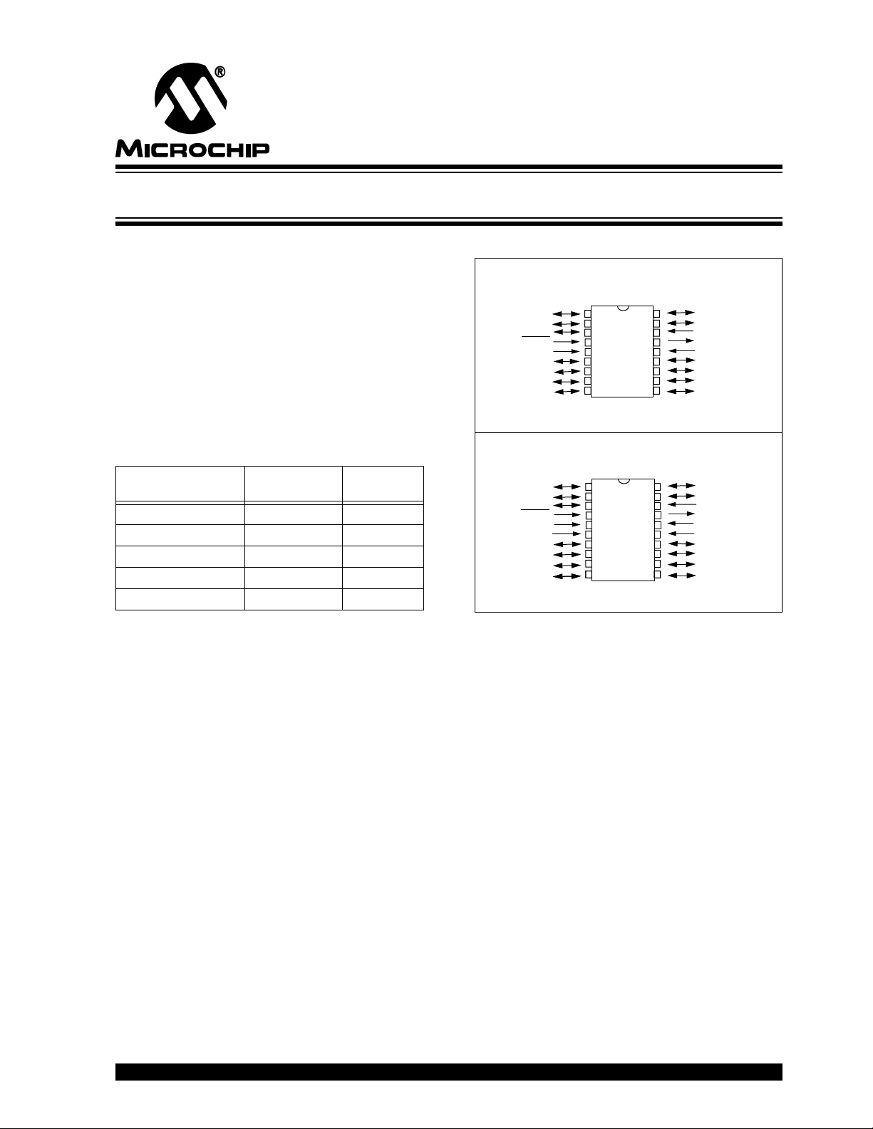
Pin Diagram
PDIP, SOIC, Windowed CERDIP
RA2
RA3
RA4/T0CKI
MCLR
VSS
RB0/INT
RB1
RB2
RB3
PIC16C55X(A)
•1
2
3
4
5
6
7
8
9
18
17
16
15
14
13
12
11
10
RA1
RA0
OSC1/CLKIN
OSC2/CLKOUT
DD
V
RB7
RB6
RB5
RB4
SSOP
RA2
RA3
RA4/T0CKI
MCLR
VSS
VSS
RB0/INT
RB1
RB2
RB3RB3
PIC16C55X(A)
•1
2
3
4
5
6
7
8
9
10
20
19
18
17
16
15
14
13
12
11
RA1
RA0
OSC1/CLKIN
OSC2/CLKOUT
V
DD
VDD
RB7
RB6
RB5
RB4
Special Microcontroller Features (cont’d)
• Programmable code protection
• Power saving SLEEP mode
• Selectable oscillator options
• Serial in-circuit programming (via two pins)
• Four user programmable ID locations
CMOS Tec hnology:
• Low-power , high-speed CMOS EPR OM technology
• Fully static design
• Wide operating voltage range
- 2.5V to 5.5V PIC16C55X
- 3.0 to 5.5V PIC16C55XA
• Commercial, industrial and extended temperature range
• Low power consumption
- < 2.0 mA @ 5.0V, 4.0 MHz
- 15 µ A typical @ 3.0V, 32 kHz
- < 1.0 µ A typical standby current @ 3.0V
1997 Microchip Technology Inc.
Preliminary
DS40143B-page 1
Page 2

PIC16C55X(A)
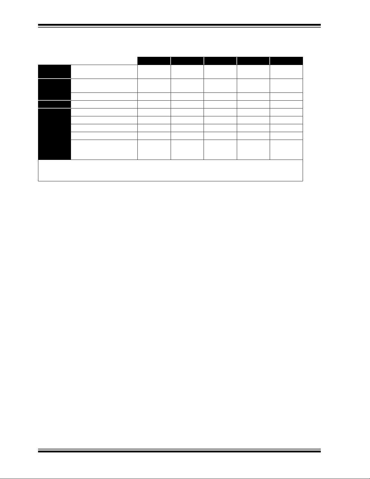
Device Differences
Device
PIC16C554 2.5 - 5.5 See Note 1 0.9
PIC16C554A 3.0 - 5.5 See Note 1 0.7
PIC16C556A 3.0 - 5.5 See Note 1 0.7
PIC16C558 2.5 - 5.5 See Note 1 0.9
PIC16C558A 3.0 - 5.5 See Note 1 0.7
Note 1: If you change from this device to another device, please verify oscillator characteristics in your application.
Voltage
Range
Oscillator
Process
Technology
(Microns)
DS40143B-page 2
Preliminary
1997 Microchip Technology Inc.
Page 3

PIC16C55X(A)
Table of Contents
1.0 General Description......................................................................................................................................................................5
2.0 PIC16C55X(A) Device Varieties...................................................................................................................................................7
3.0 Architectural Overview .................................................................................................................................................................9
4.0 Memory Organization................................................................................................................................................................ 13
5.0 I/O Ports.................................................................................................................................................................................... 23
6.0 Timer0 Module .......................................................................................................................................................................... 29
7.0 Special Features of the CPU..................................................................................................................................................... 35
8.0 Instruction Set Summary........................................................................................................................................................... 51
9.0 Development Support................................................................................................................................................................ 63
10.0 Electrical Specifications............................................................................................................................................................. 67
11.0 Packaging Information............................................................................................................................................................... 79
Appendix A: Enhancements............................................................................................................................................................ 87
Appendix B: Compatibility............................................................................................................................................................... 87
INDEX.................................................................................................................................................................................................. 89
PIC16C55X(A) Product Identification System...................................................................................................................................... 95
To Our Valued Customers
We constantly strive to improve the quality of all our products and documentation. To this end, we recently converted to a new publishing software package which we believe will enhance our entire documentation process and
product. As in any conversion process, information may have accidently been altered or deleted. We have spent an
exceptional amount of time to ensure that these documents are correct. However, we realize that we may have
missed a few things. If you find any information that is missing or appears in error from the previous version of this
data sheet (PIC16C55X(A) Data Sheet, Literature Number DS40143B), please use the reader response form in the
back of this data sheet to inform us. We appreciate your assistance in making this a better document.
1997 Microchip Technology Inc.
Preliminary
DS40143B-page 3
Page 4

PIC16C55X(A)
NOTES:
DS40143B-page 4
Preliminary
1997 Microchip Technology Inc.
Page 5

PIC16C55X(A)
1.0 GENERAL DESCRIPTION
The PIC16C55X(A) are 18 and 20-Pin EPROM-based
members of the versatile PIC16CXX family of low-cost,
high-performance, CMOS, fully-static, 8-bit
microcontrollers.
All PICmicro™ microcontrollers employ an advanced
RISC architecture. The PIC16C55X(A) have enhanced
core features, eight-le vel deep stack, and multiple internal and external interrupt sources. The separate
instruction and data buses of the Harvard architecture
allow a 14-bit wide instruction word with the separate
8-bit wide data. The two-stage instruction pipeline
allows all instructions to execute in a single-cycle,
except for program branches (which require two
cycles). A total of 35 instructions (reduced instruction
set) are available . Additionally , a large register set giv es
some of the architectural innovations used to achie ve a
very high performance.
PIC16C55X(A) microcontrollers typically achieve a 2:1
code compression and a 4:1 speed improvement over
other 8-bit microcontrollers in their class.
The PIC16C554(A) and PIC16C556A have 80 bytes of
RAM. The PIC16C558(A) has 128 bytes of RAM. Each
device has 13 I/O pins and an 8-bit timer/counter with
an 8-bit programmable prescaler.
PIC16C55X(A) devices hav e special features to reduce
external components, thus reducing cost, enhancing
system reliability and reducing power consumption.
There are four oscillator options, of which the single pin
RC oscillator provides a low-cost solution, the LP
oscillator minimizes power consumption, XT is a
standard crystal, and the HS is for High Speed crystals.
The SLEEP (power-down) mode offers power saving.
The user can wake up the chip from SLEEP through
several external and internal interrupts and reset.
A highly reliable Watchdog Timer with its own on-chip
RC oscillator provides protection against software
lock- up.
A UV-erasable CERDIP-packaged version is ideal for
code development while the cost-effective One-Time
Programmable (OTP) version is suitable for production
in any volume.
Table 1-1 shows the features of the PIC16C55X(A)
mid-range microcontroller families.
A simplified block diagram of the PIC16C55X(A) is
shown in Figure 3-1.
The PIC16C55X(A) series fit perfectly in applications
ranging from motor control to low-power remote sensors. The EPROM technology makes customization of
application programs (detection levels, pulse generation, timers, etc.) extremely fast and convenient. The
small footprint packages make this microcontroller
series perfect for all applications with space limitations.
Low-cost, low-power, high-performance, ease of use
and I/O flexibility make the PIC16C55X(A) very versatile.
1.1 F
Those users familiar with the PIC16C5X family of
microcontrollers will realize that this is an enhanced
version of the PIC16C5X architecture. Please refer to
Appendix A for a detailed list of enhancements. Code
written for PIC16C5X can be easily ported to
PIC16C55X(A) family of devices (Appendix B).
The PIC16C55X(A) f amily fills the niche for users w anting to migrate up from the PIC16C5X family and not
needing various peripheral features of other members
of the PIC16XX mid-range microcontroller family.
1.2 De
amily and Upward Compatibility
velopment Support
1997 Microchip Technology Inc.
The PIC16C55X(A) family is suppor ted by a full-featured macro assembler, a software simulator, an in-circuit emulator, a lo w-cost dev elopment programmer and
a full-featured programmer. A “C” compiler and fuzzy
logic support tools are also available.
Preliminary
DS40143B-page 5
Page 6
PIC16C55X(A)
TABLE 1-1: PIC16C55X(A) FAMILY OF DEVICES
PIC16C554
Clock
Memory
Peripherals Timer Module(s) TMR0 TMR0 TMR0 TMR0 TMR0
Features
All PICmicro™ Family devices have Power-on Reset, selectable Watchdog Timer, selectable code protect and high
I/O current capability. All PIC16C55X(A)Family devices use serial programming with clock pin RB6 and data pin RB7.
Maximum Frequency of Operation (MHz)
EPROM Program Memory
(x14 words)
Data Memory (bytes) 80 80 80 128 128
Interrupt Sources 3 3 3 3 3
I/O Pins 13 13 13 13 13
Voltage Range (Volts) 2.5-5.5 3.0-5.5 3.0-5.5 2.5-5.5 3.0-5.5
Brown-out Reset — — — — —
Packages 18-pin DIP,
20 20 20 20 20
512 512 1K 2K 2K
SOIC;
20-pin SSOP
PIC16C554A PIC16C556A PIC16C558 PIC16C558A
18-pin DIP,
SOIC;
20-pin SSOP
18-pin DIP,
SOIC;
20-pin SSOP
18-pin DIP,
SOIC;
20-pin SSOP
18-pin DIP,
SOIC;
20-pin SSOP
DS40143B-page 6
Preliminary
1997 Microchip Technology Inc.
Page 7

PIC16C55X(A)
2.0 PIC16C55X(A) DEVICE
VARIETIES
A variety of frequency ranges and packaging options are
available . Depending on application and production
requirements the proper device option can be selected
using the information in the PIC16C55X(A) Product
Identification System section at the end of this data
sheet. When placing orders, please use this page of the
data sheet to specify the correct part number.
2.1 UV Erasab
The UV erasable version, offered in CERDIP package
is optimal for prototype development and pilot
programs. This version can be erased and
reprogrammed to any of the oscillator modes.
Microchip's PICSTART
programmers both support programming of the
PIC16C55X(A).
2.2 One-Time-Pr
Devices
The availability of OTP devices is especially useful for
customers who need the flexibility for frequent code
updates and small volume applications. In addition to
the program memory, the configuration bits must also
be programmed.
le Devices
and PROMATE
ogrammable (OTP)
2.3 Quic
k-Turnaround-Production (QTP)
Devices
Microchip offers a QTP Programming Service for
factory production orders. This service is made
available for users who choose not to program a
medium to high quantity of units and whose code patterns have stabilized. The devices are identical to the
OTP devices but with all EPROM locations and configuration options already programmed by the factory.
Certain code and prototype verification procedures
apply before production shipments are available.
Please contact your Microchip Technology sales office
for more details.
2.4 Serializ
Microchip offers a unique programming service where
a few user-defined locations in each device are
programmed with different serial numbers. The serial
numbers may be random, pseudo-random or
sequential.
Serial programming allows each device to have a
unique number which can serve as an entry-code,
password or ID number.
Quick-Turnaround-Production
(SQTP
ed
SM
Devices
)
1997 Microchip Technology Inc.
Preliminary
DS40143B-page 7
Page 8

PIC16C55X(A)
NOTES:
DS40143B-page 8
Preliminary
1997 Microchip Technology Inc.
Page 9

PIC16C55X(A)
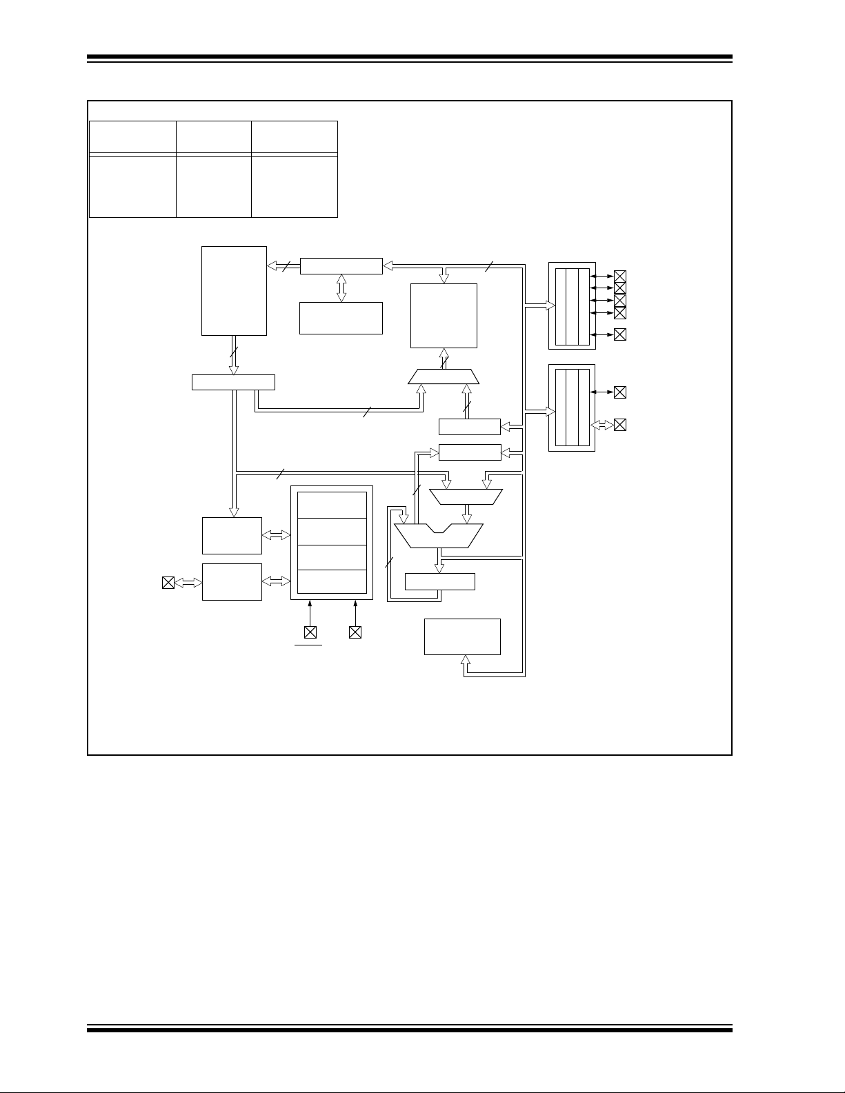
3.0 ARCHITECTURAL OVERVIEW
The high performance of the PIC16C55X(A) family can
be attributed to a number of architectural features
commonly found in RISC microprocessors. To begin
with, the PIC16C55X(A) uses a Harvard architecture,
in which, program and data are accessed from separate memories using separate busses. This improves
bandwidth over traditional von Neumann architecture
where program and data are fetched from the same
memory. Separating program and data memory further
allows instructions to be sized differently than 8-bit
wide data words. Instruction opcodes are 14-bits wide
making it possible to have all single word instructions.
A 14-bit wide program memory access bus fetches a
14-bit instruction in a single cycle. A two-stage pipeline
overlaps fetch and execution of instructions.
Consequently, all instructions (35) execute in a single-cycle (200 ns @ 20 MHz) except for program
branches.
The PIC16C554(A) addresses 512 x 14 on-chip program memory. The PIC16C556A addresses 1K x 14
program memory. The PIC16C558(A) addresses 2K x
14 program memory. All program memory is internal.
The PIC16C55X(A) can directly or indirectly address its
register files or data memory. All special function
registers including the program counter are mapped
into the data memory. The PIC16C55X(A) have an
orthogonal (symmetrical) instruction set that makes it
possible to carry out any operation on any register
using any addressing mode. This symmetrical nature
and lack of ‘special optimal situations’ make programming with the PIC16C55X(A) simple yet efficient. In
addition, the learning curve is reduced significantly.
The PIC16C55X(A) devices contain an 8-bit ALU and
working register. The ALU is a general purpose
arithmetic unit. It performs arithmetic and Boolean
functions between data in the working register and any
register file.
The ALU is 8-bits wide and capable of addition,
subtraction, shift and logical operations. Unless
otherwise mentioned, arithmetic operations are two's
complement in nature. In two-operand instructions,
typically one operand is the working register
(W register). The other operand is a file register or an
immediate constant. In single operand instructions, the
operand is either the W register or a file register.
The W register is an 8-bit working register used for ALU
operations. It is not an addressable register.
Depending on the instruction executed, the ALU may
affect the values of the Carry (C), Digit Carry (DC), and
Zero (Z) bits in the STATUS register. The C and DC bits
operate as a Bo
respectively, in subtraction. See the
SUBWF
A simplified block diagram is shown in Figure 3-1, with
a description of the device pins in Table 3-1.
instructions for examples.
rrow and Digit Borrow out bit,
SUBLW
and
1997 Microchip Technology Inc.
Preliminary
DS40143B-page 9
Page 10
PIC16C55X(A)
FIGURE 3-1: BLOCK DIAGRAM
Device
PIC16C554
PIC16C554A
PIC16C556A
PIC16C558
PIC16C558A
OSC1/CLKIN
OSC2/CLKOUT
512 x 14
512 x 14
1K x 14
2K x 14
2K x 14
Program
Bus
Program
Memory
EPROM
Program
Memory
512 x 14
to
2K x 14
14
Instruction reg
Instruction
Decode &
Control
Timing
Generation
Data Memory
(RAM)
80 x 8
80 x 8
80 x 8
128 x 8
128 x 8
13
Direct Addr
8
Program Counter
8 Level Stack
(13-bit)
Power-up
Timer
Oscillator
Start-up Timer
Power-on
Reset
Watchdog
Timer
RAM Addr
7
3
8
Data Bus
RAM
File
Registers
80 x 8 to
128 x 8
(1)
Addr MUX
FSR reg
STATUS reg
ALU
W reg
8
8
MUX
8
Indirect
Addr
PORTA
RA0
RA1
RA2
RA3
RA4/T0CKI
PORTB
RB0/INT
RB7:RB1
MCLR
VDD, VSS
Note 1: Higher order bits are from the status register.
Timer0
DS40143B-page 10
Preliminary
1997 Microchip Technology Inc.
Page 11

PIC16C55X(A)
TABLE 3-1: PIC16C55X(A) PINOUT DESCRIPTION
DIP
Name
OSC1/CLKIN 16 18 I ST/CMOS Oscillator crystal input/external clock source input.
OSC2/CLKOUT 15 17 O — Oscillator crystal output. Connects to crystal or resonator
/V
MCLR
RA0 17 19 I/O ST
RA1 18 20 I/O ST
RA2 1 1 I/O ST
RA3 2 2 I/O ST
RA4/T0CKI 3 3 I/O ST Can be selected to be the clock input to the Timer0
RB0/INT 6 7 I/O
RB1 7 8 I/O TTL
RB2 8 9 I/O TTL
RB3 9 10 I/O TTL
RB4 10 11 I/O TTL Interrupt on change pin.
RB5 11 12 I/O TTL Interrupt on change pin.
RB6 12 13 I/O TTL/ST
RB7 13 14 I/O TTL/ST
V
V
PP
SS
DD
SOIC
Pin #
SSOP
Pin #
4 4 I/P ST Master clear (reset) input/programming voltage input.
5 5,6 P — Ground reference for logic and I/O pins.
14 15,16 P — Positive supply for logic and I/O pins.
Legend: O = output I/O = input/output P = power
— = Not used I = Input ST = Schmitt Trigger input
TTL = TTL input
Note 1: This buffer is a Schmitt Trigger input when configured as the external interrupt.
Note 2: This buffer is a Schmitt Trigger input when used in serial programming mode.
I/O/P
Type
Buffer
Type
TTL/ST
Description
in crystal oscillator mode. In RC mode, OSC2 pin outputs
CLKOUT which has 1/4 the frequency of OSC1, and
denotes the instruction cycle rate.
This pin is an active low reset to the device.
PORTA is a bi-directional I/O port.
timer/counter. Output is open drain type.
PORTB is a bi-directional I/O port. PORTB can be
software programmed for internal weak pull-up on all
inputs.
(1)
(2)
(2)
RB0/INT can also be selected as an external
interrupt pin.
Interrupt on change pin. Serial programming clock.
Interrupt on change pin. Serial programming data.
1997 Microchip Technology Inc.
Preliminary
DS40143B-page 11
Page 12
PIC16C55X(A)
3.1 Cloc
king Scheme/Instruction Cycle
The clock input (OSC1/CLKIN pin) is internally divided
by four to generate four non-overlapping quadrature
clocks namely Q1, Q2, Q3 and Q4. Internally, the
program counter (PC) is incremented every Q1, the
instruction is fetched from the program memory and
latched into the instruction register in Q4. The
instruction is decoded and executed during the
following Q1 through Q4. The clocks and instruction
execution flow are shown in Figure 3-2.
FIGURE 3-2: CLOCK/INSTRUCTION CYCLE
Q2 Q3 Q4
OSC1
Q1
Q2
Q3
Q4
PC
OSC2/CLKOUT
(RC mode)
Q1
PC PC+1 PC+2
Fetch INST (PC)
Execute INST (PC-1) Fetch INST (PC+1)
Q1
3.2 Instruction Flo
w/Pipelining
An “Instruction Cycle” consists of four Q cycles (Q1,
Q2, Q3 and Q4). The instruction fetch and execute are
pipelined such that fetch takes one instruction cycle
while decode and execute takes another instruction
cycle. However, due to the pipelining, each instruction
effectively executes in one cycle. If an instruction
causes the program counter to change (e.g.,
then two cycles are required to complete the instruction
(Example 3-1).
A fetch cycle begins with the program counter (PC)
incrementing in Q1.
In the execution cycle , the fetched instruction is latched
into the “Instruction Register (IR)” in cycle Q1. This
instruction is then decoded and executed during the
Q2, Q3, and Q4 cycles. Data memory is read during Q2
(operand read) and written during Q4 (destination
write).
Q2 Q3 Q4
Execute INST (PC) Fetch INST (PC+2)
Q2 Q3 Q4
Q1
Execute INST (PC+1)
Internal
phase
clock
GOTO
)
EXAMPLE 3-1: INSTRUCTION PIPELINE FLOW
1. MOVLW 55h
2. MOVWF PORTB
3. CALL SUB_1
4. BSF PORTA, BIT3
All instructions are single cycle, except for any program branches. These take two cycles since the fetch
instruction is “flushed” from the pipeline while the new instruction is being fetched and then executed.
DS40143B-page 12
Fetch 1 Execute 1
Fetch 2 Execute 2
Preliminary
Fetch 3 Execute 3
Fetch 4 Flush
Fetch SUB_1 Execute SUB_1
1997 Microchip Technology Inc.
Page 13
PIC16C55X(A)
4.0 MEMORY ORGANIZATION
4.1 Pr
The PIC16C55X(A) has a 13-bit prog ram counter capable of addressing an 8K x 14 program memory space.
Only the first 512 x 14 (0000h - 01FFh) for the
PIC16C554(A), 1K x 14 (0000h - 03FFh) for the
PIC16C556A and 2K x 14 (0000h - 07FFh) for the
PIC16C558(A) are physically implemented. Accessing
a location above these boundaries will cause a
wrap-around within the first 512 x 14 space
PIC16C554(A) or 1K x 14 space PIC16C556A or 2K x
14 space PIC16C558(A). The reset vector is at 0000h
and the interrupt vector is at 0004h (Figure 4-1,
Figure 4-2, Figure 4-3).
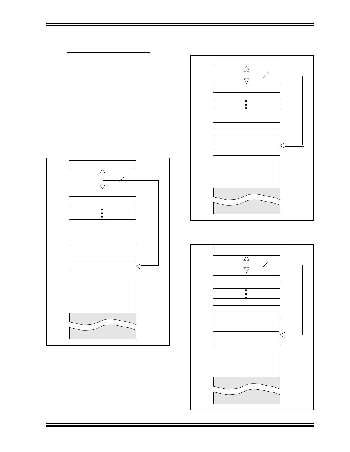
FIGURE 4-1: PROGRAM MEMORY MAP
ogram Memory Organization
AND STACK FOR THE
PIC16C554/PIC6C554A
PC<12:0>
CALL, RETURN
RETFIE, RETLW
Stack Level 1
Stack Level 2
13
FIGURE 4-2: PROGRAM MEMORY MAP
AND STACK FOR THE
PIC16C556A
PC<12:0>
CALL, RETURN
RETFIE, RETLW
Stack Level 1
Stack Level 2
Stack Level 8
Reset Vector
Interrupt Vector
On-chip Program
Memory
13
000h
0004
0005
03FFh
0400h
Stack Level 8
Reset Vector
Interrupt Vector
On-chip Program
Memory
000h
0004
0005
01FFh
0200h
1FFFh
1FFFh
FIGURE 4-3: PROGRAM MEMORY MAP
AND STACK FOR THE
PIC16C558/PIC16C558A
PC<12:0>
CALL, RETURN
RETFIE, RETLW
Stack Level 1
Stack Level 2
Stack Level 8
Reset Vector
Interrupt Vector
On-chip Program
Memory
13
000h
0004
0005
07FFh
0800h
1997 Microchip Technology Inc.
Preliminary
1FFFh
DS40143B-page 13
Page 14

PIC16C55X(A)
4.2 Data Memor
The data memory (Figure 4-4 and Figure 4-5) is
partitioned into two Banks which contain the general
purpose registers and the special function registers.
Bank 0 is selected when the RP0 bit is cleared. Bank 1
is selected when the RP0 bit (STATUS <5>) is set. The
Special Function Registers are located in the first 32
locations of each Bank. Register locations 20-6Fh
(Bank0) on the PIC16C554(A)/556A and 20-7Fh
(Bank0) and A0-BFh (Bank1) on the PIC16C558(A) are
general purpose registers implemented as static RAM.
Some special purpose registers are mapped in Bank 1.
y Organization
4.2.1 GENERAL PURPOSE REGISTER FILE The register file is organized as 80 x 8 in the
PIC16C554(A)/556A and 128 x 8 in the PIC16C558(A).
Each is accessed either directly or indirectly through
the File Select Register, FSR (Section 4.4).
DS40143B-page 14
Preliminary
1997 Microchip Technology Inc.
Page 15
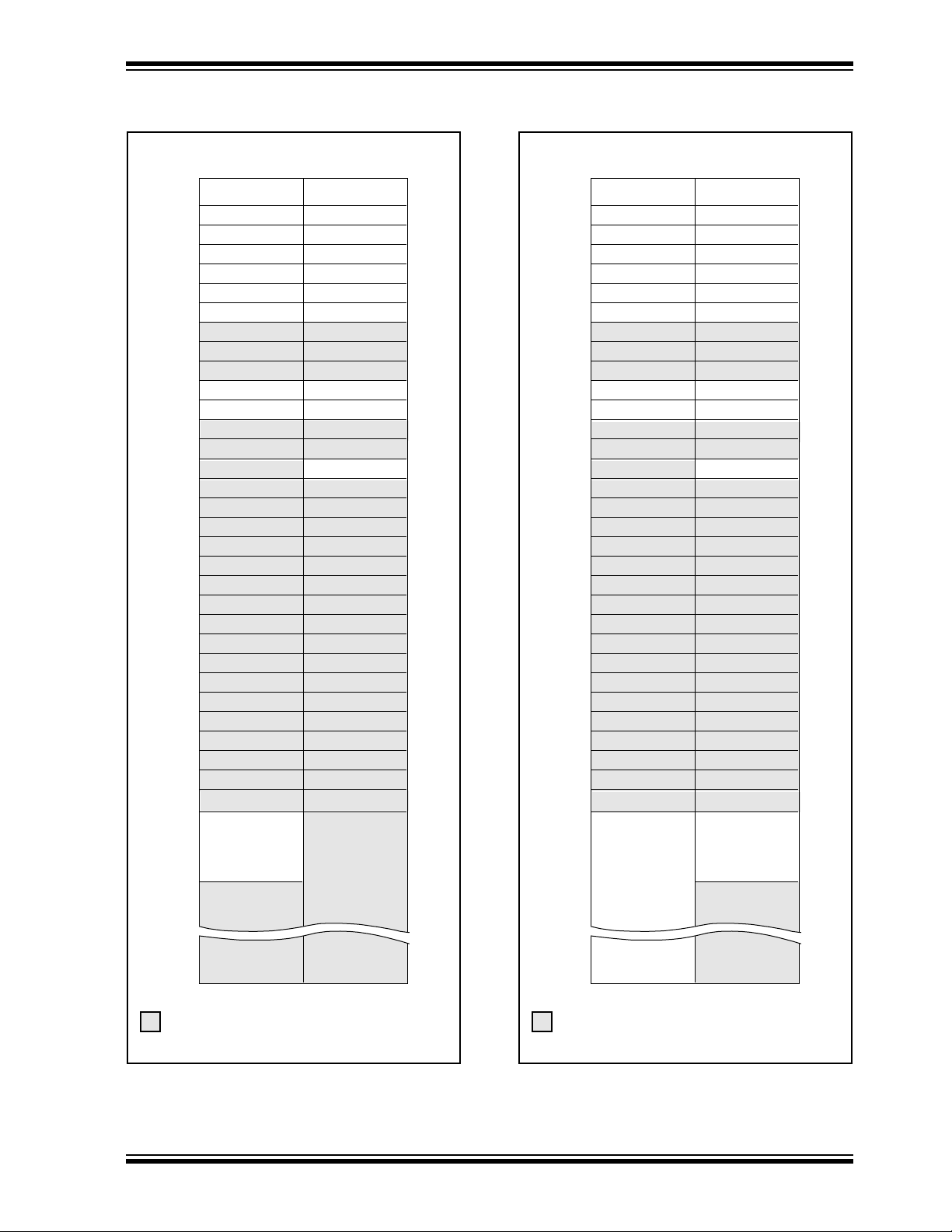
PIC16C55X(A)
FIGURE 4-4: DATA MEMORY MAP FOR
THE PIC16C554(A)/556A
File
Address
00h
01h
02h
03h
04h
05h
06h
07h
08h
09h
0Ah
0Bh
0Ch
0Dh
0Eh
0Fh
10h
11h
12h
13h
14h
15h
16h
17h
18h
19h
1Ah
1Bh
1Ch
1Dh
1Eh
1Fh
20h
6Fh
70h
(1)
INDF
TMR0
PCL
STATUS
FSR
PORTA
PORTB
PCLATH
INTCON
General
Purpose
Register
(1)
INDF
OPTION
PCL
STATUS
FSR
TRISA
TRISB
PCLATH
INTCON
PCON
File
Address
80h
81h
82h
83h
84h
85h
86h
87h
88h
89h
8Ah
8Bh
8Ch
8Dh
8Eh
8Fh
90h
91h
92h
93h
94h
95h
96h
97h
98h
99h
9Ah
9Bh
9Ch
9Dh
9Eh
9Fh
A0h
FIGURE 4-5: DATA MEMORY MAP FOR
THE PIC16C558(A)
File
Address
00h
01h
02h
03h
04h
05h
06h
07h
08h
09h
0Ah
0Bh
0Ch
0Dh
0Eh
0Fh
10h
11h
12h
13h
14h
15h
16h
17h
18h
19h
1Ah
1Bh
1Ch
1Dh
1Eh
1Fh
20h
(1)
INDF
TMR0
PCL
STATUS
FSR
PORTA
PORTB
PCLATH
INTCON
General
Purpose
Register
(1)
INDF
OPTION
PCL
STATUS
FSR
TRISA
TRISB
PCLATH
INTCON
PCON
General
Purpose
Register
File
Address
80h
81h
82h
83h
84h
85h
86h
87h
88h
89h
8Ah
8Bh
8Ch
8Dh
8Eh
8Fh
90h
91h
92h
93h
94h
95h
96h
97h
98h
99h
9Ah
9Bh
9Ch
9Dh
9Eh
9Fh
A0h
BFh
C0h
7Fh
Unimplemented data memory locations, read as '0'.
Note 1: Not a physical register.
1997 Microchip Technology Inc. Preliminary DS40143B-page 15
Bank 0 Bank 1
FFh
7Fh
Unimplemented data memory locations, read as '0'.
Note 1: Not a physical register.
Bank 0 Bank 1
FFh
Page 16
PIC16C55X(A)
4.2.2 SPECIAL FUNCTION REGISTERS
The special function registers can be classified into two
sets (core and peripheral). The special function regis-
The special function registers are registers used by the
CPU and Peripheral functions for controlling the
desired operation of the device (Table 4-1). These
registers are static RAM.
ters associated with the “core” functions are described
in this section. Those related to the operation of the
peripheral features are described in the section of that
peripheral feature.
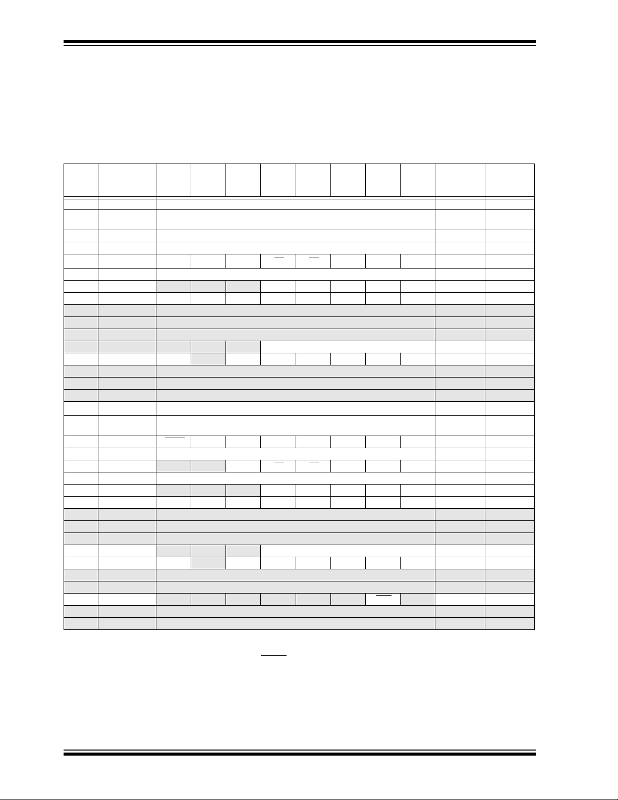
TABLE 4-1: SPECIAL REGISTERS FOR THE PIC16C55X(A)
Address Name Bit 7 Bit 6 Bit 5 Bit 4 Bit 3 Bit 2 Bit 1 Bit 0
Bank 0
00h INDF
01h TMR0 Timer0 Module’s Register xxxx xxxx uuuu uuuu
02h PCL Program Counter's (PC) Least Significant Byte 0000 0000 0000 0000
03h STATUS
04h FSR Indirect data memory address pointer xxxx xxxx uuuu uuuu
05h PORTA — — — RA4 RA3 RA2 RA1 RA0 ---x xxxx ---u uuuu
06h PORTB RB7 RB6 RB5 RB4 RB3 RB2 RB1 RB0 xxxx xxxx uuuu uuuu
07h Unimplemented — —
08h Unimplemented — —
09h Unimplemented — —
0Ah PCLATH — — — Write buffer for upper 5 bits of program counter ---0 0000 ---0 0000
0Bh INTCON GIE
0Ch Unimplemented — —
0Dh-1Eh Unimplemented — —
1Fh Unimplemented — —
Bank 1
80h INDF
81h OPTION RBPU
82h PCL Program Counter's (PC) Least Significant Byte 0000 0000 0000 0000
83h STATUS
84h FSR Indirect data memory address pointer xxxx xxxx uuuu uuuu
85h TRISA
86h TRISB TRISB7 TRISB6 TRISB5 TRISB4 TRISB3 TRISB2 TRISB1 TRISB0 1111 1111 1111 1111
87h Unimplemented — —
88h Unimplemented — —
89h Unimplemented — —
8Ah PCLATH
8Bh INTCON GIE
8Ch Unimplemented — —
8Dh Unimplemented — —
8Eh PCON
8Fh-9Eh Unimplemented — —
9Fh Unimplemented — —
Addressing this location uses contents of FSR to address data memory (not a physical
register)
(2)
IRP
Addressing this location uses contents of FSR to address data memory (not a physical
register)
— — RP0 TO PD Z DC C 0001 1xxx 000q quuu
— — — TRISA4 TRISA3 TRISA2 TRISA1 TRISA0 ---1 1111 ---1 1111
— — — Write buffer for upper 5 bits of program counter ---0 0000 ---0 0000
— — — — — — POR — ---- --0- ---- --u-
(2)
RP1
(3) T0IE INTE RBIE T0IF INTF RBIF 0000 000x 0000 000x
INTEDG T0CS T0SE PSA PS2 PS1 PS0 1111 1111 1111 1111
(3) T0IE INTE RBIE T0IF INTF RBIF 0000 000x 0000 000x
RP0 TO PD Z DC C
Value on
POR Reset
xxxx xxxx xxxx xxxx
0001 1xxx 000q quuu
xxxx xxxx xxxx xxxx
Legend: — = Unimplemented locations read as ‘0’, u = unchanged, x = unknown, q = value depends on condition,
shaded = unimplemented
Note 1: Other (non power-up) resets include MCLR reset and Watchdog Timer reset during normal operation.
Note 2: IRP & RPI bits are reserved, always maintain these bits clear.
Note 3: Bit 6 of INTCON register is reserved for future use. Always maintain this bit as clear.
Value on
all other
resets
(1)
DS40143B-page 16 Preliminary 1997 Microchip Technology Inc.
Page 17

PIC16C55X(A)
4.2.2.1 STATUS REGISTER
The STATUS register, shown in Figure 4-6, contains
the arithmetic status of the ALU, the RESET status and
the bank select bits for data memory.
The STATUS register can be the destination for any
instruction, like any other register. If the STATUS
register is the destination for an instruction that affects
the Z, DC or C bits, then the write to these three bits is
disabled. These bits are set or cleared according to the
device logic. Furthermore, the T
writable. Therefore, the result of an instruction with the
STATUS register as the destination may be different
than intended.
For example, CLRF STATUS will clear the upper-three
bits and set the Z bit. This lea ves the status register as
000uu1uu (where u = unchanged).
O and PD bits are not
It is recommended, therefore, that only BCF, BSF,
SWAPF and MOVWF instructions be used to alter the ST ATUS register because these instructions do not affect
any status bits. For other instructions, not affecting any
status bits, see the “Instruction Set Summary”.
Note 1: The IRP and RP1 bits (STATUS<7:6>)
are not used by the PIC16C55X(A) and
should be programmed as ’0'. Use of
these bits as general purpose R/W bits is
NOT recommended, since this may
affect upward compatibility with future
products.
Note 2: The C and DC bits operate as a Borro
and Digit Borrow out bit, respectively, in
subtraction. See the SUBLW and SUBWF
instructions for examples.
FIGURE 4-6: STATUS REGISTER (ADDRESS 03H OR 83H)
Reserved Reserved R/W-0 R-1 R-1 R/W-x R/W-x R/W-x
IRP RP1 RP0 TO PD Z DC C R = Readable bit
bit7 bit0
bit 7: IRP: Register Bank Select bit (used for indirect addressing)
1 = Bank 2, 3 (100h - 1FFh)
0 = Bank 0, 1 (00h - FFh)
The IRP bit is reserved on the PIC16C55X(A), always maintain this bit clear.
bit 6-5: RP1:RP0: Register Bank Select bits (used for direct addressing)
11 = Bank 3 (180h - 1FFh)
10 = Bank 2 (100h - 17Fh)
01 = Bank 1 (80h - FFh)
00 = Bank 0 (00h - 7Fh)
Each bank is 128 bytes. The RP1 bit is reserved on the PIC16C55X(A), always maintain this bit clear.
bit 4: T
bit 3: PD
bit 2: Z: Zero bit
bit 1: DC: Digit carry/borro
bit 0: C: Carry/borro
O: Time-out bit
1 = After power-up, CLRWDT instruction, or SLEEP instruction
0 = A WDT time-out occurred
: Power-down bit
1 = After power-up or by the CLRWDT instruction
0 = By execution of the SLEEP instruction
1 = The result of an arithmetic or logic operation is zero
0 = The result of an arithmetic or logic operation is not zero
w bit (ADDWF, ADDLW,SUBLW,SUBWF instructions)(for borrow the polarity is reversed)
1 = A carry-out from the 4th low order bit of the result occurred
0 = No carry-out from the 4th low order bit of the result
w bit (ADDWF, ADDLW,SUBLW,SUBWF instructions)
1 = A carry-out from the most significant bit of the result occurred
0 = No carry-out from the most significant bit of the result occurred
Note: For borro
second operand. For rotate (RRF, RLF) instructions, this bit is loaded with either the high or low order bit of
the source register.
w the polarity is reversed. A subtraction is executed by adding the two’s complement of the
W = Writable bit
- n = Value at POR reset
- x = Unknown at POR reset
w
1997 Microchip Technology Inc. Preliminary DS40143B-page 17
Page 18

PIC16C55X(A)
4.2.2.2 OPTION REGISTER
The OPTION register is a readable and writable
register which contains various control bits to configure
Note: To achieve a 1:1 prescaler assignment for
TMR0, assign the prescaler to the WDT
(PSA = 1).
the TMR0/WDT prescaler, the external RB0/INT
interrupt, TMR0 and the weak pull-ups on PORTB.
FIGURE 4-7: OPTION REGISTER (ADDRESS 81H)
R/W-1 R/W-1 R/W-1 R/W-1 R/W-1 R/W-1 R/W-1 R/W-1
RBPU INTEDG T0CS T0SE PSA PS2 PS1 PS0 R = Readable bit
bit7 bit0
bit 7: RBPU: PORTB Pull-up Enable bit
1 = PORTB pull-ups are disabled
0 = PORTB pull-ups are enabled by individual port latch values
bit 6: INTEDG: Interrupt Edge Select bit
1 = Interrupt on rising edge of RB0/INT pin
0 = Interrupt on falling edge of RB0/INT pin
bit 5: T0CS: TMR0 Clock Source Select bit
1 = Transition on RA4/T0CKI pin
0 = Internal instruction cycle clock (CLKOUT)
bit 4: T0SE: TMR0 Source Edge Select bit
1 = Increment on high-to-low transition on RA4/T0CKI pin
0 = Increment on low-to-high transition on RA4/T0CKI pin
bit 3: PSA: Prescaler Assignment bit
1 = Prescaler is assigned to the WDT
0 = Prescaler is assigned to the Timer0 module
bit 2-0: PS2:PS0: Prescaler Rate Select bits
Bit Value TMR0 Rate WDT Rate
000
001
010
011
100
101
110
111
1 : 2
1 : 4
1 : 8
1 : 16
1 : 32
1 : 64
1 : 128
1 : 256
1 : 1
1 : 2
1 : 4
1 : 8
1 : 16
1 : 32
1 : 64
1 : 128
W = Writable bit
- n = Value at POR reset
DS40143B-page 18 Preliminary 1997 Microchip Technology Inc.
Page 19

PIC16C55X(A)
4.2.2.3 INTCON REGISTER
The INTCON register is a readable and writable
register which contains the various enable and flag bits
for all interrupt sources.
Note: Interrupt flag bits get set when an interrupt
condition occurs regardless of the state of
its corresponding enable bit or the global
enable bit, GIE (INTCON<7>).
FIGURE 4-8: INTCON REGISTER (ADDRESS 0BH OR 8BH)
R/W-0 Reserved R/W-0 R/W-0 R/W-0 R/W-0 R/W-0 R/W-x
GIE — T0IE INTE RBIE T0IF INTF RBIF R = Readable bit
bit7 bit0
bit 7: GIE: Global Interrupt Enable bit
1 = Enables all un-masked interrupts
0 = Disables all interrupts
bit 6:
bit 5: T0IE: TMR0 Overflow Interrupt Enable bit
bit 4: INTE: RB0/INT External Interrupt Enable bit
bit 3: RBIE: RB Port Change Interrupt Enable bit
bit 2: T0IF: TMR0 Overflow Interrupt Flag bit
bit 1: INTF: RB0/INT External Interrupt Flag bit
bit 0: RBIF: RB Port Change Interrupt Flag bit
— = Reserved for future use. Always maintain this bit clear.
1 = Enables the TMR0 interrupt
0 = Disables the TMR0 interrupt
1 = Enables the RB0/INT external interrupt
0 = Disables the RB0/INT external interrupt
1 = Enables the RB port change interrupt
0 = Disables the RB port change interrupt
1 = TMR0 register has overflowed (must be cleared in software)
0 = TMR0 register did not overflow
1 = The RB0/INT external interrupt occurred (must be cleared in software)
0 = The RB0/INT external interrupt did not occur
1 = When at least one of the RB7:RB4 pins changed state (must be cleared in software)
0 = None of the RB7:RB4 pins have changed state
W = Writable bit
- n = Value at POR reset
- x = Unknown at POR reset
1997 Microchip Technology Inc. Preliminary DS40143B-page 19
Page 20
PIC16C55X(A)
4.2.2.4 PCON REGISTER
The PCON register contains flag bits to differentiate
between a Po wer-on Reset, an e xternal MCLR
WDT reset. See Section 7.3 and Section 7.4 for
detailed reset operation.
FIGURE 4-9: PCON REGISTER (ADDRESS 8Eh)
U-0 U-0 U-0 U-0 U-0 U-0 R/W-0 U-0
— — — — — — POR — R = Readable bit
bit7 bit0
bit 7-2: Unimplemented: Read as '0'
bit 1: POR
bit 0: Unimplemented: Read as '0'
: Power-on Reset Status bit
1 = No Power-on Reset occurred
0 = Power-on Reset occurred
reset or
W = Writable bit
U = Unimplemented bit,
- n = Value at POR reset
read as ‘0’
DS40143B-page 20 Preliminary 1997 Microchip Technology Inc.
Page 21
PIC16C55X(A)
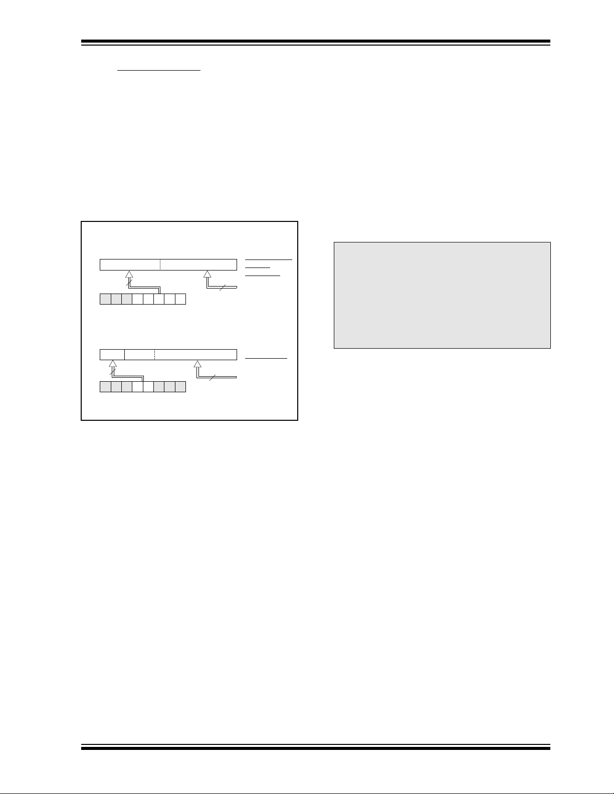
4.3 PCL and PCLATH
The program counter (PC) is 13-bits wide. The low byte
comes from the PCL register, which is a readable and
writable register. The high bits (PC<12:8>) are not directly
readable or writable and come from PCLATH. On any
reset, the PC is cleared. Figure 4-10 shows the two
situations for the loading of the PC. The upper example in
the figure shows how the PC is loaded on a write to PCL
(PCLATH<4:0> → PCH). The lo wer example in the figure
shows how the PC is loaded during a CALL or GOTO
instruction (PCLATH<4:3> → PCH).
FIGURE 4-10: LOADING OF PC IN
DIFFERENT SITUATIONS
PCH PCL
12 8 7 0
PC
PCLA TH<4:0>
5
PCLA TH
PCH PCL
12 11 10 0
PC
2
8 7
PCLATH<4:3>
11
8
Instr
uction with
PCL as
Destination
ALU result
GOTO, CALL
Opcode <10:0>
4.3.2 STACK The PIC16C55X(A) family has an 8 level deep x 13-bit
wide hardware stack (Figure 4-1, Figure 4-2 and
Figure 4-3). The stack space is not part of either program or data space and the stack pointer is not readable or writable. The PC is PUSHed onto the stack
when a CALL instruction is executed or an interrupt
causes a branch. The stack is POPed in the event of a
RETURN, RETLW or a RETFIE instruction execution.
PCLATH is not affected by a PUSH or POP operation.
The stack operates as a circular buff er . This means that
after the stack has been PUSHed eight times, the ninth
push overwrites the value that was stored from the first
push. The tenth push overwrites the second push (and
so on).
Note 1: There are no STATUS bits to indicate
stack overflow or stack underflow
conditions.
Note 2: There are no instructions mnemonics
called PUSH or POP. These are actions
that occur from the execution of the
CALL, RETURN, RETLW and RETFIE
instructions, or vectoring to an interrupt
address.
PCLATH
4.3.1 COMPUTED GOTO A computed GOTO is accomplished by adding an
offset to the program counter (ADDWF PCL). When doing
a table read using a computed GOTO method, care
should be exercised if the tab le location crosses a PCL
memory boundary (each 256 byte block). Refer to the
application note
“Implementing a Table Read"
(AN556).
1997 Microchip Technology Inc. Preliminary DS40143B-page 21
Page 22
PIC16C55X(A)
N
4.4 Indirect Addressing, INDF and FSR
Registers
The INDF register is not a physical register . Addressing
A simple program to clear RAM locations 20h-2Fh
using indirect addressing is shown in Example 4-1.
EXAMPLE 4-1: INDIRECT ADDRESSING
the INDF register will cause indirect addressing.
Indirect addressing is possible by using the INDF reg-
ister. Any instruction using the INDF register actually
accesses data pointed to by the file select register
EXT clrf INDF ;clear INDF register
(FSR). Reading INDF itself indirectly will produce 00h.
Writing to the INDF register indirectly results in a
no-operation (although status bits may be affected). An
effective 9-bit address is obtained b y concatenating the
8-bit FSR register and the IRP bit (STATUS<7>), as
CONTINUE:
shown in Figure 4-11. However, IRP is not used in the
PIC16C55X(A).
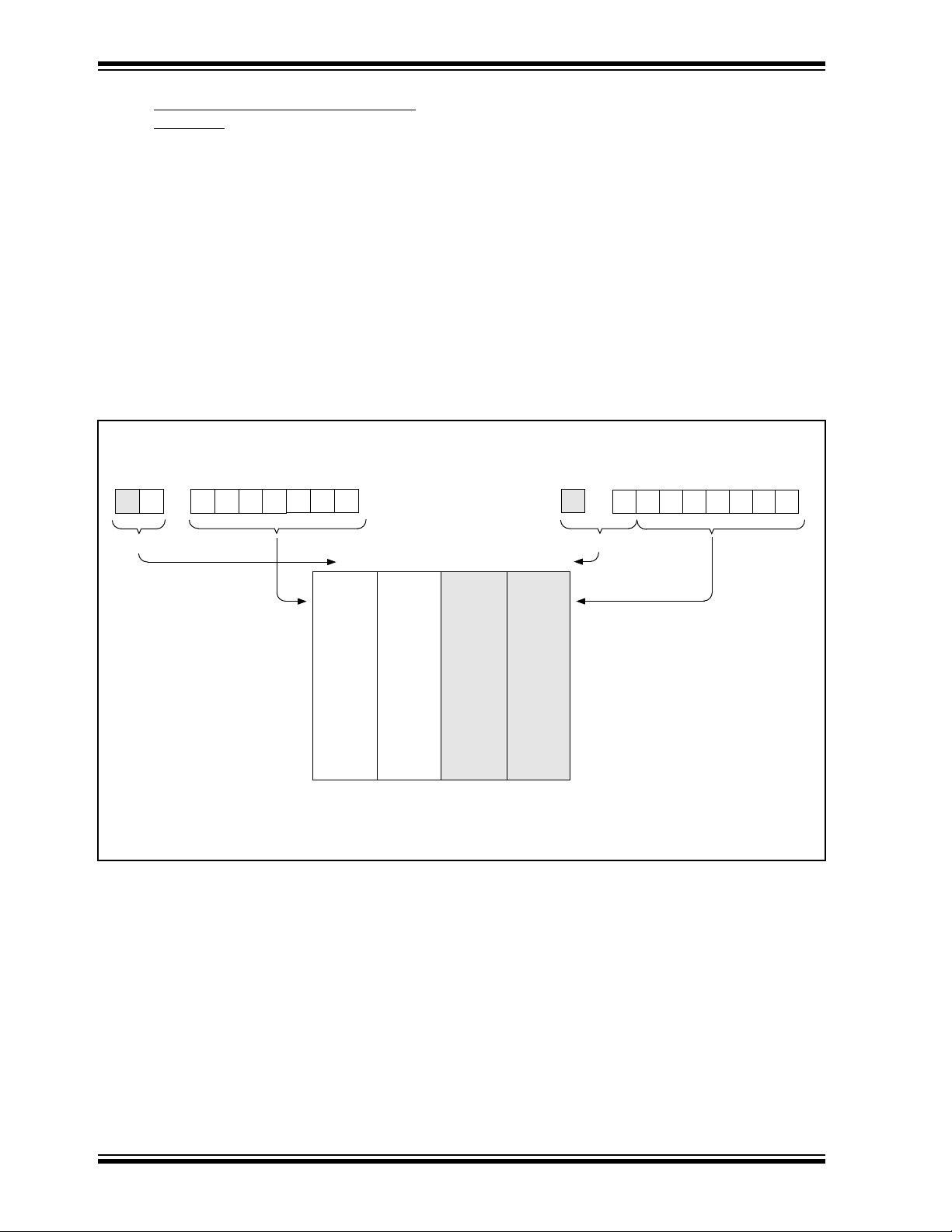
FIGURE 4-11: DIRECT/INDIRECT ADDRESSING PIC16C55X(A)
(1)
RP1 RP0 6
bank select location select
from opcode
00h
0
00 01 10 11
movlw 0x20 ;initialize pointer
movwf FSR ;to RAM
incf FSR ;inc pointer
btfss FSR,4 ;all done?
goto NEXT ;no clear next
;yes continue
Indirect AddressingDirect Addressing
(1)
IRP
bank select
00h
7
FSR register
location select
0
Data
not used
Memory
7Fh
7Fh
Bank 0 Bank 1 Bank 2 Bank 3
For memory map detail see Figure 4-4 and Figure 4-5.
Note 1: The RP1 and IRP bits are reserved, always maintain these bits clear.
DS40143B-page 22 Preliminary 1997 Microchip Technology Inc.
Page 23
PIC16C55X(A)
5.0 I/O PORTS
The PIC16C55X(A) ha ve two ports, PORT A and POR TB.
5.1 PORT A and TRISA Registers
PORTA is a 5-bit wide latch. RA4 is a Schmitt Trigger input
and an open drain output. P ort RA4 is multiplexed with the
T0CKI clock input. All other RA port pins have Schmitt
Trigger input levels and full CMOS output driv ers. All pins
have data direction bits (TRIS registers) which can configure these pins as input or output.
A '1' in the TRISA register puts the corresponding output
driver in a hi- impedance mode. A '0' in the TRISA register
puts the contents of the output latch on the selected pin(s).
Reading the PORTA register reads the status of the pins,
whereas writing to it will write to the port latch. All write
operations are read-modify-write operations. So a write
to a port implies that the port pins are first read, then this
value is modified and written to the port data latch.
Note: On reset, the TRISA register is set to all inputs.
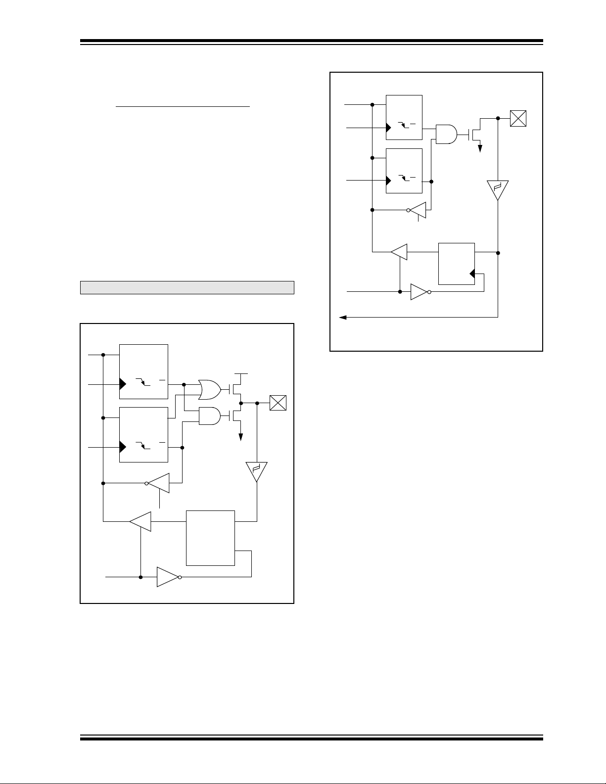
FIGURE 5-1: BLOCK DIAGRAM OF
PORT PINS RA<3:0>
Data
bus
WR
PortA
CK
Data Latch
D
QD
VDD
Q
Q
P
N
I/O pin
FIGURE 5-2: BLOCK DIAGRAM OF RA4 PIN
Data
bus
WR
PORTA
WR
TRISA
RD PORTA
TMR0 clock input
Note 1: I/O pin has protection diodes to V
QD
Q
CK
Data Latch
QD
Q
CK
TRISA Latch
RD TRISA
Schmitt
Trigger
input
buffer
Q D
EN
EN
(1)
I/O pin
N
V
SS
SS only.
WR
TRISA
RD PORTA
CK
TRIS Latch
Q
RD TRISA
Schmitt
Trigger
input
buffer
Q D
EN
SS
V
1997 Microchip Technology Inc. Preliminary DS40143B-page 23
Page 24

PIC16C55X(A)
TABLE 5-1: PORTA FUNCTIONS
Name Bit #
Buffer
Type
Function
RA0 bit0 ST Input/output
RA1 bit1 ST Input/output
RA2 bit2 ST Input/output
RA3 bit3 ST Input/output
RA4/T0CKI bit4 ST Input/output or external clock input for TMR0. Output is open drain type.
Legend: ST = Schmitt Trigger input
TABLE 5-2: SUMMARY OF REGISTERS ASSOCIATED WITH PORTA
Address Name Bit 7 Bit 6 Bit 5 Bit 4 Bit 3 Bit 2 Bit 1 Bit 0
05h PORTA — — — RA4 RA3 RA2 RA1 RA0
85h TRISA — — — TRISA4 TRISA3 TRISA2 TRISA1 TRISA0
Legend: — = Unimplemented locations, read as ‘0’
Note: Note: Shaded bits are not used by PORTA.
Value on
POR
---x xxxx ---u uuuu
---1 1111 ---1 1111
Value on
All Other Resets
DS40143B-page 24 Preliminary 1997 Microchip Technology Inc.
Page 25
PIC16C55X(A)
5.2 PORTB and TRISB Registers
PORTB is an 8-bit wide bi-directional port. The
corresponding data direction register is TRISB. A '1' in
the TRISB register puts the corresponding output driver
in a high impedance mode. A '0' in the TRISB register
puts the contents of the output latch on the selected
pin(s).
Reading PORTB register reads the status of the pins,
whereas writing to it will write to the port latch. All write
operations are read-modify-write operations. So a write
to a port implies that the por t pins are first read, then
this value is modified and written to the port data latch.
Each of the PORTB pins has a weak internal pull-up
(≈200 µA typical). A single control bit can turn on all the
pull-ups. This is done by clearing the RBPU
(OPTION<7>) bit. The weak pull-up is automatically
turned off when the port pin is configured as an output.
The pull-ups are disabled on Power-on Reset.
Four of PORTB’s pins, RB7:RB4, have an interrupt on
change feature. Only pins configured as inputs can
cause this interrupt to occur (i.e., any RB7:RB4 pin
configured as an output is excluded from the interrupt
on change comparison). The input pins (of RB7:RB4)
are compared with the old value latched on the last
read of PORTB. The “mismatch” outputs of RB7:RB4
are OR’ed together to generate the RBIF interrupt (flag
latched in INTCON<0>).
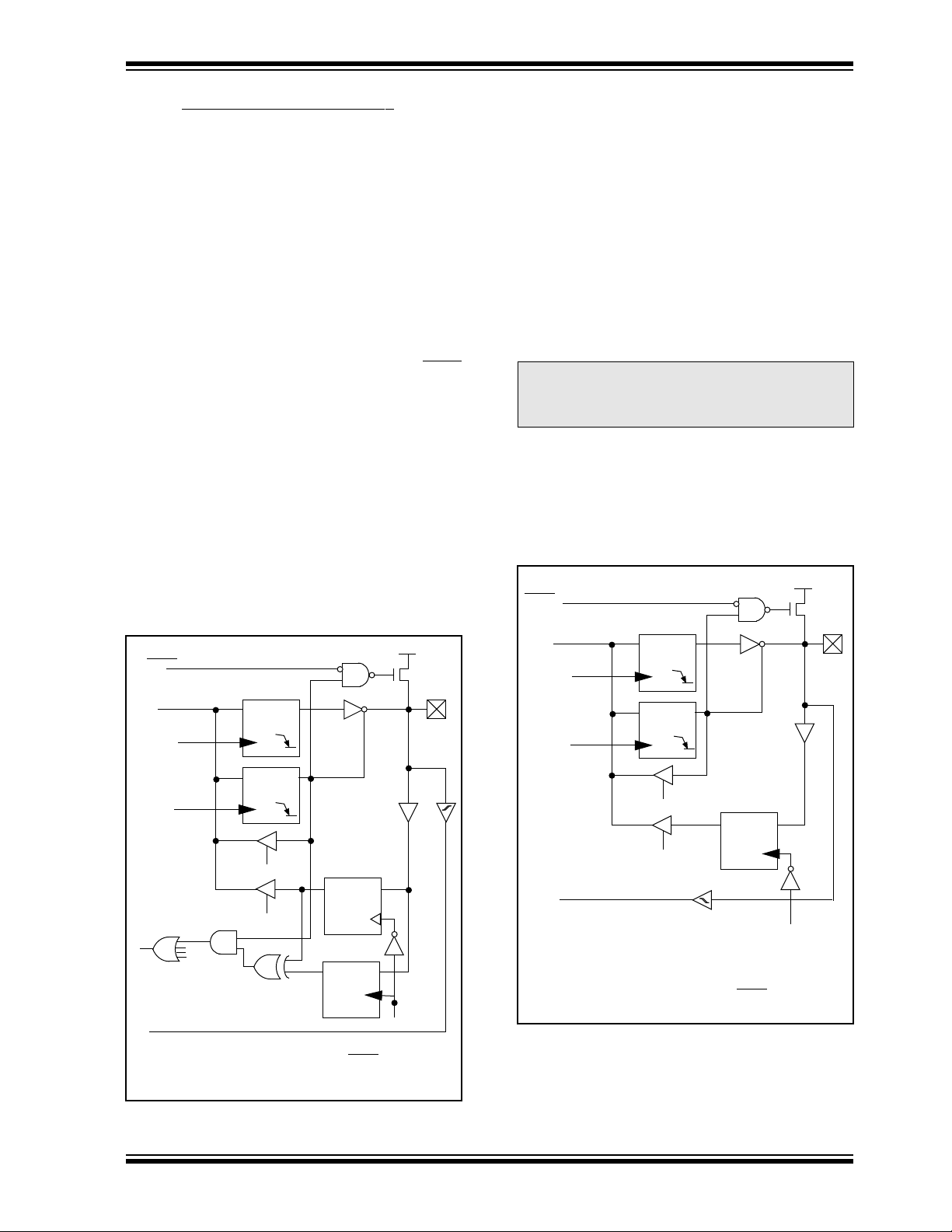
FIGURE 5-3: BLOCK DIAGRAM OF
RB7:RB4 PINS
DD
EN
TTL
Input
Buffer
V
P
weak
pull-up
I/O
pin
ST
Buffer
(1)
RBPU
Data bus
WR PortB
WR TRISB
Set RBIF
(2)
Data Latch
QD
CK
TRIS Latch
QD
CK
RD TRISB
RD PortB
Latch
Q D
This interrupt can wake the device from SLEEP. The
user, in the interrupt service routine, can clear the
interrupt in the following manner:
a) Any read or write of PORTB. This will end the
mismatch condition.
b) Clear flag bit RBIF.
A mismatch condition will continue to set flag bit RBIF.
Reading PORTB will end the mismatch condition, and
allow flag bit RBIF to be cleared.
This interrupt on mismatch feature, together with
software configurable pull-ups on these four pins allow
easy interface to a key pad and make it possible for
wake-up on key-depression. (See AN552 in the
Microchip
Note: If a change on the I/O pin should occur when the
Embedded Control Handbook
.)
read operation is being executed (start of the Q2
cycle), then the RBIF interrupt flag may not
get set.
The interrupt on change feature is recommended for
wake-up on key depression operation and operations
where PORTB is only used for the interrupt on change
feature. Polling of PORTB is not recommended while
using the interrupt on change feature.
FIGURE 5-4: BLOCK DIAGRAM OF
RB3:RB0 PINS
DD
TTL
Input
Buffer
V
weak
P
pull-up
RD Port
I/O
pin
(1)
RBPU
Data bus
WR PortB
WR TRISB
RB0/INT
(2)
Data Latch
QD
CK
QD
CK
RD TRISB
Q D
RD PortB
ST
Buffer
EN
From other
RB7:RB4 pins
RB7:RB6 in serial programming mode
Note 1: I/O pins have diode protection to VDD and VSS.
Note 2: TRISB = 1 enables weak pull-up if RBPU
(OPTION<7>).
Q D
EN
= '0'
RD Port
Note 1: I/O pins have diode protection to VDD and VSS.
Note 2: TRISB = 1 enables weak pull-up if RBPU
(OPTION<7>).
= '0'
1997 Microchip Technology Inc. Preliminary DS40143B-page 25
Page 26
PIC16C55X(A)
TABLE 5-3: PORTB FUNCTIONS
Name Bit # Buffer Type Function
(1)
RB0/INT bit0
TTL/ST
RB1 bit1 TTL Input/output pin. Internal software programmable weak pull-up.
RB2 bit2 TTL Input/output pin. Internal software programmable weak pull-up.
RB3 bit3 TTL Input/output pin. Internal software programmable weak pull-up.
RB4 bit4 TTL Input/output pin (with interrupt on change). Internal software
RB5 bit5 TTL Input/output pin (with interrupt on change). Internal software
RB6 bit6
RB7 bit7
TTL/ST
TTL/ST
Legend: ST = Schmitt Trigger, TTL = TTL input
Note 1: This buffer is a Schmitt Trigger input when configured as the external interrupt.
Note 2: This buffer is a Schmitt Trigger input when used in serial programming mode.
TABLE 5-4: SUMMARY OF REGISTERS ASSOCIATED WITH PORTB
Input/output or external interrupt input. Internal software programmable
weak pull-up.
programmable weak pull-up.
programmable weak pull-up.
(2)
Input/output pin (with interrupt on change). Internal software
programmable weak pull-up. Serial programming clock pin.
(2)
Input/output pin (with interrupt on change). Internal software
programmable weak pull-up. Serial programming data pin.
Address Name Bit 7 Bit 6 Bit 5 Bit 4 Bit 3 Bit 2 Bit 1 Bit 0
06h PORTB RB7 RB6 RB5 RB4 RB3 RB2 RB1 RB0
86h TRISB TRISB7 TRISB6 TRISB5 TRISB4 TRISB3 TRISB2 TRISB1 TRISB0
81h OPTION RBPU INTEDG T0CS T0SE PSA PS2 PS1 PS0
Note: Shaded bits are not used by PORTB.
Value on
POR
uuuu uuuu xxxx xxxx
1111 1111 1111 1111
1111 1111 1111 1111
Value on
All Other Rests
DS40143B-page 26 Preliminary 1997 Microchip Technology Inc.
Page 27
PIC16C55X(A)
5.3 I/O Programming Considerations
5.3.1 BI-DIRECTIONAL I/O PORTS Any instruction which writes, operates internally as a
read followed by a write operation. The BCF and BSF
instructions, for example, read the register into the
CPU, ex ecute the bit operation and write the result back
to the register. Caution must be used when these
instructions are applied to a port with both inputs and
outputs defined. For example, a BSF operation on bit5
of PORTB will cause all eight bits of PORTB to be read
into the CPU. Then the BSF operation takes place on
bit5 and PORTB is written to the output latches. If
another bit of PORTB is used as a bidirectional I/O pin
(e.g., bit0) and it is defined as an input at this time, the
input signal present on the pin itself would be read into
the CPU and re-written to the data latch of this
particular pin, overwriting the previous content. As long
as the pin stays in the input mode, no problem occurs.
However, if bit0 is switched into output mode later on,
the content of the data latch may now be unknown.
Reading the port register, reads the values of the port
pins. Writing to the port register writes the value to the
port latch. When using read modify write instructions
(ex. BCF, BSF , etc.) on a port, the value of the port pins
is read, the desired operation is done to this value, and
this value is then written to the port latch.
Example 5-1 shows the effect of two sequential
read-modify-write instructions (ex., BCF, BSF, etc.) on
an I/O port.
A pin actively outputting a Low or High should not be
driven from external devices at the same time in order
to change the level on this pin (“wired-or”, “wired-and”).
The resulting high output currents may damage
the chip.
EXAMPLE 5-1: READ-MODIFY-WRITE
INSTRUCTIONS ON AN
I/O PORT
;;Initial PORT settings: PORTB<7:4> Inputs
; PORTB<3:0> Outputs
;;PORTB<7:6> have external pull-up and are not
connected to other circuitry
;
; PORT latch PORT pins
; ---------- ----------
BCF PORTB, 7 ; 01pp pppp 11pp pppp
BCF PORTB, 6 ; 10pp pppp 11pp pppp
BSF STATUS,RP0 ;
BCF TRISB, 7 ; 10pp pppp 11pp pppp
BCF TRISB, 6 ; 10pp pppp 10pp pppp
;
; Note that the user may have expected the pin
; values to be 00pp pppp. The 2nd BCF caused
; RB7 to be latched as the pin value (High).
5.3.2 SUCCESSIVE OPERATIONS ON I/O PORTS The actual write to an I/O port happens at the end of an
instruction cycle, whereas for reading, the data must be
valid at the beginning of the instruction cycle
(Figure 5-5). Therefore, care must be exercised if a
write followed by a read operation is carried out on the
same I/O port. The sequence of instructions should be
such to allow the pin voltage to stabilize (load
dependent) before the next instruction which causes
that file to be read into the CPU is executed. Otherwise ,
the previous state of that pin may be read into the CPU
rather than the new state. When in doubt, it is better to
separate these instructions with an NOP or another
instruction not accessing this I/O port.
FIGURE 5-5: SUCCESSIVE I/O OPERATION
Q1 Q2 Q3 Q4 Q1 Q2 Q3 Q4 Q1 Q2 Q3 Q4 Q1 Q2 Q3 Q4
PC
Instruction
fetched
RB7:RB0
RB <7:0>
1997 Microchip Technology Inc. Preliminary DS40143B-page 27
PC
MOVWF PORTB
Write to
PORTB
PC + 1 PC + 2 PC + 3
Read PORTB
Port pin
TPD
Execute
MOVWF
PORTB
sampled here
Execute
MOVF
PORTB, W
NOPNOPMOVF PORTB, W
Execute
NOP
Note:
This example shows write to PORTB
followed by a read from PORTB.
Note that:
data setup time = (0.25 T
where TCY = instruction cycle and
TPD = propagation delay of Q1 cycle
to output valid.
Therefore, at higher clock frequencies,
a write followed by a read may be
problematic.
CY - TPD)
Page 28

PIC16C55X(A)
NOTES:
DS40143B-page 28 Preliminary 1997 Microchip Technology Inc.
Page 29
PIC16C55X(A)
6.0 TIMER0 MODULE
The Timer0 module timer/counter has the following
features:
• 8-bit timer/counter
• Readable and writable
• 8-bit software programmable prescaler
• Internal or external clock select
• Interrupt on overflow from FFh to 00h
• Edge select for external clock
Figure 6-1 is a simplified block diagram of the Timer0
module.
Timer mode is selected by clearing the T0CS bit
(OPTION<5>). In timer mode , the TMR0 will increment
every instruction cycle (without prescaler). If Timer0 is
written, the increment is inhibited for the following two
cycles (Figure 6-2 and Figure 6-3). The user can work
around this by writing an adjusted value to TMR0.
Counter mode is selected by setting the T0CS bit. In
this mode Timer0 will increment either on every rising
or falling edge of pin RA4/T0CKI. The incrementing
edge is determined by the source edge (T0SE) control
bit (OPTION<4>). Clearing the T0SE bit selects the
rising edge. Restrictions on the e xternal clock input are
discussed in detail in Section 6.2.
The prescaler is shared between the Timer0 module
and the WatchdogTimer. The prescaler assignment is
controlled in software by the control bit PSA
(OPTION<3>). Clearing the PSA bit will assign the
prescaler to Timer0. The prescaler is not readable or
writable. When the prescaler is assigned to the Timer0
module, prescale value of 1:2, 1:4, ..., 1:256 are
selectable. Section 6.3 details the operation of the
prescaler.
6.1 TIMER0 Interrupt
Timer0 interrupt is generated when the TMR0 register
timer/counter overflows from FFh to 00h. This overflow
sets the T0IF bit. The interrupt can be masked by
clearing the T0IE bit (INTCON<5>). The T0IF bit
(INTCON<2>) must be cleared in software by the
Timer0 module interrupt service routine before
re-enabling this interrupt. The Timer0 interrupt cannot
wake the processor from SLEEP since the timer is shut
off during SLEEP. See Figure 6-4 for Timer0 interrupt
timing.
FIGURE 6-1: TIMER0 BLOCK DIAGRAM
RA4/T0CKI
pin
Note 1: Bits, T0SE, T0CS, PS2, PS1, PS0 and PSA are located in the OPTION register.
2: The prescaler is shared with Watchdog Timer (Figure 6-6)
FOSC/4
T0SE
0
1
T0CS
Programmable
Prescaler
PS2:PS0
1
0
PSA
PSout
Sync with
Internal
clocks
(2 cycle delay)
PSout
FIGURE 6-2: TIMER0 (TMR0) TIMING: INTERNAL CLOCK/NO PRESCALER
PC
(Program
Counter)
Instruction
Fetch
TMR0
Instruction
Executed
Q1 Q2 Q3 Q4
PC-1
T0
Q1 Q2 Q3 Q4 Q1 Q2 Q3 Q4 Q1 Q2 Q3 Q4 Q1 Q2 Q3 Q4 Q1 Q2 Q3 Q4 Q1 Q2 Q3 Q4 Q1 Q2 Q3 Q4
PC PC+1 PC+2 PC+3 PC+4 PC+5 PC+6
MOVWF TMR0
T0+1 T0+2 NT0 NT0 NT0 NT0+1 NT0+2
MOVF TMR0,W MOVF TMR0,W MOVF TMR0,W MOVF TMR0,W MOVF TMR0,W
Write TMR0
executed
Read TMR0
reads NT0
Read TMR0
reads NT0
Read TMR0
reads NT0
Read TMR0
reads NT0 + 1
Data bus
TMR0
8
Set Flag bit T0IF
on Overflow
Read TMR0
reads NT0 + 2
T0
1997 Microchip Technology Inc. Preliminary DS40143B-page 29
Page 30

PIC16C55X(A)
FIGURE 6-3: TIMER0 TIMING: INTERNAL CLOCK/PRESCALE 1:2
PC
(Program
Counter)
Instruction
Fetch
TMR0
Instruction
Execute
Q1 Q2 Q3 Q4
PC-1
T0 NT0+1
Q1 Q2 Q3 Q4 Q1 Q2 Q3 Q4 Q1 Q2 Q3 Q4 Q1 Q2 Q3 Q4 Q1 Q2 Q3 Q4 Q1 Q2 Q3 Q4 Q1 Q2 Q3 Q4
PC PC+1 PC+2 PC+3 PC+4 PC+5 PC+6
MOVWF TMR0
MOVF TMR0,W MOVF TMR0,W MOVF TMR0,W MOVF TMR0,W MOVF TMR0,W
T0+1
Write TMR0
executed
Read TMR0
reads NT0
FIGURE 6-4: TIMER0 INTERRUPT TIMING
Q2Q1 Q3 Q4Q2Q1 Q3 Q4 Q2Q1 Q3 Q4 Q2Q1 Q3 Q4 Q2Q1 Q3 Q4
OSC1
CLKOUT(3)
TMR0 timer
T0IF bit
(INTCON<2>)
GIE bit
(INTCON<7>)
UCTION FLOW
INSTR
PC
Instruction
fetched
FEh
1
PC
Inst (PC)
FFh 00h 01h 02h
1
PC +1 PC +1 0004h 0005h
Inst (PC+1)
NT0
Read TMR0
reads NT0
Read TMR0
reads NT0
Interrupt Latency Time
Read TMR0
reads NT0
Read TMR0
reads NT0 + 1
Inst (0004h) Inst (0005h)
Instruction
executed
Inst (PC-1)
Inst (PC)
Note 1: T0IF interrupt flag is sampled here (every Q1).
2: Interrupt latency = 4Tcy, where Tcy = instruction cycle time.
3: CLKOUT is available only in RC oscillator mode.
Inst (0004h)Dummy cycle Dummy cycle
DS40143B-page 30 Preliminary 1997 Microchip Technology Inc.
Page 31

PIC16C55X(A)
6.2 Using Timer0 with External Clock
When a prescaler is used, the external clock input is
divided by the asynchronous ripple-counter type
When an external clock input is used for Timer0, it must
meet certain requirements. The external clock
requirement is due to internal phase clock (T
OSC)
synchronization. Also, there is a delay in the actual
incrementing of Timer0 after synchronization.
6.2.1 EXTERNAL CLOCK SYNCHRONIZATION When no prescaler is used, the external clock input is
the same as the prescaler output. The synchronization
of T0CKI with the internal phase clocks is
accomplished by sampling the prescaler output on the
Q2 and Q4 cycles of the internal phase clocks
(Figure 6-5). Therefore, it is necessary for T0CKI to be
high for at least 2T
and low for at least 2T
OSC (and a small RC delay of 20 ns)
OSC (and a small RC delay of
20 ns). Refer to the electrical specification of the
desired device.
prescaler so that the prescaler output is symmetrical.
For the external clock to meet the sampling
requirement, the ripple-counter must be taken into
account. Therefore, it is necessary for T0CKI to have a
period of at least 4T
40 ns) divided by the prescaler value. The only
requirement on T0CKI high and low time is that the y do
not violate the minimum pulse width requirement of
10 ns. Refer to parameters 40, 41 and 42 in the
electrical specification of the desired device.
6.2.2 TIMER0 INCREMENT DELAY Since the prescaler output is synchronized with the
internal clocks, there is a small delay from the time the
external clock edge occurs to the time the TMR0 is
actually incremented. Figure 6-5 shows the delay from
the external clock edge to the timer incrementing.
FIGURE 6-5: TIMER0 TIMING WITH EXTERNAL CLOCK
Q1 Q2 Q3 Q4 Q1 Q2 Q3 Q4 Q1 Q2 Q3 Q4 Q1 Q2 Q3 Q4
External Clock Input or
Prescaler output
External Clock/Prescaler
Output after sampling
Increment Timer0 (Q4)
(2)
(1)
(3)
OSC (and a small RC delay of
Small pulse
misses sampling
Timer0
Note 1: Delay from clock input change to Timer0 increment is 3Tosc to 7Tosc. (Duration of Q = Tosc).
Therefore, the error in measuring the interval between two edges on Timer0 input = ±4Tosc max.
2: External clock if no prescaler selected, Prescaler output otherwise.
3: The arrows indicate the points in time where sampling occurs.
T0 T0 + 1 T0 + 2
1997 Microchip Technology Inc. Preliminary DS40143B-page 31
Page 32

PIC16C55X(A)
6.3 Prescaler
The PSA and PS2:PS0 bits (OPTION<3:0>) determine
the prescaler assignment and prescale ratio.
An 8-bit counter is available as a prescaler for the
Timer0 module, or as a postscaler for the Watchdog
Timer, respectively (Figure 6-6). For simplicity, this
counter is being referred to as “prescaler” throughout
this data sheet. Note that there is only one prescaler
available which is mutually exclusive between the
Timer0 module and the Watchdog Timer. Thus, a
When assigned to the Timer0 module, all instructions
writing to the TMR0 register (e.g., CLRF 1, MOVWF 1,
BSF 1,x....etc.) will clear the prescaler. When
assigned to WDT, a CLRWDT instruction will clear the
prescaler along with the Watchdog Timer. The
prescaler is not readable or writable.
prescaler assignment for the Timer0 module means
that there is no prescaler for the Watchdog Timer, and
vice-versa.
FIGURE 6-6: BLOCK DIAGRAM OF THE TIMER0/WDT PRESCALER
CLKOUT (=Fosc/4)
T0CKI
pin
T0SE
0
1
T0CS
M
U
X
1
M
U
0
X
PSA
SYNC
2
Cycles
Data Bus
8
TMR0 reg
Set flag bit T0IF
on Overflow
0
M
U
1
Watchdog
Timer
WDT Enable bit
Note: T0SE, T0CS, PSA, PS0-PS2 are bits in the OPTION register.
X
PSA
8-bit Prescaler
8
8-to-1MUX
0
M U X
WDT
Time-out
1
PS0 - PS2
PSA
DS40143B-page 32 Preliminary 1997 Microchip Technology Inc.
Page 33

PIC16C55X(A)
6.3.1 SWITCHING PRESCALER ASSIGNMENT The prescaler assignment is fully under software
control (i.e., it can be changed “on the fly” during
program execution). To avoid an unintended device
RESET, the following instruction sequence
(Example 6-1) must be executed when changing the
prescaler assignment from Timer0 to WDT. Lines 5-7
are required only if the desired postscaler rate is 1:1
(PS<2:0> = 000) or 1:2 (PS<2:0> = 001).
EXAMPLE 6-1: CHANGING PRESCALER
(TIMER0→WDT)
1.BCF STATUS, RP0 ;Skip if already in
; Bank 0
2.CLRWDT ;Clear WDT
3.CLRF TMR0 ;Clear TMR0 & Prescaler
4.BSF STATUS, RP0 ;Bank 1
5.MOVLW '00101111’b; ;These 3 lines (5, 6, 7)
6.MOVWF OPTION ; are required only if
; desired PS<2:0> are
7.CLRWDT ; 000 or 001
8.MOVLW '00101xxx’b ;Set Postscaler to
9.MOVWF OPTION ; desired WDT rate
10.BCF STATUS, RP0 ;Return to Bank 0
To change prescaler from the WDT to the TMR0
module use the sequence shown in Example 6-2. This
precaution must be taken even if the WDT is disabled.
EXAMPLE 6-2: CHANGING PRESCALER
(WDT→TIMER0)
CLRWDT ;Clear WDT and
;prescaler
BSF STATUS, RP0
MOVLW b'xxxx0xxx' ;Select TMR0, new
;prescale value and
;clock source
MOVWF OPTION
BCF STATUS, RP0
TABLE 6-1: REGISTERS ASSOCIATED WITH TIMER0
Address Name Bit 7 Bit 6 Bit 5 Bit 4 Bit 3 Bit 2 Bit 1 Bit 0
01h TMR0 Timer0 module’s register uuuu uuuu xxxx xxxx
0Bh/8Bh INTCON GIE
81h OPTION
85h TRISA
RBPU INTEDG T0CS T0SE PSA PS2 PS1 PS0 1111 1111 1111 1111
— — — TRISA4 TRISA3 TRISA2 TRISA1 TRISA0 ---1 1111 ---1 1111
+ T0IE INTE RBIE T0IF INTF RBIF 0000 000x 0000 000x
Value on
POR
Legend: — = Unimplemented locations, read as ‘0’.
+ = Reserved for future use.
Note: Shaded bits are not used by TMR0 module.
Value on
All Other Resets
1997 Microchip Technology Inc. Preliminary DS40143B-page 33
Page 34

PIC16C55X(A)
NOTES:
DS40143B-page 34 Preliminary 1997 Microchip Technology Inc.
Page 35

PIC16C55X(A)
7.0 SPECIAL FEATURES OF THE
CPU
What sets a microcontroller apart from other
processors are special circuits to deal with the needs of
real time applications. The PIC16C55X(A) family has a
host of such features intended to maximize system
reliability, minimize cost through elimination of external
components, provide power saving operating modes
and offer code protection.
These are:
1. OSC selection
2. Reset
Power-on Reset (POR)
Power-up Timer (PWRT)
Oscillator Start-Up Timer (OST)
3. Interrupts
4. Watchdog Timer (WDT)
5. SLEEP
6. Code protection
7. ID Locations
8. In-circuit serial programming™
The PIC16C55X(A) has a Watchdog Timer which is
controlled by configuration bits. It runs off its own RC
oscillator for added reliability. There are two timers that
offer necessary delays on power-up. One is the
Oscillator Start-up Timer (OST), intended to keep the
chip in reset until the crystal oscillator is stable. The
other is the Pow er-up Timer (PWRT), which pro vides a
fixed delay of 72 ms (nominal) on power-up only,
designed to keep the part in reset while the power
supply stabilizes. With these two functions on-chip,
most applications need no external reset circuitry.
The SLEEP mode is designed to offer a very low
current power-down mode. The user can wake-up from
SLEEP through external reset, Watchdog Timer
wake-up or through an interrupt. Several oscillator
options are also made available to allow the part to fit
the application. The RC oscillator option saves system
cost while the LP crystal option saves power. A set of
configuration bits are used to select various options.
1997 Microchip Technology Inc. Preliminary DS40143B-page 35
Page 36

PIC16C55X(A)
7.1 Configuration Bits
The user will note that address 2007h is beyond
the user program memory space. In fact, it belongs
The configuration bits can be programmed (read as '0')
or left unprogrammed (read as '1') to select various
device configurations. These bits are mapped in
to the special test/configuration memory space
(2000h – 3FFFh), which can be accessed only during
programming.
program memory location 2007h.
FIGURE 7-1: CONFIGURATION WORD
CP1
bit13 bit0
bit 13-8 CP<1:0>: Code protection bits
5-4: 11 = Code protection off
bit 7: Unimplemented: Read as '1'
bit 6: Reserved: Do not use
bit 3: PWRTE: Power-up Timer Enable bit
bit 2: WDTE: Watchdog Timer Enable bit
bit 1-0: FOSC1:FOSC0: Oscillator Selection bits
1
CP1
CP0
10 = Upper half of program memory code protected
01 = Upper 3/4th of program memory code protected
00 = All memory is code protected
1 = PWRT disabled
0 = PWRT enabled
1 = WDT enabled
0 = WDT disabled
11 = RC oscillator
10 = HS oscillator
01 = XT oscillator
00 = LP oscillator
CP0
1
CP1
CP0
1
(1)
— Reserved CP1
1
PWRTE WDTE F0SC1 F0SC0
CP0
CONFIG Address
REGISTER: 2007h
Note 1: All of the CP1:CP0 pairs have to be given the same value to enable the code protection scheme listed.
DS40143B-page 36 Preliminary 1997 Microchip Technology Inc.
Page 37
PIC16C55X(A)
7.2 Oscillator Configurations
7.2.1 OSCILLATOR TYPES
The PIC16C55X(A) can be operated in four different
oscillator options. The user can program two
configuration bits (FOSC1 and FOSC0) to select one of
these four modes:
• LP Low Power Crystal
• XT Crystal/Resonator
• HS High Speed Crystal/Resonator
• RC Resistor/Capacitor
7.2.2 CRYSTAL OSCILLATOR / CERAMIC
RESONATORS
In XT, LP or HS modes a crystal or ceramic resonator
is connected to the OSC1 and OSC2 pins to establish
oscillation (Figure 7-2). The PIC16C55X(A) oscillator
design requires the use of a parallel cut crystal. Use of
a series cut crystal may give a frequency out of the
crystal manufacturers specifications. When in XT, LP or
HS modes, the device can have an external clock
source to drive the OSC1 pin (Figure 7-3).
FIGURE 7-2: CRYSTAL OPERATION
(OR CERAMIC RESONATOR)
(HS, XT OR LP OSC
CONFIGURATION)
OSC1
C1
XTAL
OSC2
RS
see Note
C2
RF
To internal logic
SLEEP
PIC16C55X(A)
See Table 7-1 and Table 7-2 for recommended
values of C1 and C2.
Note: A series resistor may be required for
AT strip cut crystals.
FIGURE 7-3: EXTERNAL CLOCK INPUT
OPERATION (HS, XT OR LP
OSC CONFIGURATION)
Clock from
ext. system
Open
OSC1
PIC16C55X(A)
OSC2
TABLE 7-1: CAPACITOR SELECTION
FOR CERAMIC RESONATORS
(PRELIMINARY)
Ranges Characterized:
Mode Freq OSC1(C1) OSC2(C2)
XT 455 kHz
2.0 MHz
4.0 MHz
HS 8.0 MHz
16.0 MHz
Higher capacitance increases the stability of the oscillator
but also increases the start-up time. These values are for
design guidance only. Since each resonator has its own
characteristics, the user should consult the resonator manufacturer for appropriate values of external components.
Resonators to be Characterized:
455 kHz Panasonic EFO-A455K04B ±0.3%
2.0 MHz Murata Erie CSA2.00MG ±0.5%
4.0 MHz Murata Erie CSA4.00MG ±0.5%
8.0 MHz Murata Erie CSA8.00MT ±0.5%
16.0 MHz Murata Erie CSA16.00MX ±0.5%
All resonators used did not have built-in capacitors.
22 - 100 pF
15 - 68 pF
15 - 68 pF
10 - 68 pF
10 - 22 pF
22 - 100 pF
15 - 68 pF
15 - 68 pF
10 - 68 pF
10 - 22 pF
T ABLE 7-2: CAPACITOR SELECTION
FOR CRYSTAL OSCILLATOR
(PRELIMINARY)
Mode Freq OSC1(C1) OSC2(C2)
LP
XT
HS
Higher capacitance increases the stability of the oscillator
but also increases the start-up time. These values are for
design guidance only. Rs may be required in HS mode as
well as XT mode to avoid overdriving crystals with low drive
level specification. Since each crystal has its own
characteristics, the user should consult the crystal manufacturer for appropriate values of external components.
Crystals to be Characterized:
32.768 kHz Epson C-001R32.768K-A ± 20 PPM
100 kHz Epson C-2 100.00 KC-P ± 20 PPM
200 kHz STD XTL 200.000 kHz ± 20 PPM
2.0 MHz ECS ECS-20-S-2 ± 50 PPM
4.0 MHz ECS ECS-40-S-4 ± 50 PPM
10.0 MHz ECS ECS-100-S-4 ± 50 PPM
20.0 MHz ECS ECS-200-S-4 ± 50 PPM
32 kHz
200 kHz
100 kHz
2 MHz
4 MHz
8 MHz
10 MHz
20 MHz
68 - 100 pF
15 - 30 pF
68 - 150 pF
15 - 30 pF
15 - 30 pF
15 - 30 pF
15 - 30 pF
15 - 30 pF
68 - 100 pF
15 - 30 pF
150 - 200 pF
15 - 30 pF
15 - 30 pF
15 - 30 pF
15 - 30 pF
15 - 30 pF
1997 Microchip Technology Inc. Preliminary DS40143B-page 37
Page 38
PIC16C55X(A)
)
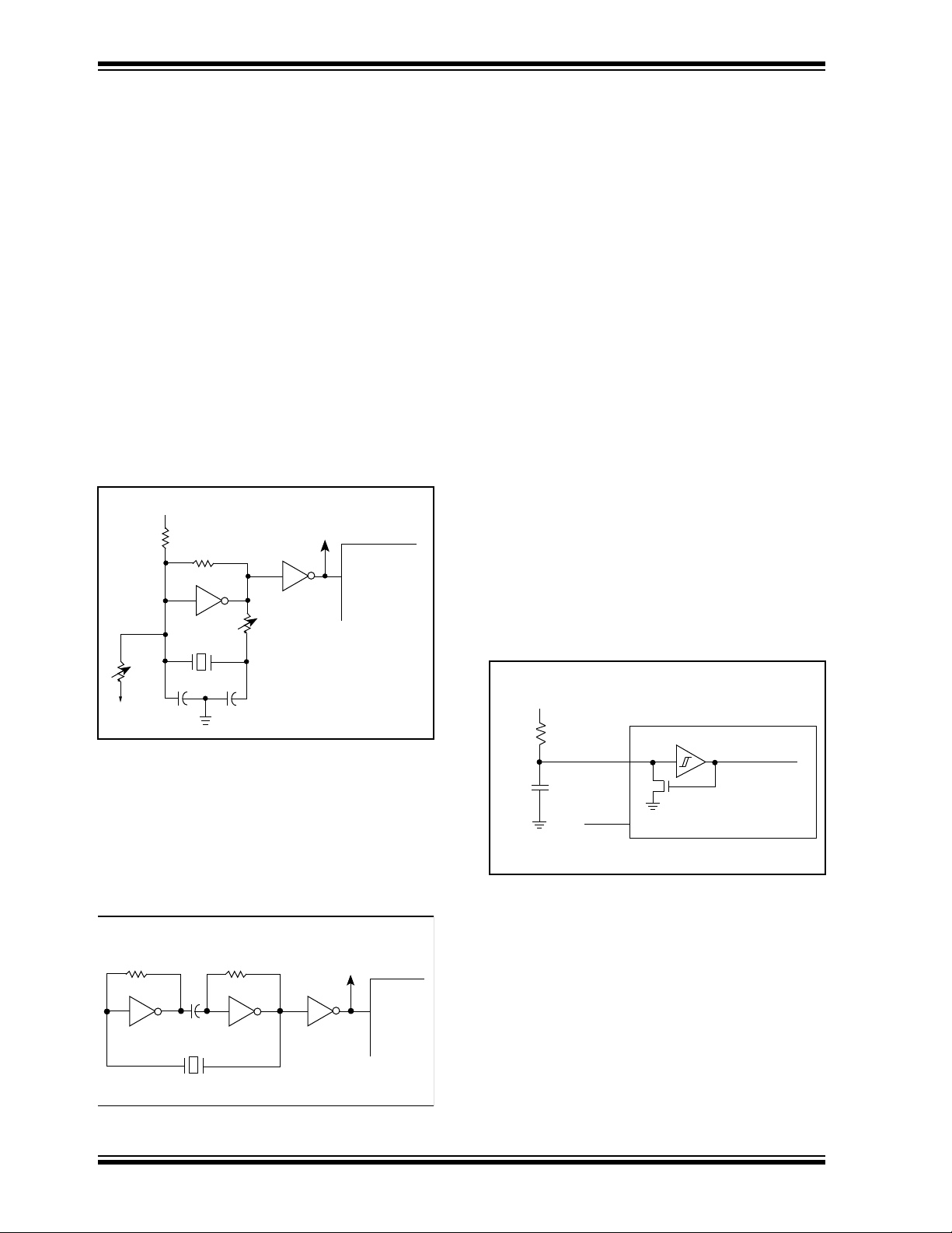
7.2.3 EXTERNAL CRYSTAL OSCILLATOR
CIRCUIT
Either a pre-packaged oscillator can be used or a simple oscillator circuit with TTL gates can be built.
Prepackaged oscillators provide a wide operating
range and better stability. A well-designed crystal
oscillator will provide good performance with TTL
gates. Two types of crystal oscillator circuits can be
used; one with series resonance, or one with parallel
resonance.
Figure 7-4 shows implementation of a parallel resonant
oscillator circuit. The circuit is designed to use the
fundamental frequency of the crystal. The 74AS04
inverter performs the 180° phase shift that a parallel
oscillator requires. The 4.7 kΩ resistor provides the
negative feedback for stability. The 10 kΩ
potentiometers bias the 74AS04 in the linear region.
This could be used for external oscillator designs.
FIGURE 7-4: EXTERNAL PARALLEL
RESONANT CRYSTAL
OSCILLATOR CIRCUIT
+5V
10k
4.7k
74AS04
10k
XTAL
10k
20 pF
20 pF
Figure 7-5 shows a series resonant oscillator circuit.
This circuit is also designed to use the fundamental
frequency of the crystal. The inverter performs a 180°
phase shift in a series resonant oscillator circuit. The
330 Ω resistors provide the negative feedback to bias
the inverters in their linear region.
74AS04
To other
Devices
PIC16C55X(A)
CLK
IN
7.2.4 RC OSCILLATOR For timing insensitive applications the “RC” device
option offers additional cost savings. The RC oscillator
frequency is a function of the supply voltage, the
resistor (Rext) and capacitor (Cext) values, and the
operating temperature. In addition to this, the oscillator
frequency will vary from unit to unit due to normal
process parameter variation. Furthermore, the
difference in lead frame capacitance between package
types will also affect the oscillation frequency,
especially for low Cext values. The user also needs to
take into account variation due to tolerance of external
R and C components used. Figure 7-6 shows how the
R/C combination is connected to the PIC16C55X. For
Rext values below 2.2 kΩ, the oscillator operation may
become unstable, or stop completely. For very high
Rext values (e.g., 1 MΩ), the oscillator becomes
sensitive to noise, humidity and leakage. Thus, we
recommend to keep Rext between 3 kΩ and 100 kΩ.
Although the oscillator will operate with no external
capacitor (Cext = 0 pF), we recommend using values
above 20 pF for noise and stability reasons. With no or
small external capacitance, the oscillation frequency
can vary dramatically due to changes in external
capacitances, such as PCB trace capacitance or
package lead frame capacitance.
The oscillator frequency, divided by 4, is available on
the OSC2/CLKOUT pin, and can be used for test
purposes or to synchronize other logic (Figure 3-2 for
waveform).
FIGURE 7-6: RC OSCILLATOR MODE
VDD
PIC16C55X(A)
Rext
OSC1
Internal Clock
Cext
V
DD
Fosc/4
OSC2/CLKOUT
FIGURE 7-5: EXTERNAL SERIES
RESONANT CRYSTAL
OSCILLATOR CIRCUIT
To other
74AS04
Devices
PIC16C55X(A
CLKIN
330 Ω
74AS04
DS40143B-page 38 Preliminary 1997 Microchip Technology Inc.
330 Ω
74AS04
0.1 µF
XTAL
Page 39

PIC16C55X(A)
7.3 Reset
on MCLR
reset during SLEEP. They are not aff ected b y
a WDT w ake-up , since this is vie wed as the resumption
The PIC16C55X(A) differentiates between various
kinds of reset:
a) Power-on reset (POR)
b) MCLR
c) MCLR
reset during normal operation
reset during SLEEP
d) WDT reset (normal operation)
e) WDT wake-up (SLEEP)
Some registers are not affected in any reset condition;
their status is unknown on POR and unchanged in any
other reset. Most other registers are reset to a “reset
state” on Power-on reset, on MCLR
or WDT reset and
of normal operation. T
O and PD bits are set or cleared
differently in different reset situations as indicated in
Table 7-4. These bits are used in software to determine
the nature of the reset. See Table 7-6 for a full description of reset states of all registers.
A simplified block diagram of the on-chip reset circuit is
shown in Figure 7-7.
The MCLR
reset path has a noise filter to detect and
ignore small pulses. See Table 10-4 for pulse width
specification.
FIGURE 7-7: SIMPLIFIED BLOCK DIAGRAM OF ON-CHIP RESET CIRCUIT
External
Reset
MCLR/
VPP Pin
V
DD
WDT
Module
V
DD rise
detect
SLEEP
WDT
Time-out
Reset
Power-on Reset
OST/PWRT
OST
10-bit Ripple-counter
OSC1/
CLKIN
Pin
On-chip
RC OSC
Note 1: This is a separate oscillator from the RC oscillator of the CLKIN pin.
PWRT
(1)
10-bit Ripple-counter
Enable PWRT
Enable OST
S
R
Q
See Table 7-3 for time-out situations.
Chip_Reset
1997 Microchip Technology Inc. Preliminary DS40143B-page 39
Page 40

PIC16C55X(A)
7.4 Power-on Reset (POR), Power-up
Timer (PWRT), Oscillator Start-up
Timer (OST)
7.4.1 POWER-ON RESET (POR)
A Power-on Reset pulse is generated on-chip when
V
DD rise is detected (in the range of 1.6 V – 1.8 V). To
take advantage of the POR, just tie the MCLR
directly (or through a resistor) to V
external RC components usually needed to create
Power-on Reset. A maximum rise time for V
required. See Electrical Specifications for details.
The POR circuit does not produce internal reset when
V
DD declines.
When the device starts normal operation (exits the
reset condition), device operating parameters (v oltage ,
frequency, temperature, etc.) must be met to ensure
operation. If these conditions are not met, the device
must be held in reset until the operating conditions are
met.
For additional information, refer to Application Note
AN607 “Power-up Trouble Shooting”.
7.4.2 POWER-UP TIMER (PWRT)
The Power-up Timer provides a fixed 72 ms (nominal)
time-out on power-up only, from POR. The Power-up
Timer operates on an internal RC oscillator. The chip is
kept in reset as long as PWRT is active. The PWRT
delay allows the V
configuration bit, PW
(if cleared or programmed) the Power-up Timer. The
Power-Up Time delay will vary from chip to chip and
due to V
DC parameters for details.
DD, temperature and process variation. See
DD to rise to an acceptable level. A
RTE can disable (if set) or enable
DD. This will eliminate
pin
DD is
7.4.3 OSCILLATOR START-UP TIMER (OST) The Oscillator Start-Up Timer (OST) provides a 1024
oscillator cycle (from OSC1 input) delay after the
PWRT delay is over. This ensures that the crystal
oscillator or resonator has started and stabilized.
The OST time-out is invoked only for XT, LP and HS
modes and only on power-on reset or wake-up from
SLEEP.
7.4.4 TIME-OUT SEQUENCE On power-up, the time-out sequence is as f ollows: First
PWRT time-out is inv ok ed after POR has expired, then
OST is activated. The total time-out will vary based on
oscillator configuration and P
example, in RC mode with PW
disabled), there will be no time-out at all. Figure 7-8,
Figure 7-9 and Figure 7-10 depict time-out sequences.
Since the time-outs occur from the POR pulse, if MCLR
is kept low long enough, the time-outs will expire . Then
bringing MCLR
(see Figure 7-9). This is useful for testing purposes or
to synchronize more than one PIC16C55X device operating in parallel.
Table 7-5 shows the reset conditions for some special
registers, while T ab le 7-6 shows the reset conditions for
all the registers.
high will begin execution immediately
WRTE bit status. For
RTE bit erased (PWRT
DS40143B-page 40 Preliminary 1997 Microchip Technology Inc.
Page 41

7.4.5 POWER CONTROL/STATUS REGISTER
(PCON)
PIC16C55X(A)
Bit1 is POR
power-on-reset and unaffected otherwise. The user
must write a ‘1’ to this bit following a power-on-reset.
On a subsequent reset if POR
a power-on-reset must have occurred (V
gone too low).
(Power-on-reset). It is a ‘0’ on
is ‘0’, it will indicate that
DD may have
TABLE 7-3: TIME-OUT IN VARIOUS SITUATIONS
Oscillator Configuration
XT, HS, LP 72 ms + 1024 TOSC 1024 TOSC 1024 TOSC
RC 72 ms — —
PWR
TE = 0 PWRTE = 1
Power-up
TABLE 7-4: STATUS BITS AND THEIR SIGNIFICANCE
POR
0 1 1
0 0 X
0 X 0
1 0 1
1 0 0
1 1 1
1 1 0
TO PD
Power-on-reset
Illegal, TO is set on POR
Illegal, PD is set on POR
WDT Reset
WDT Wake-up
MCLR reset during normal operation
MCLR reset during SLEEP
Wake-up from
SLEEP
1997 Microchip Technology Inc. Preliminary DS40143B-page 41
Page 42

PIC16C55X(A)
TABLE 7-5: INITIALIZATION CONDITION FOR SPECIAL REGISTERS
Program
Condition
Power-on Reset 000h
MCLR reset during normal operation 000h
MCLR reset during SLEEP 000h
WDT reset 000h
WDT Wake-up PC + 1
Interrupt Wake-up from SLEEP PC + 1
Legend: u = unchanged, x = unknown, - = unimplemented bit, reads as ‘0’.
Note 1: When the wake-up is due to an interrupt and global enable bit, GIE is set, the PC is loaded with the interrupt vector
(0004h) after execution of PC+1.
Counter
(1)
STATUS
Register
PCON
Register
0001 1xxx ---- --00001 1uuu ---- --u0001 0uuu ---- --u0000 1uuu ---- --uuuu0 0uuu ---- --uuuu1 0uuu ---- --u-
TABLE 7-6: INITIALIZATION CONDITION FOR REGISTERS
• MCLR Reset during
normal operation
• MCLR Reset during
SLEEP
Register Address Power-on Reset
W INDF 00h
TMR0 01h
PCL 02h
STATUS 03h
FSR 04h
PORTA 05h
PORTB 06h
PCLATH 0Ah
INTCON 0Bh
OPTION 81h
TRISA 85h
TRISB 86h
PCON 8Eh
Legend: u = unchanged, x = unknown, - = unimplemented bit, reads as ‘0’,q = value depends on condition.
Note 1: One or more bits in INTCON will be affected (to cause wake-up).
2: When the wake-up is due to an interrupt and the GIE bit is set, the PC is loaded with the interrupt
vector (0004h).
3: See Table 7-5 for reset value for specific condition.
xxxx xxxx uuuu uuuu uuuu uuuu
- - xxxx xxxx uuuu uuuu uuuu uuuu
0000 0000 0000 0000
0001 1xxx
xxxx xxxx uuuu uuuu uuuu uuuu
---x xxxx ---u uuuu ---u uuuu
xxxx xxxx uuuu uuuu uuuu uuuu
---0 0000 ---0 0000 ---u uuuu
0000 000x 0000 000x
1111 1111 1111 1111 uuuu uuuu
---1 1111 ---1 1111 ---u uuuu
1111 1111 1111 1111 uuuu uuuu
---- --0-
• WDT Reset
000q quuu
---- --u-
(3)
• Wake up from SLEEP
through interrupt
• Wake up from SLEEP
through WDT time-out
PC + 1
(2)
uuuq quuu
uuuu uuuu
---- --u-
(3)
(1)
DS40143B-page 42 Preliminary 1997 Microchip Technology Inc.
Page 43

PIC16C55X(A)
FIGURE 7-8: TIME-OUT SEQUENCE ON POWER-UP (MCLR NOT TIED TO VDD): CASE 1
VDD
MCLR
INTERNAL POR
TPWRT
PWR
T TIME-OUT
OST TIME-OUT
INTERNAL RESET
FIGURE 7-9: TIME-OUT SEQUENCE ON POWER-UP (MCLR NOT TIED TO VDD): CASE 2
VDD
TOST
MCLR
INTERNAL POR
TPWRT
T TIME-OUT
PWR
OST TIME-OUT
INTERNAL RESET
FIGURE 7-10: TIME-OUT SEQUENCE ON POWER-UP (MCLR
VDD
MCLR
INTERNAL POR
TPWRT
PWR
T TIME-OUT
TOST
TOST
TIED TO VDD): CASE 3
OST TIME-OUT
INTERNAL RESET
1997 Microchip Technology Inc. Preliminary DS40143B-page 43
Page 44

PIC16C55X(A)
FIGURE 7-11: EXTERNAL POWER-ON
RESET CIRCUIT (FOR SLOW
VDD POWER-UP)
V
VDD
DD
D
Note 1: External power-on reset circuit is required
2: < 40 kΩ is recommended to make sure
3: R1 = 100Ω to 1 kΩ will limit any current
R
R1
MCLR
C
only if V
The diode D helps discharge the capacitor quickly when V
that voltage drop across R does not violate the device’s electrical specification.
flowing into MCLR
tor C in the event of MCLR
down due to Electrostatic Discharge
(ESD) or Electrical Overstress (EOS).
DD power-up slope is too slow.
PIC16C55X(A)
DD powers down.
from external capaci-
/VPP pin break-
DS40143B-page 44 Preliminary 1997 Microchip Technology Inc.
Page 45

PIC16C55X(A)
7.5 Interrupts
The PIC16C55X(A) has 3 sources of interrupt:
• External interrupt RB0/INT
• TMR0 overflow interrupt
• PortB change interrupts (pins RB7:RB4)
The interrupt control register (INTCON) records
individual interrupt requests in flag bits. It also has
individual and global interrupt enable bits.
A global interrupt enable bit, GIE (INTCON<7>)
enables (if set) all un-masked interrupts or disables (if
cleared) all interrupts. Individual interrupts can be
disabled through their corresponding enable bits in
INTCON register. GIE is cleared on reset.
The “return from interrupt” instruction,
the interrupt routine as well as sets the GIE bit, which
re-enables RB0/INT interrupts.
The INT pin interrupt, the RB port change interrupt and
the TMR0 overflow interrupt flags are contained in the
INTCON register.
When an interrupt is responded to, the GIE is cleared
to disable any further interrupt, the return address is
pushed into the stack and the PC is loaded with 0004h.
Once in the interrupt service routine the source(s) of
the interrupt can be determined by polling the interrupt
flag bits. The interrupt flag bit(s) must be cleared in software before re-enabling interrupts to avoid RB0/INT
recursive interrupts.
RETFIE, exits
For external interrupt events, such as the INT pin or
PORTB change interrupt, the interrupt latency will be
three or four instruction cycles. The exact latency
depends when the interrupt event occurs (Figure 7-13).
The latency is the same for one or two cycle
instructions. Once in the interrupt service routine the
source(s) of the interrupt can be determined by polling
the interrupt flag bits. The interrupt flag bit(s) must be
cleared in software before re-enabling interrupts to
avoid multiple interrupt requests. Individual interrupt
flag bits are set regardless of the status of their
corresponding mask bit or the GIE bit.
Note 1: Individual interrupt flag bits are set
regardless of the status of their
corresponding mask bit or the GIE bit.
2: When an instruction that clears the GIE
bit is executed, any interrupts that were
pending for execution in the next cycle
are ignored. The CPU will execute a
NOP in the cycle immediately following
the instruction which clears the GIE bit.
The interrupts which were ignored are
still pending to be serviced when the GIE
bit is set again.
FIGURE 7-12: INTERRUPT LOGIC
T0IF
T0IE
INTF
INTE
RBIF
RBIE
GIE
Wake-up
(If in SLEEP mode)
Interrupt
to CPU
1997 Microchip Technology Inc. Preliminary DS40143B-page 45
Page 46

PIC16C55X(A)
7.5.1 RB0/INT INTERRUPT An external interrupt on RB0/INT pin is edge triggered:
either rising if INTEDG bit (OPTION<6>) is set, or falling if INTEDG bit is clear. When a valid edge appears
on the RB0/INT pin, the INTF bit (INTCON<1>) is set.
This interrupt can be disabled by clearing the INTE
control bit (INTCON<4>). The INTF bit must be cleared
in software in the interrupt service routine before
re-enabling this interrupt. The RB0/INT interrupt can
wake-up the processor from SLEEP, if the INTE bit was
set prior to going into SLEEP. The status of the GIE bit
decides whether or not the processor branches to the
interrupt vector following wake-up. See Section 7.8 for
details on SLEEP and Figure 7-16 for timing of
wake-up from SLEEP through RB0/INT interrupt.
FIGURE 7-13: INT PIN INTERRUPT TIMING
Q2Q1 Q3 Q4 Q2Q1 Q3 Q4 Q2Q1 Q3 Q4 Q2Q1 Q3 Q4 Q2Q1 Q3 Q4
OSC1
7.5.2 TMR0 INTERRUPT An overflow (FFh → 00h) in the TMR0 register will
set the T0IF (INTCON<2>) bit. The interrupt can
be enabled/disabled by setting/clearing T0IE
(INTCON<5>) bit. For operation of the Timer0 module,
see Section 6.0.
7.5.3 PORTB INTERRUPT An input change on PORTB <7:4> sets the RBIF
(INTCON<0>) bit. The interrupt can be enabled/disabled by setting/clearing the RBIE (INTCON<4>) bit.
For operation of PORTB (Section 5.2).
Note: If a change on the I/O pin should occur
when the read operation is being executed
(start of the Q2 cycle), then the RBIF interrupt flag may get set.
CLKOUT
INT pin
INTF flag
(INTCON<1>)
GIE bit
(INTCON<7>)
INSTR
PC
Instruction
fetched
Instruction
executed
Note
3
UCTION FLOW
Inst (PC-1)
1: INTF flag is sampled here (every Q1).
2: Interrupt latency = 3-4 Tcy where Tcy = instruction cycle time.
Latency is the same whether Inst (PC) is a single cycle or a 2-cycle instruction.
3: CLKOUT is available only in RC oscillator mode.
4: For minimum width of INT pulse, refer to AC specs.
5: INTF is enabled to be set anytime during the Q4-Q1 cycles.
4
1
PC PC+1 PC+1 0004h 0005h
Inst (PC)
5
1
Inst (PC+1)
Inst (PC)
Interrupt Latency
—
Dummy Cycle
2
Inst (0004h)
Dummy Cycle
Inst (0005h)
Inst (0004h)
DS40143B-page 46 Preliminary 1997 Microchip Technology Inc.
Page 47

PIC16C55X(A)
7.6 Context Saving During Interrupts
During an interrupt, only the return PC value is saved
on the stack. Typically, users may wish to sa ve key registers during an interrupt, e.g. W register and STATUS
register. This will have to be implemented in software.
Example 7-1 stores and restores the STATUS and W
registers. The user register, W_TEMP, must be defined
in both banks and must be defined at the same offset
from the bank base address (i.e., W_TEMP is defined
at 0x20 in Bank 0 and it must also be defined at 0xA0
in Bank 1). The user register, STATUS_TEMP, must be
defined in Bank 0. The Example 7-1:
• Stores the W register
• Stores the STATUS register in Bank 0
• Executes the ISR code
• Restores the STATUS (and bank select bit
register)
• Restores the W register
EXAMPLE 7-1: SAVING THE STATUS AND
W REGISTERS IN RAM
MOVWF W_TEMP ;copy W to temp register,
;could be in either bank
SWAPF STATUS,W ;swap status to be saved into W
BCF STATUS,RP0 ;change to bank 0 regardless
;of current bank
MOVWF STATUS_TEMP ;save status to bank 0
;register
:
: (ISR)
:
SWAPF STATUS_TEMP,W ;swap STATUS_TEMP register
;into W, sets bank to original
;state
MOVWF STATUS ;move W into STATUS register
SWAPF W_TEMP,F ;swap W_TEMP
SWAPF W_TEMP,W ;swap W_TEMP into W
7.7 Watchdog Timer (WDT)
The watchdog timer is a free running on-chip RC oscillator which does not require any external components.
This RC oscillator is separate from the RC oscillator of
the CLKIN pin. That means that the WDT will run, even
if the clock on the OSC1 and OSC2 pins of the device
has been stopped, for example, by execution of a
SLEEP instruction. During normal operation, a WDT
time-out generates a device RESET. If the device is in
SLEEP mode, a WDT time-out causes the device to
wake-up and continue with normal operation. The WDT
can be permanently disabled by programming the configuration bit WDTE as clear (Section 7.1).
7.7.1 WDT PERIOD The WDT has a nominal time-out period of 18 ms, (with
no prescaler). The time-out periods vary with tempera-
DD
ture, V
DC specs). If longer time-out periods are desired, a
prescaler with a division ratio of up to 1:128 can be
assigned to the WDT under software control by writing
to the OPTION register. Thus, time-out periods up to
2.3 seconds can be realized.
The
and the postscaler, if assigned to the WDT, and prevent
it from timing out and generating a device RESET.
The T
a Watchdog Timer time-out.
7.7.2 WDT PROGRAMMING CONSIDERATIONS It should also be taken in account that under worst case
conditions (V
WDT prescaler) it may take several seconds before a
WDT time-out occurs.
and process variations from part to part (see
CLRWDT and SLEEP instructions clear the WDT
O bit in the STATUS register will be cleared upon
DD = Min., Temperature = Max., max.
1997 Microchip Technology Inc. Preliminary DS40143B-page 47
Page 48

PIC16C55X(A)
FIGURE 7-14: WATCHDOG TIMER BLOCK DIAGRAM
From TMR0 Clock Source
(Figure 6-6)
0
M
Watchdog
Timer
1
•
U
X
Postscaler
8
PS<2:0>
To TMR0 (Figure 6-6)
PSA
WDT
Enable Bit
Note: T0SE, T0CS, PSA, PS0-PS2 are bits in the OPTION register.
PSA
8 - to -1 MUX
0
MUX
WDT
Time-out
•
1
FIGURE 7-15: SUMMARY OF WATCHDOG TIMER REGISTERS
Address Name Bit 7 Bit 6 Bit 5 Bit 4 Bit 3 Bit 2 Bit 1 Bit 0
2007h Config. bits
81h OPTION
Legend: Shaded cells are not used by the Watchdog Timer.
— = Unimplemented location, read as ‘0’.
+ = Reserved for future use.
— + CP1 CP0 PWRTE WDTE FOSC1 FOSC0
RBPU INTEDG T0CS T0SE PSA PS2 PS1 PS0
DS40143B-page 48 Preliminary 1997 Microchip Technology Inc.
Page 49
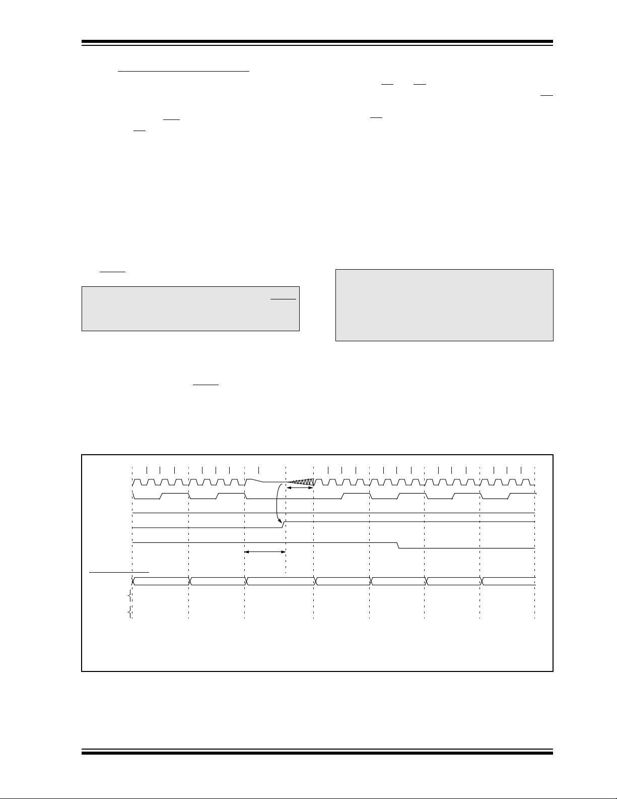
PIC16C55X(A)
7.8 Power-Down Mode (SLEEP)
The Power-down mode is entered by executing a
SLEEP instruction.
If enabled, the Watchdog Timer will be cleared but
keeps running, the PD
cleared, the T
O bit is set, and the oscillator driver is
turned off. The I/O ports maintain the status they had,
before
SLEEP was executed (driving high, low, or
hi-impedance).
For lowest current consumption in this mode, all I/O
pins should be either at V
circuitry drawing current from the I/O pin. I/O pins that
are hi-impedance inputs should be pulled high or low
externally to avoid switching currents caused by floating inputs. The T0CKI input should also be at V
V
SS for lowest current consumption. The contribution
from on chip pull-ups on PORTB should be considered.
The MCLR
pin must be at a logic high level (VIHMC).
Note: It should be noted that a RESET generated
by a WDT time-out does not drive MCLR
pin low.
7.8.1 WAKE-UP FROM SLEEP The device can wake-up from SLEEP through one of
the following events:
1. External reset input on MCLR
2. Watchdog Timer Wake-up (if WDT was enab led)
3. Interrupt from RB0/INT pin or RB Port change
bit in the STATUS register is
DD, or VSS, with no external
DD or
pin
The first event will cause a device reset. The two latter
events are considered a continuation of program execution. The T
O and PD bits in the STATUS register can
be used to determine the cause of device reset. PD
bit, which is set on power-up is cleared when SLEEP is
invoked. T
When the
O bit is cleared if WDT Wake-up occurred.
SLEEP instruction is being executed, the
next instruction (PC + 1) is pre-fetched. For the device
to wake-up through an interrupt ev ent, the corresponding interrupt enable bit must be set (enabled). Wak e-up
is regardless of the state of the GIE bit. If the GIE bit is
clear (disabled), the device continues execution at the
instruction after the
SLEEP instruction. If the GIE bit is
set (enabled), the device executes the instruction after
the
SLEEP instruction and then branches to the inter-
rupt address (0004h). In cases where the execution of
the instruction following
user should have an
SLEEP is not desirable, the
NOP after the SLEEP instruction.
Note: If the global interrupts are disabled (GIE is
cleared), but any interrupt source has both
its interrupt enable bit and the corresponding interrupt flag bits set, the device will
immediately wakeup from sleep. The sleep
instruction is completely executed.
The WDT is cleared when the device wakes-up from
sleep, regardless of the source of wake-up.
FIGURE 7-16: WAKE-UP FROM SLEEP THROUGH INTERRUPT
Q1 Q2 Q3 Q4 Q1 Q2 Q3 Q4 Q1 Q1 Q2 Q3 Q4 Q1 Q2 Q3 Q4 Q1 Q2 Q3 Q4 Q1 Q2 Q3 Q4
OSC1
OST(2)
CLKOUT(4)
INT pin
INTF flag
(INTCON<1>)
GIE bit
(INTCON<7>)
UCTION FLOW
INSTR
PC
Instruction
fetched
Instruction
executed
Note 1: XT, HS or LP oscillator mode assumed.
2: T
3: GIE = '1' assumed. In this case after wake- up, the processor jumps to the interrupt routine. If GIE = '0', execution will continue in-line.
4: CLKOUT is not available in these osc modes, but shown here for timing reference.
PC PC+1 PC+2
Inst(PC) = SLEEP
Inst(PC - 1)
OST = 1024TOSC (drawing not to scale) This delay will not be there for RC osc mode.
Inst(PC + 1)
SLEEP
Processor in
SLEEP
T
Interrupt Latency
(Note 2)
PC+2
Inst(PC + 2)
Inst(PC + 1)
PC + 2 0004h 0005h
Inst(0004h)
Dummy cycle
Dummy cycle
Inst(0005h)
Inst(0004h)
1997 Microchip Technology Inc. Preliminary DS40143B-page 49
Page 50

PIC16C55X(A)
7.9 Code Protection
If the code protection bit(s) have not been
programmed, the on-chip program memory can be
read out for verification purposes.
Note: Microchip does not recommend code
protecting windowed devices.
7.10 ID Locations
Four memory locations (2000h-2003h) are designated
as ID locations where the user can store checksum or
other code-identification numbers. These locations are
not accessible during normal execution but are
readable and writable during program/verify. Only the
least significant 4 bits of the ID locations are used.
7.11 In-Circuit Serial Programming™
The PIC16C55X(A) microcontrollers can be serially
programmed while in the end application circuit. This is
simply done with two lines for clock and data, and three
other lines for power, ground, and the programming
voltage. This allows customers to manufacture boards
with unprogrammed devices, and then program the
microcontroller just before shipping the product. This
also allows the most recent firmware or a custom
firmware to be programmed.
The device is placed into a program/verify mode by
holding the RB6 and RB7 pins low while raising the
MCLR
(VPP) pin from VIL to VIHH (see programming
specification). RB6 becomes the programming clock
and RB7 becomes the programming data. Both RB6
and RB7 are Schmitt Trigger inputs in this mode.
After reset, to place the device into programming/verify
mode, the program counter (PC) is at location 00h. A
6-bit command is then supplied to the device.
Depending on the command, 14-bits of program data
are then supplied to or from the device, depending if the
command was a load or a read. For complete details of
serial programming, please refer to the PIC16C6X/7X
Programming Specifications (Literature #DS30228).
A typical in-circuit serial programming connection is
shown in Figure 7-17.
FIGURE 7-17: TYPICAL IN-CIRCUIT SERIAL
PROGRAMMING
CONNECTION
To Normal
External
Connector
Signals
+5V
0V
VPP
CLK
Data I/O
Connections
To Normal
Connections
PIC16C55X(A)
DD
V
VSS
MCLR/VPP
RB6
RB7
VDD
DS40143B-page 50 Preliminary 1997 Microchip Technology Inc.
Page 51

PIC16C55X(A)
8.0 INSTRUCTION SET SUMMARY
Each PIC16C55X(A) instruction is a 14-bit word
divided into an OPCODE which specifies the instruction type and one or more operands which further specify the operation of the instruction. The PIC16C55X(A)
instruction set summary in Table 8-2 lists byte-ori-
ented, bit-oriented, and literal and control opera-
tions. Table 8-1 shows the opcode field descriptions.
For byte-oriented instructions, 'f' represents a file
register designator and 'd' represents a destination
designator. The file register designator specifies which
file register is to be used by the instruction.
The destination designator specifies where the result of
the operation is to be placed. If 'd' is zero, the result is
placed in the W register . If 'd' is one , the result is placed
in the file register specified in the instruction.
For bit-oriented instructions, 'b' represents a bit field
designator which selects the number of the bit affected
by the operation, while 'f' represents the number of the
file in which the bit is located.
For literal and control operations, 'k' represents an
eight or eleven bit constant or literal value.
TABLE 8-1: OPCODE FIELD
DESCRIPTIONS
Field Description
f Register file address (0x00 to 0x7F)
W Working register (accumulator)
b Bit address within an 8-bit file register
k Literal field, constant data or label
x Don't care location (= 0 or 1)
The assembler will generate code with x = 0. It is the
recommended form of use for compatibility with all
Microchip software tools.
d Destination select; d = 0: store result in W,
d = 1: store result in file register f.
Default is d = 1
label Label name
TOS Top of Stack
PC Program Counter
PCLATH
Program Counter High Latch
GIE Global Interrupt Enable bit
WDT Watchdog Timer/Counter
TO Time-out bit
PD Power-down bit
dest Destination either the W register or the specified
register file location
[ ] Options
Contents
( )
Assigned to
→
Register bit field
< >
In the set of
∈
User defined term (font is courier)
i
talics
The instruction set is highly orthogonal and is grouped
into three basic categories:
• Byte-oriented operations
• Bit-oriented operations
• Literal and control operations
All instructions are executed within one single
instruction cycle, unless a conditional test is true or the
program counter is changed as a result of an
instruction. In this case, the execution takes two
instruction cycles with the second cycle executed as a
NOP. One instruction cycle consists of four oscillator
periods. Thus, for an oscillator frequency of 4 MHz, the
normal instruction execution time is 1 µs. If a
conditional test is true or the program counter is
changed as a result of an instruction, the instruction
execution time is 2 µs.
Table 8-1 lists the instructions recognized by the
MPASM assembler.
Figure 8-1 shows the three general formats that the
instructions can have.
Note: To maintain upward compatibility with
future PICmicro™ products, do not use
the
OPTION and TRIS instructions.
All examples use the following format to represent a
hexadecimal number:
0xhh
where h signifies a hexadecimal digit.
FIGURE 8-1: GENERAL FORMAT FOR
INSTRUCTIONS
Byte-oriented file register operations
13 8 7 6 0
OPCODE d f (FILE #)
d = 0 for destination W
d = 1 for destination f
f = 7-bit file register address
Bit-oriented file register operations
13 10 9 7 6 0
OPCODE b (BIT #) f (FILE #)
b = 3-bit bit address
f = 7-bit file register address
Literal and control operations
General
13 8 7 0
OPCODE k (literal)
k = 8-bit immediate value
CALL and GOTO instructions only
13 11 10 0
OPCODE k (literal)
k = 11-bit immediate value
1997 Microchip Technology Inc. Preliminary DS40143B-page 51
Page 52

PIC16C55X(A)
TABLE 8-2: PIC16C55X(A) INSTRUCTION SET
Mnemonic,
Operands
BYTE-ORIENTED FILE REGISTER OPERATIONS
ADDWF
ANDWF
CLRF
CLRW
COMF
DECF
DECFSZ
INCF
INCFSZ
IORWF
MOVF
MOVWF
NOP
RLF
RRF
SUBWF
SWAPF
XORWF
BIT-ORIENTED FILE REGISTER OPERATIONS
BCF
BSF
BTFSC
BTFSS
LITERAL AND CONTROL OPERATIONS
ADDLW
ANDLW
CALL
CLRWDT
GOTO
IORLW
MOVLW
RETFIE
RETLW
RETURN
SLEEP
SUBLW
XORLW
Note 1: When an I/O register is modified as a function of itself ( e.g., MOVF PORTB, 1), the value used will be that value present
on the pins themselves. For example, if the data latch is '1' for a pin configured as input and is driven low by an external
device, the data will be written back with a '0'.
2: If this instruction is ex ecuted on the TMR0 register (and, where applicable, d = 1), the prescaler will be cleared if assigned
to the Timer0 Module.
3: If Program Counter (PC) is modified or a conditional test is true, the instruction requires two cycles. The second cycle is
executed as a NOP.
Description Cycles 14-Bit Opcode Status
MSb LSb
f, d
Add W and f
f, d
AND W with f
f
Clear f
-
Clear W
f, d
Complement f
f, d
Decrement f
f, d
Decrement f, Skip if 0
f, d
Increment f
f, d
Increment f, Skip if 0
f, d
Inclusive OR W with f
f, d
Move f
f
Move W to f
-
No Operation
f, d
Rotate Left f through Carry
f, d
Rotate Right f through Carry
f, d
Subtract W from f
f, d
Swap nibbles in f
f, d
Exclusive OR W with f
f, b
Bit Clear f
f, b
Bit Set f
f, b
Bit Test f, Skip if Clear
f, b
Bit Test f, Skip if Set
k
Add literal and W
k
AND literal with W
k
Call subroutine
-
Clear Watchdog Timer
k
Go to address
k
Inclusive OR literal with W
k
Move literal to W
-
Return from interrupt
k
Return with literal in W
-
Return from Subroutine
-
Go into standby mode
k
Subtract W from literal
k
Exclusive OR literal with W
1
1
1
1
1
1
1(2)
1
1(2)
1
1
1
1
1
1
1
1
1
1
1
1 (2)
1 (2)
1
1
2
1
2
1
1
2
2
2
1
1
1
00
00
00
00
00
00
00
00
00
00
00
00
00
00
00
00
00
00
01
01
01
01
11
11
10
00
10
11
11
00
11
00
00
11
11
0111
0101
0001
0001
1001
0011
1011
1010
1111
0100
1000
0000
0000
1101
1100
0010
1110
0110
00bb
01bb
10bb
11bb
111x
1001
0kkk
0000
1kkk
1000
00xx
0000
01xx
0000
0000
110x
1010
dfff
dfff
lfff
0xxx
dfff
dfff
dfff
dfff
dfff
dfff
dfff
lfff
0xx0
dfff
dfff
dfff
dfff
dfff
bfff
bfff
bfff
bfff
kkkk
kkkk
kkkk
0110
kkkk
kkkk
kkkk
0000
kkkk
0000
0110
kkkk
kkkk
ffff
ffff
ffff
xxxx
ffff
ffff
ffff
ffff
ffff
ffff
ffff
ffff
0000
ffff
ffff
ffff
ffff
ffff
ffff
ffff
ffff
ffff
kkkk
kkkk
kkkk
0100
kkkk
kkkk
kkkk
1001
kkkk
1000
0011
kkkk
kkkk
Affected
C,DC,Z
Z
Z
Z
Z
Z
Z
Z
Z
C
C
C,DC,Z
Z
C,DC,Z
Z
O,PD
T
Z
TO,PD
C,DC,Z
Z
Notes
1,2
1,2
2
1,2
1,2
1,2,3
1,2
1,2,3
1,2
1,2
1,2
1,2
1,2
1,2
1,2
1,2
1,2
3
3
DS40143B-page 52 Preliminary 1997 Microchip Technology Inc.
Page 53

8.1 Instruction Descriptions
PIC16C55X(A)
ADDLW Add Literal and W
label
Syntax: [
] ADDLW k
Operands: 0 ≤ k ≤ 255
Operation: (W) + k → (W)
Status Affected: C, DC, Z
Encoding:
Description:
11 111x kkkk kkkk
The contents of the W register are
added to the eight bit literal 'k' and the
result is placed in the W register
Words: 1
Cycles: 1
Example
ADDLW 0x15
Before Instruction
W = 0x10
After Instruction
W = 0x25
ADDWF Add W and f
label
Syntax: [
] ADDWF f,d
Operands: 0 ≤ f ≤ 127
d ∈ [0,1]
Operation: (W) + (f) → (dest)
Status Affected: C, DC, Z
Encoding:
Description:
00 0111 dfff ffff
Add the contents of the W register
with register 'f'. If 'd' is 0 the result is
stored in the W register. If 'd' is 1 the
result is stored back in register 'f'
Words: 1
Cycles: 1
Example
ADDWF FSR, 0
Before Instruction
W = 0x17
FSR = 0xC2
After Instruction
W = 0xD9
FSR = 0xC2
ANDLW AND Literal with W
label
Syntax: [
] ANDLW k
Operands: 0 ≤ k ≤ 255
Operation: (W) .AND. (k) → (W)
Status Affected: Z
Encoding:
Description:
.
11 1001 kkkk kkkk
The contents of W register are
AND’ed with the eight bit literal 'k'. The
result is placed in the W register
.
Words: 1
Cycles: 1
Example
ANDLW 0x5F
Before Instruction
W = 0xA3
After Instruction
W = 0x03
ANDWF AND W with f
label
Syntax: [
] ANDWF f,d
Operands: 0 ≤ f ≤ 127
d ∈ [0,1]
Operation: (W) .AND. (f) → (dest)
Status Affected: Z
Encoding:
Description:
.
00 0101 dfff ffff
AND the W register with register 'f'. If
'd' is 0 the result is stored in the W
register. If 'd' is 1 the result is stored
back in register 'f'
.
Words: 1
Cycles: 1
Example
ANDWF FSR, 1
Before Instruction
W = 0x17
FSR = 0xC2
After Instruction
W = 0x17
FSR = 0x02
1997 Microchip Technology Inc. Preliminary DS40143B-page 53
Page 54

PIC16C55X(A)
BCF Bit Clear f
label
Syntax: [
] BCF f,b
Operands: 0 ≤ f ≤ 127
0 ≤ b ≤ 7
Operation: 0 → (f<b>)
Status Affected: None
Encoding:
01 00bb bfff ffff
Description: Bit 'b' in register 'f' is cleared.
Words: 1
Cycles: 1
Example
BCF FLAG_REG, 7
Before Instruction
FLAG_REG = 0xC7
After Instruction
FLAG_REG = 0x47
BSF Bit Set f
label
Syntax: [
] BSF f,b
Operands: 0 ≤ f ≤ 127
0 ≤ b ≤ 7
Operation: 1 → (f<b>)
Status Affected: None
Encoding:
Description:
01 01bb bfff ffff
Bit 'b' in register 'f' is set.
Words: 1
Cycles: 1
Example
BSF FLAG_REG, 7
Before Instruction
FLAG_REG = 0x0A
After Instruction
FLAG_REG = 0x8A
BTFSC Bit Test, Skip if Clear
label
Syntax: [
] BTFSC f,b
Operands: 0 ≤ f ≤ 127
0 ≤ b ≤ 7
Operation: skip if (f<b>) = 0
Status Affected: None
Encoding:
Description:
01 10bb bfff ffff
If bit 'b' in register 'f' is '0' then the next
instruction is skipped.
If bit 'b' is '0' then the next instruction
fetched during the current instruction
execution is discarded, and a NOP is
executed instead, making this a
two-cycle instruction
.
Words: 1
Cycles: 1(2)
Example
HERE
FALSE
TRUE
BTFSC
GOTO
•
•
•
FLAG,1
PROCESS_CODE
Before Instruction
PC = address HERE
After Instruction
if FLAG<1> = 0,
PC = address TRUE
if FLAG<1>=1,
PC = address FALSE
DS40143B-page 54 Preliminary 1997 Microchip Technology Inc.
Page 55

PIC16C55X(A)
BTFSS Bit Test f, Skip if Set
label
Syntax: [
] BTFSS f,b
Operands: 0 ≤ f ≤ 127
0 ≤ b < 7
Operation: skip if (f<b>) = 1
Status Affected: None
Encoding:
Description:
01 11bb bfff ffff
If bit 'b' in register 'f' is '1' then the next
instruction is skipped.
If bit 'b' is '1', then the next instruction
fetched during the current instruction
execution, is discarded and a NOP is
executed instead, making this a
two-cycle instruction.
Words: 1
Cycles: 1(2)
Example
HERE
FALSE
TRUE
BTFSC
GOTO
•
•
•
FLAG,1
PROCESS_CODE
Before Instruction
PC = address HERE
After Instruction
if FLAG<1> = 0,
PC = address FALSE
if FLAG<1> = 1,
PC = address TRUE
CLRF Clear f
label
Syntax: [
] CLRF f
Operands: 0 ≤ f ≤ 127
Operation: 00h → (f)
1 → Z
Status Affected: Z
Encoding:
Description:
00 0001 1fff ffff
The contents of register 'f' are cleared
and the Z bit is set.
Words: 1
Cycles: 1
Example
CLRF FLAG_REG
Before Instruction
After Instruction
FLAG_REG = 0x5A
FLAG_REG = 0x00
Z = 1
CALL Call Subroutine
label
Syntax: [
] CALL k
Operands: 0 ≤ k ≤ 2047
Operation: (PC)+ 1→ TOS,
k → PC<10:0>,
(PCLATH<4:3>) → PC<12:11>
Status Affected: None
Encoding:
Description:
10 0kkk kkkk kkkk
Call Subroutine. First, return address
(PC+1) is pushed onto the stack. The
eleven bit immediate address is loaded
into PC bits <10:0>. The upper bits of
the PC are loaded from PCLATH.
CALL is a two-cycle instruction.
Words: 1
Cycles: 2
Example
HERE CALL THERE
Before Instruction
PC = Address HERE
After Instruction
PC = Address THERE
TOS= Address HERE+1
CLRW Clear W
label
Syntax: [
] CLRW
Operands: None
Operation: 00h → (W)
1 → Z
Status Affected: Z
Encoding:
Description:
00 0001 0xxx xxxx
W register is cleared. Zero bit (Z) is
set.
Words: 1
Cycles: 1
Example
CLRW
Before Instruction
After Instruction
W = 0x5A
W = 0x00
Z = 1
1997 Microchip Technology Inc. Preliminary DS40143B-page 55
Page 56

PIC16C55X(A)
CLRWDT Clear Watchdog Timer
label
Syntax: [
] CLRWDT
Operands: None
Operation: 00h → WDT
0 → WDT prescaler,
O
1 → T
1 → PD
Status Affected: TO, PD
Encoding:
Description:
00 0000 0110 0100
CLRWDT instruction resets the
Watchdog Timer. It also resets the
prescaler of the WDT. Status bits TO
and PD are set.
Words: 1
Cycles: 1
Example
CLRWDT
Before Instruction
WDT counter = ?
After Instruction
WDT counter = 0x00
WDT prescaler= 0
TO = 1
PD = 1
DECF Decrement f
label
Syntax: [
] DECF f,d
Operands: 0 ≤ f ≤ 127
d ∈ [0,1]
Operation: (f) - 1 → (dest)
Status Affected: Z
Encoding:
Description:
00 0011 dfff ffff
Decrement register 'f'. If 'd' is 0 the
result is stored in the W register. If 'd'
is 1 the result is stored back in register
'f'
.
Words: 1
Cycles: 1
Example
DECF CNT, 1
Before Instruction
CNT = 0x01
Z = 0
After Instruction
CNT = 0x00
Z = 1
COMF Complement f
label
Syntax: [
] COMF f,d
Operands: 0 ≤ f ≤ 127
d ∈ [0,1]
Operation: (f
) → (dest)
Status Affected: Z
Encoding:
Description:
00 1001 dfff ffff
The contents of register 'f' are
complemented. If 'd' is 0 the result is
stored in W. If 'd' is 1 the result is
stored back in register 'f'.
Words: 1
Cycles: 1
Example
COMF REG1,0
Before Instruction
REG1 = 0x13
After Instruction
REG1 = 0x13
W = 0xEC
DECFSZ Decrement f, Skip if 0
label
Syntax: [
] DECFSZ f,d
Operands: 0 ≤ f ≤ 127
d ∈ [0,1]
Operation: (f) - 1 → (dest); skip if result = 0
Status Affected: None
Encoding:
Description:
00 1011 dfff ffff
The contents of register 'f' are
decremented. If 'd' is 0 the result is
placed in the W register. If 'd' is 1 the
result is placed back in register 'f'.
If the result is 0, the next instruction,
which is already fetched, is discarded. A
NOP is executed instead making it a
two-cycle instruction.
Words: 1
Cycles: 1(2)
Example
HERE DECFSZ CNT, 1
GOTO LOOP
CONTINUE •
•
•
Before Instruction
PC = address HERE
After Instruction
CNT = CNT - 1
if CNT = 0,
PC = address CONTINUE
if CNT ≠ 0,
PC = address HERE+1
DS40143B-page 56 Preliminary 1997 Microchip Technology Inc.
Page 57

PIC16C55X(A)
GOTO Unconditional Branch
label
Syntax: [
] GOTO k
Operands: 0 ≤ k ≤ 2047
Operation: k → PC<10:0>
PCLATH<4:3> → PC<12:11>
Status Affected: None
Encoding:
Description:
10 1kkk kkkk kkkk
GOTO is an unconditional branch. The
eleven bit immediate value is loaded
into PC bits <10:0>. The upper bits of
PC are loaded from PCLATH<4:3>.
GOTO is a two-cycle instruction.
Words: 1
Cycles: 2
Example
GOTO THERE
After Instruction
PC = Address THERE
INCFSZ Increment f, Skip if 0
label
Syntax: [
] INCFSZ f,d
Operands: 0 ≤ f ≤ 127
d ∈ [0,1]
Operation: (f) + 1 → (dest), skip if result = 0
Status Affected: None
Encoding:
Description:
00 1111 dfff ffff
The contents of register 'f' are
incremented. If 'd' is 0 the result is
placed in the W register. If 'd' is 1 the
result is placed back in register 'f'.
If the result is 0, the next instruction,
which is already fetched, is discarded.
A NOP is executed instead making it
a two-cycle instruction
.
Words: 1
Cycles: 1(2)
Example
HERE INCFSZ CNT, 1
GOTO LOOP
CONTINUE •
•
•
Before Instruction
PC = address HERE
After Instruction
CNT = CNT + 1
if CNT= 0,
PC = address CONTINUE
if CNT≠ 0,
PC = address HERE +1
INCF Increment f
label
Syntax: [
] INCF f,d
Operands: 0 ≤ f ≤ 127
d ∈ [0,1]
Operation: (f) + 1 → (dest)
Status Affected: Z
Encoding:
Description:
00 1010 dfff ffff
The contents of register 'f' are
incremented. If 'd' is 0 the result is
placed in the W register. If 'd' is 1 the
result is placed back in register 'f'.
Words: 1
Cycles: 1
Example
INCF CNT, 1
Before Instruction
CNT = 0xFF
Z = 0
After Instruction
CNT = 0x00
Z = 1
IORLW Inclusive OR Literal with W
label
Syntax: [
] IORLW k
Operands: 0 ≤ k ≤ 255
Operation: (W) .OR. k → (W)
Status Affected: Z
Encoding:
Description:
11 1000 kkkk kkkk
The contents of the W register is
OR’ed with the eight bit literal 'k'. The
result is placed in the W register
Words: 1
Cycles: 1
Example
IORLW 0x35
Before Instruction
W = 0x9A
After Instruction
W = 0xBF
Z = 1
.
1997 Microchip Technology Inc. Preliminary DS40143B-page 57
Page 58

PIC16C55X(A)
IORWF Inclusive OR W with f
label
Syntax: [
] IORWF f,d
Operands: 0 ≤ f ≤ 127
d ∈ [0,1]
Operation: (W) .OR. (f) → (dest)
Status Affected: Z
Encoding:
Description:
00 0100 dfff ffff
Inclusive OR the W register with
register 'f'. If 'd' is 0 the result is placed
in the W register . If 'd' is 1 the result is
placed back in register 'f'.
Words: 1
Cycles: 1
Example
IORWF RESULT, 0
Before Instruction
RESULT = 0x13
W = 0x91
After Instruction
RESULT = 0x13
W = 0x93
Z = 1
MOVLW Move Literal to W
label
Syntax: [
] MOVLW k
Operands: 0 ≤ k ≤ 255
Operation: k → (W)
Status Affected: None
Encoding:
Description:
11 00xx kkkk kkkk
The eight bit literal 'k' is loaded into W
register
. The don’t cares will assemble
as 0’s.
Words: 1
Cycles: 1
Example
MOVLW 0x5A
After Instruction
W = 0x5A
MOVF Move f
label
Syntax: [
] MOVF f,d
Operands: 0 ≤ f ≤ 127
d ∈ [0,1]
Operation: (f) → (dest)
Status Affected: Z
Encoding:
Description:
00 1000 dfff ffff
The contents of register f is moved to
a destination dependant upon the
status of d. If d = 0, destination is W
register. If d = 1, the destination is file
register f itself. d = 1 is useful to test a
file register since status flag Z is
affected.
Words: 1
Cycles: 1
Example
MOVF FSR, 0
After Instruction
W = value in FSR register
Z = 1
MOVWF Move W to f
label
Syntax: [
] MOVWF f
Operands: 0 ≤ f ≤ 127
Operation: (W) → (f)
Status Affected: None
Encoding:
Description:
00 0000 1fff ffff
Move data from W register to register
'f'
.
Words: 1
Cycles: 1
Example
MOVWF OPTION
Before Instruction
OPTION = 0xFF
W = 0x4F
After Instruction
OPTION = 0x4F
W = 0x4F
DS40143B-page 58 Preliminary 1997 Microchip Technology Inc.
Page 59

PIC16C55X(A)
NOP No Operation
label
Syntax: [
] NOP
Operands: None
Operation: No operation
Status Affected: None
Encoding:
Description:
00 0000 0xx0 0000
No operation.
Words: 1
Cycles: 1
Example
NOP
OPTION Load Option Register
Syntax: [
label
] OPTION
Operands: None
Operation: (W) → OPTION
Status Affected: None
Encoding:
Description:
00 0000 0110 0010
The contents of the W register are
loaded in the OPTION register. This
instruction is supported for code
compatibility with PIC16C5X products.
Since OPTION is a readable/writable
register, the user can directly
address it.
Words: 1
Cycles: 1
Example
To maintain upward compatibility
with future PICmicro™ products,
do not use this instruction.
RETFIE Return from Interrupt
label
Syntax: [
] RETFIE
Operands: None
Operation: TOS → PC,
1 → GIE
Status Affected: None
Encoding:
Description:
00 0000 0000 1001
Return from Interrupt. Stack is POP ed
and Top of Stack (TOS) is loaded in
the PC. Interrupts are enabled by
setting Global Interrupt Enable bit,
GIE (INTCON<7>). This is a two-cycle
instruction.
Words: 1
Cycles: 2
Example
RETFIE
After Interrupt
PC = TOS
GIE = 1
RETLW Return with Literal in W
label
Syntax: [
] RETLW k
Operands: 0 ≤ k ≤ 255
Operation: k → (W);
TOS → PC
Status Affected: None
Encoding:
Description:
11 01xx kkkk kkkk
The W register is loaded with the eight
bit literal 'k'. The program counter is
loaded from the top of the stack (the
return address). This is a two-cycle
instruction.
Words: 1
Cycles: 2
Example
CALL TABLE ;W contains table
;offset value
• ;W now has table
value
•
TABLE
•
ADDWF PC ;W = offset
RETLW k1 ;Begin table
RETLW k2 ;
•
•
•
RETLW kn ; End of table
Before Instruction
W = 0x07
After Instruction
W = value of k8
1997 Microchip Technology Inc. Preliminary DS40143B-page 59
Page 60

PIC16C55X(A)
RETURN Return from Subroutine
label
Syntax: [
] RETURN
Operands: None
Operation: TOS → PC
Status Affected: None
Encoding:
Description:
00 0000 0000 1000
Return from subroutine. The stack is
POPed and the top of the stack (T OS)
is loaded into the program counter.
This is a two cycle instruction.
Words: 1
Cycles: 2
Example
RETURN
After Interrupt
PC = TOS
RRF Rotate Right f through Carry
label
Syntax: [
] RRF f,d
Operands: 0 ≤ f ≤ 127
d ∈ [0,1]
Operation: See description below
Status Affected: C
Encoding:
Description:
00 1100 dfff ffff
The contents of register 'f' are rotated
one bit to the right through the Carry
Flag. If 'd' is 0 the result is placed in
the W register. If 'd' is 1 the result is
placed back in register 'f'.
Register fC
Words: 1
Cycles: 1
Example
RRF REG1,0
Before Instruction
REG1 = 1110 0110
C = 0
After Instruction
REG1 = 1110 0110
W = 0111 0011
C = 0
RLF Rotate Left f through Carry
label
Syntax: [
] RLF f,d
Operands: 0 ≤ f ≤ 127
d ∈ [0,1]
Operation: See description below
Status Affected: C
Encoding:
Description:
00 1101 dfff ffff
The contents of register 'f' are rotated
one bit to the left through the Carry
Flag. If 'd' is 0 the result is placed in
the W register. If 'd' is 1 the result is
stored back in register 'f'.
Register fC
Words: 1
Cycles: 1
Example
RLF REG1,0
Before Instruction
REG1 = 1110 0110
C = 0
After Instruction
REG1 = 1110 0110
W = 1100 1100
C = 1
SLEEP
Syntax: [
label
] SLEEP
Operands: None
Operation: 00h → WDT,
0 → WDT prescaler,
O,
1 → T
0 → PD
Status Affected: TO, PD
Encoding:
Description:
00 0000 0110 0011
The power-down status bit, PD is
cleared. Time-out status bit, TO is
set. Watchdog Timer and its
prescaler are cleared.
The processor is put into SLEEP
mode with the oscillator stopped.
See Section 7.8 for more details.
Words: 1
Cycles: 1
Example: SLEEP
DS40143B-page 60 Preliminary 1997 Microchip Technology Inc.
Page 61

PIC16C55X(A)
SUBLW Subtract W from Literal
label
Syntax: [
] SUBLW k
Operands: 0 ≤ k ≤ 255
Operation: k - (W) → (W)
Status
C, DC, Z
Affected:
Encoding: 11 110x kkkk kkkk
Description:
The W register is subtracted (2’s complement method) from the eight bit literal
'k'. The result is placed in the W register.
Words: 1
Cycles: 1
Example 1: SUBLW 0x02
Before Instruction
W = 1
C = ?
After Instruction
W = 1
C = 1; result is positive
Example 2: Before Instruction
W = 2
C = ?
After Instruction
W = 0
C = 1; result is zero
Example 3: Before Instruction
W = 3
C = ?
After Instruction
W = 0xFF
C = 0; result is negative
SUBWF Subtract W from f
label
Syntax: [
] SUBWF f,d
Operands: 0 ≤ f ≤ 127
d ∈ [0,1]
Operation: (f) - (W) → (dest)
Status
C, DC, Z
Affected:
Encoding: 00 0010 dfff ffff
Description:
Subtract (2’s complement method)
W register from register 'f'. If 'd' is 0 the
result is stored in the W register. If 'd' is 1
the result is stored back in register 'f'.
Words: 1
Cycles: 1
Example 1: SUBWF REG1,1
Before Instruction
REG1 = 3
W = 2
C = ?
After Instruction
REG1 = 1
W = 2
C = 1; result is positive
Example 2: Before Instruction
REG1 = 2
W = 2
C = ?
After Instruction
REG1 = 0
W = 2
C = 1; result is zero
Example 3: Before Instruction
REG1 = 1
W = 2
C = ?
After Instruction
REG1 = 0xFF
W = 2
C = 0; result is negative
1997 Microchip Technology Inc. Preliminary DS40143B-page 61
Page 62

PIC16C55X(A)
SWAPF Swap Nibbles in f
label
Syntax: [
] SWAPF f,d
Operands: 0 ≤ f ≤ 127
d ∈ [0,1]
Operation: (f<3:0>) → (dest<7:4>),
(f<7:4>) → (dest<3:0>)
Status Affected: None
00
Encoding:
Description:
The upper and lower nibbles of
register 'f' are exchanged. If 'd' is 0
the result is placed in W register. If 'd'
is 1 the result is placed in register 'f'.
1110 dfff ffff
Words: 1
Cycles: 1
Example
SWAPF REG, 0
Before Instruction
REG1 = 0xA5
After Instruction
REG1 = 0xA5
W = 0x5A
XORLW Exclusive OR Literal with W
Syntax: [
label
] XORLW k
Operands: 0 ≤ k ≤ 255
Operation: (W) .XOR. k → (W)
Status Affected: Z
Encoding: 11 1010 kkkk kkkk
Description:
The contents of the W register are
XOR’ed with the eight bit literal 'k'.
The result is placed in the
W register.
Words: 1
Cycles: 1
Example: XORLW 0xAF
Before Instruction
W = 0xB5
After Instruction
W = 0x1A
TRIS Load TRIS Register
Syntax: [
label
] TRIS f
Operands: 5 ≤ f ≤ 7
Operation: (W) → TRIS register f;
Status Affected: None
Encoding:
Description:
00
0000 0110 0fff
The instruction is supported for code
compatibility with the PIC16C5X
products. Since TRIS registers are
readable and writable, the user can
directly address them.
Words: 1
Cycles: 1
Example
To maintain upward compatibility
with future PICmicro™ products,
do not use this instruction.
XORWF Exclusive OR W with f
label
Syntax: [
] XORWF f,d
Operands: 0 ≤ f ≤ 127
d ∈ [0,1]
Operation: (W) .XOR. (f) → (dest)
Status Affected: Z
Encoding:
Description:
00 0110 dfff ffff
Exclusive OR the contents of the
W register with register 'f'. If 'd' is 0 the
result is stored in the W register. If 'd'
is 1 the result is stored back in register
'f'.
Words: 1
Cycles: 1
Example XORWF
REG 1
Before Instruction
REG = 0xAF
W = 0xB5
After Instruction
REG = 0x1A
W = 0xB5
DS40143B-page 62 Preliminary 1997 Microchip Technology Inc.
Page 63

PIC16C55X(A)
9.0 DEVELOPMENT SUPPORT
9.1 Development Tools
The PICmicrο microcontrollers are supported with a
full range of hardware and software dev elopment tools:
• PICMASTER/DS40143BICMASTER CE Real-Time
In-Circuit Emulator
• ICEPIC Low-Cost PIC16C5X and PIC16CXXX
In-Circuit Emulator
• PRO MATE
• PICSTART
Programmer
• PICDEM-1 Low-Cost Demonstration Board
• PICDEM-2 Low-Cost Demonstration Board
• PICDEM-3 Low-Cost Demonstration Board
• MPASM Assembler
• MPLAB SIM Software Simulator
• MPLAB-C (C Compiler)
• Fuzzy Logic Development System
(
fuzzy
9.2 PICMASTER: High Performance
The PICMASTER Universal In-Circuit Emulator is
intended to provide the product development engineer
with a complete microcontroller design tool set for all
microcontrollers in the SX, PIC14C000, PIC16C5X,
PIC16CXXX and PIC17CXX families. PICMASTER is
supplied with the MPLAB Integrated Development
Environment (IDE), which allows editing, “make” and
download, and source debugging from a single environment.
Interchangeable target probes allow the system to be
easily reconfigured for emulation of different processors. The universal architecture of the PICMASTER
allows expansion to support all new Microchip microcontrollers.
The PICMASTER Emulator System has been
designed as a real-time emulation system with
advanced features that are generally found on more
expensive development tools. The PC compatible 386
(and higher) machine platform and Microsoft Windows
3.x environment were chosen to best make these fea-
tures available to you, the end user.
A CE compliant version of PICMASTER is availab le for
European Union (EU) countries.
II Universal Programmer
Plus Entry-Level Prototype
TECH−MP)
Universal In-Circuit Emulator with
MPLAB IDE
9.3 ICEPIC: Low-Cost PICmicro™
In-Circuit Emulator
ICEPIC is a low-cost in-circuit emulator solution for the
Microchip PIC12CXXX, PIC16C5X and PIC16CXXX
families of 8-bit OTP microcontrollers.
ICEPIC is designed to operate on PC-compatible
machines ranging from 286-AT
based machines under Windows 3.x environment.
ICEPIC features real time, non-intrusive emulation.
through Pentium
9.4 PRO MATE II: Universal Programmer
The PRO MATE II Universal Programmer is a full-featured programmer capable of operating in stand-alone
mode as well as PC-hosted mode.
The PRO MATE II has programmable V
supplies which allows it to verify programmed memory
at V
DD min and VDD max for maximum reliability. It has
an LCD display for displaying error messages, keys to
enter commands and a modular detachable socket
assembly to support various package types. In standalone mode the PRO MATE II can read, verify or program PIC12CXXX, PIC14C000, PIC16C5X,
PIC16CXXX and PIC17CXX devices. It can also set
configuration and code-protect bits in this mode.
DD and VPP
9.5 PICSTART Plus Entry Level
Development System
The PICSTART programmer is an easy-to-use, lowcost prototype programmer. It connects to the PC via
one of the COM (RS-232) ports. MPLAB Integrated
Development Environment software makes using the
programmer simple and efficient. PICSTART Plus is
not recommended for production programming.
PICSTART Plus supports all PIC12CXXX, PIC14C000,
PIC16C5X, PIC16CXXX and PIC17CXX devices with
up to 40 pins. Larger pin count devices such as the
PIC16C923 and PIC16C924 may be supported with an
adapter socket.
1997 Microchip Technology Inc. DS40143B - page 63
Page 64

PIC16C55X(A)
9.6 PICDEM-1 Low-Cost PICmicro
Demonstration Board
The PICDEM-1 is a simple board which demonstrates
the capabilities of several of Microchip’s microcontrollers. The microcontrollers supported are: PIC16C5X
(PIC16C54 to PIC16C58A), PIC16C61, PIC16C62X,
PIC16C71, PIC16C8X, PIC17C42, PIC17C43 and
PIC17C44. All necessary hardware and software is
included to run basic demo programs. The users can
program the sample microcontrollers provided with
the PICDEM-1 board, on a PRO MATE II or
PICSTART-Plus programmer, and easily test firmware. The user can also connect the PICDEM-1
board to the PICMASTER emulator and download
the firmware to the emulator for testing. Additional prototype area is available for the user to build some additional hardware and connect it to the microcontroller
socket(s). Some of the features include an RS-232
interface, a potentiometer for simulated analog input,
push-button switches and eight LEDs connected to
PORTB.
9.7 PICDEM-2 Low-Cost PIC16CXX
Demonstration Board
The PICDEM-2 is a simple demonstration board that
supports the PIC16C62, PIC16C64, PIC16C65,
PIC16C73 and PIC16C74 microcontrollers. All the
necessary hardware and software is included to
run the basic demonstration programs. The user
can program the sample microcontrollers provided
with the PICDEM-2 board, on a PRO MATE II programmer or PICSTART-Plus, and easily test firmware.
The PICMASTER emulator may also be used with the
PICDEM-2 board to test firmware. Additional prototype
area has been provided to the user for adding additional hardware and connecting it to the microcontroller
socket(s). Some of the f eatures include a RS-232 interface, push-button switches, a potentiometer for simulated analog input, a Serial EEPROM to demonstrate
usage of the I
tion to an LCD module and a keypad.
2
C bus and separate headers for connec-
9.8 PICDEM-3 Low-Cost PIC16CXXX
Demonstration Board
The PICDEM-3 is a simple demonstration board that
supports the PIC16C923 and PIC16C924 in the PLCC
package. It will also support future 44-pin PLCC
microcontrollers with a LCD Module. All the necessary hardware and software is included to run the
basic demonstration programs. The user can program the sample microcontrollers provided with
the PICDEM-3 board, on a PRO MATE II programmer or PICSTART Plus with an adapter socket, and
easily test firmware. The PICMASTER emulator may
also be used with the PICDEM-3 board to test firmware. Additional prototype area has been provided to
the user for adding hardware and connecting it to the
microcontroller socket(s). Some of the f eatures include
an RS-232 interface, push-button switches, a potentiometer for simulated analog input, a thermistor and
separate headers for connection to an external LCD
module and a keypad. Also provided on the PICDEM-3
board is an LCD panel, with 4 commons and 12 segments, that is capable of displaying time, temperature
and day of the week. The PICDEM-3 pro vides an additional RS-232 interface and Windows 3.1 software for
showing the demultiplex ed LCD signals on a PC. A simple serial interface allows the user to construct a hardware demultiplexer for the LCD signals.
9.9 MPLAB™ Integrated Development
Environment Software
The MPLAB IDE Software brings an ease of software
development previously unseen in the 8-bit microcontroller market. MPLAB is a windows based application
which contains:
• A full featured editor
• Three operating modes
- editor
- emulator
- simulator
• A project manager
• Customizable tool bar and key mapping
• A status bar with project information
• Extensive on-line help
MPLAB allows you to:
• Edit your source files (either assembly or ‘C’)
• One touch assemble (or compile) and download
to PICmicro tools (automatically updates all
project information)
• Debug using:
- source files
- absolute listing file
• Transfer data dynamically via DDE (soon to be
replaced by OLE)
• Run up to four emulators on the same PC
The ability to use MPLAB with Microchip’s simulator
allows a consistent platform and the ability to easily
switch from the low cost simulator to the full featured
emulator with minimal retraining due to development
tools.
9.10 Assembler (MPASM)
The MPASM Universal Macro Assembler is a PChosted symbolic assembler. It suppor ts all microcontroller series including the PIC12C5XX, PIC14000,
PIC16C5X, PIC16CXXX, and PIC17CXX families.
MPASM offers full featured Macro capabilities, conditional assembly , and se ver al source and listing formats.
It generates various object code formats to support
Microchip's development tools as well as third party
programmers.
MPASM allows full symbolic debugging from
PICMASTER, Microchip’s Universal Emulator System.
DS40143B - page 64 1997 Microchip Technology Inc.
Page 65

PIC16C55X(A)
MPASM has the follo wing f eatures to assist in developing software for specific use applications.
• Provides translation of Assembler source code to
object code for all Microchip microcontrollers.
• Macro assembly capability.
• Produces all the files (Object, Listing, Symbol,
and special) required for symbolic debug with
Microchip’s emulator systems.
• Supports Hex (default), Decimal and Octal source
and listing formats.
MPASM provides a rich directive language to support
programming of the PICmicro. Directives are helpful in
making the development of y our assemble source code
shorter and more maintainable.
9.11 Software Simulator (MPLAB-SIM)
The MPLAB-SIM Software Simulator allows code
development in a PC host environment. It allows the
user to simulate the PICmicro series microcontrollers
on an instruction level. On any given instruction, the
user may examine or modify any of the data areas or
provide external stimulus to any of the pins. The input/
output radix can be set by the user and the execution
can be performed in; single step , ex ecute until break, or
in a trace mode.
MPLAB-SIM fully supports symbolic debugging using
MPLAB-C and MPASM. The Software Simulator offers
the low cost flexibility to develop and debug code outside of the laboratory environment making it an excellent multi-project software development tool.
9.12 C Compiler (MPLAB-C)
9.14 MP-DriveWay – Application Code
Generator
MP-DriveWay is an easy-to-use Windows-based Application Code Generator. With MP-DriveWay you can
visually configure all the peripherals in a PICmicro
device and, with a click of the mouse, generate all the
initialization and many functional code modules in C
language. The output is fully compatible with Microchip’s MPLAB-C C compiler. The code produced is
highly modular and allows easy integration of your o wn
code. MP-DriveWay is intelligent enough to maintain
your code through subsequent code generation.
9.15 SEEVAL Evaluation and
Programming System
The SEEVAL SEEPROM Designer’s Kit supports all
Microchip 2-wire and 3-wire Serial EEPROMs. The kit
includes everything necessary to read, write, erase or
program special features of any Microchip SEEPROM
product including Smart Serials and secure serials.
The Total Endurance Disk is included to aid in tradeoff analysis and reliability calculations. The total kit can
significantly reduce time-to-market and result in an
optimized system.
9.16 KEELOQ Evaluation and
Programming Tools
KEELOQ evaluation and programming tools support
Microchips HCS Secure Data Products. The HCS evaluation kit includes an LCD display to show changing
codes, a decoder to decode transmissions, and a programming interface to program test transmitters.
The MPLAB-C Code Development System is a
complete ‘C’ compiler and integrated development
environment for Microchip’s PICmicro™ family of
microcontrollers. The compiler provides powerful integration capabilities and ease of use not found with
other compilers.
For easier source level debugging, the compiler provides symbol information that is compatible with the
MPLAB IDE memory display.
9.13 Fuzzy Logic Development System
(
fuzzy
TECH-MP)
fuzzy
TECH-MP fuzzy logic development tool is available in two versions - a low cost introductory version,
MP Explorer, for designers to gain a comprehensive
working knowledge of fuzzy logic system design; and a
full-featured version,
menting more complex systems.
Both versions include Microchip’s
stration board for hands-on experience with fuzzy logic
systems implementation.
fuzzy
TECH-MP, edition for imple-
fuzzy
LAB demon-
1997 Microchip Technology Inc. DS40143B - page 65
Page 66

PIC16C55X(A)
TABLE 9-1: DEVELOPMENT TOOLS FROM MICROCHIP
HCS200
HCS300
HCS301
24CXX
25CXX
93CXX
3Q97
Available
✔
✔
✔
✔
✔
PIC12C5XX PIC14000 PIC16C5X PIC16CXXX PIC16C6X PIC16C7XX PIC16C8X PIC16C9XX PIC17C4X PIC17C75X
/
✔ ✔ ✔ ✔ ✔ ✔ ✔ ✔ ✔
✔ ✔ ✔ ✔ ✔ ✔
✔ ✔ ✔ ✔ ✔ ✔ ✔ ✔ ✔ ✔
✔ ✔ ✔ ✔ ✔ ✔ ✔ ✔ ✔ ✔
-MP
TECH
✔ ✔ ✔ ✔ ✔ ✔ ✔ ✔ ✔
✔ ✔ ✔ ✔ ✔ ✔
✔ ✔
✔ ✔ ✔ ✔
✔ ✔ ✔ ✔ ✔ ✔ ✔ ✔ ✔ ✔
✔ ✔ ✔ ✔ ✔ ✔ ✔ ✔ ✔ ✔ ✔ ✔
II
✔ ✔ ✔ ✔
Explorer/Edition
Fuzzy Logic
PICMASTER-CE
In-Circuit Emulator
PICMASTER
DS40143B - page 66 1997 Microchip Technology Inc.
ICEPIC Low-Cost
In-Circuit Emulator
MPLAB
Integrated
Development
Emulator Products
Environment
MPLAB C
Compiler
fuzzy
Dev. Tool
MP-DriveWay
Applications
Code Generator
Software Tools
Total Endurance
Software Model
PICSTART
Lite Ultra Low-Cost
Dev. Kit
PICSTART
Plus Low-Cost
Universal Dev. Kit
PRO MATE
KEELOQ
Universal
Programmer
Programmer
Programmers
SEEVAL
Designers Kit
PICDEM-1
PICDEM-2
PICDEM-3
Demo Boards
KEELOQ
Evaluation Kit
Page 67

PIC16C55X(A)
10.0 ELECTRICAL SPECIFICATIONS
Absolute Maximum Ratings †
Ambient Temperature under bias ............................................................................................................. –40° to +125°C
Storage Temperature................................................................................................................................–65° to +150°C
Voltage on any pin with respect to V
Voltage on V
Voltage on MCLR
Total power Dissipation (Note 1)...............................................................................................................................1.0W
Maximum Current out of V
Maximum Current into V
Input Clamp Current, I
Output Clamp Current, I
Maximum Output Current sunk by any I/O pin........................................................................................................25 mA
Maximum Output Current sourced by any I/O pin...................................................................................................25 mA
Maximum Current sunk by PORTA and PORTB ...................................................................................................200 mA
Maximum Current sourced by PORTA and PORTB..............................................................................................200 mA
Note 1: Power dissipation is calculated as follows: P
DD with respect to VSS ............................................................................................................... 0 to +7.5V
with respect to VSS (Note 2)................................................................................................. 0 to +14V
SS pin...........................................................................................................................300 mA
DD pin..............................................................................................................................250 mA
IK (VI<0 or VI> VDD) ...................................................................................................................... ±20 mA
OK (V0 <0 or V0>VDD)............................................................................................................... ±20 mA
SS (except VDD and MCLR)...................................................... –0.6V to VDD +0.6V
DIS = VDD x {IDD - ∑ IOH} + ∑ {(VDD-VOH) x IOH} + ∑(VOl x IOL)
† NOTICE: Stresses above those listed under "Absolute Maximum Ratings" may cause permanent damage to the
device. This is a stress rating only and functional operation of the device at those or any other conditions above
those indicated in the operation listings of this specification is not implied. Exposure to maximum rating conditions
for extended periods may affect device reliability.
1997 Microchip Technology Inc. Preliminary DS40143B-page 67
Page 68

PIC16C55X(A)
TABLE 10-1: CROSS REFERENCE OF DEVICE SPECS FOR OSCILLATOR CONFIGURATIONS
AND FREQUENCIES OF OPERATION (COMMERCIAL DEVICES)
OSC PIC16C55X-04 PIC16C55XA-04 PIC16C55X-20 PIC16C55XA-20 PIC16LC55X-04
RC
XT
HS
LP
DD: 3.0V to
V
5.5V
DD: 3.3 mA
I
max.@5.5V
PD: 20 µA max.
I
@4.0V
Freq: 4.0 MHz
max.
DD: 3.0V to
V
5.5V
DD: 3.3 mA
I
max.@5.5V
PD: 20 µA max.
I
@4.0V
Freq: 4.0 MHz
max.
VDD: 4.5V to
5.5V
DD: 9.0 mA typ.
I
@5.5V
PD: 1.0 µA typ.
I
@4.0V
Freq: 4.0 MHz
max.
VDD: 3.0V to
5.5V
DD: 35 µA typ.
I
@32 kHz,
3.0V
PD: 1.0 µA typ.
I
@4.0 V
Freq: 200 kHz
maxi.
DD: 3.0V to
V
5.5V
DD: 3.3 mA
I
max.@5.5V
PD: 20 µA max.
I
@4.0V
Freq: 4.0 MHz
max.
DD: 3.0V to
V
5.5V
DD: 3.3 mA
I
max.@5.5V
PD: 20 µA max.
I
@4.0V
Freq: 4.0 MHz
max.
VDD: 4.5V to
5.5V
DD: 9.0 mA typ.
I
@5.5V
PD: 1.0 µA typ.
I
@4.0V
Freq: 4.0 MHz
max.
VDD: 3.0V to
5.5V
DD: 35 µA typ.
I
@32 kHz,
3.0V
PD: 1.0 µA typ.
I
@4.0 V
Freq: 200 kHz
maxi.
VDD: 4.5V to 5.5V
DD: 1.8 mA typ.
I
@5.5V
PD: 1.0 µA typ.
I
@4.5V
Freq: 4.0 MHz
max.
VDD: 4.5V to 5.5V
DD: 1.8 mA typ.
I
@5.5V
PD: 1.0 µA typ.
I
@4.5V
Freq: 4.0 MHz
max.
DD: 4.5V to
V
5.5V
DD: 20 mA
I
max. @5.5V
PD: 1.0 µA typ.
I
@4.5V
Freq: 20 MHz
max.
Do not use in LP
mode
VDD: 4.5V to 5.5V
DD: 1.8 mA typ.
I
@5.5V
PD: 1.0 µA typ.
I
@4.5V
Freq: 4.0 MHz
max.
VDD: 4.5V to 5.5V
DD: 1.8 mA typ.
I
@5.5V
PD: 1.0 µA typ.
I
@4.5V
Freq: 4.0 MHz
max.
DD: 4.5V to
V
5.5V
DD: 20 mA
I
max. @5.5V
PD: 1.0 µA typ.
I
@4.5V
Freq: 20 MHz
max.
Do not use in LP
mode
DD: 2.5V to 5.5V
V
DD: 1.4 mA typ.
I
@3.0V
PD: 0.7 µA typ.
I
@3.0V
Freq: 4.0 MHz
max.
DD: 2.5V to 5.5V
V
DD: 1.4 mA typ.
I
@3.0V
PD: 0.7 µA typ.
I
@3.0V
Freq: 4.0 MHz
max.
Do not use in
HS mode
DD: 2.5V to
V
5.5V
DD: 32 µA max.
I
@32 kHz,
3.0V
PD: 9.0 µA
I
max. @3.0V
Freq: 200 kHz
max.
PIC16C55X
JW Devices
DD: 3.0V to 5.5V
V
DD: 3.3 mA max.
I
@5.5V
PD: 20 µA max.
I
@4.0V
Freq: 4.0 MHz
max.
DD: 3.0V to 5.5V
V
DD: 3.3 mA max.
I
@5.5V
PD: 20 µA max.
I
@4.0V
Freq: 4.0 MHz
max.
VDD: 4.5V to
5.5V
DD: 20 mA
I
max.@5.5V
PD: 1.0 µA typ.
I
@4.5V
Freq: 20 MHz
max.
DD: 2.5V to
V
5.5V
DD: 32 µA max.
I
@32 kHz,
3.0V
PD: 9.0 µA
I
max. @3.0V
Freq: 200 kHz
max.
PIC16C55XA
JW Devices
DD: 3.0V to 5.5V
V
DD: 3.3 mA max.
I
@5.5V
PD: 20 µA max.
I
@4.0V
Freq: 4.0 MHz
max.
DD: 3.0V to 5.5V
V
DD: 3.3 mA max.
I
@5.5V
PD: 20 µA max.
I
@4.0V
Freq: 4.0 MHz
max.
DD: 4.5V to
V
5.5V
DD: 20 mA
I
max.@5.5V
PD: 1.0 µA typ.
I
@4.5V
Freq: 20 MHz
max.
DD: 3.0V to
V
5.5V
DD: 32 µA max.
I
@32 kHz,
3.0V
PD: 9.0 µA
I
max.@3.0V
Freq: 200 kHz
max.
The shaded sections indicate oscillator selections which are tested for functionality, but not for MIN/MAX specifications. It is recommended that the user select the device type that guarantees the specifications required.
DS40143B-page 68 Preliminary 1997 Microchip Technology Inc.
Page 69

PIC16C55X(A)
(A)
10.1 DC CHARACTERISTICS: PIC16C55X(A)-04 (Commercial, Industrial, Extended)
PIC16C55X(A)-20 (Commercial, Industrial, Extended)
Standard Operating Conditions (unless otherwise stated)
Operating temperature –40°C ≤ T
0°C ≤ T
–40°C ≤ T
Param
Sym Characteristic Min Typ† Max Units Conditions
No.
D001
V
DD Supply Voltage 3.0
D001A
D002 V
DR RAM Data Retention
Voltage (Note 1)
D003 V
POR VDD start voltage to
ensure Power-on Reset
D004 S
VDD VDD rise rate to ensure
Power-on Reset
D010
I
DD Supply Current (Note 2) –
D010A
D013
∆I
WDT WDT Current (Note 5) – 6.0 20
D020 I
PD Power Down Current (Note 3) – 1.0 2.5
∆I
WDT WDT Current (Note 5) – 6.0 20 µA VDD=4.0V
* These parameters are characterized but not tested.
† Data in "Typ" column is at 5.0V, 25°C, unless otherwise stated. These parameters are for design guidance
only and are not tested.
Note 1: This is the limit to which V
DD can be lowered in SLEEP mode without losing RAM data.
2: The supply current is mainly a function of the operating voltage and frequency. Other factors such as I/O pin
loading and switching rate, oscillator type, internal code execution pattern, and temperature also have an
impact on the current consumption.
The test conditions for all I
DD measurements in active operation mode are:
OSC1 = external square wave, from rail to rail; all I/O pins configured as input, pulled to V
MCLR
= VDD; WDT enabled/disabled as specified.
3: The power down current in SLEEP mode does not depend on the oscillator type. Power down current is
measured with the part in SLEEP mode, with all I/O pins configured as input and tied to V
4: For RC osc configuration, current through Rext is not included. The current through the resistor can be
estimated by the formula Ir = V
DD/2Rext (mA) with Rext in kΩ.
5: The ∆ current is the additional current consumed when this peripheral is enabled. This current should be
added to the base I
DD or IPD measurement.
A ≤ +85°C for industrial and
A ≤ +70°C for commercial and
A ≤ +125°C for extended
4.5
--5.5
5.5VV
XT, RC and LP osc configuration
HS osc configuration
– 1.5* – V Device in SLEEP mode
– VSS – V See section on power-on reset for
details
0.05* – – V/ms See section on power-on reset for
details
1.8
3.3
mA
XT and RC osc configuration
F
OSC = 4 MHz, VDD = 5.5V, WDT
disabled (Note 4)
–
35
70
LP osc configuration,
µA
PIC16C55X-04 only
F
OSC = 32 kHz, VDD = 4.0V, WDT
disabled
–
9.0
20
HS osc configuration
mA
F
OSC = 20 MHz, VDD = 5.5V, WDT
disabled
VDD = 4.0V
25µAµA
(+85°C to +125°C)
VDD=4.0V, WDT disabled
15µAµA
(+85°C to +125°C)
(+85°C to +125°C)
DD,
DD or VSS.
1997 Microchip Technology Inc. Preliminary DS40143B-page 69
Page 70

PIC16C55X(A)
10.2 DC CHARACTERISTICS: PIC16LC55X-04 (Commercial, Industrial, Extended)
Standard Operating Conditions (unless otherwise stated)
Operating temperature –40˚C ≤ TA ≤ +85˚C for industrial and
0˚C ≤ TA ≤ +70˚C for commercial and
–40˚C ≤ TA ≤ +125˚C for extended
Param
No.
D001 V
D002 V
D003 V
D004 S
D010
D010A
D020 I
* These parameters are characterized but not tested.
† Data in "Typ" column is at 5.0V, 25°C, unless otherwise stated. These parameters are for design guidance
Note 1: This is the limit to which V
Sym Characteristic Min Typ† Max Units Conditions
DD Supply Voltage 3.0
2.5
DR RAM Data Retention
– 1.5* – V Device in SLEEP mode
- 5.5
5.5
V XT and RC osc configuration
LP osc configuration
Voltage (Note 1)
POR VDD start voltage to
ensure Power-on Reset
VDD VDD rise rate to ensure
Power-on Reset
I
DD Supply Current (Note 2) –
– VSS – V See section on Power-on Reset for
details
0.05* – – V/ms See section on Power-on Reset for
details
1.4262.553mAµAXT and RC osc configuration
F
OSC = 2.0 MHz, VDD = 3.0V, WDT
disabled (Note 4)
–
LP osc configuration
F
OSC = 32 kHz, VDD = 3.0V, WDT
disabled
∆I
WDT WDT Current (Note 5) – 6.0 15 µA VDD = 3.0V
PD Power Down Current (Note 3) – 0.7 2 µA VDD=3.0V, WDT disabled
∆I
WDT WDT Current (Note 5) – 6.0 15 µA VDD=3.0V
only and are not tested.
DD can be lowered in SLEEP mode without losing RAM data.
2: The supply current is mainly a function of the operating voltage and frequency. Other factors such as I/O pin
loading and switching rate, oscillator type, internal code execution pattern, and temperature also have an
impact on the current consumption.
The test conditions for all IDD measurements in active operation mode are:
OSC1=external square wave, from rail to rail; all I/O pins configured as input, pulled to V
MCLR
= VDD; WDT enabled/disabled as specified.
DD,
3: The power down current in SLEEP mode does not depend on the oscillator type. Power down current is
measured with the part in SLEEP mode, with all I/O pins configured as input and tied to V
DD or VSS.
4: For RC osc configuration, current through Rext is not included. The current through the resistor can be
estimated by the formula Ir = V
DD/2Rext (mA) with Rext in kΩ.
5: The ∆ current is the additional current consumed when this peripheral is enabled. This current should be
added to the base I
DD or IPD measurement.
DS40143B-page 70 Preliminary 1997 Microchip Technology Inc.
Page 71
PIC16C55X(A)
10.3 DC CHARACTERISTICS: PIC16C55X(A) (Commercial, Industrial, Extended)
PIC16LC55X (Commercial, Industrial, Extended)
Standard Operating Conditions (unless otherwise stated)
Operating temperature –40˚C ≤ TA ≤ +85˚C for industrial and
0˚C ≤ TA ≤ +70˚C for commercial and
–40˚C ≤ TA ≤ +125˚C for automotive
Operating voltage V
Param.
Sym
Characteristic Min Typ† Max Unit Conditions
No.
VIL
Input Low Voltage
I/O ports
D030 with TTL buffer V
D031 with Schmitt Trigger input V
D032 MCLR
, RA4/T0CKI,OSC1 (in
RC mode)
D033 OSC1 (in XT* and HS) Vss - 0.3V
OSC1 (in LP*) Vss - 0.6V
VIH
Input High Voltage
I/O ports D040 with TTL buffer 2.0V - V
D041 with Schmitt Trigger input 0.8V
D042 MCLR RA4/T0CKI 0.8VDD - VDD V
D043
D043A
D070
OSC1 (XT*, HS and LP*)
OSC1 (in RC mode)
IPURB
PORTB weak pull-up current 50 200 400 µA VDD = 5.0V, VPIN = VSS
Input Leakage Current
IIL
(Notes 2, 3)
I/O ports (Except PORTA) ±1.0 µA V
D060 PORTA - - ±0.5 µA Vss ≤ V
D061 RA4/T0CKI - - ±1.0 µA Vss ≤ V
D063 OSC1, MCLR - - ±5.0 µA Vss ≤ VPIN ≤ VDD, XT, HS and LP osc
VOL
Output Low Voltage
D080 I/O ports - - 0.6 V I
D083 OSC2/CLKOUT - - 0.6 V I
(RC only) - - 0.6 V I
VOH
Output High Voltage (Note 3)
D090 I/O ports (Except RA4) V
D092 OSC2/CLKOUT V
(RC only)
*
VOD
Open-Drain High Voltage 14* V RA4 pin
* These parameters are characterized but not tested.
† Data in “Typ” column is at 5.0V, 25°C unless otherwise stated. These parameters are for design guidance
only and are not tested.
Note 1: In RC oscillator configuration, the OSC1 pin is a Schmitt Trigger input. It is not recommended that the
PIC16C55X(A) be driven with external clock in RC mode.
2: The leakage current on the MCLR
represent normal operating conditions. Higher leakage current may be measured at different input voltages.
3: Negative current is defined as coming out of the pin.
DD range as described in DC spec Table 10-1
SS - 0.8V
0.15V
SS 0.2VDD V
V VDD = 4.5V to 5.5V
DD
otherwise
Vss - 0.2VDD V Note1
DD V
DD-1.0 V
DD V
DD VDD
0.7V
DD
- VDD V
0.9VDD
Note1
configuration
OL=8.5 mA, VDD=4.5V, -40° to +85°C
- - 0.6 V I
DD-0.7 - - V IOH=-3.0 mA, VDD=4.5V, -40° to +85°C
V
DD-0.7 - - V IOH=-2.5 mA,
OL=7.0 mA, VDD=4.5V, +125°C
OL=1.6 mA, VDD=4.5V, -40° to +85°C
OL=1.2 mA, VDD=4.5V, +125°C
V
DD-0.7 - - V IOH=-1.3 mA, VDD=4.5V, -40° to +85°C
DD-0.7 - - V IOH=-1.0 mA,
V
V
pin is strongly dependent on applied voltage level. The specified levels
SS ≤ VPIN ≤ VDD, pin at hi-impedance
PIN ≤ VDD, pin at hi-impedance
PIN ≤ VDD
DD=4.5V, +125°C
DD=4.5V, +125°C
1997 Microchip Technology Inc. Preliminary DS40143B-page 71
Page 72

PIC16C55X(A)
10.3 DC CHARACTERISTICS: PIC16C55X(A) (Commercial, Industrial, Extended)
PIC16LC55X (Commercial, Industrial, Extended) (Cont.)
Standard Operating Conditions (unless otherwise stated)
Operating temperature –40˚C ≤ TA ≤ +85˚C for industrial and
0˚C ≤ TA ≤ +70˚C for commercial and
–40˚C ≤ TA ≤ +125˚C for automotive
Operating voltage V
Param.
D100
D101
Note 1: In RC oscillator configuration, the OSC1 pin is a Schmitt Trigger input. It is not recommended that the
Sym
No.
COSC2
Cio
* These parameters are characterized but not tested.
† Data in “Typ” column is at 5.0V, 25°C unless otherwise stated. These parameters are for design guidance
only and are not tested.
PIC16C55X(A) be driven with external clock in RC mode.
2: The leakage current on the MCLR
represent normal operating conditions. Higher leakage current may be measured at different input voltages.
3: Negative current is defined as coming out of the pin.
Characteristic Min Typ† Max Unit Conditions
Capacitive Loading Specs
on Output Pins
OSC2 pin 15 pF In XT, HS and LP modes when external
All I/O pins/OSC2 (in RC
mode)
DD range as described in DC spec Table 10-1
clock used to drive OSC1.
50 pF
pin is strongly dependent on applied voltage level. The specified levels
DS40143B-page 72 Preliminary 1997 Microchip Technology Inc.
Page 73
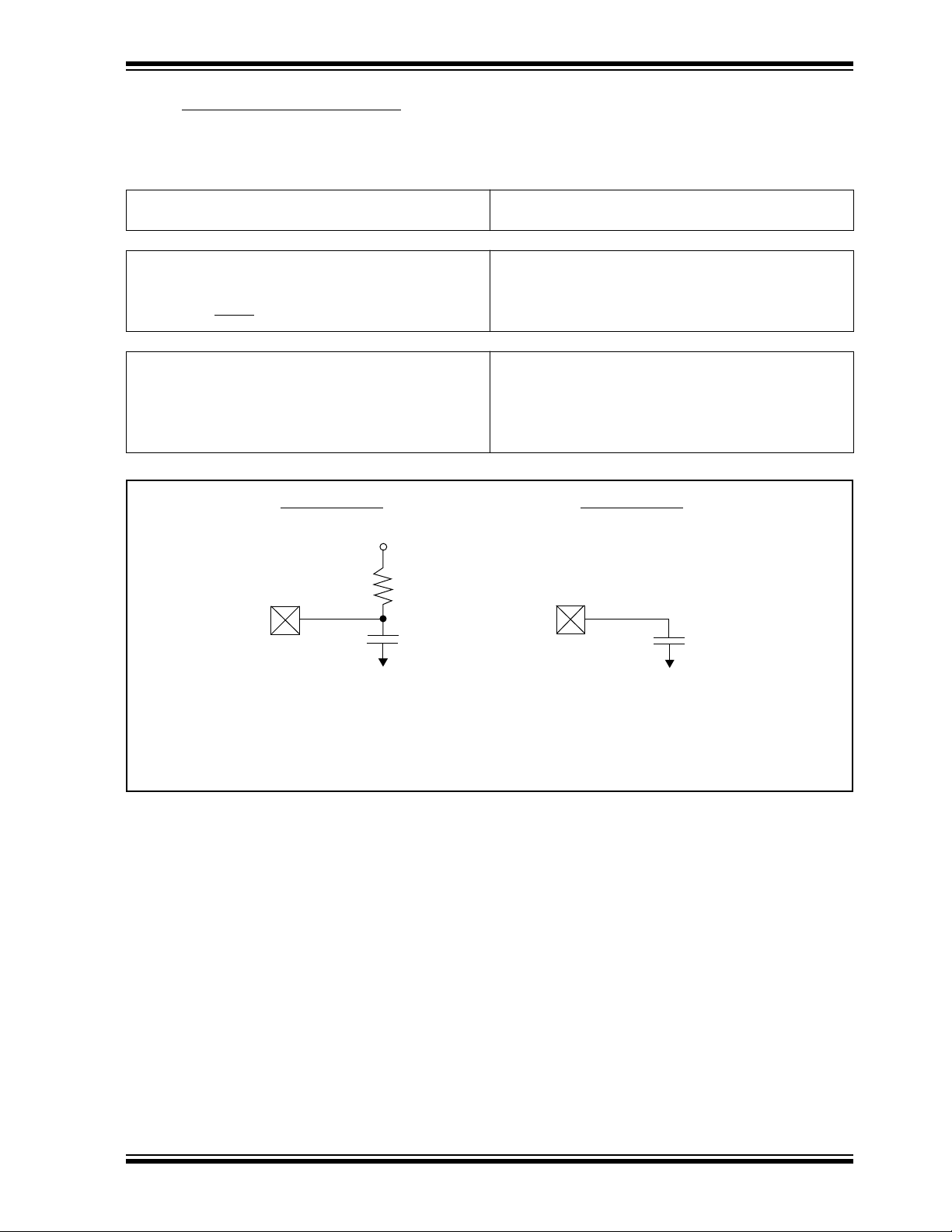
PIC16C55X(A)
10.4 Timing Parameter Symbology
The timing parameter symbols have been created with one of the following formats:
1. TppS2ppS
2. TppS
T
F Frequency T Time
Lowercase subscripts (pp) and their meanings:
pp
ck CLKOUT os OSC1
io I/O port t0 T0CKI
mc MCLR
Uppercase letters and their meanings:
S
F Fall P Period
H High R Rise
I Invalid (Hi-impedance) V Valid
L Low Z Hi-Impedance
FIGURE 10-1: LOAD CONDITIONS
Load condition 1
VDD/2
RL
L
Pin Pin
RL = 464Ω
L = 50 pF for all pins except OSC2
C
15 pF for OSC2 output
C
SS
V
Load condition 2
CL
VSS
1997 Microchip Technology Inc. Preliminary DS40143B-page 73
Page 74

PIC16C55X(A)
10.5 Timing Diagrams and Specifications
FIGURE 10-2: EXTERNAL CLOCK TIMING
OSC1
CLKOUT
Q4
Q1 Q2
1 3 3
Q3 Q4 Q1
4 4
2
TABLE 10-2: EXTERNAL CLOCK TIMING REQUIREMENTS
Parameter
No.
1 Tosc External CLKIN Period
2 TCY Instruction Cycle Time (Note 1) 1.0 Fos/4 DC µs
3* TosL,
4* TosR,
* These parameters are characterized but not tested.
† Data in "Typ" column is at 5.0V, 25°C unless otherwise stated. These parameters are for design guidance
Note 1: Instruction cycle period (T
Sym Characteristic Min Typ† Max Units Conditions
Fos External CLKIN Frequency
(Note 1)
Oscillator Frequency
(Note 1)
(Note 1)
Oscillator Period
(Note 1)
DC — 4 MHz XT and RC osc mode, VDD=5.0V
DC — 20 MHz HS osc mode
DC — 200 kHz LP osc mode
DC — 4 MHz RC osc mode, VDD=5.0V
0.1 — 4 MHz XT osc mode
1 — 20 MHz HS osc mode
DC – 200 kHz LP osc mode
250 — — ns XT and RC osc mode
50 — — ns HS osc mode
5 — — µs LP osc mode
250 — — ns RC osc mode
250 — 10,000 ns XT osc mode
50 — 1,000 ns HS osc mode
5 — — µs LP osc mode
TCY=FOS/4
External Clock in (OSC1) High or
TosH
Low Time
External Clock in (OSC1) Rise or
TosF
Fall Time
100* — — ns XT osc mode
2* — — µs LP osc mode
20* — — ns HS osc mode
25* — — ns XT osc mode
50* — — ns LP osc mode
15* — — ns HS osc mode
only and are not tested.
CY) equals four times the input oscillator time-base period. All specified values are
based on characterization data for that particular oscillator type under standard operating conditions with the
device executing code. Exceeding these specified limits may result in an unstable oscillator operation
and/or higher than expected current consumption. All devices are tested to operate at "min." values with an
external clock applied to the OSC1 pin.
When an external clock input is used, the "Max." cycle time limit is "DC" (no clock) for all devices.
DS40143B-page 74 Preliminary 1997 Microchip Technology Inc.
Page 75

FIGURE 10-3: CLKOUT AND I/O TIMING
PIC16C55X(A)
Q4
Q1
Q2 Q3
OSC1
11
12
16
CLKOUT
10
13
14
19
22
23
18
I/O Pin
(input)
15
new value
I/O Pin
(output)
17
old value
20, 21
Note: All tests must be do with specified capacitance loads (Figure 10-1) 50 pF on I/O pins and CLKOUT
TABLE 10-3: CLKOUT AND I/O TIMING REQUIREMENTS
Parameter # Sym Characteristic Min Typ† Max Units
10* TosH2ckL OSC1↑ to CLKOUT↓ (Note1) —
—
11* TosH2ckH
12* TckR
13* TckF
14* TckL2ioV
15* TioV2ckH
16* TckH2ioI
17* TosH2ioV OSC1↑ (Q1 cycle) to Port out valid —
18* TosH2ioI OSC1↑ (Q2 cycle) to Port input invalid (I/O in hold
19* TioV2osH Port input valid to OSC1↑ (I/O in setup time) 0 — — ns
20* TioR Port output rise time —
21* TioF Port output fall time —
22* Tinp RB0/INT pin high or low time 25
23 Trbp RB<7:4> change interrupt high or low time Tcy — — ns
* These parameters are characterized but not tested
† Data in "Typ" column is at 5.0V, 25°C unless otherwise stated. These parameters are for design guidance only and are not tested.
OSC1↑ to CLKOUT↑ (Note1)
CLKOUT rise time (Note1)
CLKOUT fall time (Note1)
CLKOUT ↓ to Port out valid (Note1)
Port in valid before CLKOUT ↑ (Note1)
Port in hold after CLKOUT ↑ (Note1)
time)
—
—
—
—
—
—
— — 20 ns
Tosc +200 ns
Tosc +400 ns——
0 — — ns
—
100
200
—
—
40
Note 1: Measurements are taken in RC Mode where CLKOUT output is 4 x TOSC
75
—
75
—
35
—
35
—
50 150
—
—
10
—
10
—
—
—
200
400
200
400
100
200
100
200
—
—
300
—
—
40
80
40
80
—
—
ns
ns
ns
ns
ns
ns
ns
ns
ns
ns
ns
ns
ns
ns
ns
ns
ns
ns
ns
ns
1997 Microchip Technology Inc. Preliminary DS40143B-page 75
Page 76

PIC16C55X(A)
FIGURE 10-4: RESET, WATCHDOG TIMER, OSCILLATOR START-UP TIMER AND POWER-UP
TIMER TIMING
VDD
MCLR
Internal
POR
PWRT
Timeout
OSC
Timeout
Internal
RESET
Watchdog
Timer
RESET
I/O Pins
33
32
34
30
31
34
TABLE 10-4: RESET, WATCHDOG TIMER, OSCILLATOR START-UP TIMER AND POWER-UP
TIMER REQUIREMENTS
Parameter
No.
30 TmcL MCLR Pulse Width (low) 2000 — — ns
31 Twdt Watchdog Timer Time-out Period
32 Tost Oscillation Start-up Timer Period — 1024 T
33 Tpwrt Power-up Timer Period 28* 72 132* ms
34 T
* These parameters are characterized but not tested.
† Data in "Typ" column is at 5.0V, 25°C unless otherwise stated. These parameters are for design guidance
Sym Characteristic Min Typ† Max Units Conditions
-40
° to +85°C
7* 18 33* ms
(No Prescaler)
OSC — — TOSC = OSC1 period
VDD = 5.0V, -40° to +85°C
VDD = 5.0V, -40° to +85°C
IOZ I/O hi-impedance from MCLR low — 2.0 µs
only and are not tested.
DS40143B-page 76 Preliminary 1997 Microchip Technology Inc.
Page 77

FIGURE 10-5: TIMER0 CLOCK TIMING
RA4/T0CKI
PIC16C55X(A)
40
41
42
TMR0
TABLE 10-5: TIMER0 CLOCK REQUIREMENTS
Parameter
No.
40 Tt0H T0CKI High Pulse Width No Prescaler 0.5 T
41 Tt0L T0CKI Low Pulse Width No Prescaler 0.5 TCY + 20* — — ns
42 Tt0P T0CKI Period TCY + 40*
* These parameters are characterized but not tested.
† Data in "Typ" column is at 5.0V, 25°C unless otherwise stated. These parameters are for design guidance
Sym Characteristic Min Typ† Max Units Conditions
CY + 20* — — ns
With Prescaler 10* — — ns
With Prescaler 10* — — ns
— — ns N = prescale value
N
only and are not tested.
(1, 2, 4, ..., 256)
FIGURE 10-6: LOAD CONDITIONS
Load condition 1
VDD/2
Pin Pin
V
RL = 464Ω
L = 50 pF for all pins except OSC2
C
15 pF for OSC2 output
SS
RL
C
Load condition 2
L
CL
VSS
1997 Microchip Technology Inc. Preliminary DS40143B-page 77
Page 78

PIC16C55X(A)
NOTES:
DS40143B-page 78 Preliminary 1997 Microchip Technology Inc.
Page 79

PIC16C55X(A)
11.0 PACKAGING INFORMATION
Ceramic CERDIP Dual In-Line Family
Symbol List for Ceramic CERDIP Dual In-Line Package Parameters
Symbol Description of Parameters
α Angular spacing between min. and max. lead positions measured at the gauge plane
A Distance between seating plane to highest point of body (lid)
A1 Distance between seating plane and base plane
A2 Distance from base plane to highest point of body (lid)
A3 Base body thickness
B Width of terminal leads
B1 Width of terminal lead shoulder which locate seating plane (standoff geometry optional)
C Thickness of terminal leads
D Largest overall package parameter of length
D1 Body width parameters not including leads
E Largest overall package width parameter outside of lead
E1 Body width parameter - end lead center to end lead center
eA Linear spacing of true minimum lead position center line to center line
eB Linear spacing between true lead position outside of lead to outside of lead
e1 Linear spacing between center lines of body standoffs (terminal leads)
L Distance from seating plane to end of lead
N Total number of potentially usable lead positions
S Distance from true position center line of Number 1 lead to the extremity of the body
S1 Distance from other end lead edge positions to the extremity of the body
Notes:
1. Controlling parameter: inches.
2. Parameter “e1” (“e”) is non-cumulative.
3. Seating plane (standoff) is defined by board hole size.
4. Parameter “B1” is nominal.
1997 Microchip Technology Inc. Preliminary DS40143B-page 79
Page 80
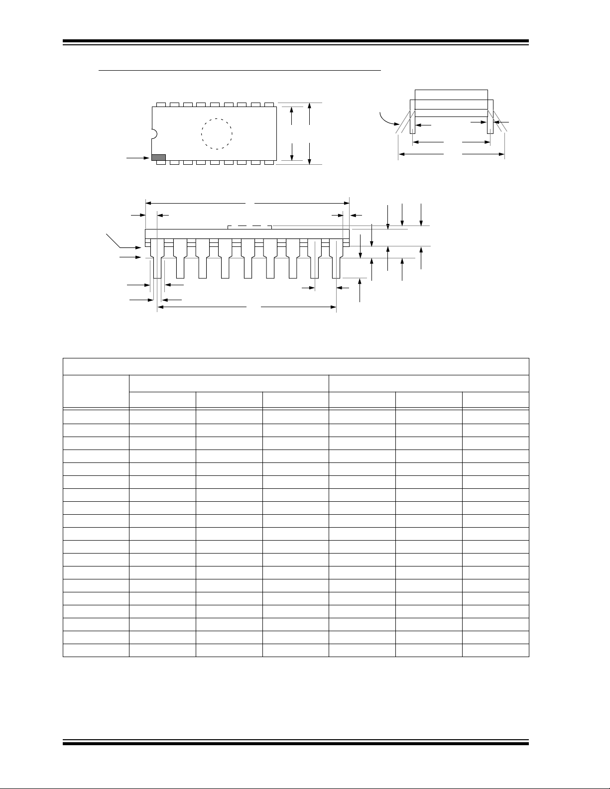
PIC16C55X(A)
11.1 18-Lead Ceramic CERDIP Dual In-line with Window (300 mil)
N
α
E1
E
Pin No. 1
Indicator
Area
D
S
Base
Plane
Seating
Plane
B1
B
Package Group: Ceramic CERDIP Dual In-Line (CDP)
Millimeters Inches
Symbol
α 0° 10° 0° 10°
A — 5.080 — 0.200
A1 0.381 1.7780 0.015 0.070
A2 3.810 4.699 0.150 0.185
A3 3.810 4.445 0.150 0.175
B 0.355 0.585 0.014 0.023
B1 1.270 1.651 Typical 0.050 0.065 Typical
C 0.203 0.381 Typical 0.008 0.015 Typical
D 22.352 23.622 0.880 0.930
D1 20.320 20.320 Reference 0.800 0.800 Reference
E 7.620 8.382 0.300 0.330
E1 5.588 7.874 0.220 0.310
e1 2.540 2.540 Reference 0.100 0.100 Reference
eA 7.366 8.128 Typical 0.290 0.320 Typical
eB 7.620 10.160 0.300 0.400
L 3.175 3.810 0.125 0.150
N 18 18 18 18
S 0.508 1.397 0.020 0.055
S1 0.381 1.270 0.015 0.050
Min Max Notes Min Max Notes
D1
S1
e1
L
A
A1
A3
A2
e
eB
A
C
DS40143B-page 80 Preliminary 1997 Microchip Technology Inc.
Page 81

PIC16C55X(A)
Plastic Dual In-Line Family
Symbol List for Plastic In-Line Package Parameters
Symbol Description of Parameters
α Angular spacing between min. and max. lead positions measured at the gauge plane
A Distance between seating plane to highest point of body
A1 Distance between seating plane and base plane
A2 Base body thickness
B Width of terminal leads
B1 Width of terminal lead shoulder which locate seating plane (standoff geometry optional)
C Thickness of terminal leads
D Largest overall package parameter of length
D1 Body length parameter - end lead center to end lead center
E Largest overall package width parameter outside of lead
E1 Body width parameters not including leads
eA Linear spacing of true minimum lead position center line to center line
eB Linear spacing between true lead position outside of lead to outside of lead
e1 Linear spacing between center lines of body standoffs (terminal leads)
L Distance from seating plane to end of lead
N Total number of potentially usable lead positions
S Distance from true position center line of Number 1 lead to the extremity of the body
S1 Distance from other end lead edge positions to the extremity of the body
Notes:
1. Controlling parameter: inches.
2. Parameter “e1” (“e”) is non-cumulative.
3. Seating plane (standoff) is defined by board hole size.
4. Parameter “B1” is nominal.
5. Details of pin Number 1 identifier are optional.
6. Parameters “D + E1” do not include mold flash/protrusions.
Mold flash or protrusions shall not exceed .010 inches.
1997 Microchip Technology Inc. Preliminary DS40143B-page 81
Page 82
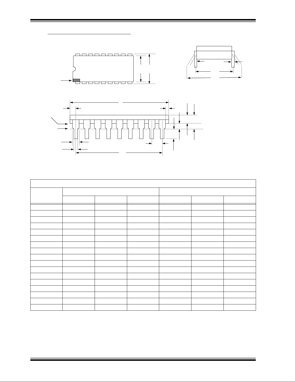
PIC16C55X(A)
11.2 18-Lead Plastic Dual In-line (300 mil)
N
Pin No. 1
Indicator
Area
D
S
Base
Plane
Seating
Plane
E1
C
E
S1
L
eA
eB
B1
B
Package Group: Plastic Dual In-Line (PLA)
Millimeters Inches
Symbol
A – 4.064 – 0.160
A1 0.381 – 0.015 –
A2 3.048 3.810 0.120 0.150
B 0.355 0.559 0.014 0.022
B1 1.524 1.524 Reference 0.060 0.060 Reference
C 0.203 0.381 Typical 0.008 0.015 Typical
D 22.479 23.495 0.885 0.925
D1 20.320 20.320 Reference 0.800 0.800 Reference
E 7.620 8.255 0.300 0.325
E1 6.096 7.112 0.240 0.280
e1 2.489 2.591 Typical 0.098 0.102 Typical
eA 7.620 7.620 Reference 0.300 0.300 Reference
eB 8.128 9.906 0.320 0.390
L 3.048 3.556 0.120 0.140
N 18 18 18 18
S 0.889 – 0.035 –
S1 0.127 – 0.005 –
Min Max Notes Min Max Notes
D1
e1
A1
A2
A
DS40143B-page 82 Preliminary 1997 Microchip Technology Inc.
Page 83

PIC16C55X(A)
Plastic Small Outline Family
Symbol List for Small Outline Package Parameters
Symbol Description of Parameters
α Angular spacing between min. and max. lead positions measured at the gauge plane
A Distance between seating plane to highest point of body
A1 Distance between seating plane and base plane
B Width of terminals
C Thickness of terminals
D Largest overall package parameter of length
E Largest overall package width parameter not including leads
e Linear spacing of true minimum lead position center line to center line
H Largest overall package dimension of width
L Length of terminal for soldering to a substrate
N Total number of potentially usable lead positions
CP Seating plane coplanarity
Notes:
1. Controlling parameter: inches.
2. All packages are gull wing lead form.
3. "D" and "E" are reference datums and do not include mold flash or protrusions. Mold flash or protrusions shall
not exceed .006 package ends and .010 on sides.
4. The chamfer on the body is optional. If it is not present, a visual index feature must be located within the
cross-hatched area to indicate pin 1 position.
5. Terminal numbers are shown for reference.
1997 Microchip Technology Inc. Preliminary DS40143B-page 83
Page 84
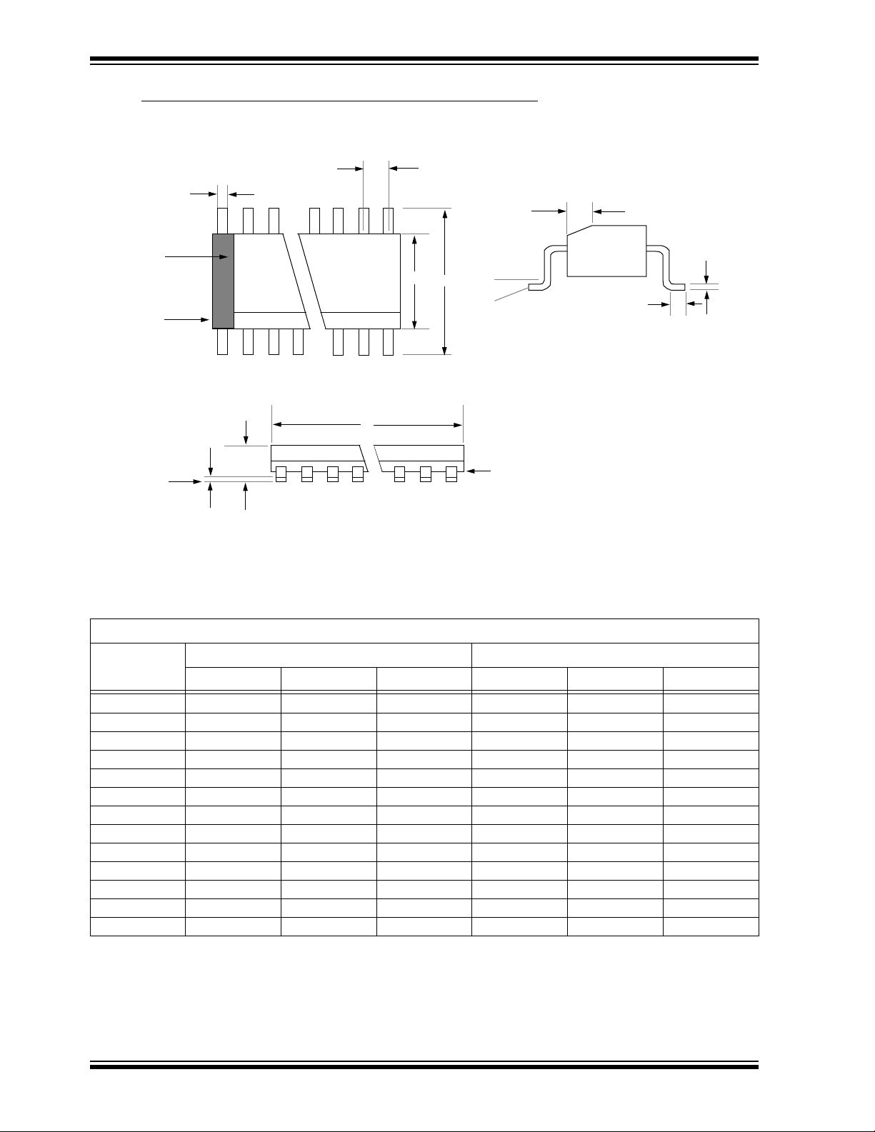
PIC16C55X(A)
11.3 18-Lead Plastic Surface Mount (SOIC - Wide, 300 mil Body)
e
B
N
Index
Area
E
Chamfer
h x 45°
H
1
2
3
D
α
h x 45°
C
L
Seating
Plane
CP
A1
A
Base
Plane
Package Group: Plastic SOIC (SO)
Millimeters Inches
Symbol
Min Max Notes Min Max Notes
α 0° 8° 0° 8°
A 2.362 2.642 0.093 0.104
A1 0.101 0.300 0.004 0.012
B 0.355 0.483 0.014 0.019
C 0.241 0.318 0.009 0.013
D 11.353 11.735 0.447 0.462
E 7.416 7.595 0.292 0.299
e 1.270 1.270 Reference 0.050 0.050 Reference
H 10.007 10.643 0.394 0.419
h 0.381 0.762 0.015 0.030
L 0.406 1.143 0.016 0.045
N 18 18 18 18
CP – 0.102 – 0.004
DS40143B-page 84 Preliminary 1997 Microchip Technology Inc.
Page 85
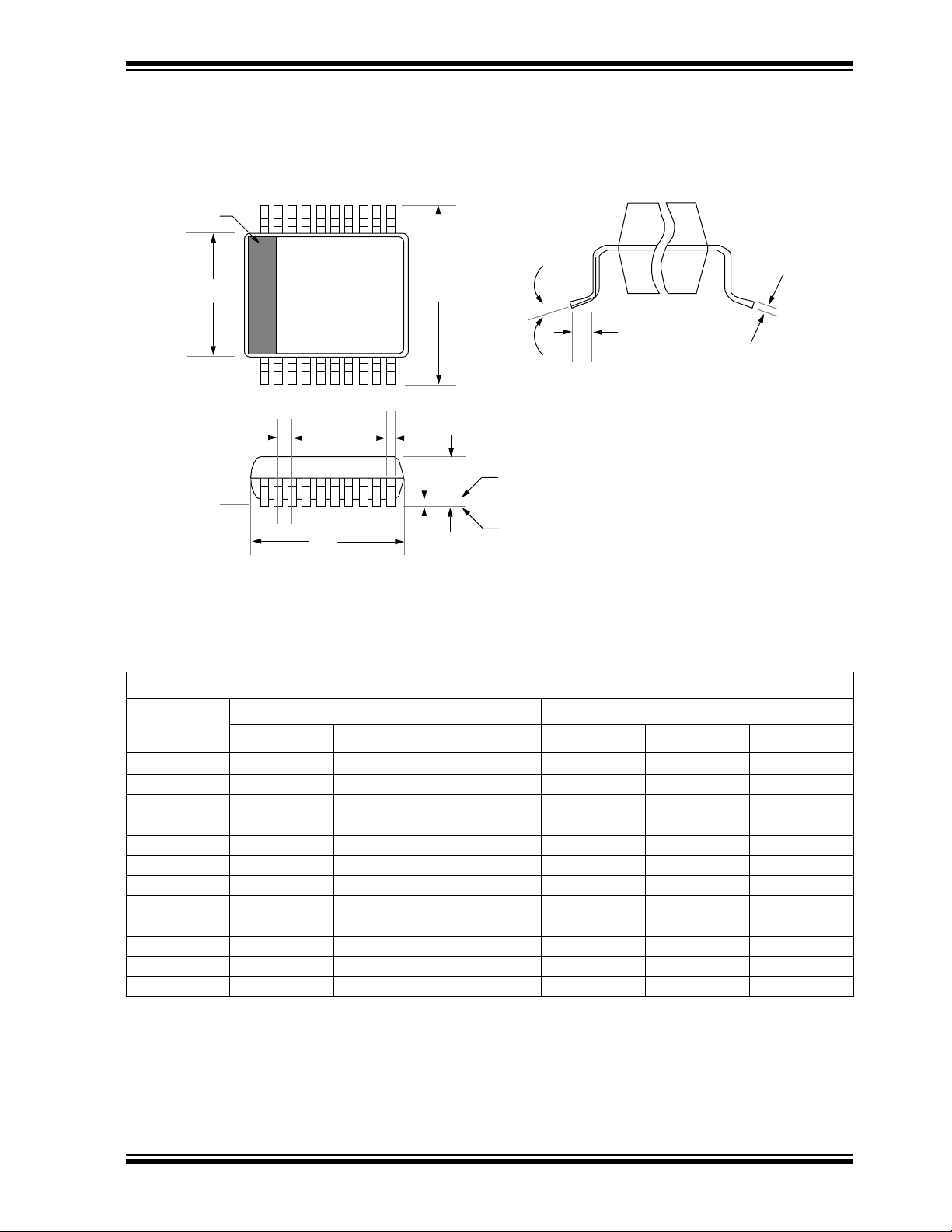
PIC16C55X(A)
11.4 20-Lead Plastic Surface Mount (SSOP - 209 mil Body 5.30 mm)
Index
area
CP
N
E
1 2 3
e
D
B
A1
H
α
L
A
Base plane
Seating plane
C
Package Group: Plastic SSOP
Millimeters Inches
Symbol
Min Max Notes Min Max Notes
α 0° 8° 0° 8°
A 1.730 1.990 0.068 0.078
A1 0.050 0.210 0.002 0.008
B 0.250 0.380 0.010 0.015
C 0.130 0.220 0.005 0.009
D 7.070 7.330 0.278 0.289
E 5.200 5.380 0.205 0.212
e 0.650 0.650 Reference 0.026 0.026 Reference
H 7.650 7.900 0.301 0.311
L 0.550 0.950 0.022 0.037
N 20 20 20 20
CP - 0.102 - 0.004
1997 Microchip Technology Inc. Preliminary DS40143B-page 85
Page 86
PIC16C55X(A)
11.5 Package Marking Information
18-Lead PDIP
XXXXXXXXXXXXXXXX
XXXXXXXXXXXXXXXX
AABBCDE
18-Lead SOIC (.300")
XXXXXXXXXXXX
XXXXXXXXXXXX
XXXXXXXXXXXX
AABBCDE
18-Lead CERDIP Windowed
XXXXXXXX
XXXXXXXX
AABBCDE
20-Lead SSOP
XXXXXXXXXX
XXXXXXXXXX
AABBCDE
Example
PIC16C558A
-04I / P456
9523 CBA
Example
PIC16C558
-04I / S0218
9518 CDK
Example
16C558
/JW
9501 CBA
Example
PIC16C558A
-04I / 218
9551 CBP
Legend: MM...M Microchip part number information
XX...X Customer specific information*
AA Year code (last 2 digits of calendar year)
BB Week code (week of January 1 is week ‘01’)
C Facility code of the plant at which wafer is manufactured
C = Chandler, Arizona, U.S.A.
D Mask revision number
E Assembly code of the plant or country of origin in which
part was assembled
Note: In the event the full Microchip part number cannot be marked on one line,
it will be carried over to the next line thus limiting the number of available
characters for customer specific information.
* Standard OTP marking consists of Microchip part number, year code, week
code, facility code, mask rev#, and assembly code. For OTP marking beyond
this, certain price adders apply. Please chec k with your Microchip Sales Office.
For QTP devices, any special marking adders are included in QTP price.
DS40143B-page 86 Preliminary 1997 Microchip Technology Inc.
Page 87

PIC16C55X(A)
APPENDIX A: ENHANCEMENTS
The following are the list of enhancements over the
PIC16C5X microcontroller family:
1. Instruction word length is increased to 14 bits.
This allows larger page sizes both in program
memory (4K now as opposed to 512 before) and
register file (up to 128 bytes now versus 32
bytes before).
2. A PC high latch register (PCLATH) is added to
handle program memory paging. PA2, PA1, PA0
bits are removed from STATUS register.
3. Data memory paging is slightly redefined.
STATUS register is modified.
4. Four new instructions have been added:
RETURN, RETFIE, ADDLW, and SUBLW.
Two instructions
phased out although they are kept for
compatibility with PIC16C5X.
5. OPTION and TRIS registers are made
addressable.
6. Interrupt capability is added. Interrupt vector is
at 0004h.
7. Stack size is increased to 8 deep.
8. Reset vector is changed to 0000h.
9. Reset of all registers is revised. Three different
reset (and wake-up) types are recognized.
Registers are reset differently.
10. Wake up from SLEEP through interrupt is
added.
11. Two separate timers, Oscillator Start-up Timer
(OST) and Power-up Timer (PWRT) are
included for more reliable power-up. These
timers are invoked selectively to avoid
unnecessary delays on power-up and wake-up.
12. PORTB has weak pull-ups and interrupt on
change feature.
13. Timer0 clock input, T0CKI pin is also a port pin
(RA4/T0CKI) and has a TRIS bit.
14. FSR is made a full 8-bit register.
15. “In-circuit programming” is made possible. The
user can program PIC16C55X devices using
only five pins: V
RB7 (data in/out).
16. PCON status register is added with a
Power-on-Reset (POR
17. Code protection scheme is enhanced such that
portions of the program memory can be
protected, while the remainder is unprotected.
18. PORTA inputs are now Schmitt Trigger inputs.
TRIS and OPTION are being
DD, VSS, VPP, RB6 (clock) and
) status bit.
APPENDIX B: COMPATIBILITY
To convert code written for PIC16C5X to
PIC16C55X(A), the user should take the following
steps:
1. Remove any program memory page select
operations (PA2, PA1, PA0 bits) for
2. Revisit any computed jump operations (write to
PC or add to PC, etc.) to make sure page bits
are set properly under the new scheme.
3. Eliminate any data memory page switching.
Redefine data variables to reallocate them.
4. Verify all writes to STATUS, OPTION, and FSR
registers since these have changed.
5. Change reset vector to 0000h.
CALL, GOTO.
1997 Microchip Technology Inc. Preliminary DS40143B-page 87
Page 88

PIC16C55X(A)
NOTES:
DS40143B-page 88 Preliminary 1997 Microchip Technology Inc.
Page 89

PIC16C55X(A)
INDEX
A
ADDLW Instruction .............................................................53
ADDWF Instruction............................................................. 53
ANDLW Instruction .............................................................53
ANDWF Instruction............................................................. 53
Architectural Overview..........................................................9
Assembler
MPASM Assembler..................................................... 64
B
BCF Instruction................................................................... 54
Block Diagram
TIMER0....................................................................... 29
TMR0/WDT PRESCALER.......................................... 32
BSF Instruction ...................................................................54
BTFSC Instruction............................................................... 54
BTFSS Instruction...............................................................55
C
CALL Instruction .................................................................55
Clocking Scheme/Instruction Cycle ....................................12
CLRF Instruction.................................................................55
CLRW Instruction................................................................55
CLRWDT Instruction...........................................................56
Code Protection.................................................................. 50
COMF Instruction................................................................56
Configuration Bits................................................................ 36
D
Data Memory Organization.................................................14
DECF Instruction................................................................. 56
DECFSZ Instruction............................................................56
Development Support......................................................... 63
Development Tools.............................................................63
E
External Crystal Oscillator Circuit .......................................38
F
Fuzzy Logic Dev. System (
fuzzy
TECH-MP) ....................65
G
General purpose Register File............................................14
GOTO Instruction................................................................57
I
I/O Ports..............................................................................23
I/O Programming Considerations........................................ 27
ICEPIC Low-Cost PIC16CXXX In-Circuit Emulator............ 63
ID Locations........................................................................50
INCF Instruction..................................................................57
INCFSZ Instruction .............................................................57
In-Circuit Serial Programming.............................................50
Indirect Addressing, INDF and FSR Registers ...................22
Instruction Flow/Pipelining.................................................. 12
Instruction Set
ADDLW.......................................................................53
ADDWF....................................................................... 53
ANDLW.......................................................................53
ANDWF....................................................................... 53
BCF............................................................................. 54
BSF.............................................................................54
BTFSC........................................................................ 54
BTFSS ........................................................................55
CALL...........................................................................55
CLRF...........................................................................55
CLRW .........................................................................55
CLRWDT.....................................................................56
COMF......................................................................... 56
DECF.......................................................................... 56
DECFSZ..................................................................... 56
GOTO......................................................................... 57
INCF........................................................................... 57
INCFSZ....................................................................... 57
IORLW........................................................................ 57
IORWF........................................................................ 58
MOVF......................................................................... 58
MOVLW...................................................................... 58
MOVWF...................................................................... 58
NOP............................................................................ 59
OPTION...................................................................... 59
RETFIE....................................................................... 59
RETLW....................................................................... 59
RETURN..................................................................... 60
RLF............................................................................. 60
RRF............................................................................ 60
SLEEP........................................................................ 60
SUBLW....................................................................... 61
SUBWF....................................................................... 61
SWAPF....................................................................... 62
TRIS ........................................................................... 62
XORLW ...................................................................... 62
XORWF...................................................................... 62
Instruction Set Summary .................................................... 51
INT Interrupt ....................................................................... 46
INTCON Register ............................................................... 19
Interrupts ............................................................................ 45
IORLW Instruction .............................................................. 57
IORWF Instruction.............................................................. 58
K
KeeLoq Evaluation and Programming Tools................... 65
M
MOVF Instruction................................................................ 58
MOVLW Instruction ............................................................ 58
MOVWF Instruction ............................................................ 58
MP-DriveWay™ - Application Code Generator .................. 65
MPLAB C............................................................................ 65
MPLAB Integrated Development Environment Software.... 64
N
NOP Instruction .................................................................. 59
O
One-Time-Programmable (OTP) Devices .............................7
OPTION Instruction ............................................................ 59
OPTION Register ............................................................... 18
Oscillator Configurations .................................................... 37
Oscillator Start-up Timer (OST).......................................... 40
P
Package Marking Information............................................. 86
Packaging Information........................................................ 79
PCL and PCLATH .............................................................. 21
PCON Register................................................................... 20
PICDEM-1 Low-Cost PICmicro Demo Board ..................... 64
PICDEM-2 Low-Cost PIC16CXX Demo Board................... 64
PICDEM-3 Low-Cost PIC16CXXX Demo Board ................ 64
PICMASTER In-Circuit Emulator..................................... 63
PICSTART Plus Entry Level Development System......... 63
Pinout Description .............................................................. 11
Port RB Interrupt................................................................. 46
PORTA ............................................................................... 23
PORTB ............................................................................... 25
Power Control/Status Register (PCON) ............................. 41
Power-Down Mode (SLEEP).............................................. 49
1997 Microchip Technology Inc. Preliminary DS40143B-page 89
Page 90

PIC16C55X(A)
Power-On Reset (POR) ......................................................40
Power-up Timer (PWRT).....................................................40
Prescaler.............................................................................32
PRO MATE II Universal Programmer...............................63
Program Memory Organization...........................................13
Q
Quick-Turnaround-Production (QTP) Devices......................7
R
RC Oscillator.......................................................................38
Reset................................................................................... 39
RETFIE Instruction.............................................................. 59
RETLW Instruction..............................................................59
RETURN Instruction............................................................60
RLF Instruction.................................................................... 60
RRF Instruction...................................................................60
S
SEEVAL Evaluation and Programming System...............65
Serialized Quick-Turnaround-Production (SQTP) Devices...7
SLEEP Instruction...............................................................60
Software Simulator (MPLAB-SIM).......................................65
Special Features of the CPU...............................................35
Special Function Registers .................................................16
Stack...................................................................................21
Status Register....................................................................17
SUBLW Instruction.............................................................. 61
SUBWF Instruction..............................................................61
SWAPF Instruction.............................................................. 62
T
Timer0
TIMER0.......................................................................29
TIMER0 (TMR0) Interrupt........................................... 29
TIMER0 (TMR0) Module.............................................29
TMR0 with External Clock...........................................31
Timer1
Switching Prescaler Assignment.................................33
Timing Diagrams and Specifications................................... 74
TMR0 Interrupt....................................................................46
TRIS Instruction ..................................................................62
TRISA..................................................................................23
TRISB..................................................................................25
W
Watchdog Timer (WDT)......................................................47
X
XORLW Instruction .............................................................62
XORWF Instruction.............................................................62
LIST OF EXAMPLES
Example 3-1: Instruction Pipeline Flow.................... 12
Example 4-1: Ndirect Addressing............................. 22
Example 5-1: Read-Modify-Write Instructions
on an I/O Port..................................... 27
Example 6-1: Changing Prescaler
(Timer0→WDT)...................................33
Example 6-2: Changing prescaler
(WDT→Timer0)...................................33
Example 7-1: Saving the Status and W Registers
in RAM .............................................47
LIST OF FIGURES
Figure 3-1: BlocK Diagram ........................................... 10
Figure 3-2: Clock/Instruction Cycle............................... 12
Figure 4-1: Program Memory Map and Stack for the
PIC16C554/PIC6C554(A) .......................... 13
Figure 4-2: Program Memory Map and Stack for the
PIC16C556(A)............................................ 13
Figure 4-3: Program Memory Map and Stack for the
PIC16C558/PIC16C558(A) ........................ 13
Figure 4-4: Data Memory Map for the
PIC16C554/554(A)..................................... 15
Figure 4-5: Data Memory Map for the
PIC16C558/558(A)..................................... 15
Figure 4-6: STATUS Register (Address
03h or 83h)................................................. 17
Figure 4-7: OPTION Register (address 81h) ................ 18
Figure 4-8: INTCON Register (address 0Bh
or 8Bh)........................................................ 19
Figure 4-9: PCON Register (Address 8Eh)................... 20
Figure 4-10: Loading Of PC In Different Situations ........ 21
Figure 4-11: Direct/indirect Addressing
PIC16C55X(A)............................................ 22
Figure 5-1: Block Diagram of
PORT pins RA<3:0>................................... 23
Figure 5-2: Block Diagram of RA4 Pin.......................... 23
Figure 5-3: Block Diagram of RB7:RB4 Pins ................ 25
Figure 5-4: Block Diagram of RB3:RB0 Pins ................ 25
Figure 5-5: Successive I/O Operation........................... 27
Figure 6-1: TIMER0 Block Diagram.............................. 29
Figure 6-2: TIMER0 (TMR0) Timing: Internal
Clock/No PrescaleR ................................... 29
Figure 6-3: TIMER0 Timing: Internal Clock/
Prescale 1:2 ............................................... 30
Figure 6-4: TIMER0 Interrupt Timing ............................ 30
Figure 6-5: TIMER0 Timing With External Clock .......... 31
Figure 6-6: Block Diagram of thE Timer0/WDT
Prescaler .................................................... 32
Figure 7-1: Configuration Word .................................... 36
Figure 7-2: Crystal Operation (or Ceramic Resonator)
(HS, XT or LP Osc Configuration).............. 37
Figure 7-3: External Clock Input Operation
(HS, XT or LP Osc Configuration).............. 37
Figure 7-4: External Parallel Resonant Crystal
Oscillator Circuit ......................................... 38
Figure 7-5: External Series Resonant Crystal
Oscillator Circuit ......................................... 38
Figure 7-6: RC Oscillator Mode .................................... 38
Figure 7-7: Simplified Block Diagram of On-chip
Reset Circuit............................................... 39
Figure 7-8: Time-out Sequence on Power-up
Figure 7-9: Time-out Sequence on Power-up
Figure 7-10: Time-out Sequence on Power-up
Figure 7-11: External Power-on Reset Circuit
Figure 7-12: Interrupt Logic ............................................ 45
Figure 7-13: INT Pin Interrupt Timing ............................. 46
Figure 7-14: Watchdog Timer Block Diagram................. 48
Figure 7-15: Summary of Watchdog Timer
Figure 7-16: Wake-up from Sleep Through
Figure 7-17: Typical In-Circuit Serial Programming
not tied to VDD): Case 1................. 43
(MCLR
(MCLR not tied to VDD): Case 2................. 43
(MCLR tied to VDD)..................................... 43
(For Slow VDD Power-up)........................... 44
Registers .................................................... 48
Interrupt...................................................... 49
Connection ................................................. 50
DS40143B-page 90 Preliminary 1997 Microchip Technology Inc.
Page 91

Figure 8-1: General Format for Instructions.................. 51
Figure 10-1: Load Conditions.......................................... 73
Figure 10-2: External Clock Timing................................. 74
Figure 10-3: CLKOUT and I/O Timing.............................75
Figure 10-4: Reset, Watchdog Timer, Oscillator
Start-Up Timer and Power-Up Timer
Timing.........................................................76
Figure 10-5: TIMER0 Clock Timing................................. 77
Figure 10-6: Load Conditions.......................................... 77
LIST OF TABLES
Table 1-1: PIC16C55X(A) Family of Devices.......... 6
Table 3-1: PIC16C55X(A) Pinout Description....... 11
Table 4-1: Special Registers for the
PIC16C55X(A)..................................... 16
Table 5-1: PORTA Functions................................ 24
Table 5-2: Summary of Registers Associated
With PORTA ........................................ 24
Table 5-3: PORTB Functions................................ 26
Table 5-4: Summary of Registers Associated
with PORTB......................................... 26
Table 6-1: Registers Associated with Timer0........ 33
Table 7-1: Capacitor Selection for Ceramic
Resonators (Preliminary)..................... 37
Table 7-2: Capacitor Selection for Crystal
Oscillator (Preliminary)......................... 37
Table 7-3: Time-out in Various Situations............. 41
Table 7-4: StatUs Bits and Their Significance....... 41
Table 7-5: Initialization Condition for Special
Registers.............................................. 42
Table 7-6: Initialization Condition for Registers..... 42
Table 8-1: OPCODE Field Descriptions................ 51
Table 8-2: PIC16C55X(A) Instruction SeT............ 52
Table 9-1: Development Tools From Microchip.... 66
Table 10-1: Cross Reference of Device Specs
for Oscillator Configurations and
Frequencies of Operation
(Commercial Devices).......................... 67
Table 10-2: External Clock Timing
Requirements....................................... 74
Table 10-3: CLKOUT and I/O Timing
Requirements....................................... 75
Table 10-4: Reset, Watchdog Timer, Oscillator
Start-up Timer and Power-up Timer
Requirements....................................... 76
Table 10-5: TIMER0 Clock Requirements .............. 77
PIC16C55X(A)
1997 Microchip Technology Inc. Preliminary DS40143B-page 91
Page 92

PIC16C55X(A)
NOTES:
DS40143B-page 92 Preliminary 1997 Microchip Technology Inc.
Page 93

PIC16C55X(A)
ON-LINE SUPPORT
Microchip provides two methods of on-line support.
These are the Microchip BBS and the Microchip World
Wide Web (WWW) site.
Use Microchip's Bulletin Board Service (BBS) to get
current information and help about Microchip products.
Microchip provides the BBS communication channel
for you to use in extending your technical staff with
microcontroller and memory experts.
To provide you with the most responsive service possible,
the Microchip systems team monitors the BBS, posts
the latest component data and software tool updates,
provides technical help and embedded systems
insights, and discusses how Microchip products provide project solutions.
The web site, like the BBS, is used by Microchip as a
means to make files and information easily availab le to
customers. To view the site, the user must have access
to the Internet and a web browser, such as Netscape or
Microsoft Explorer. Files are also available for FTP
download from our FTP site.
Connecting to the Microchip Internet Web Site
The Microchip web site is available by using your
favorite Internet browser to attach to:
The file transfer site is available by using an FTP service to connect to:
The web site and file transfer site provide a v ariety of
services. Users may download files for the latest
Development Tools, Data Sheets, Application Notes,
User's Guides, Articles and Sample Programs. A variety of Microchip specific business information is also
available, including listings of Microchip sales offices,
distributors and factory representatives. Other data
available for consideration is:
• Latest Microchip Press Releases
• Technical Support Section with Frequently Asked
Questions
• Design Tips
• Device Errata
• Job Postings
• Microchip Consultant Program Member Listing
• Links to other useful web sites related to
Microchip Products
Connecting to the Microchip BBS
Connect worldwide to the Microchip BBS using either
the Internet or the CompuServe
work.
Internet:
You can telnet or ftp to the Microchip BBS at the
address:
CompuServe Communications Network:
When using the BBS via the Compuserve Network,
in most cases, a local call is your only expense . The
Microchip BBS connection does not use CompuServe
membership services, therefore you do not need
CompuServe membership to join Microchip's BBS.
There is no charge for connecting to the Microchip BBS.
www.microchip.com
ftp.mchip.com/biz/mchip
communications net-
mchipbbs.microchip.com
The procedure to connect will vary slightly from country
to country. Please check with your local CompuServe
agent for details if you have a problem. CompuServe
service allow multiple users various baud rates
depending on the local point of access.
The following connect procedure applies in most locations.
1. Set your modem to 8-bit, No parity, and One stop
(8N1). This is not the normal CompuServe setting
which is 7E1.
2. Dial your local CompuServe access number.
3. Depress the <Enter> key and a garbage string will
appear because CompuServe is expecting a 7E1
setting.
4. Type +, depress the <Enter> key and “Host Name:”
will appear.
5. Type MCHIPBBS, depress the <Enter> key and you
will be connected to the Microchip BBS.
In the United States, to find the CompuServe phone
number closest to you, set your modem to 7E1 and dial
(800) 848-4480 for 300-2400 baud or (800) 331-7166
for 9600-14400 baud connection. After the system
responds with “Host Name:”, type NETWORK, depress
the <Enter> key and follow CompuServe's directions.
For voice information (or calling from overseas), you
may call (614) 723-1550 for your local CompuServe
number.
Microchip regularly uses the Microchip BBS to distribute
technical information, application notes, source code,
errata sheets, bug reports, and interim patches for
Microchip systems software products. For each SIG, a
moderator monitors, scans, and approves or disapproves files submitted to the SIG. No executable files
are accepted from the user community in general to
limit the spread of computer viruses.
Systems Information and Upgrade Hot Line
The Systems Information and Upgrade Line provides
system users a listing of the latest versions of all of
Microchip's development systems software products.
Plus, this line provides information on how customers
can receive any currently available upgrade kits.The
Hot Line Numbers are:
1-800-755-2345 for U.S . and most of Canada, and
1-602-786-7302 for the rest of the world.
960513
Trademarks: The Microchip name, logo, PIC, PICSTART,
PICMASTER, PRO MATE and In-Circuit Serial Programming are registered trademarks of Microchip Technology
Incorporated in the U.S.A. and other countries. PICmicro,
Flex
ROM, MPLAB, and
SQTP is a service mark of Microchip in the U.S.A.
fuzzy
TECH is a registered trademark of Inform Software
Corporation. IBM, IBM PC-AT are registered trademarks of
International Business Machines Corp. Pentium is a trademark of Intel Corporation. Windows is a trademark and
MS-DOS, Microsoft Windows are registered trademarks
of Microsoft Corporation. CompuServe is a registered
trademark of CompuServe Incorporated.
All other trademarks mentioned herein are the property of
their respective companies.
fuzzy
LAB, are trademarks and
1997 Microchip Technology Inc. Preliminary DS40143B-page 93
Page 94

PIC16C55X(A)
READER RESPONSE
It is our intention to provide you with the best documentation possible to ensure successful use of your Microchip product.
If you wish to provide your comments on organization, clarity, subject matter, and ways in which our documentation can
better serve you, please FAX your comments to the Technical Publications Manager at (602) 786-7578.
Please list the following information, and use this outline to provide us with your comments about this Data Sheet.
To:
RE: Reader Response
From:
Application (optional):
Would you like a reply? Y N
Device:
Questions:
1. What are the best features of this document?
2. How does this document meet your hardware and software development needs?
3. Do you find the organization of this data sheet easy to follow? If not, why?
Technical Publications Manager
Name
Company
Address
City / State / ZIP / Country
Telephone: (_______) _________ - _________
PIC16C55X(A)
Literature Number:
Total Pages Sent
FAX: (______) _________ - _________
DS40143B
4. What additions to the data sheet do you think would enhance the structure and subject?
5. What deletions from the data sheet could be made without affecting the overall usefullness?
6. Is there any incorrect or misleading information (what and where)?
7. How would you improve this document?
8. How would you improve our software, systems, and silicon products?
DS40143B-page 94 Preliminary 1997 Microchip Technology Inc.
Page 95

PIC16C55X(A)
PART NO
/XX
XXX
PIC16C55X(A) Product Identification System
To order or to obtain information, e.g., on pricing or delivery, please use the listed part numbers, and refer to the factory or the listed
sales offices.
. -XX X
* JW Devices are UV erasable and can be programmed to any device configuration. JW Devices meet the electrical requirement of
each oscillator type (including LC devices).
Pattern: 3-Digit Pattern Code for QTP (blank otherwise)
Package: P = PDIP
Temperature - = 0˚C to +70˚C
Range: I = –40˚C to +85˚C
Frequency 04 = 200kHz (LP osc)
Range: 04 = 4 MHz (XT and RC osc)
Device: PIC16C55X :VDD range 3.0V to 5.5V
SO = SOIC (Gull Wing, 300 mil body)
SS = SSOP (209 mil)
JW* = Windowed CERDIP
E = –40˚C to +125˚C
20 = 20 MHz (HS osc)
PIC16C55XT:VDD range 3.0V to 5.5V (Tape and Reel)
PIC16C55XA: VDD range 3.0V to 5.5V
PIC16C55XAT: VDD range 3.0V to 5.5V (Tape and Reel)
PIC16LC55X:VDD range 2.5V to 5.5V
PIC16LC55XT:VDD range 2.5V to 5.5V (Tape and Reel)
Examples:
f) PIC16C554A - 04/P 301 =
Commercial temp., PDIP package, 4 MHz, normal V
QTP pattern #301.
g) PIC16LC558- 04I/SO =
Industrial temp., SOIC package, 200kHz, extended V
limits.
DD limits,
DD
Sales and Support
Products supported by a preliminary Data Sheet may possibly have an errata sheet describing minor operational differences and
recommended workarounds. To determine if an errata sheet exists for a particular device, please contact one of the following:
Your local Microchip sales office (see below)
1.
The Microchip Corporate Literature Center U.S. FAX: (602) 786-7277
2.
The Microchip’s Bulletin Board, via your local CompuServe number (CompuServe membership NOT required).
3.
Please specify which device, revision of silicon and Data Sheet (include Literature #) you are using.
For latest version information and upgrade kits for Microchip Development Tools, please call 1-800-755-2345 or 1-602-786-7302.
1997 Microchip Technology Inc. Preliminary DS40143B-page 95
Page 96

M
WORLDWIDE SALES & SERVICE
AMERICAS
Corporate Office
Microchip Technology Inc.
2355 West Chandler Blvd.
Chandler, AZ 85224-6199
Tel: 602-786-7200 Fax: 602-786-7277
Technical Support:
Web:
http://www.microchip.com
Atlanta
Microchip Technology Inc.
500 Sugar Mill Road, Suite 200B
Atlanta, GA 30350
Tel: 770-640-0034 Fax: 770-640-0307
Boston
Microchip Technology Inc.
5 Mount Royal Avenue
Marlborough, MA 01752
Tel: 508-480-9990 Fax: 508-480-8575
Chicago
Microchip Technology Inc.
333 Pierce Road, Suite 180
Itasca, IL 60143
Tel: 630-285-0071 Fax: 630-285-0075
Dallas
Microchip Technology Inc.
14651 Dallas Parkway, Suite 816
Dallas, TX 75240-8809
Tel: 972-991-7177 Fax: 972-991-8588
Dayton
Microchip Technology Inc.
Two Prestige Place, Suite 150
Miamisburg, OH 45342
Tel: 937-291-1654 Fax: 937-291-9175
Los Angeles
Microchip Technology Inc.
18201 Von Karman, Suite 1090
Irvine, CA 92612
Tel: 714-263-1888 Fax: 714-263-1338
New York
Microchip Technology Inc.
150 Motor Parkway, Suite 416
Hauppauge, NY 11788
Tel: 516-273-5305 Fax: 516-273-5335
San Jose
Microchip Technology Inc.
2107 North First Street, Suite 590
San Jose, CA 95131
Tel: 408-436-7950 Fax: 408-436-7955
Toronto
Microchip Technology Inc.
5925 Airport Road, Suite 200
Mississauga, Ontario L4V 1W1, Canada
Tel: 905-405-6279 Fax: 905-405-6253
602 786-7627
ASIA/PACIFIC
Hong Kong
Microchip Asia Pacific
RM 3801B, Tower Two
Metroplaza
223 Hing Fong Road
Kwai Fong, N.T., Hong Kong
Tel: 852-2-401-1200 Fax: 852-2-401-3431
India
Microchip Technology Inc.
India Liaison Office
No. 6, Legacy, Convent Road
Bangalore 560 025, India
Tel: 91-80-229-4036 Fax: 91-80-559-9840
Korea
Microchip Technology Korea
168-1, Youngbo Bldg. 3 Floor
Samsung-Dong, Kangnam-Ku
Seoul, Korea
Tel: 82-2-554-7200 Fax: 82-2-558-5934
Shanghai
Microchip Technology
RM 406 Shanghai Golden Bridge Bldg.
2077 Yan’an Road West, Hong Qiao District
Shanghai, PRC 200335
Tel: 86-21-6275-5700
Fax: 86 21-6275-5060
Singapore
Microchip Technology Taiwan
Singapore Branch
200 Middle Road
#07-02 Prime Centre
Singapore 188980
Tel: 65-334-8870 Fax: 65-334-8850
Taiwan, R.O.C
Microchip Technology Taiwan
10F-1C 207
Tung Hua North Road
Taipei, Taiwan, ROC
Tel: 886 2-717-7175 Fax: 886-2-545-0139
EUROPE
United Kingdom
Arizona Microchip Technology Ltd.
Unit 6, The Courtyard
Meadow Bank, Furlong Road
Bourne End, Buckinghamshire SL8 5AJ
Tel: 44-1628-851077 Fax: 44-1628-850259
France
Arizona Microchip Technology SARL
Zone Industrielle de la Bonde
2 Rue du Buisson aux Fraises
91300 Massy, France
Tel: 33-1-69-53-63-20 Fax: 33-1-69-30-90-79
Germany
Arizona Microchip Technology GmbH
Gustav-Heinemann-Ring 125
D-81739 Müchen, Germany
Tel: 49-89-627-144 0 Fax: 49-89-627-144-44
Italy
Arizona Microchip Technology SRL
Centro Direzionale Colleoni
Palazzo Taurus 1 V. Le Colleoni 1
20041 Agrate Brianza
Milan, Italy
Tel: 39-39-6899939 Fax: 39-39-6899883
JAPAN
Microchip Technology Intl. Inc.
Benex S-1 6F
3-18-20, Shinyokohama
Kohoku-Ku, Yokohama-shi
Kanagawa 222 Japan
Tel: 81-45-471- 6166 Fax: 81-45-471-6122
8/29/97
All rights reserved. © 1997, Microchip Technology Incorporated, USA. 9/97 Printed on recycled paper.
Information contained in this publication regarding device applications and the like is intended for suggestion only and may be superseded by updates. No representation or
warranty is given and no liability is assumed by Microchip Technology Incorporated with respect to the accuracy or use of such information, or infringement of patents or other
intellectual property rights arising from such use or otherwise. Use of Microchip’s products as critical components in life support systems is not authorized except with express
written approval by Microchip. No licenses are conv ey ed, implicitly or otherwise, under any intellectual property rights. The Microchip logo and name are registered tr ademarks
of Microchip Technology Inc. in the U.S.A. and other countries. All rights reserved. All other trademarks mentioned herein are the property of their respective companies.
DS40143B-page 96 1997 Microchip Technology Inc.
 Loading...