

Page 1
PIC16C505
14-Pin, 8-Bit CMOS Microcontroller
Device included in this Data Sheet:
PIC16C505
High-Performance RISC CPU:
• Only 33 instructions to learn
• Operating speed:
- DC - 20 MHz clock input
- DC - 200 ns instruction cycle
Memory
Device
Program Data
PIC16C505 1024 x 12 72 x 8
• Direct, indirect and relative addressing modes for
data and instructions
• 12-bit wide instructions
• 8-bit wide data path
• 2-level deep hardware stack
• Eight special function hardware registers
• Direct, indirect and relative addressing modes for
data and instructions
• All single cycle instructions (200 ns) except for
program branches which are two-cycle
Peripheral Features:
• 11 I/O pins with individual direction control
• 1 input pin
• High current sink/source for direct LED drive
• Timer0: 8-bit timer/counter with 8-bit
programmable prescaler
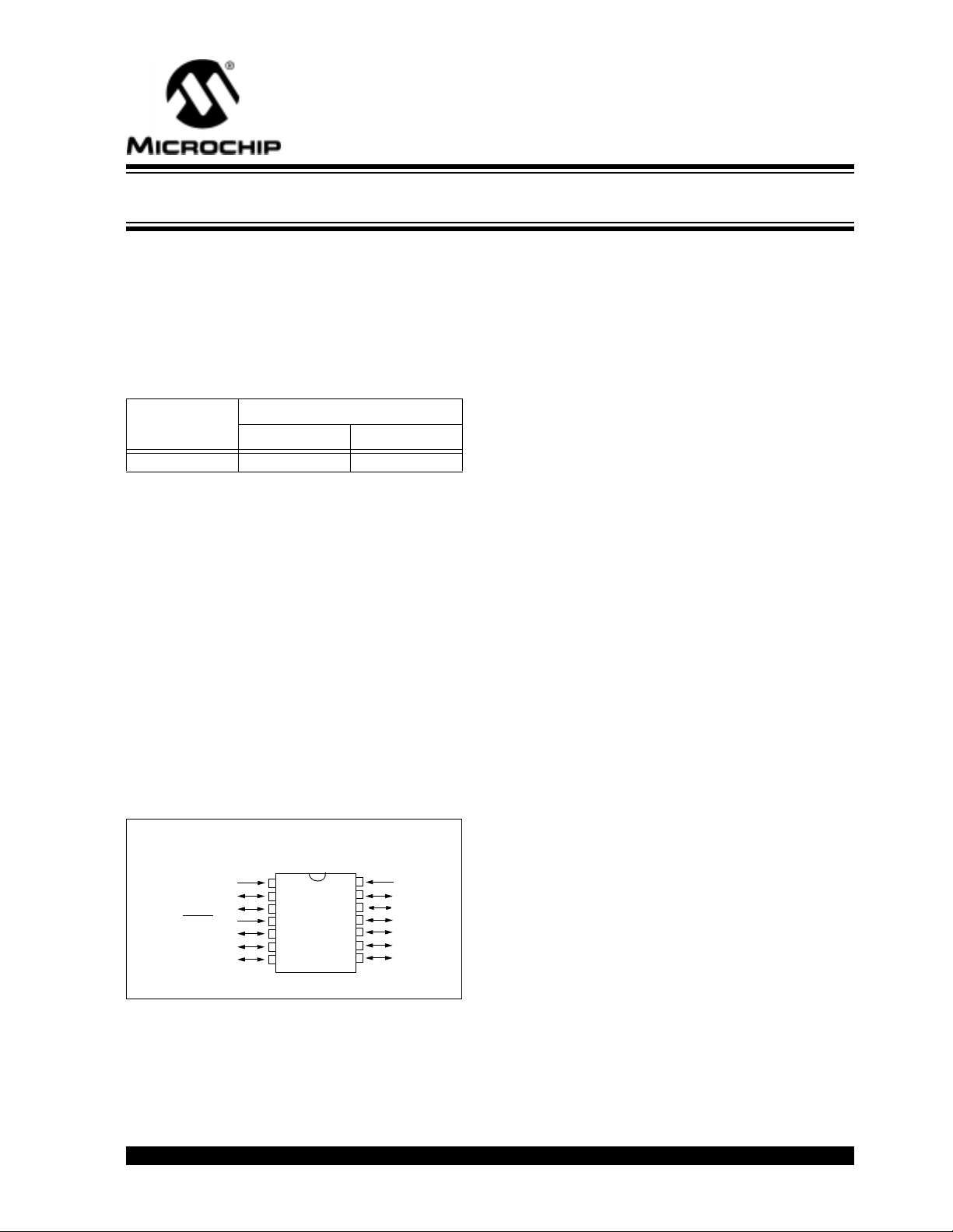
Pin Diagram:
PDIP, SOIC, Ceramic Side Brazed
RB5/OSC1/CLKIN
RB4/OSC2/CLKOUT
RB3/MCLR
VDD
/VPP
RC5/T0CKI
RC4
RC3
1
2
3
4
5
6
7
14
PIC16C505
13
12
11
10
9
8
V
SS
RB0
RB1
RB2
RC0
RC1
RC2
Special Microcontroller Features:
• In-Circ uit Serial Programming (ICSP™)
• Power-on Reset (POR)
• Device Reset Timer (DRT)
• Watchdog Timer (WDT) with dedicated on-chip
RC oscillator for reliable operation
• Programmable Code Protection
• Internal weak pull-ups on I/O pins
• Wake-up from Sleep on pin change
• Power-saving Sleep mode
• Selectable oscillator options:
- INTRC: Precision internal 4 MHz oscillator
- EXTRC: External low-cost RC oscillator
- XT: Standard crystal/resonator
- HS: High speed crystal/resonator
- LP: Power saving, low frequency
crystal
CMOS Technology:
• Low-power, high-speed CMOS EPROM
technology
• Fully static design
• Wide operating voltage range (2.5V to 5.5V)
• Wide temp erature ranges
- Commercial: 0°C to +70°C
- Industrial: -40°C to +85°C
- Extended: -40°C to +125°C
- < 1.0 µA typical standby curre nt @ 5V
• Low power consumption
- < 2.0 mA @ 5V, 4 MHz
-15µA typical @ 3.0V, 32 kHz for TMR0
running in SLEEP mode
- < 1.0 µA typical standby curre nt @ 5V
1999 Microchip Technology Inc. DS40192C-page 1
Page 2

PIC16C505
TABLE OF CONTENTS
1.0 General Description................................................................................................ .. .... .. .............................................................3
2.0 PIC16C505 Device Varieties.......................................................................................................................................................5
3.0 Architectural Overview ................................................................................................................................................................7
4.0 Memory Organization................................................................................................................................................................11
5.0 I/O Port............ ......................... ...................................... ...................................... ........................... .......................................... 19
6.0 Timer0 Module and TMR0 Register ..........................................................................................................................................23
7.0 Special Features of the CPU.....................................................................................................................................................27
8.0 Instruction Set Summary........................................................................................................................................................... 39
9.0 Development Support................................................................................................................................................................ 51
10.0 Electrical Characteristics - PIC16C505 ..................................................................................................................................... 57
11.0 DC and AC Characteristics - PIC16C505.................................................................................................................................. 71
11.0 Packaging Informatio n...... ......................... .................................................. .......................... .................................................. ..75
Index .................................................................. ...... .... ....... ...... .... .... ......... .... .... ..................................................................................79
On-Line Support........................................................... ......... .. .... .... .. ......... .. .... .... .. ......... ..................................................................... 81
Reader Response................................................................................................................................................................................82
PIC16C505 Product Identification System ..........................................................................................................................................83
To Our Valued Customers
Most Current Data Sheet
To obtain the most up-to-date version of this data sheet, please register at our Worldwide Web site at:
http://www.microchip.com
You can determine the version of a data sheet by examining its literature number found on the bottom outside corner of any page.
The last character of the literature number is the version number. e.g., DS30000A is version A of document DS30000.
New Customer Notification System
Register on our web site (www.microchip.com/cn) to receive the most current information on our products.
Errata
An errata sheet may exist for current devices, describing minor operational differences (from the data sheet) and recommended
workarounds. As device/documentation issues become known to us, w e will pub lish an errata sheet. The errata will specify the re vision of silicon and revision of document to which it applies.
To determine if an errata sheet exists for a particular device, please check with one of the following:
• Microchip’s Worldwide Web site; http://www.microchip.com
• Your local Microchip sales office (see last page)
• The Microchip Corporate Literature Center; U.S. FAX: (480) 786-7277
When contacting a sales office or the literature center, please specify which device, revision of silicon and data sheet (include liter-
ature number) you are using.
Corrections to this Data Sheet
We constantly strive to improve the quality of all our products and documentation. We have spent a great deal of time to ensure
that this document is correct. However , w e realize that we ma y ha v e missed a f ew things . If y ou find any inf ormation that is missi n g
or appears in error, please:
• Fill out and mail in the reader response form in the back of this data sheet.
• E-mail us at webmaster@microchip.com.
We appreciate your assistance in making this a better document.
DS40192C-page 2
1999 Microchip Technology Inc.
Page 3

PIC16C505
1.0 GENERAL DESCRIPTION
The PIC16C505 from Microchip Technology is a lowcost, high-performance, 8-bit, fully static, EPROM/
ROM-based CM OS microc ontroller. It employs a RISC
architecture with only 33 single word/single cycle
instructions. All instructions are single cycle (200 µs)
except for program branches, which take two cycles.
The PIC16C505 del ivers pe rformanc e an order of magnitude higher than its com petitors in the sam e price category. The 12-bit wide instructions are highly
symmetrical resulti ng in a typical 2:1 code co mpression
over other 8-bit microcontrollers in its class. The easy
to use and easy to remember instruction set reduces
development time significantly.
The PIC16C505 product is equipped with special features that reduce system cost and pow er requirements .
The Power-On Reset (POR) and Device Reset Timer
(DRT) eliminate the need for external reset circuitry.
There are five oscillator configurations to choose from,
including INTRC internal oscillator mode and the
power-saving LP (L ow Power) oscilla tor mode. Power
saving SLEEP mode, Watchdog Timer and code
protection features improve system cost, power and
reliability.
The PIC16C505 is available in the cost-effective OneTime-Program mable (OTP) version, which is suitable
for production in any volume. The customer can take
full advantage of Microchip’s price leadership in OTP
microcontrollers, while benefiting from the OTP’s
flexibility.
The PIC16C505 produ ct is supported by a f ull-fea tured
macro assembler, a software simulator, an in-circuit
emulator, a ‘C’ compiler, a low-cost development programmer and a full featured programmer. All the tools
are supported on IBM
PC and compatible machines.
1.1 Applications
The PIC16C505 fits in applications ranging from personal care appliances and security systems to lowpower remote transmitters/receivers. The EPROM
technology makes customizing application programs
(transmitter codes, appliance settings, receiver frequencies, etc.) extremely fast and convenient. The
small footprint packages, for through hole or surface
mounting, make this microc ontroller pe rfe ct f or applic ations with space limitations . Lo w-cost, lo w-po we r, highperformance, ease of use and I/O flexibility make the
PIC16C505 very versatile even in areas where no
microcontroller use has been considered before (e.g.,
timer functions, replacement of “glue” logic and PLD’s
in larger systems, and coprocessor applications).
1999 Microchip Technology Inc. DS40192C-page 3
Page 4
PIC16C505
TABLE 1-1: PIC16C505 DEVICE
PIC16C505
Clock
Memory
Peripherals
Features
The PIC16C505 device has Power-on Reset, selectable Watchdog Timer, selectable code protect, high I/O current capability and
precision internal oscillator.
The PIC16C505 device uses serial programming with data pin RB0 and clock pin RB1.
Maximum Frequency
of Operation (MHz)
EPROM Program Memory 1024
Data Memory (bytes) 72
Timer Module(s) TMR0
Wake-up from SLEEP on
pin change
I/O Pins 11
Input Pins 1
Internal Pull-ups Yes
In-Circuit Serial Programming Yes
Number of Instructions 33
Packages 14-pin DIP, SOIC, JW
20
Yes
DS40192C-page 4
1999 Microchip Technology Inc.
Page 5

PIC16C505
2.0 PIC16C505 DEVICE VARIETIES
A variety of packaging options are available.
Depending on application and production
requirements, the proper device option can be
selected using the information in this section. When
placing orders, please use the PIC16C505 Product
Identification System at the back of this data sheet to
specify the correct part number.
2.1 UV Erasable Devices
The UV erasable version, offered in a ceramic windowed package, is optimal for prototype development
and pilot programs.
The UV erasable version can be erased and
reprogrammed to any of the configuration modes.
Note: Please note that erasing the device will
also erase the pre-programmed internal
calibration value for the internal oscillator.
The calibration value must be saved prior
to erasing the part.
Microchip’s PIC ST A RT
grammers all support programming of the PIC16C505.
Third party programmers also are a vailab le; ref er to the
Microchip Third Party Gu ide,
sources.
PLUS and PRO MATE II pro-
(DS00104), for a list of
2.3 Quick-Turnaround-Production (QTP)
Devices
Microchip offers a QTP Programming Service for
factory production orders. This service is made
2.2 One-Time-Programmable (OTP) Devices
The availability of OTP devices is especially useful for
customers who need the flexibility of frequent code
updates or small volume applications.
The OTP devices, packaged in plastic packages, permit the user to program them once. In addition to the
program memory, the configuration bits must also be
programmed.
1999 Microchip Technology Inc. DS40192C-page 5
Page 6

PIC16C505
NOTES:
DS40192C-page 6
1999 Microchip Technology Inc.
Page 7

PIC16C505
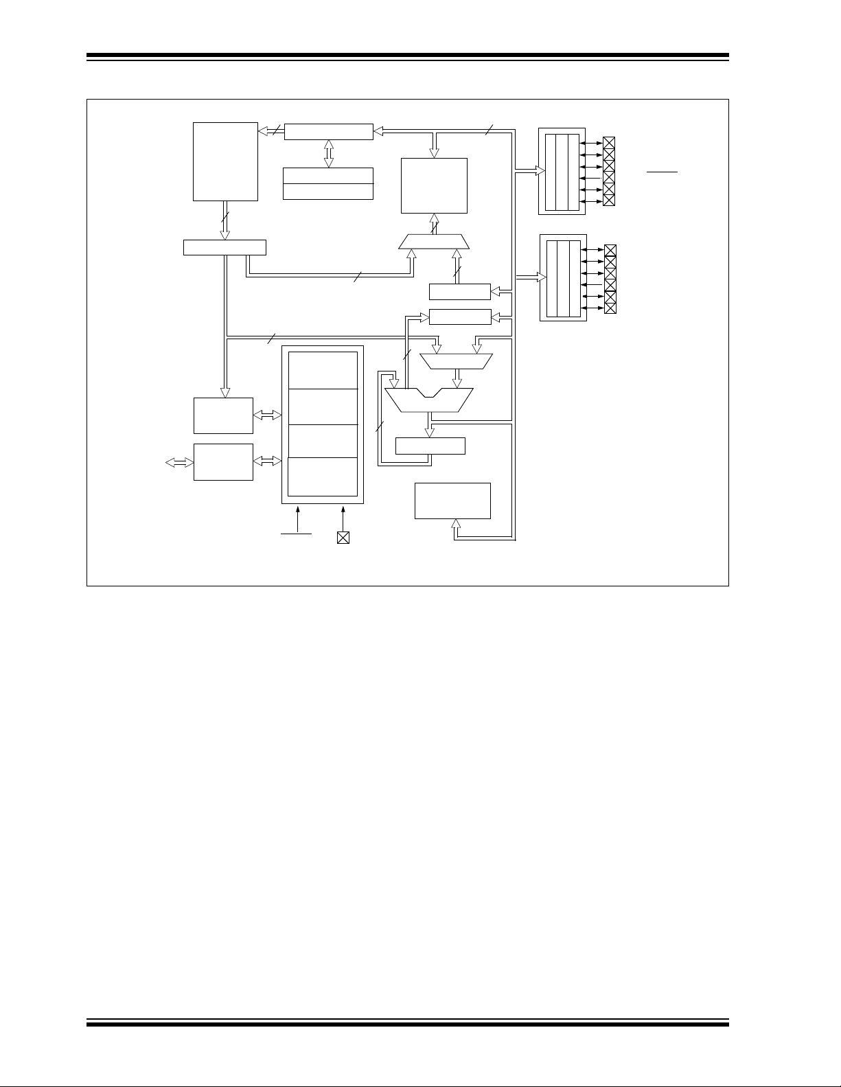
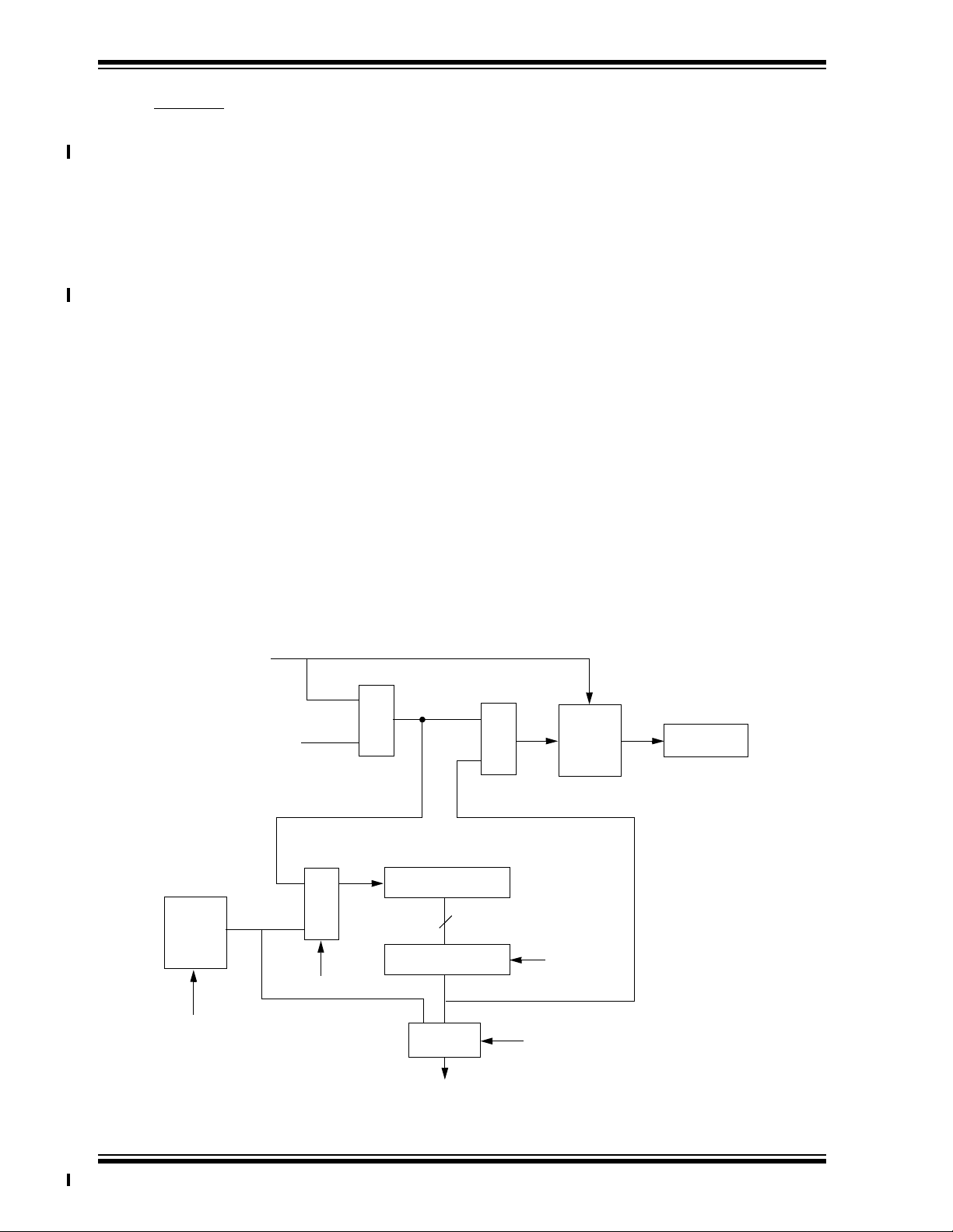
3.0 ARCHITECTURAL OVERVIEW
The high performance of the PIC16C505 can be
attributed to a number of architectural features
commonly found in RISC microprocessors. To begin
with, the PIC16C505 uses a Harvard architecture in
which program and data are accessed on separate
buses. This improves bandwidth over traditional von
Neumann architecture where program and data are
fetched on the same bus. Separating program and
data memory further allows instructions to be sized
differently than the 8-bit wide data word. Instruction
opcodes are 12 bits wide, making it possible to have
all single word instructions. A 12-bit wide program
memory access bus fetches a 12-bit instruction in a
single cycle. A two-stage pipeline overlaps fetch and
ex ecutio n of ins tructions . Co nsequ ently, all instructions
(33) execute in a single cycle (200ns @ 20MHz)
except for program branches.
The Table below lists program memory (EPROM) and
data memory (RAM) for the PIC16C505.
Memory
Device
Program Data
PIC16C505 1024 x 12 72 x 8
The PIC16C505 device contains an 8-bit ALU and
working register. The ALU is a general purpose
arithmetic unit. It performs arithmetic and Boolean
functions betwe en data in the wo rking register and an y
register file.
The ALU is 8-bits wide and capable of addition,
subtraction, shift and logical operations. Unless
otherwise mentioned, arithmetic operations are two's
complement in nature. In two-operand instructions,
one operand is typically the W (working) register. The
other operand is either a file register or an immediate
constant. In single o pera nd ins tructions , th e oper an d is
either the W register or a file register.
The W register is an 8-bit working register used for
ALU operations. It is not an addressable register.
Depending on the instruction executed, the ALU may
affect the values of the Carry (C), Digit Carry (DC),
and Zero (Z) bits in the STATUS register. The C and
DC bits operat e as a borrow
respectively, in subtracti on. See the SUBWF and ADDWF
instructions for examples.
A simplified block diagram is shown in Figure 3-1, with
the corresponding device pins described in Table 3-1.
and digit bor row out bit,
The PIC16C505 can directly or indirectly address its
register files and data memory. All special function
registers, including the program counter, are mapped
in the data memory. The PIC16C505 has a highly
orthogonal (symmetrical) instruction set that makes it
possible to carry out any operation on any register
using any addre ssing mode. This sy mmetrical nat ure
and lack of ‘special optimal situations’ make
programming with the PIC16C505 simple yet efficient.
In addition, the learning curve is reduced significantly.
1999 Microchip Technology Inc. DS40192C-page 7
Page 8
PIC16C505
FIGURE 3-1: PIC16C505 BLOCK DIAGRAM
OSC1/CLKIN
OSC2
Program
Bus
EPROM
1K x 12
Program
Memory
12
Instruction reg
Instruction
Decode &
Control
Timing
Generation
12
Program Counter
STACK1
STACK2
Direct Addr
8
Device Reset
Timer
Power-on
Reset
Watchdog
Timer
Internal RC
OSC
RAM Addr
5
Data Bus
Addr MUX
3
8
RAM
e
t
y
b
2
7
File
Registers
9
5-7
FSR reg
STATUS reg
MUX
ALU
W reg
Timer0
s
Indirect
Addr
8
PORTB
RB0
RB1
RB2
RB3/MCLR/VPP
RB4/OSC2/CLKOUT
RB5/OSC1/CLKIN
PORTC
RC0
RC1
RC2
RC3
RC4
RC5/T0CKI
MCLR
VDD, VSS
DS40192C-page 8
1999 Microchip Technology Inc.
Page 9
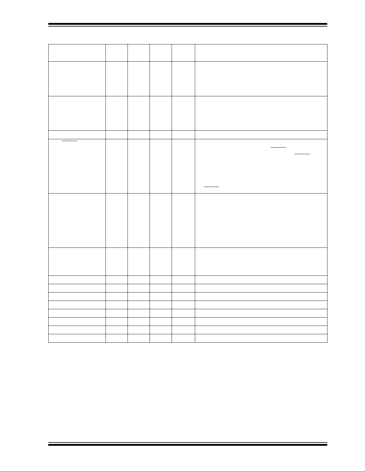
TABLE 3-1: PIC16C505 PINOUT DESCRIPTION
PIC16C505
Name
RB0 13 13 I/O TTL/ST Bi-directional I/O port/ serial programming data. Can
RB1 12 12 I/O TTL/ST Bi-directional I/O po rt/ serial programming clock. Can
RB2 11 11 I/O TTL Bi-directional I/O port.
RB3/MCLR
RB4/OSC2/CLKOUT 3 3 I/O TTL Bi-directional I/O port/oscillator crystal output. Con-
RB5/OSC1/CLKIN 2 2 I/O TTL/ST Bidirectional IO port/oscillator crystal input/external
RC0 10 10 I/O TTL Bi-directional I/O port.
RC1 9 9 I/O TTL Bi-directional I/O port.
RC2 8 8 I/O TTL Bi-directional I/O port.
RC3 7 7 I/O TTL Bi-directional I/O port.
RC4 6 6 I/O TTL Bi-directional I/O port.
RC5/T0CKI 5 5 I/O ST Bi-directional I/O port. Can be configured as T0CKI.
DD 11P— Positive supply for logic and I/O pins
V
VSS 14 14 P — Ground reference for logic and I/O pins
Legend: I = input, O = output, I/O = input/output, P = power, — = not used, TTL = TTL input,
/VPP 4 4 I TTL/ST Input port/master clear (reset) input/programming volt-
ST = Schmitt Trigger input
DIP
Pin #
SOIC
Pin #
I/O/P
Type
Buffer
Type
Description
be software progr am med f o r internal weak pull-up and
wake-up from SLEEP on pin change. This buffer is a
Schmitt Trigger input when used in serial progr amming
mode.
be software progr am med f o r internal weak pull-up and
wake-up from SLEEP on pin change. This buffer is a
Schmitt Trigger input when used in serial progr amming
mode.
age input. When configured as MCLR
active low reset to the device. Voltage on MCLR
must not exceed V
Can be software p rogr ammed f or internal weak pull-up
and wake-up from SLEEP on pin change. Weak pullup only when config ure d as R B3. ST w hen co nfi gured
as MCLR.
nections to crystal or resonator in crystal oscillator
mode (XT and LP modes only, RB4 in other modes).
Can be software p rogr ammed f or internal weak pull-up
and wake-up from SLEEP on pin change. In EXTRC
and INTRC modes, th e pin output can b e configured to
CLKOUT, which has 1/4 the frequency of OSC1 and
denotes the instruction cycle rate.
clock source input (RB5 in Internal RC mode only,
OSC1 in all other oscillator modes). TTL input when
RB5, ST input in external RC oscillator mode.
DD during normal device operation.
, this pin is an
/VPP
1999 Microchip Technology Inc. DS40192C-page 9
Page 10
PIC16C505
3.1 Clocking Scheme/Instruction Cycle
The clock input (OSC1/CLKIN pin) is internally divided
by four to generate four non-overlapping quadrature
clocks namely Q1, Q2, Q3 and Q4. Internally, the
program counter is incremented every Q1, and the
instruction is fetched from program memory and
latched into the in st ruction register in Q4. It is d ec ode d
and executed during the following Q1 through Q4. The
clocks and instruction execution flow is shown in
Figure 3-2 and Example 3-1.
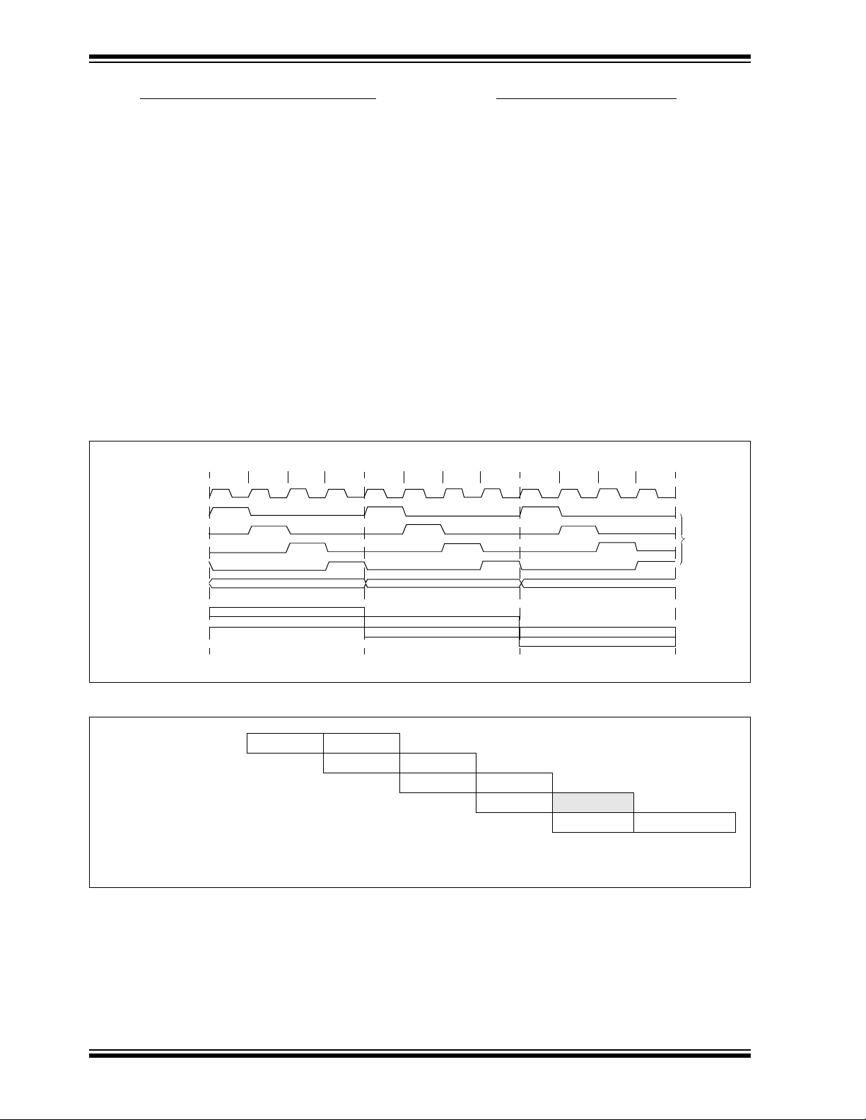
FIGURE 3-2: CLOCK/INSTRUCTION CYCLE
Q2 Q3 Q4
OSC1
Q1
Q2
Q3
Q4
PC
Q1
PC PC+1 PC+2
Q1
3.2 Instruction Flow/Pipelining
An Instruction cycle consists of four Q cycles (Q1, Q2,
Q3 and Q4). The instruction fetch and execute are
pipelined such that fetch takes one instruction cycle,
while decode and execute takes another instruction
cycle. However, due to the pipelining, each instruction
effectively executes in one cycle. If an instruction
causes the program counter to change (e.g., GOTO)
then two cycles are required to complete the
instruction (Example 3-1).
A fetch cycle begins with the program counter (PC)
incrementing in Q1.
In the execution cycle, the fetched instruction is
latched into the Instruction Register (IR) in cycle Q1.
This instruction is then decoded and executed during
the Q2, Q3 and Q4 cycles. Data memory is read
during Q2 (operand read) and written during Q4
(destination write).
Q2 Q3 Q4
Q1
Q2 Q3 Q4
Internal
phase
clock
Fetch INST (PC)
Execute INST (PC-1) Fetch INST (PC+1)
Execute INST (PC) Fetch INST (PC+2)
Execute INST (PC+1)
EXAMPLE 3-1: INSTRUCTION PIPELINE FLOW
1. MOVLW 03H
2. MOVWF PORTB
3. CALL SUB_1
4. BSF PORTB, BIT1
All instructions are single cycle, except for any program branches. These take two cycles, since the fetch
instruction is “flushed” from the pipeline, while the new instruction is being fetched and then executed.
Fetch 1 Execute 1
Fetch 2 Execute 2
Fetch 3 Execute 3
Fetch 4 Flush
Fetch SUB_1 Execute SUB_1
DS40192C-page 10
1999 Microchip Technology Inc.
Page 11
PIC16C505
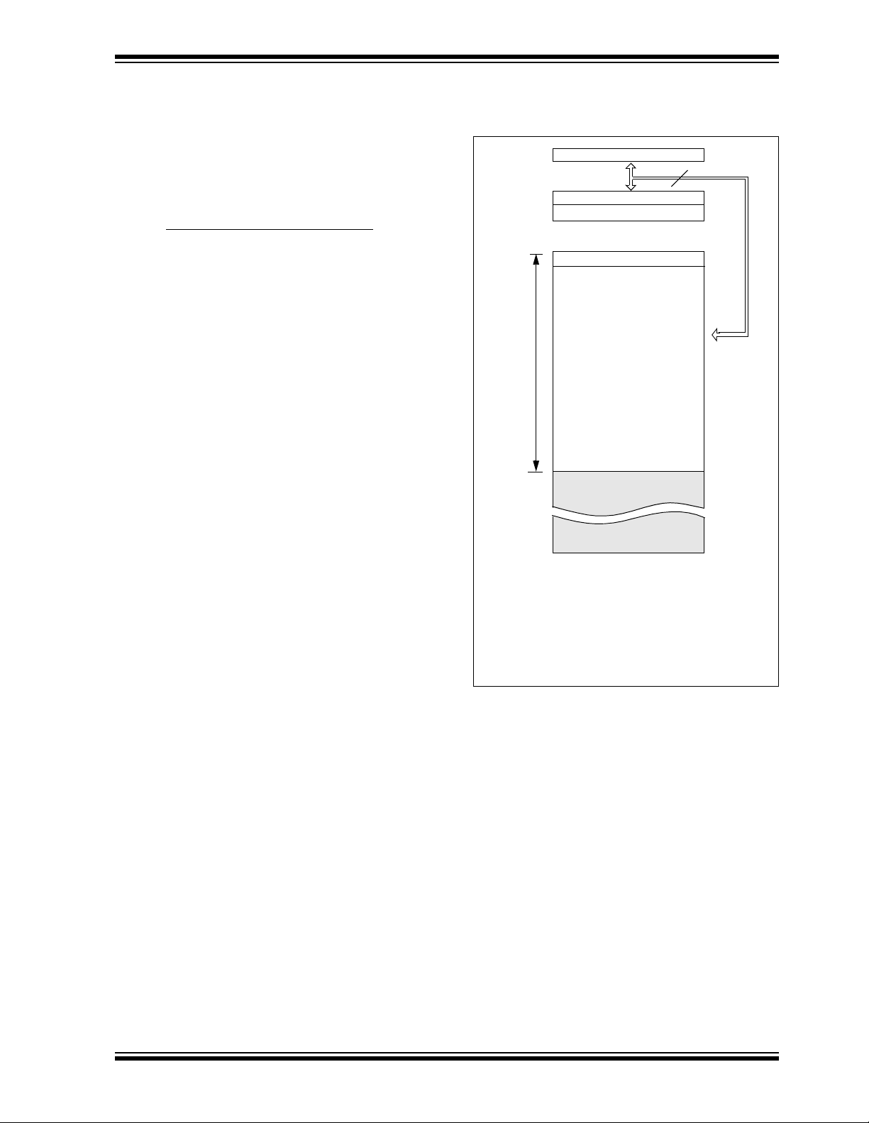
4.0 MEMORY ORGANIZATION
PIC16C505 memory is organized into program memory and data memory. For the PIC16C505, a paging
scheme is used. Program memory pages are
accessed using one STATUS register bit. Data memory banks are accessed using the File Select Register
(FSR).
4.1 Program Memory Organization
The PIC16C505 devices have a 12-bit Program
Counter (PC).
The 1K x 12 (0000h-03FFh) for the PIC16C505 are
physically implemented. Refer to Figure 4-1.
Accessing a location above this boundary will cause a
wrap-around within the first 1K x 12 space. The
effective reset vector is at 0000h, (see Figure 4-1).
Location 03FFh contains the internal clock oscillator
calibration value. This value should never be
overwritten.
FIGURE 4-1: PROGRAM MEMORY MAP
AND STACK FOR THE
PIC16C505
PC<11:0>
CALL, RETLW
Stack Level 1
Stack Level 2
Reset Vector (note 1)
Space
User Memory
On-chip Program
Memory
1024 Words
12
0000h
01FFh
0200h
03FFh
0400h
Note 1: Address 0000h becomes the
effective reset vector . Location 03FFh
contains the MOVLW XX INTERNAL RC
oscillator calibration value.
7FFh
1999 Microchip Technology Inc. DS40192C-page 11
Page 12
PIC16C505
4.2 Data Memory Organization
Data memory is composed of registers or bytes of
RAM. Therefore, data memory for a device is specified
by its register file. The register file is divided into two
functional groups: Special Function Registers and
General Purpose Registers.
The Special Function Registers include the TMR0
register, the Program Counter (PCL), the Status
Register, the I/O registers (ports) and the File Select
Register (FSR). In addition, Special Function
Registers are used to control the I/O port configuration
and prescaler options.
The General Purpose Registers are used for data and
control inf ormation un der c om m and of the instructions.
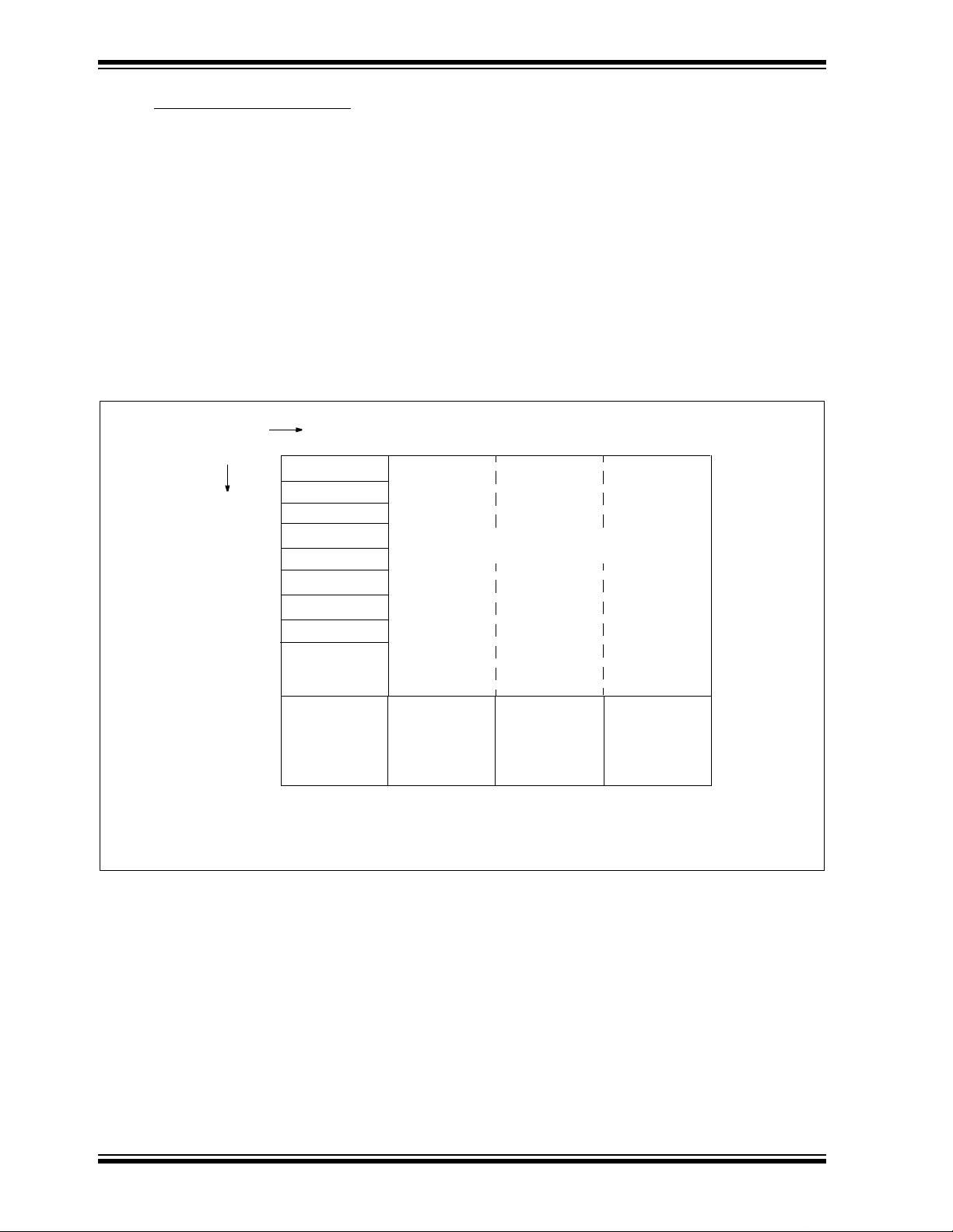
FIGURE 4-2: PIC16C505 REGISTER FILE MAP
FSR<6:5> 00 01
File Address
00h
01h
02h
03h
04h
05h
06h
07h
08h
0Fh
10h
1Fh
(1)
INDF
TMR0
PCL
STATUS
FSR
OSCCAL
PORTB
PORTC
General
Purpose
Registers
General
Purpose
Registers
Bank 0
20h
2Fh
30h
General
Purpose
Registers
3Fh
Bank 1
For the PIC16C505, the register file is composed of 8
Special Function Registers, 24 General Purpose
Registers and 48 General Purpose Registers that may
be addressed using a banking scheme (Figure 4-2).
4.2.1 GENERAL PURPOSE REGISTER FILE The General Purpose Register file is accessed, either
directly or indirectly, through th e File Select Register
FSR (Section 4.8).
10
40h
Addresses map back to
addresses in Bank 0.
4Fh
50h
General
Purpose
Registers
5Fh
Bank 2
11
60h
6Fh
70h
General
Purpose
Registers
7Fh
Bank 3
DS40192C-page 12
Note 1: Not a physical register.
1999 Microchip Technology Inc.
Page 13
PIC16C505
4.2.2 SPECIAL FUNCTION REGISTERS
The Special Function Registers (SFRs) are registers
used by the CPU and peripheral functions to control
the operation of the device (Table 4-1).
The Special Function Registers can be classified into
two sets. The Special Function Registers associated
with the “core” functions are described in this section.
Those related to the operation of the peripheral
features are described in the section for each
peripheral feature.
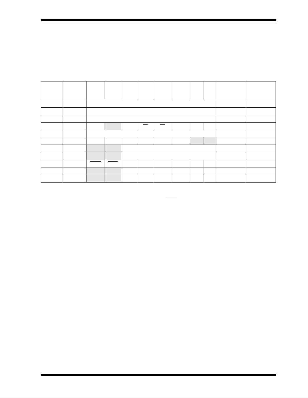
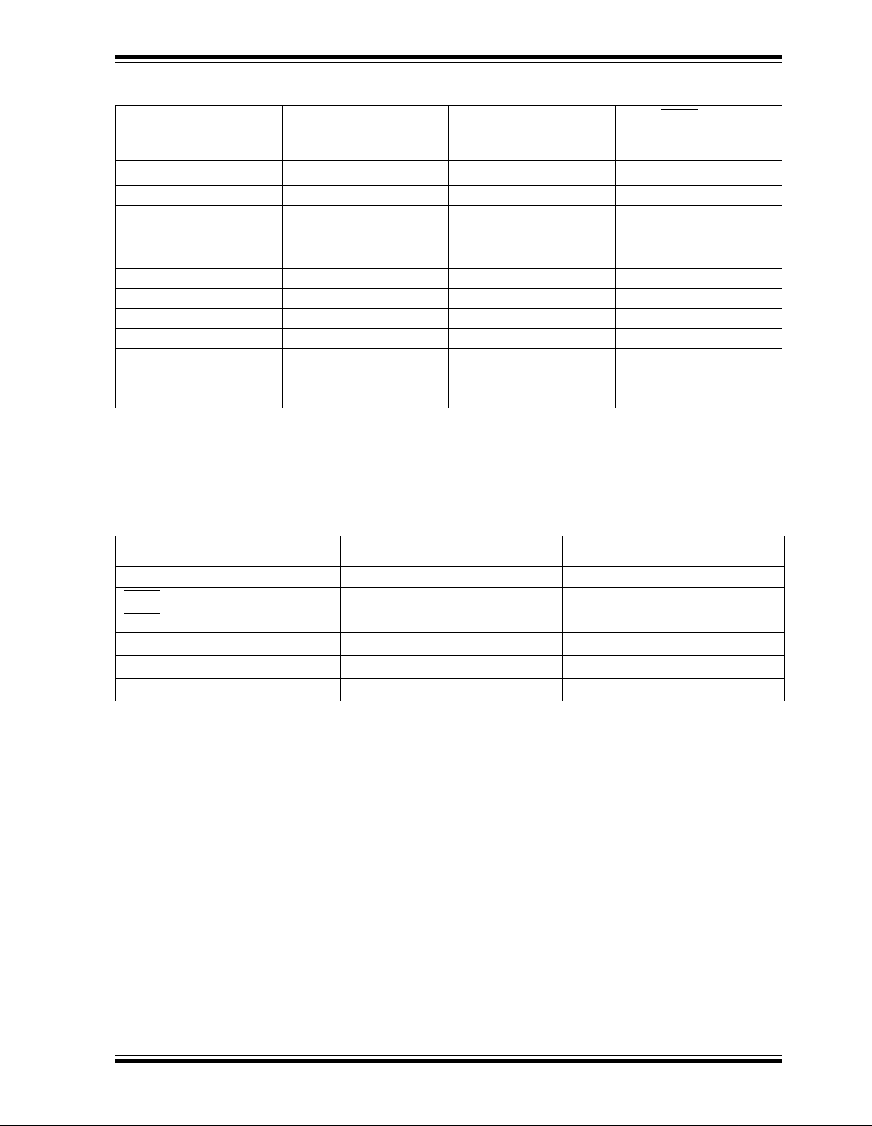
TABLE 4-1: SPECIAL FUNCTION REGISTER (SFR) SUMMARY
Value on
Power-On
Address Name Bit 7 Bit 6 Bit 5 Bit 4 Bit 3 Bit 2 Bit 1 Bit 0
00h INDF Uses contents of FSR to address data memory (not a physical register)
01h TMR0 8-bit real-time clock/counter
(1)
02h
03h STATUS RBWUF —PAOTO PD ZDCC
04h
05h OSCCAL CAL5 CAL4 CAL3 CAL2 CAL1 CAL0 — —
N/A TRISB — — I/O contro l reg ister s
N/A TRISC — — I/O control registers
N/A OPTION RBWU RBPU TOCS TOSE PSA PS2 PS1 PS0
06h PORTB — — RB5 RB4 RB3 RB2 RB1 RB0
07h POR TC — — RC5 RC4 RC3 RC2 RC1 RC0
Legend: Shaded cells not used by Port Registers, read as ‘0’, — = unimplemented, read as ‘0’, x = unknown, u = unchanged,
Note 1: If reset was due to wake-up on pin change, then bit 7 = 1. All other rests will cause bit 7 = 0.
Note 2: Other (non-power-up) resets include external reset through MCLR
PCL Low order 8 bits of PC
FSR
q = depends on condition.
Indirect data memory address pointer
, watchdog timer and wake-up on pin change reset.
Reset
xxxx xxxx uuuu uuuu
xxxx xxxx uuuu uuuu
1111 1111 1111 1111
0001 1xxx q00q quuu
110x xxxx 11uu uuuu
1000 00-- uuuu uu--
--11 1111 --11 1111
--11 1111 --11 1111
1111 1111 1111 1111
--xx xxxx --uu uuuu
--xx xxxx --uu uuuu
Val ue on
All Other
Resets
(2)
(1)
1999 Microchip Technology Inc. DS40192C-page 13
Page 14

PIC16C505
4.3 STATUS Register
For example, CLRF STATUS will clear the upper three
bits and set the Z bit. This leaves the STATUS register
This register contains the arithmetic status of the ALU,
the RESET status and the page preselect bit.
The STATUS register can be the destination for any
instruction, as with any other register. If the STATUS
register is the destination for an instruction that affe cts
the Z, DC or C bits, then the write to these three bits is
disabled. These bits are set or cleared according to
the device logic. Furthermore, the TO
and PD bits are
as 000u u1uu (where u = unchanged).
It is recommended, therefore, that only BCF, BSF and
MOVWF instructions be used to alter the STATUS
register, because these instructions do not affect the
Z, DC or C bits from the STATUS register. For other
instructions, which do affect STATUS bits, see
Instruction Set Summary.
not writable. Therefore, the result of an instruction with
the STATUS register as destination may be different
than intended.
REGISTER 4-1: STATUS REGISTER (ADDRESS:03h)
R/W-0 R/W-0 R/W-0 R-1 R -1 R/W-x R/W-x R/W-x
RBWUF
bit7 6 5 4 3 2 1 bit0
bit 7: RB WUF: I/O reset bit
bit 6: Unimplemented
bit 5: PA0: Program page preselect bits
bit 4: TO
bit 3: PD
bit 2: Z: Zero bit
bit 1: DC: Digit carry/borrow
bit 0: C: Carry/borrow
—
1 = Reset due to wake-up from SLEEP on pin change
0 = After power up or other reset
1 = Page 1 (200h - 3FFh)
0 = Page 0 (000h - 1FFh)
Each page is 512 bytes.
Using the PA0 bit as a general purpose read/write bit in devices which do not use it for program
page preselect is not recommended, since this may affect upward compatibility with future products.
: Time-out bit
1 = After power-up, CLRWDT instruction, or SLEEP instruction
0 = A WDT time-out occurred
: Power-down bit
1 = After power-up or by the CLRWDT instruction
0 = By execution of the SLEEP instruction
1 = The result of an arithmetic or logic operation is zero
0 = The result of an arithmetic or logic operation is not zero
ADDWF
1 = A carry from the 4th low order bit of the result occurred
0 = A carry from the 4th low order bit of the result did not occur
SUBWF
1 = A borrow from the 4th low order bit of the result did not occur
0 = A borrow from the 4th low order bit of the result occurred
ADDWF SUBWF RRF or RLF
1 = A carry occurred 1 = A borrow did not occur Load bit with LSB or MSB, respectively
0 = A carry did not occur 0 = A borrow occurred
PA0 TO PD Z DC C R = Readable bit
bit (for ADDWF and SUBWF instructions)
bit (for ADDWF, SUBWF and RRF, RLF instr uct i ons)
W = Writable bit
U = Unimplemented bit,
read as ‘0’
- n = Value at POR reset
DS40192C-page 14
1999 Microchip Technology Inc.
Page 15

PIC16C505
4.4 OPTION Register
The OPTION register is a 8-bit wide, write-only
register, which contains various control bits to
configure the Timer0/WDT prescaler and Timer0.
Note: If TRIS bit is set to ‘0’, the wake-up on
change and pull-up functions are disabled
for that pin (i.e., note that TRIS overrides
OPTION control of RBPU
By executing the OPTION instruction, the contents of
the W register will be transferred to the OPTION
register. A RESET sets the OPTION<7:0> bits.
REGISTER 4-2: OPTION REGISTER
W-1 W-1 W-1 W-1 W-1 W-1 W-1 W-1
RBWU
bit7 6 5 4 3 2 1 bit0
bit 7: RB WU
bit 6: RB PU
bit 5: T0CS : Timer0 clock source select bit
bit 4: T0SE: Timer0 source edge select bit
bit 3: PS A : Prescaler assignment bit
bit 2-0: PS<2:0>: Prescaler rate select bits
RBPU T0CS T 0SE PSA PS2 PS1 PS0 R = Readable bit
: Enable wake-up on pin change (RB0, RB1, RB3, RB4)
1 = Disabled
0 = Enabled
: Enable weak pull-ups (RB0, RB1, RB3, RB4)
1 = Disabled
0 = Enabled
1 = Transition on T0CKI pin (overrides TRIS <RC57>
0 = Transition on internal instruction cycle clock, Fosc/4
1 = Increment on high to low transition on the T0CKI pin
0 = Increment on low to high transition on the T0CKI pin
1 = Prescaler assigned to the WDT
0 = Prescaler assigned to Timer0
Bit Value Timer0 Rate WDT Rate
000
001
010
011
100
101
110
111
1 : 2
1 : 4
1 : 8
1 : 16
1 : 32
1 : 64
1 : 128
1 : 256
1 : 1
1 : 2
1 : 4
1 : 8
1 : 16
1 : 32
1 : 64
1 : 128
and RBWU).
W = Writable bit
U = Unimplemented bit,
read as ‘0’
- n = Value at POR reset
1999 Microchip Technology Inc. DS40192C-page 15
Page 16

PIC16C505
4.5 OSCCAL Register
The Oscillator Calibration (OSCCAL) register is used to
calibrate the internal 4 MHz oscillator. It contains six
bits for calibration
Note: Please note that erasing the device will
also erase the pre-programmed internal
calibration value for the internal oscillator.
The calibration value must be read prior to
erasing the part, so it can be reprogrammed correctly later.
After you move in the calibration constant, do not
change the value. See Section7.2.5
REGISTER 4-3: OSCCAL REGISTER (ADDRESS 05h) PIC16C505
R/W-1 R/W-0 R/W-0 R/W-0 R/W-0 R/W-0 U-0 U-0
CAL5 CAL4 CAL3 CAL2 CAL1 CAL0
bit7 bit0
bit 7-2: CAL<5:0>: Calibration
bit 1-0: Unimplemented read as ‘0’
— — R = Readable bit
W = Writable bit
U = Unimplemented bit,
read as ‘0’
- n = Value at POR reset
DS40192C-page 16
1999 Microchip Technology Inc.
Page 17
PIC16C505
4.6 Program Counter
As a program instruction is executed, the Program
Counter (PC) will contain the address of the next
program instruction to be executed. The PC value is
increased by one every instruction cycle, unless an
instruction changes the PC.
For a GOTO instruction, bits 8:0 of the PC are provided
by the GOTO instruction word. The PC Latch (PCL) is
mapped to PC<7:0>. Bit 5 of the STATUS register
provides page information to bit 9 of the PC
(Figure 4-3).
For a CALL instruction, or any instruction where the
PCL is the destination, bits 7:0 of the PC again are
provided by the instruction word. However, PC<8>
does not come from the instruction word, but is always
cleared (Figure 4-3).
Instructions where the PCL is the destination, or
Modify PCL instructions, include MOVWF PC, ADDWF
PC, and BSF PC,5.
Note: Because PC<8> is cleared in the CALL
instructi on or any Modify PCL inst ruction,
all subroutine call s or computed jumps are
limited to the first 256 l ocations of any program memory page (512 words long).
FIGURE 4-3: LOADING OF PC
BRANCH INSTRUCTIONS PIC16C505
GOTO Instruction
11
PC
70
87 0
910
PCL
Instruction Word
PA0
STATUS
4.6.1 EFFECTS OF RESET The Program Counter is set upon a RESET, which
means that the PC addresses the last location in the
last page (i.e., the oscillator calibration instruction.)
After executing MOVLW XX, the PC will roll over to
location 00h and begin executing user code.
The STATUS register page preselect bits are cleared
upon a RESET, which means that page 0 is preselected.
Therefore, upon a RESET, a GOTO instruction will
automatically cause the program to jump to page 0
until the value of the page bits is altered.
4.7 Stack
PIC16C505 devices have a 12-bit wide hardware
push/pop stack.
A CALL instruction will push the current value of stack
1 into stack 2 and then push the current program
counter value , incremen ted b y one, into stac k le v e l 1. If
more than two sequential CALL’s are executed, only
the most recent two return addresses are stored.
A RETLW instruction will pop the contents of stac k le v e l
1 into the program counter and then copy stack level 2
contents into level 1. If more than two sequential
RETLW’s are executed, the stack will be filled with the
address previously stored in level 2. Note that the
W register will be loaded wi th the liter al v alue sp ecif ied
in the instruction. This is particularly useful for the
implementation of data look-up tables within the
program memory.
Note 1: There are no STATUS bits to indicate
stack overflows or stack underflow conditions.
Note 2: There are no instructions mnemonics
called PUSH or POP. These are actions that
occur from the execution of the CALL,
RETLW, and instructions.
CALL or Modify PCL Instruction
11
PC
70
1999 Microchip Technology Inc. DS40192C-page 17
87 0
910
PCL
Instruction Word
Reset to ‘0’
PA0
STATUS
Page 18
PIC16C505
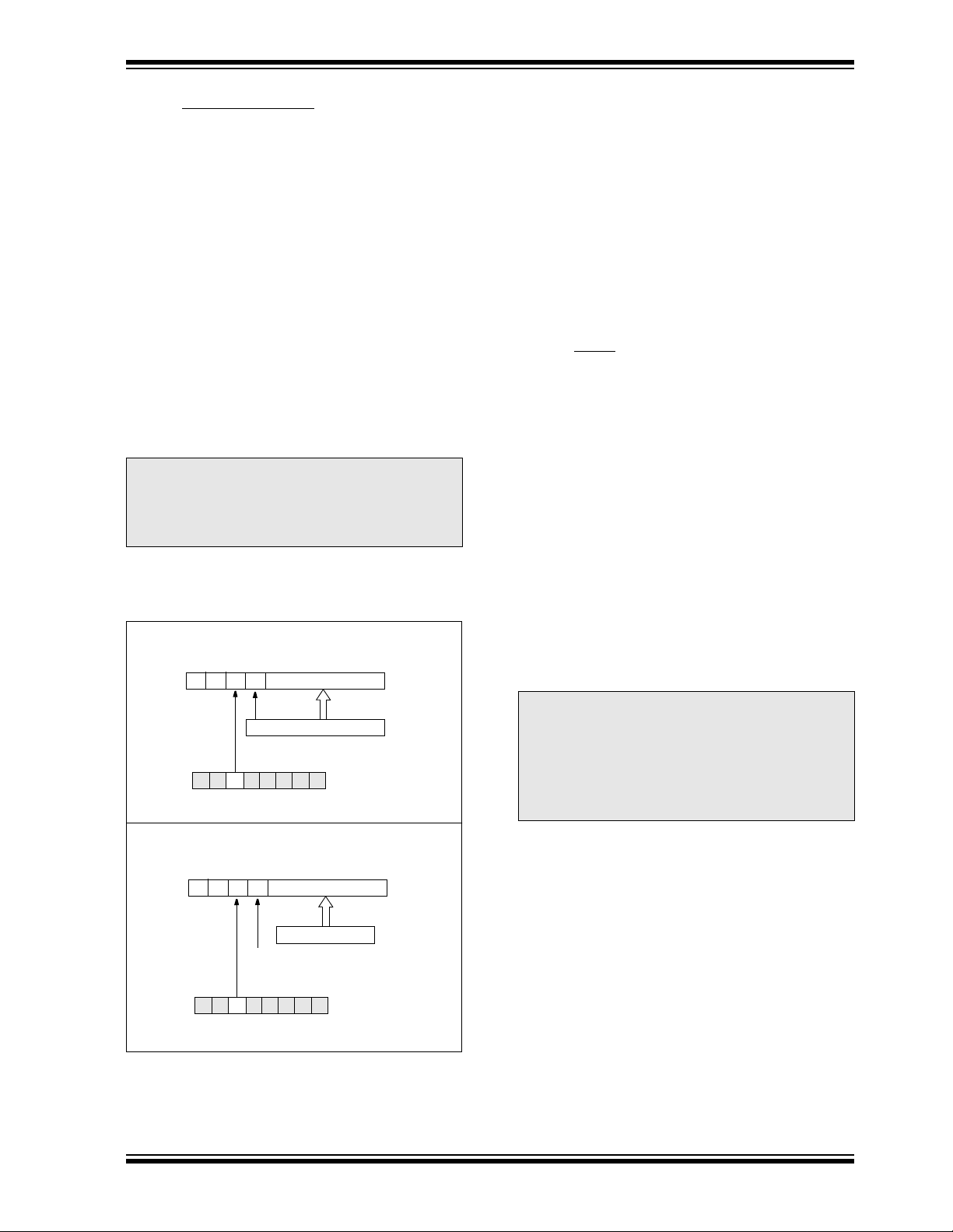
4.8 Indirect Data Addressing; INDF and FSR Registers
The INDF register is not a physical register.
Addressing INDF actually addresses the register
whose address is containe d in th e FS R reg ister (FSR
pointer
is a
). This is indirect addres sin g.
EXAMPLE 4-1: INDIRECT ADDRESSING
• Register file 07 contains the value 10h
• Register file 08 contains the value 0Ah
• Load the value 07 into the FSR register
• A read of the INDF register will return the value
of 10h
• Increment the value of the FSR register by one
(FSR = 08)
• A read of the INDR register now will return the
value of 0Ah.
Reading INDF itself indirectly (FSR = 0) will produce
00h. Writing to the INDF register indirectly results in a
no-operation (although STATUS bits may be affected).
A simple program to clear RAM locations 10h-1Fh
using indirect addressing is shown in Example 4-2.
EXAMPLE 4-2: HOW TO CLEAR RAM
USING INDIRECT
ADDRESSING
movlw 0x10 ;initialize po i nter
movwf FSR ; to RAM
NEXT clrf INDF ;clear INDF register
incf FSR,F ;inc pointer
btfsc FSR,4 ;all done?
goto NEXT ;NO, clear next
CONTINUE
: ;YES, continue
:
The FSR is a 5-bit wide register. It is used in
conjunction with the INDF reg ister to indirec tly addr ess
the data memory area.
The FSR<4:0> bits are used to select data memory
addresses 00h to 1Fh.
The device uses FSR<6:5> to select between banks
0:3.
FIGURE 4-4: DIRECT/INDIRECT ADDRESSING
Direct Addressing
(FSR)
6 5 4 (opcode) 0
bank select location select
00 01 10 11
1Fh 3Fh 5Fh 7Fh
Bank 0 Bank 1 Bank 2 Bank 3
Data
Memory
00h
0Fh
(1)
10h
Note 1: For register map detail see Section 4.2.
Addresses
map back to
addresses
in Bank 0.
Indirect Addressing
6 5 4 (FSR) 0
bank location select
DS40192C-page 18
1999 Microchip Technology Inc.
Page 19
PIC16C505
5.0 I/O PORT
As with any other register, the I/O register can be
written and read under program control. However,
read instructions (e.g., MOVF PORTB,W) always read
the I/O pins independent of the pin’s input/output
modes. On RESET, all I/O ports are defined as input
(inputs are at hi-impedance) since the I/O control
registers are all set.
5.1 PORTB
PORTB is an 8-bit I/O register. Only the low order 6
bits are used (RB<5:0>). Bits 7 and 6 are
unimplemented an d rea d as '0 's. Please note that R B3
is an input only pin. The configuration word can set
several I/O’s to alternate functions. When acting as
alternate functions, the pins will read as ‘0’ during port
read. Pins RB0, RB1, RB 3 an d RB 4 c an b e co nfi gure d
with weak pull -ups and a lso with wake-u p on chang e.
The wake-up on change and weak pull-up functions
are not pin selectable. If pin 4 is configured as MCLR
weak pull-up is always off and wake-up on change for
this pin is not enabled.
5.2 PORTC
PORTC is an 8-bit I/O register . O nly the low o rder 6 bits
are used (RC<5:0>). Bits 7 and 6 are unimplemented
and read as ‘0’s.
5.3 TRIS Registers
5.4 I/O Interfacing
The equivalent circuit for an I/O port pin is shown in
Figure 5-1. All port pins except RB3, which is input
only, may be used for b oth inp ut and out put ope ratio ns .
For input operations, these ports are non-latching. Any
input must be present until read by an input instruction
(e.g., MOVF PORTB,W). The outp uts are latc hed and
remain unchanged until th e output latch i s re written. To
use a port pin as output, the corresponding direction
control bit in TRIS mus t be cl eared (= 0). F or us e as a n
input, the corresponding TRIS bit must be set. Any I/O
pin (except RB3) can be programmed individually as
input or output.
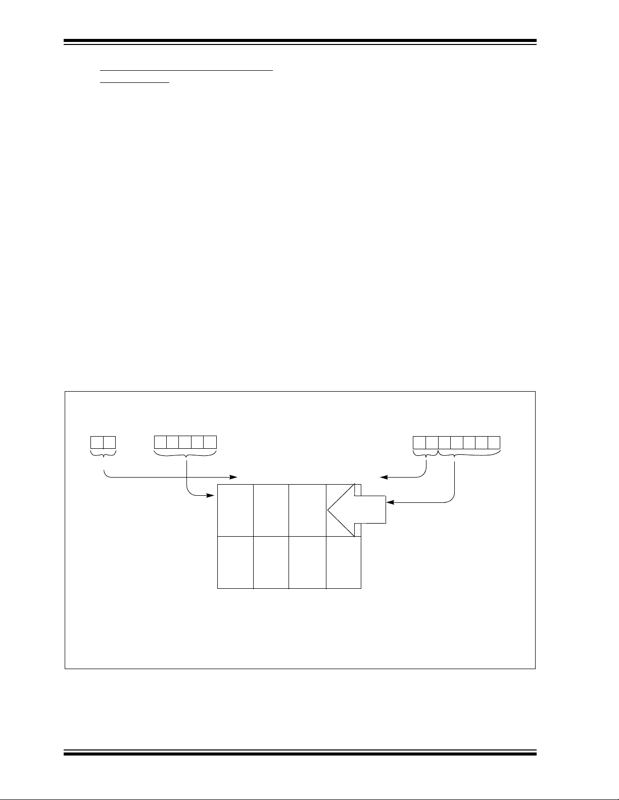
FIGURE 5-1: EQUIVALENT CIRCUIT
FOR A SINGLE I/O PIN
Data
Bus
,
WR
Port
W
Reg
TRIS ‘f’
Data
Latch
CK
TRIS
Latch
CK
QD
VDD
Q
QD
Q
P
N
V
SS
I/O
pin
(1)
The output driver control register is loaded with the
contents of the W register by executing the TRIS f
instruction. A '1' from a TRIS register bit puts the
corresponding output driver in a hi-impedance mode.
A '0' puts the contents of the output data latch on the
selected pins, enabling the output buffer. The
exceptions are RB3, which is input only, and RC5,
which may be controlled by the option register. See
Register 4-2.
Note: A read of the ports reads the pins, not the
output data latches. That is, if an output
driver on a pin is enabled and driven high,
but the external system is holding it low, a
read of the p o rt will i n di ca te t h a t th e pi n i s
low.
The TRIS registers are “write-only” and are set (output
drivers disabled) upon RESET.
Reset
Note 1: I/O pins have protection diodes to V
Note 2: See Table 3-1 for buffer type.
(2)
RD Port
DD and VSS.
1999 Microchip Technology Inc. DS40192C-page 19
Page 20
PIC16C505
TABLE 5-1: SUMMARY OF PORT REGISTERS
Address Name B it 7 Bit 6 Bit 5 Bit 4 Bit 3 Bit 2 Bit 1 B i t 0
Value on
Power-On
Reset
Value on
All Other Resets
N/A TRISB — — I/O control registers
N/A TRISC — — I/O control registers
N/A OPTION RBWU RBPU TOCS TOSE PSA PS2 PS1 PS0
03h STATUS RBWUF — PAO TO PD Z DC C
06h PORTB — — RB5 RB4 RB3 RB2 RB1 RB0
07h PORTC — — RC5 RC4 RC3 RC2 RC1 RC0
Legend: Shaded cells not used by Port Registers, read as ‘0’,
q = depends on condition.
Note 1: If reset was due to wake-up on pin change, then bit 7 = 1. All other rests will cause bit 7 = 0.
5.5 I/O Programming Considerations
5.5.1 BI-DIRECTIONAL I/O PORTS
Some instr uctions opera te intern ally as read followed
by write operations. The BCF and BSF instructions, for
example, read the entire port into the CPU, execute
the bit operation and re-write the result. Caution must
be used when these instructions are applied to a port
where one or more pins are used as input/outputs. For
example, a BSF operation on bit5 of PORTB will cause
all eight bits of PORTB to be read into the CPU, bit5 to
be set and the PORTB v al ue to be written to the output
latches. If another bit of PORTB is used as a bidirectional I/O pin (say bit0) and it is defined as an
input at this time, the input signal present on the pin
itself would be read into the CPU and rewritten to the
data latch of this particular pin, overwriting the
previous content. As long as the pin stays in the input
— = unimplemented, read as ‘0’, x = unknown, u = unchanged,
EXAMPLE 5-1: READ-MODIFY-WRITE
INSTRUCTIONS ON AN
I/O PORT
;Initial PORTB Settings
; PORTB<5:3> Inputs
; PORTB<2:0> Outputs
;
; PORTB latch PORTB pins
; ---------- --------- BCF PORTB, 5 ;--01 -ppp --11 pppp
BCF PORTB, 4 ;--10 -ppp --11 pppp
MOVLW 007h ;
TRIS PORTB ;--10 -ppp --11 pppp
;
;Note that the user may have expected the pin
;values to be --00 pppp. The 2nd BCF caused
;RB5 to be latched as the pin value (High).
5.5.2 SUCCESSIVE OPERATIONS ON I/O PORTS
mode, no problem o ccurs. However, if bit0 is switched
into output mode later on, the content of the data latch
may now be unknown.
Example 5-1 shows the effect of two sequential readmodify-write instructions (e.g., BCF, BSF, etc.) on an
I/O port.
A pin actively outputting a high or a low should not be
driven from exter n al devices at t he sa me tim e in o rder
to change the level on this pin (“wired-or”, “wiredand”). The resulting high output currents may damage
the chip.
The actual write to an I/O port happens at the end of
an instruction cycle, whereas for reading, the data
must be valid at the beginning of the instruction cycle
(Figure 5-2). Therefore, care must be exercised if a
write followed by a read operation is carried out on the
same I/O port. The sequence of instructions should
allow the pin voltage to stabilize (load dependent)
before the next instruction causes that file to be read
into the CPU. Otherwise, the previous state of that pin
may be read into the CPU rather than the new state.
When in doubt, it is better to separate these
instructions with a NOP or another instruction not
accessing this I/O port.
--11 1111 --11 1111
--11 1111 --11 1111
1111 1111 1111 1111
0001 1xxx q00q quuu
--xx xxxx --uu uuuu
--xx xxxx --uu uuuu
(1)
DS40192C-page 20
1999 Microchip Technology Inc.
Page 21
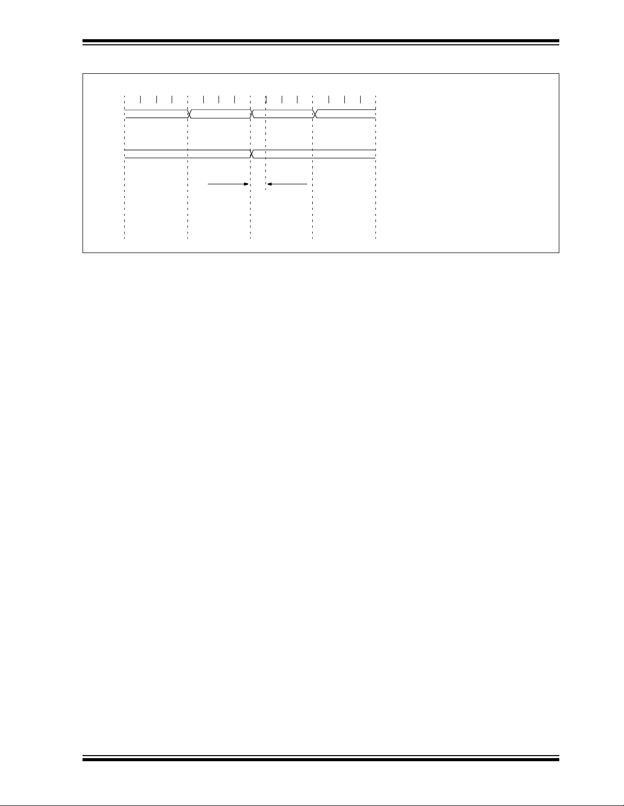
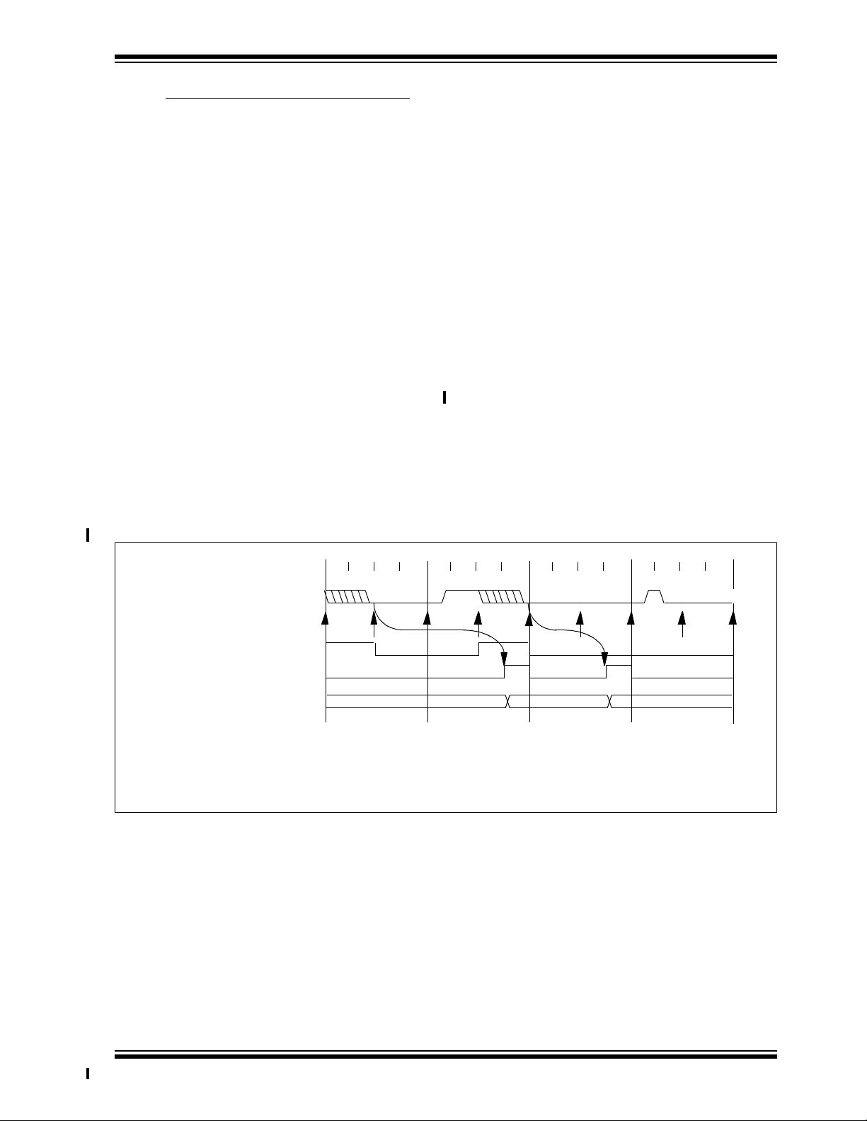
FIGURE 5-2: SUCCESSIVE I/O OPERATION
PIC16C505
Instruction
fetched
RB<5:0>
Instruction
executed
Q4
Q1 Q2
MOVWF PORTB NOP
Q3
PC PC + 1 PC + 2
Q1 Q2
Port pin
written here
MOVWF PORTB
(Write to PORTB)
Q3
Q4
Q1 Q2
(Read PORTB)
Port pin
sampled here
Q3
Q4
Q1 Q2
Q3
PC + 3
NOPMOVF PORTB,W
NOPMOVF PORTB,W
Q4
This example shows a write to PORTB
followed by a read from PORTB.
Data setup time = (0.25 T
where: T
CY = instruction cycle.
PD = propagation delay
T
CY – TPD)
Therefore, at higher clock frequencies, a
write followed by a read may be problematic.
1999 Microchip Technology Inc. DS40192C-page 21
Page 22

PIC16C505
NOTES:
DS40192C-page 22
1999 Microchip Technology Inc.
Page 23
PIC16C505
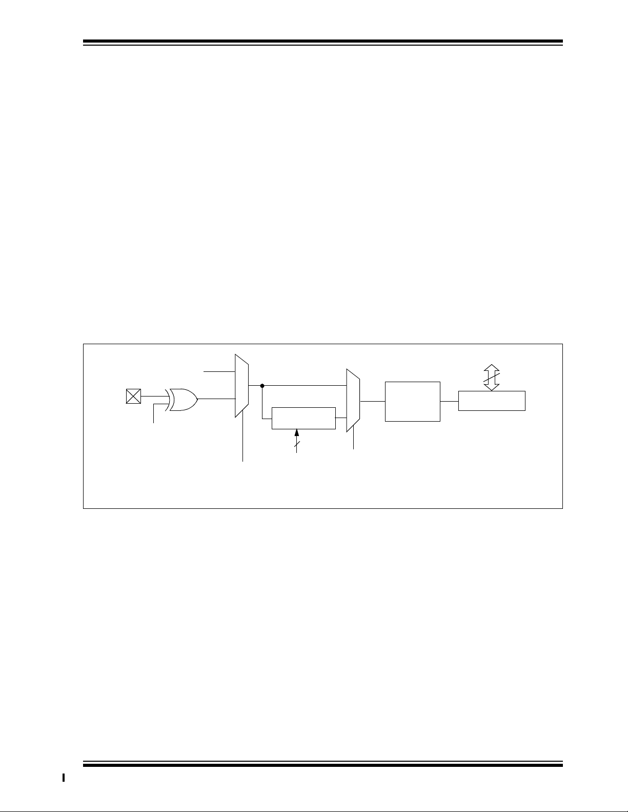
6.0 TIMER0 MODULE AND TMR0 REGISTER
The Timer0 module has the following features:
• 8-bit timer/counter register, TMR0
- Readable and writable
• 8-bit software programmable prescaler
• Internal or external clock select
- Edge select for external clock
Figure 6-1 is a simplified block diagram of the Timer0
module.
Timer mode is selected by clearing the T0CS bit
(OPTION<5>). In timer mode, the Timer0 module will
increment e very instruction cycle (witho ut prescaler). If
TMR0 register is written, the increment is inhibited for
the following two cycles (Figure 6-2 and Figure 6-3).
The user can work around this by writing an adjusted
value to the TMR0 register.
FIGURE 6-1: TIMER0 BLOCK DIAGRAM
RC5/T0CKI
Pin
T0SE
FOSC/4
0
T0CS
1
(1)
Programmable
Prescaler
PS2, PS1, PS0
Counter mode is selected by setting the T0CS bit
(OPTION<5>). In this mode, Timer0 will increment
either on every rising or falling edge of pin T0CKI. The
T0SE bit (OPTION<4>) determines the source edge.
Clearing the T0SE bit selects the rising edge.
Restrictions on the external clock input are discussed
in detail in Section 6.1.
The prescaler may be used by either the Timer0
module or the Watchdog Timer, but not both. The
prescaler assignment is controlled in software by the
control bit PSA (OPTION<3>). Clearing the PSA bit
will assign the prescaler to Timer0. The prescaler is
not readable or writable. When the prescaler is
assigned to the Timer0 module , prescale v alue s of 1:2,
1:4,..., 1:256 are selectable. Section 6.2 details the
operation of the prescale r.
A summary of registers associated with the Timer0
module is found in Table 6-1.
Data Bus
PSout
1
(2)
3
0
PSA
(1)
(1)
Sync with
Internal
Clocks
CY delay)
(2 T
TMR0 reg
PSout
Sync
8
Note1: Bits T0CS, T0SE, PSA, PS2, PS1 and PS0 are located in the OPTION register.
2: The prescaler is shared with the Watchdog Timer (Figure 6-5).
1999 Microchip Technology Inc. DS40192C-page 23
Page 24
PIC16C505
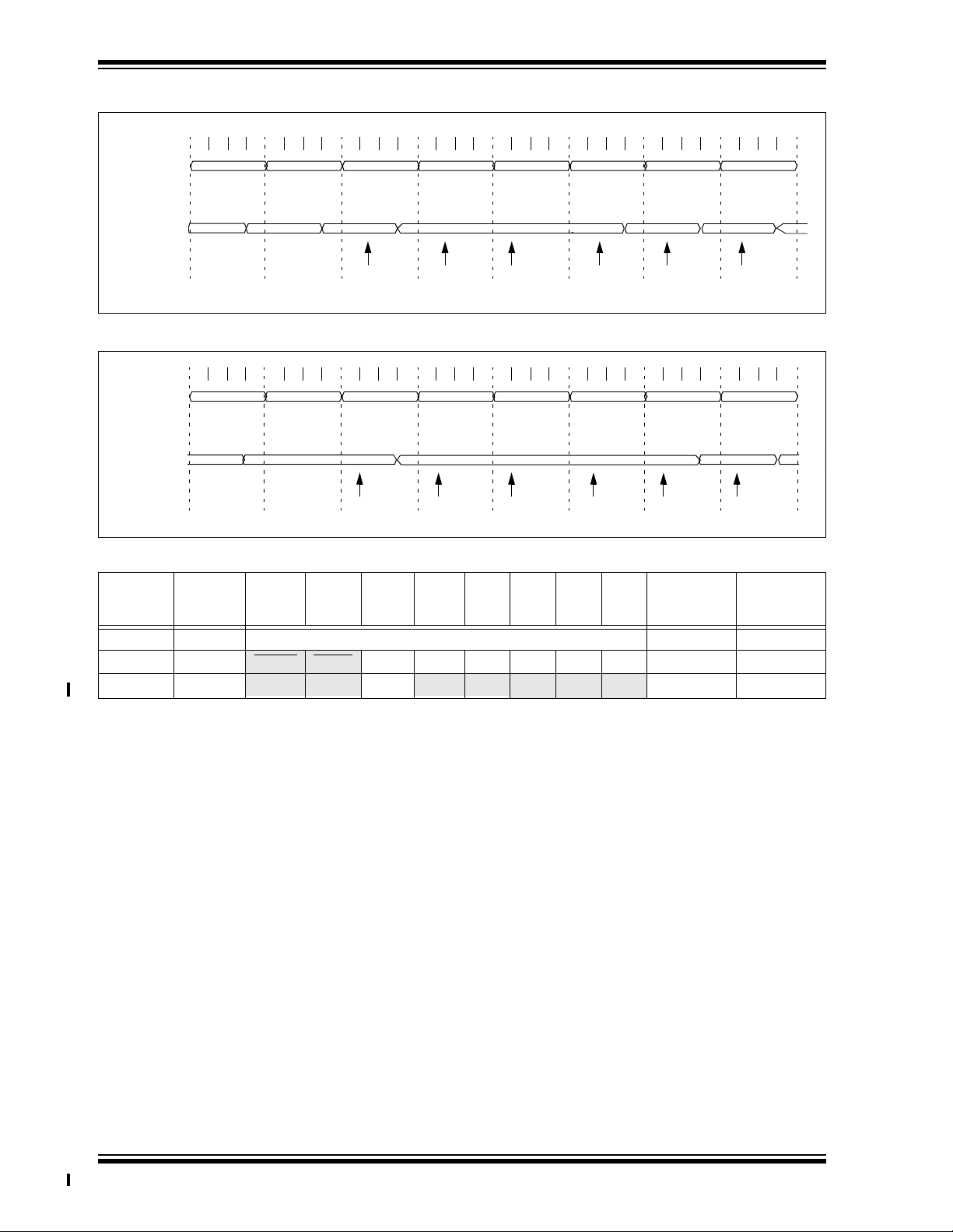
FIGURE 6-2: TIMER0 TIMING: INTERNAL CLOCK/NO PRESCALE
PC
(Program
Counter)
Instruction
Fetch
Timer0
Instruction
Executed
Q1 Q2 Q3 Q4 Q1 Q2 Q3 Q4 Q1 Q2 Q3 Q4 Q1 Q2 Q3 Q4 Q1 Q2 Q3 Q4 Q1 Q2 Q3 Q4 Q1 Q2 Q3 Q4 Q1 Q2 Q3 Q4
PC-1
T0
PC PC+1 PC+2 PC+3 PC+4 PC+5 PC+6
MOVWF TMR0
T0+1 T0+2 NT0
MOVF TMR0,W MOVF TMR0,W MOVF TMR0,W MOVF TMR0,W MOVF TMR0,W
NT0+1 NT0+2
Write TMR0
executed
Read TMR0
reads NT0
Read TMR0
reads NT0
Read TMR0
reads NT0
Read TMR0
reads NT0 + 1
Read TMR0
reads NT0 + 2
FIGURE 6-3: TIMER0 TIMING: INTERNAL CLOCK/PRESCALE 1:2
PC
(Program
Counter)
Instruction
Fetch
Timer0
Instruction
Execute
Q1 Q2 Q3 Q4 Q1 Q2 Q3 Q4 Q1 Q2 Q3 Q4 Q1 Q2 Q3 Q4 Q1 Q2 Q3 Q4 Q1 Q2 Q3 Q4 Q1 Q2 Q3 Q4 Q1 Q2 Q3 Q4
PC-1
T0 NT0+1
PC PC+1 PC+2 PC+3 PC+4 PC+5 PC+6
MOVWF TMR0
T0+1
MOVF TMR0,W MOVF TMR0,W MOVF TMR0,W MOVF TMR0,W MOVF TMR0,W
NT0
Write TMR0
executed
Read TMR0
reads NT0
Read TMR0
reads NT0
Read TMR0
reads NT0
Read TMR0
reads NT0
Read TMR0
reads NT0 + 1
TABLE 6-1: REGISTERS ASSOCIATED WITH TIMER0
Value on
Power-On
Address Name Bit 7 Bit 6 Bit 5 Bit 4 Bit 3 Bit 2 Bit 1 Bit 0
Reset
01h TMR0 Timer0 - 8-bit real-time clock/counter xxxx xxxx uuuu uuuu
N/A OPTION
N/A TRISC
Legend: Shaded cells not used by Timer0,
RBWU RBPU T0CS T0SE PSA PS2 PS1 PS0 1111 1111 1111 1111
— —
RC5
- = unimplemented, x = unknown, u = unchanged.
RC4 RC3 RC2 RC1 RC0
--11 1111 --11 1111
Val ue on
All Other
Resets
T0
DS40192C-page 24
1999 Microchip Technology Inc.
Page 25
PIC16C505
6.1 Using Timer0 with an External Clock
When an external clock input is used for Timer0, it
must meet certain requirements. The external clock
requirement is due to internal phase clock (TOSC)
synchronization. Also, there is a delay in the actual
incrementing of Timer0 after synchronization.
6.1.1 EXTERNAL CLOCK SYNCHRONIZATION
When no prescaler is used, the external clock input is
the same as the prescaler output. The synchronization
of T0CKI with the internal phase clocks is
accomplished by sampling the prescaler output on the
Q2 and Q4 cycles of the internal phase clocks
(Figure 6-4). Therefore, it is necessary for T0CKI to be
high for at least 2T
and low for at least 2T
20 ns). Refer to the electrical specification of the
desired device.
OSC (and a small RC delay of 20 ns)
OSC (and a small RC delay of
When a presca ler is used, the external clock in put is
divided by the asynchronous ripple counter-type
prescaler, so that the prescaler output is symmetrical.
For the external clock to meet the sampling
requirement, the ripple counter must be taken into
account. Therefore, it is neces sa ry f or T0 C KI to have a
period of at least 4T
OSC (and a small RC delay of
40 ns) divided by the prescaler value. The only
requirement on T0CKI high and low time is that they
do not violate the minimum pulse width requirement of
10 ns. Refer to parameters 40, 41 and 42 in the
electrical specification of the desired device.
6.1.2 TIMER0 INCREMENT DELAY Since the prescaler output is synchronized with the
internal clocks, there is a small delay from the time the
external clock edge occurs to the time the Timer0
module is actually incremented. Figure 6-4 shows the
delay from the external clock edge to the timer
incrementing.
FIGURE 6-4: TIMER0 TIMING WITH EXTERNAL CLOCK
Q1 Q2 Q3 Q4 Q1 Q2 Q3 Q4 Q1 Q2 Q3 Q4 Q1 Q2 Q3 Q4
External Clock Input or
Prescaler Output
External Clock/Prescaler
Output After Sa mpling
Increment Timer0 (Q4)
Note 1:
Delay from clock input change to Timer0 increment is 3Tosc to 7Tosc. (Duration of Q = Tosc).
Therefore, the error in measuring the interval between two edges on Timer0 input = ± 4Tosc max.
2:
External clock if no prescaler selected; prescaler output otherwise.
3:
The arrows indicate the points in time where sampling occurs.
(2)
Timer0
(3)
(1)
T0 T0 + 1 T0 + 2
Small pulse
misses sampling
1999 Microchip Technology Inc. DS40192C-page 25
Page 26
PIC16C505
6.2 Prescaler
An 8-bit counter is available as a prescaler for the
Timer0 module or as a postscaler for the Watchdog
Timer (WDT), respectively (Section 7.6). For simplicity,
this counter is being referred to as “prescaler”
throughout this data sheet. Note that the prescaler
may be used by either the Timer0 module or the WDT,
but not both. Thus, a prescaler assignment for the
Timer0 module means that there is no prescaler for
the WDT, and vice-versa.
The PSA and PS<2:0> bits (OPTION<3:0>) determine
prescaler assignment and prescale ratio.
When assigned to the Timer0 module, all instructions
writing to the TMR0 register (e.g., CLRF 1,
MOVWF 1, BSF 1,x, etc.) will clear the prescaler.
When assigned to WDT, a CLRWDT instruction will
clear the prescaler along with the WDT. The prescaler
is neither readable nor writable. On a RESET, the
prescaler contains all '0's.
6.2.1 SWITCHING PRESCALER ASSIGNMENT The prescaler assignment is fully under software
control (i.e., it can be changed “on-the-fly” during
program execution). To avoid an unintended device
RESET, the following instruction sequence
(Example 6-1) must be executed when changing the
prescaler assignment from Timer0 to the WDT.
EXAMPLE 6-1: CHANGING PRESCALER
(TIMER0→WDT)
1.CLRWDT ;Clear WDT
2.CLRF TMR0 ;Clear TMR0 & Prescaler
3.MOVLW '00xx1111’b ;These 3 lines (5, 6, 7)
4.OPTION ; are required only if
; desired
5.CLRWDT ;PS<2:0> are 000 or 001
6.MOVLW '00xx1xxx’b ;Set Postscaler to
7.OPTION ; desired WDT rate
To change prescaler from the WDT to the Timer0
module, use the sequence shown in Example 6-2.
This sequence must be used even if the WDT is
disabled. A CLRWDT instruction should be executed
before switching the prescaler.
EXAMPLE 6-2: CHANGING PRESCALER
(WDT→TIMER0)
CLRWDT ;Clear WDT and
;prescaler
MOVLW 'xxxx0xxx' ;Select TMR0, new
;prescale value and
;clock source
OPTION
FIGURE 6-5: BLOCK DIAGRAM OF THE TIMER0/WDT PRESCALER
TCY ( = Fosc/4)
0
1
Sync
2
Cycles
PS<2:0>
Watchdog
Timer
WDT Enable bit
1
0
0
M
1
PSA
8-bit Prescaler
8
8 - to - 1MUX
0
1
MUX
PSA
TMR0 reg
Note: T0CS, T0SE, PSA, PS<2:0> are bits in the OPTION register.
DS40192C-page 26
WDT
Time-Out
1999 Microchip Technology Inc.
Page 27

PIC16C505
7.0 SPECIAL FEATURES OF THE CPU
What sets a microcontroller apart from other
processors are special circuits to deal with the needs
of real-time applications. The PIC16C505
microcontroller has a host of such features intended to
maximize system reliability, minimize cost through
elimination of external components, provide power
saving operating modes and offer code protection.
These features are:
• Oscillator selection
• Reset
- Power-On Reset (POR)
- Device Reset Timer (DRT)
- Wake-up from SLEEP on pin change
• Watchdog Timer (WDT)
• SLEEP
• Code protection
• ID locations
• In-circuit Serial Programming
•Clock Out
The PIC16C505 has a Watchdog Timer, which can be
shut off only through configuration bit WDTE. It runs
off of its own RC oscillator for added reliability. If using
HS, XT or LP selectable oscillator options, there is
always an 18 ms (nominal) delay provided by the
Device Reset Timer (DRT), intended to keep the chip
in reset until the crystal oscillator is stable. If using
INTRC or EXTRC, there is an 18 ms delay only on VDD
power-up. With this timer on-chip, most applications
need no external reset circuitry.
The SLEEP mode is designed to offer a very low
current power-down mode. The user can wake-up
from SLEEP through a change on input pins or
through a Watchdog Timer time-out. Several oscillator
options are al so made availa ble to allow th e par t to fit
the application, including an internal 4 MHz oscillator.
The EXTRC oscillator option saves system cost while
the LP crystal option saves power. A set of
configuration bits are used to select various options.
7.1 Configuration Bits
The PIC16C505 configuration word consists of 12 bits.
Configuration bits can be programmed to select
various device configurations. Three bits are for the
selection of the oscillator type, one bit is the Watchdog
Timer enable bit, and one bit is the MCLR
Seven bits are for code protection (Register 7-1).
enable bit.
REGISTER 7-1: CONFIGURATION WORD FOR PIC16C505
CP CP CP CP CP CP MCLRE CP WDTE FOSC2 FOSC1 FOSC0 Register : CONFIG
bit1110987654321 bit0
bit 11-6, 4: CP Code Protection bits
bit 5: MCLRE: RB3/MCLR pin function select
1 = RB3/MCLR
0 = RB3/MCLR pin function is digital I/O, MCLR internally tied to VDD
bit 3: WDTE: Watchdog timer enable bit
1 = WDT enabled
0 = WDT disabled
bit 2-0: FOSC<1:0>: Oscillator Selection bits
111 = external RC oscillator/CLKOUT function on RB4/OSC2/CLKOUT pin
110 = external RC oscillator/RB4 function on RB4/OSC2/CLKOUT pin
101 = internal RC oscillator/CLKOUT function on RB4/OSC2/CLKOUT pin
100 = internal RC oscillator/RB4 function on RB4/OSC2/CLKOUT pin
011 = invalid selection
010 = HS oscillator
001 = XT oscillator
000 = LP oscillator
Note 1: 03FFh is always uncode protected on the PIC16C505. This location contains the
MOVLWxx calibration instruction for the INTRC.
2: Refer to the PIC16C505 Programming Specifications to determine how to access the con-
figuration word. This register is not user addressable during device operation.
3: All code protect bits must be written to the same value.
pin function is MCLR
(1)(2)(3)
Address
(2)
: 0FFFh
1999 Microchip Technology Inc. DS40192C-page 27
Page 28

PIC16C505
7.2 Oscillator Configurations
7.2.1 OSCILLATOR TYPES The PIC16C505 can be operated in four different
oscillator modes. The user can program three
configuration bits (FOSC<2:0>) to select one of these
four modes:
• LP: Low Power Crystal
• XT: Crystal/Resonator
• HS: High Speed Crystal/Resonator
• INTRC: Internal 4 MHz Oscill ator
• EXTRC: External Resistor/Capacitor
7.2.2 CRYSTAL OSCILLATOR / CERAMIC RESONATORS
In HS, XT or LP modes, a crystal or ceramic resonator
is connected to the RB5/OSC1/CLKIN and RB4/
OSC2/CLKOUT pins to establish oscillation
(Figure 7-1). The PIC16C505 oscillator design
requires the use of a parallel cut crystal. Use of a
series cut crystal may give a frequency out of the
crystal manufacturers specifications. When in HS, XT
or LP modes, the device can have an external clock
source drive the RB5/OSC1/CLKIN pin (Figure 7-2).
FIGURE 7-1: CRYSTAL OPERATION (OR
CERAMIC RESONATOR)
(HS, XT OR LP OSC
CONFIGURATION)
(1)
C1
OSC1
PIC16C505
TABLE 7-1: CAPACITOR SELECTION
FOR CERAMIC RESONATORS
- PIC16C505
Osc
Type
XT 4.0 MHz 30 pF 30 pF
HS 16 MHz 10-47 pF 10-47 pF
These values are for design guidance only. Since
each resonator has its own characteristics, the user
should consult the resonator manufacturer for
appropriate values of external components.
Resonator
Freq
Cap. RangeC1Cap. Range
C2
TABLE 7-2: CAPACITOR SELECTION
FOR CRYSTAL OSCILLATOR PIC16C505
Osc
Type
LP 32 kHz
XT 200 kHz
HS 20 MHz 15-47 pF 15-47 pF
Note1: For V
These values are for design guidance only. Rs may
be required to avoid overdriving crystals with low
drive level specification. Since each crystal has its
own characterist ics , the user shou ld consu lt the crystal manufacturer for appropriate values of external
components.
Resonator
Freq
(1)
Cap.Range
C1
15 pF 15 pF
47-68 pF
1 MHz
4 MHz
DD > 4.5V, C1 = C2 ≈ 30 pF is
15 pF
15 pF
recommended.
Cap. Range
C2
47-68 pF
15 pF
15 pF
XTAL
OSC2
(2)
RS
(1)
C2
Note 1: See Capacitor Selection tables for
recommended values of C1 and C2.
2: A series resistor (RS) may be required for AT
strip cut crystals.
3: RF approx. value = 10 MΩ.
RF
(3)
SLEEP
To inter nal
logic
FIGURE 7-2: EXTERNAL CLOCK INPUT
OPERATION (HS, XT OR LP
OSC CONFIGURATION)
Clock from
ext. system
Open
OSC1
PIC16C505
OSC2
DS40192C-page 28
1999 Microchip Technology Inc.
Page 29
PIC16C505
7.2.3 EXTERNAL CRYSTAL OSCILLATOR CIRCUIT
Either a prepackaged oscillator or a simple oscillator
circuit with TTL gates can be used as an external
crystal oscillator circuit. Prepackaged oscillators
provide a wide op erating range and better stabilit y. A
well-designed crystal oscillator will provide good
performance with TTL gates. Two types of crystal
oscillator circuits can be used: one with parallel
resonance, or one with series resonance.
Figure 7-3 shows implementation of a parallel
resonant oscillator circuit. The circuit is designed to
use the fundamental frequency of the crystal. The
74AS04 inverter performs the 180-degree phase shift
that a parallel oscillator requires. The 4.7 kΩ resistor
provides the negative feedback for stability. The 10 kΩ
potentiometers bias the 74AS04 in the linear region.
This circuit could be used for external oscillator
designs.
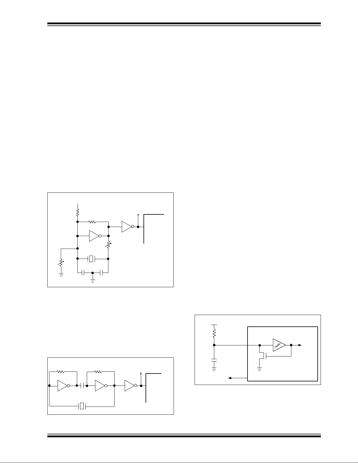
FIGURE 7-3: EXTERNAL PARALLEL
RESONANT CRYSTAL
OSCILLATOR CIRCUIT
+5V
10k
4.7k
74AS04
10k
XTAL
10k
20 pF
20 pF
Figure 7-4 shows a series resonant oscillator circuit.
This circuit is also designed to use the fundamental
frequency of the crystal. The inverter performs a 180degree phase shift in a series resonant oscillator
circuit. The 330Ω resistors provide the negative
feedback to bias the inverters in their linear region.
74AS04
To Other
Devices
PIC16C505
CLKIN
FIGURE 7-4: EXTERNAL SERIES
RESONANT CRYSTAL
OSCILLATOR CIRCUIT
To Other
74AS04
Devices
PIC16C505
CLKIN
330
74AS04
330
74AS04
0.1 mF
XTAL
7.2.4 EXTERNAL RC OSCILLATOR For timing insensitive applications, the RC device
option offers additional cost savings. The RC oscillator
frequency is a function of the supply voltage, the
resistor (Rext) and capacitor (Cext) values, and the
operating temperature. In addition to this, the oscillator
frequency will vary from unit to unit due to normal
process parameter variation. Furthermore, the
difference in l ead frame capacita nce be tw e en package
types will also affect the oscillation frequency,
especially for low Cext values. The user also needs to
take into account variation due to tolerance of external
R and C components used.
Figure 7-5 shows how the R/C combination is
connected to the PIC16C505. For Rext values below
2.2 kΩ, the oscillator op eration may become unstable,
or stop completely. For very high Rext values
(e.g., 1 MΩ) the oscillator becomes sensitive to noise,
humidity and leakage. Thus, we recommend keeping
Rext betwee n 3 kΩ and 100 kΩ.
Although the oscillator will operate with no external
capacitor (Cext = 0 pF), we recommend using values
above 20 pF for noise and stability reasons. With no or
small external capacitance, the oscillation frequency
can vary dramatically due to changes in external
capacitances, such as PCB trace capacitance or
package lead frame capacitance.
The Electrical Specifications section shows RC
frequency variation from part to part due to normal
process variation. The variation is larger for larger
values of R (since leakage current variation will affect
RC frequency more for large R) and for smaller values
of C (since variation of in put capacitance will affect RC
frequency more).
Also, see the Electrical Specifications section for
variation of oscillator frequen cy due to V
DD for gi ven
Rext/Cext valu es, as well as frequency va riat ion du e to
operating temperature for given R, C and V
DD values.
FIGURE 7-5: EXTERNAL RC OSCILLATOR
MODE
VDD
Rext
Cext
SS
V
FOSC/4
OSC1
N
OSC2/CLKOUT
Internal
clock
PIC16C505
1999 Microchip Technology Inc. DS40192C-page 29
Page 30

PIC16C505
7.2.5 INTERNAL 4 MHz RC OSCILLATOR The internal RC oscillator provi des a fixed 4 MHz (nom -
inal) system clo ck at V
Specifications section for information on variation over
voltage and temperature.
In addition, a cal ibra tion in structi on is pro g rammed in to
the last address of mem ory, which contains the calibration value for the internal RC oscillator. This location is
always protected, regardless of the code protect settings. This value is programmed as a MOVLW XX
instruction where XX is the calibration value, and is
placed at the reset vector. This will load the W register
with the calibration value upon reset and the PC will
then roll over to the users program at address 0x000.
The user then has the option of writing the value to the
OSCCAL Register (05h) or ignoring it.
OSCCAL, when written to wi th the calibrati on value , will
“trim” the internal oscilla tor to rem ov e proc ess v ariation
from the oscillator frequency.
Note: Please note that erasing the device will
also erase the pre-programmed internal
calibration value f or the internal oscillator .
The calibration value must be read prior
to erasing the part so it can be reprogrammed cor r e ctl y l a t e r.
For the PIC16C505, only bits <7:2> of OSCCAL are
implemented.
DD = 5V and 25°C, see Electrical
7.3 RESET
The device differentiates between various kinds of
reset:
a) Power on reset (POR)
b) MCLR
c) MCLR reset during SLEEP
d) WDT time-out reset during normal operation
e) WDT time-out reset during SLEEP
f) Wake-up from SLEEP on pin change
Some registers are not reset in any way, they are
unknown on POR and unchanged in any other reset.
Most other registers are res et to “reset state ” on pow eron reset (POR), MCLR
change reset during normal operation. They are not
affected b y a WD T res et during SLE EP or MCLR res et
during SLEEP, since these resets are viewed as
resumption of normal ope ra tion. The except ion s to thi s
are TO
differently in different reset situations. These bits are
used in software to determine the nature of reset. See
Table 7-3 for a full description of reset states of all
registers.
reset during normal operation
, WDT or wake-up on pin
, PD and RBWUF bits. They are set or cleared
DS40192C-page 30
1999 Microchip Technology Inc.
Page 31
PIC16C505
TABLE 7-3: RESET CONDITIONS FOR REGISTERS
MCLR
Reset
Register Address Power-on Reset
W —
INDF 00h xxxx xxxx uuuu uuuu
TMR0 01h xxxx xxxx uuuu uuuu
PC 02h 1111 1111 1111 1111
STATUS 03h 0001 1xxx
FSR 04h 110x xxxx 11uu uuuu
OSCCAL 05h 1000 00-- uuuu uu--
PORTB 06h --xx xxxxx --uu uuuu
PORTC 07h --xx xxxxx --uu uuuu
OPTION — 1111 1111 1111 1111
TRISB — --11 1111 --11 1111
TRISC — --11 1111 --11 1111
Legend: u = unchanged, x = unknown, - = unimplemented bit, read as ‘0’, q = value depends on condition.
Note 1: Bits <7:2> of W register contain oscillator calibration values due to MOVLW XX instruction at top of
memory.
Note 2: See Table 7-7 for reset value for specific conditions.
Note 3: If reset was due to wake-up on pin change, then bit 7 = 1. All other resets will cause bit 7 = 0.
qqqq qqqq
(1)
WDT time-out
Wake-up on Pin Change
qqqq qqqq
q00q quuu
(1)
(2,3)
TABLE 7-4: RESET CONDITION FOR SPECIAL REGISTERS
STATUS Addr: 03h PCL Addr: 02h
Power on reset 0001 1xxx 1111 1111
reset during normal operation 000u uuuu 1111 1111
MCLR
MCLR
reset during SLEEP 0001 0uuu 1111 1111
WDT reset during SLEEP 0000 0uuu 1111 1111
WDT reset normal operation 0000 uuuu 1111 1111
Wak e-up from SLEEP on pin c han ge 1001 0uuu 1111 1111
Legend: u = unchanged, x = unknown, - = unimplemented bit, read as ‘0’.
1999 Microchip Technology Inc. DS40192C-page 31
Page 32

PIC16C505
7.3.1 MCLR ENABLE This configuration bit when unprogrammed (left in the
‘1’ state) enables the external MCLR
programmed, the MCLR
V
DD, and the pin is assigned to be a I/O. See
function is tied to the internal
function. When
Figure 7-6.
FIGURE 7-6: MCLR SELECT
RBWU
MCLRE
WEAK
PULL-UP
RB3/MCLR/VPP
INTERNAL MCLR
7.4 Power-On Reset (POR)
The PIC16C505 family incorporates on-c hip Power-On
Reset (POR) circui try, which provides an int erna l chip
reset for most power-up situations.
The on chip POR circ uit holds the chip in reset until V
has reached a high enough level for proper operation.
To take advantage of the internal POR, program the
RB3/MCLR/VPP pin as MCLR and tie through a resis tor
DD or program the pin as RB3. An internal weak
to V
pull-up resistor is impl emented usin g a transistor. Refer
to Table 10-1 for the pull-up resistor ranges. This will
eliminate external RC components usually needed to
create a Power-on Reset. A maximum rise time for VDD
is specified. See Electrical Specifications for details.
When the device starts normal operation (exits the
reset condition), d evice operating p arameters (vol tage,
frequency, temperature, ...) must be met to ensure
operation. If these conditions are not met, the device
must be held in reset un til the oper ating par ameters ar e
met.
A simplified block diagram of the on-chip Power-On
Reset circuit is shown in Figure 7-7.
DD
The Power-On Reset circuit and the Device Reset
Timer (Section 7.5) circuit are closely related. On
power-up, the reset latch is set and the DRT is reset.
The DRT timer begins counting once it detects MCLR
to be high. After the time-out period, which is typically
18 ms, it will reset the reset latch and thus end the onchip reset signal.
A power-up example where MCLR
shown in Figure 7-8. V
DD is allowed to rise and
stabilize before bringing MCLR
actually come out of reset T
is held low is
high. The chip will
DRT msec after MCLR
goes high.
In Figure 7-9, the on-chip Power-On Reset feature is
being used (MCLR and VDD are tied t ogether or the
pin is programmed to be RB3.). The V
DD is stable
before the start-up timer times out and there is no
problem in getting a proper reset. However,
Figure 7-10 depicts a problem situation where V
DD
rises too slowly. The time between when the DRT
senses that MCLR
is high and when MC LR and VDD
actually reach their full value, is too long. In this
situation, when the start-up timer times out, V
not reached the V
DD (min) value and the chip may not
DD has
function correctly. For such situations, we recommend
that external RC circuits be used to achieve longer
POR delay times (Figure 7-9).
Note: When the device starts normal operati on
(exits the reset co ndition), de vice operatin g
parameters (voltage, frequency, temperature, etc.) must be met to ensure oper ation.
If these conditions are not met, the device
must be held in reset until the operating
conditions are met.
For additional information refer to Application Notes
Power-Up Considerations”
“
Trouble Shooting
” - AN607.
- AN522 and “
Power-up
DS40192C-page 32
1999 Microchip Technology Inc.
Page 33

PIC16C505
FIGURE 7-7: SIMPLIFIED BLOCK DIAGRAM OF ON-CHIP RESET CIRCUIT
SQ
FIGURE 7-8: TIME-OUT SEQUENCE ON POWER-UP (MCLR
FIGURE 7-9: TIME-OUT SEQUENCE ON POWER-UP (MCLR
R
PULLED LOW)
TIED TO VDD): FAST VDD RISE TIME
Q
1999 Microchip Technology Inc. DS40192C-page 33
Page 34

PIC16C505
FIGURE 7-10: TIME-OUT SEQUENCE ON POWER-UP (MCLR TIED TO VDD): SLOW VDD RISE TIME
V1
VDD
MCLR
INTERNAL POR
DRT TIME-OUT
INTERNAL RESET
Note: When VDD rises s lowly, the T DRT time-out expires long before VDD has reached its final
value. In this example, the chip will reset properly if, and only if, V1 ≥ V
TDRT
7.5 Device Reset Timer (DRT)
In the PIC16C505, the DRT runs any time the device is
powered up. DRT runs from RESET and varies based
on oscillator selec tion and reset type (see Table 7-5).
The DRT operates on an internal RC oscillator. The
processor is kept in RESET as long as the DRT is
active. The DRT delay allows V
min. and for the oscillator to s tabilize.
Oscillator circuits based on crystals or ceramic
resonators require a certain time after power-up to
establish a stable oscillation. The on-chip DRT keeps
the device in a RESET condition for approximately 18
ms after MCLR
level. Thus, programming RB3/MCLR
and using an external RC network connected to the
input is not required in most cases, allowing for
MCLR
savings in cost-sensitive and/or space restricted
applications, as well as allowing the use of the RB3/
/VPP pin as a general purpose input.
MCLR
The Device Reset time delay will vary from chip to chip
due to V
AC parameters for details.
The DRT will also be triggered upon a Watchdog
Timer time-out. This is particularly important for
applications using the WDT to wake from SLEEP
mode automatically.
Reset sources are POR, MCLR
Wake-up on pin change. (See Section 7.9.2, Notes 1,
2, and 3, page 37.)
has reached a logic high (VIHMCLR)
DD, temperature and process variation. See
DD to rise above VDD
/VPP as MCLR
, WDT time-out and
DD min.
7.6 Watchdog Timer (WDT)
The Watchdog Timer (WDT) is a free running on-chip
RC oscillator, which does not require any external
components. This RC oscillator is separate from the
external RC oscillator of the RB5/OSC1/CLKIN pin
and the internal 4 MHz oscillator. That means that the
WDT will run even if the main processor clock has
been stopped, for example, by execution of a SLEEP
instruction. During normal operation or SLEEP, a WDT
reset or wake-up reset generates a device RESET.
The TO
Watchdog Timer reset.
The WDT can be permanently disabled by
programming the configuration bit WDTE as a ’0’
(Section 7.1). Refer to the PIC16C505 Programming
Specifications to determine how to access the
configuration word.
bit (STATUS<4>) will be cleared upon a
TABLE 7-5: DRT (DEVICE RESET TIMER
PERIOD)
Oscillator
Configuration
IntRC &
ExtRC
HS, XT & LP 18 ms (typical) 18 ms (typical)
POR Reset
18 ms (typical) 300 µs
Subsequent
Resets
(typical)
DS40192C-page 34
1999 Microchip Technology Inc.
Page 35
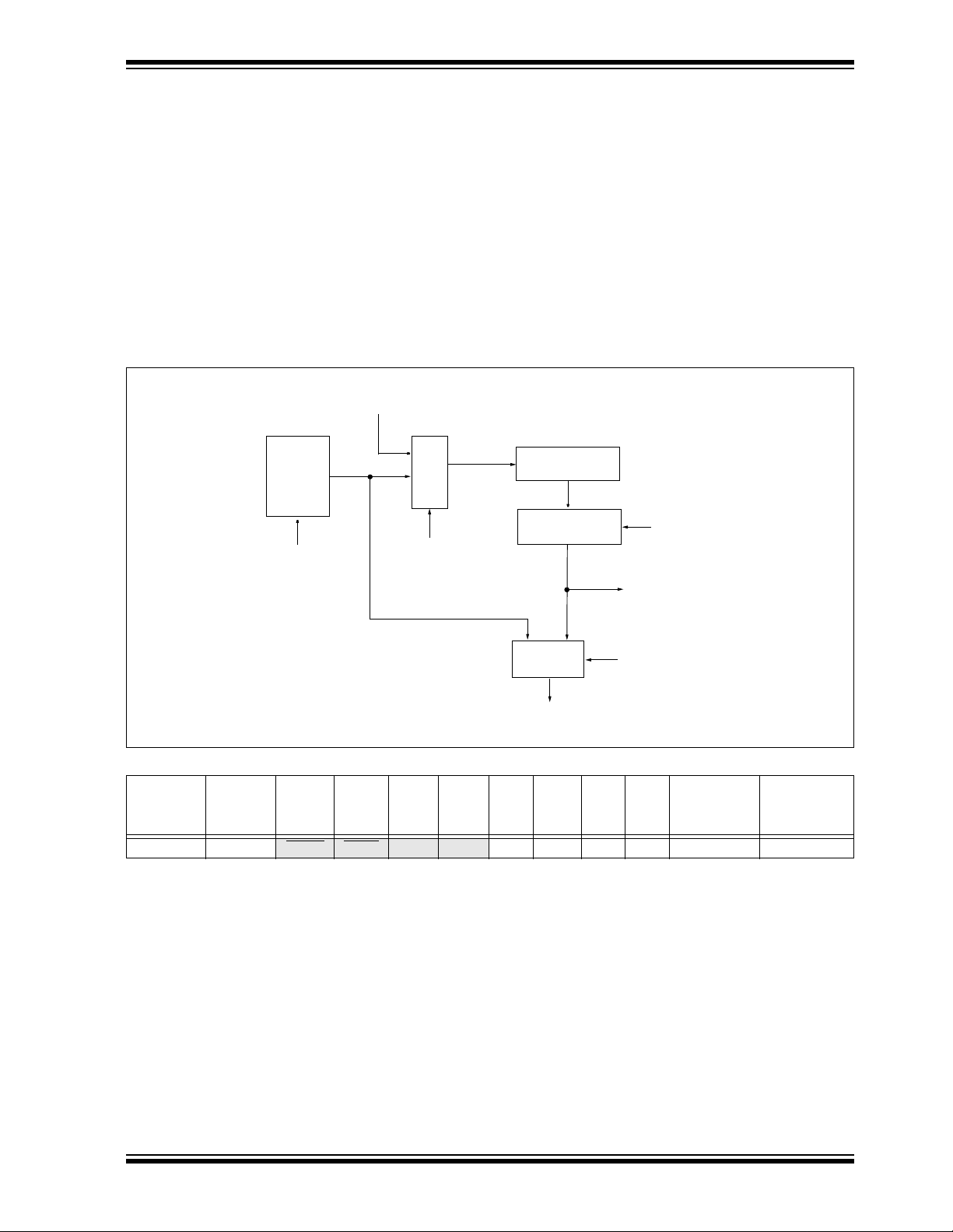
PIC16C505
7.6.1 WDT PERIOD The WDT has a nominal time-out period of 18 ms,
(with no prescaler). If a longer time-out period is
desired, a prescaler with a division ratio of up to 1:128
can be assigned to the WDT (under software control)
by writing to the OPTION register. Thus, a time-out
period of a nominal 2.3 seconds can be realized.
These periods va ry with temper ature, V
DD and part-to-
part process variations (see DC specs).
Under worst case conditions (V
DD = Min., Temperature
= Max., max. WDT prescaler), it may take several
seconds before a WDT time-out occurs.
FIGURE 7-11: WATCHDOG TIMER BLOCK DIAGRAM
From Timer0 Clock Source
(Figure 6-5)
0
M
Watchdog
Timer
WDT Enable
Configuration Bit
1
U
X
PSA
7.6.2 WDT PROGRAMMING CONSIDERATIONS The CLRWDT instruction clears the WDT and the
postscaler, if assigned to the WDT, and prevents it
from timing out and generating a device RESET.
The SLEEP instruction resets the WDT and the
postscaler, if assigned to the WDT. This gives the
maximum SLEEP time before a WDT wake-up reset.
Postscaler
Postscaler
8 - to - 1 MUX
PS<2:0>
To Timer0 (Figure 6-4)
MUX
WDT
1
PSA
0
Note: T0CS, T0SE, PSA, PS<2:0>
are bits in the OPTION register.
Time-out
TABLE 7-6: SUMMARY OF REGISTERS ASSOCIATED WITH THE WATCHDOG TIMER
Value on
Address Name Bit 7 Bit 6 Bit 5 Bit 4 Bit 3 Bit 2 Bit 1 Bit 0
N/A OPTION
Legend: Shaded boxes = Not used by Watchdog Timer, — = unimplemented, read as '0', u = unchanged.
RBWU RBPU T0CS T0SE PSA PS2 PS1 PS0 1111 1111 1111 1111
Power-On
Reset
Value on
All Other
Resets
1999 Microchip Technology Inc. DS40192C-page 35
Page 36

PIC16C505
7.7 Time-Out Sequence, Power Down, and Wake-up from SLEEP Status Bits (TO/PD/RBWUF)
The TO, PD, and RBWUF bits in the STATUS register
can be tested to determine if a RESET condition has
been caused by a power-up condition, a MCLR or
Watchdog Timer (WDT) reset.
TABLE 7-7: TO
/PD/RBWUF STATUS
AFTER RESET
RBWUF TO PD RESET caused by
000
00u
010
011
0uu
110
Legend: u = unchanged
Note 1: T he TO
status (u) until a reset occurs. A low-pulse on the
MCLR
RBWUF status bits.
WDT wake-up from
SLEEP
WDT time-out (not from
SLEEP)
MCLR wake-up from
SLEEP
Power-up
MCLR not during SLEEP
Wake-up from SLEEP on
pin change
, PD, and RBWUF bits maintain their
input does not change the TO, PD, and
FIGURE 7-13: BROWN-OUT PROTECTION
CIRCUIT 2
VDD
V
DD
R1
R2
Q1
40k*
MCLR
PIC16C505
(1)
This brown-out circuit is less expensive, although
less accurate. Transistor Q1 turns off when V
DD
is below a certain level such that:
VDD •
Note 1: Pin must be confirmed as MCLR.
R1
R1 + R2
= 0.7V
FIGURE 7-14: BROWN-OUT PROTECTION
CIRCUIT 3
VDD
7.8 Reset on Brown-Out
A brown-out is a conditi on where devic e power (VDD)
dips below its m inim um v a lue , b ut not to ze ro , an d then
recovers. The device should be reset in the event of a
brown-out.
To reset PIC16C505 devices when a brown-out
occurs, external brown-out protection circuits may be
built, as shown in Figure 7-12 and Figure 7-13.
FIGURE 7-12: BROWN-OUT PROTECTION
CIRCUIT 1
VDD
V
DD
33k
Q1
10k
This circuit will activate reset when VDD goes below
Vz + 0.7V (where Vz = Zener voltage).
Note 1: Pin must be confirmed as MCLR
MCLR
40k*
PIC16C505
(1)
.
MCP809
VSS
RST
This brown-out protection circuit employs Microchip
Technology’s MCP809 microcontroller supervisor.
There are 7 different trip point selections to
accommodate 5V to 3V systems.
capacitor
VDD
bypass
VDD
MCLR
PIC12C5XX
DS40192C-page 36
1999 Microchip Technology Inc.
Page 37

7.9 Power-Down Mode (SLEEP)
A device may be powered down (SLEEP) and later
powered up (Wake-up from SLEEP).
7.9.1 SLEEP
The Power-Down mode is entered by executing a
SLEEP instruction. If enabled, the Watchdog Timer will be cleared but
keeps running, the TO
bit (STATUS<4>) is set, the PD
PIC16C505
1999 Microchip Technology Inc. DS40192C-page 37
Page 38
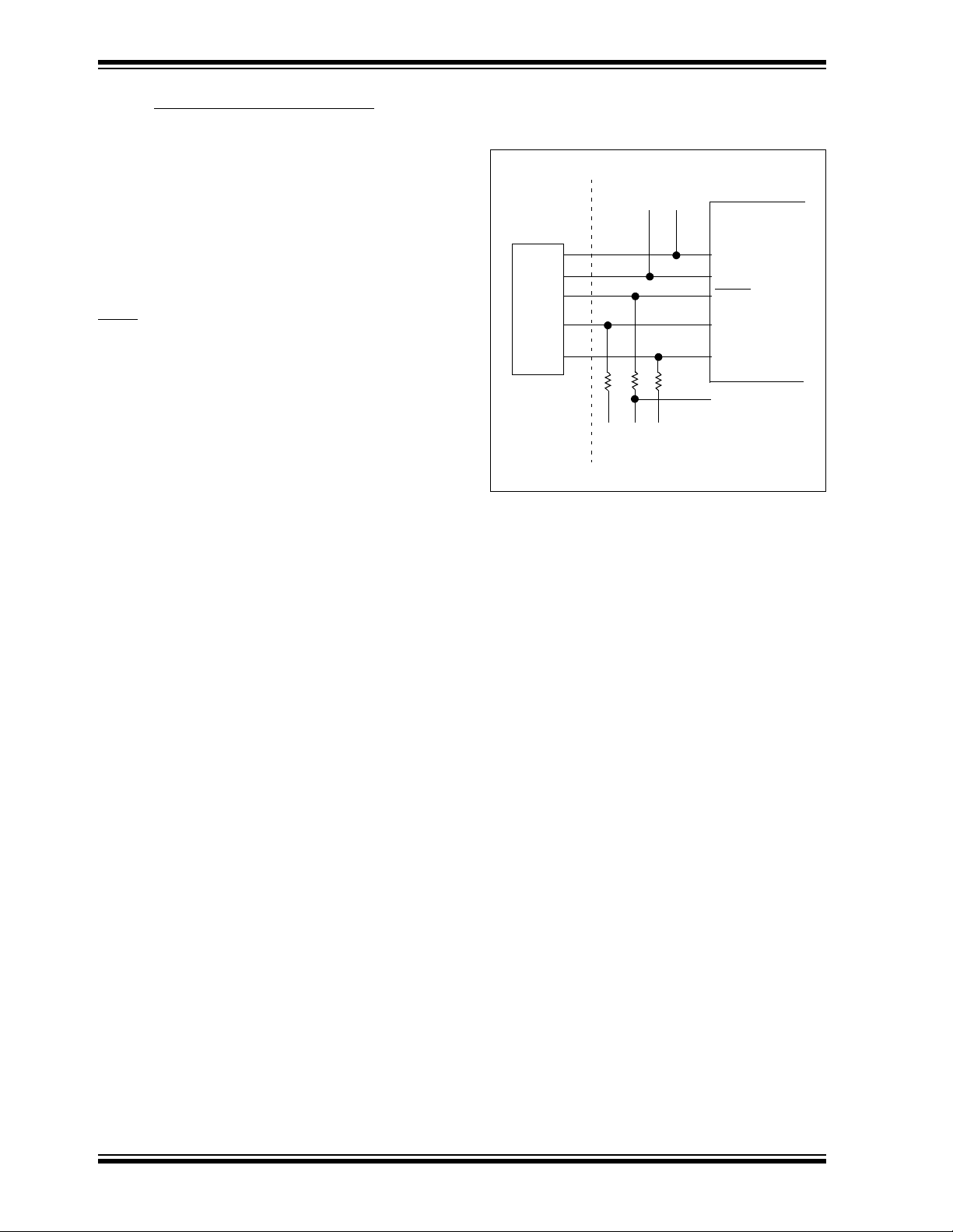
PIC16C505
7.12 In-Circuit Serial Programming
The PIC16C505 microcontrollers can be serially
programmed while i n the end appli catio n circui t. This is
simply done wit h two lin es f or cloc k a nd data, a nd three
other lines for power, ground, and the programming
voltage. This allows customers to manufacture boards
with unprogrammed devices, and then program the
microcontroller just before shipping the product. This
also allows the most recent firmware or a custom
firmware to be programmed.
The device is placed into a program/verify mode by
holding the RB1 and RB0 pins low while raising the
(VPP) pin from VIL to VIHH (see programming
MCLR
specification). RB1 becomes the programming clock
and RB0 becomes the programming data. Both RB1
and RB0 are Schmitt Trigger inputs in this mode.
After reset, a 6-bit command is then supplied to the
device. D epending on the c ommand, 14 bits of program
data are then supplie d to or from the de vice , dependin g
if the command was a load or a read. For complete
details of serial programming, please refer to the
PIC16C505 Programming Specifications.
A typical in-circuit serial programming connection is
shown in Figure7-15.
FIGURE 7-15: TYPICAL IN-CIRCUIT SERIAL
PROGRAMMING
CONNECTION
To Normal
External
Connector
Signals
+5V
0V
PP
V
CLK
Data I/O
Connections
To Normal
Connections
PIC16C505
DD
V
VSS
MCLR/VPP
RB1
RB0
DD
V
DS40192C-page 38
1999 Microchip Technology Inc.
Page 39

PIC16C505
8.0 INSTRUCTION SET SUMMARY
Each PIC16C505 instruction is a 12-bit word divided
into an OPCODE, which specifies the instruction type,
and one or more operands which further specify the
operation of the instruction. The PIC16C505
instruction set summary in Table 8-2 groups the
instructions into byte-oriented, bit-oriented, and literal
and control operations. Table 8-1 shows the opcode
field descriptions.
For byte-oriented instructions, ’f’ represents a file
register designator and ’d’ represents a destination
designator. The file register designator is used to
specify which one of the 32 file registers is to be used
by the instruction.
The destination designator specifies where the result
of the operation is to be placed. If ’d’ is ’0’, the result is
placed in the W register. If ’d’ is ’1’, the result is placed
in the file register specified in the instruction.
For bit-oriented instructions, ’b’ represents a bit field
designator which s el ec ts the number of the bit affecte d
by the operation, while ’f’ represents the number of the
file in which the bit is located.
For literal and control operations, ’k’ represents an
8 or 9-bit constant or literal value.
TABLE 8-1: OPCODE FIELD
DESCRIPTIONS
All instructions are executed within a single instruction
cycle, unless a conditional test is true or the program
counter is changed as a result of an instruction. In this
case, the execution takes two instruction cycles. One
instruction cycle consists of four oscillator periods.
Thus, for an oscillator frequency of 4 MHz, the normal
instruction execution time is 1 µs. If a condit ional test i s
true or the program counter is changed as a result of
an instruction, the instruction execution time is 2 µs.
Figure 8-1 shows the three general formats that the
instructions can ha ve. All examp les in the figure us e the
following format to represent a hexadecimal number:
0xhhh
where ’h’ signifies a hexadecimal digit.
FIGURE 8-1: GENERAL FORMAT FOR
INSTRUCTIONS
Byte-oriented file register operations
11 6 5 4 0
OPCODE d f (FILE #)
d = 0 for destination W
d = 1 for destination f
f = 5-bit file register address
Bit-oriented file register operations
11 8 7 5 4 0
OPCODE b (BIT #) f (FILE #)
Field Description
f Register file address (0x00 to 0x7F)
W Working register (accumulator)
b Bit address within an 8-bit file register
k Literal field, constant data or label
Don’t care location (= 0 or 1)
The assembler will generate code with x = 0. It is
x
the recommended form of use for compatibility
with all Microchip software tools.
Destination select;
d
label Label name
TOS Top of Stack
PC Program Counter
WDT Watchdog Timer Counter
TO
PD
dest
[ ]
( )
→
< >
∈
i
talics
d = 0 (store result in W)
d = 1 (store result in file register ’f’)
Default is d = 1
Time-Out bit
Power-Down bit
Destination, either the W register or the specified
register file location
Options
Contents
Assigned to
Register bit field
In the set of
User defined term (font is courier)
b = 3-bit bit address
f = 5-bit file register address
Literal and control operations (except GOTO)
11 8 7 0
OPCODE k (literal)
k = 8-bit immediate value
Literal and control operations - GOTO instruction
11 9 8 0
OPCODE k (literal)
k = 9-bit immediate value
1999 Microchip Technology Inc. DS40192C-page 39
Page 40

PIC16C505
TABLE 8-2: INSTRUCTION SET SUMMARY
Mnemonic,
Operands Description Cycles
ADDWF
ANDWF
CLRF
CLRW
COMF
DECF
DECFSZ
INCF
INCFSZ
IORWF
MOVF
MOVWF
NOP
RLF
RRF
SUBWF
SWAPF
XORWF
BIT-ORIENTED FILE REGISTER OPERATIONS
BCF
BSF
BTFSC
BTFSS
LITERAL AND CONTROL OPERATI ONS
ANDL W
CALL
CLRWDT
GOTO
IORL W
MOVLW
OPTION
RETLW
SLEEP
TRIS
XORLW
Note 1: The 9th bit of the program counter will be forced to a ’0’ by any instruction that writes to the PC except for GOTO .
2: When an I/O register is modified as a function of itself (e.g. MOVF PORTB, 1), the value used will be that value
3: The instruction TRIS f, where f = 6 cau ses the contents of the W re gister t o be writte n to the t ristate la tches o f
4: If this instruction is executed on th e TMR0 register (a nd , where applic able, d = 1), th e pre sc a le r wi ll be cleared
f,d
f,d
f
–
f, d
f, d
f, d
f, d
f, d
f, d
f, d
f
–
f, d
f, d
f, d
f, d
f, d
f, b
f, b
f, b
f, b
k
k
k
k
k
k
–
k
–
f
k
(Section 4.6)
present on the pi ns t hem s el ves. For exa mple, if the data latch is ’1’ for a pin configured as input an d is d riven
low by an external device, the data wi ll b e written back wi th a ’0’.
PORTB. A ’1’ forces the pin to a hi-impedance state and disables the output buffers.
(if assigned to TMR0).
Add W and f
AND W with f
Clear f
Clear W
Complement f
Decrement f
Decrement f, Skip if 0
Increment f
Increment f, Skip if 0
Inclusive OR W with f
Move f
Move W to f
No Operation
Rotate left f through Carry
Rotate right f through Carry
Subtract W from f
Swap f
Exclusive OR W with f
Bit Clear f
Bit Set f
Bit Test f, Skip if Clear
Bit Test f, Skip if Set
AND literal with W
Call subroutine
Clear Watchd og Tim er
Unconditional branch
Inclusive OR Literal with W
Move Literal to W
Load OPTION register
Return, place Literal in W
Go into standby mod e
Load TRIS register
Exclusive OR Literal to W
1
1
1
1
1
1
1(2)
1
1(2)
1
1
1
1
1
1
1
1
1
1
1
1 (2)
1 (2)
1
2
1
2
1
1
1
2
1
1
1
12-Bit Opcode
0001
0001
0000
0000
0010
0000
0010
0010
0011
0001
0010
0000
0000
0011
0011
0000
0011
0001
0100
0101
0110
0111
1110
1001
0000
101k
1101
1100
0000
1000
0000
0000
1111
11df
01df
011f
0100
01df
11df
11df
10df
11df
00df
00df
001f
0000
01df
00df
10df
10df
10df
bbbf
bbbf
bbbf
bbbf
kkkk
kkkk
0000
kkkk
kkkk
kkkk
0000
kkkk
0000
0000
kkkk
ffff
ffff
ffff
0000
ffff
ffff
ffff
ffff
ffff
ffff
ffff
ffff
0000
ffff
ffff
ffff
ffff
ffff
ffff
ffff
ffff
ffff
kkkk
kkkk
0100
kkkk
kkkk
kkkk
0010
kkkk
0011
0fff
kkkk
Status
Affected NotesMSb LSb
C,DC,Z
Z
Z
Z
Z
Z
None
Z
None
Z
Z
None
None
C
C
C,DC,Z
None
Z
None
None
None
None
Z
None
, PD
TO
None
Z
None
None
None
, PD
TO
None
Z
1,2,4
1,2,4
2,4
4
2,4
2,4
2,4
2,4
2,4
2,4
1,4
2,4
2,4
2,4
2,4
2,4
2,4
1
3
DS40192C-page 40
1999 Microchip Technology Inc.
Page 41

PIC16C505
ADDWF Add W and f
label
Syntax: [
] ADDWF f,d
Operands: 0 ≤ f ≤ 31
d ∈ [0,1]
Operation: (W) + (f) → (dest)
Status Affected: C, DC, Z
Encoding:
0001 11df ffff
Description: Add the contents of the W register
and register ’f’. If ’d’ is 0, the result
is stored in the W register. If ’d’ is
’1’, the result is stored back in reg-
ister ’f’.
Words: 1
Cycles: 1
Example:
ADDWF FSR, 0
Before Instruction
W = 0x17
FSR = 0xC2
After Instruction
W = 0xD9
FSR = 0xC2
ANDWF AND W with f
label
Syntax: [
] ANDWF f,d
Operands: 0 ≤ f ≤ 31
d ∈ [0,1]
Operation: (W) .AND. (f) → (dest)
Status Affected: Z
Encoding:
0001 01df ffff
Description: The contents of th e W register are
AND’ed with register 'f'. If 'd' is 0, the
result is sto re d i n the W register. If
'd' is '1', the result is stored back in
register 'f'.
Words: 1
Cycles: 1
Example:
ANDWF FSR, 1
Before Instruction
W = 0x17
FSR = 0xC2
After Instruction
W = 0x17
FSR = 0x02
ANDLW And literal with W
label
Syntax: [
] ANDLW k
Operands: 0 ≤ k ≤ 255
Operation: (W).AND. (k) → (W)
Status Affected: Z
Encoding:
1110 kkkk kkkk
Description: The contents of the W register are
AND’ed with the eight-bit literal 'k'.
The result is placed in the W regi s-
ter.
Words: 1
Cycles: 1
Example:
ANDLW 0x5F
Before Instruction
W= 0xA3
After Instruction
W = 0x03
BCF Bit Clear f
label
Syntax: [
] BCF f,b
Operands: 0 ≤ f ≤ 31
0 ≤ b ≤ 7
Operation: 0 → (f<b>)
Status Affected: None
Encoding:
0100 bbbf ffff
Description: Bit 'b' in register 'f' is cleared.
Words: 1
Cycles: 1
Example:
BCF FLAG_REG, 7
Before Instruction
FLAG_REG = 0xC7
After Instruction
FLAG_REG = 0x47
1999 Microchip Technology Inc. DS40192C-page 41
Page 42

PIC16C505
BSF Bit Set f
label
Syntax: [
] BSF f,b
Operands: 0 ≤ f ≤ 31
0 ≤ b ≤ 7
Operation: 1 → (f<b>)
Status Affected: None
Encoding:
0101 bbbf ffff
Description: Bit ’b’ in re gister ’f’ is set.
Words: 1
Cycles: 1
Example:
BSF FLAG_REG, 7
Before Instruction
FLAG_REG = 0x0A
After Instruction
FLAG_REG = 0x8A
BTFSC Bit Test f, Skip if Clear
label
Syntax: [
] BTFSC f,b
Operands: 0 ≤ f ≤ 31
0 ≤ b ≤ 7
Operation: skip if (f<b> ) = 0
Status Affected: None
Encoding: 0110
bbbf ffff
Description: If bit ’b’ in register ’f’ is 0 , th en the
next instruction is skipped.
If bit ’b’ is 0, then the next instruc-
tion fetched during the current
instruction execution is discarded,
and a NOP is executed instead,
making this a 2 cycle instruction.
Words: 1
Cycles: 1(2)
Example:
HERE
FALSE
TRUE
BTFSC
GOTO
•
•
•
FLAG,1
PROCESS_CODE
Before Instruction
PC = address (HERE)
After Instruction
if FLAG<1>=0,
PC = address (TRUE);
if FLAG<1>=1,
PC = address(FALSE)
BTFSS Bit Test f, Skip if Set
label
Syntax: [
] BTFSS f,b
Operands: 0 ≤ f ≤ 31
0 ≤ b < 7
Operation: skip if (f<b>) = 1
Status Affected: None
Encoding:
0111 bbbf ffff
Description: If bit ’b’ in register ’f’ is ’1’, then the
next instruction is skipped.
If bit ’b’ is ’1’, then the next instruc-
tion fetched during the current
instruction execution, is discarded
and a NOP is executed instead,
making this a 2 cycle instruction.
Words: 1
Cycles: 1(2)
Example:
HERE BTFSS FLAG,1
FALSE GOTO PROCESS_CODE
TRUE
•
•
•
Before Instruction
PC = address (HERE)
After Instruction
If FLAG<1> = 0,
PC = address (FALSE);
if FLAG<1>=1,
PC = address (TRUE)
DS40192C-page 42
1999 Microchip Technology Inc.
Page 43
PIC16C505
CALL Subroutine Call
label
Syntax: [
] CALL k
Operands: 0 ≤ k ≤ 255
Operation: (PC) + 1→ T op of Stack;
k → PC<7:0>;
(STATUS<6:5>) → PC<10:9>;
0 → PC<8>
Status Affected: None
Encoding:
1001 kkkk kkkk
Description: Subroutine call. First, return
address (PC+1) is pu shed onto the
stack. The eight bit immediate
address is loaded into PC bits
<7:0>. The upper bits PC<10:9>
are loaded from STATUS<6:5>,
PC<8> is cleared. CALL is a two
cycle instruction.
Words: 1
Cycles: 2
Example:
HERE CALL THERE
Before Instruction
PC = address (HERE)
After Instruction
PC = address (THERE)
TOS= address (HERE + 1)
CLRF Clear f
label
Syntax: [
] CLRF f
Operands: 0 ≤ f ≤ 31
Operation: 00h → (f);
1 → Z
Status Affected: Z
Encoding:
0000 011f ffff
Description: The contents of register ’f’ are
cleared and the Z bit is set.
Words: 1
Cycles: 1
Example:
CLRF FLAG_REG
Before Instruction
FLAG_REG = 0x5A
After Instruction
FLAG_REG = 0x00
Z=1
CLRW Clear W
label
Syntax: [
] CLRW
Operands: None
Operation: 00h → (W);
1 → Z
Status Affected: Z
Encoding:
0000 0100 0000
Description: The W register is cleared. Zero bit
(Z) is set.
Words: 1
Cycles: 1
Example:
CLRW
Before Instruction
W = 0x5A
After Instruction
W = 0x00
Z=1
CLRWDT Clear Watchdog Timer
label
Syntax: [
] CLRWDT
Operands: None
Operation: 00h → WDT;
0 → WDT prescaler (if assigned);
1 → TO;
1 → PD
Status Affected: TO, PD
Encoding:
0000 0000 0100
Description: The CLRWDT instruction resets the
WDT. It also resets the prescaler , if
the prescaler is assigned to the
WDT and not Timer0. Status bits
TO and PD are set.
Words: 1
Cycles: 1
Example:
CLRWDT
Before Instruction
WDT counter = ?
After Instruction
WDT counter = 0x00
WDT prescale = 0
TO
PD
=1
=1
1999 Microchip Technology Inc. DS40192C-page 43
Page 44

PIC16C505
COMF Complement f
label
Syntax: [
] COMF f,d
Operands: 0 ≤ f ≤ 31
d ∈ [0,1]
Operation: (f
) → (dest)
Status Affected: Z
Encoding:
0010 01df ffff
Description: The contents of register ’f’ are
complemented. If ’d ’ is 0, t he res ult
is stored in the W register. If ’d’ is
1, the result is stored back in regis-
ter ’f’.
Words: 1
Cycles: 1
Example:
COMF REG1,0
Before Instruction
REG1 = 0x13
After Instruction
REG1 = 0x13
W=0xEC
DECF Decrement f
label
Syntax: [
] DECF f,d
Operands: 0 ≤ f ≤ 31
d ∈ [0,1]
Operation: (f) – 1 → (dest)
Status Affected: Z
Encoding:
0000 11df ffff
Description: Decrement register 'f'. If 'd ' is 0, the
result is stored in the W register. If
'd' is 1, the result is stored back in
register 'f'.
Words: 1
Cycles: 1
Example:
DECF CNT,
1
Before Instruction
CNT = 0x01
Z=0
After Instruction
CNT = 0x00
Z=1
DECFSZ Decrement f, Skip if 0
label
Syntax: [
] DECFSZ f,d
Operands: 0 ≤ f ≤ 31
d ∈ [0,1]
Operation: (f) – 1 → d; skip if result = 0
Status Affected: None
Encoding:
0010 11df ffff
Description: The contents of register 'f' are dec-
DS40192C-page 44
1999 Microchip Technology Inc.
Page 45

PIC16C505
INCF Increment f
label
Syntax: [
] INCF f,d
Operands: 0 ≤ f ≤ 31
d ∈ [0,1]
Operation: (f) + 1 → (dest)
Status Affected: Z
Encoding:
0010 10df ffff
Description: The contents of register ’f’ are
incremented. If ’ d’ is 0, the resu lt is
placed in the W register. If ’d’ is 1,
the result is pl aced bac k i n registe r
’f’.
Words: 1
Cycles: 1
Example:
INCF CNT,
1
Before Instruction
CNT = 0xFF
Z=0
After Instruction
CNT = 0x00
Z=1
INCFSZ Increment f, Skip if 0
label
Syntax: [
] INCFSZ f,d
Operands: 0 ≤ f ≤ 31
d ∈ [0,1]
Operation: (f) + 1 → (dest), skip if result = 0
Status Affected: None
Encoding:
0011 11df ffff
Description: The contents of register ’f’ are
incremented. If ’d ’ is 0, the result is
placed in the W register. If ’d’ is 1,
the result is pl aced bac k in re gister
’f’.
If the result is 0, then the next
instruction, which is already
fetched, is discarded and a NOP is
executed instead making it a two
cycle instruction.
Words: 1
Cycles: 1(2)
Example:
HERE INCFSZ CNT, 1
GOTO LOOP
CONTINUE
•
•
•
Before Instruction
PC = address (HERE)
After Instruction
CNT = CNT + 1;
if CNT = 0,
PC = address (CONTINUE);
if CNT
PC = address (HERE +1)
0,
≠
1999 Microchip Technology Inc. DS40192C-page 45
Page 46

PIC16C505
IORLW Inclusive OR literal with W
label
Syntax: [
] IORLW k
Operands: 0 ≤ k ≤ 255
Operation: (W) .OR. (k) → (W)
Status Affected: Z
Encoding:
1101 kkkk kkkk
Description: The contents of the W register are
OR’ed with the eight bit literal 'k'.
The result is placed in the W regi s-
ter.
Words: 1
Cycles: 1
Example:
IORLW 0x35
Before Instruction
W = 0x9A
After Instruction
W= 0xBF
Z=0
IORWF Inclusive OR W with f
label
Syntax: [
] IORWF f,d
Operands: 0 ≤ f ≤ 31
d ∈ [0,1]
Operation: (W).OR. (f) → (dest)
Status Affected: Z
Encoding:
0001 00df ffff
Description: Inclusive OR the W register with
register 'f'. If 'd' is 0, the result is
placed in the W register. If 'd' is 1,
the result is placed bac k in register
'f'.
Words: 1
Cycles: 1
Example:
IORWF RESULT, 0
Before Instruction
RESULT = 0x13
W = 0x91
After Instruction
RESULT = 0x13
W = 0x93
Z=0
MOVF Move f
label
Syntax: [
] MOVF f,d
Operands: 0 ≤ f ≤ 31
d ∈ [0,1]
Operation: (f) → (dest)
Status Affected: Z
Encoding:
0010 00df ffff
Description: The contents of register 'f' are
moved to destination 'd '. If 'd' is 0,
destination is the W register. If 'd'
is 1, the destination is file register
'f'. 'd' = 1 is usefu l as a tes t of a fil e
register since status flag Z is
affected.
Words: 1
Cycles: 1
Example:
MOVF FSR, 0
After Instruction
W = value in FSR register
MOVLW Move Literal to W
label
Syntax: [
] MOVLW k
Operands: 0 ≤ k ≤ 255
Operation: k → (W)
Status Affected: None
Encoding:
1100 kkkk kkkk
Description: The eight bit literal 'k' is loaded into
the W register. The don’t cares
will assembled as 0s.
Words: 1
Cycles: 1
Example:
MOVLW 0x5A
After Instruction
W = 0x5A
DS40192C-page 46
1999 Microchip Technology Inc.
Page 47

PIC16C505
MOVWF Move W to f
label
Syntax: [
] MOVWF f
Operands: 0 ≤ f ≤ 31
Operation: (W) → (f)
Status Affected: None
Encoding:
0000 001f ffff
Description: Move data from the W register to
register ’f’ .
Words: 1
Cycles: 1
Example:
MOVWF TEMP_REG
Before Instruction
TEMP_REG = 0xFF
W = 0x4F
After Instruction
TEMP_REG = 0x4F
W = 0x4F
NOP No Operation
label
Syntax: [
] NOP
Operands: None
Operation: No operation
Status Affected: None
Encoding:
0000 0000 0000
Description: No operation.
Words: 1
Cycles: 1
Example:
NOP
OPTION Load OPTION Register
label
Syntax: [
] OPTION
Operands: None
Operation: (W) → OPTION
Status Affected: None
Encoding:
0000 0000 0010
Description: The content of the W register is
loaded into the OPTION register.
Words: 1
Cycles: 1
Example
OPTION
Before Instruction
W = 0x07
After Instruction
OPTION = 0x07
RETLW Return with Literal in W
label
Syntax: [
] RETLW k
Operands: 0 ≤ k ≤ 255
Operation: k → (W);
TOS → PC
Status Affected: None
Encoding:
1000 kkkk kkkk
Description: The W register is loaded with the
eight bit literal ’k’. The program
counter is loaded from the top of
the stack (the return address).
This is a two cycle instruction.
Words: 1
Cycles: 2
Example:
TABLE
CALL TABLE ;W contains
;table offset
;value.
;W now has table
•
;value.
•
•
ADDWF PC ;W = offset
RETLW k1 ;Begin table
RETLW k2 ;
•
•
•
RETLW kn ; End of table
Before Instruction
W = 0x07
After Instruction
W = value of k8
1999 Microchip Technology Inc. DS40192C-page 47
Page 48

PIC16C505
RLF Rotate Left f through Carry
label
Syntax: [
] RLF f,d
Operands: 0 ≤ f ≤ 31
d ∈ [0,1]
Operation: See description below
Status Affected: C
Encoding:
0011 01df ffff
Description: The contents of register ’f’ are
rotated one bit to the left through
the Carry Flag. If ’d’ is 0, the result
is placed in the W register. If ’d’ is
1, the result is stored back in regis-
ter ’f’.
C
register ’f’
Words: 1
Cycles: 1
Example:
RLF REG1,0
Before Instruction
REG1 = 1110 0110
C=0
After Instruction
REG1 = 1110 0110
W=1100 1100
C=1
RRF Rotate Right f through Carry
label
Syntax: [
] RRF f,d
Operands: 0 ≤ f ≤ 31
d ∈ [0,1]
Operation: See description below
Status Affected: C
Encoding:
0011 00df ffff
Description: The contents of register ’f’ are
rotated one bit to the right through
the Carry Flag. If ’d’ is 0, the result
is placed in the W register. If ’d’ is
1, the result is placed back in reg-
ister ’f’.
C
register ’f’
Words: 1
Cycles: 1
Example:
RRF REG1,0
Before Instruction
REG1 = 1110 0110
C=0
After Instruction
REG1 = 1110 0110
W=0111 0011
C=0
DS40192C-page 48
1999 Microchip Technology Inc.
Page 49

PIC16C505
SLEEP Enter SLEEP Mode
Syntax:
label
[
]
SLEEP
Operands: None
Operation: 00h → WDT;
0 → WDT prescaler;
1 → TO
;
0 → PD
Status Affected: TO, PD, RBWUF
Encoding:
0000 0000 0011
Description: Time-out status bit (TO) is set. The
power down status bit (PD
) is
cleared.
RBWUF is unaffected.
The WDT and its prescaler are
cleared.
The processor is put into SLEEP
mode with the oscillator stopped.
See section on SLEEP for more
details.
Words: 1
Cycles: 1
Example: SLEEP
SUBWF Subtract W from f
Syntax:
[
label
]SUBWF f,d
Operands: 0 ≤ f ≤ 31
d ∈ [0,1]
Operation: (f) – (W) → (dest)
Status Affected: C, DC, Z
Encoding:
0000 10df ffff
Description: Subtract (2’s complement method)
the W register from regi ster 'f' . If 'd '
is 0, the result is stored in the W
register. If 'd' is 1, the result is
stored back in register 'f'.
Words: 1
Cycles: 1
Example 1
:
SUBWF REG1, 1
Before Instruction
REG1 = 3
W=2
C=?
After Instruction
REG1 = 1
W=2
C = 1 ; result is positive
Example 2:
Before Instruction
REG1 = 2
W=2
C=?
After Instruction
REG1 = 0
W=2
C = 1 ; result is zero
Example 3:
Before Instruction
REG1 = 1
W=2
C=?
After Instruction
REG1 = FF
W=2
C = 0 ; result is negative
1999 Microchip Technology Inc. DS40192C-page 49
Page 50

PIC16C505
SWAPF Swap Nibbles in f
label
Syntax: [
] SWAPF f,d
Operands: 0 ≤ f ≤ 31
d ∈ [0,1]
Operation: (f<3:0>) → (dest<7:4>);
(f<7:4>) → (dest<3:0>)
Status Affected: None
Encoding:
0011 10df ffff
Description: The upper and lower nibbles of
register ’f’ are exchanged. If ’d’ is
0, the result is placed in W regis-
ter. If ’d’ is 1, the res ul t i s p la ced in
register ’f’ .
Words: 1
Cycles: 1
Example
SWAPF
REG1, 0
Before Instruction
REG1 = 0xA5
After Instruction
REG1 = 0xA5
W = 0X5A
TRIS Load TRIS Register
Syntax: [
label
] TRIS f
Operands: f = 6
Operation: (W) → TRIS register f
Status Affected: None
Encoding:
0000 0000 0fff
Description: TRIS register ’f’ (f = 6 or 7) is
loaded with the contents of the W
register
Words: 1
Cycles: 1
Example
TRIS PORTB
Before Instruction
W=0XA5
After Instruction
TRIS = 0XA5
XORLW Exclusive OR literal with W
Syntax:
[
label
] XORLW k
Operands: 0 ≤ k ≤ 255
Operation: (W) .XOR. k → (W)
Status Affected: Z
Encoding:
1111 kkkk kkkk
Description: The contents of the W register are
XOR’ed with the eight bit literal 'k'.
The result is placed in the W regis-
ter.
Words: 1
Cycles: 1
Example: XORLW 0xAF
Before Instruction
W= 0xB5
After Instruction
W = 0x1A
XORWF Exclusive OR W with f
label
Syntax: [
] XORWF f,d
Operands: 0 ≤ f ≤ 31
d ∈ [0,1]
Operation: (W) .XOR. (f) → (dest)
Status Affected: Z
Encoding:
0001 10df ffff
Description: Exclusive OR the contents of the
W register with regist er 'f'. If ' d' is 0,
the result is stored in the W regis-
ter. If 'd' is 1, the result is stored
back in register 'f'.
Words: 1
Cycles: 1
Example XORWF
REG,1
Before Instruction
REG = 0xAF
W=0xB5
After Instruction
REG = 0x1A
W=0xB5
DS40192C-page 50
1999 Microchip Technology Inc.
Page 51

PIC16C505
9.0 DEVELOPMENT S UPPORT
The PICmicro® microcontrollers are supported with a
full range of hardw are and softw are de velopment to ols:
• Integrated Development Environment
- MPLAB™ IDE Software
• Assemblers/Compilers/Linkers
- MPASM Assembler
- MPLAB-C17 and MPLAB-C18 C Compilers
- MPLINK/MPLIB Linker/Librarian
• Simulators
- MPLAB-SIM Software Simulator
•Emulators
- MPLAB-ICE Real-Time In-Circuit Emulator
- PICMASTER
Emulator
- ICEPIC™
• In-Circuit Debugger
- MPLAB-ICD for PIC16F877
• Device Programmers
-PRO MATE
- PICSTART Plus Entry-Level Prototype
Programmer
• Low-Cost Demonstration Boards
- SIMICE
- PICDEM-1
- PICDEM-2
- PICDEM-3
- PICDEM-17
- SEEVAL
-KEELOQ
9.1 MPLAB Integrated Development Environment Software
• The MPLAB IDE software brings an ease of soft-
ware development previously unseen in the 8-bit
microcontroller market. MPLAB is a Windows
based application which contains:
• Multiple functionality
-editor
- simulator
- programmer (sold separately)
- emulator (sold separately)
• A full featured editor
• A project manager
• Customizable tool bar and key mapping
• A status bar
• On-line help
®
/PICMASTER-CE In-Circuit
II Universal Programmer
-
MPLAB allows you to:
• Edit your source files (either assembly or ‘C’)
• One touch assemble (or compile) and download
to PICmicro tools (automatically updates all
project information)
• Debug using:
- source files
- absolute listing f ile
- object code
The ability to use MPLAB with Microchip’s simulator,
MPLAB-SIM, allows a c on si stent pl atform and the ability to easily switch from the cost-effective simulator to
the full featured emulator with minimal retraining.
9.2 MPASM Assembler
MPASM is a full featured un iversa l macro assem bler f or
all PICmicro MCU’s. It can produce absolute code
directly in the form of HEX files for device programmers, or it can generate relocatable objects for
MPLINK.
MPASM has a command line interface and a Windows
shell and can be u sed a s a stand alone appli cat ion o n a
Windows 3.x or greater system. MPASM generates
relocatable object files, Intel standard HEX files, MAP
files to detail memory usage and symbol reference, an
absolute LST file w hi ch con tains source lines an d ge nerated machine code, and a COD file for MPLAB
debugging.
MPASM features include:
• MPASM and MPLINK are integrated into MPLAB
projects.
• MP ASM allows user defined macros to be created
for streamlined assembly.
• MPASM allows conditional assembly for multi purpose source files.
• MPASM directives allow c omplete c ontrol o ve r the
assembly process .
9.3 MPLAB-C17 and MPLAB-C18
C Compilers
The MPLAB-C17 and MPLAB-C18 Code De v elop ment
Systems are complete ANSI ‘C’ compilers and integrated development environments for Microchip’s
PIC17CXXX and PIC18CXXX family of microcontrollers, respectively. These compilers provide powerful
integration capabilities and ease of use not found with
other compilers.
For easier source level debugging, the compilers provide symbol information that is compatible with the
MPLAB IDE memory display.
1999 Microchip Technology Inc. DS40192C-page 51
Page 52

PIC16C505
9.4 MPLINK/MPLIB Linker/Librarian
MPLINK is a relocatable linker for MPASM and
MPLAB-C17 and MPLAB-C18. It can link relocatable
objects from assembly or C source files along with precompiled libraries using directives from a linker script.
MPLIB is a librarian for pre-compiled code to be used
with MPLINK. When a routine from a library is called
from another source file, only th e modules that cont ains
that routine will be linked in with the application. This
allows large li braries to be u sed e ff ici en t l y in ma ny di f ferent applications. MPLIB manages the creation and
modification of library files.
MPLINK feature s includ e:
• MPLINK works with MPASM and MPLAB-C17
and MPLAB-C18.
• MPLINK allows all memory areas to be defined as
sections to provide link-time flexibility.
MPLIB features include:
• MPLIB makes link in g easier because sin gl e li braries can be included instead of many smaller files.
• MPLIB helps kee p code main tainab l e b y g roupin g
related modules together.
• MPLIB commands allow libraries to be created
DS40192C-page 52
1999 Microchip Technology Inc.
Page 53

PIC16C505
9.10 PRO MATE II Universal Programmer
The PRO MATE II Universal Programmer is a full-featured programme r capable of op erati ng in stand -alo ne
mode as well as PC-hosted mode. PRO MATE II is CE
compliant.
The PRO MATE II has programmable V
supplies which allows it to verify programmed memory
at V
DD min and VDD max for maximum reliability. It has
an LCD display for instructions and error messages,
keys to enter commands and a modular detachable
socket assembly to support various package types. In
stand-alone mode the PRO MATE II can read, verify or
program PICmicro devices. It can also set code-protect
bits in this mode.
DD and VPP
9.11 PICSTART Plus Entry Level Development System
The PICSTART programmer is an easy-to-use, lowcost protot ype programme r. It connects to the PC via
one of the COM (RS-232) ports. MPLAB Integrated
Development Environmen t software makes using the
programmer simple and efficient.
PICSTART Plus suppor ts a ll P ICmi cr o device s wit h up
to 40 pins. Larger pin count devices such as the
PIC16C92X, and PIC17C76X may be supported with
an adapter socket. PICSTART Plus is CE compliant.
9.12 SIMICE Entry-Level Hardware Simulator
SIMICE is an entry-level hardware development system designed to operate in a PC-based environment
with Microchip’s simulator MPLAB-SIM. Both SIMICE
and MPLAB-SIM run under Microchip Technology’s
MPLAB Integrated Development Environment (IDE)
software. Specifically, SIMICE provides hardware simulation for Mi crochip’s PIC1 2C5XX, PIC12CE5XX, and
PIC16C5X families of PICmicro 8-bit microcontrollers.
SIMICE works in conjunction with MPLAB-SIM to provide non-real-time I/O port emulation. SIMICE enables
a developer to run simulator code for driving the target
system. In addition, the target sys tem can pro vide input
to the simulator code. This capability allows for simple
and interactive debugging without having to manually
generate MPLAB-SIM stimulus files. SIMICE is a valuable debugging tool for entry-level system development.
9.13 PICDEM-1 Low-Cost PICmicro Demonstration Board
The PICDEM-1 is a simple board which demonstrates
the capabilities of several of Microchip’s microcontrollers. The microcontrollers supported are: PIC16C5X
(PIC16C54 to PIC16C58A), PIC16C61, PIC16C62X,
PIC16C71, PIC16C8X, PIC17C42, PIC17C43 and
PIC17C44. All necessary hardware and software is
included to run basic demo programs. The users can
program the sample microcontrollers provided with
the PICDEM-1 board, on a PRO MATE II or
PICSTART-Plus programmer, and easily test firmware. The user can also connect the PICDEM-1
board to the MPLAB-ICE emulator and downl o ad th e
firmware to the emulator for testing. Additional prototype area is available for the user to build some additional hardware and connect it to the microcontroller
socket(s). Some of the features include an RS-232
interface, a potentiometer for simulated analog input,
push-button switches and eight LEDs connected to
PORTB.
9.14 PICDEM-2 Low-Cost PIC16CXX Demonstration Board
The PICDEM-2 is a simple demonstration board that
supports the PIC16C62, PIC16C64, PIC16C65,
PIC16C73 and PIC16C74 microcontrollers. All the
necessary hardware and software is included to
run the basic demonstration programs. The user
can program the sample microcontrollers provided
with the PICDEM-2 board, on a PRO MATE II programmer or PICSTART-Plus, and easily test firmware .
The MPLAB-ICE emulator may also be used with the
PICDEM-2 board to test firmware. Additional prototype
area has been provided to the user for adding additional hardware and connectin g it to the microc ontroller
socket( s). Some of th e f eatures inc lude a R S-232 interface, push-button switches, a potentiometer for simulated analog input, a Serial EEPROM to demonstrate
usage of the I
tion to an LCD module and a keypad.
2
C bus and separ ate heade rs fo r connec-
9.15 PICDEM-3 Low-Cost PIC16CXXX Demonstration Board
The PICDEM-3 is a simple demonstration board that
supports the PIC16C923 and PIC16C924 in the PLCC
package. It will also support future 44-pin PLCC
microcontrollers wi th a LCD Mo dul e . Al l the necessary hardware and software is included to run the
basic demonstration programs. The user can program the sample microcontrollers provided with
the PI CDE M-3 bo ar d, on a PRO MATE II programmer o r PICSTART Plus with an adapter socket, and
easily test firmware. The MPLAB-ICE emulator may
also be used with the PICDEM-3 board to test firmware. Additional prototype area h as bee n pr ovided t o
the user for adding hard ware and con nec ting it to the
microcontroller socket(s). Some of the f eatures includ e
an RS-232 interface, push-button switches, a potentiometer for simulated analog input, a thermistor and
separate headers for connection to an external LCD
module and a ke y pad. Als o pro vide d on th e PICDEM -3
board is an LCD panel, with 4 commons and 12 segments, that is capable of displaying time, temperature
and day o f t he week. The PIC DE M-3 provides an additional RS-232 interface and Windows 3.1 software for
showing the dem ultiplex ed LCD si gnals on a PC . A simple serial interface allows the user to construct a hardware demultiplexer for the LCD signals.
1999 Microchip Technology Inc. DS40192C-page 53
Page 54

PIC16C505
9.16 PICDEM-17
The PICDEM-17 is an evaluation board that demonstrates the capabilities of several Microchip microcontrollers, including PIC17C752, PIC17C756,
PIC17C762, and PIC17C766. All necessary hardware
is included to run bas ic demo prog rams , which ar e supplied on a 3.5-inch disk. A programmed sample is
included, and the us er ma y eras e it an d prog r am it wi th
the other sample programs using the PRO MATE II or
PICST AR T Plus device programmers and easily debug
and test the sample c ode. In add ition, PICDEM-17 su pports down-loading of prog rams to and e x ecuting out of
external FLASH memory on board. The PICDEM -17 i s
also usable with the MPLAB-ICE or PI CMASTER em ulator, and all of the sample programs can be run and
modified using either emulator. Additionally, a generous prototype area is available for user hardware.
9.17 SEEV AL Evaluation and Programming System
The SEEVAL SEEPROM Designer’s Kit supports all
Microchip 2-wire and 3-wire Serial EEPROMs. The kit
includes ever ything necessary to read, write, erase or
program special features of any Microchip SEEPROM
product including Smart Serials and secure serials.
The Total Endurance Disk is included to aid in tradeoff analysis and relia bility calc ulatio ns . The tota l kit ca n
significantly reduce time-to-market and result in an
optimized syste m .
9.18 KEELOQ Evaluation and Programming Tools
KEELOQ evaluation and programming tools support
Microchips HCS Secure Dat a Products . The HCS e v aluation kit includes an LCD display to show changing
codes, a decoder to decode transmissions, and a programming interface to program test transmitters.
DS40192C-page 54
1999 Microchip Technology Inc.
Page 55

TABLE 9-1: DEVELOPMENT TOOLS FROM MICROCHIP
PIC16C505
MCP2510
MCRFXXX
HCSXXX
93CXX
25CXX/
24CXX/
PIC18CXX2
PIC17C7XX
PIC17C4X
PIC16C9XX
PIC16F8XX
PIC16C8X
PIC16C7XX
á
á
á
á
á
á
á
á
á
á
á
á
á
á
á
á
á
á
á
á
á
á
á
á
á
á
á
á
á
á
á
á
á
á
á
á
á
á
á
á
á
á
á
á
á
á
á
á
á
á
á
á
á
á
á
á
PIC16C7X
á
PIC16F62X
á
PIC16CXXX
á
PIC16C6X
á
PIC16C5X
á
PIC14000
á
PIC12CXXX
á
Integrated
á
á
á
**
á
á
á
á
á
á
á
á
á
á
á
á
á
á
á
á
á
C17 Compiler
C18 Compiler
Low-Cost
*
á
á
á
á
á
á
á
**
á
á
*
á
á
á
á
á
II
Plus
†
á
**
á
á
á
á
á
á
†
á
á
á
†
á
á
á
á
Evaluation Kit
®
Development Enviro nm e nt
MPLAB
MPLAB
MPLAB
MPASM/MPLINK
MPLAB™-ICE
PICMASTER/PICMASTER-CE
ICEPIC
In-Circuit Emulator
MPLAB-ICD In-Circuit Debugger
Software Tool s
1999 Microchip Technology Inc. DS40192C-page 55
Emulators
PICSTART
Debugger
Low-Cost Universal Dev. Kit
PRO MATE
Universal Programmer
SIMICE
PICDEM-1
PICDEM-2
Programmers
PICDEM-3áPICDEM-14AáPICDEM-17áKEELOQ
KEELOQ Transpon der KitámicroID™ Programmer’s Kitá125 kHz microID Developer’s Kitá125 kHz Anticollision microID
Demo Boards and Eval Kits
Developer’s Kitá13.56 MHz Anticollision microID
Developer’s KitáMCP2510 CAN Developer’s Kit
* Contact the Microchip Technology Inc. web site at www.microchip.com for information on how to use the MPLAB-ICD In-Circuit Debugger (DV164001) with PIC16C62, 63, 64, 65, 72, 73, 74, 76, 77
Development tool is available on select devices.
†
** Contact Microchip Technology Inc. for availability date.
Page 56

PIC16C505
NOTES:
DS40192C-page 56
1999 Microchip Technology Inc.
Page 57

PIC16C505
10.0 ELECTRICAL CHARACTERISTICS - PIC16C505
Absolute Maximum Ratings†
Ambient Temperature under bias.............................................. ...... ..... .................................. ..... ...... .....–40°C to +125°C
Storage Temperature .............................................................................................................................–65°C to +150°C
Voltage on V
Voltage on MCLR
Voltage on all other pins with respect to V
Total Power Dissipation
Max. Current out of V
Max. Current into V
Input Clamp Current, I
Output Clamp Current, I
Max. Output Current sunk by any I/O pin................................................................................................................25 mA
Max. Output Current sourced by any I/O pin...........................................................................................................25 mA
Max. Output Current sourced by I/O port .............................................................................................................100 mA
Max. Output Current sunk by I/O port ..................................................................................................................100 mA
Note 1: Power Dissipation is calculated as follows: P
†
NOTICE: Stresses above those listed under "Maximum Ratings" may cause permanent damage to the device.
This is a stress rating only and functional operation of the device at those or any other conditions above those
indicated in the operation listings of this specification is not implied. Exposure to maximum rating conditions for
extended periods may affect device reliability.
DD with respect to VSS ....................................................................................................................0 to +7 V
with respect to VSS...............................................................................................................0 to +14 V
SS ............................................................................... –0.6 V to (VDD + 0.6 V)
(1)
....................................................................................................................................700 mW
SS pin ..................................................................................................................................150 mA
DD pin.....................................................................................................................................125 mA
IK (VI < 0 or VI > VDD)....................................................................................................................±20 mA
OK (VO < 0 or VO > VDD).............................................................................................................±20 mA
DIS = VDD x {IDD - ∑ IOH} + ∑ {(VDD-VOH) x IOH} + ∑(VOL x IOL)
1999 Microchip Technology Inc. DS40192C-page 57
Page 58

PIC16C505
FIGURE 10-1: PIC16C505 VOLTAGE-FREQUENCY GRAPH, 0°C ≤ TA ≤ +70°C
6.0
5.5
5.0
4.5
DD
V
(Volts)
4.0
3.5
3.0
2.5
2.0
0
410
Frequenc y (MH z )
20
25
Note 1: The shaded region indicates the permissible combinations of voltage and frequency.
2: The maximum rated speed of the part limits the permissible combinations of voltage and frequency.
Please reference the Product Identification System section for the maximum rated speed of the parts.
FIGURE 10-2: PIC16C505 VOLTAGE-FREQUENCY GRAPH, -40°C ≤ T
6.0
5.5
5.0
4.5
DD
V
(Volts)
4.0
3.5
3.0
2.5
2.0
0
410
Frequenc y (MH z )
A
≤ 0°
20
C, +70°C ≤ TA ≤ +125°C
25
Note 1: The shaded region indicates the permissible combinations of voltage and frequency.
2: The maximum rated speed of the part limits the permissible combinations of voltage and frequency.
Please reference the Product Identification System section for the maximum rated speed of the parts.
DS40192C-page 58
1999 Microchip Technology Inc.
Page 59

PIC16C505
FIGURE 10-3: PIC16LC505 VOLTAGE-FREQUENCY GRAPH, -40°C ≤ TA ≤ +85°C
6.0
5.5
5.0
4.5
DD
V
(Volts)
4.0
3.5
3.0
2.5
2.0
0
410
Frequenc y (MH z )
20
25
Note 1: The shaded region indicates the permissible combinations of voltage and frequency.
2: The maximum rated speed of the part limits the permissible combinations of voltage and frequency.
Please reference the Product Identification System section for the maximum rated speed of the parts.
1999 Microchip Technology Inc. DS40192C-page 59
Page 60

PIC16C505
10.1 DC CHARACTERISTICS: PIC16C505-04 (Commercial, Industrial, Extended)
PIC16C505-20(Commercial, Industrial, Extended)
Standard Operating Conditions (unless otherwise specified)
DC Characteristics
Power Supply Pins
Operating Temperature 0°C ≤ T
–40°C ≤ T
–40°C ≤ T
A ≤ +70°C (commercial)
A ≤ +85°C (industrial)
A ≤ +125°C (extended)
Parm.
No.
Characteristic Sym Min Typ
(1)
Max Units Conditions
D001 Supply Voltage VDD 3.0 5.5 V See Figure 10-1 through Fi gur e 10- 3
D002 RAM Data Retention
D003 V
(2)
Voltage
DD Start Voltage to ensure
VDR — 1.5* — V Device in SLEEP mo de
VPOR —VSS — V See section on Power-on Reset for details
Power-on Reset
D004 V
DD Rise Rate to ensure
SVDD 0.05* — — V/ms See section on Power-on Reset for details
Power-on Reset
(5)
(3)
(5)
IDD —
—
—
—
—
—
IPD —
—
—
—
0.8
0.6
3
4
4.5
19
0.25
0.4
3
5
1.4
1.0
7
12
16
27
4
5.5
8
14
mA
FOSC = 4MHz, VDD = 5.5V, WDT disabled (Note 4)*
mA
F
OSC = 4MHz, VDD = 3.0V, WDT disabl ed (Note 4)
mA
mA
mA
µA
µA
µA
µA
µA
OSC = 10MHz, VDD = 3.0V, WDT disabled (Not e 6)
F
F
OSC = 20MHz, VDD = 4.5V, WDT disabled
OSC = 20MHz, VDD = 5.5V, WDT disabled*
F
F
OSC = 32kHz, VDD = 3.0V, WDT disabled (Note 6)
VDD = 3.0V (Note 6)
V
DD = 4.5V* (Note 6)
DD = 5.5V, Industrial
V
V
DD = 5.5V, E xtended Tem p.
∆IWDT —2.2 5 µAVDD = 3.0V (Note 6)
Fosc
0
—
200
kHz
All temperatures
D010 Supply Current
D020 Power-Down Current
D022 WDT Current
1A LP Oscillator Operating
Frequency
RC Oscillator Operating
Frequency
0
—
4
MHz
All temperatures
XT Oscillator Operating
Frequency
0
—
4
MHz
All temperatures
HS Oscillator Operating
Frequency
* These parameters are characterized but not tested.
0
—
20
MHz
All temperatures
Note 1: D ata in the Typical (“Typ”) column is based on characterization results at 25°C. This data is for design guidance only and is not tested.
2: This is the limit to which V
3: T he supply curr ent is mainly a function of the operating voltage and frequency. Other factors such as bus loading, oscillator type, bus
rate, internal code execution pattern and temperature also have an impact on the current consumption.
a) The test conditions for all I
OSC1 = external square wave, from rail-to-rail; all I/O pins tristated, pulled to V
WDT enabled/disabled as specified.
b) For standby current measurements, the conditions are the same, except that the device is in SLEEP mode.
4: Does not include current through Rext. The current through the resistor can be estimated by the formula:
R = VDD/2Rext (mA) with Rext in kOhm.
I
5: T he power down current in SLEEP mode does not depend on the oscillator type. Power down current is measured with the part in
SLEEP mode, with all I/O pins in hi-impedance state and tied to V
6: Commercial temperature range only.
DS40192C-page 60
DD can be lowered in SLEEP mode without losing RAM data.
DD measurements in active operation mode are:
DD or VSS.
SS, T0CKI = VDD, MCLR = VDD;
1999 Microchip Technology Inc.
Page 61

PIC16C505
10.2 DC CHARACTERISTICS: PIC16LC505-04 (Commercial, Industrial)
Standard Operating Conditions (unless otherwise specified)
Operating Temperature 0°C ≤ T
–40°C ≤ T
(1)
Max Units Conditions
A ≤ +70°C (commercial)
A ≤ +85°C (industrial)
Parm.
No.
DC Characteristics
Power Supply Pins
Characteristic Sym Min Typ
D001 Supply Voltage VDD 2.5 — 5.5 V See Figure 10-1 through Figure 10-3
D002 RAM Data Retention
D003 V
(2)
Voltage
DD Start Voltage to ensure
VDR — 1.5* — V Device in SLEEP mode
VPOR —VSS — V See section on Po wer-on Reset for details
Power-on Reset
D004 V
DD Rise Rate to ensure
SVDD 0.05* — — V/ms See section on Power-on Reset for details
Power-on Reset
D010 Supply Current
(3)
IDD —
0.8
1.4
mA
FOSC = 4MHz, VDD = 5.5V, WDT disabled
(Note 4)*
—
0.4
0.8
mA
FOSC = 4MHz, VDD = 2.5V, WDT disabled
(Note 4)
—
15
23
µA
FOSC = 32kHz, VDD = 2.5V, WDT disable d
(Note 6)
D020 Power-Down Current
D022 WDT Current
(5)
1A LP Oscillator Operating
Frequency
(5)
IPD —
—
—
0.25
0.25
3
3
4
8
µA
VDD = 2.5V (Note 6)
µA
V
DD = 3.0V * (Note 6)
µA
DD = 5.5V Industrial
V
∆IWDT —2.0 4 µAVDD = 2.5V (Note 6)
OSC
F
0
—
200
kHz
All temperatures
RC Oscillator Operating
Frequency
0
—
4
MHz
All temperatures
XT Oscillator Operating
Frequency
0
—
4
MHz
All temperatures
HS Oscillator Operating
Frequency
* These parameters are characterized but not tested.
0
—
4
MHz
All temperatures
Note 1: Data in the Typical (“Typ”) column is based on characterization results at 25°C. This data is for design
guidance only and is not tested.
2: This is the limit to which V
3: The supply current is mainly a function of the operating voltage and frequency . Other factors such as bus loading, oscillator type,
bus rate, internal code execution pattern and temperature also have an impact on the current consumption.
a) The test conditions for all I
OSC1 = external square wave, from rail-to-rail; all I/O pins tristated, pulled to V
WDT enabled/disabled as specified.
b) For standby current measurements, the conditions are the same, except that the device is in SLEEP mode.
4: Does not include current through Rext. The current through the resistor can be estimated by the formula:
R = VDD/2Rext (mA) with Rext in kOhm.
I
5: T he power down current in SLEEP mode does not depend on the oscillator type. Power down current is
measured with the part in SLEEP mode, with all I/O pins in hi-impedance state and tied to V
6: Commercial temperature range only.
1999 Microchip Technology Inc. DS40192C-page 61
DD can be lowered in SLEEP mode without losing RAM data.
DD measurements in active operation mode are:
SS, T0CKI = VDD, MCLR = VDD;
DD or VSS.
Page 62
PIC16C505
10.3 DC CHARACTERISTICS: PIC16C505-04 (Commercial, Industrial, Extended)
PIC16C505-20(Commercial, Industrial, Extended)
PIC16LC505-04 (Commercial, Industrial)
Standard Operating Conditions (unless otherwise specified)
Operating temperature 0°C ≤ T
DC CHARACTERISTICS
Operating voltage V
–40°C ≤ T
–40°C ≤ T
DD range as described in DC spec Section 10.1 and
Section 10.3.
Param
Characteristic Sym Min Typ† Max Units Conditions
No.
Input Low Voltage
I/O ports V
D030 with TTL buffer VSS
D030A V
D031 with Schmitt Trigger buffer V
D032 MCLR, RC5/T0CKI
IL
—
0.8V V For all 4.5 ≤ VDD ≤ 5.5V
SS
SS
V
SS
—
0.15VDD Votherwise
—
0.2VDD V
—
0.2VDD V
(in EXTRC mode)
D033 OSC1 (in XT, HS and LP) VSS
—
0.3VDD VNote1
Input High Voltage
DD
—
—
VDD V4.5 ≤ VDD ≤ 5.5V
—
VDD V
I/O ports V
IH
D040 with TTL buffer 2.0
D040A 0.25V
+ 0.8VDD
D041 with Schmitt Trigger buffer 0.8V
D042 MCLR, RC5/T0CKI 0.8V
D042A OSC1 (XT, HS and LP) 0.7V
D043 OSC1 (in EXTRC mode) 0.9V
D070 GPIO weak pull-up current (Note 4) I
PUR 50 250 400 µAVDD = 5V, VPIN = VSS
DD
DD
DD
DD
—
VDD V For entire VDD range
—
VDD V
—
VDD VNote1
—
VDD V
Input Leakage Current (Notes 2, 3)
D060 I/O ports I
D061 GP3/MCLRI (Note 5)
D061A GP3/MCLRI (Note 6)
D063 OSC1
IL
——
——
——
——
±1 µAVss ≤ VPIN ≤ VDD, Pin at
±30 µAVss ≤ VPIN ≤ VDD
±5 µAVss ≤ VPIN ≤ VDD
±5 µAVss ≤ VPIN ≤ VDD, XT, HS and LP
Output Low Voltage
D080 I/O ports/CLKOUT V
OL
D080A
D083 OSC2
D083A
† Data in “Typ” column is at 5V, 25°C unless otherwise stated. These parameters are for design guidance only and are not
Note 1: In EXTRC oscillator configuration, the OSC1/CLKIN pin is a Schmitt Trigger input. It is not recommended that the PIC16C505
tested.
be driven with external clock in RC mode.
2: The leakage current on the MCLR
mal operating conditions. Higher leakage current may be measured at different input voltages.
3: Negative current is defined as coming out of the pin.
4: Does not include GP3. For GP3 see parameters D061 and D061A.
5: This spec. applies to GP3/MCLR
enabled.
6: This spec. applies when GP3/MCLR
is higher than the standard I/O logic.
pin is strongly dependent on the applied voltage level. The specified levels represent nor-
configured as external MCLR and GP3/MCLR configured as input with internal pull-up
is configured as an input with pull-up disabled. The leakage current of the MCLR circuit
——
——
——
——
0.6 V IOL = 8.5 mA, VDD = 4.5V,
0.6 V IOL = 7.0 mA, VDD = 4.5V,
0.6 V IOL = 1.6 mA, VDD = 4.5V,
0.6 V IOL = 1.2 mA, VDD = 4.5V,
A ≤ +70°C (commercial)
A ≤ +85°C (industrial)
A ≤ +125°C (extended)
otherwise
hi-impedance
osc configuration
–40°C to +85°C
–40°C to +125°C
–40°C to +85°C
–40°C to +125°C
DS40192C-page 62
1999 Microchip Technology Inc.
Page 63

PIC16C505
Standard Operating Conditions (unless otherwise specified)
Operating temperature 0°C ≤ T
DC CHARACTERISTICS
Operating voltage V
–40°C ≤ T
–40°C ≤ T
DD range as described in DC spec Section 10.1 and
Section 10.3.
Param
Characteristic Sym Min Typ† Max Units Conditions
No.
Output Hi gh Voltage
D090 I/O ports/CLKOUT (Note 3) V
OH VDD - 0.7
D090A VDD - 0.7
D092 OSC2 VDD - 0.7
D092A V
DD - 0.7
——
——
——
——
Capacitive Loading Specs on
Output Pins
D100 OSC2 pin COSC2
D101 All I/O pins and OSC2 C
† Data in “Typ” column is at 5V, 25°C unless otherwise stated. These parameters are for design guidance only and are not
Note 1: In EXTRC oscillator configuration, the OSC1/CLKIN pin is a Schmitt Trigger input. It is not recommended that the PIC16C505
tested.
be driven with external clock in RC mode.
2: The leakage current on the MCLR
mal operating conditions. Higher leakage current may be measured at different input voltages.
3: Negative current is defined as coming out of the pin.
4: Does not include GP3. For GP3 see parameters D061 and D061A.
5: This spec. applies to GP3/MCLR
enabled.
6: This spec. applies when GP3/MCLR
is higher than the standard I/O logic.
pin is strongly dependent on the applied voltage level. The specified levels represent nor-
configured as external MCLR and GP3/MCLR configured as input with internal pull-up
is configured as an input with pull-up disabled. The leakage current of the MCLR circuit
IO
——
——
15 pF In XT, HS and LP modes when
50 pF
A ≤ +70°C (commercial)
A ≤ +85°C (industrial)
A ≤ +125°C (extended)
VIOH = -3.0 mA, VDD = 4.5V,
–40°C to +85°C
VIOH = -2.5 mA, VDD = 4.5V,
–40°C to +125°C
VIOH = -1.3 mA, VDD = 4.5V,
–40°C to +85°C
VIOH = -1.0 mA, VDD = 4.5V,
–40°C to +125°C
external clock is used to drive
OSC1.
1999 Microchip Technology Inc. DS40192C-page 63
Page 64
PIC16C505
TABLE 10-1: PULL-UP RESISTOR RANGES - PIC16C505
VDD (Volts) Temperature (°C) Min Typ Max Units
RB0/RB1/RB4
2.5 –40 38K 42K 63K W
25 42K 48K 63K W
85 42K 49K 63K W
125 50K 55K 63K W
5.5 –40 15K 17K 20K W
25 18K 20K 23K W
85 19K 22K 25K W
125 22K 24K 28K W
RB3
2.5 –40 285K 346K 417K W
25 343K 414K 532K W
85 368K 457K 532K W
125 431K 504K 593K W
5.5 –40 247K 292K 360K W
25 288K 341K 437K W
85 306K 371K 448K W
125 351K 407K 500K W
* These parameters are characterized but not tested.
DS40192C-page 64
1999 Microchip Technology Inc.
Page 65

10.4 Timing Parameter Symbology and Load Conditions - PIC16C505
The timing parameter symbols have been created following one of the following formats:
1. TppS2ppS
PIC16C505
1999 Microchip Technology Inc. DS40192C-page 65
Page 66

PIC16C505
10.5 Timing Diagrams and Specifications
FIGURE 10-5: EXTERNAL CLOCK TIMING - PIC16C505
OSC1
Q4
Q1 Q2
133
Q3 Q4 Q1
44
2
TABLE 10-2: EXTERNAL CLOCK TIMING REQUIREMENTS - PIC16C505
AC Characteristics Standard Operating Conditions (unless otherwise specified)
Operating Temperature 0°C ≤ T
–40°C ≤ T
–40°C ≤ T
Operating Voltage V
Parameter
No.
Sym Characteristic Min Typ
1A FOSC External CLKIN Frequency
Oscillator Frequency
1T
OSC External CLKIN Period
Oscillator Period
2T
* These parameters are characterized but not tested.
Note 1: Data in the Typical (“Typ”) column is at 5V, 25°C unless otherwise stated. These parameters are for design guidance only
2: A ll specified values are based on characterization data for that particular oscillator type under standard operating condi-
CY Instruction Cycle Time — 4/FOSC DC ns
and are not tested.
tions with the device ex ecuting code. Exceeding these specified limits ma y result in an unstab le oscillator operation and/ or
higher than expected current consumption.
When an external clock input is used, the “max” cycle time limit is “DC” (no clock) for all devices.
DD range is described in Section 10.1
(2)
(2)
(2)
(2)
A ≤ +70°C (commercial),
A ≤ +85°C (industrial),
A ≤ +125°C (extended)
(1)
Max Units Conditions
DC — 4 MHz XT osc mode
DC — 4 MHz HS osc mode
(PIC16C505-04)
DC — 20 MHz HS osc mode
(PIC16C505-20)
DC — 200 kHz LP osc mode
DC — 4 MHz EXTRC osc mode
0.1 — 4 MHz XT osc mode
4 — 4 MHz HS osc mode
(PIC16C505-04)
DC — 200 kHz LP osc mode
250 — — ns XT osc mode
50 — — ns HS osc mode
(PIC16C505-20)
— — µs LP osc mode
250 — — ns E XTRC osc mode
250 — 10,000 ns XT osc mode
250 — 250 ns HS ocs mode
(PIC16C505-04)
50 — 250 ns HS ocs mode
(PIC16C505-20)
5——µsLP osc mode
200 — ns
DS40192C-page 66
1999 Microchip Technology Inc.
Page 67

PIC16C505
TABLE 10-2: EXTERNAL CLOCK TIMING REQUIREMENTS - PIC16C505 (CONTINUED)
AC Characteristics Standard Operating Conditions (unless otherwise specified)
Operating Temperature 0°C ≤ T
–40°C ≤ T
–40°C ≤ T
Operating Voltage V
DD range is described in Section 10.1
A ≤ +70°C (commercial),
A ≤ +85°C (industrial),
A ≤ +125°C (extended)
Parameter
No.
3 TosL, TosH Clock in (OSC 1) Low or High Time 50* — — ns XT oscillator
4 TosR, TosF Clock in (OSC1) Rise or Fall Time — — 25* ns XT oscillator
* These parameters are characterized but not tested.
Note 1: Data in the Typical (“Typ”) column is at 5V, 25°C unless otherwise stated. These parameters are for design guidance only
and are not tested.
2: A ll specified values are based on characterization data for that particular oscillator type under standard operating condi-
tions with the device ex ecuting code. Exceeding these specified limits may result in an unstab le oscillator operation and/ or
higher than expected current consumption.
When an external clock input is used, the “max” cycle time limit is “DC” (no clock) for all devices.
Sym Characteristic Min Typ
2* — — µs LP oscillator
10 ns HS oscillator
— — 50* ns LP oscillator
— — 15 ns HS oscillator
(1)
Max Units Conditions
TABLE 10-3: CALIBRATED INTERNAL RC FREQUENCIES - PIC16C505
AC Characteristics Standard Operating Conditions (unless otherwise specified)
Operating Temperature 0°C ≤ T
–40°C ≤ T
–40°C ≤ T
Operating Voltage V
DD range is described in Section 10.1
A ≤ +70°C (commercial),
A ≤ +85°C (industrial),
A ≤ +125°C (extended)
Parameter
No.
* These parameters are characterized but not tested.
Note 1: Data in the Typical (“Typ”) column is at 5V, 25°C unless otherwise stated. These parameters are for design guidance only
and are not tested.
Sym Characteristic Min* Typ
Internal Calibrated RC Frequency 3.65 4.00 4 . 28 MHz VDD = 5.0V
Internal Calibrated RC Frequency
3.55 4.00 4.31 MHz V
(1)
Max* Units Conditions
DD = 2.5V
1999 Microchip Technology Inc. DS40192C-page 67
Page 68

PIC16C505
FIGURE 10-6: I/O TIMING - PIC16C505
Q4
Q1
Q2 Q3
OSC1
I/O Pin
(input)
17
I/O Pin
(output)
Note: All tests must be done with specified capacitive loads (see data sheet) 50 pF on I/O pins and CLKOUT.
Old Value
20, 21
19
18
TABLE 10-4: TIMING REQUIREMENTS - PIC16C505
AC Characteristics Standard Operating Conditions (unless otherwise specified)
Operating Temperature 0°C ≤ T
–40°C ≤ T
–40°C ≤ T
Operating Voltage V
DD range is described in Section 10.1
A ≤ +70°C (commercial)
A ≤ +85°C (industrial)
A ≤ +125°C (extended)
New Value
Parameter
No. Sym Characteristic Min Typ
17
18
19
TosH2ioV OSC1↑ (Q1 cycle) to Port out valid
TosH2ioI OSC1↑ (Q2 cycle) to Port input invalid
(I/O in hold time)
(2)
TioV2osH Port input valid to OSC1↑
(2,3)
— — 100* ns
TBD — — ns
TBD — — ns
(1)
Max Units
(I/O in setup time)
(3)
(3)
— 10 25** ns
— 10 25** ns
20
21
* These parameters are characterized but not tested.
** These parameters are design targets and are not tested.
Note 1: Data in the Typical (“Typ”) column is at 5V, 25°C unless otherwise stated. These parameters are for design guidance only
and are not tested.
2: M easurements are taken in EXTRC mode.
3: S ee Figure 10-4 for loading conditions.
TioR Port output rise time
TioF Port output fall time
DS40192C-page 68
1999 Microchip Technology Inc.
Page 69

PIC16C505
FIGURE 10-7: RESET, WATCHDOG TIMER, AND DEVICE RESET TIMER TIMING - PIC16C505
VDD
MCLR
30
Internal
POR
DRT
Timeout
(Note 2)
Internal
RESET
Watchdog
Timer
RESET
I/O pin
(Note 1)
32
34
32
32
31
34
Note 1: I/O pins must be taken out of hi-impedance mode by enabling the output drivers in software.
2: Runs in MCLR
or WDT reset only in XT, LP and HS modes.
TABLE 10-5: RESET, WATCHDOG TIMER, AND DEVICE RESET TIMER - PIC16C505
AC Characteristics Standard Operating Conditions (unless otherwise specified)
Operating Temperature 0°C ≤ T
–40°C ≤ T
–40°C ≤ T
Operating Voltage V
DD range is described in Section 10.1
Parameter
No. Sym Characteristic Min Typ
30
31
TmcL MCLR Pulse Width (low) 2000* — — ns VDD = 5.0 V
Twdt Watchdog Timer Time-out Period
A ≤ +70°C (commercial)
A ≤ +85°C (industrial)
A ≤ +125°C (extended)
(1)
Max Units Conditions
9* 18* 30* ms VDD = 5.0 V (Commercial)
(No Prescaler)
32
34
* These parameters are characterized but not tested.
Note 1: Data in the Typical (“Typ”) column is at 5V, 25°C unless otherwise stated. These parameters are for design guidance only
TDRT Device Reset Timer Period(2) 9* 18* 30* ms VDD = 5.0 V (Commercial)
TioZ I/O Hi-impedance from MCLR Low — — 2000* ns
and are not tested.
TABLE 10-6: DRT (DEVICE RESET TIMER PERIOD - PIC16C505
Oscillator Configuration POR Reset Subsequent Resets
IntRC & ExtRC 18 ms (typical) 300 µs (typical)
XT, HS & LP 18 ms (typical) 18 ms (typical)
1999 Microchip Technology Inc. DS40192C-page 69
Page 70

PIC16C505
FIGURE 10-8: TIMER0 CLOCK TIMINGS - PIC16C505
T0CKI
40 41
42
TABLE 10-7: TIMER0 CLOCK REQUIREMENTS - PIC16C505
AC Characteristi cs Standard Operating Conditions (unless otherw is e speci fied)
Operating Temperature 0°C ≤ T
–40°C ≤ T
–40°C ≤ T
Operating Voltage V
Parm
40 Tt0H T0CKI High Pulse Width
41 Tt0L T0CKI Low Pulse Width
42 Tt0P T0CKI Period 20 or T
Note 1: Data in the Typical (“Typ”) column is at 5V, 25°C unless otherwise stated. These parameters are for design guidance only
Sym Characteristic Min Typ
No.
No Prescaler
With Prescaler
No Prescaler
With Prescaler
* These parameters are characterized but not tested.
and are not tested.
DD range is described in Section 10.1.
0.5 TCY + 20* ——ns
10* — — ns
CY + 20* — — ns
0.5 T
10* — — ns
CY + 40* N — — ns Whichever is greater.
A ≤ +70°C (commercial)
A ≤ +85°C (industrial)
A ≤ +125°C (extended)
(1)
Max Units Conditions
N = Prescale Value
(1, 2, 4,..., 256)
DS40192C-page 70
1999 Microchip Technology Inc.
Page 71

PIC16C505
11.0 DC AND AC
CHARACTERISTICS PIC16C505
The graphs and tables provided in this section are for
design guidance an d are not tes ted. In so me g ra phs or
tables the data presented are outside specified
operating range (e.g., outside specified V
This is for information only and devices will operate
properly only within the specifie d range.
The data presented in this section is a statistical
summary of data collected on units from different lots
over a period of time. “Typical” represents the mean of
the distribution while “max” or “min” represents (mean
+ 3σ) and (mean – 3σ) respectively, where σ is
standard deviation.
FIGURE 11-1: CALIBRATED INTERNAL RC
FREQUENCY RANGE VS.
TEMPERATURE (V
(INTERNAL RC IS
CALIBRATED TO 25°C, 5.0V)
4.50
4.40
DD range).
DD = 5.0V)
FIGURE 11-2: CALIBRATED INTERNAL RC
FREQUENCY RANGE VS.
TEMPERATURE (V
DD = 2.5V)
(INTERNAL RC IS
CALIBRATED TO 25°C, 5.0V)
4.50
4.40
4.30
4.20
4.10
4.00
3.90
Frequency (MHz)
3.80
3.70
3.60
Max.
4.30
4.20
4.10
4.00
3.90
Frequency (MHz)
3.80
3.70
3.60
3.50
-40 25 85 125
0
Temperature (Deg.C)
Max.
Min.
3.50
-40 2 5 85 125
0
Temperature (Deg.C)
Min
.
1999 Microchip Technology Inc. DS40192C-page 71
Page 72

PIC16C505
TABLE 11-1: DYNAMIC IDD (TYPICAL) - WDT ENABLED, 25°C
Oscillator Frequency
External RC 4 MHz
VDD = 3.0V
240 µA
(1)
(2)
VDD = 5.5V
800 µA
Internal RC 4 MHz 320 µA 800 µA
XT 4 MHz 300 µA 800 µA
LP 32 kHz 19 µA 50 µA
HS 20 MHz N/A 4.5 mA
Note 1: LP oscillator based on VDD = 2.5V
2: Does not include current through external R&C.
FIGURE 11-3: WDT TIMER TIME-OU T
PERIOD vs. V
DD
FIGURE 11-4: SHORT DRT PERIOD VS. VDD
950
55
850
50
750
45
650
40
550
35
Max +125°C
30
WDT period (µS)
Max +85°C
450
WDT period (µs)
350
25
Max +125°C
Max +85°C
Typ +25°C
250
20
Typ +2 5°C
MIn –40°C
150
15
MIn –40°C
10
0 2.5 3.5 4.5 5.5 6.5
0
0 2.5 3.5 4.5 5.5 6.5
VDD (Volts)
VDD (Volts)
(2)
DS40192C-page 72
1999 Microchip Technology Inc.
Page 73

PIC16C505
FIGURE 11-5: IOH vs. VOH, VDD = 2.5 V
0
-1
-2
-3
IOH (mA)
-4
C
°
5
2
1
+
n
i
M
-5
-6
-7
500m 1.0 1.5
FIGURE 11-6: I
0
C
°
5
8
+
n
i
M
C
°
5
2
+
p
y
T
C
°
0
4
–
x
a
M
VOH (Volts)
OH vs. VOH, VDD = 5.5 V
2.0 2.5
FIGURE 11-7: IOL vs. VOL, VDD = 2.5 V
25
20
Max –40°C
15
Typ +25°C
IOL (mA)
10
Min +85°C
5
0
0
FIGURE 11-8: I
50
250.0m 500.0m 1.0
OL (Volts)
V
OL vs. VOL, VDD = 5.5 V
Min +125°C
-5
-10
-15
IOH (mA)
+
-20
-25
-30
n
i
M
n
i
M
y
T
3.5 4.0 4.5
Max –40°C
40
30
C
°
5
2
1
C
°
5
8
+
C
°
5
2
+
p
C
°
0
4
–
x
a
M
5.0 5.5
VOH (Volts)
IOL (mA)
20
10
0
250.0m
500.0m 750.0m 1.0
OL (Volts)
V
Typ +25°C
Min +85°C
Min +125°C
1999 Microchip Technology Inc. DS40192C-page 73
Page 74

PIC16C505
NOTES:
DS40192C-page 74
1999 Microchip Technology Inc.
Page 75
11.0 PACKAGING INFORMATION
11.1 Package Marking Information
PIC16C505
14-Lead PDIP (300 mil)
XXXXXXXXXXXXXX
XXXXXXXXXXXXXX
AABBCDE
14-Lead SOIC (150 mil)
XXXXXXXXXX
AABBCDE
14-Lead Windowed Ceramic (300 mil)
XXX
XXXXXX
Example
16C505-04I/P
BUILT 4 SPEED
9904SAZ
Example
16C505-04I
9904SAZ
Example
JW
16C505
Legend: MM...M Microchip part number information
XX...X Customer specific information*
AA Year code (last 2 digits of calendar year)
BB Week code (week of January 1 is week ‘01’)
C Facility code of the plant at which wafer is manufactured
O = Outside Vendor
C = 5” Line
S = 6” Line
H = 8” Line
D Mask revision number
E Assembly code of the plant or country of origin in which
part was assembled
Note: In the e vent the full Microch ip part numbe r canno t be mark ed on on e line ,
it will be carried over to the next line thus limiting the number of available
characters for customer specific information.
* Standard OTP marking consists of Microchip part number, year code, week code, facility code, mask
rev#, and assembly code. For OTP marking beyond this, certain price adders apply. Please check with
your Microchip Sales Office. For QTP devices, any special marking adders are included in QTP price.
1999 Microchip Technology Inc. DS40192C-page 75
Page 76

PIC16C505
14-Lead Plastic Dual In-line (P) – 300 mil (PDIP)
E1
D
2
n
E
β
eB
Number of Pins
Pitch
Top to Seating Plane A .140 .155 .170 3.56 3.94 4.32
Molded Package Thickness A2 .115 .130 .145 2.92 3.30 3.68
Base to Seating Plane A1 .015 0.38
Shoulder to Shoulder Width E .300 .313 .325 7.62 7.94 8.26
Molded Package Width E1 .240 .250 .260 6.10 6.35 6.60
Overall Length D .740 .750 .760 18.80 19.05 19.30
Tip to Seating Plane L .125 .130 .135 3.18 3.30 3.43
Lead Thickness
Upper Lead Width B1 .045 .058 .070 1.14 1.46 1.78
Lower Lead Width B .014 .018 .022 0.36 0.46 0.56
Overall Row Spacing
Mold Draft Angle Top
Mold Draft Angle Bottom
*Controlling Parameter
Notes:
Dimensions D and E1 do not include mold flash or protrusions. Mold flash or protrusions shall not exceed
.010” (0.254mm) per side.
JEDEC Equivalent: MS-001
Drawing No. C04-005
1
A
c
A1
Dimension Limits MIN NOM MAX MIN NOM MAX
Units INCHES* MILLIMETERS
n
p
c
eB
α
β
.008 .012 .015 0.20 0.29 0.38
.310 .370 .430 7.87 9.40 10.92
51015 51015
51015 51015
B1
B
14 14
.100 2.54
α
A2
L
p
DS40192C-page 76
1999 Microchip Technology Inc.
Page 77
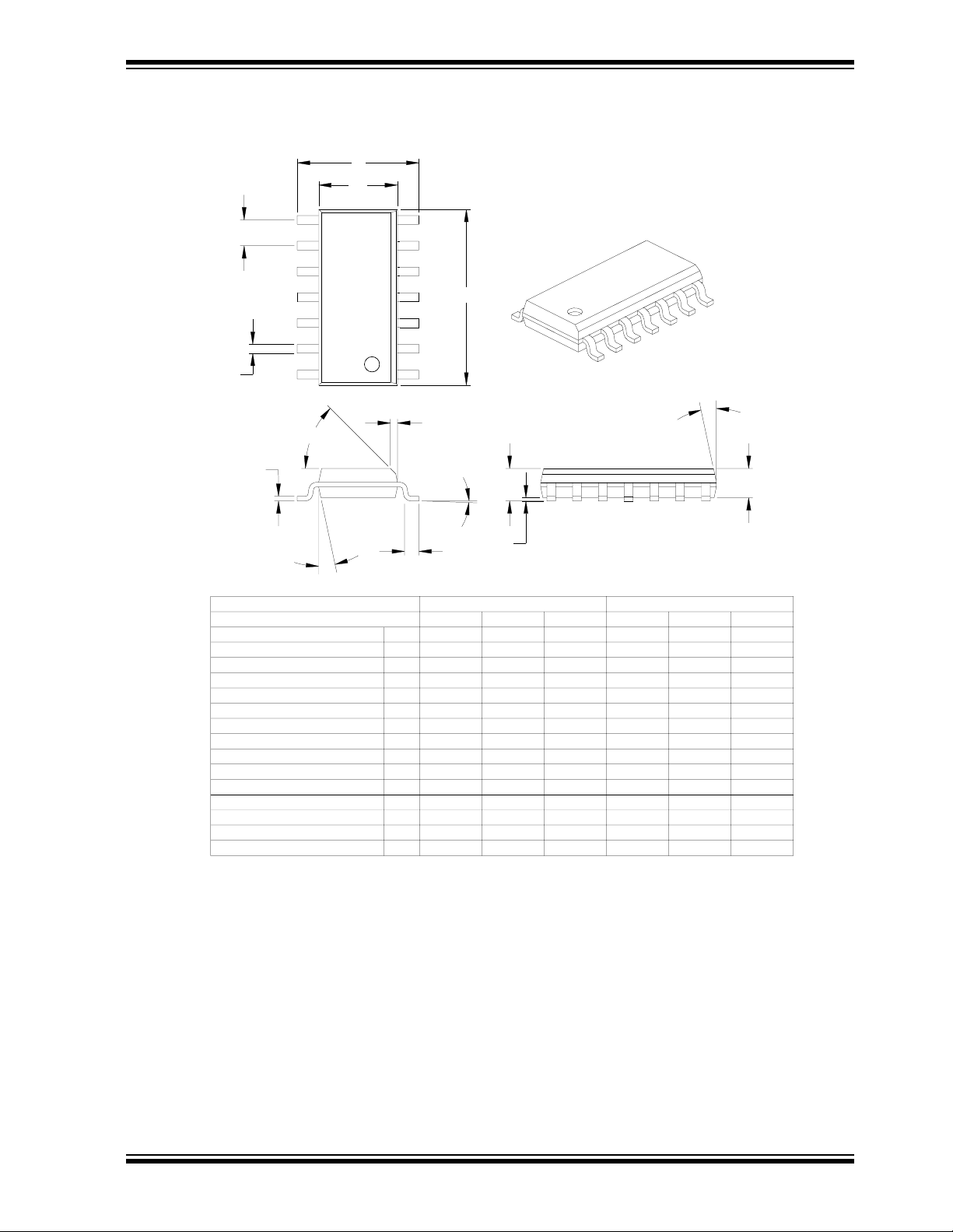
14-Lead Plastic Small Outline (SL) – Narrow, 150 mil (SOIC)
E
E1
p
D
2
B
n
1
PIC16C505
45
°
c
β
Number of Pins
Pitch
Foot Angle
Lead Thickness
Mold Draft Angle Top
Mold Draft Angle Bottom
*Controlling Parameter
Notes:
Dimensions D and E1 do not include mold flash or protrusions. Mold flash or protrusions shall not exceed
.010” (0.254mm) per side.
JEDEC Equivalent: MS-012
Drawing No. C04-065
h
A
φ
L
n
p
φ
c
α
β
A1
MILLIMETERSINCHES*Units
048048
α
A2
MAXNOMMINMAXNOMMINDimension Limits
1414
1.27.050
1.751.551.35.069.061.053AOverall Height
1.551.421.32.061.056.052A2Molded Package Thickness
0.250.180.10.010.007.004A1Standoff
6.205.995.79.244.236.228EOverall Width
3.993.903.81.157.154.150E1Molded Package Width
8.818.698.56.347.342.337DOverall Length
0.510.380.25.020.015.010hChamfer Distance
1.270.840.41.050.033.016LFoot Length
0.250.230.20.010.009.008
0.510.420.36.020.017.014BLead Width
1512015120
1512015120
1999 Microchip Technology Inc. DS40192C-page 77
Page 78
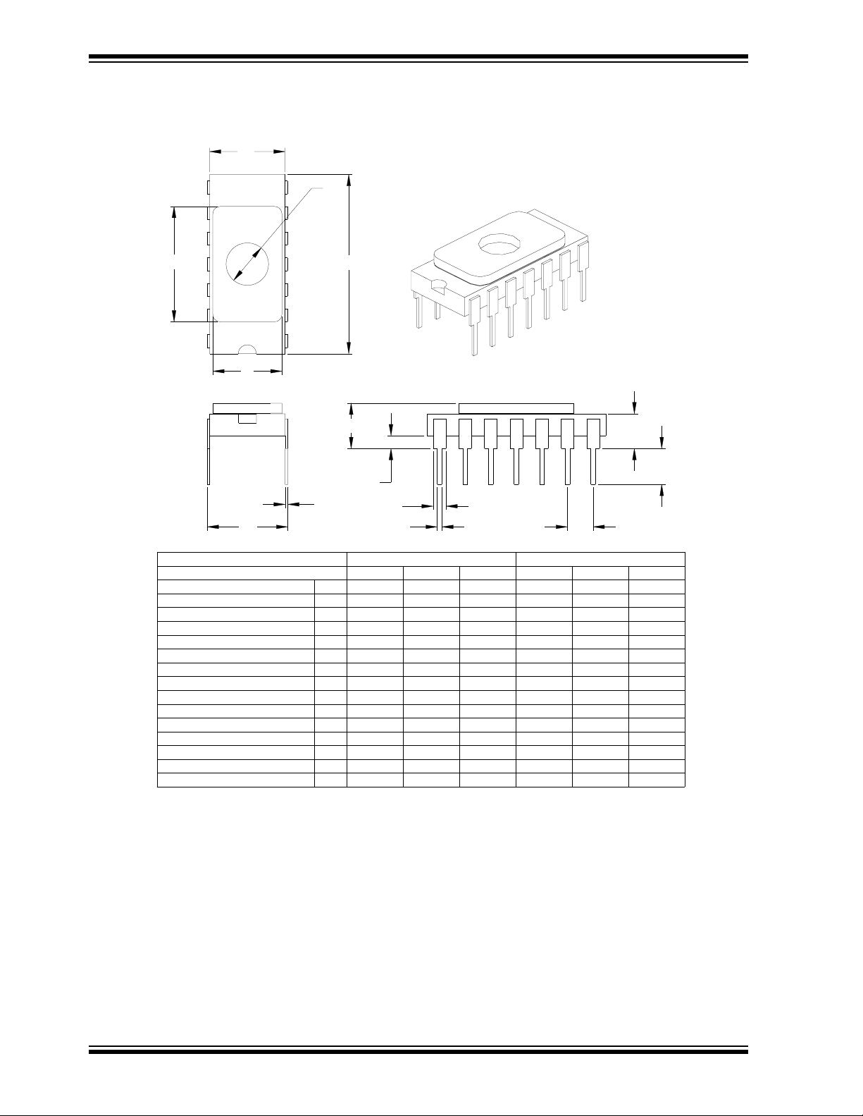
PIC16C505
14-Lead Ceramic Side Brazed Dual In-line with Window (JW) – 300 mil
E1
W
T
n
U
eB
Number of Pins
Pitch
Lead Thickness
*Controlling Parameter
JEDEC Equivalent: MS-015
Drawing No. C04-107
D
2
1
A
A1
c
n
p
c
B1
B
p
MILLIMETERSINCHES*Units
A2
L
MAXNOMMINMAXNOMMINDimension Limit s
1414
2.54.100
4.624.113.61.182.162.142ATop to Seating Plane
3.563.052.54.140.120.100A2Top of Body to Seating Plane
1.140.890.64.045.035.025A1Standoff
7.627.377.11.300.290.280E1Package Width
17.9617.7817.60.707.700.693DOverall Length
3.813.563.30.150.140.130LTip to Seating Plane
0.300.250.20.012.010.008
1.421.371.32.056.054.052B1Upper Lead Width
0.510.460.41.020.018.016BLower Lead Width
8.237.877.52.324.310.296eBOverall Row Spacing
4.344.224.09.171.166.161WWindow Diameter
11.6811.4311.18.460.450.440TLid Length
7.116.866.60.280.270.260ULid Width
DS40192C-page 78
1999 Microchip Technology Inc.
Page 79

PIC16C505
INDEX
A
ALU.......................................................................................7
Applications...........................................................................3
Architectural Overview..........................................................7
Assembler
MPASM Assembler..................................................... 51
B
Block Diagram
On-Chip Reset Circuit.................................................33
Timer0.........................................................................23
TMR0/WDT Prescaler.................................................26
Watchdog Timer..........................................................35
Brown-Out Protection Circuit ..............................................36
C
CAL0 bit..............................................................................16
CAL1 bit..............................................................................16
CAL2 bit..............................................................................16
CAL3 bit..............................................................................16
CALFST bit .........................................................................16
CALSLW bit ........................................................................16
Carry............ ............ .............................................................7
Clocking Scheme................................................................10
Code Protection ............................................................27, 37
Configuration Bits................................................................27
Configuration Word.............................................................27
D
DC and AC Characteristics.................................................71
Development Support .........................................................51
Device Varieties ....................................................................5
Digit Carry.............................................................................7
E
Errata.................................................................................... 2
F
Family of Devices
PIC16C505...................................................................4
FSR.....................................................................................18
I
I/O Interfacing............ .........................................................19
I/O Ports..................... .......................... ......................... ......19
I/O Programming Considerations........................................20
ID Locations..................................................................27, 37
INDF....................................................................................18
Indirect Data Addressing.....................................................18
Instruction Cycle .................................................................10
Instruction Flow/Pipelining..................................................10
Instruction Set Summary.....................................................40
K
KeeLoq Evaluation and Programming Tools....................54
L
Loading of PC ............................................................. .. .. .. ..17
M
Memory Organization..........................................................11
Data Memory ..............................................................12
Program Memory........................................................11
MPLAB Integrated Development Environment Software....51
O
OPTION Register................................................................15
OSC selection.....................................................................27
OSCCAL Register................... ............................................16
Oscillator Configurations..................................................... 28
Oscillator Types
HS.............. ............. ...................................... ..............28
LP................................... ............. ......................... ...... 28
RC .............................................................................. 28
XT............................................................................. ..28
P
Package Marking Information............................................. 75
Packaging Informatio n........................... ............................. 75
PICDEM-1 Low-Cost PICmicro Demo Board..................... 53
PICDEM-2 Low-Cost PIC16CXX Demo Board................... 53
PICDEM-3 Low-Cost PIC16CXXX Demo Board ................ 53
PICSTART Plus Entry Level Development System......... 53
POR
Device Reset Timer (DRT)................................... 27, 34
............................................................................... 36
PD
Power-On Reset (POR).............................................. 27
............................................................................... 36
TO
PORTB............................................................................... 19
Power-Down Mode............................................................. 37
Prescaler ............................................................................ 26
PRO MATE II Universal Programmer.............................. 53
Program Counter................................................................ 17
Q
Q cycles......... ......................... ............................................ 10
R
RC Oscillator....................................................................... 29
Read Modify Write.............................................................. 20
Register File Map...... .......................................................... 12
Registers
Special Function.........................................................13
Reset.................................................................................. 27
Reset on Brown-Out............. .............................................. 36
S
SEEVAL Evaluation and Programming System .............. 54
SLEEP.......................................................................... 27, 37
Software Simulator ( MPL AB-SIM)...................................... 52
Special Features of the CPU.............................................. 27
Special Function Registers................................................. 13
Stack................................................................................... 17
STATUS ............................................................................... 7
STATUS Register...............................................................14
T
Timer0
Switching Prescaler Assignment................................26
Timer0 ........................................................................ 23
Timer0 (TMR0) Module ..............................................23
TMR0 with External Clock..........................................25
Timing Diagrams and Specifications .................................. 66
Timing Parameter Symbology and Load Conditions .......... 65
TRIS Registers....................... ............................................ 19
W
Wake-up from SLEEP.........................................................37
Watchdog Timer (WDT)................................................ 27, 34
Period......................................................................... 35
Programming Considerat io n s..................................... 35
WWW, On-Line Support....................................................... 2
Z
Zero bit ................... ..................................... .........................7
1999 Microchip Technology Inc. DS40192B-page 79
Page 80

PIC16C505
NOTES:
DS40192B-page 80
1999 Microchip Technology Inc.
Page 81

PIC16C505
ON-LINE SUPPORT
Microchip provides on-line support on the Microchip
World Wide Web (WWW) site.
The web sit e is us ed by Microchip a s a means to make
files and infor mation easily available to customers. To
view the site, the user must ha ve access to the Int ernet
and a web browser, such as Netscape or Microsoft
Explorer. Files are also available for FTP download
from our FTP site.
Connecting to the Microchip Internet Web Site
The Microchip web site is available by using your
favorite Internet browser to attach to:
www.microchip.com
The file transfer site is available by using an FTP service to connect to:
ftp://ftp.microchip.com
The web site and file transfer site provide a variety of
services. Users may download files for the latest
Development Tools, Data Sheets, Application Notes,
User’s Guides, Articles and Sample Programs. A variety of Microchip specific business information is also
available, including listings of Microchip sales offices,
distributors and factory representatives. Other data
availa ble for consider a t io n is:
• Latest Microchip Press Releases
• Technical Support Section with Frequently Asked
Questions
• Design Tips
• Device Errata
• Job Postings
• Microchip Consultant Program Member Listing
• Links to other useful web sites related to
Microchip Products
• Conferences for products, Development Systems, technical information and more
• Listing of seminars and events
Systems Information and Upgrade Hot Line
The Systems Information and Upgrade Line provides
system users a listing of the latest versions of all of
Microchip’s development systems software products.
Plus, this line provides information on how customers
can receive any currently available upgrade kits.The
Hot Line Numbers are:
1-800-755-2345 for U.S. and most of Canada, and
1-480-786-7302 for the rest of the world.
981103
Trademarks: The Microchip name, logo, PIC, PICmicro,
PICSTART, PICMASTER and PRO MATE ar e r egistered
trademarks of Mic rochip Technology Incorpora te d in th e
U.S.A. and other countries.
LAB are trademarks and SQTP is a se rvice mark of
Microchip in the U.S.A.
All other trademarks mentioned herein are the property of
their respective companies.
Flex
ROM, MPLAB and
fuzzy-
1999 Microchip Technology Inc. DS40192C-page 81
Page 82

PIC16C505
READER RESPONSE
It is our intention to provide you with the bes t d ocu me nta t io n po ss ible to ensure succe ss ful us e of your Microchip pro duct. If you wish to provide your comments on organization, clarity, subject matter, and ways in which our documentation
can better serve you, please FAX your comments to the Technical Publications Manager at (480) 786-7578.
Please list the following information, and use this outline to provide us with your comments about this Data Sheet.
To:
RE: Reader Response
From:
Application (optional):
Would you like a reply? Y N
Device:
Questions:
1. What are the best features of this document?
2. How does this document meet your hardware and software development needs?
3. Do you find the organization of this data sheet easy to follow? If not, why?
Technical Publications Manager
Name
Company
Address
City / State / ZIP / Country
Telephone: (_______) _________ - _________
PIC16C505
Literature Number:
Total Pages Sent
F AX: (__ ___ _) ____ ___ __ - _____ ____
DS40192C
4. What additions to the data sheet do you think would enhance the structure and subject?
5. What deletions from the data sheet could be made without affecting the overall usefulness?
6. Is there any incorrect or misleading information (what and where)?
7. How would you improve this document?
8. How would you improve our software, systems, and silicon products?
DS40192C-page 82
1999 Microchip Technology Inc.
Page 83

PIC16C505
PIC16C505 Product Identification System
PART NO. -XX X /XX XXX
Pattern: Special Requirements
Package: SL = 150 mil SOIC
Temperature
Range:
Frequency
Range:
Device PIC16C505
P = 300 mil PDIP
JW = 300 mil Windowed Ceramic Side Brazed
-=0
I=-40
E=-40°C to +125°C
04 = 4 MHz (XT, INTRC, EXTRC OSC)
20 = 20 MHz (HS OSC)
PIC16LC505
PIC16C505T (T ape & reel for SOIC only)
PIC16LC505T (T ape & reel for SOIC only)
C to +70°C
°
C to +85°C
°
Please contact your local sales office for exact ordering procedures.
Sales and Support
Data Sheets
Products supported by a preliminary Data Sheet may have an errata sheet describing minor operational differences and recommended workarounds. To determine if an errata sheet exists for a particular device, please contact one of the following:
Examples
a) PIC16C505-04/P
Commercial Temp.,
PDIP Package, 4 MHz,
DD limits
normal V
b) PIC16C505-04I/SL
Industrial Temp., SOIC
package, 4MHz, normal
DD limits
V
c) PIC16C505-04I/P
Industrial Temp.,
PDIP package, 4 MHz,
DD limits
normal V
1. Your local Microchip sales office
2. The Microchip Corporate Literature Center U.S. FA X: (480) 786-7277
3. The Microchip Worldwide Site (www.microchip.com)
Please specify which device, revision of silicon and Data Sheet (include Literature #) you are using.
New Customer Notification System
Register on our web site (www.microchip.com/cn) to receive the most current information on our products.
1999 Microchip Technology Inc. DS40192C-page 83
Page 84

Note the following details of the code protection feature on PICmicro® MCUs.
• The PICmicro family meets the specifications contained in the Microchip Data Sheet.
• Microchip believes that its family of PICmicro microcontrollers is one of the most secure products of its kind on the market today,
when used in the intended manner and under normal conditions.
• There are dishonest and possibly illegal methods used to breach the code protection feature. All of these methods, to our knowl-
edge, require using the PICmicro microcontroller in a manner outside the operating specifications contained in the data sheet.
The person doing so may be engaged in theft of intellectual property.
• Microchip is willing to work with the customer who is concerned about the integrity of their code.
• Neither Microchip nor any other semiconductor manufacturer can guarantee the security of their code. Code protection does not
mean that we are guaranteeing the product as “unbreakable”.
• Code protection is constantly evolving. We at Microchip are committed to continuously improving the code protection features of
our product.
If you have any further questions about this matter, please contact the local sales office nearest to you.
Information contained in this publication regarding device
applications and the like is intended through suggestion only
and may be superseded by updates. It is your responsibility to
ensure that your application meets with your specifications.
No representation or warranty is given and no liability is
assumed by Microchip Technology Incorporated with respect
to the accuracy or use of such information, or infringement of
patents or other intellectual property rights arising from such
use or otherwise. Use of Microchip’s products as critical components in life support systems is not authorized except with
express written approval by Microchip. No licenses are conveyed, implicitly or otherwise, under any intellectual property
rights.
Trademarks
The Microchip name and logo, the Microchip logo, FilterLab,
K
EELOQ, microID, MPLAB, PIC, PICmicro, PICMASTER,
PICSTART, PRO MATE, SEEVAL and The Embedde d Control
Solutions Company are registered trademarks of Microchip Technology Incorporated in the U.S.A. and other countries.
dsPIC, ECONOMONITOR, FanSense, FlexROM, fuzzyLAB,
In-Circuit Serial Programming, ICSP, ICEPIC, microPort,
Migratable Memory, MPASM, MPLIB, MPLINK, MPSIM,
MXDEV, PICC, PICDEM, PICDEM.net, rfPIC, Select Mode
and T otal Endurance are trademarks of Microchip Technology
Incorporated in the U.S.A.
Serialized Quick Turn Programming (SQTP) is a service mark
of Microchip Technology Incorporated in the U.S.A.
All other trademarks mentioned herein are property of their
respective companies.
© 2002, Microchip Technology Incorporated, Printed in the
U.S.A., All Rights Reserved.
Printed on recycled paper.
2002 Microchip Technology Inc.
Microchip received QS-9000 quality system
certification for its worldwide headquarters,
design and wafer fabrication facilities in
Chandler and Tempe, Arizona in July 1999. The
Company’s quality system processes and
procedures are QS-9000 compliant for its
PICmicro
devices, Serial EEPROMs and microperipheral
products. In addition, Microchip’s quality
system for the design and manufacture of
development systems is ISO 9001 certified.
®
8-bit MCUs, KEELOQ
®
code hoppin g
Page 85

M
AMERICAS
Corporate Office
2355 West Chandler Blvd.
Chandler, AZ 85224-6199
Tel: 480-792-7200 Fax: 480-792-7277
Technical Support: 480-792-7627
Web Address: http://www.microchip.com
Rocky Mountain
2355 West Chandler Blvd.
Chandler, AZ 85224-6199
Tel: 480-792-7966 Fax: 480-792-7456
Atlanta
500 Sugar Mill Road, Suite 200B
Atlanta, GA 30350
Tel: 770-640-0034 Fax: 770-640 -03 07
Boston
2 Lan Drive, Suite 120
Westford, MA 01886
Tel: 978-692-3848 Fax: 978-692 -38 21
Chicago
333 Pierce Road, Suite 180
Itasca, IL 60143
Tel: 630-285-0071 Fax: 630-285-0075
Dallas
4570 Westgrove Drive, Suite 160
Addison, TX 75001
Tel: 972-818-7423 Fax: 972-818 -29 24
Detroit
Tri-Atria Office Building
32255 Northwestern Highway, Suite 190
Farmington Hills, MI 48334
Tel: 248-538-2250 Fax: 248-538-2260
Kokomo
2767 S. Albright Road
Kokomo, Indiana 46902
Tel: 765-864-8360 Fax: 765-864-8387
Los Angeles
18201 Von Karman, Suite 1090
Irvine, CA 92612
Tel: 949-263-1888 Fax: 949-263 -13 38
New York
150 Motor Parkway, Suite 202
Hauppauge, NY 11788
Tel: 631-273-5305 Fax: 631-273 -53 35
San Jose
Microchip Technology Inc.
2107 North First Street, Suite 590
San Jose, CA 95131
Tel: 408-436-7950 Fax: 408-436 -79 55
Toronto
6285 Northam Drive, Suite 108
Mississauga, Ontario L4V 1X5, Cana da
2002 Microchip Technology Inc.
 Loading...