


*8-bit, 8-pin Devices Protected by Microchip’s Low Pin C ount Patent: U .S. Patent N o. 5,847,450. Addit ional U.S. and
查询PIC12F609-E/MD供应商
PIC12F609/HV609
PIC12F615/HV615
Data Sheet
8-Pin Flash-Based, 8-Bit
CMOS Microcontrollers
foreign patents and applications m ay be issued or pending.
© 2006 Microchip Technology Inc. Preliminary DS41302A

Note the following details of the code protection feature on Microchip devices:
• Microchip products meet the specification contained in their particular Microchip Data Sheet.
• Microchip believes that its family of products is one of the most secure families of its kind on the market today, when used in the
intended manner and under normal conditions.
• There are dishonest and possibly illegal methods used to breach the code protection feature. All of these methods, to our
knowledge, require using the Microchip products in a manner outside the operating specifications contained in Microchip’s Data
Sheets. Most likely, the person doing so is engaged in theft of intellectual property.
• Microchip is willing to work with the customer who is concerned about the integrity of their code.
• Neither Microchip nor any other semiconductor manufacturer can guarantee the security of their code. Code protection does not
mean that we are guaranteeing the product as “unbreakable.”
Code protection is constantly evolving. We at Microchip are committed to continuously improving the code protection features of our
products. Attempts to break Microchip’s code protection feature may be a violation of the Digit al Millennium Copyright Act. If suc h a c t s
allow unauthorized access to your software or other copyrighted work, you may have a right to sue for relief under that Act.
Information contained in this publication regarding device
applications and t he lik e is provided only for your convenien ce
and may be su perseded by updates. It is you r responsibility to
ensure that your application meets with your specifications.
MICROCHIP MAKES NO REPRESENTATIONS OR
WARRANTIES OF ANY KIND WHETHER EXPRESS OR
IMPLIED, WRITTEN OR ORAL, STATUTORY OR
OTHERWISE, RELATED TO THE INFORMATION,
INCLUDING BUT NOT LIMITED TO ITS CONDITION,
QUALITY, PERFORMANCE, MERCHANTABILITY OR
FITNESS FOR PURPOSE. Microchip disclaims all liability
arising from this information and its use. Use of Microchip
devices in life supp ort and/or safety ap plications is entir ely at
the buyer’s risk, and the buyer agrees to defend, indemnify and
hold harmless M icrochip from any and all dama ges, claims,
suits, or expenses re sulting from such use. No licens es are
conveyed, implicitly or otherwise, under any Microchip
intellectual property rights.
Trademarks
The Microchip name and logo, the Microchip logo, Accuron,
dsPIC, K
EELOQ, microID, MPLAB, PIC, PICmicro, PICSTART,
PRO MAT E, Pow erSm art , rfPIC and SmartS hunt are
registered trademarks of Microchip Technology Incorporated
in the U.S.A. and other countries.
AmpLab, FilterLab, Migratable Memory, MXDEV, MXLAB,
SEEVAL, SmartSensor and The Embedded Control Solutions
Company are registered trademarks of Microchip Technology
Incorporated in the U.S.A.
Analog-for-the-Digital Age, Application Maestro, CodeGuard,
dsPICDEM, dsPICDEM.net, dsPICworks, ECAN,
ECONOMONITOR, FanSense, FlexROM, fuzzyLAB,
In-Circuit Serial Programming, ICSP, ICEPIC, Linear Active
Thermistor, Mindi, MiWi, MPASM, MPLIB, MPLINK, PIC kit,
PICDEM, PICDEM.net, PICLAB, PICtail, PowerCal,
PowerInfo, PowerMate, PowerTool, REAL ICE, rfLAB,
rfPICDEM, Select Mode, Smart Serial, SmartTel, Total
Endurance, UNI/O, WiperLock and ZENA are trademarks of
Microchip Technology Incorporated in the U.S.A. and other
countries.
SQTP is a service mark of Microchip Technology Incorporated
in the U.S.A.
All other trademarks mentioned herein are property of their
respective companies.
© 2006, Microchip Technology Incorporated, Printed in the
U.S.A., All Rights Reserved.
Printed on recycled paper.
Microchip received ISO/TS-16949:2002 certification for its worldwide
headquarters, design and wafer fabrication facilities in Chandler and
Tempe, Arizona, Gresham, Oregon and Mountain View, California. The
Company’s quality system processes and procedures are for its PIC
8-bit MCUs, KEELOQ
microperipherals, nonvolatile memory and analog products. In addition,
Microchip’s quality system for the design and manufacture of
development systems is ISO 9001:2000 certified.
®
code hopping devices, Serial EEPROMs,
DS41302A-page ii Preliminary © 2006 Microchip Technology Inc.
®

PIC12F609/615/12HV609/615
8-Pin Flash-Based, 8-Bit CMOS Microcontrollers
High-Performance RISC CPU:
• Only 35 instructions to learn:
- All single-cycle instructions except branches
• Operating speed:
- DC – 20 MHz oscillator/clock input
- DC – 200 ns instr uction cycle
• Interrupt capability
• 8-level deep hardware stack
• Direct, Indirect and Relative Addressing modes
Special Microcontroller Features:
• Precision Internal Oscillator:
- Factory calibrated to ±1%, typical
- Software selectable frequency: 4 MHz or
8 MHz
• Power-Saving Sleep mode
• Volt age range:
- PIC12F609/615: 2.0V to 5.5V
- PIC12HV609/615: 2.0V to user defined
maximum (see note)
• Industrial and Extended Temperature range
• Power-on Reset (PO R)
• Power-up Time r (PWRT) and Oscillator Start-up
Timer (OST)
• Brown-out Reset (BOR)
• Watchdog Timer (WDT) with independent
oscillator for reliable operation
• Multiplexed Master Clear with pull-up/input pin
• Programmable code protection
• High Endurance Flash:
- 100,000 write Flash endurance
- Flash r etention: > 40 years
Low-Power Features:
• Standby Current:
- 50 nA @ 2.0V, typical
• Operating Current:
-11μA @ 32 kHz, 2.0V, typical
-260μA @ 4 MHz, 2.0V, typical
• Watchdog Timer Current:
-1μA @ 2.0V, typical
Peripheral Features:
• Shunt Voltage Regulator (PIC12HV609/615 only):
- 5 volt regulation
- 4 mA to 50 mA shunt range
• 5 I/O pins and 1 input only
• High current source/sink for direct LED drive
- Interrupt-on-pin change or pins
- Individually programmable weak pull-ups
• Analog Comparator module with:
- One analog comparator
- Programmable on-chip voltage reference
(CV
REF) module (% of VDD)
- Comparator inputs and output externally
accessible
- Built-In Hysteresis (software selectable)
• Timer0: 8-bit timer/counter with 8-bit
programmable prescaler
• Enhanced Timer1:
- 16-bit timer/counter with prescaler
- External Timer1 Gate (cou nt enab le )
- Option to use OSC1 and OSC2 in LP mode
as Timer1 oscillator if INTOSC mode
selected
- Option to use system clock as Timer1
TM
• In-Circuit Serial Programming
pins
PIC12F615/HV615 ONLY:
• Enhanced Capture, Compare, PWM module:
- 16-bit Capture, max. resolution 12.5 ns
- Compare, max. resolution 200 ns
- 10-bit PWM with 1 or 2 output channels, 1
output channel programmable “dead time”,
max. frequency 20 kHz, auto-shutdown
• A/D Converter:
- 10-bit resolution and 4 channels, samples
internal voltage references
• Timer2: 8-bit timer/counter with 8-bit period
register, prescaler and postscaler
(ICSPTM) via two
Note: Voltage across the shunt regulator should
not exceed 5V.
© 2006 Microchip Technology Inc. Preliminary DS41302A-page 1

PIC12F609/615/12HV609/615
Program Memory Data Memory
Device
PIC12F609 1024 64 5 0 1 1/1 2.0V-5.5V
PIC12HV609 1024 64 5 0 1 1/1 2.0V-user defined
PIC12F615 1024 64 5 4 1 2/1 2.0V-5.5V
PIC12HV615 1024 64 5 4 1 2/1 2.0V-user defined
Flash
(words)
SRAM (bytes)
I/O
10-bit A/D
(ch)
Comparators
Timers
8/16-bit
Voltage Range
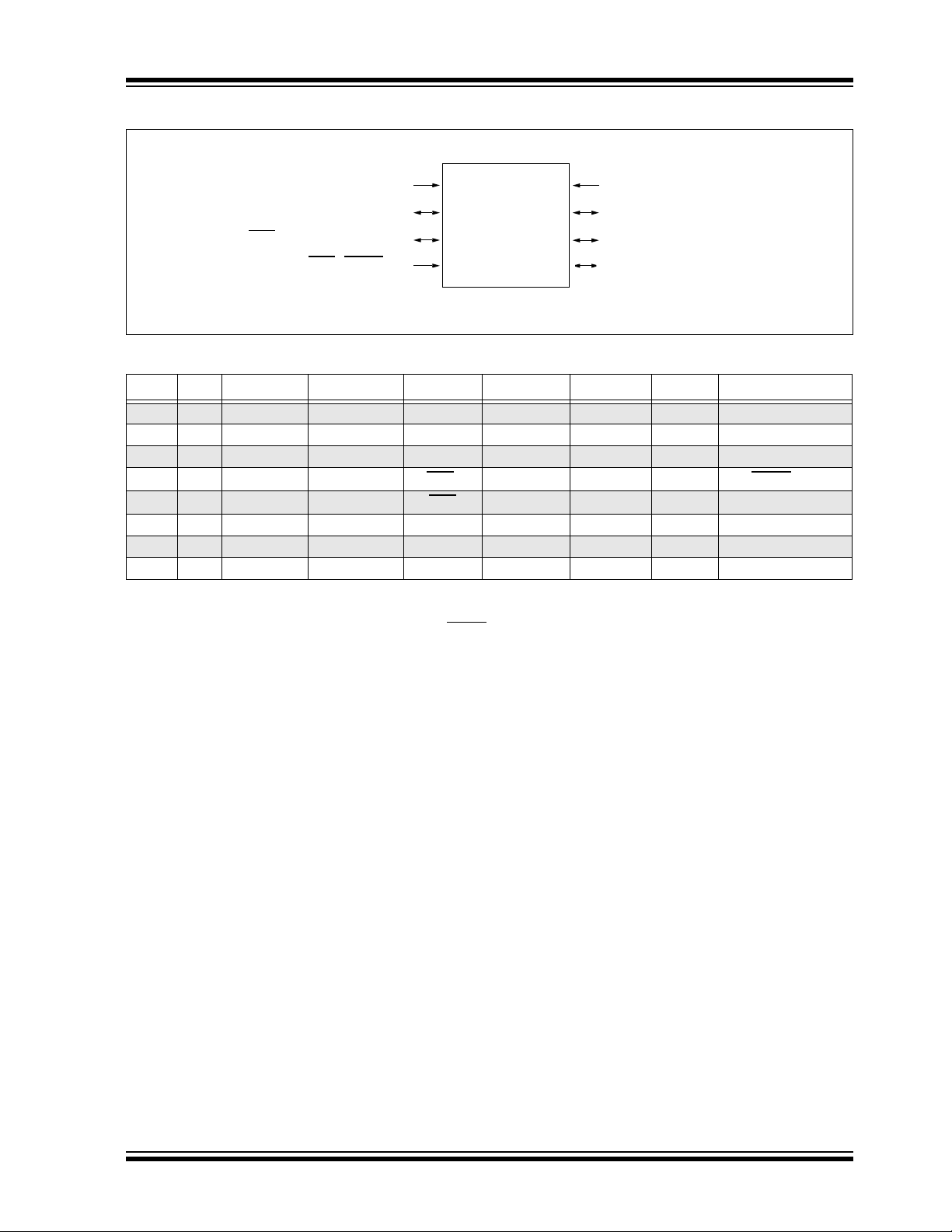
8-Pin Diagram, PIC12F609/HV609 (PDIP, SOIC, TSSOP, DFN)
GP5/T1CKI/OSC1/CLKIN
GP4/CIN1-/T1G
/OSC2/CLKOUT
GP3/MCLR
VDD
/VPP
1
2
PIC12F609/
HV609
3
4
TABLE 1: PIC12F609/HV609 PIN SUMMARY (PDIP, SOIC, TSSOP, DFN)
I/O Pin Comparators Timer Interrupts Pull-ups Basic
GP0 7 CIN+ — IOC Y ICSPDAT
GP1 6 CIN0- — IOC Y ICSPCLK
GP2 5 COUT T0CKI INT/IOC Y —
GP3
(1)
4—
GP4 3 CIN1- T1G IOC Y OSC2/CLKOUT
GP5 2 — T1CKI IOC Y OSC1/CLKIN
— 1 — — — — VDD
—8— ——— VSS
Note 1: Input only.
2: Only when pin is configured for external MCLR.
—
IOC Y
V
8
7
6
5
SS
GP0/CIN+/ICSPDAT
GP1/CIN0-/ICSPCLK
GP2/T0CKI/INT/COUT
(2)
MCLR/VPP
DS41302A-page 2 Preliminary © 2006 Microchip Technology Inc.
PIC12F609/615/12HV609/615
8-Pin Diagram, PIC12F615/HV615 (PDIP, SOIC, TSSOP, DFN)
VDD
GP5/T1CKI/P1A*/OSC1/CLKIN
GP4/AN3/CIN1-/T1G/P1B*/OSC2/CLKOUT
GP3/T1G
* Alternate pin function.
*/MCLR/VPP
1
2
PIC12F615/
HV615
3
4
V
8
7
6
5
SS
GP0/AN0/CIN+/P1B/ICSPDA T
GP1/AN1/CIN0-/VREF/ICSPCLK
GP2/AN2/T0CKI/INT/COUT/CCP1/P1A
T ABLE 2: PIC12F615/HV615 PIN SUMMARY (PDIP, SOIC, TSSOP, DFN)
I/O Pin Analog Comparators Timer CCP Interrupts Pull-ups Basic
GP0 7 AN0 CIN+ — P1B IOC Y ICSPDAT
GP1 6 AN1 CIN0- — — IOC Y ICSPCLK/VREF
GP2 5 AN2 COUT T0CKI CCP1/P1A INT/IOC Y —
(1)
GP3
GP4 3 AN3 CIN1- T1G P1B* IOC Y OSC2/CLKOUT
GP5 2 — — T1CKI P1A* IOC Y OSC1/CLKIN
— 1 — — — — — — VDD
—8 — — — — — — VSS
Note 1: Input only.
4— — T1G*— IOCY
* Alternate pin function.
2: Only when pin is configured for external MCLR
.
(2)
MCLR/VPP
© 2006 Microchip Technology Inc. Preliminary DS41302A-page 3

PIC12F609/615/12HV609/615
Table of Contents
1.0 Device Overview .......................................................................................................................................................................... 5
2.0 Memory Organization................................................................................................................................................................... 9
3.0 Oscillator Module........................................................................................................................................................................ 25
4.0 I/O Ports................. ....................................................................................................................................................................31
5.0 Timer0 Module ........................................................................................................................................................................... 41
6.0 Timer1 Module with Gate Control.............................................................. .................................................................................45
7.0 Timer2 Module (PIC12F615/HV615 only).......................................................................... ........................................................51
8.0 Comparator Module....................................................................................................................................................................53
9.0 Analog-to-Digital Converter (ADC) Module (PIC12F615/HV615 only) ....................................................................................... 65
10.0 Enhanced Capture/Compare/PWM (With Auto-Shutdown and Dead Band) Module (PIC12F615/HV615 only)........................ 75
11.0 Special Features of the CPU....................................... ............................................................................................................... 93
12.0 Voltage Regulator............................................................................. .. .. .. .. .. ....... .. .. .. .. .. .. ........................................................... 111
13.0 Instruction Set Summary.......................................................................................................................................................... 113
14.0 Development Support. ..............................................................................................................................................................123
15.0 Electrical Specifications............................................................................................................................................................ 127
16.0 DC and AC Characteristics Graphs and Tables.......................................................................................................................149
17.0 Packaging Information..................................................... ......................................................................................................... 151
Appendix A: Data Sheet Revision History..........................................................................................................................................157
Appendix B: Migrating from other PIC® Devices...............................................................................................................................157
Index ........................................................................... ... .................................................................................................................... 159
The Microchip Web Site..................................................................................................................................................................... 163
Customer Change Notification Service ..................................... ...... ............. ...... ............... ...... ........................................................... 163
Customer Support.............................................................................................................................................................................. 163
Reader Response............................................................................ .................................................................................................. 164
Product Identification System............................................................................................................................................................. 165
TO OUR VALUED CUSTOMERS
It is our intention to provide our valued customers with the best docum entation possible to ensure s uccessful use of your Microchip
products. To this end, we will continue to improve our publications to better suit your needs. Our publications will be refined and
enhanced as new volumes and updates are introduced.
If you have any questions or comments regarding this publication, please contact the Marketing Communications Department via
E-mail at docerrors@microchip.com or fax the Reader Response Form in the back of this data sheet to (480) 792-4150. We
welcome your feedback.
Most Current Data Sheet
To obtain the most up-to-date version of this data sheet, please register at our Worldwide Web site at:
http://www.microchip.com
You can determine t he version of a data sheet by examining its literature number found on the bottom outside corner of any page.
The last character of the literature number is the version number, (e.g., DS30000A is version A of document DS30000).
Errata
An errata sheet, describing minor operational differences from the data sheet and recommended workarounds, may exist for current
devices. As device/documentation issues become known to us, we will publish an errata sheet. The errata will specify the revision of
silicon and revision of document to which it applies.
To determine if an errata sheet exists for a particular device, please check with one of the following:
• Microchip’s Worldwide Web site; http://www.microchip.com
• Your local Microchip sales office (see last page)
When contacting a sales office, please specify which device, revision of silicon and data sheet (include literature number) you are
using.
Customer Notification System
Register on our web site at www.microchip.com to receive the most current information on all of our products.
DS41302A-page 4 Preliminary © 2006 Microchip Technology Inc.

PIC12F609/615/12HV609/615
1.0 DEVICE OVERVIEW
Block Diagrams and pinout descriptions of the devices
are as follows:
The PIC12F609/615/12HV609/615 devices are covered
by this data sheet. They are available in 8-pin PDIP,
SOIC, TSSOP and DFN packages.
• PIC12F609/HV609 (Figure1-1, Table 1-1)
• PIC12F615/HV615 (Figure1-2, Table 1-2)
FIGURE 1-1: PIC12F609/HV609 BLOCK DIAGRAM
13
Program Counter
8-Level Stack
Direct Addr
INT
(13-Bit)
RAM Addr
7
Program
Bus
Configuration
Flash
1K X 14
Program
Memory
14
Instruction Reg
8
Data Bus
RAM
64 Bytes
File
Registers
Addr MUX
STATUS Reg
9
8
FSR Reg
Indirect
Addr
8
GPIO
GP0
GP1
GP2
GP3
GP4
GP5
OSC1/CLKIN
OSC2/CLKOUT
T1G
T1CKI
T0CKI
Internal
Oscillator
Block
Instruction
Decode &
Control
Timing
Generation
Power-up
Timer
Oscillator
Start-up Timer
Power-on
Reset
Watchdog
Timer
Brown-out
Reset
VDD
MCLR
Timer0 Timer1
Comparator Voltage Reference
Absolute Voltage Reference
VSS
3
ALU
8
W Reg
Shunt Regulator
(PIC12HV609 only)
MUX
Analog Comparator
and Reference
CIN+
CIN0-
CIN1-
COUT
© 2006 Microchip Technology Inc. Preliminary DS41302A-page 5

PIC12F609/615/12HV609/615
FIGURE 1-2: PIC12F615/HV615 BLOCK DIAGRAM
OSC1/CLKIN
OSC2/CLKOUT
T1G*
T1G
Program
Bus
Internal
Oscillator
Block
Configuration
Flash
1K X 14
Program
Memory
14
Instruction Reg
Instruction
Decode &
Control
Timing
Generation
13
8
MCLR
INT
Program Counter
8-Level Stack
(13-Bit)
Direct Addr
Power-up
Timer
Oscillator
Start-up Timer
Power-on
Reset
Watchdog
Timer
Brown-out
Reset
VDD
VSS
7
RAM Addr
3
8
Data Bus
RAM
64 Bytes
File
Registers
9
Addr MUX
Indirect
8
Addr
FSR Reg
STATUS Reg
MUX
ALU
W Reg
Shunt Regulator
(PIC12HV615 only)
8
GPIO
GP0
GP1
GP2
GP3
GP4
GP5
T1CKI
T0CKI
VREF
Analog-To-Digital Converter
AN0
AN1
AN2
AN3
* A lte rn ate pi n func ti on.
Timer0 Timer1
Comparator Voltage Reference
Absolute Voltage Reference
Timer2
Analog Comparator
and Reference
CIN1-
COUT
ECCP
CIN+
CIN0-
CCP1/P1A
P1B
P1A*
P1B*
DS41302A-page 6 Preliminary © 2006 Microchip Technology Inc.

PIC12F609/615/12HV609/615
TABLE 1-1: PIC12F609/HV609 PINOUT DESCRIPTION
Name Function
GP0/CIN+/ICSPDAT GP0 TTL CMOS General purpose I/O with prog. pull-up and interrupt-on-change
CIN+ AN — Comparator non-inverting input
ICSPDAT ST CMOS Serial Programming Data I/O
GP1/CIN0-/ICSPCLK GP1 TTL CMOS General purpose I/O with prog. pull-up and int errupt-on-c hange
CIN0- AN — Comparator inverting input
ICSPCLK ST — Serial Programming Clock
GP2/T0CKI/INT/COUT GP2 ST CMOS General purpose I/O with prog. pull-up and interrupt-on-change
T0CKI ST — Timer0 clock input
INT ST — External Interrupt
COUT — CMOS Comparator output
CLR/VPP GP3 TTL — General purpose input with interrupt-on-change
GP3/M
MCLR
PP HV — Programming voltage
V
GP4/CIN1-/T1G
CLKOUT
GP5/T1CKI/OSC1/CLKIN GP5 TTL CMOS General purpose I/O with prog. pull-up and interrupt -on-c hange
DD VDD Power — Positive supply
V
SS VSS Power — Ground reference
V
Legend: AN = Analog input or output CMOS= CMOS com patible input or output HV = High Voltage
/OSC2/
ST = Schmitt Trigger input with CMOS levels TTL = T TL compatible input XTAL = Crystal
GP4 TTL CMOS General purpose I/O with prog. pull-up and interrupt-on-change
CIN1-
T1G
OSC2 — XTAL Crystal/Resonator
CLKOUT — CMOS F
T1CKI ST — Timer1 clock input
OSC1 XTAL — Crystal/Resonator
CLKIN ST — External clock input/RC oscillator connection
Input
Type
Output
Type
ST — Master Clear w/internal pull-up
AN — Comparator inverting input
ST — Timer1 gate (count enable)
OSC/4 output
Description
© 2006 Microchip Technology Inc. Preliminary DS41302A-page 7
PIC12F609/615/12HV609/615
TABLE 1-2: PIC12F615/HV615 PINOUT DESCRIPTION
Name Function
GP0/AN0/CIN+/P1B/ICSPDAT GP0 TTL CMOS General purpose I/O with prog. pull-up and interrupt-on-
AN0 AN — A/D Channel 0 input
CIN+ AN — Comparator non-inverting input
P1B — CMOS PWM output
ICSPDAT ST CMOS Serial Programming Data I/O
GP1/AN1/CIN0-/V
GP2/AN2/T0CKI/INT/COUT/CCP1/
P1A
GP3/T1G
GP4/AN3/CIN1-/T1G
CLKOUT
GP5/T1CKI/P1A*/OSC1/CLKIN GP5 TTL CMOS General purpose I/O with prog. pull-up and interrupt-on-
V
V
Legend: AN = Analog input or output CMOS=CMOS compatible input or output HV = High Voltage
*/MCLR/VPP GP3 TTL — G eneral purpose input with interrupt-on-change
DD VDD Power — Positive supply
SS VSS Power — Ground reference
* Alternate pin function.
REF/ICSPCLK GP1 TTL CMOS General purpose I/O with prog. pull-up and interrupt-on-
AN1 AN — A/D Channel 1 input
CIN0- AN — Comparator inverting input
REF AN — External Voltage Reference for A/D
V
ICSPCLK ST — Serial Programming Clock
GP2 ST CMOS General purpose I/O with prog. pull-up and interrupt-on-
AN2 AN — A/D Channel 2 input
T0CKI ST — Timer0 clock input
INT ST — External Interrupt
COUT — CMOS Comparator output
CCP1 ST CMOS Capture input/Compare input/PWM output
P1A — CMOS PWM output
T1G
MCLR
V
PP HV — Programming voltage
/P1B*/OSC2/
ST = Schmitt Trigger input with CMOS levels TTL =T T L compatible input XTAL= Crystal
GP4 TTL CMOS General purpose I/O with prog. pull-up and interrupt-on-
AN3 AN — A/D Channel 3 input
CIN1-
T1G
P1B* — CMOS PWM output, alternate pin
OSC2 — XTAL Crystal/Resonator
CLKOUT — CMOS F
T1CKI ST — Timer1 clock input
P1A* — CMOS PWM output, alternate pin
OSC1 XTAL — Crystal/Resonator
CLKIN ST — External clock input/RC oscillator connection
Input
Type
* ST — Timer1 gate (count enable), alternate pin
Output
Type
change
change
change
ST — Master Clear w/internal pull-up
change
AN — Comparator inverting input
ST — Timer1 gate (count enable)
OSC/4 output
change
Description
DS41302A-page 8 Preliminary © 2006 Microchip Technology Inc.

PIC12F609/615/12HV609/615
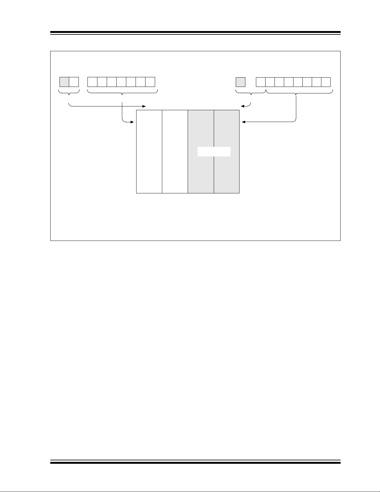
2.0 MEMORY ORGANIZATION
2.1 Program Memory Organization
The PIC12F609/615/12HV609/615 has a 13-bit program counter capable of addressing an 8K x 14 program memory space. Only the first 1K x 14 (0000h03FFh) for the PIC12F609/615/12HV609/615 is physically implemented. Accessing a location above these
boundaries will cause a wraparound within the first 1K
x 14 space. T he Rese t vec tor is at 0000 h and the int errupt vector is at 0004h (see Figure 2-1).
FIGURE 2-1: PROGRAM MEMORY MAP
AND STACK FOR THE
PIC12F609/615/12HV609/615
PC<12:0>
CALL, RETURN
RETFIE, RETLW
Stack Level 1
Stack Level 2
Stack Level 8
Reset Vector
13
0000h
2.2 Data Memory Organization
The data memory (see Figure 2-2) is partitioned into two
banks, which contain the General Purpose Registers
(GPR) and the Special Function Registers (SFR). The
Special Function Registers are located in the first 32
locations of each bank. Register locations 40h-7Fh in
Bank 0 are General Purpose Registers, implemented as
static RAM. Register locations F0h-FFh in Bank 1 point
to addresses 70h-7Fh in Bank 0. All other RAM is
unimplemented and returns ‘0’ when read. The RP0 bit
of the STATUS register is the bank select bit.
RP0
0 → Bank 0 is selected
1 → Bank 1 is selected
Note: The IRP and RP1 bits of the STATUS
register are reserved and should always be
maintained as ‘0’s.
2.2.1 GENERAL PURPOSE REGISTER
FILE
The register file is organized as 64 x 8 in the
PIC12F609/615/12HV609/615. Each register is
accessed, either directly or indirectly, through the File
Select Register (FSR) (see Section 2.4 “Indirect
Addressing, INDF and FSR Registers” ).
Interrupt Vector
On-chip Program
Memory
Wraps to 0000h-07FFh
0004h
0005h
03FFh
0400h
1FFFh
2.2.2 SPECIAL FUNCTION REGISTERS
The Special Function Registers are registers used by
the CPU and peripheral functions for controlling the
desired operation of the device (see Table2-1). These
registers are static RAM.
The special registers can be classified into two sets:
core and peripheral. The Special Function Registers
associated with the “core” are described in this section.
Those related to the operation of the peripheral features
are described in the section of that peripheral feature.
© 2006 Microchip Technology Inc. Preliminary DS41302A-page 9

PIC12F609/615/12HV609/615
FIGURE 2-2: DATA MEMORY MAP OF
THE PIC12F609/HV609
Indirect Addr.
TMR0
PCL
STATUS
FSR
GPIO
PCLATH
INTCON
PIR1
TMR1L
TMR1H
T1CON
VRCON
CMCON0
CMCON1
(1)
File
Address
00h
01h
02h
03h
04h
05h
06h
07h
08h
09h
0Ah
0Bh
0Ch
0Dh
0Eh
0Fh
10h
11h
12h
13h
14h
15h
16h
17h
18h
19h
1Ah
1Bh
1Ch
1Dh
1Eh
1Fh
20h
Indirect Addr.
OPTION_REG
PCL
STATUS
FSR
TRISIO
PCLATH
INTCON
PIE1
PCON
OSCTUNE
WPU
IOC
ANSEL
(1)
File
Address
80h
81h
82h
83h
84h
85h
86h
87h
88h
89h
8Ah
8Bh
8Ch
8Dh
8Eh
8Fh
90h
91h
92h
93h
94h
95h
96h
97h
98h
99h
9Ah
9Bh
9Ch
9Dh
9Eh
9Fh
A0h
FIGURE 2-3: DATA MEMORY MAP OF
THE PIC12F615/HV615
Indirect Addr.
TMR0
PCL
STATUS
FSR
GPIO
PCLATH
INTCON
PIR1
TMR1L
TMR1H
T1CON
TMR2
T2CON
CCPR1L
CCPR1H
CCP1CON
PWM1CON
ECCPAS
VRCON
CMCON0
CMCON1
ADRESH
ADCON0
(1)
File
Address
00h
01h
02h
03h
04h
05h
06h
07h
08h
09h
0Ah
0Bh
0Ch
0Dh
0Eh
0Fh
10h
11h
12h
13h
14h
15h
16h
17h
18h
19h
1Ah
1Bh
1Ch
1Dh
1Eh
1Fh
20h
Indirect Addr.
OPTION_REG
PCL
STATUS
FSR
TRISIO
PCLATH
INTCON
PIE1
PCON
OSCTUNE
PR2
APFCON
WPU
IOC
ADRESL
ANSEL
(1)
File
Address
80h
81h
82h
83h
84h
85h
86h
87h
88h
89h
8Ah
8Bh
8Ch
8Dh
8Eh
8Fh
90h
91h
92h
93h
94h
95h
96h
97h
98h
99h
9Ah
9Bh
9Ch
9Dh
9Eh
9Fh
A0h
3Fh
General
Purpose
Registers
64 Bytes
Bank 0
Unimplemented data memory locations, read as ‘0’.
Note 1: Not a physical register.
40h
7Fh
Accesses 70h-7Fh
Bank 1
EFh
F0h
FFh
General
Purpose
Registers
64 Bytes
Bank 0
Unimplemented data memory locations, read as ‘0’.
Note 1: Not a physical register.
3Fh
40h
7Fh
Accesses 70h-7Fh
Bank 1
EFh
F0h
FFh
DS41302A-page 10 Preliminary © 2006 Microchip Technology Inc.
PIC12F609/615/12HV609/615
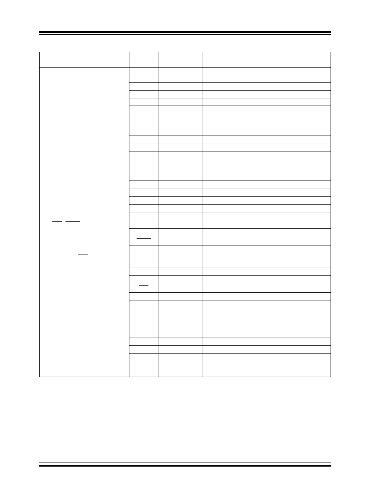
TABLE 2-1: PIC12F609/HV609 SPECIAL FUNCTION REGISTERS SUMMARY BANK 0
Addr Name Bit 7 Bit 6 Bit 5 Bit 4 Bit 3 B it 2 Bit 1 Bit 0
Bank 0
00h INDF Addressing this location uses contents of FSR to address data memory (not a physical register) xxxx xxxx 22, 100
01h TMR0 Timer0 Module’s Register xxxx xxxx 41, 100
02h PCL Program Counter’s (PC) Least Significant Byte 0000 0000 22, 100
03h STA TUS IRP
04h FSR Indirect Data Memory Address Pointer xxxx xxxx 22, 100
05h GPIO
06h — Unimplemented — —
07h — Unimplemented — —
08h — Unimplemented — —
09h — Unimplemented — —
0Ah PCLATH
0Bh INTCON GIE PEIE T0IE INTE GPIE T0IF INTF GPIF 0000 0000 17, 100
0Ch PIR1
0Dh — Unimplemented — —
0Eh TMR1L Holding Register for the Least Significant Byte of the 16-bit TMR1 Register xxxx xxxx 45, 100
0Fh TMR1H Holding Register for the Most Significant Byte of the 16-bit TMR1 Register xxxx xxxx 45, 100
10h T1CON T1GINV TMR1GE T1CKPS1 T1CKPS0 T1OSCEN T1SYNC
11h — Unimplemented — —
12h — Unimplemented — —
13h — Unimplemented — —
14h — Unimplemented — —
15h — Unimplemented — —
16h — Unimplemented — —
17h — Unimplemented — —
18h — Unimplemented — —
19h VRCON CMVREN
1Ah CMCON0 CMON COUT CMOE CMPOL
1Bh — — — — —
1Ch CMCON1
1Dh — Unimplemented — —
1Eh — Unimplemented — —
1Fh — Unimplemented — —
Legend: – = Unimplemented locations rea d as ‘0’, u = unchanged, x = unknown, q = value depends on condition, shaded = unimplemented
Note 1: IRP and RP1 bits are reserved, always maintain these bits clear.
(1)
— — GP5 GP4 GP3 GP2 GP1 GP0 --x0 x000 31, 100
— — — Write Buffer for upper 5 bits of Program Counter ---0 0000 22, 100
— — — —CMIF— —TMR1IF---- 0--0 19, 100
— — — T1ACS CMHYS — T1GSS CMSYNC ---0 0-10 59, 101
(1)
RP1
— VRR FVREN VR3 VR2 VR1 VR0 0-00 0000 62, 101
RP0 TO PD ZDCC0001 1xxx 15, 100
TMR1CS TMR1ON 0000 0000 49, 100
—CMR—CMCH0000 -0-0 58, 101
Value on
POR, BOR
Page
© 2006 Microchip Technology Inc. Preliminary DS41302A-page 11

PIC12F609/615/12HV609/615
TABLE 2-2: PIC12F615/HV615 SPECIAL FUNCTION REGISTERS SUMMARY BANK 0
Addr Name Bit 7 B it 6 Bit 5 Bit 4 Bit 3 Bit 2 Bit 1 Bit 0
Bank 0
00h INDF Addressing this location uses contents of FSR to address data memory (not a physical register) xxxx xxxx 22, 101
01h TMR0 Timer0 Module’s Register xxxx xxxx 41, 101
02h PCL Program Counter’s (PC) Least Significant Byte 0000 0000 22, 101
03h STA TUS IRP
04h FSR Indirect Data Memory Address Pointer xxxx xxxx 22, 101
05h GPIO
06h — Unimplemented — —
07h — Unimplemented — —
08h — Unimplemented — —
09h — Unimplemented — —
0Ah PCLATH
0Bh INTCON GIE PEIE T0IE INTE GPIE T0IF INTF GPIF 0000 0000 17, 101
0Ch PIR1
0Dh — Unimplemented — —
0Eh TMR1L Holding Register for the Least Significant Byte of the 16-bit TMR1 Register xxxx xxxx 45, 101
0Fh TMR1H Holding Register for the Most Significant Byte of the 16-bit TMR1 Register xxxx xxxx 45, 101
10h T1CON T1GINV TMR1GE T1CKPS1 T1CKPS0 T1OSCEN T1SYNC
11h TMR2 Timer2 Module Register 0000 0000 51, 101
12h T2CON
13h CCPR1L Capture/Compare/PWM Register 1 Low Byte XXXX XXXX 76, 101
14h CCPR1H Capture/Compare/PWM Register 1 High Byte XXXX XXXX 76, 101
15h CCP1CON P1M
16h PWM1CON PRSEN PDC6 PDC5 PDC4 PDC3 PDC2 PDC1 PDC0 0000 0000 91, 101
17h ECCPAS ECCPASE ECCPAS2 ECCPAS1 ECCPAS0 PSSAC1 PSSAC0 PSSBD1 PSSBD0 0000 0000 88, 101
18h — Unimplemented — —
19h VRCON CMVREN
1Ah CMCON0 CMON COUT CMOE CMPOL
1Bh — — — — —
1Ch CMCON1
1Dh — Unimplemented — —
1Eh ADRESH Most Significant 8 bits of the left shifted A/D result or 2 bits of right shifted result xxxx xxxx 71, 101
1Fh ADCON0 ADFM VCFG
Legend: – = Unimplemented locations rea d as ‘0’, u = unchanged, x = unknown, q = value depends on condition, shaded = unimplemented
Note 1: IRP and RP1 bits are reserved, always maintain these bits clear.
(1)
— — GP5 GP4 GP3 GP2 GP1 GP0 --x0 x000 31, 101
— — — Write Buffer for upper 5 bits of Program Counter ---0 0000 22, 101
— ADIF CCP1IF —CMIF— TMR2IF TMR1IF -00- 0-00 19, 101
— TOUTPS3 TOUTPS2 TOUTPS1 TOUTPS0 TMR2ON T2CKPS1 T2CKPS0 -000 0000 52, 101
— — — T1ACS CMHYS — T1GSS CMSYNC ---0 0-10 59, 101
(1)
RP1
— DC1B1 DC1B0 CCP1M3 CCP1M2 CCP1M1 CCP1M0 0-00 0000 75, 101
— VRR FVREN VR3 VR2 VR1 VR0 0-00 0000 62, 101
RP0 TO PD ZDCC0001 1xxx 15, 101
TMR1CS TMR1ON 0000 0000 49, 101
—CMR—CMCH0000 -0-0 58, 101
— CHS2 CHS1 CHS0 GO/DONE ADON 00-0 0000 70, 101
Value on
POR, BOR
Page
DS41302A-page 12 Preliminary © 2006 Microchip Technology Inc.
PIC12F609/615/12HV609/615
TABLE 2-3: PIC12F609/HV609 SPECIAL FUNCTION REGISTERS SUMMARY BANK 1
Addr Name Bit 7 Bit 6 Bit 5 Bit 4 Bit 3 Bit 2 Bit 1 Bit 0
Bank 1
80h INDF Addressing this location uses contents of FSR to address data memory (not a physical register) xxxx xxxx 22, 101
81h OPTION_REG GPPU
82h PCL Program Counter’s (PC) Least Significant Byte 0000 0000 22, 101
83h STATUS IRP
84h FSR Indirect Data Memory Address Pointer xxxx xxxx 22, 101
85h TRISIO
86h — Unimplemented — —
87h — Unimplemented — —
88h — Unimplemented — —
89h — Unimplemented — —
8Ah PCLATH
8Bh INTCON GIE PEIE T0IE INTE GPIE T0IF INTF GPIF
8Ch PIE1
8Dh — Unimplemented — —
8Eh PCON
8Fh — Unimplemented — —
90h OSCTUNE
91h — Unimplemented — —
92h — Unimplemented — —
93h — Unimplemented — —
94h — Unimplemented — —
95h WPU
96h IOC
97h — Unimplemented — —
98h — Unimplemented — —
99h — Unimplemented — —
9Ah — Unimplemented — —
9Bh — Unimplemented — —
9Ch — Unimplemented — —
9Dh — Unimplemented — —
9Eh — Unimplemented — —
9Fh ANSEL
Legend: – = Unimplemented locations read as ‘0’, u = unchanged, x = unknown, q = value depends on condition, shaded = unimplemented
Note 1: IRP and RP1 bits are reserved, always maintain these bits clear.
(2)
2: GP3 pull-up is enabled when MCLRE is ‘1’ in the Configuration Word register.
3: MCLR
exists.
4: TRISIO3 always reads as ‘1’ since it is an input only pin.
— — TRISIO5 TRISIO4 TRISIO3
— — — Write Buffer for upper 5 bits of Program Counter ---0 0000 22, 101
— — — —CMIE— —TMR1IE---- 0--0 18, 101
— — — — — —PORBOR ---- --qq 20, 101
— — — TUN4 TUN3 TUN2 TUN1 TUN0 ---0 0000 29, 101
— —WPU5WPU4— WPU2 WPU1 WPU0 --11 -111 34, 101
— — IOC5 IOC4 IOC3 IOC2 IOC1 IOC0 --00 0000 34, 101
— — — —ANS3— ANS1 ANS0 ---- 1-11 33, 101
and WDT Reset does not affect the previous value data latch. The GPIF bit will clear upon Reset but will set again if the mismatch
INTEDG T0CS T0SE PSA PS2 PS1 PS0 1111 1111 16, 101
(1)
RP1
(1)
RP0 TO PD ZDCC0001 1xxx 15, 101
(4)
TRISIO2 TRISIO1 TRISIO0 --11 1111 31, 101
Value on
POR, BOR
(3)
0000 0000 17, 101
Page
© 2006 Microchip Technology Inc. Preliminary DS41302A-page 13

PIC12F609/615/12HV609/615
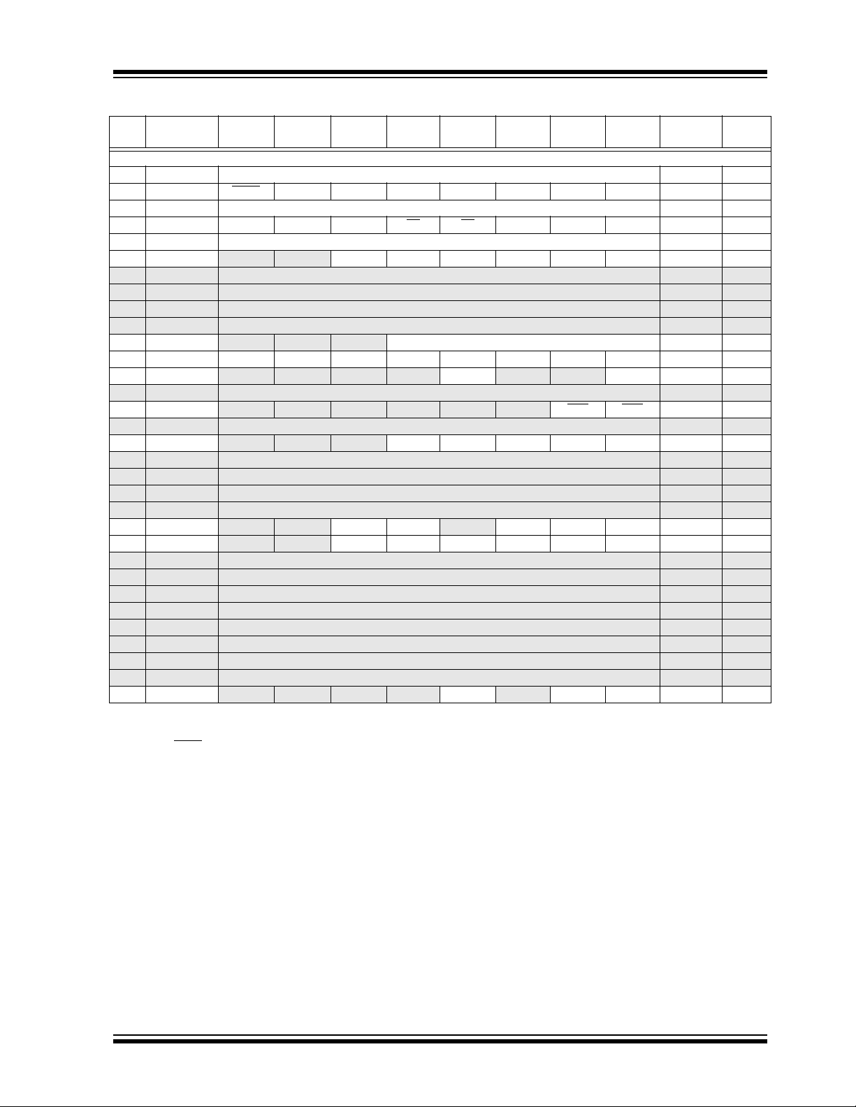
TABLE 2-4: PIC12F615/HV615 SPECIAL FUNCTION REGISTERS SUMMARY BANK 1
Addr Name Bit 7 Bit 6 Bit 5 Bit 4 Bit 3 Bit 2 Bit 1 Bit 0
Bank 1
80h INDF Addressing this location uses contents of FSR to address data memory (not a physical register) xxxx xxxx 22, 101
81h OPTION_REG GPPU
82h PCL Program Counter’s (PC) Least Significant Byte 0000 0000 22, 101
83h STATUS IRP
84h FSR Indirect Data Memory Address Pointer xxxx xxxx 22, 101
85h TRISIO
86h — Unimplemented — —
87h — Unimplemented — —
88h — Unimplemented — —
89h — Unimplemented — —
8Ah PCLATH
8Bh INTCON GIE PEIE T0IE INTE GPIE T0IF INTF GPIF
8Ch PIE1
8Dh — Unimplemented — —
8Eh PCON
8Fh — Unimplemented — —
90h OSCTUNE
91h — Unimplemented — —
92h PR2 Timer2 Module Period Register 1111 1111 51, 101
93h APFCON
94h — Unimplemented — —
95h WPU
96h IOC
97h — Unimplemented — —
98h — Unimplemented — —
99h — Unimplemented — —
9Ah — Unimplemented — —
9Bh — Unimplemented — —
9Ch — Unimplemented — —
9Dh — Unimplemented — —
9Eh ADRESL Least Significant 2 bits of the left shifted result or 8 bits of the right shifted result xxxx xxxx 71, 101
9Fh ANSEL
Legend: – = Unimplemented locations rea d as ‘0’, u = unchanged, x = unknown, q = value depends on condition, shaded = unimplemented
Note 1: IRP and RP1 bits are reserved, always maintain these bits clear.
(2)
2: GP3 pull-up is enabled when MCLRE is ‘1’ in the Configuration Word register.
3: MCLR
4: TRISIO3 always reads as ‘1’ since it is an input only pin.
and WDT Reset does not affect the previous value data latch. The GPIF bit will clear upon Reset but will set again if the mismatch
exists.
INTEDG T0CS T0SE PSA PS2 PS1 PS0 1111 1111 16, 101
(1)
— — TRISIO5 TRISIO4 TRISIO3
— — — Write Buffer for upper 5 bits of Program Counter ---0 0000 22, 101
— ADIE CCP1IE —CMIE— TMR2IE TMR1IE -00- 0-00 18, 101
— — — — — —PORBOR ---- --qq 20, 101
— — — TUN4 TUN3 TUN2 TUN1 TUN0 ---0 0000 29, 101
— — — T1GSEL — — P1BSEL P1ASEL ---0 --00 18, 101
— —WPU5WPU4— WPU2 WPU1 WPU0 --11 -111 34, 101
— — IOC5 IOC4 IOC3 IOC2 IOC1 IOC0 --00 0000 34, 101
— ADCS2 ADCS1 ADCS0 ANS3 ANS2 ANS1 ANS0 -000 1111 33, 101
RP1
(1)
RP0 TO PD ZDCC0001 1xxx 15, 101
(4)
TRISIO2 TRISIO1 TRISIO0 --11 1111 31, 101
Value on
POR, BOR
(3)
0000 0000 17, 101
Page
DS41302A-page 14 Preliminary © 2006 Microchip Technology Inc.

PIC12F609/615/12HV609/615
2.2.2.1 STATUS Register
The STATUS registe r, shown in Register 2-1, contains:
• the arithmetic status of the ALU
• the Reset status
• the bank select bits for data memory (RAM)
The STATUS register can be the destination for any
instruction, like any other register. If the STATUS
register is the destination for an instruction that affects
the Z, DC or C bits, then the write to these three bits is
disabled. These bit s are set or cleared ac cording to the
device logic. Furthermore, the TO
writable. Therefore, the result of an instruction with the
STATUS regis ter as destina tion may be differ ent than
intended.
For example, CLRF STATUS, will clear the upper three
bits and set the Z bit. This leaves the STATUS register
as ‘000u u1uu’ (where u = unchanged).
and PD bits are not
It is recommended, therefore, that only BCF, BSF,
SWAPF and MOVWF instructions are used to alter the
STATUS register, because these instructions do not
affect any Status bits. For other instructions not affecting any Status bits, see the Section 13.0 “Instruction
Set Summary”.
Note 1: Bits IRP and RP1 of the ST ATUS register
are not used by the PIC12F609/615/
12HV609/615 and should be maintained
as clear. Use of these bits is not recommended, since this may affect upward
compatibility with future products.
2: The C and DC bits operate as a Borrow
and Digit Borrow out bit, respectively, in
subtraction. See the SUBLW and SUBWF
instructions for examples.
REGISTER 2-1: STATUS: STATUS REGISTER
Reserved Reserved R/W-0 R-1 R-1 R/W-x R/W-x R/W-x
IRP RP1 RP0 T O PD ZDCC
bit 7 bit 0
Legend:
R = Readable bit W = Writable bit U = Unimplemented bit, read as ‘0’
-n = Value at POR ‘1’ = Bit is set ‘0’ = Bit is cleared x = Bit is unknown
bit 7 IRP: This bit is reserved and should be maintained as ‘0’
bit 6 RP1: This bit is reserved and should be maintained as ‘0’
bit 5 RP0: Register Bank Select bit (used for direct addressing)
1 = Bank 1 (80h – FFh)
0 = Bank 0 (00h – 7Fh)
bit 4 TO
bit 3 PD
bit 2 Z: Zero bit
bit 1 DC: Digit Carry/Borrow bit (ADDWF, ADDLW,SUBLW,SUBWF instructions), For Borrow, the polarity is
bit 0 C: Carry/Bo
: Time-out bit
1 = After power-up, CLRWDT instruction or SLEEP instruction
0 = A WDT time-out occurred
: Power-down bit
1 = After power-up or b y the CLRWDT instruction
0 = By execution of the SLEEP instruction
1 = The result of an arithmetic or logic operation is zero
0 = The result of an arithmetic or logic operation is not zero
reversed.
1 = A carry-out from the 4th low-order bit of the result occurred
0 = No carry-out from the 4th low-order bit of the result
(1)
rrow bit
1 = A carry-out from the Most Significant bit of the result occurred
0 = No carry-out from the Most Significant bit of the result occurred
(ADDWF, ADDLW, SUBLW, SUBWF instructions)
Note 1: For Bo
© 2006 Microchip Technology Inc. Preliminary DS41302A-page 15
rrow, the polarity is reversed. A subtraction is executed by adding the two’s complement of the
second operand. For rotate (RRF, RLF) instructi ons, this bit is loa ded with either the high-orde r or low-o rder
bit of the source register.

PIC12F609/615/12HV609/615
2.2.2.2 OPTION Register
The OPTION register is a readable and writable register, which contains various control bits to configure:
• Timer0/WDT prescaler
• External GP2/INT interrupt
•Timer0
• Weak pull-ups on GPIO
REGISTER 2-2: OPTION_REG: OPTION REGISTER
R/W-1 R/W-1 R/W-1 R/W-1 R/W-1 R/W-1 R/W-1 R/W-1
GPPU
bit 7 bit 0
Legend:
R = Readable bit W = Writable bit U = Unimplemented bit, read as ‘0’
-n = Value at POR ‘1’ = Bit is set ‘0’ = Bit is cleared x = Bit is unknown
INTEDG T0CS T0SE PSA PS2 PS1 PS0
Note: To achieve a 1:1 prescaler assignment for
Timer0, assign the prescaler to the WDT
by setting PSA bit to ‘1’ of the OPTION
register. See Section 5.1.3 “Software
Programmable Prescaler”.
bit 7 GPPU
: GPIO Pull-up Enable bit
1 = GPIO pull-ups are disabled
0 = GPIO pull-ups are enabled by individual PORT latch values
bit 6 INTEDG: Interrupt Edge Select bit
1 = Interrupt on rising edge of GP2/INT pin
0 = Interrupt on falling edge of GP2/INT pin
bit 5 T0CS: Timer0 Clock Source Select bit
1 = Transition on GP2/T0CKI pin
0 = Internal instruction cyc le clock (F
bit 4 T0SE: Timer0 Source Edge Select bit
1 = Increment on high-to -low transition on GP2/T0CKI pin
0 = Increment on low-to-high transition on GP2/T0CKI pin
bit 3 PSA: Prescaler Assignment bit
1 = Prescaler is assigned to the WDT
0 = Prescaler is assigned to the Timer0 module
bit 2-0 PS<2:0>: Prescaler Rate Select bits
BIT VALUE TIMER0 RATE WDT RATE
000
001
010
011
100
101
110
111
1 : 2
1 : 4
1 : 8
1 : 16
1 : 32
1 : 64
1 : 128
1 : 256
OSC/4)
1 : 1
1 : 2
1 : 4
1 : 8
1 : 16
1 : 32
1 : 64
1 : 128
DS41302A-page 16 Preliminary © 2006 Microchip Technology Inc.

PIC12F609/615/12HV609/615
2.2.2.3 INTCON Register
The INTCON register is a readable and writable
register , which c ontains the various en able and fl ag bit s
for TMR0 register ove rflo w, GPIO change and externa l
GP2/INT pin interrupts.
Note: Interrupt flag bits are set w hen an in terrupt
condition occurs, regar dless of the st ate of
its corresponding enable bit or the Global
Enable bit, GIE of the INTCON register.
User software should ensure the
appropriate interrupt flag bits are clear
prior to enabling an interrupt.
REGISTER 2-3: INTCON: INTERRUPT CONTROL REGISTER
R/W-0 R/W-0 R/W-0 R/W-0 R/W-0 R/W-0 R/W-0 R/W-0
GIE PEIE T0IE INTE GPIE T0IF INTF GPIF
bit 7 bit 0
Legend:
R = Readable bit W = Writable bit U = Unimplemented bit, read as ‘0’
-n = Value at POR ‘1’ = Bit is set ‘0’ = Bit is cleared x = Bit is unknown
bit 7 GIE: Global Interrupt Enable bit
1 = Enables all unmasked interrupts
0 = Disables all interrupts
bit 6 PEIE: Peripheral Interrupt Enable bit
1 = Enables all unmasked peripheral interrupts
0 = Disables all peripheral interrupts
bit 5 T0IE: Timer0 Overflow Interru pt Enab le bit
1 = Enables the Timer0 interrupt
0 = Disables the Timer0 interrupt
bit 4 INTE: GP2/INT External Interrupt Enable bit
1 = Enables the GP2/INT external interrupt
0 = Disables the GP2/INT external interrupt
bit 3 GPIE: GPIO Change Interrupt Enable bit
1 = Enables the GPIO change interrupt
0 = Disables the GPIO change interrupt
bit 2 T0IF: Timer0 Overflow Interrupt Flag bit
1 = Timer0 register has overflowed (must be cleared in software)
0 = Timer0 register did not overflow
bit 1 INTF: GP2/INT External Interrupt Flag bit
1 = The GP2/INT external interrupt occurred (must be cleared in software)
0 = The GP2/INT external interrupt did not occur
bit 0 GPIF: GPIO Change Interrupt Flag bit
1 = When at least one of the GPIO <5:0> pins changed state (must be cleared in software)
0 = None of the GPIO <5:0> pins have changed state
(1)
(2)
Note 1: IOC register must also be enabled.
2: T0IF bit is set when TMR0 rolls over. TMR0 is unchanged on Reset and should be initialized before
clearing T0IF bit.
© 2006 Microchip Technology Inc. Preliminary DS41302A-page 17

PIC12F609/615/12HV609/615
2.2.2.4 PIE1 Register
The PIE1 register contains the Peripheral Interrupt
Enable bits, as shown in Register 2-4.
REGISTER 2-4: PIE1: PERIPHERAL INTERRUPT ENABLE REGISTER 1
U-0 R/W-0 R/W-0 U-0 R/W-0 U-0 R/W-0 R/W-0
—ADIE
bit 7 bit 0
Legend:
R = Readable bit W = Writable bit U = Unimplemented bit, read as ‘0’
-n = Value at POR ‘1’ = Bit is set ‘0’ = Bit is cleared x = Bit is unknown
bit 7 Unimplemented: Read as ‘0’
bit 6 ADIE: A/D Converter (ADC) Interrupt Enable bit
1 = Enables the ADC interrupt
0 = Disables the ADC interrupt
bit 5 CCP1IE: CCP1 Interrupt Enable bit
1 = Enables the CCP1 interrupt
0 = Disables the CCP1 interrupt
bit 4 Unimplemented: Read as ‘0’
bit 3 CMIE: Comp ara tor Interrupt Enable bit
1 = Enables the Comparator interrupt
0 = Disables the Comparator interrupt
bit 2 Unimplemented: Read as ‘0’
bit 1 TMR2IE: Timer2 to PR2 Match Interrupt Enable bit
1 = Enables the Timer2 to PR2 match interrupt
0 = Disables the Timer2 to PR2 match interrupt
bit 0 TMR1IE: Timer1 Overflow Interrupt Enable bit
1 = Enables the Timer1 overflow interrupt
0 = Disables the Timer1 overflow inter rupt
(1)
CCP1IE
(1)
—CMIE —TMR2IE
(1)
Note: Bit PEIE of the INTCON register must be
set to enable any peripheral interrupt.
(1)
TMR1IE
(1)
(1)
Note 1: PIC12F615/HV615 only. PIC12F609/HV609 unimplemented, read as ‘0’.
DS41302A-page 18 Preliminary © 2006 Microchip Technology Inc.

PIC12F609/615/12HV609/615
2.2.2.5 PIR1 Register
The PIR1 register cont ains the Peri pheral Interrup t flag
bits, as shown in Register 2-5.
REGISTER 2-5: PIR1: PERIPHERAL INTERRUPT REQUEST REGISTER 1
U-0 R/W-0 R/W-0 U-0 R/W-0 U-0 R/W-0 R/W-0
—ADIF
bit 7 bit 0
Legend:
R = Readable bit W = Writable bit U = Unimplemented bit, read as ‘0’
-n = Value at POR ‘1’ = Bit is set ‘0’ = Bit is cleared x = Bit is unknown
bit 7 Unimplemented: Read as ‘0’
bit 6 ADIF: A/D In terrupt Flag bit
1 = A/D conversion complete
0 = A/D conversion has not completed or has not been started
bit 5 CCP1IF: CCP1 Interrupt Flag bit
Capture mode:
1 = A TMR1 register capture occurred (must be cleared in software)
0 = No TMR1 register captu re occurred
Compare mode
1 = A TMR1 register compare match occurred (must be cleared in software)
0 = No TMR1 register compare match occurred
PWM mode
Unused in this mode
bit 4 Unimplemented: Read as ‘0’
bit 3 CMIF: Comparator Interrupt Flag bit
1 = Comparator output has changed (must be cleared in software)
0 = Comparator output has not changed
bit 2 Unimplemented: Read as ‘0’
bit 1 TMR2IF: Timer2 to PR2 Match Interrupt Flag bit
1 = Timer2 to PR2 match occurred (must be cleared in software)
0 = Timer2 to PR2 match has not occurred
bit 0 TMR1IF: Timer1 Overflow Interrupt Flag bit
1 = Timer1 register overflowed (must be cleared in software)
0 = Timer1 has not overflowed
(1)
CCP1IF
:
:
(1)
—CMIF —TMR2IF
(1)
(1)
Note: Interrupt flag bits are set when an interrupt
condition occurs, regardless of the state of
its corresponding enable bit or the Global
Enable bit, GIE of the INTCON register.
User software should ensure the
appropriate interrupt flag bits are clear prior
to enabling an interrupt.
(1)
TMR1IF
(1)
Note 1: PIC12F615/HV615 only. PIC12F609/HV609 unimplemented, read as ‘0’.
© 2006 Microchip Technology Inc. Preliminary DS41302A-page 19

PIC12F609/615/12HV609/615
2.2.2.6 PCON Register
The Power Control (PCON) register (see Table 11-2)
contains flag bits to differentiate between a:
• Power-on Reset (POR
• Brown-out Reset (BOR)
• Watchdog Timer Reset (WDT)
• External MCLR
The PCON register also co ntrols the software ena ble of
the BOR
The PCON register bits are shown in Register 2-6.
.
REGISTER 2-6: PCON: POWER CONTROL REGISTER
U-0 U-0 U-0 U-0 U-0 U-0 R/W-0 R/W-0
— — — — — —PORBOR
bit 7 bit 0
Legend:
R = Readable bit W = Writable bit U = Unimplemented bit, read as ‘0’
-n = Value at POR ‘1’ = Bit is set ‘0’ = Bit is cleared x = Bit is unknown
)
Reset
(1)
bit 7-2 Unimplemented: Read as ‘0’
bit 1 POR
bit 0 BOR
Note 1 : Reads as ‘0’ if Brown-out Reset is disabled.
: Power-on Re set Status bit
1 = No Power-on Reset occurred
0 = A Power-on Reset occurred (must be set in software after a Power-on Reset occurs)
: Brown-out Reset Status bit
1 = No Brown-out Reset occurred
0 = A Brown-out Reset occurred (must be set in software after a Brown-out Reset occurs)
DS41302A-page 20 Preliminary © 2006 Microchip Technology Inc.

PIC12F609/615/12HV609/615
2.2.2.7 APFCON Register
(PIC12F615/HV615 only)
The Alternate Pin Function Control (APFC ON) reg ist er
is used to steer specific peripheral input and output
functions between different pins. For this device, the
P1A, P1B and Timer1 Gate functions can be moved
between different pins.
The APFCON register bits are shown in Register 2-7.
REGISTER 2-7: APFCON: POWER CONTROL REGISTER
U-0 U-0 U-0 R/W-0 U-0 U-0 R/W-0 R/W-0
— — — T1GSEL — — P1BSEL P1ASEL
bit 7 bit 0
Legend:
R = Readable bit W = Writable bit U = Unimplemented bit, read as ‘0’
-n = Value at POR ‘1’ = Bit is set ‘0’ = Bit is cleared x = Bit is unknown
bit 7-5 Unimplemented: Read as ‘0’
bit 4 T1GSEL: TMR1 Input Pin Select bit
1 = T1G function is on GP3/T1G
0 = T1G function is on GP4/AN3/CIN1-/T1G/P1B
bit 3-2 Unimplemented: Read as ‘0’
bit 1 P1BSEL: P1B Output Pin Select bit
1 = P1B function is on GP4/AN3/CIN1-/T1G
0 = P1B function is on GP0/AN0/CIN+/P1B/ICSPDAT
bit 0 P1ASEL: P1A Output Pin Select bit
1 = P1A function is on GP5/T1CKI/P1A
0 = P1A function is on GP2/AN2/T0CKI/INT/COUT/CCP1/P1A
(2)
/MCLR/VPP
(2)
(2)
/OSC2/CLKOUT
(2)
/P1B
/OSC2/CLKOUT
/OSC1/CLKIN
(1)
Note 1: PIC12F615/HV615 only.
2: Alternate pin function.
© 2006 Microchip Technology Inc. Preliminary DS41302A-page 21

PIC12F609/615/12HV609/615
h
>
s
n
2.3 PCL and PCLATH
The Program Counter (PC) is 13 bits wide. The lo w byte
comes from the PCL register, which is a readable and
writable register . The hig h byte (PC<12:8>) is not directl y
readable or writable and comes from PCLATH. On any
Reset, the PC is cleared. Figure 2-4 shows the two
situations for the loading of the PC. The upper example
in Figure 2-4 shows how the PC is loaded on a write to
PCL (PCLATH<4:0> → PCH). The lower example in
Figure 2-4 shows h ow the PC is l oaded during a CALL or
GOTO instruction (PCLATH<4:3> → PCH).
FIGURE 2-4: LOADING OF PC IN
DIFFERENT SITUATIONS
PCH PCL
12 8 7 0
PC
PCLATH<4:0>
5
PCLATH
PCH PCL
12 11 10 0
PC
2
87
PCLATH<4:3>
PCLATH
8
11
2.3.1 MODIFYING PCL
Executing any instruction with the PCL register as the
destination simultaneously causes the Program
Counter PC< 12:8> bits (PCH) to be replaced by the
contents of the PCLATH register . Th is allo ws the enti re
contents of the program counter to be changed by
writing the desired up per 5 bit s to the PCLATH register .
When the lower 8 bits are written to the PCL regis ter , all
13 bits of the program counter will chan ge to the values
contained in the PCLATH register and those being
written to the PCL register.
A computed GOTO is accomplish ed by adding an offset
to the program counter (ADDWF PCL). Care should be
exercised when jumping into a look-up table or
program b ranch table (computed GOTO) by modifying
the PCL register. Assuming that PCLATH is set to the
table start address, if the table length is greater than
255 instructions or if the lower 8 bits of the memory
address rolls over from 0xFF to 0x00 in the middle of
the table, then PCLATH must be incremented for each
address rollover that occurs between the table
beginning and the target location within the table.
For more information refer to Application Note AN556,
“Implementing a Table Read” (DS00556).
Instruction wit
PCL a
Destinatio
ALU Result
GOTO, CALL
OPCODE <10:0
2.3.2 STACK
The PIC12F609/615/12HV609/615 Family has an 8level x 13-bit wide hardware stack (see Figure 2-1).
The stack space is not part of either program or data
space and the S ta ck Pointer i s not rea dable or writa ble.
The PC is PUSHed onto the stack when a CALL
instruction is execute d or an interrupt ca uses a branc h.
The stack is POPed in the even t of a RETURN, RETLW
or a RETFIE instruction execution. PCLATH is not
affected by a P USH or POP operation.
The stack operat es as a circular buf fer . This means th at
after the stack has been PUSHed eight times, the ninth
push overwrites the va lue tha t was s tored fro m the first
push. The tenth pus h ov erwr i tes the se co nd push (and
so on).
Note 1: There are no Status bits to indicate stack
overflow or stack underflow conditions.
2: There are no instructions/mnemonics
called PUSH or POP. These are actions
that occur from the execution of the
CALL, RETURN, RETLW and RETFIE
instructions or the vectoring to an
interrupt address.
2.4 Indirect Addressing, INDF and
FSR Registers
The INDF register is not a physica l register . Addr essing
the INDF register will cause indirect addressing.
Indirect addressing is possible by using the INDF
register. Any instruction using the INDF register
actually accesses data pointed to by the File Select
Register (FSR). Reading INDF itself indirectly will
produce 00h. Writing to the INDF register indirectly
results in a no operation (although Status bits may be
affected). An effective 9-bit address is obtained by
concatenating the 8-bit FSR and the IRP bit of the
STATUS register, as shown in Figure 2-5.
A simple program to clear RAM location 40h-7Fh using
indirect addressing is shown in Example 2-1.
EXAMPLE 2-1: INDIRECT ADDRESS ING
MOVLW 0x40 ;initialize pointer
MOVWF FSR ;to RAM
NEXT CLRF INDF ;clear INDF register
INCF FSR ;inc pointer
BTFSS FSR,7 ;all done?
GOTO NEXT ;no clear next
CONTINUE ;yes continue
DS41302A-page 22 Preliminary © 2006 Microchip Technology Inc.
PIC12F609/615/12HV609/615
FIGURE 2-5: DIRECT/INDIRECT ADDRESSING PIC12F609/615/12HV609/615
Indirect AddressingDirect Addressing
RP1
(1)
RP0 6
From Opcode
0
IRP
(1)
7
File Select Register
0
Bank Select Location Select
00h
Data
Memory
7Fh
For memory map detail, see Figure 2-2.
Note 1: The RP1 and IRP bits are reserved; always maintain these bits clear.
2: Accesses in this area are mirrored back into Bank 0 and Bank 1.
00 01 10 11
NOT USED
Bank 0 Bank 1 Bank 2 Bank 3
(2)
Bank Select
180h
1FFh
Location Select
© 2006 Microchip Technology Inc. Preliminary DS41302A-page 23

PIC12F609/615/12HV609/615
NOTES:
DS41302A-page 24 Preliminary © 2006 Microchip Technology Inc.

PIC12F609/615/12HV609/615
3.0 OSCILLATOR MODULE
The Oscillator mod ule can be c onfigured in one of eig ht
clock modes.
3.1 Overview
The Oscillator module has a wide variety of clock
sources and selection features that allow it to be used
in a wide range of applicati ons while maximiz ing performance and minimizing power consumption. Figure 3-1
illustrates a block diagram of the Oscillator module.
Clock sources can be configured from external
oscillators, quartz cryst al resonators , ceramic resonators
and Resistor-Capacitor (RC) circuits. In addition, the
system clock source can be configured with a choice of
two selectable speeds: internal or external system clock
source.
1. EC – External clock w ith I/O on OSC2/C LKOUT.
2. LP – 32 kHz Low-Power Crystal mode.
3. XT – Medium Gain Crystal or Ceramic Resonator
Oscillator mode.
4. HS – High Gain Crystal or Ceramic Resonator
mode.
5. RC – External Resistor-Capacitor (RC) with
OSC/4 output on OSC2/CLKOUT.
F
6. RCIO – External Resistor-Capacitor (RC) with
I/O on OSC2/CLKOUT.
7. INTOSC – Internal oscillator with F
on OSC2 and I/O on OSC1/CLKIN.
8. INTOSCIO – Internal oscillator with I/O on
OSC1/CLKIN and OSC2/CLKOUT.
Clock Source modes are configured by the FOSC <2:0>
bits in the Configuration Word register (CONFIG). The
Internal Oscillator mo dule provides a select able system
clock mode of either 4 MHz (Postscaler) or 8 MHz
(INTOSC).
FIGURE 3-1: PIC® MCU CLOCK SOURCE BLOCK DIAGRAM
OSC/4 output
OSC2
OSC1
External Oscillator
INTOSC
8 MHz
Sleep
Internal Oscillator
Postscaler
4 MHz
(Configuration Word Register)
LP, XT, HS, RC, RCIO, EC
INTOSC
FOSC<2:0>
IOSCFS<7>
MUX
System Clock
(CPU and Peripherals)
© 2006 Microchip Technology Inc. Preliminary DS41302A-page 25

PIC12F609/615/12HV609/615
3.2 Clock Source Modes
Clock Source modes can be classified as external or
internal.
• External Clock mod es rely on e xternal circui try fo r
the clock source. Examples are: Oscillator modules (EC mode), quartz crystal resonators or
ceramic resonators (LP, XT and HS modes) and
Resistor-Capacitor (RC) mode circuits.
• Internal clock sources are contained internally
within the Oscillator module. The Oscillator
module has two selectable clock frequencies:
4 MHz and 8 M Hz
The system clock can be selected between external or
internal clock sources via the FOSC<2:0> bits of the
Configuration Word register.
3.3 External Clock Modes
3.3.1 OSCILLATOR START-UP TIMER (OST)
If the Oscillator module is configured for LP, XT or HS
modes, the Oscillator Start-up Timer (OST) counts
1024 oscillations from OSC1. This occurs following a
Power-on Reset (POR) and when the Power-up Timer
(PWRT) has expired (if configured), or a wake-up from
Sleep. During this time, the program counter does not
increment and program execution is suspended. The
OST ensures that the oscillator circuit, using a quartz
crystal resonator o r ce ramic res onator, has started and
is providing a stable system clock to the Oscillator
module. When switching between clock sources, a
delay is required to allow the new clock to stabilize.
These oscillator delays are shown in Table 3-1.
TABLE 3-1: OSCILLATOR DELAY EXAMPLES
Switch From Switch To Frequency Oscillator Delay
Sleep/POR INTOSC 125 kHz to 8 MHz Oscillator Warm-Up Delay (T
Sleep/POR EC, RC DC – 20 MHz 2 instruction cycles
Sleep/POR LP, XT, HS 32 kHz to 20 MHz 1024 Clock Cycles (OST)
3.3.2 EC MODE
The External Clock (EC) mode allows an externally
generated logic level as the system clock source. When
operating in this mode, an external clock source is
connected to the OSC1 input and the OSC2 is available
for general purpose I/O. Figure 3-2 shows the pin
connections for EC mode.
The Oscillator Start-up Timer (OST) is disabled when
EC mode is selected. Therefore, there is no delay in
operation after a Power-on Reset (POR) or wake-up
from Sleep. Because the PIC
static, stopping the external clock input will have the
effect of halting the device while leaving all data intact.
Upon restarting the external clock, the device will
resume operation as if no time had elapsed.
®
MCU design is fully
WARM)
FIGURE 3-2: EXTERNAL CLOCK (EC)
MODE OPERATION
Clock from
Ext. System
I/O
Note 1: Alternate pin functions are listed in the
Section 1.0 “Device Overview”.
DS41302A-page 26 Preliminary © 2006 Microchip Technology Inc.
OSC1/CLKIN
®
MCU
PIC
OSC2/CLKOUT
(1)

PIC12F609/615/12HV609/615
3.3.3 LP, XT, HS MODES
The LP, XT and HS modes support the use of quartz
crystal resonators or ceram ic resonators connected to
OSC1 and OSC2 (Figu re 3-3). The mod e selects a low ,
medium or high gain setting of the internal
inverter-amplifier to support various resonator types
and speed.
LP Oscillator mode selects the lowest gain setting of
the internal inverter-amplifier. LP mode current
consumption is the least of the three modes. T his mode
is designed to drive only 32.768 kHz tuning-fork type
crystals (watch crystals).
XT Oscillator mode selects the intermediate gain
setting of the internal inverter-amplifier. XT mode
current consumption is the medi um of the three modes.
This mode is best suited to drive resonators with a
medium drive level specification.
HS Oscillator mode selects the highest gain setting of
the internal inverter-amplifier. HS mode current
consumption is the highest of the three modes. This
mode is best suited for resonato rs that req uire a hi gh
drive setting.
Figure 3-3 and Figure 3-4 show typical circuits for
quartz crystal and ceramic resonators, respectively.
Note 1: Quartz crystal char acteristics vary a ccording
to type, package and manufacturer. The
user should consult the manu facturer data
sheets for sp ecifi catio ns an d reco mmen ded
application.
2: Always verify oscillator performance over
DD and temperature range that is
the V
expected for the application.
3: For oscillator design assistance, reference
the following Microchip Applications Notes:
• AN826, “Crystal Oscillator Basics and
Crystal Selection for rfPIC
®
and PIC®
Devices” (DS00826)
®
• AN849, “Basic PIC
Oscillator Design”
(DS00849)
®
• AN943, “Practical PIC
Oscillator
Analysis and Design” (DS00943)
• AN949, “Making Your Oscillator Work”
(DS00949)
FIGURE 3-4: CERAMIC RESONATOR
OPERATION
(XT OR HS MODE)
FIGURE 3-3: QUARTZ CRYSTAL
OPERATION (LP, XT OR
HS MODE)
PIC® MCU
OSC1/CLKIN
C1
Quartz
Crystal
C2
Note 1: A series resistor (RS) may be required for
2: The value of R
(1)
S
R
quartz crystals with low drive level.
selected (typically between 2 MΩ to 10 MΩ).
F varies with the Oscillator mode
(2)
RF
OSC2/CLKOUT
To Internal
Logic
Sleep
PIC® MCU
OSC1/CLKIN
C1
(3)
RP
C2
Ceramic
Resonator
Note 1: A series resistor (RS) may be required for
ceramic resonators with low drive level.
2: The value of R
selected (typically between 2 MΩ to 10 MΩ).
3: An additional parallel feedback resistor (R
may be required for proper ceramic resonator
operation.
(1)
R
S
F varies with the Oscillator mode
(2)
RF
OSC2/CLKOUT
To Internal
Logic
Sleep
P)
© 2006 Microchip Technology Inc. Preliminary DS41302A-page 27

PIC12F609/615/12HV609/615
3.3.4 EXT ERNAL RC MODES
The external Resistor-Capacitor (RC) modes support
the use of an external RC circuit. This allows the
designer maximum flexibility in frequency choice while
keeping costs to a minimum when clock accuracy is not
required. There are two modes: RC and RCIO.
In RC mode, the RC circuit connects to OSC1.
OSC2/CLKOUT outputs the RC oscillator frequency
divided by 4. This signal may be us ed to provide a cl ock
for external circuitry, synchronization, calibration, test
or other application requirements. Figure 3-5 shows
the external RC mode connections.
FIGURE 3-5: EXTERNAL RC MODES
REXT
CEXT
VSS
VDD
OSC/4 or
F
(2)
I/O
OSC1/CLKIN
OSC2/CLKOUT
PIC® MCU
Internal
Clock
(1)
3.4 Internal Clock Modes
The Oscillator module provides a selectable system
clock source of either 4 MHz or 8 MHz. The selectable
frequency is configured through the IOSCFS bit of the
Configuration Word.
The frequency of the int erna l os ci llator can be trimmed
with a calibration value in the OSCTUNE register.
3.4.1 INTOSC AND INTOSCIO MODES
The INTOSC and INTOSCIO modes configure the
internal oscillators as the system clock source when
the device is progra mmed usi ng the osc illator se lectio n
or the FOSC<2:0> bits in the Configuration Word
register (CONFIG). See Section 11.0 “Special
Features of the CPU” for more information.
In INTOSC mode, OSC1/CLKIN is available for general
purpose I/O. OSC2/CLKOUT outputs the selected
internal oscillator fre quency divide d by 4. The CLKO UT
signal may be used to provide a clock for external
circuitry, synchronization, calibration, test or other
application requirements.
In INTOSCIO mode, OSC1/CLKIN and OSC2/CLKOUT
are available for general purpose I/O.
Recommended values: 10 kΩ ≤ REXT ≤ 100 kΩ, <3V
3 kΩ ≤ R
C
Note 1: Alternate pin functions are listed in
Section 1.0 “Device Overview”.
2: Output depends upon R C or RCIO Clock
mode.
EXT ≤ 100 kΩ, 3-5V
EXT > 20 pF, 2-5V
In RCIO mode, the RC circuit is connected to OSC1.
OSC2 becomes an additional general purpose I/O pin.
The RC oscillator frequency is a function of the supply
voltage, the resistor (REXT) and capacito r (CEXT) values
and the operating temperature. Other factors affecting
the oscillator frequency are:
• threshold voltage variation
• component tolerances
• packaging variations in capacitance
The user also needs to take into account variation due
to tolerance of external RC components used.
DS41302A-page 28 Preliminary © 2006 Microchip Technology Inc.

PIC12F609/615/12HV609/615
3.4.1.1 OSCTUNE Register
The oscillator is factory calibrated but can be adjusted
in software by writing to the OSCTUNE register
(Register 3-1).
The default value of the OSCTUNE register is ‘0’. The
value is a 5-bit two’s complement number.
When the OSCTUNE register is modified, the frequency
will begin shifting to the new frequency . Code execution
continues during this shift. There is no indication that the
shift has occurred.
REGISTER 3-1: OSCTUNE: OSCILLATOR TUNING REGISTER
U-0 U-0 U-0 R/W-0 R/W-0 R/W-0 R/W-0 R/W-0
— — — TUN4 TUN3 TUN2 TUN1 TUN0
bit 7 bit 0
Legend:
R = Readable bit W = Writable bit U = Unimplemented bit, read as ‘0’
-n = Value at POR ‘1’ = Bit is set ‘0’ = Bit is cleared x = Bit is unknown
bit 7-5 Unimplemented: Read as ‘0’
bit 4-0 TUN<4:0>: Frequency Tuning bits
01111 = Maximum frequen cy
01110 =
•
•
•
00001 =
00000 = Oscillator module is running at the calibrated frequency.
11111 =
•
•
•
10000 = Minimum frequency
TABLE 3-2: SUMMARY OF REGISTERS ASSOCIATED WITH CLOCK SOURCES
Name Bit 7 Bit 6 Bit 5 Bit 4 Bit 3 Bit 2 Bit 1 Bit 0
CONFIG
OSCTUNE
Legend: x = unknown, u = unchanged, – = unimplemented locations read as ‘0’. Shaded cells are not used by oscillators.
Note 1: Other (non Power-up) Resets include MCLR
© 2006 Microchip Technology Inc. Preliminary DS41302A-page 29
(2)
IOSCFS CP MCLRE PWRTE WDTE FOSC2 FOSC1 FOSC0 — —
— — — TUN4 TUN3 TUN2 TUN1 TUN0 ---0 0000 ---u uuuu
Reset and Watchdog Timer Reset during normal operation.
2: See Configuration Word register (Register 11-1) for operation of all register bits.
Val ue on
POR, BOR
Val ue on
all other
(1)
Resets

PIC12F609/615/12HV609/615
NOTES:
DS41302A-page 30 Preliminary © 2006 Microchip Technology Inc.

PIC12F609/615/12HV609/615
4.0 I/O PORT
There are as many as six general purpose I/O pins
available. Depending on which peripherals are enabled,
some or all of the pins may not be available as general
purpose I/O. In gen eral, when a periphe ral is enabled,
the associated pin may not be used as a general
purpose I/O pin.
4.1 GPIO and the TRISIO Registers
GPIO is a 6-bit wide port with 5 bidirectional and 1
input-only pin. The corres pond ing dat a di rec tion register
is TRISIO (Register 4-2). Setting a TRISIO bit (= 1) will
make the corresponding GPIO pin an input (i.e., disable
the output driver). Clearing a TRISIO bit (= 0) will m ake
the corresponding GPIO pin an output (i.e., enables
output driver and puts the content s of the ou tput latch on
the selected pin). The exception is GP3, which is input
only and its TRIS bit will always read as ‘1’. Example 4-1
shows how to initialize GPIO.
Reading the GPIO register (Register 4-1) reads the
status of the pins, whereas writing to it will write to the
PORT latch. All write operations are read-modify-write
operations. Therefore, a write to a port implies that the
REGISTER 4-1: GPIO: GPIO REGISTER
port pins are read, this value is modified and then
written to the PORT data latch. GP3 reads ‘0’ when
MCLRE = 1.
The TRISIO register controls the direction of the
GPIO pins, even when they are being used as analog
inputs. The user must ensure the bits in the TRISIO
register are maintained set when using the m as analog
inputs. I/O pins co nfigure d a s analo g i nput a lways read
‘0’.
Note: The ANSEL register must be initialized to
configure an analog channel as a digital
input. Pins configu red as analo g inputs will
read ‘0’ and cannot generate an interrupt.
EXAMPLE 4-1: INITIALIZING GPIO
BANKSEL GPIO ;
CLRF GPIO ;Init GPIO
BANKSEL ANSEL ;
CLRF ANSEL ;digital I/O, ADC clock
;setting ‘don’t care’
MOVLW 0Ch ;Set GP<3:2> as inputs
MOVWF TRISIO ;and set GP<5:4,1:0>
;as outputs
U-0 U-0 R/W-x R/W-0 R-x R/W-0 R/W-0 R/W-0
— — GP5 GP4 GP3 GP2 GP1 GP0
bit 7 bit 0
Legend:
R = Readable bit W = Writable bit U = Unimplemented bit, read as ‘0’
-n = Value at POR ‘1’ = Bit is set ‘0’ = Bit is cleared x = Bit is unknown
bit 7-6 Unimplemented: Read as ‘0’
bit 5-0 GP<5:0>: GPIO I/O Pin bit
1 = GPIO pin is > V
0 = GPIO pin is < VIL
IH
REGISTER 4-2: TRISIO: GPIO TRI-STATE REGISTER
U-0 U-0 R/W-1 R/W-1 R-1 R/W-1 R/W-1 R/W-1
— — TRISIO5 TRISIO4 TRISIO3 TRISIO2 TRISIO1 TRISIO0
bit 7 bit 0
Legend:
R = Readable bit W = Writable bit U = Unimplemented bit, read as ‘0’
-n = Value at POR ‘1’ = Bit is set ‘0’ = Bit is cleared x = Bit is unknown
bit 7-6 Unimplemented: Read as ‘0’
bit 5-0 TRISIO<5:0>: GPIO Tri-State Control bit
1 = GPIO pin configured as an input (tri-stated)
0 = GPIO pin configured as an output
Note 1: TRISIO<3> always reads ‘1’.
2: TRISIO<5:4> always reads ‘1’ in XT, HS and LP Oscillator modes.
© 2006 Microchip Technology Inc. Preliminary DS41302A-page 31

PIC12F609/615/12HV609/615
4.2 Additional Pin Functions
Every GPIO pin on the PIC12F609/615/12HV609/615
has an interrupt-on-change option and a weak pull-up
option. The next three sections describe these
functions.
4.2.1 ANSEL REGISTER
The ANSEL register is used to configure the Input
mode of an I/O pin to analog. Setting the appropriate
ANSEL bit high will cause all digi t al read s on the pi n to
be read as ‘0’ and allow analog functions on the pin to
operate correctly.
The state of the ANSEL bits has no affect on digital
output functions. A pin with TRIS clear and ANSEL set
will still operate as a digital output, but the Input mode
will be analog. This can cause unexpected behavior
when executing read-modify-write instructions on the
affected port.
4.2.2 WEAK PULL-UPS
Each of the GPIO pins, ex cept GP3, has an individuall y
configurable internal weak pull-up. Control bits WPUx
enable or disable each pull-up. Refer to Register 4-5.
Each weak pull-up is automatically turned off when the
port pin is c onfigured as an out put. The pull-ups are
disabled on a Power-on Reset by the GPPU
OPTION register). A weak pull-up is automatically
enabled for GP3 when configured as MCLR and
disabled when GP3 is an I/O. There is no software
control of the MCLR pull-up.
bit of the
last read value is not affected by a MCLR
Reset. After these resets , the G PIF fla g will c ontinue to
be set if a mismatch is present.
Note: If a change on the I/O pin should occur
when any GPIO operation is being
executed, then the GPIF interru pt flag may
not get set.
nor BOR
4.2.3 INTERRUPT-ON-CHANGE
Each GPIO pin is individually configurable as an interrupt-on-change pin. Contr ol bits IOCx enable or disable
the interrupt funct ion for each pin. Refer to Reg ister4-6.
The interrupt-on-change is disabled on a Power-on
Reset.
For enabled interrupt-on-change pins, the values are
compared with the old value la tched on the last rea d of
GPIO. The ‘mismatch’ o utputs of t he last read are OR’d
together to set the GPIO Change Interrupt Flag bit
(GPIF) in the INTCON register (Register 2-3).
This interrupt can wake the device from Sleep. The
user, in the Interrupt Service Routine, clears the interrupt by:
a) Any read of GPIO AND Clear flag bit GPIF. This
will end the mismatch condition;
OR
b) Any write of GPIO AND Clear flag bit GPIF will
end the mismatch condition;
A mismatch condition will continue to set flag bit GPIF.
Reading GPIO will end the mismatch condition and
allow flag bit GPIF to be cleared. The latch holding the
DS41302A-page 32 Preliminary © 2006 Microchip Technology Inc.

PIC12F609/615/12HV609/615
REGISTER 4-3: ANSEL: ANALOG SELECT REGISTER (PIC12F609/HV609)
U-0 U-0 U-0 U-0 R/W-1 U-0 R/W-1 R/W-1
— — — —ANS3— ANS1 ANS0
bit 7 bit 0
Legend:
R = Readable bit W = Writable bit U = Unimplemented bit, read as ‘0’
-n = Value at POR ‘1’ = Bit is set ‘0’ = Bit is cleared x = Bit is unknown
bit 7-4 Unimplemented: Read as ‘0’
bit 3 ANS3: Analog Select bits
Analog select between an al og or digital function on pins AN<7: 0 >, res pectively.
1 = Analog input. Pin is assigned as analog input
0 = Digital I/O. Pin is assign ed to port or special function.
bit 2 Unimplemented: Read as ‘0’
bit 1 ANS1: Analog Select Between Analog or Digital Function on Pins GP1
1 = Analog input. Pin is assigned as analog input.
0 = Digital I/O. Pin is assigned to port or specia l function.
bit 0 ANS0: Analog Select Between Analog or Digital Function on Pins GP0
0 = Digital I/O. Pin is assigned to port or specia l function.
1 = Analog input. Pin is assigned as analog input.
(1)
.
(1)
(1)
Note 1: Setting a pin to an analog input automatically di sables the digital input circuitry, weak pull-ups, and
interrupt-on-change if available. The corresponding TRIS bit must be set to Input mode in order to allow external
control of the voltage on the pin.
REGISTER 4-4: ANSEL: ANALOG SELECT REGISTER (PIC12F615/HV615)
U-0 R/W-1 R/W-1 R/W-1 R/W-1 R/W-1 R/W-1 R/W-1
— ADCS2 ADCS1 ADCS0 ANS3 ANS2 ANS1 ANS0
bit 7 bit 0
Legend:
R = Readable bit W = Writable bit U = Unimplemented bit, read as ‘0’
-n = Value at POR ‘1’ = Bit is set ‘0’ = Bit is cleared x = Bit is unknown
bit 7 Unimplemented: Read as ‘0’
bit 6-4 ADCS<2:0>: A/D Conversion Clock Select bits
OSC/2
000 = F
001 = F
OSC/8
OSC/32
010 = F
x11 = F
RC (clock derived from a dedicated internal oscillator = 500 kHz max)
OSC/4
100 = F
101 = F
OSC/16
OSC/64
110 = F
bit 3-0 ANS<3:0>: Analog Select bits
Analog select between an al og or digital function on pins AN<7: 0 >, res pectively.
1 = Analog input. Pin is assigned as analog input
0 = Digital I/O. Pin is assign ed to port or special function.
(1)
.
Note 1: Setting a pin to an analog input automatically di sables the digital input circuitry, weak pull-ups, and
interrupt-on-change if available. The corresponding TRIS bit must be set to Input mode in order to allow external
control of the voltage on the pin.
© 2006 Microchip Technology Inc. Preliminary DS41302A-page 33

PIC12F609/615/12HV609/615
REGISTER 4-5: WPU: WEAK PULL-UP GPIO REGISTER
U-0 U-0 R/W-1 R/W-1 U-0 R/W-1 R/W-1 R/W-1
— — WPU5 WPU4 — WPU2 WPU1 WPU0
bit 7 bit 0
Legend:
R = Readable bit W = Writable bit U = Unimplemented bit, read as ‘0’
-n = Value at POR ‘1’ = Bit is set ‘0’ = Bit is cleared x = Bit is unknown
bit 7-6 Unimplemented: Read as ‘0’
bit 5-4 WPU<5:4>: Weak Pull-up Control bits
1 = Pull-up enabled
0 = Pull-up disabled
bit 3 Unimplemented: Read as ‘0’
bit 2-0 WPU<2:0>: Weak Pull-up Control bits
1 = Pull-up enabled
0 = Pull-up disabled
Note 1: Global GPPU
2: The weak pull-up device is automatically disabled if the pin is in Output mode (TRISIO = 0).
3: The GP3 pull-up is enabled when configured as MCLR and disabled as an I/O in the Configuration Word.
4: WPU<5:4> always reads ‘1’ in XT, HS and LP Oscillator modes.
must be enabled for individual pull-ups to be enabled.
REGISTER 4-6: IOC: INTERRUPT-ON-CHANGE GPIO REGISTER
U-0 U-0 R/W-0 R/W-0 R/W-0 R/W-0 R/W-0 R/W-0
— — IOC5 IOC4 IOC3 IOC2 IOC1 IOC0
bit 7 bit 0
Legend:
R = Readable bit W = Writable bit U = Unimplemented bit, read as ‘0’
-n = Value at POR ‘1’ = Bit is set ‘0’ = Bit is cleared x = Bit is unknown
bit 7-6 Unimplemented: Read as ‘0’
bit 5-0 IOC<5:0>: Interrupt-on-change GPIO Control bit
1 = Interrupt-on-change enabled
0 = Interrupt-on-change disabled
Note 1: Global Interrupt Enable (GIE) must be enabled for individual interrupts to be recognized.
2: IOC<5:4> always reads ‘1’ in XT, HS and LP Oscillator modes.
DS41302A-page 34 Preliminary © 2006 Microchip Technology Inc.

PIC12F609/615/12HV609/615
4.2.4 PIN DESCRIPTIONS AND
DIAGRAMS
Each GPIO pin is multiplexed with other functions. The
pins and thei r c ombined functions are briefly de sc ribe d
here. For specific inf ormation about indi vidual function s
such as the Comparator or the ADC, refer to the
appropriate section in this data sheet.
4.2.4.1 GP0/AN0
(1)
/CIN+/P1B
(1)
/ICSPDAT
Figure 4-1 shows th e dia gram fo r this pin. T he GP0 pin
is configurable to function as one of the following:
• a general purpose I/ O
• an analog input for the ADC
(1)
• an analog non-inverting input to the comparator
• a PWM output
(1)
• In-Circuit Serial Programming data
FIGURE 4-1: BLOCK DIAGRAM OF GP<1:0>
Data Bus
WR
WPU
WPU
RD
D
Q
CK
Q
4.2.4.2 GP1/AN1
(1)
/CIN0-/VREF
(1)
/ICSPCLK
Figure 4-1 shows th e diag ram fo r this pin. T he GP 1 pi n
is configurable to function as one of the following:
• a general purpose I/O
• an analog input for the ADC
(1)
• an analog inverting in put to the comparator
• a voltage reference input for the ADC
(1)
• In-Circuit Serial Programming clock
Note 1: PIC12F615/HV615 only.
(1)
Analog
Input Mode
GPPU
VDD
Weak
VDD
Interrupt-on-
Change
Q
Write ‘0’ to GBIF
D
Q
WR
GPIO
WR
TRISIO
RD
TRISIO
RD
GPIO
WR
IOC
RD
IOC
(2)
S
R
From other
GP<5:0> pins (GP0)
GP<5:2, 0> pins (GP1)
CK
Q
D
Q
CK
Q
(1)
Analog
Input Mode
D
Q
D
RD GPIO
(3)
Q
EN
D
Q
EN
Q1
CK
Q
To Comparator
To A/D Converter
I/O Pin
VSS
Note 1: Comparator mode and ANSEL determines Analog Input mode.
2: Set has priority over Reset.
3: PIC12F615/HV615 only.
© 2006 Microchip Technology Inc. Preliminary DS41302A-page 35

PIC12F609/615/12HV609/615
4.2.4.3 GP2/AN2
(1)
P1A
(1)
/T0CKI/INT/COUT/CCP1
(1)
Figure 4-2 shows th e dia gram for th is pi n. The GP2 pi n
is configurable to function as one of the following:
• a general purpose I/ O
• an analog input for the ADC
(1)
• the clock input for TMR0
• an external edge triggered interrupt
• a digital output from Comparator
• a Capture input/Compare input/PW M output
• a PWM output
(1)
(1)
FIGURE 4-2: BLOCK DIAGRAM OF GP2
Data Bus
WR
WPU
WPU
GPIO
RD
WR
D
Q
CK
Q
D
Q
CK
Q
/
Note 1: PIC12F615/HV615 only.
(1)
Analog
C1OE
Enable
C1OE
Input Mode
GPPU
1
0
VDD
Weak
VDD
I/O Pin
VSS
Interrupt-on-
Change
D
Q
WR
TRISIO
RD
TRISIO
RD
GPIO
WR
IOC
RD
IOC
(2)
Q
S
R
Write ‘0’ to GBIF
Note 1: Comparator mode and ANSEL determines Analog Input mode.
2: Set has priority over Reset.
3: PIC12F615/HV615 only.
From other
GP<5:3, 1:0> pins
CK
Q
D
Q
CK
Q
To Timer0
To INT
To A/D Converter
(1)
Analog
Input Mode
Q
Q
RD GPIO
(3)
EN
EN
D
Q1
D
DS41302A-page 36 Preliminary © 2006 Microchip Technology Inc.

PIC12F609/615/12HV609/615
4.2.4.4 GP3/T1G
(1, 2)
/MCLR/VPP
Figure 4-3 shows th e dia gram fo r this pin. T he GP3 pin
is configurable to function as one of the following:
• a general purpose input
• a Timer1 gate (count enable), alternate pin
(1, 2)
• as Master Clear Rese t with weak pull-up
Note 1: Alternate pin function.
2: PIC12F615/HV615 only.
FIGURE 4-3: BLOCK DIAGRAM OF GP3
Data Bus
RD
TRISIO
RD
GPIO
Q
D
WR
IOC
RD
IOC
CK
Q
VSS
MCLRE
Reset
Q
Q
MCLRE
MCLRE
D
EN
D
VDD
Weak
Input
Pin
VSS
Q1
(1)
S
Interrupt-on-
Change
Write ‘0’ to GBIF
Note 1: Set has priority over Reset
Q
R
EN
From other
GP<5:4, 2:0> pins
RD GPIO
© 2006 Microchip Technology Inc. Preliminary DS41302A-page 37

PIC12F609/615/12HV609/615
4.2.4.5 GP4/AN3
P1B
(1)
(1, 2)
/CIN1-/T1G/
/OSC2/CLKOUT
Figure 4-4 shows th e dia gram for th is pi n. The GP4 pi n
is configurable to function as one of the following:
• a general purpose I/ O
• an analog input for the ADC
(1, 2)
• Comparator inverting input
• a Timer1 gate (count enable)
FIGURE 4-4: BLOCK DIAGRAM OF GP4
Data Bus
WR
WPU
RD
WPU
WR
GPIO
WR
TRISIO
RD
TRISIO
RD
GPIO
WR
IOC
RD
IOC
Q
D
CK
Q
D
Q
CK
Q
Q
D
CK
Q
Q
D
CK
Q
• PWM output, alternate pin
(1, 2)
• a crystal/resona tor connec tio n
• a clock output
Note 1: Alternate pin function.
2: PIC12F615/HV615 only.
(3)
Analog
Input Mode
GPPU
OSC1
OSC/4
F
CLKOUT
Enable
INTOSC/
RC/EC
CLKOUT
Enable
Input Mode
CLKOUT
CLK
Modes
Oscillator
Circuit
Enable
1
0
(2)
Analog
Q
Q
(1)
EN
VDD
Weak
VDD
I/O Pin
VSS
D
Q1
D
(4)
S
Interrupt-on-
Change
Write ‘0’ to GBIF
Note 1: CLK modes are XT, HS, LP, TMR1 LP and CLKOUT Enable.
2: With CLKOUT option.
3: Analog Input mode comes from ANSEL.
4: Set has priority over Reset.
5: PIC12F615/HV6 15 only.
DS41302A-page 38 Preliminary © 2006 Microchip Technology Inc.
Q
R
From other
GP<5, 3:0> pins
To T1G
To A/D Converter
(5)
EN
RD GPIO

PIC12F609/615/12HV609/615
4.2.4.6 GP5/T1CKI/P1A
(1, 2)
/OSC1/CLKIN
Figure 4-5 shows th e dia gram fo r this pin. T he GP5 pin
is configurable to function as one of the following:
• a general purpose I/ O
• a Timer1 clock input
• PWM output, alternate pin
(1, 2)
• a crystal/resonator connection
• a clock input
FIGURE 4-5: BLOCK DIAGRAM OF GP5
Data Bus
WR
WPU
RD
WPU
D
D
CK
Note 1: Alternate pin function.
2: PIC12F615/HV615 only.
INTOSC
Mode
Q
Q
OSC2
Q
TMR1LPEN
GPPU
Oscillator
Circuit
(1)
VDD
Weak
VDD
Interrupt-on-
Change
Q
Write ‘0’ to GBIF
WR
GPIO
WR
TRISIO
RD
TRISIO
RD
GPIO
WR
IOC
RD
IOC
(2)
S
R
From other
GP<4:0> pins
CK
D
CK
D
CK
To Timer1
Q
Q
Q
INTOSC
Mode
Q
D
Q
Q
EN
Q
EN
RD GPIO
D
I/O Pin
VSS
Q1
Note 1: Timer1 LP Oscillator enabled.
2: Set has priority over Reset.
© 2006 Microchip Technology Inc. Preliminary DS41302A-page 39

PIC12F609/615/12HV609/615
TABLE 4-1: SUMMARY OF REGISTERS ASSOCIATED WITH GPIO
Name Bit 7 Bit 6 Bit 5 Bit 4 Bit 3 Bit 2 Bit 1 Bit 0
ANSEL
CMCON0
INTCON GIE
IOC
OPTION_REG GPPU
GPIO
TRISIO
WPU
T1CON
CCP1CON
APFCON
Legend: x = unknown, u = unchanged, – = unimplemented locations read as ‘0’. Shaded cells are not used by GPIO.
Note 1: PIC12F615/HV615 only.
— ADCS2
CMON COUT CMOE CMPOL —CMR—CMCH0000 -0-0 0000 -0-0
— — IOC5 IOC4 IOC3 IOC2 IOC1 IOC0 --00 0000 --00 0000
— — GP5 GP4 GP3 GP2 GP1 GP0 --x0 x000 --u0 u000
— — TRISIO5 TRISIO4 TRISIO3 TRISIO2 TRISIO1 TRISIO0 --11 1111 --11 1111
— — WPU5 WPU4 — WPU2 WPU1 WPU0 --11 -111 --11 -111
— — — — T1OSCEN — — — ---- 0---
— — — — CCP1M3 CCP1M2 CCP1M1 CCP1M0 ---- 0000
— — — T1GSEL — — P1BSEL P1ASEL ---0 --00
(1)
PEIE T0IE INTE GPIE T0IF INTF GPIF 0000 0000 0000 0000
INTEDG T0CS T0SE PSA PS2 PS1 PS0 1111 1111 1111 1111
ADCS1
(1)
ADCS0
(1)
ANS3 ANS2
(1)
ANS1 ANS0 -000 1111 -000 1111
Value on
POR, BOR
Value on
all other
Resets
DS41302A-page 40 Preliminary © 2006 Microchip Technology Inc.

PIC12F609/615/12HV609/615
5.0 TIMER0 MODULE
The Timer0 module is an 8-bit timer/c ounter with the
following features:
• 8-bit timer/counter register (TMR0)
• 8-bit prescaler (shared with Watchdog Timer)
• Programmable internal or external clock source
• Programmable external clock edge selection
• Interrupt on overflow
Figure 5-1 is a bloc k diagram of the Timer0 module.
5.1 Timer0 Operation
When used as a timer, the Timer0 module ca n be used
as either an 8-bit timer or an 8-bit counter.
5.1.1 8-BIT TIMER MODE
When used as a timer, the Timer0 module will
increment every instruction cyc le (without prescaler ).
Timer mode is selected by clearing the T0CS bit of the
OPTION register to ‘0’.
When TMR0 is written, the increment is inhibited for
two instruction cycles immediately following the write.
Note: The value written to th e TMR0 regis ter can
be adjusted, in order to ac count for th e two
instruction cycle delay when TMR0 is
written.
5.1.2 8-BIT COUNTER MODE
When used as a counter, the Timer0 module will
increment on every rising or falling edge of the T0CKI
pin. The incrementing edge is determined by the T0SE
bit of the OPTION register. Counter mode is selected by
setting the T0CS bit of the OPTION register to ‘1’.
FIGURE 5-1: BLOCK DIAGRAM OF THE TIMER0/WDT PRESCALER
FOSC/4
0
1
T0CKI
pin
T0SE
WDTE
Note 1: T0SE, T0CS, PSA, PS<2:0> are bits in the OPTION register.
Watchdog
Timer
2: WDTE bit is in the Configuration Word register.
T0CS
0
1
PSA
8-bit
Prescaler
8
PS<2:0>
1
0
PSA
1
0
PSA
Sync
CY
2 T
WDT
Time-out
Data Bus
8
TMR0
Set Flag bit T0IF
on Overflow
© 2006 Microchip Technology Inc. Preliminary DS41302A-page 41

PIC12F609/615/12HV609/615
5.1.3 SOFTWARE PROGRAMMABLE
PRESCALER
A single software programmable prescaler is available
for use with either Timer0 or the Watchdog Timer
(WDT), but not both simultaneously. The prescaler
assignment is controlled by the PSA bit o f the OP TION
register. To assi gn t he p res ca ler t o Timer0, the PSA bit
must be cleared to a ‘0’.
There are 8 prescaler options for the Timer0 module
ranging from 1:2 to 1:256. The prescale values are
selectable vi a the PS<2:0> bit s of the OPTIO N register .
In order to have a 1:1 prescaler value for the Timer0
module, the prescaler must be assigned to the WDT
module.
The prescaler is not readable or writable. When
assigned to the Tim er0 module, all instructions w riting to
the TMR0 register will clear the prescaler .
When the prescaler is assigned to WDT, a CLRWDT
instruction will clear the prescaler along with the WDT.
5.1.3.1 Switching Prescaler Between
Timer0 and WDT Modules
As a result of hav ing the prescaler assigned to either
Timer0 or the WDT, it is possible to generate an
unintended device Reset when switching prescaler
values. When changin g th e presca le r ass ig nme nt from
Timer0 to the WDT module, the instr uction sequence
shown in Example 5-1, must be executed.
EXAMPLE 5-1: CHANGING PRESCALER
(TIMER0 → WDT)
BANKSEL TMR0 ;
CLRWDT ;Clear WDT
CLRF TMR0 ;Clear TMR0 and
;prescaler
BANKSEL OPTION_REG ;
BSF OPTION_REG,PSA ;Select WDT
CLRWDT ;
;
MOVLW b’11111000’ ;Mask prescaler
ANDWF OPTION_REG,W ;bits
IORLW b’00000101’ ;Set WDT prescaler
MOVWF OPTION_REG ;to 1:32
When changing the prescaler assignment from the
WDT to the Timer0 module, the following instruction
sequence must be executed (see Example 5-2).
EXAMPLE 5-2: CHANGING PRESCALER
(WDT → TIMER0)
CLRWDT ;Clear WDT and
;prescaler
BANKSEL OPTION_REG ;
MOVLW b’11110000’ ;Mask TMR0 select and
ANDWF OPTION_REG,W ;prescaler bits
IORLW b’00000011’ ;Set prescale to 1:16
MOVWF OPTION_REG ;
5.1.4 TIMER0 INTERRUPT
Timer0 will generate an interrupt when the TMR0
register overflows from FFh to 00h. The T0IF interrupt
flag bit of the INTCON register is set every time the
TMR0 register overflows, regardless of whether or not
the Timer0 interrupt is enabled. The T0IF bit must be
cleared in software. The Timer0 interrupt enable is the
T0IE bit of the INTCON register.
Note: The Timer0 interrupt cannot wake the
processor from Sleep since the timer is
frozen during Sleep.
5.1.5 USING TIMER0 WITH AN
EXTERNAL CLOCK
When Timer0 is in Coun ter mo de, t he synchronizatio n
of the T0CKI input and the Timer0 register is accomplished by sampling the prescaler output on the Q2 and
Q4 cycles of the internal phas e clocks. Ther efore, t he
high and low periods of the extern al cl oc k so urc e mus t
meet the timing requirements as shown in the
Section 15.0 “Electrical Specifications”.
DS41302A-page 42 Preliminary © 2006 Microchip Technology Inc.

PIC12F609/615/12HV609/615
REGISTER 5-1: OPTION_REG: OPTION REGISTER
R/W-1 R/W-1 R/W-1 R/W-1 R/W-1 R/W-1 R/W-1 R/W-1
GPPU INTEDG T0CS T0SE PSA PS2 PS1 PS0
bit 7 bit 0
Legend:
R = Readable bit W = Writable bit U = Unimplemented bit, read as ‘0’
-n = Value at POR ‘1’ = Bit is set ‘0’ = Bit is cleared x = Bit is unknown
bit 7 GPPU
: GPIO Pull-up Enable bit
1 = GPIO pull-ups are disabled
0 = GPIO pull-ups are enabled by individual PORT latch values in WPU register
bit 6 INTEDG: Interrupt Edge Select bit
1 = Interrupt on rising edge of INT pin
0 = Interrupt on falling edge of INT pin
bit 5 T0CS: TMR0 Clock Source Select bit
1 = Transition on T0CKI pin
0 = Internal instruction cyc le clock (FOSC/4)
bit 4 T0SE: TMR0 Source Edge Select bit
1 = Increment on high-to-low transition on T0CKI pin
0 = Increment on low-to-high transition on T0CKI pin
bit 3 PSA: Prescaler Assignment bit
1 = Prescaler is assigned to the WDT
0 = Prescaler is assigned to the Timer0 module
bit 2-0 PS<2:0>: Prescaler Rate Select bits
BIT VALUE TMR0 R A TE WDT RATE
000
001
010
011
100
101
110
111
1 : 2
1 : 4
1 : 8
1 : 16
1 : 32
1 : 64
1 : 128
1 : 256
1 : 1
1 : 2
1 : 4
1 : 8
1 : 16
1 : 32
1 : 64
1 : 128
TABLE 5-1: SUMMARY OF REGISTERS ASSOCIATED WITH TIMER0
Name Bit 7 Bit 6 Bit 5 Bit 4 Bit 3 Bit 2 Bit 1 Bit 0
TMR0 Timer0 Module Register xxxx xxxx uuuu uuuu
INTCON GIE PEIE T0IE
OPTION_REG
TRISIO
Legend: – = Unimplemented locations, read as ‘0’, u = unchanged, x = unknown. Shaded cells are not used by the Timer0
© 2006 Microchip Technology Inc. Preliminary DS41302A-page 43
GPPU INTEDG T0CS T0SE PSA PS2 PS1 PS0 1111 1111 1111 1111
— — TRISIO5 TRISIO4 TRISIO3 TRISIO2 TRISIO1 TRISIO0 --11 1111 --11 1111
module.
INTE GPIE T0IF INTF GPIF 0000 000x 0000 000x
Value on
POR, BOR
Value on
all other
Resets

PIC12F609/615/12HV609/615
NOTES:
DS41302A-page 44 Preliminary © 2006 Microchip Technology Inc.

PIC12F609/615/12HV609/615
6.0 TIMER1 MODULE WITH GATE
CONTROL
The Timer1 module is a 16-bit timer/counter with the
following features:
• 16-bit timer/counter regist er pair (TMR1H: TMR1L)
• Programmable internal or external clock source
• 3-bit prescaler
• Optional LP oscillator
• Synchronous or asynchronous operation
• Timer1 gate (count enable) via comparator or
T1G
pin
• Interrupt on overflow
• Wake-up on overflow (external clock,
Asynchronous mode only)
• Time base for the Capture/Compare function
• Special Event Trigger (with ECCP)
• Comparator output synchronization to Timer1
clock
Figure 6-1 is a bloc k diagram of the Timer1 module.
6.1 Timer1 Operation
The Timer1 module is a 16-bit incrementing counter
which is accessed through the TMR1H:TMR1L register
pair. Writes to TMR1H or TMR1L directly update the
counter.
When used with an interna l clock so urce, the module i s
a timer. When used with an exter nal cl ock sou rce, t he
module can be used as either a timer or counter.
6.2 Clock Source Selection
The TMR1CS bit of the T1CON register is used to select
the clock source. When TMR1CS = 0, the clock source
OSC/4. When TMR1CS = 1, the clock source is
is F
supplied externally.
Clock Source TMR1CS T1ACS
F
OSC/4 00
FOSC 01
T1CKI pin 1x
© 2006 Microchip Technology Inc. Preliminary DS41302A-page 45

PIC12F609/615/12HV609/615
FIGURE 6-1: TIMER1 BLOCK DIAGRAM
Set flag bit
TMR1IF on
Overflow
OSC1/T1CKI
OSC2/T1G
INTOSC
Without CLKOUT
T1OSCEN
GP3/T1G
(4, 5)
(2)
TMR1
TMR1H TMR1L
Oscillator
F
F
OSC/4
Internal
Clock
OSC
EN
(1)
1
0
T1ACS
TMR1ON
To Comparator Module
Timer1 Clock
0
1
T1SYNC
1
Prescaler
0
1, 2, 4, 8
T1CKPS<1:0>
TMR1CS
0
1
T1GSEL
TMR1GE
T1GINV
Synchronized
clock input
Synchronize
(3)
det
2
1
COUT
(2)
0
T1GSS
Note 1: ST Buffer is low power type when using LP oscillator, or high speed type when using T1CKI.
2: Timer1 register increments on rising edge.
3: Synchronize does not operate while in Sleep.
4: Alternate pin function.
5: PIC12F615/HV615 only.
DS41302A-page 46 Preliminary © 2006 Microchip Technology Inc.

PIC12F609/615/12HV609/615
6.2.1 INTERNAL CLOCK SOURCE
When the internal clock source is selected, the
TMR1H:TMR1L register pair will increment on multiples
CY as determined by the Timer1 prescaler.
of T
6.2.2 EXT ERNAL CLOCK SOURCE
When the external clock source is selected, the Timer1
module may work as a timer or a counter.
When counting, Timer1 is incremented on the rising
edge of the external clock input T1CKI. In addition, the
Counter mode clock can be synchronized to the
microcontroller system clock or run asynchronously.
If an external clock oscillator is needed (and the
microcontroller is us ing the INTOS C without CLKOUT),
Timer1 can use the LP oscillator as a clock source.
In Counter mode, a falling edge must be registered by
the counter prior to the first incrementing rising edge
after one or more of the following conditions:
• Timer1 is enabled after POR or BOR Reset
• A write to TMR1H or TMR1L
• T1CKI is high when Timer1 is disabled and when
Timer1 is reena bl ed T1 CKI is l ow. See Figure 6-2.
6.3 Timer1 Prescaler
Timer1 has four prescaler options allowing 1, 2, 4 or 8
divisions of the clock input. The T1CKPS bits of the
T1CON register control the prescale counter. The
prescale counter is not directly readable or writable;
however, the prescaler counter is cl eared upon a write to
TMR1H or TMR1L.
6.4 Timer1 Oscillator
6.5 Timer1 Operation in
Asynchronous Counter Mode
If control bit T1SYNC of the T1CON register is set, the
external clock input is not synchronized. The timer
continues to increment asynchronous to the internal
phase clocks. The timer will continue to run during
Sleep and can generate an interrupt on overflow,
which will wake-up the processor. However, special
precautions in software are needed to read/write the
timer (see Section 6.5.1 “Reading and Writing
Timer1 in Asynchronous Counter Mode”).
Note: When switching from synchronous to
asynchronous operation, it is possible to
skip an increment. When switching from
asynchronous to synchronous operation,
it is possible to produce a single spurious
increment.
6.5.1 READING AND WRITING TIMER1 IN
ASYNCHRONOUS COUNTER
MODE
Reading TMR1H or TMR1L while the timer is running
from an external asyn chronous cl ock will e nsure a valid
read (taken care of in hardware). However, the user
should keep in mind that rea ding t he 16-bi t ti mer in two
8-bit values itself poses certain problems, since the
timer may overflow between the reads.
For writes, it is recommend ed that th e user s imply sto p
the timer and write the desired values. A write
contention may occ ur by w ritin g to th e timer regist ers,
while the register is incrementi ng. This may pro duce an
unpredictable value in the TMR1H:TTMR1L register
pair.
A low-power 32.768 kHz crystal oscillator is built-in
between pins OSC1 (input) and OSC2 (output). The
oscillator is enabled by setting the T1OSCEN control
bit of the T1CON regi ster. The oscillator will contin ue to
run during Sleep.
The Timer1 oscillator is shared with the system LP
oscillator. Thus, Timer 1 can use th is mode on ly when
the primary system clock is derived from the internal
oscillator or when in LP osci llator m ode. The us er must
provide a software time delay to ensure proper oscillator start-up.
TRISIO5 and TRISIO4 bits are set when the Timer1
oscillator is ena bled. GP 5 and GP 4 bit s read as ‘0’ an d
TRISIO5 and TRISIO4 bits read as ‘1’.
Note: The oscillator requires a start-up and
stabilization time before use. Thus,
T1OSCEN should be set and a suitable
delay observed prior to enabling Timer1.
© 2006 Microchip Technology Inc. Preliminary DS41302A-page 47
6.6 Timer1 Gate
Timer1 gate source is software configurable to be the
pin (or the alternate T1G pin) or the output of the
T1G
Comparator. This allows the device to directly time
external events using T1G or analog events using the
Comparator. See the CMCON1 Register (Register 8-2)
for selecting the Timer1 gat e source. This feature can
simplify the software for a Delta-Sigma A/D converter
and many other applications. For more information on
Delta-Sigma A/D converters, see the Microchip web site
(www.microchip.com).
Note: TMR1GE bit of the T1CON register must
be set to use either T1G
Timer1 gate so urce. See Register 8-2 for
more information on selecting the Timer1
gate source.
Timer1 gate can be inverted using the T1GINV bit of
the T1CON register , wheth er it originates from the T1G
pin or the Compa rator output. This configures T imer1 to
measure either the active-high or active-low time
between events.
or COUT as the

PIC12F609/615/12HV609/615
6.7 Timer1 Interrupt
The Timer1 register pair (TMR1H:TMR1L) increments
to FFFFh and rolls over to 0000h. When Timer1 rolls
over , the T i mer1 in terrupt fl ag bit of th e PIR1 regis ter is
set. To enable the interrupt on rollover, you must set
these bits:
• Timer1 interrupt enable bit of the PIE1 register
• PEIE bit of the INTCON register
• GIE bit of the INTCON register
The interrupt is cleared by clearing the TMR1IF bit in
the Interrupt Service Routine.
Note: The TMR1H:TTMR1L register p air and th e
TMR1IF bit should be cleared before
enabling interrupts.
6.8 Timer1 Operation During Sleep
Timer1 can only operate during Sleep when setup in
Asynchronous Count er mode. In this mode, a n external
crystal or cloc k source can be used to increment the
counter. To set up the timer to wake the device:
• TMR1ON bit of the T1CON register must be set
• TMR1IE bit of the PIE1 register must be set
• PEIE bit of the INTCON register must be set
The device will wake-up on an overflow and execute
the next instruction. If the GIE bit of the INTCON
register is set, the device will call the Interrupt Service
Routine (0004h).
In Compare mode, an event is trigge red when the value
CCPR1H:CCPR1L register pair matches the value in
the TMR1H:TMR1L register pair. This event can be a
Special Event Trigger.
For more information, see Section 10.0 “Enhanced
Capture/Compare/PWM (With Auto-Shutdown and
Dead Band) Module (PIC12F615/HV615 only)”.
6.10 ECCP Special Event Trigger
(PIC12F615/HV615 only)
If a ECCP is configured to trigger a special event, the
trigger will clear the TMR1H:TMR1L register pair. This
special event does not cause a Timer1 interrupt. The
ECCP module may still be configured to generate a
ECCP interrupt.
In this mode of operation, the CCPR1H:CCPR1L register pair effectively becomes the period register for
Timer1.
Timer1 should be synchronized to the F
the Special Event Trigger. Asynchronous operation of
Timer1 can cause a Special Event Trigger to be
missed.
In the event that a write to TMR1H or TM R1L coinci des
with a Special Event Trigger from the ECCP, the write
will take precedence.
For more information, see Section 10.0 “Enhanced
Capture/Compare/PWM (With Auto-Shutdown and
Dead Band) Module (PIC12F615/HV615 only)”.
OSC to utilize
6.9 ECCP Capture/Compare Time
Base (PIC12F615/HV615 only)
The ECCP module uses the TMR1H:TMR1L register
pair as the time base when operating in Capture or
Compare mode.
In Capture mode, the value in the TMR1H:TMR1L
register pair is copied into the CCPR1H:CCPR1L
register pair on a configured event.
FIGURE 6-2: TIMER1 INCREMENTING EDGE
T1CKI = 1
when TMR1
Enabled
T1CKI = 0
when TMR1
Enabled
Note 1: Arrows indicate counter increments.
2: In Counter mode, a falling edge must be re gistered by the counter prior to the first increment ing rising edge of
the clock.
6.1 1 Comparator Synchronization
The same cl ock used to increment Timer1 can also be
used to synchronize the comparator output. This
feature is enabled in the Comparator module.
When using the comparator for Timer1 gate, the
comparator output should be synchronized to Timer1.
This ensures Timer1 does not miss an increment if the
comparator chang es.
DS41302A-page 48 Preliminary © 2006 Microchip Technology Inc.

PIC12F609/615/12HV609/615
6.12 Timer1 Control Register
The Timer1 Control register (T1CON), shown in
Register 6-1, is used to control Timer1 and select the
various features of the Timer1 module.
REGISTER 6-1: T1CON: TIMER 1 CONTROL REGISTER
R/W-0 R/W-0 R/W-0 R/W-0 R/W-0 R/W-0 R/W-0 R/W-0
(1)
T1GINV
bit 7 bit 0
Legend:
R = Readable bit W = Writable bit U = Unimplemented bit, read as ‘0’
-n = Value at POR ‘1’ = Bit is set ‘0’ = Bit is cleared x = Bit is unknown
TMR1GE
(2)
T1CKPS1 T1CKPS0 T1OSCEN T1SYNC TMR1CS TMR1ON
bit 7 T1GINV: Timer1 Gate Invert bit
1 = Timer1 gate is active-high (Timer1 counts when gate is high)
0 = Timer1 gate is active-low (Timer1 counts when gate is low)
bit 6 TMR1GE: Timer1 Gate Enable bit
If TMR1ON = 0:
This bit is ignored
If TMR1ON =
1 = Timer1 is on if Timer1 gate is active
0 = Timer1 is on
bit 5-4 T1CKPS<1:0>: Timer1 Input Clock Prescale Select bits
11 = 1:8 Prescale Value
10 = 1:4 Prescale Value
01 = 1:2 Prescale Value
00 = 1:1 Prescale Value
bit 3 T1OSCEN: LP Oscillator Enable Control bit
If INTOSC without CLKOUT oscillator is active:
1 = LP oscillator is enabled for Timer1 clock
0 = LP oscillator is off
Else:
This bit is ignored. LP oscillator is disabled.
bit 2 T1SYNC
TMR1CS =
1 = Do not synchronize external clock inp ut
0 = Synchronize external clock input
TMR1CS =
This bit is ignored. Timer1 uses the internal clock
bit 1 TMR1CS: Timer1 Clock Source Select bit
1 = External clock from T1CKI pin (on the rising edge)
0 = Internal clock (F
bit 0 TMR1ON: Timer1 On bit
1 = Enables Timer1
0 = Stops Timer1
1:
: Timer1 External Clock Input Synchronization Control bit
1:
0:
OSC/4)
(1)
(2)
Note 1: T1GINV bit inverts the Timer1 gate logic, regardless of source.
2: TMR1GE bit must be set to use either T1G
register, as a Timer1 gate source.
© 2006 Microchip Technology Inc. Preliminary DS41302A-page 49
pin or COUT, as selected by the T1GSS bit of the CMCON1

PIC12F609/615/12HV609/615
TABLE 6-1: SUMMARY OF REGISTERS ASSOCIATED WITH TIMER1
Name Bit 7 Bit 6 Bit 5 Bit 4 Bit 3 Bit 2 Bit 1 Bit 0
(1)
APFCON
CMCON0 CMON COUT
CMCON1
INTCON GIE PEIE
PIE1
PIR1
TMR1H Holding Register for the Most Significant Byte of the 16-bit TMR1 Register xxxx xxxx uuuu uuuu
TMR1L Holding Register for the Least Significant Byte of the 16-bit TMR1 Register xxxx xxxx uuuu uuuu
T1CON T1GINV TMR1GE T 1CKPS1 T1CKPS0 T1OSCEN T1SYNC
Legend: x = unknown, u = unchanged, - = unimplemented, read as ‘0’. Shaded cells are not used by the Timer1 module.
Note 1: PIC12F615/HV615 only.
— — — T1GSEL — — P1BSEL P1ASEL ---0 --00 ---0 --00
CMOE CMPOL —CMR —CMCH0000 -0-0 0000 -0-0
— — — T1ACS CMHYS — T1GSS CMSYNC ---0 0-10 ---0 0-10
T0IE INTE GPIE T0IF INTF GPIF 0000 000x 0000 000x
— ADIE
— ADIF
(1)
(1)
CCP1IE
CCP1IF
(1)
— CMIE — TMR2IE
(1)
— CMIF — TMR2IF
(1)
TMR1IE -00- 0-00 -00- 0-00
(1)
TMR1IF -00- 0-00 -00- 0-00
TMR1CS TMR1ON 0000 0000 uuuu uuuu
Value on
POR, BOR
Value on
all other
Resets
DS41302A-page 50 Preliminary © 2006 Microchip Technology Inc.

PIC12F609/615/12HV609/615
7.0 TIMER2 MODULE
(PIC12F615/HV615 ONLY)
The Timer2 module is an 8-bit timer with the following
features:
• 8-bit timer register (TMR2)
• 8-bit period register (PR2)
• Interrupt on TMR2 match with PR2
• Software programmable prescaler (1:1, 1:4, 1:16)
• Software programmable postscaler (1:1 to 1:16)
See Figure 7-1 for a block diagram of Timer2.
7.1 Timer2 Operation
The clock input to the Timer2 module is the system
instruction clock (F
Timer2 prescaler, which has prescale options of 1:1,
1:4 or 1:16. The output of the prescal er is the n use d to
increment the TMR2 register.
The values of T MR2 and PR2 are cons tant ly comp ared
to determine when they match. TMR2 will increment
from 00h until it matches the value in PR2. When a
match occurs, two things happen:
• TMR2 is reset to 00h on the next increment cycle.
• The Timer2 postscaler is incremented
The match output of the Timer2/PR2 comparator is
then fed into th e T i mer2 post sca ler. The postscaler ha s
postscale op tions of 1 :1 to 1:16 i nclusiv e. The out put of
the Timer2 postscaler is used to set the TMR2IF
interrupt flag bit in the PIR1 register.
OSC/4). The clock is fed into the
The TMR2 and PR2 registers are both fully readable
and writable . On any Re set, th e TMR2 regis ter is set to
00h and the PR2 register is set to FFh.
Timer2 is turned on by setting the TMR2ON bit in the
T2CON register to a ‘1’. Timer2 is turned of f by clearing
the TMR2ON bit to a ‘0’.
The Timer2 prescale r is co ntro lle d by the T2CKPS bits
in the T2CON register. The Timer2 postscaler is
controlled by the TOUTPS bits in the T2CON register.
The prescaler and postscaler counters are cleared
when:
• A write to TMR2 occurs.
• A write to T2CON occurs.
• Any device Reset occurs (Po wer-on Reset, MCLR
Reset, Watchdog Timer Reset, or Brown-out
Reset).
Note: TMR2 is not cleared when T2CON is
written.
FIGURE 7-1: TIMER2 BLOCK DIAGRAM
F
OSC/4
Prescaler
1:1, 1:4, 1:16
2
T2CKPS<1:0>
TMR2
Comparator
PR2
Reset
Postscaler
1:1 to 1:16
EQ
TOUTPS<3:0>
TMR2
Output
4
Sets Flag
bit TMR2IF
© 2006 Microchip Technology Inc. Preliminary DS41302A-page 51

PIC12F609/615/12HV609/615
REGISTER 7-1: T2CON: TIMER 2 CONTROL REGISTER
U-0 R/W-0 R/W-0 R/W-0 R/W-0 R/W-0 R/W-0 R/W-0
— TOUTPS3 TOUTPS2 TOUTPS1 TOUTPS0 TMR2ON T2CKPS1 T2CKPS0
bit 7 bit 0
Legend:
R = Readable bit W = Writable bit U = Unimplemented bit, read as ‘0’
-n = Value at POR ‘1’ = Bit is set ‘0’ = Bit is cleared x = Bit is unknown
bit 7 Unimplemented: Read as ‘0’
bit 6-3 TOUTPS<3:0>: Timer2 Output Postscaler Select bits
0000 = 1:1 Postscaler
0001 = 1:2 Postscaler
0010 = 1:3 Postscaler
0011 = 1:4 Postscaler
0100 = 1:5 Postscaler
0101 = 1:6 Postscaler
0110 = 1:7 Postscaler
0111 = 1:8 Postscaler
1000 = 1:9 Postscaler
1001 = 1:10 Postscaler
1010 = 1:11 Postscaler
1011 = 1:12 Postscaler
1100 = 1:13 Postscaler
1101 = 1:14 Postscaler
1110 = 1:15 Postscaler
1111 = 1:16 Postscaler
bit 2 TMR2ON: Timer2 O n bit
1 = Timer2 is on
0 = Timer2 is off
bit 1-0 T2CKPS<1:0>: Timer2 Clock Prescale Select bits
00 =Prescaler is 1
01 =Prescaler is 4
1x = Prescaler is 16
TABLE 7-1: SUMMARY OF REGISTERS ASSOCIATED WITH TIMER2
Name Bit 7 Bit 6 Bit 5 Bit 4 Bit 3 Bit 2 Bit 1 Bit 0
INTCON GIE PEIE
PIE1
PIR1
PR2 Timer2 Module Period Register 1111 1111 1111 1111
TMR2 Holding Register for the 8-bit TMR2 Register 0000 0000 0000 0000
T2CON
Legend: x = unknown, u = unchanged, - = unimplemented read as ‘0’. Shaded cells are not used for Timer2 module.
Note 1: For PIC12F615/HV615 only.
DS41302A-page 52 Preliminary © 2006 Microchip Technology Inc.
— ADIE
— ADIF
— TOUTPS3 TOUTPS2 TOUTPS1 TOUTPS0 TMR2ON T2CKPS1 T2CKPS0 -000 0000 -000 0000
(1)
(1)
T0IE INTE GPIE T0IF INTF GPIF 0000 0000 0000 0000
CCP1IE
CCP1IF
(1)
(1)
— CMIE —TMR2IE
— CMIF —TMR2IF
(1)
TMR1IE -00- 0-00 -00- 0-00
(1)
TMR1IF -00- 0-00 -00- 0-00
Value on
POR, BOR
Value on
all other
Resets

PIC12F609/615/12HV609/615
8.0 COMPARATOR MODULE
The comparator can be used to interface analog
circuits to a digital circuit by comparing two analog
voltages and providing a digital indication of their
relative ma gnitudes. The comparat or is a very useful
mixed signal building block because it prov id es an alo g
functionality independent of the program execution.
The Analog Comparator module includes the following
features:
• Programmable input section
• Comparator output is available internally/externally
• Programmable output polarity
• Interrupt-on-change
• Wake-up from Sleep
•PWM shutdown
• Timer1 gate (co unt ena ble )
• Output synchronization to Timer1 clock input
• Programmable voltage reference
• User-enable Compara t or Hyst eres is
8.1 Comparator Overview
The comparator is shown in Figure 8-1 along with the
relationship between the analog input levels and the
digital output. When the analog voltage at V
IN+ is less
than the analog voltage at VIN-, the output of the comparator is a digital low level. When the analog voltage
at VIN+ is greater than the analog voltage at VIN-, the
output of the comparator is a digital high level.
FIGURE 8-1:SINGLE COMPARATOR
VIN+
V
IN-
VINVIN+
Output
Note: The black areas of the output of the
comparator represents the uncertainty
due to input offsets and response time.
+
–
Output
FIGURE 8-2: COMPARATOR SIMPLIFIED BLOCK DIAGRAM
DQ
Q1
EN
CMCH
Q3*RD_CMCON0
(1)
IN+
IN-
CMON
CMPOL
From Timer1
Clock
Reset
DQ
FixedRef
CVREF
CMVREN
CIN0-
CIN1-
CIN+
0
MUX
1
0
MUX
1
CMR
0
MUX
CMV
1
REF
Note 1: When CMON = 0, the comparator will produce a ‘0’ output to the XOR Gate.
2: Q1 and Q3 are phases of the four-phase system clock (F
3: Q1 is held high during Sleep mode.
4: Output shown for reference only. See I/O port pin diagram for more details .
CMV
CMV
CMPOL
DQ
EN
CL
CMSYNC
0
MUX
1
To
Data Bus
RD_CMCON0
Set CMIF
To PWM Auto-S hutdown
CMOE
COUT
SYNCCMOUT
To Timer1 Gate
OSC).
(4)
© 2006 Microchip Technology Inc. Preliminary DS41302A-page 53

PIC12F609/615/12HV609/615
8.2 Analog Input Connection
Considerations
A simplified circuit for an analog input is shown in
Figure 8-3. Since the analog i nput pins sh are thei r connection with a digital input, they have reverse biased
ESD protection diodes to V
input, therefore, must be between V
input voltage deviates from this range by more than
0.6V in either direction, one of the diodes is forward
biased and a latch-up may occur.
A maximum source impedance of 10 kΩ is recom-
mended for the analog sources. Also, any external
component connected to an analog input pin, such as
a capacitor or a Zener diode, should have very little
leakage current to minimize inaccuracies introduced.
FIGURE 8-3: ANALOG INPUT MODEL
DD and VSS. The analog
SS and VDD. If the
DD
V
Note 1: When reading a GPIO register, all pins
configured as anal og inp uts will read as a
‘0’. Pins configured as digital inputs will
convert as an analog input, according to
the input specification.
2: Analog levels on any pin de fined as a dig-
ital input, may cause the input buffer to
consume more current than is specified.
RS < 10K
AIN
PIN
VA
C
5 pF
Legend: CPIN = Input Capacitance
LEAKAGE = Leakage Current at the pin due to various junctions
I
R
IC = Intercon nect Resistance
S = Source Impedance
R
A = Analog Voltage
V
V
T = Threshold Voltage
VT ≈ 0.6V
V
T ≈ 0.6V
ILEAKAGE
±500 nA
SS
V
IC
R
To Comparator
DS41302A-page 54 Preliminary © 2006 Microchip Technology Inc.

PIC12F609/615/12HV609/615
8.3 Comparator Control
The comparator ha s two control a nd Config uration registers: CMCON0 and CMCON1. The CMCON1 register
is used for controlling the interaction with Timer1 and
simultaneously readi ng the co mparator output.
The CMCON0 register (Register8-1) contain the
control and Status bits for the following:
• Enable
• Input selection
• Reference selection
•Output selection
• Output polarity
8.3.1 COMPARATOR ENABLE
Setting the CMON bit of the CMCON0 register enables
the comparator for operation. Clearing the CMON bit
disables the comparator for minimum current
consumption.
8.3.2 COMPARATOR INPUT SELECTION
The CMCH bit of the CMCON0 register directs one of
four analog input pins to the comp arator inverting i nput.
Note: To use CIN+ and CIN- pins as analog
inputs, the appropriate bits must be set in
the ANSEL register and the corres ponding
TRIS bits must al so be set to dis able the
output driv ers.
8.3.3 COMPARATOR REFERENCE
SELECTION
Setting the CMR bit of the CMxCON0 register directs
an internal voltage reference or an analog input pin to
the non-inverting input of the comparator. See
Section 8.10 “Comparator Voltage Reference” for
more information on the internal voltage reference
module.
8.3.5 COMPARATOR OUTPUT POLARITY
Inverting the output of the comparator is functionally
equivalent to swapping the comparator inputs. The
polarity of the comparator output can be inverted by
setting the CMPOL bit of the CMCON0 register. Clearing CMPOL results in a non-inverted output. A complete table showing the output state versus input
conditions and the polarity bit is shown in Table 8-1.
TABLE 8-1: OUTPUT STATE VS. INPUT
CONDITIONS
Input Conditions CMPOL COUT
CMV
IN- > CMVIN+ 00
CMVIN- < CMVIN+ 01
IN- > CMVIN+ 11
CMV
CMVIN- < CMVIN+ 10
Note: COUT refers to both the register bit and
output pin.
8.4 Comparator Response Time
The comparator output is indeterminate for a period of
time after the chang e of an input source o r the selectio n
of a new reference volta ge. This period is referred to as
the response time. The response time of the comparator differs from the settling time of the voltage reference. Therefore, both of these times must be
considered when determining the total response time
to a comparator input change. See Section 15.0
“Electrical Specifications” for more details.
8.3.4 COMPARATOR OUTPUT
SELECTION
The output of the comparator can be monitored by
reading either the COUT bit of the CMCON0 register . In
order to make the output available for an external
connection, the following conditions must be true:
• CMOE bit of the CMxCON0 register must be set
• Corresponding TRIS bit must be cleared
• CMON bit of the CMCON0 register must be set.
Note 1: The CMOE bit overrides the PORT data
latch. Setting the CMON has no impact
on the port override.
2: The internal output of the comparator is
latched with each instruction cycle.
Unless otherwise specified, external
outputs are not latched.
© 2006 Microchip Technology Inc. Preliminary DS41302A-page 55

PIC12F609/615/12HV609/615
8.5 Comparator Interrupt Operation
The comparator interrupt flag can be set whenever
there is a chang e in the o utput value of the compa rator .
Changes are recognized by means of a mismatch
circuit which consists of two latches and an
exclusive-or gate (se e Figur e 8-4 and Figure 8-5). One
latch is updated with the comparator output level when
the CMCON0 register is read. This latch retains the
value until the next read of the CMCON0 regis ter or the
occurrence of a Reset. The other latc h of the mismatc h
circuit is updated on every Q1 system clock. A
mismatch condition will occur when a comparator
output change is clocked through the second latch on
the Q1 clock cycle. At this point the two mismatch
latches have opposite output levels which is detected
by the exclusive-or gate and fed to the interrupt
circuitry. The mismatch condition persists until either
the CMCON0 register is read or the comparator outp ut
returns to the previous state.
Note 1: A write operation to the CMCON0 register
will also clear the mismatch condition
because all writes include a read operation at the beginning of the write cycle.
2: Comparator interrupts will operate cor-
rectly regardless of the state of CMOE.
The comparator interrupt is set by the mismatch edge
and not the mismatch level. This means that the
interrupt flag can be res et w ithout the ad dition al st ep of
reading or writing the CMCON0 register to clear the
mismatch regi sters. Wh en the mismat ch regist ers are
cleared, an interrup t will oc cur upon the compara tor’s
return to the previous state, otherwise no interrupt will
be generated.
Software will need to maintain information about the
status of the comparator output, as read from the
CMCON1 register, to determine the actual chang e th at
has occurred.
The CMIF bit of the PIR1 register is the Comparator
Interrupt flag. This bit must be reset in software by
clearing it to ‘0’. Since it is also possible to write a '1' to
this register, an interrupt can be generated.
The CMIE bit of the PIE1 register and the PEIE and GIE
bits of the INTCON register must all be set to enable
comparator interrupts. If any of these bits are cleared,
the interrupt is not enabled, although the CMIF bit of
the PIR1 register will s till b e set i f an inte rrupt co nd ition
occurs.
FIGURE 8-4: COMPARATOR
INTERRUPT TIMING W/O
CMCON0 READ
Q1
Q3
CIN+
COUT
Set CMIF (edge)
CMIF
TRT
reset by software
FIGURE 8-5: COMPARATOR
INTERRUPT TIMING WITH
CMCON0 READ
Q1
Q3
CIN+
COUT
Set CMIF (edge)
CMIF
cleared by CMCON0 read
Note 1: If a change in the CMCON0 register
2: When a comparator is first enabled, bias
TRT
reset by software
(COUT) should occur when a read
operation is being executed (start of the
Q2 cycle), then the CMIF of the PIR1
register interrupt flag may not get set.
circuitry in the comparator module may
cause an invalid output from the
comparator until the bias circuitry is
stable. Allow about 1 μs for bias settling
then clear the mismatch condition and
interrupt flags before enabling
comparator interrupts.
DS41302A-page 56 Preliminary © 2006 Microchip Technology Inc.

PIC12F609/615/12HV609/615
8.6 Operation During Sleep
The comparator, if enabled before entering Sleep mode,
remains active during Sleep. The additional current
consumed by the comparator is shown separately in the
Section 15.0 “Electrical Specifications”. If the
comparator is not used to wake the device, power
consumption can be minimized while in Sleep mode by
turning off the comparator. The comparator is turned off
by clearing the CMON bit of the CMCON0 register.
A change to the comparator output can wake-up the
device from Sleep. To enable the comparator to wake
the device from Sleep, th e CMIE bit of the PIE1 register
and the PEIE bit of the INTCON register must be set.
The instruction following the SLEEP instru ction always
executes following a wake from Sleep. If the GIE bit of
the INTCON register is also set, the device will then
execute the Interrupt Service Routine.
8.7 Effects of a Reset
A device Reset forces the CMCON1 register to its
Reset state. This sets the comparator and the voltage
reference to the OFF state.
© 2006 Microchip Technology Inc. Preliminary DS41302A-page 57

PIC12F609/615/12HV609/615
REGISTER 8-1: CMCON0: COMPARATOR CONTROL REGISTER 0
R/W-0 R-0 R/W-0 R/W-0 U-0 R/W-0 U-0 R/W-0
CMON COUT CMOE CMPOL — CMR — CMCH
bit 7 bit 0
Legend:
R = Readable bit W = Writable bit U = Unimplemented bit, read as ‘0’
-n = Value at POR ‘1’ = Bit is set ‘0’ = Bit is cleared x = Bit is unknown
bit 7 CMON: Comparator Enable bit
1 = Comparator is enabled
0 = Comparator is disabled
bit 6 COUT: Comparator Output bit
If C1POL =
COUT = 0 when CMVIN+ > CMVIN-
COUT = 1 when CMV
If C1POL =
COUT = 1 when CMVIN+ > CMVIN-
COUT = 0 when CMV
bit 5 CMOE: Comparat or Output Enable bit
1 = COUT is present on the COUT pin
0 = COUT is internal only
bit 4 CMPOL: Comparator Output Polarity Select bit
1 = COUT logic is inverted
0 = COUT logic is not inverted
bit 3 Unimplemented: Read as ‘0’
bit 2 CMR: Comparator Reference Select bit (non-inverting i nput)
1 = CMVIN+ connects to CM VREF output
0 = CMV
bit 1 Unimplemented: Read as ‘0’
bit 0 CMCH: Comparator C1 Channel Select bit
00 = CMVIN- pin of the Comparator connects to CIN0-
01 = CMV
1 (inverted polarity):
IN+ < CMVIN-
0 (non-inverted polarity):
IN+ < CMVIN-
(1)
IN+ connects to CIN+ pin
IN- pin of the Comparator connects to CIN1-
Note 1: Comparator output requires the following three conditions: CMOE = 1, CMON = 1 and correspon ding p ort
TRIS bit = 0.
DS41302A-page 58 Preliminary © 2006 Microchip Technology Inc.

PIC12F609/615/12HV609/615
8.8 Comparator Gating Timer1
This feature can be used to time the duration or interval
of analog events. Clearing the T1GSS bit of the
CMCON1 register will enable Timer1 to increment
based on the output of the comparator. This requires
that Timer1 is on and gating is enabled. See
Section 6.0 “Timer1 Module with Gate Control” for
details.
It is recommended to synchronize the comparator with
Timer1 by setting the CMSYNC bit when the comparator is used as the Timer1 gate source. This ensures
Timer1 does not miss an increment if the comparator
changes during an increment.
8.9 Synchronizing Comparator Output
to Timer1
The comparator output can be synchronized with
Timer1 by setting the CMSYNC bit of the CMCON1
register. When enabled, the comparator output is
latched on the fa llin g edge of t he Timer1 clock sou rce.
If a prescaler is used with Timer1, the comparator
output is latched after the prescaling function. To
prevent a race condition, the comparator output is
latched on the falling ed ge of the Timer1 clock s ource
and Timer1 increme nts on the risi ng edge of its c lock
source. See the Comparator Block Diagram
(Figure 8-2) and the T imer1 Blo ck Diagram (Figure 6-1)
for more information.
REGISTER 8-2: CMCON1: COMPARATOR CONTROL REGISTER 1
U-0 U-0 U-0 R/W-0 R/W-0 U-0 R/W-1 R/W-0
— — — T1ACS CMHYS — T1GSS CMSYNC
bit 7 bit 0
Legend:
R = Readable bit W = Writable bit U = Unimplemented bit, read as ‘0’
-n = Value at POR ‘1’ = Bit is set ‘0’ = Bit is cleared x = Bit is unknown
bit 7-5 Unimplemented: Read as ‘0’
bit 4 T1ACS: Timer1 Alternate Clock Select bit
1 = Timer 1 Clock Source is System Clock (F
0 = Timer 1 Clock Source is Instruction Clock (F
bit 3 CMHYS: Comparator Hysteresis Select b it
1 = Comparator Hysteresis enabled
0 = Comparator Hysteresis disabled
bit 2 Unimplemented: Read as ‘0’
bit 1 T1GSS: Timer1 Gate Source Select bit
1 = Timer 1 Gate Source is T1G pin (pin should be configured as di gital input)
0 = Timer 1 Gate Source is comparator output
bit 0 CMSYNC: Comparator Output Synchronization bit
1 = Output is synchronized with falling edge of Timer1 clock
0 = Output is asynchronous
Note 1: Refer to Section 6.6 “Timer1 Gate”.
2: Refer to Figure 8-2.
OSC)
(1)
OSC\4)
(2)
© 2006 Microchip Technology Inc. Preliminary DS41302A-page 59

PIC12F609/615/12HV609/615
8.10 Comparator Voltage Reference
The Comparator Voltage Reference module provides
an internally generated voltage reference for the comparators. Th e following features are available:
• Independent from Comparator operation
• 16-level voltage range
• Output clamped to V
• Ratiometric with VDD
• Fixed Ref erence (0 .6)
The VRCON r egister (Regis ter 8-3) contro ls the Volt-
age Reference module shown in Register 8-6.
8.10.1 INDEPENDENT OPERATION
The comparator voltage reference is independent of
the comparator configuration. Setting the VREN bit of
the VRCON register will enable the voltage reference.
8.10.2 OUTPUT VOLTAGE SELECTION
The CVREF voltage reference has 2 ranges wi th 16
voltage levels in each range. Range selection is controlled by the VRR bit of the VRCON register. The 16
levels are set with the VR<3:0 > bits of th e VRCON register.
The CVREF output voltage is determined by the
following equations:
EQUATION 8-1: CVREF OUTPUT VOLTAGE
V
RR 1 (low range):=
CV
REF (VR<3:0>/24) VDD×=
VRR 0 (high range):=
REF (VDD/4) + =
CV
The full range of VSS to VDD cannot be realized due to
the construction of the module. See Figure 8-6.
SS
(VR<3:0> V
DD/32)×
8.10.3 OUTPUT CLAMPED TO VSS
The CVREF output voltage can be set to Vss with no
power consumption by configuring VRCON as follows:
•VREN=0
•VRR=1
•VR<3:0>=0000
This allows the comparator to detect a zero-crossing
while not consuming additional CV
REF module current.
8.10.4 OUTPUT RATIOMETRIC TO VDD
The comparator voltage reference is VDD d erived and
therefore, the CV
DD. The tested absolute accur acy of the Comparator
V
Voltage Reference can be found in Section 15.0
“Electrical Specifications”.
REF output changes with fluctuations in
8.10.5 FIXED VOLTAGE REFERENCE
The fixed volta ge reference is independent o f VDD, with
a nominal output volt age of 0.6V. This reference can be
enabled by setting the FVREN bit of the VRCON
register to ‘1’. This reference is always enabled when
the HFINTOSC oscillator is active.
8.10.6 FIXED VOLTAGE REFERENCE
STABILIZATION PERIOD
When the Fixed V o lta ge Refe rence mo dule is enable d,
it will require some t ime for t he refere nce an d its ampl ifier circuits to s t a bil iz e. T he u se r pro gram must include
a small delay routi ne to all ow th e m od ule to se ttl e. Se e
Section 15.0 “Electrical Specifications” for the
minimum delay requireme nt.
8.10.7 VOLTAGE REFERENCE
SELECTION
Multiplexers on the output of the Voltage Reference
module enable selection of either the CV
voltage reference for use by the comparators.
Setting the CMVREN bit of the VRCON register
enables current to flow in the CV
and selects the CV
ator. Clearing the CMVREN bit se lects th e fixed volt age
for use by the Comparator.
When the CMVREN bit is cleared, current flow in the
REF voltag e divide r is dis abled mini mizing the po wer
CV
drain of the voltage reference peripheral.
REF voltage for use by the Compar-
REF or fixed
REF voltage divider
DS41302A-page 60 Preliminary © 2006 Microchip Technology Inc.

PIC12F609/615/12HV609/615
FIGURE 8-6: COMPARATOR VOLTAGE REFERENCE BLOCK DIAGRAM
16 Stages
8RRR RR
VDD
Analog
CMVREN
(1)
REF
CV
To Comparators
and ADC Module
FixedRef
To Comparators
and ADC Module
Note 1: Care should be taken to ensure CV
Section 15.0 “Electrical Specifications” for more detail.
MUX
15
0
0.6V
VR<3:0>
4
8R
(1)
FVREN
Sleep
HFINTOSC enable
EN
Fixed Voltage
Reference
REF remains within the comparator common mode input range. See
VRR
© 2006 Microchip Technology Inc. Preliminary DS41302A-page 61

PIC12F609/615/12HV609/615
REGISTER 8-3: VRCON: VOLTAGE REFERENCE CONTROL REGISTER
R/W-0 U-0 R/W-0 R/W-0 R/W-0 R/W-0 R/W-0 R/W-0
CMVREN — VRR FVREN VR3 VR2 VR1 VR0
bit 7 bit 0
Legend:
R = Readable bit W = Writable bit U = Unimplemented bit, read as ‘0’
-n = Value at POR ‘1’ = Bit is set ‘0’ = Bit is cleared x = Bit is unknown
bit 7 CMVREN: Comparator Voltage Reference Enable bit
1 = CVREF circuit powered on and routed to CVREF input of the Comparator
0 = 0.6 Volt constant reference routed to CMV
bit 6 Unimplemented: Read as ‘0’
bit 5 VRR: CVREF Range Selection bit
1 = Low range
0 = High range
bit 4 FVREN: 0.6V Reference Enable bit
1 = Enabled
0 = Disabled
bit 3-0 VR<3:0>: Comparator Voltage Reference CV
When VRR = 1: CVREF = (VR<3:0>/24) * VDD
When VRR = 0: CVREF = VDD/4 + (VR<3:0> /32) * VDD
Note 1: When CMVREN is low, the CVREF circuit is powered down and does not contribute to IDD current.
2: When CMVREN is low and the FVREN bit is low, the CMVREF signal should provide Vss to the comp arator.
(2)
REF Value Selection bits (0 ≤ VR<3:0> ≤ 15)
(1, 2)
REF input of the Comparator
DS41302A-page 62 Preliminary © 2006 Microchip Technology Inc.

PIC12F609/615/12HV609/615
.
8.11 Comparator Hysteresis
Each comparator has built-in hysteresis that is user
enabled by setting the CMHYS bi t of the CMCON1 register. The hysteresis feature can help filt er noise and
reduce multiple com parator outpu t transitions wh en the
output is changing state.
FIGURE 8-7: COMPARATOR HYSTERESIS
H+
V
VIN-
VH-
IN+
V
VIN+
VIN-
V+
+
–
Figure 8-7 shows the relationship between the analog
input levels and di gital output of a comparator with an d
without hysteresis. The output of the comparator
changes from a low sta te to a hi gh s t ate only wh en the
analog voltage at V
threshold (V
from a high state to a low state only when the analog
voltage at V
threshold (V
IN+ rises above th e upper hystere sis
H+). The output of the comp arator change s
IN+ falls below the lower hysteresis
H-).
Output
Output
(Without Hysteresis)
Output
(With Hyste resis)
Note: The black areas of the comparator output represents the uncertainty due to input offsets and response time
© 2006 Microchip Technology Inc. Preliminary DS41302A-page 63

PIC12F609/615/12HV609/615
T ABLE 8-2: SUMMARY OF REGISTERS ASSOCIATED WITH THE COMPARATOR AND VOLTAGE
REFERENCE MODULES
Name Bit 7 Bit 6 Bit 5 Bit 4 Bit 3 Bit 2 Bit 1 Bit 0
ANSEL
CMCON0 CMON COUT CMOE CMPOL
CMCON1
INTCON GIE PEIE
PIE1
PIR1
GPIO
TRISIO
VRCON CMVREN
Legend:
— ADCS2 ADCS1 ADCS0 ANS3 ANS2 ANS1 ANS0 -000 1111 -000 1111
—CMR —CMCH0000 -000 0000 -000
— — — T1ACS CMHYS — T1GSS CMSYNC 0000 0000 0000 0000
T0IE INTE GPIE T0IF INTF GPIF 0000 000x 0000 000x
— ADIE
— ADIF
— — GP5 GP4 GP3 GP2 GP1 GP0 --xx xxxx --uu uuuu
— — TRISIO5 TRISIO4 TRISIO3 TRISIO2 TRISIO1 TRISIO0 --11 1111 --11 1111
(1)
(1)
— VRR FVREN VR3 VR2 VR1 VR0 0-00 0000 0-00 0000
CCP1IE
CCP1IF
(1)
—CMIE— TMR2IE
(1)
—CMIF— TMR2IF
(1)
(1)
x = unknown, u = unchanged, - = unimplemented, read as ‘0’. Shaded cells are not used for comparator.
Note 1: For PIC12F615/HV615 only.
Value on
POR, BOR
TMR1IE -00- 0-00 -00- 0-00
TMR1IF -00- 0-00 -00- 0-00
Value on
all other
Resets
DS41302A-page 64 Preliminary © 2006 Microchip Technology Inc.

PIC12F609/615/12HV609/615
9.0 ANALOG-TO-DIGITAL
CONVERTER (ADC) MODULE
(PIC12F615/HV615 ONLY)
The Analog-to-Digital Converter (ADC) allows
conversion of an analog input signal to a 10-bit binary
representation of that signal. This device uses analog
inputs, which are multiplexed into a single sample and
hold circuit. The output of the sample and hold is
connected to the input of the converter. The converter
generates a 10-bit binary result via successive
approximation and stores the conversion result into the
ADC result registers (ADRESL and ADRESH).
The ADC voltage reference is software selectable to
either V
pins.
The ADC can generate an interrupt upon completion of
a conversion. This interrupt can be used to wak e-up the
device from Sleep.
Figure 9-1 shows the block diagram of the ADC.
FIGURE 9-1: ADC BLOCK DIAGRAM (+3 INTERNAL)
DD or a voltage appli ed to the ex ternal reference
GP0/AN0
GP1/AN1/VREF
GP2/AN2
GP4/AN3
REF
CV
0.6V Reference
1.2V Reference
VREF
CHS
000
001
010
011
100
101
110
VDD
VCFG = 0
VCFG = 1
GO/DONE
ADON
VSS
A/D
ADFM
10
0 = Left Justify
1 = Right Justify
10
ADRESH ADRESL
© 2006 Microchip Technology Inc. Preliminary DS41302A-page 65

PIC12F609/615/12HV609/615
9.1 ADC Configuration
When configuring and using the ADC the following
functions must be considered:
• Port configuration
• Channel selection
• ADC voltage reference selection
• ADC conversion clock source
• Interrupt control
• Results formatting
9.1.1 PORT CONFIGURATION
The ADC can be used to convert both analog and digital
signals. When converting analog signals, the I/O pin
should be configured for analog by setting the associated
TRIS and ANSEL bits. See the corresponding port
section for more information.
Note: Analog voltages on any pin that is defined
as a digital input may cause the input
buffer to conduct excess current.
9.1.2 CHANNEL SELECTION
The CHS bits of the ADCON0 regi ster determ ine which
channel is connected to the sample and hold circuit.
When changing channels, a delay is required before
starting the next conversion. Refer to Section 9.2
“ADC Operation” for more information.
9.1.3 ADC VOLTAGE REFERENCE
The VCFG bit of the ADCON0 register prov ides contro l
of the positive voltage reference. The positive voltage
reference can be either V
source. The negative voltage reference is always
connected to the ground reference.
DD or an external voltage
9.1.4 CONVERSION CLOCK
The source of th e conver sion cloc k is softwa re sele ctable via the ADCS bits of the ANSEL register. There
are seven possible clock options:
OSC/2
•F
•F
OSC/4
•FOSC/8
•FOSC/16
•F
OSC/32
•FOSC/64
•FRC (dedicated internal oscillator)
The time to complete one bit conversion is defined as
AD. One full 10-bit con ve r si on requ ire s 11 TAD periods
T
as shown in Figure9-3.
For correct conversion, the appropriate T
must be met. See A/D conversion requirements in
Section 15.0 “Electrical Specifications” for more
information. Table 9-1 gives examples of appropriate
ADC clock selections.
Note: Unless using the FRC, any changes in the
system clock frequency will change the
ADC clock frequency, which may
adversely affect the ADC result.
AD specification
DS41302A-page 66 Preliminary © 2006 Microchip Technology Inc.

PIC12F609/615/12HV609/615
TABLE 9-1: ADC CLOCK PERIOD (TAD) VS. DEVICE OPERATING FREQUENCIES (VDD > 3.0V)
ADC Clock Period (T
ADC Clock Source ADCS<2:0> 20 MHz 8 MHz 4 MHz 1 MHz
F
OSC/2 000 100 ns
FOSC/4 100 200 ns
OSC/8 001 400 ns
F
FOSC/16 101 800 ns
FOSC/32 010 1.6 μs4.0 μs 8.0 μs
FOSC/64 110 3.2 μs 8.0 μs
FRC x11 2-6 μs
Legend: Shaded cells are outside of recommended range.
Note 1: The FRC source has a typical TAD time of 4 μs for VDD > 3.0V.
2: These values violate the minimum required TAD time.
3: For faster conversion times, the selection of another clock source is recommended.
4: When the device frequency is greater than 1 MHz, the F
conversion will be performed during Sleep.
AD) Device Frequency (FOSC)
(2)
(2)
(2)
(2)
(1,4)
250 ns
500 ns
1.0 μs
(2)
(2)
(2)
(2)
500 ns
(2)
1.0 μs
2.0 μs 8.0 μs
2.0 μs4.0 μs 16.0 μs
(3)
(3)
(1,4)
2-6 μs
RC clock source is only recommended if the
16.0 μs
2-6 μs
(1,4)
(3)
2.0 μs
4.0 μs
32.0 μs
64.0 μs
2-6 μs
(3)
(3)
(3)
(3)
(1,4)
FIGURE 9-2: ANALOG-TO-DIGITAL CONVERSION T
TCY to TAD
Set GO/DONE bit
TAD1 TAD2 TAD3 TAD4 TAD5 TAD6 TAD7 TAD8 TAD9
b9 b8 b7 b6 b5 b4 b3 b2
Conversion Starts
Holding Capacitor is Disconnected from Analog Input (typically 100 ns)
ADRESH and ADRESL registers are loaded,
GO bit is cleared,
ADIF bit is set,
Holding capacitor is connected to analog input
9.1.5 INTERRUPTS
The ADC module allows for the ability to generate an
interrupt upon completion of an Analog-to-Digital
conversion. The ADC interrupt flag is th e ADIF bit in the
PIR1 register . The ADC inte rrupt en able is the AD IE bit
in the PIE1 register. The ADIF bit must be cleared in
software.
Note: The ADIF bit is set at the completion of
every conversion, regardless of whether
or not the ADC interrupt is enabled.
This interrupt can be generated while the device is
operating or while in Sle ep. If the device is in Sleep, the
interrupt will wake-up the device. Upon waking from
Sleep, the next instruction following the SLEEP
instruction is always executed. If the user i s attempting
to wake-up from Sleep and resume in-line code
execution, the global interrupt must be disabled. If the
global interrupt is enabled, execution will switch to the
Interrup t Service R outine.
Please see Section 9.1.5 “Interrupts” for more
information.
AD CYCLES
TAD10 TAD11
b1 b0
© 2006 Microchip Technology Inc. Preliminary DS41302A-page 67

PIC12F609/615/12HV609/615
9.1.6 RESULT FORMATTING
The 10-bit A/D conversion res ult can be suppl ied in two
formats, left justified or right justified. The ADFM bit of
the ADCON0 register controls the output format.
Figure 9-4 shows the two output formats.
FIGURE 9-3: 10-BIT A/D CONVERSION RESULT FORMAT
ADRESH ADRESL
(ADFM = 0)MSB LSB
bit 7 bit 0 bit 7 bit 0
10-bit A/D Result Unimplemented: Read as ‘0’
(ADFM = 1)
bit 7 bit 0 bit 7 bit 0
Unimplemented: Read as ‘0’ 10-bit A/D Result
9.2 ADC Operation
9.2.1 STARTING A CONVERSION
To enable the ADC module, the ADON bit of the
ADCON0 register must be set to a ‘1’. Setting the GO/
DONE bit of the ADCON0 register to a ‘1’ will start the
Analog-to-Digital conversion.
Note: The GO/DONE bit should not be set in the
same instruction that turns on the ADC.
Refer to Section 9.2.6 “A/D Conversion
Procedure”.
9.2.2 COMPLETION OF A CO NVERSION
When the convers ion is complet e, the ADC module will:
• Clear the GO/DONE
• Set the ADIF flag bit
• Update the ADRESH:ADRESL regis ters with new
conversion result
9.2.3 TERMINATING A CONVERSION
If a conversi on must be ter min ated bef ore co mplet ion ,
the GO/DONE
ADRESH:ADRESL registers will not be updated with
the partially complete Analog-to-Digital conversion
sample. Instead, the ADRESH:ADRESL register pair
will retain the value of the prev ious conversi on. Additionally, a 2 T
sition can be initiated. Following this delay, an input
acquisition is automatically started on the selected
channel.
bit can be cleared in software. The
AD delay is required before ano ther acqui-
bit
MSB LSB
9.2.4 ADC OPERATION DURING SLEEP
The ADC module can operate during Sleep. This
requires the ADC clock source to be set to the F
option. When the FRC clock source is selected, the
ADC waits one ad ditional instructi on before star ting the
conversion. This allows the SLEEP instruction to be
executed, which can reduce system noise during the
conversion. If the ADC interrupt is enabled, the device
will wake-up from Sleep when the conversion
completes. If the ADC interrupt is disabled , the ADC
module is turned off after the conversion completes,
although the ADON bit remains set.
When the ADC clock source is something other than
RC, a SLEEP instruction causes the present conver-
F
sion to be aborted and the ADC module is turned off,
although the ADON bit remains set.
9.2.5 SPECIAL EVENT TRIGGER
The ECCP Special Event Trigger allows periodic ADC
measurements without software intervention. When
this trigger occurs, the GO/DONE bit is set by hardware
and the Timer1 counter resets to zero.
Using the Special Event T rigger does not assure proper
ADC timing. It is the user’s resp onsib ility t o ensu re that
the ADC timing requirements are met.
See Section 10.0 “Enhanced Capture/Compare/
PWM (With Auto-Shutdown and Dead Band) Module (PIC12F615/H V615 only)” for more information.
RC
Note: A device Reset forces all registers to their
Reset state. Thus, the ADC module is
turned off and any pending conversion is
terminated.
DS41302A-page 68 Preliminary © 2006 Microchip Technology Inc.

PIC12F609/615/12HV609/615
9.2.6 A/D CONVERSION PROCEDURE
This is an example procedure for using the ADC to
perform an Analog-to-Digital conversion:
1. Configure Port:
• Disable pin output driver (See TRIS register)
• Configure pin as analog
2. Configure the ADC module:
• Select ADC conversion clock
• Configure voltage reference
• Select ADC input channel
• Select result format
• Turn on ADC module
3. Configure ADC interrupt (optional):
• Clear ADC interrupt flag
• Enable ADC interrupt
• Enable peripheral interrupt
• Enable global interrupt
4. Wait the required acquisition time
5. Start conversion by setting the GO/DONE bit.
6. Wait for ADC co nver si on t o c ompl ete by one of
the following:
• Polling the GO/DONE
• Waiting for the ADC interrupt (interrupts
enabled)
7. Read ADC Result
8. Clear the ADC interru pt flag (requi red if interrupt
is enabled).
(1)
bit
(2)
.
EXAMPLE 9-1: A/D CONVERSI ON
;This code block configures the ADC
;for polling, Vdd reference, Frc clock
;and GP0 input.
;
;Conversion start & polling for completion
; are included.
;
BANKSEL TRISIO ;
BSF TRISIO,0 ;Set GP0 to input
BANKSEL ANSEL ;
MOVLW B’01110001’ ;ADC Frc clock,
IORWF ANSEL ; and GP0 as analog
BANKSEL ADCON0 ;
MOVLW B’10000001’ ;Right justify,
MOVWF ADCON0 ;Vdd Vref, AN0, On
CALL SampleTime ;Acquisiton delay
BSF ADCON0,GO ;Start conversion
BTFSC ADCON0,GO ;Is conversion done?
GOTO $-1 ;No, test again
BANKSEL ADRESH ;
MOVF ADRESH,W ;Read upper 2 bits
MOVWF RESULTHI ;Store in GPR space
BANKSEL ADRESL ;
MOVF ADRESL,W ;Read lower 8 bits
MOVWF RESULTLO ;Store in GPR space
Note 1: The global interrupt can be disabled if the
user is attempting to wake-up from Sleep
and resume in-line code execution.
2: See Section 9.3 “A/D Acquisition
Requirements” .
© 2006 Microchip Technology Inc. Preliminary DS41302A-page 69

PIC12F609/615/12HV609/615
9.2.7 ADC REGISTER DEFINITIONS
The following registers are used to control the operation of the ADC.
REGISTER 9-1: ADCON0: A/D CONTROL REGISTER 0
R/W-0 R/W-0 U-0 R/W-0 R/W-0 R/W-0 R/W-0 R/W-0
ADFM VCFG — CHS2 CHS1 CHS0 GO/DONE ADON
bit 7 bit 0
Legend:
R = Readable bit W = Writable bit U = Unimplemented bit, read as ‘0’
-n = Value at POR ‘1’ = Bit is set ‘0’ = Bit is cleared x = Bit is unknown
bit 7 ADFM: A/D Conversion Result Format Select bit
1 = Right justified
0 = Left justified
bit 6 VCFG: Voltage Referen ce bit
REF pin
1 = V
0 = V
SS
bit 5 Unimplemented: Read as ‘0’
bit 4-2 CHS<2:0>: Analog Channel Select bits
000 = Channel 00 (AN0)
001 = Channel 01 (AN1)
010 = Channel 02 (AN2)
011 = Channel 03 (AN3)
100 = CV
101 = 0.6V Reference
110 = 1.2V Reference
111 = Reserved. Do not use.
bit 1 GO/DONE
1 = A/D conversion cycle in progress. Setting this bit starts an A/D conversion cycle.
This bit is automatically cleared by hardware when the A/D conversion has completed.
0 = A/D conversion completed/not in progress
bit 0 ADON: ADC Enable bit
1 = ADC is enabled
0 = ADC is disabled and consumes no operating current
REF
: A/D Conversion Status bit
Note 1: When the CHS<2:0> bits change to select the 1.2V or 0.6V reference, the reference output voltage will
have a transient. If the Comparator module uses this 0.6V reference voltage, the comparator output may
momentarily change state due to the transient.
DS41302A-page 70 Preliminary © 2006 Microchip Technology Inc.

PIC12F609/615/12HV609/615
REGISTER 9-2: ADRESH: ADC RESULT REGISTER HIGH (ADRESH) ADFM = 0 (READ-ONLY)
R-x R-x R-x R-x R-x R-x R-x R-x
ADRES9 ADRES8 ADRES7 ADRES6 ADRES5 ADRES4 ADRES3 ADRES2
bit 7 bit 0
Legend:
R = Readable bit W = Writable bit U = Unimplemented bit, read as ‘0’
-n = Va lue at POR ‘1’ = Bit is set ‘0’ = Bit is cleared x = Bit is unknown
bit 7-0 ADRES<9:2>: ADC Result Register bits
Upper 8 bits of 10-bit conversion result
REGISTER 9-3: ADRESL: ADC RESULT REGISTER LOW (ADRESL) ADFM = 0 (READ-ONLY)
R-x R-x U-0 U-0 U-0 U-0 U-0 U-0
ADRES1 ADRES0
bit 7 bit 0
Legend:
R = Readable bit W = Writable bit U = Unimplemented bit, read as ‘0’
-n = Va lue at POR ‘1’ = Bit is set ‘0’ = Bit is cleared x = Bit is unknown
— — — — — —
bit 7-6 ADRES<1:0>: ADC Result Register bits
Lower 2 bits of 10-bit conversion result
bit 5-0 Unimplemented: Read as ‘0’
REGISTER 9-4: ADRESH: ADC RESULT REGISTER HIGH (ADRESH) ADFM = 1 (READ-ONLY)
U-0 U-0 U-0 U-0 U-0 U-0 R-x R-x
— — — — — — ADRES9 ADRES8
bit 7 bit 0
Legend:
R = Readable bit W = Writable bit U = Unimplemented bit, read as ‘0’
-n = Va lue at POR ‘1’ = Bit is set ‘0’ = Bit is cleared x = Bit is unknown
bit 7-2 Unimplemented: Read as ‘0’
bit 1-0 ADRES<9:8>: ADC Result Register bits
Upper 2 bits of 10-bit conversion result
REGISTER 9-5: ADRESL: ADC RESULT REGISTER LOW (ADRESL) ADFM = 1 (READ-ONLY)
R-x R-x R-x R-x R-x R-x R-x R-x
ADRES7 ADRES6 ADRES5 ADRES4 ADRES3 ADRES2 ADRES1 ADRES0
bit 7 bit 0
Legend:
R = Readable bit W = Writable bit U = Unimplemented bit, read as ‘0’
-n = Va lue at POR ‘1’ = Bit is set ‘0’ = Bit is cleared x = Bit is unknown
bit 7-0 ADRES<7:0>: ADC Result Register bits
Lower 8 bits of 10-bit conversion result
© 2006 Microchip Technology Inc. Preliminary DS41302A-page 71

PIC12F609/615/12HV609/615
9.3 A/D Acquisition Requirements
For the ADC to meet its specified accuracy, the charge
holding capacitor (C
charge to the input channel voltage level. The Analog
Input model is shown in Figure 9-4. The source
impedance (R
impedance directly affect the time required to charge the
capacitor CHOLD. The sampling switch (RSS) impedance
varies over the device voltage (V
The maximum recommended impedance for analog
sources is 10 kΩ. As the source impedance is
decreased, the acquisition time may be decreased.
After the analog input channel is selected (or changed),
EQUATION 9-1: ACQUISITION TIME EXAMPLE
Assumptions:
The value for T
HOLD) must be allowed to fully
S) and the internal sampling switch (RSS)
DD), see Figure 9-4.
Temperature 50°C and external impedance of 10k
TACQ Amplifier Settling Time Hold Capacitor Charging Time Temperature Coefficient++=
AMP TC TCOFF++=
T
2µs T
C can be approximated with the following equations:
C Temperature - 25°C()0.05µs/°C()[]++=
an A/D acquisition must be done before the conversion
can be started. To calculate the minimum acquisition
time, Equation 9-1 may be used. This equation
assumes that 1/2 LSb error is used (1024 steps for the
ADC). The 1/2 LSb error is the maximum er ror allow ed
for the ADC to meet its specified resolution.
Ω
5.0V V DD=
VAPPLIED 1
VAPPLIED 1e
VAPPLIED 1e
Solving for T
TC CHOLD RIC RSS RS++() ln(1/2047)–=
Therefore:
ACQ 2µS 1.37µS 50°C- 25°C()0.05µS/°C()[]++=
T
⎛⎞
----------- -
–
⎝⎠
2047
⎛⎞
–
⎜⎟
⎝⎠
⎛⎞
–
⎜⎟
⎝⎠
C:
10pF 1k
= µs
1.37
4.67µ
S=
1
TC–
--------- RC
Tc–
-------- RC
Ω
=
7k
Ω
++()– ln(0.0004885)=
VCHOLD=
VCHOLD=
VAPPLIED 1
10k
⎛⎞
⎝⎠
Ω
–
1
----------- 2047
;[1] VCHOLD charged to within 1/2 lsb
CHOLD charge response to VAPPLIED
;[2] V
;combining [1] and [2]
Note 1: The reference voltage (VREF) has no effect on the equation, since it cancels itself out.
2: The charge holding capacitor (C
3: The maximum recommended impedance for analog sources is 10 kΩ. This is required to meet the pin
leakage specification.
DS41302A-page 72 Preliminary © 2006 Microchip Technology Inc.
HOLD) is not discharged after each conversion.

PIC12F609/615/12HV609/615
FIGURE 9-4: ANALOG INPUT MODEL
V
DD
Rs
ANx
VT = 0.6V
RIC ≤ 1k
Sampling
Switch
SS
Rss
CPIN
5 pF
various junctions
T = 0.6V
V
Legend: CPIN
VT
I LEAKAGE
RIC
SS
C
HOLD
VA
= Input Capacitance
= Threshold Voltage
= Leakage current at the pin due to
= Interconnect Resistance
= Sampling Switch
= Sample/Hold Capacitance
FIGURE 9-5: ADC TRANSFER FUNCTION
Full-Scale Range
3FFh
3FEh
3FDh
3FCh
3FBh
I
LEAKAGE
± 500 nA
DD
V
6V
5V
4V
3V
2V
Sampling Switch
1 LSB ideal
C
HOLD = 10 pF
SS/VREF-
V
RSS
567891011
(kΩ)
ADC Output Code
VSS/VREF-
004h
003h
002h
001h
000h
1 LSB ideal
Zero-Scale
Transition
DD/VREF+
V
Full-Scale
Transition
Analog Input Voltage
© 2006 Microchip Technology Inc. Preliminary DS41302A-page 73

PIC12F609/615/12HV609/615
TABLE 9-2: SUMMARY OF ASSOCIATED ADC REGISTERS
Name Bit 7 Bit 6 Bit 5 Bit 4 Bit 3 B it 2 Bit 1 Bit 0
ADCON0 ADFM VCFG
ANSEL
ADRESH A/D Result Register High Byte xxxx xxxx uuuu uuuu
ADRESL A/D Result Register Low Byte xxxx xxxx uuuu uuuu
GPIO
INTCON GIE PEIE
PIE1
PIR1
TRISIO
Legend: x = unknown, u = unchanged, — = unimplemented read as ‘0’. Shaded cells are not used for ADC module.
Note 1: For PIC12F615/HV615 only.
— ADCS2 ADCS1 ADCS0 ANS3 ANS 2 ANS1 ANS0 -000 1111 -000 1111
— — GP5 GP4 GP3 GP2 GP1 GP0 --x0 x000 --x0 x000
—ADIE
—ADIF
— — TRISIO5 TRISIO4 TRISIO3 TRISIO2 TRISIO1 TRISIO0 --11 1111 --11 1111
(1)
(1)
— CHS2 CHS1 CHS0 GO/DONE ADON 00-0 0000 00-0 0000
T0IE INTE GPIE T0IF INTF GPIF 0000 0000 0000 0000
CCP1IE
CCP1IF
(1)
— CMIE — TMR2IE
(1)
— CMIF — TMR2IF
(1)
TMR1IE -00- 0-00 -00- 0-00
(1)
TMR1IF -00- 0-00 -00- 0-00
Value on
POR, BOR
Value on
all other
Resets
DS41302A-page 74 Preliminary © 2006 Microchip Technology Inc.

PIC12F609/615/12HV609/615
10.0 ENHANCED CAPTURE/
COMPARE/PWM (WITH AUTOSHUTDOWN AND DEAD BAND)
MODULE (PIC12F615/HV615
event when a predetermined amount of time has
expired. The PWM mode can generate a Pulse-Width
Modulated signal of varying frequency and duty cycle.
Table 10-1 shows the timer resources required by the
ECCP module.
ONLY)
The Enhanced Capture/Compare/PWM module is a
peripheral which allows the user to time and control
different events. In Capture mode, the peripheral
allows the timing of the duration of an event.The
Compare mode allows the user to trigger an external
REGISTER 10-1: CCP1CON: ENHANCED CCP1 CONTROL REGISTER
R/W-0
P1M
bit 7 bit 0
Legend:
R = Readable bit W = Writable bit U = Unimplemented bit, read as ‘0’
-n = Value at POR ‘1’ = Bit is set ‘0’ = Bit is cleared x = Bit is unknown
U-0
—
R/W-0 R/W-0 R/W-0 R/W-0 R/W-0 R/W-0
DC1B1 DC1B0 CCP1M3 CCP1M2 CCP1M1 CCP1M0
TABLE 10-1: ECCP MODE – TIMER
RESOURCES REQUIRED
ECCP Mode Timer Resource
Capture T imer1
Compare Timer1
PWM Timer2
bit 7 P1M: PWM Output Configuration bits
f CCP1M<3:2> = 00, 01, 10:
I
x = P1A assigne d as Capt ur e/C om pare inpu t; P1 B as sig ne d as po rt pin s
If CCP1M<3:2> = 11:
0 = Single output; P1A modulated; P1B assigned as port pins
1 = Half-Bridge output; P1A, P1B modulated with dead-band control
bit 6 Unimplemented: Read as ‘0’
bit 5-4 DC1B<1:0>: PWM Duty Cycle Least Significant bits
Capture mode:
Unused.
Compare mode:
Unused.
PWM mode:
These bits are the two LSbs of the PWM duty cycle. The eight MSbs are found in CCPR1L.
bit 3-0 CCP1M<3:0>: ECCP Mod e Se lec t bits
0000 = Capture/Compare/PWM off (resets ECCP module)
0001 = Unused (reserved)
0010 = Compare mode, toggle output on match (CCP1IF bit is set)
0011 = Unused (reserved)
0100 = Capture mode, every falling edge
0101 = Capture mode, every rising edge
0110 = Capture mode, every 4th rising edge
0111 = Capture mode, every 16th rising edge
1000 = Compare mode, set output on match (CCP1IF bit is set)
1001 = Compare mode, clear output on match (CCP1IF bit is set)
1010 = Compare mode, generate software interrupt on match (CCP1IF bit is set, CCP1 pin is
1011 = Compare mode , tri gger s pecia l even t (CCP1 IF bi t is se t; CCP 1 rese ts T MR1 or T MR2 and start s
1100 = PWM mode; P1A active-high ; P1 B act ive -h igh
1101 = PWM mode; P1A active-high ; P1 B act ive -lo w
1110 = PWM mode; P1A active-low ; P1B activ e- hig h
1111 = PWM mode; P1A active -lo w; P1B ac tiv e-lo w
unaffected)
an A/D conversion, if the ADC module is enabled)
© 2006 Microchip Technology Inc. Preliminary DS41302A-page 75

PIC12F609/615/12HV609/615
10.1 Capture Mode
In Capture mode, CCPR1H:CCPR1L captures the
16-bit value of the TMR1 regi ster when an event occu rs
on pin CCP1. An event is defined as one of the
following and is configured by the CCP1M<3:0> bits of
the CCP1CON register:
• Every falling edge
• Every rising edge
• Every 4th rising edge
• Every 16th rising edge
When a capture is m ade, the I nterrupt Reque st Flag bit
CCP1IF of the PIR1 register is set. The interrupt flag
must be cleared in software. If another capture occurs
before the value in the CCPR1H, CCPR1L register pair
is read, the old capture d value is overwri tten by the new
captured value (see Figure 10-1).
10.1.1 CCP1 PIN CONFIGURATION
In Capture mode, the CCP1 pin should be configured
as an input by setting the associated TRIS control bit.
Note: If the CCP1 pin is configured as an o utput,
a write to the port can cause a capture
condition.
10.1.2 TIMER1 MODE SELECTION
Timer1 must be running in T im er mode or Synchronized
Counter mode for the CCP module to use the capture
feature. In Asynchronous Counter mode, the capture
operation may not work.
10.1.3 SOFTWARE INTERRUPT
When the Capture mode is changed, a false capture
interrupt may be generated. The user should keep the
CCP1IE interrupt en able bit o f the PIE1 re gister clear to
avoid false interrupts. Additionally, the user should
clear the CCP1IF interrupt flag bit of the PIR1 register
following any change in operating mode.
10.1.4 CCP PRESCALER
There are four prescaler settings specified by the
CCP1M<3:0> bits of the CCP1CON register.
Whenever the CCP module is turned off, or the CCP
module is not in Capture mode, the prescaler counter
is cleared. Any Reset will clear the presca ler counter.
Switching from one capture prescaler to another does not
clear the prescaler and may generate a false interrupt. To
avoid this unexpected op eration, turn the mo dule off by
clearing the CCP1CON register before changing the
prescaler (see Example 10-1).
FIGURE 10-1: CAPTURE MODE
OPERATION BLOCK
DIAGRAM
Set Flag bit CCP1IF
(PIR1 register)
CCPR1H CCPR1L
Capture
Enable
TMR1H TMR1L
CCP1CON<3:0>
OSC)
CCP1
pin
Edge Detect
System Clock (F
Prescaler
÷ 1, 4, 16
and
EXAMPLE 10-1: CHANGING BETWEEN
CAPTURE PRESCALERS
BANKSEL CCP1CON ;Set Bank bits to point
;to CCP1CON
CLRF CCP1CON ;Turn CCP module off
MOVLW NEW_CAPT_PS ;Load the W reg with
; the new prescaler
; move value and CCP ON
MOVWF CCP1CON ;Load CCP1CON with this
; value
DS41302A-page 76 Preliminary © 2006 Microchip Technology Inc.

PIC12F609/615/12HV609/615
TABLE 10-2: SUMMARY OF REGISTERS ASSOCIATED WITH CAPTURE
Name B it 7 Bit 6 Bit 5 Bit 4 Bit 3 Bit 2 Bit 1 Bit 0
CCP1CON
CCPR1L Capture/Compare/PWM Register 1 Low Byte xxxx xxxx uuuu uuuu
CCPR1H C apture/Com pare/PW M Register 1 High Byte xxxx xxxx uuuu uuuu
INTCON GIE PEIE
PIE1
PIR1
T1CON T1GINV TMR1GE T1CKPS1 T1CKPS0 T1OSCEN T1SYNC
TMR1L Holding Register for the Least Significant Byte of the 16-bit TMR1 Register xxxx xxxx uuuu uuuu
TMR1H Holding Register for the Most Significant Byte of the 16-bit TMR1 Register xxxx xxxx uuuu uuuu
TRISIO
Legend: - = Unimplemented locations, read as ‘0’, u = unchanged, x = unknown. Shaded cells are not used by the Capture.
Note 1: For PIC12F615/HV615 only.
P1M — DC1B1 DC1B0 CCP1M3 CCP1M2 CCP1M1 CCP1M0 0-00 0000 0-00 0000
T0IE INTE GPIE T0IF INTF GPIF
— ADIE
— ADIF
— —TRISIO5TRISIO4 TRISIO3 TRISIO2 TRISIO1 TRISIO0 --11 1111 --11 1111
(1)
(1)
CCP1IE
CCP1IF
(1)
— CMIE — TMR2IE
(1)
— CMIF — TMR2IF
(1)
TMR1IE -00- 0-00 -00- 0-00
(1)
TMR1IF -00- 0-00 -00- 0-00
TMR1CS TMR1ON
Value on
POR, BOR
0000 0000 0000 0000
0000 0000 uuuu uuuu
Value on
all other
Resets
© 2006 Microchip Technology Inc. Preliminary DS41302A-page 77

PIC12F609/615/12HV609/615
10.2 Compare Mode
In Compare mo de, th e 16- bit CCP R1 re gist er valu e is
constantly compared against the TMR1 register pair
value. When a match occurs, the CCP1 module may:
• Toggle the CCP1 output.
• Set the CCP1 output.
• Clear the CCP1 output.
• Generate a Special Event Trigger.
• Generate a Software Interrupt.
The action on the pin is based on the value of the
CCP1M<3:0> control bits of the CCP1CON register.
All Compare modes can generate an interrupt.
FIGURE 10 - 2 : COMPARE MODE
OPERATION BLOCK
DIAGRAM
CCP1CON<3:0>
Mode Select
Set CCP1IF Interrupt Flag
(PIR1)
CCP1
Pin
QS
TRIS
Output Enable
Special Event Trigger
Special Event Trigger will:
• Clear TMR1H and TMR1L registers.
• NOT set interrupt flag bit TMR1IF of the PIR1 register.
• Set the GO/DONE
10.2.1 CCP1 PIN CONFIGURATION
The user must configure the C CP 1 p in a s an out put b y
clearing the associated TRIS bit.
Note: Clearing the CCP1CON register will force
the CCP1 compare output latch to the
default low level. This is not the PORT I/O
data latch.
4
Output
Logic
R
bit to start the ADC conversion.
CCPR1H CCPR1L
Match
Comparator
TMR1H TMR1L
10.2.2 TIMER1 MODE SELECTION
In Compare mode, Timer1 must be running in either
Timer mode or Synchronized Counter mode. The
compare operation may not work in Asynchronous
Counter mode.
10.2.3 SOFTWARE INTERRUPT MODE
When Generate Software Interrupt mode is chosen
(CCP1M<3:0> = 1010), the CCP1 module does not
assert control of the CCP1 pin (see the CCP1CON
register).
10.2.4 SPECIAL EVENT TRIGGER
When Special Event Trigger mode is chosen
(CCP1M<3:0> = 1011), the CCP1 module does the
following:
• Resets Timer1
• Starts an ADC conversion if ADC is enabled
The CCP1 module does not assert contro l of the CCP 1
pin in this mode (see the CCP1CON register).
The Special Event Trigger output of the CCP occurs
immediately upon a match between the TMR1H,
TMR1L register pair and the CCPR1H, CCPR1L
register pair. The TMR1H, TMR1L register pair is not
reset until the next risi ng edge of the Timer1 clock. This
allows the CCPR1H, CCPR1L register pair to
effectively provide a 16-bit programmable period
register for Timer1.
Note 1: The Special Event Trigger from the CCP
module does not set interrupt flag bit
TMRxIF of the PIR1 register.
2: Removing the match condition by
changing the contents of the CCPR1H
and CCPR1L register pair, between the
clock edge that generates the Special
Event Trigger and the clock edge that
generates the T imer1 Reset, wi ll preclude
the Reset from occurring.
DS41302A-page 78 Preliminary © 2006 Microchip Technology Inc.

PIC12F609/615/12HV609/615
TABLE 10-3: SUMMARY OF REGISTERS ASSOCIATED WITH COMPARE
Name Bit 7 Bit 6 Bit 5 Bit 4 Bit 3 Bit 2 Bit 1 Bit 0
CCP1CON
CCPR1L Capture/Compare/PWM Register 1 Low Byte xxxx xxxx uuuu uuuu
CCPR1H Capture/Compare/PWM Register 1 High Byte xxxx xxxx uuuu uuuu
INTCON GIE PEIE
PIE1
PIR1
T1CON T1GINV TMR1GE T1CKPS1 T1CKPS0 T1OSCEN T1SYNC
TMR1L Holding Register for the Least Significant Byte of the 16-bit TMR1 Register xxxx xxxx uuuu uuuu
TMR1H Holding Register for the Most Significant Byte of the 16-bit TMR1 Register xxxx xxxx uuuu uuuu
TMR2 Timer2 Module Register 0000 0000 0000 0000
TRISIO
Legend: - = Unimplemented locations, read as ‘0’, u = unchanged, x = unknown. Shaded cells are not used by the Compare.
Note 1: For PIC12F615/HV615 only.
P1M — DC1B1 DC1B0 CCP1M3 CCP1M2 CCP1M1 CCP1M0 0-00 0000 0-00 0000
T0IE INTE GPIE T0IF INTF GPIF
— ADIE
— ADIF
— —TRISIO5TRISIO4 TRISIO3 TRISIO2 TRISIO1 TRISIO0 --11 1111 --11 1111
(1)
(1)
CCP1IE
CCP1IF
(1)
— CMIE — TMR2IE
(1)
— CMIF — TMR2IF
(1)
TMR1IE -00- 0-00 -00- 0-00
(1)
TMR1IF -00- 0-00 -00- 0-00
TMR1CS TMR1ON
Value on:
POR, BOR
0000 0000 0000 0000
0000 0000 uuuu uuuu
Value on
all other
Resets
© 2006 Microchip Technology Inc. Preliminary DS41302A-page 79

PIC12F609/615/12HV609/615
.
10.3 PWM Mode
The PWM mode gene rates a Pulse-Width Mod ulated
signal on the CCP1 pin. The duty cycle, period and
resolution are determined by the following registers:
•PR2
•T2CON
• CCPR1L
• CCP1CON
In Pulse-Width Modulation (PWM) mode, the CCP
module produces up to a 10 -bit resol ution PWM output
on the CCP1 pin. Since the CCP1 pin is multiplexed
with the PORT dat a latch, the TRIS for that pin m ust be
cleared to enable the CCP1 pin output driver.
Note: Clearing the CCP1CON register will
relinquish CCP1 control of the CCP1 pin.
Figure 10-3 shows a sim pli fie d bl ock dia gr am of PWM
operation.
Figure 10-4 shows a typical waveform of the PWM
signal.
For a step-by-step proced ure on how t o set up the CCP
module for PWM operation, see Section 10.3.7
“Setup for PWM Operation”.
The PWM output (Figure 10-4) has a time base
(period) and a time that the output stays high (duty
cycle).
FIGURE 10-4: CCP PWM OUTPUT
Period
Pulse Width
TMR2 = 0
TMR2 = PR2
TMR2 = CCPRxL:CCPxCON<5:4>
FIGURE 10-3: SIMPLIFIED PWM BLOCK
DIAGRAM
Duty Cycle Registers
CCPR1L
(2)
CCPR1H
Note 1: The 8-bit timer TMR2 register is concatenated
(Slave)
Comparator
TMR2
Comparator
PR2
with the 2-bit internal system clock (FOSC), or
2 bits of the prescaler, to create the 10-bit time
base.
2: In PWM mode, CCPR1H is a read-only register
CCP1CON<5:4>
RQ
(1)
Clear Timer2,
toggle CCP1 pin and
latch duty cycle
S
CCP1
TRIS
DS41302A-page 80 Preliminary © 2006 Microchip Technology Inc.

PIC12F609/615/12HV609/615
10.3.1 PWM PERIOD
The PWM period is specified by the PR2 register of
Timer2. The PWM period can be calculated using the
formula of Equation10-1.
EQUATION 10-1: PWM PERIOD
PWM Period PR2()1+[]4TOSC •••=
(TMR2 Prescale Value)
When TMR2 is eq ual to PR2, the followi ng three ev ents
occur on the next increment cycle:
• TMR2 is cleared
• The CCP1 pin is set. (Excep tio n: If the PWM duty
cycle = 0%, the pin will not be set.)
• The PWM duty cycle is latched from CCPR1L into
CCPR1H.
Note: The Timer2 postscaler (see Section 7.1
“Timer2 Operation”) is not used in the
determination of the PWM frequency.
10.3.2 PWM DUTY CYCLE
The PWM duty cycle is specified by writing a 10-bit
value to multiple registers: CCPR1L register and
DC1B<1:0> bits of the CCP1CON register. The
CCPR1L contains the eight MSbs and the DC1B<1:0>
bits of the CCP1CON register contain the two LSbs.
CCPR1L and DC1B<1:0> bits of the CCP1CON
register can be written to at any time. The duty cycle
value is not latched into CCPR1H until after the period
completes (i.e., a match between PR2 and TMR2
registers occurs). While using the PWM, the CCPR1H
register is read-only.
Equation 10-2 is used to calculate the PWM pulse
width.
Equation 10-3 is us ed to calculate the PWM duty cycle
ratio.
EQUATION 10-2: PULSE WIDTH
Pulse Width CCPR1L:CCP1CON<5:4>()
=
TOSC •(TMR2 Prescale Value)
•
EQUATION 10-3: DUTY CYCLE RATIO
Duty Cycle Ratio
The CCPR1H register and a 2-bit internal latch are
used to double buf fer the PWM duty cycle. Thi s doubl e
buffering is essential for glitchless PWM operation.
The 8-bit timer TMR2 register is concatenated with
either the 2-bit internal system cl ock (F
the prescaler, to create the 10-bit time ba se. The system
clock is used if the Timer2 pres caler is set to 1:1.
When the 10-bit time base matches the CCPR1H and
2-bit latch, then the CCP1 pin is cleared (see
Figure 10-3).
CCPR1L:CCP1CON<5:4>()
-----------------------------------------------------------------------=
4PR2 1+()
OSC), or 2 bits of
10.3.3 PWM RESOLUTION
The resolutio n determine s the number of availabl e duty
cycles for a giv en period. F or example, a 10-bit resol ution
will result in 1024 discrete duty cycles, whereas an 8-bit
resolution will result in 256 discrete duty c ycl es .
The maximum PWM resolution is 10 bits when PR2 is
255. The resolution is a function of the PR2 register
value as shown by Equation 10-4.
EQUATION 10-4: PWM RESOLUTION
Resolution
Note: If the pulse width value is greater than the
period the assigned PWM pin(s) will
remain unchanged.
4PR2 1+()[]log
------------------------------------------ bits=
2()log
TABLE 10-4: EXAMPLE PWM FREQUENCIES AND RESOLUTIONS (F
PWM Frequency 1.22 kHz 4.88 kHz 19.53 kHz 78.12 kHz 156.3 kHz 208.3 kHz
Timer Prescale (1, 4, 16) 16 4 1 1 1 1
PR2 Value 0xFF 0xFF 0xFF 0x3F 0x1F 0x17
Maximum Resolution (bits) 10 10 10 8 7 6.6
TABLE 10-5: EXAMPLE PWM FREQUENCIES AND RESOLUTIONS (F
PWM Frequency 1.22 kHz 4.90 kHz 19.61 kHz 76.92 kHz 153.85 kHz 200.0 kHz
Timer Prescale (1, 4, 16) 16 4 1 1 1 1
PR2 Value 0x65 0x65 0x65 0x19 0x0C 0x09
Maximum Resolution (bits) 8 8 8 6 5 5
© 2006 Microchip Technology Inc. Preliminary DS41302A-page 81
OSC = 20 MHz)
OSC = 8 MHz)

PIC12F609/615/12HV609/615
10.3.4 OPERATION IN SLEEP MODE
In Sleep mode, the TMR2 register will not increment
and the state of the module will not cha nge. If the CCP1
pin is driving a value , it wi ll cont inue to d riv e that valu e.
When the device wak es up, TMR2 wil l continue from its
previous state.
10.3.5 CHANGES IN SYSTEM CLOCK
FREQUENCY
The PWM frequency is derived from the system clock
frequency. Any changes in the system clock frequency
will result in changes to the PWM frequency. See
Section 3.0 “Oscillator Module” for additional
details.
10.3.6 EFFECTS OF RESET
Any Reset will force all ports to Input mode and the
CCP registers to their Reset states.
10.3.7 SETUP FOR PWM OPERATION
The following steps should be taken when configuring
the CCP module for PWM operation:
1. Disable the PWM pin (CCP1) output drivers by
setting the associated TRIS bit.
2. Set the PWM period by loa ding the PR2 registe r.
3. Configure the CCP module for the PWM mode
by loading the CCP1CON register with the
appropriate values.
4. Set the PWM duty cycle by loading the CCPR1L
register and DC1B bits of the CCP1CON register.
5. Configure and start Timer2:
• Clear the TMR2IF interrupt flag bit of the
PIR1 register.
• Set the T imer2 pres cale value by loadin g the
T2CKPS bits of the T2CON register.
• Enable Tim er2 by se ttin g th e TM R2O N bit of
the T2CON register.
6. Enable PWM ou tput a fter a new PWM cycle has
started:
• Wait until Timer2 overflows (TMR2IF bit of
the PIR1 register is set).
• Enable the CCP1 pin output driver by clearing the associated TRIS bit.
DS41302A-page 82 Preliminary © 2006 Microchip Technology Inc.

PIC12F609/615/12HV609/615
.
10.4 PWM (Enhanced Mode)
The Enhanced PWM Mode can generate a PWM signal
on up to four different output pins with up to 10-bits of
resolution. It can do this through four different PWM
output modes:
• Single PWM
• Half-Bridge PWM
To select an Enhanced PWM mode, the P1M bits of the
CCP1CON register must be set appropriately.
The PWM outputs are multiplexed with I/O pins and are
designated P1A and P1B. The polarity of the PWM pins
is configurable and is selected by setting the CCP1M
bits in the CCP1CON register appropriately.
Table 10-6 shows the pin assignments for each
Enhanced PWM mode.
Figure 10-5 shows an example of a simplified block
diagram of the Enhanced PWM module.
Note: To prevent the generation of an
incomplete waveform when the PWM is
first enabled, the ECCP module wait s until
the start of a new PWM period before
generating a PWM signal.
FIGURE 10-5: EXAMPLE SIMPLIFIED BLOCK DIAGR AM OF T HE ENH ANC ED PWM MO DE
Duty Cycle Registers
CCPR1L
CCPR1H (Slave)
Comparator
TMR2
(1)
CCP1<1:0>
P1M<1:0>
RQ
Controller
S
2
CCP1/P1A
Output
CCP1M<3:0>
4
(APFCON<0>)
P1ASEL
(APFCON<1>)
P1BSEL
0
TRISIO2
1
TRISIO5
CCP1/P1A
CCP1/P1A*
Comparator
PR2
* Alternate pin function.
Note 1: The 8-bit timer TMR2 register is concatenated with the 2-bit internal Q clock, or 2 bits of the prescaler to create the 10-bit time base
Clear Timer2,
toggle PWM pin and
latch duty cycle
P1B
PWM1CON
0
TRISIO0
1
TRISIO4
P1B
P1B*
Note 1: The TRIS register value for each PWM output must be configured appropriately.
2: Clearing the CCP1CON register will relinquish ECCP control of all PWM output pins.
3: Any pin not used by an Enhanced PWM mode is available for alternate pin functions.
TABLE 10-6: EXAMPLE PIN ASSIGNMENTS FOR VARIOUS PWM ENHANCED MODES
ECCP Mode P1M<1:0> CCP1/P1A P1B
Single 00 Yes
(1)
Half-Bridge 10 Yes Yes
Note 1: Pulse Steering enables outputs in Single mode.
Yes
(1)
© 2006 Microchip Technology Inc. Preliminary DS41302A-page 83

PIC12F609/615/12HV609/615
FIGURE 10-6: EXAMPLE PWM (ENHANCED MODE) OUTPUT RELATIONSHIPS (ACTIVE-HIGH
STATE)
P1M<1:0>
(Single Output)
00
(Half-Bridge)
10
Relationships:
• Period = 4 * T
• Pulse Width = T
• Delay = 4 * T
Note 1: Dead-band delay is programmed using the PWM1CON register (Section 10.4.5 “Programmable Dead-Band Delay
OSC * (PR2 + 1) * (TMR2 Prescale Value)
OSC * (CCPR1L<7:0>:CCP1CON<5:4>) * (TMR2 Prescale Value)
OSC * (PWM1CON<6:0>)
mode”).
Signal
P1A Modulated
P1A Modulated
P1B Modulated
P1A Active
P1B Inactive
P1C Inactive
P1D Modulated
0
Delay
Pulse
Width
Period
(1)
Delay
(1)
PR2+1
FIGURE 10-7: EXAMPLE ENHANCED PWM OUTPUT RELATIONSHIPS (ACTIVE-LOW STATE)
P1M<1:0>
00
10
(Single Output)
(Half-Bridge)
Signal
P1A Modulated
P1A Modulated
P1B Modulated
0
Delay
Pulse
Width
Period
(1)
Delay
(1)
PR2+1
P1A Active
Relationships:
• Period = 4 * T
• Pulse Width = T
• Delay = 4 * T
Note 1: Dead-band delay is programmed using the PWM1CON register (Section 10.4.5 “Programmable Dead-Band Delay
mode”).
P1B Inactive
OSC * (PR2 + 1) * (TMR2 Prescale Value)
OSC * (CCPR1L<7:0>:CCP1CON<5:4>) * (TMR2 Prescale Value)
P1C Inactive
OSC * (PWM1CON<6:0>)
P1D Modulated
DS41302A-page 84 Preliminary © 2006 Microchip Technology Inc.

PIC12F609/615/12HV609/615
10.4.1 HALF-BRIDGE MODE
In Half-Bridge mode, two p ins are used as outputs to
drive push-pull loads. The PWM outp ut sign al is output
on the CCP1/P1A pin, whil e the complementary PWM
output signal is output on the P1B pin (see Figure 10-8).
Since the P1A and P1B outputs are multiplexed with
the PORT data latches, the associated TRIS bits must
be cleared to configure P1A and P1B as outputs.
FIGURE 10-8: EXAMPLE OF HALF-
This mode can be used for Half-Bridge applications, as
shown in Figure 10-9, or for Full-Bridge applications,
where four power switch es are being modulated with
two PWM signals.
(2)
In Half-Bridge mode, the programmable dead-band delay
P1A
can be used to prevent shoot-through current in HalfBridge power devices. The value of the PDC<6:0> bits of
the PWM1CON register sets the number of instruction
P1B
(2)
cycles before the output is dr iven active. If the value is
greater than the duty cycle, the corresponding output
remains inactive during the entire cycle. See
Section 10.4.5 “Programmable Dead-Band Delay
mode” for more details of the dead-band delay
(1)
td = Dead-Band Delay
Note 1: At this time, the TMR2 register is equal to the
operations.
2: Output signals are shown as active-high.
FIGURE 10-9: EXAMPLE OF HALF-BRIDGE APPLICATIONS
Standard Half-Bridge Circuit (“Push-Pull”)
Period
Pulse Width
td
td
PR2 register.
BRIDGE PWM OUTPUT
Period
(1) (1)
P1A
P1B
Half-Bridge Output Driving a Full-Bridge Circuit
FET
Driver
P1A
FET
Driver
P1B
FET
Driver
FET
Driver
V+
Load
Load
FET
Driver
FET
Driver
+
-
+
-
© 2006 Microchip Technology Inc. Preliminary DS41302A-page 85

PIC12F609/615/12HV609/615
10.4.2 S TART-UP CONSIDERATIONS
When any PWM mode is used, the application
hardware must use the proper external pull-up and/or
pull-down resistors on the PWM output pins.
Note: When the microcontroller is released from
Reset, all of the I/O pins are in the
high-impedance state. The external circuits must keep the p ower swit ch dev ices
in the OFF state until the microcontroller
drives the I/O pins with the proper signal
levels or activates the PWM output(s).
The CCP 1M<1:0> bits of the CC P1CON register all ow
the user to choose whe the r the P WM out put si gna ls ar e
active-high or acti ve-low for e ach PWM out put pin (P 1A
and P1B). The PWM outp ut polarities m ust be sele cted
before the PWM pin output drivers are enabled.
Changing the polari ty configuration while the PWM pin
output drivers are enable is no t recommended since it
may result in damage to the application circuits.
The P1A and P1B output latches may not be in the proper
states when the PWM module is initialized. Enabling the
PWM pin output drivers at the same time as the
Enhanced PWM modes may cause damage to the
application circuit. The Enhanc ed PWM modes must be
enabled in the prop er Output mode and comp lete a full
PWM cycle before configuring the PWM pin output
drivers. The completi on of a full PWM cycle is indicated
by the TMR2IF bit of t he PIR1 regi ster being se t as the
second PWM period begins.
DS41302A-page 86 Preliminary © 2006 Microchip Technology Inc.

PIC12F609/615/12HV609/615
10.4.3 ENHANCED PWM AUTOSHUTDOWN MODE
The PWM mode supports an Auto-Shutdow n m ode that
will disable the PWM outputs when an external
shutdown event occurs. Auto-Shutdown mode places
the PWM output pins into a predetermined state. This
mode is used to help prevent the PWM from damaging
the application.
The auto-shutdown sources are selected using the
ECCPASx bits of the ECCPAS register. A shutdown
event may be generated by:
•A logic ‘0’ on the INT pin
•Comparator
• Setting the ECCPASE bit in firmware
A shutdown condition is indicated by the ECCPASE
(Auto-Shutdown Event Status) bit of the ECCPAS
register. If the bit is a ‘0’, the PWM pins are operating
normally. If the bit is a ‘1’, the PWM outputs are in the
shutdown state. Refer to Figure 1.
When a shutdown event occurs, two things happen:
The ECCPASE bit is set to ‘1’. The ECCPASE will
remain set until cleared in firmware or an auto-restart
occurs (see Section 10.4.4 “Auto-Restart Mode”).
The enabled PWM pins are asynchronously placed in
their shutdown states. The PWM output pins are
grouped into pairs [P1A/P1C] and [P1B/P1D]. The state
of each pin pair is determined by the PSSAC and
PSSBD bits of the ECCPAS register. Each pin pair may
be placed into one of three states:
• Drive logic ‘1’
• Drive logic ‘0’
• Tri-state (high-impedance)
FIGURE 10-10: AUTO-SHUTDOWN BLOCK DIAGRAM
ECCPAS<2:0>
111
110
101
100
INT
From Comparator
011
010
001
000
PRSEN
PSSAC<0>
P1A_DRV
1
0
R
S
From Data Bus
Write to ECCPASE
© 2006 Microchip Technology Inc. Preliminary DS41302A-page 87
DQ
ECCPASE
PSSAC<1>
PSSBD<0>
P1B_DRV
PSSBD<1>
TRISx
TRISx
P1A
1
0
P1B

PIC12F609/615/12HV609/615
REGISTER 10-2: ECCPAS: ENHANCED CAPTURE/COMPARE/PWM AUTO-SHUTDOWN
CONTROL REGISTER
U-0 U-0 R/W-0 R/W-0 R/W-0 R/W-0 R/W-0 R/W-0
ECCPASE ECCPAS2 ECCPAS1 ECCPAS0 PSSAC1 PSSAC0 PSSBD1 PSSBD0
bit 7 bit 0
Legend:
R = Readable bit W = Writable bit U = Unimplemented bit, read as ‘0’
-n = Value at POR ‘1’ = Bit is set ‘0’ = Bit is cleared x = Bit is unknown
bit 7 ECCPASE: ECCP Auto-Shutdown Event Status bit
1 = A shutdown event has occurred; ECCP outputs are in shutdown state
0 = ECCP outputs are operating
bit 6-4 ECCPAS<2:0>: ECCP Auto-shutdown Source Select bits
000 = Auto-Shutdown is disabled
001 = Comparator output change
010 = Auto-Shutdown is disabled
011 = Comparator output change
100 =VIL on INT pin
101 =V
110 =V
111 =VIL on INT pin or Comparator change
bit 3-2 PSSAC<1:0>: Pin P1A Shutdown State Control bits
00 = Drive pin P1A to ‘0’
01 = Drive pin P1A to ‘1’
1x = Pin P1A tri-stat e
bit 1-0 PSSBD<1:0>: Pin P1B Shutdown State Control bits
00 = Drive pin P1B to ‘0’
01 = Drive pin P1B to ‘1’
1x = Pin P1B tri-stat e
IL on INT pin or Comparator change
IL on INT pin
(1)
(1)
Note 1: If CMSYNC is enabled, the shutdown will be delayed by Timer1.
Note 1: The auto-shutdown condition is a level-
based signal, not an edge-based signal.
As long as the level is present, the autoshutdown will persist.
2: Writing to the ECCPASE bit is disabled
while an auto-shutdown condition
persists.
3: Once the auto-shutdown condition has
been removed and the PWM restarted
(either through firmware or auto-restart)
the PWM signal will always restart at the
beginning of the next PWM period.
DS41302A-page 88 Preliminary © 2006 Microchip Technology Inc.

PIC12F609/615/12HV609/615
FIGURE 10-11: PWM AUTO-SHUTDOWN WITH FIRMWARE RESTART (PRSEN = 0)
Shutdown
Event
ECCPASE bit
PWM
Activity
Start of
PWM Period
PWM Period
Shutdown
Event Occurs
Shutdown
Event Clears
ECCPASE
Cleared by
Firmware
PWM
Resumes
10.4.4 AUTO-RESTART MODE
The Enhanced PWM can be configured to automatically restart the PWM signal once the auto-shutdown
condition has been removed. Auto -restart is enabled by
setting the PRSEN bit in the PWM1CON register.
If auto-restart is enabled, the ECCPASE bit will remain
set as long as the auto-shutdown condition is active.
When the auto-shutdown condition is removed, the
ECCPASE bit will be cleared via hardware and normal
operation will resume.
FIGURE 10-12: PWM AUTO-SHUTDOWN WITH AUTO-RESTART ENABLED (PRSEN = 1)
Shutdown
ECCPASE bit
PWM
Event
Activity
Sta rt of
PWM Period
PWM Period
Shutdown
Event Occurs
Shutdown
Event Clears
PWM
Resumes
© 2006 Microchip Technology Inc. Preliminary DS41302A-page 89

PIC12F609/615/12HV609/615
10.4.5 PROGRAMMABLE DEAD-BAND
FIGURE 10-13: EXAMPLE OF HALF-
DELAY MODE
In Half-Bridge applications where all power switches
are modulated at the PWM frequency, the power
switches normally require more time to turn off than to
turn on. If both the uppe r and lower pow er swit ches are
P1A
(2)
switched at the same time (one turned on, and the
other turned off), both switches may be on for a short
period of time until one switch completely turns off.
P1B
(2)
During this brief interval, a very high current (shootthrough current) will flow throu gh both power switches,
(1)
shorting the bridge supply. To avoid this potentially
destructive shoot-through current from flowing during
switching, turning on either of the power switches is
normally delayed to allow the other switch to
td = Dead-Band Delay
Note 1: At this time, the TMR2 register is equal to the
completely turn off.
In Half-Bridge mode, a digitally programmable dead-
2: Output signals are shown as active-high.
band delay is available to avoid shoot-through current
from destroying the bridge power switches. The delay
occurs at the signal tra nsition fro m the no n-acti ve st ate
to the active state. See Figure 10-13 for illustration.
The lower seven bits of the associated PWMxCON
register (Register10-3) sets the delay period in terms
of microcontroller instruction cycles (T
CY or 4 TOSC).
FIGURE 10-14: EXAMPLE OF HALF-BRIDGE APPLICATIONS
Period
Pulse Width
td
PR2 register.
BRIDGE PWM OUTPUT
Period
td
(1) (1)
Standard Half-Bridge Circuit (“Push-Pull”)
P1A
P1B
FET
Driver
FET
Driver
V+
V-
Load
+
V
-
+
V
-
DS41302A-page 90 Preliminary © 2006 Microchip Technology Inc.

PIC12F609/615/12HV609/615
REGISTER 10-3: PWM1CON: ENHANCED PWM CONTROL REGISTER
R/W-0 R/W-0 R/W-0 R/W-0 R/W-0 R/W-0 R/W-0 R/W-0
PRSEN PDC6 PDC5 PDC4 PDC3 PDC2 PDC1 PDC0
bit 7 bit 0
Legend:
R = Readable bit W = Writable bit U = Unimplemented bit, read as ‘0’
-n = Value at POR ‘1’ = Bit is set ‘0’ = Bit is cleared x = Bit is unknown
bit 7 PRSEN: PWM Restart Enable bit
1 = Upon auto-shutdown, the ECCPASE bit clears automatically once the shutdown event goes
away; the PWM restarts automatically
0 = Upon auto-shutdown, ECCPASE must be cleared in software to restart the PWM
bit 6-0 PDC<6:0>: PWM Delay Count bits
PDCn = Number of F
should transition active and the actual time it transitions active
TABLE 10-7: SUMMARY OF REGISTERS ASSOCIATED WITH PWM
Name Bit 7 Bit 6 Bit 5 Bit 4 Bit 3 Bit 2 Bit 1 Bit 0
APFCON
CCP1CON P1M
CCPR1L Capture/Compare/PWM Register 1 Low Byte xxxx xxxx uuuu uuuu
CCPR1H Capture/Compare/PWM Register 1 High Byte xxxx xxxx uuuu uuuu
CMCON0 CMON COUT CMOE CM POL
CMCON1
ECCPAS ECCPASE ECCPAS2 ECCPAS1 ECCPAS0 PSSAC1 PSSAC0 PSSBD1 PSSBD0 0000 0000 0000 0000
INTCON GIE PEIE
PIE1
PIR1
T2CON
TMR2 Timer2 Module Register 0000 0000 0000 0000
TRISIO
Legend: - = Unimplemented locations, read as ‘0’, u = unchanged, x = unknown. Shaded cells are not used by the PWM.
Note 1: For PIC12F615/HV615 only.
— — —T1GSEL— — P1BSEL P1ASEL ---0 --00 ---0 --00
— DC1B1 DC1B0 CCP1M3 CCP1M2 CCP1M1 CCP1M0 0-00 0000 0-00 0000
— — — T1ACS CMHYS —T1GSSCMSYNC ---0 0-10 ---0 0-10
— ADIE
— ADIF
— TOUTPS3 TOUTPS2 TOUTPS1 TOUTPS0 TMR2ON T2CKPS1 T2CKPS0 -000 0000 -000 0000
— — TRISIO5 TRISIO4 TRISIO3 TRISIO2 TRISIO1 TRISIO0 --11 1111 --11 1111
(1)
(1)
OSC/4 (4 * TOSC) cycles between the scheduled time when a PWM signal
Value on
POR, BOR
—CMR—CMCH0000 -0-0 0000 -0-0
T0IE INTE GPIE T0IF INTF GPIF
CCP1IE
CCP1IF
(1)
— CMIE —TMR2IE
(1)
— CMIF —TMR2IF
(1)
(1)
TMR1IE -00- 0-00 -00- 0-00
TMR1IF -00- 0-00 -00- 0-00
0000 0000 0000 0000
Value on
all other
Resets
© 2006 Microchip Technology Inc. Preliminary DS41302A-page 91

PIC12F609/615/12HV609/615
NOTES:
DS41302A-page 92 Preliminary © 2006 Microchip Technology Inc.

PIC12F609/615/12HV609/615
11.0 SPECIAL FEATURES OF THE
CPU
The PIC12F609/615/12HV609/615 has a host of
features intended to maximize system reliability,
minimize cost through elimination of external
components, provide power-saving features and offer
code protection.
These features are:
• Reset
- Power-on Reset (POR)
- Power-up Timer (PWRT)
- Oscillator Start-up Timer (OST)
- Brown-out Reset (BOR)
• Interrupts
• Watchdog Timer (WDT)
• Oscillator selection
• Sleep
• Code protection
• ID Locations
• In-Circuit Serial Programming
The PIC12F609/615/12H V60 9/6 15 h as tw o time rs th at
offer necessary delays on power-up. One is the
Oscillator Start-up Timer (OST), intended to keep the
chip in Reset until the crystal oscillator is stable. The
other is the Power-up Timer (PWRT), whic h p rov ide s a
fixed delay of 64 ms (nominal) on power-up only,
designed to keep the part in Reset while the power
supply stabilizes. There is also circuitry to reset the
device if a brown-out occ urs, which can us e the Powerup Timer to prov id e at lea st a 64ms Reset. With these
three functions-on-chip, most applications need no
external Reset circuitry.
The Sleep mode is de signe d to of fer a very low-c urrent
Power-Down mode. The user can wa ke -up fro m Slee p
through:
• External Reset
• Watchdog Timer Wake-up
• An interrupt
Several osci llator options ar e also made availab le to
allow the part to fit the application. The INTOSC option
saves system co st while the LP crystal opti on saves
power. A set of Config uration bits are used t o select
various options (see Register 11-1).
11. 1 Configuration Bits
The Configuration bits can be programmed (read as
‘0’), or left unprogrammed (read as ‘ 1’) to select various
device configurations as shown in Register 11-1.
These bits are mapped in program memory location
2007h.
Note: Address 2007h is beyond the user program
memory space. It belongs to the special
configuration memory space (2000h3FFFh), which can be accessed only during
programming. See “PIC12F6XX/16F6XX
Memory Programming Specification”
(DS41204) fo r more informat ion.
© 2006 Microchip Technology Inc. Preliminary DS41302A-page 93

PIC12F609/615/12HV609/615
REGISTER 11-1: CONFIG: CONFIGURATION WORD REGISTER
— —
bit 15 bit 8
IOSCFS CP
bit 7 bit 0
Legend:
R = Readable bit W = Writable bit P = Programmable’ U = Unimplemented bit,
-n = Value at POR ‘1’ = Bit is set ‘0’ = Bit is cleared x = Bit is unknown
bit 15-10 Unimplemented: Read as ‘1’
bit 9-8 BOREN<1:0>: Brown-out Reset Selection bits
bit 7 IOSCFS: Internal Oscillator Frequency Select bit
bit 6 CP: Code Protection bit
bit 5 MCLRE: MCLR
bit 4 PWRTE: Power-up Timer Enable bit
bit 3 WDTE: Watchdog Timer Enable bit
bit 2-0 FOSC<2:0>: Oscillator Selection bits
(2)
11 = BOR enabled
10 = BOR enabled during operation and disabled in Sleep
0x = BOR disabled
1 = 8 MHz
0 = 4 MHz
1 = Program memory code protection is disabled
0 = Program memory code protection is enabled
1 = MCLR pin function is MCLR
0 = MCLR pin function is digital input, MCLR internally tied to VDD
1 = PWRT disabled
0 = PWRT enabled
1 = WDT enabled
0 = WDT disabled
111 = RC oscillator: CLKOUT function on GP4/OSC2/CLKOUT pin, RC on GP5/OSC1/CLKIN
110 = RCIO oscillator: I/O function on GP4/OSC2/CLKOUT pin, RC on GP5/OSC1/CLKIN
101 = INTOSC oscillator: CLKOUT function on GP4/OSC2/CLKOUT pin, I/O function on
GP5/OSC1/CLKIN
100 = INTOSCIO oscillator: I/O function on GP4/OSC2/CLKOUT pin, I/O function on
GP5/OSC1/CLKIN
011 = EC: I/O function on GP4/OSC2/CLKOUT pin, CLKIN on GP5/OSC1/CLKIN
010 = HS oscillator: High-speed crystal/resonator on GP4/OSC2/CLKOUT and GP5/OSC1/CLKIN
001 = XT oscillator: Crystal/resonator on GP4/OS C2/CLKOUT and GP5/OSC1/ CLKIN
000 = LP oscillator: Low-power crystal on GP4/OSC2/CLKOUT and GP5/OSC1/CLKIN
— — — —BOREN1
(2)
(3)
PWRTE WDTE FOSC2 FOSC1 FOSC0
read as ‘0’
(1)
(3)
MCLRE
Pin Function Select bit
(1)
BOREN0
(1)
Note 1: Enabling Brown-out Reset does not automatically enable Power-up Timer.
2: The entire program memory will be erased when the code protection is turned off.
3: When MCLR
DS41302A-page 94 Preliminary © 2006 Microchip Technology Inc.
is asserted in INTOSC or RC mode, the internal clock oscillator is disabled.

PIC12F609/615/12HV609/615
11. 2 Calibration Bits
The 8 MHz internal oscillator is factory calibrated.
These calibration values are stored in fuses located in
the Calibration Word (2009h). The Calibration Word is
not erased when using the specified bulk erase
sequence in the “PIC12F6XX/16F6XX Memory Pro-
gramming Specifi cation” (DS41204 ) and thus, doe s not
require reprogramming.
Some registers are no t af fected in a ny Reset co ndition;
their status is un kn ow n on POR a nd unchanged in any
other Reset. Most other registers are reset to a “Reset
state” on:
• Power-on Reset
•MCLR Reset
•MCLR
Reset during Sleep
• WDT Reset
• Brown-out Reset (BOR)
11.3 Reset
The PIC12F609/615/12HV609/615 device differentiates between various kinds of Reset:
a) Power-on Reset (POR)
b) WDT Reset during normal operation
c) WDT Reset during Sleep
d) MCLR
e) MCLR Reset duri ng Sleep
f) Brown-out Reset (BOR)
Reset during normal operation
WDT wake-up does not cause register resets in the
same manner as a WDT Reset since wake-up is
viewed as the resump tio n of no rm al op era tion . TO
PD
bits are set or cleared differently in different Reset
situations, as ind icated in Table 1 1 -2. Softwar e can use
these bits to determine the nature of the Reset. See
Table 11-5 for a full description of Reset states of all
registers.
A simplified block di agram of the On-Chip Reset Circu it
is shown in Figure 11-1.
The MCLR
Reset path has a noise filter to detect and
ignore small pulses. See Section 15.0 “Electrical
Specifications” for pulse-width specifications.
FIGURE 11-1: SIMPLIFIED BLOCK DIAGRAM OF ON-CHIP RESET CIRCUIT
and
MCLR/VPP pin
DD
V
OSC1/
CLKIN pin
WDT
Module
V
DD Rise
Detect
Brown-out
Reset
OST/PWRT
On-Chip
RC OSC
External
Reset
Sleep
WDT
Time-out
Reset
Power-on Reset
(1)
BOREN
OST
10-bit Ripple Counter
PWRT
11-bit Ripple Counter
S
Chip_Reset
RQ
Enable PWRT
Enable OST
Note 1: Refer to the Configuration Word register (Register 11-1).
© 2006 Microchip Technology Inc. Preliminary DS41302A-page 95

PIC12F609/615/12HV609/615
11.3.1 POWER-ON RESET (POR)
The on-chip POR circuit holds the chip in Reset until
DD has reached a high enough level for proper
V
operation. To take advantage of the POR, simply
connect the MCLR pin through a resistor to VDD. This
will eliminate external RC components usually needed
to create Power-on Reset. A maximum rise time for
DD is required. See Section 15.0 “Electrical
V
Specifications” for detail s. If the BOR is enabled, the
maximum rise time specification does not apply. The
BOR circuitry will keep the device in Reset until V
DD
reaches VBOR (see Section 11.3.4 “Brown-out Reset
(BOR)”).
Note: The POR circuit does not produce an
internal Reset when V
enable the POR, V
DD declines. To re-
DD must reach Vss for
a minimum of 100 μs.
When the device starts normal operation (exits the
Reset condition), device operating parameters (i.e.,
voltage, frequency, temperature, etc.) must be met to
ensure proper operation. If these conditions are not
met, the device must be held in Reset until the
operating conditions are met.
For additional information, refer to Application Note
AN607, “Power-up Trouble Shooting” (DS00607).
11.3.2 MCLR
PIC12F609/615/12HV609/615 has a noise filter in the
Reset path. The filter will detect and ignore
MCLR
small pulses.
It should be noted that a WDT Reset does not drive
pin low.
MCLR
Voltages applied to the MCLR
specification can result in both MCLR
excessive current beyond the device specification
during the ESD event. For this reason, Microchip
recommends that the MCLR
directly to V
DD. The use of an RC network, as shown in
Figure 11-2, is suggested.
An internal MCLR option is enabled by clearing the
MCLRE bit in the Configuration Word register. When
MCLRE = 0, the Reset signal to the chip is generated
internally. When the MCLRE = 1, the GP3/MCLR
becomes an external Reset input. In this mode, the
GP3/MCLR
pin has a weak pull-up to VDD.
pin that exceed its
Resets and
pin no longer be tied
pin
FIGURE 11-2: RECOMMENDED MCLR
CIRCUIT
VDD
®
PIC
MCU
MCLR
SW1
(optional)
R1
1kΩ (or greater)
R2
100 Ω
(needed with capacitor)
C1
0.1 μF
(optional, not critical)
11.3.3 POWER-UP TIMER (PWRT)
The Power-up Ti mer provides a fixed 64 ms (nominal)
time-out on power-up only, from POR or Brown-out
Reset. The Power-up Timer operates from an internal
RC oscillator. For more information, see Section 3.4
“Internal Clock Modes”. The chip is kept in Reset as
long as PWRT is active. The PWRT delay allows the
DD to rise to an acceptable level. A Configuration bit,
V
PWRTE
programmed) the Power-up Timer. The Power-up
Timer should be enabled when Brown-out Reset is
enabled, although it is not required.
The Power-up Timer delay will vary from chip-to-ch ip
due to:
•V
• Temperature variation
• Process variation
See DC parameters for details (Section 15.0
“Electrical Specifications”).
, can disable (if set) or enable (if cleared or
DD variation
Note: Voltage spikes below VSS at the MCLR
pin, inducing current s gre ater than 80 mA,
may cause la tch-up . Thus, a seri es res istor of 50-100 Ω should be used when
applying a “low” level to the MCLR
rather than pulling this pin directly to V
pin,
SS.
DS41302A-page 96 Preliminary © 2006 Microchip Technology Inc.

PIC12F609/615/12HV609/615
11.3.4 BROWN-OUT RESET (BOR)
The BOREN0 and BOREN1 bits in the Configuration
Word register select one of three BOR modes. One
mode has been added to allow control of the BOR
enable for lower current during Sleep. By selecting
BOREN<1:0> = 10, the BOR is automatically disabled
in Sleep to conserv e power and ena bled on w ake-up.
See Register 11-1 for the Configuration Word
definition.
A brown-out occurs when V
greater than parameter T
“Electrical Specifications”). The brown-out condition
will reset the device. This will occur regardless of VDD
slew rate. A Brown-out Reset may not occur if VDD falls
below V
BOR for less than parameter TBOR.
On any Reset (Power-on, Brown-out Reset, Watchdog
timer, etc.), the chip will remain in Reset until V
above V
BOR (see Figure 11-3). If enabled, the Power-
up Timer wi ll be invoked b y the Reset and keep the chip
in Reset an additional 64 ms.
Note: The Power-up Timer is enabled by the
PWRTE
bit in the Configuration Word
register.
DD falls below VBOR for
BOR (see Section 15.0
DD rises
If V
DD drops below VBOR while the Power-up Timer is
running, the chip will go back into a Brown-out Reset
and the Power-up Tim er will be re-initialized. Onc e VDD
rises above VBOR, the Power-up Timer wi ll execute a
64 ms Reset.
11.3 .5 BOR CALIBRAT ION
The PIC12F609/615/12HV609/615 stores the BOR
calibration values in fuses located in the Calibration
Word register (20 08h). The Cal ibration W ord reg ister is
not erased when using the specified bulk erase
sequence in the “PIC12F6XX/16F6XX Memory Pro-
gramming Specific ation” (DS41204) and thus, does not
require reprogramming.
Note: Address 2008h is beyond the user pro-
gram memory space. It belongs to the
special configuration memory space
(2000h-3FFFh), which can be accessed
only during programming. See
“PIC12F6XX/16F6XX Memory Program-
ming Specification” (DS41204) for more
information.
FIGURE 11 -3: BROWN-OUT SITUATIONS
V
DD
Internal
Reset
V
DD
Internal
Reset
DD
V
Internal
Reset
Note 1: 64 ms delay only if PWRTE bit is programmed to ‘0’.
64 ms
< 64 ms
(1)
64 ms
64 ms
VBOR
VBOR
(1)
VBOR
(1)
© 2006 Microchip Technology Inc. Preliminary DS41302A-page 97

PIC12F609/615/12HV609/615
11.3.6 TIME-OUT SEQUENCE
On power-up, the time-out sequence is as follows:
• PWRT time-out is invoked after POR has expired.
• OST is activated after the PWRT time-out has
expired.
The total time-out will vary based on oscillator
configuration and PWRTE
mode with PWRTE
will be no time-out at all. Figure11-4, Figure 11-5 and
Figure 11-6 depict time-out sequences.
Since the time-outs occur from the POR pulse, if MCLR
is kept low long enough, the time-outs will expire. Then,
bringing MCLR
(see Figure 11-5). This is useful for testing purposes or
to synchronize more than one PIC12F609/615/
12HV609/615 device operating in parallel.
Table 11-6 shows the Reset conditions for some
special registers, while Table 11-5 shows the Reset
conditions for all the registers.
high will begin execution immediately
bit status. For example, in EC
bit erased (PWRT disabled), there
11.3.7 POWER CONTROL (PCON)
REGISTER
The Power Control register PCON (address 8Eh) has
two Status bits to indicate what type of Reset occurred
last.
Bit 0 is BOR
on Reset. It must then be set by the user and checked
on subsequent Reset s to see if BOR = 0, indicati ng that
a Brown-out has occurred. The BOR
“don’t care” and is not necessarily predictable if the
brown-out circuit is disabl ed (BOREN<1:0> = 00 in the
Configuration Word register).
Bit 1 is POR
Reset and unaffec ted oth erwise. T he user m ust write a
‘1’ to this bit following a Power-on Reset. On a subsequent Reset, if POR
on Reset has occurred (i.e., V
low).
For more information , s ee Sec tion 11.3.4 “Brown-out
Reset (BOR)”.
(Brown-out). BOR is unknown on Power-
Status bit is a
(Power-on Reset). It is a ‘0’ on Power-on
is ‘0’, it will indicate that a Power-
DD may have gone too
TABLE 11-1: TIME-OUT IN VARIOUS SITUATIONS
Oscillator Configuration
XT, HS, LP T
RC, EC, INTOSC TPWRT —TPWRT ——
PWRTE
PWRT + 1024 •
Power-up Brown-out Reset
= 0 PWRTE = 1 PWRTE = 0 PWRTE = 1
OSC
T
1024 • TOSC TPWRT + 1024 •
OSC
T
1024 • TOSC 1024 • TOSC
Wake-up from
Sleep
TABLE 11-2: STATUS/PCON BITS AND THEIR SIGNIFICANCE
POR
0x11Power-on Reset
u011Brown-out Reset
uu0uWDT Reset
uu00WDT Wake-up
uuuuMCLR
uu10MCLR
Legend: u = unchanged, x = unknown
BOR TO PD Condition
Reset during normal operation
Reset during Sleep
TABLE 11-3: SUMMARY OF REGISTERS ASSOCIATED WITH BROWN-OUT RESET
Name Bit 7 Bit 6 Bit 5 Bit 4 Bit 3 Bit 2 Bit 1 Bit 0
PCON — — — — — —PORBOR ---- --qq ---- --uu
STATUS
Legend: u = unchanged, x = unknown, – = unimplemented bit, reads as ‘0’, q = value depends on condition.
Note 1: Other (non Power-up) Resets include MCLR
IRP RP1 RP0 TO PD Z DC C 0001 1xxx 000q quuu
Shaded cells are not used by BOR.
Reset and Watchdog Timer Reset during normal operation.
Value on
POR, BOR
Value on
all other
Resets
(1)
DS41302A-page 98 Preliminary © 2006 Microchip Technology Inc.
 Loading...