

Page 1

查询PIC12C671T-10I/SM供应商
PIC12C67X AND PIC12CE67X
EPROM Memory Programming Specification
This document includes the programming
specifications for the following devices:
• PIC12C671
• PIC12C672
• PIC12CE673
• PIC12CE674
1.0 PROGRAMMING THE
PIC12C67X AND PIC12CE67X
The PIC12C67X and PIC12CE67X can be programmed using a serial method. In serial mode the
PIC12C67X and PIC12CE67X can be programmed
while in the users system. This allows for increased
design flexibility.
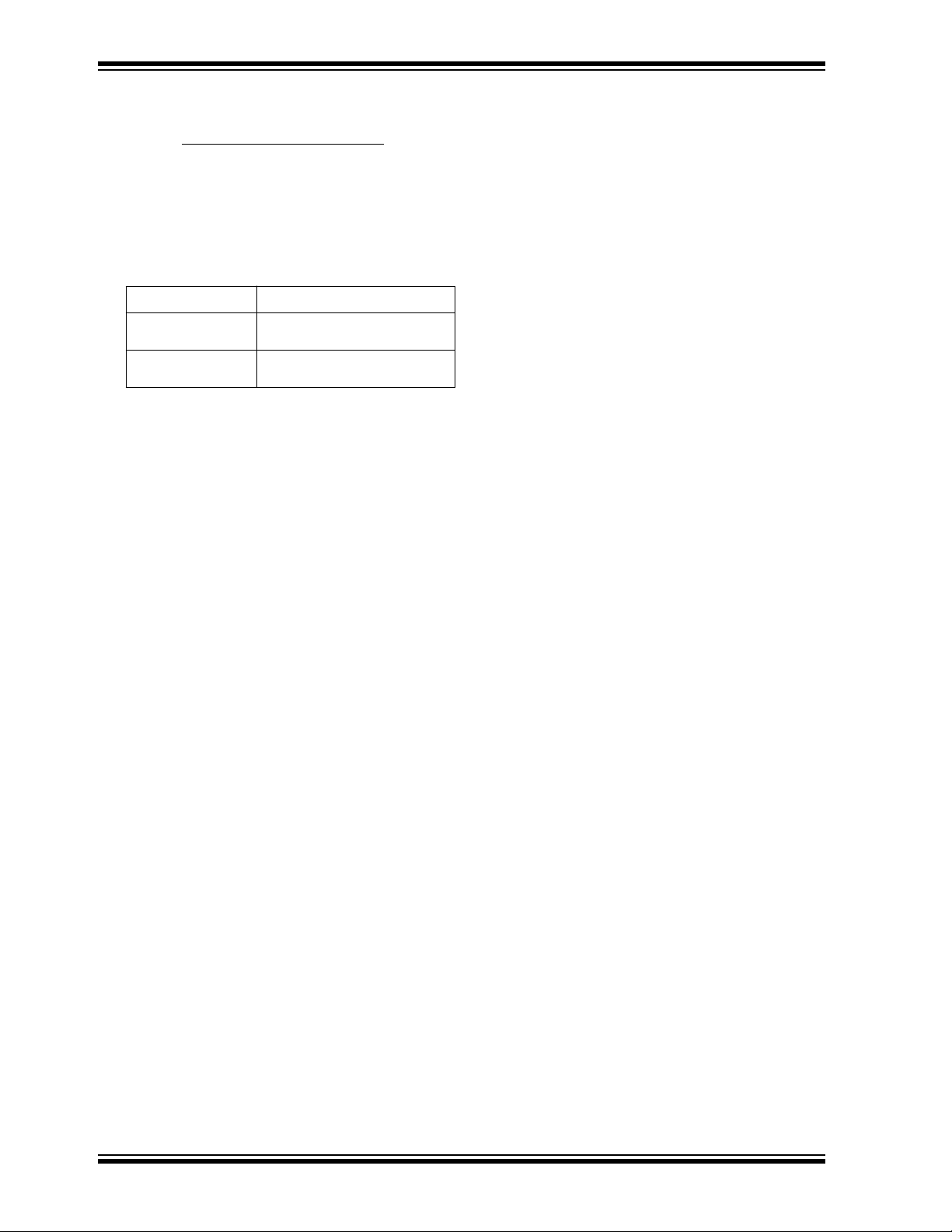
1.1 Har
The PIC12C67X and PIC12CE67X requires two programmable power supplies, one for V
recommended) and one for V
supplies should have a minimum resolution of 0.25V.
1.2 Pr
The programming mode for the PIC12C67X and
PIC12CE67X allows programming of user program
memory, special locations used f or ID, and the configuration word for the PIC12C67X and PIC12CE67X.
dware Requirements
PP
ogramming Mode
(2.0V to 6.0V
DD
(12V to 14V). Both
Pin Diagram:
PDIP
VDD
GP5/OSC1/CLKIN
GP4/OSC2/AN3/
CLKOUT
GP3/MCLR
/VPP
PIC12CE67X
1
2
3
4
PIC12C67X
8
7
6
5
VSS
GP0/AN0
GP1/AN1/V
GP2/T0CKI/
AN2/INT
REF
PIN DESCRIPTIONS (DURING PROGRAMMING): PIC12C671/672 and PIC12CE673/674
During Programming
Pin Name
GP1 CLOCK I Clock input
GP0 DATA I/O Data input/output
/V
GP3/MCLR
V
V
Legend: I = Input, O = Output, P = Power
1998 Microchip Technology Inc. DS40175A-page 1
PP
DD
SS
Pin Name Pin Type Pin Description
V
PP
DD
V
V
SS
P Programming Power
P Power Supply
P Ground
Page 2
PIC12C67X and PIC12CE67X
2.0 PROGRAM MODE ENTRY
2.1 User Pr
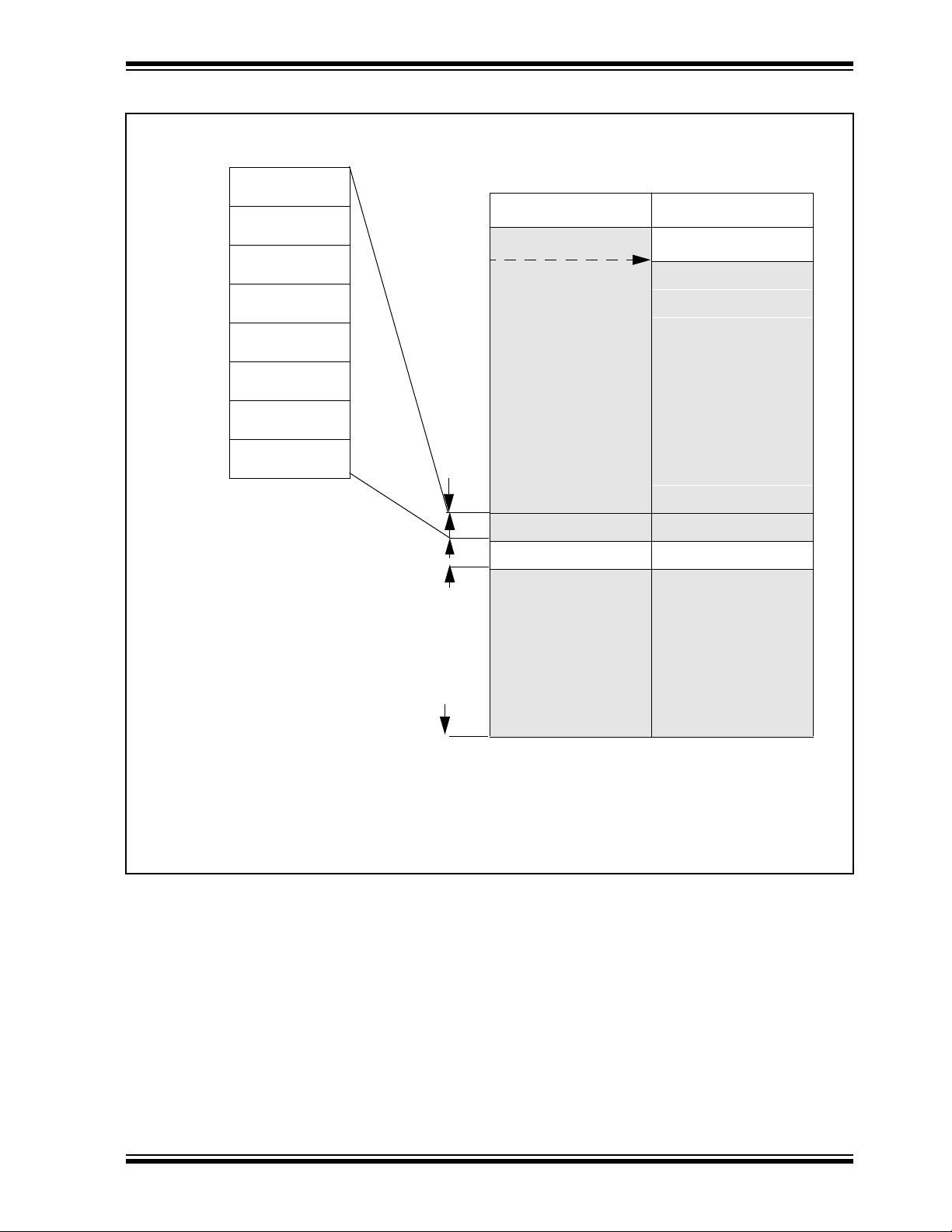
The user memory space extends from 0x0000 to
0x1FFF (8K). Table 2-1 shows actual implementation
of program memory in the PIC12C67X family.
TABLE 2-1: IMPLEMENTATION OF
Device Program Memory Size
PIC12C671/
PIC12CE673
PIC12C672/
PIC12CE674
When the PC reaches the last location of the implemented program memory, it will wrap around and
address a location within the physically implemented
memory (see Figure 2-1).
In programming mode the program memory space
extends from 0x0000 to 0x3FFF, with the first half
(0x0000-0x1FFF) being user program memory and the
second half (0x2000-0x3FFF) being configuration
memory. The PC will increment from 0x0000 to
0x1FFF and wrap to 0x000 or 0x2000 to 0x3FFF and
wrap around to 0x2000 (not to 0x0000). Once in configuration memory, the highest bit of the PC stays a '1',
thus always pointing to the configuration memory. The
only way to point to user program memory is to reset
the part and reenter program/verify mode, as described
in Section 2.2.
The last location of the program memory space holds
the factory programmed oscillator calibration value.
This location should not be programmed except when
blank (a non-blank value should not cause the device
to fail a blank check). If blank, the programmer should
program it to a RETL W XX statement where "XX" is the
calibration value.
ogram Memory Map
PROGRAM MEMORY IN THE
PIC12C67X
0x000 - 0x3FF (1K)
0x000 - 0x7FF (2K)
In the configuration memory space, 0x2000-0x20FF
are utilized. When in configuration memory, as in the
user memory, the 0x2000-0x2XFF segment is repeatedly accessed as the PC exceeds 0x2XFF (see
Figure 2-1).
A user may store identification information (ID) in four
ID locations. The ID locations are mapped in [0x2000 :
0x2003].
Note 1: All other locations in PIC configuration
memory are reserved and should not be
programmed.
Note 2: Due to the secure nature of the on-board
EEPROM memory in the
PIC12CE673/674, it can be accessed only
by the user program.
DS40175A-page 2
1998 Microchip Technology Inc.
Page 3
EPROM Memory Programming Specification
FIGURE 2-1: PROGRAM MEMORY MAPPING
2000
2001
2002
2003
2004
2005
2006
Configuration Word
2007
ID Location
ID Location
ID Location
ID Location
Reserved
Reserved
Reserved
1FF
3FF
400
7FF
800
BFF
C00
FFF
1000
1FFF
2000
2008
2100
0
1KW 2KW
Implemented Implemented
Implemented
Reserved
Reserved
Reserved Reserved
3FFF
Reserved Reserved
1998 Microchip Technology Inc. DS40175A-page 3
Page 4

PIC12C67X and PIC12CE67X
2.2 Pr
ogram/Verify Mode
The program/verify mode is entered by holding pins
GP1 and GP0 low while raising MCLR
IHH
V
(high voltage). VDD is then raised from VIL to
pin from V
IL
to
VIH.Once in this mode the user program memory and
the configuration memory can be accessed and programmed in serial fashion. The mode of operation is
serial, and the memory that is accessed is the user program memory. GP1 is a Schmitt Trigger input in this
mode.
The sequence that enters the device into the programming/verify mode places all other logic into the reset
state (the MCLR
pin was initially at V
). This means
IL
that all I/O are in the reset state (High impedance
inputs).
Note 1: The MCLR
IHH
V
before V
pin must be raised from V
DD
is applied. This is to
IL
to
ensure that the device does not have the
PC incremented while in valid operation
range.
Note 2: Do not power GP2, GP4 or GP5 before
V
is applied.
DD
1.0.1 PROGRAM/VERIFY OPERATION
The GP1 pin is used as a clock input pin, and the GP0
pin is used for entering command bits and data
input/output during serial operation. To input a command, the clock pin (GP1) is cycled six times. Each
command bit is latched on the falling edge of the clock
with the least significant bit (LSB) of the command
being input first. The data on pin GP0 is required to
have a minimum setup and hold time (see AC/DC
specs) with respect to the falling edge of the clock.
Commands that have data associated with them (read
and load) are specified to have a minimum dela y of 1 µ s
between the command and the data. After this delay
the clock pin is cycled 16 times with the first cycle being
a start bit and the last cycle being a stop bit. Data is
also input and output LSB first. Therefore, during a
read operation the LSB will be transmitted onto pin
GP0 on the rising edge of the second cycle, and during
a load operation the LSB will be latched on the falling
edge of the second cycle. A minimum 1 µ s delay is also
specified between consecutive commands.
All commands are transmitted LSB first. Data words
are also transmitted LSB first. The data is transmitted
on the rising edge and latched on the falling edge of the
clock. To allow for decoding of commands and rev ersal
of data pin configuration, a time separation of at least
1 µ s is required between a command and a data word
(or another command).
The commands that are available are listed
in Table 1-1.
1.0.1.1 LOAD CONFIGURATION
After receiving this command, the program counter
(PC) will be set to 0x2000. By then applying 16 cycles
to the clock pin, the chip will load 14-bits a “data word”
as described above, to be programmed into the configuration memory . A description of the memory mapping
schemes for normal operation and configuration mode
operation is shown in Figure 2-1. After the configuration memory is entered, the only way to get back to the user program memory is to exit the program/verify test mode by taking MCLR
low (V
).
IL
TABLE 1-1: COMMAND MAPPING
Command Mapping (MSB ... LSB) Data
Load Configuration
Load Data
Read Data
Increment Address
Begin programming
End Programming
0 0 0 0 0 0
0 0 0 0 1 0
0 0 0 1 0 0
0 0 0 1 1 0
0 0 1 0 0 0
0 0 1 1 1 0
0, data(14), 0
0, data(14), 0
0, data(14), 0
DS40175A-page 4
1998 Microchip Technology Inc.
Page 5

EPROM Memory Programming Specification
FIGURE 1-1: PROGRAM FLOW CHART - PIC12C67X AND PIC12CE67X PROGRAM MEMORY
Start
Increment Address
Command
Set VPP = V
Set VDD = V
Program Cycle
Read Data
Command
Data Correct?
Apply 3N Additional
Program Cycles
No
All Locations Done?
Verify all Locations
@ V
V
PP
N = 0
DD MIN.•
= V
IHH1
Yes
IHH2
DDP
Yes
•
No
N > 25
N = N + 1
N = # of Program Cycles
No
Yes
Report Programming
Failure
Prog
Load Data
Command
Begin Programming
Command
Wait 100 µs
ram Cycle
Data Correct?
Verify all Locations
@ V
DD MAX.
V
= V
PP
IHH2
Data Correct?
Yes
Done
• V
= VDD range for programming (typically 4.75V - 5.25V).
DDP
V
= Minimum V
DD MIN.
V
= Maximum V
DD MAX.
1998 Microchip Technology Inc. DS40175A-page 5
for device operation.
DD
for device operation.
DD
No
Yes
No
Report Verify
@ V
DD MIN.
Report Verify
@ V
DD MAX
Error
Error
End Programming
Command
Page 6

PIC12C67X and PIC12CE67X
FIGURE 1-2: PROGRAM FLOW CHART - PIC12C67X AND PIC12CE67X CONFIGURATION WORD
& ID LOCATIONS
Start
Increment Address
Command
No
Address = 2004
Increment Address
Command
Set VPP = V
Load Configuration
Command
N = 0
No Yes
Yes
Program ID Loc?
IHH1
Program Cycle
N = N + 1
N = # of Program
Cycles
No
ID/Configuration
N > 25
Yes
Error
Read Data
Command
No
Data Correct?
Yes
Apply 3N
Program Cycles
Increment Address
Command
Increment Address
Command
Done
Yes
Report Program
ID/Config. Error
No
Data Correct?
Program Cycle
100 Cycles
No
Data Correct?
Set VDD = VDDmax
Read Data Command
Set V
PP
Yes
VDDmax
= V
IHH2
Read Data
Command
No
Data Correct?
Yes
Set VDD = VDDmin
Read Data Command
Set V
PP
VDDmin
= V
IHH2
DS40175A-page 6
1998 Microchip Technology Inc.
Page 7

EPROM Memory Programming Specification
1.0.1.2 LOAD DATA
After receiving this command, the chip will load in a
14-bit “data word” when 16 cycles are applied, as
described previously . A timing diagr am for the load data
command is shown in Figure 4-1.
1.0.1.3 READ DATA
After receiving this command, the chip will transmit
data bits out of the memory currently accessed starting
with the second rising edge of the clock input. The GP0
pin will go into output mode on the second rising clock
edge, and it will revert back to input mode (hi-impedance) after the 16th rising edge. A timing diagram of
this command is shown in Figure 4-2.
1.0.1.4 INCREMENT ADDRESS
The PC is incremented when this command is
received. A timing diagram of this command is shown
in Figure 4-3.
1.0.1.5 BEGIN PROGRAMMING
A load command (load configuration or load data)
must be given before every begin programming
command. Programming of the appropriate memory
(test program memory or user program memory) will
begin after this command is received and decoded.
Programming should be performed with a series of
100 µ s programming pulses. A programming pulse is
defined as the time between the begin programming
command and the end programming command.
1.1 Pr
ogramming Algorithm Requires
Variable V
DD
The PIC12C67X and PIC12CE67X uses an intelligent
algorithm. The algorithm calls for program verification
at V
min as well as V
DD
max. Verification at V
DD
DD
min
guarantees good “erase margin”. Verification at
V
DD
max guarantees good “program margin”.
in the
The actual programming must be done with V
V
range (4.75 - 5.25V).
DDP
V
V
V
DDP
DD
DD
= V
range required during programming.
CC
min. = minimum operating V
max.= maximum operating V
DD
spec for the part.
spec for the part.
DD
DD
Programmers must verify the PIC12C67X and
PIC12CE67X at its specified V
max and V
DD
min lev-
DD
els. Since Microchip may introduce future versions of
the PIC12C67X and PIC12CE67X with a broader V
DD
range, it is best that these levels are user selectable
(defaults are ok).
Note: Any programmer not meeting these
requirements may only be classified as
“prototype” or “development” programmer
but not a “production” quality progr ammer .
1.0.1.6 END PROGRAMMING
After receiving this command, the chip stops program-
ming the memory (configuration program memory or
user program memory) that it was programming at the
time.
1998 Microchip Technology Inc. DS40175A-page 7
Page 8

PIC12C67X and PIC12CE67X
2.0 CONFIGURATION WORD
The PIC12C67X and PIC12CE67X family members
have several configuration bits. These bits can be programmed (reads '0') or left unprogrammed (reads '1') to
select various device configurations. Figure 2-1 provides an overview of configuration bits.
FIGURE 2-1: CONFIGURATION WORD
Bit Number:
13
12
CP0CP1
bit 13-8, 6-5: CP1:CP0: Code Protection bits (1) (2)
bit 7: MCLRE: GP3/MCLR pin function select
bit 4: PWRTE: Power-up Timer Enable bit (1)
bit 3: WDTE: Watchdog Timer Enable bit
bit 2-0: FOSC2:FOSC0: Oscillator Selection bits
Note 3: All of the CP1:CP0 pairs have to be given the same value to enable the code protection scheme listed.
10 9 8
11
CP0CP1
CP1
CP0
11 = Code protection off
10 = 0400h-07FFh code protected;
01 = 0200h-07FFh code protected;
00 = 0000h-07FFh code protected;
1 = GP3/MCLR pin function is MCLR
0 = GP3/MCLR pin function is digital I/O, MCLR internally tied to Vdd
1 = PWRT disabled
0 = PWRT enabled
1 = WDT enabled
0 = WDT disabled
111 = EXTRC oscillator / CLKOUT function on GP4/OSC2/CLKOUT pin
110 = EXTRC oscillator / GP4 function on GP4/OSC2/CLKOUT pin
101 = INTRC oscillator / CLKOUT function on GP4/OSC2/CLKOUT pin
100 = INTRC oscillator / GP4 function on GP4/OSC2/CLKOUT pin
011 = invalid selection
010 = HS oscillator
001 = XT oscillator
000 = LP oscillator
4: 07FFh is always uncodeprotected on the 12C672 and 03FFh is alwa ys uncodeprotected on the 12C671. This location
contains the RETLW xx calibration instruction for the INTRC.
7
6 5 4
MCLRE CP1
CP0
PWRTE
3
WDTE
2
FOSC2
1
FOSC10FOSC0
Register: CONFIG
Address 2007h
DS40175A-page 8 1998 Microchip Technology Inc.
Page 9

EPROM Memory Programming Specification
3.0 CODE PROTECTION
The program code written into the EPROM can be protected by writing to the CP0 & CP1 bits of the configuration word.
For PIC12C67X and PIC12CE67X devices, once code
protection is enabled, all protected segments read '0's
(or “garbage values”) and are prevented from further
programming. All unprotected segments, including ID
and configuration word locations , and calibration word
location read normally and can be programmed.
3.1 Embedding Configuration Word and ID Information in the Hex File
T o allow portability of code, the programmer is required to read the configuration word and ID locations from the hex
file when loading the hex file. If configuration word information was not present in the hex file then a simple warning
message may be issued. Similarly, while saving a hex file, configuration word and ID information must be included.
An option to not include this information may be provided.
Microchip Technology Inc. feels strongly that this feature is important for the benefit of the end customer.
TABLE 3-1: CONFIGURATION WORD
PIC12C671, PIC12CE673
To code protect:
• Protect all memory 00 0000 X00X XXXX
• Protect 0200h-07FFh 01 0101 X01X XXXX
• No code protection 11 1111 X11X XXXX
Program Memory Segment R/W in Protected Mode R/W in Unprotected Mode
Configuration Word (0x2007) Read Unscrambled, Write Enabled Read Unscrambled, Write Enabled
Unprotected memory segment Read Unscrambled, Write Enabled Read Unscrambled, Write Enabled
Protected memory segment Read All 0’s, Write Disabled Read Unscrambled, Write Enabled
ID Locations (0x2000 : 0x2003) Read Unscrambled, Write Enabled Read Unscrambled, Write Enabled
INTRC Calibration Word (0X3FF) Read Unscrambled, Write Enabled Read Unscrambled, Write Enabled
PIC12C672, PIC12CE674
To code protect:
• Protect all memory 00 0000 X00X XXXX
• Protect 0200h-07FFh 01 0101 X01X XXXX
• Protect 0400h-07FFh 10 1010 X10X XXXX
• No code protection 11 1111 X11X XXXX
Program Memory Segment R/W in Protected Mode R/W in Unprotected Mode
Configuration Word (0x2007) Read Unscrambled, Write Enabled Read Unscrambled, Write Enabled
Unprotected memory segment Read Unscrambled, Write Enabled Read Unscrambled, Write Enabled
Protected memory segment Read All 0’s, Write Disabled Read Unscrambled, Write Enabled
ID Locations (0x2000 : 0x2003) Read Unscrambled, Write Enabled Read Unscrambled, Write Enabled
INTRC Calibration Word (0X7FF) Read Unscrambled, Write Enabled Read Unscrambled, Write Enabled
1998 Microchip Technology Inc. DS40175A-page 9
Page 10

PIC12C67X and PIC12CE67X
3.2 Checksum
3.2.1 CHECKSUM CALCULATIONS
Checksum is calculated by reading the contents of the
PIC12C67X and PIC12CE67X memory locations and
adding the opcodes up to the maximum user addressable location, excluding the oscillator calibration location in the last address, e.g., 0x3FE for the
PIC12C671/CE673. Any carry bits exceeding 16-bits
are neglected. Finally, the configuration word (appropriately masked) is added to the checksum. Checksum
computation for each member of the PIC12C67X and
PIC12CE67X devices is shown in Table 3-2.
The checksum is calculated by summing the following:
• The contents of all program memory locations
• The configuration word, appropriately masked
• Masked ID locations (when applicable)
TABLE 3-2: CHECKSUM COMPUTATION
Device
PIC12C671
PIC12CE673
PIC12C672
PIC12CE674
Code
Protect
OFF
1/2
ALL
OFF
1/2
3/4
ALL
SUM[0x000:0x3FE] + CFGW & 0x3FFF
SUM[0x000:0x1FF] + CFGW & 0x3FFF + SUM_ID
CFGW & 0x3FFF + SUM_ID
SUM[0x000:0x7FE] + CFGW & 0x3FFF
SUM[0x000:0x3FF] + CFGW & 0x3FFF + SUM_ID
SUM[0x000:0x1FF] + CFGW & 0x3FFF + SUM_ID
CFGW & 0x3FFF + SUM_ID
The least significant 16 bits of this sum is the checksum.
The following table describes how to calculate the
checksum for each de vice. Note that the chec ksum calculation differs depending on the code protect setting.
Since the program memory locations read out differently depending on the code protect setting, the table
describes how to manipulate the actual program memory values to simulate the values that would be read
from a protected device. When calculating a checksum
by reading a device, the entire program memory can
simply be read and summed. The configuration word
and ID locations can always be read.
Note that some older devices have an additional value
added in the checksum. This is to maintain compatibility with older device programmer checksums.
Checksum*
Blank
Value
3B3F
4E5E
3B4E
373F
5D6E
4A5E
374E
Ox25E6 at
0 and max
address
070D
0013
071C
030D
0F23
FC13
031C
Legend: CFGW = Configuration Word
SUM[a:b] = [Sum of locations a through b inclusive]
SUM_ID = ID locations masked by 0xF then made into a 16-bit value with ID0 as the most significant nibble.
For example,
ID0 = 0x12, ID1 = 0x37, ID2 = 0x4, ID3 = 0x26, then SUM_ID = 0x2746.
*Checksum = [Sum of all the individual expressions] MODULO [0xFFFF]
+ = Addition
& = Bitwise AND
DS40175A-page 10 1998 Microchip Technology Inc.
Page 11

EPROM Memory Programming Specification
4.0 PROGRAM/VERIFY MODE ELECTRICAL CHARACTERISTICS
TABLE 4-1: AC/DC CHARACTERISTICS
TIMING REQUIREMENTS FOR PROGRAM/VERIFY TEST MODE
Standard Operating Conditions
Operating Temperature: +10°C ≤ T
Operating Voltage: 4.5V ≤ V
A ≤ +40°C, unless otherwise stated, (25°C is recommended)
DD ≤ 5.5V, unless otherwise stated.
Parameter
No.
Sym. Characteristic Min. Typ. Max. Units Conditions
General
PD1 V
PD2 I
DDP Supply voltage during programming 4.75 5.0 5.25 V
DDP Supply current (from VDD)
during programming
PD3 V
PD4 V
DDV Supply voltage during verify VDDmin VDDmax V Note 1
IHH1 Voltage on MCLR/VPP during
12.75 13.25 V Note 2
programming
PD5 V
PD6 I
PD9 V
PD8 V
IHH2 Voltage on MCLR/VPP during verify VDD + 4.0 13.5
PP Programming supply current (from
V
PP)
IH1 (GP0, GP1) input high level 0.8 VDD V Schmitt Trigger input
IL1 (GP0, GP1) input low level 0.2 VDD V Schmitt Trigger input
Serial Program Verify
P1 T
R MCLR/VPP rise time (VSS to VIHH)
for test mode entry
P2 Tf MCLR
Fall time 8.0 µs
P3 Tset1 Data in setup time before clock ↓ 100 ns
P4 Thld1 Data in hold time after clock ↓ 100 ns
P5 Tdly1 Data input not driven to next clock
1.0 µs
input (delay required between command/data or command/command)
P6 Tdly2 Delay between clock ↓ to clock ↑ of
1.0 µs
next command or data
P7 Tdly3 Clock ↑ to data out valid
200 ns
(during read data)
P8 Thld0 Hold time after V
P9 T
PPDP Hold time after VPP↑ 5 µs
Note 1: Program must be verified at the minimum and maximum V
Note 2: V
IHH must be greater than VDD + 4.5V to stay in programming/verify mode.
DD↑ 2 µs
DD limits for the part.
20 mA
50 mA
8.0 µs
1998 Microchip Technology Inc. DS40175A-page 11
Page 12

EPROM Memory Programming Specification
FIGURE 4-1: LOAD DATA COMMAND (PROGRAM/VERIFY)
VDD
VDD
P9
P8
P9
P8
100ns
21
P3
100n
100ns
21
P3
}
100n
min.
}
min.
0
100ns
1
P4
}
s
100ns
P4
}
s
0
0
43
0
0
0
Program/Verify Mode
43
0
1
0
00
P6
1µs min.
P5
1µs min.
P6
1µs min.
P5
1µs min.
155432165
0
P4
P3
}
}
100ns
min.
155432165
P7
RB7 = output
Program/Verify Mode
VIHH
MCLR/
VPP
GP1
(CLOCK)
GP0
(DATA)
Reset
FIGURE 4-2: READ DATA COMMAND (PROGRAM/VERIFY)
VIHH
MCLR
/VPP
GP1
(CLOCK)
GP0
(DATA)
Reset
0
RB7
input
FIGURE 4-3: INCREMENT ADDRESS COMMAND (PROGRAM/VERIFY)
VDD
P9
1 2 3 4 5 6
1
1
00 0
P3
P4
}
}
100ns
min
Program/Verify Mode
P6
1µs min.
0
1µs min.
MCLR/VPP
GP1
(CLOCK)
GP0
(DATA)
Reset
VIHH
P5
Next Command
1
0
2
0
1998 Microchip Technology Inc. DS40175A-page 12
Page 13

EPROM Memory Programming Specification
NOTES:
1998 Microchip Technology Inc. DS40175A-page 13
Page 14
M
WORLDWIDE SALES AND SERVICE
AMERICAS
Corporate Office
Microchip Technology Inc.
2355 West Chandler Blvd.
Chandler, AZ 85224-6199
Tel: 602-786-7200 Fax: 602-786-7277
Technical Support:
Web:
http://www.microchip.com
Atlanta
Microchip Technology Inc.
500 Sugar Mill Road, Suite 200B
Atlanta, GA 30350
Tel: 770-640-0034 Fax: 770-640-0307
Boston
Microchip Technology Inc.
5 Mount Royal Avenue
Marlborough, MA 01752
Tel: 508-480-9990 Fax: 508-480-8575
Chicago
Microchip Technology Inc.
333 Pierce Road, Suite 180
Itasca, IL 60143
Tel: 630-285-0071 Fax: 630-285-0075
Dallas
Microchip Technology Inc.
14651 Dallas Parkway, Suite 816
Dallas, TX 75240-8809
Tel: 972-991-7177 Fax: 972-991-8588
Dayton
Microchip Technology Inc.
Two Prestige Place, Suite 150
Miamisburg, OH 45342
Tel: 937-291-1654 Fax: 937-291-9175
Los Angeles
Microchip Technology Inc.
18201 Von Karman, Suite 1090
Irvine, CA 92612
Tel: 714-263-1888 Fax: 714-263-1338
New York
Microchip Technology Inc.
150 Motor Parkway, Suite 202
Hauppauge, NY 11788
Tel: 516-273-5305 Fax: 516-273-5335
San Jose
Microchip Technology Inc.
2107 North First Street, Suite 590
San Jose, CA 95131
Tel: 408-436-7950 Fax: 408-436-7955
Toronto
Microchip Technology Inc.
5925 Airport Road, Suite 200
Mississauga, Ontario L4V 1W1, Canada
Tel: 905-405-6279 Fax: 905-405-6253
602 786-7627
ASIA/PACIFIC
Hong Kong
Microchip Asia Pacific
RM 3801B, Tower Two
Metroplaza
223 Hing Fong Road
Kwai Fong, N.T., Hong Kong
Tel: 852-2-401-1200 Fax: 852-2-401-3431
India
Microchip Technology Inc.
India Liaison Office
No. 6, Legacy, Convent Road
Bangalore 560 025, India
Tel: 91-80-229-0061 Fax: 91-80-229-0062
Japan
Microchip Technology Intl. Inc.
Benex S-1 6F
3-18-20, Shinyokohama
Kohoku-Ku, Yokohama-shi
Kanagawa 222 Japan
Tel: 81-45-471- 6166 Fax: 81-45-471-6122
Korea
Microchip Technology Korea
168-1, Youngbo Bldg. 3 Floor
Samsung-Dong, Kangnam-Ku
Seoul, Korea
Tel: 82-2-554-7200 Fax: 82-2-558-5934
Shanghai
Microchip Technology
RM 406 Shanghai Golden Bridge Bldg.
2077 Yan’an Road West, Hong Qiao District
Shanghai, PRC 200335
Tel: 86-21-6275-5700
Fax: 86 21-6275-5060
Singapore
Microchip Technology Taiwan
Singapore Branch
200 Middle Road
#07-02 Prime Centre
Singapore 188980
Tel: 65-334-8870 Fax: 65-334-8850
ASIA/PACIFIC (CONTINUED)
Taiwan, R.O.C
Microchip Technology Taiwan
10F-1C 207
Tung Hua North Road
Taipei, Taiwan, ROC
Tel: 886-2-2717-7175 Fax: 886-2-2545-0139
EUROPE
United Kingdom
Arizona Microchip Technology Ltd.
505 Eskdale Road
Winnersh Triangle
Wokingham
Berkshire, England RG41 5TU
Tel: 44-1189-21-5858 Fax: 44-1189-21-5835
France
Arizona Microchip Technology SARL
Zone Industrielle de la Bonde
2 Rue du Buisson aux Fraises
91300 Massy, France
Tel: 33-1-69-53-63-20 Fax: 33-1-69-30-90-79
Germany
Arizona Microchip Technology GmbH
Gustav-Heinemann-Ring 125
D-81739 Müchen, Germany
Tel: 49-89-627-144 0 Fax: 49-89-627-144-44
Italy
Arizona Microchip Technology SRL
Centro Direzionale Colleoni
Palazzo Taurus 1 V. Le Colleoni 1
20041 Agrate Brianza
Milan, Italy
Tel: 39-39-6899939 Fax: 39-39-6899883
1/13/98
Microchip received ISO 9001 Quality
System certification for its worldwide
headquarters, design, and wafer
fabrication facilities in January , 1997.
Our field-programmable PICmicro™
8-bit MCUs, Serial EEPROMs,
related specialty memory products
and development systems conform
to the stringent quality standards of
the International Standard
Organization (ISO).
All rights reserved. © 1998, Microchip Technology Incorporated, USA. 2/98 Printed on recycled paper.
Information contained in this publication regarding device applications and the like is intended for suggestion only and may be superseded by updates. No representation or warranty is given and no
liability is assumed by Microchip Technology Incorporated with respect to the accuracy or use of such information, or infringement of patents or other intellectual property rights arising from such use
or otherwise. Use of Microchip’s products as critical components in life support systems is not authorized except with express written approval by Microchip. No licenses are conveyed, implicitly or
otherwise, under any intellectual property rights. The Microchip logo and name are registered trademarks of Microchip Technology Inc. in the U.S.A. and other countries. All rights reserved. All other
trademarks mentioned herein are the property of their respective companies.
DS40175A-page 14 1998 Microchip Technology Inc.
Page 15

Copyright © Each Manufacturing Company.
All Datasheets cannot be modified without permission.
This datasheet has been download from :
www.AllDataSheet.com
100% Free DataSheet Search Site.
Free Download.
No Register.
Fast Search System.
www.AllDataSheet.com
 Loading...