

PIC12C5XX
8-Pin, 8-Bit CMOS Microcontroller
Devices included in this Data Sheet:
• PIC12C508 • PIC12C508A
• PIC12C509 • PIC12C509A
Note: Throughout this data sheet PIC12C508(A)
refers to the PIC12C508 and PIC12C508A.
PIC12C509(A) refers to the PIC12C509
and PIC12C509A. PIC12C5XX refers to
the PIC12C508, PIC12C508A, PIC12C509
and PIC12C509A.
High-Performance RISC CPU:
• Only 33 single word instructions to learn
• All instructions are single cycle (1 µ s) except for
program branches which are two-cycle
• Operating speed: DC - 4 MHz clock input
DC - 1 µ s instruction cycle
Device EPROM RAM
PIC12C508 512 x 12 25
PIC12C508A 512 x 12 25
PIC12C509 1024 x 12 41
PIC12C509A 1024 x 12 41
• 12-bit wide instructions
• 8-bit wide data path
• Seven special function hardware registers
• Two-level deep hardware stack
• Direct, indirect and relative addressing modes for
data and instructions
• Internal 4 MHz RC oscillator with programmable
calibration
• In-circuit serial programming
Peripheral Features:
• 8-bit real time clock/counter (TMR0) with 8-bit
programmable prescaler
• Power-On Reset (POR)
• Device Reset Timer (DRT)
• Watchdog Timer (WDT) with its own on-chip RC
oscillator for reliable operation
• Programmable code-protection
• Power saving SLEEP mode
• Wake-up from SLEEP on pin change
• Internal weak pull-ups on I/O pins
• Internal pull-up on MCLR
• Selectable oscillator options:
- INTRC: Internal 4 MHz RC oscillator
pin
- EXTRC: External low-cost RC oscillator
- XT: Standard crystal/resonator
- LP: Power saving, low frequency crystal
CMOS Tec hnology:
• Low power, high speed CMOS EPROM
technology
• Fully static design
• Wide operating voltage range
• Wide temperature range:
- Commercial: 0 ° C to +70 ° C
- Industrial: -40 ° C to +85 ° C
- Extended: -40 ° C to +125 ° C
• Low power consumption
- < 2 mA @ 5V, 4 MHz
- 15 µ A typical @ 3V, 32 KHz
- < 1 µ A typical standby current
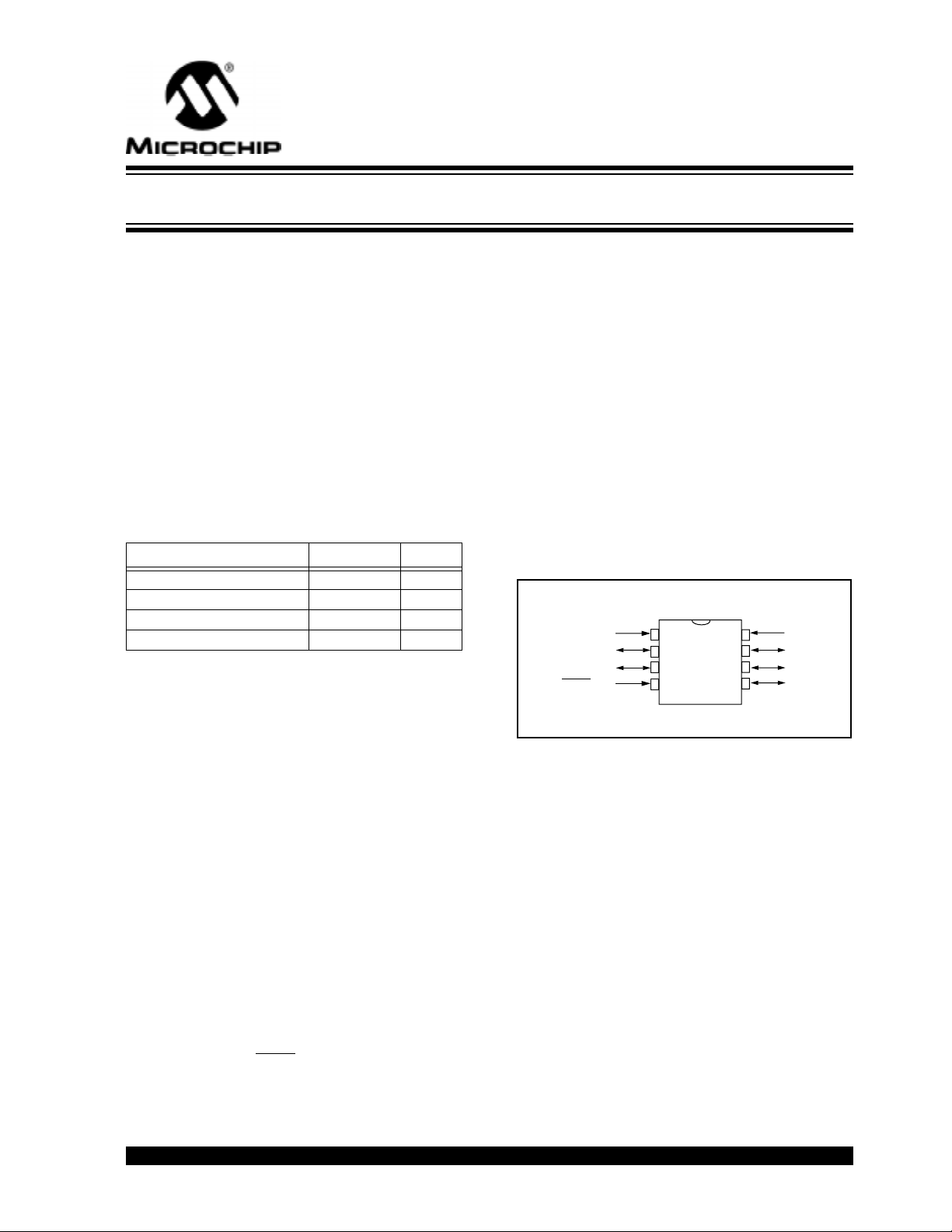
Pin Diagram
PDIP, SOIC, Windowed Ceramic Side Brazed
PIC12C508(A
VDD
GP5/OSC1/CLKIN
GP4/OSC2
GP3/MCLR
/VPP
1
2
3
4
PIC12C509(A)
8
7
6
5
)
VSS
GP0
GP1
GP2/T0CKI
1998 Microchip Technology Inc. DS40139D-page 1

PIC12C5XX
Device Differences
Device
PIC12C508A 3.0-5.5 See Note 1 6 0.7
PIC12LC508A 2.5-5.5 See Note 1 6 0.7
PIC12C508 2.5-5.5 See Note 1 4 0.9
PIC12C509A 3.0-5.5 See Note 1 6 0.7
PIC12LC509A 2.5-5.5 See Note 1 6 0.7
PIC12C509 2.5-5.5 See Note 1 4 0.9
Note 1: If you change from the PIC12C50X to the PIC12C50XA, please verify oscillator characteristics in your appli-
cation.
Note 2: See Section 7.2.5 for OSCCAL implementation differences.
Voltage
Range
Oscillator
Oscillator
Calibration
(Bits)
2
Process
Technology
(Microns)
DS40139D-page 2
1998 Microchip Technology Inc.

PIC12C5XX
TABLE OF CONTENTS
1.0 General Description......................................................................................................................................................................4
2.0 PIC12C5XX Device Varieties.......................................................................................................................................................7
3.0 Architectural Overview .................................................................................................................................................................9
4.0 Memory Organization................................................................................................................................................................ 13
5.0 I/O Port...................................................................................................................................................................................... 21
6.0 Timer0 Module and TMR0 Register.......................................................................................................................................... 23
7.0 Special Features of the CPU..................................................................................................................................................... 27
8.0 Instruction Set Summary........................................................................................................................................................... 39
9.0 Development Support................................................................................................................................................................ 51
10.0 Electrical Characteristics - PIC12C508/PIC12C509/PIC12LC508/PIC12LC509 ...................................................................... 57
11.0 DC and AC Characteristics - PIC12C508/PIC12C509/PIC12LC508/PIC12LC509................................................................... 73
12.0 Electrical Characteristics - PIC12C508A/PIC12C509A/PIC12LC508A/PIC12LC509A............................................................. 77
13.0 DC and AC Characteristics - PIC12C508A/PIC12C509A/PIC12LC508A/PIC12LC509A......................................................... 91
14.0 Packaging Information............................................................................................................................................................... 95
INDEX................................................................................................................................................................................................ 101
PIC12C5XX Product Identification System........................................................................................................................................ 105
To Our Valued Customers
Most Current Data Sheet
To obtain the most up-to-date version of this data sheet, please check our Worldwide Web site at:
http://www.microchip.com
You can determine the version of a data sheet by examining its literature number found on the bottom outside corner of any page.
The last character of the literature number is the version number. e.g., DS30000A is version A of document DS30000.
Errata
An errata sheet may exist for current devices, describing minor operational differences (from the data sheet) and recommended
workarounds. As de vice/documentation issues become known to us , we will publish an err ata sheet. The err ata will specify the revision of silicon and revision of document to which it applies.
To determine if an errata sheet exists for a particular device, please check with one of the following:
• Microchip’s Worldwide Web site; http://www.microchip.com
• Your local Microchip sales office (see last page)
• The Microchip Corporate Literature Center; U.S. FAX: (602) 786-7277
When contacting a sales office or the literature center, please specify which device, revision of silicon and data sheet (include literature number) you are using.
Corrections to this Data Sheet
We constantly strive to improve the quality of all our products and documentation. We have spent a great deal of time to ensure
that this document is correct. How e ver, we realize that w e may have missed a fe w things . If you find any information that is missing
or appears in error, please:
• Fill out and mail in the reader response form in the back of this data sheet.
• E-mail us at webmaster@microchip.com.
We appreciate your assistance in making this a better document.
1998 Microchip Technology Inc. DS40139D-page 3

PIC12C5XX
1.0 GENERAL DESCRIPTION
The PIC12C5XX from Microchip Technology is a family
of low-cost, high performance, 8-bit, fully static,
EPROM/ROM-based CMOS microcontrollers. It
employs a RISC architecture with only 33 single word/
single cycle instructions. All instructions are single
cycle (1 µ s) except for program branches which take
two cycles. The PIC12C5XX delivers perfor mance an
order of magnitude higher than its competitors in the
same price category. The 12-bit wide instructions are
highly symmetrical resulting in 2:1 code compression
over other 8-bit microcontrollers in its class. The easy
to use and easy to remember instruction set reduces
development time significantly.
The PIC12C5XX products are equipped with special
features that reduce system cost and power requirements. The Power-On Reset (POR) and Device Reset
Timer (DRT) eliminate the need for external reset circuitry. There are four oscillator configurations to choose
from, including INTRC internal oscillator mode and the
power-saving LP (Low Power) oscillator mode. Power
saving SLEEP mode, Watchdog Timer and code
protection features also improve system cost, power
and reliability.
The PIC12C5XX are available in the cost-effective
One-Time-Programmable (OTP) versions which are
suitable for production in any volume. The customer
can take full advantage of Microchip’s price leadership
in OTP microcontrollers while benefiting from the O TP’s
flexibility .
The PIC12C5XX products are supported by a full-featured macro assembler, a software simulator, an in-circuit emulator, a ‘C’ compiler, fuzzy logic support tools,
a low-cost development programmer, and a full featured programmer. All the tools are supported on IBM
PC and compatible machines.
1.1 Applications
The PIC12C5XX series fits perfectly in applications
ranging from personal care appliances and security
systems to low-power remote transmitters/receivers.
The EPROM technology makes customizing application programs (transmitter codes, appliance settings,
receiver frequencies, etc.) extremely fast and convenient. The small footprint packages, f or through hole or
surface mounting, make this microcontroller series perfect for applications with space limitations. Low-cost,
low-power, high performance, ease of use and I/O flexibility make the PIC12C5XX series very versatile even
in areas where no microcontroller use has been
considered before (e.g., timer functions, replacement
of “glue” logic and PLD’s in larger systems, coprocessor applications).
DS40139D-page 4
1998 Microchip Technology Inc.

TABLE 1-1: PIC12CXXX & PIC12CEXXX FAMILY OF DEVICES
PIC12C509(A) PIC12CE518 PIC12CE519 PIC12C671 PIC12C672 PIC12CE673 PIC12CE674
8-pin DIP,
JW, SOIC
8-pin DIP,
JW, SOIC
8-pin DIP,
JW, SOIC
8-pin DIP,
JW, SOIC
Clock
Memory
Peripherals
Features
PIC12C508(A)
Maximum
Frequency
of Operation
(MHz)
EPROM
Program
Memory
RAM Data
Memory
(bytes)
EEPROM
Data Memory
(bytes)
Timer
Module(s)
A/D Converter (8-bit)
Channels
Wake-up
from SLEEP
on pin
change
Interrupt
Sources
I/O Pins 5 5 5 5 5 5 5 5
Input Pins 1 1 1 1 1 1 1 1
Internal
Pull-ups
In-Circuit
Serial
Programming
Number of
Instructions
Packages 8-pin DIP,
4 4 4 4 10 10 10 10
512 x 12 1024 x 12 512 x 12 1024 x 12 1024 x 14 2048 x 14 1024 x 14 2048 x 14
25 41 25 41 128 128
— — 16 16 — —
TMR0 TMR0 TMR0 TMR0 TMR0 TMR0 TMR0 TMR0
— — — — 4 4 4 4
Yes Yes Yes Yes Yes Yes Yes Yes
— — 4 4 4 4
Yes Yes Yes Yes Yes Yes Yes Yes
Yes Yes Yes Yes Yes Yes Yes Yes
33 33 33 33 35 35 35 35
JW, SOIC
PIC12C5XX
128 128
16 16
8-pin DIP,
JW, SOIC
8-pin DIP, JW8-pin DIP,
JW
All PIC12CXXX & PIC12CEXXX devices have Power-on Reset, selectable Watchdog Timer, selectable
code protect and high I/O current capability.
All PIC12CXXX & PIC12CEXXX devices use serial programming with data pin GP0 and clock pin GP1.
1998 Microchip Technology Inc. DS40139D-page 5

PIC12C5XX
NOTES:
DS40139D-page 6
1998 Microchip Technology Inc.

PIC12C5XX
2.0 PIC12C5XX DEVICE VARIETIES
A variety of packaging options are available.
Depending on application and production
requirements, the proper device option can be
selected using the information in this section. When
placing orders, please use the PIC12C5XX Product
Identification System at the back of this data sheet to
specify the correct part number.
2.1 UV Erasab
The UV erasable version, offered in ceramic side
brazed package, is optimal for prototype development
and pilot programs.
The UV erasable version can be erased and
reprogrammed to any of the configuration modes.
Note: Please note that erasing the device will
also erase the pre-programmed internal
calibration value for the internal oscillator.
The calibration value must be saved prior
to erasing the part.
Microchip's PICSTART
grammers all support programming of the PIC12C5XX.
Third party programmers also are available; ref er to the
Microchip
Third Party Guide
le Devices
PLUS and PRO MATE
for a list of sources.
pro-
2.3 Quic
k-Turnaround-Production (QTP)
Devices
Microchip offers a QTP Programming Service for
factory production orders. This service is made
available for users who choose not to program a
medium to high quantity of units and whose code
patterns have stabilized. The devices are identical to
the OTP devices b ut with all EPROM locations and fuse
options already programmed by the factory. Certain
code and prototype verification procedures do apply
before production shipments are av ailable . Please contact your local Microchip Technology sales office for
more details.
2.4 Serializ
Production (SQTP
Microchip offers a unique programming service where
a few user-defined locations in each device are
programmed with different serial numbers. The serial
numbers may be random, pseudo-random or
sequential.
Serial programming allows each device to have a
unique number which can serve as an entry-code,
password or ID number.
ed Quick-Turnaround
SM
vices
) De
2.2 One-Time-Pr
ogrammable (OTP)
Devices
The availability of OTP devices is especially useful for
customers who need the flexibility for frequent code
updates or small volume applications.
The OTP devices , packaged in plastic pac kages permit
the user to program them once. In addition to the
program memory, the configuration bits must also be
programmed.
1998 Microchip Technology Inc. DS40139D-page 7

PIC12C5XX
NOTES:
DS40139D-page 8
1998 Microchip Technology Inc.
PIC12C5XX
3.0 ARCHITECTURAL OVERVIEW
The high performance of the PIC12C5XX family can
be attributed to a number of architectural features
commonly found in RISC microprocessors. To begin
with, the PIC12C5XX uses a Harvard architecture in
which program and data are accessed on separate
buses. This improves bandwidth over traditional von
Neumann architecture where program and data are
fetched on the same bus. Separating program and
data memory further allows instructions to be sized
differently than the 8-bit wide data word. Instruction
opcodes are 12-bits wide making it possible to have all
single word instructions. A 12-bit wide program
memory access bus fetches a 12-bit instruction in a
single cycle. A two-stage pipeline overlaps fetch and
execution of instructions. Consequently, all instructions
(33) execute in a single cycle (1 µ s @ 4MHz) except for
program branches.
The table below lists program memory (EPROM) and
data memory (RAM) for each PIC12C5XX device.
Device EPROM RAM
PIC12C508 512 x 12 25
PIC12C508A 512 x 12 25
PIC12C509 1024 x 12 41
PIC12C509A 1024 x 12 41
The PIC12C5XX can directly or indirectly address its
register files and data memory. All special function
registers including the program counter are mapped in
the data memory. The PIC12C5XX has a highly
orthogonal (symmetrical) instruction set that makes it
possible to carry out any operation on any register
using any addressing mode. This symmetrical nature
and lack of ‘special optimal situations’ make
programming with the PIC12C5XX simple yet efficient.
In addition, the learning curve is reduced significantly.
The PIC12C5XX device contains an 8-bit ALU and
working register. The ALU is a general purpose
arithmetic unit. It performs arithmetic and Boolean
functions between data in the working register and any
register file.
The ALU is 8-bits wide and capable of addition,
subtraction, shift and logical operations. Unless
otherwise mentioned, arithmetic operations are two's
complement in nature. In two-operand instructions,
typically one operand is the W (working) register. The
other operand is either a file register or an immediate
constant. In single operand instructions, the operand
is either the W register or a file register.
The W register is an 8-bit working register used for
ALU operations. It is not an addressable register.
Depending on the instruction executed, the ALU may
affect the values of the Carry (C), Digit Carry (DC),
and Zero (Z) bits in the STATUS register. The C and
DC bits operate as a borr
respectively, in subtraction. See the SUBWF and ADDWF
instructions for examples.
A simplified block diagram is shown in Figure 3-1, with
the corresponding device pins described in Table 3-1.
ow and digit borrow out bit,
1998 Microchip Technology Inc. DS40139D-page 9
PIC12C5XX
FIGURE 3-1: PIC12C5XX BLOCK DIAGRAM
OSC1/CLKIN
OSC2
Program
Bus
EPROM
512 x 12 or
1024 x 12
Program
Memory
12
Instruction reg
Instruction
Decode &
Control
Timing
Generation
Internal RC
OSC
12
Program Counter
STACK1
STACK2
Direct Addr
8
Device Reset
Timer
Power-on
Reset
Watchdog
Timer
MCLR
Vdd, Vss
RAM Addr
5
Data Bus
Addr MUX
3
8
RAM
25 x 8 or
41 x 8
File
Registers
9
5-7
FSR reg
STATUS reg
MUX
ALU
W reg
Timer0
8
Indirect
Addr
GPIO
GP0
GP1
GP2/T0CKI
GP3/MCLR/Vpp
GP4/OSC2
GP5/OSC1/CLKIN
DS40139D-page 10
1998 Microchip Technology Inc.
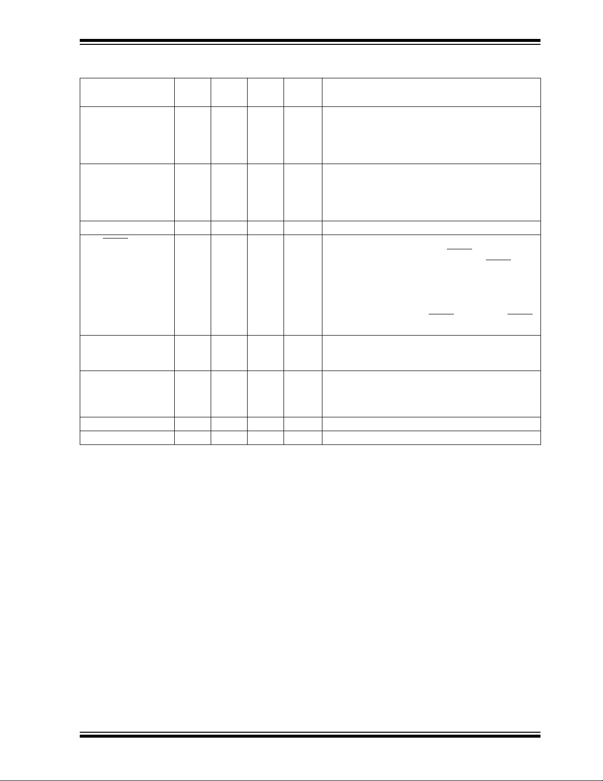
TABLE 3-1: PIC12C5XX PINOUT DESCRIPTION
PIC12C5XX
Name
GP0 7 7 I/O TTL/ST Bi-directional I/O port/ serial programming data. Can
GP1 6 6 I/O TTL/ST Bi-directional I/O port/ serial programming clock. Can
GP2/T0CKI 5 5 I/O ST Bi-directional I/O port. Can be configured as T0CKI.
GP3/MCLR
GP4/OSC2 3 3 I/O TTL Bi-directional I/O port/oscillator crystal output. Con-
GP5/OSC1/CLKIN 2 2 I/O TTL/ST Bidirectional IO port/oscillator crystal input/external
V
DD
SS
V
Legend: I = input, O = output, I/O = input/output, P = power, — = not used, TTL = TTL input,
ST = Schmitt Trigger input
/V
PP
DIP
Pin #
SOIC
Pin #
4 4 I TTL/ST Input port/master clear (reset) input/programming volt-
1 1 P — Positive supply for logic and I/O pins
8 8 P — Ground reference for logic and I/O pins
I/O/P
Type
Buffer
Type
Description
be software programmed for internal weak pull-up and
wake-up from SLEEP on pin change. This buffer is a
Schmitt Trigger input when used in serial programming
mode.
be software programmed for internal weak pull-up and
wake-up from SLEEP on pin change. This buffer is a
Schmitt Trigger input when used in serial programming
mode.
age input. When configured as MCLR
active low reset to the device. Voltage on MCLR
must not exceed V
or the device will enter programming mode. Can be
software programmed for internal weak pull-up and
wake-up from SLEEP on pin change. Weak pull-up
always on if configured as MCLR
mode.
nections to crystal or resonator in crystal oscillator
mode (XT and LP modes only, GPIO in other modes).
clock source input (GPIO in Internal RC mode only,
OSC1 in all other oscillator modes). TTL input when
GPIO, ST input in external RC oscillator mode.
DD
during normal device operation
, this pin is an
/V
PP
. ST when in MCLR
1998 Microchip Technology Inc. DS40139D-page 11
PIC12C5XX
3.1 Cloc
king Scheme/Instruction Cycle
The clock input (OSC1/CLKIN pin) is internally divided
by four to generate four non-overlapping quadrature
clocks namely Q1, Q2, Q3 and Q4. Internally, the
program counter is incremented every Q1, and the
instruction is fetched from program memory and
latched into instruction register in Q4. It is decoded
and executed during the following Q1 through Q4. The
clocks and instruction execution flow is shown in
Figure 3-2 and Example 3-1.
3.2 Instruction Flo
w/Pipelining
An Instruction Cycle consists of four Q cycles (Q1, Q2,
Q3 and Q4). The instruction fetch and execute are
pipelined such that fetch takes one instruction cycle
while decode and execute takes another instruction
cycle. However, due to the pipelining, each instruction
effectively executes in one cycle. If an instruction
causes the program counter to change (e.g., GOTO )
then two cycles are required to complete the
instruction (Example 3-1).
A fetch cycle begins with the program counter (PC)
incrementing in Q1.
In the execution cycle, the fetched instruction is
latched into the Instruction Register (IR) in cycle Q1.
This instruction is then decoded and executed during
the Q2, Q3, and Q4 cycles. Data memory is read
during Q2 (operand read) and written during Q4
(destination write).
FIGURE 3-2: CLOCK/INSTRUCTION CYCLE
Q2 Q3 Q4
OSC1
Q1
Q2
Q3
Q4
PC
Q1
PC PC+1 PC+2
Fetch INST (PC)
Execute INST (PC-1) Fetch INST (PC+1)
Q1
EXAMPLE 3-1: INSTRUCTION PIPELINE FLOW
1. MOVLW 03H
2. MOVWF GPIO
3. CALL SUB_1
4. BSF GPIO, BIT1
Fetch 1 Execute 1
Fetch 2 Execute 2
Q2 Q3 Q4
Execute INST (PC) Fetch INST (PC+2)
Q2 Q3 Q4
Q1
Execute INST (PC+1)
Fetch 3 Execute 3
Fetch 4 Flush
Fetch SUB_1 Execute SUB_1
Internal
phase
clock
All instructions are single cycle, except for any program branches. These take two cycles since the fetch
instruction is “flushed” from the pipeline while the new instruction is being fetched and then executed.
DS40139D-page 12
1998 Microchip Technology Inc.
PIC12C5XX
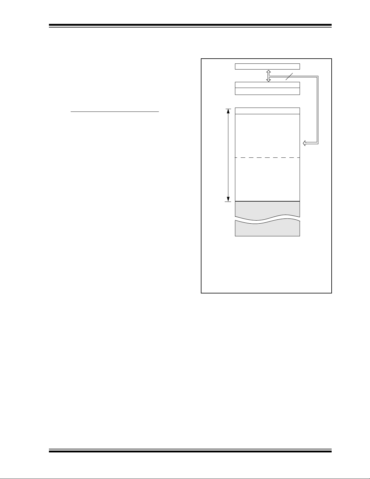
4.0 MEMORY ORGANIZATION
PIC12C5XX memory is organized into program memory and data memory. For devices with more than 512
bytes of program memory, a paging scheme is used.
Program memory pages are accessed using one STATUS register bit. For the PIC12C509(A) with a data
memory register file of more than 32 registers, a banking scheme is used. Data memory banks are accessed
using the File Select Register (FSR).
4.1 Pr
The PIC12C5XX devices have a 12-bit Program
Counter (PC) capable of addressing a 2K x 12
program memory space.
Only the first 512 x 12 (0000h-01FFh) for the
PIC12C508(A) and 1K x 12 (0000h-03FFh) for the
PIC12C509(A) are physically implemented. Refer to
Figure 4-1. Accessing a location above these
boundaries will cause a wrap-around within the first
512 x 12 space (PIC12C508(A)) or 1K x 12 space
(PIC12C509(A)). The effective reset vector is at 000h,
(see Figure 4-1). Location 01FFh (PIC12C508(A)) or
location 03FFh (PIC12C509(A)) contains the internal
clock oscillator calibration value. This value should
never be overwritten.
ogram Memory Organization
FIGURE 4-1: PROGRAM MEMORY MAP
AND STACK FOR THE
PIC12C5XX
PC<11:0>
CALL, RETLW
Stack Level 1
Stack Level 2
Reset Vector (note 1)
On-chip Program
Memory
512 Word (PIC12C508(A))
Space
User Memory
On-chip Program
Memory
1024 Word (PIC12C509(A))
12
0000h
01FFh
0200h
03FFh
0400h
Note 1: Address 0000h becomes the
effective reset vector. Location
01FFh (PIC12C508(A)) or location
03FFh (PIC12C509(A)) contains
the MOVLW XX INTERNAL RC oscil-
lator calibration value.
7FFh
1998 Microchip Technology Inc. DS40139D-page 13
PIC12C5XX
4.2 Data Memor
y Organization
Data memory is composed of registers, or bytes of
RAM. Therefore, data memory for a device is specified
by its register file. The register file is divided into two
functional groups: special function registers and
general purpose registers.
The special function registers include the TMR0
register, the Program Counter (PC), the Status
Register, the I/O registers (ports), and the File Select
Register (FSR). In addition, special purpose registers
are used to control the I/O port configuration and
prescaler options.
The general purpose registers are used for data and
control information under command of the instructions.
For the PIC12C508(A), the register file is composed of
7 special function registers and 25 general purpose
registers (Figure 4-2).
For the PIC12C509(A), the register file is composed of
7 special function registers, 25 general purpose
registers, and 16 general purpose registers that may
be addressed using a banking scheme (Figure 4-3).
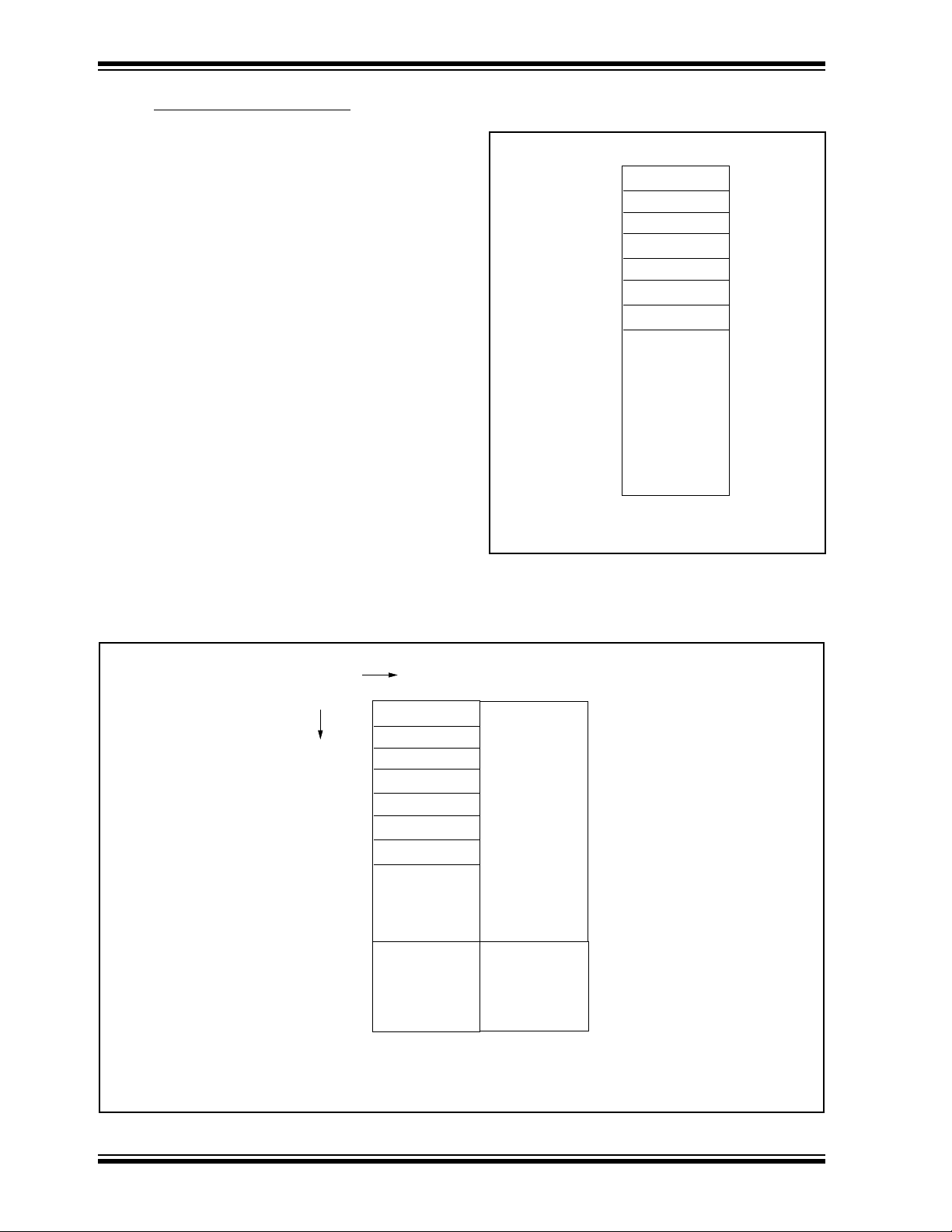
4.2.1 GENERAL PURPOSE REGISTER FILE The general purpose register file is accessed either
directly or indirectly through the file select register
FSR (Section 4.8).
FIGURE 4-2: PIC12C508(A) REGISTER FILE
MAP
File Address
(1)
00h
01h
02h
03h
04h
05h
06h
07h
1Fh
Note 1: Not a physical register. See Section 4.8
INDF
TMR0
PCL
STATUS
FSR
OSCCAL
GPIO
General
Purpose
Registers
FIGURE 4-3: PIC12C509(A) REGISTER FILE MAP
FSR<6:5> 00 01
File Address
00h
01h
02h
03h
04h
05h
06h
07h
0Fh
10h
1Fh
Note 1: Not a physical register. See Section 4.8
(1)
INDF
TMR0
PCL
STATUS
FSR
OSCCAL
GPIO
General
Purpose
Registers
General
Purpose
Registers
Bank 0 Bank 1
20h
Addresses map
back to
addresses
in Bank 0.
2Fh
30h
General
Purpose
Registers
3Fh
DS40139D-page 14
1998 Microchip Technology Inc.

PIC12C5XX
4.2.2 SPECIAL FUNCTION REGISTERS
The special registers can be classified into two sets.
The special function registers associated with the
The Special Function Registers (SFRs) are registers
used by the CPU and peripheral functions to control
the operation of the device (Table 4-1).
“core” functions are described in this section. Those
related to the operation of the peripheral features are
described in the section for each peripheral feature.
TABLE 4-1: SPECIAL FUNCTION REGISTER (SFR) SUMMARY
Address Name Bit 7 Bit 6 Bit 5 Bit 4 Bit 3 Bit 2 Bit 1 Bit 0
N/A TRIS I/O control registers
N/A OPTION
00h INDF Uses contents of FSR to address data memory (not a physical register)
01h TMR0 8-bit real-time clock/counter
(1)
02h
03h STATUS GPWUF — PA0 TO PD Z DC C
PCL Low order 8 bits of PC
Contains control bits to configure Timer0, Timer0/WDT
prescaler, wake-up on change, and weak pull-ups
Value on
Power-On
Reset
--11 1111 --11 1111
1111 1111 1111 1111
xxxx xxxx uuuu uuuu
xxxx xxxx uuuu uuuu
1111 1111 1111 1111
0001 1xxx q00q quuu
Value on
All Other
(2)
Resets
(3)
1998 Microchip Technology Inc. DS40139D-page 15

PIC12C5XX
4.3 STATUS Register
For example, CLRF STATUS will clear the upper three
bits and set the Z bit. This leaves the STATUS register
This register contains the arithmetic status of the ALU,
the RESET status, and the page preselect bit for
program memories larger than 512 words.
The STATUS register can be the destination for any
instruction, as with any other register. If the STATUS
register is the destination for an instruction that affects
the Z, DC or C bits, then the write to these three bits is
as 000u u1uu (where u = unchanged).
It is recommended, therefore, that only BCF, BSF and
MOVWF instructions be used to alter the STATUS
register because these instructions do not affect the Z,
DC or C bits from the STATUS register. For other
instructions, which do affect STATUS bits, see
Instruction Set Summary.
disabled. These bits are set or cleared according to
the device logic. Furthermore, the T
O and PD bits are
not writable. Therefore, the result of an instruction with
the STATUS register as destination may be different
than intended.
FIGURE 4-4: STATUS REGISTER (ADDRESS:03h)
R/W-0 R/W-0 R/W-0 R-1 R-1 R/W-x R/W-x R/W-x
GPWUF
bit7 6 5 4 3 2 1 bit0
bit 7: GPWUF: GPIO reset bit
bit 6: Unimplemented
bit 5: PA0: Program page preselect bits
bit 4: TO: Time-out bit
bit 3: PD: Power-down bit
bit 2: Z: Zero bit
bit 1: DC: Digit carry/borrow bit (for ADDWF and SUBWF instructions)
bit 0: C: Carry/borrow bit (for ADDWF, SUBWF and RRF, RLF instructions)
—
1 = Reset due to wake-up from SLEEP on pin change
0 = After power up or other reset
1 = Page 1 (200h - 3FFh) - PIC12C509(A)
0 = Page 0 (000h - 1FFh) - PIC12C508(A) and PIC12C509(A)
Each page is 512 bytes.
Using the PA0 bit as a general purpose read/write bit in devices which do not use it for program
page preselect is not recommended since this may affect upward compatibility with future products.
1 = After power-up, CLRWDT instruction, or SLEEP instruction
0 = A WDT time-out occurred
1 = After power-up or by the CLRWDT instruction
0 = By execution of the SLEEP instruction
1 = The result of an arithmetic or logic operation is zero
0 = The result of an arithmetic or logic operation is not zero
ADDWF
1 = A carry from the 4th low order bit of the result occurred
0 = A carry from the 4th low order bit of the result did not occur
SUBWF
1 = A borrow from the 4th low order bit of the result did not occur
0 = A borrow from the 4th low order bit of the result occurred
ADDWF SUBWF RRF or RLF
1 = A carry occurred 1 = A borrow did not occur Load bit with LSB or MSB, respectively
0 = A carry did not occur 0 = A borrow occurred
PA0 TO PD Z DC C R = Readable bit
W = Writable bit
- n = Value at POR reset
DS40139D-page 16 1998 Microchip Technology Inc.

PIC12C5XX
4.4 OPTION Register
The OPTION register is a 8-bit wide, write-only
register which contains various control bits to
configure the Timer0/WDT prescaler and Timer0.
By executing the OPTION instruction, the contents of
the W register will be transferred to the OPTION
Note: If TRIS bit is set to ‘0’, the wake-up on
change and pull-up functions are disabled
for that pin; i.e., note that TRIS overrides
OPTION control of GPPU
Note: If the T0CS bit is set to ‘1’, GP2 is f orced to
be an input even if TRIS GP2 = ‘0’.
register. A RESET sets the OPTION<7:0> bits.
FIGURE 4-5: OPTION REGISTER
W-1 W-1 W-1 W-1 W-1 W-1 W-1 W-1
GPWU GPPU T0CS T0SE PSA PS2 PS1 PS0 W = Writable bit
bit7 6 5 4 3 2 1 bit0
bit 7: GPWU
bit 6: GPPU: Enable weak pull-ups (GP0, GP1, GP3)
bit 5: T0CS: Timer0 clock source select bit
bit 4: T0SE: Timer0 source edge select bit
bit 3: PSA: Prescaler assignment bit
bit 2-0: PS2:PS0: Prescaler rate select bits
: Enable wake-up on pin change (GP0, GP1, GP3)
1 = Disabled
0 = Enabled
1 = Disabled
0 = Enabled
1 = Transition on T0CKI pin
0 = Transition on internal instruction cycle clock, Fosc/4
1 = Increment on high to low transition on the T0CKI pin
0 = Increment on low to high transition on the T0CKI pin
1 = Prescaler assigned to the WDT
0 = Prescaler assigned to Timer0
Bit Value Timer0 Rate WDT Rate
000
001
010
011
100
101
110
111
1 : 2
1 : 4
1 : 8
1 : 16
1 : 32
1 : 64
1 : 128
1 : 256
1 : 1
1 : 2
1 : 4
1 : 8
1 : 16
1 : 32
1 : 64
1 : 128
U = Unimplemented bit
- n = Value at POR reset
Reference Table 4-1 for
other resets.
and GPWU.
1998 Microchip Technology Inc. DS40139D-page 17

PIC12C5XX
4.5 OSCCAL Register
The Oscillator Calibration (OSCCAL) register is used to
calibrate the internal 4 MHz oscillator. It contains f our to
six bits for calibration. Increasing the cal value
increases the frequency. See Section 7.2.5 for more
information on the internal oscillator.
FIGURE 4-6: OSCCAL REGISTER (ADDRESS 8Fh)
R/W-0 R/W-1 R/W-1 R/W-1 R/W-0 R/W-0 U-0 U-0
CAL3 CAL2 CAL1 CAL0 — — — — R = Readable bit
bit7 bit0
bit 7-4: CAL<3:0>: Calibration
bit 3-0: Unimplemented: Read as '0'
FIGURE 4-7: OSCCAL REGISTER (ADDRESS 8Fh)PIC12C508A/C509A
W = Writable bit
U = Unimplemented bit,
read as ‘0’
- n = Value at POR reset
R/W-1 R/W-0 R/W-0 R/W-0 R/W-0 R/W-0 U-0 U-0
CAL5 CAL4 CAL3 CAL2 CAL1 CAL0 — — R = Readable bit
bit7 bit0
bit 7-2: CAL<5:0>: Calibration
bit 1-0: Unimplemented: Read as '0'
W = Writable bit
U = Unimplemented bit,
read as ‘0’
- n = Value at POR reset
DS40139D-page 18 1998 Microchip Technology Inc.
PIC12C5XX
4.6 Program Counter
As a program instruction is executed, the Program
Counter (PC) will contain the address of the next
program instruction to be executed. The PC value is
increased by one every instruction cycle, unless an
instruction changes the PC.
For a GOTO instruction, bits 8:0 of the PC are provided
by the GOTO instruction word. The PC Latch (PCL) is
mapped to PC<7:0>. Bit 5 of the STATUS register
provides page information to bit 9 of the PC (Figure 4-
8).
For a CALL instruction, or any instruction where the
PCL is the destination, bits 7:0 of the PC again are
provided by the instruction word. However, PC<8>
does not come from the instruction word, but is always
cleared (Figure 4-8).
Instructions where the PCL is the destination, or
Modify PCL instructions, include MOVWF PC, ADDWF
PC, and BSF PC,5.
Note: Because PC<8> is cleared in the CALL
instruction, or any Modify PCL instruction,
all subroutine calls or computed jumps are
limited to the first 256 locations of any program memory page (512 words long).
FIGURE 4-8: LOADING OF PC
BRANCH INSTRUCTIONS -
PIC12C5XX
GOTO Instruction
11
PC
7 0
CALL or Modify PCL Instruction
11
PC
8 7 0
910
PCL
Instruction Word
PA0
STATUS
8 7 0
910
PCL
4.6.1 EFFECTS OF RESET The Program Counter is set upon a RESET, which
means that the PC addresses the last location in the
last page i.e., the oscillator calibration instruction. After
executing MOVLW XX, the PC will roll over to location
00h, and begin executing user code.
The STATUS register page preselect bits are cleared
upon a RESET, which means that page 0 is preselected.
Therefore, upon a RESET, a GOTO instruction will
automatically cause the program to jump to page 0
until the value of the page bits is altered.
4.7 Stack
PIC12C5XX devices have a 12-bit wide L.I.F.O.
hardware push/pop stack.
push
A CALL instruction will
1 into stack 2 and then push the current program
counter value, incremented by one , into stac k le vel 1. If
more than two sequential CALL’s are executed, only
the most recent two return addresses are stored.
A RETLW instruction will
1 into the program counter and then copy stack level 2
contents into level 1. If more than two sequential
RETLW’s are executed, the stack will be filled with the
address previously stored in level 2. Note that the
W register will be loaded with the literal value specified
in the instruction. This is particularly useful for the
implementation of data look-up tables within the
program memory.
Upon any reset, the contents of the stack remain
unchanged, however the program counter (PCL) will
also be reset to 0.
Note 1: There are no STATUS bits to indicate
stack overflows or stack underflow conditions.
Note 2: There are no instructions mnemonics
called PUSH or POP. These are actions
that occur from the execution of the CALL
and RETLW instructions.
the current value of stack
pop
the contents of stack level
Instruction Word
Reset to ‘0’
PA0
7 0
STATUS
1998 Microchip Technology Inc. DS40139D-page 19
PIC12C5XX
4.8 Indirect Data Addressing; INDF and
FSR Registers
The INDF register is not a physical register.
Addressing INDF actually addresses the register
whose address is contained in the FSR register (FSR
is a
pointer
). This is indirect addressing.
EXAMPLE 4-1: INDIRECT ADDRESSING
• Register file 07 contains the value 10h
• Register file 08 contains the value 0Ah
• Load the value 07 into the FSR register
• A read of the INDF register will return the value
of 10h
• Increment the value of the FSR register by one
(FSR = 08)
• A read of the INDR register now will return the
value of 0Ah.
Reading INDF itself indirectly (FSR = 0) will produce
00h. Writing to the INDF register indirectly results in a
no-operation (although STATUS bits may be affected).
A simple program to clear RAM locations 10h-1Fh
using indirect addressing is shown in Example 4-2.
EXAMPLE 4-2: HOW TO CLEAR RAM
USING INDIRECT
ADDRESSING
movlw 0x10 ;initialize pointer
movwf FSR ; to RAM
NEXT clrf INDF ;clear INDF register
incf FSR,F ;inc pointer
btfsc FSR,4 ;all done?
goto NEXT ;NO, clear next
CONTINUE
: ;YES, continue
The FSR is a 5-bit wide register. It is used in
conjunction with the INDF register to indirectly address
the data memory area.
The FSR<4:0> bits are used to select data memory
addresses 00h to 1Fh.
PIC12C508(A): Does not use banking. FSR<7:5> are
unimplemented and read as '1's.
PIC12C509(A): Uses FSR<5>. Selects between bank
0 and bank 1. FSR<7:6> is unimplemented, read as '1’
.
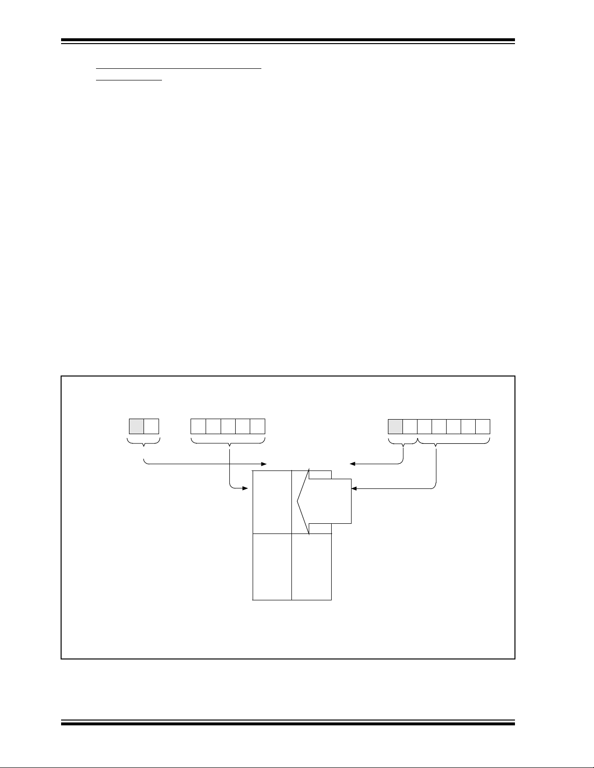
FIGURE 4-9: DIRECT/INDIRECT ADDRESSING
Direct Addressing
(FSR)
5
6
bank select
location select
(opcode) 04
00 01
00h
Data
Memory
0Fh
(1)
10h
1Fh 3Fh
Bank 0 Bank 1
Note 1: For register map detail see Section 4.2.
Note 2: PIC12C509(A) only
Addresses
map back to
addresses
in Bank 0.
(2)
Indirect Addressing
5
6
bank
(FSR)
4
location select
0
DS40139D-page 20 1998 Microchip Technology Inc.
PIC12C5XX
5.0 I/O PORT
As with any other register, the I/O register can be
written and read under program control. However,
read instructions (e.g., MOVF GPIO,W) always read the
I/O pins independent of the pin’s input/output modes.
On RESET, all I/O por ts are defined as input (inputs
are at hi-impedance) since the I/O control registers are
all set.
5.1 GPIO
GPIO is an 8-bit I/O register. Only the low order 6 bits
are used (GP5:GP0). Bits 7 and 6 are unimplemented
and read as '0's. Please note that GP3 is an input only
pin. The configuration word can set several I/O’s to
alternate functions. When acting as alternate functions
the pins will read as ‘0’ during port read. Pins GP0,
GP1, and GP3 can be configured with weak pull-ups
and also with wake-up on change. The wake-up on
change and weak pull-up functions are not pin
selectable. If pin 4 is configured as MCLR
up is always on and wake-up on change for this pin is
not enabled.
5.2 TRIS Register
The output driver control register is loaded with the
contents of the W register by executing the TRIS f
instruction. A '1' from a TRIS register bit puts the
corresponding output driver in a hi-impedance mode.
A '0' puts the contents of the output data latch on the
selected pins, enabling the output buffer. The
exceptions are GP3 which is input only and GP2 which
may be controlled by the option register, see Figure 4-
5.
, weak pull-
5.3 I/O Interfacing
The equivalent circuit for an I/O port pin is shown in
Figure 5-1. All port pins, except GP3 which is input
only, may be used for both input and output
operations. For input operations these ports are nonlatching. Any input must be present until read by an
input instruction (e.g., MOVF GPIO,W). The outputs are
latched and remain unchanged until the output latch is
rewritten. To use a port pin as output, the
corresponding direction control bit in TRIS must be
cleared (= 0). For use as an input, the corresponding
TRIS bit must be set. Any I/O pin (except GP3) can be
programmed individually as input or output.
FIGURE 5-1: EQUIVALENT CIRCUIT
FOR A SINGLE I/O PIN
Data
Bus
WR
Port
W
Reg
TRIS ‘f’
Data
Latch
CK
TRIS
Latch
CK
Reset
QD
VDD
Q
QD
Q
(2)
P
N
VSS
I/O
pin
(1)
Note: A read of the por ts reads the pins, not the
output data latches. That is, if an output
driver on a pin is enabled and driven high,
but the external system is holding it low, a
read of the port will indicate that the pin is
Note 1: I/O pins have protection diodes to VDD and VSS.
2: See Table 3-1 for buffer type.
RD Port
low.
The TRIS registers are “write-only” and are set (output
drivers disabled) upon RESET.
TABLE 5-1: SUMMARY OF PORT REGISTERS
Value on
Address Name Bit 7 Bit 6 Bit 5 Bit 4 Bit 3 Bit 2 Bit 1 Bit 0
N/A TRIS I/O control registers --11 1111 --11 1111
N/A
03H
06h
Legend: Shaded cells not used by Port Registers, read as ‘0’, — = unimplemented, read as '0', x = unknown, u = unchanged,
Note 1: If reset was due to wake-up on change, then bit 7 = 1. All other resets will cause bit 7 = 0.
OPTION GPWU GPPU T0CS T0SE PSA PS2 PS1 PS0
STATUS
GPIO
q = see tables in Section 7.7 for possible values.
GPWUF — PAO TO PD Z DC C 0001 1xxx q00q quuu
— — GP5 GP4 GP3 GP2 GP1 GP0 --xx xxxx --uu uuuu
Power-On
Reset
1111 1111 1111 1111
Value on
All Other Resets
(1)
1998 Microchip Technology Inc. DS40139D-page 21
PIC12C5XX
5.4 I/O Programming Considerations
5.4.1 BI-DIRECTIONAL I/O PORTS
Some instructions operate internally as read followed
by write operations. The BCF and BSF instructions, for
example, read the entire port into the CPU, execute
the bit operation and re-write the result. Caution must
be used when these instructions are applied to a port
where one or more pins are used as input/outputs. For
example, a BSF operation on bit5 of GPIO will cause all
eight bits of GPIO to be read into the CPU, bit5 to be
set and the GPIO value to be written to the output
latches. If another bit of GPIO is used as a bidirectional I/O pin (say bit0) and it is defined as an
input at this time, the input signal present on the pin
itself would be read into the CPU and rewritten to the
data latch of this particular pin, overwriting the
previous content. As long as the pin stays in the input
mode, no problem occurs. However, if bit0 is switched
into output mode later on, the content of the data latch
may now be unknown.
Example 5-1 shows the effect of two sequential readmodify-write instructions (e.g., BCF, BSF , etc.) on an I/
O port.
A pin actively outputting a high or a low should not be
driven from external devices at the same time in order
to change the level on this pin (“wired-or”, “wired-and”).
The resulting high output currents may damage the
chip.
EXAMPLE 5-1: READ-MODIFY-WRITE
INSTRUCTIONS ON AN
I/O PORT
;Initial GPIO Settings
; GPIO<5:3> Inputs
; GPIO<2:0> Outputs
;
; GPIO latch GPIO pins
; ---------- --------- BCF GPIO, 5 ;--01 -ppp --11 pppp
BCF GPIO, 4 ;--10 -ppp --11 pppp
MOVLW 007h ;
TRIS GPIO ;--10 -ppp --11 pppp
;
;Note that the user may have expected the pin
;values to be --00 pppp. The 2nd BCF caused
;GP5 to be latched as the pin value (High).
5.4.2 SUCCESSIVE OPERATIONS ON I/O
PORTS
The actual write to an I/O port happens at the end of
an instruction cycle, whereas for reading, the data
must be valid at the beginning of the instruction cycle
(Figure 5-2). Therefore, care must be exercised if a
write followed by a read operation is carried out on the
same I/O port. The sequence of instructions should
allow the pin voltage to stabilize (load dependent)
before the next instruction, which causes that file to be
read into the CPU, is executed. Otherwise, the
previous state of that pin may be read into the CPU
rather than the new state. When in doubt, it is better to
separate these instructions with a NOP or another
instruction not accessing this I/O port.
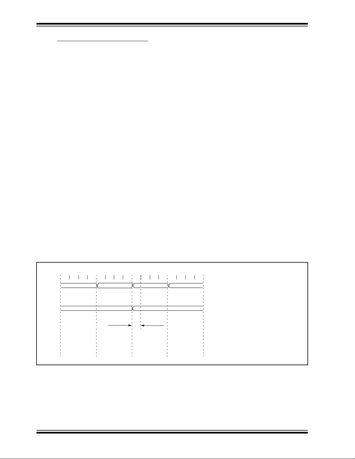
FIGURE 5-2: SUCCESSIVE I/O OPERATION
NOP
Q3
Q4
Instruction
fetched
GP5:GP0
Instruction
executed
Q4
Q1 Q2
MOVWF GPIO
Q3
PC PC + 1 PC + 2
Q1 Q2
MOVF GPIO,W
Port pin
written here
MOVWF GPIO
(Write to
GPIO)
Q3
Q4
Q1 Q2
Port pin
sampled here
MOVF GPIO,W
(Read
GPIO)
Q1 Q2
Q3
PC + 3
NOP
NOP
Q4
This example shows a write to GPIO follow ed
by a read from GPIO.
Data setup time = (0.25 TCY – TPD)
where: TCY = instruction cycle.
TPD = propagation delay
Therefore, at higher clock frequencies, a
write followed by a read may be problematic.
DS40139D-page 22 1998 Microchip Technology Inc.

PIC12C5XX
6.0 TIMER0 MODULE AND TMR0 REGISTER
The Timer0 module has the following features:
• 8-bit timer/counter register, TMR0
- Readable and writable
• 8-bit software programmable prescaler
• Internal or external clock select
- Edge select for external clock
Figure 6-1 is a simplified block diagram of the Timer0
module.
Timer mode is selected by clearing the T0CS bit
(OPTION<5>). In timer mode, the Timer0 module will
increment every instruction cycle (without prescaler). If
TMR0 register is written, the increment is inhibited for
the following two instruction cycles (Figure 6-2 and
Figure 6-3). The user can work around this by writing
an adjusted value to the TMR0 register.
FIGURE 6-1: TIMER0 BLOCK DIAGRAM
GP2/T0CKI
Pin
T0SE
FOSC/4
0
1
T0CS
PS2, PS1, PS0
(1)
Programmable
Prescaler
Counter mode is selected by setting the T0CS bit
(OPTION<5>). In this mode, Timer0 will increment
either on every rising or falling edge of pin T0CKI. The
T0SE bit (OPTION<4>) determines the source edge.
Clearing the T0SE bit selects the rising edge.
Restrictions on the external clock input are discussed
in detail in Section 6.1.
The prescaler may be used by either the Timer0
module or the Watchdog Timer, but not both. The
prescaler assignment is controlled in software by the
control bit PSA (OPTION<3>). Clearing the PSA bit
will assign the prescaler to Timer0. The prescaler is
not readable or writable. When the prescaler is
assigned to the Timer0 module, prescale v alues of 1:2,
1:4,..., 1:256 are selectable. Section 6.2 details the
operation of the prescaler.
A summary of registers associated with the Timer0
module is found in Table 6-1.
Data bus
PSout
1
(2)
3
0
PSA
(1)
(1)
Sync with
Internal
Clocks
CY delay)
(2 T
TMR0 reg
PSout
Sync
8
Note 1: Bits T0CS, T0SE, PSA, PS2, PS1 and PS0 are located in the OPTION register.
2: The prescaler is shared with the Watchdog Timer (Figure 6-5).
1998 Microchip Technology Inc. DS40139D-page 23
PIC12C5XX
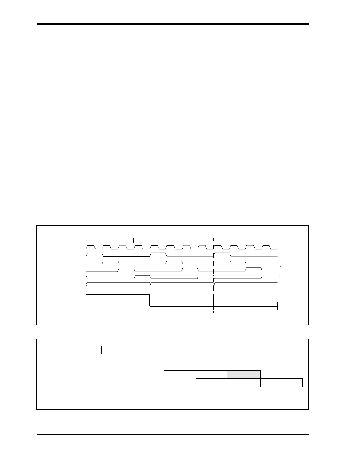
FIGURE 6-2: TIMER0 TIMING: INTERNAL CLOCK/NO PRESCALE
PC
(Program
Counter)
Instruction
Fetch
Timer0
Instruction
Executed
Q1 Q2 Q3 Q4
PC-1
T0
Q1 Q2 Q3 Q4 Q1 Q2 Q3 Q4 Q1 Q2 Q3 Q4 Q1 Q2 Q3 Q4 Q1 Q2 Q3 Q4 Q1 Q2 Q3 Q4 Q1 Q2 Q3 Q4
PC PC+1 PC+2 PC+3 PC+4 PC+5 PC+6
MOVWF TMR0
T0+1 T0+2 NT0 NT0+1 NT0+2
MOVF TMR0,W MOVF TMR0,W MOVF TMR0,W MOVF TMR0,W MOVF TMR0,W
Write TMR0
executed
Read TMR0
reads NT0
Read TMR0
reads NT0
Read TMR0
reads NT0
Read TMR0
reads NT0 + 1
Read TMR0
reads NT0 + 2
FIGURE 6-3: TIMER0 TIMING: INTERNAL CLOCK/PRESCALE 1:2
PC
(Program
Counter)
Instruction
Fetch
Timer0
Instruction
Execute
Q1 Q2 Q3 Q4
PC-1
T0 NT0+1
Q1 Q2 Q3 Q4 Q1 Q2 Q3 Q4 Q1 Q2 Q3 Q4 Q1 Q2 Q3 Q4 Q1 Q2 Q3 Q4 Q1 Q2 Q3 Q4 Q1 Q2 Q3 Q4
PC PC+1 PC+2 PC+3 PC+4 PC+5 PC+6
MOVWF TMR0
T0+1
MOVF TMR0,W MOVF TMR0,W MOVF TMR0,W MOVF TMR0,W MOVF TMR0,W
NT0
Write TMR0
executed
Read TMR0
reads NT0
Read TMR0
reads NT0
Read TMR0
reads NT0
Read TMR0
reads NT0
Read TMR0
reads NT0 + 1
TABLE 6-1: REGISTERS ASSOCIATED WITH TIMER0
Value on
Power-On
Address Name Bit 7 Bit 6 Bit 5 Bit 4 Bit 3 Bit 2 Bit 1 Bit 0
Reset
01h TMR0 Timer0 - 8-bit real-time clock/counter xxxx xxxx uuuu uuuu
N/A OPTION
N/A TRIS
Legend: Shaded cells not used by Timer0,
GPWU GPPU T0CS T0SE PSA PS2 PS1 PS0 1111 1111 1111 1111
—
— GP5 GP4 GP3 GP2 GP1 GP0
- = unimplemented, x = unknown, u = unchanged,
--11 1111 --11 1111
Value on
All Other
Resets
T0
DS40139D-page 24 1998 Microchip Technology Inc.
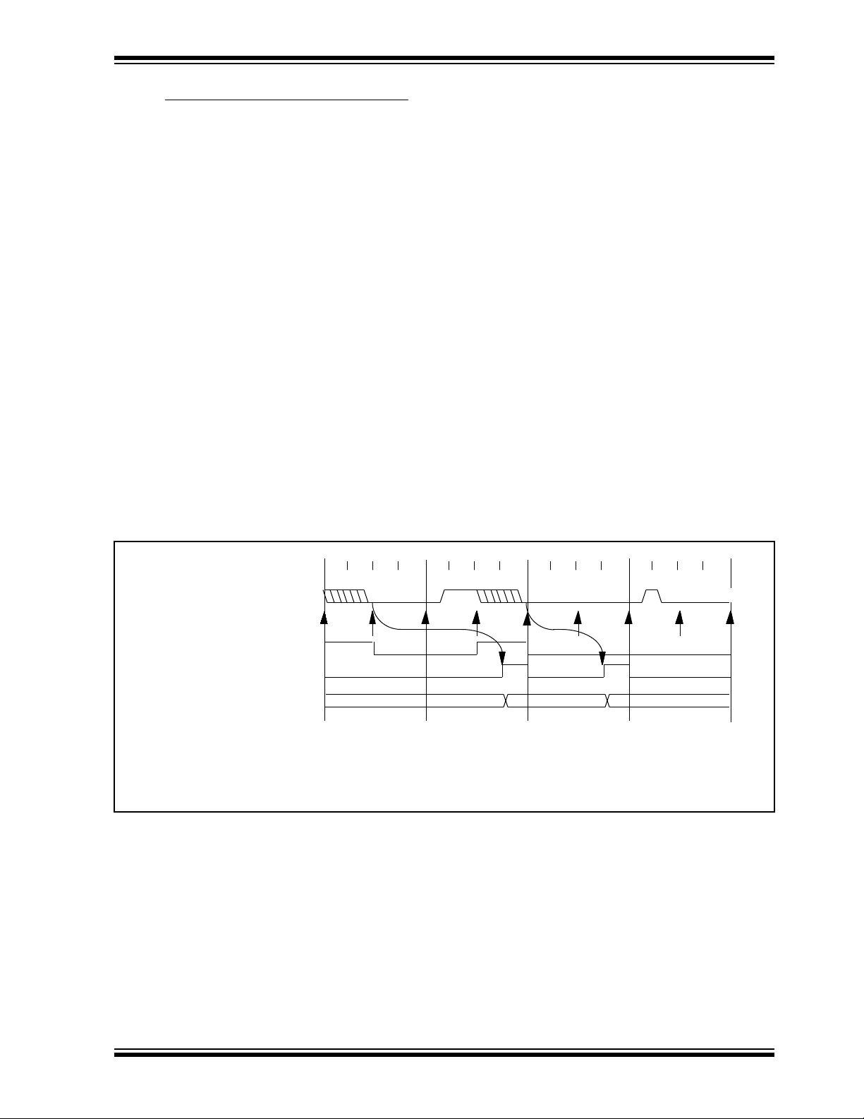
PIC12C5XX
6.1 Using Timer0 with an External Clock
When an external clock input is used for Timer0, it
must meet certain requirements. The external clock
requirement is due to internal phase clock (T
synchronization. Also, there is a delay in the actual
incrementing of Timer0 after synchronization.
6.1.1 EXTERNAL CLOCK SYNCHRONIZATION
When no prescaler is used, the external clock input is
the same as the prescaler output. The synchronization
of T0CKI with the internal phase clocks is
accomplished by sampling the prescaler output on the
Q2 and Q4 cycles of the internal phase clocks
(Figure 6-4). Therefore, it is necessary for T0CKI to be
high for at least 2T
and low for at least 2T
OSC (and a small RC delay of 20 ns)
OSC (and a small RC delay of
20 ns). Refer to the electrical specification of the
desired device.
OSC)
When a prescaler is used, the external clock input is
divided by the asynchronous ripple counter-type
prescaler so that the prescaler output is symmetrical.
For the external clock to meet the sampling
requirement, the ripple counter must be taken into
account. Therefore, it is necessary for T0CKI to have a
period of at least 4T
OSC (and a small RC delay of
40 ns) divided by the prescaler value. The only
requirement on T0CKI high and low time is that they
do not violate the minimum pulse width requirement of
10 ns. Refer to parameters 40, 41 and 42 in the
electrical specification of the desired device.
6.1.2 TIMER0 INCREMENT DELAY Since the prescaler output is synchronized with the
internal clocks, there is a small delay from the time the
external clock edge occurs to the time the Timer0
module is actually incremented. Figure 6-4 shows the
delay from the external clock edge to the timer
incrementing.
6.1.3 OPTION REGISTER EFFECT ON GP2 TRIS If the option register is set to read TIMER0 from the pin,
the port is forced to an input regardless of the TRIS register setting.
FIGURE 6-4: TIMER0 TIMING WITH EXTERNAL CLOCK
Q1 Q2 Q3 Q4 Q1 Q2 Q3 Q4 Q1 Q2 Q3 Q4 Q1 Q2 Q3 Q4
External Clock Input or
Prescaler Output (2)
External Clock/Prescaler
Output After Sampling
Increment Timer0 (Q4)
Note 1:
Delay from clock input change to Timer0 increment is 3Tosc to 7Tosc. (Duration of Q = Tosc).
Therefore, the error in measuring the interval between two edges on Timer0 input = ± 4Tosc max.
2:
External clock if no prescaler selected, Prescaler output otherwise.
3:
The arrows indicate the points in time where sampling occurs.
(3)
Timer0
(1)
T0 T0 + 1 T0 + 2
Small pulse
misses sampling
1998 Microchip Technology Inc. DS40139D-page 25
PIC12C5XX
6.2 Prescaler
An 8-bit counter is available as a prescaler for the
Timer0 module, or as a postscaler for the Watchdog
Timer (WDT), respectively (Section 7.6). For simplicity,
this counter is being referred to as “prescaler”
throughout this data sheet. Note that the prescaler
may be used by either the Timer0 module or the WDT,
but not both. Thus, a prescaler assignment for the
Timer0 module means that there is no prescaler for
the WDT, and vice-versa.
The PSA and PS2:PS0 bits (OPTION<3:0>)
determine prescaler assignment and prescale ratio.
When assigned to the Timer0 module, all instructions
writing to the TMR0 register (e.g., CLRF 1, MOVWF 1,
BSF 1,x, etc.) will clear the prescaler. When assigned
to WDT, a CLRWDT instruction will clear the prescaler
along with the WDT. The prescaler is neither readable
nor writable. On a RESET, the prescaler contains all
'0's.
6.2.1 SWITCHING PRESCALER ASSIGNMENT The prescaler assignment is fully under software control
(i.e., it can be changed “on the fly” during program
execution). To avoid an unintended device RESET, the
following instruction sequence (Example 6-1) must be
executed when changing the prescaler assignment from
Timer0 to the WDT.
EXAMPLE 6-1: CHANGING PRESCALER
(TIMER0→WDT)
1.CLRWDT ;Clear WDT
2.CLRF TMR0 ;Clear TMR0 & Prescaler
3.MOVLW '00xx1111’b ;These 3 lines (5, 6, 7)
4.OPTION ; are required only if
; desired
5.CLRWDT ;PS<2:0> are 000 or 001
6.MOVLW '00xx1xxx’b ;Set Postscaler to
7.OPTION ; desired WDT rate
To change prescaler from the WDT to the Timer0
module, use the sequence shown in Example 6-2. This
sequence must be used even if the WDT is disabled. A
CLRWDT instruction should be executed bef ore switching
the prescaler.
EXAMPLE 6-2: CHANGING PRESCALER
(WDT→TIMER0)
CLRWDT ;Clear WDT and
;prescaler
MOVLW 'xxxx0xxx' ;Select TMR0, new
;prescale value and
;clock source
OPTION
FIGURE 6-5: BLOCK DIAGRAM OF THE TIMER0/WDT PRESCALER
TCY ( = Fosc/4)
M
U
X
PSA
0
1
T0CS
M
U
X
1
0
8-bit Prescaler
8
8 - to - 1MUX
0
1
MUX
M
U
X
PSA
PSA
Sync
2
Cycles
PS2:PS0
GP2/T0CKI
Pin
T0SE
Watchdog
Timer
WDT Enable bit
0
1
Data Bus
8
TMR0 reg
WDT
Time-Out
Note: T0CS, T0SE, PSA, PS2:PS0 are bits in the OPTION register.
DS40139D-page 26 1998 Microchip Technology Inc.

PIC12C5XX
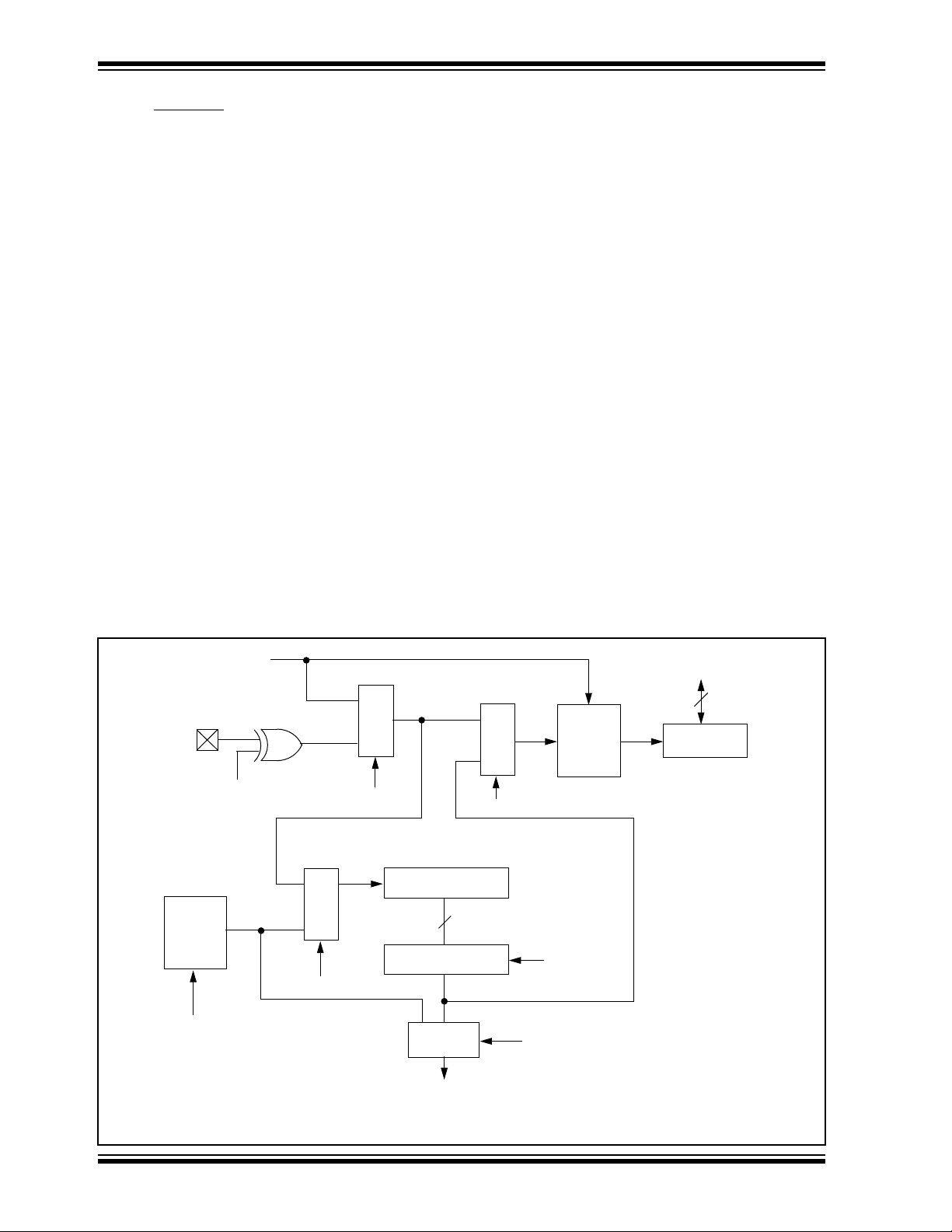
7.0 SPECIAL FEATURES OF THE CPU
What sets a microcontroller apart from other
processors are special circuits to deal with the needs
of real-time applications. The PIC12C5XX family of
microcontrollers has a host of such features intended
to maximize system reliability, minimize cost through
elimination of external components, provide power
saving operating modes and offer code protection.
These features are:
• Oscillator selection
• Reset
- Power-On Reset (POR)
- Device Reset Timer (DRT)
- Wake-up from SLEEP on pin change
• Watchdog Timer (WDT)
• SLEEP
• Code protection
• ID locations
• In-circuit Serial Programming
The PIC12C5XX has a Watchdog Timer which can be
shut off only through configuration bit WDTE. It r uns
off of its own RC oscillator for added reliability. If using
XT or LP selectable oscillator options, there is always
an 18 ms (nominal) delay provided by the Device
Reset Timer (DRT), intended to keep the chip in reset
until the crystal oscillator is stable. If using INTRC or
EXTRC there is an 18 ms delay only on V
DD power-up.
With this timer on-chip, most applications need no
external reset circuitry.
The SLEEP mode is designed to offer a very low
current power-down mode. The user can wake-up
from SLEEP through a change on input pins or
through a Watchdog Timer time-out. Several oscillator
options are also made available to allow the part to fit
the application, including an internal 4 MHz oscillator.
The EXTRC oscillator option saves system cost while
the LP crystal option saves power. A set of
configuration bits are used to select various options.
7.1 Configuration Bits
The PIC12C5XX configuration word consists of 12
bits. Configuration bits can be programmed to select
various device configurations. Two bits are for the
selection of the oscillator type, one bit is the Watchdog
Timer enable bit, and one bit is the MCLR
enable bit.
FIGURE 7-1: CONFIGURATION WORD FOR PIC12C5XX
— — — — — — — MCLRE CP WDTE FOSC1 FOSC0 Register: CONFIG
bit11 10 9 8 7 6 5 4 3 2 1 bit0
bit 11-5: Unimplemented
bit 4: MCLRE: MCLR
1 = MCLR pin enabled
0 = MCLR tied to VDD, (Internally)
bit 3: CP: Code protection bit.
1 = Code protection off
0 = Code protection on
bit 2: WDTE: Watchdog timer enable bit
1 = WDT enabled
0 = WDT disabled
bit 1-0: FOSC1:FOSC0: Oscillator selection bits
11 = EXTRC - external RC oscillator
10 = INTRC - internal RC oscillator
01 = XT oscillator
00 = LP oscillator
Note 1: Refer to the PIC12C5XX Programming Specifications to determine how to access the
configuration word. This register is not user addressable during device operation.
enable bit.
Address
(1)
: FFFh
1998 Microchip Technology Inc. DS40139D-page 27
PIC12C5XX
7.2 Oscillator Configurations
7.2.1 OSCILLATOR TYPES The PIC12C5XX can be operated in four different
oscillator modes. The user can program two
configuration bits (FOSC1:FOSC0) to select one of
these four modes:
• LP: Low Power Crystal
• XT: Crystal/Resonator
• INTRC: Internal 4 MHz Oscillator
• EXTRC: External Resistor/Capacitor
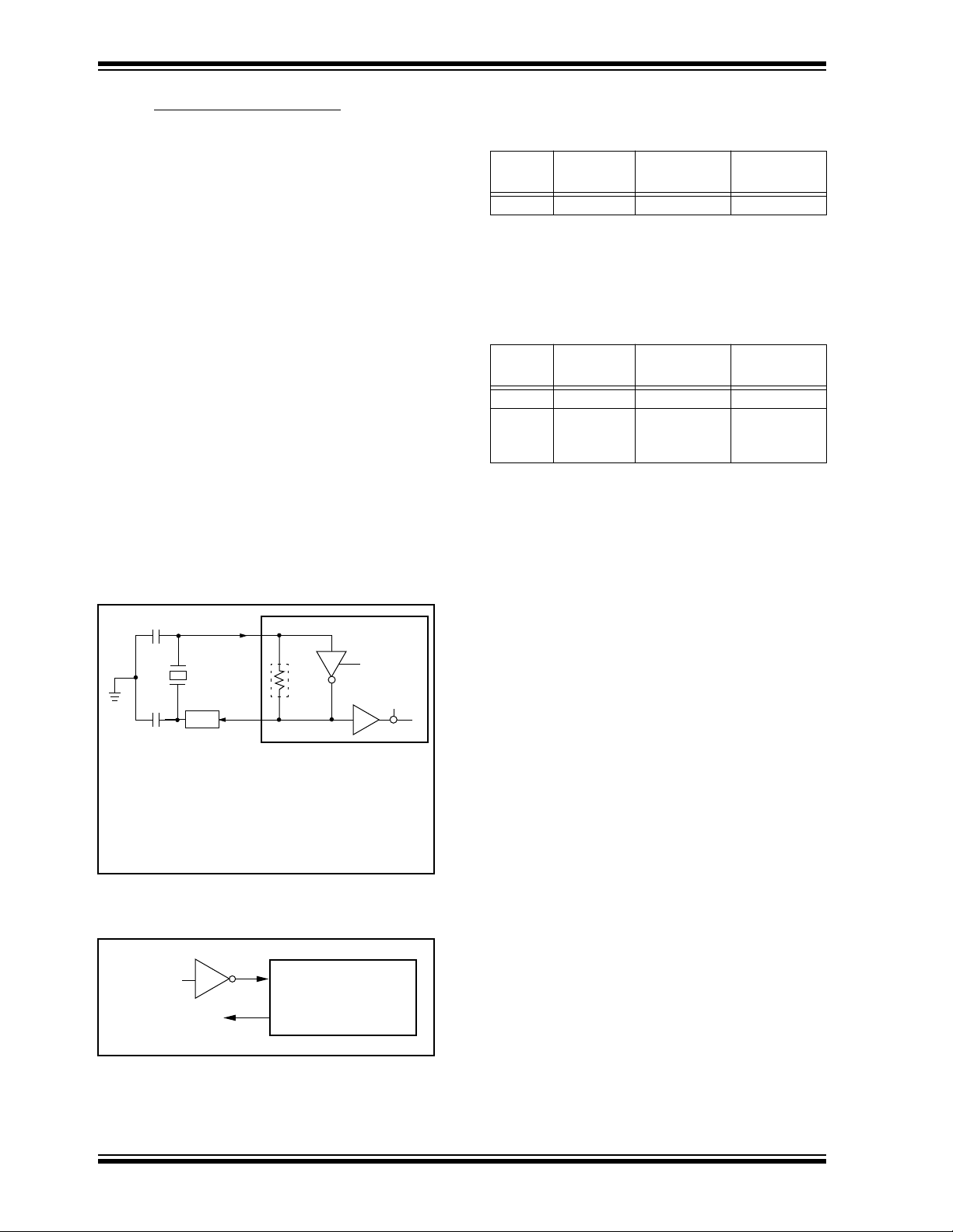
7.2.2 CRYSTAL OSCILLATOR / CERAMIC
RESONATORS
In XT or LP modes, a crystal or ceramic resonator is
connected to the GP5/OSC1/CLKIN and GP4/OSC2
pins to establish oscillation (Figure 7-2). The
PIC12C5XX oscillator design requires the use of a
parallel cut crystal. Use of a series cut crystal may
give a frequency out of the crystal manufacturers
specifications. When in XT or LP modes, the device
can have an external clock source drive the GP5/
OSC1/CLKIN pin (Figure 7-3).
FIGURE 7-2: CRYSTAL OPERATION (OR
CERAMIC RESONATOR) (XT
OR LP OSC
CONFIGURATION)
(1)
C1
OSC1
PIC12C5XX
TABLE 7-1: CAPACITOR SELECTION
FOR CERAMIC RESONATORS
- PIC12C5XX
Osc
Type
These values are for design guidance only. Since
each resonator has its own characteristics, the user
should consult the resonator manufacturer for
appropriate values of external components.
Resonator
Freq
XT 4.0 MHz 30 pF 30 pF
Cap. RangeC1Cap. Range
C2
T ABLE 7-2: CAPACITOR SELECTION
FOR CRYSTAL OSCILLATOR
- PIC12C5XX
Osc
Type
Note 1: For V
These values are for design guidance only. Rs may
be required to avoid overdriving crystals with low
drive level specification. Since each crystal has its
own characteristics, the user should consult the crystal manufacturer for appropriate values of external
components.
Resonator
Freq
LP 32 kHz
XT 200 kHz
1 MHz
4 MHz
DD > 4.5V, C1 = C2 ≈ 30 pF is
recommended.
(1)
Cap.Range
C1
15 pF 15 pF
47-68 pF
15 pF
15 pF
Cap. Range
C2
47-68 pF
15 pF
15 pF
XTAL
OSC2
(2)
RS
(1)
C2
Note 1: See Capacitor Selection tables for
recommended values of C1 and C2.
2: A series resistor (RS) may be required for
AT strip cut crystals.
3: RF approximate value = 10 MΩ.
RF
(3)
SLEEP
To internal
logic
FIGURE 7-3: EXTERNAL CLOCK INPUT
OPERATION (XT OR LP OSC
CONFIGURATION)
Clock from
ext. system
Open
OSC1
PIC12C5XX
OSC2
DS40139D-page 28 1998 Microchip Technology Inc.
PIC12C5XX
7.2.3 EXTERNAL CRYSTAL OSCILLATOR CIRCUIT
Either a prepackaged oscillator or a simple oscillator
circuit with TTL gates can be used as an external
crystal oscillator circuit. Prepackaged oscillators
provide a wide operating range and better stability. A
well-designed crystal oscillator will provide good
performance with TTL gates. Two types of crystal
oscillator circuits can be used: one with parallel
resonance, or one with series resonance.
Figure 7-4 shows implementation of a parallel
resonant oscillator circuit. The circuit is designed to
use the fundamental frequency of the crystal. The
74AS04 inverter performs the 180-degree phase shift
that a parallel oscillator requires. The 4.7 kΩ resistor
provides the negative feedback for stability. The 10 kΩ
potentiometers bias the 74AS04 in the linear region.
This circuit could be used for external oscillator
designs.
FIGURE 7-4: EXTERNAL PARALLEL
RESONANT CRYSTAL
OSCILLATOR CIRCUIT
+5V
10k
4.7k
74AS04
10k
XTAL
10k
20 pF
20 pF
Figure 7-5 shows a series resonant oscillator circuit.
This circuit is also designed to use the fundamental
frequency of the crystal. The inverter performs a 180degree phase shift in a series resonant oscillator
circuit. The 330 Ω resistors provide the negative
feedback to bias the inverters in their linear region.
74AS04
To Other
Devices
PIC12C5XX
CLKIN
FIGURE 7-5: EXTERNAL SERIES
RESONANT CRYSTAL
OSCILLATOR CIRCUIT
To Other
74AS04
Devices
PIC12C5XX
CLKIN
330
74AS04
330
74AS04
0.1 µF
XTAL
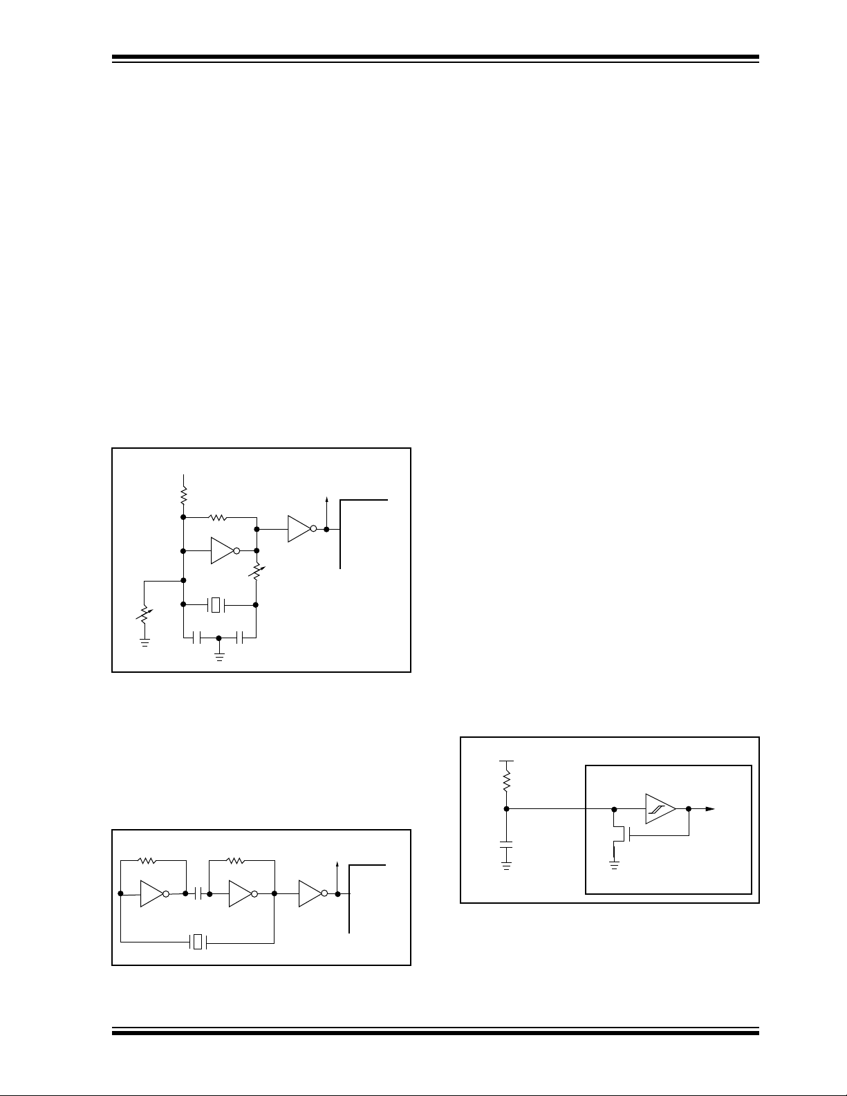
7.2.4 EXTERNAL RC OSCILLATOR For timing insensitive applications, the RC device
option offers additional cost savings. The RC oscillator
frequency is a function of the supply voltage, the
resistor (Rext) and capacitor (Cext) values, and the
operating temperature. In addition to this, the oscillator
frequency will vary from unit to unit due to normal
process parameter variation. Furthermore, the
difference in lead frame capacitance between package
types will also affect the oscillation frequency,
especially for low Cext values. The user also needs to
take into account variation due to tolerance of external
R and C components used.
Figure 7-6 shows how the R/C combination is
connected to the PIC12C5XX. For Rext values below
2.2 kΩ, the oscillator operation may become unstable,
or stop completely. For very high Rext values
(e.g., 1 MΩ) the oscillator becomes sensitive to noise,
humidity and leakage. Thus, we recommend keeping
Rext between 3 kΩ and 100 kΩ.
Although the oscillator will operate with no external
capacitor (Cext = 0 pF), we recommend using values
above 20 pF for noise and stability reasons. With no or
small external capacitance, the oscillation frequency
can vary dramatically due to changes in external
capacitances, such as PCB trace capacitance or
package lead frame capacitance.
The Electrical Specifications sections show RC
frequency variation from part to part due to normal
process variation. The variation is larger for larger R
(since leakage current variation will affect RC
frequency more for large R) and for smaller C (since
variation of input capacitance will affect RC frequency
more).
Also, see the Electrical Specifications sections for
variation of oscillator frequency due to V
DD for given
Rext/Cext values as well as frequency variation due to
operating temperature for giv en R, C, and V
DD values.
FIGURE 7-6: EXTERNAL RC OSCILLATOR
MODE
VDD
Rext
Cext
SS
V
OSC1
N
Internal
clock
PIC12C5XX
1998 Microchip Technology Inc. DS40139D-page 29

PIC12C5XX
7.2.5 INTERNAL 4 MHz RC OSCILLATOR The internal RC oscillator provides a fixed 4 MHz (nom-
inal) system clock at VDD = 5V and 25°C, see “Electri-
cal Specifications” section for infor mation on variation
over voltage and temperature..
In addition, a calibration instruction is programmed into
the top of memory which contains the calibration value
for the internal RC oscillator. This location is ne ver code
protected regardless of the code protect settings. This
value is programmed as a MOVLW XX instruction where
XX is the calibration value, and is placed at the reset
vector. This will load the W register with the calibration
value upon reset and the PC will then roll over to the
users program at address 0x000. The user then has the
option of writing the value to the OSCCAL Register
(05h) or ignoring it.
OSCCAL, when written to with the calibration value, will
“trim” the internal oscillator to remove process variation
from the oscillator frequency. .
Note: Please note that erasing the device will
also erase the pre-programmed internal
calibration value for the internal oscillator.
The calibration value must be read prior to
erasing the part. so it can be reprogrammed correctly later.
For the PIC12C508A and PIC12C509A, bits <7:2>,
CAL5-CAL0 are used for calibration. Adjusting CAL50 from 000000 to 111111 yields a higher clock speed.
Note that bits 1 and 0 of OSCCAL are unimplemented
and should be written as 0 when modifying OSCCAL
for compatibility with future devices.
For the PIC12C508 and PIC12C509, the lower 4 bits of
the register are used. Writing a larger value in this location yields a higher clock speed.
are TO, PD, and GPWUF bits. They are set or cleared
differently in different reset situations. These bits are
used in software to determine the nature of reset. See
Table 7-3 for a full description of reset states of all
registers.
7.3 RESET
The device differentiates between various kinds of
reset:
a) Power on reset (POR)
b) MCLR
c) MCLR
d) WDT time-out reset during normal operation
e) WDT time-out reset during SLEEP
f) Wake-up from SLEEP on pin change
Some registers are not reset in any way; they are
unknown on POR and unchanged in any other reset.
Most other registers are reset to “reset state” on po weron reset (POR), MCLR
change reset during normal operation. They are not
affected by a WDT reset during SLEEP or MCLR
during SLEEP, since these resets are viewed as
resumption of normal operation. The exceptions to this
DS40139D-page 30 1998 Microchip Technology Inc.
reset during normal operation
reset during SLEEP
, WDT or wake-up on pin
reset

PIC12C5XX
TABLE 7-3: RESET CONDITIONS FOR REGISTERS
Reset
MCLR
Register Address Power-on Reset
W (PIC12C508/509) —
W (PIC12C508A/509A) —
INDF 00h xxxx xxxx uuuu uuuu
TMR0 01h xxxx xxxx uuuu uuuu
PC 02h 1111 1111 1111 1111
STATUS 03h 0001 1xxx
FSR (12C508/12C508A) 04h 111x xxxx 111u uuuu
FSR (12C509/12C509A) 04h 110x xxxx 11uu uuuu
OSCCAL(12C508/509) 05h 0111 ---- uuuu ----
OSCCAL(12C508A/509A) 05h 1000 00-- uuuu uu--
GPIO 06h --xx xxxx --uu uuuu
OPTION — 1111 1111 1111 1111
TRIS — --11 1111 --11 1111
Legend: u = unchanged, x = unknown, - = unimplemented bit, read as ‘0’, q = value depends on condition.
Note 1: Bits <7:2> of W register contain oscillator calibration values due to MOVLW XX instruction at top of memory .
Note 2: See Table 7-7 for reset value for specific conditions
Note 3: If reset was due to wake-up on pin change, then bit 7 = 1. All other resets will cause bit 7 = 0.
qqqq xxxx
qqqq qqxx
(1)
(1)
WDT time-out
Wake-up on Pin Change
qqqq uuuu
qqqq qquu
q00q quuu
(1)
(1)
(2,3)
TABLE 7-4: RESET CONDITION FOR SPECIAL REGISTERS
STATUS Addr: 03h PCL Addr: 02h
Power on reset 0001 1xxx 1111 1111
reset during normal operation 000u uuuu 1111 1111
MCLR
reset during SLEEP 0001 0uuu 1111 1111
MCLR
WDT reset during SLEEP 0000 0uuu 1111 1111
WDT reset normal operation 0000 uuuu 1111 1111
Wake-up from SLEEP on pin change 1001 0uuu 1111 1111
Legend: u = unchanged, x = unknown, - = unimplemented bit, read as ‘0’.
1998 Microchip Technology Inc. DS40139D-page 31

PIC12C5XX
7.3.1 MCLR ENABLE This configuration bit when unprogrammed (left in the
‘1’ state) enables the external MCLR
programmed, the MCLR
V
DD, and the pin is assigned to be a GPIO. See
function is tied to the internal
Figure 7-7. When pin GP3/MCLR
MCLR
, the internal pull-up is always on.
function. When
/VPP is configured as
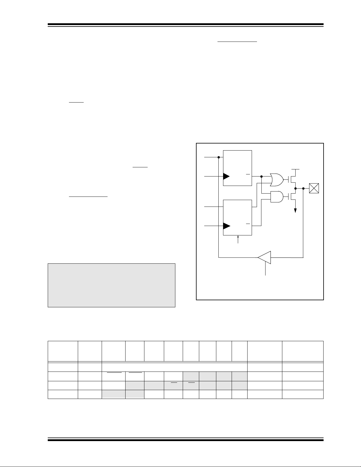
FIGURE 7-7: MCLR SELECT
MCLRE
WEAK
PULL-UP
GP3/MCLR/VPP
7.4 P
ower-On Reset (POR)
The PIC12C5XX family incorporates on-chip PowerOn Reset (POR) circuitry which provides an internal
chip reset for most power-up situations.
The on-chip POR circuit holds the chip in reset until
V
DD has reached a high enough level f or proper opera-
tion. To take advantage of the internal POR, program
the GP3/MCLR
tor to V
DD or program the pin as GP3. An internal weak
/VPP pin as MCLR and tie thru a resis-
pull-up resistor is implemented using a transistor. Refer
to Tab le 10-1 for the pull-up resistor ranges. This will
eliminate external RC components usually needed to
create a Power-on Reset. A maximum rise time for V
is specified. See Electrical Specifications for details.
When the device starts normal operation (exits the
reset condition), device operating parameters (v oltage ,
frequency, temperature, ...) must be met to ensure
operation. If these conditions are not met, the device
must be held in reset until the operating parameters are
met.
A simplified block diagram of the on-chip Power-On
Reset circuit is shown in Figure 7-8.
INTERNAL MCLR
DD
The Power-On Reset circuit and the Device Reset
Timer (Section 7.5) circuit are closely related. On
power-up, the reset latch is set and the DRT is reset.
The DRT timer begins counting once it detects MCLR
to be high. After the time-out period, which is typically
18 ms, it will reset the reset latch and thus end the onchip reset signal.
A power-up example where MCLR
shown in Figure 7-9. V
DD is allowed to rise and
stabilize before bringing MCLR
actually come out of reset T
is held low is
high. The chip will
DRT msec after MCLR
goes high.
In Figure 7-10, the on-chip Power-On Reset feature is
being used (MCLR
pin is programmed to be GP3.). The V
and VDD are tied together or the
DD is stable
before the start-up timer times out and there is no
problem in getting a proper reset. However, Figure 711 depicts a problem situation where V
DD rises too
slowly. The time between when the DRT senses that
MCLR
is high and when MCLR (and VDD) actually
reach their full value, is too long. In this situation, when
the start-up timer times out, V
V
DD (min) value and the chip is, therefore, not
DD has not reached the
guaranteed to function correctly. For such situations,
we recommend that external RC circuits be used to
achieve longer POR delay times (Figure 7-10).
Note: When the device starts nor mal operation
(exits the reset condition), device operating parameters (voltage, frequency, temperature, etc.) must be meet to ensure
operation. If these conditions are not met,
the device must be held in reset until the
operating conditions are met.
For additional information refer to Application Notes
“
Power-Up Considerations”
Trouble Shooting
” - AN607.
- AN522 and “
Power-up
DS40139D-page 32 1998 Microchip Technology Inc.

PIC12C5XX
FIGURE 7-8: SIMPLIFIED BLOCK DIAGRAM OF ON-CHIP RESET CIRCUIT
Power-Up
VDD
GP3/MCLR/VPP
Detect
POR (Power-On Reset)
Pin Change
SLEEP
Wake-up on
pin change
MCLRE
On-Chip
DRT OSC
WDT Time-out
8-bit Asynch
Ripple Counter
(Start-Up Timer)
FIGURE 7-9: TIME-OUT SEQUENCE ON POWER-UP (MCLR
VDD
MCLR
INTERNAL POR
DRT TIME-OUT
INTERNAL RESET
FIGURE 7-10: TIME-OUT SEQUENCE ON POWER-UP (MCLR
RESET
S Q
R
Q
CHIP RESET
PULLED LOW)
TDRT
TIED TO VDD): FAST VDD RISE TIME
VDD
MCLR
INTERNAL POR
DRT TIME-OUT
INTERNAL RESET
1998 Microchip Technology Inc. DS40139D-page 33
TDRT

PIC12C5XX
FIGURE 7-11: TIME-OUT SEQUENCE ON POWER-UP (MCLR TIED TO VDD): SLOW VDD RISE TIME
V1
VDD
MCLR
INTERNAL POR
DRT TIME-OUT
INTERNAL RESET
When VDD rises slowly, the TDRT time-out expires long before VDD has reached its final value. In
this example, the chip will reset properly if, and only if, V1 ≥ VDD min.
TDRT
7.5 Device Reset Timer (DRT)
In the PIC12C5XX, DRT runs from RESET and varies
based on oscillator selection (see Table 7-5.)
The DRT operates on an internal RC oscillator. The
processor is kept in RESET as long as the DRT is
active. The DRT delay allows V
min., and for the oscillator to stabilize.
Oscillator circuits based on crystals or ceramic
resonators require a certain time after power-up to
establish a stable oscillation. The on-chip DRT keeps
the device in a RESET condition for approximately 18
ms after MCLR
level. Thus, programming GP3/MCLR
and using an external RC network connected to the
MCLR
input is not required in most cases, allowing for
savings in cost-sensitive and/or space restricted
applications, as well as allowing the use of the GP3/
MCLR
/VPP pin as a general purpose input.
The Device Reset time delay will v ary from chip to chip
due to V
AC parameters for details.
The DRT will also be triggered upon a W atchdog Timer
time-out. This is particularly impor tant for applications
using the WDT to wake from SLEEP mode
automatically.
has reached a logic high (VIHMCLR)
DD, temperature, and process variation. See
DD to rise above VDD
/VPP as MCLR
7.6 Watchdog Timer (WDT)
The Watchdog Timer (WDT) is a free running on-chip
RC oscillator which does not require any external
components. This RC oscillator is separate from the
external RC oscillator of the GP5/OSC1/CLKIN pin
and the internal 4 MHz oscillator. That means that the
WDT will run even if the main processor clock has
been stopped, for example, by execution of a SLEEP
instruction. During normal operation or SLEEP, a WDT
reset or wake-up reset generates a device RESET.
The T
O bit (STATUS<4>) will be cleared upon a
Watchdog Timer reset.
The WDT can be permanently disabled by
programming the configuration bit WDTE as a '0'
(Section 7.1). Refer to the PIC12C5XX Programming
Specifications to determine how to access the
configuration word.
TABLE 7-5: DRT (DEVICE RESET TIMER
PERIOD)
Oscillator
Configuration
IntRC &
ExtRC
XT & LP 18 ms (typical) 18 ms (typical)
POR Reset
18 ms (typical) 300 µs (typical)
Subsequent
Resets
DS40139D-page 34 1998 Microchip Technology Inc.

PIC12C5XX
7.6.1 WDT PERIOD The WDT has a nominal time-out period of 18 ms,
(with no prescaler). If a longer time-out period is
desired, a prescaler with a division ratio of up to 1:128
can be assigned to the WDT (under software control)
by writing to the OPTION register. Thus, a time-out
period of a nominal 2.3 seconds can be realized.
These periods vary with temperature, V
DD and part-to-
part process variations (see DC specs).
Under worst case conditions (V
DD = Min., Temperature
= Max., max. WDT prescaler), it may take several
seconds before a WDT time-out occurs.
FIGURE 7-12: WATCHDOG TIMER BLOCK DIAGRAM
From Timer0 Clock Source
(Figure 6-5)
0
M
Watchdog
Timer
WDT Enable
Configuration Bit
1
U
X
PSA
7.6.2 WDT PROGRAMMING CONSIDERATIONS The CLRWDT instruction clears the WDT and the
postscaler, if assigned to the WDT, and prevents it
from timing out and generating a device RESET.
The SLEEP instruction resets the WDT and the
postscaler, if assigned to the WDT. This gives the
maximum SLEEP time before a WDT wake-up reset.
Postscaler
Postscaler
8 - to - 1 MUX
PS2:PS0
To Timer0 (Figure 6-4)
MUX
WDT
1
PSA
0
Time-out
TABLE 7-6: SUMMARY OF REGISTERS ASSOCIATED WITH THE WATCHDOG TIMER
Value on
Power-On
Address Name Bit 7 Bit 6 Bit 5 Bit 4 Bit 3 Bit 2 Bit 1 Bit 0
N/A OPTION GPWU GPPU T0CS T0SE PSA PS2 PS1 PS0 1111 1111 1111 1111
Legend: Shaded boxes = Not used by Watchdog Timer, — = unimplemented, read as '0', u = unchanged
Reset
Value on
All Other
Resets
1998 Microchip Technology Inc. DS40139D-page 35

PIC12C5XX
7.7 Time-Out Sequence, Power Down,
and Wake-up from SLEEP Status Bits
(TO/PD/GPWUF)
The TO, PD, and GPWUF bits in the STATUS register
can be tested to determine if a RESET condition has
been caused by a power-up condition, a MCLR
Watchdog Timer (WDT) reset.
TABLE 7-7: TO/PD/GPWUF STATUS
AFTER RESET
GPWUF TO PD RESET caused by
0 0 0
0 0 u
0 1 0
0 1 1
0 u u
1 1 0
Legend: Legend: u = unchanged
Note 1: The TO, PD, and GPWUF bits main-
WDT wake-up from
SLEEP
WDT time-out (not from
SLEEP)
MCLR wake-up from
SLEEP
Power-up
MCLR not during SLEEP
Wake-up from SLEEP on
pin change
tain their status (u) until a reset
occurs. A low-pulse on the MCLR
input does not change the TO, PD,
and GPWUF status bits.u
or
DS40139D-page 36 1998 Microchip Technology Inc.

PIC12C5XX
7.9 Power-Down Mode (SLEEP)
A device may be powered down (SLEEP) and later
powered up (Wake-up from SLEEP).
7.9.1 SLEEP
The Power-Down mode is entered by executing a
SLEEP instruction. If enabled, the Watchdog Timer will be cleared but
keeps running, the T
bit (STATUS<3>) is cleared and the oscillator driver is
turned off. The I/O por ts maintain the status they had
before the SLEEP instruction was executed (driving
high, driving low, or hi-impedance).
It should be noted that a RESET generated by a WDT
time-out does not drive the MCLR
For lowest current consumption while powered down,
the T0CKI input should be at V
MCLR
/VPP pin must be at a logic high level (VIHMC) if
MCLR
is enabled.
7.9.2 WAKE-UP FROM SLEEP The device can wake-up from SLEEP through one of
the following events:
1. An external reset input on GP3/MCLR
when configured as MCLR
2. A Watchdog Timer time-out reset (if WDT was
enabled).
3. A change on input pin GP0, GP1, or GP3/
MCLR
/VPP when wake-up on change is
enabled.
These events cause a device reset. The T
GPWUF bits can be used to determine the cause of
device reset. The T
occurred (and caused wake-up). The PD
set on power-up, is cleared when SLEEP is invoked.
The GPWUF bit indicates a change in state while in
SLEEP at pins GP0, GP1, or GP3 (since the last time
there was a file or bit operation on GP port).
O bit (STATUS<4>) is set, the PD
pin low.
DD or VSS and the GP3/
/VPP pin,
.
O, PD, and
O bit is cleared if a WDT time-out
bit, which is
7.10 Program Verification/Code Protection
If the code protection bit has not been programmed,
the on-chip program memory can be read out for
verification purposes.
The first 64 locations and the last location can be read
regardless of the code protection bit setting.
7.11 ID Locations
Four memory locations are designated as ID locations
where the user can store checksum or other codeidentification numbers. These locations are not
accessible during normal execution but are readable
and writable during program/verify.
Use only the lower 4 bits of the ID locations and
always program the upper 8 bits as '0's.
Caution: Right before entering SLEEP, read the
input pins. When in SLEEP, wake up
occurs when the values at the pins change
from the state they were in at the last
reading. If a wake-up on change occurs
and the pins are not read before
reentering SLEEP, a wake up will occur
immediately even if no pins change while
in SLEEP mode.
The WDT is cleared when the device wakes from
sleep, regardless of the wake-up source.
1998 Microchip Technology Inc. DS40139D-page 37

PIC12C5XX
7.12 In-Circuit Serial Programming
The PIC12C5XX microcontrollers can be serially
programmed while in the end application circuit. This is
simply done with two lines for clock and data, and three
other lines for power, ground, and the programming
voltage. This allows customers to manufacture boards
with unprogrammed devices, and then program the
microcontroller just before shipping the product. This
also allows the most recent firmware or a custom
firmware to be programmed.
The device is placed into a program/verify mode by
holding the GP1 and GP0 pins low while raising the
MCLR
(VPP) pin from VIL to VIHH (see programming
specification). GP1 becomes the programming clock
and GP0 becomes the programming data. Both GP1
and GP0 are Schmitt Trigger inputs in this mode.
After reset, a 6-bit command is then supplied to the
device. Depending on the command, 14-bits of program data are then supplied to or from the device,
depending if the command was a load or a read. For
complete details of serial programming, please refer to
the PIC12C5XX Programming Specifications.
A typical in-circuit serial programming connection is
shown in Figure 7-15.
FIGURE 7-15: TYPICAL IN-CIRCUIT SERIAL
PROGRAMMING
CONNECTION
To Normal
External
Connector
Signals
+5V
0V
VPP
CLK
Data I/O
Connections
To Normal
Connections
PIC12C5XX
DD
V
VSS
MCLR/VPP
GP1
GP0
VDD
DS40139D-page 38 1998 Microchip Technology Inc.

PIC12C5XX
8.0 INSTRUCTION SET SUMMARY
Each PIC12C5XX instruction is a 12-bit word divided
into an OPCODE, which specifies the instruction type,
and one or more operands which further specify the
operation of the instruction. The PIC12C5XX
instruction set summary in Table 8-2 groups the
instructions into byte-oriented, bit-oriented, and literal
and control operations. Table 8-1 shows the opcode
field descriptions.
For byte-oriented instructions, 'f' represents a file
register designator and 'd' represents a destination
designator. The file register designator is used to
specify which one of the 32 file registers is to be used
by the instruction.
The destination designator specifies where the result
of the operation is to be placed. If 'd' is '0', the result is
placed in the W register. If 'd' is '1', the result is placed
in the file register specified in the instruction.
For bit-oriented instructions, 'b' represents a bit field
designator which selects the number of the bit affected
by the operation, while 'f' represents the number of the
file in which the bit is located.
For literal and control operations, 'k' represents an
8 or 9-bit constant or literal value.
TABLE 8-1: OPCODE FIELD
DESCRIPTIONS
Field Description
f Register file address (0x00 to 0x7F)
W Working register (accumulator)
b Bit address within an 8-bit file register
k Literal field, constant data or label
Don't care location (= 0 or 1)
The assembler will generate code with x = 0. It is
x
the recommended form of use for compatibility
with all Microchip software tools.
Destination select;
d
label Label name
TOS Top of Stack
PC Program Counter
WDT Watchdog Timer Counter
TO
PD Power-Down bit
dest
[ ]
( )
→
< >
∈
i
talics
d = 0 (store result in W)
d = 1 (store result in file register 'f')
Default is d = 1
Time-Out bit
Destination, either the W register or the specified
register file location
Options
Contents
Assigned to
Register bit field
In the set of
User defined term (font is courier)
All instructions are executed within a single instruction
cycle, unless a conditional test is true or the program
counter is changed as a result of an instruction. In this
case, the execution takes two instruction cycles. One
instruction cycle consists of four oscillator periods.
Thus, for an oscillator frequency of 4 MHz, the normal
instruction execution time is 1 µs. If a conditional test
is true or the program counter is changed as a result of
an instruction, the instruction execution time is 2 µs.
Figure 8-1 shows the three general formats that the
instructions can have. All examples in the figure use the
following format to represent a hexadecimal number:
0xhhh
where 'h' signifies a hexadecimal digit.
FIGURE 8-1: GENERAL FORMAT FOR
INSTRUCTIONS
Byte-oriented file register operations
11 6 5 4 0
OPCODE d f (FILE #)
d = 0 for destination W
d = 1 for destination f
f = 5-bit file register address
Bit-oriented file register operations
11 8 7 5 4 0
OPCODE b (BIT #) f (FILE #)
b = 3-bit bit address
f = 5-bit file register address
Literal and control operations (except GOTO)
11 8 7 0
OPCODE k (literal)
k = 8-bit immediate value
Literal and control operations - GOTO instruction
11 9 8 0
OPCODE k (literal)
k = 9-bit immediate value
1998 Microchip Technology Inc. DS40139D-page 39

PIC12C5XX
TABLE 8-2: INSTRUCTION SET SUMMARY
Mnemonic,
Operands Description Cycles
ADDWF
ANDWF
CLRF
CLRW
COMF
DECF
DECFSZ
INCF
INCFSZ
IORWF
MOVF
MOVWF
NOP
RLF
RRF
SUBWF
SWAPF
XORWF
BIT-ORIENTED FILE REGISTER OPERATIONS
BCF
BSF
BTFSC
BTFSS
LITERAL AND CONTROL OPERATIONS
ANDLW
CALL
CLRWDT
GOTO
IORLW
MOVLW
OPTION
RETLW
SLEEP
TRIS
XORLW
Note 1: The 9th bit of the program counter will be forced to a '0' by any instruction that writes to the PC except for GOTO .
2: When an I/O register is modified as a function of itself (e.g. MOVF GPIO, 1), the value used will be that value
3: The instruction TRIS f, where f = 6 causes the contents of the W register to be written to the tristate latches of
4: If this instruction is executed on the TMR0 register (and, where applicab le , d = 1), the prescaler will be cleared
f,d
f,d
f
–
f, d
f, d
f, d
f, d
f, d
f, d
f, d
f
–
f, d
f, d
f, d
f, d
f, d
f, b
f, b
f, b
f, b
k
k
k
k
k
k
–
k
–
f
k
(Section 4.6)
present on the pins themselves. For example, if the data latch is '1' for a pin configured as input and is driven
low by an external device , the data will be written bac k with a '0'.
GPIO. A '1' forces the pin to a hi-impedance state and disables the output buffers.
(if assigned to TMR0).
Add W and f
AND W with f
Clear f
Clear W
Complement f
Decrement f
Decrement f, Skip if 0
Increment f
Increment f, Skip if 0
Inclusive OR W with f
Move f
Move W to f
No Operation
Rotate left f through Carry
Rotate right f through Carry
Subtract W from f
Swap f
Exclusive OR W with f
Bit Clear f
Bit Set f
Bit Test f, Skip if Clear
Bit Test f, Skip if Set
AND literal with W
Call subroutine
Clear Watchdog Timer
Unconditional branch
Inclusive OR Literal with W
Move Literal to W
Load OPTION register
Return, place Literal in W
Go into standby mode
Load TRIS register
Exclusive OR Literal to W
1
1
1
1
1
1
1(2)
1
1(2)
1
1
1
1
1
1
1
1
1
1
1
1 (2)
1 (2)
1
2
1
2
1
1
1
2
1
1
1
12-Bit Opcode
0001
0001
0000
0000
0010
0000
0010
0010
0011
0001
0010
0000
0000
0011
0011
0000
0011
0001
0100
0101
0110
0111
1110
1001
0000
101k
1101
1100
0000
1000
0000
0000
1111
11df
01df
011f
0100
01df
11df
11df
10df
11df
00df
00df
001f
0000
01df
00df
10df
10df
10df
bbbf
bbbf
bbbf
bbbf
kkkk
kkkk
0000
kkkk
kkkk
kkkk
0000
kkkk
0000
0000
kkkk
ffff
ffff
ffff
0000
ffff
ffff
ffff
ffff
ffff
ffff
ffff
ffff
0000
ffff
ffff
ffff
ffff
ffff
ffff
ffff
ffff
ffff
kkkk
kkkk
0100
kkkk
kkkk
kkkk
0010
kkkk
0011
0fff
kkkk
Status
Affected NotesMSb LSb
C,DC,Z
Z
Z
Z
Z
Z
None
Z
None
Z
Z
None
None
C
C
C,DC,Z
None
Z
None
None
None
None
Z
None
T
O, PD
None
Z
None
None
None
T
O, PD
None
Z
1,2,4
2,4
4
2,4
2,4
2,4
2,4
2,4
2,4
1,4
2,4
2,4
1,2,4
2,4
2,4
2,4
2,4
1
3
DS40139D-page 40 1998 Microchip Technology Inc.

PIC12C5XX
ADDWF Add W and f
label
Syntax: [
] ADDWF f,d
Operands: 0 ≤ f ≤ 31
d ∈ [0,1]
Operation: (W) + (f) → (dest)
Status Affected: C, DC, Z
Encoding:
Description:
0001 11df ffff
Add the contents of the W register and
register 'f'. If 'd' is 0 the result is stored
in the W register . If 'd' is '1' the result is
stored back in register 'f'
Words: 1
Cycles: 1
Example:
ADDWF FSR, 0
Before Instruction
W = 0x17
FSR = 0xC2
After Instruction
W = 0xD9
FSR = 0xC2
ANDLW And literal with W
label
Syntax: [
] ANDLW k
Operands: 0 ≤ k ≤ 255
Operation: (W).AND. (k) → (W)
Status Affected: Z
Encoding:
Description:
1110 kkkk kkkk
The contents of the W register are
AND’ed with the eight-bit literal 'k'. The
result is placed in the W register
Words: 1
Cycles: 1
Example:
ANDLW 0x5F
Before Instruction
W = 0xA3
After Instruction
W = 0x03
ANDWF AND W with f
label
Syntax: [
] ANDWF f,d
Operands: 0 ≤ f ≤ 31
d ∈ [0,1]
Operation: (W) .AND. (f) → (dest)
Status Affected: Z
Encoding:
Description:
.
0001 01df ffff
The contents of the W register are
AND’ed with register 'f'. If 'd' is 0 the
result is stored in the W register . If 'd' is
'1' the result is stored back in register 'f'
.
Words: 1
Cycles: 1
Example:
ANDWF FSR, 1
Before Instruction
W = 0x17
FSR = 0xC2
After Instruction
W = 0x17
FSR = 0x02
BCF Bit Clear f
label
Syntax: [
] BCF f,b
Operands: 0 ≤ f ≤ 31
0 ≤ b ≤ 7
Operation: 0 → (f<b>)
Status Affected: None
Encoding:
Description:
.
Words: 1
0100 bbbf ffff
Bit 'b' in register 'f' is cleared.
Cycles: 1
Example:
BCF FLAG_REG, 7
Before Instruction
FLAG_REG = 0xC7
After Instruction
FLAG_REG = 0x47
1998 Microchip Technology Inc. DS40139D-page 41

PIC12C5XX
BSF Bit Set f
label
Syntax: [
] BSF f,b
Operands: 0 ≤ f ≤ 31
0 ≤ b ≤ 7
Operation: 1 → (f<b>)
Status Affected: None
Encoding:
Description:
0101 bbbf ffff
Bit 'b' in register 'f' is set.
Words: 1
Cycles: 1
Example:
BSF FLAG_REG, 7
Before Instruction
FLAG_REG = 0x0A
After Instruction
FLAG_REG = 0x8A
BTFSC Bit Test f, Skip if Clear
label
Syntax: [
] BTFSC f,b
Operands: 0 ≤ f ≤ 31
0 ≤ b ≤ 7
Operation: skip if (f<b>) = 0
Status Affected: None
Encoding: 0110
Description:
If bit 'b' in register 'f' is 0 then the next
instruction is skipped.
If bit 'b' is 0 then the next instruction
fetched during the current instruction
execution is discarded, and an NOP is
executed instead, making this a 2 cycle
instruction.
bbbf ffff
Words: 1
Cycles: 1(2)
Example:
HERE
FALSE
TRUE
BTFSC
GOTO
•
FLAG,1
PROCESS_CODE
•
•
Before Instruction
PC = address (HERE)
After Instruction
if FLAG<1> = 0,
PC = address (TRUE);
if FLAG<1> = 1,
PC = address(FALSE)
BTFSS Bit Test f, Skip if Set
label
Syntax: [
] BTFSS f,b
Operands: 0 ≤ f ≤ 31
0 ≤ b < 7
Operation: skip if (f<b>) = 1
Status Affected: None
Encoding:
Description:
0111 bbbf ffff
If bit 'b' in register 'f' is '1' then the next
instruction is skipped.
If bit 'b' is '1', then the next instruction
fetched during the current instruction
execution, is discarded and an NOP is
executed instead, making this a 2 cycle
instruction.
Words: 1
Cycles: 1(2)
Example:
HERE BTFSS FLAG,1
FALSE GOTO PROCESS_CODE
TRUE •
•
•
Before Instruction
PC = address (HERE)
After Instruction
If FLAG<1> = 0,
PC = address (FALSE);
if FLAG<1> = 1,
PC = address (TRUE)
DS40139D-page 42 1998 Microchip Technology Inc.

PIC12C5XX
CALL Subroutine Call
label
Syntax: [
] CALL k
Operands: 0 ≤ k ≤ 255
Operation: (PC) + 1→ Top of Stack;
k → PC<7:0>;
(STATUS<6:5>) → PC<10:9>;
0 → PC<8>
Status Affected: None
Encoding:
Description:
1001 kkkk kkkk
Subroutine call. First, return address
(PC+1) is pushed onto the stack. The
eight bit immediate address is loaded
into PC bits <7:0>. The upper bits
PC<10:9> are loaded from STA-
TUS<6:5>, PC<8> is cleared. CALL is a
two cycle instruction.
Words: 1
Cycles: 2
Example:
HERE CALL THERE
Before Instruction
PC = address (HERE)
After Instruction
PC = address (THERE)
TOS= address (HERE + 1)
CLRF Clear f
label
Syntax: [
] CLRF f
Operands: 0 ≤ f ≤ 31
Operation: 00h → (f);
1 → Z
Status Affected: Z
Encoding:
Description:
0000 011f ffff
The contents of register 'f' are cleared
and the Z bit is set.
Words: 1
Cycles: 1
Example:
CLRF FLAG_REG
Before Instruction
FLAG_REG = 0x5A
After Instruction
FLAG_REG = 0x00
Z = 1
CLRW Clear W
label
Syntax: [
] CLRW
Operands: None
Operation: 00h → (W);
1 → Z
Status Affected: Z
Encoding:
Description:
0000 0100 0000
The W register is cleared. Zero bit (Z)
is set.
Words: 1
Cycles: 1
Example:
CLRW
Before Instruction
W = 0x5A
After Instruction
W = 0x00
Z = 1
CLRWDT Clear Watchdog Timer
label
Syntax: [
] CLRWDT
Operands: None
Operation: 00h → WDT;
0 → WDT prescaler (if assigned);
O;
1 → T
1 → PD
Status Affected: TO, PD
Encoding:
Description:
0000 0000 0100
The CLRWDT instruction resets the
WDT. It also resets the prescaler, if the
prescaler is assigned to the WDT and
not Timer0. Status bits TO and PD are
set.
Words: 1
Cycles: 1
Example:
CLRWDT
Before Instruction
WDT counter = ?
After Instruction
WDT counter = 0x00
WDT prescale = 0
TO = 1
PD = 1
1998 Microchip Technology Inc. DS40139D-page 43

PIC12C5XX
COMF Complement f
label
Syntax: [
] COMF f,d
Operands: 0 ≤ f ≤ 31
d ∈ [0,1]
Operation: (f
) → (dest)
Status Affected: Z
Encoding:
Description:
0010 01df ffff
The contents of register 'f' are complemented. If 'd' is 0 the result is stored in
the W register. If 'd' is 1 the result is
stored back in register 'f'.
Words: 1
Cycles: 1
Example:
COMF REG1,0
Before Instruction
REG1 = 0x13
After Instruction
REG1 = 0x13
W = 0xEC
DECF Decrement f
label
Syntax: [
] DECF f,d
Operands: 0 ≤ f ≤ 31
d ∈ [0,1]
Operation: (f) – 1 → (dest)
Status Affected: Z
Encoding:
Description:
0000 11df ffff
Decrement register 'f'. If 'd' is 0 the
result is stored in the W register . If 'd' is
1 the result is stored back in register 'f'.
Words: 1
Cycles: 1
Example:
DECF CNT,
Before Instruction
CNT = 0x01
Z = 0
After Instruction
CNT = 0x00
Z = 1
DECFSZ Decrement f, Skip if 0
label
Syntax: [
] DECFSZ f,d
Operands: 0 ≤ f ≤ 31
d ∈ [0,1]
Operation: (f) – 1 → d; skip if result = 0
Status Affected: None
Encoding:
Description:
0010 11df ffff
The contents of register 'f' are decre-
mented. If 'd' is 0 the result is placed in
the W register. If 'd' is 1 the result is
placed back in register 'f'.
If the result is 0, the next instruction,
which is already fetched, is discarded
and an NOP is executed instead mak-
ing it a two cycle instruction.
Words: 1
Cycles: 1(2)
Example:
HERE DECFSZ CNT, 1
GOTO LOOP
CONTINUE •
•
•
Before Instruction
PC = address (HERE)
After Instruction
CNT = CNT - 1;
if CNT = 0,
PC = address (CONTINUE);
if CNT ≠ 0,
PC = address (HERE+1)
GOTO Unconditional Branch
label
Syntax: [
] GOTO k
Operands: 0 ≤ k ≤ 511
Operation: k → PC<8:0>;
1
STATUS<6:5> → PC<10:9>
Status Affected: None
Encoding:
Description:
101k kkkk kkkk
GOTO is an unconditional branch. The
9-bit immediate value is loaded into PC
bits <8:0>. The upper bits of PC are
loaded from STATUS<6:5>. GOTO is a
two cycle instruction.
Words: 1
Cycles: 2
Example:
GOTO THERE
After Instruction
PC = address (THERE)
DS40139D-page 44 1998 Microchip Technology Inc.

PIC12C5XX
INCF Increment f
label
Syntax: [
] INCF f,d
Operands: 0 ≤ f ≤ 31
d ∈ [0,1]
Operation: (f) + 1 → (dest)
Status Affected: Z
Encoding:
Description:
0010 10df ffff
The contents of register 'f' are incre-
mented. If 'd' is 0 the result is placed in
the W register. If 'd' is 1 the result is
placed back in register 'f'.
Words: 1
Cycles: 1
Example:
INCF CNT,
1
Before Instruction
CNT = 0xFF
Z = 0
After Instruction
CNT = 0x00
Z = 1
INCFSZ Increment f, Skip if 0
label
Syntax: [
] INCFSZ f,d
Operands: 0 ≤ f ≤ 31
d ∈ [0,1]
Operation: (f) + 1 → (dest), skip if result = 0
Status Affected: None
Encoding:
Description:
0011 11df ffff
The contents of register 'f' are incre-
mented. If 'd' is 0 the result is placed in
the W register. If 'd' is 1 the result is
placed back in register 'f'.
If the result is 0, then the next instruc-
tion, which is already fetched, is dis-
carded and an NOP is executed
instead making it a two cycle instruc-
tion.
Words: 1
Cycles: 1(2)
Example:
HERE INCFSZ CNT, 1
GOTO LOOP
CONTINUE •
•
•
Before Instruction
PC = address (HERE)
After Instruction
CNT = CNT + 1;
if CNT = 0,
PC = address (CONTINUE);
if CNT ≠ 0,
PC = address (HERE +1)
IORLW Inclusive OR literal with W
label
Syntax: [
] IORLW k
Operands: 0 ≤ k ≤ 255
Operation: (W) .OR. (k) → (W)
Status Affected: Z
Encoding:
Description:
1101 kkkk kkkk
The contents of the W register are
OR’ed with the eight bit literal 'k'. The
result is placed in the W register.
Words: 1
Cycles: 1
Example:
IORLW 0x35
Before Instruction
W = 0x9A
After Instruction
W = 0xBF
Z = 0
IORWF Inclusive OR W with f
label
Syntax: [
] IORWF f,d
Operands: 0 ≤ f ≤ 31
d ∈ [0,1]
Operation: (W).OR. (f) → (dest)
Status Affected: Z
Encoding:
Description:
0001 00df ffff
Inclusive OR the W register with regis-
ter 'f'. If 'd' is 0 the result is placed in
the W register. If 'd' is 1 the result is
placed back in register 'f'.
Words: 1
Cycles: 1
Example:
IORWF RESULT, 0
Before Instruction
RESULT = 0x13
W = 0x91
After Instruction
RESULT = 0x13
W = 0x93
Z = 0
1998 Microchip Technology Inc. DS40139D-page 45

PIC12C5XX
MOVF Move f
label
Syntax: [
] MOVF f,d
Operands: 0 ≤ f ≤ 31
d ∈ [0,1]
Operation: (f) → (dest)
Status Affected: Z
Encoding:
Description:
0010 00df ffff
The contents of register 'f' is moved to
destination 'd'. If 'd' is 0, destination is
the W register. If 'd' is 1, the destination
is file register 'f'. 'd' is 1 is useful to test
a file register since status flag Z is
affected.
Words: 1
Cycles: 1
Example:
MOVF FSR, 0
After Instruction
W = value in FSR register
MOVLW Move Literal to W
label
Syntax: [
] MOVLW k
Operands: 0 ≤ k ≤ 255
Operation: k → (W)
Status Affected: None
Encoding:
Description:
1100 kkkk kkkk
The eight bit literal 'k' is loaded into the
W register. The don’t cares will assemble as 0s.
Words: 1
Cycles: 1
Example:
MOVLW 0x5A
After Instruction
W = 0x5A
MOVWF Move W to f
label
Syntax: [
] MOVWF f
Operands: 0 ≤ f ≤ 31
Operation: (W) → (f)
Status Affected: None
Encoding:
Description:
0000 001f ffff
Move data from the W register to register 'f'
.
Words: 1
Cycles: 1
Example:
MOVWF TEMP_REG
Before Instruction
TEMP_REG = 0xFF
W = 0x4F
After Instruction
TEMP_REG = 0x4F
W = 0x4F
NOP No Operation
label
Syntax: [
] NOP
Operands: None
Operation: No operation
Status Affected: None
Encoding:
0000 0000 0000
Description: No operation.
Words: 1
Cycles: 1
Example:
NOP
DS40139D-page 46 1998 Microchip Technology Inc.

PIC12C5XX
OPTION Load OPTION Register
label
Syntax: [
] OPTION
Operands: None
Operation: (W) → OPTION
Status Affected: None
Encoding:
Description:
0000 0000 0010
The content of the W register is loaded
into the OPTION register.
Words: 1
Cycles: 1
Example
OPTION
Before Instruction
W = 0x07
After Instruction
OPTION = 0x07
RETLW Return with Literal in W
label
Syntax: [
] RETLW k
Operands: 0 ≤ k ≤ 255
Operation: k → (W);
TOS → PC
Status Affected: None
Encoding:
Description:
1000 kkkk kkkk
The W register is loaded with the eight
bit literal 'k'. The program counter is
loaded from the top of the stack (the
return address). This is a two cycle
instruction.
Words: 1
Cycles: 2
Example:
TABLE
CALL TABLE ;W contains
;table offset
;value.
• ;W now has table
• ;value.
•
ADDWF PC ;W = offset
RETLW k1 ;Begin table
RETLW k2 ;
•
•
•
RETLW kn ; End of table
Before Instruction
W = 0x07
After Instruction
W = value of k8
RLF Rotate Left f through Carry
label
Syntax: [
] RLF f,d
Operands: 0 ≤ f ≤ 31
d ∈ [0,1]
Operation: See description below
Status Affected: C
Encoding:
Description:
0011 01df ffff
The contents of register 'f' are rotated
one bit to the left through the Carry
Flag. If 'd' is 0 the result is placed in the
W register. If 'd' is 1 the result is stored
back in register 'f'.
C
register 'f'
Words: 1
Cycles: 1
Example:
RLF REG1,0
Before Instruction
REG1 = 1110 0110
C = 0
After Instruction
REG1 = 1110 0110
W = 1100 1100
C = 1
RRF Rotate Right f through Carry
label
Syntax: [
] RRF f,d
Operands: 0 ≤ f ≤ 31
d ∈ [0,1]
Operation: See description below
Status Affected: C
Encoding:
Description:
0011 00df ffff
The contents of register 'f' are rotated
one bit to the right through the Carry
Flag. If 'd' is 0 the result is placed in the
W register. If 'd' is 1 the result is placed
back in register 'f'.
C
register 'f'
Words: 1
Cycles: 1
Example:
RRF REG1,0
Before Instruction
REG1 = 1110 0110
C = 0
After Instruction
REG1 = 1110 0110
W = 0111 0011
C = 0
1998 Microchip Technology Inc. DS40139D-page 47

PIC12C5XX
SLEEP Enter SLEEP Mode
Syntax:
label
[
]
SLEEP
Operands: None
Operation: 00h → WDT;
0 → WDT prescaler;
O;
1 → T
0 → PD
Status Affected: TO, PD, GPWUF
Encoding:
Description:
0000 0000 0011
Time-out status bit (TO) is set. The
power down status bit (PD) is cleared.
GPWUF is unaffected.
The WDT and its prescaler are
cleared.
The processor is put into SLEEP mode
with the oscillator stopped. See sec-
tion on SLEEP for more details.
Words: 1
Cycles: 1
Example: SLEEP
SUBWF Subtract W from f
Syntax:
label
] SUBWF f,d
[
Operands: 0 ≤ f ≤ 31
d ∈ [0,1]
Operation: (f) – (W) → (dest)
Status Affected: C, DC, Z
Encoding:
Description:
0000 10df ffff
Subtract (2’s complement method) the
W register from register 'f'. If 'd' is 0 the
result is stored in the W register . If 'd' is
1 the result is stored back in register 'f'.
Words: 1
Cycles: 1
SUBWF REG1, 1
Example 1
:
Before Instruction
REG1 = 3
W = 2
C = ?
After Instruction
REG1 = 1
W = 2
C = 1 ; result is positive
Example 2:
Before Instruction
REG1 = 2
W = 2
C = ?
After Instruction
REG1 = 0
W = 2
C = 1 ; result is zero
Example 3:
Before Instruction
REG1 = 1
W = 2
C = ?
After Instruction
REG1 = FF
W = 2
C = 0 ; result is negative
DS40139D-page 48 1998 Microchip Technology Inc.

PIC12C5XX
SWAPF Swap Nibbles in f
label
Syntax: [
] SWAPF f,d
Operands: 0 ≤ f ≤ 31
d ∈ [0,1]
Operation: (f<3:0>) → (dest<7:4>);
(f<7:4>) → (dest<3:0>)
Status Affected: None
Encoding:
Description:
0011 10df ffff
The upper and lower nibbles of register
'f' are exchanged. If 'd' is 0 the result is
placed in W register . If 'd' is 1 the result
is placed in register 'f'.
Words: 1
Cycles: 1
Example
SWAPF
REG1, 0
Before Instruction
REG1 = 0xA5
After Instruction
REG1 = 0xA5
W = 0X5A
TRIS Load TRIS Register
label
Syntax: [
Operands: f =
] TRIS f
6
Operation: (W) → TRIS register f
Status Affected: None
Encoding:
Description:
0000 0000 0fff
TRIS register 'f' (f = 6) is loaded with the
contents of the W register
Words: 1
Cycles: 1
Example
TRIS GPIO
Before Instruction
W = 0XA5
After Instruction
TRIS = 0XA5
Note: f = 6 for PIC12C5XX only.
XORLW Exclusive OR literal with W
Syntax:
label
] XORLW k
[
Operands: 0 ≤ k ≤ 255
Operation: (W) .XOR. k → (W)
Status Affected: Z
Encoding:
Description:
1111 kkkk kkkk
The contents of the W register are
XOR’ed with the eight bit literal 'k'. The
result is placed in the W register.
Words: 1
Cycles: 1
Example: XORLW 0xAF
Before Instruction
W = 0xB5
After Instruction
W = 0x1A
XORWF Exclusive OR W with f
label
Syntax: [
] XORWF f,d
Operands: 0 ≤ f ≤ 31
d ∈ [0,1]
Operation: (W) .XOR. (f) → (dest)
Status Affected: Z
Encoding:
Description:
0001 10df ffff
Exclusive OR the contents of the W
register with register 'f'. If 'd' is 0 the
result is stored in the W register . If 'd' is
1 the result is stored back in register 'f'.
Words: 1
Cycles: 1
Example XORWF
REG,1
Before Instruction
REG = 0xAF
W = 0xB5
After Instruction
REG = 0x1A
W = 0xB5
1998 Microchip Technology Inc. DS40139D-page 49

PIC12C5XX
NOTES:
DS40139D-page 50 1998 Microchip Technology Inc.

PIC12C5XX
9.0 DEVELOPMENT SUPPORT
9.1 Development Tools
The PICmicrο microcontrollers are supported with a
full range of hardware and software dev elopment tools:
• MPLAB™-ICE Real-Time In-Circuit Emulator
• ICEPIC Low-Cost PIC16C5X and PIC16CXXX
In-Circuit Emulator
• PRO MATE
• PICSTART
Programmer
• SIMICE
• PICDEM-1 Low-Cost Demonstration Board
• PICDEM-2 Low-Cost Demonstration Board
• PICDEM-3 Low-Cost Demonstration Board
• MPASM Assembler
• MPLAB SIM Software Simulator
• MPLAB-C17 (C Compiler)
• Fuzzy Logic Development System
(
fuzzy
• K
EELOQ
9.2 MPLAB-ICE: High Performance
II Universal Programmer
Plus Entry-Level Prototype
TECH−MP)
®
Evaluation Kits and Programmer
Universal In-Circuit Emulator with
MPLAB IDE
9.3 ICEPIC: Low-Cost PICmicro™
In-Circuit Emulator
ICEPIC is a low-cost in-circuit emulator solution for the
Microchip PIC12CXXX, PIC16C5X and PIC16CXXX
families of 8-bit OTP microcontrollers.
ICEPIC is designed to operate on PC-compatible
machines ranging from 386 through Pentium based
machines under Windows 3.x, Windows 95, or Windows NT environment. ICEPIC features real time, nonintrusive emulation.
9.4 PRO MATE II: Universal Programmer
The PRO MATE II Universal Programmer is a full-featured programmer capable of operating in stand-alone
mode as well as PC-hosted mode. PRO MATE II is CE
compliant.
The PRO MATE II has programmable V
supplies which allows it to verify programmed memory
at V
DD min and VDD max for maximum reliability. It has
an LCD display for displaying error messages, keys to
enter commands and a modular detachable socket
assembly to support various package types. In standalone mode the PRO MATE II can read, verify or program PIC12CXXX, PIC14C000, PIC16C5X,
PIC16CXXX and PIC17CXX devices. It can also set
configuration and code-protect bits in this mode.
DD and VPP
The MPLAB-ICE Universal In-Circuit Emulator is
intended to provide the product development engineer
with a complete microcontroller design tool set for
PICmicro microcontrollers (MCUs). MPLAB-ICE is supplied with the MPLAB Integrated Dev elopment Environment (IDE), which allows editing, “make” and
download, and source debugging from a single environment.
Interchangeable processor modules allow the system
to be easily reconfigured for emulation of different processors. The universal architecture of the MPLAB-ICE
allows expansion to support all new Microchip microcontrollers.
The MPLAB-ICE Emulator System has been designed
as a real-time emulation system with advanced features that are generally found on more expensive
development tools. The PC compatible 386 (and higher)
machine platform and Microsoft Windows
Windows 95 environment were chosen to best make
these features available to you, the end user.
MPLAB-ICE is available in two versions.
MPLAB-ICE 1000 is a basic, low-cost emulator system
with simple trace capabilities. It shares processor modules with the MPLAB-ICE 2000. This is a full-featured
emulator system with enhanced trace, trigger, and data
monitoring features. Both systems will operate across
the entire operating speed reange of the PICmicro
MCU.
3.x or
9.5 PICSTART Plus Entry Level
Development System
The PICSTART programmer is an easy-to-use, lowcost prototype programmer. It connects to the PC via
one of the COM (RS-232) ports. MPLAB Integrated
Development Environment software makes using the
programmer simple and efficient. PICSTART Plus is
not recommended for production programming.
PICSTART Plus supports all PIC12CXXX, PIC14C000,
PIC16C5X, PIC16CXXX and PIC17CXX devices with
up to 40 pins. Larger pin count devices such as the
PIC16C923, PIC16C924 and PIC17C756 may be supported with an adapter socket. PICSTART Plus is CE
compliant.
1998 Microchip Technology Inc. DS40139D-page 51

PIC12C5XX
9.6 SIMICE Entry-Level Hardware Simulator
SIMICE is an entry-level hardware development system designed to operate in a PC-based environment
with Microchip’s simulator MPLAB™-SIM. Both SIMICE and MPLAB-SIM run under Microchip Technology’s MPLAB Integrated Development Environment
(IDE) software. Specifically, SIMICE provides hardware
simulation for Microchip’s PIC12C5XX, PIC12CE5XX,
and PIC16C5X families of PICmicro™ 8-bit microcontrollers. SIMICE works in conjunction with MPLAB-SIM
to provide non-real-time I/O port emulation. SIMICE
enables a developer to run simulator code for dr iving
the target system. In addition, the target system can
provide input to the simulator code. This capability
allows for simple and interactive debugging without
having to manually generate MPLAB-SIM stimulus
files. SIMICE is a valuable debugging tool for entrylevel system development.
9.7 PICDEM-1 Low-Cost PICmicro
Demonstration Board
The PICDEM-1 is a simple board which demonstrates
the capabilities of several of Microchip’s microcontrollers. The microcontrollers supported are: PIC16C5X
(PIC16C54 to PIC16C58A), PIC16C61, PIC16C62X,
PIC16C71, PIC16C8X, PIC17C42, PIC17C43 and
PIC17C44. All necessary hardware and software is
included to run basic demo programs. The users can
program the sample microcontrollers provided with
the PICDEM-1 board, on a PRO MATE II or
PICSTART-Plus programmer, and easily test firmware. The user can also connect the PICDEM-1
board to the MPLAB-ICE emulator and download the
firmware to the emulator for testing. Additional prototype area is available for the user to build some additional hardware and connect it to the microcontroller
socket(s). Some of the features include an RS-232
interface, a potentiometer for simulated analog input,
push-button switches and eight LEDs connected to
PORTB.
9.8 PICDEM-2 Low-Cost PIC16CXX
Demonstration Board
The PICDEM-2 is a simple demonstration board that
supports the PIC16C62, PIC16C64, PIC16C65,
PIC16C73 and PIC16C74 microcontrollers. All the
necessary hardware and software is included to
run the basic demonstration programs. The user
can program the sample microcontrollers provided
with the PICDEM-2 board, on a PRO MATE II programmer or PICSTART-Plus, and easily test firmware.
The MPLAB-ICE emulator may also be used with the
PICDEM-2 board to test firmware. Additional prototype
area has been provided to the user for adding additional hardware and connecting it to the microcontroller
socket(s). Some of the f eatures include a RS-232 interface, push-button switches, a potentiometer for simulated analog input, a Serial EEPROM to demonstrate
usage of the I
tion to an LCD module and a keypad.
2
C bus and separate headers for connec-
9.9 PICDEM-3 Low-Cost PIC16CXXX
Demonstration Board
The PICDEM-3 is a simple demonstration board that
supports the PIC16C923 and PIC16C924 in the PLCC
package. It will also support future 44-pin PLCC
microcontrollers with a LCD Module. All the necessary hardware and software is included to run the
basic demonstration programs. The user can program the sample microcontrollers provided with
the PICDEM-3 board, on a PRO MATE II programmer or PICSTART Plus with an adapter socket, and
easily test firmware. The MPLAB-ICE emulator may
also be used with the PICDEM-3 board to test firmware. Additional prototype area has been provided to
the user for adding hardware and connecting it to the
microcontroller socket(s). Some of the f eatures include
an RS-232 interface, push-button switches, a potentiometer for simulated analog input, a thermistor and
separate headers for connection to an external LCD
module and a keypad. Also provided on the PICDEM-3
board is an LCD panel, with 4 commons and 12 segments, that is capable of displaying time, temperature
and day of the week. The PICDEM-3 provides an additional RS-232 interface and Windows 3.1 software for
showing the demultiplex ed LCD signals on a PC. A simple serial interface allows the user to construct a hardware demultiplexer for the LCD signals.
DS40139D-page 52 1998 Microchip Technology Inc.

PIC12C5XX
9.10 MPLAB Integrated Development
Environment Software
The MPLAB IDE Software brings an ease of software
development previously unseen in the 8-bit microcontroller market. MPLAB is a windows based application
which contains:
• A full featured editor
• Three operating modes
- editor
- emulator
- simulator
• A project manager
• Customizable tool bar and key mapping
• A status bar with project information
• Extensive on-line help
MPLAB allows you to:
• Edit your source files (either assembly or ‘C’)
• One touch assemble (or compile) and download
to PICmicro tools (automatically updates all
project information)
• Debug using:
- source files
- absolute listing file
The ability to use MPLAB with Microchip’s simulator
allows a consistent platform and the ability to easily
switch from the low cost simulator to the full featured
emulator with minimal retraining due to development
tools.
9.11 Assembler (MPASM)
The MPASM Universal Macro Assembler is a PChosted symbolic assembler. It suppor ts all microcontroller series including the PIC12C5XX, PIC14000,
PIC16C5X, PIC16CXXX, and PIC17CXX families.
MPASM offers full featured Macro capabilities, conditional assembly , and se ver al source and listing formats.
It generates various object code formats to support
Microchip's development tools as well as third party
programmers.
MPASM allows full symbolic debugging from MPLABICE, Microchip’s Universal Emulator System.
MPASM has the following features to assist in dev eloping software for specific use applications.
• Provides translation of Assembler source code to
object code for all Microchip microcontrollers.
• Macro assembly capability.
• Produces all the files (Object, Listing, Symbol, and
special) required for symbolic debug with
Microchip’s emulator systems.
• Supports Hex (default), Decimal and Octal source
and listing formats.
MPASM provides a rich directive language to support
programming of the PICmicro. Directives are helpful in
making the development of y our assemble source code
shorter and more maintainable.
9.12 Software Simulator (MPLAB-SIM)
The MPLAB-SIM Software Simulator allows code
development in a PC host environment. It allows the
user to simulate the PICmicro series microcontrollers
on an instruction level. On any given instruction, the
user may examine or modify any of the data areas or
provide external stimulus to any of the pins. The input/
output radix can be set by the user and the execution
can be performed in; single step , ex ecute until break, or
in a trace mode.
MPLAB-SIM fully supports symbolic debugging using
MPLAB-C17 and MPASM. The Software Simulator
offers the low cost fle xibility to de velop and deb ug code
outside of the laboratory environment making it an
excellent multi-project software development tool.
9.13 MPLAB-C17 Compiler
The MPLAB-C17 Code Development System is a
complete ANSI ‘C’ compiler and integrated development environment for Microchip’ s PIC17CXXX family of
microcontrollers. The compiler provides powerful integration capabilities and ease of use not found with
other compilers.
For easier source level debugging, the compiler provides symbol information that is compatible with the
MPLAB IDE memory display.
9.14 Fuzzy Logic Development System
(
fuzzy
TECH-MP)
fuzzy
TECH-MP fuzzy logic development tool is available in two versions - a low cost introductory version,
MP Explorer, for designers to gain a comprehensive
working knowledge of fuzzy logic system design; and a
full-featured version,
menting more complex systems.
Both versions include Microchip’s
stration board for hands-on experience with fuzzy logic
systems implementation.
fuzzy
TECH-MP, Edition for imple-
fuzzy
LAB demon-
9.15 SEEVAL Evaluation and
Programming System
The SEEVAL SEEPROM Designer’s Kit supports all
Microchip 2-wire and 3-wire Serial EEPROMs. The kit
includes everything necessary to read, write, erase or
program special features of any Microchip SEEPROM
product including Smart Serials and secure serials.
The Total Endurance Disk is included to aid in tradeoff analysis and reliability calculations. The total kit can
significantly reduce time-to-market and result in an
optimized system.
1998 Microchip Technology Inc. DS40139D-page 53

PIC12C5XX
9.16 KEELOQ Evaluation and
Programming Tools
KEELOQ evaluation and programming tools support
Microchips HCS Secure Data Products. The HCS evaluation kit includes an LCD display to show changing
codes, a decoder to decode transmissions, and a programming interface to program test transmitters.
DS40139D-page 54 1998 Microchip Technology Inc.

1998 Microchip Technology Inc. DS40139D-page 55
PIC12C5XX PIC14000 PIC16C5X PIC16CXXX PIC16C6X PIC16C7XX PIC16C8X PIC16C9XX PIC17C4X PIC17C7XX
24CXX
25CXX
93CXX
TABLE 9-1: DEVELOPMENT TOOLS FROM MICROCHIP
HCS200
HCS300
HCS301
MPLAB™-ICE
ICEPIC Low-Cost
In-Circuit Emulator
Emulator Products
MPLAB
Integrated
Development
Environment
MPLAB C17*
Compiler
fuzzy
TECH-MP
Explorer/Edition
Fuzzy Logic
Software Tools
Dev. Tool
Total Endurance
Software Model
PICSTARTPlus
Low-Cost
Universal Dev. Kit
PRO MATE
Universal
Programmer
Programmers
KEELOQ
Programmer
SEEVAL
Designers Kit
SIMICE
PICDEM-14A
PICDEM-1
PICDEM-2
PICDEM-3
Demo Boards
EELOQ
K
Evaluation Kit
EELOQ
K
Transponder Kit
II
®
ü ü ü ü ü ü ü ü ü ü
ü ü ü ü ü ü
ü ü ü ü ü ü ü ü ü ü
ü ü
ü ü ü ü ü ü ü ü ü
ü
ü ü ü ü ü ü ü ü ü ü
ü ü ü ü ü ü ü ü ü ü ü ü
ü
ü ü
ü
ü ü ü ü
ü ü
ü
ü
PIC12C5XX
ü
ü

PIC12C5XX
NOTES:
DS40139D-page 56 1998 Microchip Technology Inc.

PIC12C5XX
10.0 ELECTRICAL CHARACTERISTICS - PIC12C508/PIC12C509/
PIC12LC508/PIC12LC509
Absolute Maximum Ratings†
Ambient Temperature under bias........................................................................................................... –40˚C to +125˚C
Storage Temperature.............................................................................................................................. –65˚C to +150˚C
Voltage on V
Voltage on MCLR
Voltage on all other pins with respect to V
Total Power Dissipation
Max. Current out of V
Max. Current into V
Input Clamp Current, I
Output Clamp Current, I
Max. Output Current sunk by any I/O pin................................................................................................................25 mA
Max. Output Current sourced by any I/O pin...........................................................................................................25 mA
Max. Output Current sourced by I/O port (GPIO)..................................................................................................100 mA
Max. Output Current sunk by I/O port (GPIO )......................................................................................................100 mA
Note 1: Power Dissipation is calculated as follows: P
†
NOTICE: Stresses above those listed under "Maximum Ratings" may cause permanent damage to the device.
This is a stress rating only and functional operation of the device at those or any other conditions above those
indicated in the operation listings of this specification is not implied. Exposure to maximum rating conditions for
extended periods may affect device reliability.
DD with respect to VSS .................................................................................................................0 to +7.5 V
with respect to VSS...............................................................................................................0 to +14 V
SS ................................................................................–0.6 V to (VDD + 0.6 V)
(1)
....................................................................................................................................700 mW
SS pin...................................................................................................................................200 mA
DD pin......................................................................................................................................150 mA
IK (VI < 0 or VI > VDD) ....................................................................................................................±20 mA
OK (VO < 0 or VO > VDD) ............................................................................................................±20 mA
DIS = VDD x {IDD - ∑ IOH} + ∑ {(VDD-VOH) x IOH} + ∑(VOL x IOL)
1998 Microchip Technology Inc. DS40139D-page 57

PIC12C5XX
10.1 DC CHARACTERISTICS: PIC12C508/509 (Commercial, Industrial, Extended)
Standard Operating Conditions (unless otherwise specified)
DC Characteristics
Power Supply Pins
Operating Temperature 0°C ≤ TA ≤ +70°C (commercial)
–40°C ≤ T
–40°C ≤ T
A ≤ +85°C (industrial)
A ≤ +125°C (extended)
Characteristic Sym Min
Supply Voltage V
RAM Data Retention
Voltage
V
(2)
DD Start Voltage to ensure
VPOR VSS V See section on Power-on Reset for details
Power -on Reset
DD Rise Rate to ensure
V
SVDD 0.05* V/ms See section on Power-on Reset for details
Power-on Reset
Supply Current
(3)
∆IWDT
Power-Down Current
(5)
(1)
Typ
DD 2.5
Max Units Conditions
5.5
VVFOSC = DC to 4 MHz (Commercial/
Industrial)
3.0
5.5
F
OSC = DC to 4 MHz (Extended)
VDR 1.5* V Device in SLEEP mode
XT and EXTRC options (Note 4)
IDD
—
—
—
—
—
—
—
—
IPD —
—
—
1.8
1.8
15
19
19
3.75
3.75
3.75
0.25
0.25
2
2.4
2.4
27
35
35
18
mA
F
OSC = 4 MHz, VDD = 5.5V
mA
INTRC Option
F
OSC = 4 MHz, VDD = 5.5V
µA
LP O
PTION, Commercial Temperature
F
OSC = 32 kHz, VDD = 3.0V, WDT disabled
µA
LP O
PTION, Industrial Temperature
F
OSC = 32 kHz, VDD = 3.0V, WDT disabled
µA
LP O
PTION, Extended Temperature
F
OSC = 32 kHz, VDD = 3.0V, WDT disabled-
µA
8
9
4
4
5
V
DD = 3.0V, Commercial
µA
V
DD = 3.0V, Industrial
µA
V
DD = 3.0V, Extended
µA
VDD = 3.0V, Commercial
µA
V
DD = 3.0V, Industrial
µA
V
DD = 3.0V, Extended
* These parameters are characterized but not tested.
Note 1: Data in the Typical (“Typ”) column is based on characterization results at 25°C. This data is for design guid-
ance only and is not tested.
2: This is the limit to which V
DD can be lowered in SLEEP mode without losing RAM data.
3: The supply current is mainly a function of the operating voltage and frequency. Other factors such as bus
loading, oscillator type, bus rate, internal code execution pattern, and temperature also have an impact on
the current consumption.
a) The test conditions for all I
DD measurements in active operation mode are:
OSC1 = external square wave, from rail-to-rail; all I/O pins tristated, pulled to
V
ss, T0CKI = VDD, MCLR = VDD; WDT enabled/disabled as specified.
b) For standby current measurements, the conditions are the same, except that
the device is in SLEEP mode.
4: Does not include current through Rext. The current through the resistor can be estimated by the
formula: I
R = VDD/2Rext (mA) with Rext in kOhm.
5: The power down current in SLEEP mode does not depend on the oscillator type. Power down current is mea-
sured with the part in SLEEP mode, with all I/O pins in hi-impedance state and tied to V
DD or VSS.
DS40139D-page 58 1998 Microchip Technology Inc.

PIC12C5XX
10.2 DC CHARACTERISTICS: PIC12C508/509 (Commercial, Industrial, Extended)
Standard Operating Conditions (unless otherwise specified)
Operating temperature 0˚C ≤ T
DC CHARACTERISTICS
Operating voltage V
–40˚C ≤ T
–40°C ≤ T
DD range as described in DC spec Section 10.1 and
Section 10.2.
Param
Characteristic Sym Min Typ†Max Units Conditions
No.
Input Low Voltage
I/O ports V
IL
D030 with TTL buffer VSS - 0.5V V
D031 with Schmitt Trigger buffer V
D032 MCLR
, GP2/T0CKI/AN2/INT
SS - 0.2VDD V
VSS - 0.2VDD V
(in EXTRC mode)
D033 OSC1 (in XT, HS and LP) V
SS - 0.3VDD V Note1
Input High Voltage
I/O ports V
D040 with TTL buffer 2.0 - V
D040A 0.8V
D041 with Schmitt Trigger buffer 0.8V
D042 MCLR
, GP2/T0CKI/AN2/INT 0.8VDD - VDD V
D042A OSC1 (XT, HS and LP) 0.7V
D043 OSC1 (in EXTRC mode) 0.9V
D070 GPIO weak pull-up current I
IH -
DD V 4.5 ≤ VDD ≤ 5.5V
DD - VDD V For VDD > 5.5V or VDD < 4.5V
DD - VDD V For entire VDD range
DD - VDD V Note1
DD - VDD V
PUR 50 250 400 µA VDD = 5V, VPIN = VSS
Input Leakage Current (Notes 2, 3)
D060 I/O ports I
D061 MCLR
, GP2/T0CKI - -
IL - - +1 µA Vss ≤ VPIN ≤ VDD, Pin at hi-
(5)
5
+
D063 OSC1 - - +5 µA Vss ≤ VPIN ≤ VDD, XT , HS and LP
Output Low Voltage
D080 I/O ports/CLKOUT V
OL - - 0.6 V IOL = 8.5 mA, VDD = 4.5V,
D080A - - 0.6 V I
D083 OSC2 - - 0.6 V I
D083A - - 0.6 V I
† Data in “Typ” column is at 5V, 25°C unless otherwise stated. These parameters are for design guidance only
and are not tested.
Note 1: In EXTRC oscillator configuration, the OSC1/CLKIN pin is a Schmitt Trigger input. It is not recommended that
the PIC12C5XX be driven with external clock in RC mode.
2: The leakage current on the MCLR
pin is strongly dependent on the applied voltage level. The specified levels
represent normal operating conditions. Higher leakage current may be measured at different input voltages.
3: Negative current is defined as coming out of the pin.
4: Extended operating range is Advance Information for this device.
5: When configured as external reset, the input leakage current is the weak pulll-up current of -10mA minimum.
This pull-up is weaker than the standard I/O pull-up.
A ≤ +70˚C (commercial)
A ≤ +85˚C (industrial)
A ≤ +125˚C (extended)
impedance
µA Vss ≤ VPIN ≤ VDD
osc configuration
–40°C to +85°C
OL = 7.0 mA, VDD = 4.5V,
–40°C to +125°C
OL = 1.6 mA, VDD = 4.5V,
–40°C to +85°C
OL = 1.2 mA, VDD = 4.5V,
–40°C to +125°C
1998 Microchip Technology Inc. DS40139D-page 59

PIC12C5XX
Standard Operating Conditions (unless otherwise specified)
Operating temperature 0˚C ≤ T
DC CHARACTERISTICS
Operating voltage V
–40˚C ≤ T
–40°C ≤ T
DD range as described in DC spec Section 10.1 and
Section 10.2.
Param
Characteristic Sym Min Typ†Max Units Conditions
No.
Output High Voltage
D090 I/O ports/CLKOUT (Note 3) V
D090A V
D092 OSC2 V
D092A V
OH VDD - 0.7 - - V IOH = -3.0 mA, VDD = 4.5V,
DD - 0.7 - - V IOH = -2.5 mA, VDD = 4.5V,
DD - 0.7 - - V IOH = -1.3 mA, VDD = 4.5V,
DD - 0.7 - - V IOH = -1.0 mA, VDD = 4.5V,
Capacitive Loading Specs on
Output Pins
D100 OSC2 pin C
D101 All I/O pins and OSC2 C
OSC2 - - 15 pF In XT, HS and LP modes when
IO - - 50 pF
† Data in “Typ” column is at 5V, 25°C unless otherwise stated. These parameters are for design guidance only
and are not tested.
Note 1: In EXTRC oscillator configuration, the OSC1/CLKIN pin is a Schmitt Trigger input. It is not recommended that
the PIC12C5XX be driven with external clock in RC mode.
2: The leakage current on the MCLR
pin is strongly dependent on the applied voltage level. The specified levels
represent normal operating conditions. Higher leakage current may be measured at different input voltages.
3: Negative current is defined as coming out of the pin.
4: Extended operating range is Advance Information for this device.
5: When configured as external reset, the input leakage current is the weak pulll-up current of -10mA minimum.
This pull-up is weaker than the standard I/O pull-up.
A ≤ +70˚C (commercial)
A ≤ +85˚C (industrial)
A ≤ +125˚C (extended)
–40°C to +85°C
–40°C to +125°C
–40°C to +85°C
–40°C to +125°C
external clock is used to drive
OSC1.
DS40139D-page 60 1998 Microchip Technology Inc.

PIC12C5XX
PICLC508/509 (Commer( )T172 72BT10 0cial,( )T1.904BT10 0gy dustrial)( )T910 0 9 119.948 693.5 haracteristics( )Tj007 -12.210 0( )Tj627BT10 0o( )Tj594BT10 0wer Suppl9D
1998 Microchip Technology Inc. DS40139D-page 61

PIC12C5XX
10.4 DC CHARACTERISTICS: PIC12LC508/509 (Commercial, Industrial)
Standard Operating Conditions (unless otherwise specified)
Operating temperature 0˚C ≤ T
DC CHARACTERISTICS
Operating voltage V
–40˚C ≤ T
DD range as described in DC spec Section 10.1 and
Section 10.2.
Param
Characteristic Sym Min Typ†Max Units Conditions
No.
Input Low Voltage
I/O ports V
IL
D030 with TTL buffer VSS - 0.5V V
D031 with Schmitt Trigger buffer V
D032 MCLR
, GP2/T0CKI/AN2/INT
SS - 0.2VDD V
VSS - 0.2VDD V
(in EXTRC mode)
D033 OSC1 (in XT, HS and LP) V
SS - 0.3VDD V Note1
Input High Voltage
I/O ports V
D040 with TTL buffer 2.0 - V
D040A 0.8V
D041 with Schmitt Trigger buffer 0.8V
D042 MCLR
, GP2/T0CKI/AN2/INT 0.8VDD - VDD V
D042A OSC1 (XT, HS and LP) 0.7V
D043 OSC1 (in EXTRC mode) 0.9V
D070 GPIO weak pull-up current I
IH -
DD V 4.5 ≤ VDD ≤ 5.5V
DD - VDD V For VDD > 5.5V or VDD < 4.5V
DD - VDD V For entire VDD range
DD - VDD V Note1
DD - VDD V
PUR 50 250 400 µA VDD = 5V, VPIN = VSS
Input Leakage Current (Notes 2, 3)
D060 I/O ports I
D061 MCLR
, GP2/T0CKI - -
IL - - +1 µA Vss ≤ VPIN ≤ VDD, Pin at hi-
(5)
5
+
D063 OSC1 - - +5 µA Vss ≤ VPIN ≤ VDD, XT , HS and LP
Output Low Voltage
D080 I/O ports/CLKOUT V
OL - - 0.6 V IOL = 8.5 mA, VDD = 4.5V,
D080A - - 0.6 V I
D083 OSC2 - - 0.6 V I
D083A - - 0.6 V I
† Data in “Typ” column is at 5V, 25°C unless otherwise stated. These parameters are for design guidance only
and are not tested.
Note 1: In EXTRC oscillator configuration, the OSC1/CLKIN pin is a Schmitt Trigger input. It is not recommended that
the PIC12C5XX be driven with external clock in RC mode.
2: The leakage current on the MCLR
pin is strongly dependent on the applied voltage level. The specified levels
represent normal operating conditions. Higher leakage current may be measured at different input voltages.
3: Negative current is defined as coming out of the pin.
4: Extended operating range is Advance Information for this device.
5: When configured as external reset, the input leakage current is the weak pulll-up current of -10mA minimum.
This pull-up is weaker than the standard I/O pull-up.
A ≤ +70˚C (commercial)
A ≤ +85˚C (industrial)
impedance
µA Vss ≤ VPIN ≤ VDD
osc configuration
–40°C to +85°C
OL = 7.0 mA, VDD = 4.5V,
–40°C to +125°C
OL = 1.6 mA, VDD = 4.5V,
–40°C to +85°C
OL = 1.2 mA, VDD = 4.5V,
–40°C to +125°C
DS40139D-page 62 1998 Microchip Technology Inc.

PIC12C5XX
Standard Operating Conditions (unless otherwise specified)
Operating temperature 0˚C ≤ T
DC CHARACTERISTICS
Operating voltage V
–40˚C ≤ T
DD range as described in DC spec Section 10.1 and
Section 10.2.
Param
Characteristic Sym Min Typ†Max Units Conditions
No.
Output High Voltage
D090 I/O ports/CLKOUT (Note 3) V
D090A V
D092 OSC2 V
D092A V
OH VDD - 0.7 - - V IOH = -3.0 mA, VDD = 4.5V,
DD - 0.7 - - V IOH = -2.5 mA, VDD = 4.5V,
DD - 0.7 - - V IOH = -1.3 mA, VDD = 4.5V,
DD - 0.7 - - V IOH = -1.0 mA, VDD = 4.5V,
Capacitive Loading Specs on
Output Pins
D100 OSC2 pin C
D101 All I/O pins and OSC2 C
OSC2 - - 15 pF In XT, HS and LP modes when
IO - - 50 pF
† Data in “Typ” column is at 5V, 25°C unless otherwise stated. These parameters are for design guidance only
and are not tested.
Note 1: In EXTRC oscillator configuration, the OSC1/CLKIN pin is a Schmitt Trigger input. It is not recommended that
the PIC12C5XX be driven with external clock in RC mode.
2: The leakage current on the MCLR
pin is strongly dependent on the applied voltage level. The specified levels
represent normal operating conditions. Higher leakage current may be measured at different input voltages.
3: Negative current is defined as coming out of the pin.
4: Extended operating range is Advance Information for this device.
5: When configured as external reset, the input leakage current is the weak pulll-up current of -10mA minimum.
This pull-up is weaker than the standard I/O pull-up.
A ≤ +70˚C (commercial)
A ≤ +85˚C (industrial)
–40°C to +85°C
–40°C to +125°C
–40°C to +85°C
–40°C to +125°C
external clock is used to drive
OSC1.
1998 Microchip Technology Inc. DS40139D-page 63

PIC12C5XX
TABLE 10-1: PULL-UP RESISTOR RANGES - PIC12C508/C509
VDD (Volts) Temperature (°C) Min Typ Max Units
GP0/GP1
2.5 –40 38K 42K 63K Ω
25 42K 48K 63K Ω
85 42K 49K 63K Ω
125 50K 55K 63K Ω
5.5 –40 15K 17K 20K Ω
25 18K 20K 23K Ω
85 19K 22K 25K Ω
125 22K 24K 28K Ω
GP3
2.5 –40 285K 346K 417K Ω
25 343K 414K 532K Ω
85 368K 457K 532K Ω
125 431K 504K 593K Ω
5.5 –40 247K 292K 360K Ω
25 288K 341K 437K Ω
85 306K 371K 448K Ω
125 351K 407K 500K Ω
* These parameters are characterized but not tested.
DS40139D-page 64 1998 Microchip Technology Inc.

PIC12C5XX
10.5 Timing Parameter Symbology and Load Conditions - PIC12C508/C509
The timing parameter symbols have been created following one of the following formats:
1. TppS2ppS
2. TppS
T
F Frequency T Time
Lowercase subscripts (pp) and their meanings:
pp
2 to mc MCLR
ck CLKOUT osc oscillator
cy cycle time os OSC1
drt device reset timer t0 T0CKI
io I/O port wdt watchdog timer
Uppercase letters and their meanings:
S
F Fall P Period
H High R Rise
I Invalid (Hi-impedance) V Valid
L Low Z Hi-impedance
FIGURE 10-1: LOAD CONDITIONS - PIC12C508/C509
Pin
CL
VSS
C
L = 50 pF for all pins except OSC2
15 pF for OSC2 in XT, HS or LP
modes when external clock
is used to drive OSC1
1998 Microchip Technology Inc. DS40139D-page 65

PIC12C5XX
10.6 Timing Diagrams and Specifications
FIGURE 10-2: EXTERNAL CLOCK TIMING - PIC12C508/C509
OSC1
Q4
Q1 Q2
1 3 3
2
Q3 Q4 Q1
4 4
TABLE 10-2: EXTERNAL CLOCK TIMING REQUIREMENTS - PIC12C508/C509
AC Characteristics Standard Operating Conditions (unless otherwise specified)
Operating Temperature 0°C ≤ T
–40°C ≤ T
–40°C ≤ T
Operating Voltage V
Parameter
No.
1 T
2 Tcy
3 TosL, TosH Clock in (OSC1) Low or High Time 50* — — ns XT oscillator
4 TosR, TosF Clock in (OSC1) Rise or Fall Time — — 25* ns XT oscillator
* These parameters are characterized but not tested.
Sym Characteristic Min
FOSC
OSC
External CLKIN Frequency
Oscillator Frequency
External CLKIN Period
Oscillator Period
Instruction Cycle Time
DD range is described in Section 10.1
(2)
(2)
(2)
(2)
(3)
Note 1: Data in the Typical (“Typ”) column is at 5V, 25°C unless otherwise stated. These parameters are for design
guidance only and are not tested.
2: All specified values are based on characterization data for that particular oscillator type under standard oper-
ating conditions with the device executing code. Exceeding these specified limits may result in an unstable
oscillator operation and/or higher than expected current consumption.
When an external clock input is used, the “max” cycle time limit is “DC” (no clock) for all devices.
3: Instruction cycle period (T
CY) equals four times the input oscillator time base period.
A ≤ +70°C (commercial),
A ≤ +85°C (industrial),
A ≤ +125°C (extended)
(1)
Typ
DC — 4 MHz XT osc mode
DC — 200 kHz LP osc mode
0.1 — 4 MHz XT osc mode
DC — 200 kHz LP osc mode
250 — — ns EXTRC osc mode
250 — — ns XT osc mode
5 — — ms LP osc mode
250 — — ns EXTRC osc mode
250 — 10,000 ns XT osc mode
5 — — ms LP osc mode
— 4/FOSC — —
2* — — ms LP oscillator
— — 50* ns LP oscillator
Max Units Conditions
DS40139D-page 66 1998 Microchip Technology Inc.

PIC12C5XX
TABLE 10-3: CALIBRATED INTERNAL RC FREQUENCIES - PIC12C508/C509
AC Characteristics Standard Operating Conditions (unless otherwise specified)
Operating Temperature 0°C ≤ T
–40°C ≤ T
–40°C ≤ T
Operating Voltage V
DD range is described in Section 10.1
A ≤ +70°C (commercial),
A ≤ +85°C (industrial),
A ≤ +125°C (extended)
Parameter
No.
* These parameters are characterized but not tested.
Sym Characteristic Min*
Internal Calibrated RC Frequency 3.64 4.00 4.32 MHz VDD = 5.0V
Internal Calibrated RC Frequency
3.51 4.00 4.26 MHz V
Typ
(1)
Max* Units Conditions
DD = 2.5V
Note 1: Data in the Typical (“Typ”) column is at 5V, 25°C unless otherwise stated. These parameters are for design
guidance only and are not tested.
FIGURE 10-3: I/O TIMING - PIC12C508/C509
OSC1
I/O Pin
(input)
I/O Pin
(output)
Q4
Old Value
17
Q1
19
Q2 Q3
18
New Value
20, 21
Note: All tests must be done with specified capacitive loads (see data sheet) 50 pF on I/O pins and CLKOUT.
1998 Microchip Technology Inc. DS40139D-page 67

PIC12C5XX
TABLE 10-4: TIMING REQUIREMENTS - PIC12C508/C509
AC Characteristics Standard Operating Conditions (unless otherwise specified)
Operating Temperature 0°C ≤ T
–40°C ≤ T
–40°C ≤ T
Operating Voltage V
DD range is described in Section 10.1
A ≤ +70°C (commercial)
A ≤ +85°C (industrial)
A ≤ +125°C (extended)
Parameter
No. Sym Characteristic Min Typ
17
18
TosH2ioV
OSC1↑ (Q1 cycle) to Port out valid
(3)
TosH2ioI OSC1↑ (Q2 cycle) to Port input invalid
— — 100* ns
TBD — — ns
(1)
Max Units
(I/O in hold time)
19
TioV2osH Port input valid to OSC1↑
TBD — — ns
(I/O in setup time)
(3)
(3)
— 10 25** ns
— 10 25** ns
20
21
TioR
TioF
Port output rise time
Port output fall time
* These parameters are characterized but not tested.
** These parameters are design targets and are not tested. No characterization data available at this time.
Note 1: Data in the Typical (“Typ”) column is at 5V, 25˚C unless otherwise stated. These parameters are for design
guidance only and are not tested.
2: Measurements are taken in EXTRC mode.
3: See Figure 10-1 for loading conditions.
FIGURE 10-4: RESET, WATCHDOG TIMER, AND DEVICE RESET TIMER TIMING - PIC12C508/C509
DS40139D-page 68 1998 Microchip Technology Inc.

PIC12C5XX
TABLE 10-5: RESET, WATCHDOG TIMER, AND DEVICE RESET TIMER - PIC12C508/C509
AC Characteristics Standard Operating Conditions (unless otherwise specified)
Operating Temperature 0°C ≤ T
–40°C ≤ T
–40°C ≤ T
Operating Voltage V
DD range is described in Section 10.1
A ≤ +70°C (commercial)
A ≤ +85°C (industrial)
A ≤ +125°C (extended)
Parameter
No. Sym Characteristic Min Typ
30
31
TmcL MCLR Pulse Width (low) 2000* — — ns VDD = 5 V
Twdt Watchdog Timer Time-out Period
9* 18* 30* ms VDD = 5 V (Commercial)
(1)
Max Units Conditions
(No Prescaler)
32
34
TDRT Device Reset Timer Period
TioZ I/O Hi-impedance from MCLR Low — — 2000* ns
(2)
9* 18* 30* ms VDD = 5 V (Commercial)
* These parameters are characterized but not tested.
Note 1: Data in the Typical (“Typ”) column is at 5V, 25°C unless otherwise stated. These parameters are for design
guidance only and are not tested.
TABLE 10-6: DRT (DEVICE RESET TIMER PERIOD - PIC12C508/C509)
Oscillator Configuration POR Reset Subsequent Resets
IntRC & ExtRC 18 ms (typical) 300 µs (typical)
XT & LP 18 ms (typical) 18 ms (typical)
1998 Microchip Technology Inc. DS40139D-page 69

PIC12C5XX
FIGURE 10-5: TIMER0 CLOCK TIMINGS - PIC12C508/C509
T0CKI
40 41
42
TABLE 10-7: TIMER0 CLOCK REQUIREMENTS - PIC12C508/C509
AC Characteristics Standard Operating Conditions (unless otherwise specified)
Operating Temperature 0°C ≤ T
–40°C ≤ T
–40°C ≤ T
Operating Voltage V
Parameter
No.
40 Tt0H T0CKI High Pulse Width - No Prescaler 0.5 TCY + 20* — — ns
41 Tt0L T0CKI Low Pulse Width - No Prescaler 0.5 TCY + 20* — — ns
42 Tt0P T0CKI Period 20 or TCY + 40*
* These parameters are characterized but not tested.
Note 1: Data in the Typical (“Typ”) column is at 5V, 25˚C unless otherwise stated. These parameters are for design guidance only
Sym Characteristic Min Typ
- With Prescaler 10* — — ns
- With Prescaler 10* — — ns
and are not tested.
DD range is described in Section 10.1.
N
A ≤ +70°C (commercial)
A ≤ +85°C (industrial)
A ≤ +125°C (extended)
(1)
Max Units Conditions
— — ns Whichever is greater.
N = Prescale Value
(1, 2, 4,..., 256)
DS40139D-page 70 1998 Microchip Technology Inc.

NOTES:
PIC12C5XX
1998 Microchip Technology Inc. DS40139D-page 71

PIC12C5XX
DS40139D-page 72 1998 Microchip Technology Inc.

PIC12C5XX
11.0 DC AND AC CHARACTERISTICS - PIC12C508/PIC12C509/
PIC12LC508/PIC12LC509
The graphs and tables provided in this section are for design guidance and are not tested. In some graphs or tables
the data presented are outside specified operating range (e.g., outside specified V
only and devices will operate properly only within the specified range.
The data presented in this section is a statistical summary of data collected on units from different lots over a period of
time. “Typical” represents the mean of the distribution while “max” or “min” represents (mean + 3σ) and (mean – 3σ)
respectively, where σ is standard deviation.
FIGURE 11-1: CALIBRATED INTERNAL RC FREQUENCY RANGE VS. TEMPERATURE (VDD = 2.5V)
Calibrated Internal RC Frequency Range vs Temperature (Vdd=2.5V)
4.45
4.25
4.05
3.85
DD range). This is for information
Frequency (Mhz)
3.65
3.45
3.25
-40 25 85 125
Temperature (Deg C)
1998 Microchip Technology Inc. DS40139D-page 73

PIC12C5XX
Frequency (Mhz)
FIGURE 11-2: CALIBRATED INTERNAL RC FREQUENCY RANGE VS. TEMPERATURE (VDD = 5.0V)
FIGURE 11-3: WDT TIMER TIME-OUT
Calibrated Internal RC Frequency Range vs Temperature (Vdd=5.0V)
50
45
PERIOD vs. VDD
WDT period (mS)
25 85
Temperature (Deg C)
TABLE 11-1: DYNAMIC IDD (TYPICAL) -
WDT ENABLED, 25°C
Oscillator Frequency VDD = 2.5V VDD = 5.5V
External RC 4 MHz 250 µA* 620 µA*
Internal RC 4 MHz 420 µA 1.1 mA
XT 4 MHz 251 µA 775 µA
LP 32 KHz 7 µA 37 µA
*Does not include current through external R&C.
40
35
30
Max +125°C
25
Max +85°C
20
Typ +25°C
15
10
MIn –40°C
5
2 3 4 5 6 7
V
DD (Volts)
DS40139D-page 74 1998 Microchip Technology Inc.

PIC12C5XX
FIGURE 11-4: SHORT DRT PERIOD VS. VDD
1000
900
800
700
600
500
WDT period (µs)
Max +125°C
Max +85°C
400
300
Typ +25°C
200
100
MIn –40°C
2 3 4 5 6 7
V
DD (Volts)
FIGURE 11-5: IOH vs. VOH, VDD = 2.5 V
0
FIGURE 11-6: IOH vs. VOH, VDD = 5.5 V
0
-5
-10
-15
IOH (mA)
-20
Min +125°C
Min +85°C
-25
-30
Typ +25°C
Max –40°C
3.5 4.0 4.5
5.0 5.5
VOH (Volts)
FIGURE 11-7: IOL vs. VOL, VDD = 2.5 V
25
-1
-2
-3
IOH (mA)
-4
Min +125°C
-5
Min +85°C
-6
Typ +25°C
Max –40°C
-7
500m 1.0 1.5
VOH (Volts)
2.0 2.5
IOL (mA)
20
15
10
Max –40°C
Typ +25°C
Min +85°C
5
Min +125°C
0
0
250.0m 500.0m 1.0
OL (Volts)
V
1998 Microchip Technology Inc. DS40139D-page 75

PIC12C5XX
FIGURE 11-8: IOL vs. VOL, VDD = 5.5 V
50
Max –40°C
40
30
IOL (mA)
20
10
250.0m
NOTES:
Typ +25°C
Min +85°C
Min +125°C
0
500.0m 750.0m 1.0
OL (Volts)
V
DS40139D-page 76 1998 Microchip Technology Inc.

PIC12C5XX
12.0 ELECTRICAL CHARACTERISTICS - PIC12C508A/PIC12C509A/
PIC12LC508A/PIC12LC509A
Absolute Maximum Ratings†
Ambient Temperature under bias........................................................................................................... –40˚C to +125˚C
Storage Temperature.............................................................................................................................. –65˚C to +150˚C
Voltage on V
Voltage on MCLR
Voltage on all other pins with respect to V
Total Power Dissipation
Max. Current out of V
Max. Current into V
Input Clamp Current, I
Output Clamp Current, I
Max. Output Current sunk by any I/O pin................................................................................................................25 mA
Max. Output Current sourced by any I/O pin...........................................................................................................25 mA
Max. Output Current sourced by I/O port (GPIO)..................................................................................................100 mA
Max. Output Current sunk by I/O port (GPIO )......................................................................................................100 mA
Note 1: Power Dissipation is calculated as follows: P
†
NOTICE: Stresses above those listed under "Maximum Ratings" may cause permanent damage to the device.
This is a stress rating only and functional operation of the device at those or any other conditions above those
indicated in the operation listings of this specification is not implied. Exposure to maximum rating conditions for
extended periods may affect device reliability.
DD with respect to VSS .................................................................................................................0 to +7.0 V
with respect to VSS...............................................................................................................0 to +14 V
SS ................................................................................–0.6 V to (VDD + 0.6 V)
(1)
....................................................................................................................................700 mW
SS pin...................................................................................................................................200 mA
DD pin......................................................................................................................................150 mA
IK (VI < 0 or VI > VDD) ....................................................................................................................±20 mA
OK (VO < 0 or VO > VDD) ............................................................................................................±20 mA
DIS = VDD x {IDD - ∑ IOH} + ∑ {(VDD-VOH) x IOH} + ∑(VOL x IOL)
1998 Microchip Technology Inc. Preliminary DS40139D-page 77

PIC12C5XX
12.1 DC CHARACTERISTICS: PIC12C508A/509A (Commercial)
PIC12C508A/509A (Industrial)
PIC12C508A/509A (Extended)
Standard Operating Conditions (unless otherwise specified)
DC Characteristics
Power Supply Pins
Operating Temperature 0°C ≤ TA ≤ +70°C (commercial)
–40°C ≤ T
–40°C ≤ T
A ≤ +85°C (industrial)
A ≤ +125°C (extended)
Characteristic Sym Min
Supply Voltage V
RAM Data Retention
Voltage
V
(2)
DD Start Voltage to ensure
VPOR VSS V See section on Power-on Reset for details
Power -on Reset
DD Rise Rate to ensure
V
SVDD 0.05* V/ms See section on Power-on Reset for details
Power-on Reset
Supply Current
(3)
∆IWDT
Power-Down Current
(5)
(1)
Typ
DD 3.0 5.5 V FOSC = DC to 4 MHz (Commercial/
Max Units Conditions
Industrial, Extended)
VDR 1.5* V Device in SLEEP mode
XT and EXTRC options (Note 4)
IDD
—
—
—
—
—
—
—
—
IPD —
—
—
0.6
0.6
15
19
19
3.75
3.75
3.75
0.25
0.25
2
1.4
1.4
27
35
35
18
mA
F
OSC = 4 MHz, VDD = 5.5V
mA
INTRC Option
F
OSC = 4 MHz, VDD = 5.5V
µA
LP O
PTION, Commercial Temperature
F
OSC = 32 kHz, VDD = 3.0V, WDT disabled
µA
LP O
PTION, Industrial Temperature
F
OSC = 32 kHz, VDD = 3.0V, WDT disabled
µA
LP O
PTION, Extended Temperature
F
OSC = 32 kHz, VDD = 3.0V, WDT disabled
µA
8
9
4
4
5
V
DD = 3.0V, Commercial
µA
V
DD = 3.0V, Industrial
µA
V
DD = 3.0V, Extended
µA
VDD = 3.0V, Commercial
µA
V
DD = 3.0V, Industrial
µA
V
DD = 3.0V, Extended
* These parameters are characterized but not tested.
Note 1: Data in the Typical (“Typ”) column is based on characterization results at 25°C. This data is for design guid-
ance only and is not tested.
2: This is the limit to which V
DD can be lowered in SLEEP mode without losing RAM data.
3: The supply current is mainly a function of the operating voltage and frequency. Other factors such as bus
loading, oscillator type, bus rate, internal code execution pattern, and temperature also have an impact on
the current consumption.
a) The test conditions for all I
DD measurements in active operation mode are:
OSC1 = external square wave, from rail-to-rail; all I/O pins tristated, pulled to
V
ss, T0CKI = VDD, MCLR = VDD; WDT enabled/disabled as specified.
b) For standby current measurements, the conditions are the same, except that
the device is in SLEEP mode.
4: Does not include current through Rext. The current through the resistor can be estimated by the
formula: I
R = VDD/2Rext (mA) with Rext in kOhm.
5: The power down current in SLEEP mode does not depend on the oscillator type. Power down current is mea-
sured with the part in SLEEP mode, with all I/O pins in hi-impedance state and tied to V
DS40139D-page 78 Preliminary 1998 Microchip Technology Inc.
DD or VSS.

PIC12C5XX
12.2 DC CHARACTERISTICS: PIC12LC508A/509A (Commercial, Industrial)
DC Characteristics
Power Supply Pins
Characteristic Sym Min
Supply Voltage V
RAM Data Retention
Voltage
V
(2)
DD Start Voltage to ensure
VPOR VSS V See section on Power-on Reset for details
Power -on Reset
DD Rise Rate to ensure
V
SVDD 0.05* V/ms See section on Power-on Reset for details
Power-on Reset
Supply Current
(3)
∆IWDT
Standard Operating Conditions (unless otherwise specified)
Operating Temperature 0°C ≤ T
–40°C ≤ T
(1)
Typ
DD 2.5 5.5 V FOSC = DC to 4 MHz (Commercial/
Max Units Conditions
A ≤ +70°C (commercial)
A ≤ +85°C (industrial)
Industrial)
VDR 1.5* V Device in SLEEP mode
XT and EXTRC options (Note 4)
IDD
—
—
—
—
—
TBD
TBD
TBD
TBD
TBD
TBD
TBD
TBD
TBD
TBD
mA
mA
µA
µA
µA
F
OSC = 4 MHz, VDD = 2.5V
INTRC Option
F
OSC = 4 MHz, VDD = 2.5V
LP O
PTION, Commercial Temperature
F
OSC = 32 kHz, VDD = 2.5V, WDT disabled
LP O
PTION, Industrial Temperature
F
OSC = 32 kHz, VDD = 2.5V, WDT disabled
Power-Down Current
(5)
IPD
——TBD
TBD
TBD
TBDµAµA
VDD = 2.5V, Commercial
V
DD = 2.5V, Industrial
* These parameters are characterized but not tested.
Note 1: Data in the Typical (“Typ”) column is based on characterization results at 25°C. This data is for design guid-
ance only and is not tested.
2: This is the limit to which V
DD can be lowered in SLEEP mode without losing RAM data.
3: The supply current is mainly a function of the operating voltage and frequency. Other factors such as bus
loading, oscillator type, bus rate, internal code execution pattern, and temperature also have an impact on
the current consumption.
a) The test conditions for all I
DD measurements in active operation mode are:
OSC1 = external square wave, from rail-to-rail; all I/O pins tristated, pulled to
V
ss, T0CKI = VDD, MCLR = VDD; WDT enabled/disabled as specified.
b) For standby current measurements, the conditions are the same, except that
the device is in SLEEP mode.
4: Does not include current through Rext. The current through the resistor can be estimated by the
formula: I
R = VDD/2Rext (mA) with Rext in kOhm.
5: The power down current in SLEEP mode does not depend on the oscillator type. Power down current is mea-
sured with the part in SLEEP mode, with all I/O pins in hi-impedance state and tied to V
DD or VSS.
1998 Microchip Technology Inc. Preliminary DS40139D-page 79

PIC12C5XX
12.3 DC CHARACTERISTICS: PIC12C508A/509A (Commercial, Industrial, Extended)
Standard Operating Conditions (unless otherwise specified)
Operating temperature 0˚C ≤ T
DC CHARACTERISTICS
Operating voltage V
–40˚C ≤ T
–40°C ≤ T
DD range as described in DC spec Section 12.1 and
Section 12.2.
Param
Characteristic Sym Min Typ†Max Units Conditions
No.
Input Low Voltage
I/O ports V
IL
D030 with TTL buffer VSS - 0.5V V
D031 with Schmitt Trigger buffer V
D032 MCLR
, GP2/T0CKI/AN2/INT
SS - 0.2VDD V
VSS - 0.2VDD V
(in EXTRC mode)
D033 OSC1 (in XT, HS and LP) V
SS - 0.3VDD V Note1
Input High Voltage
I/O ports V
D040 with TTL buffer 2.0 - V
D040A 0.8V
D041 with Schmitt Trigger buffer 0.8V
D042 MCLR
, GP2/T0CKI/AN2/INT 0.8VDD - VDD V
D042A OSC1 (XT, HS and LP) 0.7V
D043 OSC1 (in EXTRC mode) 0.9V
D070 GPIO weak pull-up current I
IH -
DD V 4.5 ≤ VDD ≤ 5.5V
DD - VDD V For VDD > 5.5V or VDD < 4.5V
DD - VDD V For entire VDD range
DD - VDD V Note1
DD - VDD V
PUR 50 250 400 µA VDD = 5V, VPIN = VSS
Input Leakage Current (Notes 2, 3)
D060 I/O ports I
D061 MCLR
, GP2/T0CKI - -
IL - - +1 µA Vss ≤ VPIN ≤ VDD, Pin at hi-
(5)
5
+
D063 OSC1 - - +5 µA Vss ≤ VPIN ≤ VDD, XT, HS and LP
Output Low Voltage
D080 I/O ports/CLKOUT V
OL - - 0.6 V IOL = 8.5 mA, VDD = 4.5V,
D080A - - 0.6 V I
D083 OSC2 - - 0.6 V I
D083A - - 0.6 V I
† Data in “Typ” column is at 5V, 25°C unless otherwise stated. These parameters are for design guidance only
and are not tested.
Note 1: In EXTRC oscillator configuration, the OSC1/CLKIN pin is a Schmitt Trigger input. It is not recommended that
the PIC12C5XX be driven with external clock in RC mode.
2: The leakage current on the MCLR
pin is strongly dependent on the applied voltage level. The specified levels
represent normal operating conditions. Higher leakage current may be measured at different input voltages.
3: Negative current is defined as coming out of the pin.
4: Extended operating range is Advance Information for this device.
5: When configured as external reset, the input leakage current is the weak pulll-up current of -10mA minimum.
This pull-up is weaker than the standard I/O pull-up.
A ≤ +70˚C (commercial)
A ≤ +85˚C (industrial)
A ≤ +125˚C (extended)
impedance
µA Vss ≤ VPIN ≤ VDD
osc configuration
–40°C to +85°C
OL = 7.0 mA, VDD = 4.5V,
–40°C to +125°C
OL = 1.6 mA, VDD = 4.5V,
–40°C to +85°C
OL = 1.2 mA, VDD = 4.5V,
–40°C to +125°C
DS40139D-page 80 Preliminary 1998 Microchip Technology Inc.

PIC12C5XX
Standard Operating Conditions (unless otherwise specified)
Operating temperature 0˚C ≤ T
DC CHARACTERISTICS
Operating voltage V
–40˚C ≤ T
–40°C ≤ T
DD range as described in DC spec Section 12.1 and
Section 12.2.
Param
Characteristic Sym Min Typ†Max Units Conditions
No.
Output High Voltage
D090 I/O ports/CLKOUT (Note 3) V
D090A V
D092 OSC2 V
D092A V
OH VDD - 0.7 - - V IOH = -3.0 mA, VDD = 4.5V,
DD - 0.7 - - V IOH = -2.5 mA, VDD = 4.5V,
DD - 0.7 - - V IOH = -1.3 mA, VDD = 4.5V,
DD - 0.7 - - V IOH = -1.0 mA, VDD = 4.5V,
Capacitive Loading Specs on
Output Pins
D100 OSC2 pin C
D101 All I/O pins and OSC2 C
OSC2 - - 15 pF In XT, HS and LP modes when
IO - - 50 pF
† Data in “Typ” column is at 5V, 25°C unless otherwise stated. These parameters are for design guidance only
and are not tested.
Note 1: In EXTRC oscillator configuration, the OSC1/CLKIN pin is a Schmitt Trigger input. It is not recommended that
the PIC12C5XX be driven with external clock in RC mode.
2: The leakage current on the MCLR
pin is strongly dependent on the applied voltage level. The specified levels
represent normal operating conditions. Higher leakage current may be measured at different input voltages.
3: Negative current is defined as coming out of the pin.
4: Extended operating range is Advance Information for this device.
5: When configured as external reset, the input leakage current is the weak pulll-up current of -10mA minimum.
This pull-up is weaker than the standard I/O pull-up.
A ≤ +70˚C (commercial)
A ≤ +85˚C (industrial)
A ≤ +125˚C (extended)
–40°C to +85°C
–40°C to +125°C
–40°C to +85°C
–40°C to +125°C
external clock is used to drive
OSC1.
1998 Microchip Technology Inc. Preliminary DS40139D-page 81

PIC12C5XX
12.4 DC CHARACTERISTICS: PIC12LC508A/509A (Commercial, Industrial)
Standard Operating Conditions (unless otherwise specified)
Operating temperature 0˚C ≤ T
DC CHARACTERISTICS
Operating voltage V
–40˚C ≤ T
DD range as described in DC spec Section 12.1 and
Section 12.2.
Param
Characteristic Sym Min Typ†Max Units Conditions
No.
Input Low Voltage
I/O ports V
IL
D030 with TTL buffer VSS - 0.5V V
D031 with Schmitt Trigger buffer V
D032 MCLR
, GP2/T0CKI/AN2/INT
SS - 0.2VDD V
VSS - 0.2VDD V
(in EXTRC mode)
D033 OSC1 (in XT, HS and LP) V
SS - 0.3VDD V Note1
Input High Voltage
I/O ports V
D040 with TTL buffer TBD - V
D040A TBD - V
D041 with Schmitt Trigger buffer 0.8V
D042 MCLR
, GP2/T0CKI/AN2/INT 0.8VDD - VDD V
D042A OSC1 (XT, HS and LP) 0.7V
D043 OSC1 (in EXTRC mode) 0.9V
D070 GPIO weak pull-up current I
IH -
DD V 4.5 ≤ VDD ≤ 5.5V
DD V For VDD > 5.5V or VDD < 4.5V
DD - VDD V For entire VDD range
DD - VDD V Note1
DD - VDD V
PUR 50 250 400 µA VDD = 5V, VPIN = VSS
Input Leakage Current (Notes 2, 3)
D060 I/O ports I
D061 MCLR
, GP2/T0CKI TBD TBD TBD µA Vss ≤ VPIN ≤ VDD
IL TBD TBD TBD µA Vss ≤ VPIN ≤ VDD, Pin at hi-
D063 OSC1 TBD TBD TBD µA Vss ≤ VPIN ≤ VDD, XT, HS and LP
Output Low Voltage
D080 I/O ports/CLKOUT V
OL - - TBD V IOL = 8.5 mA, VDD = 4.5V,
D080A - - 0.6 V I
D083 OSC2 - - 0.6 V I
D083A - - 0.6 V I
† Data in “Typ” column is at 5V, 25°C unless otherwise stated. These parameters are for design guidance only
and are not tested.
Note 1: In EXTRC oscillator configuration, the OSC1/CLKIN pin is a Schmitt Trigger input. It is not recommended that
the PIC12C67X be driven with external clock in RC mode.
2: The leakage current on the MCLR
pin is strongly dependent on the applied voltage level. The specified levels
represent normal operating conditions. Higher leakage current may be measured at different input voltages.
3: Negative current is defined as coming out of the pin.
4: Extended operating range is Advance Information for this device.
5: When configured as external reset, the input leakage current is the weak pulll-up current of -10mA minimum.
This pull-up is weaker than the standard I/O pull-up.
A ≤ +70˚C (commercial)
A ≤ +85˚C (industrial)
impedance
osc configuration
–40°C to +85°C
OL = 7.0 mA, VDD = 4.5V,
–40°C to +125°C
OL = 1.6 mA, VDD = 4.5V,
–40°C to +85°C
OL = 1.2 mA, VDD = 4.5V,
–40°C to +125°C
DS40139D-page 82 Preliminary 1998 Microchip Technology Inc.

StandarDat LoatemperIn X5.5483.70(Datureandar)502.111 0 0˚C o +85∞ VDD∞∞
DC CHARACTERISTICS
Output High Voltage
D090 I/O ports/CLKOUT (Note 3) V
D090A V
D092 OSC2 V
D092A V
Capacitive Loading Specs on
Output Pins
D100 OSC2 pin C
D101 All I/O pins and OSC2 C
OH VDD - 0.7 - - V IOH = -3.0 mA, VDD = 4.5V,
OSC2 - - 15 pF In XT, HS and LP modes when
IO - - 50 pF
PIC12C5XX
–40°C to +85°C
DD - 0.7 - - V IOH = -2.5 mA, VDD = 4.5V,
–40°C to +125°C
DD - 0.7 - - V IOH = -1.3 mA, VDD = 4.5V,
–40°C to +85°C
DD - 0.7 - - V IOH = -1.0 mA, VDD = 4.5V,
–40°C to +125°C
external clock is used to drive
OSC1.
1998 Microchip Technology Inc. Preliminary DS40139D-page 83

PIC12C5XX
TABLE 12-1: PULL-UP RESISTOR RANGES - PIC12C508A/C509A
VDD (Volts) Temperature (°C) Min Typ Max Units
GP0/GP1
2.5 –40 38K 42K 63K Ω
25 42K 48K 63K Ω
85 42K 49K 63K Ω
125 50K 55K 63K Ω
5.5 –40 15K 17K 20K Ω
25 18K 20K 23K Ω
85 19K 22K 25K Ω
125 22K 24K 28K Ω
GP3
2.5 –40 285K 346K 417K Ω
25 343K 414K 532K Ω
85 368K 457K 532K Ω
125 431K 504K 593K Ω
5.5 –40 247K 292K 360K Ω
25 288K 341K 437K Ω
85 306K 371K 448K Ω
125 351K 407K 500K Ω
* These parameters are characterized but not tested.
DS40139D-page 84 Preliminary 1998 Microchip Technology Inc.

PIC12C5XX
12.5 Timing Parameter Symbology and Load Conditions - PIC12C508A/C509A
The timing parameter symbols have been created following one of the following formats:
1. TppS2ppS
2. TppS
T
F Frequency T Time
Lowercase subscripts (pp) and their meanings:
pp
2 to mc MCLR
ck CLKOUT osc oscillator
cy cycle time os OSC1
drt device reset timer t0 T0CKI
io I/O port wdt watchdog timer
Uppercase letters and their meanings:
S
F Fall P Period
H High R Rise
I Invalid (Hi-impedance) V Valid
L Low Z Hi-impedance
FIGURE 12-1: LOAD CONDITIONS - PIC12C508A/C509A
Pin
CL
VSS
C
L = 50 pF for all pins except OSC2
15 pF for OSC2 in XT, HS or LP
modes when external clock
is used to drive OSC1
1998 Microchip Technology Inc. Preliminary DS40139D-page 85

PIC12C5XX
12.6 Timing Diagrams and Specifications
FIGURE 12-2: EXTERNAL CLOCK TIMING - PIC12C508A/C509A
OSC1
Q4
Q1 Q2
1 3 3
Q3 Q4 Q1
4 4
2
TABLE 12-2: EXTERNAL CLOCK TIMING REQUIREMENTS - PIC12C508A/C509A
AC Characteristics Standard Operating Conditions (unless otherwise specified)
Operating Temperature 0°C ≤ T
–40°C ≤ T
–40°C ≤ T
Operating Voltage V
Parameter
No.
1 T
2 Tcy
3 TosL, TosH Clock in (OSC1) Low or High Time 50* — — ns XT oscillator
4 TosR, TosF Clock in (OSC1) Rise or Fall Time — — 25* ns XT oscillator
* These parameters are characterized but not tested.
Sym Characteristic Min
FOSC
OSC
External CLKIN Frequency
Oscillator Frequency
External CLKIN Period
Oscillator Period
Instruction Cycle Time
DD range is described in Section 12.1
(2)
(2)
(2)
(2)
(3)
Note 1: Data in the Typical (“Typ”) column is at 5V, 25°C unless otherwise stated. These parameters are for design
guidance only and are not tested.
2: All specified values are based on characterization data for that particular oscillator type under standard oper-
ating conditions with the device executing code. Exceeding these specified limits may result in an unstable
oscillator operation and/or higher than expected current consumption.
When an external clock input is used, the “max” cycle time limit is “DC” (no clock) for all devices.
3: Instruction cycle period (T
CY) equals four times the input oscillator time base period.
A ≤ +70°C (commercial),
A ≤ +85°C (industrial),
A ≤ +125°C (extended)
(1)
Typ
DC — 4 MHz XT osc mode
DC — 200 kHz LP osc mode
DC — 4 MHz EXTRC osc mode
0.1 — 4 MHz XT osc mode
DC — 200 kHz LP osc mode
250 — — ns XT osc mode
5 — — ms LP osc mode
250 — — ns EXTRC osc mode
250 — 10,000 ns XT osc mode
5 — — ms LP osc mode
— 4/FOSC — —
2* — — ms LP oscillator
— — 50* ns LP oscillator
Max Units Conditions
DS40139D-page 86 Preliminary 1998 Microchip Technology Inc.

PIC12C5XX
TABLE 12-3: CALIBRATED INTERNAL RC FREQUENCIES - PIC12C508A/C509A
AC Characteristics Standard Operating Conditions (unless otherwise specified)
Operating Temperature 0°C ≤ T
–40°C ≤ T
–40°C ≤ T
Operating Voltage V
DD range is described in Section 10.1
A ≤ +70°C (commercial),
A ≤ +85°C (industrial),
A ≤ +125°C (extended)
Parameter
No.
* These parameters are characterized but not tested.
Sym Characteristic Min*
Internal Calibrated RC Frequency TBD 4.00 TBD MHz VDD = 5.0V
Internal Calibrated RC Frequency
TBD 4.00 TBD MHz V
Typ
(1)
Max* Units Conditions
DD = 2.5V
Note 1: Data in the Typical (“Typ”) column is at 5V, 25°C unless otherwise stated. These parameters are for design
guidance only and are not tested.
1998 Microchip Technology Inc. Preliminary DS40139D-page 87

PIC12C5XX
FIGURE 12-3: I/O TIMING - PIC12C508A/C509A
Q4
Q1
Q2 Q3
OSC1
I/O Pin
(input)
17
I/O Pin
(output)
Note: All tests must be done with specified capacitive loads (see data sheet) 50 pF on I/O pins and CLKOUT.
Old Value
20, 21
19
18
TABLE 12-4: TIMING REQUIREMENTS - PIC12C508A/C509A
AC Characteristics Standard Operating Conditions (unless otherwise specified)
Operating Temperature 0°C ≤ T
–40°C ≤ T
–40°C ≤ T
Operating Voltage V
DD range is described in Section 12.1
A ≤ +70°C (commercial)
A ≤ +85°C (industrial)
A ≤ +125°C (extended)
New Value
Parameter
No. Sym Characteristic Min Typ
17
18
TosH2ioV
OSC1↑ (Q1 cycle) to Port out valid
(3)
TosH2ioI OSC1↑ (Q2 cycle) to Port input invalid
— — 100* ns
TBD — — ns
(1)
Max Units
(I/O in hold time)
19
TioV2osH Port input valid to OSC1↑
TBD — — ns
(I/O in setup time)
(3)
(3)
— 10 25** ns
— 10 25** ns
20
21
TioR
TioF
Port output rise time
Port output fall time
* These parameters are characterized but not tested.
** These parameters are design targets and are not tested. No characterization data available at this time.
Note 1: Data in the Typical (“Typ”) column is at 5V, 25˚C unless otherwise stated. These parameters are for design
guidance only and are not tested.
2: Measurements are taken in EXTRC mode.
3: See Figure 12-1 for loading conditions.
DS40139D-page 88 Preliminary 1998 Microchip Technology Inc.

PIC12C5XX
FIGURE 12-4: RESET, WATCHDOG TIMER, AND DEVICE RESET TIMER TIMING -
PIC12C508A/C509A
VDD
MCLR
30
Internal
POR
DRT
Timeout
(Note 2)
Internal
RESET
Watchdog
Timer
RESET
32
34
32
31
34
32
I/O pin
(Note 1)
Note 1: I/O pins must be taken out of hi-impedance mode by enabling the output drivers in software.
2: Runs in MCLR or WDT reset only in XT and LP modes.
TABLE 12-5: RESET, WATCHDOG TIMER, AND DEVICE RESET TIMER - PIC12C508A/C509A
AC Characteristics Standard Operating Conditions (unless otherwise specified)
Operating Temperature 0°C ≤ T
–40°C ≤ T
–40°C ≤ T
Operating Voltage V
DD range is described in Section 12.1
Parameter
No. Sym Characteristic Min Typ
30
31
TmcL MCLR Pulse Width (low) 2000* — — ns VDD = 5 V
Twdt Watchdog Timer Time-out Period
(No Prescaler)
32
34
TDRT Device Reset Timer Period
TioZ I/O Hi-impedance from MCLR Low — — 2000* ns
(2)
* These parameters are characterized but not tested.
Note 1: Data in the Typical (“Typ”) column is at 5V, 25°C unless otherwise stated. These parameters are for design
guidance only and are not tested.
A ≤ +70°C (commercial)
A ≤ +85°C (industrial)
A ≤ +125°C (extended)
(1)
Max Units Conditions
9* 18* 30* ms VDD = 5 V (Commercial)
9* 18* 30* ms VDD = 5 V (Commercial)
1998 Microchip Technology Inc. Preliminary DS40139D-page 89

PIC12C5XX
TABLE 12-6: DRT (DEVICE RESET TIMER PERIOD) - PIC12C508A/C509A
Oscillator Configuration POR Reset Subsequent Resets
IntRC & ExtRC 18 ms (typical) 300 µs (typical)
XT & LP 18 ms (typical) 18 ms (typical)
FIGURE 12-5: TIMER0 CLOCK TIMINGS - PIC12C508A/C509A
T0CKI
40 41
42
TABLE 12-7: TIMER0 CLOCK REQUIREMENTS - PIC12C508A/C509A
AC Characteristics Standard Operating Conditions (unless otherwise specified)
Operating Temperature 0°C ≤ T
–40°C ≤ T
–40°C ≤ T
Operating Voltage V
Parameter
No.
40 Tt0H T0CKI High Pulse Width - No Prescaler 0.5 TCY + 20* — — ns
41 Tt0L T0CKI Low Pulse Width - No Prescaler 0.5 TCY + 20* — — ns
42 Tt0P T0CKI Period 20 or TCY + 40*
* These parameters are characterized but not tested.
Note 1: Data in the Typical (“Typ”) column is at 5V, 25˚C unless otherwise stated. These parameters are for design guidance only
Sym Characteristic Min Typ
- With Prescaler 10* — — ns
- With Prescaler 10* — — ns
and are not tested.
DD range is described in Section 12.1.
N
A ≤ +70°C (commercial)
A ≤ +85°C (industrial)
A ≤ +125°C (extended)
(1)
Max Units Conditions
— — ns Whichever is greater.
N = Prescale Value
(1, 2, 4,..., 256)
DS40139D-page 90 Preliminary 1998 Microchip Technology Inc.

PIC12C5XX
13.0 DC AND AC CHARACTERISTICS - PIC12C508A/PIC12C509A/
PIC12LC508A/PIC12LC509A
The graphs and tables provided in this section are for design guidance and are not tested. In some graphs or tables
the data presented are outside specified operating range (e.g., outside specified V
only and devices will operate properly only within the specified range.
The data presented in this section is a statistical summary of data collected on units from different lots over a period of
time. “Typical” represents the mean of the distribution while “max” or “min” represents (mean + 3σ) and (mean – 3σ)
respectively, where σ is standard deviation.
FIGURE 13-1: CALIBRATED INTERNAL RC FREQUENCY RANGE VS. TEMPERATURE (VDD = 5.0V)
(INTERNAL RC IS CALIBRATED TO 25°C, 5.0V)
Not available at this time.
DD range). This is for information
FIGURE 13-2: CALIBRATED INTERNAL RC FREQUENCY RANGE VS. TEMPERATURE (V
(INTERNAL RC IS CALIBRATED TO 25°C, 5.0V)
Not available at this time.
DD = 2.5V)
1998 Microchip Technology Inc. Preliminary DS40139D-page 91

PIC12C5XX
TABLE 13-1: DYNAMIC IDD (TYPICAL) - WDT ENABLED, 25°C
Oscillator Frequency VDD =3.0V VDD = 5.5V
External RC 4 MHz 300 µA* 620 µA*
Internal RC 4 MHz 520 µA 1.1 mA
XT 4 MHz 300 µA 775 µA
LP 32 KHz 10 µA 37 µA
*Does not include current through external R&C.
FIGURE 13-3: WDT TIMER TIME-OUT
PERIOD vs. VDD
50
45
40
35
30
25
WDT period (mS)
20
15
10
5
2 3 4 5 6 7
V
DD (Volts)
Max +125°C
Max +85°C
Typ +25°C
MIn –40°C
FIGURE 13-4: SHORT DRT PERIOD VS. VDD
1000
900
800
700
600
500
WDT period (µs)
400
300
200
100
2 3 4 5 6 7
V
DD (Volts)
Max +125°C
Max +85°C
Typ +25°C
MIn –40°C
DS40139D-page 92 Preliminary 1998 Microchip Technology Inc.

PIC12C5XX
FIGURE 13-5: IOH vs. VOH, VDD = 2.5 V
0
-5
TBD
-10
-15
IOH (mA)
-20
-25
-30
1.5 2.0 2.5 3.0 3.5
VOH (Volts)
FIGURE 13-7: IOL vs. VOL, VDD = 2.5 V
35
30
TBD
25
20
IOL (mA)
15
10
5
0
0
500.0m 750.0m 1.0
OL (Volts)
V
FIGURE 13-6: IOH vs. VOH, VDD = 3.5 V
0
-5
-10
Min +125°C
-15
IOH (mA)
Min +85°C
Typ +25°C
-20
Max –40°C
-25
-30
1.5 2.0 2.5 3.0 3.5
VOH (Volts)
FIGURE 13-8: I
35
30
25
20
IOL (mA)
15
10
5
0
0
OL vs. VOL, VDD = 3.5 V
Max –40°C
Typ +25°C
Min +85°C
Min +125°C
500.0m 750.0m 1.0
OL (Volts)
V
1998 Microchip Technology Inc. Preliminary DS40139D-page 93

PIC12C5XX
DS40139D-page 94 Preliminary 1998 Microchip Technology Inc.

14.0 PACKAGING INFORMATION
14.1 Package Marking Information
8-Lead PDIP (300 mil)
PIC12C5XX
Example
XXXXXXXX
XXXXXCDE
AABB
8-Lead SOIC (150 mil)
XXXXXXX
XXXX
8-Lead SOIC (208 mil)
XXXXXXX
XXXXXXX
AABBCDE
8-Lead Windowed Ceramic Side Brazed (300 mil)
XXX
12C508A
04I/PSAZ
9825
Example
C508A
9825
Example
12C508A
04I/SM
9824SAZ
Example
JW
XXXXXX
Legend: MM...M Microchip part number information
XX...X Customer specific information*
AA Year code (last 2 digits of calendar year)
BB Week code (week of January 1 is week ‘01’)
C Facility code of the plant at which wafer is manufactured
O = Outside Vendor
C = 5” Line
S = 6” Line
H = 8” Line
D Mask revision number
E Assembly code of the plant or country of origin in which
part was assembled
Note: In the event the full Microchip part number cannot be marked on one line, it will
be carried over to the next line thus limiting the number of available characters
for customer specific information.
* Standard OTP marking consists of Microchip part number, year code, week code, facility code, mask
rev#, and assembly code. For OTP marking beyond this, certain price adders apply. Please check with
your Microchip Sales Office. For QTP devices, any special marking adders are included in QTP price.
12C508A
1998 Microchip Technology Inc. DS40139D-page 95

PIC12C5XX
Package Type: K04-018 8-Lead Plastic Dual In-line (P) – 300 mil
E
D
2
n
E1
R
β
eB
Units
Dimension Limits
PCB Row Spacing
Number of Pins
Pitch
Lower Lead Width
Upper Lead Width
Shoulder Radius
Lead Thickness
Top to Seating Plane
Top of Lead to Seating Plane
Base to Seating Plane
Tip to Seating Plane
Package Length
Molded Package Width
Radius to Radius Width
Overall Row Spacing
Mold Draft Angle Top
Mold Draft Angle Bottom
* Controlling Parameter.
†
Dimension “B1” does not include dam-bar protrusions. Dam-bar protrusions shall not exceed 0.003”
(0.076 mm) per side or 0.006” (0.152 mm) more than dimension “B1.”
‡
Dimensions “D” and “E” do not include mold flash or protrusions. Mold flash or protrusions shall not
exceed 0.010” (0.254 mm) per side or 0.020” (0.508 mm) more than dimensions “D” or “E.”
n
p
B
B1
R
c
A
A1
A2
L
D
E
E1
eB
α
β
1
α
A
c
†
‡
‡
MIN
0.014
0.055
0.000
0.006
0.140
0.060
0.005
0.120
0.355
0.245
0.267
0.310
A2
INCHES*
5
5
B1
B
0.300
0.100
0.018
0.060
0.005
0.012
0.150
0.080
0.020
0.130
0.370
0.250
0.280
10
10
MILLIMETERS
15
15
MINNOM
0.36
1.40
0.00
0.20
3.56
1.52
0.13
3.05
9.02
6.22
6.78
5
5
MAX
8
0.022
0.065
0.010
0.015
0.160
0.100
0.035
0.140
0.385
0.260
0.292
0.3800.342
A1
L
p
NOM MAX
7.62
8
2.54
0.46
1.52
0.13
0.29
3.81
2.03
0.51
3.30
9.40
6.35
7.10
10
10
0.56
1.65
0.25
0.38
4.06
2.54
0.89
3.56
9.78
6.60
7.42
9.658.677.87
15
15
DS40139D-page 96 1998 Microchip Technology Inc.

PIC12C5XX
Package Type: K04-057 8-Lead Plastic Small Outline (SN) – Narrow, 150 mil
E1
E
p
D
2
B
Units
Pitch
Number of Pins
Overall Pack. Height
Shoulder Height
Standoff
Molded Package Length
Molded Package Width
Outside Dimension
Chamfer Distance
Shoulder Radius
Gull Wing Radius
Foot Length
Foot Angle
Radius Centerline
Lead Thickness
Lower Lead Width
Mold Draft Angle Top
Mold Draft Angle Bottom
n 1
°
45
c
β
*
Controlling Parameter.
†
Dimension “B” does not include dam-bar protrusions. Dam-bar protrusions shall not exceed 0.003”
(0.076 mm) per side or 0.006” (0.152 mm) more than dimension “B.”
‡
Dimensions “D” and “E” do not include mold flash or protrusions. Mold flash or protrusions shall not
exceed 0.010” (0.254 mm) per side or 0.020” (0.508 mm) more than dimensions “D” or “E.”
p
n
A
A1
A2
D
E
E1
X
R1
R2
L
φ
L1
c
B
α
β
X
L
R2
A
R1
‡
‡
†
MINDimension Limits
φ
L1
0.054
0.027
0.004
0.189
0.150
0.229
0.010
0.005
0.005
0.011
0
0.000
0.008
0.014
0
0
A2
INCHES* MILLIMETERS
0.050
8
0.061
0.035
0.007
0.193
0.154
0.237
0.015
0.005
0.005
0.016
0.005
0.009
0.017
12
12
0.069
0.044
0.010
0.196
0.157
0.244
0.020
0.010
0.010
0.021
4 8
0.010
0.010
0.020
15
15
1.37
0.69
0.10
4.80
3.81
5.82
0.25
0.13
0.13
0.28
0.00
0.19
0.36
0
0
0
α
1.27
1.56
0.90
0.18
4.89
6.01
0.38
0.13
0.13
0.41
0.13
0.22
0.43
12
12
A1
MAXNOMMINMAXNOM
8
1.75
1.11
0.25
4.98
3.993.90
6.20
0.51
0.25
0.25
0.53
4
8
0.25
0.25
0.51
15
15
1998 Microchip Technology Inc. DS40139D-page 97

PIC12C5XX
Package Type: K04-056 8-Lead Plastic Small Outline (SM) – Medium, 208 mil
E1
E
p
D
2
n 1
B
L
c
R2
A
α
A1
β
Units
Dimension Limits
Pitch
Number of Pins
Overall Pack. Height
Shoulder Height
Standoff
Molded Package Length
Molded Package Width
Outside Dimension
Shoulder Radius
Gull Wing Radius
Foot Length
Foot Angle
Radius Centerline
Lead Thickness
Lower Lead Width
Mold Draft Angle Top
Mold Draft Angle Bottom
*
Controlling Parameter.
†
Dimension “B” does not include dam-bar protrusions. Dam-bar protrusions shall not exceed 0.003”
(0.076 mm) per side or 0.006” (0.152 mm) more than dimension “B.”
‡
Dimensions “D” and “E” do not include mold flash or protrusions. Mold flash or protrusions shall not
exceed 0.010” (0.254 mm) per side or 0.020” (0.508 mm) more than dimensions “D” or “E.”
p
n
A
A1
A2
D
E
E1
R1
R2
L
φ
L1
c
B
α
β
R1
MIN
0.070
0.037
‡
‡
†
0.002
0.200
0.203
0.300
0.005
0.005
0.011
0.010
0.014
L1
INCHES*
0
0
0
φ
NOM
0.050
0.074
0.042
0.005
0.205
0.208
0.313
0.005
0.005
0.016
0.015
0.017
A2
MAX NOM
8
0.079
0.048
0.009
0.210
0.213
0.325
0.010
0.010
0.021
4 8
0.020
0.0100.0090.008
0.020
12
12
MIN MAX
15
15
MILLIMETERS
1.78
0.94
0.05
5.08
5.16
7.62
0.13
0.13
0.28
0
0.25
0.36
0
0
1.27
1.89
1.08
0.14
5.21
5.28
7.94
0.13
0.13
0.41
0.38
0.43
12
12
8
2.00
1.21
0.22
5.33
5.41
8.26
0.25
0.25
0.53
4
8
0.51
0.250.220.19
0.51
15
15
DS40139D-page 98 1998 Microchip Technology Inc.

PIC12C5XX
Package Type: K04-084 8-Lead Ceramic Side Brazed Dual In-line with Window (JW) – 300 mil
E
T
n
U
eB
W
D
2
1
A
A2
c
B1
B
A1
L
p
Units
Dimension Limits
PCB Row Spacing
Number of Pins
Pitch
Lower Lead Width
Upper Lead Width
Lead Thickness
Top to Seating Plane
Top of Body to Seating Plane
Base to Seating Plane
Tip to Seating Plane
Package Length
Package Width
Overall Row Spacing
Window Diameter
Lid Length
Lid Width
* Controlling Parameter.
n
p
B
B1
c
A
A1
A2
L
D
E
eB
W
T
U
MIN
0.098
0.016
0.050
0.008
0.145
0.103
0.025
0.130
0.510
0.280
0.310
0.161
0.440
0.260
INCHES*
NOM
0.300
8
0.100
0.018
0.055
0.010
0.165
0.123
0.035
0.140
0.520
0.290
0.338
0.166
0.450
0.270
MAX
0.102
0.020
0.060
0.012
0.185
0.143
0.045
0.150
0.530
0.300
0.365
0.171
0.460
0.280
MIN
2.49
0.41
1.27
0.20
3.68
2.62
0.64
3.30
12.95
7.11
7.87
4.09
11.18
6.60
MILLIMETERS
NOM
7.62
8
2.54
0.46
1.40
0.25
4.19
3.12
0.89
3.56
13.21
7.37
8.57
4.22
11.43
6.86
MAX
2.59
0.51
1.52
0.30
4.70
3.63
1.14
3.81
13.46
7.62
9.27
4.34
11.68
7.11
1998 Microchip Technology Inc. DS40139D-page 99

PIC12C5XX
DS40139D-page 100 1998 Microchip Technology Inc.
 Loading...